


Languages
Pages
Legal


VSI AllianceTM
Test Data Interchange Formats andGuidelines for VC Providers
Specification Version 1.1 (TST 1 1.1)
Manufacturing Related TestDevelopment Working Group
January 2001

Dedication to Public Domain
VSI Alliance hereby dedicates all copyright that VSI Alliance holds in this ______ (the "Work") to the public domain, free of charge, and for the general benefit of the public at large.
VSI Alliance intends this dedication to be an overt act of relinquishment in perpetuity of all present and future rights that VSI Alliance may have in the Work under copyright law, whether vested or contingent, including without limitation, the right to prevent others from freely reproducing, distributing, transmitting, using, modifying, building upon or otherwise exploiting the Work for any purpose, commercial or non-commercial, or in any way.
VSI Alliance understands that such relinquishment includes the relinquishment of all rights to enforce (by lawsuit or otherwise) any copyrights that VSI Alliance may have in the Work.
IMPORTANT - NO WARRANTY. THE WORK IS PROVIDED "AS IS", "WHERE-IS", WITHOUT WARRANTY OF ANY KIND. WITHOUT LIMITING THE GENERALITY OF THE FOREGOING, VSI ALLIANCE EXPRESSLY DISCLAIMS ALL WARRANTIES WITH RESPECT TO THE WORK, WHETHER EXPRESS OR IMPLIED, INCLUDING WITHOUT LIMITATION, WARRANTIES OF TITLE, NON-INFRINGEMENT OF INTELLECTUAL PROPERTY RIGHTS, AND IMPLIED WARRANTIES OF MERCHANTABILITY AND FITNESS FOR A PARTICULAR PURPOSE.
463651.1

VSI Alliance Specification (TST 1 1.1)
C ii
Notices
Note: VSI Alliance is a trademark of Virtual Socket Interface Alliance, Inc.
Please Send Comments/Questions to:
The Chairman of the Manufacturing Related TestDevelopment Working Group. The contact informationFor the Chairman is on the VSIA Website located
At http://www.vsi.org.

VSI Alliance Specification (TST 1 1.1)
iii
Manufacturing Related TestDevelopment Working Group
(TST 1 1.1)
The members of the Development Working Group include:
Members Companies:Advantest National SemiconductorCadence Design Systems Oki Electrical Co., Ltd.Cirrus Logic PalmchipDuet Technologies Philips SemiconductorECSI SchlumbergerFujitsu Microelectronics ST MicroelectronicsHitachi SynopsysLTX ToshibaMentor Graphics
Active ContributorsRamamurti Chandramouli (Chairman).................................................................................................. SynopsysRochit Rajsuman...................................................................................................................................... AdvantestWuudian Ke, Khoan Truong..................................................................................................................... CadenceSamy Makar.......................................................................................................................................... Cirrus LogicAdam Osseiran.................................................................................................................................................. ECSISobhan Mukherji............................................................................................................................................FujitsuRajeev Jain, Kazuhiko Eguchi.....................................................................................................................HitachiDwayne Burek.......................................................................................................................................LogicVisionDennis Brophy, David Stannard, Lixin Zhou ......................................................................... Mentor GraphicsStan Cram.........................................................................................................................National SemiconductorErnest Cordan, Michael Ou ......................................................................................................................PalmchipFrank Bouwman.................................................................................................................Philips SemiconductorRudy Garcia (Past Chairman)..........................................................................................................SchlumbergerPatrick Cochennec................................................................................................................. ST MicroelectronicsTim Ayres ................................................................................................................................................. SynopsysMitsuaki Ishikawa, Felix Ng ......................................................................................................................ToshibaPrab Varma ........................................................................................... Individual Member
Other ContributorsPrab Varma (Co-Chairman)....................................................................................................Individual MemberTodd Rockoff, Mike Purtell, Jerry Katz............................................................................................... AdvantestSandeep Bhatia ..........................................................................................................................Duet TechnologiesDonald Organ (Sub-Group Chairman)........................................................................................................... LTXThomas Eberle ............................................................................................................................. Mentor GraphicsLinda Kamas .................................................................................................................................. Hewlett PackardBernd Koenemann ................................................................................................................................LogicVisionJean Luc Pelissier .......................................................................................... Schlumberger
Other ParticipantsMichael Diamond..................................................................................................................................... AdvantestSanae Saitoh....................................................................................................................... Oki Electrical Co., Ltd.H. Neil Kelly....................................................................................................................................................... LTX
Technical EditorsHerbert Leeds, Sybil Sommer

VSI Alliance Specification (TST 1 1.1)
iv

VSI Alliance Specification (TST 1 1.1)
v
Revision History
Revision Date Person makingchanges
Description of Changes
0.0.0 3/2/98 Larry Saunders Created initial document0.0.1a 5/2/98 Don Organ Added first pass of the TDI task force. (I received this
document from Prab.)0.0.1b 5/5/98 Rudy Garcia Added membership information, Scope, Referenced IP
and Summary of Deliverables Section0.0.1c 5/19/98 Don Organ Revised Section 2.0.0.1d 5/21/98 R.Chandramouli Revised Section 30.0.1e 526/98 R. Garcia Fixed the problem with drawings overprinting text.
Revised Section 30.0.1f 6/10/98 Don Organ Updated per task force inputs and revisions from the
Mentor meeting0.0.1g 7/22/98 R.Chandramouli Revised Section 30.0.1h 7/24/98 R.Chandramouli Revised Section 3.3 based on Samy's new doc on
isolation (v11)0.0.1i 7/26/98 R.Chandramouli Included some reference to Section 2 within Section 3
0.0.1j 7/26/98 Don Organ Changes to Section 20.0.1k 7/27/98 R.Chandramouli Just a cleaned up version (page numbering, spell check,
etc)0.90 8/2/98 Don Organ Numerous changes (~25) from the 7/28/98 DWG
meeting. Included changing version-numbering scheme.Cleanup of page and paragraph numbers and numeroussubstantive changes to the specification.
0.91 8/11/98 R. Garcia Added Table of Contents/Table of Figures. Fixed figurepagination and captioning. Added cross references tofigures. Prepared for Merge of DFT Rules intoDeliverables Section. Added to Glossary Section. Othermisc. changes.
0.92 8/22/98 R.Chandramouli Modified Section 2.1.3. and Section 2.1.4. on Testabilityissues and Isolation protocols to include reference to theDFT guidelines & rules and the isolation requirements.Numbered the guidelines in Section 3.2.2.2 (Scan),3.2.4.1 (logic BIST), 3.2.6.1 (IDDQ). These werebulleted list before. Removed one guideline (busconflict) from the scan guideline (3.2.2.2) since it wasredundant. Left adjusted the text in Section 3.
0.93 09/02/98 Rudy Garcia Added legal notices, Test Protocol definition, other edits0.94 9/9/98 Don Organ Edits based on 0.92 rather than 0.93. Corrected in 0.95
0.95 9/10/98 Don Organ Added definition of Test Technique to Section 1.3.Removed 2.1.2.4.c since that was redundant with thedefinitions of patterns. Numerous minor typocorrections in the glossary. Reworded the VCDCyclization Appendix. Numerous changes as identifiedin the 9/10/98 conference call: reduced the content ofthe table in Section 1.5, reworded last paragraph of2.1.1.2, removed the guaranteed by design paragraphfrom the Test Completeness Rationale
0.96 9/13/98 Rudy Garcia Rewrote Scope Section, modified Section 1.5, addedSection 1.6, incorporated Mouliís suggestions on his9/10/98 email. Performed other cleanups.
VSI Alliance Specification (TST 1 1.1)
vi
Revision History (continued)
0.98 9/20/98 Rudy Garcia General cleanup. Tightened up some text. Fixed pagenumbering. Modified Don's Test Protocol changes toreword as Test vectors & Test Protocol. Modified format the end to reflect change.
1 1.0 1/11/99 R.Chandramouli Incorporate changes based on comments from VSIAmembers after their review of the draft specification(Test 1 1.0)Cleanup. Incorporation of changes based onediting of document.
1 1.0 3/19/99 Herbert Leeds,R. Chandramouli,S. Baker
1 1.0 4/06/99 S. Baker Copy and format edits for TC Review Revision
1 1.0 4/13/99 Herbert Leeds, R.Chandramouli, S.Baker
Copy edits
1 1.0 4/26/99 Herbert Leeds, R.Chandramouli, S.Baker
1 1.0 4/27/99 Editorial Staff TC Review Revision 1 1.0 5/10/99 Editorial Staff SWG Review Revision 1 1.0 6/3/99 Editorial Staff Edit member list, copy edit 1 1.0 4Apr00 Editorial Staff Format cover/legends to match current formatting style 1 1.0 23Oct00 R. Chandramouli,
H. Leeds, EditorialStaff
Revision to Deliverables Table and Section 2 text toconform with Deliverables Rules
1 1.0 26Jan01 Editorial Staff Copy edited and format revised

Test Specification (TST 1 1.1)
. vii
TABLE OF CONTENTS
1. Overview............................................................................................................... 11.1. Scope and Field of Use.............................................................................................................................. 11.2. Referenced Intellectual Property (IP)...................................................................................................... 11.3. Definition of Terms .................................................................................................................................... 11.4. Test Development Methodology Description ....................................................................................... 3
1.4.1. Scenario............................................................................................................................................... 31.5. Summary of Test Deliverables................................................................................................................. 41.6. Endorsements.............................................................................................................................................. 6
1.6.1. IEEE Standard Test Interface Language (STIL) (P1450)........................................................... 71.6.2. IEEE P1500 ........................................................................................................................................ 7
2. Specification of Deliverables............................................................................... 82.1. Test Strategy............................................................................................................................................... 8
2.1.1. Description ......................................................................................................................................... 82.1.2. Test Completeness ............................................................................................................................ 82.1.3. Design-For-Test (DFT) Techniques .............................................................................................. 92.1.4. Test Strategy – Rationale ................................................................................................................. 92.1.5. Test Completeness - Rationale ...................................................................................................... 10
2.2. Test Modules ............................................................................................................................................ 102.2.1. Target Use........................................................................................................................................ 112.2.2. Test Modes Utilized........................................................................................................................ 112.2.3. Implementation................................................................................................................................ 112.2.4. Fault Coverage................................................................................................................................. 112.2.5. Constraints ....................................................................................................................................... 112.2.6. Diagnostic or Characterization information [optional]............................................................. 112.2.7. Test Modules – Rationale .............................................................................................................. 12
2.3. Test Modes................................................................................................................................................ 122.3.1. Target Use........................................................................................................................................ 122.3.2. Utilization......................................................................................................................................... 132.3.3. Constraints ....................................................................................................................................... 132.3.4. Diagnostic or Characterization Information [optional]............................................................. 132.3.5. Test Mode – Rationale.................................................................................................................... 13
2.4. Test Vectors & Test Protocol................................................................................................................. 132.4.1. Test Vectors and Test Protocol Format ....................................................................................... 142.4.2. Waveforms ....................................................................................................................................... 142.4.3. Timing Specification ...................................................................................................................... 142.4.4. Test Vectors & Test Protocol – Rationale................................................................................... 142.4.5. Waveforms and Timing Specifications – Rationale .................................................................. 15
3. Virtual Component Isolation, DFT Guidelines.............................................. 163.1. Virtual Component Test Interface Architecture ................................................................................. 163.2. Test of VC Internal Logic ....................................................................................................................... 16
3.2.1. Functional Test................................................................................................................................ 163.2.2. Scan Chain Guidelines ................................................................................................................... 163.2.3. Design-For-Test (DFT) Guidelines for Scan Design................................................................ 173.2.4. Logic Built-In Self Test (BIST).................................................................................................... 213.2.5. Memory Test.................................................................................................................................... 223.2.6. IDDQ Test........................................................................................................................................ 22
3.3. Isolation ..................................................................................................................................................... 243.3.1. Isolation Rules ................................................................................................................................. 243.3.2. Isolation Mechanisms ..................................................................................................................... 27

Test Specification (TST 1 1.1)
viii
LIST OF FIGURES
Figure 1. Handling Combinational Loops ................................................................. 18
Figure 2. Handling Internally Generated Clocks....................................................... 18
Figure 3. Handling Gated Clocks .............................................................................. 19
Figure 4. Handling Sequentially Controlled Asynchronous Set/Reset...................... 19
Figure 5. Handling Bus Conflicts During Scan......................................................... 20
Figure 6. Making Latches Transparent in Test Mode................................................ 20
Figure 7. Typical Logic BIST Architecture............................................................... 21
Figure 8. A Typical Memory BIST Architecture ...................................................... 22
Figure 9. An Example of a CMOS Device With Defect ........................................... 23
Figure 10. Output Isolation....................................................................................... 25
Figure 11. Isolation By Tri-Stating All Outputs....................................................... 25
Figure 12. Testing VC1 Resulting in Conflict in VC2............................................. 26
Figure 13. Input Isolation by Addition of Multiplexer............................................. 26
Figure 14. Flip-Flop Initialization Required for Safe State...................................... 27
Figure 15. Test Collar Using Multiplexers for Isolation.......................................... 28
Figure 16. Test Collar Using Bi-Stable Elements to Shift in Isolation Values ....... 28
Figure 17. Reset Bi-Stables to Isolation Values....................................................... 30

Test Specification (TST 1 1.1)
1
1. Overview
1.1. Scope and Field of Use
This specification covers Test Data Interchange formats and Design-For-Test (DFT) Guidelines for VCProviders. Its purpose is to define the nature and format of the information transferred between the VCProvider and the VC Integrator. Guidelines for VC Providers are also presented, to insure successfulincorporation of Virtual Components (VCs) into a system chip design using the VSIA (Virtual SocketInterface Alliance) methodology. All test related information from the VSIA Architecture document(including Section 1.5) and test guidelines from Section 3 are covered. Subsequent revisions of thisdocument will cover the transfer of similar information between the VC Integrator and the manufacturingTest Engineering function.
The "field of use" for VSIA standard data formats is defined as creating, defining, exchanging andintegrating descriptions of virtual components of integrated circuits.
1.2. Referenced Intellectual Property (IP)
This specification considers the following Intellectual Property:
• Standard Test Interface Language (STIL): 1450v Owner: IEEE/CSv Status: Accredited standard
• VCD (Verilog Change Dump): 1364-1995v Owner: IEEEv Status: Accredited standard
• Embedded VC Test : P1500v Owner: IEEE/CSv Status: Standardization effort in progress. Anticipated in mid 2000.
1.3. Definition of Terms
P1500 IEEE standards working group in charge of producing standard test access and testprotocol methods for testing embedded virtual components.
STIL The acronym used for the Standard Test Interface Language for Digital TestVector Data. The corresponding IEEE Draft standard, P1450, is now in thestandard approval cycle.
Shadow Logic Refers to the User Defined Logic (UDL) that is accessible only from theinput/output ports of VCs. The VC is said to cast a shadow that potentially reducesthe testability of the logic in that shadow. The addition of test access to the VCports is said to cast light on or remove the shadow. Assume the UDL containsinternal test access points (such as scan elements that can act as both test controland test observation points). In this case, the Shadow Logic will include only thelogic that is between the VC output ports and the first level of test (control) accesspoints in the UDL and between the last level of test (observation) access points inthe UDL and the VC input ports. Shadow logic that is partially accessible fromother non-shadowed UDL, through chip primary ports or test access points in theUDL, is sometimes said to be partially shadowed. In this case, the ease ofdetecting faults on some logic nodes in the Shadow Logic may be unaffectedbecause of the partial accessibility.

Test Specification (TST 1 1.1)
2
Shadow Logic Illustration
Test Engineer Person closely associated with the foundry. Responsible for: (a) selectingappropriate manufacturing test equipment, (b) considering capability, such asspeed, accuracy and timing flexibility, and (c) considering test costs and testeravailability. The Test Engineer typically creates the test programs.
Test Integrator Person focused on the testability of the system-chip. Responsible for collecting,preparing, and verifying information necessary in the generation of the testprogram used during manufacturing of the system-chip.
Test Protocol A sequence of control operations required to perform a test. A Test Protocol iscomposed of functions and/or sequences. Functions may consist of otherfunctions and/or sequences. Sequences are composed of a series of logic 0 and 1values applied to specified ports. At the lowest level a Test Protocol is just aseries of logic 0 and 1 values applied to specified test control ports. A sequencewill typically contain symbolic references to the test data to be applied to orobserved at specified test data or system data ports.
Test Protocol A sequence of control operations required to perform a test. A Test Protocol iscomposed of functions and/or sequences. Functions may consist of otherfunctions and/or sequences. Sequences are composed of a series of logic 0 and 1values applied to specified ports. At the lowest level a Test Protocol is just aseries of logic 0 and 1 values applied to specified test control ports. A sequencewill typically contain symbolic references to the test data to be applied to orobserved at specified test data or system data ports.Test Protocols involve the activation of one or more test modes and may alsocontain pre-conditioning and post-conditioning functions or sequences.Example: a scan protocol might involve the repetition of the following operations:
1) Apply a logic 1 to a scan enable port.2) Apply a sequence of n clock pulses to a clock port.3) Refer to a test data input series to be applied to a scan data input portand a test response data series (from the previous test ) expected to beobserved at a test data output port.4) Apply a logic 0 value to the scan enable port to de-activate scan mode.5) Apply a system clock pulse to capture the test responses.
Test Module An encapsulation of a Test Protocol. The Test Protocol specifies precisely how a
UDL
VC
Shadowed Gates
System Chip

Test Specification (TST 1 1.1)
3
test is to be performed. The Test Module contains additional information asintended usage, fault coverage, constraints on how the test may be used, anddiagnostic information associated with the test. The Test Module supplements theTest Protocol with information a Test Integrator will need for appropriateintegration of the system-chip test programs.
UDL User Defined Logic. Special purpose logic added by the system-chip integrator(e.g. not a purchasable virtual component), for use as glue logic, or part of thesystem-chip product differentiator.
1.4. Test Development Methodology Description
As part of the delivery of a VC to a VC Integrator, the VC Provider also delivers information associatedwith the manufacturing test of the VC. This set of information is known as the test deliverables. TheVSIA test deliverables are defined in this specification.
In a typical scenario, the VC Integrator may work closely with a Test Integrator. The VC Integrator isfocused on the system-chip's design issues (issues such as functionality, size, speed and powerconsumption). The Test Integrator is focused on the testability of the system-chip, with additionalresponsibilities, as described in Section 1.3.
Another role is involved in the test process - the Test Engineer. Similar to the role of the Test Integrator,who assists the VC Integrator with test issues, the Test Engineer is responsible for transforming theinformation provided by the Test Integrator into a test program for the targeted manufacturing testequipment.
There are two phases in the deliverables: Phase I: the information transferred with each VC from the VCProvider to the VC Integrator/Test Integrator, and Phase II: the information associated with the system-chip transferred from the VC Integrator/Test Integrator to the Test Engineer.
1.4.1. Scenario
The Test Integrator, working with the VC Integrator, develops a test strategy for the system-chip. Thisstrategy may include adding Built-In Self Test (BIST), scan, test collars, and other techniques that arerealized in the system-chip. Many issues must be resolved: (a) how to access each VC for testingpurposes, (b) how to temporarily isolate the VC under test, (c) how to test UDL, (d) how to test thesystem-chip as a whole, and (e) tradeoffs between test coverage and test time. After the strategy isdefined, the test vectors (and other test information) provided by the VC Provider should be processedand verified. All this information is then packaged as the Phase II deliverables and transferred to the TestEngineer.
The Test Engineer selects the appropriate manufacturing tester or testers, considering capability such asspeed, accuracy and timing flexibility, test-time costs, and tester availability. Processing of the Phase IIdeliverables may be necessary as a part of generating the test program for the specific tester.
Once the first system-chip is received, the VC Integrator, the Test Integrator, and the Test Engineer needto work together to resolve any yield issues. These issues may include design faults introduced at anystage in the process. Resolution will often require identifying the origin of the defect (a particular VC,the UDL, the fabrication process, the test information).
If necessary, parts , or all of this process are repeated with corrections.

Test Specification (TST 1 1.1)
4
1.5. Summary of Test Deliverables
The test deliverables are broadly called Test Data Interchange Formats. They are summarized in thefollowing table . More detail is provided in Chapter 2. This document identifies the format and type ofinformation transferred between the VC Provider & the Test Integrator. The next revision of thisdocument will identify the formats and type of information to be transferred between the Test Integratorand the Test Engineer.
The following codes indicate how critical a line item is:
M Mandatory
Mandatory is a deliverable required to make most chip designsworkable that use the particular type of VC denoted by the column itresides in.
CM Conditionally Mandatory (requirement is based on application)
R Recommended
Recommended is a deliverable which will improve the design time,quality, or accuracy for most chip designs that use the particular"hardness" of a VC denoted by the column it resides in.
CR Conditionally Recommended (requirement is based on application)For CM and CR, comments should identify a class of designs, VCs orchips containing VCs, where this deliverable is applicable if thedefined condition is met. Conditions are sufficiently described todelineate the class of designs.
Comments Comments supply clarifying information. The specific conditionsnecessary to meet a Conditionally Mandatory or a ConditionallyRecommended are described within the Comments Section for eachdeliverable.

Test Specification (TST 1 1.1)
5
Table 1: VSIA Data Deliverables
Section Deliverable VSIAEndorsedFormats
VSIASpecifiedFormats
Soft Firm Hard Comments
2.1. Test Strategy2.1.1. Description Document M M M2.1.2. Test
CompletenessTable M M M
2.1.3 Design-For-Test(DFT)Techniques
-- -- --
2.1.3.1 SCAN Document CM CM CM Conditional based upon VC Provider’sapproach to achieve test coverage.
2.1.3.2 Logic Built-InSelf Test (BIST)
Document CM CM CM Conditional based upon VC Provider’sapproach to achieve test coverage.
2.1.3.3 Idd QuiescentCurrent (IDDQTest)
Document CM CM CM Conditional based upon the requirementsof the application being tested.
2.1.3.4 VC Isolation Document M M M2.1.3.5 Isolation
ProtocolDocument CM CM CM Conditional based upon the Isolation
technique chosen by the VC Provider.2.1.3.6 Test Collar Document CM CM CM Conditional based upon the Isolation
technique chosen by the VC Provider.2.1.4 Test Strategy –
RationaleDocument -- -- -- Assignments not applicable.
2.1.5 TestCompleteness –Rationale
Document -- -- -- Assignments not applicable.
2.2. Test Modules2.2.1 Target Use Document M M M2.2.2 Test Modes
UtilizedDocument CM CM CM Conditional based upon VC Provider’s
decision to make available.2.2.3 Implementation Document,
TableM M M
2.2.4 Fault Coverage Document CM CM CM Not applicable to Test Modules yieldingno results.
2.2.5 Constraints Document M M M2.2.6 Diagnostic or
CharacterizationInformation[Optional]
Document CR CR CR Optional additional information onmakeup of Test Module.
2.2.7 Test Modules –Rationale
Document -- -- -- Assignments not applicable.
2.3. Test Modes Test Modes created for design validationand not for test purposes are excluded.

Test Specification (TST 1 1.1)
6
Table 1: VSIA Data Deliverables (Continued)
Section Deliverables VSIAEndorsedFormats
VSIASpecifiedFormats
Soft Firm Hard Comments
2.3.1 Target Use Document CM CM CM Availability based upon VC Provider’swillingness to disclose what may beproprietary information
2.3.2 Utilization Document CM CM CM See 2.3.1 Comments above.2.3.3 Constraints Document CM CM CM See 2.3.1 Comments above.2.3.4 Diagnostic or
Characterizationinformation[optional]
Document CR CR CR Optional additional informationdependent upon Test Mode yielding atest result.
2.3.5 Test Mode –Rationale
Document -- -- -- Assignments not applicable.
2.4. Test vectors &Test Protocol
Applicable to all digital VCs except formemory oriented VCs, wherealgorithmic patterns are preferred.
2.4.1. Test Vectors &Test ProtocolFormat
IEEESTIL
VCD,WGL
CM CM CM Conditional based upon VC Provider’schoice.
2.4.2. Waveforms TimingDiagram
CM CM CM Conditional based upon VC Provider’sapproach to achieve test coverage.
2.4.3. TimingSpecification
ParameterTable
CM CM CM Conditional based upon VC Provider’sapproach to achieve test coverage.
2.4.4 Test vectors &Test Protocols –Rationale
Document -- -- -- Assignments not applicable.
2.4.5 Waveforms andTimingSpecifications –Rationale
Document -- -- -- Assignments not applicable.
1.6. Endorsements
The VSIA Test DWG has been working with other standards organizations to develop new or emergingstandards required for the testing of VCs and the system chip. The Test DWG endorses the developmentof selected standards, provided the Test DWG requirements are included in the development of thesestandards. These standards will be adopted by the Test DWG, upon (1) completion of the standards,(2) approval by the standards organization and (3) meeting the Test DWG requirements.
The purpose of this endorsement is to allow VC providers, VC integrators, and EDA developers toprepare the development plans needed to support the future adoption of these emerging standards.
The following outlines the Test DWG endorsement process:• Articulate the VSIA requirements for the testing of VCs and system-chips.• Identify potential de facto, accredited or emerging standards.• Work with appropriate standards organization, to endorse the emerging standard, if de facto or
accredited standards are not available or sufficient.¡ Encourage participation from VSIA members and industry.¡ Provide VSIA inputs and requirements necessary for the development of the standard.¡ Endorse the standard development, provided that the VSIA requirements are included.

Test Specification (TST 1 1.1)
7
¡ Participate in the reviews of the draft standard.¡ Adopt the standard for the VSIA specification when the standard is completed and
approved, provided it meets the VSIA requirements.¡ Promote the use of the standard.
1.6.1. IEEE Standard Test Interface Language (STIL) (P1450)
The VSIA Test DWG has been working with the STIL group with some members common to bothgroups. The existing de facto data formats (WGL & VCD) do not offer the richness of language requiredto unambiguously specify the waveforms and timing information required by a VC, nor allow the TestIntegrator to provide similar types of information about the system-chip to the Test Engineer.The VSIA Test DWG endorses the development of the STIL Standard. The DWG intends to adopt thisstandard as the VSIA standard for vectors, timing and waveform information, when STIL is officiallyratified by the IEEE ( including the Test DWG requirements), and EDA and ATE tools equipped toread/write STIL become available.
1.6.2. IEEE P1500
The IEEE P1500 standard group is chartered by the IEEE to develop a standard method for providing testaccess and test control mechanisms for testing embedded VCs. The VSIA Test DWG has been workingclosely with the P1500 group, to make sure the needs of VSIA are considered.
Recently, the P1500 group decided that it makes more sense to extend the existing STIL language draft,than to continue to develop a new VC test language, to define the required test access and isolationprotocols. The VSIA Test DWG endorses this decision, as it makes STIL a unifying force behind thetransfer of test data (patterns, timing, etc.) and test protocols.
It is too early in the P1500 standard work for the Test DWG to endorse P1500, but the P1500 group isaddressing important VSIA test issues. The VSIA Test DWG will continue to cooperate with P1500 toinsure that common goals are being addressed.

Test Specification (TST 1 1.1)
8
2. Specification of DeliverablesThe objective of these deliverables is for the VC Provider to transmit test data to be used in the creationof a system-chip test program and to provide test know-how to the Test Integrator. This section definesthese deliverables.
Note that each sub-section has a rationale at the end. The rationale is in a separate sub-section tominimize obfuscation of the specified deliverables. First-time readers may find it helpful to consult therationale and then read the earlier portions of a sub-section. The rationale describes the VSIA's intent inspecifying the deliverables in this chapter. It is intended to provide the VC Providers with a betterunderstanding of the test integration issues. The state of the art does not allow VC Providers to delivercomplete turnkey test solutions. Therefore, the quality of the test information from a VC Provider canhave a significant impact on both the Test Integrator's development effort and the final product cost. TheVSIA hopes VC Integrators can better evaluate the quality of the provided test information by examiningthe test deliverables.
2.1. Test Strategy
This is a mandatory deliverable for all VCs. The deliverable is to be specified in the form of a documentand suitable information tables, as set forth in Sections 2.1.1 through 2.1.3. Although not a formatrequirement, a sample VC Test Strategy form is included in Appendix A as the recommended tableformat for illustration purposes.
2.1.1. Description
The VC Provider shall deliver documentation describing the test strategy. This test strategy is a highlevel overview of the recommended approach to achieving test coverage while minimizing cost factors.In addition to the documentation, the description shall identify which of the following test strategies areincorporated: functional, scan, BIST, IDDQ. The VC Provider may define additional keywords asnecessary.
2.1.2. Test Completeness
With the Test Strategy, the VC Provider shall provide a table describing the testing achieved by the TestModules (Section 2.2.). This table shall consist of a separate row for each specified parameter. This tableshall consist of the follow columns:
• (Column 1) Parameter name and description.• (Column 2) One of the terms, tested/not tested. Tested indicates the parameter is tested in the
provided set of Test Modules.• (Column 3) For the case of tested, this column indicates which Test Module provides testing for
the parameter. If multiple Test Modules are applicable, all shall be identified.• (Column 4) For the case of tested, this column may contain a description of how the parameter1
is tested. In the case of not tested, this column may contain an explanation of why it is nottested.
Note: for the purposes of Test Completeness, the functionality of a VC (i.e. functions) shall beconsidered a parameter. This means the VC Provider shall indicate how that functionality is tested, bycreating one or more rows in this table. For example, an entry named "RAM test" could indicate that theRAM is tested and identifies (in column 3) the Test Module that performs the RAM test.
1 In this context, the specified parameter is taken to mean both an actual physical parameter (e.g. an on-chip generated reference voltage) and a functional sub-unit inside the VC (e.g. an embedded ALU.)

Test Specification (TST 1 1.1)
9
2.1.3. Design-For-Test (DFT) Techniques
The VC Provider shall identify the testability of the VC such as conformance/non-conformance to theapplicable DFT Guidelines and Rules as stated in Section 3. Descriptions of the test strategies,Functional Test, Scan Test, Logic BIST, Memory BIST, IDDQ Test are found in this section. Theguidelines and rules for each strategy are partitioned as shown below.
The documentation should identify conformance/non-conformance to the DFT rules stated in Section3.2.3.1., where detailed explanations of the rules are provided. Non-conformance to a rule should includea reason for not implementing the rule. Detailed explanations of the rules are provided in the samesection.
The deliverables of Sections 2.1.3.1, 2.1.3.2, 2.1.3.3, 2.1.3.5, and 2.1.3.6 are Conditional Mandatory(CM) based upon the VC Provider’s approach to achieving test coverage. Section 2.1.3.4, VC Isolation,is Mandatory (M).
2.1.3.1. SCAN
The documentation should identify conformance/non-conformance to the scan guidelines listed inSection 3.2.2.1.
2.1.3.2. Logic Built-In Self Test (BIST)
If the VC Provider chooses Logic BIST as the DFT technique for their VC, the document should indicatethe conformance/non-conformance to the BIST guidelines shown in Section 3.2.4.1.
2.1.3.3. Idd Quiescent Current (IDDQ Test)
If a particular application requires IDDQ test, the VC Provider shall conform to the design guidelines forIDDQ Testability listed in Section 3.2.6.1.
2.1.3.4. VC Isolation
The VC Provider shall indicate how VC isolation is provided, as described in Section 3.3.2. Sections3.3.2.1, 3.3.2.2 describe two techniques, Isolation Protocol and Test Collar respectively.
2.1.3.5. Isolation Protocol
If VC isolation is provided using Isolation Protocol, the VC Provider shall document the protocol asdescribed in Section 3.3.2.1.
2.1.3.6. Test Collar
If VC isolation is provided using test collars, the VC Provider shall document the type of collar structureas well as the associated control signals as described in Section 3.3.2.2.
2.1.4. Test Strategy – Rationale
Test Integrators have a need to understand the test strategy (or lack thereof) of each VC that is integrated.The Test Integrator has the responsibility for ensuring the testability of the system-chip. This testabilitycan be achieved only if the testing of each of the components can be integrated into a cohesive whole.Understanding of the tradeoffs identified by the VC Provider gives the Test Integrator a betterunderstanding of the testing of the VC as well as the opportunity to reevaluate these tradeoffs in light ofthe objectives and constraints of the system-chip.
The Test Integrator will be defining a test strategy for the system-chip that may need to optimizenumerous cost factors; such as circuit area, test time, test equipment and test escapes (defective circuitrythat is not caught by testing).

Test Specification (TST 1 1.1)
10
Note that logic intensive soft VCs may be provided with the expectation that the VC Integrator will insertscan-logic and testability through DFT tools. This is a valid test strategy, although one that will notrequire much testing information to be transferred from the VC Provider to the Test Integrator. The Teststrategy description is still required and applicable. It should be noted that some soft VCs might havetestability issues that should be identified.
2.1.5. Test Completeness - Rationale
A Test Integrator's primary goal may be to achieve complete test coverage at an acceptable cost. It isconditional subject to the VC provider's willingness to disclose what may be proprietary. Presenting thetest coverage summary in the comments section of the table shown in Appendix A of this standard allowsthe Test Integrator to easily identify test completeness issues. By requiring that all parameters beidentified in this table, VC integrators are being encouraged to take an "if it's not here, it's not needed"attitude. In other words, the VC Integrator should consider whether to rely on any parameter that is nottested.
On the other hand, many circuits have parameters that are not tested. These parameters may be non-critical relative to their test costs. Such situations need to be acknowledged in a way that is easy for theVC Integrator and Test Integrator to recognize and evaluate.
Parameters that are guaranteed by the performance of other parameters may be considered tested,provided documentation describing these relationships is included. Parameters that are correlated by theperformance of other parameters are not actually tested, and therefore should be considered not tested.Again, documentation justifying the correlation may be appropriate.
2.2. Test Modules
This is a mandatory deliverable for all VCs. The deliverable is to be specified in the form of a documentand suitable information tables. Although not a format requirement, a sample VC Test Module form isincluded in Appendix B as the recommended table format for illustration purposes.
The VC Provider shall deliver to the Test Integrator descriptions of the VC test methodology to theextent necessary for test integration and for silicon diagnostics.
A Test Module is an encapsulation of a Test Protocol. The Test Protocol specifies precisely how a test isto be performed. The Test Module contains additional information such as intended usage, faultcoverage, constraints on how the test may be used, and diagnostic information associated with the test.The Test Module supplements the Test Protocol with information a Test Integrator will need forappropriate integration of the system-chip test programs. A Test Module is used to achieve some specifictesting objective. Many Test Modules will yield pass-fail results (commonly called tests). Some TestModules may yield a measurement, such as a propagation delay or a power-supply current measurement.Other Test Modules will not yield pass-fail or measurement results, but are necessary for a desired sideeffect, such as VC isolation, resetting or initializing the circuit-under-test.
Test Modules may be hierarchical. A Test Module may be defined as a sequence of other Test Modules.
The VC Provider shall describe the intended test methodology as a collection of Test Modules. Thefollowing sections identify requirements for the Test Module descriptions.
The following deliverables (Sections 2.2.1-2.2.6) are assigned as follows: Test Modes Utilized and FaultCoverage are Conditional Mandatory (CM) as determined by the VC provider’s approach to achieve test
Test Specification (TST 1 1.1)
11
coverage; Diagnostic or Characterization Information (Optional) is Conditional Recommended (CR) andTarget Use, Implementation, and Constraints are Mandatory (M).
2.2.1. Target Use
Target Use is a recommendation of either when or how a Test Module is intended for use. A list ofcommonly used Target Uses is provided in Appendix C, along with their definitions. The VC Providermay describe additional Target Uses if necessary.
2.2.2. Test Modes Utilized
A listing of the test modes (see Section 2.3.) utilized in this Test Module.
2.2.3. Implementation
The deliverable used for implementation of the VC Test. This may be either a Test Protocol (see Section2.4.) or a sequence of one or more Test Modules. (That is, a higher level Test Module may be defined asa sequence of lower level Test Modules. These are called hierarchical Test Modules.)
The implementation shall consist of pre-conditioning, an exact sequence of operation, and post-conditioning. The pre-conditioning prepares the circuit under test for testing. This might includeassertion of a test mode or activation of input and output isolation and initialization. The sequence ofoperations is the application of the stimuli and verification of response. The post-conditioning may resetthe pre-conditioning. The Test Integrator may need to insert system-chip operations between the pre-conditioning and operation steps or between the operation and the post-conditioning steps.
2.2.4. Fault Coverage
This field pertains to a fault coverage metric, including the fault model and the fault simulator used. Thefield is not applicable to Test Modules that yield no results.
2.2.5. Constraints
This document identifies conditions which should not be violated during testing. For example:• A Test Protocol drawing a lot of power. This condition should be identified to allow the Test
Integrator to avoid running the test concurrently with other tests (probably on other VCs),resulting in overheating the silicon.
• Tests that must be executed without interruption (i.e. avoiding a pattern reload) due to PLLs orother internal timing dynamics.
• IDDQ tests that require all other circuitry on the same power supply to be quiescent.• Programming of limited life-cycle memory cells (e.g., EEPROMs, Flash memories).• Test Modes that leave the circuitry in some nonstandard mode if the test is terminated
prematurely.
2.2.6. Diagnostic or Characterization information [optional]
The VC Provider may convey additional information about the makeup of the Test Module, generally ingreater detail than provided in the overview. If the VC has a fault dictionary (or other means ofcorrelating a test failure to a circuit defect), it would be provided here. For characterization testing(Appendix C), the description of which parameters are being isolated shall be provided here.

Test Specification (TST 1 1.1)
12
2.2.7. Test Modules – Rationale
The term Test Module is used rather than the more familiar test method, since test method was found tohave several different established meanings.
The execution of the test equipment's controlling program (the test program) is often considered asconstituting a test. Such a test program is composed of a number of individual tests that may coverleakage, power-supply current, at-speed functionality at high Vcc, at-speed functionality at low Vcc, andso forth. Each of these tests may be composed of several tests. For example, a functionality test mayconsist of many patterns run successively. Each pattern may consist of numerous vectors. Each vectormay test many pins for some small subset of functionality. As shown by these examples, testing isinherently hierarchical. Thus, Test Modules, which are encapsulations of tests, must also be hierarchical.The Test Module, as a hierarchical structure, conforms to VLSI testing, which, by its very nature, ishierarchical.
The Target Use field is intended to add more structure to what might otherwise be a brief statement in theoverview, or the field may be omitted entirely. During the life cycle, a VLSI design may be tested withnumerous objectives, where each objective may involve very different tradeoffs. The Target Use field isintended to encourage the VC Provider to assist the Test Integrator in determining appropriate usage fortests and to encourage the VC Provider to consider the numerous Target Uses that might be of interest toa particular Test Integrator.
2.3. Test Modes
This is a conditionally mandatory deliverable for all VCs. It is conditional depending on the VCProvider’s willingness to disclose what may be proprietary information. The deliverable is to bespecified in the form of a document and suitable information tables. Although not a format requirement,a sample VC Test Mode form is included in Appendix D as the recommended table format forillustration purposes.
Test Modes included in the VC strictly for the purpose of debugging the original design intent, and thatby this inclusion jeopardize the VC Provider's intellectual property rights, are excluded from thisrequirement.
Test Modes are an alternative mode of operation, specifically designed for testing of a VC. The TestMode is a different state than normal operation.
The Test Integrator needs to be aware of Test Modes to utilize the test mode and avoid unintendedusage.
The VC Provider shall provide a description of each Test Mode. The following sections identifyrequirements for Test Mode descriptions.The following deliverables (Sections 2.3.1-2.3.4) are assigned as follows: Target Use, Utilization, andConstraints are Conditional Mandatory (CM), based upon the VC provider’s willingness to discuss whatmay be proprietary information; and Diagnostic or Characterization Information (Optional) isConditional Recommended (CR).
2.3.1. Target Use
Target Use is a recommendation of either when or how the Test Mode is intended for use. A list ofcommonly used Target Uses is provided in Appendix E, along with their definitions. The VC Providermay describe additional Target Uses if necessary.

Test Specification (TST 1 1.1)
13
2.3.2. Utilization
The usage of a Test Mode is described in three components:
• (Component 1) Assertion of the Test Mode: The precise sequence of operations that puts the VCinto the Test Mode.
• (Component 2) Utilization of the Test Mode: A description of how the Test Mode is to beutilized in testing. In cases where the Test Mode performs a test, a precise description of how toexecute that test shall be included.
• (Component 3) Disabling of the Test Mode: The precise sequence of operations that returns theVC to its normal mode of operation.
In each case, as in the Test Module, the implementation may be either a Test Protocol or a sequence ofTest Modules.
2.3.3. Constraints
This documentation identifies conditions that should not be violated while the VC is in this Test Mode.(See Section 2.2.6. for examples.)
2.3.4. Diagnostic or Characterization Information [optional]
This documentation is applicable only if the Test Mode yields some type of test result (see Section2.2.7.).
2.3.5. Test Mode – Rationale
The identification of the Test Modes is appropriate so the Test Integrator can recognize the need fordisabling the test mode at the end of the test and evaluate efficiencies of organizing the tests in anefficient manner. Regarding disabling the test mode, most models of automatic test equipment terminatea vector burst when the first failure is identified. If such a failure occurs within a Test Mode, it isimportant that the Test Mode be deactivated prior to the execution of any subsequent tests.
2.4. Test Vectors & Test Protocol
This is a conditionally mandatory deliverable for all digital VCs, except for memory oriented VCs, wherean algorithmic description is better suited.
The deliverable shall be specified in the form of a document and suitable information tables, and the Testvectors. Although not a format requirement, a sample VC Test Vector & Test Protocol form is includedin Appendix F as the recommended table format for illustration purposes.
Test vectors are a precise set of stimuli to the VC, along with the expected response from the VC. Forthis purpose, Test vectors consist of the "1" and "0" vectors, along with optional waveform definitionsand timing as defined later in this sub-section.
Test Protocols are sequences of control operations (as opposed to the data itself) required for applicationof the test data. Thus at the lowest level, Test Protocols are series of logic "1" and "0" required at thecontrol nodes of the VC's control ports.
Note that in all places where test vectors may be specified, the VC Provider may alternatively providedocumentation. Generally, vectors are the preferred representation, since they are highly precise andmachine-readable (minimizing the chances of transcription or interpretation errors). However, there aresituations in which vectors are ill-suited. In these cases, documentation is the appropriate alternative.Examples include phase-locked-loop locking, IDDQ testing, and DRAM retention testing.
Test Specification (TST 1 1.1)
. 14
2.4.1. Test Vectors and Test Protocol Format
Test vectors shall be defined in Verilog Change Dump (VCD). (STIL is the emerging standard.) TestVectors shall meet these restrictions:
• The vectors shall not contain internal signals (signals, other than control signals, which are notaccessible from the surrounding circuitry).
• The vectors shall include all signal nodes available at the VC interface.• The signal names in the vectors shall exactly match the signal names provided in other
documentation for the VC.• VCD is acceptable only for single timeset VCs (see Appendix G).• The VCD shall include control signals to indicate direction of bi-directional signals. The VCD
shall be delivered with an accompanying description of which VC signals the control signalscorrespond to, and how the direction is indicated.
• The Test Protocol can be in VCD or be a textual explanation of how the test vector data is to beapplied to the VC.
2.4.2. Waveforms
Waveform descriptions (timing diagrams) may be specified in one of two ways:• VCD may be used where the precise timing/edge values are known (i.e. non-parameterized
timing), and• A traditional data-sheet timing diagram may be used. The timing diagram is preferred, as it
facilitates parameterized timing.
2.4.3. Timing Specification
Timing specifications shall be specified using a traditional data-sheet parameter table. Note that thetraditional data-sheet parameter table is not useful if the waveforms are defined in VCD, since VCD doesnot support parameterized timings.
2.4.4. Test Vectors & Test Protocol – Rationale
As described earlier in this sub-section, test vectors and test protocols may be defined either as vectors orwith documentation. Vectors are normally grouped into patterns. In many cases, the patterns will belarge, machine generated, machine-readable VCD files (eventually moving to the STIL format). VCDdoes not do a good job of representing test protocol information, whereas STIL, through its macrocapability, is able to describe the test protocol implicitly in the language.
There are many cases where vector formats are not appropriate. Memory test algorithms are notefficiently represented by VCD, and there is no widely available standard for representing memorypatterns. Most mixed-signal test methods cannot be represented using VCD or STIL, and there is nowidely available standard for representing mixed-signal test methods. Therefore, it is appropriate toallow a documentation alternative for representing stimuli and expected response.
Unfortunately, there is no single standard for digital patterns that meets all of the VSIA objectives.Clearly VCD is the de facto standard. However, it has limitations. Historically, there have been severaldifficulties in preparing VCD vectors from a simulation for execution on a tester.
• VCD contains no direction (input or output) information.• Although VCD can represent timing accurately, many simulations have been run with unit-
delays, resulting in timing information that is inaccurate or simply wrong.• Most testers are cycle-based. "Cyclizing" VCD has proven to be slow, tedious, costly and error-
prone.

Test Specification (TST 1 1.1)
15
Although different techniques have been developed for dealing with some of these issues, thesetechniques are not standardized, and, therefore, are not appropriate for use in this specification. For thesereasons, unstructured VCD cannot be considered a robust format for conveying VC test vectors. Yet,VCD is very much the de facto standard. VCD can be used successfully, provided certain guidelines areobserved and appropriate conventions are shared between the provider and the user of the VCDinformation.
There are three alternatives to VCD, two of which are new or emerging standards and one that has been ade facto standard.
STIL (IEEE 1450) became an IEEE standard in 1999. Some vendors have announced support. STIL isan automatic test equipment (friendly) format that resolves all of VCD's shortcomings, while providingadditional capability. STIL was designed as a test-interchange language. It is richer in capabilities andmore compact than extended VCD (described below). STIL supports parameterized timing, abstracteddefinitions of waveforms, and multiple timesets. STIL is not yet sufficiently mature to be specified inthis document. It should be considered as an emerging standard, reaching maturity within a year. Thespecification of STIL is expected to be included in a future revision.
Extended VCD is an incremental improvement over VCD. It adds signal direction and a few othercapabilities but stops short of the cyclization issue. Extended VCD is under consideration by the IEEE1364 ASIC Task Force, and is presently supported by several EDA vendors. It is anticipated thatExtended VCD will be balloted in early 1999, perhaps becoming a standard by the end of the year.Although Extended VCD is superior to VCD, it will not become an accredited standard prior to thecompletion of this document. The view of this DWG is that STIL is a better solution than ExtendedVCD. Extended VCD is not the acceptable solution for long term VSIA purposes.
WGL (Waveform Generation Language) is a format defined by TSSI that has been in use for some years.WGL is viewed as another de facto standard. TSSI is presently moving towards STIL, as STIL solvessome problems inherent in WGL. Therefore, WGL is considered by this DWG to be superseded by STIL.
It is common for VC Providers to supply test benches. These test benches may be used for a number ofpurposes, including the generation of vectors. However, test benches are not considered an acceptablerepresentation of test patterns. VC Providers that deliver test benches are also required to supply patternsin representations described in this section. This requirement eliminates the chance that the TestIntegrator will utilize the test bench inconsistently with the VC Provider's intention. Such inconsistencycould result in a substandard set of vectors.
2.4.5. Waveforms and Timing Specifications – Rationale
Waveforms are what have been traditionally shown as timing diagrams in digital data sheets. Timingspecifications refer to the values associated with the symbolic parameters. For example, a timing diagramidentifies a parameter named Ta as the time from an address input transition until stable data output. Inthis example, the timing specification identifies the guaranteed minimum and maximum values for Taunder different situations. If the timing diagram had a specific value (such as, 10ns) instead of referringto parameter Ta, then this reference is called absolute timing. Timing diagrams that refer to parametersare called parameterized timing. VCD is capable of representing absolute timing, but not parameterizedtiming. STIL is capable of representing parameterized timing or absolute timing.
Timing diagrams have been a cornerstone of digital testing for years. As mentioned earlier, digitalsimulations are normally performed with inaccurate timing. Often, as simulation vectors are prepared forautomatic test equipment, the timing information in these vectors is removed, to be replaced by timingdefinitions created from data-sheet timing diagrams and parameter tables. This occurrence is especiallytrue for functional testing. Thus, the timing diagrams and timing specifications are often an essentialingredient of the Test Protocol.
Test Specification (TST 1 1.)
. 16
3. Virtual Component Isolation, DFT Guidelines
3.1. Virtual Component Test Interface Architecture
The test architecture for block-based design can be broken into two areas of discussion: VC test interfaceand test of VC internal logic. The VC test interface describes the structures that enable non-interferencebetween VCs during one or more VC tests. The test of VC internal logic describes the test logic thatmight be included within the VC by the user, to facilitate the testing of the VC itself. Collectively, thetest techniques for implementing the internal test logic are called Design-For-Test (DFT) techniques. Thetest interface structures are called isolation structures.
This section considers the following topics:• Testing of VC internal logic,
Broad guidelines for the implementation of DFT techniques,• Rules that should be adopted for implementing structured DFT methods,• The VC test interface,• Rules for implementing isolation structures.
The users (VC Providers) of this guideline should interpret guidelines as recommended test designpractices and rules as mandatory in order to be compliant with the VSIA standards.
3.2. Test of VC Internal Logic
In order to manufacture a system chip with very high quality, it is important to ensure that each VC canbe tested using Test vectors of high fault coverage. The test can be either functional vectors or structuralvectors. Functional vectors are primarily developed to verify the functionality (for example, verify thatan adder performs the add operation) of the design. Structural vectors are used to verify the actualimplementation of the design (for example, verify the function of a NAND gate at the gate leveldescription of the design). In general, most structural vectors are generated based on certain types of teststructure embedded within the VC. These structures are called Design-For-Test (DFT) structure. Thefollowing sections describe some of the most commonly used DFT techniques and provide a set ofguidelines needed to implement the DFT techniques.
3.2.1. Functional Test
There are two types of applicable functional tests: compliance tests and functional verification tests.Compliance tests are a set of tests that verifies that the interface protocol complies with some knownindustry standard. Functional verification tests are a set of tests to check out the system functionality ofthe VC. In both cases, the VC Provider should verify that these functional tests achieve at least areasonable level of state coverage completeness. In addition, the functional vectors should meet themanufacturing quality standards, such as fault coverage. Fault coverage of a given set of functional testscan be measured by tools such as a fault simulator.
3.2.2. Scan Chain Guidelines
The testability of a design becomes increasingly complex as more sequential elements are encountered.A purely combinational design is easier to test than a sequential one. In order to simplify the testability,a structured design technique called scan path design is commonly used. A scan latch/flip-flop is alatch/flip-flop that has a set of connections from one latch/flip-flop directly to another in test mode.These latches/flip-flops are serially connected together through these test connections to form a scanchain. The scan chain's contents can be shifted in and out of the serial chain in test mode. In this way, thescan registers and control states can be defined by shifting in values. The results from clocking thesestorage elements under normal operational mode can be shifted back out.

Test Specification (TST 1 1.1)
. 17
There are two prevalent types of scan implementations: full scan and partial scan. In full scan all internalregisters and control states are scan latches/flip-flops. In partial scan only some of the registers andcontrol states are defined as scan latches/flip-flops.
In a scan methodology, normal flip-flops in the design are targeted for replacement by an equivalent scantype flip-flop. In this scheme, both the controllability and observability of the design are enhancedthrough the insertion of scan flip-flops. Most libraries support different scan flip-flop replacementmethodologies. These may include LSSD (Level-Sensitive Scan Design), MUX Scan and others. Theuser can select an appropriate scan flip-flop methodology based on its performance and area constraints.
3.2.2.1. Guidelines For Scan Design
In order to implement scan DFT in a given design, the user should follow the guidelines shown below. Itshould be noted that the users should refer to their internal guidelines for specific implementation (forexample, MUX-D, LSSD, etc.) rules.
• The scan flip-flops must have both a common scan clock and be triggered by the same clockedge to be on the same scan chain. An exception should be made where lock-up latches areused, in which case the clocks may be mixed but not the edges. A lock-up latch is used toperform synchronization between two clock domains. It is sometimes used to synchronizebetween positive edge and negative edge clock flip-flops that have been connected in the samescan-chain. The lock-up latch is enabled by the clock of the flip-flop driving it so that it isenabled prior to the arrival of the active clock edge and disabled immediately after it. Thus, itholds state after the arrival of the active edge of the clock controlling the first flip-flop untilafter the active edge of the clock controlling the second flip-flop has arrived. The use ofseparate scan-chains for different clock domains is preferred to the use of lock-up latches.
• All settable/resettable scan flip-flops must be settable/resettable only by a master or globalset/reset.
• All logic feedback paths must pass through scan flip-flops.• The scanout pin of the last scan flip flop in a scan chain must be observable from a VC primary
output.• The scan mode pin and the scan data-in pin of the first scan flip-flop in the chain have to be
controllable from a VC primary input.• All scannable elements in a scan path must operate from the same polarity of scan mode.• Scan data must shift through the scan chain at a rate of exactly one storage element per scan
clock (or clock sequence).
3.2.3. Design-For-Test (DFT) Guidelines for Scan Design
Much of the testability discussion references fault models. More detailed coverage of this topic isavailable in several textbooks on test engineering.
Generally, test patterns can be more easily generated when there is a high degree of observability andcontrol. A set of rules for DFT implementation and guidelines, which produce testable designs, follows.
3.2.3.1. DFT Rules
Two signals are usually needed to control the scan chain, scan_mode and scan_enable. The scan_enablesignal is activated during scan-in and scan-out operation and is used to disable normal functional logicthat might corrupt the scan-in/out operation. Scan_mode is activated throughout the scan test mode.Scan_mode is primarily used to disable logic that may cause testability problems that reduce achievablefault coverage. Both signals may also be used to enable scan operation.
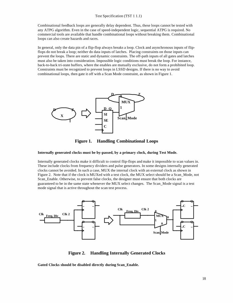
Asynchronous combinational loops must be broken during test.
Test Specification (TST 1 1.1)
18
Combinational feedback loops are generally delay dependent. Thus, these loops cannot be tested withany ATPG algorithm. Even in the case of speed-independent logic, sequential ATPG is required. Nocommercial tools are available that handle combinational loops without breaking them. Combinationalloops can also create hazards and races.
In general, only the data pin of a flip-flop always breaks a loop. Clock and asynchronous inputs of flip-flops do not break a loop; neither do data inputs of latches. Placing constraints on those inputs canprevent the loops. There are static and dynamic constraints. The off-path inputs of all gates and latchesmust also be taken into consideration. Impossible logic conditions must break the loop. For instance,back-to-back tri-state buffers, where the enables are mutually exclusive, do not form a prohibited loop.Constraints must be recognized to prevent loops in LSSD designs. If there is no way to avoidcombinational loops, then gate it off with a Scan Mode constraint, as shown in Figure 1.
Figure 1. Handling Combinational Loops
Internally generated clocks must be by-passed, by a primary clock, during Test Mode.
Internally generated clocks make it difficult to control flip-flops and make it impossible to scan values in.These include clocks from frequency dividers and pulse generators. In some designs internally generatedclocks cannot be avoided. In such a case, MUX the internal clock with an external clock as shown inFigure 2. Note that if the clock is MUXed with a test clock, the MUX select should be a Scan_Mode, notScan_Enable. Otherwise, to prevent false clocks, the designer must ensure that both clocks areguaranteed to be in the same state whenever the MUX select changes. The Scan_Mode signal is a testmode signal that is active throughout the scan test process.
Figure 2. Handling Internally Generated Clocks
Gated Clocks should be disabled directly during Scan_Enable.
Scan_Mode
MUX
0
1
D Z
X
D ZSI
SE
C
D Q
Scan_Mode
MUXClk
0
0
10
Freq. DivClk 2
Freq. Div
D Q
D Q
D Q
D Q
Clk Clk 2C
C

Test Specification (TST 1 1.1)
19
Gated clocks are sometimes used for power reduction, or just as a design style. The problem with gatedclocks is they can make it impossible to scan in values. If clock gating is employed, clocks used duringscan operations should have any clock gating disabled during the scan-in and scan-out process. In thecase where gated clocks must exist, there are two possible solutions… MUX the data with the flip-flopoutput or add a MUX that will use the clocks directly during Scan_Enable. These two approaches areillustrated in Figure 3.
Figure 3. Handling Gated Clocks
Sequential-controlled asynchronous Set/Reset should be disabled during Scan_Mode.
Sequential controlled asynchronous set or reset can destroy the data during scan operation. Thus, certainpattern combinations will not be able to be scanned in, and the coverage will drop dramatically.However, in the cases where it is absolutely necessary, the asynchronous set or reset can be disabledduring Scan_Mode, as shown in Figure 4.
Figure 4. Handling Sequentially Controlled Asynchronous Set/Reset
Bus conflicts should be prevented during scan in and scan out operations
M U X0
1
Scan_Enable
CLK
EN
CLK
EN
M U X0
1
EN
CLK
Q
Q
Q
DC
DC
D
C
Scan_Mode
Q
Q
Q
QD
C
D
C
D
C
D
C

Test Specification (TST 1 1.1)
20
A bus conflict occurs when two drivers are driving different values on the same bus. This can causeserious damage to the chip. It is important to prevent bus conflicts not just during normal operation, butalso during scan. An example of preventing conflicts is shown in Figure 5. In the first part, bus conflictsduring normal operation cannot occur. However, both flip-flops could have a value of one (1) duringscan, turning on both drivers and burning the chip. The solution shown here will prevent any busconflict.
Figure 5. Handling Bus Conflicts During Scan
3.2.3.2. DFT Guidelines
All latches should be transparent during Test Mode.
Latches cannot be scanned unless they are converted into flip-flops. This action results in an extremelylarge area overhead with clock faults that are still not detectable. If the latches are part of memory, itmight be best to model all the latches together as a memory. This approach would imply that specialmanual patterns will be needed for the latches. Using a memory model would reduce the difficulty ingenerating patterns for faults near the latches.
A more general solution is to make the latches transparent during test mode (see Figure 6). This solutiontakes care of the problem of propagating fault effects through the latches. However, the enable faults onthe latches become completely untestable. The lockup latches are excluded.
Figure 6. Making Latches Transparent in Test Mode
Shadow logic around the memory should be controllable and observable.
Apart from the memory itself, logic preceding and following the memories can only be tested bypropagating values through the memories. The most efficient way to do this is to add a special test modeto write to a known address and read from that address. This would make the memory appear as simplebuffers to the rest of the design.
Scan_Enable
Q
Q
Q
Q
D
C
D
C
D
C
D
C
Q Q
Scan_Mode
D
G
D
G
EN
EN

Test Specification (TST 1 1.1)
21
3.2.4. Logic Built-In Self Test (BIST)
Logic BIST is a design technique that allows the circuit to test itself using on-chip test pattern generatorsand output response analyzers, which usually are some form of a Linear Feedback Shift Register (LFSR).
In a typical BIST methodology for random logic, the functions performed are based on popular scandesign techniques. This methodology is implemented by adding a Pseudo-Random Pattern Generator(PRPG) to the inputs of the scan chains and a Multiple Input Signature Register (MISR) to the outputs ofthe scan chain. A BIST controller generates all of the waveforms needed for repeatedly loading thepseudo-random patterns into the scan chains that initiate a functional cycle (capture cycle) and forlogging the captured responses out into the MISR. The MISR compresses the accumulated responses intoan error-detecting code, also called a "signature." That is, any corruption in the register's final state at theend of the test indicates a defect in the chip (see Figure 7.)
Figure 7. Typical Logic BIST Architecture
3.2.4.1. Guidelines for Implementing BIST Design
This section provides the basic guidelines that must be followed for the implementation of logic BIST.The user should refer to internal guidelines for specific implementation dependent rules. It is assumedthat the users have adopted scan guidelines before logic BIST.
• The logic being tested must have deterministic output values over the set of possible inputs• (no floating or undefined states).• The algorithm used in generation and checksum must be guaranteed to not repeat over the
number of tests applied.• To effectively run a BIST test in parallel with other BIST tests, the BIST infrastructure must
automatically shut off after the specified number of burst cycles/clocks has been issued.• To facilitate manufacturing debug, the BIST structure should supply the ability to read out the
intermediate signatures and status of registers and storage elements.• The VC Provider must provide a protocol for initiating and running the self-test logic.• The fault coverage for the BIST vectors (pseudo-random vectors) should be generated using
fault simulation.• The VC Provider should also generate a signature for the final manufacturing BIST vectors.
Comb Logic(full scan)
LFSR
MISR
BISTcontrol

Test Specification (TST 1 1.1)
22
3.2.5. Memory Test
The testing of embedded memory is different from the testing of random logic. Additional fault modelsare used in memory testing due to the high density of the memory blocks. No Automatic Test ProgramGenerator (ATPG) is needed, because of the regularity of the structure of a memory block. Instead,different forms of march tests are applied, depending on the fault models used. A march test consists ofsequences of read and write operations.
3.2.5.1. Memory BIST
Memory BIST is similar to the regular BIST design, except that the on-chip test generator generatesdeterministic memory test patterns. Most of these patterns are called march tests. A typical march test isa finite sequence of operations, such as read or write, that are performed on each cell in the memory inturn, in decreasing or increasing address order. A typical memory BIST implementation consists of aBIST controller (sequence and timing generator and a comparator) and a collar around the memory (seeFigure 8). The comparator does not need to be a complex MISR, as in the case of logic BIST. The collarconsists of multiplexing logic enabling the memory to be fed by the BIST controller rather than by userlogic.
3.2.5.2. Scan-Based Memory Test
Instead of vector generation internal to the chip, the march patterns can also be generated external to thechip and applied to the memory through scan chains. It is necessary that the scan chains have access tothe embedded memory, so the memory test patterns can be scanned into the scan chain and applied to thememory and the resulting outputs can be clocked into the scan chain and shifted out to an observableoutput. During the scan operation, the write of the memory should be disabled.
Figure 8. A Typical Memory BIST Architecture
3.2.6. IDDQ Test
IDDQ is defined as the current that exits in a CMOS circuit when all logic states have settled and are in asteady state response. The IDDQ test method measures the quiescent power supply current of CMOS ICfor select test vectors (logic states) and provides a clear indication of defects, failure mechanisms, andmany types of design errors. Any defect that causes higher IDDQ than the assumed threshold value canbe detected by monitoring IDDQ. Figure 9 illustrates a CMOS device, with gate oxide shorts and defect,causing high IDDQ.
User Address
User Data
User Control
BIST Data
BIST Address
BIST ControlBIST Sequencer,
Timing Gen& Comparator
COLLAR
RAM

Test Specification (TST 1 1.1)
23
Figure 9. An Example of a CMOS Device With Defect
3.2.6.1. Design Guidelines for IDDQ Testability
This section describes some of the common design guidelines that should be observed in order to makethe design IDDQ testable.
• Provide test mode access to disable free running oscillators. Ensure that any internal oscillatorcan be stopped or isolated from the digital VDD and GND. Any signal that cannot be changedfrom switching values will prevent IDDQ from decreasing to a quiescent value, resulting innever being able to read a true IDDQ value on the tester.
• Ensure no floating nodes. Floating nodes are nodes that are not driven to any value. Such nodesare likely to drift in voltage and cause other gates to be turned at least partially on. This wouldcause the IDDQ current in the nominal circuit to be very high.
• Recognize the need to access/control the internal clocks.• Ensure the same state for the pulled net and the pull register. At the primary VC input modes
with pullups/pulldowns, where pullups or pulldowns can not be effectively disabled, IDDQ canbe measured only when the pulled net is in the same state as the pull resistor (for pullups, IDDQcan be measured only when the pulled net is "1").
• Avoid contention on internal buses. If a bus is driven by two sources and each source drives to adifferent value, then the IDDQ current would increase dramatically.v For internal tri-state buses, design a test mode with which these buses can be held in a
driven configuration for IDDQ.v Do not allow internal drive conflicts due to multiple enabled drivers on one bus. Multiplex
the driver enable ports to insure that only one driver is active at any given time.v Do not allow nodes to float when all drivers on a tri-stated bus are turned off. Use bus
repeaters (keeper latches) to hold values when the bus is not drive.• Provide a test mode to disable RAM speed up currents or to set RAM in standby mode, if the
design has embedded RAMs.• Provide separate power supply pins and rails for digital and analog sections of a mixed signal
design. This allows IDDQ to be measured on the digital section independent of the analogsections.
no defect
Vin
defect
Vdd
Vout
Vss
Vout
Vin
Iddqdefect

Test Specification (TST 1 1.1)
24
• Ensure that analog VDD and GND are not connected to digital VDD and GND. Analog circuitscan have very high currents, which invalidate IDDQ testing. The use of separate VDD and GNDpins for analog circuits ensures their high current does not affect the IDDQ test.
• Provide for partitioning of large designs. For designs above 1M transistors, the sum of eachtransistor's leakage could approach the value of the IDDQ test's threshold value. Partitioning thedesign into smaller sections, each with separate power pins, can help avoid the loss of IDDQsensitivity.
• Provide a mode for dynamic logic so that it consumes minimum power. As a result of theirdesign, dynamic circuits will typically have high current, even when they are stable. A specialmode is needed to ensure that this high current does not occur when testing IDDQ. If no IDDQtest is to be applied to the VC, then the mode can disable the logic altogether.
3.3. Isolation
Isolation is a mechanism by which the input and output ports of a VC are electrically detached fromother VCs and user logic. A VC is isolated avoid corruption of data applied to its inputs because of otherVCs in the design (internal testing). Isolation of the VC is also necessary to allow for testing (externaltesting) other parts of the system chip, such as other VCs and UDL.
Isolation is often confused with access. However, the two are very different. Access refers to a test datatransfer mechanism. That is, how the test is applied to the VC from the pads of the chip, and how theresults of the test are observed at the pads of the chip. Isolation is concerned with protection of the VCfrom other VCs and UDL.
A VC may have a perfect access mechanism without considering isolation. In a system chip with such aVC, though patterns are applied to other VCs, the patterns may become corrupt due to the lack ofisolation. On the other hand, a VC may have been properly isolated, but with no access. In such asystem chip, though the VC is prepared for test application, there is no way to get the test to it. Thisaddresses only test isolation. Rules and guidelines for test access will be provided in a subsequentrevision of this document.
The task of isolation is a joint effort between the VC Provider and the VC Integrator. The VC Providerneeds to define the mechanism for isolation of his/her VC. The VC integrator needs to ensure that eachVC can be isolated, once it is included in the design. This section focuses on the isolation issues from theVC Provider perspective.
3.3.1. Isolation Rules
This section identifies the reasons and rules for isolation. Both input and output isolation issues areaddressed. The requirements for creating a safe state are also discussed. In many of the figures in thissection, a circuit with a problem due to lack of isolation will be followed by a circuit with an example ofa solution to the problem. It is important to stress that the solutions shown here are only examples of themany ways the requirements can be satisfied, and are intended for illustration only.
3.3.1.1. Output Isolation
Output isolation involves electronically detaching, in a test mode, the output ports of the VC from thelogic driven by these outputs in system mode.
The outputs of a VC can affect the inputs and outputs of other VCs. If two VCs drive the same bus, usethe following rule. If one VC is under test, the second VC should ensure that it is not driving the samebus. For example, in Figure 11a, suppose VC2 is the current VC under test. With no output isolation,VC1 can drive a 0 on the output when VC2 is driving a 1. It is important to ensure that the tri-statedriver in VC1 is turned off during the test of VC2. This has to be controlled from the input of the VC.An example of doing this is shown in Figure 11b. Here, when testing VC2, I1 is set to 1 to isolate VC1,I2 is set to 0 to allow VC2 access to the bus.
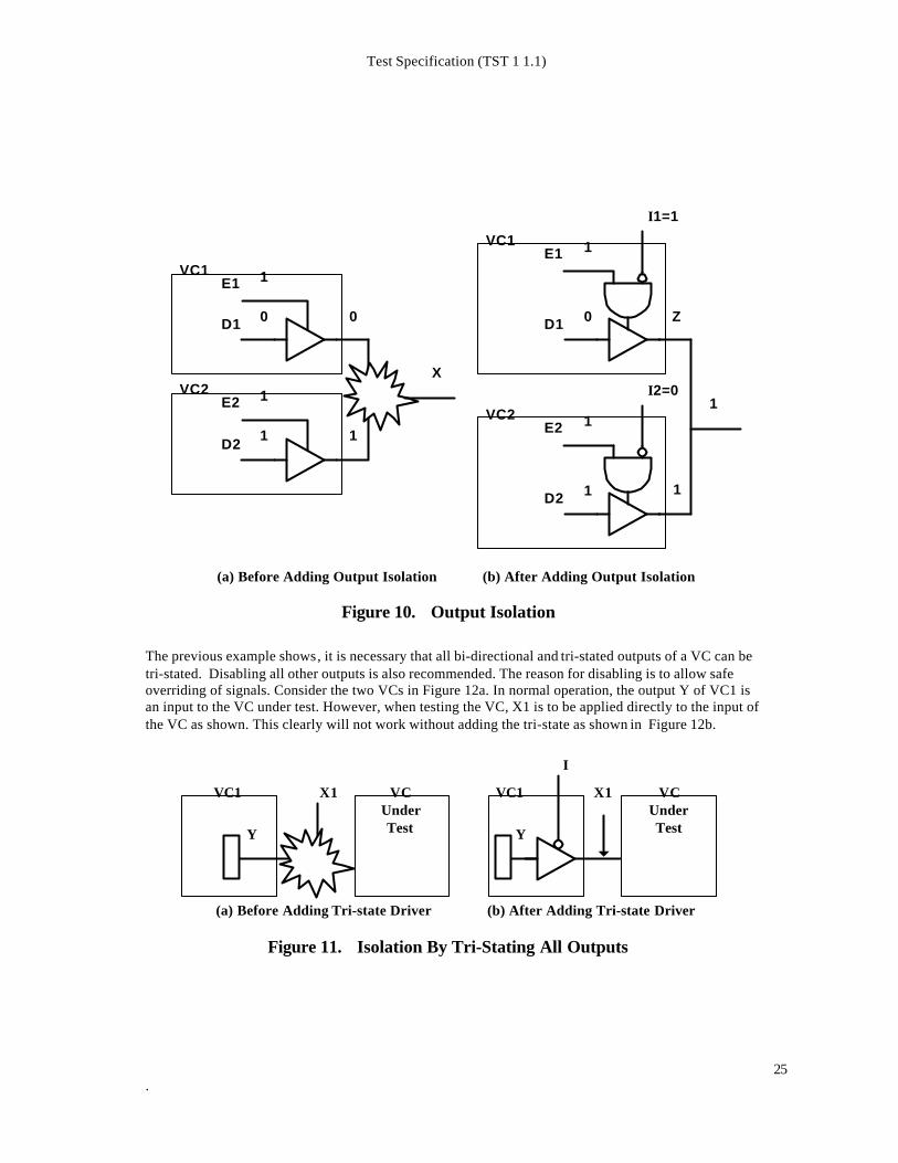
Test Specification (TST 1 1.1)
. 25
(a) Before Adding Output Isolation (b) After Adding Output Isolation
Figure 10. Output Isolation
The previous example shows, it is necessary that all bi-directional and tri-stated outputs of a VC can betri-stated. Disabling all other outputs is also recommended. The reason for disabling is to allow safeoverriding of signals. Consider the two VCs in Figure 12a. In normal operation, the output Y of VC1 isan input to the VC under test. However, when testing the VC, X1 is to be applied directly to the input ofthe VC as shown. This clearly will not work without adding the tri-state as shown in Figure 12b.
(a) Before Adding Tri-state Driver (b) After Adding Tri-state Driver
Figure 11. Isolation By Tri-Stating All Outputs
E1 1
0D1 0
VC1
E2 1
1D2
1
VC2X
0D1 Z
1
I1=1
E1 1VC1
1D2
I2=0
E2 1VC2
1
VC1
Y
VCUnderTest
X1
I
VC1
Y
X1 VCUnderTest

Test Specification (TST 1 1.1)
26
3.3.1.2. Input Isolation
Input isolation involves electronically detaching, in a test mode, the inputs of a VC from the logic thatdrives these inputs in system mode.
Protection from Illegal Inputs.
The main reason for input isolation is to protect the VC from illegal input combinations. For example,consider the circuit in Figure 13a. Here E1 and E2 are direct inputs of VC2. VC2 never expects E1 andE2 to be 1 simultaneously. However, a test for VC1 may generate such a condition. Such a conditionwill cause a conflict on Y in VC2, and could damage the entire chip. In normal operation, the conflictwill not occur because the overall design will guarantee this condition does not occur. In Figure 13b, afew gates are added to guarantee no conflict occurs. The AND gate guarantees that the tri-state driver isturned off during test mode (I=1), while the OR gate guarantees that the second tri-state driver is turnedon. This design not only guarantees no conflicts but also no floating bus. It is important to avoid floatingconditions to allow for IDDQ testing.
(a) Before Adding Input Isolation (b) After Adding Input Isolation
Figure 12. Testing VC1 Resulting in Conflict in VC2
Protection from other VCs that may not have appropriate isolation.
To avoid reliance on output isolation in other VCs (see Section 3.3.1.1), it is required that a VC include amechanism to allow its inputs to be isolated from other circuitry while testing the VC. Consider thefollowing example in Figure 13a. Here, VC1's outputs have not been properly isolated. Therefore, if X1is applied as shown, the data applied to the VC under test will be corrupted and damage is likely tooccur. Figure 13b shows how isolating the input will prevent data corruption.
(a) Without Input Isolation (b) With Input Isolation
Figure 13. Input Isolation by Addition of Multiplexer
VC1E1=1
D2=1
E2=1
D1=0
VC2
0
1
Y
VC1 E1=1
D2=1
E2=1
D1=0
VC2
1
I=1
Y
1
I
1VC1 VC
UnderTest
X1 VC1
X1
VCUnderTest
MUX1
0
1

Test Specification (TST 1 1.1)
27
3.3.1.3. Safe State
The previous discussion can be generalized to the notion of guaranteeing a safe state. A safe state of aVC is a state that cannot cause damage to the VC or system regardless of the inputs being applied to theVC. A safe state may also require that some or all the bi-stable elements be in a known initial state. Forexample, in Figure 14a, if FF1 and FF2 are not in a known state, Z could be floating or in contention.Figure 14b shows a simple approach to ensure a proper initial state. If IDDQ is a method used for testingthe VC, it will also be important to ensure that this safe state is a low current state. Such a state shouldadhere to IDDQ guidelines (Section 3.2.6.1).
(a) No Initialization Resulting in Unsafe State (b) One Method for Initialization
Figure 14. Flip-Flop Initialization Required for Safe State
3.3.2. Isolation Mechanisms
Isolation mechanisms may be implemented by using VC test collar hardware structures that have beenadded specifically for test purposes or by utilizing system logic that is already present in the VC. In bothcases isolation protocols are used to activate the isolation mechanisms. Each of these mechanisms willbe discussed separately.
3.3.2.1. Isolation Protocol
The isolation protocol can be a simple protocol if the VC Provider designs an extra input bit for isolationthat guarantees the VC will be in input and output isolation. When this input is active: all tri-stableoutputs will be turned off , and all other inputs to the VC would not be able to put the VC into an unsafestate.
The VC Integrator needs to ensure that a VC's isolation signal is active when applying a test not relatedto this VC. If there are many modes needed apart from isolation (for example, many functional modesthat the VC Provider is including in the design), it might be reasonable to add an isolation mode insteadof a single pin. In such a case, the VC Provider must properly define the isolation mode.
Another possibility is for the VC Provider to provide a sequential protocol. This protocol is a sequence ofinputs guaranteeing the VC will be in input and output isolation. An example of a sequential protocol isthe writing of a particular value to a particular register. Once in a safe state, the VC will remain in thissafe state until another protocol (possibly a reset) is applied to the VC. Any other input applied to theVC, while in a safe state (including the safe-state protocol), does not create an unsafe state.
FF1
FF2 Z
I
0
1
0
D1=0
D2=1
0
FF1
FF2
Q
S
RQ

Test Specification (TST 1 1.1)
28
3.3.2.2. Test Collar
A test collar is a test structure around the VC to be used for both access and isolation. Such a shell cancompletely isolate the VC from the rest of the system chip. There are several types of test collars. Thesimplest combinational technique is the use of multiplexers to isolate the inputs and the outputs.Multiplexers at the inputs of the VC are used to select values that guarantee a safe state (see figure 15).This structure can isolate both inputs and outputs. Figure 15 shows the inputs are isolated. The outputscan be isolated by directly using I, the Isolation Control signal, to disable all outputs with a tri-state. Ofcourse, multiplexers need not be used on the output side.
I
N VCM U X
N - Normal inputs to VCIV - Isolation Values to VCI - Isolation ControlX - VC Inputs
IV
X
Figure 15. Test Collar Using Multiplexers for Isolation
Test collars can also be built using latches and flip flops to form a scan chain around the VC. The collarsare used to control the inputs to the VC (see Figure 17). Such mechanisms are referred to as sequentialmechanisms, because several cycles are needed to get the data to the inputs. In Figure 16, the TCC (TestCollar Cell) is similar to the boundary scan cell of JTAG. (See the IEEE 1149.1 document for moreinformation on boundary scan.) Isolation values are shifted in. After the shifting is complete, I isswitched to access the shifted values.
I
X
VCMUX
N - Normal inputs to VCIV - Isolation Values to VCI - Isolation ControlX - VC Inputs
MUX
MUX
MUX
N
IV
TCCs
Figure 16. Test Collar Using Bi-Stable Elements to Shift in Isolation Values

Test Specification (TST 1 1.1)
29
A variation of the test collar approach is shown in Figure 17. Here the bi-stable elements are used foraccess, and the set and reset are used for isolation. Other isolation approaches, which use complexsequential approaches to isolation, will be discussed in the next phase of this document under TestAccess Requirements.

Test Specification (TST 1 1.1)
30
Figure 17. Reset Bi-Stables to Isolation Values
One problem with the sequential approach is the possibility of a long test application time. A solution forthe problem is to use multiple shift registers. Scan test applications in a regular design have a verysimilar problem. Multiple chains are often used to speed up the test application time.
I
X
VCMUX
N - Normal inputs to VCIV - Isolation Values to VCI - Isolation ControlX - VC Inputs
MUX
MUX
MUX
N
IV
Set/ResetControl

Test Specification (TST 1 1.1)
31
Appendices

Test Specification (TST 1 1.1)
32
Appendix A: VC Test Strategy Form (Example)
VC Test Strategy Form
VC ProviderVC NameModification Date
Strategies (check all that apply)
Functional Iddq
Scan Other:
BIST
Test Completeness Table
ParameterName
Tested ? Test Module Comments
Testability Issues (non-conformances require additional documentation)
Scan conforms to scan guidelines in section 3.2.2 Yes No N/A
DFT conforms to DFT rules in section 3.2.3.1 Yes No N/A
Logic BIST conforms to guidelines in section 3.2.4.1 Yes No N/A
Memory conforms to guidelines in section 3.2.5 Yes No N/A
IDDQ conforms to section 3.2.6.1 Yes No N/A
Isolation Protocol
Input Isolation Yes No If yes, Test Module:
Output Isolation Yes No If yes, Test Module:

Test Specification (TST 1 1.1)
.
. 33
Appendix B: VC Test Module Form (Example)
VC Test Module
VC ProviderVC NameModification Date
Overview
Target Use (check all that apply)
Wafer Sort Characterization Laser Repair
Package Test Burn-in / Stress Testing Laser Trim
Silicon debug Functional Verification Other
Test Modes (list all Test Modes utilized by this Test Module)
Implementation
Test Protocol Test Modules (please list)
Fault Coverage
Fault CoverageFault ModelFault Simulator
Constraints
Diagnostic or Characterization information
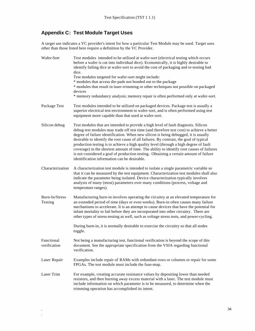
Test Specification (TST 1 1.1)
.
. 34
Appendix C: Test Module Target Uses
A target use indicates a VC provider's intent for how a particular Test Module may be used. Target usesother than those listed here require a definition by the VC Provider.
Wafer-Sort Test modules intended to be utilized at wafer-sort (electrical testing which occursbefore a wafer is cut into individual dice). Economically, it is highly desirable toidentify failing dice at wafer-sort to avoid the cost of packaging and re-testing baddice.Test modules targeted for wafer-sort might include:* modules that access die-pads not bonded out to the package* modules that result in laser-trimming or other techniques not possible on packageddevices* memory redundancy analysis; memory repair is often performed only at wafer-sort.
Package Test Test modules intended to be utilized on packaged devices. Package test is usually asuperior electrical test environment to wafer-sort, and is often performed using testequipment more capable than that used at wafer-sort.
Silicon debug Test modules that are intended to provide a high level of fault diagnosis. Silicondebug test modules may trade off test time (and therefore test cost) to achieve a betterdegree of failure identification. When new silicon is being debugged, it is usuallydesirable to identify the root cause of all failures. By contrast, the goal of typicalproduction testing is to achieve a high quality level (through a high degree of faultcoverage) in the shortest amount of time. The ability to identify root causes of failuresis not considered a goal of production testing. Obtaining a certain amount of failureidentification information can be desirable.
Characterization A characterization test module is intended to isolate a single parametric variable sothat it can be measured by the test equipment. Characterization test modules shall alsoindicate the parameter being isolated. Device characterization typically involvesanalysis of many (most) parameters over many conditions (process, voltage andtemperature ranges).
Burn-In/StressTesting
Manufacturing burn-in involves operating the circuitry at an elevated temperature foran extended period of time (days or even weeks). Burn-in often causes many failuremechanisms to accelerate. It is an attempt to cause devices that have the potential forinfant mortality to fail before they are incorporated into other circuitry. There areother types of stress-testing as well, such as voltage stress tests, and power-cycling.
During burn-in, it is normally desirable to exercise the circuitry so that all nodestoggle.
Functionalverification
Not being a manufacturing test, functional verification is beyond the scope of thisdocument. See the appropriate specification from the VSIA regarding functionalverification.
Laser Repair Examples include repair of RAMs with redundant rows or columns or repair for someFPGAs. The test module must include the fuse-map.
Laser Trim For example, creating accurate resistance values by depositing lower than neededresistors, and then burning away excess material with a laser. The test module mustinclude information on which parameter is to be measured, to determine when thetrimming operation has accomplished its intent.

Test Specification (TST 1 1.1)
.
. 35
Appendix D: VC Test Mode Form
VC Test Mode
VC ProviderVC NameModification Date
Overview
Target Use (check all that apply)
Wafer Sort Burn-in / Stress Testing AccessPackage Test Functional Verification ControlSilicon debug Laser Repair Input Isolation
Other________________
Characterization Laser Trim Output Isolation
Test Protocol
Assertion Sequence (please list) Test Modules (please list)
Disabling Sequence (please list) Test Modules (please list)
Constraints
Diagnostic or Characterization information

Test Specification (TST 1 1.1)
36
Appendix E: Test Mode Target Uses
This section lists categories of test modes that are commonly utilized in VC testing. Test mode targetuses may include these categories in addition to those identified in test module target uses.
Access A VC that is composed of multiple VCs may provide test access to the embeddedVCs. In this case, if it is necessary for the test integrator to utilize this test accessmechanism, then the VC provider shall describe such test access as a test mode.
Control This test mode defines the affecting parameter's testing, accessing, and isolationprocedures to the VC.
Isolation During VC testing, it is normally necessary to isolate a VC from the surroundingcircuitry. Input isolation causes the VC to desensitize its inputs. Output isolationcauses the VC to stabilize its outputs to prevent driving the surrounding circuitry inan unusual manner. The target use of isolation indicates the test mode achieves bothinput and output isolation. See Section 3.3 for a precise description of isolation.
Input Isolation The test mode achieves input isolation.
Output Isolation The test mode achieves output isolation.
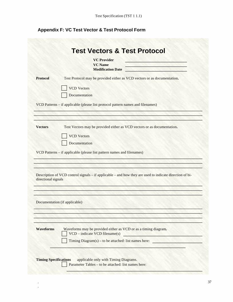
Test Specification (TST 1 1.1)
.
. 37
Appendix F: VC Test Vector & Test Protocol Form
Test Vectors & Test ProtocolVC ProviderVC NameModification Date
Protocol Test Protocol may be provided either as VCD vectors or as documentation.
VCD Vectors
Documentation
VCD Patterns – if applicable (please list protocol pattern names and filenames)
Vectors Test Vectors may be provided either as VCD vectors or as documentation.
VCD Vectors
Documentation
VCD Patterns – if applicable (please list pattern names and filenames)
Description of VCD control signals – if applicable – and how they are used to indicate direction of bi-directional signals
Documentation (if applicable)
Waveforms Waveforms may be provided either as VCD or as a timing diagram.VCD – indicate VCD filename(s)
Timing Diagram(s) – to be attached: list names here:
Timing Specifications applicable only with Timing Diagrams.Parameter Tables – to be attached: list names here:

Test Specification (TST 1 1.1)
.
. 38
Appendix G: VCD Cyclization
A VCD vector set is considered "cyclizable" if it has been processed with the following "Sequence-Preserving Transformation":
Step 1 Clock Normalization For each external clock define an integral multiplier with the highestfrequency clock, or define a phase relationship with the highestfrequency clock, in order to completely preserve the transitionsequences of all edges in a given set of VCD vectors. If this is notpossible, then the test pattern is uncyclizable. The highest frequencyclock will be considered the test cycle.
Step 2 Input Normalization For each input signal, define the minimal set of transitions starting at thebeginning of the test cycle that will completely preserve the transitionsequences of inputs, constrained by each clock (i.e. setup, hold andrecovery times) and by each other, in a given set of VCD vectors. If thisis not possible, then the set of VCD vectors is uncyclizable.
Step 3 Output StrobeNormalization
For each output, define the minimal set of transitions, starting at the endof a test cycle, that will completely preserve the expected "value" ofeach vector in the set of VCD vectors. If this is not possible, then the setof VCD vectors is uncyclizable. (Note: "unknown values" must beconsidered as part of this strobe normalization process.)Current practices show that most ASIC vendors can check a set of VCDvectors against a given timeset without simulation. However, a cyclizedset of VCD vectors must pass both best and worst process / voltage /temperature cases in test pattern verification (simulation).
Test Specification (TST 1 1.1)
39
Appendix H: Manufacturing Test Glossary of Terms
Access Any mechanism by which signals may be propagated to and from a VC either fromencapsulating circuitry or from the primary inputs and outputs of the system chip.
ATE An acronym for automatic test equipment, commonly known as testers.Control Signals In VCD utilization, a control signal is used to represent the direction of bi-
directional signals. (VCD does not implicitly contain direction information.)Cyclization The process by which discrete time signals (such as supplied in VCD) are mapped
to a representation amenable to automatic test equipment.
Defect(s) Term used to reference specific flaw(s), physical or chemical imperfection(s), on amanufactured device. Most defects can be detected and measured by a failureanalysis group. Specific devices that do not perform as expected contain defect(s)or have design flaws.
DNRZ The acronym for the cyclic timing format, delayed non-return to zero.
DFM Acronym for design for manufacturing. This is the acronym used to defineactivities done during the design process (by designers) to ensure that the design isoptimized for the fab process that will create the product.
DFT Acronym for design-for-test. This is the acronym used to define activities doneduring the design process (by VC Providers) to provide the ability to control andobserve on silicon needed by test integrators to determine the quality of theproduct.
Fault(s) Term used in reference to classes, or concepts, of defect types. The most commonof these is the stuck at type, or fault class. In the EDA and academic worlds, a faultis a software model of a defect.
Fault Coverage The percent (%) of success a test program has in finding (or uncovering ) simulatedstuck at 0/1 faults over a defined device node list. Fault coverage may be extendedto other fault model types. A general definition of fault coverage is the percentageof all faults checked on a particular fault model. A coverage figure should be givenfor each model type tested. As the operator defines the nodes to be evaluated, or,the operator defines lists of nodes not to be used in the task, the raw number haslittle meaning without a full analysis of the set up.
Input Delay Time A time-domain signal that sets the transition from the previous "level" to new"level". "Input delay time" is specified relative to the vector transition time.
Input Isolation Any mechanism for isolating the inputs of a VC from the surrounding circuitry, sothat the VC completely ignores these inputs. This may be useful while testing thesurrounding circuitry to prevent unintentional behavior in the VC.
Input PulseDelay
A time-domain signal, applicable only to RZ and RTO formats, that sets theduration in which a "level" remains unchanged before transition to thepredetermined "level".
Input PulseWidth
An "input pulse" is two successive transitions on an input pin from one 0/1 value tothe opposite value, and back again. The "input pulse width" is the difference in timebetween the two transitions.
Test Specification (TST 1 1.1)
. 40
Levels A guide to the interpretation of electric circuit node signal strengths as logic states.
ManufacturingTest
This term will be used to convey completeness of the test. It applies to all ATE testrelated activities performed by VC providers, VC integrators, semiconductorproviders, and fab / assembly / test providers. Manufacturing test is the physicalprocess of validating and debugging the performance and functional operation ofsemiconductor products. Physical testing over the manufacturing lifetime of adevice includes but is not limited to, validation, characterization, production test,and failure analysis.
Node The I/O ports of a VC (This helps to further distinguish a test pattern from thevalidation environment.) or terminals of a VC (the P1500 term).
NRZ The acronym for the cyclic timing format, non-return to zero.
Output Isolation Any mechanism for isolating a VC's outputs from the surrounding circuitry, so thatthe surrounding circuitry may be tested without contention from the VC. Partialoutput isolation is the case where the VC can isolate some, but not all outputs.
Output StrobingTime
The time at which the "value" of an output port is expected to be at the correctresponse with respect to a test pattern.
Pattern A sequence of vectors.
Patterns Test vectors used to test a VC. Test vectors should include stimuli to be applied onthe VC input pins and expected values to be measured at the VC output pins. Testvectors should be machine readable. Test vectors should be either in a cycle basedformat or in an event-based format that contains proper pin waveform information.Proper pin waveform information allows for event-based vectors to be converted tocycle-based vectors by a machine.
RTO The acronym for the cyclic timing format, return to one.
RTZ The acronym for the cyclic timing format, return to zero.
Strobe window A time-domain signal that sets the duration in which the expected response remainsunchanged.
Test Application The process of applying test vectors to the inputs of an ASIC (or VC).
Test Coverage This term defines the coverage of a VC with a specific test vector set using aspecific fault model. Test coverage should be both machine and human readableand should be embedded in the pattern file with which it is associated.
The term also defines the coverage of all specifications and functionality. Thisdefinition of Test Coverage is needed to convey completeness of the test. If adevice is defined as bad for any reason (form, fit, or function), the test coverage isby definition less than complete (less than 100%).
Test Cycle Time A time-domain signal that sets the boundaries of a timeset or the time periodcharacteristic of vector transitions during a test.
Test Method A sequenced set of operations, such that, if the VC under test responds as specified,then that VC under test is presumed free of some set of manufacturing defects. Thesequence of operations includes the stimulation of the VC under test andexamination of the VC under test's response.

Test Specification (TST 1 1.1)
41
Test Mode Any mechanism by which a VC deviates from its normal functional behavior tohelp facilitate its testing from external control, or to test itself (an alternativefunctionality intended for testing).
Test ModeAccess
Defines the access method for controlling a VC's input pins and measuring a VC'soutput pins from chip level input and output pins.
Test ModeControl
Defines a procedure in a machine readable pattern format and/or in a humanreadable format to put a VC into its different test modes from the VC level pins.
Test Mode I/OIsolation
Defines a procedure in a machine readable pattern format and/or in a humanreadable format to put a VC into isolation mode from the VC level pins. A VC inisolation mode means it will not interfere with the testing of other VCs and UDL,and the VC itself will not be damaged during the testing of other VCs and UDL.
Test Module An encapsulation of a test protocol. The test protocol specifies precisely how a testis to be performed. The test module contains additional information such asintended usage, fault coverage, constraints on how the test may be used, anddiagnostic information associated with the test. The test module supplements thetest protocol with information a test integrator will need for appropriate integrationof the system-chip test programs.
Test Pattern See Patterns.
Test Program A set of test patterns and instructions suitable for use in an ATE. A test programcan be used to perform functional, structural (stuck-at fault test) and parametric(AC, DC or other) tests.
Test Protocol A sequence of control operations required to perform a test. A test protocol iscomposed of functions and/or sequences. Functions may consist of other functionsand/or sequences. Sequences are composed of a series of logic 0 and 1 valuesapplied to specified ports. At the lowest level a test protocol is just a series of logic0 and 1 values applied to specified test control ports. A sequence will typicallycontain symbolic references to the test data to be applied to, or observed at,specified test data or system data ports.
Test Vector Test vectors are a precise set of stimuli to the VC, along with the expected responsefrom the VC. For this purpose, test vectors consist of the "1" and "0" vectors, alongwith optional waveform definitions and timing..
Timesets A set of cyclic timing formats, namely RZ, RTO, NRZ, and DNRZ. These timingformats must have appropriate timing information corresponding to each formatand the test cycle time.
Timing The input and output pin waveforms of a VC. Timing should be in a machinereadable format and should be embedded in its respective pattern file. Anotherdefinition is the time-domain relationships among successive vectors in a pattern.
Timing Format The interpretation of a value as a sequence of value changes with fixed, predefinedtime relationships among the successive values that arrive at the given value.
TimingSpecifications
Defines the input and output pin waveforms and characteristics of a VC in a humanreadable format.
Validation Validation is a "post-silicon" process intended to prove (with evidence) the design

Test Specification (TST 1 1.1)
42
to be valid. It is a physical characterization. In this document, validation is any useof special purpose test hardware to prove the product meets the design intent asopposed to other usage of the same equipment as a manufacturing screen.
Value The logic state, drive direction of a node in a digital logic circuit, specifically a VCterminal.
Vector A set of values corresponding to a set of electrical nodes (specifically the set ofterminals of a VC) at an instant in time.
Verification Verification is a "pre-silicon" process. It is normally used during development forgaining confidence that a design will produce a pre-defined result. An output ofverification may be translated into ATE vectors.