


![[DESIGN] Piezo-Piezo to Pie](https://static.fdocuments.in/doc/165x107/5571f8bb49795991698df909/design-piezo-piezo-to-pie.jpg)

Languages
Pages
Legal

Page 1
Doc
umen
t No:
0000
-01-
08-0
0-00
0 (Is
sue
C)
User Guide
This document is subject to change without notice.Document No: 0000-01-08-00-000 (Issue C)Date Published: August 21, 2013
Universal Evaluation Board User Guide
INTRODUCTION The Universal Evaluation Board (UEVB) coupled with the corresponding MeshConnect™ Wireless Module Daughtercard is a complete hardware evaluation and development platform for the MeshConnect Wireless Modules from California Eastern Laboratories (CEL). The evaluation board was designed with the engineer in mind by giving complete access to the wireless module allowing for developing, prototyping and testing of designs.
DEVICE SUPPORT • ZICM357P2-2/2C • ZICM357SPx-1/1C
SupportfornewMeshConnectWirelessModulesmaybeadded in the future.
Tofindthelatestversionofthisdocument,visit:www.cel.com/MeshConnect
FEATURES • USBInterfacetoPCforprogrammingandcontrol withbuilt-inlevelshiftingontheUARTlinesto ensurereliablecommunicationbetweenthePC and the module at different operating voltages • Regulatedpowersupplyfor5-15VDCpower • Fourpush-buttonsforgeneraluse • Four LEDs for general use • PiezoBuzzer • AnalogInputs:TemperatureSensor, PotentiometerandPhotoCell • AllMeshConnectI/Osaccessiblethroughan expansionconnectorandbreakoutboard • On-board8MbitSerialEEPROMfornonvolatile
data storage • 5-15VDCPoweravailableforthedaughtercard
board at unregulated power header • TwoSPDTslideswitchesconnectedtoVCCand
GND for use as control inputs • DIPswitchesconnectedtothemoduleGPIOs
and evaluation board peripherals to allow isolationofGPIOsandboardperipherals • BatterypackwithtwoAAbatteries • ModuleCurrentSenseHeader
Page 2
Universal Evaluation Board User Guide
This document is subject to change without notice.Document No: 0000-01-08-00-000 (Issue C)
Introduction and Overview......................................................................................................................................................... 1
Hardware Description.................................................................................................................................................................... 4
LEDs...................................................................................................................................................................................................... 5
Push-buttons..................................................................................................................................................................................... 5
USB Interface.................................................................................................................................................................................... 6
Serial Flash......................................................................................................................................................................................... 6
Module Connector.......................................................................................................................................................................... 7
Daughtercard Expansion Port................................................................................................................................................... 8
Reset Push-button.......................................................................................................................................................................... 9
Piezo Buzzer...................................................................................................................................................................................... 9
Power LED.......................................................................................................................................................................................... 9
Analog Input Select......................................................................................................................................................................... 10
Potentiometer.................................................................................................................................................................................... 10
Temperature Sensor....................................................................................................................................................................... 11
Photocell /Photo Resistor............................................................................................................................................................ 11
Power Switch..................................................................................................................................................................................... 12
External Power Supply Header................................................................................................................................................. 12
DC Power Jack.................................................................................................................................................................................. 12
Module Current Measurement Header.................................................................................................................................. 12
Unregulated Power Header......................................................................................................................................................... 13
DIP Switches..................................................................................................................................................................................... 13
Protection Diodes........................................................................................................................................................................... 13
SPDT Slide Switches..................................................................................................................................................................... 14
USB Driver and Software Installation..................................................................................................................................... 14
Installing the USB Drivers...................................................................................................................................................................... 15
Installing the New Hardware on the Computer..................................................................................................................................... 16
Locating the COM Port Assignment..................................................................................................................................................... 19
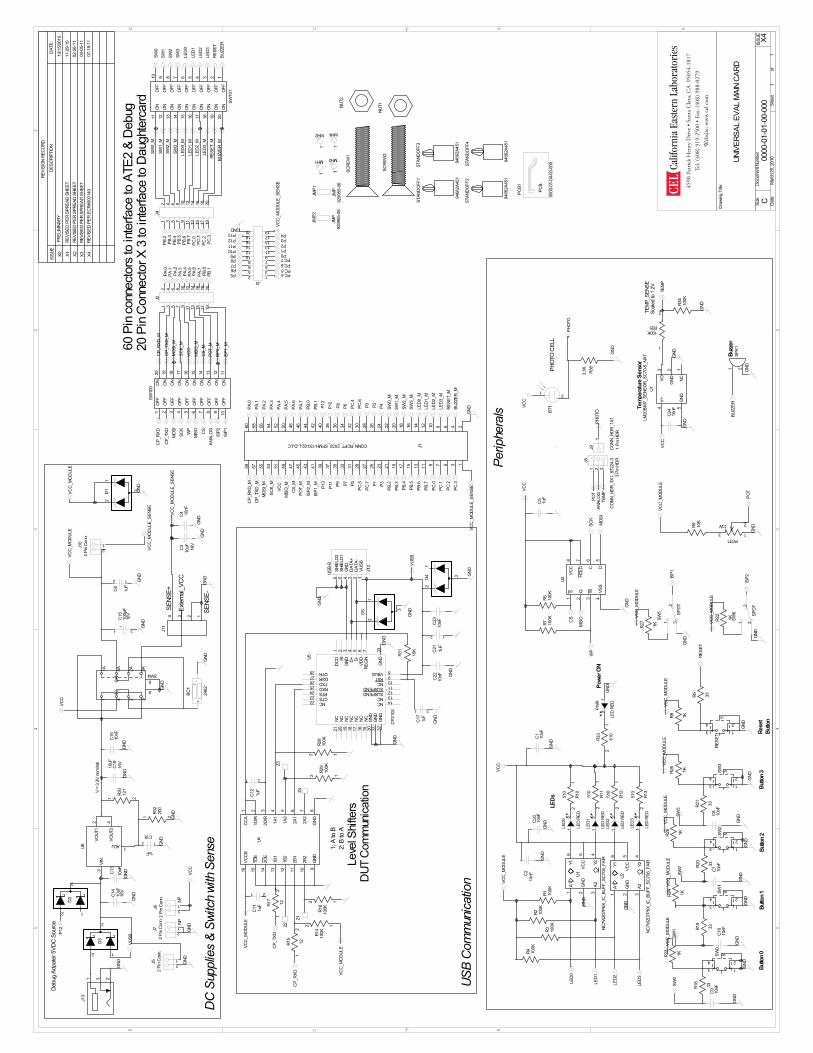
Universal Evaluation Board Schematic................................................................................................................................. 20
Universal Evaluation Board Bill of Materials...................................................................................................................... 21
Addendum: ZICM357P2................................................................................................................................................................ 23
Hardware Description.................................................................................................................................................................... 24
Module Connector................................................................................................................................................................................... 24
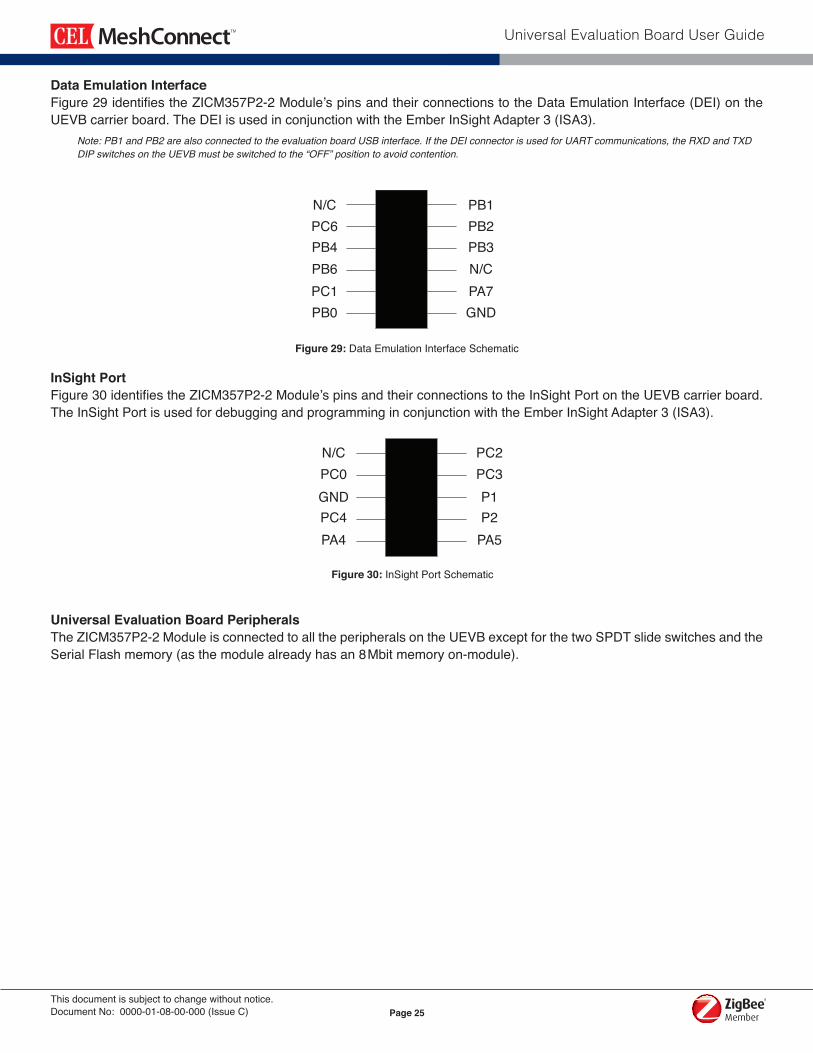
Data Emulation Interface......................................................................................................................................................................... 25
InSight Port.............................................................................................................................................................................................. 25
Universal Evaluation Board Peripherals............................................................................................................................................... 25
Pinout Listing........................................................................................................................................................................................... 26
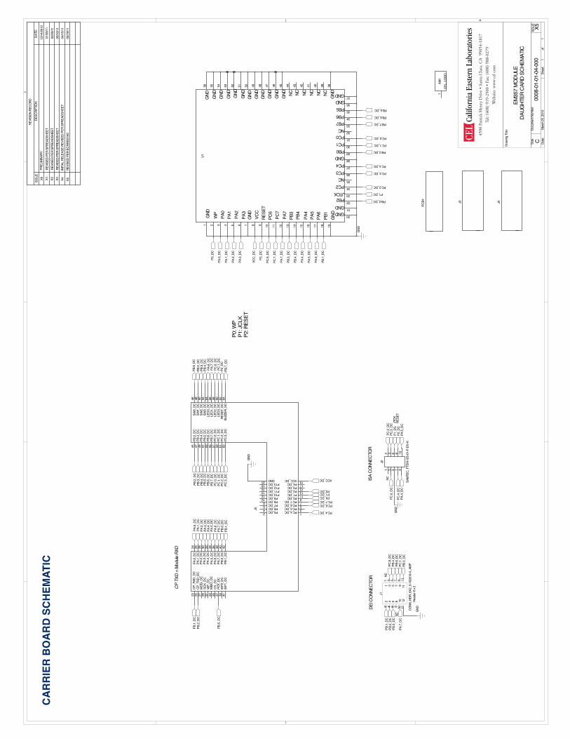
Carrier Board Schematic.............................................................................................................................................................. 28
TABLE OF CONTENTS
Page 3
Universal Evaluation Board User Guide
This document is subject to change without notice.Document No: 0000-01-08-00-000 (Issue C)
ZICM357P2 Module Daughtercard Bill of Materials......................................................................................................... 29
Addendum: ZICM357SPx-1......................................................................................................................................................... 30
Hardware Description.................................................................................................................................................................... 31
Module Connector.................................................................................................................................................................................. 31
Data Emulation Interface........................................................................................................................................................................ 32
InSight Port............................................................................................................................................................................................. 32
Universal Evaluation Board Peripherals............................................................................................................................................... 32
Pinout Listing.......................................................................................................................................................................................... 33
Carrier Board Schematic - EM35xSP..................................................................................................................................... 34
ZICM357SPx-1 Module Daughtercard Bill of Materials................................................................................................. 35
References.......................................................................................................................................................................................... 36
Revision History............................................................................................................................................................................... 36
Page 4
Universal Evaluation Board User Guide
This document is subject to change without notice.Document No: 0000-01-08-00-000 (Issue C)
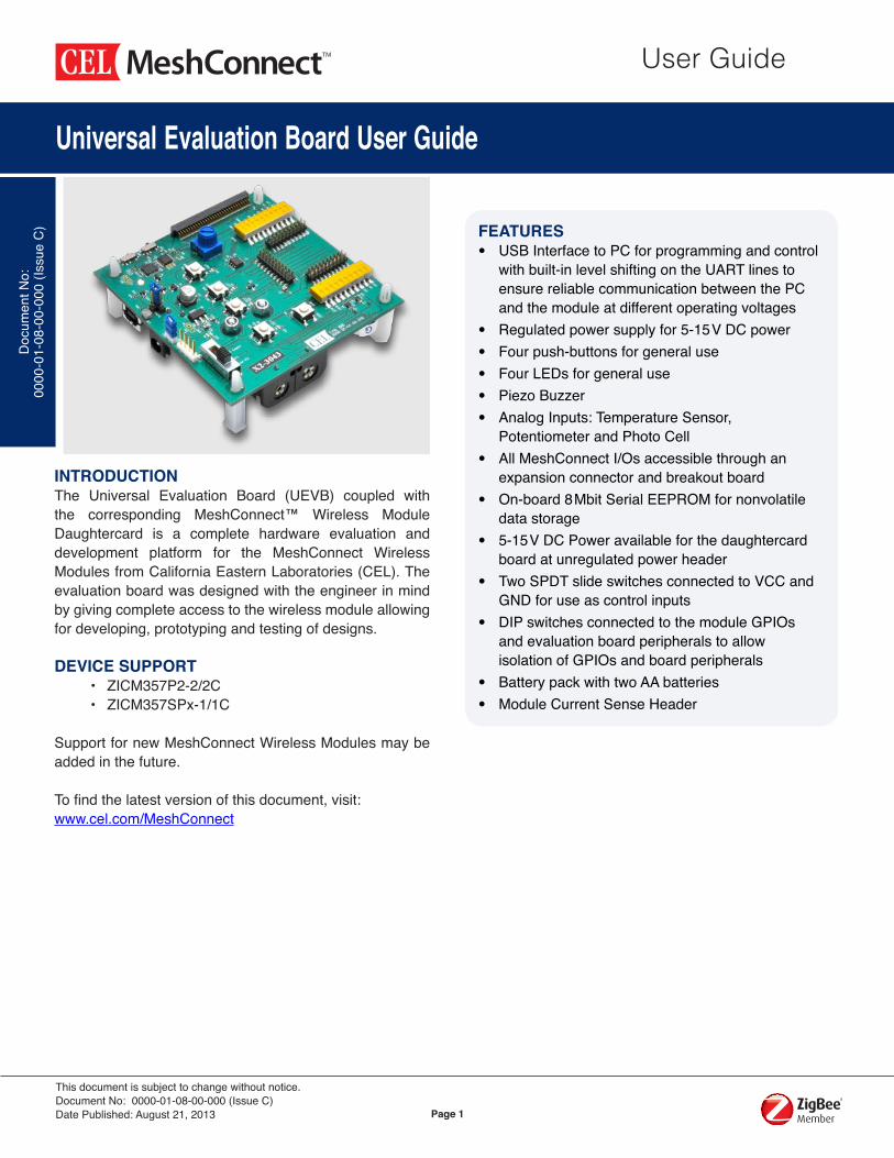
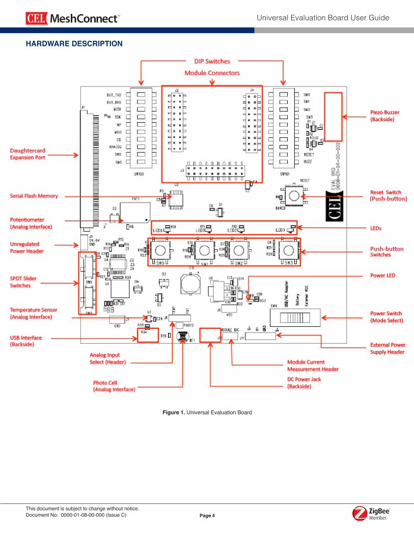
HARDWARE DESCRIPTION
Figure 1. Universal Evaluation Board
Page 5
Universal Evaluation Board User Guide
This document is subject to change without notice.Document No: 0000-01-08-00-000 (Issue C)
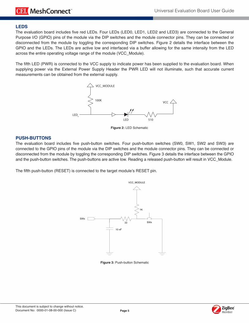
LEDSTheevaluationboardincludesfiveredLEDs.FourLEDs(LED0,LED1,LED2andLED3)areconnectedtotheGeneralPurposeI/O(GPIO)pinsofthemoduleviatheDIPswitchesandthemoduleconnectorpins.Theycanbeconnectedordisconnected from themoduleby toggling thecorrespondingDIPswitches.Figure2details the interfacebetween theGPIOandtheLEDs.TheLEDsareactivelowandinterfacedviaabufferallowingforthesameintensityfromtheLEDacross the entire operating voltage range of the module (VCC_Module).
ThefifthLED(PWR)isconnectedtotheVCCsupplytoindicatepowerhasbeensuppliedtotheevaluationboard.Whensupplying power via the External Power SupplyHeader the PWR LEDwill not illuminate, such that accurate currentmeasurementscanbeobtainedfromtheexternalsupply.
PUSH-BUTTONSThe evaluation board includes five push-button switches. Four push-button switches (SW0, SW1, SW2 and SW3) areconnectedtotheGPIOpinsofthemoduleviatheDIPswitchesandthemoduleconnectorpins.TheycanbeconnectedordisconnectedfromthemodulebytogglingthecorrespondingDIPswitches.Figure3detailstheinterfacebetweentheGPIOandthepush-buttonswitches.Thepush-buttonsareactivelow.Readingareleasedpush-buttonwillresultinVCC_Module.
Thefifthpush-button(RESET)isconnectedtothetargetmodule’sRESETpin.
SWx
10 nF
VCC_MODULE
1K
33
SWx
Figure 3:Push-buttonSchematic
LEDx
VCC_MODULE
LED
VCC100K
510
Figure 2: LEDSchematic
Page 6
Universal Evaluation Board User Guide
This document is subject to change without notice.Document No: 0000-01-08-00-000 (Issue C)
USB INTERFACETheUEVBhasasingleUSBinterface,whichisconnectedtothetargetmodule’sRS-232interfaceviaaUSBtoRS-232transceiver.IfthetargetmodulehasmorethanoneRS-232interfaceandisprogrammableviaoneoftheRS-232interfaces,theUSBinterfaceisconnectedtotheprogrammingRS-232interface.TheUSBinterfacecanbeusedforcommunicatingbetweenthetargetmoduleandanotherserialdevice,(i.e.,aPCrunningaterminalprogram)whenthetargetmoduleisnotinprogrammingmode.TheSiliconLaboratoriesCP210xfamilyofUSBtoRS-232transceiversisusedontheUEVBfollowedbyalevelshiftingIC.Thisallowsproperlogiclevelstothedeviceundertestacrosstheentirevoltageoperatingrangeofthemodule.TheUSBinterfacecanbeconnectedordisconnectedfromthemodulebytogglingthecorrespondingDIPswitch.HardwareFlowControl(RTS/CTS)isnotused.
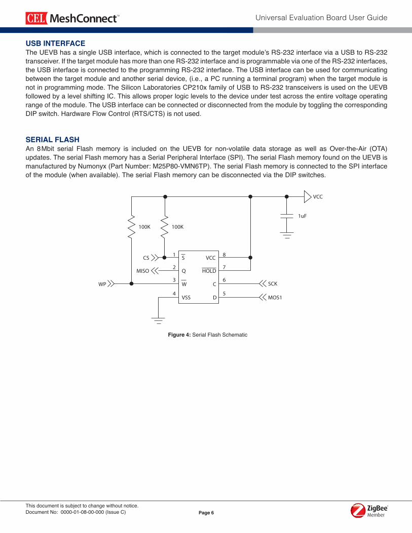
SERIAL FLASHAn 8Mbit serial Flashmemory is included on the UEVB for non-volatile data storage as well as Over-the-Air (OTA)updates.TheserialFlashmemoryhasaSerialPeripheralInterface(SPI).TheserialFlashmemoryfoundontheUEVBismanufacturedbyNumonyx(PartNumber:M25P80-VMN6TP).TheserialFlashmemoryisconnectedtotheSPIinterfaceofthemodule(whenavailable).TheserialFlashmemorycanbedisconnectedviatheDIPswitches.
Figure 4:SerialFlashSchematic
MOS1
SCK
1
2
3
4 5
6
7
8
WP
MISO
CS
100K100K
1uF
VCC
S
Q
W
VSS D
C
HOLD
VCC
Page 7
Universal Evaluation Board User Guide
This document is subject to change without notice.Document No: 0000-01-08-00-000 (Issue C)
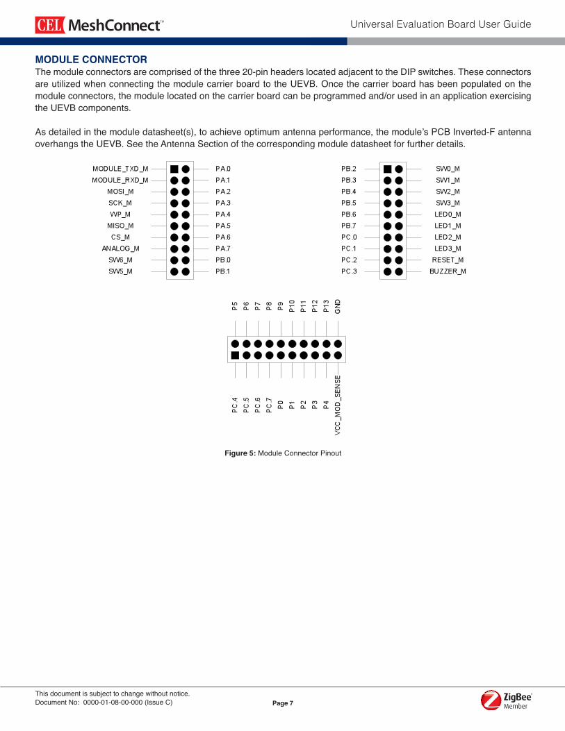
MODULE CONNECTORThemoduleconnectorsarecomprisedofthethree20-pinheaderslocatedadjacenttotheDIPswitches.TheseconnectorsareutilizedwhenconnectingthemodulecarrierboardtotheUEVB.Oncethecarrierboardhasbeenpopulatedonthemoduleconnectors,themodulelocatedonthecarrierboardcanbeprogrammedand/orusedinanapplicationexercisingthe UEVB components.
Asdetailedinthemoduledatasheet(s),toachieveoptimumantennaperformance,themodule’sPCBInverted-FantennaoverhangstheUEVB.SeetheAntennaSectionofthecorrespondingmoduledatasheetforfurtherdetails.
Figure 5:ModuleConnectorPinout
Page 8
Universal Evaluation Board User Guide
This document is subject to change without notice.Document No: 0000-01-08-00-000 (Issue C)
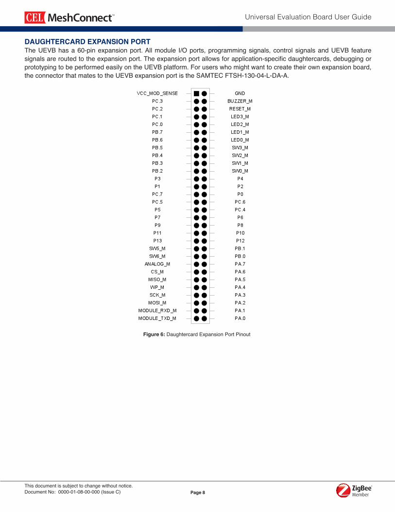
DAUGHTERCARD EXPANSION PORTTheUEVBhasa60-pinexpansionport.Allmodule I/Oports,programmingsignals,controlsignalsandUEVB featuresignalsareroutedtotheexpansionport.Theexpansionportallowsforapplication-specificdaughtercards,debuggingorprototypingtobeperformedeasilyontheUEVBplatform.Foruserswhomightwanttocreatetheirownexpansionboard,theconnectorthatmatestotheUEVBexpansionportistheSAMTECFTSH-130-04-L-DA-A.
Figure 6:DaughtercardExpansionPortPinout
Page 9
Universal Evaluation Board User Guide
This document is subject to change without notice.Document No: 0000-01-08-00-000 (Issue C)
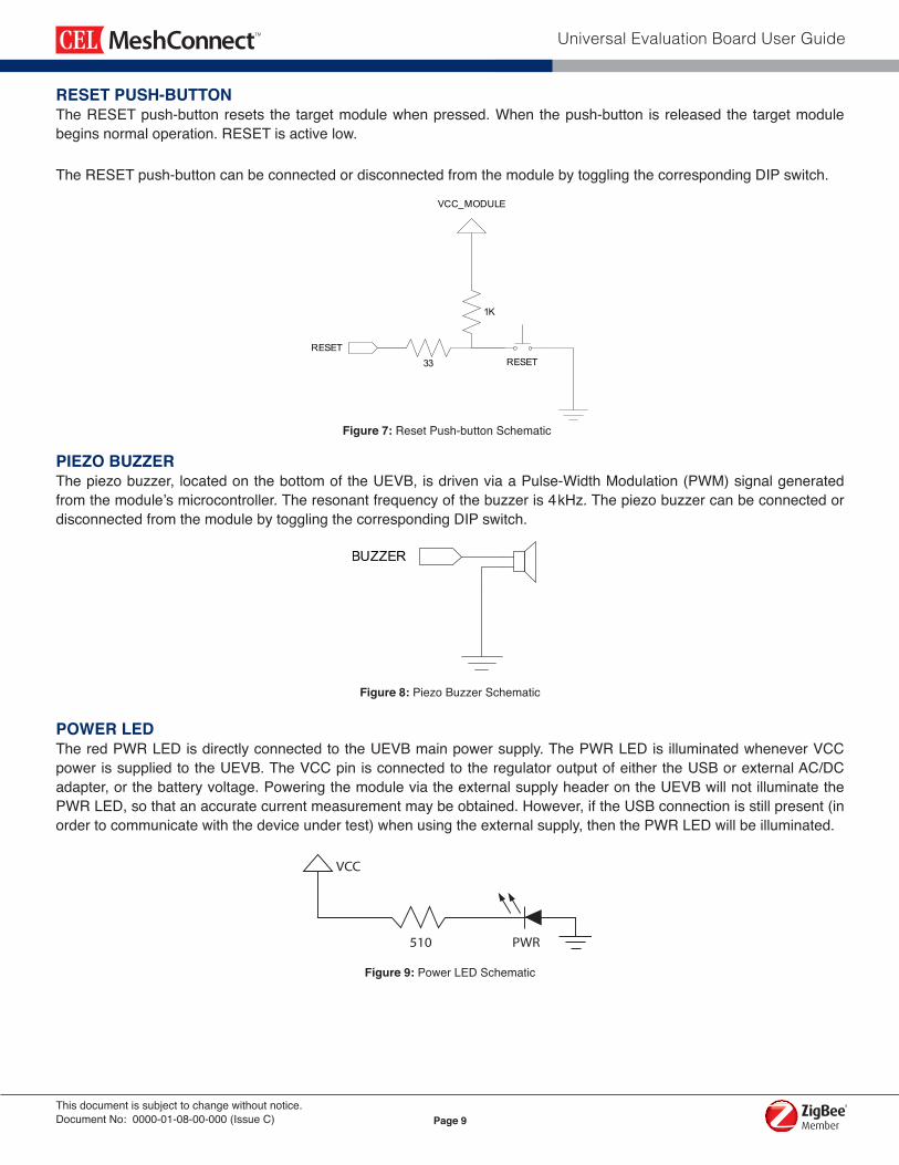
RESET PUSH-BUTTONTheRESETpush-buttonresets thetargetmodulewhenpressed.Whenthepush-button isreleasedthetargetmodulebeginsnormaloperation.RESETisactivelow.
TheRESETpush-buttoncanbeconnectedordisconnectedfromthemodulebytogglingthecorrespondingDIPswitch.
PIEZO BUZZERThepiezobuzzer, locatedonthebottomoftheUEVB,isdrivenviaaPulse-WidthModulation(PWM)signalgeneratedfromthemodule’smicrocontroller.Theresonantfrequencyofthebuzzeris4kHz.ThepiezobuzzercanbeconnectedordisconnectedfromthemodulebytogglingthecorrespondingDIPswitch.
POWER LEDTheredPWRLEDisdirectlyconnectedtotheUEVBmainpowersupply.ThePWRLEDisilluminatedwheneverVCCpowerissuppliedtotheUEVB.TheVCCpinisconnectedtotheregulatoroutputofeithertheUSBorexternalAC/DCadapter,orthebatteryvoltage.PoweringthemoduleviatheexternalsupplyheaderontheUEVBwillnotilluminatethePWRLED,sothatanaccuratecurrentmeasurementmaybeobtained.However,iftheUSBconnectionisstillpresent(inordertocommunicatewiththedeviceundertest)whenusingtheexternalsupply,thenthePWRLEDwillbeilluminated.
Figure 7:ResetPush-buttonSchematic
Figure 8:PiezoBuzzerSchematic
PWR
VCC
510
Figure 9:PowerLEDSchematic
Page 10
Universal Evaluation Board User Guide
This document is subject to change without notice.Document No: 0000-01-08-00-000 (Issue C)
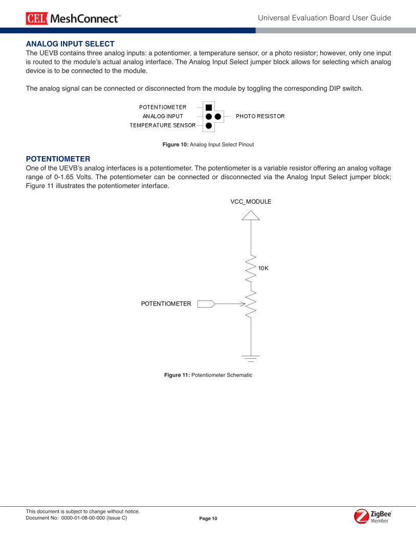
ANALOG INPUT SELECTTheUEVBcontainsthreeanaloginputs:apotentiomer,atemperaturesensor,oraphotoresistor;however,onlyoneinputisroutedtothemodule’sactualanaloginterface.TheAnalogInputSelectjumperblockallowsforselectingwhichanalogdevice is to be connected to the module.
TheanalogsignalcanbeconnectedordisconnectedfromthemodulebytogglingthecorrespondingDIPswitch.
POTENTIOMETEROneoftheUEVB’sanaloginterfacesisapotentiometer.Thepotentiometerisavariableresistorofferingananalogvoltagerangeof0-1.65Volts.Thepotentiometercanbeconnectedordisconnectedvia theAnalog InputSelect jumperblock;Figure11illustratesthepotentiometerinterface.
Figure 10:AnalogInputSelectPinout
Figure 11:PotentiometerSchematic
Page 11
Universal Evaluation Board User Guide
This document is subject to change without notice.Document No: 0000-01-08-00-000 (Issue C)
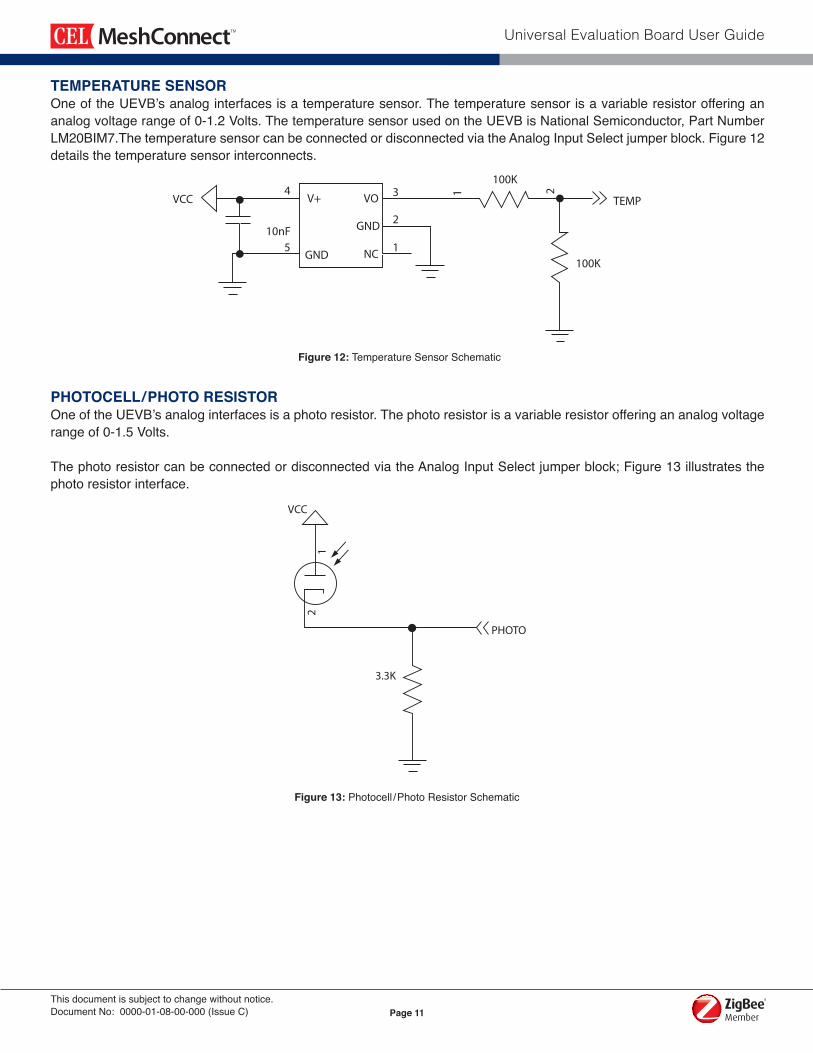
TEMPERATURE SENSOROneoftheUEVB’sanaloginterfacesisatemperaturesensor.Thetemperaturesensorisavariableresistorofferingananalogvoltagerangeof0-1.2Volts.ThetemperaturesensorusedontheUEVBisNationalSemiconductor,PartNumberLM20BIM7.ThetemperaturesensorcanbeconnectedordisconnectedviatheAnalogInputSelectjumperblock.Figure12details the temperature sensor interconnects.
PHOTOCELL/PHOTO RESISTOROneoftheUEVB’sanaloginterfacesisaphotoresistor.Thephotoresistorisavariableresistorofferingananalogvoltagerangeof0-1.5Volts.
ThephotoresistorcanbeconnectedordisconnectedviatheAnalogInputSelectjumperblock;Figure13illustratesthephoto resistor interface.
Figure 12:TemperatureSensorSchematic
VCC
10nF
4
5
3 21
1
2
TEMP
GND
GND
100K
100K
VO
NC
V+
Figure 13:Photocell /PhotoResistorSchematic
PHOTO
3.3K
21
VCC
Page 12
Universal Evaluation Board User Guide
This document is subject to change without notice.Document No: 0000-01-08-00-000 (Issue C)
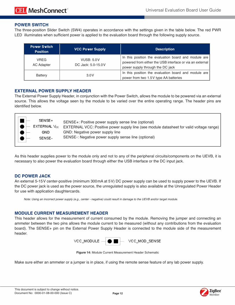
POWER SWITCHThethree-positionSliderSwitch(SW4)operatesinaccordancewiththesettingsgiveninthetablebelow.TheredPWRLEDilluminateswhensufficientpowerisappliedtotheevaluationboardthroughthefollowingsupplysource.
EXTERNAL POWER SUPPLY HEADERTheExternalPowerSupplyHeader,inconjunctionwiththePowerSwitch,allowsthemoduletobepoweredviaanexternalsource. This allows the voltage seen by the module to be varied over the entire operating range. The header pins are identifiedbelow.
Asthisheadersuppliespowertothemoduleonlyandnottoanyoftheperipheralcircuits/componentsontheUEVB,itisnecessarytoalsopowertheevaluationboardthrougheithertheUSBinterfaceortheDCinputjack.
DC POWER JACKAnexternal5-15Vcenter-positive(minimum300mAat5V)DCpowersupplycanbeusedtosupplypowertotheUEVB.IftheDCpowerjackisusedasthepowersource,theunregulatedsupplyisalsoavailableattheUnregulatedPowerHeaderfor use with application daughtercards. Note: Using an incorrect power supply (e.g., center - negative) could result in damage to the UEVB and/or target module.
MODULE CURRENT MEASUREMENT HEADERThisheaderallowsforthemeasurementofcurrentconsumedbythemodule.Removingthejumperandconnectinganammeter between the two pins allows the module current to be measured (without any contributions from the evaluation board).TheSENSE+pinon theExternalPowerSupplyHeader isconnected to themodulesideof themeasurementheader.
Makesureeitheranammeterorajumperisinplace,ifusingtheremotesensefeatureofanylabpowersupply.
Power Switch Position
VCC Power Supply Description
VREGACAdapter
VUSB:5.0VDCJack:5.0-15.0V
In this position the evaluation board and module arepoweredfromeithertheUSBinterfaceorviaanexternalpowersupplythroughtheDCjack
Battery 3.0VIn this position the evaluation board and module arepowerfromtwo1.5VtypeAAbatteries
SENSE+:Positivepowersupplysenseline(optional)EXTERNALVCC:Positivepowersupplyline(seemoduledatasheetforvalidvoltagerange)GND:NegativepowersupplylineSENSE-:Negativepowersupplysenseline(optional)
Figure 14:ModuleCurrentMeasurementHeaderSchematic
Page 13
Universal Evaluation Board User Guide
This document is subject to change without notice.Document No: 0000-01-08-00-000 (Issue C)
UNREGULATED POWER HEADERWhenusingtheDCjacktopowertheUEVB,theunregulatedinputvoltageisavailableatthisheader.Thisallowsforaneasy connection of higher supply voltages (if necessary) for application daughtercards.
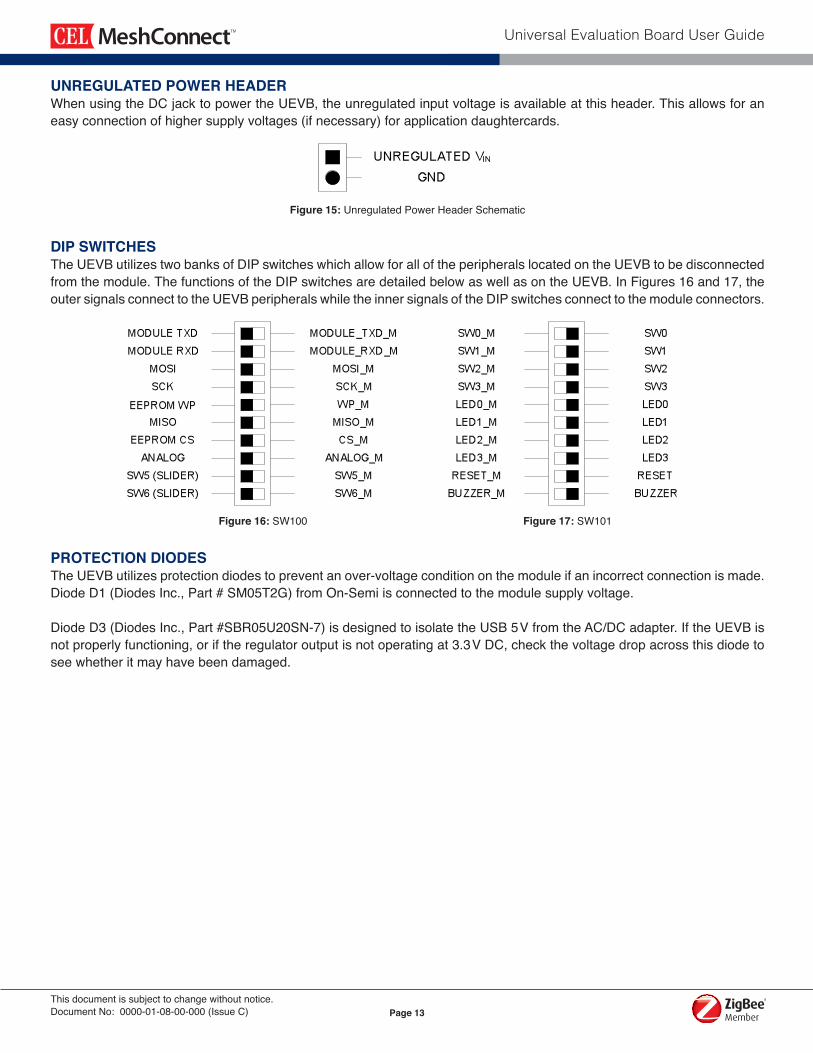
DIP SWITCHESTheUEVButilizestwobanksofDIPswitcheswhichallowforalloftheperipheralslocatedontheUEVBtobedisconnectedfromthemodule.ThefunctionsoftheDIPswitchesaredetailedbelowaswellasontheUEVB.InFigures16and17,theoutersignalsconnecttotheUEVBperipheralswhiletheinnersignalsoftheDIPswitchesconnecttothemoduleconnectors.
PROTECTION DIODESTheUEVButilizesprotectiondiodestopreventanover-voltageconditiononthemoduleifanincorrectconnectionismade.DiodeD1(DiodesInc.,Part#SM05T2G)fromOn-Semiisconnectedtothemodulesupplyvoltage.
DiodeD3(DiodesInc.,Part#SBR05U20SN-7)isdesignedtoisolatetheUSB5VfromtheAC/DCadapter.IftheUEVBisnotproperlyfunctioning,oriftheregulatoroutputisnotoperatingat3.3VDC,checkthevoltagedropacrossthisdiodetosee whether it may have been damaged.
Figure 15:UnregulatedPowerHeaderSchematic
Figure 17:SW101
Figure 16:SW100
Page 14
Universal Evaluation Board User Guide
This document is subject to change without notice.Document No: 0000-01-08-00-000 (Issue C)
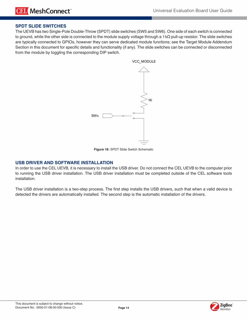
SPDT SLIDE SWITCHESTheUEVBhastwoSingle-PoleDouble-Throw(SPDT)slideswitches(SW5andSW6).Onesideofeachswitchisconnectedtoground,whiletheothersideisconnectedtothemodulesupplyvoltagethrougha1kΩpull-upresistor.TheslideswitchesaretypicallyconnectedtoGPIOs,howevertheycanservededicatedmodulefunctions;seetheTargetModuleAddendumSectioninthisdocumentforspecificdetailsandfunctionality(ifany).TheslideswitchescanbeconnectedordisconnectedfromthemodulebytogglingthecorrespondingDIPswitch.
USB DRIVER AND SOFTWARE INSTALLATIONInordertousetheCELUEVB,itisnecessarytoinstalltheUSBdriver.DonotconnecttheCELUEVBtothecomputerpriortorunningtheUSBdriverinstallation.TheUSBdriverinstallationmustbecompletedoutsideoftheCELsoftwaretoolsinstallation.
TheUSBdriverinstallationisatwo-stepprocess.ThefirststepinstallstheUSBdrivers,suchthatwhenavaliddeviceisdetected the drivers are automatically installed. The second step is the automatic installation of the drivers.
Figure 18:SPDTSlideSwitchSchematic
Page 15
Universal Evaluation Board User Guide
This document is subject to change without notice.Document No: 0000-01-08-00-000 (Issue C)
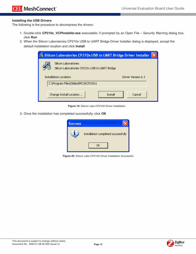
Installing the USB DriversThefollowingistheproceduretodecompressthedrivers:
1.Double-clickCP210x_VCPInstaller.exeexecutable;ifpromptedbyanOpenFile–SecurityWarningdialogbox, clickRun 2.WhentheSiliconLaboratoriesCP210xUSBtoUARTBridgeDriverInstallerdialogisdisplayed,acceptthe defaultinstallationlocationandclickInstall
3.Oncetheinstallationhascompletedsuccessfully,clickOK
Figure 19:SiliconLabsCP210XDriverInstallation
Figure 20:SiliconLabsCP210XDriverInstallationSuccessful
Page 16
Universal Evaluation Board User Guide
This document is subject to change without notice.Document No: 0000-01-08-00-000 (Issue C)
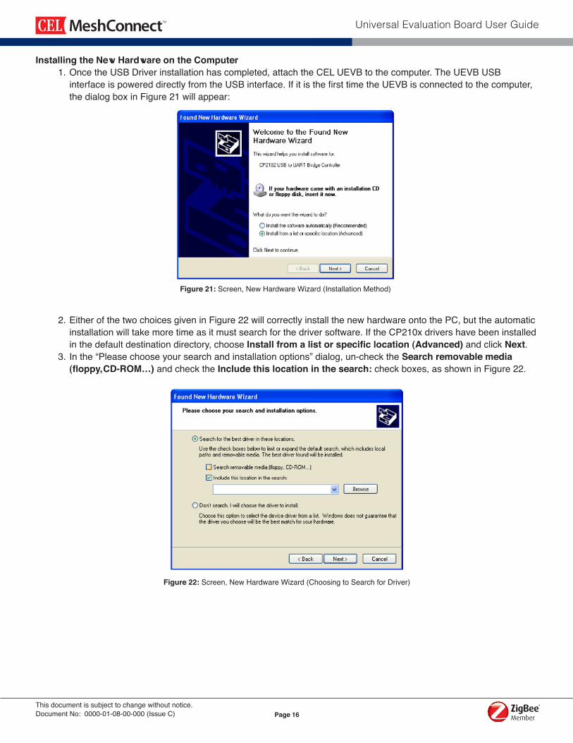
Installing the New Hardware on the Computer 1.OncetheUSBDriverinstallationhascompleted,attachtheCELUEVBtothecomputer.TheUEVBUSB interfaceispowereddirectlyfromtheUSBinterface.IfitisthefirsttimetheUEVBisconnectedtothecomputer, thedialogboxinFigure21willappear:
2.EitherofthetwochoicesgiveninFigure22willcorrectlyinstallthenewhardwareontothePC,buttheautomatic installationwilltakemoretimeasitmustsearchforthedriversoftware.IftheCP210xdrivershavebeeninstalled in the default destination directory, choose Install from a list or specific location (Advanced)andclickNext. 3.Inthe“Pleasechooseyoursearchandinstallationoptions”dialog,un-checktheSearch removable media (floppy, CD-ROM…)andchecktheInclude this location in the search:checkboxes,asshowninFigure22.
Figure 21:Screen,NewHardwareWizard(InstallationMethod)
Figure 22:Screen,NewHardwareWizard(ChoosingtoSearchforDriver)
Page 17
Universal Evaluation Board User Guide
This document is subject to change without notice.Document No: 0000-01-08-00-000 (Issue C)
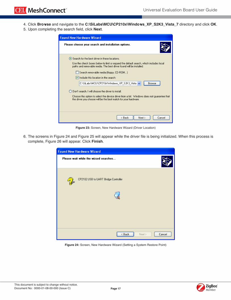
4.ClickBrowse and navigate to the C:\SiLabs\MCU\CP210x\Windows_XP_S2K3_Vista_7 directory and clickOK. 5.Uponcompletingthesearchfield,clickNext.
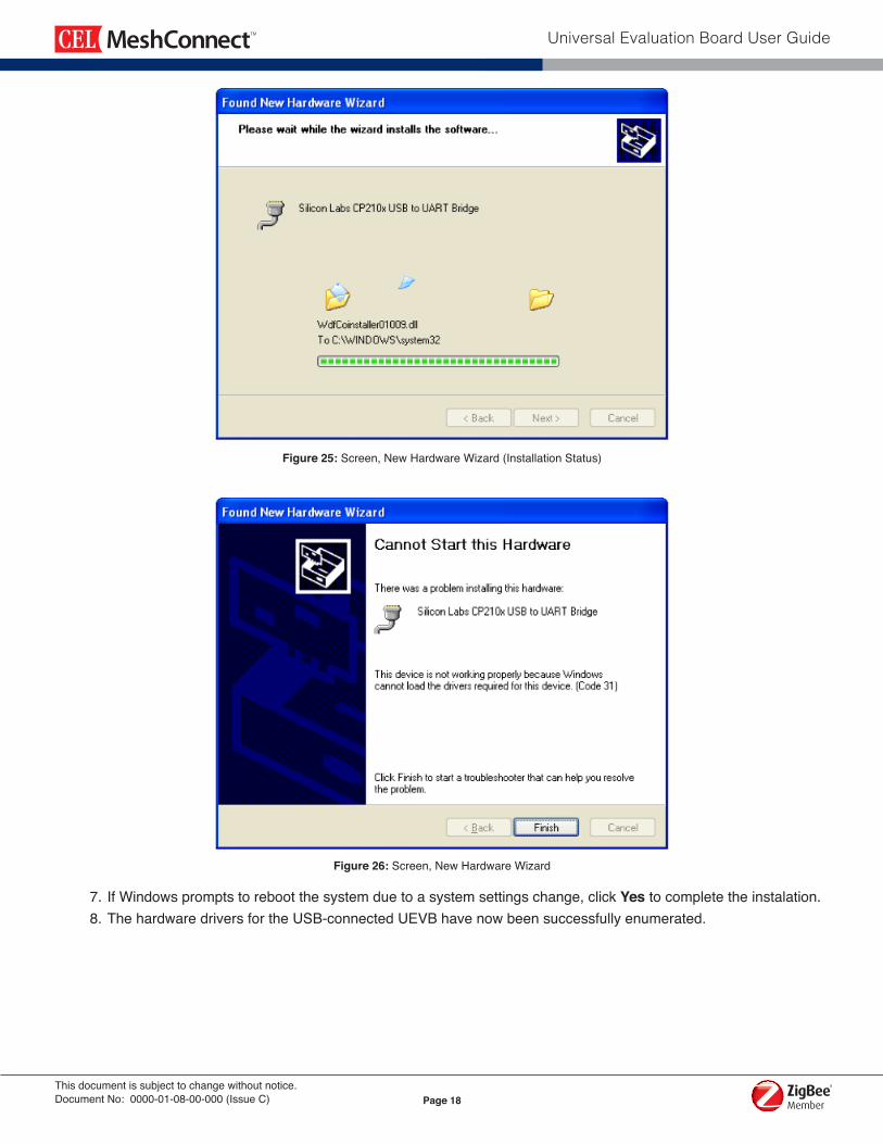
6.ThescreensinFigure24andFigure25willappearwhilethedriverfileisbeinginitialized.Whenthisprocessis complete,Figure26willappear.ClickFinish.
Figure 23:Screen,NewHardwareWizard(DriverLocation)
Figure 24:Screen,NewHardwareWizard(SettingaSystemRestorePoint)
Page 18
Universal Evaluation Board User Guide
This document is subject to change without notice.Document No: 0000-01-08-00-000 (Issue C)
Figure 25:Screen,NewHardwareWizard(InstallationStatus)
7.IfWindowspromptstorebootthesystemduetoasystemsettingschange,clickYes to complete the instalation. 8.ThehardwaredriversfortheUSB-connectedUEVBhavenowbeensuccessfullyenumerated.
Figure 26:Screen,NewHardwareWizard
Page 19
Universal Evaluation Board User Guide
This document is subject to change without notice.Document No: 0000-01-08-00-000 (Issue C)
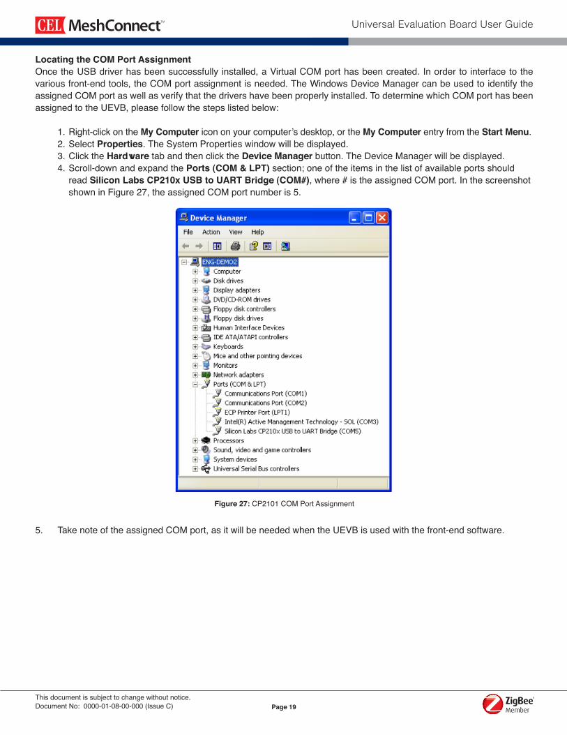
Locating the COM Port AssignmentOncetheUSBdriverhasbeensuccessfully installed,aVirtualCOMporthasbeencreated.Inordertointerfacetothevariousfront-endtools,theCOMportassignmentisneeded.TheWindowsDeviceManagercanbeusedtoidentifytheassignedCOMportaswellasverifythatthedrivershavebeenproperlyinstalled.TodeterminewhichCOMporthasbeenassignedtotheUEVB,pleasefollowthestepslistedbelow:
1.Right-clickontheMy Computericononyourcomputer’sdesktop,ortheMy Computer entry from the Start Menu. 2.SelectProperties.TheSystemPropertieswindowwillbedisplayed. 3.ClicktheHardwaretabandthenclicktheDevice Manager button. The Device Manager will be displayed. 4.Scroll-downandexpandthePorts (COM & LPT)section;oneoftheitemsinthelistofavailableportsshould read Silicon Labs CP210x USB to UART Bridge (COM#),where#istheassignedCOMport.Inthescreenshot showninFigure27,theassignedCOMportnumberis5.
5. TakenoteoftheassignedCOMport,asitwillbeneededwhentheUEVBisusedwiththefront-endsoftware.
Figure 27:CP2101COMPortAssignment
X4
UNIV
ERSA
L EV
AL M
AIN
CAR
D
11
ofSh
eet
Dat
e:
Doc
umen
t Num
ber
Size
Dra
wing
Title
:
ISSU
EC
Mar
ch 2
5, 2
010
LED
s
Rese
tBu
tton
Powe
r ON
SENS
E+
SENS
E-
BCD
54
32
1
D C B A
23
45
10/1
5/20
10
REVI
SIO
N RE
CO
RD
DES
CRI
PTIO
N:D
ATE:
ISSU
EPR
ELIM
INAR
YX0
V =
3.3V
nom
inal
Butto
n 0
Butto
n 1
Butto
n 2
Butto
n 3
Buzz
er
Exte
rnal
_VC
C
DUT
Com
mun
icat
ion
1: A
to B
2: B
to A
Leve
l Shi
fters
0000
-01-
01-0
0-00
0
60 P
in c
onne
ctor
s to
inte
rface
to A
TE2
& D
ebug
USB
Com
mun
icat
ion
DC
Sup
plie
s &
Switc
h wi
th S
ense
Deb
ug A
dpat
er 5
VDC
Sou
rce
20 P
in C
onne
ctor
X 3
to in
terfa
ce to
Dau
ghte
rcar
d
Perip
hera
ls Tem
pera
ture
Sen
sor
TEM
P_SE
NSE
Scal
ed to
1.2
V
PHO
TO C
ELL
X1RE
VISE
D P
ER S
PREA
D S
HEET
11-2
9-10
X2RE
VISE
D P
ER S
PREA
D S
HEET
02-2
6-11
X3RE
VISE
D P
ER S
PREA
D S
HEET
04-0
5-11
X4RE
VISE
D P
ER E
CR#
0001
4907
-18-
11
12
R10
510
12
LED
0
LED
RED
12
PWR
LED
RED
C23
10nF
12
LED
1
LED
RED
12
LED
2
LED
RED
12
LED
3
LED
RED
12
R11
510
12
3
D3
1 23
J13
+
-
BC1
2462
+1 2
C15
100µ
F16
V
C4 10
nF
12J1
02
Pin
Con
n.
C3
10uF 16V
12
34
5SW1
12
34
5SW0
12
34
5RE
SET
1234J1
1
1 2
C17 1uF
1ADJ
2VO
UT1
3VI
N4
VOUT
2
U6
1 2
R32
200
1 2
R30
121
C19
10uF
16V
1VU
SB2
DAT
A-3
DAT
A+4
GND
5SH
IELD
16
SHIE
LD2
J12
USB-
B
C14
10uF
16V
12
C6
1uF
12C18
1uF
12
C21 1uF
12
R33
510
12
3
D5
12
3D4
R8 1K
R23
1K
R24
1K
C9
10nF
C10
10nF
1 2SP
K1
12
R12
510
12
R13
510
12
34
5SW2
R25
1K
C7
10nF
12
34
5SW3
R26
1K
C8
10nF
21
R17
12
21
R15
12
1 2 34C
1A 2A4AC
A
3A
6
5
SW4
12
3
D2
C13
10nF
C16
10nF
C22
10nF
1C
CA
21D
IR3
2DIR
41A
15
1A2
62A
17
2A2
8G
ND9
GND
102B
2
112B
1
121B
2
131B
1
142O
E
151O
E
16VC
CB
U4
1 2
C11 1uF
1 2
C12 1uF
2 1
R29
100K
2 1
R14
100K
2 1
R28
100K
2 1
R16
100K
12
3
SW5 SP
DT
12
3
SW6 SP
DT
ON
ON
ON
ON
ON
ON
ON
ON
ON
OFF
OFF
OFF
OFF
OFF
OFF
OFF
OFF
OFF
ON
OFF
1 2 3 4 5 6 7 8 9 1011121314151617181920
SW10
0
R22
1K
R27
1K
CW
1
2
3POT1
R9 10K
C5
1uF
R5 100K
R7 100K
1S
2Q
3W
4VS
S5
D
6C
7HO
LD
8VC
C
U3
1 3 5 7 9 11 13 15 17 19
2 4 6 8 10 12 14 16 18 20
J4
13579
1113151719
2468101214161820
J3
12
34
56
78
910
1112
1314
1516
1718
1920
2122
2324
2526
2728
2930
3132
3334
3536
3738
3940
4142
4344
4546
4748
4950
5152
5354
5556
5758
5960
J1
CONN_RCPT_2X30_SFMH-130-02-L-D-LC
1A1
2G
ND
3A2
4Y2
5VC
C
6Y1
U1
NC7W
Z07P
6X_I
C_B
UFF_
SC70
6_FA
IR
1A1
2G
ND
3A2
4Y2
5VC
C
6Y1
U2
NC7W
Z07P
6X_I
C_B
UFF_
SC70
6_FA
IR
R4 100K
R3 100K
R2 100K
R1 100K
C1
10nF
C2
10nF
C20
10nF
1 3 5 7 9 11 13 15 17 19
2 4 6 8 10 12 14 16 18 20
J2O
NO
NO
NO
NO
NO
NO
NO
NO
N
OFF
OFF
OFF
OFF
OFF
OFF
OFF
OFF
OFF
ON
OFF
1234567891011 12 13 14 15 16 17 18 19 20
SW10
1
Z2Z3
Z1Z4
12J7
2 Pi
n C
onn.
NP
12J6
2 Pi
n C
onn. NP
1D
CD
2RI
3G
ND4
D+
5D
-6
VDD
7RE
GIN
8VBUS9RST
10NC11SUSPEND12SUSPEND13NC14NC
15NC
16NC
17NC
18NC
19NC
20NC
21NC
22 NC23 CTS24 RTS25 RXD26 TXD27 DSR28 DTR
30G
ND31
GND
32G
ND33
GNDU5
CP2
102
R18
33
R19
33
R20
33
R21
33
R6 33
1NC
2G
ND
3VO
4V+
5G
ND
U7LM
20BI
M7_
SENS
OR_
SC70
-5_N
AT
R36
3.3K
12
BT1
12J5
2 Pi
n C
onn.
1 2 3
J8
CO
NN_H
DR_
3X1_
8722
4-3
3 Pi
n HD
R
1J9 C
ONN
_HD
R_1X
11
Pin
HDR
12
3D1
C24
10nF
R34
100K
2
1
R35100K
R31
10K
1
MH2
PCB1
0000
-01-
04-0
0-00
0
PCB
1
MH3
1
MH1
1
MH4
JMP1
9299
55-0
6JM
P
SCRE
W1
SCRE
W2
NUT1NU
T2
STAN
DO
FF1
9466
2A45
1
STAN
DO
FF2
9466
2A45
1
STAN
DO
FF3
9466
2A45
1
STAN
DO
FF4
9466
2A45
1
JMP2
9299
55-0
6JM
P
VUSB
GND
GND
GND
GND
GND
GND
GND
GND
GND
VCC
_MO
DUL
E_SE
NSE
GND
GND
VCC
GND
GND
GND
VUSB
GND
GND
GND
VCC
_MO
DUL
E
GND
GND
GND
BUZZ
ER
GND
LED
0
LED
1
LED
2
LED
3
GND
GND
GND
GND
CP_
RXD
CP_
TXD
VCC
_MO
DUL
E_SE
NSE
RESE
T
P12
GND
GND
GND
GND
VCC
_MO
DUL
E
SW0_
M
SW1_
MSW
2_M
SW3_
MLE
D0_
MLE
D1_
MLE
D2_
MLE
D3_
MRE
SET_
M
BUZZ
ER_M
SW0
SW1
SW2
SW3
LED
0
LED
1LE
D2
LED
3RE
SET
BUZZ
ER
GND
GND
ISP2IS
P1
VCC
_MO
DUL
E
VCC
_MO
DUL
E
ISP1
_M
ISP2
_M
ISP1
ISP2
GND
POT
POT_
MAN
ALO
G
CS
MIS
O
SCK
MO
SI
WP
VCC
GND
CS_
MM
ISO
_MVC
C
SCK_
MM
OSI
_M
CS
MIS
OW
PSC
KM
OSI
CP_
TXD
_M
CP_
R XD
_M
CP_
TXD
CP_
RXD
PA.0
PA.2
PA.1
PA.3
PA.5
PA.7
PB.1
PB.3
PB.5
PB.7
PC.1
PA.4
PA.6
PB.0
PB.2
PB.4
PB.6
PC.0
PC.2
P5P6P7P8P9P10P11
PC.4PC.5PC.6PC.7
P0P1P2
VCC
_MO
DUL
E_SE
NSE
PC.3
GND
VCC
_MO
DUL
E_SE
NSE
GND
PC.3
PC.2
PC.1
PC.0
PB.7
PB.6
PB.5
PB.4
PB.3
ISP1
_MIS
P2_M
POT_
MC
S_M
MIS
O_M
SCK_
M
MO
SI_M
CP_
TXD
_MC
P_RX
D_M
P12
P10
P8 P6 P4P2P0PC.6
PC.4
SW0_
MSW
1_M
SW2_
MSW
3_M
LED
0_M
LED
1_M
LED
2_M
LED
3_M
RESE
T_M
BUZZ
ER_M
PB.2
PC.5
PC.7 P1 P3P5P7P9P11
P13
PA.0
PA.1
PA.2
PA.3
PA.4
PA.5
PA.6
PA.7
PB.0
PB.1
P3P4
P12P13
GNDG
ND
GND
GND
GND
GND
VCC
VCC
_MO
DUL
EVC
C_M
OD
ULE
VCC
_MO
DUL
EVC
C_M
OD
ULE
VCC
_MO
DUL
E
VCC
_MO
DUL
EVC
C_M
OD
ULE
VCC
_MO
DUL
E
GND
VCC
VCC
GND
GND
SW0
SW1
SW2
SW3
VCC
_MO
DUL
E
GND
GND
VCC
TEM
P
VCC
GND
PHO
TO
GND
POT
TEM
PPH
OTO
ANAL
OG
GND
GND
Page 21
Universal Evaluation Board User Guide
This document is subject to change without notice.Document No: 0000-01-08-00-000 (Issue C)
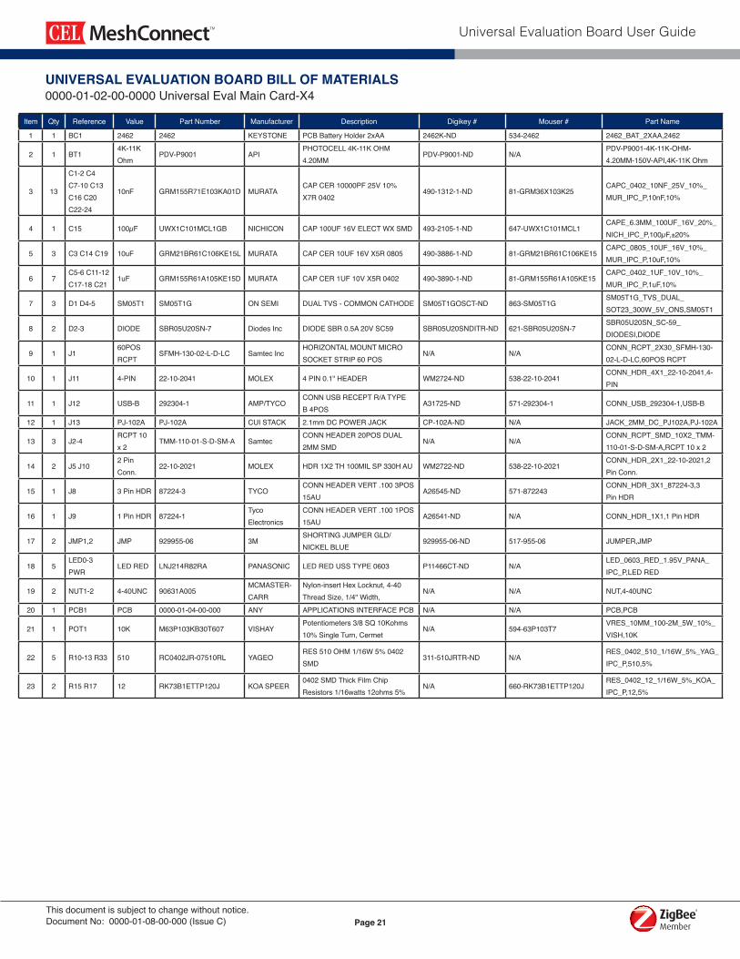
Item Qty Reference Value PartNumber Manufacturer Description Digikey# Mouser# PartName
1 1 BC1 2462 2462 KEYSTONE PCBBatteryHolder2xAA 2462K-ND 534-2462 2462_BAT_2XAA,2462
2 1 BT14K-11KOhm
PDV-P9001 APIPHOTOCELL4K-11KOHM4.20MM
PDV-P9001-ND N/APDV-P9001-4K-11K-OHM-4.20MM-150V-API,4K-11KOhm
3 13
C1-2C4C7-10C13C16C20C22-24
10nF GRM155R71E103KA01D MURATACAPCER10000PF25V10%X7R0402
490-1312-1-ND 81-GRM36X103K25CAPC_0402_10NF_25V_10%_MUR_IPC_P,10nF,10%
4 1 C15 100µF UWX1C101MCL1GB NICHICON CAP100UF16VELECTWXSMD 493-2105-1-ND 647-UWX1C101MCL1CAPE_6.3MM_100UF_16V_20%_NICH_IPC_P,100µF,±20%
5 3 C3C14C19 10uF GRM21BR61C106KE15L MURATA CAPCER10UF16VX5R0805 490-3886-1-ND 81-GRM21BR61C106KE15CAPC_0805_10UF_16V_10%_MUR_IPC_P,10uF,10%
6 7C5-6C11-12C17-18C21
1uF GRM155R61A105KE15D MURATA CAPCER1UF10VX5R0402 490-3890-1-ND 81-GRM155R61A105KE15CAPC_0402_1UF_10V_10%_MUR_IPC_P,1uF,10%
7 3 D1D4-5 SM05T1 SM05T1G ONSEMI DUALTVS-COMMONCATHODE SM05T1GOSCT-ND 863-SM05T1GSM05T1G_TVS_DUAL_SOT23_300W_5V_ONS,SM05T1
8 2 D2-3 DIODE SBR05U20SN-7 DiodesInc DIODESBR0.5A20VSC59 SBR05U20SNDITR-ND 621-SBR05U20SN-7SBR05U20SN_SC-59_DIODESI,DIODE
9 1 J160POSRCPT
SFMH-130-02-L-D-LC SamtecIncHORIZONTALMOUNTMICROSOCKETSTRIP60POS
N/A N/ACONN_RCPT_2X30_SFMH-130-02-L-D-LC,60POSRCPT
10 1 J11 4-PIN 22-10-2041 MOLEX 4PIN0.1"HEADER WM2724-ND 538-22-10-2041CONN_HDR_4X1_22-10-2041,4-PIN
11 1 J12 USB-B 292304-1 AMP/TYCOCONNUSBRECEPTR/ATYPEB4POS
A31725-ND 571-292304-1 CONN_USB_292304-1,USB-B
12 1 J13 PJ-102A PJ-102A CUISTACK 2.1mmDCPOWERJACK CP-102A-ND N/A JACK_2MM_DC_PJ102A,PJ-102A
13 3 J2-4RCPT10x2
TMM-110-01-S-D-SM-A SamtecCONNHEADER20POSDUAL2MMSMD
N/A N/ACONN_RCPT_SMD_10X2_TMM-110-01-S-D-SM-A,RCPT10x2
14 2 J5J102PinConn.
22-10-2021 MOLEX HDR1X2TH100MILSP330HAU WM2722-ND 538-22-10-2021CONN_HDR_2X1_22-10-2021,2PinConn.
15 1 J8 3PinHDR 87224-3 TYCOCONNHEADERVERT.1003POS15AU
A26545-ND 571-872243CONN_HDR_3X1_87224-3,3PinHDR
16 1 J9 1PinHDR 87224-1Tyco Electronics
CONNHEADERVERT.1001POS15AU
A26541-ND N/A CONN_HDR_1X1,1PinHDR
17 2 JMP1,2 JMP 929955-06 3MSHORTINGJUMPERGLD/NICKELBLUE
929955-06-ND 517-955-06 JUMPER,JMP
18 5LED0-3PWR
LEDRED LNJ214R82RA PANASONIC LEDREDUSSTYPE0603 P11466CT-ND N/ALED_0603_RED_1.95V_PANA_IPC_P,LEDRED
19 2 NUT1-2 4-40UNC 90631A005MCMASTER-CARR
Nylon-insertHexLocknut,4-40ThreadSize,1/4"Width,
N/A N/A NUT,4-40UNC
20 1 PCB1 PCB 0000-01-04-00-000 ANY APPLICATIONSINTERFACEPCB N/A N/A PCB,PCB
21 1 POT1 10K M63P103KB30T607 VISHAYPotentiometers3/8SQ10Kohms10%SingleTurn,Cermet
N/A 594-63P103T7VRES_10MM_100-2M_5W_10%_VISH,10K
22 5 R10-13R33 510 RC0402JR-07510RL YAGEORES510OHM1/16W5%0402SMD
311-510JRTR-ND N/ARES_0402_510_1/16W_5%_YAG_IPC_P,510,5%
23 2 R15R17 12 RK73B1ETTP120J KOASPEER0402SMDThickFilmChipResistors1/16watts12ohms5%
N/A 660-RK73B1ETTP120JRES_0402_12_1/16W_5%_KOA_IPC_P,12,5%
UNIVERSAL EVALUATION BOARD BILL OF MATERIALS0000-01-02-00-0000UniversalEvalMainCard-X4
Page 22
Universal Evaluation Board User Guide
This document is subject to change without notice.Document No: 0000-01-08-00-000 (Issue C)
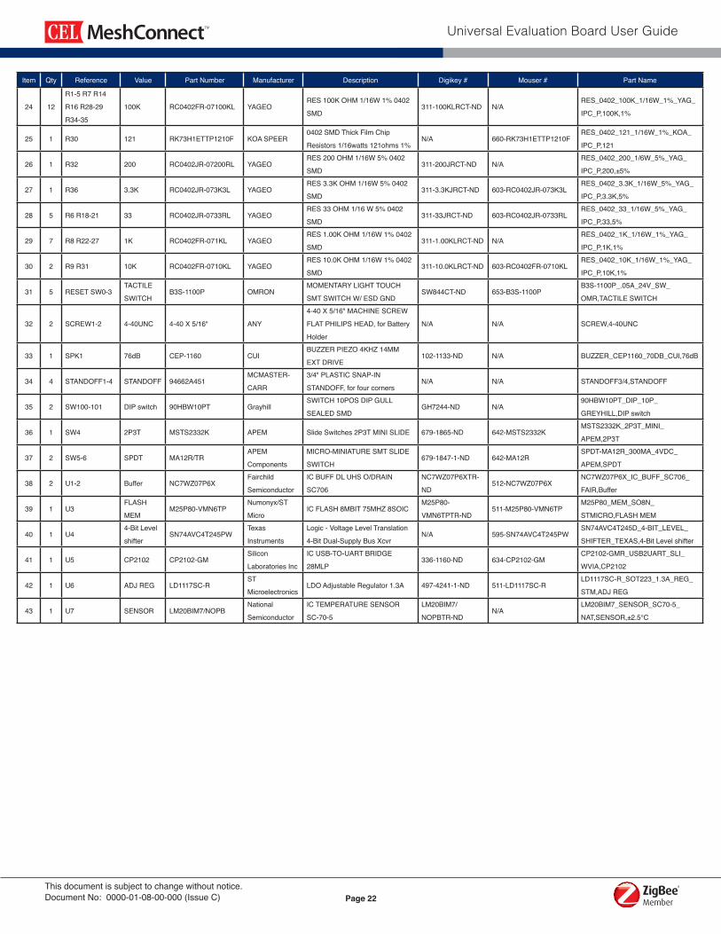
Item Qty Reference Value PartNumber Manufacturer Description Digikey# Mouser# PartName
24 12
R1-5R7R14
R16R28-29
R34-35
100K RC0402FR-07100KL YAGEORES100KOHM1/16W1%0402
SMD311-100KLRCT-ND N/A
RES_0402_100K_1/16W_1%_YAG_
IPC_P,100K,1%
25 1 R30 121 RK73H1ETTP1210F KOASPEER0402SMDThickFilmChip
Resistors1/16watts121ohms1%N/A 660-RK73H1ETTP1210F
RES_0402_121_1/16W_1%_KOA_
IPC_P,121
26 1 R32 200 RC0402JR-07200RL YAGEORES200OHM1/16W5%0402
SMD311-200JRCT-ND N/A
RES_0402_200_1/6W_5%_YAG_
IPC_P,200,±5%
27 1 R36 3.3K RC0402JR-073K3L YAGEORES3.3KOHM1/16W5%0402
SMD311-3.3KJRCT-ND 603-RC0402JR-073K3L
RES_0402_3.3K_1/16W_5%_YAG_
IPC_P,3.3K,5%
28 5 R6R18-21 33 RC0402JR-0733RL YAGEORES33OHM1/16W5%0402
SMD311-33JRCT-ND 603-RC0402JR-0733RL
RES_0402_33_1/16W_5%_YAG_
IPC_P,33,5%
29 7 R8R22-27 1K RC0402FR-071KL YAGEORES1.00KOHM1/16W1%0402
SMD311-1.00KLRCT-ND N/A
RES_0402_1K_1/16W_1%_YAG_
IPC_P,1K,1%
30 2 R9R31 10K RC0402FR-0710KL YAGEORES10.0KOHM1/16W1%0402
SMD311-10.0KLRCT-ND 603-RC0402FR-0710KL
RES_0402_10K_1/16W_1%_YAG_
IPC_P,10K,1%
31 5 RESETSW0-3TACTILE
SWITCHB3S-1100P OMRON
MOMENTARYLIGHTTOUCH
SMTSWITCHW/ESDGNDSW844CT-ND 653-B3S-1100P
B3S-1100P_.05A_24V_SW_
OMR,TACTILESWITCH
32 2 SCREW1-2 4-40UNC 4-40X5/16" ANY
4-40X5/16"MACHINESCREW
FLATPHILIPSHEAD,forBattery
Holder
N/A N/A SCREW,4-40UNC
33 1 SPK1 76dB CEP-1160 CUIBUZZERPIEZO4KHZ14MM
EXTDRIVE102-1133-ND N/A BUZZER_CEP1160_70DB_CUI,76dB
34 4 STANDOFF1-4 STANDOFF 94662A451MCMASTER-
CARR
3/4"PLASTICSNAP-IN
STANDOFF,forfourcornersN/A N/A STANDOFF3/4,STANDOFF
35 2 SW100-101 DIPswitch 90HBW10PT GrayhillSWITCH10POSDIPGULL
SEALEDSMDGH7244-ND N/A
90HBW10PT_DIP_10P_
GREYHILL,DIPswitch
36 1 SW4 2P3T MSTS2332K APEM SlideSwitches2P3TMINISLIDE 679-1865-ND 642-MSTS2332KMSTS2332K_2P3T_MINI_
APEM,2P3T
37 2 SW5-6 SPDT MA12R/TRAPEM
Components
MICRO-MINIATURESMTSLIDE
SWITCH679-1847-1-ND 642-MA12R
SPDT-MA12R_300MA_4VDC_
APEM,SPDT
38 2 U1-2 Buffer NC7WZ07P6XFairchild
Semiconductor
ICBUFFDLUHSO/DRAIN
SC706
NC7WZ07P6XTR-
ND512-NC7WZ07P6X
NC7WZ07P6X_IC_BUFF_SC706_
FAIR,Buffer
39 1 U3FLASH
MEMM25P80-VMN6TP
Numonyx/ST
MicroICFLASH8MBIT75MHZ8SOIC
M25P80-
VMN6TPTR-ND511-M25P80-VMN6TP
M25P80_MEM_SO8N_
STMICRO,FLASHMEM
40 1 U44-BitLevel
shifterSN74AVC4T245PW
Texas
Instruments
Logic-VoltageLevelTranslation
4-BitDual-SupplyBusXcvrN/A 595-SN74AVC4T245PW
SN74AVC4T245D_4-BIT_LEVEL_
SHIFTER_TEXAS,4-BitLevelshifter
41 1 U5 CP2102 CP2102-GMSilicon
LaboratoriesInc
ICUSB-TO-UARTBRIDGE
28MLP336-1160-ND 634-CP2102-GM
CP2102-GMR_USB2UART_SLI_
WVIA,CP2102
42 1 U6 ADJREG LD1117SC-RST
MicroelectronicsLDOAdjustableRegulator1.3A 497-4241-1-ND 511-LD1117SC-R
LD1117SC-R_SOT223_1.3A_REG_
STM,ADJREG
43 1 U7 SENSOR LM20BIM7/NOPBNational
Semiconductor
ICTEMPERATURESENSOR
SC-70-5
LM20BIM7/
NOPBTR-NDN/A
LM20BIM7_SENSOR_SC70-5_
NAT,SENSOR,±2.5°C

Page 23
Universal Evaluation Board User Guide
This document is subject to change without notice.Document No: 0000-01-08-00-000 (Issue C)
ADDENDUM: ZICM357P2CEL’sMeshConnectEM357ModulecombinesahighperformanceRFsolutionwiththemarket’spremierZigBeestack.TheintegratedPowerAmplifier (PA) maximizes range and performance. The small modulefootprint makes it suitable for a wide range of ZigBee applications.The MeshConnect EM357 Module is certified and qualified, enablingcustomers toaccelerate timetomarketbygreatlyreducing thedesignandcertificationphasesofdevelopment.
CEL’s MeshConnect EM357 Module (ZICM357P2-2) is based on theEmberEM357ZigBeecompliantSystemonChip (SoC) IC.The IC isa single-chip solution, compliant with ZigBee specifications and IEEE802.15.4;acompletewirelesssolutionforallZigBeeapplications.TheICconsistsofanRFtransceiverwiththebasebandmodem,ahardwiredMACandanembedded32-bitARM®Cortex™-M3microcontrollerwith internalRAM(12kB)andFlash(192kB)memory.Thedeviceprovidesnumerousgeneral-purposeI/OpinsandperipheralfunctionssuchastimersandUARTs.
TheMeshConnectEM357Module addsaPA to increase range, providemore reliable transmissions, and reduce thenumberofnodesinyournetwork.ItisespeciallyusefulforopenoutdoorapplicationswherethenodesarephysicallyfarapartorforindoorusewherethenodeshavetooperateinanoisyRFenvironment.Themodule’soutstanding120dBlinkbudgetensureshighqualityconnectionseveninsuchharshRFenvironments.
TheMeshConnectEM357Modulealsointegratesa1MBFlashmemory(off-chip)forOTAprogramupdates,makingthisdevicereadyforSmartEnergyApplications.
Page 24
Universal Evaluation Board User Guide
This document is subject to change without notice.Document No: 0000-01-08-00-000 (Issue C)
HARDWARE DESCRIPTION
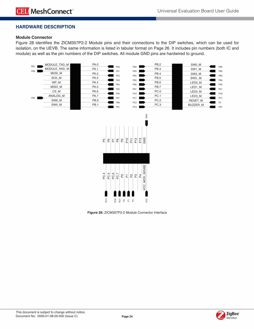
Module ConnectorFigure28 identifies theZICM357P2-2Module pinsand their connections to theDIP switches,which canbeused forisolation,ontheUEVB.ThesameinformationislistedintabularformatonPage26.Itincludespinnumbers(bothICandmodule)aswellasthepinnumbersoftheDIPswitches.AllmoduleGNDpinsarehardwiredtoground.
MODULE_TXD_M PA.0PA.1PA.2PA.3PA.4PA.5PA.6PA.7PB.0PB.1
PB.2PB.3PB.4PB.5PB.6PB.7PC.0PC.1PC.2PC.3
PC.4
PC.5
PC.6
PC.7
P0 P1 P2 P3 P4
P5 P6 P7 P8 P9 P10
P11
P12
P13
GN
DVC
C_M
OD
_SEN
SE
SW0_MSW1_MSW2_MSW3._MLED0_MLED1_MLED2_MLED3_M
RESET_MBUZZER_M
MODULE_RXD_MPB1
PB2
PB5
MOSI_MSCK_MWP_M
MISO_MCS_M
ANALOG_MSW6_MSW5_M
PA0
PA1
PA2
PA3
PA4
PA5
PA6
PA7
PB0
PB1
PB2
PB3
PB4
PB5
PB6
PB7
PC0
PC1
PC2
PC3
GN
D
PB6
PB0
PB3
PB4
PA6
PA7
PC6
PC1
P2
PB7PC
4
PC6
PC7
P0 P1 P2 VCC
Figure 28:ZICM357P2-2ModuleConnectorInterface
Page 25
Universal Evaluation Board User Guide
This document is subject to change without notice.Document No: 0000-01-08-00-000 (Issue C)
Data Emulation InterfaceFigure29identifiestheZICM357P2-2Module’spinsandtheirconnectionstotheDataEmulationInterface(DEI)ontheUEVBcarrierboard.TheDEIisusedinconjunctionwiththeEmberInSightAdapter3(ISA3). Note: PB1 and PB2 are also connected to the evaluation board USB interface. If the DEI connector is used for UART communications, the RXD and TXD DIP switches on the UEVB must be switched to the “OFF” position to avoid contention.
InSight PortFigure30identifiestheZICM357P2-2Module’spinsandtheirconnectionstotheInSightPortontheUEVBcarrierboard.TheInSightPortisusedfordebuggingandprogramminginconjunctionwiththeEmberInSightAdapter3(ISA3).
Universal Evaluation Board PeripheralsTheZICM357P2-2ModuleisconnectedtoalltheperipheralsontheUEVBexceptforthetwoSPDTslideswitchesandtheSerialFlashmemory(asthemodulealreadyhasan8Mbitmemoryon-module).
N/CPC6PB4PB6
PB0PC1
PB1PB2PB3N/C
GNDPA7
Figure 29:DataEmulationInterfaceSchematic
Figure 30:InSightPortSchematic
N/CPC0GNDPC4PA4
PC2PC3P1P2
PA5
Page 26
Universal Evaluation Board User Guide
This document is subject to change without notice.Document No: 0000-01-08-00-000 (Issue C)
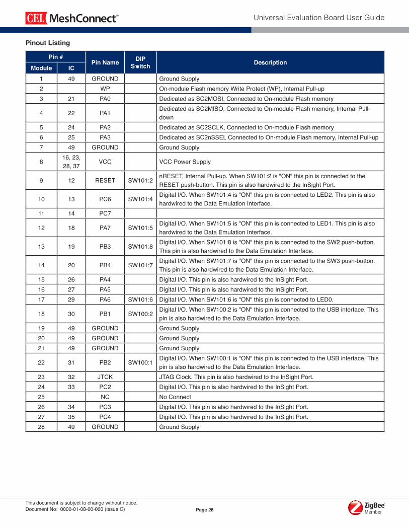
Pinout Listing
Pin #Pin Name DIP
Switch DescriptionModule IC
1 49 GROUND GroundSupply2 WP On-moduleFlashmemoryWriteProtect(WP),InternalPull-up3 21 PA0 DedicatedasSC2MOSI,ConnectedtoOn-moduleFlashmemory
4 22 PA1 DedicatedasSC2MISO,ConnectedtoOn-moduleFlashmemory,InternalPull-down
5 24 PA2 DedicatedasSC2SCLK,ConnectedtoOn-moduleFlashmemory6 25 PA3 DedicatedasSC2nSSELConnectedtoOn-moduleFlashmemory,InternalPull-up7 49 GROUND GroundSupply
816,23,28,37
VCC VCCPowerSupply
9 12 RESET SW101:2nRESET,InternalPull-up.WhenSW101:2is"ON"thispinisconnectedtotheRESETpush-button.ThispinisalsohardwiredtotheInSightPort.
10 13 PC6 SW101:4DigitalI/O.WhenSW101:4is"ON"thispinisconnectedtoLED2.ThispinisalsohardwiredtotheDataEmulationInterface.
11 14 PC7
12 18 PA7 SW101:5DigitalI/O.WhenSW101:5is"ON"thispinisconnectedtoLED1.ThispinisalsohardwiredtotheDataEmulationInterface.
13 19 PB3 SW101:8DigitalI/O.WhenSW101:8is"ON"thispinisconnectedtotheSW2push-button.ThispinisalsohardwiredtotheDataEmulationInterface.
14 20 PB4 SW101:7DigitalI/O.WhenSW101:7is"ON"thispinisconnectedtotheSW3push-button.ThispinisalsohardwiredtotheDataEmulationInterface.
15 26 PA4 DigitalI/O.ThispinisalsohardwiredtotheInSightPort.16 27 PA5 DigitalI/O.ThispinisalsohardwiredtotheInSightPort.17 29 PA6 SW101:6 DigitalI/O.WhenSW101:6is"ON"thispinisconnectedtoLED0.
18 30 PB1 SW100:2DigitalI/O.WhenSW100:2is"ON"thispinisconnectedtotheUSBinterface.ThispinisalsohardwiredtotheDataEmulationInterface.
19 49 GROUND GroundSupply20 49 GROUND GroundSupply21 49 GROUND GroundSupply
22 31 PB2 SW100:1DigitalI/O.WhenSW100:1is"ON"thispinisconnectedtotheUSBinterface.ThispinisalsohardwiredtotheDataEmulationInterface.
23 32 JTCK JTAGClock.ThispinisalsohardwiredtotheInSightPort.24 33 PC2 DigitalI/O.ThispinisalsohardwiredtotheInSightPort.25 NC No Connect26 34 PC3 DigitalI/O.ThispinisalsohardwiredtotheInSightPort.27 35 PC4 DigitalI/O.ThispinisalsohardwiredtotheInSightPort.28 49 GROUND GroundSupply
Page 27
Universal Evaluation Board User Guide
This document is subject to change without notice.Document No: 0000-01-08-00-000 (Issue C)
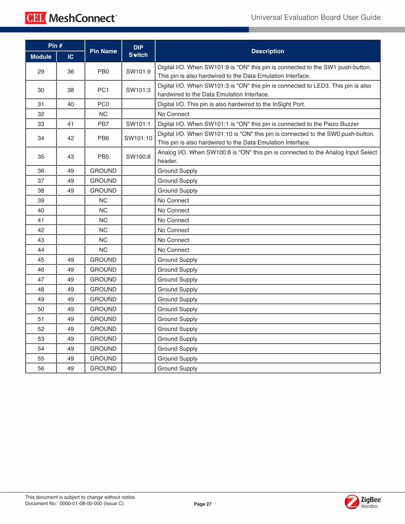
Pin #Pin Name DIP
Switch DescriptionModule IC
29 36 PB0 SW101:9DigitalI/O.WhenSW101:9is"ON"thispinisconnectedtotheSW1push-button.ThispinisalsohardwiredtotheDataEmulationInterface.
30 38 PC1 SW101:3DigitalI/O.WhenSW101:3is"ON"thispinisconnectedtoLED3.ThispinisalsohardwiredtotheDataEmulationInterface.
31 40 PC0 DigitalI/O.ThispinisalsohardwiredtotheInSightPort.32 NC No Connect33 41 PB7 SW101:1 DigitalI/O.WhenSW101:1is"ON"thispinisconnectedtothePiezoBuzzer
34 42 PB6 SW101:10DigitalI/O.WhenSW101:10is"ON"thispinisconnectedtotheSW0push-button.ThispinisalsohardwiredtotheDataEmulationInterface.
35 43 PB5 SW100:8AnalogI/O.WhenSW100:8is"ON"thispinisconnectedtotheAnalogInputSelectheader.
36 49 GROUND GroundSupply37 49 GROUND GroundSupply38 49 GROUND GroundSupply39 NC No Connect40 NC No Connect41 NC No Connect42 NC No Connect43 NC No Connect44 NC No Connect45 49 GROUND GroundSupply46 49 GROUND GroundSupply47 49 GROUND GroundSupply48 49 GROUND GroundSupply49 49 GROUND GroundSupply50 49 GROUND GroundSupply51 49 GROUND GroundSupply52 49 GROUND GroundSupply53 49 GROUND GroundSupply54 49 GROUND GroundSupply55 49 GROUND GroundSupply56 49 GROUND GroundSupply
X5M
arch
25,
201
0C
ISSU
E
Draw
ing T
itle:
Size
Docu
men
t Num
ber
Date
:Sh
eet
of1
1
DAUG
HTER
CAR
D SC
HEM
ATIC
1
A
12/1
4/20
10
REVI
SION
REC
ORD
DESC
RIPT
ION:
DATE
:IS
SUE
PREL
IMIN
ARY
X0
0008
-01-
01-0
4-00
0
EM35
7 M
ODUL
E
CP T
XD =
Mod
ule R
XD
GND
GND
GND
GND
GND
NC NC NC
GND
WP
PA0
PA1
PA2
PA3
GND
VCC
RESE
TPC
6PC
7PA
7PB
3PB
4PA
4PA
5PA
6PB
1GN
D
GND
GND
GND
GND
GND
GND
GND NC NC NC GND
GNDGNDPB2JTCKPC2NCPC3PC4GNDPB0PC1PC0NCPB7PB6PB5GNDGND
P0: W
PP1
: JCL
KP2
: RES
ET
X1RE
VISE
D PE
R SP
READ
SHEE
T01
/03/
11
NC
NC
DEI C
ONNE
CTOR
ISA
CONN
ECTO
R
NC
JTCK
RESE
T
X2RE
VISE
D PE
R SP
READ
SHEE
T02
/25/
11X3
REVI
SED
PER
SPRE
ADSH
EET
03/1
0/11
X4IN
ITIAL
REL
EASE
REV
ISED
PER
SPR
EADS
HEET
04/1
5/11
X5RE
VISE
D PE
R EC
R#00
0142
05/1
8/11
1 2 3 4 5 6 7 8 9 10 11 12 13 14 15 16 17 18 19
20
21
22
23
24
25
26
27
28
29
30
31
32
33
34
35
36
37
38394041424344454647484950515253545556U1
1AM
1CE
L_LO
GO
11
33
55
77
99
1111
22
44
66
88
1010
1212
J1
CONN
_HDR
_6X2
_5-1
0261
9-4_
AMP
Head
er 6
x 2
12
34
5
109
87
6
J2
SAM
TEC_
FTSH
-105
-01-
F-DV
-K
1PC.4_DC2 P5_DC 3PC.5_DC4 P6_DC 5PC.6_DC6 P7_DC 7PC.7_DC8 P8_DC 9P0_DC10 P9_DC 11P1_DC12 P10_DC 13P2_DC14 P11_DC 15P3_DC16 P12_DC 17P4_DC18 P13_DC 19VCC_DC20 GND
23CP
_RXD
_DC
24PA
.0_D
C25
CP_T
XD_D
C26
PA.1
_DC
27M
OSI_D
C28
PA.2
_DC
29SC
K_DC
30PA
.3_D
C31
WP_
DC32
PA.4
_DC
33M
ISO_
DC34
PA.5
_DC
35CS
_DC
36PA
.6_D
C37
POT_
DC38
PA.7
_DC
39IS
P2_D
C40
PB.0
_DC
41IS
P1_D
C42
PB.1
_DC
45PB
.2_D
C46
SW0_
DC47
PB.3
_DC
48SW
1_DC
49PB
.4_D
C50
SW2_
DC51
PB.5
_DC
52SW
3_DC
53PB
.6_D
C54
LED0
_DC
55PB
.7_D
C56
LED1
_DC
57PC
.0_D
C58
LED2
_DC
59PC
.1_D
C60
LED3
_DC
61PC
.2_D
C62
RESE
T_DC
63PC
.3_D
C64
BUZZ
ER_D
C
J5
J4J3
PCB1
PB.6
_DC
PB.0
_DC
PB.3
_DC
PB.4
_DC
PA.6
_DC
PA.7
_DC
PC.6
_DC
PC.1
_DC
PB.7
_DC
P0_DCP1_DC
VCC_DC
P2_D
C
GND
P0_D
C
PA.0
_DC
PA.1
_DC
PA.2
_DC
PA.3
_DC
VCC_
DC
P2_D
C
PC.6
_DC
PC.7
_DC
PA.7
_DC
PB.3
_DC
PB.4
_DC
PA.4
_DC
PA.5
_DC
PA.6
_DC
PB.1
_DC
P1_DC
PB.2_DC
PC.2_DC
PC.3_DC
PC.4_DC
PB.0_DC
PC.1_DC
PC.0_DC
PB.7_DC
PB.6_DC
PB.5_DC
PA.0
_DC
PA.1
_DC
PA.2
_DC
PA.3
_DC
PC.6_DCPC.7_DC
PA.7
_DC
PB.3
_DC
PB.4
_DC
PA.4
_DC
PA.5
_DC
PA.6
_DC
PB.1
_DC
PB.2
_DC
PC.2
_DC
PC.3
_DC
PC.4_DCPB
.0_D
CPC
.1_D
CPC
.0_D
C
PB.5
_DC
PB.6
_DC
PB.7
_DC
P2_DC
PB.2
_DC
PB.1
_DC
PB.5
_DC
PC.6
_DC
PB.4
_DC
PB.6
_DC
PC.1
_DC
PB.0
_DC
GND
PB.1
_DC
PB.2
_DC
PB.3
_DC
PA.7
_DC
PC.2
_DC
PC.3
_DC
P1_D
CP2
_DC
PA.5
_DC
PC.0
_DC
GND
PC.4
_DC
PA.4
_DC
GND
CA
RR
IER
BO
AR
D S
CH
EMAT
IC
Page 29
Universal Evaluation Board User Guide
This document is subject to change without notice.Document No: 0000-01-08-00-000 (Issue C)
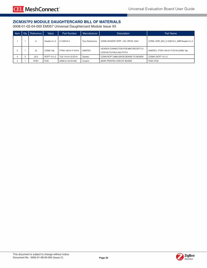
ZICM357P2 MODULE DAUGHTERCARD BILL OF MATERIALS0008-01-02-04-000EM357UniversalDaughtercardModuleIssueX5
Item Qty Reference Value PartNumber Manufacturer Description PartName
1 1 J1 Header6x2 5-102619-4 Tyco Electronics CONNHEADERVERT.10012POS15AU CONN_HDR_6X2_5-102619-4_AMP,Header6x2
2 1 J2 CONN10p FTSH-105-01-F-DV-K SAMTECHEADERCONNECTOR,PCBMNT,RECEPT,10
CONTACTS,PIN,0.050PITCHSAMTEC_FTSH-105-01-F-DV-K,CONN10p
3 3 J3-5 RCPT10x2 TLE-110-01-G-DV-A Samtec CONNRCPT2MM20POSBOARDTOBOARD CONN1,RCPT10x2
4 1 PCB1 PCB 0008-01-04-04-000 Custom BAREPRINTEDCIRCUITBOARD PCB1,PCB
Page 30
Universal Evaluation Board User Guide
This document is subject to change without notice.Document No: 0000-01-08-00-000 (Issue C)
ADDENDUM: ZICM357SPx-1CEL’sMeshConnectEM357MiniModulescombinehighperformanceRFsolutionswiththemarket’spremierZigBeestack.Availableinlowandhighoutputpoweroptions(+8dBmand+20dBm), these modules canaccommodatevariablerangeandperformancerequirements.ThetinymodulefootprintmakesthemsuitableforawiderangeofZigBeeapplications.TheMeshConnectEM357MiniModulesarecertifiedandqualified,enablingcustomerstoacceleratetimetomarketbygreatlyreducingthedesignandcertificationphasesofdevelopment.
CEL’s MeshConnect EM357 Mini Modules (ZICM357SP0 andZICM357SP2) are based on the Ember EM357 Zigbee compliantSoCradioIC.TheICisasingle-chipsolution,compliantwithZigBeespecifications and IEEE 802.15.4; a completewireless solution for all ZigBee applications.The IC consists of anRFtransceiverwiththebasebandmodem,ahardwiredMACandanembedded32-bitARM®Cortex™-M3microcontrollerwithinternalRAM(12kB)andFlash(192kB)memory.Thedeviceprovidesnumerousgeneral-purposeI/OpinsandperipheralfunctionssuchastimersandUARTs.
Page 31
Universal Evaluation Board User Guide
This document is subject to change without notice.Document No: 0000-01-08-00-000 (Issue C)
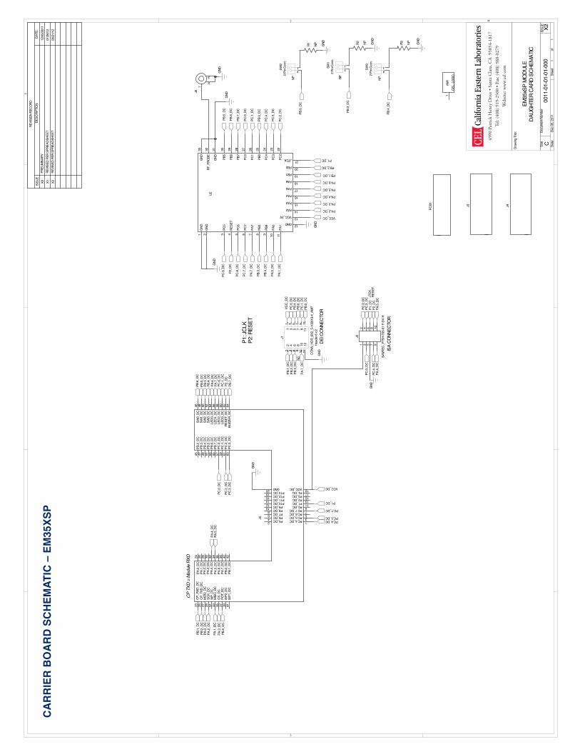
HARDWARE DESCRIPTION
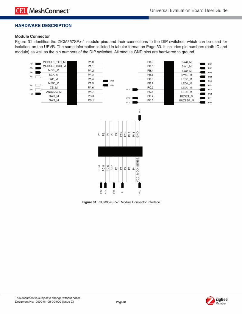
Module ConnectorFigure31 identifiestheZICM357SPx-1modulepinsandtheirconnectionsto theDIPswitches,whichcanbeusedforisolation,ontheUEVB.ThesameinformationislistedintabularformatonPage33.Itincludespinnumbers(bothICandmodule)aswellasthepinnumbersoftheDIPswitches.AllmoduleGNDpinsarehardwiredtoground.
MODULE_TXD_M PA.0PA.1PA.2PA.3PA.4PA.5PA.6PA.7PB.0PB.1
PB.2PB.3PB.4PB.5PB.6PB.7PC.0PC.1PC.2PC.3
PC.4
PC.5
PC.6
PC.7
P0 P1 P2 P3 P4
P5 P6 P7 P8 P9 P10
P11
P12
P13
GN
DVC
C_M
OD
_SEN
SE
SW0_MSW1_MSW2_MSW3._MLED0_MLED1_MLED2_MLED3_M
RESET_MBUZZER_M
MODULE_RXD_MPB1
PB2
PA0
PA2
PA1
PA3
PB5
MOSI_MSCK_MWP_M
MISO_MCS_M
ANALOG_MSW6_MSW5_M
PA4
PA5
PC0
PC2
PC3
GN
D
PB6
PB0
PB3
PB4
PA6
PA7
PC6
PC1
P2
PB7PC
4
PC5
PC7
P1 VCC
Figure 31:ZICM357SPx-1ModuleConnectorInterface
Page 32
Universal Evaluation Board User Guide
This document is subject to change without notice.Document No: 0000-01-08-00-000 (Issue C)
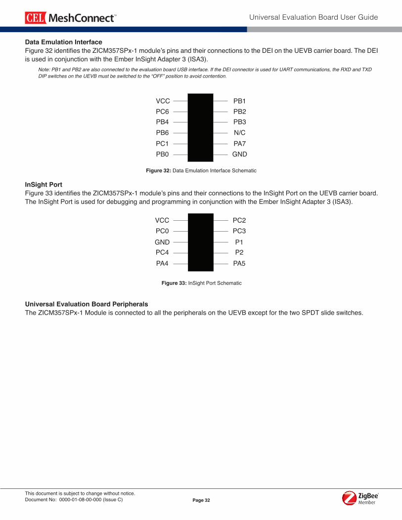
Data Emulation InterfaceFigure32identifiestheZICM357SPx-1module’spinsandtheirconnectionstotheDEIontheUEVBcarrierboard.TheDEIisusedinconjunctionwiththeEmberInSightAdapter3(ISA3). Note: PB1 and PB2 are also connected to the evaluation board USB interface. If the DEI connector is used for UART communications, the RXD and TXD DIP switches on the UEVB must be switched to the “OFF” position to avoid contention.
InSight PortFigure33identifiestheZICM357SPx-1module’spinsandtheirconnectionstotheInSightPortontheUEVBcarrierboard.TheInSightPortisusedfordebuggingandprogramminginconjunctionwiththeEmberInSightAdapter3(ISA3).
Universal Evaluation Board PeripheralsTheZICM357SPx-1ModuleisconnectedtoalltheperipheralsontheUEVBexceptforthetwoSPDTslideswitches.
VCCPC6PB4PB6
PB0PC1
PB1PB2PB3N/C
GNDPA7
Figure 32:DataEmulationInterfaceSchematic
Figure 33:InSightPortSchematic
VCCPC0GNDPC4PA4
PC2PC3P1P2
PA5
Page 33
Universal Evaluation Board User Guide
This document is subject to change without notice.Document No: 0000-01-08-00-000 (Issue C)
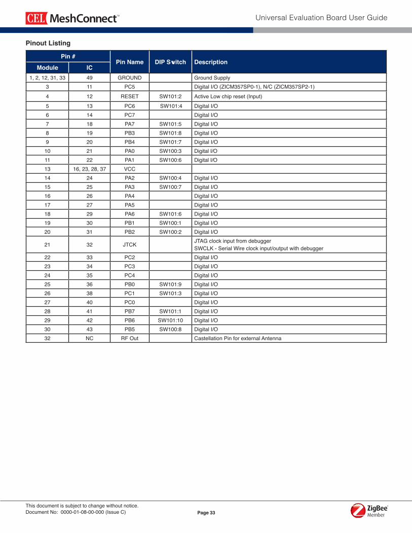
Pinout Listing
Pin #Pin Name DIP Switch Description
Module IC1,2,12,31,33 49 GROUND GroundSupply
3 11 PC5 DigitalI/O(ZICM357SP0-1),N/C(ZICM357SP2-1)4 12 RESET SW101:2 ActiveLowchipreset(Input)5 13 PC6 SW101:4 DigitalI/O6 14 PC7 DigitalI/O7 18 PA7 SW101:5 DigitalI/O8 19 PB3 SW101:8 DigitalI/O9 20 PB4 SW101:7 DigitalI/O10 21 PA0 SW100:3 DigitalI/O11 22 PA1 SW100:6 DigitalI/O13 16,23,28,37 VCC14 24 PA2 SW100:4 DigitalI/O15 25 PA3 SW100:7 DigitalI/O16 26 PA4 DigitalI/O17 27 PA5 DigitalI/O18 29 PA6 SW101:6 DigitalI/O19 30 PB1 SW100:1 DigitalI/O20 31 PB2 SW100:2 DigitalI/O
21 32 JTCK JTAGclockinputfromdebuggerSWCLK-SerialWireclockinput/outputwithdebugger
22 33 PC2 DigitalI/O23 34 PC3 DigitalI/O24 35 PC4 DigitalI/O25 36 PB0 SW101:9 DigitalI/O26 38 PC1 SW101:3 DigitalI/O27 40 PC0 DigitalI/O28 41 PB7 SW101:1 DigitalI/O29 42 PB6 SW101:10 DigitalI/O30 43 PB5 SW100:8 DigitalI/O32 NC RFOut CastellationPinforexternalAntenna
X2De
c 05,
201
1C
ISSU
E
Draw
ing T
itle:
Size
Docu
men
t Num
ber
Date
:Sh
eet
of1
1
DAUG
HTER
CAR
D SC
HEM
ATIC
1
A
12/0
5/20
11
REVI
SION
REC
ORD
DESC
RIPT
ION:
DATE
:IS
SUE
PREL
IMIN
ARY
X0
0011
-01-
01-0
1-00
0
EM35
xSP
MOD
ULE
CP T
XD =
Mod
ule R
XD
P1: J
CLK
P2: R
ESET
NC
DEI C
ONNE
CTOR
ISA
CONN
ECTO
R
JTCK
RESE
T
X1RE
VISE
D PE
R SP
READ
SHEE
T01
/26/
12X2
REVI
SED
PER
SPRE
ADSH
EET
06/2
1/12
1AM
1CE
L_LO
GO
11
33
55
77
99
1111
22
44
66
88
1010
1212
J1
CONN
_HDR
_6X2
_5-1
0261
9-4_
AMP
Head
er 6
x 2
12
34
5
109
87
6
J2
SAM
TEC_
FTSH
-105
-01-
F-DV
-K
1PC.4_DC2 P5_DC 3PC.5_DC4 P6_DC 5PC.6_DC6 P7_DC 7PC.7_DC8 P8_DC 9P0_DC10 P9_DC 11P1_DC12 P10_DC 13P2_DC14 P11_DC 15P3_DC16 P12_DC 17P4_DC18 P13_DC 19VCC_DC20 GND
23CP
_RXD
_DC
24PA
.0_D
C25
CP_T
XD_D
C26
PA.1
_DC
27M
OSI_D
C28
PA.2
_DC
29SC
K_DC
30PA
.3_D
C31
WP_
DC32
PA.4
_DC
33M
ISO_
DC34
PA.5
_DC
35CS
_DC
36PA
.6_D
C37
POT_
DC38
PA.7
_DC
39IS
P2_D
C40
PB.0
_DC
41IS
P1_D
C42
PB.1
_DC
45PB
.2_D
C46
SW0_
DC47
PB.3
_DC
48SW
1_DC
49PB
.4_D
C50
SW2_
DC51
PB.5
_DC
52SW
3_DC
53PB
.6_D
C54
LED0
_DC
55PB
.7_D
C56
LED1
_DC
57PC
.0_D
C58
LED2
_DC
59PC
.1_D
C60
LED3
_DC
61PC
.2_D
C62
RESE
T_DC
63PC
.3_D
C64
BUZZ
ER_D
C
J5
J4J3
PCB1
1
23
J6
12SW
22
Pin C
onn.
NP
12SW
12
Pin C
onn.
NP
12SW
32
Pin C
onn.
NP
R1 NP R2 NP R3 NP
3PC
54
RESE
T5
PC6
6PC
77
PA7
8PB
39
PB4
10PA
011
PA1 12GND
13VCC_3V14PA215PA316PA417PA518PA619PB120PB221JTCK
22PC
2
23PC
3
24PC
4
25PB
0
26PC
1
27PC
0
28PB
7
29PB
6
30PB
5
31GN
D
32RF
_PRO
BE
33GN
D1
GND
2GN
DU2
PB.6
_DC
PB.0
_DC
PB.3
_DC
PB.4
_DC
PA.6
_DC
PA.7
_DC
PC.6
_DC
PC.1
_DC
PB.7
_DC
P1_DC
VCC_DC
P2_D
C
PA.0
_DC
PA.1
_DC
PA.2_DC
PA.3_DC
VCC_DC
P2_D
C
PC.6
_DC
PC.7
_DC
PA.7
_DC
PB.3
_DC
PB.4
_DC
PA.4_DC
PA.5_DC
PA.6_DC
PB.1_DC
P1_DC
PB.2_DC
PC.2
_DC
PC.3
_DC
PC.4
_DC
PB.0
_DC
PC.1
_DC
PC.0
_DC
PB.7
_DC
PB.6
_DC
PB.5
_DC
PC.7_DC
PA.4
_DC
PA.5
_DC
PC.2
_DC
PC.3
_DC
PC.4_DC
PC.0
_DC
PB.2
_DC
PB.1
_DC
PB.5
_DC
PC.6
_DC
PB.4
_DC
PB.6
_DC
PC.1
_DC
PB.0
_DC
GND
PB.1
_DC
PB.2
_DC
PB.3
_DC
PA.7
_DC
PC.2
_DC
PC.3
_DC
P1_D
CP2
_DC
PA.5
_DC
PC.0
_DC
GND
PC.4
_DC
PA.4
_DC
GND
GND
GND
GND
GND
PC.5_DC
PC.5
_DC
PB.0
_DC
PB.3
_DC
PB.4
_DC
GND
GND
GND
PA.0
_DC
PA.2
_DC
PA.1
_DC
PA.3
_DC
VCC_
DC
CA
RR
IER
BO
AR
D S
CH
EMAT
IC –
EM
35XS
P
Page 35
Universal Evaluation Board User Guide
This document is subject to change without notice.Document No: 0000-01-08-00-000 (Issue C)
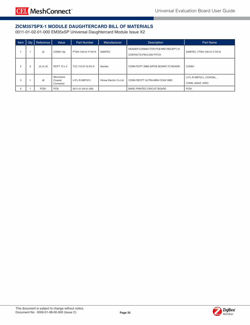
ZICM357SPX-1 MODULE DAUGHTERCARD BILL OF MATERIALS0011-01-02-01-000EM35xSPUniversalDaughtercardModuleIssueX2
Item Qty Reference Value PartNumber Manufacturer Description PartName
1 1 J2 CONN10p FTSH-105-01-F-DV-K SAMTECHEADERCONNECTOR,PCBMNT,RECEPT,10
CONTACTS,PIN,0.050PITCHSAMTEC_FTSH-105-01-F-DV-K
2 3 J3J4J5 RCPT10x2 TLE-110-01-G-DV-A Samtec CONNRCPT2MM20POSBOARDTOBOARD CONN1
3 1 J6Microwave Coaxial Connector
U.FL-R-SMT(01) HiroseElectricCoLtd CONNRECPTULTRA-MINICOAXSMDU.FL-R-SMT(01)_COAXIAL_
CONN_6GHZ_HIRO
4 1 PCB1 PCB 0011-01-04-01-000 BAREPRINTEDCIRCUITBOARD PCB1
Page 36
Universal Evaluation Board User Guide
This document is subject to change without notice.Document No: 0000-01-08-00-000 (Issue C)
REFERENCES Reference Documents Download
ZICM357SPxDatasheet-EM357MiniModules(ZICM357SP0-1,ZICM357SP0-1C,ZICM357SP2-1,ZICM357SP2-1C) Link
REVISION HISTORYPrevious Versions Changes to Current Version Page(s)
0000-01-08-00-000 (IssueA)October21,2012 InitialRelease N/A
0000-01-08-00-000 (IssueB)February20,2013 AddedZICM357SPx-1AddendumInformation,StyleChangeandNewDocumentTemplate All
0000-01-08-00-000 (IssueC)August21,2013
RemovedZICM357P2DatasheetfromReferenceDocumentsTableAddedlinkforTechnicalAssistance 36,37
Page 37
Universal Evaluation Board User Guide
This document is subject to change without notice.Document No: 0000-01-08-00-000 (Issue C)
For More information FormoreinformationaboutCELMeshConnectproductsandsolutions,visitourwebsiteat:www.cel.com/MeshConnect.
Technical AssistanceForTechnicalAssistance,visitwww.cel.com/MeshConnectHelp.
Theinformationinthisdocumentiscurrentasofthepublisheddate.Theinformationissubjecttochangewithoutnotice.Foractualdesign-in,refertothelatestpublicationsofCELDataSheetsorDataBooks,etc.,forthemostup-to-datespecificationsofCELproducts.Notallproductsand/ortypesareavailableineverycountry.PleasecheckwithanCELsalesrepresentativeforavailabilityandadditionalinformation. No part of this document may be copied or reproduced in any form or by any means without the prior written consent of CEL. CEL assumes no responsibility for any errors that may appear in this document. CEL does not assume any liability for infringement of patents, copyrights or other intellectual property rights of third parties by or arising from the useofCELproductslistedinthisdocumentoranyotherliabilityarisingfromtheuseofsuchproducts.Nolicense,express,impliedorotherwise,isgranted under any patents, copyrights or other intellectual property rights of CEL or others. Descriptions of circuits, software and other related information in this document are provided for illustrative purposes in semiconductor product operationandapplicationexamples.Theincorporationofthesecircuits,softwareandinformationinthedesignofacustomer’sequipmentshallbedone under the full responsibility of the customer. CEL assumes no responsibility for any losses incurred by customers or third parties arising from the use of these circuits, software and information. WhileCELendeavorstoenhancethequality,reliabilityandsafetyofCELproducts,customersagreeandacknowledgethatthepossibilityofdefectsthereofcannotbeeliminatedentirely.Tominimizerisksofdamagetopropertyorinjury(includingdeath)topersonsarisingfromdefectsinCELproducts,customersmustincorporatesufficientsafetymeasuresintheirdesign,suchasredundancy,fire-containmentandanti-failurefeatures.
Disclaimer
Top Related