


Languages
Pages
Legal

ULTRATHIN AND HIGHLY FLEXIBLE PARYLENE-C
PACKAGED CARBON NANOTUBE FIELD EFFECT
TRANSISTORS
A Dissertation Presented
by
Selvapraba Selvarasah
to
The Department of Electrical and Computer Engineering
in partial fulfillment of the requirements
for the degree of
Doctor of Philosophy
in
Electrical Engineering
in the field of
Microsystems and Electron Devices
Northeastern University
Boston, Massachusetts
December 2010
ii
ACKNOWLEDGMENT
I am very much obliged and thankful to all, for their great help and cooperation
extended to me in the preparation of this thesis. First of all, I would like to thank my
advisor, Prof. Mehmet Dokmeci, for all his help and guidance during this work. He has
helped me in many ways from the day I have joined his group. I am very proud and
honored to be his first student in his group at Northeastern University. He was always
available for me to share his precious knowledge and thoughts. His encouragement and
enthusiasm has motivated me in many ways to achieve my goals successfully. Secondly,
I would like to thank Prof. A. Busnaina for his advice and financial support from the
NSF-funded Nanoscale Science and Engineering Center for High-rate
Nanomanufacturing. I would also like to thank Prof. S. Sridhar for his advice and
financial support from Air Force Research Laboratory. I am happy to acknowledge Prof.
L. Menon, Prof. Y. J. Jung, Prof. V. Harris, Prof. S. Sonkusale (Tufts University), and
Prof. G. Miller (University of New Hampshire) for sharing their expertise with me. I
would like to thank Prof. J. Hopwood for sharing his valuable knowledge with me about
the low temperature etching process. I would like to thank fellow graduate students and
post doctorates from Dana 325, CHN and eMRI, especially Prashanth, Juan, Chao,
Evin, Myung, Dr. D. Mao, Dr. L. Chen, Dr. S. Somu, Dr. N-G. Cha, Dr. X. Xiong, Dr. S.
Ryley, Dr. R. Banyal, Dr. D. Nagesha, Dr. P. Vodo, Dr. W. T. Lu, Dr. B. D. F. Casse and
Dr. I. Kaur for sharing their valuable knowledge and experience which helped me get my
work done efficiently. I would also like to thank Kostas facility, especially D. McKee, S.
McNamara and R. Devito, for their support in utilizing the facility. Many thanks to our
iii
collaborators at Stanford University (Prof. Z. Bao and Y. Chung) and Harvard Medical
school (Prof. A. Khademhosseini and his group).
Above everything, I would like to thank my family, especially my parents, for
their motivation, guidance and eternal love. My dad and mom have encouraged me to
pursue PhD, and their kindness and support was very precious during my ups and downs
in the last 6 years. I would not have achieved this PhD without their moral support, and
hence I would like to dedicate this thesis to my parents. I would also like to thank my
two brothers, sister, brother-in-law and niece for their encouragement. Finally, many
more thanks to my lovely wife for her endless love and support.
iv
ABSTRACT
Flexible electronics are promising alternatives to traditional silicon based
electronics for applications that require characteristics such as lightweight, ease of
fabrication, mechanical flexibility, low cost production, and able to be wrapped into
complex shapes. The advances in organic materials and related processing techniques
have enabled several emerging applications for flexible electronics such as electronic
paper, wearable displays, large area antennas, RFID tags, etc. Despite the growing
momentum in this field, the low field effect mobility of the organic molecules used in
realizing these devices has limited their performance (eg. mobility of pentacene based
transistor is ~1 cm2/Vs). Carbon nanotubes with their unique chemical, physical and
mechanical properties are promising active materials for high performance electronic
devices. The ability to deposit and pattern CNTs from solution phase over a large area
presents them as ideal candidates for flexible electronics.
The goal of this thesis is to realize ultrathin, highly flexible and biocompatible
electronic devices using solution processed SWNTs on flexible parylene-C substrates.
Due to its excellent dielectric and passivation properties, parylene is also used as an
encapsulation layer. The adhesion and gate dielectric properties of parylene-C for CNT
based flexible devices are evaluated. Next, parylene-C packaged SWNTs based thin
(12µm) film transistor is designed and fabricated, electrical characteristic before and after
encapsulation is evaluated, and then its mechanical flexibility is studied. The stability of
all-parylene CNTFETs are also investigated in 0.9% sterile solution of sodium chloride
for 42 days. Finally, a room temperature integration of SWNTs into three dimensional
architectures is demonstrated for the realization of high density flexible devices.
v
TABLE OF CONTENTS
CHAPTER 1 FLEXIBLE ELECTRONICS.………………….……………........ 1
1.1 INTRODUCTION………................................................................................ 1
1.2 HISTROY OF FLEXIBLE ELECTRONICS.…….......................................... 3
1.3 MATERIALS FOR FLEXIBLE ELECTRONICS.………………………….. 6
1.3.1 MECHANICALLY FLEXIBLE SUBSTRATES..……………………. 7
1.3.2 GATE DIELECTRIC MATERIALS.………………………………….. 9
1.3.3 ENCAPSULATION..………………………………………………….. 11
1.4 FABRICATION TECHNOLOGY FOR FLEXIBLE ELECTRONICS.......... 13
1.5 APPLICATIONS OF FLEXIBLE ELECTRONICS.………………………... 14
CHAPTER 2 CARBON NANOTUBES..………………………………………... 16
2.1 INTRODUCTION..………………………...................................................... 16
2.2 THE HISTORY CARBON NANOTUBES..................................................... 16
2.3 CARBON NANOTUBE SYNTHESIS............................................................ 17
2.4 STRUCTURE AND PROPERTIES..……….………………………..……… 20
2.4.1 ELECTRONIC PROPERTIES..……………...………………………... 23
2.4.2 OPTICAL PROPERTIES..……………….……………………………. 25
2.4.3 MECHANICAL PROPERTIES..………….…………………………... 26
2.4.4 CHEMICAL PROPERTIES..……………….…………..……………... 28
2.4.5 THERMAL PROPERTIES....………………….……..………………... 28
2.5 CARBON NANOTUBE ASSEMBLY....…………………………………… 29
2.9 APPLICATIONS OF CNTS....……………………..……………..…………. 31
CHAPTER 3 PARYLENE-C: DEPOSITION, SURFACE
CHARACTERIZATION AND DRY ETCHING...…………………………….. 32
3.1 INTRODUCTION..…….................................................................................. 32
3.2 PARYLENE AND ITS APPLICATIONS....................................................... 33
3.2.1 PROPERTIES AND CHARACTERISTICS OF PARYLENE............... 33
3.2.2 APPLICATIONS OF PARYLENE-C..................................................... 36
3.3 RESULTS AND DISCUSSION....................................................................... 36
3.3.1 PARYLENE DEPOSITION PROCESS.................................................. 36
vi
3.3.2 SURFACE PROPERTIES OF PARYLENE-C....................................... 39
3.3.3 PLASMA ETCHING OF PARYLENE-C............................................... 43
CHAPTER 4 PARYLENE-C DIELECTRIC FOR CARBON NANOTUBE
FIELD EFFECT TRANSISTORS..…….……………………………………….. 47
4.1 INTRODUCTION..…….................................................................................. 47
4.2 FABRICATION OF PARYLENE-C BASED MIM STRUCTURE................ 50
4.3 RESULTS AND DISCUSSION....................................................................... 51
CHAPTER 5 PARYLENE-C ENCAPSULATED SINGLE WALLED
CARBON NANOTUBES BASED THIN FILM TRANSISTORS.……………. 59
5.1 INTRODUCTION..…….................................................................................. 59
5.2 FABRICATION OF FLEXIBLE SWNTS TFTS............................................. 62
5.3 RESULTS AND DISCUSSION....................................................................... 67
5.3.1 ELECTRICAL CHARACTERISTICS OF FLEXIBLE SWNTS
TFTS…………………………………………………………………………. 67
5.3.2 MECHANICAL EVALUATION OF FLEXIBLE SWNTS TFTS......... 71
CHAPTER 6 PARYLENE-C PASSIVATION FOR SWNTS FETS.…………. 77
6.1 INTRODUCTION..…….................................................................................. 77
6.2 FABRICATION OF PARYLENE-C PASSIVATED FLEXIBLE
SWNTS TFTS……………………………………………………………………. 81
6.3 RESULTS AND DISCUSSION....................................................................... 83
CHAPTER 7 BIOSTABILITY OF PARYLENE-C ENCAPSULATED
CARBON NANOTUBES FLEXIBLE TRANSISTORS.………………………. 100
7.1 INTRODUCTION..…….................................................................................. 100
7.2 DEVICE FABRICATION AND EXPERIMENTAL SETUP......................... 103
7.3 RESULTS AND DISCUSSION....................................................................... 106
CHAPTER 8 VERTICAL AND HIGH DENSITY SWNTS TRANSISTORS.. 110
8.1 INTRODUCTION..……………….................................................................. 110
8.2 HIGH DENSITY VERTICAL ASSEMBLY OF SINGLE-WALLED
CARBON NANOTUBES.…..………….……………………………................... 112
8.2.1 FABRICATION OF 3D MICROPLATFORM.…………...................... 113
8.2.2 DIELECTROPHORETIC ASSEMBLY OF 3D-SWNTS AND TWO
vii
TERMINAL ELECTRICAL MEASUREMENTS........................................... 116
8.2.3 DEP SIMULATION.…………………...……………………………… 130
8.3 A VERTICAL SWNTS FIELD EFFECT TRANSISTOR............................... 134
8.3.1 FABRICATION OF 3D SWNTS FET..……………….......................... 135
8.3.2 ELECTRICAL CHARACTERIZATION OF VERTICAL
SWNTS FETS………………………………………………………………... 137
CHAPTER 9 CONCLUSION AND FUTURE WORK..……...……................... 144
APPENDIXES.…………………………………………......................................... 146
REFERENCES..…………………………………………....................................... 167
PUBLICATIONS..…………………………………………................................... 181
viii
LIST OF TABLES
1.1 Characteristics of silicon and flexible electronics…………………............. 2
2.1 Mechanical properties of carbon nanotubes................................................. 27
3.1 ICP etch recipes for low temperature (5ºC) and low pressure (5mTorr)
parylene-C etching......................................................................................... 44
4.1 Adhesion of different metals on oxygen plasma treated or untreated
parylene-C surface......................................................................................... 52
8.1 Comparison of DEP forces for different microelectrode geometries.
FDEP is the calculated DEP force using eqn (2). Fn
DEP is the normalized
DEP force to the smallest value which is obtained at H=2828 nm................ 125
8.2 Comparison of DEP forces for different microelectrode geometries.
FDEP is the calculated dep force using eqn (2). Fn
DEP is the normalized
DEP force to the smallest value which was obtained at
Separation=2,702 nm..................................................................................... 128
8.3 Calculated transconductance and mobility values for the 3D CNTFET……141
ix
LIST OF FIGURES
1.1 Current and future flexible devices. (a) A rollable pocket eReader by
Readius, and (b) Nokia Morph concept shows future mobile devices
which are stretchable and flexible.................................................................. 6
2.1 Schematics of tip-growth and extrusion mechanisms for carbon
filament growth.............................................................................................. 18
2.2 The 2D graphene sheet is shown along with the vector which
specifies the chiral nanotube. The chiral vector Ch=na1+ma2 ≡(n,m)
is defined on the honeycomb lattice by unit vectors a1 and a2 and the
chiral angle θ is defined with respect to the zigzag axis................................ 21
2.3 A schematic theoretical model for a single-walled carbon tube with
the tube axis OB normal to: (a) the θ = 30° direction
(armchair tube) (b) the θ = 0° direction (a zigzag tube), and (c) a
general direction B with 0< θ <30 (chiral tube)............................................. 22
2.4 Schematic structures of SWNTs and how they determine the electronic
properties of the nanotubes. (a) A (10,10) arm-chair nanotube.
Bottom panel: the hexagon represents the first Broulloin zone of
a graphene sheet in reciprocal space. The vertical lines represent the
electronic states of the nanotube. The center-line crosses two corners
of the hexagon, resulting in a metallic nanotube. (b) A (12, 0) zigzag
nanotube. The electronic states cross the hexagon corners, but a small
band gap can develop due to the curvature of the nanotube. (c) The
(14, 0) zigzag tube is semiconducting because the states on the
vertical lines miss the corner points of the hexagon. (d) A (7, 16)
tube is semiconducting................................................................................... 25
3.1 Chemical structure of different parylene types. (a) Parylene N,
(b) Parylene C has one Cl atom in the benzene ring, (c) Parylene D
has two Cl atoms in the benzene ring and (d) Parylene Nova HT
has F atoms in the benzene ring..................................................................... 34
x
3.2 The parylene deposition sequence where the parylene dimer is
decomposed into monomer then polymerization takes places....................... 38
3.3 Parylene-C deposition rate. The measured parylene-C thickness is
plotted against amount of dimmer consumed................................................ 38
3.4 Contact angle measurements from the as-deposited parylene-C surface…... 39
3.5 (a) FESEM image of 10 µm thick Parylene film sealed on to a silicon
substrate and (b) magnified view of (a)......................................................... 41
3.6 Contact angle data from parylene surface after O2 plasma treatment............ 41
3.7 Tricholorosilane (anti-stiction coater) treated parylene surface.................... 42
3.8 Contact angle measurements from as-deposited parylene surface
soaked in an aqueous environment for 3 days............................................... 42
3.9 Contact angle measurement from treated parylene surface
(hydrophilic) in aqueous environments for 3 days........................................ 43
3.10 Anisotropic profiles of (a) 55μm thick parylene and (b) 10μm
thick parylene………………………………………………………………. 45
4.1 The cross section of MIM capacitor structure............................................... 50
4.2 The percentage of failure of untreated and A-174 treated MIM devices....... 53
4.3 Time dependent dielectric breakdown of A-174 treated MIM device.
(a) Staircase plot shows that the dielectric breakdown occurred at
the 200th
second at V=760V and (b) the optical photograph of the
failed device from (a) where the area of the top electrode is
1.2x10⁻³
cm2................................................................................................... 55
4.4 Time dependent dielectric breakdown of parylene-C MIM capacitors
of thickness starting from 1100 nm, 560 nm, and 330 nm down to
130 nm as a function of applied DC voltage. The active area of the
device was 1.2x10⁻³
cm2................................................................................ 56
4.5 The dielectric breakdown of thin parylene-C MIM capacitor as a
function of parylene thickness where the Inset shows the magnified
image of our results………………………………………………………… 57
5.1 Parylene-C packaged SWNT TFTs. (a) 3D schematic of bottom
gated SWNT TFT before parylene-C passivation. (b) Arrays of
xi
SWNT TFTs fabricated on a 3-inch wafer illustrating wafer scale
manufacturing capability. (c) The high resolution SEM micrograph
of assembled SWNTs between source (S) and drain (D) electrodes
of a transistor with a channel length of 10 µm and a width of 2000 μm
respectively. Inset: Top view optical photograph of the same transistor
fabricated from gold Source and Drain electrodes and an aluminum
(bottom) Gate electrodes, where the thickness of the parylene-C gate
dielectric was 1 µm. (D) The parylene film in which the devices were
embedded was wrapped around an index finger and non planar flexibility
of the transistors is illustrated in the inset. The process flow for fabrication
of all-parylene TFT is described in Appendix C........................................... 64
5.2 IDS-VDS measurements (a) before and (b) after electrical breakdown
from the flexible SWNT FETs. Drain to source current (IDS) was
recorded while voltage across the drain to source electrodes (VDS) was
swept from -1 to 1 with 10mV steps, where the gate voltage (VG) was
varied from -40 to 40V with 10V increments. After electrical breakdown,
the device exhibited an ON/OFF ratio that is 2 orders of magnitude
greater than that one before breakdown where ON and OFF currents are
measured at VG of -40V and 40V for VDS = 700mV..................................... 69
5.3 Transfer characteristics after electrical breakdown of metallic SWNTs
from the channel region of the SWNT FETs (device from figure 5.2). As
the gate voltage (VG) of the transistor was increased from
-40V to 40V with 10V increments, a pronounced decrease in
conductance was observed which exhibited a p-type transistor behavior.
The drain-source current (IDS) was strongly modulated by the gate voltage
as the VDS was decreased from 1V to 0V. The transconductance deduced
from the graph (slope in the linear region) was 0.5653 μS (VDS=0.5V).
The field-effect mobility of this device was calculated as ~2 cm2/Vs, where
the parylene-C gate dielectric constant=3.2, LDS=10 μm and WDS=73 μm,
respectively. Inset: magnified image of IDS-VG at VDS=1 V indicating an
ON/OFF ratio of 103...................................................................................... 70
xii
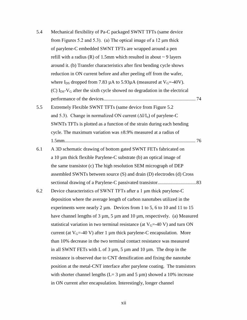
5.4 Mechanical flexibility of Pa-C packaged SWNT TFTs (same device
from Figures 5.2 and 5.3). (a) The optical image of a 12 μm thick
of parylene-C embedded SWNT TFTs are wrapped around a pen
refill with a radius (R) of 1.5mm which resulted in about ~ 9 layers
around it. (b) Transfer characteristics after first bending cycle shows
reduction in ON current before and after peeling off from the wafer,
where IDS dropped from 7.83 µA to 5.93µA (measured at VG=-40V).
(C) IDS-VG after the sixth cycle showed no degradation in the electrical
performance of the devices............................................................................ 74
5.5 Extremely Flexible SWNT TFTs (same device from Figure 5.2
and 5.3). Change in normalized ON current (∆I/Io) of parylene-C
SWNTs TFTs is plotted as a function of the strain during each bending
cycle. The maximum variation was ±8.9% measured at a radius of
1.5mm............................................................................................................ 76
6.1 A 3D schematic drawing of bottom gated SWNT FETs fabricated on
a 10 µm thick flexible Parylene-C substrate (b) an optical image of
the same transistor (c) The high resolution SEM micrograph of DEP
assembled SWNTs between source (S) and drain (D) electrodes (d) Cross
sectional drawing of a Parylene-C passivated transistor................................83
6.2 Device characteristics of SWNT TFTs after a 1 μm thick parylene-C
deposition where the average length of carbon nanotubes utilized in the
experiments were nearly 2 µm. Devices from 1 to 5, 6 to 10 and 11 to 15
have channel lengths of 3 µm, 5 µm and 10 µm, respectively. (a) Measured
statistical variation in two terminal resistance (at VG=-40 V) and turn ON
current (at VG=-40 V) after 1 µm thick parylene-C encapsulation. More
than 10% decrease in the two terminal contact resistance was measured
in all SWNT FETs with L of 3 µm, 5 µm and 10 µm. The drop in the
resistance is observed due to CNT densification and fixing the nanotube
position at the metal-CNT interface after parylene coating. The transistors
with shorter channel lengths (L= 3 µm and 5 µm) showed a 10% increase
in ON current after encapsulation. Interestingly, longer channel
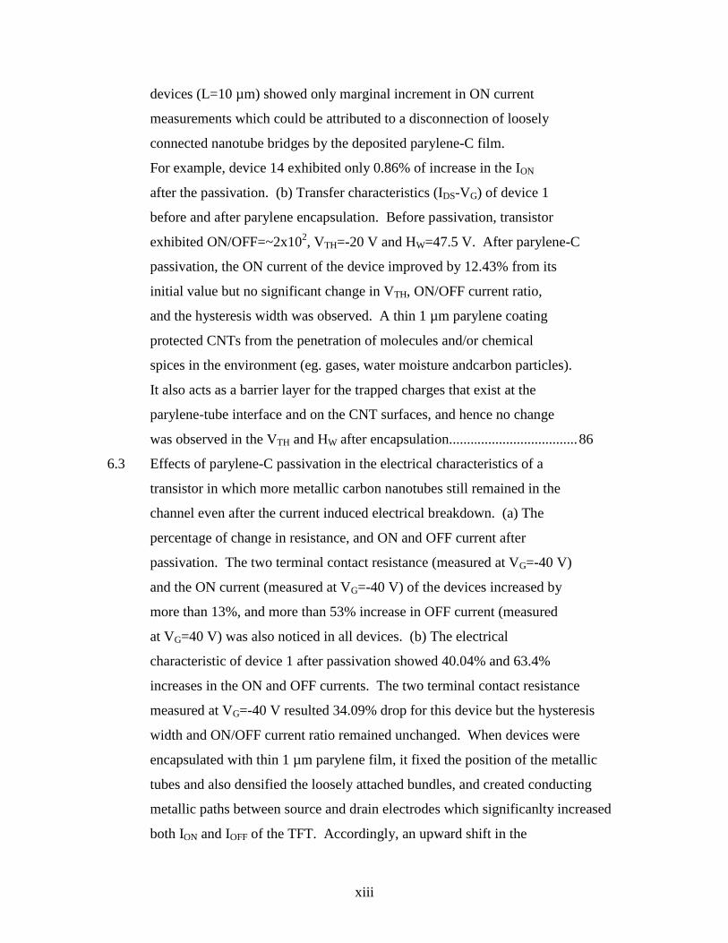
xiii
devices (L=10 µm) showed only marginal increment in ON current
measurements which could be attributed to a disconnection of loosely
connected nanotube bridges by the deposited parylene-C film.
For example, device 14 exhibited only 0.86% of increase in the ION
after the passivation. (b) Transfer characteristics (IDS-VG) of device 1
before and after parylene encapsulation. Before passivation, transistor
exhibited ON/OFF=~2x102, VTH=-20 V and HW=47.5 V. After parylene-C
passivation, the ON current of the device improved by 12.43% from its
initial value but no significant change in VTH, ON/OFF current ratio,
and the hysteresis width was observed. A thin 1 µm parylene coating
protected CNTs from the penetration of molecules and/or chemical
spices in the environment (eg. gases, water moisture andcarbon particles).
It also acts as a barrier layer for the trapped charges that exist at the
parylene-tube interface and on the CNT surfaces, and hence no change
was observed in the VTH and HW after encapsulation.................................... 86
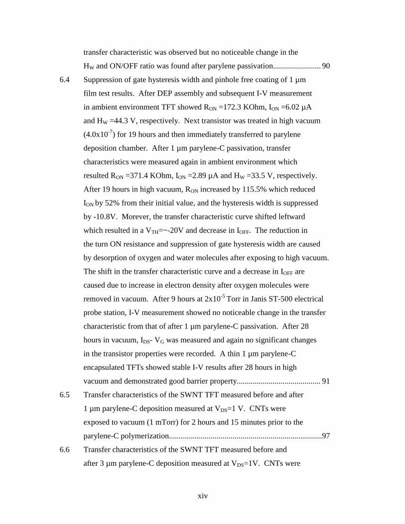
6.3 Effects of parylene-C passivation in the electrical characteristics of a
transistor in which more metallic carbon nanotubes still remained in the
channel even after the current induced electrical breakdown. (a) The
percentage of change in resistance, and ON and OFF current after
passivation. The two terminal contact resistance (measured at VG=-40 V)
and the ON current (measured at VG=-40 V) of the devices increased by
more than 13%, and more than 53% increase in OFF current (measured
at VG=40 V) was also noticed in all devices. (b) The electrical
characteristic of device 1 after passivation showed 40.04% and 63.4%
increases in the ON and OFF currents. The two terminal contact resistance
measured at VG=-40 V resulted 34.09% drop for this device but the hysteresis
width and ON/OFF current ratio remained unchanged. When devices were
encapsulated with thin 1 µm parylene film, it fixed the position of the metallic
tubes and also densified the loosely attached bundles, and created conducting
metallic paths between source and drain electrodes which significanlty increased
both ION and IOFF of the TFT. Accordingly, an upward shift in the
xiv
transfer characteristic was observed but no noticeable change in the
HW and ON/OFF ratio was found after parylene passivation........................ 90
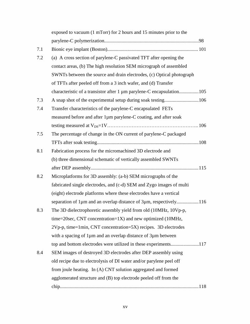
6.4 Suppression of gate hysteresis width and pinhole free coating of 1 µm
film test results. After DEP assembly and subsequent I-V measurement
in ambient environment TFT showed RON =172.3 KOhm, ION =6.02 µA
and HW =44.3 V, respectively. Next transistor was treated in high vacuum
(4.0x10⁻⁷
) for 19 hours and then immediately transferred to parylene
deposition chamber. After 1 µm parylene-C passivation, transfer
characteristics were measured again in ambient environment which
resulted RON =371.4 KOhm, ION =2.89 µA and HW =33.5 V, respectively.
After 19 hours in high vacuum, RON increased by 115.5% which reduced
ION by 52% from their initial value, and the hysteresis width is suppressed
by -10.8V. Morever, the transfer characteristic curve shifted leftward
which resulted in a VTH=~-20V and decrease in IOFF. The reduction in
the turn ON resistance and suppression of gate hysteresis width are caused
by desorption of oxygen and water molecules after exposing to high vacuum.
The shift in the transfer characteristic curve and a decrease in IOFF are
caused due to increase in electron density after oxygen molecules were
removed in vacuum. After 9 hours at 2x10⁻⁵
Torr in Janis ST-500 electrical
probe station, I-V measurement showed no noticeable change in the transfer
characteristic from that of after 1 µm parylene-C passivation. After 28
hours in vacuum, IDS- VG was measured and again no significant changes
in the transistor properties were recorded. A thin 1 µm parylene-C
encapsulated TFTs showed stable I-V results after 28 hours in high
vacuum and demonstrated good barrier property.......................................... 91
6.5 Transfer characteristics of the SWNT TFT measured before and after
1 µm parylene-C deposition measured at VDS=1 V. CNTs were
exposed to vacuum (1 mTorr) for 2 hours and 15 minutes prior to the
parylene-C polymerization.............................................................................97
6.6 Transfer characteristics of the SWNT TFT measured before and
after 3 µm parylene-C deposition measured at VDS=1V. CNTs were
xv
exposed to vacuum (1 mTorr) for 2 hours and 15 minutes prior to the
parylene-C polymerization.............................................................................98
7.1 Bionic eye implant (Boston).......................................................................... 101
7.2 (a) A cross section of parylene-C passivated TFT after opening the
contact areas, (b) The high resolution SEM micrograph of assembled
SWNTs between the source and drain electrodes, (c) Optical photograph
of TFTs after peeled off from a 3 inch wafer, and (d) Transfer
characteristic of a transistor after 1 µm parylene-C encapsulation................ 105
7.3 A snap shot of the experimental setup during soak testing............................ 106
7.4 Transfer characteristics of the parylene-C encapsulated FETs
measured before and after 1µm parylene-C coating, and after soak
testing measured at VDS=1V……………………………………………….. 106
7.5 The percentage of change in the ON current of parylene-C packaged
TFTs after soak testing................................................................................... 108
8.1 Fabrication process for the micromachined 3D electrode and
(b) three dimensional schematic of vertically assembled SWNTs
after DEP assembly........................................................................................ 115
8.2 Microplatforms for 3D assembly: (a-b) SEM micrographs of the
fabricated single electrodes, and (c-d) SEM and Zygo images of multi
(eight) electrode platforms where these electrodes have a vertical
separation of 1µm and an overlap distance of 3µm, respectively.................. 116
8.3 The 3D dielectrophoretic assembly yield from old (10MHz, 10Vp-p,
time=20sec, CNT concentration=1X) and new optimized (10MHz,
2Vp-p, time=1min, CNT concentration=5X) recipes. 3D electrodes
with a spacing of 1µm and an overlap distance of 3µm between
top and bottom electrodes were utilized in these experiments.......................117
8.4 SEM images of destroyed 3D electrodes after DEP assembly using
old recipe due to electrolysis of DI water and/or parylene peel off
from joule heating. In (A) CNT solution aggregated and formed
agglomerated structure and (B) top electrode peeled off from the
chip................................................................................................................. 118
xvi
8.5 FESEM image of SWNTs assembled between the top and bottom
metal at 10 MHz. (a) SEM micrograph of the top view of the 3D
assembled SWNT bundles at 10 Vpp (b) A high angle frontal SEM
image of the SWNTs assembled at 10 Vpp connecting the top and
bottom metals (c) A high resolution image of bundled SWNTs
assembled at 5 Vpp. (d) Side view of the assembled SWNT architecture
assembled 5 Vpp............................................................................................. 119
8.6 Measured two-terminal resistance of 3D devices before and after
parylene-C encapsulation using DEP assembly at 10Vpp and 10 MHz.
After encapsulation the room temperature resistance dropped by
(a) 12% (from 389 to 346 ohms) for a single electrode device and
(b) where as for 3D multielectrode it went down from 66 to 36 ohms
with 45% change in the resistance................................................................. 121
8.7 Measured two-terminal resistance of the 3D single electrode devices.
The amplitude of the AC electric field was increased from 1 to 10 Vpp
at a frequency of 10 MHz which resulted exponential drop in the
resistance with increasing voltage................................................................. 122
8.8 A schematic drawing of the 3D assembly electrodes illustrating the
Height (H) and Overlap distance (L), which can be varied to scale the
DEP forces between the top and the bottom electrodes................................. 123
8.9 Adjusting the distance between the top and the bottom electrodes
allows control over the magnitude of the electric field. The vertical
distance between the 3D electrodes (thickness of the parylene-C layer)
was varied from (a) 269nm, (b) 1,052nm, (c) 2,085nm and (d) 2,828nm
where the overlap distance was kept at 3µm. It is evident from the
above SEM images (a-d) that as the height was reduced the diameter
and the angle of incline of the assembled SWNT bundles have increased.
Moreover, the length of the suspended 3D SWNTs decreased when the
electrode height was reduced (this was more applicable to H ≤1µm)……... 124
8.10 The overlap distance between the top and bottom electrodes was
changed from (a) 1,022nm, (b) 117nm, (c) 1,190nm (d) to 3,290nm.
xvii
As a result, more SWNT bundles assembled around the edges of the
hemispherical top electrode as shown in the SEM micrographs
through of the 3D devices (a) to (d) which resulted in 7, 9, 20
and 30 bundles, respectively.......................................................................... 127
8.11 Scaling the electrode geometry vs measured resistance. The
two terminal resistances of the 3D SWNT devices exponentially
decreased when the spacing and the overlap distance between the
electrodes were reduced................................................................................. 128
8.12 The changes in the measured two terminal resistance of the 3D
SWNT devices after thermal annealing at 90 ºC for 30 minutes.
Seven such 3D devices with two different geometries were utilized,
and at least a 20% decrease in their contact resistance was observed
in most of the devices.................................................................................... 129
8.13 Simulation of SWNT transport during DEP assembly process.
(a) shows the electric potential surface contour and the electric field
stream lines for the SWNT in the initial stage of the assembly process,
(b) shows the electric field surface and CNT transport trajectory
during assembly. (c) shows the final position of the SWNT assembled
in between 2 electrodes.................................................................................. 134
8.14 Fabrication of 3D SWNT based vertical Field Effect Transistors.
(a) assemble nanotubes on microfabricated 3D electrodes (Cr/Au metal
thickness is 50Å/750Å), (b) deposit 1µm thick Parylene-C gate dielectric
material, (c) deposit Cr/Au gate electrode (50Å/750Å), and (d) open
source and drain contacts using conventional photolithography
(refer Appendix D for detailed information)................................................. 136
8.15 Optical photograph (top view) of the fabricated 3D CNTFET.
Inset: magnified image of the active area where nanotubes are
assembled....................................................................................................... 137
8.16 IDS-VDS measurement for the CNTs breakdown. Metallic SWNTs
were selectively burnt at a gate voltage of 20V as VDS was varied
from 0 to 15V with 1V increments................................................................ 138
xviii
8.17 SEM micrograph of the 3D SWNT FET after the metallic nanotubes
were burnt by passing a current through them. The disconnected
nanotubes are circled…………………………………………......................138
8.18 Two terminal resistance from a sample device before and after the
breakdown of metallic SWNTs...................................................................... 139
8.19 IDS-VDS characteristics where VGS is swept from -40V to 10V
with 10V increments...................................................................................... 140
8.20 IDS-VGS characteristic of 3D CNTFET measured at room temperature.
(a) A linear plot measured at VDS=-50mV. Inset: magnified IDS-VGS
showing the transition from p-type to n-type behavior. (b) Semi logarithmic
IDS-VGS plot for VDS=-90mV and VDS =-150mV........................................... 142
1
CChhaapptteerr 11
Flexible Electronics
1.1 Introduction
The development of semiconductor technology has been rapid and dramatic
during the last several decades and has a major impact on all aspects of our society.
Semiconductor materials such as germanium (Ge), indium phosphide (InP), silicon (Si),
and gallium arsenide (GaAs) have been widely used in the microelectronics industry for
many years [1]. Silicon is the most dominant material used in the integrated circuit (IC)
industry due to its numerous advantages. First, Si is a readily available material and can
operate at high temperatures because of its wider bandgap, and it can be easily oxidized
which forms an electrical insulator and barrier layer for diffusion steps needed in IC
fabrication [1]. The first Si based integrated circuit chip was fabricated by Texas
Instruments and Fairchild Semiconductor in the early 1960s [1]. The companies have
demonstrated several transistors and resistors to create logic gates and amplifier circuits.
Currently, the Intel Core 45 nm process technology processor (Intel® Core™ i7-975
Processor Extreme Edition) which was launched in June 2009 consists of 731 million
transistors on a small die [2]. The semiconductor technology has boomed in the last fifty
2
years yet there are numerous drawbacks that make it ideal for only high performance
device applications. For example, the devices which are made from these silicon and
conventional semiconductor materials are rigid and brittle, require sophisticated
microfabrication techniques which include high temperature and high vacuum processing
steps. Moreover, cost of production is very high and hence applied mainly to small area
devices eg. Intel chips [3-6].
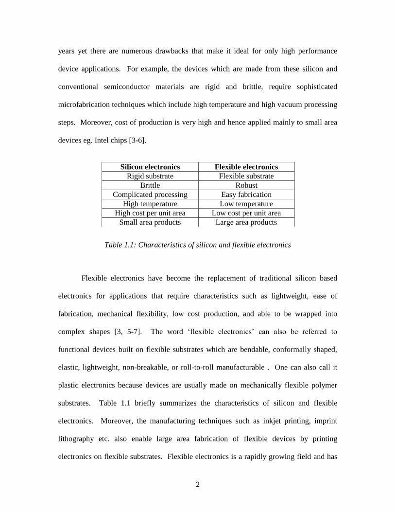
Table 1.1: Characteristics of silicon and flexible electronics
Flexible electronics have become the replacement of traditional silicon based
electronics for applications that require characteristics such as lightweight, ease of
fabrication, mechanical flexibility, low cost production, and able to be wrapped into
complex shapes [3, 5-7]. The word ‗flexible electronics‘ can also be referred to
functional devices built on flexible substrates which are bendable, conformally shaped,
elastic, lightweight, non-breakable, or roll-to-roll manufacturable . One can also call it
plastic electronics because devices are usually made on mechanically flexible polymer
substrates. Table 1.1 briefly summarizes the characteristics of silicon and flexible
electronics. Moreover, the manufacturing techniques such as inkjet printing, imprint
lithography etc. also enable large area fabrication of flexible devices by printing
electronics on flexible substrates. Flexible electronics is a rapidly growing field and has
Silicon electronics Flexible electronics
Rigid substrate Flexible substrate
Brittle Robust
Complicated processing Easy fabrication
High temperature Low temperature
High cost per unit area Low cost per unit area
Small area products Large area products
3
many applications in consumer, medical, and military sectors including wearable
electronics, portable sensors, flexible displays, radio frequency identification tags,
implantable devices, etc. [3, 5-9].
Technology is such an integral part of our daily life and is always evolving and
demanding for more end user-friendly flexible devices such as Nokia Morph. To realize
such devices they should able to be folded and unfolded easily which requires ultra
mechanical flexibility and a robust encapsulation technique. In this dissertation,
parylene-C polymeric material is utilized with single-walled carbon nanotubes to
demonstrate a parylene-C packaged SWNT TFT technology for ultra flexible, high
performance and biocompatible nano devices. Using this technology a high density and
vertical transistor concept is next demonstrated to realize compacted flexible devices.
First, an overview of flexible electronics and goal of this dissertation are discussed.
Chapter 2 gives introduction to carbon nanotubes. The parylene-C characterization and
electrical evaluation of thin parylene-C dielectric are mentioned in Chapter 3 and 4.
Chapter 5 and 6 will focus on fabrication of all-parylene SWNT TFT and their
mechanical flexibility, and parylene-C passivation for CNTFETs, respectively. The
biostability of thin parylene-C encapsulated TFTs are confirmed in Chapter 7. Finally,
high density and vertical field effect transistors are reported in Chapter 8.
1.2 History of Flexible Electronics
Flexible electronics has a long history where thinning silicon wafer approach was
first realized to make flexible devices [10]. The first flexible device, solar cell arrays,
was made in 1960s where Si wafers were first thinned to 100 µm and then they were
4
assembled on plastic substrates. Next, the low temperature deposition of hydrogenated
amorphous silicon enabled the realization of Pt/a-Si:H schottky barrier solar cell on
stainless steel substrate in 1976 [11]. In the early 1980s, Plattner et al. [12] and Okaniwa
et al. [13, 14] made a-Si-:H based schottky barrier solar cells on plastic substrates. The
roll-to-roll fabrication of a-Si:H solar cells on steels [15] and organic polymer substrates
[16] was also introduced in the beginning of early 1980s.
Brody et al. made the first thin film transistor (TFT) in 1968 using tellurium (Te)
on a strip of paper [17, 18]. Later, they made TFTs on Mylar, polyethylene and anodized
aluminum wrapping foil, and demonstrated their mechanical bending flexibility at a
bending radius of 1/16″ and devices remained operational. The a-Si:H TFT backplane
based active matrix liquid crystal display was made by Japan in the mid-1980s. Constant
et al. demonstrated a-Si:H based TFT circuits on polyimide substrates in 1994 [19]. The
flexible polycrystalline silicon (poly-Si) based TFTs were introduced in 1997 [20, 21].
Solution processable organic semiconductors have also attracted significant
interest as an alternative material for making flexible devices. It provides easy solution
based deposition of active organic materials at low (room) temperature, and also allows
for unconventional deposition methods [22] such as inkjet [23, 24] screen [25, 26] and
microcontact printing [22, 27, 28]. These organic materials are light weight,
mechanically flexible, compatible with commercially available flexible substrates. The
first organic semiconductor based field effect transistor was realized in 1964 [29]. The
flexible organic thin film transistor (OTFT) on polymer substrate was demonstrated in
1983 [30].
5
Currently, carbon nanotubes (CNTs) with their unique physical and mechanical
properties are being considered as potential replacement of existing semiconducting
materials for flexible electronics. Single-Walled Carbon Nanotubes (SWNTS), a one
dimensional quantum wire, have gained great interest as an active channel material for
flexible electronic devices due to their unique electrical, mechanical and thermal
properties. Their mobility can go as high as105 cm
2/Vs
-1, and they have large current
carrying (109 A/cm
2) and thermal conducting (5800 W/mK) capability, higher ON/OFF
ratios (>105) and extreme mechanical flexibility [31-35]. The first single-walled carbon
nanotubes field effect transistor (FET) is demonstrated in 1998 [36, 37]. SWNTs based
FETs exhibit p-type behavior in the ambient environment [34] and it can be converted to
n-type behavior by doping [32]. CNTs have been extensively utilized in many devices on
flexible substrates such as high frequency FETs, p-n diodes, memory devices, logic
circuits, etc. [38-42]. The CNTs properties and applications are discussed in details in
Chapter 2.
Since then flexible electronics technology has developed drastically, and many
research groups from various universities and companies such as Philips, Samsung,
Readius, IBM, Motorola, and Nokia are actively working in this field. For example,
Readius [43] the world‘s first pocket eReader, exploits the versatility of rollable displays
to merge the 'reading friendly‘ strengths of eBook readers with pocket size form factor
and world wide connectivity (Figure 1.1a). In February 2008, Nokia Research Center
(NRC) developed a new concept for next generation mobile devices call Nokia Morph
[44]. Morph shown in Figure 1.1b is a concept that demonstrates how future mobile
devices might be stretchable and flexible, allowing the user to transform their mobile
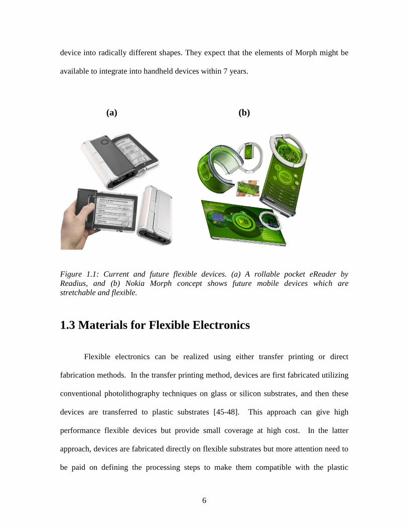
6
device into radically different shapes. They expect that the elements of Morph might be
available to integrate into handheld devices within 7 years.
Figure 1.1: Current and future flexible devices. (a) A rollable pocket eReader by
Readius, and (b) Nokia Morph concept shows future mobile devices which are
stretchable and flexible.
1.3 Materials for Flexible Electronics
Flexible electronics can be realized using either transfer printing or direct
fabrication methods. In the transfer printing method, devices are first fabricated utilizing
conventional photolithography techniques on glass or silicon substrates, and then these
devices are transferred to plastic substrates [45-48]. This approach can give high
performance flexible devices but provide small coverage at high cost. In the latter
approach, devices are fabricated directly on flexible substrates but more attention need to
be paid on defining the processing steps to make them compatible with the plastic
(a) (b)
7
substrates [3, 5-7]. Realization of complete flexible electronic structure requires
mechanically flexible substrates, front and back end electronics and compatible
encapsulation layers. For a typical flexible display application, the frontend electronics
have materials for displays which include organic light emitting diode, liquid crystal, or
electrophoretic displays. Whereas the backend electronics will be the driving circuits
which is typically arrays of thin film transistors made from a-Si:H, organic
semiconductor or carbon nanotubes materials. The mechanically flexible substrates,
polymer gate dielectrics and encapsulation layers are discussed below.
1.3.1 Mechanically Flexible Substrates
Most of current flexible electronic devices are realized on thin glass plates, metal
foil and plastic films. The mechanical flexibility can be interpreted in many ways such as
bendable, conformably shaped, elastic, lightweight, non-breakable, or rollable. The glass
plates of thickness of ~ 100 µm are reported to provide enough flexibility for flat panel
display applications [49, 50]. Similarly, metal foil substrates less than 50-125 µm are
flexible and reported in emissive or reflective display applications [51]. In this section,
plastic films as a substrate material in flexible electronics will be discussed.
Fabrication of flexible devices on polymeric substrates is strictly restricted to low
temperature processes. The glass temperature of plastic substrates range typically
between 80 and 150 °C and hence they are not able to handle fabrication processes that
require temperatures above 150 °C [43, 50, 52, 53]. The difficulty in controlling the
shrinkage of polymer films during fabrication is also a major problem. In other words,
coefficient of thermal expansion (CTE) of these polymer materials also plays a crucial
8
role in the flexible device fabrication [29]. During processing, flexible substrate coated
wafers under goes multiple heat treatment and a small thermal mismatch stress can curve
these films which eventually makes the fabrication difficult. Thermal expansion
coefficients below 20 ppm / °C are favored for Si based flexible electronics. Moreover,
permeability of gases and moistures through plastic films need to be considered to
prevent the elongation and shrinkage of these materials over long periods of time.
Polymer substrates are very attractive for flexible electronics because they are
inexpensive and can provide higher flexibility. Polymeric substrates such as
polyethylene terephthalate (PET), polyethylene naphthalate (PEN), polycarbonate (PC),
polyimide (PI or kapton), polyethersulphone (PES), polyarylates (PAR), and polycyclic
olefin (PCO) are listed as candidates for flexible substrates [29, 43, 50, 52-54]. Yet PEN,
PET, and kapton have been heavily utilized for flexible electronics as they have CTE of
below 20 ppm / °C. In addition, PEN, PET and PI can handle temperature of 200, 150
and 350 °C during fabrication, respectively. These films are available in sheet forms and
hence require attachment to carrier wafers prior to processing. Alternately, sophisticated
tools such as stamping are another method to realize devices on these substrates. The
above polymeric films come in bulks sheets with a thickness of nearly 100 µm, and gases
and moistures do permeate through these films over period of time. Finding simpler
substrate that is compatible with micromachining, inert and mechanically strong would
be beneficial to the flexible electronics field.
In this dissertation, parylene-C is explored as a flexible substrate for a CNT FET.
Despite its attractive properties, parylene-C (Pa-C) has rarely been explored as a flexible
substrate. Parylene-C, a derivative of Poly-Para-Xylylene [55] is a lightweight, stress-
9
free, optically transparent, and mechanically strong material, which is deposited at room
temperature. It is also compatible with standard microfabrication techniques (eg. it is
resistant to chemicals, insoluble in common solvents such as acetone and isopropyl
alcohol (IPA), etc). Furthermore, during processing, one can create Pa-C substrate on a
carrier wafer, complete all fabrication processes, and peel off from the handle wafer at
the end. The thickness of the parylene-C film can be well controlled down to 1 μm using
commercially available parylene deposition coaters. Due to its higher tensile strength (70
MPa) and Young‘s modulus (3.2 GPa) [55] parylene-C films as thin as 4 μm can be
easily fabricated, and still peeled off without tearing it. In general, for a thin film, the
bending rigidity of a film is proportional to the third power of its thickness [56] and is
also dependent on the elastic property of the material that comprises the film. The
thickness of Pa-C layer is controllable and as result the film can accommodate devices
requiring different flexibility. These attractive properties make it a very promising
material as a flexible substrate for CNTFETs which is detailed in Chapter 5.
1.3.2 Gate Dielectric Materials
Selection of gate dielectric material is critical for electronics especially for a
transistor. The factors such as dielectric-semiconductor interface, leakage current,
dielectric constant, processability, film roughness and morphology, stability, and
reliability need to be carefully considered during selection of gate dielectric material.
The dielectric for thin film transistors are classified into two categories called inorganic
or organic (polymers) films. Inorganic dielectrics such as silicon dioxide (SiO2), titanium
dioxide (TiO2), aluminum oxide (Al2O3) and tantalum dioxide (Ta2O5) are commonly
10
used in (organic and carbon nanotube) TFTs yet some drawbacks limit their use on
flexible applications [57-61]. The deposition of these materials is costly and requires
sophisticated tools. The process compatibility of inorganic dielectrics with different
flexible substrates is another concern during fabrication of these transistors. To achieve
better flexibility, the above gate dielectric materials are thinned down to tens of
nanometers but these thin films consist of defects and pinholes which lead to higher
leakage current. The thermal annealing at elevated temperature is frequently employed to
improve the quality of these thin dielectrics. However, the flexible substrates will not be
able to handle such high temperature process and it can deteriorate the film quality.
Polymer dielectrics have numerous advantageous compared to inorganic counterparts.
They are solution processed utilizing inexpensive methods such as dip coating and spin
coating which makes it compatible with different polymeric substrates. Furthermore,
polymers are flexible, possess excellent insulating properties and have very low leakage
current makes it attractive for flexible applications. These organic dielectrics create
superb interface with organic semiconductors and provide template for ordering organic
materials. Polymer gate dielectrics such as polystyrene (PS), polymethyl-methacrylate
(PMMA), poly (vinyl alcohol) PVA, poly (vinyl phenol) PVP and poly (4-methylstyrene)
have been utilized for OFETs [50, 62-66]. Polymers such as polyimide [67], SU8 [35],
and PMMA [68] have been reported as gate dielectrics using solution processed
techniques such as spin coating for flexible carbon nanotube FETs. The drawback of
employing these approaches for gate dielectrics is that they are usually cured at high
temperature which limits their applications for flexible devices made on polymeric
substrates. Moreover, these materials are not very compatible with standard micro
11
fabrication processing methods, and hence require sophisticated fabrication techniques
(such as imprinting) to develop a complete transistor.
I have utilized parylene-C as a gate dielectric for flexible carbon nanotube based
thin film transistors. Pa-C is deposited at room temperature and provides a pinhole free
and conformal film, and hence it is ideal for flexible devices. Parylene-C is compatible
with standard CMOS fabrication techniques for example it is resistant to chemicals,
insoluble in common solvents such as acetone and isopropyl alcohol (IPA) etc. The
parylene polymerization is oxygen free, and the organic carbon nanotube on organic
parylene gate dielectric is likely to provide better dielectric-CNT interface. The dielectric
constant of the parylene-C is 3.2 and due to its high breakdown voltage and low leakage
current several organic devices [69] are made using parylene as a gate dielectric, yet
applications of parylene in CNTFETs is rarely explored. Parylene-C gate dielectric for
SWNT FETs is discussed in details in Chapter 4 and 5.
1.3.3 Encapsulation
Flexible electronics need to be protected from environmental contamination,
detrimental gases, house hold hazardous, etc. A good encapsulant should possess
following properties: high dielectric strength, high electrical resistivity, high thermal
conductivity, low, conformability, low moisture absorption, solvent resistance, low
thermal expansion coefficient, thermal stability and high purity [70]. Today, polymer
and ceramic films are wildly used in packaging industry. Ceramic encapsulants such
Si3N4, SiO2 and Al2O3 typically have superior thermal stability, highly impermeable to
atmospheric gases, higher dielectric strength, higher tensile strength, higher thermal
12
conductivity, and lower thermal expansion coefficient comparing to polymeric films.
However, ceramic films create cracks and do not provide 100% pinhole free deposition
[71, 72]. Polymer encapsulants such as polyimide, parylene, epoxy and silicone are very
flexible, easy to process, compatible with different polymeric substrates and conformal
pinhole free coating, and hence have been extensively utilized on flexible devices [70, 72,
73]. The drawback of using polymers as a passivation layer is that the gases and
moistures permeate through these films and challenges their long term stability. These
problems opened door for making impermeable thin film coating as an encapsulation
layer in the flexible OLED industry. A multilayer composite barrier coating consists of
alternating organic/inorganic layers have been realized to improve the long term
operating life of OLEDs [74, 75].
Despite their environmental sensitivity very few studies have been conducted to
investigate passivation materials for CNT based devices. I have used parylene-C as an
encapsulant for CNTFETs. Pa-C is a pin hole free material, and it provides uniform
coating thickness over all surfaces regardless of its configuration (eg. sharp edges and
holes). It is chemically inert, and has high dielectric strength and low permeability to
moisture and gases. Film deposition is a stress-free (deposited at room temperature)
coating, hence does not introduce any adverse effects to the encapsulated electronics.
Parylene-C has traditionally been used in the medical device industry for coating
implantable device [76, 77] because it is biocompatible and classified as USP class-VI
implantable plastic material [78] by FDA. The thickness of the top parylene layer can be
controlled from submicron to tens of microns, and hence passivation is application
oriented coating where one can engineer film thickness while preserving the flexibility.
13
For example, thicker parylene-C (1-10 µm) film can be used for implantable applications
where devices are exposed to body fluids with different pH levels. It has also been
explored as passivation layer for organic semiconductor eg. pentacene based field effect
transistors to protect them from environmental conditions such as oxygen and moisture
[79, 80]. Chapter 6 and 7 discuss the parylene-C passivation for CNTFETs and their
biostability.
1.4 Fabrication Technology for Flexible Electronics
Flexible electronics has gained significant interest as a pathway to large area, low
cost, and mechanically bendable device applications. Flexible devices are fabricated by
batch processing, roll-to-roll (web) processing or printing technology. In batch
processing, flexible substrates are first attached on a rigid carrier such as glass or silicon
wafers, devices are next made using standard microfabrication methods, and finally
polymeric films are removed from the carrier wafer. Here, the device fabrication must be
performed at low temperature to avoid cracking or curling of films, and devices should be
prevented from getting damaged during peel off at the end of the process. Amorphous
silicon TFT [81, 82], organic FETs [83], and carbon nanotubes and ZnO nanowires based
flexible chemical sensors [84] have been fabricated utilizing this technique. The
fabrication on web by roll-to-roll processing is desirable for high-throughput production.
This process employs roll-to-roll photolithograph and etching tools to make device that
requires few number of patterning steps [85, 86]. The web processing is heavily utilized
for a roll-to-roll production of polymer solar cells [87]. Printing technology such as
inkjet [23, 24] screen [25, 26] and microcontact printing [24, 53, 54] technologies
14
provides easy solution based deposition of active organic materials without the need for
physical masks. The printing process is low cost, applicable to large area processing,
compatible with flexible substrates, and can be easily adapted to high-throughput
manufacturing process such as roll-to-roll printing.
In this dissertation, I have used a 10 µm thick flexible parylene-C film as a
substrate. At the end of the fabrication process a dry lift off technique is employed to
remove the paryelene-C film from the silicon carrier wafer. Prior to deposition, I have
coated the wafers with hexamethyldisilazane (HMDS) the adhesion promoter. The
HMDS provides enough adhesion between the film and substrate to complete the entire
fabrication process, and also facilitate easy peel off without tearing the film. Parylene-C
has a tensile strength of 70 MPa and Young‘s modulus of 3.2 GPa [57], and films as thin
as 4 μm can be easily fabricated and still peeled off without destroying it. These
attractive properties of parylene-C are discussed in details in Chapter 3, 4 and 5.
1.5 Applications of Flexible Electronics
Flexible electronics are becoming big part of our daily life because they are
inexpensive, bendable and easy to process, and can be fabricated in large areas. Flexible
displays is a rapidly growing field as it is a replacement of rigid glass based technology,
and numerous displays including liquid crystal display (LCD) [24, 88, 89],
electrophoretic display (EPD) [53, 54] and organic light emitting diode (OLED) [29, 30,
43] display on various polymeric substrates have been reported. Paper like displays [44]
is attractive for e-Reader or e-paper applications. Organic semiconductor based radio
frequency identification (RFID) tags have gained quite a bit of interest in the recent years

15
due to their low cost production [45, 47]. Flexible sensors have received enough
attention for applications in biomedicine, artificial skin, artificial noses and tongues, and
wearable electronics [48-50, 90]. Electroactive polymers based artificial muscles have
potential applications for biologically inspired robots, animatronics and prosthetics [51,
52]. Smart textiles are another growing industry where electronic circuits are woven or
integrated on to fabric [91, 92].
16
CChhaapptteerr 22
Carbon Nanotubes
2.1 Introduction
Carbon nanotubes (CNTs), rolling up of graphene sheets into a cigar-like shape,
have been considered as the potential candidate for the next generation of electronic
devices due to their unique physical, electrical and mechanical properties. Their mobility
can exceed 105 cm
2/Vs
-1, and they have large current carrying (10
9 A/cm
2) capability,
higher ON/OFF ratios (>105) and extreme mechanical flexibility. Metallic CNTs are
ideal for interconnect technology [93-96] while their high aspect ratio and
semiconducting behavior are attractive for field-effect transistors [97-99], sensors [100-
102] and field emitters [103, 104]. This Chapter discusses history, synthesis and general
properties of carbon nanotubes, and their potential applications in nanoelectronics.
2.2 The History of Carbon Nanotubes
Carbon is the most versatile element in the periodic table which can bond with
many elements and with itself. In the solid phase carbon can exist in three allotropic
forms which includes graphite (the softest substances), diamond (the hardest naturally
occurring substance), and buckminsterfullerene [105]. Once considered exotic, fullerenes
17
are nowadays commonly synthesized and used in research including buckyballs [106]
carbon nanotubes [107] carbon nanobuds [108, 109] and nanofibers [110]. Fullerenes
(C60 buckeyball) were first discovered by Harold Kroto, Robert Curl and Rick Smalley in
1985 [106]. In 1991, Rick Smally proposed the existence of a tubular fullerene and
envisioned a bucky tube that could be made by elongating a C60 molecule. Kroto, Curl
and Smalley were awarded the 1996 Nobel Prize in Chemistry for their roles in the
discovery of this class of compounds. After a discussion on the status of fullerene
research at carbon-carbon composite workshop in 1990, Smalley speculated the existence
of carbon nanotubes of dimensions comparable to C60. His hypothesis were later
followed by an oral presentation at a fullerene workshop in August 1991 in Philadelphia
by M. S. Dresselhaus on the symmetry of carbon nanotubes capped with fullerene
hemispheres [111]. The real breakthrough on CNT research came with Iijima‘s report of
experimental evidence of the existence of multi-walled carbon nanotubes (MWNTs)
using Transmission Electron Microscopy (TEM) in 1991. Two years after, both Iijima et
al. [112] and Bethune et al. [113] simultaneously and independently discovered single-
walled carbon nanotubes (SWNTs).
2.3 Carbon Nanotube Synthesis
Several theories have been mentioned in the literature in explaining the exact
growth mechanism for nanotubes. One theory states that metal catalyst particles are
floating or supported on graphite/another substrate, the catalyst particles are spherical or
pear-shaped, and the deposition will take place on only one half of the surface (lower
curvature side for the pear shaped particles). The carbon will diffuse along the
18
concentration gradient and precipitate on the opposite half, around and below the
bisecting diameter. But it will not precipitate from the apex of the hemisphere and
creates the hollow core structure which is the characteristic of these filaments. As
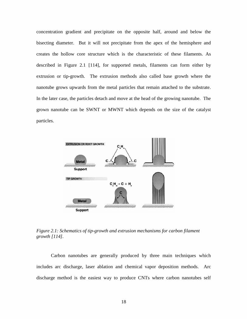
described in Figure 2.1 [114], for supported metals, filaments can form either by
extrusion or tip-growth. The extrusion methods also called base growth where the
nanotube grows upwards from the metal particles that remain attached to the substrate.
In the later case, the particles detach and move at the head of the growing nanotube. The
grown nanotube can be SWNT or MWNT which depends on the size of the catalyst
particles.
Figure 2.1: Schematics of tip-growth and extrusion mechanisms for carbon filament
growth [114].
Carbon nanotubes are generally produced by three main techniques which
includes arc discharge, laser ablation and chemical vapor deposition methods. Arc
discharge method is the easiest way to produce CNTs where carbon nanotubes self
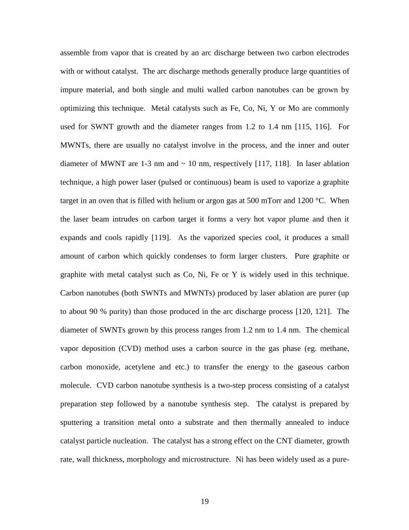
19
assemble from vapor that is created by an arc discharge between two carbon electrodes
with or without catalyst. The arc discharge methods generally produce large quantities of
impure material, and both single and multi walled carbon nanotubes can be grown by
optimizing this technique. Metal catalysts such as Fe, Co, Ni, Y or Mo are commonly
used for SWNT growth and the diameter ranges from 1.2 to 1.4 nm [115, 116]. For
MWNTs, there are usually no catalyst involve in the process, and the inner and outer
diameter of MWNT are 1-3 nm and ~ 10 nm, respectively [117, 118]. In laser ablation
technique, a high power laser (pulsed or continuous) beam is used to vaporize a graphite
target in an oven that is filled with helium or argon gas at 500 mTorr and 1200 °C. When
the laser beam intrudes on carbon target it forms a very hot vapor plume and then it
expands and cools rapidly [119]. As the vaporized species cool, it produces a small
amount of carbon which quickly condenses to form larger clusters. Pure graphite or
graphite with metal catalyst such as Co, Ni, Fe or Y is widely used in this technique.
Carbon nanotubes (both SWNTs and MWNTs) produced by laser ablation are purer (up
to about 90 % purity) than those produced in the arc discharge process [120, 121]. The
diameter of SWNTs grown by this process ranges from 1.2 nm to 1.4 nm. The chemical
vapor deposition (CVD) method uses a carbon source in the gas phase (eg. methane,
carbon monoxide, acetylene and etc.) to transfer the energy to the gaseous carbon
molecule. CVD carbon nanotube synthesis is a two-step process consisting of a catalyst
preparation step followed by a nanotube synthesis step. The catalyst is prepared by
sputtering a transition metal onto a substrate and then thermally annealed to induce
catalyst particle nucleation. The catalyst has a strong effect on the CNT diameter, growth
rate, wall thickness, morphology and microstructure. Ni has been widely used as a pure-
20
metal catalyst for the growth of aligned multi-walled carbon nanotubes. Thermal
annealing results in metal cluster formation on the substrate from which the nanotubes
grow [122]. The temperature for the synthesis of nanotubes by CVD is generally in the
range of 650 °C-900 °C [123, 124]. The low temperature CVD (under 500 °C) growths
of CNTs are also reported [125, 126]. Carbon nanotubes syntheses using plasma-
enhanced CVD, thermal chemical CVD and laser-assisted CVD have been reported as
well [127]. The diameter of the MWNTs grown by plasma-enhanced CVD process is
around 15 nm whereas the diameter of the thermally grown MWNTs depends on the
catalytic film thickness. For catalytic film thickness of 13 nm the diameter varies from
30 nm to 40 nm and for the 27 nm catalytic film the diameter ranges between 100 nm and
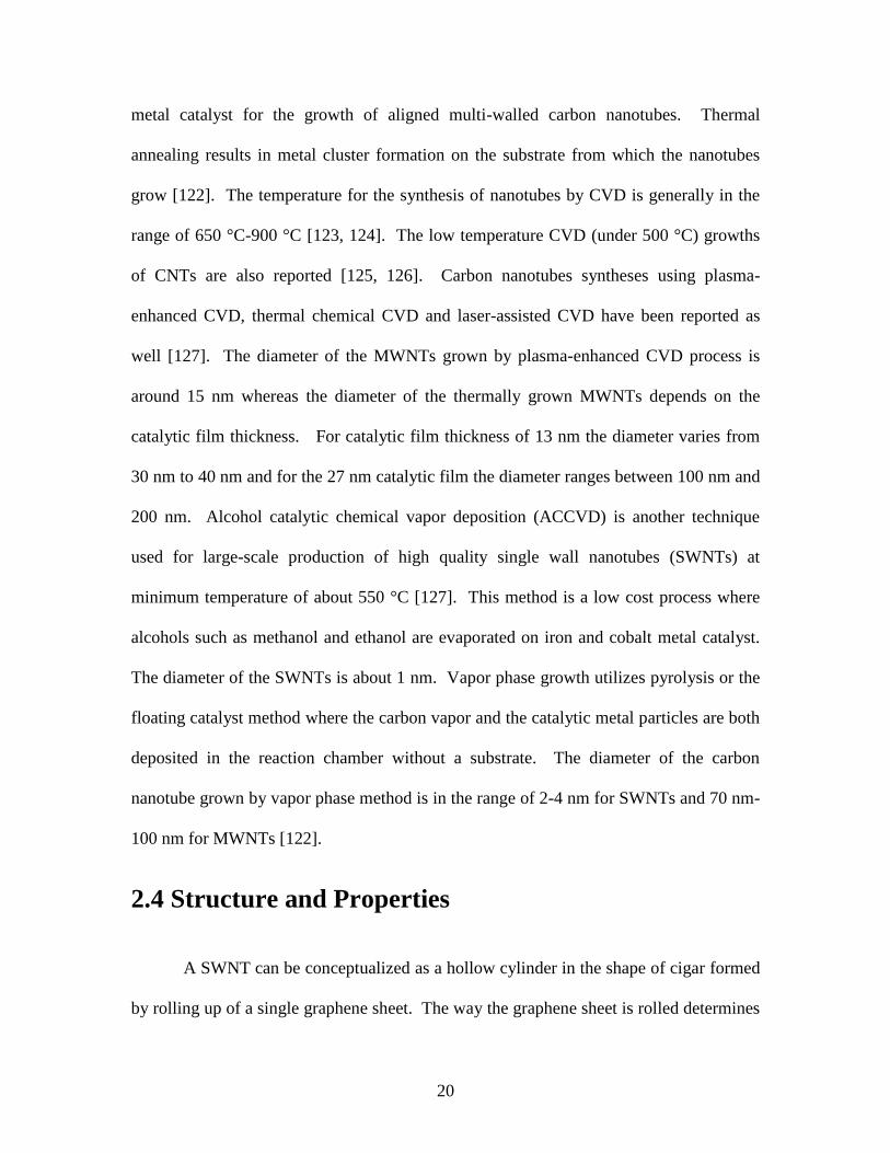
200 nm. Alcohol catalytic chemical vapor deposition (ACCVD) is another technique
used for large-scale production of high quality single wall nanotubes (SWNTs) at
minimum temperature of about 550 °C [127]. This method is a low cost process where
alcohols such as methanol and ethanol are evaporated on iron and cobalt metal catalyst.
The diameter of the SWNTs is about 1 nm. Vapor phase growth utilizes pyrolysis or the
floating catalyst method where the carbon vapor and the catalytic metal particles are both
deposited in the reaction chamber without a substrate. The diameter of the carbon
nanotube grown by vapor phase method is in the range of 2-4 nm for SWNTs and 70 nm-
100 nm for MWNTs [122].
2.4 Structure and Properties
A SWNT can be conceptualized as a hollow cylinder in the shape of cigar formed
by rolling up of a single graphene sheet. The way the graphene sheet is rolled determines
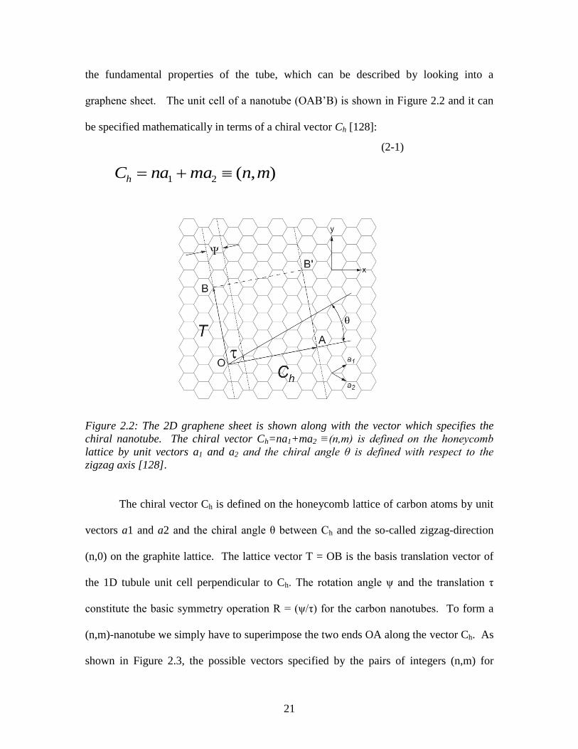
21
the fundamental properties of the tube, which can be described by looking into a
graphene sheet. The unit cell of a nanotube (OAB‘B) is shown in Figure 2.2 and it can
be specified mathematically in terms of a chiral vector Ch [128]:
Figure 2.2: The 2D graphene sheet is shown along with the vector which specifies the
chiral nanotube. The chiral vector Ch=na1+ma2 ≡(n,m) is defined on the honeycomb
lattice by unit vectors a1 and a2 and the chiral angle θ is defined with respect to the
zigzag axis [128].
The chiral vector Ch is defined on the honeycomb lattice of carbon atoms by unit
vectors a1 and a2 and the chiral angle θ between Ch and the so-called zigzag-direction
(n,0) on the graphite lattice. The lattice vector T = OB is the basis translation vector of
the 1D tubule unit cell perpendicular to Ch. The rotation angle ψ and the translation τ
constitute the basic symmetry operation R = (ψ/τ) for the carbon nanotubes. To form a
(n,m)-nanotube we simply have to superimpose the two ends OA along the vector Ch. As
shown in Figure 2.3, the possible vectors specified by the pairs of integers (n,m) for
),(21 mnmanaCh
(2-1)
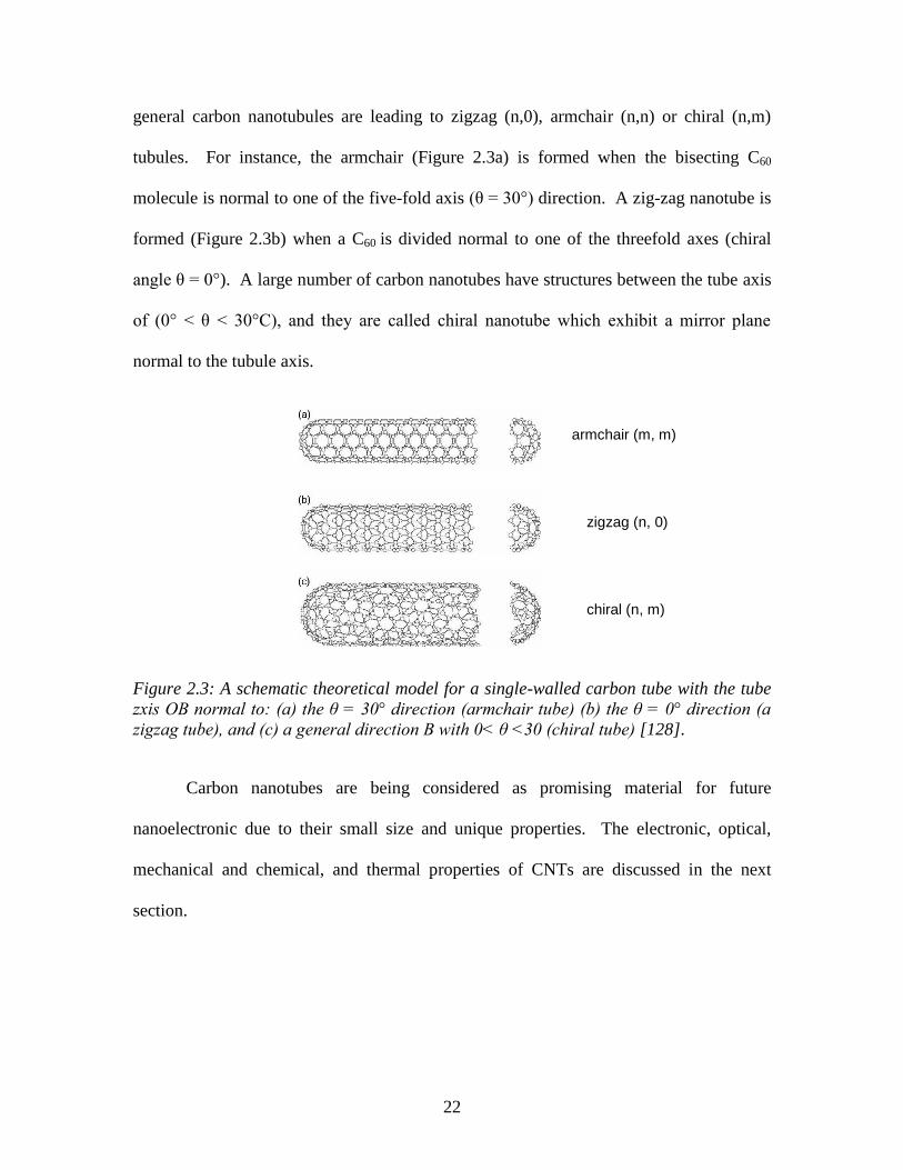
22
general carbon nanotubules are leading to zigzag (n,0), armchair (n,n) or chiral (n,m)
tubules. For instance, the armchair (Figure 2.3a) is formed when the bisecting C60
molecule is normal to one of the five-fold axis (θ = 30°) direction. A zig-zag nanotube is
formed (Figure 2.3b) when a C60 is divided normal to one of the threefold axes (chiral
angle θ = 0°). A large number of carbon nanotubes have structures between the tube axis
of (0° < θ < 30°C), and they are called chiral nanotube which exhibit a mirror plane
normal to the tubule axis.
Figure 2.3: A schematic theoretical model for a single-walled carbon tube with the tube
zxis OB normal to: (a) the θ = 30° direction (armchair tube) (b) the θ = 0° direction (a
zigzag tube), and (c) a general direction B with 0< θ <30 (chiral tube) [128].
Carbon nanotubes are being considered as promising material for future
nanoelectronic due to their small size and unique properties. The electronic, optical,
mechanical and chemical, and thermal properties of CNTs are discussed in the next
section.
chiral (n, m)
zigzag (n, 0)
armchair (m, m)
23
2.4.1 Electronic Properties
Carbon nanotubes based devices have been the subject of intense research since
discovered by Iijima. The electronic properties of CNTs have been studied both
theoretically and experimentally by many research groups [129-133]. As grown one third
of CNTs are metallic and two third is semiconductor, and this condition is derived based
on the band structure of a two-dimensional graphite sheet and periodic boundary
conditions along the circumference direction. The electronic properties of a nanotube
derived from the one dimensional energy dispersion relation of a graphite sheet with the
wave vectors (kx, ky) is [127]:
2/1
2 )2
(cos4)2
cos()2
3cos(41),(
akakak
kkEyyx
yx (2-2)
where γ is the nearest neighbor-hopping parameter and a is lattice constant. When the
graphene sheet is rolled up to form a nanotube, a periodic boundary condition is imposed
along the tube circumference or C direction in which the condition quantizes the two-
dimensional wave vector k = (kx, ky) along this direction. The k satisfying k .C = 2πq is
allowed where q is an integer and it leads to the (n - m) = 3q as the condition for metallic
conductance [127]. Accordingly, it is suggested that one third of the carbon nanotubes
are metallic and two thirds are semiconductor.
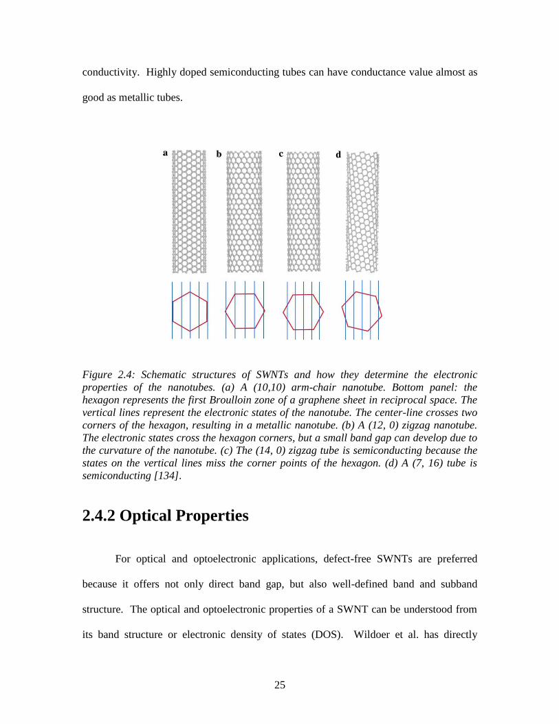
The Figure 2.4 illustrates the extreme sensitivity of nanotube electronic structures
to chirality of nanotubes [134]. For (m,m) arm-chair tubes (Figure 2.4a), there are always
states crossing the corner points of the first Brillouin zone suggesting that arm-chair tubes
should always be metallic. For (m, n) nanotubes with m - n ǂ 3n where n is an integer, the
24
electronic states (lines) miss the corner points (Figure 2.4c and d) and the nanotubes are
semiconducting. For m-n =3n, certain electronic states of the nanotube land on the corner
points of the first Broulloin zone (Figure 2.4b). These types of tubes would be semimetals
but become small-gap due to a curvature induced orbital rehybridization effect.
For metallic carbon nanotubes, it has been predicted to conduct current
ballistically without dissipating heat. For a single conduction channel with 100%
transparent contacts, the resistance is a universal constant, also known as ballistic
conduction. Ballistic conductor has crystalline properties which allow electrons to flow
through the material without collisions. That is, CNT is a ballistic conductor in the
absence of electron scattering. The conductance for a SWNT/MWNT is given by G =
G0M = (2 e2/h) M , where G0 = (2 e
2/h) = (12.9 KΩ)
-1 is quantized conductance and M is
an apparent number of conducting channels including electron-electron coupling and
intertube coupling effects in addition to intrinsic channels [127]. For a perfect SWNT, M
is equal to 2. The experimentally measured conductance is much lower than the
quantized value with the measured resistance for a single SWNT is ~10 KΩ [135] as
compared to the perfect value of 6.45 KΩ. This is because M is determined not only by
the intrinsic properties of a CNT itself, but also by the intertube coupling, the scatters
from defects, impurities, structural distortions, coupling with substrate and contacts
problems.
The band gap for semiconducting carbon nanotubes scales inversely with the
diameter of the tube, Eg = 0.84eV/d [nm] [105]. The conductance of semiconducting
nanotubes is determined on the exact position of the Fermi level with respect to the band
edges. Furthermore, the chemical or electrostatic doping can be used to change the
25
conductivity. Highly doped semiconducting tubes can have conductance value almost as
good as metallic tubes.
Figure 2.4: Schematic structures of SWNTs and how they determine the electronic
properties of the nanotubes. (a) A (10,10) arm-chair nanotube. Bottom panel: the
hexagon represents the first Broulloin zone of a graphene sheet in reciprocal space. The
vertical lines represent the electronic states of the nanotube. The center-line crosses two
corners of the hexagon, resulting in a metallic nanotube. (b) A (12, 0) zigzag nanotube.
The electronic states cross the hexagon corners, but a small band gap can develop due to
the curvature of the nanotube. (c) The (14, 0) zigzag tube is semiconducting because the
states on the vertical lines miss the corner points of the hexagon. (d) A (7, 16) tube is
semiconducting [134].
2.4.2 Optical Properties
For optical and optoelectronic applications, defect-free SWNTs are preferred
because it offers not only direct band gap, but also well-defined band and subband
structure. The optical and optoelectronic properties of a SWNT can be understood from
its band structure or electronic density of states (DOS). Wildoer et al. has directly
26
observed DOS of individual SWNTs (for both metallic and semiconducting tubes) by
scanning tunneling microscopy (STM) and has shown a good agreement with the
theoretical prediction of tight-binding zone-folding calculation [136]. Rao et al. have
shown diameter-selective resonance Raman spectra of SWNTs with laser excitation
wavelengths in the range from 514.5 nm to 1320 nm [137]. Moreover, CNTs are also
very photosensitive [138-140], and Fujiwara et al. observed a slow response on the order
of seconds when nanotube was illuminated with UV light [139].
2.4.3 Mechanical Properties
Table 2.1 summarizes calculated Young‘s modulus and tensile strength for
SWNT and bundle and MWNT with comparison with graphite and steel [127, 141]. As
compared to other materials, carbon nanotubes are the stiffest (Young‘s modulus) and
strongest (Yield strength) material. A SWNT has a Young‘s modulus of 1.2 TPa which
is nearly five times of that of a steel. The tensile strength is more than hundred times
higher than steel, and can tolerate large strains before mechanical failure. These
theoretical calculations appear to agree with that of experimental values. From
experiments, the Young‘s modulus of SWNT with diameter of 1-2 nm is about 1 TPa
whereas the Young‘s modulus for MWNT is higher than a SWNT and ranges between
1.1 and 1.3 TPa [142, 143]. The experimental results of MWNT show inconsistency
because they contain different amount of defects from different growth methods [127].
27
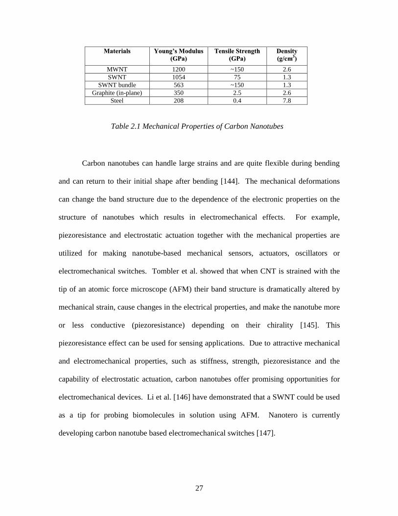
MMaatteerriiaallss YYoouunngg’’ss MMoodduulluuss
((GGPPaa))
TTeennssiillee SSttrreennggtthh
((GGPPaa))
DDeennssiittyy
((gg//ccmm33))
MWNT 1200 ~150 2.6
SWNT 1054 75 1.3
SWNT bundle 563 ~150 1.3
Graphite (in-plane) 350 2.5 2.6
Steel 208 0.4 7.8
Carbon nanotubes can handle large strains and are quite flexible during bending
and can return to their initial shape after bending [144]. The mechanical deformations
can change the band structure due to the dependence of the electronic properties on the
structure of nanotubes which results in electromechanical effects. For example,
piezoresistance and electrostatic actuation together with the mechanical properties are
utilized for making nanotube-based mechanical sensors, actuators, oscillators or
electromechanical switches. Tombler et al. showed that when CNT is strained with the
tip of an atomic force microscope (AFM) their band structure is dramatically altered by
mechanical strain, cause changes in the electrical properties, and make the nanotube more
or less conductive (piezoresistance) depending on their chirality [145]. This
piezoresistance effect can be used for sensing applications. Due to attractive mechanical
and electromechanical properties, such as stiffness, strength, piezoresistance and the
capability of electrostatic actuation, carbon nanotubes offer promising opportunities for
electromechanical devices. Li et al. [146] have demonstrated that a SWNT could be used
as a tip for probing biomolecules in solution using AFM. Nanotero is currently
developing carbon nanotube based electromechanical switches [147].
Table 2.1 Mechanical Properties of Carbon Nanotubes
28
2.4.4 Chemical Properties
Due to their small size, large surface to volume ratio and σ-π rehybridization
carbon nanotubes are very sensitive to chemical or environmental interactions, and have
become attractive for chemical and biological sensors. The chemical properties such as
opening, wetting, filling, adsorption and doping can be used for chemical and biological
separation, purification, sensing and electronics. The nanotube ends are more reactive
than the sidewall because of the greater curvature, and several groups have reported
opening nanotube ends utilizing vapor phase oxidation, plasma etching and chemical
reactions (HNO3) [148, 149]. Once the ends are terminated the interior can be easily
filled with an inorganic phase [150]. To build CNTs based logic devices it requires both
‗p‘ and ‗n‘ types nanotubes. The chemical doping is one of the means to do such
conversions, and Liu et al. demonstrated a CMOS inverter with normal p-type and
potassium doped n-type nanotube transistors [151]. Molecular adsorption also provides a
simple way to change the nanotubes into p-type with oxygen [152] or water adsorption or
n-type with C6H12 [153].
2.4.5 Thermal Properties
Carbon nanotube are expected to have an extraordinary heat capacity and thermal
conductivity at room and elevated temperatures similar to Graphite and diamond,
however it has an unusual behavior at low temperatures due to the effects of phonon
quantization [127]. For example, the heat relation of a SWNT, SWNT bundle, and
MWNT is about 700 mJ/gK when temperature (T) is more 100 K. When T < 100 K, heat
29
capacity is 0.3 for a SWNT, 0 for SWNT bundle, and 2-10 for MWNT [154]. Berber et
al. [155] has reported an unusually high thermal conductivity of 6000 W/mK on an
isolated SWNT while P. Kim [156] has measured a conductivity of 3000 W/mK on a
single MWNT. The thermal conductivity of SWNTs depends not only on tube length and
diameter, temperature and isotope impurity but also on its chirality [157]. Zhang et al.‘s
model shows a chirality dependence on the thermal conductivity in which the zigzag
nanotube has a maximum conductivity and the chiral nanotube has a minimum value
[157].
2.5 Carbon Nanotube Assembly
To realize CNT based devices they have to be placed in proper position and
desired formation. Several techniques have been reported to manipulate and deposit
carbon nanotubes in a preferred location. The chemical vapor deposition (CVD) based
nanotube growth process uses catalysts deposited either on a buried electrode [158] or
directly on metal electrodes [95]. However, this CVD-based approach is limited by high
processing temperatures (>500 ◦C) and nonselective to nanotube types [42] (metallic or
semiconducting). Self-assembled monolayer (SAM) is an attractive alternative approach
to assemble nanomaterials on predefined patterns [159]. SAMs are molecular
assemblies that form spontaneously by immersing surface functionalized substrate into
carbon nanotube solutions. CNTs will be attracted towards the functional region and self
assemble to form a predesigned structure [160]. Atomic force microscope (AFM) based
single carbon nanotube manipulation is also reported [161]. These methods have low
throughput and are not suitable for the production environment. Other solution based
30
deposition methods such as spray coating [162, 163], dip coating [164, 165], drop casting
[166] and transfer printing [167] have also been reported for carbon nanotube network
assembly. Electrophoretic deposition (EPD) of CNTs is also developed for manipulation
of CNTs [168]. In EPD, charged particles dispersed in a solvent move towards an
electrode under an applied electric field. In this dissertation, I have used
dielectrophoretic (DEP) assembly technique to deposit nanotubes between planar and
three dimensional electrodes. DEP, coined by H. A. Pohl [169], refers to the force
exerted on the induced dipole moment of small nanomaterials suspended in insulating
dielectric liquids by a nonuniform AC or DC electric field. The direction of the DEP
force depends on the electrical properties of both the nanomaterials and the suspending
medium, which is given in Eqns. (1) and (2) for the case of AC signals [170]:
22 Re2)( rmsmDEP EKabtF (1)
//
***
**
3 LK
mpm
mp
(2)
where Erms is the electrical field, a and b are the length and radius of the nanomaterials,
and εm and εp represent permittivity of the nanomaterials and the medium, respectively. K,
Clausius-Mosotti factor, shows the interrelationship between the frequency-dependent
properties of the nanomaterials and the medium. When Re(K) is greater than 0, the
assembly process is achieved through a positive dielectrophoretic force (PDEP) otherwise
it is achieved through a negative dielectrophoretic force (NDEP). For PDEP assembly,
nanomaterials are attracted to regions where the electric field strength is highest.
Alternately, for NDEP assembly, the nanomaterials are attracted to the regions of lowest
31
field strength. Among the solution based methods, dielectrophoretic assembly has
numerous advantages. It allows CNTs to deposit in desired locations with alignment
[171]. Moreover, DEP can also provide real time control over the density of assembly
[172] while the current induced oxidation eliminates or minimizes the number of metallic
nanotubes in the channel [173]. Hence, I have utilized dielectrophoretic assembly to
deposit SWNTs between 2D and 3D dimensional electrodes.
2.6 Applications of CNTs
Carbon nanotubes have unique properties which make them a promising material
for a broad range of applications. Due to its small size CNT can be utilized as a tip for
scanning probe technology eg. scanning probe microscopy (SPM), scanning-force
microscopy (SFM), etc. [174, 175]. The high current carrying capacity of metallic
nanotubes indicates potential applications in interconnects [94]. Carbon nanotubes
possess excellent field emission characteristic, and CNTs based field emitter displays
(FED) and cold cathodes x-ray tubes have been reported [103, 104]. Semiconductor
carbon nanotubes are used for p-n diodes [39], field effect transistors (FETs) [97], and
logic devices [176-178]. Metallic carbon nanotubes based single electron tunneling
transistors are also reported [179, 180]. Carbon nanotubes have extremely high surface
to volume ratio and their properties can be tailored with different functional groups for
specific applications which enabled CNTs based chemical, gas and thermal sensors, and
biosensors [101, 181-184].
32
CChhaapptteerr 33
Parylene-C: Deposition, Surface
Characterization and Dry Etching
3.1 Introduction
Parylene-C is a lightweight, stress-free, optically transparent, and mechanically
strong material, which is deposited at room temperature. It is also compatible with
standard microfabrication techniques. Parylene-C is a pin hole free material, and it
provides uniform coating thickness over all surfaces regardless of its configuration. In
this Chapter, parylene-C properties, deposition, surface characterization and dry etching
are discussed. First, parylene-C deposition is characterized and a deposition rate of ~ 0.5
µm per grams of dimer is obtained. The film thickness up to 20 μm is relatively flexible
and will conform readily to curved surfaces. Surface properties of parylene-C are next
studied. As-deposited parylene-C displays hydrophobic property with a contact angle of
~98 ºC. Furthermore, the parylene surface can be easily converted to a hydrophilic
surface with a short O2 plasma treatment. It is interesting to note that a hydrophilic
parylene surface can also be converted back to hydrophobic surface, if required.
Tricholorosilane, an anti-stiction coater, is evaporated using an oven under vacuum at an
elevated temperature (100-130°C) to do such conversion. Submersing the parylene sheet
33
(treated and untreated) into DI water for 3 days does not change the surface properties
significantly. However, the air stability study reveals that the hydrophilic parylene film
recovers its initial surface (θ=98o) after 57 hours. Finally, a low temperature parylene
etch process with multiple recipes with fast etch rates and anisotropic profiles (>8:1) is
developed.
3.2 Parylene and Its Applications
3.2.1 Properties and Characteristics of Parylene
Parylene, a white granular powder, is generic name for a class of polymers called
Poly-Para-Xylylene. Parylene is first discovered by Michael Mojzesz Swarc at the
University of Manchester in England in 1947, and it was commercialized in 1965 [55].
Parylene forms a light weight and stress-free (deposited at room temperature) coating,
hence does not introduce any adverse effects to the encapsulated electronics. It has a low
coefficient of friction and used often as a dry film lubricant. Parylene is a transparent,
inert and conformal coating, does not produce any out-gassing, and has a very low
permeability to moisture and gases.
Parylene as a film is extremely resistant to fungus and bacteria, radiation, acid and
base, and it is insoluble in solvents. It has high tensile and yield strength, dielectric
strength and wide temperature range (see Appendix A-2) which can be used to fabricate
mechanically robust microstructures. Parylene is widely utilized in electronic assemblies,
sensors, medical devices, aerospace and avionics equipments, because it possesses
attractive physical, chemical, mechanical and electrical properties compared with other
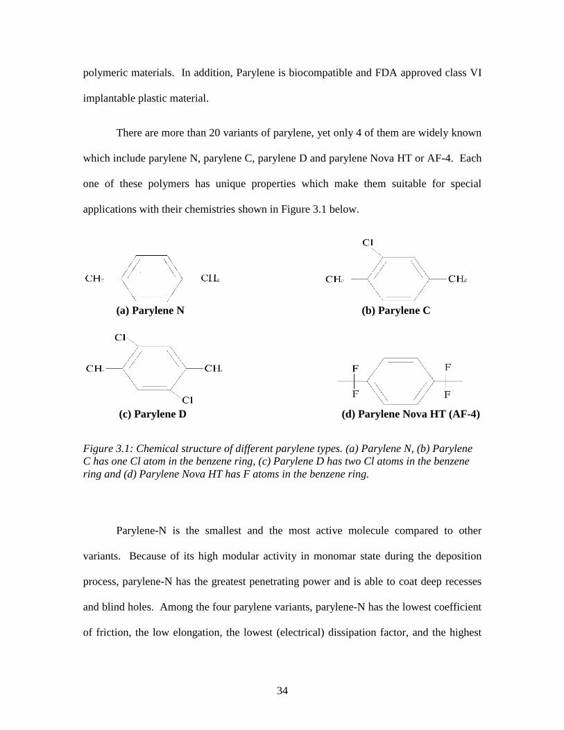
34
polymeric materials. In addition, Parylene is biocompatible and FDA approved class VI
implantable plastic material.
There are more than 20 variants of parylene, yet only 4 of them are widely known
which include parylene N, parylene C, parylene D and parylene Nova HT or AF-4. Each
one of these polymers has unique properties which make them suitable for special
applications with their chemistries shown in Figure 3.1 below.
(a) Parylene N (b) Parylene C
(c) Parylene D (d) Parylene Nova HT (AF-4)
Figure 3.1: Chemical structure of different parylene types. (a) Parylene N, (b) Parylene
C has one Cl atom in the benzene ring, (c) Parylene D has two Cl atoms in the benzene
ring and (d) Parylene Nova HT has F atoms in the benzene ring.
Parylene-N is the smallest and the most active molecule compared to other
variants. Because of its high modular activity in monomar state during the deposition
process, parylene-N has the greatest penetrating power and is able to coat deep recesses
and blind holes. Among the four parylene variants, parylene-N has the lowest coefficient
of friction, the low elongation, the lowest (electrical) dissipation factor, and the highest
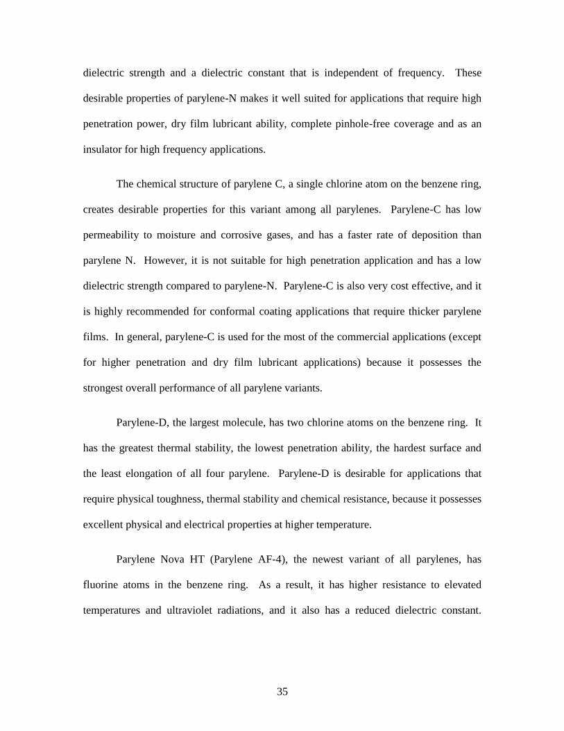
35
dielectric strength and a dielectric constant that is independent of frequency. These
desirable properties of parylene-N makes it well suited for applications that require high
penetration power, dry film lubricant ability, complete pinhole-free coverage and as an
insulator for high frequency applications.
The chemical structure of parylene C, a single chlorine atom on the benzene ring,
creates desirable properties for this variant among all parylenes. Parylene-C has low
permeability to moisture and corrosive gases, and has a faster rate of deposition than
parylene N. However, it is not suitable for high penetration application and has a low
dielectric strength compared to parylene-N. Parylene-C is also very cost effective, and it
is highly recommended for conformal coating applications that require thicker parylene
films. In general, parylene-C is used for the most of the commercial applications (except
for higher penetration and dry film lubricant applications) because it possesses the
strongest overall performance of all parylene variants.
Parylene-D, the largest molecule, has two chlorine atoms on the benzene ring. It
has the greatest thermal stability, the lowest penetration ability, the hardest surface and
the least elongation of all four parylene. Parylene-D is desirable for applications that
require physical toughness, thermal stability and chemical resistance, because it possesses
excellent physical and electrical properties at higher temperature.
Parylene Nova HT (Parylene AF-4), the newest variant of all parylenes, has
fluorine atoms in the benzene ring. As a result, it has higher resistance to elevated
temperatures and ultraviolet radiations, and it also has a reduced dielectric constant.
36
These properties make parylene Nova HT well suited for avionic and semiconductor
applications.
Other properties of the parylene variants are detailed in the Appendix A-2. The
recent book by Fortin and Lu [55] is the only and the best text that provides detailed
information about parylenes.
3.2.2 Applications of Parylene-C
Parylene-C has traditionally been used in the medical device industry for coating
implantable devices [55, 134, 185] and in the electronics industry as a insulating [186,
187] and bonding [188] material. In the Micro Electro Mechanical Systems (MEMS)
community, it has been utilized as a structural layer in many device applications, for
instance; micro check valve [189], actuators [190, 191], sensors [192], bolometer [193]
etc. Furthermore, it has also been used in the biomedical engineering research for a wide
variety of applications, from 3-dimensional (3D) neurocages [194], selective patterning
of biomolecules [195, 196] to microfluidic channels [114].
3.3 Results and Discussion
3.3.1 Parylene Deposition Process
Parylene is widely utilized in the medical and electronics industries as a
conformal pin-hole free coating. Due to its high mechanical strength it is also being
considered as a substrate for Flextronics applications [197]. Based on our experiments,
parylene film of thickness up to 20 μm are relatively flexible and will conform readily to
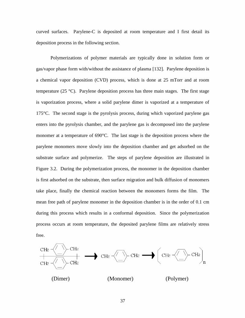
37
curved surfaces. Parylene-C is deposited at room temperature and I first detail its
deposition process in the following section.
Polymerizations of polymer materials are typically done in solution form or
gas/vapor phase form with/without the assistance of plasma [132]. Parylene deposition is
a chemical vapor deposition (CVD) process, which is done at 25 mTorr and at room
temperature (25 °C). Parylene deposition process has three main stages. The first stage
is vaporization process, where a solid parylene dimer is vaporized at a temperature of
175°C. The second stage is the pyrolysis process, during which vaporized parylene gas
enters into the pyrolysis chamber, and the parylene gas is decomposed into the parylene
monomer at a temperature of 690°C. The last stage is the deposition process where the
parylene monomers move slowly into the deposition chamber and get adsorbed on the
substrate surface and polymerize. The steps of parylene deposition are illustrated in
Figure 3.2. During the polymerization process, the monomer in the deposition chamber
is first adsorbed on the substrate, then surface migration and bulk diffusion of monomers
take place, finally the chemical reaction between the monomers forms the film. The
mean free path of parylene monomer in the deposition chamber is in the order of 0.1 cm
during this process which results in a conformal deposition. Since the polymerization
process occurs at room temperature, the deposited parylene films are relatively stress
free.
(Dimer) (Monomer) (Polymer)
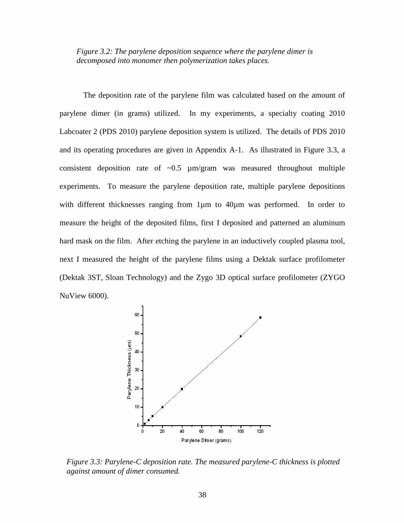
38
The deposition rate of the parylene film was calculated based on the amount of
parylene dimer (in grams) utilized. In my experiments, a specialty coating 2010
Labcoater 2 (PDS 2010) parylene deposition system is utilized. The details of PDS 2010
and its operating procedures are given in Appendix A-1. As illustrated in Figure 3.3, a
consistent deposition rate of ~0.5 µm/gram was measured throughout multiple
experiments. To measure the parylene deposition rate, multiple parylene depositions
with different thicknesses ranging from 1µm to 40µm was performed. In order to
measure the height of the deposited films, first I deposited and patterned an aluminum
hard mask on the film. After etching the parylene in an inductively coupled plasma tool,
next I measured the height of the parylene films using a Dektak surface profilometer
(Dektak 3ST, Sloan Technology) and the Zygo 3D optical surface profilometer (ZYGO
NuView 6000).
Figure 3.3: Parylene-C deposition rate. The measured parylene-C thickness is plotted
against amount of dimer consumed.
Figure 3.2: The parylene deposition sequence where the parylene dimer is
decomposed into monomer then polymerization takes places.
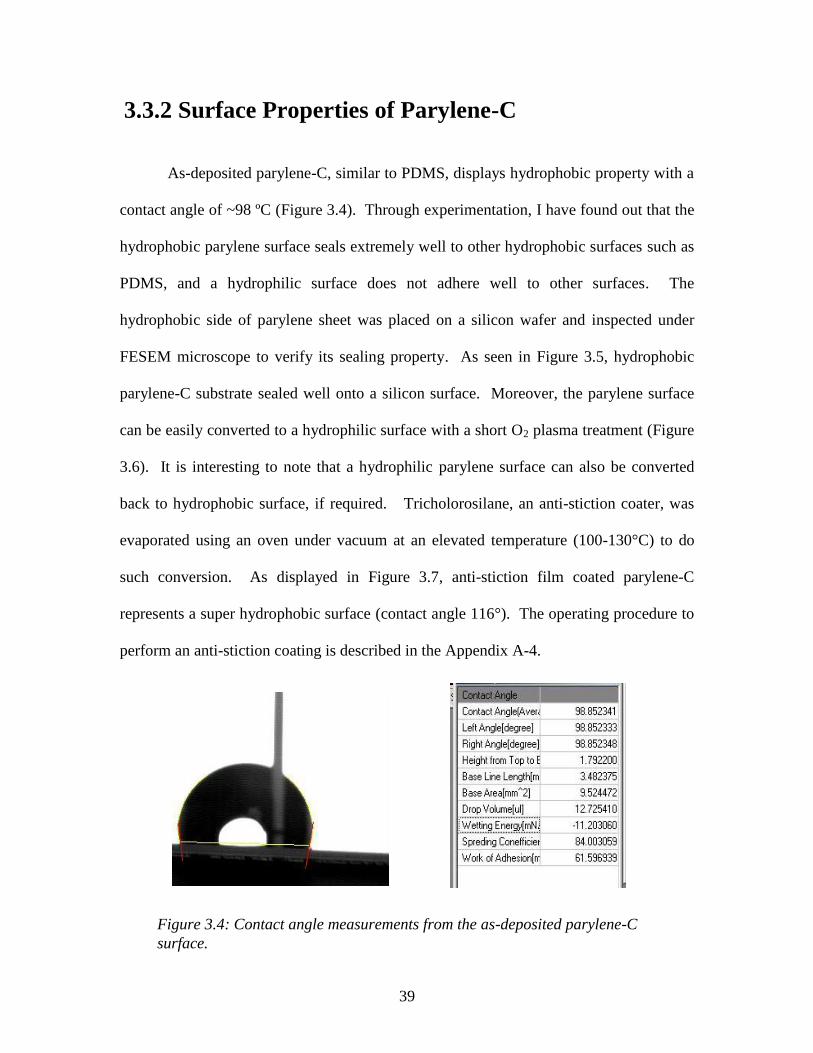
39
3.3.2 Surface Properties of Parylene-C
As-deposited parylene-C, similar to PDMS, displays hydrophobic property with a
contact angle of ~98 ºC (Figure 3.4). Through experimentation, I have found out that the
hydrophobic parylene surface seals extremely well to other hydrophobic surfaces such as
PDMS, and a hydrophilic surface does not adhere well to other surfaces. The
hydrophobic side of parylene sheet was placed on a silicon wafer and inspected under
FESEM microscope to verify its sealing property. As seen in Figure 3.5, hydrophobic
parylene-C substrate sealed well onto a silicon surface. Moreover, the parylene surface
can be easily converted to a hydrophilic surface with a short O2 plasma treatment (Figure
3.6). It is interesting to note that a hydrophilic parylene surface can also be converted
back to hydrophobic surface, if required. Tricholorosilane, an anti-stiction coater, was
evaporated using an oven under vacuum at an elevated temperature (100-130°C) to do
such conversion. As displayed in Figure 3.7, anti-stiction film coated parylene-C
represents a super hydrophobic surface (contact angle 116°). The operating procedure to
perform an anti-stiction coating is described in the Appendix A-4.
Figure 3.4: Contact angle measurements from the as-deposited parylene-C
surface.
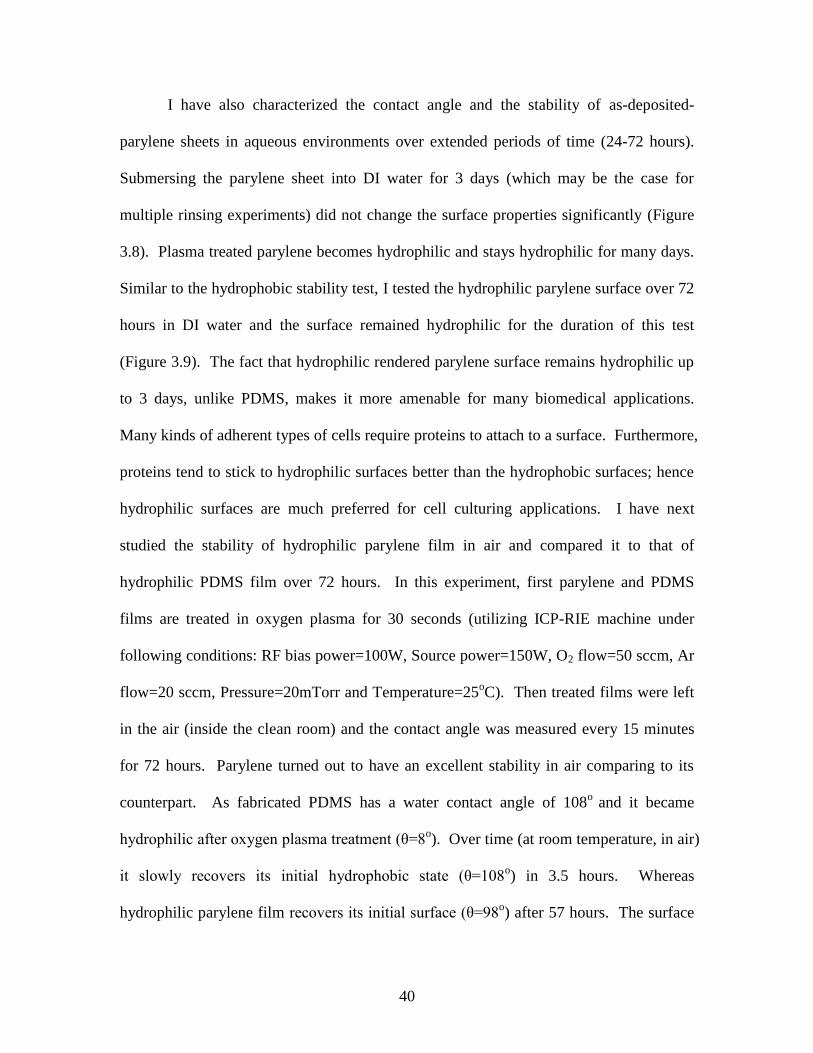
40
I have also characterized the contact angle and the stability of as-deposited-
parylene sheets in aqueous environments over extended periods of time (24-72 hours).
Submersing the parylene sheet into DI water for 3 days (which may be the case for
multiple rinsing experiments) did not change the surface properties significantly (Figure
3.8). Plasma treated parylene becomes hydrophilic and stays hydrophilic for many days.
Similar to the hydrophobic stability test, I tested the hydrophilic parylene surface over 72
hours in DI water and the surface remained hydrophilic for the duration of this test
(Figure 3.9). The fact that hydrophilic rendered parylene surface remains hydrophilic up
to 3 days, unlike PDMS, makes it more amenable for many biomedical applications.
Many kinds of adherent types of cells require proteins to attach to a surface. Furthermore,
proteins tend to stick to hydrophilic surfaces better than the hydrophobic surfaces; hence
hydrophilic surfaces are much preferred for cell culturing applications. I have next
studied the stability of hydrophilic parylene film in air and compared it to that of
hydrophilic PDMS film over 72 hours. In this experiment, first parylene and PDMS
films are treated in oxygen plasma for 30 seconds (utilizing ICP-RIE machine under
following conditions: RF bias power=100W, Source power=150W, O2 flow=50 sccm, Ar
flow=20 sccm, Pressure=20mTorr and Temperature=25oC). Then treated films were left
in the air (inside the clean room) and the contact angle was measured every 15 minutes
for 72 hours. Parylene turned out to have an excellent stability in air comparing to its
counterpart. As fabricated PDMS has a water contact angle of 108o
and it became
hydrophilic after oxygen plasma treatment (θ=8o). Over time (at room temperature, in air)
it slowly recovers its initial hydrophobic state (θ=108o) in 3.5 hours. Whereas
hydrophilic parylene film recovers its initial surface (θ=98o) after 57 hours. The surface
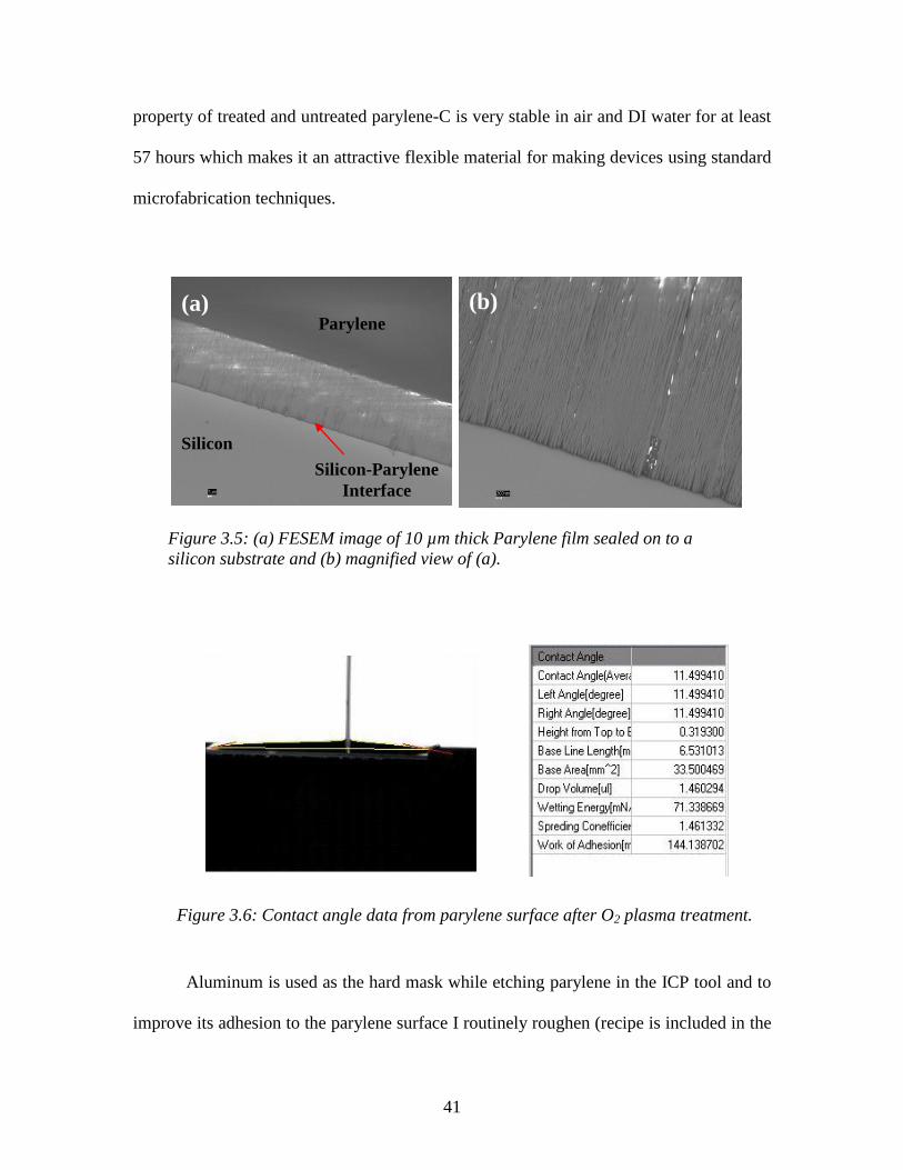
41
property of treated and untreated parylene-C is very stable in air and DI water for at least
57 hours which makes it an attractive flexible material for making devices using standard
microfabrication techniques.
Aluminum is used as the hard mask while etching parylene in the ICP tool and to
improve its adhesion to the parylene surface I routinely roughen (recipe is included in the
Figure 3.6: Contact angle data from parylene surface after O2 plasma treatment.
Figure 3.5: (a) FESEM image of 10 µm thick Parylene film sealed on to a
silicon substrate and (b) magnified view of (a).
Silicon
Parylene
Silicon-Parylene
Interface
(a) (b)
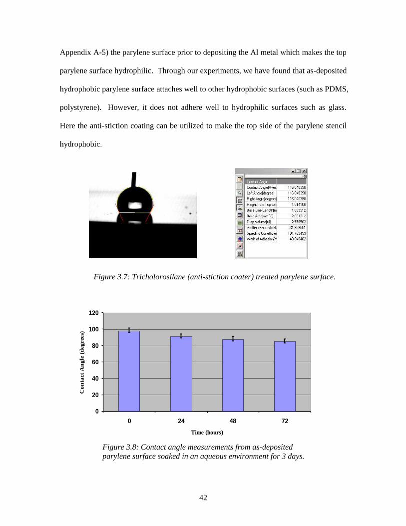
42
Appendix A-5) the parylene surface prior to depositing the Al metal which makes the top
parylene surface hydrophilic. Through our experiments, we have found that as-deposited
hydrophobic parylene surface attaches well to other hydrophobic surfaces (such as PDMS,
polystyrene). However, it does not adhere well to hydrophilic surfaces such as glass.
Here the anti-stiction coating can be utilized to make the top side of the parylene stencil
hydrophobic.
Figure 3.7: Tricholorosilane (anti-stiction coater) treated parylene surface.
Figure 3.8: Contact angle measurements from as-deposited
parylene surface soaked in an aqueous environment for 3 days.
0
20
40
60
80
100
120
0 24 48 72
Time (hours)
Co
nta
ct A
ng
le (
deg
rees
)
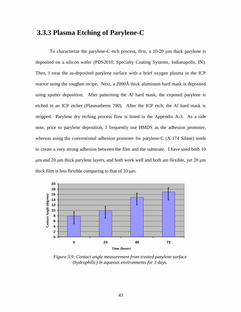
43
3.3.3 Plasma Etching of Parylene-C
To characterize the parylene-C etch process, first, a 10-20 μm thick parylene is
deposited on a silicon wafer (PDS2010, Specialty Coating Systems, Indianapolis, IN).
Then, I treat the as-deposited parylene surface with a brief oxygen plasma in the ICP
reactor using the roughen recipe. Next, a 2000Ǻ thick aluminum hard mask is deposited
using sputter deposition. After patterning the Al hard mask, the exposed parylene is
etched in an ICP etcher (Plasmatherm 790). After the ICP etch, the Al hard mask is
stripped. Parylene dry etching process flow is listed in the Appendix A-3. As a side
note, prior to parylene deposition, I frequently use HMDS as the adhesion promoter,
whereas using the conventional adhesion promoter for parylene-C (A-174 Silane) tends
to create a very strong adhesion between the film and the substrate. I have used both 10
μm and 20 μm thick parylene layers, and both work well and both are flexible, yet 20 μm
thick film is less flexible comparing to that of 10 μm.
Figure 3.9: Contact angle measurement from treated parylene surface
(hydrophilic) in aqueous environments for 3 days.
0
2
4
6
8
10
12
14
16
18
20
0 24 48 72
Time (hours)
Co
nta
ct A
ng
le (
deg
rees
)
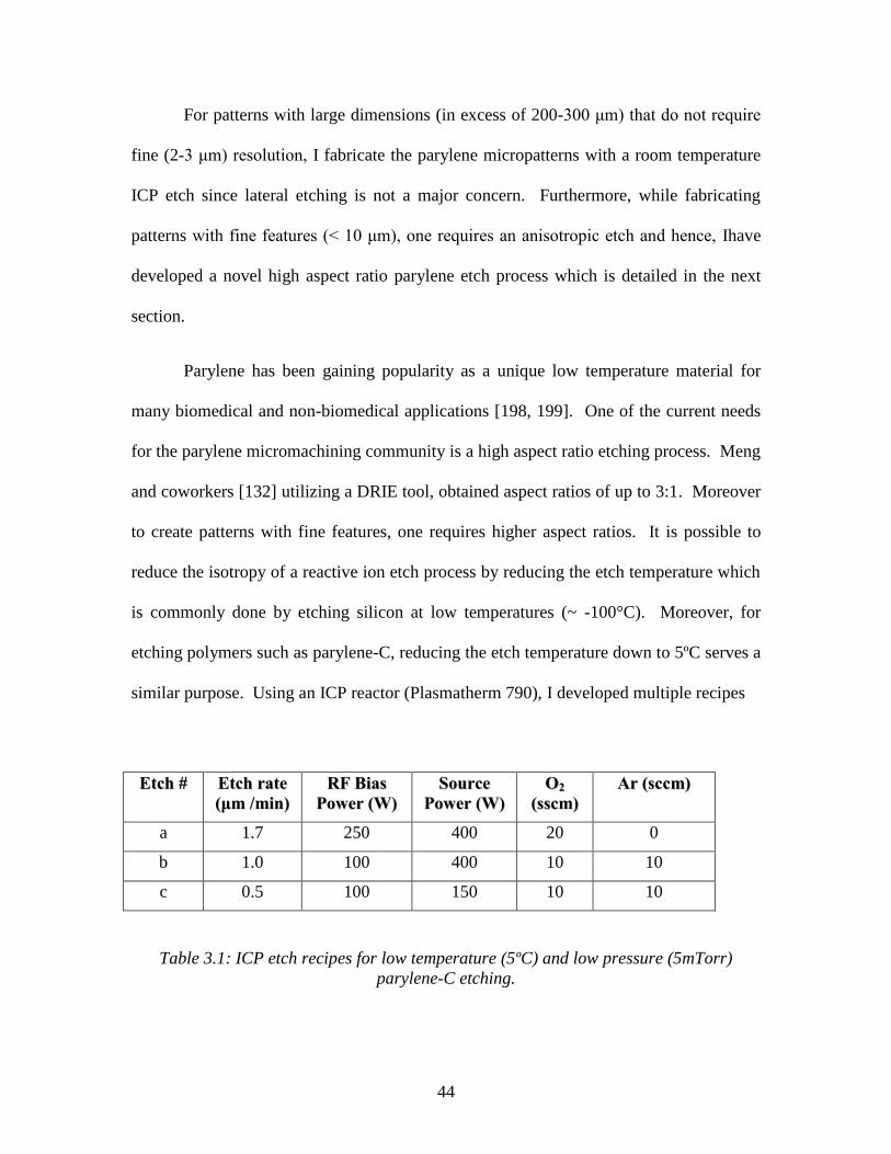
44
For patterns with large dimensions (in excess of 200-300 μm) that do not require
fine (2-3 μm) resolution, I fabricate the parylene micropatterns with a room temperature
ICP etch since lateral etching is not a major concern. Furthermore, while fabricating
patterns with fine features (< 10 μm), one requires an anisotropic etch and hence, Ihave
developed a novel high aspect ratio parylene etch process which is detailed in the next
section.
Parylene has been gaining popularity as a unique low temperature material for
many biomedical and non-biomedical applications [198, 199]. One of the current needs
for the parylene micromachining community is a high aspect ratio etching process. Meng
and coworkers [132] utilizing a DRIE tool, obtained aspect ratios of up to 3:1. Moreover
to create patterns with fine features, one requires higher aspect ratios. It is possible to
reduce the isotropy of a reactive ion etch process by reducing the etch temperature which
is commonly done by etching silicon at low temperatures (~ -100°C). Moreover, for
etching polymers such as parylene-C, reducing the etch temperature down to 5ºC serves a
similar purpose. Using an ICP reactor (Plasmatherm 790), I developed multiple recipes
EEttcchh ## EEttcchh rraattee
((μμmm //mmiinn)) RRFF BBiiaass
PPoowweerr ((WW)) SSoouurrccee
PPoowweerr ((WW)) OO22
((ssssccmm)) AArr ((ssccccmm))
a 1.7 250 400 20 0
b 1.0 100 400 10 10
c 0.5 100 150 10 10
Table 3.1: ICP etch recipes for low temperature (5ºC) and low pressure (5mTorr)
parylene-C etching.
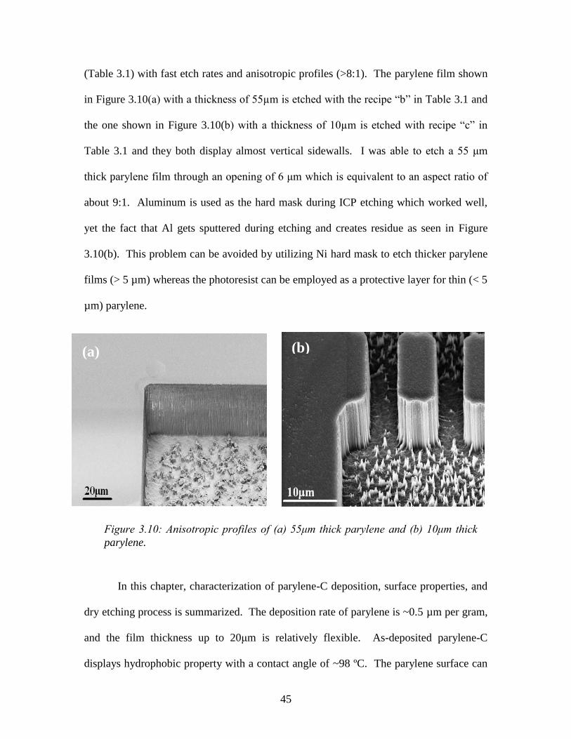
45
(Table 3.1) with fast etch rates and anisotropic profiles (>8:1). The parylene film shown
in Figure 3.10(a) with a thickness of 55µm is etched with the recipe ―b‖ in Table 3.1 and
the one shown in Figure 3.10(b) with a thickness of 10µm is etched with recipe ―c‖ in
Table 3.1 and they both display almost vertical sidewalls. I was able to etch a 55 μm
thick parylene film through an opening of 6 μm which is equivalent to an aspect ratio of
about 9:1. Aluminum is used as the hard mask during ICP etching which worked well,
yet the fact that Al gets sputtered during etching and creates residue as seen in Figure
3.10(b). This problem can be avoided by utilizing Ni hard mask to etch thicker parylene
films (> 5 µm) whereas the photoresist can be employed as a protective layer for thin (< 5
µm) parylene.
In this chapter, characterization of parylene-C deposition, surface properties, and
dry etching process is summarized. The deposition rate of parylene is ~0.5 µm per gram,
and the film thickness up to 20μm is relatively flexible. As-deposited parylene-C
displays hydrophobic property with a contact angle of ~98 ºC. The parylene surface can
Figure 3.10: Anisotropic profiles of (a) 55μm thick parylene and (b) 10μm thick
parylene.
(a) (b)
46
be easily converted to a hydrophilic surface by short O2 plasma treatment. Furthermore,
a hydrophilic parylene surface can be converted back to hydrophobic surface with a self
assembled monolayer (SAM) coating. Submersing the parylene sheet (treated and
untreated) into DI water for 3 days does not change the surface properties significantly.
However, the air stability study reveals that the hydrophilic parylene film recovers its
initial surface (θ=98o) after 57 hours. Finally, A low temperature (5 °C) high aspect ratio
(>8:1) parylene etch process is also developed to fabricate the fine structures with
anisotropic profiles.
47
CChhaapptteerr 44
Parylene-C Dielectric for Carbon
Nanotube Field Effect Transistors
4.1 Introduction
Selection and design of gate dielectric material is critical for electronics especially
for a transistor. The gate dielectric is an insulating material that separates the active
semiconductor channel from the (top or bottom) gate electrode. The factors such as
dielectric-semiconductor interface, leakage current, dielectric constant, processability,
stability and reliability need to be carefully considered during selection of gate dielectric
material. Both inorganic and polymer gate dielectric materials have been used for thin
film transistors. Inorganic dielectrics such as silicon dioxide (SiO2), titanium dioxide
(TiO2), aluminum oxide (Al2O3) and tantalum dioxide (Ta2O5) are commonly used in
flexible organic and CNT transistors [57-61] yet there are still some drawbacks. The
deposition of these materials requires costly tools (eg. ALD deposition of Al2O3) and they
are not process compatible with different polymeric substrates. Inorganic gate dielectric
materials are usually deposited in few nanometers to achieve better flexibility. Hence, it
forms defects and pinholes in the material which lead to higher leakage current. The
thermal annealing at elevated temperature is frequently employed to improve the quality
48
of these thin dielectrics. Flexible substrates cannot handle high temperature process and
it can deteriorate the film quality. Polymer dielectrics are heavily utilized in flexible
electronics because they are easy and inexpensive to process, and compatible with active
channel materials (organic semiconductors and CNTs) and metal electrodes while
maintaining flexibility. Furthermore, they possess excellent insulating properties and
have very low leakage current makes it attractive for flexible applications. These organic
dielectrics create superb interface with organic semiconductors and provide template for
ordering organic materials. Organic FETs utilizing polymer dielectrics such as
polystyrene (PS), polymethyl-methacrylate (PMMA), poly (vinyl alcohol) PVA, poly
(vinyl phenol) PVP and poly (4-methylstyrene) have been reported [50, 62-66].
Polymeric materials such as polyimide [67], SU8 [35], and PMMA [68] have been
reported as gate dielectrics using solution processed techniques such as spin coating for
flexible carbon nanotube FETs. The drawback of employing these approaches for gate
dielectrics is that they are usually cured at high temperature which limits their
applications for flexible devices made on polymeric substrates. Moreover, these
materials are not very compatible with standard micro fabrication processing methods,
and hence require sophisticated fabrication techniques (such as imprinting) to develop a
complete transistor. Parylene-C is deposited at room temperature and provides a pinhole
free and conformal film, and hence it is ideal for flexible devices. Parylene-C is
compatible with standard CMOS fabrication techniques for example it is resistant to
chemicals, insoluble in common solvents such as acetone and isopropyl alcohol (IPA)
etc. The parylene polymerization is oxygen free, and the organic carbon nanotube on to
organic parylene gate dielectric is likely to provide better dielectric-CNT interface. The
49
dielectric constant of the parylene-C is 3.2 and due to its high breakdown voltage and low
leakage current several organic devices [69, 199] are made using parylene as a gate
dielectric, yet applications of parylene in CNTFETs is rarely explored. Accordingly, in
my dissertation, I have used parylene-C gate dielectric for carbon nanotube transistors.
Carbon nanotube solution contains both metallic and semiconducting nanotubes,
and an electrical breakdown of metallic tubes is needed to achieve high performance
FETs. During current induced electrical breakdown, drain-source voltage is usually
ramped up to a higher value at a higher gate voltage causes burning of metallic tubes.
Furthermore, the low voltage operation (below 5 volts) of flexible CNTFETs is essential
for implantable device applications. One of the easiest ways to achieve low threshold
voltage transistor is by thinning down the gate dielectric material. Hence, there is a need
to study the electrical stability of thin (micron and submicron) parylene-C dielectric film
before developing all-parylene based carbon nanotube transistors. In this chapter, the
adhesion and reliability of parylene-C dielectric material was evaluated using metal-
insulator-metal (MIM) capacitor structure under the influence of constant DC stress
voltage (CVS). First, the percentage of failure between untreated and silane A-174
adhesion promoter coated parylene MIM capacitors was studied at different stress
voltage. Next, the time dependent dielectric breakdown (TDDB) of 1 µm parylene film
was characterized as a function of applied voltage. Finally, TDDB of parylene based
MIM devices was evaluated as function of dielectric thickness and applied voltage.
These results indicated that the 130 nm, 330 nm, 560 nm and 1100 nm thick parylene-C
dielectric are pinhole free, and can be utilized for low voltage and high performance
parylene-C packaged CNTFETs.
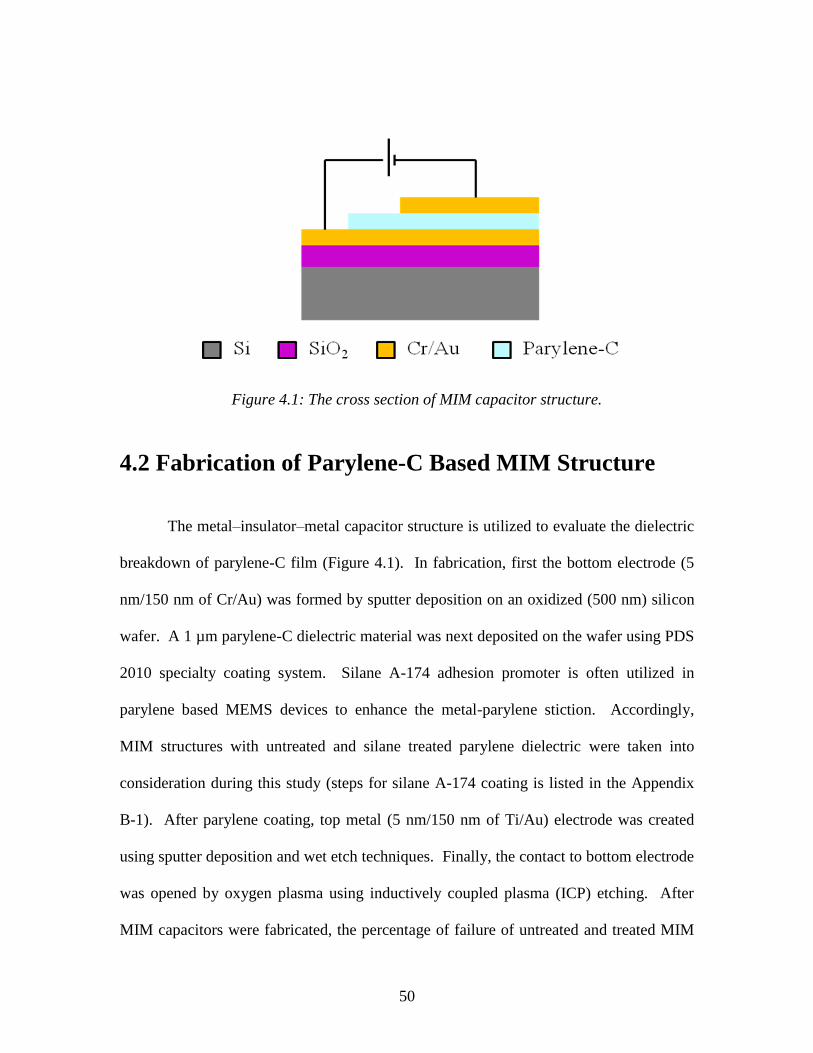
50
4.2 Fabrication of Parylene-C Based MIM Structure
The metal–insulator–metal capacitor structure is utilized to evaluate the dielectric
breakdown of parylene-C film (Figure 4.1). In fabrication, first the bottom electrode (5
nm/150 nm of Cr/Au) was formed by sputter deposition on an oxidized (500 nm) silicon
wafer. A 1 µm parylene-C dielectric material was next deposited on the wafer using PDS
2010 specialty coating system. Silane A-174 adhesion promoter is often utilized in
parylene based MEMS devices to enhance the metal-parylene stiction. Accordingly,
MIM structures with untreated and silane treated parylene dielectric were taken into
consideration during this study (steps for silane A-174 coating is listed in the Appendix
B-1). After parylene coating, top metal (5 nm/150 nm of Ti/Au) electrode was created
using sputter deposition and wet etch techniques. Finally, the contact to bottom electrode
was opened by oxygen plasma using inductively coupled plasma (ICP) etching. After
MIM capacitors were fabricated, the percentage of failure of untreated and treated MIM
Figure 4.1: The cross section of MIM capacitor structure.
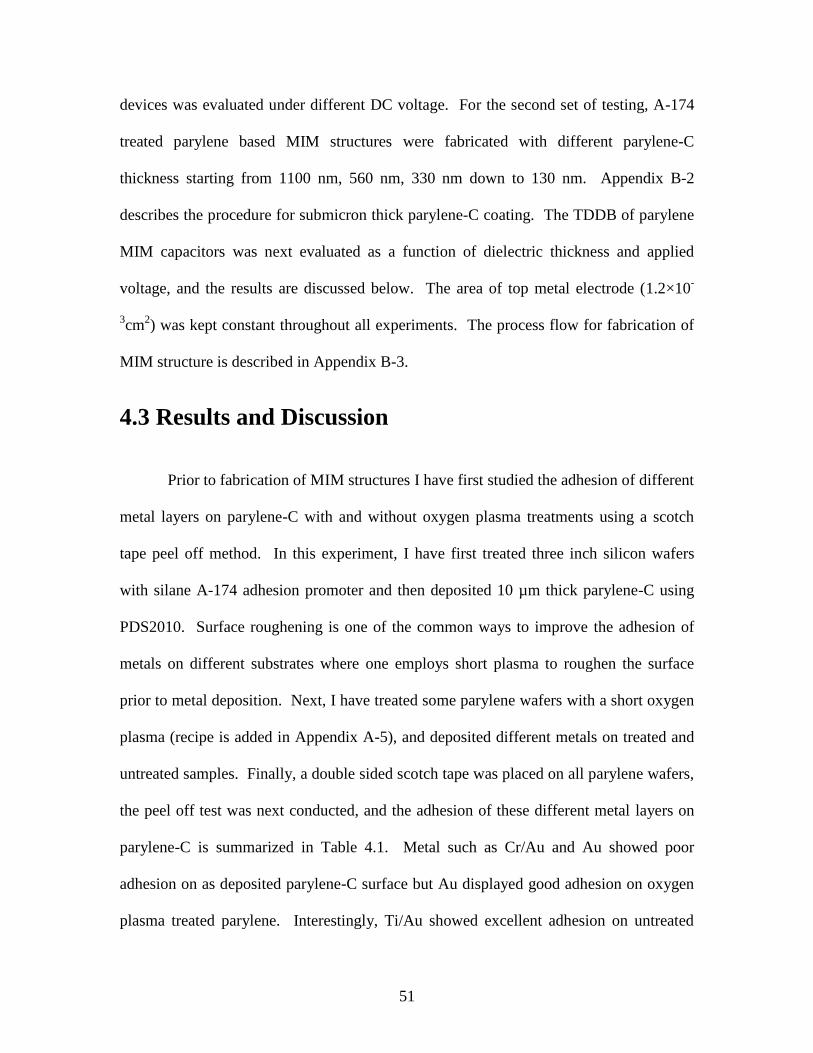
51
devices was evaluated under different DC voltage. For the second set of testing, A-174
treated parylene based MIM structures were fabricated with different parylene-C
thickness starting from 1100 nm, 560 nm, 330 nm down to 130 nm. Appendix B-2
describes the procedure for submicron thick parylene-C coating. The TDDB of parylene
MIM capacitors was next evaluated as a function of dielectric thickness and applied
voltage, and the results are discussed below. The area of top metal electrode (1.2×10-
3cm
2) was kept constant throughout all experiments. The process flow for fabrication of
MIM structure is described in Appendix B-3.
4.3 Results and Discussion
Prior to fabrication of MIM structures I have first studied the adhesion of different
metal layers on parylene-C with and without oxygen plasma treatments using a scotch
tape peel off method. In this experiment, I have first treated three inch silicon wafers
with silane A-174 adhesion promoter and then deposited 10 µm thick parylene-C using
PDS2010. Surface roughening is one of the common ways to improve the adhesion of
metals on different substrates where one employs short plasma to roughen the surface
prior to metal deposition. Next, I have treated some parylene wafers with a short oxygen
plasma (recipe is added in Appendix A-5), and deposited different metals on treated and
untreated samples. Finally, a double sided scotch tape was placed on all parylene wafers,
the peel off test was next conducted, and the adhesion of these different metal layers on
parylene-C is summarized in Table 4.1. Metal such as Cr/Au and Au showed poor
adhesion on as deposited parylene-C surface but Au displayed good adhesion on oxygen
plasma treated parylene. Interestingly, Ti/Au showed excellent adhesion on untreated
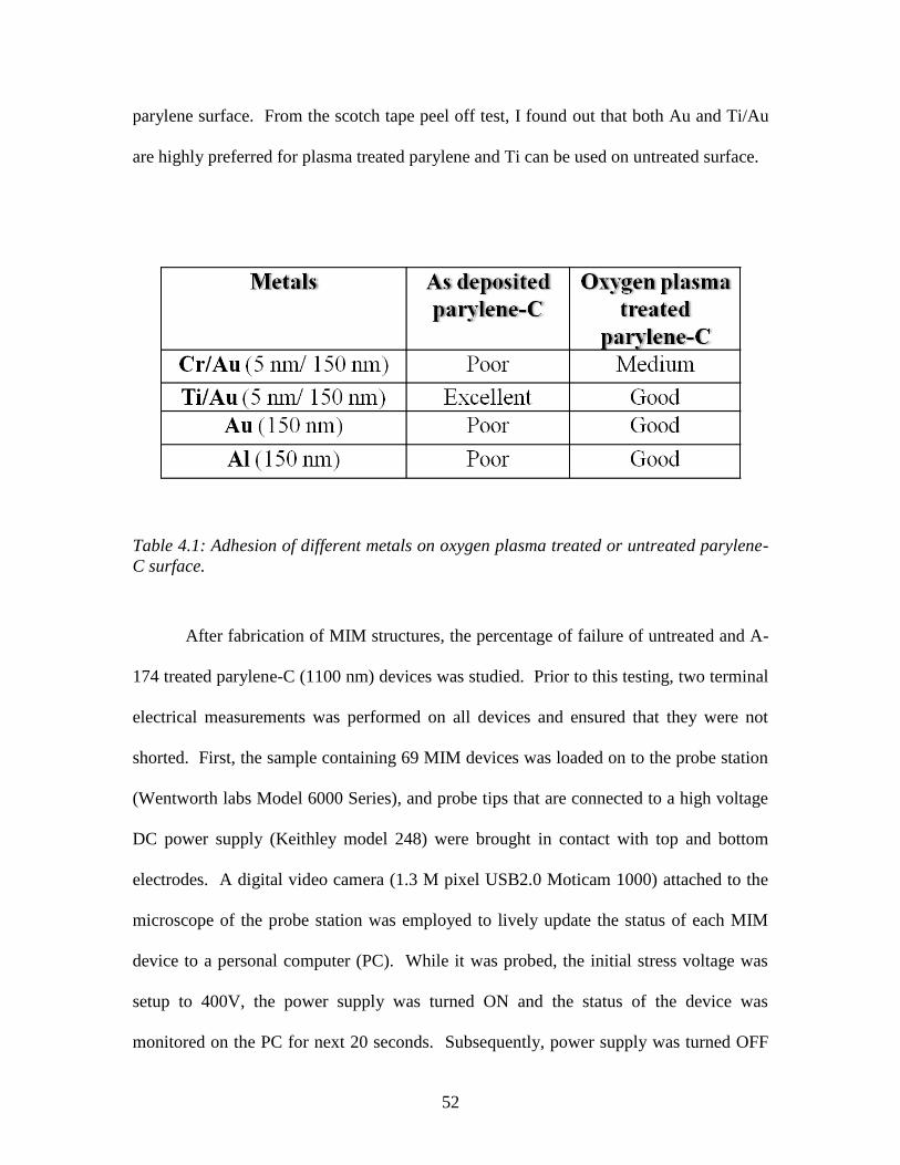
52
parylene surface. From the scotch tape peel off test, I found out that both Au and Ti/Au
are highly preferred for plasma treated parylene and Ti can be used on untreated surface.
Table 4.1: Adhesion of different metals on oxygen plasma treated or untreated parylene-
C surface.
After fabrication of MIM structures, the percentage of failure of untreated and A-
174 treated parylene-C (1100 nm) devices was studied. Prior to this testing, two terminal
electrical measurements was performed on all devices and ensured that they were not
shorted. First, the sample containing 69 MIM devices was loaded on to the probe station
(Wentworth labs Model 6000 Series), and probe tips that are connected to a high voltage
DC power supply (Keithley model 248) were brought in contact with top and bottom
electrodes. A digital video camera (1.3 M pixel USB2.0 Moticam 1000) attached to the
microscope of the probe station was employed to lively update the status of each MIM
device to a personal computer (PC). While it was probed, the initial stress voltage was
setup to 400V, the power supply was turned ON and the status of the device was
monitored on the PC for next 20 seconds. Subsequently, power supply was turned OFF
53
and the two terminal electrical measurements were carried out to electrically verify the
breakdown of parylene-C dielectric. Next, the applied voltage was varied with 40V
increment from the initial/previous value and the above experimental steps were repeated
until the breakdown of parylene-C occurred. The value of initial stress voltage was
selected as 40-50% of the breakdown voltage of 1 µm parylene-C dielectric that was
reported by Specialty Coating Systems [200].
Figure 4.2 shows the percentage of failure of untreated and A-174 treated MIM
devices where the thickness of parylene-C dielectric was 1100 nm. The silane treated
MIM devices showed predictable breakdown behavior as the stress voltage was increased
from 400 V down 760V with 40V increment. It was observed that the number of failed
devices increased as the applied voltage was increased and more than 95% of the
breakdown occurred at 760V. The untreated parylene MIM devices showed random
breakdown behavior as the stress voltage was varied from 0 to 640 V, and all devices
Figure 4.2: The percentage of failure of untreated and A-174 treated MIM devices.
54
failed at 680 V. It is possible that the intrinsic defects formed during polymerization of
parylene on untreated metal surface caused random breakdown behavior. From these
results it was found that the silane A-174 adhesion promoter not only improved the
stiction of parylene to the bottom electrode but also provided higher quality of film.
Accordingly, a consistent dielectric breakdown was observed with increasing stress
voltage and gave a higher breakdown voltage of 760V. Figure 4.3a displays the staircase
plot of time dependent breakdown of A-174 coated 1100 nm parylene-C MIM capacitor
where Figure 4.3b shows an optical photograph of a failed device. The applied voltage
was increased by 40 V every 20 seconds until the dielectric breakdown occured. The
parylene based MIM device failed at the 200th
second when DC stress voltage was 760 V.
To realize low voltage parylene-C packaged TFTs a thinner dielectric film is
always preferred. Next, time dependent dielectric breakdown of MIM capacitors with
various parylene-C thicknesses from 1100 nm, 560 nm, 330 nm down to 130 nm was
evaluated as a function of stress voltage (Figure 4.4). During fabrication of these devices
bottom electrode was treated with A-174 adhesion promoter prior to parylene deposition,
and the active area of capacitor was kept constant (1.2x10⁻³
cm2). The different parylene-
C thicknesses were measured and verified with both Dektak (Dektak 3ST, Sloan
Technology) profilometer and Zygo (ZYGO NuView 6000) 3D optical profilometer. The
applied voltage was increased with 40 V increment from the initial value every 20
seconds until the breakdown occurred while the status of the devices were monitored
lively on a PC. The MIM devices of parylene dielectric thicknesses of 1100 nm, 560 nm,
330 nm and 130nm failed on 180th
second at 760 V, 80th
second at 360 V, 240th
second at
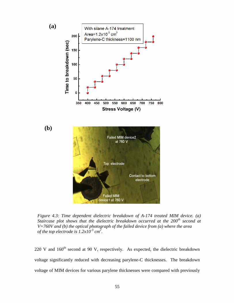
55
220 V and 160th
second at 90 V, respectively. As expected, the dielectric breakdown
voltage significantly reduced with decreasing parylene-C thicknesses. The breakdown
voltage of MIM devices for various parylene thicknesses were compared with previously
(a)
Figure 4.3: Time dependent dielectric breakdown of A-174 treated MIM device. (a)
Staircase plot shows that the dielectric breakdown occurred at the 200th
second at
V=760V and (b) the optical photograph of the failed device from (a) where the area
of the top electrode is 1.2x10⁻³
cm2.
(b)
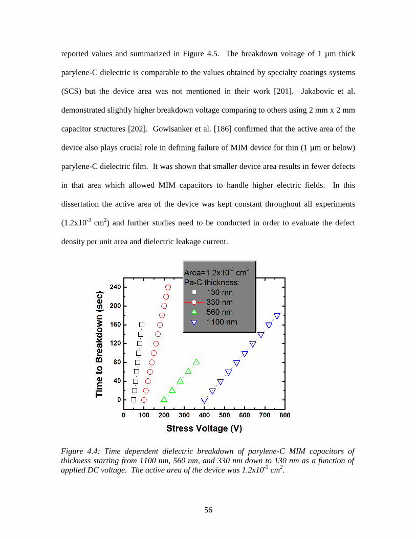
56
reported values and summarized in Figure 4.5. The breakdown voltage of 1 µm thick
parylene-C dielectric is comparable to the values obtained by specialty coatings systems
(SCS) but the device area was not mentioned in their work [201]. Jakabovic et al.
demonstrated slightly higher breakdown voltage comparing to others using 2 mm x 2 mm
capacitor structures [202]. Gowisanker et al. [186] confirmed that the active area of the
device also plays crucial role in defining failure of MIM device for thin (1 µm or below)
parylene-C dielectric film. It was shown that smaller device area results in fewer defects
in that area which allowed MIM capacitors to handle higher electric fields. In this
dissertation the active area of the device was kept constant throughout all experiments
(1.2x10⁻³
cm2) and further studies need to be conducted in order to evaluate the defect
density per unit area and dielectric leakage current.
Figure 4.4: Time dependent dielectric breakdown of parylene-C MIM capacitors of
thickness starting from 1100 nm, 560 nm, and 330 nm down to 130 nm as a function of
applied DC voltage. The active area of the device was 1.2x10⁻³
cm2.
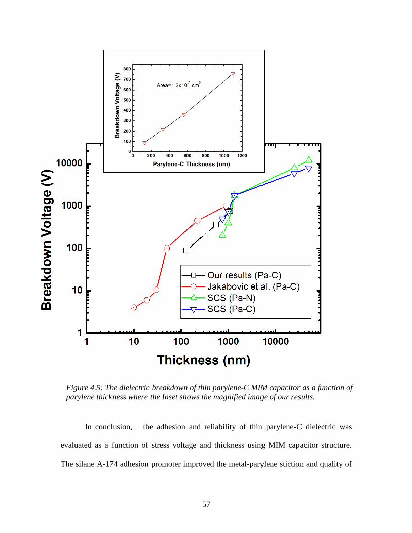
57
In conclusion, the adhesion and reliability of thin parylene-C dielectric was
evaluated as a function of stress voltage and thickness using MIM capacitor structure.
The silane A-174 adhesion promoter improved the metal-parylene stiction and quality of
Figure 4.5: The dielectric breakdown of thin parylene-C MIM capacitor as a function of
parylene thickness where the Inset shows the magnified image of our results.

58
the film (fewer defects) comparing to untreated film. The dielectric breakdown results
find that both 1100 nm and 130 nm thick parylene-C films are pinhole free, and
submicron films can be easily utilized for ultraflexible, low voltage and high performance
TFTs.
59
CChhaapptteerr 55
Parylene-C Encapsulated Single Walled
Carbon Nanotubes Based Thin Film
Transistors
5.1 Introduction
Flexible electronics have found their way into applications that require
characteristics such as lightweight, mechanically flexible, low cost, that can be wrapped
into complex shapes which are difficult to achieve with conventional electronics based on
rigid silicon technologies [3, 5-7]. The manufacturing of organic semiconductor based
flexible devices is relatively easy and inexpensive compared to silicon based electronics,
and hence organic materials have been most widely utilized as active materials in various
flexible devices including electronic artificial skin (E-skin), wearable sensors, flexible
displays, radio frequency identification tags, implantable devices, etc. [3, 5-9]. Even
though organic semiconductors (eg. pentacene) have begun to appear in commercial
products, the low mobility of these organic molecules devices has limited their capability
from realizing high performance flexible devices [41].
60
Carbon nanotubes with their unique chemical, physical and mechanical properties
are promising nanomaterials for high performance electronic devices [203-205]. CNTs
have high carrier mobility, large current carrying capability, and high mechanical
flexibility [35, 38, 67, 68, 203-205]. One main advantage of carbon nanotubes is that
similar to organic molecules they can be deposited using low cost solution based
methods. Many research groups have demonstrated high quality electronic circuits from
solution deposited nanotubes, and proven its potential as a cost effective technique for
realizing high performance CNT devices [35, 38, 67, 206, 207]. To utilize CNT based
flexible electronic devices for user friendly real world applications they should display
ultra flexibility so that it can be transformed into different shapes. Furthermore,
nanotubes are sensitive to the variations in the surrounding environment, and hence a
compatible encapsulation layer is needed to protect these devices from the environment.
Although SWNTs based flexible transistors have been previously realized and reported
on flexible substrates such as PEN [67] PET, [35, 38, 68] PI, [41] PDMS,[207]
Polyimide, [206] and Polyester (PE), [97] they failed to exhibit ultra high mechanical
flexibility. For example, Takenobu et al. [67] reported transistors on 125 µm PEN film
and observed 63% reduction in the ON current at a bending radius (R) of 6 mm.
Similarly the TFTs made on 180 µm PET substrate demonstrated by Rogers et al. [35]
displayed a ±5.5% change in the ON current where the smallest bending radius was 6
mm. CNTFETs made on 250 µm PET substrate by Chimot et al. showed 55% decrease
in the transconductance below the radius of 3.3 mm [38]. The flexible carbon nanotube
transistors reported by the previous three groups were not encapsulated. In addition, the
gas and moisure permeability of these plastic films causes elongation and shrinkage, and
61
has become a serious problem in ensuring their long term stability [208]. CNTs have an
excellent tendency to absorb gaseous molecules easily from the environment due to their
small size, hollow geometry and large surface area to volume ratio. They are extremely
sensitive to the vapors in environment which can significantly affect the electrical
properties of carbon nanotubes devices [40, 101, 209, 210]. Hence, a robust passivation
technique is required to isolate nanotubes electronics from the environmental variations
and contaminations before utilizing CNTs in nano electronics applications. Even though
thin films of ceramic and polymeric encapsulation layers have been previously reported
for carbon nanotubes devices there are several limitations to utilizing these techniques for
flexible device applications. For an example, thin Si3N4 (50 nm catalytic chemical vapor
deposited at 270°C)) and Al2O3 (15 nm deposited using ALD at 300°C) layers are
demonstrated for passivating CNT transistors [61, 204, 211]. In both of these
approaches, the materials are deposited and/or require post-deposition annealing steps at
elevated temperatures which limit their applications in flexible devices. Similarly,
polymeric encapsulants such as polymethyl-methacrylate (1.7 µm PMMA) and SU-
8/PMMA (2 µm / 200 nm) have also been reported [187, 212]. The drawback with these
polymeric materials are that gas and moisture molecules diffused through them and
caused variations in the transistor electrical characteristics. Furthermore, the flexibility
of a thin film is inversely proportional to the cube of its thickness [56]. Thus, the thin
film passivation approaches with good barrier properties are essential to protect carbon
nanotubes from environmental factors while preserving the flexibility of the devices.
Addressing these critical challenges (eg. ultra flexibility and encapsulation) and
62
rectifying it would propel flexible electronics into a new level opening up doors for ultra
flexible, high speed, easily manufacturable, low cost devices for numerous applications.
In this chapter, a parylene-C packaged SWNTs based TFTs on a polymeric
substrate is implemented and then I studied its mechanical robustness. The SWNT TFTs
exhibited p-type behavior with the mobility of ~54.6 cm2/Vs and an ON/OFF ratio of
~3x10³. Furthermore, through mechanical testing I found that the TFTs can handle
multiple bending cycles, and was operational even after exposure to the smallest bending
radius of 1.5 mm. After sharp folding conditions that induced both compressive and
tensile strains on the TFTs, the ON current of the transistors varied only within range of
±0.3% and ±8.9% where the maximum change was observed at smallest bending radius
(R=1.5 mm). To the best of my knowledge, this is the first instance of environmentally
benign and ultrathin (total thickness of 12 µm) carbon nanotube based flexible FETs
where the same polymeric material is utilized as substrate, dielectric and encapsulation
layer. Moreover, this is the highest flexibility reported at the smallest radius of curvature
of 1.5 mm for flexible CNTFETs. This versatile parylene-C packaged SWNT based
technology lays the foundations for the realization of ultra flexible, high performance and
biocompatible nano devices, which can be readily utilized in disposable biosensors
(without encapsulation), flexible electronics, wearable and implantable (eg. neural
prosthetic implants) applications.
5.2 Fabrication of Flexible SWNTs TFTs
The schematic of the flexible SWNT transistor is shown in Figure 5.1a and the
process sequence begins with the deposition of a 10 µm thick parylene-C layer on an
63
oxidized (500nm) silicon wafer at room temperature. Flexible devices using parylene-C
as a flexible substrate is increasing. The main advantage of this approach versus others is
that one can deposit parylene substrate on a carrier wafer, complete all fabrication
processes, and peel off from the career wafer at the end. Due to its higher tensile strength
(70 MPa) and Young‘s modulus (3.2 GPa) [55] parylene-C films as thin as 4 μm can be
easily fabricated and still peeled off without tearing it. In a general model for a thin film,
the bending rigidity of a film is proportional to the third power of its thickness [56] and is
also dependent on the elastic property of the material that comprises the film. The
thickness of the parylene-C film can be well controlled down to 1 μm using commercially
available parylene deposition systems, and hence the device flexibility can be engineered
to meet the needs of different applications. Next, Aluminum gate electrodes (1500Å)
were sputter deposited and patterned using conventional optical lithography and wet
etching. Then, a 1µm thick parylene-C gate dielectric layer was deposited. Polymer
dielectrics are heavily utilized in flexible CNT based electronics because they are easy
and inexpensive to process, and compatible with nanotube and metal electrodes while
maintaining flexibility. Polymeric material such as Polyimide [67], SU8 [35] and PMMA
[68] have been reported as gate dielectrics using solution processed techniques such as
spin coating. The drawback of employing these approaches for gate dielectrics is that
they are usually cured at high temperature which limits their applications for flexible
devices made on polymeric substrates. Moreover, these materials are not very
compatible with standard micro fabrication processing methods, and hence require
sophisticated fabrication techniques (such as imprinting) to develop a complete transistor.
Parylene-C is deposited at room temperature and provides a pinhole free and conformal
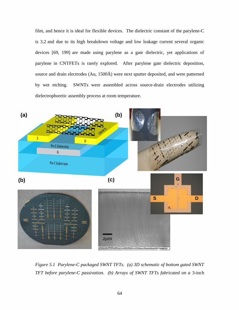
64
film, and hence it is ideal for flexible devices. The dielectric constant of the parylene-C
is 3.2 and due to its high breakdown voltage and low leakage current several organic
devices [69, 199] are made using parylene as a gate dielectric, yet applications of
parylene in CNTFETs is rarely explored. After parylene gate dielectric deposition,
source and drain electrodes (Au, 1500Å) were next sputter deposited, and were patterned
by wet etching. SWNTs were assembled across source-drain electrodes utilizing
dielectrophoretic assembly process at room temperature.
Figure 5.1 Parylene-C packaged SWNT TFTs. (a) 3D schematic of bottom gated SWNT
TFT before parylene-C passivation. (b) Arrays of SWNT TFTs fabricated on a 3-inch
(a)
(b)
(d)
(c)
2μm
(a) (b)
G
S D
65
wafer illustrating wafer scale manufacturing capability. (c) The high resolution SEM
micrograph of assembled SWNTs between source (S) and drain (D) electrodes of a
transistor with a channel length of 10 µm and a width of 2000 μm respectively. Inset:
Top view optical photograph of the same transistor fabricated from gold Source and
Drain electrodes and an aluminum (bottom) Gate electrodes, where the thickness of the
parylene-C gate dielectric was 1 µm. (D) The parylene film in which the devices were
embedded was wrapped around an index finger and non planar flexibility of the
transistors is illustrated in the inset. The process flow for fabrication of all-parylene TFT
is described in Appendix C.
Solution-based processing techniques [35, 38, 67, 97, 206, 207] have routinely
been utilized to make SWNT flexible thin film transistors. These approaches for
patterning nanotubes are favorable for realizing flexible CNT transistors since they utilize
low temperatures compatible with polymeric substrates, and the nanotubes suspended in a
solution have been purified and are free of metallic residues. Among the solution based
methods, field assisted dielectrophoretic assembly in particular is one of the preferred
methods [171-173, 213-216]. For example, using DEP, nanotubes can be deposited in
desired locations with alignment [171]. Moreover, DEP can also provide real time
control over the density of assembly [172] while the current induced oxidation eliminates
or minimizes the number of metallic nanotubes in the channel [173]. Accordingly,
dielectrophoretic assembly was utilized to assemble the SWNTs between the source and
drain electrodes. SWNTs from the CMOS grade aqueous solution procured from Brewer
Science were used.
The average length and diameter of these SWNTs were 2μm and 1.25nm,
respectively. The weight concentration of the SWNT in this aqueous solution was
0.046% while the pH of the supplied solution was 6.5. Prior to assembly, the SWNTs
66
were sonicated for 2 hours with an ultrasonic cleaner (Branson B-22-4). To perform DEP
assembly, an AC voltage with an amplitude of 5V peak-to-peak at a frequency of 300
KHz through a function generator (Agilent 33220A) is first applied. After the voltage
was turned on, a droplet (2-3μl) of the SWNT solution was dispensed on the active
channel area. Following 20 seconds of assembly the sample was blow dried and the
power was turned off concluding the DEP process which resulted in the assembly of
SWNT bundles between the source and drain electrodes. Assembly process is low
temperature and is amenable to wafer scale fabrication, [215, 216] and figure 5.1b
displays carbon nanotube TFTs fabricated on a 3-inch wafer. Figure 5.1c shows the SEM
micrograph of assembled SWNT bundles inside the channel whereas an optical
photograph of the fabricated TFT is displayed in the inset. As seen in the SEM
micrograph from figure 5.1c, the SWNTs are very dense near the edges of source and
drain electrodes, but moving away from these electrodes well aligned and separated
single bundles of nanotubes are observed. This pyramid like CNT structures near the
edge of the electrode is caused by the large surface forces associated with the drying of
liquids which has pulled nanotubes together and created denser bundles of SWNTs near
the edges of the source and drain electrodes. The problem can be resolved by using
critical point drier immediately after DEP assembly of carbon nanotubes [217].
67
5.3 Results and Discussion
5.3.1 Electrical Characteristics of Flexible SWNTs TFTs
After DEP assembly, current induced oxidation was performed which resulted in
electrical breakdown of the metallic SWNTs [173] inside the channel of the FETs.
Breakdown is needed since commercially available CNT solutions include both metallic
and semiconducting nanotubes, where the metallic nanotubes present in bundles in the
channel region result in poor transistor properties. The electrical breakdown of metallic
nanotubes was conducted at a gate to source bias voltage of 40 V where the drain-source
voltage (VDS) was ramped from 0 V to 15 V in 1 V increments. The I-V characteristics
of the transistors were measured using a semiconductor parameter analyzer (HP4155A) at
ambient room temperature and pressure. Figure 5.2 illustrates the IDS-VDS measurement
from one of the devices (L=10 μm and W=2000 μm) before (a) and after (b) the burning
process. Before electrical breakdown, the transistor was ON at a gate voltage of 40V as
seen in Figure 5.2a. When VDS was increased from 0 V to 15 V the higher current passed
only through the metallic nanotubes caused electrical burning. During current induced
electrical breakdown process the semiconductor SWNTs were depleted of charge carriers
at high gate voltage (VG=40 V) which prevented them from getting damaged. After
electrical breakdown, the conductance of the devices decreased by five orders magnitude
measured at VG=40 V while the ON/OFF current ratio increased by two orders of
magnitude indicating that the metallic paths in the channel have been reduced
significantly. The ON/OFF current ratio of the above TFT was determined at gate
voltages (VG) of -40 V and 40 V at a source-drain voltage (VDS) of 0.7 V. As the VG was
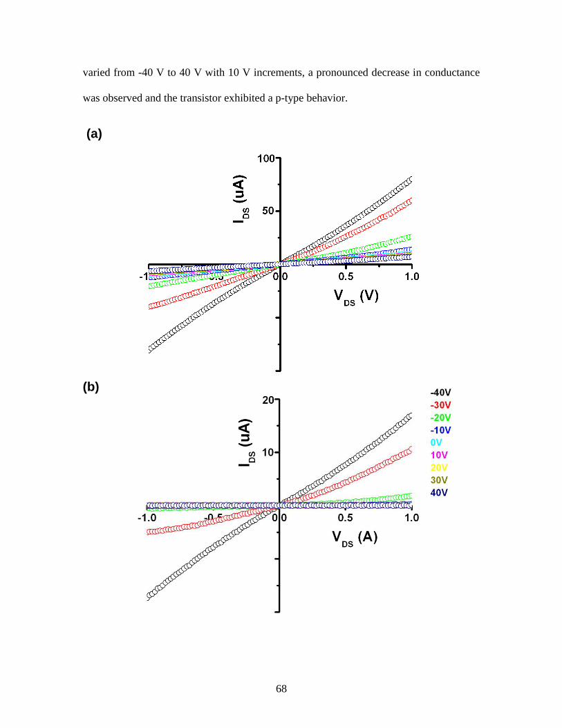
68
varied from -40 V to 40 V with 10 V increments, a pronounced decrease in conductance
was observed and the transistor exhibited a p-type behavior.
(a)
(b)
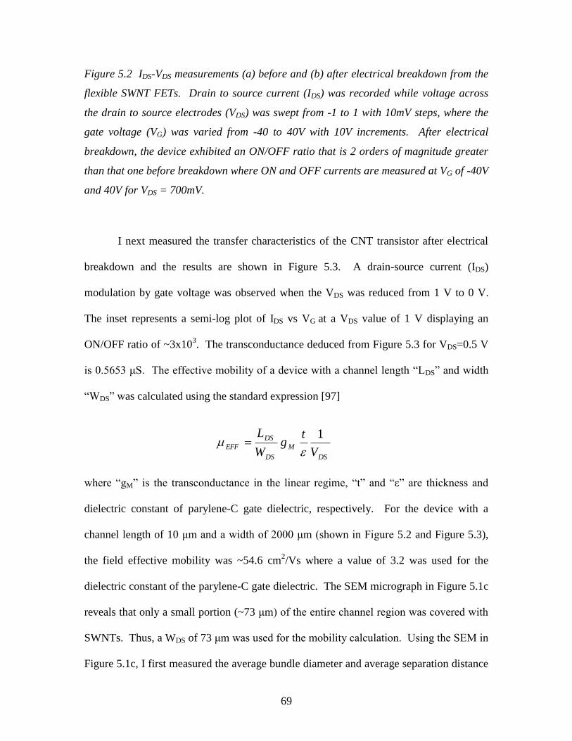
69
Figure 5.2 IDS-VDS measurements (a) before and (b) after electrical breakdown from the
flexible SWNT FETs. Drain to source current (IDS) was recorded while voltage across
the drain to source electrodes (VDS) was swept from -1 to 1 with 10mV steps, where the
gate voltage (VG) was varied from -40 to 40V with 10V increments. After electrical
breakdown, the device exhibited an ON/OFF ratio that is 2 orders of magnitude greater
than that one before breakdown where ON and OFF currents are measured at VG of -40V
and 40V for VDS = 700mV.
I next measured the transfer characteristics of the CNT transistor after electrical
breakdown and the results are shown in Figure 5.3. A drain-source current (IDS)
modulation by gate voltage was observed when the VDS was reduced from 1 V to 0 V.
The inset represents a semi-log plot of IDS vs VG at a VDS value of 1 V displaying an
ON/OFF ratio of ~3x10³. The transconductance deduced from Figure 5.3 for VDS=0.5 V
is 0.5653 μS. The effective mobility of a device with a channel length ―LDS‖ and width
―WDS‖ was calculated using the standard expression [97]
where ―gM‖ is the transconductance in the linear regime, ―t‖ and ―ε‖ are thickness and
dielectric constant of parylene-C gate dielectric, respectively. For the device with a
channel length of 10 μm and a width of 2000 μm (shown in Figure 5.2 and Figure 5.3),
the field effective mobility was ~54.6 cm2/Vs where a value of 3.2 was used for the
dielectric constant of the parylene-C gate dielectric. The SEM micrograph in Figure 5.1c
reveals that only a small portion (~73 μm) of the entire channel region was covered with
SWNTs. Thus, a WDS of 73 μm was used for the mobility calculation. Using the SEM in
Figure 5.1c, I first measured the average bundle diameter and average separation distance
DS
M
DS
DS
EFFV
tg
W
L 1
70
between bundles, and then estimated WDS. Among all the 75 devices tested, the above
device demonstrated the best electrical characteristics in terms of both effective mobility
and ON/OFF current ratio.
Figure 5.3 Transfer characteristics after electrical breakdown of metallic SWNTs from
the channel region of the SWNT FETs (device from figure 5.2). As the gate voltage (VG)
of the transistor was increased from -40V to 40V with 10V increments, a pronounced
decrease in conductance was observed which exhibited a p-type transistor behavior. The
drain-source current (IDS) was strongly modulated by the gate voltage as the VDS was
decreased from 1V to 0V. The transconductance deduced from the graph (slope in the
linear region) was 0.5653 μS (VDS=0.5V). The field-effect mobility of this device was
calculated as ~2 cm2/Vs, where the parylene-C gate dielectric constant=3.2, LDS=10 μm
and WDS=73 μm, respectively. Inset: magnified image of IDS-VG at VDS=1 V indicating an
ON/OFF ratio of 103.
71
5.3.2 Mechanical Evaluation of Flexible SWNTs TFTs
After device parameter optimization via current induced electrical breakdown, a
thin (1.0 μm) parylene-C layer was deposited as the passivation layer, and contacts to the
electrodes were opened using dry etching with O2 plasma. The extreme flexibility and
conformability of the fabricated parylene packaged TFTs are illustrated in figure 5.1d.
The detail information of parylene-C deposition and patterning is discussed in chapter 3
[218]. After passivation, electrical properties of these TFTs were measured and analyzed
with that of before encapsulation. The effect of parylene-C passivation in the electrical
characteristic of SWNTs based TFTs were analyzed separately in the next chapter.
The parylene-C encapsulated SWNT TFT was next peeled off from the silicon
substrate and the mechanical flexibility of the CNTFET was studied. Mechanical
bending tests were realized by wrapping the CNTFETs embedded in between two
parylene-C layers around cylinders of different radii and holding it in their bent position
for 5 minutes. Subsequently, they were unwrapped and the transfer characteristics of the
devices were measured. For a given bending cycle, the radius of curvature through which
the device undergoes bending was decreased in steps with values from 20, 15, 7.5, 4.5,
and down to 1.5 mm. Six such repetitive cycles were carried out on each device. Figure
5.4a displays an optical photograph of a 12 µm thick parylene film embedded with TFTs
wrapped around a cylinder (pen refill) with a radius of 1.5 mm which resulted in ~9
layers around it. Figure 5.4 b,c display the transfer characteristics of TFTs where the
results were shown after the first and sixth bending cycle (same device from Figure 5.2
and 5.3). A decrease in drain to source current from 7.83 µA to 5.93 µA (24.3%) was
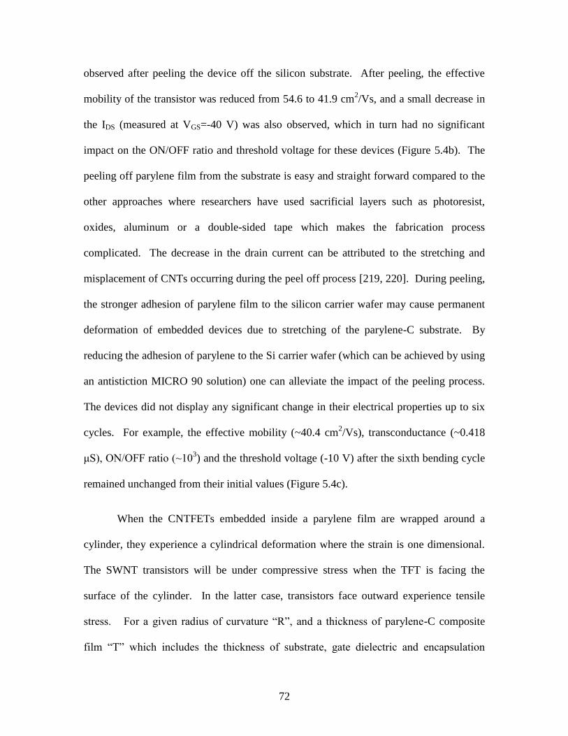
72
observed after peeling the device off the silicon substrate. After peeling, the effective
mobility of the transistor was reduced from 54.6 to 41.9 cm2/Vs, and a small decrease in
the IDS (measured at VGS=-40 V) was also observed, which in turn had no significant
impact on the ON/OFF ratio and threshold voltage for these devices (Figure 5.4b). The
peeling off parylene film from the substrate is easy and straight forward compared to the
other approaches where researchers have used sacrificial layers such as photoresist,
oxides, aluminum or a double-sided tape which makes the fabrication process
complicated. The decrease in the drain current can be attributed to the stretching and
misplacement of CNTs occurring during the peel off process [219, 220]. During peeling,
the stronger adhesion of parylene film to the silicon carrier wafer may cause permanent
deformation of embedded devices due to stretching of the parylene-C substrate. By
reducing the adhesion of parylene to the Si carrier wafer (which can be achieved by using
an antistiction MICRO 90 solution) one can alleviate the impact of the peeling process.
The devices did not display any significant change in their electrical properties up to six
cycles. For example, the effective mobility (~40.4 cm2/Vs), transconductance (~0.418
μS), ON/OFF ratio (~103) and the threshold voltage (-10 V) after the sixth bending cycle
remained unchanged from their initial values (Figure 5.4c).
When the CNTFETs embedded inside a parylene film are wrapped around a
cylinder, they experience a cylindrical deformation where the strain is one dimensional.
The SWNT transistors will be under compressive stress when the TFT is facing the
surface of the cylinder. In the latter case, transistors face outward experience tensile
stress. For a given radius of curvature ―R‖, and a thickness of parylene-C composite
film ―T‖ which includes the thickness of substrate, gate dielectric and encapsulation
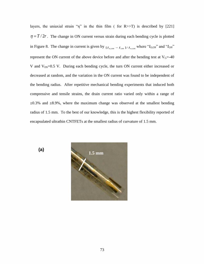
73
layers, the uniaxial strain ―η‖ in the thin film ( for R>>T) is described by [221]
rT 2/ . The change in ON current versus strain during each bending cycle is plotted
in Figure 8. The change in current is given by ONONON III ,0,0 /][ where ―I0,ON‖ and ―ION‖
represent the ON current of the above device before and after the bending test at VG=-40
V and VDS=0.5 V. During each bending cycle, the turn ON current either increased or
decreased at random, and the variation in the ON current was found to be independent of
the bending radius. After repetitive mechanical bending experiments that induced both
compressive and tensile strains, the drain current ratio varied only within a range of
±0.3% and ±8.9%, where the maximum change was observed at the smallest bending
radius of 1.5 mm. To the best of our knowledge, this is the highest flexibility reported of
encapsulated ultrathin CNTFETs at the smallest radius of curvature of 1.5 mm.
(a)
1.5 mm
1.5 mm
1.5 mm
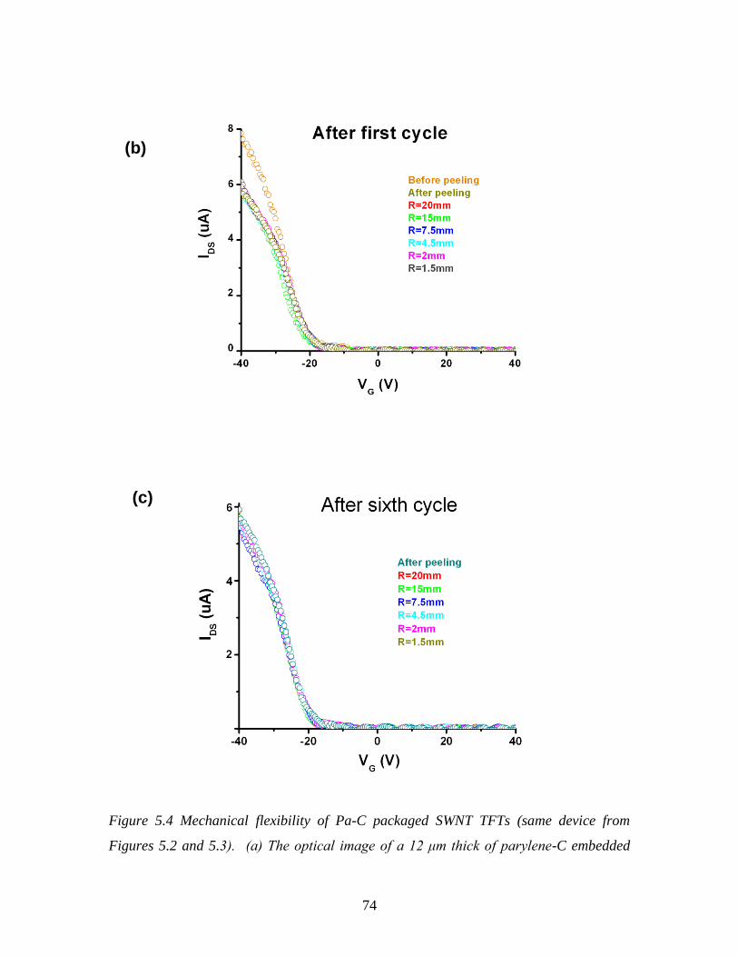
74
(b)
(c)
Figure 5.4 Mechanical flexibility of Pa-C packaged SWNT TFTs (same device from
Figures 5.2 and 5.3). (a) The optical image of a 12 μm thick of parylene-C embedded
75
SWNT TFTs are wrapped around a pen refill with a radius (R) of 1.5mm which resulted
in about ~ 9 layers around it. (b) Transfer characteristics after first bending cycle shows
reduction in ON current before and after peeling off from the wafer, where IDS dropped
from 7.83 µA to 5.93µA (measured at VG=-40V). (C) IDS-VG after the sixth cycle showed
no degradation in the electrical performance of the devices.
The real time bending flexibility (electrical characteristic of TFTs while it is bent)
of these devices for various thicknesses of substrate and encapsulation layers will be
studied in the future to investigate the long term flexibility of these devices. For
example, the smallest bending radius is set by the failure strain of the parylene-C
substrate and passivation layer. Thus, devices with different flexibility can be achieved
by scaling the total thickness of the parylene-C composite. The thickness of parylene
passivation layer and its effect in the electrical characteristics of carbon nanotube TFTs in
ambient environment and aqueous solutions medium also need to be studied to further
explore the barrier properties of packaged devices. These issues will be reported in our
future-work.
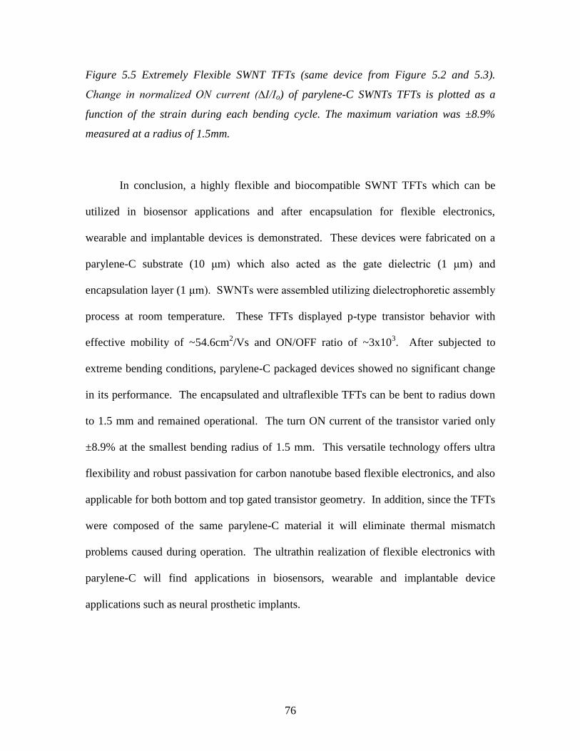
76
Figure 5.5 Extremely Flexible SWNT TFTs (same device from Figure 5.2 and 5.3).
Change in normalized ON current (∆I/Io) of parylene-C SWNTs TFTs is plotted as a
function of the strain during each bending cycle. The maximum variation was ±8.9%
measured at a radius of 1.5mm.
In conclusion, a highly flexible and biocompatible SWNT TFTs which can be
utilized in biosensor applications and after encapsulation for flexible electronics,
wearable and implantable devices is demonstrated. These devices were fabricated on a
parylene-C substrate (10 μm) which also acted as the gate dielectric (1 μm) and
encapsulation layer (1 μm). SWNTs were assembled utilizing dielectrophoretic assembly
process at room temperature. These TFTs displayed p-type transistor behavior with
effective mobility of ~54.6cm2/Vs and ON/OFF ratio of ~3x10
3. After subjected to
extreme bending conditions, parylene-C packaged devices showed no significant change
in its performance. The encapsulated and ultraflexible TFTs can be bent to radius down
to 1.5 mm and remained operational. The turn ON current of the transistor varied only
±8.9% at the smallest bending radius of 1.5 mm. This versatile technology offers ultra
flexibility and robust passivation for carbon nanotube based flexible electronics, and also
applicable for both bottom and top gated transistor geometry. In addition, since the TFTs
were composed of the same parylene-C material it will eliminate thermal mismatch
problems caused during operation. The ultrathin realization of flexible electronics with
parylene-C will find applications in biosensors, wearable and implantable device
applications such as neural prosthetic implants.
77
CChhaapptteerr 66
Parylene-C Passivation for SWNTs FETs
6.1 Introduction
Flexible electronics need to be protected from environmental contamination,
mechanical damage and detrimental gases. A good encapsulant should have high
dielectric strength, high electrical resistivity, high thermal conductivity, low dielectric
constant, conformality, low moisture absorption, solvent resistance, low thermal
expansion coefficient, thermal stability and high purity [70]. Polymer and ceramic films
are wildly used in packaging industry today. Ceramic encapsulants such Si3N4, SiO2 and
Al2O3 typically have superior thermal stability, highly impermeable to atmospheric gases,
higher dielectric strength, higher tensile strength, higher thermal conductivity, and lower
thermal expansion coefficient comparing to polymeric films. The drawback of using
ceramics as a passivation layer is that films create cracks and do not provide 100%
pinhole free deposition [71, 72]. Polymer encapsulants such as polyimide, parylene,
epoxy and silicone give conformal pinhole free coating and have also been reported [70,
72, 73] for encapsulation of organic devices. However, the gases and moisture
permeation through polymeric films challenges their long term stability. As a result,
impermeable thin film passivation has been created using a multilayer composite barrier
78
coating of alternating organic/inorganic thin layers to protect flexible organic devices [74,
75].
Due to their low carrier mobility organic molecules have limited their capability
from realizing high performance flexible devices [41]. Single-Walled Carbon Nanotubes
(SWNTs) with their unique physical, electrical and mechanical properties are being
considered as a potential replacement for existing semiconducting materials in flexible
electronics. Their mobility can exceed 105 cm
2/Vs
-1, and they have large current carrying
(109 A/cm
2) capability, higher ON/OFF ratios (>10
5) and extreme mechanical flexibility
[39]. SWNT based field effect transistors (FETs) exhibit p-type behavior in the ambient
environment, and they can be converted to n-type by doping e.g. polymer
functionalization [222]. Carbon nanotube (CNT) flexible devices such as high frequency
FETs, p-n diodes, and logic circuits have already been reported [41]. Their large surface
area to volume ratios and extreme sensitivity to the molecular species in the environment
(e.g. oxygen, moisture, etc.) can significantly affect the electrical properties of CNT
transistors [95, 205, 212], and numerous CNT based sensors (chemical and biological)
have been realized. Moreover, for electronic device applications, such sensitivity can
result in unexpected behavior including charge trapping, drift in transistor properties, etc.
Furthermore, the contaminants in the ambient such as dust, as well as handling can result
in degradation of device properties. Accordingly, proper passivation methods need to be
evaluated for carbon nanotube based devices. Despite the enormous potential of CNT
based electronics and the importance of encapsulation, I found very little studies on
encapsulation of CNT based devices. One of the main goals of the thesis is to realize
CNT devices on flexible substrates which happen to be polymeric in nature.
79
Accordingly, the encapsulation needs to be low temperature, inert and a good barrier for
moisture and other types of gases. For applications that need extreme flexibility also
requires that the coating need to be thin enough not to reduce the flexibility of the
transistor as thicker films tend to increase the rigidity of the devices.
Several groups have already explored passivation of CNT based devices with thin
polymeric films yet had limited success. For example, Dai et al.. [212] have reported a
1.7 µm polymer (polymethyl-methacrylate (PMMA)) coating for passivating carbon
nanotube based transistors. When the PMMA encapsulated devices were exposed to an
humid ambient, the electrical characteristics of the transistors changed due to permeation
of water molecules through PMMA. Similarly, Zhang et al.. [187, 223] used SU-
8/PMMA (2µm/200nm) to passivate their CNT FETs. After exposing their devices to an
NO2 environment for one hour, they have noted that the gas molecules diffused through
the SU-8/PMMA layer and caused variations in the transistor behavior. In addition to
polymeric encapsulants, chemical vapor deposited (CVD) Si3N4 (50nm catalytic chemical
vapor deposited at 270°C)) and Al2O3 (15nm deposited using atomic layer deposition
(ALD) at 300°C) layers have been utilized as passivation films for CNTFETs [61, 204,
211, 224-226]. To achieve high quality of these films they are deposited at elevated
temperature and/or go through high temperature post annealing deposition treatments.
These high temperature deposition conditions enable gas molecules to react with carbon
atoms, create defects in the nanotube and eventually introduce significant degrade in their
performance or destroys the devices. In addition, flexible substrates cannot stand this
kind of high temperature process and hence the above encapsulation techniques are not
desirable for carbon nanotube based flextronics applications.
80
To realize flexible CNT FETs which are insensitive to environmental variations,
high quality and thin encapsulation layers are needed which preserve the characteristics
of the transistors, maintain their flexibility and at the same time possess good barrier
properties. In this chapter, I demonstrate a parylene-C passivation technique for carbon
nanotube based thin film transistors which can be readily utilized for devices made on
flexible and rigid substrates. Parylene-C is a pin hole free material, and can provide a
uniform conformal coating over all surfaces regardless of the configuration of the surface
(eg. sharp edges and holes). It is also chemically inert, and has high dielectric strength
and low permeability to moisture and gases. Film deposition is stress-free (deposited at
room temperature), hence it does not introduce any adverse effects to the encapsulated
devices. These attractive properties make parylene-C a promising encapsulation layer for
flexible CNT based thin film transistors. First, I have fabricated CNT FETs on a flexible
parylene-C substrate. After measuring the electrical characteristics of the CNT FETs, I
have next encapsulated the devices with thin (1 µm and 3 µm) parylene-C layers and
studied the characteristics of the devices before and after encapsulation. After 1 µm
parylene-C passivation (PDS2010 pump down time ~10 min), more than 10% decrease in
two terminal contact resistance and 10% increase in ON current were observed in most of
the devices. No significant change in threshold voltage, ON/OFF current ratio, and gate
hysteresis width (HW) was observed after encapsulation. Treating unencapsulated
devices in high vacuum for long hours suppressed the gate hysteresis width but did not
fully eliminate it. The I-V measurements of the 1 µm parylene-C passivated TFTs after
28 hours in high vacuum showed no significant changes in the transistor properties and
demonstrated that a thin 1 µm parylene-C film provides a proper encapsulation against
81
various gases in the environment. Finally, I have studied the change in the electrical
properties of parylene-C packaged TFTs for encapsulation thickness of 1 µm and 3 µm.
My findings indicate that thin parylene-C films can be utilized as passivation layers for
CNT transistors and this versatile technique can be readily applied for the encapsulation
of CNT devices such as FETs, p-n diodes, and logic circuits fabricated on flexible/rigid
substrates.
6.2 Fabrication of Parylene-C Passivated Flexible
SWNTs TFTs
A 3D schematic of fabrication of a flexible SWNTs transistor is shown in figure
6.1(a) (see Appendix C for detailed information). First, a 10 µm thick parylene-C layer
was deposited (PDS2010, Specialty Coating Systems, Indianapolis, IN) on an oxidized
(500nm) silicon wafer at room temperature. Next, Aluminum gate electrodes (1500Å)
were sputter deposited and patterned using conventional optical lithography and wet
etching. Then, a 1 µm thick parylene-C gate dielectric layer was deposited.
Subsequently, source and drain electrodes (Cr/Au, 5/150nm) were sputter deposited, and
were patterned by wet etching. Figure 6.1b displays the optical image of one of the
sample devices fabricated. SWNTs were assembled across source-drain electrodes
utilizing dielectrophoretic assembly process at room temperature (Figure 6.1c). After
assembly, device parameters were optimized by removing metallic SWNTs from the
channel via current induced electrical breakdown process. Finally, the parylene-C
passivation layer was deposited, and contacts pads were opened for probing by etching
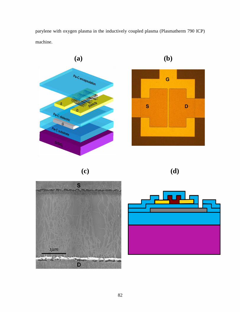
82
parylene with oxygen plasma in the inductively coupled plasma (Plasmatherm 790 ICP)
machine.
(a) (b)
(c) (d)
83
Figure 6.1: (a) A 3D schematic drawing of bottom gated SWNT FETs fabricated on a 10
µm thick flexible Parylene-C substrate (b) an optical image of the same transistor (c) The
high resolution SEM micrograph of DEP assembled SWNTs between source (S) and
drain (D) electrodes (d) Cross sectional drawing of a Parylene-C passivated transistor.
For both 1 µm and 3 µm thick parylene coating photo resist was used as a mask to etch
parylene. The detailed information of parylene-C deposition and patterning is published
in the previous chapter [218]. The cross section of parylene-C encapsulated SWNTs FET
is shown in figure 6.1d.
6.3 Results and Discussion
Carbon nanotubes are very sensitive to changes in environmental conditions such
as gases, moisture etc., and hence require proper encapsulation to protect them from the
atmosphere. After current induced electrical breakdown and subsequent transistor
measurements, samples were loaded into the parylene deposition machine (PDS2010)
and it started to pump down. After nearly 10 minutes, the system reached a low vacuum
pressure (1 mTorr), the machine was turned ON and the pyrolysis process has begun.
During this process, parylene dimer is first vaporized at 175 °C and then the dimer will
turn into a monomer at 690 °C. This process is so called pyrolization which lasted for 1
hour and 20 minutes, and the devices were exposed to vacuum (1 mTorr) during this
process. Finally, parylene monomer moved into the deposition chamber and the 1 µm
parylene-C polymerization was completed in 28 minutes.
After 1 µm parylene passivation, electrical properties of these TFTs were
remeasured, analyzed and compared with the values before encapsulation, and the results
84
are summarized in Figure 6.2. Figure 6.2a shows the percentage of change in turn ON
resistance (RON) and the turn ON current (measured at VG= -40V) of 15 good TFTs
before and after encapsulation. Definition of a ‗good TFT‘ is that the majority of metallic
SWNTs were removed from the channel during current induced electrical breakdown
process, and the transistor does turn OFF at a specific gate voltage. Among them, device
number from 1 to 5, 6 to 10 and 11 to 15 have channel lengths (L) of 3, 5 and 10 µm
respectively. The purpose of employing devices with different L is to study the
effectiveness of conformal parylene-C passivation when the gap between the source and
drain electrodes are larger than the average length of the nanotubes. SWNTs were placed
via DEP assembly, and as L was increased, fewer nanotubes bridged the source and drain
electrodes due to scaling effect of dielectrophoretic force (FDEP). The magnitude of the
DEP force scales with the following relationship [227]:
DEPF 3
2
LV
where V and L are the applied voltage and the characteristic length (distance between
source and drain) of the electrodes, respectively. Thus, the amount of assembled
nanotubes across the channel can be controlled by scaling the dielectrophoretic force via
adjusting the amplitude of the electric field or the gap between the electrodes. In the
above case, characteristic length was varied to change the magnitude of the force where
shorter channel TFTs had more CNTs connecting the source and drain electrodes where
fewer SWNTs were assembled in long channel devices. The two terminal resistance
measured at VG=-40 V for a typical 3, 5 and 10 µm channel length devices ranged from
0.214 to 30.65, 0.645 to 175.7, and 23.37 to 159.25 KOhms, respectively. More than
85
10% decrease in turn ON resistance was recorded in most of the devices with L=3 µm,
L=5 µm and L=10 µm, respectively. It was found that the deposition of a 1 µm parylene-
C layer not only fixed the position of the CNTs at the metal-nanotube interface, but also
improved the two terminal contact resistance (measured at VG=-40 V) between the gold
electrodes and the CNTs. A thin layer of parylene-C film conformally coated nanotubes
which were placed on the metal electrodes, pressed them down and fixed CNTs in their
respective position. Parylene-C is known to densify CNTs by linking neighboring tubes
together which also resulted in increased electrical stability [189, 228].
Hysteresis is a common phenomenon in carbon nanotube transistors, and it is
attributed to charge injection from nanotubes at a large gate voltage [190], trapped
charges at the dielectric-CNT interface and adsorption of charges and water molecules on
CNT surface from ambient environment [191, 212], other trapped charges from solution
processed CNTs [229] (e.g. surfactant, ionic molecules, etc.) and contamination
originating from the device fabrication processes [229]. I next investigated the hysteresis
behavior of CNTFETs before and after parylene-C passivation. The hysteresis width
between forward and backward gate voltage sweep from device 1 before and after
encapsulation (Figure 6.2b) is 47.5 V in VG. As deposited, parylene-C is hydrophobic
and oxygen free material. During fabrication of TFTs, the surface of the parylene-C
dielectric was roughened in oxygen plasma to enable the adhesion of Cr/Au source/drain
electrodes on to parylene. I believe that this oxygen plasma treatment broke bonds on the
parylene surface and induced fixed and mobile charges at the parylene-SWNT interface,
and caused large hysteresis between the forward and backward gate sweeping. Wong et
al. observed similar behavior in pentacene transistors built on a parylene dielectric [69].
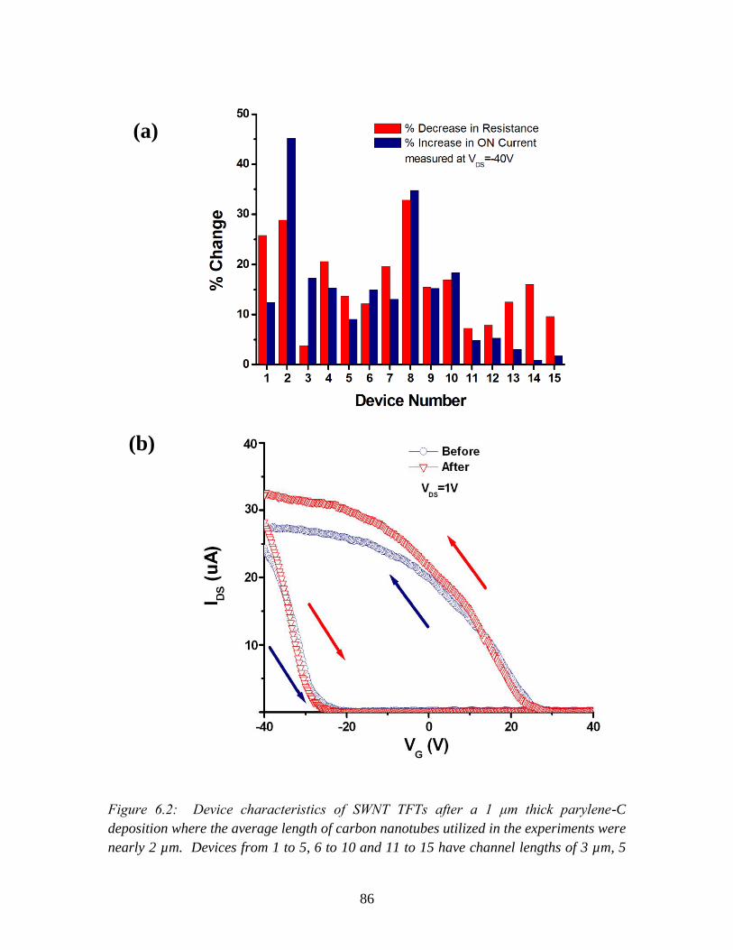
86
Figure 6.2: Device characteristics of SWNT TFTs after a 1 μm thick parylene-C
deposition where the average length of carbon nanotubes utilized in the experiments were
nearly 2 µm. Devices from 1 to 5, 6 to 10 and 11 to 15 have channel lengths of 3 µm, 5
(a)
(b)
87
µm and 10 µm, respectively. (a) Measured statistical variation in two terminal
resistance (at VG=-40 V) and turn ON current (at VG=-40 V) after 1 µm thick parylene-C
encapsulation. More than 10% decrease in the two terminal contact resistance was
measured in all SWNT FETs with L of 3 µm, 5 µm and 10 µm. The drop in the resistance
is observed due to CNT densification and fixing the nanotube position at the metal-CNT
interface after parylene coating. The transistors with shorter channel lengths (L= 3 µm
and 5 µm) showed a 10% increase in ON current after encapsulation. Interestingly,
longer channel devices (L=10 µm) showed only marginal increment in ON current
measurements which could be attributed to a disconnection of loosely connected
nanotube bridges by the deposited parylene-C film. For example, device 14 exhibited
only 0.86% of increase in the ION after the passivation. (b) Transfer characteristics (IDS-
VG) of device 1 before and after parylene encapsulation. Before passivation, transistor
exhibited ON/OFF=~2x102, VTH=-20 V and HW=47.5 V. After parylene-C passivation,
the ON current of the device improved by 12.43% from its initial value but no significant
change in VTH, ON/OFF current ratio, and the hysteresis width was observed. A thin 1
µm parylene coating protected CNTs from the penetration of molecules and/or chemical
spices in the environment (eg. gases, water moisture andcarbon particles). It also acts as
a barrier layer for the trapped charges that exist at the parylene-tube interface and on
the CNT surfaces, and hence no change was observed in the VTH and HW after
encapsulation.
Moreover, SWNTs were suspended in DI water, and DEP assembly and I-V
characteristics of all TFTs were conducted in an ambient environment which allowed
more charges to be adsorbed on the CNT surface. The short oxygen plasma made the top
parylene dielectric surface hydrophilic and attracted more molecules at CNT-dielectric
interface and resulted in a large gate hysteresis. The hysteresis effect in parylene-C
packaged SWNT FET can be minimized or eliminated by treating nanotube transistors
for long hours in high vacuum prior to parylene encapsulation which is discussed in the
next section. Before passivation with parylene-C, the CNT transistor (device 1) exhibited
ON/OFF ratio of ~2x10², threshold voltage of -20 V and a hysteresis width of 47.5 V. As
shown in Figure 6.2a, parylene-C encapsulation fixed the position of CNTs and hence the
turn ON resistance of the device decreased by ~26%, which resulted in 12.43% increase
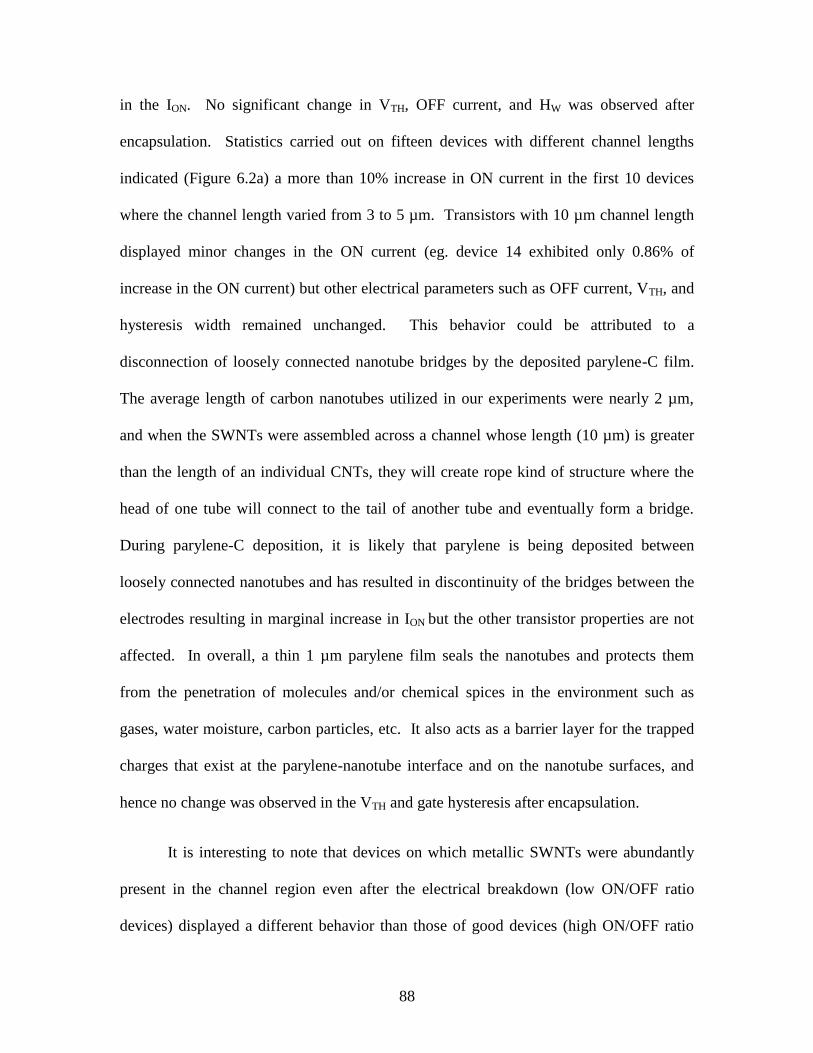
88
in the ION. No significant change in VTH, OFF current, and HW was observed after
encapsulation. Statistics carried out on fifteen devices with different channel lengths
indicated (Figure 6.2a) a more than 10% increase in ON current in the first 10 devices
where the channel length varied from 3 to 5 µm. Transistors with 10 µm channel length
displayed minor changes in the ON current (eg. device 14 exhibited only 0.86% of
increase in the ON current) but other electrical parameters such as OFF current, VTH, and
hysteresis width remained unchanged. This behavior could be attributed to a
disconnection of loosely connected nanotube bridges by the deposited parylene-C film.
The average length of carbon nanotubes utilized in our experiments were nearly 2 µm,
and when the SWNTs were assembled across a channel whose length (10 µm) is greater
than the length of an individual CNTs, they will create rope kind of structure where the
head of one tube will connect to the tail of another tube and eventually form a bridge.
During parylene-C deposition, it is likely that parylene is being deposited between
loosely connected nanotubes and has resulted in discontinuity of the bridges between the
electrodes resulting in marginal increase in ION but the other transistor properties are not
affected. In overall, a thin 1 µm parylene film seals the nanotubes and protects them
from the penetration of molecules and/or chemical spices in the environment such as
gases, water moisture, carbon particles, etc. It also acts as a barrier layer for the trapped
charges that exist at the parylene-nanotube interface and on the nanotube surfaces, and
hence no change was observed in the VTH and gate hysteresis after encapsulation.
It is interesting to note that devices on which metallic SWNTs were abundantly
present in the channel region even after the electrical breakdown (low ON/OFF ratio
devices) displayed a different behavior than those of good devices (high ON/OFF ratio
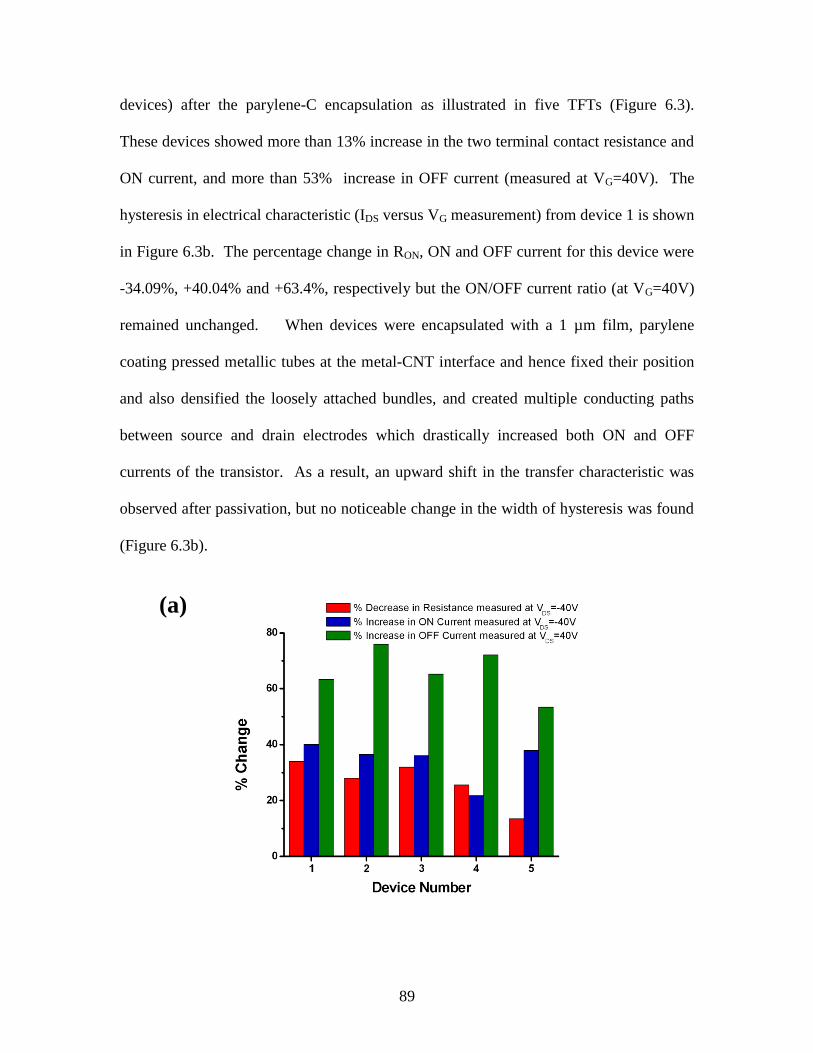
89
devices) after the parylene-C encapsulation as illustrated in five TFTs (Figure 6.3).
These devices showed more than 13% increase in the two terminal contact resistance and
ON current, and more than 53% increase in OFF current (measured at VG=40V). The
hysteresis in electrical characteristic (IDS versus VG measurement) from device 1 is shown
in Figure 6.3b. The percentage change in RON, ON and OFF current for this device were
-34.09%, +40.04% and +63.4%, respectively but the ON/OFF current ratio (at VG=40V)
remained unchanged. When devices were encapsulated with a 1 µm film, parylene
coating pressed metallic tubes at the metal-CNT interface and hence fixed their position
and also densified the loosely attached bundles, and created multiple conducting paths
between source and drain electrodes which drastically increased both ON and OFF
currents of the transistor. As a result, an upward shift in the transfer characteristic was
observed after passivation, but no noticeable change in the width of hysteresis was found
(Figure 6.3b).
(a)
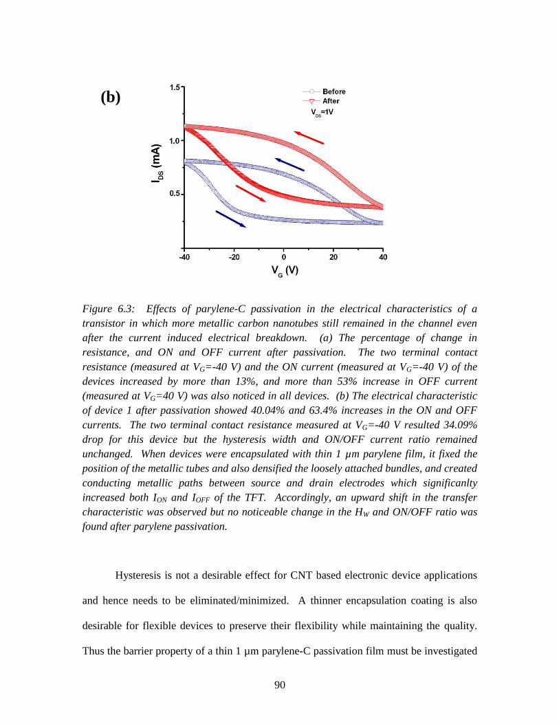
90
Figure 6.3: Effects of parylene-C passivation in the electrical characteristics of a
transistor in which more metallic carbon nanotubes still remained in the channel even
after the current induced electrical breakdown. (a) The percentage of change in
resistance, and ON and OFF current after passivation. The two terminal contact
resistance (measured at VG=-40 V) and the ON current (measured at VG=-40 V) of the
devices increased by more than 13%, and more than 53% increase in OFF current
(measured at VG=40 V) was also noticed in all devices. (b) The electrical characteristic
of device 1 after passivation showed 40.04% and 63.4% increases in the ON and OFF
currents. The two terminal contact resistance measured at VG=-40 V resulted 34.09%
drop for this device but the hysteresis width and ON/OFF current ratio remained
unchanged. When devices were encapsulated with thin 1 µm parylene film, it fixed the
position of the metallic tubes and also densified the loosely attached bundles, and created
conducting metallic paths between source and drain electrodes which significanlty
increased both ION and IOFF of the TFT. Accordingly, an upward shift in the transfer
characteristic was observed but no noticeable change in the HW and ON/OFF ratio was
found after parylene passivation.
Hysteresis is not a desirable effect for CNT based electronic device applications
and hence needs to be eliminated/minimized. A thinner encapsulation coating is also
desirable for flexible devices to preserve their flexibility while maintaining the quality.
Thus the barrier property of a thin 1 µm parylene-C passivation film must be investigated
(b)
91
in high vacuum to ensure the conformal and pinhole free deposition. Lam et al. [193]
have reported that submicron parylene-C film (20-50nm) deposited using commercially
available coaters (PDS2010) is porous, and does not guarantee pinhole free coating. To
minimize hysteresis and evaluate the quality of the thin parylene coating, the electrical
properties of CNTFETs in high vacuum before and after encapsulation was next
investigated. I first studied the reduction in hysteresis width of transistors by treating
TFTs for 19 hours in high vacuum prior to 1 µm parylene deposition. Then we examined
the thin (1 µm) parylene-C passivated TFTs in vacuum. The I-V measurements obtained
from these experiments are shown in Figure 6.4. Initially, when the SWNTs were
assembled via DEP, metallic tubes were removed by current induced breakdown and then
transistor characterization were measured in an ambient environment.
Figure 6.4: Suppression of gate hysteresis width and pinhole free coating of 1 µm film
test results. After DEP assembly and subsequent I-V measurement in ambient
environment TFT showed RON =172.3 KOhm, ION =6.02 µA and HW =44.3 V,
respectively. Next transistor was treated in high vacuum (4.0x10⁻⁷
) for 19 hours and then
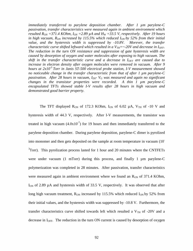
92
immediately transferred to parylene deposition chamber. After 1 µm parylene-C
passivation, transfer characteristics were measured again in ambient environment which
resulted RON =371.4 KOhm, ION =2.89 µA and HW =33.5 V, respectively. After 19 hours
in high vacuum, RON increased by 115.5% which reduced ION by 52% from their initial
value, and the hysteresis width is suppressed by -10.8V. Morever, the transfer
characteristic curve shifted leftward which resulted in a VTH=~-20V and decrease in IOFF.
The reduction in the turn ON resistance and suppression of gate hysteresis width are
caused by desorption of oxygen and water molecules after exposing to high vacuum. The
shift in the transfer characteristic curve and a decrease in IOFF are caused due to
increase in electron density after oxygen molecules were removed in vacuum. After 9
hours at 2x10⁻⁵
Torr in Janis ST-500 electrical probe station, I-V measurement showed
no noticeable change in the transfer characteristic from that of after 1 µm parylene-C
passivation. After 28 hours in vacuum, IDS- VG was measured and again no significant
changes in the transistor properties were recorded. A thin 1 µm parylene-C
encapsulated TFTs showed stable I-V results after 28 hours in high vacuum and
demonstrated good barrier property.
The TFT displayed RON of 172.3 KOhm, ION of 6.02 µA, VTH of -10 V and
hysteresis width of 44.3 V, respectively. After I-V measurements, the transistor was
treated in high vacuum (4.0x10⁻⁷
) for 19 hours and then immediately transferred to the
parylene deposition chamber. During parylene deposition, parylene-C dimer is pyrolized
into monomer and then gets deposited on the sample at room temperature in vacuum (10-
3Torr). This pyrolization process lasted for 1 hour and 20 minutes where the CNTFETs
were under vacuum (1 mTorr) during this process, and finally 1 µm parylene-C
polymerization was completed in 28 minutes. After passivation, transfer characteristics
were measured again in ambient environment where we found an RON of 371.4 KOhm,
ION of 2.89 µA and hysteresis width of 33.5 V, respectively. It was observed that after
long high vacuum treatment, RON increased by 115.5% which reduced ION by 52% from
their initial values, and the hysteresis width was suppressed by -10.8 V. Furthermore, the
transfer characteristics curve shifted towards left which resulted a VTH of -20V and a
decrease in IOFF. The reduction in the turn ON current is caused by desorption of oxygen
93
molecules in high vacuum. The oxygen molecules adsorbed on the sidewalls of CNTs
and/or at the CNT-dielectric interface were removed during exposure to high vacuum for
19 hours. Desorption of oxygen molecules from the CNTs resulted in withdrawal of
more holes causing the transistors to become less p-type doped. Hence a significant
reduction in the channel conductance of the transistors from their initial values was
observed. In addition, the removal of water molecules and other trapped charges in high
vacuum suppressed the gate hysteresis of the TFTs by -10.8 V but did not fully eliminate
it. The water molecules are very difficult to permanently remove in such vacuum
condition alone, and it usually requires much longer annealing times under high vacuum
to reduce more or completely eliminate hysteresis [191, 212]. Other trapped charges
from parylene-SWNT interface, ionic molecules and surfactants may still be present and
could also attribute to the remaining hysteresis behavior. The shift in the transfer
characteristic curve is caused due to increase in electron density after oxygen molecules
were removed in vacuum. Lin et al. [191] and Kim et al. [212] also a observed reduction
in ION, shift in transfer characteristic curve and suppression of hysteresis width when non-
encapsulated CNTFETs were treated in high vacuum. In Figure 6.2b, the transistors
exhibited no change in their hysteresis width after a 1 µm parylene-C passivation. The
commercially available parylene coater such as PDS2010 which was utilized for these
experiments can provide vacuum levels down to 10-3
Torr. The water molecules are very
difficult to remove in such a short time (1 hour 20 min) in low vacuum (1 mTorr)
conditions, and they require long hours of pumping in high vacuum (eg. 10-7
Torr) such
as seen in Figure 6.4. Furthermore, the transfer characteristics of the TFT in Figure 6.2b
showed 12.43% increase in ION current due to fixing the CNTs in position onto metal
94
electrodes and densification of nanotubes after a 1 µm parylene-C coating. Even though
the device was under vacuum (10-3
Torr) for 1 hour and 20 minutes before parylene
deposition has started I did not notice any reduction in ION. It could be that short term
low vacuum treatment was not long enough to desorb oxygen molecules from the CNT
transistor, or the effect of parylene-C encapsulation in improving the metal-CNT contact
and densification negated the outcome from oxygen being removed from CNTs.
After 1 µm parylene-C encapsulation and subsequent I-V measurement in
ambient environment, the devices were loaded into a Janis ST-500 electrical probe station
to conduct electrical characterizations in high vacuum, and pinhole free behavior of a thin
(1 µm) parylene-C coating was next investigated. Machine was pumped down for 9
hours at 2x10⁻⁵
Torr, and then I-V measurements were performed. As seen in Figure 6.4,
no noticeable changes in the transfer characteristics were observed from that of after 1
µm parylene-C passivation. After 28 hours in vacuum, IDS was measured where the VG
was swept from -40V to 40V (Figure 6.4) and showed that the electrical properties of the
CNTFET remained unchanged. Thus, the electrical characterization of thin 1 µm
parylene-C packaged TFT is very stable even after 28 hours in high vacuum and
demonstrated that the 1 µm parylene-C film provides a pinhole free coating layer.
Finally, I studied the changes in the transistor properties of these devices after
deposition of different thickness of parylene-C film. To preserve the flexibility of the
devices, thinner coating layers are preferred since the rigidity of a flexible film is
proportional to the cube of its thickness. Accordingly, I used parylene-C films with two
different thicknesses (1 µm and 3 µm). After DEP assembly and the electrical burning
breakdown process, I measured the I-V characteristics of the transistors using a
95
semiconductor parameter analyzer (HP4155A) at ambient room temperature and
atmospheric pressure. After encapsulation (1 µm and 3 µm), the electrical properties of
the CNT FETs were remeasured and compared with the values obtained before
encapsulation. Figure 6.5 and 6.6 summarize the transfer characteristics of these devices
before and after parylene-C passivation. Both devices (Figure 6.5 and 6.6) displayed a
significant gate hysteresis before and after passivation between forward (VGF) and
backward (VGB) sweeps of the gate voltage. As discussed before this phenomenon is
often observed in CNT based transistors, and it is attributed to charge injection from
nanotube at large gate voltages, water molecules, trapped charges at parylene-SWNT
interface, other trapped charges from solution processed CNTs, and contamination
originating during the fabrication of the device.
For the CNT TFTs with a 1 µm thick parylene-C coating, the two terminal
resistance (measured at VG = - 40V) was increased by 50.3%, whereas the ON current of
the device (measured at VG = - 40V) was reduced by 34.4% from their initial values. The
hysteresis width before passivation (HWB) between forward (VGF) and backward (VGB)
gate voltage sweep is defined as the difference between P2 and P1 (HWB=P2- P1) where P2
and P1 are backward and forward gate voltages of the TFT and is shown in Figure 6.5.
The gate hysteresis width before encapsulation was 47.5V. After the 1 µm parylene-C
coating, the transistor showed a gate hysteresis width of 43.75V (HWA= P4- P3). The
hysteresis width was reduced by -3.75V after the deposition of 1 µm parylene-C
passivation layer. The change in hysteresis width (∆HW) is the difference between the
hysteresis width after (HWA) and the hysteresis width before (HWB) parylene-C
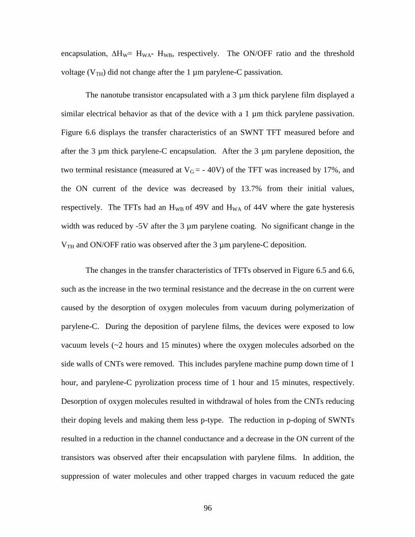
96
encapsulation, ∆HW= HWA- HWB, respectively. The ON/OFF ratio and the threshold
voltage (VTH) did not change after the 1 µm parylene-C passivation.
The nanotube transistor encapsulated with a 3 µm thick parylene film displayed a
similar electrical behavior as that of the device with a 1 µm thick parylene passivation.
Figure 6.6 displays the transfer characteristics of an SWNT TFT measured before and
after the 3 µm thick parylene-C encapsulation. After the 3 µm parylene deposition, the
two terminal resistance (measured at VG = - 40V) of the TFT was increased by 17%, and
the ON current of the device was decreased by 13.7% from their initial values,
respectively. The TFTs had an HWB of 49V and HWA of 44V where the gate hysteresis
width was reduced by -5V after the 3 µm parylene coating. No significant change in the
VTH and ON/OFF ratio was observed after the 3 µm parylene-C deposition.
The changes in the transfer characteristics of TFTs observed in Figure 6.5 and 6.6,
such as the increase in the two terminal resistance and the decrease in the on current were
caused by the desorption of oxygen molecules from vacuum during polymerization of
parylene-C. During the deposition of parylene films, the devices were exposed to low
vacuum levels (~2 hours and 15 minutes) where the oxygen molecules adsorbed on the
side walls of CNTs were removed. This includes parylene machine pump down time of 1
hour, and parylene-C pyrolization process time of 1 hour and 15 minutes, respectively.
Desorption of oxygen molecules resulted in withdrawal of holes from the CNTs reducing
their doping levels and making them less p-type. The reduction in p-doping of SWNTs
resulted in a reduction in the channel conductance and a decrease in the ON current of the
transistors was observed after their encapsulation with parylene films. In addition, the
suppression of water molecules and other trapped charges in vacuum reduced the gate
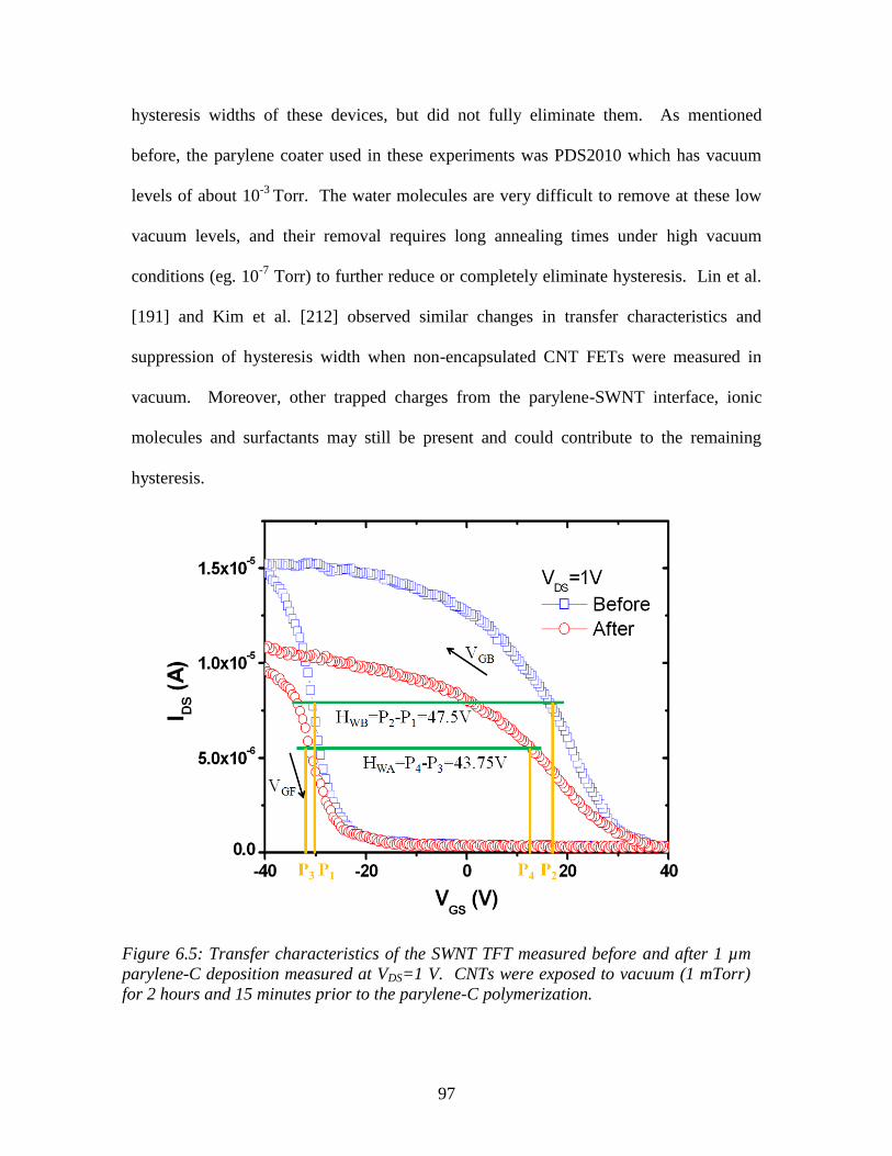
97
hysteresis widths of these devices, but did not fully eliminate them. As mentioned
before, the parylene coater used in these experiments was PDS2010 which has vacuum
levels of about 10-3
Torr. The water molecules are very difficult to remove at these low
vacuum levels, and their removal requires long annealing times under high vacuum
conditions (eg. 10-7
Torr) to further reduce or completely eliminate hysteresis. Lin et al.
[191] and Kim et al. [212] observed similar changes in transfer characteristics and
suppression of hysteresis width when non-encapsulated CNT FETs were measured in
vacuum. Moreover, other trapped charges from the parylene-SWNT interface, ionic
molecules and surfactants may still be present and could contribute to the remaining
hysteresis.
Figure 6.5: Transfer characteristics of the SWNT TFT measured before and after 1 µm
parylene-C deposition measured at VDS=1 V. CNTs were exposed to vacuum (1 mTorr)
for 2 hours and 15 minutes prior to the parylene-C polymerization.
98
In conclusion, I demonstrated a parylene-C passivation process for encapsulating
SWNT thin film transistors on flexible/rigid substrate, and studied the effect of
passivation on the electrical properties of these devices. The 1 µm parylene-C
passivation (pyrolization time of 1 hour and 20 minutes) densified carbon nanotubes and
fixed their position on metal electrodes which resulted in more than 10% increase in the
ON current of the transistors. No noticeable change in VTH, ON/OFF current ratio, and
HW was observed after a 1 µm parylene passivation coating. When unencapsulated TFTs
were exposed to high vacuum for 19 hours, a 52% reduction in the ION was observed and
the gate hysteresis width was suppressed by -10.8 V which was caused by the desorption
of oxygen and water molecules from CNTs. Furthermore, removal of oxygen molecules
from CNT surface and CNT-metal interface in high vacuum caused an increase in
Figure 6.6: Transfer characteristics of the SWNT TFT measured before and after 3
µm parylene-C deposition measured at VDS=1V. CNTs were exposed to vacuum (1
mTorr) for 2 hours and 15 minutes prior to the parylene-C polymerization.
99
electron density in CNTs, and resulted a shift in the transfer characteristic curve to
leftward and a decrease in IOFF. The transistor characteristics of 1 µm parylene-C
packaged TFT remained unchanged after 28 hours in high vacuum exposure and
indicated that the 1 µm parylene-C film is a good barrier for CNTFETs. The results from
the CNT transistors that were encapsulated with 1 µm and 3 µm thick parylene-C
coatings, demonstrated similar behaviors. This indicates that the parylene encapsulation
thickness can be adjusted based on the specification of the devices. For example, thin
parylene coating can be applied for flexible devices to maintain their flexibility, whereas
the thicker parylene-C can be utilized to protect CNT devices from the hazardous body
fluids environment for implantable device applications. Thus, parylene-C, being a pin-
hole free coating deposited at room temperature may serve to be a promising technology
for environmental protection of carbon nanotube based devices.
100
CChhaapptteerr 77
Biostability of Parylene-C Encapsulated
Carbon Nanotubes Flexible Transistors
7.1 Introduction
Biomedical micro implants are used in neural prostheses to restore body functions
after paraplegia by means of functional electrical stimulation (FES). FES gives the
possibility to neurologically rehabilitate, re-establish and reconstitute different organs,
which are irreparably damaged. In FES, human neurons or muscles are electrically
excited in order to affect muscles or a sensory organ like vision or hearing. This is
accomplished by current or voltage pulses across an electrode array. One of the specific
examples of an implantable system under development is the retinal implant by Wyatt
and his colleagues [230] as shown in Figure 7.1 and Humayun‘s group [231]. In the
human eye, there are about 2 x 10⁸ receptors which can determine about 4 x 10
5 pixels.
Overall, the total number information over all sensory organs of the human body has
been estimated to be about 1010
bits/sec. These examples illustrate that an incredibly
large number of electrodes are necessary to stimulate sensory organs. In current
technology, either each electrode is connected via a separate cable to the implantable
electronics and or relatively thick and stiff silicon based circuitry is used which can cause
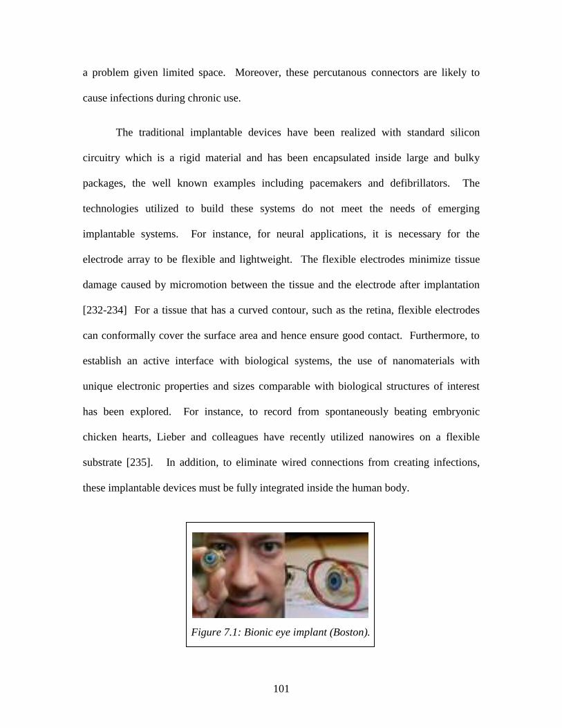
101
a problem given limited space. Moreover, these percutanous connectors are likely to
cause infections during chronic use.
The traditional implantable devices have been realized with standard silicon
circuitry which is a rigid material and has been encapsulated inside large and bulky
packages, the well known examples including pacemakers and defibrillators. The
technologies utilized to build these systems do not meet the needs of emerging
implantable systems. For instance, for neural applications, it is necessary for the
electrode array to be flexible and lightweight. The flexible electrodes minimize tissue
damage caused by micromotion between the tissue and the electrode after implantation
[232-234] For a tissue that has a curved contour, such as the retina, flexible electrodes
can conformally cover the surface area and hence ensure good contact. Furthermore, to
establish an active interface with biological systems, the use of nanomaterials with
unique electronic properties and sizes comparable with biological structures of interest
has been explored. For instance, to record from spontaneously beating embryonic
chicken hearts, Lieber and colleagues have recently utilized nanowires on a flexible
substrate [235]. In addition, to eliminate wired connections from creating infections,
these implantable devices must be fully integrated inside the human body.
Figure 7.1: Bionic eye implant (Boston).
102
For a device to operate in a living system, it needs to be protected from the harsh
environments inside. That is, these functional devices must be stable for long term inside
biological medium (biostable). Second, the living environment also needs to be isolated
from the device so that the device does not cause harm to the tissue. Hence, the
implantable materials need to be fabricated from or encapsulated with biocompatible
materials. For example, encapsulation materials such as silicone, polyimide, Si3N4,
parylene, a-SiC, and diamondlike carbon have been reported for implant applications
[236-241]. One of the materials, that is flexible, biocompatible and fits most of the needs
for implantable systems, is parylene-C, yet there is very little research conducted on
nanomaterials based devices using parylene-C. Parylene-C is one of the well established
USP grade VI biocompatible materials. It has been traditionally used as an encapsulation
material [80], coating biomedical implants [77], yet its applications for flexible
electronics though promising are rare. For biomedical applications, specifically for in
vivo cases, a conformal coating of parylene-C is required to create a surface that is
acceptable for the living tissue.
Most current flexible electronics are made using organic molecules which tend to
have limitations in performance i.e. have low carrier mobilities [80]. Second, the
substrates utilized in current flexible devices are limited in properties. For instance the
polydimethylsiloxane (PDMS) films are bulky, the materials that are commercially
available in sheet forms, ie polyethylene terephtalate (PET) and polyethylene naphthalate
(PEN) are challenging to fabricate devices onto, and other materials such as polyimides
absorb moisture and hence are not appropriate for humid environments or aqueous
solutions. Among the polymers suited for flexible substrates, parylene-C has numerous
103
attractive features. It is lightweight, stress-free, optically transparent, and mechanically
strong material. These attractive properties make it a very promising material as a
flexible substrate [242]. Furthermore, single-walled carbon nanotubes (SWNTs) with
their unique physical, electrical and mechanical properties are being considered as a
potential replacement for existing semiconducting materials in flexible electronics [35,
39]. Thus, the parylene-C together with carbon nanotubes is an attractive area of research
for realizing high performance and highly flexible devices for biomedical applications.
Previously, I have reported parylene-C packaged SWNT thin film transistors (TFT)
where parylene was utilized as substrate, dielectric and encapsulation material [185, 223].
Devices sandwiched in between parylene films displayed ultraflexiblity and were
protected from environmental contaminations. Moreover, the electrical characteristics of
TFTs after parylene-C coating remained unchanged compared to when before
passivation. In this chapter, the biostability of thin parylene-C encapsulated single walled
carbon nanotube thin film transistors are demonstrated. Devices were sandwiched in
between parylene films and then immersed in saline solution at 37°C for 42 days. The
electrical characteristic of 1 µm parylene-C passivated transistors after soak experiments
showed no significant changes in their properties comparing to that of after passivation.
7.2 Device Fabrication and Experimental Setup
The fabrication of flexible SWNT thin film transistors is briefly summarized in
Figure 7.2a. A 10 µm thick parylene-C layer was first deposited on an oxidized silicon
wafer at room temperature. Next, aluminum gate electrodes (1500 Å) were created using
conventional optical lithography and wet etching. Then, a 1 µm thick parylene-C gate
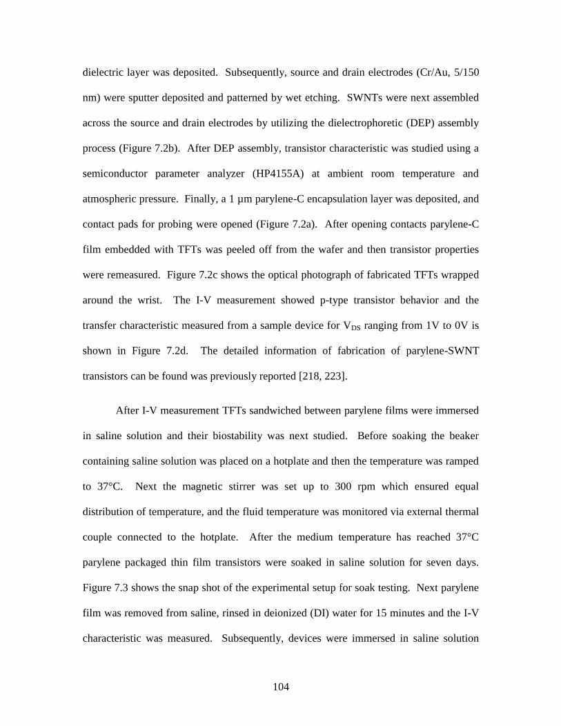
104
dielectric layer was deposited. Subsequently, source and drain electrodes (Cr/Au, 5/150
nm) were sputter deposited and patterned by wet etching. SWNTs were next assembled
across the source and drain electrodes by utilizing the dielectrophoretic (DEP) assembly
process (Figure 7.2b). After DEP assembly, transistor characteristic was studied using a
semiconductor parameter analyzer (HP4155A) at ambient room temperature and
atmospheric pressure. Finally, a 1 µm parylene-C encapsulation layer was deposited, and
contact pads for probing were opened (Figure 7.2a). After opening contacts parylene-C
film embedded with TFTs was peeled off from the wafer and then transistor properties
were remeasured. Figure 7.2c shows the optical photograph of fabricated TFTs wrapped
around the wrist. The I-V measurement showed p-type transistor behavior and the
transfer characteristic measured from a sample device for VDS ranging from 1V to 0V is
shown in Figure 7.2d. The detailed information of fabrication of parylene-SWNT
transistors can be found was previously reported [218, 223].
After I-V measurement TFTs sandwiched between parylene films were immersed
in saline solution and their biostability was next studied. Before soaking the beaker
containing saline solution was placed on a hotplate and then the temperature was ramped
to 37°C. Next the magnetic stirrer was set up to 300 rpm which ensured equal
distribution of temperature, and the fluid temperature was monitored via external thermal
couple connected to the hotplate. After the medium temperature has reached 37°C
parylene packaged thin film transistors were soaked in saline solution for seven days.
Figure 7.3 shows the snap shot of the experimental setup for soak testing. Next parylene
film was removed from saline, rinsed in deionized (DI) water for 15 minutes and the I-V
characteristic was measured. Subsequently, devices were immersed in saline solution
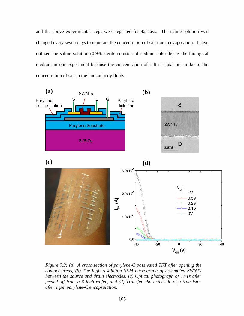
105
and the above experimental steps were repeated for 42 days. The saline solution was
changed every seven days to maintain the concentration of salt due to evaporation. I have
utilized the saline solution (0.9% sterile solution of sodium chloride) as the biological
medium in our experiment because the concentration of salt is equal or similar to the
concentration of salt in the human body fluids.
(a) (b)
(c) (d)
Figure 7.2: (a) A cross section of parylene-C passivated TFT after opening the
contact areas, (b) The high resolution SEM micrograph of assembled SWNTs
between the source and drain electrodes, (c) Optical photograph of TFTs after
peeled off from a 3 inch wafer, and (d) Transfer characteristic of a transistor
after 1 µm parylene-C encapsulation.
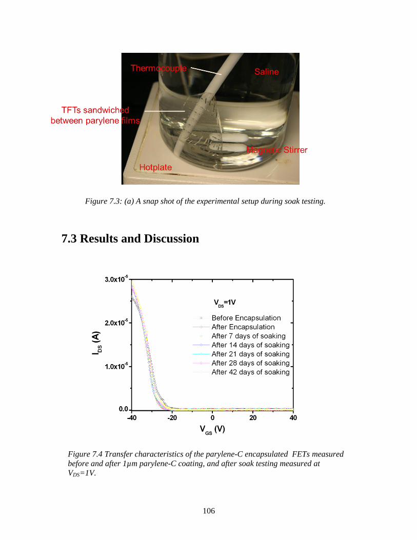
106
7.3 Results and Discussion
Figure 7.4 Transfer characteristics of the parylene-C encapsulated FETs measured
before and after 1µm parylene-C coating, and after soak testing measured at
VDS=1V.
Figure 7.3: (a) A snap shot of the experimental setup during soak testing.
107
The transfer characteristic of a sample TFT (same device in Figure 7.2d) after 42
days of soaking is shown in Figure 7.4. Before 1 µm parylene encapsulation the CNT
transistor exhibited ON/OFF ratio of ~2x10², threshold voltage (VTH) of -20V. After 1
µm parylene-C deposition the ON current (measured at VGS=-40V) of the transistor
increased from 26.2 µA to 29.4 µA where the percentage of increase was 12.43%.
Parylene has conformally coated around carbon nanotubes and has pressed them down to
the metal electrodes. Thus, thin parylene film not only acted as a barrier to CNTs but has
also fixed the nanotube position on the electrode. Hence, TFTs showed an increase in the
ON current but no changes have been observed in the other transistor characteristic such
as VTH and OFF current [185]. Moreover, the desorption of water molecule at the metal-
SWNT interface could have also possibly contributed to increase in the ON current which
was observed after thin parylene coating. During parylene deposition it is possible that
the water molecules at the interface were desorbed and resulted in slight increase in the
work function of the source/drain electrode than that of when the water molecules were
adsorbed on the Au contacts [224].
After every seven days of soak experiment transistor properties were measured
and compared with that of previously recorded measurements. The TFT in Figure 7.4
displayed turn ON current of 28.8 µA, 28.5 µA, 28.7 µA, 28.4 µA and 29.5 µA after 7,
14, 21, 28 and 42 days of soak testing, respectively. Other transistor characteristics
remained unchanged (Figure 7.4). The percentage of change in the ON current, [(ION-
I0,ON) / I0,ON] x100%, after 42 days of soaking for sample six devices is summarized in
Figure 7.5. Here ION and I0,ON represent measured ON current after soak test, and initial
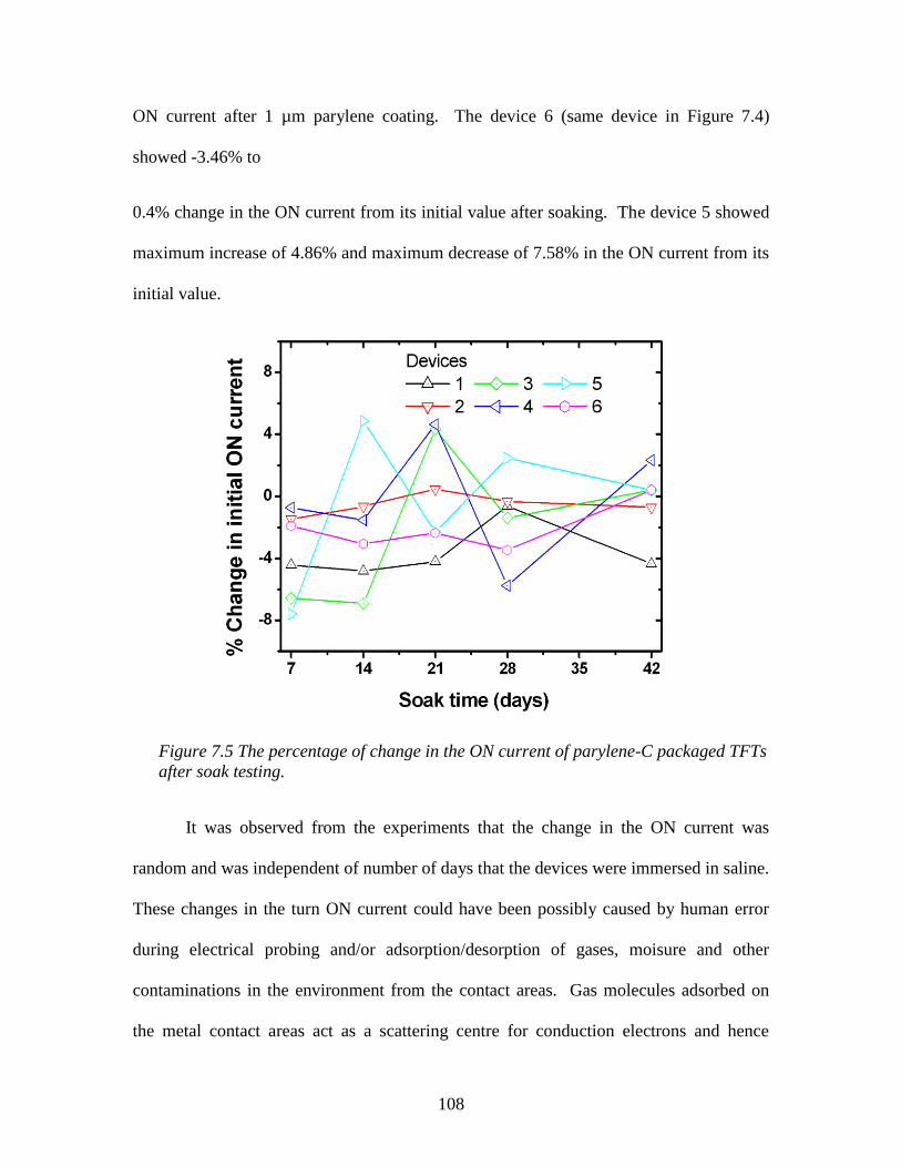
108
ON current after 1 µm parylene coating. The device 6 (same device in Figure 7.4)
showed -3.46% to
0.4% change in the ON current from its initial value after soaking. The device 5 showed
maximum increase of 4.86% and maximum decrease of 7.58% in the ON current from its
initial value.
It was observed from the experiments that the change in the ON current was
random and was independent of number of days that the devices were immersed in saline.
These changes in the turn ON current could have been possibly caused by human error
during electrical probing and/or adsorption/desorption of gases, moisure and other
contaminations in the environment from the contact areas. Gas molecules adsorbed on
the metal contact areas act as a scattering centre for conduction electrons and hence
Figure 7.5 The percentage of change in the ON current of parylene-C packaged TFTs
after soak testing.
109
increase the electrical resistivity of these metals [226]. Due to random
adsorption/desorption of molecular species from the environment random variation in the
ON current was observed in the TFTs. It should also be noted that threshold voltage of
these devices are slightly higher for implant applications yet thin gate dielectric and
optimized FET design will allow the realization of low voltage devices. Parylene-C (1
µm) passivated devices displayed stability in their I-V characteristic after 42 days of
soaking in saline at 37°C. The long term biostability of parylene packaged TFTs for
different parylene encapsulation thicknesses needs to be studied via accelerated life time
testings. These issues will be reported in our future work.
In conclusion, the biostability of 1 µm parylene-C passivated TFTs in saline
solution is demonstrated. The I-V characteristic of these devices remained unchanged
after 42 days of soak experiments. This parylene-C packaged CNT transistor technology
will find applications in areas that require high performance and highly flexible
biocompatible devices such as neural prosthetic devices.
110
CChhaapptteerr 88
Vertical and High Density SWNTs
Transistors
8.1 Introduction
The continuing demand for more functionality and higher performance is driving
the momentum to realize more transistors in a given area. This demand has traditionally
been met through technological advancements primarily through scaling of transistor
dimensions. [243] It is predicted that the limits to scaling will be reached within [244]
the next decade and alternative approaches for scaling are needed. Carbon nanotubes
with their miniature size and attractive electrical properties appear as a strong candidate
for future transistor technology. Semiconducting nanotubes are direct bandgap
semiconductors with EG≈0.8/D (eV), where D is the nanotube diameter in nanometers.
With typical diameters of 1-2nm, the single-walled carbon nanotubes have resulting
bandgaps suitable for room temperature electronics. Low field transport is near ballistic
with mobilities as high as ~100,000 cm2/V-s. [245] The direct bandgap also means that
optical devices are also possible. [246] Since there are no dangling bonds in CNTs,
surface scattering can be expected to be negligible. With these attractive properties,
111
carbon nanotube based field effect transistors have been investigated as one of the
alternatives to silicon based technology. [247, 248]
The transfer characteristics of the CNTFETs have been optimized with
approaches utilizing a shorter channel (20 nm) and a high-k dielectric. [34, 249] In
addition to back gate approaches, Javey and colleagues have demonstrated a self-aligned
top gate approach. [250] An all-Carbon transistor, utilizing carbon nanotubes as the gate
and the conducting channel, has also been realized by Chiu et al. [251] as one of the
possible means of creating high density nanoelectronics. The planar electrode based
CNTFETs have certain limitations which result in lower current densities and large
parasitic gate capacitances. [252]
In sharp contrast to planar architectures, the vertical arrangement of carbon
nanotube transistors has been proposed as another means to achieve large scale, high
density realization of nanoelectronic circuits. As a first step towards realizing this goal,
Duesberg et al. have demonstrated Catalytic Chemical Vapor Deposition (CCVD)
technique, a high temperature growth technique, and grew a single MWNT inside a 20nm
hole. [253] Furthermore, utilizing a similar CCVD method, Choi and colleagues have
achieved ultra high density nano transistors. [254] Chen et al. were able to demonstrate a
high density (108/cm
2) vertical nanowire transistor. [249] A similar high temperature
based growth mechanism was utilized to demonstrate Si and ZnO nanowire vertical field
effect transistor [255, 256] making this a very exciting area of research. In this chapter I
presented a hybrid technique combining both bottom-up dielectrophoresis and top-down
microfabrication techniques to enable room temperature integration of SWNTs into three
dimensional architectures. Utilizing this 3D microplatform, a novel 3D Field Effect
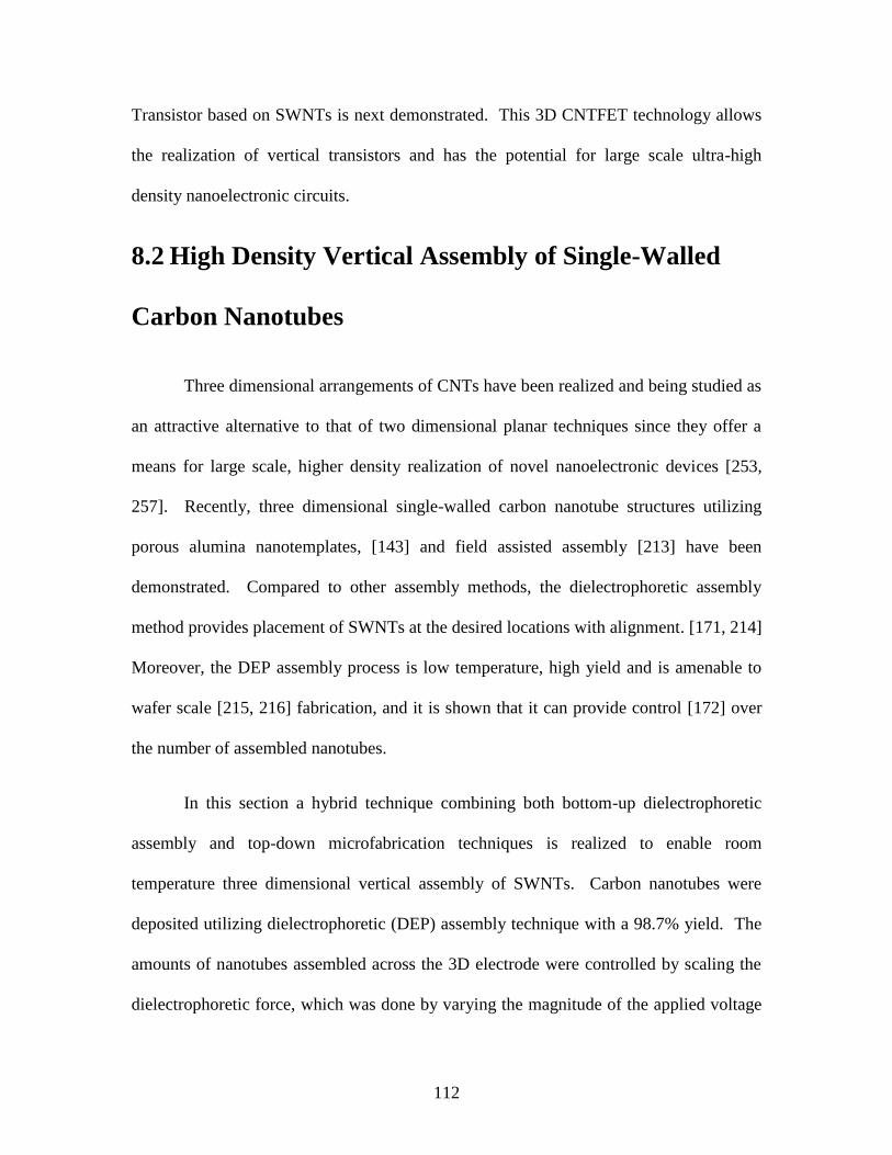
112
Transistor based on SWNTs is next demonstrated. This 3D CNTFET technology allows
the realization of vertical transistors and has the potential for large scale ultra-high
density nanoelectronic circuits.
8.2 High Density Vertical Assembly of Single-Walled
Carbon Nanotubes
Three dimensional arrangements of CNTs have been realized and being studied as
an attractive alternative to that of two dimensional planar techniques since they offer a
means for large scale, higher density realization of novel nanoelectronic devices [253,
257]. Recently, three dimensional single-walled carbon nanotube structures utilizing
porous alumina nanotemplates, [143] and field assisted assembly [213] have been
demonstrated. Compared to other assembly methods, the dielectrophoretic assembly
method provides placement of SWNTs at the desired locations with alignment. [171, 214]
Moreover, the DEP assembly process is low temperature, high yield and is amenable to
wafer scale [215, 216] fabrication, and it is shown that it can provide control [172] over
the number of assembled nanotubes.
In this section a hybrid technique combining both bottom-up dielectrophoretic
assembly and top-down microfabrication techniques is realized to enable room
temperature three dimensional vertical assembly of SWNTs. Carbon nanotubes were
deposited utilizing dielectrophoretic (DEP) assembly technique with a 98.7% yield. The
amounts of nanotubes assembled across the 3D electrode were controlled by scaling the
dielectrophoretic force, which was done by varying the magnitude of the applied voltage
113
and the characteristic distance between the electrodes. The density of the assembled
nanotubes was proportional to the applied voltage. It was also observed that when a
higher voltage was applied between the 3D electrodes more nanotubes were assembled
around the edges of the tip of the electrode and also formed thicker bundles. The
scanning electron micrograph (SEM) images revealed that by adjusting the height of the
3D microelectrodes and the overlap between them allows control over bundle size,
number of bundles and effective length of the active sensing elements (channel). The
contact resistance of the 3D devices was reduced by 20% on average from their initial
values after the thermal annealing process. Moreover, the encapsulation of these 3D
assembled devices using a conformal pin-hole free parylene layer resulted in 12-45%
decrease of the total resistance.
8.2.1 Fabrication of 3D Microplatform
The fabrication process, as illustrated in Figure 8.1a, starts with the deposition
and patterning of the first Cr/Au electrode layer (200 Å/1500 Å) by a liftoff process on an
oxidized silicon wafer (Figure 8.1a (i)). Then a thin parylene-C dielectric layer was
deposited at room temperature. Next, the second metal layer (Cr/Au 200Å/1500Å) was
deposited and patterned using lift-off technique (Figure 8.1a (ii)). These two metal layers
form the three dimensional electrodes for assembling the SWNTs. Utilizing the second
metal layer as a mask, the parylene-C layer with an inductively coupled plasma (Plasma
therm 790) reactor using O2 plasma (Figure 8.1a (iii)) was then etched. After fabrication,
dielectrophoretic assembly was utilized to assemble SWNTs between the 3D electrodes
(Figure 8.1a (iv)). Finally, a thin layer of parylene-C (1.0 μm) was deposited as the
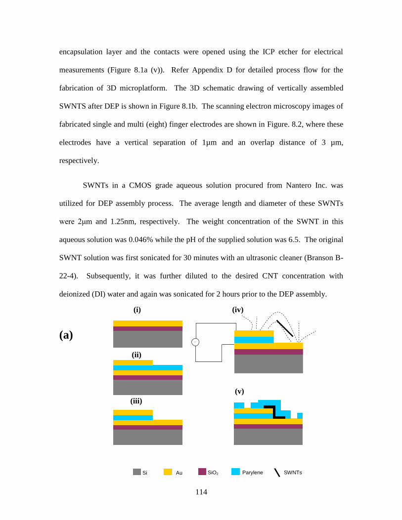
114
encapsulation layer and the contacts were opened using the ICP etcher for electrical
measurements (Figure 8.1a (v)). Refer Appendix D for detailed process flow for the
fabrication of 3D microplatform. The 3D schematic drawing of vertically assembled
SWNTS after DEP is shown in Figure 8.1b. The scanning electron microscopy images of
fabricated single and multi (eight) finger electrodes are shown in Figure. 8.2, where these
electrodes have a vertical separation of 1µm and an overlap distance of 3 µm,
respectively.
SWNTs in a CMOS grade aqueous solution procured from Nantero Inc. was
utilized for DEP assembly process. The average length and diameter of these SWNTs
were 2μm and 1.25nm, respectively. The weight concentration of the SWNT in this
aqueous solution was 0.046% while the pH of the supplied solution was 6.5. The original
SWNT solution was first sonicated for 30 minutes with an ultrasonic cleaner (Branson B-
22-4). Subsequently, it was further diluted to the desired CNT concentration with
deionized (DI) water and again was sonicated for 2 hours prior to the DEP assembly.
(a)
(i) (iv)
(ii)
(iii)
(v)
~
Si Au Parylene SWNTs SiO2
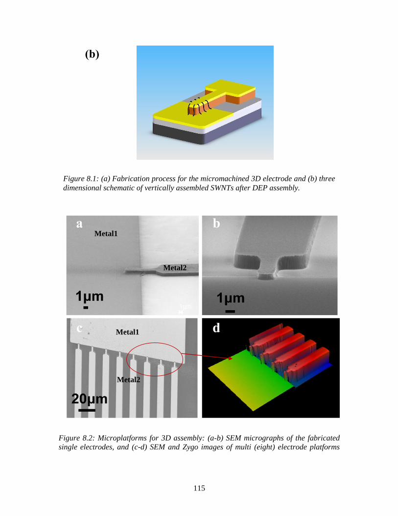
115
(b)
Figure 8.2: Microplatforms for 3D assembly: (a-b) SEM micrographs of the fabricated
single electrodes, and (c-d) SEM and Zygo images of multi (eight) electrode platforms
Figure 8.1: (a) Fabrication process for the micromachined 3D electrode and (b) three
dimensional schematic of vertically assembled SWNTs after DEP assembly.
Metal1
Metal2
Metal1
Metal2
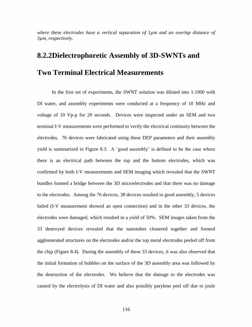
116
where these electrodes have a vertical separation of 1µm and an overlap distance of
3µm, respectively.
8.2.2Dielectrophoretic Assembly of 3D-SWNTs and
Two Terminal Electrical Measurements
In the first set of experiments, the SWNT solution was diluted into 1:1000 with
DI water, and assembly experiments were conducted at a frequency of 10 MHz and
voltage of 10 Vp-p for 20 seconds. Devices were inspected under an SEM and two
terminal I-V measurements were performed to verify the electrical continuity between the
electrodes. 76 devices were fabricated using these DEP parameters and their assembly
yield is summarized in Figure 8.3. A ‗good assembly‘ is defined to be the case where
there is an electrical path between the top and the bottom electrodes, which was
confirmed by both I-V measurements and SEM imaging which revealed that the SWNT
bundles formed a bridge between the 3D microelectrodes and that there was no damage
to the electrodes. Among the 76 devices, 38 devices resulted in good assembly, 5 devices
failed (I-V measurement showed an open connection) and in the other 33 devices, the
electrodes were damaged, which resulted in a yield of 50%. SEM images taken from the
33 destroyed devices revealed that the nanotubes clustered together and formed
agglomerated structures on the electrodes and/or the top metal electrodes peeled off from
the chip (Figure 8.4). During the assembly of these 33 devices, it was also observed that
the initial formation of bubbles on the surface of the 3D assembly area was followed by
the destruction of the electrodes. We believe that the damage to the electrodes was
caused by the electrolysis of DI water and also possibly parylene peel off due to joule
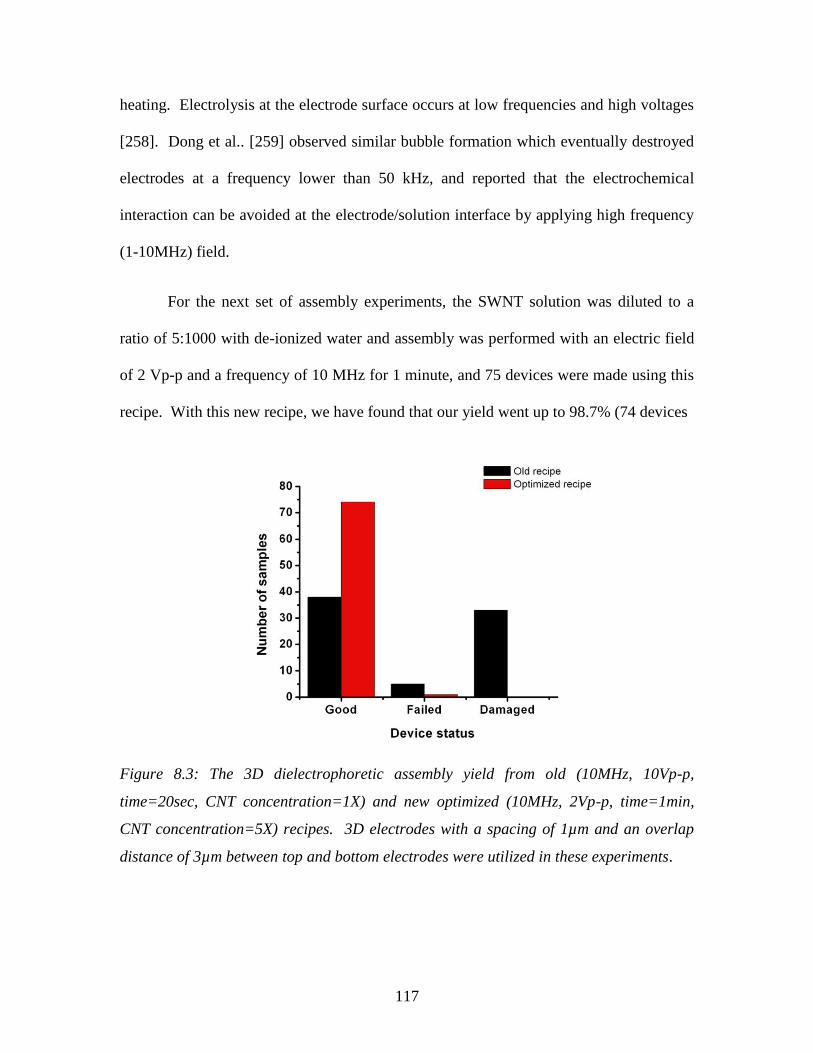
117
heating. Electrolysis at the electrode surface occurs at low frequencies and high voltages
[258]. Dong et al.. [259] observed similar bubble formation which eventually destroyed
electrodes at a frequency lower than 50 kHz, and reported that the electrochemical
interaction can be avoided at the electrode/solution interface by applying high frequency
(1-10MHz) field.
For the next set of assembly experiments, the SWNT solution was diluted to a
ratio of 5:1000 with de-ionized water and assembly was performed with an electric field
of 2 Vp-p and a frequency of 10 MHz for 1 minute, and 75 devices were made using this
recipe. With this new recipe, we have found that our yield went up to 98.7% (74 devices
Figure 8.3: The 3D dielectrophoretic assembly yield from old (10MHz, 10Vp-p,
time=20sec, CNT concentration=1X) and new optimized (10MHz, 2Vp-p, time=1min,
CNT concentration=5X) recipes. 3D electrodes with a spacing of 1µm and an overlap
distance of 3µm between top and bottom electrodes were utilized in these experiments.
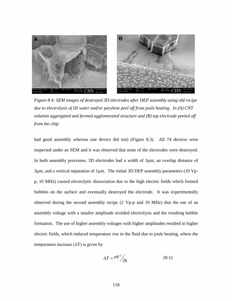
118
Figure 8.4: SEM images of destroyed 3D electrodes after DEP assembly using old recipe
due to electrolysis of DI water and/or parylene peel off from joule heating. In (A) CNT
solution aggregated and formed agglomerated structure and (B) top electrode peeled off
from the chip.
had good assembly whereas one device did not) (Figure 8.3). All 74 devices were
inspected under an SEM and it was observed that none of the electrodes were destroyed.
In both assembly processes, 3D electrodes had a width of 3µm, an overlap distance of
3µm, and a vertical separation of 1µm. The initial 3D DEP assembly parameters (10 Vp-
p, 10 MHz) caused electrolytic dissociation due to the high electric fields which formed
bubbles on the surface and eventually destroyed the electrode. It was experimentally
observed during the second assembly recipe (2 Vp-p and 10 MHz) that the use of an
assembly voltage with a smaller amplitude avoided electrolysis and the resulting bubble
formation. The use of higher assembly voltages with higher amplitudes resulted in higher
electric fields, which induced temperature rise in the fluid due to joule heating, where the
temperature increase (∆T) is given by
k
VT2
2 (8-1)
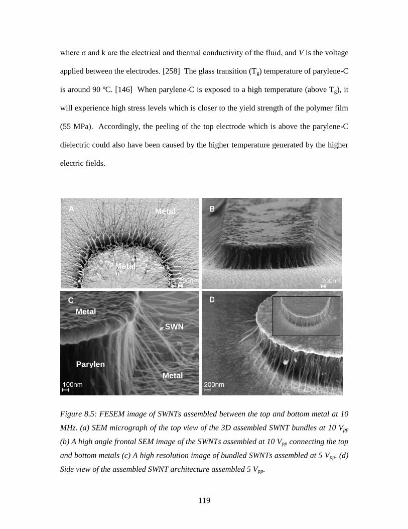
119
where σ and k are the electrical and thermal conductivity of the fluid, and V is the voltage
applied between the electrodes. [258] The glass transition (Tg) temperature of parylene-C
is around 90 ºC. [146] When parylene-C is exposed to a high temperature (above Tg), it
will experience high stress levels which is closer to the yield strength of the polymer film
(55 MPa). Accordingly, the peeling of the top electrode which is above the parylene-C
dielectric could also have been caused by the higher temperature generated by the higher
electric fields.
Figure 8.5: FESEM image of SWNTs assembled between the top and bottom metal at 10
MHz. (a) SEM micrograph of the top view of the 3D assembled SWNT bundles at 10 Vpp
(b) A high angle frontal SEM image of the SWNTs assembled at 10 Vpp connecting the top
and bottom metals (c) A high resolution image of bundled SWNTs assembled at 5 Vpp. (d)
Side view of the assembled SWNT architecture assembled 5 Vpp.
Metal II
Metal I
Parylene
SWNT
C
B
D
Metal II
Metal I
A
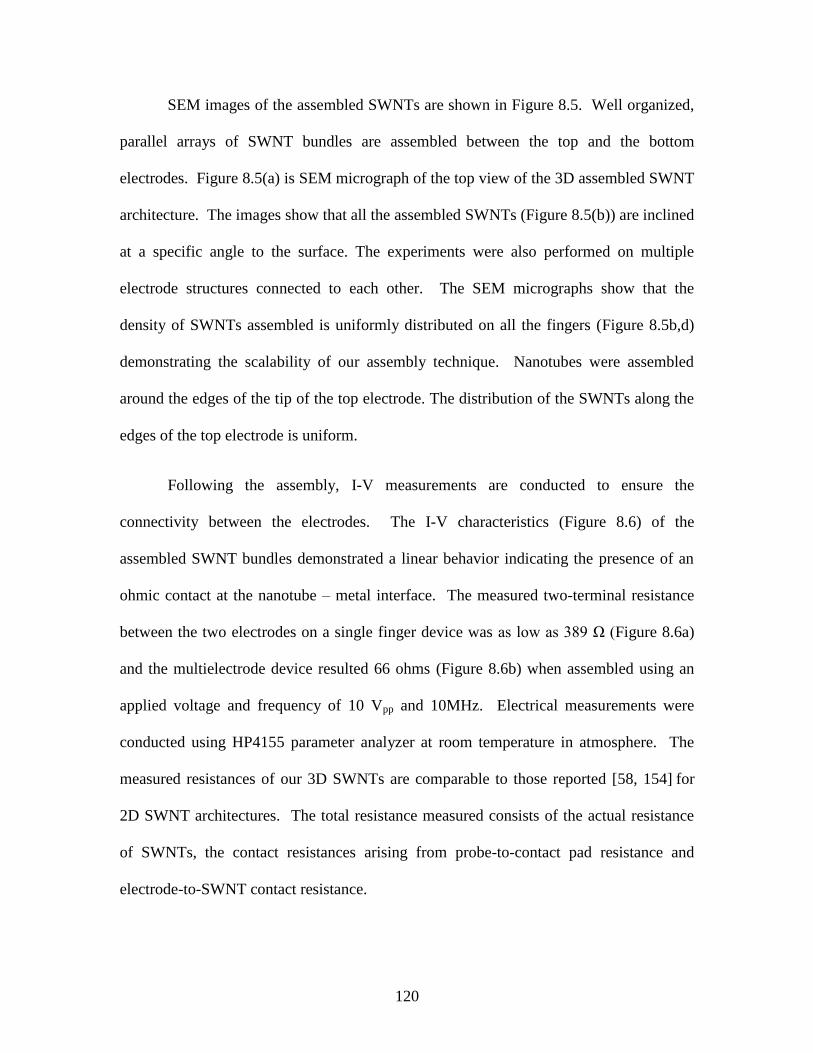
120
SEM images of the assembled SWNTs are shown in Figure 8.5. Well organized,
parallel arrays of SWNT bundles are assembled between the top and the bottom
electrodes. Figure 8.5(a) is SEM micrograph of the top view of the 3D assembled SWNT
architecture. The images show that all the assembled SWNTs (Figure 8.5(b)) are inclined
at a specific angle to the surface. The experiments were also performed on multiple
electrode structures connected to each other. The SEM micrographs show that the
density of SWNTs assembled is uniformly distributed on all the fingers (Figure 8.5b,d)
demonstrating the scalability of our assembly technique. Nanotubes were assembled
around the edges of the tip of the top electrode. The distribution of the SWNTs along the
edges of the top electrode is uniform.
Following the assembly, I-V measurements are conducted to ensure the
connectivity between the electrodes. The I-V characteristics (Figure 8.6) of the
assembled SWNT bundles demonstrated a linear behavior indicating the presence of an
ohmic contact at the nanotube – metal interface. The measured two-terminal resistance
between the two electrodes on a single finger device was as low as 389 Ω (Figure 8.6a)
and the multielectrode device resulted 66 ohms (Figure 8.6b) when assembled using an
applied voltage and frequency of 10 Vpp and 10MHz. Electrical measurements were
conducted using HP4155 parameter analyzer at room temperature in atmosphere. The
measured resistances of our 3D SWNTs are comparable to those reported [58, 154] for
2D SWNT architectures. The total resistance measured consists of the actual resistance
of SWNTs, the contact resistances arising from probe-to-contact pad resistance and
electrode-to-SWNT contact resistance.
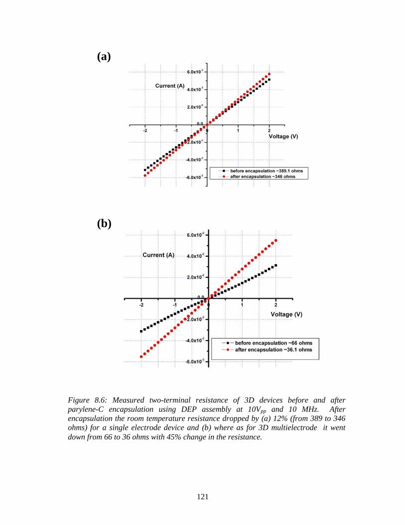
121
Figure 8.6: Measured two-terminal resistance of 3D devices before and after
parylene-C encapsulation using DEP assembly at 10Vpp and 10 MHz. After
encapsulation the room temperature resistance dropped by (a) 12% (from 389 to 346
ohms) for a single electrode device and (b) where as for 3D multielectrode it went
down from 66 to 36 ohms with 45% change in the resistance.
(b)
(a)
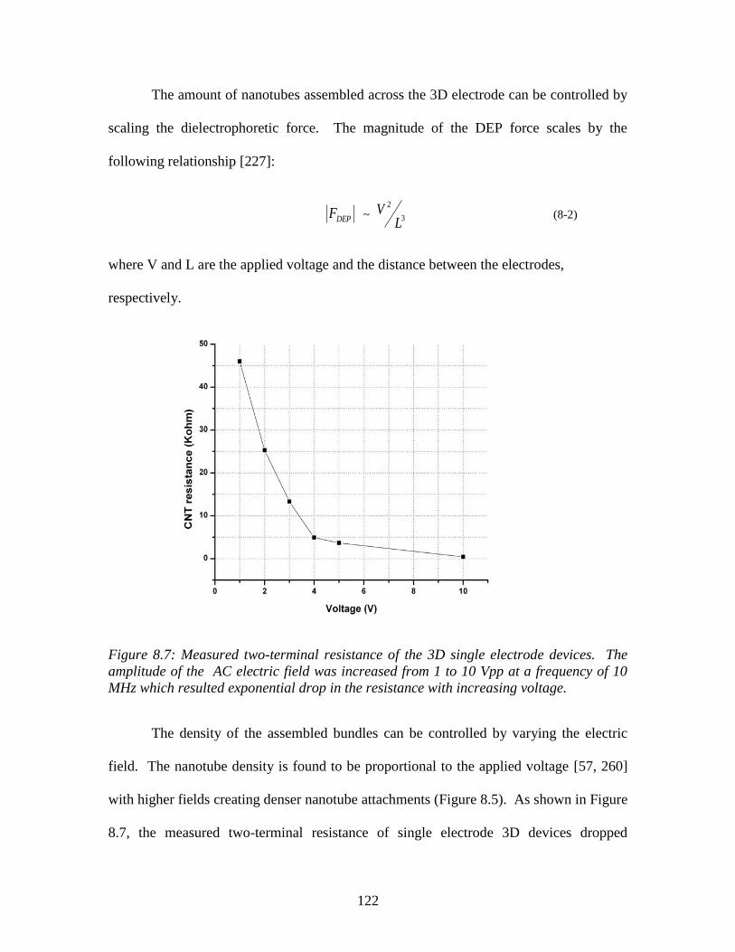
122
The amount of nanotubes assembled across the 3D electrode can be controlled by
scaling the dielectrophoretic force. The magnitude of the DEP force scales by the
following relationship [227]:
DEPF ~ 3
2
LV (8-2)
where V and L are the applied voltage and the distance between the electrodes,
respectively.
Figure 8.7: Measured two-terminal resistance of the 3D single electrode devices. The
amplitude of the AC electric field was increased from 1 to 10 Vpp at a frequency of 10
MHz which resulted exponential drop in the resistance with increasing voltage.
The density of the assembled bundles can be controlled by varying the electric
field. The nanotube density is found to be proportional to the applied voltage [57, 260]
with higher fields creating denser nanotube attachments (Figure 8.5). As shown in Figure
8.7, the measured two-terminal resistance of single electrode 3D devices dropped
(a)
123
exponentially with increasing assembly voltage. When the voltage between the
electrodes was increased more nanotubes were assembled around the edges of the tip of
the electrode. The thicker bundle size of the assembled bundled SWNTs could have been
possibly caused by the increased applied voltage. All assembly experiments were
conducted at a frequency of 10 MHz, while the AC voltage between the top electrode and
the bottom electrode was varied from 1 to 10 Vpp.
Figure 8.8: A schematic drawing of the 3D assembly electrodes illustrating the Height
(H) and Overlap distance (L), which can be varied to scale the DEP forces between the
top and the bottom electrodes.
We hypothesize that the number of assembled SWNT bundles can be controlled
by adjusting the magnitude of the electric field, which can also be done by changing the
distance between the electrodes. In the case of 3D electrodes, the spacing (H) and the
overlap/separation distance (L) between the top and bottom electrodes were varied
(Figure 8.8) to understand the interplay between the dimensions of the assembly platform
and the number of assembled SWNT bundles.
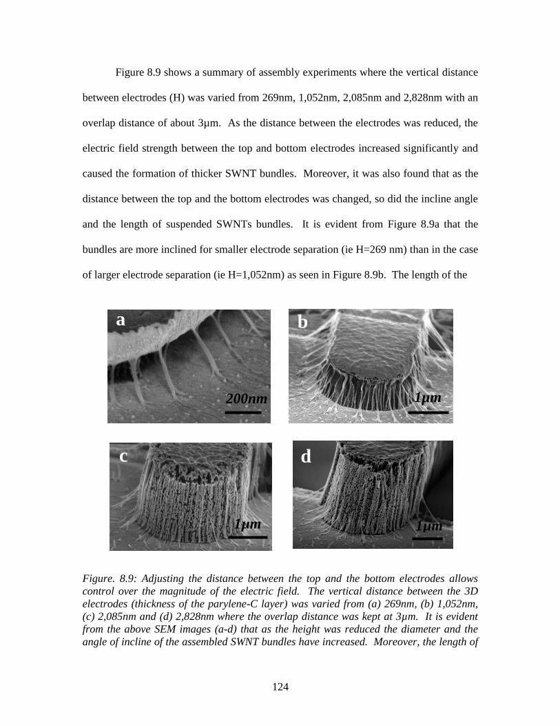
124
Figure 8.9 shows a summary of assembly experiments where the vertical distance
between electrodes (H) was varied from 269nm, 1,052nm, 2,085nm and 2,828nm with an
overlap distance of about 3µm. As the distance between the electrodes was reduced, the
electric field strength between the top and bottom electrodes increased significantly and
caused the formation of thicker SWNT bundles. Moreover, it was also found that as the
distance between the top and the bottom electrodes was changed, so did the incline angle
and the length of suspended SWNTs bundles. It is evident from Figure 8.9a that the
bundles are more inclined for smaller electrode separation (ie H=269 nm) than in the case
of larger electrode separation (ie H=1,052nm) as seen in Figure 8.9b. The length of the
Figure. 8.9: Adjusting the distance between the top and the bottom electrodes allows
control over the magnitude of the electric field. The vertical distance between the 3D
electrodes (thickness of the parylene-C layer) was varied from (a) 269nm, (b) 1,052nm,
(c) 2,085nm and (d) 2,828nm where the overlap distance was kept at 3µm. It is evident
from the above SEM images (a-d) that as the height was reduced the diameter and the
angle of incline of the assembled SWNT bundles have increased. Moreover, the length of
d
200nm
a b
1µm
c
1µm
1µm
d
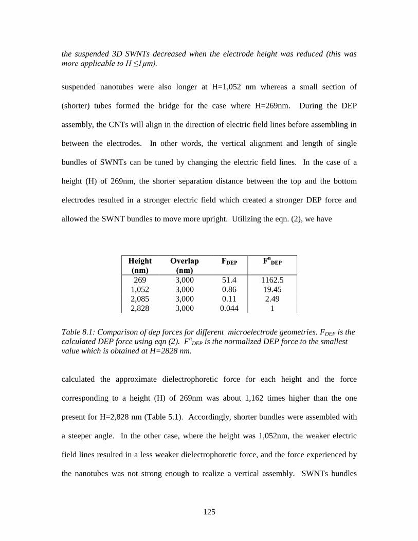
125
the suspended 3D SWNTs decreased when the electrode height was reduced (this was
more applicable to H ≤1µm).
suspended nanotubes were also longer at H=1,052 nm whereas a small section of
(shorter) tubes formed the bridge for the case where H=269nm. During the DEP
assembly, the CNTs will align in the direction of electric field lines before assembling in
between the electrodes. In other words, the vertical alignment and length of single
bundles of SWNTs can be tuned by changing the electric field lines. In the case of a
height (H) of 269nm, the shorter separation distance between the top and the bottom
electrodes resulted in a stronger electric field which created a stronger DEP force and
allowed the SWNT bundles to move more upright. Utilizing the eqn. (2), we have
Table 8.1: Comparison of dep forces for different microelectrode geometries. FDEP is the
calculated DEP force using eqn (2). Fn
DEP is the normalized DEP force to the smallest
value which is obtained at H=2828 nm.
calculated the approximate dielectrophoretic force for each height and the force
corresponding to a height (H) of 269nm was about 1,162 times higher than the one
present for H=2,828 nm (Table 5.1). Accordingly, shorter bundles were assembled with
a steeper angle. In the other case, where the height was 1,052nm, the weaker electric
field lines resulted in a less weaker dielectrophoretic force, and the force experienced by
the nanotubes was not strong enough to realize a vertical assembly. SWNTs bundles
HHeeiigghhtt
((nnmm)) OOvveerrllaapp
((nnmm)) FFDDEEPP FF
nnDDEEPP
269 3,000 51.4 1162.5
1,052 3,000 0.86 19.45
2,085 3,000 0.11 2.49
2,828 3,000 0.044 1
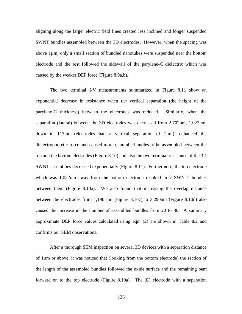
126
aligning along the larger electric field lines created less inclined and longer suspended
SWNT bundles assembled between the 3D electrodes. However, when the spacing was
above 1µm, only a small section of bundled nanotubes were suspended near the bottom
electrode and the rest followed the sidewall of the parylene-C dielectric which was
caused by the weaker DEP force (Figure 8.9a,b).
The two terminal I-V measurements summarized in Figure 8.11 show an
exponential decrease in resistance when the vertical separation (the height of the
parylene-C thickness) between the electrodes was reduced. Similarly, when the
separation (lateral) between the 3D electrodes was decreased from 2,702nm, 1,022nm,
down to 117nm (electrodes had a vertical separation of 1µm), enhanced the
dielectrophoretic force and caused more nanotube bundles to be assembled between the
top and the bottom electrodes (Figure 8.10) and also the two terminal resistance of the 3D
SWNT assemblies decreased exponentially (Figure 8.11). Furthermore, the top electrode
which was 1,022nm away from the bottom electrode resulted in 7 SWNTs bundles
between them (Figure 8.10a). We also found that increasing the overlap distance
between the electrodes from 1,190 nm (Figure 8.10c) to 3,290nm (Figure 8.10d) also
caused the increase in the number of assembled bundles from 20 to 30. A summary
approximate DEP force values calculated using eqn. (2) are shown in Table 8.2 and
confirms our SEM observations.
After a thorough SEM inspection on several 3D devices with a separation distance
of 1µm or above, it was noticed that (looking from the bottom electrode) the section of
the length of the assembled bundles followed the oxide surface and the remaining bent
forward on to the top electrode (Figure 8.10a). The 3D electrode with a separation
127
distance of less than 1µm always formed bundles inclined where the angle of incline can
be adjusted by controlling the height between the electrodes. In addition, the field
strength is nearly uniform around the edge of the hemispherical tip at their respective
height. When the top electrode begins to overlap with the first electrode, more SWNT
bundles assembled around the tip of the electrode as seen in Figure 8.10.
Figure 8.10: The overlap distance between the top and bottom electrodes was changed
from (a) 1,022nm, (b) 117nm, (c) 1,190nm (d) to 3,290nm. As a result, more SWNT
bundles assembled around the edges of the hemispherical top electrode as shown in the
SEM micrographs through of the 3D devices (a) to (d) which resulted in 7, 9, 20 and 30
bundles, respectively.
In summary, by controlling the spacing and the overall/separation distance
between the 3D electrodes allow control in the angle, the bundle thickness, the suspended
length and the number of assembled SWNT bundles around the edges of the tip of the top
electrode.
1µm
a
1µm
b
1µm
c d
1µm
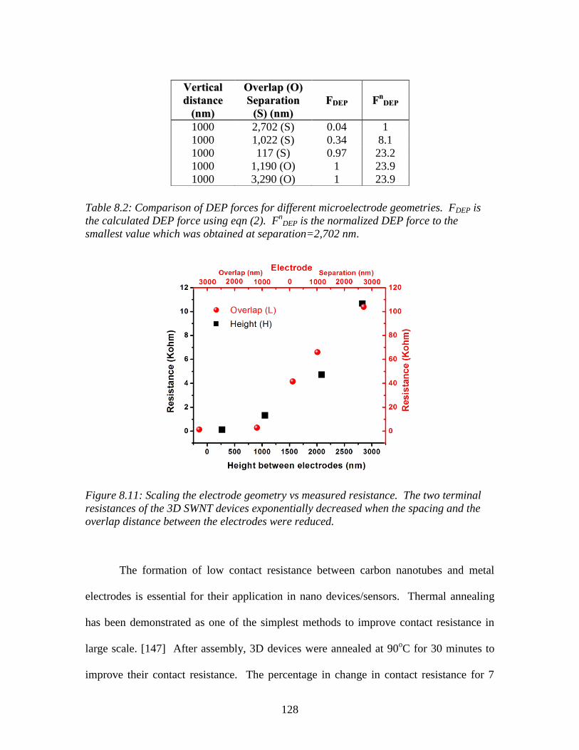
128
Table 8.2: Comparison of DEP forces for different microelectrode geometries. FDEP is
the calculated DEP force using eqn (2). Fn
DEP is the normalized DEP force to the
smallest value which was obtained at separation=2,702 nm.
Figure 8.11: Scaling the electrode geometry vs measured resistance. The two terminal
resistances of the 3D SWNT devices exponentially decreased when the spacing and the
overlap distance between the electrodes were reduced.
The formation of low contact resistance between carbon nanotubes and metal
electrodes is essential for their application in nano devices/sensors. Thermal annealing
has been demonstrated as one of the simplest methods to improve contact resistance in
large scale. [147] After assembly, 3D devices were annealed at 90oC for 30 minutes to
improve their contact resistance. The percentage in change in contact resistance for 7
VVeerrttiiccaall
ddiissttaannccee
((nnmm))
OOvveerrllaapp ((OO))
SSeeppaarraattiioonn
((SS)) ((nnmm))
FFDDEEPP
FFnn
DDEEPP
1000 2,702 (S) 0.04 1
1000 1,022 (S) 0.34 8.1
1000 117 (S) 0.97 23.2
1000 1,190 (O) 1 23.9
1000 3,290 (O) 1 23.9
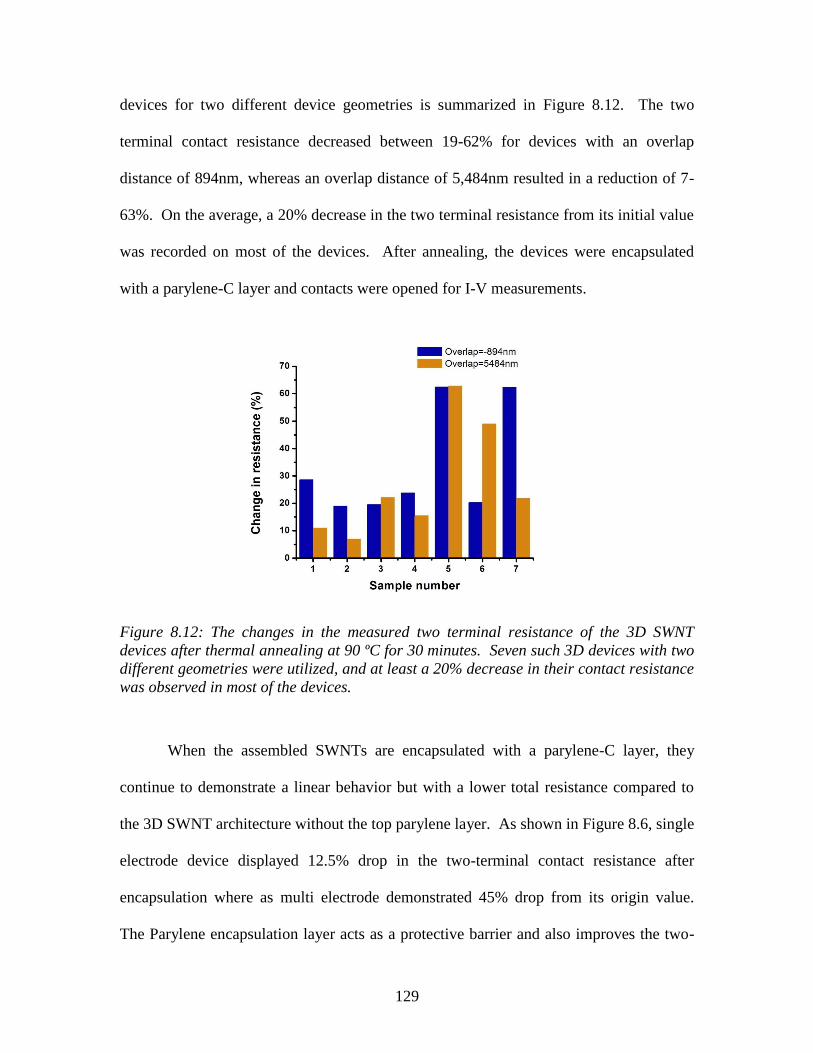
129
devices for two different device geometries is summarized in Figure 8.12. The two
terminal contact resistance decreased between 19-62% for devices with an overlap
distance of 894nm, whereas an overlap distance of 5,484nm resulted in a reduction of 7-
63%. On the average, a 20% decrease in the two terminal resistance from its initial value
was recorded on most of the devices. After annealing, the devices were encapsulated
with a parylene-C layer and contacts were opened for I-V measurements.
Figure 8.12: The changes in the measured two terminal resistance of the 3D SWNT
devices after thermal annealing at 90 ºC for 30 minutes. Seven such 3D devices with two
different geometries were utilized, and at least a 20% decrease in their contact resistance
was observed in most of the devices.
When the assembled SWNTs are encapsulated with a parylene-C layer, they
continue to demonstrate a linear behavior but with a lower total resistance compared to
the 3D SWNT architecture without the top parylene layer. As shown in Figure 8.6, single
electrode device displayed 12.5% drop in the two-terminal contact resistance after
encapsulation where as multi electrode demonstrated 45% drop from its origin value.
The Parylene encapsulation layer acts as a protective barrier and also improves the two-
130
terminal contact resistance of the 3D nano-bridge. Carbon nanotubes are highly sensitive
to a broad class of chemical vapors [59, 60]. Accordingly, to isolate the CNTs from the
environment and also to prevent contamination we have encapsulated the with a thin and
conformal Parylene-C layer. Furthermore, the deposition of the top Parylene layer
secures the position of the CNTs and possibly presses them against the Au metal
electrodes which improve contact resistance between the metal and the CNTs. It is also
likely that the parylene encapsulation increases the number of CNTs contacting the Au
metal and hence improves the two terminal resistance of the structure.
8.2.3 DEP Simulation
The approaches for controlled manipulation of nanoparticles include template-
directed synthesis, [217] atomic [161] and scanning force microscopy [261] and
nanorobotic manipulations. [262] But, these methods have low throughput and are not
suitable for the production environment. DEP, coined by H. A. Pohl, [263] refers to the
force exerted on a dielectric particle when it is subjected to a non-uniform AC or DC
electric field. Depending on the dielectric properties of the particles and the medium, if
the dielectrophoretic force acting on the nanomaterial directs the particles towards
regions where the gradient of the electric field intensity is maximum, then it is referred to
as positive DEP (PDEP). Furthermore, if the particles are directed towards regions where
the gradient of the electric field intensity is minimum, then it is referred to as negative
dielectrophoresis (NDEP). In our assembly experiments, we have utilized positive
dielectrophoresis.
131
To gain a better understanding of the assembly behavior of the SWNTs during
dielectrophoretic assembly process, we used FEMLAB multi-physics software
(COMSOL) to simulate the electric field distribution around the micro-fabricated
platform and the influence of the electric field on nanotube placement. The DEP force
was calculated and compared with the viscous drag during the assembly process, which
led to the predicted trajectory of the CNT. For simplification, we used a 2D model to
explain the assembly mechanism. The geometry of the electrodes in the simulation
software were defined considering the actual fabrication processes which results in a
curvature in electrodes resulting from fabrication and the overhang induced by isotropic
etching of the parylene resulting in an undercut. To determine the DEP force acting on
the CNTs, the following equation was used [264, 265]
22 )(Re6
rmsmdep EKlrF (1)
*
**
)(m
mpK
(2)
where l and r are the length and radius of a rod-like particle respectively, εm is the real
permittivity of the suspending medium, Erms is the root mean square (rms) of the electric
field and K (ω) is the Clausius-Mosotti factor. In equation (2), ε*
p and ε*
m are the
complex permittivities of the rod-like particle and the suspending medium, respectively.
Here )/(* i , where 1i , is the real permittivity and is the conductivity
of the material. In general, is a material property and can be written as a product of the
relative permittivity of the material and permittivity of free space 0 . As shown in
equation (1), the strength of the dielectrophoretic force is proportional to the size and
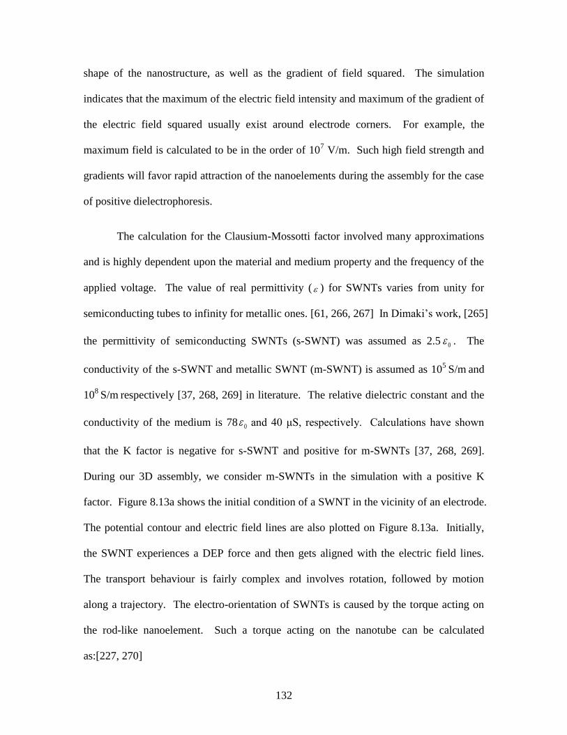
132
shape of the nanostructure, as well as the gradient of field squared. The simulation
indicates that the maximum of the electric field intensity and maximum of the gradient of
the electric field squared usually exist around electrode corners. For example, the
maximum field is calculated to be in the order of 107 V/m. Such high field strength and
gradients will favor rapid attraction of the nanoelements during the assembly for the case
of positive dielectrophoresis.
The calculation for the Clausium-Mossotti factor involved many approximations
and is highly dependent upon the material and medium property and the frequency of the
applied voltage. The value of real permittivity ( ) for SWNTs varies from unity for
semiconducting tubes to infinity for metallic ones. [61, 266, 267] In Dimaki‘s work, [265]
the permittivity of semiconducting SWNTs (s-SWNT) was assumed as 2.5 0 . The
conductivity of the s-SWNT and metallic SWNT (m-SWNT) is assumed as 105
S/m and
108
S/m respectively [37, 268, 269] in literature. The relative dielectric constant and the
conductivity of the medium is 78 0 and 40 μS, respectively. Calculations have shown
that the K factor is negative for s-SWNT and positive for m-SWNTs [37, 268, 269].
During our 3D assembly, we consider m-SWNTs in the simulation with a positive K
factor. Figure 8.13a shows the initial condition of a SWNT in the vicinity of an electrode.
The potential contour and electric field lines are also plotted on Figure 8.13a. Initially,
the SWNT experiences a DEP force and then gets aligned with the electric field lines.
The transport behaviour is fairly complex and involves rotation, followed by motion
along a trajectory. The electro-orientation of SWNTs is caused by the torque acting on
the rod-like nanoelement. Such a torque acting on the nanotube can be calculated
as:[227, 270]
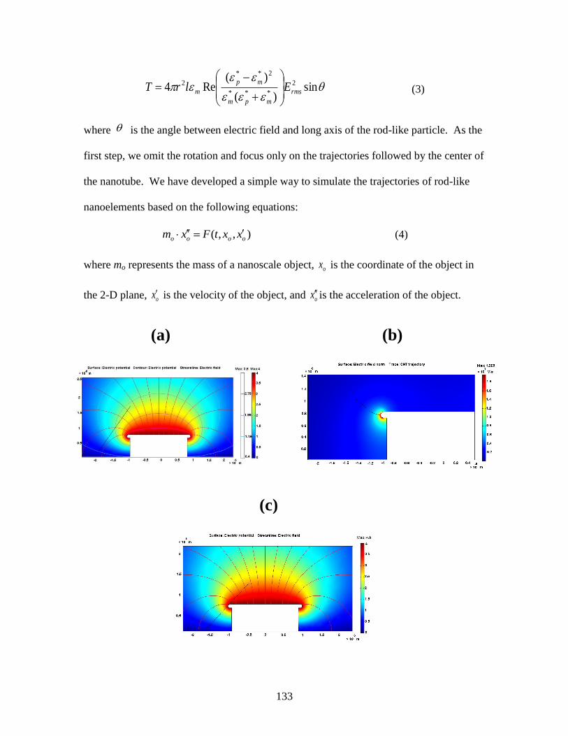
133
sin
)(
)(Re4 2
***
2**
2
rms
mpm
mp
m ElrT
(3)
where is the angle between electric field and long axis of the rod-like particle. As the
first step, we omit the rotation and focus only on the trajectories followed by the center of
the nanotube. We have developed a simple way to simulate the trajectories of rod-like
nanoelements based on the following equations:
),,( oooo xxtFxm (4)
where mo represents the mass of a nanoscale object, ox is the coordinate of the object in
the 2-D plane, ox is the velocity of the object, and ox is the acceleration of the object.
(a) (b)
(c)
134
Figure 8.13: Simulation of SWNT transport during DEP assembly process. (a) shows the
electric potential surface contour and the electric field stream lines for the SWNT in the
initial stage of the assembly process, (b) shows the electric field surface and CNT
transport trajectory during assembly. (c) shows the final position of the SWNT assembled
in between 2 electrodes.
A simplified CNT trajectory under the combined influence of DEP force and viscous
drag is illustrated in Figure 8.13b. The final position of the CNT is shown in Figure
8.13c, where an inclined attachment has been achieved following the assembly process.
8.3 A Vertical SWNTs Field Effect Transistor
Carbon nanotubes possess unique electrical, mechanical and thermal properties
and may potentially serve as the building blocks of novel devices of technological
importance. They have been extensively utilized in many nanoscale devices including
CNTFETs, [37] sensors, [100] memory devices, [40] logic circuits, [151] field-emission
displays [254] and interconnects [271]. The continuing demand for more functionality
from integrated circuits is the driving factor to realize more transistors in a given chip
area. Reducing lateral dimensions have certain limitations which result in lower current
densities and large parasitic gate capacitances. [252] There is a continuous push to
develop alternative technologies that can increase density of transistors on a chip.
The vertical arrangement of carbon nanotube transistors has been proposed as a
means for large scale, high density realization of nanoelectronic circuits. As a first step
towards realizing this goal, Duesberg et al. have demonstrated Catalytic Chemical Vapor
Deposition (CCVD) technique and grew a single MWNT inside a 20nm hole. [253] Choi
and colleagues have achieved ultrahigh density nano transistors utilizing a similar CCVD
method. [257] Chen et al. were able to demonstrate a high density vertical nanowire
b
a
135
transistor (108/cm
2) on a flexible polymer foil. [272] All these techniques have various
drawbacks which limited their potential success. For example, the CCVD method
requires high growth temperatures (>500ºC) and the template based growth is only
applicable to small areas. Polyethyleneterephthalate (PET) polymer based technology is
unstable as it is sensitive to environmental conditions. Three dimensional assembly of
carbon nanotubes on a 3D platform is previously demonstrated. Utilizing this 3D
microplatform, a 3D CNTFET technology allows the realization of vertical transistors
and has the potential for large scale ultra-high density nanoelectronic circuits is next
demonstrated.
8.3.1 Fabrication of 3D SWNTs FET
To realize the 3D CNTFETs, first a 3D micromachined platform was fabricated
on a silicon wafer utilizing the process flow detailed in our previous work. The 3D
microplatform comprises of Cr/Au (50Å/750Å) source and drain electrodes separated (in
the vertical dimension) by a 1µm thick Parylene-C dielectric layer, fabricated on a silicon
wafer with a 2 mask process. Then, utilizing dielectrophoretic (DEP) assembly, SWNTs
are incorporated between the source and drain electrodes in a vertical manner as seen in
the SEM micrographs shown in the previous section. Commercially available aqueous
suspension of highly purified HIPCo-grown SWNTs are used in these experiments. The
average diameter of the SWNTs is about 3 nm with an average length of 3 µm. To
perform nanotube assembly, a 1µl SWNT solution was dispensed over the
microelectrodes and the DEP assembly was conducted at a frequency of 300 kHz and a
peak-to-peak voltage of 10V for 30 seconds. Following the assembly, two terminal I-V
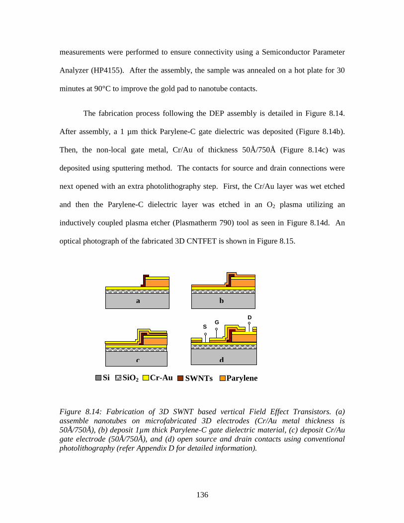
136
measurements were performed to ensure connectivity using a Semiconductor Parameter
Analyzer (HP4155). After the assembly, the sample was annealed on a hot plate for 30
minutes at 90°C to improve the gold pad to nanotube contacts.
The fabrication process following the DEP assembly is detailed in Figure 8.14.
After assembly, a 1 µm thick Parylene-C gate dielectric was deposited (Figure 8.14b).
Then, the non-local gate metal, Cr/Au of thickness 50Å/750Å (Figure 8.14c) was
deposited using sputtering method. The contacts for source and drain connections were
next opened with an extra photolithography step. First, the Cr/Au layer was wet etched
and then the Parylene-C dielectric layer was etched in an O2 plasma utilizing an
inductively coupled plasma etcher (Plasmatherm 790) tool as seen in Figure 8.14d. An
optical photograph of the fabricated 3D CNTFET is shown in Figure 8.15.
Figure 8.14: Fabrication of 3D SWNT based vertical Field Effect Transistors. (a)
assemble nanotubes on microfabricated 3D electrodes (Cr/Au metal thickness is
50Å/750Å), (b) deposit 1µm thick Parylene-C gate dielectric material, (c) deposit Cr/Au
gate electrode (50Å/750Å), and (d) open source and drain contacts using conventional
photolithography (refer Appendix D for detailed information).
Si SiO2 Cr-Au SWNTs Parylene
a b
c
G D
S
d
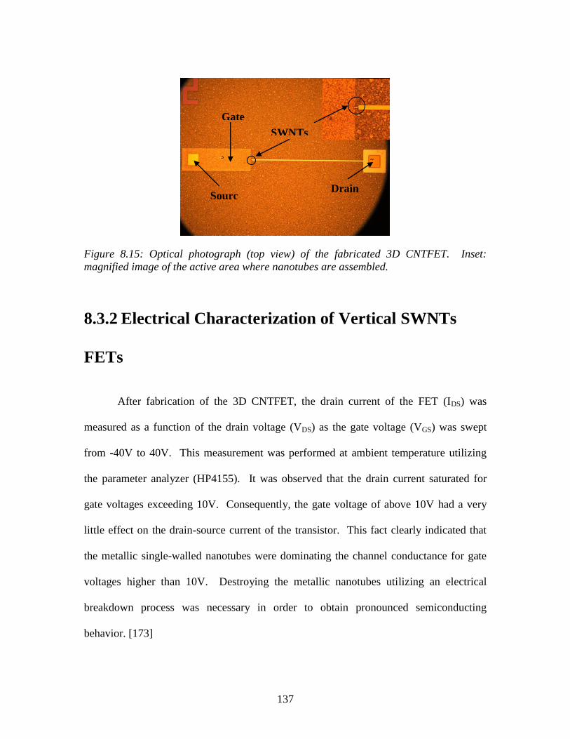
137
Figure 8.15: Optical photograph (top view) of the fabricated 3D CNTFET. Inset:
magnified image of the active area where nanotubes are assembled.
8.3.2 Electrical Characterization of Vertical SWNTs
FETs
After fabrication of the 3D CNTFET, the drain current of the FET (IDS) was
measured as a function of the drain voltage (VDS) as the gate voltage (VGS) was swept
from -40V to 40V. This measurement was performed at ambient temperature utilizing
the parameter analyzer (HP4155). It was observed that the drain current saturated for
gate voltages exceeding 10V. Consequently, the gate voltage of above 10V had a very
little effect on the drain-source current of the transistor. This fact clearly indicated that
the metallic single-walled nanotubes were dominating the channel conductance for gate
voltages higher than 10V. Destroying the metallic nanotubes utilizing an electrical
breakdown process was necessary in order to obtain pronounced semiconducting
behavior. [173]
Sourc
e
Drain
Gate
SWNTs
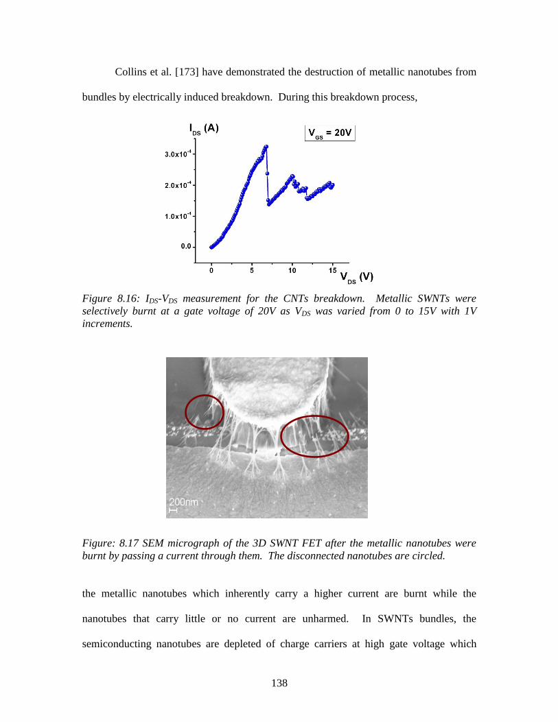
138
Collins et al. [173] have demonstrated the destruction of metallic nanotubes from
bundles by electrically induced breakdown. During this breakdown process,
Figure 8.16: IDS-VDS measurement for the CNTs breakdown. Metallic SWNTs were
selectively burnt at a gate voltage of 20V as VDS was varied from 0 to 15V with 1V
increments.
Figure: 8.17 SEM micrograph of the 3D SWNT FET after the metallic nanotubes were
burnt by passing a current through them. The disconnected nanotubes are circled.
the metallic nanotubes which inherently carry a higher current are burnt while the
nanotubes that carry little or no current are unharmed. In SWNTs bundles, the
semiconducting nanotubes are depleted of charge carriers at high gate voltage which
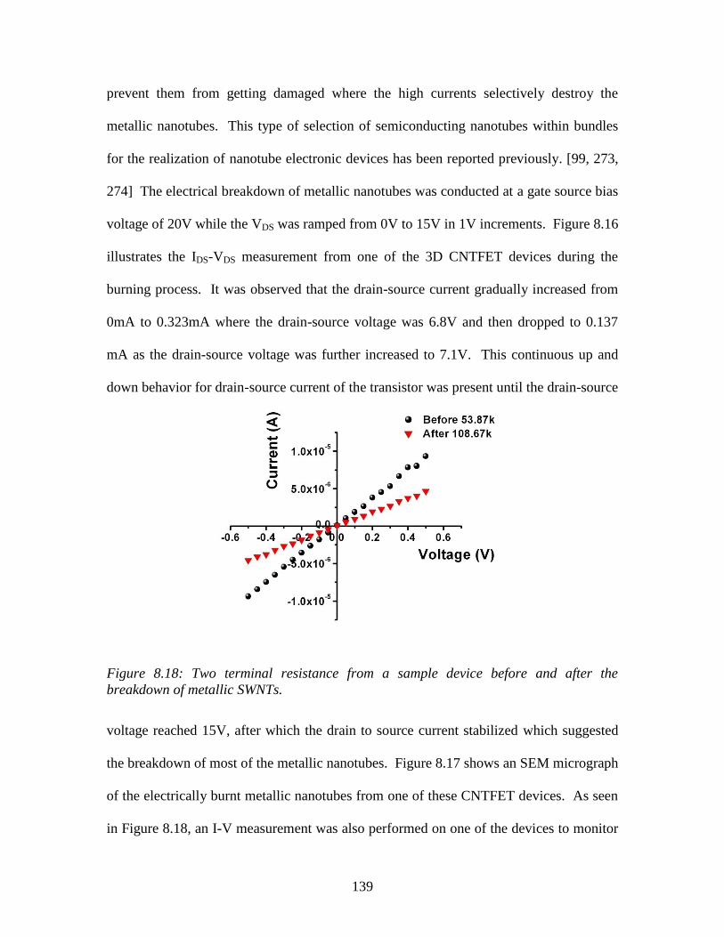
139
prevent them from getting damaged where the high currents selectively destroy the
metallic nanotubes. This type of selection of semiconducting nanotubes within bundles
for the realization of nanotube electronic devices has been reported previously. [99, 273,
274] The electrical breakdown of metallic nanotubes was conducted at a gate source bias
voltage of 20V while the VDS was ramped from 0V to 15V in 1V increments. Figure 8.16
illustrates the IDS-VDS measurement from one of the 3D CNTFET devices during the
burning process. It was observed that the drain-source current gradually increased from
0mA to 0.323mA where the drain-source voltage was 6.8V and then dropped to 0.137
mA as the drain-source voltage was further increased to 7.1V. This continuous up and
down behavior for drain-source current of the transistor was present until the drain-source
Figure 8.18: Two terminal resistance from a sample device before and after the
breakdown of metallic SWNTs.
voltage reached 15V, after which the drain to source current stabilized which suggested
the breakdown of most of the metallic nanotubes. Figure 8.17 shows an SEM micrograph
of the electrically burnt metallic nanotubes from one of these CNTFET devices. As seen
in Figure 8.18, an I-V measurement was also performed on one of the devices to monitor
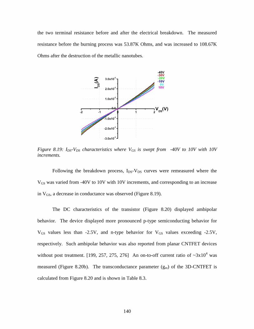
140
the two terminal resistance before and after the electrical breakdown. The measured
resistance before the burning process was 53.87K Ohms, and was increased to 108.67K
Ohms after the destruction of the metallic nanotubes.
Figure 8.19: IDS-VDS characteristics where VGS is swept from -40V to 10V with 10V
increments.
Following the breakdown process, IDS-VDS curves were remeasured where the
VGS was varied from -40V to 10V with 10V increments, and corresponding to an increase
in VGS, a decrease in conductance was observed (Figure 8.19).
The DC characteristics of the transistor (Figure 8.20) displayed ambipolar
behavior. The device displayed more pronounced p-type semiconducting behavior for
VGS values less than -2.5V, and n-type behavior for VGS values exceeding -2.5V,
respectively. Such ambipolar behavior was also reported from planar CNTFET devices
without post treatment. [199, 257, 275, 276] An on-to-off current ratio of ~3x10⁴ was
measured (Figure 8.20b). The transconductance parameter (gm) of the 3D-CNTFET is
calculated from Figure 8.20 and is shown in Table 8.3.
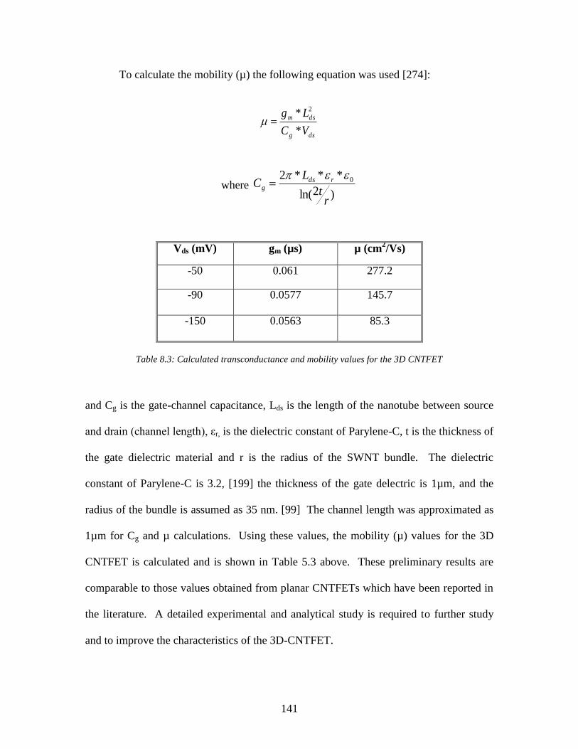
141
To calculate the mobility (µ) the following equation was used [274]:
dsg
dsm
VC
Lg
*
* 2
where )2ln(
***2 0
rt
LC rds
g
Vds (mV) gm (µs) µ (cm2/Vs)
-50 0.061 277.2
-90 0.0577 145.7
-150 0.0563 85.3
Table 8.3: Calculated transconductance and mobility values for the 3D CNTFET
and Cg is the gate-channel capacitance, Lds is the length of the nanotube between source
and drain (channel length), εr, is the dielectric constant of Parylene-C, t is the thickness of
the gate dielectric material and r is the radius of the SWNT bundle. The dielectric
constant of Parylene-C is 3.2, [199] the thickness of the gate delectric is 1µm, and the
radius of the bundle is assumed as 35 nm. [99] The channel length was approximated as
1µm for Cg and µ calculations. Using these values, the mobility (µ) values for the 3D
CNTFET is calculated and is shown in Table 5.3 above. These preliminary results are
comparable to those values obtained from planar CNTFETs which have been reported in
the literature. A detailed experimental and analytical study is required to further study
and to improve the characteristics of the 3D-CNTFET.
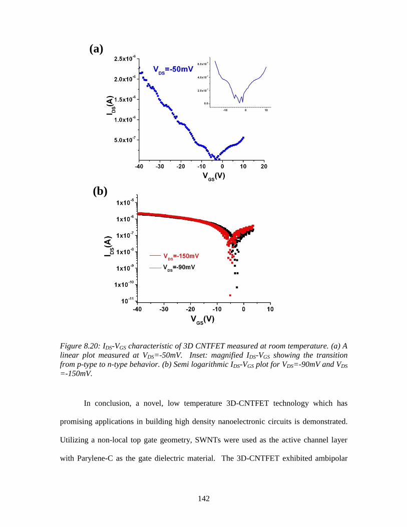
142
(a)
(b)
Figure 8.20: IDS-VGS characteristic of 3D CNTFET measured at room temperature. (a) A
linear plot measured at VDS=-50mV. Inset: magnified IDS-VGS showing the transition
from p-type to n-type behavior. (b) Semi logarithmic IDS-VGS plot for VDS=-90mV and VDS
=-150mV.
In conclusion, a novel, low temperature 3D-CNTFET technology which has
promising applications in building high density nanoelectronic circuits is demonstrated.
Utilizing a non-local top gate geometry, SWNTs were used as the active channel layer
with Parylene-C as the gate dielectric material. The 3D-CNTFET exhibited ambipolar
143
behavior with more pronounced p-type behavior than n-type behavior. The maximum
transconductance of 0.061µs, a highest mobility of 277 cm2/Vs and an on-to-off current
ratio of ~ 3x10⁴ were also measured. Carbon nanotubes are increasingly being utilized in
system level applications such as the demonstration of a carbon nanotube radio and
chemical/biological sensor systems. Translating the 3D integration concept of realizing
high density systems, CNT transistors and sensors fabricated on individual layers can be
connected to other layers utilizing vertical CNTs. The 3D-CNTFET technology can
possibly be utilized to build multi layer, compact and high density nanotube transistors
for large scale nanoelectronic circuits.
144
CChhaapptteerr 99
Conclusion and Future Work
In this thesis, I have investigated CNT FETs along with parylene-C for flexible
and biocompatible device applications. First, I have characterized parylene-C deposition
and surface properties, and developed a low temperature and low pressure ICP dry
etching process for patterning parylene film. Next, I have studied the adhesion properties
of parylene-C on silicon dioxide and metal surface utilizing dry and wet adhesion
promoters, and evaluated the reliability of thin parylene-C gate dielectric for CNT based
flexible device applications. A metal-insulator-metal (MIM) capacitor structure was
employed in the above experiments to characterize the time dependent dielectric
breakdown of various parylence-C dielectric thicknesses. Then, I have designed and
fabricated a CNTFET on a 10 µm flexible parylene-C substrate where 1 µm thick
parylene-C was employed as a gate dielectric material. The device has been realized
using dielectrophoretic assembly followed by electrical burning method. The electrical
characterization tests displayed significantly improved performance after this burning
process. Compared to the other assembly methods, DEP process is simple, high yield
and also results in aligned nanotubes. Next, I have deposited thin parylene layers on to
the flexible CNT FET and evaluated the performance of the CNT TFTs before and after
the deposition. According to my test results, a thin 1 µm parylene-C passivation
145
densified carbon nanotubes and fixed their position on metal electrodes which resulted in
more than 10% increase in the ON current of the transistors but no noticeable changes
were observed in other transistor properties. After high vacuum treatments the
unencapsulated TFTs showed suppression in the hysteresis width. Moreover, the
transistor characteristics of 1 µm parylene-C packaged TFT remained unchanged after 28
hours in high vacuum exposure and indicated that the 1 µm parylene-C film is a good
barrier for CNTFETs. The devices that were encapsulated with 1 µm and 3 µm parylene
films displayed similar behaviors and indicated that the thickness of parylene-C
passivation coating can be adjusted based on the specifications of a device. After
studying the effects of parylene passivation on CNTFETs, I have evaluated the
mechanical flexibility of 1 µm parylene-C packaged TFTs. The encapsulated and
ultraflexible TFTs can be bent to radius down to 1.5 mm and remained operational. The
stability of all-parylene CNTFETs are also studied in 0.9% sterile solution of sodium
chloride for 42 days. Finally, I have designed and fabricated high density top gated
vertical CNT FETs. Compared to other 3D FETs, the process is simple and high yield
and allows the realization of CNT FETs in the vertical dimension. As part of this
process, I have also optimized the DEP assembly parameters for realizing vertical CNT
TFTs. Even though significant progress has been made in this thesis, further work
includes the realization of low voltage FETs with thin gate dielectric, evaluation of life
expectance of parylene-C packaged TFTs in saline solution, real time bending test and
simulation of all-parylene SWNT TFTs, and contact resistance of SWNTs before and
after different thicknesses of parylene coating.
146
Appendix A
Appendix A-1 Parylene Deposition Procedure
(i) Parylene Deposition Procedure using PDS 2010 Labcoater 2
A Specialty Coating Systems Parylene Deposition System 2010 Labcoater 2 (PDS
2010) is used for Parylene deposition, which is available in the Kostas
Nanomanufacturing Facility at Northeastern University. The Figure A.1 shows the
picture of PDS 2010 equipment system.
The PDS 2010 consists of tubes, chambers and a control panel. The most
important components of this system are vaporizer, pyrolysis furnace, deposition
chamber, cold trap, vacuum pump and the control panel. As discussed earlier, vaporizer
heats the parylene dimer until it becomes parylene gas; pyrolysis furnace decomposes
parylene dimer gas into parylene monomer gas; deposition chamber is where parylene
polymerization take places. The cold trap is a cryogenic device by which a mechanical
chiller cools a finger. The chilled finger then condenses parylene process by-products
and prevents contamination of the vacuum pump. The vacuum pump maintains the PDS
2010 system in a highly vacuum condition. The Table A.1 explains the functionality of
each of the buttons on the control panel. The Parylene Deposition Process instructions
are also included in the next section.
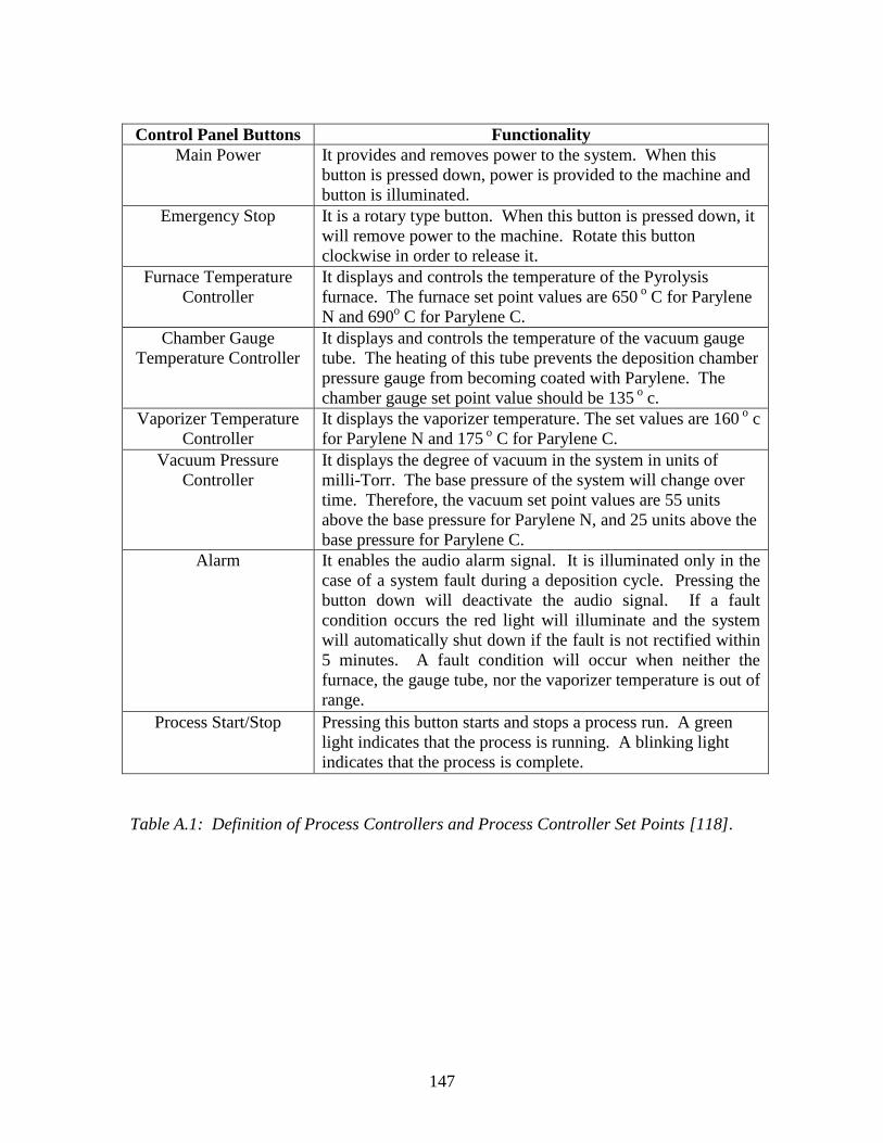
147
Control Panel Buttons Functionality
Main Power It provides and removes power to the system. When this
button is pressed down, power is provided to the machine and
button is illuminated.
Emergency Stop It is a rotary type button. When this button is pressed down, it
will remove power to the machine. Rotate this button
clockwise in order to release it.
Furnace Temperature
Controller
It displays and controls the temperature of the Pyrolysis
furnace. The furnace set point values are 650 o C for Parylene
N and 690o C for Parylene C.
Chamber Gauge
Temperature Controller
It displays and controls the temperature of the vacuum gauge
tube. The heating of this tube prevents the deposition chamber
pressure gauge from becoming coated with Parylene. The
chamber gauge set point value should be 135 o c.
Vaporizer Temperature
Controller
It displays the vaporizer temperature. The set values are 160 o
c
for Parylene N and 175 o C for Parylene C.
Vacuum Pressure
Controller
It displays the degree of vacuum in the system in units of
milli-Torr. The base pressure of the system will change over
time. Therefore, the vacuum set point values are 55 units
above the base pressure for Parylene N, and 25 units above the
base pressure for Parylene C.
Alarm It enables the audio alarm signal. It is illuminated only in the
case of a system fault during a deposition cycle. Pressing the
button down will deactivate the audio signal. If a fault
condition occurs the red light will illuminate and the system
will automatically shut down if the fault is not rectified within
5 minutes. A fault condition will occur when neither the
furnace, the gauge tube, nor the vaporizer temperature is out of
range.
Process Start/Stop Pressing this button starts and stops a process run. A green
light indicates that the process is running. A blinking light
indicates that the process is complete.
Table A.1: Definition of Process Controllers and Process Controller Set Points [118].
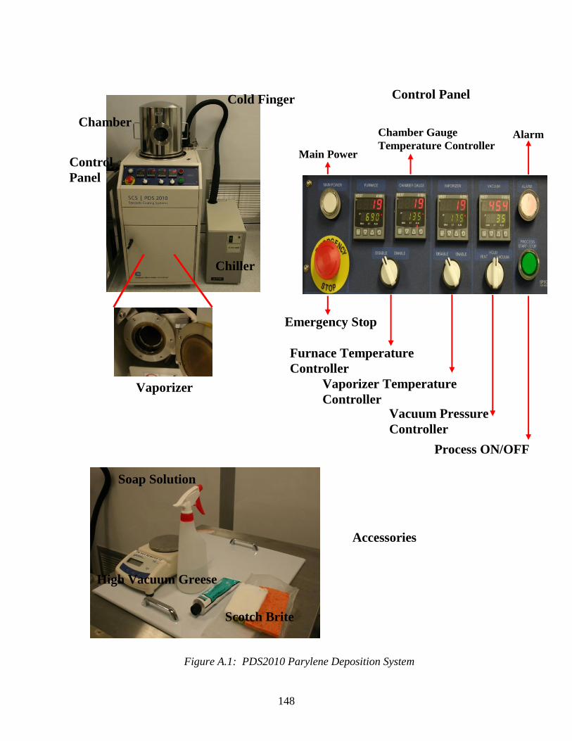
148
Vaporizer
Cold Finger
Chamber
Control Panel
Chiller
Emergency Stop
Furnace Temperature
Controller
Vaporizer Temperature
Controller Vacuum Pressure
Controller
Process ON/OFF
Chamber Gauge
Temperature Controller Main Power
Alarm
Control
Panel
Soap Solution
Scotch Brite
High Vacuum Greese
Accessories
Figure A.1: PDS2010 Parylene Deposition System
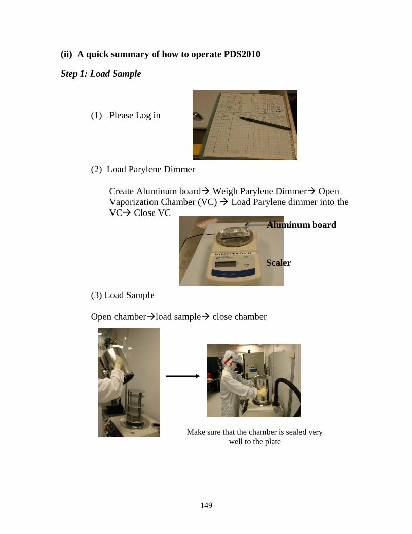
149
(ii) A quick summary of how to operate PDS2010
Step 1: Load Sample
(1) Please Log in
(2) Load Parylene Dimmer
Create Aluminum board Weigh Parylene Dimmer Open
Vaporization Chamber (VC) Load Parylene dimmer into the
VC Close VC
(3) Load Sample
Open chamberload sample close chamber
Aluminum board
Scaler
Make sure that the chamber is sealed very
well to the plate
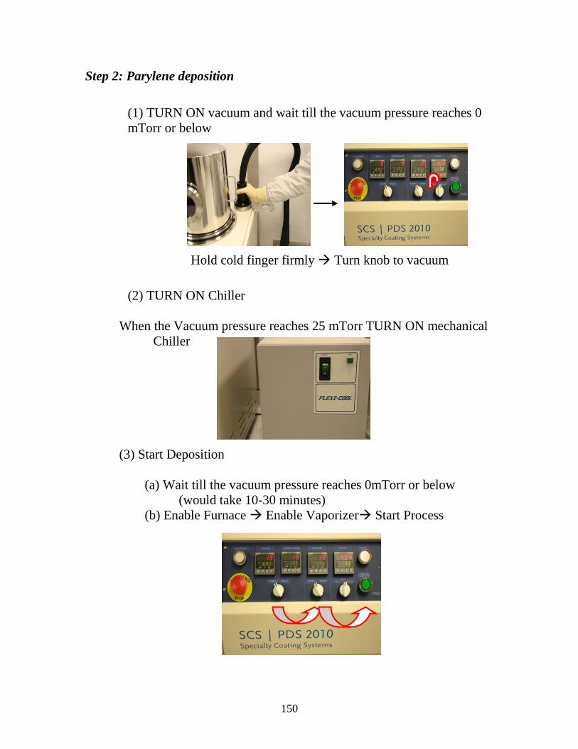
150
Step 2: Parylene deposition
(1) TURN ON vacuum and wait till the vacuum pressure reaches 0
mTorr or below
(2) TURN ON Chiller
When the Vacuum pressure reaches 25 mTorr TURN ON mechanical
Chiller
(3) Start Deposition
(a) Wait till the vacuum pressure reaches 0mTorr or below
(would take 10-30 minutes)
(b) Enable Furnace Enable Vaporizer Start Process
Hold cold finger firmly Turn knob to vacuum
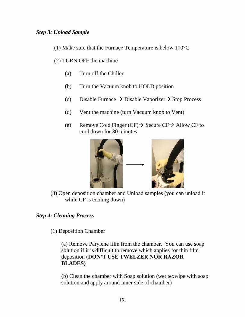
151
Step 3: Unload Sample
(1) Make sure that the Furnace Temperature is below 100°C
(2) TURN OFF the machine
(a) Turn off the Chiller
(b) Turn the Vacuum knob to HOLD position
(c) Disable Furnace Disable Vaporizer Stop Process
(d) Vent the machine (turn Vacuum knob to Vent)
(e) Remove Cold Finger (CF) Secure CF Allow CF to
cool down for 30 minutes
(3) Open deposition chamber and Unload samples (you can unload it
while CF is cooling down)
Step 4: Cleaning Process
(1) Deposition Chamber
(a) Remove Parylene film from the chamber. You can use soap
solution if it is difficult to remove which applies for thin film
deposition (DON’T USE TWEEZER NOR RAZOR
BLADES)
(b) Clean the chamber with Soap solution (wet texwipe with soap
solution and apply around inner side of chamber)
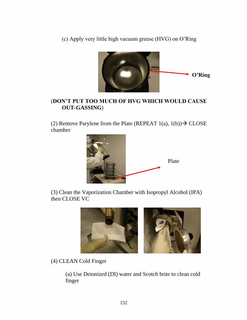
152
(c) Apply very little high vacuum greese (HVG) on O‘Ring
(DON’T PUT TOO MUCH OF HVG WHICH WOULD CAUSE
OUT-GASSING)
(2) Remove Parylene from the Plate (REPEAT 1(a), 1(b)) CLOSE
chamber
(3) Clean the Vaporization Chamber with Isopropyl Alcohol (IPA)
then CLOSE VC
(4) CLEAN Cold Finger
(a) Use Deionized (DI) water and Scotch brite to clean cold
finger
O’Ring
Plate
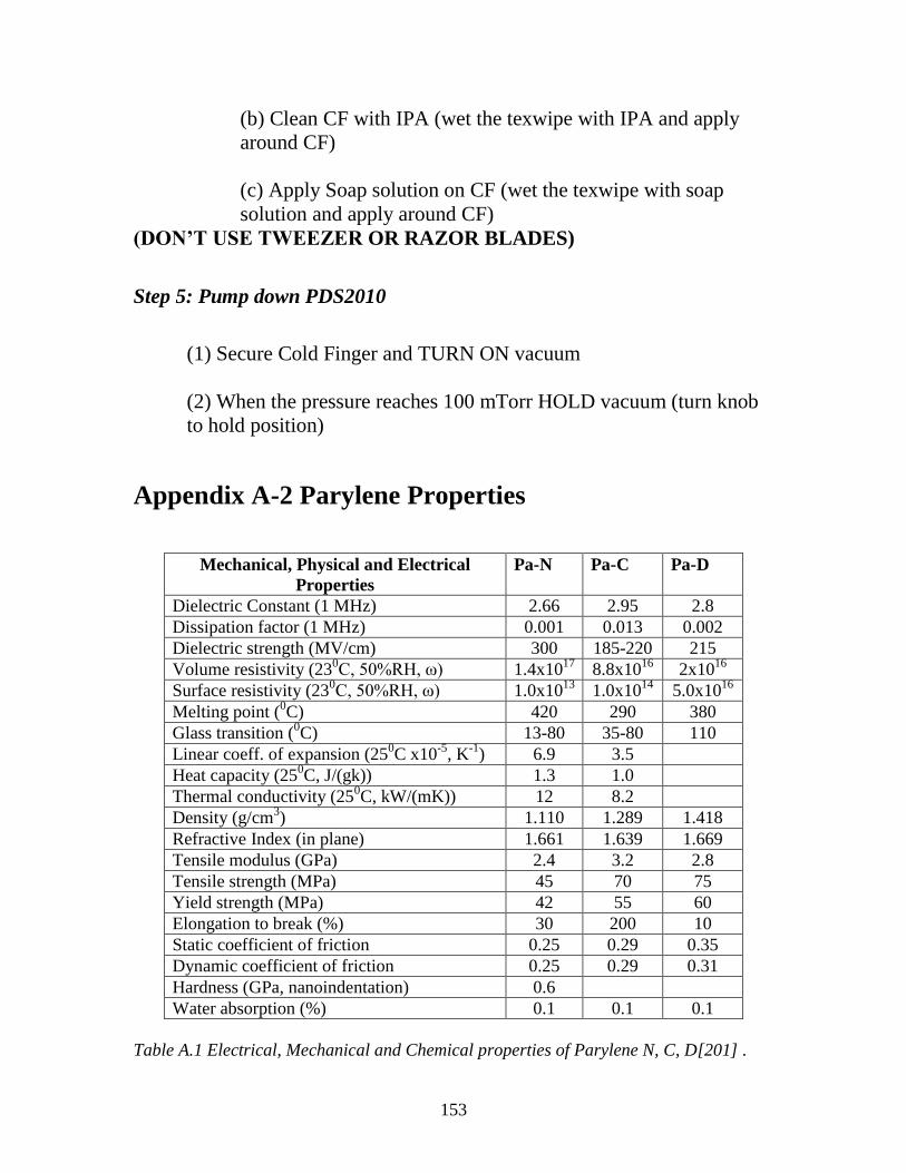
153
(b) Clean CF with IPA (wet the texwipe with IPA and apply
around CF)
(c) Apply Soap solution on CF (wet the texwipe with soap
solution and apply around CF)
(DON’T USE TWEEZER OR RAZOR BLADES)
Step 5: Pump down PDS2010
(1) Secure Cold Finger and TURN ON vacuum
(2) When the pressure reaches 100 mTorr HOLD vacuum (turn knob
to hold position)
Appendix A-2 Parylene Properties
Mechanical, Physical and Electrical
Properties
Pa-N Pa-C Pa-D
Dielectric Constant (1 MHz) 2.66 2.95 2.8
Dissipation factor (1 MHz) 0.001 0.013 0.002
Dielectric strength (MV/cm) 300 185-220 215
Volume resistivity (230C, 50%RH, ω) 1.4x10
17 8.8x10
16 2x10
16
Surface resistivity (230C, 50%RH, ω) 1.0x10
13 1.0x10
14 5.0x10
16
Melting point (0C) 420 290 380
Glass transition (0C) 13-80 35-80 110
Linear coeff. of expansion (250C x10
-5, K
-1) 6.9 3.5
Heat capacity (250C, J/(gk)) 1.3 1.0
Thermal conductivity (250C, kW/(mK)) 12 8.2
Density (g/cm3) 1.110 1.289 1.418
Refractive Index (in plane) 1.661 1.639 1.669
Tensile modulus (GPa) 2.4 3.2 2.8
Tensile strength (MPa) 45 70 75
Yield strength (MPa) 42 55 60
Elongation to break (%) 30 200 10
Static coefficient of friction 0.25 0.29 0.35
Dynamic coefficient of friction 0.25 0.29 0.31
Hardness (GPa, nanoindentation) 0.6
Water absorption (%) 0.1 0.1 0.1
Table A.1 Electrical, Mechanical and Chemical properties of Parylene N, C, D[201] .
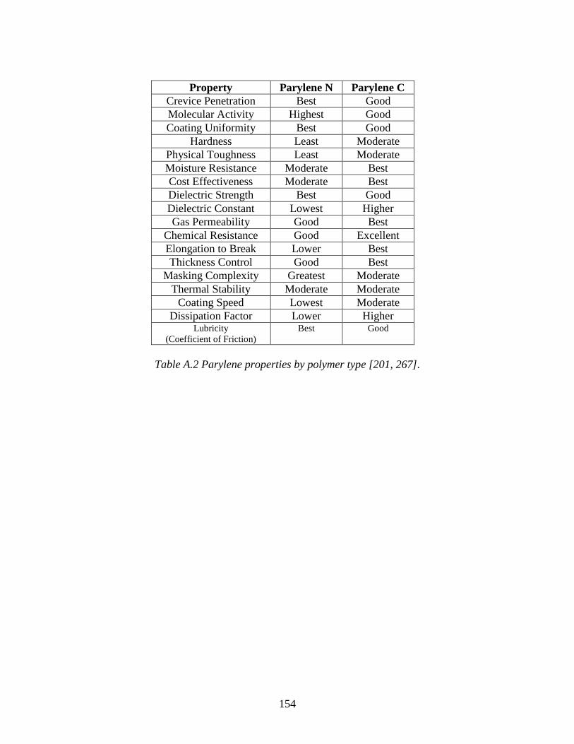
154
Property Parylene N Parylene C
Crevice Penetration Best Good
Molecular Activity Highest Good
Coating Uniformity Best Good
Hardness Least Moderate
Physical Toughness Least Moderate
Moisture Resistance Moderate Best
Cost Effectiveness Moderate Best
Dielectric Strength Best Good
Dielectric Constant Lowest Higher
Gas Permeability Good Best
Chemical Resistance Good Excellent
Elongation to Break Lower Best
Thickness Control Good Best
Masking Complexity Greatest Moderate
Thermal Stability Moderate Moderate
Coating Speed Lowest Moderate
Dissipation Factor Lower Higher Lubricity
(Coefficient of Friction)
Best Good
Table A.2 Parylene properties by polymer type [201, 267].
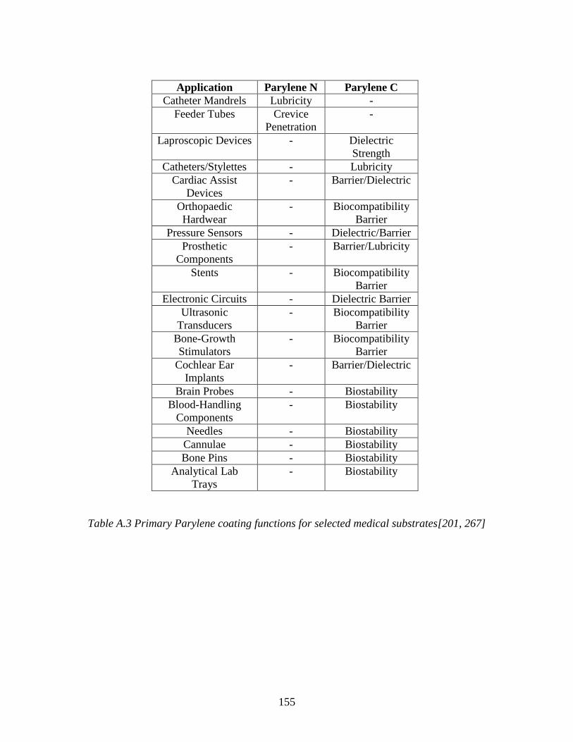
155
Application Parylene N Parylene C
Catheter Mandrels Lubricity -
Feeder Tubes Crevice
Penetration
-
Laproscopic Devices - Dielectric
Strength
Catheters/Stylettes - Lubricity
Cardiac Assist
Devices
- Barrier/Dielectric
Orthopaedic
Hardwear
- Biocompatibility
Barrier
Pressure Sensors - Dielectric/Barrier
Prosthetic
Components
- Barrier/Lubricity
Stents - Biocompatibility
Barrier
Electronic Circuits - Dielectric Barrier
Ultrasonic
Transducers
- Biocompatibility
Barrier
Bone-Growth
Stimulators
- Biocompatibility
Barrier
Cochlear Ear
Implants
- Barrier/Dielectric
Brain Probes - Biostability
Blood-Handling
Components
- Biostability
Needles - Biostability
Cannulae - Biostability
Bone Pins - Biostability
Analytical Lab
Trays
- Biostability
Table A.3 Primary Parylene coating functions for selected medical substrates[201, 267]
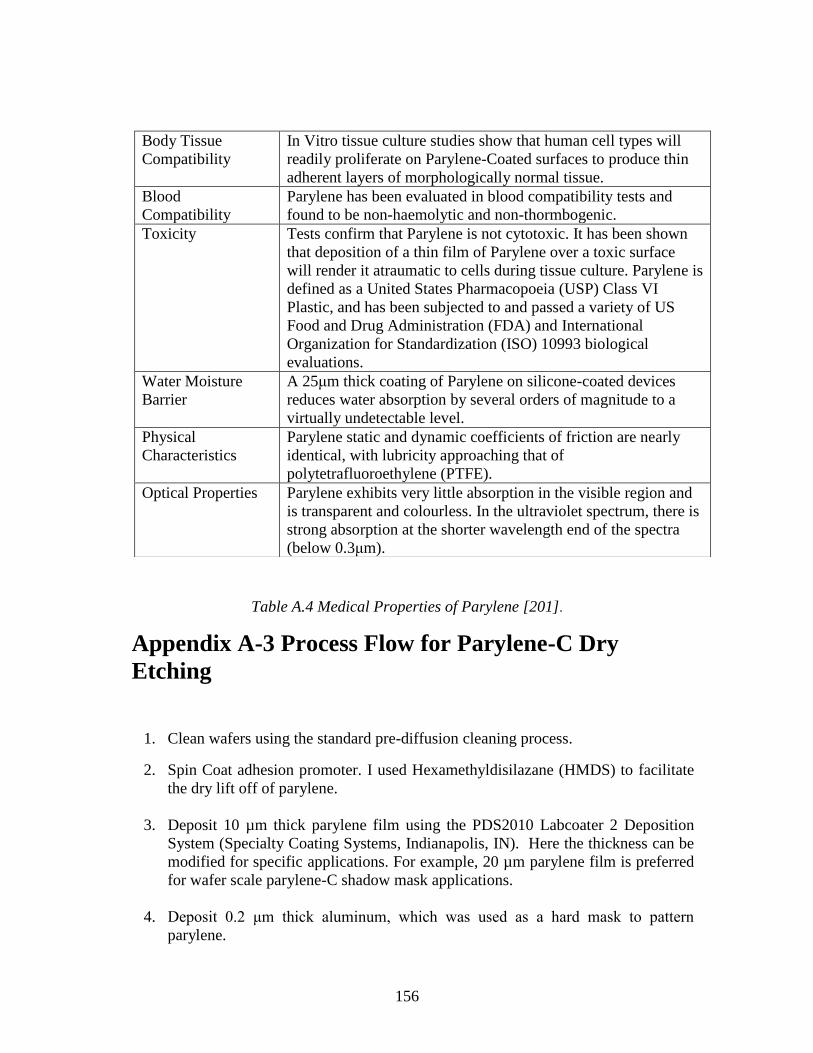
156
Table A.4 Medical Properties of Parylene [201].
Appendix A-3 Process Flow for Parylene-C Dry
Etching
1. Clean wafers using the standard pre-diffusion cleaning process.
2. Spin Coat adhesion promoter. I used Hexamethyldisilazane (HMDS) to facilitate
the dry lift off of parylene.
3. Deposit 10 µm thick parylene film using the PDS2010 Labcoater 2 Deposition
System (Specialty Coating Systems, Indianapolis, IN). Here the thickness can be
modified for specific applications. For example, 20 µm parylene film is preferred
for wafer scale parylene-C shadow mask applications.
4. Deposit 0.2 μm thick aluminum, which was used as a hard mask to pattern
parylene.
Body Tissue
Compatibility
In Vitro tissue culture studies show that human cell types will
readily proliferate on Parylene-Coated surfaces to produce thin
adherent layers of morphologically normal tissue.
Blood
Compatibility
Parylene has been evaluated in blood compatibility tests and
found to be non-haemolytic and non-thormbogenic.
Toxicity Tests confirm that Parylene is not cytotoxic. It has been shown
that deposition of a thin film of Parylene over a toxic surface
will render it atraumatic to cells during tissue culture. Parylene is
defined as a United States Pharmacopoeia (USP) Class VI
Plastic, and has been subjected to and passed a variety of US
Food and Drug Administration (FDA) and International
Organization for Standardization (ISO) 10993 biological
evaluations.
Water Moisture
Barrier
A 25μm thick coating of Parylene on silicone-coated devices
reduces water absorption by several orders of magnitude to a
virtually undetectable level.
Physical
Characteristics
Parylene static and dynamic coefficients of friction are nearly
identical, with lubricity approaching that of
polytetrafluoroethylene (PTFE).
Optical Properties Parylene exhibits very little absorption in the visible region and
is transparent and colourless. In the ultraviolet spectrum, there is
strong absorption at the shorter wavelength end of the spectra
(below 0.3μm).
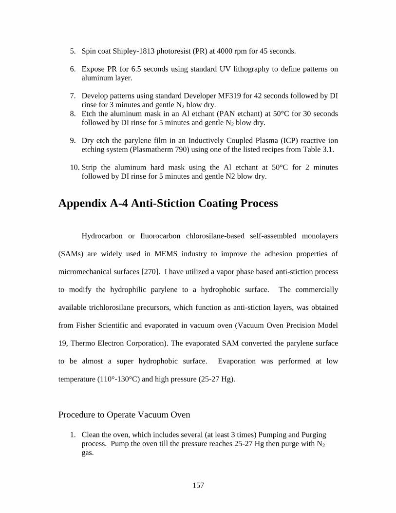
157
5. Spin coat Shipley-1813 photoresist (PR) at 4000 rpm for 45 seconds.
6. Expose PR for 6.5 seconds using standard UV lithography to define patterns on
aluminum layer.
7. Develop patterns using standard Developer MF319 for 42 seconds followed by DI
rinse for 3 minutes and gentle N2 blow dry.
8. Etch the aluminum mask in an Al etchant (PAN etchant) at 50°C for 30 seconds
followed by DI rinse for 5 minutes and gentle N2 blow dry.
9. Dry etch the parylene film in an Inductively Coupled Plasma (ICP) reactive ion
etching system (Plasmatherm 790) using one of the listed recipes from Table 3.1.
10. Strip the aluminum hard mask using the Al etchant at 50°C for 2 minutes
followed by DI rinse for 5 minutes and gentle N2 blow dry.
Appendix A-4 Anti-Stiction Coating Process
Hydrocarbon or fluorocarbon chlorosilane-based self-assembled monolayers
(SAMs) are widely used in MEMS industry to improve the adhesion properties of
micromechanical surfaces [270]. I have utilized a vapor phase based anti-stiction process
to modify the hydrophilic parylene to a hydrophobic surface. The commercially
available trichlorosilane precursors, which function as anti-stiction layers, was obtained
from Fisher Scientific and evaporated in vacuum oven (Vacuum Oven Precision Model
19, Thermo Electron Corporation). The evaporated SAM converted the parylene surface
to be almost a super hydrophobic surface. Evaporation was performed at low
temperature (110°-130°C) and high pressure (25-27 Hg).
Procedure to Operate Vacuum Oven
1. Clean the oven, which includes several (at least 3 times) Pumping and Purging
process. Pump the oven till the pressure reaches 25-27 Hg then purge with N2
gas.
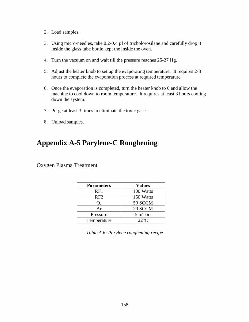
158
2. Load samples.
3. Using micro-needles, take 0.2-0.4 µl of tricholorosilane and carefully drop it
inside the glass tube bottle kept the inside the oven.
4. Turn the vacuum on and wait till the pressure reaches 25-27 Hg.
5. Adjust the heater knob to set up the evaporating temperature. It requires 2-3
hours to complete the evaporation process at required temperature.
6. Once the evaporation is completed, turn the heater knob to 0 and allow the
machine to cool down to room temperature. It requires at least 3 hours cooling
down the system.
7. Purge at least 3 times to eliminate the toxic gases.
8. Unload samples.
Appendix A-5 Parylene-C Roughening
Oxygen Plasma Treatment
PPaarraammeetteerrss VVaalluueess
RF1 100 Watts
RF2 150 Watts
O2 50 SCCM
Ar 20 SCCM
Pressure 5 mTorr
Temperature 22°C
Table A.6: Parylene roughening recipe
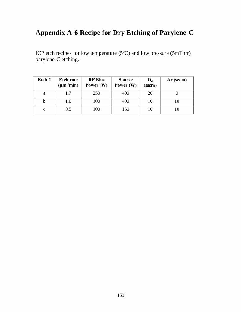
159
Appendix A-6 Recipe for Dry Etching of Parylene-C
ICP etch recipes for low temperature (5ºC) and low pressure (5mTorr)
parylene-C etching.
EEttcchh ## EEttcchh rraattee
((μμmm //mmiinn)) RRFF BBiiaass
PPoowweerr ((WW)) SSoouurrccee
PPoowweerr ((WW)) OO22
((ssssccmm)) AArr ((ssccccmm))
a 1.7 250 400 20 0
b 1.0 100 400 10 10
c 0.5 100 150 10 10
160
Appendix B
Appendix B-1 Silane A-174 Adhesion Promoter Coating
for Parylene-C
(i) Silane A-174 coating on SiO2 surface
1. Prepare Silane solution: Mix A-174: IPA: DI water in 5ml:500ml:500ml ratio.
2. Soak samples in Silane solution overnight (at least 6-8 hours of soaking is
required).
3. Air dry samples for 30 minutes.
4. Soak samples in IPA for 5 minutes.
5. Blow dry samples in N2
6. Dehydration bake at 150°C for 10minutes.
7. Load samples into PDS2010 and start parylene deposition.
(ii) Silane A-174 coating on Parylene-C surface
1. Repeat instructions from 1 to 6.
2. Dehydration bake at 90°C for 15minutes.
3. Load samples into PDS2010 and start parylene deposition.
Appendix B-2 Submicron Thick Parylene-C Deposition
1. Prior to deposition, change Furnace temperature to 650 °C and Vacumm pressure
to 25 mTorr.
2. Repeat instructions from Appendix A-1 (ii).
161
* Deposition rate is linearly proportional to the amount of dimer consumed, and it is
consistent with Figure 3.3 in Chapter 3. Using 0.5 and 0.3 grams of parylene-C
with the above recipe gave a thickness of 284.7 nm and 130 nm, respectively.
Appendix B-3 Process flow for fabrication of Metal-
Insulator-Metal (MIM) Capacitor
1. Create 500 nm thick SiO2 on a pre-diffusion cleaned silicon wafers using wet
oxidation technique.
2. Create bottom electrode of 5 nm/150 nm of Cr/Au using sputter deposition.
3. Prepare samples with/without Silane A-174 prior to parylene deposition.
4. Deposit parylene-C dielectric. Thickness of the film is varied from 1100 nm, 560
nm, and 330 nm down to 130 nm.
5. Create top electrode of 5 nm/150 nm of Ti/Au using AZ2020 negative photoresist.
a) Deposit 5 nm/150 nm of Ti/Au.
b) Spin negative photoresist AZ2020 at 4000 rpm for 60 seconds.
c) Softbake at 90°C for 1 minute.
d) UV Exposure for 4.5 seconds.
e) Post exposure bake (PEB) at 90°C for 1 minute.
f) Develop in MIF300 for 50 seconds.
g) Rinse in DI water for 5 minute followed by N2 blow dry.
h) Wet etching of 150 nm of Au for 31 seconds in GE8148 gold etchant (etch
rate of GE8148 is 50 Å/second).
i) Rinse in DI water for 5 minute followed by N2 blow dry.
j) Wet etching of 5 nm of Ti for 3-4 seconds in custom made Ti etchant (DI
water: H2O2: HF=20:1:1, etch rate=1.1 µm/min).
k) Rinse in DI water for 5 minute followed by N2 blow dry.
6. Open contact to bottom electrode in ICP plasma etcher.
a) Spin Shipley photoresist 1827 at 4000 rpm for 45 seconds.
162
b) Softbake at 90 °C for 1 minute.
c) UV exposure for 11 seconds.
d) Develop in MF319 for 50 seconds.
e) Rinse in DI water for 5 minute followed by N2 blow dry.
f) Use recipe ‗C‘ from Appendix A-6 to dry etch parylene-C in ICP etcher.
g) After ICP etching, ensure metal connectivity using HP4155 parameter
analyzer or digital multimeter.
h) Remove remaining photoresist (5 minutes in Acetone, IPA and DI water).
163
Appendix C
Appendix C-1 Process Flow for Fabrication of
Parylene-C Packaged TFT
(i) Double Lift Off Process to Create Source and Drain electrodes
1. Deposit 0.5 μm thick aluminum on the (rigid/flexible) substrate.
2. Spin coat Shipley-1813 photoresist at 4000 rpm for 45 seconds followed by
softbake at 90°C for 1 minute.
3. Expose PR for 6.5 seconds using standard UV lithography to define patterns
on aluminum layer.
4. Develop patterns using standard Developer MF319 for 42 seconds followed
by DI rinse for 5 minutes and gentle blow dry in N2.
5. Etch the aluminum mask in an Al etchant (PAN etchant) at 50 °C for 55
seconds followed by DI rinse for 5 minutes and gentle N2 blow dry.
6. Deposit Ti/Au (5 nm/150 nm) and immerse samples in Acetone for 6 hours to
lift off.
7. After 6 hours of soaking in Acetone, rinse in IPA and DI water for 5 minutes
followed by N2 blow dry.
8. Remove Al by repeating step 5 for 1 minutes and 30 seconds.
9. Rinse in Acetone, IPA and DI water for 5 minutes followed by N2 blow dry.
10. Repeat step 5 for 1 minute.
(ii) Dielectrophoretic (DEP) Assembly of SWNTs for Transistors
I have utilized two different DEP recipes to make CNTFETs.
Recipe1
1. Ultrasonicate the original CNT solution for 30 minutes.
2. Prepare SWNTs solution to the desired concentration: mix 30 µl of CNTs solution
(obtained from Brewer Science) with 10 ml of DI water.
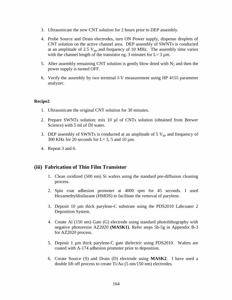
164
3. Ultrasonicate the new CNT solution for 2 hours prior to DEP assembly.
4. Probe Source and Drain electrodes, turn ON Power supply, dispense droplets of
CNT solution on the active channel area. DEP assembly of SWNTs is conducted
at an amplitude of 2.5 Vpp and frequency of 10 MHz. The assembly time varies
with the channel length of the transistor eg. 3 minutes for L= 3 µm.
5. After assembly remaining CNT solution is gently blow dried with N2 and then the
power supply is turned OFF.
6. Verify the assembly by two terminal I-V measurement using HP 4155 parameter
analyzer.
Recipe2
1. Ultrasonicate the original CNT solution for 30 minutes.
2. Prepare SWNTs solution: mix 10 µl of CNTs solution (obtained from Brewer
Science) with 5 ml of DI water.
3. DEP assembly of SWNTs is conducted at an amplitude of 5 Vpp and frequency of
300 KHz for 20 seconds for L= 3, 5 and 10 µm.
4. Repeat 3 and 6.
(iii) Fabrication of Thin Film Transistor
1. Clean oxidized (500 nm) Si wafers using the standard pre-diffusion cleaning
process.
2. Spin coat adhesion promoter at 4000 rpm for 45 seconds. I used
Hexamethyldisilazane (HMDS) to facilitate the removal of parylene.
3. Deposit 10 µm thick parylene-C substrate using the PDS2010 Labcoater 2
Deposition System.
4. Create Al (150 nm) Gate (G) electrode using standard photolithography with
negative photoresist AZ2020 (MASK1). Refer steps 5b-5g in Appendix B-3
for AZ2020 process.
5. Deposit 1 µm thick parylene-C gate dielectric using PDS2010. Wafers are
coated with A-174 adhesion promoter prior to deposition.
6. Create Source (S) and Drain (D) electrode using MASK2. I have used a
double lift off process to create Ti/Au (5 nm/150 nm) electrodes.
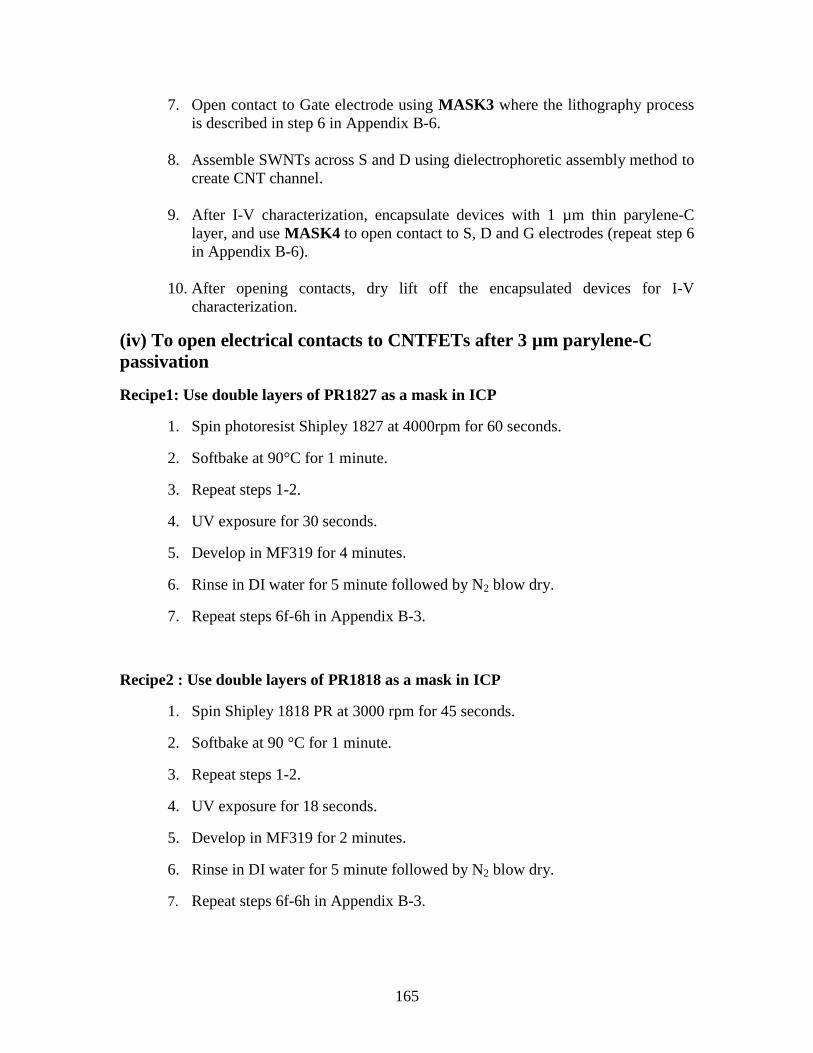
165
7. Open contact to Gate electrode using MASK3 where the lithography process
is described in step 6 in Appendix B-6.
8. Assemble SWNTs across S and D using dielectrophoretic assembly method to
create CNT channel.
9. After I-V characterization, encapsulate devices with 1 µm thin parylene-C
layer, and use MASK4 to open contact to S, D and G electrodes (repeat step 6
in Appendix B-6).
10. After opening contacts, dry lift off the encapsulated devices for I-V
characterization.
(iv) To open electrical contacts to CNTFETs after 3 µm parylene-C
passivation
Recipe1: Use double layers of PR1827 as a mask in ICP
1. Spin photoresist Shipley 1827 at 4000rpm for 60 seconds.
2. Softbake at 90°C for 1 minute.
3. Repeat steps 1-2.
4. UV exposure for 30 seconds.
5. Develop in MF319 for 4 minutes.
6. Rinse in DI water for 5 minute followed by N2 blow dry.
7. Repeat steps 6f-6h in Appendix B-3.
Recipe2 : Use double layers of PR1818 as a mask in ICP
1. Spin Shipley 1818 PR at 3000 rpm for 45 seconds.
2. Softbake at 90 °C for 1 minute.
3. Repeat steps 1-2.
4. UV exposure for 18 seconds.
5. Develop in MF319 for 2 minutes.
6. Rinse in DI water for 5 minute followed by N2 blow dry.
7. Repeat steps 6f-6h in Appendix B-3.
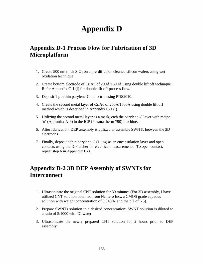
166
Appendix D
Appendix D-1 Process Flow for Fabrication of 3D
Microplatform
1. Create 500 nm thick SiO2 on a pre-diffusion cleaned silicon wafers using wet
oxidation technique.
2. Create bottom electrode of Cr/Au of 200Å/1500Å using double lift off technique.
Refer Appendix C-1 (i) for double lift off process flow.
3. Deposit 1 µm thin parylene-C dielectric using PDS2010.
4. Create the second metal layer of Cr/Au of 200Å/1500Å using double lift off
method which is described in Appendix C-1 (i).
5. Utilizing the second metal layer as a mask, etch the parylene-C layer with recipe
‗c‘ (Appendix A-6) in the ICP (Plasma therm 790) machine.
6. After fabrication, DEP assembly is utilized to assemble SWNTs between the 3D
electrodes.
7. Finally, deposit a thin parylene-C (1 μm) as an encapsulation layer and open
contacts using the ICP etcher for electrical measurements. To open contact,
repeat step 6 in Appendix B-3.
Appendix D-2 3D DEP Assembly of SWNTs for
Interconnect
1. Ultrasonicate the original CNT solution for 30 minutes (For 3D assembly, I have
utilized CNT solution obtained from Nantero Inc., a CMOS grade aqueous
solution with weight concentration of 0.046% and the pH of 6.5).
2. Prepare SWNTs solution to a desired concentration: SWNT solution is diluted to
a ratio of 5:1000 with DI water.
3. Ultrasonicate the newly prepared CNT solution for 2 hours prior to DEP
assembly.
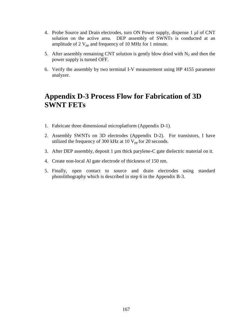
167
4. Probe Source and Drain electrodes, turn ON Power supply, dispense 1 µl of CNT
solution on the active area. DEP assembly of SWNTs is conducted at an
amplitude of 2 Vpp and frequency of 10 MHz for 1 minute.
5. After assembly remaining CNT solution is gently blow dried with N2 and then the
power supply is turned OFF.
6. Verify the assembly by two terminal I-V measurement using HP 4155 parameter
analyzer.
Appendix D-3 Process Flow for Fabrication of 3D
SWNT FETs
1. Fabricate three dimensional microplatform (Appendix D-1).
2. Assembly SWNTs on 3D electrodes (Appendix D-2). For transistors, I have
utilized the frequency of 300 kHz at 10 Vpp for 20 seconds.
3. After DEP assembly, deposit 1 µm thick parylene-C gate dielectric material on it.
4. Create non-local Al gate electrode of thickness of 150 nm.
5. Finally, open contact to source and drain electrodes using standard
photolithography which is described in step 6 in the Appendix B-3.
168
REFERENCES
[1] J. D. Plummer, et al., Silicon VLSI Technology. New Jersey: Prenice Hall, Inc.,
2000.
[2] Intel-Corporation. Intel® Core™ i7 Processor Extreme Edition [Online].
Available: http://www.intel.com/products/processor/corei7ee/specifications.htm
[3] A. L. Briseno, et al., "Patterning organic single-crystal transistor arrays," Nature,
vol. 444, pp. 913-917, 2006.
[4] D. Gamota, et al., Printed Organic and Molecular Electronics. Boston: Kluwer
Academic Publishers, 2004.
[5] P. Heremans, "Semiconductor electronics: Organic crystals at large," Nature, vol.
444, pp. 828-831, 2006.
[6] Y. L. Loo, et al., "Soft, conformable electrical contacts for organic
semiconductors: High-resolution plastic circuits by lamination," PNAS, vol. 99,
pp. 10252–10256, 2002.
[7] T. Someya, et al., "A large-area, flexible pressure sensor matrix with organic
field-effect transistors for artificial skin applications," PNAS, vol. 101, pp. 9966-
9970, 2004.
[8] C. D. Dimitrakopoulos and P. R. L. Malenfant, "Organic Thin Film Transistors
for Large Area Electronics," Advanced Materials, vol. 14, pp. 99-117, 2002.
[9] D. Feili, et al., "Flexible organic field effect transistors for biomedical
microimplants using polyimide and parylene C as substrate and insulator layers,"
J. Micromech. Microeng., vol. 16, pp. 1555-1561, 2006.
[10] R. L. Crabb and F. C. Treble, "Thin silicon solar cells for large flexible arrays,"
Nature, vol. 213, pp. 1223-1224, 1967.
[11] C. R. Wronski, et al., "Schottky-barrier characteristics of metal-amorphous-
silicon diodes," Appl. Phys. Lett., vol. 29, pp. 602-604, 1976.
[12] P. D. Plattner, et al., in 80 Photovoltaic Solar Energy Conference, 1980, p. 121.
[13] H. Okaniwa, et al., "Production and properties of a-Si:H solar cell on organic
polymer film substrate," 16th IEEE Photovoltaic specialists conference, pp.
1111–1116, Sep. 27–30, San Diego, CA 1982.
[14] H. Okaniwa, et al., "Preparation and properties of a-Si:H solar cells on organic
polymer film substrate," Jpn J Appl Phys, vol. 21, pp. 239–244, 1982.
[15] P. P. Nath and M. Izu, "Performance of large area amorphous Si-based single and
multiple junction solar cells," in 18th IEEE Photovoltaic Specialists Conference,
Las Vegas, NV, 1985, pp. 939-942.
[16] M. Yano, et al., "Roll-to-roll preparation of a hydrogenated amorphous silicon
solar cell on a polymer substrate," Thin Solid Films, vol. 146, pp. 75-81, 1987.
[17] T. P. Brody, "The thin-film transistor - A late flowering boom," IEEE Trans
Electron Devices, vol. 31, pp. 1614-1628, 1984.
[18] T. P. Brody, "The birth and early childhood of active matrix - A personal
memoir," J Soc Inf Disp, vol. 4, pp. 113-127, 1996.
[19] A. Constant, et al., "Development of Thin Film Transistor Based Circuits on
Flexible Polyimide Substrates," in Electrochemical Society Meeting, Miami,
Florida, 1994, pp. 323 - 327.
169
[20] N. D. Young, et al., "Novel fingerprint scanning arrays using polysilicon TFT's
on glass and polymer substrates," IEEE Trans Electron Devices, vol. 18, pp. 19-
20, 1997.
[21] P. M. Smith, et al., "Excimer laser crystallization and doping of silicon films on
plastic substrates," Appl. Phys. Lett., vol. 70, pp. 342-344, 1997.
[22] Z. N. Bao, et al., "Printable organic and polymeric semiconducting materials and
devices," J. Mater. Chem., vol. 9, pp. 1895-1904, 1999.
[23] J. .Kim, et al., "Flexible display prepared using phase separated composite
organic films of liquid crystals," in Proc SID 30, 1999, pp. 880–885.
[24] P. A. Penz, et al., "Plastic substrate LCD," in Proc SID XII, 1981, pp. 116–117.
[25] Z. Bao, et al., "High Performance Organic Transistors Fabricated by Printing
Techniques," Chem Mater., vol. 9, pp. 1299-1301, 1997.
[26] Y. Chen, et al., "Flexible actrive-matrix electronic ink display," Nature, vol. 423,
p. 136, 2003.
[27] B. D. Gates, et al., "New Approaches to Nanofabrication: Molding, Printing, and
Other Techniques," Chem. Rev., vol. 105, pp. 1171-1196, 2005.
[28] Y. Xia and G. M. Whitesides, "Soft Lithography," Annu. Rev. Mater. Sci., vol. 28,
pp. 153-184, 1998.
[29] J. H. Burroughes, et al., "Light-emitting diodes based on conjugated polymers,"
Nature, vol. 347, pp. 539–541, 1990.
[30] M. Pope, et al., "Electroluminescence in organic crystals," J Chem Phys, vol. 38,
pp. 2042–2043, 1963.
[31] J. Wyatt and J. Rizzo, "Ocular Implants for the blind," IEEE Spectrum, vol. 33,
pp. 47-53, 1996.
[32] Z. Yao, et al., "High-field electrical transport in single-wall carbon nanotubes,"
Phys. Rev. Lett., vol. 84, pp. 2941-44, 2000.
[33] J. Hone, et al., "Thermal Conductivity of Single-Walled Carbon Nanotubes,"
Synth. Met., vol. 103, pp. 2498-2499, 1999.
[34] A. Javey, et al., "High-k dielectrics for advanced carbon nanotube transistors and
logic gates " Nature materials, vol. 1, pp. 241-46, 2002.
[35] S.-H. Hur, et al., "Extreme bendability of single-walled carbon nanotube networks
transferred from high-temperature growth substrates to plastic and their use in
thin-film transistors," Appl. Phys. Lett., vol. 86, p. 243502, 2005.
[36] S. J. Tans, et al., "Room-temperature transistor based on a single carbon nanotube
" Nature, vol. 393, pp. 49-52, 1998.
[37] R. Martel, et al., "Single- and multi-wall carbon nanotube field-effect transistors,"
Appl. Phys. Lett., vol. 73, pp. 2447-2449, 1998.
[38] N. Chimot, et al., "Gigahertz frequency flexible carbon nanotube transistors,"
Applied Physics Letters, vol. 91, p. 153111, 2007.
[39] A. Javey, et al., "Ballistic Carbon Nanotube Transistors," Nature, vol. 424, pp.
654-657, 2003.
[40] M. S. Fuhrer, et al., "High-mobility Nanotube Transistor Memory," Nano Lett,
vol. 2, pp. 775-759, 2002.
[41] Q. Cao, et al., "Medium-scale Carbon Nanotube Thin-Film Integrated Circuits on
Flexible Plastic Substrates," Nature, vol. 454, pp. 495-500, 2008.
170
[42] A. Javey, et al., "Carbon nanotube transistor arrays for multistage complementary
logic and ring oscillators," Nano Lett., vol. 2, pp. 929-32, 2002.
[43] A. B. Chwang, et al., "Flexible OLED display development: Strategy and status,"
J SID, vol. 13, pp. 481–486, 2005.
[44] Philips. (2005). Available:
http://www.research.philips.com/newscenter/archive/2005/050902-rolldisp.html
[45] V. Subramanian, et al., "Progress Toward Development of All-Printed RFID
Tags: Materials, Processes, and Devices," Proc. IEEE, vol. 9, pp. 1330-1338,
2005.
[46] Y. Xu, et al., "IC-Integrated Flexible Shear-Stress Sensor Skin," J. Micromech.
Microeng., vol. 12, pp. 740-747, 2003.
[47] S. Steudel, et al., "50 MHz rectifier based on an organic diode," Nature Materials,
vol. 4, pp. 597 - 600, 2005.
[48] F. Lorussi, et al., "Strain sensing fabric for hand posture and gesture monitoring,"
IEEE Trans Inf Technol Biomed, vol. 9, pp. 372–381, 2005.
[49] T. Someya and T. Sakurai, "Integration of organic field-effect transistors and
rubbery pressure sensors for artificial skin applications," in IEEE International
Electron Devices Meeting (IEDM), Washington DC, 2003, pp. 203–206.
[50] H. E. Katz, et al., "Organic field-effect transistors with polarizable gate
insulators," J. Appl. Phys., vol. 91, pp. 1572 - 1576, 2002.
[51] R. Pelrine, et al., "Applications of dielectric elastomer actuators," Proc SPIE, vol.
4329, pp. 335–349, 2001.
[52] S. P. Lacour, et al., "Mechatronic system of dielectric elastomer actuators
addressed by thin film photoconductors on plastic," Sensors and Actuators A:
Physical, vol. 111, pp. 288–292, 2004.
[53] I. Ota, et al., "Electrophoretic image display panel," in Proc IEEE, 1973, pp. 832–
836.
[54] T. Whitesides, et al., "Towards video-rate microencapsulated dual-particle
electrophoretic displays," in SID Symp Digest Tech Papers, 2004, pp. 133–135.
[55] J. B. Fortin and T. M. Lu, Chemical vapor deposition polymerization: the growth
and properties of parylene thin films. Boston: Kluwer Academic Publishers, 2004.
[56] C.-L. Chen, et al., "Mechanical and Electrical Evaluation of Parylene-C
Encapsulated Carbon Nanotube Networks on a Flexible Substrate," Appl. Phys.
Lett., vol. 93, p. 093109, 2008.
[57] J. D. Plummer and P. B. Griffin, "Material and process limits in silicon VLSI
technology," Proc. IEEE, vol. 89, pp. 240-258, 2001.
[58] J. Tate, et al., "Anodization and Microcontact Printing on Electroless Silver:
Solution-Based Fabrication Procedures for Low-Voltage Electronic Systems with
Organic Active Components," Langmuir, vol. 16, pp. 6054–6060, 2000.
[59] J. H. Braun, "Titanium dioxide : A review," J. Coatings Technol., vol. 69, pp. 59-
72, 1997.
[60] A. I. Kingon, et al., "Alternative dielectrics to silicon dioxide for memory and
logic devices," Nature, vol. 406, pp. 1032-1038, 2000.
[61] S. K. Kim, et al., "Atomic layer deposited Al2O3 for gate dielectric and
passivation layer of single-walled carbon nanotube transistors," Appl. Phys. Lett.,
vol. 90, p. 163108, 2007.
171
[62] A. Facchetti, et al., "Gate Dielectrics for Organic Field-Effect Transistors: New
Opportunities for Organic Electronics," Advanced Materials, vol. 17, pp. 1705-25,
2005.
[63] M.-H. Yoon, et al., "Low-Voltage Organic Field-Effect Transistors and Inverters
Enabled by Ultrathin Cross-Linked Polymers as Gate Dielectrics," J. Am. Chem.
Soc., vol. 127, pp. 10388–10395, 2005.
[64] F. D. Angelis, et al., "High-field-effect-mobility pentacene thin-film transistors
with polymethylmetacrylate buffer layer," Appl. Phys. Lett., vol. 86, p. 203505,
2005.
[65] E. Becker, et al., "All-organic thin-film transistors patterned by means of selective
electropolymerization," Appl. Phys. Lett., vol. 83, p. 4044, 2003.
[66] M. Halik, et al., "Fully patterned all-organic thin film transistors," Appl. Phys.
Lett., vol. 81, p. 289, 2002.
[67] T. Takenobu, et al., "High-performance transparent flexible transistors using
carbon nanotube films," Appl. Phys. Lett., vol. 88, p. 033511, 2006.
[68] S. H. Tseng and N. H. Tai, "Fabrication of a transparent and flexible thin film
transistor based on single-walled carbon nanotubes using the direct transfer
method," Appl. Phys. Lett., vol. 95, pp. 204104-3, 2009.
[69] A. Wang, et al., "Tunable threshold voltage and flatband voltage in pentacene
field effect transistors," Appl. Phys. Lett., vol. 89, p. 112109, 2006.
[70] E. R. Salmon, Encapsulation of electronic devices and components. New York:
Marcel Dekker, Inc., 1987.
[71] W. Prins and J. J. Hermans, "Theory of Permeation through Metal Coated
Polymer Films," J. Phys. Chem., vol. 63, pp. 716-720, 1959.
[72] H. Chatham, "Oxygen diffusion barrier properties of transparent oxide coatings
on polymeric substrates," Surface and Coatings Technology, vol. 78, pp. 1-9,
1996.
[73] A. L. Brody, "Glass-coated flexible films for packaging: an overview," Packaging
Technological Engineering, vol. 44, p. 166, 1994.
[74] M. S. Weaver, et al., "Organic light-emitting devices with extended operating
lifetimes on plastic substrates," Appl. Phys. Lett., vol. 81, p. 2929, 2002.
[75] T. W. Kim, et al., "Transparent hybrid inorganic/organic barrier coatings for
plastic organic light-emitting diode substrates," J. Vac. Sci. Technol., vol. 23, pp.
971-977, 2005.
[76] J. D. Weiland, et al., "Recessed electrodes formed by laser ablation of parylene
coated, micromachined silicon probes," in IEEE Engineering in Medicine and
Biology Society (EMBS), Chicago, 1997, pp. 2273-2276.
[77] E. M. Schmidt, et al., "Laser exposure of Parylene-C insulated microelectrodes,"
J. Neruoscience methods, vol. 62, pp. 89-92, 1995.
[78] E. Meng, et al., "Plasma removal of Parylene C," J. Micromech. Microeng., vol.
18, p. 045004, 2008.
[79] I. Kymissis, et al., "Patterning pentacene organic thin film transistors," J. Vac.
Sci. Technol. B, vol. 20, pp. 956-959, 2002.
[80] D. Feili, et al., "Encapsulation of organic field effect transistors for flexible
biomedical microimplants," Sensors and Actuators A, vol. 120, pp. 101-109,
2005.
172
[81] H. Gleskova, et al., "a-Si:H TFTs Made on Polyimide Foil by PE-CVD at 150°C,"
Proc. Mater Res Soc vol. 508, pp. 73-78, 1998.
[82] I.-C. Cheng, et al., "Stress control for overlay registration in a-Si:H TFTs on
flexible organic-polymer-foil substrates," J. Soc. Inf. Display, vol. 13, pp. 563-
568, 2005.
[83] K. Fujita, et al., "Flexible organic field-effect transistors fabricated by the
electrode-peeling transfer with an assist of self-assembled monolayer," Appl.
Phys. Lett., vol. 82, pp. 4373-4375, 2003.
[84] P.-C. Chen, et al., "2,4,6-Trinitrotoluene (TNT) Chemical Sensing Based on
Aligned Single-Walled Carbon Nanotubes and ZnO Nanowires," Advanced
Materials, vol. 22, pp. 1900–1904, 2010.
[85] A. P. Ghosh, et al., "Thin-film encapsulation of organic light-emitting devices,"
Appl. Phys. Lett., vol. 86, p. 223503, 2005.
[86] J. Yang, et al., "Amorphous silicon based photovoltaics—from earth to the ―final
frontier‖," Solar Energy Materials and Solar Cells, vol. 78, pp. 597-612, 2003.
[87] A. Takano, et al., "Production Technologies of Film Solar Cell," in Mater Res Soc
Symp Proc Washington, DC, 2006, pp. 910:0910-A25-04.
[88] H. Okada, Pharm. Res., vol. 8, pp. 787-791, 1991.
[89] M. Okada, et al., "Reflective multicolor display using cholesteric liquid crystals,"
in SID Digest 28, 1997, pp. 1019–1022.
[90] X. Xu, et al., "IC-Integrated flexible shear-stress sensor skin," J.
Microelectromechanical Systems, vol. 12, pp. 740-747, 2003.
[91] D. Moeli and T. May-Plumlee, "Interactive electronic textile development," J
Textile Apparel, Technol Manage, vol. 2, pp. 1-12, 2002.
[92] E. Bonderover and S. Wagner, "A woven inverter circuit for e-textile
applications," IEEE Electron Device Letters, vol. 25, pp. 295–297, 2004.
[93] Z. Chen, et al., "Controllable interconnection of single-walled carbon nanotubes
under ac field," J. Phys. Chem. B, vol. 109, pp. 11420-11423, 2005.
[94] F. Kreupl, et al., "Carbon nanotubes in interconnect applications,"
Microelectronic Engineering, vol. 64, pp. 399-408, 2002.
[95] J. Li, et al., "Bottom-up approach for carbon nanotube interconnects," Appl. Phys.
Lett., vol. 82, pp. 2491-2493, 2003.
[96] Z. Chen, et al., "A selfassembled synthesis of carbon nanotubes for
interconnects," Nanotechnology, vol. 17, pp. 1062-1066, 2006.
[97] E. Artukovic, et al., "Transparent and flexible carbon nanotube transistors," Nano
Lett., vol. 5, pp. 757-60, Apr 2005.
[98] Y. A. Tarakanov and J. M. Kinaret, "A Carbon Nanotube Field Effect Transistor
with a Suspended Nanotube Gate " Nano Lett, vol. 7, pp. 2291-94, 2007.
[99] J. Li, et al., "Fabrication of Carbon Nanotube Field Effect Transistors by AC
Dielectrophoresis Method," Carbon, vol. 42, pp. 2263-2267, 2004.
[100] S. Ghosh, et al., "Carbon Nanotube Flow Sensors," Science, vol. 299, pp. 1042-
1044, 2003.
[101] J. Kong, et al., "Nanotube molecular wires as chemical sensors," Science, vol.
287, pp. 622-5, 2000.
[102] E. S. Snow, et al., "Chemical detection with a single-walled carbon nanotube
capacitor," Science, vol. 307, pp. 1942-5, 2005.
173
[103] Y. Saito and S. Uemura, "Field Emission from Carbon Nanotubes and its
Application to Electron Sources," Carbon, vol. 38, pp. 169-182, 2000.
[104] J.-M. Bonard, et al., "Field Emission from Carbon Nanotubes: the First Five
Years," Solid-State Electronics, vol. 45, pp. 893-914, 2001.
[105] M. O'Connell, Carbon nanotubes : properties and applications. Boca Raton, FL:
CRC/Taylor & Francis, 2006.
[106] H. W. Kroto, et al., "C60: Buckminsterfullerene," Nature, vol. 318, pp. 162-163,
1985.
[107] S. Iijima, "Helical microtubules of graphitic carbon " Nature, vol. 354, pp. 56-58,
1991.
[108] A. G. Nasibulin, et al., "A Novel Hybrid Carbon Material," Nature
Nanotechnology, vol. 2, pp. 156-161, 2006.
[109] A. G. Nasibulin, et al., "Investigations of NanoBud Formation," Chemical Physics
Letters, vol. 446, pp. 109-114, 2007.
[110] R. Vieira, et al., "Synthesis and Characterisation of Carbon Nanofibres with
Macroscopic Shaping Formed by Catalytic Decomposition of C2H6/H2 Over
Nickel Catalyst," Appl. Catalysis A, vol. 274, pp. 1-8, 2004.
[111] T. W. Ebbesen, Carbon Nanotubes: Preparation and Properties. Salem, USA:
CRC-Press, 1997.
[112] S. Iijima and T. Ichihashi, "Single-shell Carbon Nanotubes of 1nm Diameter,"
Nature, vol. 363, pp. 603-605, 1993.
[113] D. S. Bethune, et al., "Cobalt-catalysed Growth of Carbon Nanotubes with
Single-atomic-layer Walls," Nature, vol. 363, pp. 605-607, 1993.
[114] S. B. Sinnotta, et al., "Model of carbon nanotube growth through chemical vapor
deposition," Chem.Phys.Lett., vol. 315, pp. 25-30, 1999.
[115] T. W. Ebbesen and P. M. Ajayan, "Large-scale synthesis of carbon nanotubes,"
Nature, vol. 358, pp. 220-222, 1992.
[116] C. Journet and P. Bernier, "Production of carbon nanotubes," Applied Physics A
Materials Science & Processing, vol. 67, pp. 1-9, 1998.
[117] A. Kazunori, et al., "High-purity carbon nanotubes synthesis method by an arc
discharging in magnetic field," Applied Physics Letters, vol. 81, pp. 739-741,
2002.
[118] S. J. Lee, et al., "Large scale synthesis of carbon nanotubes by plasma rotating arc
discharge technique," Diamond and Related Materials, vol. 11, pp. 914-917,
2002.
[119] T. Guo, et al., "Catalytic growth of single-walled nanotubes by laser
vaporization," Chem. Phys. Lett., vol. 243, pp. 49-54, 1995.
[120] M. Yudasaka, et al., "Mechanism of the Effect of NiCo, Ni and Co Catalysts on
the Yield of Single-Wall Carbon Nanotubes Formed by Pulsed Nd:YAG Laser
Ablation," J. Phys. Chem. B, vol. 103, pp. 6224–6229, 1999.
[121] A. P. Bolshakov, et al., "A novel CW laser–powder method of carbon single-wall
nanotubes production," Diamond and Related Materials, vol. 11, pp. 927-930,
2002.
[122] C. N. R. Rao, et al., Nanotubes and nanowires. Cambridge, UK: RSC Pub., 2005.
[123] Z. F. Ren, et al., "Synthesis of large arrays of well-aligned carbon nanotubes on
glass," Science, vol. 282, pp. 1105-7, 1998.
174
[124] Z. F. Ren, et al., "Growth of a Single Freestanding Multiwall Carbon Nanotube
on Each Nanonickel Dot," Appl. Phys. Lett., vol. 75, pp. 1086-1088, 1999.
[125] P. B. Amama, et al., "Dendrimer-assisted low-temperature growth of carbon
nanotubes by plasma-enhanced chemical vapor deposition," Chem Commun
(Camb), pp. 2899-901, 2006.
[126] Y. S. Min, et al., "Low-temperature growth of single-walled carbon nanotubes by
water plasma chemical vapor deposition," J Am Chem Soc, vol. 127, pp. 12498-9,
2005.
[127] M. Meyyappan, Carbon nanotubes : science and applications. Boca Raton, Fla.:
CRC Press, 2005.
[128] M. S. Dresselhaus, et al., "Physics of Carbon Nanotubes," Carbon, vol. 33, pp.
883-891, 1995.
[129] S. Saito, et al., "Electronic Structure of Graphene Tubules Based on C60," Phys
Rev B, vol. 46, pp. 1804-1811, 1992.
[130] N. Hamada, et al., "New One-Dimensional Conductors: Graphitic Microtubules,"
Phys Rev Lett, vol. 68, pp. 1579-1561, 1992.
[131] J. W. Mintmire, et al., "Are Fullerene Tubules Metallic," Phys Rev Lett, vol. 68,
pp. 631-634, 1992.
[132] M. Bockrath, et al., "Single-Electron Transport in Ropes of Carbon Nanotubes,"
Science, vol. 275, pp. 1922-1925, 1997.
[133] S. J. Tans, et al., "Individual Single-Wall Carbon Nanotubes as Quantum Wires,"
Nature, vol. 386, pp. 474-477, 1997.
[134] H. Dai, "Carbon nanotubes: opportunities and challenges," Surface Science, vol.
500, pp. 218–241, 2002.
[135] H. T. Soh, et al., "Integrated nanotube circuits: Controlled growth and ohmic
contacting of single-walled carbon nanotubes," Appl. Phys. Lett., vol. 75, pp. 627-
629, 1999.
[136] J. W. G. Wildoer, et al., "Electronic Structure of Atomically Resolved Carbon
Nanotubes," Nature, vol. 391, pp. 59-62, 1998.
[137] A. M. Rao, et al., "Diameter-Selective Raman Scattering from Vibrational Modes
in Carbon Nanotubes," Science, vol. 275, pp. 187-91, 1997.
[138] R. J. Chen, et al., "Molecular Photodesorption from Single-Walled Carbon
Nanotubes," Appl. Phys. Lett., vol. 79, pp. 2258-2260, 2001.
[139] A. Fujiwara, et al., "Photoconductivity in Semiconducting Single-Walled Carbon
Nanotubes," J. J. Appl. Phys., vol. 40, pp. L1229-L1231, 2001.
[140] M. Freitag, et al., "Photoconductivity of Single Carbon Nanotubes," Nano Lett,
vol. 3, pp. 1067-1071, 2003.
[141] J. Lu and J. Han, "Carbon Nanotubes and Nanotube-based Nano Devices,"
International Journal of High Speed Electronics and Systems (IJHSES), vol. 9, p.
101, 1998.
[142] M. M. J. Treacy, et al., "Exceptionally High Young's Modulus Observed for
Individual Carbon Nanotubes," Nature, vol. 381, pp. 678-680, 1996.
[143] P. Poncharal, et al., "Electrostatic Deßections and Electromechanical Resonances
of Carbon Nanotubes," Science, vol. 283, pp. 1513-1516, 1999.
[144] S. Iijima, et al., "Structural flexibility of carbon nanotubes," J. Chem. Phys., vol.
104, pp. 2089-2092, 1995.
175
[145] T. W. Tombler, et al., "Reversible Electromechanical Characteristics of Carbon
Nanotubes under Local-Probe Manipulation," Nature, vol. 405, pp. 769-772,
2000.
[146] J. Li, et al., "Carbon Nanotubes as AFM Tips: Measuring DNA Molecules at the
Liquid/Solid Interface," Surf. Interface Anal., vol. 28, pp. 8–11, 1999.
[147] Nantero. (2010). Electromechanical switches. Available:
http://www.nantero.com/index.html
[148] S. C. Tsang, et al., "A Simple Chemical Method of Opening and Filling Carbon
Nanotubes," Nature, vol. 372, pp. 159-162, 1994.
[149] P. M. Ajayan, et al., "Opening Carbon Nanotubes with Oxygen and Implications
for Filling," Nature, vol. 362, pp. 522-525, 1993.
[150] P. M. Ajayan and S. Iijima, "Capillarity-induced Filling of Carbon Nanotubes,"
Nature, vol. 361, pp. 333-334, 1993.
[151] X. Liu, et al., "Carbon Nanotube Field-Effect Inverters," Appl. Phys. Lett., vol.
79, pp. 3329-3331, 2001.
[152] M. Kruger, et al., "Sensitivity of Single Multiwalled Carbon Nanotubes to the
Environment," N. J. of Phys., vol. 5, p. 138, 2003.
[153] J. Zhao, et al., "Noncovalent Functionalization of Carbon Nanotubes by Aromatic
Organic Molecules," Appl. Phys. Lett., vol. 82, pp. 3746-3748, 2003.
[154] J. Hone, et al., "Quantized Phonon Spectrum of Single-Wall Carbon Nanotubes,"
Science, vol. 289, pp. 1730-1733, 1999.
[155] S. Berber, et al., "Unusually High Thermal Conductivity of Carbon Nanotubes,"
Phys Rev Lett, vol. 84, pp. 4613-4616, 2000.
[156] P. Kim, et al., "Thermal Transport Measurements of Individual Multiwalled
Nanotubes," Phys. Rev. Lett., vol. 87, p. 215502, 2001.
[157] W. Zhang, et al., "Chirality Dependence of the Thermal Conductivity of Carbon
Nanotubes," Nanotechnology, vol. 15, pp. 936-939, 2004.
[158] A. P. Graham, et al., "Towards the integration of carbon nanotubes in
microelectronics," Diamond and Related Materials, vol. 13, pp. 1296-1300, 2004.
[159] A. Ulman, et al., "Concentration-Driven Surface Transition in the Wetting of
Mixed Alkanethiol Monolayers on Gold," J. Am. Chem. Soc., vol. 113, pp. 1499-
1506, 1991.
[160] S. G. Rao, et al., "Nanotube electronics: Large-scale assembly of carbon
nanotubes," Nature, vol. 425, pp. 36-37, 2003.
[161] T. Shiokawa, et al., "Nano Sturcture Construction in Single-walled Carbon
Nanotubes by AFM manipulation," in Proc., IEEE Int. Conf. on Microproc. and
Nanotech, Shimane, Japan, 2001, pp. 164-5.
[162] M. S. Haque, et al., "Absorption cahracteristics of single wall carbon nanotubes,"
presented at the NSTI Nanotech, Boston, MA, USA, 2006.
[163] Y. I. Song, et al., "Flexible transparent conducting single-wall carbon nanotube
film with network bridging method," J Colloid Interface Sci, vol. 318, pp. 365-71,
Feb 15 2008.
[164] X. Xiong, et al., "Directed Assembly of High Density Single-Walled Carbon
Nanotube Patterns on Flexible Polymer Substrates," Nanotechnology, vol. 20, p.
295302, 2009.
176
[165] Y. I. Song, et al., "Fabrication of carbon nanotube field emitters using a dip-
coating method," Chemical Vapor Deposition, vol. 12, pp. 375-379, 2006.
[166] E. Kymakis, et al., "Single-walled carbon nanotube-polymer composites:
electrical, optical and structural investigation," Synth. Met., vol. 127, pp. 59-62,
2002.
[167] Q. Cao, et al., "Highly bendable, transparent thin-film transistors that use carbon-
nanotube-based conductors and semiconductors with elastomeric dielectrics,"
Adv. Mater., vol. 18, pp. 304-309, 2006.
[168] A. R. Boccaccinia, et al., "Electrophoretic deposition of carbon nanotubes,"
Carbon, vol. 44, pp. 3149-3160, 2006.
[169] H. A. Pohl, "The motion and precipitation of suspensoids in divergent electric
fields," J. Appl. Phys., vol. 22, pp. 869-871, 1951.
[170] K. W. C. Lai, et al., "Development of an automated microspotting system for
rapid dielectrophoretic fabrication of bundled carbon nanotube sensors," IEEE
Trans. on Automation Science and Engineering, vol. 3, pp. 218-227, 2006.
[171] S. Banerjee, et al., "Precise positioning of single-walled carbon nanotubes by ac
dielectrophoresis," J. Vac. Sci. Technol., vol. 24, pp. 3173-3178, 2005.
[172] L. An and C. R. Friedrich, "Real-time gap impedance monitoring of
dielectrophoretic assembly of multiwalled carbon nanotubes," Applied Physics
Letters, vol. 92, p. 173103, 2008.
[173] P. G. Collins and P. A. M. S. Arnold, "Engineering Carbon Nanotubes and
Nanotube Circuits Using Electrical Breakdown," Science, vol. 292, pp. 706-709,
2001.
[174] R. Stevens, et al., "Improved Fabrication Approach for Carbon Nanotube Probe
Devices," Appl. Phys. Lett., vol. 77, pp. 3453-3455, 2000.
[175] C. V. Nguyen, et al., "Carbon Nanotube Tip Probes: Stability and Lateral
Resolution in Scanning Probe Mircoscopy and Application to Surface Science in
Semiconductors," Nanotechnology, vol. 12, pp. 363-367, 2001.
[176] R. Martel, et al., "Carbon nanotube field-effect transistors and logic circuits," in
Proc., 39th Conf. of Design Automation, New Orleans, USA, 2002, pp. 94-96.
[177] A. Bachtold, et al., "Logic circuits with carbon nanotube transistors," Science,
vol. 294, pp. 1317-20, 2001.
[178] V. Derycke, et al., "Carbon nanotube inter- and intramolecular logic gates," Nano
Lett., vol. 1, pp. 453-456, 2001.
[179] K. K. Likharev, "Correlated Discrete Transfer of Single Electrons in Ultrasmall
Tunnel Junctions," IBM J. res. Develop, vol. 32, p. 144, 1988.
[180] M. A. Kastner, "The Single-Electron Transistor," Rev. Mod. Phys., vol. 64, pp.
849-858, 1992.
[181] S. Chopra, et al., "Carbon-nanotube-based Resonant-circuit Sensor for
Ammonia," Appl. Phys. Lett., vol. 80, pp. 4632-4634, 2002.
[182] S. S. Wong, et al., "Covalently Functionalized Nanotubes as Nanometre-sized
Probes in Chemistry and Biology," Nature, vol. 349, pp. 52-55, 1998.
[183] C. K. M. Fung, et al., "Towards Batch Fabrication of Bundled Carbon Nanotube
Thermal Sensors," IEEE Trans. on Nanotechnology, vol. 2, pp. 866-869, 2003.
[184] J. Andzelm, et al., "Nanotube-based gas sensors - role of structural defects,"
Chem. Phys. Lett., vol. 421, pp. 58-62, 2006.
177
[185] S. Selvarasah, et al., "Ultrathin (12 µm) Highly Flexible Parylene-C Packaged
Single-Walled Carbon Nanotube Thin film Transistor," ACS Nano, 2010 (to be
submitted).
[186] S. Gowrisanker, et al., "Time dependent breakdown characteristics of parylene
dielectric in metal–insulator–metal capacitors," Organic Electronics, vol. 10, pp.
1024–1027, 2009.
[187] J. Zhang, et al., "Mechanism of NO2 detection in carbon nanotube field effect
transistor chemical sensors," Appl. Phys. Lett., vol. 88, p. 123112, 2006.
[188] H.-S. Noh, et al., "Wafer bonding using microwave heating of parylene
intermediate layers," J. Micromech. Microeng., vol. 14, pp. 625-631, 2004.
[189] L. Hu, et al., "A method of fabricating highly transparent and conductive
interpenetrated carbon nanotube–parylene networks," Nanotechnology, vol. 20, p.
465304, 2009.
[190] S. Kar, et al., "Quantitative analysis of hysteresis in carbon nanotube field-effect
devices," Appl. Phys. Lett., vol. 89, p. 132118, 2006.
[191] H. Lin and S. Tiwari, "Localized charge trapping due to adsorption in nanotube
field-effect transistor and its field-mediated transport," Appl. Phys. Lett., vol. 89,
p. 073507, 2006.
[192] R. Luharuka, et al., "Improved manufacturability and characterization of a
corrugated parylene diaphragm pressure transducer," J. Micromech. Microeng.,
vol. 16, pp. 1468-1474, 2006.
[193] R. Lam, et al., "Nanodiamond-Embedded Microfilm Devices for Localized
Chemotherapeutic Elution," ACS Nano vol. 2, pp. 2095–2102, 2008.
[194] A. Tooker, et al., "Development of biocompatible parylene neurocages," in 26th
IEEE-EMBC, San Francisco, CA, 2004, pp. 2542-45.
[195] D. Wright, et al., "Micropatterned Parylene Stencils for Generation of Dynamic
and Static Patterned Cellular Co-cultures," in MRS Fall Meeting, Boston, MA,
2006.
[196] B. Rajalingam, et al., "Reusable, Reversibly Sealable Parylene-C Membranes for
Cell and Protein Patterning," in MRS Fall Meeting, Boston, MA, 2006.
[197] C.-L. Chen, et al., "Electrohydrodynamic micropump for on-chip fluid pumping
on flexible parylene substrates," in Proc., 2nd Int. Conf. on Nano/Micro
Engineered and Molecular Systems, Bangkok, Thailand, 2007, pp. 826-829.
[198] A. Yasuda, et al., "Graphitization Mechanism during the Carbon-Nanotube
Formation Based on the In-Situ HRTEM Observation," J. Phys. Chem. B, vol.
106, pp. 1849–1852, 2002.
[199] L. Marty, et al., "Integration of Self-Assembled Carbon Nanotube Transistors:
Statistics and Gate Engineering at the Wafer Scale," Nanotechnology, vol. 17, pp.
5038-5045, 2006.
[200] Specialty-Coating-Systems. Parylene Knowledge: SCS Parylene Properties
[Online]. Available: http://www.scscookson.com/parylene/properties.htm
[201] S. C. S. (SCS). (2006). Parylene Conformal Coating Specifications & Properties.
Available: http://www.scscookson.com/parylene/properties.cfm
[202] J. Jakabovic, et al., "Preparation and properties of thin parylene layers as the gate
dielectrics for organic field effect transistors," Microelectronics, vol. 40, pp. 595–
597, 2009.
178
[203] P. Avouris, et al., "Carbon based electronics," Nature Nanotechnology, vol. 2, pp.
605-15, 2007.
[204] A. Kojima, et al., "Air Stable n-type Top Gate Carbon Nanotube Filed Effect
Transistors with Silicon Nitride Insulator Deposited by Thermal Chemical Vapor
Deposition," Jpn. J. Appl. Phys. Lett. , vol. 44, pp. L328-L330, 2005.
[205] I. Heller, et al., "Identifying the Mechanism of Biosensing with Carbon Nanotube
Transistors," Nano Lett, vol. 8, pp. 591–595, 2008.
[206] K. Bradley, et al., "Flexible nanotube electronics," Nano Lett., vol. 3, pp. 1353-
1355, 2003.
[207] J. Kang, et al., "Large-scale assembly of carbon nanotube-based flexible circuits
for DNA sensors," Nanotechnology, vol. 19, p. 135305, 2008.
[208] J. H. Cheon, et al., "Active-matrix OLED on bendable metal foil," IEEE
Transactions on Nanotechnology, vol. 53, pp. 273-1276, 2006.
[209] J. Li, et al., "Carbon Nanotubes Sensors for Gas and Organic Vapor Detection,"
Nano Lett, vol. 3, pp. 929-33, 2003.
[210] T. Kawano, et al., "An electrothermal carbon nanotube gas sensor," Nano Lett,
vol. 7, pp. 3686-90, Dec 2007.
[211] K. Maehashi, et al., "Electrical characterization of carbon nanotube field-effect
transistors with SiNx passivation films deposited by catalytic chemical vapor
deposition," Appl. Phys. Lett. , vol. 92, p. 183111, 2008.
[212] W. Kim, et al., "Hysteresis Caused by Water Molecules in Carbon Nanotube
Field-Effect Transistors," Nano Lett., vol. 3, pp. 193–198, 2003.
[213] P. Makaram, et al., "Three-Dimensional Assembly of Single-Walled Carbon
Nanotube Interconnects Using Dielectrophoresis," Nanotechnology, vol. 18, p.
395204, 2007.
[214] R. H. Krupke, F., et al., "Simultaneous deposition of metallic bundles of single-
walled carbon nanotubes using Ac-dielectrophoresis," Nano Lett., vol. 3, pp.
1019-23, 2003.
[215] A. Vijayaraghavan, et al., "Ultra-Large-Scale Directed Assembly of Single-
Walled Carbon Nanotube Devices," Nano Lett., vol. 7, pp. 1556-1560, 2007.
[216] A. H. Monica, et al., "Wafer-level assembly of carbon nanotube networks using
dielectrophoresis," Nanotechnology, vol. 19, p. 085303, 2008.
[217] Y. Hayamizu, et al., "Integrated three-dimensional microelectromechanical
devices from processable carbon nanotube wafers," Nature Nanotechnology, vol.
3, pp. 289-294, 2008.
[218] S. Selvarasah, et al., "A Reusable High Aspect Ratio Parylene-C Shadow Mask
Technology for Diverse Micropatterning Applications," Sensors and Actuators A:
Physical, vol. 145-46, pp. 306-15, June 10-14, 2008.
[219] E. D. Minot, et al., "Tuning Carbon Nanotube Band Gaps with Strain," Phys Rev
Lett, vol. 90, p. 156401, 2003.
[220] J. Cao, et al., "Electromechanical Properties of Metallic, Quasimetallic, and
Semiconducting Carbon Nanotubes under Stretching," Phys Rev Lett, vol. 90, p.
157601, 2003.
[221] Z. Suo, et al., "Mechanics of rollable and foldable film-on-foil electronics,"
Applied Physics Letters, vol. 74, p. 1177, 1999.
179
[222] M. Shim, et al., "Polymer Functionalization for Air-Stable n-Type Carbon
Nanotube Field-Effect Transistors," J. Am. Chem. Soc., vol. 123, pp. 11512–
11513, 2001.
[223] S. Selvarasah, et al., "Parylene-C passivated carbon nanotube flexible transistors,"
Appl. Phys. Lett., vol. 97, p. 153120, 2010.
[224] A. Javey, et al., "Advancements in Complementary Carbon Nanotube Field-Effect
Transistors," in IEEE International Electron Devices Meeting (IEDM),
Washington, D.C., 2003, p. 741.
[225] A. H. Mahan, et al., "Hot wire chemical vapor deposition of isolated carbon
single-walled nanotubes," Appl. Phys. Lett., vol. 81, pp. 4061-63, 2002.
[226] P. Wissmann, "The effect of gas adsorption on the conductivity of thin metal
films," Thin Solid Films, vol. 13, pp. 189-193, 1972.
[227] T. B. Jones, Electromechanics of particles. Cambridge ; New York: Cambridge
University Press, 1995.
[228] Z. Liu, et al., "Fabrication and Electrical Characterization of Densified Carbon
Nanotube Micropillars for IC Interconnection," IEEE Trans. Nanotechnology,
vol. 8, pp. 196 – 203, 2009.
[229] H. Shimauchi, et al., "Suppression of hysteresis in carbon nanotube field-effect
transistors: effect of contamination induced by device fabrication process," Jpn. J.
Appl. Phys., vol. 45, p. 5501, 2006.
[230] J. Wyatt and J. Rizzo, "Ocular implants for the blind," IEEE Spectrum, vol. 33,
pp. 47-53, 1996.
[231] J. D. Weiland and M. S. Humayun, "A biomimetic retinal stimulating array,"
IEEE Eng Med Biol Mag, vol. 24, pp. 12-13, 2005.
[232] S. Takeuchi and I. Shimoyama, "A three-dimensional shape memory alloy
microelectrode with clipping structure for insect neural recording," J.
Microelectromechaical systems, vol. 9, pp. 24-31, 2000.
[233] H. Takeuchi, et al., "Ge-Blade damascene process for post-COMS integration of
nano-mechanical resonators," IEEE Electron Device Lett., vol. 25, pp. 529-531,
2004.
[234] T. Stieglitz, et al., "A flexible, light-weight multichannel sieve electrode with
integrated cables for interfacing regenerating peripheral nerves," Sensors and
Actuators A, vol. 60, pp. 240-43, 1997.
[235] B. P. Timko, et al., "Electrical Recording from Hearts with Flexible Nanowire
Device Arrays," Nano Lett, vol. 9, pp. 914-18, 2009.
[236] N. Lago, et al., "Long term assessment of axonal regeneration through polyimide
regenerative electrodes to interface the peripheral nerve," Biomaterials, vol. 26,
pp. 2021-2031, 2005.
[237] J.-M. Hsu, et al., "Characterization of a-SiCx:H thin films as an encapsulation
material for integrated silicon based neural interface devices," Thin Solid Films,
vol. 516, pp. 34-41, November, 2007.
[238] H. Jui-Mei, et al., "Encapsulation of an Integrated Neural Interface Device With
Parylene C," IEEE Trans. Biomed. Eng., vol. 56, pp. 23-29, 2009.
[239] S. F. Cogan, et al., "Plasma-enhanced chemical vapor deposited silicon carbide as
an implantable dielectric coating," J. Biomed. Mater. Res. Part A, vol. 67A, pp.
856-867, December, 2003.
180
[240] J. L. Wu, et al., "Impact properties of PBGA assemblies reflowed in nitrogen
ambient and compressed air," IEEE Trans. Adv. Packag., vol. 23, pp. 421 - 425,
2000.
[241] R. K. Roy and K. R. Lee, "Biomedical applications of diamond-like carbon
coatings: A review," J. Biomed. Mater. Res., Part B: Appl. Biomater., vol. 83B,
pp. 72-84, 2007.
[242] S. Selvarasah, et al., "A Three Dimensional Multi-walled Carbon Nanotube based
Thermal Sensor on a Flexible Parylene Substrate," in 7th
IEEE International
Conference on Nanotechnology, Hong Kong, China, 2007, pp. 1062-66.
[243] L. Chang, et al., "Moore's law lives on [CMOS transistors]," IEEE Circuits and
Devices Magazine, vol. 19, pp. 35-42, 2003.
[244] "ITRS, International Technology Roadmap for Semiconductors, Interconnect,"
2007.
[245] J. Guo, et al., "Carbon Nanotube Field-Effect Transistors," International Journal
of High Speed Electronics and Systems, vol. 16, pp. 897-912, 2006.
[246] J. A. Misewich, et al., "Electrically Induced Optical Emission from a Carbon
Nanotube FET " Science, vol. 300, pp. 783 - 86, 2003.
[247] P. Avouris, et al., "Carbon nanotube electronics," Proc. IEEE, vol. 91, pp. 1772-
1784, 2003.
[248] A. P. Graham, et al., "How do carbon nanotubes fit into the semiconductor
roadmap?," Appl. Phys. A, vol. 80, pp. 1141-51, 2005.
[249] R. V. Seidel, et al., "Sub-20 nm Short Channel Carbon Nanotube Transistors,"
Nano Lett., vol. 5, pp. 147-150, 2005.
[250] A. Javey, et al., "Self-Aligned Ballistic Molecular Transistors and Electrically
Parallel Nanotube Arrays " Nano Lett, vol. 4, pp. 1319-22, 2004.
[251] P.-W. Chiu, et al., "Band-Structure Modulation in Carbon Nanotube T Junctions,"
Phys. Rev. Lett., vol. 92, p. 246802, 2004.
[252] Y. Yoon, et al., "A Computational Study of Vertical Partial-gate Carbon-
Nanotube FETs," IEEE Trans Electron Devices, vol. 55, pp. 283-288, 2008.
[253] G. S. Duesberg, et al., "Growth of Isolated Carbon Nanotubes with
Lithographically Defined Diameter and Locations," Nano Lett, vol. 3, pp. 257-
259, 2003.
[254] W. B. Choi, et al., "Fully Sealed, High-Brightness Carbon-Nanotube Field-
emission," Appl. Phys. Lett., vol. 75, pp. 3129-3131, 1999.
[255] J. Goldberger, et al., "Silicon Vertically Integrated Nanowire Field Effect
Transistors," Nano Lett., vol. 6, pp. 973-77, 2006.
[256] H. T. Ng, et al., "Single Crystal Nanowire Vertical Surround-Gate Field-Effect
Transistor," Nano Lett., vol. 4, pp. 1247-52, 2004.
[257] W. B. Choi, et al., "Ultrahigh-density Nanotransistors by Using Selectively
Grown Vertical Carbon Nanotubes," Appl. Phys. Lett., vol. 79, pp. 3696-3698,
2001.
[258] M. M. Treacy, et al., "Exceptionally high Young's modulus observed for
individual carbon nanotubes," Nature, vol. 38, pp. 678-680, 1996.
[259] S. Dong, et al., "Title," unpublished|.
[260] H. Seo, -W. , et al., "Controlled assembly of single SWNTs bundle using
dielectrophoresis," Microelectronic Engineering, vol. 81, pp. 83-89, 2005.
181
[261] R. Resch, et al., "Manipulation of gold nanoparticles in liquid environments using
scanning force microscopy," Ultramicroscopy vol. 82, pp. 135-139, 2000.
[262] A. Kojima, et al., "Air Stable n-type Top Gate Carbon Nanotube Filed Effect
Transistors with Silicon Nitride Insulator Deposited by Thermal Chemical Vapor
Deposition," Jpn. J. Appl. Phys. Lett., vol. 44, pp. L328-L330, 2005.
[263] H. A. Pohl, "The motion and precipitation of suspensoids in divergnet electric
fields," J. Appl. Phys., vol. 22, pp. 869-871, 1951.
[264] K. Maehashi, et al., "Electrical characterization of carbon nanotube field-effect
transistors with SiNx passivation films deposited by catalytic chemical vapor
deposition," Appl. Phys. Lett., vol. 92, p. 183111, 2008.
[265] M. Dimaki and P. Boggild, "Dielectrophoresis of carbon nanotubes using
microelectrodes: a numerical study," Nanotechnology, vol. 15, pp. 1095-1102,
2004.
[266] T. A. t. Z. o. materials. (2006). Parylenes-Protection by Polymer. Available:
http://www.azom.com/details.asp?ArticleID=264
[267] T. A. t. Z. o. materials. (2001). Parylenes - Protection by Polymer. Available:
http://www.azom.com/details.asp?ArticleID=264
[268] C. Zhou, et al., "Intrinsic Electrical Properties of Individual Single-Walled
Carbon Nanotubes with Small Band Gaps," phys Rev Lett, vol. 84, p. 5604, 2000.
[269] A. Javey, et al., "Electrical Properties and Devices of Large-Diameter Single-
Walled Carbon Nanotubes," Appl. Phys. Lett., vol. 80, p. 1064, 2002.
[270] W. R. Ashurst, et al., "Vapor Phase Anti-Stiction Coatings for MEMS‖, IEEE
Transactions on Device and Materials Reliability," IEEE Transactions on Device
and Materials Reliability, vol. 3, pp. 173-178, 2003.
[271] B. Q. Wei, et al., "Reliability and Current Carrying Capacity of Carbon
Nanotubes," Appl. Phys. Lett., vol. 79, pp. 1172-1174, 2001.
[272] J. Chen and R. Konenkamp, "Vertical Nanowire Transistor in Flexible Polymer
Foil," Appl. Phys. Lett., vol. 82, pp. 4782-4784, 2003.
[273] S. Taeger, et al., "Self-Assembly of Carbon Nanotube Field-Effect Transistors by
AC-Dielectrophoresis," Phys. Stat. Sol. B, vol. 243, pp. 3355-3358, 2006.
[274] J. Li, et al., "Fabrication of Carbon Nanotube Field-Effect Transistors by Fluidic
Alignment Technique," IEEE Trans Nanotechnology, vol. 6, pp. 481-484, 2007.
[275] L. Marty, et al., "Self-Assembled Single Wall Carbon Nanotube Field Effect
Transistors," in Proc., 3rd Int. Conf. on Nanotechnology (IEEE-NANO) San
Francisco, CA, USA, 2003, pp. 240-243.
[276] B. Babic, et al., "Ambipolar Field-Effect Transistor on As-grown Single-wall
Carbon Nanotubes," Nanotechnology, vol. 14, pp. 327-331, 2003.
182
PUBLICATIONS
Journal Publications
1. S. Selvarasah, A. Busnaina, and M. R. Dokmeci, ―A Three Dimensional Field Effect
Transistor based on Single-Walled Carbon Nanotubes‖ (in preparation).
2. S. Selvarasah, A. Busnaina, and M. R. Dokmeci, ―Biostability of Parylene-C
Packaged TFTs,‖ Applied Physics Letters, 2010 (to be submitted).
3. S. Selvarasah, S. Sivasubramanian, A. Busnaina, and M. R. Dokmeci, ―Ultrathin
Highly Flexible Parylene-C Packaged Single-Walled Carbon Nanotube Thin film
Transistors,‖ ACS Nano, 2010 (to be submitted).
4. S. Selvarasah, A. Busnaina, and M. R. Dokmeci, ―Design, Fabrication and
Characterization of Three Dimensional Single-Walled Carbon Nanotube Assembly
and Applications as Thermal Sensors,‖ IEEE Transactions on Nanotechnology, 2010
(in print).
5. S. Selvarasah, X. Li, A. Busnaina, and M. R. Dokmeci, ―Parylene-C Passivated
Carbon Nanotube Flexible Transistors,‖ Applied Physics Letters, vol. 97, 153120,
2010.
6. Y. Chung, B. Murmann, S. Selvarasah, M. R. Dokmeci and Z. Bao, ―Low-voltage
and Short-channel Pentacene Field-Effect Transistors Fabricated by Parylene-C
Shadow Masks,‖ Applied Physics Letters, vol. 96, 133306, 2010.
7. X. Liu, S. MacNaughton, D. B. Shrekenhamer, H. Tao, S. Selvarasah, A.
Totachawattana, R. D Averitt, M. R. Dokmeci, S. Sonkusale and W. J. Padilla,
"Metamaterials on parylene thin film substrates: Design, Fabrication and
Characterization at THz frequency," Applied Physics Letters, vol. 96, 011906, 2010.
8. W. M. Wang, M. C. LeMieux, S. Selvarasah, M. R. Dokmeci, and Z. Bao, "Dip-Pen
Nanolithography of Electrical Contacts to Single-Walled Carbon Nanotubes,‖ ACS
Nano, vol. 3, no. 11, pp. 3543-3551, 2009. October 2009.
9. B. D. F. Casse, W. T. Lu, R. K. Banyal, Y. J. Huang, S. Selvarasah, M. R. Dokmeci,
C. H. Perry, and S. Sridhar, "Imaging with Subwavelength Resolution by a
Generalized Superlens at Infrared Wavelengths,‖ Optics Letters, vol. 34, no. 13, pp.
1994-1996, 2009.
10. I. Kaur, W. Jia, R. P. Kopreski, S. Selvarasah, M. R. Dokmeci, C. Pramanik, N. E.
McGruer, and G. P. Miller, "Substituent Effects in Pentacenes: Gaining Control over
HOMO-LUMO Gaps and Photooxidative Resistances,‖ J. Am. Chem. Soc., vol. 130,
no. 48, pp. 16274-16286, 2008.
11. E. Gultepe, D. Nagesha, B. D. F. Casse, S. Selvarasah, A. Busnaina and S. Sridhar,
“Large scale 3D vertical assembly of single-wall carbon nanotubes at ambient
temperatures,‖ Nanotechnology, vol. 19, pp. 455309, 2008.
12. L. Wang, D. K. Nagesha, S. Selvarasah, M. R. Dokmeci, R. L. Carrier, ―Toxicity of
CdSe nanoparticles in Caco-2 cell cultures,‖ Journal of Nanobiotechnology, vol. 6:11,
2008.
13. C.-L. Chen, E. Lopez, Y.-J. Jung, S. Muftu, S. Selvarasah, and M. R. Dokmeci,
"Mechanical and Electrical Evaluation of Parylene-C Encapsulated Carbon Nanotube
Networks on a Flexible Substrate," Applied Physics Letters, vol. 93, 093109, 2008.
183
14. S. Selvarasah, S.H. Chao, C.-L. Chen, S. Sridhar, A. Busnaina, A. Khademhosseini,
and M. R. Dokmeci, "A Reusable High Aspect Ratio Parylene-C Shadow Mask
Technology for Diverse Micropatterning Applications," Sensors and Actuators A:
Physical, vol. 145-46, pp. 306-15, 2008.
15. B. D. F. Casse, R. K. Banyal, W. T. Lu, Y. J. Huang, S. Selvarasah, M. Dokmeci, and
S. Sridhar, "Nanoengineering of a Negative-Index Binary-Staircase Lens for the
Optics Regime," Applied Physics Letters, vol. 92, 243122, 2008.
16. D. Wright, B. Rajalingam, J. M. Karp, S. Selvarasah, Y. Ling, J. Yeh, R. Langer, M.
R. Dokmeci, and A. Khademhosseini, "Reusable, Reversibly Sealable Parylene
Membranes for Cell and Protein Patterning," Journal of Biomedical Materials
Research A, vol. 85A, no. 2, pp. 530-38, 2008.
17. P. Makaram*, S. Selvarasah*, X. Xiong, C.-L. Chen, A. Busnaina, N. Khanduja, and
M. R. Dokmeci, "Three-Dimensional Assembly of Single-Walled Carbon Nanotube
Interconnects Using Dielectrophoresis," Nanotechnology, 18, pp. 395204, 2007.
18. T. Y. Chang, V. G. Yadav, S. De Leo, A. Mohedas, B. Rajalingam, C.-L. Chen, S.
Selvarasah, M. R. Dokmeci, and A. Khademhosseini, "Cell and Protein Compatibility
of Parylene-C Surfaces," Langmuir, vol. 23, no. 23, pp. 11718-25, 2007.
19. D. Wright, B. Rajalingam, S. Selvarasah, M. R. Dokmeci, and A. Khademhosseini,
"Generation of Static and Dynamic Patterned Co-cultures using Microfabricated
Parylene-C Stencils," Lab on a Chip , vol. 7, no. 10, pp. 1272-79, 2007.
20. X. Xiong, A. Busnaina, S. Selvarasah, S. Somu, M. Wei, J. Mead, C.-L. Chen, J.
Aceros, P. Makaram, and M. R. Dokmeci, "Directed Assembly of Gold Nanoparticle
Nanowires and Networks for Nanodevices," Applied Physics Letters, vol. 91, 063101,
2007.
21. N. Khanduja, S. Selvarasah, C.-L. Chen, M. R. Dokmeci, X. Xiong, P. Makaram, and
A. Busnaina, "Three Dimensional Controlled Assembly of Gold Nanoparticles using
a Micromachined Platform," Applied Physics Letters, vol. 90, 083105, 2007.
Conference Proceedings and Presentations
1. S. Selvarasah, K. Chandan, A. Busnaina, and M. R. Dokmeci, "Three Dimensional
Carbon Nanotube Field Effect Transistors,‖ Materials Research Society, Boston, MA,
2010.
2. S. Selvarasah, X. Li, A. Busnaina, and M. R. Dokmeci, "Parylene-C Encapsulation of
Carbon Nanotube Field Effect Transistors for Harsh Environments,‖ Materials
Research Society, Boston, MA, 2010 (nominated for best poster award).
3. S. Selvarasah, M. Mohebbi, A. Busnaina, and M. R. Dokmeci, "Micropatterning of
Nano and Biomaterials using a Flexible Parylene-C Shadow Mask Technology,‖
Materials Research Society, Boston, MA, 2010.
4. X. Li, S. Selvarasah, Y. Liu, C. Yang, and M. R. Dokmeci, "Highly Sensitive Single-
Walled Carbon Nanotubes based Gas Sensors on Plastic Substrates," Bio Sensors,
Materials Research Society Fall Meeting, Boston, MA, 2010.
5. C. Guo. X. Li, S. Selvarasah, and M. R. Dokmeci, "Realization of Stable Carbon
Nanotube-Metal Contacts with Thermal Annealing and Selective
Metallization," Nanocarbon Interfaces and Contacts, Materials Research Society Fall
Meeting, Boston, MA, 2010.
184
6. S. Selvarasah, X. Li, A. Busnaina, and M. R. Dokmeci, ―Parylene-C Packaged
Single-Walled Carbon Nanotube Thin film Transistors,‖ NSTI Nanotechnology,
Anaheim, CA, 2010.
7. S. Selvarasah, A. Busnaina, and M. R. Dokmeci, ―Highly sensitive 3D SWNT based
Thermal Sensors,‖ NSTI Nanotechnology, Anaheim, CA, 2010.
8. S. Selvarasah, A. Busnaina, M. R. Dokmeci, ―Three Dimensional SWNT Thermal
Sensors: Design, Fabrication and Characterization,‖ Nanoelectronic Devices for
Defense & Security (NANO-DDS), Fort Lauderdale, Florida, 2009.
9. S. Selvarasah, A. Busnaina, and M. R. Dokmeci, "3D SWNT Thermal Sensors:
Design, Fabrication and Characterization,‖ Materials Research Society, Boston, MA,
2009.
10. S. Selvarasah, X. Li, A. Busnaina, and M. R. Dokmeci, ―Short and Long Term
Stability of SWNT based Flexible Thin Film Transistors in air and in Biological
Medium with Parylene-C Passivation,‖ Materials Research Society, Boston, MA,
2009.
11. S. Selvarasah, K. Anstey, S. Somu, A. Busnaina, and M. R. Dokmeci, ―Highly
Flexible and Biocompatible Carbon Nanotube Thin Film Transistors,‖ 9th
IEEE
International Conference on Nanotechnology, Genoa, Italy, 2009.
12. N. Shrivastava, S. Selvarasah, K. Anstey, A. Busnaina, and M. R. Dokmeci,
"Environmentally Benign Carbon Nanotube Field Effect Transistors on Flexible
Substrates," Reliability and Properties of Electronic Devices on Flexible Substrates,
Materials Research Society, Boston, MA, 2008.
13. K. Anstey, S. Selvarasah, N. Shrivastava, A. Busnaina, and M. R. Dokmeci,
"Patterning of Nano-Elements using Parylene-C Shadow Mask Technology,"
Polymer-Based Smart Materials-Process, Properties and Application, Materials
Research Society, Boston, MA, 2008.
14. S. Selvarasah, P. Makaram, C.-L. Chen, H. Pan, A. Busnaina, and M. R. Dokmeci, "A
Novel Three Dimensional Field Effect Transistor based on Single-Walled Carbon
Nanotubes," 8th
IEEE International Conference on Nanotechnology, Arlington, TX,
2008.
15. B. D. F. Casse, R. K. Banyal, W. Lu, S. Selvarasah, Y. J. Huang, M. R. Dokmeci, and
S. Sridhar, "Alternative Routes to Engineer Negative-index Optical Elements for
Future Optoelectronics Systems," Progress in Electromagnetics Research Symposium
(PIERS), Cambridge, MA, 2008.
16. S. Selvarasah, R. Banyal, B. D. F. Casse, W. T. Lu, S. Sridhar, and M. R. Dokmeci,
"Design and Implementation of Silicon-based Optical Nanostructures for Integrated
Photonic Circuit Applications using Deep Reactive Ion Etching (DRIE) Technique,"
Proceedings of the 11th
NSTI Nanotechnology Conference, Boston, MA, 2008.
17. C.-L. Chen, S. Jinno, H. Moller, B. Rajalingam, S.-H. Chao, S. Selvarasah, A.
Khademhosseini, and M. R. Dokmeci, "Multilayer Parylene-C Stencils for
Dynamically Controlling Cell Interactions," Proceedings of the 21st IEEE
International Conference on Microelectromechanical Systems (MEMS), Tucson, AZ,
2008.
18. C.-L. Chen, S.-H. Chao, S. Selvarasah, and M. R. Dokmeci, "Three-Dimensional
Nano Electronics by Dielectrophoretic Assembly on a Flexible Substrate,"
International Semiconductor Device Research Symposium, College Park, MD, 2007.
185
19. R. K. Banyal, B. D. Casse, W. Lu, Y. Huang, S. Selvarasah, M. Dokmeci, and S.
Sridhar, "Nanofabricated Negative Index Optical Elements from InP/InGaAsP and
SOI Heterostructures," Large-Area Processing and Patterning for Active Optical and
Electronic Devices, Materials Research Society, Boston, MA, 2007.
20. X. Xiong, M. Wei, S. Selvarasah, S. Somu, A. Busnaina, M. Dokmeci, and J. Mead,
"Directed Assembly of Gold Nanoparticle Nanowires for Nanodevices," Nanowires -
Novel Assembly Concepts and Device Integration, Materials Research Society,
Boston, MA, 2007.
21. C.-L. Chen, S. Selvarasah, S.-H. Chao, P. Makaram, A. Busnaina, and M. R.
Dokmeci, "Very High Density Three Dimensional Single-Walled Carbon Nanotube
based Interconnects," Materials and Hyperintegration Challenges in Next-Generation
Interconnect Technology, Materials Research Society, Boston, MA, 2007.
22. S.-H. Chao, C.-L. Chen, S. Selvarasah, and M. R. Dokmeci, "Three-Dimensional
Gold Nanobridges Based on Au Nanoparticles," Nanowires-Novel Assembly
Concepts and Device Integration, Materials Research Society, Boston, MA, 2007.
23. C.-L. Chen, S. Selvarasah, S.-H. Chao, A. Khanicheh, C. Mavroidis, A. U. Coskun,
and M. R. Dokmeci, "An Electrohydrodynamic Micropump for DI Water Pumping on
a Biocompatible Parylene Substrate," Microelectromechanical Systems-Materials and
Devices, Materials Research Society, Boston, MA, 2007.
24. S. Selvarasah, P. Makaram, C.-L. Chen, X. Xiong, S.-H. Chao, A. Busnaina, and M.
R. Dokmeci, "A Three Dimensional Multi-walled Carbon Nanotube based Thermal
Sensor on a Flexible Parylene Substrate," 7th
IEEE Conference on Nanotechnology,
Hong Kong, China, 2007.
25. S. Selvarasah, C. L. Chen, S.-H. Chao, P. Makaram, A. Busnaina, and M. R.
Dokmeci, "A Three Dimensional Thermal Sensor Based on Single-Walled Carbon
Nanotubes," Proceedings of the 14th
International Conference on Solid-State Sensors,
Actuators and Microsystems (Transducers '07), Lyon, France, 2007.
26. C. L. Chen, E. Lopez, P. Makaram, S. Selvarasah, A. Busnaina, Y. J. Jung, S. Muftu
and M. R. Dokmeci, "Fabrication and Evaluation of Carbon Nanotube-Parylene
Functional Composite-Films," Proceedings of the 14th
International Conference on
Solid-State Sensors, Actuators and Microsystems (Transducers '07), Lyon, France,
2007.
27. S. Selvarasah, S.-H. Chao, C.-L. Chen, D. Mao, J. Hopwood, S. Ryley, A.
Khademhosseini, A. Busnaina, and M. R. Dokmeci, "A High Aspect Ratio, Flexible,
Transparent and Low-Cost Parylene-C Shadow Mask Technology for Micro
Patterning Applications," Proceedings of the 14th
International Conference on Solid-
State Sensors, Actuators and Microsystems (Transducers '07), Lyon, France, 2007.
28. S. Selvarasah, S.H. Chao, C.-L. Chen, D. Mao, S. Ryley, A. Busnaina, M.R.
Dokmeci, "A High Aspect Ratio Parylene Micro-stencil for Large Scale Micro-
patterning for MEMS Applications," Society of Experimental Mechanics 8th
International Symposium on MEMS and Nanotechnology, Springfield, MA, 2007.
29. S. Selvarasah, N. Khanduja, C.-L. Chen, S.H. Chao, P. Makaram, A. Busnaina, M.R.
Dokmeci, "Three Dimensional Dielectrophoretic Assembly of Nanostructures on a
Micromachined Platform," Society of Experimental Mechanics 8th
International
Symposium on MEMS and Nanotechnology, Springfield, MA, 2007.
186
30. P. Makaram, S. Selvarasah, C. Chen, A. Busnaina, and M. R. Dokmeci, "Single
Walled Carbon Nanotubes based Three Dimensional Flexible Electronics,"
Proceedings of the 10th
NSTI Nanotechnology Conference, Santa Clara, CA, 2007.
31. V. G. Yadav, B. Rajalingam, S. De Leo, A. Mohedas, S. Selvarasah, M. R. Dokmeci,
and A. Khademhosseini, "Cell and Protein Compatibility of Parylene-C Membranes,"
Society for Biomaterials ' 07, Chicago, IL, 2007.
32. B. Rajalingam, D. Wright, Y. Ling, S. Selvarasah, M. R. Dokmeci, and A.
Khademhosseini, "Reusable Microfabricated Parylene-C Stencils for Controlling the
Cell Microenvironment," Society for Biomaterials ' 07, Chicago, IL, 2007.
33. N. Khanduja, S. Selvarasah, P. Makaram, C.-L. Chen, A. Busnaina, and M. R.
Dokmeci, "Three Dimensional Dielectrophoretic Assembly of Singlewalled Carbon
Nanotubes for Integrated Circuit Interconnects," Proceedings of the 20th
IEEE
International Conference on Microelectromechanical Systems (MEMS), Kobe, Japan,
2007.
34. C.-L. Chen, S. Selvarasah, S.-H. Chao, A. Khanicheh, C. Mavroidis, and M. R.
Dokmeci, "Electrohydrodynamic Micropump for On-Chip Fluid Pumping on Flexible
Parylene Substrates," Proceedings of the 2nd
International Conference on Nano/Micro
Engineered and Molecular Systems (IEEE-NEMS), Bangkok, Thailand, 2007.
35. S. Selvarasah, N. Khanduja, X. Xiong, S.-H. Chao, P. Makaram , C.-L. Chen, A.
Busnaina, and M. R. Dokmeci, "A Micromachined Platform for Three Dimensional
Dielectrophoretic Assembly of Gold Nanoparticles for Nanodevices," Proceedings of
the 2nd
International Conference on Nano/Micro Engineered and Molecular Systems (
IEEE-NEMS), Bangkok, Thailand, 2007.
36. C.-L. Chen, A. Khanicheh, S. Selvarasah, C. Mavroidis and M. R. Dokmeci, "An
Electrohydrodynamic Micropump for on-Chip Micro Bioreactors," Nanofunctional
Materials, Nanostructures, and Novel Devices for Biological and Chemical
Detection, Materials Research Society, Boston, MA, 2006.
37. D. Wright, B. Rajalingam, S. Selvarasah, Y. Ling, M. R. Dokmeci and A.
Khademhosseini, "Micropatterned Parylene Stencils for Generation of Dynamic and
Static Patterned Cellular Co-cultures," Biosurfaces and Biointerfaces, Materials
Research Society, Boston, MA, 2006.
38. B. Rajalingam, D. Wright, J. M. Karp, S. Selvarasah, Y. Ling, J. Yeh, R. Langer, M.
R. Dokmeci and A. Khademhosseini, "Reusable, Reversibly Sealable Parylene-C
Membranes for Cell and Protein Patterning," Biosurfaces and Biointerfaces,
Materials Research Society, Boston, MA, 2006.
39. S. Selvarasah and M. R. Dokmeci, "A Parylene Shadow Mask Technology for Rapid
Fabrication and Prototyping of Large Scale Micro and Nano Device Applications,"
Meta-Materials at the Milli-, Micro- and Nanoscale, Materials Research Society,
Boston, MA, 2006.
40. M. Hahm, S. Selvarasah, E. Lopez, C.-L. Chen, Y. J. Jung, M. Dokmeci and S.
Muftu, "Manufacturing and Performance Evaluation of Organized Carbon Nanotube-
Parylene Multi-Functional Active Thin-Films," Smart Dielectric Polymer Properties,
Characterization, and Their Devices, Materials Research Society, Boston, MA, 2006.
187
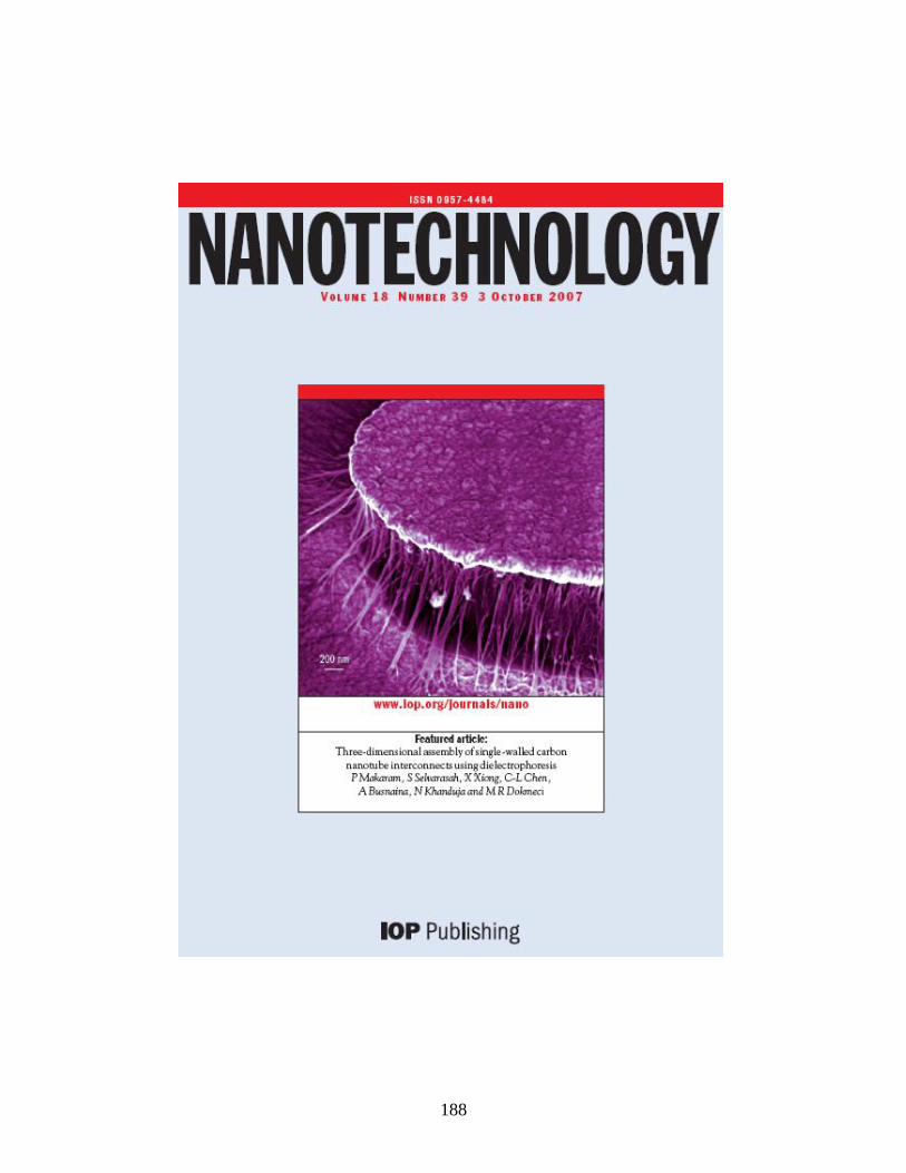
188
189

190
191
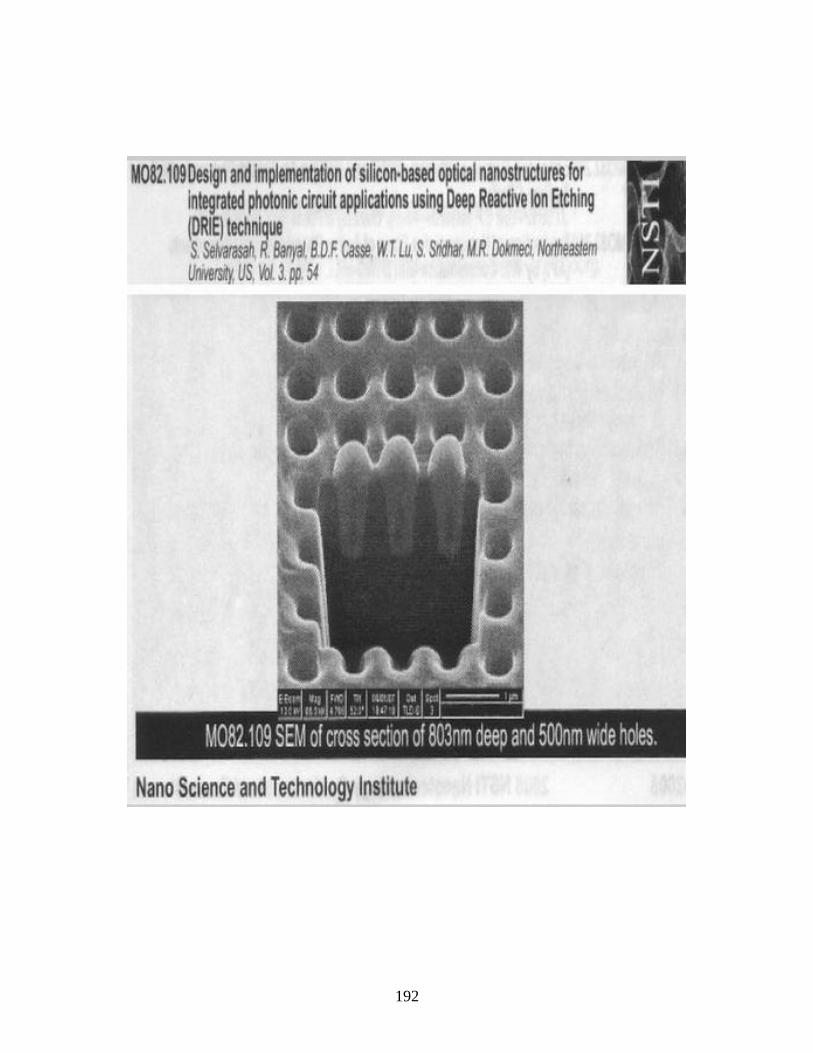
192
193
Top Related