


Languages
Pages
Legal

TSAL6200Vishay Telefunken
1 (5)Rev. 6, 20-May-99www.vishay.comDocument Number 81010
GaAs/GaAlAs IR Emitting Diode in ø 5 mm (T–1 �)Package
DescriptionTSAL6200 is a high efficiency infrared emitting diodein GaAlAs on GaAs technology, molded in clear, blue-grey tinted plastic packages. In comparison with the standard GaAs on GaAstechnology these emitters achieve more than 100 %radiant power improvement at a similar wavelength. The forward voltages at low current and at high pulsecurrent roughly correspond to the low values of thestandard technology. Therefore these emitters areideally suitable as high performance replacements ofstandard emitters.
Features� Extra high radiant power and radiant intensity
� High reliability
� Low forward voltage
� Suitable for high pulse current operation
� Standard T–1� (ø 5 mm) package
� Angle of half intensity ϕ = ± 17�
� Peak wavelength �p = 940 nm
� Good spectral matching to Si photodetectors
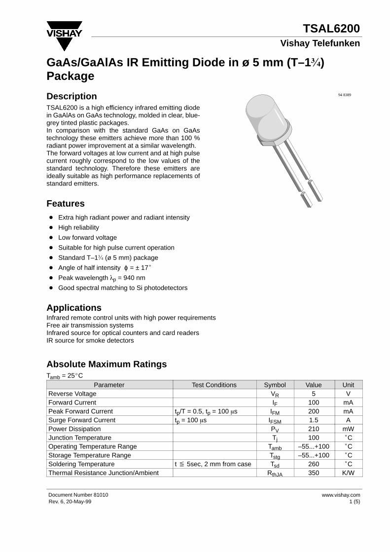
94 8389
ApplicationsInfrared remote control units with high power requirements Free air transmission systems Infrared source for optical counters and card readers IR source for smoke detectors
Absolute Maximum RatingsTamb = 25�C
Parameter Test Conditions Symbol Value UnitReverse Voltage VR 5 VForward Current IF 100 mAPeak Forward Current tp/T = 0.5, tp = 100 �s IFM 200 mASurge Forward Current tp = 100 �s IFSM 1.5 APower Dissipation PV 210 mWJunction Temperature Tj 100 �COperating Temperature Range Tamb –55...+100 �CStorage Temperature Range Tstg –55...+100 �CSoldering Temperature t � 5sec, 2 mm from case Tsd 260 �CThermal Resistance Junction/Ambient RthJA 350 K/W
TSAL6200Vishay Telefunken
2 (5) Rev. 6, 20-May-99www.vishay.com Document Number 81010
Basic CharacteristicsTamb = 25�C
Parameter Test Conditions Symbol Min Typ Max UnitForward Voltage IF = 100 mA, tp = 20 ms VF 1.35 1.6 Vg
IF = 1 A, tp = 100 �s VF 2.6 3 VTemp. Coefficient of VF IF = 100 mA TKVF –1.3 mV/KReverse Current VR = 5 V IR 10 �AJunction Capacitance VR = 0 V, f = 1 MHz, E = 0 Cj 25 pFRadiant Intensity IF = 100 mA, tp = 20 ms Ie 40 60 mW/sry
IF = 1.0 A, tp = 100 �s Ie 340 500 mW/srRadiant Power IF = 100 mA, tp = 20 ms �e 35 mWTemp. Coefficient of �e IF = 20 mA TK�e –0.6 %/KAngle of Half Intensity ϕ ±17 degPeak Wavelength IF = 100 mA �p 940 nmSpectral Bandwidth IF = 100 mA �� 50 nmTemp. Coefficient of �p IF = 100 mA TK�p 0.2 nm/KRise Time IF = 100 mA tr 800 nsFall Time IF = 100 mA tf 800 nsVirtual Source Diameter method: 63% encircled
energyø 2.8 mm
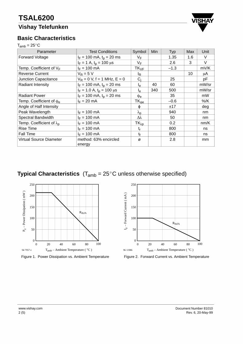
Typical Characteristics (Tamb = 25�C unless otherwise specified)
0 20 40 60 800
50
100
150
200
250
P
– P
ower
Dis
sipa
tion
( m
W )
V
Tamb – Ambient Temperature ( °C )
100
94 7957 e
RthJA
Figure 1. Power Dissipation vs. Ambient Temperature
0 20 40 60 800
50
100
150
200
250
I –
For
war
d C
urre
nt (
mA
)F
Tamb – Ambient Temperature ( °C )
100
96 11986
RthJA
Figure 2. Forward Current vs. Ambient Temperature
TSAL6200Vishay Telefunken
3 (5)Rev. 6, 20-May-99www.vishay.comDocument Number 81010
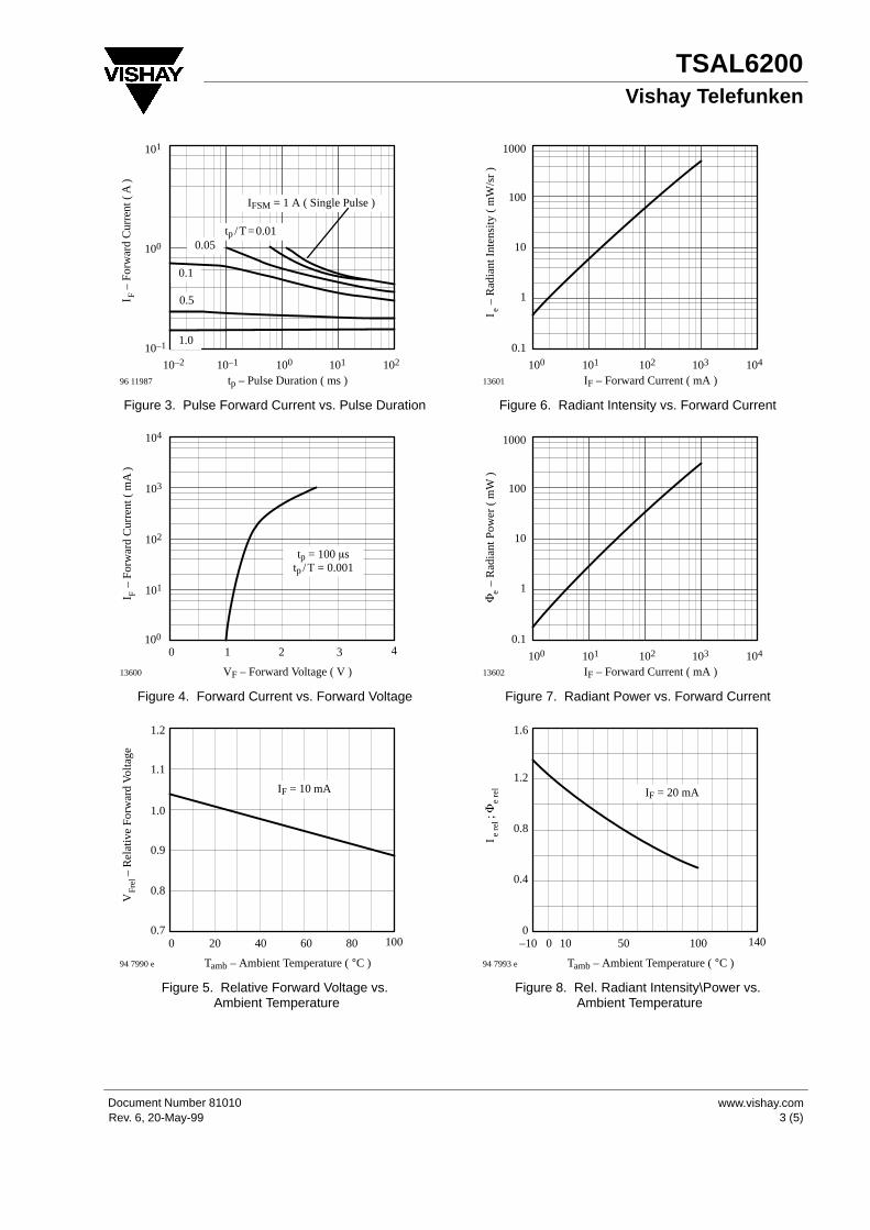
tp – Pulse Duration ( ms )96 11987
100
101
101
10–1
10–1 100 10210–2
I –
For
war
d C
urre
nt (
A )
F
tp /T=0.01
IFSM = 1 A ( Single Pulse )
0.05
0.1
0.5
1.0
Figure 3. Pulse Forward Current vs. Pulse Duration
0 1 2 3
VF – Forward Voltage ( V )
4
13600
101
100
102
103
104
I –
For
war
d C
urre
nt (
mA
)F
tp = 100 �stp/T = 0.001
Figure 4. Forward Current vs. Forward Voltage
0 20 40 60 800.7
0.8
0.9
1.0
1.1
1.2
V
–
Rel
ativ
e F
orw
ard
Volta
geF
rel
Tamb – Ambient Temperature ( °C )
100
94 7990 e
IF = 10 mA
Figure 5. Relative Forward Voltage vs. Ambient Temperature
13601
103101 102 104100
0.1
1
10
1000
100
IF – Forward Current ( mA )
I –
Rad
iant
Inte
nsity
( m
W/s
r )
e
Figure 6. Radiant Intensity vs. Forward Current
– R
adia
nt P
ower
( m
W )
e
IF – Forward Current ( mA )13602
�
103101 102 104100
0.1
1
10
1000
100
Figure 7. Radiant Power vs. Forward Current
–10 10 500 1000
0.4
0.8
1.2
1.6
I
;e
re
l
e r
el
Tamb – Ambient Temperature ( °C )
140
94 7993 e
�
IF = 20 mA
Figure 8. Rel. Radiant Intensity\Power vs. Ambient Temperature
TSAL6200Vishay Telefunken
4 (5) Rev. 6, 20-May-99www.vishay.com Document Number 81010
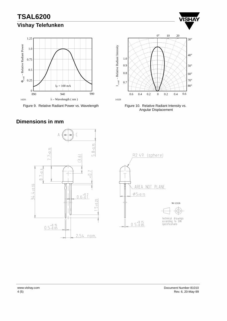
890 9400
0.25
0.5
0.75
1.0
1.25
� – Wavelength ( nm )
990
14291
– R
elat
ive
Rad
iant
Pow
ere
rel
�
IF = 100 mA
Figure 9. Relative Radiant Power vs. Wavelength
0.4 0.2 0 0.2 0.4 0.6
14329
0.6
0.9
0.8
0°30°
10°
20°
40°
50°
60°
70°
80°0.7
1.0
I
–
Rel
ativ
e R
adia
nt In
tens
itye
rel
Figure 10. Relative Radiant Intensity vs. Angular Displacement
Dimensions in mm
96 12126
TSAL6200Vishay Telefunken
5 (5)Rev. 6, 20-May-99www.vishay.comDocument Number 81010
Ozone Depleting Substances Policy Statement
It is the policy of Vishay Semiconductor GmbH to
1. Meet all present and future national and international statutory requirements.
2. Regularly and continuously improve the performance of our products, processes, distribution and operating systems with respect to their impact on the health and safety of our employees and the public, as well as their impact on the environment.
It is particular concern to control or eliminate releases of those substances into the atmosphere which are known asozone depleting substances (ODSs).
The Montreal Protocol (1987) and its London Amendments (1990) intend to severely restrict the use of ODSs andforbid their use within the next ten years. Various national and international initiatives are pressing for an earlier banon these substances.
Vishay Semiconductor GmbH has been able to use its policy of continuous improvements to eliminate the use ofODSs listed in the following documents.
1. Annex A, B and list of transitional substances of the Montreal Protocol and the London Amendments respectively
2. Class I and II ozone depleting substances in the Clean Air Act Amendments of 1990 by the EnvironmentalProtection Agency (EPA) in the USA
3. Council Decision 88/540/EEC and 91/690/EEC Annex A, B and C ( transitional substances) respectively.
Vishay Semiconductor GmbH can certify that our semiconductors are not manufactured with ozone depletingsubstances and do not contain such substances.
We reserve the right to make changes to improve technical design and may do so without further notice.Parameters can vary in different applications. All operating parameters must be validated for each customer applicationby the customer. Should the buyer use Vishay-Telefunken products for any unintended or unauthorized application, the
buyer shall indemnify Vishay-Telefunken against all claims, costs, damages, and expenses, arising out of, directly orindirectly, any claim of personal damage, injury or death associated with such unintended or unauthorized use.
Vishay Semiconductor GmbH, P.O.B. 3535, D-74025 Heilbronn, GermanyTelephone: 49 (0)7131 67 2831, Fax number: 49 (0)7131 67 2423
Top Related