


Languages
Pages
Legal

ETSI TS 138 521-1 V15.2.0 (2019-05)
5G; NR;
User Equipment (UE) conformance specification; Radio transmission and reception;
Part 1: Range 1 standalone (3GPP TS 38.521-1 version 15.2.0 Release 15)
TECHNICAL SPECIFICATION

ETSI
ETSI TS 138 521-1 V15.2.0 (2019-05)13GPP TS 38.521-1 version 15.2.0 Release 15
Reference RTS/TSGR-0538521-1vf20
Keywords 5G
ETSI
650 Route des Lucioles F-06921 Sophia Antipolis Cedex - FRANCE
Tel.: +33 4 92 94 42 00 Fax: +33 4 93 65 47 16
Siret N° 348 623 562 00017 - NAF 742 C
Association à but non lucratif enregistrée à la Sous-Préfecture de Grasse (06) N° 7803/88
Important notice
The present document can be downloaded from: http://www.etsi.org/standards-search
The present document may be made available in electronic versions and/or in print. The content of any electronic and/or print versions of the present document shall not be modified without the prior written authorization of ETSI. In case of any
existing or perceived difference in contents between such versions and/or in print, the prevailing version of an ETSI deliverable is the one made publicly available in PDF format at www.etsi.org/deliver.
Users of the present document should be aware that the document may be subject to revision or change of status. Information on the current status of this and other ETSI documents is available at
https://portal.etsi.org/TB/ETSIDeliverableStatus.aspx
If you find errors in the present document, please send your comment to one of the following services: https://portal.etsi.org/People/CommiteeSupportStaff.aspx
Copyright Notification
No part may be reproduced or utilized in any form or by any means, electronic or mechanical, including photocopying and microfilm except as authorized by written permission of ETSI.
The content of the PDF version shall not be modified without the written authorization of ETSI. The copyright and the foregoing restriction extend to reproduction in all media.
© ETSI 2019.
All rights reserved.
DECTTM, PLUGTESTSTM, UMTSTM and the ETSI logo are trademarks of ETSI registered for the benefit of its Members. 3GPPTM and LTETM are trademarks of ETSI registered for the benefit of its Members and
of the 3GPP Organizational Partners. oneM2M™ logo is a trademark of ETSI registered for the benefit of its Members and
of the oneM2M Partners. GSM® and the GSM logo are trademarks registered and owned by the GSM Association.
ETSI
ETSI TS 138 521-1 V15.2.0 (2019-05)23GPP TS 38.521-1 version 15.2.0 Release 15
Intellectual Property Rights Essential patents
IPRs essential or potentially essential to normative deliverables may have been declared to ETSI. The information pertaining to these essential IPRs, if any, is publicly available for ETSI members and non-members, and can be found in ETSI SR 000 314: "Intellectual Property Rights (IPRs); Essential, or potentially Essential, IPRs notified to ETSI in respect of ETSI standards", which is available from the ETSI Secretariat. Latest updates are available on the ETSI Web server (https://ipr.etsi.org/).
Pursuant to the ETSI IPR Policy, no investigation, including IPR searches, has been carried out by ETSI. No guarantee can be given as to the existence of other IPRs not referenced in ETSI SR 000 314 (or the updates on the ETSI Web server) which are, or may be, or may become, essential to the present document.
Trademarks
The present document may include trademarks and/or tradenames which are asserted and/or registered by their owners. ETSI claims no ownership of these except for any which are indicated as being the property of ETSI, and conveys no right to use or reproduce any trademark and/or tradename. Mention of those trademarks in the present document does not constitute an endorsement by ETSI of products, services or organizations associated with those trademarks.
Foreword This Technical Specification (TS) has been produced by ETSI 3rd Generation Partnership Project (3GPP).
The present document may refer to technical specifications or reports using their 3GPP identities, UMTS identities or GSM identities. These should be interpreted as being references to the corresponding ETSI deliverables.
The cross reference between GSM, UMTS, 3GPP and ETSI identities can be found under http://webapp.etsi.org/key/queryform.asp.
Modal verbs terminology In the present document "shall", "shall not", "should", "should not", "may", "need not", "will", "will not", "can" and "cannot" are to be interpreted as described in clause 3.2 of the ETSI Drafting Rules (Verbal forms for the expression of provisions).
"must" and "must not" are NOT allowed in ETSI deliverables except when used in direct citation.

ETSI
ETSI TS 138 521-1 V15.2.0 (2019-05)33GPP TS 38.521-1 version 15.2.0 Release 15
Contents Intellectual Property Rights ................................................................................................................................ 2
Foreword ............................................................................................................................................................. 2
Modal verbs terminology .................................................................................................................................... 2
Foreword ........................................................................................................................................................... 20
2 Reference ................................................................................................................................................ 21
3 Definitions, symbols and abbreviations ................................................................................................. 22
3.1 Definitions ........................................................................................................................................................ 22
3.2 Symbols ............................................................................................................................................................ 23
3.3 Abbreviations ................................................................................................................................................... 24
4 General ................................................................................................................................................... 25
4.1 Relationship between minimum requirements and test requirements .............................................................. 25
4.2 Applicability of minimum requirements .......................................................................................................... 26
4.3 Specification suffix information ....................................................................................................................... 26
4.4 Test points analysis .......................................................................................................................................... 26
5 Operating bands and Channel arrangement ............................................................................................ 26
5.1 General ............................................................................................................................................................. 26
5.2 Operating bands ................................................................................................................................................ 27
5.2A Operating bands for CA ................................................................................................................................... 27
5.2A.1 Intra-band CA ............................................................................................................................................. 27
5.2A.2 Inter-band CA ............................................................................................................................................. 28
5.2B Operating bands for DC ................................................................................................................................... 28
5.2B.1 General ........................................................................................................................................................ 28
5.2C Operating band combination for SUL .............................................................................................................. 28
5.3 UE channel bandwidth ..................................................................................................................................... 29
5.3.1 General ........................................................................................................................................................ 29
5.3.2 Maximum transmission bandwidth configuration ...................................................................................... 30
5.3.4 RB alignment .............................................................................................................................................. 31
5.3.5 UE channel bandwidth per operating band ................................................................................................. 31
5.3.6 Asymmetric channel bandwidths ................................................................................................................ 34
5.3A UE channel bandwidth for CA ......................................................................................................................... 35
5.3A.1 General ........................................................................................................................................................ 35
5.3A.2 Maximum transmission bandwidth configuration for CA .......................................................................... 35
5.3A.3 Minimum guard band and transmission bandwidth configuration for CA.................................................. 35
5.3A.4 RB alignment with different numerologies for CA..................................................................................... 37
5.3A.5 UE channel bandwidth per operating band for CA ..................................................................................... 37
5.4 Channel arrangement ........................................................................................................................................ 38
5.4.1 Channel spacing .......................................................................................................................................... 38
5.4.1.1 Channel spacing for adjacent NR carriers ............................................................................................. 38
5.4.2 Channel raster ............................................................................................................................................. 38
5.4.2.1 NR-ARFCN and channel raster............................................................................................................. 38
5.4.2.2 Channel raster to resource element mapping......................................................................................... 39
5.4.2.3 Channel raster entries for each operating band ..................................................................................... 39
5.4.3 Synchronization raster ................................................................................................................................ 40
5.4.3.1 Synchronization raster and numbering .................................................................................................. 40
5.4.3.2 Synchronization raster to synchronization block resource element mapping ........................................ 41
5.4.3.3 Synchronization raster entries for each operating band......................................................................... 41
5.4.4 TX–RX frequency separation ..................................................................................................................... 42
5.4A Channel arrangement for CA............................................................................................................................ 42
5.4A.1 Channel spacing for CA .............................................................................................................................. 42
5.4A.2 Channel raster for CA ................................................................................................................................. 43
5.4A.3 Synchronization raster for CA .................................................................................................................... 43
5.4A.4 Tx-Rx frequency separation for CA............................................................................................................ 43
5.5 Configurations .................................................................................................................................................. 43
5.5A Configurations for CA ...................................................................................................................................... 43

ETSI
ETSI TS 138 521-1 V15.2.0 (2019-05)43GPP TS 38.521-1 version 15.2.0 Release 15
5.5A.1 Configurations for intra-band contiguous CA............................................................................................. 43
5.5A.2 Configurations for intra-band non-contiguous CA ..................................................................................... 45
5.5A.3 Configurations for inter-band CA ............................................................................................................... 46
5.5B Configurations for DC ...................................................................................................................................... 49
5.5C Configurations for SUL .................................................................................................................................... 49
6 Transmitter characteristics ..................................................................................................................... 50
6.1 General ............................................................................................................................................................. 50
6.2 Transmitter power ............................................................................................................................................ 53
6.2.1 UE maximum output power ........................................................................................................................ 53
6.2.1.1 Test purpose .......................................................................................................................................... 53
6.2.1.2 Test applicability ................................................................................................................................... 53
6.2.1.3 Minimum conformance requirements ................................................................................................... 53
6.2.1.4 Test description ..................................................................................................................................... 55
6.2.1.4.1 Initial conditions .............................................................................................................................. 55
6.2.1.4.2 Test procedure ................................................................................................................................. 55
6.2.1.4.3 Message contents ............................................................................................................................. 56
6.2.1.5 Test requirement ................................................................................................................................... 56
6.2.2 Maximum Power Reduction (MPR) ........................................................................................................... 58
6.2.2.1 Test purpose .......................................................................................................................................... 58
6.2.2.2 Test applicability ................................................................................................................................... 58
6.2.2.3 Minimum conformance requirements ................................................................................................... 58
6.2.2.4 Test description ..................................................................................................................................... 59
6.2.2.4.1 Initial conditions ................................................................................................................................... 59
6.2.2.4.2 Test procedure ................................................................................................................................. 62
6.2.2.4.3 Message contents ............................................................................................................................. 62
6.2.2.5 Test requirement ................................................................................................................................... 62
6.2.3 UE additional maximum output power reduction ....................................................................................... 71
6.2.3.1 Test purpose .......................................................................................................................................... 71
6.2.3.2 Test applicability ................................................................................................................................... 71
6.2.3.3 Minimum conformance requirements ................................................................................................... 71
6.2.3.3.1 General ............................................................................................................................................ 71
6.2.3.3.2 A-MPR for NS_04 ........................................................................................................................... 74
6.2.3.3.3 A-MPR for NS_10 ........................................................................................................................... 75
6.2.3.3.4 A-MPR for NS_05 ........................................................................................................................... 75
6.2.3.3.5 A-MPR for NS_40 ........................................................................................................................... 77
6.2.3.3.6 A-MPR for NS_08 ........................................................................................................................... 77
6.2.3.3.7 A-MPR for NS_03 ........................................................................................................................... 79
6.2.3.3.8 A-MPR for NS_37 ........................................................................................................................... 79
6.2.3.3.9 A-MPR for NS_38 ........................................................................................................................... 80
6.2.3.3.10 A-MPR for NS_39 ........................................................................................................................... 81
6.2.3.3.11 A-MPR for NS_41 ........................................................................................................................... 81
6.2.3.3.12 A-MPR for NS_42 ........................................................................................................................... 82
6.2.3.4 Test description ..................................................................................................................................... 82
6.2.3.4.1 Initial conditions .............................................................................................................................. 82
6.2.3.4.2 Test procedure ................................................................................................................................. 86
6.2.3.4.3 Message contents ............................................................................................................................. 86
6.2.3.5 Test requirement ................................................................................................................................... 91
6.2.4 Configured transmitted power .................................................................................................................... 97
6.2.4.1 Test purpose .......................................................................................................................................... 97
6.2.4.2 Test applicability ................................................................................................................................... 97
6.2.4.3 Minimum conformance requirements ................................................................................................... 97
6.2.4.4 Test description ..................................................................................................................................... 99
6.2.4.4.1 Initial condition ............................................................................................................................... 99
6.2.4.4.2 Test procedure ................................................................................................................................. 99
6.2.4.4.3 Message contents ........................................................................................................................... 100
6.2.4.5 Test requirement ................................................................................................................................. 100
6.2A Transmitter power for CA .............................................................................................................................. 101
6.2B Transmitter power for DC .............................................................................................................................. 101
6.2C Transmitter power for SUL ............................................................................................................................ 101
6.2C.1 Configured transmitted power for SUL .................................................................................................... 101
6.2C.1.1 Test purpose ........................................................................................................................................ 101

ETSI
ETSI TS 138 521-1 V15.2.0 (2019-05)53GPP TS 38.521-1 version 15.2.0 Release 15
6.2C.1.2 Test applicability ................................................................................................................................. 101
6.2C.1.3 Minimum conformance requirements ................................................................................................. 101
6.2C.1.4 Test description ................................................................................................................................... 102
6.2C.1.5 Test requirement ................................................................................................................................. 103
6.2C.2 ΔTIB,c ......................................................................................................................................................... 103
6.2D Transmitter power for UL-MIMO .................................................................................................................. 103
6.2D.1 UE maximum output power for UL-MIMO ............................................................................................. 103
6.2D.1.1 Test purpose ........................................................................................................................................ 104
6.2D.1.2 Test applicability ................................................................................................................................. 104
6.2D.1.3 Minimum conformance requirements ................................................................................................. 104
6.2D.1.4 Test description ................................................................................................................................... 104
6.2D.1.4.1 Initial conditions ............................................................................................................................ 104
6.2D.1.4.2 Test procedure ............................................................................................................................... 105
6.2D.1.4.3 Message contents ........................................................................................................................... 105
6.2D.1.5 Test requirement ................................................................................................................................. 105
6.2D.2 UE maximum output power reduction for UL-MIMO ............................................................................. 106
6.2D.2.1 Test purpose ........................................................................................................................................ 106
6.2D.2.2 Test applicability ................................................................................................................................. 106
6.2D.2.3 Minimum conformance requirements ................................................................................................. 106
6.2D.2.4 Test description ................................................................................................................................... 106
6.2D.2.4.1 Initial conditions ............................................................................................................................ 106
6.2D.2.4.2 Test procedure ............................................................................................................................... 108
6.2D.2.4.3 Message contents ........................................................................................................................... 108
6.2D.2.5 Test requirement ................................................................................................................................. 108
6.2D.4 Configured transmitted power for UL-MIMO .......................................................................................... 111
6.2D.4.1 Test purpose ........................................................................................................................................ 111
6.2D.4.2 Test applicability ................................................................................................................................. 111
6.2D.4.3 Minimum conformance requirements ................................................................................................. 111
6.2D.4.4 Test description ................................................................................................................................... 111
6.2D.4.4.1 Initial conditions ............................................................................................................................ 111
6.2D.4.4.2 Test procedure ............................................................................................................................... 112
6.2D.4.4.3 Message contents ........................................................................................................................... 112
6.2D.4.5 Test requirement ................................................................................................................................. 113
6.3 Output power dynamics .................................................................................................................................. 113
6.3.1 Minimum output power ............................................................................................................................ 113
6.3.1.1 Test purpose ........................................................................................................................................ 113
6.3.1.2 Test applicability ................................................................................................................................. 113
6.3.1.3 Minimum conformance requirements ................................................................................................. 113
6.3.1.4 Test description ................................................................................................................................... 114
6.3.1.4.1 Initial condition ............................................................................................................................. 114
6.3.1.4.2 Test procedure ............................................................................................................................... 115
6.3.1.4.3 Message contents ........................................................................................................................... 115
6.3.1.5 Test requirement ................................................................................................................................. 115
6.3A.1 Minimum output power for CA ................................................................................................................ 115
6.3A.1.0 Minimum conformance requirements ................................................................................................. 115
6.3A.1.1 Minimum output power for CA (2UL CA) ......................................................................................... 116
6.3A.1.1.1 Test purpose .................................................................................................................................. 116
6.3A.1.1.2 Test applicability ........................................................................................................................... 116
6.3A.1.1.3 Minimum conformance requirements ............................................................................................ 116
6.3A.1.1.4 Test description ............................................................................................................................. 116
6.3A.1.1.5 Test requirement ............................................................................................................................ 117
6.3A.2 Transmit OFF power for CA..................................................................................................................... 117
6.3A.2.0 Minimum conformance requirements ................................................................................................. 117
6.3A.2.1 Transmit OFF power for CA (2UL CA) ............................................................................................. 117
6.3A.2.1.1 Test purpose .................................................................................................................................. 118
6.3A.2.1.2 Test applicability ........................................................................................................................... 118
6.3A.2.1.3 Minimum conformance requirements ............................................................................................ 118
6.3A.2.1.4 Test description ............................................................................................................................. 118
6.3A.2.1.5 Test requirement ............................................................................................................................ 118
6.3A.3 Transmit ON/OFF time mask for CA ....................................................................................................... 118
6.3A.3.0 Minimum conformance requirements ................................................................................................. 118
6.3A.3.1 Transmit ON/OFF time mask for CA (2UL CA) ................................................................................ 119

ETSI
ETSI TS 138 521-1 V15.2.0 (2019-05)63GPP TS 38.521-1 version 15.2.0 Release 15
6.3A.3.1.1 Test purpose .................................................................................................................................. 119
6.3A.3.1.2. Test applicability ........................................................................................................................... 119
6.3A.3.1.3 Minimum conformance requirements ............................................................................................ 119
6.3A.3.1.4 Test description ............................................................................................................................. 119
6.3A.3.3.5 Test requirement ............................................................................................................................ 120
6.3.2 Transmit OFF power ................................................................................................................................. 121
6.3.2.1 Test purpose ........................................................................................................................................ 121
6.3.2.2 Test applicability ................................................................................................................................. 121
6.3.2.3 Minimum conformance requirements ................................................................................................. 121
6.3.2.4 Test description ................................................................................................................................... 122
6.3.2.5 Test requirement ................................................................................................................................. 122
6.3.3 Transmit ON/OFF time mask ................................................................................................................... 122
6.3.3.1 General ................................................................................................................................................ 122
6.3.3.2 General ON/OFF time mask ............................................................................................................... 123
6.3.3.2.1 Test purpose .................................................................................................................................. 123
6.3.3.2.2 Test applicability ........................................................................................................................... 123
6.3.3.2.3 Minimum conformance requirements ............................................................................................ 123
6.3.3.2.4 Test description ............................................................................................................................. 123
6.3.3.2.5 Test requirement ............................................................................................................................ 125
6.3.3.3 Transmit power time mask for slot and [mini-slot] boundaries .......................................................... 127
6.3.3.4 PRACH time mask .............................................................................................................................. 127
6.3.3.4.1 Test purpose .................................................................................................................................. 127
6.3.3.4.2 Test applicability ........................................................................................................................... 127
6.3.3.4.3 Minimum conformance requirements ............................................................................................ 127
6.3.3.4.4 Test description ............................................................................................................................. 128
6.3.3.5 PUCCH time mask .............................................................................................................................. 130
6.3.3.5.1 Long PUCCH time mask ............................................................................................................... 130
6.3.3.5.2 Short PUCCH time mask ............................................................................................................... 130
6.3.3.6 SRS time mask .................................................................................................................................... 130
6.3.3.6.1 Test purpose .................................................................................................................................. 130
6.3.3.6.2 Test applicability ........................................................................................................................... 130
6.3.3.6.3 Minimum conformance requirements ............................................................................................ 130
6.3.3.6.4 Test description ............................................................................................................................. 131
6.3.3.6.4.1 Initial condition ........................................................................................................................ 131
6.3.3.6.5 Test requirement ............................................................................................................................ 133
6.3.3.7 PUSCH-PUCCH and PUSCH-SRS time masks ................................................................................. 134
6.3.3.7.1 Test purpose .................................................................................................................................. 134
6.3.3.7.2 Test applicability ........................................................................................................................... 134
6.3.3.7.3 Minimum conformance requirements ............................................................................................ 134
6.3.3.7.4 Test description ............................................................................................................................. 135
6.3.3.7.5 Test requirement ............................................................................................................................ 136
6.3.4 Power control ............................................................................................................................................ 137
6.3.4.1 General ................................................................................................................................................ 137
6.3.4.2 Absolute power tolerance .................................................................................................................... 137
6.3.4.2.1 Test purpose .................................................................................................................................. 137
6.3.4.2.2 Test applicability ........................................................................................................................... 137
6.3.4.2.3 Minimum conformance requirements ............................................................................................ 137
6.3.4.2.4 Test description ............................................................................................................................. 138
6.3.4.2.5 Test requirement ............................................................................................................................ 139
6.3.4.3 Power Control Relative power tolerance ............................................................................................. 140
6.3.4.3.1 Test purpose .................................................................................................................................. 140
6.3.4.3.2 Test applicability ........................................................................................................................... 140
6.3.4.3.3 Minimum conformance requirement ............................................................................................. 140
6.3.4.3.4 Test description ................................................................................................................................... 141
6.3.4.3.5 Test requirement ............................................................................................................................ 152
6.3.4.4 Aggregate power tolerance.................................................................................................................. 159
6.3.4.4.1 Test purpose .................................................................................................................................. 159
6.3.4.4.2 Test applicability ........................................................................................................................... 160
6.3.4.4.3 Minimum conformance requirements ............................................................................................ 160
6.3.4.4.4 Test description ............................................................................................................................. 160
6.3.4.4.5 Test requirement ............................................................................................................................ 162
6.3D ........................................................................................................................................................................ 162
ETSI
ETSI TS 138 521-1 V15.2.0 (2019-05)73GPP TS 38.521-1 version 15.2.0 Release 15
6.3D.1 Minimum output power for UL-MIMO .................................................................................................... 162
6.3D.1.1 Test purpose ........................................................................................................................................ 163
6.3D.1.2 Test applicability ................................................................................................................................. 163
6.3D.1.3 Minimum conformance requirements ................................................................................................. 163
6.3D.1.4 Test description ................................................................................................................................... 163
6.3D.1.4.1 Initial condition ............................................................................................................................. 163
6.3D.1.4.2 Test procedure ............................................................................................................................... 164
6.3D.1.4.3 Message contents ........................................................................................................................... 164
6.3D.1.5 Test requirement ................................................................................................................................. 164
6.3D.2 Transmit OFF power for UL-MIMO ........................................................................................................ 165
6.3D.2.1 Test purpose ........................................................................................................................................ 165
6.3D.2.2 Test applicability ................................................................................................................................. 165
6.3D.2.3 Minimum conformance requirements ................................................................................................. 165
6.3D.2.4 Test description ................................................................................................................................... 166
6.3D.2.5 Test requirement ................................................................................................................................. 166
6.3D.3 Transmit ON/OFF time mask for UL-MIMO ........................................................................................... 166
6.3D.3.1 Test purpose ........................................................................................................................................ 166
6.3D.3.2 Test applicability ................................................................................................................................. 167
6.3D.3.3 Minimum conformance requirements ................................................................................................. 167
6.3D.3.4 Test description ................................................................................................................................... 167
6.3D.3.4.1 Initial condition ............................................................................................................................. 167
6.3D.3.4.2 Test procedure ............................................................................................................................... 167
6.3D.3.4.3 Message contents ........................................................................................................................... 168
6.3D.3.5 Test requirement ................................................................................................................................. 168
6.3D.4 Power control for UL-MIMO ................................................................................................................... 169
6.3D.4.1 Absolute power tolerance for UL-MIMO ........................................................................................... 169
6.3D.4.1.1 Test purpose .................................................................................................................................. 169
6.3D.4.1.2 Test applicability ........................................................................................................................... 169
6.3D.4.1.3 Minimum conformance requirements ............................................................................................ 170
6.3D.4.1.4 Test description ............................................................................................................................. 170
6.3D.4.1.5 Test requirement ............................................................................................................................ 170
6.3D.4.2 Relative power tolerance for UL-MIMO ............................................................................................ 171
6.3D.4.2.1 Test purpose .................................................................................................................................. 171
6.3D.4.2.2 Test applicability ........................................................................................................................... 171
6.3D.4.2.3 Minimum conformance requirements ............................................................................................ 171
6.3D.4.2.4 Test description ............................................................................................................................. 172
6.3D.4.2.5 Test requirement ............................................................................................................................ 172
6.3D.4.3 Aggregate power tolerance for UL-MIMO ......................................................................................... 172
6.3D.4.3.1 Test purpose .................................................................................................................................. 173
6.3D.4.3.2 Test applicability ........................................................................................................................... 173
6.3D.4.3.3 Minimum conformance requirements ............................................................................................ 173
6.3D.4.3.4 Test description ............................................................................................................................. 173
6.3D.4.3.5 Test requirement ............................................................................................................................ 174
6.4 Transmit signal quality ................................................................................................................................... 174
6.4.1 Frequency error ......................................................................................................................................... 174
6.4.1.1 Test purpose ........................................................................................................................................ 174
6.4.1.2 Test applicability ................................................................................................................................. 174
6.4.1.3 Minimum conformance requirements ................................................................................................. 174
6.4.1.4 Test description ................................................................................................................................... 175
6.4.1.4.1 Initial condition ............................................................................................................................. 175
6.4.1.4.2 Test procedure ............................................................................................................................... 175
6.4.1.4.3 Message contents ........................................................................................................................... 176
6.4.1.5 Test requirement ................................................................................................................................. 176
6.4.2 Transmit modulation quality ..................................................................................................................... 176
6.4.2.1 Error Vector Magnitude ...................................................................................................................... 176
6.4.2.1.1 Test Purpose .................................................................................................................................. 176
6.4.2.1.2 Test applicability ........................................................................................................................... 176
6.4.2.1.3 Minimum conformance requirements ............................................................................................ 176
6.4.2.1.4 Test description ............................................................................................................................. 177
6.4.2.1.4.2 Test procedure ............................................................................................................................... 179
6.4.2.1.5 Test requirement ............................................................................................................................ 180
6.4.2.2 Carrier leakage .................................................................................................................................... 181
ETSI
ETSI TS 138 521-1 V15.2.0 (2019-05)83GPP TS 38.521-1 version 15.2.0 Release 15
6.4.2.2.1 Test purpose .................................................................................................................................. 181
6.4.2.2.2 Test applicability ........................................................................................................................... 181
6.4.2.2.3 Minimum conformance requirements ............................................................................................ 181
6.4.2.2.4 Test description ............................................................................................................................. 181
6.4.2.2.5 Test requirement ............................................................................................................................ 183
6.4.2.3 In-band emissions ............................................................................................................................... 183
6.4.2.3.1 Test purpose .................................................................................................................................. 183
6.4.2.3.2 Test applicability ........................................................................................................................... 184
6.4.2.3.3 Minimum conformance requirements ............................................................................................ 184
6.4.2.3.4 Test description ............................................................................................................................. 185
6.4.2.3.5 Test requirement ............................................................................................................................ 187
6.4.2.4 EVM equalizer spectrum flatness ....................................................................................................... 188
6.4.2.4.1 Test purpose .................................................................................................................................. 188
6.4.2.4.2 Test applicability ........................................................................................................................... 188
6.4.2.4.3 Minimum conformance requirements ............................................................................................ 188
6.4.2.4.4 Test description ............................................................................................................................. 189
6.4.2.4.5 Test requirement ............................................................................................................................ 190
6.4.2.5 EVM equalizer spectrum flatness for Pi/2 BPSK ................................................................................ 192
6.4.2.5.1 Test purpose .................................................................................................................................. 192
6.4.2.5.2 Test applicability ........................................................................................................................... 192
6.4.2.5.3 Minimum conformance requirements ............................................................................................ 192
6.4.2.5.4 Test description ............................................................................................................................. 193
6.4.2.5.5 Test requirement ............................................................................................................................ 194
6.4A Transmit signal quality for CA ....................................................................................................................... 195
6.4A.1 Frequency error for CA ............................................................................................................................. 195
6.4A.1.0 Minimum conformance requirements ................................................................................................. 195
6.4A.1.1 Frequency error for CA (2UL CA) ..................................................................................................... 195
6.4A.1.1.1 Test purpose .................................................................................................................................. 195
6.4A.1.1.2 Test applicability ........................................................................................................................... 195
6.4A.1.1.3 Minimum conformance requirements ............................................................................................ 195
6.4A.1.1.4 Test description ............................................................................................................................. 196
6.4A.1.1.5 Test requirement ............................................................................................................................ 197
6.4A.2 Transmit modulation quality for CA ......................................................................................................... 197
6.4A.2.1 Error Vector Magnitude for CA .......................................................................................................... 197
6.4A.2.1.0 Minimum conformance requirements ............................................................................................ 197
6.4A.2.1.1 Error Vector Magnitude for CA (2UL CA) ................................................................................... 198
6.4A.2.2 Carrier leakage for CA ........................................................................................................................ 200
6.4A.2.2.0 Minimum conformance requirements ............................................................................................ 200
6.4A.2.2.1 Carrier leakage for CA (2UL CA) ................................................................................................. 201
6.4A.2.3 In-band emission for CA ..................................................................................................................... 204
6.4A.2.3.0 Minimum conformance requirements ............................................................................................ 204
6.4A.2.3.1 In-band emissions for CA (2UL CA) ............................................................................................ 205
6.4D Transmit signal quality for UL-MIMO .......................................................................................................... 208
6.4D.1 Frequency error for UL-MIMO ................................................................................................................ 208
6.4D.1.1 Test purpose ........................................................................................................................................ 208
6.4D.1.2 Test applicability ................................................................................................................................. 208
6.4D.1.3 Minimum conformance requirements ................................................................................................. 209
6.4D.1.4 Test description ................................................................................................................................... 209
6.4D.1.4.1 Initial conditions ................................................................................................................................. 209
6.4D.1.4.2 Test procedure ............................................................................................................................... 209
6.4D.1.4.3 Message contents ........................................................................................................................... 209
6.4D.1.5 Test requirement ................................................................................................................................. 209
6.4D.2 Transmit modulation quality for UL-MIMO ............................................................................................ 210
6.4D.2.1 Error Vector Magnitude for UL-MIMO .............................................................................................. 210
6.4D.2.1.1 Test purpose .................................................................................................................................. 210
6.4D.2.1.2 Test applicability ........................................................................................................................... 210
6.4D.2.1.3 Minimum conformance requirements ............................................................................................ 210
6.4D.2.1.4 Test description ............................................................................................................................. 211
6.4D.2.1.5 Test requirement ............................................................................................................................ 212
6.4D.2.2 Carrier leakage for UL-MIMO ............................................................................................................ 212
6.4D.2.2.1 Test purpose .................................................................................................................................. 212
6.4D.2.2.2 Test applicability ........................................................................................................................... 212
ETSI
ETSI TS 138 521-1 V15.2.0 (2019-05)93GPP TS 38.521-1 version 15.2.0 Release 15
6.4D.2.2.3 Minimum conformance requirements ............................................................................................ 212
6.4D.2.2.4 Test description ............................................................................................................................. 213
6.4D.2.2.5 Test requirement ............................................................................................................................ 214
6.4D.2.3 In-band emissions for UL-MIMO ....................................................................................................... 215
6.4D.2.3.1 Test purpose .................................................................................................................................. 215
6.4D.2.3.2 Test applicability ........................................................................................................................... 215
6.4D.2.3.3 Minimum conformance requirements ............................................................................................ 215
6.4D.2.3.4 Test description ............................................................................................................................. 215
6.4D.2.3.4.1 Initial conditions ............................................................................................................................ 215
6.4D.2.3.5 Test requirement ............................................................................................................................ 216
6.4D.2.4 EVM equalizer spectrum flatness for UL-MIMO ............................................................................... 217
6.4D.2.4.1 Test purpose .................................................................................................................................. 217
6.4D.2.4.2 Test applicability ........................................................................................................................... 218
6.4D.2.4.3 Minimum conformance requirements ............................................................................................ 218
6.4D.2.4.5 Test requirement ............................................................................................................................ 218
6.4D.3 Time alignment error for UL-MIMO ........................................................................................................ 220
6.4D.3.1 Test purpose ........................................................................................................................................ 220
6.4D.3.2 Test applicability ................................................................................................................................. 220
6.4D.3.3 Minimum conformance requirements ................................................................................................. 220
6.4D.3.4 Test description ................................................................................................................................... 220
6.4D.3.4.1 Initial condition ................................................................................................................................... 220
6.4D.3.4.2 Test procedure ............................................................................................................................... 221
6.4D.3.4.3 Message contents ........................................................................................................................... 221
6.4D.3.5 Test requirement ................................................................................................................................. 221
6.4D.4 Requirements for coherent UL MIMO ..................................................................................................... 221
6.4D.4.1 Test purpose ........................................................................................................................................ 222
6.4D.4.2 Test applicability ................................................................................................................................. 222
6.4D.4.3 Minimum conformance requirements ................................................................................................. 222
6.4D.4.4 Test description ................................................................................................................................... 222
6.4D.4.4.1 Initial condition ............................................................................................................................. 222
6.4D.4.4.2 Test procedure ............................................................................................................................... 223
6.4D.4.4.3 Message contents ........................................................................................................................... 223
6.4D.4.5 Test requirement ................................................................................................................................. 223
6.5 Output RF spectrum emissions ....................................................................................................................... 223
6.5.1 Occupied bandwidth ................................................................................................................................. 224
6.5.1.1 Test purpose ........................................................................................................................................ 224
6.5.1.2 Test applicability ................................................................................................................................. 224
6.5.1.3 Minimum conformance requirements ................................................................................................. 224
6.5.1.4 Test description ................................................................................................................................... 224
6.5.1.4.1 Initial conditions ............................................................................................................................ 224
6.5.1.4.2 Test procedure ............................................................................................................................... 225
6.5.1.4.3 Message contents ........................................................................................................................... 226
6.5.1.5 Test requirement ................................................................................................................................. 226
6.5.2 Out of band emission ................................................................................................................................ 226
6.5.2.1 General ................................................................................................................................................ 226
6.5.2.2 Spectrum Emission Mask .................................................................................................................... 226
6.5.2.2.1 Test purpose .................................................................................................................................. 226
6.5.2.2.2 Test applicability ........................................................................................................................... 226
6.5.2.2.3 Minimum conformance requirements ............................................................................................ 226
6.5.2.2.4 Test description ............................................................................................................................. 227
6.5.2.2.5 Test requirement ............................................................................................................................ 230
6.5.2.3 Additional spectrum emission mask ................................................................................................... 231
6.5.2.3.1 Test purpose .................................................................................................................................. 232
6.5.2.3.2 Test applicability ........................................................................................................................... 232
6.5.2.3.3 Minimum conformance requirements ............................................................................................ 232
6.5.2.3.3.5 Requirements for network signalled value "NS_40" ..................................................................... 234
6.5.2.3.4 Test description ............................................................................................................................. 235
6.5.2.4 Adjacent channel leakage ratio ........................................................................................................... 237
6.5.2.4.1 NR ACLR ...................................................................................................................................... 237
6.5.2.4.2 UTRA ACLR ................................................................................................................................ 242
6.5.3 Spurious emissions ................................................................................................................................... 244
6.5.3.1 General spurious emissions ................................................................................................................. 244

ETSI
ETSI TS 138 521-1 V15.2.0 (2019-05)103GPP TS 38.521-1 version 15.2.0 Release 15
6.5.3.1.1 Test purpose .................................................................................................................................. 244
6.5.3.1.2 Test applicability ........................................................................................................................... 244
6.5.3.1.3 Minimum conformance requirements ............................................................................................ 244
6.5.3.1.4 Test description ............................................................................................................................. 245
6.5.3.1.5 Test requirement ............................................................................................................................ 246
6.5.3.2 Spurious emission for UE co-existence............................................................................................... 247
6.5.3.2.1 Test purpose .................................................................................................................................. 247
6.5.3.2.2 Test applicability ........................................................................................................................... 247
6.5.3.2.3 Minimum conformance requirements ............................................................................................ 247
6.5.3.2.4 Test description ............................................................................................................................. 253
6.5.3.2.5 Test requirement ............................................................................................................................ 255
6.5.3.3 Additional spurious emissions ............................................................................................................ 255
6.5.3.3.1 Test purpose .................................................................................................................................. 255
6.5.3.3.2 Test applicability ........................................................................................................................... 255
6.5.3.3.3 Minimum conformance requirements ............................................................................................ 255
6.5.3.3.4 Test description ............................................................................................................................. 258
6.5.3.3.5 Test requirement ............................................................................................................................ 263
6.5.4 Transmit intermodulation ......................................................................................................................... 264
6.5.4.1 Test purpose ........................................................................................................................................ 264
6.5.4.2 Test applicability ................................................................................................................................. 264
6.5.4.3 Minimum conformance requirements ................................................................................................. 265
6.5.4.4 Test description ................................................................................................................................... 265
6.5.4.4.1 Initial conditions ............................................................................................................................ 265
6.5.4.4.2 Test procedure ............................................................................................................................... 266
6.5.4.4.3 Message contents ........................................................................................................................... 266
6.5.4.5 Test requirement ................................................................................................................................. 266
6.5A Output RF spectrum emissions for CA........................................................................................................... 267
6.5A.2 Out of band emission for CA .................................................................................................................... 267
6.5A.2.2 Spectrum emission mask ..................................................................................................................... 267
6.5A.2.2.0 Minimum conformance requirements ............................................................................................ 267
6.5A.2.2.1 Spectrum emission mask for CA (2UL CA) .................................................................................. 267
6.5A.2.4 Adjacent channel leakage ratio ........................................................................................................... 271
6.5A.2.4.1 NR ACLR ...................................................................................................................................... 271
6.5A.2.4.1.0 Minimum conformance requirements ...................................................................................... 271
6.5A.2.4.1.1 NR ACLR for CA (2UL CA) ................................................................................................... 271
6.5A.2.4.2 UTRA ACLR ................................................................................................................................ 274
6.5A.2.4.2.0 Minimum conformance requirements ...................................................................................... 274
6.5A.2.4.2.1 UTRA ACLR for CA (2UL CA) ............................................................................................. 274
6.5A.3 Spurious emission for CA ......................................................................................................................... 276
6.5A.3.1 General spurious emissions for CA ..................................................................................................... 276
6.5A.3.1.0 Minimum conformance requirements ............................................................................................ 276
6.5A.3.1.1 General spurious emissions for CA (2UL CA) .............................................................................. 277
6.5A.3.2 Spurious emission for UE co-existence............................................................................................... 279
6.5A.3.2.0 Minimum conformance requirements ............................................................................................ 279
6.5A.3.2.1 Spurious emissions for UE co-existence for CA (2UL CA) .......................................................... 280
6.5A.4 Transmit intermodulation for CA ............................................................................................................. 283
6.5A.4.0 Minimum conformance requirements ................................................................................................. 283
6.5A.4.1 Transmit intermodulation for CA (2UL CA) ...................................................................................... 283
6.5A.4.1.1 Test purpose .................................................................................................................................. 283
6.5A.4.1.2 Test applicability ........................................................................................................................... 283
6.5A.4.1.3 Minimum conformance requirements ............................................................................................ 283
6.5A.4.1.4 Test description ............................................................................................................................. 283
6.5A.4.1.5 Test requirement ............................................................................................................................ 285
6.5C Output RF spectrum emissions for SUL......................................................................................................... 286
6.5C.1 Occupied bandwidth for SUL ................................................................................................................... 286
6.5C.1.1 Test purpose ........................................................................................................................................ 286
6.5C.1.2 Test applicability ................................................................................................................................. 286
6.5C.1.3 Minimum conformance requirements ................................................................................................. 286
6.5C.1.4 Test description ................................................................................................................................... 286
6.5C.1.5 Test requirement ................................................................................................................................. 287
6.5C.2 Out of band emission for SUL .................................................................................................................. 287
6.5C.2.1 General ................................................................................................................................................ 287
ETSI
ETSI TS 138 521-1 V15.2.0 (2019-05)113GPP TS 38.521-1 version 15.2.0 Release 15
6.5C.2.2 Spectrum Emission Mask for SUL ...................................................................................................... 287
6.5C.2.2.1 Test purpose .................................................................................................................................. 287
6.5C.2.2.2 Test applicability ........................................................................................................................... 287
6.5C.2.2.3 Minimum conformance requirements ............................................................................................ 287
6.5C.2.2.4 Test description ............................................................................................................................. 287
6.5C.2.2.5 Test requirement ............................................................................................................................ 288
6.5C.2.3 Additional spectrum emission mask for SUL ..................................................................................... 289
6.5C.2.3.1 Test purpose .................................................................................................................................. 290
6.5C.2.3.2 Test applicability ........................................................................................................................... 290
6.5C.2.3.3 Minimum conformance requirements ............................................................................................ 290
6.5C.2.3.4 Test description ............................................................................................................................. 290
6.5C.2.3.5 Test requirement ............................................................................................................................ 290
6.5C.2.4 Adjacent channel leakage ratio for SUL ............................................................................................. 290
6.5C.2.4.1 NR ACLR for SUL ........................................................................................................................ 290
6.5C.2.4.2 UTRA ACLR for SUL .................................................................................................................. 292
6.5C.3 Spurious emissions for SUL ..................................................................................................................... 293
6.5C.3.1 General spurious emissions for SUL ................................................................................................... 293
6.5C.3.1.1 Test purpose .................................................................................................................................. 294
6.5C.3.1.2 Test applicability ........................................................................................................................... 294
6.5C.3.1.3 Minimum conformance requirements ............................................................................................ 294
6.5C.3.1.4 Test description ............................................................................................................................. 294
6.5C.3.1.5 Test requirement ............................................................................................................................ 294
6.5C.3.2 Spurious emission for UE co-existence for SUL ................................................................................ 295
6.5C.3.2.1 Test purpose .................................................................................................................................. 295
6.5C.3.2.2 Test applicability ........................................................................................................................... 295
6.5C.3.2.3 Minimum conformance requirements ............................................................................................ 295
6.5C.3.2.4 Test description ............................................................................................................................. 295
6.5C.3.2.5 Test requirement ............................................................................................................................ 296
6.5C.3.3 Additional spurious emissions for SUL .............................................................................................. 296
6.5C.3.3.1 Test purpose .................................................................................................................................. 296
6.5C.3.3.2 Test applicability ........................................................................................................................... 296
6.5C.3.3.4 Test description ............................................................................................................................. 297
6.5C.3.3.5 Test requirement ............................................................................................................................ 297
6.5C.4 Transmit intermodulation for SUL ........................................................................................................... 297
6.5C.4.1 Test purpose ........................................................................................................................................ 298
6.5C.4.2 Test applicability ................................................................................................................................. 298
6.5C.4.3 Minimum conformance requirements ................................................................................................. 298
6.5C.4.4 Test description ................................................................................................................................... 298
6.5C.4.5 Test requirement ................................................................................................................................. 298
6.5D Output RF spectrum emissions for UL-MIMO .............................................................................................. 299
6.5D.1 Occupied bandwidth for UL-MIMO ......................................................................................................... 299
6.5D.1.1 Test purpose ........................................................................................................................................ 299
6.5D.1.2 Test applicability ................................................................................................................................. 299
6.5D.1.3 Minimum conformance requirements ................................................................................................. 299
6.5D.1.4 Test description ................................................................................................................................... 299
6.5D.1.4.1 Initial conditions ............................................................................................................................ 299
6.5D.1.4.2 Test procedure ............................................................................................................................... 300
6.5D.1.4.3 Message contents ........................................................................................................................... 301
6.5D.1.5 Test requirement ................................................................................................................................. 301
6.5D.2 Out of band emission for UL-MIMO ........................................................................................................ 301
6.5D.2.1 General ................................................................................................................................................ 301
6.5D.2.2 Spectrum Emission Mask for UL-MIMO ........................................................................................... 301
6.5D.2.2.1 Test purpose .................................................................................................................................. 301
6.5D.2.2.2 Test applicability ........................................................................................................................... 301
6.5D.2.2.3 Minimum conformance requirements ............................................................................................ 301
6.5D.2.2.4 Test description ............................................................................................................................. 302
6.5D.2.2.4.1 Initial conditions ............................................................................................................................ 302
6.5D.2.2.5 Test requirement ............................................................................................................................ 303
6.5D.2.3 Additional spectrum emission mask for UL-MIMO ................................................................................. 304
6.5D.2.3.1 Test purpose .................................................................................................................................. 305
6.5D.2.3.2 Test applicability ........................................................................................................................... 305
6.5D.2.3.3 Minimum conformance requirements ............................................................................................ 305

ETSI
ETSI TS 138 521-1 V15.2.0 (2019-05)123GPP TS 38.521-1 version 15.2.0 Release 15
6.5D.2.3.4 Test description ............................................................................................................................. 305
6.5D.2.3.5 Test requirement ............................................................................................................................ 306
6.5D.2.4 Adjacent channel leakage ratio for UL-MIMO ................................................................................... 306
6.5D.2.4.1 NR ACLR for UL-MIMO ............................................................................................................. 306
6.5D.2.4.2 UTRA ACLR for UL-MIMO ........................................................................................................ 308
6.5D.3 Spurious emissions for UL-MIMO ........................................................................................................... 310
6.5D.3.1 General spurious emissions for UL-MIMO ........................................................................................ 310
6.5D.3.1.1 Test purpose .................................................................................................................................. 310
6.5D.3.1.2 Test applicability ........................................................................................................................... 311
6.5D.3.1.3 Minimum conformance requirements ............................................................................................ 311
6.5D.3.1.4 Test description ............................................................................................................................. 311
6.5D.3.1.5 Test requirement ............................................................................................................................ 312
6.5D.3.2 Spurious emission for UE co-existence for UL-MIMO ...................................................................... 312
6.5D.3.2.1 Test purpose .................................................................................................................................. 312
6.5D.3.2.2 Test applicability ........................................................................................................................... 312
6.5D.3.2.3 Minimum conformance requirements ............................................................................................ 312
6.5D.3.2.4 Test description ............................................................................................................................. 312
6.5D.3.2.5 Test requirement ............................................................................................................................ 313
6.5D.3.3 Additional spurious emissions for UL-MIMO .................................................................................... 314
6.5D.3.3.1 Test purpose .................................................................................................................................. 314
6.5D.3.3.2 Test applicability ........................................................................................................................... 314
6.5D.3.3.5 Test requirement ............................................................................................................................ 316
6.5D.4 Transmit intermodulation for UL-MIMO ................................................................................................. 316
6.5D.4.1 Test purpose ........................................................................................................................................ 316
6.5D.4.2 Test applicability ................................................................................................................................. 316
6.5D.4.3 Minimum conformance requirements ................................................................................................. 316
6.5D.4.4 Test description ................................................................................................................................... 316
6.5D.4.4.1 Initial conditions ................................................................................................................................. 316
6.5D.4.4.2 Test procedure ............................................................................................................................... 317
6.5D.4.4.3 Message contents ........................................................................................................................... 318
6.5D.4.5 Test requirement ................................................................................................................................. 318
7 Receiver characteristics ........................................................................................................................ 318
7.1 General ........................................................................................................................................................... 318
7.2 Diversity characteristics ................................................................................................................................. 318
7.3 Reference sensitivity ...................................................................................................................................... 319
7.3.1 General ...................................................................................................................................................... 319
7.3.2 Reference sensitivity power level ............................................................................................................. 319
7.3.2.1 Test purpose ........................................................................................................................................ 319
7.3.2.2 Test applicability ................................................................................................................................. 319
7.3.2.3 Minimum conformance requirements ................................................................................................. 319
7.3.2.4 Test description ................................................................................................................................... 326
7.3.2.4.1 Initial conditions ............................................................................................................................ 326
7.3.2.4.2 Test procedure ............................................................................................................................... 331
7.3.2.4.3 Message contents ........................................................................................................................... 331
7.3.2.5 Test requirement ................................................................................................................................. 332
7.3.2_1 Reference sensitivity level with 4 Rx antenna ports ................................................................................. 335
7.3.2_1.1 Test purpose ........................................................................................................................................ 335
7.3.2_1.2 Test applicability ................................................................................................................................. 335
7.3.2_1.3 Minimum conformance requirements ................................................................................................. 335
7.3.2_1.4 Test description ................................................................................................................................... 335
7.3.2_1.4.1 Initial conditions ............................................................................................................................ 335
7.3.2_1.4.2 Test procedure ............................................................................................................................... 335
7.3.2_1.4.3 Message contents ........................................................................................................................... 335
7.3.2_1.5 Test requirement ................................................................................................................................. 336
7.3.3 ΔRIB,c ...................................................................................................................................................... 339
7.3A Reference sensitivity for CA .......................................................................................................................... 339
7.3A.0 Minimum conformance requirements ....................................................................................................... 339
7.3A.0.1 General ................................................................................................................................................ 339
7.3A.0.2 Reference sensitivity power level for CA ........................................................................................... 340
7.3A.0.2.1 Reference sensitivity power level for Intra-band contiguous CA .................................................. 340
7.3A.0.2.2 Reference sensitivity power level for Intra-band non-contiguous CA ........................................... 340
ETSI
ETSI TS 138 521-1 V15.2.0 (2019-05)133GPP TS 38.521-1 version 15.2.0 Release 15
7.3A.0.2.3 Reference sensitivity power level for Inter-band CA .................................................................... 340
7.3A.0.3 ΔRIB,c for CA .................................................................................................................................... 340
7.3A.0.3.1 General .......................................................................................................................................... 340
7.3A.0.3.2 ΔRIB,c for Inter-band CA ............................................................................................................. 340
7.3A.0.4 Reference sensitivity exceptions due to UL harmonic interference for CA ........................................ 341
7.3A.0.5 Reference sensitivity exceptions due to intermodulation interference due to 2UL CA ...................... 343
7.3A.1 Reference sensitivity power level for 2DL CA ......................................................................................... 343
7.3A.1.1 Test purpose ........................................................................................................................................ 343
7.3A.1.2 Test applicability ................................................................................................................................. 343
7.3A.1.3 Minimum requirements ....................................................................................................................... 343
7.3A.1.4 Test description ................................................................................................................................... 344
7.3A.1.4.1 Initial conditions ............................................................................................................................ 344
7.3A.1.4.2 Test procedure ............................................................................................................................... 344
7.3A.1.4.3 Message contents ........................................................................................................................... 344
7.3A.1.5 Test requirement ................................................................................................................................. 344
7.3A.2 Reference sensitivity power level for 3DL CA ......................................................................................... 344
7.3A.3 Reference sensitivity power level for 4DL CA ......................................................................................... 344
7.3A.4 Reference sensitivity power level for 5DL CA ......................................................................................... 344
7.3B Reference sensitivity for DC .......................................................................................................................... 344
7.3C Reference sensitivity for SUL ........................................................................................................................ 344
7.3C.1 General ...................................................................................................................................................... 344
7.3C.2 Reference sensitivity power level for SUL ............................................................................................... 344
7.3C.2.1 Test purpose ........................................................................................................................................ 345
7.3C.2.2 Test applicability ................................................................................................................................. 345
7.3C.2.3 Minimum conformance requirements ................................................................................................. 345
7.3C.2.4 Test description ................................................................................................................................... 347
7.3C.2.4.1 Initial conditions ............................................................................................................................ 347
7.3C.2.4.2 Test procedure ............................................................................................................................... 347
7.3C.2.4.3 Message contents ........................................................................................................................... 348
7.3C.2.5 Test requirement ................................................................................................................................. 348
7.3C.2.5.1 Reference sensitivity exceptions due to harmonic issue ................................................................ 348
7.3C.3 ΔRIB,c for SUL .......................................................................................................................................... 350
7.3C.3.1 General ................................................................................................................................................ 350
7.3C.3.2 SUL band combination ....................................................................................................................... 350
7.3D Reference sensitivity for UL-MIMO .............................................................................................................. 350
7.3D.1 General ...................................................................................................................................................... 350
7.3D.2 Reference sensitivity power level for UL-MIMO ..................................................................................... 350
7.3D.2.1 Test purpose ........................................................................................................................................ 350
7.3D.2.2 Test applicability ................................................................................................................................. 350
7.3D.2.3 Minimum conformance requirements ................................................................................................. 350
7.3D.2.4 Test description ................................................................................................................................... 351
7.3D.2.4.1 Initial conditions ............................................................................................................................ 351
7.3D.2.4.2 Test procedure ............................................................................................................................... 351
7.3D.2.4.3 Message contents ........................................................................................................................... 351
7.3D.2.5 Test requirement ................................................................................................................................. 352
7.4 Maximum input level ..................................................................................................................................... 352
7.4.1 Test purpose .............................................................................................................................................. 352
7.4.2 Test applicability ...................................................................................................................................... 352
7.4.3 Minimum conformance requirements ....................................................................................................... 352
7.4.4 Test description ......................................................................................................................................... 352
7.4.4.1 Initial conditions ................................................................................................................................. 352
7.4.4.2 Test procedure ..................................................................................................................................... 353
7.4.4.3 Message contents ................................................................................................................................ 353
7.4.5 Test requirement ....................................................................................................................................... 353
7.4A Maximum input level for CA ......................................................................................................................... 354
7.4D Maximum input level for UL-MIMO ............................................................................................................. 354
7.4D.1 Test purpose .............................................................................................................................................. 354
7.4D.2 Test applicability ...................................................................................................................................... 354
7.4D.3 Minimum conformance requirements ....................................................................................................... 354
7.4D.4 Test description ......................................................................................................................................... 355
7.4D.4.1 Initial conditions ................................................................................................................................. 355
7.4D.4.2 Test procedure ..................................................................................................................................... 355

ETSI
ETSI TS 138 521-1 V15.2.0 (2019-05)143GPP TS 38.521-1 version 15.2.0 Release 15
7.4D.4.3 Message contents ................................................................................................................................ 356
7.4D.5 Test requirement ....................................................................................................................................... 356
7.5 Adjacent channel selectivity ........................................................................................................................... 356
7.5.1 Test purpose .............................................................................................................................................. 356
7.5.2 Test applicability ...................................................................................................................................... 357
7.5.3 Minimum conformance requirements ....................................................................................................... 357
7.5.4 Test description ......................................................................................................................................... 361
7.5.4.1 Initial conditions ................................................................................................................................. 361
7.5.4.2 Test procedure ..................................................................................................................................... 361
7.5.4.3 Message contents ................................................................................................................................ 362
7.5.5 Test requirement ....................................................................................................................................... 362
7.5A Adjacent channel selectivity for CA ............................................................................................................... 366
7.5A.0 Minimum conformance requirements ...................................................................................................... 366
7.5A.0.1 Adjacent channel selectivity for Intra-band contiguous CA ............................................................... 366
7.5A.0.2 Adjacent channel selectivity Intra-band non-contiguous CA .............................................................. 367
7.5A.0.3 Adjacent channel selectivity Inter-band CA ....................................................................................... 367
7.5A.1 Adjacent channel selectivity for 2DL CA ................................................................................................. 367
7.5A.1.1 Test Purpose ........................................................................................................................................ 367
7.5A.1.2 Test Applicability ................................................................................................................................ 367
7.5A.1.3 Minimum Conformance Requirements ............................................................................................... 368
7.5A.1.4 Test Description .................................................................................................................................. 368
7.5A.1.4.1 Initial Conditions ........................................................................................................................... 368
7.5A.1.4.2 Test Procedure ............................................................................................................................... 368
7.5A.1.4.3 Message Contents .......................................................................................................................... 369
7.5A.1.5 Test Requirement ................................................................................................................................ 369
7.5A.2 Adjacent channel selectivity for 3DL CA ................................................................................................. 374
7.5A.2.1 Test Purpose ........................................................................................................................................ 374
7.5A.2.2 Test Applicability ................................................................................................................................ 374
7.5A.2.3 Minimum Conformance Requirements ............................................................................................... 374
7.5A.2.4 Test Description .................................................................................................................................. 375
7.5A.2.4.1 Initial Conditions ........................................................................................................................... 375
7.5A.2.4.2 Test Procedure ............................................................................................................................... 375
7.5A.2.4.3 Message Contents .......................................................................................................................... 375
7.5A.2.5 Test Requirement ................................................................................................................................ 375
7.5A.3 Adjacent channel selectivity for 4DL CA ................................................................................................. 376
7.5A.3.1 Test Purpose ........................................................................................................................................ 376
7.5A.3.2 Test Applicability ................................................................................................................................ 377
7.5A.3.3 Minimum Conformance Requirements ............................................................................................... 377
7.5A.3.4 Test Description .................................................................................................................................. 377
7.5A.3.4.1 Initial Conditions ........................................................................................................................... 377
7.5A.3.4.2 Test Procedure ............................................................................................................................... 377
7.5A.3.4.3 Message Contents .......................................................................................................................... 377
7.5A.3.5 Test Requirement ................................................................................................................................ 377
7.5D Adjacent channel selectivity for UL-MIMO .................................................................................................. 378
7.5D.1 Test purpose .............................................................................................................................................. 378
7.5D.2 Test applicability ...................................................................................................................................... 378
7.5D.3 Minimum conformance requirements ....................................................................................................... 378
7.5D.4 Test description ......................................................................................................................................... 379
7.5D.4.1 Initial conditions ................................................................................................................................. 379
7.5D.4.2 Test procedure ..................................................................................................................................... 379
7.5D.4.3 Message contents ................................................................................................................................ 380
7.5D.5 Test requirement ....................................................................................................................................... 380
7.6 Blocking characteristics ................................................................................................................................. 380
7.6.1 General ...................................................................................................................................................... 380
7.6.2 Inband Blocking ........................................................................................................................................ 380
7.6.2.1 Test purpose ........................................................................................................................................ 380
7.6.2.2 Test applicability ................................................................................................................................. 380
7.6.2.3 Minimum conformance requirements ................................................................................................. 380
7.6.2.4 Test description ................................................................................................................................... 382
7.6.2.4.1 Initial conditions ............................................................................................................................ 382
7.6.2.4.2 Test procedure ............................................................................................................................... 383
7.6.2.4.3 Message contents ........................................................................................................................... 383
ETSI
ETSI TS 138 521-1 V15.2.0 (2019-05)153GPP TS 38.521-1 version 15.2.0 Release 15
7.6.1.5 Test requirement ................................................................................................................................. 384
7.6.3 Out-of-band blocking ................................................................................................................................ 386
7.6.3.1 Test Purpose ........................................................................................................................................ 386
7.6.3.2 Test Applicability ................................................................................................................................ 386
7.6.3.3 Minimum Conformance Requirements ............................................................................................... 386
7.6.3.4 Test Description .................................................................................................................................. 388
7.6.3.4.1 Initial Conditions ........................................................................................................................... 388
7.6.3.4.2 Test Procedure ............................................................................................................................... 389
7.6.3.4.3 Message Contents .......................................................................................................................... 389
7.6.3.5 Test Requirement ................................................................................................................................ 390
7.6.4 Narrow band blocking .............................................................................................................................. 391
7.6.4.1 Test Purpose ........................................................................................................................................ 391
7.6.4.2 Test Applicability ................................................................................................................................ 392
7.6.4.3 Minimum Conformance Requirements ............................................................................................... 392
7.6.4.4 Test Description .................................................................................................................................. 392
7.6.4.4.1 Initial Conditions ........................................................................................................................... 392
7.6.4.4.2 Test Procedure ............................................................................................................................... 393
7.6.4.4.3 Message Contents .......................................................................................................................... 393
7.6.4.5 Test Requirement ................................................................................................................................ 393
7.6A Blocking characteristics for CA ..................................................................................................................... 394
7.6A.1 General ...................................................................................................................................................... 394
7.6A.2 Inband blocking for CA ............................................................................................................................ 394
7.6A.2.1 Intra-band contiguous CA ................................................................................................................... 394
7.6A.3 Out-of-band blocking for CA.................................................................................................................... 394
7.6A.3.1 Intra-band contiguous CA ................................................................................................................... 394
7.6A.4 Narrow band blocking for CA .................................................................................................................. 395
7.6D Blocking characteristics for UL-MIMO ......................................................................................................... 395
7.6D.1 General ...................................................................................................................................................... 395
7.6D.2 Inband blocking for UL-MIMO ................................................................................................................ 395
7.6D.2.1 Test purpose ........................................................................................................................................ 395
7.6D.2.2 Test applicability ................................................................................................................................. 395
7.6D.2.3 Minimum conformance requirements ................................................................................................. 395
7.6D.2.4 Test description ................................................................................................................................... 395
7.6D.2.4.1 Initial conditions ............................................................................................................................ 395
7.6D.2.4.2 Test procedure ............................................................................................................................... 396
7.6D.2.4.3 Message contents ........................................................................................................................... 396
7.6D.2.5 Test requirement ................................................................................................................................. 396
7.6D.3 Out-of-band blocking for UL-MIMO ....................................................................................................... 396
7.6D.3.1 Test purpose ........................................................................................................................................ 397
7.6D.3.2 Test applicability ................................................................................................................................. 397
7.6D.3.3 Minimum conformance requirements ................................................................................................. 397
7.6D.3.4 Test description ................................................................................................................................... 397
7.6D.3.4.1 Initial conditions ............................................................................................................................ 397
7.6D.3.4.2 Test procedure ............................................................................................................................... 398
7.6D.3.4.3 Message contents ........................................................................................................................... 398
7.6D.3.5 Test requirement ................................................................................................................................. 398
7.6D.4 Narrow band blocking for UL-MIMO ...................................................................................................... 398
7.6D.4.1 Test purpose ........................................................................................................................................ 398
7.6D.4.2 Test applicability ................................................................................................................................. 398
7.6D.4.3 Minimum conformance requirements ................................................................................................. 398
7.6D.4.4 Test description ................................................................................................................................... 398
7.6D.4.4.1 Initial conditions ............................................................................................................................ 398
7.6D.4.4.2 Test procedure ............................................................................................................................... 399
7.6D.4.4.3 Message contents ........................................................................................................................... 399
7.7 Spurious response ........................................................................................................................................... 400
7.7A.0 Minimum conformance requirements ....................................................................................................... 400
7.7A.0.1 Minimum conformance requirements for intra-band contiguous CA ................................................. 400
7.7A.0.2 Minimum conformance requirements for intra-band non-contiguous CA .......................................... 401
7.7A.0.3 Minimum conformance requirements for inter-band CA .................................................................... 401
7.7A.1 Spurious response for 2DL CA ................................................................................................................. 401
7.7A.1.1 Test Purpose ........................................................................................................................................ 401
7.7A.1.2 Test Applicability ................................................................................................................................ 401

ETSI
ETSI TS 138 521-1 V15.2.0 (2019-05)163GPP TS 38.521-1 version 15.2.0 Release 15
7.7A.1.3 Minimum Conformance Requirements ............................................................................................... 401
7.7A.1.4 Test Description .................................................................................................................................. 401
7.7A.1.4.1 Initial Conditions ........................................................................................................................... 401
7.7A.1.4.2 Test Procedure ............................................................................................................................... 401
7.7A.1.4.3 Message Contents .......................................................................................................................... 402
7.7A.1.5 Test Requirement ................................................................................................................................ 402
7.7A.2 Spurious response for 3DL CA ................................................................................................................. 402
7.7A.2.1 Test Purpose ........................................................................................................................................ 402
7.7A.2.2 Test Applicability ................................................................................................................................ 402
7.7A.2.3 Minimum Conformance Requirements ............................................................................................... 403
7.7A.2.4 Test Description .................................................................................................................................. 403
7.7A.2.4.1 Initial Conditions ........................................................................................................................... 403
7.7A.2.4.2 Test Procedure ............................................................................................................................... 403
7.7A.2.4.3 Message Contents .......................................................................................................................... 403
7.7A.2.5 Test Requirement ................................................................................................................................ 403
7.7A.3 Spurious response for 4DL CA ................................................................................................................. 403
7.7A.3.1 Test Purpose ........................................................................................................................................ 404
7.7A.3.2 Test Applicability ................................................................................................................................ 404
7.7A.3.3 Minimum Conformance Requirements ............................................................................................... 404
7.7A.3.4 Test Description .................................................................................................................................. 404
7.7A.3.4.1 Initial Conditions ........................................................................................................................... 404
7.7A.3.4.2 Test Procedure ............................................................................................................................... 404
7.7A.3.4.3 Message Contents .......................................................................................................................... 404
7.7A.3.5 Test Requirement ................................................................................................................................ 404
7.7.1 Test Purpose.............................................................................................................................................. 404
7.7.2 Test Applicability ..................................................................................................................................... 404
7.7.3 Minimum Conformance Requirements ..................................................................................................... 404
7.7.4 Test Description ........................................................................................................................................ 405
7.7.4.1 Initial Conditions ................................................................................................................................. 405
7.7.4.2 Test Procedure ..................................................................................................................................... 406
7.7.4.3 Message Contents ............................................................................................................................... 406
7.7.5 Test Requirement ...................................................................................................................................... 406
7.7D Spurious response for UL-MIMO .................................................................................................................. 407
7.7D.1 Test Purpose.............................................................................................................................................. 407
7.7D.2 Test Applicability ..................................................................................................................................... 407
7.7D.3 Minimum Conformance Requirements ..................................................................................................... 407
7.7D.4 Test Description ........................................................................................................................................ 408
7.7D.4.1 Initial Conditions ................................................................................................................................. 408
7.7D.4.2 Test Procedure ..................................................................................................................................... 408
7.7D.4.3 Message Contents ............................................................................................................................... 408
7.7D.5 Test Requirement ...................................................................................................................................... 408
7.8 Intermodulation characteristics ...................................................................................................................... 409
7.8.1 General ...................................................................................................................................................... 409
7.8.2 Wide band Intermodulation ...................................................................................................................... 409
7.8.2.1 Test purpose ........................................................................................................................................ 409
7.8.2.2 Test applicability ................................................................................................................................. 409
7.8.2.3 Minimum conformance requirements ................................................................................................. 409
7.8.2.4 Test description ................................................................................................................................... 411
7.8.2.4.1 Initial conditions ............................................................................................................................ 411
7.8.2.4.2 Test procedure ............................................................................................................................... 411
7.8.2.4.3 Message contents ........................................................................................................................... 412
7.8.2.5 Test requirement ................................................................................................................................. 412
7.8D Intermodulation characteristics for UL-MIMO .............................................................................................. 413
7.8D.1 General ...................................................................................................................................................... 413
7.8D.2 Wide band Intermodulation for UL-MIMO .............................................................................................. 413
7.8D.2.1 Test purpose ........................................................................................................................................ 413
7.8D.2.2 Test applicability ................................................................................................................................. 414
7.8D.2.3 Minimum conformance requirements ................................................................................................. 414
7.8D.2.4 Test description ................................................................................................................................... 414
7.8D.2.4.1 Initial conditions ............................................................................................................................ 414
7.8D.2.4.2 Test procedure ............................................................................................................................... 414
7.8D.2.4.3 Message contents ........................................................................................................................... 415

ETSI
ETSI TS 138 521-1 V15.2.0 (2019-05)173GPP TS 38.521-1 version 15.2.0 Release 15
7.9 Spurious emissions ......................................................................................................................................... 415
7.9.1 Test purpose .............................................................................................................................................. 415
7.9.2 Test applicability ...................................................................................................................................... 415
7.9.3 Minimum conformance requirements ....................................................................................................... 415
7.9.4 Test description ......................................................................................................................................... 416
7.9.4.1 Initial conditions ................................................................................................................................. 416
7.9.4.2 Test procedure ..................................................................................................................................... 416
7.9.4.3 Message contents ................................................................................................................................ 416
7.9.5 Test requirement ....................................................................................................................................... 416
7.9A.0 Minimum conformance requirements ....................................................................................................... 417
7.9A.1 Spurious emission for 2DL CA................................................................................................................. 417
7.9A.1.1 Test Purpose ........................................................................................................................................ 417
7.9A.1.2 Test Applicability ................................................................................................................................ 417
7.9A.1.3 Minimum Conformance Requirements ............................................................................................... 417
7.9A.1.4 Test Description .................................................................................................................................. 417
7.9A.1.4.1 Initial Conditions ........................................................................................................................... 417
7.9A.1.4.2 Test Procedure ............................................................................................................................... 418
7.9A.1.4.3 Message Contents .......................................................................................................................... 418
7.9A.1.5 Test Requirement ................................................................................................................................ 418
Annex A (normative): Measurement channels ................................................................................ 419
A.1 General ................................................................................................................................................. 419
A.2 UL reference measurement channels ................................................................................................... 419
A.2.1 General ........................................................................................................................................................... 419
A.2.2 Reference measurement channels for FDD .................................................................................................... 420
A.2.2.1 DFT-s-OFDM Pi/2-BPSK ........................................................................................................................ 420
A.2.2.2 DFT-s-OFDM QPSK ................................................................................................................................ 422
A.2.2.3 DFT-s-OFDM 16QAM ............................................................................................................................. 425
A.2.2.4 DFT-s-OFDM 64QAM ............................................................................................................................. 428
A.2.2.5 DFT-s-OFDM 256QAM ........................................................................................................................... 431
A.2.2.6 CP-OFDM QPSK ..................................................................................................................................... 434
A.2.2.7 CP-OFDM 16QAM .................................................................................................................................. 437
A.2.2.8 CP-OFDM 64QAM .................................................................................................................................. 440
A.2.2.9 CP-OFDM 256QAM ................................................................................................................................ 443
A.2.3 Reference measurement channels for TDD .................................................................................................... 445
A.2.3.1 DFT-s-OFDM Pi/2-BPSK ........................................................................................................................ 446
A.2.3.2 DFT-s-OFDM QPSK ................................................................................................................................ 449
A.2.3.3 DFT-s-OFDM 16QAM ............................................................................................................................. 452
A.2.3.4 DFT-s-OFDM 64QAM ............................................................................................................................. 455
A.2.3.5 DFT-s-OFDM 256QAM ........................................................................................................................... 458
A.2.3.6 CP-OFDM QPSK ..................................................................................................................................... 461
A.2.3.7 CP-OFDM 16QAM .................................................................................................................................. 464
A.2.3.8 CP-OFDM 64QAM .................................................................................................................................. 467
A.2.3.9 CP-OFDM 256QAM ................................................................................................................................ 470
A.3 DL reference measurement channels ................................................................................................... 473
A.3.1 General ........................................................................................................................................................... 473
A.3.2 DL reference measurement channels for FDD ............................................................................................... 473
A.3.2.1 General ...................................................................................................................................................... 473
A.3.2.2 FRC for receiver requirements for QPSK ................................................................................................. 474
A.3.2.3 FRC for maximum input level for 64QAM .............................................................................................. 477
A.3.2.4 FRC for maximum input level for 256 QAM ........................................................................................... 480
A.3.3 DL reference measurement channels for TDD ............................................................................................... 483
A.3.3.1 General ...................................................................................................................................................... 483
A.3.3.2 FRC for receiver requirements for QPSK ................................................................................................. 484
A.3.3.3 FRC for maximum input level for 64QAM .............................................................................................. 487
A.3.3.4 FRC for maximum input level for 256 QAM ........................................................................................... 490
A.4 CSI reference measurement channels ................................................................................................... 493
A.5 OFDMA Channel Noise Generator (OCNG) ....................................................................................... 493
A.5.1 OCNG Patterns for FDD ................................................................................................................................ 493
ETSI
ETSI TS 138 521-1 V15.2.0 (2019-05)183GPP TS 38.521-1 version 15.2.0 Release 15
A.5.1.1 OCNG FDD pattern 1: Generic OCNG FDD Pattern for all unused REs................................................. 493
A.5.2 OCNG Patterns for TDD ................................................................................................................................ 493
A.5.2.1 OCNG TDD pattern 1: Generic OCNG TDD Pattern for all unused REs ................................................ 493
Annex B (normative): Propagation Conditions ............................................................................... 494
B.0 No interference ..................................................................................................................................... 494
Annex C (normative): Downlink physical channels ........................................................................ 495
C.0 Downlink signal levels ......................................................................................................................... 495
C.1 General ................................................................................................................................................. 495
C.2 Setup ..................................................................................................................................................... 495
C.3 Connection ........................................................................................................................................... 496
C.3.1 Measurement of Receiver Characteristics ...................................................................................................... 496
Annex D (normative): Characteristics of the Interfering Signal ................................................... 497
D.1 General ................................................................................................................................................. 497
D.2 Interference signals............................................................................................................................... 497
Annex E (normative): Global In-Channel TX-Test ....................................................................... 499
E.1 General ................................................................................................................................................. 499
E.2 Signals and results ................................................................................................................................ 499
E.2.1 Basic principle ................................................................................................................................................ 499
E.2.2 Output signal of the TX under test ................................................................................................................. 499
E.2.3 Reference signal ............................................................................................................................................. 499
E.2.4 Measurement results ....................................................................................................................................... 500
E.2.5 Measurement points ....................................................................................................................................... 500
E.3 Signal processing .................................................................................................................................. 500
E.3.1 Pre FFT minimization process........................................................................................................................ 500
E.3.2 Timing of the FFT window ............................................................................................................................ 501
E.3.3 Post FFT equalisation ..................................................................................................................................... 501
E.4 Derivation of the results ....................................................................................................................... 503
E.4.1 EVM ............................................................................................................................................................... 503
E.4.2 Averaged EVM .............................................................................................................................................. 503
E.4.3 In-band emissions measurement ..................................................................................................................... 504
E.4.4 EVM equalizer spectrum flatness ................................................................................................................... 506
E.4.5 Frequency error and Carrier leakage .............................................................................................................. 506
E.4.6 EVM of Demodulation reference symbols (EVMDMRS) ................................................................................. 506
E.4.6.1 1st average for EVM DMRS ......................................................................................................................... 507
E.4.6.2 Final average for EVM DMRS ..................................................................................................................... 508
E.5 EVM and inband emissions for PUCCH .............................................................................................. 508
E.5.1 Basic principle ................................................................................................................................................ 508
E.5.2 Output signal of the TX under test ................................................................................................................. 508
E.5.3 Reference signal ............................................................................................................................................. 508
E.5.4 Measurement results ....................................................................................................................................... 508
E.5.5 Measurement points ....................................................................................................................................... 508
E.5.6 Pre FFT minimization process........................................................................................................................ 508
E.5.7 Timing of the FFT window ............................................................................................................................ 509
E.5.8 Post FFT equalisation ..................................................................................................................................... 509
E.5.9 Derivation of the results ................................................................................................................................. 510
E.5.9.1 EVMPUCCH ................................................................................................................................................. 510
E.5.9.2 Averaged EVMPUCCH ................................................................................................................................ 510
E.5.9.3 In-band emissions measurement ............................................................................................................... 510
E.6 EVM for PRACH ................................................................................................................................. 511
E.6.1 Basic principle ................................................................................................................................................ 511

ETSI
ETSI TS 138 521-1 V15.2.0 (2019-05)193GPP TS 38.521-1 version 15.2.0 Release 15
E.6.2 Output signal of the TX under test ................................................................................................................. 512
E.6.3 Reference signal ............................................................................................................................................. 512
E.6.4 Measurement results ....................................................................................................................................... 512
E.6.5 Measurement points ....................................................................................................................................... 512
E.6.6 Pre FFT minimization process........................................................................................................................ 512
E.6.7 Timing of the FFT window ............................................................................................................................ 513
E.6.8 Post FFT equalisation ..................................................................................................................................... 514
E.6.9 Derivation of the results ................................................................................................................................. 514
E.6.9.1 EVMPRACH ................................................................................................................................................. 514
E.6.9.2 Averaged EVMPRACH ................................................................................................................................ 514
Annex F (normative): Measurement uncertainties and Test Tolerances ..................................... 515
F.1 Acceptable uncertainty of Test System (normative) ............................................................................ 515
F.1.1 Measurement of test environments ................................................................................................................. 515
F.1.2 Measurement of transmitter ............................................................................................................................ 516
F.1.3 Measurement of receiver ................................................................................................................................ 523
F.2 Interpretation of measurement results (normative) .............................................................................. 526
F.3 Test Tolerance and Derivation of Test Requirements (informative) .................................................... 527
F.3.1 Measurement of test environments ................................................................................................................. 527
F.3.2 Measurement of transmitter ............................................................................................................................ 528
F.3.3 Measurement of receiver ................................................................................................................................ 534
Annex G (normative): Uplink Physical Channels ........................................................................... 537
G.0 Uplink Signal Levels ............................................................................................................................ 537
G.1 General ................................................................................................................................................. 537
G.2 Set-up ................................................................................................................................................... 539
G.3 Connection ........................................................................................................................................... 539
G.3.0 Measurement of Transmitter Characteristics .................................................................................................. 539
G.3.1 Measurement of Receiver Characteristics ...................................................................................................... 539
G.3.2 Measurement of Performance Requirements.................................................................................................. 539
Annex H (normative): Statistical Testing ......................................................................................... 540
H.1 General ................................................................................................................................................. 540
H.2 Statistical testing of receiver characteristics......................................................................................... 540
H.2.1 General ........................................................................................................................................................... 540
H.2.2 Mapping throughput to error ratio .................................................................................................................. 540
H.2.3 Design of the test ............................................................................................................................................ 541
H.2.4 Numerical definition of the pass fail limits .................................................................................................... 542
H.2.5 Pass fail decision rules ................................................................................................................................... 543
Annex I: Change history ............................................................................................. 544
History ............................................................................................................................................................ 550
ETSI
ETSI TS 138 521-1 V15.2.0 (2019-05)203GPP TS 38.521-1 version 15.2.0 Release 15
Foreword This Technical Specification has been produced by the 3rd Generation Partnership Project (3GPP).
The contents of the present document are subject to continuing work within the TSG and may change following formal TSG approval. Should the TSG modify the contents of the present document, it will be re-released by the TSG with an identifying change of release date and an increase in version number as follows:
Version x.y.z
where:
x the first digit:
1 presented to TSG for information;
2 presented to TSG for approval;
3 or greater indicates TSG approved document under change control.
y the second digit is incremented for all changes of substance, i.e. technical enhancements, corrections, updates, etc.
z the third digit is incremented when editorial only changes have been incorporated in the document.
The present document is one part of a multi-part Technical Specification (TS) covering the New Radio (NR) User Equipment (UE) conformance specification, which is divided in the following parts:
- 3GPP TS 38.521-1: " NR; User Equipment (UE) conformance specification; Radio transmission and reception; Part 1: Range 1 Standalone" (the present document).
- 3GPP TS 38.521-2 [13]: " NR; User Equipment (UE) conformance specification; Radio transmission and reception; Part 2: Range 2 Standalone".
- 3GPP TS 38.521-3 [14]: “NR; User Equipment (UE) conformance specification; Radio transmission and reception; Part 3: Range 1 and Range 2 Interworking operation with other radios”
- 3GPP TS 38.521-4 [15]: “NR; User Equipment (UE) conformance specification; Radio transmission and reception; Part 4: Performance”.
- 3GPP TS 38.522 [16]: NR; User Equipment (UE) conformance specification; Applicability of RF and RRM test cases;
- 3GPP TS 38.533 [17]: NR; User Equipment (UE) conformance specification; Radio resource management;

ETSI
ETSI TS 138 521-1 V15.2.0 (2019-05)213GPP TS 38.521-1 version 15.2.0 Release 15
1 Scope
The present document specifies the measurement procedures for the conformance test of the user equipment (UE) that contain RF characteristics for frequency Range 1 as part of the 5G-NR.
The requirements are listed in different clauses only if the corresponding parameters deviate. More generally, tests are only applicable to those mobiles that are intended to support the appropriate functionality. To indicate the circumstances in which tests apply, this is noted in the "definition and applicability" part of the test.
For example only Release 15 and later UE declared to support 5G-NR shall be tested for this functionality. In the event that for some tests different conditions apply for different releases, this is indicated within the text of the test itself.
2 Reference The following documents contain provisions which, through reference in this text, constitute provisions of the present document.
References are either specific (identified by date of publication, edition number, version number, etc.) or non-specific.
For a specific reference, subsequent revisions do not apply.
For a non-specific reference, the latest version applies. In the case of a reference to a 3GPP document (including a GSM document), a non-specific reference implicitly refers to the latest version of that document in the same Release as the present document.
Editor’s note: intended to capture more references
[1] 3GPP TR 21.905: "Vocabulary for 3GPP Specifications".
[2] 3GPP TS 38.101-1: "NR; User Equipment (UE) radio transmission and reception; Part 1: Range 1 Standalone".
[3] 3GPP TS 38.101-2: " NR; User Equipment (UE) radio transmission and reception; Part 2: Range 2 Standalone".
[4] 3GPP TS 38.101-3: " NR; User Equipment (UE) radio transmission and reception; Part 3: Range 1 and Range 2 Interworking operation with other radios".
[5] 3GPP TS 38.508-1: "5GS; User Equipment (UE) conformance specification; Part 1: Common test environment ".
[6] 3GPP TS 38.331: "NR; Radio Resource Control (RRC); Protocol specification".
[7] Recommendation ITU-R M.1545: "Measurement uncertainty as it applies to test limits for the terrestrial component of International Mobile Telecommunications-2000".
[8] 3GPP TS 38.211: "NR; Physical channels and modulation".
[9] 3GPP TS 38.213: "NR; Physical layer procedures for control".
[10] 3GPP TR 38.903: "NR; Derivation of test tolerances and measurement uncertainty for User Equipment (UE) conformance tests".
[11] 3GPP TR 38.905: "NR; Derivation of test points for radio transmission and reception conformance test cases".
[12] 3GPP TS 38.214: "NR; Physical layer procedures for data".
[13] 3GPP TS 38.521-2: “NR; User Equipment (UE) conformance specification; Radio transmission and reception; Part 2: Range 2 Standalone”.
[14] 3GPP TS 38.521-3: “NR; User Equipment (UE) conformance specification; Radio transmission and reception; Part 3: Range 1 and Range 2 Interworking operation with other radios”.
ETSI
ETSI TS 138 521-1 V15.2.0 (2019-05)223GPP TS 38.521-1 version 15.2.0 Release 15
[15] 3GPP TS 38.521-4: “NR; User Equipment (UE) conformance specification; Radio transmission and reception; Part 4: Performance”.
[16] 3GPP TS 38.522: "NR; User Equipment (UE) conformance specification; Applicability of RF and RRM test cases".
[17] 3GPP TS 38.533: "NR; User Equipment (UE) conformance specification; Applicability of RF and RRM test cases".
[18] 3GPP TS 38.321: "NR; Medium Access Control (MAC) protocol specification".
[19] 3GPP TS 38.133: "NR; Requirements for support of radio resource management ".
[20] 3GPP TS 38.215: "NR; Physical layer measurements".
3 Definitions, symbols and abbreviations
3.1 Definitions For the purposes of the present document, the terms and definitions given in 3GPP TR 21.905 [1] and the following apply. A term defined in the present document takes precedence over the definition of the same term, if any, in 3GPP TR 21.905 [1].
Aggregated Channel Bandwidth: The RF bandwidth in which a UE transmits and receives multiple contiguously aggregated carriers.
Carrier aggregation: Aggregation of two or more component carriers in order to support wider transmission bandwidths.
Carrier aggregation band: A set of one or more operating bands across which multiple carriers are aggregated with a specific set of technical requirements.
Carrier aggregation bandwidth class: A class defined by the aggregated transmission bandwidth configuration and maximum number of component carriers supported by a UE.
Carrier aggregation configuration: A combination of CA operating band(s) and CA bandwidth class(es) supported by a UE.
Contiguous carriers: A set of two or more carriers configured in a spectrum block where there are no RF requirements based on co-existence for un-coordinated operation within the spectrum block.
Contiguous resource allocation: A resource allocation of consecutive resource blocks within one carrier or across contiguously aggregated carriers. The gap between contiguously aggregated carriers due to the nominal channel spacing is allowed.
Contiguous spectrum: Spectrum consisting of a contiguous block of spectrum with no sub-block gaps.
Inter-band carrier aggregation: Carrier aggregation of component carriers in different operating bands.
NOTE: Carriers aggregated in each band can be contiguous or non-contiguous.
Intra-band contiguous carrier aggregation: Contiguous carriers aggregated in the same operating band.
Intra-band non-contiguous carrier aggregation: Non-contiguous carriers aggregated in the same operating band.
Sub-block: This is one contiguous allocated block of spectrum for transmission and reception by the same UE. There may be multiple instances of sub-blocks within an RF bandwidth.
Sub-block bandwidth: The bandwidth of one sub-block.
Sub-block gap: A frequency gap between two consecutive sub-blocks within an RF bandwidth, where the RF requirements in the gap are based on co-existence for un-coordinated operation.
UE transmission bandwidth configuration: Set of resource blocks located within the UE channel bandwidth which may be used for transmitting or receiving by the UE.
ETSI
ETSI TS 138 521-1 V15.2.0 (2019-05)233GPP TS 38.521-1 version 15.2.0 Release 15
Vehicular UE: A UE embedded in a vehicle, permanently connected to an embedded antenna system that radiates externally for NR operating bands.
NOTE: Vehicular UE does not refer to other UE form factors placed inside the vehicle.
3.2 Symbols For the purposes of the present document, the following symbols apply:
ΔFGlobal Granularity of the global frequency raster ΔFRaster Band dependent channel raster granularity ΔfOOB Δ Frequency of Out Of Band emission ΔFTX-RX Δ Frequency of default TX-RX separation of the FDD operating band ΔPPowerClass Adjustment to maximum output power for a given power class ΔRB The starting frequency offset between the allocated RB and the measured non-allocated RBΔRIB,c
Allowed reference sensitivity relaxation due to support for inter-band CA operation, for serving cell c
ΔRIB,4R Reference sensitivity adjustment due to support for 4 antenna ports ΔShift Channel raster offset ΔTC Allowed operating band edge transmission power relaxation ΔTC,c Allowed operating band edge transmission power relaxation for serving cell c ΔTIB,c Allowed maximum configured output power relaxation due to support for inter-band CA
operation, for serving cell c BWChannel Channel bandwidth BWChannel,block Sub-block bandwidth, expressed in MHz. BWChannel,block= Fedge,block,high- Fedge,block,low BWChannel_CA Aggregated channel bandwidth, expressed in MHz BWChannel,max Maximum channel bandwidth supported among all bands in a release BWGB max( BWGB,Channel(k) ) BWGB,Channel(k) Minimum guard band defined in sub-clause 5.3A.1 of carrier k BWDL Channel bandwidth for DL BWUL Channel bandwidth for UL BWinterferer Bandwidth of the interferer Ceil(x) Rounding upwards; ceil(x) is the smallest integer such that ceil(x) ≥ x Floor(x) Rounding downwards; floor(x) is the greatest integer such that floor(x) ≤ x FC RF reference frequency on the channel raster, given in table 5.4.2.2-1 FC,block, high Fc of the highest transmitted/received carrier in a sub-block
FC,block, low Fc of the lowest transmitted/received carrier in a sub-block FC_low The Fc of the lowest carrier, expressed in MHz FC_high The Fc of the highest carrier, expressed in MHz FDL_low The lowest frequency of the downlink operating band FDL_high The highest frequency of the downlink operating band FUL_low The lowest frequency of the uplink operating band FUL_high The highest frequency of the uplink operating band Fedge,block,low The lower sub-block edge, where Fedge,block,low = FC,block,low - Foffset., low
Fedge,block,high The upper sub-block edge, where Fedge,block,high = FC,block,high + Foffset., high
Fedge, low The lower edge of aggregated channel bandwidth, expressed in MHz. Fedge,low = FC,low - Foffset,low Fedge, high The higher edge of aggregated channel bandwidth, expressed in MHz. Fedge,high = FC,high + Foffset,high FInterferer (offset) Frequency offset of the interferer (between the centre frequency of the interferer and the carrier
frequency of the carrier measured) FInterferer Frequency of the interferer FIoffset Frequency offset of the interferer (between the centre frequency of the interferer and the closest
edge of the carrier measured) Foffset Frequency offset from FC_high to the higher edge or FC_low to the lower edge Foffset,high Frequency offset from FC,high to the upper UE RF Bandwidth edge, or from FC,block, high to the upper
sub-block edge Foffset,low Frequency offset from FC,low to the lower UE RF Bandwidth edge, or from FC,block, low to the lower
sub-block edge FOOB The boundary between the NR out of band emission and spurious emission domains FREF RF reference frequency FREF-Offs Offset used for calculating FREF FREF,Shift RF reference frequency for Supplementary Uplink (SUL) bands

ETSI
ETSI TS 138 521-1 V15.2.0 (2019-05)243GPP TS 38.521-1 version 15.2.0 Release 15
Fuw (offset) The frequency separation of the centre frequency of the carrier closest to the interferer and the centre frequency of the interferer
GBChannel Minimum guard band defined in sub-clause 5.3.3 LCRB Transmission bandwidth which represents the length of a contiguous resource block allocation
expressed in units of resources blocks Max() The largest of given numbers Min() The smallest of given numbers
PRBn Physical resource block number
NRACLR NR ACLR NRB Transmission bandwidth configuration, expressed in units of resource blocks NRB_alloc Total number of simultaneously transmitted resource blocks in Channel bandwidth or Aggregated
Channel Bandwidth configuration NRB,low The transmission bandwidth configurations according to Table 5.3.2-1 for the lowest assigned
component carrier in section 5.3A.1 NRB,high The transmission bandwidth configurations according to Table 5.3.2-1 for the highest assigned
component carrier in section 5.3A.1 NREF NR Absolute Radio Frequency Channel Number (NR-ARFCN) NREF-Offs Offset used for calculating NREF PCMAX The configured maximum UE output power PCMAX, c The configured maximum UE output power for serving cell c PCMAX, f, c The configured maximum UE output power for carrier f of serving cell c in each slot PEMAX Maximum allowed UE output power signalled by higher layers PEMAX, c Maximum allowed UE output power signalled by higher layers for serving cell c PInterferer Modulated mean power of the interferer PPowerClass is the nominal UE power (i.e., no tolerance) P-MPRc Maximum allowed UE output power reduction for serving cell c PRB The transmitted power per allocated RB, measured in dBm
PUMAX The measured configured maximum UE output power Puw Power of an unwanted DL signal Pw Power of a wanted DL signal P_LCRB Number of transmitted resource blocks on the Primary Component Carrier RBStart Indicates the lowest RB index of transmitted resource blocks SCSlow SCS for the lowest assigned component carrier in section 5.3A.1 SCShigh SCS for the highest assigned component carrier in section 5.3A.1 S_LCRB Number of transmitted resource blocks on the Secondary Component Carrier T(PCMAX, f, c) Tolerance for applicable values of PCMAX, f, c for configured maximum UE output power for carrier
f of serving cell c TL,c Absolute value of the lower tolerance for the applicable operating band as specified in section
6.2.1 SSREF SS block reference frequency position UTRAACLR UTRA ACLR
3.3 Abbreviations For the purposes of the present document, the abbreviations given in 3GPP TR 21.905 [1] and the following apply. An abbreviation defined in the present document takes precedence over the definition of the same abbreviation, if any, in 3GPP TR 21.905 [1].
ACLR Adjacent Channel Leakage Ratio ACS Adjacent Channel Selectivity A-MPR Additional Maximum Power Reduction BS Base Station BW Bandwidth BWP Bandwidth Part CA Carrier Aggregation CA_nX-nY Inter-band CA of component carrier(s) in one sub-block within Band X and component carrier(s)
in one sub-block within Band Y where X and Y are the applicable NR operating band CC Component Carriers CP-OFDM Cyclic Prefix-OFDM CW Continuous Wave DC Dual Connectivity
ETSI
ETSI TS 138 521-1 V15.2.0 (2019-05)253GPP TS 38.521-1 version 15.2.0 Release 15
DFT-s-OFDM Discrete Fourier Transform-spread-OFDM DM-RS Demodulation Reference Signal DTX Discontinuous TransmissionE-UTRA Evolved UTRA EVM Error Vector Magnitude FR Frequency Range FRC Fixed Reference Channel GSCN Global Synchronization Channel Number IBB In-band Blocking IDFT Inverse Discrete Fourier Transformation ITU-R Radiocommunication Sector of the International Telecommunication Union MBW Measurement bandwidth defined for the protected band MOP Maximum Output Power MPR Allowed maximum power reduction MSD Maximum Sensitivity Degradation NR New Radio NR-ARFCN NR Absolute Radio Frequency Channel Number NS Network Signalling OCNG OFDMA Channel Noise Generator OOB Out-of-band P-MPR Power Management Maximum Power Reduction PRB Physical Resource Block QAM Quadrature Amplitude Modulation RE Resource Element REFSENS Reference Sensitivity RF Radio Frequency RMS Root Mean Square (value) RSRP Reference Signal Receiving Power Rx Receiver SC Single CarrierSCS Subcarrier spacing SDL Supplementary Downlink SEM Spectrum Emission Mask SNR Signal-to-Noise Ratio SRS Sounding Reference Symbol SUL Supplementary uplink SS Synchronization Symbol TAE Time Alignment Error Tx Transmitter UL-MIMO Uplink Multiple Antenna transmission
4 General
4.1 Relationship between minimum requirements and test requirements
The TS 38.101-1 [2] is a Single-RAT specification for NR UE, covering RF characteristics and minimum performance requirements. Conformance to the TS 38.101-1 [2] is demonstrated by fulfilling the test requirements specified in the present document.
The Minimum Requirements given in TS 38.101-1 [2] make no allowance for measurement uncertainty (MU). The present document defines test tolerances (TT) and measurement uncertainty. These test tolerances are individually defined for each test. The test tolerances are used to relax the minimum requirements in this specification to create test requirements. For some requirements, including regulatory requirements, the test tolerance is set to zero.
The measurement results returned by the test system are compared - without any modification - against the test requirements as defined by either the “Never fail a good DUT” principle for Test Tolerance equal measurement uncertainty (TT = MU) or “Shared Risk” principle for Test Tolerance equal to 0 (TT = 0). Test tolerances lower that measurement uncertainty and greater than 0 (0 < TT < MU) are also considered in this specification.
The “Never fail a good DUT” and the “Shared Risk” principles are defined in Recommendation ITU-R M.1545 [7].
ETSI
ETSI TS 138 521-1 V15.2.0 (2019-05)263GPP TS 38.521-1 version 15.2.0 Release 15
4.2 Applicability of minimum requirements a) In TS 38.101-1 [2] the Minimum Requirements are specified as general requirements and additional
requirements. Where the Requirement is specified as a general requirement, the requirement is mandated to be met in all scenarios
b) For specific scenarios for which an additional requirement is specified, in addition to meeting the general requirement, the UE is mandated to meet the additional requirements.
c) The spurious emissions power requirements are for the long-term average of the power. For the purpose of reducing measurement uncertainty it is acceptable to average the measured power over a period of time sufficient to reduce the uncertainty due to the statistical nature of the signal.
d) All the requirements for intra-band contiguous and non-contiguous CA apply under the assumption of the same uplink-downlink and special subframe configurations in the PCell and SCells for SA. 3GPP3GPP
4.3 Specification suffix information Unless stated otherwise the following suffixes are used for indicating at 2nd level subclause, shown in Table 4.3-1.
Table 4.3-1: Definition of suffixes
Clause suffix Variant None Single Carrier
A Carrier Aggregation (CA) B Dual-Connectivity (DC) C Supplement Uplink (SUL) D UL MIMO
A terminal which supports the above features needs to meet both the general requirements and the additional requirement applicable to the additional subclause (suffix A, B, C and D) in clauses 5, 6 and 7. Where there is a difference in requirement between the general requirements and the additional subclause requirements (suffix A, B, C and D) in clauses 5, 6 and 7, the tighter requirements are applicable unless stated otherwise in the additional subclause.
A terminal which supports more than one feature in clauses 5, 6 and 7 shall meet all of the separate corresponding requirements.
For a terminal that supports SUL for the band combination specified in Table 5.2C-1, the current version of the specification assumes the terminal is configured with active transmission either on UL carrier or SUL carrier at any time in one serving cell and the UE requirements for single carrier shall apply for the active UL or SUL carrier accordingly.
4.4 Test points analysis The information on test point analysis and test point selection including number of test points for each test case is shown in TR 38.905 [11] clause 4.1.
5 Operating bands and Channel arrangement
5.1 General The channel arrangements presented in this clause are based on the operating bands and channel bandwidths defined in the present release of specifications.
NOTE: Other operating bands and channel bandwidths may be considered in future releases.
Requirements throughout the RF specifications are in many cases defined separately for different frequency ranges (FR). The frequency ranges in which NR can operate according to this version of the specification are identified as described in Table 5.1-1.
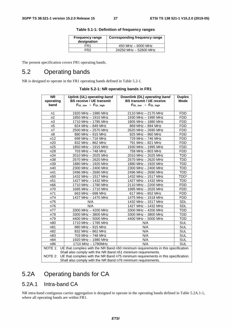
ETSI
ETSI TS 138 521-1 V15.2.0 (2019-05)273GPP TS 38.521-1 version 15.2.0 Release 15
Table 5.1-1: Definition of frequency ranges
Frequency range designation
Corresponding frequency range
FR1 450 MHz – 6000 MHz FR2 24250 MHz – 52600 MHz
The present specification covers FR1 operating bands.
5.2 Operating bands NR is designed to operate in the FR1 operating bands defined in Table 5.2-1.
Table 5.2-1: NR operating bands in FR1
NR operating
band
Uplink (UL) operating band BS receive / UE transmit
FUL_low – FUL_high
Downlink (DL) operating band BS transmit / UE receive
FDL_low – FDL_high
Duplex Mode
n1 1920 MHz – 1980 MHz 2110 MHz – 2170 MHz FDD n2 1850 MHz – 1910 MHz 1930 MHz – 1990 MHz FDD n3 1710 MHz – 1785 MHz 1805 MHz – 1880 MHz FDD n5 824 MHz – 849 MHz 869 MHz – 894 MHz FDD n7 2500 MHz – 2570 MHz 2620 MHz – 2690 MHz FDD n8 880 MHz – 915 MHz 925 MHz – 960 MHz FDD
n12 699 MHz – 716 MHz 729 MHz – 746 MHz FDD n20 832 MHz – 862 MHz 791 MHz – 821 MHz FDD n25 1850 MHz – 1915 MHz 1930 MHz – 1995 MHz FDD n28 703 MHz – 748 MHz 758 MHz – 803 MHz FDD n34 2010 MHz – 2025 MHz 2010 MHz – 2025 MHz TDD n38 2570 MHz – 2620 MHz 2570 MHz – 2620 MHz TDD n39 1880 MHz – 1920 MHz 1880 MHz – 1920 MHz TDD n40 2300 MHz – 2400 MHz 2300 MHz – 2400 MHz TDD n41 2496 MHz – 2690 MHz 2496 MHz – 2690 MHz TDD n50 1432 MHz – 1517 MHz 1432 MHz – 1517 MHz TDD1 n51 1427 MHz – 1432 MHz 1427 MHz – 1432 MHz TDD n66 1710 MHz – 1780 MHz 2110 MHz – 2200 MHz FDD n70 1695 MHz – 1710 MHz 1995 MHz – 2020 MHz FDD n71 663 MHz – 698 MHz 617 MHz – 652 MHz FDD n74 1427 MHz – 1470 MHz 1475 MHz – 1518 MHz FDD n75 N/A 1432 MHz – 1517 MHz SDL n76 N/A 1427 MHz – 1432 MHz SDL n77 3300 MHz – 4200 MHz 3300 MHz – 4200 MHz TDD n78 3300 MHz – 3800 MHz 3300 MHz – 3800 MHz TDD n79 4400 MHz – 5000 MHz 4400 MHz – 5000 MHz TDD n80 1710 MHz – 1785 MHz N/A SUL n81 880 MHz – 915 MHz N/A SUL n82 832 MHz – 862 MHz N/A SUL n83 703 MHz – 748 MHz N/A SUL n84 1920 MHz – 1980 MHz N/A SUL n86 1710 MHz – 1780MHz N/A SUL
NOTE 1: UE that complies with the NR Band n50 minimum requirements in this specification. Shall also comply with the NR Band n51 minimum requirements.
NOTE 2: UE that complies with the NR Band n75 minimum requirements in this specification. Shall also comply with the NR Band n76 minimum requirements.
5.2A Operating bands for CA
5.2A.1 Intra-band CA
NR intra-band contiguous carrier aggregation is designed to operate in the operating bands defined in Table 5.2A.1-1, where all operating bands are within FR1.
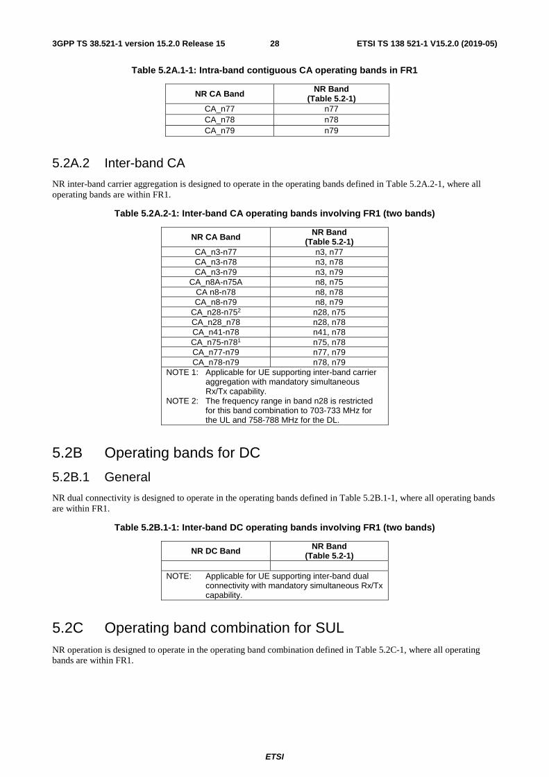
ETSI
ETSI TS 138 521-1 V15.2.0 (2019-05)283GPP TS 38.521-1 version 15.2.0 Release 15
Table 5.2A.1-1: Intra-band contiguous CA operating bands in FR1
NR CA Band NR Band (Table 5.2-1)
CA_n77 n77 CA_n78 n78 CA_n79 n79
5.2A.2 Inter-band CA
NR inter-band carrier aggregation is designed to operate in the operating bands defined in Table 5.2A.2-1, where all operating bands are within FR1.
Table 5.2A.2-1: Inter-band CA operating bands involving FR1 (two bands)
NR CA Band NR Band (Table 5.2-1)
CA_n3-n77 n3, n77 CA_n3-n78 n3, n78 CA_n3-n79 n3, n79
CA_n8A-n75A n8, n75 CA n8-n78 n8, n78 CA_n8-n79 n8, n79
CA_n28-n752 n28, n75 CA_n28_n78 n28, n78 CA_n41-n78 n41, n78 CA_n75-n781 n75, n78 CA_n77-n79 n77, n79 CA_n78-n79 n78, n79
NOTE 1: Applicable for UE supporting inter-band carrier aggregation with mandatory simultaneous Rx/Tx capability.
NOTE 2: The frequency range in band n28 is restricted for this band combination to 703-733 MHz for the UL and 758-788 MHz for the DL.
5.2B Operating bands for DC
5.2B.1 General
NR dual connectivity is designed to operate in the operating bands defined in Table 5.2B.1-1, where all operating bands are within FR1.
Table 5.2B.1-1: Inter-band DC operating bands involving FR1 (two bands)
NR DC Band NR Band (Table 5.2-1)
NOTE: Applicable for UE supporting inter-band dual
connectivity with mandatory simultaneous Rx/Tx capability.
5.2C Operating band combination for SUL NR operation is designed to operate in the operating band combination defined in Table 5.2C-1, where all operating bands are within FR1.
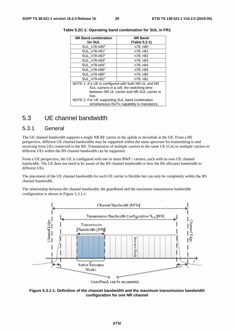
ETSI
ETSI TS 138 521-1 V15.2.0 (2019-05)293GPP TS 38.521-1 version 15.2.0 Release 15
Table 5.2C-1: Operating band combination for SUL in FR1
NR Band combination for SUL
NR Band (Table 5.2-1)
SUL_n78-n802 n78, n80 SUL_n78-n812 n78, n81 SUL_n78-n822 n78, n82 SUL_n78-n832 n78, n83 SUL_n78-n842 n78, n84 SUL_n78-n862 n78, n86 SUL_n79-n802 n79, n80 SUL_n79-n812 n79, n81
NOTE 1: If a UE is configured with both NR UL and NR SUL carriers in a cell, the switching time between NR UL carrier and NR SUL carrier is 0us.
NOTE 2: For UE supporting SUL band combination simultaneous Rx/Tx capability is mandatory.
5.3 UE channel bandwidth
5.3.1 General
The UE channel bandwidth supports a single NR RF carrier in the uplink or downlink at the UE. From a BS perspective, different UE channel bandwidths may be supported within the same spectrum for transmitting to and receiving from UEs connected to the BS. Transmission of multiple carriers to the same UE (CA) or multiple carriers to different UEs within the BS channel bandwidth can be supported.
From a UE perspective, the UE is configured with one or more BWP / carriers, each with its own UE channel bandwidth. The UE does not need to be aware of the BS channel bandwidth or how the BS allocates bandwidth to different UEs.
The placement of the UE channel bandwidth for each UE carrier is flexible but can only be completely within the BS channel bandwidth.
The relationship between the channel bandwidth, the guardband and the maximum transmission bandwidth configuration is shown in Figure 5.3.1-1.
Figure 5.3.1-1: Definition of the channel bandwidth and the maximum transmission bandwidth configuration for one NR channel

ETSI
ETSI TS 138 521-1 V15.2.0 (2019-05)303GPP TS 38.521-1 version 15.2.0 Release 15
5.3.2 Maximum transmission bandwidth configuration
The maximum transmission bandwidth configuration NRB for each UE channel bandwidth and subcarrier spacing is specified in Table 5.3.2-1.
Table 5.3.2-1: Maximum transmission bandwidth configuration NRB
5.3.3 Minimum guard band and transmission bandwidth configuration
The minimum guard band for each UE channel bandwidth and SCS is specified in Table 5.3.3-1.
Table 5.3.3-1: Minimum guard band for each UE channel bandwidth and SCS (kHz)
NOTE: The minimum guard bands have been calculated using the following equation: (CHBW x 1000 (kHz) - RB value x SCS x 12) / 2 - SCS/2, where RB values are from Table 5.3.2-1.
Figure 5.3.3-1: Void
The number of RBs configured in any channel bandwidth shall ensure that the minimum guard band specified in this clause is met.
Figure 5.3.3-2: UE PRB utilization
In the case that multiple numerologies are multiplexed in the same symbol due to transmission of SSB, the minimum guard band on each side of the carrier is the guard band applied at the configured channel bandwidth for the numerology that is received immediately adjacent to the guard.
If multiple numerologies are multiplexed in the same symbol and the UE channel bandwidth is >50 MHz, the minimum guard band applied adjacent to 15 kHz SCS shall be the same as the minimum guard band defined for 30 kHz SCS for the same UE channel bandwidth.
SCS (kHz)
5MHz 10MHz 15MHz 20 MHz
25 MHz 30 MHz 40
MHz 50MHz 60 MHz
80 MHz 90 MHz 100
MHz NRB NRB NRB NRB NRB NRB NRB NRB NRB NRB NRB NRB
15 25 52 79 106 133 160 216 270 N/A N/A N/A N/A 30 11 24 38 51 65 78 106 133 162 217 245 273 60 N/A 11 18 24 31 38 51 65 79 107 121 135
SCS (kHz) 5 MHz 10
MHz 15
MHz 20
MHz 25
MHz 30 MHz 40 MHz 50MHz 60
MHz 80 MHz 90 MHz 100 MHz
15 242.5 312.5 382.5 452.5 522.5 592.5 552.5 692.5 N/A N/A N/A N/A 30 505 665 645 805 785 945 905 1045 825 925 885 845 60 N/A 1010 990 1330 1310 1290 1610 1570 1530 1450 1410 1370
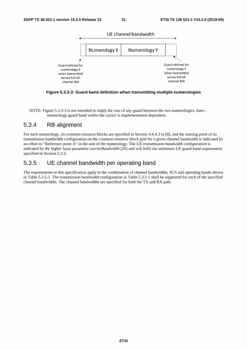
ETSI
ETSI TS 138 521-1 V15.2.0 (2019-05)313GPP TS 38.521-1 version 15.2.0 Release 15
Figure 5.3.3-3: Guard band definition when transmitting multiple numerologies
NOTE: Figure 5.3.3-3 is not intended to imply the size of any guard between the two numerologies. Inter-numerology guard band within the carrier is implementation dependent.
5.3.4 RB alignment
For each numerology, its common resource blocks are specified in Section 4.4.4.3 in [8], and the starting point of its transmission bandwidth configuration on the common resource block grid for a given channel bandwidth is indicated by an offset to “Reference point A” in the unit of the numerology. The UE transmission bandwidth configuration is indicated by the higher layer parameter carrierBandwidth [20] and will fulfil the minimum UE guard band requirement specified in Section 5.3.3.
5.3.5 UE channel bandwidth per operating band
The requirements in this specification apply to the combination of channel bandwidths, SCS and operating bands shown in Table 5.3.5-1. The transmission bandwidth configuration in Table 5.3.2-1 shall be supported for each of the specified channel bandwidths. The channel bandwidths are specified for both the TX and RX path.

ETSI
ETSI TS 138 521-1 V15.2.0 (2019-05)323GPP TS 38.521-1 version 15.2.0 Release 15
Table 5.3.5-1: Channel Bandwidths for Each NR band

ETSI
ETSI TS 138 521-1 V15.2.0 (2019-05)333GPP TS 38.521-1 version 15.2.0 Release 15
NR band / SCS / UE Channel bandwidth NR
Band SCS kHz
5 MHz
101,2 MHz
152 MHz
202 MHz
252 MHz
30 MHz
40 MHz
50 MHz
60 MHz
80 MHz
90 MHz 100 MHz
n1 15 Yes Yes Yes Yes 30 Yes Yes Yes 60 Yes Yes Yes
n2 15
Yes Yes Yes Yes 30 Yes Yes Yes 60 Yes Yes Yes
n3 15 Yes Yes Yes Yes Yes Yes 30 Yes Yes Yes Yes Yes 60 Yes Yes Yes Yes Yes
n5 15 Yes Yes Yes Yes 30 Yes Yes Yes 60
n7 15 Yes Yes Yes Yes 30 Yes Yes Yes 60 Yes Yes Yes
n8 15 Yes Yes Yes Yes 30 Yes Yes Yes 60
n12 15 Yes Yes Yes 30 Yes Yes 60
n20 15 Yes Yes Yes Yes 30 Yes Yes Yes 60
n25 15 Yes Yes Yes Yes 30 Yes Yes Yes 60 Yes Yes Yes
n28 15 Yes Yes Yes Yes 30 Yes Yes Yes 60
n34 15 Yes Yes Yes 30 Yes Yes 60 Yes Yes
n38 15 Yes Yes Yes Yes 30 Yes Yes Yes 60 Yes Yes Yes
n39 15 Yes Yes Yes Yes Yes Yes Yes 30 Yes Yes Yes Yes Yes Yes 60 Yes Yes Yes Yes Yes Yes
n40 15 Yes Yes Yes Yes Yes Yes Yes Yes 30 Yes Yes Yes Yes Yes Yes Yes Yes Yes 60 Yes Yes Yes Yes Yes Yes Yes Yes Yes
n41 15 Yes Yes Yes Yes Yes 30 Yes Yes Yes Yes Yes Yes Yes Yes Yes 60 Yes Yes Yes Yes Yes Yes Yes Yes Yes
n50 15 Yes Yes Yes Yes Yes Yes 30 Yes Yes Yes Yes Yes Yes Yes3 60 Yes Yes Yes Yes Yes Yes Yes3
n51 15 Yes 30 60
n66 15 Yes Yes Yes Yes Yes 30 Yes Yes Yes Yes 60 Yes Yes Yes Yes
n70 15 Yes Yes Yes Yes3 Yes3 30 Yes Yes Yes3 Yes3 60 Yes Yes Yes3 Yes3

ETSI
ETSI TS 138 521-1 V15.2.0 (2019-05)343GPP TS 38.521-1 version 15.2.0 Release 15
n71 15 Yes Yes Yes Yes 30 Yes Yes Yes 60
n74 15 Yes Yes Yes Yes 30 Yes Yes Yes 60 Yes Yes Yes
n75 15 Yes Yes Yes Yes 30 Yes Yes Yes 60 Yes Yes Yes
n76 15 Yes 30 60
n77 15 Yes Yes Yes Yes Yes 30 Yes Yes Yes Yes Yes Yes Yes Yes Yes 60 Yes Yes Yes Yes Yes Yes Yes Yes Yes
n78 15 Yes Yes Yes Yes Yes 30 Yes Yes Yes Yes Yes Yes Yes Yes Yes 60 Yes Yes Yes Yes Yes Yes Yes Yes Yes
n79 15 Yes Yes 30 Yes Yes Yes Yes Yes 60 Yes Yes Yes Yes Yes
n80 15 Yes Yes Yes Yes Yes Yes 30 Yes Yes Yes Yes Yes 60 Yes Yes Yes Yes Yes
n81 15 Yes Yes Yes Yes 30 Yes Yes Yes 60
n82 15 Yes Yes Yes Yes 30 Yes Yes Yes 60
n83 15 Yes Yes Yes Yes 30 Yes Yes Yes 60
n84 15 Yes Yes Yes Yes 30 Yes Yes Yes
60 Yes Yes Yes
n86 15 Yes Yes Yes Yes Yes 30 Yes Yes Yes Yes 60 Yes Yes Yes Yes
NOTE 1: 90% spectrum utilization may not be achieved for 30kHz SCS. NOTE 2: 90% spectrum utilization may not be achieved for 60kHz SCS. NOTE 3: This UE channel bandwidth is applicable only to downlink. NOTE 4: For test configuration tables from the transmitter and receiver tests in Section 6 and 7 that
refer to this table for test SCS, the Lowest SCS refers to lowest supported SCS per channel bandwidth, Highest SCS refers to highest supported SCS per channel bandwidth.
NOTE 5: For test configuration tables from the transmitter and receiver tests in Section 6 and 7 that refer to this table and list and list the test SCS as Mid or any other value; if that value is not supported by the UE in UL and/or DL, select the closest SCS supported by the UE in both UL and DL.
5.3.6 Asymmetric channel bandwidths
The UE channel bandwidth can be asymmetric in downlink and uplink. In asymmetric channel bandwidth operation, the narrower carrier shall be confined within the frequency range of the wider channel bandwidth.
In FDD, the confinement is defined as a deviation to the default Tx-Rx carrier centre frequency separation (defined in Table 5.4.4-1) as following:
ΔFTX-RX = | (BWDL – BWUL)/2 |
The operating bands and supported asymmetric channel bandwidth combinations are defined in Table 5.3.6-1.

ETSI
ETSI TS 138 521-1 V15.2.0 (2019-05)353GPP TS 38.521-1 version 15.2.0 Release 15
Table 5.3.6-1: FDD asymmetric UL and DL channel bandwidth combinations
NR Band Channel
bandwidths for UL (MHz)
Channel bandwidths for DL
(MHz)
n66 5, 10 20, 40
20 40
n70 5 10, 15
5, 10, 15 20, 25
n71 5 10
10 15 15 20
In TDD, the operating bands and supported asymmetric channel bandwidth combinations are defined in Table 5.3.6-2.
Table 5.3.6-2: TDD asymmetric UL and DL channel bandwidth combinations
NR Band Channel bandwidths for UL
(MHz)
Channel bandwidths for DL
(MHz) n50 60 80
5.3A UE channel bandwidth for CA
5.3A.1 General
Figure 5.3A.1-1: Void
Figure 5.3A.1-2: Void
5.3A.2 Maximum transmission bandwidth configuration for CA
For carrier aggregation, the maximum transmission bandwidth configuration is defined per component carrier and the requirement is specified in subclause 5.3.2.
5.3A.3 Minimum guard band and transmission bandwidth configuration for CA
For intra-band contiguous carrier aggregation, Aggregated Channel Bandwidth and Guard Bands are defined as follows, see Figure 5.3A.3-1.

ETSI
ETSI TS 138 521-1 V15.2.0 (2019-05)363GPP TS 38.521-1 version 15.2.0 Release 15
FC, low
Lo
wer E
dg
e
Up
per E
dg
e
Lowest Carrier Transmission Bandwidth
Configuration [RB]
FC, high
Foffset, low
Highest Carrier Transmission Bandwidth
Configuration [RB]
Reso
urce b
lock
Aggregated Channel Bandwidth, BWchannel_CA (MHz)
Fedge, low Fedge, high
Foffset, high
Figure 5.3A.3-1: Definition of Aggregated Channel Bandwidth for intra-band carrier aggregation
The aggregated channel bandwidth, BWChannel_CA, is defined as
BWChannel_CA = Fedge,high - Fedge,low (MHz).
The lower bandwidth edge Fedge, low and the upper bandwidth edge Fedge,high of the aggregated channel bandwidth are used as frequency reference points for transmitter and receiver requirements and are defined by
Fedge,low = FC,low - Foffset,low
Fedge,high = FC,high + Foffset,high
The lower and upper frequency offsets depend on the transmission bandwidth configurations of the lowest and highest assigned edge component carrier and are defined as
Foffset,low = (NRB,low*12 + 1)*SCSlow/2 + BWGB (MHz)
Foffset,high = (NRB,high*12 - 1)*SCShigh/2 + BWGB (MHz)
BWGB = max(BWGB,Channel(k))
BWGB,Channel(k) is the minimum guard band defined in sub-clause 5.3.3 of carrier k, while NRB,low and NRB,high are the transmission bandwidth configurations according to Table 5.3.2-1 for the lowest and highest assigned component carrier, SCSlow and SCShigh are the sub-carrier spacing for the lowest and highest assigned component carrier respectively.
For intra-band non-contiguous carrier aggregation Sub-block Bandwidth and Sub-block edges are defined as follows, see Figure 5.3A.3-2.
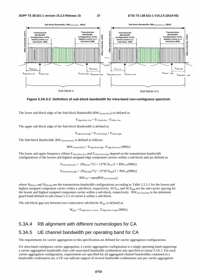
ETSI
ETSI TS 138 521-1 V15.2.0 (2019-05)373GPP TS 38.521-1 version 15.2.0 Release 15
...
Sub block n
Transmission Bandwidth
Configuration of the highest carrier in a
sub-block [RB]
Transmission Bandwidth
Configuration of the lowest carrier in a
sub-block [RB]
Fedge,block n, low FC,block n,high Fedge,block n,high
Foffset,high Foffset,low
FC,block n,low
Sub-block Bandwidth, BWChannel,block n (MHz)
Lo
wer S
ub
-blo
ck Ed
ge
Up
per S
ub
-blo
ck Ed
ge
Reso
urc
e blo
ck
Sub block n+1
Foffset, low
Fedge,block n+1, low FC,block n+1,low FC,block n+1,high Fedge,block n+1,high
Foffset,high
Sub-block Bandwidth, BWChannel,block n+1 (MHz)
Lo
wer S
ub
-blo
ck Ed
ge
Up
per S
ub
-blo
ck Ed
ge
Transmission Bandwidth
Configuration of the highest carrier in a
sub-block [RB]
Transmission Bandwidth
Configuration of the lowest carrier in a
sub-block [RB]
Reso
urc
e blo
ck
Figure 5.3A.3-2: Definition of sub-block bandwidth for intra-band non-contiguous spectrum
The lower sub-block edge of the Sub-block Bandwidth (BWChannel,block) is defined as
Fedge,block, low = FC,block,low - Foffset, low.
The upper sub-block edge of the Sub-block Bandwidth is defined as
Fedge,block,high = FC,block,high + Foffset,high.
The Sub-block Bandwidth, BWChannel,block, is defined as follows:
BWChannel,block = Fedge,block,high - Fedge,block,low (MHz)
The lower and upper frequency offsets Foffset,block,low and Foffset,block,high depend on the transmission bandwidth configurations of the lowest and highest assigned edge component carriers within a sub-block and are defined as
Foffset,block,low = (NRB,low*12 + 1)*SCSlow/2 + BWGB (MHz)
Foffset,block,high = (NRB,high*12 - 1)*SCShigh/2 + BWGB(MHz)
BWGB = max(BWGB,Channel(k))
where NRB,low and NRB,high are the transmission bandwidth configurations according to Table 5.3.2-1 for the lowest and highest assigned component carrier within a sub-block, respectively. SCSlow and SCShigh are the sub-carrier spacing for the lowest and highest assigned component carrier within a sub-block, respectively. BWGB,Channel(k) is the minimum guard band defined in sub-clause 5.3.3 of carrier k within a sub-block.
The sub-block gap size between two consecutive sub-blocks Wgap is defined as
Wgap = Fedge,block n+1,low - Fedge,block n,high (MHz)
5.3A.4 RB alignment with different numerologies for CA
5.3A.5 UE channel bandwidth per operating band for CA
The requirements for carrier aggregation in this specification are defined for carrier aggregation configurations.
For intra-band contiguous carrier aggregation, a carrier aggregation configuration is a single operating band supporting a carrier aggregation bandwidth class with associated bandwidth combination sets specified in clause 5.5A.1. For each carrier aggregation configuration, requirements are specified for all aggregated channel bandwidths contained in a bandwidth combination set, a UE can indicate support of several bandwidth combination sets per carrier aggregation

ETSI
ETSI TS 138 521-1 V15.2.0 (2019-05)383GPP TS 38.521-1 version 15.2.0 Release 15
configuration. For intra-band non-contiguous carrier aggregation, a carrier aggregation configuration is a single operating band supporting two or more sub-blocks, each supporting a carrier aggregation bandwidth class.
For inter-band carrier aggregation, a carrier aggregation configuration is a combination of operating bands, each supporting a carrier aggregation bandwidth class.
Table 5.3A.4-1: CA bandwidth classes
NR CA bandwidth class Aggregated channel bandwidth Number of contiguous CC
Fallback group
A BWChannel_CA ≤ BWChannel,max 1 B 20 MHz ≤ CBW ≤ 100 MHz 2 C 100 MHz < BWChannel_CA ≤ 2 x
BWChannel,max 2 1
D 200 MHz < BWChannel_CA ≤ 3 x BWChannel,max
3
E 300 MHz < BWChannel_CA ≤ 4 x BWChannel,max
4
F 50 MHz < BWChannel_CA ≤ 100 MHz 2 2 G 100 MHz < BWChannel_CA ≤ 150 MHz 3 H 150 MHz < BWChannel_CA ≤ 200 MHz 4 I 200 MHz < BWChannel_CA ≤ 250 MHz 5 J 250 MHz < BWChannel_CA ≤ 300 MHz 6 K 300 MHz < BWChannel_CA ≤ 350 MHz 7 L 350 MHz < BWChannel_CA ≤ 400 MHz 8
NOTE 1: BWChannel,max is maximum channel bandwidth supported among all bands in a release NOTE 2: It is mandatory for a UE to be able to fallback to lower order CA bandwidth class configuration within a fallback
group. It is not mandatory for a UE to be able to fallback to lower order CA bandwidth class configuration that belong to a different fallback group
5.4 Channel arrangement
5.4.1 Channel spacing
5.4.1.1 Channel spacing for adjacent NR carriers
The spacing between carriers will depend on the deployment scenario, the size of the frequency block available and the channel bandwidths. The nominal channel spacing between two adjacent NR carriers is defined as following:
- For NR operating bands with 100 kHz channel raster,
Nominal Channel spacing = (BWChannel(1) + BWChannel(2))/2
- For NR operating bands with 15 kHz channel raster,
Nominal Channel spacing = (BWChannel(1) + BWChannel(2))/2+{-5kHz, 0kHz, 5kHz}
- For NR operating bands with 30 kHz channel raster,
Nominal Channel spacing = (BWChannel(1) + BWChannel(2))/2+{-10kHz, 0kHz, 10kHz}
where BWChannel(1) and BWChannel(2) are the channel bandwidths of the two respective NR carriers. The channel spacing can be adjusted depending on the channel raster to optimize performance in a particular deployment scenario.
5.4.2 Channel raster
5.4.2.1 NR-ARFCN and channel raster
The global frequency channel raster defines a set of RF reference frequencies FREF. The RF reference frequency is used in signalling to identify the position of RF channels, SS blocks and other elements.
The global frequency raster is defined for all frequencies from 0 to 100 GHz. The granularity of the global frequency raster is ΔFGlobal.
ETSI
ETSI TS 138 521-1 V15.2.0 (2019-05)393GPP TS 38.521-1 version 15.2.0 Release 15
RF reference frequencies are designated by an NR Absolute Radio Frequency Channel Number (NR-ARFCN) in the range (0.. 2016666] on the global frequency raster. The relation between the NR-ARFCN and the RF reference frequency FREF in MHz is given by the following equation, where FREF-Offs and NRef-Offs are given in Table 5.4.2.1-1 and NREF is the NR-ARFCN.
FREF = FREF-Offs + ΔFGlobal (NREF – NREF-Offs)
Table 5.4.2.1-1: NR-ARFCN parameters for the global frequency raster
Frequency range (MHz) ΔFGlobal (kHz) FREF-Offs (MHz) NREF-Offs Range of NREF 0 – 3000 5 0 0 0 – 599999
3000 – 24250 15 3000 600000 600000 – 2016666
The channel raster defines a subset of RF reference frequencies that can be used to identify the RF channel position in the uplink and downlink. The RF reference frequency for an RF channel maps to a resource element on the carrier. For each operating band, a subset of frequencies from the global frequency raster are applicable for that band and forms a channel raster with a granularity ΔFRaster, which may be equal to or larger than ΔFGlobal.
For SUL bands and for the uplink of FDD bands defined in Table 5.2-1.
FREF, shift = FREF + Δshift, Δshift=0kHz or 7.5 kHz.
where Δshift is signalled by the network in higher layer parameter frequencyShift7p5khz [6].
The mapping between the channel raster and corresponding resource element is given in Section 5.4.2.2. The applicable entries for each operating band are defined in Section 5.4.2.3
5.4.2.2 Channel raster to resource element mapping
The mapping between the RF reference frequency on the channel raster and the corresponding resource element is given in Table 5.4.2.2-1 and can be used to identify the RF channel position. The mapping depends on the total number of RBs that are allocated in the channel and applies to both UL and DL. The mapping must apply to at least one numerology supported by the UE.
Table 5.4.2.2-1: Channel raster to resource element mapping
02modRB =N 12modRB =N
Resource element index k 0 6
Physical resource block number PRBn
=
2RB
PRB
Nn
=
2RB
PRB
Nn
k , PRBn , RBN are as defined in TS 38.211[8].
5.4.2.3 Channel raster entries for each operating band
The RF channel positions on the channel raster in each NR operating band are given through the applicable NR-ARFCN in Table 5.4.2.3-1, using the channel raster to resource element mapping in subclause 5.4.2.2.
For NR operating bands with 100 kHz channel raster, ΔFRaster = 20 × ΔFGlobal. In this case every 20th NR-ARFCN within the operating band are applicable for the channel raster within the operating band and the step size for the channel raster in Table 5.4.2.3-1 is given as <20>.
For NR operating bands with 15 kHz channel raster below 3GHz, ΔFRaster = I × ΔFGlobal, where I ϵ {3,6}. Every Ith NR-ARFCN within the operating band are applicable for the channel raster within the operating band and the step size for the channel raster in Table 5.4.2.3-1 is given as < I >.
For NR operating bands with 15 kHz channel raster above 3GHz, ΔFRaster = I × ΔFGlobal, where I ϵ {1,2}. Every Ith NR-ARFCN within the operating band are applicable for the channel raster within the operating band and the step size for the channel raster in table 5.4.2.3-1 is given as <I>.

ETSI
ETSI TS 138 521-1 V15.2.0 (2019-05)403GPP TS 38.521-1 version 15.2.0 Release 15
In frequency bands with two ΔFRaster, the higher ΔFRaster applies to channels using only the SCS that equals the higher ΔFRaster.
Table 5.4.2.3-1: Applicable NR-ARFCN per operating band
NR Operating
Band
ΔFRaster (kHz)
Uplink Range of NREF
(First – <Step size> – Last)
Downlink Range of NREF
(First – <Step size> – Last) n1 100 384000 – <20> – 396000 422000 – <20> – 434000 n2 100 370000 – <20> – 382000 386000 – <20> – 398000 n3 100 342000 – <20> – 357000 361000 – <20> – 376000 n5 100 164800 – <20> – 169800 173800 – <20> – 178800 n7 100 500000 – <20> – 514000 524000 – <20> – 538000 n8 100 176000 – <20> – 183000 185000 – <20> – 192000
n12 100 139800 – <20> – 143200 145800 – <20> – 149200 n20 100 166400 – <20> – 172400 158200 – <20> – 164200 n25 100 370000 – <20> – 383000 386000 – <20> – 399000 n28 100 140600 – <20> – 149600 151600 – <20> – 160600 n34 100 402000 – <20> – 405000 402000 – <20> – 405000 n38 100 514000 – <20> – 524000 514000 – <20> – 524000 n39 100 376000 – <20> – 384000 376000 – <20> – 384000 n40 100 460000 – <20> – 480000 460000 – <20> – 480000 n41 15 499200 – <3> – 537999 499200 – <3> – 537999
30 499200 – <6> – 537996 499200 – <6> – 537996 n51 100 285400 – <20> – 286400 285400 – <20> – 286400 n66 100 342000 – <20> – 356000 422000 – <20> – 440000 n70 100 339000 – <20> – 342000 399000 – <20> – 404000 n71 100 132600 – <20> – 139600 123400 – <20> – 130400 n75 100 N/A 286400 – <20> – 303400 n76 100 N/A 285400 – <20> – 286400 n77 15 620000 – <1> – 680000 620000 – <1> – 680000
30 620000 – <2> – 680000 620000 – <2> – 680000 n78 15 620000 – <1> – 653333 620000 – <1> – 653333
30 620000 – <2> – 653332 620000 – <2> – 653332 n79 15 693334 – <1> – 733333 693334 – <1> – 733333
30 693334 – <2> – 733332 693334 – <2> – 733332 n80 100 342000 – <20> – 357000 N/A n81 100 176000 – <20> – 183000 N/A n82 100 166400 – <20> – 172400 N/A n83 100 140600 – <20> –149600 N/A n84 100 384000 – <20> – 396000 N/A n86 100 342000 – <20> – 356000 N/A
5.4.3 Synchronization raster
5.4.3.1 Synchronization raster and numbering
The synchronization raster indicates the frequency positions of the synchronization block that can be used by the UE for system acquisition when explicit signalling of the synchronization block position is not present.
A global synchronization raster is defined for all frequencies. The frequency position of the SS block is defined as SSREF with corresponding number GSCN. The parameters defining the SSREF and GSCN for all the frequency ranges are in Table 5.4.3.1-1.
The resource element corresponding to the SS block reference frequency SSREF is given in subclause 5.4.3.2. The synchronization raster and the subcarrier spacing of the synchronization block are defined separately for each band.

ETSI
ETSI TS 138 521-1 V15.2.0 (2019-05)413GPP TS 38.521-1 version 15.2.0 Release 15
Table 5.4.3.1-1: GSCN parameters for the global frequency raster
Frequency range SS Block frequency position SSREF GSCN Range of GSCN
0 – 3000 MHz N * 1200kHz + M * 50 kHz, N=1:2499, M ϵ {1,3,5} (Note 1) [3N + (M-3)/2] [2 – 7498]
3000-24250 MHz 2400 MHz + N * 1.44 MHz N = 0:14756
[7499 + N] [7499 – 22255]
NOTE 1: The default value for operating bands with SCS spaced channel raster is M=3.
5.4.3.2 Synchronization raster to synchronization block resource element mapping
The mapping between the synchronization raster and the corresponding resource element of the SS block is given in Table 5.4.3.2-1. The mapping depends on the total number of RBs that are allocated in the channel and applies to both UL and DL.
Table 5.4.3.2-1: Synchronization raster to SS block resource element mapping
Resource element index k 0
Physical resource block number PRBn of the SS block 10PRB =n
k , PRBn ,are as defined in TS 38.211[8].
5.4.3.3 Synchronization raster entries for each operating band
The synchronization raster for each band is given in Table 5.4.3.3-1. The distance between applicable GSCN entries is given by the <Step size> indicated in Table 5.4.3.3-1.
Table 5.4.3.3-1: Applicable SS raster entries per operating band
NR Operating Band SS Block SCS SS Block pattern1 Range of GSCN (First – <Step size> – Last)
n1 15kHz Case A 5279 – <1> – 5419 n2 15kHz Case A 4829 – <1> – 4969 n3 15kHz Case A 4517 – <1> – 4693
n5 15kHz Case A 2177 – <1> – 2230 30kHz Case B 2183 – <1> – 2224
n7 15kHz Case A 6554 – <1> – 6718 n8 15kHz Case A 2318 – <1> – 2395
n12 15kHz Case A 1828 – <1> – 1858 n20 15kHz Case A 1982 – <1> – 2047 n25 15 kHz Case A 4829 – <1> – 4981 n28 15kHz Case A 1901 – <1> – 2002 n34 15kHz Case A 5030 – <1> – 5056 n38 15kHz Case A 6431 – <1> – 6544 n39 15kHz Case A 4706 – <1> – 4795 n40 15kHz Case A 5756 – <1> – 5995 n41 15kHz Case A 6246 – <9> – 6714
30 kHz Case C 6252 – <3> – 6714 n51 15kHz Case A 3572 – <1> – 3574
n66 15kHz Case A 5279 – <1> – 5494 30kHz Case B 5285 – <1> – 5488
n70 15kHz Case A 4993 – <1> – 5044 n71 15kHz Case A 1547 – <1> – 1624 n74 15kHz Case A 3692 – <1> – 3790 n75 15kHz Case A 3584 – <1> – 3787 n76 15kHz Case A 3572 – <1> – 3574 n77 30kHz Case C 7711 – <1> – 8329 n78 30kHz Case C 7711 – <1> – 8051 n79 30kHz Case C 8480 – <16> – 8880
NOTE 1: SS Block pattern is defined in section 4.1 in TS 38.213 [9]

ETSI
ETSI TS 138 521-1 V15.2.0 (2019-05)423GPP TS 38.521-1 version 15.2.0 Release 15
5.4.4 TX–RX frequency separation
The default TX channel (carrier centre frequency) to RX channel (carrier centre frequency) separation for operating bands is specified in Table 5.4.4-1.
Table 5.4.4-1: Default UE TX-RX frequency separation
NR Operating Band TX – RX carrier centre frequency
separation n1 190 MHz n2 80 MHz n3 95 MHz n5 45 MHz n7 120 MHz n8 45 MHz
n12 30 MHz n20 -41 MHz n25 80 MHz n28 55 MHz n66 400 MHz n70 295,3001 MHz n71 -46 MHz n74 48 MHz
NOTE 1: Default TX-RX carrier centre frequency separation.
5.4A Channel arrangement for CA
5.4A.1 Channel spacing for CA
For intra-band contiguous carrier aggregation with two or more component carriers, the nominal channel spacing between two adjacent NR component carriers is defined as the following unless stated otherwise:
For NR operating bands with 100 kHz channel raster:
[MHz]3.06.0
2spacingchannelNominal
)2()1()2()1(
−−+= ChannelChannelChannelChannel GBGBBWBW
For NR operating bands with 15 kHz channel raster:
[MHz]2*015.02*015.0
2spacingchannelNominal
1
)2()1()2()1( nn
ChannelChannelChannelChannel GBGBBWBW
−−+= +
with
),max( 21 μμ=n
where BWChannel(1) and BWChannel(2) are the channel bandwidths of the two respective NR component carriers according to Table 5.3.2-1 with values in MHz. and the GBChannel(i) is the minimum guard band defined in sub-clause 5.3.3, while µ1 and µ2 are the subcarrier spacing configurations of the component carriers as defined in TS 38.211. The channel spacing for intra-band contiguous carrier aggregation can be adjusted to any multiple of least common multiple of channel raster and sub-carrier spacing less than the nominal channel spacing to optimize performance in a particular deployment scenario.
For intra-band non-contiguous carrier aggregation the channel spacing between two NR component carriers in different sub-blocks shall be larger than the nominal channel spacing defined in this subclause
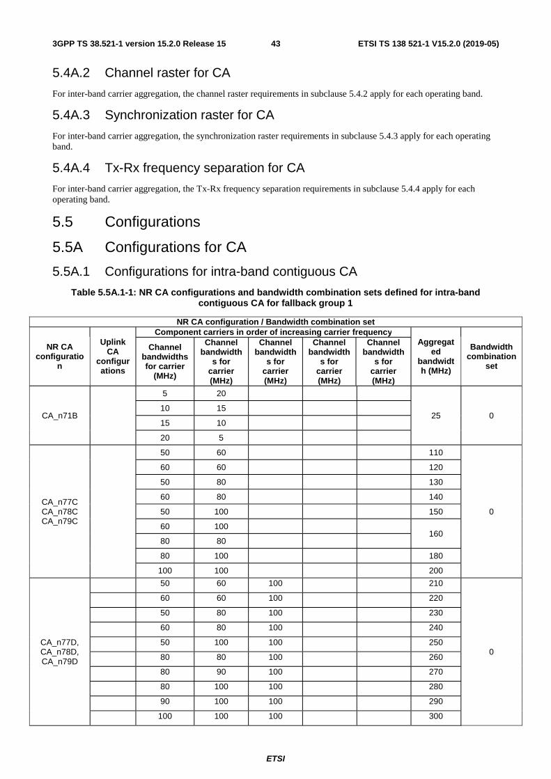
ETSI
ETSI TS 138 521-1 V15.2.0 (2019-05)433GPP TS 38.521-1 version 15.2.0 Release 15
5.4A.2 Channel raster for CA
For inter-band carrier aggregation, the channel raster requirements in subclause 5.4.2 apply for each operating band.
5.4A.3 Synchronization raster for CA
For inter-band carrier aggregation, the synchronization raster requirements in subclause 5.4.3 apply for each operating band.
5.4A.4 Tx-Rx frequency separation for CA
For inter-band carrier aggregation, the Tx-Rx frequency separation requirements in subclause 5.4.4 apply for each operating band.
5.5 Configurations
5.5A Configurations for CA
5.5A.1 Configurations for intra-band contiguous CA
Table 5.5A.1-1: NR CA configurations and bandwidth combination sets defined for intra-band contiguous CA for fallback group 1
NR CA configuration / Bandwidth combination set
NR CA configuratio
n
Uplink CA
configurations
Component carriers in order of increasing carrier frequency Aggregat
ed bandwidth (MHz)
Bandwidth combination
set
Channel bandwidths for carrier
(MHz)
Channel bandwidth
s for carrier (MHz)
Channel bandwidth
s for carrier (MHz)
Channel bandwidth
s for carrier (MHz)
Channel bandwidth
s for carrier (MHz)
CA_n71B
5 20
25 0 10 15
15 10
20 5
CA_n77C CA_n78C CA_n79C
50 60 110
0
60 60 120
50 80 130
60 80 140
50 100 150
60 100 160
80 80
80 100 180
100 100 200
CA_n77D, CA_n78D, CA_n79D
50 60 100 210
0
60 60 100 220
50 80 100 230
60 80 100 240
50 100 100 250
80 80 100 260
80 90 100 270
80 100 100 280
90 100 100 290
100 100 100 300

ETSI
ETSI TS 138 521-1 V15.2.0 (2019-05)443GPP TS 38.521-1 version 15.2.0 Release 15
CA_n77E, CA_n78E, CA_n79E
50 60 100 100 310
0
60 60 100 100 320
50 80 100 100 330
60 80 100 100 340
50 100 100 100 350
80 80 100 100 360
80 90 100 100 370
80 100 100 100 380
90 100 100 100 390
100 100 100 100 400
Table 5.5A-2: Void
ETSI
ETSI TS 138 521-1 V15.2.0 (2019-05)453GPP TS 38.521-1 version 15.2.0 Release 15
5.5A.2 Configurations for intra-band non-contiguous CA
Detailed structure of the subclause is TBD.

ETSI
ETSI TS 138 521-1 V15.2.0 (2019-05)463GPP TS 38.521-1 version 15.2.0 Release 15
5.5A.3 Configurations for inter-band CA
Table 5.5A.3-1: NR CA configurations and bandwidth combinations sets defined for inter-band CA (two bands)
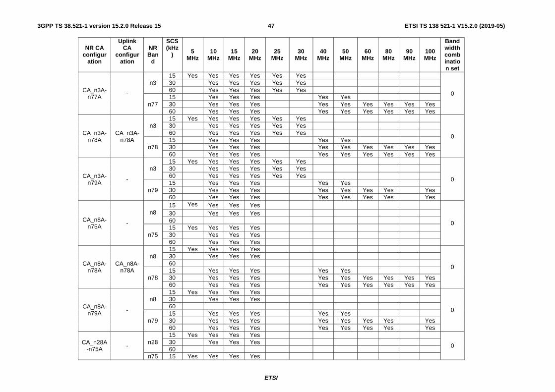
ETSI
ETSI TS 138 521-1 V15.2.0 (2019-05)473GPP TS 38.521-1 version 15.2.0 Release 15
NR CA configur
ation
Uplink CA
configuration
NR Ban
d
SCS (kHz
) 5 MHz
10 MHz
15 MHz
20 MHz
25 MHz
30 MHz
40 MHz
50 MHz
60 MHz
80 MHz
90 MHz
100 MHz
Bandwidth combination set
CA_n3A-n77A -
n3 15 Yes Yes Yes Yes Yes Yes
0
30 Yes Yes Yes Yes Yes 60 Yes Yes Yes Yes Yes
n77 15 Yes Yes Yes Yes Yes 30 Yes Yes Yes Yes Yes Yes Yes Yes Yes 60 Yes Yes Yes Yes Yes Yes Yes Yes Yes
CA_n3A-n78A
CA_n3A-n78A
n3 15 Yes Yes Yes Yes Yes Yes
0
30 Yes Yes Yes Yes Yes 60 Yes Yes Yes Yes Yes
n78 15 Yes Yes Yes Yes Yes 30 Yes Yes Yes Yes Yes Yes Yes Yes Yes 60 Yes Yes Yes Yes Yes Yes Yes Yes Yes
CA_n3A-n79A -
n3 15 Yes Yes Yes Yes Yes Yes
0
30 Yes Yes Yes Yes Yes 60 Yes Yes Yes Yes Yes
n79 15 Yes Yes Yes Yes Yes 30 Yes Yes Yes Yes Yes Yes Yes Yes 60 Yes Yes Yes Yes Yes Yes Yes Yes
CA_n8A-n75A -
n8 15 Yes Yes Yes Yes
0
30 Yes Yes Yes 60
n75 15 Yes Yes Yes Yes 30 Yes Yes Yes 60 Yes Yes Yes
CA_n8A-n78A
CA_n8A-n78A
n8 15 Yes Yes Yes Yes
0
30 Yes Yes Yes 60
n78 15 Yes Yes Yes Yes Yes 30 Yes Yes Yes Yes Yes Yes Yes Yes Yes 60 Yes Yes Yes Yes Yes Yes Yes Yes Yes
CA_n8A-n79A -
n8 15 Yes Yes Yes Yes
0
30 Yes Yes Yes 60
n79 15 Yes Yes Yes Yes Yes 30 Yes Yes Yes Yes Yes Yes Yes Yes 60 Yes Yes Yes Yes Yes Yes Yes Yes
CA_n28A-n75A -
n28 15 Yes Yes Yes Yes
0 30 Yes Yes Yes 60
n75 15 Yes Yes Yes Yes
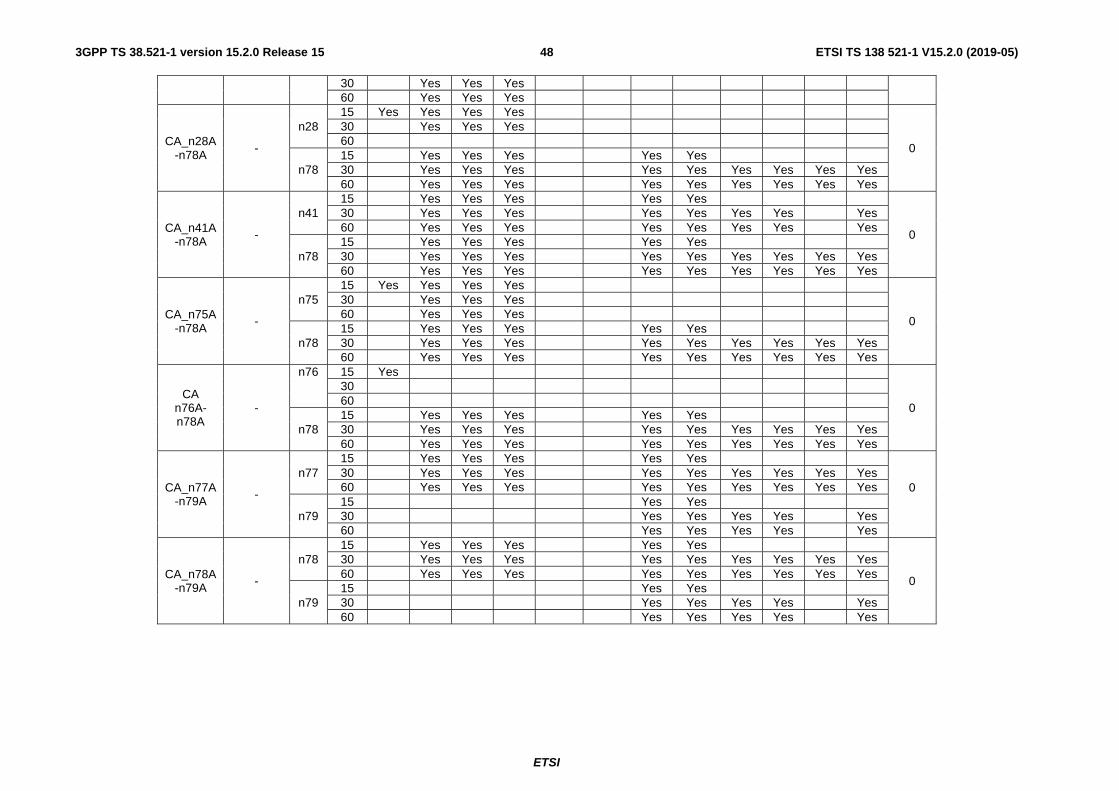
ETSI
ETSI TS 138 521-1 V15.2.0 (2019-05)483GPP TS 38.521-1 version 15.2.0 Release 15
30 Yes Yes Yes 60 Yes Yes Yes
CA_n28A-n78A -
n28 15 Yes Yes Yes Yes
0
30 Yes Yes Yes 60
n78 15 Yes Yes Yes Yes Yes 30 Yes Yes Yes Yes Yes Yes Yes Yes Yes 60 Yes Yes Yes Yes Yes Yes Yes Yes Yes
CA_n41A-n78A -
n41 15 Yes Yes Yes Yes Yes
0
30 Yes Yes Yes Yes Yes Yes Yes Yes 60 Yes Yes Yes Yes Yes Yes Yes Yes
n78 15 Yes Yes Yes Yes Yes 30 Yes Yes Yes Yes Yes Yes Yes Yes Yes 60 Yes Yes Yes Yes Yes Yes Yes Yes Yes
CA_n75A-n78A
-
n75 15 Yes Yes Yes Yes
0
30 Yes Yes Yes 60 Yes Yes Yes
n78 15 Yes Yes Yes Yes Yes 30 Yes Yes Yes Yes Yes Yes Yes Yes Yes 60 Yes Yes Yes Yes Yes Yes Yes Yes Yes
CA n76A-n78A
-
n76 15 Yes
0
30 60
n78 15 Yes Yes Yes Yes Yes 30 Yes Yes Yes Yes Yes Yes Yes Yes Yes 60 Yes Yes Yes Yes Yes Yes Yes Yes Yes
CA_n77A-n79A -
n77 15 Yes Yes Yes Yes Yes
0
30 Yes Yes Yes Yes Yes Yes Yes Yes Yes 60 Yes Yes Yes Yes Yes Yes Yes Yes Yes
n79 15 Yes Yes 30 Yes Yes Yes Yes Yes 60 Yes Yes Yes Yes Yes
CA_n78A-n79A -
n78 15 Yes Yes Yes Yes Yes
0
30 Yes Yes Yes Yes Yes Yes Yes Yes Yes 60 Yes Yes Yes Yes Yes Yes Yes Yes Yes
n79 15 Yes Yes 30 Yes Yes Yes Yes Yes 60 Yes Yes Yes Yes Yes

ETSI
ETSI TS 138 521-1 V15.2.0 (2019-05)493GPP TS 38.521-1 version 15.2.0 Release 15
5.5B Configurations for DC
5.5C Configurations for SUL Table 5.5C-1: Supported channel bandwidths per SUL band combination
SUL configurati
on NR Band
Subcarrier spacing
(kHz) 5 MHz
10 MHz
15 MHz
20 MHz
25 MHz
30 MHz
40 MHz
50 MHz
60 MHz
80 MHz
90 MHz
100 MHz
Bandwid
th combination set
SUL_n78A-n80A
n78 15 Yes Yes Yes Yes Yes
0 30 Yes Yes Yes Yes Yes Yes Yes Yes Yes 60 Yes Yes Yes Yes Yes Yes Yes Yes Yes
n80 15 Yes Yes Yes Yes Yes Yes
SUL_n78A-n81A
n78 15 Yes Yes Yes Yes Yes
0 30 Yes Yes Yes Yes Yes Yes Yes Yes Yes 60 Yes Yes Yes Yes Yes Yes Yes Yes Yes
n81 15 Yes Yes Yes Yes
SUL_n78A-n82A
n78 15 Yes Yes Yes Yes Yes
0 30 Yes Yes Yes Yes Yes Yes Yes Yes Yes 60 Yes Yes Yes Yes Yes Yes Yes Yes Yes
n82 15 Yes Yes Yes Yes
SUL_n78A-n83A
n78 15 Yes Yes Yes Yes Yes
0 30 Yes Yes Yes Yes Yes Yes Yes Yes Yes 60 Yes Yes Yes Yes Yes Yes Yes Yes Yes
n83 15 Yes Yes Yes Yes
SUL_n78A-n84A
n78 15 Yes Yes Yes Yes Yes
0 30 Yes Yes Yes Yes Yes Yes Yes Yes Yes 60 Yes Yes Yes Yes Yes Yes Yes Yes Yes
n84 15 Yes Yes Yes Yes
SUL_n78A-n86A
n78 15 Yes Yes Yes Yes Yes
0 30 Yes Yes Yes Yes Yes Yes Yes Yes Yes 60 Yes Yes Yes Yes Yes Yes Yes Yes Yes
n86 15 Yes Yes Yes Yes
SUL_n79A-n80A
n79 15 Yes Yes
0 30 Yes Yes Yes Yes Yes 60 Yes Yes Yes Yes Yes
n80 15 Yes Yes Yes Yes Yes Yes
SUL_n79A-n81A
n79 15 Yes Yes
0 30 Yes Yes Yes Yes Yes 60 Yes Yes Yes Yes Yes
n81 15 Yes Yes Yes Yes
ETSI
ETSI TS 138 521-1 V15.2.0 (2019-05)503GPP TS 38.521-1 version 15.2.0 Release 15
6 Transmitter characteristics
6.1 General Unless otherwise stated, the transmitter characteristics are specified at the antenna connector of the UE with a single or multiple transmit antenna(s). For UE with integral antenna only, a reference antenna with a gain of 0 dBi is assumed.
Unless otherwise stated, Channel Bandwidth shall be prioritized in the selecting of test points. Subcarrier spacing shall be selected after Test Channel Bandwidth is selected.
Uplink RB allocations given in Table 6.1-1 are used throughout this section, unless otherwise stated by the test case.

ETSI
ETSI TS 138 521-1 V15.2.0 (2019-05)513GPP TS 38.521-1 version 15.2.0 Release 15
Table 6.1-1: Common uplink configuration

ETSI
ETSI TS 138 521-1 V15.2.0 (2019-05)523GPP TS 38.521-1 version 15.2.0 Release 15
Channel Bandwidth SCS(kHz) OFDM
RB allocation
Ed
ge_
Fu
ll_L
eft
Ed
ge_
Fu
ll_R
igh
t
Ed
ge_
1RB
_Lef
t
Ed
ge_
1RB
_Rig
ht
Ou
ter_
Fu
ll
Inn
er_F
ull
Inn
er_1
RB
_Lef
t
Inn
er_1
RB
_Rig
ht
5MHz
15 DFT-s 2@0 2@23 1@0 1@24 25@0 12@6 1@1 1@23
CP 2@0 2@23 1@0 1@24 25@0 13@6 1@1 1@23
30 DFT-s 2@0 2@9 1@0 1@10 10@0 5@21 1@1 1@9
CP 2@0 2@9 1@0 1@10 11@0 5@21 1@1 1@9
60 DFT-s N/A N/A N/A N/A N/A N/A N/A N/A
CP N/A N/A N/A N/A N/A N/A N/A N/A
10MHz
15 DFT-s 2@0 2@50 1@0 1@51 50@0 25@12 1@1 1@50
CP 2@0 2@50 1@0 1@51 52@0 26@13 1@1 1@50
30 DFT-s 2@0 2@22 1@0 1@23 24@0 12@6 1@1 1@22
CP 2@0 2@22 1@0 1@23 24@0 12@6 1@1 1@22
60 DFT-s 2@0 2@9 1@0 1@10 10@0 5@21 1@1 1@9
CP 2@0 2@9 1@0 1@10 11@0 5@21 1@1 1@9
15MHz
15 DFT-s 2@0 2@77 1@0 1@78 75@0 36@18 1@1 1@77
CP 2@0 2@77 1@0 1@78 79@0 39@191 1@1 1@77
30 DFT-s 2@0 2@36 1@0 1@37 36@0 18@9 1@1 1@36
CP 2@0 2@36 1@0 1@37 38@0 19@9 1@1 1@36
60 DFT-s 2@0 2@16 1@0 1@17 18@0 9@4 1@1 1@16
CP 2@0 2@16 1@0 1@17 18@0 9@4 1@1 1@16
20MHz
15 DFT-s 2@0 2@104 1@0 1@105 100@0 50@25 1@1 1@104
CP 2@0 2@104 1@0 1@105 106@0 53@26 1@1 1@104
30 DFT-s 2@0 2@49 1@0 1@50 50@0 25@12 1@1 1@49
CP 2@0 2@49 1@0 1@50 51@0 25@121 1@1 1@49
60 DFT-s 2@0 2@22 1@0 1@23 24@0 12@6 1@1 1@22
CP 2@0 2@22 1@0 1@23 24@0 12@6 1@1 1@22
25MHz
15 DFT-s 2@0 2@131 1@0 1@132 128@0 64@32 1@1 1@131
CP 2@0 2@131 1@0 1@132 133@0 67@33 1@1 1@131
30 DFT-s 2@0 2@63 1@0 1@64 64@0 32@16 1@1 1@63
CP 2@0 2@63 1@0 1@64 65@0 33@16 1@1 1@63
60 DFT-s 2@0 2@29 1@0 1@30 30@0 15@71 1@1 1@29
CP 2@0 2@29 1@0 1@30 31@0 15@71 1@1 1@29
30MHz
15 DFT-s 2@0 2@158 1@0 1@159 160@0 80@40 1@1 1@158
CP 2@0 2@158 1@0 1@159 160@0 80@40 1@1 1@158
30 DFT-s 2@0 2@76 1@0 1@77 75@0 36@18 1@1 1@76
CP 2@0 2@76 1@0 1@77 78@0 39@19 1@1 1@76
60 DFT-s 2@0 2@36 1@0 1@37 36@0 18@9 1@1 1@36
CP 2@0 2@36 1@0 1@37 38@0 19@9 1@1 1@36
40MHz
15 DFT-s 2@0 2@214 1@0 1@215 216@0 108@54 1@1 1@214
CP 2@0 2@214 1@0 1@215 216@0 108@54 1@1 1@214
30 DFT-s 2@0 2@104 1@0 1@105 100@0 50@25 1@1 1@104
CP 2@0 2@104 1@0 1@105 106@0 53@26 1@1 1@104
60 DFT-s 2@0 2@49 1@0 1@50 50@0 25@12 1@1 1@49
CP 2@0 2@49 1@0 1@50 51@0 25@121 1@1 1@49
50MHz
15 DFT-s 2@0 2@268 1@0 1@269 270@0 135@67 1@1 1@268
CP 2@0 2@268 1@0 1@269 270@0 135@67 1@1 1@268
30 DFT-s 2@0 2@131 1@0 1@132 128@0 64@32 1@1 1@131
CP 2@0 2@131 1@0 1@132 133@0 67@33 1@1 1@131
60 DFT-s 2@0 2@63 1@0 1@64 64@0 32@16 1@1 1@63
CP 2@0 2@63 1@0 1@64 65@0 33@16 1@1 1@63
60MHz
15 DFT-s N/A N/A N/A N/A N/A N/A N/A N/A
CP N/A N/A N/A N/A N/A N/A N/A N/A
30 DFT-s 2@0 2@160 1@0 1@161 162@0 81@40 1@1 1@160
CP 2@0 2@160 1@0 1@161 162@0 81@40 1@1 1@160
60 DFT-s 2@0 2@77 1@0 1@78 75@0 36@18 1@1 1@77
CP 2@0 2@77 1@0 1@78 79@0 39@191 1@1 1@77
80MHz 15 DFT-s N/A N/A N/A N/A N/A N/A N/A N/A
CP N/A N/A N/A N/A N/A N/A N/A N/A
ETSI
ETSI TS 138 521-1 V15.2.0 (2019-05)533GPP TS 38.521-1 version 15.2.0 Release 15
30 DFT-s 2@0 2@215 1@0 1@216 216@0 108@54 1@1 1@215
CP 2@0 2@215 1@0 1@216 217@0 109@54 1@1 1@215
60 DFT-s 2@0 2@105 1@0 1@106 100@0 50@25 1@1 1@105
CP 2@0 2@105 1@0 1@106 107@0 53@261 1@1 1@105
90MHz
15 DFT-s N/A N/A N/A N/A N/A N/A N/A N/A
CP N/A N/A N/A N/A N/A N/A N/A N/A
30 DFT-s 2@0 2@243 1@0 1@244 240@0 120@60 1@1 1@243
CP 2@0 2@243 1@0 1@244 245@0 123@61 1@1 1@243
60 DFT-s 2@0 2@119 1@0 1@120 120@0 60@30 1@1 1@119
CP 2@0 2@119 1@0 1@120 121@0 61@30 1@1 1@119
100MHz
15 DFT-s N/A N/A N/A N/A N/A N/A N/A N/A
CP N/A N/A N/A N/A N/A N/A N/A N/A
30 DFT-s 2@0 2@271 1@0 1@272 270@0 135@67 1@1 1@271
CP 2@0 2@271 1@0 1@272 273@0 137@68 1@1 1@271
60 DFT-s 2@0 2@133 1@0 1@134 135@0 64@32 1@1 1@133
CP 2@0 2@133 1@0 1@134 135@0 67@331 1@1 1@133 Note 1: The allocated RB number LCRB is ceil(NRB/2) -1 in order to meet Inner RB allocation definition (RBStart,Low ≤
RBStart ≤ RBStart,High) described in subclause 6.2.2 of TS 38.101-1 [2].
6.2 Transmitter power
6.2.1 UE maximum output power
6.2.1.1 Test purpose
To verify that the error of the UE maximum output power does not exceed the range prescribed by the specified nominal maximum output power and tolerance.
An excess maximum output power has the possibility to interfere to other channels or other systems. A small maximum output power decreases the coverage area.
6.2.1.2 Test applicability
This test case applies to all types of NR UE release 15 and forward.
6.2.1.3 Minimum conformance requirements
The following UE Power Classes define the maximum output power for any transmission bandwidth within the channel bandwidth of NR carrier unless otherwise stated. The period of measurement shall be at least one sub frame (1ms).

ETSI
ETSI TS 138 521-1 V15.2.0 (2019-05)543GPP TS 38.521-1 version 15.2.0 Release 15
Table 6.2.1.3-1: UE Power Class
NR band
Class 1 (dBm)
Tolerance (dB)
Class 2 (dBm)
Tolerance (dB)
Class 3 (dBm)
Tolerance (dB)
n1 23 ± 2 n2 23 ± 23 n3 23 ± 23 n5 23 ± 2 n7 23 ± 23 n8 23 ± 23
n12 23 ± 23 n20 23 ± 23 n25 23 ± 2 n28 23 +2/-2.5 n34 23 ± 2 n38 23 ± 2 n39 23 ± 2 n40 23 ± 2 n41 26 +2/-33 23 ± 23 n50 23 ± 2 n51 23 ± 2 n66 23 ± 2 n70 23 ± 2 n71 23 +2/-2.5 n74 23 ± 2 n77 26 +2/-3 23 +2/-3 n78 26 +2/-3 23 +2/-3 n79 26 +2/-3 23 +2/-3 n80 23 ± 2 n81 23 ± 2 n82 23 ± 2 n83 23 ± 2/-2.5 n84 23 ± 2 n86 23 ± 2
NOTE 1: PPowerClass is the maximum UE power specified without taking into account the tolerance
NOTE 2: Power class 3 is default power class unless otherwise stated NOTE 3: Refers to the transmission bandwidths (Figure 5.3.3-1) confined within FUL_low and
FUL_low + 4 MHz or FUL_high – 4 MHz and FUL_high, the maximum output power requirement is relaxed by reducing the lower tolerance limit by 1.5 dB
If a UE supports a different power class than the default UE power class for the band and the supported power class enables the higher maximum output power than that of the default power class:
- if the field of UE capability maxUplinkDutyCycle is absent and the percentage of uplink symbols transmitted in a certain evaluation period is larger than 50% (The exact evaluation period is no less than one radio frame); or
- if the field of UE capability maxUplinkDutyCycle is not absent and the percentage of uplink symbols transmitted in a certain evaluation period is larger than maxUplinkDutyCycle as defined in TS 38.331 (The exact evaluation period is no less than one radio frame); or
- if the IE P-Max as defined in TS 38.331 [6] is provided and set to the maximum output power of the default power class or lower;
- shall apply all requirements for the default power class to the supported power class and set the configured transmitted power as specified in sub-clause 6.2.4;
- else if (the IE P-Max as defined in TS 38.331 [6] is not provided or set to the higher value than the maximum output power of the default power class and the percentage of uplink symbols transmitted in a certain evaluation period is less than or equal to maxUplinkDutyCycle as defined in TS 38.331; or
the IE P-Max as defined in TS 38.331 [6] is not provided or set to the higher value than the maximum output power of the default power class and the percentage of uplink symbols transmitted in a certain evaluation period is less than or equal to 50% when maxUplinkDutyCycle is absent. The exact evaluation period is no less than one radio frame):

ETSI
ETSI TS 138 521-1 V15.2.0 (2019-05)553GPP TS 38.521-1 version 15.2.0 Release 15
- shall apply all requirements for the supported power class and set the configured transmitted power class as specified in sub-clause 6.2.4;
The normative reference for this requirement is TS 38.101-1 [2] clause 6.2.1.
6.2.1.4 Test description
6.2.1.4.1 Initial conditions
Initial conditions are a set of test configurations the UE needs to be tested in and the steps for the SS to take with the UE to reach the correct measurement state.
The initial test configurations consist of environmental conditions, test frequencies, test channel bandwidths and sub-carrier spacing based on NR operating bands specified in table 5.3.5-1. All of these configurations shall be tested with applicable test parameters for each combination of test channel bandwidth and sub-carrier spacing, and are shown in table 6.2.1.4.1-1. The details of the uplink reference measurement channels (RMCs) are specified in Annexes A.2. Configurations of PDSCH and PDCCH before measurement are specified in Annex C.2.
Table 6.2.1.4.1-1: Test Configuration Table
Initial Conditions Test Environment as specified in TS 38.508-1 [5] subclause 4.1
Normal, TL/VL, TL/VH, TH/VL, TH/VH
Test Frequencies as specified in TS 38.508-1 [5] subclause 4.3.1
Low range, Mid range, High range
Test Channel Bandwidths as specified in TS 38.508-1 [5] subclause 4.3.1
Lowest, Mid, Highest
Test SCS as specified in Table 5.3.5-1 Lowest, Highest Test Parameters
Test ID Downlink Configuration Uplink Configuration N/A for maximum output Modulation (NOTE 2) RB allocation (NOTE 1)
1 power test case DFT-s-OFDM PI/2 BPSK Inner Full 2 DFT-s-OFDM PI/2 BPSK Inner 1RB Left 3 DFT-s-OFDM PI/2 BPSK Inner 1RB Right 4 DFT-s-OFDM QPSK Inner Full 5 DFT-s-OFDM QPSK Inner 1RB Left 6 DFT-s-OFDM QPSK Inner 1RB Right
NOTE 1: The specific configuration of each RB allocation is defined in Table 6.1-1. NOTE 2: DFT-s-OFDM PI/2 BPSK test applies only for UEs which supports half Pi BPSK in FR1.
1. Connect the SS to the UE antenna connectors as shown in TS 38.508-1 [5] Annex A, Figure A.3.1.1.1 for TE diagram and section A.3.2.1 for UE diagram.
2. The parameter settings for the cell are set up according to TS 38.508-1 [5] subclause 4.4.3.
3. Downlink signals are initially set up according to Annex C.0, C.1, C.2, and uplink signals according to Annex G.0, G.1, G.2, G.3.0.
4. The UL Reference Measurement Channel is set according to Table 6.2.1.4.1-1.
5. Propagation conditions are set according to Annex B.0.
6. Ensure the UE is in state RRC_CONNECTED with generic procedure parameters Connectivity NR, Connected without release On, Test Mode On and Test Loop Function On according to TS 38.508-1 [5] clause 4.5. Message contents are defined in clause 6.2.1.4.3.
6.2.1.4.2 Test procedure
1. SS sends uplink scheduling information for each UL HARQ process via PDCCH DCI format 0_1 for C_RNTI to schedule the UL RMC according to Table 6.2.1.4.1-1. Since the UE has no payload and no loopback data to send the UE sends uplink MAC padding bits on the UL RMC.
2. Send continuously uplink power control "up" commands in every uplink scheduling information to the UE; allow at least 200ms starting from the first TPC command in this step for the UE to reach PUMAX level corresponding to Power Class 3.

ETSI
ETSI TS 138 521-1 V15.2.0 (2019-05)563GPP TS 38.521-1 version 15.2.0 Release 15
3. Measure the mean power of the UE in the channel bandwidth of the radio access mode. The period of measurement shall be at least the continuous duration of one active sub-frame (1ms) and in the uplink symbols. For TDD symbols with transient periods are not under test.
4. For UEs supporting Power Class 2, repeat steps 1~3 on the applicable bands except PUMAX level in step 2 is corresponding to Power Class 2.
6.2.1.4.3 Message contents
Message contents are according to TS 38.508-1 [5] subclause 4.6 and 5.4 with the following exceptions.
Table 6.2.1.4.3-1: PUSCH-Config
Derivation Path: TS 38.508-1 [5], Table 4.6.3-118 with condition TRANSFORM_PRECODER_ENABLED
6.2.1.5 Test requirement
The maximum output power, derived in step 3 shall be within the range prescribed by the nominal maximum output power and tolerance in Table 6.2.1.5-1.
The maximum output power, derived in step 4 shall be within the range prescribed by the nominal maximum output power and tolerance in Table 6.2.1.5-2.

ETSI
ETSI TS 138 521-1 V15.2.0 (2019-05)573GPP TS 38.521-1 version 15.2.0 Release 15
Table 6.2.1.5-1: Maximum Output Power test requirement for Power Class 3
NR band
Class 1 (dBm)
Tolerance (dB)
Class 2 (dBm)
Tolerance (dB)
Class 3 (dBm)
Tolerance (dB)
n1 23 ±2±TT n2 23 ±23±TT n3 23 ±23±TT n5 23 ±2±TT n7 23 ±23±TT n8 23 ±23±TT
n12 23 ±23±TT n20 23 ±23±TT n25 23 ±2±TT n28 23 +2/-2.5 n34 23 ±2±TT n38 23 ±2±TT n39 23 ±2±TT n40 23 ±2±TT n41 23 ± 23±TT n50 23 ±2±TT n51 23 ±2±TT n66 23 ±2±TT n70 23 ±2±TT
n71 23 +2+TT/-2.5-TT
n74 23 ±2±TT n77 23 +2+TT/-3-TT n78 23 +2+TT/-3-TT n79 23 +2+TT/-3-TT n80 23 ±2±TT n81 23 ±2±TT n82 23 ±2±TT
n83 23 +2+TT/-2.5-TT
n84 23 ±2±TT n86 23 ±2±TT
NOTE 1: PPowerClass is the maximum UE power specified without taking into account the tolerance
NOTE 2: Power class 3 is default power class unless otherwise stated NOTE 3: Refers to the transmission bandwidths (Figure 5.3.3-1) confined within FUL_low
and FUL_low + 4 MHz or FUL_high – 4 MHz and FUL_high, the maximum output power requirement is relaxed by reducing the lower tolerance limit by 1.5 dB
NOTE 4: TT for each frequency and channel bandwidth is specified in Table 6.2.1.5-3
Table 6.2.1.5-2: Maximum Output Power test requirement for Power Class 2
NR band
Class 1 (dBm)
Tolerance (dB)
Class 2 (dBm)
Tolerance (dB)
Class 3 (dBm)
Tolerance (dB)
n41 26 +2+TT/-33-TT
n77 26 +2+TT/-3-TT
n78 26 +2+TT/-3-
TT
n79 26 +2+TT/-3-TT
NOTE 1: PPowerClass is the maximum UE power specified without taking into account the tolerance
NOTE 2: Power class 3 is default power class unless otherwise stated NOTE 3: Refers to the transmission bandwidths (Figure 5.3.3-1) confined within FUL_low
and FUL_low + 4 MHz or FUL_high – 4 MHz and FUL_high, the maximum output power requirement is relaxed by reducing the lower tolerance limit by 1.5 dB
NOTE 4: TT for each frequency and channel bandwidth is specified in Table 6.2.1.5-3

ETSI
ETSI TS 138 521-1 V15.2.0 (2019-05)583GPP TS 38.521-1 version 15.2.0 Release 15
Table 6.2.1.5-3: Test Tolerance (UE maximum output power)
f ≤ 3.0GHz 3.0GHz < f ≤ 4.2GHz 4.2GHz < f ≤ 6.0GHz BW ≤ 40MHz 0.7 dB 1.0 dB 1.0 dB
40MHz < BW ≤ 100MHz 1.0 dB 1.0 dB 1.0 dB
6.2.2 Maximum Power Reduction (MPR)
Editor’s Note: The following aspects are either missing or not yet determined:
- There are still brackets and TBD left for PC 2 in the minimum requirement.
NOTE 1: - The minimum requirement for almost contiguous signals are not tested in the existing test points.
NOTE 2: - PC1 and PC4 requirements are not defined in RAN4 Rel-15 spec.
6.2.2.1 Test purpose
The number of RB identified in Table 6.2.2.3-1 is based on meeting the requirements for adjacent channel leakage ratio and the maximum power reduction (MPR) due to Cubic Metric (CM).
6.2.2.2 Test applicability
The requirements of this test apply in test cases 6.5.2.2.1 Adjacent Channel Leakage power Ratio to all types of NR Power Class [2] and 3 UE release 15 and forward.
NOTE: As a result TC 6.2.2 has not been included in the test case applicability table 4.1.1-1, TS 38.522. This does not preclude the test from being used for R&D or other purposes if deemed useful.
6.2.2.3 Minimum conformance requirements
UE is allowed to reduce the maximum output power due to higher order modulations and transmit bandwidth configurations. For UE Power Class [2] and 3, the allowed maximum power reduction (MPR) is defined in Table 6.2.2.3-2 and 6.2.2.3-1, respectively for channel bandwidths that meets both following criteria:
• Channel bandwidth ≤ 100MHz.
• Relative channel bandwidth ≤ 4% for TDD bands and ≤ 3% for FDD bands.
Where relative channel bandwidth = 2*BWChannel / (FUL_low + FUL_high).
Table 6.2.2.3-1: Maximum Power Reduction (MPR) for Power 3
Modulation MPR (dB) Edge RB allocations Outer RB allocations Inner RB allocations
DFT-s-OFDM PI/2 BPSK ≤ 3.51 ≤ 1.21 ≤ 0.21
≤ 0.52 02 DFT-s-OFDM QPSK ≤ 1 0
DFT-s-OFDM 16 QAM ≤ 2 ≤ 1 DFT-s-OFDM 64 QAM ≤ 2.5
DFT-s-OFDM 256 QAM ≤ 4.5 CP-OFDM QPSK ≤ 3 ≤ 1.5
CP-OFDM 16 QAM ≤ 3 ≤ 2 CP-OFDM 64 QAM ≤ 3.5
CP-OFDM 256 QAM ≤ 6.5 NOTE 1: Applicable for UE operating in TDD mode with PI/2 PBSK modulation and UE indicates
support for UE capability [powerBoosting-pi2BPSK] and if the IE powerBoostPi2BPSK is set to 1 and 40% or less slots in radio frame are used for UL transmission for bands n40, n41, n77, n78 and n79. The reference power of 0dB MPR is 26dBm.
NOTE 2: Applicable for UE operating in FDD mode, or in TDD mode in bands other than n40, n41, n77, n78 and n79 and if the IE powerBoostPi2BPSK is set to 0 and if more than 40% of slots in radio frame are used for UL transmission for bands n40, n41, n77, n78 and n79.
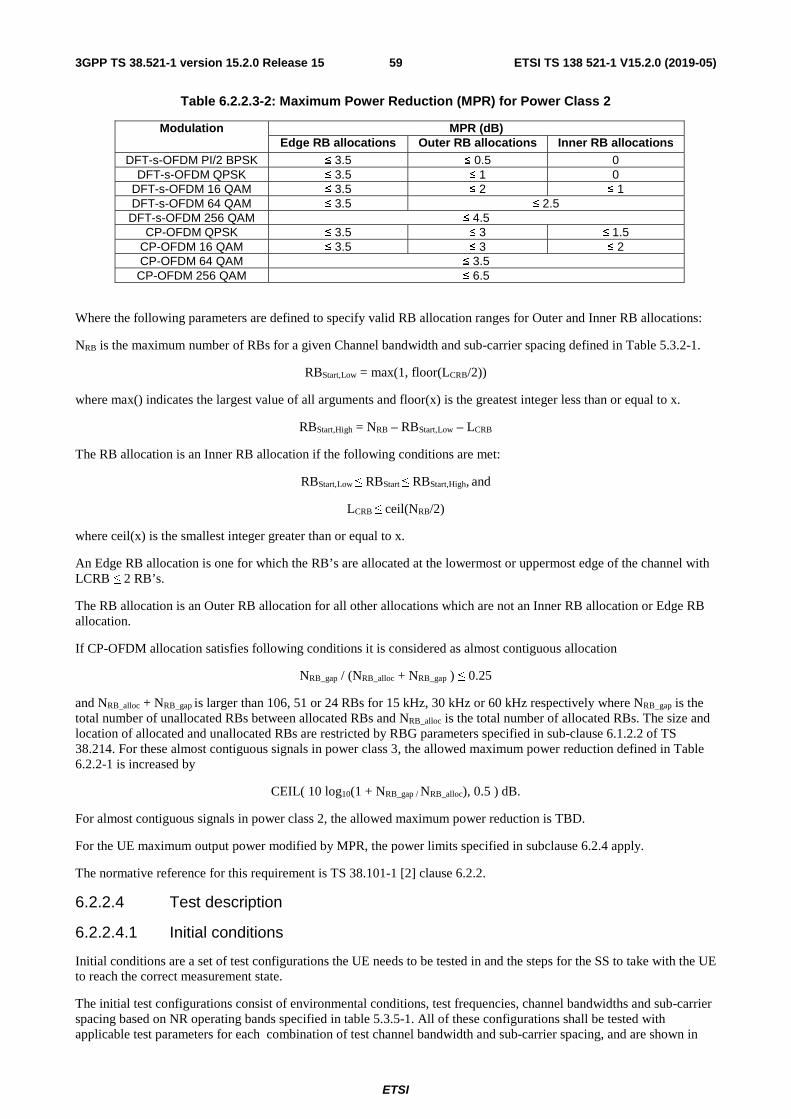
ETSI
ETSI TS 138 521-1 V15.2.0 (2019-05)593GPP TS 38.521-1 version 15.2.0 Release 15
Table 6.2.2.3-2: Maximum Power Reduction (MPR) for Power Class 2
Modulation MPR (dB) Edge RB allocations Outer RB allocations Inner RB allocations
DFT-s-OFDM PI/2 BPSK ≤ 3.5 ≤ 0.5 0 DFT-s-OFDM QPSK ≤ 3.5 ≤ 1 0
DFT-s-OFDM 16 QAM ≤ 3.5 ≤ 2 ≤ 1 DFT-s-OFDM 64 QAM ≤ 3.5 ≤ 2.5
DFT-s-OFDM 256 QAM ≤ 4.5 CP-OFDM QPSK ≤ 3.5 ≤ 3 ≤ 1.5
CP-OFDM 16 QAM ≤ 3.5 ≤ 3 ≤ 2 CP-OFDM 64 QAM ≤ 3.5
CP-OFDM 256 QAM ≤ 6.5
Where the following parameters are defined to specify valid RB allocation ranges for Outer and Inner RB allocations:
NRB is the maximum number of RBs for a given Channel bandwidth and sub-carrier spacing defined in Table 5.3.2-1.
RBStart,Low = max(1, floor(LCRB/2))
where max() indicates the largest value of all arguments and floor(x) is the greatest integer less than or equal to x.
RBStart,High = NRB – RBStart,Low – LCRB
The RB allocation is an Inner RB allocation if the following conditions are met:
RBStart,Low ≤ RBStart ≤ RBStart,High, and
LCRB ≤ ceil(NRB/2)
where ceil(x) is the smallest integer greater than or equal to x.
An Edge RB allocation is one for which the RB’s are allocated at the lowermost or uppermost edge of the channel with LCRB ≤ 2 RB’s.
The RB allocation is an Outer RB allocation for all other allocations which are not an Inner RB allocation or Edge RB allocation.
If CP-OFDM allocation satisfies following conditions it is considered as almost contiguous allocation
NRB_gap / (NRB_alloc + NRB_gap ) ≤ 0.25
and NRB_alloc + NRB_gap is larger than 106, 51 or 24 RBs for 15 kHz, 30 kHz or 60 kHz respectively where NRB_gap is the total number of unallocated RBs between allocated RBs and NRB_alloc is the total number of allocated RBs. The size and location of allocated and unallocated RBs are restricted by RBG parameters specified in sub-clause 6.1.2.2 of TS 38.214. For these almost contiguous signals in power class 3, the allowed maximum power reduction defined in Table 6.2.2-1 is increased by
CEIL( 10 log10(1 + NRB_gap / NRB_alloc), 0.5 ) dB.
For almost contiguous signals in power class 2, the allowed maximum power reduction is TBD.
For the UE maximum output power modified by MPR, the power limits specified in subclause 6.2.4 apply.
The normative reference for this requirement is TS 38.101-1 [2] clause 6.2.2.
6.2.2.4 Test description
6.2.2.4.1 Initial conditions
Initial conditions are a set of test configurations the UE needs to be tested in and the steps for the SS to take with the UE to reach the correct measurement state.
The initial test configurations consist of environmental conditions, test frequencies, channel bandwidths and sub-carrier spacing based on NR operating bands specified in table 5.3.5-1. All of these configurations shall be tested with applicable test parameters for each combination of test channel bandwidth and sub-carrier spacing, and are shown in

ETSI
ETSI TS 138 521-1 V15.2.0 (2019-05)603GPP TS 38.521-1 version 15.2.0 Release 15
table 6.2.2.4.1-1. The details of the uplink reference measurement channels (RMCs) are specified in Annexes A.2. Configurations of PDSCH and PDCCH before measurement are specified in Annex C.2.
Table 6.2.2.4.1-1: Test Configuration Table for Power Class 3
Initial Conditions Test Environment as specified in TS 38.508-1 [5] subclause 4.1
Normal, TL/VL, TL/VH, TH/VL, TH/VH
Test Frequencies as specified in TS 38.508-1 [5] subclause 4.3.1
Low range, High range
Test Channel Bandwidths as specified in TS 38.508-1 [5] subclause 4.3.1
Lowest, Highest
Test SCS as specified in Table 5.3.5-1 Lowest, Highest Test Parameters for Channel Bandwidths
Test ID
Freq Downlink Configuration Uplink Configuration
N/A for Maximum Power Modulation (NOTE 2) RB allocation (NOTE 1) 13 Default Reduction (MPR) test
case DFT-s-OFDM PI/2 BPSK Inner Full
23 Low DFT-s-OFDM PI/2 BPSK Edge_1RB_Left 33 High DFT-s-OFDM PI/2 BPSK Edge_1RB_Right 43 Default DFT-s-OFDM PI/2 BPSK Outer Full 54 Default DFT-s-OFDM PI/2 BPSK Inner Full 64 Low DFT-s-OFDM PI/2 BPSK Edge_1RB_Left 74 High DFT-s-OFDM PI/2 BPSK Edge_1RB_Right 84 Default DFT-s-OFDM PI/2 BPSK Outer Full 9 Default DFT-s-OFDM QPSK Inner Full 10 Low DFT-s-OFDM QPSK Edge_1RB_Left 11 High DFT-s-OFDM QPSK Edge_1RB_Right 12 Default DFT-s-OFDM QPSK Outer Full 13 Default DFT-s-OFDM 16 QAM Inner Full 14 Low DFT-s-OFDM 16 QAM Edge_1RB_Left 15 High DFT-s-OFDM 16 QAM Edge_1RB_Right 16 Default DFT-s-OFDM 16 QAM Outer Full 17 Low DFT-s-OFDM 64 QAM Edge_1RB_Left 18 High DFT-s-OFDM 64 QAM Edge_1RB_Right 19 Default DFT-s-OFDM 64 QAM Outer Full 20 Low DFT-s-OFDM 256 QAM Edge_1RB_Left 21 High DFT-s-OFDM 256 QAM Edge_1RB_Right 22 Default DFT-s-OFDM 256 QAM Outer Full 23 Default CP-OFDM QPSK Inner Full 24 Low CP-OFDM QPSK Edge_1RB_Left 25 High CP-OFDM QPSK Edge_1RB_Right 26 Default CP-OFDM QPSK Outer Full 27 Default CP-OFDM 16 QAM Inner Full 28 Low CP-OFDM 16 QAM Edge_1RB_Left 29 High CP-OFDM 16 QAM Edge_1RB_Right 30 Default CP-OFDM 16 QAM Outer Full 31 Low DFT-s-OFDM 64 QAM Edge_1RB_Left 32 High DFT-s-OFDM 64 QAM Edge_1RB_Right 33 Default CP-OFDM 64 QAM Outer Full 34 Low DFT-s-OFDM 256 QAM Edge_1RB_Left 35 High DFT-s-OFDM 256 QAM Edge_1RB_Right 36 Default CP-OFDM 256 QAM Outer Full
NOTE 1: The specific configuration of each RB allocation is defined in Table 6.1-1. NOTE 2: DFT-s-OFDM PI/2 BPSK test applies only for UEs which supports half Pi BPSK in FR1. NOTE 3: UE operating in TDD mode with PI/2 PBSK modulation and UE indicates support for UE capability
[powerBoosting-pi2BPSK] and the IE powerBoostPi2BPSK is set to 1 for bands n40, n41, n77, n78 and n79.
NOTE 4: UE operating in FDD mode, or in TDD mode in bands other than n40, n41, n77, n78 and n79, or in TDD mode the IE powerBoostPi2BPSK is set to 0 for bands n40, n77, n78 and n79.

ETSI
ETSI TS 138 521-1 V15.2.0 (2019-05)613GPP TS 38.521-1 version 15.2.0 Release 15
Table 6.2.2.4.1-2: Test Configuration Table for Power Class 2
Initial Conditions Test Environment as specified in TS 38.508-1 [5] subclause 4.1
Normal, TL/VL, TL/VH, TH/VL, TH/VH
Test Frequencies as specified in TS 38.508-1 [5] subclause 4.3.1
Low range, High range
Test Channel Bandwidths as specified in TS 38.508-1 [5] subclause 4.3.1
Lowest, Highest
Test SCS as specified in Table 5.3.5-1 Lowest, Highest Test Parameters for Channel Bandwidths
Test ID
Freq Downlink Configuration Uplink Configuration
N/A for Maximum Power Modulation (NOTE 2) RB allocation (NOTE 1) 1 Default Reduction (MPR) test
case DFT-s-OFDM PI/2 BPSK Inner Full
2 Low DFT-s-OFDM PI/2 BPSK Edge_1RB_Left 3 High DFT-s-OFDM PI/2 BPSK Edge_1RB_Right 4 Default DFT-s-OFDM PI/2 BPSK Outer Full 5 Default DFT-s-OFDM QPSK Inner Full 6 Low DFT-s-OFDM QPSK Edge_1RB_Left 7 High DFT-s-OFDM QPSK Edge_1RB_Right 8 Default DFT-s-OFDM QPSK Outer Full 9 Default DFT-s-OFDM 16 QAM Inner Full 10 Low DFT-s-OFDM 16 QAM Edge_1RB_Left 11 High DFT-s-OFDM 16 QAM Edge_1RB_Right 12 Default DFT-s-OFDM 16 QAM Outer Full 13 Low DFT-s-OFDM 64 QAM Edge_1RB_Left 14 High DFT-s-OFDM 64 QAM Edge_1RB_Right 15 Default DFT-s-OFDM 64 QAM Outer Full 16 Low DFT-s-OFDM 256 QAM Edge_1RB_Left 17 High DFT-s-OFDM 256 QAM Edge_1RB_Right 18 Default DFT-s-OFDM 256 QAM Outer Full 19 Default CP-OFDM QPSK Inner Full 20 Low CP-OFDM QPSK Edge_1RB_Left 21 High CP-OFDM QPSK Edge_1RB_Right 22 Default CP-OFDM QPSK Outer Full 23 Default CP-OFDM 16 QAM Inner Full 24 Low CP-OFDM 16 QAM Edge_1RB_Left 25 High CP-OFDM 16 QAM Edge_1RB_Right 26 Default CP-OFDM 16 QAM Outer Full 27 Low CP-OFDM 64 QAM Edge_1RB_Left 28 High CP-OFDM 64 QAM Edge_1RB_Right 29 Default CP-OFDM 64 QAM Outer Full 30 Low CP-OFDM 256 QAM Edge_1RB_Left 31 High CP-OFDM 256 QAM Edge_1RB_Right 32 Default CP-OFDM 256 QAM Outer Full
NOTE 1: The specific configuration of each RB allocation is defined in Table 6.1-1. NOTE 2: DFT-s-OFDM PI/2 BPSK test applies only for UEs which supports half Pi BPSK in FR1.
1. Connect the SS to the UE antenna connectors as shown in TS 38.508-1 [5] Annex A, Figure A.3.1.2.1 for TE diagram and section A.3.2.1 for UE diagram.
2. The parameter settings for the cell are set up according to TS 38.508-1 [5] subclause 4.4.3.
3. Downlink signals are initially set up according to Annex C.0, C.1, C.2 , and uplink signals according to Annex G.0, G.1, G.2, G.3.0 .
4. The UL Reference Measurement Channel is set according to Table 6.2.2.4.1-1.
5. Propagation conditions are set according to Annex B.0.
6. Ensure the UE is in State RRC_CONNECTED with generic procedure parameters Connectivity NR, Connected without release On, Test Mode On and Test Loop Function On according to TS 38.508-1 [5] clause 4.5. Message contents are defined in clause 6.2.2.4.3.
ETSI
ETSI TS 138 521-1 V15.2.0 (2019-05)623GPP TS 38.521-1 version 15.2.0 Release 15
6.2.2.4.2 Test procedure
1. SS sends uplink scheduling information for each UL HARQ process via PDCCH DCI format 0_1 for C_RNTI to schedule the UL RMC according to Table 6.2.2.4.1-1. Since the UE has no payload and no loopback data to send the UE sends uplink MAC padding bits on the UL RMC.
2. Send continuously uplink power control "up" commands in every uplink scheduling information to the UE; allow at least 200ms for the UE to reach PUMAX level.
3. Measure the mean power of the UE in the channel bandwidth of the radio access mode. The period of measurement shall be at least the continuous duration of one active sub-frame (1ms) and in the uplink symbols. For TDD slots with transient periods are not under test.
NOTE 1: When switching to DFT-s-OFDM waveform, as specified in the test configuration table 6.2.2.4.1-1, send an NR RRCReconfiguration message according to TS 38.508-1 [5] clause 4.6.3 Table 4.6.3-118 PUSCH-Config without CP-OFDM condition. When switching to CP-OFDM waveform, send an NR RRCReconfiguration message with CP-OFDM condition.
6.2.2.4.3 Message contents
Message contents are according to TS 38.508-1 [5] subclause 4.6 and 5.4.
6.2.2.5 Test requirement
The maximum output power, derived in step 3 shall be within the range prescribed by the nominal maximum output power and tolerance in Table 6.2.2.5-1 and Table 6.2.2.5-4.

ETSI
ETSI TS 138 521-1 V15.2.0 (2019-05)633GPP TS 38.521-1 version 15.2.0 Release 15
Table 6.2.2.5-1: UE Power Class test requirements(for Bands n1, n2, n3, n5, n7, n8, n12, n20, n25, n34, n38, n39, n40, n41, n50, n51, n66, n70, n74, n80, n81, n82, n84, n86) for Power Class 3
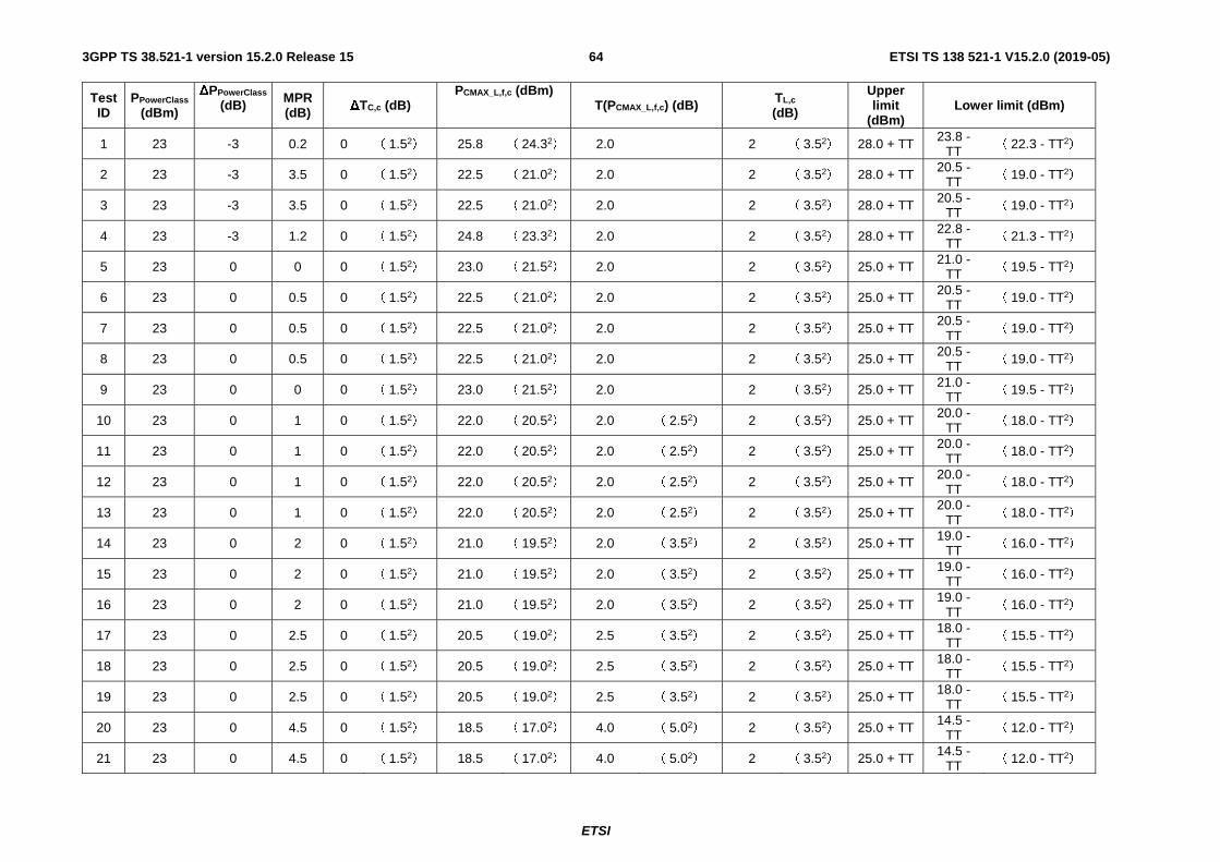
ETSI
ETSI TS 138 521-1 V15.2.0 (2019-05)643GPP TS 38.521-1 version 15.2.0 Release 15
Test ID
PPowerClass
(dBm)
ΔPPowerClass
(dB) MPR (dB) ΔTC,c (dB)
PCMAX_L,f,c (dBm) T(PCMAX_L,f,c) (dB) TL,c
(dB)
Upper limit
(dBm) Lower limit (dBm)
1 23 -3 0.2 0 ( 1.52) 25.8 ( 24.32) 2.0 2 ( 3.52) 28.0 + TT 23.8 - TT ( 22.3 - TT2)
2 23 -3 3.5 0 ( 1.52) 22.5 ( 21.02) 2.0 2 ( 3.52) 28.0 + TT 20.5 - TT ( 19.0 - TT2)
3 23 -3 3.5 0 ( 1.52) 22.5 ( 21.02) 2.0 2 ( 3.52) 28.0 + TT 20.5 - TT ( 19.0 - TT2)
4 23 -3 1.2 0 ( 1.52) 24.8 ( 23.32) 2.0 2 ( 3.52) 28.0 + TT 22.8 - TT ( 21.3 - TT2)
5 23 0 0 0 ( 1.52) 23.0 ( 21.52) 2.0 2 ( 3.52) 25.0 + TT 21.0 - TT ( 19.5 - TT2)
6 23 0 0.5 0 ( 1.52) 22.5 ( 21.02) 2.0 2 ( 3.52) 25.0 + TT 20.5 - TT ( 19.0 - TT2)
7 23 0 0.5 0 ( 1.52) 22.5 ( 21.02) 2.0 2 ( 3.52) 25.0 + TT 20.5 -
TT ( 19.0 - TT2)
8 23 0 0.5 0 ( 1.52) 22.5 ( 21.02) 2.0 2 ( 3.52) 25.0 + TT 20.5 - TT ( 19.0 - TT2)
9 23 0 0 0 ( 1.52) 23.0 ( 21.52) 2.0 2 ( 3.52) 25.0 + TT 21.0 - TT ( 19.5 - TT2)
10 23 0 1 0 ( 1.52) 22.0 ( 20.52) 2.0 ( 2.52) 2 ( 3.52) 25.0 + TT 20.0 -
TT ( 18.0 - TT2)
11 23 0 1 0 ( 1.52) 22.0 ( 20.52) 2.0 ( 2.52) 2 ( 3.52) 25.0 + TT 20.0 - TT ( 18.0 - TT2)
12 23 0 1 0 ( 1.52) 22.0 ( 20.52) 2.0 ( 2.52) 2 ( 3.52) 25.0 + TT 20.0 - TT ( 18.0 - TT2)
13 23 0 1 0 ( 1.52) 22.0 ( 20.52) 2.0 ( 2.52) 2 ( 3.52) 25.0 + TT 20.0 -
TT ( 18.0 - TT2)
14 23 0 2 0 ( 1.52) 21.0 ( 19.52) 2.0 ( 3.52) 2 ( 3.52) 25.0 + TT 19.0 - TT ( 16.0 - TT2)
15 23 0 2 0 ( 1.52) 21.0 ( 19.52) 2.0 ( 3.52) 2 ( 3.52) 25.0 + TT 19.0 - TT ( 16.0 - TT2)
16 23 0 2 0 ( 1.52) 21.0 ( 19.52) 2.0 ( 3.52) 2 ( 3.52) 25.0 + TT 19.0 - TT
( 16.0 - TT2)
17 23 0 2.5 0 ( 1.52) 20.5 ( 19.02) 2.5 ( 3.52) 2 ( 3.52) 25.0 + TT 18.0 - TT ( 15.5 - TT2)
18 23 0 2.5 0 ( 1.52) 20.5 ( 19.02) 2.5 ( 3.52) 2 ( 3.52) 25.0 + TT 18.0 - TT ( 15.5 - TT2)
19 23 0 2.5 0 ( 1.52) 20.5 ( 19.02) 2.5 ( 3.52) 2 ( 3.52) 25.0 + TT 18.0 - TT
( 15.5 - TT2)
20 23 0 4.5 0 ( 1.52) 18.5 ( 17.02) 4.0 ( 5.02) 2 ( 3.52) 25.0 + TT 14.5 - TT ( 12.0 - TT2)
21 23 0 4.5 0 ( 1.52) 18.5 ( 17.02) 4.0 ( 5.02) 2 ( 3.52) 25.0 + TT 14.5 - TT ( 12.0 - TT2)
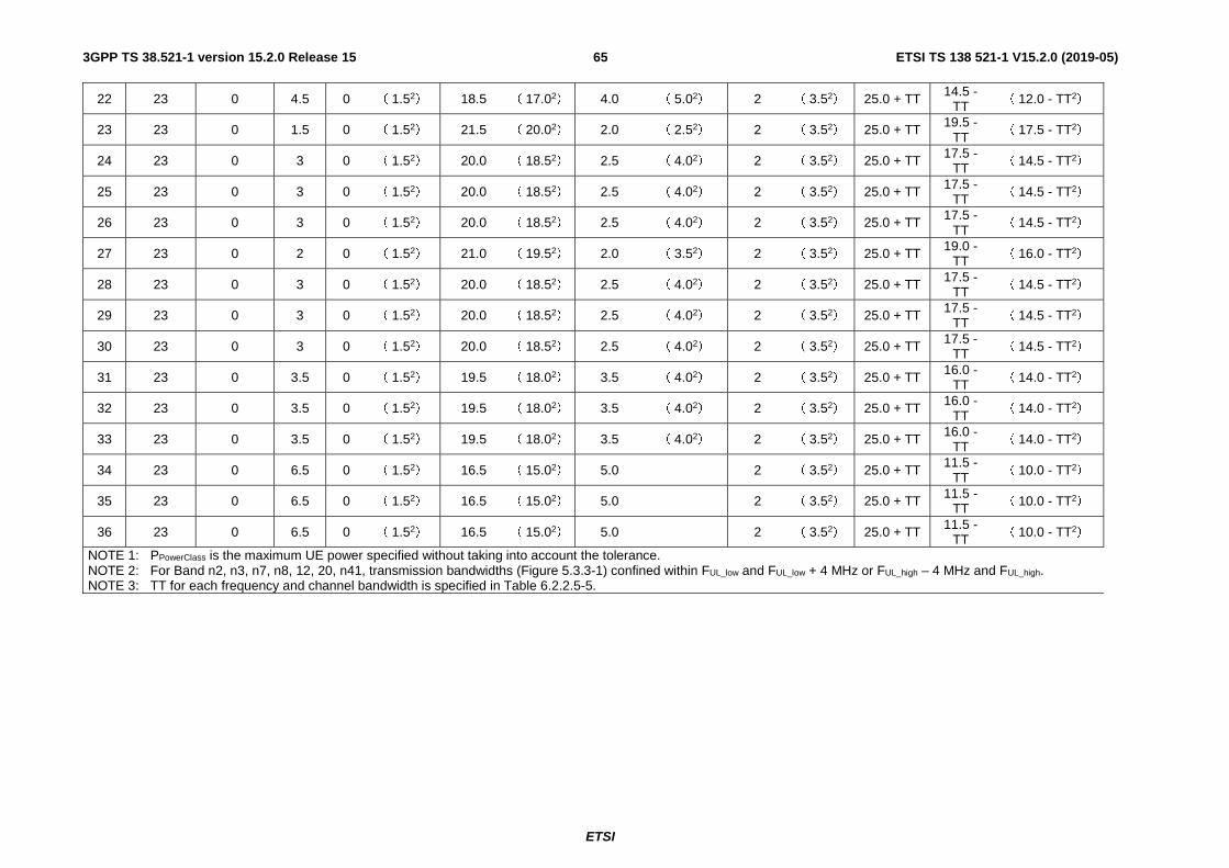
ETSI
ETSI TS 138 521-1 V15.2.0 (2019-05)653GPP TS 38.521-1 version 15.2.0 Release 15
22 23 0 4.5 0 ( 1.52) 18.5 ( 17.02) 4.0 ( 5.02) 2 ( 3.52) 25.0 + TT 14.5 - TT ( 12.0 - TT2)
23 23 0 1.5 0 ( 1.52) 21.5 ( 20.02) 2.0 ( 2.52) 2 ( 3.52) 25.0 + TT 19.5 - TT
( 17.5 - TT2)
24 23 0 3 0 ( 1.52) 20.0 ( 18.52) 2.5 ( 4.02) 2 ( 3.52) 25.0 + TT 17.5 - TT ( 14.5 - TT2)
25 23 0 3 0 ( 1.52) 20.0 ( 18.52) 2.5 ( 4.02) 2 ( 3.52) 25.0 + TT 17.5 - TT ( 14.5 - TT2)
26 23 0 3 0 ( 1.52) 20.0 ( 18.52) 2.5 ( 4.02) 2 ( 3.52) 25.0 + TT 17.5 - TT
( 14.5 - TT2)
27 23 0 2 0 ( 1.52) 21.0 ( 19.52) 2.0 ( 3.52) 2 ( 3.52) 25.0 + TT 19.0 - TT ( 16.0 - TT2)
28 23 0 3 0 ( 1.52) 20.0 ( 18.52) 2.5 ( 4.02) 2 ( 3.52) 25.0 + TT 17.5 - TT ( 14.5 - TT2)
29 23 0 3 0 ( 1.52) 20.0 ( 18.52) 2.5 ( 4.02) 2 ( 3.52) 25.0 + TT 17.5 - TT ( 14.5 - TT2)
30 23 0 3 0 ( 1.52) 20.0 ( 18.52) 2.5 ( 4.02) 2 ( 3.52) 25.0 + TT 17.5 - TT ( 14.5 - TT2)
31 23 0 3.5 0 ( 1.52) 19.5 ( 18.02) 3.5 ( 4.02) 2 ( 3.52) 25.0 + TT 16.0 - TT ( 14.0 - TT2)
32 23 0 3.5 0 ( 1.52) 19.5 ( 18.02) 3.5 ( 4.02) 2 ( 3.52) 25.0 + TT 16.0 - TT ( 14.0 - TT2)
33 23 0 3.5 0 ( 1.52) 19.5 ( 18.02) 3.5 ( 4.02) 2 ( 3.52) 25.0 + TT 16.0 - TT ( 14.0 - TT2)
34 23 0 6.5 0 ( 1.52) 16.5 ( 15.02) 5.0 2 ( 3.52) 25.0 + TT 11.5 -
TT ( 10.0 - TT2)
35 23 0 6.5 0 ( 1.52) 16.5 ( 15.02) 5.0 2 ( 3.52) 25.0 + TT 11.5 - TT ( 10.0 - TT2)
36 23 0 6.5 0 ( 1.52) 16.5 ( 15.02) 5.0 2 ( 3.52) 25.0 + TT 11.5 - TT ( 10.0 - TT2)
NOTE 1: PPowerClass is the maximum UE power specified without taking into account the tolerance. NOTE 2: For Band n2, n3, n7, n8, 12, 20, n41, transmission bandwidths (Figure 5.3.3-1) confined within FUL_low and FUL_low + 4 MHz or FUL_high – 4 MHz and FUL_high. NOTE 3: TT for each frequency and channel bandwidth is specified in Table 6.2.2.5-5.

ETSI
ETSI TS 138 521-1 V15.2.0 (2019-05)663GPP TS 38.521-1 version 15.2.0 Release 15
Table 6.2.2.5-2: UE Power Class test requirements(for Bands n28, n71, n83) for Power Class 3
Test ID PPowerClass
(dBm)
ΔPPowerClass
(dB) MPR (dB) ΔTC,c (dB)
PCMAX_L,f,c (dBm)
T(PCMAX_L,f,c) (dB)
TL,c
(dB)
Upper limit
(dBm)
Lower limit
(dBm)
5 23 0 0 0 23.0 2.0 2.5 25.0 + TT 20.5 - TT
6 23 0 0.5 0 22.5 2.0 2.5 25.0 + TT 20.0 - TT
7 23 0 0.5 0 22.5 2.0 2.5 25.0 + TT 20.0 - TT
8 23 0 0.5 0 22.5 2.0 2.5 25.0 + TT 20.0 - TT
9 23 0 0 0 23.0 2.0 2.5 25.0 + TT 20.5 - TT
10 23 0 1 0 22.0 2.0 2.5 25.0 + TT 19.5 - TT
11 23 0 1 0 22.0 2.0 2.5 25.0 + TT 19.5 - TT
12 23 0 1 0 22.0 2.0 2.5 25.0 + TT 19.5 - TT
13 23 0 1 0 22.0 2.0 2.5 25.0 + TT 19.5 - TT
14 23 0 2 0 21.0 2.0 2.5 25.0 + TT 18.5 - TT
15 23 0 2 0 21.0 2.0 2.5 25.0 + TT 18.5 - TT
16 23 0 2 0 21.0 2.0 2.5 25.0 + TT 18.5 - TT
17 23 0 2.5 0 20.5 2.5 2.5 25.0 + TT 18.0 - TT
18 23 0 2.5 0 20.5 2.5 2.5 25.0 + TT 18.0 - TT
19 23 0 2.5 0 20.5 2.5 2.5 25.0 + TT 18.0 - TT
20 23 0 4.5 0 18.5 4.0 2.5 25.0 + TT 14.5 - TT
21 23 0 4.5 0 18.5 4.0 2.5 25.0 + TT 14.5 - TT
22 23 0 4.5 0 18.5 4.0 2.5 25.0 + TT 14.5 - TT
23 23 0 1.5 0 21.5 2.0 2.5 25.0 + TT 19.0 - TT
24 23 0 3 0 20.0 2.5 2.5 25.0 + TT 17.5 - TT
25 23 0 3 0 20.0 2.5 2.5 25.0 + TT 17.5 - TT
26 23 0 3 0 20.0 2.5 2.5 25.0 + TT 17.5 - TT
27 23 0 2 0 21.0 2.0 2.5 25.0 + TT 18.5 - TT
28 23 0 3 0 20.0 2.5 2.5 25.0 + TT 17.5 - TT
29 23 0 3 0 20.0 2.5 2.5 25.0 + TT 17.5 - TT
30 23 0 3 0 20.0 2.5 2.5 25.0 + TT 17.5 - TT
31 23 0 3.5 0 19.5 3.5 2.5 25.0 + TT 16.0 - TT
32 23 0 3.5 0 19.5 3.5 2.5 25.0 + TT 16.0 - TT
33 23 0 3.5 0 19.5 3.5 2.5 25.0 + TT 16.0 - TT
34 23 0 6.5 0 16.5 5.0 2.5 25.0 + TT 11.5 - TT
35 23 0 6.5 0 16.5 5.0 2.5 25.0 + TT 11.5 - TT
36 23 0 6.5 0 16.5 5.0 2.5 25.0 + TT 11.5 - TT
NOTE 1: PPowerClass is the maximum UE power specified without taking into account the tolerance. NOTE 2: TT for each frequency and channel bandwidth is specified in Table 6.2.2.5-5.

ETSI
ETSI TS 138 521-1 V15.2.0 (2019-05)673GPP TS 38.521-1 version 15.2.0 Release 15
Table 6.2.2.5-3: UE Power Class test requirements (for Bands n77, n78, n79) for Power Class 3
Test ID
PPowerClass
(dBm) ΔPPowerClass
(dB) MPR (dB) ΔTC,c (dB)
PCMAX_L,f,c (dBm)
T(PCMAX_L,f,c) (dB)
TL,c
(dB) Upper limit
(dBm) Lower limit
(dBm)
1 23 -3 0.2 0 25.8 2.0 3 28.0 + TT 22.8 - TT
2 23 -3 3.5 0 22.5 2.0 3 28.0 + TT 19.5 - TT
3 23 -3 3.5 0 22.5 2.0 3 28.0 + TT 19.5 - TT
4 23 -3 1.2 0 24.8 2.0 3 28.0 + TT 21.8 - TT
5 23 0 0 0 23.0 2.0 3 25.0 + TT 20.0 - TT
6 23 0 0.5 0 22.5 2.0 3 25.0 + TT 19.5 - TT
7 23 0 0.5 0 22.5 2.0 3 25.0 + TT 19.5 - TT
8 23 0 0.5 0 22.5 2.0 3 25.0 + TT 19.5 - TT
9 23 0 0 0 23.0 2.0 3 25.0 + TT 20.0 - TT
10 23 0 1 0 22.0 2.0 3 25.0 + TT 19.0 - TT
11 23 0 1 0 22.0 2.0 3 25.0 + TT 19.0 - TT
12 23 0 1 0 22.0 2.0 3 25.0 + TT 19.0 - TT
13 23 0 1 0 22.0 2.0 3 25.0 + TT 19.0 - TT
14 23 0 2 0 21.0 2.0 3 25.0 + TT 18.0 - TT
15 23 0 2 0 21.0 2.0 3 25.0 + TT 18.0 - TT
16 23 0 2 0 21.0 2.0 3 25.0 + TT 18.0 - TT
17 23 0 2.5 0 20.5 2.5 3 25.0 + TT 17.5 - TT
18 23 0 2.5 0 20.5 2.5 3 25.0 + TT 17.5 - TT
19 23 0 2.5 0 20.5 2.5 3 25.0 + TT 17.5 - TT
20 23 0 4.5 0 18.5 4.0 3 25.0 + TT 14.5 - TT
21 23 0 4.5 0 18.5 4.0 3 25.0 + TT 14.5 - TT
22 23 0 4.5 0 18.5 4.0 3 25.0 + TT 14.5 - TT
23 23 0 1.5 0 21.5 2.0 3 25.0 + TT 18.5 - TT
24 23 0 3 0 20.0 2.5 3 25.0 + TT 17.0 - TT
25 23 0 3 0 20.0 2.5 3 25.0 + TT 17.0 - TT
26 23 0 3 0 20.0 2.5 3 25.0 + TT 17.0 - TT
27 23 0 2 0 21.0 2.0 3 25.0 + TT 18.0 - TT
28 23 0 3 0 20.0 2.5 3 25.0 + TT 17.0 - TT
29 23 0 3 0 20.0 2.5 3 25.0 + TT 17.0 - TT
30 23 0 3 0 20.0 2.5 3 25.0 + TT 17.0 - TT
31 23 0 3.5 0 19.5 3.5 3 25.0 + TT 16.0 - TT
32 23 0 3.5 0 19.5 3.5 3 25.0 + TT 16.0 - TT
33 23 0 3.5 0 19.5 3.5 3 25.0 + TT 16.0 - TT
34 23 0 6.5 0 16.5 5.0 3 25.0 + TT 11.5 - TT
35 23 0 6.5 0 16.5 5.0 3 25.0 + TT 11.5 - TT
36 23 0 6.5 0 16.5 5.0 3 25.0 + TT 11.5 - TT
NOTE 1: PPowerClass is the maximum UE power specified without taking into account the tolerance. NOTE 2: TT for each frequency and channel bandwidth is specified in Table 6.2.2.5-5.
ETSI
ETSI TS 138 521-1 V15.2.0 (2019-05)683GPP TS 38.521-1 version 15.2.0 Release 15
Table 6.2.2.5-4: UE Power Class test requirements (for Bands n41, n77, n78, n79) for Power Class 2

ETSI
ETSI TS 138 521-1 V15.2.0 (2019-05)693GPP TS 38.521-1 version 15.2.0 Release 15
Test ID
PPowerClass
(dBm) ΔPPowerClass
(dB) MPR (dB) ΔTC,c (dB) PCMAX_L,f,c (dBm) T(PCMAX_L,f,c) (dB) TL,c (dB) Upper limit
(dBm) Lower limit (dBm)
1 26 0 0 0 ( 1.52) 26.0 ( 24.52) 2.0 3 ( 4.52) 28.0 + TT 23.0 - TT ( 21.5 - TT2)
2 26 0 3.5 0 ( 1.52) 22.5 ( 21.02) 2.0 3 ( 4.52) 28.0 + TT 19.5 - TT ( 18.0 - TT2)
3 26 0 3.5 0 ( 1.52) 22.5 ( 21.02) 2.0 3 ( 4.52) 28.0 + TT 19.5 - TT ( 18.0- TT2)
4 26 0 0.5 0 ( 1.52) 25.5 ( 24.02) 2.0 3 ( 4.52) 28.0 + TT 22.5 - TT ( 21.0 - TT2)
5 26 0 0 0 ( 1.52) 26.0 ( 24.52) 2.0 3 ( 4.52) 28.0 + TT 23.0 - TT ( 21.5 - TT2)
6 26 0 3.5 0 ( 1.52) 22.5 ( 21.02) 2.0 3 ( 4.52) 28.0 + TT 19.5 - TT ( 18.0 - TT2)
7 26 0 3.5 0 ( 1.52) 22.5 ( 21.02) 2.0 3 ( 4.52) 28.0 + TT 19.5 - TT ( 18.0 - TT2)
8 26 0 1 0 ( 1.52) 25.0 ( 23.52) 2.0 3 ( 4.52) 28.0 + TT 22.0 - TT ( 20.5 - TT2)
9 26 0 1 0 ( 1.52) 25.0 ( 23.52) 2.0 3 ( 4.52) 28.0 + TT 22.0 - TT ( 20.5 - TT2)
10 26 0 3.5 0 ( 1.52) 22.5 ( 21.02) 2.0 3 ( 4.52) 28.0 + TT 19.5 - TT ( 18.0 - TT2)
11 26 0 3.5 0 ( 1.52) 22.5 ( 21.02) 2.0 3 ( 4.52) 28.0 + TT 19.5 - TT ( 18.0 - TT2)
12 26 0 2 0 ( 1.52) 24.0 ( 22.52) 2.0 3 ( 4.52) 28.0 + TT 21.0 - TT ( 19.5 - TT2)
13 26 0 3.5 0 ( 1.52) 22.5 ( 21.02) 2.0 3 ( 4.52) 28.0 + TT 19.5 - TT ( 18.0 - TT2)
14 26 0 3.5 0 ( 1.52) 22.5 ( 21.02) 2.0 3 ( 4.52) 28.0 + TT 19.5 - TT ( 18.0- TT2)
15 26 0 2.5 0 ( 1.52) 23.5 ( 22.02) 2.0 3 ( 4.52) 28.0 + TT 20.5 - TT ( 19.0 - TT2)
16 26 0 4.5 0 ( 1.52) 21.5 ( 20.02) 2.0 ( 2.52) 3 ( 4.52) 28.0 + TT 18.5 - TT ( 17.0 - TT2)
17 26 0 4.5 0 ( 1.52) 21.5 ( 20.02) 2.0 ( 2.52) 3 ( 4.52) 28.0 + TT 18.5 - TT ( 17.0 - TT2)
18 26 0 4.5 0 ( 1.52) 21.5 ( 20.02) 2.0 ( 2.52) 3 ( 4.52) 28.0 + TT 18.5 - TT ( 17.0 - TT2)
19 26 0 1.5 0 ( 1.52) 24.5 ( 23.02) 2.0 3 ( 4.52) 28.0 + TT 21.5 - TT ( 20.0 - TT2)
20 26 0 3.5 0 ( 1.52) 22.5 ( 21.02) 2.0 3 ( 4.52) 28.0 + TT 19.5 - TT ( 20.0 - TT2)
21 26 0 3.5 0 ( 1.52) 22.5 ( 21.02) 2.0 3 ( 4.52) 28.0 + TT 19.5 - TT ( 18.0 - TT2)
22 26 0 3 0 ( 1.52) 23.0 ( 21.52) 2.0 3 ( 4.52) 28.0 + TT 20.0 - TT ( 18.5 - TT2)
23 26 0 2 0 ( 1.52) 24.0 ( 22.52) 2.0 3 ( 4.52) 28.0 + TT 21.0 - TT ( 19.5 - TT2)
24 26 0 3.5 0 ( 1.52) 22.5 ( 21.02) 2.0 3 ( 4.52) 28.0 + TT 19.5 - TT ( 18.0 - TT2)
25 26 0 3.5 0 ( 1.52) 22.5 ( 21.02) 2.0 3 ( 4.52) 28.0 + TT 19.5 - TT ( 18.0 - TT2)
26 26 0 3 0 ( 1.52) 23.0 ( 21.52) 2.0 3 ( 4.52) 28.0 + TT 20.0 - TT ( 18.5 - TT2)
27 26 0 3.5 0 ( 1.52) 22.5 ( 21.02) 2.0 3 ( 4.52) 28.0 + TT 19.5 - TT ( 18.0 - TT2)
28 26 0 3.5 0 ( 1.52) 22.5 ( 21.02) 2.0 3 ( 4.52) 28.0 + TT 19.5 - TT ( 18.0 - TT2)
29 26 0 3.5 0 ( 1.52) 22.5 ( 21.02) 2.0 3 ( 4.52) 28.0 + TT 19.5 - TT ( 18.0 - TT2)
30 26 0 6.5 0 ( 1.52) 19.5 ( 18.02) 3.5 ( 4.02) 3 ( 4.52) 28.0 + TT 16.0 - TT ( 14.0 - TT2)

ETSI
ETSI TS 138 521-1 V15.2.0 (2019-05)703GPP TS 38.521-1 version 15.2.0 Release 15
31 26 0 6.5 0 ( 1.52) 19.5 ( 18.02) 3.5 ( 4.02) 3 ( 4.52) 28.0 + TT 16.0 - TT ( 14.0 - TT2)
32 26 0 6.5 0 ( 1.52) 19.5 ( 18.02) 3.5 ( 4.02) 3 ( 4.52) 28.0 + TT 16.0 - TT ( 14.0 - TT2)
NOTE 1: PPowerClass is the maximum UE power specified without taking into account the tolerance. NOTE 2: For Band n41, transmission bandwidths (Figure 5.3.3-1) confined within FUL_low and FUL_low + 4 MHz or FUL_high – 4 MHz and FUL_high. NOTE 3: TT for each frequency and channel bandwidth is specified in Table 6.2.2.5-5.

ETSI
ETSI TS 138 521-1 V15.2.0 (2019-05)713GPP TS 38.521-1 version 15.2.0 Release 15
Table 6.2.2.5-5: Test Tolerance (Maximum Power Reduction (MPR))
f ≤ 3.0GHz 3.0GHz < f ≤ 4.2GHz 4.2GHz < f ≤ 6.0GHz BW ≤ 40MHz 0.7 dB 1.0 dB 1.0 dB
40MHz < BW ≤ 100MHz 1.0 dB 1.0 dB 1.0 dB
6.2.3 UE additional maximum output power reduction
Editor’s note: The following aspects are either missing or not yet determined:
- Tests for network signalling values NS_03, NS_04, NS_10, NS_05, NS_08; NS_07, NS_40 and NS_09 not complete.
6.2.3.1 Test purpose
Additional emission requirements can be signalled by the network. Each additional emission requirement is associated a unique with network signalling (NS) value indicated in RRC signalling by an NR frequency band number of the applicable operating band and an associated value in the field additionalSpectrumEmission. Throughout this specification, the notion of indication or signalling of an NS value refers to the corresponding indication of an NR frequency band number of the applicable operating band (the IE freqBandIndicatorNR) and an associated value of additionalSpectrumEmission in the relevant RRC information elements [6].
To meet the additional requirements, additional maximum power reduction (A-MPR) is allowed for the maximum output power as specified in Table 6.2.1.3-1. Unless stated otherwise, an A-MPR of 0 dB shall be used.
6.2.3.2 Test applicability
The requirements of this test apply in test case 6.5.2.3 Additional Spectrum Emission mask for network signalled values NS_03, NS_03U, NS_04, NS_06, NS_35, NS_41 and NS_42, NS_40 to all types of NR UE release 15 and forward.
The requirements of this test apply in test case 6.5.3.3 Additional Spurious Emissions for network signalled values NS_05, NS_05U, NS_08, NS_08U, NS_17, NS_18, NS_37, NS_38 and NS_39 to all types of NR UE release 15 and forward.
6.2.3.3 Minimum conformance requirements
6.2.3.3.1 General
Table 6.2.3.3.1-1 specifies for UE Power Class 3 the additional requirements requirements with their associated network signalling values and the allowed A-MPR and applicable operating band(s) for each NS value. The mapping of NR frequency band numbers and values of the additionalSpectrumEmission is specified in Table 6.2.3.3.1-1A. Unless otherwise stated, the allowed A-MPR is in addition to the allowed MPR specified in subclause 6.2.2.

ETSI
ETSI TS 138 521-1 V15.2.0 (2019-05)723GPP TS 38.521-1 version 15.2.0 Release 15
Table 6.2.3.3.1-1: Additional maximum power reduction (A-MPR)
Network Signalling
label
Requirements (subclause)
NR Band Channel bandwidth
(MHz)
Resources Blocks (NRB)
A-MPR (dB) Value of additional Spectrum Emission
NS_01 Table 5.2-1 N/A 1
NS_03 6.5.2.3.3 n2, n25, n66
Table 6.2.3.3.7-1 3
n70
NS_03U 6.5.2.3.3.3, 6.5.2.4.2 n2, n25, n66 FFS
NS_04 6.5.2.3.3.2 n41 10, 15, 20, 40, 50, 60, 80, 100
Subclause 6.2.3.3.2
4
NS_05 6.5.3.3.3.3 n1, n84 5, 10, 15, 205 Subclause 6.2.3.3.4
NS_05U 6.5.3.3.3.3, 6.5.2.4.2 n1, n84 5, 10, 15, 20 FFS
NS_06 6.5.2.3.3.4 n12 5, 10, 15 5.3.5 N/A 2
NS_08 6.5.3.3.3.4 n8, n81 5, 10, 15 Subclause 6.2.3.3.6 NS_08
NS_08U 6.5.3.3.3.4, 6.5.2.4.2
n8, n81 5, 10, 15 FFS NS_08U
NS_10 n20, n82 15, 20 Table 6.2.3.3.3-1
Table 6.2.3.3.3-1 NS_xx
NS_17 [TBD] n28, n83 5, 10 Table 5.3.2-1 [1]3,4
NS_18 [TBD] n28, n83 5 ≥ 2 ≤24
10, 15, 20 ≥ 1 ≤54 NS_35 6.5.2.3.3.1 n71 5, 10, 15, 20 Table 5.3.2-1 N/A 2
NS_37 [TBD] n74 (Note 6) 10, 15 Table 6.2.3.8-1 Table 6.2.3.8-1 1
NS_38 [TBD] n74 5, 10, 15, 20 Table 6.2.3.9-1 Table 6.2.3.9-1 2
NS_39 [TBD] n74 10, 15, 20 Table 6.2.3.10-1 Table
6.2.3.10-1 3
NS_40 6.5.2.3.3.5 n51 5 Table 6.2.3.3.5-1
NS_41 6.5.2.3.3.6 n50 5, 10, 15, 20, 40, 50, 60 Table
6.2.3.3.11-1
NS_42 6.5.2.3.3.7 n50 5, 10, 15, 20, 40, 50, 60
Table 6.2.3.3.12-1
NS_100 6.5.2.4.2
n1, n2, n3, n5, n8, n20, n25, n66, n80, n81,
n82, n84, Note 1
Table 6.2.3.3.1-2
NOTE 1: This NS can be signalled for NR bands that have UTRA services deployed. NOTE 2: The total maximum output power reduction for NS_17 and NS_18 is obtained by taking the maximum value of MPR
+ A-MPR specified in Table 6.2.3.3.1-1 and Table 6.2.4-1 in TS 36.101 and A-MPR specified in Table 6.2.3.3-1. NOTE 3: The A-MPR is 0 dB for inner RB allocations for DFT-s-OFDM PI/2 BPSK and QPSK. NOTE 4: The A-MPR for CP-OFDM shall also add the corresponding MPR specified in Table 6.2.2.3-1. NOTE 5: No A-MPR is applied for 5 MHz CBW where the lower channel edge is ≥1930 MHz,10 MHz CBW where the lower channel edge is ≥1950 MHz and 15 MHz CBW where the lower channel edge is ≥1955 MHz. NOTE 6: Applicable when the NR carrier is within 1447.9 – 1462.9 MHz.

ETSI
ETSI TS 138 521-1 V15.2.0 (2019-05)733GPP TS 38.521-1 version 15.2.0 Release 15
Table 6.2.3.3.1-1A: Mapping of Network Signalling label
NR band Value of additionalSpectrumEmission 0 1 2 3 4 5 6 7
n1 NS_01 NS_100 NS_05 NS_05U n2 NS_01 NS_100 NS_03 NS_03U n3 NS_01 NS_100 n5 NS_01 NS_100 n7 NS_01 n8 NS_01 NS_100 NS_08 NS_08U
n12 NS_01 NS_06 n20 NS_01 NS_100 NS_10 n25 NS_01 NS_100 NS_03 NS_03U n28 NS_01 NS_17 NS_18 n34 NS_01 n38 NS_01 n39 NS_01 n40 NS_01 NS_40 n41 NS_01 NS_04 n51 NS_01 n66 NS_01 NS_100 NS_03 NS_03U n70 NS_01 NS_03 n71 NS_01 NS_35 n75 NS_01 n76 NS_01 n77 NS_01 n78 NS_01 n79 NS_01 n80 NS_01 NS_100 n81 NS_01 NS_100 NS_08 NS_08U n82 NS_01 NS_100 NS_10 n83 NS_01 NS_17 NS_18 n84 NS_01 NS_100 NS_05 NS_05U n86 NS_01
NOTE: additionalSpectrumEmission corresponds to an information element of the same name defined in sub-clause 6.3.2 of TS 38.331.
Table 6.2.3.3.1-2: A-MPR for UTRA protections
Modulation A-MPR
Outer RB allocations Inner RB allocations DFT-s-OFDM PI/2 BPSK ≤ 1.5 0
DFT-s-OFDM QPSK ≤ 1 0 DFT-s-OFDM 16 QAM ≤ 0.5 0 DFT-s-OFDM 64 QAM ≤ 0.5 0
DFT-s-OFDM 256 QAM 0 0 CP-OFDM QPSK ≤ 1 0
CP-OFDM 16 QAM ≤ 1 0 CP-OFDM 64 QAM ≤ 0.5 0
CP-OFDM 256 QAM 0 0 NOTE 1: A-MPR defined in this Table is additive to MPR defined in Table 6.2.2.3-1 NOTE 2: Outer and inner allocations are defined in clause 6.2.2

ETSI
ETSI TS 138 521-1 V15.2.0 (2019-05)743GPP TS 38.521-1 version 15.2.0 Release 15
The normative reference for this requirement is TS 38.101-1 [2] clause 6.2.3.1.
6.2.3.3.2 A-MPR for NS_04
For NS_04, A-MPR is not added to MPR. Also, when NS_04 is signalled, MPR shall be set to zero in the PCMAX equations to avoid double-counting MPR.
Allowed maximum power reduction is defined as A-MPR=max(MPR, A-MPR'),
Note that A-MPR=0 dB means only MPR is applied, where A-MPR is defined as
if RBstart ≤ fstart,max,IMD3 / (12⋅SCS) and LCRB ≤ AWmax,IMD3 / (12⋅SCS) and FC - BWChannel/2 < FUL_low + offsetIMD3, then
the A-MPR is defined according to Table 6.2.3.3.2-2 PC3_A2 for Power Class 3 and PC2 A4 for Power Class 2,
else,
if RBstart ≤ LCRB/2 + Δstart / (12⋅SCS) and LCRB ≤ AWmax,regrowth / (12⋅SCS) and FC - BWChannel/2 < FUL_low + offsetregrowth, then
the A-MPR is defined according to Table 6.2.3.3.2-2 PC3_A1 for Power Class 3 and PC2 A3 for Power Class 2,
else
A-MPR = 0 dB and apply MPR.
With the parameters defined in Table 6.2.3.3.2-1. Table 6.2.3.3.2-1: Parameters for region edges and frequency offsets
Parameter Symbol Value
Related condition OFDM DFT-S-OFDM
Max allocation start in IMD3 region fstart,max,IMD3 0.33 BWChannel RBstart ≤ fstart,max,IMD3 / (12SCS)
Max allocation BW in IMD3 region AWmax,IMD3 4 MHz LCRB ≤ AWmax,IMD3 / (12SCS)
Max freq. offset for IMD3 region
offsetmax,IMD3 BWChannel - 6MHz
Freq. offset required to avoid A-MPR in IMD3
region offsetIMD3 offsetmax,IMD3 FC - BWChannel/2 ≥ FUL_low + offsetIMD3
Right edge of regrowth region Δstart 0.08 BWChannel RBstart ≤ LCRB/2 + Δstart / (12SCS)
Max allocation BW in regrowth region AWmax,regrowth 100 MHz LCRB ≤ Min(LCRB,Max, AWmax,regrowth /
(12SCS))
Freq. offset required to avoid A-MPR in regrowth
region offsetregrowth
Max (10 MHz, 0.25* BWChannel
MHz)
Max (10 MHz, 0.45*
BWChannel MHz)
FC - BWChannel/2 ≥ FUL_low + offsetregrowth
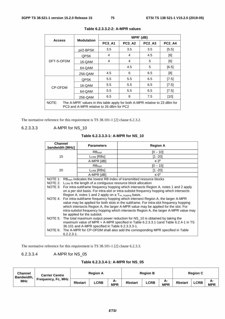
ETSI
ETSI TS 138 521-1 V15.2.0 (2019-05)753GPP TS 38.521-1 version 15.2.0 Release 15
Table 6.2.3.3.2-2: A-MPR values
Access Modulation MPR’ (dB)
PC3_A1 PC3_A2 PC2_A3 PC2_A4
DFT-S-OFDM
pi/2-BPSK 3.5 3.5 3.5 [5.5]
QPSK 4 4 4.5 [6]
16-QAM 4 4 5 [6]
64-QAM 4.5 5 [6.5]
256-QAM 4.5 6 6.5 [8]
CP-OFDM
QPSK 5.5 5.5 6.5 [7.5]
16-QAM 5.5 5.5 6.5 [7.5]
64-QAM 5.5 5.5 6.5 [7.5]
256-QAM 6.5 8 7.5 [10]
NOTE: The A-MPR’ values in this table apply for both A-MPR relative to 23 dBm for PC3 and A-MPR relative to 26 dBm for PC2
The normative reference for this requirement is TS 38.101-1 [2] clause 6.2.3.2.
6.2.3.3.3 A-MPR for NS_10
Table 6.2.3.3.3-1: A-MPR for NS_10
Channel bandwidth [MHz] Parameters Region A
15 RBstart [0 – 10]
LCRB [RBs] [1 -20] A-MPR [dB] ≤ 36
20 RBstart [0 – 15]
LCRB [RBs] [1 -20] A-MPR [dB] ≤ 66
NOTE 1: RBstart indicates the lowest RB index of transmitted resource blocks NOTE 2: LCRB is the length of a contiguous resource block allocation NOTE 3: For intra-subframe frequency hopping which intersects Region A, notes 1 and 2 apply
on a per slot basis. For intra-slot or intra-subslot frequency hopping which intersects Region A, notes 1 and 2 apply on a Tno_hopping basis.
NOTE 4: For intra-subframe frequency hopping which intersect Region A, the larger A-MPR value may be applied for both slots in the subframe. For intra-slot frequency hopping which intersects Region A, the larger A-MPR value may be applied for the slot. For intra-subslot frequency hopping which intersects Region A, the larger A-MPR value may be applied for the subslot.
NOTE 5: The total maximum output power reduction for NS_10 is obtained by taking the maximum value of MPR + A-MPR specified in Table 6.2.3.3.1-1and Table 6.2.4-1 in TS 36.101 and A-MPR specified in Table 6.2.3.3.3-1.
NOTE 6: The A-MPR for CP-OFDM shall also add the corresponding MPR specified in Table 6.2.2.3-1.
The normative reference for this requirement is TS 38.101-1 [2] clause 6.2.3.3.
6.2.3.3.4 A-MPR for NS_05
Table 6.2.3.3.4-1: A-MPR for NS_05
Channel Bandwidth,
MHz
Carrier Centre Frequency, Fc, MHz
Region A Region B Region C
Rbstart LCRB A-MPR Rbstart LCRB A-
MPR Rbstart LCRB A-MPR

ETSI
ETSI TS 138 521-1 V15.2.0 (2019-05)763GPP TS 38.521-1 version 15.2.0 Release 15
5 MHz 1922.5 ≤ FC < 1927.5 <1.62MHz/12/SCS
>2.52MHz/12/SCS A3
10 MHz 1920 ≤ FC < 1935 <1.62MHz/12/SCS >0 A1
>1.62MHz/12/SCS
≤3.60MHz/12/SCS
>5.4MHz/12/SCS A7 >7.74MHz
/12/SCS
≤1.08MHz/12/SCS
A2
10 MHz 1935 ≤ FC < 1945 >4.5MHz/12/SCS A4
15 MHz 1927.5 ≤ FC < 1932.5 <3.24MHz/12/SCS >0 A1
>3.24MHz/12/SCS
≤5.40MHz/12/SCS
>8.1MHz/12/SCS A7 >10.9MHz
/12/SCS
≤1.08MHz/12/SCS
A2
15 MHz 1932.5 ≤ FC < 1942.5 <1.62MHz/12/SCS >0 A1
>12.6 MHz/12/S
CS
≤1.08MHz/12/SCS
A2
15 MHz 1942.5 ≤ FC < 1947.5 >7.2MHz/12/SCS A5
20 MHz 1930 ≤ FC < 1950 <4.86MHz/12/SCS >0 A1
>4.86MHz/12/SCS
≤7.20MHz/12/SCS
>9.0MHz/12/SCS A7 >14.22MH
z/12/SCS
≤1.08MHz/12/SCS
A2
20 MHz 1950 ≤ FC <1960 >9.0MHz/12/SCS A6
NOTE 1: The A-MPR values are listed in Table 6.2.3.3.4-2 and 6.2.3.3.4-3. NOTE 3: For any undefined region, MPR applies
Table 6.2.3.3.4-2: A-MPR for modulation and waveform type
Modulation/Waveform A1 A2 A3
Outer/Inner Outer/Inner Outer Inner DFT-s-OFDM PI/2 BPSK ≤ 10 ≤ 5 ≤ 4 N/A
DFT-s-OFDM QPSK ≤ 10 ≤ 5 ≤ 4.5 N/A DFT-s-OFDM 16 QAM ≤ 10 ≤ 5 ≤ 6 N/A DFT-s-OFDM 64 QAM ≤ 11 ≤ 5 ≤ 6 N/A
DFT-s-OFDM 256 QAM ≤ 13 ≤ 5 ≤ 7 N/A CP-OFDM QPSK ≤ 10 ≤ 5 ≤ 7.5 ≤ 2
CP-OFDM 16 QAM ≤ 10 ≤ 5 ≤ 7.5 N/A CP-OFDM 64 QAM ≤ 11 ≤ 5 ≤ 8 N/A
CP-OFDM 256 QAM ≤ 13 N/A ≤ 10 N/A NOTE 1: The backoff applied is max (MPR, A-MPR) where MPR is
defined in Table 6.2.2.3-1 NOTE 2: Outer and inner allocations are defined in clause 6.2.2
Table 6.2.3.3.4-3: A-MPR for modulation and waveform type
Modulation/Waveform A4 A5 A6 A7
Outer Inner Outer Inner Outer Inner Outer/Inner

ETSI
ETSI TS 138 521-1 V15.2.0 (2019-05)773GPP TS 38.521-1 version 15.2.0 Release 15
DFT-s-OFDM PI/2 BPSK ≤ 1
N/A
≤ 1 N/A ≤ 1
N/A
≤ 6 DFT-s-OFDM QPSK N/A ≤ 1.5 N/A ≤ 1.5 ≤ 6
DFT-s-OFDM 16 QAM N/A N/A N/A N/A ≤ 6 DFT-s-OFDM 64 QAM N/A N/A N/A N/A ≤ 6
DFT-s-OFDM 256 QAM N/A N/A N/A N/A ≤ 6 CP-OFDM QPSK ≤ 3.5 ≤ 3.5 N/A ≤ 3.5 ≤ 6
CP-OFDM 16 QAM ≤ 3.5 ≤ 3.5 N/A ≤ 3.5 ≤ 6 CP-OFDM 64 QAM N/A N/A ≤ 4 N/A ≤ 6
CP-OFDM 256 QAM N/A N/A N/A N/A ≤ 6 NOTE 1: The backoff applied is max (MPR, A-MPR) where MPR is defined in Table
6.2.2.3-1 NOTE 2: Outer and inner allocations are defined in clause 6.2.2
The normative reference for this requirement is TS 38.101-1 [2] clause 6.2.3.4.
6.2.3.3.5 A-MPR for NS_40
Table 6.2.3.3.5-1: A-MPR for NS_40
Modulation A-MPR Channel bandwidth (MHz): 5 MHz
Outer RB allocations Inner RB allocations DFT-s-OFDM QPSK 15.5 12
DFT-s-OFDM 16 QAM 14.5 11 DFT-s-OFDM 64 QAM 14.5 10
DFT-s-OFDM 256 QAM 12.5 7.5 CP-OFDM QPSK 14.5 10
CP-OFDM 16 QAM 14.5 10 CP-OFDM 64 QAM 14 8
CP-OFDM 256 QAM 11 5.5 NOTE 1: The total maximum output power reduction for NS_40 is obtained by taking the maximum value of MPR +
A-MPR specified in Table 6.2.3.3.1-1 and Table 6.2.4-30a in TS 36.101 and MPR+A-MPR specified in Table 6.2.2.3-1 and Table 6.2.3.3.5-1.
The normative reference for this requirement is TS 38.101-1 [2] clause 6.2.3.5.
6.2.3.3.6 A-MPR for NS_08
Table 6.2.3.3.6-1: A-MPR for NS_08
Modulation A-MPR Configurations for A-MPR
(Note 3) Outer RB allocations Inner RB allocations DFT-s-OFDM PI/2 BPSK 0 0
DFT-s-OFDM QPSK ≤ 2 0 LCRB > 15 for 15kHz SCS DFT-s-OFDM 16 QAM 0 0 DFT-s-OFDM 64 QAM 0 0
DFT-s-OFDM 256 QAM 0 0 CP-OFDM QPSK ≤ 3.5 0 LCRB > 15 for 15kHz SCS
CP-OFDM 16 QAM ≤ 3.5 0 LCRB > 15 for 15kHz SCS CP-OFDM 64 QAM 0 0
CP-OFDM 256 QAM 0 0 NOTE 1: The total backoff applied is max(MPR, A-MPR) where MPR is defined in Table 6.2.2.3-1. NOTE 2: Outer and inner allocations are defined in clause 6.2.2. NOTE 3: When configurations are specified, A-MPR is only applied for the conditions and zero A-MPR is
applied for the rest of RB allocations.
Table 6.2.3.3.6-2: A-MPR for NS_08 for 10 MHz CBW
Modulation A-MPR Configurations for A-MPR
(NOTE 3) Outer RB allocations Inner RB allocations
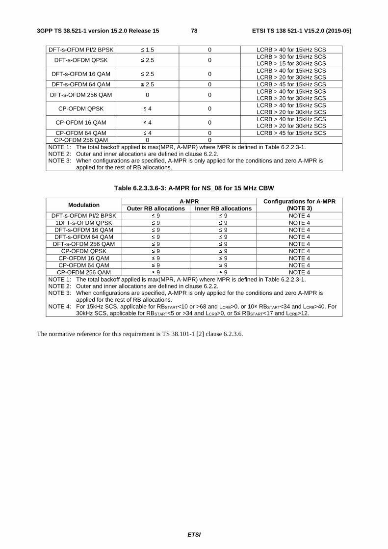
ETSI
ETSI TS 138 521-1 V15.2.0 (2019-05)783GPP TS 38.521-1 version 15.2.0 Release 15
DFT-s-OFDM PI/2 BPSK ≤ 1.5 0 LCRB > 40 for 15kHz SCS
DFT-s-OFDM QPSK ≤ 2.5 0 LCRB > 30 for 15kHz SCS LCRB > 15 for 30kHz SCS
DFT-s-OFDM 16 QAM ≤ 2.5 0 LCRB > 40 for 15kHz SCS LCRB > 20 for 30kHz SCS
DFT-s-OFDM 64 QAM ≤ 2.5 0 LCRB > 45 for 15kHz SCS
DFT-s-OFDM 256 QAM 0 0 LCRB > 40 for 15kHz SCS LCRB > 20 for 30kHz SCS
CP-OFDM QPSK ≤ 4 0 LCRB > 40 for 15kHz SCS LCRB > 20 for 30kHz SCS
CP-OFDM 16 QAM ≤ 4 0 LCRB > 40 for 15kHz SCS LCRB > 20 for 30kHz SCS
CP-OFDM 64 QAM ≤ 4 0 LCRB > 45 for 15kHz SCS CP-OFDM 256 QAM 0 0
NOTE 1: The total backoff applied is max(MPR, A-MPR) where MPR is defined in Table 6.2.2.3-1. NOTE 2: Outer and inner allocations are defined in clause 6.2.2. NOTE 3: When configurations are specified, A-MPR is only applied for the conditions and zero A-MPR is
applied for the rest of RB allocations.
Table 6.2.3.3.6-3: A-MPR for NS_08 for 15 MHz CBW
Modulation A-MPR Configurations for A-MPR
(NOTE 3) Outer RB allocations Inner RB allocations DFT-s-OFDM PI/2 BPSK ≤ 9 ≤ 9 NOTE 4
1DFT-s-OFDM QPSK ≤ 9 ≤ 9 NOTE 4 DFT-s-OFDM 16 QAM ≤ 9 ≤ 9 NOTE 4 DFT-s-OFDM 64 QAM ≤ 9 ≤ 9 NOTE 4
DFT-s-OFDM 256 QAM ≤ 9 ≤ 9 NOTE 4 CP-OFDM QPSK ≤ 9 ≤ 9 NOTE 4
CP-OFDM 16 QAM ≤ 9 ≤ 9 NOTE 4 CP-OFDM 64 QAM ≤ 9 ≤ 9 NOTE 4
CP-OFDM 256 QAM ≤ 9 ≤ 9 NOTE 4 NOTE 1: The total backoff applied is max(MPR, A-MPR) where MPR is defined in Table 6.2.2.3-1. NOTE 2: Outer and inner allocations are defined in clause 6.2.2. NOTE 3: When configurations are specified, A-MPR is only applied for the conditions and zero A-MPR is
applied for the rest of RB allocations. NOTE 4: For 15kHz SCS, applicable for RBSTART<10 or >68 and LCRB>0, or 10≤ RBSTART<34 and LCRB>40. For
30kHz SCS, applicable for RBSTART<5 or >34 and LCRB>0, or 5≤ RBSTART<17 and LCRB>12.
The normative reference for this requirement is TS 38.101-1 [2] clause 6.2.3.6.

ETSI
ETSI TS 138 521-1 V15.2.0 (2019-05)793GPP TS 38.521-1 version 15.2.0 Release 15
6.2.3.3.7 A-MPR for NS_03
Table 6.2.3.3.7-1: A-MPR for NS_03
Modulation Channel BW / Transmission BW in MHz A-MPR
5 10 15 20 40 Outer RB allocations
Inner RB allocations
DFT-s-OFDM PI/2 BPSK,
DFT-s-OFDM QPSK,
DFT-s-OFDM 16 QAM
1.44 1.44 – 2.16 1.44 – 2.88 2.16 – 3.24 2.88 – 4.32 N/A ≤1
> 1.44 > 2.16 > 2.88 > 3.24 > 4.32 ≤1 ≤2
DFT-s-OFDM 64 QAM
1.44 1.44 – 2.16 1.44 – 2.88 2.16 – 3.24 2.88 – 4.32 ≤0.5 ≤0.5 > 1.44 > 2.16 > 2.88 > 3.24 > 4.32 ≤1.5 ≤1.5
DFT-s-OFDM 256 QAM
<1.44 ≤0.5 ≤0.5
≥1.44 ≤1.5 ≤1.5
CP-OFDM QPSK 1.44 1.44 – 2.16 1.44 – 2.88 2.16 – 3.24 2.88 – 4.32 N/A ≤1
> 1.44 > 2.16 > 2.88 > 3.24 > 4.32 ≤1 ≤2 CP-OFDM 16
QAM 1.44 1.44 – 2.16 1.44 – 2.88 2.16 – 3.24 2.88 – 4.32 N/A ≤2
> 1.44 > 2.16 > 2.88 > 3.24 > 4.32 ≤1 ≤2 CP-OFDM 64
QAM > 1.08 > 1.08 > 1.44 > 1.8 > 2.88 ≤1 ≤1
CP-OFDM 256 QAM > 1.08 > 1.08 > 1.44 > 1.8 > 2.88 ≤1 ≤1
NOTE 1: A-MPR defined in this Table is additive to MPR defined in Table 6.2.2.3-1 NOTE 2: Inner and outer allocations are defined in clause 6.2.2
6.2.3.3.8 A-MPR for NS_37
Table 6.2.3.3.8-1: A-MPR for B11/B21 protection (NS_37) for 10MHz, 15MHz (1447.9-1462.9MHz)
Channel Bandwidth,
MHz
Carrier Centre
Frequency, Fc, MHz
Region A (Outer/Inner)
Region B (Outer/Inner)
Region C (Outer/Inner)
RBstart,(MHz/12/
SCS)
LCRB (MHz/12/
SCS) A-MPR
RBstart (MHz/12/
SCS)
LCRB (MHz/12/
SCS) A-MPR
RBstart (MHz/12/
SCS)
LCRB (MHz/12/
SCS) A-MPR
10MHz 1452.9 < FC ≤1457.9 ≥0 >40 ≤ A1 N/A N/A N/A N/A N/A N/A
15MHz FC =1455.4 ≥0 >55 ≤ A1 <[0.54] < [1.08] [≤ A2] >[13.86] < [1.08] [≤ A2]
NOTE 1: A-MPR values in Table 6.2.3.3.8-2. NOTE 2: The backoff applied is max (MPR, A-MPR) where MPR is defined in Table 6.2.2.3-1 NOTE 3: For any undefined region, MPR applies NOTE 4: No A-MPR for SCS=60 kHz.
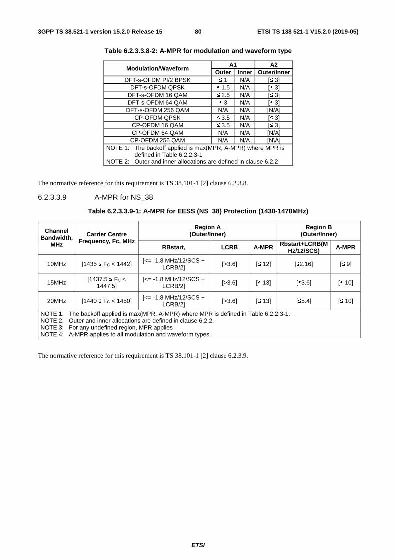
ETSI
ETSI TS 138 521-1 V15.2.0 (2019-05)803GPP TS 38.521-1 version 15.2.0 Release 15
Table 6.2.3.3.8-2: A-MPR for modulation and waveform type
Modulation/Waveform A1 A2
Outer Inner Outer/Inner DFT-s-OFDM PI/2 BPSK ≤ 1 N/A [≤ 3]
DFT-s-OFDM QPSK ≤ 1.5 N/A [≤ 3] DFT-s-OFDM 16 QAM ≤ 2.5 N/A [≤ 3] DFT-s-OFDM 64 QAM ≤ 3 N/A [≤ 3]
DFT-s-OFDM 256 QAM N/A N/A [N/A] CP-OFDM QPSK ≤ 3.5 N/A [≤ 3]
CP-OFDM 16 QAM ≤ 3.5 N/A [≤ 3] CP-OFDM 64 QAM N/A N/A [N/A]
CP-OFDM 256 QAM N/A N/A [N\A] NOTE 1: The backoff applied is max(MPR, A-MPR) where MPR is
defined in Table 6.2.2.3-1 NOTE 2: Outer and inner allocations are defined in clause 6.2.2
The normative reference for this requirement is TS 38.101-1 [2] clause 6.2.3.8.
6.2.3.3.9 A-MPR for NS_38
Table 6.2.3.3.9-1: A-MPR for EESS (NS_38) Protection (1430-1470MHz)
Channel Bandwidth,
MHz
Carrier Centre Frequency, Fc, MHz
Region A (Outer/Inner)
Region B (Outer/Inner)
RBstart, LCRB A-MPR Rbstart+LCRB(MHz/12/SCS) A-MPR
10MHz [1435 ≤ FC < 1442] [<= -1.8 MHz/12/SCS + LCRB/2] [>3.6] [≤ 12] [≤2.16] [≤ 9]
15MHz [1437.5 ≤ FC < 1447.5]
[<= -1.8 MHz/12/SCS + LCRB/2] [>3.6] [≤ 13] [≤3.6] [≤ 10]
20MHz [1440 ≤ FC < 1450] [<= -1.8 MHz/12/SCS + LCRB/2] [>3.6] [≤ 13] [≤5.4] [≤ 10]
NOTE 1: The backoff applied is max(MPR, A-MPR) where MPR is defined in Table 6.2.2.3-1. NOTE 2: Outer and inner allocations are defined in clause 6.2.2. NOTE 3: For any undefined region, MPR applies NOTE 4: A-MPR applies to all modulation and waveform types.
The normative reference for this requirement is TS 38.101-1 [2] clause 6.2.3.9.
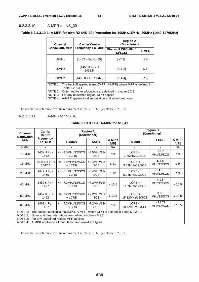
ETSI
ETSI TS 138 521-1 V15.2.0 (2019-05)813GPP TS 38.521-1 version 15.2.0 Release 15
6.2.3.3.10 A-MPR for NS_39
Table 6.2.3.3.10-1: A-MPR for own RX (NS_39) Protection for 10MHz,15MHz, 20MHz (1440-1470MHz)
Channel Bandwidth, MHz
Carrier Centre Frequency, Fc, MHz
Region A (Outer/Inner)
Rbstart+LCRB(MHz/12/SCS) A-MPR
10MHz [1462 < FC ≤1465] [>7.9] [≤ 6]
15MHz [1456.3 < FC ≤
1462.5] [>11.2] [≤ 6]
20MHz [1450.8 < FC ≤ 1460] [>14.4] [≤ 6]
NOTE 1: The backoff applied is max(MPR, A-MPR) where MPR is defined in Table 6.2.2.3-1
NOTE 2: Outer and inner allocations are defined in clause 6.2.2. NOTE 3: For any undefined region, MPR applies NOTE 4: A-MPR applies to all modulation and waveform types.
The normative reference for this requirement is TS 38.101-1 [2] clause 6.2.3.10.
6.2.3.3.11 A-MPR for NS_41
Table 6.2.3.3.11-1: A-MPR for NS_41
Channel Bandwidth,
MHz
Carrier Centre
Frequency, Fc, MHz
Region A (Outer/Inner)
Region B (Outer/Inner)
Rbstart LCRB A-MPR [dB] Rbstart LCRB A-MPR
[dB] 5 MHz - - - NA - - NA
10 MHz 1437 ≤ FC <
1442 <= -4.5MHz/12/SCS
+ LCRB >4.5MHz/12/
SCS ≤ 9 LCRB <
1.7MHz/12/SCS
≤ 2.7 MHz/12/SCS ≤ 9
15 MHz 1439.5 ≤ FC < 1447.5
<= -5.4MHz/12/SCS + LCRB
>5.4MHz/12/SCS ≤ 11 LCRB <
3.42MHz/12/SCS
≤ 3.6 MHz/12/SCS ≤ 9
20 MHz 1442 ≤ FC < 1450
<= -5.4MHz/12/SCS + LCRB
>5.4MHz/12/SCS ≤ 12 LCRB <
5.04MHz/12/SCS
≤ 5 MHz/12/SCS ≤ 9
40 MHz 1452 ≤ FC < 1497
<= -7.2MHz/12/SCS + LCRB
>7.2MHz/12/SCS ≤ 13.5 LCRB <
11.7MHz/12/SCS
≤ 18 MHz/12/SCS
≤ 10.5
50 MHz 1457 ≤ FC < 1492
<= -7.2MHz/12/SCS + LCRB
>7.2MHz/12/SCS ≤ 13.5 LCRB <
15.12MHz/12/SCS
≤ 18 MHz/12/SCS ≤ 10.5
60 MHz 1462 ≤ FC < 1487
<= -7.2MHz/12/SCS + LCRB
>7.2MHz/12/SCS ≤ 13.5 LCRB <
18.72MHz/12/SCS
≤ 18.72 MHz/12/SCS ≤ 10.5
NOTE 1: The backoff applied is max(MPR, A-MPR) where MPR is defined in Table 6.2.2.3-1 NOTE 2: Outer and inner allocations are defined in clause 6.2.2 NOTE 3: For any undefined region, MPR applies NOTE 4: A-MPR applies to all modulation and waveform types.
The normative reference for this requirement is TS 38.101-1 [2] clause 6.2.3.11.

ETSI
ETSI TS 138 521-1 V15.2.0 (2019-05)823GPP TS 38.521-1 version 15.2.0 Release 15
6.2.3.3.12 A-MPR for NS_42
Table 6.2.3.3.12-1: A-MPR for NS_42
Channel Bandwidth, MHz
Carrier Centre
Frequency, Fc, MHz
Region A
Region B
RBend A-MPR (Outer/Inner) Rbstart A-MPR
(Inner) A-MPR (Outer)
5 MHz 1512 ≤ FC ≤ 1514.5
>3.1MHz / 12 / SCS ≤ 7 <0.9MHz/12/SCS ≤ 1.5 ≤ 4
10 MHz 1497 ≤ FC ≤ 1512 >6.2MHz / 12 / SCS ≤ 8 <0.9MHz/12/SCS ≤ 1.5 ≤ 5
15 MHz 1502 FC ≤ 1509.5 >9.3MHz / 12 / SCS ≤ 8 <3.06MHz/12/SCS ≤ 1.5 ≤ 5
20 MHz 1497 ≤ FC ≤ 1507
>12.4MHz / 12 / SCS ≤ 8 <4.5MHz/12/SCS ≤ 1.5 ≤ 5
40 MHz 1477 ≤ FC ≤ 1497 >24.8MHz / 12 / SCS ≤ 8 <5.4MHz/12/SCS ≤ 1.5 ≤ 5
50 MHz 1467 ≤ FC ≤ 1492 >31MHz / 12 / SCS ≤ 8 <7.2MHz/12/SCS ≤ 1.5 ≤ 5
60 MHz 1462 ≤ FC ≤ 1487 >37.2MHz / 12 / SCS ≤ 8 <7.2MHz/12/SCS ≤ 1.5 ≤ 5
NOTE 1: The backoff applied is max(MPR, A-MPR) where MPR is defined in Table 6.2.2.3-1. NOTE 2: Outer and inner allocations are defined in clause 6.2.2. NOTE 3: For any undefined region, MPR applies NOTE 4: A-MPR applies to all modulation and waveform types.
The normative reference for this requirement is TS 38.101-1 [2] clause 6.2.3.7.
6.2.3.4 Test description
6.2.3.4.1 Initial conditions
Initial conditions are a set of test configurations the UE needs to be tested in and the steps for the SS to take with the UE to reach the correct measurement state.
The initial test configurations consist of environmental conditions, test frequencies, test channel bandwidths and sub-carrier spacing based on NR operating bands specified in table 5.3.5-1. All of these configurations shall be tested with applicable test parameters for each combination of test channel bandwidth and sub-carrier spacing, and are shown in table 6.2.3.4.1-2. The details of the uplink reference measurement channels (RMCs) are specified in Annex A.2. Configurations of PDSCH and PDCCH before measurement are specified in Annex C.2

ETSI
ETSI TS 138 521-1 V15.2.0 (2019-05)833GPP TS 38.521-1 version 15.2.0 Release 15
Table 6.2.3.4.1-1: Test Configuration table for NS_35
Initial Conditions Test Environment as specified in TS 38.508-1 [5] subclause 4.1 Normal Test Frequencies as specified in TS 38.508-1 [5] subclause 4.3.1 Low range, High range Test Channel Bandwidths as specified in TS 38.508-1 [5] subclause 4.3.1 Lowest, Highest
Test SCS as specified in Table 5.3.5-1 Lowest, Highest A-MPR test parameters for NS_35
Downlink Configuration Uplink Configuration Test ID
Freq ChBw SCS N/A for A-MPR testing. Modulation (NOTE 2)
RB allocation (NOTE 1)
1 Low Default Default DFT-s-OFDM PI/2 BPSK Edge_1RB_Left 2 High DFT-s-OFDM PI/2 BPSK Edge_1RB_Right 3 Default DFT-s-OFDM PI/2 BPSK Outer Full 4 Low DFT-s-OFDM QPSK Edge_1RB_Left 5 High DFT-s-OFDM QPSK Edge_1RB_Right 6 Default DFT-s-OFDM QPSK Outer Full 7 Low DFT-s-OFDM 16 QAM Edge_1RB_Left 8 High DFT-s-OFDM 16 QAM Edge_1RB_Right 9 Default DFT-s-OFDM 16 QAM Outer Full 10 Default DFT-s-OFDM 64 QAM Outer Full 11 Default DFT-s-OFDM 256 QAM Outer Full 12 Low CP-OFDM QPSK Edge_1RB_Left 13 High CP-OFDM QPSK Edge_1RB_Right 14 Default CP-OFDM QPSK Outer Full 15 Low CP-OFDM 16 QAM Edge_1RB_Left 16 High CP-OFDM 16 QAM Edge_1RB_Right 17 Default CP-OFDM 16 QAM Outer Full 18 Default CP-OFDM 64 QAM Outer Full 19 Default CP-OFDM 256 QAM Outer Full
NOTE 1: The specific configuration of each RB allocation is defined in Table 6.1-1. NOTE 2: DFT-s-OFDM PI/2 BPSK test applies only for UEs which supports half Pi BPSK in FR1.

ETSI
ETSI TS 138 521-1 V15.2.0 (2019-05)843GPP TS 38.521-1 version 15.2.0 Release 15
Table 6.2.3.4.1-2: Test Configuration table for NS_04
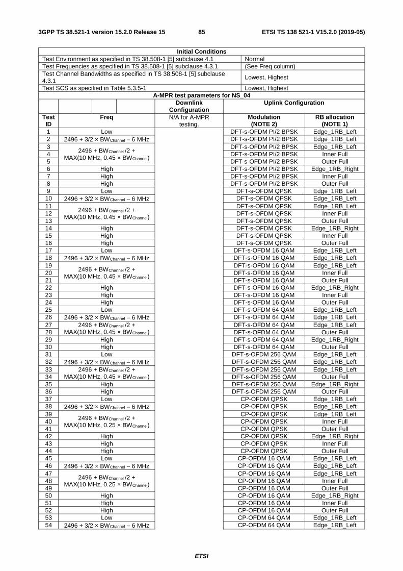
ETSI
ETSI TS 138 521-1 V15.2.0 (2019-05)853GPP TS 38.521-1 version 15.2.0 Release 15
Initial Conditions Test Environment as specified in TS 38.508-1 [5] subclause 4.1 Normal Test Frequencies as specified in TS 38.508-1 [5] subclause 4.3.1 (See Freq column) Test Channel Bandwidths as specified in TS 38.508-1 [5] subclause 4.3.1 Lowest, Highest
Test SCS as specified in Table 5.3.5-1 Lowest, Highest A-MPR test parameters for NS_04
Downlink Configuration
Uplink Configuration
Test ID
Freq N/A for A-MPR testing.
Modulation (NOTE 2)
RB allocation (NOTE 1)
1 Low DFT-s-OFDM PI/2 BPSK Edge_1RB_Left 2 2496 + 3/2 × BWChannel − 6 MHz DFT-s-OFDM PI/2 BPSK Edge_1RB_Left 3
2496 + BWChannel /2 + MAX(10 MHz, 0.45 × BWChannel)
DFT-s-OFDM PI/2 BPSK Edge_1RB_Left 4 DFT-s-OFDM PI/2 BPSK Inner Full 5 DFT-s-OFDM PI/2 BPSK Outer Full 6 High DFT-s-OFDM PI/2 BPSK Edge_1RB_Right 7 High DFT-s-OFDM PI/2 BPSK Inner Full 8 High DFT-s-OFDM PI/2 BPSK Outer Full 9 Low DFT-s-OFDM QPSK Edge_1RB_Left 10 2496 + 3/2 × BWChannel − 6 MHz DFT-s-OFDM QPSK Edge_1RB_Left 11
2496 + BWChannel /2 + MAX(10 MHz, 0.45 × BWChannel)
DFT-s-OFDM QPSK Edge_1RB_Left 12 DFT-s-OFDM QPSK Inner Full 13 DFT-s-OFDM QPSK Outer Full 14 High DFT-s-OFDM QPSK Edge_1RB_Right 15 High DFT-s-OFDM QPSK Inner Full 16 High DFT-s-OFDM QPSK Outer Full 17 Low DFT-s-OFDM 16 QAM Edge_1RB_Left 18 2496 + 3/2 × BWChannel − 6 MHz DFT-s-OFDM 16 QAM Edge_1RB_Left 19
2496 + BWChannel /2 + MAX(10 MHz, 0.45 × BWChannel)
DFT-s-OFDM 16 QAM Edge_1RB_Left 20 DFT-s-OFDM 16 QAM Inner Full 21 DFT-s-OFDM 16 QAM Outer Full 22 High DFT-s-OFDM 16 QAM Edge_1RB_Right 23 High DFT-s-OFDM 16 QAM Inner Full 24 High DFT-s-OFDM 16 QAM Outer Full 25 Low DFT-s-OFDM 64 QAM Edge_1RB_Left 26 2496 + 3/2 × BWChannel − 6 MHz DFT-s-OFDM 64 QAM Edge_1RB_Left 27 2496 + BWChannel /2 +
MAX(10 MHz, 0.45 × BWChannel) DFT-s-OFDM 64 QAM Edge_1RB_Left
28 DFT-s-OFDM 64 QAM Outer Full 29 High DFT-s-OFDM 64 QAM Edge_1RB_Right 30 High DFT-s-OFDM 64 QAM Outer Full 31 Low DFT-s-OFDM 256 QAM Edge_1RB_Left 32 2496 + 3/2 × BWChannel − 6 MHz DFT-s-OFDM 256 QAM Edge_1RB_Left 33 2496 + BWChannel /2 +
MAX(10 MHz, 0.45 × BWChannel) DFT-s-OFDM 256 QAM Edge_1RB_Left
34 DFT-s-OFDM 256 QAM Outer Full 35 High DFT-s-OFDM 256 QAM Edge_1RB_Right 36 High DFT-s-OFDM 256 QAM Outer Full 37 Low CP-OFDM QPSK Edge_1RB_Left 38 2496 + 3/2 × BWChannel − 6 MHz CP-OFDM QPSK Edge_1RB_Left 39
2496 + BWChannel /2 + MAX(10 MHz, 0.25 × BWChannel)
CP-OFDM QPSK Edge_1RB_Left 40 CP-OFDM QPSK Inner Full 41 CP-OFDM QPSK Outer Full 42 High CP-OFDM QPSK Edge_1RB_Right 43 High CP-OFDM QPSK Inner Full 44 High CP-OFDM QPSK Outer Full 45 Low CP-OFDM 16 QAM Edge_1RB_Left 46 2496 + 3/2 × BWChannel − 6 MHz CP-OFDM 16 QAM Edge_1RB_Left 47
2496 + BWChannel /2 + MAX(10 MHz, 0.25 × BWChannel)
CP-OFDM 16 QAM Edge_1RB_Left 48 CP-OFDM 16 QAM Inner Full 49 CP-OFDM 16 QAM Outer Full 50 High CP-OFDM 16 QAM Edge_1RB_Right 51 High CP-OFDM 16 QAM Inner Full 52 High CP-OFDM 16 QAM Outer Full 53 Low CP-OFDM 64 QAM Edge_1RB_Left 54 2496 + 3/2 × BWChannel − 6 MHz CP-OFDM 64 QAM Edge_1RB_Left

ETSI
ETSI TS 138 521-1 V15.2.0 (2019-05)863GPP TS 38.521-1 version 15.2.0 Release 15
55 2496 + BWChannel /2 + MAX(10 MHz, 0.25 × BWChannel)
CP-OFDM 64 QAM Edge_1RB_Left 56 CP-OFDM 64 QAM Outer Full 57 High CP-OFDM 64 QAM Edge_1RB_Right 58 High CP-OFDM 64 QAM Outer Full 59 Low CP-OFDM 256 QAM Edge_1RB_Left 60 2496 + 3/2 × BWChannel − 6 MHz CP-OFDM 256 QAM Edge_1RB_Left 61 2496 + BWChannel /2 +
MAX(10 MHz, 0.25 × BWChannel) CP-OFDM 256 QAM Edge_1RB_Left
62 CP-OFDM 256 QAM Outer Full 63 High CP-OFDM 256 QAM Edge_1RB_Right 64 High CP-OFDM 256 QAM Outer Full
NOTE 1: The specific configuration of each RB allocation is defined in Table 6.1-1. NOTE 2: DFT-s-OFDM PI/2 BPSK test applies only for UEs which supports half Pi BPSK in FR1.
Editor’s note: The following lines belong at the end of subclause 6.2.3.4.1. As new tables are added to this section, these lines should always follow the tables
1. Connect the SS to the UE antenna connectors as shown in TS 38.508-1 [5] Annex A, Figure A.3.1.1.1 for TE diagram and section A.3.2.1 for UE diagram.
2. The parameter settings for the cell are set up according to TS 38.508-1 [5] subclause 4.4.3.
3. Downlink signals are initially set up according to Annex C.0, C.1, C.2 and uplink signals according Annex G.0, G.1, G.2 and G.3.0.
4. The UL Reference Measurement channels are set according to the applicable table from Table 6.2.3.4.1-1 to Table 6.2.3.4.1-2.
5. Propagation conditions are set according to Annex B.0.
6. Ensure the UE is in state RRC_CONNECTED with generic procedure parameters Connectivity NR, Connected without release On, Test Mode On and Test Loop Function On according to TS 38.508-1 [5] clause 4.5. Message contents are defined in clause 6.2.3.4.3.
6.2.3.4.2 Test procedure
1. SS sends uplink scheduling information for each UL HARQ process via PDCCH DCI format [0_1] for C_RNTI to schedule the UL RMC according to the applicable table from Table 6.2.4.3.1-1 to Table 6.2.4.3.1-2. Since the UE has no payload data to send, the UE transmits uplink MAC padding bits on the UL RMC.
2. Send continuously uplink power control "up" commands in the uplink scheduling information to the UE Allow at least 200ms starting from the first TPC command in this step for the UE to reach PUMAX level.
3. Measure the mean power of the UE in the channel bandwidth of the radio access mode. The period of measurement shall be at least the continuous duration one sub-frame (1ms). [For TDD slots with transient periods are not under test.]
6.2.3.4.3 Message contents
Message contents are according to TS 38.508-1 [5] subclause 4.6.1, with the following exceptions for each network signalled value.
6.2.3.4.3.1 Message contents exceptions for network signalled value “NS_03”
1. Information element additionalSpectrumEmission is set to NS_03. This can be set in the SystemInformationblockType2 as part of the cell broadcast message. This exception indicates that the UE shall meet the additional spurious emission requirement for a specific deployment scenario.
Table 6.2.3.4.3.1-1: SystemInformationBlockType2: Additional spurious emissions test requirement for "NS_03" and NR band n2, n25 and n66
Derivation Path: TS 38.508-1 [5] clause [TBD], Table [TBD] Information Element Value/remark Comment Condition
additionalSpectrumEmission 2 (NS_03)
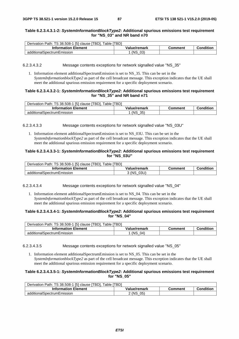
ETSI
ETSI TS 138 521-1 V15.2.0 (2019-05)873GPP TS 38.521-1 version 15.2.0 Release 15
Table 6.2.3.4.3.1-2: SystemInformationBlockType2: Additional spurious emissions test requirement for "NS_03" and NR band n70
Derivation Path: TS 38.508-1 [5] clause [TBD], Table [TBD] Information Element Value/remark Comment Condition
additionalSpectrumEmission 1 (NS_03)
6.2.3.4.3.2 Message contents exceptions for network signalled value "NS_35"
1. Information element additionalSpectrumEmission is set to NS_35. This can be set in the SystemInformationblockType2 as part of the cell broadcast message. This exception indicates that the UE shall meet the additional spurious emission requirement for a specific deployment scenario.
Table 6.2.3.4.3.2-1: SystemInformationBlockType2: Additional spurious emissions test requirement for "NS_35" and NR band n71
Derivation Path: TS 38.508-1 [5] clause [TBD], Table [TBD] Information Element Value/remark Comment Condition
additionalSpectrumEmission 1 (NS_35)
6.2.3.4.3.3 Message contents exceptions for network signalled value "NS_03U"
1. Information element additionalSpectrumEmission is set to NS_03U. This can be set in the SystemInformationblockType2 as part of the cell broadcast message. This exception indicates that the UE shall meet the additional spurious emission requirement for a specific deployment scenario.
Table 6.2.3.4.3.3-1: SystemInformationBlockType2: Additional spurious emissions test requirement for "NS_03U"
Derivation Path: TS 38.508-1 [5] clause [TBD], Table [TBD] Information Element Value/remark Comment Condition
additionalSpectrumEmission 3 (NS_03U)
6.2.3.4.3.4 Message contents exceptions for network signalled value "NS_04"
1. Information element additionalSpectrumEmission is set to NS_04. This can be set in the SystemInformationblockType2 as part of the cell broadcast message. This exception indicates that the UE shall meet the additional spurious emission requirement for a specific deployment scenario.
Table 6.2.3.4.3.4-1: SystemInformationBlockType2: Additional spurious emissions test requirement for "NS_04"
Derivation Path: TS 38.508-1 [5] clause [TBD], Table [TBD] Information Element Value/remark Comment Condition
additionalSpectrumEmission 1 (NS_04)
6.2.3.4.3.5 Message contents exceptions for network signalled value "NS_05"
1. Information element additionalSpectrumEmission is set to NS_05. This can be set in the SystemInformationblockType2 as part of the cell broadcast message. This exception indicates that the UE shall meet the additional spurious emission requirement for a specific deployment scenario.
Table 6.2.3.4.3.5-1: SystemInformationBlockType2: Additional spurious emissions test requirement for "NS_05"
Derivation Path: TS 38.508-1 [5] clause [TBD], Table [TBD] Information Element Value/remark Comment Condition
additionalSpectrumEmission 2 (NS_05)

ETSI
ETSI TS 138 521-1 V15.2.0 (2019-05)883GPP TS 38.521-1 version 15.2.0 Release 15
6.2.3.4.3.6 Message contents exceptions for network signalled value "NS_05U"
1. Information element additionalSpectrumEmission is set to NS_05U. This can be set in the SystemInformationblockType2 as part of the cell broadcast message. This exception indicates that the UE shall meet the additional spurious emission requirement for a specific deployment scenario.
Table 6.2.3.4.3.6-1: SystemInformationBlockType2: Additional spurious emissions test requirement for "NS_05U"
Derivation Path: TS 38.508-1 [5] clause [TBD], Table [TBD] Information Element Value/remark Comment Condition
additionalSpectrumEmission 3 (NS_05U)
6.2.3.4.3.7 Message contents exceptions for network signalled value "NS_06"
1. Information element additionalSpectrumEmission is set to NS_06. This can be set in the SystemInformationblockType2 as part of the cell broadcast message. This exception indicates that the UE shall meet the additional spurious emission requirement for a specific deployment scenario.
Table 6.2.3.4.3.7-1: SystemInformationBlockType2: Additional spurious emissions test requirement for "NS_06"
Derivation Path: TS 38.508-1 [5] clause [TBD], Table [TBD] Information Element Value/remark Comment Condition
additionalSpectrumEmission 1 (NS_06)
6.2.3.4.3.8 Message contents exceptions for network signalled value "NS_08"
1. Information element additionalSpectrumEmission is set to NS_08. This can be set in the SystemInformationblockType2 as part of the cell broadcast message. This exception indicates that the UE shall meet the additional spurious emission requirement for a specific deployment scenario.
Table 6.2.3.4.3.8-1: SystemInformationBlockType2: Additional spurious emissions test requirement for "NS_08"
Derivation Path: TS 38.508-1 [5] clause [TBD], Table [TBD] Information Element Value/remark Comment Condition
additionalSpectrumEmission 1 (NS_08)
6.2.3.4.3.9 Message contents exceptions for network signalled value "NS_08U"
1. Information element additionalSpectrumEmission is set to NS_08U. This can be set in the SystemInformationblockType2 as part of the cell broadcast message. This exception indicates that the UE shall meet the additional spurious emission requirement for a specific deployment scenario.
Table 6.2.3.4.3.9-1: SystemInformationBlockType2: Additional spurious emissions test requirement for "NS_08U"
Derivation Path: TS 38.508-1 [5] clause [TBD], Table [TBD] Information Element Value/remark Comment Condition
additionalSpectrumEmission 3 (NS_08U)
6.2.3.4.3.10 Message contents exceptions for network signalled value "NS_10"
1. Information element additionalSpectrumEmission is set to NS_10. This can be set in the SystemInformationblockType2 as part of the cell broadcast message. This exception indicates that the UE shall meet the additional spurious emission requirement for a specific deployment scenario.

ETSI
ETSI TS 138 521-1 V15.2.0 (2019-05)893GPP TS 38.521-1 version 15.2.0 Release 15
Table 6.2.3.4.3.10-1: SystemInformationBlockType2: Additional spurious emissions test requirement for "NS_10"
Derivation Path: TS 38.508-1 [5] clause [TBD], Table [TBD] Information Element Value/remark Comment Condition
additionalSpectrumEmission 2 (NS_10)
6.2.3.4.3.11 Message contents exceptions for network signalled value "NS_17"
1. Information element additionalSpectrumEmission is set to NS_17. This can be set in the SystemInformationblockType2 as part of the cell broadcast message. This exception indicates that the UE shall meet the additional spurious emission requirement for a specific deployment scenario.
Table 6.2.3.4.3.11-1: SystemInformationBlockType2: Additional spurious emissions test requirement for "NS_17"
Derivation Path: TS 38.508-1 [5] clause [TBD], Table [TBD] Information Element Value/remark Comment Condition
additionalSpectrumEmission 1 (NS_17)
6.2.3.4.3.12 Message contents exceptions for network signalled value "NS_18"
1. Information element additionalSpectrumEmission is set to NS_18. This can be set in the SystemInformationblockType2 as part of the cell broadcast message. This exception indicates that the UE shall meet the additional spurious emission requirement for a specific deployment scenario.
Table 6.2.3.4.3.12-1: SystemInformationBlockType2: Additional spurious emissions test requirement for "NS_18"
Derivation Path: TS 38.508-1 [5] clause [TBD], Table [TBD] Information Element Value/remark Comment Condition
additionalSpectrumEmission 2 (NS_18)
6.2.3.4.3.13 Message contents exceptions for network signalled value "NS_37"
1. Information element additionalSpectrumEmission is set to NS_37. This can be set in the SystemInformationblockType2 as part of the cell broadcast message. This exception indicates that the UE shall meet the additional spurious emission requirement for a specific deployment scenario.
Table 6.2.3.4.3.13-1: SystemInformationBlockType2: Additional spurious emissions test requirement for "NS_37"
Derivation Path: TS 38.508-1 [5] clause [TBD], Table [TBD] Information Element Value/remark Comment Condition
additionalSpectrumEmission 1 (NS_37)
6.2.3.4.3.14 Message contents exceptions for network signalled value "NS_38"
1. Information element additionalSpectrumEmission is set to NS_38. This can be set in the SystemInformationblockType2 as part of the cell broadcast message. This exception indicates that the UE shall meet the additional spurious emission requirement for a specific deployment scenario.
Table 6.2.3.4.3.14-1: SystemInformationBlockType2: Additional spurious emissions test requirement for "NS_38"
Derivation Path: TS 38.508-1 [5] clause [TBD], Table [TBD] Information Element Value/remark Comment Condition
additionalSpectrumEmission 2 (NS_38)
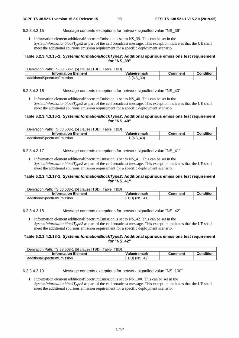
ETSI
ETSI TS 138 521-1 V15.2.0 (2019-05)903GPP TS 38.521-1 version 15.2.0 Release 15
6.2.3.4.3.15 Message contents exceptions for network signalled value "NS_39"
1. Information element additionalSpectrumEmission is set to NS_39. This can be set in the SystemInformationblockType2 as part of the cell broadcast message. This exception indicates that the UE shall meet the additional spurious emission requirement for a specific deployment scenario.
Table 6.2.3.4.3.15-1: SystemInformationBlockType2: Additional spurious emissions test requirement for "NS_39"
Derivation Path: TS 38.508-1 [5] clause [TBD], Table [TBD] Information Element Value/remark Comment Condition
additionalSpectrumEmission 3 (NS_39)
6.2.3.4.3.16 Message contents exceptions for network signalled value "NS_40"
1. Information element additionalSpectrumEmission is set to NS_40. This can be set in the SystemInformationblockType2 as part of the cell broadcast message. This exception indicates that the UE shall meet the additional spurious emission requirement for a specific deployment scenario.
Table 6.2.3.4.3.16-1: SystemInformationBlockType2: Additional spurious emissions test requirement for "NS_40"
Derivation Path: TS 38.508-1 [5] clause [TBD], Table [TBD] Information Element Value/remark Comment Condition
additionalSpectrumEmission 1 (NS_40)
6.2.3.4.3.17 Message contents exceptions for network signalled value "NS_41"
1. Information element additionalSpectrumEmission is set to NS_41. This can be set in the SystemInformationblockType2 as part of the cell broadcast message. This exception indicates that the UE shall meet the additional spurious emission requirement for a specific deployment scenario.
Table 6.2.3.4.3.17-1: SystemInformationBlockType2: Additional spurious emissions test requirement for "NS_41"
Derivation Path: TS 38.508-1 [5] clause [TBD], Table [TBD] Information Element Value/remark Comment Condition
additionalSpectrumEmission [TBD] (NS_41)
6.2.3.4.3.18 Message contents exceptions for network signalled value "NS_42"
1. Information element additionalSpectrumEmission is set to NS_42. This can be set in the SystemInformationblockType2 as part of the cell broadcast message. This exception indicates that the UE shall meet the additional spurious emission requirement for a specific deployment scenario.
Table 6.2.3.4.3.18-1: SystemInformationBlockType2: Additional spurious emissions test requirement for "NS_42"
Derivation Path: TS 38.508-1 [5] clause [TBD], Table [TBD] Information Element Value/remark Comment Condition
additionalSpectrumEmission [TBD] (NS_42)
6.2.3.4.3.19 Message contents exceptions for network signalled value "NS_100"
1. Information element additionalSpectrumEmission is set to NS_100. This can be set in the SystemInformationblockType2 as part of the cell broadcast message. This exception indicates that the UE shall meet the additional spurious emission requirement for a specific deployment scenario.

ETSI
ETSI TS 138 521-1 V15.2.0 (2019-05)913GPP TS 38.521-1 version 15.2.0 Release 15
Table 6.2.3.4.3.19-1: SystemInformationBlockType2: Additional spurious emissions test requirement for "NS_100"
Derivation Path: TS 38.508-1 [5] clause [TBD], Table [TBD] Information Element Value/remark Comment Condition
additionalSpectrumEmission 1 (NS_100)
6.2.3.5 Test requirement
The maximum output power, derived in step 3 shall be within the range prescribed by the nominal maximum output power and tolerance in the applicable table from table 6.2.3.5-1. The allowed A-MPR values specified in table 6.2.3.3-1 are in addition to the allowed MPR requirements specified in clause 6.2.2. For the UE maximum output power modified by MPR and/or A-MPR, the power limits specified in table 6.2.1.3-1 apply.
Table 6.2.3.5-0: Test Tolerance (UE additional maximum output power reduction)
f ≤ 3.0GHz 3.0GHz < f ≤ 4.2GHz 4.2GHz < f ≤ 6.0GHz BW ≤ 40MHz 0.7 dB 1.0 dB 1.0 dB
40MHz < BW ≤ 100MHz 1.0 dB 1.0 dB 1.0 dB
Table 6.2.3.5-1: UE Power Class 3 test requirements (NS_35) for band n71.
Test ID
PPowerClass
(dBm) MPR (dB)
A-MPR (dB)
ΔTC,c (dB)
PCMAX,c (dBm)
T(PCMAX_L,c) (dB)
TL,c
(dB) Upper limit
(dBm) Lower limit
(dBm) 1 23 0.5 0 0 22.5 2 2.5 25.7 19.3 2 23 0.5 0 0 22.5 2 2.5 25.7 19.3 3 23 0.5 0 0 22.5 2 2.5 25.7 19.3 4 23 1 0 0 22 2 2.5 25.7 18.8 5 23 1 0 0 22 2 2.5 25.7 18.8 6 23 1 0 0 22 2 2.5 25.7 18.8 7 23 2 0 0 21 2 2.5 25.7 17.8 8 23 2 0 0 21 2 2.5 25.7 17.8 9 23 2 0 0 21 2 2.5 25.7 17.8
10 23 2.5 0 0 20.5 2.5 2.5 25.7 17.3 11 23 4.5 0 0 18.5 4 2.5 25.7 13.8 12 23 3 0 0 20 2.5 2.5 25.7 16.8 13 23 3 0 0 20 2.5 2.5 25.7 16.8 14 23 3 0 0 20 2.5 2.5 25.7 16.8 15 23 3 0 0 20 2.5 2.5 25.7 16.8 16 23 3 0 0 20 2.5 2.5 25.7 16.8 17 23 3 0 0 20 2.5 2.5 25.7 16.8 18 23 3.5 0 0 19.5 3.5 2.5 25.7 15.3 19 23 6.5 0 0 16.5 5 2.5 25.7 10.8
NOTE 1: PPowerClass is the maximum UE power specified without taking into account the tolerance. NOTE 2: TT for each frequency and channel bandwidth is specified in Table 6.2.3.5-0.
ETSI
ETSI TS 138 521-1 V15.2.0 (2019-05)923GPP TS 38.521-1 version 15.2.0 Release 15
Table 6.2.3.5-2: UE Power Class 2 test requirements (NS_04) for band n41.

ETSI
ETSI TS 138 521-1 V15.2.0 (2019-05)933GPP TS 38.521-1 version 15.2.0 Release 15
Test ID
PPowerClass
(dBm) MPR (dB)
A-MPR (dB)
ΔTC,c (dB)
PCMAX,c (dBm)
T(PCMAX_L,c) (dB)
TL,c
(dB) Upper limit
(dBm)
Lower limit (Note 2)
(dBm) 1 26 0 [5.5] 0 20.5 2.5 2 28+TT [17.5+TT]
2 26 0 [5.5] 0 20.5 2.5 2 28+TT [17.5+TT]
3 26 0 3.5 0 22.5 2 2 28+TT 19.5+TT
4 26 0 3.5 0 22.5 2 2 28+TT 19.5+TT
5 26 0 3.5 0 22.5 2 2 28+TT 19.5+TT
6 26 3.5 0 0 22.5 2 2 28+TT 19.5+TT
7 26 0.2 0 0 25.8 2 2 28+TT 22.8+TT
8 26 1.2 0 0 24.8 2 2 28+TT 21.8+TT
9 26 0 [6] 0 20 2.5 2 28+TT [17+TT]
10 26 0 [6] 0 20 2.5 2 28+TT [17+TT]
11 26 0 4.5 0 21.5 2 2 28+TT 18.5+TT
12 26 0 4.5 0 21.5 2 2 28+TT 18.5+TT
13 26 0 4.5 0 21.5 2 2 28+TT 18.5+TT
14 26 3.5 0 0 22.5 2 2 28+TT 19.5+TT
15 26 0.2 0 0 25.8 2 2 28+TT 22.8+TT
16 26 1.2 0 0 24.8 2 2 28+TT 21.8+TT
17 26 0 [6] 0 20 2.5 2 28+TT [17+TT]
18 26 0 [6] 0 20 2.5 2 28+TT [17+TT]
19 26 0 5 0 21 2 2 28+TT 18+TT
20 26 0 5 0 21 2 2 28+TT 18+TT
21 26 0 5 0 21 2 2 28+TT 18+TT
22 26 3.5 0 0 22.5 2 2 28+TT 19.5+TT
23 26 0.2 0 0 25.8 2 2 28+TT 22.8+TT
24 26 1.2 0 0 24.8 2 2 28+TT 21.8+TT
25 26 0 [6.5] 0 19.5 3.5 2 28+TT [16+TT]
26 26 0 [6.5] 0 19.5 3.5 2 28+TT [16+TT]
27 26 0 5 0 21 2 2 28+TT 18+TT
28 26 0 5 0 21 2 2 28+TT 18+TT
29 26 3.5 0 0 22.5 2 2 28+TT 19.5+TT
30 26 1.2 0 0 24.8 2 2 28+TT 21.8+TT
31 26 0 [8] 0 18 4 2 28+TT [14+TT]
32 26 0 [8] 0 18 4 2 28+TT [14+TT]
33 26 0 6.5 0 19.5 3.5 2 28+TT 16+TT
34 26 0 6.5 0 19.5 3.5 2 28+TT 16+TT
35 26 3.5 0 0 22.5 2 2 28+TT 19.5+TT
36 26 1.2 0 0 24.8 2 2 28+TT 21.8+TT
37 26 0 [7.5] 0 18.5 4 2 28+TT [14.5+TT]
38 26 0 [7.5] 0 18.5 4 2 28+TT [14.5+TT]
39 26 0 6.5 0 19.5 3.5 2 28+TT 16+TT
40 26 0 6.5 0 19.5 3.5 2 28+TT 16+TT
41 26 0 6.5 0 19.5 3.5 2 28+TT 16+TT
42 26 3.5 0 0 22.5 2 2 28+TT 19.5+TT
43 26 0.2 0 0 25.8 2 2 28+TT 22.8+TT
44 26 1.2 0 0 24.8 2 2 28+TT 21.8+TT
45 26 0 [7.5] 0 18.5 4 2 28+TT [14.5+TT]
46 26 0 [7.5] 0 18.5 4 2 28+TT [14.5+TT]
47 26 0 6.5 0 19.5 3.5 2 28+TT 16+TT
48 26 0 6.5 0 19.5 3.5 2 28+TT 16+TT

ETSI
ETSI TS 138 521-1 V15.2.0 (2019-05)943GPP TS 38.521-1 version 15.2.0 Release 15
49 26 0 6.5 0 19.5 3.5 2 28+TT 16+TT
50 26 3.5 0 0 22.5 2 2 28+TT 19.5+TT
51 26 0.2 0 0 25.8 2 2 28+TT 22.8+TT
52 26 1.2 0 0 24.8 2 2 28+TT 21.8+TT
53 26 0 [7.5] 0 18.5 4 2 28+TT [14.5+TT]
54 26 0 [7.5] 0 18.5 4 2 28+TT [14.5+TT]
55 26 0 6.5 0 19.5 3.5 2 28+TT 16+TT
56 26 0 6.5 0 19.5 3.5 2 28+TT 16+TT
57 26 3.5 0 0 22.5 2 2 28+TT 19.5+TT
58 26 1.2 0 0 24.8 2 2 28+TT 21.8+TT
59 26 0 [10] 0 16 5 2 28+TT [11+TT]
60 26 0 [10] 0 16 5 2 28+TT [11+TT]
61 26 0 7.5 0 18.5 4 2 28+TT 14.5+TT
62 26 0 7.5 0 18.5 4 2 28+TT 14.5+TT
63 26 3.5 0 0 22.5 2 2 28+TT 19.5+TT
64 26 1.2 0 0 24.8 2 2 28+TT 21.8+TT
NOTE 1: PPowerClass is the maximum UE power specified without taking into account the tolerance. NOTE 2: For Band n41, refers to the transmission bandwidths (Figure 5.3.3-1) confined within FUL_low and FUL_low + 4 MHz
or FUL_high – 4 MHz and FUL_high, the lower limit shall be decreased by 1.0 dB for CP-OFDM 256 QAM and decreased by 1.5 dB for other modulations.
NOTE 3: TT=0.7 dB for BWchannel ≤ 40 MHz; TT=1.0 dB for 40 MHz < BWchannel ≤ 100 MHz.

ETSI
ETSI TS 138 521-1 V15.2.0 (2019-05)953GPP TS 38.521-1 version 15.2.0 Release 15
Table 6.2.3.5-3: UE Power Class 3 test requirements (NS_04) for band n41.
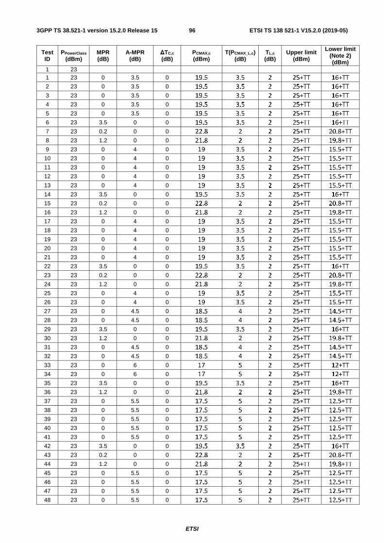
ETSI
ETSI TS 138 521-1 V15.2.0 (2019-05)963GPP TS 38.521-1 version 15.2.0 Release 15
Test ID
PPowerClass
(dBm) MPR (dB)
A-MPR (dB)
ΔTC,c (dB)
PCMAX,c (dBm)
T(PCMAX_L,c) (dB)
TL,c
(dB) Upper limit
(dBm)
Lower limit (Note 2)
(dBm) 1 23 1 23 0 3.5 0 19.5 3.5 2 25+TT 16+TT
2 23 0 3.5 0 19.5 3.5 2 25+TT 16+TT
3 23 0 3.5 0 19.5 3.5 2 25+TT 16+TT
4 23 0 3.5 0 19.5 3.5 2 25+TT 16+TT
5 23 0 3.5 0 19.5 3.5 2 25+TT 16+TT
6 23 3.5 0 0 19.5 3.5 2 25+TT 16+TT
7 23 0.2 0 0 22.8 2 2 25+TT 20.8+TT
8 23 1.2 0 0 21.8 2 2 25+TT 19.8+TT
9 23 0 4 0 19 3.5 2 25+TT 15.5+TT
10 23 0 4 0 19 3.5 2 25+TT 15.5+TT
11 23 0 4 0 19 3.5 2 25+TT 15.5+TT
12 23 0 4 0 19 3.5 2 25+TT 15.5+TT
13 23 0 4 0 19 3.5 2 25+TT 15.5+TT
14 23 3.5 0 0 19.5 3.5 2 25+TT 16+TT
15 23 0.2 0 0 22.8 2 2 25+TT 20.8+TT
16 23 1.2 0 0 21.8 2 2 25+TT 19.8+TT
17 23 0 4 0 19 3.5 2 25+TT 15.5+TT
18 23 0 4 0 19 3.5 2 25+TT 15.5+TT
19 23 0 4 0 19 3.5 2 25+TT 15.5+TT
20 23 0 4 0 19 3.5 2 25+TT 15.5+TT
21 23 0 4 0 19 3.5 2 25+TT 15.5+TT
22 23 3.5 0 0 19.5 3.5 2 25+TT 16+TT
23 23 0.2 0 0 22.8 2 2 25+TT 20.8+TT
24 23 1.2 0 0 21.8 2 2 25+TT 19.8+TT
25 23 0 4 0 19 3.5 2 25+TT 15.5+TT
26 23 0 4 0 19 3.5 2 25+TT 15.5+TT
27 23 0 4.5 0 18.5 4 2 25+TT 14.5+TT
28 23 0 4.5 0 18.5 4 2 25+TT 14.5+TT
29 23 3.5 0 0 19.5 3.5 2 25+TT 16+TT
30 23 1.2 0 0 21.8 2 2 25+TT 19.8+TT
31 23 0 4.5 0 18.5 4 2 25+TT 14.5+TT
32 23 0 4.5 0 18.5 4 2 25+TT 14.5+TT
33 23 0 6 0 17 5 2 25+TT 12+TT
34 23 0 6 0 17 5 2 25+TT 12+TT
35 23 3.5 0 0 19.5 3.5 2 25+TT 16+TT
36 23 1.2 0 0 21.8 2 2 25+TT 19.8+TT
37 23 0 5.5 0 17.5 5 2 25+TT 12.5+TT
38 23 0 5.5 0 17.5 5 2 25+TT 12.5+TT
39 23 0 5.5 0 17.5 5 2 25+TT 12.5+TT
40 23 0 5.5 0 17.5 5 2 25+TT 12.5+TT
41 23 0 5.5 0 17.5 5 2 25+TT 12.5+TT
42 23 3.5 0 0 19.5 3.5 2 25+TT 16+TT
43 23 0.2 0 0 22.8 2 2 25+TT 20.8+TT
44 23 1.2 0 0 21.8 2 2 25+TT 19.8+TT
45 23 0 5.5 0 17.5 5 2 25+TT 12.5+TT
46 23 0 5.5 0 17.5 5 2 25+TT 12.5+TT
47 23 0 5.5 0 17.5 5 2 25+TT 12.5+TT
48 23 0 5.5 0 17.5 5 2 25+TT 12.5+TT

ETSI
ETSI TS 138 521-1 V15.2.0 (2019-05)973GPP TS 38.521-1 version 15.2.0 Release 15
49 23 0 5.5 0 17.5 5 2 25+TT 12.5+TT
50 23 3.5 0 0 19.5 3.5 2 25+TT 16+TT
51 23 0.2 0 0 22.8 2 2 25+TT 20.8+TT
52 23 1.2 0 0 21.8 2 2 25+TT 19.8+TT
53 23 0 5.5 0 17.5 5 2 25+TT 12.5+TT
54 23 0 5.5 0 17.5 5 2 25+TT 12.5+TT
55 23 0 5.5 0 17.5 5 2 25+TT 12.5+TT
56 23 0 5.5 0 17.5 5 2 25+TT 12.5+TT
57 23 3.5 0 0 19.5 3.5 2 25+TT 16+TT
58 23 1.2 0 0 21.8 2 2 25+TT 19.8+TT
59 23 0 6.5 0 16.5 5 2 25+TT 11.5+TT
60 23 0 6.5 0 16.5 5 2 25+TT 11.5+TT
61 23 0 8 0 15 5 2 25+TT 10+TT
62 23 0 8 0 15 5 2 25+TT 10+TT
63 23 3.5 0 0 19.5 3.5 2 25+TT 16+TT
NOTE 1: PPowerClass is the maximum UE power specified without taking into account the tolerance. NOTE 2: For Band n41, refers to the transmission bandwidths (Figure 5.3.3-1) confined within FUL_low and FUL_low + 4 MHz
or FUL_high – 4 MHz and FUL_high, the lower limit shall be decreased by 1.0 dB for CP-OFDM 256 QAM and decreased by 1.5 dB for other modulations.
NOTE 3: TT=0.7 dB for BWchannel ≤ 40 MHz; TT=1.0 dB for 40 MHz < BWchannel ≤ 100 MHz.
6.2.4 Configured transmitted power
6.2.4.1 Test purpose
To verify the measured UE configured maximum output power PUMAX,f,c is within the specified bounds.
6.2.4.2 Test applicability
This test case applies to all types of NR UE release 15 and forward.
6.2.4.3 Minimum conformance requirements
The UE is allowed to set its configured maximum output power PCMAX,f,c for carrier f of serving cell c in each slot. The configured maximum output power PCMAX,f,c is set within the following bounds:
PCMAX_L,f,c ≤ PCMAX,f,c ≤ PCMAX_H,f,c with
PCMAX_L,f,c = MIN {PEMAX,c– ∆TC,c, (PPowerClass – ΔPPowerClass) – MAX(MPRc + A-MPRc+ ΔTIB,c + ∆TC,c + ∆TRxSRS, P-MPRc) }
PCMAX_H,f,c = MIN {PEMAX,c, PPowerClass – ΔPPowerClass }
where
PEMAX,c is the value given by IE P-Max for serving cell c, defined in TS 38.331[6];
PPowerClass is the maximum UE power specified in Table 6.2.1.3-1 without taking into account the tolerance specified in the Table 6.2.1.3-1;
When the IE powerBoostPi2BPSK is set to 1, PEMAX,c is increased by +3 dB for a power class 3 capable UE operating in TDD bands n40, n41, n77, n78, and n79 with PI/2 BPSK modulation and UE indicates support for UE capability [powerBoosting-pi2BPSK] and 40% or less slots in radio frame are used for UL transmission when PEMAX,c ≥ 20 dBm.
When the IE powerBoostPi2BPSK is set to 1, ΔPPowerClass = -3 dB for a power class 3 capable UE operating in TDD bands n40, n41, n77, n78, and n79 with PI/2 BPSK modulation and 40% or less slots in radio frame are used for UL transmission.
ΔPPowerClass = 3 dB for a power class 2 capable UE, when P-max of 23 dBm or lower is indicated; or when the field of UE capability maxUplinkDutyCycle is absent and the percentage of uplink symbols transmitted in a certain evaluation

ETSI
ETSI TS 138 521-1 V15.2.0 (2019-05)983GPP TS 38.521-1 version 15.2.0 Release 15
period is larger than 50%; or when the field of UE capability maxUplinkDutyCycle is not absent and the percentage of uplink symbols transmitted in a certain evaluation period is larger than maxUplinkDutyCycle as defined in TS 38.331 (The exact evaluation period is no less than one radio frame); otherwise ΔPPowerClass = 0 dB;
∆TIB,c is the additional tolerance for serving cell c as specified in TS 38.101-3 [4] subclause 6.2A.4.2 and 6.2B.4.2; ∆TIB,c = 0 dB otherwise;
∆TC,c= 1.5dB when NOTE 3 in Table 6.2.1-1 in 38.101-1 applies for a serving cell c, otherwise ∆TC,c = 0dB ;
MPRc and A-MPRc for serving cell c are specified in subclause 6.2.2.3 and subclause 6.2.3.3, respectively;
∆TRxSRS is applied when UE transmits SRS to other than first SRS port when the SRS-TxSwitch capability is indicated as '1T2R', '1T4R' or, '1T4R/2T4R' with UE configured with 4 SRS resources in the SRS resource set, and when UE transmits SRS to other than first or second SRS port when the SRS-TxSwitch capability is indicated as '2T4R' or '1T4R/2T4R' with the UE configured with 2 SRS resources in the SRS resource set. The value of ∆TRxSRS is 4.5dB for n79 and 3 dB for bands whose FUL_high is lower than the FUL_low of n79.
For other SRS transmissions ∆TRxSRS is zero;
P-MPRc is the allowed maximum output power reduction for
a) ensuring compliance with applicable electromagnetic energy absorption requirements and addressing unwanted emissions / self defence requirements in case of simultaneous transmissions on multiple RAT(s) for scenarios not in scope of 3GPP RAN specifications;
b) ensuring compliance with applicable electromagnetic energy absorption requirements in case of proximity detection is used to address such requirements that require a lower maximum output power.
The UE shall apply P-MPRc for serving cell c only for the above cases. For UE conducted conformance testing P-MPRc shall be 0 dB
NOTE 1: P-MPRc was introduced in the PCMAX,f,c equation such that the UE can report to the eNB the available maximum output transmit power. This information can be used by the eNB for scheduling decisions.
NOTE 2: P-MPRc may impact the maximum uplink performance for the selected UL transmission path.
TREF and Teval are specified in Table 6.2.4.3-1. For each TREF, the PCMAX,L,c for serving cell c are evaluated per Teval and given by the minimum value taken over the transmission(s) within the Teval; the minimum PCMAX_L,f,c over one or more Teval is then applied for the entire TREF
Table 6.2.4.3-1: Evaluation and reference periods for Pcmax
TREF Teval Teval with frequency hopping Physical channel
length Physical channel length Min(Tno_hopping, Physical Channel
Length)
The measured configured maximum output power PUMAX,f,c shall be within the following bounds:
PCMAX_L,f,c – MAX{TL,c, T(PCMAX_L,f,c)} ≤ PUMAX,f,c ≤ PCMAX_H,f,c + T(PCMAX_H,f,c).
where the tolerance T(PCMAX,f,c) for applicable values of PCMAX,f,c is specified in Table 6.2.4.3-2. The tolerance TL,c is the absolute value of the lower tolerance for the applicable operating band as specified in Table 6.2.1.3-1.
Table 6.2.4.3-2: PCMAX tolerance
PCMAX,f,c (dBm) Tolerance T(PCMAX,f,c) (dB) 23 < PCMAX,c ≤ 33 2.0 21 ≤ PCMAX,c ≤ 23 2.0 20 ≤ PCMAX,c < 21 2.5 19 ≤ PCMAX,c < 20 3.5 18 ≤ PCMAX,c < 19 4.0 13 ≤ PCMAX,c < 18 5.0 8 ≤ PCMAX,c < 13 6.0 -40 ≤ PCMAX,c < 8 7.0

ETSI
ETSI TS 138 521-1 V15.2.0 (2019-05)993GPP TS 38.521-1 version 15.2.0 Release 15
The normative reference for this requirement is TS 38.101-1 [2] clause 6.2.4.
6.2.4.4 Test description
6.2.4.4.1 Initial condition
Initial conditions are a set of test configurations the UE needs to be tested in and the steps for the SS to take with the UE to reach the correct measurement state.
The initial test configurations consist of environmental conditions, test frequencies, test channel bandwidths and sub-carrier spacing based on NR operating bands specified in table 5.3.5-1. All of these configurations shall be tested with applicable test parameters for each combination of test channel bandwidth and sub-carrier spacing, and are shown in table 6.2.4.4.1-1. The details of the uplink reference measurement channels (RMCs) are specified in Annexes A.2. Configurations of PDSCH and PDCCH before measurement are specified in Annex C.2.
Table 6.2.4.4.1-1: Test Configuration Table
Initial Conditions Test Environment as specified in TS 38.508-1 [5] subclause 4.1
Normal, TL/VL, TL/VH, TH/VL, TH/VH
Test Frequencies as specified in TS 38.508-1 [5] subclause 4.3.1
Mid range
Test Channel Bandwidths as specified in TS 38.508-1 [5] subclause 4.3.1
Lowest, Mid, Highest
Test SCS as specified in Table 5.3.5-1 Lowest Test Parameters for Channel Bandwidths
Test ID Downlink Configuration Uplink Configuration N/A for minimum output
power Modulation (NOTE 2) RB allocation (NOTE 1)
1 test case DFT-s-OFDM Pi/2 BPSK Inner Full 2 DFT-s-OFDM QPSK Inner Full 33 DFT-s-OFDM Pi/2 BPSK Inner Full
NOTE 1: The specific configuration of each RB allocation is defined in Table 6.1-1. NOTE 2: DFT-s-OFDM PI/2 BPSK test applies only for UEs which supports half Pi BPSK in FR1. NOTE 3: UE operating in TDD mode with PI/2 PBSK modulation and UE indicates support for UE capability
[powerBoosting-pi2BPSK] and the IE powerBoostPi2BPSK is set to 1 for bands n40, n41, n77, n78 and n79.
1. Connect the SS to the UE antenna connectors as shown in TS 38.508-1 [5] Annex A, Figure A.3.1.1.1 for TE diagram and section A.3.2.1 for UE diagram.
2. The parameter settings for the cell are set up according to TS 38.508-1 [5] subclause 4.4.3.
3. Downlink signals are initially set up according to Annex C.0, C.1, C.2, and uplink signals according to Annex G.0, G.1, G.2, G.3.0.
4. The UL Reference Measurement Channel is set according to Table 6.2.4.4.1-1.
5. Propagation conditions are set according to Annex B.0.
6. Ensure the UE is in State RRC_CONNECTED with generic procedure parameters Connectivity NR, Connected without release On, Test Mode On and Test Loop Function On according to TS 38.508-1 [5] clause 4.5. Message contents are defined in clause 6.2.4.4.3.
6.2.4.4.2 Test procedure
1. SS sends uplink scheduling information for each UL HARQ process via PDCCH DCI format 0_1 for C_RNTI to schedule the UL RMC according to Table 6.2.4.4.1-1. Since the UE has no payload and no loopback data to send the UE sends uplink MAC padding bits on the UL RMC.
2. Send continuously uplink power control "up" commands in every uplink scheduling information to the UE; allow at least 200ms starting from the first TPC command in this step to ensure that the UE reaches the Pumax level of the test point.
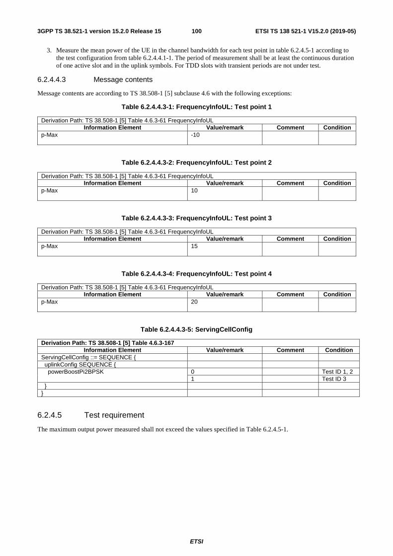
ETSI
ETSI TS 138 521-1 V15.2.0 (2019-05)1003GPP TS 38.521-1 version 15.2.0 Release 15
3. Measure the mean power of the UE in the channel bandwidth for each test point in table 6.2.4.5-1 according to the test configuration from table 6.2.4.4.1-1. The period of measurement shall be at least the continuous duration of one active slot and in the uplink symbols. For TDD slots with transient periods are not under test.
6.2.4.4.3 Message contents
Message contents are according to TS 38.508-1 [5] subclause 4.6 with the following exceptions:
Table 6.2.4.4.3-1: FrequencyInfoUL: Test point 1
Derivation Path: TS 38.508-1 [5] Table 4.6.3-61 FrequencyInfoUL Information Element Value/remark Comment Condition
p-Max -10
Table 6.2.4.4.3-2: FrequencyInfoUL: Test point 2
Derivation Path: TS 38.508-1 [5] Table 4.6.3-61 FrequencyInfoUL Information Element Value/remark Comment Condition
p-Max 10
Table 6.2.4.4.3-3: FrequencyInfoUL: Test point 3
Derivation Path: TS 38.508-1 [5] Table 4.6.3-61 FrequencyInfoUL Information Element Value/remark Comment Condition
p-Max 15
Table 6.2.4.4.3-4: FrequencyInfoUL: Test point 4
Derivation Path: TS 38.508-1 [5] Table 4.6.3-61 FrequencyInfoUL Information Element Value/remark Comment Condition
p-Max 20
Table 6.2.4.4.3-5: ServingCellConfig
Derivation Path: TS 38.508-1 [5] Table 4.6.3-167 Information Element Value/remark Comment Condition
ServingCellConfig ::= SEQUENCE { uplinkConfig SEQUENCE { powerBoostPi2BPSK 0 Test ID 1, 2 1 Test ID 3 } }
6.2.4.5 Test requirement
The maximum output power measured shall not exceed the values specified in Table 6.2.4.5-1.

ETSI
ETSI TS 138 521-1 V15.2.0 (2019-05)1013GPP TS 38.521-1 version 15.2.0 Release 15
Table 6.2.4.5-1: PCMAX configured UE output power
Maximum output power
Test ID 1,2 Test ID 3 for Power Class 2
Test ID 3 for Power Class 3
Measured UE output power test point 1 -10 dBm ± (7+TT) -10 dBm ± (7+TT)
Measured UE output power test point 2
10 dBm ± (6+TT) 10 dBm ± (6+TT)
Measured UE output power test point 3
15 dBm ± (5+TT) 15 dBm ± (5+TT)
Measured UE output power test point 4
20 dBm ± (2.5+TT) 23 dBm ± (2.0+TT)
Note 1: TT for each frequency and channel bandwidth is specified in Table 6.2.4.5-2. Note 2: In addition note 2 in Table 6.2.1.3-1 shall apply to the tolerances.
Table 6.2.4.5-2: Test Tolerance (Configured transmitted power)
f ≤ 3.0GHz 3.0GHz < f ≤ 6.0GHz BW ≤ 40MHz 0.7 dB 1.0 dB
40MHz < BW ≤ 100MHz 1.0 dB 1.0 dB
For the UE which supports inter-band NR CA configurations or inter-band EN-DC configurations, the ΔTIB,c in TS 38.101-3 [4] subclause 6.2A.4.2 and 6.2B.4.2 shall be applied for applicable bands.
6.2A Transmitter power for CA FFS
6.2B Transmitter power for DC FFS
6.2C Transmitter power for SUL
6.2C.1 Configured transmitted power for SUL
Editor’s notes:
- Connection diagram is TBD.
- Parameters setting for Cell setup in 38.508 subclause is FFS.
6.2C.1.1 Test purpose
Same test purpose as in clause 6.2.4.1
6.2C.1.2 Test applicability
This test applies to all types of NR UE release 15 and forward that support SUL operating on the SUL bands.
6.2C.1.3 Minimum conformance requirements
Refer to clause 6.2.4.3, and with the following supplementary specification for UE configured with SUL
For single carrier configured transmit power, as the UL carrier and SUL carrier is a same cell, the configured transmit power is specified for each UL carrier in a serving cell. The configured transmit power requirement for serving cell is applied for each UL carrier.
For the UE which supports SUL band combination, ΔTIB,c in Table 6.2C.2-1 applies.
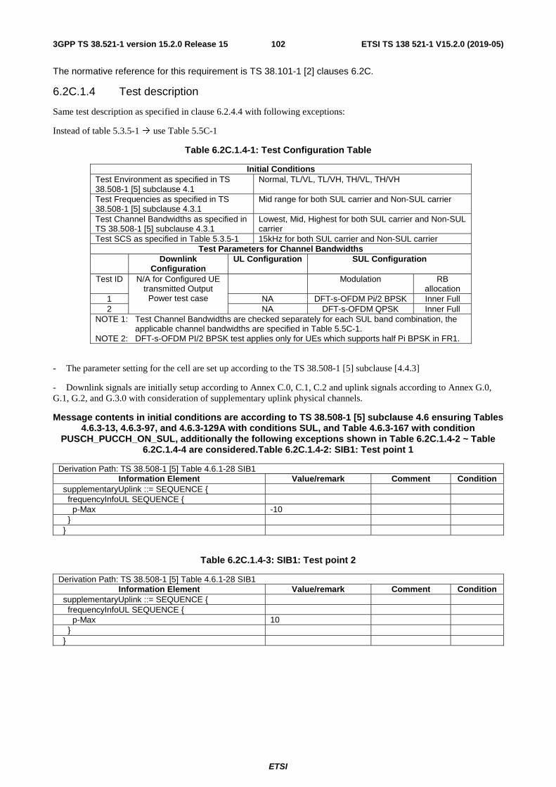
ETSI
ETSI TS 138 521-1 V15.2.0 (2019-05)1023GPP TS 38.521-1 version 15.2.0 Release 15
The normative reference for this requirement is TS 38.101-1 [2] clauses 6.2C.
6.2C.1.4 Test description
Same test description as specified in clause 6.2.4.4 with following exceptions:
Instead of table 5.3.5-1 use Table 5.5C-1
Table 6.2C.1.4-1: Test Configuration Table
Initial Conditions Test Environment as specified in TS 38.508-1 [5] subclause 4.1
Normal, TL/VL, TL/VH, TH/VL, TH/VH
Test Frequencies as specified in TS 38.508-1 [5] subclause 4.3.1
Mid range for both SUL carrier and Non-SUL carrier
Test Channel Bandwidths as specified in TS 38.508-1 [5] subclause 4.3.1
Lowest, Mid, Highest for both SUL carrier and Non-SUL carrier
Test SCS as specified in Table 5.3.5-1 15kHz for both SUL carrier and Non-SUL carrier Test Parameters for Channel Bandwidths
Downlink Configuration
UL Configuration SUL Configuration
Test ID N/A for Configured UE transmitted Output
Power test case
Modulation RB allocation
1 NA DFT-s-OFDM Pi/2 BPSK Inner Full 2 NA DFT-s-OFDM QPSK Inner Full
NOTE 1: Test Channel Bandwidths are checked separately for each SUL band combination, the applicable channel bandwidths are specified in Table 5.5C-1.
NOTE 2: DFT-s-OFDM PI/2 BPSK test applies only for UEs which supports half Pi BPSK in FR1.
- The parameter setting for the cell are set up according to the TS 38.508-1 [5] subclause [4.4.3]
- Downlink signals are initially setup according to Annex C.0, C.1, C.2 and uplink signals according to Annex G.0, G.1, G.2, and G.3.0 with consideration of supplementary uplink physical channels.
Message contents in initial conditions are according to TS 38.508-1 [5] subclause 4.6 ensuring Tables 4.6.3-13, 4.6.3-97, and 4.6.3-129A with conditions SUL, and Table 4.6.3-167 with condition
PUSCH_PUCCH_ON_SUL, additionally the following exceptions shown in Table 6.2C.1.4-2 ~ Table 6.2C.1.4-4 are considered.Table 6.2C.1.4-2: SIB1: Test point 1
Derivation Path: TS 38.508-1 [5] Table 4.6.1-28 SIB1 Information Element Value/remark Comment Condition
supplementaryUplink ::= SEQUENCE { frequencyInfoUL SEQUENCE { p-Max -10 } }
Table 6.2C.1.4-3: SIB1: Test point 2
Derivation Path: TS 38.508-1 [5] Table 4.6.1-28 SIB1 Information Element Value/remark Comment Condition
supplementaryUplink ::= SEQUENCE { frequencyInfoUL SEQUENCE { p-Max 10 } }
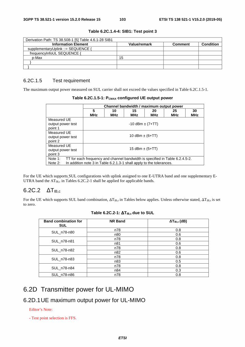
ETSI
ETSI TS 138 521-1 V15.2.0 (2019-05)1033GPP TS 38.521-1 version 15.2.0 Release 15
Table 6.2C.1.4-4: SIB1: Test point 3
Derivation Path: TS 38.508-1 [5] Table 4.6.1-28 SIB1 Information Element Value/remark Comment Condition
supplementaryUplink ::= SEQUENCE { frequencyInfoUL SEQUENCE { p-Max 15 } }
6.2C.1.5 Test requirement
The maximum output power measured on SUL carrier shall not exceed the values specified in Table 6.2C.1.5-1.
Table 6.2C.1.5-1: PCMAX configured UE output power
Channel bandwidth / maximum output power 5
MHz 10
MHz 15
MHz 20
MHz 25
MHz 30
MHz Measured UE output power test point 1
-10 dBm ± (7+TT)
Measured UE output power test point 2
10 dBm ± (6+TT)
Measured UE output power test point 3
15 dBm ± (5+TT)
Note 1: TT for each frequency and channel bandwidth is specified in Table 6.2.4.5-2. Note 2: In addition note 3 in Table 6.2.1.3-1 shall apply to the tolerances.
For the UE which supports SUL configurations with uplink assigned to one E-UTRA band and one supplementary E-UTRA band the ΔTIB,c in Tables 6.2C.2-1 shall be applied for applicable bands.
6.2C.2 ΔTIB,c
For the UE which supports SUL band combination, ΔTIB,c in Tables below applies. Unless otherwise stated, ΔTIB,c is set to zero.
Table 6.2C.2-1: ΔTIB,c due to SUL
Band combination for SUL
NR Band ΔTIB,c (dB)
SUL_n78-n80 n78 0.8 n80 0.6
SUL_n78-n81 n78 0.8 n81 0.6
SUL_n78-n82 n78 0.8 n82 0.6
SUL_n78-n83 n78 0.8 n83 0.5
SUL_n78-n84 n78 0.8 n84 0.3
SUL_n78-n86 n78 0.8
6.2D Transmitter power for UL-MIMO
6.2D.1 UE maximum output power for UL-MIMO
Editor’s Note:
- Test point selection is FFS.

ETSI
ETSI TS 138 521-1 V15.2.0 (2019-05)1043GPP TS 38.521-1 version 15.2.0 Release 15
- MU/TT is FFS
- Test case is incomplete since there is no CP-OFDM configuration satisfying MPR=0dB requirements in RAN4
6.2D.1.1 Test purpose
To verify that the error of the UE maximum output power for UL-MIMO does not exceed the range prescribed by the specified nominal maximum output power and tolerance.
An excess maximum output power has the possibility to interfere to other channels or other systems. A small maximum output power decreases the coverage area.
6.2D.1.2 Test applicability
This test case applies to all types of NR UE release 15 and forward that support UL-MIMO.
6.2D.1.3 Minimum conformance requirements
For PC2 UE with two transmit antenna connectors in closed-loop spatial multiplexing scheme, the maximum output power for any transmission bandwidth within the channel bandwidth is specified in Table 6.2D.1.3-1. The requirements shall be met with the UL-MIMO configurations specified in Table 6.2D.1.3-2. For UE supporting UL-MIMO, the maximum output power is measured as the sum of the maximum output power at each UE antenna connector. The period of measurement shall be at least one sub frame (1ms).
The requirements shall be met with the UL-MIMO configurations of using 2-layer UL-MIMO transmission with
codebook of . DCI Format for UE configured in PUSCH transmission mode for uplink single-user MIMO
shall be used.
Table 6.2D.1.3-1: UE Power Class for UL-MIMO in closed loop spatial multiplexing scheme
NR band
Class 1 (dBm)
Tolerance (dB)
Class 2 (dBm)
Tolerance (dB)
Class 3 (dBm)
Tolerance (dB)
Class 4 (dBm)
Tolerance (dB)
n41 26 +2/-31 23 +2/-31 n77 26 +2/-3 23 +2/-3 n78 26 +2/-3 23 +2/-3 n79 26 +2/-3 23 +2/-3
NOTE 1: 1 refers to the transmission bandwidths confined within FUL_low and FUL_low + 4 MHz or FUL_high – 4 MHz and FUL_high, the maximum output power requirement is relaxed by reducing the lower tolerance limit by 1.5 dB
Table 6.2D.1.3-2: UL-MIMO configuration in closed-loop spatial multiplexing scheme
Transmission scheme DCI format Codebook Index Codebook based uplink DCI format 0_1 Codebook index 0
If UE is configured for transmission on single-antenna port, the requirements in subclause 6.2.1 apply.
The normative reference for this requirement is TS 38.101-1 [2] clause 6.2D.1.
6.2D.1.4 Test description
6.2D.1.4.1 Initial conditions
Initial conditions are a set of test configurations the UE needs to be tested in and the steps for the SS to take with the UE to reach the correct measurement state.
The initial test configurations consist of environmental conditions, test frequencies, test channel bandwidths and sub-carrier spacing based on NR operating bands specified in table 5.3.5-1. All of these configurations shall be tested with applicable test parameters for each combination of test channel bandwidth and sub-carrier spacing, and are shown in table 6.2D.1.4.1-1. The details of the uplink reference measurement channels (RMCs) are specified in Annexes A.2. Configurations of PDSCH and PDCCH before measurement are specified in Annex C.2.
10
01
2
1

ETSI
ETSI TS 138 521-1 V15.2.0 (2019-05)1053GPP TS 38.521-1 version 15.2.0 Release 15
Table 6.2D.1.4.1-1: Test Configuration Table
FFS
1. Connect the SS to the UE antenna connectors as shown in TS 38.508-1 [5] Annex A, Figure A.3.1.1.2 for TE diagram and section A.3.2 for UE diagram.
2. The parameter settings for the cell are set up according to TS 38.508-1 [5] subclause 4.4.3.
3. Downlink signals are initially set up according to Annex C.0, C.1, C.2, and uplink signals according to Annex G.0, G.1, G.2, G.3.0.
4. The UL Reference Measurement Channel is set according to Table 6.2D.1.4.1-1.
5. Propagation conditions are set according to Annex B.0.
6. Ensure the UE is in state RRC_CONNECTED with generic procedure parameters Connectivity NR, Connected without release On, Test Mode On and Test Loop Function On according to TS 38.508-1 [5] clause 4.5. Message contents are defined in clause 6.2D.1.4.3.
6.2D.1.4.2 Test procedure
1. SS sends uplink scheduling information for each UL HARQ process via PDCCH DCI format 0_1 for C_RNTI to schedule the UL RMC according to Table 6.2D.1.4.1-1. Since the UE has no payload and no loopback data to send the UE sends uplink MAC padding bits on the UL RMC. The PDCCH DCI format 0_1 is specified with the condition 2TX_UL_MIMO in 38.508-1 [5] subclause 4.3.6.1.1.2.
2. Send continuously uplink power control "up" commands in every uplink scheduling information to the UE; allow at least 200ms starting from the first TPC command in this step for the UE to reach PUMAX level.
3. Measure the sum of the mean power of the UE at each transmit antenna connector in the channel bandwidth of the radio access mode. The period of measurement shall be at least the continuous duration of 1ms over all active uplink slots and in the uplink symbols. For TDD slots only slots consisting of only UL symbols are under.
Editor’s note: the end of the sentence of 3. is missing!
6.2D.1.4.3 Message contents
Message contents are according to TS 38.508-1 [5] subclause 4.6 and 5.4 ensuring Table 4.6.3-182 with the condition 2TX_UL_MIMO.
6.2D.1.5 Test requirement
The maximum output power, derived in step 3 shall be within the range prescribed by the nominal maximum output power and tolerance in Table 6.2D.1.5-1.
Table 6.2D.1.5-1: UE Power Class
NR band
Class 1 (dBm)
Tolerance (dB)
Class 2 (dBm)
Tolerance (dB)
Class 3 (dBm)
Tolerance (dB)
Class 4 (dBm)
Tolerance (dB)
n41 26 +2+TT/-31-TT
23 +2+TT/-31-TT
n77 26 +2+TT/-3-TT
23 +2+TT/-3-TT
n78 26 +2+TT/-3-TT
23 +2+TT/-3-TT
n79 26 +2+TT/-3-TT
23 +2+TT/-3-TT
NOTE 1: 1 refers to the transmission bandwidths confined within FUL_low and FUL_low + 4 MHz or FUL_high – 4 MHz and FUL_high, the maximum output power requirement is relaxed by reducing the lower tolerance limit by 1.5 dB
NOTE 2: TT for each frequency and channel bandwidth is specified in Table 6.2D.1.5-2

ETSI
ETSI TS 138 521-1 V15.2.0 (2019-05)1063GPP TS 38.521-1 version 15.2.0 Release 15
Table 6.2D.1.5-2: Test Tolerance (UE maximum output power)
f ≤ 3.0GHz 3.0GHz < f ≤ 4.2GHz 4.2GHz < f ≤ 6.0GHz BW ≤ 40MHz FFS FFS FFS
40MHz < BW ≤ 100MHz FFS FFS FFS
6.2D.2 UE maximum output power reduction for UL-MIMO
Editor’s Note:
-MU and TT are FFS
-MU and TT are FFS
6.2D.2.1 Test purpose
To verify that the power reduction of UE due to higher order modulations and transmit bandwidth configuration does not exceed the specified maximum power reduction.
6.2D.2.2 Test applicability
The requirements of this test apply in test cases 6.5.2.4 Adjacent Channel Leakage power Ratio for UL-MIMO to all types of NR UE release 15 and forward that support UL-MIMO.
6.2D.2.3 Minimum conformance requirements
For UE with two transmit antenna connectors in closed-loop spatial multiplexing scheme, the allowed Maximum Power Reduction (MPR) for the maximum output power in Table 6.2D.1.3-1 is specified in Table 6.2.2.3-1. The requirements shall be met with UL-MIMO configurations defined in Table 6.2D.1.3-2. For UE supporting UL-MIMO, the maximum output power is measured as the sum of the maximum output power at each UE antenna connector.
For the UE maximum output power modified by MPR, the power limits specified in subclause 6.2D.4.3 apply.
If UE is configured for transmission on single-antenna port, the requirements in subclause 6.2.2.3 apply.
The normative reference for this requirement is TS 38.101-1 [2] clause 6.2D.2.
6.2D.2.4 Test description
6.2D.2.4.1 Initial conditions
Initial conditions are a set of test configurations the UE needs to be tested in and the steps for the SS to take with the UE to reach the correct measurement state.
The initial test configurations consist of environmental conditions, test frequencies, test channel bandwidths and sub-carrier spacing based on NR operating bands specified in table 5.3.5-1. All of these configurations shall be tested with applicable test parameters for each combination of test channel bandwidth and sub-carrier spacing, and are shown in table 6.2D.2.4.1-1. The details of the uplink reference measurement channels (RMCs) are specified in Annexes A.2. Configurations of PDSCH and PDCCH before measurement are specified in Annex C.2.
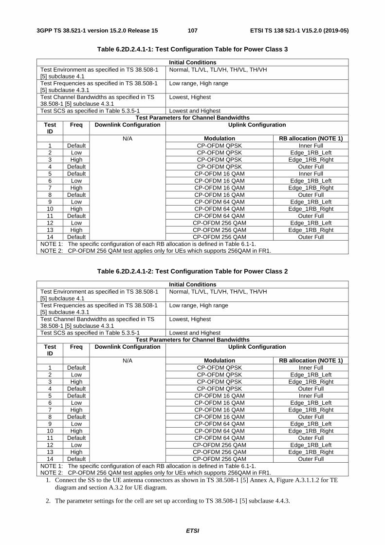
ETSI
ETSI TS 138 521-1 V15.2.0 (2019-05)1073GPP TS 38.521-1 version 15.2.0 Release 15
Table 6.2D.2.4.1-1: Test Configuration Table for Power Class 3
Initial Conditions Test Environment as specified in TS 38.508-1 [5] subclause 4.1
Normal, TL/VL, TL/VH, TH/VL, TH/VH
Test Frequencies as specified in TS 38.508-1 [5] subclause 4.3.1
Low range, High range
Test Channel Bandwidths as specified in TS 38.508-1 [5] subclause 4.3.1
Lowest, Highest
Test SCS as specified in Table 5.3.5-1 Lowest and Highest Test Parameters for Channel Bandwidths
Test ID
Freq Downlink Configuration Uplink Configuration
N/A Modulation RB allocation (NOTE 1) 1 Default CP-OFDM QPSK Inner Full 2 Low CP-OFDM QPSK Edge_1RB_Left 3 High CP-OFDM QPSK Edge_1RB_Right 4 Default CP-OFDM QPSK Outer Full 5 Default CP-OFDM 16 QAM Inner Full 6 Low CP-OFDM 16 QAM Edge_1RB_Left 7 High CP-OFDM 16 QAM Edge_1RB_Right 8 Default CP-OFDM 16 QAM Outer Full 9 Low CP-OFDM 64 QAM Edge_1RB_Left 10 High CP-OFDM 64 QAM Edge_1RB_Right 11 Default CP-OFDM 64 QAM Outer Full 12 Low CP-OFDM 256 QAM Edge_1RB_Left 13 High CP-OFDM 256 QAM Edge_1RB_Right 14 Default CP-OFDM 256 QAM Outer Full
NOTE 1: The specific configuration of each RB allocation is defined in Table 6.1-1. NOTE 2: CP-OFDM 256 QAM test applies only for UEs which supports 256QAM in FR1.
Table 6.2D.2.4.1-2: Test Configuration Table for Power Class 2
Initial Conditions Test Environment as specified in TS 38.508-1 [5] subclause 4.1
Normal, TL/VL, TL/VH, TH/VL, TH/VH
Test Frequencies as specified in TS 38.508-1 [5] subclause 4.3.1
Low range, High range
Test Channel Bandwidths as specified in TS 38.508-1 [5] subclause 4.3.1
Lowest, Highest
Test SCS as specified in Table 5.3.5-1 Lowest and Highest Test Parameters for Channel Bandwidths
Test ID
Freq Downlink Configuration Uplink Configuration
N/A Modulation RB allocation (NOTE 1) 1 Default CP-OFDM QPSK Inner Full 2 Low CP-OFDM QPSK Edge_1RB_Left 3 High CP-OFDM QPSK Edge_1RB_Right 4 Default CP-OFDM QPSK Outer Full 5 Default CP-OFDM 16 QAM Inner Full 6 Low CP-OFDM 16 QAM Edge_1RB_Left 7 High CP-OFDM 16 QAM Edge_1RB_Right 8 Default CP-OFDM 16 QAM Outer Full 9 Low CP-OFDM 64 QAM Edge_1RB_Left 10 High CP-OFDM 64 QAM Edge_1RB_Right 11 Default CP-OFDM 64 QAM Outer Full 12 Low CP-OFDM 256 QAM Edge_1RB_Left 13 High CP-OFDM 256 QAM Edge_1RB_Right 14 Default CP-OFDM 256 QAM Outer Full
NOTE 1: The specific configuration of each RB allocation is defined in Table 6.1-1. NOTE 2: CP-OFDM 256 QAM test applies only for UEs which supports 256QAM in FR1.
1. Connect the SS to the UE antenna connectors as shown in TS 38.508-1 [5] Annex A, Figure A.3.1.1.2 for TE diagram and section A.3.2 for UE diagram.
2. The parameter settings for the cell are set up according to TS 38.508-1 [5] subclause 4.4.3.

ETSI
ETSI TS 138 521-1 V15.2.0 (2019-05)1083GPP TS 38.521-1 version 15.2.0 Release 15
3. Downlink signals are initially set up according to Annex C.0, C.1, C.2, and uplink signals according to Annex G.0, G.1, G.2, G.3.0.
4. The UL Reference Measurement Channel is set according to Table 6.2D.2.4.1-1.
5. Propagation conditions are set according to Annex B.0.
6. Ensure the UE is in state RRC_CONNECTED with generic procedure parameters Connectivity NR, Connected without release On, Test Mode On and Test Loop Function On according to TS 38.508-1 [5] clause 4.5. Message contents are defined in clause 6.2D.2.4.3.
6.2D.2.4.2 Test procedure
1. SS sends uplink scheduling information for each UL HARQ process via PDCCH DCI format 0_1 for C_RNTI to schedule the UL RMC according to Table 6.2D.2.4.1-1. Since the UE has no payload and no loopback data to send the UE sends uplink MAC padding bits on the UL RMC. The PDCCH DCI format 0_1 is specified with the condition 2TX_UL_MIMO in 38.508-1 [5] subclause 4.3.6.1.1.2.
2. Send continuously uplink power control "up" commands in every uplink scheduling information to the UE; allow at least 200ms starting from the first TPC command in this step for the UE to reach PUMAX level.
3. Measure the sum of the mean power of the UE at each transmit antenna connector in the channel bandwidth of the radio access mode. The period of measurement shall be at least the continuous duration of one active sub-frame (1ms) and in the uplink symbols. For TDD symbol with transient periods are not under test.
6.2D.2.4.3 Message contents
Message contents are according to TS 38.508-1 [5] subclause 4.6 and 5.4.
6.2D.2.5 Test requirement
The maximum output power, derived in step 3 shall be within the range prescribed by the nominal maximum output power and tolerance in Table 6.2D.2.5-1 and Table 6.2D.2.5-2.

ETSI
ETSI TS 138 521-1 V15.2.0 (2019-05)1093GPP TS 38.521-1 version 15.2.0 Release 15
Table 6.2D.2.5-1: UE Power Class test requirements (for Band n41, n77, n78, n79) for Power Class 3
Test ID
PPowerClass
(dBm)
ΔPPowerClass
(dB) MPR (dB) ΔTC,c (dB)
PCMAX_L,f,c (dBm) T(PCMAX_L,f,c) (dB) TL,c
Upper limit
(dBm) Lower limit (dBm)
1 23 0 1.5 0 ( 1.52) 21.5 ( 20.02) 5.0 ( 6.02) 3 25.0 + TT 16.5 - TT ( 14.0 - TT2)
2 23 0 3 0 ( 1.52) 20.0 ( 18.52) 6.0 ( 5.02) 3 25.0 + TT 14.0 - TT ( 13.5 - TT2)
3 23 0 3 0 ( 1.52) 20.0 ( 18.52) 6.0 ( 5.02) 3 25.0 + TT 14.0 - TT ( 13.5 - TT2)
4 23 0 3 0 ( 1.52) 20.0 ( 18.52) 6.0 ( 5.02) 3 25.0 + TT 14.0 - TT ( 13.5 - TT2)
5 23 0 2 0 ( 1.52) 21.0 ( 19.52) 5.0 ( 5.02) 3 25.0 + TT 16.0 - TT ( 14.5 - TT2)
6 23 0 3 0 ( 1.52) 20.0 ( 18.52) 6.0 ( 5.02) 3 25.0 + TT 14.0 - TT ( 13.5 - TT2)
7 23 0 3 0 ( 1.52) 20.0 ( 18.52) 6.0 ( 5.02) 3 25.0 + TT 14.0 - TT ( 13.5 - TT2)
8 23 0 3 0 ( 1.52) 20.0 ( 18.52) 6.0 ( 5.02) 3 25.0 + TT 14.0 - TT ( 13.5 - TT2)
9 23 0 3.5 0 ( 1.52) 19.5 ( 18.02) 5.0 ( 5.02) 3 25.0 + TT 14.5 - TT ( 13.0 - TT2)
10 23 0 3.5 0 ( 1.52) 19.5 ( 18.02) 5.0 ( 5.02) 3 25.0 + TT 14.5 - TT ( 13.0 - TT2)
11 23 0 3.5 0 ( 1.52) 19.5 ( 18.02) 5.0 ( 5.02) 3 25.0 + TT 14.5 - TT ( 13.0 - TT2)
12 23 0 6.5 0 ( 1.52) 16.5 ( 15.02) 5.0 ( 6.02) 3 25.0 + TT 11.5 - TT ( 9.0 - TT2)
13 23 0 6.5 0 ( 1.52) 16.5 ( 15.02) 5.0 ( 6.02) 3 25.0 + TT 11.5 - TT ( 9.0 - TT2)
14 23 0 6.5 0 ( 1.52) 16.5 ( 15.02) 5.0 ( 6.02) 3 25.0 + TT 11.5 - TT ( 9.0 - TT2)
Table 6.2D.2.5-2: UE Power Class test requirements (for Bands n41, n77, n78, n79) for Power Class 2

ETSI
ETSI TS 138 521-1 V15.2.0 (2019-05)1103GPP TS 38.521-1 version 15.2.0 Release 15
Test ID
PPowerClass
(dBm) ΔPPowerClass
(dB) MPR (dB) ΔTC,c (dB) PCMAX_L,f,c (dBm) T(PCMAX_L,f,c) (dB) TL,c (dB) Upper limit
(dBm) Lower limit (dBm)
1 26 0 1.5 0 ( 1.52) 24.5 ( 23.02) 2.0 ( 2.52) 3 28.0 + TT 21.5 - TT ( 20.0 - TT2)
2 26 0 3.5 0 ( 1.52) 22.5 ( 21.02) 5.0 ( 5.02) 3 28.0 + TT 17.5 - TT ( 16.0 - TT2)
3 26 0 3.5 0 ( 1.52) 22.5 ( 21.02) 5.0 ( 5.02) 3 28.0 + TT 17.5 - TT ( 16.0 - TT2)
4 26 0 3 0 ( 1.52) 23.0 ( 21.52) 3.0 ( 5.02) 3 28.0 + TT 20.0 - TT ( 16.5 - TT2)
5 26 0 2 0 ( 1.52) 24.0 ( 22.52) 3.0 ( 5.02) 3 28.0 + TT 21.0 - TT ( 17.5 - TT2)
6 26 0 3.5 0 ( 1.52) 22.5 ( 21.02) 5.0 ( 5.02) 3 28.0 + TT 17.5 - TT ( 16.0 - TT2)
7 26 0 3.5 0 ( 1.52) 22.5 ( 21.02) 5.0 ( 5.02) 3 28.0 + TT 17.5 - TT ( 16.0 - TT2)
8 26 0 3 0 ( 1.52) 23.0 ( 21.52) 3.0 ( 5.02) 3 28.0 + TT 20.0 - TT ( 16.5 - TT2)
9 26 0 3.5 0 ( 1.52) 22.5 ( 21.02) 5.0 ( 5.02) 3 28.0 + TT 17.5 - TT ( 16.0 - TT2)
10 26 0 3.5 0 ( 1.52) 22.5 ( 21.02) 5.0 ( 5.02) 3 28.0 + TT 17.5 - TT ( 16.0 - TT2)
11 26 0 3.5 0 ( 1.52) 22.5 ( 21.02) 5.0 ( 5.02) 3 28.0 + TT 17.5 - TT ( 16.0 - TT2)
12 26 0 6.5 0 ( 1.52) 19.5 ( 18.02) 5.0 ( 5.02) 3 28.0 + TT 14.5 - TT ( 13.0 - TT2)
13 26 0 6.5 0 ( 1.52) 19.5 ( 18.02) 5.0 ( 5.02) 3 28.0 + TT 14.5 - TT ( 13.0 - TT2)
14 26 0 6.5 0 ( 1.52) 19.5 ( 18.02) 5.0 ( 5.02) 3 28.0 + TT 14.5 - TT ( 13.0 - TT2)
Table 6.2D.2.5-3: Test Tolerance (Maximum Power Reduction (MPR))
f ≤ 3.0GHz 3.0GHz < f ≤ 6.0GHz BW ≤ 40MHz FFS FFS
40MHz < BW ≤ 100MHz FFS FFS

ETSI
ETSI TS 138 521-1 V15.2.0 (2019-05)1113GPP TS 38.521-1 version 15.2.0 Release 15
6.2D.4 Configured transmitted power for UL-MIMO
Editor’s Note:
- MU and TT need further study on whether any deviation from basic test case is needed.
6.2D.4.1 Test purpose
To verify the measured UE configured maximum output power PUMAX,f,c for UL-MIMO is within the specified bounds.
6.2D.4.2 Test applicability
This test case applies to all types of NR UE release 15 and forward that support UL-MIMO.
6.2D.4.3 Minimum conformance requirements
For UE supporting UL-MIMO, the transmitted power is configured per each UE.
The definitions of configured maximum output power PCMAX,c, the lower bound PCMAX_L,c, and the higher bound PCMAX_H,c specified in subclause 6.2.4 shall apply to UE supporting UL-MIMO, where
PPowerClass, ΔPPowerClass and ΔTC,c are specified in subclause 6.2D.1.3;
MPRc is specified in subclause 6.2D.2.3;
A-MPRc is specified in subclause 6.2D.3.3.
The measured configured maximum output power PUMAX,c for serving cell c shall be within the following bounds:
PCMAX_L,c – MAX{TL, T LOW(PCMAX_L,c)} ≤ PUMAX,c ≤ PCMAX_H,c + T HIGH(PCMAX_H,c)
where TLOW(PCMAX_L,c) and THIGH(PCMAX_H,c) are defined as the tolerance and applies to PCMAX_L,c and PCMAX_H,c separately, while TL is the absolute value of the lower tolerance in Table 6.2D.1.3-1 for the applicable operating band.
For UE with two transmit antenna connectors in closed-loop spatial amultiplexing scheme, the tolerance is specified in Table 6.2D.4.3-1. The requirements shall be met with UL-MIMO configurations specified in Table 6.2D.1.3-2.
Table 6.2D.4.3-1: PCMAX,c tolerance in closed-loop spatial multiplexing scheme
PCMAX,c
(dBm) Tolerance
TLOW(PCMAX_L,c) (dB) Tolerance
THIGH(PCMAX_H,c) (dB) PCMAX,c =26 3.0 2.0
23 ≤ PCMAX,c < 26 3.0 2.0
22 ≤ PCMAX,c < 23 5.0 2.0
21 ≤ PCMAX,c < 22 5.0 3.0
20 ≤ PCMAX,c < 21 6.0 4.0
16 ≤ PCMAX,c < 20 5.0
11 ≤ PCMAX,c < 16 6.0 -40 ≤ PCMAX,c < 11 7.0
If UE is configured for transmission on single-antenna port, the requirements in subclause 6.2.4.3 apply.
The normative reference for this requirement is TS 38.101-1 [2] clause 6.2D.4.
6.2D.4.4 Test description
6.2D.4.4.1 Initial conditions
Initial conditions are a set of test configurations the UE needs to be tested in and the steps for the SS to take with the UE to reach the correct measurement state.
The initial test configurations consist of environmental conditions, test frequencies, test channel bandwidths and sub-carrier spacing based on NR operating bands specified in table 5.3.5-1. All of these configurations shall be tested with applicable test parameters for each combination of test channel bandwidth and sub-carrier spacing, and are shown in

ETSI
ETSI TS 138 521-1 V15.2.0 (2019-05)1123GPP TS 38.521-1 version 15.2.0 Release 15
table 6.2D.4.4.1-1. The details of the uplink reference measurement channels (RMCs) are specified in Annexes A.2. Configurations of PDSCH and PDCCH before measurement are specified in Annex C.2.
Table 6.2D.4.4.1-1: Test Configuration Table
Initial Conditions Test Environment as specified in TS 38.508-1 [5] subclause 4.1
Normal, TL/VL, TL/VH, TH/VL, TH/VH
Test Frequencies as specified in TS 38.508-1 [5] subclause 4.3.1
Low range, Mid range, High range
Test Channel Bandwidths as specified in TS 38.508-1 [5] subclause 4.3.1
Lowest, Mid, Highest
Test SCS as specified in Table 5.3.5-1 Lowest Test Parameters for Channel Bandwidths
Test ID Downlink Configuration Uplink Configuration N/A Modulation RB allocation (NOTE 1)
1 CP-OFDM QPSK Inner Full NOTE 1: The specific configuration of each RB allocation is defined in Table 6.1-1.
1. Connect the SS to the UE antenna connectors as shown in TS 38.508-1 [5] Annex A, Figure A.3.1. 1.2 for TE diagram and section A.3.2 for UE diagram.
2. The parameter settings for the cell are set up according to TS 38.508-1 [5] subclause 4.4.3.
3. Downlink signals are initially set up according to Annex C.0, C.1, C.2, and uplink signals according to Annex G.0, G.1, G.2, G.3.0.
4. The UL Reference Measurement Channel is set according to Table 6.2D.4.4.1-1.
5. Propagation conditions are set according to Annex B.0.
6. Ensure the UE is in state RRC_CONNECTED with generic procedure parameters Connectivity NR, Connected without release On, Test Mode On and Test Loop Function On according to TS 38.508-1 [5] clause 4.5. Message contents are defined in clause 6.2D.4.4.3.
6.2D.4.4.2 Test procedure
1. SS sends uplink scheduling information for each UL HARQ process via PDCCH DCI format 0_1 for C_RNTI to schedule the UL RMC according to Table 6.2D.4.4.1-1. Since the UE has no payload and no loopback data to send the UE sends uplink MAC padding bits on the UL RMC. The PDCCH DCI format 0_1 is specified with the condition 2TX_UL_MIMO in 38.508-1 [5] subclause 4.3.6.1.1.2.
2. Send continuously uplink power control "up" commands in every uplink scheduling information to the UE; allow at least 200ms starting from the first TPC command in this step for the UE to reach PUMAX level of the test point.
3. Measure the sum of the mean power of the UE at each transmit antenna connector in the channel bandwidth of the radio access mode. The period of measurement shall be at least the continuous duration of 1ms over all active uplink slots and in the uplink symbols. For TDD slots only slots consisting of only UL symbols are under test.
6.2D.4.4.3 Message contents
Message contents are according to TS 38.508-1 [5] subclause 4.6 ensuring Table 4.6.3-182 with the condition 2TX_UL_MIMO and following exception.
Table 6.2D.4.4.3-1: FrequencyInfoUL: Test point 1
Derivation Path: TS 38.508-1 [5] Table 4.6.3-61 FrequencyInfoUL Information Element Value/remark Comment Condition
p-Max 0
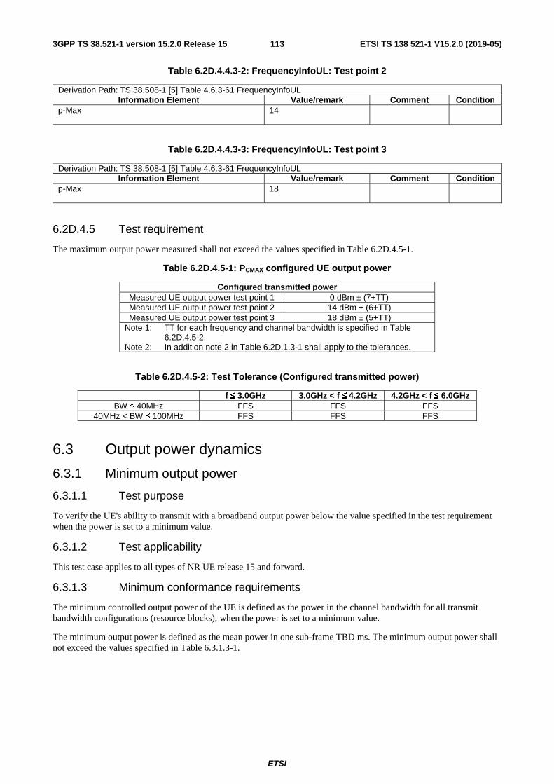
ETSI
ETSI TS 138 521-1 V15.2.0 (2019-05)1133GPP TS 38.521-1 version 15.2.0 Release 15
Table 6.2D.4.4.3-2: FrequencyInfoUL: Test point 2
Derivation Path: TS 38.508-1 [5] Table 4.6.3-61 FrequencyInfoUL Information Element Value/remark Comment Condition
p-Max 14
Table 6.2D.4.4.3-3: FrequencyInfoUL: Test point 3
Derivation Path: TS 38.508-1 [5] Table 4.6.3-61 FrequencyInfoUL Information Element Value/remark Comment Condition
p-Max 18
6.2D.4.5 Test requirement
The maximum output power measured shall not exceed the values specified in Table 6.2D.4.5-1.
Table 6.2D.4.5-1: PCMAX configured UE output power
Configured transmitted power Measured UE output power test point 1 0 dBm ± (7+TT) Measured UE output power test point 2 14 dBm ± (6+TT) Measured UE output power test point 3 18 dBm ± (5+TT)
Note 1: TT for each frequency and channel bandwidth is specified in Table 6.2D.4.5-2.
Note 2: In addition note 2 in Table 6.2D.1.3-1 shall apply to the tolerances.
Table 6.2D.4.5-2: Test Tolerance (Configured transmitted power)
f ≤ 3.0GHz 3.0GHz < f ≤ 4.2GHz 4.2GHz < f ≤ 6.0GHz BW ≤ 40MHz FFS FFS FFS
40MHz < BW ≤ 100MHz FFS FFS FFS
6.3 Output power dynamics
6.3.1 Minimum output power
6.3.1.1 Test purpose
To verify the UE's ability to transmit with a broadband output power below the value specified in the test requirement when the power is set to a minimum value.
6.3.1.2 Test applicability
This test case applies to all types of NR UE release 15 and forward.
6.3.1.3 Minimum conformance requirements
The minimum controlled output power of the UE is defined as the power in the channel bandwidth for all transmit bandwidth configurations (resource blocks), when the power is set to a minimum value.
The minimum output power is defined as the mean power in one sub-frame TBD ms. The minimum output power shall not exceed the values specified in Table 6.3.1.3-1.

ETSI
ETSI TS 138 521-1 V15.2.0 (2019-05)1143GPP TS 38.521-1 version 15.2.0 Release 15
Table 6.3.1.3-1: Minimum output power
Channel bandwidth (MHz)
Minimum output power (dBm)
Measurement bandwidth (MHz)
5 -40 4.515 10 -40 9.375 15 -40 14.235 20 -40 19.095 25 -39 23.955 30 -38.2 28.815 40 -37 38.895 50 -36 48.615 60 -35.2 58.35 80 -34 78.15 90 -33.5 88.23
100 -33 98.31
The normative reference for this requirement is TS 38.101-1 [2] clause 6.3.1.
6.3.1.4 Test description
6.3.1.4.1 Initial condition
Initial conditions are a set of test configurations the UE needs to be tested in and the steps for the SS to take with the UE to reach the correct measurement state.
The initial test configurations consist of environmental conditions, test frequencies, test channel bandwidths and sub-carrier spacing based on NR operating bands specified in table 5.3.5-1. All of these configurations shall be tested with applicable test parameters for each combination of test channel bandwidth and sub-carrier spacing, and are shown in table 6.3.1.4.1-1. The details of the uplink reference measurement channels (RMCs) are specified in Annexes A.2. Configurations of PDSCH and PDCCH before measurement are specified in Annex C.2.
Table 6.3.1.4.1-1: Test Configuration Table
Initial Conditions Test Environment as specified in TS 38.508-1 [5] subclause 4.1
Normal, TL/VL, TL/VH, TH/VL, TH/VH
Test Frequencies as specified in TS 38.508-1 [5] subclause 4.3.1
Low range, Mid range, High range
Test Channel Bandwidths as specified in TS 38.508-1 [5] subclause 4.3.1
Lowest, Mid, Highest
Test SCS as specified in Table 5.3.5-1 Highest Test Parameters for Channel Bandwidths
Test ID Downlink Configuration Uplink Configuration N/A for minimum output
power Modulation RB allocation (NOTE 1)
1 test case DFT-s-OFDM QPSK Outer Full NOTE 1: The specific configuration of each RB allocation is defined in Table 6.1-1.
1. Connect the SS to the UE antenna connectors as shown in TS 38.508-1 [5] Annex A, Figure A.3.1.1.1 for TE diagram and section A.3.2.1 for UE diagram.
2. The parameter settings for the cell are set up according to TS 38.508-1 [5] subclause 4.4.3.
3. Downlink signals are initially set up according to Annex C.0, C.1, C.2, and uplink signals according to Annex G.0, G.1, G.2, G.3.0.
4. The UL Reference Measurement Channel is set according to Table 6.3.1.4.1-1.
5. Propagation conditions are set according to Annex B.0.

ETSI
ETSI TS 138 521-1 V15.2.0 (2019-05)1153GPP TS 38.521-1 version 15.2.0 Release 15
6. Ensure the UE is in State RRC_CONNECTED with generic procedure parameters Connectivity NR, Connected without release On, Test Mode On and Test Loop Function On according to TS 38.508-1 [5] clause 4.5. Message contents are defined in clause 6.3.1.4.3.
6.3.1.4.2 Test procedure
1. SS sends uplink scheduling information for each UL HARQ process via PDCCH DCI format 0_1 for C_RNTI to schedule the UL RMC according to Table 6.3.1.4.1-1. Since the UE has no payload and no loopback data to send the UE sends uplink MAC padding bits on the UL RMC.
2. Send continuously uplink power control "down" commands in every uplink scheduling information to the UE; allow at least 200ms starting from the first TPC command in this step to ensure that the UE transmits at its minimum output power.
3. Measure the mean power of the UE in the associated measurement channel bandwidth specified in Table 6.3.1.5-1 for the specific channel bandwidth under test. The period of measurement shall be at least the continuous duration of one active sub-frame (1ms) and in the uplink symbols. For TDD symbols with transient periods are not under test.
6.3.1.4.3 Message contents
Message contents are according to TS 38.508-1 [5] subclause 4.6 with following exception.
Table 6.3.1.4.3-1: PUSCH-Config
Derivation Path: TS 38.508-1 [5], Table 4.6.3-118 with condition TRANSFORM_PRECODER_ENABLED
6.3.1.5 Test requirement
The minimum output power, derived in step 3 shall not exceed the values specified in Table 6.3.1.5-1.
Table 6.3.1.5-1: Minimum output power
Channel bandwidth (MHz)
Minimum output power (dBm)
Measurement bandwidth (MHz)
5 -40+TT 4.515 10 -40+TT 9.375 15 -40+TT 14.235 20 -40+TT 19.095 25 -39+TT 23.955 30 -38.2+TT 28.815 40 -37+TT 38.895 50 -36+TT 48.615 60 -35.2+TT 58.35 80 -34+TT 78.15 90 -33.5+TT 88.23
100 -33+TT 98.31 NOTE 1: TT for each frequency and channel bandwidth is specified in Table 6.3.1.5-2
Table 6.3.1.5-2: Test Tolerance (Minimum output power)
f ≤ 3.0GHz 3.0GHz < f ≤ 6.0GHz BW ≤ 40MHz 1.0 dB 1.3 dB
40MHz < BW ≤ 100MHz 1.3 dB 1.3 dB
6.3A.1 Minimum output power for CA
6.3A.1.0 Minimum conformance requirements
For inter-band carrier aggregation with uplink assigned to two NR bands, the minimum output power is defined per carrier and the requirement is specified in subclause 6.3.1.

ETSI
ETSI TS 138 521-1 V15.2.0 (2019-05)1163GPP TS 38.521-1 version 15.2.0 Release 15
The normative reference for this requirement is TS 38.101-1 [2] clause 6.3A.1.
6.3A.1.1 Minimum output power for CA (2UL CA)
Editor’s note: This clause is incomplete. The following aspects are either missing or not yet determined:
- Test config table is FFS.
- Connection diagram is FFS in TS 38.508-1.
- MU and TT is FFS in Annex F.
6.3A.1.1.1 Test purpose
To verify the UE's ability to transmit with a broadband output power for 2UL CA below the value specified in the test requirement when the power is set to a minimum value.
6.3A.1.1.2 Test applicability
This test case applies to all types of NR UE release 15 and forward that support 2UL CA.
6.3A.1.1.3 Minimum conformance requirements
The minimum conformance requirements are defined in clause 6.3A.1.0.
6.3A.1.1.4 Test description
6.3A.1.1.4.1 Initial condition
Initial conditions are a set of test configurations the UE needs to be tested in and the steps for the SS to take with the UE to reach the correct measurement state.
The initial test configurations consist of environmental conditions, test frequencies, test channel bandwidths and sub-carrier spacing based on NR CA configurations specified in 5.5A. All of these configurations shall be tested with applicable test parameters for each CA configuration, and are shown in table 6.3A.1.1.4.1-1. The details of the uplink reference measurement channels (RMCs) are specified in Annexes A.2 and A.3. Configurations of PDSCH and PDCCH before measurement are specified in Annex C.2.
Table 6.3A.1.1.4.1-1: Test Configuration Table
FFS
1. Connect the SS to the UE antenna connectors as shown in TS 38.508-1 [5] Annex A, Figure [FFS] for TE diagram and section A.3.2.1 for UE diagram.
2. The parameter settings for the cell are set up according to TS 38.508-1 [5] subclause 4.4.3.
3. Downlink signals are initially set up according to Annex C.0, C.1, C.2, and uplink signals according to Annex G.0, G.1, G.2, G.3.0.
4. The UL Reference Measurement Channel is set according to Table 6.3A.1.1.4.1-1.
5. Propagation conditions are set according to Annex B.0.
6. Ensure the UE is in State RRC_CONNECTED with generic procedure parameters Connectivity NR, Connected without release On, Test Mode On and Test Loop Function On according to TS 38.508-1 [5] clause 4.5. Message contents are defined in clause 6.3A.1.1.4.3.
6.3A.1.1.4.2 Test procedure
1. Configure SCC according to Annex C.0, C.1, C.2 for all downlink physical channels.
2. The SS shall configure SCC as per TS 38.508-1 [5] clause [TBD]. Message contents are defined in clause 6.3A.1.3.4.3.
3. SS activates SCC by sending the activation MAC CE (Refer TS 38.321 [18], clauses 5.9, 6.1.3.10). Wait for at least 2 seconds (Refer TS 38.133 [19], clause 9.3).

ETSI
ETSI TS 138 521-1 V15.2.0 (2019-05)1173GPP TS 38.521-1 version 15.2.0 Release 15
4. SS sends uplink scheduling information for each UL HARQ process via PDCCH DCI format 0_1 for C_RNTI to schedule the UL RMC according to Table 6.3A.1.1.4.1-1 on both PCC and SCC. Since the UE has no payload and no loopback data to send the UE sends uplink MAC padding bits on the UL RMC.
5. Send continuously uplink power control "down" commands for both carriers in every uplink scheduling information to the UE; allow at least 200ms starting from the first TPC command in this step to ensure that the UE transmits at its minimum output power.
6. Measure the mean power of the UE for each component carrier in the associated measurement channel bandwidth specified in Table 6.3A.1.1.5-1 for the specific channel bandwidth under test. The period of measurement shall be at least the continuous duration of 1ms in all active uplink slots and in the uplink symbols. For TDD, only slots consisting of only UL symbols are under test
6.3A.1.1.4.3 Message contents
Message contents are according to TS 38.508-1 [5] subclause 4.6.
6.3A.1.1.5 Test requirement
The minimum output power of each component carrier, derived in step 6 shall not exceed the values specified in Table 6.3A.1.1.5-1.
Table 6.3A.1.1.5-1: Minimum output power
Channel bandwidth (MHz)
Minimum output power (dBm)
Measurement bandwidth (MHz)
5 -40+TT 4.515 10 -40+TT 9.375 15 -40+TT 14.235 20 -40+TT 19.095 25 -39+TT 23.955 30 -38.2+TT 28.815 40 -37+TT 38.895 50 -36+TT 48.615 60 -35.2+TT 58.35 80 -34+TT 78.15 90 -33.5+TT 88.23
100 -33+TT 98.31 NOTE 1: TT for each frequency and channel bandwidth is specified in Table 6.3A.1.1.5-
2
Table 6.3A.1.1.5-2: Test Tolerance (Minimum output power)
f ≤ 3.0GHz 3.0GHz < f ≤ 6.0GHz BW ≤ 40MHz FFS FFS
40MHz < BW ≤ 100MHz FFS FFS
6.3A.2 Transmit OFF power for CA
6.3A.2.0 Minimum conformance requirements
For inter-band carrier aggregation with uplink assigned to two NR bands, the transmit OFF power specified in subclause 6.3.2 is applicable for each component carrier when the transmitter is OFF on all component carriers. The transmitter is considered to be OFF when the UE is not allowed to transmit or during periods when the UE is not transmitting a sub-frame. During measurements gaps, the UE is not considered to be OFF.
The normative reference for this requirement is TS 38.101-1 [2] clause 6.3A.2
6.3A.2.1 Transmit OFF power for CA (2UL CA)
Editor’s Note: This clause is incomplete. The following aspects are either missing or not yet determined:
- Test config table is FFS.
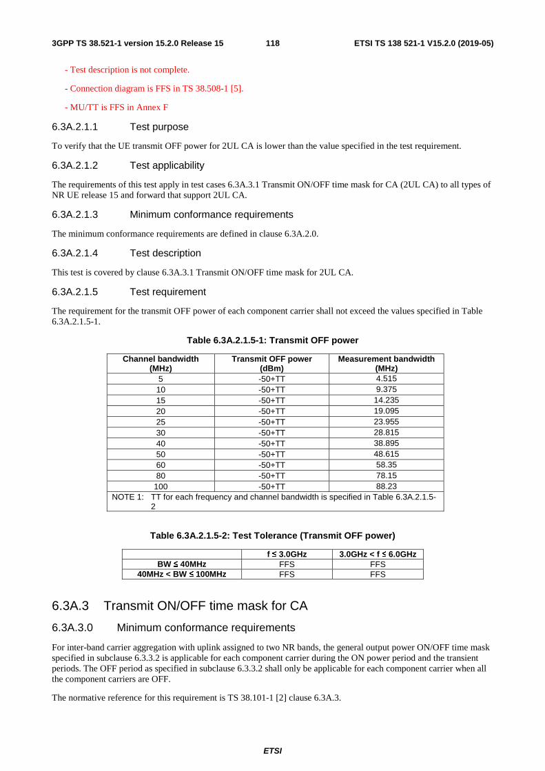
ETSI
ETSI TS 138 521-1 V15.2.0 (2019-05)1183GPP TS 38.521-1 version 15.2.0 Release 15
- Test description is not complete.
- Connection diagram is FFS in TS 38.508-1 [5].
- MU/TT is FFS in Annex F
6.3A.2.1.1 Test purpose
To verify that the UE transmit OFF power for 2UL CA is lower than the value specified in the test requirement.
6.3A.2.1.2 Test applicability
The requirements of this test apply in test cases 6.3A.3.1 Transmit ON/OFF time mask for CA (2UL CA) to all types of NR UE release 15 and forward that support 2UL CA.
6.3A.2.1.3 Minimum conformance requirements
The minimum conformance requirements are defined in clause 6.3A.2.0.
6.3A.2.1.4 Test description
This test is covered by clause 6.3A.3.1 Transmit ON/OFF time mask for 2UL CA.
6.3A.2.1.5 Test requirement
The requirement for the transmit OFF power of each component carrier shall not exceed the values specified in Table 6.3A.2.1.5-1.
Table 6.3A.2.1.5-1: Transmit OFF power
Channel bandwidth (MHz)
Transmit OFF power (dBm)
Measurement bandwidth (MHz)
5 -50+TT 4.515 10 -50+TT 9.375 15 -50+TT 14.235 20 -50+TT 19.095 25 -50+TT 23.955 30 -50+TT 28.815 40 -50+TT 38.895 50 -50+TT 48.615 60 -50+TT 58.35 80 -50+TT 78.15
100 -50+TT 88.23 NOTE 1: TT for each frequency and channel bandwidth is specified in Table 6.3A.2.1.5-
2
Table 6.3A.2.1.5-2: Test Tolerance (Transmit OFF power)
f ≤ 3.0GHz 3.0GHz < f ≤ 6.0GHz BW ≤ 40MHz FFS FFS
40MHz < BW ≤ 100MHz FFS FFS
6.3A.3 Transmit ON/OFF time mask for CA
6.3A.3.0 Minimum conformance requirements
For inter-band carrier aggregation with uplink assigned to two NR bands, the general output power ON/OFF time mask specified in subclause 6.3.3.2 is applicable for each component carrier during the ON power period and the transient periods. The OFF period as specified in subclause 6.3.3.2 shall only be applicable for each component carrier when all the component carriers are OFF.
The normative reference for this requirement is TS 38.101-1 [2] clause 6.3A.3.

ETSI
ETSI TS 138 521-1 V15.2.0 (2019-05)1193GPP TS 38.521-1 version 15.2.0 Release 15
6.3A.3.1 Transmit ON/OFF time mask for CA (2UL CA)
Editor’s Note: This clause is incomplete. The following aspects are either missing or not yet determined:
- Test config table is FFS
- Connection diagram is FFS in TS 38.508-1.
- MU/TT is FFS in Annex F
6.3A.3.1.1 Test purpose
To verify that the general ON/OFF time mask for CA (2UL CA) meets the requirements given in 6.3A.3.1.5
The transmit power time mask for transmit ON/OFF defines the transient period(s) allowed between transmit OFF power and transmit ON power symbols for CA.
Transmission of the wrong power increases interference to other channels, or increases transmission errors in the uplink channel.
6.3A.3.1.2. Test applicability
This test case applies to all types of NR UE release 15 and forward that support 2UL CA.
6.3A.3.1.3 Minimum conformance requirements
The minimum conformance requirements are defined in clause 6.3A.3.0.
6.3A.3.1.4 Test description
6.3A.3.1.4.1 Initial condition
Initial conditions are a set of test configurations the UE needs to be tested in and the steps for the SS to take with the UE to reach the correct measurement state.
The initial test configurations consist of environmental conditions, test frequencies, test channel bandwidths and sub-carrier spacing based on NR CA configuration specified in 5.5A. All of these configurations shall be tested with applicable test parameters for each CA configuration, and are shown in table 6.3A.3.1.4.1-1. The details of the uplink reference measurement channels (RMCs) are specified in Annexe A.2 and A.3. Configurations of PDSCH and PDCCH before measurement are specified in Annex C.2.
Table 6.3A.3.1.4.1-1: Test Configuration Table
FFS
1. Connect the SS to the UE antenna connectors as shown in TS 38.508-1 [5] Annex A, Figure [FFS] for TE diagram and section A.3.2.1 for UE diagram.
2. The parameter settings for the cell are set up according to TS 38.508-1 [5] subclause 4.4.3.
3. Downlink signals are initially set up according to Annex C.0, C.1, C.2, and uplink signals according to Annex G.0, G.1, G.2, G.3.0.
4. The UL Reference Measurement Channel is set according to Table 6.3A.3.1.4.1-1.
5. Propagation conditions are set according to Annex B.0.
6. Ensure the UE is in State RRC_CONNECTED with generic procedure parameters Connectivity NR, Connected without release On, Test Mode On and Test Loop Function On according to TS 38.508-1 [5] clause 4.5. Message contents are defined in clause 6.3A.3.1.4.3.
6.3A.3.3.4.2 Test procedure
1. Configure SCC according to Annex C.0, C.1, C.2 for all downlink physical channels.
2. The SS shall configure SCC as per TS 38.508-1 [5] clause [TBD]. Message contents are defined in clause 6.3A.3.1.4.3.
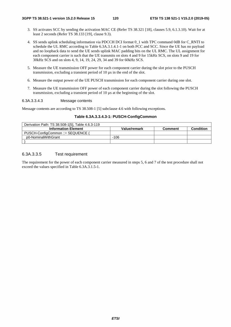
ETSI
ETSI TS 138 521-1 V15.2.0 (2019-05)1203GPP TS 38.521-1 version 15.2.0 Release 15
3. SS activates SCC by sending the activation MAC CE (Refer TS 38.321 [18], clauses 5.9, 6.1.3.10). Wait for at least 2 seconds (Refer TS 38.133 [19], clause 9.3).
4. SS sends uplink scheduling information via PDCCH DCI format 0_1 with TPC command 0dB for C_RNTI to schedule the UL RMC according to Table 6.3A.3.1.4.1-1 on both PCC and SCC. Since the UE has no payload and no loopback data to send the UE sends uplink MAC padding bits on the UL RMC. The UL assignment for each component carrier is such that the UE transmits on slots 4 and 9 for 15kHz SCS, on slots 9 and 19 for 30kHz SCS and on slots 4, 9, 14, 19, 24, 29, 34 and 39 for 60kHz SCS.
5. Measure the UE transmission OFF power for each component carrier during the slot prior to the PUSCH transmission, excluding a transient period of 10 µs in the end of the slot.
6. Measure the output power of the UE PUSCH transmission for each component carrier during one slot.
7. Measure the UE transmission OFF power of each component carrier during the slot following the PUSCH transmission, excluding a transient period of 10 µs at the beginning of the slot.
6.3A.3.3.4.3 Message contents
Message contents are according to TS 38.508-1 [5] subclause 4.6 with following exceptions.
Table 6.3A.3.3.4.3-1: PUSCH-ConfigCommon
Derivation Path: TS 38.508-1[5], Table 4.6.3-119 Information Element Value/remark Comment Condition
PUSCH-ConfigCommon ::= SEQUENCE { p0-NominalWithGrant -106 }
6.3A.3.3.5 Test requirement
The requirement for the power of each component carrier measured in steps 5, 6 and 7 of the test procedure shall not exceed the values specified in Table 6.3A.3.1.5-1.
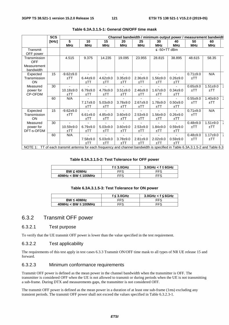
ETSI
ETSI TS 138 521-1 V15.2.0 (2019-05)1213GPP TS 38.521-1 version 15.2.0 Release 15
Table 6.3A.3.1.5-1: General ON/OFF time mask
SCS Channel bandwidth / minimum output power / measurement bandwidth [kHz] 5
MHz 10
MHz 15
MHz 20
MHz 25
MHz 30
MHz 40
MHz 50
MHz 60
MHz Transmit
OFF power ≤ -50+TT dBm
Transmission OFF
Measurement bandwidth
4.515 9.375 14.235 19.095 23.955 28.815 38.895 48.615 58.35
Expected Transmission
ON
15 -9.62±9.0 ±TT
-6.44±9.0
±TT
-4.62±9.0
±TT
-3.35±9.0
±TT
-2.36±9.0
±TT
-1.56±9.0
±TT
-0.26±9.0
±TT
0.71±9.0 ±TT
N/A
Measured power for CP-OFDM
30 -10.18±9.0
±TT
-6.79±9.0
±TT
-4.79±9.0
±TT
-3.51±9.0
±TT
-2.46±9.0
±TT
-1.67±9.0
±TT
-0.34±9.0
±TT
0.65±9.0 ±TT
1.51±9.0 ±TT
2
60 N/A -7.17±9.0
±TT
-5.03±9.0
±TT
-3.78±9.0
±TT
-2.67±9.0
±TT
-1.78±9.0
±TT
-0.50±9.0
±TT
0.55±9.0 ±TT
1.40±9.0 ±TT
2
Expected Transmission
ON
15 -9.62±9.0 ±TT
-6.61±9.0
±TT
-4.85±9.0
±TT
-3.60±9.0
±TT
-2.53±9.0
±TT
-1.56±9.0
±TT
-0.26±9.0
±TT
0.71±9.0 ±TT
N/A
Measured power for
DFT-s-OFDM
30 -10.59±9.0
±TT
-6.79±9.0
±TT
-5.03±9.0
±TT
-3.60±9.0
±TT
-2.53±9.0
±TT
-1.84±9.0
±TT
-0.59±9.0
±TT
0.48±9.0 ±TT
1.51±9.0 ±TT
2
60 N/A -7.58±9.0
±TT
-5.03±9.0
±TT
-3.78±9.0
±TT
-2.81±9.0
±TT
-2.02±9.0
±TT
-0.59±9.0
±TT
0.48±9.0 ±TT
1.17±9.0 ±TT
2
NOTE 1: TT of each transmit antenna for each frequency and channel bandwidth is specified in Table 6.3A.3.1.5-2 and Table 6.3A
Table 6.3A.3.1.5-2: Test Tolerance for OFF power
f ≤ 3.0GHz 3.0GHz < f ≤ 6GHz BW ≤ 40MHz FFS FFS
40MHz < BW ≤ 100MHz FFS FFS
Table 6.3A.3.1.5-3: Test Tolerance for ON power
f ≤ 3.0GHz 3.0GHz < f ≤ 6GHz BW ≤ 40MHz FFS FFS
40MHz < BW ≤ 100MHz FFS FFS
6.3.2 Transmit OFF power
6.3.2.1 Test purpose
To verify that the UE transmit OFF power is lower than the value specified in the test requirement.
6.3.2.2 Test applicability
The requirements of this test apply in test cases 6.3.3 Transmit ON/OFF time mask to all types of NR UE release 15 and forward.
6.3.2.3 Minimum conformance requirements
Transmit OFF power is defined as the mean power in the channel bandwidth when the transmitter is OFF. The transmitter is considered OFF when the UE is not allowed to transmit or during periods when the UE is not transmitting a sub-frame. During DTX and measurements gaps, the transmitter is not considered OFF.
The transmit OFF power is defined as the mean power in a duration of at least one sub-frame (1ms) excluding any transient periods. The transmit OFF power shall not exceed the values specified in Table 6.3.2.3-1.

ETSI
ETSI TS 138 521-1 V15.2.0 (2019-05)1223GPP TS 38.521-1 version 15.2.0 Release 15
Table 6.3.2.3-1: Transmit OFF power
Channel bandwidth (MHz)
Transmit OFF power (dBm)
Measurement bandwidth (MHz)
5 -50 4.515 10 -50 9.375 15 -50 14.235 20 -50 19.095 25 -50 23.955 30 -50 28.815 40 -50 38.895 50 -50 48.615 60 -50 58.35 80 -50 78.15
100 -50 88.23
The normative reference for this requirement is TS 38.101-1 [2] clause 6.3.2.
An excess transmit OFF power potentially increases the Rise Over Thermal (RoT) and therefore reduces the cell coverage area for other UEs.
6.3.2.4 Test description
This test is covered by clause 6.3.3 Transmit ON/OFF time mask.
6.3.2.5 Test requirement
The requirement for the transmit OFF power shall not exceed the values specified in Table 6.3.2.5-1.
Table 6.3.2.5-1: Transmit OFF power
Channel bandwidth (MHz)
Transmit OFF power (dBm)
Measurement bandwidth (MHz)
5 -50+TT 4.515 10 -50+TT 9.375 15 -50+TT 14.235 20 -50+TT 19.095 25 -50+TT 23.955 30 -50+TT 28.815 40 -50+TT 38.895 50 -50+TT 48.615 60 -50+TT 58.35 80 -50+TT 78.15
100 -50+TT 88.23 NOTE 1: TT for each frequency and channel bandwidth is specified in Table 6.3.2.5-2
Table 6.3.2.5-2: Test Tolerance (Transmit OFF power)
f ≤ 3.0GHz 3.0GHz < f ≤ 6.0GHz BW ≤ 40MHz 1.5 dB 1.8 dB
40MHz < BW ≤ 100MHz 1.7 dB 1.8 dB
6.3.3 Transmit ON/OFF time mask
6.3.3.1 General
The transmit power time mask defines the transient period(s) allowed
- between transmit OFF power as defined in sub-clause 6.3.2 and transmit ON power symbols (transmit ON/OFF)
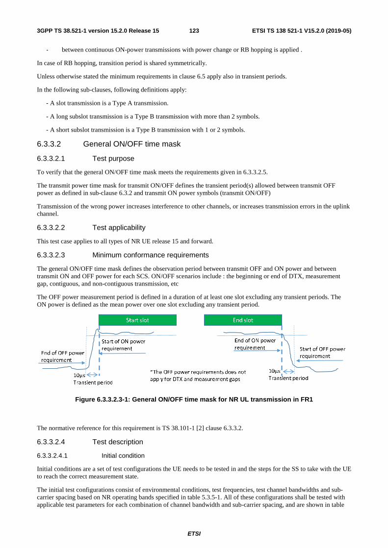
ETSI
ETSI TS 138 521-1 V15.2.0 (2019-05)1233GPP TS 38.521-1 version 15.2.0 Release 15
- between continuous ON-power transmissions with power change or RB hopping is applied .
In case of RB hopping, transition period is shared symmetrically.
Unless otherwise stated the minimum requirements in clause 6.5 apply also in transient periods.
In the following sub-clauses, following definitions apply:
- A slot transmission is a Type A transmission.
- A long subslot transmission is a Type B transmission with more than 2 symbols.
- A short subslot transmission is a Type B transmission with 1 or 2 symbols.
6.3.3.2 General ON/OFF time mask
6.3.3.2.1 Test purpose
To verify that the general ON/OFF time mask meets the requirements given in 6.3.3.2.5.
The transmit power time mask for transmit ON/OFF defines the transient period(s) allowed between transmit OFF power as defined in sub-clause 6.3.2 and transmit ON power symbols (transmit ON/OFF)
Transmission of the wrong power increases interference to other channels, or increases transmission errors in the uplink channel.
6.3.3.2.2 Test applicability
This test case applies to all types of NR UE release 15 and forward.
6.3.3.2.3 Minimum conformance requirements
The general ON/OFF time mask defines the observation period between transmit OFF and ON power and between transmit ON and OFF power for each SCS. ON/OFF scenarios include : the beginning or end of DTX, measurement gap, contiguous, and non-contiguous transmission, etc
The OFF power measurement period is defined in a duration of at least one slot excluding any transient periods. The ON power is defined as the mean power over one slot excluding any transient period.
Figure 6.3.3.2.3-1: General ON/OFF time mask for NR UL transmission in FR1
The normative reference for this requirement is TS 38.101-1 [2] clause 6.3.3.2.
6.3.3.2.4 Test description
6.3.3.2.4.1 Initial condition
Initial conditions are a set of test configurations the UE needs to be tested in and the steps for the SS to take with the UE to reach the correct measurement state.
The initial test configurations consist of environmental conditions, test frequencies, test channel bandwidths and sub-carrier spacing based on NR operating bands specified in table 5.3.5-1. All of these configurations shall be tested with applicable test parameters for each combination of channel bandwidth and sub-carrier spacing, and are shown in table
Start slot End slot
End of OFF power
requirement
Start of OFF power
requirement
Start of ON power
requirement
End of ON power
requirement
10µs
Transient period
10µs
Transient period*The OFF power requirements does not
apply for DTX and measurement gaps

ETSI
ETSI TS 138 521-1 V15.2.0 (2019-05)1243GPP TS 38.521-1 version 15.2.0 Release 15
6.3.3.2.4.1-1. The details of the uplink reference measurement channels (RMCs) are specified in Annexe A.2. Configurations of PDSCH and PDCCH before measurement are specified in Annex C.2.
Table 6.3.3.2.4.1-1: Test Configuration Table
Initial Conditions Test Environment as specified in TS 38.508-1 [5] subclause 4.1
Normal, TL/VL, TL/VH, TH/VL, TH/VH
Test Frequencies as specified in TS 38.508-1 [5] subclause 4.3.1
Low range, Mid range, High range
Test Channel Bandwidths as specified in TS 38.508-1 [5] subclause 4.3.1
Lowest, Mid, Highest
Test SCS as specified in Table 5.3.5-1 Lowest, Highest Test Parameters for Channel Bandwidths
Test ID Downlink Configuration Uplink Configuration N/A for minimum output
power Modulation RB allocation (NOTE 1)
1 test case CP-OFDM QPSK Outer Full NOTE 1: The specific configuration of each RB allocation is defined in Table 6.1-1.
1. Connect the SS to the UE antenna connectors as shown in TS 38.508-1 [5] Annex A, Figure A.3.1.1.1 for TE diagram and section A.3.2.1 for UE diagram.
2. The parameter settings for the cell are set up according to TS 38.508-1 [5] subclause 4.4.3.
3. Downlink signals are initially set up according to Annex C.0, C.1, C.2, and uplink signals according to Annex G.0, G.1, G.2, G.3.0.
4. The UL Reference Measurement Channel is set according to Table 6.3.3.2.4.1-1.
5. Propagation conditions are set according to Annex B.0.
6. Ensure the UE is in State RRC_CONNECTED with generic procedure parameters Connectivity NR, Connected without release On, Test Mode On and Test Loop Function On according to TS 38.508-1 [5] clause 4.5. Message contents are defined in clause 6.3.3.2.4.3.
6.3.3.2.4.2 Test procedure
1. SS sends uplink scheduling information via PDCCH DCI format 0_1 with TPC command 0dB for C_RNTI to schedule the UL RMC according to Table 6.3.3.2.4.1-1. Since the UE has no payload and no loopback data to send the UE sends uplink MAC padding bits on the UL RMC. The UL assignment is such that the UE transmits on slots 4 and 9 for15kHz SCS, on slots 9 and 19 for 30kHz SCS and on slots 4, 9, 14, 19, 24, 29, 34 and 39 for 60kHz SCS.
2. Measure the UE transmission OFF power during the slot prior to the PUSCH transmission, excluding a transient period of 10 µs in the end of the slot.
3. Measure the output power of the UE PUSCH transmission during one slot.
4. Measure the UE transmission OFF power during the slot following the PUSCH transmission, excluding a transient period of 10 µs at the beginning of the slot.
6.3.3.2.4.3 Message contents
Message contents are according to TS 38.508-1 [5] subclause 4.6 with following exceptions.
Table 6.3.3.2.4.3-1: PUSCH-ConfigCommon
Derivation Path: TS 38.508-1[5], Table 4.6.3-119 Information Element Value/remark Comment Condition
PUSCH-ConfigCommon ::= SEQUENCE { p0-NominalWithGrant -106 }

ETSI
ETSI TS 138 521-1 V15.2.0 (2019-05)1253GPP TS 38.521-1 version 15.2.0 Release 15
Table 6.3.3.2.4.3-2: PUSCH-Config
Derivation Path: TS 38.508-1 [5], Table 4.6.3-118 with condition CP-OFDM
6.3.3.2.5 Test requirement
The requirement for the power measured in steps 2, 3 and 4 of the test procedure shall not exceed the values specified in Table 6.3.3.2.5-1.

ETSI
ETSI TS 138 521-1 V15.2.0 (2019-05)1263GPP TS 38.521-1 version 15.2.0 Release 15
Table 6.3.3.2.5-1: General ON/OFF time mask
SCS Channel bandwidth / minimum output power / measurement bandwidth [kHz] 5
MHz 10
MHz 15
MHz 20
MHz 25
MHz 30
MHz 40
MHz 50
MHz 60
MHz 80
MHz 90
MHz 100 MHz
Transmit OFF power
≤ -50+TT dBm
Transmission OFF
Measurement bandwidth
4.515 9.375 14.235 19.095 23.955 28.815 38.895 48.615 58.35 78.15 88.23 98.31
Expected Transmission
ON
15 -9.62±9.0 ±TT
-6.44±9.0
±TT
-4.62±9.0
±TT
-3.35±9.0
±TT
-2.36±9.0
±TT
-1.56±9.0
±TT
-0.26±9.0
±TT
0.71±9.0 ±TT
N/A N/A N/A N/A
Measured power for CP-OFDM
30 -10.18±9.0
±TT
-6.79±9.0
±TT
-4.79±9.0
±TT
-3.51±9.0
±TT
-2.46±9.0
±TT
-1.67±9.0
±TT
-0.34±9.0
±TT
0.65±9.0 ±TT
1.51±9.0 ±TT
2.77±9.0 ±TT
3.30±9.0 ±TT
3.77±9.0 ±TT
60 N/A -7.17±9.0
±TT
-5.03±9.0
±TT
-3.78±9.0
±TT
-2.67±9.0
±TT
-1.78±9.0
±TT
-0.50±9.0
±TT
0.55±9.0 ±TT
1.40±9.0 ±TT
2.71±9.0 ±TT
3.25±9.0 ±TT
3.72±9.0 ±TT
Expected Transmission
ON
15 -9.62±9.0 ±TT
-6.61±9.0
±TT
-4.85±9.0
±TT
-3.60±9.0
±TT
-2.53±9.0
±TT
-1.56±9.0
±TT
-0.26±9.0
±TT
0.71±9.0 ±TT
N/A N/A N/A N/A
Measured power for
DFT-s-OFDM
30 -10.59±9.0
±TT
-6.79±9.0
±TT
-5.03±9.0
±TT
-3.60±9.0
±TT
-2.53±9.0
±TT
-1.84±9.0
±TT
-0.59±9.0
±TT
0.48±9.0 ±TT
1.51±9.0 ±TT
2.75±9.0 ±TT
3.21±9.0 ±TT
3.72±9.0 ±TT
60 N/A -7.58±9.0
±TT
-5.03±9.0
±TT
-3.78±9.0
±TT
-2.81±9.0
±TT
-2.02±9.0
±TT
-0.59±9.0
±TT
0.48±9.0 ±TT
1.17±9.0 ±TT
2.42±9.0 ±TT
3.21±9.0 ±TT
3.72±9.0 ±TT
NOTE 1: TT for each frequency and channel bandwidth is specified in Table 6.3.3.2.5-2
Table 6.3.3.2.5-2: Test Tolerance for OFF power
f ≤ 3.0GHz 3.0GHz < f ≤ 6GHz BW ≤ 40MHz 1.5 dB 1.8 dB
40MHz < BW ≤ 100MHz 1.7 dB 1.8 dB
Table 6.3.3.2.5-3: Test Tolerance for ON power
f ≤ 3.0GHz 3.0GHz < f ≤ 6GHz BW ≤ 40MHz 1.5 dB 1.8 dB
40MHz < BW ≤ 100MHz 1.7 dB 1.8 dB

ETSI
ETSI TS 138 521-1 V15.2.0 (2019-05)1273GPP TS 38.521-1 version 15.2.0 Release 15
6.3.3.3 Transmit power time mask for slot and [mini-slot] boundaries
FFS
6.3.3.4 PRACH time mask
6.3.3.4.1 Test purpose
To verify that the PRACH time mask meets the requirements given in 6.3.3.4.5.
The time mask for PRACH time mask defines the transient period(s)allowed between transmit OFF power and transmit ON power when transmitting the PRACH.
Transmission of the wrong power increases interference to other channels, or increases transmission errors in the uplink channel
6.3.3.4.2 Test applicability
This test case applies to all types of NR UE release 15 and forward.
6.3.3.4.3 Minimum conformance requirements
The PRACH ON power is specified as the mean power over the PRACH measurement period excluding any transient periods as shown in Figure 6.3.3.4.3-1. The measurement period for different PRACH preamble format is specified in Table 6.3.3.4.3-1.
Table 6.3.3.4.3-1: PRACH ON power measurement period
PRACH preamble format SCS (kHz) Measurement period (ms)
0 1.25 0.903125 1 1.25 2.284375 2 1.25 3.352604 3 5 0.903125
A1 15 0.142708 30 0.071354
A2 15 0.285417 30 0.142708
A3 15 0.428125 30 0.2140625
B1 15 0.140365 30 0.070182
B4 15 0.83046875 30 0.415234375
A1/B1 15 0.142708 ms for first six occasion
0.140365 ms for the last occasion
30 0.071354 ms for first six occasion 0.070182 ms for the last occasion
A2/B2 15 0.285417 ms for first two occasion
0.278385 ms for the third occasion
30 0.142708 ms for first two occasion 0.1391925 ms for the third occasion
A3/B3 15 0.428125 ms for the first occasion
0.41640625 ms for the second occasion
30 0.2140625 ms for the first occasion 0.208203125 ms for the second occasion
C0 15 0.10703125 30 0.053515625
C2 15 0.333333 30 0.166667
NOTE: For PRACH on PRACH occasion start from the beginning of 0.5ms or span the boundary of 0.5ms of the subframe, the measurement period will plus 0.032552μs

ETSI
ETSI TS 138 521-1 V15.2.0 (2019-05)1283GPP TS 38.521-1 version 15.2.0 Release 15
Figure 6.3.3.4.3-1: PRACH ON/OFF time mask
The normative reference for this requirement is TS 38.101-1 [2] clause 6.3.3.4.
6.3.3.4.4 Test description
6.3.3.4.4.1 Initial condition
Initial conditions are a set of test configurations the UE needs to be tested in and the steps for the SS to take with the UE to reach the correct measurement state.
The initial test configurations consist of environmental conditions, test frequencies, test channel bandwidths and sub-carrier spacing based on NR operating bands specified in table 5.2-1. All of these configurations shall be tested with applicable test parameters for each combination of test channel bandwidth and sub-carrier spacing, and are shown in table 6.3.3.4.4.1-1. The details of the uplink reference measurement channels (RMCs) are specified in Annexes [TBD]. Configurations of PDSCH and PDCCH before measurement are specified in Annex C.2.
Table 6.3.3.4.4.1-1: Test Configuration Table
Initial Conditions Test Environment as specified in TS 38.508-1 [5] subclause 4.1
Normal, TL/VL, TL/VH, TH/VL, TH/VH
Test Frequencies as specified in TS 38.508-1 [5] subclause 4.3.1
Mid range
Test Channel Bandwidths as specified in TS 38.508-1 [5] subclause 4.3.1
Lowest, Mid, Highest
Test SCS as specified in Table 5.3.5-1 SCS defined in TS 38.211 [8] subclause 6.3.3.2 PRACH preamble format
Paired Spectrum Unpaired Spectrum PRACH Configuration Index 4 (long sequence),
160 (short sequence) 15 (long sequence), 131 (short sequence)
1. Connect the SS to the UE antenna connectors as shown in TS 38.508-1 [5] Annex A, Figure A.3.1.1.1 for TE diagram and section A.3.2.1 for UE diagram.
2. The parameter settings for the cell are set up according to TS 38.508-1 [5] subclause 4.4.3.
3. Downlink signals are initially set up according to Annex C.0, C.1, C.2, and uplink signals according to Annex G.0, G.1, G.2, G.3.0.
4. Propagation conditions are set according to Annex B.0.
5. Ensure the UE is in State RRC_CONNECTED with generic procedure parameters Connectivity NR, Connected without release On, Test Mode On and Test Loop Function On according to TS 38.508-1 [5] clause 4.5. Message contents are defined in clause 6.3.3.4.4.3.
6.3.3.4.4.2 Test procedure
1. The SS shall signal a Random Access Preamble ID via a PDCCH order to the UE and initiate a Non-contention based Random Access procedure.
PRACH
End of OFF power
requirement
Start of OFF power
requirement
Start of ON power
requirement
End of ON power
requirement
10µs
Transient period
10µs
Transient period

ETSI
ETSI TS 138 521-1 V15.2.0 (2019-05)1293GPP TS 38.521-1 version 15.2.0 Release 15
2. The UE shall send the signalled preamble to the SS.
3. The SS measure the UE transmission OFF power during the slot preceding the PRACH preamble excluding a transient period of 10 µs according to Figure 6.3.3.4.3-1.
4. Measure the output power of the transmitted PRACH preamble according to Figure 6.3.3.4.3-1.
5. Measure the UE transmission OFF power, starting 10 µs after the PRACH preamble ends for a measurement period.
6.3.3.4.4.3 Message contents
Message contents are according to TS 38.508-1 [5] subclause 4.6.3 with the following exceptions:
Table 6.3.3.4.4.3-1: RACH-ConfigGeneric: PRACH measurement
Derivation Path: TS 38.331 [6], clause 6.3.2 Information Element Value/remark Comment Condition
RACH-ConfigGeneric ::= SEQUENCE { prach-ConfigurationIndex 4 Paired Spectrum PRACH
Format 0 160 Paired Spectrum PRACH
Format A3 15 Unpaired
Spectrum PRACH Format 0
131 Unpaired Spectrum
PRACH Format A3
powerRampingStep dB0 }
Table 6.3.3.4.4.3-2: ServingCellConfigCommonSIB: PRACH measurement
Derivation Path: TS 38.331 [6], clause 6.3.2 Information Element Value/remark Comment Condition
ServingCellConfigCommonSIB ::= SEQUENCE { ss-PBCH-BlockPower 32 }
6.3.3.4.5 Test requirement
The requirement for the power measured in steps (3), (4) and (5) of the test procedure shall not exceed the values specified in Table 6.3.3.4.5-1.
Table 6.3.3.4.5-1: PRACH time mask
Channel bandwidth / minimum output power / measurement ban 5
MHz 10
MHz 15
MHz 20
MHz 25
MHz 30
MHz 40
MHz 50
MHz Transmit OFF power ≤ -50+TT dBm Transmission OFF
Measurement bandwidth
4.515 9.375 14.235 19.095 23.955 28.815 38.895 48.615
Expected PRACH Transmission ON Measured Power
-1 dBm -1 dBm -1 dBm -1 dBm -1 dBm -1 dBm -1 dBm -1 dBm -
ON Power Tolerance ± (9+TT)dB NOTE 1: TT for each frequency and channel bandwidth is specified in Table 6.3.3.4.5-2
Table 6.3.3.4.5-2: Test Tolerance (Transmit OFF power and PRACH time mask)
f ≤ 3.0GHz 3.0GHz < f ≤ 6.0GHz BW ≤ 40MHz 1.5 dB 1.8 dB
40MHz < BW ≤ 100MHz 1.7 dB 1.8 dB

ETSI
ETSI TS 138 521-1 V15.2.0 (2019-05)1303GPP TS 38.521-1 version 15.2.0 Release 15
6.3.3.5 PUCCH time mask
6.3.3.5.1 Long PUCCH time mask
FFS
6.3.3.5.2 Short PUCCH time mask
FFS
6.3.3.6 SRS time mask
6.3.3.6.1 Test purpose
To verify that the SRS time mask meets the requirements given in 6.3.3.6.5.
The time mask for SRS time mask defines the transient period(s) allowed between transmit OFF power and transmit ON power when transmitting the SRS.
Transmission of the wrong power increases interference to other channels, or increases transmission errors in the uplink channel.
6.3.3.6.2 Test applicability
This test case applies to all types of NR UE release 15 and forward.
6.3.3.6.3 Minimum conformance requirements
For SRS transmission mapped to one OFDM symbol, the ON power is defined as the mean power over the symbol duration excluding any transient period; Figure 6.3.3.6.3-1
Figure 6.3.3.6.3-1: Single SRS time mask for NR UL transmission
For SRS transmission mapped to two OFDM symbols the ON power is defined as the mean power for each symbol duration excluding any transient period. See Figure 6.3.3.6.3-2
Figure 6.3.3.6.3-2: Consecutive SRS time mask for the case when no power change is required
SRS
End of OFF power
requirement
Start of OFF power
requirement
SRS ON power
requirement
10µs
Transient period
10µs
Transient period
SRS
End of OFF power
requirement
Start of OFF power
requirement
SRS ON power requirement on consecutive NR symbols
10µs
Transient period
10µs
Transient period
SRS SRS SRS

ETSI
ETSI TS 138 521-1 V15.2.0 (2019-05)1313GPP TS 38.521-1 version 15.2.0 Release 15
When power change between consecutive SRS transmissions is required, then Figure 6.3.3.6.3-3 and Figure 6.3.3.6.3-4 apply.
Figure 6.3.3.6.3-3: Consecutive SRS time mask for the case when power change is required and when 15kHz and 30kHz SCS is used in FR1
Figure 6.3.3.6.3-4: Consecutive SRS time mask for the case when power change is required and when 60kHz SCS is used in FR1
The normative reference for this requirement is TS 38.101-1 [2] clause 6.3.3.6.
6.3.3.6.4 Test description
6.3.3.6.4.1 Initial condition
Initial conditions are a set of test configurations the UE needs to be tested in and the steps for the SS to take with the UE to reach the correct measurement state.
The initial test configurations consist of environmental conditions, test frequencies, test channel bandwidths and sub-carrier spacing based on NR operating bands specified in table 5.3.5-1. All of these configurations shall be tested with applicable test parameters for each combination of channel bandwidth and sub-carrier spacing, and are shown in table 6.3.3.6.4.1-1. The details of the uplink reference measurement channels (RMCs) are specified in Annexe A.2. Configurations of PDSCH and PDCCH before measurement are specified in Annex C.2.
SRS
End of OFF power
requirement
Start of OFF power
requirement
SRS ON power
requirement
10µs
Transient period
10µs
Transient period
SRS SRS SRS
10µs
Transient period
10µs
Transient period
10µs
Transient period
SRS ON power
requirementSRS ON power
requirementSRS ON power
requirement
SRS
End of OFF power
requirement
Start of OFF power
requirement
SRS ON power
requirement
10µs
Transient period
SRS SRS SRS
10µs
Transient
period will be
taken in the
blanked SRS
symbol
SRS ON power
requirement
17.86µs
10µs
Transient
period will be
taken in the
blanked SRS
symbol
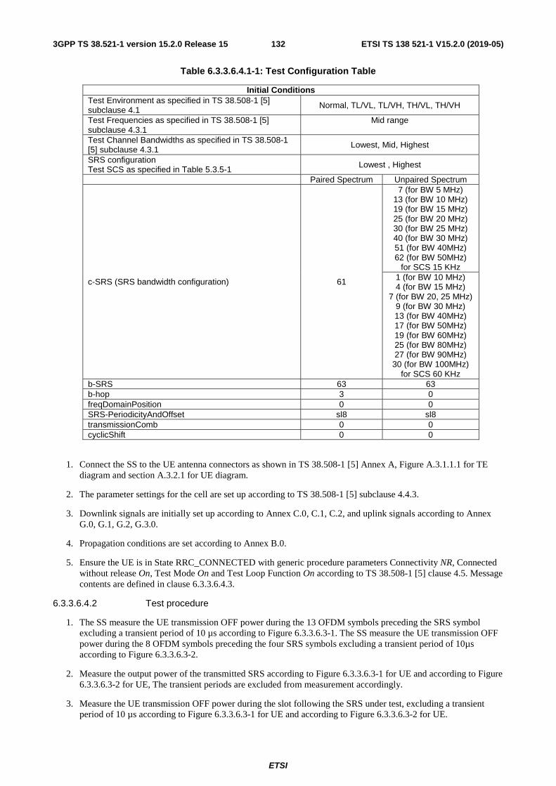
ETSI
ETSI TS 138 521-1 V15.2.0 (2019-05)1323GPP TS 38.521-1 version 15.2.0 Release 15
Table 6.3.3.6.4.1-1: Test Configuration Table
Initial Conditions Test Environment as specified in TS 38.508-1 [5] subclause 4.1 Normal, TL/VL, TL/VH, TH/VL, TH/VH
Test Frequencies as specified in TS 38.508-1 [5] subclause 4.3.1
Mid range
Test Channel Bandwidths as specified in TS 38.508-1 [5] subclause 4.3.1 Lowest, Mid, Highest
SRS configuration Test SCS as specified in Table 5.3.5-1 Lowest , Highest
Paired Spectrum Unpaired Spectrum
c-SRS (SRS bandwidth configuration) 61
7 (for BW 5 MHz) 13 (for BW 10 MHz) 19 (for BW 15 MHz) 25 (for BW 20 MHz) 30 (for BW 25 MHz) 40 (for BW 30 MHz) 51 (for BW 40MHz) 62 (for BW 50MHz)
for SCS 15 KHz 1 (for BW 10 MHz) 4 (for BW 15 MHz)
7 (for BW 20, 25 MHz) 9 (for BW 30 MHz) 13 (for BW 40MHz) 17 (for BW 50MHz) 19 (for BW 60MHz) 25 (for BW 80MHz) 27 (for BW 90MHz)
30 (for BW 100MHz) for SCS 60 KHz
b-SRS 63 63 b-hop 3 0 freqDomainPosition 0 0 SRS-PeriodicityAndOffset sl8 sl8 transmissionComb 0 0 cyclicShift 0 0
1. Connect the SS to the UE antenna connectors as shown in TS 38.508-1 [5] Annex A, Figure A.3.1.1.1 for TE diagram and section A.3.2.1 for UE diagram.
2. The parameter settings for the cell are set up according to TS 38.508-1 [5] subclause 4.4.3.
3. Downlink signals are initially set up according to Annex C.0, C.1, C.2, and uplink signals according to Annex G.0, G.1, G.2, G.3.0.
4. Propagation conditions are set according to Annex B.0.
5. Ensure the UE is in State RRC_CONNECTED with generic procedure parameters Connectivity NR, Connected without release On, Test Mode On and Test Loop Function On according to TS 38.508-1 [5] clause 4.5. Message contents are defined in clause 6.3.3.6.4.3.
6.3.3.6.4.2 Test procedure
1. The SS measure the UE transmission OFF power during the 13 OFDM symbols preceding the SRS symbol excluding a transient period of 10 µs according to Figure 6.3.3.6.3-1. The SS measure the UE transmission OFF power during the 8 OFDM symbols preceding the four SRS symbols excluding a transient period of 10µs according to Figure 6.3.3.6.3-2.
2. Measure the output power of the transmitted SRS according to Figure 6.3.3.6.3-1 for UE and according to Figure 6.3.3.6.3-2 for UE, The transient periods are excluded from measurement accordingly.
3. Measure the UE transmission OFF power during the slot following the SRS under test, excluding a transient period of 10 µs according to Figure 6.3.3.6.3-1 for UE and according to Figure 6.3.3.6.3-2 for UE.

ETSI
ETSI TS 138 521-1 V15.2.0 (2019-05)1333GPP TS 38.521-1 version 15.2.0 Release 15
6.3.3.6.4.3 Message contents
Message contents are according to TS 38.508-1 [5] subclause 4.6. 3 with the following exceptions:
Table 6.3.3.6.4.3-1: SRS-Config: SRS time mask measurement
Derivation Path: TS 38.331 [6], clause 6.3.2 Information Element Value/remark Comment Condition
SRS-Config ::= SEQUENCE { srs-ResourceToAddModList SEQUENCE (SIZE(1..maxNrofSRS-Resources)) OF SEQUENCE {
1 entry
srs-ResourceId 0 nrofSRS-Ports port1 transmissionComb CHOICE { n2 SEQUENCE { combOffset-n2 0 cyclicShift-n2 0 } } freqDomainPosition 0 freqDomainShift 0 freqHopping SEQUENCE { c-SRS 61 Paired Spectrum
7 (for BW 5 MHz) 13 (for BW 10 MHz) 19 (for BW 15 MHz) 25 (for BW 20 MHz) 30 (for BW 25 MHz) 40 (for BW 30 MHz) 51 (for BW 40MHz) 62 (for BW 50MHz)
Unpaired Spectrum for SCS 15 KHz
1 (for BW 10 MHz) 4 (for BW 15 MHz) 7 (for BW 20, 25 MHz) 9 (for BW 30 MHz) 13 (for BW 40MHz) 17 (for BW 50MHz) 19 (for BW 60MHz) 25 (for BW 80MHz) 27 (for BW 90MHz) 30 (for BW 100MHz)
Unpaired Spectrum for SCS 60 KHz
b-SRS 63 b-hop 3 Paired Spectrum
0 Unpaired Spectrum } sequenceId 0 } }
6.3.3.6.5 Test requirement
The requirement for the power measured in steps (1), (2) and (3) of the test procedure shall not exceed the values specified in Table 6.3.3.6.5-1.
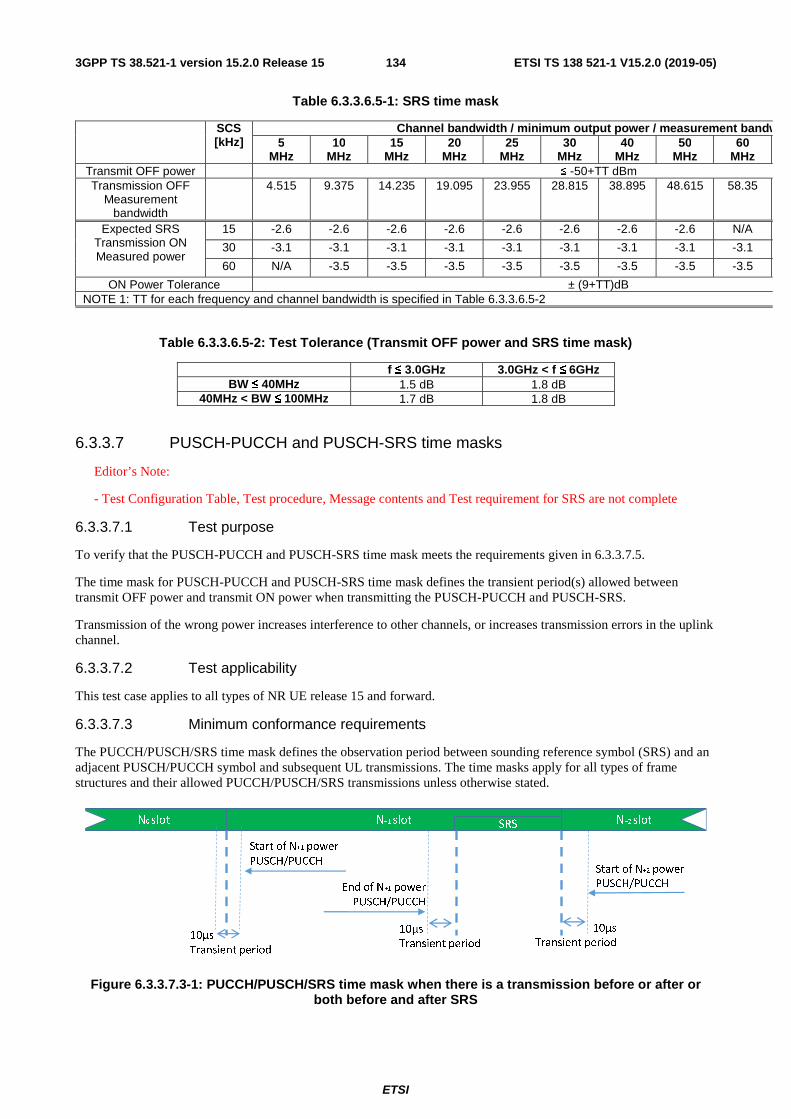
ETSI
ETSI TS 138 521-1 V15.2.0 (2019-05)1343GPP TS 38.521-1 version 15.2.0 Release 15
Table 6.3.3.6.5-1: SRS time mask
SCS [kHz]
Channel bandwidth / minimum output power / measurement bandw5
MHz 10
MHz 15
MHz 20
MHz 25
MHz 30
MHz 40
MHz 50
MHz 60
MHz Transmit OFF power ≤ -50+TT dBm Transmission OFF
Measurement bandwidth
4.515 9.375 14.235 19.095 23.955 28.815 38.895 48.615 58.35
Expected SRS Transmission ON Measured power
15 -2.6 -2.6 -2.6 -2.6 -2.6 -2.6 -2.6 -2.6 N/A
30 -3.1 -3.1 -3.1 -3.1 -3.1 -3.1 -3.1 -3.1 -3.1
60 N/A -3.5 -3.5 -3.5 -3.5 -3.5 -3.5 -3.5 -3.5
ON Power Tolerance ± (9+TT)dB NOTE 1: TT for each frequency and channel bandwidth is specified in Table 6.3.3.6.5-2
Table 6.3.3.6.5-2: Test Tolerance (Transmit OFF power and SRS time mask)
f ≤ 3.0GHz 3.0GHz < f ≤ 6GHz BW ≤ 40MHz 1.5 dB 1.8 dB
40MHz < BW ≤ 100MHz 1.7 dB 1.8 dB
6.3.3.7 PUSCH-PUCCH and PUSCH-SRS time masks
Editor’s Note:
- Test Configuration Table, Test procedure, Message contents and Test requirement for SRS are not complete
6.3.3.7.1 Test purpose
To verify that the PUSCH-PUCCH and PUSCH-SRS time mask meets the requirements given in 6.3.3.7.5.
The time mask for PUSCH-PUCCH and PUSCH-SRS time mask defines the transient period(s) allowed between transmit OFF power and transmit ON power when transmitting the PUSCH-PUCCH and PUSCH-SRS.
Transmission of the wrong power increases interference to other channels, or increases transmission errors in the uplink channel.
6.3.3.7.2 Test applicability
This test case applies to all types of NR UE release 15 and forward.
6.3.3.7.3 Minimum conformance requirements
The PUCCH/PUSCH/SRS time mask defines the observation period between sounding reference symbol (SRS) and an adjacent PUSCH/PUCCH symbol and subsequent UL transmissions. The time masks apply for all types of frame structures and their allowed PUCCH/PUSCH/SRS transmissions unless otherwise stated.
Figure 6.3.3.7.3-1: PUCCH/PUSCH/SRS time mask when there is a transmission before or after or both before and after SRS
10µs
Transient period
N+1 slot SRSN0 slot
10µs
Transient period
10µs
Transient period
Start of N+2 power
PUSCH/PUCCHEnd of N+1 power
PUSCH/PUCCH
Start of N+1 power
PUSCH/PUCCH
N+2 slot

ETSI
ETSI TS 138 521-1 V15.2.0 (2019-05)1353GPP TS 38.521-1 version 15.2.0 Release 15
When there is no transmission preceding SRS transmission or succeeding SRS transmission, then the same time mask applies as shown in Figure 6.3.3.7.3-1.
The normative reference for this requirement is TS 38.101-1 [2] clause 6.3.3.7.
6.3.3.7.4 Test description
6.3.3.7.4.1 Initial condition
Initial conditions are a set of test configurations the UE needs to be tested in and the steps for the SS to take with the UE to reach the correct measurement state.
The initial test configurations consist of environmental conditions, test frequencies, test channel bandwidths and sub-carrier spacing based on NR operating bands specified in table 5.3.5-1. All of these configurations shall be tested with applicable test parameters for each combination of channel bandwidth and sub-carrier spacing, and are shown in table 6.3.3.7.4.1-1. The details of the uplink reference measurement channels (RMCs) are specified in Annexe A.2. Configurations of PDSCH and PDCCH before measurement are specified in Annex C.2.
Table 6.3.3.7.4.1-1: Test Configuration Table
Initial Conditions Test Environment as specified in TS 38.508-1 [5] subclause 4.1
Normal, TL/VL, TL/VH, TH/VL, TH/VH
Test Frequencies as specified in TS 38.508-1 [5] subclause 4.3.1
Mid range
Test Channel Bandwidths as specified in TS 38.508-1 [5] subclause 4.3.1
Lowest, Mid, Highest
Test SCS as specified in Table 5.3.5-1 Lowest, Highest Test Parameters for Channel Bandwidths
Test ID Downlink Configuration Uplink Configuration N/A for minimum output
power Modulation RB allocation (NOTE 1)
1 test case CP-OFDM QPSK Outer Full NOTE 1: The specific configuration of each RB allocation is defined in Table 6.1-1.
1. Connect the SS to the UE antenna connectors as shown in TS 38.508-1 [5] Annex A, Figure A.3.1.1.1 for TE diagram and section A.3.2.1 for UE diagram.
2. The parameter settings for the cell are set up according to TS 38.508-1 [5] subclause 4.4.3.
3. Downlink signals are initially set up according to Annex C.0, C.1, C.2, and uplink signals according to Annex G.0, G.1, G.2, G.3.0.
4. Propagation conditions are set according to Annex B.0.
5. Ensure the UE is in State RRC_CONNECTED with generic procedure parameters Connectivity NR, Connected without release On, Test Mode On and Test Loop Function On according to TS 38.508-1 [5] clause 4.5. Message contents are defined in clause 6.3.3.7.4.3.
6.3.3.7.4.2 Test procedure
1. SS sends uplink scheduling information via PDCCH DCI format 0_1 with TPC command 0dB for C_RNTI to schedule the UL RMC according to Table 6.3.3.7.4.1-1. Since the UE has no payload and no loopback data to send the UE sends uplink MAC padding bits on the UL RMC. The UL assignment is such that the UE transmits on slots 4 and 9 for15kHz SCS, on slots 9 and 19 for 30kHz SCS and on slots 4, 9, 14, 19, 24, 29, 34 and 39 for 60kHz SCS.
2. Measure the output power of the UE PUSCH/PUCCH transmission during one slot, excluding a transient period of 10 µs at the beginning of the slot.
3. Excluding a transient period of 10 µs before SRS.
4. Excluding a transient period of 10 µs at the end of the slot after SRS.
ETSI
ETSI TS 138 521-1 V15.2.0 (2019-05)1363GPP TS 38.521-1 version 15.2.0 Release 15
6.3.3.7.4.3 Message contents
Message contents are according to TS 38.508-1 [5] subclause 4.6 with following exceptions.
Table 6.3.3.7.4.3-1: PUSCH-ConfigCommon
Derivation Path: TS 38.508-1[5], Table 4.6.3-119 Information Element Value/remark Comment Condition
PUSCH-ConfigCommon ::= SEQUENCE { p0-NominalWithGrant -106 }
Table 6.3.3.7.4.3-2: PUSCH-Config
Derivation Path: TS 38.508-1 [5], Table 4.6.3-118 with condition CP-OFDM
6.3.3.7.5 Test requirement
The requirement for the power measured in step (2) of the test procedure shall not exceed the values specified in Table 6.3.3.7.5-1.

ETSI
ETSI TS 138 521-1 V15.2.0 (2019-05)1373GPP TS 38.521-1 version 15.2.0 Release 15
Table 6.3.3.7.5-1: PUSCH-PUCCH and PUSCH-SRS time mask
SCS Channel bandwidth / minimum output power / measurement ban [kHz] 5
MHz 10
MHz 15
MHz 20
MHz 25
MHz 30
MHz 40
MHz 50
MHz Expected
PUSCH/PUCCH Transmission
ON
15 9.6 6.4 4.6 3.3 2.3 1.5 0.2 0.7
Measured power for CP-
OFDM
30 10.1 6.7 4.7 3.5 2.4 1.6 0.3 0.6
60 N/A 7.1 5.0 3.7 2.6 1.7 0.5 0.5 ON Power Tolerance ± (9+TT)dB
NOTE 1: TT for each frequency and channel bandwidth is specified in Table 6.3.3.7.5-2
Table 6.3.3.7.5-2: Test Tolerance for ON power
f ≤ 3.0GHz 3.0GHz < f ≤ 6GHz BW ≤ 40MHz 1.5 dB 1.8 dB
40MHz < BW ≤ 100MHz 1.7 dB 1.8 dB
6.3.4 Power control
6.3.4.1 General
The requirements on power control accuracy apply under normal conditions.
6.3.4.2 Absolute power tolerance
Editor’s Note:
- SA Generic procedures with condition NR in TS 38.508-1 [5] is FFS.
- SA message contents in TS 38.508-1 [5] subclause 4.6 is FFS
- Message Contents are tentative pending review of values for p0-NominalWithGrant
- Test requirement is TBD
- Test Tolerance is TBD for SCS60, needs to be higher due to shorter measurement period forced by UL-DL Config.
6.3.4.2.1 Test purpose
To verify the ability of the UE transmitter to set its initial output power to a specific value at the start of a contiguous transmission or non-contiguous transmission with a long transmission gap, i.e. transmission gap is larger than 20ms .
6.3.4.2.2 Test applicability
This test case applies to all types of NR UE release 15 and forward.
6.3.4.2.3 Minimum conformance requirements
The absolute power tolerance is the ability of the UE transmitter to set its initial output power to a specific value for the first sub-frame at the start of a contiguous transmission or non-contiguous transmission with a transmission gap larger than 20ms. The tolerance includes the channel estimation error.
The minimum requirement specified in Table 6.3.4.2.3-1 apply in the power range bounded by the minimum output power as specified in sub-clause 6.3.1 and the maximum output power as specified in sub-clause 6.2.1.
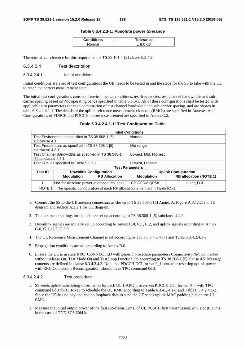
ETSI
ETSI TS 138 521-1 V15.2.0 (2019-05)1383GPP TS 38.521-1 version 15.2.0 Release 15
Table 6.3.4.2.3-1: Absolute power tolerance
Conditions Tolerance Normal ± 9.0 dB
The normative reference for this requirement is TS 38.101-1 [2] clause 6.3.4.2
6.3.4.2.4 Test description
6.3.4.2.4.1 Initial conditions
Initial conditions are a set of test configurations the UE needs to be tested in and the steps for the SS to take with the UE to reach the correct measurement state.
The initial test configurations consist of environmental conditions, test frequencies, test channel bandwidths and sub-carrier spacing based on NR operating bands specified in table 5.3.5-1. All of these configurations shall be tested with applicable test parameters for each combination of test channel bandwidth and sub-carrier spacing, and are shown in table 6.3.4.2.4.1-1. The details of the uplink reference measurement channels (RMCs) are specified in Annexes A.2. Configurations of PDSCH and PDCCH before measurement are specified in Annex C.2.
Table 6.3.4.2.4.1-1: Test Configuration Table
Initial Conditions Test Environment as specified in TS 38.508-1 [5] subclause 4.1
Normal
Test Frequencies as specified in TS 38.508-1 [5] subclause 4.3.1
Mid range
Test Channel Bandwidths as specified in TS 38.508-1 [5] subclause 4.3.1
Lowest, Mid, Highest
Test SCS as specified in Table 5.3.5-1 Lowest, Highest Test Parameters
Test ID Downlink Configuration Uplink Configuration Modulation RB Allocation Modulation RB allocation (NOTE 1)
1 N/A for Absolute power tolerance test case CP-OFDM QPSK Outer_Full
NOTE 1: The specific configuration of each RF allocation is defined in Table 6.1-1.
1. Connect the SS to the UE antenna connectors as shown in TS 38.508-1 [5] Annex A, Figure A.3.1.1.1 for TE diagram and section A.3.2.1 for UE diagram.
2. The parameter settings for the cell are set up according to TS 38.508-1 [5] subclause 4.4.3.
3. Downlink signals are initially set up according to Annex C.0, C.1, C.2, and uplink signals according to Annex G.0, G.1, G.2, G.3.0.
4. The UL Reference Measurement Channel is set according to Table 6.3.4.2.4.1-1 and Table 6.3.4.2.4.1-2
5. Propagation conditions are set according to Annex B.0.
6. Ensure the UE is in state RRC_CONNECTED with generic procedure parameters Connectivity NR, Connected without release On, Test Mode On and Test Loop Function On according to TS 38.508-1 [5] clause 4.5. Message contents are defined in clause 6.3.4.2.4.3. Note that PDCCH DCI format 0_1 sent after resetting uplink power with RRC Connection Reconfiguration, should have TPC command 0dB.
6.3.4.2.4.2 Test procedure
1. SS sends uplink scheduling information for each UL HARQ process via PDCCH DCI format 0_1 with TPC command 0dB for C_RNTI to schedule the UL RMC according to Table 6.3.4.2.4.1-1 and Table 6.3.4.2.4.1-2. Since the UE has no payload and no loopback data to send the UE sends uplink MAC padding bits on the UL RMC.
2. Measure the initial output power of the first sub-frame (1ms) of UE PUSCH first transmission, or 1 slot (0.25ms) in the case of TDD SCS 60kHz.

ETSI
ETSI TS 138 521-1 V15.2.0 (2019-05)1393GPP TS 38.521-1 version 15.2.0 Release 15
3. Repeat for the two test points as indicated in section 6.3.4.2.4.3. The timing of the execution between the two test points shall be larger than 20ms.
6.3.4.2.4.3 Message contents
Message contents are according to TS 38.508-1 [5] subclause 4.6 with the following exceptions:
Table 6.3.4.2.4.3-1: UplinkPowerControlCommon: Test point 1
Derivation Path: TS 38.508-1 [5] subclause 4.6.3 Table 4.6.3-119 PUSCH-ConfigCommon Information Element Value/remark Comment Condition
PUSCH-ConfigCommon::= SEQUENCE { p0-NominalWithGrant [-105] Test point 1 to
verify a UE relative low initial power transmission
}
Table 6.3.4.2.4.3-2: UplinkPowerControlCommon: Test point 2
Derivation Path: TS 38.508-1 [5] subclause 4.6.3 Table 4.6.3-119 PUSCH-ConfigCommon Information Element Value/remark Comment Condition
PUSCH-ConfigCommon::= SEQUENCE { p0-NominalWithGrant [-93] Test point 2 to
verify a UE relative high initial power transmission
}
Table 6.3.4.2.4.3-3: PUSCH-Config
Derivation Path: TS 38.508-1 [5], Table 4.6.3-118 with condition CP-OFDM
6.3.4.2.5 Test requirement
The requirement for the power measured in step (2) of the test procedure is not to exceed the values specified in Table 6.3.4.2.5-1 and 6.3.4.2.5-2.
Table 6.3.4.2.5-1: Absolute power tolerance: test point 1
Channel bandwidth / expected output power (dBm) 5
MHz 10
MHz 15
MHz 20
MHz 25
MHz 30
MHz 40
MHz 50
MHz 60
MHz 80
MHz 90
MHz 100 MHz
Expected Measured power
SCS15 -6 -2.8 -1.0 0.3 1.2 2.0 3.3 4.3 SCS30 -6.6 -3.2 -1.2 0.1 1.1 1.9 3.3 4.2 5.1 6.4 6.9 7.4 SCS60 -3.6 -1.4 -0.2 0.9 1.8 3.1 4.1 5.0 6.3 6.8 7.3
Power tolerance ± (9+TT)dB
Note 1: The lower power limit shall not exceed the minimum output power requirements defined in sub-clause 6.3.2.3 Note 2: TT for each duplex, Sub-Carrier Spacing, frequency and channel bandwidth is specified in Table 6.3.4.2.5-3.

ETSI
ETSI TS 138 521-1 V15.2.0 (2019-05)1403GPP TS 38.521-1 version 15.2.0 Release 15
Table 6.3.4.2.5-2: Absolute power tolerance: test point 2
Channel bandwidth / expected output power (dBm) 5
MHz 10
MHz 15
MHz 20
MHz 25
MHz 30
MHz 40
MHz 50
MHz 60
MHz 80
MHz 90
MHz 100 MHz
Expected Measured power
SCS15 6 9.2 11.0 12.3 13.2 14.0 15.3 16.3 SCS30 5.4 8.8 10.8 12.1 13.1 13.9 15.3 16.2 17.1 18.4 18.9 19.4 SCS60 8.4 10.6 11.8 12.9 13.8 15.1 16.1 17.0 18.3 18.8 19.3
Power tolerance ± (9+TT)dB
Note 1: The lower power limit shall not exceed the minimum output power requirements defined in sub-clause 6.3.2.3 Note 2: TT for each duplex, Sub-Carrier Spacing, frequency and channel bandwidth is specified in Table 6.3.4.2.5-3.
Table 6.3.4.2.5-3: Test Tolerance
f ≤ 3.0GHz 3.0GHz < f ≤ 4.2GHz
4.2GHz < f ≤ 6.0GHz
FDD, TDD SCS 15kHz & TDD SCS 30khz
BW ≤ 40MHz 1.0 dB 1.4 dB 1.4 dB 40MHz < BW ≤ 100MHz 1.4 dB 1.4 dB 1.4 dB
TDD SCS 60kHz [TBD] [TBD] [TBD]
6.3.4.3 Power Control Relative power tolerance
6.3.4.3.1 Test purpose
To verify the ability of the UE transmitter to set its output power in a target sub-frame relatively to the power of the most recently transmitted reference sub-frame if the transmission gap between these sub-frames is larger than 20ms.
6.3.4.3.2 Test applicability
This test applies to all types of NR UE release 15 and forward.
6.3.4.3.3 Minimum conformance requirement
The UE shall meet the requirements specified in Table 6.3.4.3.3-1.
The minimum requirements specified in Table 6.3.4.3.3-1 apply when the power of the target and reference sub-frames are within the power range bounded by the minimum output power as defined in sub-clause 6.3.1 and the measured PUMAXas defined in sub-clause 6.2.4.
Table 6.3.4.3.3-1: Relative Power Tolerance
Power step ΔP (Up or down)
(dB)
All combinations of PUSCH and
PUCCH transitions (dB)
All combinations of PUSCH/PUCCH and
SRS transitions between sub-frames (dB)
PRACH (dB)
ΔP < 2 ± 2.0 (NOTE) ± 2.5 ± 2.0
2 ≤ ΔP < 3 ± 2.5 ± 3.5 ± 2.5
3 ≤ ΔP < 4 ± 3.0 ± 4.5 ± 3.0
4 ≤ ΔP ≤ 10 ± 3.5 ± 5.5 ± 3.5
10 ≤ ΔP < 15 ± 4.0 ± 7.0 ± 4.0
15 ≤ ΔP ± 5.0 ± 8.0 ± 5.0 NOTE: For PUSCH to PUSCH transitions with the allocated resource blocks
fixed in frequency and no transmission gaps other than those generated by downlink subframes, DwPTS fields or Guard Periods: for a power step ΔP ≤ 1 dB, the relative power tolerance for transmission is ± 0.7 dB.
The normative reference for this requirement is TS 38.101-1 [2] clause 6.3.4.3.
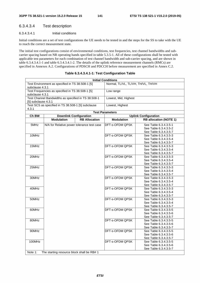
ETSI
ETSI TS 138 521-1 V15.2.0 (2019-05)1413GPP TS 38.521-1 version 15.2.0 Release 15
6.3.4.3.4 Test description
6.3.4.3.4.1 Initial conditions
Initial conditions are a set of test configurations the UE needs to be tested in and the steps for the SS to take with the UE to reach the correct measurement state.
The initial test configurations consist of environmental conditions, test frequencies, test channel bandwidths and sub-carrier spacing based on NR operating bands specified in table 5.3.5-1. All of these configurations shall be tested with applicable test parameters for each combination of test channel bandwidth and sub-carrier spacing, and are shown in table 6.3.4.3.4.1-1 and table 6.3.4.3.4.1-2. The details of the uplink reference measurement channels (RMCs) are specified in Annexes A.2. Configurations of PDSCH and PDCCH before measurement are specified in Annex C.2.
Table 6.3.4.3.4.1-1: Test Configuration Table
Initial Conditions Test Environment as specified in TS 38.508-1 [5] subclause 4.3.1
Normal, TL/VL, TL/VH, TH/VL, TH/VH
Test Frequencies as specified in TS 38.508-1 [5] subclause 4.3.1
Low range
Test Channel Bandwidths as specified in TS 38.508-1 [5] subclause 4.3.1
Lowest, Mid, Highest
Test SCS as specified in TS 38.508-1 [5] subclause 4.3.1
Lowest, Highest
Test Parameters Ch BW Downlink Configuration Uplink Configuration
Modulation RB Allocation Modulation RB allocation (NOTE 1)
5MHz N/A for Relative power tolerance test case DFT-s-OFDM QPSK See Table 6.3.4.3.5-1 See Table 6.3.4.3.5-2 See Table 6.3.4.3.5-7
10MHz DFT-s-OFDM QPSK See Table 6.3.4.3.5-3 See Table 6.3.4.3.5-4 See Table 6.3.4.3.5-7
15MHz DFT-s-OFDM QPSK See Table 6.3.4.3.5-3 See Table 6.3.4.3.5-4 See Table 6.3.4.3.5-7
20MHz DFT-s-OFDM QPSK See Table 6.3.4.3.5-3 See Table 6.3.4.3.5-4 See Table 6.3.4.3.5-7
25MHz DFT-s-OFDM QPSK See Table 6.3.4.3.5-3 See Table 6.3.4.3.5-4 See Table 6.3.4.3.5-7
30MHz DFT-s-OFDM QPSK See Table 6.3.4.3.5-3 See Table 6.3.4.3.5-4 See Table 6.3.4.3.5-7
40MHz DFT-s-OFDM QPSK See Table 6.3.4.3.5-3 See Table 6.3.4.3.5-4 See Table 6.3.4.3.5-7
50MHz DFT-s-OFDM QPSK See Table 6.3.4.3.5-3 See Table 6.3.4.3.5-4 See Table 6.3.4.3.5-7
60MHz DFT-s-OFDM QPSK See Table 6.3.4.3.5-5 See Table 6.3.4.3.5-6 See Table 6.3.4.3.5-7
80MHz DFT-s-OFDM QPSK See Table 6.3.4.3.5-5 See Table 6.3.4.3.5-6 See Table 6.3.4.3.5-7
90MHz DFT-s-OFDM QPSK See Table 6.3.4.3.5-5 See Table 6.3.4.3.5-6 See Table 6.3.4.3.5-7
100MHz DFT-s-OFDM QPSK See Table 6.3.4.3.5-5 See Table 6.3.4.3.5-6 See Table 6.3.4.3.5-7
Note 1: The starting resource block shall be RB# 1

ETSI
ETSI TS 138 521-1 V15.2.0 (2019-05)1423GPP TS 38.521-1 version 15.2.0 Release 15
1. Connect the SS to the UE antenna connectors as shown in TS 38.508-1 [5] Annex A, Figure A.3.1.1.1 for TE diagram and section A.3.2.1 for UE diagram.
2. The parameter settings for the cell are set up according to TS 38.508-1 [5] subclause 4.4.3.
3. Downlink signals are initially set up according to Annex C.0, C.1, C.2, and uplink signals according to Annex G.0, G.1, G.2, G.3.0.
4. The UL Reference Measurement Channel is set according to Table 6.3.4.3.4.1-1 and Table 6.3.4.3.4.1-2.
5. Propagation conditions are set according to Annex B.0.
6. Ensure the UE is in state RRC_CONNECTED with generic procedure parameters Connectivity NR, Connected without release On, Test Mode On and Test Loop Function On according to TS 38.508-1 [5] clause 4.5 Message contents are defined in clause 6.3.4.3.4.3.
6.3.4.3.4.2 Test procedure
The procedure is separated in various subtests to verify different aspects of relative power control. The power patterns of the subtests are described in figure 6.3.4.3.4.2-1 thru figure 6.3.4.3.4.2-11.
0 .. 9 sub-frame# 1 2 3 4 radio frame
0 .. 9 sub-frame# 1 2 3 4 radio frame
RB change
RB change
Power pattern A
Power pattern C
0 .. 9 sub-frame# 1 2 3 4 radio frame
RB change
Power pattern B
Figure 6.3.4.3.4.2-1: FDD ramping up test power patterns
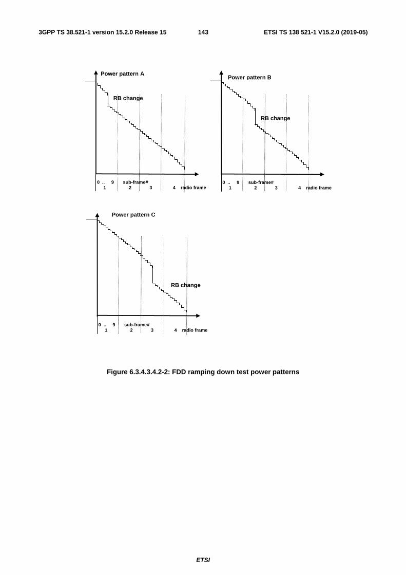
ETSI
ETSI TS 138 521-1 V15.2.0 (2019-05)1433GPP TS 38.521-1 version 15.2.0 Release 15
0 .. 9 sub-frame# 1 2 3 4 radio frame
Power pattern A
RB change
0 .. 9 sub-frame# 1 2 3 4 radio frame
RB change
0 .. 9 sub-frame# 1 2 3 4 radio frame
Power pattern B
Power pattern C
RB change
Figure 6.3.4.3.4.2-2: FDD ramping down test power patterns
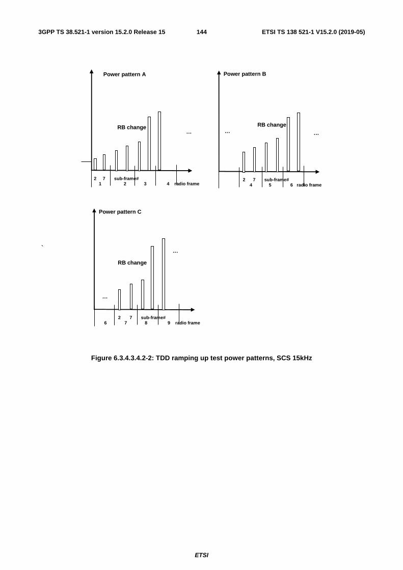
ETSI
ETSI TS 138 521-1 V15.2.0 (2019-05)1443GPP TS 38.521-1 version 15.2.0 Release 15
`
2 7 sub-frame# 1 2 3 4 radio frame
RB change …
2 7 sub-frame# 4 5 6 radio frame
Power pattern B
RB change …
2 7 sub-frame# 6 7 8 9 radio frame
Power pattern C
RB change
…
…
Power pattern A
…
Figure 6.3.4.3.4.2-2: TDD ramping up test power patterns, SCS 15kHz

ETSI
ETSI TS 138 521-1 V15.2.0 (2019-05)1453GPP TS 38.521-1 version 15.2.0 Release 15
`
18 19 8 9 18 slot# 2 3 radio frame
RB change …
8 9 18 19 8 9 slot# 5 6 radio frame
Power pattern B
RB change
…
18 19 8 9 18 slot# 8 9 radio frame
Power pattern C
RB change
…
…
Power pattern A
…
…
Figure 6.3.4.3.4.2-4: TDD ramping up test power patterns, SCS 30kHz

ETSI
ETSI TS 138 521-1 V15.2.0 (2019-05)1463GPP TS 38.521-1 version 15.2.0 Release 15
`
36 37 38 39 16 17 18 19 slot# 1 2 radio frame
RB change …
16 17 18 19 36 37 38 39 slot# 3 radio frame
Power pattern B
RB change
…
16 17 18 19 36 37 38 39 slot# 4 radio frame
Power pattern C
RB change
…
…
Power pattern A
…
Figure 6.3.4.3.4.2-5: TDD ramping up test power patterns, SCS 60kHz

ETSI
ETSI TS 138 521-1 V15.2.0 (2019-05)1473GPP TS 38.521-1 version 15.2.0 Release 15
`
2 7 sub-frame# 1 2 3 4 radio frame
Power pattern A
2 7 sub-frame# 3 4 5 6 radio frame
Power pattern B
RB change
…
RB change
…
…
2 7 sub-frame# 6 7 8 9 radio frame
Power pattern C
RB change
…
…
Figure 6.3.4.3.4.2-6: TDD ramping down test power patterns, SCS 15kHz
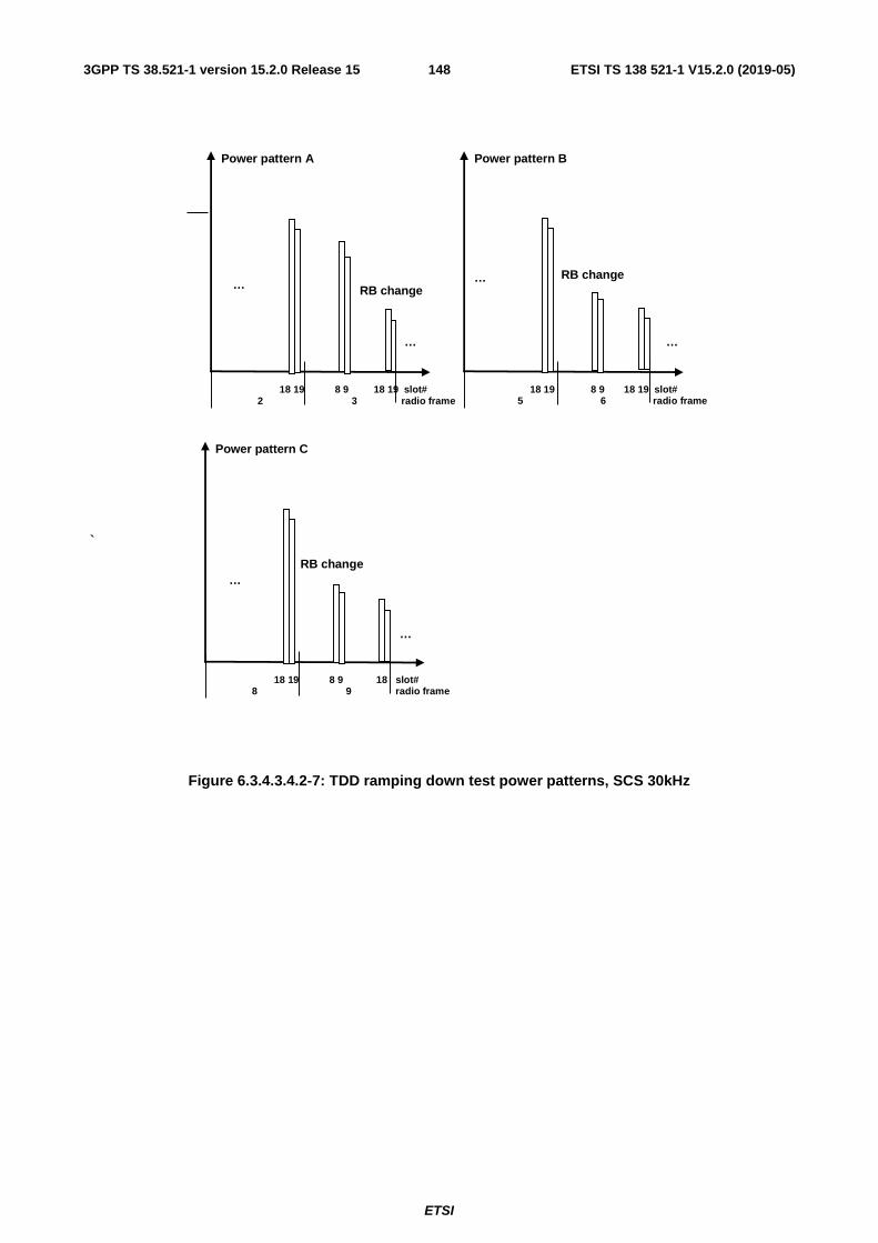
ETSI
ETSI TS 138 521-1 V15.2.0 (2019-05)1483GPP TS 38.521-1 version 15.2.0 Release 15
`
18 19 8 9 18 19 slot# 2 3 radio frame
Power pattern A
18 19 8 9 18 19 slot# 5 6 radio frame
Power pattern B
…
RB change
…
…
18 19 8 9 18 slot# 8 9 radio frame
Power pattern C
RB change
…
…
RB change …
Figure 6.3.4.3.4.2-7: TDD ramping down test power patterns, SCS 30kHz

ETSI
ETSI TS 138 521-1 V15.2.0 (2019-05)1493GPP TS 38.521-1 version 15.2.0 Release 15
`
36 37 38 39 16 17 18 19 slot# 1 2 radio frame
Power pattern A
16 17 18 19 36 37 38 39 slot# 3 radio frame
Power pattern B
RB change
…
RB change
…
…
16 17 18 19 36 37 38 39 slot# 4 radio frame
Power pattern C
RB change
…
…
…
Figure 6.3.4.3.4.2-8: TDD ramping down test power patterns, SCS 60kHz

ETSI
ETSI TS 138 521-1 V15.2.0 (2019-05)1503GPP TS 38.521-1 version 15.2.0 Release 15
Power
FDD test patterns
0 1 9 sub-frame#
Power
TDD test patterns
0 2 7 9 sub-frame#
Figure 6.3.4.3.4.2-9: Alternating Test Power patterns, SCS 15kHz
Power
FDD test patterns
0 1 9 0 1 9 slot#
Power
TDD test patterns
0 1 8 9 18 19 slot#
Figure 6.3.4.3.4.2-10: Alternating Test Power patterns, SCS 30kHz

ETSI
ETSI TS 138 521-1 V15.2.0 (2019-05)1513GPP TS 38.521-1 version 15.2.0 Release 15
Power
FDD test patterns
0 1 9 0 1 9 slot#
Power
TDD test patterns
0 1 16 17 18 19 36 37 38 39
Figure 6.3.4.3.4.2-11: Alternating Test Power patterns, SCS 60kHz
1. Sub test: ramping up pattern
1.1 SS sends uplink scheduling information for each UL HARQ process via PDCCH DCI format 0_1 for C_RNTI to schedule the UL RMC according to Table 6.3.4.3.4.1-1. Since the UE has no payload and no loopback data to send the UE sends uplink MAC padding bits on the UL RMC. Send the appropriate TPC commands for PUSCH to the UE to ensure that the UE transmits PUSCH at -30.3 dBm +/- 2.7 dB
1.2 Schedule the UE's PUSCH data transmission as described in Figure 6.3.4.3.4.2-1 (FDD pattern A: sub-test is divided in 4/2/1 arbitrary radio frames with 10/20/40 active uplink slots per radio frame for SCS 15kHz/30kHz/60kHz), Figure 6.3.4.3.4.2-3 (TDD, SCS 15kHz, pattern A: sub-test is divided in 20 arbitrary radio frames with 2 active uplink slots per radio frame), Figure 6.3.4.3.4.2-4 (TDD, SCS 30kHz, pattern A: sub-test is divided in 10 arbitrary radio frames with 4 active uplink slots per radio frames), Figure 6.3.4.3.4.2-5 (TDD, SCS 60kHz, pattern A: sub-test is divided in 5 arbitrary radio frames with 8 active uplink slots per radio frames). Uplink RB allocation as defined in table 6.3.4.3.5-1/6.3.4.3.5-3/ 6.3.4.3.5-5 depending on channel bandwidth. On the PDCCH format 0_1 for the scheduling of the PUSCH the SS will transmit a +1dB TPC command. Note that the measurement need not be done continuously, provided that interruptions are whole numbers of frames, and TPC commands of 0dB are sent during the interruption.
1.3 Measure the power of PUSCH transmissions to verify the UE relative power control meet test requirements 6.3.4.3.5. For power transients between slots, transient periods of 40us between slots are excluded. For ON/OFF or OFF/ON transients, transient periods of 20 us at the beginning of the slot are excluded.
1.4 Repeat the subtest different pattern B, C to move the RB allocation change at different points in the pattern as described in Table 6.3.4.3.5-1/6.3.4.3.5-3/ 6.3.4.3.5-5 to force bigger UE power steps at various points in the power range.
2. Sub test: ramping down pattern
2.1 SS sends uplink scheduling information for each UL HARQ process via PDCCH DCI format 0_1 for C_RNTI to schedule the UL RMC according to Table 6.3.4.3.4.1-1. Since the UE has no payload and no loopback data to send the UE sends uplink MAC padding bits on the UL RMC. Send the appropriate TPC commands for PUSCH to the UE to ensure that the UE transmits PUSCH at 18 dBm +/- 2.7 dB.
2.2. Schedule the UE's PUSCH data transmission as described in Figure 6.3.4.3.4.2-2 (FDD pattern A: sub-test is divided in 4/2/1 arbitrary radio frames with 10/20/40 active uplink slots per radio frame for SCS 15kHz/30kHz/60kHz), Figure 6.3.4.3.4.2-6 (TDD, SCS 15kHz, pattern A: sub-test is divided in 20 arbitrary radio frames with 2 active uplink slots per radio frame), Figure 6.3.4.3.4.2-7 (TDD, SCS 30kHz, pattern A: sub-test is divided in 10 arbitrary radio frames with 4 active uplink slots per radio frames), Figure 6.3.4.3.4.2-8 (TDD, SCS 60kHz, pattern A: sub-test is divided in 5 arbitrary radio frames with 8 active uplink slots per
ETSI
ETSI TS 138 521-1 V15.2.0 (2019-05)1523GPP TS 38.521-1 version 15.2.0 Release 15
radio frames). Uplink RB allocation as defined in table 6.3.4.3.5-2/6.3.4.3.5-4/ 6.3.4.3.5-6 depending on channel bandwidth. On the PDCCH format 0_1 for the scheduling of the PUSCH the SS will transmit a -1dB TPC command. Note that the measurement need not be done continuously, provided that interruptions are whole numbers of frames, and TPC commands of 0dB are sent during the interruption.
2.3. Measure the power of PUSCH transmissions to verify the UE relative power control meet test requirements 6.3.4.4.5. For power transients between slots, transient periods of 40us between slots are excluded. For ON/OFF or OFF/ON transients, transient periods of 20 us at the beginning of the slot are excluded.
2.4. Repeat the subtest different pattern B, C to move the RB allocation change at different points in the pattern as described in Table 6.3.4.3.5-2/6.3.4.3.5-4/ 6.3.4.3.5-6 to force bigger UE power steps at various points in the power range.
3. Sub test: alternating pattern
3.1 SS sends uplink scheduling information for each UL HARQ process via PDCCH DCI format 0_1 for C_RNTI to schedule the UL RMC according to Table 6.3.4.3.4.1-1. Since the UE has no payload and no loopback data to send the UE sends uplink MAC padding bits on the UL RMC. Send the appropriate TPC commands for PUSCH to the UE to ensure that the UE transmits PUSCH at -10 dBm +/- 2.7 dB. The initial uplink RB allocation is defined as the smaller uplink RB allocation value specified in table 6.3.4.3.4.1-1. The power level and RB allocation are reset for each sub-test.
3.2. Schedule the UE's PUSCH data transmission as described in Figure 6.3.5.2.4.2-9 for 20 frames, Figure 6.3.5.2.4.2-10 for 10 frames, Figure 6.3.5.2.4.2-11 for 5 frames for SCS 15/30/60 kHz respectively with an uplink RB allocation alternating pattern as defined in table 6.3.4.3.5-7 while transmitting 0dB TPC command for PUSCH via the PDCCH.
3.3. Measure the power of PUSCH transmissions to verify the UE relative power control meet test requirements specified in clause 6.3.4.3.5. For power transients between slot, transient periods of 40us between slots are excluded. For ON/OFF or OFF/ON transients, transient periods of 20 us at the beginning of the slots are excluded.
6.3.4.3.4.3 Message contents
Message contents are according to TS 38.508-1 [5] subclause 4.6.
6.3.4.3.5 Test requirement
Each UE power step measured in the test procedure 6.3.4.3.4.2 should satisfy the test requirements specified in Table 6.3.4.3.5-1 thru 6.3.4.3.5-7.
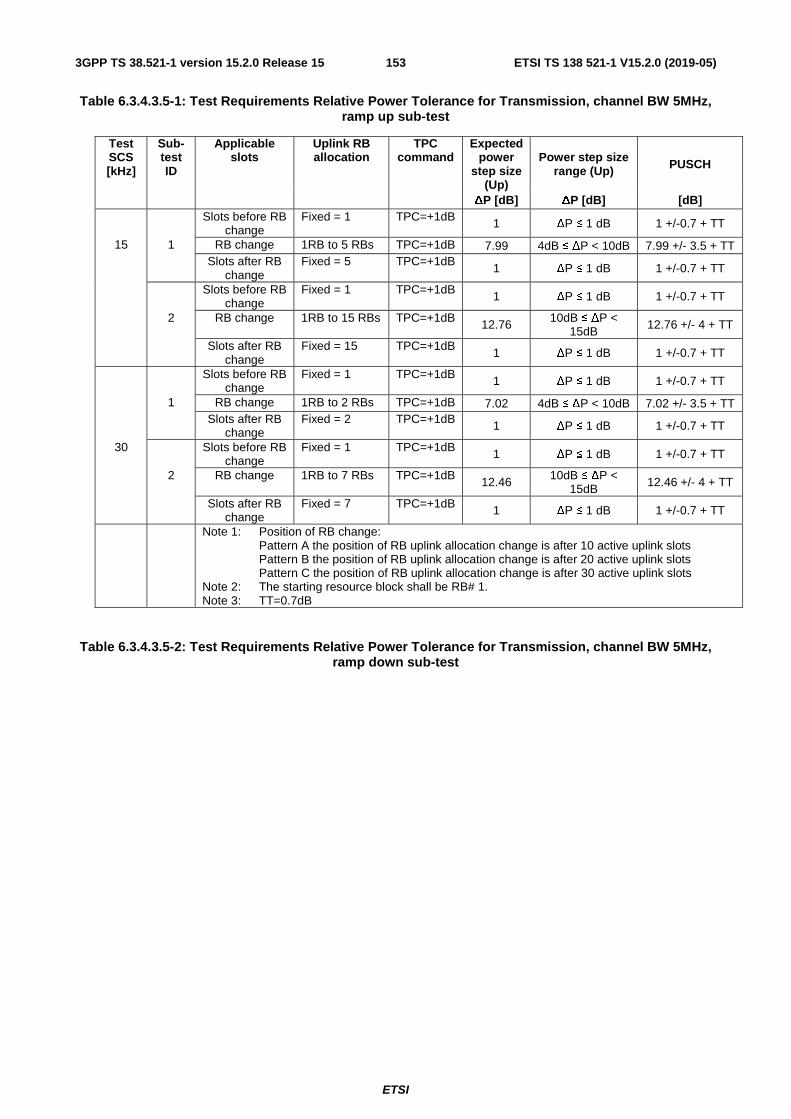
ETSI
ETSI TS 138 521-1 V15.2.0 (2019-05)1533GPP TS 38.521-1 version 15.2.0 Release 15
Table 6.3.4.3.5-1: Test Requirements Relative Power Tolerance for Transmission, channel BW 5MHz, ramp up sub-test
Test SCS [kHz]
Sub-test ID
Applicable slots
Uplink RB allocation
TPC command
Expected power
step size (Up)
Power step size range (Up) PUSCH
ΔP [dB] ΔP [dB] [dB] Slots before RB
change Fixed = 1 TPC=+1dB 1 ΔP ≤ 1 dB 1 +/-0.7 + TT
15 1 RB change 1RB to 5 RBs TPC=+1dB 7.99 4dB ≤ ΔP < 10dB 7.99 +/- 3.5 + TT Slots after RB
change Fixed = 5 TPC=+1dB
1 ΔP ≤ 1 dB 1 +/-0.7 + TT
Slots before RB change
Fixed = 1 TPC=+1dB 1 ΔP ≤ 1 dB 1 +/-0.7 + TT
2 RB change 1RB to 15 RBs TPC=+1dB 12.76 10dB ≤ ΔP < 15dB 12.76 +/- 4 + TT
Slots after RB change
Fixed = 15 TPC=+1dB 1 ΔP ≤ 1 dB 1 +/-0.7 + TT
Slots before RB change
Fixed = 1 TPC=+1dB 1 ΔP ≤ 1 dB 1 +/-0.7 + TT
1 RB change 1RB to 2 RBs TPC=+1dB 7.02 4dB ≤ ΔP < 10dB 7.02 +/- 3.5 + TT Slots after RB
change Fixed = 2 TPC=+1dB 1 ΔP ≤ 1 dB 1 +/-0.7 + TT
30 Slots before RB change
Fixed = 1 TPC=+1dB 1 ΔP ≤ 1 dB 1 +/-0.7 + TT
2 RB change 1RB to 7 RBs TPC=+1dB 12.46 10dB ≤ ΔP < 15dB 12.46 +/- 4 + TT
Slots after RB change
Fixed = 7 TPC=+1dB 1 ΔP ≤ 1 dB 1 +/-0.7 + TT
Note 1: Position of RB change: Pattern A the position of RB uplink allocation change is after 10 active uplink slots Pattern B the position of RB uplink allocation change is after 20 active uplink slots Pattern C the position of RB uplink allocation change is after 30 active uplink slots
Note 2: The starting resource block shall be RB# 1. Note 3: TT=0.7dB
Table 6.3.4.3.5-2: Test Requirements Relative Power Tolerance for Transmission, channel BW 5MHz, ramp down sub-test

ETSI
ETSI TS 138 521-1 V15.2.0 (2019-05)1543GPP TS 38.521-1 version 15.2.0 Release 15
Test SCS [kHz]
Sub-test ID
Applicable sub-
frames
Uplink RB allocation
TPC command
Expected power
step size (Up)
Power step size range (Up) PUSCH
ΔP [dB] ΔP [dB] [dB] Slots
before RB change
Fixed = 5 TPC=-1dB 1 ΔP ≤ 1 dB 1 +/-0.7 + TT
1 RB change 5 RBs to 1 RB TPC=-1dB 7.99 4dB ≤ ΔP < 10dB 7.99 +/- 3.5 + TT Slots after
RB change Fixed = 1 TPC=-1dB 1 ΔP ≤ 1 dB 1 +/-0.7 + TT
15 Slots before RB
change
Fixed = 15 TPC=-1dB 1 ΔP ≤ 1 dB 1 +/-0.7 + TT
2 RB change 15 RBs to 1 RB TPC=-1dB 12.76 10dB ≤ ΔP < 15dB 12.76 +/- 3.5 + TT
Slots after RB change
Fixed = 1 TPC=-1dB 1 ΔP ≤ 1 dB 1 +/-0.7 + TT
Slots before RB
change
Fixed = 2 TPC=-1dB 1 ΔP ≤ 1 dB 1 +/-0.7 + TT
1 RB change 2 RBs to 1 RB TPC=-1dB 7.02 4dB ≤ ΔP < 10dB 7.02 +/- 3.5 + TT Slots after
RB change Fixed = 1 TPC=-1dB 1 ΔP ≤ 1 dB 1 +/-0.7 + TT
30 Slots before RB
change
Fixed = 7 TPC=-1dB 1 ΔP ≤ 1 dB 1 +/-0.7 + TT
2 RB change 7 RBs to 1 RB TPC=-1dB 12.46
10dB ≤ ΔP < 15dB 12.46 +/- 4 + TT
Note 1: Position of RB change: Pattern A the position of RB uplink allocation change is after 10 active uplink slots Pattern B the position of RB uplink allocation change is after 20 active uplink slots Pattern C the position of RB uplink allocation change is after 30 active uplink slots
Note 2: The starting resource block shall be RB# 1. Note 3: TT=0.7dB

ETSI
ETSI TS 138 521-1 V15.2.0 (2019-05)1553GPP TS 38.521-1 version 15.2.0 Release 15
Table 6.3.4.3.5-3: Test Requirements Relative Power Tolerance for Transmission, channel BW 10MHz, 15MHz, 20MHz, 25MHz, 30MHz, 40MHz, 50MHz ramp up sub-test
Test SCS [kHz]
Sub-test ID
Applicable sub-
frames
Uplink RB allocation
TPC command
Expected power
step size (Up)
Power step size range (Up) PUSCH
ΔP [dB] ΔP [dB] [dB] Slots
before RB change
1RB TPC=+1dB 1 ΔP ≤ 1 dB 1 +/-0.7 + TT
1 RB change 1RB to 5 RBs TPC=+1dB 7.99 4dB ≤ ΔP < 10dB 7.99 +/- 3.5 + TT Slots after
RB change Fixed = 5 TPC=+1dB 1 ΔP ≤ 1 dB 1 +/-0.7 + TT
Slots before RB
change
1RB TPC=+1dB 1 ΔP ≤ 1 dB 1 +/-0.7 + TT
15 2 RB change 1RB to 20 RBs TPC=+1dB 14.01 10dB ≤ ΔP < 15dB 14.01 +/- 4 + TT Slots after
RB change Fixed = 20 TPC=+1dB
1 ΔP ≤ 1 dB 1 +/-0.7 + TT
Slots before RB
change
1RB TPC=+1dB 1 ΔP ≤ 1 dB 1 +/-0.7 + TT
3 RB change 1RB to 50 RBs TPC=+1dB 17.99 15dB ≤ ΔP 17.99 +/- 5 + TT Slots after
RB change Fixed = 50 TPC=+1dB 1 ΔP ≤ 1 dB 1 +/-0.7 + TT
Slots before RB
change
1RB TPC=+1dB 1 ΔP ≤ 1 dB 1 +/-0.7 + TT
1 RB change 1RB to 2 RBs TPC=+1dB 7.02 4dB ≤ ΔP < 10dB 7.02 +/- 3.5 + TT Slots after
RB change Fixed = 2 TPC=+1dB 1 ΔP ≤ 1 dB 1 +/-0.7 + TT
Slots before RB
change
1RB TPC=+1dB 1 ΔP ≤ 1 dB 1 +/-0.7 + TT
30 2 RB change 1RB to 10 RBs TPC=+1dB 14.01 10dB ≤ ΔP < 15dB 14.01 +/- 4 + TT Slots after
RB change Fixed = 10 TPC=+1dB 1 ΔP ≤ 1 dB 1 +/-0.7 + TT
Slots before RB
change
1RB TPC=+1dB 1 ΔP ≤ 1 dB 1 +/-0.7 + TT
3 RB change 1RB to 22 RBs TPC=+1dB 17.43 15dB < ΔP 17.43 +/- 5 + TT Slots after
RB change Fixed = 22 TPC=+1dB 1 ΔP ≤ 1 dB 1 +/-0.7 + TT
Slots before RB
change
1RB TPC=+1dB 1 ΔP ≤ 1 dB 1 +/-0.7 + TT
1 RB change 1RB to 5 RBs TPC=+1dB 14.01 10dB ≤ ΔP < 15dB 14.01 +/- 4 + TT Slots after
RB change Fixed = 5 TPC=+1dB 1 ΔP ≤ 1 dB 1 +/-0.7 + TT
60 Slots before RB
change
1RB TPC=+1dB 1 ΔP ≤ 1 dB 1 +/-0.7 + TT
2 RB change 1RB to 9 RBs TPC=+1dB 16.56 15dB < ΔP 16.56 +/- 5 + TT Slots after
RB change Fixed = 9 TPC=+1dB 1 ΔP ≤ 1 dB 1 +/-0.7 + TT
Note 1: Position of RB change: Pattern A the position of RB uplink allocation change is after 10 active uplink slots, except for TDD SCS 60 kHz which is after 8 active uplink slots. Pattern B the position of RB uplink allocation change is after 20 active uplink slots Pattern C the position of RB uplink allocation change is after 30 active uplink slots, except for TDD SCS 60 kHz which is after 28 active uplink slots.
Note 2: The starting resource block shall be RB# 1. Note 3: TT=0.7dB

ETSI
ETSI TS 138 521-1 V15.2.0 (2019-05)1563GPP TS 38.521-1 version 15.2.0 Release 15
Table 6.3.4.3.5-4: Test Requirements Relative Power Tolerance for Transmission, channel BW 10MHz, 15MHz, 20MHz, 25MHz, 30MHz, 40MHz, 50MHz ramp down sub-test
Test SCS [kHz]
Sub-test ID
Applicable sub-
frames
Uplink RB allocation
TPC command
Expected power
step size (Up)
Power step size range (Up) PUSCH
ΔP [dB] ΔP [dB] [dB] Slots
before RB change
Fixed = 5 TPC=-1dB 1 ΔP ≤ 1 dB 1 +/-0.7 + TT
1 RB change 5 RBs to 1RBs TPC=-1dB 7.99 4dB ≤ ΔP < 10dB 7.99 +/- 3.5 + TT Slots after
RB change Fixed = 1 TPC=-1dB 1 ΔP ≤ 1 dB 1 +/-0.7 + TT
Slots before RB
change
Fixed = 20 TPC=-1dB 1 ΔP ≤ 1 dB 1 +/-0.7 + TT
15 2 RB change 20 RBs to 1 RB TPC=-1dB 14.01 10dB ≤ ΔP < 15dB 14.01 +/- 4 + TT Slots after
RB change Fixed = 1 TPC=-1dB
1 ΔP ≤ 1 dB 1 +/-0.7 + TT
Slots before RB
change
Fixed = 50 TPC=-1dB 1 ΔP ≤ 1 dB 1 +/-0.7 + TT
3 RB change 50 RBs to 1 RB TPC=-1dB 17.99 15dB ≤ ΔP 17.99 +/- 5 + TT Slots after
RB change Fixed = 1 TPC=-1dB 1 ΔP ≤ 1 dB 1 +/-0.7 + TT
Slots before RB
change
Fixed = 2 TPC=-1dB 1 ΔP ≤ 1 dB 1 +/-0.7 + TT
1 RB change 2 RBs to 1 RB TPC=-1dB 7.02 4dB ≤ ΔP < 10dB 7.02 +/- 3.5 + TT Slots after
RB change Fixed = 1 TPC=-1dB 1 ΔP ≤ 1 dB 1 +/-0.7 + TT
Slots before RB
change
Fixed = 10 TPC=-1dB 1 ΔP ≤ 1 dB 1 +/-0.7 + TT
30 2 RB change 10 RBs to 1 RB TPC=-1dB 14.01 10dB ≤ ΔP < 15dB 14.01 +/- 4 + TT Slots after
RB change Fixed = 1 TPC=-1dB 1 ΔP ≤ 1 dB 1 +/-0.7 + TT
Slots before RB
change
Fixed = 22 TPC=-1dB 1 ΔP ≤ 1 dB 1 +/-0.7 + TT
3 RB change 22 RBs to 1 RB TPC=-1dB 17.43 15dB < ΔP 17.43 +/- 5 + TT Slots after
RB change Fixed = 1 TPC=-1dB 1 ΔP ≤ 1 dB 1 +/-0.7 + TT
Slots before RB
change
Fixed = 5 TPC=-1dB 1 ΔP ≤ 1 dB 1 +/-0.7 + TT
1 RB change 5 RBs to 1 RB TPC=-1dB 14.01 10dB ≤ ΔP < 15dB 14.01 +/- 4 + TT Slots after
RB change Fixed = 1 TPC=-1dB 1 ΔP ≤ 1 dB 1 +/-0.7 + TT
60 Slots before RB
change
Fixed = 9 TPC=-1dB 1 ΔP ≤ 1 dB 1 +/-0.7 + TT
2 RB change 9 RBs to 1 RB TPC=-1dB 16.56 15dB < ΔP 16.56 +/- 5 + TT Slots after
RB change Fixed = 1 TPC=-1dB 1 ΔP ≤ 1 dB 1 +/-0.7 + TT
Note 1: Position of RB change: Pattern A the position of RB uplink allocation change is after 10 active uplink slots, except for TDD SCS 60 kHz which is after 8 active uplink slots. Pattern B the position of RB uplink allocation change is after 20 active uplink slots Pattern C the position of RB uplink allocation change is after 30 active uplink slots, except for TDD SCS 60 kHz which is after 28 active uplink slots.
Note 2: The starting resource block shall be RB# 1. Note 3: TT=0.7dB
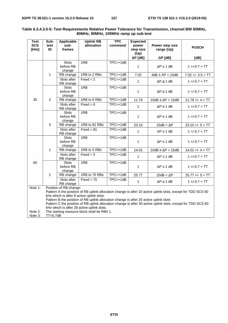
ETSI
ETSI TS 138 521-1 V15.2.0 (2019-05)1573GPP TS 38.521-1 version 15.2.0 Release 15
Table 6.3.4.3.5-5: Test Requirements Relative Power Tolerance for Transmission, channel BW 60MHz, 80MHz, 90MHz, 100MHz ramp up sub-test
Test SCS [kHz]
Sub-test ID
Applicable sub-
frames
Uplink RB allocation
TPC command
Expected power
step size (Up)
Power step size range (Up) PUSCH
ΔP [dB] ΔP [dB] [dB] Slots
before RB change
1RB TPC=+1dB 1 ΔP ≤ 1 dB 1 +/-0.7 + TT
1 RB change 1RB to 2 RBs TPC=+1dB 7.02 4dB ≤ ΔP < 10dB 7.02 +/- 3.5 + TT Slots after
RB change Fixed = 2 TPC=+1dB 1 ΔP ≤ 1 dB 1 +/-0.7 + TT
Slots before RB
change
1RB TPC=+1dB 1 ΔP ≤ 1 dB 1 +/-0.7 + TT
30 2 RB change 1RB to 6 RBs TPC=+1dB 11.79 10dB ≤ ΔP < 15dB 11.79 +/- 4 + TT Slots after
RB change Fixed = 6 TPC=+1dB
1 ΔP ≤ 1 dB 1 +/-0.7 + TT
Slots before RB
change
1RB TPC=+1dB 1 ΔP ≤ 1 dB 1 +/-0.7 + TT
3 RB change 1RB to 81 RBs TPC=+1dB 23.10 15dB < ΔP 23.10 +/- 5 + TT Slots after
RB change Fixed = 81 TPC=+1dB 1 ΔP ≤ 1 dB 1 +/-0.7 + TT
Slots before RB
change
1RB TPC=+1dB 1 ΔP ≤ 1 dB 1 +/-0.7 + TT
1 RB change 1RB to 5 RBs TPC=+1dB 14.01 10dB ≤ ΔP < 15dB 14.01 +/- 4 + TT Slots after
RB change Fixed = 5 TPC=+1dB 1 ΔP ≤ 1 dB 1 +/-0.7 + TT
60 Slots before RB
change
1RB TPC=+1dB 1 ΔP ≤ 1 dB 1 +/-0.7 + TT
2 RB change 1RB to 75 RBs TPC=+1dB 25.77 15dB < ΔP 25.77 +/- 5 + TT Slots after
RB change Fixed = 75 TPC=+1dB 1 ΔP ≤ 1 dB 1 +/-0.7 + TT
Note 1: Position of RB change: Pattern A the position of RB uplink allocation change is after 10 active uplink slots, except for TDD SCS 60 kHz which is after 8 active uplink slots. Pattern B the position of RB uplink allocation change is after 20 active uplink slots Pattern C the position of RB uplink allocation change is after 30 active uplink slots, except for TDD SCS 60 kHz which is after 28 active uplink slots.
Note 2: The starting resource block shall be RB# 1. Note 3: TT=0.7dB

ETSI
ETSI TS 138 521-1 V15.2.0 (2019-05)1583GPP TS 38.521-1 version 15.2.0 Release 15
Table 6.3.4.3.5-6: Test Requirements Relative Power Tolerance for Transmission, channel BW 60MHz, 80MHz, 90MHz, 100MHz ramp down sub-test
Test SCS [kHz]
Sub-test ID
Applicable sub-
frames
Uplink RB allocation
TPC command
Expected power
step size (Up)
Power step size range (Up) PUSCH
ΔP [dB] ΔP [dB] [dB] Slots
before RB change
Fixed = 2 TPC=-1dB 1 ΔP ≤ 1 dB 1 +/-0.7 + TT
1 RB change 2 RBs to 1 RB TPC=-1dB 7.02 4dB ≤ ΔP < 10dB 7.02 +/- 3.5 + TT Slots after
RB change Fixed = 1 TPC=-1dB 1 ΔP ≤ 1 dB 1 +/-0.7 + TT
Slots before RB
change
Fixed = 6 TPC=-1dB 1 ΔP ≤ 1 dB 1 +/-0.7 + TT
30 2 RB change 6 RBs to 1 RB TPC=-1dB 11.79 10dB ≤ ΔP < 15dB 11.79 +/- 4 + TT Slots after
RB change Fixed = 1 TPC=-1dB
1 ΔP ≤ 1 dB 1 +/-0.7 + TT
Slots before RB
change
Fixed = 81 TPC=-1dB 1 ΔP ≤ 1 dB 1 +/-0.7 + TT
3 RB change 81 RBs to 1 RB TPC=-1dB 23.10 15dB < ΔP 23.10 +/- 5 + TT Slots after
RB change Fixed = 1 TPC=-1dB 1 ΔP ≤ 1 dB 1 +/-0.7 + TT
Slots before RB
change
Fixed = 5 TPC=-1dB 1 ΔP ≤ 1 dB 1 +/-0.7 + TT
1 RB change 5 RBs to 1 RB TPC=-1dB 14.01 10dB ≤ ΔP < 15dB 14.01 +/- 4 + TT Slots after
RB change Fixed = 1 TPC=-1dB 1 ΔP ≤ 1 dB 1 +/-0.7 + TT
60 Slots before RB
change
Fixed = 75 TPC=-1dB 1 ΔP ≤ 1 dB 1 +/-0.7 + TT
2 RB change 75 RBs to 1 RB TPC=-1dB 25.77 15dB < ΔP 25.77 +/- 5 + TT Slots after
RB change Fixed = 1 TPC=-1dB 1 ΔP ≤ 1 dB 1 +/-0.7 + TT
Note 1: Position of RB change: Pattern A the position of RB uplink allocation change is after 10 active uplink slots, except for TDD SCS 60 kHz which is after 8 active uplink slots. Pattern B the position of RB uplink allocation change is after 20 active uplink slots Pattern C the position of RB uplink allocation change is after 30 active uplink slots, except for TDD SCS 60 kHz which is after 28 active uplink slots.
Note 2: The starting resource block shall be RB# 1. Note 3: TT=0.7dB

ETSI
ETSI TS 138 521-1 V15.2.0 (2019-05)1593GPP TS 38.521-1 version 15.2.0 Release 15
Table 6.3.4.3.5-7: Test Requirements Relative Power Tolerance for Transmission, alternating sub-test
BW Test SCS [kHz]
Sub-test ID
Uplink RB allocation
TPC command
Expected power
step size (Up)
Power step size range (Up) PUSCH
ΔP [dB] ΔP [dB] [dB] 1 Alternating 1
and 2 TPC=0dB 3.01 3dB ≤ ΔP < 4dB 3.01 +/- 3 + TT
15 2 Alternating 1 and 5
TPC=0dB 6.99
4dB ≤ ΔP < 10dB
6.99 +/- 3.5 + TT
5 3 Alternating 1 and 15
TPC=0dB 11.76 10dB ≤ ΔP < 15dB 11.76 +/- 4 + TT
1 Alternatting 1 and 2
TPC=0dB 6.02 4dB ≤ ΔP < 10dB
6.02 +/- 3.5 + TT
30 2 Alternating 1 and 7
TPC=0dB 11.46
10dB ≤ ΔP < 15dB 11.46 +/- 4 + TT
1 Alternating 1 and 2
TPC=0dB 3.01 3dB ≤ ΔP < 4dB 3.01 +/- 3 + TT
2 Alternating 1 and 5
TPC=0dB 6.99 4dB ≤ ΔP < 10dB
6.99 +/- 3.5 + TT
15 3 Alternating 1 and 20
TPC=0dB 13.01 10dB ≤ ΔP < 15dB
13.01 +/- 4 + TT
4 Alternating 1 and 50
TPC=0dB 16.99 15dB ≤ ΔP 16.99 +/- 5 + TT
1 Alternating 1 and 2
TPC=0dB 6.02 4dB ≤ ΔP < 10dB
6.02 +/- 3.5 + TT
10,15,20, 25,30,40,50
30 2 Alternating 1 and 10
TPC=0dB 13.01 10dB ≤ ΔP < 15dB
13.01 +/- 4 + TT
3 Alternating 1 and 22 RBs
TPC=0dB 16.43 15dB < ΔP 16.43 +/- 5 + TT
1 Alternating 1 and 5
TPC=0dB 13.01 10dB ≤ ΔP < 15dB 13.01 +/- 4 + TT
60 2 Alternating 1 and 9
TPC=0dB 15.56 15dB < ΔP 15.56 +/- 5 + TT
1 Alternating 1 and 2
TPC=0dB 6.02 4dB ≤ ΔP < 10dB
6.02 +/- 3.5 + TT
30 2 Alternating 1 and 6
TPC=0dB 10.79 10dB ≤ ΔP < 15dB 10.79 +/- 4 + TT
3 Alternating 1 and 81
TPC=0dB 22.10 15dB < ΔP 22.10 +/- 5 + TT
60,80,90,100 1 Alternating 1 and 2
TPC=0dB 9.03 4dB ≤ ΔP < 10dB
9.03 +/- 3.5 + TT
60 2 Alternating 1 and 5
TPC=0dB 13.01 10dB ≤ ΔP < 15dB 13.01 +/- 4 + TT
3 Alternating 1 and 75
TPC=0dB 24.77 15dB < ΔP 24.77 +/- 5 + TT
Note 1: The starting resource block shall be RB# 1. Note 2: TT=0.7dB
6.3.4.4 Aggregate power tolerance
Editor’s Note:
- SA Generic procedures with condition NR in TS 38.508-1 [5] is FFS.
- SA message contents in TS 38.508-1 [5] subclause 4.6 is FFS
- Test Tolerance is TBD
6.3.4.4.1 Test purpose
To verify the ability of the UE transmitter to maintain its power during non-contiguous transmissions within 21ms in response to 0 dB commands with respect to the first UE transmission and all other power control parameters as specified in 38.213 kept constant.

ETSI
ETSI TS 138 521-1 V15.2.0 (2019-05)1603GPP TS 38.521-1 version 15.2.0 Release 15
6.3.4.4.2 Test applicability
This test case applies to all types of NR UE release 15 and forward.
6.3.4.4.3 Minimum conformance requirements
The aggregate power control tolerance is the ability of the UE transmitter to maintain its power during non-contiguous transmissions within 21ms in response to 0 dB commands with respect to the first UE transmission and all other power control parameters as specified in 38.213 kept constant.
The minimum requirement specified in Table 6.3.4.4.3-1 apply in the power range bounded by the minimum output power as specified in sub-clause 6.3.1 and the maximum output power as specified in sub-clause 6.2.2.
Table 6.3.4.4.3-1: Aggregate power tolerance
TPC command UL channel Aggregate power tolerance within 21ms
0 dB PUCCH ± 2.5 dB 0 dB PUSCH ± 3.5 dB
The normative reference for this requirement is TS 38.01-1 [2] clause 6.3.4.4
6.3.4.4.4 Test description
6.3.4.4.4.1 Initial conditions
Initial conditions are a set of test configurations the UE needs to be tested in and the steps for the SS to take with the UE to reach the correct measurement state.
The initial test configurations consist of environmental conditions, test frequencies, test channel bandwidths and sub-carrier spacing based on NR operating bands specified in table 5.3.5-1. All of these configurations shall be tested with applicable test parameters for each combination of test channel bandwidth and sub-carrier spacing, and are shown in table 6.3.4.4.4.1-1 and table 6.3.4.4.4.1-2. The details of the uplink reference measurement channels (RMCs) are specified in Annexes A.2. Configurations of PDSCH and PDCCH before measurement are specified in Annex C.2.
Table 6.3.4.4.4.1-1: Test Configuration Table: PUCCH sub-test
Initial Conditions Test Environment as specified in TS 38.508-1 [5] subclause 4.1
Normal
Test Frequencies as specified in TS 38.508-1 [5] subclause 4.3.1
Mid range
Test Channel Bandwidths as specified in TS 38.508-1 [5] subclause 4.3.1
Lowest, Mid, Highest
Test SCS as specified in Table 5.3.5-1 Lowest, Highest Test Parameters for Channel Bandwidths
Test ID Downlink Configuration Uplink Configuration N/A for aggregate power tolerance
testcase PUCCH format = Format 1
Length in OFDM symbols = 14 1

ETSI
ETSI TS 138 521-1 V15.2.0 (2019-05)1613GPP TS 38.521-1 version 15.2.0 Release 15
Table 6.3.4.4.4.1-2: Test Configuration Table: PUSCH sub-test
Initial Conditions Test Environment as specified in TS 38.508-1 [5] subclause 4.1
Normal
Test Frequencies as specified in TS 38.508-1 [5] subclause 4.3.1
Mid range
Test Channel Bandwidths as specified in TS 38.508-1 [5] subclause 4.3.1
Lowest, Mid, Highest
Test SCS as specified in Table 5.3.5-1 Lowest, Highest Test Parameters for Channel Bandwidths
Test ID Downlink Configuration Uplink Configuration N/A for aggregate power
tolerance testcase Modulation RB allocation (NOTE 1)
1 CP-OFDM QPSK Outer_Full NOTE 1: The specific configuration of each RF allocation is defined in Table 6.1-1.
1. Connect the SS to the UE antenna connectors as shown in TS 38.508-1 [5] Annex A, Figure A.3.1.1.1 for TE diagram and section A.3.2.1 for UE diagram.
2. The parameter settings for the cell are set up according to TS 38.508-1 [5] subclause 4.4.3.
3. Downlink signals are initially set up according to Annex C.0, C.1, C.2, and uplink signals according to G.0, G.1, G.2, G.3.0.
4. The UL and DL Reference Measurement channels are set according to Table 6.3.4.4.4.1-1 (PUCCH sub-test) and Table 6.3.4.4.4.1-2 (PUSCH sub-test)
5. Propagation conditions are set according to Annex B.0.
6. Ensure the UE is in state RRC_CONNECTED with generic procedure parameters Connectivity NR, Connected without release On, Test Mode On and Test Loop Function On according to TS 38.508-1 [5] clause 4.5. Message contents are defined in clause 6.3.4.4.4.3.
6.3.4.4.4.2 Test procedure
The procedure is separated in two subtests to verify PUCCH and PUSCH aggregate power control tolerance respectively. The uplink transmission patterns are described in figure 6.3.4.4.4.2-1.
TDD SCS 15kHz test patterns FDD test patterns
0 5 0 5 0 sub-frame#
4 9 4 9 4 slot#
TDD SCS 60kHz test patterns, note TX is only 0.25ms
Power
TDD SCS 30kHz test patterns
8,9 18,19 8,9 18,19 8,9 slot#
4 24 4 24 4 slot#
Power
Power
Power
Figure 6.3.4.4.4.2-1 Test uplink transmission
1. PUCCH sub test:

ETSI
ETSI TS 138 521-1 V15.2.0 (2019-05)1623GPP TS 38.521-1 version 15.2.0 Release 15
1.1 The SS transmits PDSCH via PDCCH DCI format 0_1 for C_RNTI to transmit the DL RMC according to Table 6.3.4.4.4.1-1. The SS sends downlink MAC padding bits on the DL RMC. The transmission of PDSCH will make the UE send uplink ACK/NACK using PUCCH. Send the appropriate TPC commands for PUCCH to the UE to ensure that the UE transmits PUCCH at 0dBm +/- 3.5 dB+TT for carrier frequency f ≤ 3.0GHz or at 0dBm +/- 3.5 dB+TT for carrier frequency 3.0GHz < f.
1.2. Every 5 sub-frames (5ms) transmit to the UE downlink PDSCH MAC padding bits as well as 0 dB TPC command for PUCCH via the PDCCH to make the UE transmit ACK/NACK on the PUCCH for 1 sub-frame(1ms), or 1 slot (0.25ms) in the case of TDD SCS 60kHz. The downlink transmission is scheduled in the appropriate slots to make the UE transmit PUCCH as described in figure 6.3.4.4.4.2-1
1.3. Measure the power of 5 consecutive PUCCH transmissions to verify the UE transmitted PUCCH power is maintained within 21ms.
2. PUSCH sub test:
2.1. The SS sends uplink scheduling information via PDCCH DCI format 0_1 for C_RNTI to schedule the PUSCH. Since the UE has no payload and no loopback data to send the UE sends uplink MAC padding bits on the UL RMC. Send the appropriate TPC commands for PUSCH to the UE to ensure that the UE transmits PUSCH at 0dBm +/- 2.5 dB+TT for carrier frequency f ≤ 3.0GHz or at 0dBm +/- 2.5 dB+TT for carrier frequency 3.0GHz < f.
2.2. Every 5 sub-frames (5ms) schedule the UE's PUSCH data transmission for 1 sub-frame(1ms) , or 1 slot (0.25ms) in the case of TDD SCS 60kHz,and transmit 0 dB TPC command for PUSCH via the PDCCH to make the UE transmit PUSCH. The uplink transmission patterns are described in figure 6.3.4.4.4.2-1,
2.3. Measure the power of 5 consecutive PUSCH transmissions to verify the UE transmitted PUSCH power is maintained within 21ms transmissions.
6.3.4.4.4.3 Message contents
Message contents are according to TS 38.508-1 [5] subclause 4.6.
6.3.4.4.5 Test requirement
The requirement for the power measurements made in step (1.3) and (2.3) of the test procedure shall not exceed the values specified in Table 6.3.4.4.5-1. The power measurement period shall be 1 sub-frame, or 1 slot (0.25ms) in the case of TDD SCS 60kHz.
Table 6.3.4.4.5-1: Power control tolerance
TPC command UL channel Test requirement measured power
0 dB PUCCH Given 5power measurements in the pattern, the 2nd, and later measurements shall be within ± 2.5dB of the 1st
measurement. 0 dB PUSCH Given TBD power measurements in the pattern, the 2nd,
and later measurements shall be within ± 3.5dB of the 1st measurement.
Note 1: For SCS 30kHz 1 sub-frame corresponds to 2 slots, so 2 TPC commands will be sent for a single measurement period.
Note 2: TT for each duplex, Sub-Carrier Spacing, frequency and channel bandwidth is specified in Table 6.3.4.4.5-2.
Table 6.3.4.4.5-2: Test Tolerance
[TBD]
6.3D
6.3D.1 Minimum output power for UL-MIMO
Editor’s Note:
- Test point analysis is still pending.

ETSI
ETSI TS 138 521-1 V15.2.0 (2019-05)1633GPP TS 38.521-1 version 15.2.0 Release 15
- MU/TT is still FFS
6.3D.1.1 Test purpose
To verify the UE's ability to transmit with a UL-MIMO broadband output power below the value specified in the test requirement when the power is set to a minimum value.
6.3D.1.2 Test applicability
This test case applies to all types of NR UE release 15 and forward that support UL-MIMO.
6.3D.1.3 Minimum conformance requirements
For UE with two transmit antenna connectors in closed-loop spatial multiplexing scheme, the minimum output power is defined as the sum of the mean power at each UE antenna connector in one sub-frame (1ms). The minimum output power shall not exceed the values specified in Table 6.3D.1.3-1.
Table 6.3D.1.3-1: Minimum output power
Channel bandwidth (MHz)
Minimum output power (dBm)
Measurement bandwidth (MHz)
5 -40 4.515 10 -40 9.375 15 -40 14.235 20 -40 19.095 25 -39 23.955 30 -38.2 28.815 40 -37 38.895 50 -36 48.615 60 -35.2 58.35 80 -34 78.15 90 -33.5 88.23
100 -33 98.31
The normative reference for this requirement is TS 38.101-1 [2] clause 6.3D.1.
6.3D.1.4 Test description
6.3D.1.4.1 Initial condition
Initial conditions are a set of test configurations the UE needs to be tested in and the steps for the SS to take with the UE to reach the correct measurement state.
The initial test configurations consist of environmental conditions, test frequencies, and channel bandwidths and sub-carrier spacing based on NR operating bands specified in table 5.3.5-1. All of these configurations shall be tested with applicable test parameters for each combination of test channel bandwidth and sub-carrier spacing, and are shown in table 6.3D.1.4.1-1. The details of the uplink reference measurement channels (RMCs) are specified in Annexes A.2. Configurations of PDSCH and PDCCH before measurement are specified in Annex C.2.

ETSI
ETSI TS 138 521-1 V15.2.0 (2019-05)1643GPP TS 38.521-1 version 15.2.0 Release 15
Table 6.3D.1.4.1-1: Test Configuration Table
Initial Conditions Test Environment as specified in TS 38.508-1 [5] subclause 4.1
Normal, TL/VL, TL/VH, TH/VL, TH/VH
Test Frequencies as specified in TS 38.508-1 [5] subclause 4.3.1
Low range, Mid range, High range
Test Channel Bandwidths as specified in TS 38.508-1 [5] subclause 4.3.1
Lowest, Mid, Highest
Test SCS as specified in Table 5.3.5-1 Lowest, Highest Test Parameters for Channel Bandwidths
Test ID Downlink Configuration Uplink Configuration N/A for minimum output
power Modulation RB allocation (NOTE 1)
1 test case CP-OFDM QPSK Outer Full NOTE 1: The specific configuration of each RB allocation is defined in Table 6.1-1.
1. Connect the SS to the UE antenna connectors as shown in TS 38.508-1 [5] Annex A, Figure A.3.1.1.2 for TE diagram and Figure A.3.2 for UE diagram.
2. The parameter settings for the cell are set up according to TS 38.508-1 [5] subclause 4.4.3.
3. Downlink signals are initially set up according to Annex C.0, C.1, C.2, and uplink signals according to Annex G.0, G.1, G.2, G.3.0.
4. The UL Reference Measurement Channel is set according to Table 6.3D.1.4.1-1.
5. Propagation conditions are set according to Annex B.0.
6. Ensure the UE is in State RRC_CONNECTED with generic procedure parameters Connectivity NR, Connected without release On, Test Mode On and Test Loop Function On according to TS 38.508-1 [5] clause 4.5. Message contents are defined in clause 6.3D.1.4.3.
6.3D.1.4.2 Test procedure
1. SS sends uplink scheduling information for each UL HARQ process via PDCCH DCI format 0_1 for C_RNTI to schedule the UL RMC according to Table 6.3D.1.4.1-1. Since the UE has no payload and no loopback data to send the UE sends uplink MAC padding bits on the UL RMC. The PDCCH DCI format 0_1 is specified with the condition 2TX_UL_MIMO in 38.508-1 [5] subclause 4.3.6.1.1.2.
2. Send continuously uplink power control "down" commands in every uplink scheduling information to the UE; allow at least 200ms starting from the first TPC command in this step to ensure that the UE transmits at its minimum output power.
3. Measure the sum of mean power of the UE at each UE antenna connector in the associated measurement channel bandwidth specified in Table 6.3D.1.5-1 for the specific channel bandwidth under test. The period of measurement shall be at least the continuous duration of 1ms over all active uplink slots and in the uplink symbols. For TDD, only slots consisting of only UL symbols are under test.
6.3D.1.4.3 Message contents
Message contents are according to TS 38.508-1 [5] subclause 4.6 ensuring Table 4.6.3-182 with condition 2TX_UL_MIMO.
6.3D.1.5 Test requirement
The minimum output power, derived in step 3 shall not exceed the values specified in Table 6.3D.1.5-1.

ETSI
ETSI TS 138 521-1 V15.2.0 (2019-05)1653GPP TS 38.521-1 version 15.2.0 Release 15
Table 6.3D.1.5-1: Minimum output power
Channel bandwidth (MHz)
Minimum output power (dBm)
Measurement bandwidth (MHz)
5 -40+TT 4.515 10 -40+TT 9.375 15 -40+TT 14.235 20 -40+TT 19.095 25 -39+TT 23.955 30 -38.2+TT 28.815 40 -37+TT 38.895 50 -36+TT 48.615 60 -35.2+TT 58.35 80 -34+TT 78.15 90 -33.5+TT 88.23
100 -33+TT 98.31 NOTE 1: TT for each frequency and channel bandwidth is specified in Table 6.3D.1.5-2
Table 6.3D.1.5-2: Test Tolerance (Minimum output power)
f ≤ 3.0GHz 3.0GHz < f ≤ 6.0GHz BW ≤ 40MHz FFS FFS
40MHz < BW ≤ 100MHz FFS FFS
6.3D.2 Transmit OFF power for UL-MIMO
Editor's note: Test description is not complete
6.3D.2.1 Test purpose
To verify that the UE transmit OFF power for UL-MIMO is lower than the value specified in the test requirement.
6.3D.2.2 Test applicability
The requirements of this test apply in test cases 6.3D.3 Transmit ON/OFF time mask for UL-MIMO to all types of NR UE release 15 and forward that support UL-MIMO.
6.3D.2.3 Minimum conformance requirements
The transmit OFF power is defined as the mean power at each transmit connector in a duration of at least one sub-frame (1ms) excluding any transient periods. The transmit OFF power at each transmit connector shall not exceed the values specified in Table 6.3D.2.3-1.
Table 6.3D.2.3-1: Transmit OFF power
Channel bandwidth (MHz)
Transmit OFF power (dBm)
Measurement bandwidth (MHz)
5 -50 4.515 10 -50 9.375 15 -50 14.235 20 -50 19.095 25 -50 23.955 30 -50 28.815 40 -50 38.895 50 -50 48.615 60 -50 58.35 80 -50 78.15 90 -50 88.23
100 -50 98.31

ETSI
ETSI TS 138 521-1 V15.2.0 (2019-05)1663GPP TS 38.521-1 version 15.2.0 Release 15
Transmit OFF power is defined as the mean power in the channel bandwidth when the transmitter is OFF. The transmitter is considered OFF when the UE is not allowed to transmit or during periods when the UE is not transmitting a sub-frame. During DTX and measurements gaps, the transmitter is not considered OFF.
The normative reference for this requirement is TS 38.101-1 [2] clause 6.3D.2.
An excess transmit OFF power potentially increases the Rise Over Thermal (RoT) and therefore reduces the cell coverage area for other UEs.
6.3D.2.4 Test description
This test is covered by clause 6.3D.3 Transmit ON/OFF time mask for UL-MIMO.
6.3D.2.5 Test requirement
The requirement for the transmit OFF power at each transmit antenna connector shall not exceed the values specified in Table 6.3D.2.5-1.
Table 6.3D.2.5-1: Transmit OFF power
Channel bandwidth (MHz)
Transmit OFF power (dBm)
Measurement bandwidth (TBD)
5 -50+TT 10 -50+TT 15 -50+TT 20 -50+TT 25 -50+TT 30 -50+TT 40 -50+TT 50 -50+TT 60 -50+TT 80 -50+TT 90 -50+TT
100 -50+TT NOTE 1: TT for each frequency and channel bandwidth is specified in Table 6.3D.2.5-2
Table 6.3D.2.5-2: Test Tolerance (Transmit OFF power)
f ≤ 3.0GHz 3.0GHz < f ≤ 6GHz BW ≤ 40MHz FFS FFS
40MHz < BW ≤ 100MHz FFS FFS
6.3D.3 Transmit ON/OFF time mask for UL-MIMO
Editor’s Note:
- SA Generic procedures with condition NR in TS 38.508-1 [2] is FFS.
- SA message contents in TS 38.508-1[5] subclause 4.6 is FFS
- Test config table is FFS
- Connection diagram is FFS
6.3D.3.1 Test purpose
To verify that the general ON/OFF time mask for UL-MIMO meets the requirements given in 6.3D.3.5
The transmit power time mask for transmit ON/OFF defines the transient period(s) allowed between transmit OFF power as defined in sub-clause 6.3D.2 and transmit ON power symbols (transmit ON/OFF)
Transmission of the wrong power increases interference to other channels, or increases transmission errors in the uplink channel.
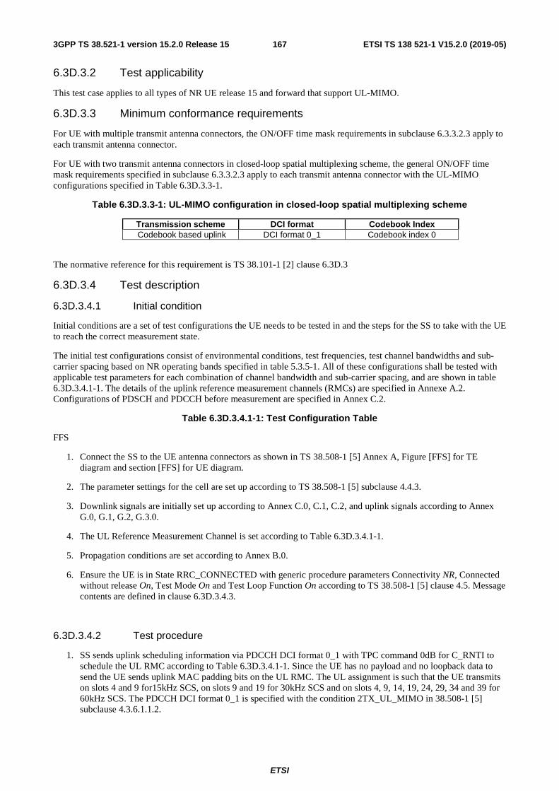
ETSI
ETSI TS 138 521-1 V15.2.0 (2019-05)1673GPP TS 38.521-1 version 15.2.0 Release 15
6.3D.3.2 Test applicability
This test case applies to all types of NR UE release 15 and forward that support UL-MIMO.
6.3D.3.3 Minimum conformance requirements
For UE with multiple transmit antenna connectors, the ON/OFF time mask requirements in subclause 6.3.3.2.3 apply to each transmit antenna connector.
For UE with two transmit antenna connectors in closed-loop spatial multiplexing scheme, the general ON/OFF time mask requirements specified in subclause 6.3.3.2.3 apply to each transmit antenna connector with the UL-MIMO configurations specified in Table 6.3D.3.3-1.
Table 6.3D.3.3-1: UL-MIMO configuration in closed-loop spatial multiplexing scheme
Transmission scheme DCI format Codebook Index Codebook based uplink DCI format 0_1 Codebook index 0
The normative reference for this requirement is TS 38.101-1 [2] clause 6.3D.3
6.3D.3.4 Test description
6.3D.3.4.1 Initial condition
Initial conditions are a set of test configurations the UE needs to be tested in and the steps for the SS to take with the UE to reach the correct measurement state.
The initial test configurations consist of environmental conditions, test frequencies, test channel bandwidths and sub-carrier spacing based on NR operating bands specified in table 5.3.5-1. All of these configurations shall be tested with applicable test parameters for each combination of channel bandwidth and sub-carrier spacing, and are shown in table 6.3D.3.4.1-1. The details of the uplink reference measurement channels (RMCs) are specified in Annexe A.2. Configurations of PDSCH and PDCCH before measurement are specified in Annex C.2.
Table 6.3D.3.4.1-1: Test Configuration Table
FFS
1. Connect the SS to the UE antenna connectors as shown in TS 38.508-1 [5] Annex A, Figure [FFS] for TE diagram and section [FFS] for UE diagram.
2. The parameter settings for the cell are set up according to TS 38.508-1 [5] subclause 4.4.3.
3. Downlink signals are initially set up according to Annex C.0, C.1, C.2, and uplink signals according to Annex G.0, G.1, G.2, G.3.0.
4. The UL Reference Measurement Channel is set according to Table 6.3D.3.4.1-1.
5. Propagation conditions are set according to Annex B.0.
6. Ensure the UE is in State RRC_CONNECTED with generic procedure parameters Connectivity NR, Connected without release On, Test Mode On and Test Loop Function On according to TS 38.508-1 [5] clause 4.5. Message contents are defined in clause 6.3D.3.4.3.
6.3D.3.4.2 Test procedure
1. SS sends uplink scheduling information via PDCCH DCI format 0_1 with TPC command 0dB for C_RNTI to schedule the UL RMC according to Table 6.3D.3.4.1-1. Since the UE has no payload and no loopback data to send the UE sends uplink MAC padding bits on the UL RMC. The UL assignment is such that the UE transmits on slots 4 and 9 for15kHz SCS, on slots 9 and 19 for 30kHz SCS and on slots 4, 9, 14, 19, 24, 29, 34 and 39 for 60kHz SCS. The PDCCH DCI format 0_1 is specified with the condition 2TX_UL_MIMO in 38.508-1 [5] subclause 4.3.6.1.1.2.

ETSI
ETSI TS 138 521-1 V15.2.0 (2019-05)1683GPP TS 38.521-1 version 15.2.0 Release 15
2. Measure the UE transmission OFF power during the slot prior to the PUSCH transmission, excluding a transient period of 10 µs in the end of the slot.
3. Measure the output power of the UE PUSCH transmission during one slot.
4. Measure the UE transmission OFF power during the slot following the PUSCH transmission, excluding a transient period of 10 µs at the beginning of the slot.
5. Repeat step 2) until 4) for each of transmit antenna of the UE
6.3D.3.4.3 Message contents
Message contents are according to TS 38.508-1 [5] subclause 4.6 with following exceptions.
Table 6.3D.3.4.3-1: PUSCH-ConfigCommon
Derivation Path: TS 38.508-1[5], Table 4.6.3-119 Information Element Value/remark Comment Condition
PUSCH-ConfigCommon ::= SEQUENCE { p0-NominalWithGrant -106 }
Table 6.3D.3.4.3-2: PUSCH-Config
Derivation Path: TS 38.508-1 [5], Table 4.6.3-118 with condition CP-OFDM
6.3D.3.5 Test requirement
The requirement for the power of each transmit antenna measured in steps 2, 3 and 4 of the test procedure shall not exceed the values specified in Table 6.3D.3.5-1.
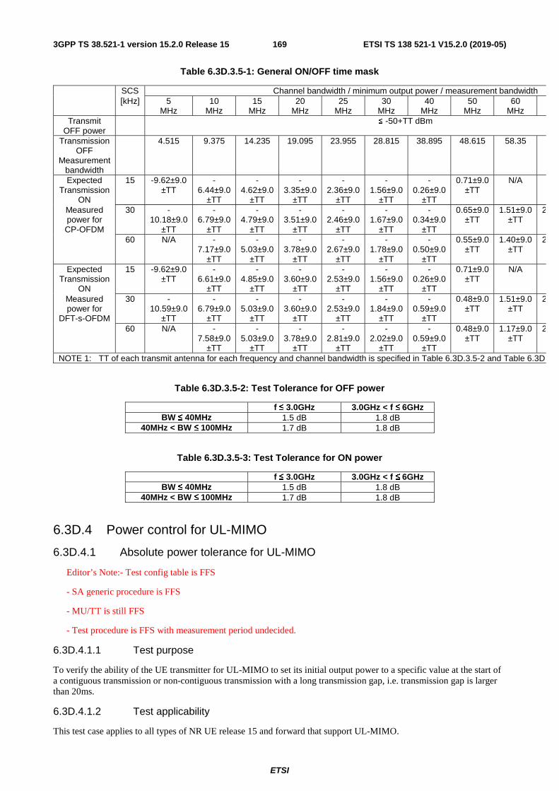
ETSI
ETSI TS 138 521-1 V15.2.0 (2019-05)1693GPP TS 38.521-1 version 15.2.0 Release 15
Table 6.3D.3.5-1: General ON/OFF time mask
SCS Channel bandwidth / minimum output power / measurement bandwidth [kHz] 5
MHz 10
MHz 15
MHz 20
MHz 25
MHz 30
MHz 40
MHz 50
MHz 60
MHz Transmit
OFF power ≤ -50+TT dBm
Transmission OFF
Measurement bandwidth
4.515 9.375 14.235 19.095 23.955 28.815 38.895 48.615 58.35
Expected Transmission
ON
15 -9.62±9.0 ±TT
-6.44±9.0
±TT
-4.62±9.0
±TT
-3.35±9.0
±TT
-2.36±9.0
±TT
-1.56±9.0
±TT
-0.26±9.0
±TT
0.71±9.0 ±TT
N/A
Measured power for CP-OFDM
30 -10.18±9.0
±TT
-6.79±9.0
±TT
-4.79±9.0
±TT
-3.51±9.0
±TT
-2.46±9.0
±TT
-1.67±9.0
±TT
-0.34±9.0
±TT
0.65±9.0 ±TT
1.51±9.0 ±TT
2.
60 N/A -7.17±9.0
±TT
-5.03±9.0
±TT
-3.78±9.0
±TT
-2.67±9.0
±TT
-1.78±9.0
±TT
-0.50±9.0
±TT
0.55±9.0 ±TT
1.40±9.0 ±TT
2.
Expected Transmission
ON
15 -9.62±9.0 ±TT
-6.61±9.0
±TT
-4.85±9.0
±TT
-3.60±9.0
±TT
-2.53±9.0
±TT
-1.56±9.0
±TT
-0.26±9.0
±TT
0.71±9.0 ±TT
N/A
Measured power for
DFT-s-OFDM
30 -10.59±9.0
±TT
-6.79±9.0
±TT
-5.03±9.0
±TT
-3.60±9.0
±TT
-2.53±9.0
±TT
-1.84±9.0
±TT
-0.59±9.0
±TT
0.48±9.0 ±TT
1.51±9.0 ±TT
2.
60 N/A -7.58±9.0
±TT
-5.03±9.0
±TT
-3.78±9.0
±TT
-2.81±9.0
±TT
-2.02±9.0
±TT
-0.59±9.0
±TT
0.48±9.0 ±TT
1.17±9.0 ±TT
2.
NOTE 1: TT of each transmit antenna for each frequency and channel bandwidth is specified in Table 6.3D.3.5-2 and Table 6.3D.3
Table 6.3D.3.5-2: Test Tolerance for OFF power
f ≤ 3.0GHz 3.0GHz < f ≤ 6GHz BW ≤ 40MHz 1.5 dB 1.8 dB
40MHz < BW ≤ 100MHz 1.7 dB 1.8 dB
Table 6.3D.3.5-3: Test Tolerance for ON power
f ≤ 3.0GHz 3.0GHz < f ≤ 6GHz BW ≤ 40MHz 1.5 dB 1.8 dB
40MHz < BW ≤ 100MHz 1.7 dB 1.8 dB
6.3D.4 Power control for UL-MIMO
6.3D.4.1 Absolute power tolerance for UL-MIMO
Editor’s Note:- Test config table is FFS
- SA generic procedure is FFS
- MU/TT is still FFS
- Test procedure is FFS with measurement period undecided.
6.3D.4.1.1 Test purpose
To verify the ability of the UE transmitter for UL-MIMO to set its initial output power to a specific value at the start of a contiguous transmission or non-contiguous transmission with a long transmission gap, i.e. transmission gap is larger than 20ms.
6.3D.4.1.2 Test applicability
This test case applies to all types of NR UE release 15 and forward that support UL-MIMO.
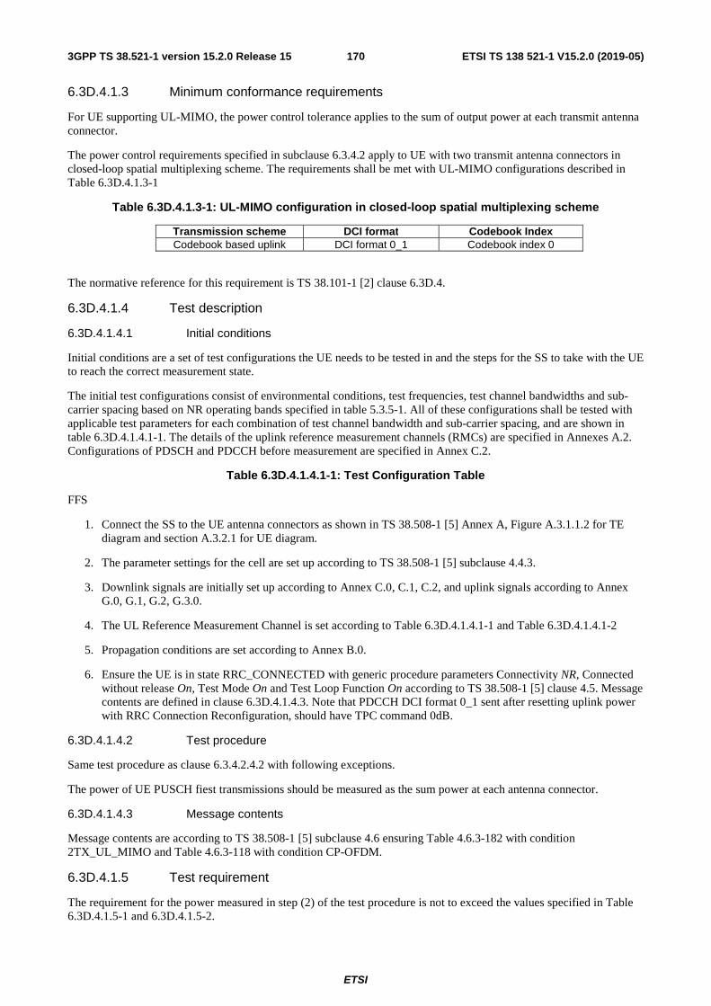
ETSI
ETSI TS 138 521-1 V15.2.0 (2019-05)1703GPP TS 38.521-1 version 15.2.0 Release 15
6.3D.4.1.3 Minimum conformance requirements
For UE supporting UL-MIMO, the power control tolerance applies to the sum of output power at each transmit antenna connector.
The power control requirements specified in subclause 6.3.4.2 apply to UE with two transmit antenna connectors in closed-loop spatial multiplexing scheme. The requirements shall be met with UL-MIMO configurations described in Table 6.3D.4.1.3-1
Table 6.3D.4.1.3-1: UL-MIMO configuration in closed-loop spatial multiplexing scheme
Transmission scheme DCI format Codebook Index Codebook based uplink DCI format 0_1 Codebook index 0
The normative reference for this requirement is TS 38.101-1 [2] clause 6.3D.4.
6.3D.4.1.4 Test description
6.3D.4.1.4.1 Initial conditions
Initial conditions are a set of test configurations the UE needs to be tested in and the steps for the SS to take with the UE to reach the correct measurement state.
The initial test configurations consist of environmental conditions, test frequencies, test channel bandwidths and sub-carrier spacing based on NR operating bands specified in table 5.3.5-1. All of these configurations shall be tested with applicable test parameters for each combination of test channel bandwidth and sub-carrier spacing, and are shown in table 6.3D.4.1.4.1-1. The details of the uplink reference measurement channels (RMCs) are specified in Annexes A.2. Configurations of PDSCH and PDCCH before measurement are specified in Annex C.2.
Table 6.3D.4.1.4.1-1: Test Configuration Table
FFS
1. Connect the SS to the UE antenna connectors as shown in TS 38.508-1 [5] Annex A, Figure A.3.1.1.2 for TE diagram and section A.3.2.1 for UE diagram.
2. The parameter settings for the cell are set up according to TS 38.508-1 [5] subclause 4.4.3.
3. Downlink signals are initially set up according to Annex C.0, C.1, C.2, and uplink signals according to Annex G.0, G.1, G.2, G.3.0.
4. The UL Reference Measurement Channel is set according to Table 6.3D.4.1.4.1-1 and Table 6.3D.4.1.4.1-2
5. Propagation conditions are set according to Annex B.0.
6. Ensure the UE is in state RRC_CONNECTED with generic procedure parameters Connectivity NR, Connected without release On, Test Mode On and Test Loop Function On according to TS 38.508-1 [5] clause 4.5. Message contents are defined in clause 6.3D.4.1.4.3. Note that PDCCH DCI format 0_1 sent after resetting uplink power with RRC Connection Reconfiguration, should have TPC command 0dB.
6.3D.4.1.4.2 Test procedure
Same test procedure as clause 6.3.4.2.4.2 with following exceptions.
The power of UE PUSCH fiest transmissions should be measured as the sum power at each antenna connector.
6.3D.4.1.4.3 Message contents
Message contents are according to TS 38.508-1 [5] subclause 4.6 ensuring Table 4.6.3-182 with condition 2TX_UL_MIMO and Table 4.6.3-118 with condition CP-OFDM.
6.3D.4.1.5 Test requirement
The requirement for the power measured in step (2) of the test procedure is not to exceed the values specified in Table 6.3D.4.1.5-1 and 6.3D.4.1.5-2.
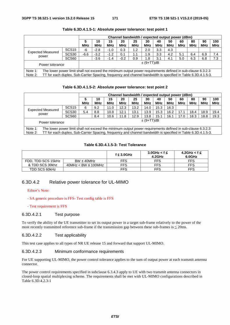
ETSI
ETSI TS 138 521-1 V15.2.0 (2019-05)1713GPP TS 38.521-1 version 15.2.0 Release 15
Table 6.3D.4.1.5-1: Absolute power tolerance: test point 1
Channel bandwidth / expected output power (dBm) 5
MHz 10
MHz 15
MHz 20
MHz 25
MHz 30
MHz 40
MHz 50
MHz 60
MHz 80
MHz 90
MHz 100 MHz
Expected Measured power
SCS15 -6 -2.8 -1.0 0.3 1.2 2.0 3.3 4.3 SCS30 -6.6 -3.2 -1.2 0.1 1.1 1.9 3.3 4.2 5.1 6.4 6.9 7.4 SCS60 -3.6 -1.4 -0.2 0.9 1.8 3.1 4.1 5.0 6.3 6.8 7.3
Power tolerance ± (9+TT)dB
Note 1: The lower power limit shall not exceed the minimum output power requirements defined in sub-clause 6.3.2.3 Note 2: TT for each duplex, Sub-Carrier Spacing, frequency and channel bandwidth is specified in Table 6.3D.4.1.5-3.
Table 6.3D.4.1.5-2: Absolute power tolerance: test point 2
Channel bandwidth / expected output power (dBm) 5
MHz 10
MHz 15
MHz 20
MHz 25
MHz 30
MHz 40
MHz 50
MHz 60
MHz 80
MHz 90
MHz 100 MHz
Expected Measured power
SCS15 6 9.2 11.0 12.3 13.2 14.0 15.3 16.3 SCS30 5.4 8.8 10.8 12.1 13.1 13.9 15.3 16.2 17.1 18.4 18.9 19.4 SCS60 8.4 10.6 11.8 12.9 13.8 15.1 16.1 17.0 18.3 18.8 19.3
Power tolerance ± (9+TT)dB
Note 1: The lower power limit shall not exceed the minimum output power requirements defined in sub-clause 6.3.2.3 Note 2: TT for each duplex, Sub-Carrier Spacing, frequency and channel bandwidth is specified in Table 6.3D.4.1.5-3.
Table 6.3D.4.1.5-3: Test Tolerance
f ≤ 3.0GHz 3.0GHz < f ≤ 4.2GHz
4.2GHz < f ≤ 6.0GHz
FDD, TDD SCS 15kHz & TDD SCS 30khz
BW ≤ 40MHz FFS FFS FFS 40MHz < BW ≤ 100MHz FFS FFS FFS
TDD SCS 60kHz FFS FFS FFS
6.3D.4.2 Relative power tolerance for UL-MIMO
Editor’s Note:
- SA generic procedure is FFS- Test config table is FFS
- Test requirement is FFS
6.3D.4.2.1 Test purpose
To verify the ability of the UE transmitter to set its output power in a target sub-frame relatively to the power of the most recently transmitted reference sub-frame if the transmission gap between these sub-frames is ≤ 20ms.
6.3D.4.2.2 Test applicability
This test case applies to all types of NR UE release 15 and forward that support UL-MIMO.
6.3D.4.2.3 Minimum conformance requirements
For UE supporting UL-MIMO, the power control tolerance applies to the sum of output power at each transmit antenna connector.
The power control requirements specified in subclause 6.3.4.3 apply to UE with two transmit antenna connectors in closed-loop spatial multiplexing scheme. The requirements shall be met with UL-MIMO configurations described in Table 6.3D.4.2.3-1

ETSI
ETSI TS 138 521-1 V15.2.0 (2019-05)1723GPP TS 38.521-1 version 15.2.0 Release 15
Table 6.3D.4.2.3-1: UL-MIMO configuration in closed-loop spatial multiplexing scheme
Transmission scheme DCI format Codebook Index Codebook based uplink DCI format 0_1 Codebook index 0
The normative reference for this requirement is TS 38.101-1 [2] clause 6.3D.4
6.3D.4.2.4 Test description
6.3D.4.2.4.1 Initial conditions
Initial conditions are a set of test configurations the UE needs to be tested in and the steps for the SS to take with the UE to reach the correct measurement state.
The initial test configurations consist of environmental conditions, test frequencies, test channel bandwidths and sub-carrier spacing based on NR operating bands specified in table 5.3.5-1. All of these configurations shall be tested with applicable test parameters for each combination of test channel bandwidth and sub-carrier spacing, and are shown in table 6.3D.4.2.4.1-1 and table 6.3D.4.2.4.1-2. The details of the uplink reference measurement channels (RMCs) are specified in Annexes A.2. Configurations of PDSCH and PDCCH before measurement are specified in Annex C.2.
Table 6.3D.4.2.4.1-1: Test Configuration Table
FFS
Table 6.3.4.2.4.1-2: Uplink Configuration of each RB allocation
FFS
1. Connect the SS to the UE antenna connectors as shown in TS 38.508-1 [5] Annex A, Figure A.3.1.1.2 for TE diagram and section A.3.2.1 for UE diagram.
2. The parameter settings for the cell are set up according to TS 38.508-1 [5] subclause 4.4.3.
3. Downlink signals are initially set up according to Annex C.0, C.1, C.2, and uplink signals according to Annex G.0, G.1, G.2, G.3.0.
4. The UL Reference Measurement Channel is set according to Table 6.3D.4.2.4.1-1 and Table 6.3D.4.2.4.1-2.
5. Propagation conditions are set according to Annex B.0.
6. Ensure the UE is in state RRC_CONNECTED with generic procedure parameters Connectivity NR, Connected without release On, Test Mode On and Test Loop Function On according to TS 38.508-1 [5] clause 4.5. Message contents are defined in clause 6.3D.4.2.4.3.
6.3D.4.2.4.2 Test procedure
Same test procedure as clause 6.3.4.3.4.2 with following exceptions.
The power of PUSCH transmissions should be measured as the sum power at each antenna connector.
6.3D.4.2.4.3 Message contents
Message contents are according to TS 38.508-1 [5] subclause 4.6 ensuring Table 4.6.3-182 with condition 2TX_UL_MIMO and Table 4.6.3-118 with condition CP-OFDM.
6.3D.4.2.5 Test requirement
FFS
6.3D.4.3 Aggregate power tolerance for UL-MIMO
Editor’s Note:
- Test config table is FFS
- MU/TT is FFS

ETSI
ETSI TS 138 521-1 V15.2.0 (2019-05)1733GPP TS 38.521-1 version 15.2.0 Release 15
6.3D.4.3.1 Test purpose
To verify the ability of the UE with UL-MIMO to maintain its power during non-contiguous transmissions within 21ms in response to 0 dB commands with respect to the first UE transmission and all other power control parameters as specified in 38.213 kept constant.
6.3D.4.3.2 Test applicability
This test case applies to all types of NR UE release 15 and forward that support UL-MIMO.
6.3D.4.3.3 Minimum conformance requirements
For UE supporting UL-MIMO, the power control tolerance applies to the sum of output power at each transmit antenna connector.
The power control requirements specified in subclause 6.3.4.4 apply to UE with two transmit antenna connectors in closed-loop spatial multiplexing scheme. The requirements shall be met with UL-MIMO configurations described in Table 6.3D.4.3.3-1
Table 6.3D.4.3.3-1: UL-MIMO configuration in closed-loop spatial multiplexing scheme
Transmission scheme DCI format Codebook Index Codebook based uplink DCI format 0_1 Codebook index 0
The normative reference for this requirement is TS 38.101-1 [2] clause 6.3D.4
6.3D.4.3.4 Test description
6.3D.4.3.4.1 Initial conditions
Initial conditions are a set of test configurations the UE needs to be tested in and the steps for the SS to take with the UE to reach the correct measurement state.
The initial test configurations consist of environmental conditions, test frequencies, test channel bandwidths and sub-carrier spacing based on NR operating bands specified in table 5.3.5-1. All of these configurations shall be tested with applicable test parameters for each combination of test channel bandwidth and sub-carrier spacing, and are shown in table 6.3D.4.3.4.1-1 and table 6.3D.4.3.4.1-2. The details of the uplink reference measurement channels (RMCs) are specified in Annexes A.2. Configurations of PDSCH and PDCCH before measurement are specified in Annex C.2.
Table 6.3D.4.3.4.1-1: Test Configuration Table: PUCCH sub-test
FFS
Table 6.3D.4.3.4.1-2: Test Configuration Table: PUSCH sub-test
FFS
1. Connect the SS to the UE antenna connectors as shown in TS 38.508-1 [5] Annex A, Figure A.3.1.1.2 for TE diagram and section A.3.2.1 for UE diagram.
2. The parameter settings for the cell are set up according to TS 38.508-1 [5] subclause 4.4.3.
3. Downlink signals are initially set up according to Annex C.0, C.1, C.2, and uplink signals according to Annex G.0, G.1, G.2, G.3.0.
4. The UL and DL Reference Measurement channels are set according to Table 6.3D.4.3.4.1-1 (PUCCH sub-test) and Table 6.3D.4.3.4.1-2 (PUSCH sub-test)
5. Propagation conditions are set according to Annex B.0.
6. Ensure the UE is in state RRC_CONNECTED with generic procedure parameters Connectivity NR, Connected without release On, Test Mode On and Test Loop Function On according to TS 38.508-1 [5] clause 4.5. Message contents are defined in clause 6.3D.4.3.4.3.

ETSI
ETSI TS 138 521-1 V15.2.0 (2019-05)1743GPP TS 38.521-1 version 15.2.0 Release 15
6.3D.4.3.4.2 Test procedure
Same test procedure as clause 6.3.4.4.4.2 with following exceptions.
The power of PDCCH /PUSCH transmissions should be measured as the sum power at each antenna connector.
6.3D.4.3.4.3 Message contents
Message contents are according to TS 38.508-1 [5] subclause 4.6 ensuring Table 4.6.3-182 with condition 2TX_UL_MIMO and Table 4.6.3-118 with condition CP-OFDM.
6.3D.4.3.5 Test requirement
The requirement for the power measurements made in step (1.3) and (2.3) of the test procedure shall not exceed the values specified in Table 6.3D.4.3.5-1. The power measurement period shall be 1 sub-frame, or [TBD]slot in the case of TDD SCS 60kHz.
Table 6.3D.4.3.5-1: Power control tolerance
TPC commands
UL channel Test requirement measured power
0 dB PUCCH Given 5 power measurements in the pattern, the 2nd, and later measurements shall be within ± 2.5dB+TT of the 1st
measurement. 0 dB PUSCH Given 5 power measurements in the pattern, the 2nd, and
later measurements shall be within ± 3.5dB+TT of the 1st measurement.
Note 1: For SCS 30kHz 1 sub-frame corresponds to 2 slots, so 2 TPC commands will be sent for a single measurement period.
Note 2: TT for each duplex, Sub-Carrier Spacing, frequency and channel bandwidth is specified in Table 6.3D.4.3.5-2.
Table 6.3D.4.3.5-2: Test Tolerance
FFS
6.4 Transmit signal quality In this clause a multitude of results are derived, all using one common algorithm returning these results: Global In-Channels TX-Test Annex E. Each sub clause of this clause contains a procedure and test requirements described for a specific measurement. If all relevant test parameters in different sub clauses are the same, then the results, returned by the Global In-Channel TX-Test, may be used across the applicable sub clauses.
6.4.1 Frequency error
6.4.1.1 Test purpose
This test verifies the ability of both, the receiver and the transmitter, to process frequency correctly.
Receiver: to extract the correct frequency from the stimulus signal, offered by the System simulator, under ideal propagation conditions and low level.
Transmitter: to derive the correct modulated carrier frequency from the results, gained by the receiver.
6.4.1.2 Test applicability
This test case applies to all types of NR UE release 15 and forward.
6.4.1.3 Minimum conformance requirements
The UE modulated carrier frequency shall be accurate to within ±0.1 PPM observed over a period of 1 ms compared to the carrier frequency received from the NR Node B.
The normative reference for this requirement is TS 38.101-1 [2] clause 6.4.1
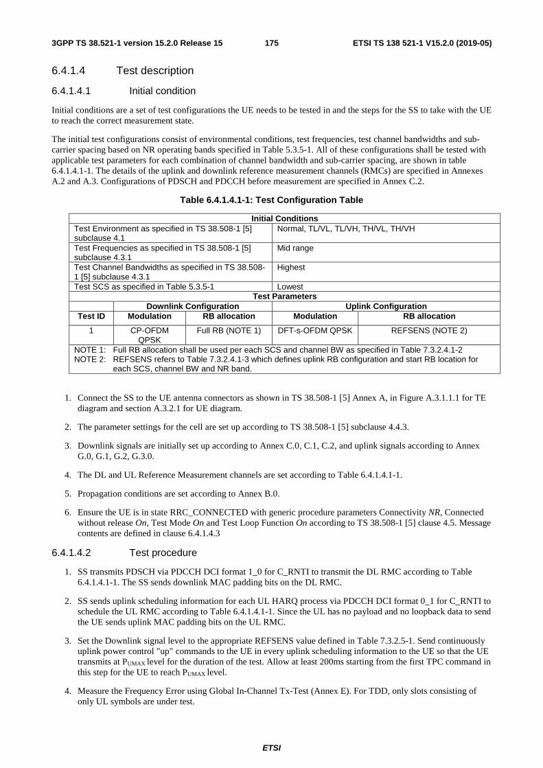
ETSI
ETSI TS 138 521-1 V15.2.0 (2019-05)1753GPP TS 38.521-1 version 15.2.0 Release 15
6.4.1.4 Test description
6.4.1.4.1 Initial condition
Initial conditions are a set of test configurations the UE needs to be tested in and the steps for the SS to take with the UE to reach the correct measurement state.
The initial test configurations consist of environmental conditions, test frequencies, test channel bandwidths and sub-carrier spacing based on NR operating bands specified in Table 5.3.5-1. All of these configurations shall be tested with applicable test parameters for each combination of channel bandwidth and sub-carrier spacing, are shown in table 6.4.1.4.1-1. The details of the uplink and downlink reference measurement channels (RMCs) are specified in Annexes A.2 and A.3. Configurations of PDSCH and PDCCH before measurement are specified in Annex C.2.
Table 6.4.1.4.1-1: Test Configuration Table
Initial Conditions Test Environment as specified in TS 38.508-1 [5] subclause 4.1
Normal, TL/VL, TL/VH, TH/VL, TH/VH
Test Frequencies as specified in TS 38.508-1 [5] subclause 4.3.1
Mid range
Test Channel Bandwidths as specified in TS 38.508-1 [5] subclause 4.3.1
Highest
Test SCS as specified in Table 5.3.5-1 Lowest Test Parameters
Downlink Configuration Uplink Configuration Test ID Modulation RB allocation Modulation RB allocation
1 CP-OFDM QPSK
Full RB (NOTE 1) DFT-s-OFDM QPSK REFSENS (NOTE 2)
NOTE 1: Full RB allocation shall be used per each SCS and channel BW as specified in Table 7.3.2.4.1-2 NOTE 2: REFSENS refers to Table 7.3.2.4.1-3 which defines uplink RB configuration and start RB location for
each SCS, channel BW and NR band.
1. Connect the SS to the UE antenna connectors as shown in TS 38.508-1 [5] Annex A, in Figure A.3.1.1.1 for TE diagram and section A.3.2.1 for UE diagram.
2. The parameter settings for the cell are set up according to TS 38.508-1 [5] subclause 4.4.3.
3. Downlink signals are initially set up according to Annex C.0, C.1, C.2, and uplink signals according to Annex G.0, G.1, G.2, G.3.0.
4. The DL and UL Reference Measurement channels are set according to Table 6.4.1.4.1-1.
5. Propagation conditions are set according to Annex B.0.
6. Ensure the UE is in state RRC_CONNECTED with generic procedure parameters Connectivity NR, Connected without release On, Test Mode On and Test Loop Function On according to TS 38.508-1 [5] clause 4.5. Message contents are defined in clause 6.4.1.4.3
6.4.1.4.2 Test procedure
1. SS transmits PDSCH via PDCCH DCI format 1_0 for C_RNTI to transmit the DL RMC according to Table 6.4.1.4.1-1. The SS sends downlink MAC padding bits on the DL RMC.
2. SS sends uplink scheduling information for each UL HARQ process via PDCCH DCI format 0_1 for C_RNTI to schedule the UL RMC according to Table 6.4.1.4.1-1. Since the UL has no payload and no loopback data to send the UE sends uplink MAC padding bits on the UL RMC.
3. Set the Downlink signal level to the appropriate REFSENS value defined in Table 7.3.2.5-1. Send continuously uplink power control "up" commands to the UE in every uplink scheduling information to the UE so that the UE transmits at PUMAX level for the duration of the test. Allow at least 200ms starting from the first TPC command in this step for the UE to reach PUMAX level.
4. Measure the Frequency Error using Global In-Channel Tx-Test (Annex E). For TDD, only slots consisting of only UL symbols are under test.
ETSI
ETSI TS 138 521-1 V15.2.0 (2019-05)1763GPP TS 38.521-1 version 15.2.0 Release 15
6.4.1.4.3 Message contents
Message contents are according to TS 38.508-1 [5] subclause 4.6.
6.4.1.5 Test requirement
The 20 frequency error Δf results must fulfil the test requirement:
|Δf| ≤ (0.1 PPM + 15 Hz)
6.4.2 Transmit modulation quality
Transmit modulation defines the modulation quality for expected in-channel RF transmissions from the UE. This transmit modulation limit is specified in terms of:
- Error Vector Magnitude (EVM) for the allocated resources blocks (RB),
- EVM equalizer spectrum flatness derived from the equalizer coefficients generated by the EVM measurement process
- Carrier leakage
- In-band emissions for the non-allocated RB
All the parameters defined in subclause 6.4.2 are defined using the measurement methodology specified in Annex E.
6.4.2.1 Error Vector Magnitude
Editor’s note: This clause is incomplete. The following aspects are either missing or not yet determined:
- Annex on Global In-Channel TX-Test contains TBDs for PRACH.
6.4.2.1.1 Test Purpose
The Error Vector Magnitude is a measure of the difference between the reference waveform and the measured waveform. This difference is called the error vector. Before calculating the EVM the measured waveform is corrected by the sample timing offset and RF frequency offset. Then the carrier leakage shall be removed from the measured waveform before calculating the EVM.
The measured waveform is further equalised using the channel estimates subjected to the EVM equaliser spectrum flatness requirement specified in sub-clause 6.4.2.4.3. For DFT-s-OFDM waveforms, the EVM result is defined after the front-end FFT and IDFT as the square root of the ratio of the mean error vector power to the mean reference power expressed as a %. For CP-OFDM waveforms, the EVM result is defined after the front-end FFT as the square root of the ratio of the mean error vector power to the mean reference power expressed as a %.
The basic EVM measurement interval in the time domain is one preamble sequence for the PRACH and the duration of PUCCH/PUSCH channel, or one hop, if frequency hopping is enabled for PUCCH and PUSCH in the time domain. The EVM measurement interval is reduced by any symbols that contains an allowable power transient as defined in subclause 6.3.3.3.
6.4.2.1.2 Test applicability
This test case applies to all types of NR UE release 15 and forward.
6.4.2.1.3 Minimum conformance requirements
The RMS average of the basic EVM measurements for 10 sub-frames excluding any transient period for the average EVM case, and 60 sub-frames excluding any transient period for the reference signal EVM case, for the different modulations schemes shall not exceed the values specified in Table 6.4.2.1.3-1 for the parameters defined in Table 6.4.2.1.3-2. For EVM evaluation purposes, all PRACH preamble formats 0-4 and all PUCCH formats 1, 1a, 1b, 2, 2a and 2b are considered to have the same EVM requirement as QPSK modulated.

ETSI
ETSI TS 138 521-1 V15.2.0 (2019-05)1773GPP TS 38.521-1 version 15.2.0 Release 15
Table 6.4.2.1.3-1: Requirements for Error Vector Magnitude
Parameter Unit Average EVM Level Pi/2-BPSK % 30 QPSK % 17.5 16 QAM % 12.5 64 QAM % 8 256 QAM % 3.5
Table 6.4.2.1.3-2: Parameters for Error Vector Magnitude
Parameter Unit Level UE Output Power dBm ≥ Table 6.3.1.3-1 UE Output Power for 256 QAM dBm ≥ Table 6.3.1-1 + 10 dB Operating conditions Normal conditions
The normative reference for this requirement is TS 38.101 [2] clause 6.4.2.1.
6.4.2.1.4 Test description
6.4.2.1.4.1 Initial conditions
Initial conditions are a set of test configurations the UE needs to be tested in and the steps for the SS to take with the UE to reach the correct measurement state.
The initial test configurations consist of environmental conditions, test frequencies, test channel bandwidths and sub-carrier spacing based on NR operating bands specified in Table 5.3.5-1. All of these configurations shall be tested with applicable test parameters for each combination of channel bandwidth and sub-carrier spacing, are shown in table 6.4.2.1.4.1-1. The details of the uplink and downlink reference measurement channels (RMCs) are specified in Annexes A.2 and A.3. Configurations of PDSCH and PDCCH before measurement are specified in Annex C.2.
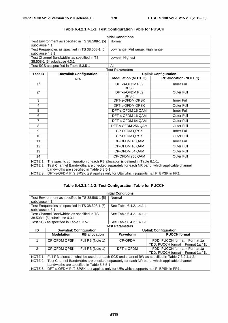
ETSI
ETSI TS 138 521-1 V15.2.0 (2019-05)1783GPP TS 38.521-1 version 15.2.0 Release 15
Table 6.4.2.1.4.1-1: Test Configuration Table for PUSCH
Initial Conditions Test Environment as specified in TS 38.508-1 [5] subclause 4.1
Normal
Test Frequencies as specified in TS 38.508-1 [5] subclause 4.3.1
Low range, Mid range, High range
Test Channel Bandwidths as specified in TS 38.508-1 [5] subclause 4.3.1
Lowest, Highest
Test SCS as specified in Table 5.3.5-1 All Test Parameters
Test ID Downlink Configuration Uplink Configuration N/A Modulation (NOTE 3) RB allocation (NOTE 1)
13 DFT-s-OFDM PI/2 BPSK
Inner Full
23 DFT-s-OFDM PI/2 BPSK
Outer Full
3 DFT-s-OFDM QPSK Inner Full
4 DFT-s-OFDM QPSK Outer Full
5 DFT-s-OFDM 16 QAM Inner Full
6 DFT-s-OFDM 16 QAM Outer Full
7 DFT-s-OFDM 64 QAM Outer Full
8 DFT-s-OFDM 256 QAM Outer Full
9 CP-OFDM QPSK Inner Full
10 CP-OFDM QPSK Outer Full
11 CP-OFDM 16 QAM Inner Full
12 CP-OFDM 16 QAM Outer Full
13 CP-OFDM 64 QAM Outer Full
14 CP-OFDM 256 QAM Outer Full
NOTE 1: The specific configuration of each RB allocation is defined in Table 6.1-1. NOTE 2: Test Channel Bandwidths are checked separately for each NR band, which applicable channel
bandwidths are specified in Table 5.3.5-1. NOTE 3: DFT-s-OFDM PI/2 BPSK test applies only for UEs which supports half Pi BPSK in FR1.
Table 6.4.2.1.4.1-2: Test Configuration Table for PUCCH
Initial Conditions Test Environment as specified in TS 38.508-1 [5] subclause 4.1
Normal
Test Frequencies as specified in TS 38.508-1 [5] subclause 4.3.1
See Table 6.4.2.1.4.1-1
Test Channel Bandwidths as specified in TS 38.508-1 [5] subclause 4.3.1
See Table 6.4.2.1.4.1-1
Test SCS as specified in Table 5.3.5-1 See Table 6.4.2.1.4.1-1 Test Parameters
ID Downlink Configuration Uplink Configuration Modulation RB allocation Waveform PUCCH format
1 CP-OFDM QPSK Full RB (Note 1) CP-OFDM FDD: PUCCH format = Format 1a TDD: PUCCH format = Format 1a / 1b
2 CP-OFDM QPSK Full RB (Note 1) DFT-s-OFDM FDD: PUCCH format = Format 1a TDD: PUCCH format = Format 1a / 1b
NOTE 1: Full RB allocation shall be used per each SCS and channel BW as specified in Table 7.3.2.4.1-2. NOTE 2: Test Channel Bandwidths are checked separately for each NR band, which applicable channel
bandwidths are specified in Table 5.3.5-1. NOTE 3: DFT-s-OFDM PI/2 BPSK test applies only for UEs which supports half Pi BPSK in FR1.

ETSI
ETSI TS 138 521-1 V15.2.0 (2019-05)1793GPP TS 38.521-1 version 15.2.0 Release 15
Table 6.4.2.1.4.1-3: Test Configuration for PRACH
Initial Conditions Test Environment as specified in TS 38.508-1 [5] subclause 4.1
Normal
Test Frequencies as specified in TS 38.508-1 [5] subclause 4.3.1
See Table 6.4.2.1.4.1-1
Test Channel Bandwidths as specified in TS 38.508-1 [5] subclause 4.3.1
See Table 6.4.2.1.4.1-1
Test SCS as specified in Table 5.3.5-1 See Table 6.4.2.1.4.1-1 PRACH preamble format
FDD TDD PRACH Configuration Index 17 52 RS EPRE setting for test point 1 (dBm/15kHz) -71 -65 RS EPRE setting for test point 2 (dBm/15kHz) -86 -80
1. Connect the SS to the UE antenna connectors as shown in TS 38.508-1 [5] Annex A, in Figure A.3.1.1.1 for TE diagram and section A.3.2.1 for UE diagram.
2. The parameter settings for the cell are set up according to TS 38.508-1 [5] subclause 4.4.3.
3. Downlink signals are initially set up according to Annex C.0, C.1, C.2, and uplink signals according to Annex G.0, G.1, G.2, G.3.0.
4. The UL Reference Measurement channels are set according to Table 6.4.2.1.4.1-1.
5. Propagation conditions are set according to Annex B.0.
6. Ensure the UE is in state RRC_CONNECTED with generic procedure parameters Connectivity NR, Connected without release On, Test Mode On and Test Loop Function On according to TS 38.508-1 [5] clause 4.5. Message contents are defined in clause 6.4.2.1.4.3
6.4.2.1.4.2 Test procedure
Test procedure for PUSCH:
1.1 SS sends uplink scheduling information for each UL HARQ process via PDCCH DCI format 0_1 for C_RNTI to schedule the UL RMC according to Table 6.4.2.1.4.1-1. Since the UE has no payload data to send, the UE transmits uplink MAC padding bits on the UL RMC.
1.2 Send continuously uplink power control "up" commands in the uplink scheduling information to the UE until the UE transmits at PUMAX level, allow at least 200ms starting from the first TPC command in this step for the UE to reach PUMAX level.
1.3 Measure the EVM and DMRSEVM using Global In-Channel Tx-Test (Annex E). For TDD, only slots consisting of only UL symbols are under test.
1.4 For modulations except 256QAM, send the appropriate TPC commands in the uplink scheduling information to the UE until UE output power is in the range Pmin + PW ± PW, where Pmin is the minimum output power according to Table 6.3.1.3-1 and PW is the power window according to Table 6.4.2.1.4.2-1 for the carrier frequency f and the channel bandwidth BW. For 256 QAM, send the appropriate TPC commands in the uplink scheduling information to the UE until UE output power is in the range Pmin + 10 dB + PW ± PW, where Pmin is the minimum output power according to Table 6.3.1.3-1 and PW is the power window according to Table 6.4.2.1.4.2-1 for the carrier frequency f and the channel bandwidth BW
1.5 Measure the EVM and DMRSEVM using Global In-Channel Tx-Test (Annex E). For TDD, only slots consisting of only UL symbols are under test.
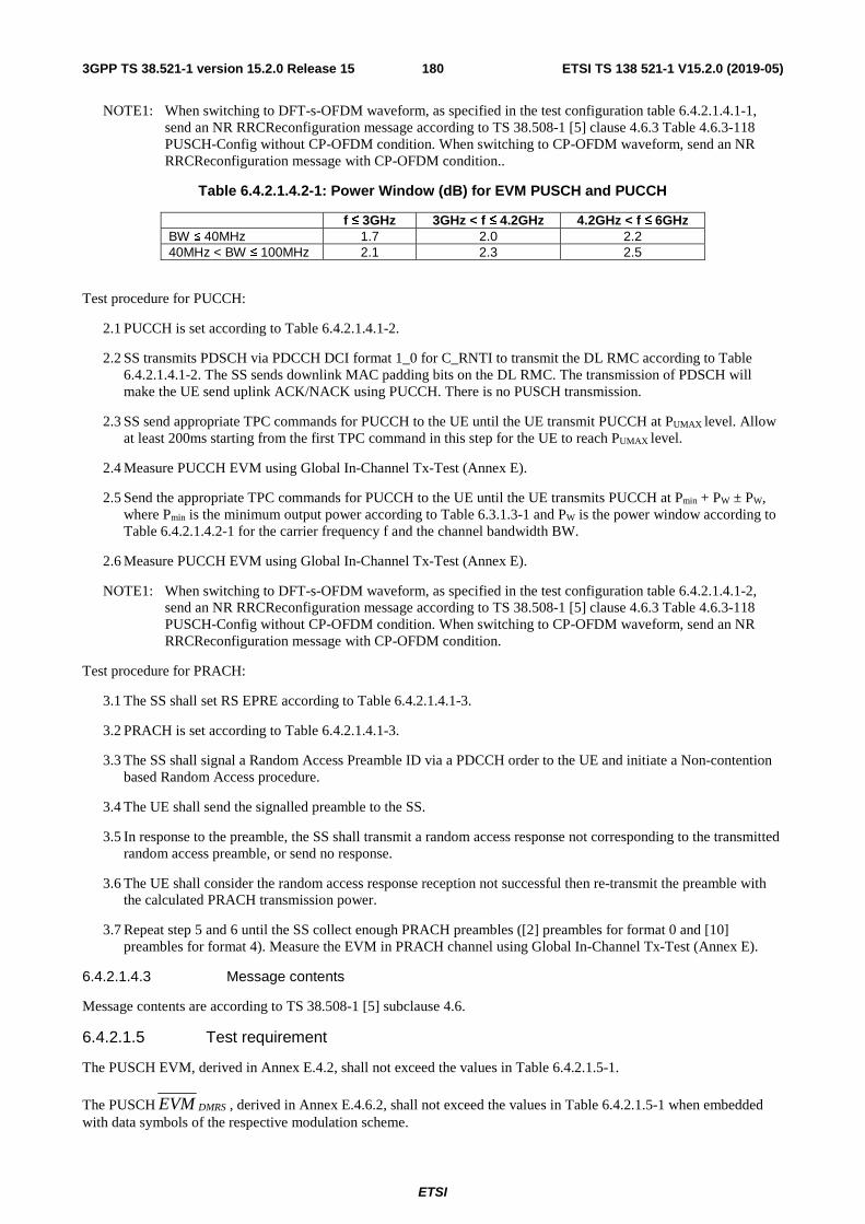
ETSI
ETSI TS 138 521-1 V15.2.0 (2019-05)1803GPP TS 38.521-1 version 15.2.0 Release 15
NOTE1: When switching to DFT-s-OFDM waveform, as specified in the test configuration table 6.4.2.1.4.1-1, send an NR RRCReconfiguration message according to TS 38.508-1 [5] clause 4.6.3 Table 4.6.3-118 PUSCH-Config without CP-OFDM condition. When switching to CP-OFDM waveform, send an NR RRCReconfiguration message with CP-OFDM condition..
Table 6.4.2.1.4.2-1: Power Window (dB) for EVM PUSCH and PUCCH
f ≤ 3GHz 3GHz < f ≤ 4.2GHz 4.2GHz < f ≤ 6GHz BW ≤ 40MHz 1.7 2.0 2.2 40MHz < BW ≤ 100MHz 2.1 2.3 2.5
Test procedure for PUCCH:
2.1 PUCCH is set according to Table 6.4.2.1.4.1-2.
2.2 SS transmits PDSCH via PDCCH DCI format 1_0 for C_RNTI to transmit the DL RMC according to Table 6.4.2.1.4.1-2. The SS sends downlink MAC padding bits on the DL RMC. The transmission of PDSCH will make the UE send uplink ACK/NACK using PUCCH. There is no PUSCH transmission.
2.3 SS send appropriate TPC commands for PUCCH to the UE until the UE transmit PUCCH at PUMAX level. Allow at least 200ms starting from the first TPC command in this step for the UE to reach PUMAX level.
2.4 Measure PUCCH EVM using Global In-Channel Tx-Test (Annex E).
2.5 Send the appropriate TPC commands for PUCCH to the UE until the UE transmits PUCCH at Pmin + PW ± PW, where Pmin is the minimum output power according to Table 6.3.1.3-1 and PW is the power window according to Table 6.4.2.1.4.2-1 for the carrier frequency f and the channel bandwidth BW.
2.6 Measure PUCCH EVM using Global In-Channel Tx-Test (Annex E).
NOTE1: When switching to DFT-s-OFDM waveform, as specified in the test configuration table 6.4.2.1.4.1-2, send an NR RRCReconfiguration message according to TS 38.508-1 [5] clause 4.6.3 Table 4.6.3-118 PUSCH-Config without CP-OFDM condition. When switching to CP-OFDM waveform, send an NR RRCReconfiguration message with CP-OFDM condition.
Test procedure for PRACH:
3.1 The SS shall set RS EPRE according to Table 6.4.2.1.4.1-3.
3.2 PRACH is set according to Table 6.4.2.1.4.1-3.
3.3 The SS shall signal a Random Access Preamble ID via a PDCCH order to the UE and initiate a Non-contention based Random Access procedure.
3.4 The UE shall send the signalled preamble to the SS.
3.5 In response to the preamble, the SS shall transmit a random access response not corresponding to the transmitted random access preamble, or send no response.
3.6 The UE shall consider the random access response reception not successful then re-transmit the preamble with the calculated PRACH transmission power.
3.7 Repeat step 5 and 6 until the SS collect enough PRACH preambles ([2] preambles for format 0 and [10] preambles for format 4). Measure the EVM in PRACH channel using Global In-Channel Tx-Test (Annex E).
6.4.2.1.4.3 Message contents
Message contents are according to TS 38.508-1 [5] subclause 4.6.
6.4.2.1.5 Test requirement
The PUSCH EVM, derived in Annex E.4.2, shall not exceed the values in Table 6.4.2.1.5-1.
The PUSCH DMRSEVM , derived in Annex E.4.6.2, shall not exceed the values in Table 6.4.2.1.5-1 when embedded with data symbols of the respective modulation scheme.
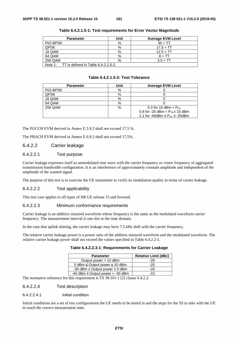
ETSI
ETSI TS 138 521-1 V15.2.0 (2019-05)1813GPP TS 38.521-1 version 15.2.0 Release 15
Table 6.4.2.1.5-1: Test requirements for Error Vector Magnitude
Parameter Unit Average EVM Level Pi/2-BPSK % 30 + TT QPSK % 17.5 + TT 16 QAM % 12.5 + TT 64 QAM % 8 + TT 256 QAM % 3.5 + TT Note 1: TT is defined in Table 6.4.2.1.5-2.
Table 6.4.2.1.5-2: Test Tolerance
Parameter Unit Average EVM Level Pi/2-BPSK % 0 QPSK % 0 16 QAM % 0 64 QAM % 0 256 QAM % 0.3 for 15 dBm < PUL
0.8 for -25 dBm < PUL≤ 15 dBm 1.1 for -40dBm ≤ PUL ≤ -25dBm
The PUCCH EVM derived in Annex E.5.9.2 shall not exceed 17.5 %.
The PRACH EVM derived in Annex E.6.9.2 shall not exceed 17.5%.
6.4.2.2 Carrier leakage
6.4.2.2.1 Test purpose
Carrier leakage expresses itself as unmodulated sine wave with the carrier frequency or centre frequency of aggregated transmission bandwidth configuration. It is an interference of approximately constant amplitude and independent of the amplitude of the wanted signal.
The purpose of this test is to exercise the UE transmitter to verify its modulation quality in terms of carrier leakage.
6.4.2.2.2 Test applicability
This test case applies to all types of NR UE release 15 and forward.
6.4.2.2.3 Minimum conformance requirements
Carrier leakage is an additive sinusoid waveform whose frequency is the same as the modulated waveform carrier frequency. The measurement interval is one slot in the time domain.
In the case that uplink sharing, the carrier leakage may have 7.5 kHz shift with the carrier frequency.
The relative carrier leakage power is a power ratio of the additive sinusoid waveform and the modulated waveform. The relative carrier leakage power shall not exceed the values specified in Table 6.4.2.2-1.
Table 6.4.2.2.3-1: Requirements for Carrier Leakage
Parameter Relative Limit (dBc) Output power > 10 dBm -28
0 dBm ≤ Output power ≤ 10 dBm -25 -30 dBm ≤ Output power ≤ 0 dBm -20
-40 dBm ≤ Output power < -30 dBm -10 The normative reference for this requirement is TS 38.101-1 [2] clause 6.4.2.2.
6.4.2.2.4 Test description
6.4.2.2.4.1 Initial condition
Initial conditions are a set of test configurations the UE needs to be tested in and the steps for the SS to take with the UE to reach the correct measurement state.

ETSI
ETSI TS 138 521-1 V15.2.0 (2019-05)1823GPP TS 38.521-1 version 15.2.0 Release 15
The initial test configurations consist of environmental conditions, test frequencies, test channel bandwidths and sub-carrier spacing based on NR operating bands specified in Table 5.3.5-1. All of these configurations shall be tested with applicable test parameters for each combination of channel bandwidth and sub-carrier spacing, are shown in table 6.4.2.2.4.1-1. The details of the uplink and downlink reference measurement channels (RMCs) are specified in Annexes A.2 and A.3. Configurations of PDSCH and PDCCH before measurement are specified in Annex C.2.
Table 6.4.2.2.4.1-1: Test Configuration
Initial Conditions Test Environment as specified in TS 38.508-1 [5] subclause 4.1
Normal
Test Frequencies as specified in TS 38.508-1 [5] subclause 4.3.1
Low range, Mid range, High range
Test Channel Bandwidths as specified in TS 38.508-1 [5] subclause 4.3.1
Mid
Test SCS as specified in Table 5.3.5-1 Lowest Test Parameters
Test ID Downlink Configuration Uplink Configuration N/A Modulation RB allocation (NOTE 1, 3)
1 DFT-s-OFDM QPSK Inner_1RB_Left
NOTE 1: The specific configuration of each RB allocation is defined in Table 6.1-1. NOTE 2: Test Channel Bandwidths are checked separately for each NR band, which applicable channel
bandwidths are specified in Table 5.3.5-1. NOTE 3: When the signalled DC carrier position is at Inner_1RB_Left, use Inner_1RB_Right for UL RB allocation.
1. Connect the SS to the UE antenna connectors as shown in TS 38.508-1 [5] Annex A, in Figure A.3.1.1.1 for TE diagram and section A.3.2.1 for UE diagram.
2. The parameter settings for the cell are set up according to TS 38.508-1 [5] subclause 4.4.3.
3. Downlink signals are initially set up according to AnnexC.0, C.1, C.2 and uplink signals according to Annex G.0, G.1, G.2, G.3.0.
4. The UL Reference Measurement channels are set according to Table 6.4.2.2.4.1-1.
5. Propagation conditions are set according to Annex B.0.
6. Ensure the UE is in state RRC_CONNECTED with generic procedure parameters Connectivity NR, Connected without release On, Test Mode On and Test Loop Function On according to TS 38.508-1 [5] clause 4.5. Message contents are defined in clause 6.4.2.2.4.3
6.4.2.2.4.2 Test procedure
1. SS sends uplink scheduling information for each UL HARQ process via PDCCH DCI format 0_1 for C_RNTI to schedule the UL RMC according to Table 6.4.2.2.4.1-1. Since the UE has no payload and no loopback data to send the UE sends uplink MAC padding bits on the UL RMC.
2. Send the appropriate TPC commands in the uplink scheduling information to the UE until UE output power is 10 + PW dBm ± PW dB where PW is the power window according to Table 6.4.2.2.4.2-1 for the carrier frequency f and the channel bandwidth BW.
3. Measure carrier leakage using Global In-Channel Tx-Test (Annex E). For TDD, only slots consisting of only UL symbols are under test.
4. Send the appropriate TPC commands in the uplink scheduling information to the UE until UE output power is 0 + PW dBm ± PW dB where PW is the power window according to Table 6.4.2.2.4.2-1 for the carrier frequency f and the channel bandwidth BW.
5. Measure carrier leakage using Global In-Channel Tx-Test (Annex E). For TDD, only slots consisting of only UL symbols are under test.
6. Send the appropriate TPC commands in the uplink scheduling information to the UE until UE output power is -30 + PW dBm ± PW dB where PW is the power window according to Table 6.4.2.2.4.2-2 for the carrier frequency f and the channel bandwidth BW.

ETSI
ETSI TS 138 521-1 V15.2.0 (2019-05)1833GPP TS 38.521-1 version 15.2.0 Release 15
7. Measure carrier leakage using Global In-Channel Tx-Test (Annex E). For TDD, only slots consisting of only UL symbols are under test.
8. Send the appropriate TPC commands in the uplink scheduling information to the UE until UE output power is -40 + PW dBm ± PW dB where PW is the power window according to Table 6.4.2.2.4.2-2 for the carrier frequency f and the channel bandwidth BW.
9. Measure carrier leakage using Global In-Channel Tx-Test (Annex E). For TDD, only slots consisting of only UL symbols are under test.
Table 6.4.2.2.4.2-1: Power Window (dB) for carrier leakage (step 2 and step 4)
f ≤ 3GHz 3GHz < f ≤ 4.2GHz 4.2GHz < f ≤ 6GHz BW ≤ 20MHz 1.4 1.7 2 20MHz < BW ≤ 40MHz 1.4 1.7 2.2 40MHz < BW ≤ 100MHz 2.1 2.3 2.3
Table 6.4.2.1.4.2-2: Power Window (dB) for carrier leakage (step 6 and step 8)
f ≤ 3GHz 3GHz < f ≤ 4.2GHz 4.2GHz < f ≤ 6GHz BW ≤ 40MHz 1.7 2.0 2.2 40MHz < BW ≤ 100MHz 2.1 2.3 2.5
6.4.2.2.4.3 Message contents
Message contents are according to TS 38.508-1 [5] subclause 4.6.
6.4.2.2.5 Test requirement
Each of the n carrier leakage results, derived in Annex E.3.1, shall not exceed the values in table 6.4.2.2.5-1. Allocated RBs are not under test.
Table 6.4.2.2.5-1: Test requirements for Relative Carrier Leakage Power
Parameters UE output power
Relative limit (dBc)
10 + PW dBm ± PW dB5 -28 + TT 0 + PW dBm ± PW dB5 -25 + TT
-30 + PW dBm ± PW dB6 -20 + TT -40 + PW dBm ± PW dB6 -10 + TT
NOTE 1: The measurement bandwidth is 1 RB and the limit is expressed as a ratio of measured power in one non-allocated RB to the measured total power in all allocated RBs.
NOTE 2: The applicable frequencies for this limit are those that are enclosed in the RBs containing the carrier leakage frequency
if RBN is odd, or in the two RBs immediately adjacent to the
carrier leakage frequency if RBN is even but excluding any
allocated RB.
NOTE 3: RBN is the Transmission Bandwidth Configuration (see
Figure 5.3.3). NOTE 4: PW is the power window according to Table 6.4.2.2.4.2-1 for
the carrier frequency f and the channel bandwidth BW. NOTE 5: PW is the power window according to Table 6.4.2.2.4.2-2 for
the carrier frequency f and the channel bandwidth BW. NOTE 6: Test tolerance TT = 0.8 dB.
6.4.2.3 In-band emissions
6.4.2.3.1 Test purpose
The in-band emissions are a measure of the interference falling into the non-allocated resources blocks

ETSI
ETSI TS 138 521-1 V15.2.0 (2019-05)1843GPP TS 38.521-1 version 15.2.0 Release 15
The in-band emission is defined as the average emission across 12 sub-carriers and as a function of the RB offset from the edge of the allocated UL transmission bandwidth. The in-band emission is measured as the ratio of the UE output power in a non–allocated RB to the UE output power in an allocated RB.
The basic in-band emissions measurement interval is defined over one slot in the time domain, however, the minimum requirement applies when the in-band emission measurement is averaged over 10 sub-frames. When the PUSCH or PUCCH transmission slot is shortened due to multiplexing with SRS, the in-band emissions measurement interval is reduced by one or more symbols, accordingly.
The purpose of this test is to exercise the UE transmitter to verify its modulation quality in terms of in-band emissions.
6.4.2.3.2 Test applicability
This test case applies to all types of NR UE release 15 and forward.
6.4.2.3.3 Minimum conformance requirements
The average of the basic in-band emission measurement over 10 sub-frames shall not exceed the values specified in Table 6.4.2.3.3-1.
Table 6.4.2.3.3-1: Requirements for in-band emissions
Parameter description Unit Limit (NOTE 1) Applicable
Frequencies
General dB
{
( ) }RB
CRBRB
CRBRB
PkHzSCSdBm
LEVM
LN
−+−−Δ⋅−−⋅
⋅−−
15/log1057
,/)1(53log20
),/(log1025max
10
10
10
Any non-allocated (NOTE 2)
IQ Image dB -28 Image frequencies when output power > 10 dBm Image
frequencies (NOTES 2, 3) -25 Image frequencies when output power ≤ 10 dBm
Carrier leakage dBc
-28 Output power > 10 dBm Carrier leakage
frequency (NOTES 4, 5)
-25 0 dBm ≤ Output power ≤ 10 dBm -20 -30 dBm ≤ Output power ≤ 0 dBm -10 -40 dBm ≤ Output power < -30 dBm
NOTE 1: An in-band emissions combined limit is evaluated in each non-allocated RB. For each such RB, the minimum requirement is calculated as the higher of PRB - 30 dB and the power sum of all limit values (General, IQ Image or Carrier leakage) that apply. PRB is defined in NOTE 10.
NOTE 2: The measurement bandwidth is 1 RB and the limit is expressed as a ratio of measured power in one non-allocated RB to the measured average power per allocated RB, where the averaging is done across all allocated RBs.
NOTE 3: The applicable frequencies for this limit are those that are enclosed in the reflection of the allocated bandwidth, based on symmetry with respect to the carrier leakage frequency, but excluding any allocated RBs.
NOTE 4: The measurement bandwidth is 1 RB and the limit is expressed as a ratio of measured power in one non-allocated RB to the measured total power in all allocated RBs.
NOTE 5: The applicable frequencies for this limit are those that are enclosed in the RBs containing the carrier
leakage frequency if RBN is odd, or in the two RBs immediately adjacent to the carrier leakage frequency
if RBN is even but excluding any allocated RB.
NOTE 6: CRBL is the Transmission Bandwidth (see Figure 5.3.3).
NOTE 7: RBN is the Transmission Bandwidth Configuration (see Figure 5.3.3).
NOTE 8: EVM is the limit specified in Table 6.4.2.1.3-1 for the modulation format used in the allocated RBs.
NOTE 9: RBΔ is the starting frequency offset between the allocated RB and the measured non-allocated RB (e.g.
1=ΔRB or 1−=ΔRB for the first adjacent RB outside of the allocated bandwidth.
NOTE 10: RBP is the transmitted power normalized by the number of allocated RBs, measured in dBm.
The normative reference for this requirement is TS 38.101-1 [2] clause 6.4.2.3.

ETSI
ETSI TS 138 521-1 V15.2.0 (2019-05)1853GPP TS 38.521-1 version 15.2.0 Release 15
6.4.2.3.4 Test description
6.4.2.3.4.1 Initial condition
Initial conditions are a set of test configurations the UE needs to be tested in and the steps for the SS to take with the UE to reach the correct measurement state.
The initial test configurations consist of environmental conditions, test frequencies, test channel bandwidths and sub-carrier spacing based on NR operating bands specified in Table 5.3.5-1. All of these configurations shall be tested with applicable test parameters for each combination of channel bandwidth and sub-carrier spacing, are shown in table 6.4.2.3.4.1-1. The details of the uplink and downlink reference measurement channels (RMCs) are specified in Annexes A.2 and A.3. Configurations of PDSCH and PDCCH before measurement are specified in Annex C.2.
Table 6.4.2.3.4.1-1: Test Configuration Table for PUSCH
Initial Conditions Test Environment as specified in TS 38.508-1 [5] subclause 4.1
Normal
Test Frequencies as specified in TS 38.508-1 [5] subclause 4.3.1
Low range, Mid range, High range
Test Channel Bandwidths as specified in TS 38.508-1 [5] subclause 4.3.1
Lowest, Mid, Highest
Test SCS as specified in Table 5.3.5-1 Lowest Test Parameters
Test ID Downlink Configuration Uplink Configuration N/A Modulation RB allocation (NOTE 1)
1 DFT-s-OFDM QPSK Inner_1RB_Left
2 DFT-s-OFDM QPSK Inner_1RB_Right
3 CP-OFDM QPSK Inner_1RB_Left
4 CP-OFDM QPSK Inner_1RB_Right
NOTE 1: The specific configuration of each RB allocation is defined in Table 6.1-1. NOTE 2: Test Channel Bandwidths are checked separately for each NR band, which applicable channel
bandwidths are specified in Table 5.3.5-1.
Table 6.4.2.3.4.1-2: Test Configuration Table for PUCCH
Initial Conditions Test Environment as specified in TS 38.508-1 [5] subclause 4.1
See Table 6.4.2.3.4.1-1
Test Frequencies as specified in TS 38.508-1 [5] subclause 4.3.1
See Table 6.4.2.3.4.1-1
Test Channel Bandwidths as specified in TS 38.508-1 [5] subclause 4.3.1
See Table 6.4.2.3.4.1-1
Test SCS as specified in Table 5.3.5-1 See Table 6.4.2.3.4.1-1 Test Parameters
ID Downlink Configuration Uplink Configuration Modulation RB allocation Waveform PUCCH format
1 CP-OFDM QPSK Full RB (Note 1) DFT-s-OFDM FDD: PUCCH format = Format 1a TDD: PUCCH format = Format 1a / 1b
2 CP-OFDM QPSK Full RB (Note 1) CP-OFDM FDD: PUCCH format = Format 1a TDD: PUCCH format = Format 1a / 1b
NOTE 1: Full RB allocation shall be used per each SCS and channel BW as specified in Table 7.3.2.4.1-2. NOTE 2: Test Channel Bandwidths are checked separately for each NR band, which applicable channel
bandwidths are specified in Table 5.3.5-1. NOTE 3: DFT-s-OFDM PI/2 BPSK test applies only for UEs which supports half Pi BPSK in FR1.
1. Connect the SS to the UE antenna connectors as shown in TS 38.508-1 [5] Annex A, in Figure A.3.1.1.1 for TE diagram and section A.3.2.1 for UE diagram.
2. The parameter settings for the cell are set up according to TS 38.508-1 [5] subclause 4.4.3.
3. Downlink signals are initially set up according to Annex C.0, C.1, C.2, and uplink signals according to Annex G.0, G.1, G.2, G.3.0.

ETSI
ETSI TS 138 521-1 V15.2.0 (2019-05)1863GPP TS 38.521-1 version 15.2.0 Release 15
4. The UL Reference Measurement channels are set according to Table 6.4.2.3.4.1-1.
5. Propagation conditions are set according to Annex B.0.
6. Ensure the UE is in state RRC_CONNECTED with generic procedure parameters Connectivity NR, Connected without release On, Test Mode On and Test Loop Function On according to TS 38.508-1 [5] clause 4.5. Message contents are defined in clause 6.4.2.3.4.3
6.4.2.3.4.2 Test procedure
Test procedure for PUSCH:
1.1 SS sends uplink scheduling information for each UL HARQ process via PDCCH DCI format 0_1 for C_RNTI to schedule the UL RMC according to Table 6.4.2.3.4.1-1. Since the UE has no payload and no loopback data to send the UE sends uplink MAC padding bits on the UL RMC.
1.2 Send the appropriate TPC commands in the uplink scheduling information to the UE until UE output power is 10 + PW dBm ± PW dB where PW is the power window according to Table 6.4.2.3.4.2-1 for the carrier frequency f and the channel bandwidth BW.
1.3 Measure In-band emission using Global In-Channel Tx-Test (Annex E). For TDD, only slots consisting of only UL symbols are under test.
1.4 Send the appropriate TPC commands in the uplink scheduling information to the UE until UE output power is 0 + PW dBm ± PW dB where PW is the power window according to Table 6.4.2.3.4.2-1 for the carrier frequency f and the channel bandwidth BW.
1.5 Measure In-band emission using Global In-Channel Tx-Test (Annex E). For TDD, only slots consisting of only UL symbols are under test.
1.6 Send the appropriate TPC commands in the uplink scheduling information to the UE until UE output power is -30 + PW dBm ± PW dB where PW is the power window according to Table 6.4.2.3.4.2-2 for the carrier frequency f and the channel bandwidth BW.
1.7 Measure In-band emission using Global In-Channel Tx-Test (Annex E). For TDD, only slots consisting of only UL symbols are under test.
1.8 Send the appropriate TPC commands in the uplink scheduling information to the UE until UE output power is -40 + PW dBm ± PW dB where PW is the power window according to Table 6.4.2.3.4.2-2 for the carrier frequency f and the channel bandwidth BW.
1.9 Measure In-band emission using Global In-Channel Tx-Test (Annex E). For TDD, only slots consisting of only UL symbols are under test.
NOTE1: When switching to DFT-s-OFDM waveform, as specified in the test configuration table 6.4.2.3.4.1-1, send an NR RRCReconfiguration message according to TS 38.508-1 [5] clause 4.6.3 Table 4.6.3-118 PUSCH-Config without CP-OFDM condition. When switching to CP-OFDM waveform, send an NR RRCReconfiguration message with CP-OFDM condition
Test procedure for PUCCH:
2.1 PUCCH is set according to Table 6.4.2.3.4.1-2. SS transmits PDSCH via PDCCH DCI format [1A] for C_RNTI to transmit the DL RMC according to Table 6.4.2.3.4.1-2. The SS sends downlink MAC padding bits on the DL RMC. The transmission of PDSCH will make the UE send uplink ACK/NACK using PUCCH.
2.2 Send the appropriate TPC commands in the uplink scheduling information for PUCCH to the UE until UE output power is 10 + PW dBm ± PW dB where PW is the power window according to Table 6.4.2.3.4.2-1 for the carrier frequency f and the channel bandwidth BW.
2.3 Measure In-band emission using Global In-Channel Tx-Test (Annex E)
2.4 Send the appropriate TPC commands in the uplink scheduling information for PUCCH to the UE until UE output power is 0 + PW dBm ± PW dB where PW is the power window according to Table 6.4.2.3.4.2-1 for the carrier frequency f and the channel bandwidth BW.
2.5 Measure In-band emission using Global In-Channel Tx-Test (Annex E)

ETSI
ETSI TS 138 521-1 V15.2.0 (2019-05)1873GPP TS 38.521-1 version 15.2.0 Release 15
2.6 Send the appropriate TPC commands for PUCCH in the uplink scheduling information to the UE until UE output power is -30 + PW dBm ± PW dB where PW is the power window according to Table 6.4.2.3.4.2-2 for the carrier frequency f and the channel bandwidth BW.
2.7 Measure In-band emission using Global In-Channel Tx-Test (Annex E)
2.8 Send the appropriate TPC commands for PUCCH in the uplink scheduling information to the UE until UE output power is -40 + PW dBm ± PW dB where PW is the power window according to Table 6.4.2.3.4.2-2 for the carrier frequency f and the channel bandwidth BW.
2.9 Measure In-band emission using Global In-Channel Tx-Test (Annex E)
NOTE1: When switching to DFT-s-OFDM waveform, as specified in the test configuration table 6.4.2.3.4.1-2, send an NR RRCReconfiguration message according to TS 38.508-1 [5] clause 4.6.3 Table 4.6.3-118 PUSCH-Config without CP-OFDM condition. When switching to CP-OFDM waveform, send an NR RRCReconfiguration message with CP-OFDM condition
Table 6.4.2.3.4.2-1: Power Window (dB) for carrier leakage (steps 1.2, 1.4, 2.2, and 2.4)
f ≤ 3GHz 3GHz < f ≤ 4.2GHz 4.2GHz < f ≤ 6GHz BW ≤ 20MHz 1.4 1.7 2 20MHz < BW ≤ 40MHz 1.4 1.7 2.2 40MHz < BW ≤ 100MHz 2.1 2.3 2.3
Table 6.4.2.3.4.2-2: Power Window (dB) for carrier leakage (steps 1.6, 1.8, 2.6, and 2.8)
f ≤ 3GHz 3GHz < f ≤ 4.2GHz 4.2GHz < f ≤ 6GHz BW ≤ 40MHz 1.7 2.0 2.2 40MHz < BW ≤ 100MHz 2.1 2.3 2.5
6.4.2.3.4.3 Message contents
Message contents are according to TS 38.508-1 [5] subclause 4.6.
6.4.2.3.5 Test requirement
Each of the n In-band emissions results, derived in Annex E.4.3 shall not exceed the corresponding values in Tables 6.4.2.3.5-1.
Table 6.4.2.3.5-1: Test requirements for in-band emissions
Parameter description Unit Limit (NOTE 1) Applicable
Frequencies
General dB
{
( ) }RB
CRBRB
CRBRB
PkHzSCSdBm
LEVM
LN
−+−−Δ⋅−−⋅
⋅−−
15/log1057
,/)1(53log20
),/(log1025max
10
10
10
+ TT Any non-allocated (NOTE 2)
IQ Image dB -28 + TT Image frequencies when output power > 10 dBm Image
frequencies (NOTES 2, 3) -25 + TT Image frequencies when output power ≤ 10 dBm
Carrier leakage dBc
-28 + TT Output power > 10 dBm Carrier leakage
frequency (NOTES 4, 5)
-25 + TT 0 dBm ≤ Output power ≤ 10 dBm -20 + TT -30 dBm ≤ Output power ≤ 0 dBm -10 + TT -40 dBm ≤ Output power < -30 dBm
ETSI
ETSI TS 138 521-1 V15.2.0 (2019-05)1883GPP TS 38.521-1 version 15.2.0 Release 15
NOTE 1: An in-band emissions combined limit is evaluated in each non-allocated RB. For each such RB, the minimum requirement is calculated as the higher of PRB - 30 dB and the power sum of all limit values (General, IQ Image or Carrier leakage) that apply. PRB is defined in NOTE 10.
NOTE 2: The measurement bandwidth is 1 RB and the limit is expressed as a ratio of measured power in one non-allocated RB to the measured average power per allocated RB, where the averaging is done across all allocated RBs.
NOTE 3: The applicable frequencies for this limit are those that are enclosed in the reflection of the allocated bandwidth, based on symmetry with respect to the carrier leakage frequency, but excluding any allocated RBs.
NOTE 4: The measurement bandwidth is 1 RB and the limit is expressed as a ratio of measured power in one non-allocated RB to the measured total power in all allocated RBs.
NOTE 5: The applicable frequencies for this limit are those that are enclosed in the RBs containing the carrier
leakage frequency if RBN is odd, or in the two RBs immediately adjacent to the carrier leakage frequency
if RBN is even, but excluding any allocated RB.
NOTE 6: CRBL is the Transmission Bandwidth (see Figure 5.3.3).
NOTE 7: RBN is the Transmission Bandwidth Configuration (see Figure 5.3.3).
NOTE 8: EVM is the limit specified in Table 6.4.2.1.3-1 for the modulation format used in the allocated RBs. NOTE 9: RBΔ is the starting frequency offset between the allocated RB and the measured non-allocated RB (e.g.
1=ΔRB or 1−=ΔRB for the first adjacent RB outside of the allocated bandwidth.
NOTE 10: RBP is the transmitted power normalized by the number of allocated RBs, measured in dBm.
NOTE 11: Test tolerance TT = 0.8 dB.
6.4.2.4 EVM equalizer spectrum flatness
6.4.2.4.1 Test purpose
The zero-forcing equalizer correction applied in the EVM measurement process (as described in Annex E) must meet a spectral flatness requirement for the EVM measurement to be valid. The EVM equalizer spectrum flatness is defined in terms of the maximum peak-to-peak ripple of the equalizer coefficients (dB) across the allocated uplink block, at which the equalizer coefficients are generated by the EVM measurement process. The basic measurement interval is the same as for EVM.
The EVM equalizer spectrum flatness requirement does not limit the correction applied to the signal in the EVM measurement process but for the EVM result to be valid, the equalizer correction that was applied must meet the EVM equalizer spectrum flatness minimum requirements.
6.4.2.4.2 Test applicability
This test case applies to all types of NR UE release 15 and forward.
6.4.2.4.3 Minimum conformance requirements
The peak-to-peak variation of the EVM equalizer coefficients contained within the frequency range of the uplink allocation shall not exceed the maximum ripple specified in Table 6.4.2.4.3-1 for normal conditions. For uplink allocations contained within both Range 1 and Range 2, the coefficients evaluated within each of these frequency ranges shall meet the corresponding ripple requirement and the following additional requirement: the relative difference between the maximum coefficient in Range 1 and the minimum coefficient in Range 2 must not be larger than 5 dB, and the relative difference between the maximum coefficient in Range 2 and the minimum coefficient in Range 1 must not be larger than 7 dB (see Figure 6.4.2.4.3-1).
The EVM equalizer spectral flatness shall not exceed the values specified in Table 6.4.2.4.3-2 for extreme conditions. For uplink allocations contained within both Range 1 and Range 2, the coefficients evaluated within each of these frequency ranges shall meet the corresponding ripple requirement and the following additional requirement: the relative difference between the maximum coefficient in Range 1 and the minimum coefficient in Range 2 must not be larger than 6 dB, and the relative difference between the maximum coefficient in Range 2 and the minimum coefficient in Range 1 must not be larger than 10 dB (see Figure 6.4.2.4.3-1).

ETSI
ETSI TS 138 521-1 V15.2.0 (2019-05)1893GPP TS 38.521-1 version 15.2.0 Release 15
Table 6.4.2.4.3-1: Requirements for EVM equalizer spectrum flatness (normal conditions)
Frequency range Maximum ripple (dB) FUL_Meas – FUL_Low ≥ 3 MHz and FUL_High – FUL_Meas ≥ 3 MHz
(Range 1) 4 (p-p)
FUL_Meas – FUL_Low < 3 MHz or FUL_High – FUL_Meas < 3 MHz (Range 2)
8 (p-p)
NOTE 1: FUL_Meas refers to the sub-carrier frequency for which the equalizer coefficient is evaluated
NOTE 2: FUL_Low and FUL_High refer to each E-UTRA frequency band specified in Table 5.5-1
Table 6.4.2.4.3-2: Minimum requirements for EVM equalizer spectrum flatness (extreme conditions)
Frequency range Maximum Ripple (dB) FUL_Meas – FUL_Low ≥ 5 MHz and FUL_High – FUL_Meas ≥ 5 MHz
(Range 1) 4 (p-p)
FUL_Meas – FUL_Low < 5 MHz or FUL_High – FUL_Meas < 5 MHz (Range 2)
12 (p-p)
NOTE 1: FUL_Meas refers to the sub-carrier frequency for which the equalizer coefficient is evaluated
NOTE 2: FUL_Low and FUL_High refer to each E-UTRA frequency band specified in Table 5.5-1
Figure 6.4.2.4.3-1: The limits for EVM equalizer spectral flatness with the maximum allowed variation of the coefficients indicated (the ETC minimum requirement are within brackets)
The normative reference for this requirement is TS 38.101-1 [2] clause 6.4.2.4.
6.4.2.4.4 Test description
6.4.2.4.4.1 Initial condition
Initial conditions are a set of test configurations the UE needs to be tested in and the steps for the SS to take with the UE to reach the correct measurement state.
The initial test configurations consist of environmental conditions, test frequencies, test channel bandwidths and sub-carrier spacing based on NR operating bands specified in Table 5.3.5-1. All of these configurations shall be tested with applicable test parameters for each combination of channel bandwidth and sub-carrier spacing, are shown in table 6.4.2.4.4.1-1. The details of the uplink and downlink reference measurement channels (RMCs) are specified in Annexes A.2 and A.3. Configurations of PDSCH and PDCCH before measurement are specified in Annex C.2.
f FUL_High FUL_High – 3(5) MHz
< 4(4) dBp-p
Range 1 Range 2
max(Range 1)-min(Range 2) < 5(6) dB max(Range 2)-min(Range 1) < 7(10) dB < 8(12) dBp-p
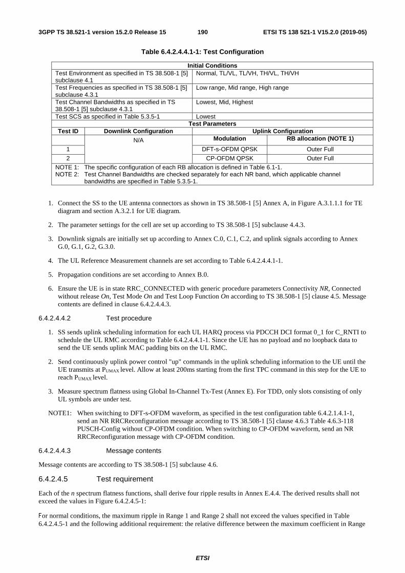
ETSI
ETSI TS 138 521-1 V15.2.0 (2019-05)1903GPP TS 38.521-1 version 15.2.0 Release 15
Table 6.4.2.4.4.1-1: Test Configuration
Initial Conditions Test Environment as specified in TS 38.508-1 [5] subclause 4.1
Normal, TL/VL, TL/VH, TH/VL, TH/VH
Test Frequencies as specified in TS 38.508-1 [5] subclause 4.3.1
Low range, Mid range, High range
Test Channel Bandwidths as specified in TS 38.508-1 [5] subclause 4.3.1
Lowest, Mid, Highest
Test SCS as specified in Table 5.3.5-1 Lowest Test Parameters
Test ID Downlink Configuration Uplink Configuration N/A Modulation RB allocation (NOTE 1)
1 DFT-s-OFDM QPSK Outer Full
2 CP-OFDM QPSK Outer Full
NOTE 1: The specific configuration of each RB allocation is defined in Table 6.1-1. NOTE 2: Test Channel Bandwidths are checked separately for each NR band, which applicable channel
bandwidths are specified in Table 5.3.5-1.
1. Connect the SS to the UE antenna connectors as shown in TS 38.508-1 [5] Annex A, in Figure A.3.1.1.1 for TE diagram and section A.3.2.1 for UE diagram.
2. The parameter settings for the cell are set up according to TS 38.508-1 [5] subclause 4.4.3.
3. Downlink signals are initially set up according to Annex C.0, C.1, C.2, and uplink signals according to Annex G.0, G.1, G.2, G.3.0.
4. The UL Reference Measurement channels are set according to Table 6.4.2.4.4.1-1.
5. Propagation conditions are set according to Annex B.0.
6. Ensure the UE is in state RRC_CONNECTED with generic procedure parameters Connectivity NR, Connected without release On, Test Mode On and Test Loop Function On according to TS 38.508-1 [5] clause 4.5. Message contents are defined in clause 6.4.2.4.4.3.
6.4.2.4.4.2 Test procedure
1. SS sends uplink scheduling information for each UL HARQ process via PDCCH DCI format 0_1 for C_RNTI to schedule the UL RMC according to Table 6.4.2.4.4.1-1. Since the UE has no payload and no loopback data to send the UE sends uplink MAC padding bits on the UL RMC.
2. Send continuously uplink power control "up" commands in the uplink scheduling information to the UE until the UE transmits at PUMAX level. Allow at least 200ms starting from the first TPC command in this step for the UE to reach PUMAX level.
3. Measure spectrum flatness using Global In-Channel Tx-Test (Annex E). For TDD, only slots consisting of only UL symbols are under test.
NOTE1: When switching to DFT-s-OFDM waveform, as specified in the test configuration table 6.4.2.1.4.1-1, send an NR RRCReconfiguration message according to TS 38.508-1 [5] clause 4.6.3 Table 4.6.3-118 PUSCH-Config without CP-OFDM condition. When switching to CP-OFDM waveform, send an NR RRCReconfiguration message with CP-OFDM condition.
6.4.2.4.4.3 Message contents
Message contents are according to TS 38.508-1 [5] subclause 4.6.
6.4.2.4.5 Test requirement
Each of the n spectrum flatness functions, shall derive four ripple results in Annex E.4.4. The derived results shall not exceed the values in Figure 6.4.2.4.5-1:
For normal conditions, the maximum ripple in Range 1 and Range 2 shall not exceed the values specified in Table 6.4.2.4.5-1 and the following additional requirement: the relative difference between the maximum coefficient in Range

ETSI
ETSI TS 138 521-1 V15.2.0 (2019-05)1913GPP TS 38.521-1 version 15.2.0 Release 15
1 and the minimum coefficient in Range 2 must not be larger than 6.4 dB, and the relative difference between the maximum coefficient in Range 2 and the minimum coefficient in Range 1 must not be larger than 8.4 dB (see Figure 6.4.2.4.5-1).
For normal conditions, the peak-to-peak variation of the EVM equalizer coefficients contained within the frequency range of the uplink allocation shall not exceed the maximum ripple specified in Table 6.4.2.4.5-1. For uplink allocations contained within both Range 1 and Range 2, the coefficients evaluated within each of these frequency ranges shall meet the corresponding ripple requirement and the following additional requirement: the relative difference between the maximum coefficient in Range 1 and the minimum coefficient in Range 2 must not be larger than 6.4 dB, and the relative difference between the maximum coefficient in Range 2 and the minimum coefficient in Range 1 must not be larger than 8.4 dB (see Figure 6.4.2.4.5-1).
For extreme conditions, the EVM equalizer spectral flatness shall not exceed the values specified in Table 6.4.2.4.5-2. For uplink allocations contained within both Range 1 and Range 2, the coefficients evaluated within each of these frequency ranges shall meet the corresponding ripple requirement and the following additional requirement: the relative difference between the maximum coefficient in Range 1 and the minimum coefficient in Range 2 must not be larger than 7.4 dB, and the relative difference between the maximum coefficient in Range 2 and the minimum coefficient in Range 1 must not be larger than 11.4 dB (see Figure 6.4.2.4.5-1).
Table 6.4.2.4.5-1: Requirements for EVM equalizer spectrum flatness (normal conditions)
Frequency range Maximum ripple [dB] FUL_Meas – FUL_Low ≥ 3 MHz and FUL_High – FUL_Meas ≥ 3 MHz
(Range 1) 4 + TT (p-p)
FUL_Meas – FUL_Low < 3 MHz or FUL_High – FUL_Meas < 3 MHz (Range 2)
8 + TT (p-p)
NOTE 1: FUL_Meas refers to the sub-carrier frequency for which the equalizer coefficient is evaluated
NOTE 2: FUL_Low and FUL_High refer to each E-UTRA frequency band specified in Table 5.5-1
NOTE 3: Test tolerance TT = 1.4 dB.
Table 6.4.2.4.5-2: Minimum requirements for EVM equalizer spectrum flatness (extreme conditions)
Frequency range Maximum Ripple [dB] FUL_Meas – FUL_Low ≥ 5 MHz and FUL_High – FUL_Meas ≥ 5 MHz
(Range 1) 4 + TT (p-p)
FUL_Meas – FUL_Low < 5 MHz or FUL_High – FUL_Meas < 5 MHz (Range 2)
12 + TT (p-p)
NOTE 1: FUL_Meas refers to the sub-carrier frequency for which the equalizer coefficient is evaluated
NOTE 2: FUL_Low and FUL_High refer to each E-UTRA frequency band specified in Table 5.5-1
NOTE 3: Test tolerance TT = 1.4 dB.

ETSI
ETSI TS 138 521-1 V15.2.0 (2019-05)1923GPP TS 38.521-1 version 15.2.0 Release 15
f FUL_High FUL_High – 3(5) MHz
< 5.4(5.4) dBp-
p
Range 1 Range 2
max(Range 1)-min(Range 2) < 6.4(7.4) dB
max(Range 2)-min(Range 1) < 8.4(11.4) dB < 9.4(13.4) dBp-
p
Figure 6.4.2.4.5-1: The test requirements for EVM equalizer spectral flatness with the maximum allowed variation of the coefficients indicated for unshaped modulations (the ETC test requirements
are within brackets)
6.4.2.5 EVM equalizer spectrum flatness for Pi/2 BPSK
Editor’s note: This clause is incomplete. The following aspects are either missing or not yet determined:
- Whether and, if yes, how to test the requirement on shaping filter is FFS.
6.4.2.5.1 Test purpose
The zero-forcing equalizer correction applied in the EVM measurement process (as described in Annex E) must meet a spectral flatness requirement for the EVM measurement to be valid. The EVM equalizer spectrum flatness is defined in terms of the maximum peak-to-peak ripple of the equalizer coefficients (dB) across the allocated uplink block, at which the equalizer coefficients are generated by the EVM measurement process. The basic measurement interval is the same as for EVM.
6.4.2.5.2 Test applicability
This test case applies to all types of NR UE release 15 and forward indicating support for UE capability [powerBoosting-pi2BPSK].
6.4.2.5.3 Minimum conformance requirements
These requirements apply if the IE powerBoostPi2BPSK is set to 1 for power class 3 capable UE operating in TDD bands n40, n41, n77, n78 and n79 with pi/2 BPSK modulation and UE indicates support for UE capability [powerBoosting-pi2BPSK] and 40 % or less slots in radio frame are used for UL transmission. Otherwise the requirements for EVM equalizer spectrum flatness defined in clause 6.4.2.4.3 apply.
The EVM equalizer coefficients across the allocated uplink block shall be modified to fit inside the mask specified in Table 6.4.2.5.3-1 for normal conditions, prior to the calculation of EVM.
Table 6.4.2.5.3-1: Mask for EVM equalizer coefficients for pi/2 BPSK, normal conditions
Frequency range Parameter Maximum ripple [dB] F_meas – F_center ≤ X MHz or F_center – F_meas ≤ X MHz
(Range 1) X1 6 (p-p)
F_meas – F_center > X MHz or F_center – F_meas > X MHz (Range 2)
X2 14 (p-p)
NOTE 1: F_meas refers to the sub-carrier frequency for which the equalizer coefficient is evaluated NOTE 2: F_center refers to the centre frequency of an allocated block of PRBs NOTE 3: X, in MHz, is equal to 25% of the bandwidth of the PRB allocation NOTE 4: See Figure 6.4.2.4-1 for description of X1, X2
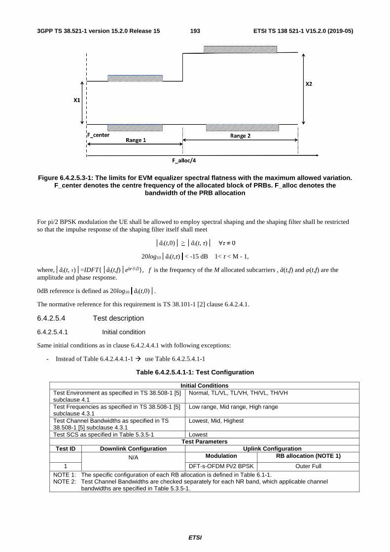
ETSI
ETSI TS 138 521-1 V15.2.0 (2019-05)1933GPP TS 38.521-1 version 15.2.0 Release 15
Figure 6.4.2.5.3-1: The limits for EVM equalizer spectral flatness with the maximum allowed variation. F_center denotes the centre frequency of the allocated block of PRBs. F_alloc denotes the
bandwidth of the PRB allocation
For pi/2 BPSK modulation the UE shall be allowed to employ spectral shaping and the shaping filter shall be restricted so that the impulse response of the shaping filter itself shall meet
│ãt(t,0)│ ≥ │ãt(t, τ)│ ∀τ ≠ 0
20log10│ãt(t,τ)│< -15 dB 1< τ < M - 1,
where,│ãt(t, τ)│=IDFT{│ãt(t,f)│ejφ (t,f)}, f is the frequency of the M allocated subcarriers , ã(t,f) and φ(t,f) are the amplitude and phase response.
0dB reference is defined as 20log10│ãt(t,0)│.
The normative reference for this requirement is TS 38.101-1 [2] clause 6.4.2.4.1.
6.4.2.5.4 Test description
6.4.2.5.4.1 Initial condition
Same initial conditions as in clause 6.4.2.4.4.1 with following exceptions:
- Instead of Table 6.4.2.4.4.1-1 use Table 6.4.2.5.4.1-1
Table 6.4.2.5.4.1-1: Test Configuration
Initial Conditions Test Environment as specified in TS 38.508-1 [5] subclause 4.1
Normal, TL/VL, TL/VH, TH/VL, TH/VH
Test Frequencies as specified in TS 38.508-1 [5] subclause 4.3.1
Low range, Mid range, High range
Test Channel Bandwidths as specified in TS 38.508-1 [5] subclause 4.3.1
Lowest, Mid, Highest
Test SCS as specified in Table 5.3.5-1 Lowest Test Parameters
Test ID Downlink Configuration Uplink Configuration N/A Modulation RB allocation (NOTE 1)
1 DFT-s-OFDM Pi/2 BPSK Outer Full
NOTE 1: The specific configuration of each RB allocation is defined in Table 6.1-1. NOTE 2: Test Channel Bandwidths are checked separately for each NR band, which applicable channel
bandwidths are specified in Table 5.3.5-1.

ETSI
ETSI TS 138 521-1 V15.2.0 (2019-05)1943GPP TS 38.521-1 version 15.2.0 Release 15
6.4.2.5.4.2 Test procedure
1. SS sends uplink scheduling information for each UL HARQ process via PDCCH DCI format 0_1 for C_RNTI to schedule the UL RMC according to Table 6.4.2.4.4.1-1. Since the UE has no payload and no loopback data to send the UE sends uplink MAC padding bits on the UL RMC.
2. Send continuously uplink power control "up" commands in the uplink scheduling information to the UE until the UE transmits at PUMAX level. Allow at least 200ms starting from the first TPC command in this step for the UE to reach PUMAX level.
3. Measure spectrum flatness using Global In-Channel Tx-Test (Annex E). For TDD, only slots consisting of only UL symbols are under test.
6.4.2.5.4.3 Message contents
Message contents are according to TS 38.508-1 [5] subclause 4.6 with the following exception:
Table 6.4.2.5.4.3-1: ServingCellConfig
Derivation Path: TS 38.508-1 [5] clause 4.6.3, Table 4.6.3-167 Information Element Value/remark Comment Condition
uplinkConfig SEQUENCE { initialUplinkBWP BWP-UplinkDedicated uplinkBWP-ToReleaseList Not present uplinkBWP-ToAddModList Not present firstActiveUplinkBWP-Id BWP-Id pusch-ServingCellConfig CHOICE { setup PUSCH-
ServingCellConfig
} carrierSwitching Not present powerBoostPi2BPSK enabled }
6.4.2.5.5 Test requirement
Each of the n spectrum flatness functions, shall derive four ripple results in Annex E.4.4. The derived results shall not exceed the values in Figure 6.4.2.5.5-1:
Table 6.4.2.5.5-1: Mask for EVM equalizer coefficients for pi/2 BPSK, normal conditions
Frequency range Parameter Maximum ripple [dB] F_meas – F_center ≤ X MHz or F_center – F_meas ≤ X MHz
(Range 1) X1 6 + TT (p-p)
F_meas – F_center > X MHz or F_center – F_meas > X MHz (Range 2)
X2 14 + TT (p-p)
NOTE 1: F_meas refers to the sub-carrier frequency for which the equalizer coefficient is evaluated NOTE 2: F_center refers to the centre frequency of an allocated block of PRBs NOTE 3: X, in MHz, is equal to 25% of the bandwidth of the PRB allocation NOTE 4: See Figure 6.4.2.4-1 for description of X1, X2 NOTE 5: Test tolerance TT = 1.4 dB.
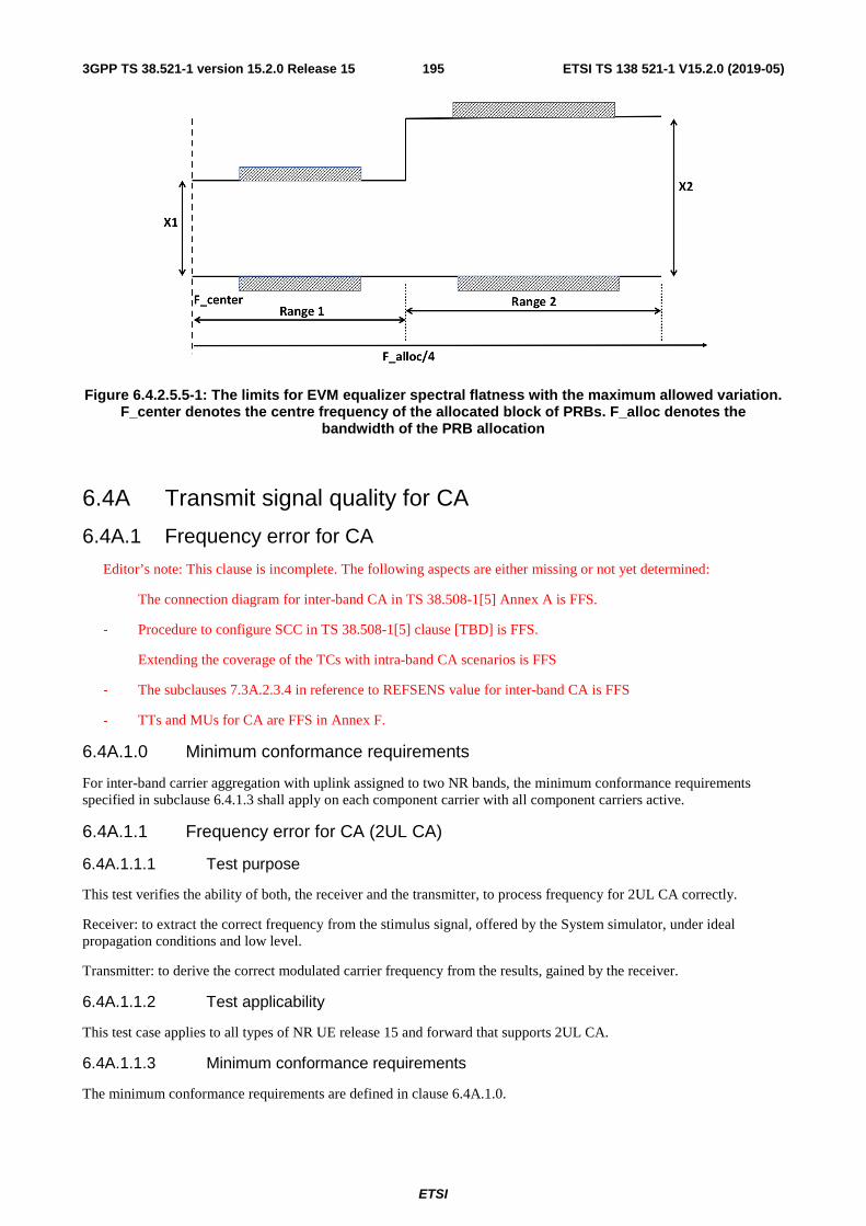
ETSI
ETSI TS 138 521-1 V15.2.0 (2019-05)1953GPP TS 38.521-1 version 15.2.0 Release 15
Figure 6.4.2.5.5-1: The limits for EVM equalizer spectral flatness with the maximum allowed variation. F_center denotes the centre frequency of the allocated block of PRBs. F_alloc denotes the
bandwidth of the PRB allocation
6.4A Transmit signal quality for CA
6.4A.1 Frequency error for CA
Editor’s note: This clause is incomplete. The following aspects are either missing or not yet determined:
- The connection diagram for inter-band CA in TS 38.508-1[5] Annex A is FFS.
- Procedure to configure SCC in TS 38.508-1[5] clause [TBD] is FFS.
- Extending the coverage of the TCs with intra-band CA scenarios is FFS
- The subclauses 7.3A.2.3.4 in reference to REFSENS value for inter-band CA is FFS
- TTs and MUs for CA are FFS in Annex F.
6.4A.1.0 Minimum conformance requirements
For inter-band carrier aggregation with uplink assigned to two NR bands, the minimum conformance requirements specified in subclause 6.4.1.3 shall apply on each component carrier with all component carriers active.
6.4A.1.1 Frequency error for CA (2UL CA)
6.4A.1.1.1 Test purpose
This test verifies the ability of both, the receiver and the transmitter, to process frequency for 2UL CA correctly.
Receiver: to extract the correct frequency from the stimulus signal, offered by the System simulator, under ideal propagation conditions and low level.
Transmitter: to derive the correct modulated carrier frequency from the results, gained by the receiver.
6.4A.1.1.2 Test applicability
This test case applies to all types of NR UE release 15 and forward that supports 2UL CA.
6.4A.1.1.3 Minimum conformance requirements
The minimum conformance requirements are defined in clause 6.4A.1.0.

ETSI
ETSI TS 138 521-1 V15.2.0 (2019-05)1963GPP TS 38.521-1 version 15.2.0 Release 15
6.4A.1.1.4 Test description
6.4A.1.1.4.1 Initial condition
Initial conditions are a set of test configurations the UE needs to be tested in and the steps for the SS to take with the UE to reach the correct measurement state. The initial test configurations consist of environmental conditions, test frequencies, test channel bandwidths and sub-carrier spacing based on NR CA configuration specified in clause 5.5A. All of these configurations shall be tested with applicable test parameters for each CA configuration, and are shown in Table 6.4A.1.1.4.1-1. The details of the uplink and downlink reference measurement channels (RMCs) are specified in Annexes A.2 and A.3. Configurations of PDSCH and PDCCH before measurement are specified in Annex C.2.
Table 6.4A.1.1.4.1-1: Inter band CA Test Configuration Table
Initial Conditions Test Environment as specified in TS 38.508-1 [5] subclause 4.1
Normal, TL/VL, TL/VH, TH/VL, TH/VH
Test Frequencies as specified in TS 38.508-1 [5] subclause4.3.1.1.3 for inter band CA in FR1
Mid range for PCC and SCC
Test Channel Bandwidths as specified in TS 38.508-1 [5] subclause 4.3.1
Highest for both PCC and SCC
Test SCS as specified in Table 5.5A.3-1 Lowest Test Parameters
Downlink Configuration Uplink Configuration Test ID Modulation RB allocation Modulation RB allocation
1 CP-OFDM QPSK
Full RB (NOTE 1) DFT-s-OFDM QPSK REFSENS (NOTE 2)
NOTE 1: Full RB allocation shall be used per each SCS and channel BW as specified in Table 7.3.2.4.1-2. NOTE 2: REFSENS refers to Table 7.3.2.4.1-3 which defines uplink RB configuration and start RB location for
each SCS, channel BW and NR band belongs to inter-band CA combination.
1. Connect the SS to the UE antenna connectors as shown in TS 38.508-1 [5] Annex A, in Figure [TBD] for TE diagram and section A.3.2.1 for UE diagram.
2. The parameter settings for the cell are set up according to TS 38.508-1 [5] subclause4.4.3.
3. Downlink signals for PCC are initially set up according to Annex C.0, C.1, C.2, and uplink signals according to Annex G.0, G.1, G.2, G.3.0.
4. The DL and UL Reference Measurement channels are set according to Table 6.4A.1.1.4.1-1.
5. Propagation conditions are set according to Annex B.0.
6. Ensure the UE is in state RRC_CONNECTED with generic procedure parameters Connectivity NR, Connected without release On, Test Mode On and Test Loop Function On according to TS 38.508-1 [5] clause 4.5. Message contents are defined in clause 6.4A.1.1.4.3
6.4A.1.1.4.2 Test procedure
1. Configure SCC according to Annex C.0, C.1, C.2 for all downlink physical channels.
2. The SS shall configure SCC as per TS 38.508-1 [5] clause [TBD]. Message contents are defined in clause 6.4A.1.1.4.3
3. SS activates SCC by sending the activation MAC CE (Refer TS 38.321 [18], clauses 5.9, 6.1.3.10). Wait for at least 2 seconds (Refer TS 38.133[19], clause 9.3).
4. SS transmits PDSCH via PDCCH DCI format 1_0 for C_RNTI to transmit the DL RMC according to Table6.4A.1.3.4.1-1 on both PCC and SCC. The SS sends downlink MAC padding bits on the DL RMC.
5. SS sends uplink scheduling information for each UL HARQ process via PDCCH DCI format 0_1 for C_RNTI to schedule the UL RMC according to Table 6.4A.1.1.4.1-1 on both PCC and SCC. Since the UL has no payload and no loopback data to send the UE sends uplink MAC padding bits on the UL RMC.
6. Set the Downlink signal level to the appropriate REFSENS value defined in subclauses 7.3A.2.3.4 and 7.3A.4. Send continuously uplink power control "up" commands in every uplink scheduling information to the UE so
ETSI
ETSI TS 138 521-1 V15.2.0 (2019-05)1973GPP TS 38.521-1 version 15.2.0 Release 15
that the UE transmits at PUMAX level for the duration of the test. Allow at least 200ms starting from the first TPC command in this step for the UE to reach PUMAX level.
7. Measure the Frequency Error on PCC and SCC using Global In-Channel Tx-Test (Annex E) respectively. For TDD slots with transient periods are not under test.
NOTE 1: When switching to DFT-s-OFDM waveform, as specified in the test configuration table 6.5.2.2.4.1-1, send an NR RRCReconfiguration message according to TS 38.508-1 [5] clause 4.6.3 Table 4.6.3-118 PUSCH-Config with TRANSFORM_PRECODER_ENABLED condition.
6.4A.1.1.4.3 Message contents
Message contents are according to TS 38.508-1 [5] subclause 4.6.
6.4A.1.1.5 Test requirement
The 20 frequency error Δf results must fulfil the test requirement:
|Δf| ≤ (0.1 PPM + TT) for each test point
where PPM refers to each CC UL frequency.
Table 6.4A.1.1.5-1: Test Tolerance for frequency error
f ≤ 3.0GHz 3.0GHz < f ≤ 6GHz BW ≤ 40MHz FFS FFS
40MHz < BW ≤ 100MHz FFS FFS
6.4A.2 Transmit modulation quality for CA
Editor’s note: This clause is incomplete. The following aspects are either missing or not yet determined:
- The connection diagram for inter-band CA in TS 38.508-1[5] Annex A is FFS.
- Procedure to configure SCC in TS 38.508-1[5] clause [TBD] is FFS
- Extending the coverage of the TCs with intra-band CA scenarios is FFS
- MUs and TTs for CA is FFS in Annex F.
The requirements in this clause apply with PCC and SCC in the UL configured and activated: PCC with PRB allocation and SCC without PRB allocation and without CSI reporting and SRS configured.
6.4A.2.1 Error Vector Magnitude for CA
6.4A.2.1.0 Minimum conformance requirements
For Inter-band carrier aggregation, EVM measurements are evaluated for each component carrier, and for the different modulations schemes, the EVM requirements shall not exceed the values specified in Table 6.4A.2.1.0-1 for the parameters defined in Table 6.4A.2.1. 0-2, if CA is configured in uplink.
Table 6.4A.2.1.0-1: Requirements for Error Vector Magnitude
Parameter Unit Average EVM Level Pi/2-BPSK % 30 QPSK % 17.5 16QAM % 12.5 64QAM % 8 256 QAM % 3.5
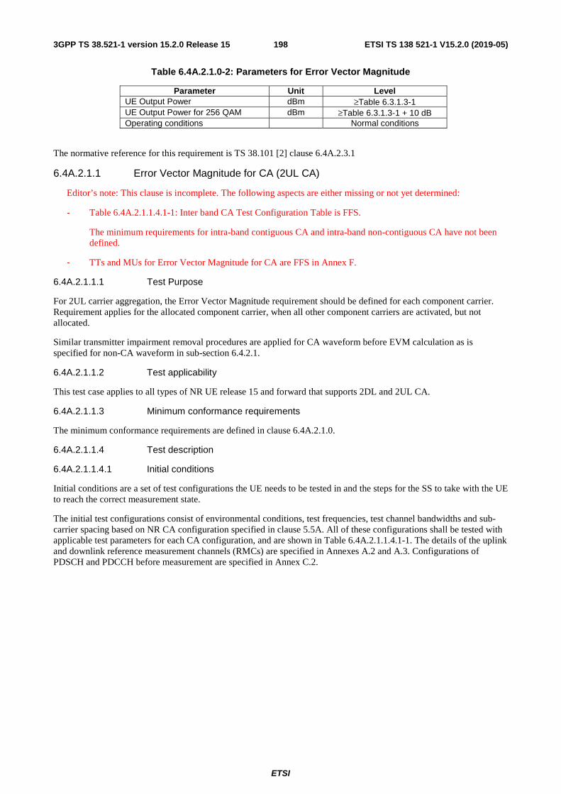
ETSI
ETSI TS 138 521-1 V15.2.0 (2019-05)1983GPP TS 38.521-1 version 15.2.0 Release 15
Table 6.4A.2.1.0-2: Parameters for Error Vector Magnitude
Parameter Unit Level UE Output Power dBm ≥Table 6.3.1.3-1 UE Output Power for 256 QAM dBm ≥Table 6.3.1.3-1 + 10 dB Operating conditions Normal conditions
The normative reference for this requirement is TS 38.101 [2] clause 6.4A.2.3.1
6.4A.2.1.1 Error Vector Magnitude for CA (2UL CA)
Editor’s note: This clause is incomplete. The following aspects are either missing or not yet determined:
- Table 6.4A.2.1.1.4.1-1: Inter band CA Test Configuration Table is FFS.
- The minimum requirements for intra-band contiguous CA and intra-band non-contiguous CA have not been defined.
- TTs and MUs for Error Vector Magnitude for CA are FFS in Annex F.
6.4A.2.1.1.1 Test Purpose
For 2UL carrier aggregation, the Error Vector Magnitude requirement should be defined for each component carrier. Requirement applies for the allocated component carrier, when all other component carriers are activated, but not allocated.
Similar transmitter impairment removal procedures are applied for CA waveform before EVM calculation as is specified for non-CA waveform in sub-section 6.4.2.1.
6.4A.2.1.1.2 Test applicability
This test case applies to all types of NR UE release 15 and forward that supports 2DL and 2UL CA.
6.4A.2.1.1.3 Minimum conformance requirements
The minimum conformance requirements are defined in clause 6.4A.2.1.0.
6.4A.2.1.1.4 Test description
6.4A.2.1.1.4.1 Initial conditions
Initial conditions are a set of test configurations the UE needs to be tested in and the steps for the SS to take with the UE to reach the correct measurement state.
The initial test configurations consist of environmental conditions, test frequencies, test channel bandwidths and sub-carrier spacing based on NR CA configuration specified in clause 5.5A. All of these configurations shall be tested with applicable test parameters for each CA configuration, and are shown in Table 6.4A.2.1.1.4.1-1. The details of the uplink and downlink reference measurement channels (RMCs) are specified in Annexes A.2 and A.3. Configurations of PDSCH and PDCCH before measurement are specified in Annex C.2.
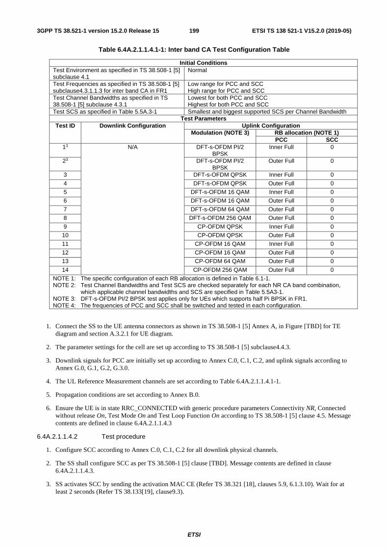
ETSI
ETSI TS 138 521-1 V15.2.0 (2019-05)1993GPP TS 38.521-1 version 15.2.0 Release 15
Table 6.4A.2.1.1.4.1-1: Inter band CA Test Configuration Table
Initial Conditions Test Environment as specified in TS 38.508-1 [5] subclause 4.1
Normal
Test Frequencies as specified in TS 38.508-1 [5] subclause4.3.1.1.3 for inter band CA in FR1
Low range for PCC and SCC High range for PCC and SCC
Test Channel Bandwidths as specified in TS 38.508-1 [5] subclause 4.3.1
Lowest for both PCC and SCC Highest for both PCC and SCC
Test SCS as specified in Table 5.5A.3-1 Smallest and biggest supported SCS per Channel Bandwidth Test Parameters
Test ID Downlink Configuration Uplink Configuration Modulation (NOTE 3) RB allocation (NOTE 1)
PCC SCC 13 N/A DFT-s-OFDM PI/2
BPSK Inner Full 0
23 DFT-s-OFDM PI/2 BPSK
Outer Full 0
3 DFT-s-OFDM QPSK Inner Full 0
4 DFT-s-OFDM QPSK Outer Full 0
5 DFT-s-OFDM 16 QAM Inner Full 0
6 DFT-s-OFDM 16 QAM Outer Full 0
7 DFT-s-OFDM 64 QAM Outer Full 0
8 DFT-s-OFDM 256 QAM Outer Full 0
9 CP-OFDM QPSK Inner Full 0
10 CP-OFDM QPSK Outer Full 0
11 CP-OFDM 16 QAM Inner Full 0
12 CP-OFDM 16 QAM Outer Full 0
13 CP-OFDM 64 QAM Outer Full 0
14 CP-OFDM 256 QAM Outer Full 0
NOTE 1: The specific configuration of each RB allocation is defined in Table 6.1-1. NOTE 2: Test Channel Bandwidths and Test SCS are checked separately for each NR CA band combination,
which applicable channel bandwidths and SCS are specified in Table 5.5A3-1. NOTE 3: DFT-s-OFDM PI/2 BPSK test applies only for UEs which supports half Pi BPSK in FR1. NOTE 4: The frequencies of PCC and SCC shall be switched and tested in each configuration.
1. Connect the SS to the UE antenna connectors as shown in TS 38.508-1 [5] Annex A, in Figure [TBD] for TE diagram and section A.3.2.1 for UE diagram.
2. The parameter settings for the cell are set up according to TS 38.508-1 [5] subclause4.4.3.
3. Downlink signals for PCC are initially set up according to Annex C.0, C.1, C.2, and uplink signals according to Annex G.0, G.1, G.2, G.3.0.
4. The UL Reference Measurement channels are set according to Table 6.4A.2.1.1.4.1-1.
5. Propagation conditions are set according to Annex B.0.
6. Ensure the UE is in state RRC_CONNECTED with generic procedure parameters Connectivity NR, Connected without release On, Test Mode On and Test Loop Function On according to TS 38.508-1 [5] clause 4.5. Message contents are defined in clause 6.4A.2.1.1.4.3
6.4A.2.1.1.4.2 Test procedure
1. Configure SCC according to Annex C.0, C.1, C.2 for all downlink physical channels.
2. The SS shall configure SCC as per TS 38.508-1 [5] clause [TBD]. Message contents are defined in clause 6.4A.2.1.1.4.3.
3. SS activates SCC by sending the activation MAC CE (Refer TS 38.321 [18], clauses 5.9, 6.1.3.10). Wait for at least 2 seconds (Refer TS 38.133[19], clause9.3).

ETSI
ETSI TS 138 521-1 V15.2.0 (2019-05)2003GPP TS 38.521-1 version 15.2.0 Release 15
4. SS sends uplink scheduling information for each UL HARQ process via PDCCH DCI format 0_1 for C_RNTI to schedule the UL RMC according to Table 6.4A.2.1.1.4.1-1. Since the UE has no payload data to send, the UE transmits uplink MAC padding bits on the UL RMC.
5. Send continuously uplink power control "up" commands in the uplink scheduling information to the UE until the UE transmits at PUMAX level, allow at least 200ms starting from the first TPC command in this step for the UE to reach PUMAX level.
6. Measure the EVM and DMRSEVM on PCC using Global In-Channel Tx-Test (Annex E).
7. For modulations except 256QAM, send the appropriate TPC commands in the uplink scheduling information to the UE until UE output power is in the range Pmin + PW± PW, where Pmin is the minimum output power according to Table 6.3.1.3-1 and PW is the power window according to Table 6.4.2.1.4.2-1 for the carrier frequency f and the channel bandwidth BW. For 256 QAM, send the appropriate TPC commands in the uplink scheduling information to the UE until UE output power is in the range Pmin + 10 dB + PW ± PW, where Pmin is the minimum output power according to Table 6.3.1.3-1 and PW is the power window according to Table 6.4.2.1.4.2-1 for the carrier frequency f and the channel bandwidth BW..
8. Measure the EVM and DMRSEVM on PCC using Global In-Channel Tx-Test (Annex E).
NOTE 1: When switching to DFT-s-OFDM waveform, as specified in the test configuration table 6.5.2.2.4.1-1, send an NR RRCReconfiguration message according to TS 38.508-1 [5] clause 4.6.3 Table 4.6.3-118 PUSCH-Config with TRANSFORM_PRECODER_ENABLED condition.
6.4A.2.1.1.4.3 Message contents
Message contents are according to TS 38.508-1 [5] subclause 4.6.
6.4A.2.1.1.5 Test requirement
The PUSCH EVM, derived in Annex E.4.2, shall not exceed the values in Table 6.4A.2.1.1.5-1.
The PUSCH DMRSEVM ,derived in Annex E.4.6.2, shall not exceed the values in Table 6.4A.2.1.1.5-1 when embedded with data symbols of the respective modulation scheme.
Table 6.4A.2.1.1.5-1: Test requirements for Error Vector Magnitude
Parameter Unit Average EVM Level Pi/2-BPSK % 30+TT QPSK % 17.5+TT 16QAM % 12.5+TT 64QAM % 8+TT 256 QAM % 3.8+TT for 15 dBm< PUL
4.3+TT for -25 dBm< PUL≤ 15 dBm 4.6+TT for -40dBm ≤ PUL≤ -25dBm
Table 6.4A.2.1.1.5-2: Test Tolerance for Error Vector Magnitude
f ≤ 3.0GHz 3.0GHz < f ≤ 6GHz BW ≤ 40MHz FFS FFS
40MHz < BW ≤ 100MHz FFS FFS
6.4A.2.2 Carrier leakage for CA
6.4A.2.2.0 Minimum conformance requirements
6.4A.2.2.0.1 Minimum conformance requirements for intra-band contiguous CA
FFS

ETSI
ETSI TS 138 521-1 V15.2.0 (2019-05)2013GPP TS 38.521-1 version 15.2.0 Release 15
6.4A.2.2.0.2 Minimum conformance requirements for intra-band non-contiguous CA
FFS
6.4A.2.2.0.3 Minimum conformance requirements for inter-band CA
For inter-band carrier aggregation, the carrier leakage shall not exceed the values specified in Table 6.4A.2.2.0.3-1.
In the case that uplink sharing, the carrier leakage may have 7.5 kHz shift with the carrier frequency.
Table 6.4A.2.2.0.3-1: Requirements for carrier leakage
Parameter description Unit Limit Applicable
Frequencies
Carrier leakage dBc
-28 Output power > 10 dBm Carrier leakage
frequency (NOTES 1, 2)
-25 0 dBm ≤ Output power ≤10 dBm -20 -30 dBm ≤ Output power ≤ 0 dBm -10 -40 dBm ≤ Output power < -30 dBm
NOTE 1: The measurement bandwidth is 1 RB and the limit is expressed as a ratio of measured power in one non-allocated RB to the measured total power in all allocated RBs.
NOTE 2: The applicable frequencies for this limit are those that are enclosed in the RBs containing the carrier
leakage frequency if RBN is odd, or in the two RBs immediately adjacent to the carrier leakage frequency
if RBN is even but excluding any allocated RB.
The normative reference for this requirement is TS 38.101-1 [2] clauses 6.4A.2.3.
6.4A.2.2.1 Carrier leakage for CA (2UL CA)
Editor’s note: This clause is incomplete. The following aspects are either missing or not yet determined:
- Table 6.4A.2.2.1.4.1-1: Inter band CA Test Configuration Table is FFS.
- The minimum requirements for intra-band contiguous CA and intra-band non-contiguous CA have not been defined.
- TTs and MUs for Error Vector Magnitude for CA are FFS in Annex F.
6.4A.2.2.1.1 Test purpose
Carrier leakage is an additive sinusoid waveform that is confined within the aggregated transmission bandwidth configuration. The carrier leakage requirement for 2UL CA is defined for each component carrier and is measured on the component carrier with PRBs allocated.
6.4A.2.2.1.2 Test applicability
This test case applies to all types of NR UE release 15 and forward that supports 2DL and 2UL CA.
6.4A.2.2.1.3 Minimum conformance requirements
The minimum conformance requirements are defined in clause 6.4A.2.2.0.
6.4A.2.2.1.4 Test description
6.4A.2.2.1.4.1 Initial condition
Initial conditions are a set of test configurations the UE needs to be tested in and the steps for the SS to take with the UE to reach the correct measurement state.
The initial test configurations consist of environmental conditions, test frequencies, test channel bandwidths and sub-carrier spacing based on NR CA configuration specified in clause 5.5A. All of these configurations shall be tested with applicable test parameters for each CA configuration, and are shown in Table 6.4A.2.2.1.4.1-1. The details of the uplink and downlink reference measurement channels (RMCs) are specified in Annexes A.2 and A.3. Configurations of PDSCH and PDCCH before measurement are specified in Annex C.2.

ETSI
ETSI TS 138 521-1 V15.2.0 (2019-05)2023GPP TS 38.521-1 version 15.2.0 Release 15
Table 6.4A.2.2.1.4.1-1: Inter band CA Test Configuration Table
Initial Conditions Test Environment as specified in TS 38.508-1 [5] subclause 4.1
Normal
Test Frequencies as specified in TS 38.508-1 [5] subclause4.3.1.1.3 for inter band CA in FR1
Low range for PCC and SCC High range for PCC and SCC
Test Channel Bandwidths as specified in TS 38.508-1 [5] subclause 4.3.1
Mid for both PCC and SCC
Test SCS as specified in Table 5.5A.3-1 Smallest supported SCS per Channel Bandwidth Test Parameters
Test ID Downlink Configuration Uplink Configuration Modulation RB allocation (NOTE 1, 3)
PCC SCC 1 N/A DFT-s-OFDM QPSK Inner_1RB_Left 0
NOTE 1: The specific configuration of each RB allocation is defined in Table 6.1-1. NOTE 2: Test Channel Bandwidths and Test SCS are checked separately for each NR CA band combination,
which applicable channel bandwidths and SCS are specified in Table 5.5A3-1. NOTE 3: When the signalled DC carrier position is at Inner_1RB_Left, use Inner_1RB_Right for UL RB allocation. NOTE 4: The frequencies of PCC and SCC shall be switched and tested in each configuration.
1. Connect the SS to the UE antenna connectors as shown in TS 38.508-1 [5] Annex A, in Figure [TBD] for TE diagram and section A.3.2.1 for UE diagram.
2. The parameter settings for the cell are set up according to TS 38.508-1 [5] subclause4.4.3.
3. Downlink signals for PCC are initially set up according to AnnexC.0, C.1, C.2 and uplink signals according to Annex G.0, G.1, G.2, G.3.0.
4. The UL Reference Measurement channels are set according to Table 6.4A.2.2.1.4.1-1.
5. Propagation conditions are set according to Annex B.0.
6. Ensure the UE is in state RRC_CONNECTED with generic procedure parameters Connectivity NR, Connected without release On, Test Mode On and Test Loop Function On according to TS 38.508-1 [5] clause 4.5. Message contents are defined in clause 6.4A.2.2.1.4.3.
6.4A.2.2.1.4.2 Test procedure
1. Configure SCC according to Annex C.0, C.1, C.2 for all downlink physical channels.
2. The SS shall configure SCC as per TS 38.508-1 [5] clause [TBD]. Message contents are defined in clause 6.4A.2.2.1.4.3.
3. SS activates SCC by sending the activation MAC CE (Refer TS 38.321 [18], clauses 5.9, 6.1.3.10). Wait for at least 2 seconds (Refer TS 38.133[19], clause9.3).
4. SS sends uplink scheduling information for each UL HARQ process via PDCCH DCI format [0_1] for C_RNTI to schedule the UL RMC according to Table 6.4A.2.2.1.4.1-1. Since the UE has no payload and no loopback data to send the UE sends uplink MAC padding bits on the UL RMC.
5. Send the appropriate TPC commands in the uplink scheduling information to the UE until UE output power is 10 + PWdBm±PW dB where PW is the power window according to Table 6.4A.2.2.1.4.2-1 for the carrier frequency f and the channel bandwidth BW.
6. Measure carrier leakage using Global In-Channel Tx-Test (Annex E). For TDD slots with transient periods are not under test.
7. Send the appropriate TPC commands in the uplink scheduling information to the UE until UE output power is 0 + PWdBm±PW dB where PW is the power window according to Table 6.4A.2.2.1.4.2-1 for the carrier frequency f and the channel bandwidth BW.
8. Measure carrier leakage on PCC using Global In-Channel Tx-Test (Annex E). For TDD slots with transient periods are not under test.

ETSI
ETSI TS 138 521-1 V15.2.0 (2019-05)2033GPP TS 38.521-1 version 15.2.0 Release 15
9. Send the appropriate TPC commands in the uplink scheduling information to the UE until UE output power is -30 + PWdBm±PW dB where PW is the power window according to Table 6.4A.2.2.1.4.2-2 for the carrier frequency f and the channel bandwidth BW.
10. Measure carrier leakage on PCC using Global In-Channel Tx-Test (Annex E). For TDD slots with transient periods are not under test.
11. Send the appropriate TPC commands in the uplink scheduling information to the UE until UE output power is -40 + PWdBm±PW dB where PW is the power window according to Table 6.4A.2.2.1.4.2-2 for the carrier frequency f and the channel bandwidth BW.
12. Measure carrier leakage on PCC using Global In-Channel Tx-Test (Annex E). For TDD slots with transient periods are not under test.
NOTE 1: When switching to DFT-s-OFDM waveform, as specified in the test configuration table 6.5.2.2.4.1-1, send an NR RRCReconfiguration message according to TS 38.508-1 [5] clause 4.6.3 Table 4.6.3-118 PUSCH-Config with TRANSFORM_PRECODER_ENABLED condition
Table 6.4A.2.2.1.4.2-1: Power Window (dB) for carrier leakage (step 5 and step 7)
f ≤ 3GHz 3GHz < f ≤ 4.2GHz 4.2GHz < f ≤ 6GHz BW ≤ 20MHz [1.4] [1.7] [2] 20MHz < BW ≤ 40MHz [1.4] [1.7] [2.2] 40MHz < BW ≤ 100MHz [2.1] [2.3] [2.3]
Table 6.4A.2.2.1.4.2-2: Power Window (dB) for carrier leakage (step 9 and step 11)
f ≤ 3GHz 3GHz < f ≤ 4.2GHz 4.2GHz < f ≤ 6GHz BW ≤ 40MHz [1.7] [2.0] [2.2] 40MHz < BW ≤ 100MHz [2.1] [2.3] [2.5]
6.4A.2.2.1.4.3 Message contents
Message contents are according to TS 38.508-1 [5] subclause 4.6.
6.4A.2.2.1.5 Test requirement
Each of the [20] carrier leakage results, derived in Annex E.3.1, shall not exceed the values in table 6.4A.2.2.1.5-1. Allocated RBs are not under test.

ETSI
ETSI TS 138 521-1 V15.2.0 (2019-05)2043GPP TS 38.521-1 version 15.2.0 Release 15
Table 6.4A.2.2.1.5-1: Test requirements for Carrier Leakage
LO Leakage Parameters UE output power
Relative limit (dBc)
10 + PWdBm±PW dB5 -27.2+TT 0 + PWdBm±PW dB5 -24.2+TT
-30 + PWdBm±PW dB6 -19.2+TT -40 + PWdBm±PW dB6 -9.2+TT
NOTE 1: The measurement bandwidth is 1 RB and the limit is expressed as a ratio of measured power in one non-allocated RB to the measured total power in all allocated RBs.
NOTE 2: The applicable frequencies for this limit are those that are enclosed in the RBs containing the carrier leakage frequency
if RBN is odd, or in the two RBs immediately adjacent to the
carrier leakage frequency if RBN is even but excluding any
allocated RB.
NOTE 3: RBN is the Transmission Bandwidth Configuration (see
Figure 5.3.3).
NOTE 4: RBP is the transmitted power normalized by the number of allocated RBs, measured in dBm.
NOTE 5: PW is the power window according to Table 6.4A.2.3.2.4.2-1 for the carrier frequency f and the channel bandwidth BW.
NOTE 6: PW is the power window according to Table 6.4A.2.3.2.4.2-2 for the carrier frequency f and the channel bandwidth BW.
Table 6.4A.2.2.1.5-2: Test Tolerance for Carrier Leakage
f ≤ 3.0GHz 3.0GHz < f ≤ 6GHz BW ≤ 40MHz FFS FFS
40MHz < BW ≤ 100MHz FFS FFS
6.4A.2.3 In-band emission for CA
6.4A.2.3.0 Minimum conformance requirements
For inter-band carrier aggregation with uplink assigned to two NR bands, the requirements shall apply on each component carrier as defined in clause 6.4.2 with all component carriers active.
The requirements in Table 6.4A.2.3.0-1 apply with PCC and SCC in the UL configured and activated: PCC with PRB allocation and SCC without PRB allocation and without CSI reporting and SRS configured.
Table 6.4A.2.3.0-1: Inter band CA Requirements for in-band emissions
Parameter description Unit Limit (NOTE 1) Applicable
Frequencies
General dB
{
( ) }RB
CRBRB
CRBRB
PkHzSCSdBm
LEVM
LN
−+−−Δ⋅−−⋅
⋅−−
15/log1057
,/)1(53log20
),/(log1025max
10
10
10
Any non-allocated (NOTE 2)
IQ Image dB -28 Image frequencies when output power > 10 dBm Image
frequencies (NOTES 2, 3) -25 Image frequencies when output power ≤ 10 dBm
Carrier leakage dBc
-28 Output power > 10 dBm Carrier leakage
frequency (NOTES 4, 5)
-25 0 dBm ≤ Output power ≤10 dBm -20 -30 dBm ≤ Output power ≤ 0 dBm -10 -40 dBm≤ Output power < -30 dBm

ETSI
ETSI TS 138 521-1 V15.2.0 (2019-05)2053GPP TS 38.521-1 version 15.2.0 Release 15
NOTE 1: An in-band emissions combined limit is evaluated in each non-allocated RB. For each such RB, the minimum requirement is calculated as the higher of PRB - 30 dB and the power sum of all limit values (General, IQ Image or Carrier leakage) that apply. PRB is defined in NOTE 10.
NOTE 2: The measurement bandwidth is 1 RB and the limit is expressed as a ratio of measured power in one non-allocated RB to the measured average power per allocated RB, where the averaging is done across all allocated RBs.
NOTE 3: The applicable frequencies for this limit are those that are enclosed in the reflection of the allocated bandwidth, based on symmetry with respect to the carrier leakage frequency, but excluding any allocated RBs.
NOTE 4: The measurement bandwidth is 1 RB and the limit is expressed as a ratio of measured power in one non-allocated RB to the measured total power in all allocated RBs.
NOTE 5: The applicable frequencies for this limit are those that are enclosed in the RBs containing the carrier
leakage frequency if RBN is odd, or in the two RBs immediately adjacent to the carrier leakage frequency
if RBN is even but excluding any allocated RB.
NOTE 6: CRBL is the Transmission Bandwidth (see Figure 5.3.3).
NOTE 7: RBN is the Transmission Bandwidth Configuration (see Figure 5.3.3).
NOTE 8: EVM is the limit specified in Table 6.4A.2.3.1.3-1 for the modulation format used in the allocated RBs. NOTE 9: RBΔ is the starting frequency offset between the allocated RB and the measured non-allocated RB (e.g.
1=ΔRB or 1−=ΔRB for the first adjacent RB outside of the allocated bandwidth.
NOTE 10: RBP is the transmitted power normalized by the number of allocated RBs, measured in dBm.
The normative reference for this requirement is TS 38.101-1 [2] clause 6.4A.2.3.
6.4A.2.3.1 In-band emissions for CA (2UL CA)
6.4A.2.3.1.1 Test purpose
The in-band emissions are a measure of the interference falling into the non-allocated resources blocks.
For an allocated component carrier, the in-band emission is defined as the average across 12 sub-carrier and as a function of the RB offset from the edge of the allocated UL transmission bandwidth. The in-band emission is measured as the ratio of the UE output power in a non–allocated RB to the UE output power in an allocated RB. The basic in-band emissions measurement interval is defined over one slot in the time domain, however, the minimum requirement applies when the in-band emission measurement is averaged over 10 sub-frames. When the PUSCH or PUCCH transmission slot is shortened due to multiplexing with SRS, the in-band emissions measurement interval is reduced by one or more symbols, accordingly.
For a non allocated component carrier a spectral measurement is specified.
6.4A.2.3.1.2 Test applicability
This test case applies to all types of NR UE release 15 and forward that supports 2DL and 2UL CA.
6.4A.2.3.1.3 Minimum conformance requirements
The minimum conformance requirements are defined in clause 6.4A.2.3.0.
6.4A.2.3.1.4 Test description
6.4A.2.3.1.4.1 Initial condition
Initial conditions are a set of test configurations the UE needs to be tested in and the steps for the SS to take with the UE to reach the correct measurement state.
The initial test configurations consist of environmental conditions, test frequencies, test channel bandwidths and sub-carrier spacing based on NR CA configuration specified in clause 5.5A. All of these configurations shall be tested with applicable test parameters for each CA configuration, and are shown in Table 6.4A.2.3.1.4.1-1. The details of the uplink and downlink reference measurement channels (RMCs) are specified in Annexes A.2 and A.3. Configurations of PDSCH and PDCCH before measurement are specified in Annex C.2.

ETSI
ETSI TS 138 521-1 V15.2.0 (2019-05)2063GPP TS 38.521-1 version 15.2.0 Release 15
Table 6.4A.2.3.1.4.1-1: Test Configuration Table
Initial Conditions Test Environment as specified in TS 38.508-1 [5] subclause 4.1
Normal
Test Frequencies as specified in TS 38.508-1 [5] subclause4.3.1.1.3 for inter band CA in FR1
Low range for PCC and SCC High range for PCC and SCC
Test Channel Bandwidths as specified in TS 38.508-1 [5] subclause 4.3.1
Lowest for both PCC and SCC Highest for both PCC and SCC
Test SCS as specified in Table 5.5A.3-1 Smallest supported SCS per Channel Bandwidth Test Parameters
Test ID Downlink Configuration Uplink Configuration Modulation RB allocation (NOTE 1)
PCC SCC 1 N/A DFT-s-OFDM QPSK Inner_1RB_Left 0
2 DFT-s-OFDM QPSK Inner_1RB_Right 0
3 CP-OFDM QPSK Inner_1RB_Left 0
4 CP-OFDM QPSK Inner_1RB_Right 0
NOTE 1: The specific configuration of each RB allocation is defined in Table 6.1-1. NOTE 2: Test Channel Bandwidths are checked separately for each NR band, which applicable channel
bandwidths are specified in Table 5.5A3-1. NOTE 3: The frequencies of PCC and SCC shall be switched and tested in each configuration.
1. Connect the SS to the UE antenna connectors as shown in TS 38.508-1 [5] Annex A, in Figure [TBD] for TE diagram and section A.3.2.1 for UE diagram.
2. The parameter settings for the cell are set up according to TS 38.508-1 [5] subclause4.4.3.
3. Downlink signals for PCC are initially set up according to Annex C.0, C.1, C.2, and uplink signals according to Annex G.0, G.1, G.2, G.3.0.
4. The UL Reference Measurement channels are set according to Table 6.4A.2.3.1.4.1-1.
5. Propagation conditions are set according to Annex B.0.
6. Ensure the UE is in state RRC_CONNECTED with generic procedure parameters Connectivity NR, Connected without release On, Test Mode On and Test Loop Function On according to TS 38.508-1 [5] clause 4.5. Message contents are defined in clause 6.4A.2.3.1.4.3.
6.4A.2.3.1.4.2 Test procedure
1. Configure SCC according to Annex C.0, C.1, C.2 for all downlink physical channels.
2. The SS shall configure SCC as per TS 38.508-1 [5] clause [TBD]. Message contents are defined in clause 6.4A.2.3.1.4.3.
3. SS activates SCC by sending the activation MAC CE (Refer TS 38.321 [18], clauses 5.9, 6.1.3.10). Wait for at least 2 seconds (Refer TS 38.133[19], clause9.3).
4. SS sends uplink scheduling information for each UL HARQ process via PDCCH DCI format 1_0 for C_RNTI to schedule the UL RMC according to Table 6.4A.2.3.1.4.1-1. Since the UE has no payload and no loopback data to send the UE sends uplink MAC padding bits on the UL RMC.
5. Send the appropriate TPC commands in the uplink scheduling information to the UE until UE output power is 10 + PWdBm±PW dB where PW is the power window according to Table 6.4A.2.3.1.4.2-1 for the carrier frequency f and the channel bandwidth BW.
6. Measure In-band emission on PCC using Global In-Channel Tx-Test (Annex E). Measure power spectral density on the SCC. For TDD slots with transient periods are not under test.
7. Send the appropriate TPC commands in the uplink scheduling information to the UE until UE output power is 0 + PWdBm±PW dB where PW is the power window according to Table 6.4A.2.3.1.4.2-1 for the carrier frequency f and the channel bandwidth BW.
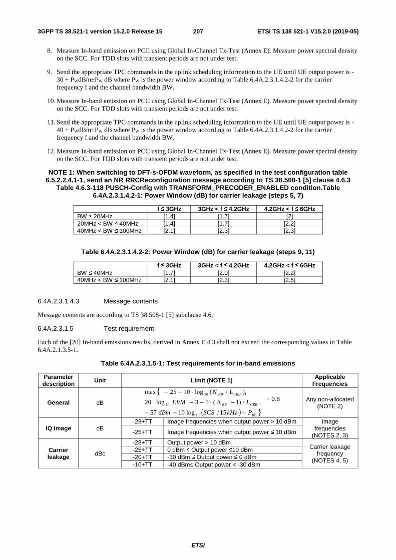
ETSI
ETSI TS 138 521-1 V15.2.0 (2019-05)2073GPP TS 38.521-1 version 15.2.0 Release 15
8. Measure In-band emission on PCC using Global In-Channel Tx-Test (Annex E). Measure power spectral density on the SCC. For TDD slots with transient periods are not under test.
9. Send the appropriate TPC commands in the uplink scheduling information to the UE until UE output power is -30 + PWdBm±PW dB where PW is the power window according to Table 6.4A.2.3.1.4.2-2 for the carrier frequency f and the channel bandwidth BW.
10. Measure In-band emission on PCC using Global In-Channel Tx-Test (Annex E). Measure power spectral density on the SCC. For TDD slots with transient periods are not under test.
11. Send the appropriate TPC commands in the uplink scheduling information to the UE until UE output power is -40 + PWdBm±PW dB where PW is the power window according to Table 6.4A.2.3.1.4.2-2 for the carrier frequency f and the channel bandwidth BW.
12. Measure In-band emission on PCC using Global In-Channel Tx-Test (Annex E). Measure power spectral density on the SCC. For TDD slots with transient periods are not under test.
NOTE 1: When switching to DFT-s-OFDM waveform, as specified in the test configuration table 6.5.2.2.4.1-1, send an NR RRCReconfiguration message according to TS 38.508-1 [5] clause 4.6.3
Table 4.6.3-118 PUSCH-Config with TRANSFORM_PRECODER_ENABLED condition.Table 6.4A.2.3.1.4.2-1: Power Window (dB) for carrier leakage (steps 5, 7)
f ≤ 3GHz 3GHz < f ≤ 4.2GHz 4.2GHz < f ≤ 6GHz BW ≤ 20MHz [1.4] [1.7] [2] 20MHz < BW ≤ 40MHz [1.4] [1.7] [2.2] 40MHz < BW ≤ 100MHz [2.1] [2.3] [2.3]
Table 6.4A.2.3.1.4.2-2: Power Window (dB) for carrier leakage (steps 9, 11)
f ≤ 3GHz 3GHz < f ≤ 4.2GHz 4.2GHz < f ≤ 6GHz BW ≤ 40MHz [1.7] [2.0] [2.2] 40MHz < BW ≤ 100MHz [2.1] [2.3] [2.5]
6.4A.2.3.1.4.3 Message contents
Message contents are according to TS 38.508-1 [5] subclause 4.6.
6.4A.2.3.1.5 Test requirement
Each of the [20] In-band emissions results, derived in Annex E.4.3 shall not exceed the corresponding values in Table 6.4A.2.1.3.5-1.
Table 6.4A.2.3.1.5-1: Test requirements for in-band emissions
Parameter description Unit Limit (NOTE 1) Applicable
Frequencies
General dB
{
( ) }RB
CRBRB
CRBRB
PkHzSCSdBm
LEVM
LN
−+−−Δ⋅−−⋅
⋅−−
15/log1057
,/)1(53log20
),/(log1025max
10
10
10
+ 0.8 Any non-allocated (NOTE 2)
IQ Image dB -28+TT Image frequencies when output power > 10 dBm Image
frequencies (NOTES 2, 3) -25+TT Image frequencies when output power ≤ 10 dBm
Carrier leakage dBc
-28+TT Output power > 10 dBm Carrier leakage
frequency (NOTES 4, 5)
-25+TT 0 dBm ≤ Output power ≤10 dBm -20+TT -30 dBm ≤ Output power ≤ 0 dBm -10+TT -40 dBm≤ Output power < -30 dBm

ETSI
ETSI TS 138 521-1 V15.2.0 (2019-05)2083GPP TS 38.521-1 version 15.2.0 Release 15
NOTE 1: An in-band emissions combined limit is evaluated in each non-allocated RB. For each such RB, the minimum requirement is calculated as the higher of PRB - 30 dB and the power sum of all limit values (General, IQ Image or Carrier leakage) that apply. PRBis defined in NOTE 10.
NOTE 2: The measurement bandwidth is 1 RB and the limit is expressed as a ratio of measured power in one non-allocated RB to the measured average power per allocated RB, where the averaging is done across all allocated RBs.
NOTE 3: The applicable frequencies for this limit are those that are enclosed in the reflection of the allocated bandwidth, based on symmetry with respect to the carrier leakage frequency, but excluding any allocated RBs.
NOTE 4: The measurement bandwidth is 1 RB and the limit is expressed as a ratio of measured power in one non-allocated RB to the measured total power in all allocated RBs.
NOTE 5: The applicable frequencies for this limit are those that are enclosed in the RBs containing the carrier
leakage frequency if RBN is odd, or in the two RBs immediately adjacent to the carrier leakage frequency
if RBN is even, but excluding any allocated RB.
NOTE 6: CRBL is the Transmission Bandwidth (see Figure 5.3.3).
NOTE 7: RBN is the Transmission Bandwidth Configuration (see Figure 5.3.3).
NOTE 8: EVM is the limit specified in Table 6.4.2.1.3-1 for the modulation format used in the allocated RBs. NOTE 9: RBΔ is the starting frequency offset between the allocated RB and the measured non-allocated RB (e.g.
1=ΔRB or 1−=ΔRB for the first adjacent RB outside of the allocated bandwidth.
NOTE 10: RBP is the transmitted power normalized by the number of allocated RBs, measured in dBm.
Table 6.4A.2.3.1.5-2: Test Tolerance for In-band emission
f ≤ 3.0GHz 3.0GHz < f ≤ 6GHz BW ≤ 40MHz FFS FFS
40MHz < BW ≤ 100MHz FFS FFS
6.4D Transmit signal quality for UL-MIMO
6.4D.1 Frequency error for UL-MIMO
Editor’s Note:
- SA Generic procedures with condition NR in TS 38.508-1 is FFS.
- SA message contents in TS 38.508-1[5] subclause 4.6 is FFS
- Test point selection is FFS.
- Connection diagram is FFS.
- MU and TT need further study on whether any deviation from basic test case is needed.
6.4D.1.1 Test purpose
This test verifies the ability of both, the receiver and the transmitter for UL-MIMO, to process frequency correctly.
Receiver: to extract the correct frequency from the stimulus signal, offered by the System simulator, under ideal propagation conditions and low level.
Transmitter: to derive the correct modulated carrier frequency for each antenna connector from the results, gained by the receiver.
6.4D.1.2 Test applicability
This test case applies to all types of NR UE release 15 and forward that support UL-MIMO.
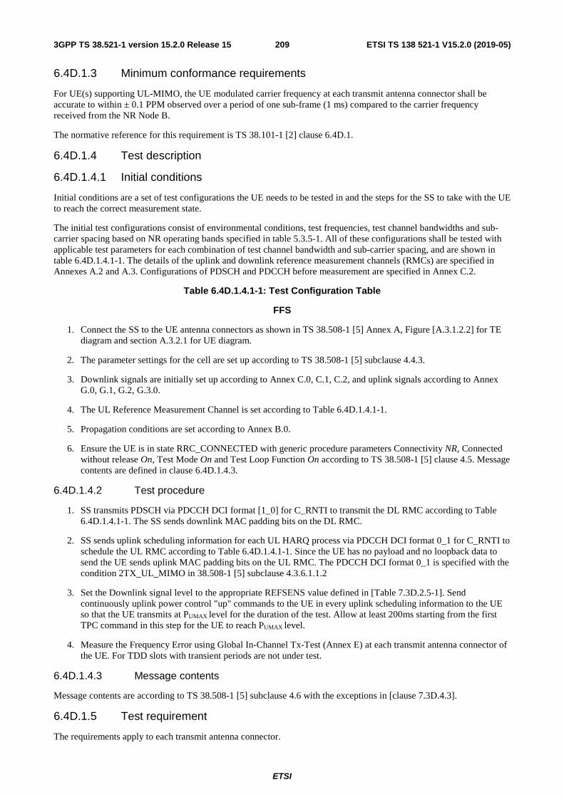
ETSI
ETSI TS 138 521-1 V15.2.0 (2019-05)2093GPP TS 38.521-1 version 15.2.0 Release 15
6.4D.1.3 Minimum conformance requirements
For UE(s) supporting UL-MIMO, the UE modulated carrier frequency at each transmit antenna connector shall be accurate to within ± 0.1 PPM observed over a period of one sub-frame (1 ms) compared to the carrier frequency received from the NR Node B.
The normative reference for this requirement is TS 38.101-1 [2] clause 6.4D.1.
6.4D.1.4 Test description
6.4D.1.4.1 Initial conditions
Initial conditions are a set of test configurations the UE needs to be tested in and the steps for the SS to take with the UE to reach the correct measurement state.
The initial test configurations consist of environmental conditions, test frequencies, test channel bandwidths and sub-carrier spacing based on NR operating bands specified in table 5.3.5-1. All of these configurations shall be tested with applicable test parameters for each combination of test channel bandwidth and sub-carrier spacing, and are shown in table 6.4D.1.4.1-1. The details of the uplink and downlink reference measurement channels (RMCs) are specified in Annexes A.2 and A.3. Configurations of PDSCH and PDCCH before measurement are specified in Annex C.2.
Table 6.4D.1.4.1-1: Test Configuration Table
FFS
1. Connect the SS to the UE antenna connectors as shown in TS 38.508-1 [5] Annex A, Figure [A.3.1.2.2] for TE diagram and section A.3.2.1 for UE diagram.
2. The parameter settings for the cell are set up according to TS 38.508-1 [5] subclause 4.4.3.
3. Downlink signals are initially set up according to Annex C.0, C.1, C.2, and uplink signals according to Annex G.0, G.1, G.2, G.3.0.
4. The UL Reference Measurement Channel is set according to Table 6.4D.1.4.1-1.
5. Propagation conditions are set according to Annex B.0.
6. Ensure the UE is in state RRC_CONNECTED with generic procedure parameters Connectivity NR, Connected without release On, Test Mode On and Test Loop Function On according to TS 38.508-1 [5] clause 4.5. Message contents are defined in clause 6.4D.1.4.3.
6.4D.1.4.2 Test procedure
1. SS transmits PDSCH via PDCCH DCI format [1_0] for C_RNTI to transmit the DL RMC according to Table 6.4D.1.4.1-1. The SS sends downlink MAC padding bits on the DL RMC.
2. SS sends uplink scheduling information for each UL HARQ process via PDCCH DCI format 0_1 for C_RNTI to schedule the UL RMC according to Table 6.4D.1.4.1-1. Since the UE has no payload and no loopback data to send the UE sends uplink MAC padding bits on the UL RMC. The PDCCH DCI format 0_1 is specified with the condition 2TX_UL_MIMO in 38.508-1 [5] subclause 4.3.6.1.1.2
3. Set the Downlink signal level to the appropriate REFSENS value defined in [Table 7.3D.2.5-1]. Send continuously uplink power control "up" commands to the UE in every uplink scheduling information to the UE so that the UE transmits at PUMAX level for the duration of the test. Allow at least 200ms starting from the first TPC command in this step for the UE to reach PUMAX level.
4. Measure the Frequency Error using Global In-Channel Tx-Test (Annex E) at each transmit antenna connector of the UE. For TDD slots with transient periods are not under test.
6.4D.1.4.3 Message contents
Message contents are according to TS 38.508-1 [5] subclause 4.6 with the exceptions in [clause 7.3D.4.3].
6.4D.1.5 Test requirement
The requirements apply to each transmit antenna connector.
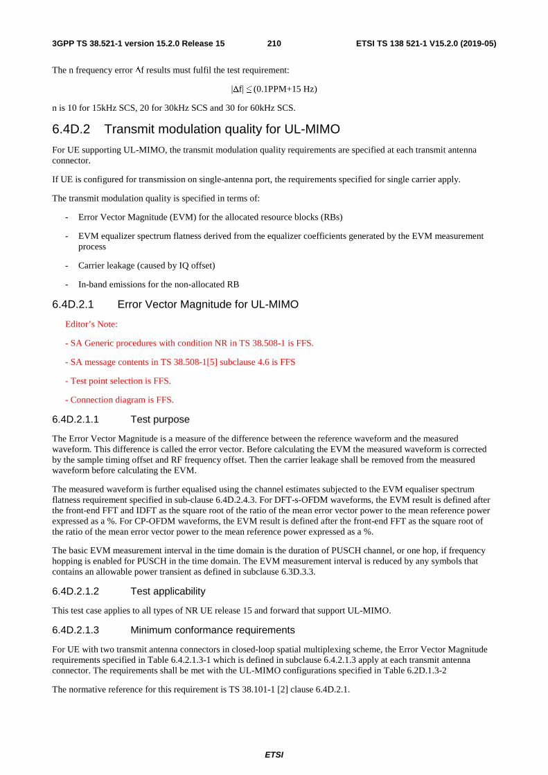
ETSI
ETSI TS 138 521-1 V15.2.0 (2019-05)2103GPP TS 38.521-1 version 15.2.0 Release 15
The n frequency error Δf results must fulfil the test requirement:
|Δf| ≤ (0.1PPM+15 Hz)
n is 10 for 15kHz SCS, 20 for 30kHz SCS and 30 for 60kHz SCS.
6.4D.2 Transmit modulation quality for UL-MIMO
For UE supporting UL-MIMO, the transmit modulation quality requirements are specified at each transmit antenna connector.
If UE is configured for transmission on single-antenna port, the requirements specified for single carrier apply.
The transmit modulation quality is specified in terms of:
- Error Vector Magnitude (EVM) for the allocated resource blocks (RBs)
- EVM equalizer spectrum flatness derived from the equalizer coefficients generated by the EVM measurement process
- Carrier leakage (caused by IQ offset)
- In-band emissions for the non-allocated RB
6.4D.2.1 Error Vector Magnitude for UL-MIMO
Editor’s Note:
- SA Generic procedures with condition NR in TS 38.508-1 is FFS.
- SA message contents in TS 38.508-1[5] subclause 4.6 is FFS
- Test point selection is FFS.
- Connection diagram is FFS.
6.4D.2.1.1 Test purpose
The Error Vector Magnitude is a measure of the difference between the reference waveform and the measured waveform. This difference is called the error vector. Before calculating the EVM the measured waveform is corrected by the sample timing offset and RF frequency offset. Then the carrier leakage shall be removed from the measured waveform before calculating the EVM.
The measured waveform is further equalised using the channel estimates subjected to the EVM equaliser spectrum flatness requirement specified in sub-clause 6.4D.2.4.3. For DFT-s-OFDM waveforms, the EVM result is defined after the front-end FFT and IDFT as the square root of the ratio of the mean error vector power to the mean reference power expressed as a %. For CP-OFDM waveforms, the EVM result is defined after the front-end FFT as the square root of the ratio of the mean error vector power to the mean reference power expressed as a %.
The basic EVM measurement interval in the time domain is the duration of PUSCH channel, or one hop, if frequency hopping is enabled for PUSCH in the time domain. The EVM measurement interval is reduced by any symbols that contains an allowable power transient as defined in subclause 6.3D.3.3.
6.4D.2.1.2 Test applicability
This test case applies to all types of NR UE release 15 and forward that support UL-MIMO.
6.4D.2.1.3 Minimum conformance requirements
For UE with two transmit antenna connectors in closed-loop spatial multiplexing scheme, the Error Vector Magnitude requirements specified in Table 6.4.2.1.3-1 which is defined in subclause 6.4.2.1.3 apply at each transmit antenna connector. The requirements shall be met with the UL-MIMO configurations specified in Table 6.2D.1.3-2
The normative reference for this requirement is TS 38.101-1 [2] clause 6.4D.2.1.

ETSI
ETSI TS 138 521-1 V15.2.0 (2019-05)2113GPP TS 38.521-1 version 15.2.0 Release 15
6.4D.2.1.4 Test description
6.4D.2.1.4.1 Initial conditions
Initial conditions are a set of test configurations the UE needs to be tested in and the steps for the SS to take with the UE to reach the correct measurement state.
The initial test configurations consist of environmental conditions, test frequencies, test channel bandwidths and sub-carrier spacing based on NR operating bands specified in table 5.3.5-1. All of these configurations shall be tested with applicable test parameters for each combination of test channel bandwidth and sub-carrier spacing, and are shown in table 6.4D.2.1.4.1-1. The details of the uplink and downlink reference measurement channels (RMCs) are specified in Annexes A.2 and A.3. Configurations of PDSCH and PDCCH before measurement are specified in Annex C.2.
Table 6.4D.2.1.4.1-1: Test Configuration Table
FFS
1. Connect the SS to the UE antenna connectors as shown in TS 38.508-1 [5] Annex A, Figure [A.3.1.2.2] for TE diagram and section A.3.2.1 for UE diagram.
2. The parameter settings for the cell are set up according to TS 38.508-1 [5] subclause 4.4.3.
3. Downlink signals are initially set up according to Annex C.0, C.1, C.2, and uplink signals according to Annex G.0, G.1, G.2, G.3.0.
4. The UL Reference Measurement Channel is set according to Table 6.4D.2.1.4.1-1.
5. Propagation conditions are set according to Annex B.0.
6. Ensure the UE is in state RRC_CONNECTED with generic procedure parameters Connectivity NR, Connected without release On, Test Mode On and Test Loop Function On according to TS 38.508-1 [5] clause 4.5. Message contents are defined in clause 6.4D.2.1.4.3.
6.4D.2.1.4.2 Test procedure
Test procedure for PUSCH:
1.1 SS sends uplink scheduling information for each UL HARQ process via PDCCH DCI format [0_1] for C_RNTI to schedule the UL RMC according to Table 6.4D.2.1.4.1-1. Since the UE has no payload data to send, the UE transmits uplink MAC padding bits on the UL RMC. The PDCCH DCI format 0_1 is specified with the condition 2TX_UL_MIMO in 38.508-1 [5] subclause 4.3.6.1.1.2
1.2 Send continuously uplink power control "up" commands in the uplink scheduling information to the UE until the UE transmits at PUMAX level, allow at least 200ms starting from the first TPC command in this step for the UE to reach PUMAX level.
1.3 Measure the EVM and DMRSEVM using Global In-Channel Tx-Test (Annex E) for each of transmit antenna of the UE.
1.4 For modulations except 256QAM, send the appropriate TPC commands in the uplink scheduling information to the UE until UE output power is in the range Pmin + PW ± PW, where Pmin is the minimum output power according to Table 6.3.1.3-1 and PW is the power window according to Table 6.4D.2.1.4.2-1 for the carrier frequency f and the channel bandwidth BW. For 256 QAM, send the appropriate TPC commands in the uplink scheduling information to the UE until UE output power is in the range TBD ± TBD.
1.5 Measure the EVM and DMRSEVM using Global In-Channel Tx-Test (Annex E).
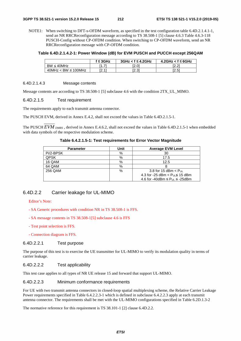
ETSI
ETSI TS 138 521-1 V15.2.0 (2019-05)2123GPP TS 38.521-1 version 15.2.0 Release 15
NOTE1: When switching to DFT-s-OFDM waveform, as specified in the test configuration table 6.4D.2.1.4.1-1, send an NR RRCReconfiguration message according to TS 38.508-1 [5] clause 4.6.3 Table 4.6.3-118 PUSCH-Config without CP-OFDM condition. When switching to CP-OFDM waveform, send an NR RRCReconfiguration message with CP-OFDM condition.
Table 6.4D.2.1.4.2-1: Power Window (dB) for EVM PUSCH and PUCCH except 256QAM
f ≤ 3GHz 3GHz < f ≤ 4.2GHz 4.2GHz < f ≤ 6GHz BW ≤ 40MHz [1.7] [2.0] [2.2] 40MHz < BW ≤ 100MHz [2.1] [2.3] [2.5]
6.4D.2.1.4.3 Message contents
Message contents are according to TS 38.508-1 [5] subclause 4.6 with the condition 2TX_UL_MIMO.
6.4D.2.1.5 Test requirement
The requirements apply to each transmit antenna connector.
The PUSCH EVM, derived in Annex E.4.2, shall not exceed the values in Table 6.4D.2.1.5-1.
The PUSCH DMRSEVM , derived in Annex E.4.6.2, shall not exceed the values in Table 6.4D.2.1.5-1 when embedded with data symbols of the respective modulation scheme.
Table 6.4.2.1.5-1: Test requirements for Error Vector Magnitude
Parameter Unit Average EVM Level Pi/2-BPSK % 30 QPSK % 17.5 16 QAM % 12.5 64 QAM % 8 256 QAM % 3.8 for 15 dBm < PUL
4.3 for -25 dBm < PUL≤ 15 dBm 4.6 for -40dBm ≤ PUL ≤ -25dBm
6.4D.2.2 Carrier leakage for UL-MIMO
Editor’s Note:
- SA Generic procedures with condition NR in TS 38.508-1 is FFS.
- SA message contents in TS 38.508-1[5] subclause 4.6 is FFS
- Test point selection is FFS.
- Connection diagram is FFS.
6.4D.2.2.1 Test purpose
The purpose of this test is to exercise the UE transmitter for UL-MIMO to verify its modulation quality in terms of carrier leakage.
6.4D.2.2.2 Test applicability
This test case applies to all types of NR UE release 15 and forward that support UL-MIMO.
6.4D.2.2.3 Minimum conformance requirements
For UE with two transmit antenna connectors in closed-loop spatial multiplexing scheme, the Relative Carrier Leakage Power requirements specified in Table 6.4.2.2.3-1 which is defined in subclause 6.4.2.2.3 apply at each transmit antenna connector. The requirements shall be met with the UL-MIMO configurations specified in Table 6.2D.1.3-2
The normative reference for this requirement is TS 38.101-1 [2] clause 6.4D.2.2.

ETSI
ETSI TS 138 521-1 V15.2.0 (2019-05)2133GPP TS 38.521-1 version 15.2.0 Release 15
6.4D.2.2.4 Test description
6.4D.2.2.4.1 Initial conditions
Initial conditions are a set of test configurations the UE needs to be tested in and the steps for the SS to take with the UE to reach the correct measurement state.
The initial test configurations consist of environmental conditions, test frequencies, test channel bandwidths and sub-carrier spacing based on NR operating bands specified in table 5.3.5-1. All of these configurations shall be tested with applicable test parameters for each combination of test channel bandwidth and sub-carrier spacing, and are shown in table 6.4D.2.2.4.1-1. The details of the uplink and downlink reference measurement channels (RMCs) are specified in Annexes A.2 and A.3. Configurations of PDSCH and PDCCH before measurement are specified in Annex C.2.
Table 6.4D.2.2.4.1-1: Test Configuration Table
FFS
1. Connect the SS to the UE antenna connectors as shown in TS 38.508-1 [5] Annex A, Figure [A.3.1.2.2] for TE diagram and section A.3.2.1 for UE diagram.
2. The parameter settings for the cell are set up according to TS 38.508-1 [5] subclause 4.4.3.
3. Downlink signals are initially set up according to Annex C.0, C.1, C.2, and uplink signals according to Annex G.0, G.1, G.2, G.3.0.
4. The UL Reference Measurement Channel is set according to Table 6.4D.2.2.4.1-1.
5. Propagation conditions are set according to Annex B.0.
6. Ensure the UE is in state RRC_CONNECTED with generic procedure parameters Connectivity NR, Connected without release On, Test Mode On and Test Loop Function On according to TS 38.508-1 [5] clause 4.5. Message contents are defined in clause 6.4D.2.2.4.3.
6.4D.2.2.4.2 Test procedure
1. SS sends uplink scheduling information for each UL HARQ process via PDCCH DCI format [0_1] for C_RNTI to schedule the UL RMC according to Table 6.4D.2.2.4.1-1. Since the UE has no payload and no loopback data to send the UE sends uplink MAC padding bits on the UL RMC. The PDCCH DCI format 0_1 is specified with the condition 2TX_UL_MIMO in 38.508-1 [5] subclause 4.3.6.1.1.2.
2. Send the appropriate TPC commands in the uplink scheduling information to the UE until UE output power is 10 + PW dBm ± PW dB where PW is the power window according to Table 6.4D.2.2.4.2-1 for the carrier frequency f and the channel bandwidth BW.
3. Measure carrier leakage using Global In-Channel Tx-Test (Annex E) for each of transmit antenna of the UE. For TDD slots with transient periods are not under test.
4. Send the appropriate TPC commands in the uplink scheduling information to the UE until UE output power is 0 + PW dBm ± PW dB where PW is the power window according to Table 6.4D.2.2.4.2-1 for the carrier frequency f and the channel bandwidth BW.
5. Measure carrier leakage using Global In-Channel Tx-Test (Annex E) for each of transmit antenna of the UE. For TDD slots with transient periods are not under test.
6. Send the appropriate TPC commands in the uplink scheduling information to the UE until UE output power is -30 + PW dBm ± PW dB where PW is the power window according to Table 6.4D.2.2.4.2-2 for the carrier frequency f and the channel bandwidth BW.
7. Measure carrier leakage using Global In-Channel Tx-Test (Annex E) for each of transmit antenna of the UE. For TDD slots with transient periods are not under test
8. Send the appropriate TPC commands in the uplink scheduling information to the UE until UE output power is -40 + PW dBm ± PW dB where PW is the power window according to Table 6.4D.2.2.4.2-2 for the carrier frequency f and the channel bandwidth BW.
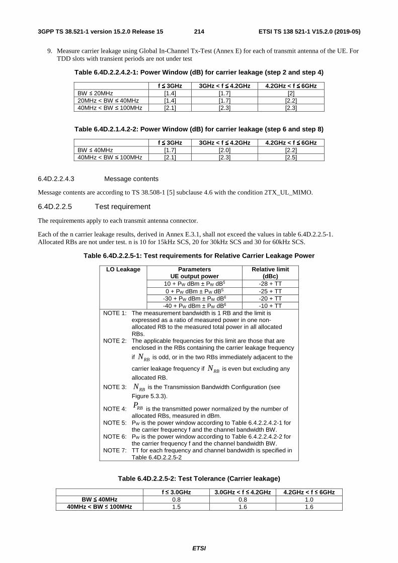
ETSI
ETSI TS 138 521-1 V15.2.0 (2019-05)2143GPP TS 38.521-1 version 15.2.0 Release 15
9. Measure carrier leakage using Global In-Channel Tx-Test (Annex E) for each of transmit antenna of the UE. For TDD slots with transient periods are not under test
Table 6.4D.2.2.4.2-1: Power Window (dB) for carrier leakage (step 2 and step 4)
f ≤ 3GHz 3GHz < f ≤ 4.2GHz 4.2GHz < f ≤ 6GHz BW ≤ 20MHz [1.4] [1.7] [2] 20MHz < BW ≤ 40MHz [1.4] [1.7] [2.2] 40MHz < BW ≤ 100MHz [2.1] [2.3] [2.3]
Table 6.4D.2.1.4.2-2: Power Window (dB) for carrier leakage (step 6 and step 8)
f ≤ 3GHz 3GHz < f ≤ 4.2GHz 4.2GHz < f ≤ 6GHz BW ≤ 40MHz [1.7] [2.0] [2.2] 40MHz < BW ≤ 100MHz [2.1] [2.3] [2.5]
6.4D.2.2.4.3 Message contents
Message contents are according to TS 38.508-1 [5] subclause 4.6 with the condition 2TX_UL_MIMO.
6.4D.2.2.5 Test requirement
The requirements apply to each transmit antenna connector.
Each of the n carrier leakage results, derived in Annex E.3.1, shall not exceed the values in table 6.4D.2.2.5-1. Allocated RBs are not under test. n is 10 for 15kHz SCS, 20 for 30kHz SCS and 30 for 60kHz SCS.
Table 6.4D.2.2.5-1: Test requirements for Relative Carrier Leakage Power
LO Leakage Parameters UE output power
Relative limit (dBc)
10 + PW dBm ± PW dB5 -28 + TT 0 + PW dBm ± PW dB5 -25 + TT
-30 + PW dBm ± PW dB6 -20 + TT -40 + PW dBm ± PW dB6 -10 + TT
NOTE 1: The measurement bandwidth is 1 RB and the limit is expressed as a ratio of measured power in one non-allocated RB to the measured total power in all allocated RBs.
NOTE 2: The applicable frequencies for this limit are those that are enclosed in the RBs containing the carrier leakage frequency
if RBN is odd, or in the two RBs immediately adjacent to the
carrier leakage frequency if RBN is even but excluding any
allocated RB.
NOTE 3: RBN is the Transmission Bandwidth Configuration (see
Figure 5.3.3).
NOTE 4: RBP is the transmitted power normalized by the number of allocated RBs, measured in dBm.
NOTE 5: PW is the power window according to Table 6.4.2.2.4.2-1 for the carrier frequency f and the channel bandwidth BW.
NOTE 6: PW is the power window according to Table 6.4.2.2.4.2-2 for the carrier frequency f and the channel bandwidth BW.
NOTE 7: TT for each frequency and channel bandwidth is specified in Table 6.4D.2.2.5-2
Table 6.4D.2.2.5-2: Test Tolerance (Carrier leakage)
f ≤ 3.0GHz 3.0GHz < f ≤ 4.2GHz 4.2GHz < f ≤ 6GHz BW ≤ 40MHz 0.8 0.8 1.0
40MHz < BW ≤ 100MHz 1.5 1.6 1.6

ETSI
ETSI TS 138 521-1 V15.2.0 (2019-05)2153GPP TS 38.521-1 version 15.2.0 Release 15
6.4D.2.3 In-band emissions for UL-MIMO
Editor’s Note:
- SA Generic procedures with condition NR in TS 38.508-1 is FFS.
- SA message contents in TS 38.508-1[5] subclause 4.6 is FFS
- Test point selection is FFS.
- Connection diagram is FFS.
6.4D.2.3.1 Test purpose
The purpose of this test is to exercise the UE transmitter for UL-MIMO to verify its modulation quality in terms of in-band emissions.
6.4D.2.3.2 Test applicability
This test case applies to all types of NR UE release 15 and forward that support UL-MIMO.
6.4D.2.3.3 Minimum conformance requirements
For UE with two transmit antenna connectors in closed-loop spatial multiplexing scheme, the In-band Emission requirements specified in Table 6.4.2.3.3-1 which is defined in subclause 6.4.2.3.3 apply at each transmit antenna connector. The requirements shall be met with the uplink MIMO configurations specified in Table 6.2D.1.3-2.
The normative reference for this requirement is TS 38.101-1 [2] clause 6.4D.2.3.
6.4D.2.3.4 Test description
6.4D.2.3.4.1 Initial conditions
Initial conditions are a set of test configurations the UE needs to be tested in and the steps for the SS to take with the UE to reach the correct measurement state.
The initial test configurations consist of environmental conditions, test frequencies, test channel bandwidths and sub-carrier spacing based on NR operating bands specified in table 5.3.5-1. All of these configurations shall be tested with applicable test parameters for each combination of test channel bandwidth and sub-carrier spacing, and are shown in table 6.4D.2.3.4.1-1. The details of the uplink and downlink reference measurement channels (RMCs) are specified in Annexes A.2 and A.3. Configurations of PDSCH and PDCCH before measurement are specified in Annex C.2.
Table 6.4D.2.3.4.1-1: Test Configuration Table
FFS
1. Connect the SS to the UE antenna connectors as shown in TS 38.508-1 [5] Annex A, Figure [A.3.1.2.2] for TE diagram and section A.3.2.1 for UE diagram.
2. The parameter settings for the cell are set up according to TS 38.508-1 [5] subclause 4.4.3.
3. Downlink signals are initially set up according to Annex C.0, C.1, C.2, and uplink signals according to Annex G.0, G.1, G.2, G.3.0.
4. The UL Reference Measurement Channel is set according to Table 6.4D.2.3.4.1-1.
5. Propagation conditions are set according to Annex B.0.
6. Ensure the UE is in state RRC_CONNECTED with generic procedure parameters Connectivity NR, Connected without release On, Test Mode On and Test Loop Function On according to TS 38.508-1 [5] clause 4.5. Message contents are defined in clause 6.4D.2.3.4.3.
6.4D.2.3.4.2 Test procedure
Test procedure for PUSCH:

ETSI
ETSI TS 138 521-1 V15.2.0 (2019-05)2163GPP TS 38.521-1 version 15.2.0 Release 15
1.1 SS sends uplink scheduling information for each UL HARQ process via PDCCH DCI format [1_0] for C_RNTI to schedule the UL RMC according to Table 6.4D.2.3.4.1-1. Since the UE has no payload and no loopback data to send the UE sends uplink MAC padding bits on the UL RMC. The PDCCH DCI format 0_1 is specified with the condition 2TX_UL_MIMO in 38.508-1 [5] subclause 4.3.6.1.1.2.
1.2 Send the appropriate TPC commands in the uplink scheduling information to the UE until UE output power is 10 + PW dBm ± PW dB where PW is the power window according to Table 6.4D.2.3.4.2-1 for the carrier frequency f and the channel bandwidth BW.
1.3 Measure In-band emission using Global In-Channel Tx-Test (Annex E) for each of transmit antennas of the UE. For TDD slots with transient periods are not under test.
1.4 Send the appropriate TPC commands in the uplink scheduling information to the UE until UE output power is 0 + PW dBm ± PW dB where PW is the power window according to Table 6.4D.2.3.4.2-1 for the carrier frequency f and the channel bandwidth BW.
1.5 Measure In-band emission using Global In-Channel Tx-Test (Annex E) for each of transmit antennas of the UE. For TDD slots with transient periods are not under test.
1.6 Send the appropriate TPC commands in the uplink scheduling information to the UE until UE output power is -30 + PW dBm ± PW dB where PW is the power window according to Table 6.4D.2.3.4.2-2 for the carrier frequency f and the channel bandwidth BW.
1.7 Measure In-band emission using Global In-Channel Tx-Test (Annex E) for each of transmit antennas of the UE. For TDD slots with transient periods are not under test.
1.8 Send the appropriate TPC commands in the uplink scheduling information to the UE until UE output power is -40 + PW dBm ± PW dB where PW is the power window according to Table 6.4D.2.3.4.2-2 for the carrier frequency f and the channel bandwidth BW.
1.9 Measure In-band emission using Global In-Channel Tx-Test (Annex E) for each of transmit antennas of the UE. For TDD slots with transient periods are not under test.
NOTE1: When switching to DFT-s-OFDM waveform, as specified in the test configuration table 6.4D.2.3.4.1-1, send an NR RRCReconfiguration message according to TS 38.508-1 [5] clause 4.6.3 Table 4.6.3-118 PUSCH-Config without CP-OFDM condition. When switching to CP-OFDM waveform, send an NR RRCReconfiguration message with CP-OFDM condition
Table 6.4D.2.3.4.2-1: Power Window (dB) for carrier leakage (steps 1.2, 1.4)
f ≤ 3GHz 3GHz < f ≤ 4.2GHz 4.2GHz < f ≤ 6GHz BW ≤ 20MHz [1.4] [1.7] [2] 20MHz < BW ≤ 40MHz [1.4] [1.7] [2.2] 40MHz < BW ≤ 100MHz [2.1] [2.3] [2.3]
Table 6.4D.2.3.4.2-2: Power Window (dB) for carrier leakage (steps 1.6, 1.8)
f ≤ 3GHz 3GHz < f ≤ 4.2GHz 4.2GHz < f ≤ 6GHz BW ≤ 40MHz [1.7] [2.0] [2.2] 40MHz < BW ≤ 100MHz [2.1] [2.3] [2.5]
6.4D.2.3.4.3 Message contents
Message contents are according to TS 38.508-1 [5] subclause 4.6 with the condition 2TX_UL_MIMO.
6.4D.2.3.5 Test requirement
The requirements apply to each transmit antenna connector.
Each of the n In-band emissions results, derived in Annex E.4.3 shall not exceed the corresponding values in Tables 6.4D.2.3.5-1. n is 10 for 15kHz SCS, 20 for 30kHz SCS and 30 for 60kHz SCS.

ETSI
ETSI TS 138 521-1 V15.2.0 (2019-05)2173GPP TS 38.521-1 version 15.2.0 Release 15
Table 6.4D.2.3.5-1: Test requirements for in-band emissions
Parameter description Unit Limit (NOTE 1) Applicable
Frequencies
General dB
{
( ) }RB
CRBRB
CRBRB
PkHzSCSdBm
LEVM
LN
−+−−Δ⋅−−⋅
⋅−−
15/log1057
,/)1(53log20
),/(log1025max
10
10
10
+ 0.8 Any non-allocated (NOTE 2)
IQ Image dB -28 + TT Image frequencies when output power > 10 dBm Image
frequencies (NOTES 2, 3) -25 + TT Image frequencies when output power ≤ 10 dBm
Carrier leakage dBc
-28 + TT Output power > 10 dBm Carrier leakage
frequency (NOTES 4, 5)
-25 + TT 0 dBm ≤ Output power ≤10 dBm -20 + TT -30 dBm ≤ Output power ≤ 0 dBm -10 + TT -40 dBm ≤ Output power < -30 dBm
NOTE 1: An in-band emissions combined limit is evaluated in each non-allocated RB. For each such RB, the minimum requirement is calculated as the higher of PRB - 30 dB and the power sum of all limit values (General, IQ Image or Carrier leakage) that apply. PRB is defined in NOTE 10.
NOTE 2: The measurement bandwidth is 1 RB and the limit is expressed as a ratio of measured power in one non-allocated RB to the measured average power per allocated RB, where the averaging is done across all allocated RBs.
NOTE 3: The applicable frequencies for this limit are those that are enclosed in the reflection of the allocated bandwidth, based on symmetry with respect to the carrier leakage frequency, but excluding any allocated RBs.
NOTE 4: The measurement bandwidth is 1 RB and the limit is expressed as a ratio of measured power in one non-allocated RB to the measured total power in all allocated RBs.
NOTE 5: The applicable frequencies for this limit are those that are enclosed in the RBs containing the carrier
leakage frequency if RBN is odd, or in the two RBs immediately adjacent to the carrier leakage frequency
if RBN is even, but excluding any allocated RB.
NOTE 6: CRBL is the Transmission Bandwidth (see Figure 5.3.3).
NOTE 7: RBN is the Transmission Bandwidth Configuration (see Figure 5.3.3).
NOTE 8: EVM is the limit specified in Table 6.4.2.1.3-1 for the modulation format used in the allocated RBs.
NOTE 9: RBΔ is the starting frequency offset between the allocated RB and the measured non-allocated RB (e.g.
1=ΔRB or 1−=ΔRB for the first adjacent RB outside of the allocated bandwidth.
NOTE 10: RBP is the transmitted power normalized by the number of allocated RBs, measured in dBm.
NOTE 11: TT for each frequency and channel bandwidth is specified in Table 6.4D.2.3.5-2
Table 6.4D.2.3.5-2: Test Tolerance (In-band emissions)
f ≤ 3.0GHz 3.0GHz < f ≤ 4.2GHz 4.2GHz < f ≤ 6GHz BW ≤ 40MHz 0.8 0.8 1.0
40MHz < BW ≤ 100MHz 1.5 1.6 1.6
6.4D.2.4 EVM equalizer spectrum flatness for UL-MIMO
Editor’s Note:
- SA Generic procedures with condition NR in TS 38.508-1 is FFS.
- SA message contents in TS 38.508-1[5] subclause 4.6 is FFS
- Test point selection is FFS.
- Connection diagram is FFS.
6.4D.2.4.1 Test purpose
The purpose of this test is to verify the zero-forcing equalizer correction applied in the EVM measurement process (as described in Annex E) meets a spectrum flatness requirement for the EVM measurement to be valid.
ETSI
ETSI TS 138 521-1 V15.2.0 (2019-05)2183GPP TS 38.521-1 version 15.2.0 Release 15
6.4D.2.4.2 Test applicability
This test case applies to all types of NR UE release 15 and forward that support UL-MIMO.
6.4D.2.4.3 Minimum conformance requirements
For UE with two transmit antenna connectors in closed-loop spatial multiplexing scheme, the EVM Equalizer Spectrum Flatness requirements specified in Table 6.4.2.4.3-1 and Table 6.4.2.4.3-2 which are defined in subclause 6.4.2.4.3 apply at each transmit antenna connector. The requirements shall be met with the UL-MIMO configurations specified in Table 6.2D.1.3-2
The normative reference for this requirement is TS 38.101-1 [2] clause 6.4D.2.4.
6.4D.2.4.4 Test description
6.4D.2.4.4.1 Initial conditions
Initial conditions are a set of test configurations the UE needs to be tested in and the steps for the SS to take with the UE to reach the correct measurement state.
The initial test configurations consist of environmental conditions, test frequencies, test channel bandwidths and sub-carrier spacing based on NR operating bands specified in table 5.3.5-1. All of these configurations shall be tested with applicable test parameters for each combination of test channel bandwidth and sub-carrier spacing, and are shown in table 6.4D.2.4.4.1-1. The details of the uplink and downlink reference measurement channels (RMCs) are specified in Annexes A.2 and A.3. Configurations of PDSCH and PDCCH before measurement are specified in Annex C.2.
Table 6.4D.2.4.4.1-1: Test Configuration Table
FFS
1. Connect the SS to the UE antenna connectors as shown in TS 38.508-1 [5] Annex A, Figure [A.3.1.2.2] for TE diagram and section A.3.2.1 for UE diagram.
2. The parameter settings for the cell are set up according to TS 38.508-1 [5] subclause 4.4.3.
3. Downlink signals are initially set up according to Annex C.0, C.1, C.2, and uplink signals according to Annex G.0, G.1, G.2, G.3.0.
4. The UL Reference Measurement Channel is set according to Table 6.4D.2.4.4.1-1.
5. Propagation conditions are set according to Annex B.0.
6. Ensure the UE is in state RRC_CONNECTED with generic procedure parameters Connectivity NR, Connected without release On, Test Mode On and Test Loop Function On according to TS 38.508-1 [5] clause 4.5. Message contents are defined in clause 6.4D.2.4.4.3.
6.4D.2.4.4.2 Test procedure
1. SS sends uplink scheduling information for each UL HARQ process via PDCCH DCI format [0_1] for C_RNTI to schedule the UL RMC according to Table 6.4D.2.4.4.1-1. Since the UE has no payload and no loopback data to send the UE sends uplink MAC padding bits on the UL RMC. The PDCCH DCI format 0_1 is specified with the condition 2TX_UL_MIMO in 38.508-1 [5] subclause 4.3.6.1.1.2.
2. Send continuously uplink power control "up" commands in the uplink scheduling information to the UE until the UE transmits at PUMAX level. Allow at least 200ms starting from the first TPC command in this step for the UE to reach PUMAX level.
3. Measure spectrum flatness using Global In-Channel Tx-Test (Annex E) for each of transmit antennas of the UE. For TDD slots with transient periods are not under test.
6.4D.2.4.4.3 Message contents
Message contents are according to TS 38.508-1 [5] subclause 4.6 with the condition 2TX_UL_MIMO.
6.4D.2.4.5 Test requirement
The requirements apply to each transmit antenna connector.

ETSI
ETSI TS 138 521-1 V15.2.0 (2019-05)2193GPP TS 38.521-1 version 15.2.0 Release 15
Each of the [20] spectrum flatness functions, shall derive four ripple results in Annex E.4.4. The derived results shall not exceed the values in Figure 6.4D.2.4.5-1:
For shaped Pi/2-BPSK modulated waveforms, the test requirements are TBD.
For normal conditions and unshaped modulated waveforms, the maximum ripple in Range 1 and Range 2 shall not exceed the values specified in Table 6.4D.2.4.5-1 and the following additional requirement: the relative difference between the maximum coefficient in Range 1 and the minimum coefficient in Range 2 must not be larger than 6.4 dB, and the relative difference between the maximum coefficient in Range 2 and the minimum coefficient in Range 1 must not be larger than 8.4 dB (see Figure 6.4D.2.4.5-1).
For normal conditions and for unshaped modulated waveforms, the peak-to-peak variation of the EVM equalizer coefficients contained within the frequency range of the uplink allocation shall not exceed the maximum ripple specified in Table 6.4D.2.4.5-1. For uplink allocations contained within both Range 1 and Range 2, the coefficients evaluated within each of these frequency ranges shall meet the corresponding ripple requirement and the following additional requirement: the relative difference between the maximum coefficient in Range 1 and the minimum coefficient in Range 2 must not be larger than 6.4 dB, and the relative difference between the maximum coefficient in Range 2 and the minimum coefficient in Range 1 must not be larger than 8.4 dB (see Figure 6.4D.2.4.5-1).
For extreme conditions, the EVM equalizer spectral flatness shall not exceed the values specified in Table 6.4D.2.4.5-2. For uplink allocations contained within both Range 1 and Range 2, the coefficients evaluated within each of these frequency ranges shall meet the corresponding ripple requirement and the following additional requirement: the relative difference between the maximum coefficient in Range 1 and the minimum coefficient in Range 2 must not be larger than 7.4 dB, and the relative difference between the maximum coefficient in Range 2 and the minimum coefficient in Range 1 must not be larger than 11.4 dB (see Figure 6.4D.2.4.5-1).
Table 6.4D.2.4.5-1: Requirements for EVM equalizer spectrum flatness for unshaped modulations (normal conditions)
Frequency range Maximum ripple [dB] FUL_Meas – FUL_Low ≥ 3 MHz and FUL_High – FUL_Meas ≥ 3 MHz
(Range 1) 5.4 (p-p)
FUL_Meas – FUL_Low < 3 MHz or FUL_High – FUL_Meas < 3 MHz (Range 2)
9.4 (p-p)
NOTE 1: FUL_Meas refers to the sub-carrier frequency for which the equalizer coefficient is evaluated
NOTE 2: FUL_Low and FUL_High refer to each E-UTRA frequency band specified in Table 5.5-1
Table 6.4D.2.4.5-2: Minimum requirements for EVM equalizer spectrum flatness for unshaped modulations (extreme conditions)
Frequency range Maximum Ripple [dB] FUL_Meas – FUL_Low ≥ 5 MHz and FUL_High – FUL_Meas ≥ 5 MHz
(Range 1) 5.4 (p-p)
FUL_Meas – FUL_Low < 5 MHz or FUL_High – FUL_Meas < 5 MHz (Range 2)
13.4 (p-p)
NOTE 1: FUL_Meas refers to the sub-carrier frequency for which the equalizer coefficient is evaluated
NOTE 2: FUL_Low and FUL_High refer to each E-UTRA frequency band specified in Table 5.5-1
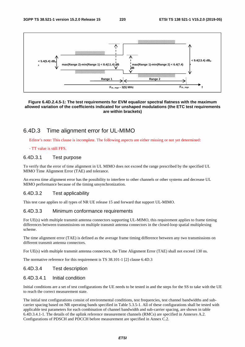
ETSI
ETSI TS 138 521-1 V15.2.0 (2019-05)2203GPP TS 38.521-1 version 15.2.0 Release 15
f FUL_High FUL_High – 3(5) MHz
< 5.4(5.4) dBp-
p
Range 1 Range 2
max(Range 1)-min(Range 2) < 6.4(7.4) dB
max(Range 2)-min(Range 1) < 8.4(11.4) dB < 9.4(13.4) dBp-
p
Figure 6.4D.2.4.5-1: The test requirements for EVM equalizer spectral flatness with the maximum allowed variation of the coefficients indicated for unshaped modulations (the ETC test requirements
are within brackets)
6.4D.3 Time alignment error for UL-MIMO
Editor’s note: This clause is incomplete. The following aspects are either missing or not yet determined:
- TT value is still FFS.
6.4D.3.1 Test purpose
To verify that the error of time alignment in UL MIMO does not exceed the range prescribed by the specified UL MIMO Time Alignment Error (TAE) and tolerance.
An excess time alignment error has the possibility to interfere to other channels or other systems and decrease UL MIMO performance because of the timing unsynchronization.
6.4D.3.2 Test applicability
This test case applies to all types of NR UE release 15 and forward that support UL-MIMO.
6.4D.3.3 Minimum conformance requirements
For UE(s) with multiple transmit antenna connectors supporting UL-MIMO, this requirement applies to frame timing differences between transmissions on multiple transmit antenna connectors in the closed-loop spatial multiplexing scheme.
The time alignment error (TAE) is defined as the average frame timing difference between any two transmissions on different transmit antenna connectors.
For UE(s) with multiple transmit antenna connectors, the Time Alignment Error (TAE) shall not exceed 130 ns.
The normative reference for this requirement is TS 38.101-1 [2] clause 6.4D.3
6.4D.3.4 Test description
6.4D.3.4.1 Initial condition
Initial conditions are a set of test configurations the UE needs to be tested in and the steps for the SS to take with the UE to reach the correct measurement state.
The initial test configurations consist of environmental conditions, test frequencies, test channel bandwidths and sub-carrier spacing based on NR operating bands specified in Table 5.3.5-1. All of these configurations shall be tested with applicable test parameters for each combination of channel bandwidth and sub-carrier spacing, are shown in table 6.4D.3.4.1-1. The details of the uplink reference measurement channels (RMCs) are specified in Annexes A.2. Configurations of PDSCH and PDCCH before measurement are specified in Annex C.2.
ETSI
ETSI TS 138 521-1 V15.2.0 (2019-05)2213GPP TS 38.521-1 version 15.2.0 Release 15
Table 6.4D.3.4.1-1: Test Configuration Table
Initial Conditions Test Environment as specified in TS 38.508-1 [5] subclause 4.1
Normal
Test Frequencies as specified in TS 38.508-1 [5] subclause 4.3.1
Mid range
Test Channel Bandwidths as specified in TS 38.508-1 [5] subclause 4.3.1
Lowest, Mid, Highest
Test SCS as specified in Table 5.3.5-1 Lowest, Highest Test Parameters for Channel Bandwidths
Test ID Downlink Configuration Uplink Configuration N/A for Time alignment error
for UL-MIMO Modulation RB allocation (NOTE 1)
1 test case CP-OFDM QPSK Outer Full NOTE 1: The specific configuration of each RB allocation is defined in Table 6.1-1.
1. Connect the SS to the UE antenna connectors as shown in TS 38.508-1 [5] Annex A, in Figure A.3.1.1.2 for TE diagram and section A.3.2 for UE diagram.
2. The parameter settings for the cell are set up according to TS 38.508-1 [5] subclause 4.4.3.
3. Downlink signals are initially set up according to Annex C.0, C.1, C.2, and uplink signals according to Annex G.0, G.1, G.2, G.3.0.
4. The UL Reference Measurement channels are set according to Table 6.4D.3.4.1-1.
5. Propagation conditions are set according to Annex B.0.
6. Ensure the UE is in state RRC_CONNECTED with generic procedure parameters Connectivity NR, Connected without release On, Test Mode On and Test Loop Function On according to TS 38.508-1 [5] clause 4.5. Message contents are defined in clause 6.4D.3.4.3
6.4D.3.4.2 Test procedure
1. SS sends uplink scheduling information for each UL HARQ process via PDCCH DCI format 0_1 for C_RNTI to schedule the UL RMC according to Table 6.4D.3.4.1-1. Since the UE has no payload and no loopback data to send the UE sends uplink MAC padding bits on the UL RMC. The PDCCH DCI format 0_1 is specified with the condition 2TX_UL_MIMO in 38.508-1 [5] subclause 4.3.6.1.1.2.
2. Send continuously uplink power control "up" commands in every uplink scheduling information to the UE; allow at least 200ms for the UE to reach PUMAX level.
3. Measure the timing of one sub-frame at each antenna connector.
6.4D.3.4.3 Message contents
Message contents are according to TS 38.508-1 [5] subclause 4.6 ensuring Table 4.6.3-182 with condition 2TX_UL_MIMO.
6.4D.3.5 Test requirement
For UE(s) with multiple transmit antenna connectors, the Time Alignment Error (TAE) shall not exceed 130 + TT ns.
Table 6.4D.3.5-1: Test Tolerance (Time alignment error for UL-MIMO)
Test Tolerance [25ns]
6.4D.4 Requirements for coherent UL MIMO
Editor’s note: This clause is incomplete. The following aspects are either missing or not yet determined:
- Test config table is still FFS.

ETSI
ETSI TS 138 521-1 V15.2.0 (2019-05)2223GPP TS 38.521-1 version 15.2.0 Release 15
- SA Generic procedures with condition NR in TS 38.508-1 is FFS.
- SA message contents in TS 38.508-1[5] subclause 4.6 is FFS
- The test procedure is FFS.
- TT value is still FFS
6.4D.4.1 Test purpose
To verify that the difference of relative phase error and the difference of relative power error between antenna ports in coherent UL MIMO do not exceed the range prescribed by the specified requirements for coherent UL MIMO and tolerance.
An excess relative phase error or excess relative power error has the possibility to interfere to other channels and decrease UL MIMO performance because of the timing unsynchronization.
6.4D.4.2 Test applicability
This test case applies to all types of NR UE release 15 and forward that support coherent UL-MIMO.
6.4D.4.3 Minimum conformance requirements
For coherent UL MIMO, Table 6.4D.4.3-1 lists the maximum allowable difference between the measured relative power and phase errors between different antenna ports in any slot within the specified time window from the last transmitted SRS on the same antenna ports, for the purpose of uplink transmission (codebook or non-codebook usage) and those measured at that last SRS. The requirements in Table 6.4D.4.3-1 apply when the UL transmission power at each antenna port is larger than 0 dBm for SRS transmission and for the duration of time window.
Table 6.4D.4.3-1: Maximum allowable difference of relative phase and power errors in a given slot compared to those measured at last SRS transmitted
Difference of relative phase error Difference of relative power error Time window
40 degrees 4 dB 20 msec
The above requirements when all the following conditions are met within the specified time window:
- UE is not signaled with a change in number of SRS ports in SRS-config, or a change in PUSCH-config
- UE remains in DRX active time (UE does not enter DRX OFF time)
- No measurement gap occurs
- No instance of SRS transmission with the usage antenna switching occurs
- Active BWP remains the same
- EN-DC and CA configuration is not changed for the UE (UE is not configured or de-configured with PScell or SCell(s))
The normative reference for this requirement is TS 38.101-1 [2] clause 6.4D.4
6.4D.4.4 Test description
6.4D.4.4.1 Initial condition
Initial conditions are a set of test configurations the UE needs to be tested in and the steps for the SS to take with the UE to reach the correct measurement state.
The initial test configurations consist of environmental conditions, test frequencies, test channel bandwidths and sub-carrier spacing based on NR operating bands specified in Table 5.3.5-1. All of these configurations shall be tested with applicable test parameters for each combination of channel bandwidth and sub-carrier spacing, are shown in table

ETSI
ETSI TS 138 521-1 V15.2.0 (2019-05)2233GPP TS 38.521-1 version 15.2.0 Release 15
6.4D.4.4.1-1. The details of the uplink reference measurement channels (RMCs) are specified in Annexes A.2. Configurations of PDSCH and PDCCH before measurement are specified in Annex C.2.
Table 6.4D.4.4.1-1: Test Configuration Table
FFS
1. Connect the SS to the UE antenna connectors as shown in TS 38.508-1 [5] Annex A, in Figure A.3.1.1.2 for TE diagram and section A.3.2.1 for UE diagram.
2. The parameter settings for the cell are set up according to TS 38.508-1 [5] subclause 4.4.3.
3. Downlink signals are initially set up according to Annex C.0, C.1, C.2, and uplink signals according to Annex G.0, G.1, G.2, G.3.0.
4. The UL Reference Measurement channels are set according to Table 6.4D.4.4.1-1.
5. Propagation conditions are set according to Annex B.0.
6. Ensure the UE is in state RRC_CONNECTED with generic procedure parameters Connectivity NR, Connected without release On, Test Mode On and Test Loop Function On according to TS 38.508-1 [5] clause 4.5. Message contents are defined in clause 6.4D.4.4.3
6.4D.4.4.2 Test procedure
FFS
6.4D.4.4.3 Message contents
Message contents are according to TS 38.508-1 [5] subclause 4.6 with following exception [FFS]
6.4D.4.5 Test requirement
Maximum allowable difference of relative phase and power errors in a given slot within the Time window compared to those measured at last SRS transmitted shall not exceed the described value in Table 6.4D.4.5-1.
Table 6.4D.4.5-1: Maximum allowable difference of relative phase and power errors in a given slot compared to those measured at last SRS transmitted
Difference of relative phase error Difference of relative power error Time window
40+TT degrees 4+TT dB 20 msec
6.5 Output RF spectrum emissions Unwanted emissions are divided into "Out-of-band emission" and "Spurious emissions" in 3GPP RF specifications. This notation is in line with ITU-R recommendations such as SM.329 [TBD] and the Radio Regulations [TBD].
ITU defines:
Out-of-band emission = Emission on a frequency or frequencies immediately outside the necessary bandwidth which results from the modulation process, but excluding spurious emissions.
Spurious emission = Emission on a frequency, or frequencies, which are outside the necessary bandwidth and the level of which may be reduced without affecting the corresponding transmission of information. Spurious emissions include harmonic emissions, parasitic emissions, intermodulation products and frequency conversion products but exclude out-of-band emissions.
Unwanted emissions = Consist of spurious emissions and out-of-band emissions.
The UE transmitter spectrum emission consists of the three components; the occupied bandwidth (channel bandwidth), the Out Of Band (OOB) emissions and the far out spurious emission domain.
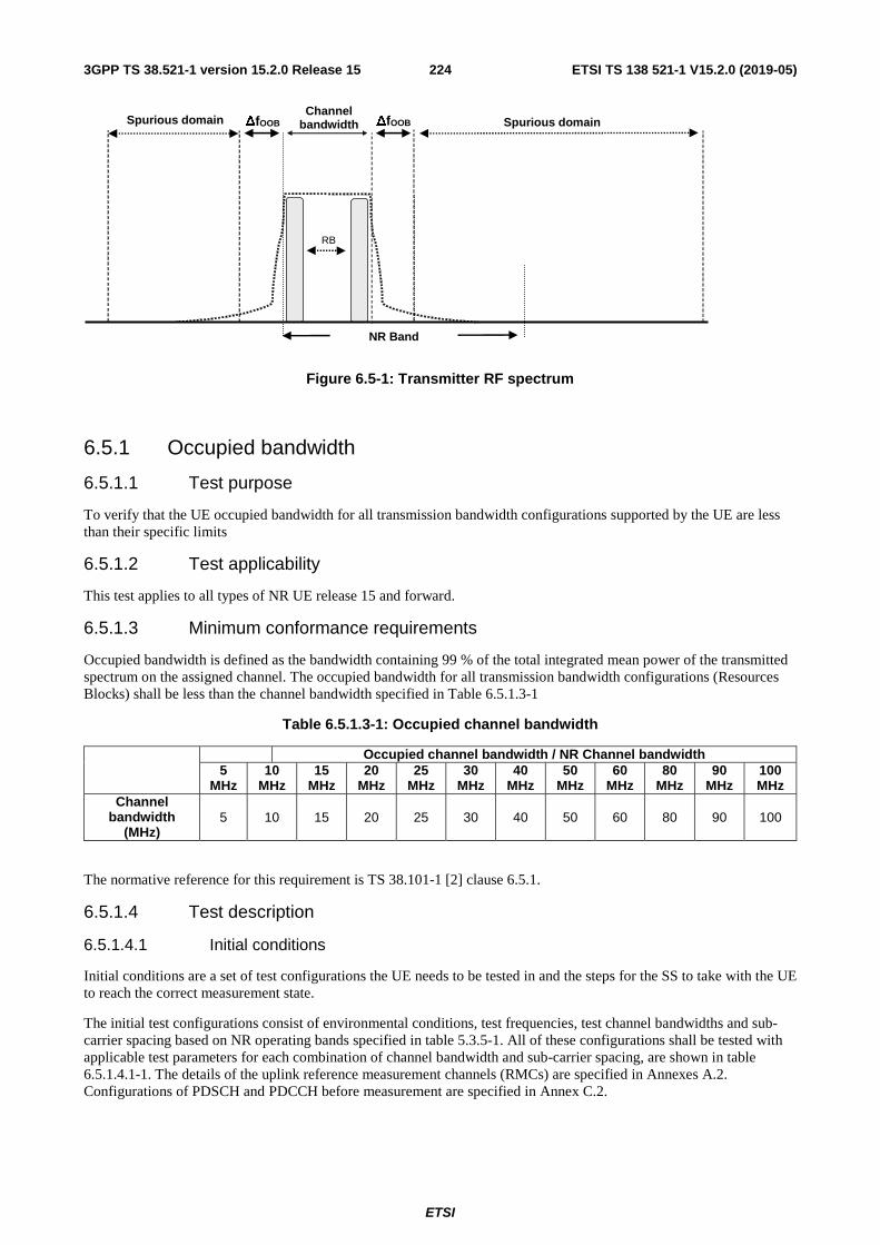
ETSI
ETSI TS 138 521-1 V15.2.0 (2019-05)2243GPP TS 38.521-1 version 15.2.0 Release 15
Spurious domain
RB
Channel bandwidth Spurious domain ΔfOOB ΔfOOB
NR Band
Figure 6.5-1: Transmitter RF spectrum
6.5.1 Occupied bandwidth
6.5.1.1 Test purpose
To verify that the UE occupied bandwidth for all transmission bandwidth configurations supported by the UE are less than their specific limits
6.5.1.2 Test applicability
This test applies to all types of NR UE release 15 and forward.
6.5.1.3 Minimum conformance requirements
Occupied bandwidth is defined as the bandwidth containing 99 % of the total integrated mean power of the transmitted spectrum on the assigned channel. The occupied bandwidth for all transmission bandwidth configurations (Resources Blocks) shall be less than the channel bandwidth specified in Table 6.5.1.3-1
Table 6.5.1.3-1: Occupied channel bandwidth
Occupied channel bandwidth / NR Channel bandwidth 5
MHz 10
MHz 15
MHz 20
MHz 25
MHz 30
MHz 40
MHz 50
MHz 60
MHz 80
MHz 90
MHz 100 MHz
Channel bandwidth
(MHz) 5 10 15 20 25 30 40 50 60 80 90 100
The normative reference for this requirement is TS 38.101-1 [2] clause 6.5.1.
6.5.1.4 Test description
6.5.1.4.1 Initial conditions
Initial conditions are a set of test configurations the UE needs to be tested in and the steps for the SS to take with the UE to reach the correct measurement state.
The initial test configurations consist of environmental conditions, test frequencies, test channel bandwidths and sub-carrier spacing based on NR operating bands specified in table 5.3.5-1. All of these configurations shall be tested with applicable test parameters for each combination of channel bandwidth and sub-carrier spacing, are shown in table 6.5.1.4.1-1. The details of the uplink reference measurement channels (RMCs) are specified in Annexes A.2. Configurations of PDSCH and PDCCH before measurement are specified in Annex C.2.
ETSI
ETSI TS 138 521-1 V15.2.0 (2019-05)2253GPP TS 38.521-1 version 15.2.0 Release 15
Table 6.5.1.4.1-1: Test Configuration Table
Initial Conditions Test Environment as specified in TS 38.508-1 [5] subclause 4.1
Normal
Test Frequencies as specified in TS 38.508-1 [5] subclause 4.3.1
Mid range by default, exceptions listed in Table 6.5.1.4.1-2
Test Channel Bandwidths as specified in TS 38.508-1 [5] subclause 4.3.1
All
Test SCS as specified in Table 5.3.5-1 Lowest Test Parameters
Test ID Downlink Configuration Uplink Configuration N/A for occupied bandwidth test
case
Modulation RB allocation (NOTE 1)
1 CP-OFDM QPSK Outer_full
NOTE 1: The specific configuration of each RB allocation is defined in Table 6.1-1.
Table 6.5.1.4.1-2: Test frequency exceptions for Occupied Bandwidth
5G NR Band Test Frequency
n77 Low Range, Mid Range, High Range
n78 Low Range, Mid Range, High Range
n79 Low Range, Mid Range, High Range
1. Connect the SS to the UE antenna connectors as shown in TS 38.508-1 [5] Annex A, Figure A.3.1.1.1 for TE diagram and section A.3.2.1 for UE diagram.
2. The parameter settings for the cell are set up according to TS 38.508-1 [5] subclause 4.4.3.
3. Downlink signals are initially set up according to Annex C.0, C.1, C.2 , and uplink signals according to Annex G.0, G.1, G.2, G.3.0.
4. The UL Reference Measurement channels are set according to Table 6.5.1.4.1-1.
5. Propagation conditions are set according to Annex B.0 -
6. Ensure the UE is in state RRC_CONNECTED with generic procedure parameters Connectivity NR, Connected without release On, Test Mode On and Test Loop Function On according to TS 38.508-1 [5] clause 4.5. Message contents are defined in clause 6.5.1.4.3
6.5.1.4.2 Test procedure
1. SS sends uplink scheduling information for each UL HARQ process via PDCCH DCI format 0_1 for C_RNTI to schedule the UL RMC according to Table 6.5.1.4.1-1. Since the UL has no payload and no loopback data to send the UE sends uplink MAC padding bits on the UL RMC.
2. Send continuously power control “up” commands to the UE until the UE transmits at PUMAX level. Allow at least 200ms for the UE to reach PUMAX level.
3. Measure the power spectrum distribution within two times or more range over the requirement for Occupied Bandwidth specification centring on the current carrier frequency. The characteristics of the filter shall be approximately Gaussian (typical spectrum analyser filter). Other methods to measure the power spectrum distribution are allowed. The measuring duration is at least 1ms over consecutive active uplink slots.
4. Calculate the total power within the range of all frequencies measured in step 3 and save this value as “Total power”.
5. Identify the measurement window whose center is aligned on the center of the channel for which the sum of the power measured is 99% of the “Total power”.
6. The “Occupied Bandwidth” is the width of the measurement window obtained in step 5.
ETSI
ETSI TS 138 521-1 V15.2.0 (2019-05)2263GPP TS 38.521-1 version 15.2.0 Release 15
6.5.1.4.3 Message contents
Message contents are according to TS 38.508-1 [5] subclause 4.6.
6.5.1.5 Test requirement
The measured Occupied Bandwidth shall not exceed values in Table 6.5.1.5-1.
Table 6.5.1.5-1: Occupied channel bandwidth
Occupied channel bandwidth / NR Channel bandwidth 5
MHz 10
MHz 15
MHz 20
MHz 25
MHz 30
MHz 40
MHz 50
MHz 60
MHz 80
MHz 90
MHz 100 MHz
Channel bandwidth
(MHz) 5 10 15 20 25 30 40 50 60 80 90 100
6.5.2 Out of band emission
6.5.2.1 General
The Out of band emissions are unwanted emissions immediately outside the assigned channel bandwidth resulting from the modulation process and non-linearity in the transmitter but excluding spurious emissions. This out of band emission limit is specified in terms of a spectrum emission mask and an adjacent channel leakage power ratio.
To improve measurement accuracy, sensitivity and efficiency, the resolution bandwidth may be smaller than the measurement bandwidth. When the resolution bandwidth is smaller than the measurement bandwidth, the result should be integrated over the measurement bandwidth in order to obtain the equivalent noise bandwidth of the measurement bandwidth.
6.5.2.2 Spectrum Emission Mask
The spectrum emission mask of the UE applies to frequencies (ΔfOOB) starting from the ± edge of the assigned NR channel bandwidth. For frequencies offset greater than FOOB, the spurious requirements in subclause 6.5.3 are applicable.
NOTE: For measurement conditions at the edge of each frequency range, the lowest frequency of the measurement position in each frequency range should be set at the lowest boundary of the frequency range plus MBW/2. The highest frequency of the measurement position in each frequency range should be set at the highest boundary of the frequency range minus MBW/2. MBW denotes the measurement bandwidth defined for the protected band.
6.5.2.2.1 Test purpose
To verify that the power of any UE emission shall not exceed specified level for the specified channel bandwidth.
6.5.2.2.2 Test applicability
This test case applies to all types of NR UE release 15 and forward.
6.5.2.2.3 Minimum conformance requirements
The power of any UE emission shall not exceed the levels specified in Table 6.5.2.2.3-1 for the specified channel bandwidth.
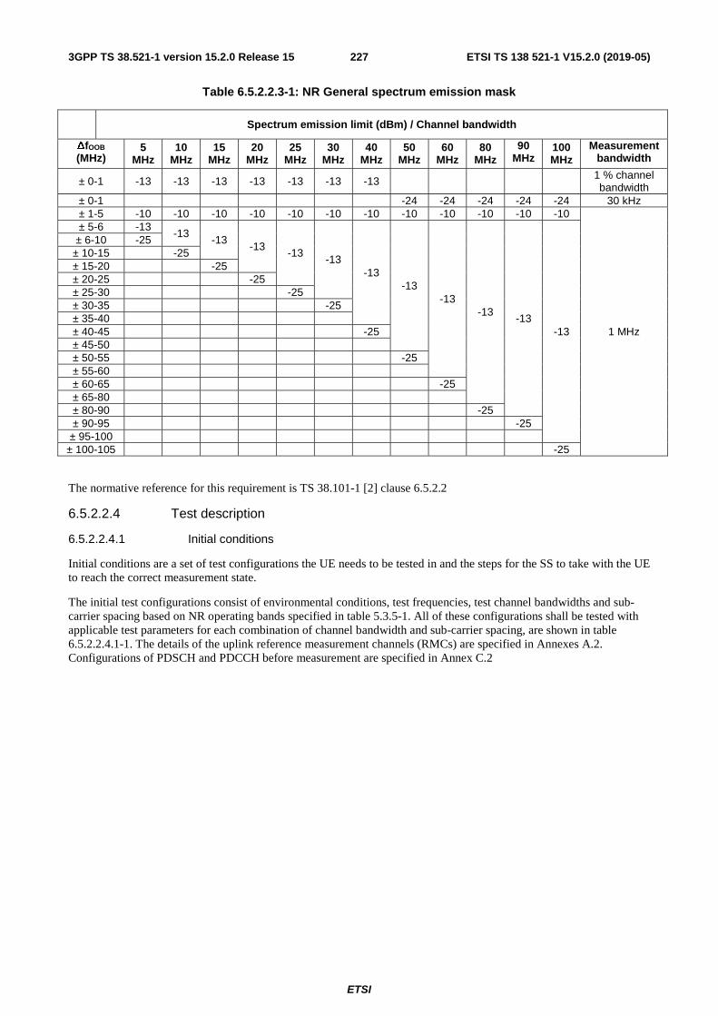
ETSI
ETSI TS 138 521-1 V15.2.0 (2019-05)2273GPP TS 38.521-1 version 15.2.0 Release 15
Table 6.5.2.2.3-1: NR General spectrum emission mask
Spectrum emission limit (dBm) / Channel bandwidth
ΔfOOB (MHz)
5 MHz
10 MHz
15 MHz
20 MHz
25 MHz
30 MHz
40 MHz
50 MHz
60 MHz
80 MHz
90 MHz
100 MHz
Measurement bandwidth
± 0-1 -13 -13 -13 -13 -13 -13 -13 1 % channel bandwidth
± 0-1 -24 -24 -24 -24 -24 30 kHz ± 1-5 -10 -10 -10 -10 -10 -10 -10 -10 -10 -10 -10 -10
1 MHz
± 5-6 -13 -13
-13 -13
-13 -13
-13 -13
-13 -13
-13 -13
± 6-10 -25 ± 10-15 -25 ± 15-20 -25 ± 20-25 -25 ± 25-30 -25 ± 30-35 -25 ± 35-40 ± 40-45 -25 ± 45-50 ± 50-55 -25 ± 55-60 ± 60-65 -25 ± 65-80 ± 80-90 -25 ± 90-95 -25
± 95-100 ± 100-105 -25
The normative reference for this requirement is TS 38.101-1 [2] clause 6.5.2.2
6.5.2.2.4 Test description
6.5.2.2.4.1 Initial conditions
Initial conditions are a set of test configurations the UE needs to be tested in and the steps for the SS to take with the UE to reach the correct measurement state.
The initial test configurations consist of environmental conditions, test frequencies, test channel bandwidths and sub-carrier spacing based on NR operating bands specified in table 5.3.5-1. All of these configurations shall be tested with applicable test parameters for each combination of channel bandwidth and sub-carrier spacing, are shown in table 6.5.2.2.4.1-1. The details of the uplink reference measurement channels (RMCs) are specified in Annexes A.2. Configurations of PDSCH and PDCCH before measurement are specified in Annex C.2

ETSI
ETSI TS 138 521-1 V15.2.0 (2019-05)2283GPP TS 38.521-1 version 15.2.0 Release 15
Table 6.5.2.2.4.1-1: Test Configuration Table

ETSI
ETSI TS 138 521-1 V15.2.0 (2019-05)2293GPP TS 38.521-1 version 15.2.0 Release 15
Default Conditions Test Environment as specified in TS 38.508-1 [5] subclause 4.1
Normal
Test Frequencies as specified in TS 38.508-1 [5] subclause 4.3.1
Low range, High range
Test Channel Bandwidths as specified in TS 38.508-1 [5] subclause 4.3.1
Lowest, Highest
Test SCS as specified in Table 5.3.5-1 Lowest, Highest Test Parameters for Channel Bandwidths
Test ID
Freq ChBw SCS Downlink Configuration
Uplink Configuration
Default Default N/A for Spectrum Emission
Mask test case
Modulation (NOTE 2)
RB allocation (NOTE 1)
13 Low DFT-s-OFDM PI/2 BPSK
Edge_1RB_Left
23 High DFT-s-OFDM PI/2 BPSK
Edge_1RB_Right
33 Default DFT-s-OFDM PI/2 BPSK
Outer_Full
4 Low DFT-s-OFDM QPSK
Edger_1RB_Left
5 High DFT-s-OFDM QPSK
Edge_1RB_Right
6 Default DFT-s-OFDM QPSK
Outer_Full
7 Low DFT-s-OFDM 16 QAM
Edge_1RB_Left
8 High DFT-s-OFDM 16 QAM
Edge_1RB_Right
9 Default DFT-s-OFDM 16 QAM
Outer_Full
10 Low DFT-s-OFDM 64 QAM
Edge_1RB_Left
11 High DFT-s-OFDM 64 QAM
Edge_1RB_Right
12 Default DFT-s-OFDM 64 QAM
Outer_Full
13 Low DFT-s-OFDM 256 QAM
Edge_1RB_Left
14 High DFT-s-OFDM 256 QAM
Edge_1RB_Right
15 Default DFT-s-OFDM 256 QAM
Outer_Full
16 Low CP-OFDM QPSK
Outer_1RB_Left
17 High CP-OFDM QPSK
Outer_1RB_Right
18 Default CP-OFDM QPSK
Outer_Full
19 Low CP-OFDM 16 QAM
Outer_1RB_Left
20 High CP-OFDM 16 QAM
Outer_1RB_Right
21 Default CP-OFDM 16 QAM
Outer_Full
22 Low CP-OFDM 64 QAM
Edge_1RB_Left
23 High CP-OFDM 64 QAM
Edge_1RB_Right
24 Default CP-OFDM 64 QAM
Outer_Full
25 Low CP-OFDM 256 QAM
Edge_1RB_Left
26 High CP-OFDM 256 QAM
Edge_1RB_Right
27 Default CP-OFDM 256 QAM
Outer_Full
ETSI
ETSI TS 138 521-1 V15.2.0 (2019-05)2303GPP TS 38.521-1 version 15.2.0 Release 15
NOTE 1: The specific configuration of each RF allocation is defined in Table 6.1-1. NOTE 2: DFT-s-OFDM PI/2 BPSK test applies only for UEs which supports half Pi BPSK in
FR1. NOTE 3: For Power Class 3 testing, include two steps for UE operating in bands n40, n77, n78
and n79, with IE [P-Boost-BPSK] set to 1 and 0 separately.
1. Connect the SS to the UE antenna connectors as shown in TS 38.508-1 [5] Annex A, Figure A.3.1.1.1 for TE diagram and section A.3.2.1 for UE diagram.
2. The parameter settings for the cell are set up according to TS 38.508-1 [5] subclause 4.4.3.
3. Downlink signals are initially set up according to Annex C.0, C.1, C.2 , and uplink signals according to Annex G.0, G.1, G.2, G.3.0.
4. The UL Reference Measurement channels are set according to Table 6.5.2.2.4.1-1.
5. Propagation conditions are set according to Annex B.0.
6. Ensure the UE is in state RRC_CONNECTED with generic procedure parameters Connectivity NR, Connected without release On, Test Mode On and Test Loop Function On according to TS 38.508-1 [5] clause 4.5. Message contents are defined in clause 6.5.2.2.4.3
6.5.2.2.4.2 Test procedure
1. SS sends uplink scheduling information for each UL HARQ process via PDCCH DCI format 0_1 for C_RNTI to schedule the UL RMC according to Table 6.5.2.2.1.4.1-1. Since the UL has no payload and no loopback data to send the UE sends uplink MAC padding bits on the UL RMC.
2. Send continuously power control “up” commands to the UE until the UE transmits at PUMAX level. Allow at least 200ms for the UE to reach PUMAX level.
3. Measure the mean power of the UE in the channel bandwidth of the radio access mode according to the test configuration, which shall meet the requirements described in Table 6.2.1.5-1 for 6.2.2.5-1. The period of the measurement shall be at least the continuous duration of 1ms over consecutive active uplink slots. For TDD, only slots consisting of only UL symbols are under test.
4. Measure the power of the transmitted signal with a measurement filter of bandwidths according to table 6.5.2.2.5-1. The centre frequency of the filter shall be stepped in continuous steps according to the same table. The measured power shall be recorded for each step. The measurement period shall capture the active TSs.
NOTE 1: When switching to DFT-s-OFDM waveform, as specified in the test configuration table 6.5.2.2.4.1-1, send an NR RRCReconfiguration message according to TS 38.508-1 [5] clause 4.6.3 Table 4.6.3-118 PUSCH-Config with TRANSFORM_PRECODER_ENABLED condition.
6.5.2.2.4.3 Message contents
Message contents are according to TS 38.508-1 [5] subclause 4.6.
6.5.2.2.5 Test requirement
The measured UE mean power in the channel bandwidth, derived in step 3, shall fulfil requirements in Tables 6.2.1.5-1 or 6.2.2.5-1 as appropriate, and the power of any UE emission shall fulfil requirements in Table 6.5.2.2.5-1.
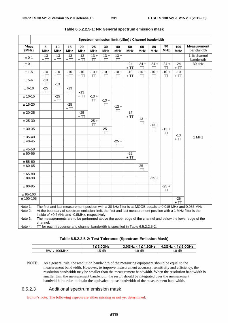
ETSI
ETSI TS 138 521-1 V15.2.0 (2019-05)2313GPP TS 38.521-1 version 15.2.0 Release 15
Table 6.5.2.2.5-1: NR General spectrum emission mask
Spectrum emission limit (dBm) / Channel bandwidth
ΔfOOB (MHz)
5 MHz
10 MHz
15 MHz
20 MHz
25 MHz
30 MHz
40 MHz
50 MHz
60 MHz
80 MHz
90 MHz
100 MHz
Measurement bandwidth
± 0-1 -13 + TT
-13 + TT
-13 + TT
-13 + TT
-13 + TT
-13 + TT
-13 + TT 1 % channel
bandwidth ± 0-1 -24
+ TT -24 + TT
-24 + TT
-24 + TT
-24 + TT
30 kHz
± 1-5 -10 + TT
-10 + TT
-10 + TT
-10 + TT
-10 + TT
-10 + TT
-10 + TT
-10 + TT
-10 + TT
-10 + TT
-10 + TT
-10 + TT
1 MHz
± 5-6 -13 + TT -13
+ TT -13 + TT -13
+ TT -13 + TT -13 +
TT -13 + TT
-13 + TT
-13 + TT
-13 + TT -13 +
TT -13
+ TT
± 6-10 -25 + TT
± 10-15 -25 + TT
± 15-20 -25 + TT
± 20-25
-25 + TT
± 25-30 -25 + TT
± 30-35 -25 + TT
± 35-40 ± 40-45 -25 +
TT ± 45-50 ± 50-55 -25
+ TT ± 55-60 ± 60-65 -25 +
TT ± 65-80 ± 80-90 -25 +
TT ± 90-95 -25 +
TT ± 95-100
± 100-105 -25 + TT
Note 1: The first and last measurement position with a 30 kHz filter is at ΔfOOB equals to 0.015 MHz and 0.985 MHz. Note 2: At the boundary of spectrum emission limit, the first and last measurement position with a 1 MHz filter is the
inside of +0.5MHz and -0.5MHz, respectively. Note 3: The measurements are to be performed above the upper edge of the channel and below the lower edge of the
channel. Note 4: TT for each frequency and channel bandwidth is specified in Table 6.5.2.2.5-2.
Table 6.5.2.2.5-2: Test Tolerance (Spectrum Emission Mask)
f ≤ 3.0GHz 3.0GHz < f ≤ 4.2GHz 4.2GHz < f ≤ 6.0GHz BW ≤ 100MHz 1.5 dB 1.8 dB 1.8 dB
NOTE: As a general rule, the resolution bandwidth of the measuring equipment should be equal to the measurement bandwidth. However, to improve measurement accuracy, sensitivity and efficiency, the resolution bandwidth may be smaller than the measurement bandwidth. When the resolution bandwidth is smaller than the measurement bandwidth, the result should be integrated over the measurement bandwidth in order to obtain the equivalent noise bandwidth of the measurement bandwidth.
6.5.2.3 Additional spectrum emission mask
Editor’s note: The following aspects are either missing or not yet determined:

ETSI
ETSI TS 138 521-1 V15.2.0 (2019-05)2323GPP TS 38.521-1 version 15.2.0 Release 15
- Initial condition is not complete.
6.5.2.3.1 Test purpose
To verify that the power of any UE emission shall not exceed specified level for the specified channel bandwidth under the deployment scenarios where additional requirements are specified.
6.5.2.3.2 Test applicability
This test case applies to all types of NR UE release 15 and forward.
6.5.2.3.3 Minimum conformance requirements
6.5.2.3.3.1 Minimum requirement for " NS_35"
Additional spectrum emission requirements are signalled by the network to indicate that the UE shall meet an additional requirement for a specific deployment scenario as part of the cell handover/broadcast message.
When " NS_35" is indicated in the cell, the power of any UE emission shall not exceed the levels specified in Table 6.5.2.2.3.3.1-1.
Table 6.5.2.2.3.3.1-1: Additional requirements for “NS_35”
ΔfOOB (MHz)
5 MHz
10 MHz
15 MHz
20 MHz
Measurement bandwidth
(unless otherwise
stated) ± 0-0.1 -15 -18 -20 -21 30 kHz ± 0.1-6 -13 -13 -13 -13 100 kHz ± 6-10 -251 -13 -13 -13 100 kHz
± 10-15 -251 -13 -13 100 kHz ± 15-20 -251 -13 100 kHz ± 20-25 -25 1 MHz
NOTE 1: The measurement bandwidth shall be 1 MHz
NOTE: As a general rule, the resolution bandwidth of the measuring equipment should be equal to the measurement bandwidth. However, to improve measurement accuracy, sensitivity and efficiency, the resolution bandwidth may be smaller than the measurement bandwidth. When the resolution bandwidth is smaller than the measurement bandwidth, the result should be integrated over the measurement bandwidth in order to obtain the equivalent noise bandwidth of the measurement bandwidth.
The normative reference for this requirement is TS 38.101-1 [2] clause 6.5.2.3.1.
6.5.2.3.3.2 Requirements for network signalled value "NS_04"
Additional spectrum emission requirements are signalled by the network to indicate that the UE shall meet an additional requirement for a specific deployment scenario as part of the cell handover/broadcast message.
The n41 SEM transition point from -13 dBm/MHz to -25 dBm/MHz is based on the emission bandwidth. The emission bandwidth is defined as the width of the signal between two points, one below the carrier centre frequency and one above the carrier centre frequency, outside of which all emissions are attenuated at least 26 dB below the transmitter power. Since the 26-dB emission bandwidth is implementation dependent, the transmission bandwidths occupied by RBs is used for the SEM.
Table 6.5.2.3.3.2-1: n41 transmission bandwidths for CP-OFDM
SCS (kHz)
Channel bandwidths (MHz) 10 15 20 40 50 60 80 90 100
15 9.36 14.22 19.08 38.88 48.6 N.A N.A N.A N.A 30 8.64 13.68 18.36 38.16 47.88 58.32 78.12 88.02 98.28 60 7.92 12.96 17.28 36.72 46.8 56.88 77.04 87.12 97.20

ETSI
ETSI TS 138 521-1 V15.2.0 (2019-05)2333GPP TS 38.521-1 version 15.2.0 Release 15
Table 6.5.2.3.3.2-2: n41 transmission bandwidths for DFT-S-OFDM
SCS (kHz)
Channel bandwidths (MHz) 10 15 20 40 50 60 80 90 100
15 9.00 13.50 18.00 38.88 48.60 N/A N/A N/A N/A 30 8.64 12.96 18.00 36.00 46.08 58.32 77.76 87.48 97.20 60 7.20 12.96 17.28 36.00 46.08 54.00 72.00 86.40 97.20
SCS (kHz)
Channel bandwidths (MHz) 10 15 20 40 50 60 80 90 100
15 9.00 13.50 18.00 38.88 48.60 N/A N/A N/A N/A 30 8.64 12.96 18.00 36.00 46.08 58.32 77.76 87.48 97.20 60 7.20 12.96 17.28 36.00 46.08 54.00 72.00 86.40 97.20
When "NS_04" is indicated in the cell, the power of any UE emission shall not exceed the levels specified in Table 6.5.2.3.2-3.
Table 6.5.2.3.3.2-3: n41 SEM with “NS_04”
Spectrum emission limit (dBm) / measurement bandwidth for each channel bandwidth
ΔfOOB MHz
10 MHz
15 MHz
20 MHz
40 MHz
50 MHz
60 MHz
80 MHz
90 MHz
100 MHz
Measurement bandwidth
± 0 - 1 -10 -10 -10 -10 2 % channel bandwidth
-10 1 MHz
± 1 - 5 -10
1 MHz ± 5 - X -13 ± X - (BWChannel + 5
MHz) -25
NOTE: X is defined in Table 6.5.2.3.2-1 for CP-OFDM and 6.5.2.3.2-2 for DFT-S-OFDM
The normative reference for this requirement is TS 38.101-1 [2] clause 6.5.2.3.2.
6.5.2.3.3.3 Requirements for network signalled value "NS_03"
Additional spectrum emission requirements are signalled by the network to indicate that the UE shall meet an additional requirement for a specific deployment scenario as part of the cell handover/broadcast message.
When "NS_03", is indicated in the cell, the power of any UE emission shall not exceed the levels specified in Table 6.5.2.3.3-1.
Table 6.5.2.3.3.3-1: Additional requirements for “NS_03”
Spectrum emission limit (dBm)/ Channel bandwidth ΔfOOB (MHz)
5 MHz
10 MHz
15 MHz
20 MHz
40 MHz
Measurement bandwidth
± 0-1 -13 -13 -13 -13 -13 1 % of channel BW ± 1-6 -13 -13 -13 -13 -13 1 MHz
± 6-10 -25 -13 -13 -13 -13 1 MHz ± 10-15 -25 -13 -13 -13 1 MHz ± 15-20 -25 -13 -13 1 MHz ± 20-25 -25 -13 1 MHz ± 25-40 -13 1 MHz ± 40-45 -25 1 MHz
NOTE: As a general rule, the resolution bandwidth of the measuring equipment should be equal to the measurement bandwidth. However, to improve measurement accuracy, sensitivity and efficiency, the resolution bandwidth may be smaller than the measurement bandwidth. When the resolution bandwidth is smaller than the measurement bandwidth, the result should be integrated over the measurement bandwidth in order to obtain the equivalent noise bandwidth of the measurement bandwidth.
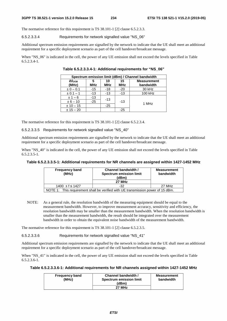
ETSI
ETSI TS 138 521-1 V15.2.0 (2019-05)2343GPP TS 38.521-1 version 15.2.0 Release 15
The normative reference for this requirement is TS 38.101-1 [2] clause 6.5.2.3.3.
6.5.2.3.3.4 Requirements for network signalled value "NS_06"
Additional spectrum emission requirements are signalled by the network to indicate that the UE shall meet an additional requirement for a specific deployment scenario as part of the cell handover/broadcast message.
When "NS_06" is indicated in the cell, the power of any UE emission shall not exceed the levels specified in Table 6.5.2.3.4-1.
Table 6.5.2.3.3.4-1: Additional requirements for “NS_06”
Spectrum emission limit (dBm) / Channel bandwidth ΔfOOB (MHz)
5 MHz
10 MHz
15 MHz
Measurement bandwidth
± 0 – 0.1 -15 -18 -20 30 kHz ± 0.1 – 1 -13 -13 -13 100 kHz ± 1 – 6 -13
-13 -13
1 MHz ± 6 – 10 -25 ± 10 – 15 -25 ± 15 – 20 -25
The normative reference for this requirement is TS 38.101-1 [2] clause 6.5.2.3.4.
6.5.2.3.3.5 Requirements for network signalled value "NS_40"
Additional spectrum emission requirements are signalled by the network to indicate that the UE shall meet an additional requirement for a specific deployment scenario as part of the cell handover/broadcast message.
When "NS_40" is indicated in the cell, the power of any UE emission shall not exceed the levels specified in Table 6.5.2.3.5-1.
Table 6.5.2.3.3.5-1: Additional requirements for NR channels are assigned within 1427-1452 MHz
Frequency band (MHz)
Channel bandwidth / Spectrum emission limit
(dBm)
Measurement bandwidth
27 MHz 1400 ≤ f ≤ 1427 -32 27 MHz
NOTE 1: This requirement shall be verified with UE transmission power of 15 dBm.
NOTE: As a general rule, the resolution bandwidth of the measuring equipment should be equal to the measurement bandwidth. However, to improve measurement accuracy, sensitivity and efficiency, the resolution bandwidth may be smaller than the measurement bandwidth. When the resolution bandwidth is smaller than the measurement bandwidth, the result should be integrated over the measurement bandwidth in order to obtain the equivalent noise bandwidth of the measurement bandwidth.
The normative reference for this requirement is TS 38.101-1 [2] clause 6.5.2.3.5.
6.5.2.3.3.6 Requirements for network signalled value “NS_41”
Additional spectrum emission requirements are signalled by the network to indicate that the UE shall meet an additional requirement for a specific deployment scenario as part of the cell handover/broadcast message.
When "NS_41" is indicated in the cell, the power of any UE emission shall not exceed the levels specified in Table 6.5.2.3.6-1.
Table 6.5.2.3.3.6-1: Additional requirements for NR channels assigned within 1427-1452 MHz
Frequency band (MHz)
Channel bandwidth / Spectrum emission limit
(dBm)
Measurement bandwidth
27 MHz

ETSI
ETSI TS 138 521-1 V15.2.0 (2019-05)2353GPP TS 38.521-1 version 15.2.0 Release 15
1400 ≤ f ≤ 1427 -32 27 MHz NOTE 1: This requirement shall be verified with UE transmission power of 15 dBm.
NOTE: As a general rule, the resolution bandwidth of the measuring equipment should be equal to the measurement bandwidth. However, to improve measurement accuracy, sensitivity and efficiency, the resolution bandwidth may be smaller than the measurement bandwidth. When the resolution bandwidth is smaller than the measurement bandwidth, the result should be integrated over the measurement bandwidth in order to obtain the equivalent noise bandwidth of the measurement bandwidth.
The normative reference for this requirement is TS 38.101-1 [2] clause 6.5.2.3.6.
6.5.2.3.3.7 Requirements for network signalled value "NS_42"
Additional spectrum emission requirements are signalled by the network to indicate that the UE shall meet an additional requirement for a specific deployment scenario as part of the cell handover/broadcast message.
When "NS_42" is indicated in the cell, the power of any UE emission shall not exceed the levels specified in Table 6.5.2.3.7-1.
Table 6.5.2.3.3.7-1: Additional requirements for NR channels assigned within 1492-1517 MHz
Frequency band (MHz)
Channel bandwidth / Spectrum emission limit
(dBm)
Measurement bandwidth
1 MHz 1518 ≤ f ≤ 1520 -0.8 1 MHz 1520 < f ≤ 1559 -30 1 MHz
NOTE: As a general rule, the resolution bandwidth of the measuring equipment should be equal to the measurement bandwidth. However, to improve measurement accuracy, sensitivity and efficiency, the resolution bandwidth may be smaller than the measurement bandwidth. When the resolution bandwidth is smaller than the measurement bandwidth, the result should be integrated over the measurement bandwidth in order to obtain the equivalent noise bandwidth of the measurement bandwidth.
The normative reference for this requirement is TS 38.101-1 [2] clause 6.5.2.3.7.
6.5.2.3.4 Test description
6.5.2.3.4.1 Initial conditions
Initial conditions are a set of test configurations the UE needs to be tested in and the steps for the SS to take with the UE to reach the correct measurement state.
The initial test configurations consist of environmental conditions, test frequencies, test channel bandwidths and sub-carrier spacing based on NR operating bands specified in table 5.3.5-1. All of these configurations shall be tested with applicable test parameters for each combination of test channel bandwidth and sub-carrier spacing, and are shown in table 6.2.3.4.1-1 through 6.2.3.4.1-2”. The details of the uplink reference measurement channels (RMCs) are specified in Annexes A.2 . Configurations of PDSCH and PDCCH before measurement are specified in Annex C.2.
1. Connect the SS to the UE antenna connectors as shown in TS 38.508-1 [5] Annex A, Figure A.3.1.1.1 for TE diagram and section A.3.2.1 for UE diagram.
2. The parameter settings for the cell are set up according to TS 38.508-1 [5] subclause 4.4.3..
3. Downlink signals are initially set up according to Annex C.0, C.1, C.2 and uplink signals according Annex G.0, G.1, G.2, G.3.0..
4. The UL Reference Measurement channels are set according to the applicable table from Table 6.2.3.4.1-1 to Table 6.2.3.4.1-2.
5. Propagation conditions are set according to Annex B.0.

ETSI
ETSI TS 138 521-1 V15.2.0 (2019-05)2363GPP TS 38.521-1 version 15.2.0 Release 15
6. Ensure the UE is in state RRC_CONNECTED with generic procedure parameters Connectivity NR, Connected without release On, Test Mode On and Test Loop Function On according to TS 38.508-1 [5] clause 4.5. Message contents are defined in clause 6.2.3.4.3.
6.5.2.3.4.2 Test procedure
1. SS sends uplink scheduling information for each UL HARQ process via PDCCH DCI format [0_1] for C_RNTI to schedule the UL RMC according to the applicable table from table 6.2.4.3.1-1 to table 6.2.4.3.1-2.1. Since the UE has no payload data to send, the UE transmits uplink MAC padding bits on the UL RMC.
2. Send continuously uplink power control "up" commands in the uplink scheduling information to the UE. Allow at least 200ms starting from the first TPC command in this step for the UE to reach PUMAX level.
3. Measure the mean power of the UE in the channel bandwidth of the radio access mode. The period of measurement shall be at least the continuous duration one sub-frame (1ms). For TDD slots with transient periods are not under test.
6.5.2.3.4.3 Message contents
Message contents are according to TS 38.508-1 [5] subclause [TBD], with the following exceptions for each network signalled value.
6.5.2.3.4.3.1 Message contents exceptions (network signalled value " NS_35")
For " NS_35" see A-MPR test case in table 6.2.3.4.3.2-1.
6.5.2.3.4.3.2 Message contents exceptions (network signalled value "NS_04")
For "NS_04" see A-MPR test case in table 6.2.3.4.3.4-1.
6.5.2.3.5 Test requirement
Table 6.5.2.3.5-1: Test Tolerance (Additional spectrum emission mask)
f ≤ 3.0GHz 3.0GHz < f ≤ 4.2GHz 4.2GHz < f ≤ 6.0GHz BW ≤ 100MHz 1.5 dB 1.8 dB 1.8 dB
6.5.2.3.5.1 Test requirements (network signalled value "NS_35")
When "NS_35" is indicated in the cell:
- the measured UE mean power in the channel bandwidth, derived in step 3, shall fulfil requirements in table 6.5.2.3.5.1-1 as appropriate for a NR UE.
and
- the power of any UE emission shall fulfil requirements in table [TBD], as applicable.

ETSI
ETSI TS 138 521-1 V15.2.0 (2019-05)2373GPP TS 38.521-1 version 15.2.0 Release 15
Table 6.5.2.3.5.1-1: Additional test requirements "NS_35"
ΔfOOB (MHz)
5 MHz
10 MHz
15 MHz
20 MHz
Measurement bandwidth
(unless otherwise
stated) ± 0-0.1 -15 +
TT -18 + TT
-20 + TT
-21 + TT
30 kHz
± 0.1-6 -13 + TT
-13 + TT
-13 + TT
-13 + TT
100 kHz
± 6-10 -25 + TT 1
-13 + TT
-13 + TT
-13 + TT
100 kHz
± 10-15 -25 + TT1
-13 + TT
-13 + TT
100 kHz
± 15-20 -25 + TT 1
-13 + TT
100 kHz
± 20-25 -25 + TT
1 MHz
NOTE 1: The measurement bandwidth shall be 1 MHz NOTE 2: TT for each frequency and channel bandwidth is specified
in Table 6.5.2.3.5-1.
6.5.2.3.5.2 Test requirements (network signalled value "NS_04")
When "NS_04" is indicated in the cell:
- the measured UE mean power in the channel bandwidth, derived in step 3, shall fulfil requirements in Table 6.2.3.5-2 for UE power class 2 or Table 6.2.3.5-3 UE power class 2.
and
- the power of any UE emission shall fulfil requirements in table 6.5.2.3.5.2-1.
Table 6.5.2.3.5.2-1: Additional test requirements for "NS_04"
Spectrum emission limit (dBm) / measurement bandwidth for each channel bandwidth
ΔfOOB MHz
10 MHz
15 MHz
20 MHz
40 MHz
50 MHz
60 MHz
80 MHz
90 MHz
100 MHz
Measurement bandwidth
± 0 - 1 -10 + TT -10 + TT -10 + TT -10 + TT 2 % channel bandwidth
-10 + TT 1 MHz
± 1 - 5 -10 + TT
1 MHz ± 5 - X -13 + TT ± X - (BWChannel + 5
MHz) -25 + TT
NOTE1: X is defined in Table 6.5.2.3.2-1 for CP-OFDM and 6.5.2.3.2-2 for DFT-S-OFDM NOTE2: TT for each frequency and channel bandwidth is specified in Table 6.5.2.3.5-1.
6.5.2.4 Adjacent channel leakage ratio
Adjacent channel leakage power Ratio (ACLR) is the ratio of the filtered mean power centred on the assigned channel frequency to the filtered mean power centred on an adjacent channel frequency.
6.5.2.4.1 NR ACLR
Editor’s note: The following aspects are either missing or not yet determined:
- Only for DFT-s-OFDM PI/2 BPSK pending analysis about DFT-s-OFDM PI/2 BPSK test points is required to aligned with DFT-s-OFDM PI/2 BPSK MPR requirements defined in TS 38.101-1 v15.4.0.

ETSI
ETSI TS 138 521-1 V15.2.0 (2019-05)2383GPP TS 38.521-1 version 15.2.0 Release 15
6.5.2.4.1.1 Test purpose
To verify that UE transmitter does not cause unacceptable interference to adjacent channels in terms of Adjacent Channel Leakage power Ratio (ACLR).
6.5.2.4.1.2 Test applicability
This test case applies to all types of NR UE release 15 and forward.
6.5.2.4.1.3 Minimum conformance requirements
NR adjacent channel leakage power ratio (NRACLR) is the ratio of the filtered mean power centred on the assigned NR channel frequency to the filtered mean power centred on an adjacent NR channel frequency at nominal channel spacing.
The assigned NR channel power and adjacent NR channel power are measured with rectangular filters with measurement bandwidths specified in Table 6.5.2.4.1.3-1.
If the measured adjacent channel power is greater than –50dBm then the NRACLR shall be higher than the value specified in Table 6.5.2.4.1.3-2.
Table 6.5.2.4.1.3-1: NR ACLR measurement bandwidth
NR channel bandwidth / NR ACLR measurement bandwidth
5
MHz 10
MHz 15
MHz 20
MHz 25
MHz 30
MHz 40
MHz 50
MHz 60
MHz 80
MHz 90
MHz 100 MHz
NR ACLR measurement
bandwidth 4.515 9.375 14.235 19.095 23.955 28.815 38.895 48.615 58.35 78.15 88.23 98.31
Table 6.5.2.4.1.3-2: NR ACLR requirement
Power class 1 Power class 2 Power class 3 NR ACLR 31 dB 30 dB
The normative reference for this requirement is TS 38.101-1 [2] clause 6.5.2.4.1.
6.5.2.4.1.4 Test description
6.5.2.4.1.4.1 Initial conditions
Initial conditions are a set of test configurations the UE needs to be tested in and the steps for the SS to take with the UE to reach the correct measurement state.
The initial test configurations consist of environmental conditions, test frequencies, test channel bandwidths and sub-carrier spacing based on NR operating bands specified in table 5.3.5-1. All of these configurations shall be tested with applicable test parameters for each combination of channel bandwidth and sub-carrier spacing, are shown in table 6.5.2.4.1.4.1-1. The details of the uplink reference measurement channels (RMCs) are specified in Annexes A.2. Configurations of PDSCH and PDCCH before measurement are specified in Annex C.2
ETSI
ETSI TS 138 521-1 V15.2.0 (2019-05)2393GPP TS 38.521-1 version 15.2.0 Release 15
Table 6.5.2.4.1.4.1-1: Test Configuration Table

ETSI
ETSI TS 138 521-1 V15.2.0 (2019-05)2403GPP TS 38.521-1 version 15.2.0 Release 15
Default Conditions Test Environment as specified in TS 38.508-1 [5] subclause 4.1
Normal, TL/VL, TL/VH, TH/VL, TH/VH
Test Frequencies as specified in TS 38.508-1 [5] subclause 4.3.1
Low range, High range
Test Channel Bandwidths as specified in TS 38.508-1 [5] subclause 4.3.1
Lowest, Highest
Test SCS as specified in Table 5.3.5-1 Lowest, Highest Test Parameters for Channel Bandwidths
Test ID
Freq ChBw SCS Downlink Configuration
Uplink Configuration
Default Default N/A for Adjacent Channel
Leakage Ratio test case
Modulation (NOTE 2)
RB allocation (NOTE 1)
13 Default DFT-s-OFDM PI/2 BPSK
Inner_Full
23 Low DFT-s-OFDM PI/2 BPSK
Edge_1RB_Left
33 High DFT-s-OFDM PI/2 BPSK
Edge_1RB_Right
43 Default DFT-s-OFDM PI/2 BPSK
Outer_Full
5 Default DFT-s-OFDM QPSK
Inner_Full
6 Low DFT-s-OFDM QPSK
Edge_1RB_Left
7 High DFT-s-OFDM QPSK
Edge_1RB_Right
8 Default DFT-s-OFDM QPSK
Outer_Full
9 Default DFT-s-OFDM 16 QAM
Inner_Full
10 Low DFT-s-OFDM 16 QAM
Edge_1RB_Left
11 High DFT-s-OFDM 16 QAM
Edge_1RB_Right
12 Default DFT-s-OFDM 16 QAM
Outer_Full
13 Low DFT-s-OFDM 64 QAM
Edge_1RB_Left
14 High DFT-s-OFDM 64 QAM
Edge_1RB_Right
15 Default DFT-s-OFDM 64 QAM
Outer_Full
16 Low DFT-s-OFDM 256 QAM
Edge_1RB_Left
17 High DFT-s-OFDM 256 QAM
Edge_1RB_Right
18 Default DFT-s-OFDM 256 QAM
Outer_Full
19 Default CP-OFDM QPSK Inner_Full 20 Low CP-OFDM QPSK Edge_1RB_Left 21 High CP-OFDM QPSK Edge_1RB_Right 22 Default CP-OFDM QPSK Outer_Full 23 Default CP-OFDM 16
QAM Inner_Full
24 Low CP-OFDM 16 QAM
Edge_1RB_Left
25 High CP-OFDM 16 QAM
Edge_1RB_Right
26 Default CP-OFDM 16 QAM
Outer_Full
27 Low CP-OFDM 64 QAM
Edge_1RB_Left
28 High CP-OFDM 64 QAM
Edge_1RB_Right
29 Default CP-OFDM 64 QAM
Outer_Full
ETSI
ETSI TS 138 521-1 V15.2.0 (2019-05)2413GPP TS 38.521-1 version 15.2.0 Release 15
30 Low CP-OFDM 256 QAM
Edge_1RB_Left
31 High CP-OFDM 256 QAM
Edge_1RB_Right
32 Default CP-OFDM 256 QAM
Outer_Full
NOTE 1: The specific configuration of each RF allocation is defined in Table 6.1-1. NOTE 2: DFT-s-OFDM PI/2 BPSK test applies only for UEs which supports half Pi BPSK in FR1. NOTE 3: For Power Class 3 testing, include two steps for UE operating in bands n40, n77, n78
and n79, with IE [P-Boost-BPSK] set to 1 and 0 separately.
1. Connect the SS to the UE antenna connectors as shown in TS 38.508-1 [5] Annex A, Figure A.3.1.1.1 for TE diagram and section A.3.2.1 for UE diagram.
2. The parameter settings for the cell are set up according to TS 38.508-1 [5] subclause 4.4.3.
3. Downlink signals are initially set up according to Annex C.0, C.1, C.2 , and uplink signals according to Annex G.0, G.1, G.2, G.3.0 .
4. The UL Reference Measurement channels are set according to Table 6.5.2.4.1.4.1-1.
5. Propagation conditions are set according to Annex B.0
6. Ensure the UE is in state RRC_CONNECTED with generic procedure parameters Connectivity NR, Connected without release On, Test Mode On and Test Loop Function On according to TS 38.508-1 [5] clause 4.5. Message contents are defined in clause 6.5.2.4.1.4.3
6.5.2.4.1.4.2 Test procedure
1. SS sends uplink scheduling information for each UL HARQ process via PDCCH DCI format 0_1 for C_RNTI to schedule the UL RMC according to Table 6.5.2.2.1.4.1-1. Since the UL has no payload and no loopback data to send the UE sends uplink MAC padding bits on the UL RMC.
2. Send continuously power control “up” commands to the UE until the UE transmits at PUMAX level. Allow at least 200ms for the UE to reach PUMAX level.
3. Measure the mean power of the UE in the channel bandwidth of the radio access mode according to the test configuration, which shall meet the requirements described in Tables 6.2.2.5-1 and 6.2.2.5-5 as appropriate. The period of the measurement shall be at least the continuous duration of 1ms over consecutive active uplink slots. For TDD, only slots consisting of only UL symbols are under test.
4. Measure the rectangular filtered mean power for the assigned NR channel.
5. Measure the rectangular filtered mean power of the first NR adjacent channel on both lower and upper side of the assigned NR channel, respectively.
6. Calculate the ratios of the power between the values measured in step 4 over step 5 for lower and upper NR ACLR, respectively.
NOTE 1: When switching to DFT-s-OFDM waveform, as specified in the test configuration table 6.5.2.4.1.4.1-1, send an NR RRCReconfiguration message according to TS 38.508-1 [5] clause 4.6.3 Table 4.6.3-118 PUSCH-Config with TRANSFORM_PRECODER_ENABLED condition.
6.5.2.4.1.4.3 Message contents
Message contents are according to TS 38.508-1 [5] subclause 4.6.
6.5.2.4.1.5 Test requirement
The measured UE mean power in the channel bandwidth, derived in step 3, shall fulfil requirements in Tables 6.2.2.5-1 and 6.2.2.5-5 as appropriate, and if the measured adjacent channel power is greater than –50 dBm then the measured NR ACLR, derived in step 6, shall be higher than the limits in Table 6.5.2.4.1.5-2.
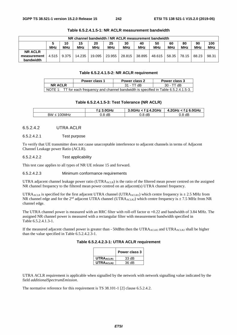
ETSI
ETSI TS 138 521-1 V15.2.0 (2019-05)2423GPP TS 38.521-1 version 15.2.0 Release 15
Table 6.5.2.4.1.5-1: NR ACLR measurement bandwidth
NR channel bandwidth / NR ACLR measurement bandwidth
5
MHz 10
MHz 15
MHz 20
MHz 25
MHz 30
MHz 40
MHz 50
MHz 60
MHz 80
MHz 90
MHz 100 MHz
NR ACLR measurement
bandwidth 4.515 9.375 14.235 19.095 23.955 28.815 38.895 48.615 58.35 78.15 88.23 98.31
Table 6.5.2.4.1.5-2: NR ACLR requirement
Power class 1 Power class 2 Power class 3 NR ACLR 31 - TT dB 30 - TT dB
NOTE 1: TT for each frequency and channel bandwidth is specified in Table 6.5.2.4.1.5-3.
Table 6.5.2.4.1.5-3: Test Tolerance (NR ACLR)
f ≤ 3.0GHz 3.0GHz < f ≤ 4.2GHz 4.2GHz < f ≤ 6.0GHz BW ≤ 100MHz 0.8 dB 0.8 dB 0.8 dB
6.5.2.4.2 UTRA ACLR
6.5.2.4.2.1 Test purpose
To verify that UE transmitter does not cause unacceptable interference to adjacent channels in terms of Adjacent Channel Leakage power Ratio (ACLR).
6.5.2.4.2.2 Test applicability
This test case applies to all types of NR UE release 15 and forward.
6.5.2.4.2.3 Minimum conformance requirements
UTRA adjacent channel leakage power ratio (UTRAACLR) is the ratio of the filtered mean power centred on the assigned NR channel frequency to the filtered mean power centred on an adjacent(s) UTRA channel frequency.
UTRAACLR is specified for the first adjacent UTRA channel (UTRAACLR1) which centre frequency is ± 2.5 MHz from NR channel edge and for the 2nd adjacent UTRA channel (UTRAACLR2) which centre frequency is ± 7.5 MHz from NR channel edge.
The UTRA channel power is measured with an RRC filter with roll-off factor α =0.22 and bandwidth of 3.84 MHz. The assigned NR channel power is measured with a rectangular filter with measurement bandwidth specified in Table 6.5.2.4.1.3-1.
If the measured adjacent channel power is greater than - 50dBm then the UTRAACLR1 and UTRAACLR2 shall be higher than the value specified in Table 6.5.2.4.2.3-1.
Table 6.5.2.4.2.3-1: UTRA ACLR requirement
Power class 3
UTRAACLR1 33 dB UTRAACLR2 36 dB
UTRA ACLR requirement is applicable when signalled by the network with network signalling value indicated by the field additionalSpectrumEmission.
The normative reference for this requirement is TS 38.101-1 [2] clause 6.5.2.4.2.

ETSI
ETSI TS 138 521-1 V15.2.0 (2019-05)2433GPP TS 38.521-1 version 15.2.0 Release 15
6.5.2.4.2.4 Test description
6.5.2.4.2.4.1 Initial conditions
Same as in subclause 6.5.2.4.1.4.1 with the following exepction;
- For band n8 and n81, use 15MHz test channel bandwidth instead of Highest if NS_08U is signaled.
6.5.2.4.2.4.2 Test procedure
1. SS sends uplink scheduling information for each UL HARQ process via PDCCH DCI format 0_1 for C_RNTI to schedule the UL RMC according to Table 6.5.2.2.1.4.1-1. Since the UL has no payload and no loopback data to send the UE sends uplink MAC padding bits on the UL RMC.
2. Send continuously power control “up” commands to the UE until the UE transmits at PUMAX level. Allow at least 200ms for the UE to reach PUMAX level.
3. Measure the mean power of the UE in the channel bandwidth of the radio access mode according to the test configuration, which shall meet the requirements described in Tables 6.2.2.5-1 and 6.2.2.5-5 as appropriate. The period of the measurement shall be at least the continuous duration of one active sub-frame (1ms) and in the uplink symbols. For TDD slots with transient periods are not under test.
4. Measure the rectangular filtered mean power for the assigned NR channel.
5. Measure the RRC filtered mean power of the first and the second UTRA adjacent channel on both lower and upper side of the NR channel, respectively.
6. Calculate the ratios of the power between the values measured in step 4 over step 5 for lower and upper UTRA ACLR, respectively.
NOTE 1: When switching to DFT-s-OFDM waveform, as specified in the test configuration table 6.5.2.4.2.4.1-1, send an NR RRCReconfiguration message according to TS 38.508-1 [5] clause 4.6.3 Table 4.6.3-118 PUSCH-Config with TRANSFORM_PRECODER_ENABLED condition.
6.5.2.4.2.4.3 Message contents
Message contents are according to TS 38.508-1 [5] subclause 4.6 with the following exceptions:
Table 6.5.2.4.2.4.3-1: AdditionalSpectrumEmission
Derivation Path: 38.508-1 [5] clause 4.6.3, Table 4.6.3-1 AdditionalSpectrumEmission Information Element Value/remark Comment Condition
AdditionalSpectrumEmission NS_03U NS_05U NS_08U NS_100
for band n2, n25, n66 for band n1, n84 for band n8, n81 for band n1, n2, n3, n5, n8, n20, n25, n66, n80, n81, n82, n84 (NOTE1)
NOTE 1: This NS can be signalled for NR bands that have UTRA services deployed
6.5.2.4.2.5 Test requirement
The measured UE mean power in the channel bandwidth, derived in step 3, shall fulfil requirements in Tables 6.2.2.5-1 and 6.2.2.5-5 as appropriate, and if the measured adjacent channel power is greater than –50 dBm then the measured UTRA ACLR, derived in step 6, shall be higher than the limits in table 6.5.2.2.1.5-2.
Table 6.5.2.4.2.5-1: Measurement bandwidth for NR carrier
NR channel bandwidth / NR ACLR measurement bandwidth
5 MHz
10 MHz
15 MHz
20 MHz
25 MHz
30 MHz
40 MHz
50 MHz
60 MHz
80 MHz
90 MHz
100 MHz
NR ACLR measurement
bandwidth 4.515 9.375 14.235 19.095 23.955 28.815 38.895 48.615 58.35 78.15 88.23 98.31
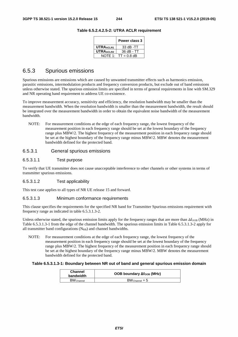
ETSI
ETSI TS 138 521-1 V15.2.0 (2019-05)2443GPP TS 38.521-1 version 15.2.0 Release 15
Table 6.5.2.4.2.5-2: UTRA ACLR requirement
Power class 3
UTRAACLR1 33 dB -TT UTRAACLR2 36 dB - TT
NOTE 1: TT = 0.8 dB
6.5.3 Spurious emissions
Spurious emissions are emissions which are caused by unwanted transmitter effects such as harmonics emission, parasitic emissions, intermodulation products and frequency conversion products, but exclude out of band emissions unless otherwise stated. The spurious emission limits are specified in terms of general requirements in line with SM.329 and NR operating band requirement to address UE co-existence.
To improve measurement accuracy, sensitivity and efficiency, the resolution bandwidth may be smaller than the measurement bandwidth. When the resolution bandwidth is smaller than the measurement bandwidth, the result should be integrated over the measurement bandwidth in order to obtain the equivalent noise bandwidth of the measurement bandwidth.
NOTE: For measurement conditions at the edge of each frequency range, the lowest frequency of the measurement position in each frequency range should be set at the lowest boundary of the frequency range plus MBW/2. The highest frequency of the measurement position in each frequency range should be set at the highest boundary of the frequency range minus MBW/2. MBW denotes the measurement bandwidth defined for the protected band.
6.5.3.1 General spurious emissions
6.5.3.1.1 Test purpose
To verify that UE transmitter does not cause unacceptable interference to other channels or other systems in terms of transmitter spurious emissions.
6.5.3.1.2 Test applicability
This test case applies to all types of NR UE release 15 and forward.
6.5.3.1.3 Minimum conformance requirements
This clause specifies the requirements for the specified NR band for Transmitter Spurious emissions requirement with frequency range as indicated in table 6.5.3.1.3-2.
Unless otherwise stated, the spurious emission limits apply for the frequency ranges that are more than ΔfOOB (MHz) in Table 6.5.3.1.3-1 from the edge of the channel bandwidth. The spurious emission limits in Table 6.5.3.1.3-2 apply for all transmitter band configurations (NRB) and channel bandwidths.
NOTE: For measurement conditions at the edge of each frequency range, the lowest frequency of the measurement position in each frequency range should be set at the lowest boundary of the frequency range plus MBW/2. The highest frequency of the measurement position in each frequency range should be set at the highest boundary of the frequency range minus MBW/2. MBW denotes the measurement bandwidth defined for the protected band.
Table 6.5.3.1.3-1: Boundary between NR out of band and general spurious emission domain
Channel bandwidth OOB boundary ΔfOOB (MHz)
BWChannel BWChannel + 5

ETSI
ETSI TS 138 521-1 V15.2.0 (2019-05)2453GPP TS 38.521-1 version 15.2.0 Release 15
Table 6.5.3.1.3-2: Requirement for general spurious emissions limits
Frequency Range Maximum Level
Measurement bandwidth
NOTE
9 kHz ≤ f < 150 kHz -36 dBm 1 kHz 150 kHz ≤ f < 30 MHz -36 dBm 10 kHz
30 MHz ≤ f < 1000 MHz -36 dBm 100 kHz 1 GHz ≤ f < 12.75 GHz -30 dBm 1 MHz
-25 dBm 1 MHz 3 12.75 GHz ≤ f < 5th
harmonic of the upper frequency edge of the UL operating band in
GHz
-30 dBm 1 MHz 1
12.75 GHz < f < 26 GHz -30 dBm 1 MHz 2 NOTE 1: Applies for Band that the upper frequency edge of the UL Band more
than 2.69 GHz NOTE 2: Applies for Band that the upper frequency edge of the UL Band more
than 5.2 GHz NOTE 3: Applies for Band n41, CA configurations including Band n41, and EN-
DC configurations that include n41 specified in sub-clause 5.2B of [4] when NS_04 is signalled.
The normative reference for this requirement is TS 38.101-1 [2] subclause 6.5.3.1
6.5.3.1.4 Test description
6.5.3.1.4.1 Initial conditions
Initial conditions are a set of test configurations the UE needs to be tested in and the steps for the SS to take with the UE to reach the correct measurement state.
The initial test configurations consist of environmental conditions, test frequencies, test channel bandwidths and sub-carrier spacing based on NR operating bands specified in Table 5.3.5-1. All of these configurations shall be tested with applicable test parameters for each combination of channel bandwidth and sub-carrier spacing, are shown in table 6.5.3.1.4.1-1. The details of the uplink reference measurement channels (RMCs) are specified in Annexes A.2. Configurations of PDSCH and PDCCH before measurement are specified in Annex C.2.
Table 6.5.3.1.4.1-1: Test Configuration Table
Initial Conditions Test Environment as specified in TS 38.508-1 [5] subclause 4.1.
Normal
Test Frequencies as specified in TS 38.508-1 [5] subclause 4.3.1.
Low range, Mid range, High range
Test Channel Bandwidths as specified in TS 38.508-1 [5] subclause 4.3.1.
Lowest, Mid, Highest
Test SCS as specified in Table 5.3.5-1 Lowest Test Parameters
Test ID Downlink Configuration Uplink Configuration
N/A for Spurious Emissions testing
Modulation RB allocation (NOTE 1) 1 CP-OFDM QPSK OuterFull 2 CP-OFDM QPSK Edge_1RB_Left 3 CP-OFDM QPSK Edge_1RB_Right
NOTE 1: The specific configuration of each RB allocation is defined in Table 6.1-1 Common UL configuration
1. Connect the SS to the UE antenna connectors as shown in TS 38.508-1 [5] Annex A, Figure A.3.1.1.1 for TE diagram and section A.3.2.1 for UE diagram.
2. The parameter settings for the cell are set up according to TS 38.508-1 [5] subclause 4.4.3.
3. Downlink signals are initially set up according to Annex C.0, C.1 and C.2, and uplink signals according to Annex G.0, G.1, G.2, G.3.0.

ETSI
ETSI TS 138 521-1 V15.2.0 (2019-05)2463GPP TS 38.521-1 version 15.2.0 Release 15
4. The UL Reference Measurement channels are set according to Table 6.5.3.1.4.1-1.
5. Propagation conditions are set according to Annex B.0.
6. Ensure the UE is in state RRC_CONNECTED with generic procedure parameters Connectivity NR, Connected without release On, Test Mode On and Test Loop Function On according to TS 38.508-1 [5] clause 4.5. Message contents are defined in clause 6.5.3.1.4.3.
6.5.3.1.4.2 Test procedure
1. SS sends uplink scheduling information for each UL HARQ process via PDCCH DCI format [0_1] for C_RNTI to schedule the UL RMC according to Table 6.5.3.1.4.1-1. Since the UE has no payload data to send, the UE transmits uplink MAC padding bits on the UL RMC.
2. Send continuously uplink power control "up" commands in the uplink scheduling information to the UE until the UE transmits at PUMAX level.
3. Measure the power of the transmitted signal with a measurement filter of bandwidths according to table 6.5.3.1.5-1. The centre frequency of the filter shall be stepped in contiguous steps according to table 6.5.3.1.5-1. The measured power shall be verified for each step. The measurement period shall capture the active time slots.
6.5.3.1.4.3 Message contents
Message contents are according to TS 38.508-1 [5] subclause 4.6.
6.5.3.1.5 Test requirement
This clause specifies the requirements for the specified NR band for Transmitter Spurious emissions requirement with frequency range as indicated in table 6.5.3.1.5-1.
Unless otherwise stated, the spurious emission limits apply for the frequency ranges that are more than ΔfOOB (MHz) in Table 6.5.3.1.3-1 from the edge of the channel bandwidth. The spurious emission limits in Table 6.5.3.1.5-1 apply for all transmitter band configurations (NRB) and channel bandwidths.
The measured average power of spurious emission, derived in step 3, shall not exceed the described value in Table 6.5.3.1.5-1.
Table 6.5.3.1.5-1: General spurious emissions test requirements
Frequency Range Maximum Level
Measurement bandwidth
NOTE
9 kHz ≤ f < 150 kHz -36 dBm 1 kHz 150 kHz ≤ f < 30 MHz -36 dBm 10 kHz
30 MHz ≤ f < 1000 MHz -36 dBm 100 kHz 1 GHz ≤ f < 12.75 GHz -30 dBm 1 MHz
-25 dBm 1 MHz 3 12.75 GHz ≤ f < 5th
harmonic of the upper frequency edge of the UL operating band in
GHz
-30 dBm 1 MHz 1
12.75 GHz < f < 26 GHz -30 dBm 1 MHz 2 NOTE 1: Applies for Band that the upper frequency edge of the UL Band more
than 2.69 GHz NOTE 2: Applies for Band that the upper frequency edge of the UL Band more
than 5.2 GHz NOTE 3: Applies for Band n41, CA configurations including Band n41, and EN-
DC configurations that include n41 specified in sub-clause 5.2B of [4] when NS_04 is signalled.

ETSI
ETSI TS 138 521-1 V15.2.0 (2019-05)2473GPP TS 38.521-1 version 15.2.0 Release 15
6.5.3.2 Spurious emission for UE co-existence
6.5.3.2.1 Test purpose
To verify that UE transmitter does not cause unacceptable interference to co-existing systems for the specified bands which has specific requirements in terms of transmitter spurious emissions.
6.5.3.2.2 Test applicability
This test case applies to all types of NR UE release 15 and forward.
6.5.3.2.3 Minimum conformance requirements
This clause specifies the requirements for the specified NR band for coexistence with protected bands as indicated in Table 6.5.3.2.3-1.
NOTE: For measurement conditions at the edge of each frequency range, the lowest frequency of the measurement position in each frequency range should be set at the lowest boundary of the frequency range plus MBW/2. The highest frequency of the measurement position in each frequency range should be set at the highest boundary of the frequency range minus MBW/2. MBW denotes the measurement bandwidth defined for the protected band.

ETSI
ETSI TS 138 521-1 V15.2.0 (2019-05)2483GPP TS 38.521-1 version 15.2.0 Release 15
Table 6.5.3.2.3-1: Requirements for spurious emissions for UE co-existence

ETSI
ETSI TS 138 521-1 V15.2.0 (2019-05)2493GPP TS 38.521-1 version 15.2.0 Release 15
NR Band
Spurious emission for UE co-existence
Protected band Frequency range (MHz)
Maximum
Level (dBm)
MBW (MHz)
NOTE
n1, n84 E-UTRA Band 1, 5, 7, 8, 11, 18, 19, 20, 21, 22, 26, 27, 28, 31, 32, 38, 40, 41, 42, 43, 44, 45, 50, 51, 65, 67, 68, 69, 72, 73,
74, 75, 76 NR Band n78, n79
FDL_low -- FDL_high -50 1
NR Band n77 FDL_low - FDL_high -50 1 2 E-UTRA Band 3, 34 FDL_low - FDL_high -50 1 15
Frequency range 1880 - 1895 -40 1 15, 27
Frequency range 1895 - 1915 -15.5 5 15, 26, 27
Frequency range 1915 - 1920 +1.6 5 15, 26,
27 n2 E-UTRA Band 4, 5, 10, 12, 13,
14, 17, 24, 26, 27, 28, 29, 30, 41, 42, 48, 50, 51, 66, 70, 71, 74
FDL_low - FDL_high -50 1
E-UTRA Band 2, 25 FDL_low - FDL_high -50 1 15 E-UTRA Band 43 FDL_low - FDL_high -50 1 2
n3, n80 E-UTRA Band 1, 5, 7, 8, 20, 26, 27, 28, 31, 32, 33, 34, 38, 39, 40, 41, 43, 44, 45, 50, 51, 65, 67, 68, 69, 72, 73,74, 75, 76
NR Band n79
FDL_low - FDL_high -50 1
E-UTRA Band 3 FDL_low - FDL_high -50 1 15 E-UTRA Band 11, 18, 19, 21 FDL_low - FDL_high -50 1 13
E-UTRA Band 22, 42 NR Band n77, n78
FDL_low - FDL_high -50 1 2
Frequency range 1884.5 - 1915.7 -41 0.3 13 n5 E-UTRA Band 1, 2, 3, 4, 5, 7, 8,
10, 12, 13, 14, 17, 18, 19, 24, 25, 26, 28, 29, 30, 31, 34, 38, 40, 42, 43, 45, 48, 50, 51, 65,
66, 70, 71, 73, 74, 85
FDL_low - FDL_high -50
E-UTRA Band 41, 52 FDL_low - FDL_high -50 1 2 E-UTRA Band 11, 21 FDL_low - FDL_high -50 1 39
Frequency range 1884.5 - 1915.7 -41 0.3 8,39 n7 E-UTRA Band 1, 2, 3, 4, 5, 7, 8,
10, 12, 13, 14, 17, 20, 22, 26, 27, 28, 29, 30, 31, 32, 33, 34, 40, 42, 43, 50, 51, 65, 66, 67,
68, 72, 74, 75, 76 NR Band n77, n78
FDL_low - FDL_high -50 1
Frequency range 2570 - 2575 +1.6 5 15, 21, 26
Frequency range 2575 - 2595 -15.5 5 15, 21, 26
Frequency range 2595 - 2620 -40 1 15, 21 n8, n81 E-UTRA Band 1, 20, 28, 31, 32,
33, 34, 38, 39, 40, 45, 50, 51, 65, 67, 68, 69, 72, 73, 74, 75, 76
FDL_low - FDL_high -50 1
E-UTRA band 3, 7, 22, 41, 42, 43
NR Band n77, n78, n79
FDL_low - FDL_high -50 1 2
E-UTRA 8 FDL_low - FDL_high -50 1 15 E-UTRA Band 11, 21 FDL_low - FDL_high -50 1 23
Frequency range 1884.5 - 1915.7 -41 0.3 8
n12 E-UTRA Band 2, 5, 13, 14, 17, 24, 25, 26, 27, 30, 41, 48, 50,
51, 71, 74
FDL_low - FDL_high -50 1

ETSI
ETSI TS 138 521-1 V15.2.0 (2019-05)2503GPP TS 38.521-1 version 15.2.0 Release 15
E-UTRA Band 4, 10, 66, 70 FDL_low - FDL_high -50 1 2 E-UTRA Band 12, 85 FDL_low - FDL_high -50 1 15
n20, n82 E-UTRA Band 1, 3, 7, 8, 22, 31, 32, 33, 34, 40, 43, 50, 51, 65,
67, 68, 72, 74, 75, 76
FDL_low - FDL_high -50 1
E-UTRA Band 20 FDL_low - FDL_high -50 1 15 E-UTRA Band 38, 42, 69
NR Band n77, n78 FDL_low - FDL_high -50 1 2
Frequency range 758 - 788 -50 1 n25 E-UTRA Band 4, 5, 10,12, 13,
14, 17, 24, 26, 27, 28, 29, 30, 41, 42, 48, 66, 70, 71, 85
FDL_low - FDL_high -50 1
E-UTRA Band 2 FDL_low - FDL_high -50 1 15 E-UTRA Band 25 FDL_low - FDL_high -50 1 15 E-UTRA Band 43 FDL_low - FDL_high -50 1 2
n28, n83 E-UTRA Band 1, 4, 10, 22, 42, 43, 50, 51, 65, 73, 74, 75, 76
NR Band n77, n78
FDL_low - FDL_high -50 1 2
E-UTRA Band 1 FDL_low - FDL_high -50 1 19, 25 E-UTRA Band 2, 3, 5, 7, 8, 18, 19, 20, 25, 26, 27, 31, 34, 38,
40, 41, 66, 72 NR Band n79
FDL_low - FDL_high -50 1
E-UTRA Band 11, 21 FDL_low - FDL_high -50 1 19, 24 Frequency range 470 - 694 -42 8 15, 35 Frequency range 470 - 710 -26.2 6 34 Frequency range 662 - 694 -26.2 6 15 Frequency range 758 - 773 -32 1 15 Frequency range 773 - 803 -50 1 Frequency range 1884.5 - 1915.7 -41 0.3 8, 19
n34 E-UTRA Band 1, 3, 7, 8, 11, 18, 19, 20, 21, 22, 26, 28, 31, 32,
33, 38,39, 40, 41, 42, 43, 44, 45, 50, 51, 65, 67, 69, 72, 74, 75, 76
NR Band n78, n79
FDL_low - FDL_high -50 1 5
NR Band n77 FDL_low - FDL_high -50 1 2 Frequency range 1884.5 - 1915.7 -41 0.3 8
n38 E-UTRA Band 1, 2, 3, 4, 5, 8, 10, 12, 13, 14, 17, 20, 22, 27, 28, 29, 30, 31, 32, 33, 34, 40, 42, 43, 50, 51, 65, 66, 67, 68,
72, 74, 75, 76
FDL_low - FDL_high -50 1
Frequency range 2620 - 2645 -15.5 5 15, 22, 26
Frequency range 2645 - 2690 -40 1 15, 22 n39 E-UTRA Band 1, 8, 22, 26, 34,
40, 41, 42, 44, 45, 50, 51, 74 NR Band n79
FDL_low - FDL_high -50
Frequency range 1805 - 1855 -40 1 33 Frequency range 1855 - 1880 -15.5 5 15, 26,
33 n40 E-UTRA Band 1, 3, 5, 7, 8, 20,
22, 26, 27, 28, 31, 32, 33, 34, 38, 39, 41, 42, 43, 44, 45, 50,
51, 65, 67, 68, 69, 72, 74, 75, 76 NR Band n77, n78
FDL_low - FDL_high -50 1
NR Band n79 FDL_low - FDL_high -50 1 2 n41 E-UTRA Band 1, 2, 3, 4, 5, 8,
10, 12, 13 , 14, 17, 24, 25, 26, 27, 28, 29, 30, 34, 39, 40, 42, 44, 45, 48, 50, 51, 65, 66, 70,
71, 73, 74 NR Band n77, n78
FDL_low - FDL_high -50 1
NR Band n79 FDL_low - FDL_high -50 1 2

ETSI
ETSI TS 138 521-1 V15.2.0 (2019-05)2513GPP TS 38.521-1 version 15.2.0 Release 15
E-UTRA Band 9, 11, 18, 19, 21 FDL_low - FDL_high -50 1 30 Frequency range 1884.5 1915.7 -41 0.3 8, 30
n50 E-UTRA Band 1, 2, 3, 4, 5, 7, 8, 12, 13, 17, 20, 26, 28, 29, 31, 34, 38, 39, 40, 41, 42, 43, 48,
65, 66, 67, 68
FDL_low - FDL_high -50 1
n51 E-UTRA Band 1, 2, 3, 4, 5, 7, 8, 12, 13, 17, 20, 26, 28, 29, 31, 34, 38, 39, 40, 41, 42, 43, 48,
65, 66, 67, 68
FDL_low - FDL_high -50 1
n66, n86 E-UTRA Band 2, 4, 5, 7, 12, 13, 17, 26, 28, 29, 38, 41, 43, 66,
70, 71
FDL_low - FDL_high -50 1
E-UTRA Band 42, 48 FDL_low - FDL_high -50 1 2 n70 E-UTRA Band 2, 4, 5, 10, 12,
13, 14, 17, 24, 25, 29, 30, 41, 48, 66, 70, 71
FDL_low - FDL_high -50 1 2
n71 E-UTRA Band 4, 5, 12, 13, 14, 17, 24, 26, 30, 48, 66, 85
FDL_low - FDL_high -50 1
E-UTRA Band 2, 25, 41, 70 FDL_low - FDL_high -50 1 2 E-UTRA Band 29 FDL_low - FDL_high -38 1 15 E-UTRA Band 71 FDL_low - FDL_high -50 1 15
n74 E-UTRA Band 1, 2, 3, 4, 5, 7, 8, 12, 13, 17, 18, 19, 20, 26, 28, 29, 31, 34, 38, 39, 40, 41, 42,
43, 48, 65, 66, 67, 68
FDL_low - FDL_high -50 1
Frequency range 1884.5 - 1915.7 -41 0.3 8 Frequency range 1400 - 1427 -32 27 15, 41 Frequency range 1475 - 1488 -50 1 42 Frequency range 1488 - 1518 -50 1 15
n77, n78 E-UTRA Band 1, 3, 5, 7, 8, 11, 18, 19, 20, 21, 26, 28, 34, 39,
40, 41, 65
FDL_low - FDL_high -50 1
Frequency range 1884.5 - 1915.7 -41 0.3 8 n79 E-UTRA Band 1, 3, 5, 8, 11, 18,
19, 21, 28, 34, 39, 40, 41, 42, 65 FDL_low - FDL_high -50 1
Frequency range 1884.5 - 1915.7 -41 0.3 8 n80 See n3 n81 See n8 n82 See n20 n83 See n28 n84 See n1 n86 See n66
ETSI
ETSI TS 138 521-1 V15.2.0 (2019-05)2523GPP TS 38.521-1 version 15.2.0 Release 15
NOTE 1: FDL_low and FDL_high refer to each frequency band specified in Table 5.2-1 in TS 38.101-1 [2]. NOTE 2: As exceptions, measurements with a level up to the applicable requirements defined in Table
6.5.3.1.3-2 are permitted for each assigned NR carrier used in the measurement due to 2nd, 3rd, 4th [or 5th] harmonic spurious emissions. Due to spreading of the harmonic emission the exception is also allowed for the first 1 MHz frequency range immediately outside the harmonic emission on both sides of the harmonic emission. This results in an overall exception interval centred at the harmonic emission of (2MHz + N x LCRB x 180kHz), where N is 2, 3, 4, [5] for the 2nd, 3rd, 4th [or 5th] harmonic respectively. The exception is allowed if the measurement bandwidth (MBW) totally or partially overlaps the overall exception interval.
NOTE 3: 15 kHz SCS is assumed when RB is mentioned in the note. NOTE 4: N/A NOTE 5: For non synchronised TDD operation to meet these requirements some restriction will be needed
for either the operating band or protected band NOTE 6: N/A NOTE 7: Applicable when co-existence with PHS system operating in 1884.5 -1919.6MHz. NOTE 8: Applicable when co-existence with PHS system operating in 1884.5 -1915.7MHz. NOTE 9: N/A NOTE 10: N/A NOTE 11: Whether the applicable frequency range should be 793-805MHz instead of 799-805MHz is TBD NOTE 12: The emissions measurement shall be sufficiently power averaged to ensure a standard deviation <
0.5 dB NOTE 13: This requirement applies for 5, 10, 15 and 20 MHz NR channel bandwidth allocated within
1744.9MHz and 1784.9MHz. NOTE 14: N/A NOTE 15: These requirements also apply for the frequency ranges that are less than FOOB (MHz) in Table
6.6.3.1.3-1 and Table 6.6A.3.1.3-1 from the edge of the channel bandwidth. NOTE 16: N/A NOTE 17: N/A NOTE 18: N/A NOTE 19: Applicable when the assigned NR carrier is confined within 718 MHz and 748 MHz and when the
channel bandwidth used is 5 or 10 MHz. NOTE 20: N/A NOTE 21: This requirement is applicable for any channel bandwidths within the range 2500 - 2570 MHz with
the following restriction: for carriers of 15 MHz bandwidth when carrier centre frequency is within the range 2560.5 - 2562.5 MHz and for carriers of 20 MHz bandwidth when carrier centre frequency is within the range 2552 - 2560 MHz the requirement is applicable only for an uplink transmission bandwidth less than or equal to 54 RB.
NOTE 22: This requirement is applicable for power class 3 UE for any channel bandwidths within the range 2570 - 2615 MHz with the following restriction: for carriers of 15 MHz bandwidth when carrier centre frequency is within the range 2605.5 - 2607.5 MHz and for carriers of 20 MHz bandwidth when carrier centre frequency is within the range 2597 - 2605 MHz the requirement is applicable only for an uplink transmission bandwidth less than or equal to 54 RB. For power class 2 UE for any channel bandwidths within the range 2570 - 2615 MHz, NS_44 shall apply. For power class 2 or 3 UE for carriers with channel bandwidth overlapping the frequency range 2615 - 2620 MHz the requirement applies with the maximum output power configured to +19 dBm in the IE P-Max.
NOTE 23: Void. NOTE 24: As exceptions, measurements with a level up to the applicable requirement of -38 dBm/MHz is
permitted for each assigned NR carrier used in the measurement due to 2nd harmonic spurious emissions. An exception is allowed if there is at least one individual RB within the transmission bandwidth (see Figure 5.3.3-1) for which the 2nd harmonic totally or partially overlaps the measurement bandwidth (MBW).
NOTE 25: As exceptions, measurements with a level up to the applicable requirement of -36 dBm/MHz is permitted for each assigned NR carrier used in the measurement due to 3rd harmonic spurious emissions. An exception is allowed if there is at least one individual RB within the transmission bandwidth (see Figure 5.3.3-1) for which the 3rd harmonic totally or partially overlaps the measurement bandwidth (MBW).
NOTE 26: For these adjacent bands, the emission limit could imply risk of harmful interference to UE(s) operating in the protected operating band.
NOTE 27: This requirement is applicable for any channel bandwidths within the range 1920 - 1980 MHz with the following restriction: for carriers of 15 MHz bandwidth when carrier centre frequency is within the range 1927.5 - 1929.5 MHz and for carriers of 20 MHz bandwidth when carrier centre frequency is within the range 1930 - 1938 MHz the requirement is applicable only for an uplink transmission bandwidth less than or equal to 54 RB.
NOTE 28: N/A NOTE 29: N/A NOTE 30: This requirement applies when the NR carrier is confined within 2545-2575MHz or 2595-2645MHz
and the channel bandwidth is 10 or 20 MHz NOTE 31: N/A
ETSI
ETSI TS 138 521-1 V15.2.0 (2019-05)2533GPP TS 38.521-1 version 15.2.0 Release 15
NOTE 32: Void NOTE 33: This requirement is only applicable for carriers with bandwidth confined within 1885-1920 MHz
(requirement for carriers with at least 1RB confined within 1880 - 1885 MHz is not specified). This requirement applies for an uplink transmission bandwidth less than or equal to 54 RB for carriers of 15 MHz bandwidth when carrier centre frequency is within the range 1892.5 - 1894.5 MHz and for carriers of 20 MHz bandwidth when carrier centre frequency is within the range 1895 - 1903 MHz.
NOTE 34: This requirement is applicable for 5 and 10 MHz NR channel bandwidth allocated within 718-728MHz. For carriers of 10 MHz bandwidth, this requirement applies for an uplink transmission bandwidth less than or equal to 30 RB with Restart > 1 and Restart<48.
NOTE 35: This requirement is applicable in the case of a 10 MHz NR carrier confined within 703 MHz and 733 MHz, otherwise the requirement of -25 dBm with a measurement bandwidth of 8 MHz applies.
NOTE 36: This requirement is applicable for NR channel bandwidth allocated within 1920-1980 MHz. NOTE 37: Applicable when the upper edge of the channel bandwidth frequency is greater than 1980MHz. NOTE 38: Applicable when NS_33 or NS_34 is configured by the pre-configured radio parameters. NOTE 39: Void. NOTE 40: In the frequency range x-5950MHz, SE requirement of -30dBm/MHz should be applied; where x =
max (5925, face + 15), where face is the channel centre frequency. NOTE 41: Applicable for 1.4 MHz bandwidth, and when the lower edge of the assigned NR UL channel
bandwidth frequency is greater than or equal to 1427 MHz + the channel BW assigned for 3, 5 and 10 MHz bandwidth, and when the lower edge of the assigned E-UTRA UL channel bandwidth frequency is greater than or equal to 1440 MHz for 15 and 20 MHz bandwidth.
NOTE 42: Applicable for 1.4 , 3 and 5 MHz bandwidth, and when the upper edge of the assigned NR UL channel bandwidth frequency is less than or equal to 1467 MHz assigned for10 MHz bandwidth, and when the upper edge of the assigned NR UL channel bandwidth frequency is less than or equal to 1463.8 MHz for 15 MHz bandwidth, and when the upper edge of the assigned NR UL channel bandwidth frequency is less than or equal to 1460.8 MHz for 20 MHz bandwidth.
Note: To simplify Table 6.5.3.2.3-1, E-UTRA band numbers are listed for bands which are specified only for E-UTRA operation or both E-UTRA and NR operation. NR band numbers are listed for bands which are specified only for NR operation.
The normative reference for this requirement is TS 38.101-1 [2] subclause 6.5.3.2.
6.5.3.2.4 Test description
6.5.3.2.4.1 Initial conditions
Initial conditions are a set of test configurations the UE needs to be tested in and the steps for the SS to take with the UE to reach the correct measurement state.
The initial test configurations consist of environmental conditions, test frequencies, test channel bandwidths and sub-carrier spacing based on NR operating bands specified in Table 5.3.5-1. All of these configurations shall be tested with applicable test parameters for each combination of channel bandwidth and sub-carrier spacing, are shown in table 6.5.3.2.4.1-1. The details of the uplink reference measurement channels (RMCs) are specified in Annexes A.2. Configurations of PDSCH and PDCCH before measurement are specified in Annex C.2.

ETSI
ETSI TS 138 521-1 V15.2.0 (2019-05)2543GPP TS 38.521-1 version 15.2.0 Release 15
Table 6.5.3.2.4.1-1: Test Configuration Table
Initial Conditions Test Environment as specified in TS 38.508-1 [5] subclause 4.1.
Normal
Test Frequencies as specified in TS 38.508-1 [5] subclause 4.3.1.
Low range, Mid range, High range
Test Channel Bandwidths as specified in TS 38.508-1 [5] subclause 4.3.1.
Lowest, Mid, Highest
Test SCS as specified in Table 5.3.5-1 Lowest,
Test Parameters Ch BW Downlink Configuration Uplink Configuration
N/A for Spurious Emissions testing
Modulation RB allocation (NOTE 1) 5 MHz CP-OFDM QPSK
Outer_Full
Edge_1RB_Left Edge_1RB_Right
10 MHz CP-OFDM QPSK Outer_Full
Edge_1RB_Left Edge_1RB_Right
15 MHz CP-OFDM QPSK Outer_Full
Edge_1RB_Left Edge_1RB_Right
20 MHz CP-OFDM QPSK Outer_Full
Edge_1RB_Left Edge_1RB_Right
25 MHz CP-OFDM QPSK Outer_Full
Edge_1RB_Left Edge_1RB_Right
30 MHz CP-OFDM QPSK Outer_Full
Edge_1RB_Left Edge_1RB_Right
40 MHz CP-OFDM QPSK Outer_Full
Edge_1RB_Left Edge_1RB_Right
50 MHz CP-OFDM QPSK Outer_Full
Edge_1RB_Left Edge_1RB_Right
60 MHz CP-OFDM QPSK Outer_Full
Edge_1RB_Left Edge_1RB_Right
80 MHz CP-OFDM QPSK Outer_Full
Edge_1RB_Left Edge_1RB_Right
90 MHz CP-OFDM QPSK Outer_Full
Edge_1RB_Left Edge_1RB_Right
100 MHz CP-OFDM QPSK Outer_Full
Edge_1RB_Left Edge_1RB_Right
NOTE 1: The specific configuration of each RB allocation is defined in Table 6.1-1 Common UL configuration.
1. Connect the SS to the UE antenna connectors as shown in TS 38.508-1 [5] Annex A, Figure A.3.1.1.1 for TE diagram and section A.3.2.1 for UE diagram.
2. The parameter settings for the cell are set up according to TS 38.508-1 [6] subclause 4.4.3.
3. Downlink signals are initially set up according to Annex C.0, C.1, C.2, and uplink signals according to Annex G.0, G.1, G.2, G.3.0.
4. The UL Reference Measurement channels are set according to Table 6.5.3.2.4.1-1.
5. Propagation conditions are set according to Annex B.0.

ETSI
ETSI TS 138 521-1 V15.2.0 (2019-05)2553GPP TS 38.521-1 version 15.2.0 Release 15
6. Ensure the UE is in state RRC_CONNECTED with generic procedure parameters Connectivity NR, Connected without release On, Test Mode On and Test Loop Function On according to TS 38.508-1 [5] clause 4.5. Message contents are defined in clause 6.5.3.2.4.3.
6.5.3.2.4.2 Test procedure
1 SS sends uplink scheduling information for each UL HARQ process via PDCCH DCI format [0_1] for C_RNTI to schedule the UL RMC according to Table 6.5.3.2.4.1-1. Since the UE has no payload data to send, the UE transmits uplink MAC padding bits on the UL RMC.
2. Send continuously uplink power control "up" commands in the uplink scheduling information to the UE until the UE transmits at PUMAX level.
3. Measure the power of the transmitted signal with a measurement filter of bandwidths according to table 6.5.3.2.3-1. The centre frequency of the filter shall be stepped in contiguous steps according to table 6.5.3.2.3-1. The measured power shall be verified for each step. The measurement period shall capture the active time slots.
6.5.3.2.4.3 Message contents
Message contents are according to TS 38.508-1 [5] subclause 4.6.
6.5.3.2.5 Test requirement
Test requirements for Spurious Emissions UE Co-existence are the same as the minimum requirements and are not repeated in this section.
Unless otherwise stated, the spurious emission limits apply for the frequency ranges that are more than ΔfOOB (MHz) in Table 6.5.3.2.3-1 from the edge of the channel bandwidth. The spurious emission limits in Table 6.5.3.2.3-1 apply for all transmitter band configurations (NRB) and channel bandwidths.
The measured average power of spurious emission, derived in step [3], shall not exceed the described value in Table 6.5.3.2.3-1.
NOTE 1: The frequency range applicable with network signalled values of NS_04, NS_17, NS_18, NS_05, NS_08, NS_37, NS_38, NS_39 are covered in subclause 6.6.3.3 Additional Spurious Emissions.
NOTE 2: The following is applied to Note 2 in Table 6.6.3.2.3-1. For frequency with 2nd, 3rd or 4th harmonic spurious emissions, the measurements are covered in subclause 6.6.3.1.
NOTE 3: The restriction on the maximum uplink transmission to 54 RB in Notes 21 and 22 of Table 6.6.3.2.5-1 is intended for conformance testing and may be applied to network operation to facilitate coexistence when the aggressor and victim bands are deployed in the same geographical area. The applicable spurious emission requirement of -15.5 dBm/5MHz is a least restrictive technical condition for FDD/TDD coexistence and may have to be revised in the future.
6.5.3.3 Additional spurious emissions
Editor’s note: Initial condition for NS value of 17, 18, 05, 08, 37, 38 and 39 are incomplete.
6.5.3.3.1 Test purpose
To verify that UE transmitter does not cause unacceptable interference to other channels or other systems in terms of transmitter spurious emissions under the deployment scenarios where additional requirements are specified.
6.5.3.3.2 Test applicability
This test case applies to all types of NR UE release 15 and forward.
6.5.3.3.3 Minimum conformance requirements
These requirements are specified in terms of an additional spectrum emission requirement. Additional spurious emission requirements are signalled by the network to indicate that the UE shall meet an additional requirement for a specific deployment scenario as part of the cell handover/broadcast message.
ETSI
ETSI TS 138 521-1 V15.2.0 (2019-05)2563GPP TS 38.521-1 version 15.2.0 Release 15
NOTE: For measurement conditions at the edge of each frequency range, the lowest frequency of the measurement position in each frequency range should be set at the lowest boundary of the frequency range plus MBW/2. The highest frequency of the measurement position in each frequency range should be set at the highest boundary of the frequency range minus MBW/2. MBW denotes the measurement bandwidth defined for the protected band.
6.5.3.3.3.1 Minimum conformance requirements (network signalled value "NS_04")
When "NS 04" is indicated in the cell, the power of any UE emission shall not exceed the levels specified in Table 6.5.3.3.3.1-1. This requirement also applies for the frequency ranges that are less than FOOB (MHz) in Table 6.5.3.1.3-1 from the edge of the channel bandwidth.
Table 6.5.3.3.3.1-1: Additional requirements
Frequency band (MHz)
Channel bandwidth / Spectrum emission limit (dBm)
Measurement bandwidth
10, 15, 20, 40, 50, 60, 80, 90, 100 MHz
2495 ≤ f < 2496 -13 1% of Channel BW 2490.5 ≤ f < 2495 -13 1 MHz 0.009 < f < 2490.5 -25 1 MHz
The normative reference for this requirement is TS 38.101-1 [2] subclause 6.5.3.3.1.
6.5.3.3.3.2 Minimum conformance requirements (network signalled value "NS_17")
When “NS_17” is indicated in the cell, the power of any UE emission shall not exceed the levels specified in Table 6.5.3.3.3.2-1. This requirement also applies for the frequency ranges that are less than FOOB (MHz) in Table 6.5.3.1.3-1 from the edge of the channel bandwidth.
Table 6.5.3.3.3.2-1: Additional requirements
Frequency band (MHz)
Channel bandwidth / Spectrum emission limit (dBm)
Measurement bandwidth
NOTE
5, 10 MHz
470 ≤ f ≤ 710 -26.2 6 MHz 1 NOTE 1: Applicable when the assigned E-UTRA carrier is confined within 718 MHz
and 748 MHz and when the channel bandwidth used is 5 or 10 MHz.
The normative reference for this requirement is TS 38.101-1 [2] subclause 6.5.3.3.2.
6.5.3.3.3.3 Minimum conformance requirements (network signalled value "NS_18")
When “NS_18” is indicated in the cell, the power of any UE emission shall not exceed the levels specified in Table 6.5.3.3.3.3-1. This requirement also applies for the frequency ranges that are less than FOOB (MHz) in Table 6.5.3.1.3-1 from the edge of the channel bandwidth.
Table 6.5.3.3.3.3-1: Additional requirements
Frequency band (MHz)
Channel bandwidth / Spectrum emission limit (dBm)
Measurement bandwidth
NOTE
5, 10, 15, 20 MHz
692-698 -26.2 6 MHz
The normative reference for this requirement is TS 38.101-1 [2] subclause 6.5.3.3.3.
ETSI
ETSI TS 138 521-1 V15.2.0 (2019-05)2573GPP TS 38.521-1 version 15.2.0 Release 15
6.5.3.3.3.4 Minimum conformance requirements (network signalled value "NS_05")
When “NS_05” is indicated in the cell, the power of any UE emission shall not exceed the levels specified in Table 6.5.3.3.3.4-1. This requirement also applies for the frequency ranges that are less than FOOB (MHz) in Table 6.5.3.1.3-1 from the edge of the channel bandwidth.
Table 6.5.3.3.3.4-1: Additional requirements
Frequency band
(MHz)
Channel bandwidth / Spectrum emission limit (dBm)
Measurement bandwidth
NOTE
5
MHz
10
MHz
15
MHz
20
MHz
1884.5 ≤ f ≤1915.7 -41 -41 -41 -41 300 KHz
The normative reference for this requirement is TS 38.101-1 [2] subclause 6.5.3.3.4.
6.5.3.3.3.5 Minimum conformance requirements (network signalled value "NS_08")
When “NS_08” is indicated in the cell, the power of any UE emission shall not exceed the levels specified in Table 6.5.3.3.3.5-1. This requirement also applies for the frequency ranges that are less than FOOB (MHz) in Table 6.5.3.1.3-1 from the edge of the channel bandwidth.
Table 6.5.3.3.3.5-1: Additional requirement
Frequency band (MHz)
Channel bandwidth / Spectrum emission limit (dBm) Measurement bandwidth
5 MHz 10 MHz 15 MHz
860 ≤ f ≤ 890 -40 -40 -40 1 MHz
The normative reference for this requirement is TS 38.101-1 [2] subclause 6.5.3.3.5.
6.5.3.3.3.6 Minimum conformance requirements (network signalled value "NS_37")
When “NS 37” is indicated in the cell, the power of any UE emission shall not exceed the levels specified in Table 6.5.3.3.6-1. This requirement also applies for the frequency ranges that are less than FOOB (MHz) in Table 6.5.3.1-1 from the edge of the channel bandwidth.
Table 6.5.3.3.6-1: Additional requirement
Frequency band (MHz)
Channel bandwidth / Spectrum emission limit (dBm) Measurement bandwidth
5MHz 10MHz 15MHz 20MHz
1475.9 ≤ f ≤ 1510.9 -35 -35 -35 -35 1 MHz
The normative reference for this requirement is TS 38.101-1 [2] subclause 6.5.3.3.6.
6.5.3.3.3.7 Minimum conformance requirements (network signalled value "NS_38")
When “NS 38” is indicated in the cell, the power of any UE emission shall not exceed the levels specified in Table 6.5.3.3.7-1. This requirement also applies for the frequency ranges that are less than FOOB (MHz) in Table 6.5.3.1-1 from the edge of the channel bandwidth.
ETSI
ETSI TS 138 521-1 V15.2.0 (2019-05)2583GPP TS 38.521-1 version 15.2.0 Release 15
Table 6.5.3.3.7-1: Additional requirements
Frequency band (MHz)
Channel bandwidth / Spectrum emission limit
(dBm)
Measurement bandwidth
5 MHz, 10 MHz, 15 MHz, 20 MHz 1400 ≤ f ≤ 1427 -32 27MHz
NOTE 1: This requirement shall be verified with UE transmission power of 15 dBm.
The normative reference for this requirement is TS 38.101-1 [2] subclause 6.5.3.3.7.
6.5.3.3.3.8 Minimum conformance requirements (network signalled value "NS_39")
When “NS 39” is indicated in the cell, the power of any UE emission shall not exceed the levels specified in Table 6.5.3.3.8-1. This requirement also applies for the frequency ranges that are less than FOOB (MHz) in Table 6.5.3.1-1 from the edge of the channel bandwidth.
Table 6.5.3.3.8-1: Additional requirements
Frequency band (MHz)
Channel bandwidth / Spectrum emission limit
(dBm)
Measurement bandwidth
5 MHz, 10 MHz, 15 MHz, 20 MHz 1475 ≤ f ≤ 1488 -28 1MHz
The normative reference for this requirement is TS 38.101-1 [2] subclause 6.5.3.3.8.
6.5.3.3.4 Test description
6.5.3.3.4.1 Initial conditions
Initial conditions are a set of test configurations the UE needs to be tested in and the steps for the SS to take with the UE to reach the correct measurement state.
The initial test configurations consist of environmental conditions, test frequencies, test channel bandwidths and sub-carrier spacing based on NR operating bands specified in Table 5.3.5-1. All these configurations shall be tested with applicable test parameters for each channel bandwidth and sub-carrier spacing, are shown in Table 6.5.3.3.4.1-1 through Table 6.5.3.3.4.1-8 for different NS values. The details of the uplink reference measurement channels (RMCs) are specified in Annex A.2.2. Configurations of PDSCH and PDCCH before measurement are specified in Annex C.2.
Table 6.5.3.3.4.1-1: Test Configuration Table (network signalled value "NS_04")
Initial Conditions Test Environment as specified in TS 38.508-1 [5] subclause 4.1
Normal
Test Frequencies as specified in TS 38.508-1 [5] subclause 4.3.1
Low range
Test Channel Bandwidths as specified in TS 38.508-1 [5] subclause 4.3.1
Lowest, Mid, Highest
Test SCS as specified in Table 5.3.5-1 Lowest, Highest Test Parameters
Test ID Downlink Configuration Uplink Configuration
N/A for Spurious Emissions testing
Modulation RB allocation (NOTE 1)
1 CP-OFDM QPSK Edge_1RB_Left 2 CP-OFDM QPSK Edge_1RB_Right 3 CP-OFDM QPSK Inner Full 4 CP-OFDM QPSK Outer Full
NOTE 1: The specific configuration of each RB allocation is defined in Table 6.1-1 Common UL configuration

ETSI
ETSI TS 138 521-1 V15.2.0 (2019-05)2593GPP TS 38.521-1 version 15.2.0 Release 15
Table 6.5.3.3.4.1-2: Test Configuration Table (network signalled value "NS_17")
Initial Conditions Test Environment as specified in TS 38.508-1 [5] subclause 4.1
Normal
Test Frequencies as specified in TS 38.508-1 [5] subclause 4.3.1
[TBD]
Test Channel Bandwidths as specified in TS 38.508-1 [5] subclause 4.3.1
[TBD]
Test SCS as specified in Table 5.3.5-1 [TBD] Test Parameters
Test ID Downlink Configuration Uplink Configuration
N/A for Spurious Emissions testing
Modulation RB allocation (NOTE 1)
1 FFS FFS 2 FFS FFS 3 FFS FFS
NOTE 1: The specific configuration of each RB allocation is defined in Table 6.1-1 Common UL configuration
Table 6.5.3.3.4.1-3: Test Configuration Table (network signalled value "NS_18")
Initial Conditions Test Environment as specified in TS 38.508-1 [5] subclause 4.1
Normal
Test Frequencies as specified in TS 38.508-1 [5] subclause 4.3.1
[TBD]
Test Channel Bandwidths as specified in TS 38.508-1 [5] subclause 4.3.1
[TBD]
Test SCS as specified in Table 5.3.5-1 [TBD] Test Parameters
Test ID Downlink Configuration Uplink Configuration
N/A for Spurious Emissions testing
Modulation RB allocation (NOTE 1)
1 FFS FFS 2 FFS FFS 3 FFS FFS
NOTE 1: The specific configuration of each RB allocation is defined in Table 6.1-1 Common UL configuration
Table 6.5.3.3.4.1-4: Test Configuration Table (network signalled value "NS_05")
Initial Conditions Test Environment as specified in TS 38.508-1 [5] subclause 4.1
Normal
Test Frequencies as specified in TS 38.508-1 [5] subclause 4.3.1
[TBD]
Test Channel Bandwidths as specified in TS 38.508-1 [5] subclause 4.3.1
[TBD]
Test SCS as specified in Table 5.3.5-1 [TBD] Test Parameters
Test ID Downlink Configuration Uplink Configuration
N/A for Spurious Emissions testing
Modulation RB allocation (NOTE 1)
1 FFS FFS 2 FFS FFS 3 FFS FFS
NOTE 1: The specific configuration of each RB allocation is defined in Table 6.1-1 Common UL configuration
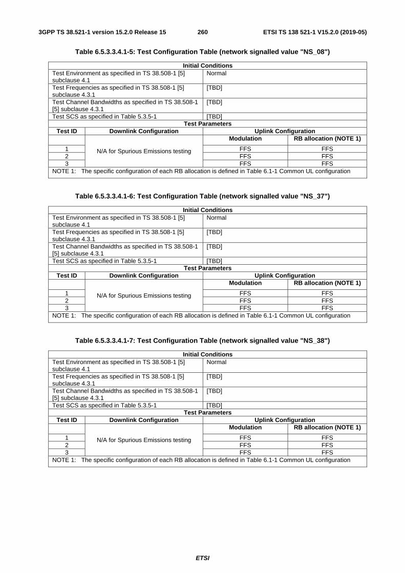
ETSI
ETSI TS 138 521-1 V15.2.0 (2019-05)2603GPP TS 38.521-1 version 15.2.0 Release 15
Table 6.5.3.3.4.1-5: Test Configuration Table (network signalled value "NS_08")
Initial Conditions Test Environment as specified in TS 38.508-1 [5] subclause 4.1
Normal
Test Frequencies as specified in TS 38.508-1 [5] subclause 4.3.1
[TBD]
Test Channel Bandwidths as specified in TS 38.508-1 [5] subclause 4.3.1
[TBD]
Test SCS as specified in Table 5.3.5-1 [TBD] Test Parameters
Test ID Downlink Configuration Uplink Configuration
N/A for Spurious Emissions testing
Modulation RB allocation (NOTE 1)
1 FFS FFS 2 FFS FFS 3 FFS FFS
NOTE 1: The specific configuration of each RB allocation is defined in Table 6.1-1 Common UL configuration
Table 6.5.3.3.4.1-6: Test Configuration Table (network signalled value "NS_37")
Initial Conditions Test Environment as specified in TS 38.508-1 [5] subclause 4.1
Normal
Test Frequencies as specified in TS 38.508-1 [5] subclause 4.3.1
[TBD]
Test Channel Bandwidths as specified in TS 38.508-1 [5] subclause 4.3.1
[TBD]
Test SCS as specified in Table 5.3.5-1 [TBD] Test Parameters
Test ID Downlink Configuration Uplink Configuration
N/A for Spurious Emissions testing
Modulation RB allocation (NOTE 1)
1 FFS FFS 2 FFS FFS 3 FFS FFS
NOTE 1: The specific configuration of each RB allocation is defined in Table 6.1-1 Common UL configuration
Table 6.5.3.3.4.1-7: Test Configuration Table (network signalled value "NS_38")
Initial Conditions Test Environment as specified in TS 38.508-1 [5] subclause 4.1
Normal
Test Frequencies as specified in TS 38.508-1 [5] subclause 4.3.1
[TBD]
Test Channel Bandwidths as specified in TS 38.508-1 [5] subclause 4.3.1
[TBD]
Test SCS as specified in Table 5.3.5-1 [TBD] Test Parameters
Test ID Downlink Configuration Uplink Configuration
N/A for Spurious Emissions testing
Modulation RB allocation (NOTE 1)
1 FFS FFS 2 FFS FFS 3 FFS FFS
NOTE 1: The specific configuration of each RB allocation is defined in Table 6.1-1 Common UL configuration

ETSI
ETSI TS 138 521-1 V15.2.0 (2019-05)2613GPP TS 38.521-1 version 15.2.0 Release 15
Table 6.5.3.3.4.1-8: Test Configuration Table (network signalled value "NS_39")
Initial Conditions Test Environment as specified in TS 38.508-1 [5] subclause 4.1
Normal
Test Frequencies as specified in TS 38.508-1 [5] subclause 4.3.1
[TBD]
Test Channel Bandwidths as specified in TS 38.508-1 [5] subclause 4.3.1
[TBD]
Test SCS as specified in Table 5.3.5-1 [TBD] Test Parameters
Test ID Downlink Configuration Uplink Configuration
N/A for Spurious Emissions testing
Modulation RB allocation (NOTE 1)
1 FFS FFS 2 FFS FFS 3 FFS FFS
NOTE 1: The specific configuration of each RB allocation is defined in Table 6.1-1 Common UL configuration
1. Connect the SS to the UE to the UE antenna connectors as shown in TS 38.508-1 [5] Annex A, Figure A.3.1.1.1 for TE diagram and section A.3.2.1 for UE diagram.
2. The parameter settings for the cell are set up according to TS 38.508-1 [5] subclause 4.4.3.
3. Downlink signals are initially set up according to Annex C.0, C.1, C.2, and uplink signals according to Annex G.0, G.1, G.2, G.3.0.
4. The UL Reference Measurement channels are set according to Table 6.5.3.3.4.1-1 through Table 6.5.3.3.4.1-8.
5. Propagation conditions are set according to Annex B.0.
6. Ensure the UE is in state RRC_CONNECTED with generic procedure parameters Connectivity NR, Connected without release On, Test Mode On and Test Loop Function On according to TS 38.508-1 [5] clause 4.5. Message contents are defined in clause 6.5.3.3.4.3.
6.5.3.3.4.2 Test procedure
1 SS sends uplink scheduling information for each UL HARQ process via PDCCH DCI format [0_1] for C_RNTI to schedule the UL RMC according to Table 6.5.3.3.4.1-1 through Table [TBD]. Since the UE has no payload data to send, the UE transmits uplink MAC padding bits on the UL RMC.
2. Send continuously uplink power control "up" commands in the uplink scheduling information to the UE until the UE transmits at PUMAX level.
3. Measure the mean power of the UE in the channel bandwidth of the radio access mode according to the test configuration, which shall meet the requirements with allowed A-MPR values specified in table 6.2.3.5-2 per test condition specified in Table 6.2.3.4.1-2. For NS_04. The measured power shall be verified for each step. The measurement period shall capture the active time slots.
4. Measure the power of the transmitted signal with a measurement filter of bandwidths according to Tables 6.5.3.3.3.1-1 to Table 6.5.3.3.8-1 as appropriate. The centre frequency of the filter shall be stepped in contiguous steps according to the same table.
6.5.3.3.4.3 Message contents
6.6.3.3.4.3.1 Message contents exceptions (network signalled value "NS_04")
Message contents are according to TS 38.508 [5] subclause 4.6, with the following exceptions:
1. Information element additionalSpectrumEmission is set to NS_04. This can be set in the SystemInformationblockType2 as part of the cell broadcast message. This exception indicates that the UE shall meet the additional spurious emission requirement for a specific deployment scenario.

ETSI
ETSI TS 138 521-1 V15.2.0 (2019-05)2623GPP TS 38.521-1 version 15.2.0 Release 15
Table 6.6.3.3.4.3.1-1: SystemInformationBlockType2: Additional spurious emissions test requirement for "NS_04"
Derivation Path: TS 38.508-1 [5] clause 4.6.3, Table 4.6.3-1 Information Element Value/remark Comment Condition
additionalSpectrumEmission 1 (NS_04)
6.6.3.3.4.3.2 Message contents exceptions (network signalled value "NS_17")
Message contents are according to TS 38.508 [5] subclause 4.6, with the following exceptions:
1. Information element additionalSpectrumEmission is set to NS_17. This can be set in the SystemInformationblockType2 as part of the cell broadcast message. This exception indicates that the UE shall meet the additional spurious emission requirement for a specific deployment scenario.
Table 6.6.3.3.4.3.1-1: SystemInformationBlockType2: Additional spurious emissions test requirement for "NS_17"
Derivation Path: TS 38.508-1 [5] clause 4.6.3, Table 4.6.3-1 Information Element Value/remark Comment Condition
additionalSpectrumEmission 1 (NS_17)
6.6.3.3.4.3.3 Message contents exceptions (network signalled value "NS_18")
Message contents are according to TS 38.508 [5] subclause 4.6, with the following exceptions:
1. Information element additionalSpectrumEmission is set to NS_18. This can be set in the SystemInformationblockType2 as part of the cell broadcast message. This exception indicates that the UE shall meet the additional spurious emission requirement for a specific deployment scenario.
Table 6.6.3.3.4.3.1-1: SystemInformationBlockType2: Additional spurious emissions test requirement for "NS_18"
Derivation Path: TS 38.508-1 [5] clause 4.6.3, Table 4.6.3-1 Information Element Value/remark Comment Condition
additionalSpectrumEmission 2 (NS_18)
6.6.3.3.4.3.4 Message contents exceptions (network signalled value "NS_05")
Message contents are according to TS 38.508 [5] subclause 4.6, with the following exceptions:
1. Information element additionalSpectrumEmission is set to NS_05. This can be set in the SystemInformationblockType2 as part of the cell broadcast message. This exception indicates that the UE shall meet the additional spurious emission requirement for a specific deployment scenario.
Table 6.6.3.3.4.3.1-1: SystemInformationBlockType2: Additional spurious emissions test requirement for "NS_05"
Derivation Path: TS 38.508-1 [5] clause 4.6.3, Table 4.6.3-1 Information Element Value/remark Comment Condition
additionalSpectrumEmission 2 (NS_05)
6.6.3.3.4.3.5 Message contents exceptions (network signalled value "NS_08")
Message contents are according to TS 38.508 [5] subclause 4.6, with the following exceptions:
1. Information element additionalSpectrumEmission is set to NS_08. This can be set in the SystemInformationblockType2 as part of the cell broadcast message. This exception indicates that the UE shall meet the additional spurious emission requirement for a specific deployment scenario.
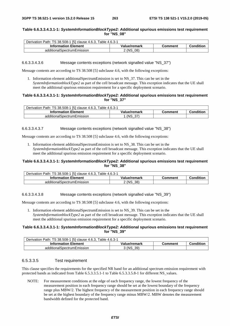
ETSI
ETSI TS 138 521-1 V15.2.0 (2019-05)2633GPP TS 38.521-1 version 15.2.0 Release 15
Table 6.6.3.3.4.3.1-1: SystemInformationBlockType2: Additional spurious emissions test requirement for "NS_08"
Derivation Path: TS 38.508-1 [5] clause 4.6.3, Table 4.6.3-1 Information Element Value/remark Comment Condition
additionalSpectrumEmission 2 (NS_08)
6.6.3.3.4.3.6 Message contents exceptions (network signalled value "NS_37")
Message contents are according to TS 38.508 [5] subclause 4.6, with the following exceptions:
1. Information element additionalSpectrumEmission is set to NS_37. This can be set in the SystemInformationblockType2 as part of the cell broadcast message. This exception indicates that the UE shall meet the additional spurious emission requirement for a specific deployment scenario.
Table 6.6.3.3.4.3.1-1: SystemInformationBlockType2: Additional spurious emissions test requirement for "NS_37"
Derivation Path: TS 38.508-1 [5] clause 4.6.3, Table 4.6.3-1 Information Element Value/remark Comment Condition
additionalSpectrumEmission 1 (NS_37)
6.6.3.3.4.3.7 Message contents exceptions (network signalled value "NS_38")
Message contents are according to TS 38.508 [5] subclause 4.6, with the following exceptions:
1. Information element additionalSpectrumEmission is set to NS_38. This can be set in the SystemInformationblockType2 as part of the cell broadcast message. This exception indicates that the UE shall meet the additional spurious emission requirement for a specific deployment scenario.
Table 6.6.3.3.4.3.1-1: SystemInformationBlockType2: Additional spurious emissions test requirement for "NS_38"
Derivation Path: TS 38.508-1 [5] clause 4.6.3, Table 4.6.3-1 Information Element Value/remark Comment Condition
additionalSpectrumEmission 2 (NS_38)
6.6.3.3.4.3.8 Message contents exceptions (network signalled value "NS_39")
Message contents are according to TS 38.508 [5] subclause 4.6, with the following exceptions:
1. Information element additionalSpectrumEmission is set to NS_39. This can be set in the SystemInformationblockType2 as part of the cell broadcast message. This exception indicates that the UE shall meet the additional spurious emission requirement for a specific deployment scenario.
Table 6.6.3.3.4.3.1-1: SystemInformationBlockType2: Additional spurious emissions test requirement for "NS_39"
Derivation Path: TS 38.508-1 [5] clause 4.6.3, Table 4.6.3-1 Information Element Value/remark Comment Condition
additionalSpectrumEmission 3 (NS_39)
6.5.3.3.5 Test requirement
This clause specifies the requirements for the specified NR band for an additional spectrum emission requirement with protected bands as indicated from Table 6.5.3.3.5.1-1 to Table 6.5.3.3.5.8-1 for different NS_values.
NOTE: For measurement conditions at the edge of each frequency range, the lowest frequency of the measurement position in each frequency range should be set at the lowest boundary of the frequency range plus MBW/2. The highest frequency of the measurement position in each frequency range should be set at the highest boundary of the frequency range minus MBW/2. MBW denotes the measurement bandwidth defined for the protected band.
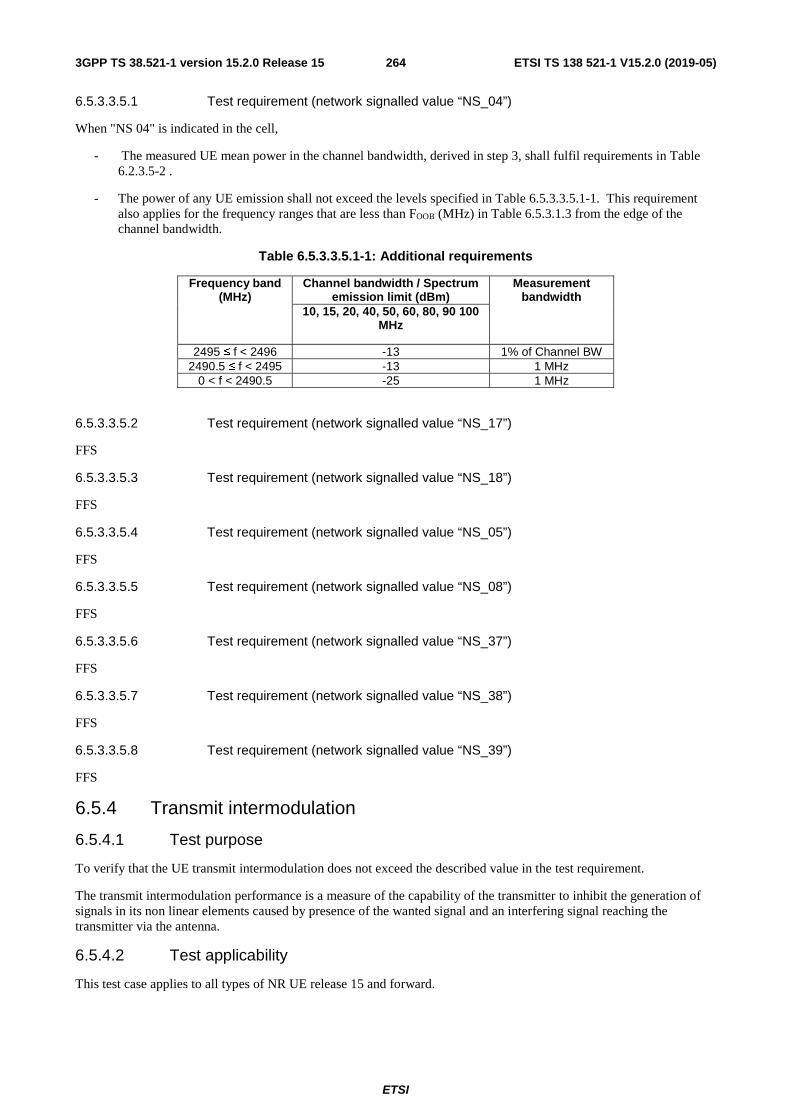
ETSI
ETSI TS 138 521-1 V15.2.0 (2019-05)2643GPP TS 38.521-1 version 15.2.0 Release 15
6.5.3.3.5.1 Test requirement (network signalled value “NS_04”)
When "NS 04" is indicated in the cell,
- The measured UE mean power in the channel bandwidth, derived in step 3, shall fulfil requirements in Table 6.2.3.5-2 .
- The power of any UE emission shall not exceed the levels specified in Table 6.5.3.3.5.1-1. This requirement also applies for the frequency ranges that are less than FOOB (MHz) in Table 6.5.3.1.3 from the edge of the channel bandwidth.
Table 6.5.3.3.5.1-1: Additional requirements
Frequency band (MHz)
Channel bandwidth / Spectrum emission limit (dBm)
Measurement bandwidth
10, 15, 20, 40, 50, 60, 80, 90 100 MHz
2495 ≤ f < 2496 -13 1% of Channel BW 2490.5 ≤ f < 2495 -13 1 MHz
0 < f < 2490.5 -25 1 MHz
6.5.3.3.5.2 Test requirement (network signalled value “NS_17”)
FFS
6.5.3.3.5.3 Test requirement (network signalled value “NS_18”)
FFS
6.5.3.3.5.4 Test requirement (network signalled value “NS_05”)
FFS
6.5.3.3.5.5 Test requirement (network signalled value “NS_08”)
FFS
6.5.3.3.5.6 Test requirement (network signalled value “NS_37”)
FFS
6.5.3.3.5.7 Test requirement (network signalled value “NS_38”)
FFS
6.5.3.3.5.8 Test requirement (network signalled value “NS_39”)
FFS
6.5.4 Transmit intermodulation
6.5.4.1 Test purpose
To verify that the UE transmit intermodulation does not exceed the described value in the test requirement.
The transmit intermodulation performance is a measure of the capability of the transmitter to inhibit the generation of signals in its non linear elements caused by presence of the wanted signal and an interfering signal reaching the transmitter via the antenna.
6.5.4.2 Test applicability
This test case applies to all types of NR UE release 15 and forward.

ETSI
ETSI TS 138 521-1 V15.2.0 (2019-05)2653GPP TS 38.521-1 version 15.2.0 Release 15
6.5.4.3 Minimum conformance requirements
UE transmit intermodulation is defined by the ratio of the mean power of the wanted signal to the mean power of the intermodulation product when an interfering CW signal is added at a level below the wanted signal at each transmitter antenna port with the other antenna port(s) if any terminated. Both the wanted signal power and the intermodulation product power are measured through NR rectangular filter with measurement bandwidth shown in Table 6.5.4.3-1.
The requirement of transmit intermodulation is specified in Table 6.5.4.3-1.
Table 6.5.4.3-1: Transmit Intermodulation
Wanted signal channel bandwidth BWChannel
Interference signal frequency offset from channel centre
BWChannel 2*BWChannel
Interference CW signal level -40dBc
Intermodulation product < -29dBc < -35dBc
Measurement bandwidth The maximum transmission bandwidth configuration among the different SCSs for the channel BW as defined in Table 6.5.2.2.3-1
Measurement offset from channel centre
BWChannel and 2*BWChannel 2*BWChannel and 4*BWChannel
The normative reference for this requirement is TS 38.101-1 [2] clause 6.5.4.
6.5.4.4 Test description
6.5.4.4.1 Initial conditions
Initial conditions are a set of test configurations the UE needs to be tested in and the steps for the SS to take with the UE to reach the correct measurement state.
The initial test configurations consist of environmental conditions, test frequencies, test channel bandwidths and sub-carrier spacing based on NR operating bands specified in table 5.3.5-1. All of these configurations shall be tested with applicable test parameters for each combination of channel bandwidth and sub-carrier spacing, and are shown in table 6.5.4.4.1-1. The details of the uplink reference measurement channels (RMCs) are specified in Annexes A.2. Configurations of PDSCH and PDCCH before measurement are specified in Annex C.2.
Table 6.5.4.4.1-1: Test Configuration Table
Initial Conditions Test Environment as specified in TS 38.508-1 [5] subclause 4.1
Normal
Test Frequencies as specified in TS 38.508-1 [5] subclause 4.3.1
Mid range
Test Channel Bandwidths as specified in TS 38.508-1 [5] subclause 4.3.1
Mid, Highest
Test SCS as specified in Table 5.3.5-1 Lowest, Highest Test Parameters
Test ID Downlink Configuration Uplink Configuration
N/A for transmit intermodulation test case
Modulation RB allocation (NOTE 1) 1 DFT-s-OFDM PI/2 BPSK Inner Full 2 DFT-s-OFDM QPSK Inner Full
NOTE 1: The specific configuration of each RB allocation is defined in Table 6.1-1.
1. Connect the SS to the UE antenna connectors as shown in TS 38.508-1 [5] Annex A, in Figure A.3.1.3.1 for TE diagram and section A.3.2.1 for UE diagram.
2. The parameter settings for the cell are set up according to TS 38.508-1 [5] subclause 4.4.3.
3. Downlink signals are initially set up according to Annex C.0, C.1, C.2, and uplink signals according to Annex G.0, G.1, G.2, G.3.0.
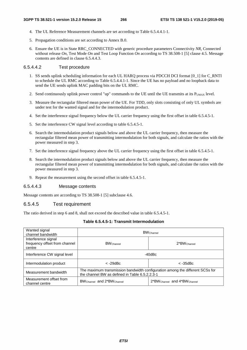
ETSI
ETSI TS 138 521-1 V15.2.0 (2019-05)2663GPP TS 38.521-1 version 15.2.0 Release 15
4. The UL Reference Measurement channels are set according to Table 6.5.4.4.1-1.
5. Propagation conditions are set according to Annex B.0.
6. Ensure the UE is in State RRC_CONNECTED with generic procedure parameters Connectivity NR, Connected without release On, Test Mode On and Test Loop Function On according to TS 38.508-1 [5] clause 4.5. Message contents are defined in clause 6.5.4.4.3.
6.5.4.4.2 Test procedure
1. SS sends uplink scheduling information for each UL HARQ process via PDCCH DCI format [0_1] for C_RNTI to schedule the UL RMC according to Table 6.5.4.4.1-1. Since the UE has no payload and no loopback data to send the UE sends uplink MAC padding bits on the UL RMC.
2. Send continuously uplink power control "up" commands to the UE until the UE transmits at its PUMAX level.
3. Measure the rectangular filtered mean power of the UE. For TDD, only slots consisting of only UL symbols are under test for the wanted signal and for the intermodulation product.
4. Set the interference signal frequency below the UL carrier frequency using the first offset in table 6.5.4.5-1.
5. Set the interference CW signal level according to table 6.5.4.5-1.
6. Search the intermodulation product signals below and above the UL carrier frequency, then measure the rectangular filtered mean power of transmitting intermodulation for both signals, and calculate the ratios with the power measured in step 3.
7. Set the interference signal frequency above the UL carrier frequency using the first offset in table 6.5.4.5-1.
8. Search the intermodulation product signals below and above the UL carrier frequency, then measure the rectangular filtered mean power of transmitting intermodulation for both signals, and calculate the ratios with the power measured in step 3.
9. Repeat the measurement using the second offset in table 6.5.4.5-1.
6.5.4.4.3 Message contents
Message contents are according to TS 38.508-1 [5] subclause 4.6.
6.5.4.5 Test requirement
The ratio derived in step 6 and 8, shall not exceed the described value in table 6.5.4.5-1.
Table 6.5.4.5-1: Transmit Intermodulation
Wanted signal channel bandwidth BWChannel
Interference signal frequency offset from channel centre
BWChannel 2*BWChannel
Interference CW signal level -40dBc
Intermodulation product < -29dBc < -35dBc
Measurement bandwidth The maximum transmission bandwidth configuration among the different SCSs for the channel BW as defined in Table 6.5.2.2.3-1
Measurement offset from channel centre BWChannel and 2*BWChannel 2*BWChannel and 4*BWChannel

ETSI
ETSI TS 138 521-1 V15.2.0 (2019-05)2673GPP TS 38.521-1 version 15.2.0 Release 15
6.5A Output RF spectrum emissions for CA
6.5A.2 Out of band emission for CA
6.5A.2.2 Spectrum emission mask
Editor’s note: This clause is incomplete. The following aspects are either missing or not yet determined:
- The connection diagram for inter-band CA in TS 38.508-1[5] Annex A is FFS.
- Procedure to configure SCC in TS 38.508-1[5] clause [TBD] is FFS.
- The subclause 6.2A. 2 in reference to requirements for transmitter power for inter-band CA is FFS.
- Extending the coverage of the TCs with intra-band CA scenarios is FFS
- MU and TT for CA is FFS in Annex F.
6.5A.2.2.0 Minimum conformance requirements
For inter-band carrier aggregation with uplink assigned to two NR bands, the minimum conformance requirements specified in subclause 6.5.2.2 shall apply on each component carrier with all component carriers active. If for some frequency spectrum emission masks of component carriers overlap then spectrum emission mask allowing higher power spectral density applies for that frequency. If for some frequency a component carrier spectrum emission mask overlaps with the channel bandwidth of another component carrier, then the emission mask does not apply for that frequency.
6.5A.2.2.1 Spectrum emission mask for CA (2UL CA)
6.5A.2.2.1.1 Test purpose
To verify that the power of any UE emission shall not exceed specified level for the specified channel bandwidth for 2UL CA.
6.5A.2.2.1.2 Test applicability
This test case applies to all types of NR UE release 15 and forward that supports 2DL and 2UL CA.
6.5A.2.2.1.3 Minimum conformance requirements
The minimum conformance requirements are defined in subclause6.5A.2.2.0.
6.5A.2.2.1.4 Test description
6.5A.2.2.1.4.1 Initial conditions
Initial conditions are a set of test configurations the UE needs to be tested in and the steps for the SS to take with the UE to reach the correct measurement state.
The initial test configurations consist of environmental conditions, test frequencies, test channel bandwidths and sub-carrier spacing based on NR CA configuration specified in clause 5.5A. All of these configurations shall be tested with applicable test parameters for each CA configuration, are shown in Table 6.5A.2.2.1.4.1-1. The details of the uplink reference measurement channels (RMCs) are specified in Annexes A.2. Configurations of PDSCH and PDCCH before measurement are specified in Annex C.2.

ETSI
ETSI TS 138 521-1 V15.2.0 (2019-05)2683GPP TS 38.521-1 version 15.2.0 Release 15
Table 6.5A.2.2.1.4.1-1: Inter band CA Test Configuration Table
Initial Conditions Test Environment as specified in TS 38.508-1 [5] subclause 4.1
Normal
Test Frequencies as specified in TS 38.508-1 [5] subclause4.3.1.1.3 for inter band CA in FR1
Low range for PCC and SCC High range for PCC and SCC
Test Channel Bandwidths as specified in TS 38.508-1 [5] subclause 4.3.1
Lowest for both PCC and SCC Highest for both PCC and SCC
Test SCS as specified in Table 5.5A.3-1 Smallest and biggest supported SCS per Channel Bandwidth Test Parameters
Test ID
Freq Downlink Configuration
Uplink Configuration Modulation (NOTE 3) RB allocation (NOTE 1)
PCC SCC 13 Low N/A DFT-s-OFDM PI/2
BPSK Outer_1RB_Left Outer_1RB_Left
23 High DFT-s-OFDM PI/2 BPSK
Outer_1RB_Right Outer_1RB_Right
3 Low DFT-s-OFDM QPSK Outer_1RB_Left Outer_1RB_Left
4 High DFT-s-OFDM QPSK Outer_1RB_Right Outer_1RB_Right
5 Low DFT-s-OFDM 16 QAM Outer_1RB_Left Outer_1RB_Left
6 High DFT-s-OFDM 16 QAM Outer_1RB_Right Outer_1RB_Right
7 Default DFT-s-OFDM 64 QAM Outer_Full Outer_Full
8 Default DFT-s-OFDM 256 QAM Outer_Full Outer_Full
9 Low CP-OFDM QPSK Outer_1RB_Left Outer_1RB_Left
10 High CP-OFDM QPSK Outer_1RB_Right Outer_1RB_Right
11 Low CP-OFDM 16 QAM Outer_1RB_Left Outer_1RB_Left
12 High CP-OFDM 16 QAM Outer_1RB_Right Outer_1RB_Right
13 Default CP-OFDM 64 QAM Outer_Full Outer_Full
14 Default CP-OFDM 256 QAM Outer_Full Outer_Full
NOTE 1: The specific configuration of each RB allocation is defined in Table 6.1-1. NOTE 2: Test Channel Bandwidths and Test SCS are checked separately for each NR CA band combination,
which applicable channel bandwidths and SCS are specified in Table 5.5A3-1. NOTE 3: DFT-s-OFDM PI/2 BPSK test applies only for UEs which supports half Pi BPSK in FR1.
1. Connect the SS to the UE antenna connectors as shown in TS 38.508-1 [5] Annex A, in Figure [TBD] for TE diagram and section A.3.2.1 for UE diagram.
2. The parameter settings for the cell are set up according to TS 38.508-1 [5] subclause 4.4.3.
3. Downlink signals for PCC are initially set up according to Annex C.0, C.1, C.2, and uplink signals according to Annex G.0, G.1, G.2, G.3.0.
4. The UL Reference Measurement channels are set according to Table 6.5A.2.2.1.4.1-1.
5. Propagation conditions are set according to Annex B.0.
6. Ensure the UE is in state RRC_CONNECTED with generic procedure parameters Connectivity NR, Connected without release On, Test Mode On and Test Loop Function On according to TS 38.508-1 [5] clause 4.5. Message contents are defined in clause 6.5A.2.2.1.4.3.
6.5A.2.2.1.4.2 Test procedure
1. Configure SCC according to Annex C.0, C.1, C.2 for all downlink physical channels.
2. The SS shall configure SCC as per TS 38.508-1 [5] clause [TBD]. Message contents are defined in clause 6.5A.2.2.1.4.3.
3. SS activates SCC by sending the activation MAC CE (Refer TS 38.321 [18], clauses 5.9, 6.1.3.10). Wait for at least 2 seconds (Refer TS 38.133[19], clause9.3).
ETSI
ETSI TS 138 521-1 V15.2.0 (2019-05)2693GPP TS 38.521-1 version 15.2.0 Release 15
4. SS sends uplink scheduling information for each UL HARQ process via PDCCH DCI format 0_1 for C_RNTI to schedule the UL RMC according to Table 6.5A.2.2.1.4.1-1 on both PCC and SCC. Since the UL has no payload and no loopback data to send the UE sends uplink MAC padding bits on the UL RMC.
5. Send continuously power control “up” commands in every uplink scheduling information to the UE until the UE transmits at PUMAX level. Allow at least 200ms for the UE to reach PUMAX level.
6. Measure the mean power of the UE in the channel bandwidth of the radio access mode for each CC according to the test configuration, which shall meet the requirements described in clause 6.2A.2. The period of the measurement shall be at least the continuous duration of one active sub-frame (1ms) and in the uplink symbols. For TDD slots with transient periods are not under test.
7. Measure the power of the transmitted signal with a measurement filter of bandwidths for each CC according to Table 6.5A.2.2.1.5-1. The centre frequency of the filter shall be stepped in continuous steps according to the same table. The measured power shall be recorded for each step. The measurement period shall capture the active TSs.
NOTE 1: When switching to DFT-s-OFDM waveform, as specified in the test configuration table 6.5.2.2.4.1-1, send an NR RRCReconfiguration message according to TS 38.508-1 [5] clause 4.6.3 Table 4.6.3-118 PUSCH-Config with TRANSFORM_PRECODER_ENABLED condition.
6.5A.2.2.1.4.3 Message contents
Message contents are according to TS 38.508-1 [5] subclause 4.6.
6.5A.2.2.1.5 Test requirement
The measured UE mean power in the channel bandwidth for each CC, derived in step 6, shall fulfil requirements in clause 6.2A.2 as appropriate, and the power of any UE emission for each CC, derived in step 7, shall fulfil requirements in Table 6.5A.2.2.1.5-1.If for some frequency spectrum emission masks of component carriers overlap then spectrum emission mask allowing higher power spectral density applies for that frequency. If for some frequency a component carrier spectrum emission mask overlaps with the channel bandwidth of another component carrier, then the emission mask does not apply for that frequency.

ETSI
ETSI TS 138 521-1 V15.2.0 (2019-05)2703GPP TS 38.521-1 version 15.2.0 Release 15
Table 6.5A.2.2.1.5-1: NR General spectrum emission mask
Spectrum emission limit (dBm) / Channel bandwidth
ΔfOOB (MHz)
5 MHz
10 MHz
15 MHz
20 MHz
25 MHz
30 MHz
40 MHz
50 MHz
60 MHz
80 MHz
90 MHz
100 MHz
Measurement bandwidth
± 0-1 -13 + TT
-13 + TT
-13 + TT
-13 + TT
-13 + TT
-13 + TT
-13 + TT 1 % channel
bandwidth ± 0-1 -24
+ TT -24
+ TT -24
+ TT -24
+ TT -24
+ TT 30 kHz
± 1-5 -10 + TT
-10 + TT
-10 + TT
-10 + TT
-10 + TT
-10 + TT
-10 + TT
-10 + TT
-10 + TT
-10 + TT
-10 + TT
-10 + TT
1 MHz
± 5-6 -13 + TT -13
+ TT -13 + TT -13
+ TT -13 + TT -13
+ TT -13
+ TT -13
+ TT -13
+ TT -13
+ TT -13 + TT
-13 + TT
± 6-10 -25 + TT
± 10-15 -25 + TT
± 15-20 -25 + TT
± 20-25
-25 + TT
± 25-30 -25 + TT
± 30-35 -25 + TT
± 35-40 ± 40-45 -25
+ TT ± 45-50 ± 50-55 -25
+ TT ± 55-60 ± 60-65 -25
+ TT ± 65-80 ± 80-90 -25
+ TT ± 90-95 -25
+ TT ± 95-100
± 100-105 -25 + TT
Note 1: The first and last measurement position with a 30 kHz filter is at ΔfOOB equals to 0.015 MHz and 0.985 MHz. Note 2: At the boundary of spectrum emission limit, the first and last measurement position with a 1 MHz filter is the
inside of +0.5MHz and -0.5MHz, respectively. Note 3: The measurements are to be performed above the upper edge of the channel and below the lower edge of the
channel.
Table 6.5A.2.2.1.5-2: Test Tolerance for Spectrum emission mask
f ≤ 3.0GHz 3.0GHz < f ≤ 6GHz BW ≤ 40MHz FFS FFS
40MHz < BW ≤ 100MHz FFS FFS
NOTE: As a general rule, the resolution bandwidth of the measuring equipment should be equal to the measurement bandwidth. However, to improve measurement accuracy, sensitivity and efficiency, the resolution bandwidth may be smaller than the measurement bandwidth. When the resolution bandwidth is smaller than the measurement bandwidth, the result should be integrated over the measurement bandwidth in order to obtain the equivalent noise bandwidth of the measurement bandwidth.

ETSI
ETSI TS 138 521-1 V15.2.0 (2019-05)2713GPP TS 38.521-1 version 15.2.0 Release 15
6.5A.2.4 Adjacent channel leakage ratio
6.5A.2.4.1 NR ACLR
Editor’s note: This clause is incomplete. The following aspects are either missing or not yet determined:
- PC1 and PC4 requirements are missing in TS 38.101-1 [2].
- The connection diagram for inter-band CA in TS 38.508-1[5] Annex A is FFS.
- Procedure to configure SCC in TS 38.508-1[5] clause [TBD] is FFS.
- The subclause 6.2A.2 in reference to requirements for transmitter power for inter-band CA is FFS.
- Extending the coverage of the TCs with intra-band CA scenarios is FFS
- MUs and TTs for CA is FFS in Annex F.
6.5A.2.4.1.0 Minimum conformance requirements
For inter-band carrier aggregation with uplink assigned to two NR bands, the minimum conformance requirements specified in subclause 6.5.2.4.1.3 shall apply on each component carrier with all component carriers active.
6.5A.2.4.1.1 NR ACLR for CA (2UL CA)
6.5A.2.4.1.1.1 Test purpose
To verify that UE transmitter does not cause unacceptable interference to adjacent channels in terms of Adjacent Channel Leakage power Ratio (ACLR) for 2UL CA.
6.5A.2.4.1.1.2 Test applicability
This test case applies to all types of NR UE release 15 and forward that supports 2DL and 2UL CA.
6.5A.2.4.1.1.3 Minimum conformance requirements
The minimum conformance requirements are defined in subclause 6.5A.2.4.1.0.
6.5A.2.4.1.1.4 Test description
6.5A.2.4.1.1.4.1 Initial conditions
Initial conditions are a set of test configurations the UE needs to be tested in and the steps for the SS to take with the UE to reach the correct measurement state.
The initial test configurations consist of environmental conditions, test frequencies, test channel bandwidths and sub-carrier spacing based on NR CA configuration specified in clause 5.5A. All of these configurations shall be tested with applicable test parameters for each CA configuration, are shown in Table 6.5A.2.4.1.1.4.1-1. The details of the uplink reference measurement channels (RMCs) are specified in Annexes A.2. Configurations of PDSCH and PDCCH before measurement are specified in Annex C.2
Table 6.5A.2.4.1.1.4.1-1: Inter band CA Test Configuration Table
Initial Conditions Test Environment as specified in TS 38.508-1 [5] subclause 4.1
Normal, TL/VL, TL/VH, TH/VL, TH/VH
Test Frequencies as specified in TS 38.508-1 [5] subclause4.3.1.1.3 for inter band CA in FR1
Low range for PCC and SCC High range for PCC and SCC
Test Channel Bandwidths as specified in TS 38.508-1 [5] subclause 4.3.1
Lowest for both PCC and SCC Highest for both PCC and SCC
Test SCS as specified in Table 5.5A.3-1 Smallest and biggest supported SCS per Channel Bandwidth Test Parameters
Test ID
Freq Downlink Configuration Uplink Configuration Modulation (NOTE 3) RB allocation (NOTE 1)
PCC SCC

ETSI
ETSI TS 138 521-1 V15.2.0 (2019-05)2723GPP TS 38.521-1 version 15.2.0 Release 15
13 Low N/A DFT-s-OFDM PI/2 BPSK
Outer_1RB_Left Outer_1RB_Left
23 High DFT-s-OFDM PI/2 BPSK
Outer_1RB_Right Outer_1RB_Right
33 Default DFT-s-OFDM PI/2 BPSK
Outer_Full Outer_Full
4 Default DFT-s-OFDM PI/2 BPSK
Inner_Full Inner_Full
5 Low DFT-s-OFDM QPSK Outer_1RB_Left Outer_1RB_Left
6 High DFT-s-OFDM QPSK Outer_1RB_Right Outer_1RB_Right
7 Default DFT-s-OFDM QPSK Outer_Full Outer_Full
8 Default DFT-s-OFDM QPSK Inner_Full Inner_Full
9 Default DFT-s-OFDM 16 QAM Inner_Full Inner_Full
10 Low DFT-s-OFDM 16 QAM Outer_1RB_Left Outer_1RB_Left
11 High DFT-s-OFDM 16 QAM Outer_1RB_Right Outer_1RB_Right
12 Default DFT-s-OFDM 16 QAM Outer_Full Outer_Full
13 Low DFT-s-OFDM 64 QAM Outer_1RB_Left Outer_1RB_Left
14 High DFT-s-OFDM 64 QAM Outer_1RB_Right Outer_1RB_Right
15 Default DFT-s-OFDM 64 QAM Outer_Full Outer_Full
16 Default DFT-s-OFDM 256 QAM Outer_Full Outer_Full
17 Default CP-OFDM QPSK Inner_Full Inner_Full
18 Low CP-OFDM QPSK Outer_1RB_Left Outer_1RB_Left 19 High CP-OFDM QPSK Outer_1RB_Right Outer_1RB_Right 20 Default CP-OFDM QPSK Outer_Full Outer_Full
21 Default CP-OFDM 16 QAM Inner_Full Inner_Full
22 Low CP-OFDM 16 QAM Outer_1RB_Left Outer_1RB_Left
23 High CP-OFDM 16 QAM Outer_1RB_Right Outer_1RB_Right
24 Default CP-OFDM 16 QAM Outer_Full Outer_Full
25 Low CP-OFDM 64 QAM Outer_1RB_Left Outer_1RB_Left
26 High CP-OFDM 64 QAM Outer_1RB_Right Outer_1RB_Right
27 Default CP-OFDM 64 QAM Outer_Full Outer_Full
28 Default CP-OFDM 256 QAM Outer_Full Outer_Full
NOTE 1: The specific configuration of each RB allocation is defined in Table 6.1-1. NOTE 2: Test Channel Bandwidths and Test SCS are checked separately for each NR CA band combination,
which applicable channel bandwidths and SCS are specified in Table 5.5A3-1. NOTE 3: DFT-s-OFDM PI/2 BPSK test applies only for UEs which supports half Pi BPSK in FR1.
1. Connect the SS to the UE antenna connectors as shown in TS 38.508-1 [5] Annex A, in Figure [TBD] for TE diagram and section A.3.2.1 for UE diagram.
2. The parameter settings for the cell are set up according to TS 38.508-1 [5] subclause4.4.3.
3. Downlink signals for PCC are initially set up according to Annex C.0, C.1, C.2, and uplink signals according to Annex G.0, G.1, G.2, G.3.0.
4. The UL Reference Measurement channels are set according to Table 6.5A.2.4.1.1.4.1-1.
5. Propagation conditions are set according to Annex B.0
6. Ensure the UE is in state RRC_CONNECTED with generic procedure parameters Connectivity NR, Connected without release On, Test Mode On and Test Loop Function On according to TS 38.508-1 [5] clause 4.5. Message contents are defined in clause 6.5A.2.4.1.1.4.3
6.5A.2.4.1.1.4.2 Test procedure
1. Configure SCC according to Annex C.0, C.1, C.2 for all downlink physical channels.
2. The SS shall configure SCC as per TS 38.508-1 [5] clause [TBD]. Message contents are defined in clause 6.5A.2.4.1.1.4.3.
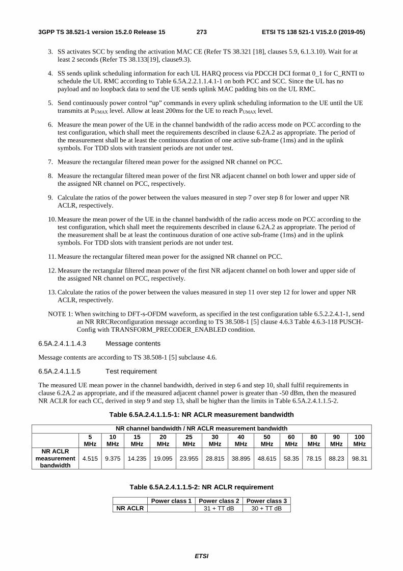
ETSI
ETSI TS 138 521-1 V15.2.0 (2019-05)2733GPP TS 38.521-1 version 15.2.0 Release 15
3. SS activates SCC by sending the activation MAC CE (Refer TS 38.321 [18], clauses 5.9, 6.1.3.10). Wait for at least 2 seconds (Refer TS 38.133[19], clause9.3).
4. SS sends uplink scheduling information for each UL HARQ process via PDCCH DCI format 0_1 for C_RNTI to schedule the UL RMC according to Table 6.5A.2.2.1.1.4.1-1 on both PCC and SCC. Since the UL has no payload and no loopback data to send the UE sends uplink MAC padding bits on the UL RMC.
5. Send continuously power control “up” commands in every uplink scheduling information to the UE until the UE transmits at PUMAX level. Allow at least 200ms for the UE to reach PUMAX level.
6. Measure the mean power of the UE in the channel bandwidth of the radio access mode on PCC according to the test configuration, which shall meet the requirements described in clause 6.2A.2 as appropriate. The period of the measurement shall be at least the continuous duration of one active sub-frame (1ms) and in the uplink symbols. For TDD slots with transient periods are not under test.
7. Measure the rectangular filtered mean power for the assigned NR channel on PCC.
8. Measure the rectangular filtered mean power of the first NR adjacent channel on both lower and upper side of the assigned NR channel on PCC, respectively.
9. Calculate the ratios of the power between the values measured in step 7 over step 8 for lower and upper NR ACLR, respectively.
10. Measure the mean power of the UE in the channel bandwidth of the radio access mode on PCC according to the test configuration, which shall meet the requirements described in clause 6.2A.2 as appropriate. The period of the measurement shall be at least the continuous duration of one active sub-frame (1ms) and in the uplink symbols. For TDD slots with transient periods are not under test.
11. Measure the rectangular filtered mean power for the assigned NR channel on PCC.
12. Measure the rectangular filtered mean power of the first NR adjacent channel on both lower and upper side of the assigned NR channel on PCC, respectively.
13. Calculate the ratios of the power between the values measured in step 11 over step 12 for lower and upper NR ACLR, respectively.
NOTE 1: When switching to DFT-s-OFDM waveform, as specified in the test configuration table 6.5.2.2.4.1-1, send an NR RRCReconfiguration message according to TS 38.508-1 [5] clause 4.6.3 Table 4.6.3-118 PUSCH-Config with TRANSFORM_PRECODER_ENABLED condition.
6.5A.2.4.1.1.4.3 Message contents
Message contents are according to TS 38.508-1 [5] subclause 4.6.
6.5A.2.4.1.1.5 Test requirement
The measured UE mean power in the channel bandwidth, derived in step 6 and step 10, shall fulfil requirements in clause 6.2A.2 as appropriate, and if the measured adjacent channel power is greater than -50 dBm, then the measured NR ACLR for each CC, derived in step 9 and step 13, shall be higher than the limits in Table 6.5A.2.4.1.1.5-2.
Table 6.5A.2.4.1.1.5-1: NR ACLR measurement bandwidth
NR channel bandwidth / NR ACLR measurement bandwidth
5
MHz 10
MHz 15
MHz 20
MHz 25
MHz 30
MHz 40
MHz 50
MHz 60
MHz 80
MHz 90
MHz 100 MHz
NR ACLR measurement
bandwidth 4.515 9.375 14.235 19.095 23.955 28.815 38.895 48.615 58.35 78.15 88.23 98.31
Table 6.5A.2.4.1.1.5-2: NR ACLR requirement
Power class 1 Power class 2 Power class 3 NR ACLR 31 + TT dB 30 + TT dB

ETSI
ETSI TS 138 521-1 V15.2.0 (2019-05)2743GPP TS 38.521-1 version 15.2.0 Release 15
Table 6.5A.2.4.1.1.5-3: Test Tolerance for NR ACLR
f ≤ 3.0GHz 3.0GHz < f ≤ 6GHz BW ≤ 40MHz FFS FFS
40MHz < BW ≤ 100MHz FFS FFS
6.5A.2.4.2 UTRA ACLR
Editor’s note: This clause is incomplete. The following aspects are either missing or not yet determined:
- The connection diagram for inter-band CA in TS 38.508-1[5] Annex A is FFS.
- Procedure to configure SCC in TS 38.508-1[5] clause [TBD] is FFS.
- The subclause 6.2A.2 in reference to requirements for transmitter power for inter-band CA is FFS.
- Extending the coverage of the TCs with intra-band CA scenarios is FFS
- MUs and TTs for CA is FFS in Annex F.
6.5A.2.4.2.0 Minimum conformance requirements
For inter-band carrier aggregation with uplink assigned to two NR bands, the minimum conformance requirements specified in subclause 6.5.2.4.2.3 shall apply on each component carrier with all component carriers active.
6.5A.2.4.2.1 UTRA ACLR for CA (2UL CA)
6.5A.2.4.2.1.1 Test purpose
To verify that UE transmitter does not cause unacceptable interference to adjacent UTRA channels in terms of Adjacent Channel Leakage power Ratio (UTRA ACLR) for 2UL CA.
6.5A.2.4.2.1.2 Test applicability
This test case applies to all types of NR UE release 15 and forward that supports 2DL and 2UL CA.
6.5A.2.4.2.1.3 Minimum conformance requirements
The minimum conformance requirements are defined in subclause 6.5A.2.4.2.0.
6.5A.2.4.2.1.4 Test description
6.5A.2.4.2.1.4.1 Initial conditions
Initial conditions are a set of test configurations the UE needs to be tested in and the steps for the SS to take with the UE to reach the correct measurement state.
The initial test configurations consist of environmental conditions, test frequencies, test channel bandwidths and sub-carrier spacing based on NR CA configuration specified in clause 5.5A. All of these configurations shall be tested with applicable test parameters for each CA configuration, are shown in Table 6.5A.2.4.1.1.4.1-1. The details of the uplink reference measurement channels (RMCs) are specified in Annexes A.2. Configurations of PDSCH and PDCCH before measurement are specified in Annex C.2
Table 6.5A.2.4.2.1.4.1-1: Void
1. Connect the SS to the UE antenna connectors as shown in TS 38.508-1 [5] Annex A, in Figure [TBD] for TE diagram and section A.3.2.1 for UE diagram.
2. The parameter settings for the cell are set up according to TS 38.508-1 [5] subclause4.4.3.
3. Downlink signals for PCC are initially set up according to Annex C.0, C.1, C.2, and uplink signals according to Annex G.0, G.1, G.2, G.3.0.
4. The UL Reference Measurement channels are set according to Table 6.5A.2.4.2.1.4.1-1.
5. Propagation conditions are set according to Annex B.0.

ETSI
ETSI TS 138 521-1 V15.2.0 (2019-05)2753GPP TS 38.521-1 version 15.2.0 Release 15
6. Ensure the UE is in state RRC_CONNECTED with generic procedure parameters Connectivity NR, Connected without release On, Test Mode On and Test Loop Function On according to TS 38.508-1 [5] clause 4.5. Message contents are defined in clause 6.5A.2.4.2.1.4.3
6.5A.2.4.2.1.4.2 Test procedure
1. Configure SCC according to Annex C.0, C.1, C.2 for all downlink physical channels.
2. The SS shall configure SCC as per TS 38.508-1 [5] clause [TBD]. Message contents are defined in clause 6.5A.2.4.2.1.4.3.
3. SS activates SCC by sending the activation MAC CE (Refer TS 38.321 [18], clauses 5.9, 6.1.3.10). Wait for at least 2 seconds (Refer TS 38.133[19], clause9.3).
4. SS sends uplink scheduling information for each UL HARQ process via PDCCH DCI format 0_1 for C_RNTI to schedule the UL RMC according to Table 6.5A.2.2.1.1.4.1-1 on both PCC and SCC. Since the UL has no payload and no loopback data to send the UE sends uplink MAC padding bits on the UL RMC.
5. Send continuously power control “up” commands in every uplink scheduling information to the UE until the UE transmits at PUMAX level. Allow at least 200ms for the UE to reach PUMAX level.
6. Measure the mean power of the UE in the channel bandwidth of the radio access mode on PCC according to the test configuration, which shall meet the requirements described in clause 6.2A.2 as appropriate. The period of the measurement shall be at least the continuous duration of one active sub-frame (1ms) and in the uplink symbols. For TDD slots with transient periods are not under test.
7. Measure the rectangular filtered mean power for the assigned NR channel on PCC.
8. Measure the RRC filtered mean power of the first and the second UTRA adjacent channel on both lower and upper side of the assigned NR channel on PCC, respectively.
9. Calculate the ratios of the power between the values measured in step 7 over step 8 for lower and upper UTRA ACLR, respectively.
10. Measure the mean power of the UE in the channel bandwidth of the radio access mode on SCC according to the test configuration, which shall meet the requirements described in clause [6.2A.3.3.5] as appropriate. The period of the measurement shall be at least the continuous duration of one active sub-frame (1ms) and in the uplink symbols. For TDD slots with transient periods are not under test.
11. Measure the rectangular filtered mean power for the assigned NR channel on SCC.
12. Measure the RRC filtered mean power of the first and the second UTRA adjacent channel on both lower and upper side of the assigned NR channel on SCC, respectively.
13. Calculate the ratios of the power between the values measured in step 11 over step 12 for lower and upper UTRA ACLR, respectively.
NOTE 1: When switching to DFT-s-OFDM waveform, as specified in the test configuration table 6.5.2.2.4.1-1, send an NR RRCReconfiguration message according to TS 38.508-1 [5] clause 4.6.3 Table 4.6.3-118 PUSCH-Config with TRANSFORM_PRECODER_ENABLED condition.
6.5A.2.4.2.1.4.3 Message contents
Message contents are according to TS 38.508-1 [5] subclause 4.6 with the following exceptions:
Table 6.5A.2.4.2.3.4.3-1: AdditionalSpectrumEmission
Derivation Path: 38.508-1 [5] clause 4.6.3, Table 4.6.3-1 AdditionalSpectrumEmission Information Element Value/remark Comment Condition
AdditionalSpectrumEmission 1 Only for NR band n1, n2, n3, n5, n8, n20, n25, and n66
3 For NR band n1, n2, n8, n25, n66
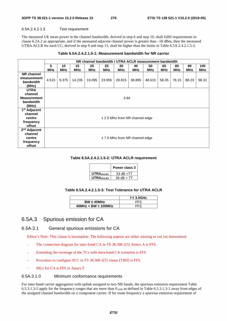
ETSI
ETSI TS 138 521-1 V15.2.0 (2019-05)2763GPP TS 38.521-1 version 15.2.0 Release 15
6.5A.2.4.2.1.5 Test requirement
The measured UE mean power in the channel bandwidth, derived in step 6 and step 10, shall fulfil requirements in clause 6.2A.2 as appropriate, and if the measured adjacent channel power is greater than –50 dBm, then the measured UTRA ACLR for each CC, derived in step 9 and step 13, shall be higher than the limits in Table 6.5A.2.4.2.1.5-2.
Table 6.5A.2.4.2.1.5-1: Measurement bandwidth for NR carrier
NR channel bandwidth / UTRA ACLR measurement bandwidth
5 MHz
10 MHz
15 MHz
20 MHz
25 MHz
30 MHz
40 MHz
50 MHz
60 MHz
80 MHz
90 MHz
100 MHz
NR channel measurement
bandwidth (MHz)
4.515 9.375 14.235 19.095 23.955 28.815 38.895 48.615 58.35 78.15 88.23 98.31
UTRA channel
Measurement bandwidth
(MHz)
3.84
1st Adjacent channel centre
frequency offset
± 2.5 MHz from NR channel edge
2nd Adjacent channel centre
frequency offset
± 7.5 MHz from NR channel edge
Table 6.5A.2.4.2.1.5-2: UTRA ACLR requirement
Power class 3
UTRAACLR1 33 dB +TT UTRAACLR2 36 dB + TT
Table 6.5A.2.4.2.1.5-3: Test Tolerance for UTRA ACLR
f ≤ 3.0GHz BW ≤ 40MHz FFS
40MHz < BW ≤ 100MHz FFS
6.5A.3 Spurious emission for CA
6.5A.3.1 General spurious emissions for CA
Editor’s Note: This clause is incomplete. The following aspects are either missing or not yet determined:
- The connection diagram for inter-band CA in TS 38.508-1[5] Annex A is FFS.
- Extending the coverage of the TCs with intra-band CA scenarios is FFS
- Procedure to configure SCC in TS 38.508-1[5] clause [TBD] is FFS
- MUs for CA is FFS in Annex F
6.5A.3.1.0 Minimum conformance requirements
For inter-band carrier aggregation with uplink assigned to two NR bands, the spurious emission requirement Table 6.5.3.1.3-2 apply for the frequency ranges that are more than FOOB as defined in Table 6.5.3.1.3-1 away from edges of the assigned channel bandwidth on a component carrier. If for some frequency a spurious emission requirement of

ETSI
ETSI TS 138 521-1 V15.2.0 (2019-05)2773GPP TS 38.521-1 version 15.2.0 Release 15
individual component carrier overlaps with the spectrum emission mask or channel bandwidth of another component carrier then it does not apply.
NOTE 1: For inter-band carrier aggregation with uplink assigned to two NR bands the requirements in Table 6.5.3.1.3-2 could be verified by measuring spurious emissions at the specific frequencies where second and third order intermodulation products generated by the two transmitted carriers can occur; in that case, the requirements for remaining applicable frequencies in Table 6.5.3.1.3-2 would be considered to be verified by the measurements verifying the one uplink inter-band CA spurious emission requirement.
The normative reference for this requirement is TS 38.101-1 [2] subclause 6.5A.3.1
6.5A.3.1.1 General spurious emissions for CA (2UL CA)
6.5A.3.1.1.1 Test purpose
To verify that UE transmitter does not cause unacceptable interference to other channels or other systems in terms of transmitter spurious emissions.
6.5A.3.1.1.2 Test applicability
This test case applies to all types of NR UE release 15 and forward that supports 2DL and 2UL CA.
6.5A.3.1.1.3 Minimum conformance requirements
The minimum conformance requirements are defined in subclause 6.5A.3.1.0.
6.5A.3.1.1.4 Test description
6.5A.3.1.1.4.1 Initial conditions
Initial conditions are a set of test configurations the UE needs to be tested in and the steps for the SS to take with the UE to reach the correct measurement state.
The initial test configurations consist of environmental conditions, test frequencies, test channel bandwidths and sub-carrier spacing based on NR CA configuration specified in clause 5.5A. All of these configurations shall be tested with applicable test parameters for each CA configuration, are shown in Table 6.5A.3.1.1.4.1-1. The details of the uplink reference measurement channels (RMCs) are specified in Annexes A.2. Configurations of PDSCH and PDCCH before measurement are specified in Annex C.2.
Table 6.5A.3.1.1.4.1-1: Inter band CA Test Configuration Table
Initial Conditions Test Environment as specified in TS 38.508-1 [5] subclause 4.1
Normal
Test Frequencies as specified in TS 38.508-1 [5] subclause4.3.1.1.3 for inter band CA in FR1
Low range for PCC and SCC High range for PCC and SCC
Test Channel Bandwidths as specified in TS 38.508-1 [5] subclause 4.3.1
Lowest for both PCC and SCC Highest for both PCC and SCC
Test SCS as specified in Table 5.5A.3-1 Smallest and biggest supported SCS per Channel Bandwidth Test Parameters
Test ID Downlink Configuration Uplink Configuration Modulation RB allocation (NOTE 1)
PCC SCC 1 N/A CP-OFDM QPSK Outer_Full Outer_Full
2 CP-OFDM QPSK Outer_1RB_Left Outer_1RB_Left
3 CP-OFDM QPSK Outer_1RB_Right Outer_1RB_Right
NOTE 1: The specific configuration of each RB allocation is defined in Table 6.1-1. NOTE 2: Test Channel Bandwidths and Test SCS are checked separately for each NR CA band combination,
which applicable channel bandwidths and SCS are specified in Table 5.5A3-1.
1. Connect the SS to the UE antenna connectors as shown in TS 38.508-1 [5] Annex A, in Figure [TBD] for TE diagram and section A.3.2.1 for UE diagram.
2. The parameter settings for the cell are set up according to TS 38.508-1 [5] subclause 4.4.3.

ETSI
ETSI TS 138 521-1 V15.2.0 (2019-05)2783GPP TS 38.521-1 version 15.2.0 Release 15
3. Downlink signals for PCC are initially set up according to Annex C.0, C.1 and C.2, and uplink signals according to Annex G.0, G.1, G.2, G.3.0.
4. The UL Reference Measurement channels are set according to Table 6.5A.3.1.1.4.1-1.
5. Propagation conditions are set according to Annex B.0.
6. Ensure the UE is in state RRC_CONNECTED with generic procedure parameters Connectivity NR, Connected without release On, Test Mode On and Test Loop Function On according to TS 38.508-1 [5] clause 4.5. Message contents are defined in clause 6.5A.3.1.1.4.3.
6.5A.3.1.1.4.2 Test procedure
1. Configure SCC according to Annex C.0, C.1, C.2 for all downlink physical channels.
2. The SS shall configure SCC as per TS 38.508-1 [5] clause [TBD]. Message contents are defined in clause 6.5A.3.1.1.4.3.
3. SS activates SCC by sending the activation MAC CE (Refer TS 38.321 [18], clauses 5.9, 6.1.3.10). Wait for at least 2 seconds (Refer TS 38.133[19], clause9.3).
4. SS sends uplink scheduling information for each UL HARQ process via PDCCH DCI format 0_1 for C_RNTI to schedule the UL RMC according to Table 6.5A.3.1.1.4.1-1 on both PCC and SCC. Since the UE has no payload data to send, the UE transmits uplink MAC padding bits on the UL RMC.
5. Send continuously uplink power control "up" commands in every uplink scheduling information to the UE until the UE transmits at PUMAX level.
6. Measure the power of the transmitted signal with a measurement filter of bandwidths according to Table 6.5A.3.1.1.5-1. The centre frequency of the filter shall be stepped in contiguous steps according to Table 6.5A.3.1.1.5-1. The measured power shall be verified for each step. The measurement period shall capture the active time slots.
6.5A.3.1.1.4.3 Message contents
Message contents are according to TS 38.508-1 [5] subclause 4.6.
6.5A.3.1.1.5 Test requirement
This clause specifies the requirements for the specified NR band for Transmitter Spurious emissions requirement with frequency range as indicated in Table 6.5A.3.1.1.5-1.
Unless otherwise stated, the spurious emission limits apply for the frequency ranges that are more than ΔfOOB (MHz) in Table 6.5.3.1.3-1 from the edge of the channel bandwidth. If for some frequency a spurious emission requirement of individual component carrier overlaps with the spectrum emission mask or channel bandwidth of another component carrier then it does not apply.
The measured average power of spurious emission, derived in step 6, shall not exceed the described value in Table 6.5A.3.1.1.5-1.
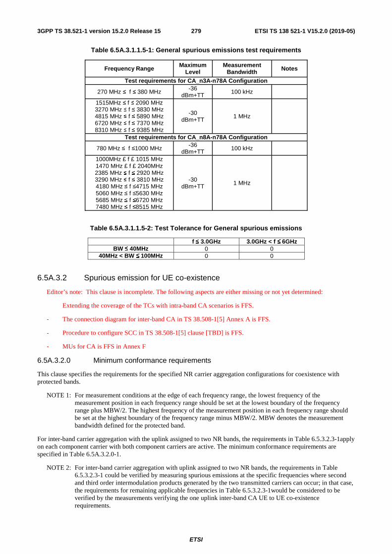
ETSI
ETSI TS 138 521-1 V15.2.0 (2019-05)2793GPP TS 38.521-1 version 15.2.0 Release 15
Table 6.5A.3.1.1.5-1: General spurious emissions test requirements
Frequency Range Maximum Level
Measurement Bandwidth Notes
Test requirements for CA_n3A-n78A Configuration
270 MHz ≤ f ≤ 380 MHz -36 dBm+TT 100 kHz
1515MHz ≤ f ≤ 2090 MHz 3270 MHz ≤ f ≤ 3830 MHz 4815 MHz ≤ f ≤ 5890 MHz 6720 MHz ≤ f ≤ 7370 MHz 8310 MHz ≤ f ≤ 9385 MHz
-30 dBm+TT 1 MHz
Test requirements for CA_n8A-n78A Configuration
780 MHz ≤ f ≤1000 MHz -36 dBm+TT 100 kHz
1000MHz £ f £ 1015 MHz 1470 MHz £ f £ 2040MHz 2385 MHz ≤ f ≤ 2920 MHz 3290 MHz ≤ f ≤ 3810 MHz 4180 MHz ≤ f ≤4715 MHz 5060 MHz ≤ f ≤5630 MHz 5685 MHz ≤ f ≤6720 MHz 7480 MHz ≤ f ≤8515 MHz
-30 dBm+TT 1 MHz
Table 6.5A.3.1.1.5-2: Test Tolerance for General spurious emissions
f ≤ 3.0GHz 3.0GHz < f ≤ 6GHz BW ≤ 40MHz 0 0
40MHz < BW ≤ 100MHz 0 0
6.5A.3.2 Spurious emission for UE co-existence
Editor’s note: This clause is incomplete. The following aspects are either missing or not yet determined:
- Extending the coverage of the TCs with intra-band CA scenarios is FFS.
- The connection diagram for inter-band CA in TS 38.508-1[5] Annex A is FFS.
- Procedure to configure SCC in TS 38.508-1[5] clause [TBD] is FFS.
- MUs for CA is FFS in Annex F
6.5A.3.2.0 Minimum conformance requirements
This clause specifies the requirements for the specified NR carrier aggregation configurations for coexistence with protected bands.
NOTE 1: For measurement conditions at the edge of each frequency range, the lowest frequency of the measurement position in each frequency range should be set at the lowest boundary of the frequency range plus MBW/2. The highest frequency of the measurement position in each frequency range should be set at the highest boundary of the frequency range minus MBW/2. MBW denotes the measurement bandwidth defined for the protected band.
For inter-band carrier aggregation with the uplink assigned to two NR bands, the requirements in Table 6.5.3.2.3-1apply on each component carrier with both component carriers are active. The minimum conformance requirements are specified in Table 6.5A.3.2.0-1.
NOTE 2: For inter-band carrier aggregation with uplink assigned to two NR bands, the requirements in Table 6.5.3.2.3-1 could be verified by measuring spurious emissions at the specific frequencies where second and third order intermodulation products generated by the two transmitted carriers can occur; in that case, the requirements for remaining applicable frequencies in Table 6.5.3.2.3-1would be considered to be verified by the measurements verifying the one uplink inter-band CA UE to UE co-existence requirements.

ETSI
ETSI TS 138 521-1 V15.2.0 (2019-05)2803GPP TS 38.521-1 version 15.2.0 Release 15
The normative reference for this requirement is TS 38.101-1 [2] subclause 6.5A.3.2.
Table 6.5A.3.2.0-1: Requirements for uplink inter-band carrier aggregation (two bands)
NR CA Configuration
Spurious emission Protected Band Frequency range (Mhz) Maximum
Level (dBm)
MBW (MHz)
NOTE
CA_n3A-n78A E-UTRA Band 1, 3, 5, 7, 8, 11, 18, 19, 20, 21, 26, 28, 34, 39,
40, 41, 65 FDL_low - FDL_high -50 1
Frequency range 1884.5 - 1915.7 -41 0.3 3 NR Band n257 26500 - 29500 -5 100
CA_n8A-n78A E-UTRA Band 1,8, 20, 28, 34, 39, 40,65 FDL_low - FDL_high -50 1
E-UTRA Band 3, 7,41 FDL_low - FDL_high -50 1 2 E-UTRA Band 11, 21 FDL_low - FDL_high -50 1 5
Frequency range 860 - 890 -40 1 4,5 Frequency range 1884.5 - 1915.7 -41 0.3 3 NR Band n257 26500 - 29500 -5 100 NR Band n258 24250 - 27500 -5 100
NOTE 1: FDL_low and FDL_high refer to each frequency band specified in Table 5.2-1 or Table 5.5-1 in TS 36.101 NOTE 2: As exceptions, measurements with a level up to the applicable requirements defined in Table 6.5.3.1-2 are
permitted for each assigned NR carrier used in the measurement due to 2nd, 3rd, 4th or 5th harmonic spurious emissions. Due to spreading of the harmonic emission the exception is also allowed for the first 1 MHz frequency range immediately outside the harmonic emission on both sides of the harmonic emission. This results in an overall exception interval centred at the harmonic emission of (2MHz + N x LCRB x 180kHz), where N is 2, 3, 4, 5 for the 2nd, 3rd, 4th or 5th harmonic respectively. The exception is allowed if the measurement bandwidth (MBW) totally or partially overlaps the overall exception interval.
NOTE 3: Applicable when co-existence with PHS system operating in 1884.5 -1915.7MHz NOTE 4: These requirements also apply for the frequency ranges that are less than FOOB (MHz) in Table 6.5.3.1-1
and Table 6.5A.3.1-1 from the edge of the channel bandwidth. NOTE 5: This requirement is applicable only for the following cases: - for carriers of 5 MHz channel bandwidth when
carrier centre frequency (Fc) is within the range 902.5 MHz ≤ Fc < 907.5 MHz with an uplink transmission bandwidth less than or equal to 20 RB - for carriers of 5 MHz channel bandwidth when carrier centre frequency (Fc) is within the range 907.5 MHz ≤ Fc ≤ 912.5 MHz without any restriction on uplink transmission bandwidth. - for carriers of 10 MHz channel bandwidth when carrier centre frequency (Fc) is Fc = 910 MHz with an uplink transmission bandwidth less than or equal to 32 RB with RBstart> 3.
6.5A.3.2.1 Spurious emissions for UE co-existence for CA (2UL CA)
6.5A.3.2.1.1 Test purpose
To verify that UE transmitter does not cause unacceptable interference to co-existing systems for the specified bands which has specific requirements in terms of transmitter spurious emissions for 2UL CA.
6.5A.3.2.1.2 Test applicability
This test case applies to all types of NR UE release 15 and forward that support 2DL and 2UL CA.
6.5A.3.2.1.3 Minimum conformance requirements
The minimum conformance requirements are defined in subclause 6.5A.3.2.0.
6.5A.3.2.1.4 Test description
6.5A.3.2.1.4.1 Initial conditions
Initial conditions are a set of test configurations the UE needs to be tested in and the steps for the SS to take with the UE to reach the correct measurement state.
The initial test configurations consist of environmental conditions, test frequencies, test channel bandwidths and sub-carrier spacing based on NR CA configuration specified in clause 5.5A. All of these configurations shall be tested with applicable test parameters for each CA configuration, are shown in Table 6.5A.3.2.1.4.1-1. The details of the uplink reference measurement channels (RMCs) are specified in Annexes A.2. Configurations of PDSCH and PDCCH before measurement are specified in Annex C.2.

ETSI
ETSI TS 138 521-1 V15.2.0 (2019-05)2813GPP TS 38.521-1 version 15.2.0 Release 15
Table 6.5A.3.2.1.4.1-1: Inter band CA Test Configuration Table
Initial Conditions
Test Environment as specified in TS 38.508-1 [5] subclause 4.1 NC
Test Frequencies as specified in TS 38.508-1 [5] subclause4.3.1.1.3 for inter band CA in FR1 For test frequencies refer to “Range” columns.
Test Channel Bandwidths as specified in TS 38.508-1 [5] subclause 4.3.1 Refer to “PCC NRB@SCS”and “SCC NRB@SCS ” columns
Test SCS as specified in Table 5.5A.3-1 Refer to “PCC NRB@SCS”and “SCC NRB@SCS ” columns
Test Parameters for CA Configurations
ID
CA Configuration / NRB_agg (Note 4) DL Allocation
UL Allocation (Note 2,3)
CA Configuration PCC NRB
@SCS SCC NRB@SCS
CC MOD
PCC & SCC RB allocation
CC MOD
PCC & SCC RB allocations (LCRB @ RBstart) PCC SCC P
CC
SC
C
Band Range Band Range
Default Test Settings for a CA_XA-YA Configuration
1 X Low Y Low Highest NRB@SCS
Highest NRB@SCS
CP-OFDM QPSK
NA CP-OFDM QPSK
1@0 1@0
2 X High Y High Highest NRB@SCS
Highest NRB@SCS
CP-OFDM QPSK
NA CP-OFDM QPSK
1@RBmax 1@RBmax
Test Settings for CA_n3A-n78A Configuration
1 n3 Mid n78 Mid 160@15kHz 270@15kHz CP-
OFDM QPSK
NA CP-
OFDM QPSK
1@160 1@270
2 n3 Mid n78 Mid 78@30KHz 273@30KHz CP-
OFDM QPSK
NA CP-
OFDM QPSK
1@78 1@273
3 n3 Mid n78 Mid 38@60KHz 135@60KHz CP-
OFDM QPSK
NA CP-
OFDM QPSK
1@38 1@135
Test Settings for CA_n8A-n78A Configuration
1 n8 Mid n78 Mid 106@15kHz 270@15kHz CP-
OFDM QPSK
NA CP-
OFDM QPSK
1@0 1@0
2 n8
Mid n78 Mid 106@15kHz 270@15kHz CP-
OFDM QPSK
NA CP-
OFDM QPSK
1@106 1@270
3 n8
Low n78 Low 51@30KHz 273@30KHz CP-
OFDM QPSK
NA CP-
OFDM QPSK
1@51 1@273
4 n8
Mid n78 Mid 51@30KHz 273@30KHz CP-
OFDM QPSK
NA CP-
OFDM QPSK
1@51 1@273
1. Connect the SS to the UE antenna connectors as shown in TS 38.508-1 [5] Annex A, in Figure [TBD] for TE diagram and section A.3.2.1 for UE diagram.
2. The parameter settings for the cell are set up according to TS 38.508-1 [6] subclause4.4.3.
3. Downlink signals for PCC are initially set up according to Annex C.0, C.1, C.2, and uplink signals according to Annex G.0, G.1, G.2, G.3.0.
4. The UL Reference Measurement channels are set according to Table 6.5A.3.2.1.4.1-1.
5. Propagation conditions are set according to Annex B.0.

ETSI
ETSI TS 138 521-1 V15.2.0 (2019-05)2823GPP TS 38.521-1 version 15.2.0 Release 15
6. Ensure the UE is in state RRC_CONNECTED with generic procedure parameters Connectivity NR, Connected without release On, Test Mode On and Test Loop Function On according to TS 38.508-1 [5] clause 4.5. Message contents are defined in clause 6.5A.3.2.1.4.3.
6.5A.3.2.1.4.2 Test procedure
1. Configure SCC according to Annex C.0, C.1, and Annex C.2 for all downlink physical channels.
2. The SS shall configure SCC as per TS 38.508-1 [5] clause [TBD]. Message contents are defined in clause 6.5A.3.2.1.4.3.
3. SS activates SCC by sending the activation MAC CE (Refer TS 38.321 [18], clauses 5.9, 6.1.3.10). Wait for at least 2 seconds (Refer TS 38.133[19], clause9.3).
4. SS sends uplink scheduling information for each UL HARQ process via PDCCH DCI format 0_1 for C_RNTI to schedule the UL RMC according to Table 6.5A.3.2.1.4.1-1 on both PCC and SCC. Since the UE has no payload data to send, the UE transmits uplink MAC padding bits on the UL RMC.
5. Send continuously uplink power control "up" commands in every uplink scheduling information to the UE until the UE transmits at PUMAX level.
6. Measure the power of the transmitted signal with a measurement filter of bandwidths according to Table 6.5.3.2.3-1. The centre frequency of the filter shall be stepped in contiguous steps according to Table 6.5.3.2.3-1. The measured power shall be verified for each step. The measurement period shall capture the active time slots.
6.5A.3.2.1.4.3 Message contents
Message contents are according to TS 38.508-1 [5] subclause 4.6.
6.5A.3.2.1.5 Test requirement
Test requirements for Spurious Emissions UE Co-existence are the same as the minimum requirements. The measured average power of spurious emission, derived in step 6, shall not exceed the described value in Table 6.5A.3.2.1.5-1.
Table 6.5A.3.2.1.5-1: Requirements for uplink inter-band carrier aggregation (two bands)
NR CA Configuration
Spurious emission Protected Band Frequency range (Mhz) Maximum
Level (dBm)
MBW (MHz)
NOTE
CA_n3A-n78A E-UTRA Band 3, 34, 39 FDL_low - FDL_high -50+TT 1 Frequency range 1884.5 - 1915.7 -41+TT 0.3 3
CA_n8A-n78A E-UTRA Band 8, 20, 28, 34, 39, 40 FDL_low - FDL_high -50+TT 1
E-UTRA Band 3, 7,41 FDL_low - FDL_high -50+TT 1 2 E-UTRA Band 11, 21 FDL_low - FDL_high -50+TT 1 5
Frequency range 860 - 890 -40+TT 1 4,5 Frequency range 1884.5 - 1915.7 -41+TT 0.3 3
NOTE 1: FDL_low and FDL_high refer to each frequency band specified in Table 5.2-1 or Table 5.5-1 in TS 36.101 NOTE 2: As exceptions, measurements with a level up to the applicable requirements defined in Table 6.5.3.1-2 are
permitted for each assigned NR carrier used in the measurement due to 2nd, 3rd, 4th or 5th harmonic spurious emissions. Due to spreading of the harmonic emission the exception is also allowed for the first 1 MHz frequency range immediately outside the harmonic emission on both sides of the harmonic emission. This results in an overall exception interval centred at the harmonic emission of (2MHz + N x LCRB x 180kHz), where N is 2, 3, 4, 5 for the 2nd, 3rd, 4th or 5th harmonic respectively. The exception is allowed if the measurement bandwidth (MBW) totally or partially overlaps the overall exception interval.
NOTE 3: Applicable when co-existence with PHS system operating in 1884.5 -1915.7MHz NOTE 4: These requirements also apply for the frequency ranges that are less than FOOB (MHz) in Table 6.5.3.1-1
and Table 6.5A.3.1-1 from the edge of the channel bandwidth. NOTE 5: This requirement is applicable only for the following cases: - for carriers of 5 MHz channel bandwidth when
carrier centre frequency (Fc) is within the range 902.5 MHz ≤ Fc < 907.5 MHz with an uplink transmission bandwidth less than or equal to 20 RB - for carriers of 5 MHz channel bandwidth when carrier centre frequency (Fc) is within the range 907.5 MHz ≤ Fc ≤ 912.5 MHz without any restriction on uplink transmission bandwidth. - for carriers of 10 MHz channel bandwidth when carrier centre frequency (Fc) is Fc = 910 MHz with an uplink transmission bandwidth less than or equal to 32 RB with RBstart> 3.
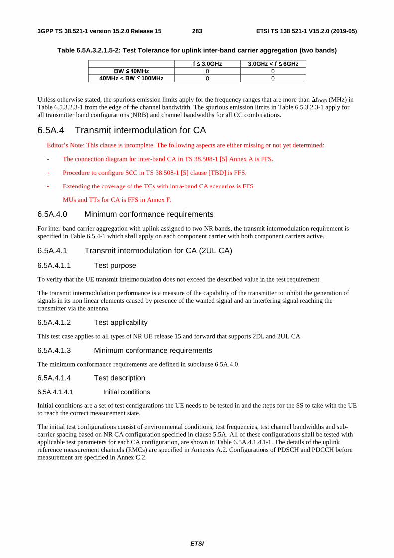
ETSI
ETSI TS 138 521-1 V15.2.0 (2019-05)2833GPP TS 38.521-1 version 15.2.0 Release 15
Table 6.5A.3.2.1.5-2: Test Tolerance for uplink inter-band carrier aggregation (two bands)
f ≤ 3.0GHz 3.0GHz < f ≤ 6GHz BW ≤ 40MHz 0 0
40MHz < BW ≤ 100MHz 0 0
Unless otherwise stated, the spurious emission limits apply for the frequency ranges that are more than ΔfOOB (MHz) in Table 6.5.3.2.3-1 from the edge of the channel bandwidth. The spurious emission limits in Table 6.5.3.2.3-1 apply for all transmitter band configurations (NRB) and channel bandwidths for all CC combinations.
6.5A.4 Transmit intermodulation for CA
Editor’s Note: This clause is incomplete. The following aspects are either missing or not yet determined:
- The connection diagram for inter-band CA in TS 38.508-1 [5] Annex A is FFS.
- Procedure to configure SCC in TS 38.508-1 [5] clause [TBD] is FFS.
- Extending the coverage of the TCs with intra-band CA scenarios is FFS
- MUs and TTs for CA is FFS in Annex F.
6.5A.4.0 Minimum conformance requirements
For inter-band carrier aggregation with uplink assigned to two NR bands, the transmit intermodulation requirement is specified in Table 6.5.4-1 which shall apply on each component carrier with both component carriers active.
6.5A.4.1 Transmit intermodulation for CA (2UL CA)
6.5A.4.1.1 Test purpose
To verify that the UE transmit intermodulation does not exceed the described value in the test requirement.
The transmit intermodulation performance is a measure of the capability of the transmitter to inhibit the generation of signals in its non linear elements caused by presence of the wanted signal and an interfering signal reaching the transmitter via the antenna.
6.5A.4.1.2 Test applicability
This test case applies to all types of NR UE release 15 and forward that supports 2DL and 2UL CA.
6.5A.4.1.3 Minimum conformance requirements
The minimum conformance requirements are defined in subclause 6.5A.4.0.
6.5A.4.1.4 Test description
6.5A.4.1.4.1 Initial conditions
Initial conditions are a set of test configurations the UE needs to be tested in and the steps for the SS to take with the UE to reach the correct measurement state.
The initial test configurations consist of environmental conditions, test frequencies, test channel bandwidths and sub-carrier spacing based on NR CA configuration specified in clause 5.5A. All of these configurations shall be tested with applicable test parameters for each CA configuration, are shown in Table 6.5A.4.1.4.1-1. The details of the uplink reference measurement channels (RMCs) are specified in Annexes A.2. Configurations of PDSCH and PDCCH before measurement are specified in Annex C.2.
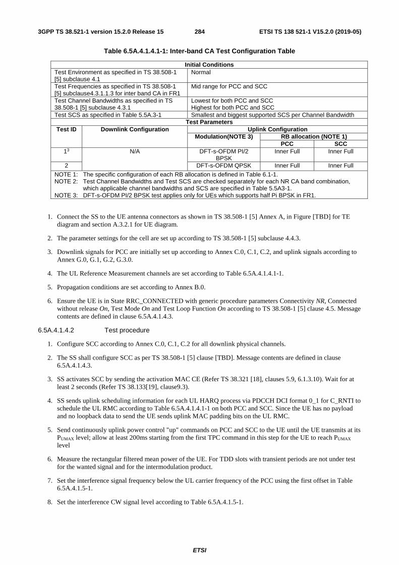
ETSI
ETSI TS 138 521-1 V15.2.0 (2019-05)2843GPP TS 38.521-1 version 15.2.0 Release 15
Table 6.5A.4.1.4.1-1: Inter-band CA Test Configuration Table
Initial Conditions Test Environment as specified in TS 38.508-1 [5] subclause 4.1
Normal
Test Frequencies as specified in TS 38.508-1 [5] subclause4.3.1.1.3 for inter band CA in FR1
Mid range for PCC and SCC
Test Channel Bandwidths as specified in TS 38.508-1 [5] subclause 4.3.1
Lowest for both PCC and SCC Highest for both PCC and SCC
Test SCS as specified in Table 5.5A.3-1 Smallest and biggest supported SCS per Channel Bandwidth Test Parameters
Test ID Downlink Configuration Uplink Configuration Modulation(NOTE 3) RB allocation (NOTE 1)
PCC SCC 13 N/A DFT-s-OFDM PI/2
BPSK Inner Full Inner Full
2 DFT-s-OFDM QPSK Inner Full Inner Full
NOTE 1: The specific configuration of each RB allocation is defined in Table 6.1-1. NOTE 2: Test Channel Bandwidths and Test SCS are checked separately for each NR CA band combination,
which applicable channel bandwidths and SCS are specified in Table 5.5A3-1. NOTE 3: DFT-s-OFDM PI/2 BPSK test applies only for UEs which supports half Pi BPSK in FR1.
1. Connect the SS to the UE antenna connectors as shown in TS 38.508-1 [5] Annex A, in Figure [TBD] for TE diagram and section A.3.2.1 for UE diagram.
2. The parameter settings for the cell are set up according to TS 38.508-1 [5] subclause 4.4.3.
3. Downlink signals for PCC are initially set up according to Annex C.0, C.1, C.2, and uplink signals according to Annex G.0, G.1, G.2, G.3.0.
4. The UL Reference Measurement channels are set according to Table 6.5A.4.1.4.1-1.
5. Propagation conditions are set according to Annex B.0.
6. Ensure the UE is in State RRC_CONNECTED with generic procedure parameters Connectivity NR, Connected without release On, Test Mode On and Test Loop Function On according to TS 38.508-1 [5] clause 4.5. Message contents are defined in clause 6.5A.4.1.4.3.
6.5A.4.1.4.2 Test procedure
1. Configure SCC according to Annex C.0, C.1, C.2 for all downlink physical channels.
2. The SS shall configure SCC as per TS 38.508-1 [5] clause [TBD]. Message contents are defined in clause 6.5A.4.1.4.3.
3. SS activates SCC by sending the activation MAC CE (Refer TS 38.321 [18], clauses 5.9, 6.1.3.10). Wait for at least 2 seconds (Refer TS 38.133[19], clause9.3).
4. SS sends uplink scheduling information for each UL HARQ process via PDCCH DCI format 0_1 for C_RNTI to schedule the UL RMC according to Table 6.5A.4.1.4.1-1 on both PCC and SCC. Since the UE has no payload and no loopback data to send the UE sends uplink MAC padding bits on the UL RMC.
5. Send continuously uplink power control "up" commands on PCC and SCC to the UE until the UE transmits at its PUMAX level; allow at least 200ms starting from the first TPC command in this step for the UE to reach PUMAX level
6. Measure the rectangular filtered mean power of the UE. For TDD slots with transient periods are not under test for the wanted signal and for the intermodulation product.
7. Set the interference signal frequency below the UL carrier frequency of the PCC using the first offset in Table 6.5A.4.1.5-1.
8. Set the interference CW signal level according to Table 6.5A.4.1.5-1.

ETSI
ETSI TS 138 521-1 V15.2.0 (2019-05)2853GPP TS 38.521-1 version 15.2.0 Release 15
9. Search the intermodulation product signals below and above the UL carrier frequency of the PCC, then measure the rectangular filtered mean power of transmitting intermodulation for both signals, and calculate the ratios with the power measured in step 6.
10. Set the interference signal frequency above the UL carrier frequency of the PCC using the first offset in Table 6.5A.4.1.5-1.
11. Search the intermodulation product signals below and above the UL carrier frequency of the PCC, then measure the rectangular filtered mean power of transmitting intermodulation for both signals, and calculate the ratios with the power measured in step 6.
12. Set the interference signal frequency below the UL carrier frequency of the SCC using the first offset in Table 6.5A.4.1.5-1.
13. Search the intermodulation product signals below and above the UL carrier frequency of the SCC, then measure the rectangular filtered mean power of transmitting intermodulation for both signals, and calculate the ratios with the power measured in step 6.
14. Set the interference signal frequency above the UL carrier frequency of the SCC using the first offset in Table 6.5A.4.1.5-1.
15. Search the intermodulation product signals below and above the UL carrier frequency of the SCC, then measure the rectangular filtered mean power of transmitting intermodulation for both signals, and calculate the ratios with the power measured in step 6.
16. Repeat the measurement using the second offset in Table 6.5A.4.1.5-1.
NOTE 1: When switching to DFT-s-OFDM waveform, as specified in the test configuration table 6.5.2.2.4.1-1, send an NR RRCReconfiguration message according to TS 38.508-1 [5] clause 4.6.3 Table 4.6.3-118 PUSCH-Config with TRANSFORM_PRECODER_ENABLED condition.
6.5A.4.1.4.3 Message contents
Message contents are according to TS 38.508-1 [5] subclause 4.6.
6.5A.4.1.5 Test requirement
The ratio derived in steps9, 11, 13 and 15, shall not exceed the described value in Table 6.5A.4.1.5-1.
Table 6.5A.4.1.5-1: Transmit Intermodulation
Wanted signal channel bandwidth BWChannel
Interference signal frequency offset from channel centre
BWChannel 2*BWChannel
Interference CW signal level -40dBc
Intermodulation product <-29dBc+TT < -35dBc+TT
Measurement bandwidth The maximum transmission bandwidth configuration among the different SCSs for the channel BW as defined in Table 6.5.2.2.3-1
Measurement offset from channel centre
BWChannel and 2*BWChannel
2*BWChannel and 4*BWChannel
Table6.5A.4.1.5-2: Test Tolerance for Transmit Intermodulation
f ≤ 3.0GHz 3.0GHz < f ≤ 6GHz BW ≤ 40MHz FFS FFS
40MHz < BW ≤ 100MHz FFS FFS
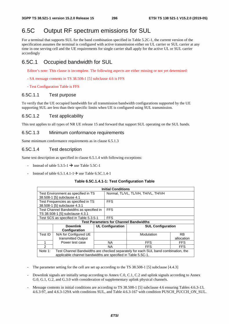
ETSI
ETSI TS 138 521-1 V15.2.0 (2019-05)2863GPP TS 38.521-1 version 15.2.0 Release 15
6.5C Output RF spectrum emissions for SUL For a terminal that supports SUL for the band combination specified in Table 5.2C-1, the current version of the specification assumes the terminal is configured with active transmission either on UL carrier or SUL carrier at any time in one serving cell and the UE requirements for single carrier shall apply for the active UL or SUL carrier accordingly
6.5C.1 Occupied bandwidth for SUL
Editor’s note: This clause is incomplete. The following aspects are either missing or not yet determined:
- SA message contents in TS 38.508-1 [5] subclause 4.6 is FFS
- Test Configuration Table is FFS
6.5C.1.1 Test purpose
To verify that the UE occupied bandwidth for all transmission bandwidth configurations supported by the UE supporting SUL are less than their specific limits when UE is configured using SUL transmission.
6.5C.1.2 Test applicability
This test applies to all types of NR UE release 15 and forward that support SUL operating on the SUL bands.
6.5C.1.3 Minimum conformance requirements
Same minimum conformance requirements as in clause 6.5.1.3
6.5C.1.4 Test description
Same test description as specified in clause 6.5.1.4 with following exceptions:
- Instead of table 5.3.5-1 use Table 5.5C-1
- Instead of table 6.5.1.4.1-1 use Table 6.5C.1.4-1
Table 6.5C.1.4.1-1: Test Configuration Table
Initial Conditions Test Environment as specified in TS 38.508-1 [5] subclause 4.1
Normal, TL/VL, TL/VH, TH/VL, TH/VH
Test Frequencies as specified in TS 38.508-1 [5] subclause 4.3.1
FFS
Test Channel Bandwidths as specified in TS 38.508-1 [5] subclause 4.3.1
FFS
Test SCS as specified in Table 5.3.5-1 FFS Test Parameters for Channel Bandwidths
Downlink Configuration
UL Configuration SUL Configuration
Test ID N/A for Configured UE transmitted Output
Power test case
Modulation RB allocation
1 NA FFS FFS 2 NA FFS FFS
Note 1: Test Channel Bandwidths are checked separately for each SUL band combination, the applicable channel bandwidths are specified in Table 5.5C-1.
- The parameter setting for the cell are set up according to the TS 38.508-1 [5] subclause [4.4.3]
- Downlink signals are initially setup according to Annex C.0, C.1, C.2 and uplink signals according to Annex G.0, G.1, G.2, and G.3.0 with consideration of supplementary uplink physical channels.
- Message contents in initial conditions are according to TS 38.508-1 [5] subclause 4.6 ensuring Tables 4.6.3-13, 4.6.3-97, and 4.6.3-129A with conditions SUL, and Table 4.6.3-167 with condition PUSCH_PUCCH_ON_SUL.

ETSI
ETSI TS 138 521-1 V15.2.0 (2019-05)2873GPP TS 38.521-1 version 15.2.0 Release 15
6.5C.1.5 Test requirement
The measured Occupied Bandwidth on SUL carrier shall not exceed values in Table 6.5C.1.5-1.
Table 6.5C.1.5-1: Occupied channel bandwidth
Occupied channel bandwidth / NR Channel bandwidth 5
MHz 10
MHz 15
MHz 20
MHz 25
MHz 30
MHz 40
MHz 50
MHz 60
MHz 80
MHz 90
MHz 100 MHz
Channel bandwidth
(MHz) 5 10 15 20 25 30 40 50 60 80 90 100
6.5C.2 Out of band emission for SUL
6.5C.2.1 General
Void
6.5C.2.2 Spectrum Emission Mask for SUL
The spectrum emission mask of the UE applies to frequencies (ΔfOOB) starting from the ± edge of the assigned NR channel bandwidth. For frequencies greater than (ΔfOOB) the spurious requirements in subclause 6.5.3 are applicable.
NOTE: For measurement conditions at the edge of each frequency range, the lowest frequency of the measurement position in each frequency range should be set at the lowest boundary of the frequency range plus MBW/2. The highest frequency of the measurement position in each frequency range should be set at the highest boundary of the frequency range minus MBW/2. MBW denotes the measurement bandwidth defined for the protected band.
Editor’s note: This clause is incomplete. The following aspects are either missing or not yet determined:
- SA message contents in TS 38.508-1[5] subclause 4.6 is FFS
- Configuration table is FFS
- The clause in reference to the total transmission power is TBD.
6.5C.2.2.1 Test purpose
To verify that the power of any UE emission shall not exceed specified level for the specified channel bandwidth.
6.5C.2.2.2 Test applicability
This test applies to all types of NR UE release 15 and forward that support SUL operating on the SUL bands.
6.5C.2.2.3 Minimum conformance requirements
Same minimum conformance requirements as in the clause 6.5.2.2.3.
6.5C.2.2.4 Test description
Same test description as specified in clause 6.5.2.2 with following exceptions:
- Instead of table 5.3.5-1 use Table 5.5C-1
- Instead of table 6.5.2.2.4.1-1 use Table 6.5C.2.2.4.1-1

ETSI
ETSI TS 138 521-1 V15.2.0 (2019-05)2883GPP TS 38.521-1 version 15.2.0 Release 15
Table 6.5C.2.2.4.1-1: Test Configuration Table(FFS)
Initial Conditions Test Environment as specified in TS 38.508-1 [5] subclause 4.1
Normal, TL/VL, TL/VH, TH/VL, TH/VH
Test Frequencies as specified in TS 38.508-1 [5] subclause 4.3.1
FFS
Test Channel Bandwidths as specified in TS 38.508-1 [5] subclause 4.3.1
FFS
Test SCS as specified in Table 5.3.5-1 FFS Test Parameters for Channel Bandwidths
Downlink Configuration
UL Configuration
SUL Configuration
Test ID N/A for Configured UE transmitted Output
Power test case
Modulation RB allocation 1 NA FFS FFS 2 NA FFS FFS
Note 1: Test Channel Bandwidths are checked separately for each SUL band combination, the applicable channel bandwidths are specified in Table 5.5C-1.
- The parameter setting for the cell are set up according to the TS 38.508-1 [5] subclause [4.4.3]
- Downlink signals are initially setup according to Annex C.0, C.1, C.2 and uplink signals according to Annex G.0, G.1, G.2, and G.3.0 with consideration of supplementary uplink physical channels.
- Message contents in initial conditions are according to TS 38.508-1 [5] subclause 4.6 ensuring Tables 4.6.3-13, 4.6.3-97, and 4.6.3-129A with conditions SUL, and Table 4.6.3-167 with condition PUSCH_PUCCH_ON_SUL.
6.5C.2.2.5 Test requirement
The measured sum of the UE mean power in the channel bandwidth on the SUL carrier, derived in step 3, shall fulfil requirements in Tables [6.2C.1.5-1 or 6.2C.2.5-1] as appropriate, and the power of any UE emission shall fulfil requirements in Table 6.5C.2.2.5-1.
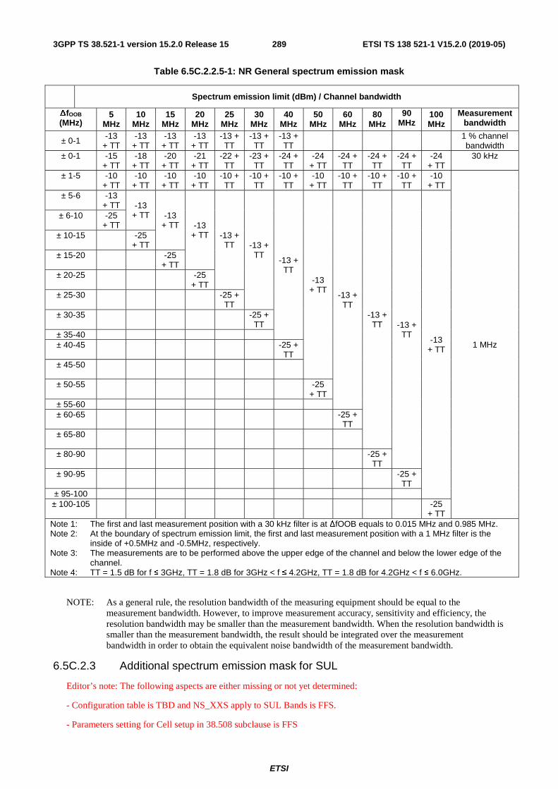
ETSI
ETSI TS 138 521-1 V15.2.0 (2019-05)2893GPP TS 38.521-1 version 15.2.0 Release 15
Table 6.5C.2.2.5-1: NR General spectrum emission mask
Spectrum emission limit (dBm) / Channel bandwidth
ΔfOOB (MHz)
5 MHz
10 MHz
15 MHz
20 MHz
25 MHz
30 MHz
40 MHz
50 MHz
60 MHz
80 MHz
90 MHz
100 MHz
Measurement bandwidth
± 0-1 -13 + TT
-13 + TT
-13 + TT
-13 + TT
-13 + TT
-13 + TT
-13 + TT 1 % channel
bandwidth ± 0-1 -15
+ TT -18
+ TT -20
+ TT -21
+ TT -22 + TT
-23 + TT
-24 + TT
-24 + TT
-24 + TT
-24 + TT
-24 + TT
-24 + TT
30 kHz
± 1-5 -10 + TT
-10 + TT
-10 + TT
-10 + TT
-10 + TT
-10 + TT
-10 + TT
-10 + TT
-10 + TT
-10 + TT
-10 + TT
-10 + TT
1 MHz
± 5-6 -13 + TT -13
+ TT -13 + TT -13
+ TT -13 + TT -13 +
TT -13 + TT
-13 + TT
-13 + TT
-13 + TT -13 +
TT -13
+ TT
± 6-10 -25 + TT
± 10-15 -25 + TT
± 15-20 -25 + TT
± 20-25 -25
+ TT ± 25-30 -25 +
TT ± 30-35 -25 +
TT ± 35-40 ± 40-45 -25 +
TT ± 45-50
± 50-55
-25 + TT
± 55-60 ± 60-65 -25 +
TT ± 65-80
± 80-90 -25 + TT
± 90-95 -25 + TT
± 95-100 ± 100-105 -25
+ TT Note 1: The first and last measurement position with a 30 kHz filter is at ΔfOOB equals to 0.015 MHz and 0.985 MHz. Note 2: At the boundary of spectrum emission limit, the first and last measurement position with a 1 MHz filter is the
inside of +0.5MHz and -0.5MHz, respectively. Note 3: The measurements are to be performed above the upper edge of the channel and below the lower edge of the
channel. Note 4: TT = 1.5 dB for f ≤ 3GHz, TT = 1.8 dB for 3GHz < f ≤ 4.2GHz, TT = 1.8 dB for 4.2GHz < f ≤ 6.0GHz.
NOTE: As a general rule, the resolution bandwidth of the measuring equipment should be equal to the measurement bandwidth. However, to improve measurement accuracy, sensitivity and efficiency, the resolution bandwidth may be smaller than the measurement bandwidth. When the resolution bandwidth is smaller than the measurement bandwidth, the result should be integrated over the measurement bandwidth in order to obtain the equivalent noise bandwidth of the measurement bandwidth.
6.5C.2.3 Additional spectrum emission mask for SUL
Editor’s note: The following aspects are either missing or not yet determined:
- Configuration table is TBD and NS_XXS apply to SUL Bands is FFS.
- Parameters setting for Cell setup in 38.508 subclause is FFS
ETSI
ETSI TS 138 521-1 V15.2.0 (2019-05)2903GPP TS 38.521-1 version 15.2.0 Release 15
- SA Generic procedures with condition NR in TS 38.508-1 [5] is FFS.
- Message contents in reference to clause 6.2C.3.4.3 is TBD
- Test point analysis in reference to clause 6.2C.3 is TBD
- Test procedure is incomplete, the clause in reference to the total transmission power is TBD.
- Test requirements is incomplete.
6.5C.2.3.1 Test purpose
Same test purpose as in clause 6.5.2.3.1
6.5C.2.3.2 Test applicability
This test applies to all types of NR UE release 15 and forward that support SUL operating on the SUL bands.
6.5C.2.3.3 Minimum conformance requirements
Same minimum conformance requirements as in the clause 6.5.2.3.3 with consideration of the NS_XXs applicable to the SUL bands.
6.5C.2.3.4 Test description
Same test description as specified in clause 6.5.2.3.4 with following exceptions:
- Instead of table 5.3.5-1 use Table 5.5C-1
- The parameter setting for the cell are set up according to the TS 38.508-1 [5] subclause [4.4.3]
- Downlink signals are initially setup according to Annex C.0, C.1, C.2 and uplink signals according to Annex G.0, G.1, G.2, and G.3.0 with consideration of supplementary uplink physical channels.
- Message contents in initial conditions are according to TS 38.508-1 [5] subclause 4.6 ensuring Tables 4.6.3-13, 4.6.3-97, and 4.6.3-129A with conditions SUL, and Table 4.6.3-167 with condition PUSCH_PUCCH_ON_SUL, additionally the following exceptions shown in Table 6.2C.1.4-2 ~ Table 6.2C.1.4-4 are considered.
[FFS]
6.5C.2.3.4.3 Message contents
The same message contents as in Clause 6.2C.3.4.3
6.5C.2.3.5 Test requirement
[FFS for NS_XXs]
6.5C.2.4 Adjacent channel leakage ratio for SUL
Adjacent channel leakage power Ratio (ACLR) is the ratio of the filtered mean power centred on the assigned channel frequency to the filtered mean power centred on an adjacent channel frequency.
6.5C.2.4.1 NR ACLR for SUL
Editor’s note: This clause is incomplete. The following aspects are either missing or not yet determined:
- SA message contents in TS 38.508-1[5] subclause 4.6 is FFS
- PC1 and PC4 requirements are missing in TS 38.101-1 [2].
- Test point analysis is FFS
- The clause 6.2C.2.5 in reference to the total transmission power is TBD

ETSI
ETSI TS 138 521-1 V15.2.0 (2019-05)2913GPP TS 38.521-1 version 15.2.0 Release 15
6.5C.2.4.1.1 Test purpose
To verify that UE transmitter does not cause unacceptable interference to adjacent channels in terms of Adjacent Channel Leakage power Ratio (ACLR).
6.5C.2.4.1.2 Test applicability
This test applies to all types of NR UE release 15 and forward that support SUL operating on the SUL bands.
6.5C.2.4.1.3 Minimum conformance requirements
The minimum conformance requirements specified in Clause 6.5.2.4.1.3 applies to the UE that support SUL operating on the SUL bands.
The normative reference for this requirement is TS 38.101-] clauses 6.5.2.4.1.
6.5C.2.4.1.4 Test description
Same test description as specified in clause 6.5.2.4.1.4 with following exceptions:
- Instead of table 5.3.5-1 use Table 5.5C-1
- Instead of table 6.5.2.4.1.4.1-1 use Table 6.5C.2.4.1.4-1
Table 6.5C.2.4.1.4-1: Test Configuration Table
Initial Conditions Test Environment as specified in TS 38.508-1 [5] subclause 4.1
Normal, TL/VL, TL/VH, TH/VL, TH/VH
Test Frequencies as specified in TS 38.508-1 [5] subclause 4.3.1
Mid range for both SUL carrier and Non-SUL carrier
Test Channel Bandwidths as specified in TS 38.508-1 [5] subclause 4.3.1
Lowest, Mid, Highest for both SUL carrier and Non-SUL carrier
Test SCS as specified in Table 5.3.5-1 15kHz for both SUL carrier and Non-SUL carrier Test Parameters for Channel Bandwidths
Downlink Configuration
UL Configuration SUL Configuration
Test ID N/A for Configured UE transmitted Output
Power test case
Modulation RB allocation
1 NA FFS FFS 2 NA FFS FFS
Note 1: Test Channel Bandwidths are checked separately for each SUL band combination, the applicable channel bandwidths are specified in Table 5.5C-1.
- The parameter setting for the cell are set up according to the TS 38.508-1 [5] subclause [4.4.3]
- Downlink signals are initially setup according to Annex C.0, C.1, C.2 and uplink signals according to Annex G.0, G.1, G.2, and G.3.0 with consideration of supplementary uplink physical channels.
- Message contents in initial conditions are according to TS 38.508-1 [5] subclause 4.6 ensuring Tables 4.6.3-13, 4.6.3-97, and 4.6.3-129A with conditions SUL, and Table 4.6.3-167 with condition PUSCH_PUCCH_ON_SUL.
6.5C.2.4.1.5 Test requirement
The measured UE mean power in the channel bandwidth on SUL carrier, derived in step 3, shall fulfil requirements in [Clause 6.2C.2.5] as appropriate, and if the measured adjacent channel power is greater than –50 dBm then the measured NR ACLR, derived in step 6, shall be higher than the limits in Table 6.5C.2.4.1.5-1.

ETSI
ETSI TS 138 521-1 V15.2.0 (2019-05)2923GPP TS 38.521-1 version 15.2.0 Release 15
Table 6.5C.2.4.1.5-1: NR ACLR measurement bandwidth
NR channel bandwidth / NR ACLR measurement bandwidth
5
MHz 10
MHz 15
MHz 20
MHz 25
MHz 30
MHz 40
MHz 50
MHz 60
MHz 80
MHz 90
MHz 100 MHz
NR ACLR measurement
bandwidth 4.515 9.375 14.235 19.095 23.955 28.815 38.895 48.615 58.35 78.15 88.23 98.31
Table 6.5C.2.4.1.5-2: NR ACLR requirement
Power class 1 Power class 2 Power class 3 NR ACLR 31 + TT dB 30 + TT dB
NOTE 1: TT = 0.8 dB for f ≤ 4.0GHz, TT = 1.0 dB for 4.0GHz < f ≤ 6.0GHz,
6.5C.2.4.2 UTRA ACLR for SUL
Editor’s note: This clause is incomplete. The following aspects are either missing or not yet determined:
- SA message contents in TS 38.508-1[5] subclause 4.6 is FFS
- Test point analysis is FFS
- The requirement is incomplete: No specified requirements for the UEs of PC other than PC3, the additionalSpectrumEmission. is unspecified in the core requirement.
- The clause 6.2C.3.5 in reference to the total transmission power is TBD
- The clause 6.5.2.4.2.3 in reference to the minimum requirements is TBD.
6.5C.2.4.2.1 Test purpose
To verify that UE transmitter does not cause unacceptable interference to adjacent channels in terms of Adjacent Channel Leakage power Ratio (ACLR).
6.5C.2.4.2.2 Test applicability
This test applies to all types of NR UE release 15 and forward that support SUL operating on the SUL bands.
6.5C.2.4.2.3 Minimum conformance requirements
The minimum conformance requirements specified in Clause [6.5.2.4.2.3] the UE that support SUL operating on the SUL bands.
The normative reference for this requirement is TS 38.101-] clause 6.5.2.4.2.
6.5C.2.4.2.4 Test description
Same test description as specified in clause 6.5.2.4.2.4 with following exceptions:
- Instead of table 5.3.5-1 use Table 5.5C-1
- Instead of table 6.5.2.4.2.4.1-1 use Table 6.5C.2.4.2.4-1

ETSI
ETSI TS 138 521-1 V15.2.0 (2019-05)2933GPP TS 38.521-1 version 15.2.0 Release 15
Table 6.5C.2.4.2.4-1: Test Configuration Table(FFS)
Initial Conditions Test Environment as specified in TS 38.508-1 [5] subclause 4.1
Normal, TL/VL, TL/VH, TH/VL, TH/VH
Test Frequencies as specified in TS 38.508-1 [5] subclause 4.3.1
FFS
Test Channel Bandwidths as specified in TS 38.508-1 [5] subclause 4.3.1
FFS
Test SCS as specified in Table 5.3.5-1 FFS Test Parameters for Channel Bandwidths
Downlink Configuration
UL Configuration SUL Configuration
Test ID N/A for Configured UE transmitted Output
Power test case
Modulation RB allocation
1 NA FFS FFS 2 NA FFS FFS
Note 1: Test Channel Bandwidths are checked separately for each SUL band combination, the applicable channel bandwidths are specified in Table 5.5C-1.
- The parameter setting for the cell are set up according to the TS 38.508-1 [5] subclause [4.4.3]
- Downlink signals are initially setup according to Annex C.0, C.1, C.2 and uplink signals according to Annex G.0, G.1, G.2, and G.3.0 with consideration of supplementary uplink physical channels.
- Message contents in initial conditions are according to TS 38.508-1 [5] subclause 4.6 ensuring Tables 4.6.3-13, 4.6.3-97, and 4.6.3-129A with conditions SUL, and Table 4.6.3-167 with condition PUSCH_PUCCH_ON_SUL, together with the exceptions as specified in Table 6.5C.2.4.2.4-2
Table 6.5C.2.4.2.4-2: SystemInformationBlockType2: UTRA ACLR test requirement for "NS_XX"
Derivation Path: TS 38.508-1 [5] clause [TBD], Table [TBD] Information Element Value/remark Comment Condition
additionalSpectrumEmission XX (NS_XX)
6.5C.2.4.2.5 Test requirement
UTRA ACLR requirement is applicable when signalled by the network with network signalling value indicated by the field additionalSpectrumEmission.
The measured UE mean total power in the channel bandwidth on SUL carrier, derived in step 3, shall fulfil requirements in [Clause 6.2C.3.5] as appropriate, and if the measured adjacent channel power is greater than –50 dBm then the measured UTRA ACLR, derived in step 6, shall be higher than the limits in Table 6.5C.2.4.2.5-1.
Table 6.5C.2.4.2.5-1: NR ACLR requirement
Power class 3
UTRAACLR1 33 dB + TT UTRAACLR2 36 dB + TT
NOTE 1: TT = 0.8 dB for f ≤ 4.0GHz, TT = 1.0 dB for 4.0GHz < f ≤ 6.0GHz,
6.5C.3 Spurious emissions for SUL
6.5C.3.1 General spurious emissions for SUL
Editor’s Note:
- SA message contents in TS 38.508-1[5] subclause 4.6 is FFS.
- The clause 6.2C.2.5 in reference to the total transmission power is TBD

ETSI
ETSI TS 138 521-1 V15.2.0 (2019-05)2943GPP TS 38.521-1 version 15.2.0 Release 15
- Parameters setting for Cell setup in 38.508 subclause is FFS.
- The configuration needs FFS to incorporate into the Edge allocation.
6.5C.3.1.1 Test purpose
To verify that UE transmitter does not cause unacceptable interference to other channels or other systems in terms of transmitter spurious emissions.
6.5C.3.1.2 Test applicability
This test applies to all types of NR UE release 15 and forward that support SUL operating on the SUL bands.
6.5C.3.1.3 Minimum conformance requirements
The general spurious emission requirement specified in clause 6.5.3.1.3 applies to the UE that support SUL operating on the SUL bands.
The normative reference for this requirement is TS 38.101-1 [2] subclauses 6.5.3.1
6.5C.3.1.4 Test description
Same test description as specified in clause 6.5.3.1.4 with following exceptions:
- Instead of table 5.3.5-1 use Table 5.5C-1
- Instead of table 6.5.3.1.4.1-1 use Table 6.5C.3.1.4-1
Table 6.5C.3.1.4-1: Test Configuration Table
Initial Conditions Test Environment as specified in TS 38.508-1 [5] subclause 4.1
Normal, TL/VL, TL/VH, TH/VL, TH/VH
Test Frequencies as specified in TS 38.508-1 [5] subclause 4.3.1
Low range, Mid range, High range
Test Channel Bandwidths as specified in TS 38.508-1 [5] subclause 4.3.1
Lowest, Mid, Highest
Test SCS as specified in Table 5.3.5-1 Lowest, Highest Test Parameters for Channel Bandwidths
Downlink Configuration
UL Configuration SUL Configuration
Test ID N/A for Configured UE transmitted
Output Power test case
Modulation RB allocation 1 CP-OFDM QPSK Outer_Full CP-OFDM QPSK 2 CP-OFDM QPSK Outer_1RB_Left CP-OFDM QPSK 3 CP-OFDM QPSK Outer_1RB_Right CP-OFDM QPSK
Note 1: Test Channel Bandwidths are checked separately for each SUL band combination, the applicable channel bandwidths are specified in Table 5.5C-1.
- The parameter setting for the cell are set up according to the TS 38.508-1 [5] subclause [4.4.3]
- Downlink signals are initially setup according to Annex C.0, C.1, C.2 and uplink signals according to Annex G.0, G.1, G.2, and G.3.0 with consideration of supplementary uplink physical channels.
- Message contents in initial conditions are according to TS 38.508-1 [5] subclause 4.6 ensuring Tables 4.6.3-13, 4.6.3-97, and 4.6.3-129A with conditions SUL, and Table 4.6.3-167 with condition PUSCH_PUCCH_ON_SUL.
- Instead of Table 6.5C.3.1.5-1 use Table 6.5C.3.1.5-1
6.5C.3.1.5 Test requirement
The measured average power of spurious emission on the SUL carrier, derived in step 3, shall not exceed the described value in Table 6.5C.3.1.5-1.
The spurious emission limits apply for the frequency ranges that are more than ΔfOOB (MHz) in Table 6.5C.3.1.3-1from the edge of the channel bandwidth.
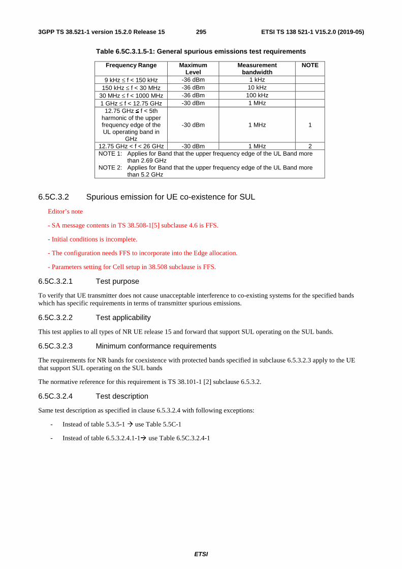
ETSI
ETSI TS 138 521-1 V15.2.0 (2019-05)2953GPP TS 38.521-1 version 15.2.0 Release 15
Table 6.5C.3.1.5-1: General spurious emissions test requirements
Frequency Range Maximum Level
Measurement bandwidth
NOTE
9 kHz ≤ f < 150 kHz -36 dBm 1 kHz 150 kHz ≤ f < 30 MHz -36 dBm 10 kHz
30 MHz ≤ f < 1000 MHz -36 dBm 100 kHz 1 GHz ≤ f < 12.75 GHz -30 dBm 1 MHz
12.75 GHz ≤ f < 5th harmonic of the upper frequency edge of the UL operating band in
GHz
-30 dBm 1 MHz 1
12.75 GHz < f < 26 GHz -30 dBm 1 MHz 2 NOTE 1: Applies for Band that the upper frequency edge of the UL Band more
than 2.69 GHz NOTE 2: Applies for Band that the upper frequency edge of the UL Band more
than 5.2 GHz
6.5C.3.2 Spurious emission for UE co-existence for SUL
Editor’s note
- SA message contents in TS 38.508-1[5] subclause 4.6 is FFS.
- Initial conditions is incomplete.
- The configuration needs FFS to incorporate into the Edge allocation.
- Parameters setting for Cell setup in 38.508 subclause is FFS.
6.5C.3.2.1 Test purpose
To verify that UE transmitter does not cause unacceptable interference to co-existing systems for the specified bands which has specific requirements in terms of transmitter spurious emissions.
6.5C.3.2.2 Test applicability
This test applies to all types of NR UE release 15 and forward that support SUL operating on the SUL bands.
6.5C.3.2.3 Minimum conformance requirements
The requirements for NR bands for coexistence with protected bands specified in subclause 6.5.3.2.3 apply to the UE that support SUL operating on the SUL bands
The normative reference for this requirement is TS 38.101-1 [2] subclause 6.5.3.2.
6.5C.3.2.4 Test description
Same test description as specified in clause 6.5.3.2.4 with following exceptions:
- Instead of table 5.3.5-1 use Table 5.5C-1
- Instead of table 6.5.3.2.4.1-1 use Table 6.5C.3.2.4-1
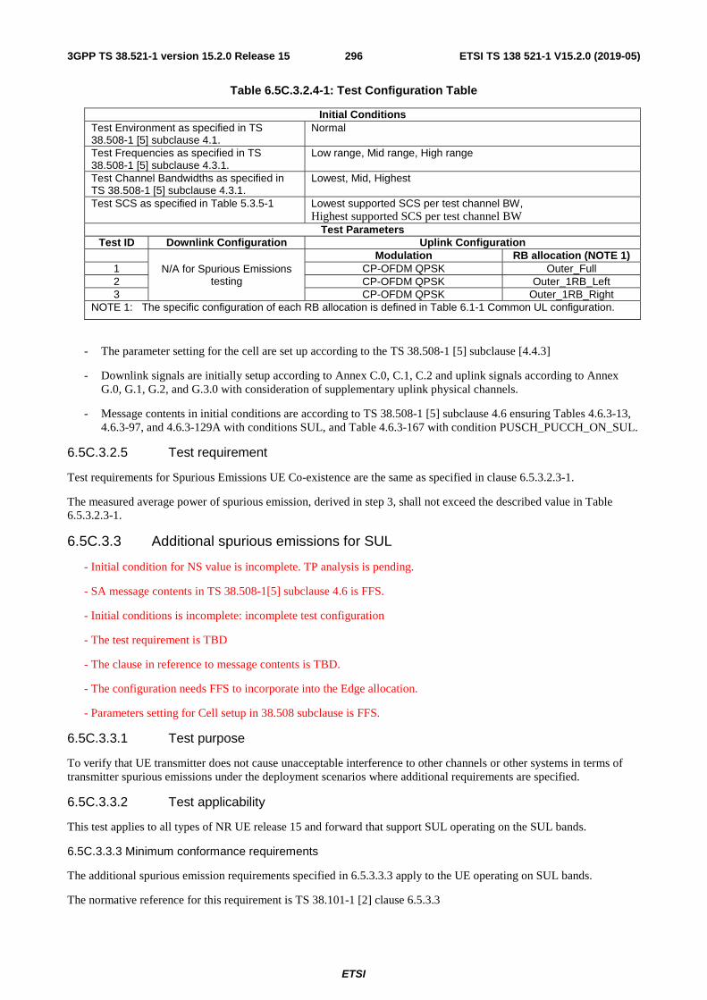
ETSI
ETSI TS 138 521-1 V15.2.0 (2019-05)2963GPP TS 38.521-1 version 15.2.0 Release 15
Table 6.5C.3.2.4-1: Test Configuration Table
Initial Conditions Test Environment as specified in TS 38.508-1 [5] subclause 4.1.
Normal
Test Frequencies as specified in TS 38.508-1 [5] subclause 4.3.1.
Low range, Mid range, High range
Test Channel Bandwidths as specified in TS 38.508-1 [5] subclause 4.3.1.
Lowest, Mid, Highest
Test SCS as specified in Table 5.3.5-1 Lowest supported SCS per test channel BW, Highest supported SCS per test channel BW
Test Parameters Test ID Downlink Configuration Uplink Configuration
N/A for Spurious Emissions
testing
Modulation RB allocation (NOTE 1) 1 CP-OFDM QPSK Outer_Full 2 CP-OFDM QPSK Outer_1RB_Left 3 CP-OFDM QPSK Outer_1RB_Right
NOTE 1: The specific configuration of each RB allocation is defined in Table 6.1-1 Common UL configuration.
- The parameter setting for the cell are set up according to the TS 38.508-1 [5] subclause [4.4.3]
- Downlink signals are initially setup according to Annex C.0, C.1, C.2 and uplink signals according to Annex G.0, G.1, G.2, and G.3.0 with consideration of supplementary uplink physical channels.
- Message contents in initial conditions are according to TS 38.508-1 [5] subclause 4.6 ensuring Tables 4.6.3-13, 4.6.3-97, and 4.6.3-129A with conditions SUL, and Table 4.6.3-167 with condition PUSCH_PUCCH_ON_SUL.
6.5C.3.2.5 Test requirement
Test requirements for Spurious Emissions UE Co-existence are the same as specified in clause 6.5.3.2.3-1.
The measured average power of spurious emission, derived in step 3, shall not exceed the described value in Table 6.5.3.2.3-1.
6.5C.3.3 Additional spurious emissions for SUL
- Initial condition for NS value is incomplete. TP analysis is pending.
- SA message contents in TS 38.508-1[5] subclause 4.6 is FFS.
- Initial conditions is incomplete: incomplete test configuration
- The test requirement is TBD
- The clause in reference to message contents is TBD.
- The configuration needs FFS to incorporate into the Edge allocation.
- Parameters setting for Cell setup in 38.508 subclause is FFS.
6.5C.3.3.1 Test purpose
To verify that UE transmitter does not cause unacceptable interference to other channels or other systems in terms of transmitter spurious emissions under the deployment scenarios where additional requirements are specified.
6.5C.3.3.2 Test applicability
This test applies to all types of NR UE release 15 and forward that support SUL operating on the SUL bands.
6.5C.3.3.3 Minimum conformance requirements
The additional spurious emission requirements specified in 6.5.3.3.3 apply to the UE operating on SUL bands.
The normative reference for this requirement is TS 38.101-1 [2] clause 6.5.3.3

ETSI
ETSI TS 138 521-1 V15.2.0 (2019-05)2973GPP TS 38.521-1 version 15.2.0 Release 15
6.5C.3.3.4 Test description
Same test description as specified in clause 6.5.3.2.4 with following exceptions:
- Instead of table 5.3.5-1 use Table 5.5C-1
- Instead of table 6.5.3.3.4.1-1 use Table 6.5C.3.3.4-1
Table 6.5C.3.3.4-1: Test Configuration Table
Initial Conditions Test Environment as specified in TS 38.508-1 [5] subclause 4.1
Normal
Test Frequencies as specified in TS 38.508-1 [5] subclause 4.3.1
[TBD]
Test Channel Bandwidths as specified in TS 38.508-1 [5] subclause 4.3.1
[TBD]
Test SCS as specified in Table 5.3.5-1 [TBD] Test Parameters
Test ID Downlink Configuration Uplink Configuration
N/A for Spurious Emissions testing
Modulation RB allocation (NOTE 1)
1 FFS FFS 2 FFS FFS 3 FFS FFS
NOTE 1: The specific configuration of each RB allocation is defined in Table 6.1-1 Common UL configuration
- The parameter setting for the cell are set up according to the TS 38.508-1 [5] subclause [4.4.3]
- Downlink signals are initially setup according to Annex C.0, C.1, C.2 and uplink signals according to Annex G.0, G.1, G.2, and G.3.0 with consideration of supplementary uplink physical channels.
- Instead of table 6.5.3.3.5.1-1 use Table 6.5C.3.3.5-1
- Message contents in initial conditions are according to TS 38.508-1 [5] subclause 4.6 ensuring Tables 4.6.3-13, 4.6.3-97, and 4.6.3-129A with conditions SUL, and Table 4.6.3-167 with condition PUSCH_PUCCH_ON_SUL, together with the exceptions as specified in Clause [6.2C.3.4.3]
6.5C.3.3.5 Test requirement
The measured power on SUL carrier derived in step 4 shall meet the requirements for the specified NR band for an additional spectrum emission requirement with protected bands as indicated in Table 6.5C.3.3.5-1.
NOTE: For measurement conditions at the edge of each frequency range, the lowest frequency of the measurement position in each frequency range should be set at the lowest boundary of the frequency range plus MBW/2. The highest frequency of the measurement position in each frequency range should be set at the highest boundary of the frequency range minus MBW/2. MBW denotes the measurement bandwidth defined for the protected band.
Table 6.5C.3.3.5-1: Additional spurious emissions test requirements
[FFS]
6.5C.4 Transmit intermodulation for SUL
Editor’s Note:
- SA message contents in TS 38.508-1 [5] subclause 4.6 is FFS
- How to deal with TDD slots with transient periods is FFS
- Initial conditions is incomplete: Test configuration table is incomplete
- Parameters setting for Cell setup in 38.508 subclause is FFS.

ETSI
ETSI TS 138 521-1 V15.2.0 (2019-05)2983GPP TS 38.521-1 version 15.2.0 Release 15
6.5C.4.1 Test purpose
To verify that the UE transmit intermodulation does not exceed the described value in the test requirement.
The transmit intermodulation performance is a measure of the capability of the transmitter to inhibit the generation of signals in its non linear elements caused by presence of the wanted signal and an interfering signal reaching the transmitter via the antenna.
6.5C.4.2 Test applicability
This test applies to all types of NR UE release 15 and forward that support SUL operating on the SUL bands.
6.5C.4.3 Minimum conformance requirements
The requirements in subclause 6.5.4 apply to the UE operating on SUL bands
The normative reference for this requirement is TS 38.101-1 [2] clause 6.5.4.
6.5C.4.4 Test description
Same test description as specified in clause 6.2.4.4 with following exceptions:
- Instead of table 5.3.5-1 use Table 5.5C-1
- Instead of table 6.5.4.4.1-1 use Table 6.5C.4.4-1
Table 6.5C.4.4-1: Test Configuration Table
Initial Conditions Test Environment as specified in TS 38.508-1 [5] subclause 4.1
Normal
Test Frequencies as specified in TS 38.508-1 [5] subclause 4.3.1
FFS
Test Channel Bandwidths as specified in TS 38.508-1 [5] subclause 4.3.1
FFS
Test SCS as specified in Table 5.3.5-1 Lowest, Highest Test Parameters
Test ID Downlink Configuration Uplink Configuration
N/A for transmit intermodulation test case
Modulation RB allocation (NOTE 1) 1 FFS FFS 2 FFS FFS
NOTE 1: The specific configuration of each RB allocation is defined in Table 6.1-1.
- The parameter setting for the cell are set up according to the TS 38.508-1 [5] subclause [4.4.3]
- Downlink signals are initially setup according to Annex C.0, C.1, C.2 and uplink signals according to Annex G.0, G.1, G.2, and G.3.0 with consideration of supplementary uplink physical channels.
- Instead of table 6.5.4.5-1 use Table 6.5C.4.5-1
- Message contents in initial conditions are according to TS 38.508-1 [5] subclause 4.6 ensuring Tables 4.6.3-13, 4.6.3-97, and 4.6.3-129A with conditions SUL, and Table 4.6.3-167 with condition PUSCH_PUCCH_ON_SUL.
6.5C.4.5 Test requirement
The ratio derived in step 6 and 8, shall not exceed the described value in table 6.5C.4.5-1.
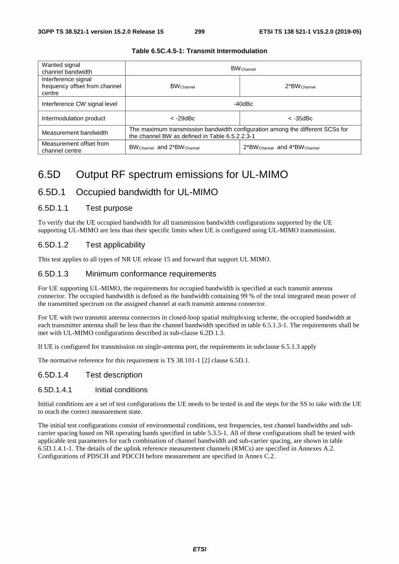
ETSI
ETSI TS 138 521-1 V15.2.0 (2019-05)2993GPP TS 38.521-1 version 15.2.0 Release 15
Table 6.5C.4.5-1: Transmit Intermodulation
Wanted signal channel bandwidth BWChannel
Interference signal frequency offset from channel centre
BWChannel 2*BWChannel
Interference CW signal level -40dBc
Intermodulation product < -29dBc < -35dBc
Measurement bandwidth The maximum transmission bandwidth configuration among the different SCSs for the channel BW as defined in Table 6.5.2.2.3-1
Measurement offset from channel centre BWChannel and 2*BWChannel 2*BWChannel and 4*BWChannel
6.5D Output RF spectrum emissions for UL-MIMO
6.5D.1 Occupied bandwidth for UL-MIMO
6.5D.1.1 Test purpose
To verify that the UE occupied bandwidth for all transmission bandwidth configurations supported by the UE supporting UL-MIMO are less than their specific limits when UE is configured using UL-MIMO transmission.
6.5D.1.2 Test applicability
This test applies to all types of NR UE release 15 and forward that support UL MIMO.
6.5D.1.3 Minimum conformance requirements
For UE supporting UL-MIMO, the requirements for occupied bandwidth is specified at each transmit antenna connector. The occupied bandwidth is defined as the bandwidth containing 99 % of the total integrated mean power of the transmitted spectrum on the assigned channel at each transmit antenna connector.
For UE with two transmit antenna connectors in closed-loop spatial multiplexing scheme, the occupied bandwidth at each transmitter antenna shall be less than the channel bandwidth specified in table 6.5.1.3-1. The requirements shall be met with UL-MIMO configurations described in sub-clause 6.2D.1.3.
If UE is configured for transmission on single-antenna port, the requirements in subclause 6.5.1.3 apply
The normative reference for this requirement is TS 38.101-1 [2] clause 6.5D.1.
6.5D.1.4 Test description
6.5D.1.4.1 Initial conditions
Initial conditions are a set of test configurations the UE needs to be tested in and the steps for the SS to take with the UE to reach the correct measurement state.
The initial test configurations consist of environmental conditions, test frequencies, test channel bandwidths and sub-carrier spacing based on NR operating bands specified in table 5.3.5-1. All of these configurations shall be tested with applicable test parameters for each combination of channel bandwidth and sub-carrier spacing, are shown in table 6.5D.1.4.1-1. The details of the uplink reference measurement channels (RMCs) are specified in Annexes A.2. Configurations of PDSCH and PDCCH before measurement are specified in Annex C.2.

ETSI
ETSI TS 138 521-1 V15.2.0 (2019-05)3003GPP TS 38.521-1 version 15.2.0 Release 15
Table 6.5D.1.4.1-1: Test Configuration Table
Initial Conditions Test Environment as specified in TS 38.508-1 [5] subclause 4.1
Normal
Test Frequencies as specified in TS 38.508-1 [5] subclause 4.3.1
Mid range by default, exceptions listed in Table 6.5D.1.4.1-2
Test Channel Bandwidths as specified in TS 38.508-1 [5] subclause 4.3.1
All
Test SCS as specified in Table 5.3.5-1 Lowest SCS Test Parameters
Test ID Downlink Configuration Uplink Configuration N/A for occupied bandwidth test
case
Modulation RB allocation (NOTE 1)
1 CP-OFDM QPSK Outer_full
NOTE 1: The specific configuration of each RB allocation is defined in Table 6.1-1.
Table 6.5D.1.4.1-2: Test frequency exceptions for Occupied Bandwidth
5G NR Band Test Frequency
n77 Low Range, Mid Range, High Range
n78 Low Range, Mid Range, High Range
n79 Low Range, Mid Range, High Range
1. Connect the SS to the UE antenna connectors as shown in TS 38.508-1 [5] Annex A, Figure A.3.1.1.2 for TE diagram and section A.3.2 for UE diagram.
2. The parameter settings for the cell are set up according to TS 38.508-1 [5] subclause 4.4.3.
3. Downlink signals are initially set up according to Annex C.0, C.1, C.2, and uplink signals according to Annex G.0, G.1, G.2, G.3.0.
4. The UL Reference Measurement channels are set according to Table 6.5D.1.4.1-1.
5. Propagation conditions are set according to Annex B.0.
6. Ensure the UE is in state RRC_CONNECTED with generic procedure parameters Connectivity NR, Connected without release On, Test Mode On and Test Loop Function On according to TS 38.508-1 [5] clause 4.5. Message contents are defined in clause 6.5D.1.4.3
6.5D.1.4.2 Test procedure
1. SS sends uplink scheduling information for each UL HARQ process via PDCCH DCI format 0_1 for C_RNTI to schedule the UL RMC according to Table 6.5D.1.4.1-1. Since the UL has no payload and no loopback data to send the UE sends uplink MAC padding bits on the UL RMC. The PDCCH DCI format 0_1 is specified with condition 2TX_UL_MIMO in 38.508-1 [5] subclause 4.3.6.1.1.2
2. Send continuously power control “up” commands to the UE until the UE transmits at PUMAX level. Allow at least 200ms for the UE to reach PUMAX level.
3. Measure the power spectrum distribution within two times or more range over the requirement for Occupied Bandwidth specification centring on the current carrier frequency. The characteristics of the filter shall be approximately Gaussian (typical spectrum analyser filter). Other methods to measure the power spectrum distribution are allowed. The measuring duration is 1ms over consecutive active uplink slots. For TDD, only slots consisting of only UL symbols are under test.
4. Calculate the total power within the range of all frequencies measured in step 3 and save this value as “Total power”.
5. Sum up the power upward from the lower boundary of the measured frequency range in step 3 and seek the limit frequency point by which this sum becomes 0.5% of “Total power” and save this point as “Lower Frequency”.

ETSI
ETSI TS 138 521-1 V15.2.0 (2019-05)3013GPP TS 38.521-1 version 15.2.0 Release 15
6. Sum up the power downward from the upper boundary of the measured frequency range in step 3 and seek the limit frequency point by which this sum becomes 0.5% of “Total power” and save this point as “Upper Frequency”.
7. Calculate the difference “Upper Frequency” – “Lower Frequency” = “Occupied Bandwidth” between the two limit frequencies obtained in step 5 and step 6.
8. Repeat step 3 until step 7 for each of transmit antenna of the UE.
6.5D.1.4.3 Message contents
Message contents are according to TS 38.508-1 [5] subclause 4.6 ensuring Table 4.6.3-182 with condition 2TX_UL_MIMO
6.5D.1.5 Test requirement
The measured Occupied Bandwidth in step 6 for each antenna shall not exceed values in Table 6.5D.1.5-1.
Table 6.5D.1.5-1: Occupied channel bandwidth
Occupied channel bandwidth / NR Channel bandwidth 5
MHz 10
MHz 15
MHz 20
MHz 25
MHz 30
MHz 40
MHz 50
MHz 60
MHz 80
MHz 90
MHz 100 MHz
Channel bandwidth
(MHz) 5 10 15 20 25 30 40 50 60 80 90 100
Note 1: TT = 0.
6.5D.2 Out of band emission for UL-MIMO
6.5D.2.1 General
For UE supporting UL-MIMO, the requirements for Out of band emissions resulting from the modulation process and non-linearity in the transmitters are specified at each transmit antenna connector.
For UEs with two transmit antenna connectors in closed-loop spatial multiplexing scheme, the requirements in subclause 6.5.2 apply to each transmit antenna connector. The requirements shall be met with UL-MIMO configurations described in sub-clause 6.2D.1.3
If UE is configured for transmission on single-antenna port, the requirements in subclause 6.5.2 apply.
6.5D.2.2 Spectrum Emission Mask for UL-MIMO
The spectrum emission mask of the UE applies to frequencies (ΔfOOB) starting from the ± edge of the assigned NR channel bandwidth. For frequencies greater than (ΔfOOB) the spurious requirements in subclause 6.5D.3 are applicable.
NOTE: For measurement conditions at the edge of each frequency range, the lowest frequency of the measurement position in each frequency range should be set at the lowest boundary of the frequency range plus MBW/2. The highest frequency of the measurement position in each frequency range should be set at the highest boundary of the frequency range minus MBW/2. MBW denotes the measurement bandwidth defined for the protected band.
6.5D.2.2.1 Test purpose
To verify that the power of any UE emission shall not exceed specified level for the specified channel bandwidth.
6.5D.2.2.2 Test applicability
This test case applies to all types of NR UE release 15 and forward that supports UL-MIMO.
6.5D.2.2.3 Minimum conformance requirements
The power of any UE emission shall not exceed the levels specified in Table 6.5.2.2.3-1 for the specified channel bandwidth at each transmit antenna connector.

ETSI
ETSI TS 138 521-1 V15.2.0 (2019-05)3023GPP TS 38.521-1 version 15.2.0 Release 15
The normative reference for this requirement is TS 38.101-1 [2] clause 6.5D.2 and 6.5.2.2
6.5D.2.2.4 Test description
6.5D.2.2.4.1 Initial conditions
Initial conditions are a set of test configurations the UE needs to be tested in and the steps for the SS to take with the UE to reach the correct measurement state.
The initial test configurations consist of environmental conditions, test frequencies, test channel bandwidths and sub-carrier spacing based on NR operating bands specified in table 5.3.5-1. All of these configurations shall be tested with applicable test parameters for each combination of channel bandwidth and sub-carrier spacing, and are shown in table 6.5D.2.2.4.1-1. The details of the uplink reference measurement channels (RMCs) are specified in Annexes A.2. Configurations of PDSCH and PDCCH before measurement are specified in Annex C.2
Table 6.5D.2.2.4.1-1: Test Configuration Table
Default Conditions Test Environment as specified in TS 38.508-1 [5] subclause 4.1
Normal
Test Frequencies as specified in TS 38.508-1 [5] subclause 4.3.1
Low range, High range
Test Channel Bandwidths as specified in TS 38.508-1 [5] subclause 4.3.1
Lowest, Highest
Test SCS as specified in Table 5.3.5-1 Lowest and Highest Test Parameters for Channel Bandwidths
Test ID
Freq ChBw SCS Downlink Configuration
Uplink Configuration
Default Default N/A for Spectrum Emission
Mask test case
Modulation RB allocation (NOTE 1)
1 Low CP-OFDM QPSK
Outer_1RB_Left
2 High CP-OFDM QPSK
Outer_1RB_Right
3 Default CP-OFDM QPSK
Outer_Full
4 Low CP-OFDM 16 QAM
Outer_1RB_Left
5 High CP-OFDM 16 QAM
Outer_1RB_Right
6 Default CP-OFDM 16 QAM
Outer_Full
7 Low CP-OFDM 64 QAM
Edge_1RB_Left
8 High CP-OFDM 64 QAM
Edge_1RB_Right
9 Default CP-OFDM 64 QAM
Outer_Full
10 Low CP-OFDM 256 QAM
Edge_1RB_Left
11 High CP-OFDM 256 QAM
Edge_1RB_Right
12 Default CP-OFDM 256 QAM
Outer_Full
NOTE 1: The specific configuration of each RF allocation is defined in Table 6.1-1.
1. Connect the SS to the UE antenna connectors as shown in TS 38.508-1 [5] Annex A, Figure A.3.1.1.2 for TE diagram and section A.3.2 for UE diagram.
2. The parameter settings for the cell are set up according to TS 38.508-1 [5] subclause 4.4.3.
3. Downlink signals are initially set up according to Annex C.0, C.1, C.2, and uplink signals according to Annex G.0, G.1, G.2, G.3.0.
4. The UL Reference Measurement channels are set according to Table 6.5D.2.2.4.1-1.

ETSI
ETSI TS 138 521-1 V15.2.0 (2019-05)3033GPP TS 38.521-1 version 15.2.0 Release 15
5. Propagation conditions are set according to Annex B.0.
6. Ensure the UE is in state RRC_CONNECTED with generic procedure parameters Connectivity NR, Connected without release On, Test Mode On and Test Loop Function On according to TS 38.508-1 [5] clause 4.5. Message contents are defined in clause 6.5D.2.2.4.3
6.5D.2.2.4.2 Test procedure
1. SS sends uplink scheduling information for each UL HARQ process via PDCCH DCI format0_1 for C_RNTI to schedule the UL RMC according to Table 6.5D.2.2.4.1-1. Since the UL has no payload and no loopback data to send the UE sends uplink MAC padding bits on the UL RMC. The PDCCH DCI format 0_1 is specified with condition 2TX_UL_MIMO in 38.508-1 [5] subclause 4.3.6.1.1.2
2. Send continuously power control “up” commands to the UE until the UE transmits at PUMAX level. Allow at least 200ms for the UE to reach PUMAX level.
3. Measure the sum of the mean power of the UE in the channel bandwidth of the radio access mode according to the test configuration, which shall meet the requirements described in Tables 6.2D.2.5-1 or 6.2D.2.5-2 as appropriate. The period of the measurement shall be at least the continuous duration of 1ms over consecutive active uplink slots and uplink symbols. For TDD, only slots consisting of only UL symbols are under test.
4. Measure the power of the transmitted signal at each antenna connector with a measurement filter of bandwidths according to table 6.5D.2.2.5-1. The centre frequency of the filter shall be stepped in continuous steps according to the same table. The measured power shall be recorded for each step. The measurement period shall capture the active TSs.
6.5D.2.2.4.3 Message contents
Message contents are according to TS 38.508-1 [5] subclause 4.6 ensuring Table 4.6.3-182 with condition 2TX_UL_MIMO.
6.5D.2.2.5 Test requirement
The measured sum of the UE mean power in the channel bandwidth, derived in step 3, shall fulfil requirements in Tables 6.2D.2.5-1 or 6.2D.2.5-2 as appropriate, and the power of any UE emission measured at each antenna in step 4 shall fulfil requirements in Table 6.5D.2.2.5-1.

ETSI
ETSI TS 138 521-1 V15.2.0 (2019-05)3043GPP TS 38.521-1 version 15.2.0 Release 15
Table 6.5D.2.2.5-1: NR General spectrum emission mask
Spectrum emission limit (dBm) / Channel bandwidth
ΔfOOB (MHz)
5 MHz
10 MHz
15 MHz
20 MHz
25 MHz
30 MHz
40 MHz
50 MHz
60 MHz
80 MHz
90 MHz
100 MHz
Measurement bandwidth
± 0-1 -13 + TT
-13 + TT
-13 + TT
-13 + TT
-13 + TT
-13 + TT
-13 + TT 1 % channel
bandwidth ± 0-1 -15
+ TT -18
+ TT -20
+ TT -21
+ TT -22 + TT
-23 + TT
-24 + TT
-24 + TT
-24 + TT
-24 + TT
-24 + TT
-24 + TT
30 kHz
± 1-5 -10 + TT
-10 + TT
-10 + TT
-10 + TT
-10 + TT
-10 + TT
-10 + TT
-10 + TT
-10 + TT
-10 + TT
-10 + TT
-10 + TT
1 MHz
± 5-6 -13 + TT -13
+ TT -13 + TT -13
+ TT -13 + TT -13 +
TT -13 + TT
-13 + TT
-13 + TT
-13 + TT -13 +
TT -13
+ TT
± 6-10 -25 + TT
± 10-15 -25 + TT
± 15-20 -25 + TT
± 20-25
-25 + TT
± 25-30 -25 + TT
± 30-35 -25 + TT
± 35-40 ± 40-45 -25 +
TT ± 45-50 ± 50-55 -25
+ TT ± 55-60 ± 60-65 -25 +
TT ± 65-80 ± 80-90 -25 +
TT ± 90-95 -25 +
TT ± 95-100
± 100-105 -25 + TT
Note 1: The first and last measurement position with a 30 kHz filter is at ΔfOOB equals to 0.015 MHz and 0.985 MHz. Note 2: At the boundary of spectrum emission limit, the first and last measurement position with a 1 MHz filter is the
inside of +0.5MHz and -0.5MHz, respectively. Note 3: The measurements are to be performed above the upper edge of the channel and below the lower edge of the
channel. Note 4: TT = 1.5 dB for f ≤ 3GHz, TT = 1.8 dB for 3GHz < f ≤ 4.2GHz, TT = 1.8 dB for 4.2GHz < f ≤ 6.0GHz.
NOTE: As a general rule, the resolution bandwidth of the measuring equipment should be equal to the measurement bandwidth. However, to improve measurement accuracy, sensitivity and efficiency, the resolution bandwidth may be smaller than the measurement bandwidth. When the resolution bandwidth is smaller than the measurement bandwidth, the result should be integrated over the measurement bandwidth in order to obtain the equivalent noise bandwidth of the measurement bandwidth.
6.5D.2.3 Additional spectrum emission mask for UL-MIMO
Editor’s note: This clause is incomplete. The following aspects are either missing or not yet determined:
- The pointer to A-MPR UL-MIMO measurements is TBD
- There are FFS for NS-XXs:
- Test points analysis is TBD

ETSI
ETSI TS 138 521-1 V15.2.0 (2019-05)3053GPP TS 38.521-1 version 15.2.0 Release 15
- Test configuration table is TBD.
6.5D.2.3.1 Test purpose
To verify that the power of any UE emission at each transmit antenna shall not exceed specified lever for the specified channel bandwidth under the deployment scenarios where additional requirements are specified.
6.5D.2.3.2 Test applicability
This test case applies to all types of NR UE release 15 and forward that supports UL-MIMO.
6.5D.2.3.3 Minimum conformance requirements
The power of any UE emission shall not exceed the levels specified in Table 6.5.2.3.3-1 for the specified channel bandwidth at each transmit antenna connector.
The normative reference for this requirement is TS 38.101-1 [2] clause 6.5D.2 and 6.5.2.3
6.5D.2.3.4 Test description
6.5D.2.3.4.1 Initial conditions
Initial conditions are a set of test configurations the UE needs to be tested in and the steps for the SS to take with the UE to reach the correct measurement state.
The initial test configurations consist of environmental conditions, test frequencies, test channel bandwidths and sub-carrier spacing based on NR operating bands specified in table 5.3.5-1. All of these configurations shall be tested with applicable test parameters for each combination of channel bandwidth and sub-carrier spacing, and are shown in table 6.5D.2.3.4.1-1. The details of the uplink reference measurement channels (RMCs) are specified in Annexes A.2. Configurations of PDSCH and PDCCH before measurement are specified in Annex C.2
Table 6.5D.2.3.4.1-1: Test Configuration Table for NS_35
FFS
1. Connect the SS to the UE antenna connectors as shown in TS 38.508-1 [5] Annex A, Figure A.3.1.1.2 for TE diagram and section A.3.2 for UE diagram.
2. The parameter settings for the cell are set up according to TS 38.508-1 [5] subclause 4.4.3.
3. Downlink signals are initially set up according to Annex C.0, C.1, C.2, and uplink signals according to Annex G.0, G.1, G.2, G.3.0.
4. The UL Reference Measurement channels are set according to Tables 6.5D.2.3.4.1-1 as appropriate for NS_35.
5. Propagation conditions are set according to Annex B.0.
6. Ensure the UE is in state RRC_CONNECTED with generic procedure parameters Connectivity NR, Connected without release On, Test Mode On and Test Loop Function On according to TS 38.508-1 [5] clause 4.5. Message contents are defined in clause 6.5D.2.3.4.3
6.5D.2.3.4.2 Test procedure
Same test procedure as defined in clause 6.5D.2.2.4.2 with the following exceptions:
- Instead of Table 6.2D.2.5-1, [Table 6.2D.3.5-1] as approriate for NS_35 is applied in step 3;
- Intead of Table 6.5D.2.2.5-1, [6.5D.2.3.5-1] as approriate for the corresponding NS_35 is applied in step 4;
6.5D.2.3.4.3 Message contents
Message contents are according to TS 38.508-1 [5] subclause 4.6 ensuring Table 4.6.3-182 with condition 2TX_UL_MIMO and exceptions listed in clause [6.2D.3.4.3]
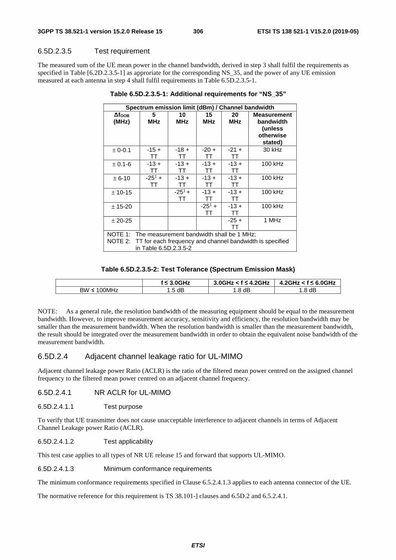
ETSI
ETSI TS 138 521-1 V15.2.0 (2019-05)3063GPP TS 38.521-1 version 15.2.0 Release 15
6.5D.2.3.5 Test requirement
The measured sum of the UE mean power in the channel bandwidth, derived in step 3 shall fulfil the requirements as specified in Table [6.2D.2.3.5-1] as approriate for the corresponding NS_35, and the power of any UE emission measured at each antenna in step 4 shall fulfil requirements in Table 6.5D.2.3.5-1.
Table 6.5D.2.3.5-1: Additional requirements for “NS_35”
Spectrum emission limit (dBm) / Channel bandwidth ΔfOOB (MHz)
5 MHz
10 MHz
15 MHz
20 MHz
Measurement bandwidth
(unless otherwise
stated) ± 0-0.1 -15 +
TT -18 + TT
-20 + TT
-21 + TT
30 kHz
± 0.1-6 -13 + TT
-13 + TT
-13 + TT
-13 + TT
100 kHz
± 6-10 -251 + TT
-13 + TT
-13 + TT
-13 + TT
100 kHz
± 10-15 -251 + TT
-13 + TT
-13 + TT
100 kHz
± 15-20 -251 + TT
-13 + TT
100 kHz
± 20-25 -25 + TT
1 MHz
NOTE 1: The measurement bandwidth shall be 1 MHz; NOTE 2: TT for each frequency and channel bandwidth is specified
in Table 6.5D.2.3.5-2
Table 6.5D.2.3.5-2: Test Tolerance (Spectrum Emission Mask)
f ≤ 3.0GHz 3.0GHz < f ≤ 4.2GHz 4.2GHz < f ≤ 6.0GHz BW ≤ 100MHz 1.5 dB 1.8 dB 1.8 dB
NOTE: As a general rule, the resolution bandwidth of the measuring equipment should be equal to the measurement bandwidth. However, to improve measurement accuracy, sensitivity and efficiency, the resolution bandwidth may be smaller than the measurement bandwidth. When the resolution bandwidth is smaller than the measurement bandwidth, the result should be integrated over the measurement bandwidth in order to obtain the equivalent noise bandwidth of the measurement bandwidth.
6.5D.2.4 Adjacent channel leakage ratio for UL-MIMO
Adjacent channel leakage power Ratio (ACLR) is the ratio of the filtered mean power centred on the assigned channel frequency to the filtered mean power centred on an adjacent channel frequency.
6.5D.2.4.1 NR ACLR for UL-MIMO
6.5D.2.4.1.1 Test purpose
To verify that UE transmitter does not cause unacceptable interference to adjacent channels in terms of Adjacent Channel Leakage power Ratio (ACLR).
6.5D.2.4.1.2 Test applicability
This test case applies to all types of NR UE release 15 and forward that supports UL-MIMO.
6.5D.2.4.1.3 Minimum conformance requirements
The minimum conformance requirements specified in Clause 6.5.2.4.1.3 applies to each antenna connector of the UE.
The normative reference for this requirement is TS 38.101-] clauses and 6.5D.2 and 6.5.2.4.1.
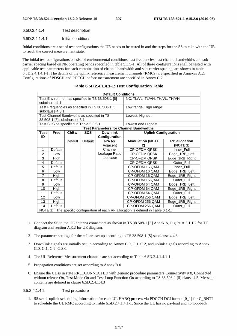
ETSI
ETSI TS 138 521-1 V15.2.0 (2019-05)3073GPP TS 38.521-1 version 15.2.0 Release 15
6.5D.2.4.1.4 Test description
6.5D.2.4.1.4.1 Initial conditions
Initial conditions are a set of test configurations the UE needs to be tested in and the steps for the SS to take with the UE to reach the correct measurement state.
The initial test configurations consist of environmental conditions, test frequencies, test channel bandwidths and sub-carrier spacing based on NR operating bands specified in table 5.3.5-1. All of these configurations shall be tested with applicable test parameters for each combination of channel bandwidth and sub-carrier spacing, are shown in table 6.5D.2.4.1.4.1-1. The details of the uplink reference measurement channels (RMCs) are specified in Annexes A.2. Configurations of PDSCH and PDCCH before measurement are specified in Annex C.2
Table 6.5D.2.4.1.4.1-1: Test Configuration Table
Default Conditions Test Environment as specified in TS 38.508-1 [5] subclause 4.1
NC, TL/VL, TL/VH, TH/VL, TH/VH
Test Frequencies as specified in TS 38.508-1 [5] subclause 4.3.1
Low range, High range
Test Channel Bandwidths as specified in TS 38.508-1 [5] subclause 4.3.1
Lowest, Highest
Test SCS as specified in Table 5.3.5-1 Lowest and Highest Test Parameters for Channel Bandwidths
Test ID
Freq ChBw SCS Downlink Configuration
Uplink Configuration
Default Default N/A for Adjacent Channel
Leakage Ratio test case
Modulation (NOTE 2)
RB allocation (NOTE 1)
1 Default CP-OFDM QPSK Inner_Full 2 Low CP-OFDM QPSK Edge_1RB_Left 3 High CP-OFDM QPSK Edge_1RB_Right 4 Default CP-OFDM QPSK Outer_Full 5 Default CP-OFDM 16 QAM Inner_Full 6 Low CP-OFDM 16 QAM Edge_1RB_Left 7 High CP-OFDM 16 QAM Edge_1RB_Right 8 Default CP-OFDM 16 QAM Outer_Full 9 Low CP-OFDM 64 QAM Edge_1RB_Left 10 High CP-OFDM 64 QAM Edge_1RB_Right 11 Default CP-OFDM 64 QAM Outer_Full 12 Low CP-OFDM 256 QAM Edge_1RB_Left 13 High CP-OFDM 256 QAM Edge_1RB_Right 14 Default CP-OFDM 256 QAM Outer_Full
NOTE 1: The specific configuration of each RF allocation is defined in Table 6.1-1.
1. Connect the SS to the UE antenna connectors as shown in TS 38.508-1 [5] Annex A, Figure A.3.1.1.2 for TE diagram and section A.3.2 for UE diagram.
2. The parameter settings for the cell are set up according to TS 38.508-1 [5] subclause 4.4.3.
3. Downlink signals are initially set up according to Annex C.0, C.1, C.2, and uplink signals according to Annex G.0, G.1, G.2, G.3.0.
4. The UL Reference Measurement channels are set according to Table 6.5D.2.4.1.4.1-1.
5. Propagation conditions are set according to Annex B.0
6. Ensure the UE is in state RRC_CONNECTED with generic procedure parameters Connectivity NR, Connected without release On, Test Mode On and Test Loop Function On according to TS 38.508-1 [5] clause 4.5. Message contents are defined in clause 6.5D.2.4.1.4.3
6.5.2.4.1.4.2 Test procedure
1. SS sends uplink scheduling information for each UL HARQ process via PDCCH DCI format [0_1] for C_RNTI to schedule the UL RMC according to Table 6.5D.2.4.1.4.1-1. Since the UL has no payload and no loopback

ETSI
ETSI TS 138 521-1 V15.2.0 (2019-05)3083GPP TS 38.521-1 version 15.2.0 Release 15
data to send the UE sends uplink MAC padding bits on the UL RMC. The PDCCH DCI format 0_1 is specified with condition 2TX_UL_MIMO in 38.508-1 [5] subclause 4.3.6.1.1.2
2. Send continuously power control “up” commands to the UE until the UE transmits at PUMAX level. Allow at least 200ms for the UE to reach PUMAX level.
3. Measure the sum of the mean power of the UE at each antenna connector in the channel bandwidth of the radio access mode according to the test configuration, which shall meet the requirements described in clauses 6.2D.2.5 and [6.2D.3.5] as appropriate. The period of the measurement shall be at least the continuous duration of 1ms over consecutive active uplink slots and uplink symbols. For TDD, only slots consisting of only UL symbols are under test.
4. Measure the rectangular filtered mean power for the assigned NR channel at each antenna connector of UE.
5. Measure the rectangular filtered mean power of the first NR adjacent channel at each antenna connector of UE on both lower and upper side of the assigned NR channel, respectively.
6. Calculate the ratios of the power between the values measured in step 4 over step 5 for lower and upper NR ACLR at each antenna connector of UE, respectively.
6.5D.2.4.1.4.3 Message contents
Message contents are according to TS 38.508-1 [5] subclause 4.6 ensuring Table 4.6.3-182 with condition 2TX_UL_MIMO.
6.5D.2.4.1.5 Test requirement
The measured UE mean total power in the channel bandwidth at all the antenna connectors, derived in step 3, shall fulfil requirements in Clause 6.2D.2.5 and [6.2D.3.5] as appropriate, and if the measured adjacent channel power is greater than –50 dBm then the measured NR ACLR, derived in step 6 for each antenna connector, shall be higher than the limits in Table 6.5D.2.4.1.5-2.
Table 6.5D.2.4.1.5-1: NR ACLR measurement bandwidth
NR channel bandwidth / NR ACLR measurement bandwidth
5
MHz 10
MHz 15
MHz 20
MHz 25
MHz 30
MHz 40
MHz 50
MHz 60
MHz 80
MHz 90
MHz 100 MHz
NR ACLR measurement
bandwidth 4.515 9.375 14.235 19.095 23.955 28.815 38.895 48.615 58.35 78.15 88.23 98.31
Table 6.5D.2.4.1.5-2: NR ACLR requirement
Power class 1 Power class 2 Power class 3 NR ACLR 31 + TT dB 30 + TT dB NOTE 1: TT = 0.8 dB
6.5D.2.4.2 UTRA ACLR for UL-MIMO
Editor’s note: This clause is incomplete. The following aspects are either missing or not yet determined:
- Test point analysis is FFS
- The clause 6.2D.3.5 in reference to the total transmission power is TBD
6.5D.2.4.2.1 Test purpose
To verify that UE transmitter does not cause unacceptable interference to adjacent channels in terms of Adjacent Channel Leakage power Ratio (ACLR).
6.5D.2.4.2.2 Test applicability
This test case applies to all types of NR UE release 15 and forward that supports UL-MIMO.

ETSI
ETSI TS 138 521-1 V15.2.0 (2019-05)3093GPP TS 38.521-1 version 15.2.0 Release 15
6.5D.2.4.2.3 Minimum conformance requirements
The minimum conformance requirements specified in Clause 6.5.2.4.2.3 applies to each antenna connector of the UE.
The normative reference for this requirement is TS 38.101-1 [2] clauses 6.5D.2 and 6.5.2.4.2.
6.5D.2.4.2.4 Test description
6.5D.2.4.2.4.1 Initial conditions
Initial conditions are a set of test configurations the UE needs to be tested in and the steps for the SS to take with the UE to reach the correct measurement state.
The initial test configurations consist of environmental conditions, test frequencies, test channel bandwidths and sub-carrier spacing based on NR operating bands specified in table 5.3.5-1. All of these configurations shall be tested with applicable test parameters for each combination of channel bandwidth and sub-carrier spacing, are shown in table 6.5D.2.4.2.4.1-1. The details of the uplink reference measurement channels (RMCs) are specified in Annexes A.2. Configurations of PDSCH and PDCCH before measurement are specified in Annex C.2
Table 6.5D.2.4.2.4.1-1: Test Configuration Table
[FFS]
1. Connect the SS to the UE antenna connectors as shown in TS 38.508-1 [5] Annex A, Figure A.3.1.1.2 for TE diagram and section A.3.2 for UE diagram.
2. The parameter settings for the cell are set up according to TS 38.508-1 [5] subclause 4.4.3.
3. Downlink signals are initially set up according to Annex C.0, C.1, C.2, and uplink signals according to Annex G.0, G.1, G.2, G.3.0.
4. The UL Reference Measurement channels are set according to Table 6.5D.2.4.2.4.1-1.
5. Propagation conditions are set according to Annex B.0
6. Ensure the UE is in state RRC_CONNECTED with generic procedure parameters Connectivity NR, Connected without release On, Test Mode On and Test Loop Function On according to TS 38.508-1 [5] clause 4.5. Message contents are defined in clause 6.5D.2.4.2.4.3
6.5D.2.4.2.4.2 Test procedure
1. SS sends uplink scheduling information for each UL HARQ process via PDCCH DCI format [0_1] for C_RNTI to schedule the UL RMC according to Table 6.5D.2.4.2.4.1-1. Since the UL has no payload and no loopback data to send the UE sends uplink MAC padding bits on the UL RMC. The PDCCH DCI format 0_1 is specified with condition 2TX_UL_MIMO in 38.508-1 [5] subclause 4.3.6.1.1.2
2. Send continuously power control “up” commands to the UE until the UE transmits at PUMAX level. Allow at least 200ms for the UE to reach PUMAX level.
3. Measure the sum of the mean power of the UE at each antenna connector in the channel bandwidth of the radio access mode according to the test configuration, which shall meet the requirements described in clause [6.2D.3.5] as appropriate. The period of the measurement shall be at least the continuous duration of 1ms over consecutive active uplink slots and uplink symbols. For TDD, only slots consisting of only UL symbols are under test.
4. Measure the rectangular filtered mean power for the assigned NR channel at each antenna connector of UE.
5. Measure the RRC filtered mean power of the first and the second UTRA adjacent channel at each antenna connector of UE on both lower and upper side of the assigned NR channel, respectively.
6. Calculate the ratio of the power between the values measured in step 4 over step 5 for UTRAACLR1, UTRAACLR2
for both lower an upper side of the assigned NR channel, respectively.
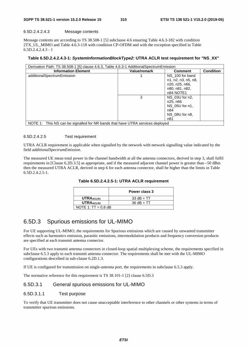
ETSI
ETSI TS 138 521-1 V15.2.0 (2019-05)3103GPP TS 38.521-1 version 15.2.0 Release 15
6.5D.2.4.2.4.3 Message contents
Message contents are according to TS 38.508-1 [5] subclause 4.6 ensuring Table 4.6.3-182 with condition 2TX_UL_MIMO and Table 4.6.3-118 with condition CP-OFDM and with the exception specified in Table 6.5D.2.4.2.4.3 - 1
Table 6.5D.2.4.2.4.3-1: SystemInformationBlockType2: UTRA ACLR test requirement for "NS_XX"
Derivation Path: TS 38.508-1 [5] clause 4.6.3, Table 4.6.3-1 AdditionalSpectrumEmission Information Element Value/remark Comment Condition
additionalSpectrumEmission 1 NS_100 for band n1, n2, n3, n5, n8, n20, n25, n66, n80, n81, n82, n84 NOTE1
3 NS_03U for n2, n25, n66 NS_05U for n1, n84 NS_08U for n8, n81
NOTE 1: This NS can be signalled for NR bands that have UTRA services deployed
6.5D.2.4.2.5 Test requirement
UTRA ACLR requirement is applicable when signalled by the network with network signalling value indicated by the field additionalSpectrumEmission.
The measured UE mean total power in the channel bandwidth at all the antenna connectors, derived in step 3, shall fulfil requirements in [Clause 6.2D.3.5] as appropriate, and if the measured adjacent channel power is greater than –50 dBm then the measured UTRA ACLR, derived in step 6 for each antenna connector, shall be higher than the limits in Table 6.5D.2.4.2.5-1.
Table 6.5D.2.4.2.5-1: UTRA ACLR requirement
Power class 3
UTRAACLR1 33 dB + TT UTRAACLR2 36 dB + TT
NOTE 1: TT = 0.8 dB
6.5D.3 Spurious emissions for UL-MIMO
For UE supporting UL-MIMO, the requirements for Spurious emissions which are caused by unwanted transmitter effects such as harmonics emission, parasitic emissions, intermodulation products and frequency conversion products are specified at each transmit antenna connector.
For UEs with two transmit antenna connectors in closed-loop spatial multiplexing scheme, the requirements specified in subclause 6.5.3 apply to each transmit antenna connector. The requirements shall be met with the UL-MIMO configurations described in sub-clause 6.2D.1.3.
If UE is configured for transmission on single-antenna port, the requirements in subclause 6.5.3 apply.
The normative reference for this requirement is TS 38.101-1 [2] clause 6.5D.3
6.5D.3.1 General spurious emissions for UL-MIMO
6.5D.3.1.1 Test purpose
To verify that UE transmitter does not cause unacceptable interference to other channels or other systems in terms of transmitter spurious emissions.
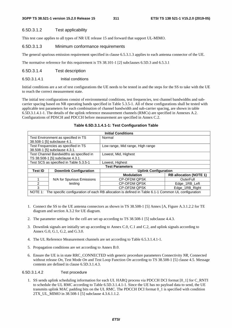
ETSI
ETSI TS 138 521-1 V15.2.0 (2019-05)3113GPP TS 38.521-1 version 15.2.0 Release 15
6.5D.3.1.2 Test applicability
This test case applies to all types of NR UE release 15 and forward that support UL-MIMO.
6.5D.3.1.3 Minimum conformance requirements
The general spurious emission requirement specified in clause 6.5.3.1.3 applies to each antenna connector of the UE.
The normative reference for this requirement is TS 38.101-1 [2] subclauses 6.5D.3 and 6.5.3.1
6.5D.3.1.4 Test description
6.5D.3.1.4.1 Initial conditions
Initial conditions are a set of test configurations the UE needs to be tested in and the steps for the SS to take with the UE to reach the correct measurement state.
The initial test configurations consist of environmental conditions, test frequencies, test channel bandwidths and sub-carrier spacing based on NR operating bands specified in Table 5.3.5-1. All of these configurations shall be tested with applicable test parameters for each combination of channel bandwidth and sub-carrier spacing, are shown in table 6.5D.3.1.4.1-1. The details of the uplink reference measurement channels (RMCs) are specified in Annexes A.2. Configurations of PDSCH and PDCCH before measurement are specified in Annex C.2.
Table 6.5D.3.1.4.1-1: Test Configuration Table
Initial Conditions Test Environment as specified in TS 38.508-1 [5] subclause 4.1.
Normal
Test Frequencies as specified in TS 38.508-1 [5] subclause 4.3.1.
Low range, Mid range, High range
Test Channel Bandwidths as specified in TS 38.508-1 [5] subclause 4.3.1.
Lowest, Mid, Highest
Test SCS as specified in Table 5.3.5-1 Lowest, Highest Test Parameters
Test ID Downlink Configuration Uplink Configuration
N/A for Spurious Emissions testing
Modulation RB allocation (NOTE 1) 1 CP-OFDM QPSK OuterFull 2 CP-OFDM QPSK Edge_1RB_Left 3 CP-OFDM QPSK Edge_1RB_Right
NOTE 1: The specific configuration of each RB allocation is defined in Table 6.1-1 Common UL configuration
1. Connect the SS to the UE antenna connectors as shown in TS 38.508-1 [5] Annex [A, Figure A.3.1.2.2 for TE diagram and section A.3.2 for UE diagram.
2. The parameter settings for the cell are set up according to TS 38.508-1 [5] subclause 4.4.3.
3. Downlink signals are initially set up according to Annex C.0, C.1 and C.2, and uplink signals according to Annex G.0, G.1, G.2, and G.3.0.
4. The UL Reference Measurement channels are set according to Table 6.5.3.1.4.1-1.
5. Propagation conditions are set according to Annex B.0.
6. Ensure the UE is in state RRC_CONNECTED with generic procedure parameters Connectivity NR, Connected without release On, Test Mode On and Test Loop Function On according to TS 38.508-1 [5] clause 4.5. Message contents are defined in clause 6.5D.3.1.4.3.
6.5D.3.1.4.2 Test procedure
1. SS sends uplink scheduling information for each UL HARQ process via PDCCH DCI format [0_1] for C_RNTI to schedule the UL RMC according to Table 6.5D.3.1.4.1-1. Since the UE has no payload data to send, the UE transmits uplink MAC padding bits on the UL RMC. The PDCCH DCI format 0_1 is specified with condition 2TX_UL_MIMO in 38.508-1 [5] subclause 4.3.6.1.1.2.

ETSI
ETSI TS 138 521-1 V15.2.0 (2019-05)3123GPP TS 38.521-1 version 15.2.0 Release 15
2. Send continuously uplink power control "up" commands in the uplink scheduling information to the UE until the UE transmits at PUMAX level.
3. Measure the power of the transmitted signal at each antenna connector with a measurement filter of bandwidths according to table 6.5D.3.1.5-1. The centre frequency of the filter shall be stepped in contiguous steps according to table 6.5D.3.1.5-1. The measured power shall be verified for each step. The measurement period shall capture the active time slots.
6.5D.3.1.4.3 Message contents
Message contents are according to TS 38.508-1 [5] subclause 4.6 ensuring Table 4.6.3-182 with condition 2TX_UL_MIMO
6.5D.3.1.5 Test requirement
The measured average power of spurious emission at each antenna connector, derived in step 3, shall not exceed the described value in Table 6.5D.3.1.5-1.
The spurious emission limits apply for the frequency ranges that are more than ΔfOOB (MHz) in Table 6.5.3.1.3-1from the edge of the channel bandwidth.
Table 6.5D.3.1.5-1: General spurious emissions test requirements
Frequency Range Maximum Level
Measurement bandwidth
NOTE
9 kHz ≤ f < 150 kHz -36 dBm 1 kHz 150 kHz ≤ f < 30 MHz -36 dBm 10 kHz
30 MHz ≤ f < 1000 MHz -36 dBm 100 kHz 1 GHz ≤ f < 12.75 GHz -30 dBm 1 MHz
12.75 GHz ≤ f < 5th harmonic of the upper frequency edge of the UL operating band in
GHz
-30 dBm 1 MHz 1
12.75 GHz < f < 26 GHz -30 dBm 1 MHz 2 NOTE 1: Applies for Band that the upper frequency edge of the UL Band more
than 2.69 GHz NOTE 2: Applies for Band that the upper frequency edge of the UL Band more
than 5.2 GHz
6.5D.3.2 Spurious emission for UE co-existence for UL-MIMO
6.5D.3.2.1 Test purpose
To verify that UE transmitter does not cause unacceptable interference to co-existing systems for the specified bands which has specific requirements in terms of transmitter spurious emissions.
6.5D.3.2.2 Test applicability
This test case applies to all types of NR UE release 15 and forward that support UL-MIMO.
6.5D.3.2.3 Minimum conformance requirements
The requirements for NR bands for coexistence with protected bands specified in subclause 6.5.3.2.3 apply to each UE transmit antenna connector
The normative reference for this requirement is TS 38.101-1 [2] subclauses 6.5.3.2 and 6.5D.3.
6.5D.3.2.4 Test description
6.5D.3.2.4.1 Initial conditions
Initial conditions are a set of test configurations the UE needs to be tested in and the steps for the SS to take with the UE to reach the correct measurement state.

ETSI
ETSI TS 138 521-1 V15.2.0 (2019-05)3133GPP TS 38.521-1 version 15.2.0 Release 15
The initial test configurations consist of environmental conditions, test frequencies, test channel bandwidths and sub-carrier spacing based on NR operating bands specified in Table 5.3.5-1. All of these configurations shall be tested with applicable test parameters for each combination of channel bandwidth and sub-carrier spacing, are shown in table 6.5D.3.2.4.1-1. The details of the uplink reference measurement channels (RMCs) are specified in Annexes A.2. Configurations of PDSCH and PDCCH before measurement are specified in Annex C.2.
Table 6.5D.3.2.4.1-1: Test Configuration Table
Initial Conditions Test Environment as specified in TS 38.508-1 [5] subclause 4.1.
Normal
Test Frequencies as specified in TS 38.508-1 [5] subclause 4.3.1.
Low range, Mid range, High range
Test Channel Bandwidths as specified in TS 38.508-1 [5] subclause 4.3.1.
Lowest, Mid, Highest
Test SCS as specified in Table 5.3.5-1 Lowest supported SCS per test channel BW, Highest supported SCS per test channel BW
Test Parameters Test ID Downlink Configuration Uplink Configuration
N/A for Spurious Emissions
testing
Modulation RB allocation (NOTE 1) 1 CP-OFDM QPSK Outer_Full 2 CP-OFDM QPSK Edge_1RB_Left 3 CP-OFDM QPSK Edge_1RB_Right
NOTE 1: The specific configuration of each RB allocation is defined in Table 6.1-1 Common UL configuration.
1. Connect the SS to the UE antenna connectors as shown in TS 38.508-1 [5] Annex A, Figure A.3.1.2.2 for TE diagram and section A.3.2 for UE diagram.
2. The parameter settings for the cell are set up according to TS 38.508-1 [6] subclause 4.4.3. .
3. Downlink signals are initially set up according to Annex C.0, C.1, C.2, and uplink signals according to Annex G.0, G.1, G.2, G.3.0.
4. The UL Reference Measurement channels are set according to Table 6.5D.3.2.4.1-1.
5. Propagation conditions are set according to Annex B.0.
6. Ensure the UE is in state RRC_CONNECTED with generic procedure parameters Connectivity NR, Connected without release On, Test Mode On and Test Loop Function On according to TS 38.508-1 [5] clause 4.5. Message contents are defined in clause 6.5D.3.2.4.3.
6.5D.3.2.4.2 Test procedure
1 SS sends uplink scheduling information for each UL HARQ process via PDCCH DCI format 0_1 for C_RNTI to schedule the UL RMC according to Table 6.5D.3.2.4.1-1. Since the UE has no payload data to send, the UE transmits uplink MAC padding bits on the UL RMC. The PDCCH DCI format 0_1 is specified with condition 2TX_UL_MIMO in 38.508-1 [5] subclause 4.3.6.1.1.2.
2. Send continuously uplink power control "up" commands in the uplink scheduling information to the UE until the UE transmits at PUMAX level.
3. Measure the power of the transmitted signal at each UE antenna connector with a measurement filter of bandwidths according to table 6.5.3.2.3-1. The centre frequency of the filter shall be stepped in contiguous steps according to table 6.5.3.2.3-1. The measured power shall be verified for each step. The measurement period shall capture the active time slots.
6.5D.3.2.4.3 Message contents
Message contents are according to TS 38.508-1 [5] subclause 4.6 ensuring Table 4.6.3-182 with condition 2TX_UL_MIMO.
6.5D.3.2.5 Test requirement
The measured average power of spurious emission, derived in step 3 at each UE antenna connector, shall not exceed the described value in Table 6.5.3.2.3-1.

ETSI
ETSI TS 138 521-1 V15.2.0 (2019-05)3143GPP TS 38.521-1 version 15.2.0 Release 15
6.5D.3.3 Additional spurious emissions for UL-MIMO
Editor’s note: This clause is incomplete. The following aspects are either missing or not yet determined:
- The A-MPR test for UL-MIMO is TBD
- There are NS-XXs other than NS_04 FFS:
6.5D.3.3.1 Test purpose
To verify that UE transmitter does not cause unacceptable interference to other channels or other systems in terms of transmitter spurious emissions under the deployment scenarios where additional requirements are specified.
6.5D.3.3.2 Test applicability
This test case applies to all types of NR UE release 15 and forward that support UL-MIMO.
6.5D.3.3.3 Minimum conformance requirements
The additional spurious emission requirements specified in 6.5.3.3.3 apply to each UE antenna connector.
The normative reference for this requirement is TS 38.101-1 [2] clauses 6.5D.3 and 6.5.3.3
6.5D.3.3.4 Test description
6.5D.3.3.4.1 Initial conditions
Initial conditions are a set of test configurations the UE needs to be tested in and the steps for the SS to take with the UE to reach the correct measurement state.
The initial test configurations consist of environmental conditions, test frequencies, test channel bandwidths and sub-carrier spacing based on NR operating bands specified in Table 5.3.5-1. All these configurations shall be tested with applicable test parameters for each combination of channel bandwidth and sub-carrier spacing, and are shown in Table 6.5D.3.3.4.1-1 through Table 6.5D.3.3.4.1. The details of the uplink reference measurement channels (RMCs) are specified in Annex A.2.2. Configurations of PDSCH and PDCCH before measurement are specified in Annex C.2.

ETSI
ETSI TS 138 521-1 V15.2.0 (2019-05)3153GPP TS 38.521-1 version 15.2.0 Release 15
Table 6.5D.3.3.4.1-1: Test Configuration Table (network signalled value "NS_04")
Initial Conditions Test Environment as specified in TS 38.508-1 [5] subclause 4.1 Normal Test Frequencies as specified in TS 38.508-1 [5] subclause 4.3.1 (See Freq column) Test Channel Bandwidths as specified in TS 38.508-1 [5] subclause 4.3.1 Lowest and Highest
Test SCS as specified in Table 5.3.5-1 Lowest and Highest A-MPR test parameters for NS_04
Downlink Configuration
Uplink Configuration
Test ID
Freq N/A for A-MPR testing.
Modulation
RB allocation (NOTE 1)
1 Low CP-OFDM QPSK Edge_1RB_Left 2 2496 + 3/2 × BWChannel − 6 MHz CP-OFDM QPSK Edge_1RB_Left 3
2496 + BWChannel /2 + MAX(10 MHz, 0.25 × BWChannel)
CP-OFDM QPSK Edge_1RB_Left 4 CP-OFDM QPSK Inner Full 5 CP-OFDM QPSK Outer Full 6 High CP-OFDM QPSK Edge_1RB_Right 7 High CP-OFDM QPSK Inner Full 8 High CP-OFDM QPSK Outer Full 9 Low CP-OFDM 16 QAM Edge_1RB_Left 10 2496 + 3/2 × BWChannel − 6 MHz CP-OFDM 16 QAM Edge_1RB_Left 11
2496 + BWChannel /2 + MAX(10 MHz, 0.25 × BWChannel)
CP-OFDM 16 QAM Edge_1RB_Left 12 CP-OFDM 16 QAM Inner Full 13 CP-OFDM 16 QAM Outer Full 14 High CP-OFDM 16 QAM Edge_1RB_Right 15 High CP-OFDM 16 QAM Inner Full 16 High CP-OFDM 16 QAM Outer Full 17 Low CP-OFDM 64 QAM Edge_1RB_Left 18 2496 + 3/2 × BWChannel − 6 MHz CP-OFDM 64 QAM Edge_1RB_Left 19 2496 + BWChannel /2 +
MAX(10 MHz, 0.25 × BWChannel) CP-OFDM 64 QAM Edge_1RB_Left
20 CP-OFDM 64 QAM Outer Full 21 High CP-OFDM 64 QAM Edge_1RB_Right 22 High CP-OFDM 64 QAM Outer Full 23 Low CP-OFDM 256 QAM Edge_1RB_Left 24 2496 + 3/2 × BWChannel − 6 MHz CP-OFDM 256 QAM Edge_1RB_Left 25 2496 + BWChannel /2 +
MAX(10 MHz, 0.25 × BWChannel) CP-OFDM 256 QAM Edge_1RB_Left
26 CP-OFDM 256 QAM Outer Full 27 High CP-OFDM 256 QAM Edge_1RB_Right 28 High CP-OFDM 256 QAM Outer Full
NOTE 1: The specific configuration of each RB allocation is defined in Table 6.1-1.
1. Connect the SS to the UE to the UE antenna connectors as shown in TS 38.508-1 [5] Annex A Figure A.3.1.2.2 for TE diagram and section A.3.2 for UE diagram.
2. The parameter settings for the cell are set up according to TS 38.508-1 [5] subclause 4.4.3.
3. Downlink signals are initially set up according to Annex C.0, C.1, C.2, and uplink signals according to Annex G.0, G.1, G.2, G.3.0.
4. The UL Reference Measurement channels are set according to Table 6.5D.3.3.4.1-1 through Table [TBD]
5. Propagation conditions are set according to Annex B.0.
6. Ensure the UE is in state RRC_CONNECTED with generic procedure parameters Connectivity NR, Connected without release On, Test Mode On and Test Loop Function On according to TS 38.508-1 [5] clause 4.5. Message contents are defined in clause 6.5D.3.3.4.3.
6.5D.3.3.4.2 Test procedure
1 SS sends uplink scheduling information for each UL HARQ process via PDCCH DCI format 0_1 for C_RNTI to schedule the UL RMC according to Table 6.5D.3.3.4.1-1 as appropriate for NS_04. Since the UE has no payload data to send, the UE transmits uplink MAC padding bits on the UL RMC. The PDCCH DCI format 0_1 is specified with condition 2TX_UL_MIMO in 38.508-1 [5] subclause 4.3.6.1.1.2

ETSI
ETSI TS 138 521-1 V15.2.0 (2019-05)3163GPP TS 38.521-1 version 15.2.0 Release 15
2. Send continuously uplink power control "up" commands in the uplink scheduling information to the UE until the UE transmits at PUMAX level.
3. Measure the sum of the mean power at each UE antenna connector in the channel bandwidth of the radio access mode, which shall meet the requirements described in Clauses from 6.2D.2.5, or [6.2D.3.5] as appropriate for NS_04. The period of measurement shall be at least the continuous duration of 1ms over consecutive active uplink slots and uplink symbols. For TDD, only slots consisting of only UL symbols are under test.
4. Measure the power of the transmitted signal at each UE antenna connector with a measurement filter of bandwidths according to Tables 6.5.3.3.5.1-1 as appropriate for NS_04. The centre frequency of the filter shall be stepped in contiguous steps according to the same table the measured power shall be verified for each step. The measurement period shall capture the active time slots.
6.5D.3.3.4.3 Message contents
Message contents are according to TS 38.508-1 [5] subclause 4.6 ensuring Table 4.6.3-182 with condition 2TX_UL_MIMO and same exceptions listed in clause 6.5.3.3.4.3
6.5D.3.3.5 Test requirement
The measured power at each UE antenna connector derived in step 4 shall meet the requirements for the specified NR band for an additional spectrum emission requirement with protected bands as indicated in clause 6.5.3.3.5.
NOTE: For measurement conditions at the edge of each frequency range, the lowest frequency of the measurement position in each frequency range should be set at the lowest boundary of the frequency range plus MBW/2. The highest frequency of the measurement position in each frequency range should be set at the highest boundary of the frequency range minus MBW/2. MBW denotes the measurement bandwidth defined for the protected band.
6.5D.4 Transmit intermodulation for UL-MIMO
6.5D.4.1 Test purpose
To verify that the UE transmit intermodulation does not exceed the described value in the test requirement.
The transmit intermodulation performance is a measure of the capability of the transmitter to inhibit the generation of signals in its non linear elements caused by presence of the wanted signal and an interfering signal reaching the transmitter via the antenna.
6.5D.4.2 Test applicability
This test case applies to all types of NR UE release 15 and forward that support UL-MIMO.
6.5D.4.3 Minimum conformance requirements
For UE supporting UL-MIMO, the transmit intermodulation requirements are specified at each transmit antenna connector and the wanted signal is defined as the sum of output power at each transmit antenna connector.
For UEs with two transmit antenna connectors in closed-loop spatial multiplexing scheme, the requirements specified in subclause 6.5.4 apply to each transmit antenna connector. The requirements shall be met with the UL-MIMO configurations described in sub-clause 6.2D.1.
If UE is configured for transmission on single-antenna port, the requirements in subclause 6.5.4 apply.
The normative reference for this requirement is TS 38.101-1 [2] clauses 6.5D.4 and 6.5.4.
6.5D.4.4 Test description
6.5D.4.4.1 Initial conditions
Initial conditions are a set of test configurations the UE needs to be tested in and the steps for the SS to take with the UE to reach the correct measurement state.
The initial test configurations consist of environmental conditions, test frequencies, test channel bandwidths and sub-carrier spacing based on NR operating bands specified in table 5.3.5-1. All of these configurations shall be tested with

ETSI
ETSI TS 138 521-1 V15.2.0 (2019-05)3173GPP TS 38.521-1 version 15.2.0 Release 15
applicable test parameters for each combination of channel bandwidth and sub-carrier spacing, and are shown in table 6.5D.4.4.1-1. The details of the uplink reference measurement channels (RMCs) are specified in Annexes A.2. Configurations of PDSCH and PDCCH before measurement are specified in Annex C.2.
Table 6.5D.4.4.1-1: Test Configuration Table
Initial Conditions Test Environment as specified in TS 38.508-1 [5] subclause 4.1
Normal
Test Frequencies as specified in TS 38.508-1 [5] subclause 4.3.1
Mid range
Test Channel Bandwidths as specified in TS 38.508-1 [5] subclause 4.3.1
Mid, Highest
Test SCS as specified in Table 5.3.5-1 Lowest, Highest Test Parameters
Test ID Downlink Configuration Uplink Configuration N/A for transmit
intermodulation test case Modulation RB allocation (NOTE 1)
1 CP-OFDM QPSK Inner Full NOTE 1: The specific configuration of each RB allocation is defined in Table 6.1-1.
1. Connect the SS to the UE antenna connectors as shown in TS 38.508-1 [5] Annex A, in Figure A.3.1.3.2 for TE diagram and section A.3.2 for UE diagram.
2. The parameter settings for the cell are set up according to TS 38.508-1 [5] subclause 4.4.3.
3. Downlink signals are initially set up according to Annex C.0, C.1, C.2, and uplink signals according to Annex G.0, G.1, G.2, G.3.0.
4. The UL Reference Measurement channels are set according to Table 6.5D.4.4.1-1.
5. Propagation conditions are set according to Annex B.0.
6. Ensure the UE is in State RRC_CONNECTED with generic procedure parameters Connectivity NR, Connected without release On, Test Mode On and Test Loop Function On according to TS 38.508-1 [5] clause 4.5. Message contents are defined in clause 6.5D.4.4.3.
6.5D.4.4.2 Test procedure
1. SS sends uplink scheduling information for each UL HARQ process via PDCCH DCI format 0_1 for C_RNTI to schedule the UL RMC according to Table 6.5D.4.4.1-1. Since the UE has no payload and no loopback data to send the UE sends uplink MAC padding bits on the UL RMC. The PDCCH DCI format 0_1 is specified with condition 2TX_UL_MIMO in 38.508-1 [5] subclause 4.3.6.1.1.2
2. Send continuously uplink power control "up" commands to the UE until the UE transmits at its PUMAX level.
3. Measure the rectangular filtered mean power at each antenna connector of the UE. For TDD, only slots consisting of only UL symbols are under test.
4. Set the interference signal frequency below the UL carrier frequency using the first offset in table 6.5D.4.5-1.
5. Set the interference CW signal level according to table 6.5D.4.5-1.
6. Search the intermodulation product signals below and above the UL carrier frequency at each UE antenna connector, then measure the rectangular filtered mean power of transmitting intermodulation for both signals, and calculate the ratios for each UE antenna connector with the power measured in step 3.
7. Set the interference signal frequency above the UL carrier frequency using the first offset in table 6.5D.4.5-1.
8. Search the intermodulation product signals below and above the UL carrier frequency at each UE antenna connector, then measure the rectangular filtered mean power of transmitting intermodulation for both signals, and calculate the ratios for each UE antenna with the power measured in step 3.
9. Repeat the measurement using the second offset in table 6.5D.4.5-1.
10. Repeat step 3) until 9) for each of transmit antenna of the UE.
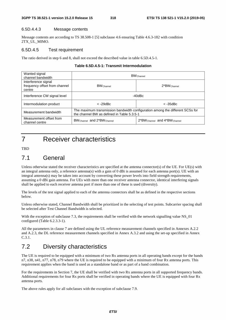
ETSI
ETSI TS 138 521-1 V15.2.0 (2019-05)3183GPP TS 38.521-1 version 15.2.0 Release 15
6.5D.4.4.3 Message contents
Message contents are according to TS 38.508-1 [5] subclause 4.6 ensuring Table 4.6.3-182 with condition 2TX_UL_MIMO.
6.5D.4.5 Test requirement
The ratio derived in step 6 and 8, shall not exceed the described value in table 6.5D.4.5-1.
Table 6.5D.4.5-1: Transmit Intermodulation
Wanted signal channel bandwidth BWChannel
Interference signal frequency offset from channel centre
BWChannel 2*BWChannel
Interference CW signal level -40dBc
Intermodulation product < -29dBc < -35dBc
Measurement bandwidth The maximum transmission bandwidth configuration among the different SCSs for the channel BW as defined in Table 5.3.5-1
Measurement offset from channel centre BWChannel and 2*BWChannel 2*BWChannel and 4*BWChannel
7 Receiver characteristics TBD
7.1 General Unless otherwise stated the receiver characteristics are specified at the antenna connector(s) of the UE. For UE(s) with an integral antenna only, a reference antenna(s) with a gain of 0 dBi is assumed for each antenna port(s). UE with an integral antenna(s) may be taken into account by converting these power levels into field strength requirements, assuming a 0 dBi gain antenna. For UEs with more than one receiver antenna connector, identical interfering signals shall be applied to each receiver antenna port if more than one of these is used (diversity).
The levels of the test signal applied to each of the antenna connectors shall be as defined in the respective sections below.
Unless otherwise stated, Channel Bandwidth shall be prioritized in the selecting of test points. Subcarrier spacing shall be selected after Test Channel Bandwidth is selected.
With the exception of subclause 7.3, the requirements shall be verified with the network signalling value NS_01 configured (Table 6.2.3.3-1).
All the parameters in clause 7 are defined using the UL reference measurement channels specified in Annexes A.2.2 and A.2.3, the DL reference measurement channels specified in Annex A.3.2 and using the set-up specified in Annex C.3.1.
7.2 Diversity characteristics The UE is required to be equipped with a minimum of two Rx antenna ports in all operating bands except for the bands n7, n38, n41, n77, n78, n79 where the UE is required to be equipped with a minimum of four Rx antenna ports. This requirement applies when the band is used as a standalone band or as part of a band combination.
For the requirements in Section 7, the UE shall be verified with two Rx antenna ports in all supported frequency bands. Additional requirements for four Rx ports shall be verified in operating bands where the UE is equipped with four Rx antenna ports.
The above rules apply for all subclasses with the exception of subclause 7.9.

ETSI
ETSI TS 138 521-1 V15.2.0 (2019-05)3193GPP TS 38.521-1 version 15.2.0 Release 15
7.3 Reference sensitivity
7.3.1 General
The reference sensitivity power level REFSENS is the minimum mean power applied to each one of the UE antenna ports for all UE categories, at which the throughput shall meet or exceed the requirements for the specified reference measurement channel.
In later subclauses of Section 7 where the value of REFSENS is used as a reference to set the corresponding requirement.
For all bands, the UE shall be verified against those requirements by applying the REFSENS value in Table 7.3.2.3-1 with 2 Rx antenna ports tested.
For bands where the UE is required to be equipped with 4 Rx antenna ports, the UE shall additionally be verified against those requirements by applying the resulting REFSENS value derived from the requirement in Table 7.3.2_1.3-1with 4 Rx antenna ports tested.
7.3.2 Reference sensitivity power level
Editor’s note: For bands with asymmetric CH BWs (defined in clause 5.3.6), the test point analysis requires an to accommodate the test configurations for asymmetric CH BWs.
7.3.2.1 Test purpose
The test purpose is to verify the ability of the UE to receive data with a given average throughput for a specified reference measurement channel, under conditions of low signal level, ideal propagation and no added noise.
7.3.2.2 Test applicability
This test case applies to all types of NR UE release 15 and forward
7.3.2.3 Minimum conformance requirements
The reference sensitivity power level REFSENS is the minimum mean power applied to each one of the UE antenna ports for all UE categories, at which the throughput shall meet or exceed the requirements for the specified reference measurement channel.
The throughput shall be ≥ 95% of the maximum throughput of the reference measurement channels as specified in Annexes A.2.2, A.2.3 and A.3.2 (with one sided dynamic OCNG Pattern OP.1 FDD/TDD for the DL-signal as described in Annex A.5.1.1/A.5.2.1) with parameters specified in Table 7.3.2.3-1 and Table 7.3.2.3-2.
ETSI
ETSI TS 138 521-1 V15.2.0 (2019-05)3203GPP TS 38.521-1 version 15.2.0 Release 15
Table 7.3.2.3-1: Two antenna port reference sensitivity QPSK PREFSENS

ETSI
ETSI TS 138 521-1 V15.2.0 (2019-05)3213GPP TS 38.521-1 version 15.2.0 Release 15
Operating band / SCS / Channel bandwidth / Duplex-mode
Operating Band
SCS kHz
5 MHz
(dBm)
10 MHz
(dBm)
15 MHz
(dBm)
20 MHz
(dBm)
25 MHz
(dBm)
30 MHz
(dBm)
40 MHz
(dBm)
50 MHz
(dBm)
60 MHz
(dBm)
80 MHz
(dBm)
90 MHz
(dBm)
100 MHz
(dBm)
Duplex Mode
n1
15 -100.0 -96.8 -95.0 -93.8
FDD 30 -97.1 -95.1 -94.0
60 -97.5 -95.4 -94.2
n2
15 -98.0 -94.8 -93.0 -91.8
FDD 30 -95.1 -93.1 -92.0
60 -95.5 -93.4 -92.2
n3
15 -97.0 -93.8 -92.0 -90.8 -89.7 -88.9
FDD 30 -94.1 -92.1 -91.0 -89.8 -89.0
60 -94.5 -92.4 -91.2 -90.0 -89.1
n5
15 -98.0 -94.8 -93.0 -90.8
FDD 30 -95.1 -93.1 -91.0
60
n71
15 -98.0 -94.8 -93.0 -91.8
FDD 30 -95.1 -93.1 -92.0
60 -95.5 -93.4 -92.2
n8
15 -97.0 -93.8 -92.0 -90.0
FDD 30 -94.1 -92.1 -90.2
60
n12
15 -97.0 -93.8 -84.0
FDD 30 -94.1 -84.1 60
n20
15 -97.0 -93.8 -91.0 -89.8
FDD 30 -94.1 -91.1 -90.0
60
n25
15 -96.5 -93.3 -91.5 -90.3
FDD 30 -93.6 -91.6 -90.5 60 -94.0 -91.9 -90.7
n28
15 -98.5 -95.5 -93.5 -90.8
FDD 30 -95.6 -93.6 -91.0
60
n34
15 -100.0 -96.8 -95.0
TDD 30 -97.1 -95.1 60 -97.5 -95.4
n381
15 -100.0 -96.8 -95.0 -93.8
TDD 30 -97.1 -95.1 -94.0
60 -97.5 -95.4 -94.2
n39
15 -100.0 -96.8 -95.0 -93.8 -92.7 -91.9 -90.6
TDD 30 -97.1 -95.1 -94.0 -92.8 -92.0 -90.7 60 -97.5 -95.4 -94.2 -93.0 -92.1 -90.9
n40
15 -100.0 -96.8 -95.0 -93.8 -92.7 -91.9 -90.6 -89.6
TDD 30 -97.1 -95.1 -94.0 -92.8 -92.0 -90.7 -89.7 -88.9 -87.6 60 -97.5 -95.4 -94.2 -93.0 -92.1 -90.9 -89.8 -89.1 -87.6
n411
15 -94.8 -93.0 -91.8 -88.6 -87.6
TDD 30 -95.1 -93.1 -92.0 -88.7 -87.7 -86.9 -85.6 -85.1 -84.7
60 -95.5 -93.4 -92.2 -88.9 -87.8 -87.1 -85.6 -85.1 -84.7
n50
15 -100.0 -96.8 -95.0 -93.8 -90.6 -89.6
TDD 30 -97.1 -95.1 -94.0 -90.7 -89.7 -88.9 -87.6
60 -97.5 -95.4 -94.2 -90.9 -89.8 -89.1 -87.6
n51 15 -100.0
TDD 30
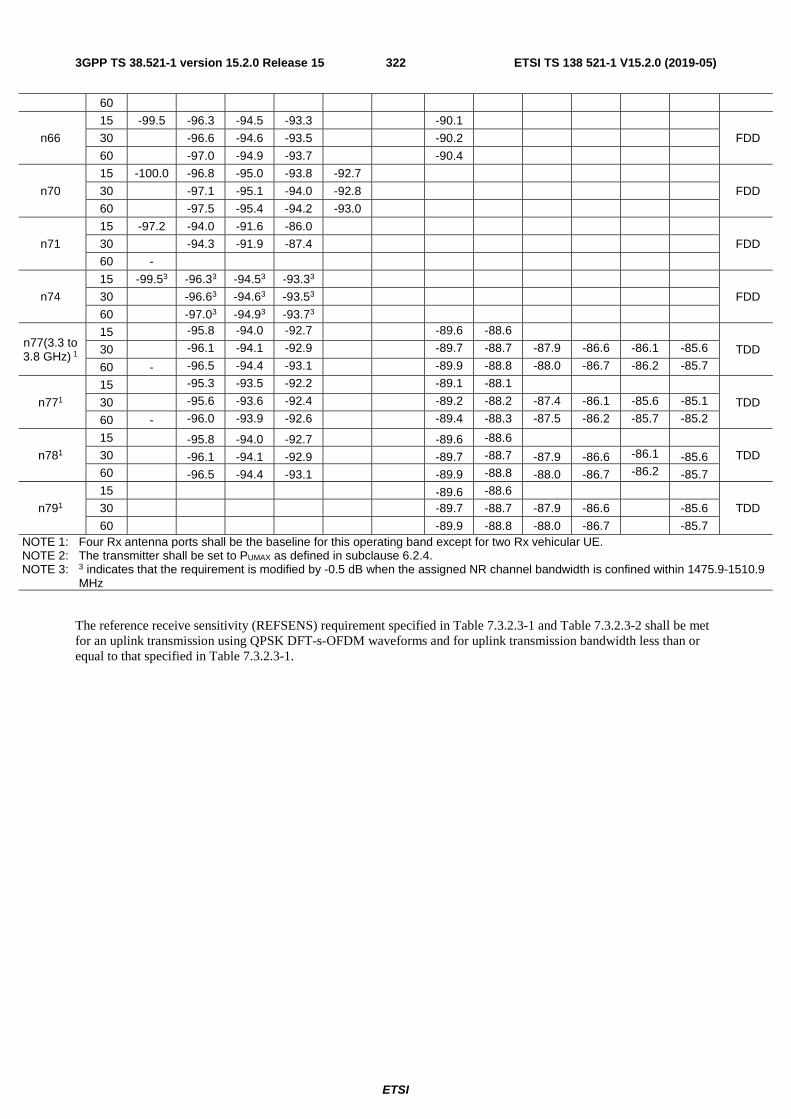
ETSI
ETSI TS 138 521-1 V15.2.0 (2019-05)3223GPP TS 38.521-1 version 15.2.0 Release 15
60
n66
15 -99.5 -96.3 -94.5 -93.3 -90.1
FDD 30 -96.6 -94.6 -93.5 -90.2
60 -97.0 -94.9 -93.7 -90.4
n70
15 -100.0 -96.8 -95.0 -93.8 -92.7
FDD 30 -97.1 -95.1 -94.0 -92.8
60 -97.5 -95.4 -94.2 -93.0
n71
15 -97.2 -94.0 -91.6 -86.0
FDD 30 -94.3 -91.9 -87.4
60 -
n74
15 -99.53 -96.33 -94.53 -93.33
FDD 30 -96.63 -94.63 -93.53
60 -97.03 -94.93 -93.73
n77(3.3 to 3.8 GHz) 1
15 -95.8 -94.0 -92.7 -89.6 -88.6
TDD 30 -96.1 -94.1 -92.9 -89.7 -88.7 -87.9 -86.6 -86.1 -85.6
60 - -96.5 -94.4 -93.1 -89.9 -88.8 -88.0 -86.7 -86.2 -85.7
n771
15 -95.3 -93.5 -92.2 -89.1 -88.1 TDD 30 -95.6 -93.6 -92.4 -89.2 -88.2 -87.4 -86.1 -85.6 -85.1
60 - -96.0 -93.9 -92.6 -89.4 -88.3 -87.5 -86.2 -85.7 -85.2
n781
15 -95.8 -94.0 -92.7 -89.6 -88.6
TDD 30 -96.1 -94.1 -92.9 -89.7 -88.7 -87.9 -86.6 -86.1 -85.6 60 -96.5 -94.4 -93.1 -89.9 -88.8 -88.0 -86.7 -86.2 -85.7
n791
15 -89.6 -88.6
TDD 30 -89.7 -88.7 -87.9 -86.6 -85.6
60 -89.9 -88.8 -88.0 -86.7 -85.7 NOTE 1: Four Rx antenna ports shall be the baseline for this operating band except for two Rx vehicular UE. NOTE 2: The transmitter shall be set to PUMAX as defined in subclause 6.2.4. NOTE 3: 3 indicates that the requirement is modified by -0.5 dB when the assigned NR channel bandwidth is confined within 1475.9-1510.9
MHz
The reference receive sensitivity (REFSENS) requirement specified in Table 7.3.2.3-1 and Table 7.3.2.3-2 shall be met for an uplink transmission using QPSK DFT-s-OFDM waveforms and for uplink transmission bandwidth less than or equal to that specified in Table 7.3.2.3-1.

ETSI
ETSI TS 138 521-1 V15.2.0 (2019-05)3233GPP TS 38.521-1 version 15.2.0 Release 15
Table 7.3.2.3-3: Uplink configuration for reference sensitivity

ETSI
ETSI TS 138 521-1 V15.2.0 (2019-05)3243GPP TS 38.521-1 version 15.2.0 Release 15
Operating Band
SCS kHz
5 MHz
10 MHz
15 MHz
20 MHz
25 MHz
30 MHz
40 MHz
50 MHz
60 MHz
80 MHz
90 MHz
100 MHz
Duplex Mode
n1
15 25 501 751 1001
FDD 30 24 361 501
60 101 18 24
n2
15 25 501 501 501
FDD 30 101 24 241 241
60 101 101 101
n3
15 25 501 501 501 501 501
FDD 30 24 241 241 241 241
60 101 101 101 101 101
n5
15 25 251 251 251
FDD 30 101 101 101
60
n7
15 25 501 751 751
FDD 30 24 361 361
60 101 18 181
n8
15 25 251 251 251
FDD 30 101 101 101
60
n12
15 201 201 201
FDD 30 101 101 60
n20
15 25 201 202 202
FDD 30 101 102 102
60
n25
15 25 50 501 501
FDD 30 24 241 241 60 10 101 101
n28
15 25 251 251 251
FDD 30 101 101 101
60
n34
15 25 50 75
30 24 36
60 10 18
n38
15 25 50 75 100
TDD 30 24 36 50
60 10 18 24
n39
15 25 50 75 100 128 160 216
TDD 30 24 36 50 64 75 100
60 10 18 24 30 36 50
n40
15 25 50 75 100 128 160 216 270
TDD 30 24 36 50 64 75 100 128 162 216
60 10 18 24 30 36 50 64 75 100
n41
15 50 75 100 216 270
TDD 30 24 36 50 100 128 162 216 243 270
60 10 18 24 50 64 75 100 120 135
n50
15 25 50 75 100 216 270
TDD 30 24 36 50 100 128 162 NOTE
3
60 10 18 24 50 64 75 NOTE 3
n51
15 25
TDD 30
60
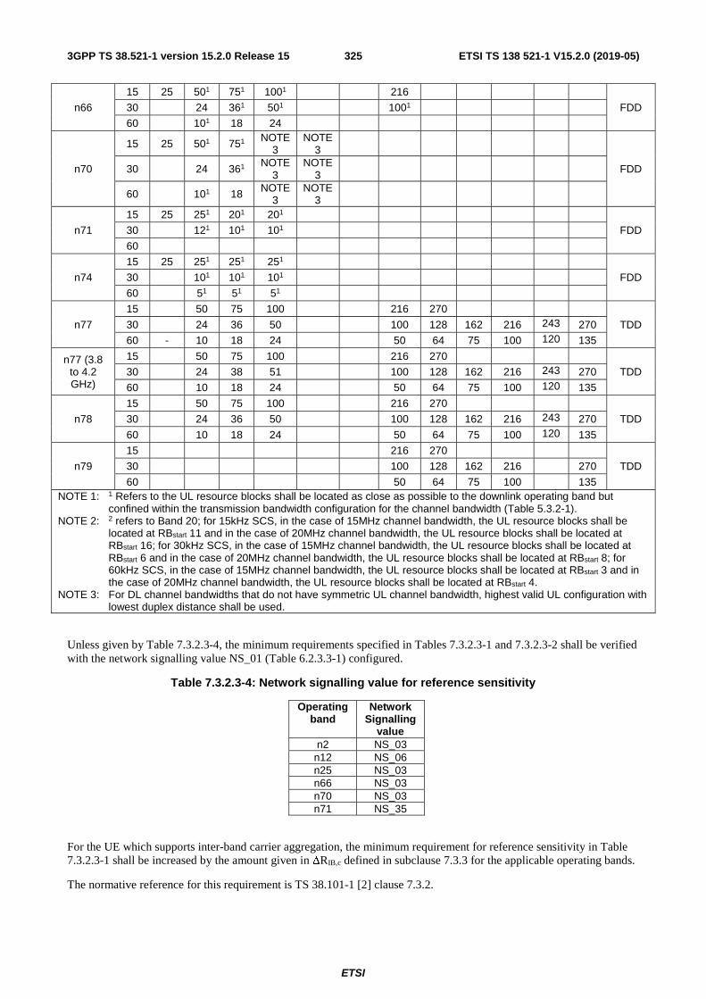
ETSI
ETSI TS 138 521-1 V15.2.0 (2019-05)3253GPP TS 38.521-1 version 15.2.0 Release 15
n66
15 25 501 751 1001 216
FDD 30 24 361 501 1001
60 101 18 24
n70
15 25 501 751 NOTE 3
NOTE 3
FDD 30 24 361 NOTE
3 NOTE
3
60 101 18 NOTE 3
NOTE 3
n71
15 25 251 201 201
FDD 30 121 101 101
60
n74
15 25 251 251 251
FDD 30 101 101 101
60 51 51 51
n77
15 50 75 100 216 270
TDD 30 24 36 50 100 128 162 216 243 270
60 - 10 18 24 50 64 75 100 120 135
n77 (3.8 to 4.2 GHz)
15 50 75 100 216 270
TDD 30 24 38 51 100 128 162 216 243 270
60 10 18 24 50 64 75 100 120 135
n78
15 50 75 100 216 270
TDD 30 24 36 50 100 128 162 216 243 270
60 10 18 24 50 64 75 100 120 135
n79
15 216 270
TDD 30 100 128 162 216 270
60 50 64 75 100 135 NOTE 1: 1 Refers to the UL resource blocks shall be located as close as possible to the downlink operating band but
confined within the transmission bandwidth configuration for the channel bandwidth (Table 5.3.2-1). NOTE 2: 2 refers to Band 20; for 15kHz SCS, in the case of 15MHz channel bandwidth, the UL resource blocks shall be
located at RBstart 11 and in the case of 20MHz channel bandwidth, the UL resource blocks shall be located at RBstart 16; for 30kHz SCS, in the case of 15MHz channel bandwidth, the UL resource blocks shall be located at RBstart 6 and in the case of 20MHz channel bandwidth, the UL resource blocks shall be located at RBstart 8; for 60kHz SCS, in the case of 15MHz channel bandwidth, the UL resource blocks shall be located at RBstart 3 and in the case of 20MHz channel bandwidth, the UL resource blocks shall be located at RBstart 4.
NOTE 3: For DL channel bandwidths that do not have symmetric UL channel bandwidth, highest valid UL configuration with lowest duplex distance shall be used.
Unless given by Table 7.3.2.3-4, the minimum requirements specified in Tables 7.3.2.3-1 and 7.3.2.3-2 shall be verified with the network signalling value NS_01 (Table 6.2.3.3-1) configured.
Table 7.3.2.3-4: Network signalling value for reference sensitivity
Operating band
Network Signalling
value n2 NS_03
n12 NS_06 n25 NS_03 n66 NS_03 n70 NS_03 n71 NS_35
For the UE which supports inter-band carrier aggregation, the minimum requirement for reference sensitivity in Table 7.3.2.3-1 shall be increased by the amount given in ΔRIB,c defined in subclause 7.3.3 for the applicable operating bands.
The normative reference for this requirement is TS 38.101-1 [2] clause 7.3.2.
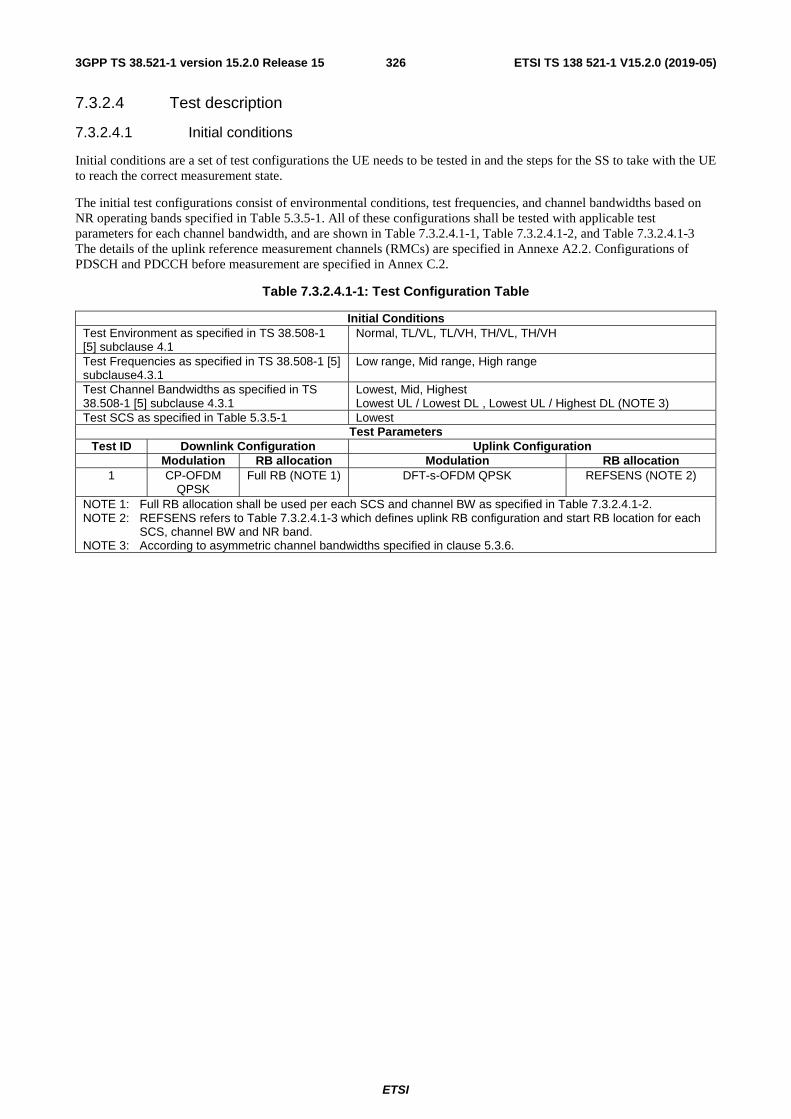
ETSI
ETSI TS 138 521-1 V15.2.0 (2019-05)3263GPP TS 38.521-1 version 15.2.0 Release 15
7.3.2.4 Test description
7.3.2.4.1 Initial conditions
Initial conditions are a set of test configurations the UE needs to be tested in and the steps for the SS to take with the UE to reach the correct measurement state.
The initial test configurations consist of environmental conditions, test frequencies, and channel bandwidths based on NR operating bands specified in Table 5.3.5-1. All of these configurations shall be tested with applicable test parameters for each channel bandwidth, and are shown in Table 7.3.2.4.1-1, Table 7.3.2.4.1-2, and Table 7.3.2.4.1-3 The details of the uplink reference measurement channels (RMCs) are specified in Annexe A2.2. Configurations of PDSCH and PDCCH before measurement are specified in Annex C.2.
Table 7.3.2.4.1-1: Test Configuration Table
Initial Conditions Test Environment as specified in TS 38.508-1 [5] subclause 4.1
Normal, TL/VL, TL/VH, TH/VL, TH/VH
Test Frequencies as specified in TS 38.508-1 [5] subclause4.3.1
Low range, Mid range, High range
Test Channel Bandwidths as specified in TS 38.508-1 [5] subclause 4.3.1
Lowest, Mid, Highest Lowest UL / Lowest DL , Lowest UL / Highest DL (NOTE 3)
Test SCS as specified in Table 5.3.5-1 Lowest Test Parameters
Test ID Downlink Configuration Uplink Configuration Modulation RB allocation Modulation RB allocation
1 CP-OFDM QPSK
Full RB (NOTE 1) DFT-s-OFDM QPSK REFSENS (NOTE 2)
NOTE 1: Full RB allocation shall be used per each SCS and channel BW as specified in Table 7.3.2.4.1-2. NOTE 2: REFSENS refers to Table 7.3.2.4.1-3 which defines uplink RB configuration and start RB location for each
SCS, channel BW and NR band. NOTE 3: According to asymmetric channel bandwidths specified in clause 5.3.6.
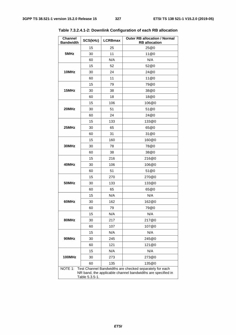
ETSI
ETSI TS 138 521-1 V15.2.0 (2019-05)3273GPP TS 38.521-1 version 15.2.0 Release 15
Table 7.3.2.4.1-2: Downlink Configuration of each RB allocation
Channel Bandwidth SCS(kHz) LCRBmax Outer RB allocation / Normal
RB allocation
5MHz
15 25 25@0
30 11 11@0
60 N/A N/A
10MHz
15 52 52@0
30 24 24@0
60 11 11@0
15MHz
15 79 79@0
30 38 38@0
60 18 18@0
20MHz
15 106 106@0
30 51 51@0
60 24 24@0
25MHz
15 133 133@0
30 65 65@0
60 31 31@0
30MHz
15 160 160@0
30 78 78@0
60 38 38@0
40MHz
15 216 216@0
30 106 106@0
60 51 51@0
50MHz
15 270 270@0
30 133 133@0
60 65 65@0
60MHz
15 N/A N/A
30 162 162@0
60 79 79@0
80MHz
15 N/A N/A
30 217 217@0
60 107 107@0
90MHz
15 N/A N/A
30 245 245@0
60 121 121@0
100MHz
15 N/A N/A
30 273 273@0
60 135 135@0
NOTE 1: Test Channel Bandwidths are checked separately for each NR band, the applicable channel bandwidths are specified in Table 5.3.5-1.

ETSI
ETSI TS 138 521-1 V15.2.0 (2019-05)3283GPP TS 38.521-1 version 15.2.0 Release 15
Table 7.3.2.4.1-3: Uplink configuration for reference sensitivity, LCRB @ Restart format
Operating Band
SCS kHz
5 MHz
10 MHz
15 MHz
20 MHz
25 MHz 30 MHz 40
MHz 50
MHz 60
MHz 80
MHz 90
MHz 100 MHz
Duplex Mode
n1
15 25@0 50@01 75@01 100@01
FDD 30 24@0 36@01 50@01
60 10@01 18@0 24@0
n2
15 25@0 50@01 50@251 50@501
FDD 30 10@01 24@0 24@121 24@261
60 10@01 10@81 10@141
n3
15 25@0 50@01 50@251 50@501 50@781 50@1101
FDD 30 24@0 24@121 24@261 24@401 24@511
60 10@01 10@81 10@141 10@201 10@261
n5
15 25@0 25@251 25@501 25@751
FDD 30 10@141 10@261 10@401
60
n7
15 25@0 50@01 75@01 75@251
FDD 30 24@0 36@01 36@141
60 10@01 18@0 18@81
n8
15 25@0 25@251 25@501 25@751
FDD 30 10@141 10@261 10@401
60
n12
15 20@51 20@301 20@551
30 10@141 10@261 60
n20
15 25@0 20@01 20@112 20@162
FDD 30 10@01 10@62 10@82
60
n25
15 25@0 50@0 50@251 50@501
FDD 30 24@0 24@121 24@261 60 10@0 10@81 10@141
n28
15 25@0 25@251 25@501 25@751
FDD 30 10@141 10@261 10@401
60
n34
15 25@0 50@0 75@0
TDD 30 24@0 36@0
60 10@0 18@0

ETSI
ETSI TS 138 521-1 V15.2.0 (2019-05)3293GPP TS 38.521-1 version 15.2.0 Release 15
n38
15 25@0 50@0 75@0 100@0
TDD 30 24@0 36@0 50@0
60 10@0 18@0 24@0
n39
15 25@0 50@0 75@0 100@0 128@0 160@0 216@0
TDD 30 24@0 36@01 50@0 64@0 75@0 100@0
60 10@0 18@0 24@0 30@0 36@0 50@0
n40
15 25@0 50@0 75@0 100@0 128@0 160@0 216@0 270@0
TDD 30 24@0 36@0 50@0 64@0 75@0 100@0 128@0 162@0 216@0
60 10@0 18@0 24@0 30@0 36@0 50@0 64@0 75@0 100@0
n41
15 50@0 75@0 100@0 216@0 270@0
TDD 30 24@0 36@0 50@0 100@0 128@0 162@0 216@0 243@0 270@0
60 10@0 18@0 24@0 50@0 64@0 75@0 100@0 120@0 135@0
n50
15 25@0 50@0 75@0 100@01 216@0 270@0
TDD 30 24@0 36@0 50@0 100@0 128@0 162@0 NOTE
3
60 10@0 18@0 24@0 50@0 64@0 75@0 NOTE 3
n51
15 25@0
TDD 30
60
n66
15 25@0 50@01 75@01 1001 216@0
FDD 30 24@0 36@01 50@01 100@01
60 10@01 18@0 24@0 50@01
n70
15 25@0 50@01 75@01 NOTE 3
NOTE 3
FDD 30 24@0 36@01 NOTE 3
NOTE 3
60 10@01 18@0 NOTE 3
NOTE 3
n71
15 25@0 25@01 20@01 20@01
FDD 30 12@01 10@01 10@01
60
n74
15 25@0 25@251 25@501 25@751
FDD 30 10@141 10@261 10@401
60 5@51 5@131 5@191
n77
15 50@0 75@0 100@0 216@0 270@0
TDD 30 24@0 36@0 50@0 100@0 128@0 162@0 216@0 243@0 270@0
60 - 10@0 18@0 24@0 50@0 64@0 75@0 100@0 120@0 135@0

ETSI
ETSI TS 138 521-1 V15.2.0 (2019-05)3303GPP TS 38.521-1 version 15.2.0 Release 15
n77 (3.8 to 4.2 GHz)
15 50@01 75@01 100@01 216@0 270@0
TDD 30 24@0 36@0 50@0 100@01 128@01 162@0 216@01 243@01 270@01
60 10@01 18@0 24@0 50@01 64@01 75@01 100@01 120@01 135@0
n78
15 50@0 75@0 100@01 216@0 270@0
TDD 30 24@0 36@0 50@0 100@0 128@0 162@0 216@0 243@0 270@0
60 10@0 18@0 24@0 50@0 64@0 75@0 100@0 120@0 135@0
n79
15 216@0 270@0
TDD 30 100@0 128@0 162@0 216@0 270@0
60 50@0 64@0 75@0 100@0 135@0 NOTE 1: 1 Refers to the UL resource blocks shall be located as close as possible to the downlink operating band but confined within the transmission
bandwidth configuration for the channel bandwidth (Table 5.3.2-1). NOTE 2: 2 refers to Band 20; for 15kHz SCS, in the case of 15MHz channel bandwidth, the UL resource blocks shall be located at RBstart 11 and in the case
of 20MHz channel bandwidth, the UL resource blocks shall be located at RBstart 16; for 30kHz SCS, in the case of 15MHz channel bandwidth, the UL resource blocks shall be located at RBstart 6 and in the case of 20MHz channel bandwidth, the UL resource blocks shall be located at RBstart 8; for 60kHz SCS, in the case of 15MHz channel bandwidth, the UL resource blocks shall be located at RBstart 3 and in the case of 20MHz channel bandwidth, the UL resource blocks shall be located at RBstart 4.
NOTE 3: For DL channel bandwidths that do not have symmetric UL channel bandwidth, highest valid UL configuration with lowest duplex distance shall be used.
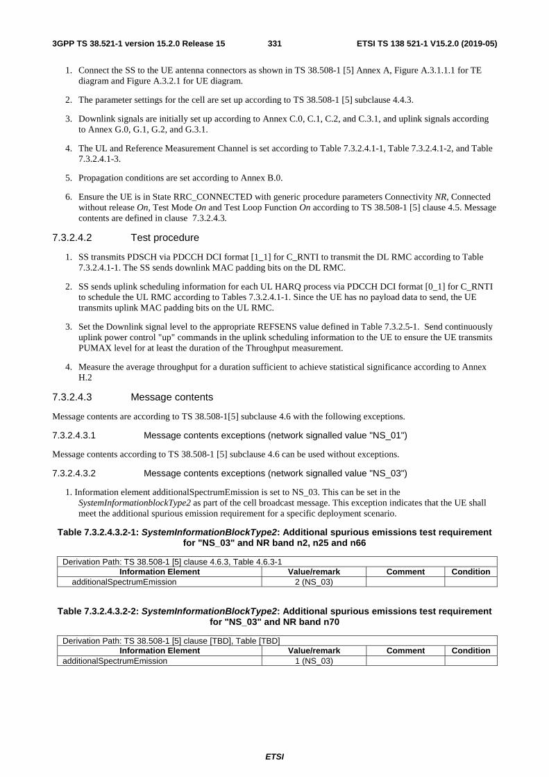
ETSI
ETSI TS 138 521-1 V15.2.0 (2019-05)3313GPP TS 38.521-1 version 15.2.0 Release 15
1. Connect the SS to the UE antenna connectors as shown in TS 38.508-1 [5] Annex A, Figure A.3.1.1.1 for TE diagram and Figure A.3.2.1 for UE diagram.
2. The parameter settings for the cell are set up according to TS 38.508-1 [5] subclause 4.4.3.
3. Downlink signals are initially set up according to Annex C.0, C.1, C.2, and C.3.1, and uplink signals according to Annex G.0, G.1, G.2, and G.3.1.
4. The UL and Reference Measurement Channel is set according to Table 7.3.2.4.1-1, Table 7.3.2.4.1-2, and Table 7.3.2.4.1-3.
5. Propagation conditions are set according to Annex B.0.
6. Ensure the UE is in State RRC_CONNECTED with generic procedure parameters Connectivity NR, Connected without release On, Test Mode On and Test Loop Function On according to TS 38.508-1 [5] clause 4.5. Message contents are defined in clause 7.3.2.4.3.
7.3.2.4.2 Test procedure
1. SS transmits PDSCH via PDCCH DCI format [1_1] for C_RNTI to transmit the DL RMC according to Table 7.3.2.4.1-1. The SS sends downlink MAC padding bits on the DL RMC.
2. SS sends uplink scheduling information for each UL HARQ process via PDCCH DCI format [0_1] for C_RNTI to schedule the UL RMC according to Tables 7.3.2.4.1-1. Since the UE has no payload data to send, the UE transmits uplink MAC padding bits on the UL RMC.
3. Set the Downlink signal level to the appropriate REFSENS value defined in Table 7.3.2.5-1. Send continuously uplink power control "up" commands in the uplink scheduling information to the UE to ensure the UE transmits PUMAX level for at least the duration of the Throughput measurement.
4. Measure the average throughput for a duration sufficient to achieve statistical significance according to Annex H.2
7.3.2.4.3 Message contents
Message contents are according to TS 38.508-1[5] subclause 4.6 with the following exceptions.
7.3.2.4.3.1 Message contents exceptions (network signalled value "NS_01")
Message contents according to TS 38.508-1 [5] subclause 4.6 can be used without exceptions.
7.3.2.4.3.2 Message contents exceptions (network signalled value "NS_03")
1. Information element additionalSpectrumEmission is set to NS_03. This can be set in the SystemInformationblockType2 as part of the cell broadcast message. This exception indicates that the UE shall meet the additional spurious emission requirement for a specific deployment scenario.
Table 7.3.2.4.3.2-1: SystemInformationBlockType2: Additional spurious emissions test requirement for "NS_03" and NR band n2, n25 and n66
Derivation Path: TS 38.508-1 [5] clause 4.6.3, Table 4.6.3-1 Information Element Value/remark Comment Condition
additionalSpectrumEmission 2 (NS_03)
Table 7.3.2.4.3.2-2: SystemInformationBlockType2: Additional spurious emissions test requirement for "NS_03" and NR band n70
Derivation Path: TS 38.508-1 [5] clause [TBD], Table [TBD] Information Element Value/remark Comment Condition
additionalSpectrumEmission 1 (NS_03)

ETSI
ETSI TS 138 521-1 V15.2.0 (2019-05)3323GPP TS 38.521-1 version 15.2.0 Release 15
7.3.2.4.3.3 Message contents exceptions (network signalled value "NS_06")
1. Information element additionalSpectrumEmission is set to NS_06. This can be set in the SystemInformationblockType2 as part of the cell broadcast message. This exception indicates that the UE shall meet the additional spurious emission requirement for a specific deployment scenario.
Table 7.3.2.4.3.3-1: SystemInformationBlockType2: Additional spurious emissions test requirement for "NS_06" and NR band n12
Derivation Path: TS 38.508-1 [5] clause 4.6.3, Table 4.6.3-1 Information Element Value/remark Comment Condition
additionalSpectrumEmission 1 (NS_06)
7.3.2.4.3.4 Message contents exceptions (network signalled value "NS_35")
1. Information element additionalSpectrumEmission is set to NS_35. This can be set in the SystemInformationblockType2 as part of the cell broadcast message. This exception indicates that the UE shall meet the additional spurious emission requirement for a specific deployment scenario.
Table 7.3.2.4.3.4-1: SystemInformationBlockType2: Additional spurious emissions test requirement for "NS_35" and NR band n71
Derivation Path: TS 38.508-1 [5] clause 4.6.3, Table 4.6.3-1 Information Element Value/remark Comment Condition
additionalSpectrumEmission 1 (NS_35)
7.3.2.5 Test requirement
The throughput shall be ≥ 95% of the maximum throughput of the reference measurement channels as specified in Annex A3.2 with reference receive power level specified in Tables 7.3.2.5-1 and parameters specified Tables 7.3.2.4.1-1, Tables 7.3.2.4.1-2 and Tables 7.3.2.4.1-3.
Table 7.3.2.5-1: Reference sensitivity QPSK PREFSENS
Operating band / SCS / Channel bandwidth / Duplex-mode
Operating Band
SCS kHz
5 MHz
(dBm)
10 MHz
(dBm)
15 MHz
(dBm)
20 MHz
(dBm)
25 MHz
(dBm)
30 MHz
(dBm)
40 MHz
(dBm)
50 MHz
(dBm)
60 MHz
(dBm)
80 MHz
(dBm)
90 MHz
(dBm)
100 MHz
(dBm)
Duplex Mode
n1
15 -100.0 +TT
-96.8 +TT
-95.0 +TT
-93.8 +TT
FDD 30 -97.1 +TT
-95.1 +TT
-94.0 +TT
60 -97.5 +TT
-95.4 +TT
-94.2 +TT
n2
15 -98.0 +TT
-94.8 +TT
-93.0 +TT
-91.8 +TT
FDD 30 -95.1 +TT
-93.1 +TT
-92.0 +TT
60 -95.5 +TT
-93.4 +TT
-92.2 +TT
n3
15 -97.0 +TT
-93.8 +TT
-92.0 +TT
-90.8 +TT
-89.7 +TT
-88.9 +TT
FDD 30 -94.1 +TT
-92.1 +TT
-91.0 +TT
-89.8 +TT
-89.0 +TT
60 -94.5 +TT
-92.4 +TT
-91.2 +TT
-90.0 +TT
-89.1 +TT
n5
15 -98.0 +TT
-94.8 +TT
-93.0 +TT
-90.8 +TT
FDD 30 -95.1 +TT
-93.1 +TT
-91.0 +TT
60
n71 15 -98.0 +TT
-94.8 +TT
-93.0 +TT
-91.8 +TT FDD

ETSI
ETSI TS 138 521-1 V15.2.0 (2019-05)3333GPP TS 38.521-1 version 15.2.0 Release 15
30 -95.1 +TT
-93.1 +TT
-92.0 +TT
60 -95.5 +TT
-93.4 +TT
-92.2 +TT
n8
15 -97.0 +TT
-93.8 +TT
-92.0 +TT
-90.0 +TT
FDD 30 -94.1 +TT
-92.1 +TT
-90.2 +TT
60
n12
15 -97.0 +TT
-93.8 +TT
-84.0 +TT
FDD 30 -94.1 +TT
-84.1 +TT
60
n20
15 -97.0 +TT
-93.8 +TT
-91.0 +TT
-89.8 +TT
FDD 30 -94.1 +TT
-91.1 +TT
-90.0 +TT
60
n25
15 -96.5 +TT
-93.3 +TT
-91.5 +TT
-90.3 +TT
FDD 30 -93.6 +TT
-91.6 +TT
-90.5 +TT
60 -94.0 +TT
-91.9 +TT
-90.7 +TT
n28
15 -98.5 +TT
-95.5 +TT
-93.5 +TT
-90.8 +TT
FDD 30 -95.6 +TT
-93.6 +TT
-91.0 +TT
60
n34
15 -100.0 +TT
-96.8 +TT
-95.0 +TT
TDD 30 -97.1
+TT -95.1 +TT
60 -97.5 +TT
-95.4 +TT
n38
15 -100.0 +TT
-96.8 +TT
-95.0 +TT
-93.8 +TT
TDD 30 -97.1 +TT
-95.1 +TT
-94.0 +TT
60 -97.5 +TT
-95.4 +TT
-94.2 +TT
n39
15 -100.0 +TT
-96.8 +TT
-95.0 +TT
-93.8 +TT
-92.7 +TT
-91.9 +TT
-90.6 +TT
TDD 30 -97.1 +TT
-95.1 +TT
-94.0 +TT
-92.8 +TT
-92.0 +TT
-90.7 +TT
60 -97.5 +TT
-95.4 +TT
-94.2 +TT
-93.0 +TT
-92.1 +TT
-90.9 +TT
n40
15 -100.0 +TT
-96.8 +TT
-95.0 +TT
-93.8 +TT
-92.7 +TT
-91.9 +TT
-90.6 +TT
-89.6 +TT
TDD 30 -97.1 +TT
-95.1 +TT
-94.0 +TT
-92.8 +TT
-92.0 +TT
-90.7 +TT
-89.7 +TT
-88.9 +TT
-87.6 +TT
60 -97.5 +TT
-95.4 +TT
-94.2 +TT
-93.0 +TT
-92.1 +TT
-90.9 +TT
-89.8 +TT
-89.1 +TT
-87.6 +TT
n411
15 -94.8 +TT
-93.0 +TT
-91.8 +TT -88.6
+TT -87.6 +TT
TDD 30 -95.1 +TT
-93.1 +TT
-92.0 +TT -88.7
+TT -87.7 +TT
-86.9 +TT
-85.6 +TT
-85.1 +TT
-84.7 +TT
60 -95.5 +TT
-93.4 +TT
-92.2 +TT -88.9
+TT -87.8 +TT
-87.1 +TT
-85.6 +TT
-85.1 +TT
-84.7 +TT
n50
15 -100.0 +TT
-96.8 +TT
-95.0 +TT
-93.8 +TT -90.6
+TT -89.6 +TT
TDD 30 -97.1 +TT
-95.1 +TT
-94.0 +TT -90.7
+TT -89.7 +TT
-88.9 +TT
-87.6 +TT
60 -97.5 +TT
-95.4 +TT
-94.2 +TT -90.9
+TT -89.8 +TT
-89.1 +TT
-87.6 +TT

ETSI
ETSI TS 138 521-1 V15.2.0 (2019-05)3343GPP TS 38.521-1 version 15.2.0 Release 15
n51
15 -100.0 +TT
TDD 30
60
n66
15 -99.5 +TT
-96.3 +TT
-94.5 +TT
-93.3 +TT -90.1
+TT
FDD 30 -96.6 +TT
-94.6 +TT
-93.5 +TT -90.2
+TT
60 -97.0 +TT
-94.9 +TT
-93.7 +TT
-90.4 +TT
n70
15 -100.0 +TT
-96.8 +TT
-95.0 +TT
-93.8 +TT
-92.7 +TT
FDD 30 -97.1 +TT
-95.1 +TT
-94.0 +TT
-92.8 +TT
60 -97.5 +TT
-95.4 +TT
-94.2 +TT
-93.0 +TT
n71
15 -97.2 +TT
-94.0 +TT
-91.6 +TT
-86.0 +TT
FDD 30 -94.3 +TT
-91.9 +TT
-87.4 +TT
60 -
n74
15 -99.53
+TT -96.33
+TT -94.53
+TT -93.33
+TT
FDD 30 -96.63
+TT -94.63
+TT -93.53
+TT
60 -97.03
+TT -94.93
+TT -93.73
+TT
n77(3.3 to 3.8 GHz)1
15 -95.8 +TT
-94.0 +TT
-92.7 +TT
-89.6 +TT
-88.6 +TT
TDD 30 -96.1 +TT
-94.1 +TT
-92.9 +TT
-89.7 +TT
-88.7 +TT
-87.9 +TT
-86.6 +TT
-86.1 +TT
-85.6 +TT
60 - -96.5 +TT
-94.4 +TT
-93.1 +TT
-89.9 +TT
-88.8 +TT
-88.0 +TT
-86.7 +TT
-86.2 +TT
-85.7 +TT
n771
15 -95.3 +TT
-93.5 +TT
-92.2 +TT
-89.1 +TT
-88.1 +TT
TDD 30 -95.6 +TT
-93.6 +TT
-92.4 +TT
-89.2 +TT
-88.2 +TT
-87.4 +TT
-86.1 +TT
-85.6 +TT
-85.1 +TT
60 - -96.0 +TT
-93.9 +TT
-92.6 +TT
-89.4 +TT
-88.3 +TT
-87.5 +TT
-86.2 +TT
-85.7 +TT
-85.2 +TT
n781
15 -95.8 +TT
-94.0 +TT
-92.7 +TT -89.6
+TT -88.6 +TT
TDD 30 -96.1 +TT
-94.1 +TT
-92.9 +TT -89.7
+TT -88.7 +TT
-87.9 +TT
-86.6 +TT
-86.1 +TT
-85.6 +TT
60 -96.5 +TT
-94.4 +TT
-93.1 +TT -89.9
+TT -88.8 +TT
-88.0 +TT
-86.7 +TT
-86.2 +TT
-85.7 +TT
n791
15
-89.6 +TT
-88.6 +TT
TDD 30
-89.7 +TT
-88.7 +TT
-87.9 +TT
-86.6 +TT
-85.6 +TT
60
-89.9 +TT
-88.8 +TT
-88.0 +TT
-86.7 +TT
-85.7 +TT
NOTE 1: Four Rx antenna ports shall be the baseline for this operating band except for two Rx vehicular UE. NOTE 2: The transmitter shall be set to PUMAX as defined in subclause 6.2.4 NOTE 3: 3 indicates that the requirement is modified by -0.5 dB when the assigned NR channel bandwidth is confined within 1475.9-
1510.9 MHz. NOTE 4: TT for each frequency and channel bandwidth is specified in Table 7.3.2.5-2
Table 7.3.2.5-2: Test Tolerance (TT) for RX sensitivity level
f ≤ 3.0GHz 3.0GHz < f ≤ 6.0 GHz 0.7 dB 1.0 dB
For the UE which supports inter-band carrier aggregation, the minimum requirement for reference sensitivity in Table 7.3.2.5-1 shall be increased by the amount given in ΔRIB,c defined in subclause 7.3.3 for the applicable operating bands
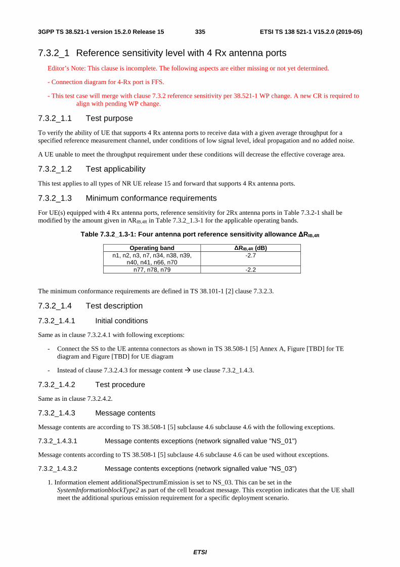
ETSI
ETSI TS 138 521-1 V15.2.0 (2019-05)3353GPP TS 38.521-1 version 15.2.0 Release 15
7.3.2_1 Reference sensitivity level with 4 Rx antenna ports
Editor’s Note: This clause is incomplete. The following aspects are either missing or not yet determined.
- Connection diagram for 4-Rx port is FFS.
- This test case will merge with clause 7.3.2 reference sensitivity per 38.521-1 WP change. A new CR is required to align with pending WP change.
7.3.2_1.1 Test purpose
To verify the ability of UE that supports 4 Rx antenna ports to receive data with a given average throughput for a specified reference measurement channel, under conditions of low signal level, ideal propagation and no added noise.
A UE unable to meet the throughput requirement under these conditions will decrease the effective coverage area.
7.3.2_1.2 Test applicability
This test applies to all types of NR UE release 15 and forward that supports 4 Rx antenna ports.
7.3.2_1.3 Minimum conformance requirements
For UE(s) equipped with 4 Rx antenna ports, reference sensitivity for 2Rx antenna ports in Table 7.3.2-1 shall be modified by the amount given in ΔRIB,4R in Table 7.3.2_1.3-1 for the applicable operating bands.
Table 7.3.2_1.3-1: Four antenna port reference sensitivity allowance ΔRIB,4R
Operating band ΔRIB,4R (dB) n1, n2, n3, n7, n34, n38, n39,
n40, n41, n66, n70 -2.7
n77, n78, n79 -2.2
The minimum conformance requirements are defined in TS 38.101-1 [2] clause 7.3.2.3.
7.3.2_1.4 Test description
7.3.2_1.4.1 Initial conditions
Same as in clause 7.3.2.4.1 with following exceptions:
- Connect the SS to the UE antenna connectors as shown in TS 38.508-1 [5] Annex A, Figure [TBD] for TE diagram and Figure [TBD] for UE diagram
- Instead of clause 7.3.2.4.3 for message content use clause 7.3.2_1.4.3.
7.3.2_1.4.2 Test procedure
Same as in clause 7.3.2.4.2.
7.3.2_1.4.3 Message contents
Message contents are according to TS 38.508-1 [5] subclause 4.6 subclause 4.6 with the following exceptions.
7.3.2_1.4.3.1 Message contents exceptions (network signalled value "NS_01")
Message contents according to TS 38.508-1 [5] subclause 4.6 subclause 4.6 can be used without exceptions.
7.3.2_1.4.3.2 Message contents exceptions (network signalled value "NS_03")
1. Information element additionalSpectrumEmission is set to NS_03. This can be set in the SystemInformationblockType2 as part of the cell broadcast message. This exception indicates that the UE shall meet the additional spurious emission requirement for a specific deployment scenario.
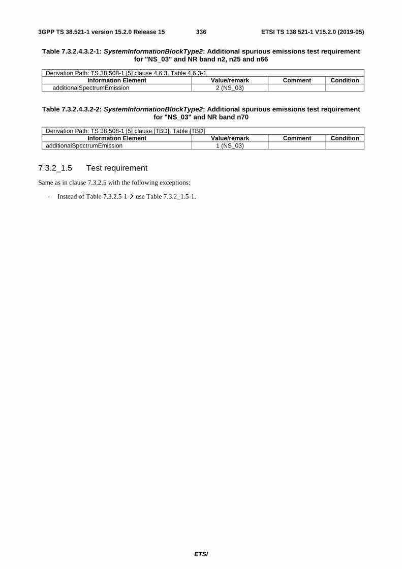
ETSI
ETSI TS 138 521-1 V15.2.0 (2019-05)3363GPP TS 38.521-1 version 15.2.0 Release 15
Table 7.3.2.4.3.2-1: SystemInformationBlockType2: Additional spurious emissions test requirement for "NS_03" and NR band n2, n25 and n66
Derivation Path: TS 38.508-1 [5] clause 4.6.3, Table 4.6.3-1 Information Element Value/remark Comment Condition
additionalSpectrumEmission 2 (NS_03)
Table 7.3.2.4.3.2-2: SystemInformationBlockType2: Additional spurious emissions test requirement for "NS_03" and NR band n70
Derivation Path: TS 38.508-1 [5] clause [TBD], Table [TBD] Information Element Value/remark Comment Condition
additionalSpectrumEmission 1 (NS_03)
7.3.2_1.5 Test requirement
Same as in clause 7.3.2.5 with the following exceptions:
- Instead of Table 7.3.2.5-1 use Table 7.3.2_1.5-1.

ETSI
ETSI TS 138 521-1 V15.2.0 (2019-05)3373GPP TS 38.521-1 version 15.2.0 Release 15
Table 7.3.2_1.5-1: Reference sensitivity QPSK PREFSENS

ETSI
ETSI TS 138 521-1 V15.2.0 (2019-05)3383GPP TS 38.521-1 version 15.2.0 Release 15
Operating band / SCS / Channel bandwidth / Duplex-mode
Operating Band
SCS kHz
5 MHz
(dBm)
10 MHz
(dBm)
15 MHz
(dBm)
20 MHz
(dBm)
25 MHz
(dBm)
30 MHz
(dBm)
40 MHz
(dBm)
50 MHz
(dBm)
60 MHz
(dBm)
80 MHz
(dBm)
90 MHz
(dBm)
100 MHz
(dBm)
Duplex Mode
n1
15 -102.7 +TT
-99.5 +TT
-97.7 +TT
-96.5 +TT
FDD 30 -99.8 +TT
-97.8 +TT
-96.7 +TT
60 -100.2 +TT
-98.1 +TT
-96.9 +TT
n2
15 -100.7 +TT
-97.5 +TT
-95.7 +TT
-94.5 +TT
FDD 30 -97.8 +TT
-95.8 +TT
-94.7 +TT
60 -98.2 +TT
-96.1 +TT
-94.9 +TT
n3
15 -99.7 +TT
-96.5 +TT
-94.7 +TT
-93.5 +TT
-92.4 +TT
-91.6 +TT
FDD 30 -96.8 +TT
-94.8 +TT
-93.7 +TT
-92.5 +TT
-91.7 +TT
60 -97.2 +TT
-95.1 +TT
-93.9 +TT
-92.7 +TT
-91.8 +TT
n7
15 -100.7 +TT
-97.5 +TT
-95.7 +TT
-94.5 +TT
FDD 30 -97.8 +TT
-95.8 +TT
-94.7 +TT
60 -98.2 +TT
-97.1 +TT
-94.9 +TT
n34
15 -102.7 +TT
-99.5 +TT
-97.7 +TT
TDD 30 -99.8 +TT
-97.8 +TT
60 -100.2 +TT
-98.1 +TT
n38
15 -102.7 +TT
-99.5 +TT
-97.7 +TT
-96.5 +TT
TDD 30 -99.8 +TT
-97.8 +TT
-96.7 +TT
60 -100.2 +TT
-98.1 +TT
-96.9 +TT
n39
15 -102.7 +TT
-99.5 +TT
-97.7 +TT
-96.5 +TT
-95.4 +TT
-94.6 +TT
-93.3 +TT
TDD 30 -99.8 +TT
-97.8 +TT
-96.7 +TT
-95.5 +TT
-94.7 +TT
-93.4 +TT
60 -100.2 +TT
-98.1 +TT
-96.9 +TT
-95.7 +TT
-94.8 +TT
-93.6 +TT
n40
15 -102.7 +TT
-99.5 +TT
-97.7 +TT
-96.5 +TT
-95.4 +TT
-94.6 +TT
-93.3 +TT
-92.3 +TT
TDD 30 -99.8 +TT
-97.8 +TT
-96.7 +TT
-95.5 +TT
-94.7 +TT
-93.4 +TT
-92.4 +TT
-91.6 +TT
-90.3 +TT
60 -100.2 +TT
-98.1 +TT
-96.9 +TT
-95.7 +TT
-94.8 +TT
-93.6 +TT
-92.5 +TT
-91.8 +TT
-90.3 +TT
n41
15 -97.5 +TT
-95.7 +TT
-94.5 +TT -91.3
+TT -90.3 +TT
TDD 30 -97.8 +TT
-95.8 +TT
-94.7 +TT -91.4
+TT -90.4 +TT
-89.6 +TT
-88.3 +TT
-87.8 +TT
-87.4 +TT
60 -98.2 +TT
-96.1 +TT
-94.9 +TT -91.6
+TT -90.5 +TT
-89.8 +TT
-88.3 +TT
-87.8 +TT
-87.4 +TT
n66
15 -102.2 +TT
-99.0 +TT
-97.2 +TT
-96.0 +TT -92.8
+TT
FDD 30 -99.3 +TT
-97.3 +TT
-96.2 +TT -92.9
+TT
60 -99.7 +TT
-97.6 +TT
-96.4 +TT -93.1
+TT
n70 15 -102.7 +TT
-99.5 +TT
-97.7 +TT
-96.5 +TT
-95.4 +TT
FDD

ETSI
ETSI TS 138 521-1 V15.2.0 (2019-05)3393GPP TS 38.521-1 version 15.2.0 Release 15
30 -99.8 +TT
-97.8 +TT
-96.7 +TT
-95.5 +TT
60 -100.2 +TT
-98.1 +TT
-96.9 +TT
-95.7 +TT
n77
15 -98.0 +TT
-96.2 +TT
-94.9 +TT
-91.8 +TT
-90.8 +TT
TDD 30 -98.3 +TT
-96.3 +TT
-95.1 +TT
-91.9 +TT
-90.9 +TT
-90.1 +TT
-88.8 +TT
-88.3 +TT
-87.8 +TT
60 - -98.7 +TT
-96.6 +TT
-95.3 +TT
-92.1 +TT
-91.0 +TT
-90.2 +TT
-88.9 +TT
-88.4 +TT
-87.9 +TT
n78
15 -98.0 +TT
-96.2 +TT
-94.9 +TT -91.8
+TT -90.8 +TT
TDD 30 -98.3 +TT
-96.3 +TT
-95.1 +TT
-91.9 +TT
-90.9 +TT
-90.1 +TT
-88.8 +TT
-88.3 +TT
-87.8 +TT
60 -98.7 +TT
-96.6 +TT
-95.3 +TT -92.1
+TT -91.0 +TT
-90.2 +TT
-88.9 +TT
-88.4 +TT
-87.9 +TT
n79 -91.8
+TT -90.8 +TT
TDD
-91.9 +TT
-90.9 +TT
-90.1 +TT
-88.8 +TT
-87.8 +TT
NOTE 1: Four Rx antenna ports shall be the baseline for above listed operating band except for two Rx vehicular UE NOTE 2: TT for each frequency and channel bandwidth is specified in Table 7.3.2_1.5-2
Table 7.3.2_1.5-2: Test Tolerance (TT) for RX sensitivity level
f ≤ 3.0GHz 3.0GHz < f ≤ 6.0 GHz 0.7 dB 1.0 dB
7.3.3 ΔRIB,c
Editor’s note: ΔRIB,c is pending RAN4 update.
7.3A Reference sensitivity for CA Editor’s Note: This clause is incomplete. The following aspects are either missing or not yet determined:
- Minimum requirement for Reference sensitivity power level for Intra-band non-contiguous CA is FFS (pending RAN4).
- Test procedure is not complete
- Message contents is not complete
- Test requirement table is incomplete.
- Reference sensitivity power level for 3DL CA is FFS.
- Tests for network signalling values NS_03, NS_04, NS_06, NS_40, NS_41 and NS_42 not complete.
- Test description for exceptional cases are incomplete.
7.3A.0 Minimum conformance requirements
7.3A.0.1 General
The reference sensitivity power level REFSENS is the minimum mean power applied to each one of the UE antenna ports for all UE categories, at which the throughput shall meet or exceed the requirements for the specified reference measurement channel.
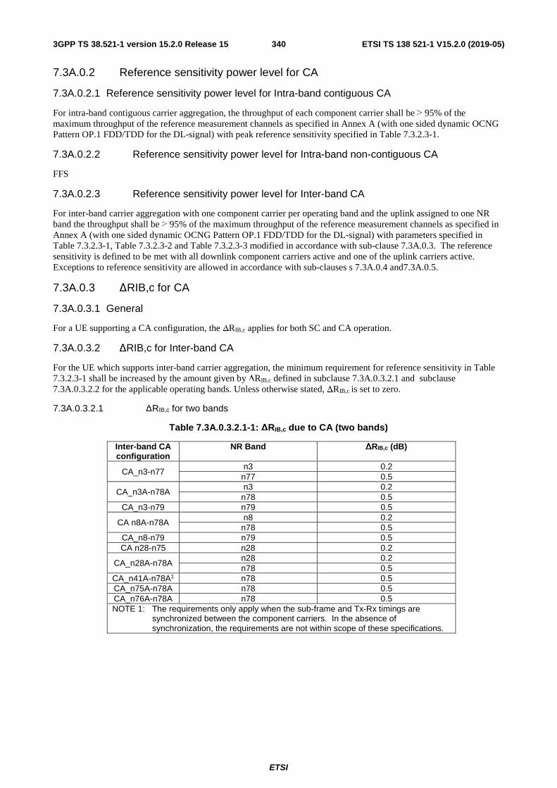
ETSI
ETSI TS 138 521-1 V15.2.0 (2019-05)3403GPP TS 38.521-1 version 15.2.0 Release 15
7.3A.0.2 Reference sensitivity power level for CA
7.3A.0.2.1 Reference sensitivity power level for Intra-band contiguous CA
For intra-band contiguous carrier aggregation, the throughput of each component carrier shall be ≥ 95% of the maximum throughput of the reference measurement channels as specified in Annex A (with one sided dynamic OCNG Pattern OP.1 FDD/TDD for the DL-signal) with peak reference sensitivity specified in Table 7.3.2.3-1.
7.3A.0.2.2 Reference sensitivity power level for Intra-band non-contiguous CA
FFS
7.3A.0.2.3 Reference sensitivity power level for Inter-band CA
For inter-band carrier aggregation with one component carrier per operating band and the uplink assigned to one NR band the throughput shall be ≥ 95% of the maximum throughput of the reference measurement channels as specified in Annex A (with one sided dynamic OCNG Pattern OP.1 FDD/TDD for the DL-signal) with parameters specified in Table 7.3.2.3-1, Table 7.3.2.3-2 and Table 7.3.2.3-3 modified in accordance with sub-clause 7.3A.0.3. The reference sensitivity is defined to be met with all downlink component carriers active and one of the uplink carriers active. Exceptions to reference sensitivity are allowed in accordance with sub-clauses s 7.3A.0.4 and7.3A.0.5.
7.3A.0.3 ΔRIB,c for CA
7.3A.0.3.1 General
For a UE supporting a CA configuration, the ΔRIB,c applies for both SC and CA operation.
7.3A.0.3.2 ΔRIB,c for Inter-band CA
For the UE which supports inter-band carrier aggregation, the minimum requirement for reference sensitivity in Table 7.3.2.3-1 shall be increased by the amount given by ΔRIB,c defined in subclause 7.3A.0.3.2.1 and subclause 7.3A.0.3.2.2 for the applicable operating bands. Unless otherwise stated, ΔRIB,c is set to zero.
7.3A.0.3.2.1 ΔRIB,c for two bands
Table 7.3A.0.3.2.1-1: ΔRIB,c due to CA (two bands)
Inter-band CA configuration
NR Band ΔRIB,c (dB)
CA_n3-n77 n3 0.2
n77 0.5
CA_n3A-n78A n3 0.2
n78 0.5 CA_n3-n79 n79 0.5
CA n8A-n78A n8 0.2
n78 0.5 CA_n8-n79 n79 0.5 CA n28-n75 n28 0.2
CA_n28A-n78A n28 0.2 n78 0.5
CA_n41A-n78A1 n78 0.5 CA_n75A-n78A n78 0.5 CA_n76A-n78A n78 0.5 NOTE 1: The requirements only apply when the sub-frame and Tx-Rx timings are
synchronized between the component carriers. In the absence of synchronization, the requirements are not within scope of these specifications.

ETSI
ETSI TS 138 521-1 V15.2.0 (2019-05)3413GPP TS 38.521-1 version 15.2.0 Release 15
7.3A.0.3.2.2 ΔRIB,c for three bands
Table 7.3A.0.3.2.2-1: ΔRIB,c due to CA (three bands)
FFS
Inter-band CA configuration
NR Band ΔRIB,c (dB)
7.3A.0.4 Reference sensitivity exceptions due to UL harmonic interference for CA
Sensitivity degradation is allowed for a band in frequency range 1 if it is impacted by UL harmonic interference from another band in frequency range 1 of the same CA configuration. Reference sensitivity exceptions are specified in Table 7.3A.0.4-1 with uplink configuration specified in Table 7.3A.0.4-2.
Table 7.3A.0.4-1: Reference sensitivity exceptions due to UL harmonic for NR CA FR1
MSD due to harmonic exception for the DL band
UL band
DL band
5 MHz
10 MHz
15 MHz
20 MHz
25 MHz
30 MHz
40 MHz
50 MHz
60 MHz
80 MHz
90 MHz
100 MHz
dB dB dB dB dB dB dB dB dB dB dB dB
n3 n771,2 23.9 22.1 20.9 17.9 16.9 16.1 n773 1.1 0.8 0.3
n3 n781,2 23.9 22.1 20.9 17.9 16.9 16.1 n783 1.1 0.8 0.3
n8 n784,5 10.8 9.1 8.0 5.1 4.2 3.5 2.3 1.4 n8 n781,2 10.8 9.1 8 3.5 2.3 1.4 n8 n791,2 [6.8] 6.2 [5.6] 4.9 4.4
n28 n751,2 28.1 25.3 24.0 22.8 n781,2 [10.4] [8.9] [7.8] [4.7] [3.7] [3] [1.7] [1.2] [0.7]
NOTE 1: These requirements apply when there is at least one individual RE within the uplink transmission bandwidth of the aggressor (lower) band for which the 2nd transmitter harmonic is within the downlink transmission bandwidth of a victim (higher) band.
NOTE 2: The requirements should be verified for UL NR-ARFCN of the aggressor (lower) band (superscript LB) such that 1.02.0/HB
DLLB
UL ff = in MHz and _ _/ 2 / 2LB LB LB LB LB
UL low Channel UL UL high ChannelF BW f F BW+ ≤ ≤ − with carrier
frequency in the victim (higher) band in MHz and the channel bandwidth configured in the lower
band. NOTE 3: The requirements are only applicable to channel bandwidths with a carrier frequency at
( )2/20 HBChannelBW+± MHz offset from
LBULf2 in the victim (higher band) with
_ _/ 2 / 2LB LB LB LB LBUL low Channel UL UL high ChannelF BW f F BW+ ≤ ≤ −
, where andHB
ChannelBW are the channel bandwidths configured in the aggressor (lower) and victim (higher) bands in MHz, respectively.
NOTE 4: These requirements apply when there is at least one individual RE within the uplink transmission bandwidth of a low band for which the 4th transmitter harmonic is within the downlink transmission bandwidth of a high band.
NOTE 5: The requirements should be verified for UL NR-ARFCN of a low band (superscript LB) such that
in MHz and with the
carrier frequency of a high band in MHz and the channel bandwidth configured in the low band.
HBDLf
LBChannelBW
LBChannelBW
/ 0.4 0.1LB HB
UL DLf f= _ _/ 2 / 2LB LB LB LB LB
UL low Channel UL UL high ChannelF BW f F BW+ ≤ ≤ − HBDLf
LBChannelBW

ETSI
ETSI TS 138 521-1 V15.2.0 (2019-05)3423GPP TS 38.521-1 version 15.2.0 Release 15
Table 7.3A.0.4-2: Uplink configuration for reference sensitivity exceptions due to UL harmonic interference for NR CA, FR1
NR Band / Channel bandwidth of the high band
UL band
DL band
5 MHz
10 MHz
15 MHz
20 MHz
25 MHz
30 MHz
40 MHz
50 MHz
60 MHz
80 MHz
90 MHz
100 MHz
n3 n77 26 39 53 106 133 160
n3 n78 26 39 53 106 133 160 25
n8 n78 16 25 25 25 25 25 25 25 25
n8 n79 25 25 25 25 25
n28 n75 12 25 36 50
n28 n78 5 10 15 20 NOTE: 15kHz SCS is assumed for UL band.
For unsynchronized operation, Rx de-sensing in one band will be caused by another band due to lack of isolation in the band filters. Reference sensitivity exceptions for cross band are specified in Table 7.3A.0.4-3 with uplink configuration specified in Table 7.3A.0.4-4.
Table 7.3A.0.4-3: MSD for the CA configuration for asynchronous operation and cross band isolation for CA
Channel bandwidth NR CA
Configuration NR
band 5
MHz 10
MHz 15
MHz 20
MHz 40
MHz 50
MHz 60
MHz 80
MHz 90
MHz 100 MHz
Duplex mode
CA_n41A-n78A n41 -
90.3 -
88.5 -
87.3 -
84.1 -
83.1
TDD
Table 7.3A.0.4-4: Uplink configuration for reference sensitivity exceptions due to cross band isolation for CA
NR Band / Channel bandwidth of the high band
UL band
DL band
SCS (kHz)
5 MHz
10 MHz
15 MHz
20 MHz
25 MHz
30 MHz
40 MHz
50 MHz
60 MHz
80 MHz
90 MHz
100 MHz
n78 n41 30 N/A 273 273 273 N/A N/A 273 273 273 273 273 273
Table 7.3A.0.4-5: Reference sensitivity exceptions due to harmonic mixing for CA in NR FR1
UL band
DL band
5 MHz (dB)
10 MHz (dB)
15 MHz (dB)
20 MHz (dB)
25 MHz (dB)
40 MHz (dB)
50 MHz (dB)
60 MHz (dB)
80 MHz (dB)
90 MHz (dB)
100 MHz (dB)
n41 n781 N/A 8.3 8.0 6.9 N/A 3.9 3 2.3 1.2 0.4
n78 n412 N/A 10.4 10.4 10.4 N/A 7.2 6.2 5.5 4.5 4.5 NOTE 1: The requirements should be verified for UL EARFCN of the aggressor (lower) band (superscript LB) such
that 1.015.0/HBDL
LBUL ff = in MHz and _ _/ 2 / 2LB LB LB LB LB
UL low Channel UL UL high ChannelF BW f F BW+ ≤ ≤ − with carrier
frequency in the victim (higher) band in MHz and the channel bandwidth configured in the lower band.
NOTE 2: The requirements should be verified for UL EARFCN of the aggressor (high) band (superscript HB) such
that 1.0*15 HBDL
LBUL ff = in MHz and
2/2/ __HB
ChannelHB
highULHB
ULHB
ChannelHB
lowUL BWffBWF −≤≤+ with
LBDLf carrier
frequency in the victim (lower) band in MHz and LB
ChannelBW the channel bandwidth configured in the higher band.
HBDLf
LBChannelBW

ETSI
ETSI TS 138 521-1 V15.2.0 (2019-05)3433GPP TS 38.521-1 version 15.2.0 Release 15
Table 7.3A.0.4-6: Uplink configuration for reference sensitivity exceptions due to receiver harmonic mixing for CA in NR FR1
UL band
DL band
SCS (kHz)
5 MHz
10 MHz
15 MHz
20 MHz
25 MHz
40 MHz
50 MHz
60 MHz
80 MHz
90 MHz
100 MHz
n41 n78 30 N/A 24 24 24 N/A 24 24 24 24 24 24
n78 n41 30 N/A 50 50 50 N/A 50 50 50 50 50 50
7.3A.0.5 Reference sensitivity exceptions due to intermodulation interference due to 2UL CA
For inter-band carrier aggregation with uplink assigned to two NR bands given in Table 7.3A.0.5-1 the reference sensitivity is defined only for the specific uplink and downlink test points specified in Table 7.3A.0.5-1. For these test points the reference sensitivity requirement specified in Table 7.3.2.3-1 and Table 7.3.2.3-2 are relaxed by the amount of the corresponding parameter MSD given in Table 7.3A.0.5-1.
Table 7.3A.0.5-1: 2DL/2UL interband Reference sensitivity QPSK PREFSENS and uplink/downlink configurations
Band / Channel bandwidth / NRB / Duplex mode Source of IMD
NR CA Configuration NR band UL Fc
(MHz)
UL/DL BW
(MHz)
UL CLRB
DL Fc (MHz)
MSD (dB)
Duplex mode
CA_n3A-n78A n3 1740 5 25 1835
[26] FDD
IMD24 [28.75]
n78 3575 10 25 3575 N/A TDD N/A
CA_n3A-n78A n3 1765 5 25 1860
[8.0] FDD
IMD44 [10.75]
n78 3435 10 25 3435 N/A TDD N/A
CA_n8A-n78A n8 897.5 5 25 942.5 8.3 FDD IMD4
n78 3635 10 52 3635 N/A TDD N/A NOTE 1: Both of the transmitters shall be set min(+20 dBm, PCMAX_L,f,c) as defined in subclause 6.2A.4 NOTE 2: RBSTART = 0, 15kHz SCS is assumed. NOTE 3: No requirements apply when there is at least one individual RE within the intermodulation generated by the
dual uplink is within the downlink transmission bandwidth of the FDD band. The reference sensitivity should only be verified when this is not the case (the requirements specified in clause 7.3 apply).
NOTE4: This band is subject to IMD5 also which MSD is not specified. NOTE 5: Applicable only if operation with 4 antenna ports is supported in the band with carrier aggregation configured.
The normative reference for this requirement is TS 38.101-1 [2] clause 7.3.A.
7.3A.1 Reference sensitivity power level for 2DL CA
7.3A.1.1 Test purpose
To verify the ability of UE that support CA to receive data with a given average throughput for a specified reference measurement channel, under conditions of low signal level, ideal propagation and no added noise.
A UE unable to meet the throughput requirement under these conditions will decrease the effective coverage area
7.3A.1.2 Test applicability
This test case applies to all types of NR UE release 15 and forward that support NR 2DL CA
7.3A.1.3 Minimum requirements
The minimum conformance requirements are defined in clause 7.3A2.0.

ETSI
ETSI TS 138 521-1 V15.2.0 (2019-05)3443GPP TS 38.521-1 version 15.2.0 Release 15
7.3A.1.4 Test description
7.3A.1.4.1 Initial conditions
Initial conditions are a set of test configurations the UE needs to be tested in and the steps for the SS to take with the UE to reach the correct measurement state.
The initial test configurations consist of environmental conditions, test frequencies, and channel bandwidths based on NR operating bands specified in Table 5.2-1. All of these configurations shall be tested with applicable test parameters for each channel bandwidth, and are shown in Table TBD. The details of the uplink reference measurement channels (RMCs) are specified in Annexe A2.2. Configurations of PDSCH and PDCCH before measurement are specified in Annex C.2.
Table 7.3A.1.4.1-1: Test Configuration Table
FFS
7.3A.1.4.2 Test procedure
FFS
7.3A.1.4.3 Message contents
Message contents are according to TS 38.508-1 [5] subclause 4.6.
7.3A.1.5 Test requirement
The throughput shall be ≥ 95% of the maximum throughput of the reference measurement channels as specified in Annexes A.2.2, A.2.3 and A.3.2 (with one sided dynamic OCNG Pattern OP.1 FDD/TDD for the DL-signal as described in Annex A.5.1.1/A.5.2.1) with parameters specified in Table 7.3A.1.5-1 and Table 7.3A.1.5-2.
Table 7.3A.1.5-1: Reference sensitivity for intra-band 2DL_CA
FFS
Table 7.3A.1.5-2: Intra-band 2DL_CA uplink configuration for reference sensitivity
FFS
7.3A.2 Reference sensitivity power level for 3DL CA
FFS
7.3A.3 Reference sensitivity power level for 4DL CA
FFS
7.3A.4 Reference sensitivity power level for 5DL CA
FFS
7.3B Reference sensitivity for DC
7.3C Reference sensitivity for SUL
7.3C.1 General
The reference sensitivity power level REFSENS is the minimum mean power applied to each one of the UE antenna ports for all UE categories, at which the throughput shall meet or exceed the requirements for the specified reference measurement channel.
7.3C.2 Reference sensitivity power level for SUL
Editor’s Note: This clause is incomplete. The following aspects are either missing or not yet determined:
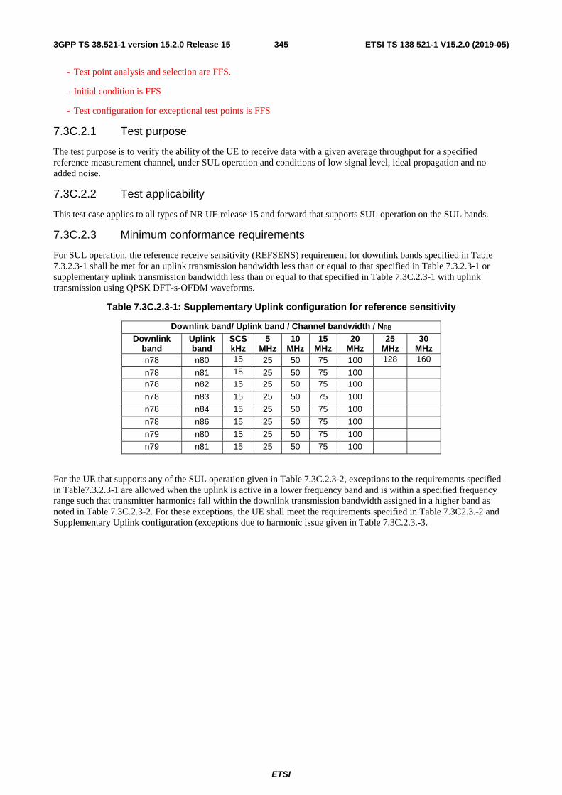
ETSI
ETSI TS 138 521-1 V15.2.0 (2019-05)3453GPP TS 38.521-1 version 15.2.0 Release 15
- Test point analysis and selection are FFS.
- Initial condition is FFS
- Test configuration for exceptional test points is FFS
7.3C.2.1 Test purpose
The test purpose is to verify the ability of the UE to receive data with a given average throughput for a specified reference measurement channel, under SUL operation and conditions of low signal level, ideal propagation and no added noise.
7.3C.2.2 Test applicability
This test case applies to all types of NR UE release 15 and forward that supports SUL operation on the SUL bands.
7.3C.2.3 Minimum conformance requirements
For SUL operation, the reference receive sensitivity (REFSENS) requirement for downlink bands specified in Table 7.3.2.3-1 shall be met for an uplink transmission bandwidth less than or equal to that specified in Table 7.3.2.3-1 or supplementary uplink transmission bandwidth less than or equal to that specified in Table 7.3C.2.3-1 with uplink transmission using QPSK DFT-s-OFDM waveforms.
Table 7.3C.2.3-1: Supplementary Uplink configuration for reference sensitivity
Downlink band/ Uplink band / Channel bandwidth / NRB Downlink
band Uplink band
SCS kHz
5 MHz
10 MHz
15 MHz
20 MHz
25 MHz
30 MHz
n78 n80 15 25 50 75 100 128 160
n78 n81 15 25 50 75 100
n78 n82 15 25 50 75 100
n78 n83 15 25 50 75 100
n78 n84 15 25 50 75 100
n78 n86 15 25 50 75 100
n79 n80 15 25 50 75 100
n79 n81 15 25 50 75 100
For the UE that supports any of the SUL operation given in Table 7.3C.2.3-2, exceptions to the requirements specified in Table7.3.2.3-1 are allowed when the uplink is active in a lower frequency band and is within a specified frequency range such that transmitter harmonics fall within the downlink transmission bandwidth assigned in a higher band as noted in Table 7.3C.2.3-2. For these exceptions, the UE shall meet the requirements specified in Table 7.3C2.3.-2 and Supplementary Uplink configuration (exceptions due to harmonic issue given in Table 7.3C.2.3.-3.

ETSI
ETSI TS 138 521-1 V15.2.0 (2019-05)3463GPP TS 38.521-1 version 15.2.0 Release 15
Table 7.3C.2.3-2: Reference sensitivity for SUL operation (exceptions due to harmonic issue)
NR Band / Channel bandwidth of the high band UL
band DL
band 5
MHz 10
MHz 15
MHz 20
MHz 25
MHz 30
MHz 40
MHz 50
MHz 60
MHz 80
MHz 90
MHz 100 MHz
dB dB dB dB dB dB dB dB dB dB dB dB n80 n781,2 23.9 22.1 20.9 17.9
n783 1.1 0.8 0.3 n82 n784,5 10.8 9.1 8 6 n81 n781,2 10.8 9.1 8 5.1 4.2 3.5 2.3 1.4 n81 n786,7 10.4 8.9 7.8 4.7 3.7 3 1.7 1.2 0.7
n86 n781,2 23.9 22.1 20.9 17.9 n783 1.1 0.8 0.3
n81 n796,7 [6.8] 6.2 [5.6] 4.9 4.4 NOTE 1: These requirements apply when there is at least one individual RE within the uplink transmission
bandwidth of the aggressor (lower) band for which the 2nd transmitter harmonic is within the downlink transmission bandwidth of a victim (higher) band.
NOTE 2: The requirements should be verified for UL EARFCN of the aggressor (lower) band (superscript LB) such
that in MHz and with carrier
frequency in the victim (higher) band in MHz and the channel bandwidth configured in the lower band.
NOTE 3: The requirements are only applicable to channel bandwidths with a carrier frequency at
MHz offset from in the victim (higher band) with
, where and are the channel bandwidths configured in the aggressor (lower) and victim (higher) bands in MHz, respectively.
NOTE 4: These requirements apply when there is at least one individual RE within the uplink transmission bandwidth of the aggressor (lower) band for which the 4th transmitter harmonic is within the downlink transmission bandwidth of a victim (higher) band.
NOTE 5: The requirements should be verified for UL EARFCN of the aggressor (lower) band (superscript LB) such that 1.04.0/HB
DLLB
UL ff = in MHz and _ _/ 2 / 2LB LB LB LB LB
UL low Channel UL UL high ChannelF BW f F BW+ ≤ ≤ − with carrier
frequency in the victim (higher) band in MHz and the channel bandwidth configured in the lower
band. NOTE 6: The requirements should be verified for UL EARFCN of the aggressor (lower) band (superscript LB) such
that 1.05.0/HBDL
LBUL ff = in MHz and
_ _/ 2 / 2LB LB LB LB LBUL low Channel UL UL high ChannelF BW f F BW+ ≤ ≤ − with carrier
frequency in the victim (higher) band in MHz and the channel bandwidth configured in the lower
band. NOTE 7: These requirements apply when there is at least one individual RE within the uplink transmission
bandwidth of the aggressor (lower) band for which the 4th transmitter harmonic is within the downlink transmission bandwidth of a victim (higher) band
Table 7.3C.2.3-3: Supplementary Uplink configuration (exceptions due to harmonic issue)
NR Band / Channel bandwidth of the high band UL
band DL band
5 MHz (NRB)
10 MHz (NRB)
15 MHz (NRB)
20 MHz (NRB)
25 MHz (NRB)
30 MHz (NRB)
40 MHz (NRB)
50 MHz (NRB)
60 MHz (NRB)
80 MHz (NRB)
90 MHz (NRB)
100 MHz (NRB)
n80 n78 25 36 50 100
n81 n78 16 25 25 25 25 25 25 25 25
n81 n79 25 25 25 25 25 25
n83 n78 10 15 20 25 25 25 25 25 25
n86 n78 26 39 53 100
NOTE 1: 15kHz SCS is assumed for UL band. NOTE 2: The UL configuration applies regardless of the channel bandwidth of the low band unless the UL resource blocks exceed
that specified in Table 7.3.2.3-3 for the uplink bandwidth in which case the allocation according to Table 7.3.2.3-3 applies.
For the UE which supports SUL band combination, the minimum requirement for reference sensitivity in Table 7.3.2.3-1 shall be increased by the amount given in ΔRIB,c defined in subclause 7.3C.3 for the applicable NR bands. The normative reference for this requirement is TS 38.101-1 [2] clause 7.3C.2
1.02.0/HBDL
LBUL ff = _ _/ 2 / 2LB LB LB LB LB
UL low Channel UL UL high ChannelF BW f F BW+ ≤ ≤ −HB
DLf
LBChannelBW
( )2/20 HBChannelBW+± LB
ULf2
_ _/ 2 / 2LB LB LB LB LBUL low Channel UL UL high ChannelF BW f F BW+ ≤ ≤ − LB
ChannelBW HBChannelBW
HBDLf
LBChannelBW
HBDLf
LBChannelBW

ETSI
ETSI TS 138 521-1 V15.2.0 (2019-05)3473GPP TS 38.521-1 version 15.2.0 Release 15
7.3C.2.4 Test description
7.3C.2.4.1 Initial conditions
Same test description as specified in clause 7.3.2.4.1 with following exceptions:
- Instead of table 5.3.5-1 use Table 5.5C-1
- Instead of table 7.3.2.4.1-1 use Table 7.3C.2.4.1-1
Table 7.3C.2.4.1-1: Test Configuration Table
Initial Conditions Test Environment as specified in TS 38.508-1 [5] subclause 4.1
FFS
Test Frequencies as specified in TS 38.508-1 [5] subclause4.3.1
FFS
Test Channel Bandwidths as specified in TS 38.508-1 [5] subclause 4.3.1
FFS
Test SCS as specified in Table 5.3.5-1 FFS Test Parameters
Test ID
Downlink Configuration Uplink Configuration SUL Configuration
Modulation
RB allocation Modulation RB allocation Modulation RB allocation
1 FFS FFS FFS FFS FFS FFS
Table 7.3C.2.4.1-2: Test configurations table for SUL operation exceptions due to UL harmonic issue for n78 with SUL 80
FFS
1. Connect the SS to the UE antenna connectors as shown in TS 38.508-1 [5] Annex A, Figure A.3.1.1.1 for TE diagram and section A.3.2.1 for UE diagram.
2. The parameter settings for the cell are set up according to TS 38.508-1 [5] subclause 4.4.3.
3. Downlink signals are initially set up according to Annex C0, C.1, C.2, C3.1, and uplink signals according to Annex G.0, G.1, G.2, G.3.0 with consideration of supplementary uplink physical channels.
4. The UL and DL Reference Measurement Channel shall be set according to Table 7.3.2.4.1-1, Table 7.3.2.4.1-2, Table 7.3.2.4.1-3 and Table 7.3C.2.4.1-1.
5. The UL Reference Measurement Channel shall be set according to Table 7.3C.2.3-2 and 7.3C.2.3-3 when testing is performed with UL/DL band combination listed in Table 7.3C.2.3-2 for exceptions due to harmonic issue.
5. Propagation conditions are set according to Annex B.0.
6. Ensure the UE is in State RRC_CONNECTED with generic procedure parameters Connectivity NR, Connected without release On, Test Mode On and Test Loop Function On according to TS 38.508-1 [5] clause 4.5. Message contents are defined in clause 7.3C.2.4.3
7.3C.2.4.2 Test procedure
1 SS transmits PDSCH via PDCCH DCI format [1_1] for C_RNTI to transmit the DL RMC according to Table 7.3.4.1-1. The SS sends downlink MAC padding bits on the DL RMC.
2. SS sends uplink scheduling information for each UL HARQ process via PDCCH DCI format [0_1] for C_RNTI to schedule the UL RMC according to Tables 7.3.4.1-1. Since the UE has no payload data to send, the UE transmits uplink MAC padding bits on the UL RMC.
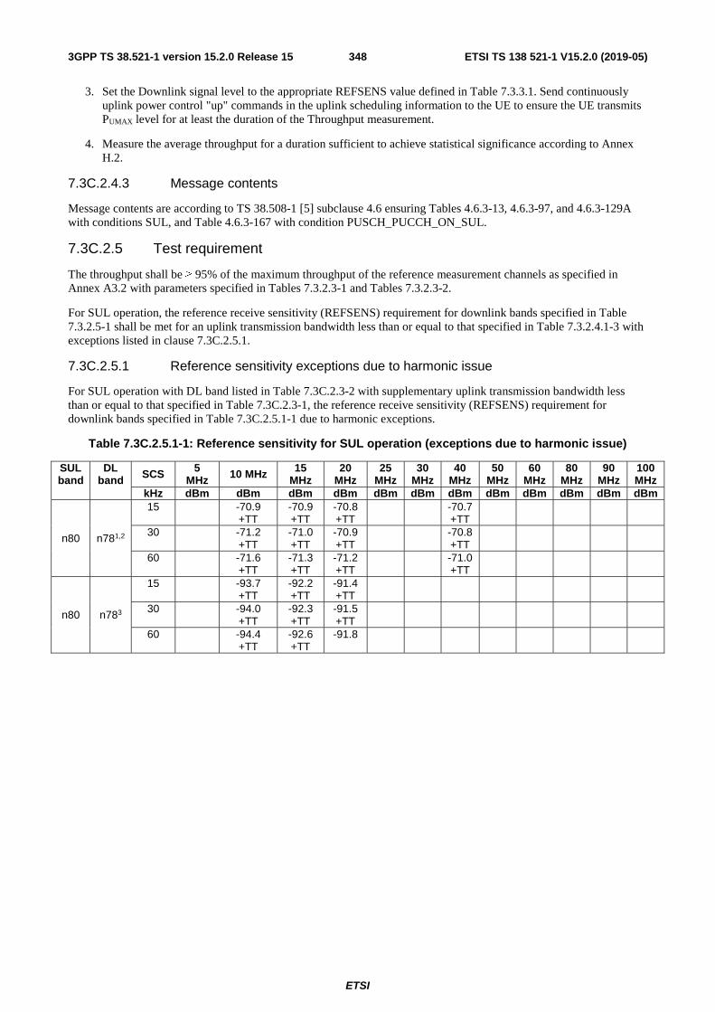
ETSI
ETSI TS 138 521-1 V15.2.0 (2019-05)3483GPP TS 38.521-1 version 15.2.0 Release 15
3. Set the Downlink signal level to the appropriate REFSENS value defined in Table 7.3.3.1. Send continuously uplink power control "up" commands in the uplink scheduling information to the UE to ensure the UE transmits PUMAX level for at least the duration of the Throughput measurement.
4. Measure the average throughput for a duration sufficient to achieve statistical significance according to Annex H.2.
7.3C.2.4.3 Message contents
Message contents are according to TS 38.508-1 [5] subclause 4.6 ensuring Tables 4.6.3-13, 4.6.3-97, and 4.6.3-129A with conditions SUL, and Table 4.6.3-167 with condition PUSCH_PUCCH_ON_SUL.
7.3C.2.5 Test requirement
The throughput shall be ≥ 95% of the maximum throughput of the reference measurement channels as specified in Annex A3.2 with parameters specified in Tables 7.3.2.3-1 and Tables 7.3.2.3-2.
For SUL operation, the reference receive sensitivity (REFSENS) requirement for downlink bands specified in Table 7.3.2.5-1 shall be met for an uplink transmission bandwidth less than or equal to that specified in Table 7.3.2.4.1-3 with exceptions listed in clause 7.3C.2.5.1.
7.3C.2.5.1 Reference sensitivity exceptions due to harmonic issue
For SUL operation with DL band listed in Table 7.3C.2.3-2 with supplementary uplink transmission bandwidth less than or equal to that specified in Table 7.3C.2.3-1, the reference receive sensitivity (REFSENS) requirement for downlink bands specified in Table 7.3C.2.5.1-1 due to harmonic exceptions.
Table 7.3C.2.5.1-1: Reference sensitivity for SUL operation (exceptions due to harmonic issue)
SUL band
DL band SCS 5
MHz 10 MHz 15 MHz
20 MHz
25 MHz
30 MHz
40 MHz
50 MHz
60 MHz
80 MHz
90 MHz
100 MHz
kHz dBm dBm dBm dBm dBm dBm dBm dBm dBm dBm dBm dBm
n80 n781,2
15 -70.9 +TT
-70.9 +TT
-70.8 +TT
-70.7 +TT
30 -71.2 +TT
-71.0 +TT
-70.9 +TT
-70.8 +TT
60 -71.6 +TT
-71.3 +TT
-71.2 +TT
-71.0 +TT
n80 n783
15 -93.7 +TT
-92.2 +TT
-91.4 +TT
30 -94.0 +TT
-92.3 +TT
-91.5 +TT
60 -94.4 +TT
-92.6 +TT
-91.8
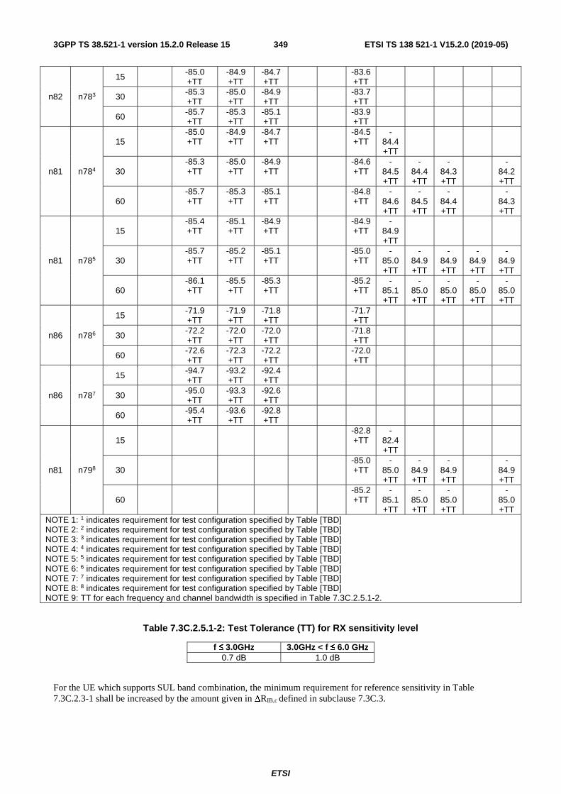
ETSI
ETSI TS 138 521-1 V15.2.0 (2019-05)3493GPP TS 38.521-1 version 15.2.0 Release 15
n82 n783
15 -85.0 +TT
-84.9 +TT
-84.7 +TT
-83.6 +TT
30 -85.3 +TT
-85.0 +TT
-84.9 +TT
-83.7 +TT
60 -85.7 +TT
-85.3 +TT
-85.1 +TT
-83.9 +TT
n81 n784
15 -85.0 +TT
-84.9 +TT
-84.7 +TT
-84.5 +TT
-84.4 +TT
30 -85.3 +TT
-85.0 +TT
-84.9 +TT
-84.6 +TT
-84.5 +TT
-84.4 +TT
-84.3 +TT
-84.2 +TT
60 -85.7 +TT
-85.3 +TT
-85.1 +TT
-84.8 +TT
-84.6 +TT
-84.5 +TT
-84.4 +TT
-84.3 +TT
n81 n785
15 -85.4 +TT
-85.1 +TT
-84.9 +TT
-84.9 +TT
-84.9 +TT
30 -85.7 +TT
-85.2 +TT
-85.1 +TT
-85.0 +TT
-85.0 +TT
-84.9 +TT
-84.9 +TT
-84.9 +TT
-84.9 +TT
60 -86.1 +TT
-85.5 +TT
-85.3 +TT
-85.2 +TT
-85.1 +TT
-85.0 +TT
-85.0 +TT
-85.0 +TT
-85.0 +TT
n86 n786
15 -71.9 +TT
-71.9 +TT
-71.8 +TT
-71.7 +TT
30 -72.2 +TT
-72.0 +TT
-72.0 +TT
-71.8 +TT
60 -72.6 +TT
-72.3 +TT
-72.2 +TT
-72.0 +TT
n86 n787
15 -94.7 +TT
-93.2 +TT
-92.4 +TT
30 -95.0 +TT
-93.3 +TT
-92.6 +TT
60 -95.4 +TT
-93.6 +TT
-92.8 +TT
n81 n798
15 -82.8
+TT -
82.4 +TT
30 -85.0
+TT -
85.0 +TT
-84.9 +TT
-84.9 +TT
-84.9 +TT
60 -85.2
+TT -
85.1 +TT
-85.0 +TT
-85.0 +TT
-85.0 +TT
NOTE 1: 1 indicates requirement for test configuration specified by Table [TBD] NOTE 2: 2 indicates requirement for test configuration specified by Table [TBD] NOTE 3: 3 indicates requirement for test configuration specified by Table [TBD] NOTE 4: 4 indicates requirement for test configuration specified by Table [TBD] NOTE 5: 5 indicates requirement for test configuration specified by Table [TBD] NOTE 6: 6 indicates requirement for test configuration specified by Table [TBD] NOTE 7: 7 indicates requirement for test configuration specified by Table [TBD] NOTE 8: 8 indicates requirement for test configuration specified by Table [TBD] NOTE 9: TT for each frequency and channel bandwidth is specified in Table 7.3C.2.5.1-2.
Table 7.3C.2.5.1-2: Test Tolerance (TT) for RX sensitivity level
f ≤ 3.0GHz 3.0GHz < f ≤ 6.0 GHz 0.7 dB 1.0 dB
For the UE which supports SUL band combination, the minimum requirement for reference sensitivity in Table 7.3C.2.3-1 shall be increased by the amount given in ΔRIB,c defined in subclause 7.3C.3.

ETSI
ETSI TS 138 521-1 V15.2.0 (2019-05)3503GPP TS 38.521-1 version 15.2.0 Release 15
7.3C.3 ΔRIB,c for SUL
7.3C.3.1 General
For a UE supporting a SUL configuration, the ΔRIB,c applies for both SC and SUL operation.
7.3C.3.2 SUL band combination
For the UE which supports SUL band combination, the minimum requirement for reference sensitivity in Table 7.3.2.3-1 shall be increased by the amount given in ΔRIB,c defined in Table 7.3C.3.2-1 for the applicable operating bands.
Table 7.3C.3.2-1: ΔRIB,c due to SUL (two bands)
Band combination
for SUL
NR Band ΔRIB,c [dB]
SUL_n78-n80 n78 0.5 n80 0.2
SUL_n78-n81 n78 0.2 n81 0.2
SUL_n78-n82 n78 0.5
SUL_n78-n83 n78 0.5 n83 0.2
SUL_n78-n84 n78 0.5
SUL_n78-n86 n78 0.5 n86 0.2
7.3D Reference sensitivity for UL-MIMO
7.3D.1 General
For UE with two transmitter antenna connectors in closed-loop spatial multiplexing scheme, the minimum requirements specified in subclause 7.3 shall be met with the UL-MIMO configurations described in sub-clause 6.2D.1. For UL-MIMO, the parameter PUMAX is the total transmitter power over the two transmits power over the two transmit antenna connectors.
The normative reference for this requirement is TS 38.101-1 [2] clauses 7.3D
7.3D.2 Reference sensitivity power level for UL-MIMO
7.3D.2.1 Test purpose
The test purpose is to verify the ability of the UE to receive data with a given average throughput for a specified reference measurement channel, under conditions of low signal level, ideal propagation and no added noise.
7.3D.2.2 Test applicability
This test case applies to all types of NR UE release 15 and forward that support UL-MIMO
7.3D.2.3 Minimum conformance requirements
For UE with two transmitter antenna connectors in closed-loop spatial multiplexing scheme, the minimum requirements specified in subclause 7.3 shall be met with the UL-MIMO configurations described in sub-clause 6.2D.1. For UL-MIMO, the parameter PUMAX is the total transmitter power over the two transmits power over the two transmit antenna connectors
The normative reference for this requirement is TS 38.101-1 [2] clauses 7.3D and 7.3.
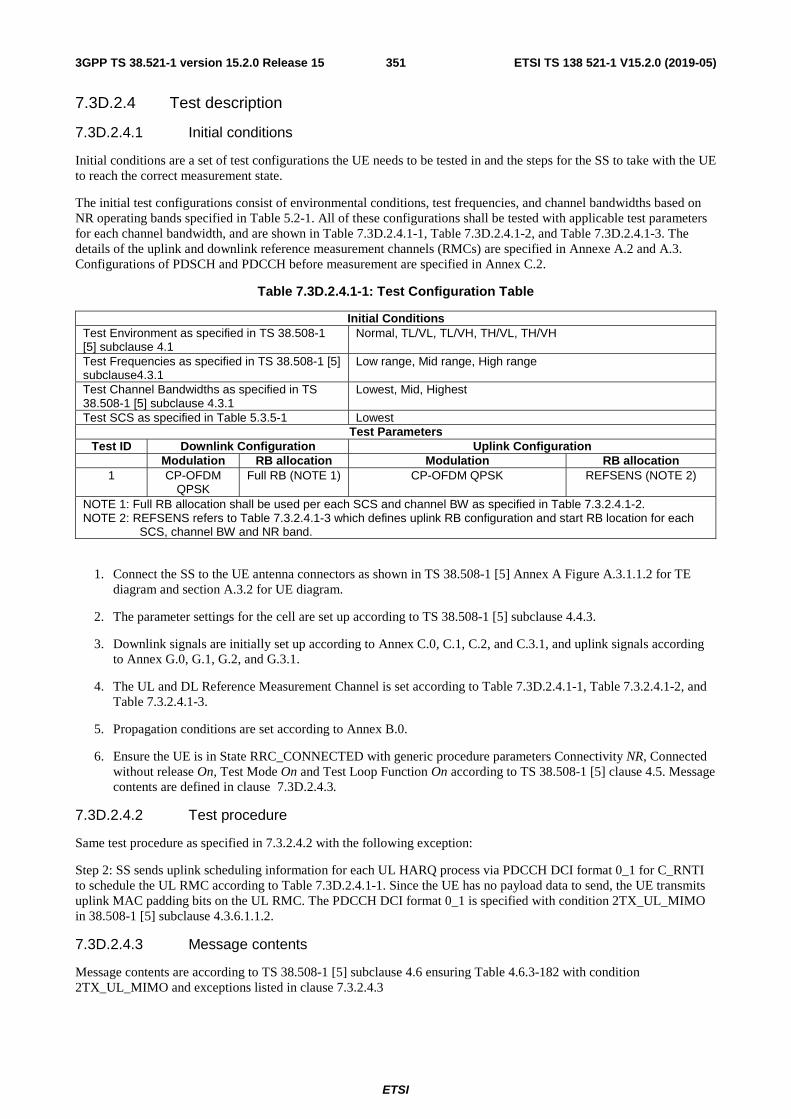
ETSI
ETSI TS 138 521-1 V15.2.0 (2019-05)3513GPP TS 38.521-1 version 15.2.0 Release 15
7.3D.2.4 Test description
7.3D.2.4.1 Initial conditions
Initial conditions are a set of test configurations the UE needs to be tested in and the steps for the SS to take with the UE to reach the correct measurement state.
The initial test configurations consist of environmental conditions, test frequencies, and channel bandwidths based on NR operating bands specified in Table 5.2-1. All of these configurations shall be tested with applicable test parameters for each channel bandwidth, and are shown in Table 7.3D.2.4.1-1, Table 7.3D.2.4.1-2, and Table 7.3D.2.4.1-3. The details of the uplink and downlink reference measurement channels (RMCs) are specified in Annexe A.2 and A.3. Configurations of PDSCH and PDCCH before measurement are specified in Annex C.2.
Table 7.3D.2.4.1-1: Test Configuration Table
Initial Conditions Test Environment as specified in TS 38.508-1 [5] subclause 4.1
Normal, TL/VL, TL/VH, TH/VL, TH/VH
Test Frequencies as specified in TS 38.508-1 [5] subclause4.3.1
Low range, Mid range, High range
Test Channel Bandwidths as specified in TS 38.508-1 [5] subclause 4.3.1
Lowest, Mid, Highest
Test SCS as specified in Table 5.3.5-1 Lowest Test Parameters
Test ID Downlink Configuration Uplink Configuration Modulation RB allocation Modulation RB allocation
1 CP-OFDM QPSK
Full RB (NOTE 1) CP-OFDM QPSK REFSENS (NOTE 2)
NOTE 1: Full RB allocation shall be used per each SCS and channel BW as specified in Table 7.3.2.4.1-2. NOTE 2: REFSENS refers to Table 7.3.2.4.1-3 which defines uplink RB configuration and start RB location for each
SCS, channel BW and NR band.
1. Connect the SS to the UE antenna connectors as shown in TS 38.508-1 [5] Annex A Figure A.3.1.1.2 for TE diagram and section A.3.2 for UE diagram.
2. The parameter settings for the cell are set up according to TS 38.508-1 [5] subclause 4.4.3.
3. Downlink signals are initially set up according to Annex C.0, C.1, C.2, and C.3.1, and uplink signals according to Annex G.0, G.1, G.2, and G.3.1.
4. The UL and DL Reference Measurement Channel is set according to Table 7.3D.2.4.1-1, Table 7.3.2.4.1-2, and Table 7.3.2.4.1-3.
5. Propagation conditions are set according to Annex B.0.
6. Ensure the UE is in State RRC_CONNECTED with generic procedure parameters Connectivity NR, Connected without release On, Test Mode On and Test Loop Function On according to TS 38.508-1 [5] clause 4.5. Message contents are defined in clause 7.3D.2.4.3.
7.3D.2.4.2 Test procedure
Same test procedure as specified in 7.3.2.4.2 with the following exception:
Step 2: SS sends uplink scheduling information for each UL HARQ process via PDCCH DCI format 0_1 for C_RNTI to schedule the UL RMC according to Table 7.3D.2.4.1-1. Since the UE has no payload data to send, the UE transmits uplink MAC padding bits on the UL RMC. The PDCCH DCI format 0_1 is specified with condition 2TX_UL_MIMO in 38.508-1 [5] subclause 4.3.6.1.1.2.
7.3D.2.4.3 Message contents
Message contents are according to TS 38.508-1 [5] subclause 4.6 ensuring Table 4.6.3-182 with condition 2TX_UL_MIMO and exceptions listed in clause 7.3.2.4.3

ETSI
ETSI TS 138 521-1 V15.2.0 (2019-05)3523GPP TS 38.521-1 version 15.2.0 Release 15
7.3D.2.5 Test requirement
The throughput shall be ≥ 95% of the maximum throughput of the reference measurement channels as specified in Annex A3.2 with reference receive power level specified in Tables 7.3.2.5-1 and parameters specified Tables 7.3D.2.4.1-1, Tables 7.3.2.4.1-2 and Tables 7.3.2.4.1-3.
7.4 Maximum input level
7.4.1 Test purpose
Maximum input level tests the UE's ability to receive data with a given average throughput for a specified reference measurement channel, under conditions of high signal level, ideal propagation and no added noise.
A UE unable to meet the throughput requirement under these conditions will decrease the coverage area near to a g-NodeB.
7.4.2 Test applicability
This test applies to all types of NR UE release 15 and forward.
7.4.3 Minimum conformance requirements
Maximum input level is defined as the maximum mean power received at the UE antenna port, at which the specified relative throughput shall meet or exceed the minimum requirements for the specified reference measurement channel. The throughput shall be ≥ 95% of the maximum throughput of the reference measurement channels as specified in Annex A.3 (with one sided dynamic OCNG Pattern OP.1 FDD/TDD as described in Annex A.5.1.1/A.5.2.1) with parameters specified in Table 7.4.3-1.
Table 7.4.3-1: Maximum input level
Rx Parameter
Units Channel bandwidth 5
MHz 10
MHz 15
MHz 20
MHz 25
MHz 30
MHz 40
MHz 50
MHz 60
MHz 80
MHz 90
MHz 100 MHz
Power in Transmission Bandwidth Configuration
dBm
-252 -242 -232 -222 -212 -202
-273 -263 -253 -243 -233 -223
NOTE 1: The transmitter shall be set to 4dB below PCMAX_L at the minimum uplink configuration specified in Table 7.3.2.3-3 with PCMAX_L as defined in subclause 6.2.4.
NOTE 2: Reference measurement channel is Annex A.3.2.3/A.3.3.3 for 64-QAM. NOTE 3: Reference measurement channel is Annex A.3.2.4/A.3.3.4 for 256-QAM.
The normative reference for this requirement is TS 38.101-1 [2] clause 7.4.
7.4.4 Test description
7.4.4.1 Initial conditions
Initial conditions are a set of test configurations the UE needs to be tested in and the steps for the SS to take with the UE to reach the correct measurement state.
The initial test configurations consist of environmental conditions, test frequencies, test channel bandwidths and sub-carrier spacing based on NR operating bands specified in table 5.3.5-1. All of these configurations shall be tested with applicable test parameters for each combination of channel bandwidth and sub-carrier spacing, are shown in table 7.4.4.1-1. The details of the uplink and downlink reference measurement channels (RMC) are specified in Annexes A.2 and A.3. The details of the OCNG patterns used are specified in Annex A.5. Configurations of PDSCH and PDCCH before measurement are specified in Annex C.2.
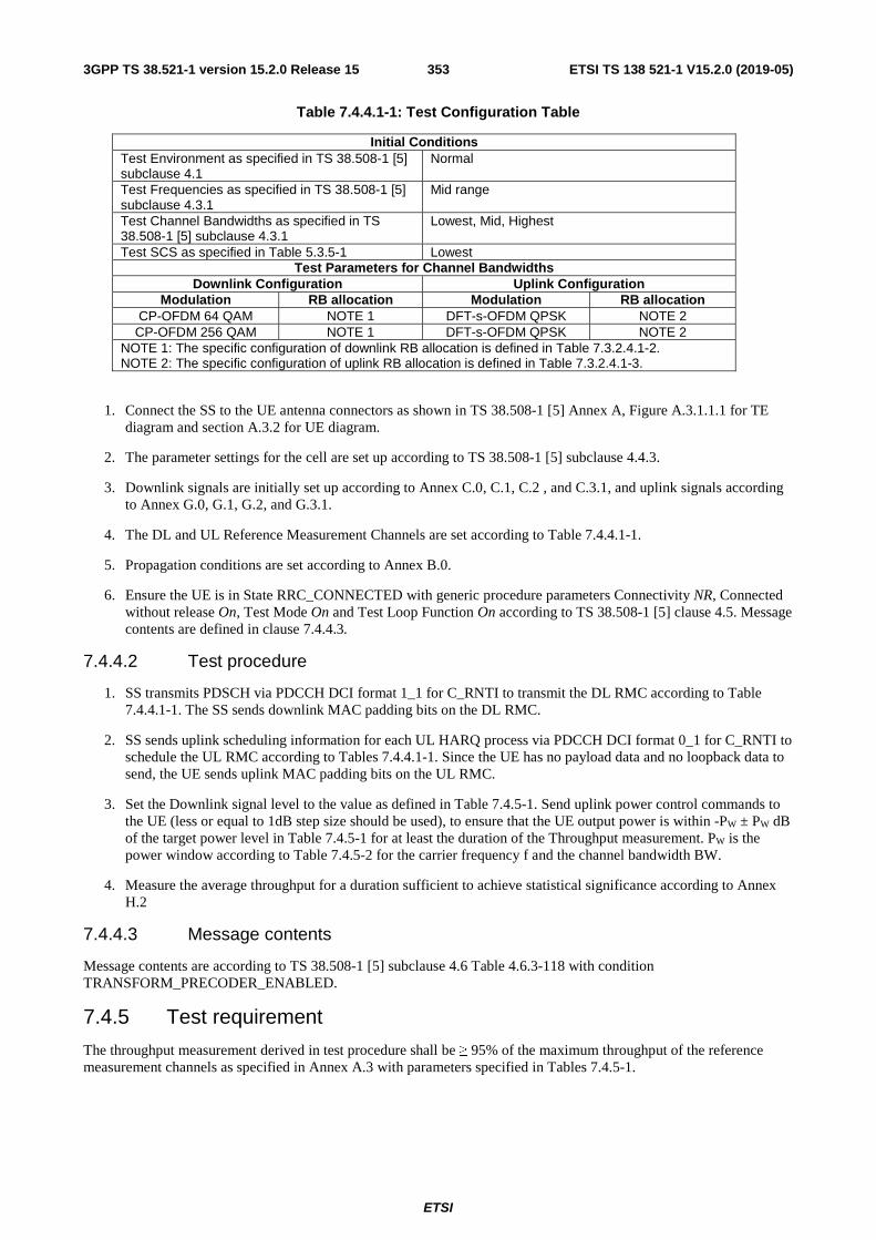
ETSI
ETSI TS 138 521-1 V15.2.0 (2019-05)3533GPP TS 38.521-1 version 15.2.0 Release 15
Table 7.4.4.1-1: Test Configuration Table
Initial Conditions Test Environment as specified in TS 38.508-1 [5] subclause 4.1
Normal
Test Frequencies as specified in TS 38.508-1 [5] subclause 4.3.1
Mid range
Test Channel Bandwidths as specified in TS 38.508-1 [5] subclause 4.3.1
Lowest, Mid, Highest
Test SCS as specified in Table 5.3.5-1 Lowest Test Parameters for Channel Bandwidths
Downlink Configuration Uplink Configuration Modulation RB allocation Modulation RB allocation
CP-OFDM 64 QAM NOTE 1 DFT-s-OFDM QPSK NOTE 2 CP-OFDM 256 QAM NOTE 1 DFT-s-OFDM QPSK NOTE 2
NOTE 1: The specific configuration of downlink RB allocation is defined in Table 7.3.2.4.1-2. NOTE 2: The specific configuration of uplink RB allocation is defined in Table 7.3.2.4.1-3.
1. Connect the SS to the UE antenna connectors as shown in TS 38.508-1 [5] Annex A, Figure A.3.1.1.1 for TE diagram and section A.3.2 for UE diagram.
2. The parameter settings for the cell are set up according to TS 38.508-1 [5] subclause 4.4.3.
3. Downlink signals are initially set up according to Annex C.0, C.1, C.2 , and C.3.1, and uplink signals according to Annex G.0, G.1, G.2, and G.3.1.
4. The DL and UL Reference Measurement Channels are set according to Table 7.4.4.1-1.
5. Propagation conditions are set according to Annex B.0.
6. Ensure the UE is in State RRC_CONNECTED with generic procedure parameters Connectivity NR, Connected without release On, Test Mode On and Test Loop Function On according to TS 38.508-1 [5] clause 4.5. Message contents are defined in clause 7.4.4.3.
7.4.4.2 Test procedure
1. SS transmits PDSCH via PDCCH DCI format 1_1 for C_RNTI to transmit the DL RMC according to Table 7.4.4.1-1. The SS sends downlink MAC padding bits on the DL RMC.
2. SS sends uplink scheduling information for each UL HARQ process via PDCCH DCI format 0_1 for C_RNTI to schedule the UL RMC according to Tables 7.4.4.1-1. Since the UE has no payload data and no loopback data to send, the UE sends uplink MAC padding bits on the UL RMC.
3. Set the Downlink signal level to the value as defined in Table 7.4.5-1. Send uplink power control commands to the UE (less or equal to 1dB step size should be used), to ensure that the UE output power is within -PW ± PW dB of the target power level in Table 7.4.5-1 for at least the duration of the Throughput measurement. PW is the power window according to Table 7.4.5-2 for the carrier frequency f and the channel bandwidth BW.
4. Measure the average throughput for a duration sufficient to achieve statistical significance according to Annex H.2
7.4.4.3 Message contents
Message contents are according to TS 38.508-1 [5] subclause 4.6 Table 4.6.3-118 with condition TRANSFORM_PRECODER_ENABLED.
7.4.5 Test requirement
The throughput measurement derived in test procedure shall be ≥ 95% of the maximum throughput of the reference measurement channels as specified in Annex A.3 with parameters specified in Tables 7.4.5-1.
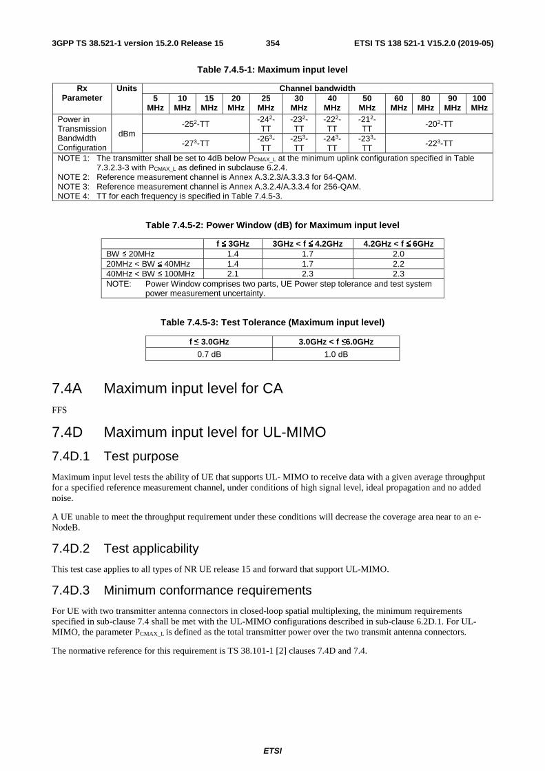
ETSI
ETSI TS 138 521-1 V15.2.0 (2019-05)3543GPP TS 38.521-1 version 15.2.0 Release 15
Table 7.4.5-1: Maximum input level
Rx Parameter
Units Channel bandwidth 5
MHz 10
MHz 15
MHz 20
MHz 25
MHz 30
MHz 40
MHz 50
MHz 60
MHz 80
MHz 90
MHz 100 MHz
Power in Transmission Bandwidth Configuration
dBm -252-TT -242-
TT -232-TT
-222-TT
-212-TT -202-TT
-273-TT -263-TT
-253-TT
-243-TT
-233-TT -223-TT
NOTE 1: The transmitter shall be set to 4dB below PCMAX_L at the minimum uplink configuration specified in Table 7.3.2.3-3 with PCMAX_L as defined in subclause 6.2.4.
NOTE 2: Reference measurement channel is Annex A.3.2.3/A.3.3.3 for 64-QAM. NOTE 3: Reference measurement channel is Annex A.3.2.4/A.3.3.4 for 256-QAM. NOTE 4: TT for each frequency is specified in Table 7.4.5-3.
Table 7.4.5-2: Power Window (dB) for Maximum input level
f ≤ 3GHz 3GHz < f ≤ 4.2GHz 4.2GHz < f ≤ 6GHz BW ≤ 20MHz 1.4 1.7 2.0 20MHz < BW ≤ 40MHz 1.4 1.7 2.2 40MHz < BW ≤ 100MHz 2.1 2.3 2.3 NOTE: Power Window comprises two parts, UE Power step tolerance and test system
power measurement uncertainty.
Table 7.4.5-3: Test Tolerance (Maximum input level)
f ≤ 3.0GHz 3.0GHz < f ≤6.0GHz
0.7 dB 1.0 dB
7.4A Maximum input level for CA FFS
7.4D Maximum input level for UL-MIMO
7.4D.1 Test purpose
Maximum input level tests the ability of UE that supports UL- MIMO to receive data with a given average throughput for a specified reference measurement channel, under conditions of high signal level, ideal propagation and no added noise.
A UE unable to meet the throughput requirement under these conditions will decrease the coverage area near to an e-NodeB.
7.4D.2 Test applicability
This test case applies to all types of NR UE release 15 and forward that support UL-MIMO.
7.4D.3 Minimum conformance requirements
For UE with two transmitter antenna connectors in closed-loop spatial multiplexing, the minimum requirements specified in sub-clause 7.4 shall be met with the UL-MIMO configurations described in sub-clause 6.2D.1. For UL-MIMO, the parameter PCMAX_L is defined as the total transmitter power over the two transmit antenna connectors.
The normative reference for this requirement is TS 38.101-1 [2] clauses 7.4D and 7.4.
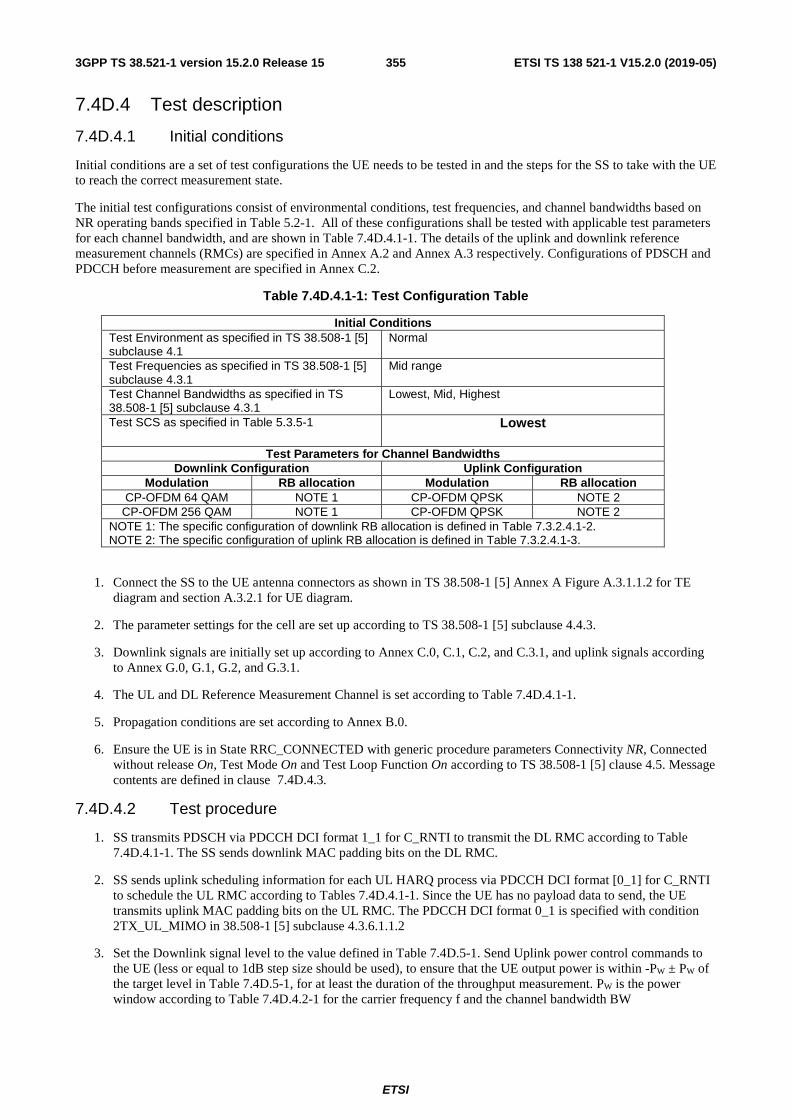
ETSI
ETSI TS 138 521-1 V15.2.0 (2019-05)3553GPP TS 38.521-1 version 15.2.0 Release 15
7.4D.4 Test description
7.4D.4.1 Initial conditions
Initial conditions are a set of test configurations the UE needs to be tested in and the steps for the SS to take with the UE to reach the correct measurement state.
The initial test configurations consist of environmental conditions, test frequencies, and channel bandwidths based on NR operating bands specified in Table 5.2-1. All of these configurations shall be tested with applicable test parameters for each channel bandwidth, and are shown in Table 7.4D.4.1-1. The details of the uplink and downlink reference measurement channels (RMCs) are specified in Annex A.2 and Annex A.3 respectively. Configurations of PDSCH and PDCCH before measurement are specified in Annex C.2.
Table 7.4D.4.1-1: Test Configuration Table
Initial Conditions Test Environment as specified in TS 38.508-1 [5] subclause 4.1
Normal
Test Frequencies as specified in TS 38.508-1 [5] subclause 4.3.1
Mid range
Test Channel Bandwidths as specified in TS 38.508-1 [5] subclause 4.3.1
Lowest, Mid, Highest
Test SCS as specified in Table 5.3.5-1 Lowest
Test Parameters for Channel Bandwidths Downlink Configuration Uplink Configuration
Modulation RB allocation Modulation RB allocation CP-OFDM 64 QAM NOTE 1 CP-OFDM QPSK NOTE 2
CP-OFDM 256 QAM NOTE 1 CP-OFDM QPSK NOTE 2 NOTE 1: The specific configuration of downlink RB allocation is defined in Table 7.3.2.4.1-2. NOTE 2: The specific configuration of uplink RB allocation is defined in Table 7.3.2.4.1-3.
1. Connect the SS to the UE antenna connectors as shown in TS 38.508-1 [5] Annex A Figure A.3.1.1.2 for TE diagram and section A.3.2.1 for UE diagram.
2. The parameter settings for the cell are set up according to TS 38.508-1 [5] subclause 4.4.3.
3. Downlink signals are initially set up according to Annex C.0, C.1, C.2, and C.3.1, and uplink signals according to Annex G.0, G.1, G.2, and G.3.1.
4. The UL and DL Reference Measurement Channel is set according to Table 7.4D.4.1-1.
5. Propagation conditions are set according to Annex B.0.
6. Ensure the UE is in State RRC_CONNECTED with generic procedure parameters Connectivity NR, Connected without release On, Test Mode On and Test Loop Function On according to TS 38.508-1 [5] clause 4.5. Message contents are defined in clause 7.4D.4.3.
7.4D.4.2 Test procedure
1. SS transmits PDSCH via PDCCH DCI format 1_1 for C_RNTI to transmit the DL RMC according to Table 7.4D.4.1-1. The SS sends downlink MAC padding bits on the DL RMC.
2. SS sends uplink scheduling information for each UL HARQ process via PDCCH DCI format [0_1] for C_RNTI to schedule the UL RMC according to Tables 7.4D.4.1-1. Since the UE has no payload data to send, the UE transmits uplink MAC padding bits on the UL RMC. The PDCCH DCI format 0_1 is specified with condition 2TX_UL_MIMO in 38.508-1 [5] subclause 4.3.6.1.1.2
3. Set the Downlink signal level to the value defined in Table 7.4D.5-1. Send Uplink power control commands to the UE (less or equal to 1dB step size should be used), to ensure that the UE output power is within -PW ± PW of the target level in Table 7.4D.5-1, for at least the duration of the throughput measurement. PW is the power window according to Table 7.4D.4.2-1 for the carrier frequency f and the channel bandwidth BW

ETSI
ETSI TS 138 521-1 V15.2.0 (2019-05)3563GPP TS 38.521-1 version 15.2.0 Release 15
4. Measure the average throughput for a duration sufficient to achieve statistical significance according to Annex H.2
Table 7.4D.4-2-1: Power Window (dB) for Maximum input level
f ≤ 3GHz 3GHz < f ≤ 4.2GHz 4.2GHz < f ≤ 6GHz BW ≤ 20MHz 1.4 1.7 2 20MHz < BW ≤ 40MHz 1.4 1.7 2.2 40MHz < BW ≤ 100MHz 2.1 2.3 2.3
7.4D.4.3 Message contents
Message contents are according to TS 38.508-1 [5] subclause 4.6 ensuring Table 4.6.3-182 with condition 2TX_UL_MIMO
7.4D.5 Test requirement
The throughput shall be ≥ 95% of the maximum throughput of the reference measurement channels as specified in Annex A.3.2 and A3.3 with parameters specified in Table 7.4D.5-1.
Table 7.4D.5-1 Maximum input level
Rx Parameter
Units
Channel bandwidth 5
MHz
10 MHz
15 MHz
20 MHz
25 MHz
30 MHz
40 MHz
50 MHz
60 MHz
80 MHz
90 MHz
100 MHz
Power in Transmission Bandwidth Configuration
dBm
-252-TT + TT
-242
-TT +
TT
-232
-TT +
TT
-222
-TT+
TT
-212
-TT+
TT
-20-TT 2+ TT
-273-TT + TT
-263
-TT+
TT
-253
-TT+
TT
-243
-TT+
TT
-233
-TT+
TT
-223-TT+ TT
NOTE 1: The transmitter shall be set to 4dB below PCMAX_L at the minimum uplink configuration specified in Table 7.3-3 with PCMAX_L as defined in subclause 6.2.4.
NOTE 2: Reference measurement channel is A.3.2.3/A.3.3.3 for 64-QAM. NOTE 3: Reference measurement channel is A.3.2.4/A.3.3.4 for 256-QAM. NOTE 4: TT for each frequency is specified in Table 7.4D.5-2 Table 7.4.5-3.
Table 7.4D.5-2: Test Tolerance (Maximum input level)
f ≤ 3.0GHz 3.0GHz < f ≤6.0GHz
0.7 dB 1.0 dB
7.5 Adjacent channel selectivity Editor’s note: This clause is incomplete. The following aspects are either missing or not yet determined:
- ACS requirements in square brackets.
- Annex D: Characteristics of the interfering signal is TBD.
7.5.1 Test purpose
Adjacent channel selectivity (ACS) is a measure of a receiver's ability to receive an NR signal at its assigned channel frequency in the presence of an adjacent channel signal at a given frequency offset from the centre frequency of the

ETSI
ETSI TS 138 521-1 V15.2.0 (2019-05)3573GPP TS 38.521-1 version 15.2.0 Release 15
assigned channel. ACS is the ratio of the receive filter attenuation on the assigned channel frequency to the receive filter attenuation on the adjacent channel(s).
7.5.2 Test applicability
This test applies to all types of NR UE release 15 and forward.
7.5.3 Minimum conformance requirements
The UE shall fulfil the minimum requirements specified in Table 7.5.3-1 for NR bands with FDL_high < 2700 MHz and FUL_high < 2700 MHz and the minimum requirements specified in Table 7.5.3-2. for NR bands with FDL_low ≥ 3300 MHz and FUL_low ≥ 3300 MHz. These requirements apply for all values of an adjacent channel interferer up to -25 dBm and for any SCS specified for the channel bandwidth of the wanted signal. However, it is not possible to directly measure the ACS; instead the lower and upper range of test parameters are chosen as in Table 7.5.3-3 and Table 7.5.3-4 for verification of the requirements specified in Table 7.5.3-1 and as in Table 7.5.3-5, and Table 7.5.3-6 for verification of the requirements specified in Table 7.5.3-2. For these test parameters, the throughput shall be ≥ 95% of the maximum throughput of the reference measurement channels as specified in [Annexes A.2.2, A.2.3 and A.3.2(with one sided dynamic OCNG Pattern OP.1 FDD/TDD for the DL-signal as described in Annex A.5)]. For operating bands with an unpaired DL part (as noted in Table 5.2-1), the requirements only apply for carriers assigned in the paired part.
Table 7.5.3-1: ACS for NR bands with FDL_high < 2700 MHz and FUL_high < 2700 MHz
RX parameter Units Channel bandwidth 5 MHz 10 MHz 15 MHz 20 MHz 25 MHz
ACS dB [33] [33] [30] [27] [26] RX parameter Units Channel bandwidth
30 MHz 40 MHz 50 MHz 60 MHz 80 MHz ACS dB [25.5] [24] [23] [22.5] [21]
RX parameter Units Channel bandwidth 90 MHz 100 MHz
ACS dB [20.5] [20]
Table 7.5.3-2: ACS for NR bands with FDL_low ≥ 3300 MHz and FUL_low ≥ 3300 MHz
RX parameter Units Channel bandwidth 10 MHz 15 MHz 20 MHz 40 MHz 50 MHz
ACS dB [33] [33] [33] [33] [33] RX parameter Units Channel bandwidth
60 MHz 80 MHz 90 MHz 100 MHz ACS dB [33] [33] [33] [33]

ETSI
ETSI TS 138 521-1 V15.2.0 (2019-05)3583GPP TS 38.521-1 version 15.2.0 Release 15
Table 7.5.3-3: Test parameters for NR bands with FDL_high < 2700 MHz and FUL_high < 2700 MHz, case 1
RX parameter Units Channel bandwidth 5 MHz 10 MHz 15 MHz 20 MHz 25 MHz
Power in transmission bandwidth
configuration
dBm REFSENS + 14 dB
Pinterferer dBm REFSENS + [45.5] dB
REFSENS + [45.5] dB
REFSENS + [42.5] dB
REFSENS + [39.5] dB
REFSENS + [38.5] dB
BWinterferer MHz 5 5 5 5 5 Finterferer (offset) MHz 5
/ -5
7.5 /
-7.5
10 /
-10
12.5 /
-12.5
15 /
-15 RX parameter Units Channel bandwidth
30 MHz 40 MHz 50 MHz 60 MHz 80 MHz Power in
transmission bandwidth
configuration
dBm REFSENS + 14 dB
Pinterferer dBm REFSENS + [38] dB
REFSENS + [36.5] dB
REFSENS + [35.5] dB
REFSENS + [35] dB
REFSENS + [33.5] dB
BWinterferer MHz 5 5 5 5 5 Finterferer (offset) MHz 17.5
/ -17.5
22.5 /
-22.5
27.5 /
-27.5
32.5 /
-32.5
42.5 /
-42.5 RX parameter Units Channel bandwidth
90 MHz 100 MHz Power in
transmission bandwidth
configuration
dBm REFSENS + 14 dB
Pinterferer dBm REFSENS + [33] dB
REFSENS + [32.5] dB
BWinterferer MHz 5 5 Finterferer (offset) MHz 47.5
/ -47.5
52.5 /
-52.5
NOTE 1: The transmitter shall be set to 4dB below PCMAX_L,f,c at the minimum UL configuration specified in Table 7.3.2.3-3 with PCMAX_L,f,c defined in clause 6.2.4.
NOTE 2: The absolute value of the interferer offset Finterferer (offset) shall be further adjusted to
( )SCSSCSF 5.0/interferer + MHz with SCS the sub-carrier spacing of the wanted signal in MHz.
The interferer is an NR signal with an SCS equal to that of the wanted signal. NOTE 3: The interferer consists of the NR interferer RMC specified in FFS

ETSI
ETSI TS 138 521-1 V15.2.0 (2019-05)3593GPP TS 38.521-1 version 15.2.0 Release 15
Table 7.5.3-4: Test parameters for NR bands with FDL_high < 2700 MHz and FUL_high < 2700 MHz, case 2
RX parameter Units Channel bandwidth 5 MHz 10 MHz 15 MHz 20 MHz 25 MHz
Power in transmission bandwidth
configuration
dBm [-56.5] [-56.5] [-53.5] [-50.5] [-49.5]
Pinterferer dBm -25 BWinterferer MHz 5 5 5 5 5
Finterferer (offset) MHz 5 /
-5
7.5 /
-7.5
10 /
-10
12.5 /
-12.5
15 /
-15 RX parameter Units Channel bandwidth
30 MHz 40 MHz 50 MHz 60 MHz 80 MHz Power in
transmission bandwidth
configuration
dBm [-49] [-47] [-46.5] [-46] [-44.5]
Pinterferer dBm -25
BWinterferer MHz 5 5 5 5 5 Finterferer (offset) MHz 17.5
/ -17.5
22.5 /
-22.5
27.5 /
-27.5
32.5 /
-32.5
42.5 /
-42.5 RX parameter Units Channel bandwidth
90 MHz 100 MHz Power in
transmission bandwidth
configuration
dBm
[-44] [-43.5]
Pinterferer dBm -25 BWinterferer MHz 5 5
Finterferer (offset) MHz 47.5 /
-47.5
52.5 /
-52.5
NOTE 1: The transmitter shall be set to 24 dB below PCMAX_L,f,c at the minimum UL configuration specified in Table 7.3.2.3-3 with PCMAX_L,f,c defined in clause 6.2.4.
NOTE 2: The absolute value of the interferer offset Finterferer (offset) shall be further adjusted to
( )SCSSCSF 5.0/interferer + MHz with SCS the sub-carrier spacing of the wanted signal in MHz.
The interferer is an NR signal with an SCS equal to that of the wanted signal. NOTE 3: The interferer consists of the RMC specified in FFS

ETSI
ETSI TS 138 521-1 V15.2.0 (2019-05)3603GPP TS 38.521-1 version 15.2.0 Release 15
Table 7.5.3-5: Test parameters for NR bands with FDL_low ≥ 3300 MHz and FUL_low ≥ 3300 MHz, case 1
RX parameter Units Channel bandwidth 10 MHz 15 MHz 20 MHz 40 MHz 50 MHz
Power in transmission bandwidth
configuration
dBm REFSENS + 14 dB
Pinterferer dBm REFSENS + [45.5] dB BWinterferer MHz 10 15 20 40 50
Finterferer (offset) MHz 10 /
-10
15 /
-15
20 /
-20
40 /
-40
50 /
-50 RX parameter Units Channel bandwidth
60 MHz 80 MHz 90 MHz 100 MHz Power in
transmission bandwidth
configuration
dBm
REFSENS + 14 dB
Pinterferer dBm REFSENS + [45.5] dB
REFSENS + [45.5] dB
REFSENS + [45.5] dB
REFSENS + [45.5] dB
BWinterferer MHz 60 80 90 100 Finterferer (offset) MHz 60
/ -60
80 /
-80
90 /
-90
100 /
-100
NOTE 1: The transmitter shall be set to 4dB below PCMAX_L,f,c at the minimum UL configuration specified in Table 7.3.2.3-3 with PCMAX_L,f,c defined in clause 6.2.4.
NOTE 2: The absolute value of the interferer offset Finterferer (offset) shall be further adjusted to
( )SCSSCSF 5.0/interferer + MHz with SCS the sub-carrier spacing of the wanted signal in MHz.
The interferer is an NR signal with an SCS equal to that of the wanted signal. NOTE 3: The interferer consists of the RMC specified in FFS
Table 7.5.3-6: Test parameters for NR bands with FDL_low ≥ 3300 MHz and FUL_low ≥ 3300 MHz, case 2
RX parameter Units Channel bandwidth 10 MHz 15 MHz 20 MHz 40 MHz 50 MHz
Power in transmission bandwidth
configuration
dBm
[-56.5]
Pinterferer dBm -25 BWinterferer MHz 10 15 20 40 50
Finterferer (offset) MHz 10 /
-10
15 /
-15
20 /
-20
40 /
-40
50 /
-50 RX parameter Units Channel bandwidth
60 MHz 80 MHz 90 MHz 100 MHz Power in
transmission bandwidth
configuration
dBm
[-56.5]
Pinterferer dBm -25 -25 -25 -25 BWinterferer MHz 60 80 90 100
Finterferer (offset) MHz 60 /
-60
80 /
-80
90 /
-90
100 /
-100
NOTE 1: The transmitter shall be set to 24 dB below PCMAX_L,f,c at the minimum UL configuration specified in Table 7.3.2.3-3 with PCMAX_L,f,c defined in clause 6.2.4 .
NOTE 2: The absolute value of the interferer offset Finterferer (offset) shall be further adjusted to
( )SCSSCSF 5.0/interferer + MHz with SCS the sub-carrier spacing of the wanted signal in MHz.
The interferer is an NR signal with an SCS equal to that of the wanted signal. NOTE 3: The interferer consists of the RMC specified in FSS
The normative reference for this requirement is TS 38.101-1 [2] clause 7.5.

ETSI
ETSI TS 138 521-1 V15.2.0 (2019-05)3613GPP TS 38.521-1 version 15.2.0 Release 15
7.5.4 Test description
7.5.4.1 Initial conditions
Initial conditions are a set of test configurations the UE needs to be tested in and the steps for the SS to take with the UE to reach the correct measurement state.
The initial test configurations consist of environmental conditions, test frequencies, test channel bandwidths and sub-carrier spacing based on NR operating bands specified in Table 5.3.5-1. All of these configurations shall be tested with applicable test parameters for each combination of channel bandwidth and sub-carrier spacing, are shown in table 7.5.4.1-1. The details of the uplink and downlink reference measurement channels (RMC) are specified in Annexes A.2 and A.3. Configuration of PDSCH and PDCCH before measurement are specified in Annex C.2.
Table 7.5.4.1-1: Test Configuration Table
Default Conditions Test Environment as specified in TS 38.508-1 [5] subclause 4.1
Normal
Test Frequencies as specified in TS 38.508-1 [5] subclause 4.3.1
Mid range
Test Channel Bandwidths as specified in TS 38.508-1 [5] subclause 4.3.1
Lowest, Mid, Highest
Test SCS as specified in Table 5.3.5-1 Lowest Test Parameters
Downlink Configuration Uplink Configuration Test ID Mod'n RB allocation Mod'n RB allocation
1 CP-OFDM QPSK NOTE 1 DFT-s-OFDM QPSK NOTE 1 NOTE 1: The specific configuration of uplink and downlink are defined in Table 7.3.2.4.1-1.
1. Connect the SS to the UE antenna connectors as shown in TS 38.508-1 [5] Annex A, in Figure A.3.1.4.1 for TE diagram and section A.3.2.1 for UE diagram.
2. The parameter settings for the cell are set up according to TS 38.508-1 [5] subclause 4.4.3.
3. Downlink signals are initially set up according to Annex C.0, C.1, C.2, C.3.1, and uplink signals according to Annex G.0, G.1, G.2, G.3.1.
4. The DL and UL Reference Measurement channels are set according to Table 7.5.4.1-1.
5. Propagation conditions are set according to Annex B.0.
6. Ensure the UE is in state RRC_CONNECTED with generic procedure parameters Connectivity NR, Connected without release On, Test Mode On and Test Loop Function On according to TS 38.508-1 [5] clause 4.5. Message content are defined in clause 7.5.4.3.
7.5.4.2 Test procedure
1. SS transmits PDSCH via PDCCH DCI format [1_1] for C_RNTI to transmit the DL RMC according to Table 7.5.4.1-1. The SS sends downlink MAC padding bits on the DL RMC.
2. SS sends uplink scheduling information for each UL HARQ process via PDCCH DCI format [0_1] for C_RNTI to schedule the UL RMC according to Table 7.5.4.1-1. Since the UL has no payload and no loopback data to send the UE sends uplink MAC padding bits on the UL RMC.
3. Set the Downlink signal level to the value as defined in Table 7.5.5-2 or Table 7.5.5-5 as appropriate (Case 1). Send Uplink power control commands to the UE (less or equal to 1 dB step size should be used), to ensure that the UE output power is within - PW ± PW dB of the target power level in Table 7.5.5-2 or Table 7.5.5-5 for at least the duration of the Throughput measurement. PW is the power window according to Table 7.5.5-7 for the carrier frequency f and the channel bandwidth BW..
4. Set the Interferer signal level to the value as defined in Table 7.5.5-2 or Table 7.5.5-5 as appropriate (Case 1) and frequency below the wanted signal, using a modulated interferer bandwidth as defined in Annex [TBD].

ETSI
ETSI TS 138 521-1 V15.2.0 (2019-05)3623GPP TS 38.521-1 version 15.2.0 Release 15
5. Measure the average throughput for a duration sufficient to achieve statistical significance according to Annex H.
6. Repeat steps from 3 to 5, using an interfering signal above the wanted signal in Case 1 at step 4.
7. Set the Downlink signal level to the value as defined in Table 7.5.5-3 or Table 7.5.5-6 as appropriate (Case 2). Send Uplink power control commands to the UE (less or equal to 1dB step size should be used), to ensure that the UE output power is within - PW ± PW dB of the target power level in Table 7.5.5-3 or Table 7.5.5-6 for at least the duration of the Throughput measurement. PW is the power window according to Table 7.5.5-7 for the carrier frequency f and the channel bandwidth BW..
8. Set the Interferer signal level to the value as defined in Table 7.5.5-3 or Table 7.5.5-6 as appropriate (Case 2) and frequency below the wanted signal, using a modulated interferer bandwidth as defined in Annex [TBD].
9. Measure the average throughput for a duration sufficient to achieve statistical significance according to Annex H.
10. Repeat steps from 7 to 9, using an interfering signal above the wanted signal in Case 2 at step 8.
11. Repeat for applicable channel bandwidths and operating band combinations in both Case 1 and Case 2.
7.5.4.3 Message contents
Message contents are according to TS 38.508-1 [5] subclause 4.6 with DFT-s-OFDM condition in Table 4.6.3-118 PUSCH-Config.
7.5.5 Test requirement
For NR bands with FDL_high < 2700 MHz and FUL_high < 2700 MHz, the throughput measurement derived in test procedure shall be ≥ 95% of the maximum throughput of the reference measurement channels as specified in [Annexes A.2.2, A.2.3 and A.3.2 (with one sided dynamic OCNG Pattern OP.1 FDD/TDD for the DL-signal as described in Annex A.5.1.1/A.5.2.1)] with parameters specified in Tables 7.5.5-2 and 7.5.5-3.
Table 7.5.5-1: ACS for NR bands with FDL_high < 2700 MHz and FUL_high < 2700 MHz
RX parameter Units Channel bandwidth 5 MHz 10 MHz 15 MHz 20 MHz 25 MHz
ACS dB [33] [33] [30] [27] [26] RX parameter Units Channel bandwidth
30 MHz 40 MHz 50 MHz 60 MHz 80 MHz ACS dB [25.5] [24] [23] [22.5] [21]
RX parameter Units Channel bandwidth 90 MHz 100 MHz
ACS dB [20.5] [20]
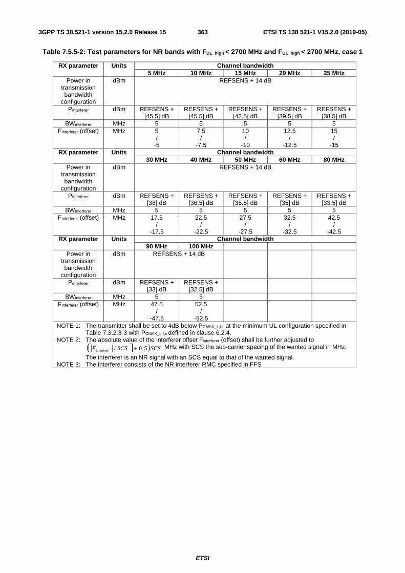
ETSI
ETSI TS 138 521-1 V15.2.0 (2019-05)3633GPP TS 38.521-1 version 15.2.0 Release 15
Table 7.5.5-2: Test parameters for NR bands with FDL_high < 2700 MHz and FUL_high < 2700 MHz, case 1
RX parameter Units Channel bandwidth 5 MHz 10 MHz 15 MHz 20 MHz 25 MHz
Power in transmission bandwidth
configuration
dBm REFSENS + 14 dB
Pinterferer dBm REFSENS + [45.5] dB
REFSENS + [45.5] dB
REFSENS + [42.5] dB
REFSENS + [39.5] dB
REFSENS + [38.5] dB
BWinterferer MHz 5 5 5 5 5 Finterferer (offset) MHz 5
/ -5
7.5 /
-7.5
10 /
-10
12.5 /
-12.5
15 /
-15 RX parameter Units Channel bandwidth
30 MHz 40 MHz 50 MHz 60 MHz 80 MHz Power in
transmission bandwidth
configuration
dBm REFSENS + 14 dB
Pinterferer dBm REFSENS + [38] dB
REFSENS + [36.5] dB
REFSENS + [35.5] dB
REFSENS + [35] dB
REFSENS + [33.5] dB
BWinterferer MHz 5 5 5 5 5 Finterferer (offset) MHz 17.5
/ -17.5
22.5 /
-22.5
27.5 /
-27.5
32.5 /
-32.5
42.5 /
-42.5 RX parameter Units Channel bandwidth
90 MHz 100 MHz Power in
transmission bandwidth
configuration
dBm REFSENS + 14 dB
Pinterferer dBm REFSENS + [33] dB
REFSENS + [32.5] dB
BWinterferer MHz 5 5 Finterferer (offset) MHz 47.5
/ -47.5
52.5 /
-52.5
NOTE 1: The transmitter shall be set to 4dB below PCMAX_L,f,c at the minimum UL configuration specified in Table 7.3.2.3-3 with PCMAX_L,f,c defined in clause 6.2.4.
NOTE 2: The absolute value of the interferer offset Finterferer (offset) shall be further adjusted to
( )SCSSCSF 5.0/interferer + MHz with SCS the sub-carrier spacing of the wanted signal in MHz.
The interferer is an NR signal with an SCS equal to that of the wanted signal. NOTE 3: The interferer consists of the NR interferer RMC specified in FFS
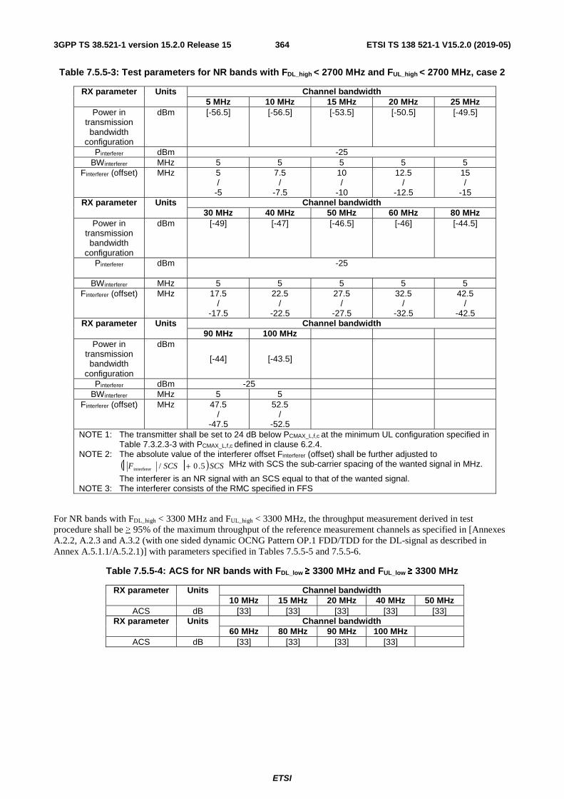
ETSI
ETSI TS 138 521-1 V15.2.0 (2019-05)3643GPP TS 38.521-1 version 15.2.0 Release 15
Table 7.5.5-3: Test parameters for NR bands with FDL_high < 2700 MHz and FUL_high < 2700 MHz, case 2
RX parameter Units Channel bandwidth 5 MHz 10 MHz 15 MHz 20 MHz 25 MHz
Power in transmission bandwidth
configuration
dBm [-56.5] [-56.5] [-53.5] [-50.5] [-49.5]
Pinterferer dBm -25 BWinterferer MHz 5 5 5 5 5
Finterferer (offset) MHz 5 /
-5
7.5 /
-7.5
10 /
-10
12.5 /
-12.5
15 /
-15 RX parameter Units Channel bandwidth
30 MHz 40 MHz 50 MHz 60 MHz 80 MHz Power in
transmission bandwidth
configuration
dBm [-49] [-47] [-46.5] [-46] [-44.5]
Pinterferer dBm -25
BWinterferer MHz 5 5 5 5 5 Finterferer (offset) MHz 17.5
/ -17.5
22.5 /
-22.5
27.5 /
-27.5
32.5 /
-32.5
42.5 /
-42.5 RX parameter Units Channel bandwidth
90 MHz 100 MHz Power in
transmission bandwidth
configuration
dBm
[-44] [-43.5]
Pinterferer dBm -25 BWinterferer MHz 5 5
Finterferer (offset) MHz 47.5 /
-47.5
52.5 /
-52.5
NOTE 1: The transmitter shall be set to 24 dB below PCMAX_L,f,c at the minimum UL configuration specified in Table 7.3.2.3-3 with PCMAX_L,f,c defined in clause 6.2.4.
NOTE 2: The absolute value of the interferer offset Finterferer (offset) shall be further adjusted to
( )SCSSCSF 5.0/interferer + MHz with SCS the sub-carrier spacing of the wanted signal in MHz.
The interferer is an NR signal with an SCS equal to that of the wanted signal. NOTE 3: The interferer consists of the RMC specified in FFS
For NR bands with FDL_high < 3300 MHz and FUL_high < 3300 MHz, the throughput measurement derived in test procedure shall be ≥ 95% of the maximum throughput of the reference measurement channels as specified in [Annexes A.2.2, A.2.3 and A.3.2 (with one sided dynamic OCNG Pattern OP.1 FDD/TDD for the DL-signal as described in Annex A.5.1.1/A.5.2.1)] with parameters specified in Tables 7.5.5-5 and 7.5.5-6.
Table 7.5.5-4: ACS for NR bands with FDL_low ≥ 3300 MHz and FUL_low ≥ 3300 MHz
RX parameter Units Channel bandwidth 10 MHz 15 MHz 20 MHz 40 MHz 50 MHz
ACS dB [33] [33] [33] [33] [33] RX parameter Units Channel bandwidth
60 MHz 80 MHz 90 MHz 100 MHz ACS dB [33] [33] [33] [33]

ETSI
ETSI TS 138 521-1 V15.2.0 (2019-05)3653GPP TS 38.521-1 version 15.2.0 Release 15
Table 7.5.5-5: Test parameters for NR bands with FDL_low ≥ 3300 MHz and FUL_low ≥ 3300 MHz, case 1
RX parameter Units Channel bandwidth 10 MHz 15 MHz 20 MHz 40 MHz 50 MHz
Power in transmission bandwidth
configuration
dBm REFSENS + 14 dB
Pinterferer dBm REFSENS + [45.5] dB BWinterferer MHz 10 15 20 40 50
Finterferer (offset) MHz 10 /
-10
15 /
-15
20 /
-20
40 /
-40
50 /
-50 RX parameter Units Channel bandwidth
60 MHz 80 MHz 90 MHz 100 MHz Power in
transmission bandwidth
configuration
dBm
REFSENS + 14 dB
Pinterferer dBm REFSENS + [45.5] dB
REFSENS + [45.5] dB
REFSENS + [45.5] dB
REFSENS + [45.5] dB
BWinterferer MHz 60 80 90 100 Finterferer (offset) MHz 60
/ -60
80 /
-80
90 /
-90
100 /
-100
NOTE 1: The transmitter shall be set to 4dB below PCMAX_L,f,c at the minimum UL configuration specified in Table 7.3.2.3-3 with PCMAX_L,f,c defined in clause 6.2.4. NOTE 2: The absolute value of the interferer offset Finterferer (offset) shall be further adjusted to
( )SCSSCSF 5.0/interferer + MHz with SCS the sub-carrier spacing of the wanted signal in MHz.
The interferer is an NR signal with an SCS equal to that of the wanted signal. NOTE 3: The interferer consists of the RMC specified in FFS
Table 7.5.5-6: Test parameters for NR bands with FDL_low ≥ 3300 MHz and FUL_low ≥ 3300 MHz, case 2
RX parameter Units Channel bandwidth 10 MHz 15 MHz 20 MHz 40 MHz 50 MHz
Power in transmission bandwidth
configuration
dBm
[-56.5]
Pinterferer dBm -25 BWinterferer MHz 10 15 20 40 50
Finterferer (offset) MHz 10 /
-10
15 /
-15
20 /
-20
40 /
-40
50 /
-50 RX parameter Units Channel bandwidth
60 MHz 80 MHz 90 MHz 100 MHz Power in
transmission bandwidth
configuration
dBm
[-56.5]
Pinterferer dBm -25 -25 -25 -25 BWinterferer MHz 60 80 90 100
Finterferer (offset) MHz 60 /
-60
80 /
-80
90 /
-90
100 /
-100
NOTE 1: The transmitter shall be set to 24 dB below PCMAX_L,f,c at the minimum UL configuration specified in Table 7.3.2.3-3 with PCMAX_L,f,c defined in clause 6.2.4. NOTE 2: The absolute value of the interferer offset Finterferer (offset) shall be further adjusted to
( )SCSSCSF 5.0/interferer + MHz with SCS the sub-carrier spacing of the wanted signal in MHz.
The interferer is an NR signal with an SCS equal to that of the wanted signal. NOTE 3: The interferer consists of the RMC specified in FFS

ETSI
ETSI TS 138 521-1 V15.2.0 (2019-05)3663GPP TS 38.521-1 version 15.2.0 Release 15
Table 7.5.5-7: Power Window (dB) for Adjacent channel selectivity
f ≤ 3GHz 3GHz < f ≤ 4.2GHz 4.2GHz < f ≤ 6GHz BW ≤ 20MHz 1.4 1.7 2 20MHz < BW ≤ 40MHz 1.4 1.7 2.2 40MHz < BW ≤ 100MHz 2.1 2.3 2.3 Note: Power Window setting comprises two quantities, UE Power tolerance and test
system power measurement
7.5A Adjacent channel selectivity for CA
7.5A.0 Minimum conformance requirements
7.5A.0.1 Adjacent channel selectivity for Intra-band contiguous CA
For intra-band contiguous carrier aggregation with two component carriers and aggregated bandwidth BWChannel_CA shall be configured at nominal channel spacing to the PCC. The UE shall fulfil the minimum requirement specified in Table 7.5A.0.1-1 for an adjacent channel interferer on either side of the aggregated downlink signal at a specified frequency offset and for an interferer power up to -25 dBm.
The throughput of each carrier shall be ≥ 95% of the maximum throughput of the reference measurement channels as specified in Annexes A.2.2, A.2.3, A.3.2 and A.3.3 (with one sided dynamic OCNG Pattern for the DL-signal as described in Annex A.5.1.1/A.5.2.1) with parameters specified in Tables 7.5A.0.1-2 and 7.5A.0.1-3.
Table 7.5A.0.1-1: ACS for intra-band contiguous CA with FDL_low ≥ 3300 MHz and FUL_low ≥ 3300 MHz
CA Bandwidth Class Rx
Parameter Units C D E
ACS dB 33.0 25.2 24.0
Table 7.5A.0.1-2: Test parameters for intra-band contiguous CA with FDL_low ≥ 3300 MHz and FUL_low ≥ 3300 MHz, case 1
Rx Parameter Units CA Bandwidth Class C D E
Pw in Transmission Bandwidth
Configuration, per CC
REFSENS + 14 dB REFSENS + 14 dB REFSENS + 14 dB
PInterferer dBm Aggregated power + 31.5 dB
Aggregated power + 23.7 dB
Aggregated power + 22.5 dB
BWInterferer MHz BWchannel CA 50 50 FInterferer (offset) MHz BWchannel CA
/ -BWchannel CA
25 + Foffset /
-25 -Foffset
25 + Foffset
/ -25 -Foffset
NOTE 1: The transmitter shall be set to 4 dB below PCMAX_L,f,c at the minimum UL configuration specified in Table 7.3.2.3-3 with PCMAX_L,f,c defined in clause 6.2.4.3 .
NOTE 2: The absolute value of the interferer offset Finterferer (offset) shall be further adjusted to
MHz with SCS the sub-carrier spacing of the wanted signal in MHz. The interferer is an NR signal with an SCS equal to that of the wanted signal.
NOTE 3: The interferer consists of the RMC specified in [FFS]
( )SCSSCSF 5.0/interferer +

ETSI
ETSI TS 138 521-1 V15.2.0 (2019-05)3673GPP TS 38.521-1 version 15.2.0 Release 15
Table 7.5A.0.1-3: Test parameters for intra-band contiguous CA with FDL_low ≥ 3300 MHz and FUL_low ≥ 3300 MHz, case 2
Rx Parameter Units CA Bandwidth Class C D E
Pw in Transmission Bandwidth
Configuration, per CC
REFSENS + 14 dB REFSENS + 14 dB REFSENS + 14 dB
PInterferer dBm Aggregated power + 31.5 dB
Aggregated power + 23.7 dB
Aggregated power + 22.5 dB
BWInterferer MHz BWchannel CA 50 50 FInterferer (offset) MHz BWchannel CA
/ -BWchannel CA
25 + Foffset /
-25 -Foffset
25 + Foffset /
-25 -Foffset NOTE 1: The transmitter shall be set to 4 dB below PCMAX_L,f,c at the minimum UL configuration specified in Table
7.3.2.3-3 with PCMAX_L,f,c defined in clause 6.2.4.3. NOTE 2: The absolute value of the interferer offset Finterferer (offset) shall be further adjusted to
MHz with SCS the sub-carrier spacing of the wanted signal in MHz. The interferer is an NR signal with an SCS equal to that of the wanted signal.
NOTE 3: The interferer consists of the RMC specified in [FFS]
7.5A.0.2 Adjacent channel selectivity Intra-band non-contiguous CA
Detailed structure of the subclause is TBD.
7.5A.0.3 Adjacent channel selectivity Inter-band CA
For inter-band carrier aggregation with one component carrier per operating band and the uplink assigned to one NR band, the adjacent channel requirements are defined with the uplink active on the band(s) other than the band whose downlink is being tested. The UE shall meet the requirements specified in subclause 7.5.3 for each component carrier while all downlink carriers are active.
The throughput of each carrier shall be ≥ 95% of the maximum throughput of the reference measurement channels as specified in A.2.2, A.2.3, A.3.2 and A.3.3 (with one sided dynamic OCNG Pattern for the DL-signal as described in Annex A.5.1.1/A.5.2.1).
7.5A.1 Adjacent channel selectivity for 2DL CA
Editor’s note: This clause is incomplete. The following aspects are either missing or not yet determined:
- Test config table is FFS
- Connection diagram is FFS
- Characteristics of the interfering signal is TBD.
- Statistical testing of receiver characteristics for CA is TBD
- MU/TT is still FFS
- ACS requirements in square brackets.
7.5A.1.1 Test Purpose
Adjacent channel selectivity for 2DL CA verifies the receiver's ability to receive a wanted 2DL carrier aggregated at its assigned channel frequency in the presence of an adjacent channel signal at a given frequency offset from the centre frequency of the assigned channel.
7.5A.1.2 Test Applicability
This test case applies to all types of NR UE release 15 and forward that support 2DL CA.
( )SCSSCSF 5.0/interferer +
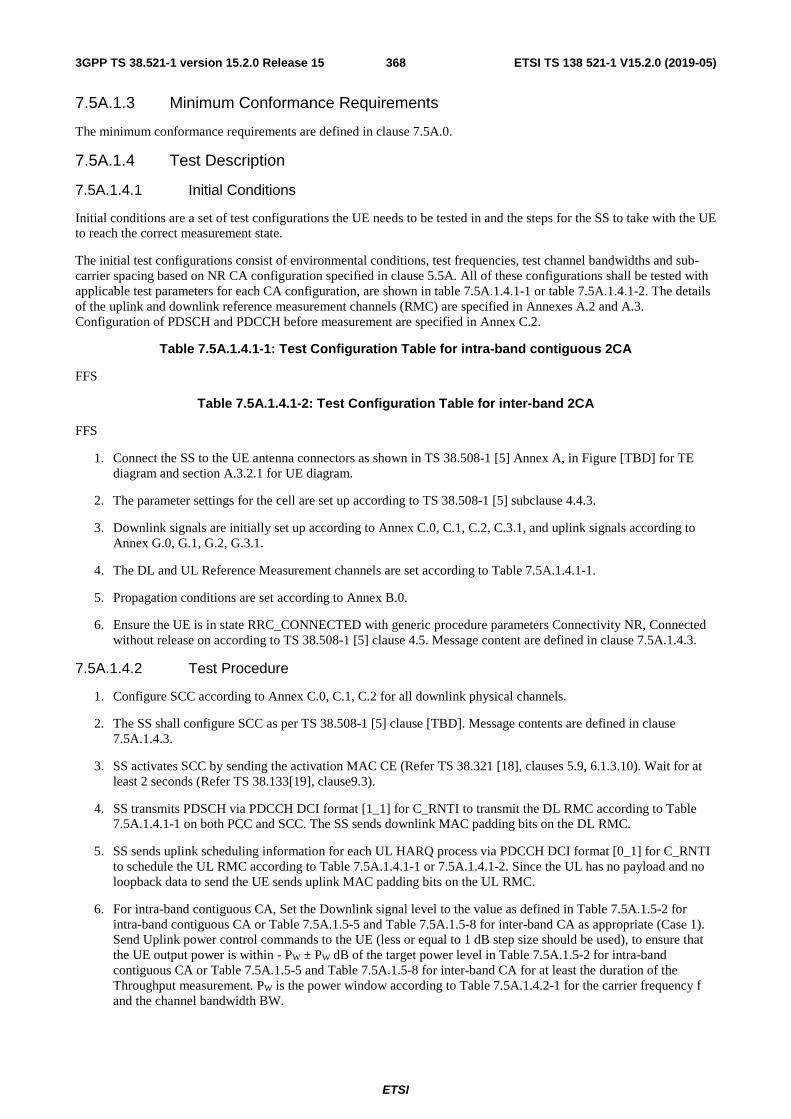
ETSI
ETSI TS 138 521-1 V15.2.0 (2019-05)3683GPP TS 38.521-1 version 15.2.0 Release 15
7.5A.1.3 Minimum Conformance Requirements
The minimum conformance requirements are defined in clause 7.5A.0.
7.5A.1.4 Test Description
7.5A.1.4.1 Initial Conditions
Initial conditions are a set of test configurations the UE needs to be tested in and the steps for the SS to take with the UE to reach the correct measurement state.
The initial test configurations consist of environmental conditions, test frequencies, test channel bandwidths and sub-carrier spacing based on NR CA configuration specified in clause 5.5A. All of these configurations shall be tested with applicable test parameters for each CA configuration, are shown in table 7.5A.1.4.1-1 or table 7.5A.1.4.1-2. The details of the uplink and downlink reference measurement channels (RMC) are specified in Annexes A.2 and A.3. Configuration of PDSCH and PDCCH before measurement are specified in Annex C.2.
Table 7.5A.1.4.1-1: Test Configuration Table for intra-band contiguous 2CA
FFS
Table 7.5A.1.4.1-2: Test Configuration Table for inter-band 2CA
FFS
1. Connect the SS to the UE antenna connectors as shown in TS 38.508-1 [5] Annex A, in Figure [TBD] for TE diagram and section A.3.2.1 for UE diagram.
2. The parameter settings for the cell are set up according to TS 38.508-1 [5] subclause 4.4.3.
3. Downlink signals are initially set up according to Annex C.0, C.1, C.2, C.3.1, and uplink signals according to Annex G.0, G.1, G.2, G.3.1.
4. The DL and UL Reference Measurement channels are set according to Table 7.5A.1.4.1-1.
5. Propagation conditions are set according to Annex B.0.
6. Ensure the UE is in state RRC_CONNECTED with generic procedure parameters Connectivity NR, Connected without release on according to TS 38.508-1 [5] clause 4.5. Message content are defined in clause 7.5A.1.4.3.
7.5A.1.4.2 Test Procedure
1. Configure SCC according to Annex C.0, C.1, C.2 for all downlink physical channels.
2. The SS shall configure SCC as per TS 38.508-1 [5] clause [TBD]. Message contents are defined in clause 7.5A.1.4.3.
3. SS activates SCC by sending the activation MAC CE (Refer TS 38.321 [18], clauses 5.9, 6.1.3.10). Wait for at least 2 seconds (Refer TS 38.133[19], clause9.3).
4. SS transmits PDSCH via PDCCH DCI format [1_1] for C_RNTI to transmit the DL RMC according to Table 7.5A.1.4.1-1 on both PCC and SCC. The SS sends downlink MAC padding bits on the DL RMC.
5. SS sends uplink scheduling information for each UL HARQ process via PDCCH DCI format [0_1] for C_RNTI to schedule the UL RMC according to Table 7.5A.1.4.1-1 or 7.5A.1.4.1-2. Since the UL has no payload and no loopback data to send the UE sends uplink MAC padding bits on the UL RMC.
6. For intra-band contiguous CA, Set the Downlink signal level to the value as defined in Table 7.5A.1.5-2 for intra-band contiguous CA or Table 7.5A.1.5-5 and Table 7.5A.1.5-8 for inter-band CA as appropriate (Case 1). Send Uplink power control commands to the UE (less or equal to 1 dB step size should be used), to ensure that the UE output power is within - PW ± PW dB of the target power level in Table 7.5A.1.5-2 for intra-band contiguous CA or Table 7.5A.1.5-5 and Table 7.5A.1.5-8 for inter-band CA for at least the duration of the Throughput measurement. PW is the power window according to Table 7.5A.1.4.2-1 for the carrier frequency f and the channel bandwidth BW.

ETSI
ETSI TS 138 521-1 V15.2.0 (2019-05)3693GPP TS 38.521-1 version 15.2.0 Release 15
7. Set the Interferer signal level to the value as defined in Table 7.5A.1.5-2 for intra-band contiguous CA or Table 7.5A.1.5-5 and Table 7.5A.1.5-8 for inter-band CA as appropriate (Case 1) and frequency below the wanted signal, using a modulated interferer bandwidth as defined in Annex [TBD].
8. Measure the average throughput for each component carrier for a duration sufficient to achieve statistical significance according to Annex [TBD].
9. Repeat steps from 6 to 8, using an interfering signal above the wanted signal in Case 1 at step 7.
10. Set the Downlink signal level to the value as defined in Table 7.5A.1.5-3 for intra-band contiguous CA or Table 7.5A.1.5-6 and Table 7.5A.1.5-9 for inter-band CA as appropriate (Case 2). Send Uplink power control commands to the UE (less or equal to 1 dB step size should be used), to ensure that the PCC and SCC output power is within - PW ± PW dB of the target power level in Table 7.5A.1.5-3 for intra-band contiguous CA or Table 7.5A.1.5-6 and Table 7.5A.1.5-9 for inter-band CA for at least the duration of the Throughput measurement. PW is the power window according to Table 7.5A.1.4.2-1 for the carrier frequency f and the channel bandwidth BW.
11. Set the Interferer signal level to the value as defined in Table 7.5A.1.5-3 for intra-band contiguous CA or Table 7.5A.1.5-6 and Table 7.5A.1.5-9 for inter-band CA as appropriate (Case 2) and frequency below the wanted signal, using a modulated interferer bandwidth as defined in Annex [TBD].
12. Measure the average throughput for each component carrier for a duration sufficient to achieve statistical significance according to Annex [TBD].
13. Repeat steps from 10 to 12, using an interfering signal above the wanted signal in Case 2 at step 11.
14. Repeat for applicable channel bandwidths and operating band combinations in both Case 1 and Case 2.
Table 7.5A.1.4.2-1: Power Window (dB) for Adjacent channel selectivity
f ≤ 3GHz 3GHz < f ≤ 4.2GHz 4.2GHz < f ≤ 6GHz BW ≤ 20MHz 1.4 1.7 2 20MHz < BW ≤ 40MHz 1.4 1.7 2.2 40MHz < BW ≤ 100MHz 2.1 2.3 2.3 Note: Power Window setting comprises two quantities, UE Power tolerance and test
system power measurement
7.5A.1.4.3 Message Contents
Message contents are according to TS 38.508-1 [5] subclause 4.6 with DFT-s-OFDM condition in Table 4.6.3-118 PUSCH-Config.
7.5A.1.5 Test Requirement
The throughput of each carrier shall be ≥ 95% of the maximum throughput of the reference measurement channels as specified in Annexes A.2.2, A.2.3, A.3.2 and A.3.3 (with one sided dynamic OCNG Pattern for the DL-signal as described in Annex A.5.1.1/A.5.2.1) with parameters specified in Tables 7.5A.1.5-2 and 7.5A.1.5-3.
Table 7.5A.1.5-1: ACS for intra-band contiguous 2CA with FDL_low ≥ 3300 MHz and FUL_low ≥ 3300 MHz
CA Bandwidth Class Rx
Parameter Units C D E
ACS dB 33.0

ETSI
ETSI TS 138 521-1 V15.2.0 (2019-05)3703GPP TS 38.521-1 version 15.2.0 Release 15
Table 7.5A.1.5-2: Test parameters for intra-band contiguous 2CA with FDL_low ≥ 3300 MHz and FUL_low ≥ 3300 MHz, case 1
Rx Parameter Units CA Bandwidth Class C D E
Pw in Transmission Bandwidth
Configuration, per CC
REFSENS + 14 dB
PInterferer dBm Aggregated power + 31.5 dB
BWInterferer MHz BWchannel CA FInterferer (offset) MHz BWchannel CA
/ -BWchannel CA
NOTE 1: The transmitter shall be set to 4 dB below PCMAX_L,f,c at the minimum UL configuration specified in Table 7.3.2.3-3 with PCMAX_L,f,c defined in clause 6.2.4.3 .
NOTE 2: The absolute value of the interferer offset Finterferer (offset) shall be further adjusted to ( )SCSSCSF 5.0/interferer + MHz with SCS the sub-carrier spacing of the wanted signal in MHz. The
interferer is an NR signal with an SCS equal to that of the wanted signal. NOTE 3: The interferer consists of the RMC specified in [FFS]
Table 7.5A.1.5-3: Test parameters for intra-band contiguous 2CA with FDL_low ≥ 3300 MHz and FUL_low ≥ 3300 MHz, case 2
Rx Parameter Units CA Bandwidth Class C D E
Pw in Transmission Bandwidth
Configuration, per CC
REFSENS + 14 dB
PInterferer dBm Aggregated power + 31.5 dB
BWInterferer MHz BWchannel CA FInterferer (offset) MHz BWchannel CA
/ -BWchannel CA
NOTE 1: The transmitter shall be set to 4 dB below PCMAX_L,f,c at the minimum UL configuration specified in Table 7.3.2.3-3 with PCMAX_L,f,c defined in clause 6.2.4.3.
NOTE 2: The absolute value of the interferer offset Finterferer (offset) shall be further adjusted to ( )SCSSCSF 5.0/interferer + MHz with SCS the sub-carrier spacing of the wanted signal in MHz. The
interferer is an NR signal with an SCS equal to that of the wanted signal. NOTE 3: The interferer consists of the RMC specified in [FFS]
For NR SCC of inter-band CA with FDL_high < 2700 MHz and FUL_high < 2700 MHz, the throughput measurement derived in test procedure shall be ≥ 95% of the maximum throughput of the reference measurement channels as specified in [Annexes A.2.2, A.2.3 and A.3.2 (with one sided dynamic OCNG Pattern OP.1 FDD/TDD for the DL-signal as described in Annex A.5.1.1/A.5.2.1)] with parameters specified in Tables 7.5A.1.5-5 and 7.5A.1.5-6.
Table 7.5A.1.5-4: ACS for NR band with FDL_high < 2700 MHz and FUL_high < 2700 MHz
RX parameter Units Channel bandwidth 5 MHz 10 MHz 15 MHz 20 MHz 25 MHz
ACS dB [33] [33] [30] [27] [26] RX parameter Units Channel bandwidth
30 MHz 40 MHz 50 MHz 60 MHz 80 MHz ACS dB [25.5] [24] [23] [22.5] [21]
RX parameter Units Channel bandwidth 90 MHz 100 MHz
ACS dB [20.5] [20]
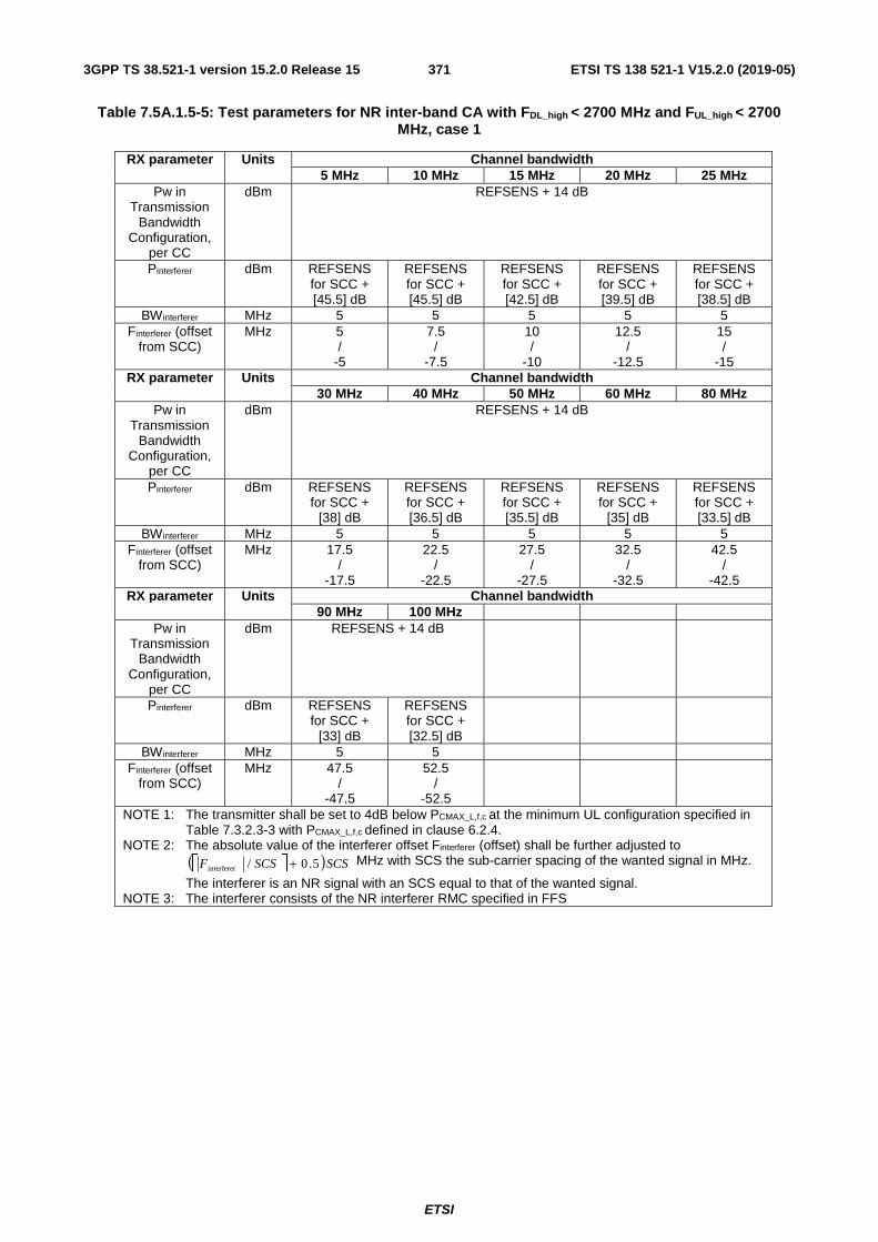
ETSI
ETSI TS 138 521-1 V15.2.0 (2019-05)3713GPP TS 38.521-1 version 15.2.0 Release 15
Table 7.5A.1.5-5: Test parameters for NR inter-band CA with FDL_high < 2700 MHz and FUL_high < 2700 MHz, case 1
RX parameter Units Channel bandwidth 5 MHz 10 MHz 15 MHz 20 MHz 25 MHz
Pw in Transmission
Bandwidth Configuration,
per CC
dBm REFSENS + 14 dB
Pinterferer dBm REFSENS for SCC + [45.5] dB
REFSENS for SCC + [45.5] dB
REFSENS for SCC + [42.5] dB
REFSENS for SCC + [39.5] dB
REFSENS for SCC + [38.5] dB
BWinterferer MHz 5 5 5 5 5 Finterferer (offset
from SCC) MHz 5
/ -5
7.5 /
-7.5
10 /
-10
12.5 /
-12.5
15 /
-15 RX parameter Units Channel bandwidth
30 MHz 40 MHz 50 MHz 60 MHz 80 MHz Pw in
Transmission Bandwidth
Configuration, per CC
dBm REFSENS + 14 dB
Pinterferer dBm REFSENS for SCC +
[38] dB
REFSENS for SCC + [36.5] dB
REFSENS for SCC + [35.5] dB
REFSENS for SCC +
[35] dB
REFSENS for SCC + [33.5] dB
BWinterferer MHz 5 5 5 5 5 Finterferer (offset
from SCC) MHz 17.5
/ -17.5
22.5 /
-22.5
27.5 /
-27.5
32.5 /
-32.5
42.5 /
-42.5 RX parameter Units Channel bandwidth
90 MHz 100 MHz Pw in
Transmission Bandwidth
Configuration, per CC
dBm REFSENS + 14 dB
Pinterferer dBm REFSENS for SCC +
[33] dB
REFSENS for SCC + [32.5] dB
BWinterferer MHz 5 5 Finterferer (offset
from SCC) MHz 47.5
/ -47.5
52.5 /
-52.5
NOTE 1: The transmitter shall be set to 4dB below PCMAX_L,f,c at the minimum UL configuration specified in Table 7.3.2.3-3 with PCMAX_L,f,c defined in clause 6.2.4.
NOTE 2: The absolute value of the interferer offset Finterferer (offset) shall be further adjusted to
( )SCSSCSF 5.0/interferer + MHz with SCS the sub-carrier spacing of the wanted signal in MHz.
The interferer is an NR signal with an SCS equal to that of the wanted signal. NOTE 3: The interferer consists of the NR interferer RMC specified in FFS
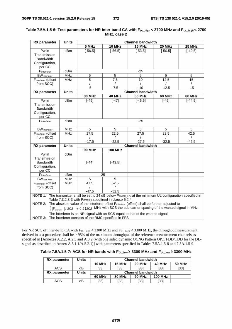
ETSI
ETSI TS 138 521-1 V15.2.0 (2019-05)3723GPP TS 38.521-1 version 15.2.0 Release 15
Table 7.5A.1.5-6: Test parameters for NR inter-band CA with FDL_high < 2700 MHz and FUL_high < 2700 MHz, case 2
RX parameter Units Channel bandwidth 5 MHz 10 MHz 15 MHz 20 MHz 25 MHz
Pw in Transmission
Bandwidth Configuration,
per CC
dBm [-56.5] [-56.5] [-53.5] [-50.5] [-49.5]
Pinterferer dBm -25 BWinterferer MHz 5 5 5 5 5
Finterferer (offset from SCC)
MHz 5 /
-5
7.5 /
-7.5
10 /
-10
12.5 /
-12.5
15 /
-15 RX parameter Units Channel bandwidth
30 MHz 40 MHz 50 MHz 60 MHz 80 MHz Pw in
Transmission Bandwidth
Configuration, per CC
dBm [-49] [-47] [-46.5] [-46] [-44.5]
Pinterferer dBm -25
BWinterferer MHz 5 5 5 5 5 Finterferer (offset
from SCC) MHz 17.5
/ -17.5
22.5 /
-22.5
27.5 /
-27.5
32.5 /
-32.5
42.5 /
-42.5 RX parameter Units Channel bandwidth
90 MHz 100 MHz Pw in
Transmission Bandwidth
Configuration, per CC
dBm
[-44] [-43.5]
Pinterferer dBm -25 BWinterferer MHz 5 5
Finterferer (offset from SCC)
MHz 47.5 /
-47.5
52.5 /
-52.5
NOTE 1: The transmitter shall be set to 24 dB below PCMAX_L,f,c at the minimum UL configuration specified in Table 7.3.2.3-3 with PCMAX_L,f,c defined in clause 6.2.4.
NOTE 2: The absolute value of the interferer offset Finterferer (offset) shall be further adjusted to
( )SCSSCSF 5.0/interferer + MHz with SCS the sub-carrier spacing of the wanted signal in MHz.
The interferer is an NR signal with an SCS equal to that of the wanted signal. NOTE 3: The interferer consists of the RMC specified in FFS
For NR SCC of inter-band CA with FDL_high < 3300 MHz and FUL_high < 3300 MHz, the throughput measurement derived in test procedure shall be ≥ 95% of the maximum throughput of the reference measurement channels as specified in [Annexes A.2.2, A.2.3 and A.3.2 (with one sided dynamic OCNG Pattern OP.1 FDD/TDD for the DL-signal as described in Annex A.5.1.1/A.5.2.1)] with parameters specified in Tables 7.5A.1.5-8 and 7.5A.1.5-9.
Table 7.5A.1.5-7: ACS for NR bands with FDL_low ≥ 3300 MHz and FUL_low ≥ 3300 MHz
RX parameter Units Channel bandwidth 10 MHz 15 MHz 20 MHz 40 MHz 50 MHz
ACS dB [33] [33] [33] [33] [33] RX parameter Units Channel bandwidth
60 MHz 80 MHz 90 MHz 100 MHz ACS dB [33] [33] [33] [33]
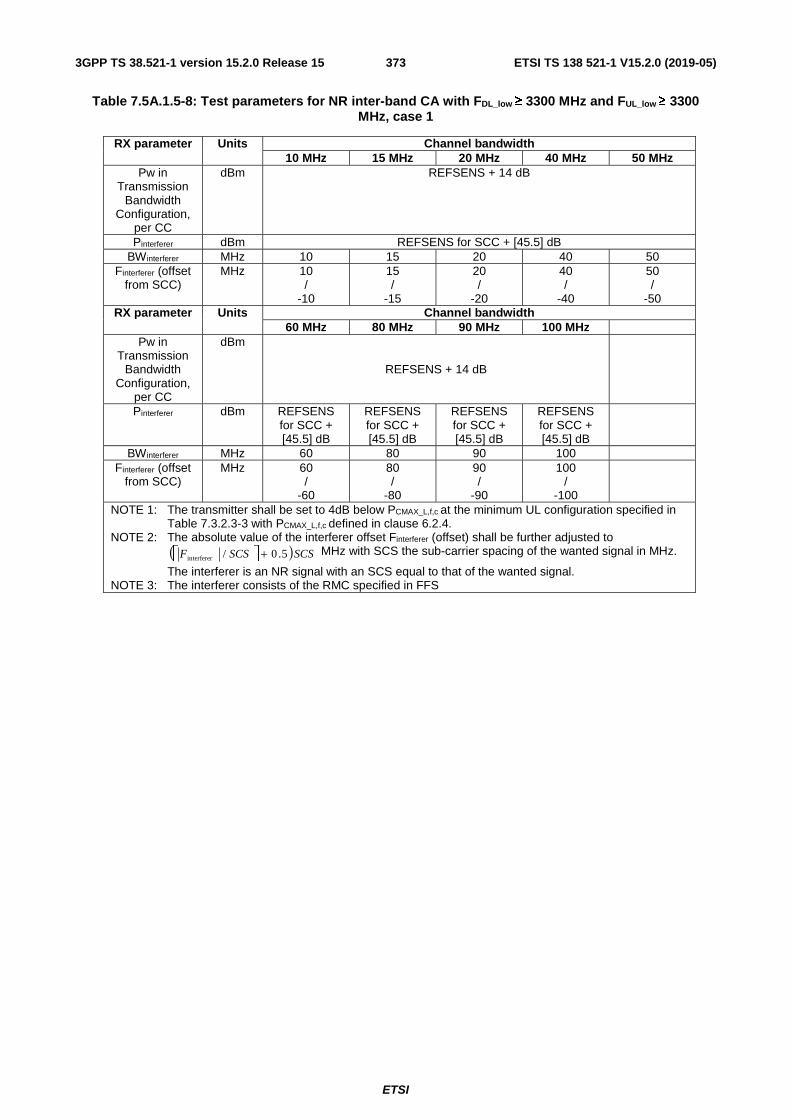
ETSI
ETSI TS 138 521-1 V15.2.0 (2019-05)3733GPP TS 38.521-1 version 15.2.0 Release 15
Table 7.5A.1.5-8: Test parameters for NR inter-band CA with FDL_low ≥ 3300 MHz and FUL_low ≥ 3300 MHz, case 1
RX parameter Units Channel bandwidth 10 MHz 15 MHz 20 MHz 40 MHz 50 MHz
Pw in Transmission
Bandwidth Configuration,
per CC
dBm REFSENS + 14 dB
Pinterferer dBm REFSENS for SCC + [45.5] dB BWinterferer MHz 10 15 20 40 50
Finterferer (offset from SCC)
MHz 10 /
-10
15 /
-15
20 /
-20
40 /
-40
50 /
-50 RX parameter Units Channel bandwidth
60 MHz 80 MHz 90 MHz 100 MHz Pw in
Transmission Bandwidth
Configuration, per CC
dBm
REFSENS + 14 dB
Pinterferer dBm REFSENS for SCC + [45.5] dB
REFSENS for SCC + [45.5] dB
REFSENS for SCC + [45.5] dB
REFSENS for SCC + [45.5] dB
BWinterferer MHz 60 80 90 100 Finterferer (offset
from SCC) MHz 60
/ -60
80 /
-80
90 /
-90
100 /
-100
NOTE 1: The transmitter shall be set to 4dB below PCMAX_L,f,c at the minimum UL configuration specified in Table 7.3.2.3-3 with PCMAX_L,f,c defined in clause 6.2.4.
NOTE 2: The absolute value of the interferer offset Finterferer (offset) shall be further adjusted to
( )SCSSCSF 5.0/interferer + MHz with SCS the sub-carrier spacing of the wanted signal in MHz.
The interferer is an NR signal with an SCS equal to that of the wanted signal. NOTE 3: The interferer consists of the RMC specified in FFS

ETSI
ETSI TS 138 521-1 V15.2.0 (2019-05)3743GPP TS 38.521-1 version 15.2.0 Release 15
Table 7.5A.1.5-9: Test parameters for NR inter-band CA with FDL_low ≥ 3300 MHz and FUL_low ≥ 3300 MHz, case 2
RX parameter Units Channel bandwidth 10 MHz 15 MHz 20 MHz 40 MHz 50 MHz
Pw in Transmission
Bandwidth Configuration,
per CC
dBm
[-56.5]
Pinterferer dBm -25 BWinterferer MHz 10 15 20 40 50
Finterferer (offset from SCC)
MHz 10 /
-10
15 /
-15
20 /
-20
40 /
-40
50 /
-50 RX parameter Units Channel bandwidth
60 MHz 80 MHz 90 MHz 100 MHz Pw in
Transmission Bandwidth
Configuration, per CC
dBm
[-56.5]
Pinterferer dBm -25 -25 -25 -25 BWinterferer MHz 60 80 90 100
Finterferer (offset from SCC)
MHz 60 /
-60
80 /
-80
90 /
-90
100 /
-100
NOTE 1: The transmitter shall be set to 24 dB below PCMAX_L,f,c at the minimum UL configuration specified in Table 7.3.2.3-3 with PCMAX_L,f,c defined in clause 6.2.4.
NOTE 2: The absolute value of the interferer offset Finterferer (offset) shall be further adjusted to
( )SCSSCSF 5.0/interferer + MHz with SCS the sub-carrier spacing of the wanted signal in MHz.
The interferer is an NR signal with an SCS equal to that of the wanted signal. NOTE 3: The interferer consists of the RMC specified in FFS
7.5A.2 Adjacent channel selectivity for 3DL CA
Editor’s note: This clause is incomplete. The following aspects are either missing or not yet determined:
- Test config table is FFS
- Connection diagram is FFS
- Characteristics of the interfering signal is TBD.
- Statistical testing of receiver characteristics for CA is TBD
- MU/TT is still FFS
7.5A.2.1 Test Purpose
Adjacent channel selectivity for 3DL CA verifies the receiver's ability to receive a wanted 3DL carrier aggregated at its assigned channel frequency in the presence of an adjacent channel signal at a given frequency offset from the centre frequency of the assigned channel.
7.5A.2.2 Test Applicability
This test case applies to all types of NR UE release 15 and forward that support 3DL CA.
7.5A.2.3 Minimum Conformance Requirements
The minimum conformance requirements are defined in clause 7.5A.0.
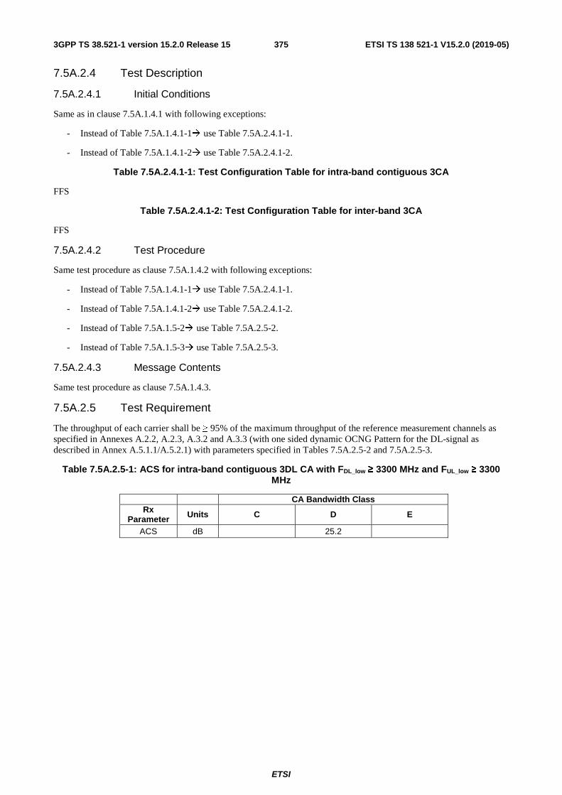
ETSI
ETSI TS 138 521-1 V15.2.0 (2019-05)3753GPP TS 38.521-1 version 15.2.0 Release 15
7.5A.2.4 Test Description
7.5A.2.4.1 Initial Conditions
Same as in clause 7.5A.1.4.1 with following exceptions:
- Instead of Table 7.5A.1.4.1-1 use Table 7.5A.2.4.1-1.
- Instead of Table 7.5A.1.4.1-2 use Table 7.5A.2.4.1-2.
Table 7.5A.2.4.1-1: Test Configuration Table for intra-band contiguous 3CA
FFS
Table 7.5A.2.4.1-2: Test Configuration Table for inter-band 3CA
FFS
7.5A.2.4.2 Test Procedure
Same test procedure as clause 7.5A.1.4.2 with following exceptions:
- Instead of Table 7.5A.1.4.1-1 use Table 7.5A.2.4.1-1.
- Instead of Table 7.5A.1.4.1-2 use Table 7.5A.2.4.1-2.
- Instead of Table 7.5A.1.5-2 use Table 7.5A.2.5-2.
- Instead of Table 7.5A.1.5-3 use Table 7.5A.2.5-3.
7.5A.2.4.3 Message Contents
Same test procedure as clause 7.5A.1.4.3.
7.5A.2.5 Test Requirement
The throughput of each carrier shall be ≥ 95% of the maximum throughput of the reference measurement channels as specified in Annexes A.2.2, A.2.3, A.3.2 and A.3.3 (with one sided dynamic OCNG Pattern for the DL-signal as described in Annex A.5.1.1/A.5.2.1) with parameters specified in Tables 7.5A.2.5-2 and 7.5A.2.5-3.
Table 7.5A.2.5-1: ACS for intra-band contiguous 3DL CA with FDL_low ≥ 3300 MHz and FUL_low ≥ 3300 MHz
CA Bandwidth Class Rx
Parameter Units C D E
ACS dB 25.2

ETSI
ETSI TS 138 521-1 V15.2.0 (2019-05)3763GPP TS 38.521-1 version 15.2.0 Release 15
Table 7.5A.2.5-2: Test parameters for intra-band contiguous 3DL CA with FDL_low ≥ 3300 MHz and FUL_low ≥ 3300 MHz, case 1
Rx Parameter Units CA Bandwidth Class C D E
Pw in Transmission Bandwidth
Configuration, per CC
REFSENS + 14 dB
PInterferer dBm Aggregated power + 23.7 dB
BWInterferer MHz 50 FInterferer (offset) MHz
25 + Foffset
/ -25 -Foffset
NOTE 1: The transmitter shall be set to 4 dB below PCMAX_L,f,c at the minimum UL configuration specified in Table 7.3.2.3-3 with PCMAX_L,f,c defined in clause 6.2.4.3 .
NOTE 2: The absolute value of the interferer offset Finterferer (offset) shall be further adjusted to ( )SCSSCSF 5.0/interferer + MHz with SCS the sub-carrier spacing of the wanted signal in MHz. The
interferer is an NR signal with an SCS equal to that of the wanted signal. NOTE 3: The interferer consists of the RMC specified in [FFS]
Table 7.5A.2.5-3: Test parameters for intra-band contiguous 3DL CA with FDL_low ≥ 3300 MHz and FUL_low ≥ 3300 MHz, case 2
Rx Parameter Units CA Bandwidth Class C D E
Pw in Transmission Bandwidth
Configuration, per CC
REFSENS + 14 dB
PInterferer dBm Aggregated power + 23.7 dB
BWInterferer MHz 50 FInterferer (offset) MHz
25 + Foffset
/ -25 -Foffset
NOTE 1: The transmitter shall be set to 4 dB below PCMAX_L,f,c at the minimum UL configuration specified in Table 7.3.2.3-3 with PCMAX_L,f,c defined in clause 6.2.4.3.
NOTE 2: The absolute value of the interferer offset Finterferer (offset) shall be further adjusted to ( )SCSSCSF 5.0/interferer + MHz with SCS the sub-carrier spacing of the wanted signal in MHz. The
interferer is an NR signal with an SCS equal to that of the wanted signal. NOTE 3: The interferer consists of the RMC specified in [FFS]
7.5A.3 Adjacent channel selectivity for 4DL CA
Editor’s note: This clause is incomplete. The following aspects are either missing or not yet determined:
- Test config table is FFS
- Connection diagram is FFS
- Characteristics of the interfering signal is TBD.
- Statistical testing of receiver characteristics for CA is TBD
- MU/TT is still FFS
7.5A.3.1 Test Purpose
Adjacent channel selectivity for 4DL CA verifies the receiver's ability to receive a wanted 4DL carrier aggregated at its assigned channel frequency in the presence of an adjacent channel signal at a given frequency offset from the centre frequency of the assigned channel.

ETSI
ETSI TS 138 521-1 V15.2.0 (2019-05)3773GPP TS 38.521-1 version 15.2.0 Release 15
7.5A.3.2 Test Applicability
This test case applies to all types of NR UE release 15 and forward that support 4DL CA.
7.5A.3.3 Minimum Conformance Requirements
The minimum conformance requirements are defined in clause 7.5A.0.
7.5A.3.4 Test Description
7.5A.3.4.1 Initial Conditions
Same as in clause 7.5A.1.4.1 with following exceptions:
- Instead of Table 7.5A.1.4.1-1 use Table 7.5A.3.4.1-1.
- Instead of Table 7.5A.1.4.1-2 use Table 7.5A.3.4.1-2.
Table 7.5A.3.4.1-1: Test Configuration Table for intra-band contiguous 4CA
FFS
Table 7.5A.3.4.1-2: Test Configuration Table for inter-band 4CA
FFS
7.5A.3.4.2 Test Procedure
Same test procedure as clause 7.5A.1.4.2 with following exceptions:
- Instead of Table 7.5A.1.4.1-1 use Table 7.5A.3.4.1-1.
- Instead of Table 7.5A.1.4.1-2 use Table 7.5A.3.4.1-2.
- Instead of Table 7.5A.1.5-2 use Table 7.5A.3.5-2.
- Instead of Table 7.5A.1.5-3 use Table 7.5A.3.5-3.
7.5A.3.4.3 Message Contents
Same test procedure as clause 7.5A.1.4.3.
7.5A.3.5 Test Requirement
The throughput of each carrier shall be ≥ 95% of the maximum throughput of the reference measurement channels as specified in Annexes A.2.2, A.2.3, A.3.2 and A.3.3 (with one sided dynamic OCNG Pattern for the DL-signal as described in Annex A.5.1.1/A.5.2.1) with parameters specified in Tables 7.5A.3.5-2 and 7.5A.3.5-3.
Table 7.5A.3.5-1: ACS for intra-band contiguous 4DL CA with FDL_low ≥ 3300 MHz and FUL_low ≥ 3300 MHz
CA Bandwidth Class Rx
Parameter Units C D E
ACS dB 24.0
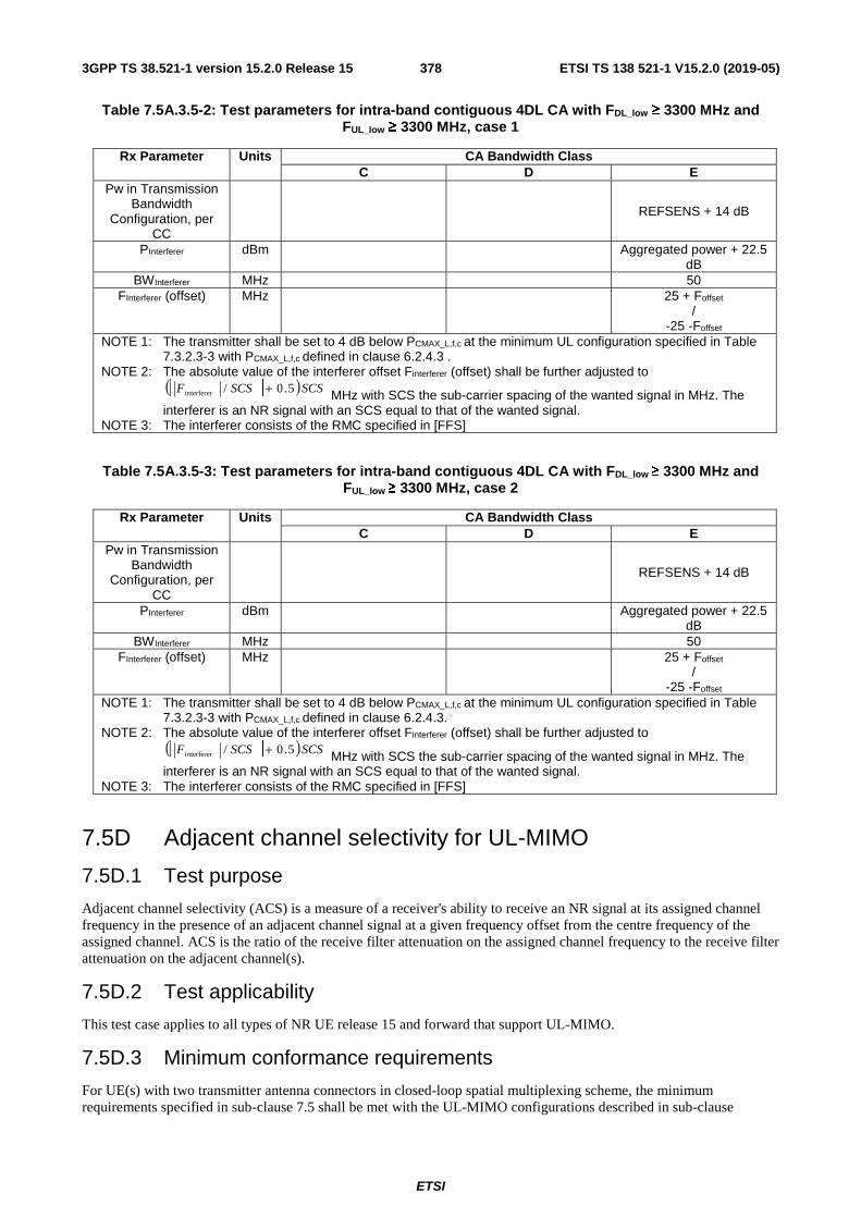
ETSI
ETSI TS 138 521-1 V15.2.0 (2019-05)3783GPP TS 38.521-1 version 15.2.0 Release 15
Table 7.5A.3.5-2: Test parameters for intra-band contiguous 4DL CA with FDL_low ≥ 3300 MHz and FUL_low ≥ 3300 MHz, case 1
Rx Parameter Units CA Bandwidth Class C D E
Pw in Transmission Bandwidth
Configuration, per CC
REFSENS + 14 dB
PInterferer dBm Aggregated power + 22.5 dB
BWInterferer MHz 50 FInterferer (offset) MHz
25 + Foffset
/ -25 -Foffset
NOTE 1: The transmitter shall be set to 4 dB below PCMAX_L,f,c at the minimum UL configuration specified in Table 7.3.2.3-3 with PCMAX_L,f,c defined in clause 6.2.4.3 .
NOTE 2: The absolute value of the interferer offset Finterferer (offset) shall be further adjusted to ( )SCSSCSF 5.0/interferer + MHz with SCS the sub-carrier spacing of the wanted signal in MHz. The
interferer is an NR signal with an SCS equal to that of the wanted signal. NOTE 3: The interferer consists of the RMC specified in [FFS]
Table 7.5A.3.5-3: Test parameters for intra-band contiguous 4DL CA with FDL_low ≥ 3300 MHz and FUL_low ≥ 3300 MHz, case 2
Rx Parameter Units CA Bandwidth Class C D E
Pw in Transmission Bandwidth
Configuration, per CC
REFSENS + 14 dB
PInterferer dBm Aggregated power + 22.5 dB
BWInterferer MHz 50 FInterferer (offset) MHz
25 + Foffset
/ -25 -Foffset
NOTE 1: The transmitter shall be set to 4 dB below PCMAX_L,f,c at the minimum UL configuration specified in Table 7.3.2.3-3 with PCMAX_L,f,c defined in clause 6.2.4.3.
NOTE 2: The absolute value of the interferer offset Finterferer (offset) shall be further adjusted to ( )SCSSCSF 5.0/interferer + MHz with SCS the sub-carrier spacing of the wanted signal in MHz. The
interferer is an NR signal with an SCS equal to that of the wanted signal. NOTE 3: The interferer consists of the RMC specified in [FFS]
7.5D Adjacent channel selectivity for UL-MIMO
7.5D.1 Test purpose
Adjacent channel selectivity (ACS) is a measure of a receiver's ability to receive an NR signal at its assigned channel frequency in the presence of an adjacent channel signal at a given frequency offset from the centre frequency of the assigned channel. ACS is the ratio of the receive filter attenuation on the assigned channel frequency to the receive filter attenuation on the adjacent channel(s).
7.5D.2 Test applicability
This test case applies to all types of NR UE release 15 and forward that support UL-MIMO.
7.5D.3 Minimum conformance requirements
For UE(s) with two transmitter antenna connectors in closed-loop spatial multiplexing scheme, the minimum requirements specified in sub-clause 7.5 shall be met with the UL-MIMO configurations described in sub-clause
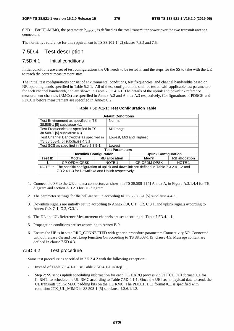
ETSI
ETSI TS 138 521-1 V15.2.0 (2019-05)3793GPP TS 38.521-1 version 15.2.0 Release 15
6.2D.1. For UL-MIMO, the parameter PCMAX_L is defined as the total transmitter power over the two transmit antenna connectors.
The normative reference for this requirement is TS 38.101-1 [2] clauses 7.5D and 7.5.
7.5D.4 Test description
7.5D.4.1 Initial conditions
Initial conditions are a set of test configurations the UE needs to be tested in and the steps for the SS to take with the UE to reach the correct measurement state.
The initial test configurations consist of environmental conditions, test frequencies, and channel bandwidths based on NR operating bands specified in Table 5.2-1. All of these configurations shall be tested with applicable test parameters for each channel bandwidth, and are shown in Table 7.5D.4.1-1. The details of the uplink and downlink reference measurement channels (RMCs) are specified in Annex A.2 and Annex A.3 respectively. Configurations of PDSCH and PDCCH before measurement are specified in Annex C.2.
Table 7.5D.4.1-1: Test Configuration Table
Default Conditions Test Environment as specified in TS 38.508-1 [5] subclause 4.1
Normal
Test Frequencies as specified in TS 38.508-1 [5] subclause 4.3.1
Mid range
Test Channel Bandwidths as specified in TS 38.508-1 [5] subclause 4.3.1
Lowest, Mid and Highest
Test SCS as specified in Table 5.3.5-1 Lowest Test Parameters
Downlink Configuration Uplink Configuration Test ID Mod'n RB allocation Mod'n RB allocation
1 CP-OFDM QPSK NOTE 1 CP-OFDM QPSK NOTE 1 NOTE 1: The specific configuration of uplink and downlink are defined in Table 7.3.2.4.1-2 and
7.3.2.4.1-3 for Downlinkd and Uplink respectively.
1. Connect the SS to the UE antenna connectors as shown in TS 38.508-1 [5] Annex A, in Figure A.3.1.4.4 for TE diagram and section A.3.2.3 for UE diagram.
2. The parameter settings for the cell are set up according to TS 38.508-1 [5] subclause 4.4.3.
3. Downlink signals are initially set up according to Annex C.0, C.1, C.2, C.3.1, and uplink signals according to Annex G.0, G.1, G.2, G.3.1.
4. The DL and UL Reference Measurement channels are set according to Table 7.5D.4.1-1.
5. Propagation conditions are set according to Annex B.0.
6. Ensure the UE is in state RRC_CONNECTED with generic procedure parameters Connectivity NR, Connected without release On and Test Loop Function On according to TS 38.508-1 [5] clause 4.5. Message content are defined in clause 7.5D.4.3.
7.5D.4.2 Test procedure
Same test procedure as specified in 7.5.2.4.2 with the following exception:
- Instead of Table 7.5.4.1-1, use Table 7.5D.4.1-1 in step 1.
- Step 2: SS sends uplink scheduling information for each UL HARQ process via PDCCH DCI format 0_1 for C_RNTI to schedule the UL RMC according to Table 7.5D.4.1-1. Since the UE has no payload data to send, the UE transmits uplink MAC padding bits on the UL RMC. The PDCCH DCI format 0_1 is specified with condition 2TX_UL_MIMO in 38.508-1 [5] subclause 4.3.6.1.1.2.

ETSI
ETSI TS 138 521-1 V15.2.0 (2019-05)3803GPP TS 38.521-1 version 15.2.0 Release 15
7.5D.4.3 Message contents
Message contents are according to TS 38.508-1 [5] subclause 4.6 ensuring Table 4.6.3-182 with condition 2TX_UL_MIMO
7.5D.5 Test requirement
Same test requirement as defined in Clause 7.5.5.
7.6 Blocking characteristics The blocking characteristic is a measure of the receiver’s ability to receive a wanted signal at its assigned channel frequency in the presence of an unwanted interferer on frequencies other than those of the spurious response or the adjacent channels, without this unwanted input signal causing a degradation of the performance of the receiver beyond a specified limit. The blocking performance shall apply at all frequencies except those at which a spurious response occurs.
7.6.1 General
FFS
7.6.2 Inband Blocking
Editor’s note: This clause is incomplete. The following aspects are either missing or not yet determined:
- Annex D: Characteristics of the interfering signal is TBD.
7.6.2.1 Test purpose
Inband blocking is defined for an unwanted interfering signal falling into the range from 15 MHz below to 15 MHz above the UE receive band, with FDL_high < 2700 MHz and FUL_high < 2700 MHz, or into an immediately adjacent frequency range up 3CBW below or above the UE receive band, with FDL_high < 3300 MHz and FUL_high < 3300 MHz, at which the relative throughput shall meet or exceed the requirement for the specified measurement channel.
7.6.2.2 Test applicability
This test applies to all types of NR UE release 15 and forward.
7.6.2.3 Minimum conformance requirements
For NR bands with FDL_high < 2700 MHz and FUL_high < 2700 MHz, in-band blocking (IBB) is defined for an unwanted interfering signal falling into the UE receive band or into the first 15 MHz below or above the UE receive band. The throughput of the wanted signal shall be ≥ 95% of the maximum throughput of the reference measurement channels as specified in Annexes A.2.2, A.2.3 and A.3.2 (with one sided dynamic OCNG Pattern OP.1 FDD/TDD for the DL signal as described in Annex A.5) with parameters specified in Table 7.6.2.3-1 and Table 7.6.2.3-2. The said relative throughput shall be met for any SCS specified for the channel bandwidth of the wanted signal. For operating bands with an unpaired DL part (as noted in Table 5.2-1), the requirements only apply for carriers assigned in the paired part.
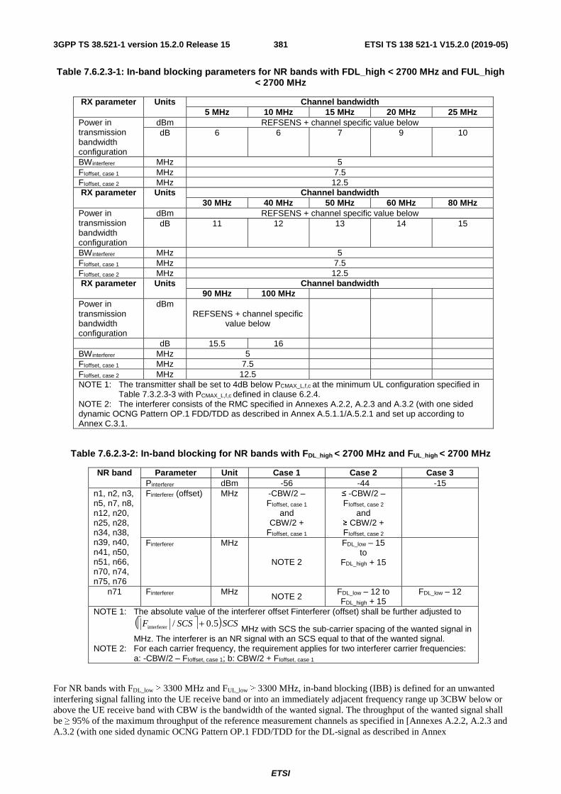
ETSI
ETSI TS 138 521-1 V15.2.0 (2019-05)3813GPP TS 38.521-1 version 15.2.0 Release 15
Table 7.6.2.3-1: In-band blocking parameters for NR bands with FDL_high < 2700 MHz and FUL_high < 2700 MHz
RX parameter Units Channel bandwidth 5 MHz 10 MHz 15 MHz 20 MHz 25 MHz
Power in transmission bandwidth configuration
dBm REFSENS + channel specific value below dB 6 6 7 9 10
BWinterferer MHz 5 FIoffset, case 1 MHz 7.5 FIoffset, case 2 MHz 12.5 RX parameter Units Channel bandwidth
30 MHz 40 MHz 50 MHz 60 MHz 80 MHz Power in transmission bandwidth configuration
dBm REFSENS + channel specific value below dB 11 12 13 14 15
BWinterferer MHz 5 FIoffset, case 1 MHz 7.5 FIoffset, case 2 MHz 12.5 RX parameter Units Channel bandwidth
90 MHz 100 MHz Power in transmission bandwidth configuration
dBm REFSENS + channel specific
value below
dB 15.5 16 BWinterferer MHz 5 FIoffset, case 1 MHz 7.5 FIoffset, case 2 MHz 12.5 NOTE 1: The transmitter shall be set to 4dB below PCMAX_L,f,c at the minimum UL configuration specified in
Table 7.3.2.3-3 with PCMAX_L,f,c defined in clause 6.2.4. NOTE 2: The interferer consists of the RMC specified in Annexes A.2.2, A.2.3 and A.3.2 (with one sided dynamic OCNG Pattern OP.1 FDD/TDD as described in Annex A.5.1.1/A.5.2.1 and set up according to Annex C.3.1.
Table 7.6.2.3-2: In-band blocking for NR bands with FDL_high < 2700 MHz and FUL_high < 2700 MHz
NR band Parameter Unit Case 1 Case 2 Case 3 Pinterferer dBm -56 -44 -15
n1, n2, n3, n5, n7, n8, n12, n20, n25, n28, n34, n38, n39, n40, n41, n50, n51, n66, n70, n74, n75, n76
Finterferer (offset) MHz -CBW/2 – FIoffset, case 1
and CBW/2 +
FIoffset, case 1
≤ -CBW/2 – FIoffset, case 2
and ≥ CBW/2 + FIoffset, case 2
Finterferer MHz
NOTE 2
FDL_low – 15 to
FDL_high + 15
n71 Finterferer MHz NOTE 2 FDL_low – 12 to FDL_high + 15
FDL_low – 12
NOTE 1: The absolute value of the interferer offset Finterferer (offset) shall be further adjusted to
MHz with SCS the sub-carrier spacing of the wanted signal in MHz. The interferer is an NR signal with an SCS equal to that of the wanted signal.
NOTE 2: For each carrier frequency, the requirement applies for two interferer carrier frequencies: a: -CBW/2 – FIoffset, case 1; b: CBW/2 + FIoffset, case 1
For NR bands with FDL_low ≥ 3300 MHz and FUL_low ≥ 3300 MHz, in-band blocking (IBB) is defined for an unwanted interfering signal falling into the UE receive band or into an immediately adjacent frequency range up 3CBW below or above the UE receive band with CBW is the bandwidth of the wanted signal. The throughput of the wanted signal shall be ≥ 95% of the maximum throughput of the reference measurement channels as specified in [Annexes A.2.2, A.2.3 and A.3.2 (with one sided dynamic OCNG Pattern OP.1 FDD/TDD for the DL-signal as described in Annex
( )SCSSCSF 5.0/interferer +

ETSI
ETSI TS 138 521-1 V15.2.0 (2019-05)3823GPP TS 38.521-1 version 15.2.0 Release 15
A.5.1.1/A.5.2.1)] with parameters specified in Table 7.6.2.3-3 and Table 7.6.2.3-4. The said relative throughput requirement shall be met for any SCS specified for the channel bandwidth of the wanted signal.
Table 7.6.2.3-3: In-band blocking parameters for NR bands with FDL_low ≥ 3300 MHz and FUL_low ≥ 3300 MHz
RX parameter Units Channel bandwidth 10 MHz 15 MHz 20 MHz 40 MHz 50 MHz
Power in transmission bandwidth configuration
dBm REFSENS + channel specific value below dB 6
BWinterferer MHz 10 15 20 40 50 FIoffset, case 1 MHz 15 22.5 30 60 75 FIoffset, case 2 MHz 25 37.5 50 100 125 RX parameter Units Channel bandwidth
60 MHz 80 MHz 90 MHz 100 MHz Power in transmission bandwidth configuration
dBm REFSENS + channel specific value below dB 6
BWinterferer MHz 60 80 90 100 FIoffset, case 1 MHz 90 120 135 150 FIoffset, case 2 MHz 150 200 225 250 NOTE 1: The transmitter shall be set to 4dB below PCMAX_L,f,c at the minimum UL configuration specified in
Table 7.3.2.3-3 with PCMAX_L,f,c defined in clause 6.2.4. NOTE 2: The interferer consists of the RMC specified in Annexes A.2.2, A.2.3 and A.3.2 (with one sided
dynamic OCNG Pattern OP.1 FDD/TDD as described in Annex A.5.1.1/A.5.2.1 and set up according to Annex C.3.1.
Table 7.6.2.3-4: In-band blocking for NR bands with FDL_low ≥ 3300 MHz and FUL_low ≥ 3300 MHz
NR band Parameter Unit Case 1 Case 2 Pinterferer dBm -56 -44
n77, n78, n79
Finterferer (offset) MHz -CBW/2 – FIoffset, case 1
and BW/2 +
FIoffset, case 1
≤ -CBW/2 – FIoffset, case 2
and ≥ CBW/2 + FIoffset, case 2
Finterferer NOTE 2
FDL_low – 3CBW to
FDL_high + 3CBW NOTE 1: The absolute value of the interferer offset Finterferer (offset) shall be
further adjusted to MHz with SCS the sub-carrier spacing of the wanted signal in MHz. The interferer is an NR signal with an SCS equal to that of the wanted signal.
NOTE 2: For each carrier frequency, the requirement applies for two interferer carrier frequencies: a: -CBW/2 – FIoffset, case 1; b: CBW/2 + FIoffset, case 1
NOTE 3: CBW denotes the channel bandwidth of the wanted signal
The normative reference for this requirement is TS 38.101-1 [2] clause 7.6.2.
7.6.2.4 Test description
7.6.2.4.1 Initial conditions
Initial conditions are a set of test configurations the UE needs to be tested in and the steps for the SS to take with the UE to reach the correct measurement state.
The initial test configurations consist of environmental conditions, test frequencies, test channel bandwidths and sub-carrier spacing based on NR operating bands specified in Table 5.3.5-1. All of these configurations shall be tested with applicable test parameters for each combination of channel bandwidth and sub-carrier spacing, are shown in table 7.6.2.4.1-1. The details of the uplink and downlink reference measurement channels (RMC) are specified in Annexes A.2 and A.3. Configuration of PDSCH and PDCCH before measurement are specified in Annex C.2.
( )SCSSCSF 5.0/interferer +

ETSI
ETSI TS 138 521-1 V15.2.0 (2019-05)3833GPP TS 38.521-1 version 15.2.0 Release 15
Table 7.6.2.4.1-1: Test Configuration Table
Default Conditions Test Environment as specified in TS 38.508-1 [5] subclause 4.1
Normal
Test Frequencies as specified in TS 38.508-1 [5] subclause 4.3.1
Mid range
Test Channel Bandwidths as specified in TS 38.508-1 [5] subclause 4.3.1
Lowest, Mid, Highest
Test SCS as specified in Table 5.3.5-1 Lowest Test Parameters
Downlink Configuration Uplink Configuration Test ID Mod'n RB allocation Mod'n RB allocation
1 CP-OFDM QPSK NOTE 1 DFT-s-OFDM QPSK NOTE 1 NOTE 1: The specific configuration of uplink and downlink are defined in Table 7.3.2.4.1-1.
1. Connect the SS to the UE antenna connectors as shown in TS 38.508-1 [5] Annex A, in Figure A.3.1.4.1 for TE diagram and section A.3.2.1 for UE diagram.
2. The parameter settings for the cell are set up according to TS 38.508-1 [5] subclause 4.4.3.
3. Downlink signals are initially set up according to Annex C.0, C.1, C.2, C.3.1, and uplink signals according to Annex G.0, G.1, G.2, G.3.1.
4. The DL and UL Reference Measurement channels are set according to Table 7.6.2.4.1-1.
5. Propagation conditions are set according to Annex B.0.
6. Ensure the UE is in state RRC_CONNECTED with generic procedure parameters Connectivity NR, Connected without release On, Test Mode On and Test Loop Function On according to TS 38.508-1 [5] clause 4.5. Message content are defined in clause 7.6.2.4.3.
7.6.2.4.2 Test procedure
1. SS transmits PDSCH via PDCCH DCI format [1_1] for C_RNTI to transmit the DL RMC according to Table 7.6.2.4.1-1. The SS sends downlink MAC padding bits on the DL RMC.
2. SS sends uplink scheduling information for each UL HARQ process via PDCCH DCI format [0_1] for C_RNTI to schedule the UL RMC according to Table 7.6.2.4.1-1. Since the UL has no payload and no loopback data to send the UE sends uplink MAC padding bits on the UL RMC.
3. Set the parameters of the signal generator for an interfering signal below the wanted signal in Case 1 according to Tables 7.6.2.5-1 and 7.6.2.5-2 or Tables 7.6.2.5-3 and 7.6.2.5-4 as appropriate depending on NR band.
4. Set the downlink signal level according to the table 7.6.2.5-1 or 7.6.2.5-3 as appropriate. Send uplink power control commands to the UE (less or equal to 1 dB step size should be used), to ensure that the UE output power is within - PW ± PW dB of the target power level in Table 7.6.2.5-1 or Table 7.6.2.5-3 for at least the duration of the Throughput measurement. PW is the power window according to Table 7.6.2.5-5 for the carrier frequency f and the channel bandwidth BW..
5. Measure the average throughput for a duration sufficient to achieve statistical significance according to Annex H.
6. Repeat steps from 3 to 5, using an interfering signal above the wanted signal in Case 1 at step 3.
7. Repeat steps from 3 to 6, using interfering signals in Case 2 at step 3and 6. The ranges of case 2 are covered in steps equal to the interferer bandwidth.
7.6.2.4.3 Message contents
Message contents are according to TS 38.508-1 [5] subclause 4.6 with DFT-s-OFDM condition in Table 4.6.3-118 PUSCH-Config.

ETSI
ETSI TS 138 521-1 V15.2.0 (2019-05)3843GPP TS 38.521-1 version 15.2.0 Release 15
7.6.1.5 Test requirement
For NR bands with FDL_high < 2700 MHz and FUL_high < 2700 MHz, the throughput measurement derived in test procedure shall be ≥ 95% of the maximum throughput of the reference measurement channels as specified in Annex in Annexes A.2.2, A.2.3 and A.3.2 with parameters specified in Tables 7.6.2.5-1 and 7.6.2.5-2.
Table 7.6.2.5-1: In-band blocking parameters for NR bands with FDL_high < 2700 MHz and FUL_high < 2700 MHz
RX parameter Units Channel bandwidth 5 MHz 10 MHz 15 MHz 20 MHz 25 MHz
Power in transmission bandwidth configuration
dBm REFSENS + channel specific value below dB 6 6 7 9 10
BWinterferer MHz 5 FIoffset, case 1 MHz 7.5 FIoffset, case 2 MHz 12.5 RX parameter Units Channel bandwidth
30 MHz 40 MHz 50 MHz 60 MHz 80 MHz Power in transmission bandwidth configuration
dBm REFSENS + channel specific value below dB 11 12 13 14 15
BWinterferer MHz 5 FIoffset, case 1 MHz 7.5 FIoffset, case 2 MHz 12.5 RX parameter Units Channel bandwidth
90 MHz 100 MHz Power in transmission bandwidth configuration
dBm REFSENS + channel specific
value below
dB 15.5 16 BWinterferer MHz 5 FIoffset, case 1 MHz 7.5 FIoffset, case 2 MHz 12.5 NOTE 1: The transmitter shall be set to 4dB below PCMAX_L,f,c at the minimum UL configuration specified in
Table 7.3.2.3-3 with PCMAX_L,f,c defined in clause 6.2.4. NOTE 2: The interferer consists of the RMC specified in Annexes A.2.2, A.2.3 and A.3.2 (with one sided
dynamic OCNG Pattern OP.1 FDD/TDD as described in Annex A.5.1.1/A.5.2.1 and set up according to Annex C.3.1.
Table 7.6.2.5-2: In-band blocking for NR bands with FDL_high < 2700 MHz and FUL_high < 2700 MHz
NR band Parameter Unit Case 1 Case 2 Case 3 Pinterferer dBm -56 -44 -15
n1, n2, n3, n5, n7, n8, n12, n20, n28, n38, n39, n40, n41, n50, n51, n66, n70, n74, n75, n76
Finterferer (offset) MHz -CBW/2 – FIoffset, case 1
and CBW/2 +
FIoffset, case 1
≤ -CBW/2 – FIoffset, case 2
and ≥ CBW/2 + FIoffset, case 2
Finterferer MHz
NOTE 2
FDL_low – 15 to
FDL_high + 15
n71 Finterferer MHz NOTE 2 FDL_low – 12 to FDL_high + 15
FDL_low – 12
NOTE 1: The absolute value of the interferer offset Finterferer (offset) shall be further adjusted to
MHz with SCS the sub-carrier spacing of the wanted signal in MHz. The interferer is an NR signal with an SCS equal to that of the wanted signal.
NOTE 2: For each carrier frequency, the requirement applies for two interferer carrier frequencies: a: -CBW/2 – FIoffset, case 1; b: CBW/2 + FIoffset, case 1
( )SCSSCSF 5.0/interferer +

ETSI
ETSI TS 138 521-1 V15.2.0 (2019-05)3853GPP TS 38.521-1 version 15.2.0 Release 15
For NR bands with FDL_low ≥ 3300 MHz and FUL_low ≥ 3300 MHz, the throughput measurement derived in test procedure shall be ≥ 95% of the maximum throughput of the reference measurement channels as specified in Annex A.2 and A.3 with parameters specified in Tables 7.6.2.5-3 and 7.6.2.5-4.
Table 7.6.2.5-3: In-band blocking parameters for NR bands with FDL_low ≥ 3300 MHz and FUL_low ≥ 3300 MHz
RX parameter Units Channel bandwidth 10 MHz 15 MHz 20 MHz 40 MHz 50 MHz
Power in transmission bandwidth configuration
dBm REFSENS + channel specific value below dB 6
BWinterferer MHz 10 15 20 40 50 FIoffset, case 1 MHz 15 22.5 30 60 75 FIoffset, case 2 MHz 25 37.5 50 100 125 RX parameter Units Channel bandwidth
60 MHz 80 MHz 90 MHz 100 MHz Power in transmission bandwidth configuration
dBm REFSENS + channel specific value below dB 6
BWinterferer MHz 60 80 90 100 FIoffset, case 1 MHz 90 120 135 150 FIoffset, case 2 MHz 150 200 225 250 NOTE 1: The transmitter shall be set to 4dB below PCMAX_L,f,c at the minimum UL configuration specified in
Table 7.3.2.3-3 with PCMAX_L,f,c defined in clause 6.2.4. NOTE 2: The interferer consists of the RMC specified in Annexes A.2.2, A.2.3 and A.3.2 (with one sided
dynamic OCNG Pattern OP.1 FDD/TDD as described in Annex A.5.1.1/A.5.2.1 and set up according to Annex C.3.1.
Table 7.6.2.5-4: In-band blocking for NR bands with FDL_low ≥ 3300 MHz and FUL_low ≥ 3300 MHz
NR band Parameter Unit Case 1 Case 2 Pinterferer dBm -56 -44
n77, n78, n79
Finterferer (offset) MHz -CBW/2 – FIoffset, case 1
and BW/2 +
FIoffset, case 1
≤ -CBW/2 – FIoffset, case 2
and ≥ CBW/2 + FIoffset, case 2
Finterferer NOTE 2
FDL_low – 3CBW to
FDL_high + 3CBW NOTE 1: The absolute value of the interferer offset Finterferer (offset) shall be
further adjusted to MHz with SCS the sub-carrier spacing of the wanted signal in MHz. The interferer is an NR signal with an SCS equal to that of the wanted signal.
NOTE 2: For each carrier frequency, the requirement applies for two interferer carrier frequencies: a: -CBW/2 – FIoffset, case 1; b: CBW/2 + FIoffset, case 1
NOTE 3: CBW denotes the channel bandwidth of the wanted signal
Table 7.6.2.5-5: Power Window (dB) for Inband Blocking
f ≤ 3GHz 3GHz < f ≤ 4.2GHz 4.2GHz < f ≤ 6GHz BW ≤ 20MHz 1.4 1.7 2 20MHz < BW ≤ 40MHz 1.4 1.7 2.2 40MHz < BW ≤ 100MHz 2.1 2.3 2.3 Note: Power Window setting comprises two quantities, UE Power tolerance and test
system power measurement
( )SCSSCSF 5.0/interferer +

ETSI
ETSI TS 138 521-1 V15.2.0 (2019-05)3863GPP TS 38.521-1 version 15.2.0 Release 15
7.6.3 Out-of-band blocking
7.6.3.1 Test Purpose
Out-of-band band blocking is defined for an unwanted CW interfering signal falling outside a frequency range 15 MHz below or above the UE receive band, with FDL_high < 2700 MHz and FUL_high < 2700 MHz, or falling outside a frequency range up to 3CBW below or from 3CBW above the UE receive band, with FDL_low ≥ 3300 MHz and FUL_low ≥ 3300 MHz, at which a given average throughput shall meet or exceed the requirement for the specified measurement channels.
7.6.3.2 Test Applicability
This test applies to all types of NR UE release 15 and forward.
7.6.3.3 Minimum Conformance Requirements
For NR bands with FDL_high < 2700 MHz and FUL_high < 2700 MHz out-of-band band blocking is defined for an unwanted CW interfering signal falling outside a frequency range 15 MHz below or above the UE receive band. The throughput of the wanted signal shall be ≥ 95% of the maximum throughput of the reference measurement channels as specified in Annexes A.2.2, A.2.3 and A.3.2 (with one sided dynamic OCNG Pattern OP.1 FDD/TDD for the DL-signal as described in Annex A.5.1.1/A.5.2.1) with parameters specified in Table 7.6.3-1 and Table 7.6.3-2. The said relative throughput requirement shall be met for any SCS specified for the channel bandwidth of the wanted signal. For operating bands with an unpaired DL part (as noted in Table 5.5-1), the requirements only apply for carriers assigned in the paired part.
Table 7.6.3-1: Out-of-band blocking parameters for NR bands with FDL_high < 2700 MHz and FUL_high < 2700 MHz
RX parameter Units Channel bandwidth
5 MHz 10 MHz 15 MHz 20 MHz 25 MHz Power in
transmission bandwidth
configuration
dBm REFSENS + channel specific value below dB 6 6 7 9 10
RX parameter Units Channel bandwidth
30 MHz 40 MHz 50 MHz 60 MHz 80 MHz Power in
transmission bandwidth
configuration
dBm REFSENS + channel specific value below
dB 11 12 13 14 15
RX parameter Units Channel bandwidth
90 MHz 100 MHz Power in transmission bandwidth configuration
dBm REFSENS + channel specific value below
dB 15.5 16 NOTE: The transmitter shall be set to 4dB below PCMAX_L,f,c at the minimum UL configuration specified in
Table 7.3.2-3 with PCMAX_L,f,c defined in clause 6.2.4.

ETSI
ETSI TS 138 521-1 V15.2.0 (2019-05)3873GPP TS 38.521-1 version 15.2.0 Release 15
Table 7.6.3-2: Out of-band blocking for NR bands with FDL_high < 2700 MHz and FUL_high < 2700 MHz
NR band Parameter Unit Range 1 Range 2 Range 3 n1, n2, n3, n5, n7, n8, n12, n20, n25, n28, n34, n38, n39, n40, n41, n51, n66, n70, n71, n75,
n76
Pinterferer dBm -44 -30 -15 Finterferer (CW) MHz
-60 < f – FDL_low < -15 or
15 < f – FDL_high < 60
-85 < f – FDL_low ≤ -60 or
60 ≤ f – FDL_high < 85
1 ≤ f ≤ FDL_low – 85 or
FDL_high + 85 ≤ f ≤ 12750
NOTE: The power level of the interferer (PInterferer) for Range 3 shall be modified to -20 dBm for FInterferer > 6000 MHz.
For interferer frequencies across ranges 1, 2 and 3 in Table 7.6.3-2, a maximum of
{ } { } 5,10/min6/6,24max RBRB NnNn ⋅⋅⋅
exceptions are allowed for spurious response frequencies in each assigned frequency channel when measured using a step size of )5,2/min( CBW MHz with
RBN the number of resource blocks in the downlink transmission bandwidth
configuration, CBW the bandwidth of the frequency channel in MHz and n = 1,2,3 for SCS = 15,30,60 kHz, respectively. For these exceptions, the requirements in sub-clause 7.7 apply.
For NR bands with FDL_low ≥ 3300 MHz and FUL_low ≥ 3300 MHz out-of-band band blocking is defined for an unwanted CW interfering signal falling outside a frequency range up to 3CBW below or from 3CBW above the UE receive band, where CBW is the channel bandwidth. The throughput of the wanted signal shall be ≥ 95% of the maximum throughput of the reference measurement channels as specified in Annexes A.2.2, A.2.3 and A.3.2 (with one sided dynamic OCNG Pattern OP.1 FDD/TDD for the DL-signal as described in Annex A.5.1.1/A.5.2.1) with parameters specified in Table 7.6.3-3 and Table 7.6.3-4. The said relative throughput requirement shall be met for any SCS specified for the channel bandwidth of the wanted signal.
Table 7.6.3-3: Out-of-band blocking parameters for NR bands with FDL_low ≥ 3300 MHz and FUL_low ≥ 3300 MHz
RX parameter Units Channel bandwidth 10 MHz 15 MHz 20 MHz 40 MHz 50 MHz
Power in transmission bandwidth configuration
dBm REFSENS + channel specific value below dB 6 7 9 9 9
RX parameter Units Channel bandwidth 60 MHz 80 MHz 90 MHz 100 MHz
Power in transmission bandwidth configuration
dBm REFSENS + channel specific value below dB 9 9 9 9
NOTE: The transmitter shall be set to 4dB below PCMAX_L,f,c at the minimum UL configuration specified in Table 7.3.2-3 with PCMAX_L,f,c defined in clause 6.2.4.

ETSI
ETSI TS 138 521-1 V15.2.0 (2019-05)3883GPP TS 38.521-1 version 15.2.0 Release 15
Table 7.6.3-4: Out of-band blocking for NR bands with FDL_low ≥ 3300 MHz and FUL_low ≥ 3300 MHz
NR band Parameter Unit Range1 Range 2 Range 3 n77, n78 (NOTE 3)
Pinterferer dBm -44 -30 -15 Finterferer (CW) MHz -60 < f – FDL_low ≤
-3CBW or
3CBW ≤ f – FDL_high < 60
-200 < f – FDL_low ≤ -MAX(60,3CBW)
or MAX(60,3CBW) ≤ f –
FDL_high < 200
1 ≤ f ≤ FDL_low – MAX(200,3CBW)
or FDL_high
+ MAX(200,3CBW) ≤ f ≤ 12750
n79 (NOTE 4)
Finterferer (CW) MHz
N/A
-150 < f – FDL_low ≤ -MAX(60,3CBW)
or MAX(60,3CBW) ≤ f –
FDL_high < 150
1 ≤ f ≤ FDL_low – MAX(150,3CBW)
or FDL_high
+ MAX(150,3CBW) ≤ f ≤ 12750
NOTE 1: The power level of the interferer (PInterferer) for Range 3 shall be modified to -20 dBm for FInterferer > 6000 MHz.
NOTE 2: CBW denotes the channel bandwidth of the wanted signal NOTE 3: The power level of the interferer (PInterferer) for Range 3 shall be modified to -20 dBm, for FInterferer >
2700 MHz and FInterferer < 4800 MHz. For CBW > 15 MHz, the requirement for Range 1 is not applicable and Range 2 applies from the frequency offset of 3CBW from the band edge. For CBW larger than 60 MHz, the requirement for Range 2 is not applicable and Range 3 applies from the frequency offset of 3CBW from the band edge.
NOTE 4: The power level of the interferer (PInterferer) for Range 3 shall be modified to -20 dBm, for FInterferer > 3650 MHz and FInterferer < 5750 MHz. For CBW ≥ 40 MHz, the requirement for Range 2 is not applicable and Range 3 applies from the frequency offset of 3CBW from the band edge.
For interferer frequencies across ranges 1, 2 and 3 in Table 7.6.3-4, a maximum of
{ } { } 5,10/min6/6,24max RBRB NnNn ⋅⋅⋅
exceptions are allowed for spurious response frequencies in each assigned frequency channel when measured using a step size of )5,2/min( CBW MHz with
RBN the number of resource blocks in the downlink transmission bandwidth
configuration, CBW the bandwidth of the frequency channel in MHz and n = 1,2,3 for SCS = 15, 30, 60 kHz, respectively. For these exceptions, the requirements in sub-clause 7.7 apply.
The normative reference for this requirement is TS 38.101-1 [2] clause 7.6.3.
7.6.3.4 Test Description
7.6.3.4.1 Initial Conditions
Initial conditions are a set of test configurations the UE needs to be tested in and the steps for the SS to take with the UE to reach the correct measurement state.
The initial test configurations consist of environmental conditions, test frequencies, and channel bandwidths based on NR operating bands specified in table 5.3.5-1. All of these configurations shall be tested with applicable test parameters for each combination of channel bandwidth and sub-carrier spacing, and are shown in table 7.6.3.4.1-1. The details of the uplink and downlink reference measurement channels (RMCs) are specified in Annexes A.2 and A.3 respectively. The details of the OCNG patterns used are specified in Annex A.5. Configurations of PDSCH and PDCCH before measurement are specified in Annex C.3.
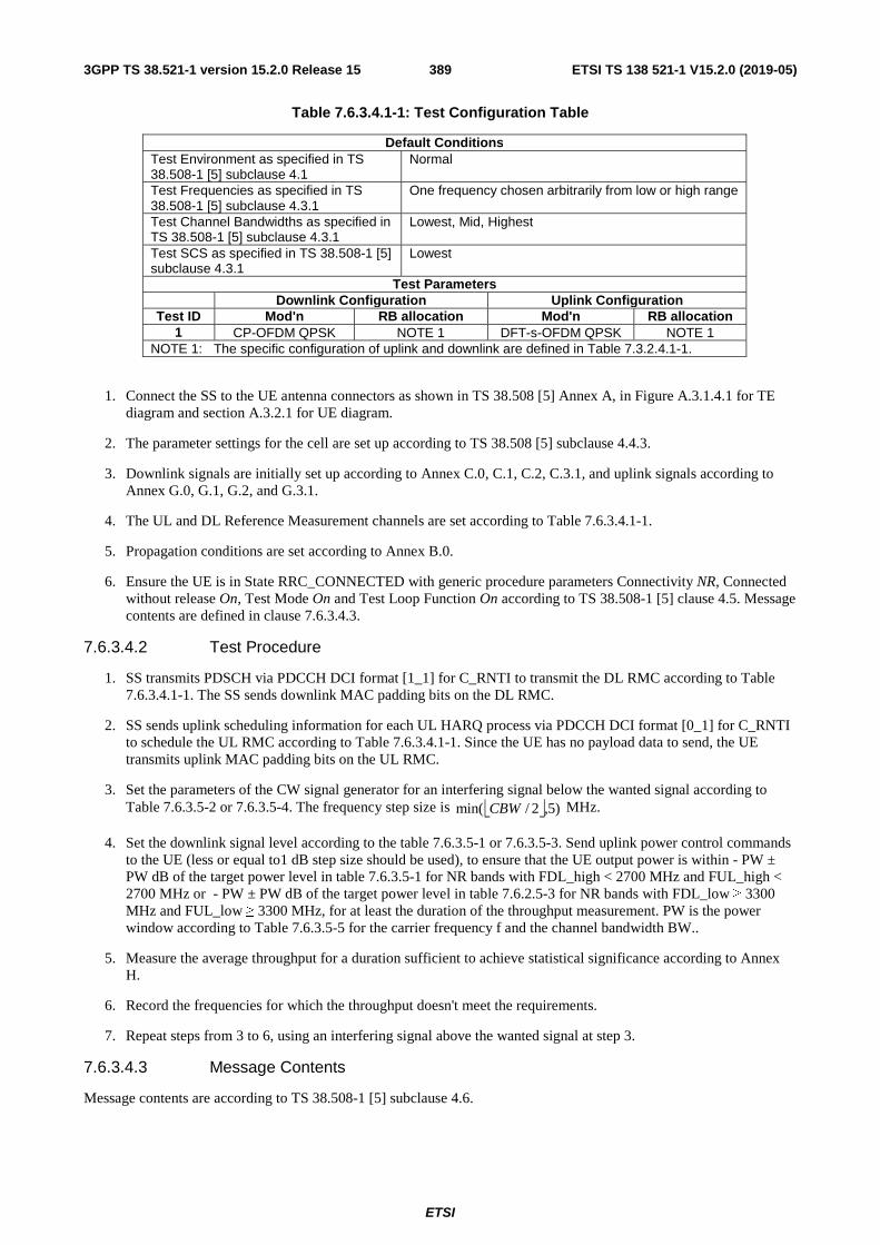
ETSI
ETSI TS 138 521-1 V15.2.0 (2019-05)3893GPP TS 38.521-1 version 15.2.0 Release 15
Table 7.6.3.4.1-1: Test Configuration Table
Default Conditions Test Environment as specified in TS 38.508-1 [5] subclause 4.1
Normal
Test Frequencies as specified in TS 38.508-1 [5] subclause 4.3.1
One frequency chosen arbitrarily from low or high range
Test Channel Bandwidths as specified in TS 38.508-1 [5] subclause 4.3.1
Lowest, Mid, Highest
Test SCS as specified in TS 38.508-1 [5] subclause 4.3.1
Lowest
Test Parameters Downlink Configuration Uplink Configuration Test ID Mod'n RB allocation Mod'n RB allocation
1 CP-OFDM QPSK NOTE 1 DFT-s-OFDM QPSK NOTE 1 NOTE 1: The specific configuration of uplink and downlink are defined in Table 7.3.2.4.1-1.
1. Connect the SS to the UE antenna connectors as shown in TS 38.508 [5] Annex A, in Figure A.3.1.4.1 for TE diagram and section A.3.2.1 for UE diagram.
2. The parameter settings for the cell are set up according to TS 38.508 [5] subclause 4.4.3.
3. Downlink signals are initially set up according to Annex C.0, C.1, C.2, C.3.1, and uplink signals according to Annex G.0, G.1, G.2, and G.3.1.
4. The UL and DL Reference Measurement channels are set according to Table 7.6.3.4.1-1.
5. Propagation conditions are set according to Annex B.0.
6. Ensure the UE is in State RRC_CONNECTED with generic procedure parameters Connectivity NR, Connected without release On, Test Mode On and Test Loop Function On according to TS 38.508-1 [5] clause 4.5. Message contents are defined in clause 7.6.3.4.3.
7.6.3.4.2 Test Procedure
1. SS transmits PDSCH via PDCCH DCI format [1_1] for C_RNTI to transmit the DL RMC according to Table 7.6.3.4.1-1. The SS sends downlink MAC padding bits on the DL RMC.
2. SS sends uplink scheduling information for each UL HARQ process via PDCCH DCI format [0_1] for C_RNTI to schedule the UL RMC according to Table 7.6.3.4.1-1. Since the UE has no payload data to send, the UE transmits uplink MAC padding bits on the UL RMC.
3. Set the parameters of the CW signal generator for an interfering signal below the wanted signal according to Table 7.6.3.5-2 or 7.6.3.5-4. The frequency step size is )5,2/min( CBW MHz.
4. Set the downlink signal level according to the table 7.6.3.5-1 or 7.6.3.5-3. Send uplink power control commands to the UE (less or equal to1 dB step size should be used), to ensure that the UE output power is within - PW ± PW dB of the target power level in table 7.6.3.5-1 for NR bands with FDL_high < 2700 MHz and FUL_high < 2700 MHz or - PW ± PW dB of the target power level in table 7.6.2.5-3 for NR bands with FDL_low ≥ 3300 MHz and FUL_low ≥ 3300 MHz, for at least the duration of the throughput measurement. PW is the power window according to Table 7.6.3.5-5 for the carrier frequency f and the channel bandwidth BW..
5. Measure the average throughput for a duration sufficient to achieve statistical significance according to Annex H.
6. Record the frequencies for which the throughput doesn't meet the requirements.
7. Repeat steps from 3 to 6, using an interfering signal above the wanted signal at step 3.
7.6.3.4.3 Message Contents
Message contents are according to TS 38.508-1 [5] subclause 4.6.
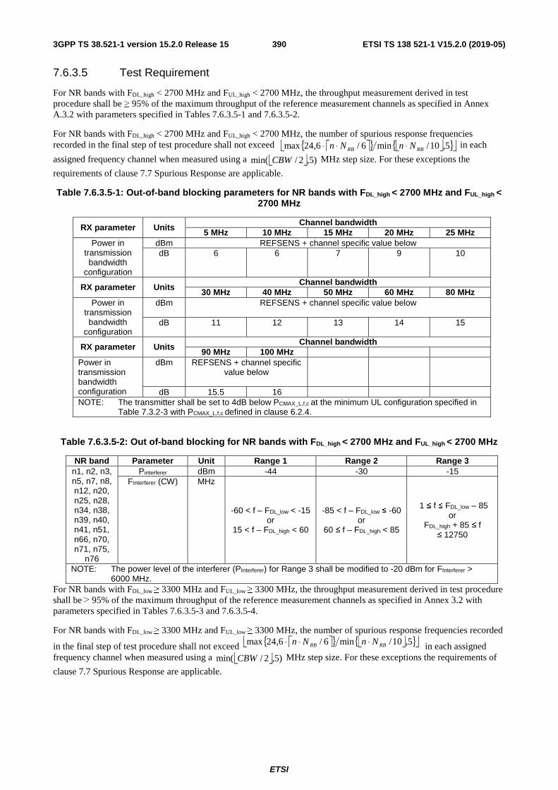
ETSI
ETSI TS 138 521-1 V15.2.0 (2019-05)3903GPP TS 38.521-1 version 15.2.0 Release 15
7.6.3.5 Test Requirement
For NR bands with FDL_high < 2700 MHz and FUL_high < 2700 MHz, the throughput measurement derived in test procedure shall be ≥ 95% of the maximum throughput of the reference measurement channels as specified in Annex A.3.2 with parameters specified in Tables 7.6.3.5-1 and 7.6.3.5-2.
For NR bands with FDL_high < 2700 MHz and FUL_high < 2700 MHz, the number of spurious response frequencies recorded in the final step of test procedure shall not exceed { } { } 5,10/min6/6,24max RBRB NnNn ⋅⋅⋅ in each
assigned frequency channel when measured using a )5,2/min( CBW MHz step size. For these exceptions the
requirements of clause 7.7 Spurious Response are applicable.
Table 7.6.3.5-1: Out-of-band blocking parameters for NR bands with FDL_high < 2700 MHz and FUL_high < 2700 MHz
RX parameter Units Channel bandwidth
5 MHz 10 MHz 15 MHz 20 MHz 25 MHz Power in
transmission bandwidth
configuration
dBm REFSENS + channel specific value below dB 6 6 7 9 10
RX parameter Units Channel bandwidth
30 MHz 40 MHz 50 MHz 60 MHz 80 MHz Power in
transmission bandwidth
configuration
dBm REFSENS + channel specific value below
dB 11 12 13 14 15
RX parameter Units Channel bandwidth
90 MHz 100 MHz Power in transmission bandwidth configuration
dBm REFSENS + channel specific value below
dB 15.5 16 NOTE: The transmitter shall be set to 4dB below PCMAX_L,f,c at the minimum UL configuration specified in
Table 7.3.2-3 with PCMAX_L,f,c defined in clause 6.2.4.
Table 7.6.3.5-2: Out of-band blocking for NR bands with FDL_high < 2700 MHz and FUL_high < 2700 MHz
NR band Parameter Unit Range 1 Range 2 Range 3 n1, n2, n3, n5, n7, n8, n12, n20, n25, n28, n34, n38, n39, n40, n41, n51, n66, n70, n71, n75,
n76
Pinterferer dBm -44 -30 -15 Finterferer (CW) MHz
-60 < f – FDL_low < -15 or
15 < f – FDL_high < 60
-85 < f – FDL_low ≤ -60 or
60 ≤ f – FDL_high < 85
1 ≤ f ≤ FDL_low – 85 or
FDL_high + 85 ≤ f ≤ 12750
NOTE: The power level of the interferer (PInterferer) for Range 3 shall be modified to -20 dBm for FInterferer > 6000 MHz.
For NR bands with FDL_low ≥ 3300 MHz and FUL_low ≥ 3300 MHz, the throughput measurement derived in test procedure shall be ≥ 95% of the maximum throughput of the reference measurement channels as specified in Annex 3.2 with parameters specified in Tables 7.6.3.5-3 and 7.6.3.5-4.
For NR bands with FDL_low ≥ 3300 MHz and FUL_low ≥ 3300 MHz, the number of spurious response frequencies recorded
in the final step of test procedure shall not exceed { } { } 5,10/min6/6,24max RBRB NnNn ⋅⋅⋅ in each assigned frequency channel when measured using a )5,2/min( CBW MHz step size. For these exceptions the requirements of
clause 7.7 Spurious Response are applicable.

ETSI
ETSI TS 138 521-1 V15.2.0 (2019-05)3913GPP TS 38.521-1 version 15.2.0 Release 15
Table 7.6.3.5-3: Out-of-band blocking parameters for NR bands with FDL_low ≥ 3300 MHz and FUL_low ≥ 3300 MHz
RX parameter Units Channel bandwidth 10 MHz 15 MHz 20 MHz 40 MHz 50 MHz
Power in transmission bandwidth configuration
dBm REFSENS + channel specific value below dB 6 7 9 9 9
RX parameter Units Channel bandwidth 60 MHz 80 MHz 90 MHz 100 MHz
Power in transmission bandwidth configuration
dBm REFSENS + channel specific value below dB 9 9 9 9
NOTE: The transmitter shall be set to 4dB below PCMAX_L,f,c at the minimum UL configuration specified in Table 7.3.2-3 with PCMAX_L,f,c defined in clause 6.2.4.
Table 7.6.3.5-4: Out of-band blocking for NR bands with FDL_low ≥ 3300 MHz and FUL_low ≥ 3300 MHz
NR band Parameter Unit Range1 Range 2 Range 3 n77, n78 (NOTE 3)
Pinterferer dBm -44 -30 -15 Finterferer (CW) MHz
-60 < f – FDL_low ≤ -3CBW
or 3CBW ≤ f – FDL_high <
60
-200 < f – FDL_low ≤ -MAX(60,3CBW)
or MAX(60,3CBW) ≤ f –
FDL_high < 200
1 ≤ f ≤ FDL_low – MAX(200,3CBW)
or FDL_high
+ MAX(200,3CBW) ≤ f ≤ 12750
n79 (NOTE 4)
Finterferer (CW) MHz
N/A
-150 < f – FDL_low ≤ -MAX(60,3CBW)
or MAX(60,3CBW) ≤ f –
FDL_high < 150
1 ≤ f ≤ FDL_low – MAX(150,3CBW)
or FDL_high
+ MAX(150,3CBW) ≤ f ≤ 12750
NOTE 1: The power level of the interferer (PInterferer) for Range 3 shall be modified to -20 dBm for FInterferer > 6000 MHz.
NOTE 2: CBW denotes the channel bandwidth of the wanted signal NOTE 3: The power level of the interferer (PInterferer) for Range 3 shall be modified to -20 dBm, for FInterferer >
2700 MHz and FInterferer < 4800 MHz. For CBW > 15 MHz, the requirement for Range 1 is not applicable and Range 2 applies from the frequency offset of 3CBW from the band edge. For CBW larger than 60 MHz, the requirement for Range 2 is not applicable and Range 3 applies from the frequency offset of 3CBW from the band edge.
NOTE 4: The power level of the interferer (PInterferer) for Range 3 shall be modified to -20 dBm, for FInterferer > 3650 MHz and FInterferer < 5750 MHz. For CBW ≥ 40 MHz, the requirement for Range 2 is not applicable and Range 3 applies from the frequency offset of 3CBW from the band edge.
Table 7.6.3.5-5: Power Window (dB) for Out-of-band Blocking
f ≤ 3GHz 3GHz < f ≤ 4.2GHz 4.2GHz < f ≤ 6GHz BW ≤ 20MHz 1.4 1.7 2 20MHz < BW ≤ 40MHz 1.4 1.7 2.2 40MHz < BW ≤ 100MHz 2.1 2.3 2.3 Note: Power Window setting comprises two quantities, UE Power tolerance and test system power measurement;
7.6.4 Narrow band blocking
7.6.4.1 Test Purpose
Verifies a receiver's ability to receive a NR signal at its assigned channel frequency in the presence of an unwanted narrow band CW interferer at a frequency, which is less than the nominal channel spacing.
The lack of narrow-band blocking ability will decrease the coverage area when other NR Node B transmitters exist (except in the adjacent channels and spurious response).

ETSI
ETSI TS 138 521-1 V15.2.0 (2019-05)3923GPP TS 38.521-1 version 15.2.0 Release 15
7.6.4.2 Test Applicability
This test applies to all types of NR UE release 15 and forward.
7.6.4.3 Minimum Conformance Requirements
The relative throughput shall be ≥ 95% of the maximum throughput of the reference measurement channels as specified in Annexes A.2.2, A.2.3 and A.3.2 (with one sided dynamic OCNG Pattern OP.1 FDD/TDD for the DL-signal as described in Annex A.5.1.1/A.5.2.1) with parameters specified in Table 7.6.4.3-1. For operating bands with an unpaired DL part (as noted in Table 5.5-1), the requirements only apply for carriers assigned in the paired part.
Table 7.6.4.3-1: Narrow Band Blocking
NR band
Parameter
Unit Channel Bandwidth 5 MHz 10
MHz 15
MHz 20
MHz 25
MHz 40
MHz 50
MHz 60
MHz 80
MHz 90
MHz 100M
Hz n1,n2,
n3, n5, n7, n8,
n12, n20,
n25 n28, n34, n38, n39, n40, n41, n50, n51, n66, n70, n71, n74, n75, n76
Pw dBm PREFSENS + channel-bandwidth specific value below 16 13 14 16 16 16 16 16 16 16 16
Puw (CW)
dBm -55 -55 -55 -55 -55 -55 -55 -55 -55 -55 -55
Fuw (offset SCS=
15 kHz)
MHz 2.7075 5.2125
7.7025
10.2075
13.0275
20.5575
NA NA NA NA NA
Fuw (offset SCS=
30 kHz)
MHz NA NA NA NA TBD TBD
NOTE 1: The transmitter shall be set a 4 dB below PCMAX_L,f,c at the minimum UL configuration specified in Table 7.3.2-3 with PCMAX_L,f,c defined in clause 6.2.4
NOTE 2: Reference measurement channel is specified in Annex A.3.2 with one sided dynamic OCNG Pattern OP.1 FDD/TDD as described in Annex A.5.1.1/A.5.2.1.
NOTE 3: The PREFSENS power level is specified in Table 7.3.1-1 and Table 7.3.1-1a for two and four antenna ports, respectively.
The normative reference for this requirement is TS 38.101-1 [2] clause 7.6.4.
7.6.4.4 Test Description
7.6.4.4.1 Initial Conditions
Initial conditions are a set of test configurations the UE needs to be tested in and the steps for the SS to take with the UE to reach the correct measurement state.
The initial test configurations consist of environmental conditions, test frequencies, and channel bandwidths based on NR operating bands specified in table 5.3.5-1. All of these configurations shall be tested with applicable test parameters for each combination of channel bandwidth and sub-carrier spacing, and are shown in table 7.6.4.4.1-1. The details of the uplink and downlink reference measurement channels (RMCs) are specified in Annexes A.2 and A.3 respectively. The details of the OCNG patterns used are specified in Annex A.5. Configurations of PDSCH and PDCCH before measurement are specified in Annex C.2.
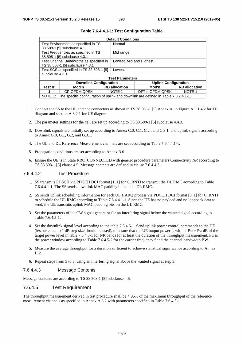
ETSI
ETSI TS 138 521-1 V15.2.0 (2019-05)3933GPP TS 38.521-1 version 15.2.0 Release 15
Table 7.6.4.4.1-1: Test Configuration Table
Default Conditions Test Environment as specified in TS 38.508-1 [5] subclause 4.1
Normal
Test Frequencies as specified in TS 38.508-1 [5] subclause 4.3.1
Mid range
Test Channel Bandwidths as specified in TS 38.508-1 [5] subclause 4.3.1
Lowest, Mid and Highest
Test SCS as specified in TS 38.508-1 [5] subclause 4.3.1
Lowest
Test Parameters Downlink Configuration Uplink Configuration Test ID Mod'n RB allocation Mod'n RB allocation
1 CP-OFDM QPSK NOTE 1 DFT-s-OFDM QPSK NOTE 1 NOTE 1: The specific configuration of uplink and downlink are defined in Table 7.3.2.4.1-1.
1. Connect the SS to the UE antenna connectors as shown in TS 38.508-1 [5] Annex A, in Figure A.3.1.4.2 for TE diagram and section A.3.2.1 for UE diagram.
2. The parameter settings for the cell are set up according to TS 38.508-1 [5] subclause 4.4.3.
3. Downlink signals are initially set up according to Annex C.0, C.1, C.2 , and C.3.1, and uplink signals according to Annex G.0, G.1, G.2, and G.3.1.
4. The UL and DL Reference Measurement channels are set according to Table 7.6.4.4.1-1.
5. Propagation conditions are set according to Annex B.0.
6. Ensure the UE is in State RRC_CONNECTED with generic procedure parameters Connectivity NR according to TS 38.508-1 [5] clause 4.5. Message contents are defined in clause 7.6.4.4.3.
7.6.4.4.2 Test Procedure
1. SS transmits PDSCH via PDCCH DCI format [1_1] for C_RNTI to transmit the DL RMC according to Table 7.6.4.4.1-1. The SS sends downlink MAC padding bits on the DL RMC.
2. SS sends uplink scheduling information for each UL HARQ process via PDCCH DCI format [0_1] for C_RNTI to schedule the UL RMC according to Table 7.6.4.4.1-1. Since the UE has no payload and no loopback data to send, the UE transmits uplink MAC padding bits on the UL RMC.
3. Set the parameters of the CW signal generator for an interfering signal below the wanted signal according to Table 7.6.4.5-1.
4. Set the downlink signal level according to the table 7.6.4.5-1. Send uplink power control commands to the UE (less or equal to 1 dB step size should be used), to ensure that the UE output power is within- PW ± PW dB of the target power level in table 7.6.4.5-1 for NR bands for at least the duration of the throughput measurement. PW is the power window according to Table 7.6.4.5-2 for the carrier frequency f and the channel bandwidth BW.
5. Measure the average throughput for a duration sufficient to achieve statistical significance according to Annex H.2.
6. Repeat steps from 3 to 5, using an interfering signal above the wanted signal at step 3.
7.6.4.4.3 Message Contents
Message contents are according to TS 38.508-1 [5] subclause 4.6.
7.6.4.5 Test Requirement
The throughput measurement derived in test procedure shall be ≥ 95% of the maximum throughput of the reference measurement channels as specified in Annex A.3.2 with parameters specified in Table 7.6.4.5-1.

ETSI
ETSI TS 138 521-1 V15.2.0 (2019-05)3943GPP TS 38.521-1 version 15.2.0 Release 15
Table 7.6.4.5-1: Narrow-band blocking
NR band
Parameter
Unit Channel Bandwidth 5 MHz 10 MHz 15
MHz 20
MHz 25
MHz 40
MHz 50
MHz 60
MHz 80
MHz 90
MHz 100M
Hz n1,n2,
n3, n5, n7, n8,
n12, n20,
n25 n28, n34, n38, n39, n40, n41, n50, n51, n66, n70, n71, n74, n75, n76
Pw dBm PREFSENS + channel-bandwidth specific value below 16 13 14 16 16 16 16 16 16 16 16
Puw (CW)
dBm -55 -55 -55 -55 -55 -55 -55 -55 -55 -55 -55
Fuw (offset SCS=
15 kHz)
MHz 2.7075 5.2125 7.7025 10.2075
13.0275
20.5575
NA NA NA NA NA
Fuw (offset SCS=
30 kHz)
MHz NA NA NA NA TBD TBD
NOTE 1: The transmitter shall be set a 4 dB below PCMAX_L,f,c at the minimum UL configuration specified in Table 7.3.2-3 with PCMAX_L,f,c defined in clause 6.2.4
NOTE 2: Reference measurement channel is specified in Annex A.3.2 with one sided dynamic OCNG Pattern OP.1 FDD/TDD as described in Annex A.5.1.1/A.5.2.1.
Table 7.6.4.5-2 Power Window (dB) for Narrow Band Blocking
f ≤ 3GHz 3GHz < f ≤ 4.2GHz 4.2GHz < f ≤ 6GHz BW ≤ 20MHz 1.4 1.7 2 20MHz < BW ≤ 40MHz 1.4 1.7 2.2 40MHz < BW ≤ 100MHz 2.1 2.3 2.3 Note: Power Window setting comprises two quantities, UE Power tolerance and test system power measurement;
7.6A Blocking characteristics for CA
7.6A.1 General
7.6A.2 Inband blocking for CA
7.6A.2.1 Intra-band contiguous CA
FFS
7.6A.3 Out-of-band blocking for CA
7.6A.3.1 Intra-band contiguous CA
FFS
ETSI
ETSI TS 138 521-1 V15.2.0 (2019-05)3953GPP TS 38.521-1 version 15.2.0 Release 15
7.6A.4 Narrow band blocking for CA
7.6D Blocking characteristics for UL-MIMO
7.6D.1 General
The blocking characteristic for UL-MIMO is a measure of the receiver's ability of an UE that support UL-MIMO to receive a wanted signal at its assigned channel frequency in the presence of an unwanted interferer on frequencies other than those of the spurious response or the adjacent channels, without this unwanted input signal causing a degradation of the performance of the receiver beyond a specified limit. The blocking performance shall apply at all frequencies except those at which a spurious response occur.
For UE with two transmitter antenna connectors in closed-loop spatial multiplexing scheme, the minimum requirements specified in subclause 7.6 shall be met with the UL-MIMO configurations described in sub-clause 6.2D.1. For UL-MIMO, the parameter PCMAX_L is defined as the total transmitter power over the two transmit antenna connectors.
7.6D.2 Inband blocking for UL-MIMO
Editor’s Note: This clause is incomplete. The following aspects are either missing or not yet determined:
- TP analysis is TBD.
7.6D.2.1 Test purpose
In-band blocking for UL- MIMO is defined for an unwanted interfering signal falling into the range from 15MHz below to 15MHz above the receive band of an UE that support UL-MIMO, with FDL_high < 2700 MHz and FUL_high < 2700 MHz, or into the range from 3CBW below to 3CBW above the receive band of an UE that support UL-MIMO, with FDL_high < 3300 MHz and FUL_high < 3300 MHz, at which the relative throughput shall meet or exceed the requirement for the specified measurement channels.
The lack of in-band blocking ability will decrease the coverage area when other g-NodeB transmitters exist (except in the adjacent channels and spurious response).
7.6D.2.2 Test applicability
This test case applies to all types of NR UE release 15 and forward that support UL-MIMO.
7.6D.2.3 Minimum conformance requirements
For UE with two transmitter antenna connectors in closed-loop spatial multiplexing scheme, the minimum requirements specified in subclause 7.6 shall be met with the UL-MIMO configurations described in sub-clause 6.2D.1. For UL-MIMO, the parameter PCMAX_L is defined as the total transmitter power over the two transmit antenna connectors.
The normative reference for this requirement is TS 38.101-1 [2] clause 7.6D.
7.6D.2.4 Test description
7.6D.2.4.1 Initial conditions
Initial conditions are a set of test configurations the UE needs to be tested in and the steps for the SS to take with the UE to reach the correct measurement state.
The initial test configurations consist of environmental conditions, test frequencies, test channel bandwidths and sub-carrier spacing based on NR operating bands specified in table 5.3.5-1. All of these configurations shall be tested with applicable test parameters for each combination of channel bandwidth and sub-carrier spacing, are shown in table 7.6D.2.4.1-1. The details of the uplink and downlink reference measurement channels (RMC) are specified in Annexes A.2 and A.3. The details of the OCNG patterns used are specified in Annex A.5. Configurations of PDSCH and PDCCH before measurement are specified in Annex C.2.

ETSI
ETSI TS 138 521-1 V15.2.0 (2019-05)3963GPP TS 38.521-1 version 15.2.0 Release 15
Table 7.6D.2.4.1-1: Test Configuration Table
Default Conditions Test Environment as specified in TS 38.508-1 [5] subclause 4.1
Normal
Test Frequencies as specified in TS 38.508-1 [5] subclause 4.3.1
Mid range
Test Channel Bandwidths as specified in TS 38.508-1 [5] subclause 4.3.1
Lowest, Mid and Highest
Test SCS as specified in Table 5.3.5-1 Lowest Test Parameters
Downlink Configuration Uplink Configuration Test ID Mod'n RB allocation Mod'n RB allocation
1 CP-OFDM QPSK NOTE 1 CP-OFDM QPSK NOTE 1 NOTE 1: The specific configuration of uplink and downlink are defined in Table 7.3D.2.4.1-1.
1. Connect the SS and interfering source to the UE antenna connectors as shown in TS 38.508-1 [5] Annex A, in Figure A.3.1.4.4 for TE diagram and section A.3.2 for UE diagram.
2. The parameter settings for the cell are set up according to TS 38.508-1 [5] subclause 4.4.3.
3. Downlink signals are initially set up according to Annex C.0, C.1, C.2, C.3.1, and uplink signals according to Annex G.0, G.1, G.2, G.3.1.
4. The DL and UL Reference Measurement channels are set according to Table 7.6D.2.4.1-1.
5. Propagation conditions are set according to Annex B.0.
6. Ensure the UE is in state RRC_CONNECTED with generic procedure parameters Connectivity NR, Connected without release On , Test Mode On and Test Loop Function On according to TS 38.508-1 [5] clause 4.5. Message content are defined in clause 7.6D.2.4.3.
7.6D.2.4.2 Test procedure
Same test procedure as specified in 7.6.2.4.2 with the following exceptions:
PW is the power window according to Table 7.6D.2.5-1 for the carrier frequency f and the channel bandwidth BW.
7.6D.2.4.3 Message contents
Message contents are according to TS 38.508-1 [5] subclause 4.6 ensuring Table 4.6.3-182 with condition 2TX_UL_MIMO.
7.6D.2.5 Test requirement
Same test requirement as specified in 7.6.2.5 with the following exceptions:
The power window table is replaced by Table 7.6D.2.5-1.
Table 7.6D.2.5-1: Power Window (dB) for Inband blocking for UL-MIMO
f ≤ 3GHz 3GHz < f ≤ 4.2GHz 4.2GHz < f ≤ 6GHz BW ≤ 20MHz 1.7 2.1 2.5 20MHz < BW ≤ 40MHz 1.7 2.1 2.8 40MHz < BW ≤ 100MHz 2.7 3.0 3.0 NOTE: Power Window comprises two parts, UE Power step tolerance and test system
power measurement uncertainty.
7.6D.3 Out-of-band blocking for UL-MIMO
Editor’s Note: This clause is incomplete. The following aspects are either missing or not yet determined:
- TP analysis is TBD.

ETSI
ETSI TS 138 521-1 V15.2.0 (2019-05)3973GPP TS 38.521-1 version 15.2.0 Release 15
7.6D.3.1 Test purpose
Out-of-band blocking for UL-MIMO is defined for an unwanted CW interfering signal falling more than 15 MHz below or above the receive band of an UE that support UL- MIMO, with FDL_high < 2700 MHz and FUL_high < 2700 MHz, or falling more than 3CBW below or above the receive band of an UE that support UL- MIMO, with FDL_low ≥ 3300 MHz and FUL_low ≥ 3300 MHz, at which a given average throughput shall meet or exceed the requirement for the specified measurement channels.
The lack of out-of-band blocking ability will decrease the coverage area when other g-NodeB transmitters exist (except in the adjacent channels and spurious response).
7.6D.3.2 Test applicability
This test case applies to all types of NR UE release 15 and forward that support UL-MIMO.
7.6D.3.3 Minimum conformance requirements
For UE with two transmitter antenna connectors in closed-loop spatial multiplexing scheme, the minimum requirements specified in subclause 7.6 shall be met with the UL-MIMO configurations described in sub-clause 6.2D.1. For UL-MIMO, the parameter PCMAX_L is defined as the total transmitter power over the two transmit antenna connectors.
The normative reference for this requirement is TS 38.101-1 [2] clause 7.6D.
7.6D.3.4 Test description
7.6D.3.4.1 Initial conditions
Initial conditions are a set of test configurations the UE needs to be tested in and the steps for the SS to take with the UE to reach the correct measurement state.
The initial test configurations consist of environmental conditions, test frequencies, test channel bandwidths and sub-carrier spacing based on NR operating bands specified in table 5.3.5-1. All of these configurations shall be tested with applicable test parameters for each combination of channel bandwidth and sub-carrier spacing, are shown in table 7.6D.3.4.1-1. The details of the uplink and downlink reference measurement channels (RMC) are specified in Annexes A.2 and A.3. The details of the OCNG patterns used are specified in Annex A.5. Configurations of PDSCH and PDCCH before measurement are specified in Annex C.2.
Table 7.6D.3.4.1-1: Test Configuration Table
Default Conditions Test Environment as specified in TS 38.508-1 [5] subclause 4.1
Normal
Test Frequencies as specified in TS 38.508-1 [5] subclause 4.3.1
One frequency chosen arbitrarily from low or high range
Test Channel Bandwidths as specified in TS 38.508-1 [5] subclause 4.3.1
Lowest, Mid and Highest
Test SCS as specified in Table 5.3.5-1 Lowest Test Parameters
Downlink Configuration Uplink Configuration Test ID Mod'n RB allocation Mod'n RB allocation
1 CP-OFDM QPSK NOTE 1 CP-OFDM QPSK NOTE 1 NOTE 1: The specific configuration of uplink and downlink are defined in Table 7.3D.2.4.1-1.
1. Connect the SS and interfering source to the UE antenna connectors as shown in TS 38.508-1 [5] Annex A, in Figure A.3.1.4.5 for TE diagram and section A.3.2 for UE diagram.
2. The parameter settings for the cell are set up according to TS 38.508-1 [5] subclause 4.4.3.
3. Downlink signals are initially set up according to Annex C.0, C.1, C.2, C.3.1, and uplink signals according to Annex G.0, G.1, G.2, G.3.1.
4. The DL and UL Reference Measurement channels are set according to Table 7.6D.3.4.1-1.
5. Propagation conditions are set according to Annex B.0.

ETSI
ETSI TS 138 521-1 V15.2.0 (2019-05)3983GPP TS 38.521-1 version 15.2.0 Release 15
6. Ensure the UE is in state RRC_CONNECTED with generic procedure parameters Connectivity NR, Connected without release On , Test Mode On and Test Loop Function On according to TS 38.508-1 [5] clause 4.5. Message content are defined in clause 7.6D.3.4.3.
7.6D.3.4.2 Test procedure
Same test procedure as specified in 7.6.3.4.2 with the following exceptions:
PW is the power window according to Table 7.6D.3.5-1 for the carrier frequency f and the channel bandwidth BW.
7.6D.3.4.3 Message contents
Message contents are according to TS 38.508-1 [5] subclause 4.6 ensuring Table 4.6.3-182 with condition 2TX_UL_MIMO.
7.6D.3.5 Test requirement
Same test requirement as specified in 7.6.3.5 with the following exceptions:
The power window table is replaced by Table 7.6D.3.5-1.
Table 7.6D.3.5-1: Power Window (dB) for Out-of-band blocking for UL-MIMO
f ≤ 3GHz 3GHz < f ≤ 4.2GHz 4.2GHz < f ≤ 6GHz BW ≤ 20MHz 1.7 2.1 2.5 20MHz < BW ≤ 40MHz 1.7 2.1 2.8 40MHz < BW ≤ 100MHz 2.7 3.0 3.0 NOTE: Power Window comprises two parts, UE Power step tolerance and test system
power measurement uncertainty.
7.6D.4 Narrow band blocking for UL-MIMO
Editor’s Note: This clause is incomplete. The following aspects are either missing or not yet determined:
- TP analysis is TBD.
7.6D.4.1 Test purpose
Narrow band blocking for UL-MIMO is defined for a receiver's ability of an UE that supports UL-MIMO to receive a NR signal at its assigned channel frequency in the presence of an unwanted narrow band CW interferer at a frequency, which is less than the nominal channel spacing, at which a given average throughput shall meet or exceed the requirement for the specified measurement channels.
The lack of narrow-band blocking ability will decrease the coverage area when other g-NodeB transmitters exist (except in the adjacent channels and spurious response).
7.6D.4.2 Test applicability
This test case applies to all types of NR UE release 15 and forward that support UL-MIMO.
7.6D.4.3 Minimum conformance requirements
For UE with two transmitter antenna connectors in closed-loop spatial multiplexing scheme, the minimum requirements specified in subclause 7.6 shall be met with the UL-MIMO configurations described in sub-clause 6.2D.1. For UL-MIMO, the parameter PCMAX_L is defined as the total transmitter power over the two transmit antenna connectors.
The normative reference for this requirement is TS 38.101-1 [2] clause 7.6D.
7.6D.4.4 Test description
7.6D.4.4.1 Initial conditions
Initial conditions are a set of test configurations the UE needs to be tested in and the steps for the SS to take with the UE to reach the correct measurement state.

ETSI
ETSI TS 138 521-1 V15.2.0 (2019-05)3993GPP TS 38.521-1 version 15.2.0 Release 15
The initial test configurations consist of environmental conditions, test frequencies, test channel bandwidths and sub-carrier spacing based on NR operating bands specified in table 5.3.5-1. All of these configurations shall be tested with applicable test parameters for each combination of channel bandwidth and sub-carrier spacing, are shown in table 7.6D.4.4.1-1. The details of the uplink and downlink reference measurement channels (RMC) are specified in Annexes A.2 and A.3. The details of the OCNG patterns used are specified in Annex A.5. Configurations of PDSCH and PDCCH before measurement are specified in Annex C.2.
Table 7.6D.4.4.1-1: Test Configuration Table
Default Conditions Test Environment as specified in TS 38.508-1 [5] subclause 4.1
Normal
Test Frequencies as specified in TS 38.508-1 [5] subclause 4.3.1
Mid range
Test Channel Bandwidths as specified in TS 38.508-1 [5] subclause 4.3.1
Lowest, Mid and Highest
Test SCS as specified in Table 5.3.5-1 Lowest Test Parameters
Downlink Configuration Uplink Configuration Test ID Mod'n RB allocation Mod'n RB allocation
1 CP-OFDM QPSK NOTE 1 CP-OFDM QPSK NOTE 1 NOTE 1: The specific configuration of uplink and downlink are defined in Table 7.3D.2.4.1-1.
1. Connect the SS and interfering source to the UE antenna connectors as shown in TS 38.508-1 [5] Annex A, in Figure A.3.1.4.5 for TE diagram and section A.3.2 for UE diagram.
2. The parameter settings for the cell are set up according to TS 38.508-1 [5] subclause 4.4.3.
3. Downlink signals are initially set up according to Annex C.0, C.1, C.2, C.3.1, and uplink signals according to Annex G.0, G.1, G.2, G.3.1.
4. The DL and UL Reference Measurement channels are set according to Table 7.6D.4.4.1-1.
5. Propagation conditions are set according to Annex B.0.
6. Ensure the UE is in state RRC_CONNECTED with generic procedure parameters Connectivity NR, Connected without release On , Test Mode On and Test Loop Function On according to TS 38.508-1 [5] clause 4.5. Message content are defined in clause 7.6D.4.4.3.
7.6D.4.4.2 Test procedure
Same test procedure as specified in 7.6.4.4.2 with the following exceptions:
PW is the power window according to Table 7.6D.4.5-1 for the carrier frequency f and the channel bandwidth BW.
7.6D.4.4.3 Message contents
Message contents are according to TS 38.508-1 [5] subclause 4.6 ensuring Table 4.6.3-182 with condition 2TX_UL_MIMO.
7.6D.4.5 Test requirement Same test requirement as specified in 7.6.4.5 with the following exceptions:
The power window table is replaced by Table 7.6D.4.5-1.
Table 7.6D.4.5-1: Power Window (dB) for Narrow band blocking for UL-MIMO
f ≤ 3GHz 3GHz < f ≤ 4.2GHz 4.2GHz < f ≤ 6GHz BW ≤ 20MHz 1.7 2.1 2.5 20MHz < BW ≤ 40MHz 1.7 2.1 2.8 40MHz < BW ≤ 100MHz 2.7 3.0 3.0 NOTE: Power Window comprises two parts, UE Power step tolerance and test system
power measurement uncertainty.

ETSI
ETSI TS 138 521-1 V15.2.0 (2019-05)4003GPP TS 38.521-1 version 15.2.0 Release 15
7.7 Spurious response
7.7A.0 Minimum conformance requirements
Editor’s note: This clause is incomplete. The following aspects are either missing or not yet determined:
- The Spurious response parameters with FDL_high < 2700 MHz and FUL_high < 2700 MHz (intra-band contiguous CA) are still missing in Clause 7.7A.1 Spurious response for Intra-band contiguous CA of TS 38.101-1 [2].
- The Spurious response parameters with FDL_low ≥ 3300 MHz and FUL_low ≥ 3300 MHz (intra-band non-contiguous CA) are still missing in Clause 7.7A.2 Spurious response for Intra-band non-contiguous CA of TS 38.101-1 [2].
- The Spurious response parameters with FDL_high < 2700 MHz and FUL_high < 2700 MHz (intra-band non-contiguous CA) are still missing in Clause 7.7A.2 Spurious response for Intra-band non-contiguous CA of TS 38.101-1 [2].
- [Table 7.3A.2.xx] Intra-band xDL_CA uplink configuration for reference sensitivity are still missing in Clause 7.3A.2
7.7A.0.1 Minimum conformance requirements for intra-band contiguous CA
For intra-band contiguous carrier aggregation the downlink SCC(s) shall be configured at nominal channel spacing to the PCC. For FDD, the PCC shall configure closest to the uplink band. All downlink carriers shall be active throughout the test. The uplink output power shall be set as specified in Table 7.7A.0-1 with the uplink configuration set according to [Table 7.3A.2.xx] for the applicable carrier aggregation configuration. For UE(s) supporting one uplink carrier, the uplink configuration of the PCC shall be in accordance with Table 7.3.2.3-3. The throughput shall be ≥ 95% of the maximum throughput of the reference measurement channels as specified in Annexes A.2.2, A.2.3, A.3.2 and A.3.3 (with one sided dynamic OCNG Pattern OP.1 FDD/TDD for the DL-signal as described in Annex A.5.1.1/A.5.2.1) with parameters specified in Tables 7.7A.0-1 and 7.7A.0-2. For operating bands of SDL (as noted in Table 5.2-1), the requirements also apply for an SCC assigned in the unpaired part with parameters specified in Tables 7.7A.0-1 and 7.7A.0-2.
The normative reference for this requirement is TS 38.101-1 [2] clause 7.7A.1.
Table 7.7A.0.1-1: Spurious response parameters with FDL_low ≥ 3300 MHz and FUL_low ≥ 3300 MHz (intra-band contiguous CA)
RX parameter Units Channel bandwidth 110 MHz 120 MHz 130 MHz 140 MHz 150 MHz
Power in transmission bandwidth configuration
dBm REFSENS + channel specific value below dB 9 9 9 9 9
RX parameter Units Channel bandwidth 160 MHz 180 MHz 200 MHz
Power in transmission bandwidth configuration
dBm REFSENS + channel
specific value below
REFSENS + channel
specific value below
REFSENS + channel
specific value below
dB 9 9 9 NOTE 1: The transmitter shall be set to 4 dB below PCMAX_L,f,c at the minimum UL configuration specified in
Table 7.3.2.3-3 with PCMAX_L,f,c defined in clause 6.2.4.
Table 7.7A.0.1-2: Spurious response for CA
Parameter Unit Level
PInterferer (CW) dBm -44
FInterferer MHz Spurious response frequencies

ETSI
ETSI TS 138 521-1 V15.2.0 (2019-05)4013GPP TS 38.521-1 version 15.2.0 Release 15
7.7A.0.2 Minimum conformance requirements for intra-band non-contiguous CA
7.7A.0.3 Minimum conformance requirements for inter-band CA
For inter-band carrier aggregation with one component carrier per operating band and the uplink assigned to one NR band, the spurious response are defined with the uplink active on the band(s) other than the band whose downlink is being tested. The UE shall meet the requirements specified in subclause 7.7 for each component carrier while all downlink carriers are active.
For the UE which supports inter-band CA configuration in subclause 7.3A.2.0.4.2, Pinterferer power defined in Table 7.7A-2 is increased by the amount given by ΔRIB,c defined in subclause 7.3A.2.0.4.2.
The throughput of each carrier shall be ≥ 95% of the maximum throughput of the reference measurement channels as specified in Annexes A.2.2, A.2.3, A.3.2 and A.3.3 (with one sided dynamic OCNG Pattern OP.1 FDD/TDD for the DL-signal as described in Annex A.5.1.1/A.5.2.1).
The normative reference for this requirement is TS 38.101-1 [2] clause 7.7A.3.
7.7A.1 Spurious response for 2DL CA
Editor’s note: This clause is incomplete. The following aspects are either missing or not yet determined:
- The content of sub-clause 7.6A.3 is FFS.
- The content of clause “7.6A.3.1.4.1 Initial Conditions” for Out-of-band blocking for 2DL CA has not been defined yet.
- Annex [H.2A] Statistical testing of receiver characteristics for CA is FFS.
- The MU and TT for Spurious response CA is FFS in Annex F.
7.7A.1.1 Test Purpose
Spurious response for 2DL CA verifies the receiver's ability to receive a wanted 2DL carrier aggregated signal on its assigned channel frequency without exceeding a given degradation due to the presence of an unwanted CW interfering signal at any other frequency at which a response is obtained i.e. for which the out of band blocking limit as specified in sub-clause 7.6A.3 is not met.
The lack of the spurious response ability decreases the coverage area when other unwanted interfering signal exists at any other frequency.
7.7A.1.2 Test Applicability
This test case applies to all types of NR UE release 15 and forward that support 2DL CA.
7.7A.1.3 Minimum Conformance Requirements
The minimum conformance requirements are defined in clause 7.7A.0.
7.7A.1.4 Test Description
7.7A.1.4.1 Initial Conditions
The initial conditions shall be the same as in clause [7.6A.3.1.4.1] in order to test spurious responses obtained in clause 7.6A.3.1 under the same conditions.
7.7A.1.4.2 Test Procedure
1. SS transmits PDSCH via PDCCH DCI format 1_1 for C_RNTI to transmit the DL RMC according to Test Configuration Table [FFS] in Clause [7.6A.3] on both PCC and SCC. The SS sends downlink MAC padding bits on the DL RMC.
2. SS sends uplink scheduling information for each UL HARQ process via PDCCH DCI format 0_1 for C_RNTI to schedule the UL RMC according to Test Configuration Table [FFS] in Clause [7.6A.3] on both PCC and SCC. Since the UE has no payload data to send, the UE sends uplink MAC padding bits on the UL RMC.

ETSI
ETSI TS 138 521-1 V15.2.0 (2019-05)4023GPP TS 38.521-1 version 15.2.0 Release 15
3. Set the parameters of the CW signal generator for an interfering signal according to Table 7.7A.0.1-2. The spurious frequencies are taken from records in the final step of test procedures in clause 7.6A.3 Out-of-band blocking for CA.
4. Set the downlink signal level according to Table 7.7A.0.1-1 for both carriers. Send uplink power control commands to the UE (less or equal to 1dB step size should be used), to ensure that for at least the duration of the throughput measurement: The PCC output power is within -PW ± PW dB of (target level in Table 7.7A.0.1-1 + 10log(P_LCRB/NRB_alloc)), for carrier frequency f ≤ 3.0GHz, or within -PW ± PW dB of (target level in Table 7.7A.0.1-1 + 10log(P_LCRB/NRB_alloc)) for carrier frequency 3.0GHz < f ≤ 4.2GHz. The SCC output power is within -PW ± PW dB of (target level in Table 7.7A.0.1-1 + 10log(S_LCRB/NRB_alloc)), for carrier frequency f ≤ 3.0GHz, or within -PW ± PW dB of (target level in Table 7.7A.0.1-1 + 10log(S_LCRB/NRB_alloc)) for carrier frequency 3.0GHz < f ≤ 4.2GHz.
PW is the power window according to Table 7.7A.1.4.2-1 for the carrier frequency f and the channel bandwidth BW.
5. For each spurious frequency, measure the average throughput for each component carrier for duration sufficient to achieve statistical significance according to Annex [H.2A].
Table 7.7A.1.4.2-1: Power Window (dB) for Spurious response CA
f ≤ 3GHz 3GHz < f ≤ 4.2GHz 4.2GHz < f ≤ 6GHz BW ≤ 20MHz [1.4] [1.7] [2] 20MHz < BW ≤ 40MHz [1.4] [1.7] [2.2] 40MHz < BW ≤ 100MHz [2.1] [2.3] [2.3]
7.7A.1.4.3 Message Contents
Message contents are according to TS 38.508-1 [5] subclause 4.6.
7.7A.1.5 Test Requirement
The throughput measurement of each carrier derived in test procedure shall be ≥ 95% of the maximum throughput of the reference measurement channels as specified in Annex A.2.2, A.2.3, A.3.2 and A.3.3 (with one sided dynamic OCNG Pattern OP.1 FDD/TDD for the DL-signal as described in Annex A.5.1.1/A.5.2.1) with parameters specified in Table 7.7A.0.1-1 and 7.7A.0.1-2.For the UE which supports inter-band 2DL CA configuration in Table 7.3.2_1.3-1 and Table 7.3A.2.0.4.2.1-1, PInterferer power defined in Table 7.7A.0.1-2 is increased by the amount given by ΔRIB,c in Table 7.3.2_1.3-1 and Table 7.3A.2.0.4.2.1-1.
7.7A.2 Spurious response for 3DL CA
Editor’s note: This clause is incomplete. The following aspects are either missing or not yet determined:
- The content of sub-clause 7.6A.3 is FFS.
- The content of clause “7.6A.3.2.4.1 Initial Conditions” for Out-of-band blocking for 3DL CA has not been defined yet.
7.7A.2.1 Test Purpose
Spurious response for 3DL CA verifies the receiver's ability to receive a wanted 3DL carrier aggregated signal on its assigned channel frequency without exceeding a given degradation due to the presence of an unwanted CW interfering signal at any other frequency at which a response is obtained i.e. for which the out of band blocking limit as specified in sub-clause 7.6A.3 is not met.
The lack of the spurious response ability decreases the coverage area when other unwanted interfering signal exists at any other frequency.
7.7A.2.2 Test Applicability
This test case applies to all types of NR UE release 15 and forward that support 3DL CA.

ETSI
ETSI TS 138 521-1 V15.2.0 (2019-05)4033GPP TS 38.521-1 version 15.2.0 Release 15
7.7A.2.3 Minimum Conformance Requirements
The minimum conformance requirements are defined in clause 7.7A.0.
7.7A.2.4 Test Description
7.7A.2.4.1 Initial Conditions
The initial conditions shall be the same as in clause 7.6A.3.2.4.1 in order to test spurious responses obtained in clause 7.6A.3.2 under the same conditions.
7.7A.2.4.2 Test Procedure
Same test procedure as sub-clause 7.7A.1.4.2 with the following exceptions:
Step 1, 2 and 4 of Test Procedure as in clause 7.7A.1.4.2 is replaced by:
1. SS transmits PDSCH via PDCCH DCI format 1_1 for C_RNTI to transmit the DL RMC according to Test Configuration Table [FFS] in Clause [7.6A.3] on both PCC and SCCs. The SS sends downlink MAC padding bits on the DL RMC.
2. SS sends uplink scheduling information for each UL HARQ process via PDCCH DCI format 0_1 for C_RNTI to schedule the UL RMC according to Test Configuration Table [FFS] in Clause [7.6A.3] on both PCC and SCCs. Since the UE has no payload data to send, the UE sends uplink MAC padding bits on the UL RMC.
4. Set the downlink signal level according to Table 7.7A.0.1-1 for both carriers. Send uplink power control commands to the UE (less or equal to 1dB step size should be used), to ensure that for at least the duration of the throughput measurement: The PCC output power is within -PW ± PW dB of (target level in Table 7.7A.0.1-1 + 10log(P_LCRB/NRB_alloc)), for carrier frequency f ≤ 3.0GHz, or within -PW ± PW dB of (target level in Table 7.7A.0.1-1 + 10log(P_LCRB/NRB_alloc)) for carrier frequency 3.0GHz < f ≤ 4.2GHz. The SCCs output power is within -PW ± PW dB of (target level in Table 7.7A.0.1-1 + 10log(S_LCRB/NRB_alloc)), for carrier frequency f ≤ 3.0GHz, or within -PW ± PW dB of (target level in Table 7.7A.0.1-1 + 10log(S_LCRB/NRB_alloc)) for carrier frequency 3.0GHz < f ≤ 4.2GHz.
PW is the power window according to Table 7.7A.1.4.2-1 for the carrier frequency f and the channel bandwidth BW.
7.7A.2.4.3 Message Contents
Same message contents as sub-clause 7.7A.1.4.3.
7.7A.2.5 Test Requirement
The throughput measurement of each carrier derived in test procedure shall be ≥ 95% of the maximum throughput of the reference measurement channels as specified in Annex A.2.2, A.2.3, A.3.2 and A.3.3 (with one sided dynamic OCNG Pattern OP.1 FDD/TDD for the DL-signal as described in Annex A.5.1.1/A.5.2.1) with parameters specified in Table 7.7A.0.1-1 and 7.7A.0.1-2.For the UE which supports inter-band 3DL CA configuration in Table 7.3.2_1.3-1 and Table 7.3A.2.0.4.2.2-1, PInterferer power defined in Table 7.7A.0.1-2 is increased by the amount given by ΔRIB,c in Table 7.3.2_1.3-1 and Table 7.3A.2.0.4.2.2-1.
7.7A.3 Spurious response for 4DL CA
Editor’s note: This clause is incomplete. The following aspects are either missing or not yet determined:
- The content of sub-clause 7.6A.3 is FFS.
- Table [7.3A.2.0.4.2.3-1] ΔRIB,c due to CA (four bands) has not been defined yet.
- The content of clause “7.6A.3.3.4.1 Initial Conditions” for Out-of-band blocking for 4DL CA has not been defined yet.

ETSI
ETSI TS 138 521-1 V15.2.0 (2019-05)4043GPP TS 38.521-1 version 15.2.0 Release 15
7.7A.3.1 Test Purpose
Spurious response for 4DL CA verifies the receiver's ability to receive a wanted 4DL carrier aggregated signal on its assigned channel frequency without exceeding a given degradation due to the presence of an unwanted CW interfering signal at any other frequency at which a response is obtained i.e. for which the out of band blocking limit as specified in sub-clause 7.6A.3 is not met.
The lack of the spurious response ability decreases the coverage area when other unwanted interfering signal exists at any other frequency.
7.7A.3.2 Test Applicability
This test case applies to all types of NR UE release 15 and forward that support 4DL CA.
7.7A.3.3 Minimum Conformance Requirements
The minimum conformance requirements are defined in clause 7.7A.0.
7.7A.3.4 Test Description
7.7A.3.4.1 Initial Conditions
The initial conditions shall be the same as in clause 7.6A.3.3.4.1 in order to test spurious responses obtained in clause 7.6A.3.3 under the same conditions.
7.7A.3.4.2 Test Procedure
Same test procedure as sub-clause 7.7A.2.4.2.
7.7A.3.4.3 Message Contents
Same message contents as sub-clause 7.7A.1.4.3.
7.7A.3.5 Test Requirement
The throughput measurement of each carrier derived in test procedure shall be ≥ 95% of the maximum throughput of the reference measurement channels as specified in Annex A.2.2, A.2.3, A.3.2 and A.3.3 (with one sided dynamic OCNG Pattern OP.1 FDD/TDD for the DL-signal as described in Annex A.5.1.1/A.5.2.1) with parameters specified in Table 7.7A.0.1-1 and 7.7A.0.1-2.For the UE which supports inter-band 4DL CA configuration in Table 7.3.2_1.3-1 and Table [7.3A.2.0.4.2.3-1], PInterferer power defined in Table 7.7A.0.1-2 is increased by the amount given by ΔRIB,c in Table 7.3.2_1.3-1 and Table [7.3A.2.0.4.2.3-1].
7.7.1 Test Purpose
Spurious response is a measure of the ability of the receiver to receive a wanted signal on its assigned channel frequency without exceeding a given degradation due to the presence of an unwanted CW interfering signal at any other frequency for which a response is obtained, i.e. for which the out-of-band blocking limit as specified in subclause 7.6.3 is not met.
The lack of the spurious response ability decreases the coverage area when other unwanted interfering signal exists at any other frequency.
7.7.2 Test Applicability
This test applies to all types of NR UE release 15 and forward.
7.7.3 Minimum Conformance Requirements
The throughput shall be ≥ 95% of the maximum throughput of the reference measurement channels as specified in Annexes A.2.2, A.2.3 and A.3.2 (with one sided dynamic OCNG Pattern OP.1 FDD/TDD for the DL-signal as described in Annex A.5.1.1/A.5.2.1) with parameters for the wanted signal as specified in Table 7.7.3-1 for NR bands with FDL_high < 2700 MHz and FUL_high < 2700 MHz and in Table 7.7.3-1a for NR bands with FDL_high ≥ 3300 MHz and FUL_high ≥ 3300 MHz and for the interferer as specified in Table 7.7.3-2. The said relative throughput requirement shall
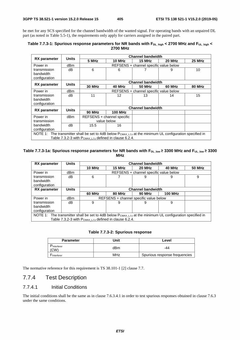
ETSI
ETSI TS 138 521-1 V15.2.0 (2019-05)4053GPP TS 38.521-1 version 15.2.0 Release 15
be met for any SCS specified for the channel bandwidth of the wanted signal. For operating bands with an unpaired DL part (as noted in Table 5.5-1), the requirements only apply for carriers assigned in the paired part.
Table 7.7.3-1: Spurious response parameters for NR bands with FDL_high < 2700 MHz and FUL_high < 2700 MHz
RX parameter Units Channel bandwidth
5 MHz 10 MHz 15 MHz 20 MHz 25 MHz Power in transmission bandwidth configuration
dBm REFSENS + channel specific value below dB 6 6 7 9 10
RX parameter Units Channel bandwidth
30 MHz 40 MHz 50 MHz 60 MHz 80 MHz Power in transmission bandwidth configuration
dBm REFSENS + channel specific value below dB 11 12 13 14 15
RX parameter Units Channel bandwidth
90 MHz 100 MHz Power in transmission bandwidth configuration
dBm REFSENS + channel specific value below
dB 15.5 16
NOTE 1: The transmitter shall be set to 4dB below PCMAX_L,f,c at the minimum UL configuration specified in Table 7.3.2-3 with PCMAX_L,f,c defined in clause 6.2.4.
Table 7.7.3-1a: Spurious response parameters for NR bands with FDL_low ≥ 3300 MHz and FUL_low ≥ 3300 MHz
RX parameter Units Channel bandwidth 10 MHz 15 MHz 20 MHz 40 MHz 50 MHz
Power in transmission bandwidth configuration
dBm REFSENS + channel specific value below dB 6 7 9 9 9
RX parameter Units Channel bandwidth 60 MHz 80 MHz 90 MHz 100 MHz
Power in transmission bandwidth configuration
dBm REFSENS + channel specific value below dB 9 9 9 9
NOTE 1: The transmitter shall be set to 4dB below PCMAX_L,f,c at the minimum UL configuration specified in Table 7.3.2-3 with PCMAX_L,f,c defined in clause 6.2.4.
Table 7.7.3-2: Spurious response
Parameter Unit Level
PInterferer
(CW) dBm -44
FInterferer MHz Spurious response frequencies
The normative reference for this requirement is TS 38.101-1 [2] clause 7.7.
7.7.4 Test Description
7.7.4.1 Initial Conditions
The initial conditions shall be the same as in clause 7.6.3.4.1 in order to test spurious responses obtained in clause 7.6.3 under the same conditions.

ETSI
ETSI TS 138 521-1 V15.2.0 (2019-05)4063GPP TS 38.521-1 version 15.2.0 Release 15
7.7.4.2 Test Procedure
1. SS transmits PDSCH via PDCCH DCI format [1_1] for C_RNTI to transmit the DL RMC according to Table 7.6.3.4.1-1. The SS sends downlink MAC padding bits on the DL RMC.
2. SS sends uplink scheduling information for each UL HARQ process via PDCCH DCI format [0_1] for C_RNTI to schedule the UL RMC according to Table 7.6.3.4.1-1. Since the UE has no payload and no loopback data to send, the UE transmits uplink MAC padding bits on the UL RMC.
3. Set the parameters of the CW signal generator for an interfering signal according to Table 7.7.5-2. The spurious frequencies are taken from records in the final step of test procedures in clause 7.6.3.4.2.
4. Set the downlink signal level according to the table 7.7.5-1 or 7.7.5-1a. Send uplink power control commands to the UE (less or equal to1 dB step size should be used), to ensure that the UE output power is within - PW ± PW dB of the target power level in table 7.7.5-1 or 7.7.5-1a for NR bands for at least the duration of the throughput measurement. PW is the power window according to Table 7.7.5-3 for the carrier frequency f and the channel bandwidth BW.
5. For the spurious frequency, measure the average throughput for a duration sufficient to achieve statistical significance according to Annex H.2.
7.7.4.3 Message Contents
Message contents are according to TS 38.508-1 [5] subclause 4.6.
7.7.5 Test Requirement
The throughput measurement derived in test procedure shall be ≥ 95% of the maximum throughput of the reference measurement channels as specified in Annex A.3.2 with parameters for the wanted signal as specified in Table 7.7.5-1 for NR bands with FDL_high < 2700 MHz and FUL_high < 2700 MHz and in Table 7.7.5-1a for NR bands with FDL_high ≥ 3300 MHz and FUL_high ≥ 3300 MHz and for the interferer as specified in Table 7.7.5-2.
Table 7.7.5-1: Spurious response parameters for NR bands with FDL_high < 2700 MHz and FUL_high < 2700 MHz
RX parameter Units Channel bandwidth
5 MHz 10 MHz 15 MHz 20 MHz 25 MHz Power in transmission bandwidth configuration
dBm REFSENS + channel specific value below dB 6 6 7 9 10
RX parameter Units Channel bandwidth
30 MHz 40 MHz 50 MHz 60 MHz 80 MHz Power in transmission bandwidth configuration
dBm REFSENS + channel specific value below dB 11 12 13 14 15
RX parameter Units Channel bandwidth
90 MHz 100 MHz Power in transmission bandwidth configuration
dBm REFSENS + channel specific value below
dB 15.5 16
NOTE 1: The transmitter shall be set to 4dB below PCMAX_L,f,c at the minimum UL configuration specified in Table 7.3.2-3 with PCMAX_L,f,c defined in clause 6.2.4.

ETSI
ETSI TS 138 521-1 V15.2.0 (2019-05)4073GPP TS 38.521-1 version 15.2.0 Release 15
Table 7.7.5-1a: Spurious response parameters for NR bands with FDL_low ≥ 3300 MHz and FUL_low ≥ 3300 MHz
RX parameter Units Channel bandwidth 10 MHz 15 MHz 20 MHz 40 MHz 50 MHz
Power in transmission bandwidth configuration
dBm REFSENS + channel specific value below dB 6 7 9 9 9
RX parameter Units Channel bandwidth 60 MHz 80 MHz 90 MHz 100 MHz
Power in transmission bandwidth configuration
dBm REFSENS + channel specific value below dB 9 9 9 9
NOTE 1: The transmitter shall be set to 4dB below PCMAX_L,f,c at the minimum UL configuration specified in Table 7.3.2-3 with PCMAX_L,f,c defined in clause 6.2.4.
Table 7.7.5-2: Spurious response
Parameter Unit Level
PInterferer
(CW) dBm -44
FInterferer MHz Spurious response frequencies
Table 7.7.5-3 Power Window (dB) for Spurious Response
f ≤ 3GHz 3GHz < f ≤ 4.2GHz 4.2GHz < f ≤ 6GHz BW ≤ 20MHz 1.4 1.7 2 20MHz < BW ≤ 40MHz 1.4 1.7 2.2 40MHz < BW ≤ 100MHz 2.1 2.3 2.3 Note: Power Window setting comprises two quantities, UE Power tolerance and test system power measurement;
7.7D Spurious response for UL-MIMO Editor’s note:
7.7D.1 Test Purpose
Spurious response verifies the ability of the UE that support UL-MIMO to receive a wanted signal on its assigned channel frequency without exceeding a given degradation due to the presence of an unwanted CW interfering signal at any other frequency at which a response is obtained i.e. for which the out of band blocking for UL-MIMO limit as specified in sub-clause 7.6D.3 is not met.
The lack of the spurious response ability decreases the coverage area when other unwanted interfering signal exists at any other frequency.
7.7D.2 Test Applicability
This test applies to all types of NR UE release 15 and forward that support UL-MIMO.
7.7D.3 Minimum Conformance Requirements
For UE with two transmitter antenna connectors in closed-loop spatial multiplexing scheme, the minimum requirements in Clause 7.7D.3 shall be met with the UL-MIMO configurations specified in Table 6.2D.1.4.1-1 in Clause 6D.2.1 UE maximum output power for UL-MIMO. For UL-MIMO, the parameter PCMAX_L is defined as the total transmitter power over the two transmitter antenna connectors.
The normative reference for this requirement is TS 38.101-1 [2] clause 7.7D.

ETSI
ETSI TS 138 521-1 V15.2.0 (2019-05)4083GPP TS 38.521-1 version 15.2.0 Release 15
7.7D.4 Test Description
7.7D.4.1 Initial Conditions
The initial conditions shall be the same as in clause 7.6D.3.4.1 in order to test spurious responses obtained in clause 7.6D.3 under the same conditions.
7.7D.4.2 Test Procedure
1. SS transmits PDSCH via PDCCH DCI format 1_1 for C_RNTI to transmit the DL RMC according to Test Configuration Table 7.6D.3.4.1-1 in Clause 7.6D.3. The SS sends downlink MAC padding bits on the DL RMC.
2. SS sends uplink scheduling information for each UL HARQ process via PDCCH DCI format 0_1 for C_RNTI to schedule the UL RMC according to Test Configuration Table 7.6D.3.4.1-1 in Clause 7.6D.3. Since the UE has no payload data to send, the UE transmits uplink MAC padding bits on the UL RMC. The PDCCH DCI format 0_1 is specified with condition 2TX_UL_MIMO in 38.508-1 [5] subclause 4.3.6.1.1.2.
3. Set the parameters of the CW signal generator for an interfering signal according to Table 7.7D.5-2. The spurious frequencies are taken from records in the final step of test procedures in clause 7.6D.3.4.2.
4. Set the downlink signal level according to the Table 7.7D.5-1. Send uplink power control commands to the UE (less or equal to 1dB step size should be used), to ensure that the UE output power is within +0, - 3.4 dB of the target level in table 7.7D.5-1 for carrier frequency f ≤ 3.0GHz or within +0, -4.0 dB of the target level for carrier frequency 3.0GHz < f ≤ 4.2GHz, for at least the duration of the throughput measurement.
5. For the spurious frequency, measure the average throughput for a duration sufficient to achieve statistical significance according to Annex H.2.
7.7D.4.3 Message Contents
Message contents are according to TS 38.508-1 [5] clause 4.6 ensuring Table 4.6.3-182 with condition 2TX_UL_MIMO.
7.7D.5 Test Requirement
The throughput measurement derived in test procedure shall be ≥ 95% of the maximum throughput of the reference measurement channels as specified in Annex A.3 with parameters specified in Tables 7.7D.5-1 and 7.7D.5-2.
Table 7.7D.5-1: Spurious response parameters
RX parameter Units Channel bandwidth 10 MHz 15 MHz 20 MHz 40 MHz 50 MHz
Power in transmission bandwidth configuration
dBm REFSENS + channel specific value below dB 6 7 9 9 9
RX parameter Units Channel bandwidth 60 MHz 80 MHz 90 MHz 100 MHz
Power in transmission bandwidth configuration
dBm REFSENS + channel specific value below dB 9 9 9 9
Note 1: The transmitter shall be set to 4dB below PCMAX_L with PCMAX_L as defined in clause 6.2.4. Note 2: The reference measurement channel is specified in Annex A.3 with one sided dynamic OCNG
Pattern OP.1 FDD/TDD as described in Annex A.5.1.1/A.5.2.1.
Table 7.7D.5-2: Spurious Response
Parameter Unit Level
PInterferer
(CW) dBm -44
FInterferer MHz Spurious response frequencies

ETSI
ETSI TS 138 521-1 V15.2.0 (2019-05)4093GPP TS 38.521-1 version 15.2.0 Release 15
7.8 Intermodulation characteristics
7.8.1 General
Intermodulation response rejection is a measure of the capability of the receiver to receiver a wanted signal on its assigned channel frequency in the presence of two or more interfering signals which have a specific frequency relationship to the wanted signal
7.8.2 Wide band Intermodulation
Editor’s note: This clause is incomplete. The following aspects are either missing or not yet determined:- TBD remains in the 38.101-1
7.8.2.1 Test purpose
Intermodulation response tests the UE's ability to receive data with a given average throughput for a specified reference measurement channel, in the presence of two or more interfering signals which have a specific frequency relationship to the wanted signal, under conditions of ideal propagation and no added noise.
A UE unable to meet the throughput requirement under these conditions will decrease the coverage area when two or more interfering signals exist which have a specific frequency relationship to the wanted signal.
7.8.2.2 Test applicability
This test applies to all types of NR UE release 15 and forward.
7.8.2.3 Minimum conformance requirements
The wide band intermodulation requirement is defined using a CW carrier and modulated NR signal as interferer 1 and interferer 2 respectively.
The throughput shall be ≥ 95% of the maximum throughput of the reference measurement channels as specified in Annexes A.2.2, A.2.3 and A.3.2 (with one sided dynamic OCNG Pattern OP.1 FDD/TDD for the DL-signal as described in Annex A.5.1.1/A.5.2.1) with parameters specified in Table 7.8.2-1 for NR bands with FDL_high < 2700 MHz and FUL_high < 2700 MHz and Table 7.8.2-2 for NR bands with FDL_low ≥ 3300 MHz and FUL_low ≥ 3300 MHz. The said relative throughput requirement shall be met for any SCS specified for the channel bandwidth of the wanted signal. For operating bands with an unpaired DL part (as noted in Table 5.5-1), the requirements only apply for carriers assigned in the paired part.
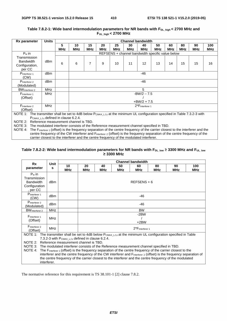
ETSI
ETSI TS 138 521-1 V15.2.0 (2019-05)4103GPP TS 38.521-1 version 15.2.0 Release 15
Table 7.8.2-1: Wide band intermodulation parameters for NR bands with FDL_high < 2700 MHz and FUL_high < 2700 MHz
Rx parameter Units Channel bandwidth 5
MHz 10
MHz 15
MHz 20
MHz 25
MHz 30
MHz 40
MHz 50
MHz 60
MHz 80
MHz 90
MHz 100 MHz
Pw in Transmission
Bandwidth Configuration,
per CC
dBm
REFSENS + channel bandwidth specific value below
6 6 7 9 10 11 12 13 14 15 15 16
PInterferer 1 (CW)
dBm -46
PInterferer 2 (Modulated)
dBm -46
BWInterferer 2 MHz 5 FInterferer 1 (Offset)
MHz -BW/2 – 7.5 /
+BW/2 + 7.5 FInterferer 2 (Offset)
MHz 2*FInterferer 1
NOTE 1: The transmitter shall be set to 4dB below PCMAX_L,f,c at the minimum UL configuration specified in Table 7.3.2-3 with PCMAX_L,f,c defined in clause 6.2.4.
NOTE 2: Reference measurement channel is TBD. NOTE 3: The modulated interferer consists of the Reference measurement channel specified in TBD. NOTE 4: The Finterferer 1 (offset) is the frequency separation of the centre frequency of the carrier closest to the interferer and the
centre frequency of the CW interferer and Finterferer 2 (offset) is the frequency separation of the centre frequency of the carrier closest to the interferer and the centre frequency of the modulated interferer.
Table 7.8.2-2: Wide band intermodulation parameters for NR bands with FDL_low ≥ 3300 MHz and FUL_low ≥ 3300 MHz
Rx parameter
Units
Channel bandwidth 10
MHz 20
MHz 40
MHz 50
MHz 60
MHz 80
MHz 90
MHz 100 MHz
Pw in Transmission
Bandwidth Configuration
, per CC
dBm
REFSENS + 6
PInterferer 1 (CW)
dBm -46
PInterferer 2 (Modulated) dBm -46
BWInterferer 2 MHz BW
FInterferer 1 (Offset) MHz
-2BW /
+2BW FInterferer 2 (Offset) MHz
2*FInterferer 1
NOTE 1: The transmitter shall be set to 4dB below PCMAX_L,f,c at the minimum UL configuration specified in Table 7.3.2-3 with PCMAX_L,f,c defined in clause 6.2.4.
NOTE 2: Reference measurement channel is TBD. NOTE 3: The modulated interferer consists of the Reference measurement channel specified in TBD. NOTE 4: The Finterferer 1 (offset) is the frequency separation of the centre frequency of the carrier closest to the
interferer and the centre frequency of the CW interferer and Finterferer 2 (offset) is the frequency separation of the centre frequency of the carrier closest to the interferer and the centre frequency of the modulated interferer.
The normative reference for this requirement is TS 38.101-1 [2] clause 7.8.2.

ETSI
ETSI TS 138 521-1 V15.2.0 (2019-05)4113GPP TS 38.521-1 version 15.2.0 Release 15
7.8.2.4 Test description
7.8.2.4.1 Initial conditions
Initial conditions are a set of test configurations the UE needs to be tested in and the steps for the SS to take with the UE to reach the correct measurement state.
The initial test configurations consist of environmental conditions, test frequencies, test channel bandwidths and sub-carrier spacing based on NR operating bands specified in Table 5.3.5-1. All of these configurations shall be tested with applicable test parameters for each combination of channel bandwidth and sub-carrier spacing, are shown in table 7.8.2.4.1-1. The details of the uplink and downlink reference measurement channels (RMC) are specified in Annexes A.2 and A.3. Configuration of PDSCH and PDCCH before measurement are specified in Annex C.2.
Table 7.8.2.4.1-1: Test Configuration Table
Default Conditions Test Environment as specified in TS 38.508-1 [5] subclause 4.1
Normal
Test Frequencies as specified in TS 38.508-1 [5] subclause 4.3.1
Mid range
Test Channel Bandwidths as specified in TS 38.508-1 [5] subclause 4.3.1
Lowest, Mid, Highest
Test SCS as specified in Table 5.3.5-1 Highest Test Parameters
Downlink Configuration Uplink Configuration Test ID Mod'n RB allocation Mod'n RB allocation
1 CP-OFDM QPSK NOTE 1 DFT-s-OFDM QPSK NOTE 1 NOTE 1: The specific configuration of uplink and downlink are defined in Table 7.3.2.4.1-1.
1. Connect the SS to the UE antenna connectors as shown in TS 38.508-1 [5] Annex A, in Figure A.3.1.4.3 for TE diagram and section A.3.2.1 for UE diagram.
2. The parameter settings for the cell are set up according to TS 38.508-1 [5] subclause 4.4.3.
3. Downlink signals are initially set up according to Annex C.0, C.1, C.2 , C.3.1 , and uplink signals according to Annex G.0, G.1, G.2, G.3.1.
4. The DL and UL Reference Measurement channels are set according to Table 7.5.4.1-1.
5. Propagation conditions are set according to Annex B.0 .
6. Ensure the UE is in state RRC_CONNECTED with generic procedure parameters Connectivity NR, Connected without release On, Test Mode On and Test Loop Function On according to TS 38.508-1 [5] clause 4.5. Message content are defined in clause 7.5.4.3.
7.8.2.4.2 Test procedure
1. SS transmits PDSCH via PDCCH DCI format 1_1 for C_RNTI to transmit the DL RMC according to Table 7.8.2.4.1-1. The SS sends downlink MAC padding bits on the DL RMC.
2. SS sends uplink scheduling information for each UL HARQ process via PDCCH DCI format 0_1 for C_RNTI to schedule the UL RMC according to Table 7.8.2.4.1-1. Since the UE has no payload data to send, the UE transmits uplink MAC padding bits on the UL RMC.
3. Set the Downlink signal level to the value as defined in Table 7.8.2.5-1. Send Uplink power control commands to the UE (less or equal to 1dB step size should be used), to ensure that the UE output power is within -PW ± PW dB of the target level in Table 7.8.2.5-1. PW is the power window according to Table 7.8.2-3 for the carrier frequency f and the channel bandwidth BW.
4. Set the Interfering signal levels to the values as defined in Table 7.8.2.5-1 and frequency below the wanted signal, using a modulated interferer bandwidth as defined in [TBD] of the present document.
5. Measure the average throughput for a duration sufficient to achieve statistical significance according to Annex G.2.

ETSI
ETSI TS 138 521-1 V15.2.0 (2019-05)4123GPP TS 38.521-1 version 15.2.0 Release 15
6. Repeat steps from 3 to 5, using an interfering signal above the wanted signal at step 4.
7.8.2.4.3 Message contents
Message contents are according to TS 38.508-1 [5] subclause 4.6 with DFT-s-OFDM condition in Table 4.6.3-118 PUSCH-Config.
7.8.2.5 Test requirement
The throughput shall be ≥ 95% of the maximum throughput of the reference measurement channels as specified in Annex A.3.2 with parameters specified in Table 7.8.2.5-1 for the specified wanted signal mean power in the presence of two interfering signals.
Table 7.8.2.5-1: Wide band intermodulation parameters for NR bands with FDL_high < 2700 MHz and FUL_high < 2700 MHz
Rx parameter Units Channel bandwidth 5
MHz 10
MHz 15
MHz 20
MHz 25
MHz 30
MHz 40
MHz 50
MHz 60
MHz 80
MHz 90
MHz 100 MHz
Pw in Transmission
Bandwidth Configuration,
per CC
dBm
REFSENS + channel bandwidth specific value below
6 6 7 9 10 11 12 13 14 15 15 16
PInterferer 1 (CW)
dBm -46
PInterferer 2 (Modulated)
dBm -46
BWInterferer 2 MHz 5 FInterferer 1 (Offset)
MHz -BW/2 – 7.5 /
+BW/2 + 7.5 FInterferer 2 (Offset)
MHz 2*FInterferer 1
NOTE 1: The transmitter shall be set to 4dB below PCMAX_L,f,c at the minimum UL configuration specified in Table 7.3.2-3 with PCMAX_L,f,c defined in clause 6.2.4.
NOTE 2: Reference measurement channel is TBD. NOTE 3: The modulated interferer consists of the Reference measurement channel specified in TBD. NOTE 4: The Finterferer 1 (offset) is the frequency separation of the centre frequency of the carrier closest to the interferer and the
centre frequency of the CW interferer and Finterferer 2 (offset) is the frequency separation of the centre frequency of the carrier closest to the interferer and the centre frequency of the modulated interferer.
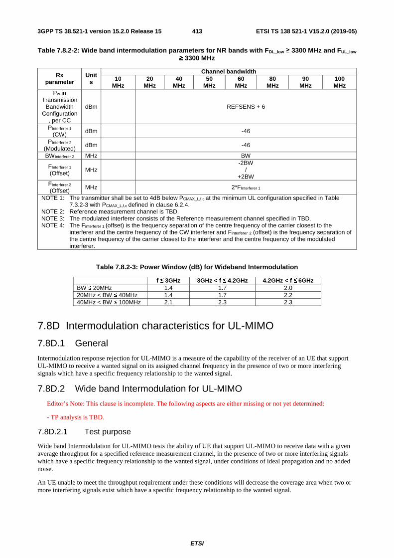
ETSI
ETSI TS 138 521-1 V15.2.0 (2019-05)4133GPP TS 38.521-1 version 15.2.0 Release 15
Table 7.8.2-2: Wide band intermodulation parameters for NR bands with FDL_low ≥ 3300 MHz and FUL_low ≥ 3300 MHz
Rx parameter
Units
Channel bandwidth 10
MHz 20
MHz 40
MHz 50
MHz 60
MHz 80
MHz 90
MHz 100 MHz
Pw in Transmission
Bandwidth Configuration
, per CC
dBm
REFSENS + 6
PInterferer 1 (CW)
dBm -46
PInterferer 2 (Modulated)
dBm -46
BWInterferer 2 MHz BW
FInterferer 1 (Offset) MHz
-2BW /
+2BW FInterferer 2 (Offset)
MHz 2*FInterferer 1
NOTE 1: The transmitter shall be set to 4dB below PCMAX_L,f,c at the minimum UL configuration specified in Table 7.3.2-3 with PCMAX_L,f,c defined in clause 6.2.4.
NOTE 2: Reference measurement channel is TBD. NOTE 3: The modulated interferer consists of the Reference measurement channel specified in TBD. NOTE 4: The Finterferer 1 (offset) is the frequency separation of the centre frequency of the carrier closest to the
interferer and the centre frequency of the CW interferer and Finterferer 2 (offset) is the frequency separation of the centre frequency of the carrier closest to the interferer and the centre frequency of the modulated interferer.
Table 7.8.2-3: Power Window (dB) for Wideband Intermodulation
f ≤ 3GHz 3GHz < f ≤ 4.2GHz 4.2GHz < f ≤ 6GHz BW ≤ 20MHz 1.4 1.7 2.0 20MHz < BW ≤ 40MHz 1.4 1.7 2.2 40MHz < BW ≤ 100MHz 2.1 2.3 2.3
7.8D Intermodulation characteristics for UL-MIMO
7.8D.1 General
Intermodulation response rejection for UL-MIMO is a measure of the capability of the receiver of an UE that support UL-MIMO to receive a wanted signal on its assigned channel frequency in the presence of two or more interfering signals which have a specific frequency relationship to the wanted signal.
7.8D.2 Wide band Intermodulation for UL-MIMO
Editor’s Note: This clause is incomplete. The following aspects are either missing or not yet determined:
- TP analysis is TBD.
7.8D.2.1 Test purpose
Wide band Intermodulation for UL-MIMO tests the ability of UE that support UL-MIMO to receive data with a given average throughput for a specified reference measurement channel, in the presence of two or more interfering signals which have a specific frequency relationship to the wanted signal, under conditions of ideal propagation and no added noise.
An UE unable to meet the throughput requirement under these conditions will decrease the coverage area when two or more interfering signals exist which have a specific frequency relationship to the wanted signal.

ETSI
ETSI TS 138 521-1 V15.2.0 (2019-05)4143GPP TS 38.521-1 version 15.2.0 Release 15
7.8D.2.2 Test applicability
This test case applies to all types of NR UE release 15 and forward that support UL-MIMO.
7.8D.2.3 Minimum conformance requirements
For UE(s) with two transmitter antenna connectors in closed-loop spatial multiplexing scheme, the minimum requirements in subclause 7.8 shall be met with the UL-MIMO configurations described in sub-clause 6.2D.1. For UL-MIMO, the parameter PCMAX_L is defined as the total transmitter power over the two transmit antenna connectors.
The normative reference for this requirement is TS 38.101-1 [2] clause 7.8D.
7.8D.2.4 Test description
7.8D.2.4.1 Initial conditions
Initial conditions are a set of test configurations the UE needs to be tested in and the steps for the SS to take with the UE to reach the correct measurement state.
The initial test configurations consist of environmental conditions, test frequencies, test channel bandwidths and sub-carrier spacing based on NR operating bands specified in table 5.3.5-1. All of these configurations shall be tested with applicable test parameters for each combination of channel bandwidth and sub-carrier spacing, are shown in table 7.8D.2.4.1-1. The details of the uplink and downlink reference measurement channels (RMC) are specified in Annexes A.2 and A.3. The details of the OCNG patterns used are specified in Annex A.5. Configurations of PDSCH and PDCCH before measurement are specified in Annex C.2.
Table 7.8D.2.4.1-1: Test Configuration Table
Default Conditions Test Environment as specified in TS 38.508-1 [5] subclause 4.1
Normal
Test Frequencies as specified in TS 38.508-1 [5] subclause 4.3.1
Mid range
Test Channel Bandwidths as specified in TS 38.508-1 [5] subclause 4.3.1
Lowest, Mid and Highest
Test SCS as specified in Table 5.3.5-1 Lowest Test Parameters
Downlink Configuration Uplink Configuration Test ID Mod'n RB allocation Mod'n RB allocation
1 CP-OFDM QPSK NOTE 1 CP-OFDM QPSK NOTE 1 NOTE 1: The specific configuration of uplink and downlink are defined in Table 7.3D.2.4.1-1.
1. Connect the SS and interfering sources to the UE antenna connectors as shown in TS 38.508-1 [5] Annex A, in Figure A.3.1.4.6 for TE diagram and section A.3.2 for UE diagram.
2. The parameter settings for the cell are set up according to TS 38.508-1 [5] subclause 4.4.3.
3. Downlink signals are initially set up according to Annex C.0, C.1, C.2, C.3.1, and uplink signals according to Annex G.0, G.1, G.2, G.3.1.
4. The DL and UL Reference Measurement channels are set according to Table 7.8D.2.4.1-1.
5. Propagation conditions are set according to Annex B.0.
6. Ensure the UE is in state RRC_CONNECTED with generic procedure parameters Connectivity NR, Connected without release On , Test Mode On and Test Loop Function On according to TS 38.508-1 [5] clause 4.5. Message content are defined in clause 7.8D.2.4.3.
7.8D.2.4.2 Test procedure
Same test procedure as specified in 7.8.2.4.2 with the following exceptions:
PW is the power window according to Table 7.8D.2.5-1 for the carrier frequency f and the channel bandwidth BW.

ETSI
ETSI TS 138 521-1 V15.2.0 (2019-05)4153GPP TS 38.521-1 version 15.2.0 Release 15
7.8D.2.4.3 Message contents
Message contents are according to TS 38.508-1 [5] subclause 4.6 ensuring Table 4.6.3-182 with condition 2TX_UL_MIMO.7.8D.2.5
Test requirement
Same test requirement as specified in 7.8.2.5 with the following exceptions:
The power window table is replaced by Table 7.8D.2.5-1.
Table 7.8D.2.5-1: Power Window (dB) for Wide band Intermodulation for UL-MIMO
f ≤ 3GHz 3GHz < f ≤ 4.2GHz 4.2GHz < f ≤ 6GHz BW ≤ 20MHz 1.7 2.1 2.5 20MHz < BW ≤ 40MHz 1.7 2.1 2.8 40MHz < BW ≤ 100MHz 2.7 3.0 3.0 NOTE: Power Window comprises two parts, UE Power step tolerance and test system
power measurement uncertainty.
7.9 Spurious emissions The spurious emissions power is the power of emissions generated or amplified in a receiver that appear at the UE antenna connector.
7.9.1 Test purpose
Test verifies the UE's spurious emissions meet the requirements described in clause 7.9.3.
Excess spurious emissions increase the interference to other systems.
7.9.2 Test applicability
This test applies to all types of NR UE release 15 and forward.
7.9.3 Minimum conformance requirements
The spurious emissions power is the power of emissions generated or amplified in a receiver that appear at the UE antenna connector.
The power of any narrow band CW spurious emission shall not exceed the maximum level specified in Table 7.9.3-1
Table 7.9.3-1: General receiver spurious emission requirements
Frequency range Measurement bandwidth
Maximum level
NOTE
30 MHz ≤ f < 1 GHz 100 kHz -57 dBm 1 GHz ≤ f ≤ 12.75 GHz 1 MHz -47 dBm
12.75 GHz ≤ f ≤ 5th harmonic of the upper frequency edge of the DL operating band in
GHz
1 MHz -47 dBm 2
12.75 GHz – 26 GHz 1 MHz -47dBm 3 NOTE 1: Unused PDCCH resources are padded with resource element groups with power level given
by PDCCH_RA/RB as defined in Annex C.3.1. NOTE 2: Applies for Band that the upper frequency edge of the DL Band more than 2.69 GHz. NOTE 3: Applies for Band that the upper frequency edge of the DL Band more than 5.2 GHz.
The normative reference for this requirement is TS 38.101-1 [2] clause 7.9.

ETSI
ETSI TS 138 521-1 V15.2.0 (2019-05)4163GPP TS 38.521-1 version 15.2.0 Release 15
7.9.4 Test description
7.9.4.1 Initial conditions
Initial conditions are a set of test configurations the UE needs to be tested in and the steps for the SS to take with the UE to reach the correct measurement state.
The initial test configurations consist of environmental conditions, test frequencies, test channel bandwidths and sub-carrier spacing based on NR operating bands specified in Table 5.3.5-1. All of these configurations shall be tested with applicable test parameters for each combination of channel bandwidth and sub-carrier spacing, are shown in table 7.9.4.1-1. The details of the uplink and downlink reference measurement channels (RMC) are specified in Annexes A.2 and A.3. Configuration of PDSCH and PDCCH before measurement are specified in Annex C.2.
Table 7.9.4.1-1: Test Configuration Table
Default Conditions Test Environment as specified in TS 38.508-1 [5] subclause 4.1
Normal
Test Frequencies as specified in TS 38.508-1 [5] subclause 4.3.1
Low range, Mid range, High range
Test Channel Bandwidths as specified in TS 38.508-1 [5] subclause 4.3.1
Highest
Test SCS as specified in Table 5.3.5-1 Highest Test Parameters
Downlink Configuration Uplink Configuration Test ID Mod'n RB allocation Mod'n RB allocation
1 N/A 0 N/A 0 NOTE 1: The specific configuration of uplink and downlink are defined in Table 7.3.2.4.1-1.
1. Connect the SS to the UE antenna connectors as shown in TS 38.508-1 [5] Annex A, in Figure A.3.1.5 for TE
diagram and section A.3.2.1 for UE diagram.
2. The parameter settings for the cell are set up according to TS 38.508-1 [5] subclause 4.4.3.
3. Downlink signals are initially set up according to Annex C.0, C.1, C.2 , C.3.1 , and uplink signals according to Annex G.0, G.1, G.2, G.3.1.
4. The DL and UL Reference Measurement channels are set according to Table 7.9.4.1-1.
5. Propagation conditions are set according to Annex B.0 .
6. Ensure the UE is in state RRC_CONNECTED with generic procedure parameters Connectivity NR, Connected without release On, Test Mode On and Test Loop Function On according to TS 38.508-1 [5] clause 4.5. Message content are defined in clause 7.5.4.3.
7.9.4.2 Test procedure
1. Sweep the spectrum analyzer (or equivalent equipment) over a frequency range and measure the average power of spurious emission.
2. Repeat step 1 for all NR Rx antennas of the UE.
7.9.4.3 Message contents
Message contents are according to TS 38.508-1 [5] subclause 4.6.
7.9.5 Test requirement
The measured spurious emissions derived in step 1), shall not exceed the maximum level specified in Table 7.9.5-1.

ETSI
ETSI TS 138 521-1 V15.2.0 (2019-05)4173GPP TS 38.521-1 version 15.2.0 Release 15
Table 7.9.5-1: General receiver spurious emission requirements
Frequency range Measurement bandwidth
Maximum level
NOTE
30 MHz ≤ f < 1 GHz 100 kHz -57 dBm 1 GHz ≤ f ≤ 12.75 GHz 1 MHz -47 dBm
12.75 GHz ≤ f ≤ 5th harmonic of the upper frequency edge of the DL operating band in
GHz
1 MHz -47 dBm 2
12.75 GHz – 26 GHz 1 MHz -47dBm 3 NOTE 1: Unused PDCCH resources are padded with resource element groups with power level given
by PDCCH_RA/RB as defined in Annex C.3.1. NOTE 2: Applies for Band that the upper frequency edge of the DL Band more than 2.69 GHz. NOTE 3: Applies for Band that the upper frequency edge of the DL Band more than 5.2 GHz.
7.9A.0 Minimum conformance requirements
For inter-band carrier aggregation with one component carrier per operating band and the uplink assigned to one NR band, the UE shall meet the Rx spurious emissions requirements specified in subclause 7.9 for each component carrier while all downlink carriers are active.
The normative reference for this requirement is TS 38.101-1 [2] clause 7.9A.3.
7.9A.1 Spurious emission for 2DL CA
Editor's note: This test case is not complete. Following aspects are either missing or not yet determined:
- Table [5.3A.5-X] NR CA configurations and bandwidth combination sets defined for inter-band 2DL CA
7.9A.1.1 Test Purpose
Test verifies the UE's spurious emissions meet the requirements described in clause 7.9A.1.3.
Excess spurious emissions increase the interference to other systems.
7.9A.1.2 Test Applicability
This test case applies to all types of NR UE release 15 and forward that support inter-band 2DL CA with a DL-only band.
7.9A.1.3 Minimum Conformance Requirements
The minimum conformance requirements are defined in clause 7.9A.0.
7.9A.1.4 Test Description
7.9A.1.4.1 Initial Conditions
Initial conditions are a set of test configurations the UE needs to be tested in and the steps for the SS to take with the UE to reach the correct measurement state.
The initial test configurations consist of environmental conditions, test frequencies, and channel bandwidths based on NR CA bands specified in Table [5.3A.5-X]. All of these configurations shall be tested with applicable test parameters for each CA Configuration, and are shown in Table 7.9A.1.4.1-1. The details of the uplink reference measurement channels (RMCs) are specified in Annexe A.2. Configurations of PDSCH and PDCCH before measurement are specified in Annex C.2.
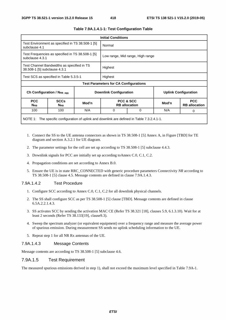
ETSI
ETSI TS 138 521-1 V15.2.0 (2019-05)4183GPP TS 38.521-1 version 15.2.0 Release 15
Table 7.9A.1.4.1-1: Test Configuration Table
Initial Conditions
Test Environment as specified in TS 38.508-1 [5] subclause 4.1 Normal
Test Frequencies as specified in TS 38.508-1 [5] subclause 4.3.1
Low range, Mid range, High range
Test Channel Bandwidths as specified in TS 38.508-1 [5] subclause 4.3.1 Highest
Test SCS as specified in Table 5.3.5-1 Highest
Test Parameters for CA Configurations
Ch Configuration / NRB_agg Downlink Configuration Uplink Configuration
PCC NRB
SCCs NRB Mod'n PCC & SCC
RB allocation Mod'n PCC RB allocation
100 100 N/A 0 0 N/A 0
NOTE 1: The specific configuration of uplink and downlink are defined in Table 7.3.2.4.1-1.
1. Connect the SS to the UE antenna connectors as shown in TS 38.508-1 [5] Annex A, in Figure [TBD] for TE diagram and section A.3.2.1 for UE diagram.
2. The parameter settings for the cell are set up according to TS 38.508-1 [5] subclause 4.4.3.
3. Downlink signals for PCC are initially set up according toAnnex C.0, C.1, C.2.
4. Propagation conditions are set according to Annex B.0.
5. Ensure the UE is in state RRC_CONNECTED with generic procedure parameters Connectivity NR according to TS 38.508-1 [5] clause 4.5. Message contents are defined in clause 7.9A.1.4.3.
7.9A.1.4.2 Test Procedure
1. Configure SCC according to Annex C.0, C.1, C.2 for all downlink physical channels.
2. The SS shall configure SCC as per TS 38.508-1 [5] clause [TBD]. Message contents are defined in clause 6.5A.2.2.1.4.3.
3. SS activates SCC by sending the activation MAC CE (Refer TS 38.321 [18], clauses 5.9, 6.1.3.10). Wait for at least 2 seconds (Refer TS 38.133[19], clause9.3).
4. Sweep the spectrum analyzer (or equivalent equipment) over a frequency range and measure the average power of spurious emission. During measurement SS sends no uplink scheduling information to the UE.
5. Repeat step 1 for all NR Rx antennas of the UE.
7.9A.1.4.3 Message Contents
Message contents are according to TS 38.508-1 [5] subclause 4.6.
7.9A.1.5 Test Requirement
The measured spurious emissions derived in step 1), shall not exceed the maximum level specified in Table 7.9A-1.
ETSI
ETSI TS 138 521-1 V15.2.0 (2019-05)4193GPP TS 38.521-1 version 15.2.0 Release 15
Annex A (normative): Measurement channels
A.1 General The throughput values defined in the measurement channels specified in Annex A, are calculated and are valid per data stream (codeword). For multi-stream (more than one codeword) transmissions, the throughput referenced in the minimum requirements is the sum of throughputs of all data streams (code words).
The UE category entry in the definition of the reference measurement channel in Annex A is only informative and reveals the UE categories, which can support the corresponding measurement channel. Whether the measurement channel is used for testing a certain UE category or not is specified in the individual minimum requirements.
A.2 UL reference measurement channels
A.2.1 General The measurement channels in the following subclauses are defined to derive the requirements in clause 6 (Transmitter Characteristics) and clause 7 (Receiver Characteristics). The measurement channels represent example configurations of physical channels for different data rates.

ETSI
ETSI TS 138 521-1 V15.2.0 (2019-05)4203GPP TS 38.521-1 version 15.2.0 Release 15
A.2.2 Reference measurement channels for FDD
A.2.2.1 DFT-s-OFDM Pi/2-BPSK
Table A.2.2.1-1: Reference Channels for DFT-s-OFDM Pi/2-BPSK for 15kHz SCS
Parameter
Channel bandwidt
h
Subcarrier Spacing
Allocated
resource blocks
DFT-s-OFDM
Symbols per slot
(Note 1)
Modulation
MCS Index (Note
2)
Target Coding
Rate
Payload size
Transport block CRC
LDPC Base Graph
Number of code blocks per slot (Note 3)
Total number of bits
per slot
Total modulated symbols
per slot
Unit MHz KHz Bits Bits Bits 5-50 15 1 11 pi/2 BPSK 0 1/4 32 16 2 1 132 132 5 15 12 11 pi/2 BPSK 0 1/4 384 16 2 1 1584 1584 5 15 25 11 pi/2 BPSK 0 1/4 808 16 2 1 3300 3300 10 15 25 11 pi/2 BPSK 0 1/4 808 16 2 1 3300 3300 10 15 50 11 pi/2 BPSK 0 1/4 1544 16 2 1 6600 6600 15 15 36 11 pi/2 BPSK 0 1/4 1128 16 2 1 4752 4752 15 15 75 11 pi/2 BPSK 0 1/4 2408 16 2 1 9900 9900 20 15 50 11 pi/2 BPSK 0 1/4 1544 16 2 1 6600 6600 20 15 100 11 pi/2 BPSK 0 1/4 3104 16 2 1 13200 13200 25 15 64 11 pi/2 BPSK 0 1/4 2024 16 2 1 8448 8448 25 15 128 11 pi/2 BPSK 0 1/4 3976 24 2 2 16896 16896 30 15 80 11 pi/2 BPSK 0 1/4 2472 16 2 1 10560 10560 30 15 160 11 pi/2 BPSK 0 1/4 4872 24 2 2 21120 21120 40 15 108 11 pi/2 BPSK 0 1/4 3368 16 2 1 14256 14256 40 15 216 11 pi/2 BPSK 0 1/4 6664 24 2 2 28512 28512 50 15 135 11 pi/2 BPSK 0 1/4 4104 24 2 2 17820 17820 50 15 270 11 pi/2 BPSK 0 1/4 8448 24 2 3 35640 35640 Note 1: PUSCH mapping Type-A and single-symbol DM-RS configuration Type-1 with 2 additional DM-RS symbols, such that the DM-RS positions are set to symbols 2, 7,
11. DMRS is [TDM’ed] with PUSCH data. Note 2: MCS Index is based on MCS table 6.1.4.1-1 defined in TS 38.214 [12]. Note 3: If more than one Code Block is present, an additional CRC sequence of L = 24 Bits is attached to each Code Block (otherwise L = 0 Bit)
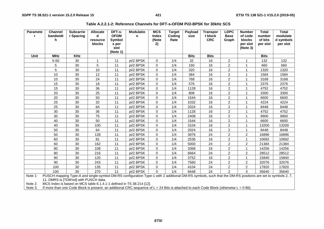
ETSI
ETSI TS 138 521-1 V15.2.0 (2019-05)4213GPP TS 38.521-1 version 15.2.0 Release 15
Table A.2.2.1-2: Reference Channels for DFT-s-OFDM Pi/2-BPSK for 30kHz SCS
Parameter
Channel bandwidt
h
Subcarrier Spacing
Allocated
resource blocks
DFT-s-OFDM
Symbols per slot
(Note 1)
Modulation
MCS Index (Note
2)
Target Coding
Rate
Payload size
Transport block CRC
LDPC Base Graph
Number of code blocks per slot (Note 3)
Total number of bits
per slot
Total modulated symbols
per slot
Unit MHz KHz Bits Bits Bits 5-50 30 1 11 pi/2 BPSK 0 1/4 32 16 2 1 132 132 5 30 5 11 pi/2 BPSK 0 1/4 160 16 2 1 660 660 5 30 10 11 pi/2 BPSK 0 1/4 320 16 2 1 1320 1320 10 30 12 11 pi/2 BPSK 0 1/4 384 16 2 1 1584 1584 10 30 24 11 pi/2 BPSK 0 1/4 768 16 2 1 3168 3168 15 30 18 11 pi/2 BPSK 0 1/4 576 16 2 1 2376 2376 15 30 36 11 pi/2 BPSK 0 1/4 1128 16 2 1 4752 4752 20 30 25 11 pi/2 BPSK 0 1/4 808 16 2 1 3300 3300 20 30 50 11 pi/2 BPSK 0 1/4 1544 16 2 1 6600 6600 25 30 32 11 pi/2 BPSK 0 1/4 1032 16 2 1 4224 4224 25 30 64 11 pi/2 BPSK 0 1/4 2024 16 2 1 8448 8448 30 30 36 11 pi/2 BPSK 0 1/4 1128 16 2 1 4752 4752 30 30 75 11 pi/2 BPSK 0 1/4 2408 16 2 1 9900 9900 40 30 50 11 pi/2 BPSK 0 1/4 1544 16 2 1 6600 6600 40 30 100 11 pi/2 BPSK 0 1/4 3104 16 2 1 13200 13200 50 30 64 11 pi/2 BPSK 0 1/4 2024 16 2 1 8448 8448 50 30 128 11 pi/2 BPSK 0 1/4 3976 24 2 2 16896 16896 60 30 81 11 pi/2 BPSK 0 1/4 2536 16 2 1 10692 10692 60 30 162 11 pi/2 BPSK 0 1/4 5000 24 2 2 21384 21384 80 30 108 11 pi/2 BPSK 0 1/4 3368 16 2 1 14256 14256 80 30 216 11 pi/2 BPSK 0 1/4 6664 24 2 2 28512 28512 90 30 120 11 pi/2 BPSK 0 1/4 3752 16 2 1 15840 15840 90 30 243 11 pi/2 BPSK 0 1/4 7560 24 2 2 32076 32076 100 30 135 11 pi/2 BPSK 0 1/4 4104 24 2 2 17820 17820 100 30 270 11 pi/2 BPSK 0 1/4 8448 24 2 3 35640 35640 Note 1: PUSCH mapping Type-A and single-symbol DM-RS configuration Type-1 with 2 additional DM-RS symbols, such that the DM-RS positions are set to symbols 2, 7,
11. DMRS is [TDM’ed] with PUSCH data. Note 2: MCS Index is based on MCS table 6.1.4.1-1 defined in TS 38.214 [12]. Note 3: If more than one Code Block is present, an additional CRC sequence of L = 24 Bits is attached to each Code Block (otherwise L = 0 Bit)
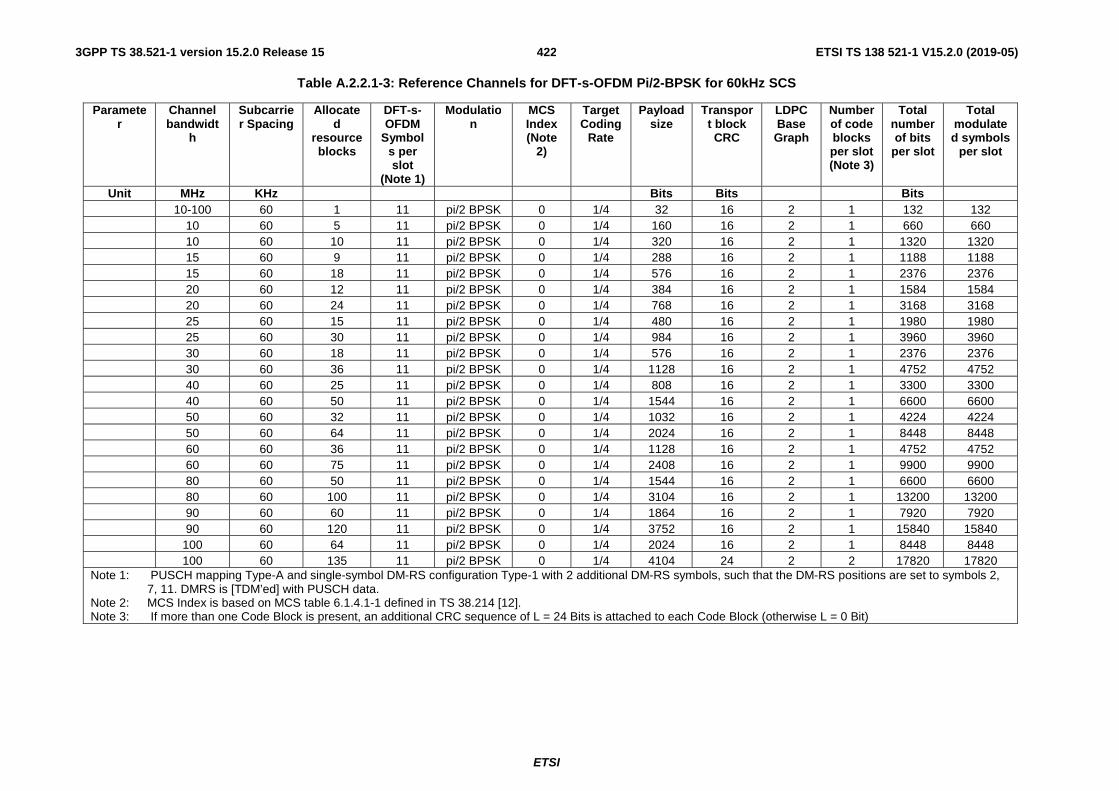
ETSI
ETSI TS 138 521-1 V15.2.0 (2019-05)4223GPP TS 38.521-1 version 15.2.0 Release 15
Table A.2.2.1-3: Reference Channels for DFT-s-OFDM Pi/2-BPSK for 60kHz SCS
Parameter
Channel bandwidt
h
Subcarrier Spacing
Allocated
resource blocks
DFT-s-OFDM
Symbols per slot
(Note 1)
Modulation
MCS Index (Note
2)
Target Coding
Rate
Payload size
Transport block CRC
LDPC Base Graph
Number of code blocks per slot (Note 3)
Total number of bits
per slot
Total modulated symbols
per slot
Unit MHz KHz Bits Bits Bits 10-100 60 1 11 pi/2 BPSK 0 1/4 32 16 2 1 132 132 10 60 5 11 pi/2 BPSK 0 1/4 160 16 2 1 660 660 10 60 10 11 pi/2 BPSK 0 1/4 320 16 2 1 1320 1320 15 60 9 11 pi/2 BPSK 0 1/4 288 16 2 1 1188 1188 15 60 18 11 pi/2 BPSK 0 1/4 576 16 2 1 2376 2376 20 60 12 11 pi/2 BPSK 0 1/4 384 16 2 1 1584 1584 20 60 24 11 pi/2 BPSK 0 1/4 768 16 2 1 3168 3168 25 60 15 11 pi/2 BPSK 0 1/4 480 16 2 1 1980 1980 25 60 30 11 pi/2 BPSK 0 1/4 984 16 2 1 3960 3960 30 60 18 11 pi/2 BPSK 0 1/4 576 16 2 1 2376 2376 30 60 36 11 pi/2 BPSK 0 1/4 1128 16 2 1 4752 4752 40 60 25 11 pi/2 BPSK 0 1/4 808 16 2 1 3300 3300 40 60 50 11 pi/2 BPSK 0 1/4 1544 16 2 1 6600 6600 50 60 32 11 pi/2 BPSK 0 1/4 1032 16 2 1 4224 4224 50 60 64 11 pi/2 BPSK 0 1/4 2024 16 2 1 8448 8448 60 60 36 11 pi/2 BPSK 0 1/4 1128 16 2 1 4752 4752 60 60 75 11 pi/2 BPSK 0 1/4 2408 16 2 1 9900 9900 80 60 50 11 pi/2 BPSK 0 1/4 1544 16 2 1 6600 6600 80 60 100 11 pi/2 BPSK 0 1/4 3104 16 2 1 13200 13200 90 60 60 11 pi/2 BPSK 0 1/4 1864 16 2 1 7920 7920 90 60 120 11 pi/2 BPSK 0 1/4 3752 16 2 1 15840 15840 100 60 64 11 pi/2 BPSK 0 1/4 2024 16 2 1 8448 8448 100 60 135 11 pi/2 BPSK 0 1/4 4104 24 2 2 17820 17820 Note 1: PUSCH mapping Type-A and single-symbol DM-RS configuration Type-1 with 2 additional DM-RS symbols, such that the DM-RS positions are set to symbols 2,
7, 11. DMRS is [TDM’ed] with PUSCH data. Note 2: MCS Index is based on MCS table 6.1.4.1-1 defined in TS 38.214 [12]. Note 3: If more than one Code Block is present, an additional CRC sequence of L = 24 Bits is attached to each Code Block (otherwise L = 0 Bit)
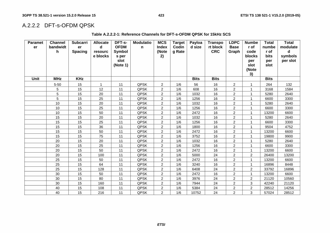
ETSI
ETSI TS 138 521-1 V15.2.0 (2019-05)4233GPP TS 38.521-1 version 15.2.0 Release 15
A.2.2.2 DFT-s-OFDM QPSK
Table A.2.2.2-1: Reference Channels for DFT-s-OFDM QPSK for 15kHz SCS
Parameter
Channel bandwidt
h
Subcarrier
Spacing
Allocated
resource blocks
DFT-s-OFDM
Symbols per slot
(Note 1)
Modulation
MCS Index (Note
2)
Target Coding Rate
Payload size
Transport block
CRC
LDPC Base
Graph
Number of
code blocks
per slot
(Note 3)
Total numbe
r of bits per slot
Total modulate
d symbols per slot
Unit MHz KHz Bits Bits Bits 5-50 15 1 11 QPSK 2 1/6 56 16 2 1 264 132 5 15 12 11 QPSK 2 1/6 608 16 2 1 3168 1584 5 15 20 11 QPSK 2 1/6 1032 16 2 1 5280 2640 5 15 25 11 QPSK 2 1/6 1256 16 2 1 6600 3300 10 15 20 11 QPSK 2 1/6 1032 16 2 1 5280 2640 10 15 25 11 QPSK 2 1/6 1256 16 2 1 6600 3300 10 15 50 11 QPSK 2 1/6 2472 16 2 1 13200 6600 15 15 20 11 QPSK 2 1/6 1032 16 2 1 5280 2640 15 15 25 11 QPSK 2 1/6 1256 16 2 1 6600 3300 15 15 36 11 QPSK 2 1/6 1800 16 2 1 9504 4752 15 15 50 11 QPSK 2 1/6 2472 16 2 1 13200 6600 15 15 75 11 QPSK 2 1/6 3752 16 2 1 19800 9900 20 15 20 11 QPSK 2 1/6 1032 16 2 1 5280 2640 20 15 25 11 QPSK 2 1/6 1256 16 2 1 6600 3300 20 15 50 11 QPSK 2 1/6 2472 16 2 1 13200 6600 20 15 100 11 QPSK 2 1/6 5000 24 2 2 26400 13200 25 15 50 11 QPSK 2 1/6 2472 16 2 1 13200 6600 25 15 64 11 QPSK 2 1/6 3240 16 2 1 16896 8448 25 15 128 11 QPSK 2 1/6 6408 24 2 2 33792 16896 30 15 50 11 QPSK 2 1/6 2472 16 2 1 13200 6600 30 15 80 11 QPSK 2 1/6 3976 24 2 2 21120 10560 30 15 160 11 QPSK 2 1/6 7944 24 2 3 42240 21120 40 15 108 11 QPSK 2 1/6 5384 24 2 2 28512 14256 40 15 216 11 QPSK 2 1/6 10752 24 2 3 57024 28512
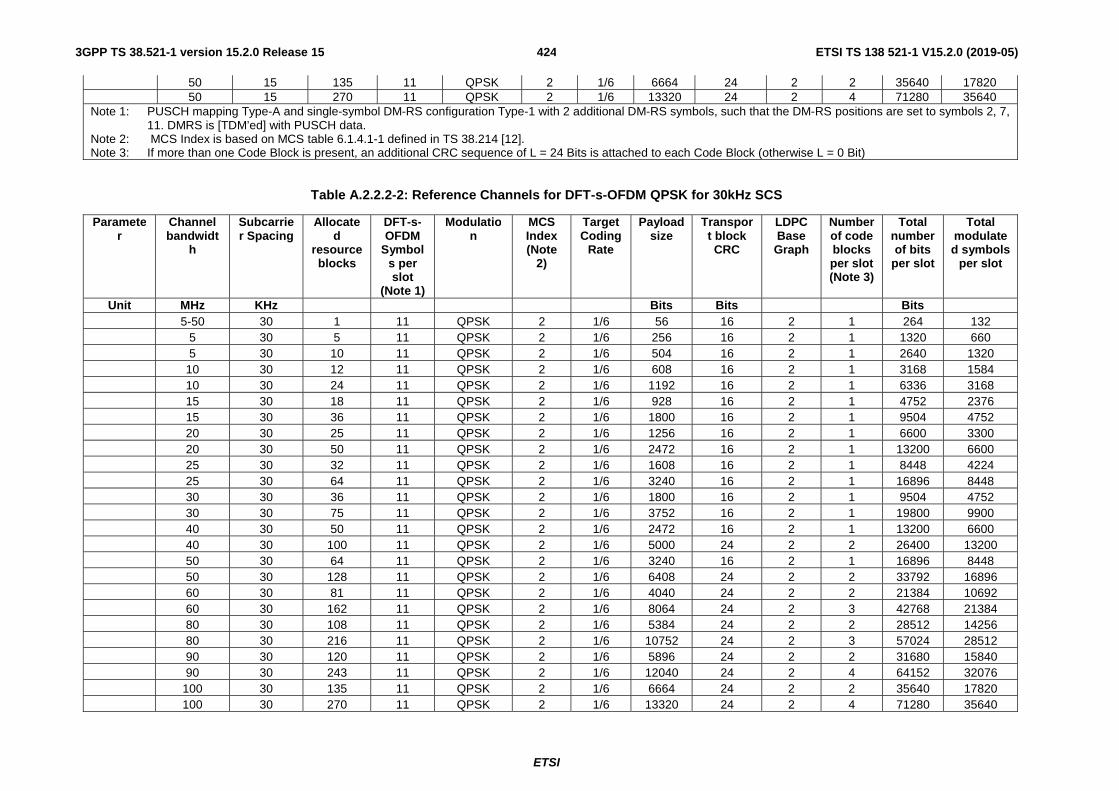
ETSI
ETSI TS 138 521-1 V15.2.0 (2019-05)4243GPP TS 38.521-1 version 15.2.0 Release 15
50 15 135 11 QPSK 2 1/6 6664 24 2 2 35640 17820 50 15 270 11 QPSK 2 1/6 13320 24 2 4 71280 35640 Note 1: PUSCH mapping Type-A and single-symbol DM-RS configuration Type-1 with 2 additional DM-RS symbols, such that the DM-RS positions are set to symbols 2, 7,
11. DMRS is [TDM’ed] with PUSCH data. Note 2: MCS Index is based on MCS table 6.1.4.1-1 defined in TS 38.214 [12]. Note 3: If more than one Code Block is present, an additional CRC sequence of L = 24 Bits is attached to each Code Block (otherwise L = 0 Bit)
Table A.2.2.2-2: Reference Channels for DFT-s-OFDM QPSK for 30kHz SCS
Parameter
Channel bandwidt
h
Subcarrier Spacing
Allocated
resource blocks
DFT-s-OFDM
Symbols per slot
(Note 1)
Modulation
MCS Index (Note
2)
Target Coding
Rate
Payload size
Transport block CRC
LDPC Base Graph
Number of code blocks per slot (Note 3)
Total number of bits
per slot
Total modulated symbols
per slot
Unit MHz KHz Bits Bits Bits 5-50 30 1 11 QPSK 2 1/6 56 16 2 1 264 132 5 30 5 11 QPSK 2 1/6 256 16 2 1 1320 660 5 30 10 11 QPSK 2 1/6 504 16 2 1 2640 1320 10 30 12 11 QPSK 2 1/6 608 16 2 1 3168 1584 10 30 24 11 QPSK 2 1/6 1192 16 2 1 6336 3168 15 30 18 11 QPSK 2 1/6 928 16 2 1 4752 2376 15 30 36 11 QPSK 2 1/6 1800 16 2 1 9504 4752 20 30 25 11 QPSK 2 1/6 1256 16 2 1 6600 3300 20 30 50 11 QPSK 2 1/6 2472 16 2 1 13200 6600 25 30 32 11 QPSK 2 1/6 1608 16 2 1 8448 4224 25 30 64 11 QPSK 2 1/6 3240 16 2 1 16896 8448 30 30 36 11 QPSK 2 1/6 1800 16 2 1 9504 4752 30 30 75 11 QPSK 2 1/6 3752 16 2 1 19800 9900 40 30 50 11 QPSK 2 1/6 2472 16 2 1 13200 6600 40 30 100 11 QPSK 2 1/6 5000 24 2 2 26400 13200 50 30 64 11 QPSK 2 1/6 3240 16 2 1 16896 8448 50 30 128 11 QPSK 2 1/6 6408 24 2 2 33792 16896 60 30 81 11 QPSK 2 1/6 4040 24 2 2 21384 10692 60 30 162 11 QPSK 2 1/6 8064 24 2 3 42768 21384 80 30 108 11 QPSK 2 1/6 5384 24 2 2 28512 14256 80 30 216 11 QPSK 2 1/6 10752 24 2 3 57024 28512 90 30 120 11 QPSK 2 1/6 5896 24 2 2 31680 15840 90 30 243 11 QPSK 2 1/6 12040 24 2 4 64152 32076 100 30 135 11 QPSK 2 1/6 6664 24 2 2 35640 17820 100 30 270 11 QPSK 2 1/6 13320 24 2 4 71280 35640

ETSI
ETSI TS 138 521-1 V15.2.0 (2019-05)4253GPP TS 38.521-1 version 15.2.0 Release 15
Note 1: PUSCH mapping Type-A and single-symbol DM-RS configuration Type-1 with 2 additional DM-RS symbols, such that the DM-RS positions are set to symbols 2, 7, 11. DMRS is [TDM’ed] with PUSCH data.
Note 2: MCS Index is based on MCS table 6.1.4.1-1 defined in TS 38.214 [12]. Note 3: If more than one Code Block is present, an additional CRC sequence of L = 24 Bits is attached to each Code Block (otherwise L = 0 Bit)
Table A.2.2.2-3: Reference Channels for DFT-s-OFDM QPSK for 60kHz SCS
Parameter
Channel bandwidt
h
Subcarrier Spacing
Allocated
resource blocks
DFT-s-OFDM
Symbols per slot
(Note 1)
Modulation
MCS Index (Note
2)
Target Coding
Rate
Payload size
Transport block CRC
LDPC Base Graph
Number of code blocks per slot (Note 3)
Total number of bits
per slot
Total modulated symbols
per slot
Unit MHz KHz Bits Bits Bits 10-100 60 1 11 QPSK 2 1/6 56 16 2 1 264 132 10 60 5 11 QPSK 2 1/6 256 16 2 1 1320 660 10 60 10 11 QPSK 2 1/6 504 16 2 1 2640 1320 15 60 9 11 QPSK 2 1/6 456 16 2 1 2376 1188 15 60 18 11 QPSK 2 1/6 928 16 2 1 4752 2376 20 60 12 11 QPSK 2 1/6 608 16 2 1 3168 1584 20 60 24 11 QPSK 2 1/6 1192 16 2 1 6336 3168 25 60 15 11 QPSK 2 1/6 768 16 2 1 3960 1980 25 60 30 11 QPSK 2 1/6 1544 16 2 1 7920 3960 30 60 18 11 QPSK 2 1/6 928 16 2 1 4752 2376 30 60 36 11 QPSK 2 1/6 1800 16 2 1 9504 4752 40 60 25 11 QPSK 2 1/6 1256 16 2 1 6600 3300 40 60 50 11 QPSK 2 1/6 2472 16 2 1 13200 6600 50 60 32 11 QPSK 2 1/6 1608 16 2 1 8448 4224 50 60 64 11 QPSK 2 1/6 3240 16 2 1 16896 8448 60 60 36 11 QPSK 2 1/6 1800 16 2 1 9504 4752 60 60 75 11 QPSK 2 1/6 3752 16 2 1 19800 9900 80 60 50 11 QPSK 2 1/6 2472 16 2 1 13200 6600 80 60 100 11 QPSK 2 1/6 5000 24 2 2 26400 13200 90 60 60 11 QPSK 2 1/6 3104 16 2 1 15840 7920 90 60 120 11 QPSK 2 1/6 5896 24 2 2 31680 15840 100 60 64 11 QPSK 2 1/6 3240 16 2 1 16896 8448 100 60 135 11 QPSK 2 1/6 6664 24 2 2 35640 17820 Note 1: PUSCH mapping Type-A and single-symbol DM-RS configuration Type-1 with 2 additional DM-RS symbols, such that the DM-RS positions are set to symbols 2, 7,
11. DMRS is [TDM’ed] with PUSCH data. Note 2: MCS Index is based on MCS table 6.1.4.1-1 defined in TS 38.214 [12]. Note 3: If more than one Code Block is present, an additional CRC sequence of L = 24 Bits is attached to each Code Block (otherwise L = 0 Bit)
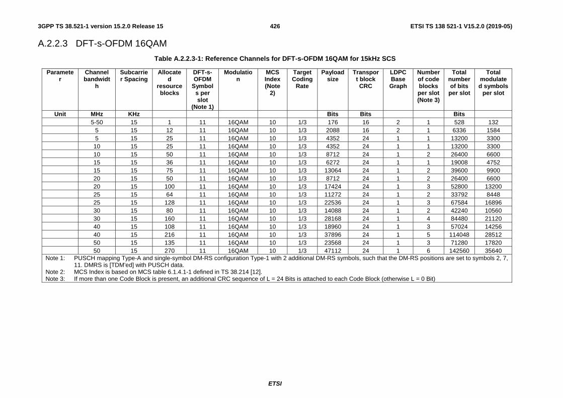
ETSI
ETSI TS 138 521-1 V15.2.0 (2019-05)4263GPP TS 38.521-1 version 15.2.0 Release 15
A.2.2.3 DFT-s-OFDM 16QAM
Table A.2.2.3-1: Reference Channels for DFT-s-OFDM 16QAM for 15kHz SCS
Parameter
Channel bandwidt
h
Subcarrier Spacing
Allocated
resource blocks
DFT-s-OFDM
Symbols per slot
(Note 1)
Modulation
MCS Index (Note
2)
Target Coding
Rate
Payload size
Transport block CRC
LDPC Base Graph
Number of code blocks per slot (Note 3)
Total number of bits
per slot
Total modulated symbols
per slot
Unit MHz KHz Bits Bits Bits 5-50 15 1 11 16QAM 10 1/3 176 16 2 1 528 132 5 15 12 11 16QAM 10 1/3 2088 16 2 1 6336 1584 5 15 25 11 16QAM 10 1/3 4352 24 1 1 13200 3300 10 15 25 11 16QAM 10 1/3 4352 24 1 1 13200 3300 10 15 50 11 16QAM 10 1/3 8712 24 1 2 26400 6600 15 15 36 11 16QAM 10 1/3 6272 24 1 1 19008 4752 15 15 75 11 16QAM 10 1/3 13064 24 1 2 39600 9900 20 15 50 11 16QAM 10 1/3 8712 24 1 2 26400 6600 20 15 100 11 16QAM 10 1/3 17424 24 1 3 52800 13200 25 15 64 11 16QAM 10 1/3 11272 24 1 2 33792 8448 25 15 128 11 16QAM 10 1/3 22536 24 1 3 67584 16896 30 15 80 11 16QAM 10 1/3 14088 24 1 2 42240 10560 30 15 160 11 16QAM 10 1/3 28168 24 1 4 84480 21120 40 15 108 11 16QAM 10 1/3 18960 24 1 3 57024 14256 40 15 216 11 16QAM 10 1/3 37896 24 1 5 114048 28512 50 15 135 11 16QAM 10 1/3 23568 24 1 3 71280 17820 50 15 270 11 16QAM 10 1/3 47112 24 1 6 142560 35640 Note 1: PUSCH mapping Type-A and single-symbol DM-RS configuration Type-1 with 2 additional DM-RS symbols, such that the DM-RS positions are set to symbols 2, 7,
11. DMRS is [TDM’ed] with PUSCH data. Note 2: MCS Index is based on MCS table 6.1.4.1-1 defined in TS 38.214 [12]. Note 3: If more than one Code Block is present, an additional CRC sequence of L = 24 Bits is attached to each Code Block (otherwise L = 0 Bit)

ETSI
ETSI TS 138 521-1 V15.2.0 (2019-05)4273GPP TS 38.521-1 version 15.2.0 Release 15
Table A.2.2.3-2: Reference Channels for DFT-s-OFDM 16QAM for 30kHz SCS
Parameter
Channel bandwidt
h
Subcarrier Spacing
Allocated
resource blocks
DFT-s-OFDM
Symbols per slot
(Note 1)
Modulation
MCS Index (Note
2)
Target Coding
Rate
Payload size
Transport block CRC
LDPC Base Graph
Number of code blocks per slot (Note 3)
Total number of bits
per slot
Total modulated symbols
per slot
Unit MHz KHz Bits Bits Bits 5-50 30 1 11 16QAM 10 1/3 176 16 2 1 528 132 5 30 5 11 16QAM 10 1/3 888 16 2 1 2640 660 5 30 10 11 16QAM 10 1/3 1800 16 2 1 5280 1320 10 30 12 11 16QAM 10 1/3 2088 16 2 1 6336 1584 10 30 24 11 16QAM 10 1/3 4224 24 1 1 12672 3168 15 30 18 11 16QAM 10 1/3 3240 16 2 1 9504 2376 15 30 36 11 16QAM 10 1/3 6272 24 1 1 19008 4752 20 30 25 11 16QAM 10 1/3 4352 24 1 1 13200 3300 20 30 50 11 16QAM 10 1/3 8712 24 1 2 26400 6600 25 30 32 11 16QAM 10 1/3 5632 24 1 1 16896 4224 25 30 64 11 16QAM 10 1/3 11272 24 1 2 33792 8448 30 30 36 11 16QAM 10 1/3 6272 24 1 1 19008 4752 30 30 75 11 16QAM 10 1/3 13064 24 1 2 39600 9900 40 30 50 11 16QAM 10 1/3 8712 24 1 2 26400 6600 40 30 100 11 16QAM 10 1/3 17424 24 1 3 52800 13200 50 30 64 11 16QAM 10 1/3 11272 24 1 2 33792 8448 50 30 128 11 16QAM 10 1/3 22536 24 1 3 67584 16896 60 30 81 11 16QAM 10 1/3 14088 24 1 2 42768 10692 60 30 162 11 16QAM 10 1/3 28168 24 1 4 85536 21384 80 30 108 11 16QAM 10 1/3 18960 24 1 3 57024 14256 80 30 216 11 16QAM 10 1/3 37896 24 1 5 114048 28512 90 30 120 11 16QAM 10 1/3 21000 24 1 3 63360 15840 90 30 243 11 16QAM 10 1/3 43032 24 1 6 128304 32076 100 30 135 11 16QAM 10 1/3 23568 24 1 3 71280 17820 100 30 270 11 16QAM 10 1/3 47112 24 1 6 142560 35640
Note 1: PUSCH mapping Type-A and single-symbol DM-RS configuration Type-1 with 2 additional DM-RS symbols, such that the DM-RS positions are set to symbols 2, 7, 11. DMRS is [TDM’ed] with PUSCH data.
Note 2: MCS Index is based on MCS table 6.1.4.1-1 defined in TS 38.214 [12]. Note 3: If more than one Code Block is present, an additional CRC sequence of L = 24 Bits is attached to each Code Block (otherwise L = 0 Bit)

ETSI
ETSI TS 138 521-1 V15.2.0 (2019-05)4283GPP TS 38.521-1 version 15.2.0 Release 15
Table A.2.2.3-3: Reference Channels for DFT-s-OFDM 16QAM for 60kHz SCS
Parameter
Channel bandwidt
h
Subcarrier Spacing
Allocated
resource blocks
DFT-s-OFDM
Symbols per slot
(Note 1)
Modulation
MCS Index
(Note 2)
Target Coding
Rate
Payload size
Transport block CRC
LDPC Base
Graph
Number of code blocks per slot (Note 3)
Total number of bits
per slot
Total modulated symbols per slot
Unit MHz KHz Bits Bits Bits 10-100 60 1 11 16QAM 10 1/3 176 16 2 1 528 132 10 60 5 11 16QAM 10 1/3 888 16 2 1 2640 660 10 60 10 11 16QAM 10 1/3 1800 16 2 1 5280 1320 15 60 9 11 16QAM 10 1/3 1608 16 2 1 4752 1188 15 60 18 11 16QAM 10 1/3 3240 16 2 1 9504 2376 20 60 12 11 16QAM 10 1/3 2088 16 2 1 6336 1584 20 60 24 11 16QAM 10 1/3 4224 24 1 1 12672 3168 25 60 15 11 16QAM 10 1/3 2664 16 2 1 7920 1980 25 60 30 11 16QAM 10 1/3 5248 24 1 1 15840 3960 30 60 18 11 16QAM 10 1/3 3240 16 2 1 9504 2376 30 60 36 11 16QAM 10 1/3 6272 24 1 1 19008 4752 40 60 25 11 16QAM 10 1/3 4352 24 1 1 13200 3300 40 60 50 11 16QAM 10 1/3 8712 24 1 2 26400 6600 50 60 32 11 16QAM 10 1/3 5632 24 1 1 16896 4224 50 60 64 11 16QAM 10 1/3 11272 24 1 2 33792 8448 60 60 36 11 16QAM 10 1/3 6272 24 1 1 19008 4752 60 60 75 11 16QAM 10 1/3 13064 24 1 2 39600 9900 80 60 50 11 16QAM 10 1/3 8712 24 1 2 26400 6600 80 60 100 11 16QAM 10 1/3 17424 24 1 3 52800 13200 90 60 60 11 16QAM 10 1/3 10504 24 1 2 31680 7920 90 60 120 11 16QAM 10 1/3 21000 24 1 3 63360 15840 100 60 64 11 16QAM 10 1/3 11272 24 1 2 33792 8448 100 60 135 11 16QAM 10 1/3 23568 24 1 3 71280 17820
Note 1: PUSCH mapping Type-A and single-symbol DM-RS configuration Type-1 with 2 additional DM-RS symbols, such that the DM-RS positions are set to symbols 2, 7, 11. DMRS is [TDM’ed] with PUSCH data.
Note 2: MCS Index is based on MCS table 6.1.4.1-1 defined in TS 38.214 [12]. Note 3: If more than one Code Block is present, an additional CRC sequence of L = 24 Bits is attached to each Code Block (otherwise L = 0 Bit)

ETSI
ETSI TS 138 521-1 V15.2.0 (2019-05)4293GPP TS 38.521-1 version 15.2.0 Release 15
A.2.2.4 DFT-s-OFDM 64QAM
Table A.2.2.4-1: Reference Channels for DFT-s-OFDM 64QAM for 15kHz SCS
Parameter
Channel bandwidt
h
Subcarrier Spacing
Allocated
resource blocks
DFT-s-OFDM
Symbols per slot
(Note 1)
Modulation
MCS Index (Note
2)
Target Coding
Rate
Payload size
Transport block CRC
LDPC Base Graph
Number of code blocks per slot (Note 3)
Total number of bits
per slot
Total modulated symbols
per slot
Unit MHz KHz Bits Bits Bits 5 15 25 11 64QAM 18 1/2 9992 24 1 2 19800 3300 10 15 50 11 64QAM 18 1/2 19968 24 1 3 39600 6600 15 15 75 11 64QAM 18 1/2 30216 24 1 4 59400 9900 20 15 100 11 64QAM 18 1/2 39936 24 1 5 79200 13200 25 15 128 11 64QAM 18 1/2 51216 24 1 7 101376 16896 30 15 160 11 64QAM 18 1/2 63528 24 1 8 126720 21120 40 15 216 11 64QAM 18 1/2 86040 24 1 11 171072 28512 50 15 270 11 64QAM 18 1/2 108552 24 1 13 213840 35640
Note 1: PUSCH mapping Type-A and single-symbol DM-RS configuration Type-1 with 2 additional DM-RS symbols, such that the DM-RS positions are set to symbols 2, 7, 11. DMRS is [TDM’ed] with PUSCH data.
Note 2: MCS Index is based on MCS table 6.1.4.1-1 defined in TS 38.214 [12]. Note 3: If more than one Code Block is present, an additional CRC sequence of L = 24 Bits is attached to each Code Block (otherwise L = 0 Bit)

ETSI
ETSI TS 138 521-1 V15.2.0 (2019-05)4303GPP TS 38.521-1 version 15.2.0 Release 15
Table A.2.2.4-2: Reference Channels for DFT-s-OFDM 64QAM for 30kHz SCS
Parameter
Channel bandwidt
h
Subcarrier Spacing
Allocated
resource blocks
DFT-s-OFDM
Symbols per slot
(Note 1)
Modulation
MCS Index (Note
2)
Target Coding
Rate
Payload size
Transport block CRC
LDPC Base Graph
Number of code blocks per slot (Note 3)
Total number of bits
per slot
Total modulated symbols
per slot
Unit MHz KHz Bits Bits Bits 5 30 10 11 64QAM 18 1/2 3968 24 1 1 7920 1320 10 30 24 11 64QAM 18 1/2 9480 24 1 2 19008 3168 15 30 36 11 64QAM 18 1/2 14344 24 1 2 28512 4752 20 30 50 11 64QAM 18 1/2 19968 24 1 3 39600 6600 25 30 64 11 64QAM 18 1/2 25608 24 1 4 50688 8448 30 30 75 11 64QAM 18 1/2 30216 24 1 4 59400 9900 40 30 100 11 64QAM 18 1/2 39936 24 1 5 79200 13200 50 30 128 11 64QAM 18 1/2 51216 24 1 7 101376 16896 60 30 162 11 64QAM 18 1/2 64552 24 1 8 128304 21384 80 30 216 11 64QAM 18 1/2 86040 24 1 11 171072 28512 90 30 243 11 64QAM 18 1/2 96264 24 1 12 192456 32076 100 30 270 11 64QAM 18 1/2 108552 24 1 13 213840 35640
Note 1: PUSCH mapping Type-A and single-symbol DM-RS configuration Type-1 with 2 additional DM-RS symbols, such that the DM-RS positions are set to symbols 2, 7, 11. DMRS is [TDM’ed] with PUSCH data.
Note 2: MCS Index is based on MCS table 6.1.4.1-1 defined in TS 38.214 [12]. Note 3: If more than one Code Block is present, an additional CRC sequence of L = 24 Bits is attached to each Code Block (otherwise L = 0 Bit)

ETSI
ETSI TS 138 521-1 V15.2.0 (2019-05)4313GPP TS 38.521-1 version 15.2.0 Release 15
Table A.2.2.4-3: Reference Channels for DFT-s-OFDM 64QAM for 60kHz SCS
Parameter
Channel bandwidt
h
Subcarrier Spacing
Allocated
resource blocks
DFT-s-OFDM
Symbols per slot
(Note 1)
Modulation
MCS Index (Note
2)
Target Coding
Rate
Payload size
Transport block CRC
LDPC Base Graph
Number of code blocks per slot (Note 3)
Total number of bits
per slot
Total modulated symbols
per slot
Unit MHz KHz Bits Bits Bits 10 60 10 11 64QAM 18 1/2 3968 24 1 1 7920 1320 15 60 18 11 64QAM 18 1/2 7168 24 1 1 14256 2376 20 60 24 11 64QAM 18 1/2 9480 24 1 2 19008 3168 25 60 30 11 64QAM 18 1/2 12040 24 1 2 23760 3960 30 60 36 11 64QAM 18 1/2 14344 24 1 2 28512 4752 40 60 50 11 64QAM 18 1/2 19968 24 1 3 39600 6600 50 60 64 11 64QAM 18 1/2 25608 24 1 4 50688 8448 60 60 75 11 64QAM 18 1/2 30216 24 1 4 59400 9900 80 60 100 11 64QAM 18 1/2 39936 24 1 5 79200 13200 90 60 120 11 64QAM 18 1/2 48168 24 1 6 95040 15840 100 60 135 11 64QAM 18 1/2 54296 24 1 7 106920 17820
Note 1: PUSCH mapping Type-A and single-symbol DM-RS configuration Type-1 with 2 additional DM-RS symbols, such that the DM-RS positions are set to symbols 2, 7, 11. DMRS is [TDM’ed] with PUSCH data.
Note 2: MCS Index is based on MCS table 6.1.4.1-1 defined in TS 38.214 [12]. Note 3: If more than one Code Block is present, an additional CRC sequence of L = 24 Bits is attached to each Code Block (otherwise L = 0 Bit)

ETSI
ETSI TS 138 521-1 V15.2.0 (2019-05)4323GPP TS 38.521-1 version 15.2.0 Release 15
A.2.2.5 DFT-s-OFDM 256QAM
Table A.2.2.5-1: Reference Channels for DFT-s-OFDM 256QAM for 15kHz SCS
Parameter
Channel bandwidt
h
Subcarrier Spacing
Allocated
resource blocks
DFT-s-OFDM
Symbols per slot
(Note 1)
Modulation
MCS Index (Note
2)
Target Coding
Rate
Payload size
Transport block CRC
LDPC Base Graph
Number of code blocks per slot (Note 3)
Total number of bits
per slot
Total modulated symbols
per slot
Unit MHz KHz Bits Bits Bits 5 15 25 11 256QAM 20 2/3 17424 24 1 3 26400 3300 10 15 50 11 256QAM 20 2/3 34816 24 1 5 52800 6600 15 15 75 11 256QAM 20 2/3 53288 24 1 7 79200 9900 20 15 100 11 256QAM 20 2/3 69672 24 1 9 105600 13200 25 15 128 11 256QAM 20 2/3 90176 24 1 11 135168 16896 30 15 160 11 256QAM 20 2/3 112648 24 1 14 168960 21120 40 15 216 11 256QAM 20 2/3 151608 24 1 18 228096 28512 50 15 270 11 256QAM 20 2/3 188576 24 1 23 285120 35640
Note 1: PUSCH mapping Type-A and single-symbol DM-RS configuration Type-1 with 2 additional DM-RS symbols, such that the DM-RS positions are set to symbols 2, 7, 11. DMRS is [TDM’ed] with PUSCH data.
Note 2: MCS Index is based on MCS table 5.1.3.1-2 defined in TS 38.214 [12]. Note 3: If more than one Code Block is present, an additional CRC sequence of L = 24 Bits is attached to each Code Block (otherwise L = 0 Bit)
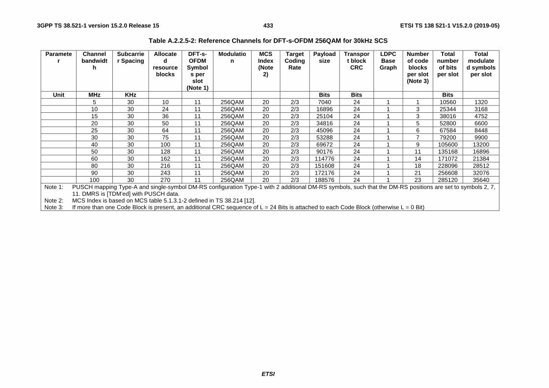
ETSI
ETSI TS 138 521-1 V15.2.0 (2019-05)4333GPP TS 38.521-1 version 15.2.0 Release 15
Table A.2.2.5-2: Reference Channels for DFT-s-OFDM 256QAM for 30kHz SCS
Parameter
Channel bandwidt
h
Subcarrier Spacing
Allocated
resource blocks
DFT-s-OFDM
Symbols per slot
(Note 1)
Modulation
MCS Index (Note
2)
Target Coding
Rate
Payload size
Transport block CRC
LDPC Base Graph
Number of code blocks per slot (Note 3)
Total number of bits
per slot
Total modulated symbols
per slot
Unit MHz KHz Bits Bits Bits 5 30 10 11 256QAM 20 2/3 7040 24 1 1 10560 1320 10 30 24 11 256QAM 20 2/3 16896 24 1 3 25344 3168 15 30 36 11 256QAM 20 2/3 25104 24 1 3 38016 4752 20 30 50 11 256QAM 20 2/3 34816 24 1 5 52800 6600 25 30 64 11 256QAM 20 2/3 45096 24 1 6 67584 8448 30 30 75 11 256QAM 20 2/3 53288 24 1 7 79200 9900 40 30 100 11 256QAM 20 2/3 69672 24 1 9 105600 13200 50 30 128 11 256QAM 20 2/3 90176 24 1 11 135168 16896 60 30 162 11 256QAM 20 2/3 114776 24 1 14 171072 21384 80 30 216 11 256QAM 20 2/3 151608 24 1 18 228096 28512 90 30 243 11 256QAM 20 2/3 172176 24 1 21 256608 32076 100 30 270 11 256QAM 20 2/3 188576 24 1 23 285120 35640
Note 1: PUSCH mapping Type-A and single-symbol DM-RS configuration Type-1 with 2 additional DM-RS symbols, such that the DM-RS positions are set to symbols 2, 7, 11. DMRS is [TDM’ed] with PUSCH data.
Note 2: MCS Index is based on MCS table 5.1.3.1-2 defined in TS 38.214 [12]. Note 3: If more than one Code Block is present, an additional CRC sequence of L = 24 Bits is attached to each Code Block (otherwise L = 0 Bit)
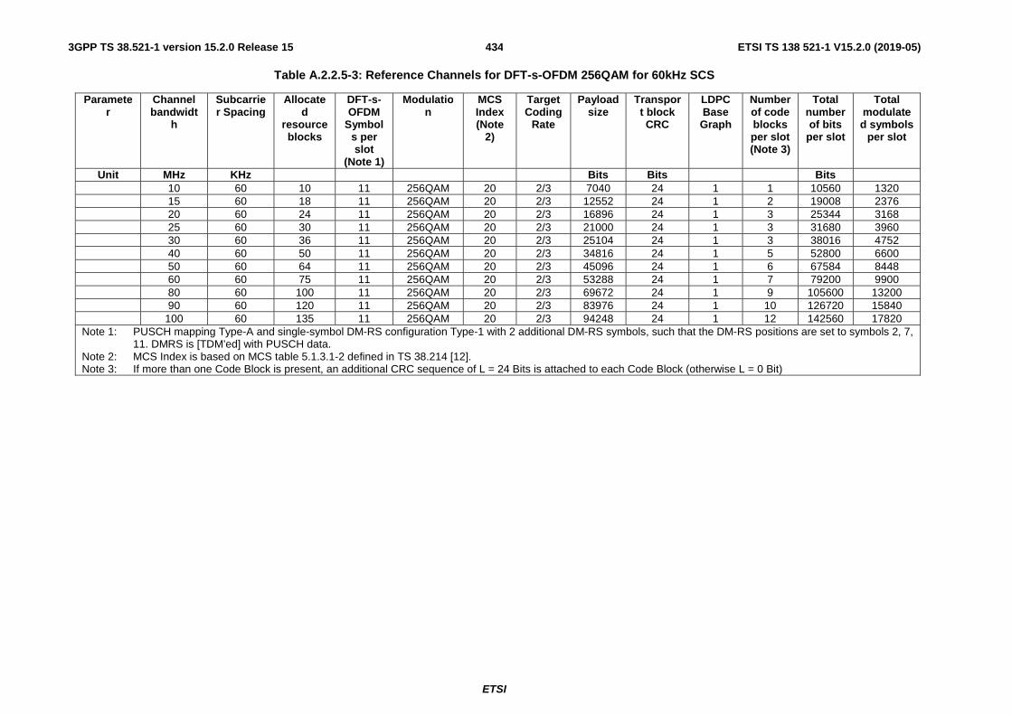
ETSI
ETSI TS 138 521-1 V15.2.0 (2019-05)4343GPP TS 38.521-1 version 15.2.0 Release 15
Table A.2.2.5-3: Reference Channels for DFT-s-OFDM 256QAM for 60kHz SCS
Parameter
Channel bandwidt
h
Subcarrier Spacing
Allocated
resource blocks
DFT-s-OFDM
Symbols per slot
(Note 1)
Modulation
MCS Index (Note
2)
Target Coding
Rate
Payload size
Transport block CRC
LDPC Base Graph
Number of code blocks per slot (Note 3)
Total number of bits
per slot
Total modulated symbols
per slot
Unit MHz KHz Bits Bits Bits 10 60 10 11 256QAM 20 2/3 7040 24 1 1 10560 1320 15 60 18 11 256QAM 20 2/3 12552 24 1 2 19008 2376 20 60 24 11 256QAM 20 2/3 16896 24 1 3 25344 3168 25 60 30 11 256QAM 20 2/3 21000 24 1 3 31680 3960 30 60 36 11 256QAM 20 2/3 25104 24 1 3 38016 4752 40 60 50 11 256QAM 20 2/3 34816 24 1 5 52800 6600 50 60 64 11 256QAM 20 2/3 45096 24 1 6 67584 8448 60 60 75 11 256QAM 20 2/3 53288 24 1 7 79200 9900 80 60 100 11 256QAM 20 2/3 69672 24 1 9 105600 13200 90 60 120 11 256QAM 20 2/3 83976 24 1 10 126720 15840 100 60 135 11 256QAM 20 2/3 94248 24 1 12 142560 17820
Note 1: PUSCH mapping Type-A and single-symbol DM-RS configuration Type-1 with 2 additional DM-RS symbols, such that the DM-RS positions are set to symbols 2, 7, 11. DMRS is [TDM’ed] with PUSCH data.
Note 2: MCS Index is based on MCS table 5.1.3.1-2 defined in TS 38.214 [12]. Note 3: If more than one Code Block is present, an additional CRC sequence of L = 24 Bits is attached to each Code Block (otherwise L = 0 Bit)
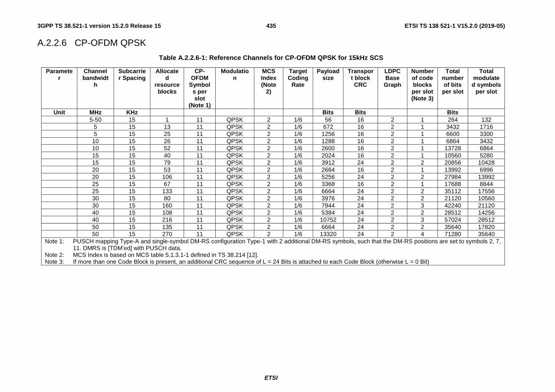
ETSI
ETSI TS 138 521-1 V15.2.0 (2019-05)4353GPP TS 38.521-1 version 15.2.0 Release 15
A.2.2.6 CP-OFDM QPSK
Table A.2.2.6-1: Reference Channels for CP-OFDM QPSK for 15kHz SCS
Parameter
Channel bandwidt
h
Subcarrier Spacing
Allocated
resource blocks
CP-OFDM
Symbols per slot
(Note 1)
Modulation
MCS Index (Note
2)
Target Coding
Rate
Payload size
Transport block CRC
LDPC Base Graph
Number of code blocks per slot (Note 3)
Total number of bits
per slot
Total modulated symbols
per slot
Unit MHz KHz Bits Bits Bits 5-50 15 1 11 QPSK 2 1/6 56 16 2 1 264 132 5 15 13 11 QPSK 2 1/6 672 16 2 1 3432 1716 5 15 25 11 QPSK 2 1/6 1256 16 2 1 6600 3300 10 15 26 11 QPSK 2 1/6 1288 16 2 1 6864 3432 10 15 52 11 QPSK 2 1/6 2600 16 2 1 13728 6864 15 15 40 11 QPSK 2 1/6 2024 16 2 1 10560 5280 15 15 79 11 QPSK 2 1/6 3912 24 2 2 20856 10428 20 15 53 11 QPSK 2 1/6 2664 16 2 1 13992 6996 20 15 106 11 QPSK 2 1/6 5256 24 2 2 27984 13992 25 15 67 11 QPSK 2 1/6 3368 16 2 1 17688 8844 25 15 133 11 QPSK 2 1/6 6664 24 2 2 35112 17556 30 15 80 11 QPSK 2 1/6 3976 24 2 2 21120 10560 30 15 160 11 QPSK 2 1/6 7944 24 2 3 42240 21120 40 15 108 11 QPSK 2 1/6 5384 24 2 2 28512 14256 40 15 216 11 QPSK 2 1/6 10752 24 2 3 57024 28512 50 15 135 11 QPSK 2 1/6 6664 24 2 2 35640 17820 50 15 270 11 QPSK 2 1/6 13320 24 2 4 71280 35640
Note 1: PUSCH mapping Type-A and single-symbol DM-RS configuration Type-1 with 2 additional DM-RS symbols, such that the DM-RS positions are set to symbols 2, 7, 11. DMRS is [TDM’ed] with PUSCH data.
Note 2: MCS Index is based on MCS table 5.1.3.1-1 defined in TS 38.214 [12]. Note 3: If more than one Code Block is present, an additional CRC sequence of L = 24 Bits is attached to each Code Block (otherwise L = 0 Bit)
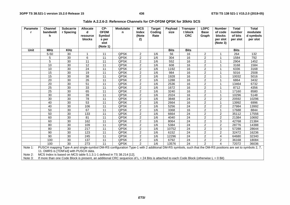
ETSI
ETSI TS 138 521-1 V15.2.0 (2019-05)4363GPP TS 38.521-1 version 15.2.0 Release 15
Table A.2.2.6-2: Reference Channels for CP-OFDM QPSK for 30kHz SCS
Parameter
Channel bandwidt
h
Subcarrier Spacing
Allocated
resource blocks
CP-OFDM
Symbols per slot
(Note 1)
Modulation
MCS Index (Note
2)
Target Coding
Rate
Payload size
Transport block CRC
LDPC Base Graph
Number of code blocks per slot (Note 3)
Total number of bits
per slot
Total modulated symbols
per slot
Unit MHz KHz Bits Bits Bits 5-50 30 1 11 QPSK 2 1/6 56 16 2 1 264 132 5 30 6 11 QPSK 2 1/6 304 16 2 1 1584 792 5 30 11 11 QPSK 2 1/6 552 16 2 1 2904 1452 10 30 12 11 QPSK 2 1/6 608 16 2 1 3168 1584 10 30 24 11 QPSK 2 1/6 1192 16 2 1 6336 3168 15 30 19 11 QPSK 2 1/6 984 16 2 1 5016 2508 15 30 38 11 QPSK 2 1/6 1928 16 2 1 10032 5016 20 30 26 11 QPSK 2 1/6 1288 16 2 1 6864 3432 20 30 51 11 QPSK 2 1/6 2536 16 2 1 13464 6732 25 30 33 11 QPSK 2 1/6 1672 16 2 1 8712 4356 25 30 65 11 QPSK 2 1/6 3240 16 2 1 17160 8580 30 30 39 11 QPSK 2 1/6 2024 16 2 1 10296 5148 30 30 78 11 QPSK 2 1/6 3848 24 2 2 20592 10296 40 30 53 11 QPSK 2 1/6 2664 16 2 1 13992 6996 40 30 106 11 QPSK 2 1/6 5256 24 2 2 27984 13992 50 30 67 11 QPSK 2 1/6 3368 16 2 1 17688 8844 50 30 133 11 QPSK 2 1/6 6664 24 2 2 35112 17556 60 30 81 11 QPSK 2 1/6 4040 24 2 2 21384 10692 60 30 162 11 QPSK 2 1/6 8064 24 2 3 42768 21384 80 30 109 11 QPSK 2 1/6 5384 24 2 2 28776 14388 80 30 217 11 QPSK 2 1/6 10752 24 2 3 57288 28644 90 30 123 11 QPSK 2 1/6 6152 24 2 2 32472 16236 90 30 245 11 QPSK 2 1/6 12296 24 2 4 64680 32340 100 30 137 11 QPSK 2 1/6 6792 24 2 2 36168 18084 100 30 273 11 QPSK 2 1/6 13576 24 2 4 72072 36036
Note 1: PUSCH mapping Type-A and single-symbol DM-RS configuration Type-1 with 2 additional DM-RS symbols, such that the DM-RS positions are set to symbols 2, 7, 11. DMRS is [TDM’ed] with PUSCH data.
Note 2: MCS Index is based on MCS table 5.1.3.1-1 defined in TS 38.214 [12]. Note 3: If more than one Code Block is present, an additional CRC sequence of L = 24 Bits is attached to each Code Block (otherwise L = 0 Bit)

ETSI
ETSI TS 138 521-1 V15.2.0 (2019-05)4373GPP TS 38.521-1 version 15.2.0 Release 15
Table A.2.2.6-3: Reference Channels for CP-OFDM QPSK for 60kHz SCS
Parameter
Channel bandwidt
h
Subcarrier Spacing
Allocated
resource blocks
CP-OFDM
Symbols per slot
(Note 1)
Modulation
MCS Index (Note
2)
Target Coding
Rate
Payload size
Transport block CRC
LDPC Base Graph
Number of code blocks per slot (Note 3)
Total number of bits
per slot
Total modulated symbols
per slot
Unit MHz KHz Bits Bits Bits 10-100 60 1 11 QPSK 2 1/6 56 16 2 1 264 132 10 60 6 11 QPSK 2 1/6 304 16 2 1 1584 792 10 60 11 11 QPSK 2 1/6 552 16 2 1 2904 1452 15 60 9 11 QPSK 2 1/6 456 16 2 1 2376 1188 15 60 18 11 QPSK 2 1/6 928 16 2 1 4752 2376 20 60 12 11 QPSK 2 1/6 608 16 2 1 3168 1584 20 60 24 11 QPSK 2 1/6 1192 16 2 1 6336 3168 25 60 16 11 QPSK 2 1/6 808 16 2 1 4224 2112 25 60 31 11 QPSK 2 1/6 1544 16 2 1 8184 4092 30 60 19 11 QPSK 2 1/6 984 16 2 1 5016 2508 30 60 38 11 QPSK 2 1/6 1928 16 2 1 10032 5016 40 60 26 11 QPSK 2 1/6 1288 16 2 1 6864 3432 40 60 51 11 QPSK 2 1/6 2536 16 2 1 13464 6732 50 60 33 11 QPSK 2 1/6 1672 16 2 1 8712 4356 50 60 65 11 QPSK 2 1/6 3240 16 2 1 17160 8580 60 60 40 11 QPSK 2 1/6 2024 16 2 1 10560 5280 60 60 79 11 QPSK 2 1/6 3912 24 2 2 20856 10428 80 60 54 11 QPSK 2 1/6 2664 16 2 1 14256 7128 80 60 107 11 QPSK 2 1/6 5256 24 2 2 28248 14124 90 60 61 11 QPSK 2 1/6 3104 16 2 1 16104 8052 90 60 121 11 QPSK 2 1/6 6024 24 2 2 31944 15972 100 60 68 11 QPSK 2 1/6 3368 16 2 1 17952 8976 100 60 135 11 QPSK 2 1/6 6664 24 2 2 35640 17820
Note 1: PUSCH mapping Type-A and single-symbol DM-RS configuration Type-1 with 2 additional DM-RS symbols, such that the DM-RS positions are set to symbols 2, 7, 11. DMRS is [TDM’ed] with PUSCH data.
Note 2: MCS Index is based on MCS table 5.1.3.1-1 defined in TS 38.214 [12]. Note 3: If more than one Code Block is present, an additional CRC sequence of L = 24 Bits is attached to each Code Block (otherwise L = 0 Bit)
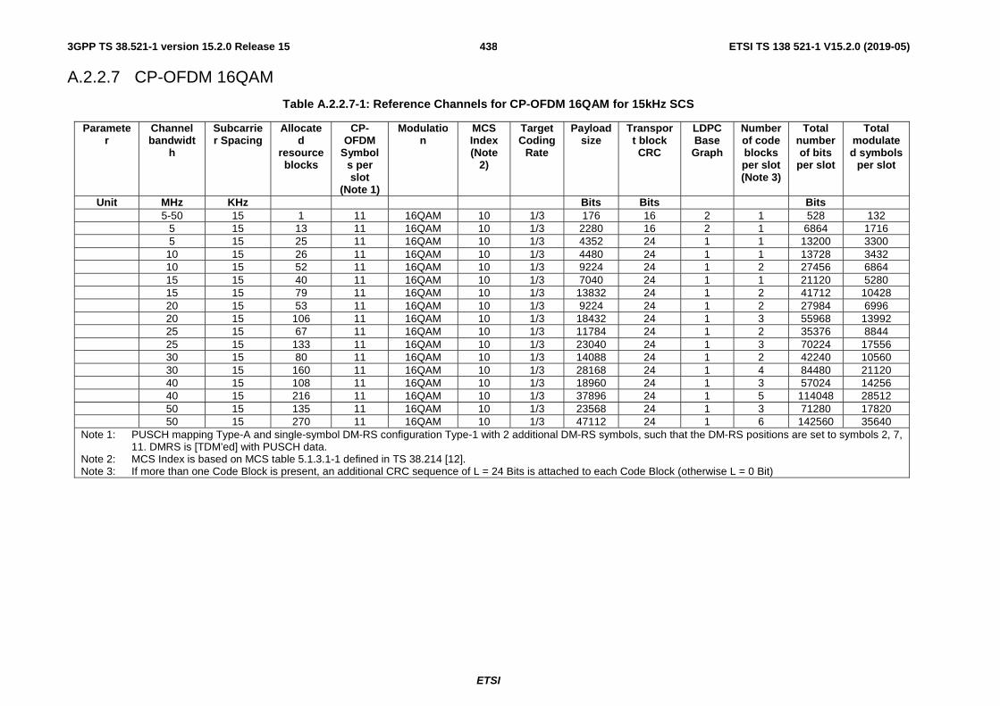
ETSI
ETSI TS 138 521-1 V15.2.0 (2019-05)4383GPP TS 38.521-1 version 15.2.0 Release 15
A.2.2.7 CP-OFDM 16QAM
Table A.2.2.7-1: Reference Channels for CP-OFDM 16QAM for 15kHz SCS
Parameter
Channel bandwidt
h
Subcarrier Spacing
Allocated
resource blocks
CP-OFDM
Symbols per slot
(Note 1)
Modulation
MCS Index (Note
2)
Target Coding
Rate
Payload size
Transport block CRC
LDPC Base Graph
Number of code blocks per slot (Note 3)
Total number of bits
per slot
Total modulated symbols
per slot
Unit MHz KHz Bits Bits Bits 5-50 15 1 11 16QAM 10 1/3 176 16 2 1 528 132 5 15 13 11 16QAM 10 1/3 2280 16 2 1 6864 1716 5 15 25 11 16QAM 10 1/3 4352 24 1 1 13200 3300 10 15 26 11 16QAM 10 1/3 4480 24 1 1 13728 3432 10 15 52 11 16QAM 10 1/3 9224 24 1 2 27456 6864 15 15 40 11 16QAM 10 1/3 7040 24 1 1 21120 5280 15 15 79 11 16QAM 10 1/3 13832 24 1 2 41712 10428 20 15 53 11 16QAM 10 1/3 9224 24 1 2 27984 6996 20 15 106 11 16QAM 10 1/3 18432 24 1 3 55968 13992 25 15 67 11 16QAM 10 1/3 11784 24 1 2 35376 8844 25 15 133 11 16QAM 10 1/3 23040 24 1 3 70224 17556 30 15 80 11 16QAM 10 1/3 14088 24 1 2 42240 10560 30 15 160 11 16QAM 10 1/3 28168 24 1 4 84480 21120 40 15 108 11 16QAM 10 1/3 18960 24 1 3 57024 14256 40 15 216 11 16QAM 10 1/3 37896 24 1 5 114048 28512 50 15 135 11 16QAM 10 1/3 23568 24 1 3 71280 17820 50 15 270 11 16QAM 10 1/3 47112 24 1 6 142560 35640
Note 1: PUSCH mapping Type-A and single-symbol DM-RS configuration Type-1 with 2 additional DM-RS symbols, such that the DM-RS positions are set to symbols 2, 7, 11. DMRS is [TDM’ed] with PUSCH data.
Note 2: MCS Index is based on MCS table 5.1.3.1-1 defined in TS 38.214 [12]. Note 3: If more than one Code Block is present, an additional CRC sequence of L = 24 Bits is attached to each Code Block (otherwise L = 0 Bit)

ETSI
ETSI TS 138 521-1 V15.2.0 (2019-05)4393GPP TS 38.521-1 version 15.2.0 Release 15
Table A.2.2.7-2: Reference Channels for CP-OFDM 16QAM for 30kHz SCS
Parameter
Channel bandwidt
h
Subcarrier Spacing
Allocated
resource blocks
CP-OFDM
Symbols per slot
(Note 1)
Modulation
MCS Index (Note
2)
Target Coding
Rate
Payload size
Transport block CRC
LDPC Base Graph
Number of code blocks per slot (Note 3)
Total number of bits
per slot
Total modulated symbols
per slot
Unit MHz KHz Bits Bits Bits 5-50 30 1 11 16QAM 10 1/3 176 16 2 1 528 132 5 30 6 11 16QAM 10 1/3 1064 16 2 1 3168 792 5 30 11 11 16QAM 10 1/3 1928 16 2 1 5808 1452 10 30 12 11 16QAM 10 1/3 2088 16 2 1 6336 1584 10 30 24 11 16QAM 10 1/3 4224 24 1 1 12672 3168 15 30 19 11 16QAM 10 1/3 3368 16 2 1 10032 2508 15 30 38 11 16QAM 10 1/3 6656 24 1 1 20064 5016 20 30 26 11 16QAM 10 1/3 4480 24 1 1 13728 3432 20 30 51 11 16QAM 10 1/3 8968 24 1 2 26928 6732 25 30 33 11 16QAM 10 1/3 5760 24 1 1 17424 4356 25 30 65 11 16QAM 10 1/3 11272 24 1 2 34320 8580 30 30 39 11 16QAM 10 1/3 6784 24 1 1 20592 5148 30 30 78 11 16QAM 10 1/3 13576 24 1 2 41184 10296 40 30 53 11 16QAM 10 1/3 9224 24 1 2 27984 6996 40 30 106 11 16QAM 10 1/3 18432 24 1 3 55968 13992 50 30 67 11 16QAM 10 1/3 11784 24 1 2 35376 8844 50 30 133 11 16QAM 10 1/3 23040 24 1 3 70224 17556 60 30 81 11 16QAM 10 1/3 14088 24 1 2 42768 10692 60 30 162 11 16QAM 10 1/3 28168 24 1 4 85536 21384 80 30 109 11 16QAM 10 1/3 18960 24 1 3 57552 14388 80 30 217 11 16QAM 10 1/3 37896 24 1 5 114576 28644 90 30 123 11 16QAM 10 1/3 21504 24 1 3 64944 16236 90 30 245 11 16QAM 10 1/3 43032 24 1 6 129360 32340 100 30 137 11 16QAM 10 1/3 24072 24 1 3 72336 18084 100 30 273 11 16QAM 10 1/3 48168 24 1 6 144144 36036
Note 1: PUSCH mapping Type-A and single-symbol DM-RS configuration Type-1 with 2 additional DM-RS symbols, such that the DM-RS positions are set to symbols 2, 7, 11. DMRS is [TDM’ed] with PUSCH data.
Note 2: MCS Index is based on MCS table 5.1.3.1-1 defined in TS 38.214 [12]. Note 3: If more than one Code Block is present, an additional CRC sequence of L = 24 Bits is attached to each Code Block (otherwise L = 0 Bit)
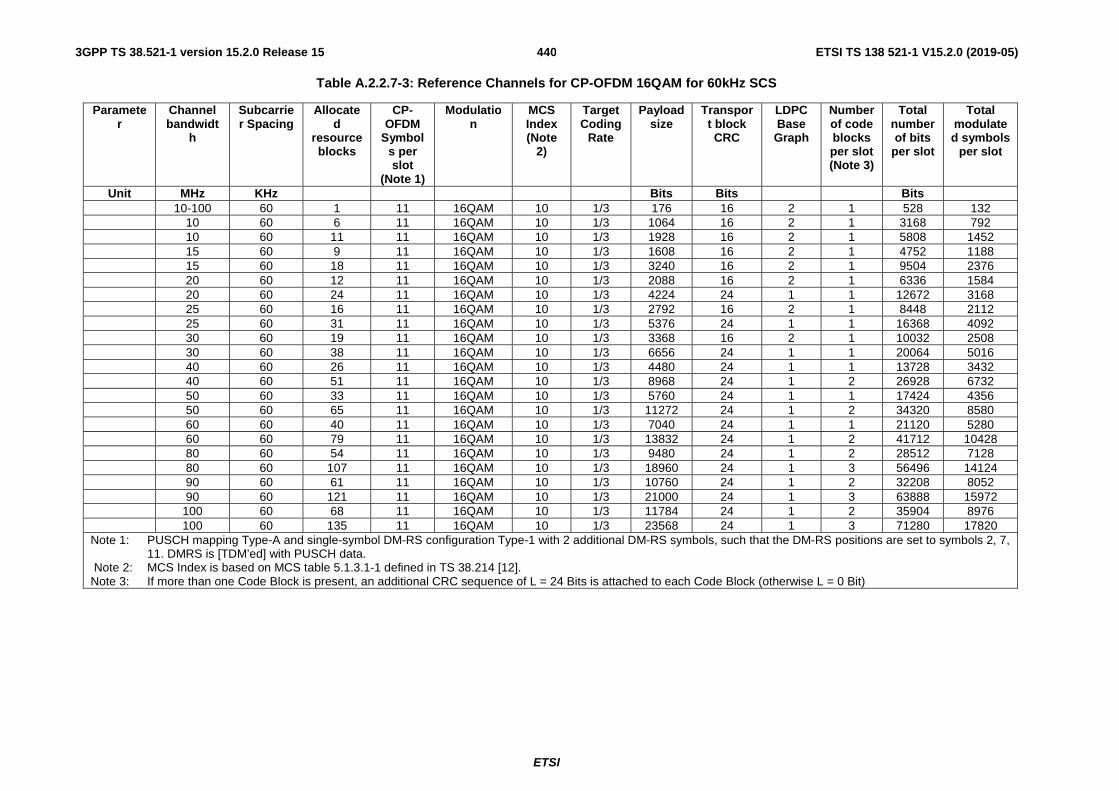
ETSI
ETSI TS 138 521-1 V15.2.0 (2019-05)4403GPP TS 38.521-1 version 15.2.0 Release 15
Table A.2.2.7-3: Reference Channels for CP-OFDM 16QAM for 60kHz SCS
Parameter
Channel bandwidt
h
Subcarrier Spacing
Allocated
resource blocks
CP-OFDM
Symbols per slot
(Note 1)
Modulation
MCS Index (Note
2)
Target Coding
Rate
Payload size
Transport block CRC
LDPC Base Graph
Number of code blocks per slot (Note 3)
Total number of bits
per slot
Total modulated symbols
per slot
Unit MHz KHz Bits Bits Bits 10-100 60 1 11 16QAM 10 1/3 176 16 2 1 528 132 10 60 6 11 16QAM 10 1/3 1064 16 2 1 3168 792 10 60 11 11 16QAM 10 1/3 1928 16 2 1 5808 1452 15 60 9 11 16QAM 10 1/3 1608 16 2 1 4752 1188 15 60 18 11 16QAM 10 1/3 3240 16 2 1 9504 2376 20 60 12 11 16QAM 10 1/3 2088 16 2 1 6336 1584 20 60 24 11 16QAM 10 1/3 4224 24 1 1 12672 3168 25 60 16 11 16QAM 10 1/3 2792 16 2 1 8448 2112 25 60 31 11 16QAM 10 1/3 5376 24 1 1 16368 4092 30 60 19 11 16QAM 10 1/3 3368 16 2 1 10032 2508 30 60 38 11 16QAM 10 1/3 6656 24 1 1 20064 5016 40 60 26 11 16QAM 10 1/3 4480 24 1 1 13728 3432 40 60 51 11 16QAM 10 1/3 8968 24 1 2 26928 6732 50 60 33 11 16QAM 10 1/3 5760 24 1 1 17424 4356 50 60 65 11 16QAM 10 1/3 11272 24 1 2 34320 8580 60 60 40 11 16QAM 10 1/3 7040 24 1 1 21120 5280 60 60 79 11 16QAM 10 1/3 13832 24 1 2 41712 10428 80 60 54 11 16QAM 10 1/3 9480 24 1 2 28512 7128 80 60 107 11 16QAM 10 1/3 18960 24 1 3 56496 14124 90 60 61 11 16QAM 10 1/3 10760 24 1 2 32208 8052 90 60 121 11 16QAM 10 1/3 21000 24 1 3 63888 15972 100 60 68 11 16QAM 10 1/3 11784 24 1 2 35904 8976 100 60 135 11 16QAM 10 1/3 23568 24 1 3 71280 17820
Note 1: PUSCH mapping Type-A and single-symbol DM-RS configuration Type-1 with 2 additional DM-RS symbols, such that the DM-RS positions are set to symbols 2, 7, 11. DMRS is [TDM’ed] with PUSCH data.
Note 2: MCS Index is based on MCS table 5.1.3.1-1 defined in TS 38.214 [12]. Note 3: If more than one Code Block is present, an additional CRC sequence of L = 24 Bits is attached to each Code Block (otherwise L = 0 Bit)

ETSI
ETSI TS 138 521-1 V15.2.0 (2019-05)4413GPP TS 38.521-1 version 15.2.0 Release 15
A.2.2.8 CP-OFDM 64QAM
Table A.2.2.8-1: Reference Channels for CP-OFDM 64QAM for 15kHz SCS
Parameter
Channel bandwidt
h
Subcarrier Spacing
Allocated
resource blocks
CP-OFDM
Symbols per slot
(Note 1)
Modulation
MCS Index (Note
2)
Target Coding
Rate
Payload size
Transport block CRC
LDPC Base Graph
Number of code blocks per slot (Note 3)
Total number of bits
per slot
Total modulated symbols
per slot
Unit MHz KHz Bits Bits Bits 5 15 25 11 64QAM 19 1/2 9992 24 1 2 19800 3300 10 15 52 11 64QAM 19 1/2 21000 24 1 3 41184 6864 15 15 79 11 64QAM 19 1/2 31752 24 1 4 62568 10428 20 15 106 11 64QAM 19 1/2 42016 24 1 5 83952 13992 25 15 133 11 64QAM 19 1/2 53288 24 1 7 105336 17556 30 15 160 11 64QAM 19 1/2 63528 24 1 8 126720 21120 40 15 216 11 64QAM 19 1/2 86040 24 1 11 171072 28512 50 15 270 11 64QAM 19 1/2 108552 24 1 13 213840 35640
Note 1: PUSCH mapping Type-A and single-symbol DM-RS configuration Type-1 with 2 additional DM-RS symbols, such that the DM-RS positions are set to symbols 2, 7, 11. DMRS is [TDM’ed] with PUSCH data.
Note 2: MCS Index is based on MCS table 5.1.3.1-1 defined in TS 38.214 [12]. Note 3: If more than one Code Block is present, an additional CRC sequence of L = 24 Bits is attached to each Code Block (otherwise L = 0 Bit)
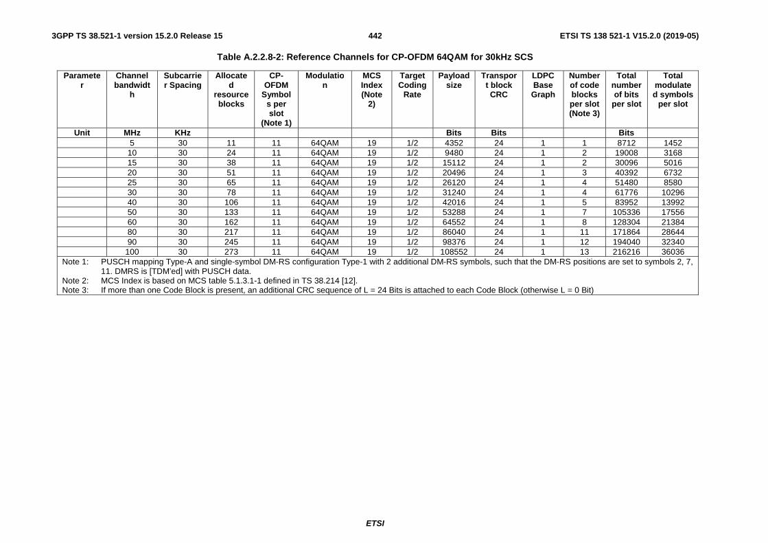
ETSI
ETSI TS 138 521-1 V15.2.0 (2019-05)4423GPP TS 38.521-1 version 15.2.0 Release 15
Table A.2.2.8-2: Reference Channels for CP-OFDM 64QAM for 30kHz SCS
Parameter
Channel bandwidt
h
Subcarrier Spacing
Allocated
resource blocks
CP-OFDM
Symbols per slot
(Note 1)
Modulation
MCS Index (Note
2)
Target Coding
Rate
Payload size
Transport block CRC
LDPC Base Graph
Number of code blocks per slot (Note 3)
Total number of bits
per slot
Total modulated symbols
per slot
Unit MHz KHz Bits Bits Bits 5 30 11 11 64QAM 19 1/2 4352 24 1 1 8712 1452 10 30 24 11 64QAM 19 1/2 9480 24 1 2 19008 3168 15 30 38 11 64QAM 19 1/2 15112 24 1 2 30096 5016 20 30 51 11 64QAM 19 1/2 20496 24 1 3 40392 6732 25 30 65 11 64QAM 19 1/2 26120 24 1 4 51480 8580 30 30 78 11 64QAM 19 1/2 31240 24 1 4 61776 10296 40 30 106 11 64QAM 19 1/2 42016 24 1 5 83952 13992 50 30 133 11 64QAM 19 1/2 53288 24 1 7 105336 17556 60 30 162 11 64QAM 19 1/2 64552 24 1 8 128304 21384 80 30 217 11 64QAM 19 1/2 86040 24 1 11 171864 28644 90 30 245 11 64QAM 19 1/2 98376 24 1 12 194040 32340 100 30 273 11 64QAM 19 1/2 108552 24 1 13 216216 36036
Note 1: PUSCH mapping Type-A and single-symbol DM-RS configuration Type-1 with 2 additional DM-RS symbols, such that the DM-RS positions are set to symbols 2, 7, 11. DMRS is [TDM’ed] with PUSCH data.
Note 2: MCS Index is based on MCS table 5.1.3.1-1 defined in TS 38.214 [12]. Note 3: If more than one Code Block is present, an additional CRC sequence of L = 24 Bits is attached to each Code Block (otherwise L = 0 Bit)

ETSI
ETSI TS 138 521-1 V15.2.0 (2019-05)4433GPP TS 38.521-1 version 15.2.0 Release 15
Table A.2.2.8-3: Reference Channels for CP-OFDM 64QAM for 60kHz SCS
Parameter
Channel bandwidt
h
Subcarrier Spacing
Allocated
resource blocks
CP-OFDM
Symbols per slot
(Note 1)
Modulation
MCS Index (Note
2)
Target Coding
Rate
Payload size
Transport block CRC
LDPC Base Graph
Number of code blocks per slot (Note 3)
Total number of bits
per slot
Total modulated symbols
per slot
Unit MHz KHz Bits Bits Bits 10 60 11 11 64QAM 19 1/2 4352 24 1 1 8712 1452 15 60 18 11 64QAM 19 1/2 7168 24 1 1 14256 2376 20 60 24 11 64QAM 19 1/2 9480 24 1 2 19008 3168 25 60 31 11 64QAM 19 1/2 12296 24 1 2 24552 4092 30 60 38 11 64QAM 19 1/2 15112 24 1 2 30096 5016 40 60 51 11 64QAM 19 1/2 20496 24 1 3 40392 6732 50 60 65 11 64QAM 19 1/2 26120 24 1 4 51480 8580 60 60 79 11 64QAM 19 1/2 31752 24 1 4 62568 10428 80 60 107 11 64QAM 19 1/2 43032 24 1 6 84744 14124 90 60 121 11 64QAM 19 1/2 48168 24 1 6 95832 15972 100 60 135 11 64QAM 19 1/2 54296 24 1 7 106920 17820
Note 1: PUSCH mapping Type-A and single-symbol DM-RS configuration Type-1 with 2 additional DM-RS symbols, such that the DM-RS positions are set to symbols 2, 7, 11. DMRS is [TDM’ed] with PUSCH data.
Note 2: MCS Index is based on MCS table 5.1.3.1-1 defined in TS 38.214 [12]. Note 3: If more than one Code Block is present, an additional CRC sequence of L = 24 Bits is attached to each Code Block (otherwise L = 0 Bit)

ETSI
ETSI TS 138 521-1 V15.2.0 (2019-05)4443GPP TS 38.521-1 version 15.2.0 Release 15
A.2.2.9 CP-OFDM 256QAM
Table A.2.2.9-1: Reference Channels for CP-OFDM 256QAM for 15kHz SCS
Parameter
Channel bandwidt
h
Subcarrier Spacing
Allocated
resource blocks
CP-OFDM
Symbols per slot
(Note 1)
Modulation
MCS Index (Note
2)
Target Coding
Rate
Payload size
Transport block CRC
LDPC Base Graph
Number of code blocks per slot (Note 3)
Total number of bits
per slot
Total modulated symbols
per slot
Unit MHz KHz Bits Bits Bits 5 15 25 11 256QAM 20 2/3 17424 24 1 3 26400 3300 10 15 52 11 256QAM 20 2/3 36896 24 1 5 54912 6864 15 15 79 11 256QAM 20 2/3 55304 24 1 7 83424 10428 20 15 106 11 256QAM 20 2/3 73776 24 1 9 111936 13992 25 15 133 11 256QAM 20 2/3 94248 24 1 12 140448 17556 30 15 160 11 256QAM 20 2/3 112648 24 1 14 168960 21120 40 15 216 11 256QAM 20 2/3 151608 24 1 18 228096 28512 50 15 270 11 256QAM 20 2/3 188576 24 1 23 285120 35640
Note 1: PUSCH mapping Type-A and single-symbol DM-RS configuration Type-1 with 2 additional DM-RS symbols, such that the DM-RS positions are set to symbols 2, 7, 11. DMRS is [TDM’ed] with PUSCH data.
Note 2: MCS Index is based on MCS table 5.1.3.1-2 defined in TS 38.214 [12]. Note 3: If more than one Code Block is present, an additional CRC sequence of L = 24 Bits is attached to each Code Block (otherwise L = 0 Bit)

ETSI
ETSI TS 138 521-1 V15.2.0 (2019-05)4453GPP TS 38.521-1 version 15.2.0 Release 15
Table A.2.2.9-2: Reference Channels for CP-OFDM 256QAM for 30kHz SCS
Parameter
Channel bandwidt
h
Subcarrier Spacing
Allocated
resource blocks
CP-OFDM
Symbols per slot
(Note 1)
Modulation
MCS Index (Note
2)
Target Coding
Rate
Payload size
Transport block CRC
LDPC Base Graph
Number of code blocks per slot (Note 3)
Total number of bits
per slot
Total modulated symbols
per slot
Unit MHz KHz Bits Bits Bits 5 30 11 11 256QAM 20 2/3 7680 24 1 1 11616 1452 10 30 24 11 256QAM 20 2/3 16896 24 1 3 25344 3168 15 30 38 11 256QAM 20 2/3 26632 24 1 4 40128 5016 20 30 51 11 256QAM 20 2/3 35856 24 1 5 53856 6732 25 30 65 11 256QAM 20 2/3 46104 24 1 6 68640 8580 30 30 78 11 256QAM 20 2/3 55304 24 1 7 82368 10296 40 30 106 11 256QAM 20 2/3 73776 24 1 9 111936 13992 50 30 133 11 256QAM 20 2/3 94248 24 1 12 140448 17556 60 30 162 11 256QAM 20 2/3 114776 24 1 14 171072 21384 80 30 217 11 256QAM 20 2/3 151608 24 1 18 229152 28644 90 30 245 11 256QAM 20 2/3 172176 24 1 21 258720 32340 100 30 273 11 256QAM 20 2/3 192624 24 1 23 288288 36036
Note 1: PUSCH mapping Type-A and single-symbol DM-RS configuration Type-1 with 2 additional DM-RS symbols, such that the DM-RS positions are set to symbols 2, 7, 11. DMRS is [TDM’ed] with PUSCH data.
Note 2: MCS Index is based on MCS table 5.1.3.1-2 defined in TS 38.214 [12]. Note 3: If more than one Code Block is present, an additional CRC sequence of L = 24 Bits is attached to each Code Block (otherwise L = 0 Bit)

ETSI
ETSI TS 138 521-1 V15.2.0 (2019-05)4463GPP TS 38.521-1 version 15.2.0 Release 15
Table A.2.2.9-3: Reference Channels for CP-OFDM 256QAM for 60kHz SCS
Parameter Channel bandwidth
Subcarrier Spacing
Allocated resource blocks
CP-OFDM
Symbols per slot (Note 1)
Modulation MCS Index
(Note 2)
Target Coding
Rate
Payload size
Transport block CRC
LDPC Base
Graph
Number of code blocks per slot (Note 3)
Total number of bits
per slot
Total modulated symbols per slot
Unit MHz KHz Bits Bits Bits 10 60 11 11 256QAM 20 2/3 7680 24 1 1 11616 1452 15 60 18 11 256QAM 20 2/3 12552 24 1 2 19008 2376 20 60 24 11 256QAM 20 2/3 16896 24 1 3 25344 3168 25 60 31 11 256QAM 20 2/3 22032 24 1 3 32736 4092 30 60 38 11 256QAM 20 2/3 26632 24 1 4 40128 5016 40 60 51 11 256QAM 20 2/3 35856 24 1 5 53856 6732 50 60 65 11 256QAM 20 2/3 46104 24 1 6 68640 8580 60 60 79 11 256QAM 20 2/3 55304 24 1 7 83424 10428 80 60 107 11 256QAM 20 2/3 75792 24 1 9 112992 14124 90 60 121 11 256QAM 20 2/3 86040 24 1 11 127776 15972 100 60 135 11 256QAM 20 2/3 94248 24 1 12 142560 17820
Note 1: PUSCH mapping Type-A and single-symbol DM-RS configuration Type-1 with 2 additional DM-RS symbols, such that the DM-RS positions are set to symbols 2, 7, 11. DMRS is [TDM’ed] with PUSCH data.
Note 2: MCS Index is based on MCS table 5.1.3.1-2 defined in TS 38.214 [12]. Note 3: If more than one Code Block is present, an additional CRC sequence of L = 24 Bits is attached to each Code Block (otherwise L = 0 Bit)
A.2.3 Reference measurement channels for TDD TDD slot patterns defined for reference sensitivity tests will be used for UL RMCs defined below.
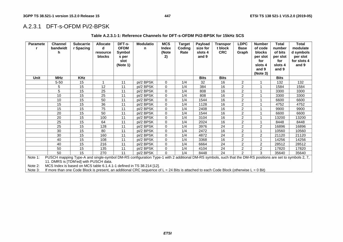
ETSI
ETSI TS 138 521-1 V15.2.0 (2019-05)4473GPP TS 38.521-1 version 15.2.0 Release 15
A.2.3.1 DFT-s-OFDM Pi/2-BPSK
Table A.2.3.1-1: Reference Channels for DFT-s-OFDM Pi/2-BPSK for 15kHz SCS
Parameter
Channel bandwidt
h
Subcarrier Spacing
Allocated
resource blocks
DFT-s-OFDM
Symbols per slot
(Note 1)
Modulation
MCS Index (Note
2)
Target Coding
Rate
Payload size for slots 4 and 9
Transport block CRC
LDPC Base Graph
Number of code blocks per slot
for slots 4 and 9
(Note 3)
Total number of bits
per slot for
slots 4 and 9
Total modulated symbols
per slot for slots 4
and 9
Unit MHz KHz Bits Bits Bits 5-50 15 1 11 pi/2 BPSK 0 1/4 32 16 2 1 132 132 5 15 12 11 pi/2 BPSK 0 1/4 384 16 2 1 1584 1584 5 15 25 11 pi/2 BPSK 0 1/4 808 16 2 1 3300 3300 10 15 25 11 pi/2 BPSK 0 1/4 808 16 2 1 3300 3300 10 15 50 11 pi/2 BPSK 0 1/4 1544 16 2 1 6600 6600 15 15 36 11 pi/2 BPSK 0 1/4 1128 16 2 1 4752 4752 15 15 75 11 pi/2 BPSK 0 1/4 2408 16 2 1 9900 9900 20 15 50 11 pi/2 BPSK 0 1/4 1544 16 2 1 6600 6600 20 15 100 11 pi/2 BPSK 0 1/4 3104 16 2 1 13200 13200 25 15 64 11 pi/2 BPSK 0 1/4 2024 16 2 1 8448 8448 25 15 128 11 pi/2 BPSK 0 1/4 3976 24 2 2 16896 16896 30 15 80 11 pi/2 BPSK 0 1/4 2472 16 2 1 10560 10560 30 15 160 11 pi/2 BPSK 0 1/4 4872 24 2 2 21120 21120 40 15 108 11 pi/2 BPSK 0 1/4 3368 16 2 1 14256 14256 40 15 216 11 pi/2 BPSK 0 1/4 6664 24 2 2 28512 28512 50 15 135 11 pi/2 BPSK 0 1/4 4104 24 2 2 17820 17820 50 15 270 11 pi/2 BPSK 0 1/4 8448 24 2 3 35640 35640
Note 1: PUSCH mapping Type-A and single-symbol DM-RS configuration Type-1 with 2 additional DM-RS symbols, such that the DM-RS positions are set to symbols 2, 7, 11. DMRS is [TDM’ed] with PUSCH data.
Note 2: MCS Index is based on MCS table 6.1.4.1-1 defined in TS 38.214 [12]. Note 3: If more than one Code Block is present, an additional CRC sequence of L = 24 Bits is attached to each Code Block (otherwise L = 0 Bit)

ETSI
ETSI TS 138 521-1 V15.2.0 (2019-05)4483GPP TS 38.521-1 version 15.2.0 Release 15
Table A.2.3.1-2: Reference Channels for DFT-s-OFDM Pi/2-BPSK for 30kHz SCS
Parameter
Channel bandwidt
h
Subcarrier Spacing
Allocated
resource blocks
DFT-s-OFDM
Symbols per slot
(Note 1)
Modulation
MCS Index (Note
2)
Target Coding
Rate
Payload size for slots 8,
9, 18 and 19
Transport block CRC
LDPC Base Graph
Number of code blocks per slot
for slots 8,
9, 18 and 19
(Note 3)
Total number of bits
per slot for
slots 8, 9, 18
and 19
Total modulated symbols
per slot for slots 8, 9, 18 and 19
Unit MHz KHz Bits Bits Bits 5-50 30 1 11 pi/2 BPSK 0 1/4 32 16 2 1 132 132 5 30 5 11 pi/2 BPSK 0 1/4 160 16 2 1 660 660 5 30 10 11 pi/2 BPSK 0 1/4 320 16 2 1 1320 1320 10 30 12 11 pi/2 BPSK 0 1/4 384 16 2 1 1584 1584 10 30 24 11 pi/2 BPSK 0 1/4 768 16 2 1 3168 3168 15 30 18 11 pi/2 BPSK 0 1/4 576 16 2 1 2376 2376 15 30 36 11 pi/2 BPSK 0 1/4 1128 16 2 1 4752 4752 20 30 25 11 pi/2 BPSK 0 1/4 808 16 2 1 3300 3300 20 30 50 11 pi/2 BPSK 0 1/4 1544 16 2 1 6600 6600 25 30 32 11 pi/2 BPSK 0 1/4 1032 16 2 1 4224 4224 25 30 64 11 pi/2 BPSK 0 1/4 2024 16 2 1 8448 8448 30 30 36 11 pi/2 BPSK 0 1/4 1128 16 2 1 4752 4752 30 30 75 11 pi/2 BPSK 0 1/4 2408 16 2 1 9900 9900 40 30 50 11 pi/2 BPSK 0 1/4 1544 16 2 1 6600 6600 40 30 100 11 pi/2 BPSK 0 1/4 3104 16 2 1 13200 13200 50 30 64 11 pi/2 BPSK 0 1/4 2024 16 2 1 8448 8448 50 30 128 11 pi/2 BPSK 0 1/4 3976 24 2 2 16896 16896 60 30 81 11 pi/2 BPSK 0 1/4 2536 16 2 1 10692 10692 60 30 162 11 pi/2 BPSK 0 1/4 5000 24 2 2 21384 21384 80 30 108 11 pi/2 BPSK 0 1/4 3368 16 2 1 14256 14256 80 30 216 11 pi/2 BPSK 0 1/4 6664 24 2 2 28512 28512 90 30 120 11 pi/2 BPSK 0 1/4 3752 16 2 1 15840 15840 90 30 243 11 pi/2 BPSK 0 1/4 7560 24 2 2 32076 32076 100 30 135 11 pi/2 BPSK 0 1/4 4104 24 2 2 17820 17820 100 30 270 11 pi/2 BPSK 0 1/4 8448 24 2 3 35640 35640
Note 1: PUSCH mapping Type-A and single-symbol DM-RS configuration Type-1 with 2 additional DM-RS symbols, such that the DM-RS positions are set to symbols 2, 7, 11. DMRS is [TDM’ed] with PUSCH data.
Note 2: MCS Index is based on MCS table 6.1.4.1-1 defined in TS 38.214 [12]. Note 3: If more than one Code Block is present, an additional CRC sequence of L = 24 Bits is attached to each Code Block (otherwise L = 0 Bit)

ETSI
ETSI TS 138 521-1 V15.2.0 (2019-05)4493GPP TS 38.521-1 version 15.2.0 Release 15
Table A.2.3.1-3: Reference Channels for DFT-s-OFDM Pi/2-BPSK for 60kHz SCS
Parameter
Channel bandwidt
h
Subcarrier Spacing
Allocated
resource blocks
DFT-s-OFDM
Symbols per slot
(Note 1)
Modulation
MCS Index (Note
2)
Target Coding
Rate
Payload size for
slots 16, 17, 18, 19, 36, 37, 38 and
39
Transport block CRC
LDPC Base Graph
Number of code blocks per slot
for slots
16, 17, 18, 19, 36, 37, 38 and
39 (Note 3)
Total number of bits
per slot for
slots 16, 17, 18, 19, 36, 37, 38 and
39
Total modulated symbols
per slot for slots
16, 17, 18, 19, 36, 37, 38 and 39
Unit MHz KHz Bits Bits Bits 10-100 60 1 11 pi/2 BPSK 0 1/4 32 16 2 1 132 132 10 60 5 11 pi/2 BPSK 0 1/4 160 16 2 1 660 660 10 60 10 11 pi/2 BPSK 0 1/4 320 16 2 1 1320 1320 15 60 9 11 pi/2 BPSK 0 1/4 288 16 2 1 1188 1188 15 60 18 11 pi/2 BPSK 0 1/4 576 16 2 1 2376 2376 20 60 12 11 pi/2 BPSK 0 1/4 384 16 2 1 1584 1584 20 60 24 11 pi/2 BPSK 0 1/4 768 16 2 1 3168 3168 25 60 15 11 pi/2 BPSK 0 1/4 480 16 2 1 1980 1980 25 60 30 11 pi/2 BPSK 0 1/4 984 16 2 1 3960 3960 30 60 18 11 pi/2 BPSK 0 1/4 576 16 2 1 2376 2376 30 60 36 11 pi/2 BPSK 0 1/4 1128 16 2 1 4752 4752 40 60 25 11 pi/2 BPSK 0 1/4 808 16 2 1 3300 3300 40 60 50 11 pi/2 BPSK 0 1/4 1544 16 2 1 6600 6600 50 60 32 11 pi/2 BPSK 0 1/4 1032 16 2 1 4224 4224 50 60 64 11 pi/2 BPSK 0 1/4 2024 16 2 1 8448 8448 60 60 36 11 pi/2 BPSK 0 1/4 1128 16 2 1 4752 4752 60 60 75 11 pi/2 BPSK 0 1/4 2408 16 2 1 9900 9900 80 60 50 11 pi/2 BPSK 0 1/4 1544 16 2 1 6600 6600 80 60 100 11 pi/2 BPSK 0 1/4 3104 16 2 1 13200 13200 90 60 60 11 pi/2 BPSK 0 1/4 1864 16 2 1 7920 7920 90 60 120 11 pi/2 BPSK 0 1/4 3752 16 2 1 15840 15840 100 60 64 11 pi/2 BPSK 0 1/4 2024 16 2 1 8448 8448 100 60 135 11 pi/2 BPSK 0 1/4 4104 24 2 2 17820 17820
Note 1: PUSCH mapping Type-A and single-symbol DM-RS configuration Type-1 with 2 additional DM-RS symbols, such that the DM-RS positions are set to symbols 2, 7, 11. DMRS is [TDM’ed] with PUSCH data.
Note 2: MCS Index is based on MCS table 6.1.4.1-1 defined in TS 38.214 [12]. Note 3: If more than one Code Block is present, an additional CRC sequence of L = 24 Bits is attached to each Code Block (otherwise L = 0 Bit)
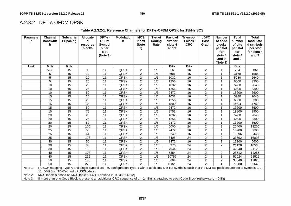
ETSI
ETSI TS 138 521-1 V15.2.0 (2019-05)4503GPP TS 38.521-1 version 15.2.0 Release 15
A.2.3.2 DFT-s-OFDM QPSK
Table A.2.3.2-1: Reference Channels for DFT-s-OFDM QPSK for 15kHz SCS
Parameter
Channel bandwidt
h
Subcarrier Spacing
Allocated
resource blocks
DFT-s-OFDM
Symbols per slot
(Note 1)
Modulation
MCS Index (Note
2)
Target Coding
Rate
Payload size for slots 4 and 9
Transport block CRC
LDPC Base Graph
Number of code blocks per slot
for slots 4 and 9
(Note 3)
Total number of bits
per slot for
slots 4 and 9
Total modulated symbols
per slot for slots 4
and 9
Unit MHz KHz Bits Bits Bits 5-50 15 1 11 QPSK 2 1/6 56 16 2 1 264 132 5 15 12 11 QPSK 2 1/6 608 16 2 1 3168 1584 5 15 20 11 QPSK 2 1/6 1032 16 2 1 5280 2640 5 15 25 11 QPSK 2 1/6 1256 16 2 1 6600 3300 10 15 20 11 QPSK 2 1/6 1032 16 2 1 5280 2640 10 15 25 11 QPSK 2 1/6 1256 16 2 1 6600 3300 10 15 50 11 QPSK 2 1/6 2472 16 2 1 13200 6600 15 15 20 11 QPSK 2 1/6 1032 16 2 1 5280 2640 15 15 25 11 QPSK 2 1/6 1256 16 2 1 6600 3300 15 15 36 11 QPSK 2 1/6 1800 16 2 1 9504 4752 15 15 50 11 QPSK 2 1/6 2472 16 2 1 13200 6600 15 15 75 11 QPSK 2 1/6 3752 16 2 1 19800 9900 20 15 20 11 QPSK 2 1/6 1032 16 2 1 5280 2640 20 15 25 11 QPSK 2 1/6 1256 16 2 1 6600 3300 20 15 50 11 QPSK 2 1/6 2472 16 2 1 13200 6600 20 15 100 11 QPSK 2 1/6 5000 24 2 2 26400 13200 25 15 50 11 QPSK 2 1/6 2472 16 2 1 13200 6600 25 15 64 11 QPSK 2 1/6 3240 16 2 1 16896 8448 25 15 128 11 QPSK 2 1/6 6408 24 2 2 33792 16896 30 15 50 11 QPSK 2 1/6 2472 16 2 1 13200 6600 30 15 80 11 QPSK 2 1/6 3976 24 2 2 21120 10560 30 15 160 11 QPSK 2 1/6 7944 24 2 3 42240 21120 40 15 108 11 QPSK 2 1/6 5384 24 2 2 28512 14256 40 15 216 11 QPSK 2 1/6 10752 24 2 3 57024 28512 50 15 135 11 QPSK 2 1/6 6664 24 2 2 35640 17820 50 15 270 11 QPSK 2 1/6 13320 24 2 4 71280 35640
Note 1: PUSCH mapping Type-A and single-symbol DM-RS configuration Type-1 with 2 additional DM-RS symbols, such that the DM-RS positions are set to symbols 2, 7, 11. DMRS is [TDM’ed] with PUSCH data.
Note 2: MCS Index is based on MCS table 6.1.4.1-1 defined in TS 38.214 [12]. Note 3: If more than one Code Block is present, an additional CRC sequence of L = 24 Bits is attached to each Code Block (otherwise L = 0 Bit)
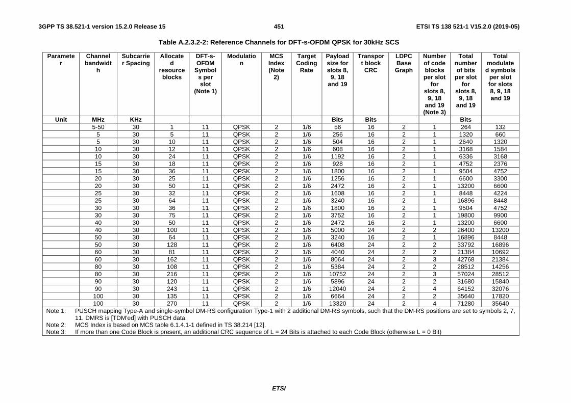
ETSI
ETSI TS 138 521-1 V15.2.0 (2019-05)4513GPP TS 38.521-1 version 15.2.0 Release 15
Table A.2.3.2-2: Reference Channels for DFT-s-OFDM QPSK for 30kHz SCS
Parameter
Channel bandwidt
h
Subcarrier Spacing
Allocated
resource blocks
DFT-s-OFDM
Symbols per slot
(Note 1)
Modulation
MCS Index (Note
2)
Target Coding
Rate
Payload size for slots 8,
9, 18 and 19
Transport block CRC
LDPC Base Graph
Number of code blocks per slot
for slots 8,
9, 18 and 19
(Note 3)
Total number of bits
per slot for
slots 8, 9, 18
and 19
Total modulated symbols
per slot for slots 8, 9, 18 and 19
Unit MHz KHz Bits Bits Bits 5-50 30 1 11 QPSK 2 1/6 56 16 2 1 264 132 5 30 5 11 QPSK 2 1/6 256 16 2 1 1320 660 5 30 10 11 QPSK 2 1/6 504 16 2 1 2640 1320 10 30 12 11 QPSK 2 1/6 608 16 2 1 3168 1584 10 30 24 11 QPSK 2 1/6 1192 16 2 1 6336 3168 15 30 18 11 QPSK 2 1/6 928 16 2 1 4752 2376 15 30 36 11 QPSK 2 1/6 1800 16 2 1 9504 4752 20 30 25 11 QPSK 2 1/6 1256 16 2 1 6600 3300 20 30 50 11 QPSK 2 1/6 2472 16 2 1 13200 6600 25 30 32 11 QPSK 2 1/6 1608 16 2 1 8448 4224 25 30 64 11 QPSK 2 1/6 3240 16 2 1 16896 8448 30 30 36 11 QPSK 2 1/6 1800 16 2 1 9504 4752 30 30 75 11 QPSK 2 1/6 3752 16 2 1 19800 9900 40 30 50 11 QPSK 2 1/6 2472 16 2 1 13200 6600 40 30 100 11 QPSK 2 1/6 5000 24 2 2 26400 13200 50 30 64 11 QPSK 2 1/6 3240 16 2 1 16896 8448 50 30 128 11 QPSK 2 1/6 6408 24 2 2 33792 16896 60 30 81 11 QPSK 2 1/6 4040 24 2 2 21384 10692 60 30 162 11 QPSK 2 1/6 8064 24 2 3 42768 21384 80 30 108 11 QPSK 2 1/6 5384 24 2 2 28512 14256 80 30 216 11 QPSK 2 1/6 10752 24 2 3 57024 28512 90 30 120 11 QPSK 2 1/6 5896 24 2 2 31680 15840 90 30 243 11 QPSK 2 1/6 12040 24 2 4 64152 32076 100 30 135 11 QPSK 2 1/6 6664 24 2 2 35640 17820 100 30 270 11 QPSK 2 1/6 13320 24 2 4 71280 35640
Note 1: PUSCH mapping Type-A and single-symbol DM-RS configuration Type-1 with 2 additional DM-RS symbols, such that the DM-RS positions are set to symbols 2, 7, 11. DMRS is [TDM’ed] with PUSCH data.
Note 2: MCS Index is based on MCS table 6.1.4.1-1 defined in TS 38.214 [12]. Note 3: If more than one Code Block is present, an additional CRC sequence of L = 24 Bits is attached to each Code Block (otherwise L = 0 Bit)

ETSI
ETSI TS 138 521-1 V15.2.0 (2019-05)4523GPP TS 38.521-1 version 15.2.0 Release 15
Table A.2.3.2-3: Reference Channels for DFT-s-OFDM QPSK for 60kHz SCS
Parameter
Channel bandwidt
h
Subcarrier Spacing
Allocated
resource blocks
DFT-s-OFDM
Symbols per slot
(Note 1)
Modulation
MCS Index (Note
2)
Target Coding
Rate
Payload size for
slots 16, 17, 18, 19, 36, 37, 38 and
39
Transport block CRC
LDPC Base Graph
Number of code blocks per slot
for slots
16, 17, 18, 19, 36, 37, 38 and
39 (Note 3)
Total number of bits
per slot for
slots 16, 17, 18, 19, 36, 37, 38 and
39
Total modulated symbols
per slot for slots
16, 17, 18, 19, 36, 37, 38 and 39
Unit MHz KHz Bits Bits Bits 10-100 60 1 11 QPSK 2 1/6 56 16 2 1 264 132 10 60 5 11 QPSK 2 1/6 256 16 2 1 1320 660 10 60 10 11 QPSK 2 1/6 504 16 2 1 2640 1320 15 60 9 11 QPSK 2 1/6 456 16 2 1 2376 1188 15 60 18 11 QPSK 2 1/6 928 16 2 1 4752 2376 20 60 12 11 QPSK 2 1/6 608 16 2 1 3168 1584 20 60 24 11 QPSK 2 1/6 1192 16 2 1 6336 3168 25 60 15 11 QPSK 2 1/6 768 16 2 1 3960 1980 25 60 30 11 QPSK 2 1/6 1544 16 2 1 7920 3960 30 60 18 11 QPSK 2 1/6 928 16 2 1 4752 2376 30 60 36 11 QPSK 2 1/6 1800 16 2 1 9504 4752 40 60 25 11 QPSK 2 1/6 1256 16 2 1 6600 3300 40 60 50 11 QPSK 2 1/6 2472 16 2 1 13200 6600 50 60 32 11 QPSK 2 1/6 1608 16 2 1 8448 4224 50 60 64 11 QPSK 2 1/6 3240 16 2 1 16896 8448 60 60 36 11 QPSK 2 1/6 1800 16 2 1 9504 4752 60 60 75 11 QPSK 2 1/6 3752 16 2 1 19800 9900 80 60 50 11 QPSK 2 1/6 2472 16 2 1 13200 6600 80 60 100 11 QPSK 2 1/6 5000 24 2 2 26400 13200 90 60 60 11 QPSK 2 1/6 3104 16 2 1 15840 7920 90 60 120 11 QPSK 2 1/6 5896 24 2 2 31680 15840 100 60 64 11 QPSK 2 1/6 3240 16 2 1 16896 8448 100 60 135 11 QPSK 2 1/6 6664 24 2 2 35640 17820
Note 1: PUSCH mapping Type-A and single-symbol DM-RS configuration Type-1 with 2 additional DM-RS symbols, such that the DM-RS positions are set to symbols 2, 7, 11. DMRS is [TDM’ed] with PUSCH data.
Note 2: MCS Index is based on MCS table 6.1.4.1-1 defined in TS 38.214 [12]. Note 3: If more than one Code Block is present, an additional CRC sequence of L = 24 Bits is attached to each Code Block (otherwise L = 0 Bit)

ETSI
ETSI TS 138 521-1 V15.2.0 (2019-05)4533GPP TS 38.521-1 version 15.2.0 Release 15
A.2.3.3 DFT-s-OFDM 16QAM
Table A.2.3.3-1: Reference Channels for DFT-s-OFDM 16QAM for 15kHz SCS
Parameter
Channel bandwidt
h
Subcarrier Spacing
Allocated
resource blocks
DFT-s-OFDM
Symbols per slot
(Note 1)
Modulation
MCS Index (Note
2)
Target Coding
Rate
Payload size for slots 4 and 9
Transport block CRC
LDPC Base Graph
Number of code blocks per slot
for slots 4 and 9
(Note 3)
Total number of bits
per slot for
slots 4 and 9
Total modulated symbols
per slot for slots 4
and 9
Unit MHz KHz Bits Bits Bits 5-50 15 1 11 16QAM 10 1/3 176 16 2 1 528 132 5 15 12 11 16QAM 10 1/3 2088 16 2 1 6336 1584 5 15 25 11 16QAM 10 1/3 4352 24 1 1 13200 3300 10 15 25 11 16QAM 10 1/3 4352 24 1 1 13200 3300 10 15 50 11 16QAM 10 1/3 8712 24 1 2 26400 6600 15 15 36 11 16QAM 10 1/3 6272 24 1 1 19008 4752 15 15 75 11 16QAM 10 1/3 13064 24 1 2 39600 9900 20 15 50 11 16QAM 10 1/3 8712 24 1 2 26400 6600 20 15 100 11 16QAM 10 1/3 17424 24 1 3 52800 13200 25 15 64 11 16QAM 10 1/3 11272 24 1 2 33792 8448 25 15 128 11 16QAM 10 1/3 22536 24 1 3 67584 16896 30 15 80 11 16QAM 10 1/3 14088 24 1 2 42240 10560 30 15 160 11 16QAM 10 1/3 28168 24 1 4 84480 21120 40 15 108 11 16QAM 10 1/3 18960 24 1 3 57024 14256 40 15 216 11 16QAM 10 1/3 37896 24 1 5 114048 28512 50 15 135 11 16QAM 10 1/3 23568 24 1 3 71280 17820 50 15 270 11 16QAM 10 1/3 47112 24 1 6 142560 35640
Note 1: PUSCH mapping Type-A and single-symbol DM-RS configuration Type-1 with 2 additional DM-RS symbols, such that the DM-RS positions are set to symbols 2, 7, 11. DMRS is [TDM’ed] with PUSCH data.
Note 2: MCS Index is based on MCS table 6.1.4.1-1 defined in TS 38.214 [12]. Note 3: If more than one Code Block is present, an additional CRC sequence of L = 24 Bits is attached to each Code Block (otherwise L = 0 Bit)

ETSI
ETSI TS 138 521-1 V15.2.0 (2019-05)4543GPP TS 38.521-1 version 15.2.0 Release 15
Table A.2.3.3-2: Reference Channels for DFT-s-OFDM 16QAM for 30kHz SCS
Parameter
Channel bandwidt
h
Subcarrier Spacing
Allocated
resource blocks
DFT-s-OFDM
Symbols per slot
(Note 1)
Modulation
MCS Index (Note
2)
Target Coding
Rate
Payload size for slots 8,
9, 18 and 19
Transport block CRC
LDPC Base Graph
Number of code blocks per slot
for slots 8,
9, 18 and 19
(Note 3)
Total number of bits
per slot for
slots 8, 9, 18
and 19
Total modulated symbols
per slot for slots 8, 9, 18 and 19
Unit MHz KHz Bits Bits Bits 5-50 30 1 11 16QAM 10 1/3 176 16 2 1 528 132 5 30 5 11 16QAM 10 1/3 888 16 2 1 2640 660 5 30 10 11 16QAM 10 1/3 1800 16 2 1 5280 1320 10 30 12 11 16QAM 10 1/3 2088 16 2 1 6336 1584 10 30 24 11 16QAM 10 1/3 4224 24 1 1 12672 3168 15 30 18 11 16QAM 10 1/3 3240 16 2 1 9504 2376 15 30 36 11 16QAM 10 1/3 6272 24 1 1 19008 4752 20 30 25 11 16QAM 10 1/3 4352 24 1 1 13200 3300 20 30 50 11 16QAM 10 1/3 8712 24 1 2 26400 6600 25 30 32 11 16QAM 10 1/3 5632 24 1 1 16896 4224 25 30 64 11 16QAM 10 1/3 11272 24 1 2 33792 8448 30 30 36 11 16QAM 10 1/3 6272 24 1 1 19008 4752 30 30 75 11 16QAM 10 1/3 13064 24 1 2 39600 9900 40 30 50 11 16QAM 10 1/3 8712 24 1 2 26400 6600 40 30 100 11 16QAM 10 1/3 17424 24 1 3 52800 13200 50 30 64 11 16QAM 10 1/3 11272 24 1 2 33792 8448 50 30 128 11 16QAM 10 1/3 22536 24 1 3 67584 16896 60 30 81 11 16QAM 10 1/3 14088 24 1 2 42768 10692 60 30 162 11 16QAM 10 1/3 28168 24 1 4 85536 21384 80 30 108 11 16QAM 10 1/3 18960 24 1 3 57024 14256 80 30 216 11 16QAM 10 1/3 37896 24 1 5 114048 28512 90 30 120 11 16QAM 10 1/3 21000 24 1 3 63360 15840 90 30 243 11 16QAM 10 1/3 43032 24 1 6 128304 32076 100 30 135 11 16QAM 10 1/3 23568 24 1 3 71280 17820 100 30 270 11 16QAM 10 1/3 47112 24 1 6 142560 35640
Note 1: PUSCH mapping Type-A and single-symbol DM-RS configuration Type-1 with 2 additional DM-RS symbols, such that the DM-RS positions are set to symbols 2, 7, 11. DMRS is [TDM’ed] with PUSCH data.
Note 2: MCS Index is based on MCS table 6.1.4.1-1 defined in TS 38.214 [12]. Note 3: If more than one Code Block is present, an additional CRC sequence of L = 24 Bits is attached to each Code Block (otherwise L = 0 Bit)
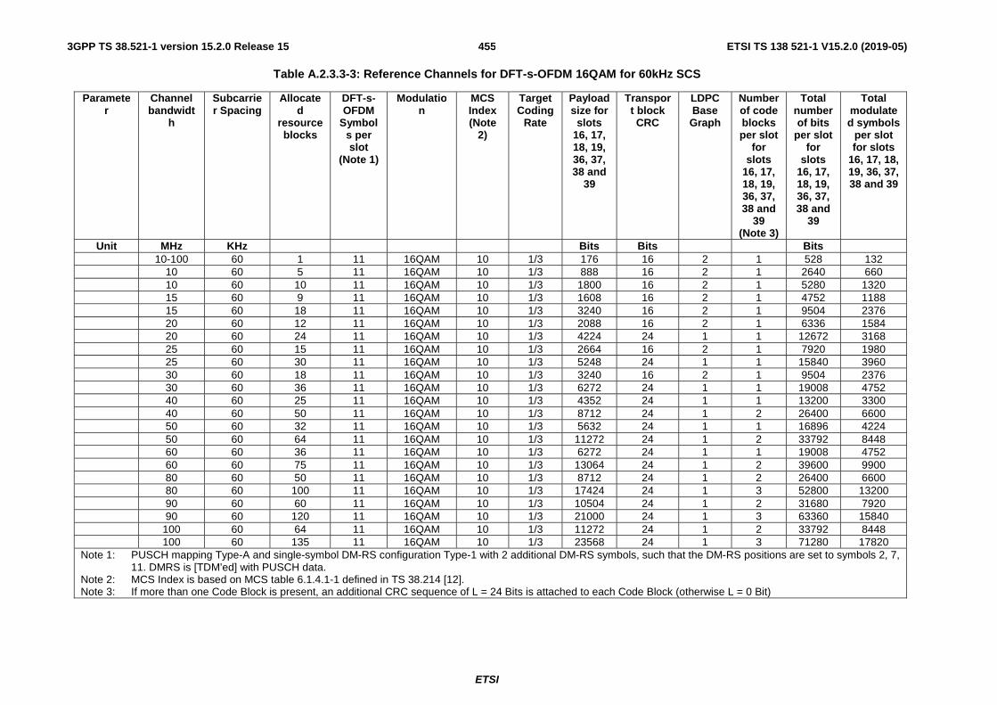
ETSI
ETSI TS 138 521-1 V15.2.0 (2019-05)4553GPP TS 38.521-1 version 15.2.0 Release 15
Table A.2.3.3-3: Reference Channels for DFT-s-OFDM 16QAM for 60kHz SCS
Parameter
Channel bandwidt
h
Subcarrier Spacing
Allocated
resource blocks
DFT-s-OFDM
Symbols per slot
(Note 1)
Modulation
MCS Index (Note
2)
Target Coding
Rate
Payload size for
slots 16, 17, 18, 19, 36, 37, 38 and
39
Transport block CRC
LDPC Base Graph
Number of code blocks per slot
for slots
16, 17, 18, 19, 36, 37, 38 and
39 (Note 3)
Total number of bits
per slot for
slots 16, 17, 18, 19, 36, 37, 38 and
39
Total modulated symbols
per slot for slots
16, 17, 18, 19, 36, 37, 38 and 39
Unit MHz KHz Bits Bits Bits 10-100 60 1 11 16QAM 10 1/3 176 16 2 1 528 132 10 60 5 11 16QAM 10 1/3 888 16 2 1 2640 660 10 60 10 11 16QAM 10 1/3 1800 16 2 1 5280 1320 15 60 9 11 16QAM 10 1/3 1608 16 2 1 4752 1188 15 60 18 11 16QAM 10 1/3 3240 16 2 1 9504 2376 20 60 12 11 16QAM 10 1/3 2088 16 2 1 6336 1584 20 60 24 11 16QAM 10 1/3 4224 24 1 1 12672 3168 25 60 15 11 16QAM 10 1/3 2664 16 2 1 7920 1980 25 60 30 11 16QAM 10 1/3 5248 24 1 1 15840 3960 30 60 18 11 16QAM 10 1/3 3240 16 2 1 9504 2376 30 60 36 11 16QAM 10 1/3 6272 24 1 1 19008 4752 40 60 25 11 16QAM 10 1/3 4352 24 1 1 13200 3300 40 60 50 11 16QAM 10 1/3 8712 24 1 2 26400 6600 50 60 32 11 16QAM 10 1/3 5632 24 1 1 16896 4224 50 60 64 11 16QAM 10 1/3 11272 24 1 2 33792 8448 60 60 36 11 16QAM 10 1/3 6272 24 1 1 19008 4752 60 60 75 11 16QAM 10 1/3 13064 24 1 2 39600 9900 80 60 50 11 16QAM 10 1/3 8712 24 1 2 26400 6600 80 60 100 11 16QAM 10 1/3 17424 24 1 3 52800 13200 90 60 60 11 16QAM 10 1/3 10504 24 1 2 31680 7920 90 60 120 11 16QAM 10 1/3 21000 24 1 3 63360 15840 100 60 64 11 16QAM 10 1/3 11272 24 1 2 33792 8448 100 60 135 11 16QAM 10 1/3 23568 24 1 3 71280 17820
Note 1: PUSCH mapping Type-A and single-symbol DM-RS configuration Type-1 with 2 additional DM-RS symbols, such that the DM-RS positions are set to symbols 2, 7, 11. DMRS is [TDM’ed] with PUSCH data.
Note 2: MCS Index is based on MCS table 6.1.4.1-1 defined in TS 38.214 [12]. Note 3: If more than one Code Block is present, an additional CRC sequence of L = 24 Bits is attached to each Code Block (otherwise L = 0 Bit)

ETSI
ETSI TS 138 521-1 V15.2.0 (2019-05)4563GPP TS 38.521-1 version 15.2.0 Release 15
A.2.3.4 DFT-s-OFDM 64QAM
Table A.2.3.4-1: Reference Channels for DFT-s-OFDM 64QAM for 15kHz SCS
Parameter
Channel bandwidt
h
Subcarrier Spacing
Allocated
resource blocks
DFT-s-OFDM
Symbols per slot
(Note 1)
Modulation
MCS Index (Note
2)
Target Coding
Rate
Payload size for slots 4 and 9
Transport block CRC
LDPC Base Graph
Number of code blocks per slot
for slots 4 and 9
(Note 3)
Total number of bits
per slot for
slots 4 and 9
Total modulated symbols
per slot for slots 4
and 9
Unit MHz KHz Bits Bits Bits 5 15 25 11 64QAM 18 1/2 9992 24 1 2 19800 3300 10 15 50 11 64QAM 18 1/2 19968 24 1 3 39600 6600 15 15 75 11 64QAM 18 1/2 30216 24 1 4 59400 9900 20 15 100 11 64QAM 18 1/2 39936 24 1 5 79200 13200 25 15 128 11 64QAM 18 1/2 51216 24 1 7 101376 16896 30 15 160 11 64QAM 18 1/2 63528 24 1 8 126720 21120 40 15 216 11 64QAM 18 1/2 86040 24 1 11 171072 28512 50 15 270 11 64QAM 18 1/2 108552 24 1 13 213840 35640
Note 1: PUSCH mapping Type-A and single-symbol DM-RS configuration Type-1 with 2 additional DM-RS symbols, such that the DM-RS positions are set to symbols 2, 7, 11. DMRS is [TDM’ed] with PUSCH data.
Note 2: MCS Index is based on MCS table 6.1.4.1-1 defined in TS 38.214 [12]. Note 3: If more than one Code Block is present, an additional CRC sequence of L = 24 Bits is attached to each Code Block (otherwise L = 0 Bit)

ETSI
ETSI TS 138 521-1 V15.2.0 (2019-05)4573GPP TS 38.521-1 version 15.2.0 Release 15
Table A.2.3.4-2: Reference Channels for DFT-s-OFDM 64QAM for 30kHz SCS
Parameter
Channel bandwidt
h
Subcarrier Spacing
Allocated
resource blocks
DFT-s-OFDM
Symbols per slot
(Note 1)
Modulation
MCS Index (Note
2)
Target Coding
Rate
Payload size for slots 8,
9, 18 and 19
Transport block CRC
LDPC Base Graph
Number of code blocks per slot
for slots 8,
9, 18 and 19
(Note 3)
Total number of bits
per slot for
slots 8, 9, 18
and 19
Total modulated symbols
per slot for slots 8, 9, 18 and 19
Unit MHz KHz Bits Bits Bits 5 30 10 11 64QAM 18 1/2 3968 24 1 1 7920 1320 10 30 24 11 64QAM 18 1/2 9480 24 1 2 19008 3168 15 30 36 11 64QAM 18 1/2 14344 24 1 2 28512 4752 20 30 50 11 64QAM 18 1/2 19968 24 1 3 39600 6600 25 30 64 11 64QAM 18 1/2 25608 24 1 4 50688 8448 30 30 75 11 64QAM 18 1/2 30216 24 1 4 59400 9900 40 30 100 11 64QAM 18 1/2 39936 24 1 5 79200 13200 50 30 128 11 64QAM 18 1/2 51216 24 1 7 101376 16896 60 30 162 11 64QAM 18 1/2 64552 24 1 8 128304 21384 80 30 216 11 64QAM 18 1/2 86040 24 1 11 171072 28512 90 30 243 11 64QAM 18 1/2 96264 24 1 12 192456 32076 100 30 270 11 64QAM 18 1/2 108552 24 1 13 213840 35640
Note 1: PUSCH mapping Type-A and single-symbol DM-RS configuration Type-1 with 2 additional DM-RS symbols, such that the DM-RS positions are set to symbols 2, 7, 11. DMRS is [TDM’ed] with PUSCH data.
Note 2: MCS Index is based on MCS table 6.1.4.1-1 defined in TS 38.214 [12]. Note 3: If more than one Code Block is present, an additional CRC sequence of L = 24 Bits is attached to each Code Block (otherwise L = 0 Bit)
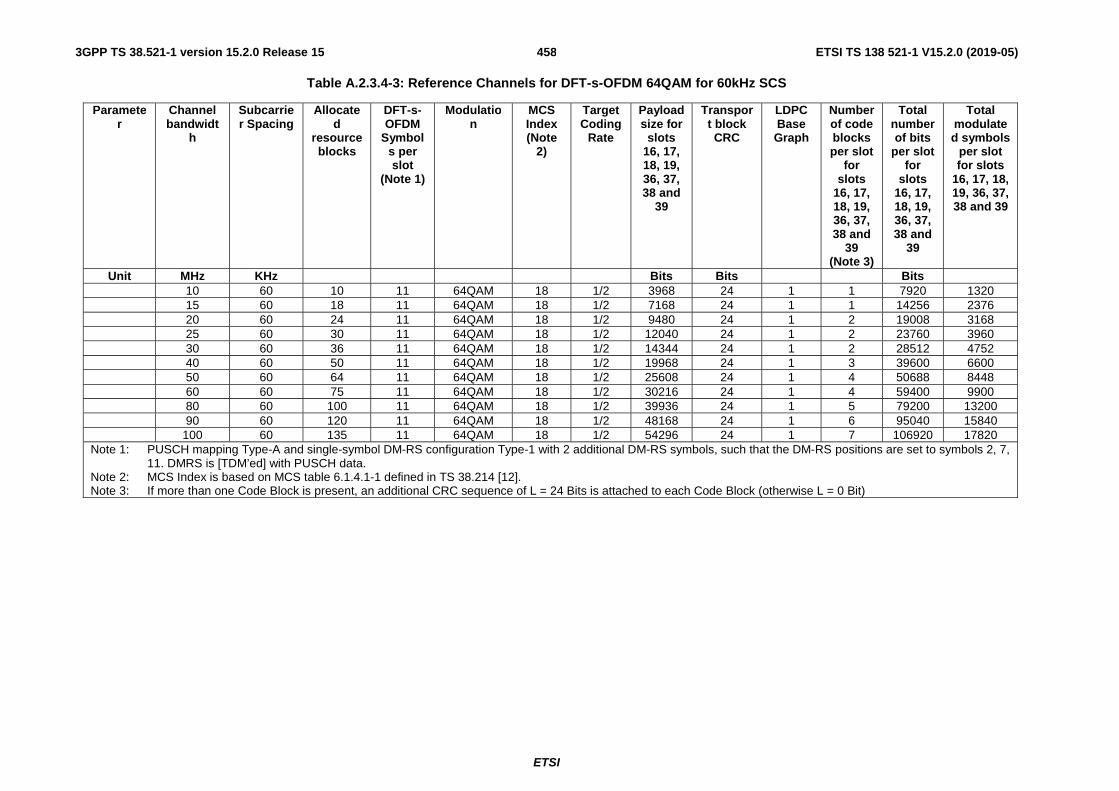
ETSI
ETSI TS 138 521-1 V15.2.0 (2019-05)4583GPP TS 38.521-1 version 15.2.0 Release 15
Table A.2.3.4-3: Reference Channels for DFT-s-OFDM 64QAM for 60kHz SCS
Parameter
Channel bandwidt
h
Subcarrier Spacing
Allocated
resource blocks
DFT-s-OFDM
Symbols per slot
(Note 1)
Modulation
MCS Index (Note
2)
Target Coding
Rate
Payload size for
slots 16, 17, 18, 19, 36, 37, 38 and
39
Transport block CRC
LDPC Base Graph
Number of code blocks per slot
for slots
16, 17, 18, 19, 36, 37, 38 and
39 (Note 3)
Total number of bits
per slot for
slots 16, 17, 18, 19, 36, 37, 38 and
39
Total modulated symbols
per slot for slots
16, 17, 18, 19, 36, 37, 38 and 39
Unit MHz KHz Bits Bits Bits 10 60 10 11 64QAM 18 1/2 3968 24 1 1 7920 1320 15 60 18 11 64QAM 18 1/2 7168 24 1 1 14256 2376 20 60 24 11 64QAM 18 1/2 9480 24 1 2 19008 3168 25 60 30 11 64QAM 18 1/2 12040 24 1 2 23760 3960 30 60 36 11 64QAM 18 1/2 14344 24 1 2 28512 4752 40 60 50 11 64QAM 18 1/2 19968 24 1 3 39600 6600 50 60 64 11 64QAM 18 1/2 25608 24 1 4 50688 8448 60 60 75 11 64QAM 18 1/2 30216 24 1 4 59400 9900 80 60 100 11 64QAM 18 1/2 39936 24 1 5 79200 13200 90 60 120 11 64QAM 18 1/2 48168 24 1 6 95040 15840 100 60 135 11 64QAM 18 1/2 54296 24 1 7 106920 17820
Note 1: PUSCH mapping Type-A and single-symbol DM-RS configuration Type-1 with 2 additional DM-RS symbols, such that the DM-RS positions are set to symbols 2, 7, 11. DMRS is [TDM’ed] with PUSCH data.
Note 2: MCS Index is based on MCS table 6.1.4.1-1 defined in TS 38.214 [12]. Note 3: If more than one Code Block is present, an additional CRC sequence of L = 24 Bits is attached to each Code Block (otherwise L = 0 Bit)
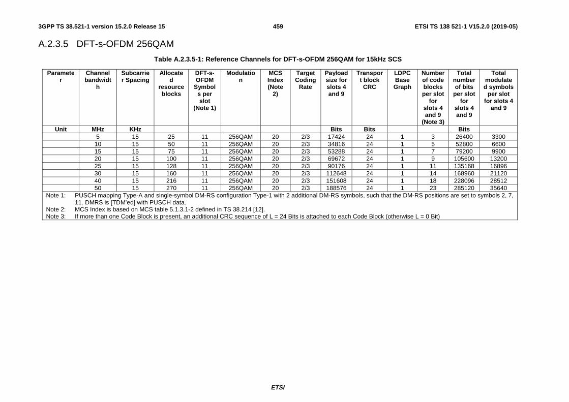
ETSI
ETSI TS 138 521-1 V15.2.0 (2019-05)4593GPP TS 38.521-1 version 15.2.0 Release 15
A.2.3.5 DFT-s-OFDM 256QAM
Table A.2.3.5-1: Reference Channels for DFT-s-OFDM 256QAM for 15kHz SCS
Parameter
Channel bandwidt
h
Subcarrier Spacing
Allocated
resource blocks
DFT-s-OFDM
Symbols per slot
(Note 1)
Modulation
MCS Index (Note
2)
Target Coding
Rate
Payload size for slots 4 and 9
Transport block CRC
LDPC Base Graph
Number of code blocks per slot
for slots 4 and 9
(Note 3)
Total number of bits
per slot for
slots 4 and 9
Total modulated symbols
per slot for slots 4
and 9
Unit MHz KHz Bits Bits Bits 5 15 25 11 256QAM 20 2/3 17424 24 1 3 26400 3300 10 15 50 11 256QAM 20 2/3 34816 24 1 5 52800 6600 15 15 75 11 256QAM 20 2/3 53288 24 1 7 79200 9900 20 15 100 11 256QAM 20 2/3 69672 24 1 9 105600 13200 25 15 128 11 256QAM 20 2/3 90176 24 1 11 135168 16896 30 15 160 11 256QAM 20 2/3 112648 24 1 14 168960 21120 40 15 216 11 256QAM 20 2/3 151608 24 1 18 228096 28512 50 15 270 11 256QAM 20 2/3 188576 24 1 23 285120 35640
Note 1: PUSCH mapping Type-A and single-symbol DM-RS configuration Type-1 with 2 additional DM-RS symbols, such that the DM-RS positions are set to symbols 2, 7, 11. DMRS is [TDM’ed] with PUSCH data.
Note 2: MCS Index is based on MCS table 5.1.3.1-2 defined in TS 38.214 [12]. Note 3: If more than one Code Block is present, an additional CRC sequence of L = 24 Bits is attached to each Code Block (otherwise L = 0 Bit)
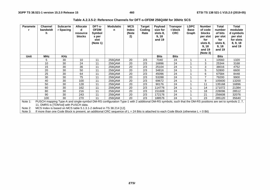
ETSI
ETSI TS 138 521-1 V15.2.0 (2019-05)4603GPP TS 38.521-1 version 15.2.0 Release 15
Table A.2.3.5-2: Reference Channels for DFT-s-OFDM 256QAM for 30kHz SCS
Parameter
Channel bandwidt
h
Subcarrier Spacing
Allocated
resource blocks
DFT-s-OFDM
Symbols per slot
(Note 1)
Modulation
MCS Index (Note
2)
Target Coding
Rate
Payload size for slots 8,
9, 18 and 19
Transport block CRC
LDPC Base Graph
Number of code blocks per slot
for slots 8,
9, 18 and 19
(Note 3)
Total number of bits
per slot for
slots 8, 9, 18
and 19
Total modulated symbols
per slot for slots 8, 9, 18 and 19
Unit MHz KHz Bits Bits Bits 5 30 10 11 256QAM 20 2/3 7040 24 1 1 10560 1320 10 30 24 11 256QAM 20 2/3 16896 24 1 3 25344 3168 15 30 36 11 256QAM 20 2/3 25104 24 1 3 38016 4752 20 30 50 11 256QAM 20 2/3 34816 24 1 5 52800 6600 25 30 64 11 256QAM 20 2/3 45096 24 1 6 67584 8448 30 30 75 11 256QAM 20 2/3 53288 24 1 7 79200 9900 40 30 100 11 256QAM 20 2/3 69672 24 1 9 105600 13200 50 30 128 11 256QAM 20 2/3 90176 24 1 11 135168 16896 60 30 162 11 256QAM 20 2/3 114776 24 1 14 171072 21384 80 30 216 11 256QAM 20 2/3 151608 24 1 18 228096 28512 90 30 243 11 256QAM 20 2/3 172176 24 1 21 256608 32076 100 30 270 11 256QAM 20 2/3 188576 24 1 23 285120 35640
Note 1: PUSCH mapping Type-A and single-symbol DM-RS configuration Type-1 with 2 additional DM-RS symbols, such that the DM-RS positions are set to symbols 2, 7, 11. DMRS is [TDM’ed] with PUSCH data.
Note 2: MCS Index is based on MCS table 5.1.3.1-2 defined in TS 38.214 [12]. Note 3: If more than one Code Block is present, an additional CRC sequence of L = 24 Bits is attached to each Code Block (otherwise L = 0 Bit)

ETSI
ETSI TS 138 521-1 V15.2.0 (2019-05)4613GPP TS 38.521-1 version 15.2.0 Release 15
Table A.2.3.5-3: Reference Channels for DFT-s-OFDM 256QAM for 60kHz SCS
Parameter
Channel bandwidt
h
Subcarrier Spacing
Allocated
resource blocks
DFT-s-OFDM
Symbols per slot
(Note 1)
Modulation
MCS Index (Note
2)
Target Coding
Rate
Payload size for
slots 16, 17, 18, 19, 36, 37, 38 and
39
Transport block CRC
LDPC Base Graph
Number of code blocks per slot
for slots
16, 17, 18, 19, 36, 37, 38 and
39 (Note 3)
Total number of bits
per slot for
slots 16, 17, 18, 19, 36, 37, 38 and
39
Total modulated symbols
per slot for slots
16, 17, 18, 19, 36, 37, 38 and 39
Unit MHz KHz Bits Bits Bits 10 60 10 11 256QAM 20 2/3 7040 24 1 1 10560 1320 15 60 18 11 256QAM 20 2/3 12552 24 1 2 19008 2376 20 60 24 11 256QAM 20 2/3 16896 24 1 3 25344 3168 25 60 30 11 256QAM 20 2/3 21000 24 1 3 31680 3960 30 60 36 11 256QAM 20 2/3 25104 24 1 3 38016 4752 40 60 50 11 256QAM 20 2/3 34816 24 1 5 52800 6600 50 60 64 11 256QAM 20 2/3 45096 24 1 6 67584 8448 60 60 75 11 256QAM 20 2/3 53288 24 1 7 79200 9900 80 60 100 11 256QAM 20 2/3 69672 24 1 9 105600 13200 90 60 120 11 256QAM 20 2/3 83976 24 1 10 126720 15840 100 60 135 11 256QAM 20 2/3 94248 24 1 12 142560 17820
Note 1: PUSCH mapping Type-A and single-symbol DM-RS configuration Type-1 with 2 additional DM-RS symbols, such that the DM-RS positions are set to symbols 2, 7, 11. DMRS is [TDM’ed] with PUSCH data.
Note 2: MCS Index is based on MCS table 5.1.3.1-2 defined in TS 38.214 [12]. Note 3: If more than one Code Block is present, an additional CRC sequence of L = 24 Bits is attached to each Code Block (otherwise L = 0 Bit)

ETSI
ETSI TS 138 521-1 V15.2.0 (2019-05)4623GPP TS 38.521-1 version 15.2.0 Release 15
A.2.3.6 CP-OFDM QPSK
Table A.2.3.6-1: Reference Channels for CP-OFDM QPSK for 15kHz SCS
Parameter
Channel bandwidt
h
Subcarrier Spacing
Allocated
resource blocks
CP-OFDM
Symbols per slot
(Note 1)
Modulation
MCS Index (Note
2)
Target Coding
Rate
Payload size for slots 4 and 9
Transport block CRC
LDPC Base Graph
Number of code blocks per slot
for slots 4 and 9
(Note 3)
Total number of bits
per slot for
slots 4 and 9
Total modulated symbols
per slot for slots 4
and 9
Unit MHz KHz Bits Bits Bits 5-50 15 1 11 QPSK 2 1/6 56 16 2 1 264 132 5 15 13 11 QPSK 2 1/6 672 16 2 1 3432 1716 5 15 25 11 QPSK 2 1/6 1256 16 2 1 6600 3300 10 15 26 11 QPSK 2 1/6 1288 16 2 1 6864 3432 10 15 52 11 QPSK 2 1/6 2600 16 2 1 13728 6864 15 15 40 11 QPSK 2 1/6 2024 16 2 1 10560 5280 15 15 79 11 QPSK 2 1/6 3912 24 2 2 20856 10428 20 15 53 11 QPSK 2 1/6 2664 16 2 1 13992 6996 20 15 106 11 QPSK 2 1/6 5256 24 2 2 27984 13992 25 15 67 11 QPSK 2 1/6 3368 16 2 1 17688 8844 25 15 133 11 QPSK 2 1/6 6664 24 2 2 35112 17556 30 15 80 11 QPSK 2 1/6 3976 24 2 2 21120 10560 30 15 160 11 QPSK 2 1/6 7944 24 2 3 42240 21120 40 15 108 11 QPSK 2 1/6 5384 24 2 2 28512 14256 40 15 216 11 QPSK 2 1/6 10752 24 2 3 57024 28512 50 15 135 11 QPSK 2 1/6 6664 24 2 2 35640 17820 50 15 270 11 QPSK 2 1/6 13320 24 2 4 71280 35640
Note 1: PUSCH mapping Type-A and single-symbol DM-RS configuration Type-1 with 2 additional DM-RS symbols, such that the DM-RS positions are set to symbols 2, 7, 11. DMRS is [TDM’ed] with PUSCH data.
Note 2: MCS Index is based on MCS table 5.1.3.1-1 defined in TS 38.214 [12]. Note 3: If more than one Code Block is present, an additional CRC sequence of L = 24 Bits is attached to each Code Block (otherwise L = 0 Bit)

ETSI
ETSI TS 138 521-1 V15.2.0 (2019-05)4633GPP TS 38.521-1 version 15.2.0 Release 15
Table A.2.3.6-2: Reference Channels for CP-OFDM QPSK for 30kHz SCS
Parameter
Channel bandwidt
h
Subcarrier Spacing
Allocated
resource blocks
CP-OFDM
Symbols per slot
(Note 1)
Modulation
MCS Index (Note
2)
Target Coding
Rate
Payload size for slots 8,
9, 18 and 19
Transport block CRC
LDPC Base Graph
Number of code blocks per slot
for slots 8,
9, 18 and 19
(Note 3)
Total number of bits
per slot for
slots 8, 9, 18
and 19
Total modulated symbols
per slot for slots 8, 9, 18 and 19
Unit MHz KHz Bits Bits Bits 5-50 30 1 11 QPSK 2 1/6 56 16 2 1 264 132 5 30 6 11 QPSK 2 1/6 304 16 2 1 1584 792 5 30 11 11 QPSK 2 1/6 552 16 2 1 2904 1452 10 30 12 11 QPSK 2 1/6 608 16 2 1 3168 1584 10 30 24 11 QPSK 2 1/6 1192 16 2 1 6336 3168 15 30 19 11 QPSK 2 1/6 984 16 2 1 5016 2508 15 30 38 11 QPSK 2 1/6 1928 16 2 1 10032 5016 20 30 26 11 QPSK 2 1/6 1288 16 2 1 6864 3432 20 30 51 11 QPSK 2 1/6 2536 16 2 1 13464 6732 25 30 33 11 QPSK 2 1/6 1672 16 2 1 8712 4356 25 30 65 11 QPSK 2 1/6 3240 16 2 1 17160 8580 30 30 39 11 QPSK 2 1/6 2024 16 2 1 10296 5148 30 30 78 11 QPSK 2 1/6 3848 24 2 2 20592 10296 40 30 53 11 QPSK 2 1/6 2664 16 2 1 13992 6996 40 30 106 11 QPSK 2 1/6 5256 24 2 2 27984 13992 50 30 67 11 QPSK 2 1/6 3368 16 2 1 17688 8844 50 30 133 11 QPSK 2 1/6 6664 24 2 2 35112 17556 60 30 81 11 QPSK 2 1/6 4040 24 2 2 21384 10692 60 30 162 11 QPSK 2 1/6 8064 24 2 3 42768 21384 80 30 109 11 QPSK 2 1/6 5384 24 2 2 28776 14388 80 30 217 11 QPSK 2 1/6 10752 24 2 3 57288 28644 90 30 123 11 QPSK 2 1/6 6152 24 2 2 32472 16236 90 30 245 11 QPSK 2 1/6 12296 24 2 4 64680 32340 100 30 137 11 QPSK 2 1/6 6792 24 2 2 36168 18084 100 30 273 11 QPSK 2 1/6 13576 24 2 4 72072 36036
Note 1: PUSCH mapping Type-A and single-symbol DM-RS configuration Type-1 with 2 additional DM-RS symbols, such that the DM-RS positions are set to symbols 2, 7, 11. DMRS is [TDM’ed] with PUSCH data.
Note 2: MCS Index is based on MCS table 5.1.3.1-1 defined in TS 38.214 [12]. Note 3: If more than one Code Block is present, an additional CRC sequence of L = 24 Bits is attached to each Code Block (otherwise L = 0 Bit)

ETSI
ETSI TS 138 521-1 V15.2.0 (2019-05)4643GPP TS 38.521-1 version 15.2.0 Release 15
Table A.2.3.6-3: Reference Channels for CP-OFDM QPSK for 60kHz SCS
Parameter
Channel bandwidt
h
Subcarrier Spacing
Allocated
resource blocks
CP-OFDM
Symbols per slot
(Note 1)
Modulation
MCS Index (Note
2)
Target Coding
Rate
Payload size for
slots 16, 17, 18, 19, 36, 37, 38 and
39
Transport block CRC
LDPC Base Graph
Number of code blocks per slot
for slots
16, 17, 18, 19, 36, 37, 38 and
39 (Note 3)
Total number of bits
per slot for
slots 16, 17, 18, 19, 36, 37, 38 and
39
Total modulated symbols
per slot for slots
16, 17, 18, 19, 36, 37, 38 and 39
Unit MHz KHz Bits Bits Bits 10-100 60 1 11 QPSK 2 1/6 56 16 2 1 264 132 10 60 6 11 QPSK 2 1/6 304 16 2 1 1584 792 10 60 11 11 QPSK 2 1/6 552 16 2 1 2904 1452 15 60 9 11 QPSK 2 1/6 456 16 2 1 2376 1188 15 60 18 11 QPSK 2 1/6 928 16 2 1 4752 2376 20 60 12 11 QPSK 2 1/6 608 16 2 1 3168 1584 20 60 24 11 QPSK 2 1/6 1192 16 2 1 6336 3168 25 60 16 11 QPSK 2 1/6 808 16 2 1 4224 2112 25 60 31 11 QPSK 2 1/6 1544 16 2 1 8184 4092 30 60 19 11 QPSK 2 1/6 984 16 2 1 5016 2508 30 60 38 11 QPSK 2 1/6 1928 16 2 1 10032 5016 40 60 26 11 QPSK 2 1/6 1288 16 2 1 6864 3432 40 60 51 11 QPSK 2 1/6 2536 16 2 1 13464 6732 50 60 33 11 QPSK 2 1/6 1672 16 2 1 8712 4356 50 60 65 11 QPSK 2 1/6 3240 16 2 1 17160 8580 60 60 40 11 QPSK 2 1/6 2024 16 2 1 10560 5280 60 60 79 11 QPSK 2 1/6 3912 24 2 2 20856 10428 80 60 54 11 QPSK 2 1/6 2664 16 2 1 14256 7128 80 60 107 11 QPSK 2 1/6 5256 24 2 2 28248 14124 90 60 61 11 QPSK 2 1/6 3104 16 2 1 16104 8052 90 60 121 11 QPSK 2 1/6 6024 24 2 2 31944 15972 100 60 68 11 QPSK 2 1/6 3368 16 2 1 17952 8976 100 60 135 11 QPSK 2 1/6 6664 24 2 2 35640 17820
Note 1: PUSCH mapping Type-A and single-symbol DM-RS configuration Type-1 with 2 additional DM-RS symbols, such that the DM-RS positions are set to symbols 2, 7, 11. DMRS is [TDM’ed] with PUSCH data.
Note 2: MCS Index is based on MCS table 5.1.3.1-1 defined in TS 38.214 [12]. Note 3: If more than one Code Block is present, an additional CRC sequence of L = 24 Bits is attached to each Code Block (otherwise L = 0 Bit)

ETSI
ETSI TS 138 521-1 V15.2.0 (2019-05)4653GPP TS 38.521-1 version 15.2.0 Release 15
A.2.3.7 CP-OFDM 16QAM
Table A.2.3.7-1: Reference Channels for CP-OFDM 16QAM for 15kHz SCS
Parameter
Channel bandwidt
h
Subcarrier Spacing
Allocated
resource blocks
CP-OFDM
Symbols per slot
(Note 1)
Modulation
MCS Index (Note
2)
Target Coding
Rate
Payload size for slots 4 and 9
Transport block CRC
LDPC Base Graph
Number of code blocks per slot
for slots 4 and 9
(Note 3)
Total number of bits
per slot for
slots 4 and 9
Total modulated symbols
per slot for slots 4
and 9
Unit MHz KHz Bits Bits Bits 5-50 15 1 11 16QAM 10 1/3 176 16 2 1 528 132 5 15 13 11 16QAM 10 1/3 2280 16 2 1 6864 1716 5 15 25 11 16QAM 10 1/3 4352 24 1 1 13200 3300 10 15 26 11 16QAM 10 1/3 4480 24 1 1 13728 3432 10 15 52 11 16QAM 10 1/3 9224 24 1 2 27456 6864 15 15 40 11 16QAM 10 1/3 7040 24 1 1 21120 5280 15 15 79 11 16QAM 10 1/3 13832 24 1 2 41712 10428 20 15 53 11 16QAM 10 1/3 9224 24 1 2 27984 6996 20 15 106 11 16QAM 10 1/3 18432 24 1 3 55968 13992 25 15 67 11 16QAM 10 1/3 11784 24 1 2 35376 8844 25 15 133 11 16QAM 10 1/3 23040 24 1 3 70224 17556 30 15 80 11 16QAM 10 1/3 14088 24 1 2 42240 10560 30 15 160 11 16QAM 10 1/3 28168 24 1 4 84480 21120 40 15 108 11 16QAM 10 1/3 18960 24 1 3 57024 14256 40 15 216 11 16QAM 10 1/3 37896 24 1 5 114048 28512 50 15 135 11 16QAM 10 1/3 23568 24 1 3 71280 17820 50 15 270 11 16QAM 10 1/3 47112 24 1 6 142560 35640
Note 1: PUSCH mapping Type-A and single-symbol DM-RS configuration Type-1 with 2 additional DM-RS symbols, such that the DM-RS positions are set to symbols 2, 7, 11. DMRS is [TDM’ed] with PUSCH data.
Note 2: MCS Index is based on MCS table 5.1.3.1-1 defined in TS 38.214 [12]. Note 3: If more than one Code Block is present, an additional CRC sequence of L = 24 Bits is attached to each Code Block (otherwise L = 0 Bit)

ETSI
ETSI TS 138 521-1 V15.2.0 (2019-05)4663GPP TS 38.521-1 version 15.2.0 Release 15
Table A.2.3.7-2: Reference Channels for CP-OFDM 16QAM for 30kHz SCS
Parameter
Channel bandwidt
h
Subcarrier Spacing
Allocated
resource blocks
CP-OFDM
Symbols per slot
(Note 1)
Modulation
MCS Index (Note
2)
Target Coding
Rate
Payload size for slots 8,
9, 18 and 19
Transport block CRC
LDPC Base Graph
Number of code blocks per slot
for slots 8,
9, 18 and 19
(Note 3)
Total number of bits
per slot for
slots 8, 9, 18
and 19
Total modulated symbols
per slot for slots 8, 9, 18 and 19
Unit MHz KHz Bits Bits Bits 5-50 30 1 11 16QAM 10 1/3 176 16 2 1 528 132 5 30 6 11 16QAM 10 1/3 1064 16 2 1 3168 792 5 30 11 11 16QAM 10 1/3 1928 16 2 1 5808 1452 10 30 12 11 16QAM 10 1/3 2088 16 2 1 6336 1584 10 30 24 11 16QAM 10 1/3 4224 24 1 1 12672 3168 15 30 19 11 16QAM 10 1/3 3368 16 2 1 10032 2508 15 30 38 11 16QAM 10 1/3 6656 24 1 1 20064 5016 20 30 26 11 16QAM 10 1/3 4480 24 1 1 13728 3432 20 30 51 11 16QAM 10 1/3 8968 24 1 2 26928 6732 25 30 33 11 16QAM 10 1/3 5760 24 1 1 17424 4356 25 30 65 11 16QAM 10 1/3 11272 24 1 2 34320 8580 30 30 39 11 16QAM 10 1/3 6784 24 1 1 20592 5148 30 30 78 11 16QAM 10 1/3 13576 24 1 2 41184 10296 40 30 53 11 16QAM 10 1/3 9224 24 1 2 27984 6996 40 30 106 11 16QAM 10 1/3 18432 24 1 3 55968 13992 50 30 67 11 16QAM 10 1/3 11784 24 1 2 35376 8844 50 30 133 11 16QAM 10 1/3 23040 24 1 3 70224 17556 60 30 81 11 16QAM 10 1/3 14088 24 1 2 42768 10692 60 30 162 11 16QAM 10 1/3 28168 24 1 4 85536 21384 80 30 109 11 16QAM 10 1/3 18960 24 1 3 57552 14388 80 30 217 11 16QAM 10 1/3 37896 24 1 5 114576 28644 90 30 123 11 16QAM 10 1/3 21504 24 1 3 64944 16236 90 30 245 11 16QAM 10 1/3 43032 24 1 6 129360 32340 100 30 137 11 16QAM 10 1/3 24072 24 1 3 72336 18084 100 30 273 11 16QAM 10 1/3 48168 24 1 6 144144 36036
Note 1: PUSCH mapping Type-A and single-symbol DM-RS configuration Type-1 with 2 additional DM-RS symbols, such that the DM-RS positions are set to symbols 2, 7, 11. DMRS is [TDM’ed] with PUSCH data.
Note 2: MCS Index is based on MCS table 5.1.3.1-1 defined in TS 38.214 [12]. Note 3: If more than one Code Block is present, an additional CRC sequence of L = 24 Bits is attached to each Code Block (otherwise L = 0 Bit)

ETSI
ETSI TS 138 521-1 V15.2.0 (2019-05)4673GPP TS 38.521-1 version 15.2.0 Release 15
Table A.2.3.7-3: Reference Channels for CP-OFDM 16QAM for 60kHz SCS
Parameter
Channel bandwidt
h
Subcarrier Spacing
Allocated
resource blocks
CP-OFDM
Symbols per slot
(Note 1)
Modulation
MCS Index (Note
2)
Target Coding
Rate
Payload size for
slots 16, 17, 18, 19, 36, 37, 38 and
39
Transport block CRC
LDPC Base Graph
Number of code blocks per slot
for slots
16, 17, 18, 19, 36, 37, 38 and
39 (Note 3)
Total number of bits
per slot for
slots 416, 17, 18, 19, 36, 37, 38 and
39
Total modulated symbols
per slot for slots
16, 17, 18, 19, 36, 37, 38 and 39
Unit MHz KHz Bits Bits Bits 10-100 60 1 11 16QAM 10 1/3 176 16 2 1 528 132 10 60 6 11 16QAM 10 1/3 1064 16 2 1 3168 792 10 60 11 11 16QAM 10 1/3 1928 16 2 1 5808 1452 15 60 9 11 16QAM 10 1/3 1608 16 2 1 4752 1188 15 60 18 11 16QAM 10 1/3 3240 16 2 1 9504 2376 20 60 12 11 16QAM 10 1/3 2088 16 2 1 6336 1584 20 60 24 11 16QAM 10 1/3 4224 24 1 1 12672 3168 25 60 16 11 16QAM 10 1/3 2792 16 2 1 8448 2112 25 60 31 11 16QAM 10 1/3 5376 24 1 1 16368 4092 30 60 19 11 16QAM 10 1/3 3368 16 2 1 10032 2508 30 60 38 11 16QAM 10 1/3 6656 24 1 1 20064 5016 40 60 26 11 16QAM 10 1/3 4480 24 1 1 13728 3432 40 60 51 11 16QAM 10 1/3 8968 24 1 2 26928 6732 50 60 33 11 16QAM 10 1/3 5760 24 1 1 17424 4356 50 60 65 11 16QAM 10 1/3 11272 24 1 2 34320 8580 60 60 40 11 16QAM 10 1/3 7040 24 1 1 21120 5280 60 60 79 11 16QAM 10 1/3 13832 24 1 2 41712 10428 80 60 54 11 16QAM 10 1/3 9480 24 1 2 28512 7128 80 60 107 11 16QAM 10 1/3 18960 24 1 3 56496 14124 90 60 61 11 16QAM 10 1/3 10760 24 1 2 32208 8052 90 60 121 11 16QAM 10 1/3 21000 24 1 3 63888 15972 100 60 68 11 16QAM 10 1/3 11784 24 1 2 35904 8976 100 60 135 11 16QAM 10 1/3 23568 24 1 3 71280 17820
Note 1: PUSCH mapping Type-A and single-symbol DM-RS configuration Type-1 with 2 additional DM-RS symbols, such that the DM-RS positions are set to symbols 2, 7, 11. DMRS is [TDM’ed] with PUSCH data.
Note 2: MCS Index is based on MCS table 5.1.3.1-1 defined in TS 38.214 [12]. Note 3: If more than one Code Block is present, an additional CRC sequence of L = 24 Bits is attached to each Code Block (otherwise L = 0 Bit)

ETSI
ETSI TS 138 521-1 V15.2.0 (2019-05)4683GPP TS 38.521-1 version 15.2.0 Release 15
A.2.3.8 CP-OFDM 64QAM
Table A.2.3.8-1: Reference Channels for CP-OFDM 64QAM for 15kHz SCS
Parameter
Channel bandwidt
h
Subcarrier Spacing
Allocated
resource blocks
CP-OFDM
Symbols per slot
(Note 1)
Modulation
MCS Index (Note
2)
Target Coding
Rate
Payload size for slots 4 and 9
Transport block CRC
LDPC Base Graph
Number of code blocks per slot
for slots 4 and 9
(Note 3)
Total number of bits
per slot for
slots 4 and 9
Total modulated symbols
per slot for slots 4
and 9
Unit MHz KHz Bits Bits Bits 5 15 25 11 64QAM 19 1/2 9992 24 1 2 19800 3300 10 15 52 11 64QAM 19 1/2 21000 24 1 3 41184 6864 15 15 79 11 64QAM 19 1/2 31752 24 1 4 62568 10428 20 15 106 11 64QAM 19 1/2 42016 24 1 5 83952 13992 25 15 133 11 64QAM 19 1/2 53288 24 1 7 105336 17556 30 15 160 11 64QAM 19 1/2 63528 24 1 8 126720 21120 40 15 216 11 64QAM 19 1/2 86040 24 1 11 171072 28512 50 15 270 11 64QAM 19 1/2 108552 24 1 13 213840 35640
Note 1: PUSCH mapping Type-A and single-symbol DM-RS configuration Type-1 with 2 additional DM-RS symbols, such that the DM-RS positions are set to symbols 2, 7, 11. DMRS is [TDM’ed] with PUSCH data.
Note 2: MCS Index is based on MCS table 5.1.3.1-1 defined in TS 38.214 [12]. Note 3: If more than one Code Block is present, an additional CRC sequence of L = 24 Bits is attached to each Code Block (otherwise L = 0 Bit)

ETSI
ETSI TS 138 521-1 V15.2.0 (2019-05)4693GPP TS 38.521-1 version 15.2.0 Release 15
Table A.2.3.8-2: Reference Channels for CP-OFDM 64QAM for 30kHz SCS
Parameter
Channel bandwidt
h
Subcarrier Spacing
Allocated
resource blocks
CP-OFDM
Symbols per slot
(Note 1)
Modulation
MCS Index (Note
2)
Target Coding
Rate
Payload size for slots 8,
9, 18 and 19
Transport block CRC
LDPC Base Graph
Number of code blocks per slot
for slots 8,
9, 18 and 19
(Note 3)
Total number of bits
per slot for
slots 8, 9, 18
and 19
Total modulated symbols
per slot for slots 8, 9, 18 and 19
Unit MHz KHz Bits Bits Bits 5 30 11 11 64QAM 19 1/2 4352 24 1 1 8712 1452 10 30 24 11 64QAM 19 1/2 9480 24 1 2 19008 3168 15 30 38 11 64QAM 19 1/2 15112 24 1 2 30096 5016 20 30 51 11 64QAM 19 1/2 20496 24 1 3 40392 6732 25 30 65 11 64QAM 19 1/2 26120 24 1 4 51480 8580 30 30 78 11 64QAM 19 1/2 31240 24 1 4 61776 10296 40 30 106 11 64QAM 19 1/2 42016 24 1 5 83952 13992 50 30 133 11 64QAM 19 1/2 53288 24 1 7 105336 17556 60 30 162 11 64QAM 19 1/2 64552 24 1 8 128304 21384 80 30 217 11 64QAM 19 1/2 86040 24 1 11 171864 28644 90 30 245 11 64QAM 19 1/2 98376 24 1 12 194040 32340 100 30 273 11 64QAM 19 1/2 108552 24 1 13 216216 36036
Note 1: PUSCH mapping Type-A and single-symbol DM-RS configuration Type-1 with 2 additional DM-RS symbols, such that the DM-RS positions are set to symbols 2, 7, 11. DMRS is [TDM’ed] with PUSCH data.
Note 2: MCS Index is based on MCS table 5.1.3.1-1 defined in TS 38.214 [12]. Note 3: If more than one Code Block is present, an additional CRC sequence of L = 24 Bits is attached to each Code Block (otherwise L = 0 Bit)
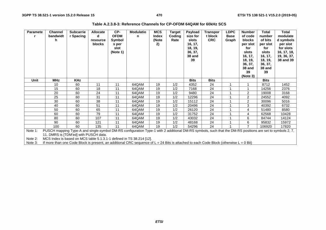
ETSI
ETSI TS 138 521-1 V15.2.0 (2019-05)4703GPP TS 38.521-1 version 15.2.0 Release 15
Table A.2.3.8-3: Reference Channels for CP-OFDM 64QAM for 60kHz SCS
Parameter
Channel bandwidt
h
Subcarrier Spacing
Allocated
resource blocks
CP-OFDM
Symbols per slot
(Note 1)
Modulation
MCS Index (Note
2)
Target Coding
Rate
Payload size for
slots 16, 17, 18, 19, 36, 37, 38 and
39
Transport block CRC
LDPC Base Graph
Number of code blocks per slot
for slots
16, 17, 18, 19, 36, 37, 38 and
39 (Note 3)
Total number of bits
per slot for
slots 16, 17, 18, 19, 36, 37, 38 and
39
Total modulated symbols
per slot for slots
16, 17, 18, 19, 36, 37, 38 and 39
Unit MHz KHz Bits Bits Bits 10 60 11 11 64QAM 19 1/2 4352 24 1 1 8712 1452 15 60 18 11 64QAM 19 1/2 7168 24 1 1 14256 2376 20 60 24 11 64QAM 19 1/2 9480 24 1 2 19008 3168 25 60 31 11 64QAM 19 1/2 12296 24 1 2 24552 4092 30 60 38 11 64QAM 19 1/2 15112 24 1 2 30096 5016 40 60 51 11 64QAM 19 1/2 20496 24 1 3 40392 6732 50 60 65 11 64QAM 19 1/2 26120 24 1 4 51480 8580 60 60 79 11 64QAM 19 1/2 31752 24 1 4 62568 10428 80 60 107 11 64QAM 19 1/2 43032 24 1 6 84744 14124 90 60 121 11 64QAM 19 1/2 48168 24 1 6 95832 15972 100 60 135 11 64QAM 19 1/2 54296 24 1 7 106920 17820
Note 1: PUSCH mapping Type-A and single-symbol DM-RS configuration Type-1 with 2 additional DM-RS symbols, such that the DM-RS positions are set to symbols 2, 7, 11. DMRS is [TDM’ed] with PUSCH data.
Note 2: MCS Index is based on MCS table 5.1.3.1-1 defined in TS 38.214 [12]. Note 3: If more than one Code Block is present, an additional CRC sequence of L = 24 Bits is attached to each Code Block (otherwise L = 0 Bit)

ETSI
ETSI TS 138 521-1 V15.2.0 (2019-05)4713GPP TS 38.521-1 version 15.2.0 Release 15
A.2.3.9 CP-OFDM 256QAM
Table A.2.3.9-1: Reference Channels for CP-OFDM 256QAM for 15kHz SCS
Parameter
Channel bandwidt
h
Subcarrier Spacing
Allocated
resource blocks
CP-OFDM
Symbols per slot
(Note 1)
Modulation
MCS Index (Note
2)
Target Coding
Rate
Payload size for slots 4 and 9
Transport block CRC
LDPC Base Graph
Number of code blocks per slot
for slots 4 and 9
(Note 3)
Total number of bits
per slot for
slots 4 and 9
Total modulated symbols
per slot for slots 4
and 9
Unit MHz KHz Bits Bits Bits 5 15 25 11 256QAM 20 2/3 17424 24 1 3 26400 3300 10 15 52 11 256QAM 20 2/3 36896 24 1 5 54912 6864 15 15 79 11 256QAM 20 2/3 55304 24 1 7 83424 10428 20 15 106 11 256QAM 20 2/3 73776 24 1 9 111936 13992 25 15 133 11 256QAM 20 2/3 94248 24 1 12 140448 17556 30 15 160 11 256QAM 20 2/3 112648 24 1 14 168960 21120 40 15 216 11 256QAM 20 2/3 151608 24 1 18 228096 28512 50 15 270 11 256QAM 20 2/3 188576 24 1 23 285120 35640
Note 1: PUSCH mapping Type-A and single-symbol DM-RS configuration Type-1 with 2 additional DM-RS symbols, such that the DM-RS positions are set to symbols 2, 7, 11. DMRS is [TDM’ed] with PUSCH data.
Note 2: MCS Index is based on MCS table 5.1.3.1-2 defined in TS 38.214 [12]. Note 3: If more than one Code Block is present, an additional CRC sequence of L = 24 Bits is attached to each Code Block (otherwise L = 0 Bit)

ETSI
ETSI TS 138 521-1 V15.2.0 (2019-05)4723GPP TS 38.521-1 version 15.2.0 Release 15
Table A.2.3.9-2: Reference Channels for CP-OFDM 256QAM for 30kHz SCS
Parameter
Channel bandwidt
h
Subcarrier Spacing
Allocated
resource blocks
CP-OFDM
Symbols per slot
(Note 1)
Modulation
MCS Index (Note
2)
Target Coding
Rate
Payload size for slots 8,
9, 18 and 19
Transport block CRC
LDPC Base Graph
Number of code blocks per slot
for slots 8,
9, 18 and 19
(Note 3)
Total number of bits
per slot for
slots 8, 9, 18
and 19
Total modulated symbols
per slot for slots 8, 9, 18 and 19
Unit MHz KHz Bits Bits Bits 5 30 11 11 256QAM 20 2/3 7680 24 1 1 11616 1452 10 30 24 11 256QAM 20 2/3 16896 24 1 3 25344 3168 15 30 38 11 256QAM 20 2/3 26632 24 1 4 40128 5016 20 30 51 11 256QAM 20 2/3 35856 24 1 5 53856 6732 25 30 65 11 256QAM 20 2/3 46104 24 1 6 68640 8580 30 30 78 11 256QAM 20 2/3 55304 24 1 7 82368 10296 40 30 106 11 256QAM 20 2/3 73776 24 1 9 111936 13992 50 30 133 11 256QAM 20 2/3 94248 24 1 12 140448 17556 60 30 162 11 256QAM 20 2/3 114776 24 1 14 171072 21384 80 30 217 11 256QAM 20 2/3 151608 24 1 18 229152 28644 90 30 245 11 256QAM 20 2/3 172176 24 1 21 258720 32340 100 30 273 11 256QAM 20 2/3 192624 24 1 23 288288 36036
Note 1: PUSCH mapping Type-A and single-symbol DM-RS configuration Type-1 with 2 additional DM-RS symbols, such that the DM-RS positions are set to symbols 2, 7, 11. DMRS is [TDM’ed] with PUSCH data.
Note 2: MCS Index is based on MCS table 5.1.3.1-2 defined in TS 38.214 [12]. Note 3: If more than one Code Block is present, an additional CRC sequence of L = 24 Bits is attached to each Code Block (otherwise L = 0 Bit)

ETSI
ETSI TS 138 521-1 V15.2.0 (2019-05)4733GPP TS 38.521-1 version 15.2.0 Release 15
Table A.2.3.9-3: Reference Channels for CP-OFDM 256QAM for 60kHz SCS
Parameter Channel bandwidth
Subcarrier Spacing
Allocated resource blocks
CP-OFDM
Symbols per slot (Note 1)
Modulation MCS Index
(Note 2)
Target Coding
Rate
Payload size for
slots 16, 17, 18, 19, 36, 37, 38 and
39
Transport block CRC
LDPC Base
Graph
Number of code blocks per slot for slots 16, 17, 18, 19, 36, 37, 38 and
39 (Note 3)
Total number of bits
per slot for
slots 16, 17, 18, 19, 36, 37, 38 and
39
Total modulated symbols per slot for slots
16, 17, 18, 19, 36, 37, 38 and 39
Unit MHz KHz Bits Bits Bits 10 60 11 11 256QAM 20 2/3 7680 24 1 1 11616 1452 15 60 18 11 256QAM 20 2/3 12552 24 1 2 19008 2376 20 60 24 11 256QAM 20 2/3 16896 24 1 3 25344 3168 25 60 31 11 256QAM 20 2/3 22032 24 1 3 32736 4092 30 60 38 11 256QAM 20 2/3 26632 24 1 4 40128 5016 40 60 51 11 256QAM 20 2/3 35856 24 1 5 53856 6732 50 60 65 11 256QAM 20 2/3 46104 24 1 6 68640 8580 60 60 79 11 256QAM 20 2/3 55304 24 1 7 83424 10428 80 60 107 11 256QAM 20 2/3 75792 24 1 9 112992 14124 90 60 121 11 256QAM 20 2/3 86040 24 1 11 127776 15972 100 60 135 11 256QAM 20 2/3 94248 24 1 12 142560 17820
Note 1: PUSCH mapping Type-A and single-symbol DM-RS configuration Type-1 with 2 additional DM-RS symbols, such that the DM-RS positions are set to symbols 2, 7, 11. DMRS is [TDM’ed] with PUSCH data.
Note 2: MCS Index is based on MCS table 5.1.3.1-2 defined in TS 38.214 [12]. Note 3: If more than one Code Block is present, an additional CRC sequence of L = 24 Bits is attached to each Code Block (otherwise L = 0 Bit)

ETSI
ETSI TS 138 521-1 V15.2.0 (2019-05)4743GPP TS 38.521-1 version 15.2.0 Release 15
A.3 DL reference measurement channels
A.3.1 General Unless otherwise stated, Tables A.3.2.2-1, A.3.2.2-2, A.3.2.2-3, A.3.3.2-1, A.3.3.2-2 and A.3.3.2-3 are applicable for measurements of the Receiver Characteristics (clause 7) with the exception of subclauses 7.4 (Maximum input level).
Unless otherwise stated, Tables A.3.2.3-1, A.3.2.3-2, A.3.2.3-3, A.3.3.3-1, A.3.3.3-2 and A.3.3.3-3 are applicable for subclauses 7.4 (Maximum input level) and for UE not supporting PDSCH 256QAM,
Unless otherwise stated, Tables A.3.2.4-1, A.3.2.4-2, A.3.2.4-3, A.3.3.4-1, A.3.3.4-2 and A.3.3.4-3 are applicable for subclauses 7.4 (Maximum input level) and for UE supporting PDSCH 256QAM,
Unless otherwise stated, Tables A.3.2.2-1, A.3.2.2-2, A.3.2.2-3, A.3.3.2-1, A.3.3.2-2 and A.3.3.2-3 also apply for the modulated interferer used in Clauses 7.5, 7.6 and 7.8 with test specific bandwidths.
Table A.3.1-1: Common reference channel parameters
Parameter Unit Value CORESET frequency domain allocation Full BW CORESET time domain allocation 2 OFDM symbols at the begin of each slot PDSCH mapping type Type A PDSCH start symbol index (S) 2 Number of consecutive PDSCH symbols (L) 12 PDSCH PRB bundling PRBs 2 Dynamic PRB bundling false Overhead value for TBS determination 0 First DMRS position for Type A PDSCH mapping 2 DMRS type Type 1 Number of additional DMRS 2 FDM between DMRS and PDSCH Disable TRS configuration 2 slots, periodicity 10 ms, offset 0 PTRS configuration PTRS is not configured
A.3.2 DL reference measurement channels for FDD
A.3.2.1 General
Table A.3.2.1-1: Additional reference channels parameters for FDD
Parameter Unit Value Number of HARQ Processes 4 K1 value 2 for all slots

ETSI
ETSI TS 138 521-1 V15.2.0 (2019-05)4753GPP TS 38.521-1 version 15.2.0 Release 15
A.3.2.2 FRC for receiver requirements for QPSK
Table A.3.2.2-1: Fixed reference channel for receiver requirements (SCS 15 kHz, FDD, QPSK 1/3)
Parameter Unit Value Channel bandwidth MHz 5 10 15 20 25 30 40 50 Subcarrier spacing kHz 15 15 15 15 15 15 15 15
Subcarrier spacing configuration μ
0 0 0 0 0 0 0 0
Allocated resource blocks 25 52 79 106 133 [160] 216 270 Subcarriers per resource block 12 12 12 12 12 12 12 12 Allocated slots per Frame 9 9 9 9 9 9 9 9 MCS Index 4 4 4 4 4 4 4 4 MCS Table for TBS determination 64QAM Modulation QPSK QPSK QPSK QPSK QPSK QPSK QPSK QPSK Target Coding Rate 1/3 1/3 1/3 1/3 1/3 1/3 1/3 1/3 Maximum number of HARQ transmissions 1 1 1 1 1 1 1 1
Information Bit Payload per Slot
For Slot 0 Bits N/A N/A N/A N/A N/A N/A N/A N/A For Slots 1,2,3,4,5,6,7,8,9 Bits 1672 3368 5120 6912 8712 10504 14088 17424 Transport block CRC Bits 16 16 24 24 24 24 24 24 LDPC base graph 2 2 1 1 1 1 1 1 Number of Code Blocks per Slot For Slot 0 CBs N/A N/A N/A N/A N/A N/A N/A N/A For Slots 1,2,3,4,5,6,7,8,9 CBs 1 1 1 1 2 2 2 3 Binary Channel Bits per Slot For Slot 0 Bits N/A N/A N/A N/A N/A N/A N/A N/A For Slots 1,2,3,4,5,6,7,8,9 Bits 5400 11232 17064 22896 28728 34560 46656 58320
Max. Throughput averaged over 1 frame Mbps 1.504 3.031 4.608 6.220 7.841 9.454 12.679
15.682
Note 1: Additional parameters are specified in Table A.3.1-1 and Table A.3.2.1-1. Note 2: If more than one Code Block is present, an additional CRC sequence of L = 24 Bits is attached to each Code Block
(otherwise L = 0 Bit). Note 3: SS/PBCH block is transmitted in slot #0 of each frame. Note 4: Slot i is slot index per frame, QPSK 1/3.

ETSI
ETSI TS 138 521-1 V15.2.0 (2019-05)4763GPP TS 38.521-1 version 15.2.0 Release 15
Table A.3.2.2-2: Fixed reference channel for receiver requirements (SCS 30 kHz, FDD, QPSK 1/3)
Parameter Unit Value Channel bandwidth MHz 5 10 15 20 25 30 40 50 60 80 90 100
Subcarrier spacing configuration μ
1 1 1 1 1 1 1 1 1 1 1 1
Allocated resource blocks 11 24 38 51 65 [78] 106 133 162 217 245 273 Subcarriers per resource block 12 12 12 12 12 12 12 12 12 12 12 12 Allocated slots per Frame 19 19 19 19 19 19 19 19 19 19 19 19 MCS Index 4 4 4 4 4 4 4 4 4 4 4 4 MCS Table for TBS determination 64QAM Modulation QPSK QPSK QPSK QPSK QPSK QPSK QPSK QPSK QPSK QPSK QPSK QPSK Target Coding Rate 1/3 1/3 1/3 1/3 1/3 1/3 1/3 1/3 1/3 1/3 1/3 1/3 Maximum number of HARQ transmissions 1 1 1 1 1 1 1 1 1 1 1 1 Information Bit Payload per Slot For Slot 0 Bits N/A N/A N/A N/A N/A N/A N/A N/A N/A N/A N/A N/A For Slots 1,…,19 Bits 736 1608 2472 3368 4224 4992 6912 8712 10504 14088 15880 17928 Transport block CRC Bits 16 16 16 16 24 24 24 24 24 24 24 24 LDPC base graph 2 2 2 2 1 1 1 1 1 1 1 1 Number of Code Blocks per Slot For Slot 0 CBs N/A N/A N/A N/A N/A N/A N/A N/A N/A N/A N/A N/A For Slots 1,…,19 CBs 1 1 1 1 1 1 1 2 2 2 2 3 Binary Channel Bits per Slot For Slot 0 Bits N/A N/A N/A N/A N/A N/A N/A N/A N/A N/A N/A N/A For Slots 1,…,19 Bits 2376 5184 8208 11016 14040 16848 22896 28728 34992 46872 52920 58968
Max. Throughput averaged over 1 frame Mbps 1.398 3.055 4.697 6.399 8.025 9.485 13.133 16.553 19.958 26.767 30.172 34.063
Note 1: Additional parameters are specified in Table A.3.1-1 and Table A.3.2.1-1. Note 2: If more than one Code Block is present, an additional CRC sequence of L = 24 Bits is attached to each Code Block (otherwise L = 0 Bit). Note 3: SS/PBCH block is transmitted in slot #0 of each frame. Note 4: Slot i is slot index per frame.

ETSI
ETSI TS 138 521-1 V15.2.0 (2019-05)4773GPP TS 38.521-1 version 15.2.0 Release 15
Table A.3.2.2-3: Fixed reference channel for receiver requirements (SCS 60 kHz, FDD, QPSK 1/3)
Parameter Unit Value Channel bandwidth MHz 10 15 20 25 30 40 50 60 80 90 100
Subcarrier spacing configuration μ
2 2 2 2 2 2 2 2 2 2 2
Allocated resource blocks 11 18 24 31 38 51 65 79 107 121 135 Subcarriers per resource block 12 12 12 12 12 12 12 12 12 12 12 Allocated slots per Frame 38 38 38 38 38 38 38 38 38 38 38 MCS Index 4 4 4 4 4 4 4 4 4 4 4 MCS Table for TBS Determination 64QAM Modulation QPSK QPSK QPSK QPSK QPSK QPSK QPSK QPSK QPSK QPSK QPSK Target Coding Rate 1/3 1/3 1/3 1/3 1/3 1/3 1/3 1/3 1/3 1/3 1/3 Maximum number of HARQ transmissions 1 1 1 1 1 1 1 1 1 1 1 Information Bit Payload per Slot For Slot 0,1 Bits N/A N/A N/A N/A N/A N/A N/A N/A N/A N/A N/A For Slots 2,…,39 Bits 736 1192 1608 2024 2472 3368 4224 5120 6912 7808 8712 Transport block CRC Bits 16 16 16 16 16 16 24 24 24 24 24 LDPC base graph 2 2 2 2 2 2 1 1 1 1 1 Number of Code Blocks per Slot For Slot 0,1 CBs N/A N/A N/A N/A N/A N/A N/A N/A N/A N/A N/A For Slots 2,…,39 CBs 1 1 1 1 1 1 1 1 1 1 2 Binary Channel Bits per Slot For Slot 0,1 Bits N/A N/A N/A N/A N/A N/A N/A N/A N/A N/A N/A For Slots 2,…,39 Bits 2376 3888 5184 6696 8208 11016 14040 17064 23112 26136 29160 Max. Throughput averaged over 1 frame Mbps 2.870 4.649 6.271 7.894 9.641 13.135 16.474 19.968 26.957 30.451 33.977 NOTE 1: Additional parameters are specified in Table A.3.1-1 and Table A.3.2.1-1. NOTE 2: If more than one Code Block is present, an additional CRC sequence of L = 24 Bits is attached to each Code Block (otherwise L = 0 Bit). NOTE 3: SS/PBCH block is transmitted in slot #0 of each frame. NOTE 4: Slot i is slot index per frame.
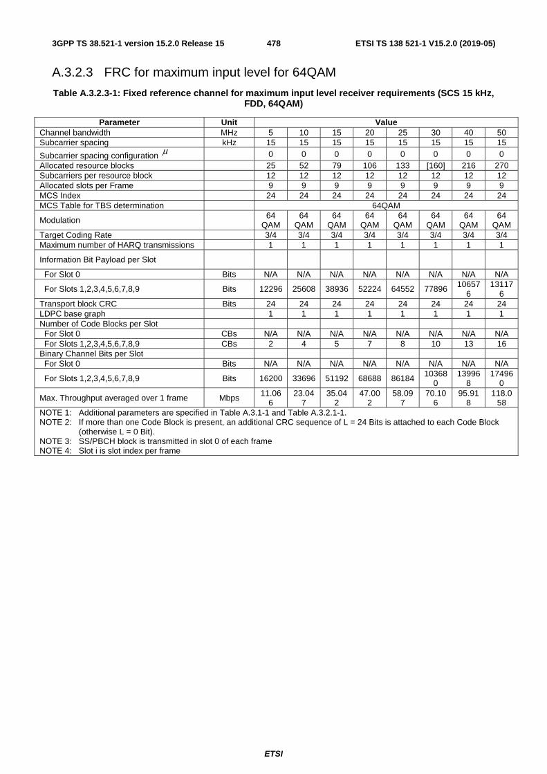
ETSI
ETSI TS 138 521-1 V15.2.0 (2019-05)4783GPP TS 38.521-1 version 15.2.0 Release 15
A.3.2.3 FRC for maximum input level for 64QAM
Table A.3.2.3-1: Fixed reference channel for maximum input level receiver requirements (SCS 15 kHz, FDD, 64QAM)
Parameter Unit Value Channel bandwidth MHz 5 10 15 20 25 30 40 50 Subcarrier spacing kHz 15 15 15 15 15 15 15 15
Subcarrier spacing configuration μ 0 0 0 0 0 0 0 0 Allocated resource blocks 25 52 79 106 133 [160] 216 270 Subcarriers per resource block 12 12 12 12 12 12 12 12 Allocated slots per Frame 9 9 9 9 9 9 9 9 MCS Index 24 24 24 24 24 24 24 24 MCS Table for TBS determination 64QAM
Modulation 64 QAM
64 QAM
64 QAM
64 QAM
64 QAM
64 QAM
64 QAM
64 QAM
Target Coding Rate 3/4 3/4 3/4 3/4 3/4 3/4 3/4 3/4 Maximum number of HARQ transmissions 1 1 1 1 1 1 1 1
Information Bit Payload per Slot
For Slot 0 Bits N/A N/A N/A N/A N/A N/A N/A N/A
For Slots 1,2,3,4,5,6,7,8,9 Bits 12296 25608 38936 52224 64552 77896 106576
131176
Transport block CRC Bits 24 24 24 24 24 24 24 24 LDPC base graph 1 1 1 1 1 1 1 1 Number of Code Blocks per Slot For Slot 0 CBs N/A N/A N/A N/A N/A N/A N/A N/A For Slots 1,2,3,4,5,6,7,8,9 CBs 2 4 5 7 8 10 13 16 Binary Channel Bits per Slot For Slot 0 Bits N/A N/A N/A N/A N/A N/A N/A N/A
For Slots 1,2,3,4,5,6,7,8,9 Bits 16200 33696 51192 68688 86184 103680
139968
174960
Max. Throughput averaged over 1 frame Mbps 11.066
23.047
35.042
47.002
58.097
70.106
95.918
118.058
NOTE 1: Additional parameters are specified in Table A.3.1-1 and Table A.3.2.1-1. NOTE 2: If more than one Code Block is present, an additional CRC sequence of L = 24 Bits is attached to each Code Block
(otherwise L = 0 Bit). NOTE 3: SS/PBCH block is transmitted in slot 0 of each frame NOTE 4: Slot i is slot index per frame
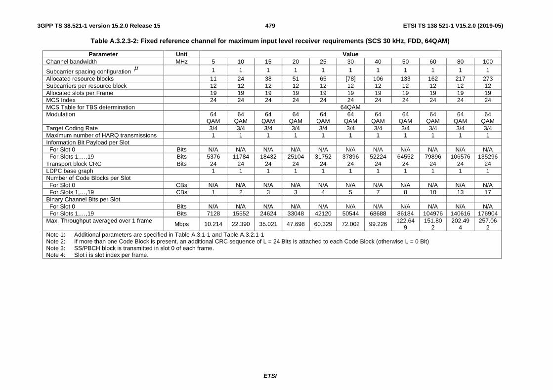
ETSI
ETSI TS 138 521-1 V15.2.0 (2019-05)4793GPP TS 38.521-1 version 15.2.0 Release 15
Table A.3.2.3-2: Fixed reference channel for maximum input level receiver requirements (SCS 30 kHz, FDD, 64QAM)
Parameter Unit Value Channel bandwidth MHz 5 10 15 20 25 30 40 50 60 80 100
Subcarrier spacing configuration μ
1 1 1 1 1 1 1 1 1 1 1
Allocated resource blocks 11 24 38 51 65 [78] 106 133 162 217 273 Subcarriers per resource block 12 12 12 12 12 12 12 12 12 12 12 Allocated slots per Frame 19 19 19 19 19 19 19 19 19 19 19 MCS Index 24 24 24 24 24 24 24 24 24 24 24 MCS Table for TBS determination 64QAM Modulation 64
QAM 64
QAM 64
QAM 64
QAM 64
QAM 64
QAM 64
QAM 64
QAM 64
QAM 64
QAM 64
QAM Target Coding Rate 3/4 3/4 3/4 3/4 3/4 3/4 3/4 3/4 3/4 3/4 3/4 Maximum number of HARQ transmissions 1 1 1 1 1 1 1 1 1 1 1 Information Bit Payload per Slot For Slot 0 Bits N/A N/A N/A N/A N/A N/A N/A N/A N/A N/A N/A For Slots 1,…,19 Bits 5376 11784 18432 25104 31752 37896 52224 64552 79896 106576 135296 Transport block CRC Bits 24 24 24 24 24 24 24 24 24 24 24 LDPC base graph 1 1 1 1 1 1 1 1 1 1 1 Number of Code Blocks per Slot For Slot 0 CBs N/A N/A N/A N/A N/A N/A N/A N/A N/A N/A N/A For Slots 1,…,19 CBs 1 2 3 3 4 5 7 8 10 13 17 Binary Channel Bits per Slot For Slot 0 Bits N/A N/A N/A N/A N/A N/A N/A N/A N/A N/A N/A For Slots 1,…,19 Bits 7128 15552 24624 33048 42120 50544 68688 86184 104976 140616 176904 Max. Throughput averaged over 1 frame Mbps 10.214 22.390 35.021 47.698 60.329 72.002 99.226 122.64
9 151.80
2 202.49
4 257.06
2 Note 1: Additional parameters are specified in Table A.3.1-1 and Table A.3.2.1-1 Note 2: If more than one Code Block is present, an additional CRC sequence of L = 24 Bits is attached to each Code Block (otherwise L = 0 Bit) Note 3: SS/PBCH block is transmitted in slot 0 of each frame. Note 4: Slot i is slot index per frame.

ETSI
ETSI TS 138 521-1 V15.2.0 (2019-05)4803GPP TS 38.521-1 version 15.2.0 Release 15
Table A.3.2.3-3: Fixed Reference Channel for Maximum input level receiver requirements (SCS 60 kHz, FDD, 64QAM)
Parameter Unit Value Channel bandwidth MHz 10 15 20 25 30 40 50 60 80 100
Subcarrier spacing configuration μ
2 2 2 2 2 2 2 2 2 2
Allocated resource blocks 11 18 24 31 [38] 51 65 79 107 135 Subcarriers per resource block 12 12 12 12 12 12 12 12 12 12 Allocated slots per Frame 38 38 38 38 38 38 38 38 38 38 MCS Index 24 24 24 24 24 24 24 24 24 24 MCS Table for TBS determination 64QAM Modulation 64
QAM 64
QAM 64
QAM 64
QAM 64
QAM 64
QAM 64
QAM 64
QAM 64
QAM 64
QAM Target Coding Rate 3/4 3/4 3/4 3/4 3/4 3/4 3/4 3/4 3/4 3/4 Maximum number of HARQ transmissions 1 1 1 1 1 1 1 1 1 1 Information Bit Payload per Slot For Slot 0,1 Bits N/A N/A N/A N/A N/A N/A N/A N/A N/A N/A For Slots 2,…,39 Bits 5376 8712 11784 15112 18432 25104 31752 38936 52224 65576 Transport block CRC Bits 24 24 24 24 24 24 24 24 24 24 LDPC base graph 1 1 1 1 1 1 1 1 1 1 Number of Code Blocks per Slot For Slot 0,1 CBs N/A N/A N/A N/A N/A N/A N/A N/A N/A N/A For Slots 2,…,39 CBs 1 2 2 2 3 3 4 5 7 8 Binary Channel Bits per Slot For Slot 0,1 Bits N/A N/A N/A N/A N/A N/A N/A N/A N/A N/A For Slots 2,…,39 Bits 7128 11664 15552 20088 24624 33048 42120 51192 69336 87480 Max. Throughput averaged over 1 frame Mbps 20.429 33.106 44.779 57.426 70.042 95.395 120.65
8 147.95
7 198.45
1 249.18
9 Note 1: Additional parameters are specified in Table A.3.1-1 and Table A.3.2.1-1. Note 2: If more than one Code Block is present, an additional CRC sequence of L = 24 Bits is attached to each Code Block (otherwise L = 0 Bit) Note 3: SS/PBCH block is transmitted in slot #0 of each frame. Note 4: Slot i is slot index per frame.

ETSI
ETSI TS 138 521-1 V15.2.0 (2019-05)4813GPP TS 38.521-1 version 15.2.0 Release 15
A.3.2.4 FRC for maximum input level for 256 QAM
Table A.3.2.4-1: Fixed reference channel for maximum input level receiver requirements (SCS 15 kHz, FDD, 256QAM)
Parameter Unit Value Channel bandwidth MHz 5 10 15 20 25 30 40 50 Subcarrier spacing kHz 15 15 15 15 15 15 15 15
Subcarrier spacing configuration μ
0 0 0 0 0 0 0 0
Allocated resource blocks 25 52 79 106 133 [160] 216 270 Subcarriers per resource block 12 12 12 12 12 12 12 12 Allocated slots per Frame 9 9 9 9 9 9 9 9 MCS Index 23 23 23 23 23 23 23 23 MCS Table for TBS determination 256QAM
Modulation 256 QAM
256 QAM
256 QAM
256 QAM
256 QAM
256 QAM
256 QAM
256 QAM
Target Coding Rate 4/5 4/5 4/5 4/5 4/5 4/5 4/5 4/5 Maximum number of HARQ transmissions 1 1 1 1 1 1 1 1
Information Bit Payload per Slot
For Slot 0 Bits N/A N/A N/A N/A N/A N/A N/A N/A
For Slots 1,2,3,4,5,6,7,8,9 Bits 16896 34816 53288 71688 90176 108552
143400
180376
Transport block CRC Bits 24 24 24 24 24 24 24 24 LDPC base graph 1 1 1 1 1 1 1 1 Number of Code Blocks per Slot For Slot 0 CBs N/A N/A N/A N/A N/A N/A N/A N/A For Slots 1,2,3,4,5,6,7,8,9 CBs 3 5 7 9 12 14 18 23 Binary Channel Bits per Slot For Slot 0 Bits N/A N/A N/A N/A N/A N/A N/A N/A
For Slots 1,2,3,4,5,6,7,8,9 Bits 21600 44928 68256 91584 114912
138240
186624
233280
Max. Throughput averaged over 1 frame Mbps 15.206
31.334
47.959
64.519
81.158
97.697
129.060
162.338
Note 1: Additional parameters are specified in Table A.3.1-1 and Table A.3.2.1-1. Note 2: If more than one Code Block is present, an additional CRC sequence of L = 24 Bits is attached to each Code Block
(otherwise L = 0 Bit) Note 3: SS/PBCH block is transmitted in slot 0 of each frame. Note 4: Slot i is slot index per frame.

ETSI
ETSI TS 138 521-1 V15.2.0 (2019-05)4823GPP TS 38.521-1 version 15.2.0 Release 15
Table A.3.2.4-2: Fixed reference channel for maximum input level receiver requirements (SCS 30 kHz, FDD, 256QAM)
Parameter Unit Value Channel bandwidth MHz 5 10 15 20 25 30 40 50 60 80 100
Subcarrier spacing configuration μ
1 1 1 1 1 1 1 1 1 1 1
Allocated resource blocks 11 24 38 51 65 [78] 106 133 162 217 273 Subcarriers per resource block 12 12 12 12 12 12 12 12 12 12 12 Allocated slots per Frame 19 19 19 19 19 19 19 19 19 19 19 MCS Index 23 23 23 23 23 23 23 23 23 23 23 MCS Table for TBS determination 256QAM Modulation 256
QAM 256
QAM 256
QAM 256
QAM 256
QAM 256
QAM 256
QAM 256
QAM 256
QAM 256
QAM 256
QAM Target Coding Rate 4/5 4/5 4/5 4/5 4/5 4/5 4/5 4/5 4/5 4/5 4/5 Maximum number of HARQ transmissions 1 1 1 1 1 1 1 1 1 1 1 Information Bit Payload per Slot For Slot 0 Bits N/A N/A N/A N/A N/A N/A N/A N/A N/A N/A N/A For Slots 1,…,19 Bits 7424 16136 25608 33816 44040 52224 71688 90176 108552 147576 184424 Transport block CRC Bits 24 24 24 24 24 24 24 24 24 24 24 LDPC base graph 1 1 1 1 1 1 1 1 1 1 1 Number of Code Blocks per Slot For Slot 0 CBs N/A N/A N/A N/A N/A N/A N/A N/A N/A N/A N/A For Slots 1,…,19 CBs 1 3 4 5 6 7 9 12 14 19 23 Binary Channel Bits per Slot For Slot 0 Bits N/A N/A N/A N/A N/A N/A N/A N/A N/A N/A N/A For Slots 1,…,19 Bits 9504 20736 32832 44064 56160 67392 91584 114912 139968 187488 235872 Max. Throughput averaged over 1 frame Mbps 14.106 30.658 48.655 64.250 83.676 99.226 136.20
7 171.33
4 206.24
9 280.39
4 350.40
6 Note 1: Additional parameters are specified in Table A.3.1-1 and Table A.3.2.1-1. Note 2: If more than one Code Block is present, an additional CRC sequence of L = 24 Bits is attached to each Code Block (otherwise L = 0 Bit) Note 3: SS/PBCH block is transmitted in slot 0 of each frame. Note 4: Slot i is slot index per frame.

ETSI
ETSI TS 138 521-1 V15.2.0 (2019-05)4833GPP TS 38.521-1 version 15.2.0 Release 15
Table A.3.2.4-3: Fixed reference channel for maximum input level receiver requirements (SCS 60 kHz, FDD, 256QAM)
Parameter Unit Value Channel bandwidth MHz 10 15 20 25 30 40 50 60 80 100
Subcarrier spacing configuration μ
2 2 2 2 2 2 2 2 2 2
Allocated resource blocks 11 18 24 31 [38] 51 65 79 107 135 Subcarriers per resource block 12 12 12 12 12 12 12 12 12 12 Allocated slots per Frame 38 38 38 38 38 38 38 38 38 38 MCS Index 23 23 23 23 23 23 23 23 23 23 MCS Table for TBS determination 256QAM Modulation 256
QAM 256
QAM 256
QAM 256
QAM 256
QAM 256
QAM 256
QAM 256
QAM 256
QAM 256
QAM Target Coding Rate 4/5 4/5 4/5 4/5 4/5 4/5 4/5 4/5 4/5 4/5 Maximum number of HARQ transmissions 1 1 1 1 1 1 1 1 1 1 Information Bit Payload per Slot For Slot 0,1 Bits N/A N/A N/A N/A N/A N/A N/A N/A N/A N/A For Slots 2,…,39 Bits 7424 12040 16136 21000 25608 33816 44040 53288 71688 90176 Transport block CRC Bits 24 24 24 24 24 24 24 24 24 24 LDPC base graph 1 1 1 1 1 1 1 1 1 1 Number of Code Blocks per Slot For Slot 0,1 CBs N/A N/A N/A N/A N/A N/A N/A N/A N/A N/A For Slots 2,…,39 CBs 1 2 3 3 4 5 6 7 9 12 Binary Channel Bits per Slot For Slot 0,1 Bits N/A N/A N/A N/A N/A N/A N/A N/A N/A N/A For Slots 2,…,39 Bits 9504 15552 20736 26784 32832 44064 56160 68256 92448 116640 Max. Throughput averaged over 1 frame Mbps 28.211 45.752 61.317 79.800 97.310 128.50
1 167.35
2 202.49
4 272.41
4 342.66
9 Note 1: Additional parameters are specified in Table A.3.1-1 and Table A.3.2.1-1. Note 2: If more than one Code Block is present, an additional CRC sequence of L = 24 Bits is attached to each Code Block (otherwise L = 0 Bit) Note 3: SS/PBCH block is transmitted in slot #0 of each frame. Note 4: Slot i is slot index per frame.
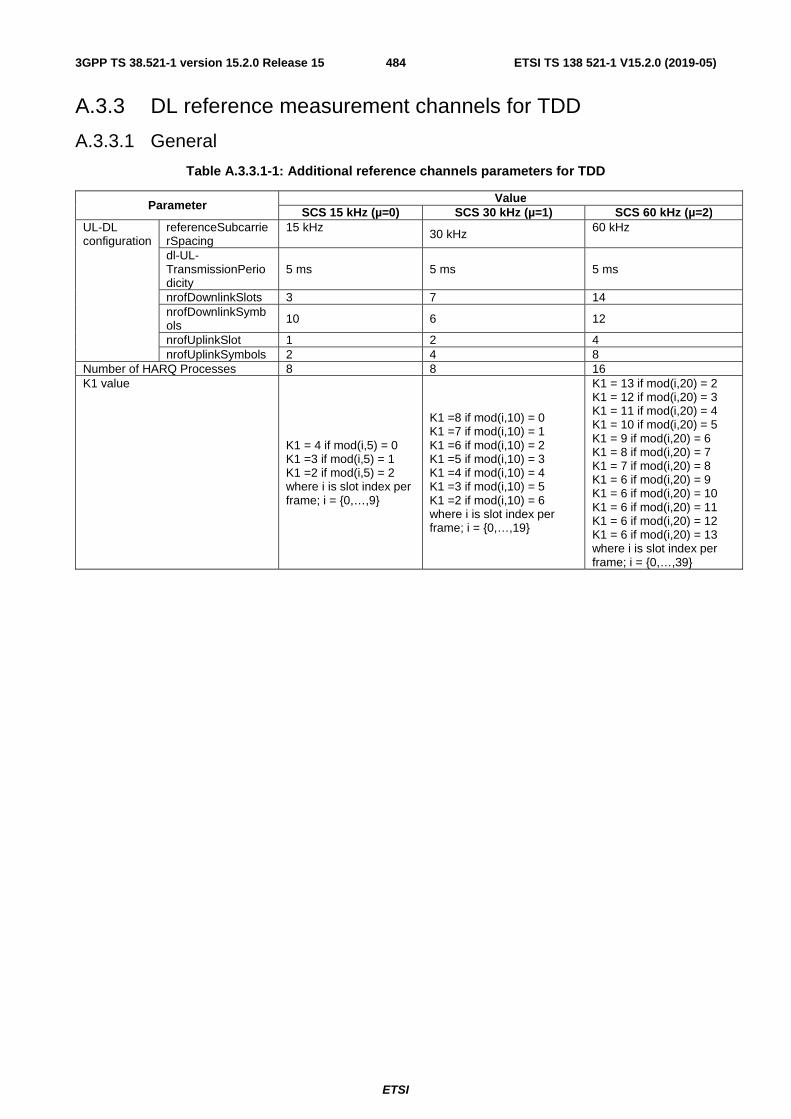
ETSI
ETSI TS 138 521-1 V15.2.0 (2019-05)4843GPP TS 38.521-1 version 15.2.0 Release 15
A.3.3 DL reference measurement channels for TDD
A.3.3.1 General
Table A.3.3.1-1: Additional reference channels parameters for TDD
Parameter Value
SCS 15 kHz (µ=0) SCS 30 kHz (µ=1) SCS 60 kHz (µ=2) UL-DL configuration
referenceSubcarrierSpacing
15 kHz 30 kHz 60 kHz
dl-UL-TransmissionPeriodicity
5 ms 5 ms 5 ms
nrofDownlinkSlots 3 7 14 nrofDownlinkSymbols 10 6 12
nrofUplinkSlot 1 2 4 nrofUplinkSymbols 2 4 8
Number of HARQ Processes 8 8 16 K1 value
K1 = 4 if mod(i,5) = 0 K1 =3 if mod(i,5) = 1 K1 =2 if mod(i,5) = 2 where i is slot index per frame; i = {0,…,9}
K1 =8 if mod(i,10) = 0 K1 =7 if mod(i,10) = 1 K1 =6 if mod(i,10) = 2 K1 =5 if mod(i,10) = 3 K1 =4 if mod(i,10) = 4 K1 =3 if mod(i,10) = 5 K1 =2 if mod(i,10) = 6 where i is slot index per frame; i = {0,…,19}
K1 = 13 if mod(i,20) = 2 K1 = 12 if mod(i,20) = 3 K1 = 11 if mod(i,20) = 4 K1 = 10 if mod(i,20) = 5 K1 = 9 if mod(i,20) = 6 K1 = 8 if mod(i,20) = 7 K1 = 7 if mod(i,20) = 8 K1 = 6 if mod(i,20) = 9 K1 = 6 if mod(i,20) = 10 K1 = 6 if mod(i,20) = 11 K1 = 6 if mod(i,20) = 12 K1 = 6 if mod(i,20) = 13 where i is slot index per frame; i = {0,…,39}
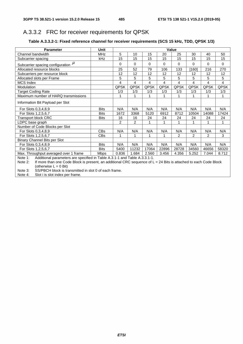
ETSI
ETSI TS 138 521-1 V15.2.0 (2019-05)4853GPP TS 38.521-1 version 15.2.0 Release 15
A.3.3.2 FRC for receiver requirements for QPSK
Table A.3.3.2-1: Fixed reference channel for receiver requirements (SCS 15 kHz, TDD, QPSK 1/3)
Parameter Unit Value Channel bandwidth MHz 5 10 15 20 25 30 40 50 Subcarrier spacing kHz 15 15 15 15 15 15 15 15
Subcarrier spacing configuration μ
0 0 0 0 0 0 0 0
Allocated resource blocks 25 52 79 106 133 [160] 216 270 Subcarriers per resource block 12 12 12 12 12 12 12 12 Allocated slots per Frame 5 5 5 5 5 5 5 5 MCS Index 4 4 4 4 4 4 4 4 Modulation QPSK QPSK QPSK QPSK QPSK QPSK QPSK QPSK Target Coding Rate 1/3 1/3 1/3 1/3 1/3 1/3 1/3 1/3 Maximum number of HARQ transmissions 1 1 1 1 1 1 1 1
Information Bit Payload per Slot
For Slots 0,3,4,8,9 Bits N/A N/A N/A N/A N/A N/A N/A N/A For Slots 1,2,5,6,7 Bits 1672 3368 5120 6912 8712 10504 14088 17424 Transport block CRC Bits 16 16 24 24 24 24 24 24 LDPC base graph 2 2 1 1 1 1 1 1 Number of Code Blocks per Slot For Slots 0,3,4,8,9 CBs N/A N/A N/A N/A N/A N/A N/A N/A For Slots 1,2,5,6,7 CBs 1 1 1 1 2 2 2 3 Binary Channel Bits per Slot For Slots 0,3,4,8,9 Bits N/A N/A N/A N/A N/A N/A N/A N/A For Slots 1,2,5,6,7 Bits 5400 11232 17064 22896 28728 34560 46656 58320 Max. Throughput averaged over 1 frame Mbps 0.836 1.684 2.560 3.456 4.356 5.252 7.044 8.712 Note 1: Additional parameters are specified in Table A.3.1-1 and Table A.3.3.1-1. Note 2: If more than one Code Block is present, an additional CRC sequence of L = 24 Bits is attached to each Code Block
(otherwise L = 0 Bit) Note 3: SS/PBCH block is transmitted in slot 0 of each frame. Note 4: Slot i is slot index per frame.

ETSI
ETSI TS 138 521-1 V15.2.0 (2019-05)4863GPP TS 38.521-1 version 15.2.0 Release 15
Table A.3.3.2-2: Fixed reference channel for receiver requirements (SCS 30 kHz, TDD, QPSK 1/3)
Parameter Unit Value Channel bandwidth MHz 5 10 15 20 25 30 40 50 60 80 100
Subcarrier spacing configuration μ
1 1 1 1 1 1 1 1 1 1 1
Allocated resource blocks 11 24 38 51 65 78 106 133 162 217 273 Subcarriers per resource block 12 12 12 12 12 12 12 12 12 12 12 Allocated slots per Frame 13 13 13 13 13 13 13 13 13 13 13 MCS Index 4 4 4 4 4 4 4 4 4 4 4 Modulation QPSK QPSK QPSK QPSK QPSK QPSK QPSK QPSK QPSK QPSK QPSK Target Coding Rate 1/3 1/3 1/3 1/3 1/3 1/3 1/3 1/3 1/3 1/3 1/3 Maximum number of HARQ transmissions 1 1 1 1 1 1 1 1 1 1 1 Information Bit Payload per Slot For Slots 0 and Slot i, if mod(i, 10) = {7,8,9} for i from {0,…,19} Bits N/A N/A N/A N/A N/A N/A N/A N/A N/A N/A N/A
For Slot i, if mod(i, 10) = {0,1,2,3,4,5,6} for i from {1,…,19} Bits 736 1608 2472 3368 4224 4992 6912 8712 10504 14088 17928
Transport block CRC Bits 16 16 16 16 24 24 24 24 24 24 24 LDPC base graph 2 2 2 2 1 1 1 1 1 1 1 Number of Code Blocks per Slot For Slots 0 and Slot i, if mod(i, 10) = {7,8,9} for i from {0,…,19} CBs N/A N/A N/A N/A N/A N/A N/A N/A N/A N/A N/A
For Slot i, if mod(i, 10) = {0,1,2,3,4,5,6} for i from {1,…,19}
CBs 1 1 1 1 1 1 1 2 2 2 3
Binary Channel Bits per Slot For Slots 0 and Slot i, if mod(i, 10) = {7,8,9} for i from {0,…,19} Bits N/A N/A N/A N/A N/A N/A N/A N/A N/A N/A N/A
For Slot i, if mod(i, 10) = {0,1,2,3,4,5,6} for i from {1,…,19} Bits 2376 5184 8208 11016 14040 16848 22896 28728 34992 46872 58968
Max. Throughput averaged over 1 frame Mbps 0.957 2.090 3.214 4.378 5.491 6.490 8.986 11.326 13.655 18.314 23.306 Note 1: Additional parameters are specified in Table A.3.1-1 and Table A.3.3.1-1. Note 2: If more than one Code Block is present, an additional CRC sequence of L = 24 Bits is attached to each Code Block (otherwise L = 0 Bit) Note 3: SS/PBCH block is transmitted in slot #0 of each frame. Note 4: Slot i is slot index per frame.
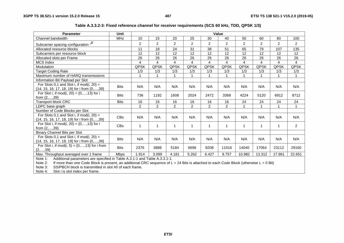
ETSI
ETSI TS 138 521-1 V15.2.0 (2019-05)4873GPP TS 38.521-1 version 15.2.0 Release 15
Table A.3.3.2-3: Fixed reference channel for receiver requirements (SCS 60 kHz, TDD, QPSK 1/3)
Parameter Unit Value Channel bandwidth MHz 10 15 20 25 30 40 50 60 80 100
Subcarrier spacing configuration μ
2 2 2 2 2 2 2 2 2 2
Allocated resource blocks 11 18 24 31 38 51 65 79 107 135 Subcarriers per resource block 12 12 12 12 12 12 12 12 12 12 Allocated slots per Frame 26 26 26 26 26 26 26 26 26 26 MCS Index 4 4 4 4 4 4 4 4 4 4 Modulation QPSK QPSK QPSK QPSK QPSK QPSK QPSK QPSK QPSK QPSK Target Coding Rate 1/3 1/3 1/3 1/3 1/3 1/3 1/3 1/3 1/3 1/3 Maximum number of HARQ transmissions 1 1 1 1 1 1 1 1 1 1 Information Bit Payload per Slot For Slots 0,1 and Slot i, if mod(i, 20) = {14, 15, 16, 17, 18, 19} for i from {0,…,39} Bits N/A N/A N/A N/A N/A N/A N/A N/A N/A N/A
For Slot i, if mod(i, 20) = {0,…,13} for i from {2,…,39} Bits 736 1192 1608 2024 2472 3368 4224 5120 6912 8712
Transport block CRC Bits 16 16 16 16 16 16 24 24 24 24 LDPC base graph 2 2 2 2 2 2 1 1 1 1 Number of Code Blocks per Slot For Slots 0,1 and Slot i, if mod(i, 20) = {14, 15, 16, 17, 18, 19} for i from {0,…,39} CBs N/A N/A N/A N/A N/A N/A N/A N/A N/A N/A
For Slot i, if mod(i, 20) = {0,…,13} for i from {2,…,39}
CBs 1 1 1 1 1 1 1 1 1 2
Binary Channel Bits per Slot For Slots 0,1 and Slot i, if mod(i, 20) = {14, 15, 16, 17, 18, 19} for i from {0,…,39} Bits N/A N/A N/A N/A N/A N/A N/A N/A N/A N/A
For Slot i, if mod(i, 5) = {0,…,13} for i from {2,…,39} Bits 2376 3888 5184 6696 8208 11016 14040 17064 23112 29160
Max. Throughput averaged over 1 frame Mbps 1.914 3.099 4.181 5.262 6.427 8.757 10.982 13.312 17.961 22.651 Note 1: Additional parameters are specified in Table A.3.1-1 and Table A.3.3.1-1. Note 2: If more than one Code Block is present, an additional CRC sequence of L = 24 Bits is attached to each Code Block (otherwise L = 0 Bit) Note 3: SS/PBCH block is transmitted in slot #0 of each frame. Note 4: Slot i is slot index per frame.

ETSI
ETSI TS 138 521-1 V15.2.0 (2019-05)4883GPP TS 38.521-1 version 15.2.0 Release 15
A.3.3.3 FRC for maximum input level for 64QAM
Table A.3.3.3-1: Fixed reference channel for maximum input level receiver requirements (SCS 15 kHz, TDD, 64QAM)
Parameter Unit Value Channel bandwidth MHz 5 10 15 20 25 30 40 50 Subcarrier spacing kHz 15 15 15 15 15 15 15 15
Subcarrier spacing configuration μ
0 0 0 0 0 0 0 0
Allocated resource blocks 25 52 79 106 133 [160] 216 270 Subcarriers per resource block 12 12 12 12 12 12 12 12 Allocated slots per Frame 5 5 5 5 5 5 5 5 MCS Index 24 24 24 24 24 24 24 24
Modulation 64 QAM
64 QAM
64 QAM
64 QAM
64 QAM
64 QAM
64 QAM
64 QAM
Target Coding Rate 3/4 3/4 3/4 3/4 3/4 3/4 3/4 3/4 Maximum number of HARQ transmissions 1 1 1 1 1 1 1 1
Information Bit Payload per Slot
For Slots 0,3,4,8,9 Bits N/A N/A N/A N/A N/A N/A N/A N/A
For Slots 1,2,5,6,7 Bits 12296 25608 38936 52224 64552 77896 106576
131176
Transport block CRC Bits 24 24 24 24 24 24 24 24 LDPC base graph 1 1 1 1 1 1 1 1 Number of Code Blocks per Slot For Slots 0,3,4,8,9 CBs N/A N/A N/A N/A N/A N/A N/A N/A For Slots 1,2,5,6,7 CBs 2 4 5 7 8 10 13 16 Binary Channel Bits per Slot For Slots 0,3,4,8,9 Bits N/A N/A N/A N/A N/A N/A N/A N/A
For Slots 1,2,5,6,7 Bits 16200 33696 51192 68688 86184 103680
139968
174960
Max. Throughput averaged over 1 frame Mbps 6.148 12.804
19.468
26.112
32.276
38.948
53.288
65.588
Note 1: Additional parameters are specified in Table A.3.1-1 and Table A.3.3.1-1. Note 2: If more than one Code Block is present, an additional CRC sequence of L = 24 Bits is attached to each Code Block
(otherwise L = 0 Bit) Note 3: SS/PBCH block is transmitted in slot 0 of each frame. Note 4: Slot i is slot index per frame.
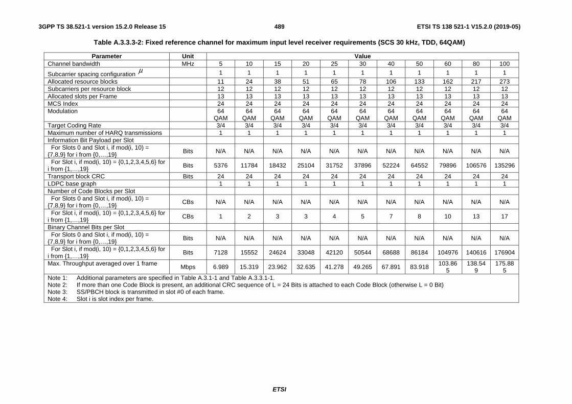
ETSI
ETSI TS 138 521-1 V15.2.0 (2019-05)4893GPP TS 38.521-1 version 15.2.0 Release 15
Table A.3.3.3-2: Fixed reference channel for maximum input level receiver requirements (SCS 30 kHz, TDD, 64QAM)
Parameter Unit Value Channel bandwidth MHz 5 10 15 20 25 30 40 50 60 80 100
Subcarrier spacing configuration μ
1 1 1 1 1 1 1 1 1 1 1
Allocated resource blocks 11 24 38 51 65 78 106 133 162 217 273 Subcarriers per resource block 12 12 12 12 12 12 12 12 12 12 12 Allocated slots per Frame 13 13 13 13 13 13 13 13 13 13 13 MCS Index 24 24 24 24 24 24 24 24 24 24 24 Modulation 64
QAM 64
QAM 64
QAM 64
QAM 64
QAM 64
QAM 64
QAM 64
QAM 64
QAM 64
QAM 64
QAM Target Coding Rate 3/4 3/4 3/4 3/4 3/4 3/4 3/4 3/4 3/4 3/4 3/4 Maximum number of HARQ transmissions 1 1 1 1 1 1 1 1 1 1 1 Information Bit Payload per Slot For Slots 0 and Slot i, if mod(i, 10) = {7,8,9} for i from {0,…,19} Bits N/A N/A N/A N/A N/A N/A N/A N/A N/A N/A N/A
For Slot i, if mod(i, 10) = {0,1,2,3,4,5,6} for i from {1,…,19} Bits 5376 11784 18432 25104 31752 37896 52224 64552 79896 106576 135296
Transport block CRC Bits 24 24 24 24 24 24 24 24 24 24 24 LDPC base graph 1 1 1 1 1 1 1 1 1 1 1 Number of Code Blocks per Slot For Slots 0 and Slot i, if mod(i, 10) = {7,8,9} for i from {0,…,19} CBs N/A N/A N/A N/A N/A N/A N/A N/A N/A N/A N/A
For Slot i, if mod(i, 10) = {0,1,2,3,4,5,6} for i from {1,…,19} CBs 1 2 3 3 4 5 7 8 10 13 17
Binary Channel Bits per Slot For Slots 0 and Slot i, if mod(i, 10) = {7,8,9} for i from {0,…,19} Bits N/A N/A N/A N/A N/A N/A N/A N/A N/A N/A N/A
For Slot i, if mod(i, 10) = {0,1,2,3,4,5,6} for i from {1,…,19}
Bits 7128 15552 24624 33048 42120 50544 68688 86184 104976 140616 176904
Max. Throughput averaged over 1 frame Mbps 6.989 15.319 23.962 32.635 41.278 49.265 67.891 83.918 103.865
138.549
175.885
Note 1: Additional parameters are specified in Table A.3.1-1 and Table A.3.3.1-1. Note 2: If more than one Code Block is present, an additional CRC sequence of L = 24 Bits is attached to each Code Block (otherwise L = 0 Bit) Note 3: SS/PBCH block is transmitted in slot #0 of each frame. Note 4: Slot i is slot index per frame.
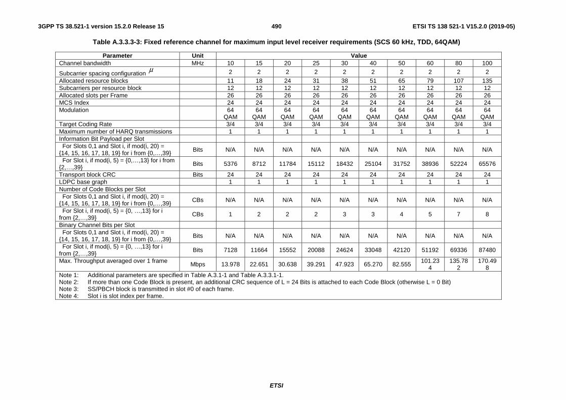
ETSI
ETSI TS 138 521-1 V15.2.0 (2019-05)4903GPP TS 38.521-1 version 15.2.0 Release 15
Table A.3.3.3-3: Fixed reference channel for maximum input level receiver requirements (SCS 60 kHz, TDD, 64QAM)
Parameter Unit Value Channel bandwidth MHz 10 15 20 25 30 40 50 60 80 100
Subcarrier spacing configuration μ
2 2 2 2 2 2 2 2 2 2
Allocated resource blocks 11 18 24 31 38 51 65 79 107 135 Subcarriers per resource block 12 12 12 12 12 12 12 12 12 12 Allocated slots per Frame 26 26 26 26 26 26 26 26 26 26 MCS Index 24 24 24 24 24 24 24 24 24 24 Modulation 64
QAM 64
QAM 64
QAM 64
QAM 64
QAM 64
QAM 64
QAM 64
QAM 64
QAM 64
QAM Target Coding Rate 3/4 3/4 3/4 3/4 3/4 3/4 3/4 3/4 3/4 3/4 Maximum number of HARQ transmissions 1 1 1 1 1 1 1 1 1 1 Information Bit Payload per Slot For Slots 0,1 and Slot i, if mod(i, 20) = {14, 15, 16, 17, 18, 19} for i from {0,…,39} Bits N/A N/A N/A N/A N/A N/A N/A N/A N/A N/A
For Slot i, if mod(i, 5) = {0,…,13} for i from {2,…,39} Bits 5376 8712 11784 15112 18432 25104 31752 38936 52224 65576
Transport block CRC Bits 24 24 24 24 24 24 24 24 24 24 LDPC base graph 1 1 1 1 1 1 1 1 1 1 Number of Code Blocks per Slot For Slots 0,1 and Slot i, if mod(i, 20) = {14, 15, 16, 17, 18, 19} for i from {0,…,39} CBs N/A N/A N/A N/A N/A N/A N/A N/A N/A N/A
For Slot i, if mod(i, 5) = {0, …,13} for i from {2,…,39} CBs 1 2 2 2 3 3 4 5 7 8
Binary Channel Bits per Slot For Slots 0,1 and Slot i, if mod(i, 20) = {14, 15, 16, 17, 18, 19} for i from {0,…,39} Bits N/A N/A N/A N/A N/A N/A N/A N/A N/A N/A
For Slot i, if mod(i, 5) = {0, …,13} for i from {2,…,39}
Bits 7128 11664 15552 20088 24624 33048 42120 51192 69336 87480
Max. Throughput averaged over 1 frame Mbps 13.978 22.651 30.638 39.291 47.923 65.270 82.555 101.234
135.782
170.498
Note 1: Additional parameters are specified in Table A.3.1-1 and Table A.3.3.1-1. Note 2: If more than one Code Block is present, an additional CRC sequence of L = 24 Bits is attached to each Code Block (otherwise L = 0 Bit) Note 3: SS/PBCH block is transmitted in slot #0 of each frame. Note 4: Slot i is slot index per frame.

ETSI
ETSI TS 138 521-1 V15.2.0 (2019-05)4913GPP TS 38.521-1 version 15.2.0 Release 15
A.3.3.4 FRC for maximum input level for 256 QAM
Table A.3.3.4-1: Fixed reference channel for maximum input level receiver requirements (SCS 15 kHz, TDD, 256QAM)
Parameter Unit Value Channel bandwidth MHz 5 10 15 20 25 30 40 50 Subcarrier spacing kHz 15 15 15 15 15 15 15 15
Subcarrier spacing configuration μ
0 0 0 0 0 0 0 0
Allocated resource blocks 25 52 79 106 133 [160] 216 270 Subcarriers per resource block 12 12 12 12 12 12 12 12 Allocated slots per Frame 5 5 5 5 5 5 5 5 MCS Index 23 23 23 23 23 23 23 23
Modulation 256 QAM
256 QAM
256 QAM
256 QAM
256 QAM
256 QAM
256 QAM
256 QAM
Target Coding Rate 4/5 4/5 4/5 4/5 4/5 4/5 4/5 4/5 Maximum number of HARQ transmissions 1 1 1 1 1 1 1 1
Information Bit Payload per Slot
For Slots 0,3,4,8,9 Bits N/A N/A N/A N/A N/A N/A N/A N/A
For Slots 1,2,5,6,7 Bits 16896 34816 53288 71688 90176 108552
143400
180376
Transport block CRC Bits 24 24 24 24 24 24 24 24 LDPC base graph 1 1 1 1 1 1 1 1 Number of Code Blocks per Slot For Slots 0,3,4,8,9 CBs N/A N/A N/A N/A N/A N/A N/A N/A For Slots 1,2,5,6,7 CBs 3 5 7 9 12 14 18 23 Binary Channel Bits per Slot For Slots 0,3,4,8,9 Bits N/A N/A N/A N/A N/A N/A N/A N/A
For Slots 1,2,5,6,7 Bits 21600 44928 68256 91584 114912
138240
186624
233280
Max. Throughput averaged over 1 frame Mbps 8.448 17.408
26.644
35.844
45.088
54.276
71.700
90.188
Note 1: Additional parameters are specified in Table A.3.1-1 and Table A.3.3.1-1. Note 2: If more than one Code Block is present, an additional CRC sequence of L = 24 Bits is attached to each Code Block
(otherwise L = 0 Bit) Note 3: SS/PBCH block is transmitted in slot 0 of each frame. Note 4: Slot i is slot index per frame.

ETSI
ETSI TS 138 521-1 V15.2.0 (2019-05)4923GPP TS 38.521-1 version 15.2.0 Release 15
Table A.3.3.4-2: Fixed Reference channel for maximum input level receiver requirements (SCS 30 kHz, TDD, 256QAM)
Parameter Unit Value Channel bandwidth MHz 5 10 15 20 25 30 40 50 60 80 100
Subcarrier spacing configuration μ
1 1 1 1 1 1 1 1 1 1 1
Allocated resource blocks 11 24 38 51 65 78 106 133 162 217 273 Subcarriers per resource block 12 12 12 12 12 12 12 12 12 12 12 Allocated slots per Frame 13 13 13 13 13 13 13 13 13 13 13 MCS Index 23 23 23 23 23 23 23 23 23 23 23 Modulation 256
QAM 256
QAM 256
QAM 256
QAM 256
QAM 256
QAM 256
QAM 256
QAM 256
QAM 256
QAM 256
QAM Target Coding Rate 4/5 4/5 4/5 4/5 4/5 4/5 4/5 4/5 4/5 4/5 4/5 Maximum number of HARQ transmissions 1 1 1 1 1 1 1 1 1 1 1 Information Bit Payload per Slot For Slots 0 and Slot i, if mod(i, 10) = {7,8,9} for i from {0,…,19} Bits N/A N/A N/A N/A N/A N/A N/A N/A N/A N/A N/A
For Slot i, if mod(i, 10) = {0,1,2,3,4,5,6} for i from {1,…,19} Bits 7424 16136 25608 33816 44040 52224 71688 90176 108552 147576 184424
Transport block CRC Bits 24 24 24 24 24 24 24 24 24 24 24 LDPC base graph 1 1 1 1 1 1 1 1 1 1 1 Number of Code Blocks per Slot For Slots 0 and Slot i, if mod(i, 10) = {7,8,9} for i from {0,…,19} CBs N/A N/A N/A N/A N/A N/A N/A N/A N/A N/A N/A
For Slot i, if mod(i, 10) = {0,1,2,3,4,5,6} for i from {1,…,19} CBs 1 1 1 1 1 1 1 2 2 2 3
Binary Channel Bits per Slot For Slots 0 and Slot i, if mod(i, 10) = {7,8,9} for i from {0,…,19} Bits N/A N/A N/A N/A N/A N/A N/A N/A N/A N/A N/A
For Slot i, if mod(i, 10) = {0,1,2,3,4,5,6} for i from {1,…,19}
Bits 9504 20736 32832 44064 56160 67392 91584 114912 139968 187488 235872
Max. Throughput averaged over 1 frame Mbps 9.651 20.977 33.290 43.961 57.252 67.891 93.194 117.229
141.118
191.849
239.751
Note 1: Additional parameters are specified in Table A.3.1-1 and Table A.3.3.1-1. Note 2: If more than one Code Block is present, an additional CRC sequence of L = 24 Bits is attached to each Code Block (otherwise L = 0 Bit) Note 3: SS/PBCH block is transmitted in slot #0 of each frame. Note 4: Slot i is slot index per frame.
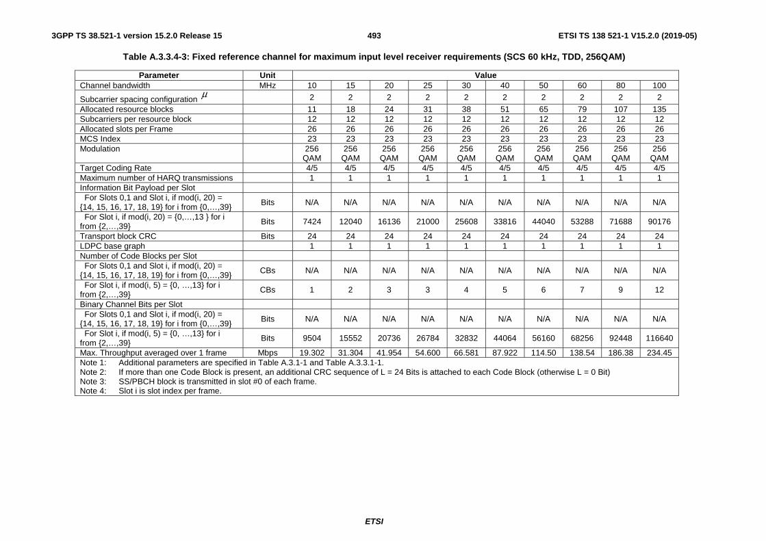
ETSI
ETSI TS 138 521-1 V15.2.0 (2019-05)4933GPP TS 38.521-1 version 15.2.0 Release 15
Table A.3.3.4-3: Fixed reference channel for maximum input level receiver requirements (SCS 60 kHz, TDD, 256QAM)
Parameter Unit Value Channel bandwidth MHz 10 15 20 25 30 40 50 60 80 100
Subcarrier spacing configuration μ
2 2 2 2 2 2 2 2 2 2
Allocated resource blocks 11 18 24 31 38 51 65 79 107 135 Subcarriers per resource block 12 12 12 12 12 12 12 12 12 12 Allocated slots per Frame 26 26 26 26 26 26 26 26 26 26 MCS Index 23 23 23 23 23 23 23 23 23 23 Modulation 256
QAM 256
QAM 256
QAM 256
QAM 256
QAM 256
QAM 256
QAM 256
QAM 256
QAM 256
QAM Target Coding Rate 4/5 4/5 4/5 4/5 4/5 4/5 4/5 4/5 4/5 4/5 Maximum number of HARQ transmissions 1 1 1 1 1 1 1 1 1 1 Information Bit Payload per Slot For Slots 0,1 and Slot i, if mod(i, 20) = {14, 15, 16, 17, 18, 19} for i from {0,…,39} Bits N/A N/A N/A N/A N/A N/A N/A N/A N/A N/A
For Slot i, if mod(i, 20) = {0,…,13 } for i from {2,…,39} Bits 7424 12040 16136 21000 25608 33816 44040 53288 71688 90176
Transport block CRC Bits 24 24 24 24 24 24 24 24 24 24 LDPC base graph 1 1 1 1 1 1 1 1 1 1 Number of Code Blocks per Slot For Slots 0,1 and Slot i, if mod(i, 20) = {14, 15, 16, 17, 18, 19} for i from {0,…,39} CBs N/A N/A N/A N/A N/A N/A N/A N/A N/A N/A
For Slot i, if mod(i, 5) = {0, …,13} for i from {2,…,39} CBs 1 2 3 3 4 5 6 7 9 12
Binary Channel Bits per Slot For Slots 0,1 and Slot i, if mod(i, 20) = {14, 15, 16, 17, 18, 19} for i from {0,…,39} Bits N/A N/A N/A N/A N/A N/A N/A N/A N/A N/A
For Slot i, if mod(i, 5) = {0, …,13} for i from {2,…,39}
Bits 9504 15552 20736 26784 32832 44064 56160 68256 92448 116640
Max. Throughput averaged over 1 frame Mbps 19.302 31.304 41.954 54.600 66.581 87.922 114.50 138.54 186.38 234.45 Note 1: Additional parameters are specified in Table A.3.1-1 and Table A.3.3.1-1. Note 2: If more than one Code Block is present, an additional CRC sequence of L = 24 Bits is attached to each Code Block (otherwise L = 0 Bit) Note 3: SS/PBCH block is transmitted in slot #0 of each frame. Note 4: Slot i is slot index per frame.

ETSI
ETSI TS 138 521-1 V15.2.0 (2019-05)4943GPP TS 38.521-1 version 15.2.0 Release 15
A.4 CSI reference measurement channels TBD
A.5 OFDMA Channel Noise Generator (OCNG)
A.5.1 OCNG Patterns for FDD
A.5.1.1 OCNG FDD pattern 1: Generic OCNG FDD Pattern for all unused REs
Table A.5.1.1-1: OP.1 FDD: Generic OCNG FDD Pattern for all unused REs
OCNG Distribution OCNG Parameters
Control Region (Core Set)
Data Region
Resources allocated All unused REs (Note 1) All unused REs (Note 2) Structure PDCCH PDSCH Content Uncorrelated pseudo random
QPSK modulated data Uncorrelated pseudo random QPSK modulated data
Transmission scheme for multiple antennas ports transmission
Single Tx port transmission Spatial multiplexing using any precoding matrix with dimensions same as the precoding matrix for PDSCH
Subcarrier Spacing Same as for RMC PDCCH in the active BWP
Same as for RMC PDSCH in the active BWP
Power Level Same as for RMC PDCCH Same as for RMC PDSCH Note 1: All unused REs in the active CORESETS appointed by the search spaces in use. Note 2: Unused available REs refer to REs in PRBs not allocated for any physical channels, CORESETs,
synchronization signals or reference signals in channel bandwidth.
A.5.2 OCNG Patterns for TDD
A.5.2.1 OCNG TDD pattern 1: Generic OCNG TDD Pattern for all unused REs
Table A.5.2.1-1: OP.1 TDD: Generic OCNG TDD Pattern for all unused REs
OCNG Distribution OCNG Parameters
Control Region (Core Set)
Data Region
Resources allocated All unused REs (Note 1) All unused REs (Note 2) Structure PDCCH PDSCH Content Uncorrelated pseudo random
QPSK modulated data Uncorrelated pseudo random QPSK modulated data
Transmission scheme for multiple antennas ports transmission
Single Tx port transmission Spatial multiplexing using any precoding matrix with dimensions same as the precoding matrix for PDSCH
Subcarrier Spacing Same as for RMC PDCCH in the active BWP
Same as for RMC PDSCH in the active BWP
Power Level Same as for RMC PDCCH Same as for RMC PDSCH Note 1: All unused REs in the active CORESETS appointed by the search spaces in use. Note 2: Unused available REs refer to REs in PRBs not allocated for any physical channels, CORESETs,
synchronization signals or reference signals in channel bandwidth.
ETSI
ETSI TS 138 521-1 V15.2.0 (2019-05)4953GPP TS 38.521-1 version 15.2.0 Release 15
Annex B (normative): Propagation Conditions The propagation conditions and channel models for various environments are specified. For each environment a propagation model is used to evaluate the propagation pathless due to the distance. Channel models are formed by combining delay profiles with a Doppler spectrum, with the addition of correlation properties in the case of a multi-antenna scenario.
B.0 No interference The downlink connection between the System Simulator and the UE is without Additive White Gaussian Noise, and has no fading or multipath effects.

ETSI
ETSI TS 138 521-1 V15.2.0 (2019-05)4963GPP TS 38.521-1 version 15.2.0 Release 15
Annex C (normative): Downlink physical channels
C.0 Downlink signal levels The downlink power settings in Table C.0-1 is used unless otherwise specified in a test case.
If the UE has more than one Rx antenna, the downlink signal is applied to each one. All UE Rx antennas shall be connected.
If the UE has one Rx antenna, the downlink signal is applied to it.
Table C.0-1: Default Downlink power levels for NR
SCS (kHz)
Unit Channel bandwidth 5
MHz 10
MHz 15
MHz 20
MHz 25
MHz 30
MHz 40
MHz 50
MHz 60
MHz 80
MHz 90
MHz 100 MHz
15
Number of RBs 25 50 75 100 128 160 215 270 N/A N/A N/A N/A
Channel BW power dBm -60 -57 -55 -54 -53 -52 -51 -50 N/A N/A N/A N/A
30
Number of RBs 10 24 36 50 64 75 100 128 162 216 243 270
Channel BW power dBm -61 -57 -55 -54 -53 -52 -51 -50 -49 -48 -47 -47
60
Number of RBs N/A 10 18 24 30 36 50 64 75 100 120 135
Channel BW power dBm N/A -58 -56 -54 -53 -52 -51 -50 -49 -48 -47 -47
RS EPRE dBm/ 15kH
z -85 -85 -85 -85 -85 -85 -85 -85 -85 -85 -85 -85
Note 1: The channel bandwidth powers are informative, based on -85dBm/15kHz SS/PBCH SSS EPRE, then scaled according to the number of RBs and rounded to the nearest integer dBm value. Full RE allocation with no boost or deboost is assumed.
Note 2: The power level is specified at each UE Rx antenna. Note 3: DL level is applied for any of the Subcarrier Spacing configuration ( ) with the same power spectrum density of -
85dBm/15kHz.
The default signal level uncertainty is +/-3dB at each test port, for any level specified. If the uncertainty value is critical for the test purpose, a tighter uncertainty is specified for the related test case in Annex F
C.1 General The following clauses, describes the downlink Physical Channels that are transmitted during a connection i.e., when measurements are done.
C.2 Setup Table C.2-1 describes the downlink Physical Channels that are required for connection set up.
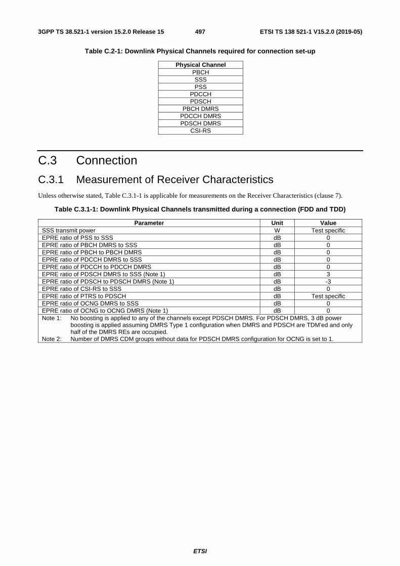
ETSI
ETSI TS 138 521-1 V15.2.0 (2019-05)4973GPP TS 38.521-1 version 15.2.0 Release 15
Table C.2-1: Downlink Physical Channels required for connection set-up
Physical Channel PBCH SSS PSS
PDCCH PDSCH
PBCH DMRS PDCCH DMRS PDSCH DMRS
CSI-RS
C.3 Connection
C.3.1 Measurement of Receiver Characteristics Unless otherwise stated, Table C.3.1-1 is applicable for measurements on the Receiver Characteristics (clause 7).
Table C.3.1-1: Downlink Physical Channels transmitted during a connection (FDD and TDD)
Parameter Unit Value SSS transmit power W Test specific EPRE ratio of PSS to SSS dB 0 EPRE ratio of PBCH DMRS to SSS dB 0 EPRE ratio of PBCH to PBCH DMRS dB 0 EPRE ratio of PDCCH DMRS to SSS dB 0 EPRE ratio of PDCCH to PDCCH DMRS dB 0 EPRE ratio of PDSCH DMRS to SSS (Note 1) dB 3 EPRE ratio of PDSCH to PDSCH DMRS (Note 1) dB -3 EPRE ratio of CSI-RS to SSS dB 0 EPRE ratio of PTRS to PDSCH dB Test specific EPRE ratio of OCNG DMRS to SSS dB 0 EPRE ratio of OCNG to OCNG DMRS (Note 1) dB 0 Note 1: No boosting is applied to any of the channels except PDSCH DMRS. For PDSCH DMRS, 3 dB power
boosting is applied assuming DMRS Type 1 configuration when DMRS and PDSCH are TDM’ed and only half of the DMRS REs are occupied.
Note 2: Number of DMRS CDM groups without data for PDSCH DMRS configuration for OCNG is set to 1.

ETSI
ETSI TS 138 521-1 V15.2.0 (2019-05)4983GPP TS 38.521-1 version 15.2.0 Release 15
Annex D (normative): Characteristics of the Interfering Signal
D.1 General Some RF performance requirements for the NR UE receiver are defined with interfering signals present in addition to the wanted signal.
For NR bands with FDL_high< 2700 MHz and FUL_high< 2700 MHz, a modulated 5MHz full bandwidth NR down link signal, and in some cases an additional CW signal, are used as interfering signal.
For NR bands with FDL_low≥ 3300 MHz and FUL_low≥ 3300 MHz, a modulated NR downlink signal which equals to channel bandwidth of the wanted signal for Single Carrier case and Inter-band CA case is used as interfering. For intra-band contiguous CA Bandwidth Class C case, a modulated NR downlink signal which equals to the aggregated channel bandwidth of the wanted signal is used. For intra-band contiguous CA Bandwidth Class D and E case, a modulated 50MHz NR downlink signal is used. And in some cases, an additional CW signal is used.
D.2 Interference signals Table D.2-1 describes the modulated interferer for different channel bandwidth options for NR band lower than 2700MHz.
Table D.2-1: Description of modulated NR interferer for NR bands with FDL_high< 2700 MHz and FUL_high< 2700 MHz
Channel bandwidth
5 MHz 10MHz 15 MHz 20 MHz 25 MHz 30 MHz RB NOTE1
BWInterferer 5 MHz
Channel bandwidth
40 MHz 50 MHz 60 MHz 80 MHz 90 MHz 100 MHz RB NOTE1
BWInterferer 5 MHz NOTE 1: The RB configured for interfering signal is the same as maximum RB
number defined in Table 5.3.2-1 for each sub-carrier spacing.
Table D.2-2 and Table D.2-3 describe the modulated interferer for different channel bandwidth options for NR band higher than 3300MHz.
Table D.2-2: Description of modulated NR interferer for NR bands with FDL_low≥ 3300 MHz and FUL_low≥ 3300 MHz
Channel bandwidth
10 MHz 15 MHz 20 MHz 40 MHz 50 MHz 60 MHz 80 MHz 90 MHz 100 MHz RB NOTE1
BWInterferer 10 MHz 15 MHz 20 MHz 40 MHz 50 MHz 60 MHz 80 MHz 90 MHz 100 MHz NOTE 1: The RB configured for interfering signal is the same as maximum RB number defined in Table 5.3.2-1 for
each sub-carrier spacing.

ETSI
ETSI TS 138 521-1 V15.2.0 (2019-05)4993GPP TS 38.521-1 version 15.2.0 Release 15
Table D.2-3: Description of modulated NR interferer for NR bands with FDL_low≥ 3300 MHz and FUL_low≥ 3300 MHz for Intra-band contiguous CA
Aggregated Channel bandwidth of Bandwidth Class C Bandwidth
Class D/E 110 MHz
120 MHz
130 MHz
140 MHz 150 MHz 160 MHz 180
MHz 200 MHz
RB(SCS=30 kHz) Note 1 133
RB(SCS=60 kHz) Note 1 65
BWInterferer 110 MHz
120 MHz
130 MHz
140 MHz 150 MHz 160 MHz 180
MHz 200 MHz 50MHz
NOTE 1: The interfering signal shall be configured in the same way as the aggregated bandwidth of the wanted signal. The RB configurations for each component carrier are defined in Table 5.3.2-1 for each sub-carrier spacing.

ETSI
ETSI TS 138 521-1 V15.2.0 (2019-05)5003GPP TS 38.521-1 version 15.2.0 Release 15
Annex E (normative): Global In-Channel TX-Test
Editor’s note: This clause is incomplete. The following aspects are either missing or not yet determined:
Number of preamble sequences over which EVMPRACH is averaged is TBD in TS 38.101-1.
Note: Clauses E.2.2 to E.5.9.3 are descriptions, which assume no power ramping adjacent to the measurement period.
E.1 General The global in-channel TX test enables the measurement of all relevant parameters that describe the in-channel quality of the output signal of the TX under test in a single measurement process.
The parameters describing the in-channel quality of a transmitter, however, are not necessarily independent. The algorithm chosen for description inside this annex places particular emphasis on the exclusion of all interdependencies among the parameters.
E.2 Signals and results
E.2.1 Basic principle The process is based on the comparison of the actual output signal of the TX under test, received by an ideal receiver, with a reference signal, that is generated by the measuring equipment and represents an ideal error free received signal. All signals are represented as equivalent (generally complex) baseband signals.
The description below uses numbers as examples. These numbers are taken from FDD with normal CP length and 100 MHz bandwidth with 30 kHz SCS. The application of the text below, however, is not restricted to this frame structure and bandwidth.
E.2.2 Output signal of the TX under test The output signal of the TX under test is acquired by the measuring equipment and stored for further processing. It is sampled at a sampling rate of 122.88 Mbps. In the time domain it comprises at least 10 uplink subframes. The measurement period is derived by concatenating the correct number of individual uplink slots until the correct measurement period is reached. The output signal is named z(ν). Each slot is modelled as a signal with the following parameters: demodulated data content, carrier frequency, amplitude and phase for each subcarrier, timing, carrier leakage.
NOTE 1: TDD
Since the uplink subframes are not continuous, n slots should be extracted from more than 1 continuous radio frame where
.
E.2.3 Reference signal
Two types of reference signal are defined:
The reference signal i1(ν) is constructed by the measuring equipment according to the relevant TX specifications, using the following parameters: demodulated data content, nominal carrier frequency, nominal amplitude and phase for each

ETSI
ETSI TS 138 521-1 V15.2.0 (2019-05)5013GPP TS 38.521-1 version 15.2.0 Release 15
subcarrier, nominal timing, no carrier leakage. It is represented as a sequence of samples at a sampling rate of 122.88 Msps in the time domain.
The reference signal i2(ν) is constructed by the measuring equipment according to the relevant TX specifications, using the following parameters: restricted data content: nominal reference symbols, (all modulation symbols for user data symbols are set to 0V), nominal carrier frequency, nominal amplitude and phase for each applicable subcarrier, nominal timing, no carrier leakage. It is represented as a sequence of samples at a sampling rate of 122.88 Msps in the time domain.
NOTE: The PUCCH is off during the time under test.
E.2.4 Measurement results The measurement results, achieved by the global in channel TX test are the following:
- Carrier Frequency error
- EVM (Error Vector Magnitude)
- Carrier leakage
- Unwanted emissions, falling into non allocated resource blocks.
- EVM equalizer spectrum flatness
E.2.5 Measurement points The unwanted emission falling into non-allocated RB(s) is calculated directly after the FFT as described below. In contrast to this, the EVM for the allocated RB(s) is calculated after the IDFT for DFT-s-OFDM or after the Tx-Rx chain equalizer for CP-OFDM. The samples after the TX-RX chain equalizer are used to calculate EVM equalizer spectrum flatness. Carrier frequency error and carrier leakage is calculated in the block “RF correction”.
Figure E.2.5-1: EVM measurement points
E.3 Signal processing
E.3.1 Pre FFT minimization process Before applying the pre-FFT minimization process, z(ν) and i(ν) are portioned into n pieces, comprising one slot each, where
. Each slot is processed separately. Sample timing, Carrier frequency and carrier leakage in z(ν) are jointly varied in order to minimise the difference between z(ν) and i(ν). Best fit (minimum difference) is achieved when the RMS difference value between z(ν) and i(ν) is an absolute minimum.
ETSI
ETSI TS 138 521-1 V15.2.0 (2019-05)5023GPP TS 38.521-1 version 15.2.0 Release 15
The carrier frequency variation and the IQ variation are the measurement results: Carrier Frequency Error and Carrier leakage.
From the acquired samples n carrier frequencies and n carrier leakages can be derived.
NOTE 1: The minimisation process, to derive carrier leakage and RF error can be supported by Post FFT operations. However the minimisation process defined in the pre FFT domain comprises all acquired samples (i.e. it does not exclude the samples in between the FFT widths and it does not exclude the bandwidth outside the transmission bandwidth configuration
NOTE 2: The algorithm would allow deriving Carrier Frequency error and Sample Frequency error of the TX under test separately. However there are no requirements for Sample Frequency error. Hence the algorithm models the RF and the sample frequency commonly (not independently). It returns one error and does not distinguish between both.
After this process the samples z(ν) are called z0(ν).
E.3.2 Timing of the FFT window The FFT window length is 4096 samples per OFDM symbol. 14 FFTs (57344 samples) cover less than the acquired number of samples (61440 samples). The position in time for FFT must be determined.
In an ideal signal, the FFT may start at any instant within the cyclic prefix without causing an error. The TX filter, however, reduces the window. The EVM requirements shall be met within a window W<CP. There are three different instants for FFT:
Centre of the reduced window, called , –W/2 and +W/2.
The timing of the measured signal is determined in the pre FFT domain as follows, using z0(ν) and i2(ν) :
1. The measured signal is delay spread by the TX filter. Hence the distinct boarders between the OFDM symbols and between Data and CP are also spread and the timing is not obvious.
2. In the Reference Signal i2(ν) the timing is known.
3. Correlation between (1.) and (2.) will result in a correlation peak. The meaning of the correlation peak is approx. the “impulse response” of the TX filter. The meaning of “impulse response” assumes that the autocorrelation of the reference signal i2(ν) is a Dirac peak and that the correlation between the reference signal i2(ν) and the data in the measured signal is 0. The correlation peak, (the highest, or in case of more than one, the earliest) indicates the timing in the measured signal.
From the acquired samples, n timings can be derived.
For all calculations, except EVM, the number of samples in z0(ν) is reduced to 14 blocks of samples, comprising 4096 samples (FFT width) and starting with in each OFDM symbol including the demodulation reference signal.
For the EVM calculation the output signal under test is reduced to 28 blocks of samples, comprising 4096 samples (FFT width) and starting with –W/2 and +W/2 in each OFDM symbol including the demodulation reference signal.
The number of samples, used for FFT is reduced compared to z0(ν). This subset of samples is called z’(ν).
The timing of the centre with respect to the different CP length in a slot is as follows: (FDD, normal CP length)
is on Tf=144 (=CP/2) within the CP of length 288 FFT samples (in OFDM symbols except 0 and 28 (=7 ⋅ 2�),
where symbol 0 is the first symbol of each subframe) for 100 MHz channel bandwidth and SCS = 30 kHz.
is on Tf=176 (=320-144) within the CP of length 320 (in OFDM symbol 0 and 28 (=7 ⋅ 2�), where symbol 0 is the
first symbol of each subframe) for 100 MHz channel bandwidth and SCS = 30 kHz.
E.3.3 Post FFT equalisation
Perform 14 FFTs on z’(ν), one for each OFDM symbol in a slot using the timing , including the demodulation reference symbol. The result is an array of samples, 14 in the time axis t times 4096 in the frequency axis f. The
c~Δ c~Δ c~Δ
c~Δ
c~Δ c~Δ
c~Δ
c~Δ
c~Δ
c~Δ

ETSI
ETSI TS 138 521-1 V15.2.0 (2019-05)5033GPP TS 38.521-1 version 15.2.0 Release 15
samples represent the data symbols (in OFDM-symbol 0,1,3,4,5,6,8,9,10,12,13 in each slot) and demodulation reference symbols (OFDM symbol 2, 7, 11 in each slot) in the allocated RBs and inband emissions in the non-allocated RBs within the transmission BW.
Only the allocated resource blocks in the frequency domain are used for equalisation.
The nominal demodulation reference symbols and nominal data symbols are used to equalize the measured data symbols. (Location for equalization see Figure E.2.5-1)
NOTE: The nomenclature inside this note is local and not valid outside.
The nominal data symbols are created by a demodulation process. The location to gain the demodulated data symbols is “EVM” in Figure E.2.5-1. For CP-OFDM, the process described in Annex E.5 can be applied. A demodulation process as follows is recommended for DFT-s-OFDM:
1. Equalize the measured data symbols using the reference symbols for equalisation. Result: Equalized data symbols
2. Only for DFT-s-OFDM, iDFT transform the equalized data symbols: Result: Equalized data symbols
3. Decide for the nearest constellation point: Result: Nominal data symbols
4. Only for DFT-s-OFDM, DFT transform the nominal data symbols: Result: Nominal data symbols
At this stage we have an array of Measured data-Symbols and reference-Symbols (MS(f,t))
versus an array of Nominal data-Symbols and reference Symbols (NS(f,t))
(complex, the arrays comprise 11 data symbols and 3 demodulation reference symbol in the time axis and the number of allocated subcarriers in the frequency axis.)
MS(f,t) and NS(f,t) are processed with a least square (LS) estimator, to derive one equalizer coefficient per time slot and per allocated subcarrier. EC(f) is defined as
.
With * denoting complex conjugation.
EC(f) are used to equalize the DFT-coded data symbols. The measured DFT-coded data and the references symbols are equalized by:
Z’(f,t) = MS(f,t) . EC(f)
With . denoting multiplication.
Z’(f,t), restricted to the data symbol (excluding t=2,7,11) is used to calculate EVM, as described in E.4.1.
EC(f) is used in E.4.4 to calculate EVM equalizer spectral flatness.
NOTE: The post FFT minimisation process is done over 14 symbols (11 DFT-coded data symbols and 3 reference symbols).
The samples of the non-allocated resource blocks within the transmission bandwidth configuration in the post FFT domain are called Y(f,t) (f covering the non-allocated subcarriers within the transmission bandwidth configuration, t covering the OFDM symbols during 1 slot).
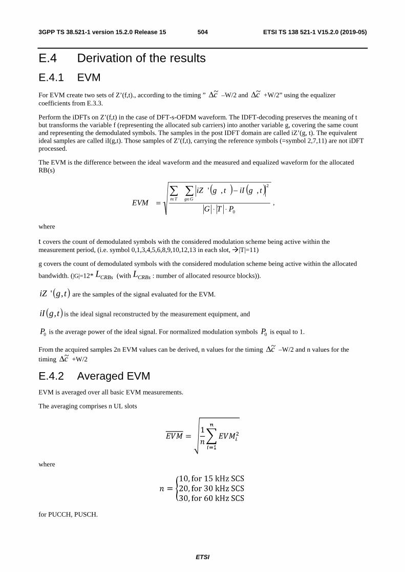
ETSI
ETSI TS 138 521-1 V15.2.0 (2019-05)5043GPP TS 38.521-1 version 15.2.0 Release 15
E.4 Derivation of the results
E.4.1 EVM
For EVM create two sets of Z’(f,t)., according to the timing ” –W/2 and +W/2” using the equalizer coefficients from E.3.3.
Perform the iDFTs on Z’(f,t) in the case of DFT-s-OFDM waveform. The IDFT-decoding preserves the meaning of t but transforms the variable f (representing the allocated sub carriers) into another variable g, covering the same count and representing the demodulated symbols. The samples in the post IDFT domain are called iZ’(g, t). The equivalent ideal samples are called iI(g,t). Those samples of Z’(f,t), carrying the reference symbols (=symbol 2,7,11) are not iDFT processed.
The EVM is the difference between the ideal waveform and the measured and equalized waveform for the allocated RB(s)
,
where
t covers the count of demodulated symbols with the considered modulation scheme being active within the measurement period, (i.e. symbol 0,1,3,4,5,6,8,9,10,12,13 in each slot, |T|=11)
g covers the count of demodulated symbols with the considered modulation scheme being active within the allocated
bandwidth. (|G|=12* (with : number of allocated resource blocks)).
are the samples of the signal evaluated for the EVM.
is the ideal signal reconstructed by the measurement equipment, and
is the average power of the ideal signal. For normalized modulation symbols is equal to 1.
From the acquired samples 2n EVM values can be derived, n values for the timing –W/2 and n values for the
timing +W/2
E.4.2 Averaged EVM EVM is averaged over all basic EVM measurements.
The averaging comprises n UL slots
��� � �1�����
�
�
���
where
for PUCCH, PUSCH.
c~Δ c~Δ
( ) ( )
0
2,,'
PTG
tgiItgiZ
EVMGgTt
⋅⋅
−=
∈∈
CRBsL CRBsL
( )tgiZ ,'
( )tgiI ,
0P 0P
c~Δc~Δ

ETSI
ETSI TS 138 521-1 V15.2.0 (2019-05)5053GPP TS 38.521-1 version 15.2.0 Release 15
The averaging is done separately for timing¦ –W/2 and +W/2 leading to and
is compared against the test requirements.
E.4.3 In-band emissions measurement The in-band emissions are a measure of the interference falling into the non-allocated resources blocks.
Explanatory Note:
The inband emission measurement is only meaningful with allocated RB(s) next to non-allocated RB. The allocated RB(s) are necessary but not under test. The non-allocated RBs are under test. The RB allocation for this test is as follows: The allocated RB(s) are at one end of the channel BW, leaving the other end unallocated. The number of allocated RB(s) is smaller than half of the number of RBs, available in the channel BW. This means that the vicinity of the carrier in the centre is unallocated.
There are 3 types of inband emissions:
1. General
2. IQ image
3. Carrier leakage
Carrier leakage are inband emissions next to the carrier.
IQ image are inband emissions symmetrically (with respect to the carrier) on the other side of the allocated RBs.
General are applied to all unallocated RBs.
For each evaluated RB, the minimum requirement is calculated as the higher of PRB - 30 dB and the power sum of all limit values (General, IQ Image or Carrier leakage) that apply.
In specific the following combinations:
- Power (General)
- Power (General + Carrier leakage)
- Power (General + IQ Image)
1 and 2 is expressed in terms of power in one non allocated RB under test, normalized to the average power of an allocated RB (unit dB).
3 is expressed in terms of power in one non allocated RB, normalized to the power of all allocated RBs. (unit dBc).
This is the reason for two formulas Emissions relative.
Create one set of Y(t,f) per slot according to the timing “ ”
For the non-allocated RBs below the in-band emissions are calculated as follows
,
where
the upper formula represents the in band emissions below the allocated frequency block and the lower one the in band emissions above the allocated frequency block.
c~Δ c~Δ lEVM hEVM
)EVM ,EVMmax( lfinal hEVM =
c~Δ
>Δ
<Δ=Δ
∈
ΔΔ⋅+
Δ−Δ⋅+
∈
Δ+Δ⋅+
ΔΔ⋅+
0,),(1
0,),(1
)( ))*12(,min(
*)1112(
2
*)1112(
))*12(,max(
2
max
min
RBTt
fcf
fcs
RBTt
fc
fcfsRBabsolute
s
RBh
RBh
s
RBl
RBl
ftYT
ftYT
Emissions
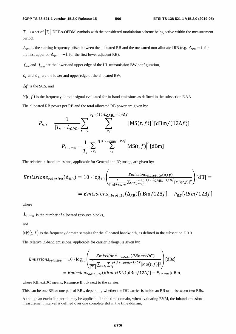
ETSI
ETSI TS 138 521-1 V15.2.0 (2019-05)5063GPP TS 38.521-1 version 15.2.0 Release 15
is a set of DFT-s-OFDM symbols with the considered modulation scheme being active within the measurement
period,
is the starting frequency offset between the allocated RB and the measured non-allocated RB (e.g. for
the first upper or for the first lower adjacent RB),
and are the lower and upper edge of the UL transmission BW configuration,
and are the lower and upper edge of the allocated BW,
is the SCS, and
is the frequency domain signal evaluated for in-band emissions as defined in the subsection E.3.3
The allocated RB power per RB and the total allocated RB power are given by:
The relative in-band emissions, applicable for General and IQ image, are given by:
where
is the number of allocated resource blocks,
and
is the frequency domain samples for the allocated bandwidth, as defined in the subsection E.3.3.
The relative in-band emissions, applicable for carrier leakage, is given by:
where RBnextDC means: Resource Block next to the carrier.
This can be one RB or one pair of RBs, depending whether the DC carrier is inside an RB or in-between two RBs.
Although an exclusion period may be applicable in the time domain, when evaluating EVM, the inband emissions measurement interval is defined over one complete slot in the time domain.
sT sT
RBΔ 1=ΔRB
1−=ΔRB
minf maxf
lc hc
fΔ
( )ftY ,
dBm][ ),(MS1 *)112(lc
lc
2 ∈
Δ−⋅+
− =sTt
fCRBsL
s
RBsAll ftT
P
CRBsL
( )ft,MS

ETSI
ETSI TS 138 521-1 V15.2.0 (2019-05)5073GPP TS 38.521-1 version 15.2.0 Release 15
From the acquired samples n functions for general in band emissions and IQ image inband emissions can be derived. n values or n pairs of carrier leakage inband emissions can be derived. They are compared against different limits.
E.4.4 EVM equalizer spectrum flatness For EVM equalizer spectrum flatness use EC(f) as defined in E.3.3. Note, EC(f) represents equalizer coefficient
Ff ∈, f is the allocated subcarriers within the transmission bandwidth ((|F|=12* CRBsL )
From the acquired samples n functions EC(f) can be derived.
EC(f) is broken down to 2 functions:
1),f(EC1 Rangef ∈
2),f(EC2 Rangef ∈
Where Range 1 and Range 2 are as defined in Table 6.5.2.4.5-1 for normal condition and Table 6.5.2.4.5-2 for extreme condition
The following peak to peak ripple is calculated:
|)))f(ECmin(|/|))f(EC(|(max log*02RP 111 = ,which denote the maximum ripple in Range 1
|)))f(ECmin(|/|))f(EC(|(max log*02RP 222 = ,which denote the maximum ripple in Range 2
|)))f(ECmin(|/|))f(EC(|(max log*02RP 2112 = ,which denote the maximum ripple between the upper side
of Range 1 and lower side of Range 2
|)))f(ECmin(|/|))f(EC(|(max log*02RP 1221 = ,which denote the maximum ripple between the upper side
of Range 2 and lower side of Range 1
E.4.5 Frequency error and Carrier leakage See E.3.1.
E.4.6 EVM of Demodulation reference symbols (EVMDMRS) For the purpose of EVM DMRS, the steps E.2.2 to E.4.2 are repeated 6 times, constituting 6 EVM DMRS sub-periods. The only purpose of the repetition is to cover the longer gross measurement period of EVM DMRS ( time slots) and to derive the FFT window timing per sub-period.
The bigger of the EVM results in one n TS period corresponding to the timing¦ c~Δ –W/2 or c~Δ +W/2 is compared against the limit. (Clause E.4.2) This timing is re-used for EVM DMRS in the equivalent EVM DMRS sub-period.
For EVM the demodulation reference symbols are excluded, while the data symbols are used. For EVMDMRS the data symbols are excluded, while the demodulation references symbols are used. This is illustrated in figure E.4.6-1

ETSI
ETSI TS 138 521-1 V15.2.0 (2019-05)5083GPP TS 38.521-1 version 15.2.0 Release 15
DFT
IFFT
TX Front-end
C hannel
RF
correction FFT
Tx -Rx chain equalizer
0
0
… … …
IDFT
DUT Tx
Test equipment Rx
… … …
… … …
… … …
DMRS
Figure E.4.6-1: EVMDMRS measurement points
Re-use the following formula from E.3.3:
Z’(f,t) = MS(f,t) . EC(f)
To calculate EVMDMRS , the data symbol ( t=0,1,3,4,5,6,8,9,10,12,13) in Z’(f,t) are excluded and only the reference symbols (t=2,7,11) is used.
The EVM DMRS is the difference between the ideal waveform and the measured and equalized waveform for the allocated RB(s)
( ) ( )FPT
tfItfZ
EVMFfTt
DMRS ⋅⋅
−=
∈∈
0
2,,'
,
where
t covers the count of demodulation reference symbols (i.e. symbols 2,7,11 in each slot, so count=3)
f covers the count of demodulation reference symbols within the allocated bandwidth. (|F|=12* CRBsL (with CRBsL :
number of allocated resource blocks)).
( )tfZ ,' are the samples of the signal evaluated for the EVM DMRS
( )tfI , is the ideal signal reconstructed by the measurement equipment, and
0P is the average power of the ideal signal. For normalized modulation symbols 0P is equal to 1.
n such results are generated per measurement sub-period.
E.4.6.1 1st average for EVM DMRS
EVM DMRS is averaged over all basic EVM DMRS measurements in one sub-period
The averaging comprises n UL slots
The timing is taken from the EVM for the data. 6 of those results are achieved from the samples. In general the timing is not the same for each result.
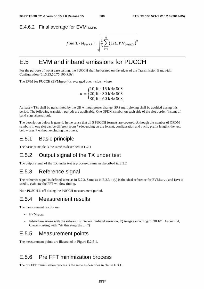
ETSI
ETSI TS 138 521-1 V15.2.0 (2019-05)5093GPP TS 38.521-1 version 15.2.0 Release 15
E.4.6.2 Final average for EVM DMRS
E.5 EVM and inband emissions for PUCCH For the purpose of worst case testing, the PUCCH shall be located on the edges of the Transmission Bandwidth Configuration (6,15,25,50,75,100 RBs).
The EVM for PUCCH (EVMPUCCH) is averaged over n slots, where
.
At least n TSs shall be transmitted by the UE without power change. SRS multiplexing shall be avoided during this period. The following transition periods are applicable: One OFDM symbol on each side of the slot border (instant of band edge alternation).
The description below is generic in the sense that all 5 PUCCH formats are covered. Although the number of OFDM symbols in one slot can be different from 7 (depending on the format, configuration and cyclic prefix length), the text below uses 7 without excluding the others.
E.5.1 Basic principle The basic principle is the same as described in E.2.1
E.5.2 Output signal of the TX under test The output signal of the TX under test is processed same as described in E.2.2
E.5.3 Reference signal The reference signal is defined same as in E.2.3. Same as in E.2.3, i1(ν) is the ideal reference for EVMPUCCH and i2(ν) is used to estimate the FFT window timing.
Note PUSCH is off during the PUCCH measurement period.
E.5.4 Measurement results The measurement results are:
- EVMPUCCH
- Inband emissions with the sub-results: General in-band emission, IQ image (according to: 38.101. Annex F.4, Clause starting with: “At this stage the ….”)
E.5.5 Measurement points The measurement points are illustrated in Figure E.2.5-1.
E.5.6 Pre FFT minimization process The pre FFT minimisation process is the same as describes in clause E.3.1.

ETSI
ETSI TS 138 521-1 V15.2.0 (2019-05)5103GPP TS 38.521-1 version 15.2.0 Release 15
NOTE: although an exclusion period for EVMPUCCH is applicable in E.5.9.1, the pre FFT minimisation process is done over the complete slot.
RF error, and carrier leakage are necessary for best fit of the measured signal towards the ideal signal in the pre FFT domain. However they are not used to compare them against the limits.
E.5.7 Timing of the FFT window Timing of the FFT window is estimated with the same method as described in E.3.2.
E.5.8 Post FFT equalisation The post FFT equalisation is described separately without reference to E.3.3:
Perform 14 FFTs on z’(ν), one for each OFDM symbol in a slot using the timing c~Δ , including the demodulation reference symbol. The result is an array of samples, 14 in the time axis t times 4096 in the frequency axis f. The samples represent the OFDM symbols (data and reference symbols) in the allocated RBs and inband emissions in the non-allocated RBs within the transmission BW.
Only the allocated resource blocks in the frequency domain are used for equalisation.
The nominal reference symbols and nominal OFDM data symbols are used to equalize the measured data symbols.
Note: (The nomenclature inside this note is local and not valid outside)
The nominal OFDM data symbols are created by a demodulation process. A demodulation process as follows is recommended:
1. Equalize the measured OFDM data symbols using the reference symbols for equalisation. Result: Equalized OFDM data symbols
2. Decide for the nearest constellation point, however not independent for each subcarrier in the RB. 12 constellation points are decided dependent, using the applicable CAZAC sequence. Result: Nominal OFDM data symbols
At this stage we have an array of Measured data-Symbols and reference-Symbols (MS(f,t))
versus an array of Nominal data-Symbols and reference Symbols (NS(f,t))
The arrays comprise in sum 14 data and reference symbols, depending on the PUCCH format, in the time axis and the number of allocated sub-carriers in the frequency axis.
MS(f,t) and NS(f,t) are processed with a least square (LS) estimator, to derive one equalizer coefficient per time slot and per allocated subcarrier. EC(f)
=
== 6
0
*
6
0
*
),(),(
),(),()(
t
t
tfNStfMS
tfNStfNSfEC
With * denoting complex conjugation.
EC(f) are used to equalize the OFDM data together with the demodulation reference symbols by:
Z’(f,t) = MS(f,t) . EC(f)
With . denoting multiplication.
Z’(f,t) is used to calculate EVMPUCCH, as described in E.5.9 1
NOTE: although an exclusion period for EVMPUCCH is applicable in E.5.9.1, the post FFT minimisation process is done over 14 OFDM symbols.
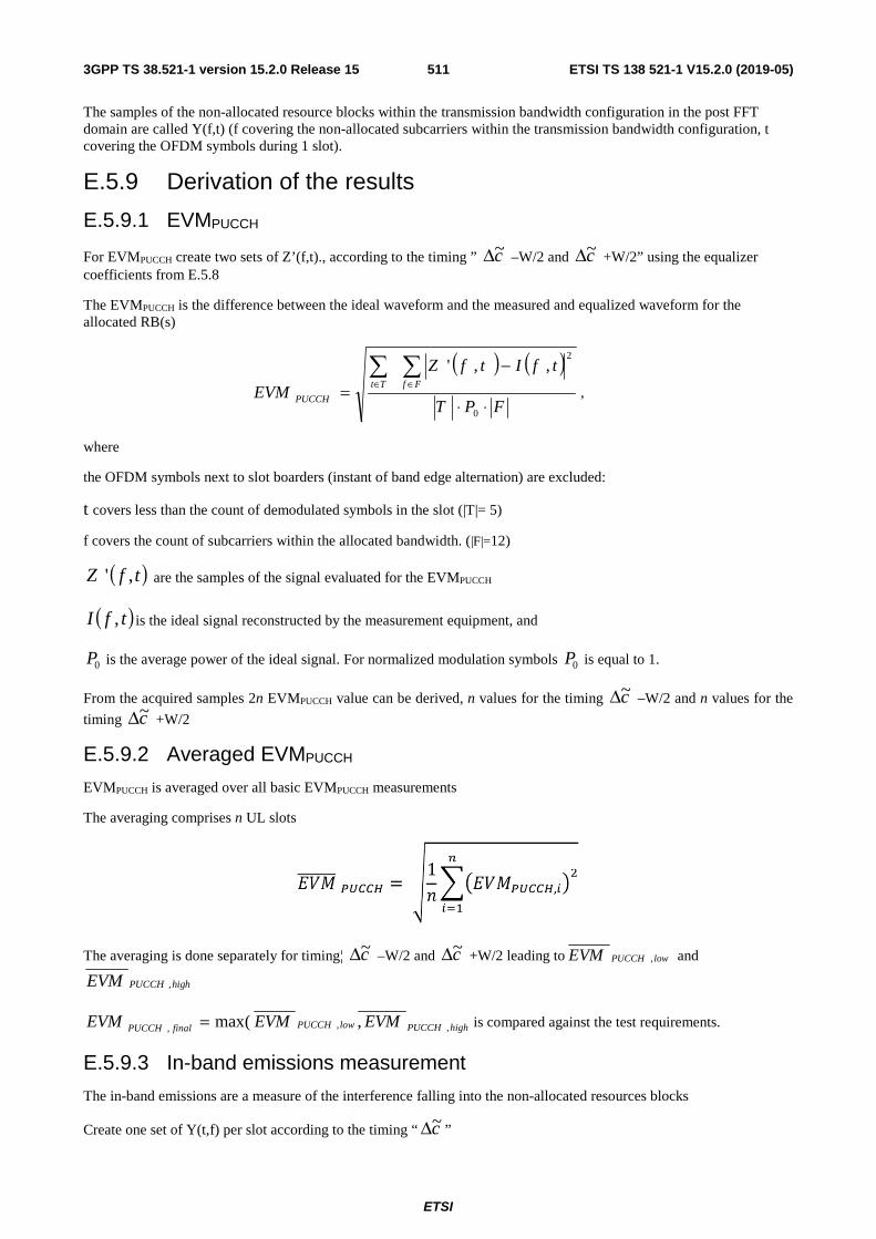
ETSI
ETSI TS 138 521-1 V15.2.0 (2019-05)5113GPP TS 38.521-1 version 15.2.0 Release 15
The samples of the non-allocated resource blocks within the transmission bandwidth configuration in the post FFT domain are called Y(f,t) (f covering the non-allocated subcarriers within the transmission bandwidth configuration, t covering the OFDM symbols during 1 slot).
E.5.9 Derivation of the results
E.5.9.1 EVMPUCCH
For EVMPUCCH create two sets of Z’(f,t)., according to the timing ” c~Δ –W/2 and c~Δ +W/2” using the equalizer coefficients from E.5.8
The EVMPUCCH is the difference between the ideal waveform and the measured and equalized waveform for the allocated RB(s)
( ) ( )FPT
tfItfZ
EVMFfTt
PUCCH ⋅⋅
−=
∈∈
0
2,,'
,
where
the OFDM symbols next to slot boarders (instant of band edge alternation) are excluded:
t covers less than the count of demodulated symbols in the slot (|T|= 5)
f covers the count of subcarriers within the allocated bandwidth. (|F|=12)
( )tfZ ,' are the samples of the signal evaluated for the EVMPUCCH
( )tfI , is the ideal signal reconstructed by the measurement equipment, and
0P is the average power of the ideal signal. For normalized modulation symbols 0P is equal to 1.
From the acquired samples 2n EVMPUCCH value can be derived, n values for the timing c~Δ –W/2 and n values for the
timing c~Δ +W/2
E.5.9.2 Averaged EVMPUCCH
EVMPUCCH is averaged over all basic EVMPUCCH measurements
The averaging comprises n UL slots
The averaging is done separately for timing¦ c~Δ –W/2 and c~Δ +W/2 leading to lowPUCCHEVM , and
highPUCCHEVM ,
highPUCCHlowPUCCHfinalPUCCH EVMEVMEVM ,,, ,max(= is compared against the test requirements.
E.5.9.3 In-band emissions measurement
The in-band emissions are a measure of the interference falling into the non-allocated resources blocks
Create one set of Y(t,f) per slot according to the timing “ c~Δ ”

ETSI
ETSI TS 138 521-1 V15.2.0 (2019-05)5123GPP TS 38.521-1 version 15.2.0 Release 15
For the non-allocated RBs the in-band emissions are calculated as follows
>Δ
<Δ=Δ
∈
ΔΔ⋅+
Δ−Δ⋅+
∈
Δ+Δ⋅+
ΔΔ⋅+
0,),(1
0,),(1
)( ))*12(,min(
*)1112(
2
*)1112(
))*12(,max(
2
max
min
RBTt
fcf
fcs
RBTt
fc
fcfsRBabsolute
s
RBh
RBh
s
RBl
RBl
ftYT
ftYT
Emissions ,
where
the upper formula represents the inband emissions below the allocated frequency block and the lower one the inband emissions above the allocated frequency block.
sT is a set of sT OFDM symbols in the measurement period,
RBΔ is the starting frequency offset between the allocated RB and the measured non-allocated RB (e.g. 1=ΔRB for
the first upper or 1−=ΔRB for the first lower adjacent RB),
minf and maxf are the lower and upper edge of the UL system BW,
lc and hc are the lower and upper edge of the allocated BW,
fΔ is the SCS, and
( )ftY , is the frequency domain signal evaluated for in-band emissions as defined in the subsection E.5.8
The relative in-band emissions are, given by
][
),(MS1
)(log*10)(
)*112(c
c
210
l
l
dB
ftLT
EmissionsEmissions
s
CRBs
Tt
fL
CRBss
RBabsoluteRBrelative
∈
Δ−⋅+
⋅
Δ=Δ
where
CRBsL is the number of allocated RBs,
and ( )ft,MS is the frequency domain samples for the allocated bandwidth, as defined in the subsection E.5.8
Although an exclusion period for EVM is applicable in E.5.9.1, the inband emissions measurement interval is defined over one complete slot in the time domain.
From the acquired samples n functions for inband emissions can be derived.
Since the PUCCH allocation is always on the upper or lower band-edge, the opposite of the allocated one represents the IQ image, and the remaining inner RBs represent the general inband emissions. They are compared against different limits.
E.6 EVM for PRACH The description below is generic in the sense that all PRACH formats are covered. The numbers, used in the text below are taken from PRACH format#0 without excluding the other formats. The sampling rate for PRACH is assumed as , 30.72 Msps in the time domain.
E.6.1 Basic principle The basic principle is the same as described in E.2.1

ETSI
ETSI TS 138 521-1 V15.2.0 (2019-05)5133GPP TS 38.521-1 version 15.2.0 Release 15
E.6.2 Output signal of the TX under test The output signal of the TX under test is processed same as described in E.2.2
The measurement period is TBD.
E.6.3 Reference signal The test description in 6.4.2.1.4.1 is based on non-contention based access:
- PRACH configuration index (responsible for Preamble format, System frame number and subframe number)
- Preamble ID
- Preamble power
signalled to the UE, defines the reference signal unambiguously, such that no demodulation process is necessary to gain the reference signal.
The reference signal i(ν) is constructed by the measuring equipment according to the relevant TX specifications, using the following parameters: the applicable Zadoff Chu sequence, nominal carrier frequency, nominal amplitude and phase for each subcarrier, nominal timing, no carrier leakage. It is represented as a sequence of samples at a sampling rate of 122.88 Msps in the time domain.
E.6.4 Measurement results The measurement result is:
- EVMPRACH
E.6.5 Measurement points The measurement points are illustrated in the figure below:
Figure E.6.5-1:Measurement points
E.6.6 Pre FFT minimization process The pre-FFT minimization process is applied to each PRACH preamble separately. The time period for the pre- FFT minimisation process includes the complete CP and Zadoff-Chu sequence (in other words, the power transition period is per definition outside of this time period) Sample timing, Carrier frequency and carrier leakage in z(ν) are jointly varied in order to minimise the difference between z(ν) and i(ν). Best fit (minimum difference) is achieved when the RMS difference value between z(ν) and i(ν) is an absolute minimum.
After this process the samples z(ν) are called z0(ν).
RF error, and carrier leakage are necessary for best fit of the measured signal towards the ideal signal in the pre FFT domain. However they are not used to compare them against the limits.
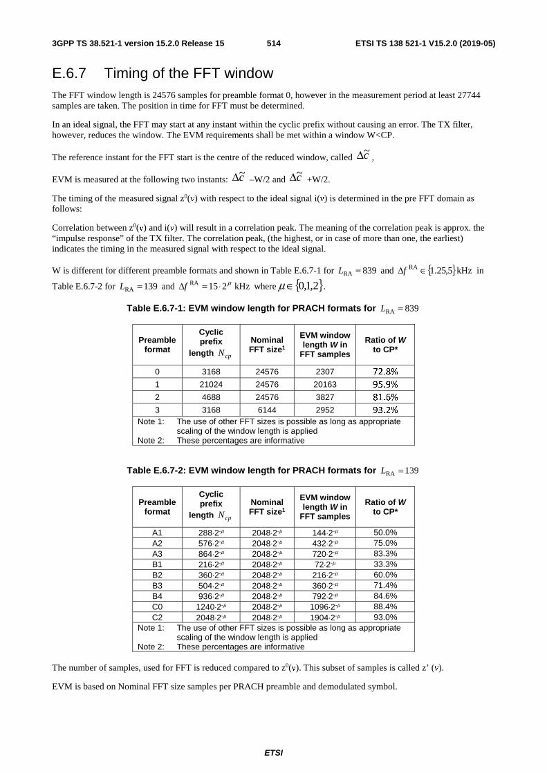
ETSI
ETSI TS 138 521-1 V15.2.0 (2019-05)5143GPP TS 38.521-1 version 15.2.0 Release 15
E.6.7 Timing of the FFT window The FFT window length is 24576 samples for preamble format 0, however in the measurement period at least 27744 samples are taken. The position in time for FFT must be determined.
In an ideal signal, the FFT may start at any instant within the cyclic prefix without causing an error. The TX filter, however, reduces the window. The EVM requirements shall be met within a window W<CP.
The reference instant for the FFT start is the centre of the reduced window, called c~Δ ,
EVM is measured at the following two instants: c~Δ –W/2 and c~Δ +W/2.
The timing of the measured signal z0(ν) with respect to the ideal signal i(ν) is determined in the pre FFT domain as follows:
Correlation between z0(ν) and i(ν) will result in a correlation peak. The meaning of the correlation peak is approx. the “impulse response” of the TX filter. The correlation peak, (the highest, or in case of more than one, the earliest) indicates the timing in the measured signal with respect to the ideal signal.
W is different for different preamble formats and shown in Table E.6.7-1 for 839RA =L and { }kHz 5,25.1RA ∈Δf in
Table E.6.7-2 for 139RA =L and kHz 215RA μ⋅=Δf where { }2,1,0∈μ .
Table E.6.7-1: EVM window length for PRACH formats for 839RA =L
Preamble format
Cyclic prefix
length cpN
Nominal FFT size1
EVM window length W in
FFT samples
Ratio of W to CP*
0 3168 24576 2307 72.8%
1 21024 24576 20163 95.9%
2 4688 24576 3827 81.6%
3 3168 6144 2952 93.2% Note 1: The use of other FFT sizes is possible as long as appropriate
scaling of the window length is applied Note 2: These percentages are informative
Table E.6.7-2: EVM window length for PRACH formats for 139RA =L
Preamble format
Cyclic prefix
length cpN
Nominal FFT size1
EVM window length W in
FFT samples
Ratio of W to CP*
A1 288⋅2-μ 2048⋅2-μ 144⋅2-μ 50.0% A2 576⋅2-μ 2048⋅2-μ 432⋅2-μ 75.0% A3 864⋅2-μ 2048⋅2-μ 720⋅2-μ 83.3% B1 216⋅2-μ 2048⋅2-μ 72⋅2-μ 33.3% B2 360⋅2-μ 2048⋅2-μ 216⋅2-μ 60.0% B3 504⋅2-μ 2048⋅2-μ 360⋅2-μ 71.4% B4 936⋅2-μ 2048⋅2-μ 792⋅2-μ 84.6% C0 1240⋅2-μ 2048⋅2-μ 1096⋅2-μ 88.4% C2 2048⋅2-μ 2048⋅2-μ 1904⋅2-μ 93.0%
Note 1: The use of other FFT sizes is possible as long as appropriate scaling of the window length is applied
Note 2: These percentages are informative The number of samples, used for FFT is reduced compared to z0(ν). This subset of samples is called z’ (ν).
EVM is based on Nominal FFT size samples per PRACH preamble and demodulated symbol.

ETSI
ETSI TS 138 521-1 V15.2.0 (2019-05)5153GPP TS 38.521-1 version 15.2.0 Release 15
E.6.8 Post FFT equalisation Equalisation is not applicable for the PRACH.
E.6.9 Derivation of the results
E.6.9.1 EVMPRACH
Perform FFT on z’(ν) and i(ν) using the FFT timing c~Δ –W/2 and c~Δ +W/2.
For format 2 and 3 the first and the repeated preamble sequence are FFT-converted separately. using the standard FFT length of 2048.
The EVMPRACH is the difference between the ideal waveform and the measured and equalized waveform for the allocated RB(s).
( ) ( ) 2
0
' , ,t T f F
PRACH
Z f t I f t
EVMT P F
∈ ∈
−=
⋅ ⋅
,
where
t covers the count of demodulated symbols in the slot.
f covers the count of demodulated symbols within the allocated bandwidth.
( )tfZ ,' are the samples of the signal evaluated for the EVMPRACH
( )tfI , is the ideal signal reconstructed by the measurement equipment, and
0P is the average power of the ideal signal. For normalized modulation symbols 0P is equal to 1.
From the acquired samples TBD EVMPRACH values can be derived, TBD values for the timing c~Δ –W/2 and TBD
values for the timing c~Δ +W/2.
E.6.9.2 Averaged EVMPRACH
The PRACH EVM, PRACHEVM , is averaged over TBD preamble sequence measurements.
( )2PRACH PRACH ,
1
1
==
m
ii
EVM EVMm
where m is TBD.
The averaging is done separately for timing¦ c~Δ –W/2 and c~Δ +W/2 leading to lowPRACHEVM , and
highPRACHEVM ,
),max( ,,, highPRACHlowPRACHfinalPRACH EVMEVMEVM = is compared against the test requirements.

ETSI
ETSI TS 138 521-1 V15.2.0 (2019-05)5163GPP TS 38.521-1 version 15.2.0 Release 15
Annex F (normative): Measurement uncertainties and Test Tolerances
F.1 Acceptable uncertainty of Test System (normative) The maximum acceptable uncertainty of the Test System is specified below for each test, where appropriate. The Test System shall enable the stimulus signals in the test case to be adjusted to within the specified range, and the equipment under test to be measured with an uncertainty not exceeding the specified values. All ranges and uncertainties are absolute values, and are valid for a confidence level of 95 %, unless otherwise stated.
A confidence level of 95 % is the measurement uncertainty tolerance interval for a specific measurement that contains 95 % of the performance of a population of test equipment.
For RF tests it should be noted that the uncertainties in clause F.1 apply to the Test System operating into a nominal 50 ohm load and do not include system effects due to mismatch between the DUT and the Test System.
The downlink signal uncertainties apply at each receiver antenna connector.
F.1.1 Measurement of test environments The measurement accuracy of the UE test environments defined in TS 38.508-1 [5] subclause 4.1, Test environments shall be
- Pressure ±5 kPa.
- Temperature ±2 degrees.
- Relative Humidity ±5 %.
- DC Voltage ±1,0 %.
- AC Voltage ±1,5 %.
- Vibration 10 %.
- Vibration frequency 0,1 Hz.
The above values shall apply unless the test environment is otherwise controlled and the specification for the control of the test environment specifies the uncertainty for the parameter.

ETSI
ETSI TS 138 521-1 V15.2.0 (2019-05)5173GPP TS 38.521-1 version 15.2.0 Release 15
F.1.2 Measurement of transmitter Table F.1.2-1: Maximum Test System Uncertainty for transmitter tests

ETSI
ETSI TS 138 521-1 V15.2.0 (2019-05)5183GPP TS 38.521-1 version 15.2.0 Release 15
Subclause Maximum Test System Uncertainty Derivation of Test System Uncertainty
6.2.1 UE maximum output power
f ≤ 3.0GHz ±0.7 dB, BW ≤ 40MHz ±1.4 dB, 40MHz < BW ≤ 100MHz 3.0GHz < f ≤ 4.2GHz ±1.0 dB, BW ≤ 40MHz ±1.6 dB, 40MHz < BW ≤ 100MHz 4.2GHz < f ≤ 6.0GHz ±1.3 dB, BW ≤ 20MHz ±1.5 dB, 20MHz < BW ≤ 40MHz ±1.6 dB, 40MHz < BW ≤ 100MHz
6.2.2 Maximum Power Reduction (MPR)
f ≤ 3.0GHz ±0.7 dB, BW ≤ 40MHz ±1.4 dB, 40MHz < BW ≤ 100MHz 3.0GHz < f ≤ 4.2GHz ±1.0 dB, BW ≤ 40MHz ±1.6 dB, 40MHz < BW ≤ 100MHz 4.2GHz < f ≤ 6.0GHz ±1.3 dB, BW ≤ 20MHz ±1.5 dB, 20MHz < BW ≤ 40MHz ±1.6 dB, 40MHz < BW ≤ 100MHz
6.2.3 UE additional maximum output power reduction
f ≤ 3.0GHz ±0.7 dB, BW ≤ 40MHz ±1.4 dB, 40MHz < BW ≤ 100MHz 3.0GHz < f ≤ 4.2GHz ±1.0 dB, BW ≤ 40MHz ±1.6 dB, 40MHz < BW ≤ 100MHz 4.2GHz < f ≤ 6.0GHz ±1.3 dB, BW ≤ 20MHz ±1.5 dB, 20MHz < BW ≤ 40MHz ±1.6 dB, 40MHz < BW ≤ 100MHz
6.2.4 Configured transmitted power
f ≤ 3.0GHz ±0.7 dB, BW ≤ 40MHz ±1.4 dB, 40MHz < BW ≤ 100MHz 3.0GHz < f ≤ 4.2GHz ±1.0 dB, BW ≤ 40MHz ±1.6 dB, 40MHz < BW ≤ 100MHz 4.2GHz < f ≤ 6.0GHz ±1.3 dB, BW ≤ 20MHz ±1.5 dB, 20MHz < BW ≤ 40MHz ±1.6 dB, 40MHz < BW ≤ 100MHz
6.2C.1 Configured transmitted power for SUL
Same as 6.2.1
6.2D.1 UE maximum output power for UL-MIMO
f ≤ 3.0GHz ±1.0 dB, BW ≤ 40MHz ±2.0 dB, 40MHz < BW ≤ 100MHz 3.0GHz < f ≤ 4.2GHz ±1.4 dB, BW ≤ 40MHz ±2.3 dB, 40MHz < BW ≤ 100MHz 4.2GHz < f ≤ 6.0GHz ±1.8 dB, BW ≤ 20MHz ±2.1 dB, 20MHz < BW ≤ 40MHz ±2.3 dB, 40MHz < BW ≤ 100MHz
MU is for the sum of power at each of UE antenna connector, and is derived as RSS of 2 single Tx antenna MU in 6.2.1

ETSI
ETSI TS 138 521-1 V15.2.0 (2019-05)5193GPP TS 38.521-1 version 15.2.0 Release 15
6.2D.2 UE maximum output power reduction for UL-MIMO
f ≤ 3.0GHz ±1.0 dB, BW ≤ 40MHz ±2.0 dB, 40MHz < BW ≤ 100MHz 3.0GHz < f ≤ 4.2GHz ±1.4 dB, BW ≤ 40MHz ±2.3 dB, 40MHz < BW ≤ 100MHz 4.2GHz < f ≤ 6.0GHz ±1.8 dB, BW ≤ 20MHz ±2.1 dB, 20MHz < BW ≤ 40MHz ±2.3 dB, 40MHz < BW ≤ 100MHz
MU is for the sum of power at each of UE antenna connector, and is derived as RSS of 2 single Tx antenna MU in 6.2.2
6.2D.3 UE additional maximum output power reduction for UL-MIMO
f ≤ 3.0GHz ±1.0 dB, BW ≤ 40MHz ±2.0 dB, 40MHz < BW ≤ 100MHz 3.0GHz < f ≤ 4.2GHz ±1.4 dB, BW ≤ 40MHz ±2.3 dB, 40MHz < BW ≤ 100MHz 4.2GHz < f ≤ 6.0GHz ±1.8 dB, BW ≤ 20MHz ±2.1 dB, 20MHz < BW ≤ 40MHz ±2.3 dB, 40MHz < BW ≤ 100MHz
MU is for the sum of power at each of UE antenna connector, and is derived as RSS of 2 single Tx antenna MU in 6.2.3
6.2D.4 Configured transmitted power for UL-MIMO
f ≤ 3.0GHz ±1.0 dB, BW ≤ 40MHz ±2.0 dB, 40MHz < BW ≤ 100MHz 3.0GHz < f ≤ 4.2GHz ±1.4 dB, BW ≤ 40MHz ±2.3 dB, 40MHz < BW ≤ 100MHz 4.2GHz < f ≤ 6.0GHz ±1.8 dB, BW ≤ 20MHz ±2.1 dB, 20MHz < BW ≤ 40MHz ±2.3 dB, 40MHz < BW ≤ 100MHz
MU is for the sum of power at each of UE antenna connector, and is derived as RSS of 2 single Tx antenna MU in 6.2.4
6.3.1 Minimum output power f ≤ 3.0GHz ±1.0 dB, BW ≤ 40MHz ±1.4 dB, 40MHz < BW ≤ 100MHz 3.0GHz < f ≤ 4.2GHz ±1.3 dB, BW ≤ 40MHz ±1.6 dB, 40MHz < BW ≤ 100MHz 4.2GHz < f ≤ 6.0GHz ±1.5 dB, BW ≤ 40MHz ±1.8 dB, 40MHz < BW ≤ 100MHz
6.3.2 Transmit OFF power f ≤ 3.0GHz ±1.5 dB, BW ≤ 40MHz ±1.7 dB, 40MHz < BW ≤ 100MHz 3.0GHz < f ≤ 4.2GHz ±1.8 dB, BW ≤ 40MHz ±1.9 dB, 40MHz < BW ≤ 80MHz ±2.2 dB, 80MHz < BW ≤ 100MHz 4.2GHz < f ≤ 6.0GHz ±2.0 dB, BW ≤ 20MHz ±2.1 dB, 20MHz < BW ≤ 80MHz ±2.2 dB, 80MHz < BW ≤ 100MHz

ETSI
ETSI TS 138 521-1 V15.2.0 (2019-05)5203GPP TS 38.521-1 version 15.2.0 Release 15
6.3.3.2 General ON/OFF time mask
f ≤ 3.0GHz ±1.5 dB, BW ≤ 40MHz ±1.7 dB, 40MHz < BW ≤ 100MHz 3.0GHz < f ≤ 4.2GHz ±1.8 dB, BW ≤ 40MHz ±1.9 dB, 40MHz < BW ≤ 80MHz ±2.2 dB, 80MHz < BW ≤ 100MHz 4.2GHz < f ≤ 6.0GHz ±2.0 dB, BW ≤ 20MHz ±2.1 dB, 20MHz < BW ≤ 80MHz ±2.2 dB, 80MHz < BW ≤ 100MHz
6.3.3.4 PRACH time mask f ≤ 3.0GHz ±1.5 dB, BW ≤ 40MHz ±1.7 dB, 40MHz < BW ≤ 100MHz 3.0GHz < f ≤ 4.2GHz ±1.8 dB, BW ≤ 40MHz ±1.9 dB, 40MHz < BW ≤ 80MHz ±2.2 dB, 80MHz < BW ≤ 100MHz 4.2GHz < f ≤ 6.0GHz ±2.0 dB, BW ≤ 20MHz ±2.1 dB, 20MHz < BW ≤ 80MHz ±2.2 dB, 80MHz < BW ≤ 100MHz
6.3.3.6 SRS time mask f ≤ 3.0GHz ±1.5 dB, BW ≤ 40MHz ±1.7 dB, 40MHz < BW ≤ 100MHz 3.0GHz < f ≤ 4.2GHz ±1.8 dB, BW ≤ 40MHz ±1.9 dB, 40MHz < BW ≤ 80MHz ±2.2 dB, 80MHz < BW ≤ 100MHz 4.2GHz < f ≤ 6.0GHz ±2.0 dB, BW ≤ 20MHz ±2.1 dB, 20MHz < BW ≤ 80MHz ±2.2 dB, 80MHz < BW ≤ 100MHz
6.3.3.7 PUSCH-PUCCH and PUSCH-SRS time masks
f ≤ 3.0GHz ±1.5 dB, BW ≤ 40MHz ±1.7 dB, 40MHz < BW ≤ 100MHz 3.0GHz < f ≤ 4.2GHz ±1.8 dB, BW ≤ 40MHz ±1.9 dB, 40MHz < BW ≤ 80MHz ±2.2 dB, 80MHz < BW ≤ 100MHz 4.2GHz < f ≤ 6.0GHz ±2.0 dB, BW ≤ 20MHz ±2.1 dB, 20MHz < BW ≤ 80MHz ±2.2 dB, 80MHz < BW ≤ 100MHz
6.3.4.2 Absolute power tolerance
f ≤ 3.0GHz ±1.0 dB, BW ≤ 40MHz ±1.6 dB, 40MHz < BW ≤ 100MHz 3.0GHz < f ≤ 4.2GHz ±1.4 dB, BW ≤ 40MHz ±1.9 dB, 40MHz < BW ≤ 100MHz 4.2GHz < f ≤ 6.0GHz ±2.0 dB, BW ≤ 20MHz ±2.1 dB, 20MHz < BW ≤ 40MHz ±2.2 dB, 80MHz < BW ≤ 100MHz
Test System uncertainty = SQRT (UL Meas Uncer2 + DL Meas Uncer2)
6.3.4.3 Power Control Relative power tolerance
±0.7 dB, BW ≤ 40MHz ±1.0 dB, 40MHz < f ≤ 100MHz
6.3.4.4 Aggregate power tolerance
±0.7 dB, BW ≤ 40MHz ±1.0 dB, 40MHz < f ≤ 100MHz

ETSI
ETSI TS 138 521-1 V15.2.0 (2019-05)5213GPP TS 38.521-1 version 15.2.0 Release 15
6.3D.1 Minimum output power for UL-MIMO
f ≤ 3.0GHz ±1.4 dB, BW ≤ 40MHz ±2.0 dB, 40MHz < BW ≤ 100MHz 3.0GHz < f ≤ 4.2GHz ±1.8 dB, BW ≤ 40MHz ±2.3 dB, 40MHz < BW ≤ 100MHz 4.2GHz < f ≤ 6.0GHz ±2.1 dB, BW ≤ 40MHz ±2.5 dB, 40MHz < BW ≤ 100MHz
MU is for the sum of power at each of UE antenna connector, and is derived as RSS of 2 single Tx antenna MU in 6.3.1
6.3D.2 Transmit OFF power for UL-MIMO
FFS
6.3D.3 Transmit ON/OFF time mask for UL-MIMO
Same as 6.3.3.2 for each antenna
6.3D.4.1 Absolute Power tolerance
f ≤ 3.0GHz ±1.4 dB, BW ≤ 40MHz ±2.3 dB, 40MHz < BW ≤ 100MHz 3.0GHz < f ≤ 4.2GHz ±2.0 dB, BW ≤ 40MHz ±2.7 dB, 40MHz < BW ≤ 100MHz 4.2GHz < f ≤ 6.0GHz ±2.8 dB, BW ≤ 20MHz ±3.0 dB, 20MHz < BW ≤ 40MHz ±3.1 dB, 80MHz < BW ≤ 100MHz
MU is for the sum of power at each of UE antenna connector
6.3D.4.2 Relative Power tolerance
FFS MU is for the sum of power at each of UE antenna connector
6.3D.4.3 Aggregate Power tolerance
FFS MU is for the sum of power at each of UE antenna connector
6.4.1 Frequency Error ±15 Hz, f ≤ 3.0GHz ±36 Hz, f > 3.0GHz DL Signal level: ±0.7 dB, f ≤ 3.0GHz ±1.0 dB, 3.0GHz < f ≤ 4.2GHz ±1.5 dB, 4.2GHz < f ≤ 6.0GHz
6.4.2.1 Error Vector Magnitude
For up to 256QAM: f ≤ 6.0GHz, BW ≤ 100MHz 15 dBm < PUL PUSCH, PUCCH, PRACH: ±1.5 % -25 dBm < PUL ≤ 15 dBm PUSCH, PUCCH, PRACH: ±2.5 % -40dBm ≤ PUL ≤ -25dBm PUSCH, PUCCH, PRACH: ±3.0 %
6.4.2.2 Carrier Leakage f ≤ 3.0GHz ±0.8 dB, BW ≤ 40MHz ±1.5 dB, 40MHz < BW ≤ 100MHz 3.0GHz < f ≤ 4.2GHz ±0.8 dB, BW ≤ 40MHz ±1.6 dB, 40MHz < BW ≤ 100MHz 4.2GHz < f ≤ 6.0GHz ±1.0 dB, BW ≤ 40MHz ±1.6 dB, 40MHz < BW ≤ 100MHz

ETSI
ETSI TS 138 521-1 V15.2.0 (2019-05)5223GPP TS 38.521-1 version 15.2.0 Release 15
6.4.2.3 In-band emissions f ≤ 3.0GHz ±0.8 dB, BW ≤ 40MHz ±1.5 dB, 40MHz < BW ≤ 100MHz 3.0GHz < f ≤ 4.2GHz ±0.8 dB, BW ≤ 40MHz ±1.6 dB, 40MHz < BW ≤ 100MHz 4.2GHz < f ≤ 6.0GHz ±1.0 dB, BW ≤ 40MHz ±1.6 dB, 40MHz < BW ≤ 100MHz
6.4.2.4 EVM equalizer spectrum flatness
±1.4 dB, BW ≤ 40MHz ±1.6 dB, 40MHz < BW ≤ 100MHz
6.4.2.5 EVM equalizer spectrum flatness for Pi/2 BPSK
Same as 6.4.2.4
6.4D.1 Frequency error for UL-MIMO
Same as 6.4.1 for each antenna
6.4D.2.1 Error Vector Magnitude for UL-MIMO
Same as 6.4.2.1 for each antenna
6.4D.2.2 Carrier leakage for UL-MIMO
Same as 6.4.2.2 for each antenna
6.4D.2.3 In-band emissions for UL-MIMO
Same as 6.4.2.3 for each antenna
6.4D.2.4 EVM equalizer spectrum flatness for UL-MIMO
Same as 6.4.2.4 for each antenna
6.4D.3 Time alignment error for UL-MIMO
[±25ns]
6.4D.4 Requirements for Coherent UL MIMO
FFS
6.5.1 Occupied bandwidth 1.5% of channel bandwidth 6.5C.1 Occupied bandwidth for SUL
Same as 6.5.1
6.5.2.2 Spectrum Emission Mask
±1.5 dB, f ≤ 3.0GHz ±1.8 dB, 3.0GHz < f ≤ 4.2GHz ±2.0 dB, 4.2GHz < f ≤ 6.0GHz
6.5C.2.2 Spectrum Emission Mask for SUL
Same as 6.5.2.2
6.5.2.3 Additional spectrum emission mask
±1.5 dB, f ≤ 3.0GHz ±1.8 dB, 3.0GHz < f ≤ 4.2GHz ±2.0 dB, 4.2GHz < f ≤ 6.0GHz
6.5C.2.3 Additional spectrum emission mask for SUL
Same as 6.5.2.3
6.5.2.4.1 NR ACLR ±0.8 dB, f ≤ 4.0GHz ±1.0 dB, 4.0GHz < f ≤ 6.0GHz
6.5C.2.4.1 NR ACLR for SUL
Same 6.5.2.4.1
6.5.2.4.2 UTRA ACLR ±0.8 dB, f ≤ 4.0GHz ±1.0 dB, 4.0GHz < f ≤ 6.0GHz
6.5C.2.4.2 UTRA ACLR for SUL
Same as 6.5.2.4.2
6.5.3.1 General spurious emissions
for results > -60 dBm: ±2.0 dB, 9kHz < f ≤ 3GHz ±2.5 dB, 3GHz < f ≤ 4GHz ±4.0 dB, 4GHz < f ≤ 19GHz ±6.0 dB, 19GHz < f ≤ 26GHz
6.5C.3.1 General spurious emissions for SUL
Same as 6.5.3.1
6.5.3.2 Spurious emission for UE co-existence
for results > -60 dBm: ±2.0 dB, 9kHz < f ≤ 3GHz ±2.5 dB, 3GHz < f ≤ 4GHz ±4.0 dB, 4GHz < f ≤ 19GHz ±6.0 dB, 19GHz < f ≤ 26GHz
6.5C.3.2 Spurious emission for UE co-existence for SUL
Same as 6.5.3.2

ETSI
ETSI TS 138 521-1 V15.2.0 (2019-05)5233GPP TS 38.521-1 version 15.2.0 Release 15
6.5.3.3 Additional spurious emissions
for results > -60 dBm: ±2.0 dB, 9kHz < f ≤ 3GHz ±2.5 dB, 3GHz < f ≤ 4GHz ±4.0 dB, 4GHz < f ≤ 19GHz ±6.0 dB, 19GHz < f ≤ 26GHz
6.5C.3.3 Additional spurious emissions for SUL
Same as 6.5.3.3
6.5.4 Transmit intermodulation
f ≤ 3.0GHz ±2.7 dB, BW ≤ 40MHz ±3.1 dB, 40MHz < BW ≤ 100MHz 3.0GHz < f ≤ 4.2GHz ±3.7 dB, BW ≤ 40MHz ±4.0 dB, 40MHz < BW ≤ 100MHz 4.2GHz < f ≤ 6.0GHz ±5.1 dB, BW ≤ 40MHz ±5.3 dB, 40MHz < BW ≤ 100MHz
Overall system uncertainty comprises four quantities:
1. Wanted signal setting error 2. CW Interferer level error 3. Wanted signal meas. error 4. Intermodulation product measurement error
The relative level of the wanted signal and the CW interferer has 2 x effect on the intermodulation product.
Items 1, 2, 3 and 4 are assumed to be uncorrelated so can be root sum squared to provide the combined effect.
Test System uncertainty = SQRT [(2 x SQRT (Wanted setting_error2 + CW_level_error2)) 2 + Wanted_level_meas error2 + Intermodulation product measurement error2]
6.5C.4 Transmit intermodulation for SUL
Same as 6.5.4
6.5D.1 Occupied bandwidth for UL-MIMO
Same as 6.5.1 for each antenna
6.5D.2.2 Spectrum emission mask for UL-MIMO
Same as 6.5.2.2 for each antenna
6.5D.2.3 Additional spectrum emission mask for UL-MIMO
Same as 6.5.2.3 for each antenna
6.5D.2.4.1 NR ACLR for UL-MIMO
Same as 6.5.2.4.1 for each antenna
6.5D.2.4.2 UTRA ACLR for UL-MIMO
Same as 6.5.2.4.2 for each antenna
6.5D.3.1 General spurious emissions for UL-MIMO
Same as 6.5.3.1 for each antenna
6.5D.3.2 Spurious emissions for UE co-existence for UL-MIMO
Same as 6.5.3.2 for each antenna
6.5D.3.3 Additional spurious emissions for UL MIMO
Same as 6.5.3.3 for each antenna
6.5D.4 Transmit intermodulation for UL-MIMO
Same as 6.5.4 for each antenna
ETSI
ETSI TS 138 521-1 V15.2.0 (2019-05)5243GPP TS 38.521-1 version 15.2.0 Release 15
F.1.3 Measurement of receiver Table F.1.3-1: Maximum Test System Uncertainty for receiver tests

ETSI
ETSI TS 138 521-1 V15.2.0 (2019-05)5253GPP TS 38.521-1 version 15.2.0 Release 15
Subclause Maximum Test System Uncertainty Derivation of Test System Uncertainty
7.3.2 Reference sensitivity power level
±0.7 dB, f ≤ 3.0GHz ±1.0 dB, 3.0GHz < f ≤ 4.2GHz ±1.5 dB, 4.2GHz < f ≤ 6GHz
7.3.2_1 Reference sensitivity level with 4 Rx antenna ports
±0.7 dB, f ≤ 3.0GHz ±1.0 dB, 3.0GHz < f ≤ 4.2GHz ±1.5 dB, 4.2GHz < f ≤ 6GHz
7.3C.2 Reference sensitivity power level
Same as 7.3.2
7.3D Reference sensitivity for MIMO
Same as 7.3.2
7.4 Maximum input level Downlink power ±0.7 dB, f ≤ 3.0GHz ±1.0 dB, 3.0GHz < f ≤ 4.2GHz ±1.5 dB, 4.2GHz < f ≤ 6GHz Uplink power measurement f ≤ 3.0GHz ±0.7 dB, BW ≤ 40MHz ±1.4 dB, 40MHz < BW ≤ 100MHz 3.0GHz < f ≤ 4.2GHz ±1.0 dB, BW ≤ 40MHz ±1.6 dB, 40MHz < BW ≤ 100MHz 4.2GHz < f ≤ 6.0GHz ±1.3 dB, BW ≤ 20MHz ±1.5 dB, 20MHz < BW ≤ 40MHz ±1.6 dB, 40MHz < BW ≤ 100MHz
7.4D Maximum input level for UL-MIMO
Downlink power same as 7.4 Uplink power measurement same as 6.2D.1
The overall UL power is the linear sum of the output powers over all Tx antenna connectors
7.5 Adjacent channel selectivity
ACS value ±1.6 dB, f ≤ 3.0GHz ±2.3 dB, 3.0GHz < f ≤ 4.2GHz ±3.0 dB, 4.2GHz < f ≤ 6.0GHz Uplink power measurement f ≤ 3.0GHz ±0.7 dB, BW ≤ 40MHz ±1.4 dB, 40MHz < BW ≤ 100MHz 3.0GHz < f ≤ 4.2GHz ±1.0 dB, BW ≤ 40MHz ±1.6 dB, 40MHz < BW ≤ 100MHz 4.2GHz < f ≤ 6.0GHz ±1.3 dB, BW ≤ 20MHz ±1.5 dB, 20MHz < BW ≤ 40MHz ±1.6 dB, 40MHz < BW ≤ 100MHz
Overall ACS uncertainty comprises three quantities:
1. Wanted signal level error 2. Interferer signal level error 3. Additional impact of interferer ACLR
Items 1 and 2 are assumed to be uncorrelated so can be root sum squared to provide the ratio error of the two signals. The interferer ACLR effect is systematic, and is added arithmetically.
Test System uncertainty = [SQRT (wanted_level_error2 + interferer_level_error2)] + ACLR effect.
7.5D Adjacent channel selectivity for UL-MIMO
ACS value same as 7.5 Uplink power measurement same as 6.2D.1
The overall UL power is the linear sum of the output powers over all Tx antenna connectors

ETSI
ETSI TS 138 521-1 V15.2.0 (2019-05)5263GPP TS 38.521-1 version 15.2.0 Release 15
7.6.2 Inband Blocking Blocking ±1.6 dB, f ≤ 3.0GHz ±2.3 dB, 3.0GHz < f ≤ 4.2GHz ±3.0 dB, 4.2GHz < f ≤ 6.0GHz Uplink power measurement f ≤ 3.0GHz ±0.7 dB, BW ≤ 40MHz ±1.4 dB, 40MHz < BW ≤ 100MHz 3.0GHz < f ≤ 4.2GHz ±1.0 dB, BW ≤ 40MHz ±1.6 dB, 40MHz < BW ≤ 100MHz 4.2GHz < f ≤ 6.0GHz ±1.3 dB, BW ≤ 20MHz ±1.5 dB, 20MHz < BW ≤ 40MHz ±1.6 dB, 40MHz < BW ≤ 100MHz
Overall blocking uncertainty can have these contributions: 1. Wanted signal level error 2. Interferer signal level error 3. Interferer ACLR 4. Interferer broadband noise Items 1 and 2 are assumed to be uncorrelated so can be root sum squared to provide the ratio error of the two signals. The Interferer ACLR or Broadband noise effect is systematic, and is added arithmetically. Test System uncertainty = [SQRT (wanted_level_error2 + interferer_level_error2)] + ACLR effect + Broadband noise effect. In-band blocking, using modulated interferer: Broadband noise not applicable
7.6.3 Out-of-band blocking Wanted signal, f ≤ 3.0GHz ±2.0 dB, Blocking, 1MHz < finterferer ≤ 3GHz ±3.9 dB, Blocking, 3GHz < finterferer ≤ 12.75GHz Wanted signal, 3.0GHz < f ≤ 4.2GHz ±2.2 dB, Blocking, 1MHz < finterferer ≤ 3GHz ±4.0 dB, Blocking, 3GHz < finterferer ≤ 12.75GHz Wanted signal, 4.2GHz < f ≤ 6GHz ±2.6 dB, Blocking, 1MHz < finterferer ≤ 3GHz ±4.2 dB, Blocking, 3GHz < finterferer ≤ 12.75GHz Uplink power measurement f ≤ 3.0GHz ±0.7 dB, BW ≤ 40MHz ±1.4 dB, 40MHz < BW ≤ 100MHz 3.0GHz < f ≤ 4.2GHz ±1.0 dB, BW ≤ 40MHz ±1.6 dB, 40MHz < BW ≤ 100MHz 4.2GHz < f ≤ 6.0GHz ±1.3 dB, BW ≤ 20MHz ±1.5 dB, 20MHz < BW ≤ 40MHz ±1.6 dB, 40MHz < BW ≤ 100MHz
Out of band blocking, using CW interferer: Interferer ACLR not applicable Impact of interferer Broadband noise 0.8dB
Figures are combined to give Test System uncertainty, using formula given for 7.6.2
7.6.4 Narrow band blocking Blocking ± 2.0dB, f ≤ 3.0GHz ± 2.4dB, 3.0GHz < f ≤ 4.2GHz ± 3.1dB, 4.2GHz < f ≤ 6.0GHz Uplink power measurement f ≤ 3.0GHz ±0.7 dB, BW ≤ 40MHz ±1.4 dB, 40MHz < BW ≤ 100MHz 3.0GHz < f ≤ 4.2GHz ±1.0 dB, BW ≤ 40MHz ±1.6 dB, 40MHz < BW ≤ 100MHz 4.2GHz < f ≤ 6.0GHz ±1.3 dB, BW ≤ 20MHz ±1.5 dB, 20MHz < BW ≤ 40MHz ±1.6 dB, 40MHz < BW ≤ 100MHz
Narrow band blocking, using CW interferer: Interferer ACLR not applicable Impact of interferer Broadband noise 0.8dB
Figures are combined to give Test System uncertainty, using formula given for 7.6.2
7.6D.2 Inband blocking for UL MIMO
Blocking same as 7.6.2 Uplink power measurement same as 6.2D.1
The overall UL power is the linear sum of the output powers over all Tx antenna connectors

ETSI
ETSI TS 138 521-1 V15.2.0 (2019-05)5273GPP TS 38.521-1 version 15.2.0 Release 15
7.6D.3 Out-of-band blocking for UL MIMO
Wanted signal same as 7.6.3 Uplink power measurement same as 6.2D.1
The overall UL power is the linear sum of the output powers over all Tx antenna connectors
7.6D.4 Narrow-band blocking for UL MIMO
Blocking same as 7.6.4 Uplink power measurement same as 6.2D.1
The overall UL power is the linear sum of the output powers over all Tx antenna connectors
7.7 Spurious response Same as 7.6.3 Same as 7.6.3 7.7D Spurious response for UL-MIMO
Same as 7.7 Uplink power measurement same as 6.2D.1
The overall UL power is the linear sum of the output powers over all Tx antenna connectors
7.8.2 Wide band Intermodulation
Intermodulation ± 2.3dB, f ≤ 3.0GHz ± 3.1dB, 3.0GHz < f ≤ 4.2GHz ± 4.3dB, 4.2GHz < f ≤ 6.0GHz Uplink power measurement f ≤ 3.0GHz ±0.7 dB, BW ≤ 40MHz ±1.4 dB, 40MHz < BW ≤ 100MHz 3.0GHz < f ≤ 4.2GHz ±1.0 dB, BW ≤ 40MHz ±1.6 dB, 40MHz < BW ≤ 100MHz 4.2GHz < f ≤ 6.0GHz ±1.3 dB, BW ≤ 20MHz ±1.5 dB, 20MHz < BW ≤ 40MHz ±1.6 dB, 40MHz < BW ≤ 100MHz
Overall intermodulation uncertainty comprises three quantities: 1. Wanted signal level error 2. CW Interferer level error 3. Modulated Interferer level error Effect of interferer ACLR has not been included as modulated interferer has larger frequency offset The effect of the closer CW signal has twice the effect. Items 1, 2 and 3 are assumed to be uncorrelated so can be root sum squared to provide the combined effect of the three signals. Test System uncertainty = SQRT [(2 x CW_level_error)2 +(mod interferer_level_error)2 +(wanted signal_level_error)2]
7.8D Intermodulation characteristics for UL-MIMO
Intermodulation same as 7.8.2 Uplink power measurement same as 6.2D.1
The overall UL power is the linear sum of the output powers over all Tx antenna connectors
7.9 Spurious emissions for results > -60 dBm: ±2.0 dB, 9kHz < f ≤ 3GHz ±2.5 dB, 3GHz < f ≤ 4GHz ±4.0 dB, 4GHz < f ≤ 19GHz ±6.0 dB, 19GHz < f ≤ 26GHz
F.2 Interpretation of measurement results (normative) The measurement results returned by the Test System are compared – without any modification – against the Test Requirements. The Test Requirement is defined as a threshold considered in a test to assess compliance of the device; it might be either equal (“Shared Risk” principle) or relaxed (“Never fail a good DUT” principle) compared to the corresponding core specification value by an amount defined in Annex F.3 as Test Tolerance.
The “Shared Risk” and the “Never fail a good DUT” principles are defined in Rec. ITU-R M.1545.
The actual measurement uncertainty of the Test System for the measurement of each parameter shall be included in the test report.
The recorded value for the Test System uncertainty shall be, for each measurement, equal to or lower than the appropriate figure in clause F.1 of the present document.
If the Test System for a test is known to have a measurement uncertainty greater than that specified in clause F.1, it is still permitted to use this apparatus provided that an adjustment is made value as follows:
Any additional uncertainty in the Test System over and above that specified in clause F.1 shall be used to tighten the Test Requirement, making the test harder to pass. For some tests, for example receiver tests, this may require modification of stimulus signals. This procedure will ensure that a Test System not compliant with clause F.1does not

ETSI
ETSI TS 138 521-1 V15.2.0 (2019-05)5283GPP TS 38.521-1 version 15.2.0 Release 15
increase the chance of passing a device under test where that device would otherwise have failed the test if a Test System compliant with clause F.1 had been used.
F.3 Test Tolerance and Derivation of Test Requirements (informative)
The Test Requirements in the present document have been calculated by relaxing the Minimum Requirements of the core specification using the Test Tolerances defined in this clause. When the Test Tolerance is zero, the Test Requirement will be the same as the Minimum Requirement. When the Test Tolerance is non-zero, the Test Requirements will differ from the Minimum Requirements, and the formula used for the relaxation is given in this clause.
The Test Tolerances are derived from Test System uncertainties, regulatory requirements and criticality to system performance. As a result, the Test Tolerances may sometimes be set to zero.
The test tolerances should not be modified for any reason e.g. to take account of commonly known test system errors (such as mismatch, cable loss, etc.).
The downlink Test Tolerances apply at each receiver antenna connector.
F.3.1 Measurement of test environments The UE test environments are set to the values defined in TS 38.508-1 subclause 4.1, without any relaxation. The applied Test Tolerance is therefore zero.

ETSI
ETSI TS 138 521-1 V15.2.0 (2019-05)5293GPP TS 38.521-1 version 15.2.0 Release 15
F.3.2 Measurement of transmitter Table F.3.2-1: Derivation of Test Requirements (Transmitter tests)

ETSI
ETSI TS 138 521-1 V15.2.0 (2019-05)5303GPP TS 38.521-1 version 15.2.0 Release 15
Sub clause Test Tolerance (TT) Formula for test requirement 6.2.1 UE maximum output power
f ≤ 3.0GHz 0.7 dB, BW ≤ 40MHz 1.0 dB, 40MHz < BW ≤ 100MHz 3.0GHz < f ≤ 6.0GHz 1.0 dB, BW ≤ 100MHz
Upper limit + TT, Lower limit - TT
6.2.2 Maximum Power Reduction (MPR)
f ≤ 3.0GHz 0.7 dB, BW ≤ 40MHz 1.0 dB, 40MHz < BW ≤ 100MHz 3.0GHz < f ≤ 6.0GHz 1.0 dB, BW ≤ 100MHz
Upper limit + TT, Lower limit - TT
6.2.3 UE additional maximum output power reduction
f ≤ 3.0GHz 0.7 dB, BW ≤ 40MHz 1.0 dB, 40MHz < BW ≤ 100MHz 3.0GHz < f ≤ 6.0GHz 1.0 dB, BW ≤ 100MHz
Upper limit + TT, Lower limit - TT
6.2.4 Configured transmitted power
f ≤ 3.0GHz 0.7 dB, BW ≤ 40MHz 1.0 dB, 40MHz < BW ≤ 100MHz 3.0GHz < f ≤ 6.0GHz 1.0 dB, BW ≤ 100MHz
Upper limit + TT, Lower limit - TT
6.2C.1 Configured transmitted power for SUL
Same as 6.2.1 Same as 6.2.1
6.2D.1 UE maximum output power for UL-MIMO
FFS Same as 6.2.1 Uplink power measurement applies to overall UL power, which is the linear sum of the output powers over all Tx antenna connectors
6.2D.2 UE maximum output power reduction for UL-MIMO
FFS Same as 6.2.2 Uplink power measurement applies to overall UL power, which is the linear sum of the output powers over all Tx antenna connectors
6.2D.3 UE additional maximum output power reduction for UL-MIMO
FFS Same as 6.2.3 Uplink power measurement applies to overall UL power, which is the linear sum of the output powers over all Tx antenna connectors
6.2D.4 Configured transmitted power for UL-MIMO
FFS Same as 6.2.4 Uplink power measurement applies to overall UL power, which is the linear sum of the output powers over all Tx antenna connectors
6.3.1 Minimum output power
f ≤ 3.0GHz 1.0 dB, BW ≤ 40MHz 1.3 dB, 40MHz < BW ≤ 100MHz 3.0GHz < f ≤ 6.0GHz 1.3 dB, BW ≤ 100MHz
Minimum requirement + TT
6.3.2 Transmit OFF power f ≤ 3.0GHz 1.5 dB, BW ≤ 40MHz 1.7 dB, 40MHz < BW ≤ 100MHz 3.0GHz < f ≤ 6.0GHz 1.8 dB, BW ≤ 100MHz
Minimum requirement + TT

ETSI
ETSI TS 138 521-1 V15.2.0 (2019-05)5313GPP TS 38.521-1 version 15.2.0 Release 15
6.3.3.2 General ON/OFF time mask
f ≤ 3.0GHz 1.5 dB, BW ≤ 40MHz 1.7 dB, 40MHz < BW ≤ 100MHz 3.0GHz < f ≤ 6.0GHz 1.8 dB, BW ≤ 100MHz
OFF Power: Minimum requirement + TT ON Power: Upper limit + TT, Lower limit - TT
6.3.3.4 PRACH time mask f ≤ 3.0GHz 1.5 dB, BW ≤ 40MHz 1.7 dB, 40MHz < BW ≤ 100MHz 3.0GHz < f ≤ 6.0GHz 1.8 dB, BW ≤ 100MHz
OFF Power: Minimum requirement + TT ON Power: Upper limit + TT, Lower limit - TT
6.3.3.6 SRS time mask f ≤ 3.0GHz 1.5 dB, BW ≤ 40MHz 1.7 dB, 40MHz < BW ≤ 100MHz 3.0GHz < f ≤ 6.0GHz 1.8 dB, BW ≤ 100MHz
OFF Power: Minimum requirement + TT ON Power: Upper limit + TT, Lower limit - TT
6.3.3.7 PUSCH-PUCCH and PUSCH-SRS time masks
f ≤ 3.0GHz 1.5 dB, BW ≤ 40MHz 1.7 dB, 40MHz < BW ≤ 100MHz 3.0GHz < f ≤ 6.0GHz 1.8 dB, BW ≤ 100MHz
OFF Power: Minimum requirement + TT ON Power: Upper limit + TT, Lower limit - TT
6.3.4.2 Absolute power tolerance
UL Power ≥ 0dBm TDD SCS 60kHz: [TBD] dB due to 0.25ms measurement time Otherwise: f ≤ 3.0GHz 1.0 dB, BW ≤ 40MHz 1.4 dB, 40MHz < BW ≤ 100MHz 3.0GHz < f ≤ 6.0GHz 1.4 dB, BW ≤ 100MHz
Upper limit + TT, Lower limit – TT
6.3.4.3 Power Control Relative power tolerance
0.7 dB, BW ≤ 100MHz Upper limit + TT, Lower limit – TT
6.3.4.4 Aggregate power tolerance
TBD Upper limit + TT, Lower limit – TT
6.3D.1 Minimum output power for UL-MIMO
FFS Same as 6.3.1 Uplink power measurement applies to overall UL power, which is the linear sum of the output powers over all Tx antenna connectors
6.3D.2 Transmit OFF power for UL-MIMO
FFS Same as 6.3.2 Uplink power measurement applies to each Tx antenna connector
6.3D.3 Transmit ON/OFF time mask for UL-MIMO
Same as 6.3.3.2 for each antenna
6.3D.4.1 Absolute Power tolerance
FFS Same as 6.3.4.2 Uplink power measurement applies to overall UL power, which is the linear sum of the output powers over all Tx antenna connectors
6.3D.4.2 Relative Power tolerance
FFS Same as 6.3.4.3 Uplink power measurement applies to overall UL power, which is the linear sum of the output powers over all Tx antenna connectors

ETSI
ETSI TS 138 521-1 V15.2.0 (2019-05)5323GPP TS 38.521-1 version 15.2.0 Release 15
6.3D.4.3 Aggregate Power tolerance
FFS Same as 6.3.4.4 Uplink power measurement applies to overall UL power, which is the linear sum of the output powers over all Tx antenna connectors
6.4.1 Frequency Error 15 Hz Modulated carrier frequency: Upper limit + TT, Lower limit – TT DL power: REFSENS + TT
6.4.2.1 Error Vector Magnitude
For up to 64QAM 0% For 256QAM f ≤ 6.0GHz, BW ≤ 100MHz 0.3%, 15dBm < PUL 0.8%, -25dBm < PUL ≤ 15dBm, 1.1%, -40dBm ≤ PUL ≤ -25dBm
Minimum requirement + TT
6.4.2.2 Carrier Leakage 0.8 dB, BW ≤ 100MHz Minimum requirement + TT 6.4.2.3 In-band emissions 0.8 dB, BW ≤ 100MHz Minimum requirement + TT 6.4.2.4 EVM equalizer spectrum flatness
1.4 dB, BW ≤ 100MHz Minimum requirement + TT
6.4.2.5 EVM equalizer spectrum flatness for Pi/2 BPSK
Same as 6.4.2.4 Minimum requirement + TT
6.4D.1 Frequency error for UL-MIMO
Same as 6.4.1 for each antenna Same as 6.4.1
6.4D.2.1 Error Vector Magnitude for UL-MIMO
Same as 6.4.2.1 for each antenna Same as 6.4.2.1 Uplink power measurement window applies to overall UL power, which is the linear sum of the output powers over all Tx antenna connectors
6.4D.2.2 Carrier leakage for UL-MIMO
Same as 6.4.2.2 for each antenna Same as 6.4.2.2 Uplink power measurement window applies to overall UL power, which is the linear sum of the output powers over all Tx antenna connectors
6.4D.2.3 In-band emissions for UL-MIMO
Same as 6.4.2.3 for each antenna Same as 6.4.2.3 Uplink power measurement window applies to overall UL power, which is the linear sum of the output powers over all Tx antenna connectors
6.4D.2.4 EVM equalizer spectrum flatness for UL-MIMO
Same as 6.4.2.4 for each antenna Same as 6.4.2.4
6.4D.3 Time alignment error for UL-MIMO
[25ns] Minimum Requirement + TT
6.4D.4 Requirements for Ccoherent UL MIMO
FFS FFS
6.4A.1.1 Frequency error for CA (2UL CA)
TBD Modulated carrier frequency: Upper limit + TT, Lower limit – TT
6.4A.2.1.1 Error Vector Magnitude for CA (2UL CA)
For up to 64QAM 0% For 256QAM TBD
Minimum requirement + TT
6.4A.2.2.1 Carrier leakage for CA (2UL CA)
TBD Minimum requirement + TT
6.4A.2.3.1 In-band emissions for CA (2UL CA)
TBD Minimum requirement + TT
6.5.1 Occupied bandwidth 0 kHz Minimum requirement + TT 6.5.2.2 Spectrum Emission Mask
1.5 dB, f ≤ 3.0GHz 1.8 dB, 3.0GHz < f ≤ 6.0GHz
Minimum requirement + TT
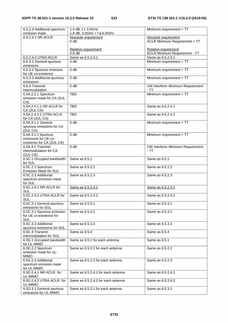
ETSI
ETSI TS 138 521-1 V15.2.0 (2019-05)5333GPP TS 38.521-1 version 15.2.0 Release 15
6.5.2.3 Additional spectrum emission mask
1.5 dB, f ≤ 3.0GHz 1.8 dB, 3.0GHz < f ≤ 6.0GHz
Minimum requirement + TT
6.5.2.4.1 NR ACLR Absolute requirement 0 dB Relative requirement 0.8 dB
Absolute requirement ACLR Minimum Requirement + TT Relative requirement ACLR Minimum Requirement - TT
6.5.2.4.2 UTRA ACLR Same as 6.5.2.4.1 Same as 6.5.2.4.1 6.5.3.1 General spurious emissions
0 dB Minimum requirement + TT
6.5.3.2 Spurious emission for UE co-existence
0 dB Minimum requirement + TT
6.5.3.3 Additional spurious emissions
0 dB Minimum requirement + TT
6.5.4 Transmit intermodulation
0 dB CW interferer Minimum Requirement - TT
6.5A.2.2.1 Spectrum emission mask for CA (2UL CA)
TBD Minimum requirement + TT
6.5A.2.4.1.1 NR ACLR for CA (2UL CA)
TBD Same as 6.5.2.4.1
6.5A.2.4.2.1 UTRA ACLR for CA (2UL CA)
TBD Same as 6.5.2.4.2
6.5A.3.1.1 General spurious emissions for CA (2UL CA)
0 dB Minimum requirement + TT
6.5A.3.2.1 Spurious emissions for UE co-existence for CA (2UL CA)
0 dB Minimum requirement + TT
6.5A.4.1 Transmit intermodulation for CA (2UL CA)
0 dB CW interferer Minimum Requirement - TT
6.5C.1 Occupied bandwidth for SUL
Same as 6.5.1 Same as 6.5.1
6.5C.2.2 Spectrum Emission Mask for SUL
Same as 6.5.2.2 Same as 6.5.2.2
6.5C.2.3 Additional spectrum emission mask for SUL
Same as 6.5.2.3 Same as 6.5.2.3
6.5C.2.4.1 NR ACLR for SUL
Same as 6.5.2.4.1 Same as 6.5.2.4.1
6.5C.2.4.2 UTRA ACLR for SUL
Same as 6.5.2.4.2 Same as 6.5.2.4.2
6.5C.3.1 General spurious emissions for SUL
Same as 6.5.3.1 Same as 6.5.3.1
6.5C.3.2 Spurious emission for UE co-existence for SUL
Same as 6.5.3.2 Same as 6.5.3.2
6.5C.3.3 Additional spurious emissions for SUL
Same as 6.5.3.3 Same as 6.5.3.3
6.5C.4 Transmit intermodulation for SUL
Same as 6.5.4 Same as 6.5.4
6.5D.1 Occupied bandwidth for UL-MIMO
Same as 6.5.1 for each antenna Same as 6.5.1
6.5D.2.2 Spectrum emission mask for UL-MIMO
Same as 6.5.2.2 for each antenna Same as 6.5.2.2
6.5D.2.3 Additional spectrum emission mask for UL-MIMO
Same as 6.5.2.3 for each antenna Same as 6.5.2.3
6.5D.2.4.1 NR ACLR for UL-MIMO
Same as 6.5.2.4.1 for each antenna Same as 6.5.2.4.1
6.5D.2.4.2 UTRA ACLR for UL-MIMO
Same as 6.5.2.4.2 for each antenna Same as 6.5.2.4.2
6.5D.3.1 General spurious emissions for UL-MIMO
Same as 6.5.3.1 for each antenna Same as 6.5.3.1

ETSI
ETSI TS 138 521-1 V15.2.0 (2019-05)5343GPP TS 38.521-1 version 15.2.0 Release 15
6.5D.3.2 Spurious emissions for UE co-existence for UL-MIMO
Same as 6.5.3.2 for each antenna Same as 6.5.3.2
6.5D.3.3 Additional spurious emissions for UL MIMO
Same as 6.5.3.3 for each antenna Same as 6.5.3.3
6.5D.4 Transmit intermodulation for UL-MIMO
Same as 6.5.4 for each antenna Same as 6.5.4
ETSI
ETSI TS 138 521-1 V15.2.0 (2019-05)5353GPP TS 38.521-1 version 15.2.0 Release 15
F.3.3 Measurement of receiver Table F.3.3-1: Derivation of Test Requirements (Receiver tests)
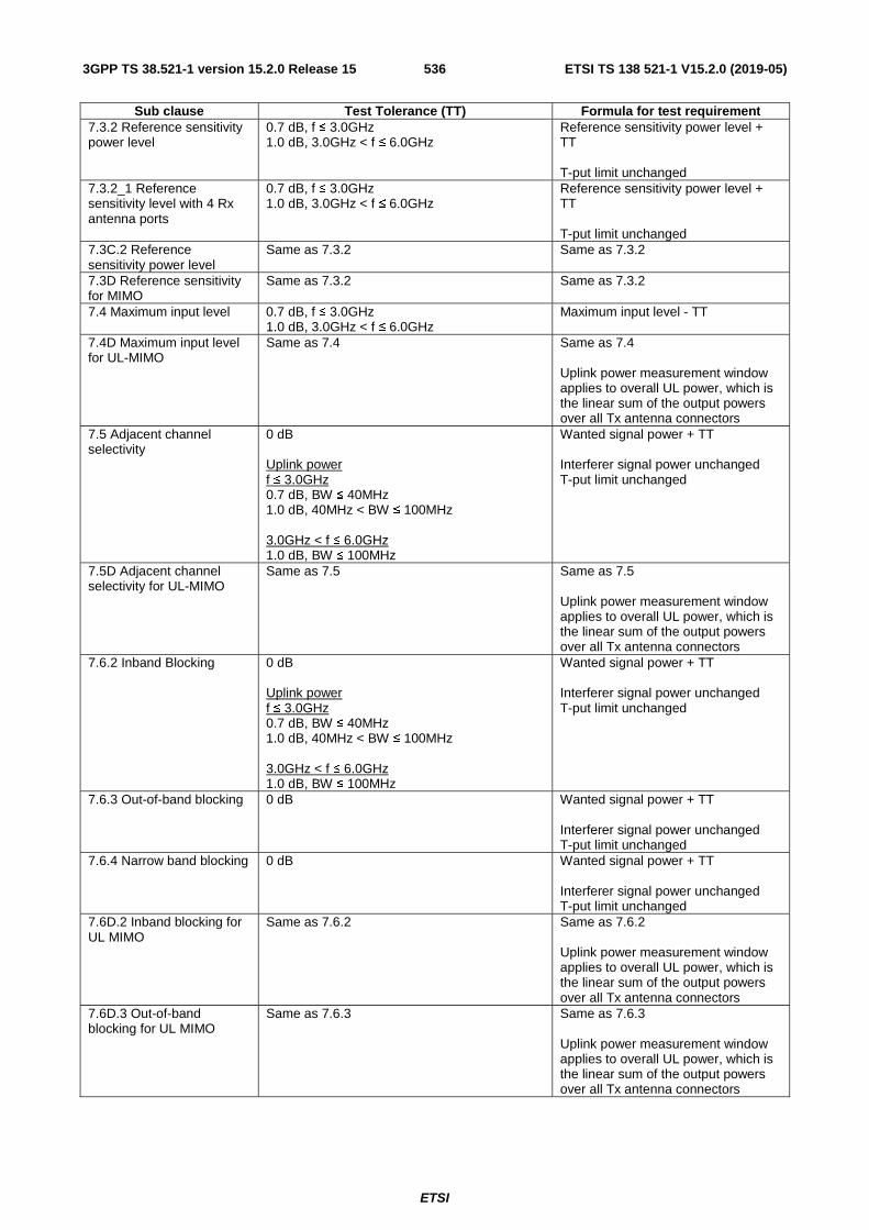
ETSI
ETSI TS 138 521-1 V15.2.0 (2019-05)5363GPP TS 38.521-1 version 15.2.0 Release 15
Sub clause Test Tolerance (TT) Formula for test requirement 7.3.2 Reference sensitivity power level
0.7 dB, f ≤ 3.0GHz 1.0 dB, 3.0GHz < f ≤ 6.0GHz
Reference sensitivity power level + TT T-put limit unchanged
7.3.2_1 Reference sensitivity level with 4 Rx antenna ports
0.7 dB, f ≤ 3.0GHz 1.0 dB, 3.0GHz < f ≤ 6.0GHz
Reference sensitivity power level + TT T-put limit unchanged
7.3C.2 Reference sensitivity power level
Same as 7.3.2 Same as 7.3.2
7.3D Reference sensitivity for MIMO
Same as 7.3.2 Same as 7.3.2
7.4 Maximum input level 0.7 dB, f ≤ 3.0GHz 1.0 dB, 3.0GHz < f ≤ 6.0GHz
Maximum input level - TT
7.4D Maximum input level for UL-MIMO
Same as 7.4 Same as 7.4 Uplink power measurement window applies to overall UL power, which is the linear sum of the output powers over all Tx antenna connectors
7.5 Adjacent channel selectivity
0 dB Uplink power f ≤ 3.0GHz 0.7 dB, BW ≤ 40MHz 1.0 dB, 40MHz < BW ≤ 100MHz 3.0GHz < f ≤ 6.0GHz 1.0 dB, BW ≤ 100MHz
Wanted signal power + TT Interferer signal power unchanged T-put limit unchanged
7.5D Adjacent channel selectivity for UL-MIMO
Same as 7.5 Same as 7.5 Uplink power measurement window applies to overall UL power, which is the linear sum of the output powers over all Tx antenna connectors
7.6.2 Inband Blocking 0 dB Uplink power f ≤ 3.0GHz 0.7 dB, BW ≤ 40MHz 1.0 dB, 40MHz < BW ≤ 100MHz 3.0GHz < f ≤ 6.0GHz 1.0 dB, BW ≤ 100MHz
Wanted signal power + TT Interferer signal power unchanged T-put limit unchanged
7.6.3 Out-of-band blocking 0 dB Wanted signal power + TT Interferer signal power unchanged T-put limit unchanged
7.6.4 Narrow band blocking 0 dB Wanted signal power + TT Interferer signal power unchanged T-put limit unchanged
7.6D.2 Inband blocking for UL MIMO
Same as 7.6.2 Same as 7.6.2 Uplink power measurement window applies to overall UL power, which is the linear sum of the output powers over all Tx antenna connectors
7.6D.3 Out-of-band blocking for UL MIMO
Same as 7.6.3 Same as 7.6.3 Uplink power measurement window applies to overall UL power, which is the linear sum of the output powers over all Tx antenna connectors
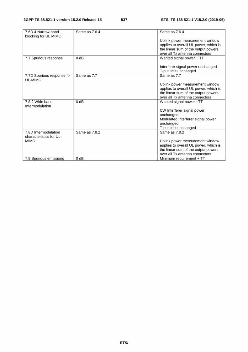
ETSI
ETSI TS 138 521-1 V15.2.0 (2019-05)5373GPP TS 38.521-1 version 15.2.0 Release 15
7.6D.4 Narrow-band blocking for UL MIMO
Same as 7.6.4 Same as 7.6.4 Uplink power measurement window applies to overall UL power, which is the linear sum of the output powers over all Tx antenna connectors
7.7 Spurious response 0 dB Wanted signal power + TT Interferer signal power unchanged T-put limit unchanged
7.7D Spurious response for UL-MIMO
Same as 7.7 Same as 7.7 Uplink power measurement window applies to overall UL power, which is the linear sum of the output powers over all Tx antenna connectors
7.8.2 Wide band Intermodulation
0 dB Wanted signal power +TT CW Interferer signal power unchanged Modulated Interferer signal power unchanged T-put limit unchanged
7.8D Intermodulation characteristics for UL-MIMO
Same as 7.8.2 Same as 7.8.2 Uplink power measurement window applies to overall UL power, which is the linear sum of the output powers over all Tx antenna connectors
7.9 Spurious emissions 0 dB Minimum requirement + TT

ETSI
ETSI TS 138 521-1 V15.2.0 (2019-05)5383GPP TS 38.521-1 version 15.2.0 Release 15
Annex G (normative): Uplink Physical Channels
G.0 Uplink Signal Levels Uplink signal power is a UE figure, which is configured by the Test System by means of:
RRC messages (IE-s), such as:
- PUSCH-PowerControl
- PUCCH-PowerControl
- RACH-ConfigGeneric
- SRS-Config
and L1/2 Power control commands (TPC).
The uplink power settings are specified in the test case.
Otherwise, the uplink power settings result from the default RRC messages described in 3GPP TS 38.508 [5], and appropriate TPC-s, which are sent to the UE to transmit with an UL power level necessary for maintaining the call during the test.
G.1 General This annex specifies the uplink physical channels that are needed for setting a connection and channels that are needed during a connection. Table G.1-1 describes the mapping of uplink physical channels and signals to physical resources

ETSI
ETSI TS 138 521-1 V15.2.0 (2019-05)5393GPP TS 38.521-1 version 15.2.0 Release 15
Table G.1-1: Mapping of uplink physical channels and signals to physical resources
Physical channel
Time Domain Location Frequency Domain Location Note
PRACH Allowed by the parameter prach-ConfigurationIndex provided by higher layers
Allowed by the parameter msg1-FrequencyStart provided by higher layers
Mapping rule is specified in TS 38.211 [8] Section 6.3.3
DMRS For DMRS on PUCCH format 1: Every other symbols i.e., 0, 2, 4... For DMRS on PUCCH format 2: All the PUCCH symbols For DMRS on PUCCH format 3,4: PUCCH length dependent For One symbol DMRS on PUSCH: Symbol 0 of each slot
DMRS on CP-OFDM PUSCH: Specified by the parameters dmrs-Type provided by higher layers. DMRS on DFT-OFDM PUSCH: Allowed for DMRS configuration type1 DMRS on PUCCH: PUCCH bandwidth dependent.
Mapping rule of DMRS for PUCCH is specified in TS 38.211 [8] Section 6.4.1.3 Mapping rule of DMRS for PUSCH is specified in TS 38.211 [8] Sections 6.4.1.1, 6.4.1.2
PUCCH For PUCCH Format 0: 1 ~ 2 symbols each slot, specified by the parameters of nrofSymbols and startingSymbolIndex in PUCCH-format0 provided by the higher layer. For PUCCH Format 1: 4 ~ 14 symbols each slot, specified by the parameters of nrofSymbols and those of startingSymbolIndex of PUCCH-format1 provided by the higher layer. For PUCCH Format 2, 1 ~ 2 symbols each slot, specified by the parameters of nrofSymbols and startingSymbolIndex in PUCCH-format2 provided by the higher layer. For PUCCH Format 3: 4 ~ 14 symbols each slot, allowed by the parameters of nrofSymbols and startingSymbolIndex in PUCCH-format3, provided by the higher layer. For PUCCH Format 4: 4 ~ 14 symbols each slot, specified by the parameters of nrofSymbols and startingSymbolIndex in PUCCH-format4, provided by higher layer.
For PUCCH Format 0, 1 1 RB, the position specified by the parameters of startingPRB and intraSlotFrequencyHopping in the corresponding PUCCH-Resource provided by the higher layer. For PUCCH Format 2, 3: 1~16 RBs, specified by the parameter of nrofPRBs in PUCCH-format2 and PUCCH-format3 respectively; additionally the position specified by the parameters of startingPRB and intraSlotFrequencyHopping in the corresponding PUCCH-Resource provided by the higher layer. For PUCCH Format 4 1 RB, the position specified by the parameters of startingPRB and intraSlotFrequencyHopping in the corresponding PUCCH-Resource provided by the higher layer
Mapping rule is specified in TS 38.211 [8] Section 6.3.2 and 38.213 [9] Section 9.2
PUSCH All remaining uplink symbols of each slot not allocated to DMRS
RBs allocated according to Reference Measurement channel in Annex A.2
Mapping rule is specified in TS 38.211 [8] Section 6.3 and 38.214 [12] Section 6.1
SRS 1, 2, or 4 symbols among the last 6 symbols in each SRS transmission slot specified by the parameters of resourceMapping, and resourceType in SRS-Config provided by the higher layer.
RBs specified by the ue-specific parameters of freqDomainPosition, freqDomainShift and freqHopping in SRS-Config provided by the higher layer.
Mapping rule is specified in TS 38.211 [8] Section 6.4.1.4.3
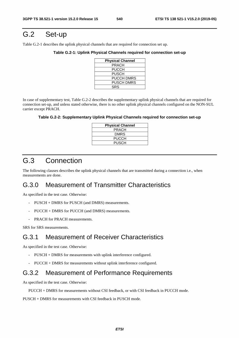
ETSI
ETSI TS 138 521-1 V15.2.0 (2019-05)5403GPP TS 38.521-1 version 15.2.0 Release 15
G.2 Set-up Table G.2-1 describes the uplink physical channels that are required for connection set up.
Table G.2-1: Uplink Physical Channels required for connection set-up
Physical Channel PRACH PUCCH PUSCH PUCCH DMRS PUSCH DMRS SRS
In case of supplementary test, Table G.2-2 describes the supplementary uplink physical channels that are required for connection set-up, and unless stated otherwise, there is no other uplink physical channels configured on the NON-SUL carrier except PRACH.
Table G.2-2: Supplementary Uplink Physical Channels required for connection set-up
Physical Channel PRACH DMRS
PUCCH PUSCH
G.3 Connection The following clauses describes the uplink physical channels that are transmitted during a connection i.e., when measurements are done.
G.3.0 Measurement of Transmitter Characteristics As specified in the test case. Otherwise:
- PUSCH + DMRS for PUSCH (and DMRS) measurements.
- PUCCH + DMRS for PUCCH (and DMRS) measurements.
- PRACH for PRACH measurements.
SRS for SRS measurements.
G.3.1 Measurement of Receiver Characteristics As specified in the test case. Otherwise:
- PUSCH + DMRS for measurements with uplink interference configured.
- PUCCH + DMRS for measurements without uplink interference configured.
G.3.2 Measurement of Performance Requirements As specified in the test case. Otherwise:
PUCCH + DMRS for measurements without CSI feedback, or with CSI feedback in PUCCH mode.
PUSCH + DMRS for measurements with CSI feedback in PUSCH mode.

ETSI
ETSI TS 138 521-1 V15.2.0 (2019-05)5413GPP TS 38.521-1 version 15.2.0 Release 15
Annex H (normative): Statistical Testing
H.1 General FFS.
H.2 Statistical testing of receiver characteristics
H.2.1 General The test of receiver characteristics is twofold.
1. A signal or a combination of signals is offered to the RX port(s) of the receiver.
2. The ability of the receiver to demodulate /decode this signal is verified by measuring the throughput.
In (2) is the statistical aspect of the test and is treated here.
The minimum requirement for all receiver tests is >95% of the maximum throughput.
All receiver tests are performed in static propagation conditions. No fading conditions are applied.
H.2.2 Mapping throughput to error ratio a) The measured information bit throughput R is defined as the sum (in kilobits) of the information bit payloads
successfully received during the test interval, divided by the duration of the test interval (in seconds).
b) In measurement practice the UE indicates successfully received information bit payload by signalling an ACK to the SS. If payload is received, but damaged and cannot be decoded, the UE signals a NACK.
c) Only the ACK and NACK signals, not the data bits received, are accessible to the SS. The number of bits is known in the SS from knowledge of what payload was sent.
d) For the reference measurement channel, applied for testing, the number of bits is different in different subframes, however in a radio frame it is fixed during one test.
e) The time in the measurement interval is composed of successfully received subframes (ACK), unsuccessfully received subframes (NACK) and no reception at all (DTX-subframes).
f) DTX-subframes may occur regularly according the applicable reference measurement channel (regDTX). In real live networks this is the time when other UEs are served. In TDD these are the UL and special subframes. regDTX vary from test to test but are fixed within the test.
g) Additional DTX-subframes occur statistically when the UE is not responding ACK or NACK where it should. (statDTX) This may happen when the UE was not expecting data or decided that the data were not intended for it.
The pass / fail decision is done by observing the:
- number of NACKs
- number of ACKs and
- number of statDTXs (regDTX is implicitly known to the SS)
The ratio (NACK + statDTX)/(NACK+ statDTX + ACK)is the Error Ratio (ER). Taking into account the time consumed by the ACK, NACK, and DTX-TTIs (regular and statistical), ER can be mapped unambiguously to throughput for any single reference measurement channel test.
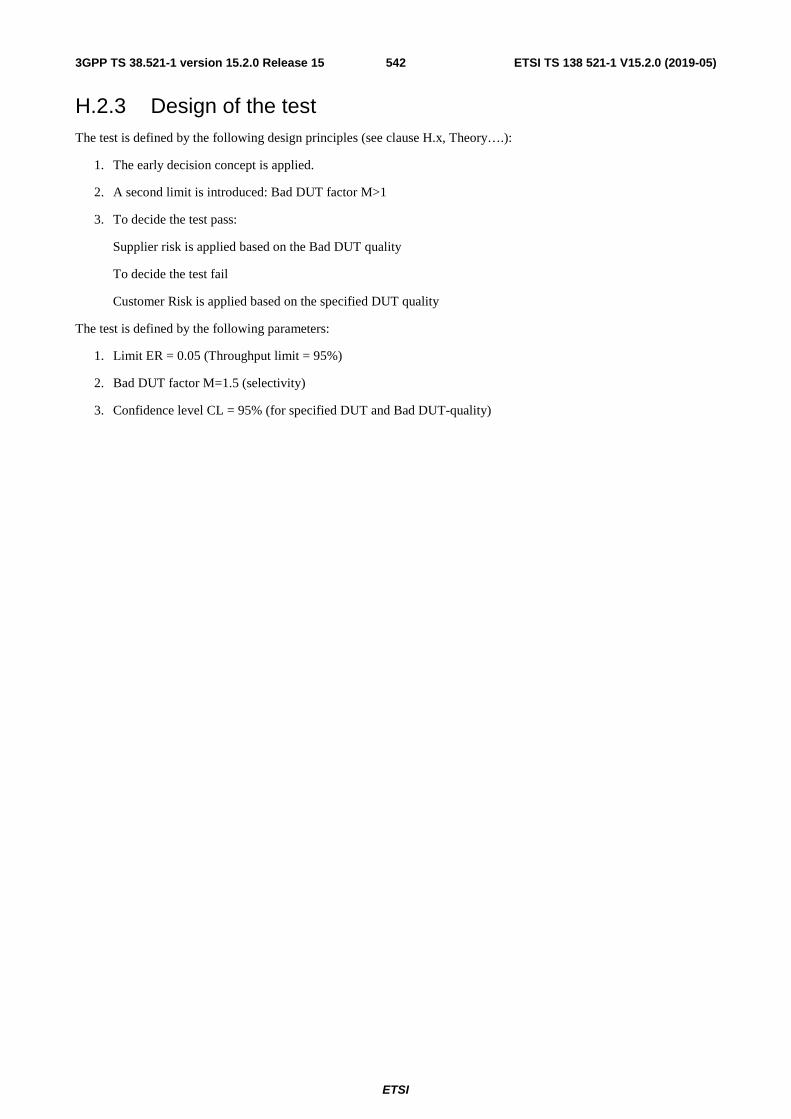
ETSI
ETSI TS 138 521-1 V15.2.0 (2019-05)5423GPP TS 38.521-1 version 15.2.0 Release 15
H.2.3 Design of the test The test is defined by the following design principles (see clause H.x, Theory….):
1. The early decision concept is applied.
2. A second limit is introduced: Bad DUT factor M>1
3. To decide the test pass:
Supplier risk is applied based on the Bad DUT quality
To decide the test fail
Customer Risk is applied based on the specified DUT quality
The test is defined by the following parameters:
1. Limit ER = 0.05 (Throughput limit = 95%)
2. Bad DUT factor M=1.5 (selectivity)
3. Confidence level CL = 95% (for specified DUT and Bad DUT-quality)

ETSI
ETSI TS 138 521-1 V15.2.0 (2019-05)5433GPP TS 38.521-1 version 15.2.0 Release 15
H.2.4 Numerical definition of the pass fail limits Table H.2.4-1: pass fail limits
ne nsp nsf ne nsp nsf ne nsp nsf ne nsp nsf
0 67 NA 39 763 500 78 1366 1148 117 1951 1828
1 95 NA 40 778 516 79 1381 1166 118 1965 1845
2 119 NA 41 794 532 80 1396 1183 119 1980 1863
3 141 NA 42 810 548 81 1412 1200 120 1995 1881
4 162 NA 43 826 564 82 1427 1217 121 2010 1899
5 183 NA 44 842 580 83 1442 1234 122 2025 1916
6 202 NA 45 858 596 84 1457 1252 123 2039 1934
7 222 NA 46 873 612 85 1472 1269 124 2054 1952
8 241 NA 47 889 629 86 1487 1286 125 2069 1969
9 259 NA 48 905 645 87 1502 1303 126 2084 1987
10 278 76 49 920 661 88 1517 1321 127 2099 2005
11 296 88 50 936 678 89 1532 1338 128 2113 2023
12 314 100 51 952 694 90 1547 1355 129 2128 2040
13 332 113 52 967 711 91 1562 1373 130 2143 2058
14 349 126 53 983 727 92 1577 1390 131 2158 2076
15 367 140 54 998 744 93 1592 1407 132 2172 2094
16 384 153 55 1014 760 94 1607 1425 133 2187 2111
17 401 167 56 1029 777 95 1623 1442 134 2202 2129
18 418 181 57 1045 793 96 1637 1459 135 2217 2147
19 435 195 58 1060 810 97 1652 1477 136 2231 2165
20 452 209 59 1076 827 98 1667 1494 137 2246 2183
21 469 224 60 1091 844 99 1682 1512 138 2261 2201
22 486 238 61 1106 860 100 1697 1529 139 2275 2218
23 503 253 62 1122 877 101 1712 1547 140 2290 2236
24 519 268 63 1137 894 102 1727 1564 141 2305 2254
25 536 283 64 1153 911 103 1742 1582 142 2320 2272
26 552 298 65 1168 928 104 1757 1599 143 2334 2290
27 569 313 66 1183 944 105 1772 1617 144 2349 2308
28 585 328 67 1199 961 106 1787 1634 145 2364 2326
29 602 343 68 1214 978 107 1802 1652 146 2378 2344
30 618 359 69 1229 995 108 1817 1669 147 2393 2361
31 634 374 70 1244 1012 109 1832 1687 148 2408 2379
32 650 389 71 1260 1029 110 1847 1704 149 2422 2397
33 667 405 72 1275 1046 111 1861 1722 150 2437 2415
34 683 421 73 1290 1063 112 1876 1740 151 2452 2433
35 699 436 74 1305 1080 113 1891 1757 152 2466 2451
36 715 452 75 1321 1097 114 1906 1775 153*) NA 2469
37 731 468 76 1336 1114 115 1921 1793
38 747 484 77 1351 1131 116 1936 1810 *) note 2 in H.2.5
NOTE 1: The first column is the number of errors (ne = number of NACK + statDTX)
NOTE 2: The second column is the number of samples for the pass limit (nsp, ns=Number of Samples= number of NACK + statDTX + ACK)
NOTE 3: The third column is the number of samples for the fail limit (nsf)

ETSI
ETSI TS 138 521-1 V15.2.0 (2019-05)5443GPP TS 38.521-1 version 15.2.0 Release 15
H.2.5 Pass fail decision rules The pass fail decision rules apply for a single test, comprising one component in the test vector. The overall Pass /Fail conditions are defined in clause H.2.6and H.2A.6
Having observed 0 errors, pass the test at 67+ samples, otherwise continue
Having observed 1 error, pass the test at 95+ otherwise continue
Having observed 2 errors, pass the test at 119+ samples, otherwise continue
Etc. etc.
Having observed 151 errors, pass the test at 2452+ samples, fail the test at 2433- samples, otherwise continue
Having observed 152 errors, pass the test at 2466+ samples, fail the test at 2451- samples.
Where x+ means: x or more, x- means x or less
NOTE 1: an ideal DUT passes after 67 samples. The maximum test time is 2466 samples.
NOTE 2: It is allowed to deviate from the early decision concept by postponing the decision (pass/fail or continue). Postponing the decision to or beyond the end of Table H.2.4-1 requires a pass fail decision against the test limit: pass the DUT for ER<0.0618, otherwise fail.

ETSI
ETSI TS 138 521-1 V15.2.0 (2019-05)5453GPP TS 38.521-1 version 15.2.0 Release 15
Annex I: Change history

ETSI
ETSI TS 138 521-1 V15.2.0 (2019-05)5463GPP TS 38.521-1 version 15.2.0 Release 15
Change history Date Meeting TDoc CR R
ev Cat Subject/Comment New
version
2017-08 RAN5#76 R5-175705 - - - Draft skeleton 0.0.1 2018-01 RAN5#1-
5G-NR Adhoc
R5-180068 R5-180069 R5-180070 R5-180071 R5-180072 R5-180073 R5-180075 R5-180076 R5-180077 R5-180078 R5-180079
- - - Implementation of pCRs to TS 38.521-1 V0.1.0 0.1.0
2018-01 RAN5#78 R5-181506 R5-181507 R5-181670 R5-181671 R5-181672 R5-181676 R5-181677 R5-181678 R5-181679 R5-181685 R5-181686 R5-181698 R5-181699 R5-181700
- - - Implementation of pCRs to TS 38.521-1 V0.2.0 0.2.0
2018-03 RAN5#2-5G-NR Adhoc
R5-181759 - - - Update TS 38.521-1 to align with new structure of TS 38.101-1 based on endorsed CR R4-1802403
0.3.0
2018-04 RAN5#2-5G-NR Adhoc
R5-81976 - - - 3GU mismatch 0.3.1
2018-04 RAN5#2-5G-NR Adhoc
R5-181771 R5-181833 R5-181842 R5-182000 R5-182002 R5-182003 R5-182004 R5-182005 R5-182020 R5-182021 R5-182026
- - - Implementation of pCRs to TS 38.521-1 V0.4.0 Add clause 4.4 Test point analysis
0.4.0
2018-07 RAN5#79 R5-182768 R5-182973 R5-183702 R5-183703 R5-183704 R5-183705 R5-183906 R5-183936 R5-183280 R5-183923 R5-183953 R5-183954 R5-183955 R5-183956 R5-183957 R5-183958 R5-183959 R5-183960
- - - Implementation of pCRs to TS 38.521-1 V0.5.0 0.5.0
2018-07 RAN5#79 R5-183960 R5-183279
- - - Corrected Table numbering issues in subclause 6.5.2.4.1.4.2 Test procedure to capture R5-183960 changes into draft TS 38.521-1 v0.5.1
0.5.1
2018-07 RAN5#79 R5-182363 - - - withdrawn 1.0.0
ETSI
ETSI TS 138 521-1 V15.2.0 (2019-05)5473GPP TS 38.521-1 version 15.2.0 Release 15
2018-08 RAN5#80 R5-185321 R5-184298 R5-185305 R5-185322 R5-185323 R5-185495 R5-185444 R5-185565 R5-185445 R5-185524 R5-184572 R5-185390 R5-184574 R5-185521 R5-185408 R5-184822 R5-185446 R5-185324 R5-185447 R5-185411 R5-185413 R5-185496 R5-185414 R5-185415 R5-185325 R5-185500 R5-185501 R5-185312 R5-185326 R5-185315 R5-185317 R5-185327 R5-185320
- - - Implementation of pCRs to TS 38.521-1 V1.0.1 1.0.1
2018-09 RAN#81 - - - - raised to v15.0.0 with editorial changes only 15.0.0 2018-12 RAN#82 R5-186604 0072 - F 5G_FR1 Text update for 7.3 Reference sensitivity 15.1.0 2018-12 RAN#82 R5-186605 0073 - F 5R_FR1 Text Update for 6.5.3.1_General spurious emissions 15.1.0 2018-12 RAN#82 R5-186606 0074 - F 5R FR1 Text Update for 6.5.3.2 Spurious emission for UE co-
existence 15.1.0
2018-12 RAN#82 R5-186670 0078 - F Updating test case 6.2.3 UE additional maximum output power reduction
15.1.0
2018-12 RAN#82 R5-186671 0079 - F Updating test case 6.5.2.3 Additional spectrum emission mask 15.1.0 2018-12 RAN#82 R5-186680 0080 - F Update of test case 6.5.2.4.2, UTRA ACLR in 38.521-1 15.1.0 2018-12 RAN#82 R5-186736 0084 - F Update of FR1 Transmit OFF power 15.1.0 2018-12 RAN#82 R5-186774 0088 - F Addition of 6.3D.1 Minimum output power for UL-MIMO 15.1.0 2018-12 RAN#82 R5-186776 0089 - F Addition of 6.3D.2 Transmit OFF power for UL-MIMO 15.1.0 2018-12 RAN#82 R5-186781 0090 - F Addition of 6.3D.3 Transmit ON/OFF time mask for UL-MIMO 15.1.0 2018-12 RAN#82 R5-186901 0091 - F Update SEM requirements to TS 38.101-1 v15.3.0 15.1.0 2018-12 RAN#82 R5-186902 0092 - F Update ACS and inband blocking test cases in TS 38.521-1 15.1.0 2018-12 RAN#82 R5-187034 0107 - F Adding edge allocation into common uplink configuration in 6.1 15.1.0 2018-12 RAN#82 R5-187038 0109 - F Update test points for multiple FR1 test cases 15.1.0 2018-12 RAN#82 R5-187149 0111 - F Updated to Annexes for FR1 tests 15.1.0 2018-12 RAN#82 R5-187150 0112 - F General clauses updated for TS38.521-1 15.1.0 2018-12 RAN#82 R5-187376 0120 - F Update of 6.2.1 MOP 15.1.0 2018-12 RAN#82 R5-187378 0122 - F Update of 6.3.1 Minimum Output Power 15.1.0 2018-12 RAN#82 R5-187379 0123 - F Update of 6.3.3.2 General ON/OFF time mask 15.1.0 2018-12 RAN#82 R5-187380 0124 - F Addition of 6.2D.1 MOP for MIMO 15.1.0 2018-12 RAN#82 R5-187381 0125 - F Addition of 6.2D.2 MPR for MIMO 15.1.0 2018-12 RAN#82 R5-187382 0126 - F Addition of 6.2D.4 Configured Output Power for MIMO 15.1.0 2018-12 RAN#82 R5-187383 0127 - F Addition of 6.4D.1 Frequency error for MIMO 15.1.0 2018-12 RAN#82 R5-187384 0128 - F Addition of 6.4D.2.1 EVM for MIMO 15.1.0 2018-12 RAN#82 R5-187385 0129 - F Addition of 6.4D.2.2 Carrier Leakage for MIMO 15.1.0 2018-12 RAN#82 R5-187386 0130 - F Addition of 6.4D.2.3 In-band emissions for MIMO 15.1.0 2018-12 RAN#82 R5-187387 0131 - F Addition of 6.4D.2.4 EVM equalizer spectrum flatness for MIMO 15.1.0 2018-12 RAN#82 R5-187395 0132 - F Update of test case 6.2.3 UE A-MPR, general 15.1.0 2018-12 RAN#82 R5-187397 0133 - F Update of test case 6.2.3 UE A-MPR, NS_04 15.1.0 2018-12 RAN#82 R5-187399 0134 - F Update of test case test case 6.5.2.3 Additional spectrum emission
mask, NS_04 15.1.0
2018-12 RAN#82 R5-187421 0136 - F Introduction of TC 6.5D.1 Occupied bandwidth for UL MIMO 15.1.0 2018-12 RAN#82 R5-187422 0137 - F Introduction of TC 6.5D.2.2 Spectrum Emission Mask for UL MIMO 15.1.0 2018-12 RAN#82 R5-187423 0138 - F Introduction of TC 6.5D.2.3 Additional Spectrum Emission Mask for
UL MIMO 15.1.0
2018-12 RAN#82 R5-187424 0139 - F Introduction of TC 6.5D.2.4.1 NR ACLR for UL MIMO 15.1.0 2018-12 RAN#82 R5-187425 0140 - F Introduction of TC 6.5D.2.4.2 UTRA ACLR for UL MIMO 15.1.0 2018-12 RAN#82 R5-187429 0144 - F Introduction of TC 6.5D.4 Transmit intermodulation for UL MIMO 15.1.0
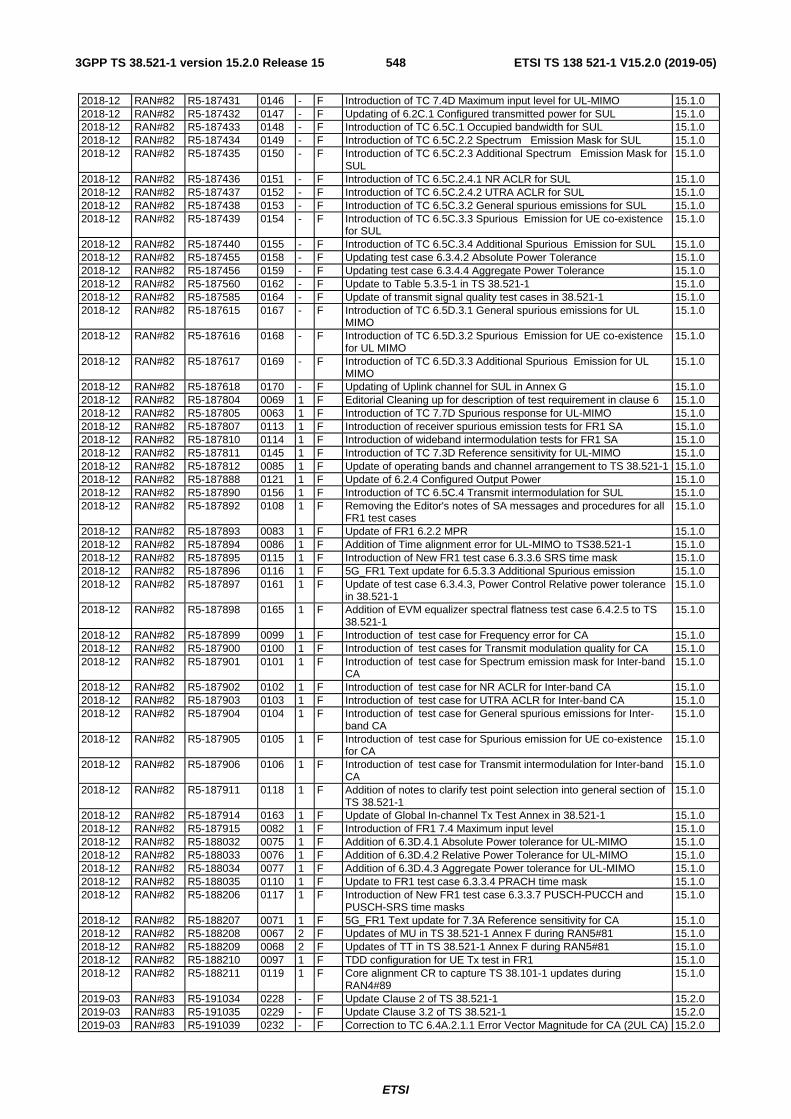
ETSI
ETSI TS 138 521-1 V15.2.0 (2019-05)5483GPP TS 38.521-1 version 15.2.0 Release 15
2018-12 RAN#82 R5-187431 0146 - F Introduction of TC 7.4D Maximum input level for UL-MIMO 15.1.0 2018-12 RAN#82 R5-187432 0147 - F Updating of 6.2C.1 Configured transmitted power for SUL 15.1.0 2018-12 RAN#82 R5-187433 0148 - F Introduction of TC 6.5C.1 Occupied bandwidth for SUL 15.1.0 2018-12 RAN#82 R5-187434 0149 - F Introduction of TC 6.5C.2.2 Spectrum Emission Mask for SUL 15.1.0 2018-12 RAN#82 R5-187435 0150 - F Introduction of TC 6.5C.2.3 Additional Spectrum Emission Mask for
SUL 15.1.0
2018-12 RAN#82 R5-187436 0151 - F Introduction of TC 6.5C.2.4.1 NR ACLR for SUL 15.1.0 2018-12 RAN#82 R5-187437 0152 - F Introduction of TC 6.5C.2.4.2 UTRA ACLR for SUL 15.1.0 2018-12 RAN#82 R5-187438 0153 - F Introduction of TC 6.5C.3.2 General spurious emissions for SUL 15.1.0 2018-12 RAN#82 R5-187439 0154 - F Introduction of TC 6.5C.3.3 Spurious Emission for UE co-existence
for SUL 15.1.0
2018-12 RAN#82 R5-187440 0155 - F Introduction of TC 6.5C.3.4 Additional Spurious Emission for SUL 15.1.0 2018-12 RAN#82 R5-187455 0158 - F Updating test case 6.3.4.2 Absolute Power Tolerance 15.1.0 2018-12 RAN#82 R5-187456 0159 - F Updating test case 6.3.4.4 Aggregate Power Tolerance 15.1.0 2018-12 RAN#82 R5-187560 0162 - F Update to Table 5.3.5-1 in TS 38.521-1 15.1.0 2018-12 RAN#82 R5-187585 0164 - F Update of transmit signal quality test cases in 38.521-1 15.1.0 2018-12 RAN#82 R5-187615 0167 - F Introduction of TC 6.5D.3.1 General spurious emissions for UL
MIMO 15.1.0
2018-12 RAN#82 R5-187616 0168 - F Introduction of TC 6.5D.3.2 Spurious Emission for UE co-existence for UL MIMO
15.1.0
2018-12 RAN#82 R5-187617 0169 - F Introduction of TC 6.5D.3.3 Additional Spurious Emission for UL MIMO
15.1.0
2018-12 RAN#82 R5-187618 0170 - F Updating of Uplink channel for SUL in Annex G 15.1.0 2018-12 RAN#82 R5-187804 0069 1 F Editorial Cleaning up for description of test requirement in clause 6 15.1.0 2018-12 RAN#82 R5-187805 0063 1 F Introduction of TC 7.7D Spurious response for UL-MIMO 15.1.0 2018-12 RAN#82 R5-187807 0113 1 F Introduction of receiver spurious emission tests for FR1 SA 15.1.0 2018-12 RAN#82 R5-187810 0114 1 F Introduction of wideband intermodulation tests for FR1 SA 15.1.0 2018-12 RAN#82 R5-187811 0145 1 F Introduction of TC 7.3D Reference sensitivity for UL-MIMO 15.1.0 2018-12 RAN#82 R5-187812 0085 1 F Update of operating bands and channel arrangement to TS 38.521-1 15.1.0 2018-12 RAN#82 R5-187888 0121 1 F Update of 6.2.4 Configured Output Power 15.1.0 2018-12 RAN#82 R5-187890 0156 1 F Introduction of TC 6.5C.4 Transmit intermodulation for SUL 15.1.0 2018-12 RAN#82 R5-187892 0108 1 F Removing the Editor's notes of SA messages and procedures for all
FR1 test cases 15.1.0
2018-12 RAN#82 R5-187893 0083 1 F Update of FR1 6.2.2 MPR 15.1.0 2018-12 RAN#82 R5-187894 0086 1 F Addition of Time alignment error for UL-MIMO to TS38.521-1 15.1.0 2018-12 RAN#82 R5-187895 0115 1 F Introduction of New FR1 test case 6.3.3.6 SRS time mask 15.1.0 2018-12 RAN#82 R5-187896 0116 1 F 5G_FR1 Text update for 6.5.3.3 Additional Spurious emission 15.1.0 2018-12 RAN#82 R5-187897 0161 1 F Update of test case 6.3.4.3, Power Control Relative power tolerance
in 38.521-1 15.1.0
2018-12 RAN#82 R5-187898 0165 1 F Addition of EVM equalizer spectral flatness test case 6.4.2.5 to TS 38.521-1
15.1.0
2018-12 RAN#82 R5-187899 0099 1 F Introduction of test case for Frequency error for CA 15.1.0 2018-12 RAN#82 R5-187900 0100 1 F Introduction of test cases for Transmit modulation quality for CA 15.1.0 2018-12 RAN#82 R5-187901 0101 1 F Introduction of test case for Spectrum emission mask for Inter-band
CA 15.1.0
2018-12 RAN#82 R5-187902 0102 1 F Introduction of test case for NR ACLR for Inter-band CA 15.1.0 2018-12 RAN#82 R5-187903 0103 1 F Introduction of test case for UTRA ACLR for Inter-band CA 15.1.0 2018-12 RAN#82 R5-187904 0104 1 F Introduction of test case for General spurious emissions for Inter-
band CA 15.1.0
2018-12 RAN#82 R5-187905 0105 1 F Introduction of test case for Spurious emission for UE co-existence for CA
15.1.0
2018-12 RAN#82 R5-187906 0106 1 F Introduction of test case for Transmit intermodulation for Inter-band CA
15.1.0
2018-12 RAN#82 R5-187911 0118 1 F Addition of notes to clarify test point selection into general section of TS 38.521-1
15.1.0
2018-12 RAN#82 R5-187914 0163 1 F Update of Global In-channel Tx Test Annex in 38.521-1 15.1.0 2018-12 RAN#82 R5-187915 0082 1 F Introduction of FR1 7.4 Maximum input level 15.1.0 2018-12 RAN#82 R5-188032 0075 1 F Addition of 6.3D.4.1 Absolute Power tolerance for UL-MIMO 15.1.0 2018-12 RAN#82 R5-188033 0076 1 F Addition of 6.3D.4.2 Relative Power Tolerance for UL-MIMO 15.1.0 2018-12 RAN#82 R5-188034 0077 1 F Addition of 6.3D.4.3 Aggregate Power tolerance for UL-MIMO 15.1.0 2018-12 RAN#82 R5-188035 0110 1 F Update to FR1 test case 6.3.3.4 PRACH time mask 15.1.0 2018-12 RAN#82 R5-188206 0117 1 F Introduction of New FR1 test case 6.3.3.7 PUSCH-PUCCH and
PUSCH-SRS time masks 15.1.0
2018-12 RAN#82 R5-188207 0071 1 F 5G_FR1 Text update for 7.3A Reference sensitivity for CA 15.1.0 2018-12 RAN#82 R5-188208 0067 2 F Updates of MU in TS 38.521-1 Annex F during RAN5#81 15.1.0 2018-12 RAN#82 R5-188209 0068 2 F Updates of TT in TS 38.521-1 Annex F during RAN5#81 15.1.0 2018-12 RAN#82 R5-188210 0097 1 F TDD configuration for UE Tx test in FR1 15.1.0 2018-12 RAN#82 R5-188211 0119 1 F Core alignment CR to capture TS 38.101-1 updates during
RAN4#89 15.1.0
2019-03 RAN#83 R5-191034 0228 - F Update Clause 2 of TS 38.521-1 15.2.0 2019-03 RAN#83 R5-191035 0229 - F Update Clause 3.2 of TS 38.521-1 15.2.0 2019-03 RAN#83 R5-191039 0232 - F Correction to TC 6.4A.2.1.1 Error Vector Magnitude for CA (2UL CA) 15.2.0
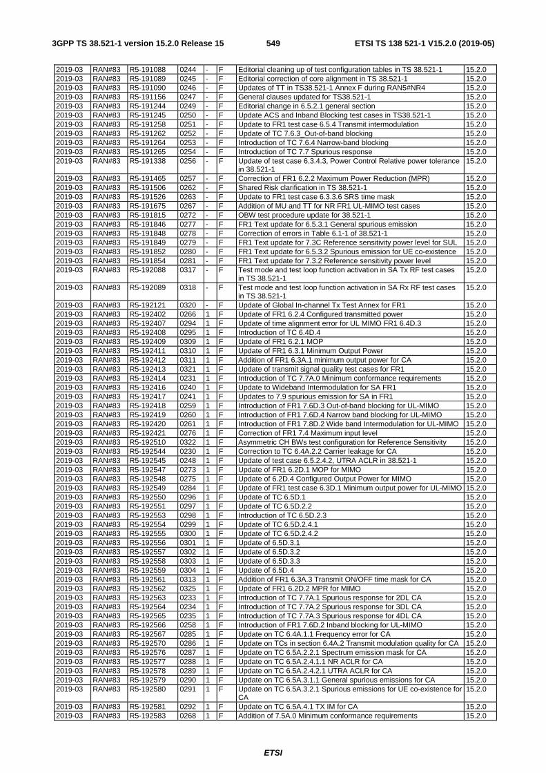
ETSI
ETSI TS 138 521-1 V15.2.0 (2019-05)5493GPP TS 38.521-1 version 15.2.0 Release 15
2019-03 RAN#83 R5-191088 0244 - F Editorial cleaning up of test configuration tables in TS 38.521-1 15.2.0 2019-03 RAN#83 R5-191089 0245 - F Editorial correction of core alignment in TS 38.521-1 15.2.0 2019-03 RAN#83 R5-191090 0246 - F Updates of TT in TS38.521-1 Annex F during RAN5#NR4 15.2.0 2019-03 RAN#83 R5-191156 0247 - F General clauses updated for TS38.521-1 15.2.0 2019-03 RAN#83 R5-191244 0249 - F Editorial change in 6.5.2.1 general section 15.2.0 2019-03 RAN#83 R5-191245 0250 - F Update ACS and Inband Blocking test cases in TS38.521-1 15.2.0 2019-03 RAN#83 R5-191258 0251 - F Update to FR1 test case 6.5.4 Transmit intermodulation 15.2.0 2019-03 RAN#83 R5-191262 0252 - F Update of TC 7.6.3_Out-of-band blocking 15.2.0 2019-03 RAN#83 R5-191264 0253 - F Introduction of TC 7.6.4 Narrow-band blocking 15.2.0 2019-03 RAN#83 R5-191265 0254 - F Introduction of TC 7.7 Spurious response 15.2.0 2019-03 RAN#83 R5-191338 0256 - F Update of test case 6.3.4.3, Power Control Relative power tolerance
in 38.521-1 15.2.0
2019-03 RAN#83 R5-191465 0257 - F Correction of FR1 6.2.2 Maximum Power Reduction (MPR) 15.2.0 2019-03 RAN#83 R5-191506 0262 - F Shared Risk clarification in TS 38.521-1 15.2.0 2019-03 RAN#83 R5-191526 0263 - F Update to FR1 test case 6.3.3.6 SRS time mask 15.2.0 2019-03 RAN#83 R5-191675 0267 - F Addition of MU and TT for NR FR1 UL-MIMO test cases 15.2.0 2019-03 RAN#83 R5-191815 0272 - F OBW test procedure update for 38.521-1 15.2.0 2019-03 RAN#83 R5-191846 0277 - F FR1 Text update for 6.5.3.1 General spurious emission 15.2.0 2019-03 RAN#83 R5-191848 0278 - F Correction of errors in Table 6.1-1 of 38.521-1 15.2.0 2019-03 RAN#83 R5-191849 0279 - F FR1 Text update for 7.3C Reference sensitivity power level for SUL 15.2.0 2019-03 RAN#83 R5-191852 0280 - F FR1 Text update for 6.5.3.2 Spurious emission for UE co-existence 15.2.0 2019-03 RAN#83 R5-191854 0281 - F FR1 Text update for 7.3.2 Reference sensitivity power level 15.2.0 2019-03 RAN#83 R5-192088 0317 - F Test mode and test loop function activation in SA Tx RF test cases
in TS 38.521-1 15.2.0
2019-03 RAN#83 R5-192089 0318 - F Test mode and test loop function activation in SA Rx RF test cases in TS 38.521-1
15.2.0
2019-03 RAN#83 R5-192121 0320 - F Update of Global In-channel Tx Test Annex for FR1 15.2.0 2019-03 RAN#83 R5-192402 0266 1 F Update of FR1 6.2.4 Configured transmitted power 15.2.0 2019-03 RAN#83 R5-192407 0294 1 F Update of time alignment error for UL MIMO FR1 6.4D.3 15.2.0 2019-03 RAN#83 R5-192408 0295 1 F Introduction of TC 6.4D.4 15.2.0 2019-03 RAN#83 R5-192409 0309 1 F Update of FR1 6.2.1 MOP 15.2.0 2019-03 RAN#83 R5-192411 0310 1 F Update of FR1 6.3.1 Minimum Output Power 15.2.0 2019-03 RAN#83 R5-192412 0311 1 F Addition of FR1 6.3A.1 minimum output power for CA 15.2.0 2019-03 RAN#83 R5-192413 0321 1 F Update of transmit signal quality test cases for FR1 15.2.0 2019-03 RAN#83 R5-192414 0231 1 F Introduction of TC 7.7A.0 Minimum conformance requirements 15.2.0 2019-03 RAN#83 R5-192416 0240 1 F Update to Wideband Intermodulation for SA FR1 15.2.0 2019-03 RAN#83 R5-192417 0241 1 F Updates to 7.9 spurious emission for SA in FR1 15.2.0 2019-03 RAN#83 R5-192418 0259 1 F Introduction of FR1 7.6D.3 Out-of-band blocking for UL-MIMO 15.2.0 2019-03 RAN#83 R5-192419 0260 1 F Introduction of FR1 7.6D.4 Narrow band blocking for UL-MIMO 15.2.0 2019-03 RAN#83 R5-192420 0261 1 F Introduction of FR1 7.8D.2 Wide band Intermodulation for UL-MIMO 15.2.0 2019-03 RAN#83 R5-192421 0276 1 F Correction of FR1 7.4 Maximum input level 15.2.0 2019-03 RAN#83 R5-192510 0322 1 F Asymmetric CH BWs test configuration for Reference Sensitivity 15.2.0 2019-03 RAN#83 R5-192544 0230 1 F Correction to TC 6.4A.2.2 Carrier leakage for CA 15.2.0 2019-03 RAN#83 R5-192545 0248 1 F Update of test case 6.5.2.4.2, UTRA ACLR in 38.521-1 15.2.0 2019-03 RAN#83 R5-192547 0273 1 F Update of FR1 6.2D.1 MOP for MIMO 15.2.0 2019-03 RAN#83 R5-192548 0275 1 F Update of 6.2D.4 Configured Output Power for MIMO 15.2.0 2019-03 RAN#83 R5-192549 0284 1 F Update of FR1 test case 6.3D.1 Minimum output power for UL-MIMO 15.2.0 2019-03 RAN#83 R5-192550 0296 1 F Update of TC 6.5D.1 15.2.0 2019-03 RAN#83 R5-192551 0297 1 F Update of TC 6.5D.2.2 15.2.0 2019-03 RAN#83 R5-192553 0298 1 F Introduction of TC 6.5D.2.3 15.2.0 2019-03 RAN#83 R5-192554 0299 1 F Update of TC 6.5D.2.4.1 15.2.0 2019-03 RAN#83 R5-192555 0300 1 F Update of TC 6.5D.2.4.2 15.2.0 2019-03 RAN#83 R5-192556 0301 1 F Update of 6.5D.3.1 15.2.0 2019-03 RAN#83 R5-192557 0302 1 F Update of 6.5D.3.2 15.2.0 2019-03 RAN#83 R5-192558 0303 1 F Update of 6.5D.3.3 15.2.0 2019-03 RAN#83 R5-192559 0304 1 F Update of 6.5D.4 15.2.0 2019-03 RAN#83 R5-192561 0313 1 F Addition of FR1 6.3A.3 Transmit ON/OFF time mask for CA 15.2.0 2019-03 RAN#83 R5-192562 0325 1 F Update of FR1 6.2D.2 MPR for MIMO 15.2.0 2019-03 RAN#83 R5-192563 0233 1 F Introduction of TC 7.7A.1 Spurious response for 2DL CA 15.2.0 2019-03 RAN#83 R5-192564 0234 1 F Introduction of TC 7.7A.2 Spurious response for 3DL CA 15.2.0 2019-03 RAN#83 R5-192565 0235 1 F Introduction of TC 7.7A.3 Spurious response for 4DL CA 15.2.0 2019-03 RAN#83 R5-192566 0258 1 F Introduction of FR1 7.6D.2 Inband blocking for UL-MIMO 15.2.0 2019-03 RAN#83 R5-192567 0285 1 F Update on TC 6.4A.1.1 Frequency error for CA 15.2.0 2019-03 RAN#83 R5-192570 0286 1 F Update on TCs in section 6.4A.2 Transmit modulation quality for CA 15.2.0 2019-03 RAN#83 R5-192576 0287 1 F Update on TC 6.5A.2.2.1 Spectrum emission mask for CA 15.2.0 2019-03 RAN#83 R5-192577 0288 1 F Update on TC 6.5A.2.4.1.1 NR ACLR for CA 15.2.0 2019-03 RAN#83 R5-192578 0289 1 F Update on TC 6.5A.2.4.2.1 UTRA ACLR for CA 15.2.0 2019-03 RAN#83 R5-192579 0290 1 F Update on TC 6.5A.3.1.1 General spurious emissions for CA 15.2.0 2019-03 RAN#83 R5-192580 0291 1 F Update on TC 6.5A.3.2.1 Spurious emissions for UE co-existence for
CA 15.2.0
2019-03 RAN#83 R5-192581 0292 1 F Update on TC 6.5A.4.1 TX IM for CA 15.2.0 2019-03 RAN#83 R5-192583 0268 1 F Addition of 7.5A.0 Minimum conformance requirements 15.2.0
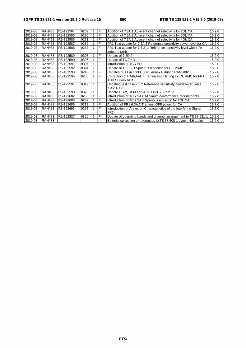
ETSI
ETSI TS 138 521-1 V15.2.0 (2019-05)5503GPP TS 38.521-1 version 15.2.0 Release 15
2019-03 RAN#83 R5-192584 0269 1 F Addition of 7.5A.1 Adjacent channel selectivity for 2DL CA 15.2.0 2019-03 RAN#83 R5-192585 0270 1 F Addition of 7.5A.2 Adjacent channel selectivity for 3DL CA 15.2.0 2019-03 RAN#83 R5-192586 0271 1 F Addition of 7.5A.3 Adjacent channel selectivity for 4DL CA 15.2.0 2019-03 RAN#83 R5-192587 0282 1 F FR1 Text update for 7.3A.2 Reference sensitivity power level for CA 15.2.0 2019-03 RAN#83 R5-192588 0283 1 F FR1 Text update for 7.3.2_1 Reference sensitivity level with 4 Rx
antenna ports 15.2.0
2019-03 RAN#83 R5-192589 0305 1 F Update of 7.3D.2 15.2.0 2019-03 RAN#83 R5-192590 0306 1 F Update of TC 7.4D 15.2.0 2019-03 RAN#83 R5-192591 0307 1 F Introduction of TC 7.5D 15.2.0 2019-03 RAN#83 R5-192592 0324 1 F Update of TC 7.7D Spurious response for UL-MIMO 15.2.0 2019-03 RAN#83 R5-192593 0243 1 F Updates of TT in TS38.521-1 Annex F during RAN5#82 15.2.0 2019-03 RAN#83 R5-192594 0265 1 F Correction of HARQ-ACK transmission timing for DL RMC for FR1
TDD SCS=60kHz 15.2.0
2019-03 RAN#83 R5-192597 0319 1 F Updating test case 7.3.2 Reference sensitivity power level Table 7.3.2.4.1-3
15.2.0
2019-03 RAN#83 R5-192598 0323 1 F Update OBW, SEM and ACLR in TS 38.521-1 15.2.0 2019-03 RAN#83 R5-192682 0236 1 F Introduction of TC 7.9A.0 Minimum conformance requirements 15.2.0 2019-03 RAN#83 R5-192683 0237 1 F Introduction of TC 7.9A.1 Spurious emission for 2DL CA 15.2.0 2019-03 RAN#83 R5-192685 0312 2 F Addition of FR1 6.3A.2 Transmit OFF power for CA 15.2.0 2019-03 RAN#83 R5-192693 0293 1 F Introduction of Annex on Characteristics of the Interfering Signal
FR1 15.2.0
2019-03 RAN#83 R5-192837 0326 1 F Update of operating bands and channel arrangement to TS 38.521-1 15.2.0 2019-03 RAN#83 - - - - Editorial correction of references to TS 38.508-1 clause 4.6 tables 15.2.0

ETSI
ETSI TS 138 521-1 V15.2.0 (2019-05)5513GPP TS 38.521-1 version 15.2.0 Release 15
History
Document history
V15.0.0 October 2018 Publication
V15.1.0 April 2019 Publication
V15.2.0 May 2019 Publication
Top Related