


Languages
Pages
Legal


Toward a Methodology for Manufacturability-Driven Design Rule Exploration
Toward a Methodology for Manufacturability-Driven Design Rule Exploration
Luigi Capodieci, Puneet Gupta, Andrew B. Luigi Capodieci, Puneet Gupta, Andrew B. Kahng, Kahng,
Dennis Sylvester, and Dennis Sylvester, and Jie YangJie Yang
Univ. of Michigan, Ann ArborUniv. of Michigan, Ann ArborUniv. of California, San DiegoUniv. of California, San Diego
Advanced Micro DevicesAdvanced Micro Devices

OutlineOutline
IntroductionIntroduction Motivation of the restrictive design ruleMotivation of the restrictive design rule
(RDR) approach(RDR) approach RDR embedded design flowRDR embedded design flow Evaluation metrics Evaluation metrics Experimental resultsExperimental results Conclusions and future workConclusions and future work

IntroductionIntroduction
Projected gate CD control in sub-wavelength Projected gate CD control in sub-wavelength lithography regime (ITRS 2003)lithography regime (ITRS 2003)
YearYear 20012001 20042004 20072007 20092009
Technology nodeTechnology nodeMPU gate length (nm)MPU gate length (nm)Gate CD control (3Gate CD control (3σσ) )
(nm)(nm)
130n130nmm90905.35.3
90nm90nm5353
3.753.75
65nm65nm35352.5
50nm50nm28282
MPU pitch (nm)MPU pitch (nm)Wavelength (λ) (nm)Wavelength (λ) (nm)
300300248248
180180193193
130130193193
100100157 (?)157 (?)
– Manufacturable solutions are not known foritalicized numbers
– Intel may not use 157nm at 50nm technology node

Introduction (Cont.)Introduction (Cont.)
Trends in Mask CostTrends in Mask Cost– Mask data preparation is a serious bottleneck due toMask data preparation is a serious bottleneck due to
the heavily applied RETthe heavily applied RET Figure count explodes as dimensions shrinkFigure count explodes as dimensions shrink Data volume for a single mask layer can approach Data volume for a single mask layer can approach
200GB200GB
180nm 130nm 90nm 70nm0
50
100
150
200
250
300
350
ME
BE
S D
ata
Vo
lum
e (G
B)
MEBES File Size for One Critical Layer vs. Technology Node

Introduction (Cont.)Introduction (Cont.)
Trends in Mask Cost (Cont.)Trends in Mask Cost (Cont.)– Mask writing time increases from a few days to over a Mask writing time increases from a few days to over a
monthmonth– Mask set cost increases at an accelerated rate with RET Mask set cost increases at an accelerated rate with RET
application as the primary driverapplication as the primary driver– ASIC users turn to FPGAs due to high mask cost on low ASIC users turn to FPGAs due to high mask cost on low
volume designsvolume designs
Writing-Optical or e-beam
Defect Inspection
Defect Repair
Data Prep.-OPC conversion/e-beam file
Materials
Others
0 10 20 30 40
Weight in Mask Cost (%)

OutlineOutline
IntroductionIntroduction Motivation of the restrictive design ruleMotivation of the restrictive design rule
(RDR) approach(RDR) approach RDR embedded design flowRDR embedded design flow Evaluation metrics Evaluation metrics Experimental resultsExperimental results Conclusions and future workConclusions and future work

Motivation of RDRMotivation of RDR
RETs need to become part of a cohesive RETs need to become part of a cohesive design flow in which libraries and layouts are design flow in which libraries and layouts are optimized directly based on conflicts optimized directly based on conflicts discovered by the RET tool, no longer a post-discovered by the RET tool, no longer a post-layout procedurelayout procedure
More conservative design rules or restricted More conservative design rules or restricted design rules (RDRs) seek to push the design rules (RDRs) seek to push the manufacturability and performance tradeoff manufacturability and performance tradeoff more in favor of the manufacturing sidemore in favor of the manufacturing side
Apply RDR within ASIC design methodologyApply RDR within ASIC design methodology

OutlineOutline
IntroductionIntroduction Motivation of the restrictive design ruleMotivation of the restrictive design rule
(RDR) approach(RDR) approach RDR embedded design flowRDR embedded design flow Evaluation metrics Evaluation metrics Experimental resultsExperimental results Conclusions and future workConclusions and future work

RDR Embedded Design FlowRDR Embedded Design Flow
Totally “Free”Design Rules
GDSII for Cells
.lib Files Associated WithDifferent Design Rule Set
Cap Extraction+ HSPICE Simulation
GDSII for Testbench
Standard P&R
More RestrictedDesign Rules
OPC Recipe
Std cellsNetlist
Auto LayoutGeneration
Electrical Performance (Area, Power, Delay)vs. Restrictive Design Rules, in
Manufacturability & Reliability (EPE, Ave.CD) and Mask Cost (MEBES Data Volume)
OPC Correction andMask Data Preparation

RDR CandidatesRDR Candidates
Bentgate “on” as Bentgate “on” as baselinebaseline (1) (1)– Bentgate line width (5)Bentgate line width (5)
Bentgate “off”Bentgate “off”– Poly to poly spacing (2)Poly to poly spacing (2)– Poly to diffusion spacing (3)Poly to diffusion spacing (3)– Poly end extension (4)Poly end extension (4)
(3)
(2)
(4)(5)(1)

Value Ranges of RDRValue Ranges of RDR
Rule name Default (μm) Modifiled (μm) Bentgate “off” “on”, baseline “on” Line width 0.12 0.12 (bentgate) 0.14 (bent_w14) Poly_poly space 0.20 (sp_20) 0.24 (sp_24) 0.28 (sp_28) Poly_diffusion space 0.08 0.10 (pdsp_10) 0.12 (pdsp_12) Poly end extension 0.28 0.34 (povg_34) 0.40 (povg_40)
The parentheses contain the corresponding labels in all figures
Use IBM 0.13Use IBM 0.13μμm technology as “default”m technology as “default” GuidelineGuideline
– Start from the most “free” design rule set, i.e., for best Start from the most “free” design rule set, i.e., for best performance in delay & area – “bentgate on” as performance in delay & area – “bentgate on” as baselinebaseline
– Create more conservative design rules Create more conservative design rules Only one rule differs from “Default” rule setOnly one rule differs from “Default” rule set Moving to more conservative direction,Moving to more conservative direction,
e.g. increasing poly to poly spacing, line width, etc.e.g. increasing poly to poly spacing, line width, etc.

Value Ranges of RDR (Cont.)Value Ranges of RDR (Cont.)
We use edge placement errors (EPEs) as a We use edge placement errors (EPEs) as a quantifying metric to determine value rangequantifying metric to determine value range– Measure how closely a printed feature actually reflects Measure how closely a printed feature actually reflects
the corresponding designed featurethe corresponding designed feature– Defined as the distance between the edges of printed Defined as the distance between the edges of printed
image and drawn feature (positive value indicates image and drawn feature (positive value indicates printed image outside of drawn feature boundary while printed image outside of drawn feature boundary while negative value indicates it’s inside)negative value indicates it’s inside)
EPE>0 EPE<0EPE>0 EPE<0EPE>0 EPE<0
(a) (b)
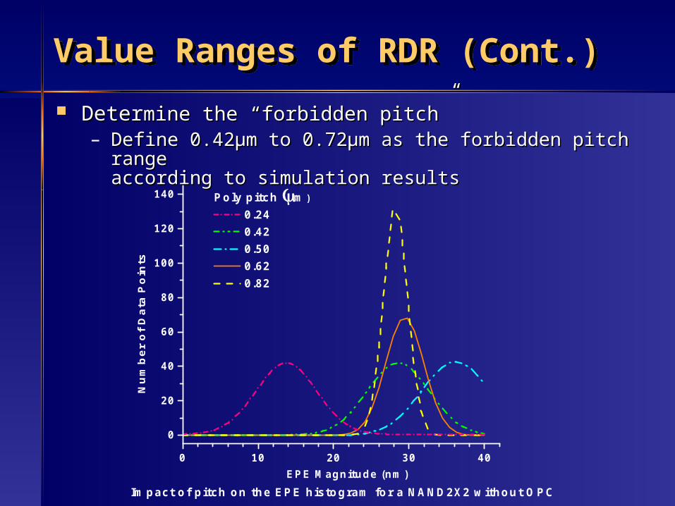
Value Ranges of RDR (Cont.)Value Ranges of RDR (Cont.)
DeterDetermine the “forbidden pitch”mine the “forbidden pitch”– Define 0.42Define 0.42μμm to 0.72m to 0.72μμm as the forbidden pitch rangem as the forbidden pitch range
according to simulation resultsaccording to simulation results
0 10 20 30 40
0
20
40
60
80
100
120
140 Poly pitch m)
0.24 0.42 0.50 0.62 0.82
Nu
mb
er o
f D
ata
Po
ints
EPE Magnitude (nm)
Impact of pitch on the EPE histogram for a NAND2X2 without OPC

OutlineOutline
IntroductionIntroduction Motivation of the restrictive design ruleMotivation of the restrictive design rule
(RDR) approach(RDR) approach RDR embedded design flowRDR embedded design flow Evaluation metricsEvaluation metrics Experimental resultsExperimental results Conclusions and future workConclusions and future work

Evaluation MetricsEvaluation Metrics
For manufacturability: EPE and average CDFor manufacturability: EPE and average CD– EPEs to measure the effectiveness of OPCEPEs to measure the effectiveness of OPC
Goal is to achieve a tight EPE distribution with mean around zeroGoal is to achieve a tight EPE distribution with mean around zero– Using average CD to compensate for the limitation of EPEUsing average CD to compensate for the limitation of EPE
The EPE distributions can not correctly reflect CDThe EPE distributions can not correctly reflect CD Use average gate-length calculated from a printed non-uniform Use average gate-length calculated from a printed non-uniform
gate area for further evaluationgate area for further evaluation
For OPC cost: MEBES data volumeFor OPC cost: MEBES data volume– MEBES is the standard mask writer formatMEBES is the standard mask writer format
The explosion of MEBES data volume due to RETs has made The explosion of MEBES data volume due to RETs has made mask data preparation a serious bottleneck. mask data preparation a serious bottleneck.
It shows the complexity of OPC layer and reflects the mask costIt shows the complexity of OPC layer and reflects the mask cost
Mask
OPC Fracture

OutlineOutline
IntroductionIntroduction Motivation of the restrictive design rule (RDR) Motivation of the restrictive design rule (RDR)
approachapproach RDR embedded design flowRDR embedded design flow Evaluation metrics Evaluation metrics Experimental resultsExperimental results Conclusions and future workConclusions and future work
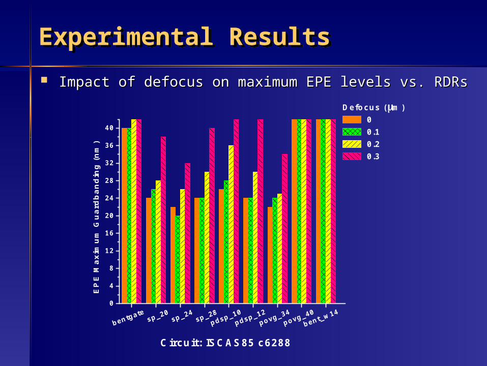
Experimental ResultsExperimental Results
Impact of defocus on maximum EPE levels vs. RDRsImpact of defocus on maximum EPE levels vs. RDRs
0
4
8
12
16
20
24
28
32
36
40
Defocus (m) 0 0.1 0.2 0.3
EP
E M
axim
um
Gu
ard
ban
din
g (
nm
)
Circuit: ISCAS85 c6288

Experimental ResultsExperimental Results
Impact of defocus on CD distribution (circuit: c7552)Impact of defocus on CD distribution (circuit: c7552)
DefocusDefocus00 0.1 (µm)0.1 (µm) 0.2 (µm)0.2 (µm) 0.3 (µm)0.3 (µm)
RDRRDR MeanMean σσ MeanMean σσ MeanMean σσ MeanMean σσ
sp_20sp_20 147.147.22
7.77.799
140.2140.2 7.97.988
138.138.33
8.08.088
136.2136.2 7.97.999
sp_24sp_24 147.147.00
7.77.799
141.0141.0 7.97.911
138.138.11
7.97.944
136.1136.1 9.59.544
sp_28sp_28 146.146.77
7.97.977
139.8139.8 7.87.844
137.137.77
7.57.544
134.8134.8 8.68.677
pdsp_10pdsp_10 147.147.11
8.28.233
140.3140.3 8.18.166
138.138.22
8.38.366
135.8135.8 9.09.033
pdsp_12pdsp_12 147.147.11
8.48.488
141.2141.2 8.28.233
137.137.99
8.48.444
135.5135.5 8.58.555
povg_34povg_34 140.140.22
8.28.277
138.9138.9 8.18.133
138.138.88
8.98.900
135.1135.1 9.19.100
povg_40povg_40 140.140.55
9.59.588
142.5142.5 9.29.255
139.139.22
9.09.033
136.4136.4 33.33.77
bentgatbentgatee
146.146.99
8.08.055
139.1139.1 7.67.600
135.135.77
7.47.411
132.6132.6 7.97.977
bent_w1bent_w144
147.147.00
7.87.800
139.3139.3 7.37.366
135.135.44
7.17.133
132.9132.9 7.07.088

Experimental ResultsExperimental Results
Impact of defocus on functional yield for a fixed 10% LImpact of defocus on functional yield for a fixed 10% Lgate gate
variation (circuit: c7552)variation (circuit: c7552)
66
68
70
72
74
76
78
80
82
84
86
88
90
92
94
96Y
ield
fo
r a
fixe
d 1
0% L
gat
e Var
iati
on
(%
)
Restricted Design Rules
Defocus (m) 0 0.1 0.2 0.3
Experimental ResultsExperimental Results
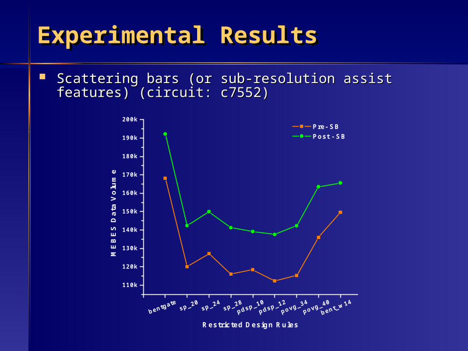
Scattering bars (or sub-resolution assist features) (circuit: Scattering bars (or sub-resolution assist features) (circuit: c7552)c7552)
110k
120k
130k
140k
150k
160k
170k
180k
190k
200kM
EB
ES
Dat
a V
olu
me
Restricted Design Rules
Pre- SB Post - SB

Experimental ResultsExperimental Results
Approach of the single pitch RDR Approach of the single pitch RDR (circuit: c7552)(circuit: c7552)– Single pitch, single orientationSingle pitch, single orientation– Poly pitch larger than default value to allow contact be insertedPoly pitch larger than default value to allow contact be inserted– Pseudo single pitch (97.6% fixed at a single value)Pseudo single pitch (97.6% fixed at a single value)– AOI, OAI cells are excludedAOI, OAI cells are excluded– With SRAFs tuned for the single pitch library at 0.1µm defocusWith SRAFs tuned for the single pitch library at 0.1µm defocus
Delay Area Power MEBES
0.7
0.8
0.9
1.0
1.1
No
rma
lize
d C
irc
uit
Pe
rfo
rma
nc
e Reduced Default Library Single Pitch Library
0.1 0.2 0.30.5
0.6
0.7
0.8
0.9
1.0
Defocus (m)
Nor
mal
ized
3
Unc
erta
inty

Experimental ResultsExperimental Results
Circuit performance Circuit performance analysisanalysis
0.6
0.7
0.8
0.9
1.0
1.1
1.2
No
rmal
ized
Per
form
ance
c7552
0.80
0.85
0.90
0.95
1.00
1.05
1.10
1.15
c6288
No
rmal
ized
Per
form
ance
0.7
0.8
0.9
1.0
1.1
1.2 Delay
Area
Power
MEBES
Yield
c5315
No
rmal
ized
Per
form
ance
Restricted Design Rules

Experimental ResultsExperimental Results
Tradeoff between functional yield at 10% EPE tolerance Tradeoff between functional yield at 10% EPE tolerance and mask cost with loose OPC for corner correction and mask cost with loose OPC for corner correction (circuit: c7552)(circuit: c7552)
RDRRDR Slightly ConservativeSlightly Conservative Very ConservativeVery ConservativeYieldYield MEBESMEBES YieldYield MEBESMEBES
sp_20sp_20 1.001.00 0.980.98 0.810.81 0.910.91sp_24sp_24 1.001.00 0.970.97 0.800.80 0.900.90sp_28sp_28 1.001.00 0.990.99 0.780.78 0.940.94pdsp_10pdsp_10 1.001.00 0.980.98 0.810.81 0.860.86pdsp_12pdsp_12 1.001.00 0.980.98 0.820.82 0.950.95povg_34povg_34 1.001.00 0.980.98 0.910.91 0.930.93povg_40povg_40 1.001.00 0.980.98 0.910.91 0.970.97bentgatbentgatee
1.001.00 0.990.99 0.840.84 0.970.97
bent_w1bent_w144
0.990.99 1.001.00 0.840.84 0.920.92

Conclusions and Future WorkConclusions and Future Work
Restrictive design rules can result in more Restrictive design rules can result in more robust and cost-effective circuits without robust and cost-effective circuits without sacrificing performancesacrificing performance
Data volume reduction on the order of 20-30% Data volume reduction on the order of 20-30% relative to baseline rule setrelative to baseline rule set
Worst-case EPE reduction nearly 50% with Worst-case EPE reduction nearly 50% with small penalty on performancesmall penalty on performance
RDR sets can be formulated to support sub-RDR sets can be formulated to support sub-wavelength lithography by providing wavelength lithography by providing substantial cost reductions with negligible substantial cost reductions with negligible performance tradeoffperformance tradeoff

Conclusions and Future WorkConclusions and Future Work
Multi-layer design rulesMulti-layer design rules– Metal design rulesMetal design rules
Besides poly, OPC is also heavily applied on metal.Besides poly, OPC is also heavily applied on metal.Metal design rules are promising candidates for RDRsMetal design rules are promising candidates for RDRs
– Contact design rulesContact design rules A great number of correcting features are inserted to A great number of correcting features are inserted to
maintain the fidelity of the layer covering the contact maintain the fidelity of the layer covering the contact while the goal should be obtain enough overlap areawhile the goal should be obtain enough overlap area
E.g., avoid contact very close to metal line end mayE.g., avoid contact very close to metal line end mayreduce both the OPC cost on metal and the possibilityreduce both the OPC cost on metal and the possibilityfor an open faultfor an open fault
Performance analysis for post-OPCPerformance analysis for post-OPC Reduce correction cost on field poly whenever Reduce correction cost on field poly whenever
possiblepossible
Top Related