


Languages
Pages
Legal


8/7/2019 Thin Film Processing
http://slidepdf.com/reader/full/thin-film-processing 1/24
Center for Materials for Information Technologyan NSF Materials Science and Engineering Center
Thin Film Processing
Gary Mankey
MINT Center and Department of Physics
http://bama.ua.edu/~gmankey/[email protected]

8/7/2019 Thin Film Processing
http://slidepdf.com/reader/full/thin-film-processing 2/24
Center for Materials for Information Technologyan NSF Materials Science and Engineering Center
Vacuum
A vacuum is defined as lessthan 1 Atmosphere of pressure.
1 Atm = 105 Pa = 103 mbar =760 Torr
Below 10-3 Torr, there are moregas molecules on the surface of the vessel then in the volume of the vessel.
High Vacuum < 10-3 Torr Very High Vacuum < 10-6 Torr
Ultra High Vacuum < 10-8 Torr
760 mm Hg
Vacuum
ATM

8/7/2019 Thin Film Processing
http://slidepdf.com/reader/full/thin-film-processing 3/24
Center for Materials for Information Technologyan NSF Materials Science and Engineering Center
Why do we need a vacuum?
Keep surfaces free of contaminants.
Process films with low densityof impurities.
Maintain plasma discharge for sputtering sources.
Large mean free path for electrons and molecules(P = 1 m @ 7 x 10⁻⁵ mbar).
P
Mean free path for air at
20 ºC:P = 7 x 10⁻³ cm / P(mbar)

8/7/2019 Thin Film Processing
http://slidepdf.com/reader/full/thin-film-processing 4/24
Center for Materials for Information Technologyan NSF Materials Science and Engineering Center
Vacuum Systems
A vacuum system consists of chamber, pumps and gauges.
Chambers are typically made of glass or stainless steel and
sealed with elastomer or metalgaskets.
Pumps include mechanical,turbomolecular, diffusion, ion,sublimation and cryogenic.
Gauges include thermocouplefor 1 to 10-3 mbar and Bayard-Alpert for 10-3 to 10-11 mbar.
8/7/2019 Thin Film Processing
http://slidepdf.com/reader/full/thin-film-processing 5/24
Center for Materials for Information Technologyan NSF Materials Science and Engineering Center
Alabama Deposition of Advanced Materials
All materials are either glass, ceramics, stainlesssteel, copper and puremetals.
A turbomolecular pumpand a cryo pump createthe vacuum.
Sputtering sources areused for deposition.
Characterizationmethods includeRHEED, and Auger electron spectroscopy.

8/7/2019 Thin Film Processing
http://slidepdf.com/reader/full/thin-film-processing 6/24
Center for Materials for Information Technologyan NSF Materials Science and Engineering Center
1 cm
e-
e-
e-
Bayard-Alpert or Ionization Gauge
Electrons, e-, produced by thehot filament are acceleratedthrough the grid acquiringsufficient energy to ionizeneutral gas atoms, n.
The ionized gas atoms, I+, arethen attracted to the negatively,
biased collector and their current is measured with an
electrometer. Typical ion gauges have a
sensitivity of 1-10 Amp / mbar and range of 10-3-10-11 mbar.
Electrometer +150V-45V
6VAC
e-
n n
nn
n
n
n
n
I+
I+I+
Filament Collector
Grid

8/7/2019 Thin Film Processing
http://slidepdf.com/reader/full/thin-film-processing 7/24
Center for Materials for Information Technologyan NSF Materials Science and Engineering Center
Residual Gas Analysis
A quarupole mass spectrometer analyzes the composition of gasin the vacuum system.
The system must be ³baked´ at
150 - 200 ºC for 24 hours toremove excess water vapor fromthe stainless steel walls.
The presence of an O2 peak atM/Q = 32 indicates an air leak.
At UHV the gas composition isH2, CH4, H2O, CO and CO2.

8/7/2019 Thin Film Processing
http://slidepdf.com/reader/full/thin-film-processing 8/24
Center for Materials for Information Technologyan NSF Materials Science and Engineering Center
Monolayer Time
W
e define the monolayer time asthe time for one atomic layer of gasto adsorb on the surface:X = 1 / (SZA).
At 3 x 10⁻⁵ Torr, it takes about one
second for a monolayer of gas toadsorb on a surface assuming asticking coefficient, S = 1.
At 10-9 Torr, it takes 1 hour to form
a monolayer for S = 1. For most gases at room
temperature S<<1, so themonolayer time is much longer.
Impingement rate for air:
Z = 3 x 10²⁰ P(Torr) cm-2 s-1
Sticking CoefficientS = # adsorbed / # incident
Area of an adsorption site:A } 1 Å2 = 10-16 cm2

8/7/2019 Thin Film Processing
http://slidepdf.com/reader/full/thin-film-processing 9/24
Center for Materials for Information Technologyan NSF Materials Science and Engineering Center
Vapor Pressure Curves
The vapor pressures of mostmaterials follow an Arrheniusequation behavior:PVAP = P0 exp(-EA/kT).
Most metals must be heated totemperatures well above 1000 K to achieve an appreciable vapor
pressure.
For PVAP = 10-4 mbar, thedeposition rate is approximately10 Å / sec.

8/7/2019 Thin Film Processing
http://slidepdf.com/reader/full/thin-film-processing 10/24
Center for Materials for Information Technologyan NSF Materials Science and Engineering Center
Physical Evaporation
A current, I, is passed throughthe boat to heat it.
The heating power is I2R, whereR is the electrical resistance of
the boat (typically a few ohms). For boats made of refractory
metals (W, Mo, or Ta)temperatures exceeding 2000º Ccan be achieved.
Materials which alloy with the boat material cannot beevaporated using this method.
High CurrentSource
Substrate
Flux
Boat Evaporant
8/7/2019 Thin Film Processing
http://slidepdf.com/reader/full/thin-film-processing 11/24
Center for Materials for Information Technologyan NSF Materials Science and Engineering Center
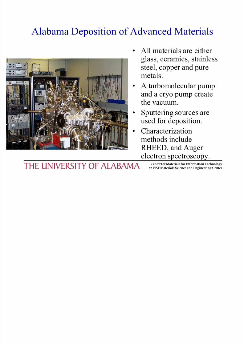
Limitation of Physical Evaporation
Most transition metals, TM,form eutectics with refractory
materials. The vapor pressure curvesshow that they must be heatedto near their melting points.
Once a eutectic is formed, the boat melts and the heatingcurrent is interrupted.

8/7/2019 Thin Film Processing
http://slidepdf.com/reader/full/thin-film-processing 12/24
Center for Materials for Information Technologyan NSF Materials Science and Engineering Center
Electron Beam Evaporator
B
Substrate
Flux
Crucible
e-beam
e-gun
The e-gun produces a beam of electrons with 15 keV kineticenergy and at a variable current of up to 100 mA.
The electron beam is deflected
270º by a magnetic field, B. The heating power delivered to a
small (~5mm) spot in the evaporantis 15 k V x 100 mA = 1.5 k W.
The power is sufficient to heatmost materials to over 1000 ºC.
Heating power is adjusted bycontrolling the electron current.
Evaporant

8/7/2019 Thin Film Processing
http://slidepdf.com/reader/full/thin-film-processing 13/24
Center for Materials for Information Technologyan NSF Materials Science and Engineering Center
The Sputtering Process
Electrons (e-) are localized in the plasma by a magnetic field.The e- collide with argon gasatoms to produce argon ions.The Ar+ are accelerated in an
electric field such that they strikethe target with sufficient energy toeject target atoms.The target atoms, being electricallyneutral, pass through the plasmaand condense on the substrate.N SS
SN N
-
+
Magnets
Target
PlasmaDischarge
Substrate
1 mTorr Ar

8/7/2019 Thin Film Processing
http://slidepdf.com/reader/full/thin-film-processing 14/24
Center for Materials for Information Technologyan NSF Materials Science and Engineering Center
Measuring and Calibrating Flux
Many fundamental physical properties aresensitive to film thickness.
In situ probes which are implemented inthe vacuum system include a quartz crystalmicrobalance, BA gauge, Auger / XPS,
and RHEED. Ex situ probes which measure film
thickness outside the vacuum systeminclude the stylus profilometer,
spectroscopic ellipsometer, and x-raydiffractometer.
Measuring film thickness with sub-angstrom precision is possible.
?

8/7/2019 Thin Film Processing
http://slidepdf.com/reader/full/thin-film-processing 15/24
Center for Materials for Information Technologyan NSF Materials Science and Engineering Center
Quartz Crystal Microbalance
The microbalance measures a shiftin resonant frequency of avibrating quartz crystal with a
precision of 1 part in 106.
f r = 1/2T sqrt(k/m) }f 0(1-(m/2m). For a 6 MHz crystal disk, 1 cm in
diameter this corresponds to achange in mass of several
nanograms. d = m / ( VA), so for a typical metal
d } 10 ng / (10 g/cm3*1 cm2) =0.1 Angstroms.
Quartz
Crystal
Substrate
FrequencyMeasurement
Conversion toThickness
Display
Flux

8/7/2019 Thin Film Processing
http://slidepdf.com/reader/full/thin-film-processing 16/24
Center for Materials for Information Technologyan NSF Materials Science and Engineering Center
Auger / XPS
An x-ray source produces photoelectrons or a electron gun produces Auger electrons.
The electrons have kinetic
energies which are characteristicof the material.
The attenuation of substrateelectrons by the film is described
by Beer¶s law:I = I0 exp(-dcos5/0).
Since, 0 } 10 Å, this techniquehas a high sensitivity.
Photoelectrons &
Auger Electrons
Excitation:X-rays or keV Electrons
Electron EnergyAnalyzer

8/7/2019 Thin Film Processing
http://slidepdf.com/reader/full/thin-film-processing 17/24
Center for Materials for Information Technologyan NSF Materials Science and Engineering Center
Auger Electron Spectroscopy
The excitation knocks a coreelectron out producing a core hole.
To lower the energy of the ion, anelectron from an upper shell decays
nonradiatively into the core hole. The Auger electron from the upper
shell acquires an energy equal to theenergy difference of the core hole
and upper shell. The kinetic energy of the electrons
are measured to identify thechemical species of the atoms.
EVAC
Excitation
CoreHole
Upper Shell
KineticEnergy

8/7/2019 Thin Film Processing
http://slidepdf.com/reader/full/thin-film-processing 18/24
Center for Materials for Information Technologyan NSF Materials Science and Engineering Center
Secondary Electron Energy Distribution
The energy distribution ischaracterized by ± An elastic peak at the
incident electron energy.
± A low energy peak whichincreases as 1/E2 and dropsoff rapidly below 10 eV.
± Auger electrons, which can be measured to determinechemical composition.

8/7/2019 Thin Film Processing
http://slidepdf.com/reader/full/thin-film-processing 19/24
Center for Materials for Information Technologyan NSF Materials Science and Engineering Center
Cu Auger Scan in Pulse Counting Mode
These transitionscorrespond to Auger electrons ejected from thevalence band by aneighboring electronfilling the L shell or 2plevels.

8/7/2019 Thin Film Processing
http://slidepdf.com/reader/full/thin-film-processing 20/24
Center for Materials for Information Technologyan NSF Materials Science and Engineering Center
Cu Auger Spectrum for Analog Mode
In analog mode, theanalyzer energy ismodulated and a lock-inamplifier detects thederivative of the number of electrons or dN(e)/dEvs. E.
The high energy peakscorrespond to those on the
previous slide.

8/7/2019 Thin Film Processing
http://slidepdf.com/reader/full/thin-film-processing 21/24
Center for Materials for Information Technologyan NSF Materials Science and Engineering Center
The Universal Curve for 0
The Universal Curve describes thedependence of electron mean free
path, 0, on energy for most
materials. In most cases, it is accurate to
within a factor of two.
0 = (35 / E)2
+ 0.5 Ewith 0 in Å and E in eV.

8/7/2019 Thin Film Processing
http://slidepdf.com/reader/full/thin-film-processing 22/24
Center for Materials for Information Technologyan NSF Materials Science and Engineering Center
Reflection High-Energy Electron Diffraction
15 keV
electrons reflect from thesurface and are displayed as a spoton a phosphor screen.
The angle is adjusted such thatelectrons reflecting from adjacent
layers interfere destructively. When only one layer is exposed, the
spot is bright.
When the top layer covers half of
the surface, the spot is extinguished. The time between two maxima in
the intensity plot is the monolayer time.
d = atomicspacing
15 keVElectron Gun Screen
U
Path difference = 2dsin5 = (n+1/2) P
P = [150 / E(eV)]1/2

8/7/2019 Thin Film Processing
http://slidepdf.com/reader/full/thin-film-processing 23/24
Center for Materials for Information Technologyan NSF Materials Science and Engineering Center
Epitaxial Growth
Epi-Taxi ( greek)epi meaning ³on´taxi meaning ³arrangementin relation to a source of stimulation´ The crystal structure of thefilm has a direct relationship
to that of the substrate
Film
Substrate

8/7/2019 Thin Film Processing
http://slidepdf.com/reader/full/thin-film-processing 24/24
Center for Materials for Information Technologyan NSF Materials Science and Engineering Center
Growth Modes for Ultrathin Films
The growing film surface canexhibit different behaviorsdepending on substratetemperature, interfacial
strain, and alloy miscibility. The growth modes must becharacterized using acombination of chemicaltools such as Auger electron
spectroscopy and structuraltools such as RHEED andatomic force microscopy.
Stranski-Kastranov
Diffusion Limited
Surface AlloySurface Segregation
Volmer-Weber
Layer by Layer
Top Related