


Languages
Pages
Legal


The octa-twin tetraleg ZnO nanostructures
Ying Daia, Yue Zhanga,b,*, Zhong Lin Wangc
aDepartment of Materials Physics and State Key Laboratory for Advanced Metals and Materials, University of Science and Technology Beijing,
Beijing 100083, People’s Republic of ChinabSchool of Materials Science and Engineering, Georgia Institute of Technology, Atlanta, GA 30332-0245, USA
cSchool of Materials Science and Engineering, Georgia Institute of Technology, 771 Ferst Dr, Atlanta, GA 30332-0245, USA
Received 27 January 2003; accepted 31 March 2003 by D.E. Van Dyck
Abstract
We have developed a simple solid–vapor approach for controlled growth of the tetraleg ZnO nanostructure at high yield. The
length of the tetraleg is 2–3 mm and the edge size of its centering nucleus is 70–200 nm. Our electron microscopy study gives
the first direct evidence about the existence of the octahedral multiple twin nucleus, which is confirmed to be responsible for the
formation of the tetraleg ZnO nanostructure. The tetraleg ZnO nanostructure is likely to be a candidate as building blocks for
contructing photonic crystals.
q 2003 Elsevier Science Ltd. All rights reserved.
PACS: 79.60.Jv; 36.40.2c; 61.46.tw
Keywords: A. Nanostructure; B. Crystal growth
Nanoscale materials exhibit a wide range of electrical and
optical properties that depend sensitively on both shape and
size, and are of both fundamental and technological interest.
One-dimensional (1D) nanostructures, such as nanotubes,
nanowires and nanobelts, have attracted extraordinary
attention for their potential applications in device and
interconnect integration in nanoelectronics and molecular
electronics [1–5]. Although different levels of growth
controls for nanowires (including positional, orientational,
diameter, and density control) have been achieved [6], the
shape control of nanostructures is not easily obtained. The
synthesis of complex structures of rod-based CdSe nano-
crystals e.g. arrow and teardrop, has demonstrated some
success in this direction [7–9]. Since the novel properties of
nanomaterials depend sensitively on their shape and size,
the development of synthetic methods and an understanding
of the mechanism by which the shape and size of
nanostructures can be easily controlled is a key issue in
nanoscience.
ZnO exhibits a direct bandgap of 3.37 eV at room
temperature with a large exciton binding energy of 60 meV.
The strong exciton binding energy, which is much larger
than that of GaN (25 meV) and the thermal energy at room
temperature (26 meV), can ensure an efficient exciton
emission at room temperature under low excitation energy
[10–11]. As a consequence, ZnO is recognized as a
promising photonic material in the blue-UV region. Room
temperature UV lasing properties have recently been
demonstrated from ZnO epitaxial films, microcrystalline
thin films, and nanoclusters [12–15]. The synthesis of 1D
single-crystalline ZnO nanostructures has been of growing
interest owing to their promising application in nanoscale
optoelectronic devices. Single-crystalline ZnO nanowires
have been synthesized successfully in several groups
[16–20]. Wang et al. reported the synthesis of oxide
nanobelts by simply evaporating the commercial metal
oxide powders at high temperatures [3,19–20]. The as-
synthesized oxide nanobelts are pure, structurally uniform,
and single crystalline, and most of them are of free from
0038-1098/03/$ - see front matter q 2003 Elsevier Science Ltd. All rights reserved.
doi:10.1016/S0038-1098(03)00277-1
Solid State Communications 126 (2003) 629–633
www.elsevier.com/locate/ssc
* Corresponding author. Tel.: þ 86-10-62332281.
E-mail addresses: [email protected] (Y. Zhang),
[email protected] (Y. Dai).

defects and dislocations. Room temperature UV lasing in
ZnO nanowires has been demonstrated very recently [21]. In
this paper, we report a simple method for controlled
synthesis of a three-dimensional (3D) ZnO nanostructure,
called tetraleg ZnO (T-ZnO) nanostructure, by oxidation of
Zn powders. The structure of the T-ZnO is fully character-
ized and a possible growth mechanism is proposed.
The T-ZnO nanostructures were synthesized by thermal
evaporation of 99.9% pure zinc powders under controlled
conditions without the presence of catalyst. The zinc
powders were placed in an alumina crucible that was
inserted in a horizontal tube furnace, where the temperature,
pressure, and evaporation time were controlled. The
temperature of the furnace was ramped to 850–950 8C at
a rate of 50–100 8C/min and kept at that temperature for 1–
30 min. T-ZnO nanostructures were obtained in the reaction
vessel. Structural characterization of the T-ZnO nanostruc-
tures were carried out by X-ray diffraction (XRD, D/MAX-
RB) with the Cu Ka radiation, scanning electron
microscopy (SEM, S250-II), transmission electron
microscopy (TEM (Hitachi H-800) and High-resolution
TEM (HRTEM) (JEM-2010F).
The T-ZnO has a unique structure. Although large size
T-ZnO whiskers were reported previously [22–24], the
synthesis of nano-size T-ZnO structures in high yield is
demonstrated only recently [25]. Fig. 1(a) is a typical SEM
images of the T-ZnO nanostructure. The particles are of a
tetrahedral shape with four legs. The length of the legs is 2–
3 mm and the edge size of the centering nucleus is 70–
200 nm. Very little secondary growth components are
observed in our synthesis process. Fig. 1(b) is an TEM
image of a T-ZnO nanostructure. It is obvious that four legs
are extended from the central part. The structure is not single
crystalline but composed of several crystalline pieces. A
typical XRD pattern of the T-ZnO nanostructures is shown
in Fig. 1(c), which proves that the T-ZnO has a wurtzite
structure with lattice constants of a ¼ 0:324 nm and c ¼
0:519 nm: No diffraction peaks from Zn or other impurity
phases are found in any of our samples, confirming that the
products are pure ZnO.
The detailed structure of individual T-ZnO nanostructure
is characterized by TEM. Fig. 2(a) and (b) are bright-field
and dark-field images of a T-ZnO nanostructure, respect-
ively. Fig. 2(b) was taken by selecting a diffraction spot
coming from the central region of the tetraleg. It is apparent
that the center is a distinct grain that is responsible at least in
form for the nucleation and growth of the tetraleg structure.
HRTEM observation of the T-ZnO nanostructure is
shown in Fig. 3. A low-magnification image given in Fig.
3(a) shows the projected four-fold twin structure at the
central region. Fig. 3(b) is a corresponding HRTEM image
from the central region. It reveals the structure of the twin
boundaries between the element crystals. From the HRTEM
image, it can be seen that the interfaces are sharp and show
no amorphous layer. These twins are smoothly conjugated
fairly coherently at the boundaries with little lattice
distortion. A Fourier transform of Fig. 3(b) is given in Fig.
3(c), based on which the twin planes can be determined to be
the {112̄2} family. The index corresponding the grain at the
bottom-left corner of Fig. 3(b) is labeled in Fig. 3(c). The
twin plane is indicated by an arrowhead. The incident beam
direction is [2̄42̄3], along which the four twin boundaries are
imaged edge-on.
The T-ZnO whiskers have stimulated many investigators
in the literature to study their structure and growth
mechanism. The various models have been proposed for
the growth process of the tetrahedral ZnO particles [26–30],
but the structure of the T-ZnO whiskers has not been
Fig. 1. (a) A typical SEM image showing the general morphology of
the tetraleg ZnO nanostructure. (b) An TEM image of the tetraleg
structure. (c) XRD pattern from the tetraleg ZnO nanostructure,
showing the Wurtzite structure.
Y. Dai et al. / Solid State Communications 126 (2003) 629–633630

completely determined because the particles investigated by
these authors were too large to be identified by TEM.
Shioziri suggested that T-ZnO whiskers have the zincblende
structure, four wurtzite crystals formed on their (111) faces
by introducing stacking faults [26]. Iwanaga proposed the
octahedral multiple twin (octa-twin) nucleus models [27].
Nishio proposed a new growth model based on the phase
transformation from an octahedral zincblende ZnO crystal
to a twinned wurtzite ZnO crystal [28]. Among these
models, only the Iwanaga’ model (so called octa-twin
model) can explain the prototype angle relation. Although
his model explained the orientation relationship and the
measured angles between the legs matched exactly to that
measured from surface morphology, there is no direct
evidence in the literature about the existence of the octa-
twin nucleus in T-ZnO structure. The nanoscale T-ZnO
nanostructures synthesized by us make it possible to directly
reveal the structure of the T-ZnO nanostructures by HRTEM
for the first time.
The formation of the T-ZnO structure has two stages:
nucleation and growth. In our process, nucleation at the
initial stage might have a crucial role on the formation of T-
ZnO nanostructures. The metallic zinc is in its vapor state at
the high temperature (Zn: boiling point of 911 8C). The
gaseous zinc diffuse and immediately reoxidize in the
environment of oxygen. It is known that the gaseous ZnO
only exists as highly activated species with an extremely
short lifetime [29]. The oxidation reaction at our processing
temperature is as follows: 2Zn(g) þ O2 ¼ 2ZnO(s). The
process of the initial nucleation includes diffusion, collision
of atoms and reaction between the vapor molecules
(including vapor Zn and O2). When the supersaturation
increases to a level at which nuclei formed, the produced
ZnO nuclei grow to sizes larger than the critical size. The
ZnO nuclei formed in the alumina crucible are homo-
geneous as carried by the gas phase.
According to the octa-twin nucleus model, ZnO nuclei
formed in an atmosphere containing oxygen are octa-twins
nuclei which consist of eight tetrahedral-shape crystals, each
consisting of three {112̄2} pyramidal facets and one (0001)
basal facet (Fig. 4(a)). The eight tetrahedral crystals are
connected together by making the pyramidal faces contact
one with another to form an octahedron. The surfaces of the
octa-twin are all basal planes. An important additional
Fig. 2. (a) Bright-field electron micrograph of a tetraleg ZnO
nanostructure. (b) A dark-field electron micrograph from the same
region, showing a distinct grain at the center, which will be
explained by the model presented in Fig. 4(b).
Fig. 3. (a) Low magnification TEM image of a tetraleg ZnO
nanostructure. (b) A high-resolution TEM image recorded from the
center of the tetraleg structure. (c) A Fourier transform of the image
given in (b) and the indexes corresponding to one of the bottom-left
grain in (b). The incident beam direction is [2̄42̄3].
Y. Dai et al. / Solid State Communications 126 (2003) 629–633 631
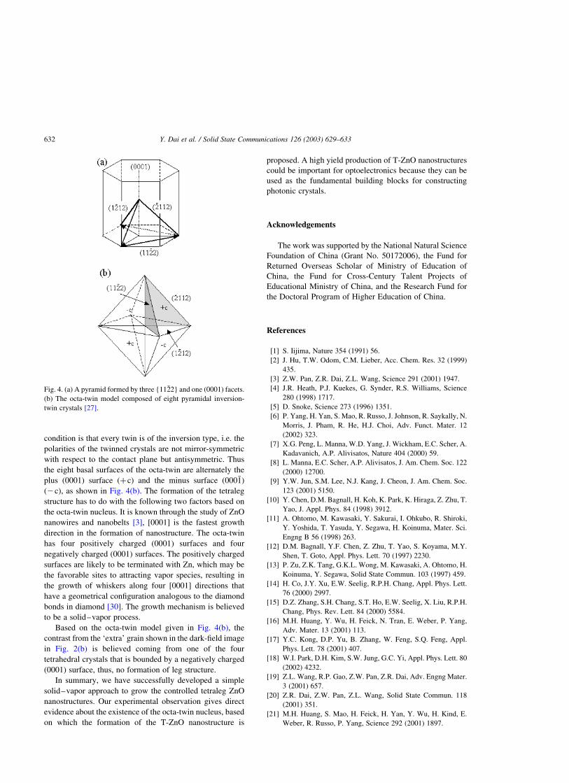
condition is that every twin is of the inversion type, i.e. the
polarities of the twinned crystals are not mirror-symmetric
with respect to the contact plane but antisymmetric. Thus
the eight basal surfaces of the octa-twin are alternately the
plus (0001) surface (þc) and the minus surface (0001̄)
(2c), as shown in Fig. 4(b). The formation of the tetraleg
structure has to do with the following two factors based on
the octa-twin nucleus. It is known through the study of ZnO
nanowires and nanobelts [3], [0001] is the fastest growth
direction in the formation of nanostructure. The octa-twin
has four positively charged (0001) surfaces and four
negatively charged (0001) surfaces. The positively charged
surfaces are likely to be terminated with Zn, which may be
the favorable sites to attracting vapor species, resulting in
the growth of whiskers along four [0001] directions that
have a geometrical configuration analogous to the diamond
bonds in diamond [30]. The growth mechanism is believed
to be a solid–vapor process.
Based on the octa-twin model given in Fig. 4(b), the
contrast from the ‘extra’ grain shown in the dark-field image
in Fig. 2(b) is believed coming from one of the four
tetrahedral crystals that is bounded by a negatively charged
(0001) surface, thus, no formation of leg structure.
In summary, we have successfully developed a simple
solid–vapor approach to grow the controlled tetraleg ZnO
nanostructures. Our experimental observation gives direct
evidence about the existence of the octa-twin nucleus, based
on which the formation of the T-ZnO nanostructure is
proposed. A high yield production of T-ZnO nanostructures
could be important for optoelectronics because they can be
used as the fundamental building blocks for constructing
photonic crystals.
Acknowledgements
The work was supported by the National Natural Science
Foundation of China (Grant No. 50172006), the Fund for
Returned Overseas Scholar of Ministry of Education of
China, the Fund for Cross-Century Talent Projects of
Educational Ministry of China, and the Research Fund for
the Doctoral Program of Higher Education of China.
References
[1] S. Iijima, Nature 354 (1991) 56.
[2] J. Hu, T.W. Odom, C.M. Lieber, Acc. Chem. Res. 32 (1999)
435.
[3] Z.W. Pan, Z.R. Dai, Z.L. Wang, Science 291 (2001) 1947.
[4] J.R. Heath, P.J. Kuekes, G. Synder, R.S. Williams, Science
280 (1998) 1717.
[5] D. Snoke, Science 273 (1996) 1351.
[6] P. Yang, H. Yan, S. Mao, R. Russo, J. Johnson, R. Saykally, N.
Morris, J. Pham, R. He, H.J. Choi, Adv. Funct. Mater. 12
(2002) 323.
[7] X.G. Peng, L. Manna, W.D. Yang, J. Wickham, E.C. Scher, A.
Kadavanich, A.P. Alivisatos, Nature 404 (2000) 59.
[8] L. Manna, E.C. Scher, A.P. Alivisatos, J. Am. Chem. Soc. 122
(2000) 12700.
[9] Y.W. Jun, S.M. Lee, N.J. Kang, J. Cheon, J. Am. Chem. Soc.
123 (2001) 5150.
[10] Y. Chen, D.M. Bagnall, H. Koh, K. Park, K. Hiraga, Z. Zhu, T.
Yao, J. Appl. Phys. 84 (1998) 3912.
[11] A. Ohtomo, M. Kawasaki, Y. Sakurai, I. Ohkubo, R. Shiroki,
Y. Yoshida, T. Yasuda, Y. Segawa, H. Koinuma, Mater. Sci.
Engng B 56 (1998) 263.
[12] D.M. Bagnall, Y.F. Chen, Z. Zhu, T. Yao, S. Koyama, M.Y.
Shen, T. Goto, Appl. Phys. Lett. 70 (1997) 2230.
[13] P. Zu, Z.K. Tang, G.K.L. Wong, M. Kawasaki, A. Ohtomo, H.
Koinuma, Y. Segawa, Solid State Commun. 103 (1997) 459.
[14] H. Co, J.Y. Xu, E.W. Seelig, R.P.H. Chang, Appl. Phys. Lett.
76 (2000) 2997.
[15] D.Z. Zhang, S.H. Chang, S.T. Ho, E.W. Seelig, X. Liu, R.P.H.
Chang, Phys. Rev. Lett. 84 (2000) 5584.
[16] M.H. Huang, Y. Wu, H. Feick, N. Tran, E. Weber, P. Yang,
Adv. Mater. 13 (2001) 113.
[17] Y.C. Kong, D.P. Yu, B. Zhang, W. Feng, S.Q. Feng, Appl.
Phys. Lett. 78 (2001) 407.
[18] W.I. Park, D.H. Kim, S.W. Jung, G.C. Yi, Appl. Phys. Lett. 80
(2002) 4232.
[19] Z.L. Wang, R.P. Gao, Z.W. Pan, Z.R. Dai, Adv. Engng Mater.
3 (2001) 657.
[20] Z.R. Dai, Z.W. Pan, Z.L. Wang, Solid State Commun. 118
(2001) 351.
[21] M.H. Huang, S. Mao, H. Feick, H. Yan, Y. Wu, H. Kind, E.
Weber, R. Russo, P. Yang, Science 292 (2001) 1897.
Fig. 4. (a) A pyramid formed by three {112̄2} and one (0001) facets.
(b) The octa-twin model composed of eight pyramidal inversion-
twin crystals [27].
Y. Dai et al. / Solid State Communications 126 (2003) 629–633632

[22] M.L. Fuller, J. Appl. Phys. 15 (1944) 164.
[23] Y. Suyama, T. Tomokiyo, T. Manabe, E. Tanaka, J. Am.
Ceram. Soc. 71 (1988) 391.
[24] H. Iwanaga, M. Fujii, S. Takeuchi, J. Cryst. Growth 134
(1993) 275.
[25] Y. Dai, Y. Zhang, Q.K. Li, C.W. Nan, Chem. Phys. Lett. 358
(2002) 83.
[26] M. Shiojiri, C. Kaito, J. Cryst. Growth 52 (1981) 173.
[27] S. Takeuchi, H. Iwanaga, M. Fujii, Philos. Mag. A 69 (1994)
1125.
[28] K. Nishio, T. Isshiki, Philos. Mag. A 76 (1997) 889.
[29] G.V. Chertihin, L. Andrews, J. Chem. Phys. 106 (1997) 3457.
[30] H. Iwanaga, N. Shibata, O. Nittono, M. Kasuga, J. Cryst.
Growth 45 (1978) 228.
Y. Dai et al. / Solid State Communications 126 (2003) 629–633 633
Top Related