


Languages
Pages
Legal


TCLSERVICE MANUAL
MS19C LA Chassis L24S10F
1 Caution 2 2 Specification 6
3 Alignment Procedure 74 Block Diagram 225 Schematic Diagram 236 Trouble Shooting 307 PCB Layout 36ACCESSORIES1. Explode View Diagram 402. BOM LIST 41
This manual is the latest at the time of printing, and does not include the modification which may be made after the printing, by the constant improvement of product

CA UTION: TO RE DUCE THE RIS K OFELECTR ICAL SHOCK, DO NOT REMOVECOVER (OR BACK). NO USER SERVICEABLEPAR TS INS IDE . RE FER SER VIC ING TOQUALIFIED SERVICE PERSONNEL.
The lighting flash with arrowhead symbol, with an equilateral triangle is intended to
alert the user to the presence of uninsulated voltage within the products
enclosure that may be of sufficient magnitude to constitute a risk of electric shock to
the person.
The exclamation point within an equilateral triangle is intended to alert the user to the
presence of important operating and maintenance (servicing) instructions in the
literature accompanying the appliance.
CAUTION:
Use of controls, adjustments or procedures other than those specified herein may result in
hazardous radiation exposure.
CAU T IONRISKRISK OF ELECTRIELECTRIC
SHOCKSHOCK DO NOTNOT OPEN.OPEN.
2
dangerous
WARNING: TO REDUCE RISK OF FIRE OR ELECTRIC SHOCK, DO NOT EXPOSE THIS APPLIANCE TO RAIN OR MOISTURE.
SCHNEIDER ELECTRONICS GMBH-GERMANY
1. CAUTION
2

1. When the power cord or plug is damaged or frayed, unplug this television set from the wall outlet and refer servicing to
qualified service personnel.
2. Do not overload wall outlets and extension cords as this can result in fire or electric shock.
3. Do not allow anything to rest on or roll over the power cord, and do not place the TV where power cord is subject to
traffic or abuse. This may result in a shock or fire hazard.
4. Do not attempt to service this television set yourself as opening or removing covers may expose you to dangerous
voltage or other hazards. Refer all servicing to qualified service personnel.
5. Never push objects of any kind into this television set through cabinet slots as they may touch dangerous voltage
points or short out parts that could result in a fire or electric shock. Never spill liquid of any kind on the television set.
6. If the television set has been dropped or the cabinet has been damaged, unplug this television set from the wall outlet
and refer servicing to qualified service personnel.
7. If liquid has been spilled into the television set, unplug this television set from the wall outlet and refer servicing to
qualified service personnel.
8. Do not subject your television set to impact of any kind. Be particularly careful not to damage the picture tube surface.
9. Unplug this television set from the wall outlet before cleaning. Do not use liquid cleaners or aerosol cleaners. Use a
damp cloth for cleaning.
10.1. Do not place this television set on an unstable cart, stand, or table. The television set may fall, causing serious injury
to a child or an adult, and serious damage to the appliance. Use only with a cart or stand recommended by the
manufacturer, or sold with the television set. Wall or shelf mounting should follow the manufacturer s instructions, and
should use a mounting kit approved by the manufacturer.
10.2. An appliance and cart combination should be moved with care. Quick stops, excessive force, and uneven surfaces
may cause the appliance and cart combination to overturn.
CAUTION:
Read all of these instructions. Sa ve these instructions for later use . Follo w all Warnings and
Instructions marked on the audio equipment.
1. Read Instructions-All the safety and operating instructionsshouldbe read before the productis operated.
2. Retain Instructions- The safety and operating instructions should be retained for future reference.
3. Heed Warnings- All warnings on the productand in the operating instructions should be adhered to.
4. Follow Instructions- All operating and use instructions should be followed.
3
SCHNEIDER ELECTRONICS GMBH-GERMANY
IMPORTANT SAFETY INSTRUCTIONS
FOR YOUR PERSONAL SAFETY
3

11. Do not use this television set near water ... for example, near a bathtub, washbowl, kitchen sink, or laundry tub, in a
wet basement, or near a swimming pool, etc.
Never expose the set to rain or water. If the set has been exposed to rain or water, unplug the set from the wall
outlet and refer servicing to qualified service personnel.
12. Choose a place where light (artificial or sunlight) does not shine directly on the screen.
13. Avoid dusty places, since piling up of dust inside TV chassis may cause failure of the set when high humidity persists.
14. The set has slots, or openings in the cabinet for ventilation purposes, to provide reliable operation of the receiver, to
protect it from overheating. These openings must not be blocked or covered.
Never cover the slots or openings with cloth or other material.
Never block the bottom ventilation slots of the set by placing it on a bed, sofa, rug, etc.
Never place the set near or over a radiator or heat register.
Never place the set in enclosure, unless proper ventilation is provided.
15.1. If an outside antenna is connected to the television set, be sure the antenna system is grounded so as to provide some
protection against voltage surges and built up static charges, Section 810 of the National Electrical Code, NFPA No.
70-1975, provides information with respect to proper grounding of the mast and supporting structure, grounding of the
lead-in wire to an antenna discharge unit, size of grounding conductors, location of antenna discharge unit, connection
to grounding electrode, and requirements for the grounding electrode.
15.2. Note to CATV system installer : (Only for the television set with CATV reception)
This reminder is provided to call the CATV system attention to Article 820-40 of the NEC that provides
guidelines for proper grounding and, in particular, specifies that the cable ground shall be connected to the grounding
system of the building, as close to the point of cable entry as practical.
16. An outside antenna system should not be located in the vicinity of overhead power lines or other electric lights or power
circuits, or where it can fall into such power lines or circuits. When installing an outside antenna system, extreme care
should be taken to keep from touching such power lines or circuits as contact with them might be fatal.
17. For added protection for this television set during a lightning storm, or when it is left unattended and unused for long
periods of time, unplug it from the wall outlet and disconnect the antenna. This will prevent damage due to lightning
and power-line surges.
ANTENNALEAD- IN WIRE
ANTENNA DISCHARGE
UNIT (NEC SECTION
810-20)
GROUNDING
CONDUCTORS
(NEC SECTION810-21)
GROUND CLAMPS
POWER SERVICE GROUNDING
ELECTRODE SYSTEM
(NEC ART 250. PART H)
ELECTRIC SERVICEEQUIPMENT
GROUND CLAMP
NEC-NATIONAL ELECTRICAL CODE
EXAMPLE OF ANTENNA GROUNDING AS PER
NATIONAL ELECTRICAL CODE
EXAMPLE OF ANTENNA GROUNDING AS PER NATIONAL ELECTRICAL CODE INSTRUCTIONS
a built-in
installer s
4
SCHNEIDER ELECTRONICS GMBH-GERMANY
PROTECTION AND LOCATION OF YOUR SET
PROTECTION AND LOCATION OF YOUR SET
4

18. This television set should be operated only from the type of power source indicated on the marking label.If you are not
sure of the type of power supply at your home, consult your television dealer or local power company. For television
sets designed to operate from battery power, refer to the operating instructions.
19. If the television set does not operate normally by following the operating instructions, unplug this television set from the
wall outlet and refer servicing to qualified service personnel. Adjust only those controls that are covered in the operating
instructions as improper adjustment of other controls may result in damage and will often require extensive work by a
qualified technician to restore the television set to normal operation.
20. When going on a holiday : If your television set is to remain unused for a period of time, for instance, when you go on
a holiday, turn the television set and unplug the television set from the wall outlet.
21. If you are unable to restorenormal operationby followingthe detailedprocedurein youroperatinginstructions,
do not attempt any further adjustment. Unplug the set and call your dealer or service technician.
22. Whenever the television set is damaged or fails, or a distinct change in performance indicates a need for
service, unplug the set and have it checked by a professional service technician.
23. It is normal for some TV sets to make occasional snapping or popping sounds, particularly when being
turned on or off. If the snapping or popping is continuous or frequent, unplug the set and consult your
dealer or service technician.
24. Do not use attachments not recommendedby the television set manufacturer as they may cause hazards.
25. When replacementparts are required,be sure the service technicianhas used replacementparts specified
by the manufacturer that have the same characteristics as the original part. Unauthorized substitutions
may result in fire, electric shock, or other hazards.
26. Upon completion of any service or repairs to the television set, ask the service technician to perform
routine safety checks to determine that the television is in safe operating condition.
off
5
SCHNEIDER ELECTRONICS GMBH-GERMANY
OPERATION OF YOUR SET
IF THE SET DOES NOT OPERATE PROPERLY
FOR SERVICE AND MODIFICATION
5

EM BUSINESS CENTER FTV PRODUCT MANAGEMENT DEPT.
SPECIFICATION RELEASE Version: V1.0 Issued Date: 2009.12.9
PICTURECategory LCDTV
Naturalight Technology Yes (Dynamic Backlight)
Dynamic Contrast YesColor Temperature Warm / Normal / Cold SIGNAL FORMAT CAPABILITYBacklight Adjustable Yes Component Video Format Y,Pb/Cb,Pr/Cr:up to 1080P
Scaler Mode 4:3, Full, Subtitle, Wide Screen DVI Video Format Up to XGA for HDMI-PCPicture Effect Personal, Bright, Standard and Soft HDMI Video Format up to 1080PFilm Mode (3:2 pull down) AUTO PC Compatibility Up to SXGA1080i/1080p Dot to Dot Display Yes (Original) TERMINALSVGA Dot to Dot Display Yes (Auto Adapt) Audio/CVBS Input (Composite) 2 R/L+2 Video: AV1, AV2(Side)
S-Video Input --
Audio Input for S-Video -- Comb Filter 3D YPbPr Input 1 Dynamic Noise Reduction 3D Audio Input for YPbPr 1 Adaptive Deinterlacing 3D YCbCr Input Share with "YPbPr" Blue Stretch Yes Audio Input for YCbCr Share with Audio for "YPbPr" Black Stretch Yes VGA Input(RGB) 1 (D-Sub,15 Pins) Motion Compensation Yes Audio Input for RGB Share with Audio for "YPbPr" DLTI Yes DVI -- DCTI Yes Audio Input for DVI -- Dynamic Skin Correction Yes HDMI 2 (HDMI1,HDMI2)
Audio/CVBS Output (Composite) 1 (R/L+CVBS) (RCA)PANEL SPECIFICATION SPDIF Output 1 (Coaxial digital audio output)
Headphone Output 1 (�3.5mm ) Panel supplier CM0 RF Input(Antenna) 1 (F Type) Aspect Ratio 16:9 USB 1 Panel Size (inch) 23.6" BASIC INFO. Display Resolution 1920*1080 TV System NTSC-M;PAL-M;PAL-N
Brightness (cd/m2) 300 AV System PAL,NTSC Contrast Ratio 800:1 Channels Cable 125 (1 125) , Antenna 68 (2 69) Response Time Tr/Tf 1.5/3.5ms Chassis MS19C-LA Viewing Angle (H/V) 160°/150° Certification CB Life Time 50,000hrs (min) Power Supply AC 100V-240V 50/60Hz Color 16.7M Power Consumption-TV on 50W
SOUND Power Consumption-Standby WSpeakers Integrated speakers (Bottom side) Default Color of Front Cabinet BlackAudio Power Output 2×5W Keyboard Position SideSmart Volume Yes AVC Base Stand Detachable YesSound Effect Stereo,Music,Cinema,News Unpackaged Dimension for Main Body (L*H*D) (mm)
Sound Control Volume; Balance; Sound Channel Selecting For VGA With Base Stand (mm) 625.5×470×91
Without Base Stand (mm) 625.5×425×91Packaged Dimension (L*H*D)
Sound Processing BTSC (Mono;Stereo;Sap) Main Body (mm) 734×197×533 Speaker Box --
FUNCTION Base Stand 420×270×129OSD Language English/Portuguese/Spanish Net Weight (Kg) 5.2 kgOSD Features Motion Bmp style Gross Weight (Kg) 7.2kgSource in OSD Source Bmp Icon Selecting Container LoadingCC (Closed Caption) Yes (CC1~CC4,TT1~TT4 ;CC On When Mute) 20 feet 372PIP/POP -- 40 feet 760Clock/Sleep Timers Yes 40 feet high 950Wake up/Turn off time Yes ACCESSORIESWake up Source/Chanel Yes Operation Manual English(Default)Watch Time Limit Yes Remote Control For TV control (with two batteries)Source Rename Yes Base Stand separate packagingSmart Switch AIS Yes(Signal Auto Detecting and Changing Source) Speaker Box IntegratedPicture Freeze Yes Wall Mount Optional (TBD)USB Connection Yes. Only for mp3 Play and JPG Photo Dispaly Others AC Power cordListen Only Yes (Listening to Music without picture) Demo Function OptionalHotel OptionalDVD Combo --
Design and specifications are subject to change without notice! Page 1 of 1
Model: L24S10F/MS19C-LA/CM1
Approved by:
AV Stereo, Scene Selecting DeskTop Mode andHangUp Mode
Picture Enhancement
Sound Features
Drafted by: ( Wise Zhang)

TCL Multimedia Technology Holdings Ltd. R&D Center
Alignment Procedure
MS19C-AP / MS19C-LA Chassis
Version: 1.0
Release Date: 2009-12-18
PREPARED BY: Wise Zhang DATE: 2009-12-18
APPROVED BY: DATE:

MS19C-AP/MS19C-LA
PRELIMINARY INFORMATION ----- SUBJECT TO CHANGE 2
Content1. General Description 3
2. Factory Menu 3
2.1 Way of accessing 3
2.2 Factory Menu 3
2.3 ADC calibration menu 5
2.4 White Balance adjustment 6
3. Design Menu 7
3.1 way of accessing 7
3.2 SHOP MENU 8
3.3 SERVICE MENU 9
3.4 PROJECT ID 10
3.5 PARAMETER SETTING MENU 10
3.6 HOTEL MENU 11
4. Steps of debugging 12
4.1 Device 12
4.2 steps of debugging 12
4.3 ADC calibration 12
4.4 White Balance adjustment 13
4.5 White Balance adjustment (automatically) 14
5. Chip list of software programming before SMT 14
6. USB software upgrade 15
History Description of major changes Release Date
V1.0 2009-12-18
Chassis Model
MS19C-AP L24P10F, L24S10F, L24V10F, L42M9F, L42N9F etc. FHD
MS19C-LA L24P10F, L24S10F, L24V10F etc.
HD MS19C-AP L26M9, L26N9, L32M9, L32N9 etc.

MS19C-AP/MS19C-LA
PRELIMINARY INFORMATION ----- SUBJECT TO CHANGE 3
2.2 Factory Menu
1. General Description MS19C-AP/MS19C-LA is our latest design especially for LCDTV products selling in Asia Pacific (AP) / Latin America (LA) market. It features by its high integration, easy debugging as well as convenience in terms of maintenance. Fast software upgrade through USB disk facilitates both manufacture and after service. Meantime, a variety of functions involved in Factory Menu (FM) and Design Menu (DM) can not only bring benefits for production, but also satisfy various demands of customer.
2.1 Accessing way: a. In the first place, press Menu button of remote control, then select Contrast item of Picture submenu. Finally, press 9, 7, 3, 5 consecutively.
b. When the FAC HOTKEY item of Factory Menu is enabled(ON), press Go Back button of remote control.
Factory Menu
Name Default Description Status
FAC HOTKEY
OFF Factory Menu shortcut button switch
The item must be disabled (OFF) after production
OK
WARM UP
OFF OFF: Normal mode. Display black screen when no signal. Turn to automatically standby mode if keep the signal unavailable over 15 minutes.
ON: Aging mode. Display snow dot when no signal. The set will not turn to standby even if the unavailability of signal
OK
ADC >> ADC calibration ( see details below) OK
WHITEBALANCE
>> White Balance Adjustment ( see details below) OK
SHOP DO It is crucial that the function is executed after production aim to clear information of production process, ensure user cannot access to Factory Menu after execute the item.
OK
NVM RESET DO Restore default value except WB and ADC data. OK
2. Factory Menu

MS19C-AP/MS19C-LA
PRELIMINARY INFORMATION ----- SUBJECT TO CHANGE 4
SET FAC CH DO Preset the channel table of factory. After choosing the item, press of remote control, prompt “wait” will appear. Please wait until the appearance of “OK”.
POWER ON LAST/STB ON: the set will power on after switching on power.
STB: the set will remain standby status after switching on power.
Last: the set will turn to the status in which it lies when last switching off.
If without requirement from certain customer,
by default, the value should be Last for
MS19C-AP and STB for MS19C-LA.
OK
USBUPDATE
Upgrade software. Please see details below. OK
FAC CH SEL Select the factory where the chassis is produced. This item correlates with SET FAC CH. When certain factory is chosen, the channel table of the factory will be preset after execution of SET FAC CH.
OK
SWVERSION
OFF Version information of software for U202 OK
SW DATE Release date and time of software for U202 OK
PRODUCT Product model OK
SIACP VERSION
Serial port remote control protocol OK

MS19C-AP/MS19C-LA
PRELIMINARY INFORMATION ----- SUBJECT TO CHANGE 5
2.3 ADC calibration menu ADC Menu Press the button in remote control to select certain item and
to change the value of ADC data or start ADC calibration.
Notes:
1. Only YPBPR and PC source should be calibrated.
ADC Calibration menu
Name Default Description Status
SOURCE Select the source you intend to ADC Calibrate.
Only YPBPR and PC are available.
OK
AUTO TUNE
DO Select and execute the item, ADC Calibration starts. It indicates a successful calibration if prompt “OK” is displayed. Otherwise, It is a failing calibration (“NG” displayed).
OK
R OFFSET 127 Offset of R channel ( cannot be changed after auto calibration) OK
G OFFSET 127 Offset of G channel ( cannot be changed after auto calibration) OK
B OFFSET 127 Offset of B channel ( cannot be changed after auto calibration) OK
R GAIN 128 Gain of R channel ( cannot be changed after auto calibration) OK
G GAIN 128 Gain of G channel ( cannot be changed after auto calibration) OK
B GAIN 128 Gain of B channel ( cannot be changed after auto calibration) OK

MS19C-AP/MS19C-LA
PRELIMINARY INFORMATION ----- SUBJECT TO CHANGE 6
2.4 White Balance Adjustment menu
White Balance menu Press the button in remote control to select certain item and
to adjust White Balance
White Balance Adjustment menu
Name Default Description Status
SOURCE Select the source you intend to apply WB adjustment.
Only HDMI1, AV1, YPBPR, PC and should be adjusted.
OK
COLOR TEMP
NORMAL Select color temperature you intend to adjust Three groups of color temperature: Normal, Warm, Cool are available for each source.
OK
R GAIN 128 Gain of R channel ( cannot be changed after auto calibration) OK
G GAIN 128 Gain of G channel ( cannot be changed after auto calibration) OK
B GAIN 128 Gain of B channel ( cannot be changed after auto calibration) OK
R OFFSET 128 Offset of R channel ( cannot be changed after auto calibration) OK
G OFFSET 128 Offset of G channel ( cannot be changed after auto calibration) OK
B OFFSET 128 Offset of B channel ( cannot be changed after auto calibration) OK
MS19C-AP/MS19C-LA
PRELIMINARY INFORMATION ----- SUBJECT TO CHANGE 7
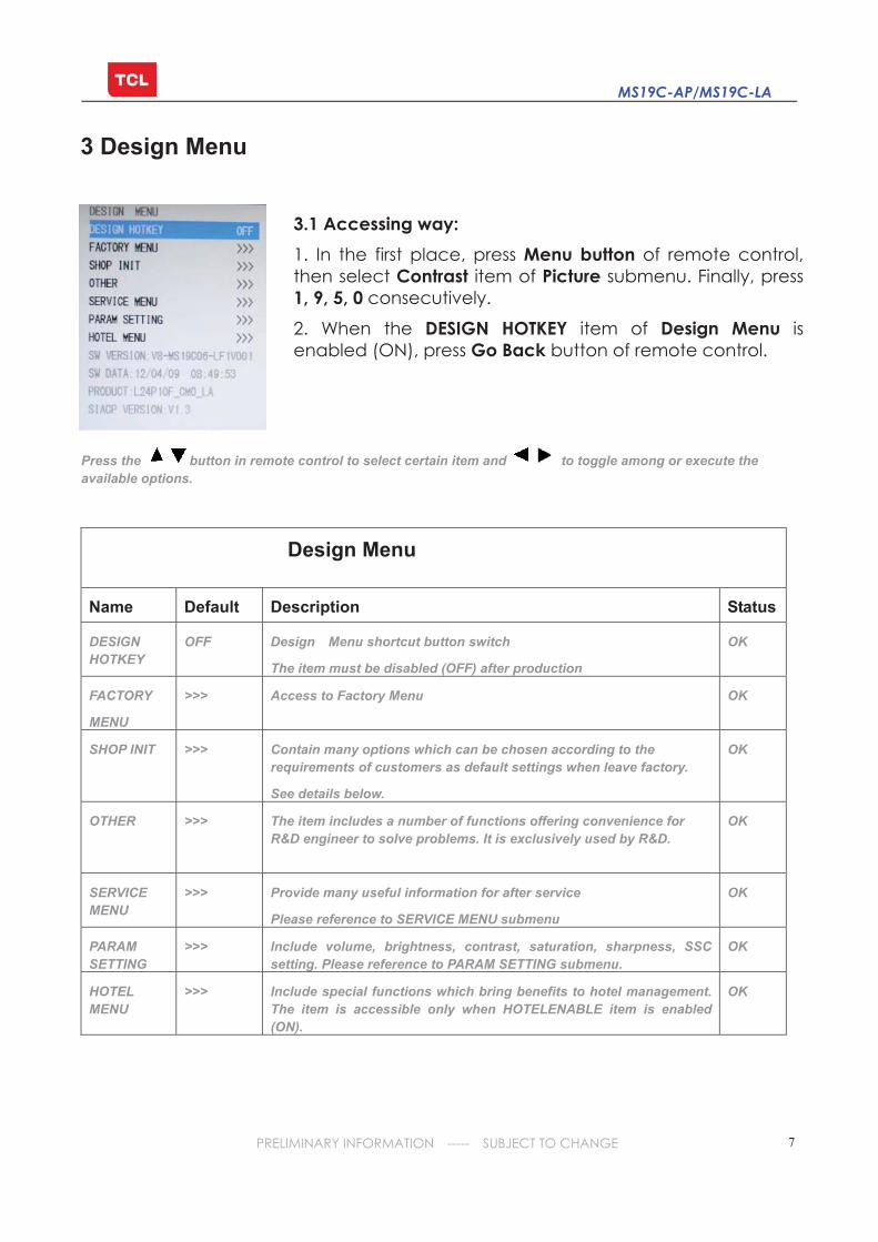
3 Design Menu
Design Menu
Name Default Description Status
DESIGNHOTKEY
OFF Design Menu shortcut button switch
The item must be disabled (OFF) after production
OK
FACTORY
MENU
>>> Access to Factory Menu OK
SHOP INIT >>> Contain many options which can be chosen according to the requirements of customers as default settings when leave factory.
See details below.
OK
OTHER >>> The item includes a number of functions offering convenience for R&D engineer to solve problems. It is exclusively used by R&D.
OK
SERVICE MENU
>>> Provide many useful information for after service
Please reference to SERVICE MENU submenu
OK
PARAM SETTING
>>> Include volume, brightness, contrast, saturation, sharpness, SSC setting. Please reference to PARAM SETTING submenu.
OK
HOTEL MENU
>>> Include special functions which bring benefits to hotel management. The item is accessible only when HOTELENABLE item is enabled (ON).
OK
3.1 Accessing way: 1. In the first place, press Menu button of remote control, then select Contrast item of Picture submenu. Finally, press 1, 9, 5, 0 consecutively.
2. When the DESIGN HOTKEY item of Design Menu isenabled (ON), press Go Back button of remote control.
Press the button in remote control to select certain item and to toggle among or execute the available options.

MS19C-AP/MS19C-LA
PRELIMINARY INFORMATION ----- SUBJECT TO CHANGE 8
3.2 SHOP MENU
SHOP MENU
Name Default Description Status
VOLUME 30 Volume setting, 0~100 adjustable OK
PIC MODE STANDARD Picture mode. Options:
STANDARD, BRIGHT, SOFT, USER.
OK
SOUNDMODE
STEREO Sound effects. Options:
STEREO, ODEUM, CINEMA, NEWS, USER.
OK
CH NUMBER 199 The maximum number of channel OK
LANGUAGE ENGLISH OSD language.
MS19C-AP
MS19C-LA English, Portuguese, Spanish
OK
COLOR SYS AUTO COLOR SYSTEM. Options: AUTO, PAL, NTSC, SECAM
PAL M, PAL N, NTSC4.43
OK
SOUND SYS M SOUND SYSTEM. Options:
MS19C-AP AUTO B/G, D/K, I, M
MS19C-LA AUTO
OK
PRESET CH 1 Preset channel. 0~199 optional OK
COLORTEMP
NORMAL Color temperature. Option: NORMAL, WARM, COOL OK
Contain many options which can be chosen according to the
requirements of customers as default settings when leave factory.
Press the button in remote control to select certain item and
to toggle among the available options..

MS19C-AP/MS19C-LA
PRELIMINARY INFORMATION ----- SUBJECT TO CHANGE 9
3.3 SERVICE MENU
Press the button in remote control to select certain item and
to toggle among the available options..
SERVICE MENU (PRODUCT INFO)
Name Default Description Status
SWVERSION
Software virtual code No. OK
DATE, TIME Release date, time OK
PRODUCT Model of product OK
SIACP VERSION
Serial port remote control protocol OK
CHASSIS MS19C-AP/MS19C/LA Chassis name OK
PANEL Panel code OK
ERROR CODE
NG
USBUPDATE
USB upgrade. Reference to descript below. OK
PROJECT ID
Select project parameters through project ID. OK
TCL SHOW OFF Switch of DEMO function. It is designed for demo in shop and must be closed after selling out.
OK
HOTEL ENABLE
OFF Switch of Hotel Menu. OK
LOGOSELECT
ON Choose LOGO according to customer demand OK
AV OVERSCANCAL
>>> OVERSCAN adjustment OK

MS19C-AP/MS19C-LA
PRELIMINARY INFORMATION ----- SUBJECT TO CHANGE 10
3.4 PROJECT ID
3.5 PARAM SETTING MENU
PARAM SETTING MENU
Name Default Description Status
VOLUME >>> Sound curve. Exclusively used by R&D. OK
BRIGHTNESS >>> Brightness curve. Exclusively used by R&D. OK
CONTRAST >>> Contrast curve. Exclusively used by R&D. OK
SATURATION >>> Saturation curve. Exclusively used by R&D. OK
SHARPNESS >>> Sharpness curve. Exclusively used by R&D. OK
SSCSETTING
>>> SSC parameters. Exclusively used by R&D. OK
Press the button in remote control to select certain item and
to enter menu.
PROJECT ID number Product model
Remote control name
Power supply number Panel code
MS19C-AP/MS19C-LA
PRELIMINARY INFORMATION ----- SUBJECT TO CHANGE 11
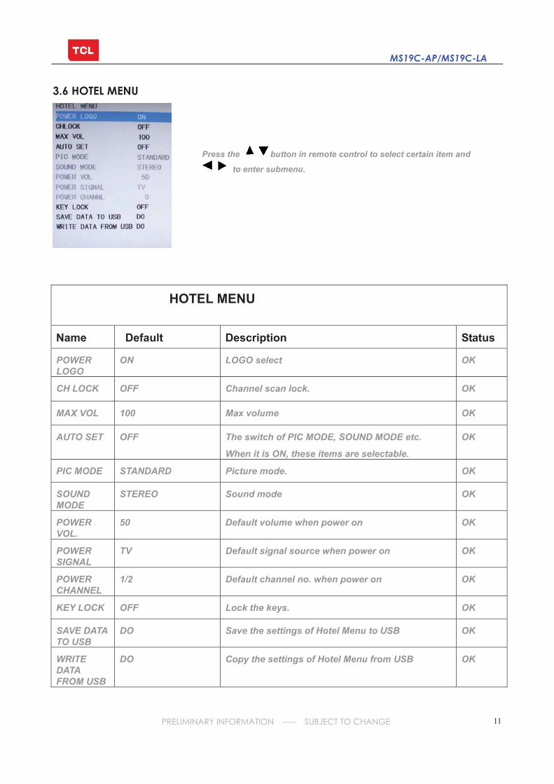
3.6 HOTEL MENU
Press the button in remote control to select certain item and
to enter submenu.
HOTEL MENU
Name Default Description Status
POWERLOGO
ON LOGO select OK
CH LOCK OFF Channel scan lock. OK
MAX VOL 100 Max volume OK
AUTO SET OFF The switch of PIC MODE, SOUND MODE etc.
When it is ON, these items are selectable.
OK
PIC MODE STANDARD Picture mode. OK
SOUND MODE
STEREO Sound mode OK
POWERVOL.
50 Default volume when power on OK
POWERSIGNAL
TV Default signal source when power on OK
POWERCHANNEL
1/2 Default channel no. when power on OK
KEY LOCK OFF Lock the keys. OK
SAVE DATA TO USB
DO Save the settings of Hotel Menu to USB OK
WRITEDATA FROM USB
DO Copy the settings of Hotel Menu from USB OK

MS19C-AP/MS19C-LA
PRELIMINARY INFORMATION ----- SUBJECT TO CHANGE 12
Color Analyzer CA-210. Video Pattern Generator Chroma2329. Color TV Pattern Generator PM5418, VGA cable, AV cable(RCA),YPBPR(RCA) cable.
Chroma2329 Fluke5418 CA-210
According to the requirement of order, we suggest take the below steps to finish the appropriate settings.A enter the Factory Menu, enable FAC HOTKEY.B Check the version of software, release date displayed at the bottom of Factory
Menu.C enter Design Menu, choose SERVICE MENU->Project ID, choose corresponding Project ID number of the product (Please refer to the description in BOM about Project ID number).D return to Factory Menu, check the Product model.E choose Factory Menu-> NVM RESET and press and wait until prompt OK
appears.F restart the set G according to the requirement of order, set the items of SHOP INIT and Hotel Menu
etc. H After aging under normal temperature, calibrate ADC and adjust white balance. I choose Factory Menu-> SHOP and press button of remote control to initialize the set.Note: after step I ( execute shop) , Hotel Menu will be disabled by default. Therefore, if order requires hotel function, it is necessary to enable hotel function by set DesignMenu-> Service Menu->HOTEL ENABLE to ON.
.signal and generator
VGA: Chroma2329 Pattern42, Timing 14(1024x768@60Hz 5 MOSAIC)
YPBPR: Chroma2329 Pattern103, Timing 79(100% Color Bar, 720p)
5 MOSAIC 100% Color Bar
4. The steps of debugging
4.1 Device
4.2 steps of debugging
4.3 ADC Calibration

MS19C-AP/MS19C-LA
PRELIMINARY INFORMATION ----- SUBJECT TO CHANGE 13
.steps of debug:
1) Access to the Factory menu->ADC
2) Select PC source
3) Select AUTO TUNE Press button in your remote control to calibrate the ADC automatically.
4) Select YPBPR source
5) Repeat step 3.
6) When the OK appears the calibration has been finished successfully.
VGA calibration YPBPR calibration
Before adjustment, you must ensure Color Analyzer has been calibrated. Only AV1, YPBPR, VGA , HDMI 1 need to be adjusted. It is necessary to adjustment HDMI 1 firstly.
a. signal and generator The pattern of the signal should be used are White (Chroma2329 pattern113) and Grey (pattern 114).The format of signal are respectively 720p for HDMI1 (Chroma2329 Timing 69), NTSC for AV1 (Chroma2329 Timing 37),1024×768@60Hz
(Chroma2329 Timing 14) for VGA and 720p (Chroma2329 Timing 79)for YPBPR
b. steps of adjustment 1) enter the factory menu-> White Balance, select source HDMI 1 and COLORTEMPnormal.2) input grey signal in 720p format
3) change R OFFSET and B OFFSET to make sure the value of color coordination equal to (x=280+/-5,y=290+/-5).
4) input white signal in 720p format
4.4 White Balance adjustment (Manual)

MS19C-AP/MS19C-LA
PRELIMINARY INFORMATION ----- SUBJECT TO CHANGE 14
5) change R Gain and B Gain to make sure the value of color coordination equal to
(x=280+/-5,y=290+/-5).
6) repeat step 2~5 until both of the value of color coordination of white and grey
equal to (x=280+/-5,y=290+/-5).
In addition to select COLORTEMP COOL/WARM, the adjustment method of COOLand WARM color temperature is same with that of NORMAL. The color coordination we recommend for COOL and WARM color temperature is respectively (270+/-5, 270+/-5) and (300+/-5, 305+/-5). Except select corresponding SOURCE and signal, the method of white balance adjustment for AV1, VGA and YPBPR is same with that of HDMI 1.
4.5 ADC Calibration and White Balance Adjustment (automatic)The process of adjusting ADC and White Balance automatically is out of the range of this file. Please refer to the relevant technical file of HuiZhou factory of TCL
5. Chip list of software programming before SMT Following chips must be programmed before SMT by ALL-11 or other tools.
Note: 1) the software for U202( Flash software) and U203 (HDCP) of Main Board can be
program using ISP tool. 2) Please check HDCP function in the process of production. 3) EDID of VGA and HDMI source are integrated in the software for U202,
therefore, there is no need to program extra EDID software for MS19C-AP/LA chassis.
Position Chip type Software description
1 U202 Flash main software
2 U203 E2PROM HDMI HDCP key
HDMI White Balance adjustment

MS19C-AP/MS19C-LA
PRELIMINARY INFORMATION ----- SUBJECT TO CHANGE 15
6. Software upgrade through USB disk
Way 1: 1) Please ensure the software you are using has a correct file name
(if the resolution of panel is 1920*1080, the software name should
be TCL_MS19C_UPDATE_FHD.bin, if resolution is 1366*768, file name
should be TCL_MS19C_UPDATE.bin, copy it to the root directory of a
USB disk.
2) Insert the USB disk to the USB socket of the set for which you are
going to upgrade program.
3) Enter the Factory Menu, select USB UPDATE, press button of
remote control to start upgrade.
Way 2: 1) Please ensure the software you are using has a correct file name
(if the resolution of panel is 1920*1080, the software name should
be TCL_MS19C_UPDATE_FHD.bin, if resolution is 1366*768, file name
should be TCL_MS19C_UPDATE.bin, copy it to the root
directory of a USB disk.
2) Insert the USB disk to the USB socket of the set for which you are going
to upgrade program.
press CH- button in key board and switch on at the same time. Wait
for 10 seconds then let off the CH- button to start upgrade
Notes:
We recommend you use former way to
upgrade if the set can work properly.
In some circumstances, such as no
picture, however, the set cannot be
upgraded successfully by means of
the former way, the later way can
be an alternative. Over the course of
upgrade, power supply cannot be cut off. Otherwise, to upgrade program, it is necessary to adopt ISP tool. After
upgrading the software, please restart the set (power off then power on) in
order to ensure the correct EEPROM data. Left figure shows the prompt
after upgrade.

MS1
9C (A
P&LA
) Cha
ssis
Blo
ck D
iagr
am
12V
or 5
V
LVD
S_S
EL
BL_ON
DIM
24V
Firs
t Iss
ued
V
0.1
ZC
X 2
009-
12-0
6
LCD
Pan
el
U20
1
Mai
nch
ipse
t
Z101
TUN
ER
CN
&A
P07
-380
FI5-
NA
9GLA
07-4
57FF
5-N
A2G
U60
113
-STA
559-
BW
B(2
4~37
")13
-STA
335-
BW
B(4
0~52
")
U60
213
-RC
4558
-DR
B
8R/8
W
P50
3:47
-RC
A28
6-X
X0G
P40
1:47
-HD
I008
-XS
1
P40
3:47
-VG
A01
9-X
X0
U80
3D
C/D
C13
-MP
1593
-C2B
Pow
er B
oard
M
odul
e
PW
L323
5-01
IPB
:IP
L192
2LIP
L22C
LPL2
4CIP
L42A
-01
X10
1S
AW
F (P
ictu
re)
CN
&AP
: 45-
SA
WK
62-7
4DLA
: 45-
SA
WF3
9-53
0
X10
2S
AW
F (S
ound
)C
N&
AP
: 45-
SA
WK
93-5
2MLA
: 45-
SA
WF9
3-70
0
PC
INP
UT
R/G
/B/H
S/V
S
AV
1 IN
PU
TV
ideo
P50
2:47
-RC
A24
9-X
X2G
AV
2 IN
PU
TV
ideo
HD
MI 2
IN
PU
T
U50
2A
udio
SW
13-E
F405
2-B
TB
TV V
TV SIF
Tune
r I2
C B
US
AM
P L
/R
P50
4:47
-RC
A275
-XX
0G
VID
EO
OU
TPU
T V
/ L/R
SP
DIF
OU
TPU
T
LVD
S O
dd S
igna
l
U20
2FL
AS
H M
EM
OR
YC
N&
AP
13-W
25X
32-V
SB
LA13
-W25
Q16
-00B
U20
4E
EPR
OM
13-M
24C
64-W
6B
U20
3H
DC
P K
EY
13-M
24C
04-M
NB
SP
I BU
S
I2C
BU
S
AC
U80
7D
C/D
C13
-RT8
110-
00B
U80
1LD
O13
-AZ1
084-
33B
U10
2LD
O13
-AS
1117
-50B
+12V
+5V
U81
1LD
O13
-AZ1
117-
DA
B
U80
8M
OS
FET
12-1
3N03
L-0B
X
For t
uner
& IF
de
mod
ulat
or+5
V_I
F
For A
udio
Am
plifi
er P
ower
+12V
_AM
P
24/1
2V-S
W
STB
_CTL
1V
26
PW_ON/OFF
STB_CTL
AMP-MUTE
PANEL_ON/OFF
BL_PWM
HDMI_DET
LED
WP_EEP
AU SW0/SW1
IR_SYNC
RESET
RXD/TXD
3V3STB/1V26/+3.3V
Not
e: If
use
inne
r dem
odul
atio
n,th
is p
art N
C.
Pow
er S
uppl
y B
lock
Dia
gram
KEY1/KEY2
D80
4
P40
2:47
-HD
I008
-XS
1
HD
MI 1
IN
PU
T
U60
313
-TD
A151
-7A
B(1
9~22
")
U20
5D
DR
SD
RA
M13
-W94
12G
-61BU50
113
-RC
4558
-DR
BA
UD
IO O
UTP
UT
Q10
3IF
AM
P11
-SC
3779
-DBX
I2S
BU
S
Ear
phon
e L
/R
P50
1:47
-RC
A25
5-X
X0G
YP
BP
R I
NP
UT
Vid
eo
P50
5:47
-RC
A27
6-X
X0G
US
B I
NP
UT
MU
X L
/RAU
SW
0
AU S
W1
Y0
Y1
Y3
Y2
U10
1
IFde
mod
ulat
or
13-T
DA
988-
5TB
S
V_IF
S_IF
VID
EO
OU
TPU
T
AU
DIO
AM
P
LVD
S E
ven
Sig
nal
DC
24V
DC
12V
3V3S
TB
5VS
TB/D
C 5
V
U81
0LD
O13
-LD
1117
-DTB
Q80
8Q
810
D80
3
D81
4D
808
U80
4LD
O13
-AS1
117-
25B
+24V
_AM
P
U60
3:13
-TD
A15
1-7A
B(1
9~22
")U
601:
13-S
TA55
9-B
WB
(24~
37")
U60
1:13
-STA
335-
BW
B(4
0~52
")
+3.3
V
DC
12V
5VA
IN
U80
5D
C/D
C13
-MP
1482
-DS
B
+2_6
VFo
r DD
R
D81
7
5VS
TB/D
C 5
V
3V3S
TB
3V3S
TBD
C 2
4V
+3_3
VS
TB
1V
26
Not
e: If
use
U81
1,th
is p
art N
C.
PW
_ON
/OFF
P40
4:47
-US
B00
2-X
X0
P604
:47-
EAR
005-
XX
0
S_I
F
V_I
F
MONO

DG
ND
T
T
DG
ND
DG
ND
DG
ND
DG
ND
DG
ND
DG
ND
DG
ND
DG
ND
DG
ND
DG
ND
DG
ND
DG
ND
DG
ND
DG
ND
DG
ND
OUT2
OUT1
GND
IN/GND
IN
DG
ND
DG
ND
DG
ND
DG
ND
DG
ND
DG
ND
DG
ND
DG
ND
DG
ND
DG
ND
A
1
F E D C B
87
65
43
21
THIS DRAWING CANNOT BE COMMUNICATED TO UNAUTHORIZED PERSONS COPIED UNLES S PERMITTED IN WRITING
F E D C B A
67
8
FOR
MA
T D
IN A
2
T
DG
ND
DG
ND
DG
ND
DG
ND
DG
ND
DG
ND
DG
ND
DG
ND
DG
ND
DG
ND
DG
ND
DG
ND
DG
ND
DG
ND
DG
ND
AG
C AS
SC
L
SD
A
NC BP BT IF
NC
TAGC
REF
VAGC
VIF1
VIF2
OP1
FMPLL
DEEM
AFD
DGND
AUDCVBS
AGND
VPLL
VP
AFC
SIF1
SIF2
OP2
TOP
SDA
SCL
SIOMAD
TT
T
T
T
T
GND/ADJ
OUT
VIN
4
DG
ND
DG
ND
OUT2
OUT1
GND
IN/GND
IN
Onl
y fo
r LA
cha
ssis
clos
e to
R15
7
osci
llate
freq
uenc
y is
abo
ut 4
40K
hz
TUN
ER
PA
RT
54
32
1
X10
2S
AW
-K93
52M
R1630R
R13
60R
TV_V
OU
T
TV_V
OU
T
+12V
12V
_IF
C15
0
10U
R15
727
R
R13
010
K
R13
110
K
R11
30R
C11
30.
1U
13
2
D10
20B
AV
99
4
1
2
3
U10
2LD
1117
S50
TV1_
RIN
R15
9
0R
R14
147
R
BP
BT
AG
C
SD
A-T
U
SC
L-TU
AS
C11
210
U16
V
C14
810
0U16
V
L107
600R
C14
722
P(N
C)
X10
3
4M/(N
C) 13
14
15
16
1
2
3
4
5
6
7
817
18
19
20
21
23
24
22
9
10
11
12
U101
TDA9885T/(NC)
0RR13
9
TV1_
LIN
C12
810
0U16
V
C10
710
0U16
V
22P
C13
4
(NC
)C
125
22P
C12
922
0P
B
C E
Q10
3S
C37
79 B
C E
Q10
4C
124E
T
B
C E
Q10
5B
T390
4
20RR11
5
0.01
UC
138
L103
0.82
UH
L102
1UH
(0R
)
C14
44U
7
1 3 4 5 6 7 9 11
Z101
C10
24U
7(N
C)
C10
10.
1U
R10
212
K
2N70
02Q
107
Q10
62N
7002
C11
647
00P
C11
520
0P
R11
11K
2
R10
96K
8C
109
0.01
U2U
2C
108
150RR10
8 C11
00.
01U
R10
622
K
R10
40R
C13
956
0P
R14
9
12K
R14
810
K
5V-IF R
123
22K
C12
10.
1UR
124
22K
R14
62K
2
5V-IF
R14
022
0R
C12
60.
1U
22R
R13
8
5V-IF
R12
512
K
R12
610
0K
C12
40.
22U
C12
222
0P
R12
733
0RC
123
0.47
U
C14
639
0PR
142
5K6C
130
0.01
U
C13
10.
01U
C13
310
00P
C13
20.
47U
C13
50.
1U(N
C)
C13
60.
1U(N
C)
D10
1LL
4148
0RR10
1
R10
30R
(NC
)
5V-IF
L101
600R
C10
50.
1UC
106
1U
L119
1UH
(NC
)R
107
56R
33V
C10
410
0P
C10
310
0PR
F_S
DA
RF_
SC
L
RF_
AG
C
RF_
AG
C
R11
268
0R
R11
60R
R11
056
R R11
4 1K
VIF
P
R12
9 0RR12
80R
(NC
)
R13
40R
(NC
)
R13
5 0R
0RR12
2
(NC
)0R
R12
1
(NC
)
R12
00RR
119
0R
TV-V
IN+
5V_T
V
R11
70R (N
C)
L104
1UH
NC
SIF
P
SIF
M
SIF
M
SIF
P
R14
710
0RR14
510
0R
C11
10.
01U
AU
-SW
0
NTS
C/P
AL_
SW
(NC
)0R
R13
7
I2C
_SD
A
RF_
SC
LI2
C_S
CL
RF_
SD
A
2U2
C14
510
KR
153
10K
R15
0R
152
10K
5K1
R15
1
RF_
SD
A
RF_
SC
L
5V-IF
5V-IF
5V-IF
5V-IF
TAG
C
33V
R14
310
0R
R14
410
0R
D10
7B
A27
7
B
C E
Q10
2B
C84
6B
1000UHL121
L105
1000
UH
R10
50R
0.1U
C11
7C
118
560P
+12V
C25
00.
1U
C14
32U
2
R15
410
R
VIF
M
R15
647
K
C24
20.
1U
R11
80R
54
32
1
X10
1S
AW
-K62
74D
R13
322
KR
132
4K7
D10
333
VC
120
0.01
U
R15
510
0K
C11
90.
1U
C11
40.
47U
5V_T
V
5V_T
V
+12V
IN
TV_C
VB
S
SIF
PO
UT
L1062.2UH
IF
SD
A-T
US
CL-
TU
AG
C IFBTBP
R15
80R
C14
9
10U
L128 12
UH
R161NC
R16
015
0R
12
3
X10
4
4M5
TV_C
VB
S

TT
DG
ND
T
DG
ND
T
T
T
DG
ND
DG
ND
DG
ND
DG
ND
DG
ND
DG
ND
DG
ND
DG
ND
DG
ND
DG
ND
DG
ND
DG
ND
DG
ND
DG
ND
DG
ND
DG
ND
DG
ND
DG
ND
DG
ND
DG
ND DGND
DG
ND
DG
ND
DGNDDG
ND
DG
ND
DG
ND
DG
ND
DG
ND
DG
ND
DG
ND
DG
ND
DG
ND
DG
ND
DG
ND
DG
ND
DG
ND
DG
ND
DG
ND
DG
ND
DG
ND
A0
A1
A2
A3
A4
A5
A6
A7
A8
A9
A10
/AP
A11
DQ
0
DQ
1D
Q2
DQ
3D
Q4
DQ
5D
Q6
DQ
7D
Q8
DQ
9D
Q10
DQ
11D
Q12
DQ
13D
Q14
DQ
15
BA
0B
A1
CS
RA
SC
AS
WE
LDM
UD
M
LDQ
SU
DQ
S
CK
EC
LKC
LK
MV
DD
MV
DD
1
MV
DD
2
VD
DQ
VD
DQ
1
VD
DQ
2
VD
DQ
3
VD
DQ
4
VS
S
VS
S1
VS
S2
VS
SQ
VS
SQ
1
VS
SQ
2
VS
SQ
3
VR
EF
VS
SQ
4N
C
NC
1
NC
2
NC
3N
C4
NC
5
NC
6
NC
7
DG
ND
T
T
T
TT
TT
TT
T
T
T T
T
DG
ND
SD
A
SC
L
WC
VC
C
VS
S
E2/
NC
E1/
NC
E0/
NC
SD
A
SC
L
WC
VC
C
VS
S
E2/
NC
E1/
NC
E0/
NC
DG
ND
TD
GN
D
DI
CLK
HO
LD#
VC
C
VS
S
WP
#
DO
CS
#
RE
SE
TG
ND
VD
D
DGND
DGND
DGND
T
T
T
T
GND
RX
AC
KP
GND1
RX
AC
KN
TAG
C
RX
A0N
RX
A0P
AVDD_33
RX
A1N
RX
A1P
HO
TPLU
GA
RE
XT
DD
CD
A_S
DA
DD
CD
A_S
CL
HS
YN
C0
VS
YN
C0
VC
LAM
PR
EFP
RE
FM
BIN
0PS
OG
IN0
GIN
0PR
IN0P
BIN
0M
BIN
1PG
IN0M
RIN
1P
AVDD_33_1
CV
BS
4C
VB
S3
CV
BS
2C
VB
S1
VC
OM
1C
VB
S0
VC
OM
0
AVDD_33_2
GP
IOD
0/R
XD
1G
PIO
D1/
TXD
1G
PIO
D[2
]
VR
27
GND2
DQ
S[1
]M
DA
TA[1
5]M
DA
TA[1
4]
GND3
MD
ATA
[12]
AVDD_MI
MD
ATA
[11]
MD
ATA
[10]
BA
DR
[1]
GND4
AVDD_MI1
MD
ATA
[7]
MD
ATA
[6]
MD
ATA
[4]
AVDD_MI2
MD
ATA
[3]
MD
ATA
[2]
MD
ATA
[1]
MD
ATA
[0]
DQ
S[0
]D
QM
0
MV
RE
FM
CLK
E
MC
LKZ
MC
LK
GND5
AVDD_MI3
AVDD_MIPLL
CA
SZ
WE
Z
MA
DR
[0]
MA
DR
[1]
MA
DR
[2]
MA
DR
[3]
MA
DR
[4]
AVDD_MI4
VDDC
MA
DR
[8]
SPI_SCK
ALE
/SO
FTW
AR
E_S
DA
VDDC1
SPI_SDISPI_SCZSPI_SDO
SAR1SAR2
PWM0
MA
DR
[6]
VDDP
SAR3
GND6
VDDP1
PWM3
VDDC2
VDDP2
LVA
3PLV
A3M
LVA
CK
PLV
AC
KM
LVA
2PLV
A2M
LVA
1PLV
A1M
LVA
0PLV
A0M
VDDP3
INT
LVB
3PLV
B3M
LVB
CK
PLV
BC
KM
LVB
2PLV
B2M
LVB
1PLV
B1M
LVB
0PLV
B0M
RD
Z//S
OFT
WA
RE
_SC
L
VDDP4
RX
B1P
RX
B2P
HO
TPLU
GB
VDDC3
HWRESET
XOUT
XIN
AVDD_MPLL
VIF
P
RX
A2P
RX
A2N
PWM2
GP
IOM
[0]
GP
IOM
[1]/H
DM
I_C
EC
GIN
1PS
OG
IN1
CV
BS
OU
T0
SIF
P
AVDD_AU
VIF
MS
IFM
AU
VR
MA
UV
RP
AU
VA
GAVDD_AU1
LIN
E_I
N_0
LLI
NE
_IN
_0R
LIN
E_I
N_1
LLI
NE
_IN
_1R
AU
CO
M
LIN
E_O
UT_
3LLI
NE
_OU
T_3R
LIN
E_O
UT_
1LLI
NE
_OU
T_1R
LIN
E_O
UT_
2LLI
NE
_OU
T_2R
PWM1
SAR0
IRIN
GND7
GND8GND9
GND10
WR
Z/S
PD
IFO
AD
[1]
AD
[2]
AD
[3]/S
PD
IF_I
N
MA
DR
[5]
MA
DR
[7]
MA
DR
[9]
MA
DR
[10]
MA
DR
[11]
BA
DR
[0]
RA
SZ
MD
ATA
[13]
MD
ATA
[9]
MD
ATA
[8]
MD
ATA
[5]
LVA
4PLA
4M
LVB
4PLV
B4M
VDDP5
GND11
RX
B2N
RX
BC
KN
RX
BC
KP
DQ
M1
GPIOT[1]/USB_DRVVBUS
RX
B0N
RX
B0P
RX
B1N
AVDD_RXS
AVDD_RXV
AVDD_MI5AVDD_MI6
VDDC4
GND12
GND13
AD
[0]
GND14
US
B2_
RE
XT
AVDD_USB
US
B20
_DM
US
B20
_DP
GND15
AVDD_33_3
GND16
DD
CD
B_S
DA
DD
CD
B_S
CL
VS
YN
C2
CV
BS
OU
T1
DD
CR
_SD
AD
DC
R_S
CL
DD
CA
_SD
AD
DC
A_S
CL
T
T
T
DG
ND
T
DG
ND
T
T
T
T
T
DG
ND
T
T
DG
ND
add
for E
M m
arke
t
NO
T 5V
tole
rant
WA
RN
ING
!!
plea
se c
lose
to c
hip
0
0
-->
seria
l bus
X
1
--->
inte
rnal
MC
U
PW
M0
PW
M1
MO
DE
Sel
ectio
n P
WM
1PW
M0=
10
NO
T 5V
tole
rant
NO
T 5V
tole
rant
HD
CP
KE
Y
PW
M0,
PW
M3,
SA
R3
FLA
SH
WP
PIN
3_3V
AIN
C24
60.
1U
R29
910
0R
R29
810
0R
4K7
R29
7N
C
R29
64K
7
4K7R295
R33
6
NC
4K7
R30
210
0R
100R
R30
1
R30
01K
C32
147
P
47P
C25
1
0.1U
C24
9C
248
2U2
0.1U
C24
1C
2A0
1000
P
R29010K
C2722U2
C2702U2
+3_3
VS
TB
C32
010
P
C20
4 27P
C2710.1U
WP
_EE
P
+3_3
VS
TB
C21
710
00P
C2370.01U
C2682U2
C2660.1U
R27510K(NC)
R27610K
R27
733
K
R27
247
0RR
271
470R
0RR
316
R31
90R
0RR
315
R31
80R
R32110K
R25
210
0R
C3220.1U
0.1U C329
0.1U C327
KE
Y0-
INK
EY
1-IN
SC
_FS
+3.3
V
L201 12
0R
+3_3
VS
TB
L225
120R
KE
Y0
SA
R3
C33
210
U
LED
_G WP
_F
WP
_FLA
SH
VB
R_E
XT
VB
R_E
XT
OD
SE
LV
BR
_OU
T
C33
110
0P
0.1U
C32
6 +5V 0R
R20
5
0.1U C328
IR-IN
C244100P
0.1U
C20
6
SC
_FB
RIN
2P
LVD
S_S
EL
BIT
_SE
L
Z2
28
2
42
1 553 4
39
6 7 10 1112 13 29 3014 15 16 22 25 24 26 21 1723 20
27
32 33 34 35 36 37 38
5
737475
46
53
134
132
131
57
129
122
127
126
86
90
117
121
120
118
111
116
115
113
112
110
109
139
138
136
137
114
107
108
9293105
104
103
102
101
91
171
97
146
85
151
147148149
153154
156
99
184
155
144
145
166
89
167
174
175
176
177
178
179
180
181
182
183
164
162
188
189
190
191
192
193
194
195
196
197
84
76
210
213
214
78
169
43
44
45
5298
165
200
201
1918 41 49
56
51 5058596061
62 63 64 65 66 67 68 71 7269 70
157
152
163
125
170185
208
83 808182100
98 96 95 94 8788130
124
123
119
172
173
186
187
198
199
212
203
204
135
168
206
207
209
47
54
128133
202
77
106
79
150
140
141
142
143
48
205
211
215
216 31 40 158
159
160
161
U20
1M
ST9
U19
JSP
R+
HD
MI2
_DE
TH
DM
I1_D
ET
TV1_
RIN
TV1_
LIN
C21
90.
047U
214 3
L223
N90
0
214 3
L222
N90
0
214 3L2
21N
900
214 3
L220
N90
021
4 3
L219
N90
0
214 3
L218
N90
0
214 3
L217
N90
0
214 3
L215
N90
0
214 3
L216
N90
0
214 3
L214
N90
021
4 3
L213
N90
0
RX
E4+
RX
E4-
RX
E3+
RX
E3-
RX
EC
+
RX
EC
-
RX
E2+
RX
E2-
RX
E1+
RX
E1-
RX
E0+
RX
E0-
RX
O4+
RX
O4-
RX
O3+
RX
O3-
RX
OC
+
RX
OC
-
RX
O2+
RX
O2-
RX
O1+
B_R
XO
1+
RX
O1-
RX
O0-
RX
O0+
RX
O0+
A_R
XE
4+
A_R
XE
4+
A_R
XE
4-
A_R
XE
4-
A_R
XE
3+
A_R
XE
3+
A_R
XE
3-
A_R
XE
3-
A_R
XE
C+
A_R
XE
C+
A_R
XE
C-
A_R
XE
C-
A_R
XE
2+
A_R
XE
2+
A_R
XE
2-
A_R
XE
2-
A_R
XE
1+
A_R
XE
1+
A_R
XE
1-
A_R
XE
1-
A_R
XE
0+
A_R
XE
0+
A_R
XE
0-
B_R
XO
4+
B_R
XO
4+
B_R
XO
4-
B_R
XO
4-
B_R
XO
3+
B_R
XO
3+
B_R
XO
3-
B_R
XO
3-
B_R
XO
C+
B_R
XO
C-
B_R
XO
C-
B_R
XO
2+
B_R
XO
2-
B_R
XO
2-B
_RX
O1+
B_R
XO
1-
B_R
XO
1-
B_R
XO
0+
B_R
XO
0+
B_R
XO
0-
VC
C-P
AN
EL
Z218
Z1
CZ
54
721 3
68RP
202
100R
R30
710
0R
R30
610
0R
XTA
LI
C32
3
0.1U
C2630.1U
BL_PWM
AR
3A
R2
R23
110
0R10
0RR
230
R21
710
0R10
0RR
218
STB
_CTL
PWM3
+3_3
VS
TB
TXD
0
R2703K3
R2693K3
C243100P
0R
R23
8N
C
R20110K
2
1
3
U20
6TC
M80
9/(N
C)
L210 12
0RL2
09 120R
L208 12
0RL2
07 120R
L206 12
0R
L205 12
0R
L204
120R
/(NC
)
L203
120R
L202
120R
5678
4321
U20
2
EN
25F8
0-10
0/P
MC
25L0
80
C201100U
16V
US
B1_
D-
US
B1_
D+
0RR237
NC+3
_3V
STB
D203
3V3
RE
SE
T
0R R208NC
MC
U-R
ES
ET
R23610K
R20
2
4K7
R233220K
AV
1-V
IN-
AV
1-V
IN+
AV
2-V
IN-
AV
2-V
IN+
TV-V
IN+
SO
YY
+
PB
+
RIN
+G
IN+
SO
GB
IN+
C3080.1U
C2740.1U
C2750.1U
C2730.1U
C2690.1U
C2670.1U
C2650.1U
C2600.1U
C2590.1U
C2580.1U
C2570.1U
C2560.1U
C2550.1U
C2540.1U
C2530.1U
C22
92U
2
C22
40.
047U
0.04
7UC
223
C20
90.
1UC
207
0.1U
C20
80.
1U
C21
50.
1UC
214
0.1U
C21
110
00P
C21
00.
047U
C3060.1U
C22
20.
047U
C22
10.
047U
C22
00.
047U
0.04
7UC
218
C21
60.
047U
C21
30.
047U
0.04
7UC
212R22
20R
R22
90R
5678
4321U20
3 M24
C04
MN
B_R
XO
0-
10P
C30
2
C28
710
P
10P
C28
2
10P
C28
0
10P
C27
7C2622U2
0RR
251
C23
22U
2
AV
DD
_33_
PM
MW
EZ
R30
410
0R
5678
4321U20
4 M24
C32
MN
AM
P-M
UTE
AM
P_R
ES
ET
PWM0
100R
R26
5
R25722K
AM
P-L
SC
1-R
SC
1-L
HD
MI1
-DD
C-S
DA
HD
MI1
-RX
2+
HD
MI1
-RX
1+H
DM
I1-R
X1-
HD
MI1
-RX
0+
HD
MI1
-RX
C+
HD
MI1
-RX
C-
HD
MI2
-RX
2-
0RR
210
R31
110
0RR
312
100R
R219100K
R22
04K
7
R22
11K
CV
BS
OU
T2
AU
-SW
1
AU
-SW
0
R28910K
R28610K
ON
_PB
AC
K
R28810K
GA
IN_S
W
+3.3
V
R28410K
10K R287
R28510K
PO
WE
R_C
TRL
POWER_CTRL
AM
P-R
100R
R25
3
R20
610
R
BA
1
RA
SZ
AR
10
AR
11
VB
R_O
UT
DC
R
OD
SE
LB
IT_S
EL
VB
R_E
XT
RX
O4+
RX
O4-
EE
P-G
ND
I2C
-SD
A
I2C
_SC
L
E2P
_VC
C
HD
CP
_VC
C
HD
CP
-SD
AH
DC
P-S
CL
CK
DI
+3_3
VLO
GO
LED
_G
GN
D
KE
Y1
54
721 3
68R
P21
033
R
R31
310
0R
ON
_PB
AC
K
LIN
E_O
UT_
0L
VIF
P
+3_3
VS
TB
+3_3
VS
TB
PW
M3
R2044K7
+3_3
VS
TB
LED
_G
123456789
P20
1
54
721 3
68R
P20
910
0R
54
721 3
68RP
207 1
00R
LDQ
M
29 30 31 32353637383940
28
41
2 4 5 7 8 10 11 135456575960626365
26 27242322212047
1651 444546
1 18 333 9 15
5561 344866
6 12
5864 495214 17 19 25
4353 50 42
U20
5H
Y5D
U28
1622
ETP
R32310K
10P
C27
9
C28
810
P 10P
C29
3
10P
C29
6
10P
C29
8C
299
10P
C30
110
P
10P
C30
5
C2642U2
0.1U C239
C23
30.
1U
MU
X-L
INC
230
2U2
0.1U C227
R33
34K
7N
C
4K7
R33
1N
C
0RR
329 NCR32
74K
7N
C4K
7R
328
NC
MD
QS
0
54
721 3
68R
P20
6 100
R
MR
AS
ZW
CA
SZ
R30
310
0R
R29
210
0RR
291
100R
IR-IN
LED
WP
_FLA
SH
I2C
_SC
LI2
C_S
DA
R263 4K7
R262 2K7
R261 2K7
HD
MI1
-DD
C-S
CL
0RR
226
R21
50R
R21
40R
HD
MI2
-RX
1+H
DM
I2-R
X1-
0RR
213
HD
MI2
-RX
C+
0RR
211
HD
MI2
-RX
0-
HD
MI2
-RX
C-
R27
310
0R
R27
410
0R
R30
510
0R
AU
MC
KO
WP
_EE
P
AU
SD
O
AU
WS
AU
SC
K
R20
90R
AVDD_33_PM
AVDD_AU
5VA
IN
5VA
IN
+3.3
V
5VA
IN
5VAIN
+5V
STB
R26
04K
7
R264 4K7
5 4
7 2
1
36
8RP20133R
R280NC4K7
+3_3
VS
TB2U
2C
252
+3_3
VS
TB
+3_3
VS
TB
+3.3V
R3254K7NC
VD
DP
_PM
+3_3
VS
TB
VDDP_PM
AV
DD
_RX
V
AV
DD
_RX
S
AV
DD
_US
B+3
.3V
+3.3
V+3_3
VS
TB
C26110U
+3_3
VS
TBA
VD
D_M
PLL
_PM
VD
DP
AV
DD
_33_
PM
+3_3
VS
TB
+2_6
VM
L212
30R
L211
30R
+2.6
V_D
MC
+2.6
V_D
MQ
+2.6
V_D
MQ
+2.6
V_D
MC
SP
DIF
_RC
AO
UT
HD
MIB
_HP
DC
TRL
+3.3
V
+3_3
VS
TB
+3_3
VS
TB
5V-IF
+3_3
VS
TB
+3_3
VS
TB
VD
DC
VDDP
+2_6MVDD
AVDD_MEMPLL
AVDD_MPLL_PM
AVDD_RXS
AVDD_RXV
AVDD_USB
+2_6
MV
DD
+2.6
V_D
MQ
R2034K7
HD
MI2
-DD
C-S
CL
HD
MI1
-RX
2-
HD
MI1
-RX
0-
HD
MI2
-DD
C-S
DA
HD
MI2
-RX
2+
HD
MI2
-RX
0+
HD
MIB
-CLK
N
HD
MIA
_HP
DC
TRL
HD
MIB
_HP
DC
TRL
HD
MIA
_HP
DC
TRL
R25010K
R24910K
NC4K7 R282
SP
I_C
ZR
279
0R
R33
04K
7N
C
RESETXTALO
C20
5 27P
C2031000P
0R R207
13
2
D20
10B
AV
99
B
E C
BT3
906
Q20
2
C2022U2
SP
DIF
C24
50.
01U
R294220R
AU
-SW
0
AU
-SW
1
GA
IN_S
W
AM
P_R
ES
ET
R30
822
RB
A0
MV
RE
FFS
VR
EF
C3170.1U
C3161000P
C3150.1U
C3141000P
R32010K
C3090.1U
C3100.1U
C3070.1U
R33
715
0R
R31
410
0R
A_R
XE
0-
B_R
XO
C+
B_R
XO
2+
CK
E
MC
LK+
MC
LK-
UD
QM
DQ
S1
DA
TA15
DA
TA14
DA
TA13
DA
TA12
DA
TA11
DA
TA10
DA
TA9
DA
TA8
DA
TA0
DA
TA1
DA
TA2
DA
TA3
DA
TA4
DA
TA5
DA
TA6
DA
TA7
DQ
S0
MD
QS
1D
QM
1
MC
LKZ
MC
LK
MC
LKE
MV
RE
FM
CLK
EM
CLK
MC
LKZ
DQ
M1
MD
QS
1
MD
ATA
15
MD
ATA
14
MD
ATA
13
MD
ATA
12
MD
ATA
11
MD
ATA
10
MD
ATA
9
MD
ATA
8
MD
ATA
7
MD
ATA
6
MD
ATA
5
MD
ATA
4
MD
ATA
3
MD
ATA
2
MD
ATA
1
MD
ATA
0
DQ
M0
MD
ATA
0M
DA
TA1
MD
ATA
2M
DA
TA3
MD
ATA
4M
DA
TA5
MD
ATA
6M
DA
TA7
MD
ATA
8M
DA
TA9
MD
ATA
10M
DA
TA11
MD
ATA
12M
DA
TA13
MD
ATA
14M
DA
TA15
MD
QS
0D
QM
0
54
721 3
68RP
208
100R
54
721 3
68RP
205
22R
CA
SZ
WE
Z
AR
9
AR
8
AR
7
AR
6
AR
5
AR
4
AR
3
AR
2
AR
1
AR
0M
AD
R0
MA
DR
1
MA
DR
2
MA
DR
3
MA
DR
4
MA
DR
5
MA
DR
6
MA
DR
7
MA
DR
8
MA
DR
9
MA
DR
10
MA
DR
11
MA
DR
0M
AD
R1
MA
DR
2M
AD
R3
MA
DR
4M
AD
R5
MA
DR
6M
AD
R7
MA
DR
8M
AD
R9
MA
DR
10M
AD
R11
54
721 3
68RP
204
22R
54
721 3
68RP
203
22R
R31
022
RR
309
22R
R33
80R
NC A
R11
DA
TA5
DA
TA6
DA
TA9
DA
TA11
DA
TA15
DA
TA14
DA
TA13
DA
TA12
RX
E4+
DA
TA10
DA
TA8
DQ
S1
FSV
RE
F
UD
QM
CK
EM
CLK
+M
CLK
-
AR
4A
R5
AR
6A
R7
AR
8A
R9
AR
1A
R0
AR
10B
A1
BA
0
RA
SZ
CA
SZ
WE
ZLD
QM
DQ
S0
DA
TA0
DA
TA1
DA
TA2
DA
TA3
DA
TA4
DA
TA7
WP
_EE
P
ON
_PA
NE
L
R283NC4K7R2811K
AM
P-M
UTE
R278100R
R26
810
0R
SPI_DO
SPI_DI
SPI_CZ
RX
D0
100R
R26
7R
266
100RC24010U
C22810U
0.1U C238
C2350.01U
C2340.01U
R25622K
MU
X-R
INC
231
2U2
C2261U
C2254U7
R23
239
0R
R22
40R
R22
50R0R
R22
3
R22
80R0R
R22
7
0RR
216
R21
20R
C27
610
P
C27
810
P
R23
51M
R33
50R
NC
4K7
R33
4N
C
+3.3
V
R33
20R N
C
R32
6
0R NCR33
90R
124681214161820 1022242628
357911131517192123252729303234363840
3133353739
P20
3V
BR
_O
R23
420
0R
LVD
S_S
EL
RX
O1-
RX
O0-
RX
E2+
RX
E4-
RX
E3+
RX
E3-
RX
EC
+R
XE
C-
RX
E2-
RX
E1+
RX
E1-
RX
E0+
RX
E0-
RX
O3+
RX
O3-
RX
OC
+R
XO
C-
RX
O2+
RX
O2-
RX
O1+
RX
O0+
C28
310
P
C28
110
P
10P
C28
9C
290
10P
10P
C28
6
10P
C28
4C
285
10P
OD
SE
L
RX
O1+
RX
O2+
RX
OC
+R
XO
3+R
XO
4+
DC
RR
XE
0+R
XE
1+R
XE
2+R
XE
C+
RX
E3+
RX
E4+
10P
C30
0
10P
C30
3C
304
10P
C29
510
P
C29
710
P
C29
410
P
C29
210
P10
PC
291
BIT
_SE
L
RX
O0-
RX
O1-
RX
O2-
RX
OC
-R
XO
3-R
XO
4-V
BR
_OU
T
LVD
S_S
EL
RX
E0-
RX
E1-
RX
E2-
RX
EC
-R
XE
3-
RX
E4-
SIF
MV
IFM
SIF
P
CV
BS
OU
T
VS
_RG
BH
S_R
GB
TAG
C
DA
C_O
UT_
0RD
AC
_OU
T_0L
LIN
E_O
UT_
1RLI
NE
_OU
T_1L
LIN
E_O
UT_
0R
AU
CO
MA
UR
1A
UL1
AU
R0
AU
L0
AU
VR
AD
PA
UV
RE
F
VC
OM
0C
VB
S0
VC
OM
1C
VB
S1
CV
BS
2C
1Y1
GIN
2PS
OG
IN2
BIN
2PV
CO
M3
VC
OM
2
RIN
1PG
IN1P
SO
GIN
1B
IN1PRE
FMR
EFP
VC
LPH
DM
I-RE
XT
HD
MIA
-SC
LH
DM
IA-S
DA
HD
MIA
-RX
2PH
DM
IA-R
X2N
HD
MIA
-RX
1PH
DM
IA-R
X1N
HD
MIA
-RX
0PH
DM
IA-R
X0N
HD
MIA
-CLK
PH
DM
IA-C
LKN
HD
MIB
-SC
LH
DM
IB-S
DA
HD
MIB
-RX
2PH
DM
IB-R
X2N
HD
MIB
-RX
1PH
DM
IB-R
X1N
HD
MIB
-RX
0PH
DM
IB-R
X0N
HD
MIB
-CLK
P
R31
791
0R
C3110.1U
C3120.1U
C3130.1U
R32210K
R29
310
0R
XTA
LO
X20114M3
XTALI
I2C
_SD
A
I2C
_SC
L
WP
_EE
P
I2C
_SC
L
I2C
_SD
A
AV
DD
_ME
MP
LLA
VD
D_A
U+3
.3V
+3.3
V+3
.3V
R3244K7NC
DO
SP
I_D
O
SP
I_C
K
SP
I_D
I
HD
CP
-SD
A
HD
CP
-SC
L
100R
R25
410
0RR
255
R25922K
C2360.01U
R25822K
SPI_CK
RE
SE
T
B
C E
Q20
1B
T390
4LE
D
C318100P
R340470R
SA
R1
PW
M0
SP
DIF
WP
_E
VC
C-P
AN
EL
214 3
L224
N90
0
DC
R
LVD
S_S
EL
DC
R
BIT
_SE
L
VB
R_O
UT
0.1U
C32
5
KE
Y0-
IN
KE
Y1-
IN
IR-IN
LED
_G
LOG
O
0.1U C330
+5V
WP
_F
12345678910
P20
4
0R
R34
1
KE
Y0-
IN
+5V
LED
_G
LOG
O
3_3V
AIN
IR-IN
KE
Y1-
IN
SA
R0
3_3V
STB
3_3V
AIN
L226 12
0R
5VA
IN
12345
P20
2
R34
20R
R34
30R
R34
40R
TXD
/SD
A
R34
50R
RX
D/S
CL
+3_3
VS
TB
RX
D0
TXD
0
I2C
_SC
LI2
C_S
DA

D2
D1
GS2
S3
D4
D3
S1
DG
ND
VO
UT
VIN
AD
J/G
ND
TT
DG
ND
T
T
T
T
DG
ND
TT
DG
ND
DG
ND
DG
ND
DG
ND
T
DG
ND
DG
ND
DG
ND
DG
ND
DG
ND
T
DG
ND
BO
OT
DR
IVE
FBG
ND
LGA
TE
PH
AS
E
VC
C
UG
ATE
D1B D1A
G2
G1
S2
D2B
D2A
S1
DG
ND
DG
ND
T
DG
ND
DG
ND
DG
ND
DG
ND
DG
ND
DG
ND
BS
IN SW
CO
MP FBSS
GN
D
EN
DG
ND
DG
ND
DG
ND
DG
ND
DG
ND
DG
ND
DG
ND
DG
ND
DG
ND
T
T
T
DG
ND
DG
ND
BS
IN SW
CO
MP FBSS
GN
D
EN
DG
ND
T
T
T
T
T
DG
ND
DG
ND
DG
ND
GND/ADJ
OUT
VIN
4
INO
UT
GN
D
INO
UT
GN
D
VO
=0.8
(3.6
+0.6
8)/0
.68
VO
UT=
1.22
X(2
4+2.
7)/2
.7
PO
WE
R P
AR
T
VE
F=0.
923V
VO
=0.9
23(3
.6+9
.1+0
.75)
/(9.1
+0.7
5)=1
.26V
1.32
V>V
DD
C>1
.26V
C8450.1U
+24V
/12V
R81
647
K
R81347K
GD
SQ81
2P
MV
65X
P
D81
4FM
5817
+12V
_AU
DIO
V-A
UD
IO
C84
110
U
R85
922
0R
5VA
IN
32
1
U81
0LD
1117
DT
32
1
U81
1LD
1117
DT
1
2
3
4
U80
4LD
1117
S33
L807
30R
C86
30.
1U
+3_3
VS
TB
+3_3VSTB
+3.3
V_S
BY
/5V
MS
T
+3.3
V_S
BY
/5V
MS
T
R8812R2
L816
30R
DG
ND
DG
ND
DG
ND
DG
ND
L801 30
R
R86
1
1K
R86
310
K
L809
30R
D80
3S
2L40
U
PMV65XPQ808
C81
822
0U25
V
(NC)
+5V
+5V
STB
R8780R
+5V
D80
4S
2L40
U
L805
10U
H
12468121416 10
3579111315
P80
1
R80
50R
C81
010
UC
809
330U
16V
+12V
IN
+12V
L818
30R L819
30R
10K
R87
6100R
R83
1
+3_3
VS
TB
R86
010
K
C8690.01U
C83
30.
01U
Z4
+3.3
V_S
BY
/5V
MS
T
DIM
P_O
N/O
FF
BL_
ON
/OFF
P_O
N/O
FF
Z3
+12_
AU
DIO
L806 30
R
VD
DC
VC
C-1
_26V
R81
410
K
R81
510
KB
C E
Q80
1C
124E
T
4U7
C80
1
+3_3
VS
TB
C82
610
U
+3V
3IN
L814 30
R
5VA
IN
+3.3
V_S
BY
/5V
MS
T
R86
23K
3
R82
43K
3
R82
6
1K
B
C E
Q80
3B
T390
4
R85
122
0R NC
R858200R
R83
524
K
(NC
)
2K7
R83
4(N
C)
4700
PC
817
(NC
)
15K
R83
3
(NC
)C
864
390P
(NC
)
10U
C82
1
(NC
)
0.1U
C82
0
(NC
)1UC81
9
(NC
)
L804
15U
H/(N
C)
D80
5S
R34(NC)
C81
60.
1U(N
C)
C81
50.
01U
(NC
)
0.1U
C81
4
(NC
)
C81
322
0U35
V(N
C)
1 2 36 58
4
7
U80
3
MP
1593
DN
/(NC
)
R80
60R
R85020R
NC
C84
90.
1U NC
C85
02U
2 NCC
851
0.1U NC
L810 30
R
R855
10K
R854
10K
R83
01K
R83
88K
2
5VA
IN
R82
50R N
C
R84
975
0R
9K1
R84
6
R84
73K
6
DIM
BL_
ON
/OFF
DIM
+12V
100K
R83
2N
C
C8580.1U
C8570.1U
C8560.1U
C8550.1U
C8540.1U
C8480.1U
C8470.1U
C8460.1U
C8440.1U
C8430.1U
C8420.1U
L811
30R
+3.3
V
PO
WE
R_C
TRL
R81
10R
NC
R80
90R 0R
R81
0
+3_3
VS
TB
C83
810
U
5VA
IN
+3_3
VS
TB
5VA
IN
R80
30R
VB
R_E
XT
1UC
802
LL41
48D
801
+5V
DC
-1_2
6V
+5V
STB
DG
ND
DG
ND
0RR80
2
NC
VD
DC
+2_6
MV
DD
+2_6
VM
C82
50.
1U
BL_
PW
M
L803
10U
H
C83
010
0U16
V
B
C E
Q80
4B
T390
4
R84
30R
NCR80
10R
VB
R_O
0RR
812
NC
+12V
100R
R83
6
EC
BB
T390
4Q
806
10K
R83
9
470R
R84
1
1UC83
6
5VA
IN
0RR84
4N
C33
0RR
842
10K
R83
7
B
C
E
Q80
5B
T390
4
+3.3
V
R82
91K N
C1K
R82
8
ON
_PB
AC
K
C80
80.
01U
C81
10.
1U
B
C E
Q80
2B
T390
4+12V
IN
R81
820
K
C83
522
0U10
V
VC
C-P
AN
EL
C80
3 1U
VB
R_O
0RR
804
C84
00.
1U
R84
0
NC10
K
R82
210
0KN
C
100K
R82
0N
C
R82
13K
6 R82
368
0R
C80
722
0U16
V
7
4
8 56321
MP
1482
U80
5
2K2
R84
8
3300
PC
834
C82
722
0P
R84
510
0K
+12V
C83
20.
01U
C81
210
00P
C80
64U
747
0KR
817
5VA
IN
+3_3
VS
TB
R81
910
R
D80
2LL
4148
C80
40.
1U
C82
22U
2
R82
710
0R
7 8
4 23
5 6
1
U80
8
PH
KD
13N
03LT
C80
50.
1U
1 2 36 58
4
7
RT8
110
U80
7
C83
92U
2
Z802
PW
-ON
/OFF
-INV
+3.3
V_S
BY
/5V
MS
T
D80
7LL
4148
0.1U
C83
1
0.1U
C83
7
DC
-1_2
6V
+2_6
VM
C82
30.
1U
5VA
IN
+2_6
V
C82
42U
2
5VIN
C85
32U
2
VC
C-1
V26
VB
R0/
5VS
TB
+24/
12V
+3V
3STB
VB
R_O
/5V
MS
T
+24V
/12V
+24V
/12V
+24V
/12V
C86
210
U
C86
10.
1U
+3.3
V
C85
90.
1U
+3V
3
C86
02U
2
+5V
IN
23
1
U80
1A
IC10
84
B
C E
Q80
7B
T390
4
4U7
C86
6
R86
447
K
C85
210
U
C8700.01U
C8680.01U
P_O
N/O
FF
BL_
ON
/OFF
R87
010
K
STB
_CTL
D81
641
48W
S
ON
_PA
NE
L
R8770R
+12V
D80
8
S2L
40U
R88
00R
R87
90R
R88
222
0R
200RR852
R88
722
0R
D817FM5817
78
42 3
56
1U
802
PM
K50
XP
C8970.1U

T
T
DG
ND
VC
C-1
DN
EG
-1
DP
OS
-1
GN
D-1
MN
T-H
OLE
1
MN
T-H
OLE
2
T SR
DG
ND
DG
ND
DG
ND
DG
ND
DG
ND
DG
ND
NC
21
GN
D1
RX
2-RX
1+
GN
D2R
X1-
RX
0+GN
D3
RX
0-RX
C+
GN
D4R
XC
-
NC
1NC
2
DD
CC
LKDD
CD
A
GN
D5V
CC
RX
2+
HP
DNC
20
...
......
......
.
DD
-MM
DD
-MM
DD
-MM
DD
-MM
... ... ... ...
... ... ...
... ...
5-5-
2008
_15:
52...
......
..
......
... ...... ...
DD
-MM
-YY
......
Tel +
86-7
55-3
331x
xxx
Fa
x +8
6-75
5-33
31xx
xxN
ansh
an D
istri
ct, S
henz
hen,
Gua
ngdo
ngB
Bui
ldin
g, T
CL
Tow
er, N
anha
i Roa
dTC
L Th
omso
n El
ectro
nics
Ltd
.
OF
:
PAG
E:O
N:
BY
:B
Y:
ON
:C
HEC
KED
DA
TE
Las
t sav
ed :
DE
SCR
IPT
ION
Las
t mod
ifN
AM
E
A
32
1
F E D C B
87
65 5
43
21
THIS DRAWING CANNOT BE COMMUNICATED TO UNAUTHORIZED PERSONS COPIED UNLES S PERMITTED IN WRITING
F E D C B A
46
78
FOR
MA
T D
IN A
2
Inde
x-L
abD
ESIG
NA
TIO
N
SBU
:TC
LNO
:
DR
AW
N
DG
ND
DG
ND
DG
ND
DG
ND
DG
ND
DG
ND
DG
ND
DG
ND
DG
ND
DG
ND
DG
ND
NC
21
GN
D1RX
2-R
X1+G
ND
2R
X1-R
X0+
GN
D3RX
0-R
XC
+GN
D4
RX
C-N
C1
NC
2DD
CC
LKD
DC
DAGN
D5
VC
C RX
2+
HP
D
NC
20
TT
TT
TT
TT
TT
TT
TT
DG
ND
DG
ND
DG
ND
US
B P
OR
T 512
VG
A IN
HD
MI I
N
D40
5S
2L40
U
1
2
3
4
P40
6
+3.3
V
TXD
0
VG
A-S
CL
VG
A-S
DA
R43
7
100R
/NC
RX
D0
Z5U
SB
_D+
US
B_5
VU
SB
_D-
VS
HS
RIN
GIN
VG
A_S
DA
VG
A_S
CL
RX
D0
TXD
0
PC
-LIN
PC
-RIN
C41
12U
2
HD
MI1
_DE
T
HD
MI2
_DE
T
12K
R44
2
HD
MI1
-DD
C-S
CL
HD
MI1
-DD
C-S
DA
21
RV
436
V27
0RA
NC
21
RV
437
V27
0RA
NC
21
RV
415
V27
0RA
NC
HD
MI_
CE
C
R40
10R
HD
MI2
-5V
HD
MI1
-5V
HD
MI1
-5V
12
3
D40
7B
AT5
4C
12
3
D40
6B
AT5
4C
5VA
IN
HD
MI2
-DD
C-S
CL
HD
MI2
-DD
C-S
DA
HD
MI2
-DD
C-S
DA
21
RV
438
V27
0RA
NC 2
1R
V43
9V
270R
AN
C
21
RV
401
V27
0RA
NC
12
RV
417
NC
21
RV
405
NC
HD
MI1
-DD
C-S
CL
HD
MI1
-DD
C-S
CL
HD
MI1
-DD
C-S
DA
HD
MI1
-DD
C-S
DA
HD
MI2
-DD
C-S
CL
HD
MI2
-DD
C-S
CL
HD
MI2
-DD
C-S
DA
R45
910
K
R45
810
KR
457
10K
R44
710
K
HD
MI_
CE
C
21 23456789101112131415161718 11920
P40
2
R45
510
0R
12
RV
422
NC
21
RV
423
NC 1
2R
V42
4N
C
21
RV
421
NC
21
RV
420
NC1
2R
V41
9N
C2
1R
V41
8N
C
1 2
RV
434
1 2
V270RARV430
NC
21
RV433V270RA
NC
1 2
V270RARV432
NC
21
RV431V270RA
NC
21
RV429V270RA
NC
1 2
V270RARV428
NC
21
RV427V270RA
NC
21
RV426V270RA
NC
1 2
V270RARV425
NC
21
RV
412
NC
12
RV
411
NC2
1R
V41
0N
C1
2R
V40
9N
C1
2R
V40
8N
C21
RV
407
NC
12
RV
406
NC
R44
622
0R
R44
810
K
TXD
0
RX
D0
VG
A/5
V
R44922K
HD
MI2
-5V
R45
410
0R
+3.3
V
B
C E
Q40
4B
T390
4
HD
MI2
-5V
F411
F410
F408
F406
F407
F405
F404
F403
F402
F401
5VA
IN
US
B1_
D+
560P
C40
7
C40
656
0P
R43
510
0R
R43
410
0R
PC
-LIN
RX
D0
TXD
0
R42
647
0R
GIN
+47
RR
427
R42
847
R
47R
R42
5
C40
310
0P(N
C)
100P
C40
4
(NC
)
VS
_RG
BH
S_R
GB
HD
MI2
-RX
2+
HD
MI2
-RX
2-H
DM
I2-R
X1+
HD
MI2
-RX
1-
HD
MI2
-RX
0+
HD
MI2
-RX
0-H
DM
I2-R
XC
+
HD
MI2
-RX
C-
HD
MI2
-RX
0+
HD
MI2
-RX
0-
HD
MI2
-RX
C+
HD
MI2
-RX
2-
HD
MI2
-RX
2+
HD
MI2
-RX
1+
HD
MI2
-RX
1-
HD
MI2
-RX
C-
HD
MI1
-RX
C-
R42
110
K(N
C)
R42
210
K
HD
MI1
-RX
0-
HD
MI1
-RX
2+
HD
MI1
-RX
2-H
DM
I1-R
X1+
HD
MI1
-RX
1-
HD
MI1
-RX
0+
HD
MI1
-RX
C+
HD
MI1
-RX
C-
HD
MI1
-RX
2+
HD
MI1
-RX
2-
HD
MI1
-RX
1+
HD
MI1
-RX
1-
HD
MI1
-RX
0+
HD
MI1
-RX
0-
HD
MI1
-RX
C+
HO
T-P
LUG
1H
OT-
PLU
G2
HD
MIB
_HP
DC
TRL
HD
MIA
_HP
DC
TRL
R41
91K
R41
8 0R
R42
010
K
HP
D_2
HP
D_2
HP
D_1
HP
D_1
B
C E
Q40
3B
T390
4
R41
010
K(N
C)
R41
110
KB
C E
Q40
1B
T390
4
R40
310
KR40
21K
PC
-RIN
R44
112
K
R43
910
K
R44
010
K
F409
+3.3
V
21 23456789101112131415161718 11920
P40
1
R43
8
100R
/NC
64 111415 71285 13310 9 1216 17
P40
3
BIN
+
75R
R42
9R
431
75R
75R
R43
0
RIN
+2 13
P40
5
(NC
)R
444 0R
US
B1_
D-
21
RV
435
C40
90.
1UC
408
10U
6 5 4 3 2 1P
404
SO
G
R45222K
R45
310
K
+3.3
V R45
110
K B
C E
Q40
5B
T390
4H
DM
I1-5
V
R45
022
0R
R42
310
KR
424
10K
R45
610
K
R46
00R
C41
02U
2
TXD
-IN
RX
D-IN
RG
BIN
BVS HS
R47
910
0RR
480
100R
Z415
+5V
_US
B1

DG
ND
DG
ND
TT
DG
ND
DG
ND
T
T
DG
ND
TT
TD
GN
D
T
T
DG
ND
T
T
T
T
T
DG
ND
DG
ND
BLA
CK
RE
D
WH
ITE
YE
LLO
W
GR
EE
N
BLU
E
RE
D
WH
ITE
RE
D
DD
-MM
-YY
......
Tel +
86-7
55-3
331x
xxx
Fa
x +8
6-75
5-33
31xx
xxN
ansh
an D
istri
ct, S
henz
hen,
Gua
ngdo
ngB
Bui
ldin
g, T
CL
Tow
er, N
anha
i Roa
dTC
L Th
omso
n El
ectro
nics
Ltd
.
OF
:
PAG
E:O
N:
BY
:B
Y:
ON
:C
HEC
KED
DA
TE
Las
t sav
ed :
DE
SCR
IPT
ION
Las
t mod
ifN
AM
E
A
32
1
F E D C B
87
65 5
43
21
THIS DRAWING CANNOT BE COMMUNICATED TO UNAUTHORIZED PERSONS COPIED UNLES S PERMITTED IN WRITING
F E D C B A
46
78
FOR
MA
T D
IN A
2
Inde
x-L
abD
ESIG
NA
TIO
N
SBU
:TC
LNO
:
DR
AW
N
DG
ND
DG
ND
DG
ND
WH
ITE
RE
D
YE
LLO
W
DG
ND
DG
ND
DG
NDD
GN
D
DG
ND
DG
ND
DG
ND
DG
ND
DG
ND
DG
ND
DG
ND
DG
ND
DG
ND
DG
ND
DG
ND
2IN
+
2IN
-
2OU
T
VC
C+
1IN
+
1IN
-
1OU
T
VC
C-
DG
ND
DG
ND
Y0B
Y2B
ZB Y3B
Y1B
E VE
E
VS
SA
1
A0
Y3A
Y0AZAY1A
Y2A
VD
D
DG
ND
TT
TT
T
T
T
T T
T
DG
ND
DG
ND
DG
ND
DG
ND
T
T
TDG
ND
DG
ND
WH
ITE
RE
D
YE
LLO
W
DG
ND
312
AV
1 IN
AV
2 IN
HD
TV IN
AV
-OU
T
SP
DIF
-OU
T
AV
2-V
+12V
12V
_IF
L509
220R
L501
220R
L502
220R
LOG
O
+12V
AV
2-R
AV
2-L
AV
2-V
14 25 36P
503
AV
2-R
AV
2-L
AV
2-V
IN+
AV
2-V
IN+
AV
2-LI
NA
V2-
LIN
AV
2-R
INA
V2-
RIN
Z515
Z6
Z517
R586
75R
C55810U
R52475R
C53
40.
1U
AV
-VO
UT
AV
-VO
UT
5V-IF 1K
R585
12K
R51
1
R58310K
B
C E
Q51
0B
T390
4
C52
010
U
R51
710
K
1KR
530
B
C EQ50
2B
T390
4B
E C
Q50
1B
T390
6
R53
533
0R(0
R)R53
418
K
R53
224
K
39R
R52
9
R53
31K
C54
60.
047U
C52
60.
047U
0.1U
C53
6
220RR52
8R
527
240R
AV
2-V
L505
2.2U
H
47R
R54
3
SP
DIF
1 2
V270RARV501
NC
F517
C50
222
P
C51
322
0PC
512
220P
R50
775
RR
541
47R
AV
-RO
UT
AV
1
AV
2-R
AV
2-L
HD
1-L
HD
1-R
HD
-PB
HD
-Y
F516
3300
PC
531
F506
C50
72U
2
EC
B
BT3
904/
NC
Q50
3
21
V27
0RA
RV
508
NC
21
RV505V270RA
NC
21
RV504V270RA
NC
1 2
V270RARV503
NC
1 2
V270RARV502
NC
10K
R55
9R
558 10
K10
KR
557
R55
6 10K
10K
R55
4R
553 10
K10
KR
552
R55
1 10K
C540
100U 16V
D50
210
V
16 15 14 13 12 11 10 987654321
HE
F405
2B
U50
2
5V-IF
5V-IF
R51
312
0R
L503
120R
5V-IF
C51
456
0P
33K
R53
6
(NC
)
SP
DIF
_RC
AO
UT
AU
-SW
1
AU
-SW
0
SC
1-R
SC
1-L
CV
BS
OU
T
GA
IN_S
W
PR
+
PB
+
Y+
SO
Y47
0RR50
1
R50
247
R
47R
R50
3
R54
847
R
AV
1-V
IN-
AV
1-V
IN+
AV
2-V
IN-
C51
02U
2
MU
X-R
IN
PC
-RIN
AV
2-R
IN
0.1U
C54
2
C54
10.
1U
C54
310
U
PC
-LIN
R56
112
0R
+12V
33K
R51
4
C52
510
0P
R51
6
39K
4 123
8765
RC
4558
U50
1C
530
3300
PC
545
2U2
10K
R52
2
100P
C54
7
39K
R52
3
C52
410
UC
523
0.1U
R51
533
K
D50
110
V
MU
X-L
IN
+12V
SW
_A1
SW
_A0
1000
PC
544
R56
5 1K
R56
4 1KB
C E
Q50
5B
T390
4
B
C E
Q50
6B
T390
4
R56
210
KR
563
10K
1000
PC
539
1KR
555
1KR
560
AV
1-LI
N
HD
1_L
HD
1_L
R52
51K
10U
C53
7
100KR52
6C
535
4U7
B
C E
Q50
4B
T390
4
R53
115
0R47
PC
538
C53
32U
2
AV
2-LI
NA
V1-
RIN
HD
1_R
C52
810
U
10U
C52
9R
520
100R
R51
810
0R
10K
R52
1
10K
R51
9
AV
1-LI
N
AV
1-R
IN
123456
P50
2
C51
12U
212
KR
540
R53
912
KC
508
560P
C50
956
0P
R54
275
RF5
07F5
08F5
09C
506
2U2
HD
1_R
R50
5
75R
C50
322
P
R50
6
75R
C50
122
P
R51
0 12K
F504
F505
F503
F502
F501
C50
556
0P
C50
456
0P
R50
810
K
R50
910
K
...
......
......
.
DD
-MM
DD
-MM
DD
-MM
DD
-MM
... ... ... ...
... ... ...
... ...
9-2-
2009
_16:
18...
......
..
......
... ...... ...
123456789101112P
501
63 52 41
P50
4
12P
505
R53
710
K
R53
810
K
C51
62U
2
C51
72U
212
KR
547
R54
612
K
C51
556
0P
R54
975
RC
519
220P
L504
2.2U
H
C51
822
0PF5
10F5
11F5
12
R54
410
K
R54
510
K
2U2
C52
7
10V
_MU
X
47R
R55
0
R50
447
R
R51
212
0R
12V
-CV
BS
F515
HD
-PR
HD
1_Y
HD
1_P
B1
HD
1_P
R1
AV
1-R
AV
1-L
AV
-LO
UT
AV
-OU
T
AV
-RO
UT
AV
-LO
UT
12KR584
C55
90.
1U
Z516
Z519
12345
P50
8
Z520
D-IR
D-C
ON
1246810
3579
P50
7C
548
220P
D-L
IN
D_+
12V
L50830R
L50730R
R56
710
K
C55
12U
2TV
1_LI
N
C55
22U
212
KR
571
R57
012
KC
549
560P
C55
056
0P
R56
610
K
TV1_
RIN
L506
2.2U
HR
569
47R
TV-V
IN+
R56
875
R
D-C
VB
S
D-R
IN
C55
522
0P
D-C
ON
D-IR
D-L
IN
D-R
IN
D-C
VB
S
+3.3
V
+3.3
V
C5570.01U
R58
210
K
R57
810
K
R57
910
KR
576
10K B
C E
Q50
8B
T390
4
R57
722
0RR
581
10K B
C E
Q50
9B
T390
4
R58
022
0R
C5560.01U
D-C
ON
D-IR
HD
MI1
_DE
T

DG
ND
DG
ND
DG
ND
DG
ND
DG
ND
DG
ND
T
T
...
......
......
.
DD
-MM
DD
-MM
DD
-MM
DD
-MM
... ... ... ...
... ... ...
... ...
5-5-
2008
_15:
52...
......
..
......
... ...... ...
DD
-MM
-YY
......
Tel +
86-7
55-3
331x
xxx
Fa
x +8
6-75
5-33
31xx
xxN
ansh
an D
istri
ct, S
henz
hen,
Gua
ngdo
ngB
Bui
ldin
g, T
CL
Tow
er, N
anha
i Roa
dTC
L Th
omso
n El
ectro
nics
Ltd
.
OF
:
PAG
E:O
N:
BY
:B
Y:
ON
:C
HEC
KED
DA
TE
Las
t sav
ed :
DE
SCR
IPT
ION
Las
t mod
ifN
AM
E
A
32
1
F E D C B
87
65 5
43
21
THIS DRAWING CANNOT BE COMMUNICATED TO UNAUTHORIZED PERSONS COPIED UNLES S PERMITTED IN WRITING
F E D C B A
46
78
FOR
MA
T D
IN A
2
Inde
x-L
abD
ESIG
NA
TIO
N
SBU
:TC
LNO
:
DR
AW
N
DG
ND
DG
ND
DG
ND
DG
ND
DG
ND
DG
ND
DG
ND
DG
ND
DG
ND
DG
ND
DG
ND
DG
ND
DGND
TT
T
TT
T
T
VD
D_D
IG2
GN
D_D
IG
SC
L
SD
A
INT_
LIN
E
RE
SE
T
SD
I
LRC
KL
BIC
KL
XT1
PLL
GN
D
PLL
_FIL
TER
PLL
_VD
D
PO
WE
RD
N
VS
S_D
IG
VD
D_D
IG
OU
T4B
OU
T3A
OU
T3B
CO
NFI
G
VD
D
GN
D_R
EG
OU
T1A
GN
D1
VC
C1
OU
T1B
OU
T2A
VC
C2
GN
D2
OU
T2B
VC
C_R
EG
VS
S
TES
TMO
DE
SA
GN
D_S
UB
OU
T4A
DG
ND
DGND
DG
ND
DG
ND
C78
5/C
786/
C78
7/C
788
--- 3
30U
/25
;
7
R77
5/R
776/
R77
7/R
778
--- 3
K3
.
C77
9 --
- 0.4
7U ,R
798
--- 0
R ;
???C
769/
C75
9/C
761/
C77
71/R
789/
R79
1 --
- N/C
,
12
R79
6 --
- 22R
,R79
7 --
- 0R
, C
778
--- 3
30P
;
FOR
2.1
CO
NFI
G:
STA
333B
W A
D: 0
X38
(W)/0
X39
(R)
AM
P_M
UTE
AM
P_M
UTE
D60
8LL
4148
AM
P_R
ES
ET
D60
2LL
4148
C8960.1U
C8950.1U
0.1UC894
0.1UC893
C8920.1U
+3.3
V
0.1UC876
+5V
12V
_IF
+3_3
VS
TB+1
2V5V
AIN
0.1UC879
C61
80.
1U
0.1UC622
L609220R
220R L610
V-A
UD
IO_I
N
V-A
UD
IO_I
N
V-A
UD
IO
C61
60.
1U
C62
147
0U35
V35
V47
0UC
620
AM
P_3
V3
AM
P_3
V3
AM
P_3
V3
100RR611
B
C E
Q60
5B
T390
4
10U
C61
3
R61
62K
2
L602
120R
C63
622
0U25
V
25V
220U
C63
5
C63
422
0U25
V
25V
220U
C63
7
L605 22
UH
L606 22
UH
L604 22
UH
L603 22
UH
36 35 34 33 32 31 30 29 28 27 26 25 24 23 22 21 20
181716151413121110987654321
19
U60
1
STA
333B
W13
-STA
333-
BW
B
R61
010
0RN
CR60
910
0RN
C
10K
R60
1
SW
+/R
+
R+/
L-L+
/L+
L-/N
C
SW
-/R-
R-/N
CM
UTE
L+/L
+
SW
+/R
+
SW
-/R-
R-/N
C
R+/
L-
L-/N
C
AM
P_P
LL_F
T
BIC
KI
SD
I
#AM
P_R
ES
ET
D60
3LL
4148
R60
310
K
R61
410
K
10KR612
I2C
_SD
A
AM
P_S
CL
R60
410
0RI2
C_S
CL
AM
P_S
DA
R60
210
0R
AU
WS
AU
SC
K
AU
SD
O
AU
MC
KO
AM
P_S
DA
+3.3
V
I2C
_SD
A
I2C
_SC
L
AM
P-M
UTE
XTI
AM
P_S
CL
+12V
R-/N
C
R+/
L-
L-/N
C
L+/L
+
SW
-/R-
SW
+/R
+
AM
P_3
V3
10PC604C603
10P10PC602C601
10P
R62
43R
3
C61
51U
10K
R61
3
R62
23R
3
C61
90.
1U
C61
71U
L127
120R
R62310K
C61
20.
1U
C6074700P
C6110.1U
OU
T1A
OU
T1A
OU
T1B
OU
T1B
OU
T2A
OU
T2A
OU
T2B
OU
T2B
Z611
R62
00R
0RR61
9
R61
80R
R62110K
C608680P
B
E CQ
603
BT3
906
D601RLZ5B6
C6050.1U
C60
610
00P
C60910U
C6100.1U
L601120R
C61
40.
1UA
MP
-RE
SE
T
R61
70R
AM
P_P
LL_G
ND
LRC
KI
#AM
P_P
D
R63
36R
8
R63
83K
3
3K3
R63
9R
637
3K3
3K3
R63
610
00P
C63
3
C62
810
00P
R63
50R
C62
70.
47U
C63
10.
47U
C62
333
0P
330P
C62
9C
630
0.1U
C62
50.
1U
R63
46R
822
RR
632
R63
022
R
0RR63
1
OU
T1B
OU
T1B
OU
T1A
OU
T1A
1000
PC
632
C62
60.
1U
0.1U
C62
4
1000
PC
646
C64
40.
47U
C64
510
00P
0.1U
C64
0
C64
10.
1U
C64
20.
1UR
642
6R8
R64
16R
8
R64
022
R
C63
933
0P
OU
T2B
OU
T2B
OU
T2A
OU
T2A
1000
PC
647
C64
30.
1U
1 2 3 4 5 6
P60
1
10K
R61
5
EC
BB
T390
4Q
604
2N70
02Q
602
Q60
12N
7002
C8770.1U
C8780.1U
0.1UC880
0.1UC884
0.1UC881
C8820.1U
C8830.1U
0.1UC885
0.1UC888
0.1UC887
C8860.1U
C8750.1U
0.1UC873
0.1UC872
C8710.1U
C8740.1U
0.1UC889
C8900.1U
C8910.1U

DG
ND
T
DG
ND
DG
ND
DG
ND
DG
ND
DG
ND
DG
ND
DG
ND
DG
ND
DG
ND
TT
2IN
+
2IN
-
2OU
T
VC
C+
1IN
+
1IN
-
1OU
T
VC
C-
DG
ND
DG
ND
T
TT
DG
ND
DG
ND
DG
ND
DG
ND
PGND1
OUT1A
NC4
PGND2
OUT2A
OUT2B
NC5
VP1
VP2
MODE
IN2-
NC6
NC7NC1
NC2
IN1+
SGND
SVRR
NC3
OUT1B
D2
D1
GS2
S3
D4
D3
S1
MU
TE C
IRC
UIT C
ON
TRO
L 19
' 22'
PO
WE
R B
OA
RD
R86
747
K
R86
647
K
PH
ON
E-R
-INPH
ON
E-L
-IN
R69
510
KR
694
10K
R66
210
K
PH
ON
E-R
-INP
HO
NE
-L-IN
R6960R
R6970R
R67
90R
R6921K
R6911K
V-A
UD
IO_I
N
2 31P
607
78
42 3
56
1Q
810
PM
K50
XP
AM
P_R
ES
ET
10
8
7
11
12
13
14
15
16
17
18
19
201
2
3
4
5
6
9U
603
TDA
1517
ATW
NC
C668100U 16V
R6901K
2R2R66
8
R65
24K
7
4U7
C86
7
AM
P-M
UTE D60
6LL
4148
C649100U16V
M/S
S
R64
7 1K
B
C E
Q60
7B
T390
4
R65
056
K
L+R-
R+
1 2 3 4
P60
2/N
C
R-R+
R67
40R
L+
123
P60
6
PH
ON
E-R
PH
ON
E-L
1UC
865
L-
P_O
N/O
FF
+24V
/12V
R86
510
KB
C E
Q80
9C
124E
T
330RR
689
(NC
)
330RR
688
(NC
)
(NC
)R
671
0R
PH
ON
E-R
PH
ON
E-L
R66
60R
R66
447
0R
PH
ON
E-R
PH
ON
E-L
0RR68
4
(NC
)
L608
220R
(NC
)
C67
547
0U16
V
C67
447
0U16
V
R68
00R
R68
50R
R68
70R
0RR68
6(N
C)
39K
R65
8
10K
R65
54 123
8765
RC
4558
/NC
U60
20RR
672
0RR67
3 (NC
)
R68
20R
NC
R68
10R
NC 31 2
P60
4
R66
72R
2
VS
12+
R64
510
0K
R64
6 0R
R64
422
0R
C65
810
U
AM
P-R
AM
P-L
R66
30R
R+
L+25
V47
0UC
670
C66
41U
M/S
SV
S12
+
R65
48K
2
2U2
C65
1
R65
912
0R
AM
P-R
AM
P-L
10K
R64
9
(NC
)
AMP_MUTE
R65
110
K
R66
510
KC
665
4700
P
R66
147
0R
+12V
0.1U
C67
1
VS
12+
C65
32U
2
C65
20.
1U
R65
310
K
D60
5LL
4148
27K
R64
8
1UC64
8
D60
4LL
4148
B
E C
Q60
6B
T390
6
C66
110
U
C65
70.
1U
+12V
5V-IF
10U
C66
0
C65
910
0P
C66
71U
C66
247
00P
R67
010
RR
669
10R
C67
60.
1UC
677
0.1U
33K
R65
7
R66
039
KR
683
10K
100P
C65
6
C65
510
U
R65
633
K
D60
710
V
C65
40.
1U
F602
F601
C65
010
U
LL41
48D
813
+12V
470K
R86
8
R-
B
C E
Q60
8B
T390
4
100RR693
GD
SQ81
5P
MV
65X
P

0
Rep
lace
U80
1
Sta
ndby
pow
er O
K, T
V c
an’t
send
pow
er o
n si
gnal
Che
ck U
801
outp
ut +
3.3V
Che
ck a
nd re
pair
the
perip
hera
l com
pone
nts
Rep
lace
U20
1 or
X20
1
OK
No
OK
No
Che
ck U
201
and
X20
1
Trou
ble
Shoo
ting

1
Rep
lace
U80
8/U
807
Pow
er O
K, n
o ba
cklig
ht, n
o ra
ster
Che
ck U
808/
U80
7
OK
No
Rep
lace
U80
4/U
805/
U81
0C
heck
U80
4/U
805/
U81
0 OK
No
Rep
lace
X20
1/U
202/
U20
4
OK
No
Rep
lace
U20
1
Che
ck X
201/
U20
2/U
204

2
Rep
lace
Q81
2
Pow
er O
K, b
ackl
ight
O
K, n
o ra
ster
Che
ck th
e vo
ltage
of p
in “S
”of Q
812
OK
No
Rep
lace
Q81
2C
heck
the
outp
ut o
f Q81
2
Che
ck th
e vo
ltage
of
LVD
S s
igna
l
No
OK
Rep
lace
U20
1N
o
OK
Rep
lace
T-C
ON
bo
ard
of p
anel
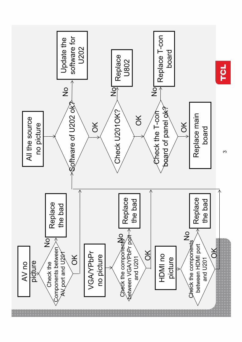
3
Upd
ate
the
softw
are
for
U20
2S
oftw
are
of U
202
ok?
No
Rep
lace
U80
2C
heck
U20
1OK
?N
o
OK
Rep
lace
T-c
on
boar
d
No
OK
Rep
lace
mai
n bo
ard
All
the
sour
ce
no p
ictu
re OK
Che
ck th
e T-
con
boar
d of
pan
el o
k?
Rep
lace
the
bad
Rep
lace
the
bad
Rep
lace
the
bad
HD
MI n
o pi
ctur
e
VG
A/Y
PbP
rno
pic
ture
Che
ck th
e C
ompo
nent
s be
twee
n A
V p
ort a
nd U
201
Che
ck th
e co
mpo
nent
sbe
twee
n V
GA
/YP
bPrp
ort
and
U20
1
Che
ck th
e co
mpo
nent
sbe
twee
n H
DM
I por
tan
d U
201
No
OK
No
OK
No
OK
AV
no
pict
ure
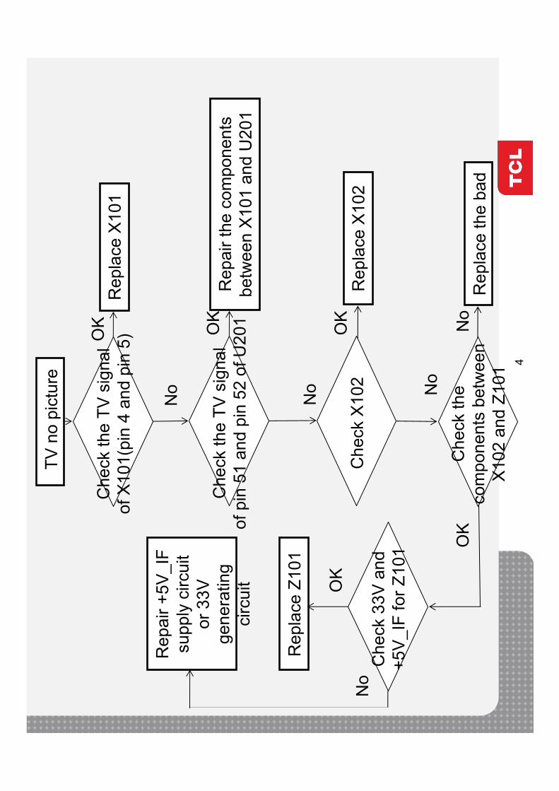
4
Rep
lace
X10
1
Rep
air t
he c
ompo
nent
s be
twee
n X
101
and
U20
1
Rep
lace
X10
2
Rep
lace
the
bad
Rep
lace
Z10
1
Rep
air +
5V_I
F su
pply
circ
uit
or 3
3V
gene
ratin
gci
rcui
t
OK
No
Che
ck th
e TV
sig
nal
of X
101(
pin
4 an
d pi
n 5)
OK
No
OK
No
OK
TV n
o pi
ctur
e
Che
ck th
e TV
sig
nal
of p
in 5
1 an
d pi
n 52
of U
201
Che
ck X
102
Che
ck th
e co
mpo
nent
s be
twee
n X
102
and
Z101
No
OK
No
Che
ck 3
3V a
nd
+5V
_IF
for Z
101
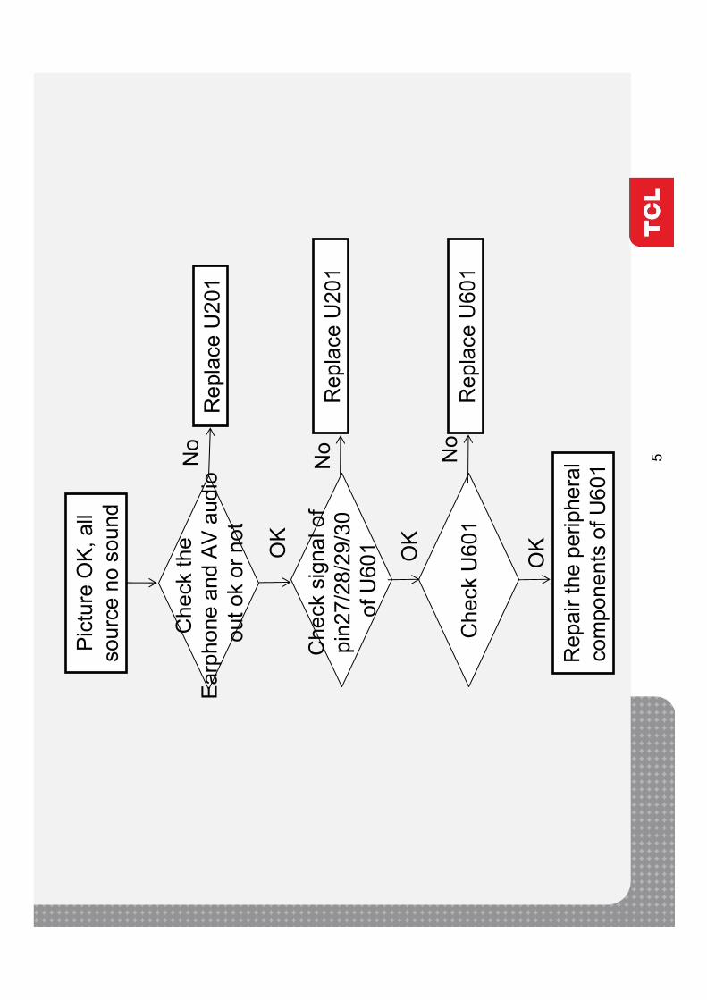
5
Rep
lace
U20
1
Pic
ture
OK
, all
sour
ce n
o so
und
Che
ck th
e E
arph
one
and
AV
aud
io
out o
k or
not
OK
No
Rep
lace
U20
1C
heck
sig
nal o
f pi
n27/
28/2
9/30
of U
601
Che
ck U
601
No
OK
Rep
lace
U60
1N
o
OK
Rep
air t
he p
erip
hera
l co
mpo
nent
s of
U60
1


Top Related