


Languages
Pages
Legal

Stratix 10 HPS ComponentReference Manual
SubscribeSend Feedback
S10-HPSCOMPONENT | 2017.11.06Latest document on the web: PDF | HTML

Contents
1 Introduction to the Intel® Stratix® 10 HPS Component....................................................41.1 Cortex-A53 MPCore Processor.................................................................................. 41.2 CoreSight* Debug Components................................................................................ 51.3 Interconnect.......................................................................................................... 51.4 FPGA Bridges......................................................................................................... 51.5 Memory Controllers.................................................................................................61.6 Support Peripherals................................................................................................ 6
1.6.1 Interface Peripherals................................................................................... 61.6.2 On-Chip Memories...................................................................................... 7
1.7 Introduction to the HPS Component Revision History................................................... 7
2 Instantiating the Intel Stratix 10 HPS Component........................................................... 82.1 Using the HPS Parameter Editor................................................................................82.2 FPGA Interfaces......................................................................................................9
2.2.1 General Interfaces...................................................................................... 92.2.2 FPGA-to-HPS SDRAM AXI-4 Slave Interface.................................................. 102.2.3 Interrupts................................................................................................ 112.2.4 AXI Bridges..............................................................................................12
2.3 Configuring HPS Clocks and Resets..........................................................................132.3.1 Alternate Clock Source from FPGA...............................................................132.3.2 User Clocks..............................................................................................132.3.3 Reset Interfaces....................................................................................... 142.3.4 Peripheral FPGA Clocks.............................................................................. 15
2.4 Configuring Peripheral Pin Multiplexing.....................................................................162.4.1 Configuring Peripherals..............................................................................16
2.5 Configuring the External Memory Interface...............................................................172.6 Using the Address Span Extender Component...........................................................172.7 Generating and Compiling the HPS Component......................................................... 182.8 Instantiating the HPS Component Revision History.................................................... 19
3 Stratix 10 HPS Component Interfaces............................................................................203.1 Memory-Mapped Interfaces.................................................................................... 20
3.1.1 FPGA-to-HPS Bridge.................................................................................. 203.1.2 HPS-to-FPGA and Lightweight HPS-to-FPGA Bridges.......................................213.1.3 FPGA-to-HPS SDRAM Interface................................................................... 223.1.4 EMIF Conduit............................................................................................22
3.2 Clocks................................................................................................................. 223.2.1 Alternative Clock Input to HPS PLLs.............................................................223.2.2 User Clocks..............................................................................................233.2.3 AXI Bridge FPGA Interface Clocks................................................................233.2.4 SDRAM Clocks.......................................................................................... 233.2.5 Peripheral FPGA Clocks.............................................................................. 23
3.3 Resets.................................................................................................................243.3.1 HPS-to-FPGA Reset Interfaces.................................................................... 243.3.2 Peripheral Reset Interfaces.........................................................................24
3.4 Debug and Trace Interfaces....................................................................................243.4.1 FPGA System Trace Macrocell Events Interface..............................................253.4.2 FPGA Cross Trigger Interface...................................................................... 25
Contents
Stratix 10 HPS Component Reference Manual2

3.4.3 Debug APB* Interface............................................................................... 253.5 Peripheral Signal Interfaces....................................................................................25
3.5.1 Platform Designer Peripheral Port Interface Mapping...................................... 253.5.2 DMA Controller Interface............................................................................32
3.6 Other Interfaces................................................................................................... 323.6.1 MPU Standby and Event Interfaces..............................................................333.6.2 General Purpose Signals............................................................................ 333.6.3 FPGA-to-HPS Interrupts............................................................................. 33
3.7 I/O Delays........................................................................................................... 343.8 HPS Component Interfaces Revision History............................................................. 34
Contents
Stratix 10 HPS Component Reference Manual3

1 Introduction to the Intel® Stratix® 10 HPS ComponentThe hard processor system (HPS) component is a wrapper that interfaces logic in theuser design to the HPS hard logic, simulation models, bus functional models (BFMs),and software handoff files. It instantiates the HPS hard logic in the user design; andenables other soft components to interface with the HPS hard logic. The HPScomponent itself has a small footprint in the FPGA fabric, because its only purpose isto enable soft logic to connect to the extensive hard logic in the HPS. You can connectsoft logic to the HPS.
After the soft logic is connected to the HPS, Platform Designer ensures the followingfeatures:
• Interoperability by adapting Avalon® Memory-Mapped (Avalon-MM) interfaces toAXI*
• Handle data width mismatches
• Clock domain transfer crossing
This allows you to integrate IP from , 3rd party IP cores, and custom IP cores to theHPS without having to create integration logic.
For more information about the HPS and its integration into the system on a chip(SoC), refer to the Intel Stratix 10 Device Datasheet.
For more information about the HPS system architecture and features, refer to the"Introduction to the Hard Processor" chapter in the Intel® Stratix® 10 Hard ProcessorSystem Technical Reference Manual .
For more information about instantiating the HPS Component, refer to the"Instantiating the HPS Component" chapter.
For more information about the HPS component interfaces, refer to the "HPSComponent Interfaces" chapter.
Related Links
• Introduction to the Hard Processor System
• Intel Stratix 10 Device Datasheet
• Instantiating the Intel Stratix 10 HPS Component on page 8
• Stratix 10 HPS Component Interfaces on page 20
1.1 Cortex-A53 MPCore Processor
The Arm Cortex-A53 MPCore Processor is composed of four Armv8-A architecturecentral processing units (CPUs).
S10-HPSCOMPONENT | 2017.11.06
Intel Corporation. All rights reserved. Intel, the Intel logo, Altera, Arria, Cyclone, Enpirion, MAX, Nios, Quartusand Stratix words and logos are trademarks of Intel Corporation or its subsidiaries in the U.S. and/or othercountries. Intel warrants performance of its FPGA and semiconductor products to current specifications inaccordance with Intel's standard warranty, but reserves the right to make changes to any products and servicesat any time without notice. Intel assumes no responsibility or liability arising out of the application or use of anyinformation, product, or service described herein except as expressly agreed to in writing by Intel. Intelcustomers are advised to obtain the latest version of device specifications before relying on any publishedinformation and before placing orders for products or services.*Other names and brands may be claimed as the property of others.
ISO9001:2008Registered

Related Links
Cortex-A53 MPCore Processor
1.2 CoreSight* Debug Components
The following lists the Arm CoreSight* debug components:
• Debug Access Port (DAP)
• System Trace Macrocell (STM)
• Embedded Trace FIFO (ETF)
• AMBA* Trace Bus Replicator
• Embedded Trace Router (ETR)
• Trace Port Interface Unit (TPIU)
• Embedded Cross Trigger (ECT)
Related Links
Introduction to the Stratix 10 HPS Component
1.3 Interconnect
The interconnect consists of the L3 interconnect, SDRAM L3 interconnect, and level 4(L4) buses.
The L3 Interconnect provides high-bandwidth routing featuring Arm TrustZone*-compliant security firewalls with programmable Quality of Service (QoS) betweenmasters and slaves in the HPS. The L3 Interconnect also provides a lower performancetier of L4 buses for mid to low-bandwidth slave peripherals and peripheral control andstatus registers. The SDRAM L3 interconnect connects the HPS to the Hard MemoryController (HMC) located in the FPGA I/O column.
Related Links
System Interconnect
1.4 FPGA Bridges
The FPGA bridges provide a variety of communication channels between the HPS andthe FPGA fabric. The HPS is highly integrated with the FPGA fabric, resulting inthousands of connecting signals. Some of the HPS-to-FPGA interfaces include:
• FPGA-to-HPS bridge
• HPS-to-FPGA bridge
• Lightweight HPS-to-FPGA bridge
• FPGA-to-HPS SDRAM bridge
Related Links
HPS-FPGA Bridges
1 Introduction to the Intel® Stratix® 10 HPS Component
S10-HPSCOMPONENT | 2017.11.06
Stratix 10 HPS Component Reference Manual5

1.5 Memory Controllers
The following lists the memory controller peripherals:
• NAND Flash Controller
• SD/MMC Controller
Related Links
• System Interconnect
• NAND Flash Controller
• SD/MMC Controller
1.6 Support Peripherals
The support peripherals are listed below:
• Clock Manager
• Reset Manager
• System Manager
• Timers
• Watchdog Timers
• Direct Memory Access (DMA) Controller
• Error Checking and Correction Controller
Related Links
• Clock Manager
• Reset Manager
• System Manager
• DMA Controller
• Timer
• Watchdog Timer
1.6.1 Interface Peripherals
The interface peripherals are listed below:
• Ethernet Media Access Controllers (EMAC)
• USB 2.0 On-The-Go (OTG) Controllers
• I2C Controllers
• UARTs
• SPI Master Controllers
• SPI Slave Controllers
• GPIO Interfaces
Related Links
• Ethernet Media Access Controller
1 Introduction to the Intel® Stratix® 10 HPS Component
S10-HPSCOMPONENT | 2017.11.06
Stratix 10 HPS Component Reference Manual6

• USB 2.0 OTG Controller
• SPI Controller
• I2C Controller
• UART Controller
• General-Purpose I/O Interface
1.6.2 On-Chip Memories
On-Chip RAM is the only on-chip memory.
Related Links
On-Chip Memory
1.7 Introduction to the HPS Component Revision History
Table 1. Document Revision History
Version Changes
2017.11.06 Initial release
1 Introduction to the Intel® Stratix® 10 HPS Component
S10-HPSCOMPONENT | 2017.11.06
Stratix 10 HPS Component Reference Manual7

2 Instantiating the Intel Stratix 10 HPS ComponentThis chapter describes the parameters available in the hard processor system (HPS)component parameter editor, which opens when you add or edit an HPS component.You instantiate the HPS component in Platform Designer.
2.1 Using the HPS Parameter Editor
1. Install the Intel Stratix 10 ACDS version 17.1.
2. Open the Intel Quartus® Prime software.
3. Open Platform Designer by selecting Tools ➤ Platform Designer.
4. In the Device Family tab, select a 1SXxxx device from the Device pull-downmenu.
5. In the IP Catalog tab, under Library, select Processors and Peripherals ➤Hard Processor Systems ➤ Stratix 10 Hard Processor System.
Figure 1. Platform Designer Device Family Tab
S10-HPSCOMPONENT | 2017.11.06
Intel Corporation. All rights reserved. Intel, the Intel logo, Altera, Arria, Cyclone, Enpirion, MAX, Nios, Quartusand Stratix words and logos are trademarks of Intel Corporation or its subsidiaries in the U.S. and/or othercountries. Intel warrants performance of its FPGA and semiconductor products to current specifications inaccordance with Intel's standard warranty, but reserves the right to make changes to any products and servicesat any time without notice. Intel assumes no responsibility or liability arising out of the application or use of anyinformation, product, or service described herein except as expressly agreed to in writing by Intel. Intelcustomers are advised to obtain the latest version of device specifications before relying on any publishedinformation and before placing orders for products or services.*Other names and brands may be claimed as the property of others.
ISO9001:2008Registered

2.2 FPGA Interfaces
The FPGA Interfaces tab is one of four tabs on the HPS Component. This tabcontains several groups with the parameters shown in the following figure.
Figure 2. FPGA Interfaces Tab
Related Links
Introduction to the Intel Stratix 10 HPS Component on page 4
2.2.1 General Interfaces
When enabled, the interfaces described in the following table become visible in theHPS component.
Table 2. General Parameters
Parameter Name Parameter Description Interface Name
Enable MPU standby and eventsignals
Enables interfaces that perform the followingfunctions:• Notify the FPGA fabric that the
microprocessor unit (MPU) is in standbymode.
• Wake up an MPCore processor from a waitfor event (WFE) state.
h2f_mpu_events
Input for FPGA to signal events to bothprocessors. This signal must be asserted highfor at least two MPU clock cycles to be visibleto either Cortex-A53 processor core. Thissignal is used to wake either processor corefrom standby mode.
h2f_mpu_eventi
Output event from either processor sent to theFPGA. The output event is a multiple cyclepulse so logic in the FPGA should detect itusing a rising edge detector circuit to detectthe occurrence of the event. This signal isasserted each time either processor executesthe SEV instruction.
h2f_mpu_evento
continued...
2 Instantiating the Intel Stratix 10 HPS Component
S10-HPSCOMPONENT | 2017.11.06
Stratix 10 HPS Component Reference Manual9

Parameter Name Parameter Description Interface Name
Output per processor that indicates if theprocessor is in WFE standby mode. When highthe processor is in WFE standby mode.
h2f_mpu_standbywfe [1..0]
Output per processor that indicates if theprocessor is in WFI standby mode. When highthe processor is in WFI standby mode.
h2f_mpu_standbywfi [1..0]
Enable Debug APB interface Enables debug interface to the FPGA, allowingaccess to debug components in the HPS. Formore information, refer to the "CoreSightDebug and Trace" chapter.
h2f_debug_apb
• h2f_dbg_apb_PADDR[17..0]
• h2f_dbg_apb_PADDR31
• h2f_dbg_apb_PENABLE
• h2f_dbg_apb_PRDATA[31..0]
• h2f_dbg_apb_PREADY
• h2f_dbg_apb_PSEL
• h2f_dbg_apb_PSLVERB
• h2f_dbg_apb_PWDATA[31..0]
• h2f_dbg_apb_PWRITE
h2f_debug_apb_sideband
• h2f_debug_apb_PCLKEN
• h2f_debug_apb_DBG_APB_DISABLE
h2f_debug_apb_clock
• h2f_abg_apb_clk
h2f_debug_apb_reset
• h2f_dbg_apb_rst_n
Enable System Trace Macrocellhardware events
Enables system trace macrocell (STM)hardware events, allowing logic inside theFPGA to insert messages into the trace stream.For more information, refer to the "CoreSightDebug and Trace" chapter.
f2h_stm_hw_events
• f2h_stm_hwevents [27..0]
Enable FPGA Cross Triggerinterface
Enables the cross trigger interface (CTI), whichallows trigger sources and sinks to interfacewith the embedded cross trigger (ECT). Formore information, refer to the "CoreSightDebug and Trace" chapter.If this interface has to be connected to aSignalTap II instance in the FPGA fabric, thenit has to be left disabled in Platform Designer.
h2f_cti
• h2f_cti_trig_in [7..0]
• h2f_cti_trig_out_ack[7..0]
• h2f_cti_trig_out [7..0]
• h2f_cti_trig_in_ack[7..0]
Related Links
CoreSight Debug and Trace
2.2.2 FPGA-to-HPS SDRAM AXI-4 Slave Interface
In the FPGA-to-HPS SDRAM AXI-4 Slave Interface table, you can configure the:
2 Instantiating the Intel Stratix 10 HPS Component
S10-HPSCOMPONENT | 2017.11.06
Stratix 10 HPS Component Reference Manual10
• FPGA-to-SDRAM0 - FPGA-to-SDRAM2 Interface enable/data width by choosing:unused, 32-, 64-, or 128-bit from the pull-down menu
• FPGA-to-SDRAM0 - FPGA-to-SDRAM2 Ready Latency pipeline by choosing: unused,1, 2, 3, or 4 registers from the pull-down menu
• FPGA-to-SDRAM Bridge Address Width by choosing address widths ranging from21-bit (2 MB) to 37-bit (128 GB) from the pull-down menu
Related Links
Using the Address Span Extender Component on page 17For more information about address span extender details
2.2.3 Interrupts
Table 3. FPGA-to-HPS Interrupts Interface
Parameter Name Parameter Description Interface Name
Enable FPGA-to-HPS Interrupts Enables interface for FPGA interrupt signals to theMPU (in the HPS).
f2h_irq0
f2h_irq1
You can enable the interfaces for each HPS peripheral interrupt to the FPGA.
Table 4. HPS-to-FPGA Interrupts InterfaceThe following table lists the available HPS to FPGA interrupt interfaces and the corresponding parameters toenable them.
Parameter Name Parameter Description Interface Name
Enable Clock Peripheral Interrupts Enables interface for HPS clockmanager and MPU wake-up interruptsignals to the FPGA
h2f_clkmgr_interrupt
h2f_mpuwakeup_interrupt
Enable DMA Interrupts Enables interface for HPS DMAchannels interrupt and DMA abortinterrupt to the FPGA
h2f_dma_interrupt0
h2f_dma_interrupt1
h2f_dma_interrupt2
h2f_dma_interrupt3
h2f_dma_interrupt4
h2f_dma_interrupt5
h2f_dma_interrupt6
h2f_dma_interrupt7
h2f_dma_abort_interrupt
Enable EMAC Interrupts Enables interface for HPS EthernetMAC controller interrupt to the FPGA.EMAC must be enabled in Pin Mux Tabbefore enabling interrupt.
h2f_emac0_interrupt
h2f_emac1_interrupt
h2f_emac2_interrupt
Enable GPIO Interrupts Enables interface for the HPS generalpurpose IO (GPIO) interrupt to theFPGA
h2f_gpio0_interrupt
h2f_gpio1_interrupt
h2f_gpio2_interrupt
Enable I2C-EMAC Interrupts Enable the HPS peripheral interrupt forI2CEMAC to be driven into the FPGAfabric
h2f_i2c_emac0_interrupt
h2f_i2c_emac1_interrupt
h2f_i2c_emac2_interrupt
continued...
2 Instantiating the Intel Stratix 10 HPS Component
S10-HPSCOMPONENT | 2017.11.06
Stratix 10 HPS Component Reference Manual11

Parameter Name Parameter Description Interface Name
Enable I2C Peripherals Interrupts Enable the HPS peripheral interrupt forI2C0 to be driven into the FPGA fabric.The I2C must be enabled in the PinMux Tab before enabling interrupt.
h2f_i2c0_interrupt
h2f_i2c1_interrupt
Enable L4 Timer Interrupts Enables the HPS peripheral interruptfor L4TIMER to be driven into the FPGAfabric.
h2f_timer_l4sp_0_interrupt
h2f_timer_l4sp_1_interrupt
Enable NAND Interrupts Enables interface for the HPS NANDcontroller interrupt to the FPGA. TheNAND IP Block must be enabled in PinMux Tab before enabling interrupt.
h2f_nand_interrupt
Enable SYS Timer Interrupts Enables the HPS peripheral interruptfor SYSTIMER to be driven into theFPGA fabric.
h2f_timer_sys_0_interrupt
h2f_timer_sys_1_interrupt
Enable SD/MMC Interrupts Enables interface for the HPS SD/MMCcontroller interrupt to the FPGA. TheSD/MMC IP Block must be enabled inPin Mux Tab before enabling interrupt.
h2f_sdmmc_interrupt
Enable SPI Master Interrupts Enables interface for the HPS SPImaster controller interrupt to theFPGA. The SPI Master IP Block must beenabled in Pin Mux Tab before enablinginterrupt.
h2f_spim0_interrupt
h2f_spim1_interrupt
Enable SPI Slave Interrupts Enables interface for the HPS SPI slavecontroller interrupt to the FPGA. TheSPI IP Block must be enabled in PinMux Tab before enabling interrupt.
h2f_spis0_interrupt
h2f_spis1_interrupt
Enable ECC/Parity_L1 Interrupts Enables the HPS peripheral interruptfor ECC single and double bit error andL1 parity error to be driven into theFPGA fabric.
h2f_ecc_serr_interrupt
h2f_ecc_derr_interrupt
h2f_parity_l1_interrupt
Enable UART Interrupts Enables interface for the HPS UARTcontroller interrupt to the FPGA. TheUART IP Block must be enabled in PinMux Tab before enabling interrupt.
h2f_uart0_interrupt
h2f_uart1_interrupt
Enable USB Interrupts Enables interface for the HPS USBcontroller interrupt to the FPGA. TheUSB IP Block must be enabled in PinMux Tab before enabling interrupt.
h2f_usb0_interrupt
s2f_usb1_interrupt
Enable Watchdog Interrupts Enables interface for the HPS watchdoginterrupt to the FPGA
h2f_wdog0_interrupt
h2f_wdog1_interrupt
2.2.4 AXI Bridges
Table 5. Bridge Parameters
Parameter Name Parameter Description Interface Name
FPGA-to-HPS slave interface: datawidth
Enable either AXI-4 interface or ACE*-lite interface.
f2h_axi_slave
f2h_axi_clock
f2h_axi_reset
HPS-to-FPGA AXI-4 Master interface:data width
Enable or disable the HPS-to-FPGAinterface; if enabled, set the datawidth to 32, 64, or 128 bits.
h2f_axi_master
h2f_axi_clock
continued...
2 Instantiating the Intel Stratix 10 HPS Component
S10-HPSCOMPONENT | 2017.11.06
Stratix 10 HPS Component Reference Manual12

Parameter Name Parameter Description Interface Name
h2f_axi_reset
Lightweight HPS-to-FPGA Masterinterface: data width
Enable or disable the lightweight HPS-to-FPGA interface. When enabled, thedata width is 32 bits.
h2f_lw_axi_master
h2f_lw_axi_clock
h2f_lw_axi_reset
FPGA-to-HPS SDRAM AXI-4 Slaveinterface: data width
Enable or disable the FPGA to HPSSDRAM AXI-4 slave interface from 0 to2, if enabled, the data width of eachinterface can be set to 32, 64 or 128bits.
f2sdram0_clockf2sdram0_dataf2sdram0_resetf2sdram1_clockf2sdram1_dataf2sdram1_resetf2sdram2_clockf2sdram2_dataf2sdram2_reset
Note: To facilitate accessing these slaves from a memory-mapped master with a smalleraddress width, you can use the Intel Address Span Extender. You can also use the"Bridge address width" option.
Related Links
Using the Address Span Extender Component on page 17For more information about address span extender details
2.3 Configuring HPS Clocks and Resets
The HPS Clocks and Reset tab is one of four tabs on the HPS Component. This tabcontains several groups with the following parameters:
Alternate Clock Source from FPGA on page 13
User Clocks on page 13
Reset Interfaces on page 14
Peripheral FPGA Clocks on page 15
2.3.1 Alternate Clock Source from FPGA
Table 6. Alternate Clock Source Parameters
Parameter Name Parameter Description Clock Interface Name
Enable Alternate Clock Source fromFPGA
Drives the HPS Clock source tooriginate from the FPGA fabric insteadof the dedicated HPS input clock pin.
f2h_free_clk
2.3.2 User Clocks
When you enable a HPS-to-FPGA user clock, you must manually enter its maximumfrequency for timing analysis. The TimeQuest Timing Analyzer has no otherinformation about how software running on the HPS configures the phase-locked loop(PLL) outputs. Each possible clock, including clocks that are available from peripherals,has its own parameter for describing the clock frequency.
2 Instantiating the Intel Stratix 10 HPS Component
S10-HPSCOMPONENT | 2017.11.06
Stratix 10 HPS Component Reference Manual13

2.3.2.1 User Clock Parameters
The frequencies that you provide are the maximum expected frequencies. The actualclock frequencies can be modified through the register interface, for example bysoftware running on the microprocessor unit (MPU).
Parameter Name Parameter Description Clock Interface Name
Enable HPS-to-FPGA user 0 clock Enable main PLL from HPS-to-FPGA h2f_user0_clock
User 0 clock frequency Specify the maximum expectedfrequency for the main PLL
Enable HPS-to-FPGA user 1 clock Enable peripheral PLL from HPS-to-FPGA
h2f_user1_clock
User 1 clock frequency Specify the maximum expectedfrequency for the peripheral PLL
2.3.2.2 Clock Frequency Usage
The clock frequencies you provide are reported in a Synopsys* Design Constraints File(.sdc) generated by Platform Designer. The .sdc file will be referenced in thesystem .qip file when the system is generated.
Related Links
Clock ManagerFor more information about the Clock Manager features and interface.
2.3.3 Reset Interfaces
You can enable the resets on an individual basis through the HPS Clocks and resetstab under the Resets sub tab.
Table 7. Reset Parameters
Parameter Name Parameter Description Interface Name
Enable HPS-to-FPGA cold andwarm reset output
Reset output from the HPS to FPGA that asserts onboth cold and warm HPS reset events.
h2f_reset_n
Enable HPS-to-FPGA cold resetoutput
Enable interface for HPS-to-FPGA cold reset output h2f_cold_reset
Enable HPS warm resethandshake signals
Enable an additional pair of reset handshake signalsallowing soft logic to notify the HPS when it is safe toinitiate a warm reset in the FPGA fabric.
h2f_warm_reset_handshake
Enable watchdog reset Enable interface for FPGA to HPS watchdog reset h2f_watchdog_rst
2 Instantiating the Intel Stratix 10 HPS Component
S10-HPSCOMPONENT | 2017.11.06
Stratix 10 HPS Component Reference Manual14

Figure 3. Recommended SDRAM Reset Connections
I/OBanks
mem_conduit_end
pll_ref_clk_clock_sink
oct_conduit_end
hps_emif_conduit_end
External Memory Interface for HPS
ClocksCommand
DataMemory Hard
Logic Connection(Including Reset
Requests)emif
HardProcessor System
Master User Logic f2sdram0
Master User Logic f2sdram1
Master User Logic f2sdram2
Note: SDRAM and the EMIF conduit can be enabled through the Platform Designer FPGAInterface and SDRAM tab.
Related Links
Reset Manager
2.3.4 Peripheral FPGA Clocks
Parameter Name Parameter Description
EMAC 0 (emac0_md_clk clock frequency) If EMAC 0 peripheral is routed to FPGA, use the input fieldto specify EMAC 0 MDIO clock frequency
EMAC 0 (emac0_gtx_clk clock frequency) If EMAC 0 peripheral is routed to FPGA, use the input fieldto specify EMAC 0 transmit clock frequency
EMAC 1 (emac1_md_clk clock frequency) If EMAC 1 peripheral is routed to FPGA, use the input fieldto specify EMAC 1 MDIO clock frequency
EMAC 1 (emac1_gtx_clk clock frequency) If EMAC 1 peripheral is routed to FPGA, use the input fieldto specify EMAC 1 transmit clock frequency
EMAC 2 (emac2_md_clk clock frequency) If EMAC 2 peripheral is routed to FPGA, use the input fieldto specify EMAC 2 MDIO clock frequency
EMAC 2 (emac2_gtx_clk clock frequency) If EMAC 2 peripheral is routed to FPGA, use the input fieldto specify EMAC 2 transmit clock frequency
SD/MMC (sdmmc_cclk) If this peripheral pin multiplexing is configured to route toFPGA fabric, use the input field to specify the SD/MMCsdmmc_cclk clock frequency
SPIM 0 (spim0_sclk_out clock frequency) If SPI master 0 peripheral is routed to FPGA, use the inputfield to specify SPI master 0 output clock frequency
SPIM 1 (spim1_sclk_out clock frequency) If SPI master 1 peripheral is routed to FPGA, use the inputfield to specify SPI master 1 output clock frequency
I2C0 (i2c0_clk clock frequency) If I2C 0 peripheral is routed to FPGA, use the input field tospecify I2C 0 output clock frequency
I2C1 (i2c1_clk clock frequency) If I2C 1 peripheral is routed to FPGA, use the input field tospecify I2C 1 output clock frequency
continued...
2 Instantiating the Intel Stratix 10 HPS Component
S10-HPSCOMPONENT | 2017.11.06
Stratix 10 HPS Component Reference Manual15
Parameter Name Parameter Description
I2CEMAC0 (i2cemac0_clk) If this peripheral pin multiplexing is configured to route tothe FPGA fabric, use the input field to specify the I2CEMAC0i2cemac0_clk clock frequency
I2CEMAC1 (i2cemac1_clk) If this peripheral pin multiplexing is configured to route tothe FPGA fabric, use the input field to specify the I2CEMAC1i2cemac1_clk clock frequency
I2CEMAC2 (i2cemac2_clk) If this peripheral pin multiplexing is configured to route tothe FPGA fabric, use the input field to specify the I2CEMAC2i2cemac2_clk clock frequency
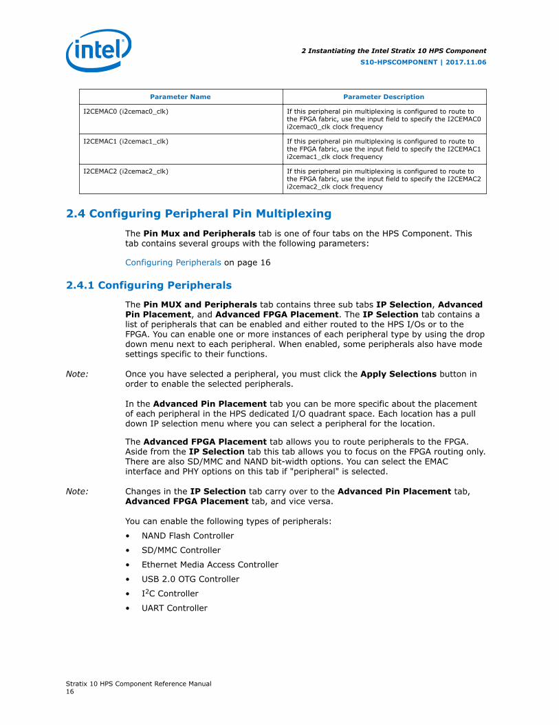
2.4 Configuring Peripheral Pin Multiplexing
The Pin Mux and Peripherals tab is one of four tabs on the HPS Component. Thistab contains several groups with the following parameters:
Configuring Peripherals on page 16
2.4.1 Configuring Peripherals
The Pin MUX and Peripherals tab contains three sub tabs IP Selection, AdvancedPin Placement, and Advanced FPGA Placement. The IP Selection tab contains alist of peripherals that can be enabled and either routed to the HPS I/Os or to theFPGA. You can enable one or more instances of each peripheral type by using the dropdown menu next to each peripheral. When enabled, some peripherals also have modesettings specific to their functions.
Note: Once you have selected a peripheral, you must click the Apply Selections button inorder to enable the selected peripherals.
In the Advanced Pin Placement tab you can be more specific about the placementof each peripheral in the HPS dedicated I/O quadrant space. Each location has a pulldown IP selection menu where you can select a peripheral for the location.
The Advanced FPGA Placement tab allows you to route peripherals to the FPGA.Aside from the IP Selection tab this tab allows you to focus on the FPGA routing only.There are also SD/MMC and NAND bit-width options. You can select the EMACinterface and PHY options on this tab if "peripheral" is selected.
Note: Changes in the IP Selection tab carry over to the Advanced Pin Placement tab,Advanced FPGA Placement tab, and vice versa.
You can enable the following types of peripherals:
• NAND Flash Controller
• SD/MMC Controller
• Ethernet Media Access Controller
• USB 2.0 OTG Controller
• I2C Controller
• UART Controller
2 Instantiating the Intel Stratix 10 HPS Component
S10-HPSCOMPONENT | 2017.11.06
Stratix 10 HPS Component Reference Manual16

• SPI Master
• SPI Slave
• CoreSight Debug and Trace
For more information about these peripherals, refer to their corresponding chapters inthe Intel Stratix 10 HPS Technical Reference Manual.
Related Links
• CoreSight Debug and Trace
• NAND Flash Controller
• Ethernet Media Access Controller
• USB 2.0 OTG Controller
• I2C Controller
• UART Controller
• SD/MMC ControllerFor more information about the SD/MMC Controller features and interface.
• SPI Master
• SPI Slave
2.5 Configuring the External Memory Interface
The SDRAM tab is one of four tabs on the HPS component. Enable the conduit toconnect to the Intel Stratix 10 External Memory Interface. This option enables aconduit interface for the HPS to talk to the Intel Stratix 10 External Memory interfacesfor the HPS.
The HPS supports one memory interface implementing double data rate 3 (DDR3),double data rate 3 Low Voltage (DDR3L), and double data rate 4 (DDR4) protocols.
2.6 Using the Address Span Extender Component
The FPGA-to-HPS bridge and FPGA-to-HPS SDRAM bridge memory-mapped interfacescan be configured to expose their entire address spaces to the FPGA fabric, 132GBand 128GB, respectively. The address span extender component provides a memory-mapped window into the address space that it masters. Using the address spanextender, an FPGA master with a smaller address span can access the entire addressspace exposed by the FPGA bridge.
You can use the address span extender between a soft logic master and an FPGA-to-HPS bridge or FPGA-to-HPS SDRAM interface. This component reduces the number ofaddress bits required for a master to address a memory-mapped slave interfacelocated in the HPS.
In the example shown in the figure below, the bridges in the HPS component areconfigured for 32-bit wide addresses (4GB address span).
2 Instantiating the Intel Stratix 10 HPS Component
S10-HPSCOMPONENT | 2017.11.06
Stratix 10 HPS Component Reference Manual17

Figure 4. Address Span Extender ComponentsTwo address span extender components used in a system with the HPS.
M
M
M
S M
S M
4 GB
4 GB
4 GB1 GB
512 MB
512 MB
DMA
Nios IIProcessor
Address SpanExtender
Address SpanExtender
S
S
FPGA-to-SDRAMInterface
S
FPGA-to-HPSBridge
HPS
Platform Designer System
1GBWindow
512 MBWindow
You can also use the address span extender in the HPS-to-FPGA direction, for slaveinterfaces in the FPGA. In this case, the HPS-to-FPGA bridge exposes a limited,variable address space in the FPGA, which can be paged in using the address spanextender.
For example, suppose that the HPS-to-FPGA bridge has a 1-GB span, and the HPSneeds to access three independent 1-GB memories in the FPGA portion of the device.To achieve this, the HPS programs the address span extender to access one SDRAM(1-GB) in the FPGA at a time. This technique is commonly called paging or windowing.
Related Links
Platform Designer System Design ComponentsFor more information about the Intel Span Extender, refer to the Address SpanExtender section in the Platform Designer System Design Components chapter ofthe Platform Designer Design Handbook.
2.7 Generating and Compiling the HPS Component
The process of generating and compiling an HPS design is very similar to the processfor any other Platform Designer project. Perform the following steps:
1. Generate the design with Platform Designer. The generated files include an .sdcfile containing clock timing constraints. If simulation is enabled, simulation filesare also generated.
2. Add <qsys_system_name>.qip to the Intel Quartus Prime project.<qsys_system_name>.qip is the Intel Quartus Prime IP File for the HPScomponent, generated by Platform Designer.
Note: Platform Designer generates pin assignments in the .qip file.
3. Perform analysis and synthesis with the Intel Quartus Prime software.
4. Compile the design with the Intel Quartus Prime software.
5. Optionally back-annotate the SDRAM pin assignments, to eliminate pin assignmentwarnings the next time you compile the design.
2 Instantiating the Intel Stratix 10 HPS Component
S10-HPSCOMPONENT | 2017.11.06
Stratix 10 HPS Component Reference Manual18

Related Links
Configuring Peripheral Pin Multiplexing on page 16
2.8 Instantiating the HPS Component Revision History
Table 8. Document Revision History
Version Changes
2017.11.06 Initial release
2 Instantiating the Intel Stratix 10 HPS Component
S10-HPSCOMPONENT | 2017.11.06
Stratix 10 HPS Component Reference Manual19

3 Stratix 10 HPS Component InterfacesThis chapter describes the interfaces, including clocks and resets, implemented by thehard processor system (HPS) component.
The majority of the resets can be enabled on an individual basis. The exception is theh2f_reset interface, which is always enabled.
You must declare the clock frequency of each HPS-to-FPGA clock for timing purposes.Each possible clock, including ones that are available from peripherals, has its ownparameter for describing the clock frequency. Declaring the clock frequency for HPS-to-FPGA clocks specifies how you plan to configure the PLLs and peripherals, to enableTimeQuest to accurately estimate system timing. It has no effect on PLL settings.
Related Links
• Reset ManagerFor more information about the Reset Manager features and interface.
• Clock ManagerFor more information about the Clock Manager features and interface.
• Avalon Interface SpecificationsFor Avalon protocol timing, refer to the Avalon Interface Specifications .
• Instantiating the Intel Stratix 10 HPS Component on page 8For information about instantiating the HPS component, refer to the"Instantiating the HPS Component" chapter.
• ARM InfocenterFor Advanced Microcontroller Bus Architecture ( AMBA ) Advanced eXtensibleInterface ( AXI ) protocol timing, refer to the AMBA AXI Protocol Specificationv1.0, which you can download from the ARM info center website.
3.1 Memory-Mapped Interfaces
3.1.1 FPGA-to-HPS Bridge
Table 9. FPGA-to-HPS Bridges and Clocks
Interface Name Description Associated Clock Interface
f2h_axi_slave FPGA-to-HPS ACE-Lite slave interface f2h_axi_clock
The FPGA-to-HPS interface is a 128-bit width ACE-Lite slave allowing FPGA masters toissue transactions to the HPS. This interface allows the FPGA fabric to access themajority of the HPS slaves. This interface also provides a coherent memory interface.
S10-HPSCOMPONENT | 2017.11.06
Intel Corporation. All rights reserved. Intel, the Intel logo, Altera, Arria, Cyclone, Enpirion, MAX, Nios, Quartusand Stratix words and logos are trademarks of Intel Corporation or its subsidiaries in the U.S. and/or othercountries. Intel warrants performance of its FPGA and semiconductor products to current specifications inaccordance with Intel's standard warranty, but reserves the right to make changes to any products and servicesat any time without notice. Intel assumes no responsibility or liability arising out of the application or use of anyinformation, product, or service described herein except as expressly agreed to in writing by Intel. Intelcustomers are advised to obtain the latest version of device specifications before relying on any publishedinformation and before placing orders for products or services.*Other names and brands may be claimed as the property of others.
ISO9001:2008Registered

Other interface standards in the FPGA fabric, such as connecting to Avalon Memory-Mapped (Avalon-MM) interfaces, can be supported through the use of soft logicadapters. The Platform Designer system integration tool automatically generatesadapter logic to connect AXI to Avalon-MM interfaces.
The FPGA-to-HPS interface is an ACE-Lite compliant interface with the followingfeatures:
• Fixed data width of 128 bits
• Flexible ready latency pipelining in the FPGA fabric to assist with timing closure atthe FPGA-to-HPS boundary: configurable depths of 0 (none), 1, 2, 3, or 4
For more information, refer to the Features of the Intel Stratix 10 HPS-FPGA Bridgesection in the "HPS-FPGA Bridges" chapter in the Intel Stratix 10 Hard ProcessorSystem Technical Reference Manual.
Related Links
• Clocks on page 22
• HPS-FPGA BridgesFor more information about the HPS-FPGA Bridges features and interface.
• Instantiating the Intel Stratix 10 HPS Component on page 8For information about the address span extender, refer to the Using theAddress Span Extender Component section in the "Instantiating the HPSComponent" chapter.
3.1.2 HPS-to-FPGA and Lightweight HPS-to-FPGA Bridges
Table 10. HPS-to-FPGA and Lightweight HPS-to-FPGA Bridges and Clocks
Interface Name Description Associated Clock Interface
h2f_axi_master HPS-to-FPGA AXI-4 master interface h2f_axi_clock
h2f_lw_axi_master HPS-to-FPGA lightweight AXI-4 master interface h2f_lw_axi_clock
The HPS-to-FPGA interface is a configurable data width AXI-4 master (32-, 64-, or128-bit) that allows HPS masters to issue transactions to the FPGA fabric.
The lightweight HPS-to-FPGA interface is a 32-bit AXI-4 master that allows HPSmasters to issue transactions to the FPGA fabric.
Other interface standards in the FPGA fabric, such as connecting to Avalon-MMinterfaces, can be supported through the use of soft logic adapters. The PlatformDesigner system integration tool automatically generates adapter logic to connect AXIto Avalon-MM interfaces.
Each AXI bridge accepts a clock input from the FPGA fabric and performs clock domaincrossing internally. The exposed AXI interface operates on the same clock domain asthe clock supplied by the FPGA fabric.
Both bridges offer flexible ready latency pipelining in the FPGA fabric to assist withtiming closure at the FPGA-to-HPS boundary with configurable depths of 0 (none), 1,2, 3, or 4.
3 Stratix 10 HPS Component Interfaces
S10-HPSCOMPONENT | 2017.11.06
Stratix 10 HPS Component Reference Manual21

For more information, refer to the Features of the Intel Stratix 10 HPS-FPGA Bridgesection in the "HPS-FPGA Bridges" chapter in the Intel Stratix 10 Hard ProcessorSystem Technical Reference Manual.
Related Links
• Clocks on page 22
• HPS-FPGA BridgesFor more information about the HPS-FPGA Bridges features and interface.
3.1.3 FPGA-to-HPS SDRAM Interface
The FPGA-to-HPS SDRAM interface is a direct connection between the FPGA fabric andthe HPS SDRAM Scheduler in the L3 SDRAM Interconnect. This interface supportsAMBA AXI-4 interface standards.
Table 11. FPGA-to-HPS SDRAM Interfaces and Clocks
Interface Name Associated Data Interface Associated Clock Interface
F2SDRAM0 f2sdram0_data f2sdram0_clock
F2SDRAM1 f2sdram1_data f2sdram1_clock
F2SDRAM2 f2sdram2_data f2sdram2_clock
The FPGA-to-HPS SDRAM interface is a configurable interface to the SDRAM Schedulerin the L3 SDRAM Interconnect. For each of the F2SDRAM interfaces, you can selectbetween 32-, 64- or 128-bit data widths. Flexible ready latency pipelining in the FPGAfabric assists with timing closure at the FPGA-to-HPS boundary with configurabledepths of 0 (none), 1, 2, 3, or 4.
3.1.4 EMIF Conduit
Under the SDRAM tab in Platform Designer, the EMIF conduit can be enabled. Thisenables the HPS dedicated conduit to the Intel Stratix 10 External Memory Interfacefor HPS. This conduit cannot connect to any other External Memory Interface (EMIF)IP. Only the Intel Stratix 10 External Memory Interface for HPS Platform Designer IPshould be used.
3.2 Clocks
The HPS-to-FPGA clock interface supplies physical clocks to the FPGA. These clocksand resets are generated in the HPS.
3.2.1 Alternative Clock Input to HPS PLLs
An alternative clock input to HPS PLLs is the FPGA-to-HPS free clock(f2h_free_clk), which drives the HPS clock source to originate from the FPGA fabricinstead of the dedicated HPS input clock pin.
3 Stratix 10 HPS Component Interfaces
S10-HPSCOMPONENT | 2017.11.06
Stratix 10 HPS Component Reference Manual22

3.2.2 User Clocks
A user clock is a PLL output that is connected to the FPGA fabric rather than the HPS.You can connect a user clock to logic that you instantiate in the FPGA fabric.
• h2f_user0_clock—HPS-to-FPGA user clock, driven from main PLL
• h2f_user1_clock—HPS-to-FPGA user clock, driven from peripheral PLL
3.2.3 AXI Bridge FPGA Interface Clocks
The AXI interface has an asynchronous clock crossing in the FPGA-to-HPS bridge. TheFPGA-to-HPS and HPS-to-FPGA interfaces are synchronized to clocks generated in theFPGA fabric. These interfaces can be asynchronous to one another.
• f2h_axi_clock—AXI slave clock for FPGA-to-HPS bridge, generated in FPGAfabric
• h2f_axi_clock—AXI master clock for HPS-to-FPGA bridge, generated in FPGAfabric
• h2f_lw_axi_clock—AXI master clock for lightweight HPS-to-FPGA bridge,generated in FPGA fabric
3.2.4 SDRAM Clocks
You can configure the HPS component with up to three FPGA-to-HPS SDRAM clocks.
Each command channel to the SDRAM controller has an individual clock source fromthe FPGA fabric. The interface clock is always supplied by the FPGA fabric, with clockcrossing occurring on the HPS side of the boundary.
The FPGA-to-HPS SDRAM clocks are driven by soft logic in the FPGA fabric.
• f2h_sdram0_clock—SDRAM clock for port 0
• f2h_sdram1_clock—SDRAM clock for port 1
• f2h_sdram2_clock—SDRAM clock for port 2
3.2.5 Peripheral FPGA Clocks
The HPS peripheral clocks are exposed when the peripheral signals are routed to theFPGA.
Table 12. Peripheral FPGA Clocks
Clock Name Description
emac_md_clk Ethernet PHY management interface clock (MDIO)
emac_gtx_clk Ethernet transmit clock that is used by the PHY in GMII 1Gbps mode
i2cemac_clk Ethernet PHY management interface clock (I2C)
emac_rx_clk_in Ethernet MAC reference clock from the PHY
emac_tx_clk_in Ethernet MAC uses this clock input for TX reference inGMII/MII 10/100Mbps modes
continued...
3 Stratix 10 HPS Component Interfaces
S10-HPSCOMPONENT | 2017.11.06
Stratix 10 HPS Component Reference Manual23
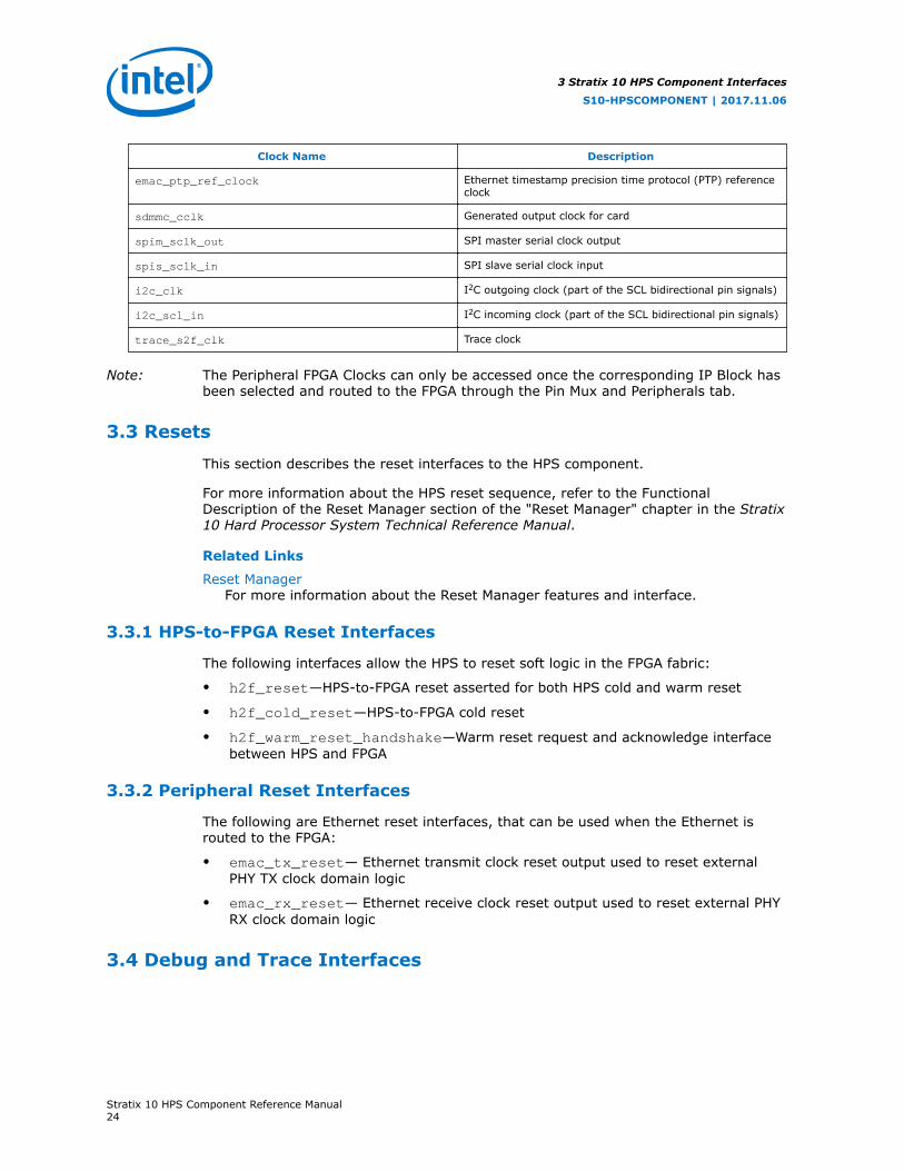
Clock Name Description
emac_ptp_ref_clock Ethernet timestamp precision time protocol (PTP) referenceclock
sdmmc_cclk Generated output clock for card
spim_sclk_out SPI master serial clock output
spis_sclk_in SPI slave serial clock input
i2c_clk I2C outgoing clock (part of the SCL bidirectional pin signals)
i2c_scl_in I2C incoming clock (part of the SCL bidirectional pin signals)
trace_s2f_clk Trace clock
Note: The Peripheral FPGA Clocks can only be accessed once the corresponding IP Block hasbeen selected and routed to the FPGA through the Pin Mux and Peripherals tab.
3.3 Resets
This section describes the reset interfaces to the HPS component.
For more information about the HPS reset sequence, refer to the FunctionalDescription of the Reset Manager section of the "Reset Manager" chapter in the Stratix10 Hard Processor System Technical Reference Manual.
Related Links
Reset ManagerFor more information about the Reset Manager features and interface.
3.3.1 HPS-to-FPGA Reset Interfaces
The following interfaces allow the HPS to reset soft logic in the FPGA fabric:
• h2f_reset—HPS-to-FPGA reset asserted for both HPS cold and warm reset
• h2f_cold_reset—HPS-to-FPGA cold reset
• h2f_warm_reset_handshake—Warm reset request and acknowledge interfacebetween HPS and FPGA
3.3.2 Peripheral Reset Interfaces
The following are Ethernet reset interfaces, that can be used when the Ethernet isrouted to the FPGA:
• emac_tx_reset— Ethernet transmit clock reset output used to reset externalPHY TX clock domain logic
• emac_rx_reset— Ethernet receive clock reset output used to reset external PHYRX clock domain logic
3.4 Debug and Trace Interfaces
3 Stratix 10 HPS Component Interfaces
S10-HPSCOMPONENT | 2017.11.06
Stratix 10 HPS Component Reference Manual24

3.4.1 FPGA System Trace Macrocell Events Interface
The system trace macrocell (STM) hardware events allow logic in the FPGA to insertmessages into the trace stream.
• f2h_stm_hw_events
3.4.2 FPGA Cross Trigger Interface
The cross trigger interface (CTI) allows trigger sources and sinks to interface with theembedded cross trigger (ECT), h2f_cti.
3.4.3 Debug APB* Interface
The debug Advanced Peripheral Bus (APB*) interface allows debug components in theFPGA fabric to debug components on the CoreSight debug APB.
• h2f_debug_apb
• h2f_debug_apb_sideband
• h2f_debug_apb_reset
• h2f_debug_apb_clock
3.5 Peripheral Signal Interfaces
3.5.1 Platform Designer Peripheral Port Interface Mapping
For many of the HPS component peripherals, the Platform Designer ports can berouted to the HPS pins, FPGA pins or both. The following tables show the availablemappings.
3.5.1.1 NAND Flash Controller Interface
Table 13. NAND Flash Controller Interface Platform Designer Port Mappings
Platform Designer PortName
Routed to FPGA Routed to HPS I/O HPS Pin Name
nand_adq_i[15:0] Yes Yes NAND_ADQ[15:0]
nand_adq_oe Yes Yes
nand_adq_o[15:0] Yes Yes
nand_ale_o Yes Yes NAND_ALE
nand_ce_o[3:0] Yes, 4 chip enables Yes, 1 chip enable NAND_CE_N
nand_cle_o Yes Yes NAND_CLE
nand_re_o Yes Yes NAND_RE_N
nand_rdy_busy_i[3:0] Yes, 4 ready/busy signals Yes, 1 ready/busy signal NAND_RB
nand_we_o Yes Yes NAND_WE_N
nand_wp_o Yes Yes NAND_WP_N
3 Stratix 10 HPS Component Interfaces
S10-HPSCOMPONENT | 2017.11.06
Stratix 10 HPS Component Reference Manual25
Related Links
NAND Flash ControllerFor more information about the NAND Flash Controller features and interface.
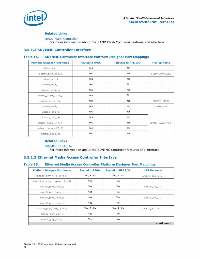
3.5.1.2 SD/MMC Controller Interface
Table 14. SD/MMC Controller Interface Platform Designer Port Mappings
Platform Designer Port Name Routed to FPGA Routed to HPS I/O HPS Pin Name
sdmmc_vs_o Yes No -
sdmmc_pwr_ena_o Yes Yes SDMMC_PWR_ENA
sdmmc_wp_i Yes No -
sdmmc_cdn_i Yes No -
sdmmc_rstn_o Yes No -
sdmmc_card_intn_i Yes No -
sdmmc_cclk_out Yes Yes SDMMC_CCLK
sdmmc_cmd_i Yes Yes SDMMC_CMD
sdmmc_cmd_o Yes Yes
sdmmc_cmd_oe Yes Yes
sdmmc_data_i[7:0] Yes Yes SDMMC_DATA[7:0]
sdmmc_data_o[7:0] Yes Yes
sdmmc_data_oe Yes Yes
Related Links
SD/MMC ControllerFor more information about the SD/MMC Controller features and interface.
3.5.1.3 Ethernet Media Access Controller Interface
Table 15. Ethernet Media Access Controller Platform Designer Port Mappings
Platform Designer Port Name Routed to FPGA Routed to HPS I/O HPS Pin Name
emac0_phy_txd_o[7:0] Yes, 8 bits Yes, 4 bits EMAC0_TXD[3:0]
emac0_phy_mac_speed [1:0] Yes No -
emac0_phy_txen_o Yes Yes EMAC0_TX_CTL
emac0_phy_txer_o Yes No -
emac0_phy_rxdv_i No Yes EMAC0_RX_CTL
emac0_phy_rxer_i Yes No -
emac0_phy_rxd_i[7:0] Yes, 8 bits Yes, 4 bits EMAC0_RXD[3:0]
emac0_phy_col_i Yes No -
emac0_phy_crs_i Yes No -
continued...
3 Stratix 10 HPS Component Interfaces
S10-HPSCOMPONENT | 2017.11.06
Stratix 10 HPS Component Reference Manual26

Platform Designer Port Name Routed to FPGA Routed to HPS I/O HPS Pin Name
emac0_gmii_mdc_o Yes Yes EMAC0_MDC
emac0_gmii_mdo_o Yes Yes EMAC0_MDIO
emac0_gmii_mdo_o_e Yes Yes
emac0_gmii_mdi_i Yes Yes
emac0_ptp_pps_o Yes No -
emac0_ptp_aux_ts_trig_i Yes No -
emac0_clk_rx_i Yes Yes EMAC0_RX_CLK
emac0_clk_tx_i Yes No -
emac0_phy_txclk_o Yes Yes EMAC0_TX_CLK
emac0_rst_clk_tx_n_o Yes No -
emac0_rst_clk_rx_n_o Yes No -
emac1_phy_txd_o[7:0] Yes, 8 bits Yes, 4 bits EMAC1_TXD[3:0]
emac1_phy_mac_speed_o Yes No -
emac1_phy_txen_o Yes Yes EMAC1_TX_CTL
emac1_phy_txer_o Yes No -
emac1_phy_rxdv_i Yes Yes EMAC1_RX_CTL
emac1_phy_rxer_i Yes No -
emac1_phy_rxd_i[7:0] Yes, 8 bits Yes, 4 bits EMAC1_RXD[3:0]
emac1_phy_col_i Yes No -
emac1_phy_crs_i Yes No -
emac1_gmii_mdc_o Yes Yes EMAC1_MDC
emac1_gmii_mdo_o Yes Yes EMAC1_MDIO
emac1_gmii_mdo_o_e Yes Yes
emac1_gmii_mdi_i Yes Yes
emac1_ptp_pps_o Yes No -
emac1_ptp_aux_ts_trig_i Yes No -
emac1_clk_rx_i Yes Yes EMAC1_RX_CLK
emac1_clk_tx_i Yes No -
emac1_phy_txclk_o Yes Yes EMAC1_TX_CLK
emac1_rst_clk_tx_n_o Yes No -
emac1_rst_clk_rx_n_o Yes No -
emac2_phy_txd_o[7:0] Yes, 8 bits Yes, 4 bits EMAC2_TXD[3:0]
emac2_phy_mac_speed_o Yes No -
emac2_phy_txen_o Yes Yes EMAC2_TX_CTL
continued...
3 Stratix 10 HPS Component Interfaces
S10-HPSCOMPONENT | 2017.11.06
Stratix 10 HPS Component Reference Manual27

Platform Designer Port Name Routed to FPGA Routed to HPS I/O HPS Pin Name
emac2_phy_txer_o Yes No -
emac2_phy_rxdv_i Yes Yes EMAC2_RX_CTL
emac2_phy_rxer_i Yes - No
emac2_phy_rxd_i[7:0] Yes, 8 bits Yes, 4 bits EMAC2_RXD[3:0]
emac2_phy_col_i Yes No -
emac2_phy_crs_i Yes No -
emac2_gmii_mdc_o Yes Yes EMAC2_MDC
emac2_gmii_mdo_o Yes Yes EMAC2_MDIO
emac2_gmii_mdo_o_e Yes Yes
emac2_gmii_mdi_i Yes Yes
emac2_ptp_pps_o Yes No -
emac2_ptp_aux_ts_trig_i Yes No _
emac2_clk_rx_i Yes Yes EMAC2_RX_CLK
emac2_clk_tx_i Yes No -
emac2_phy_txclk_o Yes Yes EMAC2_TX_CLK
emac2_rst_clk_tx_n_o Yes No -
emac2_rst_clk_rx_n_o Yes No -
Related Links
Ethernet Media Access ControllerFor more information about the Ethernet Media Access Controller features andinterface.
3.5.1.4 USB 2.0 OTG Controller Interface
Table 16. USB 2.0 OTG Controller Platform Designer Port Mappings
Platform Designer Port Name Routed to FPGA Routed to HPS I/O HPS Pin Name
usb0_ulpi_clk No Yes USB0_CLK
usb0_ulpi_dir No Yes USB0_DIR
usb0_ulpi_nxt No Yes USB0_NXT
usb0_ulpi_stp No Yes USB0_STP
usb0_ulpi_data_i[7:0] No Yes USB0_DATA[7:0]
usb0_ulpi_data_o[7:0] No Yes
usb0_ulpi_data_oe[7:0] No Yes
usb1_ulpi_clk No Yes USB1_CLK
usb1_ulpi_dir No Yes USB1_DIR
usb1_ulpi_nxt No Yes USB1_NXT
continued...
3 Stratix 10 HPS Component Interfaces
S10-HPSCOMPONENT | 2017.11.06
Stratix 10 HPS Component Reference Manual28

Platform Designer Port Name Routed to FPGA Routed to HPS I/O HPS Pin Name
usb1_ulpi_stp No Yes USB1_STP
usb1_ulpi_data_i[7:0] No Yes USB1_DATA[7:0]
usb1_ulpi_data_o[7:0] No Yes
usb1_ulpi_data_oe[7:0] No Yes
Related Links
USB 2.0 OTG ControllerFor more information about the USB 2.0 OTG Controller features and interface.
3.5.1.5 SPI Controller Interface
Table 17. SPI Controller Interface Platform Designer Port Mappings
Platform Designer Port Name Routed to FPGA Routed to HPS I/O HPS Pin Name
spim0_sclk_out Yes Yes SPIM0_CLK
spim0_mosi_o Yes Yes SPIM0_MOSI
spim0_mosi_oe Yes No
spim0_miso_i Yes Yes SPIM0_MISO
spim0_ss_in_n Yes No -
spim0_mosi_oe Yes No -
spim0_ss0_n_o Yes Yes SPIM0_SS0_N
spim0_ss1_n_o Yes Yes SPIM0_SS1_N
spim0_ss2_n_o Yes No -
spim0_ss3_n_o Yes No -
spim1_sclk_out Yes Yes SPIM1_CLK
spim1_mosi_o Yes Yes SPIM1_MOSI
spim1_mosi_oe Yes Yes
spim1_miso_i Yes Yes SPIM1_MISO
spim1_ss_in_n Yes No -
spim1_ss0_n_o Yes Yes SPIM1_SS0_N
spim1_ss1_n_o Yes Yes SPIM1_SS1_N
spim1_ss2_n_o Yes No -
spim1_ss3_n_o Yes No -
spis0_sclk_in Yes Yes SPIS0_CLK
spis0_mosi_i Yes Yes SPIS0_MOSI
spis0_ss_in_n Yes Yes SPIS0_SS0_N
spis0_miso_o Yes Yes SPIS0_MISO
spis0_miso_oe Yes Yes
continued...
3 Stratix 10 HPS Component Interfaces
S10-HPSCOMPONENT | 2017.11.06
Stratix 10 HPS Component Reference Manual29

Platform Designer Port Name Routed to FPGA Routed to HPS I/O HPS Pin Name
spis1_sclk_in Yes Yes SPIS1_CLK
spis1_mosi_i Yes Yes SPIS1_MOSI
spis1_ss_in_n Yes Yes SPIS1_SS0_N
spis1_miso_o Yes Yes SPIS1_MISO
spis1_miso_oe Yes Yes
Related Links
SPI ControllerFor more information about the SPI Controller features and interface.
3.5.1.6 I2C Controller Interface
Table 18. I2C Controller Platform Designer Port Mappings
Platform Designer Port Name Routed to FPGA Routed to HPS I/O HPS Pin Name
i2c0_scl_i Yes Yes I2C0_SCL
i2c0_scl_oe Yes Yes
i2c0_sda_i Yes Yes I2C0_SDA
i2c0_sda_oe Yes Yes
i2c1_scl_i Yes Yes I2C1_SCL
i2c1_scl_oe Yes Yes
i2c1_sda_i Yes Yes I2C1_SDA
i2c1_sda_oe Yes Yes
i2c_emac0_scl_i Yes Yes I2C_EMAC0_SCL
i2c_emac0_scl_oe Yes Yes
i2c_emac0_sda_i Yes Yes I2C_EMAC0_SDA
i2c_emac0_sda_oe Yes Yes
i2c_emac1_scl_i Yes Yes I2C_EMAC1_SCL
i2c_emac1_scl_oe Yes Yes
i2c_emac1_sda_i Yes Yes I2C_EMAC1_SDA
i2c_emac1_sda_oe Yes Yes
i2c_emac2_scl_i Yes Yes I2C_EMAC2_SCL
i2c_emac2_scl_oe Yes Yes
i2c_emac2_sda_i Yes Yes I2C_EMAC2_SDA
i2c_emac2_sda_oe Yes Yes
Note: When routing the I2C signals to the FPGA I/O, the I2C output signal should beconnected to ground. Refer to the I2C Controller chapter for more information.
3 Stratix 10 HPS Component Interfaces
S10-HPSCOMPONENT | 2017.11.06
Stratix 10 HPS Component Reference Manual30

Related Links
I2C ControllerFor more information about the I2C Controller features and interface.
3.5.1.7 UART Interface
Table 19. UART Interface Platform Designer Port Mappings
Platform Designer Port Name Routed to FPGA Routed to HPS I/O HPS Pin Name
uart0_cts_n Yes Yes UART0_CTS_N
uart0_dsr_n Yes No -
uart0_dcd_n Yes No -
uart0_ri_n Yes No -
uart0_rx Yes Yes UART0_RX
uart0_dtr_n Yes No -
uart0_rts_n Yes Yes UART0_RTS_N
uart0_out1_n Yes No -
uart0_out2_n Yes No -
uart0_tx Yes Yes UART0_TX
uart1_cts_n Yes Yes UART1_CTS_N
uart1_dsr_n Yes No -
uart1_dcd_n Yes No -
uart1_ri_n Yes No -
uart1_rx Yes Yes UART1_RX
uart1_dtr_n yes No -
uart1_rts_n Yes Yes UART1_RTS_N
uart1_out1_n Yes No -
uart1_out2_n Yes No -
uart1_tx Yes Yes UART1_TX
Related Links
UART ControllerFor more information about the UART Controller features and interface.
3 Stratix 10 HPS Component Interfaces
S10-HPSCOMPONENT | 2017.11.06
Stratix 10 HPS Component Reference Manual31

3.5.2 DMA Controller Interface
The DMA controller interface allows soft IP in the FPGA fabric to communicate with theDMA controller in the HPS. You can configure up to eight separate interface channels.
• f2h_dma_req0—FPGA DMA controller peripheral request interface 0
• f2h_dma_req1—FPGA DMA controller peripheral request interface 1
• f2h_dma_req2—FPGA DMA controller peripheral request interface 2
• f2h_dma_req3—FPGA DMA controller peripheral request interface 3
• f2h_dma_req4—FPGA DMA controller peripheral request interface 4
• f2h_dma_req5—FPGA DMA controller peripheral request interface 5
• f2h_dma_req6—FPGA DMA controller peripheral request interface 6
• f2h_dma_req7—FPGA DMA controller peripheral request interface 7
Each DMA peripheral request interface contains the following three signals, where <n>corresponds to a specific request interface enabled in Platform Designer:
• f2h_dma<n>_req—This signal is used to request burst transfer using the DMA
• f2h_dma<n>_single—This signal is used to request single word transfer usingthe DMA
• f2h_dma<n>_ack—This signal indicates the DMA acknowledgment upon requestsfrom the FPGA
Related Links
DMA ControllerFor more information about the DMA Controller, refer to "DMA Controller" chapter.
3.6 Other Interfaces
3 Stratix 10 HPS Component Interfaces
S10-HPSCOMPONENT | 2017.11.06
Stratix 10 HPS Component Reference Manual32

3.6.1 MPU Standby and Event Interfaces
MPU standby signals are notification signals to the FPGA fabric that the MPU is instandby. Event signals are used to wake up the Cortex-A53 processors from a wait forevent (WFE) state. The following shows the signals in the interface:
• h2f_mpu_events—MPU standby and event interface, including the followingsignals.
• h2f_mpu_eventi—Sends an event from logic in the FPGA fabric to the MPU. ThisFPGA-to-HPS signal is used to wake up a processor that is in a Wait For Eventstate. Asserting this signal has the same effect as executing the SEV instruction inthe Cortex-A53. This signal must be de-asserted until the FPGA fabric isconfigured.
• h2f_mpu_evento—Sends an event from the MPU to logic in the FPGA fabric. ThisHPS-to-FPGA signal is asserted when an SEV instruction is executed by one of theCortex-A53 processors.
• h2f_mpu_standbywfe[3:0]—Indicates which Cortex-A53 processor is in theWFE state
• h2f_mpu_standbywfi[3:0]—Indicates which Cortex-A53 processor is in thewait for interrupt (WFI) state
The MPU provides signals to indicate when it is in a standby state. These signals areavailable to custom hardware designs in the FPGA fabric.
Related Links
Clock ManagerFor more information about the Clock Manager features and interface.
3.6.2 General Purpose Signals
h2f_mpu_gp—General purpose interface
Table 20. General Purpose Interfaces
Signal Description Associated Signal
h2f_gp General purpose interface. Enables apair of 32-bit unidirectional general-purpose interfaces between the FPGAmanager in HPS and the FPGA fabric.
h2f_gp_in
h2f_gp_out
3.6.3 FPGA-to-HPS Interrupts
You can configure the HPS component to provide 64 general purpose FPGA-to-HPSinterrupts, allowing soft IP in the FPGA fabric to trigger interrupts to the MPU’s genericinterrupt controller (GIC). The interrupts are implemented through the following 32-bitinterfaces:
• f2h_irq0—FPGA-to-HPS interrupts 0 through 31
• f2h_irq1—FPGA-to-HPS interrupts 32 through 63
The FPGA-to-HPS interrupts are asynchronous on the FPGA interface. Inside the HPS,the interrupts are synchronized to the MPU’s internal peripheral clock(mpu_periph_clk).
3 Stratix 10 HPS Component Interfaces
S10-HPSCOMPONENT | 2017.11.06
Stratix 10 HPS Component Reference Manual33

Related Links
Instantiating the Intel Stratix 10 HPS Component on page 8For information about the address span extender, refer to the Using the AddressSpan Extender Component section in the "Instantiating the HPS Component"chapter.
3.7 I/O Delays
You can optionally select additional delay chain to the input or output of the 48 HPSDedicated I/Os. The I/O Delays tab in the HPS Component allows you to selectbetween:
• Zero_chain_dly—input or output signal will bypass the delay chain
• Chain_dly—input or output signal will go through the minimum delay chain path
• One_chain_dly to fifteen_chain_dly—input or output signal will go throughbetween one to fifteen chain delays, in addition to the minimum delay chain path
For more information about the delay timings, refer to the Stratix 10 Datasheet.
Related Links
Intel Stratix 10 Device Datasheet
3.8 HPS Component Interfaces Revision History
Table 21. Document Revision History
Version Changes
2017.11.06 Initial release
3 Stratix 10 HPS Component Interfaces
S10-HPSCOMPONENT | 2017.11.06
Stratix 10 HPS Component Reference Manual34
Top Related