


Languages
Pages
Legal


www.ll.mit.edu
Technology in Support of National Security
MICROELECTRONICSL A B O R A T O R Y
SPOTLIGHT ON
www.ll.mit.edu
A finished 200-mm-diameter GaN-on-Si wafer.
Lincoln Laboratory developed fully Si CMOS–compatible technologies for GaN MMICs on 200-mm-diameter Si wafers. Measured fT and fmax are in the 50 and 90 GHz range, respectively, for GaN high-electron-mobility transistors (HEMTs) with 120-nm gate length on Si substrates. We are applying wafer-scale 3D integration technology to the heterogeneous integration of GaN MMICs and Si CMOS circuits for high-performance RF modules.
KEY FEATURES
• CMOS-compatible process for GaN-on-Si monolithic microwave integrated circuits (MMICs)
• Use of 200-mm-diameter Si substrate and CMOS tools reduces cost and increases yield
• Wafer-scale 3D integration of GaN MMICs with CMOS to enhance functionalities with improved size, weight, and power benefits
GaN-CMOS Wafer-Scale 3D Integration
SPOTLIGHT ON GaN-CMOS Wafer-Scale 3D Integration
Approved for public release; distribution unlimited. This material is based upon work supported under Air Force Contract no. FA8702- 15-D-0001. Any opinions, findings and conclusions, or recommendations expressed in this material are those of the author and do not necessarily reflect the views of the U.S. Air Force. Delivered to the U.S. government with unlimited rights, as defined in DFARS Part 252.227-7013 or 7014 (Feb 2014). Use of this work other than as specifically authorized by the U.S. government may violate any copy-rights that exist in this work.© 2020 Massachusetts Institute of Technology
Chang-Lee Chen RF Technology Group
MIT Lincoln Laboratory, 244 Wood Street, Lexington, MA 02421
TECHNICAL CONTACT
Features of Lincoln Laboratory Process
• Growth of high-quality GaN HEMT layers on 200-mm-diameter Si substrates
• Fully CMOS compatible with gold-free metallization
• High yield and uniformity across 200-mm wafer
• Breakdown voltage of approximately 90 V with 1-μm gate to drain spacing
• Wafer-scale 3D integration with Si CMOS wafers, allowing multiple-tier wafer stacking
• Integrated GaN-MMIC and CMOS circuits for high-performance RF modules with small size, weight, power, and cost
• Use of standard CMOS processes and tools to enable direct technology transfer to Si foundries
Going Forward
• The GaN-on-Si MMIC and Si CMOS 3D integration technology is available to external designs through multiple project wafer (MPW) runs.
• We provide models and process design kits for GaN MMICs and CMOS co-design and support.
• Lincoln Laboratory facility is ISO-9001 certified and accredited for Trusted design and aggregation through packaged circuit delivery.
200-mm-diameter GaN-on-Si MMIC and Si CMOS wafers are 3D integrated at wafer scale. The two wafers are bonded face-to-face using a low-temperature oxide-oxide bonding technique. The Si substrate of the silicon-on-insulator wafer is completely removed by grinding and selective wet etch to stop at the buried oxide (BOX). Vias to the back of CMOS and to the top of GaN circuits are etched separately and interconnected with a top metal. The vertical integration minimizes the chip size and reduces the interconnect distance to lower the loss and delay.
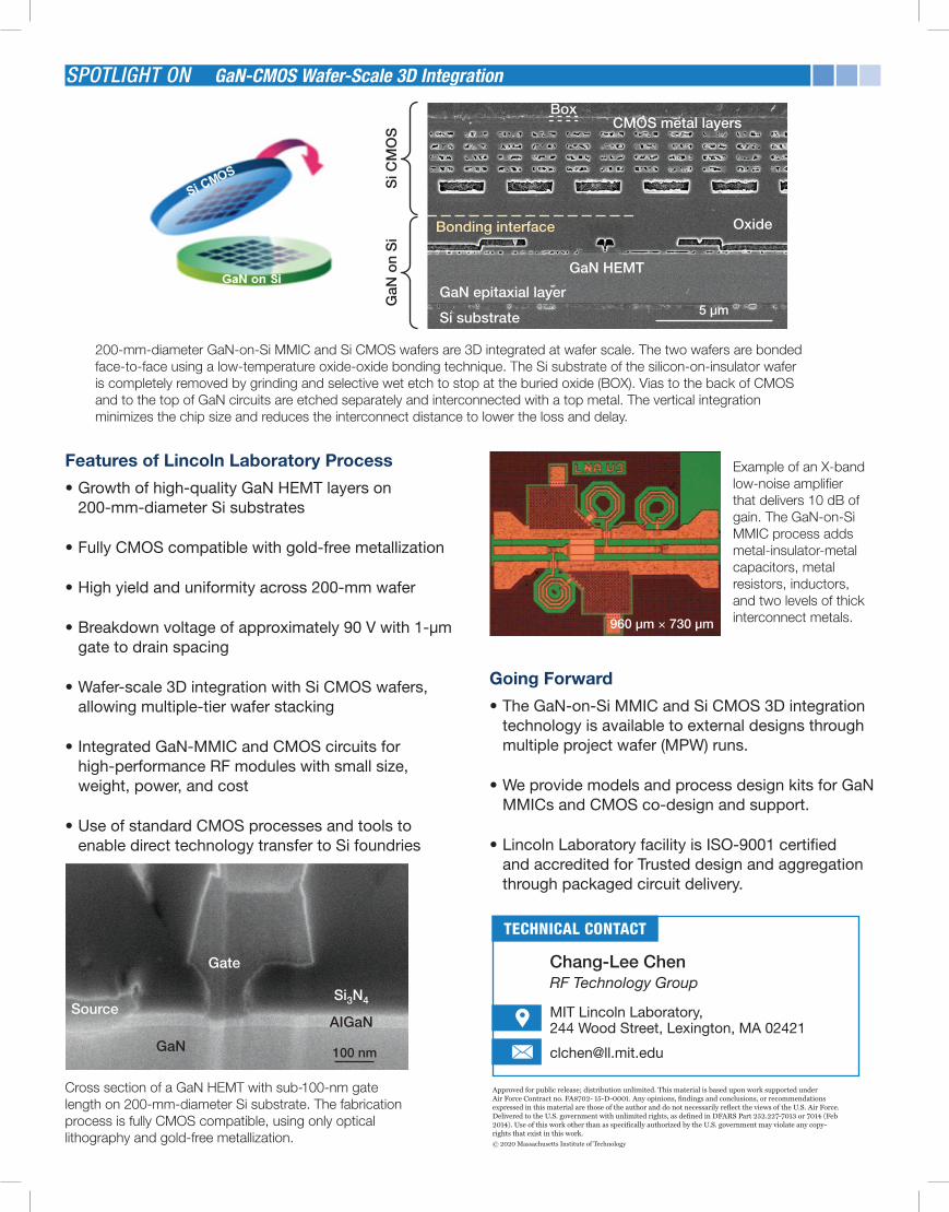
Cross section of a GaN HEMT with sub-100-nm gate length on 200-mm-diameter Si substrate. The fabrication process is fully CMOS compatible, using only optical lithography and gold-free metallization.
Example of an X-band low-noise amplifier that delivers 10 dB of gain. The GaN-on-Si MMIC process adds metal-insulator-metal capacitors, metal resistors, inductors, and two levels of thick interconnect metals.
Oxide
GaN HEMT
GaN epitaxial layer
Si substrate
CMOS metal layers
Bonding interface
Box
GaN
on
Si
Si C
MO
S
5 µm
Gate
Si3N4
AIGaN
GaN
Source
100 nm
960 µm × 730 µm
Top Related