


Languages
Pages
Legal


Silic
on Im
age
Confid
entia
l for
Forte
x In
dust
rial L
td.
Inte
rnal
Use
Onl
y
Data Sheet
SiI9394 and SiI9679 HDMI/MHL 1, 2, 3 Bridge and Receiver with HDCP 2.2 Support
Data Sheet
SiI-DS-1146-B
February 2014
Silic
on Im
age
Confid
entia
l for
Forte
x In
dust
rial L
td.
Inte
rnal
Use
Onl
y
SiI9394 and SiI9679 HDMI/MHL 1, 2, 3 Bridge and Receiver with HDCP 2.2 Support Data Sheet
2 © 2014 Silicon Image, Inc. All rights reserved. SiI-DS-1146-B CONFIDENTIAL
Copyright Notice
Copyright © 2014 Silicon Image, Inc. All rights reserved. The contents of these materials contain proprietary and confidential information (including trade secrets, copyright, and other Intellectual Property interests) of Silicon Image, Inc. or its affiliates. All rights are reserved and contents, (in whole or in part) may not be reproduced, downloaded, disseminated, published, or transferred in any form or by any means, except with the prior written permission of Silicon Image, Inc. or its affiliates. You may not use these materials except only for your bona fide non-commercial evaluation of your potential purchase of products and/or services from Silicon Image or its affiliates; and only in connection with your purchase of products or services from Silicon Image or its affiliates, and only in accordance with the terms and conditions stipulated. Copyright infringement is a violation of federal law subject to criminal and civil penalties. You have no right to copy, modify, transfer, sublicense, publicly display, create derivative works of, distribute these materials, or otherwise make these materials available, in whole or in part, to any third party.
Patents
The subject matter described herein may contain one or more inventions claimed in patents or patents pending owned by Silicon Image, Inc. or its affiliates.
Trademark Acknowledgment
Silicon Image®, the Silicon Image logo, Instaport®, the Instaport logo, InstaPrevue®, Simplay®, Simplay HD®, and UltraGig™ are trademarks or registered trademarks of Silicon Image, Inc. in the United States or other countries. HDMI® and the HDMI logo with High-Definition Multimedia Interface are trademarks or registered trademarks of, and are used under license from, HDMI Licensing, LLC. in the United States or other countries. MHL® and the MHL logo are trademarks or registered trademarks of, and are used under license from, MHL, LLC. in the United States or other countries. WirelessHD®, the WirelessHD logo, WiHD® and the WiHD logo are trademarks, registered trademarks or service marks of SiBeam, Inc. in the United States or other countries.
HDMI Licensing, LLC; MHL, LLC; Simplay Labs, LLC; and SiBeam, Inc. are wholly owned subsidiaries of Silicon Image, Inc.
All other trademarks and registered trademarks are the property of their respective owners in the United States or other countries. The absence of a trademark symbol does not constitute a waiver of Silicon Image’s trademarks or other intellectual property rights with regard to a product name, logo or slogan.
Export Controlled Document
This document contains materials subject to the Export Administration Regulations. Transfer of this information by any means to a foreign destination may require a license. These materials shall not, in the absence of authorization under U.S. and local law and regulations, as required, be used by or exported or re-exported to (i) any U.S. sanctioned or embargoed country, or to nationals or residents of such countries; or (ii) any person, entity, organization or other party identified on the U.S. Department of Commerce's Denied Persons or Entity List, the U.S. Department of Treasury's Specially Designated Nationals or Blocked Persons List, or the Department of State's Debarred Parties List, as published and revised from time to time; (iii) any party engaged in nuclear, chemical/biological weapons or missile proliferation activities; or (iv) any party for use in the design, development, or production of rocket systems or unmanned air vehicles.
Further Information
To request other materials, documentation, and information, contact your local Silicon Image, Inc. sales office or visit the Silicon Image, Inc. web site at www.siliconimage.com.
Disclaimers
These materials are provided on an “AS IS” basis. Silicon Image, Inc. and its affiliates disclaim all representations and warranties (express, implied, statutory or otherwise), including but not limited to: (i) all implied warranties of merchantability, fitness for a particular purpose, and/or non-infringement of third party rights; (ii) all warranties arising out of course-of-dealing, usage, and/or trade; and (iii) all warranties that the information or results provided in, or that may be obtained from use of, the materials are accurate, reliable, complete, up-to-date, or produce specific outcomes. Silicon Image, Inc. and its affiliates assume no liability or responsibility for any errors or omissions in these materials, makes no commitment or warranty to correct any such errors or omissions or update or keep current the information contained in these materials, and expressly disclaims all direct, indirect, special, incidental, consequential, reliance and punitive damages, including WITHOUT LIMITATION any loss of profits arising out of your access to, use or interpretation of, or actions taken or not taken based on the content of these materials. Silicon Image, Inc. and its affiliates reserve the right, without notice, to periodically modify the information in these materials, and to add to, delete, and/or change any of this information.
Products and Services
The products and services described in these materials, and any other information, services, designs, know-how and/or products provided by Silicon Image, Inc. and/or its affiliates are provided on “AS IS” basis, except to the extent that Silicon Image, Inc. and/or its affiliates provides an applicable written limited warranty in its standard form license agreements, standard Terms and Conditions of Sale and Service or its other applicable standard form agreements, in which case such limited warranty shall apply and shall govern in lieu of all other warranties (express, statutory, or implied). EXCEPT FOR SUCH LIMITED WARRANTY, SILICON IMAGE, INC. AND ITS AFFILIATES DISCLAIM ALL REPRESENTATIONS AND WARRANTIES (EXPRESS, IMPLIED, STATUTORY OR OTHERWISE), REGARDING THE INFORMATION, SERVICES, DESIGNS, KNOW-HOW AND PRODUCTS PROVIDED BY SILICON IMAGE, INC. AND/OR ITS AFFILIATES, INCLUDING BUT NOT LIMITED TO, ALL IMPLIED WARRANTIES OF MERCHANTABILITY, FITNESS FOR A PARTICULAR PURPOSE, AND/OR NON-INFRINGEMENT OF THIRD PARTY RIGHTS. YOU ACKNOWLEDGE AND AGREE THAT SUCH INFORMATION, SERVICES, DESIGNS, KNOW-HOW AND PRODUCTS HAVE NOT BEEN DESIGNED, TESTED, OR MANUFACTURED FOR USE OR RESALE IN SYSTEMS WHERE THE FAILURE, MALFUNCTION, OR ANY INACCURACY OF THESE ITEMS CARRIES A RISK OF DEATH OR SERIOUS BODILY INJURY, INCLUDING, BUT NOT LIMITED TO, USE IN NUCLEAR FACILITIES, AIRCRAFT NAVIGATION OR COMMUNICATION, EMERGENCY SYSTEMS, OR OTHER SYSTEMS WITH A SIMILAR DEGREE OF POTENTIAL HAZARD. NO PERSON IS AUTHORIZED TO MAKE ANY OTHER WARRANTY OR REPRESENTATION CONCERNING THE PERFORMANCE OF THE INFORMATION, PRODUCTS, KNOW-HOW, DESIGNS OR SERVICES OTHER THAN AS PROVIDED IN THESE TERMS AND CONDITIONS.

Silic
on Im
age
Confid
entia
l for
Forte
x In
dust
rial L
td.
Inte
rnal
Use
Onl
y
SiI9394 and SiI9679 HDMI/MHL 1, 2, 3 Bridge and Receiver with HDCP 2.2 Support Data Sheet
SiI-DS-1146-B © 2014 Silicon Image, Inc. All rights reserved. 3 CONFIDENTIAL
Contents General Description .............................................................................................................................................................. 6
General Features .............................................................................................................................................................. 6 SiI9394 Bridge Only ........................................................................................................................................................... 7 SiI9679 Receiver Only ....................................................................................................................................................... 7 Packaging .......................................................................................................................................................................... 7
Pin Diagram .......................................................................................................................................................................... 8 Functional Description ........................................................................................................................................................ 10
HDMI/MHL 1, 2, 3 Receiver Block ................................................................................................................................... 10 Video Data Conversion Logic Block ................................................................................................................................. 12
Color Space Converter ................................................................................................................................................ 12 YCbCr Range Compression .......................................................................................................................................... 12 4:4:4 to 4:2:2 Downsampler ....................................................................................................................................... 12 4:2:2 to 4:4:4 Upsampler ............................................................................................................................................ 12 RGB Range Expansion ................................................................................................................................................. 13 10 to 8 Bit Dither ........................................................................................................................................................ 13
Receiver HDCP Authentication Logic Block..................................................................................................................... 13 HDCP Decryption Engine Block ....................................................................................................................................... 13 Transmitter HDCP Authentication Logic ......................................................................................................................... 13 HDCP Encryption Engine Block ....................................................................................................................................... 13 HDCP Repeater Block ...................................................................................................................................................... 14 One-Time Programmable (OTP) ..................................................................................................................................... 14 HDMI TMDS Transmitter Block ....................................................................................................................................... 14 eCBUS Data Tunneling Block........................................................................................................................................... 14 CBUS Control Block ......................................................................................................................................................... 14 Low Power Standby Block ............................................................................................................................................... 15 HSIC PHY ......................................................................................................................................................................... 15 SPI Logic Block ................................................................................................................................................................ 15 ISP Block .......................................................................................................................................................................... 15 Microcontroller Unit ....................................................................................................................................................... 15 Internal Oscillator ........................................................................................................................................................... 15 Local I
2C Slave Logic Block .............................................................................................................................................. 15
Configuration, Status, and Interrupt Control Logic Block ............................................................................................... 16 Receiver DDC Interface ................................................................................................................................................... 17 Transmitter DDC Interface .............................................................................................................................................. 17 Audio Output Logic Block – SiI9394 Bridge Only ............................................................................................................ 17 CEC Interface Block – SiI9394 Bridge Only ...................................................................................................................... 17 On-Chip Regulators ......................................................................................................................................................... 17
Electrical Specifications ...................................................................................................................................................... 18 Absolute Maximum Conditions ...................................................................................................................................... 18 Normal Operating Conditions ......................................................................................................................................... 19 DC Specification .............................................................................................................................................................. 20
Digital I/O Specifications ............................................................................................................................................. 20 CBUS I/O Specification ................................................................................................................................................ 22 DC Power Consumption .............................................................................................................................................. 22
AC Specification .............................................................................................................................................................. 23 TMDS AC Timing Specifications .................................................................................................................................. 23 Audio Output Timings for the SiI9394 Bridge ............................................................................................................. 24 SPI Interface Timing .................................................................................................................................................... 25 HSIC Interface Timing ................................................................................................................................................. 26 Miscellaneous Timings ................................................................................................................................................ 26 ESD Specifications ....................................................................................................................................................... 26
Timing Diagrams ................................................................................................................................................................. 27 RESETN Timing Diagrams ................................................................................................................................................ 27

Silic
on Im
age
Confid
entia
l for
Forte
x In
dust
rial L
td.
Inte
rnal
Use
Onl
y
SiI9394 and SiI9679 HDMI/MHL 1, 2, 3 Bridge and Receiver with HDCP 2.2 Support Data Sheet
4 © 2014 Silicon Image, Inc. All rights reserved. SiI-DS-1146-B CONFIDENTIAL
Digital Audio Output Timings .......................................................................................................................................... 28 Pin Descriptions .................................................................................................................................................................. 30
HDMI/MHL1, 2, 3 Receiver Port Pins .............................................................................................................................. 30 HDMI Transmitter Port Pins ............................................................................................................................................ 31 Data Tunneling Pins ........................................................................................................................................................ 31 Digital Audio Output Pins ................................................................................................................................................ 32 Control and Configuration Pins ....................................................................................................................................... 33 Power and Ground Pins .................................................................................................................................................. 34 Not Connected Pins for the SiI9679 Bridge..................................................................................................................... 34 Not Connected Pins for the SiI9679 Receiver ................................................................................................................. 34
Feature Information ........................................................................................................................................................... 35 RGB to YCbCr Color Space Converter .............................................................................................................................. 35 YCbCr to RGB Color Space Converter .............................................................................................................................. 35 SiI9394 and SiI9679 Input and Output Matrix with HDCP .............................................................................................. 36 3D Video Formats ........................................................................................................................................................... 36 Device Address Configuration Using CI2CA/GPIO4/GPIO5 ............................................................................................. 38 Audio Output Interface ................................................................................................................................................... 38
S/PDIF ......................................................................................................................................................................... 38 I2S ................................................................................................................................................................................ 38
TDM ............................................................................................................................................................................ 39 AV Link Data Rate in MHL 3 Mode .................................................................................................................................. 40
Design Recommendations .................................................................................................................................................. 41 Power Supplies Decoupling ............................................................................................................................................ 41 High-speed TMDS Signals ............................................................................................................................................... 42
Layout Guidelines ....................................................................................................................................................... 42 ESD Protection ............................................................................................................................................................ 42
EMI Considerations ......................................................................................................................................................... 42 Packaging ............................................................................................................................................................................ 43
ePad Requirements ......................................................................................................................................................... 43 Package Dimensions ....................................................................................................................................................... 44 Marking Specification ..................................................................................................................................................... 45 Ordering Information ...................................................................................................................................................... 45
References .......................................................................................................................................................................... 46 Standards Documents ..................................................................................................................................................... 46 Silicon Image Documents ................................................................................................................................................ 46
Revision History .................................................................................................................................................................. 47
Figures Figure 1. Typical Application for the SiI9394 Bridge ............................................................................................................. 6 Figure 2. Typical Application for the SiI9679 Receiver.......................................................................................................... 7 Figure 3. SiI9394 Pin Diagram ............................................................................................................................................... 8 Figure 4. SiI9679 Pin Diagram ............................................................................................................................................... 9 Figure 5. Functional Block Diagram .................................................................................................................................... 10 Figure 6. Default Video Processing Path ............................................................................................................................. 12 Figure 7. Stand-alone Mode ............................................................................................................................................... 16 Figure 8. External MCU Mode ............................................................................................................................................. 16 Figure 9. Test Point VDDTP for VDD Noise Tolerance Specification ................................................................................... 19 Figure 10. Audio Crystal Application ................................................................................................................................... 25 Figure 11. Conditions for Use of RESETN ............................................................................................................................ 27 Figure 12. RESETN Minimum Timings ................................................................................................................................. 27 Figure 13. I
2S Output Timings ............................................................................................................................................. 28
Figure 14. TDM Output Timings .......................................................................................................................................... 28 Figure 15. S/PDIF Output Timings ....................................................................................................................................... 28 Figure 16. MCLK Timings ..................................................................................................................................................... 28

Silic
on Im
age
Confid
entia
l for
Forte
x In
dust
rial L
td.
Inte
rnal
Use
Onl
y
SiI9394 and SiI9679 HDMI/MHL 1, 2, 3 Bridge and Receiver with HDCP 2.2 Support Data Sheet
SiI-DS-1146-B © 2014 Silicon Image, Inc. All rights reserved. 5 CONFIDENTIAL
Figure 17. SPI Write Setup and Hold Times ........................................................................................................................ 29 Figure 18. SPI Read Setup and Hold Times ......................................................................................................................... 29 Figure 19. HSIC Timing Diagram ......................................................................................................................................... 29 Figure 20. Word and Channel in TDM Audio Interface ....................................................................................................... 39 Figure 21. TDM Frame ........................................................................................................................................................ 39 Figure 22. TDM – Delay of First Channel MSB to FS ........................................................................................................... 39 Figure 23. Decoupling and Bypass Schematic ..................................................................................................................... 41 Figure 24. Decoupling and Bypass Capacitor Placement .................................................................................................... 41 Figure 25. 76-pin QFN Package Diagram ............................................................................................................................ 44 Figure 26. Marking Diagram for SiI9394 Bridge .................................................................................................................. 45 Figure 27. Marking Diagram for SiI9679 Receiver .............................................................................................................. 45
Tables Table 1. Supported 2D Video Formats ................................................................................................................................ 11 Table 2. Absolute Maximum Conditions ............................................................................................................................. 18 Table 3. Normal Operating Conditions ............................................................................................................................... 19 Table 4. DC Digital I/O Specifications.................................................................................................................................. 20 Table 5. TMDS Input DC Specifications – HDMI Mode ....................................................................................................... 21 Table 6. TMDS Input DC Specifications – MHL 1, 2 Mode .................................................................................................. 21 Table 7. TMDS Input DC Specifications – MHL 3 Mode ...................................................................................................... 21 Table 8. TMDS Output DC Specifications ............................................................................................................................ 21 Table 9. Digital CBUS I/O Specifications ............................................................................................................................. 22 Table 10. Standby DC Power Consumption ........................................................................................................................ 22 Table 11. HDMI Input Mode DC Power Consumption ........................................................................................................ 22 Table 12. MHL 1/2 Input Mode DC Power Consumption ................................................................................................... 22 Table 13. MHL 3 (eCBUS-S) Mode DC Power Consumption ............................................................................................... 23 Table 14. TMDS Input Timings – HDMI Mode .................................................................................................................... 23 Table 15. TMDS Input Timings – MHL 1/MHL 2 Mode ....................................................................................................... 23 Table 16. TMDS Input Timings – MHL 3 (eCBUS-S) Mode .................................................................................................. 23 Table 17. TMDS Input Timings – MHL 3 (eCBUS-D) Mode .................................................................................................. 24 Table 18. TMDS Output Timing AC Specifications .............................................................................................................. 24 Table 19. I
2S Output Port Timings ....................................................................................................................................... 24
Table 20. TDM Output Port Timings ................................................................................................................................... 24 Table 21. S/PDIF Output Port Timings ................................................................................................................................ 25 Table 22. Audio Crystal Timings .......................................................................................................................................... 25 Table 23. SPI Control Signal Timings ................................................................................................................................... 25 Table 24. HSIC Interface Control Signal Timings ................................................................................................................. 26 Table 25. Miscellaneous Timings ........................................................................................................................................ 26 Table 26. ESD Specifications ............................................................................................................................................... 26 Table 27. RGB to YCbCr Conversion Formulas .................................................................................................................... 35 Table 28. YCbCr-to-RGB Conversion Formulas ................................................................................................................... 35 Table 29. SiI9394 and SiI9679 Input and Output Matrix with HDCP .................................................................................. 36 Table 30. Supported HDMI 3D Input Video Formats .......................................................................................................... 36 Table 31. Supported MHL 3 (eCBUS-D) Mode 3D Input Video Formats ............................................................................. 37 Table 32. Supported MHL 3 (eCBUS-S) Mode 3D Input Video Formats ............................................................................. 37 Table 33. Supported MHL 2 3D Input Video Formats ......................................................................................................... 37 Table 34. Control of I2C Address with CI2CA Signal ........................................................................................................... 38 Table 35. Control of I2C Address with GPIO4/GPIO5 Signal ............................................................................................... 38 Table 36. Supported MCLK Frequencies ............................................................................................................................. 38 Table 37. Input Video Pixel Clock Bandwidth vs. AV link Data Rate in MHL 3 Mode.......................................................... 40 Table 38. Referenced Documents....................................................................................................................................... 46 Table 39. Standards Groups Contact Information .............................................................................................................. 46 Table 40. Silicon Image Publications ................................................................................................................................... 46

Silic
on Im
age
Confid
entia
l for
Forte
x In
dust
rial L
td.
Inte
rnal
Use
Onl
y
SiI9394 and SiI9679 HDMI/MHL 1, 2, 3 Bridge and Receiver with HDCP 2.2 Support Data Sheet
6 © 2014 Silicon Image, Inc. All rights reserved. SiI-DS-1146-B CONFIDENTIAL
General Description The Silicon Image SiI9394 Mobile High-Definition Link (MHL®) 1, 2, 3 to High-Definition Multimedia Interface (HMDI®) bridge is an advanced integrated High-definition (HD) solution which can receive the latest MHL 1.x, MHL 2.x with High-bandwidth Digital Content Protection (HDCP) 1.4 encryption or MHL 3 with HDCP 2.2 encryption inputs, and support HDMI output with HDCP 1.4 or HDCP 2.2 encryption. The SiI9394 device can support up to 4K x 2K Ultra HD video format.
The SiI9679 HDMI/MHL 1, 2, 3 receiver is an advanced integrated High-definition (HD) solution which can receive the latest HDMI, MHL 1.x, MHL 2.x with HDCP1.4 encryption or HDMI, MHL 3 with HDCP2.2 encryption inputs, and support HDMI output with HDCP1.4 encryption. The SiI9679 device can support up to 4K x 2K Ultra HD video format.
The SiI9394 or the SiI9679 device implements MHL 3 eCBUS which supports SPI data tunneling and HSIC data tunneling.
General Features Support MHL 1.x, MHL 2.x, MHL 3 inputs, and
HDMI output.
Support SPI data tunneling. It implements Time Division Multiplexing (TDM) to hybrid Serial Peripheral Interface (SPI) data and legacy CBUS commands on the eCBUS-S or eCBUS-D.
Support High-Speed Inter-Chip (HSIC) data tunneling. It implements TDM to hybrid the HSIC data and legacy CBUS commands on the eCBUS-S or eCBUS-D. The HSIC data is compliant with HISC specification.
Support color space conversions among RGB, YCbCr 4:4:4, YCbCr 4:2:2 and xvYCC video formats without deep color.
Support video format up to 4K x 2K @ 30 Hz with RGB/YCbCr 4:4:4/YCbCr 4:2:2, and up to 4k x 2k @ 60 Hz with YCbCr 4:2:0
Support 3D frame sequential video format up to 1080p @ 60 Hz.
Support high resolution VESA mode video format up to QSXGA @ 60 Hz.
Support stand-alone mode with internal MCU controller and external MCU control mode.
Integrated ISP module to support internal MCU firmware update through local I
2C interface.
Low power 1.0 V core.
MHL1, 2, 3
Source
Controller
SiI9394
Bridge
HSIC
PHYSPI
USB
Device
HD
MI
Ou
tpu
t
MHL1, 2, 3 to HDMI
Tri-mode Dongle
Flash/
EEPROM
USB
Device
HDMI Output
Audio
DAC/AMP
I2S/TDM/
S/PDIF
Home Theater
Audio
Output
HDCP 2.2-capable TV
or HDCP 1.x-capable TVDig
ita
l
Au
dio
Inp
utMHL Source Input
Figure 1. Typical Application for the SiI9394 Bridge

Silic
on Im
age
Confid
entia
l for
Forte
x In
dust
rial L
td.
Inte
rnal
Use
Onl
y
SiI9394 and SiI9679 HDMI/MHL 1, 2, 3 Bridge and Receiver with HDCP 2.2 Support Data Sheet
SiI-DS-1146-B © 2014 Silicon Image, Inc. All rights reserved. 7 CONFIDENTIAL
HDMI/MHL1, 2, 3
Source
USB
Device
USB
Device
HDMI/MHL
Source Input
HD
MI
SoC
US
BU
SB USB
USB
HDMI/MHL1, 2, 3
Input HDMI
HSIC
SPI
SiI9679
Receiver
HDCP 1.x/2.2-
capable TV
Flash/
EEPROM
Figure 2. Typical Application for the SiI9679 Receiver
SiI9394 Bridge Only Support MHL 1.x, MHL 2.x, and MHL 3 inputs only.
Support HDCP 2.2 and HDCP 1.x for both input and output ports.
Support HDCP 2.2 repeater, HDCP 1.x repeater, and HDCP 2.2 to 1.x down-converter, and supports up to 127 downstream devices.
Support Consumer Electronics Control (CEC) interface for HDMI output.
Support audio extraction.
One I2S output lane supports two audio channels.
TDM audio interface supports up to eight audio channels.
S/PDIF output supports multichannel (5.1) Dolby Digital, DTS, MPEG2 Audio, and two-channel PCM (32 kHz – 192 kHz fS sample rate).
SiI9679 Receiver Only Support HDMI and MHL 1.x, MHL 2.x, MHL 3 input.
Support HDCP 2.2 and HDCP 1.x for input port.
Support HDMI output without HDCP.
Support optional HDCP 1.x output only for HDCP 2.2 input without repeater function.
Packaging 76-pin QFN (9 mm × 9 mm) package
Standard part covers extended (–20 °C to +85 °C) temperature range.

Silic
on Im
age
Confid
entia
l for
Forte
x In
dust
rial L
td.
Inte
rnal
Use
Onl
y
SiI9394 and SiI9679 HDMI/MHL 1, 2, 3 Bridge and Receiver with HDCP 2.2 Support Data Sheet
8 © 2014 Silicon Image, Inc. All rights reserved. SiI-DS-1146-B CONFIDENTIAL
Pin Diagram Figure 3 shows the pin diagram of the SiI9394 device. Figure 4 on the next page shows the pin diagram of the SiI9679 device. The SiI9394/SiI9679 device is the 76-pin, 9 mm × 9 mm QFN package with an exposed pad (ePad). Refer to the Pin Descriptions on page 30 for a description of the pin functions.
1VDD33OUT
2VDD5V_IN
3RPWR5V
4CBUS
5CoC_GND
6AVDD10_DoC
7RXCN
8RXCP
9AVDD10
10VDD33
11RX0N
12RX0P
13RX1N
14RX1P
15RX2N
16RX2P
17AVDD10
18FVDD10
19VDDIO33
20
INT
21 22 23 24
GP
IO0
_C
I2C
A
GP
IO1
_P
SC
TL
GP
IO2
VD
D1
0
28272625
TM
OD
E
WS
SD
0_
SP
DIF
SC
K
373635343332313029
MC
LK
GP
IO3
GP
IO4
GP
IO5
VD
DIO
33
RE
SE
TN
VD
D1
0
AV
DD
10
_P
LL
NC
38
TX
_H
PD
39 AVDD10_DP
40 TXCN
54
53
52
51
50
49
48
47
46
45
44
43
42
41
HSIC_STB
XTAL_VDD33
TX2P
XTAL_OUT
XTAL_IN
HSIC_DAT
MVDD10
TX1P
TX1N
TX0N
TX0P
TX2N
XTAL_GND
TXCP
55 HSIC_GND
56 VDD12OUT
57 HSIC_VDD33
58
HS
IC_
VD
D1
0
VD
D1
0
59
SP
I_M
OS
I
SP
I_C
S1
SP
I_C
S0
SP
I_C
LK
60616263
DS
CL
LP
SB
V5
V
NC
CE
C_
A
MH
L_
CD
VD
D1
0
CS
DA
CS
CL
TD
SD
A
TD
SC
L
VD
DIO
33
SP
I_M
ISO
DS
DA
64656667686970717273747576
Top View
SiI9394
ePad (GND)
Figure 3. SiI9394 Pin Diagram

Silic
on Im
age
Confid
entia
l for
Forte
x In
dust
rial L
td.
Inte
rnal
Use
Onl
y
SiI9394 and SiI9679 HDMI/MHL 1, 2, 3 Bridge and Receiver with HDCP 2.2 Support Data Sheet
SiI-DS-1146-B © 2014 Silicon Image, Inc. All rights reserved. 9 CONFIDENTIAL
1VDD33OUT
2VDD5V_IN
3RPWR5V
4CBUS_HPD
5CoC_GND
6AVDD10_DoC
7RXCN
8RXCP
9AVDD10
10VDD33
11RX0N
12RX0P
13RX1N
14RX1P
15RX2N
16RX2P
17AVDD10
18FVDD10
19VDDIO33
20
INT
21 22 23 24
GP
IO0
_C
I2C
A
GP
IO1
_P
SC
TL
GP
IO2
VD
D1
0
28272625
TM
OD
E
NC
NC
NC
373635343332313029
NC
GP
IO3
GP
IO4
GP
IO5
VD
DIO
33
RE
SE
TN
VD
D1
0
AV
DD
10
_P
LL
NC
38T
X_
HP
D
39 AVDD10_DP
40 TXCN
54
53
52
51
50
49
48
47
46
45
44
43
42
41
HSIC_STB
XTAL_VDD33
TX2P
XTAL_OUT
XTAL_IN
HSIC_DAT
NC
TX1P
TX1N
TX0N
TX0P
TX2N
XTAL_GND
TXCP
55 HSIC_GND
56 VDD12OUT
57 HSIC_VDD33
58
HS
IC_
VD
D1
0
VD
D1
0
59
SP
I_M
OS
I
SP
I_C
S1
SP
I_C
S0
SP
I_C
LK
60616263
DS
CL
LP
SB
V5
V
WA
KE
UP
NC
MH
L_C
D
VD
D1
0
CS
CL
TD
SD
A
TD
SC
L
VD
DIO
33
SP
I_M
ISO
DS
DA
64656667686970717273747576
Top View
SiI9679
ePad (GND)
CS
DA
Figure 4. SiI9679 Pin Diagram

Silic
on Im
age
Confid
entia
l for
Forte
x In
dust
rial L
td.
Inte
rnal
Use
Onl
y
SiI9394 and SiI9679 HDMI/MHL 1, 2, 3 Bridge and Receiver with HDCP 2.2 Support Data Sheet
10 © 2014 Silicon Image, Inc. All rights reserved. SiI-DS-1146-B CONFIDENTIAL
Functional Description The SiI9394 bridge and the SiI9679 receiver can accept HDMI as well as MHL signals, sharing the same input interface. However, only one kind of input is available at a time. The MHL input signals include the MHL 1.x, MHL 2.x, MHL 3 (eCBUS-S) mode that has one differential TMDS lane and one single-end control bus, and MHL 3 (eCBUS-D) mode that has one differential TMDS lanes and one differential clock signal. When the SiI9394 or the SiI9679 device is in MHL 3 mode, the SiI9394 or the SiI9679 device can support data tunneling with HSIC and SPI interfaces. The SiI9394 or the SiI9679 device supports HDCP 1.x and HDCP 2.2.
The difference between the SiI9394 bridge and the SiI9679 receiver is that the SiI9394 bridge supports audio extraction and CEC function of the HDMI output interface, while the SiI9679 receiver does not. Figure 5 shows the functional block diagram of the chip.
Registers,
Configuration,
and Interrupt
Control Registers
Local I2C
RXCP/N
GPIO0_CI2CA
CBUS_HPD
MHL_CD
GPIO1_PSCTL
INT
VDD5V_INVCC33OUT
HSIC_DAT
HSIC_STB
RX0P/N
RX1P/N
RX2P/N
DDC_Rx
RPWR5V
RESETN
Video Data
Conversion
Logic
3V3
Regulator
HDMI/
MHL1, 2, 3
Receiver
1V8
Regulator
Rx HDCP
Authentication
Logic
Local I2C
Slave Logic
CBUS
Control
Rx DDC
Interface
Data
Tunneling
Tx DDC
Interface
SPI_MISO
SPI_MOSI
SPI_CS0
SPI_CLK SPI Logic
HSIC PHY
DDC_Tx
GPIO2
SPI Slave
SPI Master
TX2P/N
TX1P/N
TX0P/N
TXCP/N
GPIO3
HDCP
Repeater
Logic
Tx HDCP
Encryption
Engine
HDCP
Decryption
Engine
Tx HDCP
Authentication
Logic
HDMI TMDS
Transmitter
Audio
Output
Logic
Video Data
Audio Data
WS
SCK
MCLK
SD0_SPDIF
XTALIN
XTALOUT
OTP
(SiI9394
Dongle Only)
CEC_A
CEC
Interface
(SiI9394
Dongle Only)
Clo
ck
(C
oC
)
Da
ta (
Do
C)
ISP
1V2 Regulator
SPI_CS1
TX_HPD
GPIO4
GPIO5
LPSBLPSBV
WAKEUP
OSC
MCU
Figure 5. Functional Block Diagram
HDMI/MHL 1, 2, 3 Receiver Block The HDMI/MHL 1, 2, 3 Receiver Block consists of HDMI, MHL 1.x, MHL 2.x, and MHL 3 interfaces. The working mode of the SiI9394 or the SiI9679 device depends on the type of source device that is connected to the input interface. The SiI9394 or the SiI9679 device selects the working mode of the receiver block automatically by detecting the status or actions of several pins, such as the RPWR5V, CBUS, or MHL_CD pin. In addition, the status of the discovery pulses on the CBUS is also to be considered. Refer to the corresponding MHL Specification section for details.

Silic
on Im
age
Confid
entia
l for
Forte
x In
dust
rial L
td.
Inte
rnal
Use
Onl
y
SiI9394 and SiI9679 HDMI/MHL 1, 2, 3 Bridge and Receiver with HDCP 2.2 Support Data Sheet
SiI-DS-1146-B © 2014 Silicon Image, Inc. All rights reserved. 11 CONFIDENTIAL
The HDMI/MHL 1, 2, 3 Receiver Block receives the TMDS signals and recovers the video, audio, and auxiliary data according to the working mode. For the MHL 3 (eCBUS-S) mode, the receiver block recovers the data with the link clock that is transmitted over the single-end eCBUS. For the MHL 3(eCBUS-D) mode, the receiver block recovers the data with the link clock that is transmitted over the differential eCBUS.
Table 1 shows the supported 2D formats. See the 3D Video Formats section on page 36 for details of the supported 3D formats.
Table 1. Supported 2D Video Formats
2D Video Resolution
Pixel Format
Bus Width Maximum
Frame Rate
(Hz) HDMI
MHL 1.x/
MHL 2.x MHL 3
VGA RGB 24 24 24 60
WVGA RGB 24 24 24 60
SVGA RGB 24 24 24 60
XGA RGB 24 24 24 60
SXGA RGB 24 No 24 60
UXGA RGB 24 No No 60
WUXGA RGB 24 No No 60
QXGA RGB 24 No No 60
WQXGA RGB 24 No No 60
480p/i
RGB
YCbCr 4:4:4 24, 30, 36 24 24
60
YCbCr 4:2:2 16, 20, 24 16 16
576p/i
RGB
YCbCr 4:4:4 24, 30, 36 24 24
50
YCbCr 4:2:2 16, 20, 24 16 16
720p
RGB
YCbCr 4:4:4 24, 30, 36 24 24
50/60
YCbCr 4:2:2 16, 20, 24 16 16
1080i
RGB
YCbCr 4:4:4 24, 30, 36 24 24
50/60
YCbCr 4:2:2 16, 20, 24 16 16
1080p
RGB
YCbCr 4:4:4 24, 30, 36 24 24
24/30
YCbCr 4:2:2 16, 20, 24 16 16
1080p
RGB
YCbCr 4:4:4 24, 30, 36 No 24
50/60
YCbCr 4:2:2 16, 20, 24 16 (PackedPixel) 16
4K x 2K
RGB
YCbCr 4:4:4 24 No No
24/25/30
YCbCr 4:2:2 16, 20, 24 No 16 (PackedPixel)
YCbCr 4:2:0 12 No No 50/60
Notes:
1. For the 4K x 2K YCbCr 4:2:0 format, no video data color space conversion is supported. 2. For deep color formats, no video data color space conversion is supported.

Silic
on Im
age
Confid
entia
l for
Forte
x In
dust
rial L
td.
Inte
rnal
Use
Onl
y
SiI9394 and SiI9679 HDMI/MHL 1, 2, 3 Bridge and Receiver with HDCP 2.2 Support Data Sheet
12 © 2014 Silicon Image, Inc. All rights reserved. SiI-DS-1146-B CONFIDENTIAL
Video Data Conversion Logic Block The SiI9394 bridge and the SiI9679 receiver device has a video data conversion logic block that is similar to that of other Silicon Image HDMI or MHL receiver products. Figure 6 shows the processing stages for the video data. Each of the processing blocks can be bypassed by setting the appropriate register bits.
The 4K x 2K YCbCr 4:2:0 @ 50/60 Hz video format and deep color video formats are not supported in the Video Data Conversion Logic Block. Therefore these formats will bypass this block.
10 to 8 Bit
Dither
4:4:4 to
4:2:2
Downsampler
bypass
4:2:2 to
4:4:4
Upsampler
YCbCr
Range
Compression
bypass
xvYCC/YCbCr to
RGB
Color Space
Converter
RGB
Range
Expansion
bypass bypass
bypass
bypass
bypass
RGB to
YCbCr Color
Space
Converter
Figure 6. Default Video Processing Path
Color Space Converter
The Color Space Converter (CSC) converts RGB data to the Standard-Definition (ITU.601) or High-Definition (ITU.709) YCbCr formats, and vice-versa. To support the latest extended-gamut xvYCC displays, the SiI9394 or the SiI9679 device implements color space converter blocks to convert RGB data to the extended-gamut Standard-Definition (ITU.601) or High-Definition (ITU.709) xvYCC formats, and vice-versa. The CSC can be adjusted to perform standard-definition conversions (ITU.601) or high-definition conversions (ITU.709) by setting the appropriate registers.
See the RGB to YCbCr Color Space Converter and YCbCr to RGB Color Space Converter sections on page 35 for more information.
xvYCC Support
The SiI9394 or the SiI9679 device adds support for the extended gamut xvYCC color space only in the HDMI mode. This extended format has roughly 1.8 times more colors than the RGB color space. The use of the xvYCC color space is possible because of the availability of LED and laser-based light sources for the next generation displays. This format also makes use of the full range of values (1 to 254) in an 8-bit space instead of 16 to 235 in the RGB format.
YCbCr Range Compression
When enabled by itself, the Range Compression Block compresses 0 – 255 full-range data into 16 – 235 limited-range data for each video channel, and compresses to 16 – 240 for the Cb and Cr channels. The color range scaling is linear.
4:4:4 to 4:2:2 Downsampler
Downsampling reduces the number of chrominance samples in each line by half, converting 4:4:4 sampled video to 4:2:2 video.
4:2:2 to 4:4:4 Upsampler Chrominance upsampling and downsampling increase or decrease the number of chrominance samples in each line of video. Upsampling doubles the number of chrominance samples in each line, converting 4:2:2 sampled video to 4:4:4
sampled video.

Silic
on Im
age
Confid
entia
l for
Forte
x In
dust
rial L
td.
Inte
rnal
Use
Onl
y
SiI9394 and SiI9679 HDMI/MHL 1, 2, 3 Bridge and Receiver with HDCP 2.2 Support Data Sheet
SiI-DS-1146-B © 2014 Silicon Image, Inc. All rights reserved. 13 CONFIDENTIAL
RGB Range Expansion
The SiI9394 or the SiI9679 device can scale the input color from limited-range into full-range using the range expansion block. When enabled by itself, the range expansion block expands 16 – 235 limited-range data into 0 – 255 for each video channel. When the range expansion and the xvYCbCr/YCbCr to RGB color space converter are both enabled, the input conversion range for the Cb and Cr channels is 16 – 240.
10 to 8 Bit Dither
The 10 to 8 Bit Dither block dithers internally processed 10-bit data to 8-bit data for output.
Receiver HDCP Authentication Logic Block The Receiver HDCP Authentication Logic Block handles the task of establishing a secure link for receiving protected content from upstream device. This process involves exchanging security information with the source over the CBUS or DDC. The HDCP authentication logic has two parts: one is for HDCP 2.2 authentication, and the other is for HDCP 1.x authentication. The SiI9394 bridge and the SiI9679 receiver support different HDCP modes. Refer to the SiI9394 and SiI9679 Input and Output Matrix with HDCP section on page 36 for more details.
HDCP Decryption Engine Block The SiI9394 or the SiI9679 device has two HDCP decryption engines: HDCP 2.2 decryption engine and HDCP 1.x decryption engine.
The HDCP Decryption Engine Block handles the task of decrypt data coming from the HDMI/MHL1, 2, 3 receiver blocks. The appropriate decryption key is applied to the HDCP decryption engine block to descramble the video, audio, and auxiliary packets.
The decryption mode can be configured by the device. Refer to the SiI9394 and SiI9679 Input and Output Matrix with HDCP section on page 36 for more details.
Transmitter HDCP Authentication Logic The Transmitter HDCP Authentication Logic Block handles the task of establishing a secure link for transmitting protected content to downstream device. It also has two parts: one is for HDCP 2.2 authentication, and the other is for HDCP 1.x authentication. The authentication mode is determined by the configuration of the chip.
Unlike the HDCP 1.x authentication, the process for HDCP 2.2 involves authentication and key exchange, pairing for downstream device, random number generating, and locality check and session key exchange.
The SiI9394 bridge and the SiI9679 receiver support different HDCP modes. Refer to the SiI9394 and SiI9679 Input and Output Matrix with HDCP section on page 36 for more details.
HDCP Encryption Engine Block The SiI9394 or the SiI9679 device has two HDCP encryption engines: HDCP 2.2 encryption engine and HDCP 1.x encryption engine.
The HDCP Encryption Engine Block contains the necessary logic to encrypt the incoming audio and video data and includes support for HDCP authentication. The system microcontroller or microprocessor controls the encryption process by using a set sequence of register reads and writes.
The decryption mode is configured by the device. Refer to the SiI9394 and SiI9679 Input and Output Matrix with HDCP section on page 36 for more details.

Silic
on Im
age
Confid
entia
l for
Forte
x In
dust
rial L
td.
Inte
rnal
Use
Onl
y
SiI9394 and SiI9679 HDMI/MHL 1, 2, 3 Bridge and Receiver with HDCP 2.2 Support Data Sheet
14 © 2014 Silicon Image, Inc. All rights reserved. SiI-DS-1146-B CONFIDENTIAL
HDCP Repeater Block The SiI9394 bridge supports HDCP 2.2 repeater, HDCP 1.x repeater, and HDCP 2.2 to 1.x down-converter.
The SiI9679 receiver supports HDCP 1.x output optional only for HDCP 2.2 input without repeater function.
The HDCP Repeater Block is only used when the chip is configured as a repeater, in which HDMI receiver and HDMI/MHL transmitter connections are cascaded. In this case, each transmitter has to ensure that all downstream receivers are HDCP-compliant. To ensure that all receivers in the downstream path are protected by HDCP, the downstream transmitters propagate a ready signal to the final upstream source transmitter.
One-Time Programmable (OTP) The SiI9394 or the SiI9679 device comes preprogrammed with a set of production HDCP keys stored in an internal ROM. System manufacturers do not need to purchase key sets from the Digital Content Protection LLC. Silicon Image handles all purchasing, programming, and security for the HDCP keys. The pre-programmed HDCP keys provide the highest level of security because there is no way to read the keys once the devices are programmed. Customers must sign the HDCP license agreement (www.digital-cp.com) or be under a specific NDA with Silicon Image before receiving samples of the device.
HDMI TMDS Transmitter Block The HDMI TMDS Transmitter Block delivers an HDMI content stream, based on the content of the original stream from the source. Internal source termination eliminates the need to use external R-C components for signal shaping. The internal source termination can be disabled.
eCBUS Data Tunneling Block The eCBUS Data Tunneling Block is used only for MHL 3 modes. In MHL 3 mode, the eCBUS data tunneling block implements the Time Division Multiplexing (TDM) to encode and decode the HSIC data, SPI data and legacy CBUS commands over eCBUS physical link, which can be used for eCBUS-S or eCBUS-D mode. Both modes support eCBUS data tunneling function with different bandwidth. The bandwidth of eCBUS-S is 75Mbps and eCBUS-D is 600Mbps.
The HSIC data is compliant with the HSIC Specification and the SPI data can include mouse, keyboard commands, and USB 1.1 data and so on. With this Data Tunneling Block, it realizes that the MHL 3 transmitter and receiver can exchange the SPI or the HSIC data through the MHL 3 interface. This block will transfer the SPI or HSIC data from or to the SPI Logic block or the HSIC PHY block accordingly.
CBUS Control Block The CBUS Control Block handles the MHL Control Bus Interface. It is integrated with the CBUS controller of MHL 1.x, MHL 2.x, and MHL 3. The working mode of the CBUS control block is configured based on the input source type. The CBUS control block follows a specific communication and arbitration protocol to exchange EDID, Control, and HDCP information and so on.
In MHL 3 eCBUS-S mode, the Clock on CBUS (CoC) function will be supported. The link clock is carried on the eCBUS signal, which is fixed to 75 MHz. This link clock will be extracted in the CBUS Control Block, and sent to the HDMI/MHL1, 2, 3 Receiver Block for data recovery.
In MHL 3 eCBUS-D mode, the Data on Clock (DoC) function will be supported. The eCBUS commands are hybrid on the differential clock other than the legacy CBUS signal. Therefore, the CBUS Control Block will exchange the legacy eCBUS commands with the Data Tunneling Block, but not the CBUS signal. The CBUS signal is only used to handle the CBUS discovery process.

Silic
on Im
age
Confid
entia
l for
Forte
x In
dust
rial L
td.
Inte
rnal
Use
Onl
y
SiI9394 and SiI9679 HDMI/MHL 1, 2, 3 Bridge and Receiver with HDCP 2.2 Support Data Sheet
SiI-DS-1146-B © 2014 Silicon Image, Inc. All rights reserved. 15 CONFIDENTIAL
Low Power Standby Block The Low Power Standby Block (LPSB) serves to minimize the power consumption while the device is in LPSB mode. This block is powered by LPSBV5V pin, which should be always powered. All other powers except LPSBV5V should be off when chip is in LPSB mode to minimize the leakage. LPSB block generates a wake up pulse through WAKEUP pin to the SoC to enable these power supplies when CBUS starts toggling or HDMI source is plugged in.
HSIC PHY The HSIC PHY is used to communicate with the external System-On-Chip (SoC) for transmitting and receiving the HSIC data that will be sent on MHL 3 eCBUS. It offers 480 Mbps data traffic for the HSIC data that is compliant with HSIC specification.
SPI Logic Block The SPI Logic Block has SPI Master and SPI Slave sharing the same interface. Only one interface is available at one time.
The SPI interface defaults to be an SPI Master and is sampled once after reset to load data from the external Flash when chip works in stand-alone mode. The SPI Master is also used when the In-System-Program (ISP) function block is enabled. Refer to the ISP Block section below for more details.
The SPI master and SPI slave use the same interface except the SPI Chip Select (SPI_CS) pins. The SPI_CS0 pin is only used for the SPI master, and the SPI_CS1 pin is only used for the SPI slave. Refer to the Data Tunneling Pins section on page 31 for details.
ISP Block The SiI9394 or the SiI9679 device supports ISP for firmware upgrade. The ISP Block provides a connection between the Local I
2C Slave Logic and the SPI Master Logic. The firmware code is stored in the external Flash device that connected
to the SPI interface. With this ISP block, the external SoC can program the latest code into the external Flash device directly through the local I
2C slave interface. The memory size of SPI Flash should not less than 100 kB.
Microcontroller Unit The SiI9394 or the SiI9679 device has an embedded Microcontroller Unit (MCU) that provides a low-cost system implementation. It is used to control the main data flow by register configuration and interrupt handling, as well as handle the initialization at reset, HDCP 1.x/2.2 authentication and encryption and so on. This internal MCU will boot from the external Flash through the SPI master interface.
Internal Oscillator The SiI9394 or the SiI9679 device has an Internal Oscillator (OSC) that provides the driving clock of the internal MCU for stand-alone mode. The frequency of this oscillator is 20 MHz, which is calibrated in the factory. In addition, the internal MCU can also use the external crystal as the clock source.
Local I2C Slave Logic Block The local I
2C slave bus provides a communication interface from the host to the SiI9394 or the SiI9679 device. The
controller I2C interface on the SiI9394 or the SiI9679 device (signals CSCL and CSDA) is a slave interface capable of
running up to 400 kHz (see parametric limitation above 100 kHz in Table 25 on page 26). The host uses this interface to configure the SiI9394 or the SiI9679 device by reading from and writing to appropriate registers.
I2C addresses of the device can be altered with the level of the CI2CA/GPIO4/GPIO5 signal, as described in the Device
Address Configuration Using CI2CA/GPIO4/GPIO5 section on page 38.

Silic
on Im
age
Confid
entia
l for
Forte
x In
dust
rial L
td.
Inte
rnal
Use
Onl
y
SiI9394 and SiI9679 HDMI/MHL 1, 2, 3 Bridge and Receiver with HDCP 2.2 Support Data Sheet
16 © 2014 Silicon Image, Inc. All rights reserved. SiI-DS-1146-B CONFIDENTIAL
Configuration, Status, and Interrupt Control Logic Block The Configuration Block is used to configure and control the operation of the device, which can operate in either stand-alone mode (with internal 8051 enabled), or in External MCU mode.
The Power-On Reset (POR) circuit is also contained in this block. POR provides an on-chip reset function to eliminate the need of an external POR circuit.
The level on INT pin is latched when the POR transitions from the asserted state to the deasserted state. If the latched status is HIGH, the stand-alone mode is selected. Otherwise, External MCU mode is selected.
In the Stand-alone mode, the SiI9394 or the SiI9679 device requires an SPI flash/EEPROM for firmware code storage and loading the code to the internal MCU after the POR. All registers are configured by the internal MCU. This mode supports ISP function for firmware update.
In the External MCU mode, the SiI9394 or the SiI9679 device requires an external I2C master such as MCU/SoC for
register configuration.
Figure 7 and Figure 8 show the connection of the local I2C port, SPI interface, and INT signal in stand-alone mode or in
External MCU mode.
SPI Flash
INT
VDD33
SiI9394/SiI9679
8051
CS
0
SC
K
MIS
O
MO
SI
Figure 7. Stand-alone Mode
MCU
INT
VDD33
SiI9394/SiI9679
CSDA
CSCL
Figure 8. External MCU Mode
The INT signal interrupts the host processor when certain conditions arise inside the SiI9394 or the SiI9679 device. The INT output is programmable to be either active HIGH or active LOW pending on the operating mode.

Silic
on Im
age
Confid
entia
l for
Forte
x In
dust
rial L
td.
Inte
rnal
Use
Onl
y
SiI9394 and SiI9679 HDMI/MHL 1, 2, 3 Bridge and Receiver with HDCP 2.2 Support Data Sheet
SiI-DS-1146-B © 2014 Silicon Image, Inc. All rights reserved. 17 CONFIDENTIAL
For implementation, an API adapter driver is required by the hardware-independent interface between the SiI9394 or SiI9679 device and the application software. Refer to the SiI9394 Software API Reference document (SiI-AR-1000) for details.
Receiver DDC Interface The Receiver DDC Interface provides a DDC master controller and a DDC slave controller.
In HDMI mode, the Receiver DDC Interface is used as a DDC slave for the HDMI source to read the EDID from the internal SRAM of the SiI9394 or the SiI9679 device and exchange the HDCP information.
In MHL mode, which includes MHL 1.x, MHL 2.x, and MHL 3 modes, the Receiver DDC Interface is also used to read the external EDID and exchange the HDCP information for the MHL source device. The data read from this DDC interface is encoded and decoded by the CBUS control block and sent over the legacy CBUS interface or the eCBUS to the MHL source device.
Transmitter DDC Interface The Transmitter DDC Interface is a DDC Master for the HDMI downstream device connection. The DDC master port is used for direct connection to the HDMI cable. DDC read and write operations are executed by reading and writing registers in the device. This feature simplifies the system design and helps to lower its cost.
Audio Output Logic Block – SiI9394 Bridge Only The SiI9394 device implements the Audio Output Logic Block to support the audio extraction function. It supports S/PDIF, two channel I
2S, and up to eight channels TDM audio interface as audio output. The pins for each format are
shared. Thus only one audio interface is available at a time.
More information about audio support is available in the Audio Output Interface section on page 38.
The Audio Output Logic Block contains an Automatic Audio Configuration (AAC) logic that controls the audio output based on the current states of FIFO, Video, ECC, ACR, PLL, and InfoFrame. Audio output is enabled only when all necessary conditions are met. If any critical condition is missing, the audio output is disabled automatically.
CEC Interface Block – SiI9394 Bridge Only The SiI9394 device supports the CEC interface for the HDMI output interface. The Consumer Electronics Control (CEC) Interface and CPI Register block provides CEC-compliant signals between CEC devices and a CEC master. This CEC controller has a high-level register interface accessible through the I
2C interface, which is used to send and receive CEC
commands. The I2C interface is compatible with the Silicon Image CEC Programming Interface (CPI). This controller
makes CEC control easy and straightforward, removing the burden of requiring the host processor perform these low-level transactions on the CEC bus.
On-Chip Regulators The SiI9394 or the SiI9679 device has two internal regulators: 3.3 V regulator and 1.2 V regulator. The on-chip regulators provide a low-cost system implementation.
The internal 3.3 V regulator is powered from the 5 V (RPWR5V or SBVCC5V) input and provides 3.3 V for internal use. The internal 1.2 V regulator provides 1.2 V for the internal HSIC PHY only. Each of the internal regulators has one output pin. The output pins are VDD33OUT and VDD12OUT. Neither pin can be used as an external power supply, however a separate 4.7 µF capacitor to ground is required for each pin.

Silic
on Im
age
Confid
entia
l for
Forte
x In
dust
rial L
td.
Inte
rnal
Use
Onl
y
SiI9394 and SiI9679 HDMI/MHL 1, 2, 3 Bridge and Receiver with HDCP 2.2 Support Data Sheet
18 © 2014 Silicon Image, Inc. All rights reserved. SiI-DS-1146-B CONFIDENTIAL
Electrical Specifications
Absolute Maximum Conditions
Table 2. Absolute Maximum Conditions
Symbol Parameter Min Typ Max Units Notes
XTAL_VDD33 XTAL Power Supply –0.3 — 4.0 V 1, 2, 3
HSIC_VDD33 HSIC Transceiver Power Supply –0.3 — 4.0 V 1, 2
VDD33 Receiver Termination 3.3 V Analog Power Supply
–0.3 — 4.0 V 1, 2
VDDIO33 Digital I/O Power Supply –0.3 — 4.0 V 1, 2
VDD10 Digital Core Power Supply –0.3 — 1.25 V 1, 2
HSIC_VDD10 HSIC PHY Power Supply –0.3 — 1.25 V 1, 2
AVDD10_DoC Analog DoC (Data on Clock) Power Supply
–0.3 — 1.25 V 1, 2
AVDD10 Analog Receiver PHY Power Supply –0.3 — 1.25 V 1, 2
AVDD10_PLL Analog PLL Power –0.3 — 1.25 V 1, 2
AVDD10_DP Analog Data Path Power –0.3 — 1.25 V 1, 2
FVDD10 Fractional PLL Power –0.3 — 1.25 V 1, 2
MVDD10 Audio PLL Power –0.3 — 1.25 V 1, 2
RPWR5V 5 V Input from Power Pin of HDMI Connector
–0.3 —
5.7 V 1, 2
VDD5V_IN Local Power 5 V Input –0.3 — 5.7 V 1, 2
LPSBV5V Standby Power for Low Power Standby Mode
–0.3 —
5.7 V 1, 2
VI Input Voltage –0.3 — VDDIO33 + 0.3 V 1, 2
VO Output Voltage –0.3 — VDDIO33 + 0.3 V 1, 2
V5V-Tolerant Input Voltage on 5 V Tolerant Pins –0.3 — 5.5 V 1, 2, 4
TJ Junction Temperature — — 125 C —
TSTG Storage Temperature −65 — 150 C —
Notes:
1. Permanent device damage can occur if absolute maximum conditions are exceeded. 2. Functional operation should be restricted to the conditions described under Normal Operating Conditions. 3. Voltage undershoot or overshoot cannot exceed absolute maximum conditions. 4. This is for 5V tolerant pins, such as TX_HPD, RX_HPD, DSCL, DSDA, INT, TDSCL, TDSDA, CSCL, CSDA, GPIO0, GPIO1,
GPIO2, GPIO3, GPIO4, and GPIO5.

Silic
on Im
age
Confid
entia
l for
Forte
x In
dust
rial L
td.
Inte
rnal
Use
Onl
y
SiI9394 and SiI9679 HDMI/MHL 1, 2, 3 Bridge and Receiver with HDCP 2.2 Support Data Sheet
SiI-DS-1146-B © 2014 Silicon Image, Inc. All rights reserved. 19 CONFIDENTIAL
Normal Operating Conditions
Table 3. Normal Operating Conditions
Symbol Parameter Min Typ Max Units Notes
XTAL_VDD33 XTAL Power Supply 3.13 3.3 3.47 V —
HSIC_VDD33 HSIC Transceiver Power Supply 3.13 3.3 3.47 V —
VDD33 Receiver Termination 3.3 V Analog Power Supply 3.13 3.3 3.47 V 1
VDDIO33 Digital I/O Power Supply 3.13 3.3 3.47 V —
VDD10 Digital Core Power Supply 0.95 1.0 1.05 V —
HSIC_VDD10 HSIC PHY Power Supply 0.95 1.0 1.05 V —
AVDD10_DoC Analog DoC (Data on Clock) Power Supply 0.95 1.0 1.05 V —
AVDD10 Analog Receiver PHY Power Supply 0.95 1.0 1.05 V —
AVDD10_PLL Analog PLL Power 0.95 1.0 1.05 V —
AVDD10_DP Analog Data Path Power 0.95 1.0 1.05 V —
FVDD10 Fractional PLL Power 0.95 1.0 1.05 V —
MVDD10 Audio PLL Power 0.95 1.0 1.05 V —
RPWR5V 5 V Input from Power Pin of HDMI Connector 4.3 5.0 5.25 V —
VDD5V_IN Local Power 5 V Input 4.3 5.0 5.25 V —
LPSBV5V Standby Power for Low Power Standby Mode 4.75 5.0 5.25 V —
VDDN Supply Voltage Noise — — 100 mVP-P 2
TA Ambient Temperature (with power applied) –30 +25 +85 C —
ja Ambient Thermal Resistance (Theta JA) — — 28.0 C/W 3
jc Junction to Case Resistance (Theta JC) — — 14.4 C/W 3
Notes:
1. The HDMI Specification requires termination voltage (VDD33) to be controlled to 3.3 V ± 5%. 2. The supply voltage noise is measured at test point VDDTP as shown in Figure 9. The ferrite bead provides filtering
of power supply noise. 3. Airflow at 0 m/s, 4-layer PCB.
See the Power Supplies Decoupling section on page 41 for the recommended decoupling and power supply regulation.
VDD
GND
Ferrite
VDDTP
10 mF 0.1 mF 0.01 mF2.2 mF
SiI9394/SiI9679
Figure 9. Test Point VDDTP for VDD Noise Tolerance Specification

Silic
on Im
age
Confid
entia
l for
Forte
x In
dust
rial L
td.
Inte
rnal
Use
Onl
y
SiI9394 and SiI9679 HDMI/MHL 1, 2, 3 Bridge and Receiver with HDCP 2.2 Support Data Sheet
20 © 2014 Silicon Image, Inc. All rights reserved. SiI-DS-1146-B CONFIDENTIAL
DC Specification
Digital I/O Specifications
Under normal operating conditions unless otherwise specified.
Table 4. DC Digital I/O Specifications
Symbol Parameter Pin Type3 Conditions
2 Min Typ Max Units Notes
VIH HIGH Level Input Voltage LVTTL — 2.0 — — V 2
VIL LOW Level Input Voltage LVTTL — — — 0.8 V 2
VIH HIGH Level Input Voltage HSIC — 0.65 * VHSIC_VDD — VHSIC_VDD
+ 0.3 V 9
VIL LOW Level Input Voltage HSIC — –0.3 — 0.35 *
VHSIC_VDD V 9
VTH+DDC LOW to HIGH Threshold DDC BUS
Schmitt — 3.5 — — V 5, 8
VTH-DDC HIGH to LOW Threshold DDC BUS
Schmitt — — — 1.5 V 5, 8
VTH+CEC_A LOW to HIGH Threshold, CEC_A Pin
Schmitt — 2.0 — — V 5
VTH-CEC_A HIGH to LOW Threshold, CEC_A Pin
Schmitt — — — 0.8 V 5
VTH+RESETN LOW to HIGH Threshold RESETN pin
Schmitt — 2.0 — — V —
VTH-RESETN HIGH to LOW Threshold RESETN pin
Schmitt — — — 0.8 V —
VTH+I2C LOW to HIGH Threshold, I2C Bus
Schmitt — 2.0 — — V —
VTH-I2C HIGH to LOW Threshold, I2C Bus
Schmitt — — — 0.8 V —
VOH HIGH Level Output Voltage LVTTL
Open Drain IOH = 3 mA 2.4 — — V —
VOL LOW Level Output Voltage LVTTL
Open Drain IOL = 3 mA — — 0.4 V —
VOH HIGH Level Output Voltage HSIC — 0.75 * VHSIC_VDD — — V 9
VOL LOW Level Output Voltage HSIC — — — 0.25 *
VHSIC_VDD V 9
OD I/O Pad Drive Strength HSIC — 40 — 60 Ω —
Zi I/O input Impedance HSIC — 240 — — KΩ —
IIL/IIH Input Leakage Current — — –10 — 10 mA —
TX_HPD IIL/IIH
Input Leakage Current — — -30 — 30 mA —
CEC_A, HSIC
IIL/IIH
Input Leakage Current — — -20 — 20 mA —
IOD General Digital Output Drive Output VOH = 2.4 V
7.5 — — mA 1, 6, 7
VOL = 0.4 V — — mA 1, 6, 7
Notes:
1. These limits are guaranteed by design. 2. Under normal operating conditions unless otherwise specified, including output pin loading CL = 10 pF. 3. Refer to the Pin Descriptions section on page 30 for pin type designations for all package pins. 4. Differential input voltage is a single-ended measurement, according to the DVI Specification. 5. Only these Schmitt trigger input pin thresholds VTH+ and VTH- correspond to VIH and VIL, respectively and are
guaranteed by design.

Silic
on Im
age
Confid
entia
l for
Forte
x In
dust
rial L
td.
Inte
rnal
Use
Onl
y
SiI9394 and SiI9679 HDMI/MHL 1, 2, 3 Bridge and Receiver with HDCP 2.2 Support Data Sheet
SiI-DS-1146-B © 2014 Silicon Image, Inc. All rights reserved. 21 CONFIDENTIAL
6. Minimum output drive specified at ambient = 70 C and VDD33 = 3.0 V. Typical output drive specified at
ambient =25 C and VDD33 = 3.3 V. Maximum output drive specified at ambient = −20 C and VDD33 = 3.6 V. 7. IOD Output applies to all pins defined as LVTTL and LVTTL/Schmitt trigger. 8. IODDDC Output applies to all pins defined as Schmitt trigger. 9. VHSIC_VDD is the internal 1.2 V HSIC signaling voltage, which supports 1.1 V - 1.3 V.
Table 5. TMDS Input DC Specifications – HDMI Mode
Symbol Parameter Conditions Min Typ Max Units
VIDC Single-ended Input DC Voltage
— 150 — 1200 mV
VIDF Differential Mode Input Swing Voltage
— VTERM – 400 — VTERM – 37.5 mV
VICM Common Mode Input Swing Voltage
— 150 — 1200 mV
Table 6. TMDS Input DC Specifications – MHL 1, 2 Mode
Symbol Parameter Conditions Min Typ Max Units
VIDC Single-ended Input DC Voltage
— VTERM – 1200 — VTERM – 300 mV
VIDF Differential Mode Input Swing Voltage
— 200 — 1000 mV
VICM Common Mode Input Swing Voltage
— 170 — Min (720, 0.85 VIDF) mV
Table 7. TMDS Input DC Specifications – MHL 3 Mode
Symbol Parameter Conditions Min Typ Max Units
VIDC Single-ended Input DC Voltage
— VTERM – 1200 — VTERM – 300 mV
VIDF Differential Mode Input Swing Voltage
— 200 — 1000 mV
VICM Common Mode Input Swing Voltage
— 170 — Min (720, 0.85 VIDF) mV
Table 8. TMDS Output DC Specifications
Symbol Parameter Conditions Min Typ Max Units
VSWING Single-ended Output Swing Voltage
RLOAD = 50 Ω 400 — 600 mV
VH Single-ended high-level Output Voltage
— AVDD33 – 200 — AVDD33 + 10 mV
VL Single-ended low-level Output Voltage
— AVDD33 – 700 — AVDD33 – 400 mV

Silic
on Im
age
Confid
entia
l for
Forte
x In
dust
rial L
td.
Inte
rnal
Use
Onl
y
SiI9394 and SiI9679 HDMI/MHL 1, 2, 3 Bridge and Receiver with HDCP 2.2 Support Data Sheet
22 © 2014 Silicon Image, Inc. All rights reserved. SiI-DS-1146-B CONFIDENTIAL
CBUS I/O Specification Table 9. Digital CBUS I/O Specifications
Symbol Parameter Signal Conditions Min Typ Max Units
VIH_CBUS LOW to HIGH Threshold, CBUS pin
CBUS — 1.0 — — V
VIL_CBUS HIGH to LOW Threshold, CBUS pin
CBUS — — — 0.6 V
VOH_CBUS Output HIGH Voltage, CBUS pin
CBUS 85C, IOH = 300 µA 1.5 — 1.9 V
VOL_CBUS Output LOW Voltage, CBUS pin
CBUS 85C, IOL = 300 µA — — 0.2 V
IIL Input Leakage Current CBUS High Impedance –1.0 — 1.0 μA
ZCBUS_SINK_DISCOVER Pull down resistance – Discovery CBUS — 800 1000 1200 Ω
ZCBUS_SINK_ON Pull down resistance – ON CBUS — 90 100 110 kΩ
DC Power Consumption
Table 10. Standby DC Power Consumption
Symbol Parameter Video
Format
Typical Maximum Units Notes
5 V 3.3 V 1.0 V 5.25 V 3.47 V 1.05 V
IDDLPSB Low power standby current
— 5.7 0 0 6.5 0 0 µA 1
IDDSB Standby current — 7.4 10.1 160 8.1 8.7 365 mA 2
Notes:
1. Test under LPSB mode, only LPSBV5V is supplied and other power supplies are disabled. 2. All power nets are supplied and no input and output are connected.
Table 11. HDMI Input Mode DC Power Consumption
Symbol Parameter Video Format Typical Maximum
Units 5 V 3.3 V 1.0 V 5.25 V 3.47 V 1.05 V
IDDFP Full operation current
720x480p60 7.4 53.5 171 8.1 53.9 332 mA
1920x1080p60 7.4 53.2 187 8.1 53.5 361 mA
4Kx2Kp30 7.4 52.7 265 8.1 53.1 432 mA
Notes: Test results will differ pending on TMDS driving current settings of the source.
Table 12. MHL 1/2 Input Mode DC Power Consumption
Symbol Parameter Video Format Typical Maximum
Units 5 V 3.3 V 1.0 V 5.25 V 3.47 V 1.05 V
IDDFP Full operation current
720x480p 7.4 21.9 128 8.1 21.3 260 mA
1280x720p60 7.4 21.9 141 8.1 21.3 270 mA
1920x1080p60 7.4 21.1 169 8.1 21.2 283 mA
Notes: Test results will differ pending on TMDS driving current settings of the source.
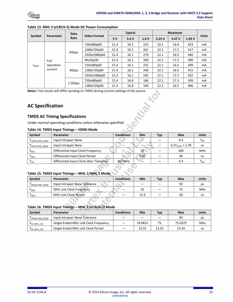
Silic
on Im
age
Confid
entia
l for
Forte
x In
dust
rial L
td.
Inte
rnal
Use
Onl
y
SiI9394 and SiI9679 HDMI/MHL 1, 2, 3 Bridge and Receiver with HDCP 2.2 Support Data Sheet
SiI-DS-1146-B © 2014 Silicon Image, Inc. All rights reserved. 23 CONFIDENTIAL
Table 13. MHL 3 (eCBUS-S) Mode DC Power Consumption
Symbol Parameter Data Rate
Video Format Typical Maximum
Units 5 V 3.3 V 1.0 V 5.25 V 3.47 V 1.05 V
IDDFP Full operation current
6Gbps
720x480p60 21.4 16.1 252 22.1 16.4 423 mA
1280x720p60 21.4 16.1 261 22.1 17.2 417 mA
1920x1080p60 21.4 16.1 279 22.1 16.5 446 mA
4Kx2Kp30 21.4 16.1 330 22.1 17.3 490 mA
3Gbps
720x480p60 21.4 16.1 231 22.1 16.5 409 mA
1280x720p60 21.4 16.1 240 22.1 16.5 415 mA
1920x1080p60 21.4 16.1 245 22.1 17.2 432 mA
1.5Gbps 720x480p60 21.4 16.9 186 22.1 17.3 399 mA
1280x720p60 21.4 16.8 194 22.1 16.5 406 mA
Notes: Test results will differ pending on TMDS driving current settings of the source.
AC Specification
TMDS AC Timing Specifications
Under normal operating conditions unless otherwise specified.
Table 14. TMDS Input Timings – HDMI Mode
Symbol Parameter Conditions Min Typ Max Units
TINTRA-PAIR_SKEW Input Intrapair Skew — — — 0.4 TBIT
TINTER-PAIR_SKEW Input Intrapair Skew — — — 0.2TPIXEL + 1.78 ns
FRXC Differential Input Clock Frequency — 25 — 300 MHz
TRXC Differential Input Clock Period — 6.06 — 40 ns
TIJIT Differential Input Clock Jitter Tolerance 165 MHz — — 0.3 TBIT
Table 15. TMDS Input Timings – MHL 1/MHL 2 Mode
Symbol Parameter Conditions Min Typ Max Units
TINTRA-PAIR_SKEW Input Intrapair Skew Tolerance — — — 93 ps
FMHL MHL Link Clock Frequency — 25 — 75 MHz
TMHL MHL Link Clock Period — 13.3 — 40 ns
Table 16. TMDS Input Timings – MHL 3 (eCBUS-S) Mode
Symbol Parameter Conditions Min Typ Max Units
TINTRA-PAIR_SKEW Input Intrapair Skew Tolerance — — — 93 ps
FSE_MHL_CLK Single-Ended MHL Link Clock Frequency — 74.9625 75 75.0375 MHz
TSE_MHL_CLK Single-Ended MHL Link Clock Period — 13.32 13.33 13.34 ns

Silic
on Im
age
Confid
entia
l for
Forte
x In
dust
rial L
td.
Inte
rnal
Use
Onl
y
SiI9394 and SiI9679 HDMI/MHL 1, 2, 3 Bridge and Receiver with HDCP 2.2 Support Data Sheet
24 © 2014 Silicon Image, Inc. All rights reserved. SiI-DS-1146-B CONFIDENTIAL
Table 17. TMDS Input Timings – MHL 3 (eCBUS-D) Mode
Symbol Parameter Conditions Min Typ Max Units
TINTRA-PAIR_SKEW Input Intrapair Skew — — — 25 ps
FDF_MHL_CLK Differential MHL Link Clock Frequency — 149.925 150 150.075 MHz
TDF_MHL_CLK Differential MHL Link Clock Period — 6663.33 6666.67 6670.00 ns
Note: Refer to the MHL Specification for more information on AC Specifications.
Table 18. TMDS Output Timing AC Specifications
Symbol Parameter Conditions Min Typ Max Units
TTXDPS Intrapair Differential Output Skew — — — 0.15 TBIT
TTXRT Data/Clock Rise Time — 75 — — ps
TTXFT Data/Clock Fall Time — 75 — — ps
FTXC Differential Output Clock Frequency — 25 — 300 MHz
TTXC Differential Output Clock Period — 3.33 — 40 ns
TDUTY Differential Output Clock Duty Cycle — 40 — 60 TTXC
TOJIT Differential Output Clock Jitter — — — 0.25 TBIT
Audio Output Timings for the SiI9394 Bridge
Table 19. I2S Output Port Timings
Symbol Parameter Conditions Min Typ Max Units Figure Notes
TTR SCK Clock Period (TX) CL = 10 pF 1.00 — — TTR
Figure 13
1
TSU Setup Time, SCK to SD/WS CL = 10 pF 0.4TTR – 5 — — ns 1
THD Hold Time, SCK to SD/WS CL = 10 pF 0.4TTR – 5 — — ns 1
TSCKDUTY SCK Duty Cycle CL = 10 pF 40% — 60% TTR 1
TSCK2SD SCK to SD or WS Delay CL = 10 pF –5 — +5 ns 2
TAUDDLY Audio Pipeline Delay — — 40 80 µs — —
Notes:
1. See Figure 13 on page 28. Meets timings in Philips I2S Specification.
2. Applies also to SD-to-WS delay.
Table 20. TDM Output Port Timings
Symbol Parameter Conditions Min Typ Max Units Figure Notes
FS_TDM Sample Rate 2-8 Channel 32 — 192 kHz — 2
TSCKCYC TDM SCK Cycle Time CL = 10 pF — 1.0 — UI
Figure 14
1
TSCKDUTY TDM SCK Duty Cycle CL = 10 pF 40 — 60 %UI 1
TTDMSU Setup Time, SCK to FS/SD CL = 10 pF 0.4UI – 3.5 — — ns 1
TTDMHD Hold Time, SCK to FS/SD CL = 10 pF 0.4UI – 3.5 — — ns 1
TSCK2SD SCK to SD or WS Delay CL = 10 pF –3.5 — +3.5 ns —
TAUDDLY Audio Pipeline Delay — — 40 80 µs — —
Notes:
1. Proportional to unit time (UI), according to sample rate.
2. The video mode lower than 720p does not support multichannel 192 kHz sample rate.

Silic
on Im
age
Confid
entia
l for
Forte
x In
dust
rial L
td.
Inte
rnal
Use
Onl
y
SiI9394 and SiI9679 HDMI/MHL 1, 2, 3 Bridge and Receiver with HDCP 2.2 Support Data Sheet
SiI-DS-1146-B © 2014 Silicon Image, Inc. All rights reserved. 25 CONFIDENTIAL
Table 21. S/PDIF Output Port Timings
Symbol Parameter Conditions Min Typ Max Units Figure Notes
TSPCYC SPDIF Cycle Time CL = 10 pF — 2.0 — UI
Figure 15
1, 2
FSPDIF SPDIF Frequency — 4 — 24 MHz 3
TSPDUTY SPDIF Duty Cycle CL = 10 pF 90% — 110% UI 2, 5
TMCLKCYC MCLK Cycle Time CL = 10 pF 20 — 250 ns
Figure 16
1, 2, 4
FMCLK MCLK Frequency CL = 10 pF 4 — 50 MHz 1, 2, 4
TMCLKDUTY MCLK Duty Cycle CL = 10 pF 40% — 60% TMCLKCYC 2, 4
TAUDDLY Audio Pipeline Delay — — 40 80 µs — —
Notes:
1. Guaranteed by design.
2. Proportional to unit time (UI), according to sample rate.
3. SPDIF is not a true clock, but is generated from the internal 128 fs clock, for fs from 128 to 512 kHz.
4. MCLK refers to MCLKOUT.
5. Intrinsic jitter on S/PDIF output can limit its use as an S/PDIF transmitter. The S/PDIF intrinsic jitter is approximately 0.1 UI.
Table 22. Audio Crystal Timings
Symbol Parameter Conditions Min Typ Max Units Figure
FXTAL External Crystal Frequency — 26 27 28.5 MHz Figure 10
1Mohm
XTAL_VDD33
XTAL_IN
XTAL_OUT
27 MHz
18 pF
18pF
3
5
4
3.3 V
SiI9394
Figure 10. Audio Crystal Application
SPI Interface Timing
Table 23. SPI Control Signal Timings
Symbol Parameter Min Typ Max Units Figure
FSPI_CLK SPI_CLK Frequency 1.0 30 66 MHz —
tCSs SPI_CS_N Setup Time to SPI_CLK 1.05 — — ns
Figure 17,
Figure 18
tCSh SPI_CS_N Hold Time to SPI_CLK 1.25 — — ns
tTXs SPI_MOSI Setup Time to SPI_CLK 0.45 — — ns
tTXh SPI_MOSI Hold Time to SPI_CLK 2.0 — — ns
tRXp SPI_MISO Output Time from SPI_CLK Launch Edge
1.0 — 4.54 ns Figure 18
Note: Under normal operating conditions otherwise specified.

Silic
on Im
age
Confid
entia
l for
Forte
x In
dust
rial L
td.
Inte
rnal
Use
Onl
y
SiI9394 and SiI9679 HDMI/MHL 1, 2, 3 Bridge and Receiver with HDCP 2.2 Support Data Sheet
26 © 2014 Silicon Image, Inc. All rights reserved. SiI-DS-1146-B CONFIDENTIAL
HSIC Interface Timing
Table 24. HSIC Interface Control Signal Timings
Symbol Parameter Conditions Min Typ Max Units Figure
FSTROBE Strobe Frequency — 239.988 240 240.012 MHz
Figure 19
TSLEW Slew Rate (rise and fall) — 0.7 1.0 1.2 V/ns
TS Receiver data setup time — 365 — — ps
TT Transmitter uncertainty — — — 365 ps
TH Receiver data hold time — 300 — — ps
Miscellaneous Timings
Under normal operating conditions unless otherwise specified.
Table 25. Miscellaneous Timings
Symbol Parameter Conditions1 Min Typ Max Units Figure Notes
TI2CDVD Delay from falling edge of I
2C clock
that I2C data is valid
CL = 400 pF — — 700 ns — —
FDDC Speed on TMDS DDC port CL = 400 pF — — 100 kHz — 2
FI2C Speed on local I2C port CL = 400 pF — — 400 kHz — 3
TRESET RESETN Signal LOW Time for valid reset
— 2 — — ms Figure 11 —
TRESET_VDD Time required for RESETN high before VDD
50% RESETN to 90% VDD
1 — — ms Figure 12 —
Notes:
1. Under normal operating conditions unless otherwise specified, including output pin loading of CL = 10 pF. 2. DDC port is limited to 100 kHz by the HDMI Specification, and meets I
2C Standard mode timings.
3. Local I2C can operate up to fast mode 400 kHz speed.
ESD Specifications
Table 26. ESD Specifications
Symbol Parameter Min Typ Max Units Notes
Latch up ESD Latch up ± 200 — — mA 1, 2
HBM Human Body Model 2000 — — V 3
MM Machine Model 200 — — V 4
CDM Charged Device Model 500 — — V 5
Notes:
1. Test is performed at 70 °C. 2. Measured according to JESD78B standard. 3. Measured according to JESD22-A114 standard. 4. Measured according to JESD22-A115 standard. 5. Measured according to JESD22-C101 standard.

Silic
on Im
age
Confid
entia
l for
Forte
x In
dust
rial L
td.
Inte
rnal
Use
Onl
y
SiI9394 and SiI9679 HDMI/MHL 1, 2, 3 Bridge and Receiver with HDCP 2.2 Support Data Sheet
SiI-DS-1146-B © 2014 Silicon Image, Inc. All rights reserved. 27 CONFIDENTIAL
Timing Diagrams
RESETN Timing Diagrams Power sequencing is not required for the SiI9394 or the SiI9679 device. However, to ensure a proper reset the rules mentioned under the diagrams in Figure 11 and Figure 12 must be followed.
VCC must be stable between its limits for Normal Operating Conditions for TRESET_VDD before RESETN goes HIGH, as shown in Figure 11. Before accessing registers, RESETN must be pulled low for TRESET. This can be done by holding RESETN low until TRESET_VDD after stable power, as described above, or by pulling RESETN LOW from a HIGH state for at least TRESET, as shown in Figure 12.
RESETN
VCCmin
VCCmax
TRESET_VDD
VCC
Figure 11. Conditions for Use of RESETN
RESETN
TRESET
Figure 12. RESETN Minimum Timings

Silic
on Im
age
Confid
entia
l for
Forte
x In
dust
rial L
td.
Inte
rnal
Use
Onl
y
SiI9394 and SiI9679 HDMI/MHL 1, 2, 3 Bridge and Receiver with HDCP 2.2 Support Data Sheet
28 © 2014 Silicon Image, Inc. All rights reserved. SiI-DS-1146-B CONFIDENTIAL
Digital Audio Output Timings
WS
SD
SCK
TTR
TSCKDUTY
TSU THDTSCK2SD_MAX TSCK2SD_MIN
Data ValidData Valid Data Valid
Figure 13. I2S Output Timings
FS
SD
SCK
TSCKCYC
TSCKDUTY
TTDMSU TTDMHDTSCK2SD_MAX TSCK2SD_MIN
Data ValidData Valid Data Valid
Figure 14. TDM Output Timings
SPDIF
TSPDUTY
50%
TSPCYC
Figure 15. S/PDIF Output Timings
MCLK
TMCLKCYC
TMCLKDUTY
50%50%
Figure 16. MCLK Timings
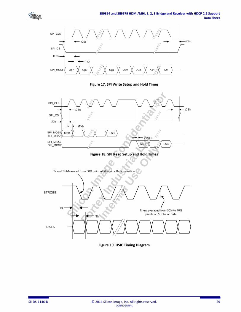
Silic
on Im
age
Confid
entia
l for
Forte
x In
dust
rial L
td.
Inte
rnal
Use
Onl
y
SiI9394 and SiI9679 HDMI/MHL 1, 2, 3 Bridge and Receiver with HDCP 2.2 Support Data Sheet
SiI-DS-1146-B © 2014 Silicon Image, Inc. All rights reserved. 29 CONFIDENTIAL
SPI_CLK
Op7 Op6 Op1 Op0 A15 A14 D0
SPI_CS
SPI_MOSI
tCShtCSs
tTXh
tTXs
Figure 17. SPI Write Setup and Hold Times
SPI_CLK
SPI_CS
tCSs
tTXh
tTXs
tCSh
MSB LSB
tRXp
MSB LSBSPI_MISO/
SPI_MOSI
SPI_MOSI/
SPI_MISO
Figure 18. SPI Read Setup and Hold Times
STROBE
DATA
Th
Ts
Ts and Th Measured from 50% point of Strobe or Data transition
Tslew averaged from 30% to 70% points on Strobe or Data
Figure 19. HSIC Timing Diagram

Silic
on Im
age
Confid
entia
l for
Forte
x In
dust
rial L
td.
Inte
rnal
Use
Onl
y
SiI9394 and SiI9679 HDMI/MHL 1, 2, 3 Bridge and Receiver with HDCP 2.2 Support Data Sheet
30 © 2014 Silicon Image, Inc. All rights reserved. SiI-DS-1146-B CONFIDENTIAL
Pin Descriptions
HDMI/MHL1, 2, 3 Receiver Port Pins Pin Name Pin Type Dir Description
RXCN 7 TMDS Input HDMI Differential Clock Input or Differential Link Clock Input of MHL 3 eCBUS-D mode.
In MHL 3 eCBUS-D mode, the differential link clock transmit fixed clock hybrid with SPI/HSIC data and eCBUS commands.
In MHL 1.x, MHL 2.x or MHL 3 eCBUS-S mode, this clock pair is not used. RXCP 8 TMDS Input
RX0N 11 TMDS Input
HDMI Channel 0 Data Input or MHL 1.x, MHL 2.x, and MHL 3 mode Data Input.
In MHL 1.x or MHL 2.x mode, this data pair is the single differential pair for a TMDS Data channel carried with common mode clock. The other HDMI channels and clock pair are not used.
In MHL 3 mode, this data pair is the single differential pair for a TMDS Data channel without common mode clock. The other HDMI channels and clock pair are not used.
RX0P 12 TMDS Input
RX1N 13 TMDS Input HDMI Channel 1 Data Input
RX1P 14 TMDS Input
RX2N 15 TMDS Input HDMI Channel 2 Data Input
RX2P 16 TMDS Input
CBUS/CBUS_HPD 4 Custom CBUS 5 V tolerant
Input/ Output
The SiI9394 bridge: CBUS Signal.
The SiI9679 receiver: Hot-Plug Detect (HPD) Signal Output for HDMI Mode or CBUS Signal for MHL 1.x, MHL 2.x, and MHL 3 mode.
In LPSB mode, if RPWR5V is HIGH and MHL_CD is LOW, this pin will be pulled up HIGH by internal 1 KΩ resistor to wake up function. In normal operation mode, this pin can be controlled by register.
DSCL 75 Schmitt
Open-drain 5 V tolerant
Input/ Output
DDC Clock and Data for HDMI Mode.
In HDMI mode, these signals are true open-drain, and do not pull to ground when power is not applied to the device. These pins require an external pull-up resistor.
In MHL 1.x, MHL 2.x or MHL 3 mode, these pins are also used for cable detect input.
DSDA 76 Schmitt
Open-drain 5 V tolerant
Input/ Output

Silic
on Im
age
Confid
entia
l for
Forte
x In
dust
rial L
td.
Inte
rnal
Use
Onl
y
SiI9394 and SiI9679 HDMI/MHL 1, 2, 3 Bridge and Receiver with HDCP 2.2 Support Data Sheet
SiI-DS-1146-B © 2014 Silicon Image, Inc. All rights reserved. 31 CONFIDENTIAL
HDMI Transmitter Port Pins Pin Name Pin Type Dir Description
TXCN 40 TMDS Output HDMI Differential Clock Output.
TXCP 41 TMDS Output
TX0N 42 TMDS Output HDMI Channel 0 Data Output.
TX0P 43 TMDS Output
TX1N 44 TMDS Output HDMI Channel 1 Data Output.
TX1P 45 TMDS Output
TX2N 46 TMDS Output HDMI Channel 2 Data Output.
TX2P 47 TMDS Output
TX_HPD 38 5 V tolerant Input Hot Plug Detection Input.
An external 10 kΩ pull-down resistor is required on this pin.
CEC_A/NC 72 CEC Compliant Input/ Output
The SiI9394 bridge: Interface to CEC devices.
The SiI9679 receiver: NC.
For the SiI9394 bridge, this pin is CEC electrical specification compliant signal powered by VDD33. This pin has an internal pull-up. Therefore an external 27 kΩ resistor is not required.
For the SiI9679 receiver, this pin must not be connected to anything.
TDSCL 66 Schmitt
Open-drain 5 V tolerant
Input/ Output DDC Clock and Data for transmitter (I
2C Master).
These pins implement true open-drain circuits; external pull-up (1.8 kΩ ± 10% typical) resistors to DDC 5 V are required. These are 5 V tolerant pins. TDSDA 67
Schmitt Open-drain 5 V tolerant
Input/ Output
Data Tunneling Pins Pin Name Pin Type Dir Description
SPI_CLK 60 LVTTL Input/Output SPI Master Interface for stand-alone mode and SPI Slave Interface for MHL 3 mode data tunneling function.
This interface is shared with the SPI master and slave, only one mode is available at one time. The SPI_CS0 pin is the chip strobe output of the SPI master and should be connected to the external SPI slave device like SPI Flash/EEPROM. And the SPI_CS1 pin is the chip strobe input of the SPI slave and should be connected to the external SPI master device like SoC.
This interface defaults to an SPI master and is sampled once at reset to load the data from the external SPI Flash/EEPROM.
SPI_CS0 61 LVTTL Output
SPI_CS1 62 LVTTL Input
SPI_MOSI 63 LVTTL Input/Output
SPI_MISO 64 LVTTL Input/Output
HSIC_STB 54 HSIC Input/Output HSIC Interface for MHL 3 Mode.
In MHL 3 mode, these pins are used to exchange the USB data that transferred over the eCBUS with the external SoC.
These pins are not used for other modes.
HSIC_DAT 53 HSIC Input/Output

Silic
on Im
age
Confid
entia
l for
Forte
x In
dust
rial L
td.
Inte
rnal
Use
Onl
y
SiI9394 and SiI9679 HDMI/MHL 1, 2, 3 Bridge and Receiver with HDCP 2.2 Support Data Sheet
32 © 2014 Silicon Image, Inc. All rights reserved. SiI-DS-1146-B CONFIDENTIAL
Digital Audio Output Pins Pin Name Pin Type Dir Description
XTAL_IN 49 LVTTL Input Crystal Clock Input.
XTAL_OUT 50 LVTTL Output Crystal Clock Output.
MCLK/NC 29 LVTTL Output The SiI9394 bridge: Audio output Master Clock.
The SiI9679 receiver: Not Connected (NC)
SCK/NC 28 LVTTL Output The SiI9394 bridge: I
2S or TDM Serial Clock.
The SiI9679 receiver: NC
WS/NC 27 LVTTL Output
The SiI9394 bridge: I2S word select or TDM Frame Start (FS)
signal.
The SiI9679 receiver: NC
SD0_SPDIF/NC 26 LVTTL Output The SiI9394 bridge: I
2S/TDM serial data or S/PDIF audio output.
The SiI9679 receiver: NC

Silic
on Im
age
Confid
entia
l for
Forte
x In
dust
rial L
td.
Inte
rnal
Use
Onl
y
SiI9394 and SiI9679 HDMI/MHL 1, 2, 3 Bridge and Receiver with HDCP 2.2 Support Data Sheet
SiI-DS-1146-B © 2014 Silicon Image, Inc. All rights reserved. 33 CONFIDENTIAL
Control and Configuration Pins Pin Name Pin Type Dir Description
RESETN 34 LVTTL
Schmitt Input
External Reset pin (Active LOW).
This pin should not be left floating.
An external 4.7 kΩ pull-up resistor to 3.3 V is required.
CSCL 68
LVTTL Schmitt
Open-drain 5 V tolerant
Input/ Output
Local I2C Bus Clock.
Chip configuration/status registers are accessed through this I2C port.
An external 4.7 kΩ pull-up resistor to 3.3 V is required.
CSDA 69
LVTTL Schmitt
Open-drain 5 V tolerant
Input/ Output
Local I2C Bus Data.
Chip configuration/status registers are accessed through this I2C port.
An external 4.7 kΩ pull-up resistor to 3.3 V is required.
TMODE 25 LVTTL
Schmitt 5 V tolerant
Input Test Mode Enable. Pull down for normal operation.
INT 20
LVTTL Schmitt
Open-drain 5 V tolerant
Input/ Output
Internal MCU Enable Input during POR or Interrupt Output in Normal Operation.
This is an open-drain output and requires an external pull-up resistor. During the power-on reset (POR), this pin is used as an input to latch the internal 8051 enabled or not. The level on this pin is latched when the POR transitions from the asserted state to the deasserted state. After completion of POR, this pin is used as interrupt output, which defaults active LOW.
GPIO0_CI2CA 21
LVTTL Schmitt
Open-drain 5 V tolerant
Input/ Output
General Purpose I/O 0 or CI2CA.
This pin defaults to an input and is sampled once at reset to select the local I
2C target address ranges.
GPIO1_PSCTL 22
LVTTL Schmitt
Open-drain 5 V tolerant
Input/ Output
General Purpose I/O 1 or PSCTL.
In HDMI mode, this pin is used as GPIO 1.
In MHL 3 mode, this pin is used as PSCTL to enable or disable system VBUS power to downstream device. This pin defaults to an output.
GPIO2 23
LVTTL Schmitt
Open-drain 5 V tolerant
Input/ Output
General Purpose I/O 2.
This pin defaults to an input.
GPIO3 30
LVTTL Schmitt
Open-drain 5 V tolerant
Input/ Output
General Purpose I/O 3.
This pin defaults to an input.
GPIO4 31
LVTTL Schmitt
Open-drain 5 V tolerant
Input/ Output
General Purpose I/O 4.
This pin defaults to an input.
GPIO5 32
LVTTL Schmitt
Open-drain 5 V tolerant
Input/ Output
General Purpose I/O 5.
This pin defaults to an input.
MHL_CD 71 LVTTL
Schmitt 5 V tolerant
Input MHL Cable Detect Input.
This pin requires a 300 kΩ pull-down resistor.
WAKEUP 73 LVTTL
Open-drain 5 V tolerant
Output Low Power Standby Mode wakes up pulse output.

Silic
on Im
age
Confid
entia
l for
Forte
x In
dust
rial L
td.
Inte
rnal
Use
Onl
y
SiI9394 and SiI9679 HDMI/MHL 1, 2, 3 Bridge and Receiver with HDCP 2.2 Support Data Sheet
34 © 2014 Silicon Image, Inc. All rights reserved. SiI-DS-1146-B CONFIDENTIAL
Power and Ground Pins Pin Name Pin Type Description Supply
XTAL_VDD33 48 Power XTAL Power. 3.3 V
HSIC_VDD33 57 Power HSIC Transceiver Power Supply. 3.3 V
VDD33 10 Power Receiver Termination 3.3 V Analog Power. 3.3 V
VDDIO33 19, 33, 65 Power Digital I/O Power. 3.3 V
HSIC_VDD10 58 Power HSIC Analog PHY Interface Power. 1.0 V
VDD10 24, 35, 59, 70 Power Digital Core Power. 1.0 V
AVDD10_DoC 6 Power Analog DoC (Data on Clock) Power. 1.0 V
AVDD10 9, 17 Power Analog Core Power. 1.0 V
AVDD10_PLL 36 Power Analog PLL Power. 1.0 V
AVDD10_DP 39 Power Analog Data Path Power. 1.0 V
FVDD10 18 Power Fractional PLL Power. 1.0 V
MVDD10/NC 52 Power The SiI9394 bridge: Audio PLL Power.
The SiI9679 receiver: NC 1.0 V
VDD5V_IN 2 Power
Local Power 5 V Input.
If there is no RPWR5V input, an active 5 V power input of this pin is required.
5 V
LPSBV 74 Power Standby Power for Low Power Standby Mode. 5 V
RPWR5V 3 Power
5 V Port Detection Input.
Connect to 5 V signal from HDMI input connector. This pin requires a 10 Ω series resistor, a 5.1 kΩ pull-down resistor, and at least a 1 µF capacitor to ground.
5 V
VDD33OUT 1 Power
Internal 3.3 V Regulator Output.
This pin requires a 4.7 µF capacitor to ground. Must not be used as any external power supply.
—
VDD12OUT 56 Power
Internal 1.2 V Regulator Output.
This pin requires a 4.7 µF capacitor to ground. Must not be used as any external power supply.
—
CoC_GND 5 Ground Clock over CBUS Ground.
This pin must be connected to Ground. Ground
XTAL_GND 51 Ground XTAL Ground. Ground
HSIC_GND 55 Ground HSIC Interface Ground. Ground
GND ePad Ground
Ground.
All ground connections to the device are through the ePad, therefore it must be soldered to the board and the pad must have a low resistance connection to the board ground plane.
Ground
Not Connected Pins for the SiI9679 Bridge Name Pin Type Description
NC 37, 73 NC Not Connected.
These pins must not be connected to anything.
Not Connected Pins for the SiI9679 Receiver Name Pin Type Description
NC 26, 27, 28, 29, 37, 52, 72 NC Not Connected.
These pins must not be connected to anything.

Silic
on Im
age
Confid
entia
l for
Forte
x In
dust
rial L
td.
Inte
rnal
Use
Onl
y
SiI9394 and SiI9679 HDMI/MHL 1, 2, 3 Bridge and Receiver with HDCP 2.2 Support Data Sheet
SiI-DS-1146-B © 2014 Silicon Image, Inc. All rights reserved. 35 CONFIDENTIAL
Feature Information
RGB to YCbCr Color Space Converter The RGBYCbCr color space converter can convert from video data RGB to standard definition or to high definition YCbCr formats. Table 27 shows the conversion formulas that are used. The HDMI AVI packet defines the color space of the incoming video.
Table 27. RGB to YCbCr Conversion Formulas
Video Format Conversion Formulas
CE Mode 16-235 RGB
VGA ITU-R BT.601
Y = 0.299R′ + 0.587G′ + 0.114B′ Cb = –0.172R′ – 0.339G′ + 0.511B′ + 128 Cr = 0.511R′ – 0.428G′ – 0.083B′ + 128
WVGA ITU-R BT.601
SVGA ITU-R BT.601
480p/i ITU-R BT.601
576p/i ITU-R BT.601
XGA ITU-R BT.709
Y = 0.213R′ + 0.715G′ + 0.072B′ Cb = –0.117R′ – 0.394G′ + 0.511B′ + 128 Cr = 0.511R′ – 0.464G′ – 0.047B′ + 128
SXGA ITU-R BT.709
UXGA ITU-R BT.709
WUXGA ITU-R BT.709
720p ITU-R BT.709
1080i ITU-R BT.709
1080p ITU-R BT.709
4K x 2K ITU-R BT.709
YCbCr to RGB Color Space Converter The YCbCrRGB color space converter allows MPEG decoders to interface with RGB-only inputs. The CSC can convert from YCbCr in standard-definition (ITU.601) or high-definition (ITU.709) to RGB. See Table 28 for the detailed formulasX. Note the difference between RGB range for CE modes and PC modes.
Table 28. YCbCr-to-RGB Conversion Formulas
Format Change Conversion YCbCr Input Color Range
YCbCr 16-235 Input to RGB 16-235 Output
601* R′ = Y + 1.371(Cr – 128) G′ = Y – 0.698(Cr – 128) – 0.336(Cb – 128) B′ = Y + 1.732(Cb – 128)
709 R′ = Y + 1.540(Cr – 128) G′ = Y – 0.459(Cr – 128) – 0.183(Cb – 128) B′ = Y + 1.816(Cb – 128)
YCbCr 16-235 Input to RGB 0-255 Output
601 R′ = 1.164((Y-16) + 1.371(Cr – 128)) G′ = 1.164((Y-16) – 0.698(Cr – 128) – 0.336(Cb – 128)) B′ = 1.164((Y-16) + 1.732(Cb – 128))
709 R′ = 1.164((Y-16) + 1.540(Cr – 128)) G′ = 1.164((Y-16) – 0.459(Cr – 128) – 0.183(Cb – 128)) B′ = 1.164((Y-16) + 1.816(Cb – 128))
*Note: No clipping can be done.

Silic
on Im
age
Confid
entia
l for
Forte
x In
dust
rial L
td.
Inte
rnal
Use
Onl
y
SiI9394 and SiI9679 HDMI/MHL 1, 2, 3 Bridge and Receiver with HDCP 2.2 Support Data Sheet
36 © 2014 Silicon Image, Inc. All rights reserved. SiI-DS-1146-B CONFIDENTIAL
SiI9394 and SiI9679 Input and Output Matrix with HDCP The SiI9394 bridge and the SiI9679 receiver support different HDCP modes. See Table 29 below for details.
Table 29. SiI9394 and SiI9679 Input and Output Matrix with HDCP
Device HDCP Mode
Input Output
HDMI MHL 1.x/MHL 2.x MHL 3
(eCBUS-S)
MHL 3
(eCBUS-D) HDMI
SiI9394 Bridge
HDCP 1.x — Y Y Y Y2
HDCP 2.2 — N Y Y Y2
SiI9679 Receiver
HDCP 1.x Y Y Y Y Y3
HDCP 2.2 Y N Y Y N
Notes:
1. Y = Supported, N = Not Supported. 2. The SiI9394 bridge supports three types of HDCP repeater: HDCP 2.2 repeater, HDCP 1.x repeater, HDCP 2.2 to
HDCP 1.x down-converter. 3. The SiI9679 receiver supports HDMI output without HDCP, and supports optional HDCP 1.x output only for HDCP
2.2 input without repeater function.
3D Video Formats The SiI9394 or the SiI9679 device supports the 3D video modes described in the HDMI 1.4a Specification. All modes support RGB 4:4:4, YCbCr 4:2:2 and YCbCr 4:4:4 color formats and 8-bit color depth. External separate HSYNC, VSYNC, and DE signals can be supplied, or these signals can be supplied as embedded EAV/SAV sequences in the video stream. Table 30 shows only the maximum possible resolution with a given frame rate. For example, Side-by-Side mode is defined for 1080p @ 60 Hz frame, which implies that 720p @ 60 Hz and 480p @ 60 Hz are also supported. Furthermore, a frame rate of 24 Hz also means that a frame rate of 23.98 Hz is supported. A frame rate of 60 Hz means a frame rate of 59.94 Hz and its associated pixel frequency is supported as well.
Table 30. Supported HDMI 3D Input Video Formats
HDMI 3D Format Extended Definition
Resolution Frame Rate
(Hz) Input Pixel Clock
(MHz)
Frame Packing —
1080p 50/60 300
1080p 24/30 148.5
720p/1080i 50/60
Side-by-Side Full
1080p 50/60 300
1080p 24/30
148.5 720p/1080i 50/60
Half 1080p 50/60
Top-and-Bottom —
1080p 50/60
1080p 24/30 74.25
720p/1080i 50/60
Line Alternative —
1080p 50/60 300
1080p 24/30
148.5 720p/1080i 50/60
Field Alternative — 1080i 50/60
L + Depth —
1080p 50/60 300
1080p 24/30 148.5
720p/1080i 50/60

Silic
on Im
age
Confid
entia
l for
Forte
x In
dust
rial L
td.
Inte
rnal
Use
Onl
y
SiI9394 and SiI9679 HDMI/MHL 1, 2, 3 Bridge and Receiver with HDCP 2.2 Support Data Sheet
SiI-DS-1146-B © 2014 Silicon Image, Inc. All rights reserved. 37 CONFIDENTIAL
When the SiI9394 or the SiI9679 device is in MHL 2.x, MHL 3 eCBUS-S mode, or MHL 3 eCBUS-D mode, the MHL 3D input formats are transcoded to HDMI mode 3D formats accordingly. The supported MHL input 3D formats are listed in Table 31, Table 32, and Table 33.
Table 31. Supported MHL 3 (eCBUS-D) Mode 3D Input Video Formats
MHL 3 (eCBUS-D) Mode 3D Format
Corresponding HDMI Format
Resolution Frame Rate
(Hz) Input Pixel Clock for
8-bit color (MHz)
Frame Sequential Frame Packing
1080p 50/60 300
1080p 24/30 148.5
720p/1080i 50/60
Top-Bottom Top-and-Bottom
1080p 50/60 148.5
1080p 24/30 74.25
720p/1080i 50/60
Left-Right Side-by-Side (Half)
1080p 50/60 148.5
1080p 24/30 74.25
720p/1080i 50/60 74.25
Table 32. Supported MHL 3 (eCBUS-S) Mode 3D Input Video Formats
MHL 3 (eCBUS-S)
Mode 3D Format
Corresponding HDMI Format
Resolution Frame Rate
(Hz) Input Pixel Clock for
8-bit color (MHz)
Frame Sequential Frame Packing
1080p 50/60 300 (PackedPixel)
1080p 24/30 148.5
720p/1080i 50/60
Top-Bottom Top-and-Bottom
1080p 50/60 148.5
1080p 24/30 74.25
720p/1080i 50/60
Left-Right Side-by-Side (Half)
1080p 50/60 148.5
1080p 24/30 74.25
720p/1080i 50/60 74.25
Table 33. Supported MHL 2 3D Input Video Formats
MHL 2
3D Format
Corresponding HDMI Format
Resolution Frame Rate
(Hz) Input Link Clock for
8-bit color (MHz)
Frame Sequential Frame Packing 1080p 24/30
74.25 (PackedPixel) 720p/1080i 50/60
Top-Bottom Top-and-Bottom
1080p 50/60 74.25 (PackedPixel)
1080p 24/30 74.25
720p/1080i 50/60
Left-Right Side-by-Side (Half)
1080p 50/60 74.25 (PackedPixel)
1080p 24/30 74.25
720p/1080i 50/60 74.25

Silic
on Im
age
Confid
entia
l for
Forte
x In
dust
rial L
td.
Inte
rnal
Use
Onl
y
SiI9394 and SiI9679 HDMI/MHL 1, 2, 3 Bridge and Receiver with HDCP 2.2 Support Data Sheet
38 © 2014 Silicon Image, Inc. All rights reserved. SiI-DS-1146-B CONFIDENTIAL
Device Address Configuration Using CI2CA/GPIO4/GPIO5 All functions of the SiI9394 or the SiI9679 device are controlled and observed with I
2C registers. The I
2C address of the
device depends on the working mode: External MCU mode or stand-alone mode. The GPIO0_CI2CA/GPIO4/GPIO5 pins default to an input signal and are sampled once at reset to select the local I
2C address ranges.
For External MCU mode, CI2CA signal is used for the local I2C address selection, which is fixed to 0x60/0x62. Refer to
Table 34.
Table 34. Control of I2C Address with CI2CA Signal
Local I2C address of Page 0 CI2CA
0x60 Low
0x62 High
For stand-alone mode GPIO4 and GPIO5 signals are used for the local I2C address selection, which is defined by the
firmware of internal MCU. Refer to the Table 35.
Table 35. Control of I2C Address with GPIO4/GPIO5 Signal
Local I2C address of Page 0 GPIO4 GPIO5 Notes
Value1 Low Low 1, 2
Value2 Low High 1, 2
Value3 High Low 1, 2
Value4 High High 1, 2
Notes:
1. The I2C address value is defined by firmware of the internal MCU. 2. Value1, 2, 3, and 4 is configurable based on system design requirement.
Audio Output Interface
S/PDIF
The S/PDIF stream can carry two-channel uncompressed PCM data (IEC 60958) or a compressed bit stream for multi-channel (IEC 61937) formats. The audio data output logic forms the audio data output stream from the HDMI audio packets. The S/PDIF output supports audio sampling rates from 32 to 192 kHz. A separate master clock output (MCLK), coherent with the S/PDIF output, is provided for time-stamping purposes. Coherent means that the MCLK and S/PDIF are created from the same clock source.
I2S
The I2S bus format is programmable through registers, to allow interfacing with I
2S audio DACs or audio DSPs with I
2S
inputs. Additionally, the MCLK (audio master clock) frequency is selectable to be an integer multiple of the audio sample rate Fs.
MCLK frequencies support various audio sample rates as shown in Table 36.
Table 36. Supported MCLK Frequencies
Multiple of Fs Audio Sample Rate, Fs : I
2S and S/PDIF Supported Rates
32 kHz 44.1 kHz 48 kHz 88.2 kHz 96 kHz 176.4 kHz 192 kHz
128 4.096 MHz 5.645 MHz 6.144 MHz 11.290 MHz 12.288 MHz 22.579 MHz 24.576 MHz
192 6.144 MHz 8.467 MHz 9.216 MHz 16.934 MHz 18.432 MHz 33.868 MHz 36.864 MHz
256 8.192 MHz 11.290 MHz 12.288 MHz 22.579 MHz 24.576 MHz 45.158 MHz 49.152 MHz
384 12.288 MHz 16.934 MHz 18.432 MHz 33.864 MHz 36.864 MHz — —
512 16.384 MHz 22.579 MHz 24.576 MHz 45.158 MHz 49.152 MHz — —

Silic
on Im
age
Confid
entia
l for
Forte
x In
dust
rial L
td.
Inte
rnal
Use
Onl
y
SiI9394 and SiI9679 HDMI/MHL 1, 2, 3 Bridge and Receiver with HDCP 2.2 Support Data Sheet
SiI-DS-1146-B © 2014 Silicon Image, Inc. All rights reserved. 39 CONFIDENTIAL
TDM
Serial audio interfaces such as I2S and TDM consist of words and channels (or slots), as shown in Figure 20.
HDMI and MHL allow 24-bit words. The TDM allows 32-bit channels. Each channel has up to 24-bit audio word and zero pads for the rest. The TDM frame can have 2/4/6/8 channel. TDM FS (Frame Start) identifies the first channel of the TDM frame, as shown in Figure 21.
CLK
Bit
word
channel (or slot)
SDMSB
– 2MSB
MSB
– 1
LSB
– 2
LSB
– 1LSB
0
Pad
0
Pad
0
Pad
0
PadMSB
Figure 20. Word and Channel in TDM Audio Interface
SD
FS
TDM Frame
Ch 0 Ch 1 Ch 2 Ch 3 Ch 4 Ch 5 Ch 6 Ch 7 Ch 0 Ch 1 Ch 2 Ch 3 Ch 4 Ch 5 Ch 6 Ch 7
Figure 21. TDM Frame
In TDM, the first channel MSB has a one bit delay to FS. To cover the compliance issues, we have three options between the MSB of the first channel and FS: No delay, 1-bit delay, or 2-bit delay, as shown in Figure 22.
The control registers of the TDM share I2S.
CLK
Frame Sync
Channel 0 Channel 1
Channel 0 Channel 1
Channel 0 Channel 1
SD : 0b delay
SD : 2b delay
SD : 1b delay
Figure 22. TDM – Delay of First Channel MSB to FS

Silic
on Im
age
Confid
entia
l for
Forte
x In
dust
rial L
td.
Inte
rnal
Use
Onl
y
SiI9394 and SiI9679 HDMI/MHL 1, 2, 3 Bridge and Receiver with HDCP 2.2 Support Data Sheet
40 © 2014 Silicon Image, Inc. All rights reserved. SiI-DS-1146-B CONFIDENTIAL
AV Link Data Rate in MHL 3 Mode When the SiI9394 or the SiI9679 device operates in MHL 3 mode, Receiver Block of the AV Link stream can be configured to 6Gbps, 3Gbps, and 1.5Gbps data rate, which depends on the setting of CBUS command - AV LINK_MODE_CONTROL from the MHL 3 source.
The capability of the Receiver Block varies depending on its setting for a different TMDS link data rate mode. MHL 3 source should carefully select the link rate based on pixel clock of the video format, power consumption, and EMI requirement.
Table 37 shows bandwidth limitations of the input video pixel clock under different data rate.
Table 37. Input Video Pixel Clock Bandwidth vs. AV link Data Rate in MHL 3 Mode
eCBUS Mode Link Clock Frequency Video Format Color Depth AV Link Data Rate Input Video
Pixel Clock Bandwidth
eCBUS-S 75 MHz
16bpp
(YCbCr 4:2:2, Packet Pixel mode)
1.5 Gbp/s Up to 75 MHz
3.0 Gbp/s Up to 150 MHz
6.0 Gbp/s Up to 300 MHz
24bpp
(YCbCr 4:4:4 or RGB)
1.5 Gbp/s Up to 50 MHz
3.0 Gbp/s Up to 100 MHz
6.0 Gbp/s Up to 200 MHz
eCBUS-D 150 MHz
16bpp
(YCbCr 4:2:2, Packet Pixel mode)
1.5 Gbp/s Up to 75 MHz
3.0 Gbp/s Up to 150 MHz
6.0 Gbp/s Up to 300 MHz
24bpp
(YCbCr 4:4:4 or RGB)
1.5 Gbp/s Up to 50 MHz
3.0 Gbp/s Up to 100 MHz
6.0 Gbp/s Up to 200 MHz

Silic
on Im
age
Confid
entia
l for
Forte
x In
dust
rial L
td.
Inte
rnal
Use
Onl
y
SiI9394 and SiI9679 HDMI/MHL 1, 2, 3 Bridge and Receiver with HDCP 2.2 Support Data Sheet
SiI-DS-1146-B © 2014 Silicon Image, Inc. All rights reserved. 41 CONFIDENTIAL
Design Recommendations The tolerance of all resistors shown in this section is ± 5% unless otherwise noted.
Power Supplies Decoupling Silicon Image recommends that designers include decoupling and bypass capacitors at each power pin in the layout. These are shown schematically in Figure 23. Place these components as close as possible to the pins of the SiI9394 or the SiI9679 device, and avoid routing traces through vias if possible. An example of this layout configuration is shown in Figure 24. Connections in one group (such as VDD) can share C2, the ferrite, and C3, with each pin having a separate C1 placed as close to the pin as possible. Suggested values for C1, C2, and C3 are 0.01 µF, 0.1 µF, and 10 µF, respectively. The recommended impedance of ferrite L1 is 10 Ω or more in the frequency range of 1 – 2 MHz for all power supplies.
C2C1
L1
VDD Pin
GND
VDD
C3
Figure 23. Decoupling and Bypass Schematic
C1
VDD
Ferrite
Via to GND
VDD
C2
C3
L1
Figure 24. Decoupling and Bypass Capacitor Placement

Silic
on Im
age
Confid
entia
l for
Forte
x In
dust
rial L
td.
Inte
rnal
Use
Onl
y
SiI9394 and SiI9679 HDMI/MHL 1, 2, 3 Bridge and Receiver with HDCP 2.2 Support Data Sheet
42 © 2014 Silicon Image, Inc. All rights reserved. SiI-DS-1146-B CONFIDENTIAL
High-speed TMDS Signals
Layout Guidelines
The layout guidelines below help to ensure signal integrity. Silicon Image strongly encourages the board designer to follow these guidelines.
Place the input and output connectors that carry the TMDS signals as close as possible to the device.
Route the differential lines as directly as possible from the connector to the device when using industry-standard HDMI connectors.
Route the two traces of each differential pair together.
Minimize the number of vias through which the signal lines are routed.
Lay out the MHL input pin traces with a controlled differential impedance of 100 Ω and a common mode impedance of 30 Ω. The differential impedance of the HDMI output pins must be designed within ± 15% of 100 Ω.
Serpentine traces are not recommended to compensate for inter-pair trace skew.
Lay out the HSIC trace with a controlled impedance of 50 Ω within ± 10% range. Circuit board trace length should be less than 10 cm.
ESD Protection
The SiI9394 or the SiI9679 device can withstand electrostatic discharges (ESD) due to handling during manufacture. In applications where higher protection levels are required, ESD-limiting components can be placed on the differential lines of the chip. These components typically have a capacitive effect that reduces the signal quality at higher clock frequencies. Use the lowest capacitance devices possible. ESD components must be placed after the receiver series termination resistors and as close as possible to the input or output connector. In no case can the capacitance value of these components exceed 1 pF.
EMI Considerations Electromagnetic interference (EMI) is a function of board layout, shielding, receiver component operating voltage, frequency of operation, and other factors. When attempting to control emissions, it is important not to place any passive components on the differential signal lines, except the common-mode chokes and ESD protection described earlier. The differential signaling used in HDMI is inherently low in EMI if the routing recommendations noted in the Layout Guidelines section are followed.
The PCB ground plane should extend unbroken under as much of the transmitter chip and associated circuitry as possible, with all ground pins of the chip using a common ground.

Silic
on Im
age
Confid
entia
l for
Forte
x In
dust
rial L
td.
Inte
rnal
Use
Onl
y
SiI9394 and SiI9679 HDMI/MHL 1, 2, 3 Bridge and Receiver with HDCP 2.2 Support Data Sheet
SiI-DS-1146-B © 2014 Silicon Image, Inc. All rights reserved. 43 CONFIDENTIAL
Packaging
ePad Requirements The SiI9394 or the SiI9679 chip is packaged in a 76-pin, 9 mm × 9 mm QFN package with an ePad that is used for electrical ground of the device and for improving thermal transfer characteristics.
The ePad dimensions are 5.38 mm × 5.38 mm shown on the following page. Soldering the ePad to the ground plane of the PCB is required to meet package power dissipation requirements at full speed operation, and to correctly connect the chip circuitry to electrical ground. As a general guideline, a clearance of at least 0.25 mm should be designed on the PCB between the edge of the ePad and the inner edges of the lead pads to avoid the possibility of electrical short circuit. Figure 25 on page 44 shows the package dimensions of the SiI9394 or the SiI9679 device.

Silic
on Im
age
Confid
entia
l for
Forte
x In
dust
rial L
td.
Inte
rnal
Use
Onl
y
SiI9394 and SiI9679 HDMI/MHL 1, 2, 3 Bridge and Receiver with HDCP 2.2 Support Data Sheet
44 © 2014 Silicon Image, Inc. All rights reserved. SiI-DS-1146-B CONFIDENTIAL
Package Dimensions Package drawings are not to scale.
76
1
JEDEC Package Code MO-220
Symbol Description Min Typ Max
A Thickness 0.80 0.85 0.90
A1 Stand-off 0.00 0.02 0.05
A3 Base thickness 0.20 REF
D / E Body size 8.90 9.00 9.10
D2 / E2 ePad size 6.15 6.30 6.45
b Plated lead width 0.15 0.20 0.25
e Lead pitch 0.40 BSC
L Lead foot length 0.30 0.40 0.50
R Lead tip radius 0.075 — —
K Lead to ePad clearance 0.20 — —
aaa — 0.10
bbb — 0.07
ccc — 0.10
ddd — 0.05
eee — 0.08
fff — 0.10
All dimensions are in millimeters.
Figure 25. 76-pin QFN Package Diagram

Silic
on Im
age
Confid
entia
l for
Forte
x In
dust
rial L
td.
Inte
rnal
Use
Onl
y
SiI9394 and SiI9679 HDMI/MHL 1, 2, 3 Bridge and Receiver with HDCP 2.2 Support Data Sheet
SiI-DS-1146-B © 2014 Silicon Image, Inc. All rights reserved. 45 CONFIDENTIAL
Marking Specification Marking drawing is not to scale.
Pin 1
Location
SiI9394CNUC
LLLLLL.LL-L
YYWW
Logo
Silicon Image Part Number
Lot # (= Job#)
Date code
XXXXXXX Trace code
Figure 26. Marking Diagram for SiI9394 Bridge
Pin 1
Location
SiI9679CNUC
LLLLLL.LL-L
YYWW
Logo
Silicon Image Part Number
Lot # (= Job#)
Date code
XXXXXXX Trace code
Figure 27. Marking Diagram for SiI9679 Receiver
Ordering Information Production Part Numbers: Part Number Device
SiI9394 CNUC SiI9394 MHL 1, 2, 3 to HDMI Bridge with HDCP 2.2 Support
SiI9679 CNUC SiI9679 HDMI/MHL 1, 2, 3 Receiver with HDCP 2.2 Support
The universal package can be used in lead-free and ordinary process lines.

Silic
on Im
age
Confid
entia
l for
Forte
x In
dust
rial L
td.
Inte
rnal
Use
Onl
y
SiI9394 and SiI9679 HDMI/MHL 1, 2, 3 Bridge and Receiver with HDCP 2.2 Support Data Sheet
46 © 2014 Silicon Image, Inc. All rights reserved. SiI-DS-1146-B CONFIDENTIAL
References
Standards Documents Table 38 lists the abbreviations used in this document. Contact the responsible standards groups listed in Table 39 for more information on these specifications.
Table 38. Referenced Documents
Abbreviation Standards publication, organization, and date
HDMI High Definition Multimedia Interface, Revision 1.4a, HDMI Consortium, March 2010
HCTS HDMI Compliance Test Specification, Revision 1.4a, HDMI Consortium, March 2010
DVI Digital Visual Interface, Revision 1.0, Digital Display Working Group; April 1999
E-EDID Enhanced Extended Display Identification Data Standard, Release A Revision 1, VESA; Feb. 2000
E-DID IG VESA EDID Implementation Guide, VESA, March 2001
CEA-861-D A DTV Profile for Uncompressed High Speed Digital Interfaces, Draft 020328, EIA/CEA; July 2006
EDDC Enhanced Display Data Channel Standard, Version 1.1, VESA; March 2004
I2C The I
2C Bus Specification, Version 2.1, Philips Semiconductors, January 2000
MHL MHL (Mobile High-definition Link) Specification, Version 3, MHL, LLC, Month 2013
Table 39. Standards Groups Contact Information
Standards Group Web URL e-mail Phone
ANSI/EIA/CEA http://global.ihs.com [email protected] 800-854-7179
VESA http://www.vesa.org — 408-957-9270
DVI http://www.ddwg.org [email protected] —
I2C http://www.nxp.com — —
HDMI http://www.hdmi.org [email protected] —
MHL http://www.mhlconsortium.org [email protected] 408-962-4269
Silicon Image Documents Table 40 lists Silicon Image documents that are available from your Silicon Image sales representative.
Table 40. Silicon Image Publications
Document Title
SiI-AR-1000 SiI9394 Software API Reference Document

Silic
on Im
age
Confid
entia
l for
Forte
x In
dust
rial L
td.
Inte
rnal
Use
Onl
y
SiI9394 and SiI9679 HDMI/MHL 1, 2, 3 Bridge and Receiver with HDCP 2.2 Support Data Sheet
SiI-DS-1146-B © 2014 Silicon Image, Inc. All rights reserved. 47 CONFIDENTIAL
Revision History
Revision B, February 2014
Summary of additions and changes:
Table 4. DC Digital I/O Specifications, updated VOH, VOL and VOL_DDC Conditions; updated VOL_DDC. Parameter.
Table 9. Digital CBUS I/O Specifications, specified Min value for VOH_CBUS.
Table 14. TMDS Input Timings – HDMI Mode, specified Max value for FRXC.
Updated Table 15. TMDS Input Timings – MHL 1/MHL 2 Mode, Table 16. TMDS Input Timings – MHL 3 (eCBUS-S) Mode, and Table 17. TMDS Input Timings – MHL 3 (eCBUS-D) Mode.
Table 26. ESD Specifications, updated value for HBM, MM, and CDM.
Revision A, January 2014
First production release.

Silic
on Im
age
Confid
entia
l for
Forte
x In
dust
rial L
td.
Inte
rnal
Use
Onl
y
1140 E. Arques Avenue
Sunnyvale, CA 94085
T 408.616.4000 F 408.830.9530
www.siliconimage.com
Top Related