


Languages
Pages
Legal


SHARC and the SHARC logo are registered trademarks of Analog Devices, Inc.
SHARC ProcessorADSP-21477/ADSP-21478/ADSP-21479
Rev. D Document FeedbackInformation furnished by Analog Devices is believed to be accurate and reliable.However, no responsibility is assumed by Analog Devices for its use, nor for anyinfringements of patents or other rights of third parties that may result from its use.Specifications subject to change without notice. No license is granted by implicationor otherwise under any patent or patent rights of Analog Devices. Trademarks andregistered trademarks are the property of their respective companies.
One Technology Way, P.O. Box 9106, Norwood, MA 02062-9106 U.S.A.Tel: 781.329.4700 ©2017 Analog Devices, Inc. All rights reserved.Technical Support www.analog.com
SUMMARYHigh performance 32-bit/40-bit floating-point processor
optimized for high performance audio processingSingle-instruction, multiple-data (SIMD) computational
architectureOn-chip memory—up to 5M bits of on-chip RAM, 4M bits of
on-chip ROMUp to 300 MHz operating frequencyQualified for automotive applications. See Automotive
ProductsCode compatible with all other members of the SHARC family
The ADSP-2147x processors are available with unique audio-centric peripherals, such as the digital applications interface, serial ports, precision clock generators, S/PDIF transceiver, asynchronous sample rate converters, input data port, and more.
Factory programmed ROM versions containing latest audio decoders from Dolby and DTS, available to IP licenses
For complete ordering information, see Ordering Guide.
Figure 1. Functional Block Diagram
Internal Memory I/F
Block 0RAM/ROM
B0D64-BIT
Instruction Cache
5 Stage Sequencer
PEx PEy
PMD 64-BIT
IOD0 32-BITEPD BUS 64-BIT
Core BusCross Bar
S/PDIFTx/Rx
PCGA-D
DPI Routing/Pins
SPI/B UART
Block 1RAM/ROM
Block 2RAM
Block 3RAM
AMI SDRAMCTL
EP
External Port Pin MUX
TIMER1-0
SPORT7-0
ASRC3-0
PWM3-0
DAG1/2CoreTimer
PDAP/IDP7-0
TWI
IOD0 BUSDTCP/MTM
PCGC-D
PERIPHERAL BUS 32-BIT
COREFLAGS/PWM3-1
JTAG
Internal Memory
DMD 64-BIT
PMD 64-BIT
COREFLAGS
IOD1 32-BIT
PERIPHERAL BUS
B1D64-BIT
B2D64-BIT
B3D64-BIT
DPI Peripherals DAI Peripherals Peripherals External Port
SIMD Core
S
THERMALDIODE
FFTFIRIIR
MLB
SPEP BUS
DMD 64-BIT
FLAGx/IRQx/TMREXP
WDTRTCSHIFTREG
DAI Routing/Pins

Rev. D | Page 2 of 76 | April 2017
ADSP-21477/ADSP-21478/ADSP-21479TABLE OF CONTENTSGeneral Description . . . . . . . . . . . . . . . . . . . . . . . . . . . . . . . . . . . . . . . . . . . . . . . . . 3
Family Core Architecture . . . . . . . . . . . . . . . . . . . . . . . . . . . . . . . . . . . . . . . . 4Family Peripheral Architecture . . . . . . . . . . . . . . . . . . . . . . . . . . . . . . . . 8I/O Processor Features . . . . . . . . . . . . . . . . . . . . . . . . . . . . . . . . . . . . . . . . . 12System Design . . . . . . . . . . . . . . . . . . . . . . . . . . . . . . . . . . . . . . . . . . . . . . . . . . . . 13Development Tools . . . . . . . . . . . . . . . . . . . . . . . . . . . . . . . . . . . . . . . . . . . . . 13Additional Information . . . . . . . . . . . . . . . . . . . . . . . . . . . . . . . . . . . . . . . . 15Related Signal Chains . . . . . . . . . . . . . . . . . . . . . . . . . . . . . . . . . . . . . . . . . . 15
Pin Function Descriptions . . . . . . . . . . . . . . . . . . . . . . . . . . . . . . . . . . . . . . . 16Specifications . . . . . . . . . . . . . . . . . . . . . . . . . . . . . . . . . . . . . . . . . . . . . . . . . . . . . . . . 21
Operating Conditions . . . . . . . . . . . . . . . . . . . . . . . . . . . . . . . . . . . . . . . . . . 21Electrical Characteristics . . . . . . . . . . . . . . . . . . . . . . . . . . . . . . . . . . . . . . . 22Maximum Power Dissipation . . . . . . . . . . . . . . . . . . . . . . . . . . . . . . . . 24Package Information . . . . . . . . . . . . . . . . . . . . . . . . . . . . . . . . . . . . . . . . . . . 24ESD Sensitivity . . . . . . . . . . . . . . . . . . . . . . . . . . . . . . . . . . . . . . . . . . . . . . . . . . . 24
Absolute Maximum Ratings . . . . . . . . . . . . . . . . . . . . . . . . . . . . . . . . . . . 24Timing Specifications . . . . . . . . . . . . . . . . . . . . . . . . . . . . . . . . . . . . . . . . . . . 25Output Drive Currents . . . . . . . . . . . . . . . . . . . . . . . . . . . . . . . . . . . . . . . . . 65Test Conditions . . . . . . . . . . . . . . . . . . . . . . . . . . . . . . . . . . . . . . . . . . . . . . . . . . 65Capacitive Loading . . . . . . . . . . . . . . . . . . . . . . . . . . . . . . . . . . . . . . . . . . . . . . 65Thermal Characteristics . . . . . . . . . . . . . . . . . . . . . . . . . . . . . . . . . . . . . . . . 66
88-LFCSP_VQ Lead Assignment . . . . . . . . . . . . . . . . . . . . . . . . . . . . . . . . 68100-LQFP_EP Lead Assignment . . . . . . . . . . . . . . . . . . . . . . . . . . . . . . . . 70196-BGA Ball Assignment . . . . . . . . . . . . . . . . . . . . . . . . . . . . . . . . . . . . . . . . 72Outline Dimensions . . . . . . . . . . . . . . . . . . . . . . . . . . . . . . . . . . . . . . . . . . . . . . . . 73
Surface-Mount Design . . . . . . . . . . . . . . . . . . . . . . . . . . . . . . . . . . . . . . . . . . 75Automotive Products . . . . . . . . . . . . . . . . . . . . . . . . . . . . . . . . . . . . . . . . . . . 75
Ordering Guide . . . . . . . . . . . . . . . . . . . . . . . . . . . . . . . . . . . . . . . . . . . . . . . . . . . . . 76
REVISION HISTORY4/2017—Rev. C to Rev. DChange to RTXI Description in Table 11 of Pin Function Descriptions . . . . . . . . . . . . . . . . . . . . . . . . . . . . . . . . . . . . . . . 16Changes to Operating Conditions . . . . . . . . . . . . . . . . . . . . . . . . . . . . . . 21Change to Figure 5 of Core Clock Requirements . . . . . . . . . . . . 25Changes to AMI Read . . . . . . . . . . . . . . . . . . . . . . . . . . . . . . . . . . . . . . . . . . . . . 37Change to tWDE Switching Characteristic in AMI Write . . . 39Change to Table 64 of Automotive Products . . . . . . . . . . . . . . . . . 75
PRODUCT APPLICATION RESTRICTIONNot for use in in-vivo applications for body fluid constituent monitoring, including monitoring one or more of the compo-nents that form, or may be a part of, or contaminate human blood or other body fluids, such as, but not limited to, car-boxyhemoglobin, methemoglobin total hemoglobin, oxygen saturation, oxygen content, fractional arterial oxygen satura-tion, bilirubin, glucose, drugs, lipids, water, protein, and pH.

ADSP-21477/ADSP-21478/ADSP-21479
Rev. D | Page 3 of 76 | April 2017
GENERAL DESCRIPTIONThe ADSP-2147x SHARC® processors are members of the SIMD SHARC family of DSPs that feature Analog Devices’ Super Harvard Architecture. The processors are source code compatible with the ADSP-2126x, ADSP-2136x, ADSP-2137x, ADSP-2146x, and ADSP-2116x DSPs as well as with first generation ADSP-2106x SHARC processors in SISD (single-instruction, single-data) mode. These processors are 32-bit/40-bit floating-point processors optimized for high perfor-mance audio applications with a large on-chip SRAM, multiple internal buses to eliminate I/O bottlenecks, and an innovative digital applications interface (DAI).Table 1 shows performance benchmarks for the ADSP-2147x processors. Table 2 shows the features of the individual product offerings.
The diagram on Page 1 shows the two clock domains (core and I/O processor) that make up the ADSP-2147x processors. The core clock domain contains the following features.
• Two processing elements (PEx, PEy), each of which com-prises an ALU, multiplier, shifter, and data register file
• Two data address generators (DAG1, DAG2)• A program sequencer with instruction cache• PM and DM buses capable of supporting 2 × 64-bit data
transfers between memory and the core at every core pro-cessor cycle
• One periodic interval timer with pinout• On-chip SRAM (up to 5M bit)• A JTAG test access port for emulation and boundary scan.
The JTAG provides software debug through user break-points, which allows flexible exception handling.
Table 1. Processor Benchmarks
Benchmark AlgorithmSpeed (at 300 MHz)
Speed (at 200 MHz)
1024 Point Complex FFT (Radix 4, with Reversal)
30.59 μs 45.885 μs
FIR Filter (per Tap)1
1 Assumes two files in multichannel SIMD mode.
1.66 ns 2.49 ns IIR Filter (per Biquad)1 6.65 ns 9.975 ns Matrix Multiply (Pipelined)[3 × 3] × [3 × 1][4 × 4] × [4 × 1]
14.99 ns26.66 ns
22.485 ns39.99 ns
Divide (y/×) 11.61 ns 17.41 ns Inverse Square Root 18.08 ns 27.12 ns
Table 2. ADSP-2147x Family Features
Feature AD
SP-2
1477
AD
SP-2
1478
AD
SP-2
1479
Frequency 200 MHz Up to 300 MHz
RAM 2M bits 3M bits 5M bits
ROM N/A 4M bits
Pulse-Width Modulation 3 4 units (3 in 100-lead
package)
External Port Interface (SDRAM, AMI)1 No Yes, 16-Bit
Serial Ports 8
Direct DMA from SPORTs to External Memory No Yes
FIR, IIR, FFT Accelerator Yes
MediaLB Interface NoAutomotive models
only
Watch Dog Timer2 No Yes
Real-Time Clock2, 3 No Yes
Shift Register2 No Yes
IDP/PDAP Yes
UART 1
DAI (SRU)/DPI (SRU2) 20/14 Pins
S/PDIF Transceiver 1
SPI 2
TWI 1
SRC SNR Performance –128 dB
Thermal Diode4 Yes
VISA Support Yes
Package1
100-Lead LQFP88-Lead LFCSP_VQ
196-Ball CSP_BGA100-Lead LQFP
88-lead LFCSP_VQ
1 The 100-lead and 88-lead packages of the processors do not contain an external port. The SDRAM controller pins must be disabled when using this package. For more information, see Pin Function Descriptions.
2 Available on the 196-ball CSP_BGA package only.3 Real Time Clock (RTC) is supported only for products with a temperature range
of 0°C to +70°C and not supported for all other temperature grades.4 Available on the 88-lead and 100-lead packages only.
Table 2. ADSP-2147x Family Features (Continued)
Feature AD
SP-2
1477
AD
SP-2
1478
AD
SP-2
1479

Rev. D | Page 4 of 76 | April 2017
ADSP-21477/ADSP-21478/ADSP-21479The block diagram of the ADSP-2147x on Page 1 also shows the peripheral clock domain (also known as the I/O processor), which contains the following features:
• IOD0 (peripheral DMA) and IOD1 (external port DMA) buses for 32-bit data transfers
• Peripheral and external port buses for core connection• External port with an asynchronous memory interface
(AMI) and SDRAM controller• 4 units for pulse width modulation (PWM) control• 1 memory-to-memory (MTM) unit for internal-to-internal
memory transfers• Digital applications interface that includes four precision
clock generators (PCG), an input data port (IDP/PDAP) for serial and parallel interconnect, an S/PDIF receiver/transmitter, four asynchronous sample rate con-verters, eight serial ports, a shift register, and a flexible signal routing unit (DAI SRU).
• Digital peripheral interface that includes two timers, a 2- wire interface, one UART, two serial peripheral interfaces (SPI), two precision clock generators (PCG), three pulse width modulation (PWM) units, and a flexible signal rout-ing unit (DPI SRU).
As shown in the SHARC core block diagram on Page 5, the pro-cessors use two computational units to deliver a significant performance increase over the previous SHARC processors on a range of DSP algorithms. With its SIMD computational hard-ware, the processors can perform 1.8 GFLOPS running at300 MHz.
FAMILY CORE ARCHITECTUREThe processors are code compatible at the assembly level with the ADSP-2146x, ADSP-2137x, ADSP-2136x, ADSP-2126x, ADSP-21160, and ADSP-21161, and with the first generation ADSP-2106x SHARC processors. The ADSP-2147x share archi-tectural features with the ADSP-2126x, ADSP-2136x, ADSP-2137x, ADSP-2146x, and ADSP-2116x SIMD SHARC proces-sors, as shown in Figure 2 and detailed in the following sections.
SIMD Computational Engine
The processors contain two computational processing elements that operate as a single-instruction, multiple-data (SIMD) engine. The processing elements are referred to as PEX and PEY and each contains an ALU, multiplier, shifter, and register file. PEX is always active, and PEY may be enabled by setting the PEYEN mode bit in the MODE1 register. SIMD mode allows the processor to execute the same instruction in both processing elements, but each processing element operates on different data. This architecture is efficient at executing math intensive DSP algorithms.SIMD mode also affects the way data is transferred between memory and the processing elements because twice the data bandwidth is required to sustain computational operation in the processing elements. Therefore, entering SIMD mode also dou-bles the bandwidth between memory and the processing
elements. When using the DAGs to transfer data in SIMD mode, two data values are transferred with each memory or reg-ister file access.SIMD mode is supported from external SDRAM but is not sup-ported in the AMI.
Independent, Parallel Computation Units
Within each processing element is a set of computational units. The computational units consist of an arithmetic/logic unit (ALU), multiplier, and shifter. These units perform all opera-tions in a single cycle. The three units within each processing element are arranged in parallel, maximizing computational throughput. Single multifunction instructions execute parallel ALU and multiplier operations. In SIMD mode, the parallel ALU and multiplier operations occur in both processing ele-ments. These computation units support IEEE 32-bit single-precision floating-point, 40-bit extended precision floating-point, and 32-bit fixed-point data formats.
Timer
The processor contains a core timer that can generate periodic software interrupts. The core timer can be configured to use FLAG3 as a timer expired signal.
Data Register File
Each processing element contains a general-purpose data regis-ter file. The register files transfer data between the computation units and the data buses, and store intermediate results. These 10-port, 32-register (16 primary, 16 secondary) register files, combined with the processor’s enhanced Harvard architecture, allow unconstrained data flow between computation units and internal memory. The registers in PEX are referred to as R0–R15 and in PEY as S0–S15.
Context Switch
Many of the processor’s registers have secondary registers that can be activated during interrupt servicing for a fast context switch. The data registers in the register file, the DAG registers, and the multiplier result registers all have secondary registers. The primary registers are active at reset, while the secondary registers are activated by control bits in a mode control register.
Universal Registers
Universal registers can be used for general-purpose tasks. The USTAT (4) registers allow easy bit manipulations (Set, Clear, Toggle, Test, XOR) for all peripheral control and status registers. The data bus exchange register (PX) permits data to be passed between the 64-bit PM data bus and the 64-bit DM data bus, or between the 40-bit register file and the PM/DM data bus. These registers contain hardware to handle the data width difference.
Single-Cycle Fetch of Instruction and Four Operands
The processors feature an enhanced Harvard architecture in which the data memory (DM) bus transfers data and the pro-gram memory (PM) bus transfers both instructions and data (see Figure 2). With its separate program and data memory

ADSP-21477/ADSP-21478/ADSP-21479
Rev. D | Page 5 of 76 | April 2017
buses and on-chip instruction cache, the processor can simulta-neously fetch four operands (two over each data bus) and one instruction (from the cache), all in a single cycle.
Instruction Cache
The processor includes an on-chip instruction cache that enables three-bus operation for fetching an instruction and four data values. The cache is selective—only the instructions whose fetches conflict with PM bus data accesses are cached. This cache allows full speed execution of core looped operations such as digital filter multiply-accumulates, and FFT butterfly processing.
Data Address Generators with Zero-Overhead Hardware Circular Buffer Support
The processor’s two data address generators (DAGs) are used for indirect addressing and implementing circular data buffers in hardware. Circular buffers allow efficient programming of delay lines and other data structures required in digital signal processing, and are commonly used in digital filters and Fourier transforms. The two DAGs of the processors contain sufficient registers to allow the creation of up to 32 circular buffers (16
primary register sets, 16 secondary). The DAGs automatically handle address pointer wraparound, reduce overhead, increase performance, and simplify implementation. Circular buffers can start and end at any memory location.
Flexible Instruction Set
The 48-bit instruction word accommodates a variety of parallel operations, for concise programming. For example, the processors can conditionally execute a multiply, an add, and a subtract in both processing elements while branching and fetch-ing up to four 32-bit values from memory—all in a single instruction.
Variable Instruction Set Architecture (VISA)
In addition to supporting the standard 48-bit instructions from previous SHARC processors, the processors support new instructions of 16 and 32 bits. This feature, called Variable Instruction Set Architecture (VISA), drops redundant/unused
Figure 2. SHARC Core Block Diagram
S
SIMD CoreCACHEINTERRUPT
5 STAGEPROGRAM SEQUENCER
PM ADDRESS 32
DM ADDRESS 32
DM DATA 64
PM DATA 64
DAG116×32
MRF80-BIT
ALUMULTIPLIER SHIFTER
RFRx/FxPEx
16×40-BIT
JTAG
DMD/PMD 64
ASTATx
STYKx
ASTATy
STYKy
TIMER
RFSx/SFx
PEy16×40-BIT
MRB80-BIT
MSB80-BIT
MSF80-BIT
FLAG
SYSTEMI/F
USTAT4×32-BIT
PX64-BIT
DAG216×32
ALU MULTIPLIERSHIFTER
DATA SWAP
PM ADDRESS 24
PM DATA 48

Rev. D | Page 6 of 76 | April 2017
ADSP-21477/ADSP-21478/ADSP-21479bits within the 48-bit instruction to create more efficient and compact code. The program sequencer supports fetching these 16-bit and 32-bit instructions from both internal and external SDRAM memory. This support is not extended to the asynchro-nous memory interface (AMI). Source modules need to be built using the VISA option, in order to allow code generation tools to create these more efficient opcodes.
On-Chip Memory
The processors contain varying amounts of internal RAM and internal ROM which is shown in Table 3 through Table 5. Each block can be configured for different combinations of code and data storage. Each memory block supports single-cycle, inde-pendent accesses by the core processor and I/O processor.The processor’s SRAM can be configured as a maximum of 160k words of 32-bit data, 320k words of 16-bit data, 106.7k words of 48-bit instructions (or 40-bit data), or combinations of different word sizes up to 5M bits. All of the memory can be accessed as 16-bit, 32-bit, 48-bit, or 64-bit words. A 16-bit
floating-point storage format is supported that effectively dou-bles the amount of data that may be stored on-chip. Conversion between the 32-bit floating-point and 16-bit floating-point formats is performed in a single instruction. While each mem-ory block can store combinations of code and data, accesses are most efficient when one block stores data using the DM bus for transfers, and the other block stores instructions and data using the PM bus for transfers.Using the DM bus and PM buses, with one bus dedicated to a memory block, assures single-cycle execution with two data transfers. In this case, the instruction must be available in the cache. The memory maps in Table 3 through Table 5 display the inter-nal memory address space of the processors. The 48-bit space section describes what this address range looks like to an instruction that retrieves 48-bit memory. The 32-bit section describes what this address range looks like to an instruction that retrieves 32-bit memory.
Table 3. ADSP-21477 Internal Memory Space (2M bits)
IOP Registers 0x0000 0000–0x0003 FFFF
Long Word (64 Bits)Extended Precision Normal or Instruction Word (48 Bits) Normal Word (32 Bits) Short Word (16 Bits)
Block 0 ROM (Reserved)0x0004 0000–0x0004 7FFF
Block 0 ROM (Reserved)0x0008 0000–0x0008 AAA9
Block 0 ROM (Reserved)0x0008 0000–0x0008 FFFF
Block 0 ROM (Reserved)0x0010 0000–0x0011 FFFF
Reserved0x0004 8000–0x0004 8FFF
Reserved0x0008 AAAA–0x0008 BFFF
Reserved0x0009 0000–0x0009 1FFF
Reserved0x0012 0000–0x0012 FFFF
Block 0 SRAM0x0004 9000–0x0004 BFFF
Block 0 SRAM0x0008 C000–0x0008 FFFF
Block 0 SRAM0x0009 2000–0x0009 7FFF
Block 0 SRAM0x0012 4000–0x0012 FFFF
Reserved0x0004 C000–0x0004 FFFF
Reserved0x0009 000–0x0009 5554
Reserved0x0009 8000–0x0009 FFFF
Reserved0x0013 0000–0x0013 FFFF
Block 1 ROM (Reserved)0x0005 0000–0x0005 7FFF
Block 1 ROM (Reserved)0x000A 0000–0x000A AAA9
Block 1 ROM (Reserved)0x000A 0000–0x000AFFFF
Block 1 ROM (Reserved)0x0014 0000–0x0015 FFFF
Reserved0x0005 8000–0x0005 8FFF
Reserved0x000A AAAA–0x000A BFFF
Reserved0x000B 0000–0x000B 1FFF
Reserved0x0016 0000–0x0016 3FFF
Block 1 SRAM0x0005 9000–0x0005 BFFF
Block 1 SRAM0x000A C000–0x000A FFFF
Block 1 SRAM0x000B 2000–0x000B 7FFF
Block 1 SRAM0x0016 4000–0x0016 FFFF
Reserved0x0005 C000–0x0005 FFFF
Reserved0x000B 0000–0x000B 5554
Reserved0x000B 8000–0x000B FFFF
Reserved0x0017 0000–0x0017 FFFF
Block 2 SRAM0x0006 0000–0x0006 0FFF
Block 2 SRAM0x000C 0000–0x000C 1554
Block 2 SRAM0x000C 0000–0x000C 1FFF
Block 2 SRAM0x0018 0000–0x0018 3FFF
Reserved0x0006 1000– 0x0006 FFFF
Reserved0x000C 1555–0x000D 5554
Reserved0x000C 2000–0x000D FFFF
Reserved0x0018 4000–0x001B FFFF
Block 3 SRAM0x0007 0000–0x0007 0FFF
Block 3 SRAM0x000E 0000–0x000E 1554
Block 3 SRAM0x000E 0000–0x000E 1FFF
Block 3 SRAM0x001C 0000–0x001C 3FFF
Reserved0x0007 1000–0x0007 FFFF
Reserved0x000E 1555–0x000F 5554
Reserved0x000E 2000–0x000F FFFF
Reserved0x001C 4000–0x001F FFFF

ADSP-21477/ADSP-21478/ADSP-21479
Rev. D | Page 7 of 76 | April 2017
Table 4. ADSP-21478 Internal Memory Space (3M bits)1
IOP Registers 0x0000 0000–0x0003 FFFF
Long Word (64 Bits)Extended Precision Normal or Instruction Word (48 Bits) Normal Word (32 Bits) Short Word (16 Bits)
Block 0 ROM (Reserved)0x0004 0000–0x0004 7FFF
Block 0 ROM (Reserved)0x0008 0000–0x0008 AAA9
Block 0 ROM (Reserved)0x0008 0000–0x0008 FFFF
Block 0 ROM (Reserved)0x0010 0000–0x0011 FFFF
Reserved0x0004 8000–0x0004 8FFF
Reserved 0x0008 AAAA–0x0008 BFFF
Reserved0x0009 0000–0x0009 1FFF
Reserved0x0012 0000–0x0012 3FFF
Block 0 SRAM0x0004 9000–0x0004 CFFF
Block 0 SRAM0x0008 C000–0x0009 1554
Block 0 SRAM0x0009 2000–0x0009 9FFF
Block 0 SRAM0x0012 4000–0x0013 3FFF
Reserved0x0004 D000–0x0004 FFFF
Reserved 0x0009 1555–0x0009 FFFF
Reserved0x0009 A000–0x0009 FFFF
Reserved0x0013 4000–0x0013 FFFF
Block 1 ROM (Reserved)0x0005 0000–0x0005 7FFF
Block 1 ROM (Reserved)0x000A 0000–0x000A AAA9
Block 1 ROM (Reserved)0x000A 0000–0x000A FFFF
Block 1 ROM (Reserved)0x0014 0000–0x0015 FFFF
Reserved0x0005 8000–0x0005 8FFF
Reserved0x000A AAAA–0x000A BFFF
Reserved0x000B 0000–0x000B 1FFF
Reserved0x0016 0000–0x0016 3FFF
Block 1 SRAM0x0005 9000–0x0005 CFFF
Block 1 SRAM0x000A C000–0x000B 1554
Block 1 SRAM0x000B 2000–0x000B 9FFF
Block 1 SRAM0x0016 4000–0x0017 3FFF
Reserved0x0005 D000–0x0005 FFFF
Reserved 0x000B 1555–0x000B FFFF
Reserved0x000B A000–0x000B FFFF
Reserved0x0017 4000–0x0017 FFFF
Block 2 SRAM0x0006 0000–0x0006 1FFF
Block 2 SRAM0x000C 0000–0x000C 2AA9
Block 2 SRAM0x000C 0000–0x000C 3FFF
Block 2 SRAM0x0018 0000–0x0018 7FFF
Reserved0x0006 2000– 0x0006 FFFF
Reserved0x000C 2AAA–0x000D FFFF
Reserved0x000C 4000–0x000D FFFF
Reserved0x0018 8000–0x001B FFFF
Block 3 SRAM0x0007 0000–0x0007 1FFF
Block 3 SRAM0x000E 0000–0x000E 2AA9
Block 3 SRAM0x000E 0000–0x000E 3FFF
Block 3 SRAM0x001C 0000–0x001C 7FFF
Reserved0x0007 2000–0x0007 FFFF
Reserved 0x000E 2AAA–0x000F FFFF
Reserved0x000E 4000–0x000F FFFF
Reserved0x001C 8000–0x001F FFFF
1 Some processors include a customer-definable ROM block. ROM addresses on these models are not reserved as shown in this table. Please contact your Analog Devices sales representative for additional details.

Rev. D | Page 8 of 76 | April 2017
ADSP-21477/ADSP-21478/ADSP-21479
On-Chip Memory Bandwidth
The internal memory architecture allows programs to have four accesses at the same time to any of the four blocks (assuming there are no block conflicts). The total bandwidth is realized using the DMD and PMD buses (2 × 64-bit at CCLK speed) and the IOD0/1 buses (2 × 32-bit at PCLK speed).
ROM Based Security
The processors have a ROM security feature that provides hard-ware support for securing user software code by preventing unauthorized reading from the internal code. When using this feature, the processors do not boot-load any external code, exe-cuting exclusively from internal ROM. Additionally, the processor is not freely accessible via the JTAG port. Instead, a unique 64-bit key, which must be scanned in through the JTAG or Test Access Port, is assigned to each customer. The device ignores an incorrect key. Emulation features are available after the correct key is scanned.
Digital Transmission Content Protection
The DTCP specification defines a cryptographic protocol for protecting audio entertainment content from illegal copying, intercepting, and tampering as it traverses high performance digital buses, such as the IEEE 1394 standard. Only legitimate entertainment content delivered to a source device via another approved copy protection system (such as the DVD content scrambling system) is protected by this copy protection system. For more information on this feature, contact your local ADI sales office.
FAMILY PERIPHERAL ARCHITECTUREThe ADSP-2147x family contains a rich set of peripherals that support a wide variety of applications including high quality audio, medical imaging, communications, military, test equip-ment, 3D graphics, speech recognition, motor control, imaging, and other applications.
Table 5. ADSP-21479 Internal Memory Space (5M bits)1
IOP Registers 0x0000 0000–0x0003 FFFF
Long Word (64 Bits)Extended Precision Normal or Instruction Word (48 Bits) Normal Word (32 Bits) Short Word (16 Bits)
Block 0 ROM (Reserved)0x0004 0000–0x0004 7FFF
Block 0 ROM (Reserved)0x0008 0000–0x0008 AAA9
Block 0 ROM (Reserved)0x0008 0000–0x0008 FFFF
Block 0 ROM (Reserved)0x0010 0000–0x0011 FFFF
Reserved0x0004 8000–0x0004 8FFF
Reserved 0x0008 AAAA–0x0008 BFFF
Reserved0x0009 0000–0x0009 1FFF
Reserved0x0012 0000–0x0012 3FFF
Block 0 SRAM0x0004 9000–0x0004 EFFF
Block 0 SRAM0x0008 C000–0x0009 3FFF
Block 0 SRAM0x0009 2000–0x0009 DFFF
Block 0 SRAM0x0012 4000–0x0013 BFFF
Reserved0x0004 F000–0x0004 FFFF
Reserved 0x0009 4000–0x0009 FFFF
Reserved0x0009 E000–0x0009 FFFF
Reserved0x0013 C000–0x0013 FFFF
Block 1 ROM (Reserved)0x0005 0000–0x0005 7FFF
Block 1 ROM (Reserved)0x000A 0000–0x000A AAA9
Block 1 ROM (Reserved)0x000A 0000–0x000AFFFF
Block 1 ROM (Reserved)0x0014 0000–0x0015 FFFF
Reserved0x0005 8000–0x0005 8FFF
Reserved 0x000A AAAA–0x000A BFFF
Reserved0x000B 0000–0x000B 1FFF
Reserved0x0016 0000–0x0016 3FFF
Block 1 SRAM0x0005 9000–0x0005 EFFF
Block 1 SRAM0x000A C000–0x000B 3FFF
Block 1 SRAM0x000B 2000–0x000B DFFF
Block 1 SRAM0x0016 4000–0x0017 BFFF
Reserved0x0005 F000–0x0005 FFFF
Reserved 0x000B 4000–0x000B FFFF
Reserved0x000B E000–0x000B FFFF
Reserved0x0017 C000–0x0017 FFFF
Block 2 SRAM0x0006 0000–0x0006 3FFF
Block 2 SRAM0x000C 0000–0x000C 5554
Block 2 SRAM0x000C 0000–0x000C 7FFF
Block 2 SRAM0x0018 0000–0x0018 FFFF
Reserved0x0006 4000– 0x0006 FFFF
Reserved0x000C 5555–0x0000D FFFF
Reserved0x000C 8000–0x000D FFFF
Reserved0x0019 0000–0x001B FFFF
Block 3 SRAM0x0007 0000–0x0007 3FFF
Block 3 SRAM0x000E 0000–0x000E 5554
Block 3 SRAM0x000E 0000–0x000E 7FFF
Block 3 SRAM0x001C 0000–0x001C FFFF
Reserved0x0007 4000–0x0007 FFFF
Reserved 0x000E 5555–0x0000F FFFF
Reserved0x000E 8000–0x000F FFFF
Reserved0x001D 0000–0x001F FFFF
1 Some processors include a customer-definable ROM block. ROM addresses on these models are not reserved as shown in this table. Please contact your Analog Devices sales representative for additional details.

ADSP-21477/ADSP-21478/ADSP-21479
Rev. D | Page 9 of 76 | April 2017
External Memory
The external memory interface supports access to the external memory through core and DMA accesses. The external memory address space is divided into four banks. Any bank can be pro-grammed as either asynchronous or synchronous memory. The external ports are comprised of the following modules.
• An AMI which communicates with SRAM, FLASH, and other devices that meet the standard asynchronous SRAM access protocol. The AMI supports 6M words of external memory in Bank 0 and 8M words of external memory in Bank 1, Bank 2, and Bank 3.
• An SDRAM controller that supports a glueless interface with any of the standard SDRAMs. The SDC supports 62M words of external memory in Bank 0, and 64M words of external memory in Bank 1, Bank 2, and Bank 3.
• Arbitration logic to coordinate core and DMA transfers between internal and external memory over the external port.
External Port
The external port provides a high performance, glueless inter-face to a wide variety of industry-standard memory devices. The external port, available on the 196-ball CSP_BGA, may be used to interface to synchronous and/or asynchronous memory devices through the use of its separate internal memory control-lers. The first is an SDRAM controller for connection of industry-standard synchronous DRAM devices while the sec-ond is an asynchronous memory controller intended to interface to a variety of memory devices. Four memory select pins enable up to four separate devices to coexist, supporting any desired combination of synchronous and asynchronous device types. Non-SDRAM external memory address space is shown in Table 6.
SIMD Access to External MemoryThe SDRAM controller supports SIMD access on the 64-bit external port data bus (EPD) which allows access to the comple-mentary registers on the PEy unit in the normal word space (NW). This improves performance since there is no need to explicitly load the complementary registers (as in SISD mode).
VISA and ISA Access to External MemoryThe SDRAM controller supports VISA code operation which reduces the memory load since the VISA instructions are com-pressed. Moreover, bus fetching is reduced because, in the best case, one 48-bit fetch contains three valid instructions. Code execution from the traditional ISA operation is also supported.
Note that code execution is only supported from Bank 0 regard-less of VISA/ISA. Table 7 shows the address ranges for instruction fetch in each mode.
SDRAM Controller
The SDRAM controller, available on the ADSP-2147x in the 196-ball CSP_BGA package, provides an interface of up to four separate banks of industry-standard SDRAM devices or DIMMs, at speeds up to fSDCLK. Fully compliant with the SDRAM standard, each bank has its own memory select line (MS0–MS3), and can be configured to contain between 4 Mbytes and 256 Mbytes of memory. SDRAM external mem-ory address space is shown in Table 8.
A set of programmable timing parameters is available to config-ure the SDRAM banks to support slower memory devices. The SDRAM and the AMI interface do not support 32-bit wide devices.The SDRAM controller address, data, clock, and control pins can drive loads up to distributed 30 pF. For larger memory sys-tems, the SDRAM controller external buffer timing should be selected and external buffering should be provided so that the load on the SDRAM controller pins does not exceed 30 pF.Note that the external memory bank addresses shown are for normal-word (32-bit) accesses. If 48-bit instructions as well as 32-bit data are both placed in the same external memory bank, care must be taken while mapping them to avoid overlap.
Asynchronous Memory Controller
The asynchronous memory controller, available on the ADSP-2147x in the 196-ball CSP_BGA package, provides a con-figurable interface for up to four separate banks of memory or I/O devices. Each bank can be independently programmed with different timing parameters, enabling connection to a wide vari-ety of memory devices including SRAM, flash, and EPROM, as well as I/O devices that interface with standard memory control lines. Bank 0 occupies a 6M word window and Banks 1, 2, and 3
Table 6. External Memory for Non-SDRAM Addresses
BankSize in Words Address Range
Bank 0 6M 0x0020 0000–0x007F FFFFBank 1 8M 0x0400 0000–0x047F FFFFBank 2 8M 0x0800 0000–0x087F FFFFBank 3 8M 0x0C00 0000–0x0C7F FFFF
Table 7. External Bank 0 Instruction Fetch
Access TypeSize in Words Address Range
ISA (NW) 4M 0x0020 0000–0x005F FFFF
VISA (SW) 10M 0x0060 0000–0x00FF FFFF
Table 8. External Memory for SDRAM Addresses
BankSize in Words Address Range
Bank 0 62M 0x0020 0000–0x03FF FFFF
Bank 1 64M 0x0400 0000–0x07FF FFFF
Bank 2 64M 0x0800 0000–0x0BFF FFFF
Bank 3 64M 0x0C00 0000–0x0FFF FFFF

Rev. D | Page 10 of 76 | April 2017
ADSP-21477/ADSP-21478/ADSP-21479occupy a 8M word window in the processor’s address space but, if not fully populated, these windows are not made contiguous by the memory controller logic.
External Port Throughput
The throughput for the external port, based on 133 MHz clock and 16-bit data bus, is 88 Mbytes/sec for the AMI and 266 Mbytes/sec for SDRAM.
MediaLB
The automotive models of the processors have an MLB interface which allows the processor to function as a media local bus device. It includes support for both 3-pin and 5-pin MLB proto-cols. It supports speeds up to 1024 FS (49.25M bits/sec, FS = 48.1 kHz) and up to 31 logical channels, with up to 124 bytes of data per media local bus frame. For a list of auto-motive products, see Automotive Products.
Digital Applications Interface (DAI)
The digital applications interface (DAI) provides the ability to connect various peripherals to any of the DAI pins (DAI_P20–1).Programs make these connections using the signal routing unit (SRU), shown in Figure 1.The SRU is a matrix routing unit (or group of multiplexers) that enables the peripherals provided by the DAI to be intercon-nected under software control. This allows easy use of the DAI associated peripherals for a much wider variety of applications by using a larger set of algorithms than is possible with non con-figurable signal paths.The associated peripherals include eight serial ports, four preci-sion clock generators (PCG), a S/PDIF transceiver, four ASRCs, and an input data port (IDP). The IDP provides an additional input path to the SHARC core, configurable as either eight channels of serial data, or a single 20-bit wide synchronous par-allel data acquisition port. Each data channel has its own DMA channel that is independent from the processor’s serial ports.
Serial Ports (SPORTs)The processors feature eight synchronous serial ports that pro-vide an inexpensive interface to a wide variety of digital and mixed-signal peripheral devices such as Analog Devices’ AD183x family of audio codecs, ADCs, and DACs. The serial ports are made up of two data lines, a clock, and frame sync. The data lines can be programmed to either transmit or receive and each data line has a dedicated DMA channel.Serial ports can support up to 16 transmit or 16 receive DMA channels of audio data when all eight SPORTs are enabled, or four full duplex TDM streams of 128 channels per frame.Serial port data can be automatically transferred to and from on-chip memory/external memory via dedicated DMA chan-nels. Each of the serial ports can work in conjunction with another serial port to provide TDM support. One SPORT pro-vides two transmit signals while the other SPORT provides the two receive signals. The frame sync and clock are shared.
Serial ports operate in five modes:• Standard serial mode• Multichannel (TDM) mode• I2S mode• Packed I2S mode• Left-justified mode
S/PDIF-Compatible Digital Audio Receiver/TransmitterThe S/PDIF receiver/transmitter has no separate DMA chan-nels. It receives audio data in serial format and converts it into a bi phase encoded signal. The serial data input to the receiver/transmitter can be formatted as left justified, I2S or right-justified with word widths of 16, 18, 20, or 24 bits.The serial data, clock, and frame sync inputs to the S/PDIF receiver/transmitter are routed through the signal routing unit (SRU). They can come from a variety of sources, such as the SPORTs, external pins, the precision clock generators (PCGs), and are controlled by the SRU control registers.
Asynchronous Sample Rate Converter (SRC)The sample rate converter contains four blocks and is the same core as that used in the AD1896 192 kHz stereo asynchronous sample rate converter. The SRC block provides up to 128 dB SNR and is used to perform synchronous or asynchronous sam-ple rate conversion across independent stereo channels, without using internal processor resources. The four SRC blocks can also be configured to operate together to convert multichannel audio data without phase mismatches. Finally, the SRC can be used to clean up audio data from jittery clock sources such as the S/PDIF receiver.
Input Data PortThe IDP provides up to eight serial input channels—each with its own clock, frame sync, and data inputs. The eight channels are automatically multiplexed into a single 32-bit by eight-deep FIFO. Data is always formatted as a 64-bit frame and divided into two 32-bit words. The serial protocol is designed to receive audio channels in I2S, left-justified sample pair, or right-justified mode. The IDP also provides a parallel data acquisition port (PDAP) which can be used for receiving parallel data. The PDAP port has a clock input and a hold input. The data for the PDAP can be received from DAI pins or from the external port pins. The PDAP supports a maximum of 20-bit data and four different packing modes to receive the incoming data.
Precision Clock GeneratorsThe precision clock generators (PCG) consist of four units, each of which generates a pair of signals (clock and frame sync) derived from a clock input signal. The units, A B, C, and D are identical in functionality and operate independently of each other. The two signals generated by each unit are normally used as a serial bit clock/frame sync pair.The outputs of PCG A and B can be routed through the DAI pins and the outputs of PCG C and D can be driven on to the DAI as well as the DPI pins.

ADSP-21477/ADSP-21478/ADSP-21479
Rev. D | Page 11 of 76 | April 2017
Digital Peripheral Interface (DPI)
The digital peripheral interface provides connections to two serial peripheral interface ports (SPI), one universal asynchro-nous receiver-transmitter (UART), 12 flags, a 2-wire interface (TWI), three PWM modules (PWM3–1), and two general-purpose timers.
Serial Peripheral (Compatible) Interface (SPI)The SPI is an industry-standard synchronous serial link, enabling the SPI-compatible port to communicate with other SPI compatible devices. The SPI consists of two data pins, one device select pin, and one clock pin. It is a full-duplex synchro-nous serial interface, supporting both master and slave modes. The SPI port can operate in a multi-master environment by interfacing with up to four other SPI-compatible devices, either acting as a master or slave device. The SPI-compatible periph-eral implementation also features programmable baud rate and clock phase and polarities. The SPI-compatible port uses open drain drivers to support a multi-master configuration and to avoid data contention.
UART PortThe processors provide a full-duplex Universal Asynchronous Receiver/Transmitter (UART) port, which is fully compatible with PC-standard UARTs. The UART port provides a simpli-fied UART interface to other peripherals or hosts, supporting full-duplex, DMA-supported, asynchronous transfers of serial data. The UART also has multiprocessor communication capa-bility using 9-bit address detection. This allows it to be used in multidrop networks through the RS-485 data interface standard. The UART port also includes support for 5 to 8 data bits, 1 or 2 stop bits, and none, even, or odd parity. The UART port supports two modes of operation:
• PIO (programmed I/O) – The processor sends or receives data by writing or reading I/O-mapped UART registers. The data is double-buffered on both transmit and receive.
• DMA (direct memory access) – The DMA controller trans-fers both transmit and receive data. This reduces the number and frequency of interrupts required to transfer data to and from memory. The UART has two dedicated DMA channels, one for transmit and one for receive. These DMA channels have lower default priority than most DMA channels because of their relatively low service rates.
The UART port's baud rate, serial data format, error code gen-eration and status, and interrupts are programmable:
• Support for bit rates ranging from (fPCLK/1,048,576) to (fPCLK/16) bits per second.
• Support for data formats from 7 to 12 bits per frame.• Both transmit and receive operations can be configured to
generate maskable interrupts to the processor.In conjunction with the general-purpose timer functions, auto-baud detection is supported.
Pulse-Width ModulationThe PWM module is a flexible, programmable, PWM waveform generator that can be programmed to generate the required switching patterns for various applications related to motor and engine control or audio power control. The PWM generator can generate either center-aligned or edge-aligned PWM wave-forms. In addition, it can generate complementary signals on two outputs in paired mode or independent signals in non-paired mode (applicable to a single group of four PWM waveforms). The entire PWM module has four groups of four PWM outputs generating 16 PWM outputs in total. Each PWM group pro-duces two pairs of PWM signals on the four PWM outputs. The PWM generator is capable of operating in two distinct modes while generating center-aligned PWM waveforms: single update mode or double update mode. In single update mode the duty cycle values are programmable only once per PWM period. This results in PWM patterns that are symmetrical about the midpoint of the PWM period. In double update mode, a second updating of the PWM registers is implemented at the midpoint of the PWM period. In this mode, it is possible to produce asymmetrical PWM patterns that produce lower harmonic dis-tortion in three-phase PWM inverters.PWM signals can be mapped to the external port address lines or to the DPI pins.
TimersThe processors have a total of three timers: a core timer that can generate periodic software interrupts and two general-purpose timers that can generate periodic interrupts and be inde-pendently set to operate in one of three modes:
• Pulse waveform generation mode• Pulse width count/capture mode• External event watch dog mode
The core timer can be configured to use FLAG3 as a timer expired signal, and the general-purpose timers have one bidirec-tional pin and four registers that implement its mode of operation: a 6-bit configuration register, a 32-bit count register, a 32-bit period register, and a 32-bit pulse width register. A sin-gle control and status register enables or disables the general-purpose timer.
2-Wire Interface Port (TWI)The TWI is a bidirectional 2-wire serial bus used to move 8-bit data while maintaining compliance with the I2C bus protocol. The TWI master incorporates the following features:
• 7-bit addressing• Simultaneous master and slave operation on multiple
device systems with support for multi-master data arbitration
• Digital filtering and timed event processing• 100 kbps and 400 kbps data rates• Low interrupt rate

Rev. D | Page 12 of 76 | April 2017
ADSP-21477/ADSP-21478/ADSP-21479Shift Register
The shift register can be used as a serial to parallel data con-verter. The shift register module consists of an 18-stage serial shift register, 18-bit latch, and three-state output buffers. The shift register and latch have separate clocks. Data is shifted into the serial shift register on the positive-going transitions of the shift register serial clock (SR_SCLK) input. The data in each flip-flop is transferred to the respective latch on a positive-going transition of the shift register latch clock (SR_LAT) input. The shift register’s signals can be configured as follows.
• The SR_SCLK can come from any of the SPORT0–7 SCLK outputs, PCGA/B clock, any of the DAI pins (1–8), and one dedicated pin (SR_SCLK).
• The SR_LAT can come from any of SPORT0–7 frame sync outputs, PCGA/B frame sync, any of the DAI pins (1–8), and one dedicated pin (SR_LAT).
• The SR_SDI input can from any of SPORT0–7 serial data outputs, any of the DAI pins (1–8), and one dedicated pin (SR_SDI).
Note that the SR_SCLK, SR_LAT, and SR_SDI inputs must come from same source except in the case of where SR_SCLK comes from PCGA/B or SR_SCLK and SR_LAT come from PCGA/B.If SR_SCLK comes from PCGA/B, then SPORT0–7 generates the SR_LAT and SR_SDI signals. If SR_SCLK and SR_LAT come from PCGA/B, then SPORT0–7 generates the SR_SDI signal.
I/O PROCESSOR FEATURESThe I/O processor provides up to 65 channels of DMA as well as an extensive set of peripherals.
DMA Controller
The DMA controller operates independently and invisibly to the processor core, allowing DMA operations to occur while the core is simultaneously executing its program instructions. DMA transfers can occur between the processor’s internal memory and its serial ports, the SPI-compatible (serial peripheral inter-face) ports, the IDP (input data port), the parallel data acquisition port (PDAP) or the UART. Up to 65 channels of DMA are available on the processors as shown in Table 9.Programs can be downloaded using DMA transfers. Other DMA features include interrupt generation upon completion of DMA transfers, and DMA chaining for automatic linked DMA transfers.
Delay Line DMAThe processor provides delay line DMA functionality. This allows processor reads and writes to external delay line buffers (and therefore to external memory) with limited core interaction.
Scatter/Gather DMAThe processor provides scatter/gather DMA functionality. This allows processor DMA reads/writes to/from noncontiguous memory blocks.
FFT Accelerator
The FFT accelerator implements radix-2 complex/real input, complex output FFTs with no core intervention. The FFT accel-erator runs at the peripheral clock frequency.
FIR Accelerator
The FIR (finite impulse response) accelerator consists of a 1024 word coefficient memory, a 1024 word deep delay line for the data, and four MAC units. A controller manages the accelerator. The FIR accelerator runs at the peripheral clock frequency.
IIR Accelerator
The IIR (infinite impulse response) accelerator consists of a 1440 word coefficient memory for storage of biquad coeffi-cients, a data memory for storing the intermediate data and one MAC unit. A controller manages the accelerator. The IIR accel-erator runs at the peripheral clock frequency.
Watchdog Timer (WDT)
The processors include a 32-bit watchdog timer that can be used to implement a software watchdog function. A software watch-dog can improve system reliability by forcing the processor to a known state through generation of a system reset if the timer expires before being reloaded by software. Software initializes the count value of the timer, and then enables the timer.The WDT is used to supervise the stability of the system soft-ware. When used in this way, software reloads the WDT in a regular manner so that the downward counting timer never expires. An expiring timer then indicates that system software might be out of control.The WDT resets both the core and the internal peripherals. Software must be able to determine if the watch dog was the source of the hardware reset by interrogating a status bit in the watch dog timer control register.
Table 9. DMA Channels
Peripheral DMA ChannelsSPORTs 16PDAP 8SPI 2UART 2
External Port 2Accelerators 2Memory-to-Memory 2MediaLB1 31
1 Automotive models only.
Table 9. DMA Channels (Continued)
Peripheral DMA Channels

ADSP-21477/ADSP-21478/ADSP-21479
Rev. D | Page 13 of 76 | April 2017
The watch dog timer also has an internal RC oscillator that can be used as the clock source. The internal RC oscillator can be used as an optional alternative to using an external clock applied to the WDT_CLIN pin.
Real-Time Clock
The real-time clock (RTC) provides a robust set of digital watch features, including current time, stopwatch, and alarm. The RTC is clocked by a 32.768 kHz crystal external to the SHARC processor. Connect RTC pins RTXI and RTXO with external components as shown in Figure 3.The RTC peripheral has dedicated power supply pins so that it can remain powered up and clocked even when the rest of the processor is in a low power state. The RTC provides several pro-grammable interrupt options, including interrupt per second, minute, hour, or day clock ticks, interrupt on programmable stopwatch countdown, or interrupt at a programmed alarm time. An RTCLKOUT signal that operates at 1 Hz is also pro-vided for calibration.
The 32.768 kHz input clock frequency is divided down to a 1 Hz signal by a prescaler. The counter function of the timer consists of four counters: a 60-second counter, a 60-minute counter, a 24-hour counter, and a 32,768-day counter. When the alarm interrupt is enabled, the alarm function generates an interrupt when the output of the timer matches the programmed value in the alarm control register. There are two alarms: The first alarm is for a time of day. The second alarm is for a day and time of that day.The stopwatch function counts down from a programmed value, with one-second resolution. When the stopwatch inter-rupt is enabled and the counter underflows, an interrupt is generated.
SYSTEM DESIGNThe following sections provide an introduction to system design options and power supply issues.
Program Booting
The internal memory boots at system power-up from an 8-bit EPROM via the external port, an SPI master, or an SPI slave. Booting is determined by the boot configuration (BOOT_CFG2–0) pins in Table 10.
A running reset feature is used to reset the processor core and peripherals without resetting the PLL and SDRAM controller, or performing a boot. The functionality of the RESETOUT /RUNRSTIN pin has now been extended to also act as the input for initiating a running reset. For more information, see the ADSP-214xx SHARC Processor Hardware Reference.
Power Supplies
The processors have separate power supply connections for the internal (VDD_INT) and external (VDD_EXT) power supplies. The internal and analog supplies must meet the VDD_INT specifica-tions. The external supply must meet the VDD_EXT specification. All external supply pins must be connected to the same power supply.To reduce noise coupling, the PCB should use a parallel pair of power and ground planes for VDD_INT and GND.
Target Board JTAG Emulator Connector
Analog Devices DSP Tools product line of JTAG emulators uses the IEEE 1149.1 JTAG test access port of the processors to mon-itor and control the target board processor during emulation. Analog Devices DSP Tools product line of JTAG emulators pro-vides emulation at full processor speed, allowing inspection and modification of memory, registers, and processor stacks. The processor's JTAG interface ensures that the emulator will not affect target system loading or timing.For complete information on Analog Devices’ SHARC DSP Tools product line of JTAG emulator operation, see the appro-priate emulator hardware user’s guide.
DEVELOPMENT TOOLSAnalog Devices supports its processors with a complete line of software and hardware development tools, including integrated development environments (which include CrossCore® Embed-ded Studio and/or VisualDSP++®), evaluation products, emulators, and a wide variety of software add-ins.
Integrated Development Environments (IDEs)
For C/C++ software writing and editing, code generation, and debug support, Analog Devices offers two IDEs. The newest IDE, CrossCore Embedded Studio, is based on the EclipseTM framework. Supporting most Analog Devices proces-sor families, it is the IDE of choice for future processors, including multicore devices. CrossCore Embedded Studio
Figure 3. External Components for RTC
RTXO
C1 C2
X1
NOTE: C1 AND C2 ARE SPECIFIC TO CRYSTAL SPECIFIED FOR X1.CONTACT CRYSTAL MANUFACTURER FOR DETAILS. C1 AND C2SPECIFICATIONS ASSUME BOARD TRACE CAPACITANCE OF 3 pF.
RTXI
R1
Table 10. Boot Mode Selection
BOOT_CFG2–01 Booting Mode000 SPI Slave Boot001 SPI Master Boot (from Flash and Other Slaves)010 AMI User Boot (for 8-bit Flash Boot)011 No Boot (Processor Executes from Internal
ROM After Reset)100 Reserved1xx Reserved
1 The BOOT_CFG2 pin is not available on the 100-lead or 88-lead packages.
Rev. D | Page 14 of 76 | April 2017
ADSP-21477/ADSP-21478/ADSP-21479seamlessly integrates available software add-ins to support real time operating systems, file systems, TCP/IP stacks, USB stacks, algorithmic software modules, and evaluation hardware board support packages. For more information visit www.analog.com/cces.The other Analog Devices IDE, VisualDSP++, supports proces-sor families introduced prior to the release of CrossCore Embedded Studio. This IDE includes the Analog Devices VDK real time operating system and an open source TCP/IP stack. For more information visit www.analog.com/visualdsp. Note that VisualDSP++ will not support future Analog Devices processors.
EZ-KIT Lite Evaluation Board
For processor evaluation, Analog Devices provides wide range of EZ-KIT Lite® evaluation boards. Including the processor and key peripherals, the evaluation board also supports on-chip emulation capabilities and other evaluation and development features. Also available are various EZ-Extenders®, which are daughter cards delivering additional specialized functionality, including audio and video processing. For more information visit www.analog.com and search on “ezkit” or “ezextender”.
EZ-KIT Lite Evaluation Kits
For a cost-effective way to learn more about developing with Analog Devices processors, Analog Devices offer a range of EZ-KIT Lite evaluation kits. Each evaluation kit includes an EZ-KIT Lite evaluation board, directions for downloading an evaluation version of the available IDE(s), a USB cable, and a power supply. The USB controller on the EZ-KIT Lite board connects to the USB port of the user’s PC, enabling the chosen IDE evaluation suite to emulate the on-board processor in-circuit. This permits the customer to download, execute, and debug programs for the EZ-KIT Lite system. It also supports in-circuit programming of the on-board Flash device to store user-specific boot code, enabling standalone operation. With the full version of Cross-Core Embedded Studio or VisualDSP++ installed (sold separately), engineers can develop software for supported EZ-KITs or any custom system utilizing supported Analog Devices processors.
Software Add-Ins for CrossCore Embedded Studio
Analog Devices offers software add-ins which seamlessly inte-grate with CrossCore Embedded Studio to extend its capabilities and reduce development time. Add-ins include board support packages for evaluation hardware, various middleware pack-ages, and algorithmic modules. Documentation, help, configuration dialogs, and coding examples present in these add-ins are viewable through the CrossCore Embedded Studio IDE once the add-in is installed.
Board Support Packages for Evaluation Hardware
Software support for the EZ-KIT Lite evaluation boards and EZ-Extender daughter cards is provided by software add-ins called Board Support Packages (BSPs). The BSPs contain the required drivers, pertinent release notes, and select example code for the given evaluation hardware. A download link for a specific BSP is
located on the web page for the associated EZ-KIT or EZ-Extender product. The link is found in the Product Download area of the product web page.
Middleware Packages
Analog Devices separately offers middleware add-ins such as real time operating systems, file systems, USB stacks, and TCP/IP stacks. For more information see the following web pages:
• www.analog.com/ucos3• www.analog.com/ucfs• www.analog.com/ucusbd• www.analog.com/lwip
Algorithmic Modules
To speed development, Analog Devices offers add-ins that per-form popular audio and video processing algorithms. These are available for use with both CrossCore Embedded Studio and VisualDSP++. For more information visit www.analog.com and search on “Blackfin software modules” or “SHARC software modules”.
Designing an Emulator-Compatible DSP Board (Target)
For embedded system test and debug, Analog Devices provides a family of emulators. On each JTAG DSP, Analog Devices sup-plies an IEEE 1149.1 JTAG Test Access Port (TAP). In-circuit emulation is facilitated by use of this JTAG interface. The emu-lator accesses the processor’s internal features via the processor’s TAP, allowing the developer to load code, set break-points, and view variables, memory, and registers. The processor must be halted to send data and commands, but once an operation is completed by the emulator, the DSP system is set to run at full speed with no impact on system timing. The emu-lators require the target board to include a header that supports connection of the DSP’s JTAG port to the emulator.For details on target board design issues including mechanical layout, single processor connections, signal buffering, signal ter-mination, and emulator pod logic, see the EE-68: Analog Devices JTAG Emulation Technical Reference on the Analog Devices website (www.analog.com)—use site search on “EE-68.” This document is updated regularly to keep pace with improvements to emulator support.
ADSP-21477/ADSP-21478/ADSP-21479
Rev. D | Page 15 of 76 | April 2017
ADDITIONAL INFORMATIONThis data sheet provides a general overview of the ADSP-2147x architecture and functionality. For detailed information on the family core architecture and instruction set, refer to the SHARC Processor Programming Reference.
RELATED SIGNAL CHAINSA signal chain is a series of signal conditioning electronic com-ponents that receive input (data acquired from sampling either real-time phenomena or from stored data) in tandem, with the output of one portion of the chain supplying input to the next. Signal chains are often used in signal processing applications to gather and process data or to apply system controls based on analysis of real-time phenomena.Analog Devices eases signal processing system development by providing signal processing components that are designed to work together well. A tool for viewing relationships between specific applications and related components is available on the www.analog.com website.The Reference Designs page provides a link to Circuits from the LabTM (www.analog.com/signal chains) which contains:
• Graphical circuit block diagram presentation of signal chains for a variety of circuit types and applications
• Drill down links for components in each chain to selection guides and application information
• Reference designs applying best practice design techniques
Rev. D | Page 16 of 76 | April 2017
ADSP-21477/ADSP-21478/ADSP-21479PIN FUNCTION DESCRIPTIONSTable 11. Pin Descriptions
Name TypeState During/ After Reset Description
ADDR23–0 I/O/T (ipu) High-Z/driven low (boot)
External Address. The processor outputs addresses for external memory and peripherals on these pins. The ADDR pins can be multiplexed to support the external memory interface address, FLAGS15–8 (I/O) and PWM (O). After reset, all ADDR pins are in EMIF mode, and FLAG(0–3) pins are in FLAGS mode (default). When configured in the IDP_PDAP_CTL register, IDP channel 0 scans the ADDR23–4 pins for parallel input data.
DATA15–0 I/O/T (ipu) High-Z External Data. The data pins can be multiplexed to support the external memory interface data (I/O) and FLAGS7–0 (I/O).
AMI_ACK I (ipu) Memory Acknowledge. External devices can deassert AMI_ACK (low) to add wait states to an external memory access. AMI_ACK is used by I/O devices, memory controllers, or other peripherals to hold off completion of an external memory access.
MS0–1 O/T (ipu) High-Z Memory Select Lines 0–1. These lines are asserted (low) as chip selects for the corresponding banks of external memory. The MS1-0 lines are decoded memory address lines that change at the same time as the other address lines. When no external memory access is occurring the MS1-0 lines are inactive; they are active however when a conditional memory access instruction is executed, when the condition evaluates as true. The MS1 pin can be used in EPORT/FLASH boot mode. For more information on processor booting, see the ADSP-214xx SHARC Processor Hardware Reference.
AMI_RD O/T (ipu) High-Z AMI Port Read Enable. AMI_RD is asserted whenever the processor reads a word from external memory.
AMI_WR O/T (ipu) High-Z AMI Port Write Enable. AMI_WR is asserted when the processor writes a word to external memory.
FLAG0/IRQ0 I/O (ipu) FLAG[0] INPUT FLAG0/Interrupt Request0.
FLAG1/IRQ1 I/O (ipu) FLAG[1] INPUT FLAG1/Interrupt Request1.
FLAG2/IRQ2/MS2 I/O (ipu) FLAG[2] INPUT FLAG2/Interrupt Request2/Memory Select2. This pin is multiplexed with MS2 in the 196-ball BGA package only.
FLAG3/TMREXP/MS3 I/O (ipu) FLAG[3] INPUT FLAG3/Timer Expired/Memory Select3. This pin is multiplexed with MS3 in the 196-ball BGA package only.
The following symbols appear in the Type column of Table 11: A = asynchronous, I = input, O = output, S = synchronous, A/D = active drive,O/D = open drain, and T = three-state, ipd = internal pull-down resistor, ipu = internal pull-up resistor.The internal pull-up (ipu) and internal pull-down (ipd) resistors are designed to hold the internal path from the pins at the expected logic levels. To pull-up or pull-down the external pads to the expected logic levels, use external resistors. Internal pull-up/pull-down resistors cannot be enabled/disabled and the value of these resistors cannot be programmed. The range of an ipu resistor can be 26 kΩ to 63 kΩ. The range of an ipd resistor can be 31 kΩ to 85 kΩ. The three-state voltage of ipu pads will not reach to full the VDD_EXT level; at typical conditions the voltage is in the range of 2.3 V to 2.7 V. In this table, all pins are LVTTL compliant with the exception of the thermal diode, shift register, and real-time clock (RTC) pins.Not all pins are available in the 88-lead LFCSP_VQ and 100-lead LQFP package. For more information, see Table 2 on Page 3 and Table 62 on Page 70.

ADSP-21477/ADSP-21478/ADSP-21479
Rev. D | Page 17 of 76 | April 2017
SDRAS O/T (ipu) High-Z/driven high
SDRAM Row Address Strobe. Connect to SDRAM’s RAS pin. In conjunction with other SDRAM command pins, defines the operation for the SDRAM to perform.
SDCAS O/T (ipu) High-Z/driven high
SDRAM Column Address Select. Connect to SDRAM’s CAS pin. In conjunction with other SDRAM command pins, defines the operation for the SDRAM to perform.
SDWE O/T (ipu) High-Z/driven high
SDRAM Write Enable. Connect to SDRAM’s WE or W buffer pin.
SDCKE O/T (ipu) High-Z/driven high
SDRAM Clock Enable. Connect to SDRAM’s CKE pin. Enables and disables the CLK signal. For details, see the data sheet supplied with the SDRAM device.
SDA10 O/T (ipu) High-Z/driven high
SDRAM A10 Pin. Enables applications to refresh an SDRAM in parallel with non-SDRAM accesses. This pin replaces the DSP’s ADDR10 pin only during SDRAM accesses.
SDDQM O/T (ipu) High-Z/driven high
DQM Data Mask. SDRAM input mask signal for write accesses and output enable signal for read accesses. Input data is masked when DQM is sampled high during a write cycle. The SDRAM output buffers are placed in a High-Z state when DQM is sampled high during a read cycle. SDDQM is driven high from reset de-assertion until SDRAM initialization completes. Afterwards, it is driven low irrespective of whether any SDRAM accesses occur or not.
SDCLK O/T (ipd) High-Z/driving
SDRAM Clock Output. Clock driver for this pin differs from all other clock drivers. See Figure 47. For models in the 100-lead package, the SDRAM interface should be disabled to avoid unnecessary power switching by setting the DSDCTL bit in SDCTL register. For more information, see the ADSP-214xx SHARC Processor Hardware Reference.
DAI _P20–1 I/O/T (ipu) High-Z Digital Applications Interface. These pins provide the physical interface to the DAI SRU. The DAI SRU configuration registers define the combination of on-chip audio-centric peripheral inputs or outputs connected to the pin and to the pin’s output enable. The configuration registers of these peripherals then determines the exact behavior of the pin. Any input or output signal present in the DAI SRU may be routed to any of these pins.
DPI _P14–1 I/O/T (ipu) High-Z Digital Peripheral Interface. These pins provide the physical interface to the DPI SRU. The DPI SRU configuration registers define the combination of on-chip peripheral inputs or outputs connected to the pin and to the pin's output enable. The configuration registers of these peripherals then determine the exact behavior of the pin. Any input or output signal present in the DPI SRU may be routed to any of these pins.
WDT_CLKIN I Watch Dog Timer Clock Input. This pin should be pulled low when not used.
WDT_CLKO O Watch Dog Resonator Pad Output.
WDTRSTO O (ipu) Watch Dog Timer Reset Out.
Table 11. Pin Descriptions (Continued)
Name TypeState During/ After Reset Description
The following symbols appear in the Type column of Table 11: A = asynchronous, I = input, O = output, S = synchronous, A/D = active drive,O/D = open drain, and T = three-state, ipd = internal pull-down resistor, ipu = internal pull-up resistor.The internal pull-up (ipu) and internal pull-down (ipd) resistors are designed to hold the internal path from the pins at the expected logic levels. To pull-up or pull-down the external pads to the expected logic levels, use external resistors. Internal pull-up/pull-down resistors cannot be enabled/disabled and the value of these resistors cannot be programmed. The range of an ipu resistor can be 26 kΩ to 63 kΩ. The range of an ipd resistor can be 31 kΩ to 85 kΩ. The three-state voltage of ipu pads will not reach to full the VDD_EXT level; at typical conditions the voltage is in the range of 2.3 V to 2.7 V. In this table, all pins are LVTTL compliant with the exception of the thermal diode, shift register, and real-time clock (RTC) pins.Not all pins are available in the 88-lead LFCSP_VQ and 100-lead LQFP package. For more information, see Table 2 on Page 3 and Table 62 on Page 70.

Rev. D | Page 18 of 76 | April 2017
ADSP-21477/ADSP-21478/ADSP-21479
THD_P I Thermal Diode Anode. When not used, this pin can be left floating.
THD_M O Thermal Diode Cathode. When not used, this pin can be left floating.
MLBCLK I Media Local Bus Clock. This clock is generated by the MLB controller that is synchronized to the MOST network and provides the timing for the entire MLB interface at 49.152 MHz at FS = 48 kHz. When the MLB controller is not used, this pin should be grounded.
MLBDAT I/O/T in 3 pin mode. I in 5 pin mode.
High-Z Media Local Bus Data. The MLBDAT line is driven by the transmitting MLB device and is received by all other MLB devices including the MLB controller. The MLBDAT line carries the actual data. In 5-pin MLB mode, this pin is an input only. When the MLB controller is not used, this pin should be grounded.
MLBSIG I/O/T in 3 pin mode. I in 5 pin mode
High-Z Media Local Bus Signal. This is a multiplexed signal which carries the Channel/Address generated by the MLB Controller, as well as the Command and RxStatus bytes from MLB devices. In 5-pin mode, this pin is input only. When the MLB controller is not used, this pin should be grounded.
MLBDO O/T High-Z Media Local Bus Data Output (in 5 Pin Mode). This pin is used only in 5-pin MLB mode and serves as the output data pin. When the MLB controller is not used, this pin should be grounded.
MLBSO O/T High-Z Media Local Bus Signal Output (in 5 Pin Mode). This pin is used only in 5-pin MLB mode and serves as the output signal pin. When the MLB controller is not used, this pin should be grounded.
SR_SCLK I (ipu) Shift Register Serial Clock. (Active high, rising edge sensitive)
SR_CLR I (ipu) Shift Register Reset. (Active low)
SR_SDI I (ipu) Shift Register Serial Data Input.
SR_SDO O (ipu) Driven Low Shift Register Serial Data Output.
SR_LAT I (ipu) Shift Register Latch Clock Input. (Active high, rising edge sensitive)
SR_LDO17–0 O/T (ipu) High-Z Shift Register Parallel Data Output.
RTXI I RTC Crystal Input. If RTC is not used, then this pin can be NC (no connect) or grounded and the RTC_PDN and RTC_BUSDIS bits of the RTC_INIT register must be set to 1.
RTXO O RTC Crystal Output. If RTC is not used, then this pin needs to be NC (No Connect).
RTCLKOUT O (ipd) RTC Clock Output. For calibration purposes. The clock runs at 1 Hz. If RTC is not used, then this pin needs to be NC (No Connect).
Table 11. Pin Descriptions (Continued)
Name TypeState During/ After Reset Description
The following symbols appear in the Type column of Table 11: A = asynchronous, I = input, O = output, S = synchronous, A/D = active drive,O/D = open drain, and T = three-state, ipd = internal pull-down resistor, ipu = internal pull-up resistor.The internal pull-up (ipu) and internal pull-down (ipd) resistors are designed to hold the internal path from the pins at the expected logic levels. To pull-up or pull-down the external pads to the expected logic levels, use external resistors. Internal pull-up/pull-down resistors cannot be enabled/disabled and the value of these resistors cannot be programmed. The range of an ipu resistor can be 26 kΩ to 63 kΩ. The range of an ipd resistor can be 31 kΩ to 85 kΩ. The three-state voltage of ipu pads will not reach to full the VDD_EXT level; at typical conditions the voltage is in the range of 2.3 V to 2.7 V. In this table, all pins are LVTTL compliant with the exception of the thermal diode, shift register, and real-time clock (RTC) pins.Not all pins are available in the 88-lead LFCSP_VQ and 100-lead LQFP package. For more information, see Table 2 on Page 3 and Table 62 on Page 70.
ADSP-21477/ADSP-21478/ADSP-21479
Rev. D | Page 19 of 76 | April 2017
TDI I (ipu) Test Data Input (JTAG). Provides serial data for the boundary scan logic.
TDO O/T High-Z Test Data Output (JTAG). Serial scan output of the boundary scan path.
TMS I (ipu) Test Mode Select (JTAG). Used to control the test state machine.
TCK I Test Clock (JTAG). Provides a clock for JTAG boundary scan. TCK must be asserted (pulsed low) after power-up or held low for proper operation of the device.
TRST I (ipu) Test Reset (JTAG). Resets the test state machine. TRST must be asserted (pulsed low) after power-up or held low for proper operation of the processor.
EMU O (O/D, ipu) High-Z Emulation Status. Must be connected to the Analog Devices DSP Tools product line of JTAG emulators target board connector only.
CLK_CFG1–0 I Core to CLKIN Ratio Control. These pins set the startup clock frequency. Note that the operating frequency can be changed by programming the PLL multiplier and divider in the PMCTL register at any time after the core comes out of reset. The allowed values are:00 = 8:101 = 32:110 = 16:111 = reserved
CLKIN I Local Clock In. Used in conjunction with XTAL. CLKIN is the clock input. It configures the processors to use either its internal clock generator or an external clock source. Connecting the necessary components to CLKIN and XTAL enables the internal clock generator. Connecting the external clock to CLKIN while leaving XTAL unconnected configures the processors to use the external clock source such as an external clock oscillator. CLKIN may not be halted, changed, or operated below the specified frequency.
XTAL O Crystal Oscillator Terminal. Used in conjunction with CLKIN to drive an external crystal.
RESET I Processor Reset. Resets the processor to a known state. Upon deassertion, there is a 4096 CLKIN cycle latency for the PLL to lock. After this time, the core begins program execution from the hardware reset vector address. The RESET input must be asserted (low) at power-up.
RESETOUT/RUNRSTIN I/O (ipu) Reset Out/Running Reset In. The default setting on this pin is reset out. This pin also has a second function as RUNRSTIN which is enabled by setting bit 0 of the RUNRSTCTL register. For more information, see the ADSP-214xx SHARC Processor Hardware Reference.
BOOT_CFG2–0 I Boot Configuration Select. These pins select the boot mode for the processor. The BOOT_CFG pins must be valid before RESET (hardware and software) is de-asserted.The BOOT_CFG2 pin is only available on the 196-lead package.
Table 11. Pin Descriptions (Continued)
Name TypeState During/ After Reset Description
The following symbols appear in the Type column of Table 11: A = asynchronous, I = input, O = output, S = synchronous, A/D = active drive,O/D = open drain, and T = three-state, ipd = internal pull-down resistor, ipu = internal pull-up resistor.The internal pull-up (ipu) and internal pull-down (ipd) resistors are designed to hold the internal path from the pins at the expected logic levels. To pull-up or pull-down the external pads to the expected logic levels, use external resistors. Internal pull-up/pull-down resistors cannot be enabled/disabled and the value of these resistors cannot be programmed. The range of an ipu resistor can be 26 kΩ to 63 kΩ. The range of an ipd resistor can be 31 kΩ to 85 kΩ. The three-state voltage of ipu pads will not reach to full the VDD_EXT level; at typical conditions the voltage is in the range of 2.3 V to 2.7 V. In this table, all pins are LVTTL compliant with the exception of the thermal diode, shift register, and real-time clock (RTC) pins.Not all pins are available in the 88-lead LFCSP_VQ and 100-lead LQFP package. For more information, see Table 2 on Page 3 and Table 62 on Page 70.
Rev. D | Page 20 of 76 | April 2017
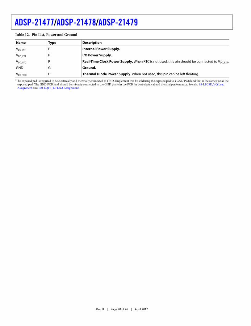
ADSP-21477/ADSP-21478/ADSP-21479Table 12. Pin List, Power and Ground
Name Type Description
VDD_INT P Internal Power Supply.
VDD_EXT P I/O Power Supply.
VDD_RTC P Real-Time Clock Power Supply. When RTC is not used, this pin should be connected to VDD_EXT.
GND1 G Ground.
VDD_THD P Thermal Diode Power Supply. When not used, this pin can be left floating.1 The exposed pad is required to be electrically and thermally connected to GND. Implement this by soldering the exposed pad to a GND PCB land that is the same size as the
exposed pad. The GND PCB land should be robustly connected to the GND plane in the PCB for best electrical and thermal performance. See also 88-LFCSP_VQ Lead Assignment and 100-LQFP_EP Lead Assignment.

ADSP-21477/ADSP-21478/ADSP-21479
Rev. D | Page 21 of 76 | April 2017
SPECIFICATIONSFor information about product specifications, contact your Analog Devices, Inc. representative.
OPERATING CONDITIONS
Description
200 MHz 266 MHz 300 MHz
Parameter1
1 Specifications subject to change without notice.
Min Nom Max Min Nom Max Min Nom Max Unit
VDD_INT Internal (Core) Supply Voltage 1.14 1.2 1.26 1.14 1.2 1.26 1.25 1.3 1.35 VVDD_EXT External (I/O) Supply Voltage 3.13 3.3 3.47 3.13 3.3 3.47 3.13 3.3 3.47 VVDD_THD Thermal Diode Supply Voltage 3.13 3.3 3.47 3.13 3.3 3.47 3.13 3.3 3.47 VVDD_RTC Real-Time Clock Power Supply Voltage 2.0 3.0 3.6 2.0 3.0 3.6 2.0 3.0 3.6 VVIH
2
2 Applies to input and bidirectional pins: ADDR23–0, DATA15–0, FLAG3–0, DAI_Px, DPI_Px, BOOT_CFGx, CLK_CFGx, RUNRSTIN, RESET, TCK, TMS, TDI, TRST, SDA10, AMI_ACK, MLBCLK, MLBDAT, MLBSIG.
High Level Input Voltage @ VDD_EXT = Max 2.0 2.0 2.0 VVIL
3
3 Applies to input pin CLKIN, WDT_CLKIN.
Low Level Input Voltage @ VDD_EXT = Min 0.8 0.8 0.8 VVIH_CLKIN
3 High Level Input Voltage @ VDD_EXT = Max 2.2 VDD_EXT 2.2 VDD_EXT 2.2 VDD_EXT VVIL_CLKIN Low Level Input Voltage @ VDD_EXT = Max –0.3 +0.8 –0.3 +0.8 –0.3 +0.8 VTJ Junction Temperature 88-Lead LFCSP_VQ @
TAMBIENT 0C to +70C0 105 N/A N/A N/A N/A °C
TJ Junction Temperature 88-Lead LFCSP_VQ @ TAMBIENT –40C to +85C
–40 +115 N/A N/A N/A N/A °C
TJ Junction Temperature 100-Lead LQFP_EP @ TAMBIENT 0°C to +70°C
0 105 0 105 N/A N/A °C
TJ Junction Temperature 100-Lead LQFP_EP @ TAMBIENT –40°C to +85°C
N/A N/A –40 +125 N/A N/A °C
TJ4
4 Real Time Clock (RTC) is supported only for products in the BGA package with a temperature range of 0°C to +70°C. For the status of unused RTC pins please see Table 11.
Junction Temperature 196-Ball CSP_BGA @ TAMBIENT 0°C to +70°C
N/A N/A 0 105 0 100 °C
TJ Junction Temperature 196-Ball CSP_BGA @ TAMBIENT –40°C to +85°C
N/A N/A –40 +125 N/A N/A °C
AUTOMOTIVE USE ONLYTJ Junction Temperature 88-Lead LFCSP_VQ @
TAMBIENT –40C to +105C (Automotive Grade)
–40 +1255
5 Automotive application use profile only. Not supported for nonautomotive use. Contact Analog Devices for more information.
N/A N/A N/A N/A °C
TJ Junction Temperature 100-Lead LQFP_EP @ TAMBIENT –40°C to +105°C (Automotive Grade)
–40 +1255 –40 +125 N/A N/A °C
TJ4 Junction Temperature 196-Ball CSP_BGA @
TAMBIENT –40°C to +105°C (Automotive Grade)
–40 +1255 N/A N/A N/A N/A °C

Rev. D | Page 22 of 76 | April 2017
ADSP-21477/ADSP-21478/ADSP-21479ELECTRICAL CHARACTERISTICS
200 MHz 266 MHz 300 MHz
UnitParameter1 Description Test Conditions Min Max Min Max Min Max
VOH2 High Level Output Voltage @ VDD_EXT = Min,
IOH = –1.0 mA32.4 2.4 2.4 V
VOL2 Low Level Output Voltage @ VDD_EXT = Min,
IOL = 1.0 mA30.4 0.4 0.4 V
IIH4, 5 High Level Input Current @ VDD_EXT = Max,
VIN = VDD_EXT Max10 10 10 μA
IIL4 Low Level Input Current @ VDD_EXT = Max, VIN = 0 V –10 –10 –10 μA
IILPU5 Low Level Input Current
Pull-up@ VDD_EXT = Max, VIN = 0 V 200 200 200 μA
IOZH6, 7 Three-State Leakage
Current@ VDD_EXT = Max, VIN = VDD_EXT Max
10 10 10 μA
IOZL6 Three-State Leakage
Current@ VDD_EXT = Max, VIN = 0 V –10 –10 –10 μA
IOZLPU7 Three-State Leakage
Current Pull-up@ VDD_EXT = Max, VIN = 0 V 200 200 200 μA
IOZHPD8 Three-State Leakage
Current Pull-down@ VDD_EXT = Max, VIN = VDD_EXT Max
200 200 200 μA
IDD_RTC VDD_RTC Current @ VDD_RTC = 3.0, TJ = 25°C
0.76 0.76 0.76 μA
IDD_INT9 Supply Current (Internal) fCCLK > 0 MHz Table 14
+ Table 15 × ASF
Table 14 + Table 15 × ASF
Table 14 + Table 15 × ASF
mA
CIN10, 11 Input Capacitance TCASE = 25°C 5 5 5 pF
1 Specifications subject to change without notice.2 Applies to output and bidirectional pins: ADDR23-0, DATA15-0, AMI_RD, AMI_WR, FLAG3–0, DAI_Px, DPI_Px, EMU, TDO, RESETOUT,MLBSIG, MLBDAT, MLBDO,MLBSO, SDRAS, SDCAS, SDWE, SDCKE, SDA10, SDDQM, MS0-1.3 See Output Drive Currents for typical drive current capabilities.4 Applies to input pins: BOOT_CFGx, CLK_CFGx, TCK, RESET, CLKIN.5 Applies to input pins with internal pull-ups: TRST, TMS, TDI.6 Applies to three-statable pins: TDO, MLBDAT, MLBSIG, MLBDO, and MLBSO.7 Applies to three-statable pins with pull-ups: DAI_Px, DPI_Px, EMU.8 Applies to three-statable pin with pull-down: SDCLK.9 See Engineer-to-Engineer Note “Estimating Power Dissipation for ADSP-214xx SHARC Processors” for further information.10Applies to all signal pins.11Guaranteed, but not tested.

ADSP-21477/ADSP-21478/ADSP-21479
Rev. D | Page 23 of 76 | April 2017
Total Power Dissipation
The information in this section should be augmented with Estimating Power for ADSP-214xx SHARC Processors (EE-348). Total power dissipation has two components:
1. Internal power consumption is additionally comprised of two components:
• Static current due to leakage. Table 14 shows the static current consumption (IDD_INT_STATIC) as a function of junction temperature (TJ) and core voltage (VDD_INT).
• Dynamic current (IDD_INT_DYNAMIC), due to transistor switching characteristics and activity level of the pro-cessor. The activity level is reflected by the Activity Scaling Factor (ASF), which represents the activity level of the application code running on the processor core and having various levels of peripheral and exter-nal port activity (Table 13). Dynamic current consumption is calculated by selecting the ASF that corresponds most closely with the user application and then multiplying that with the dynamic current consumption (Table 15).
2. External power consumption is due to the switching activ-ity of the external pins.
Table 13. Activity Scaling Factors (ASF)1
Activity Scaling Factor (ASF)Idle 0.31Low 0.53Medium Low 0.62Medium High 0.78Peak-Typical (50:50)2 0.85Peak-Typical (60:40)2 0.93Peak-Typical (70:30)2 1.00High Typical 1.18High 1.28Peak 1.34
1 See Estimating Power for ADSP-214xx SHARC Processors (EE-348) for more information on the explanation of the power vectors specific to the ASF table.
2 Ratio of continuous instruction loop (core) to SDRAM control code reads and writes.
Table 14. Static Current—IDD_INT_STATIC (mA)1
TJ (°C)Voltage (VDD_INT)
1.05 V 1.10 V 1.15 V 1.20 V 1.25 V 1.30 V 1.35 V–45 < 0.1 < 0.1 0.4 0.8 1.3 2.1 3.3–35 < 0.1 < 0.1 0.4 0.7 1.1 1.7 2.9–25 < 0.1 0.2 0.4 0.8 1.2 1.7 2.9–15 < 0.1 0.4 0.6 1.0 1.4 1.9 3.2–5 0.2 0.6 0.9 1.3 1.8 2.3 3.7+5 0.5 0.9 1.3 1.8 2.3 3.0 4.4+15 0.8 1.4 1.8 2.3 3.0 3.7 5.1+25 1.3 1.9 2.5 3.1 3.9 4.7 6.2+35 2.0 2.8 3.4 4.2 5.1 6.0 8.0+45 3.0 3.9 4.7 5.7 6.7 7.8 10.1+55 4.3 5.4 6.3 7.6 8.8 10.3 12.9+65 6.0 7.3 8.6 10.1 11.7 13.5 16.4+75 8.3 9.9 11.5 13.3 15.3 17.4 21.2+85 11.2 13.2 15.3 17.5 19.9 22.6 27.1+95 15.2 17.6 20.1 22.9 26.1 29.4 34.6+100 17.4 20.2 22.9 25.9 29.4 33.0 39.2+105 20.0 23.0 26.1 29.5 33.4 N/A N/A+115 26.3 30.0 33.9 38.2 42.9 N/A N/A+125 34.4 38.9 43.6 48.8 54.8 N/A N/A
1 Valid temperature and voltage ranges are model-specific. See Operating Conditions.

Rev. D | Page 24 of 76 | April 2017
ADSP-21477/ADSP-21478/ADSP-21479
MAXIMUM POWER DISSIPATIONSee Engineer-to-Engineer Note “Estimating Power Dissipation for ADSP-2147x SHARC Processors” for detailed thermal and power information regarding maximum power dissipation. For information on package thermal specifications, see Thermal Characteristics.
PACKAGE INFORMATIONThe information presented in Figure 4 provides details about the package branding. For a complete listing of product avail-ability, see Ordering Guide.
ESD SENSITIVITY
ABSOLUTE MAXIMUM RATINGSStresses greater than those listed in Table 17 may cause perma-nent damage to the device. These are stress ratings only; functional operation of the device at these or any other condi-tions greater than those indicated in Operating Conditions is not implied. Exposure to absolute maximum rating conditions for extended periods may affect device reliability.
Table 15. Dynamic Current in CCLK Domain—IDD_INT_DYNAMIC (mA, with ASF = 1.0)1, 2
fCCLK (MHz)Voltage (VDD_INT)
1.05 V 1.10 V 1.15 V 1.20 V 1.25 V 1.30 V 1.35 V100 75 78 82 86 90 95 98150 111 117 122 128 134 141 146200 N/A N/A 162 170 178 186 194266 N/A N/A 215 225 234 246 256300 N/A N/A N/A N/A 264 279 291
1 The values are not guaranteed as standalone maximum specifications. They must be combined with static current per the equations of Electrical Characteristics.2 Valid frequency and voltage ranges are model-specific. See Operating Conditions.
Figure 4. Typical Package Brand
Table 16. Package Brand Information1
1 Nonautomotive only. For branding information specific to automotive products, contact Analog Devices Inc.
Brand Key Field Descriptiont Temperature Rangepp Package TypeZ RoHS Compliant Option cc See Ordering Guidevvvvvv.x Assembly Lot Coden.n Silicon Revision# RoHS Compliant Designationyyww Date Code
vvvvvv.x n.n
tppZ-cc
S
ADSP-2147x
a
#yyww country_of_originTable 17. Absolute Maximum Ratings
Parameter RatingInternal (Core) Supply Voltage (VDD_INT) –0.3 V to +1.35 VExternal (I/O) Supply Voltage (VDD_EXT) –0.3 V to +4.6 VReal Time Clock Voltage (VDD_RTC) –0.3 V to +4.6 VThermal Diode Supply Voltage (VDD_THD) –0.3 V to +4.6 VInput Voltage –0.5 V to +3.8 VOutput Voltage Swing –0.5 V to VDD_EXT +0.5 VStorage Temperature Range –65°C to +150°CJunction Temperature While Biased 125°C
ESD (electrostatic discharge) sensitive device.Charged devices and circuit boards can discharge without detection. Although this product features patented or proprietary protection circuitry, damage may occur on devices subjected to high energy ESD. Therefore, proper ESD precautions should be taken to avoid performance degradation or loss of functionality.

ADSP-21477/ADSP-21478/ADSP-21479
Rev. D | Page 25 of 76 | April 2017
TIMING SPECIFICATIONSUse the exact timing information given. Do not attempt to derive parameters from the addition or subtraction of others. While addition or subtraction would yield meaningful results for an individual device, the values given in this data sheet reflect statistical variations and worst cases. Consequently, it is not meaningful to add parameters to derive longer times. See Figure 49 under Test Conditions for voltage reference levels.Switching Characteristics specify how the processor changes its signals. Circuitry external to the processor must be designed for compatibility with these signal characteristics. Switching char-acteristics describe what the processor will do in a given circumstance. Use switching characteristics to ensure that any timing requirement of a device connected to the processor (such as memory) is satisfied.Timing Requirements apply to signals that are controlled by cir-cuitry external to the processor, such as the data input for a read operation. Timing requirements guarantee that the processor operates correctly with other devices.
Core Clock Requirements
The processor’s internal clock (a multiple of CLKIN) provides the clock signal for timing internal memory, processor core, and serial ports. During reset, program the ratio between the proces-sor’s internal clock frequency and external (CLKIN) clock frequency with the CLK_CFG1–0 pins.The processor’s internal clock switches at higher frequencies than the system input clock (CLKIN). To generate the internal clock, the processor uses an internal phase-locked loop (PLL, see Figure 5). This PLL-based clocking minimizes the skew between the system clock (CLKIN) signal and the processor’s internal clock.
Voltage Controlled Oscillator (VCO)In application designs, the PLL multiplier value should be selected in such a way that the VCO frequency never exceeds fVCO specified in Table 20.
• The product of CLKIN and PLLM must never exceed 1/2 of fVCO (max) in Table 20 if the input divider is not enabled (INDIV = 0).
• The product of CLKIN and PLLM must never exceed fVCO (max) in Table 20 if the input divider is enabled (INDIV = 1).
The VCO frequency is calculated as follows: fVCO = 2 × PLLM × fINPUT fCCLK = (2 × PLLM × fINPUT) ÷ PLLDwhere:fVCO = VCO outputPLLM = Multiplier value programmed in the PMCTL register. During reset, the PLLM value is derived from the ratio selected using the CLK_CFG pins in hardware.PLLD = 2, 4, 8, or 16 based on the divider value programmed on the PMCTL register. During reset this value is 2.fINPUT is the input frequency to the PLL.
fINPUT = CLKIN when the input divider is disabled, orCLKIN ÷ 2 when the input divider is enabled.Note the definitions of the clock periods that are a function of CLKIN and the appropriate ratio control shown in Table 20. All of the timing specifications for the peripherals are defined in relation to tPCLK. See the peripheral specific section for each peripheral’s timing information.
Figure 5 shows core to CLKIN relationships with an external oscillator or crystal. The shaded divider/multiplier blocks denote where clock ratios can be set through hardware or soft-ware using the power management control register (PMCTL). For more information, see the ADSP-214xx SHARC Processor Hardware Reference.
Table 18. Clock Periods
Timing Requirements DescriptiontCK CLKIN Clock Period tCCLK Processor Core Clock PeriodtPCLK Peripheral Clock Period = 2 × tCCLK
tSDCLK SDRAM Clock Period = (tCCLK) × SDCKR

Rev. D | Page 26 of 76 | April 2017
ADSP-21477/ADSP-21478/ADSP-21479
Figure 5. Core Clock and System Clock Relationship to CLKIN
LOOPFILTER
CLKIN
PCLK
SDRAMDIVIDER
BY
PA
SS
MU
X
PMCTL(SDCKR)
CCLK
PLL
XTAL
CLKINDIVIDER
RESET
fVCO ÷ (2 × PLLM)
BUF
VCO
BUF
PMCTL(INDIV)
PLLDIVIDER
RESETOUT
CLKOUT (TEST ONLY)*
DELAY OF4096 CLKIN
CYCLES
PCLK
PMCTL(PLLBP)
PMCTL(PLLD)
fVCO
fCCLK
fINPUT
*CLKOUT (TEST ONLY) FREQUENCY IS THE SAME AS fINPUT.THIS SIGNAL IS NOT SPECIFIED OR SUPPORTED FOR ANY DESIGN.
CLK_CFGx/PMCTL (2 × PLLM) DIVIDE
BY 2
PIN
MU
X
PMCTL(PLLBP)
CCLK
RESETOUT
CORERST
SDCLK
BY
PA
SS
MU
X

ADSP-21477/ADSP-21478/ADSP-21479
Rev. D | Page 27 of 76 | April 2017
Power-Up Sequencing
The timing requirements for processor startup are given in Table 19. While no specific power-up sequencing is required between VDD_EXT and VDD_INT, there are some considerations that the system designs should take into account.
• No power supply should be powered up for an extended period of time (>200 ms) before another supply starts to ramp up.
• If the VDD_INT power supply comes up after VDD_EXT, any pin, such as RESETOUT and RESET, may actually drive momentarily until the VDD_INT rail has powered up. Systems sharing these signals on the board must determine if there are any issues that need to be addressed based on this behavior.
Note that during power-up, when the VDD_INT power supply comes up after VDD_EXT, a leakage current of the order of three-state leakage current pull-up, pull-down, may be observed on any pin, even if that is an input only (for example, the RESET pin), until the VDD_INT rail has powered up.
Table 19. Power-Up Sequencing Timing Requirements (Processor Startup)
Parameter Min Max UnitTiming RequirementstRSTVDD RESET Low Before VDD_EXT or VDD_INT On 0 mstIVDDEVDD VDD_INT On Before VDD_EXT –200 +200 mstCLKVDD
1 CLKIN Valid After VDD_INT and VDD_EXT Valid 0 200 mstCLKRST CLKIN Valid Before RESET Deasserted 102 μstPLLRST PLL Control Setup Before RESET Deasserted 203 μsSwitching CharacteristictCORERST Core Reset Deasserted After RESET Deasserted 4096 × tCK + 2 × tCCLK 4, 5
1 Valid VDD_INT and VDD_EXT assumes that the supplies are fully ramped to their nominal values (it does not matter which supply comes up first). Voltage ramp rates can vary from microseconds to hundreds of milliseconds depending on the design of the power supply subsystem.
2 Assumes a stable CLKIN signal, after meeting worst-case startup timing of crystal oscillators. Refer to your crystal oscillator manufacturer's data sheet for startup time. Assume a 25 ms maximum oscillator startup time if using the XTAL pin and internal oscillator circuit in conjunction with an external crystal.
3 Based on CLKIN cycles.4 Applies after the power-up sequence is complete. Subsequent resets require a minimum of four CLKIN cycles for RESET to be held low in order to properly initialize and
propagate default states at all I/O pins.5 The 4096 cycle count depends on tSRST specification in Table 21. If setup time is not met, one additional CLKIN cycle may be added to the core reset time, resulting in 4097
cycles maximum.
Figure 6. Power-Up Sequencing
tRSTVDD
tCLKVDD
tCLKRST
tCORERSTtPLLRST
VDDEXT
VDDINT
CLKIN
CLK_CFG1–0
RESET
RESETOUT
tIVDDEVDD
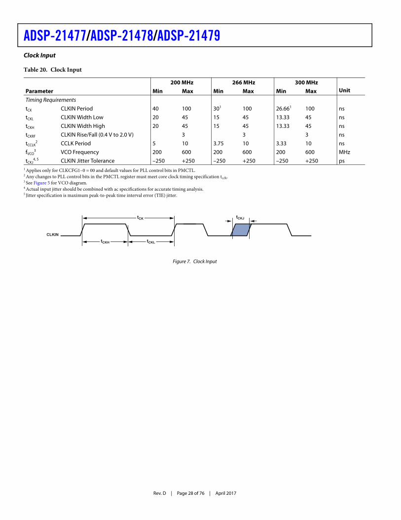
Rev. D | Page 28 of 76 | April 2017
ADSP-21477/ADSP-21478/ADSP-21479Clock Input
Table 20. Clock Input
Parameter200 MHz 266 MHz 300 MHz
UnitMin Max Min Max Min MaxTiming RequirementstCK CLKIN Period 40 100 301
1 Applies only for CLKCFG1–0 = 00 and default values for PLL control bits in PMCTL.
100 26.661 100 nstCKL CLKIN Width Low 20 45 15 45 13.33 45 nstCKH CLKIN Width High 20 45 15 45 13.33 45 nstCKRF CLKIN Rise/Fall (0.4 V to 2.0 V) 3 3 3 nstCCLK
2
2 Any changes to PLL control bits in the PMCTL register must meet core clock timing specification tcclk.
CCLK Period 5 10 3.75 10 3.33 10 nsfVCO
3
3 See Figure 5 for VCO diagram.
VCO Frequency 200 600 200 600 200 600 MHztCKJ
4, 5
4 Actual input jitter should be combined with ac specifications for accurate timing analysis.5 Jitter specification is maximum peak-to-peak time interval error (TIE) jitter.
CLKIN Jitter Tolerance –250 +250 –250 +250 –250 +250 ps
Figure 7. Clock Input
CLKIN
tCK
tCKLtCKH
tCKJ

ADSP-21477/ADSP-21478/ADSP-21479
Rev. D | Page 29 of 76 | April 2017
Clock Signals
The processors can use an external clock or a crystal. See the CLKIN pin description in Table 11. Programs can configure the processor to use its internal clock generator by connecting the necessary components to CLKIN and XTAL. Figure 8 shows the component connections used for a crystal operating in funda-
mental mode. Note that the clock rate is achieved using a 16.67 MHz crystal and a PLL multiplier ratio 16:1 (CCLK:CLKIN achieves a clock speed of 266 MHz). To achieve the full core clock rate, programs need to configure the multi-plier bits in the PMCTL register.
Reset
Figure 8. 266 MHz Operation (Fundamental Mode Crystal)
C122pF Y1
R11MΩ *
XTALCLKIN
C222pF
16.67
R247Ω *
ADSP-2147x
CHOOSE C1 AND C2 BASED ON THE CRYSTAL Y1. CHOOSE R2 TO LIMIT CRYSTAL DRIVE POWER. REFER TO CRYSTAL MANUFACTURER'S SPECIFICATIONS
*TYPICAL VALUES
Table 21. Reset
Parameter Min Max UnitTiming RequirementstWRST
1 RESET Pulse Width Low 4 × tCK nstSRST RESET Setup Before CLKIN Low 8 ns
1 Applies after the power-up sequence is complete. At power-up, the processor’s internal phase-locked loop requires no more than 100 s while RESET is low, assuming stable VDD and CLKIN (not including start-up time of external clock oscillator).
Figure 9. Reset
CLKIN
RESET
tSRSTtWRST
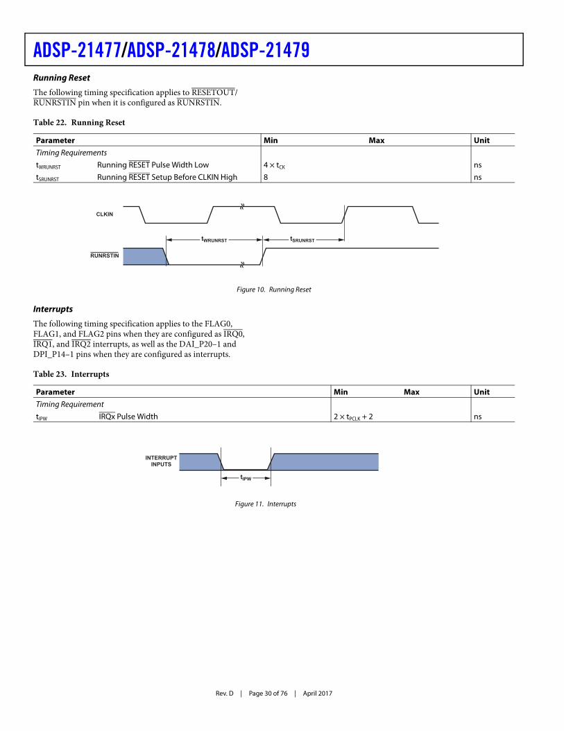
Rev. D | Page 30 of 76 | April 2017
ADSP-21477/ADSP-21478/ADSP-21479Running Reset
The following timing specification applies to RESETOUT/ RUNRSTIN pin when it is configured as RUNRSTIN.
Interrupts
The following timing specification applies to the FLAG0, FLAG1, and FLAG2 pins when they are configured as IRQ0, IRQ1, and IRQ2 interrupts, as well as the DAI_P20–1 and DPI_P14–1 pins when they are configured as interrupts.
Table 22. Running Reset
Parameter Min Max UnitTiming RequirementstWRUNRST Running RESET Pulse Width Low 4 × tCK nstSRUNRST Running RESET Setup Before CLKIN High 8 ns
Figure 10. Running Reset
CLKIN
RUNRSTIN
tWRUNRST tSRUNRST
Table 23. Interrupts
Parameter Min Max UnitTiming RequirementtIPW IRQx Pulse Width 2 × tPCLK + 2 ns
Figure 11. Interrupts
INTERRUPTINPUTS
tIPW

ADSP-21477/ADSP-21478/ADSP-21479
Rev. D | Page 31 of 76 | April 2017
Core Timer
The following timing specification applies to FLAG3 when it is configured as the core timer (TMREXP).
Timer PWM_OUT Cycle Timing
The following timing specification applies to timer0 and timer1 in PWM_OUT (pulse-width modulation) mode. Timer signals are routed to the DPI_P14–1 pins through the DPI SRU. There-fore, the timing specifications provided below are valid at the DPI_P14–1 pins.
Table 24. Core Timer
88-Lead LFCSP Package All Other PackagesUnitParameter Min Max Min Max
Switching CharacteristictWCTIM TMREXP Pulse Width 4 × tPCLK – 1.55 4 × tPCLK – 1.2 ns
Figure 12. Core Timer
FLAG3(TMREXP)
tWCTIM
Table 25. Timer PWM_OUT Timing
88-Lead LFCSP Package All Other PackagesUnitParameter Min Max Min Max
Switching CharacteristictPWMO Timer Pulse Width Output 2 × tPCLK – 1.65 2 × (231 – 1) × tPCLK 2 × tPCLK – 1.2 2 × (231 – 1) × tPCLK ns
Figure 13. Timer PWM_OUT Timing
PWMOUTPUTS
tPWMO

Rev. D | Page 32 of 76 | April 2017
ADSP-21477/ADSP-21478/ADSP-21479Timer WDTH_CAP Timing
The following timing specification applies to timer0 and timer1, and in WDTH_CAP (pulse width count and capture) mode. Timer signals are routed to the DPI_P14–1 pins through the SRU. Therefore, the timing specification provided below is valid at the DPI_P14–1 pins.
Watchdog Timer Timing
Table 26. Timer Width Capture Timing
Parameter Min Max UnitTiming RequirementtPWI Timer Pulse Width 2 × tPCLK 2 × (231 – 1) × tPCLK ns
Figure 14. Timer Width Capture Timing
TIMERCAPTURE
INPUTS
tPWI
Table 27. Watchdog Timer Timing
Parameter Min Max UnitTiming RequirementtWDTCLKPER 100 1000 nsSwitching CharacteristicstRST WDT Clock Rising Edge to Watchdog Timer
RESET Falling Edge 3 7.6 ns
tRSTPW Reset Pulse Width 64 × tWDTCLKPER1 ns
1 When the internal oscillator is used, the 1/tWDTCLKPER varies from 1.5 MHz to 2.5 MHz and the WDT_CLKIN pin should be pulled low.
Figure 15. Watchdog Timer Timing
WDT_CLKIN
WDTRSTO
tWDTCLKPER
tRSTtRSTPW

ADSP-21477/ADSP-21478/ADSP-21479
Rev. D | Page 33 of 76 | April 2017
Pin to Pin Direct Routing (DAI and DPI)
For direct pin connections only (for example, DAI_PB01_I to DAI_PB02_O).
Table 28. DAI/DPI Pin to Pin Routing
Parameter Min Max UnitTiming RequirementtDPIO Delay DAI/DPI Pin Input Valid to DAI/DPI Output Valid 1.5 10 ns
Figure 16. DAI Pin to Pin Direct Routing
DAI_PnDPI_Pn
DAI_PmDPI_Pm
tDPIO

Rev. D | Page 34 of 76 | April 2017
ADSP-21477/ADSP-21478/ADSP-21479Precision Clock Generator (Direct Pin Routing)
This timing is only valid when the SRU is configured such that the precision clock generator (PCG) takes its inputs directly from the DAI pins (via pin buffers) and sends its outputs directly to the DAI pins. For the other cases, where the PCG’s
inputs and outputs are not directly routed to/from DAI pins (via pin buffers) there is no timing data available. All timing param-eters and switching characteristics apply to external DAI pins (DAI_P01 – DAI_P20).
Table 29. Precision Clock Generator (Direct Pin Routing)
88-Lead LFCSP Package All Other PackagesUnitParameter Min Max Min Max
Timing RequirementstPCGIP Input Clock Period tPCLK × 4 tPCLK × 4 nstSTRIG PCG Trigger Setup Before
Falling Edge of PCG Input Clock4.5 4.5 ns
tHTRIG PCG Trigger Hold After Falling Edge of PCG Input Clock
3 3 ns
Switching CharacteristicstDPCGIO PCG Output Clock and Frame
Sync Active Edge Delay After PCG Input Clock
2.52 × tPCLK
2.512.5
ns
tDTRIGCLK PCG Output Clock Delay After PCG Trigger
2.5 + (2.5 × tPCGIP) 2 × tPCLK + (2.5 × tPCGIP) 2.5 + (2.5 × tPCGIP) 12.5 + (2.5 × tPCGIP) ns
tDTRIGFS PCG Frame Sync Delay After PCG Trigger
2.5 + ((2.5 + D – PH) × tPCGIP)
2 × tPCLK + ((2.5 + D – PH) × tPCGIP)
2.5 + ((2.5 + D – PH) × tPCGIP)
12.5 + ((2.5 + D – PH) × tPCGIP)
ns
tPCGOW1 Output Clock Period 2 × tPCGIP – 1 2 × tPCGIP – 1 ns
D = FSxDIV, PH = FSxPHASE. For more information, see the ADSP-214xx SHARC Processor Hardware Reference, “Precision Clock Generators” chapter.
1 Normal mode of operation.
Figure 17. Precision Clock Generator (Direct Pin Routing)
DAI_PnDPI_Pn
PCG_TRIGx_I
DAI_PmDPI_Pm
PCG_EXTx_I(CLKIN)
DAI_PyDPI_Py
PCK_CLKx_O
DAI_PzDPI_Pz
PCG_FSx_O
tDTRIGFS
tDTRIGCLK
tDPCGIO
tSTRIG tHTRIG
tPCGOWtDPCGIO
tPCGIP
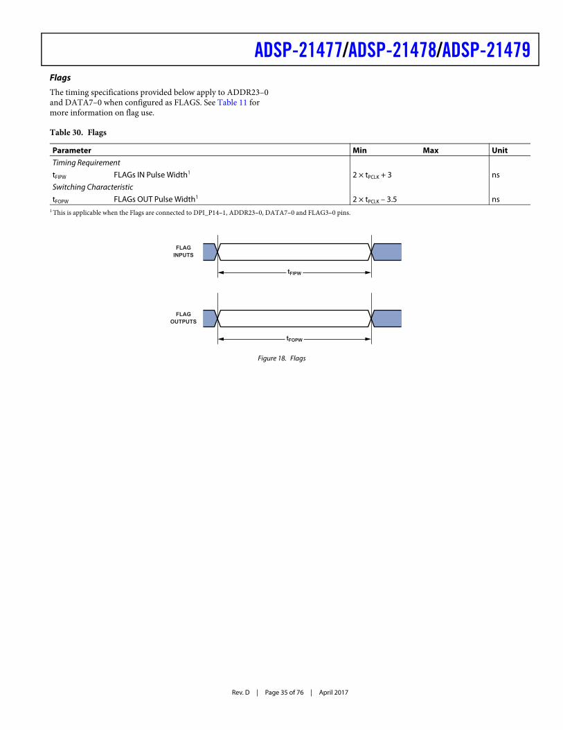
ADSP-21477/ADSP-21478/ADSP-21479
Rev. D | Page 35 of 76 | April 2017
Flags
The timing specifications provided below apply to ADDR23–0 and DATA7–0 when configured as FLAGS. See Table 11 for more information on flag use.
Table 30. Flags
Parameter Min Max UnitTiming RequirementtFIPW FLAGs IN Pulse Width1 2 × tPCLK + 3 nsSwitching CharacteristictFOPW FLAGs OUT Pulse Width1 2 × tPCLK – 3.5 ns
1 This is applicable when the Flags are connected to DPI_P14–1, ADDR23–0, DATA7–0 and FLAG3–0 pins.
Figure 18. Flags
FLAGINPUTS
FLAGOUTPUTS
tFOPW
tFIPW

Rev. D | Page 36 of 76 | April 2017
ADSP-21477/ADSP-21478/ADSP-21479SDRAM Interface Timing
Table 31. SDRAM Interface Timing
133 MHz 150 MHzUnitParameter Min Max Min Max
Timing RequirementstSSDAT DATA Setup Before SDCLK 0.7 0.7 nstHSDAT DATA Hold After SDCLK 1.66 1.5 nsSwitching CharacteristicstSDCLK
1
1 Systems should use the SDRAM model with a speed grade higher than the desired SDRAM controller speed. For example, to run the SDRAM controller at 133 MHz theSDRAM model with a speed grade of 143 MHz or above should be used. See Engineer-to-Engineer Note “Interfacing SDRAM memory to SHARC processors (EE-286)” formore information on hardware design guidelines for the SDRAM interface.
SDCLK Period 7.5 6.66 nstSDCLKH SDCLK Width High 2.5 2.2 nstSDCLKL SDCLK Width Low 2.5 2.2 nstDCAD
2
2 Command pins include: SDCAS, SDRAS, SDWE, MSx, SDA10, SDQM, SDCKE.
Command, ADDR, Data Delay After SDCLK 5 4.75 nstHCAD
2 Command, ADDR, Data Hold After SDCLK 1 1 nstDSDAT Data Disable After SDCLK 6.2 5.3 nstENSDAT Data Enable After SDCLK 0.3 0.3 ns
Figure 19. SDRAM Interface Timing
SDCLK
DATA (IN)
DATA (OUT)
COMMAND/ADDR(OUT)
tSDCLKH
tSDCLKLtHSDATtSSDAT
tHCADtDCAD
tENSDAT
tDCAD tDSDAT
tHCAD
tSDCLK

ADSP-21477/ADSP-21478/ADSP-21479
Rev. D | Page 37 of 76 | April 2017
AMI Read
Use these specifications for asynchronous interfacing to memo-ries. Note that timing for AMI_ACK, ADDR, DATA, AMI_RD, AMI_WR, and strobe timing parameters only apply to asyn-chronous access mode.
Table 32. AMI Read
Parameter Min Max UnitTiming RequirementstDAD
1, 2, 3 Address Selects Delay to Data Valid W + tSDCLK – 6.32 ns tDRLD
1, 3 AMI_RD Low to Data Valid W – 3 ns tSDS
4, 5 Data Setup to AMI_RD High 2.6 ns tHDRH Data Hold from AMI_RD High 0.4 nstDAAK
2, 6 AMI_ACK Delay from Address Selects tSDCLK – 10 + W ns tDSAK
4 AMI_ACK Delay from AMI_RD Low W – 7.0 ns Switching CharacteristicstDRHA Address Selects Hold After AMI_RD High RHC + 0.38 ns tDARL
2 Address Selects to AMI_RD Low tSDCLK – 5 nstRW AMI_RD Pulse Width W – 1.4 nstRWR AMI_RD High to AMI_RD Low HI + tSDCLK – 1.2 nsW = (number of wait states specified in AMICTLx register) × tSDCLK.RHC = (number of Read Hold Cycles specified in AMICTLx register) × tSDCLK
Where PREDIS = 0 HI = RHC (if IC = 0): Read to Read from same bank HI = RHC+ tSDCLK (if IC > 0): Read to Read from same bank HI = RHC + IC: Read to Read from different bank HI = RHC + Max (IC, (4 × tSDCLK)): Read to Write from same or different bank Where PREDIS = 1 HI = RHC + Max (IC, (4 × tSDCLK)): Read to Write from same or different bank HI = RHC + (3 × tSDCLK): Read to Read from same bank HI = RHC + Max (IC, (3 × tSDCLK)): Read to Read from different bank IC = (number of idle cycles specified in AMICTLx register) × tSDCLK
H = (number of hold cycles specified in AMICTLx register) × tSDCLK. 1 Data delay/setup: System must meet tDAD, tDRLD, or tSDS.2 The falling edge of AMI_MSx, is referenced.3 The maximum limit of timing requirement values for tDAD and tDRLD parameters are applicable for the case where AMI_ACK is always high and when the ACK feature is not used.4 Note that timing for AMI_ACK, ADDR, DATA, AMI_RD, AMI_WR, and strobe timing parameters only apply to asynchronous access mode.5 Data hold: User must meet tHDRH in asynchronous access mode. See Test Conditions for the calculation of hold times given capacitive and dc loads.6 AMI_ACK delay/setup: User must meet tdaak, or tdsak, for deassertion of AMI_ACK (low).

Rev. D | Page 38 of 76 | April 2017
ADSP-21477/ADSP-21478/ADSP-21479
Figure 20. AMI Read
ACK
DATA
tDRHAtRW
tHDRH
tRWR
tDAD
tDARL
tDRLD tSDS
tDSAK
tDAAK
WR
RD
ADDR
MSx

ADSP-21477/ADSP-21478/ADSP-21479
Rev. D | Page 39 of 76 | April 2017
AMI Write
Use these specifications for asynchronous interfacing to memo-ries. Note that timing for AMI_ACK, ADDR, DATA, AMI_RD, AMI_WR, and strobe timing parameters only apply to asyn-chronous access mode.
Table 33. AMI Write
Parameter Min Max UnitTiming RequirementstDAAK AMI_ACK Delay from Address Selects1, 2 tSDCLK – 10.1 + W ns tDSAK AMI_ACK Delay from AMI_WR Low1, 3 W – 7.1 ns Switching CharacteristicstDAWH Address Selects to AMI_WR Deasserted2 tSDCLK – 4.4 + W ns tDAWL Address Selects to AMI_WR Low2 tSDCLK – 4.5 ns tWW AMI_WR Pulse Width W – 1.3 ns tDDWH Data Setup Before AMI_WR High tSDCLK – 4.3 + W ns tDWHA Address Hold After AMI_WR Deasserted H ns tDWHD Data Hold After AMI_WR Deasserted H ns tDATRWH Data Disable After AMI_WR Deasserted4 tSDCLK – 1.37 + H tSDCLK + 6.75+ H ns tWWR AMI_WR High to AMI_WR Low5 tSDCLK – 1.5+ H ns tDDWR Data Disable Before AMI_RD Low 2 × tSDCLK – 7.1 nstWDE Data Enabled to AMI_WR Low tSDCLK – 4.5 nsW = (number of wait states specified in AMICTLx register) × tSDCLK H = (number of hold cycles specified in AMICTLx register) × tSDCLK
1 AMI_ACK delay/setup: System must meet tDAAK, or tDSAK, for deassertion of AMI_ACK (low).2 The falling edge of AMI_MSx is referenced.3 Note that timing for AMI_ACK, ADDR, DATA, AMI_RD, AMI_WR, and strobe timing parameters only applies to asynchronous access mode.4 See Test Conditions for calculation of hold times given capacitive and dc loads.5 For Write to Write: tSDCLK + H, for both same bank and different bank. For Write to Read: 3 × tSDCLK + H, for the same bank and different banks.

Rev. D | Page 40 of 76 | April 2017
ADSP-21477/ADSP-21478/ADSP-21479
Figure 21. AMI Write
ACK
DATA
tDAWH tDWHA
tWWR
tDATRWH
tDWHD
tWW
tDDWRtDDWH
tDAWL
tWDE
tDSAK
tDAAK
RD
WR
ADDR
MSx

ADSP-21477/ADSP-21478/ADSP-21479
Rev. D | Page 41 of 76 | April 2017
Serial Ports
In slave transmitter mode and master receiver mode, the maxi-mum serial port frequency is fPCLK/8. In master transmitter mode and slave receiver mode, the maximum serial port clock frequency is fPCLK/4.To determine whether communication is possible between two devices at clock speed, n, the following specifications must be confirmed: 1) frame sync delay and frame sync setup and hold, 2) data delay and data setup and hold, and 3) SCLK width.
Serial port signals (SCLK, FS, Data Channel A, Data Channel B) are routed to the DAI_P20–1 pins using the SRU. Therefore, the timing specifications provided below are valid at the DAI_P20–1 pins.
Table 34. Serial Ports—External Clock
88-Lead LFCSP Package All Other PackagesUnitParameter Min Max Min Max
Timing RequirementstSFSE
1 Frame Sync Setup Before SCLK (Externally Generated Frame Sync in Either Transmit or Receive Mode)
4 2.5 ns
tHFSE1 Frame Sync Hold After SCLK
(Externally Generated Frame Sync in Either Transmit or Receive Mode)
4 2.5 ns
tSDRE1 Receive Data Setup Before Receive SCLK 4 2.5 ns
tHDRE1 Receive Data Hold After SCLK 4 2.5 ns
tSCLKW SCLK Width (tPCLK × 4) ÷ 2 – 1.5 (tPCLK × 4) ÷ 2 – 1.5 ns tSCLK SCLK Period tPCLK × 4 tPCLK × 4 nsSwitching CharacteristicstDFSE
2 Frame Sync Delay After SCLK (Internally Generated Frame Sync in Either Transmit or Receive Mode)
15 15 ns
tHOFSE2 Frame Sync Hold After SCLK
(Internally Generated Frame Sync in Either Transmit or Receive Mode)
2 2 ns
tDDTE2 Transmit Data Delay After Transmit SCLK 15 15 ns
tHDTE2 Transmit Data Hold After Transmit SCLK 2 2 ns
1 Referenced to sample edge.2 Referenced to drive edge.

Rev. D | Page 42 of 76 | April 2017
ADSP-21477/ADSP-21478/ADSP-21479Table 35. Serial Ports—Internal Clock
88-Lead LFCSP Package All Other PackagesUnitParameter Min Max Min Max
Timing RequirementstSFSI
1 Frame Sync Setup Before SCLK (Externally Generated Frame Sync in Either Transmit or Receive Mode)
13 10.5 ns
tHFSI1 Frame Sync Hold After SCLK
(Externally Generated Frame Sync in Either Transmit or Receive Mode)
2.5 2.5 ns
tSDRI1 Receive Data Setup Before SCLK 13 10.5 ns
tHDRI1 Receive Data Hold After SCLK 2.5 2.5 ns
Switching CharacteristicstDFSI
2 Frame Sync Delay After SCLK (Internally Generated Frame Sync in Transmit Mode)
5 5 ns
tHOFSI2 Frame Sync Hold After SCLK (Internally Generated
Frame Sync in Transmit Mode)–1.0 –1.0 ns
tDFSIR2 Frame Sync Delay After SCLK (Internally Generated
Frame Sync in Receive Mode)10.7 10.7 ns
tHOFSIR2 Frame Sync Hold After SCLK (Internally Generated
Frame Sync in Receive Mode)–1.0 –1.0 ns
tDDTI2 Transmit Data Delay After SCLK 4 4 ns
tHDTI2 Transmit Data Hold After SCLK –1.0 –1.0 ns
tSCKLIW Transmit or Receive SCLK Width 2 × tPCLK – 1.5 2 × tPCLK + 1.5 2 × tPCLK – 1.5 2 × tPCLK + 1.5 ns1 Referenced to the sample edge.2 Referenced to drive edge.

ADSP-21477/ADSP-21478/ADSP-21479
Rev. D | Page 43 of 76 | April 2017
Figure 22. Serial Ports
DRIVE EDGE SAMPLE EDGE
DAI_P20–1(DATA
CHANNEL A/B)
DAI_P20–1(FS)
DAI_P20–1(SCLK)
tHOFSIR tHFSI
tHDRI
DATA RECEIVE—INTERNAL CLOCK
DRIVE EDGE SAMPLE EDGE
DAI_P20–1(DATA
CHANNEL A/B)
DAI_P20–1(FS)
DAI_P20–1(SCLK)
tHFSI
tDDTI
DATA TRANSMIT—INTERNAL CLOCK
DRIVE EDGE SAMPLE EDGE
DAI_P20–1(DATA
CHANNEL A/B)
DAI_P20–1(FS)
DAI_P20–1(SCLK)
tHOFSEtHOFSI
tHDTI
tHFSE
tHDTE
tDDTE
DATA TRANSMIT—EXTERNAL CLOCK
DRIVE EDGE SAMPLE EDGE
DAI_P20–1(DATA
CHANNEL A/B)
DAI_P20–1(FS)
DAI_P20–1(SCLK)
tHOFSE tHFSE
tHDRE
DATA RECEIVE—EXTERNAL CLOCK
tSCLKIW
tDFSIR
tSFSI
tSDRI
tSCLKW
tDFSE
tSFSE
tSDRE
tDFSE
tSFSEtSFSI
tDFSI
tSCLKIW tSCLKW

Rev. D | Page 44 of 76 | April 2017
ADSP-21477/ADSP-21478/ADSP-21479Table 36. Serial Ports—External Late Frame Sync
88-Lead LFCSP Package All Other PackagesUnitParameter Min Max Min Max
Switching CharacteristicstDDTLFSE
1 Data Delay from Late External Transmit Frame Sync or External Receive Frame Sync with MCE = 1, MFD = 0
2 × tPCLK 13.5ns
tDDTENFS1 Data Enable for MCE = 1, MFD = 0 0.5 0.5 ns
1 The tDDTLFSE and tDDTENFS parameters apply to left-justified as well as DSP serial mode, and MCE = 1, MFD = 0.
Figure 23. External Late Frame Sync1
1 This figure reflects changes made to support left-justified mode.
DRIVE SAMPLE
EXTERNAL RECEIVE FS WITH MCE = 1, MFD = 0
2ND BIT
DAI_P20–1(SCLK)
DAI_P20–1(FS)
DAI_P20–1(DATA CHANNEL
A/B)1ST BIT
DRIVE
tDDTE/I
tHDTE/I
tDDTLFSE
tDDTENFS
tSFSE/I
DRIVE SAMPLE
LATE EXTERNAL TRANSMIT FS
2ND BIT
DAI_P20–1(SCLK)
DAI_P20–1(FS)
DAI_P20–1(DATA CHANNEL
A/B)1ST BIT
DRIVE
tDDTE/I
tHDTE/I
tDDTLFSE
tDDTENFS
tSFSE/I
tHFSE/I
tHFSE/I

ADSP-21477/ADSP-21478/ADSP-21479
Rev. D | Page 45 of 76 | April 2017
Table 37. Serial Ports—Enable and Three-State
88-Lead LFCSP Package All Other PackagesUnitParameter Min Max Min Max
Switching CharacteristicstDDTEN
1 Data Enable from External Transmit SCLK 2 2 ns tDDTTE
1 Data Disable from External Transmit SCLK 23 20 ns tDDTIN
1 Data Enable from Internal Transmit SCLK –1 –1 ns 1 Referenced to drive edge.
Figure 24. Enable and Three-State
DRIVE EDGE
DRIVE EDGE
DRIVE EDGE
tDDTIN
tDDTEN tDDTTE
DAI_P20–1(SCLK, INT)
DAI_P20–1(DATA
CHANNEL A/B)
DAI_P20–1(SCLK, EXT)
DAI_P20–1(DATA
CHANNEL A/B)

Rev. D | Page 46 of 76 | April 2017
ADSP-21477/ADSP-21478/ADSP-21479The SPORTx_TDV_O output signal (routing unit) becomes active in SPORT multichannel/packed mode. During transmit slots (enabled with active channel selection registers), the SPORTx_TDV_O is asserted for communication with external devices.
Table 38. Serial Ports—TDV (Transmit Data Valid)
88-Lead LFCSP Package All Other PackagesUnitParameter Min Max Min Max
Switching Characteristics1
tDRDVEN TDV Assertion Delay from Drive Edge of External Clock 3 3 ns tDFDVEN TDV Deassertion Delay from Drive Edge of External Clock 2 × tPCLK 13.25 ns tDRDVIN TDV Assertion Delay from Drive Edge of Internal Clock –0.1 –0.1 ns tDFDVIN TDV Deassertion Delay from Drive Edge of Internal Clock 3.5 3.5 ns
1 Referenced to drive edge.
Figure 25. Serial Ports—TDV Internal and External Clock
DRIVE EDGE DRIVE EDGE
DAI_P20–1(SCLK, EXT)
tDRDVEN
tDFDVEN
DRIVE EDGE DRIVE EDGE
DAI_P20–1(SCLK, INT)
tDRDVIN
tDFDVIN
TDVxDAI_P20-1
TDVxDAI_P20-1

ADSP-21477/ADSP-21478/ADSP-21479
Rev. D | Page 47 of 76 | April 2017
Input Data Port (IDP)
The timing requirements for the IDP are given in Table 39. IDP signals are routed to the DAI_P20–1 pins using the SRU. There-fore, the timing specifications provided below are valid at the DAI_P20–1 pins.
Table 39. Input Data Port (IDP)
88-Lead LFCSP Package All Other PackagesUnitParameter Min Max Min Max
Timing RequirementstSISFS
1 Frame Sync Setup Before Serial Clock Rising Edge 4.5 3.8 ns tSIHFS
1 Frame Sync Hold After Serial Clock Rising Edge 3 2.5 ns tSISD
1 Data Setup Before Serial Clock Rising Edge 4 2.5 ns tSIHD
1 Data Hold After Serial Clock Rising Edge 3 2.5 ns tIDPCLKW Clock Width (tPCLK × 4) ÷ 2 – 1 (tPCLK × 4) ÷ 2 – 1 ns tIDPCLK Clock Period tPCLK × 4 tPCLK × 4 ns
1 The serial clock, data, and frame sync signals can come from any of the DAI pins. The serial clock and frame sync signals can also come via PCG or SPORTs. The PCG’s input can be either CLKIN or any of the DAI pins.
Figure 26. IDP Master Timing
DAI_P20–1(SCLK)
SAMPLE EDGE
DAI_P20–1(FS)
DAI_P20–1(SDATA)
tIPDCLK
tIPDCLKW
tSISFS tSIHFS
tSIHDtSISD

Rev. D | Page 48 of 76 | April 2017
ADSP-21477/ADSP-21478/ADSP-21479Parallel Data Acquisition Port (PDAP)
The timing requirements for the PDAP are provided in Table 40. PDAP is the parallel mode operation of Channel 0 of the IDP. For details on the operation of the PDAP, see the
PDAP chapter of the ADSP-214xx SHARC Processor Hardware Reference. Note that the 20 bits of external PDAP data can be provided through the ADDR23–0 pins or over the DAI pins.
Table 40. Parallel Data Acquisition Port (PDAP)
88-Lead LFCSP Package All Other PackagesUnitParameter Min Max Min Max
Timing RequirementstSPHOLD
1 PDAP_HOLD Setup Before PDAP_CLK Sample Edge 4 2.5 nstHPHOLD
1 PDAP_HOLD Hold After PDAP_CLK Sample Edge 4 2.5 ns tPDSD
1 PDAP_DAT Setup Before SCLK PDAP_CLK Sample Edge 5 3.85 ns tPDHD
1 PDAP_DAT Hold After SCLK PDAP_CLK Sample Edge 4 2.5 ns tPDCLKW Clock Width (tPCLK × 4) ÷ 2 – 3 (tPCLK × 4) ÷ 2 – 3 ns tPDCLK Clock Period tPCLK × 4 tPCLK × 4 ns Switching CharacteristicstPDHLDD Delay of PDAP Strobe After Last PDAP_CLK
Capture Edge for a Word2 × tPCLK + 3 2 × tPCLK + 3 ns
tPDSTRB PDAP Strobe Pulse Width 2 × tPCLK – 1.5 2 × tPCLK – 1.5 ns 1 Source pins of DATA and control are ADDR23–0 or DAI pins. Source pins for SCLK and FS are: 1) DAI pins, 2) CLKIN through PCG, or 3) DAI pins through PCG.
Figure 27. PDAP Timing
DAI_P20–1(PDAP_CLK)
SAMPLE EDGE
DAI_P20–1(PDAP_HOLD)
DAI_P20–1(PDAP_STROBE)
tPDSTRBtPDHLDD
tPDHDtPDSD
tSPHOLD tHPHOLD
tPDCLK
tPDCLKW
DAI_P20–1/ADDR23–4
(PDAP_DATA)

ADSP-21477/ADSP-21478/ADSP-21479
Rev. D | Page 49 of 76 | April 2017
Sample Rate Converter—Serial Input Port
The ASRC input signals are routed from the DAI_P20–1 pins using the SRU. Therefore, the timing specifications provided in Table 41 are valid at the DAI_P20–1 pins.
Table 41. ASRC, Serial Input Port
Parameter Min Max UnitTiming RequirementstSRCSFS
1 Frame Sync Setup Before Serial Clock Rising Edge 4 ns tSRCHFS
1 Frame Sync Hold After Serial Clock Rising Edge 5.5 ns tSRCSD
1 Data Setup Before Serial Clock Rising Edge 4 ns tSRCHD
1 Data Hold After Serial Clock Rising Edge 5.5 ns tSRCCLKW Clock Width (tPCLK × 4) ÷ 2 – 1 ns tSRCCLK Clock Period tPCLK × 4 ns
1 The serial clock, data, and frame sync signals can come from any of the DAI pins. The serial clock and frame sync signals can also come via PCG or SPORTs. PCG’s input can be either CLKIN or any of the DAI pins.
Figure 28. ASRC Serial Input Port Timing
DAI_P20–1(SCLK)
SAMPLE EDGE
DAI_P20–1(FS)
DAI_P20–1(SDATA)
tSRCCLK
tSRCCLKW
tSRCSFS tSRCHFS
tSRCHDtSRCSD

Rev. D | Page 50 of 76 | April 2017
ADSP-21477/ADSP-21478/ADSP-21479Sample Rate Converter—Serial Output Port
For the serial output port, the frame sync is an input, and it should meet setup and hold times with regard to the serial clock on the output port. The serial data output has a hold time and
delay specification with regard to serial clock. Note that serial clock rising edge is the sampling edge and the falling edge is the drive edge.
Table 42. ASRC, Serial Output Port
88-Lead LFCSP Package All Other PackagesUnitParameter Min Max Min Max
Timing RequirementstSRCSFS
1 Frame Sync Setup Before Serial Clock Rising Edge 4 4 ns tSRCHFS
1 Frame Sync Hold After Serial Clock Rising Edge 5.5 5.5 ns tSRCCLKW Clock Width (tPCLK × 4) ÷ 2 – 1 (tPCLK × 4) ÷ 2 – 1 ns tSRCCLK Clock Period tPCLK × 4 tPCLK × 4 ns Switching CharacteristicstSRCTDD
1 Transmit Data Delay After Serial Clock Falling Edge 2 × tPCLK 13 ns tSRCTDH
1 Transmit Data Hold After Serial Clock Falling Edge 1 1 ns 1 The serial clock, data, and frame sync signals can come from any of the DAI pins. The serial clock and frame sync signals can also come via PCG or SPORTs. PCG’s input can
be either CLKIN or any of the DAI pins.
Figure 29. ASRC Serial Output Port Timing
DAI_P20–1(SCLK)
SAMPLE EDGE
DAI_P20–1(FS)
DAI_P20–1(SDATA)
tSRCCLK
tSRCCLKW
tSRCSFS tSRCHFS
tSRCTDD
tSRCTDH

ADSP-21477/ADSP-21478/ADSP-21479
Rev. D | Page 51 of 76 | April 2017
Pulse-Width Modulation Generators (PWM)
The following timing specifications apply when the ADDR23–8/DPI_14–1 pins are configured as PWM.
Table 43. Pulse-Width Modulation (PWM) Timing
88-Lead LFCSP Package All Other PackagesUnitParameter Min Max Min Max
Switching CharacteristicstPWMW PWM Output Pulse Width tPCLK – 2 (216 – 2) × tPCLK tPCLK – 2 (216 – 2) × tPCLK nstPWMP PWM Output Period 2 × tPCLK – 2 (216 – 1) × tPCLK 2 × tPCLK – 1.5 (216 – 1) × tPCLK ns
Figure 30. PWM Timing
PWMOUTPUTS
tPWMW
tPWMP
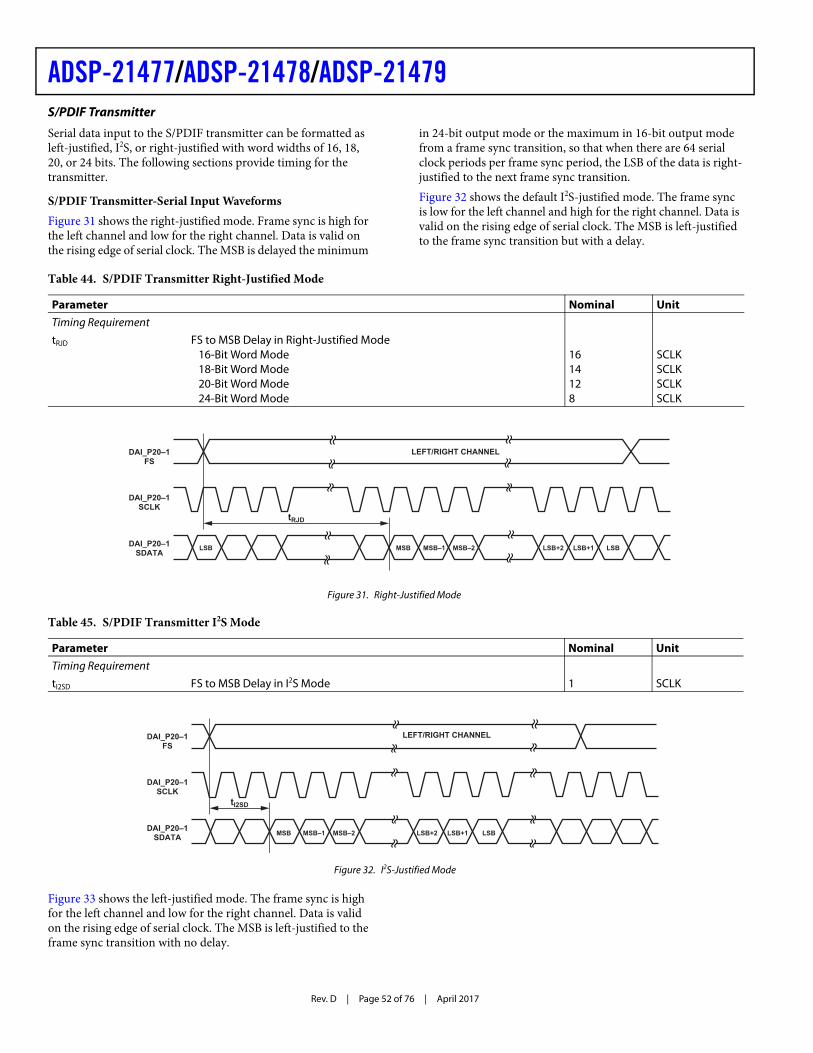
Rev. D | Page 52 of 76 | April 2017
ADSP-21477/ADSP-21478/ADSP-21479S/PDIF Transmitter
Serial data input to the S/PDIF transmitter can be formatted as left-justified, I2S, or right-justified with word widths of 16, 18, 20, or 24 bits. The following sections provide timing for the transmitter.
S/PDIF Transmitter-Serial Input WaveformsFigure 31 shows the right-justified mode. Frame sync is high for the left channel and low for the right channel. Data is valid on the rising edge of serial clock. The MSB is delayed the minimum
in 24-bit output mode or the maximum in 16-bit output mode from a frame sync transition, so that when there are 64 serial clock periods per frame sync period, the LSB of the data is right-justified to the next frame sync transition.Figure 32 shows the default I2S-justified mode. The frame sync is low for the left channel and high for the right channel. Data is valid on the rising edge of serial clock. The MSB is left-justified to the frame sync transition but with a delay.
Figure 33 shows the left-justified mode. The frame sync is high for the left channel and low for the right channel. Data is valid on the rising edge of serial clock. The MSB is left-justified to the frame sync transition with no delay.
Table 44. S/PDIF Transmitter Right-Justified Mode
Parameter Nominal UnitTiming RequirementtRJD FS to MSB Delay in Right-Justified Mode
16-Bit Word Mode 18-Bit Word Mode 20-Bit Word Mode 24-Bit Word Mode
1614128
SCLKSCLKSCLKSCLK
Figure 31. Right-Justified Mode
Table 45. S/PDIF Transmitter I2S Mode
Parameter Nominal UnitTiming RequirementtI2SD FS to MSB Delay in I2S Mode 1 SCLK
Figure 32. I2S-Justified Mode
MSB
LEFT/RIGHT CHANNEL
LSB LSBMSB–1 MSB–2 LSB+2 LSB+1
DAI_P20–1FS
DAI_P20–1SCLK
DAI_P20–1SDATA
tRJD
MSB
LEFT/RIGHT CHANNEL
LSBMSB–1 MSB–2 LSB+2 LSB+1
DAI_P20–1FS
DAI_P20–1SCLK
DAI_P20–1SDATA
tI2SD

ADSP-21477/ADSP-21478/ADSP-21479
Rev. D | Page 53 of 76 | April 2017
Table 46. S/PDIF Transmitter Left-Justified Mode
Parameter Nominal UnitTiming RequirementtLJD FS to MSB Delay in Left-Justified Mode 0 SCLK
Figure 33. Left-Justified Mode
MSB
LEFT/RIGHT CHANNEL
LSBMSB–1 MSB–2 LSB+2 LSB+1
DAI_P20–1FS
DAI_P20–1SCLK
DAI_P20–1SDATA
tLJD

Rev. D | Page 54 of 76 | April 2017
ADSP-21477/ADSP-21478/ADSP-21479S/PDIF Transmitter Input Data TimingThe timing requirements for the S/PDIF transmitter are given in Table 47. Input signals are routed to the DAI_P20–1 pins using the SRU. Therefore, the timing specifications provided below are valid at the DAI_P20–1 pins.
Oversampling Clock (TxCLK) Switching CharacteristicsThe S/PDIF transmitter requires an oversampling clock input. This high frequency clock (TxCLK) input is divided down to generate the internal biphase clock.
Table 47. S/PDIF Transmitter Input Data Timing
88-Lead LFCSP Package All Other PackagesUnitParameter Min Max Min Max
Timing RequirementstSISFS
1 Frame Sync Setup Before Serial Clock Rising Edge 4.5 3 ns tSIHFS
1 Frame Sync Hold After Serial Clock Rising Edge 3 3 ns tSISD
1 Data Setup Before Serial Clock Rising Edge 4.5 3 ns tSIHD
1 Data Hold After Serial Clock Rising Edge 3 3 ns tSITXCLKW Transmit Clock Width 9 9 ns tSITXCLK Transmit Clock Period 20 20 ns tSISCLKW Clock Width 36 36 ns tSISCLK Clock Period 80 80 ns
1 The serial clock, data, and frame sync signals can come from any of the DAI pins. The serial clock and frame sync signals can also come via PCG or SPORTs. PCG’s input can be either CLKIN or any of the DAI pins.
Figure 34. S/PDIF Transmitter Input Timing
SAMPLE EDGE
DAI_P20–1(TxCLK)
DAI_P20–1(SCLK)
DAI_P20–1(FS)
DAI_P20–1(SDATA)
tSITXCLKW tSITXCLK
tSISCLKW
tSISCLK
tSISFS tSIHFS
tSISD tSIHD
Table 48. Oversampling Clock (TxCLK) Switching Characteristics
Parameter Max UnitFrequency for TxCLK = 384 × Frame Sync Oversampling Ratio × Frame Sync ≤ 1/tSITXCLK MHzFrequency for TxCLK = 256 × Frame Sync 49.2 MHzFrame Rate (FS) 192.0 kHz
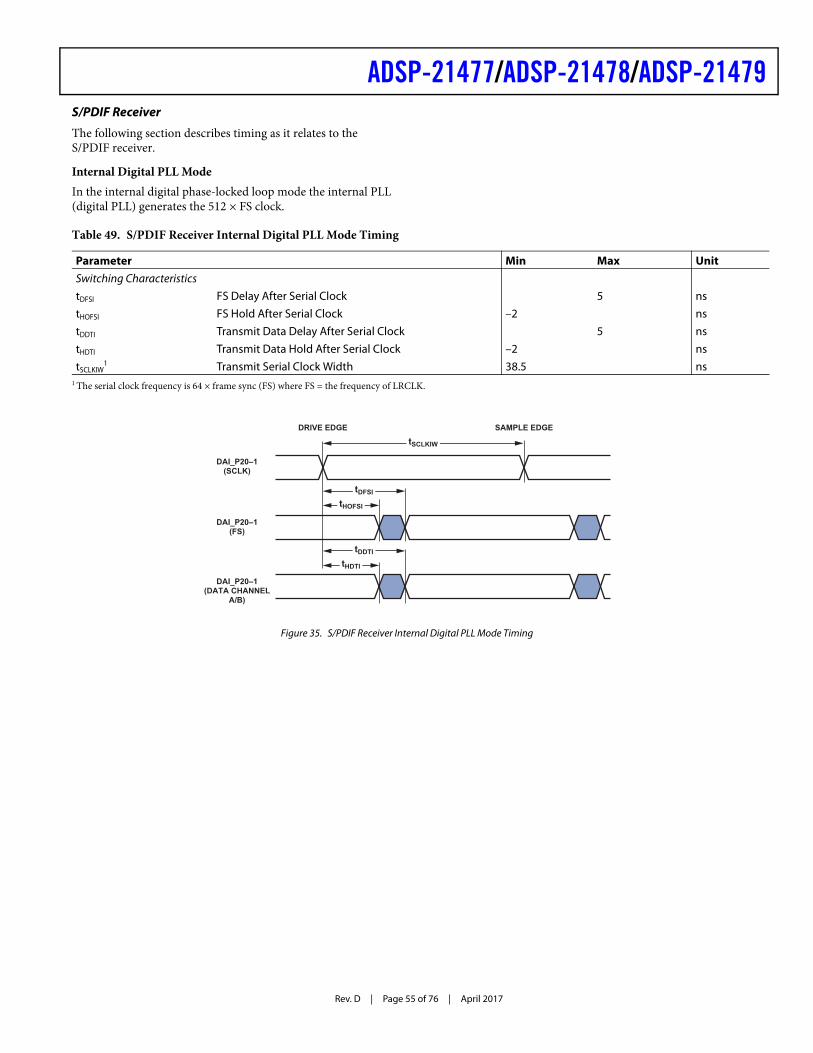
ADSP-21477/ADSP-21478/ADSP-21479
Rev. D | Page 55 of 76 | April 2017
S/PDIF Receiver
The following section describes timing as it relates to the S/PDIF receiver.
Internal Digital PLL ModeIn the internal digital phase-locked loop mode the internal PLL (digital PLL) generates the 512 × FS clock.
Table 49. S/PDIF Receiver Internal Digital PLL Mode Timing
Parameter Min Max UnitSwitching CharacteristicstDFSI FS Delay After Serial Clock 5 nstHOFSI FS Hold After Serial Clock –2 nstDDTI Transmit Data Delay After Serial Clock 5 nstHDTI Transmit Data Hold After Serial Clock –2 nstSCLKIW
1 Transmit Serial Clock Width 38.5 ns1 The serial clock frequency is 64 × frame sync (FS) where FS = the frequency of LRCLK.
Figure 35. S/PDIF Receiver Internal Digital PLL Mode Timing
DAI_P20–1(SCLK)
SAMPLE EDGE
DAI_P20–1(FS)
DAI_P20–1(DATA CHANNEL
A/B)
DRIVE EDGE
tSCLKIW
tDFSI
tHOFSI
tDDTI
tHDTI
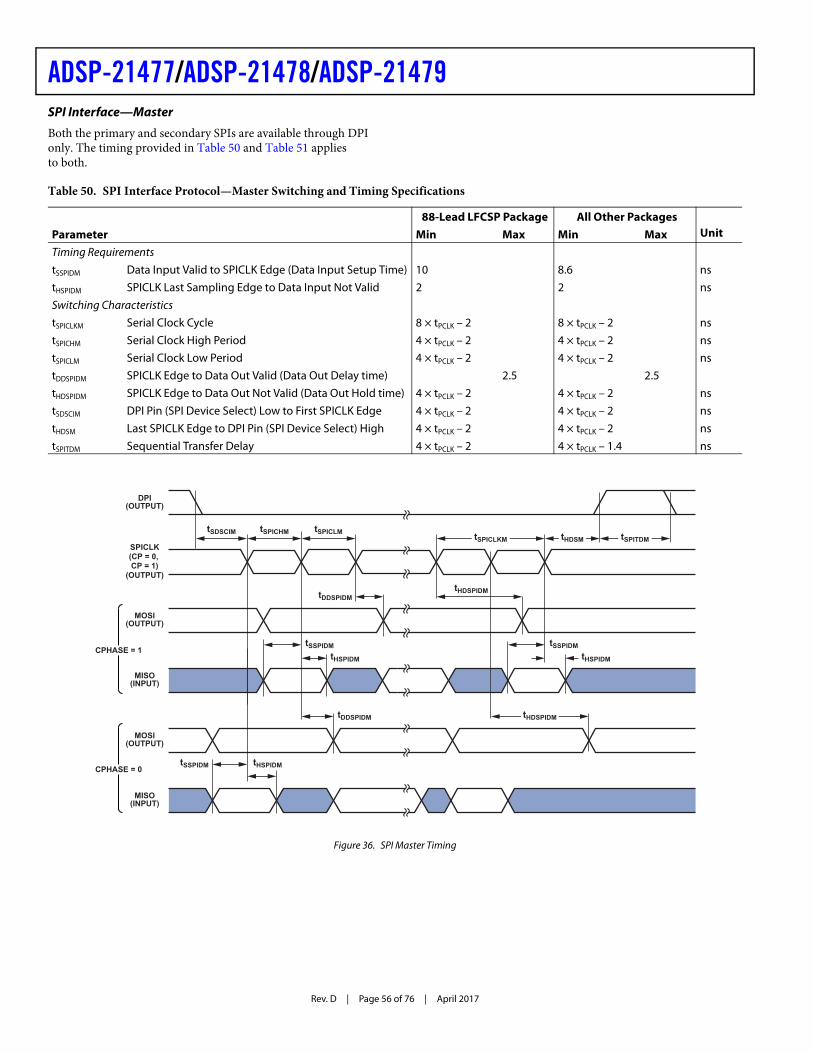
Rev. D | Page 56 of 76 | April 2017
ADSP-21477/ADSP-21478/ADSP-21479SPI Interface—Master
Both the primary and secondary SPIs are available through DPI only. The timing provided in Table 50 and Table 51 applies to both.
Table 50. SPI Interface Protocol—Master Switching and Timing Specifications
88-Lead LFCSP Package All Other PackagesUnitParameter Min Max Min Max
Timing RequirementstSSPIDM Data Input Valid to SPICLK Edge (Data Input Setup Time) 10 8.6 nstHSPIDM SPICLK Last Sampling Edge to Data Input Not Valid 2 2 nsSwitching CharacteristicstSPICLKM Serial Clock Cycle 8 × tPCLK – 2 8 × tPCLK – 2 nstSPICHM Serial Clock High Period 4 × tPCLK – 2 4 × tPCLK – 2 nstSPICLM Serial Clock Low Period 4 × tPCLK – 2 4 × tPCLK – 2 nstDDSPIDM SPICLK Edge to Data Out Valid (Data Out Delay time) 2.5 2.5 tHDSPIDM SPICLK Edge to Data Out Not Valid (Data Out Hold time) 4 × tPCLK – 2 4 × tPCLK – 2 nstSDSCIM DPI Pin (SPI Device Select) Low to First SPICLK Edge 4 × tPCLK – 2 4 × tPCLK – 2 nstHDSM Last SPICLK Edge to DPI Pin (SPI Device Select) High 4 × tPCLK – 2 4 × tPCLK – 2 nstSPITDM Sequential Transfer Delay 4 × tPCLK – 2 4 × tPCLK – 1.4 ns
Figure 36. SPI Master Timing
tSPICHMtSDSCIM tSPICLM tSPICLKM tHDSM tSPITDM
tDDSPIDM
tHSPIDMtSSPIDM
DPI(OUTPUT)
MOSI(OUTPUT)
MISO(INPUT)
MOSI(OUTPUT)
MISO(INPUT)
CPHASE = 1
CPHASE = 0
tHDSPIDM
tHSPIDMtHSPIDM
tSSPIDM tSSPIDM
tDDSPIDM
tHDSPIDM
SPICLK(CP = 0, CP = 1)
(OUTPUT)

ADSP-21477/ADSP-21478/ADSP-21479
Rev. D | Page 57 of 76 | April 2017
SPI Interface—Slave
Table 51. SPI Interface Protocol—Slave Switching and Timing Specifications
88-Lead LFCSP Package All Other PackagesUnitParameter Min Max Min Max
Timing RequirementstSPICLKS Serial Clock Cycle 4 × tPCLK – 2 4 × tPCLK – 2 nstSPICHS Serial Clock High Period 2 × tPCLK – 2 2 × tPCLK – 2 nstSPICLS Serial Clock Low Period 2 × tPCLK – 2 2 × tPCLK – 2 nstSDSCO SPIDS Assertion to First SPICLK Edge, CPHASE = 0 or CPHASE = 1 2 × tPCLK 2 × tPCLK nstHDS Last SPICLK Edge to SPIDS Not Asserted, CPHASE = 0 2 × tPCLK 2 × tPCLK nstSSPIDS Data Input Valid to SPICLK Edge (Data Input Setup Time) 2 2 nstHSPIDS SPICLK Last Sampling Edge to Data Input Not Valid 2 2 nstSDPPW SPIDS Deassertion Pulse Width (CPHASE = 0) 2 × tPCLK 2 × tPCLK nsSwitching CharacteristicstDSOE SPIDS Assertion to Data Out Active 0 13 0 10.25 nstDSOE
1 SPIDS Assertion to Data Out Active (SPI2) 0 13 0 10.25 nstDSDHI SPIDS Deassertion to Data High Impedance 0 2 × tPCLK 0 13.25 nstDSDHI
1 SPIDS Deassertion to Data High Impedance (SPI2) 0 2 × tPCLK 0 13.25 nstDDSPIDS SPICLK Edge to Data Out Valid (Data Out Delay Time) 13 11.5 nstHDSPIDS SPICLK Edge to Data Out Not Valid (Data Out Hold Time) 2 × tPCLK 2 × tPCLK nstDSOV SPIDS Assertion to Data Out Valid (CPHASE = 0) 5 × tPCLK 5 × tPCLK ns
1 The timing for these parameters applies when the SPI is routed through the signal routing unit. For more information, see the processor hardware reference, “Serial Peripheral Interface Port (SPI)” chapter.
Figure 37. SPI Slave Timing
tSPICHS tSPICLS tSPICLKS tHDS tSDPPW
tSDSCO
tDSOEtDDSPIDS
tDDSPIDS
tDSDHI
tHDSPIDS
tHSPIDStSSPIDS
tDSDHI
tDSOVtHSPIDS
tHDSPIDS
SPIDS(INPUT)
MISO(OUTPUT)
MOSI(INPUT)
MISO(OUTPUT)
MOSI(INPUT)
CPHASE = 1
CPHASE = 0
SPICLK(CP = 0, CP = 1)(INPUT)
tSSPIDS

Rev. D | Page 58 of 76 | April 2017
ADSP-21477/ADSP-21478/ADSP-21479Media Local Bus
All the numbers given are applicable for all speed modes (1024 FS, 512 FS, and 256 FS for 3-pin; 512 FS and 256 FS for 5-pin) unless otherwise specified. Please refer to MediaLB speci-fication document rev 3.0 for more details.
Table 52. MLB Interface, 3-Pin Specifications
Parameter Min Typ Max Unit3-Pin CharacteristicstMLBCLK MLB Clock Period
1024 FS 512 FS 256 FS
20.34081
nsnsns
tMCKL MLBCLK Low Time 1024 FS 512 FS 256 FS
6.11430
nsnsns
tMCKH MLBCLK High Time 1024 FS 512 FS 256 FS
9.31430
nsnsns
tMCKR MLBCLK Rise Time (VIL to VIH) 1024 FS 512 FS/256 FS
13
nsns
tMCKF MLBCLK Fall Time (VIH to VIL) 1024 FS 512 FS/256 FS
13
nsns
tMPWV1 MLBCLK Pulse Width Variation
1024 FS 512 FS/256
0.72.0
ns p-pns p-p
tDSMCF DAT/SIG Input Setup Time 1 nstDHMCF DAT/SIG Input Hold Time 1.2 nstMCFDZ DAT/SIG Output Time to Three-State 0 15 nstMCDRV DAT/SIG Output Data Delay From MLBCLK Rising Edge 8 nstMDZH
2 Bus Hold Time 1024 FS 512 FS/256
24
nsns
CMLB DAT/SIG Pin Load 1024 FS 512 FS/256
4060
pfpf
1 Pulse width variation is measured at 1.25 V by triggering on one edge of MLBCLK and measuring the spread on the other edge, measured in ns peak-to-peak (p-p).2 The board must be designed to ensure that the high impedance bus does not leave the logic state of the final driven bit for this time period. Therefore, coupling must be
minimized while meeting the maximum capacitive load listed.

ADSP-21477/ADSP-21478/ADSP-21479
Rev. D | Page 59 of 76 | April 2017
Figure 38. MLB Timing (3-Pin Interface)
Table 53. MLB Interface, 5-Pin Specifications
Parameter Min Typ Max Unit5-Pin CharacteristicstMLBCLK MLB Clock Period
512 FS 256 FS
4081
nsns
tMCKL MLBCLK Low Time 512 FS 256 FS
1530
nsns
tMCKH MLBCLK High Time 512 FS 256 FS
1530
nsns
tMCKR MLBCLK Rise Time (VIL to VIH) 6 nstMCKF MLBCLK Fall Time (VIH to VIL) 6 nstMPWV
1 MLBCLK Pulse Width Variation 2 ns p-ptDSMCF
2 DAT/SIG Input Setup Time 3 nstDHMCF DAT/SIG Input Hold Time 5 nstMCDRV DS/DO Output Data Delay From MLBCLK Rising Edge 8 nstMCRDL
3 DO/SO Low From MLBCLK High 512 FS 256 FS
1020
nsns
Cmlb DS/DO Pin Load 40 pf1 Pulse width variation is measured at 1.25 V by triggering on one edge of MLBCLK and measuring the spread on the other edge, measured in ns peak-to-peak (p-p).2 Gate delays due to OR’ing logic on the pins must be accounted for.3 When a node is not driving valid data onto the bus, the MLBSO and MLBDO output lines shall remain low. If the output lines can float at anytime, including while in reset,
external pull-down resistors are required to keep the outputs from corrupting the MediaLB signal lines when not being driven.
tMCKH
MLBSIG/MLBDAT
(Rx, Input)
tMCKL
tMCKR
MLBSIG/MLBDAT
(Tx, Output)
tMCFDZ
tDSMCF
MLBCLK
tMLBCLK
VALID
tDHMCF
tMCKF
tMCDRV
VALID
tMDZH

Rev. D | Page 60 of 76 | April 2017
ADSP-21477/ADSP-21478/ADSP-21479
Figure 39. MLB Timing (5-Pin Interface)
Figure 40. MLB 3-Pin and 5-Pin MLBCLK Pulse Width Variation Timing
tMCKH
MLBSIG/MLBDAT
(Rx, Input)
tMCKL
tMCKR
MLBSO/MLBDO
(Tx, Output)
tMCRDL
tDSMCF
MLBCLK
tMLBCLK
VALID
VALID
tDHMCF
tMCKF
tMCDRV
tMPWV tMPWV
MLBCLK

ADSP-21477/ADSP-21478/ADSP-21479
Rev. D | Page 61 of 76 | April 2017
Shift Register
Table 54. Shift Register
Parameter Min Max UnitTiming RequirementstSSDI SR_SDI Setup Before SR_SCLK Rising Edge 7 nstHSDI SR_SDI Hold After SR_SCLK Rising Edge 2 nstSSDIDAI
1 DAI_P08–01 (SR_SDI) Setup Before DAI_P08–01 (SR_SCLK) Rising Edge 7 nstHSDIDAI
1 DAI_P08–01 (SR_SDI) Hold After DAI_P08–01 (SR_SCLK) Rising Edge 2 nstSSCK2LCK
2 SR_SCLK to SR_LAT Setup 2 nstSSCK2LCKDAI
1, 2 DAI_P08–01 (SR_SCLK) to DAI_P08–01 (SR_LAT) Setup 2 nstCLRREM2SCK Removal Time SR_CLR to SR_SCLK 3 × tPCLK – 5 nstCLRREM2LCK Removal Time SR_CLR to SR_LAT 2 × tPCLK – 5 nstCLRW SR_CLR Pulse Width 4 × tPCLK – 5 nstSCKW SR_SCLK Clock Pulse Width 2 × tPCLK – 2 nstLCKW SR_LAT Clock Pulse Width 2 × tPCLK – 5 nsfMAX Maximum Clock Frequency SR_SCLK or SR_LAT fPCLK 4 MHzSwitching Characteristics nstDSDO1
3 SR_SDO Hold After SR_SCLK Rising Edge 3 nstDSDO2
3 SR_SDO Max. Delay After SR_SCLK Rising Edge 13 nstDSDODAI1
1, 3 SR_SDO Hold After DAI_P08–01 (SR_SCLK) Rising Edge 3 nstDSDODAI2
1, 3 SR_SDO Max. Delay After DAI_P08–01 (SR_SCLK) Rising Edge 13 nstDSDOSP1
3, 4 SR_SDO Hold After DAI_P20–01 (SR_SCLK) Rising Edge –2 nstDSDOSP2
3, 4 SR_SDO Max. Delay After DAI_P20–01 (SR_SCLK) Rising Edge 5 nstDSDOPCG1
3, 5, 6 SR_SDO Hold After DAI_P20–01 (SR_SCLK) Rising Edge –2 nstDSDOPCG2
3, 5, 6 SR_SDO Max. Delay After DAI_P20–01 (SR_SCLK) Rising Edge 5 nstDSDOCLR1
3 SR_CLR to SR_SDO Min. Delay 4 nstDSDOCLR2
3 SR_CLR to SR_SDO Max. Delay 13 nstDLDO1
3 SR_LDO Hold After SR_LAT Rising Edge 3 nstDLDO2
3 SR_LDO Max. Delay After SR_LAT Rising Edge 13 nstDLDODAI1
3 SR_LDO Hold After DAI_P08–01 (SR_LAT) Rising Edge 3 nstDLDODAI2
3 SR_LDO Max. Delay After DAI_P08–01 (SR_LAT) Rising Edge 13 nstDLDOSP1
3, 4 SR_LDO Hold After DAI_P20–01 (SR_LAT) Rising Edge –2 nstDLDOSP2
3, 4 SR_LDO Max. Delay After DAI_P20–01 (SR_LAT) Rising Edge 5 nstDLDOPCG1
3, 5, 6 SR_LDO Hold After DAI_P20–01 (SR_LAT) Rising Edge –2 nstDLDOPCG2
3, 5, 6 SR_LDO Max. Delay After DAI_P20–01 (SR_LAT) Rising Edge 5 nstDLDOCLR1
3 SR_CLR to SR_LDO Min. Delay 4 nstDLDOCLR2
3 SR_CLR to SR_LDO Max. Delay 14 ns1 Any of the DAI_P08–01 pins can be routed to the shift register clock, latch clock and serial data input via the SRU.2 Both clocks can be connected to the same clock source. If both clocks are connected to same clock source, then data in the 18-stage shift register is always one cycle ahead of
latch register data.3 For setup/hold timing requirements of off-chip shift register interfacing devices.4 SPORTx serial clock out, frame sync out, and serial data outputs are routed to shift register block internally and are also routed onto DAI_P20–01.5 PCG serial clock output is routed to SPORT and shift register block internally and are also routed onto DAI_P20–01. The SPORTs generate SR_LAT and SDI internally.6 PCG Serial clock and frame sync outputs are routed to SPORT and shift register block internally and are also routed onto DAI_P20–01. The SPORTs generate SDI internally.

Rev. D | Page 62 of 76 | April 2017
ADSP-21477/ADSP-21478/ADSP-21479
Figure 41. SR_SDI Setup, Hold
Figure 42. SR_ SDO Delay
Figure 43. SR_LDO Delay
DAI_P08-01OR
SR_SCLK
tSSDI,tSSDIDAI
tHSDI,tHSDIDAI
DAI_P08-01OR
SR_SDI
SR_SDO
SR_SCLK OR DAI_P08-01 OR
DAI_P20-01(SPx_CLK_O) OR DAI_P20-01(PCG_CLKx_O)
tDSDO1tDSDO2
SR_SDO
THE TIMING PARAMETERS SHOWN FOR tDSDO1 AND tDSDO2 ARE VALID FOR tDSDODAI1, tDSDOSP1, tDSDOPCG1, tDSDODAI2, tDSDOSP2, AND tDSDOPCG2
SR_LAT ORDAI_P08-01 OR
DAI_P20-01(SPx_FS_O)
ORDAI_P20-01
(PCG_FSx_O) tDLDO1 tDLDO2
SR_LDO
THE TIMING PARAMETERS SHOWN FOR tDLDO1 AND tDLDO2 ARE ALSO VALID FOR tDLDODAI1, tDLDODAI2, tDLDOSP1, tDLDOSP2, tDLDOPCG1, AND tDLDOPCG2.

ADSP-21477/ADSP-21478/ADSP-21479
Rev. D | Page 63 of 76 | April 2017
Figure 44. SR_SCLK to SR_LAT Setup, Clocks Pulse Width and Maximum Frequency
Figure 45. Shift Register Reset Timing
SR_SCLKOR
DAI_P08-01
SR_SDIOR
DAI_P08-01
SR_LDO
SR_LATOR
DAI_P08-01
tSSCK2LCKDAI
tSSCK2LCK
SR_SDCLKOR
DAI_P08-01
SR_LDO
SR_LATOR
DAI_P08-01
tDSDOCLR2
tDSDOCLR1
tDLDOCLR2
tDLDOCLR1
tCLRW
tCLRREM2SCK
tCLRREM2LCK
SR_CLR
SR_SDO

Rev. D | Page 64 of 76 | April 2017
ADSP-21477/ADSP-21478/ADSP-21479Universal Asynchronous Receiver-Transmitter (UART) Ports—Receive and Transmit Timing
For information on the UART port receive and transmit opera-tions, see the ADSP-214xx SHARC Hardware Reference Manual.
2-Wire Interface (TWI)—Receive and Transmit Timing
For information on the TWI receive and transmit operations, see the ADSP-214xx SHARC Hardware Reference Manual.
JTAG Test Access Port and Emulation
Table 55. JTAG Test Access Port and Emulation
88-Lead LFCSP Package All Other PackagesUnitParameter Min Max Min Max
Timing RequirementstTCK TCK Period 20 20 nstSTAP TDI, TMS Setup Before TCK High 5 5 nstHTAP TDI, TMS Hold After TCK High 6 6 nstSSYS
1
1 System Inputs = DATA15–0, CLK_CFG1–0, RESET, BOOT_CFG1–0, DAI_Px, DPI_Px, FLAG3–0, MLBCLK, MLBDAT, MLBSIG, SR_SCLK, SR_CLR, SR_SDI, and SR_LAT.
System Inputs Setup Before TCK High 7 7 nstHSYS
1 System Inputs Hold After TCK High 18 18 nstTRSTW TRST Pulse Width 4 × tCK 4 × tCK nsSwitching CharacteristicstDTDO TDO Delay from TCK Low 11.5 10.5 nstDSYS
2
2 System Outputs = DAI_Px, DPI_Px, ADDR23–0, AMI_RD, AMI_WR, FLAG3–0, SDRAS, SDCAS, SDWE, SDCKE, SDA10, SDDQM, SDCLK, MLBDAT, MLBSIG, MLBDO, MLBSO, SR_SDO, SR_LDO, and EMU.
System Outputs Delay After TCK Low tCK ÷ 2 + 7 tCK ÷ 2 + 7 ns
Figure 46. IEEE 1149.1 JTAG Test Access Port
TCK
TMSTDI
TDO
SYSTEMINPUTS
SYSTEMOUTPUTS
tTCK
tSTAP tHTAP
tDTDO
tSSYS tHSYS
tDSYS

ADSP-21477/ADSP-21478/ADSP-21479
Rev. D | Page 65 of 76 | April 2017
OUTPUT DRIVE CURRENTSTable 56 shows the driver types and the pins associated with each driver. Figure 47 shows typical I-V characteristics for each driver. The curves represent the current drive capability of the output drivers as a function of output voltage.
TEST CONDITIONSThe ac signal specifications (timing parameters) appear in Table 21 through Table 55. These include output disable time, output enable time, and capacitive loading. The timing specifi-cations for the SHARC apply for the voltage reference levels in Figure 48. Timing is measured on signals when they cross the 1.5 V level as described in Figure 49. All delays (in nanoseconds) are mea-sured between the point that the first signal reaches 1.5 V and the point that the second signal reaches 1.5 V.
CAPACITIVE LOADINGOutput delays and holds are based on standard capacitive loads: 30 pF on all pins (see Figure 48). Figure 52 shows graphically how output delays and holds vary with load capacitance. The graphs of Figure 50, Figure 51, and Figure 52 may not be linear outside the ranges shown for Typical Output Delay vs. Load Capacitance and Typical Output Rise Time (20% to 80%, V = Min) vs. Load Capacitance.
Table 56. Driver Types
Driver Type Associated PinsA FLAG[0–3], AMI_ADDR[23–0], DATA[15–0],
AMI_RD, AMI_WR, AMI_ACK, MS[1-0], SDRAS, SDCAS, SDWE, SDDQM, SDCKE, SDA10, EMU, TDO, RESETOUT, DPI[1–14], DAI[1–20], WDTRSTO, MLBDAT, MLBSIG, MLBSO, MLBDO, MLBCLK, SR_CLR, SR_LAT, SR_LDO[17–0], SR_SCLK, SR_SDI
B SDCLK, RTCLKOUT
Figure 47. Typical Drive at Junction Temperature
SWEEP (VDDEXT) VOLTAGE (V)
0 3.50.5 1.0 1.5 2.0 2.5 3.0
0
100
200
SO
UR
CE
/SIN
K (
VD
DE
XT)
CU
RR
EN
T (
mA
) 150
50
-100
-200
-150
-50
VOH 3.13 V, 125 °C
VOL 3.13 V, 125 °C
TYPE A
TYPE A
TYPE B
TYPE B
Figure 48. Equivalent Device Loading for AC Measurements (Includes All Fixtures)
Figure 49. Voltage Reference Levels for AC Measurements
Figure 50. Typical Output Rise/Fall Time (20% to 80%, VDD_EXT = Max)
T1
ZO = 50 (impedance)TD = 4.04 � 1.18 ns
2pF
TESTER PIN ELECTRONICS
50
0.5pF
70
400
45
4pF
NOTES:THE WORST CASE TRANSMISSION LINE DELAY IS SHOWN AND CAN BE USEDFOR THE OUTPUT TIMING ANALYSIS TO REFLECT THE TRANSMISSION LINEEFFECT AND MUST BE CONSIDERED. THE TRANSMISSION LINE (TD) IS FOR LOAD ONLY AND DOES NOT AFFECT THE DATA SHEET TIMING SPECIFICATIONS.
ANALOG DEVICES RECOMMENDS USING THE IBIS MODEL TIMING FOR A GIVEN SYSTEM REQUIREMENT. IF NECESSARY, A SYSTEM MAY INCORPORATE EXTERNAL DRIVERS TO COMPENSATE FOR ANY TIMING DIFFERENCES.
VLOADDUT
OUTPUT
50
INPUTOR
OUTPUT1.5V 1.5V
LOAD CAPACITANCE (pF)
6
00
7
4
2
1
3
RIS
E A
ND
FA
LL
TIM
ES
(n
s)
125 20010025 17550 75 150
5y = 0.0331x + 0.2662
y = 0.0184x + 0.3065
y = 0.0421x + 0.2418
y = 0.0206x + 0.2271
TYPE A DRIVE FALLTYPE A DRIVE RISE
TYPE B DRIVE FALL
TYPE B DRIVE RISE

Rev. D | Page 66 of 76 | April 2017
ADSP-21477/ADSP-21478/ADSP-21479
THERMAL CHARACTERISTICSThe processor is rated for performance over the temperature range specified in Operating Conditions.Table 58 airflow measurements comply with JEDEC standards JESD51-2 and JESD51-6 and the junction-to-board measure-ment complies with JESD51-8. Test board design complies with JEDEC standards JESD51-7 (PBGA). The junction-to-case mea-surement complies with MIL- STD-883. All measurements use a 2S2P JEDEC test board.To determine the junction temperature of the device while on the application PCB, use:
where:TJ = junction temperature (°C)TCASE = case temperature (°C) measured at the top center of the packageJT = junction-to-top (of package) characterization parameter is the typical value from Table 58PD = power dissipation Values of θJA are provided for package comparison and PCB design considerations. θJA can be used for a first order approxi-mation of TJ by the equation:
where:TA = ambient temperature °CValues of θJC are provided for package comparison and PCB design considerations when an external heatsink is required.Note that the thermal characteristics values provided in Table 58 are modeled values.
Figure 51. Typical Output Rise/Fall Time (20% to 80%, VDD_EXT = Min)
Figure 52. Typical Output Delay or Hold vs. Load Capacitance (at Ambient Temperature)
LOAD CAPACITANCE (pF)
6
00
10
4
2
RIS
E A
ND
FA
LL
TIM
ES
(n
s)
25 20015050 75 100 125 175
y = 0.0567x + 0.482
y = 0.0367x + 0.4502
y = 0.0314x + 0.5729
TYPE A DRIVE FALL
TYPE A DRIVE RISE
TYPE B DRIVE RISE
TYPE B DRIVE FALL8
12
14
y = 0.0748x + 0.4601
LOAD CAPACITANCE (pF)
3
0
3.5
2
1
0.5
1.5
RIS
E A
ND
FA
LL
DE
LA
Y (
ns)
2.5
y = 0.015x + 1.4889
y = 0.0088x + 1.6008
y = 0.0199x + 1.1083
y = 0.0102x + 1.2726
0 25 20015050 75 100 125 175
TYPE A DRIVE FALL
TYPE A DRIVE RISE
TYPE B DRIVE RISE
TYPE B DRIVE FALL
4
4.5
TJ TCASE JT PD +=
Table 57. Thermal Characteristics for 88-Lead LFCSP_VQ
Parameter Condition Typical UnitJA Airflow = 0 m/s 22.6 °C/WJMA Airflow = 1 m/s 18.2 °C/WJMA Airflow = 2 m/s 17.3 °C/WJC 7.9 °C/WJT Airflow = 0 m/s 0.22 °C/WJMT Airflow = 1 m/s 0.36 °C/WJMT Airflow = 2 m/s 0.44 °C/W
Table 58. Thermal Characteristics for 100-Lead LQFP_EP
Parameter Condition Typical UnitθJA Airflow = 0 m/s 18.1 °C/WθJMA Airflow = 1 m/s 15.5 °C/WθJMA Airflow = 2 m/s 14.6 °C/WθJC 2.4 °C/WΨJT Airflow = 0 m/s 0.22 °C/WΨJMT Airflow = 1 m/s 0.36 °C/WΨJMT Airflow = 2 m/s 0.50 °C/W
Table 59. Thermal Characteristics for 196-Ball CSP_BGA
Parameter Condition Typical UnitθJA Airflow = 0 m/s 29.0 °C/WθJMA Airflow = 1 m/s 26.1 °C/WθJMA Airflow = 2 m/s 25.1 °C/WθJC 8.8 °C/WΨJT Airflow = 0 m/s 0.23 °C/WΨJMT Airflow = 1 m/s 0.42 °C/WΨJMT Airflow = 2 m/s 0.52 °C/W
TJ TA JA PD +=

ADSP-21477/ADSP-21478/ADSP-21479
Rev. D | Page 67 of 76 | April 2017
Thermal Diode
The processors incorporate thermal diode/s to monitor the die temperature. The thermal diode is a grounded collector, PNP bipolar junction transistor (BJT). The THD_P pin is connected to the emitter, and the THD_M pin is connected to the base of the transistor. These pins can be used by an external tempera-ture sensor (such as ADM1021A or LM86 or others) to read the die temperature of the chip. The technique used by the external temperature sensor is to measure the change in VBE when the thermal diode is operated at two different currents. This is shown in the following equation:
where:n = multiplication factor close to 1, depending on process variationsk = Boltzmann constantT = temperature (°C)q = charge of the electronN = ratio of the two currentsThe two currents are usually in the range of 10 μA to 300 μA for the common temperature sensor chips available.Table 60 contains the thermal diode specifications using the transistor model.
VBE n kTq
------ In(N)=
Table 60. Thermal Diode Parameters—Transistor Model1
Symbol Parameter Min Typ Max UnitIFW
2 Forward Bias Current 10 300 μAIE Emitter Current 10 300 μAnQ
3, 4 Transistor Ideality 1.012 1.015 1.017RT
3, 5 Series Resistance 0.12 0.2 0.28 Ω1 Analog Devices does not recommend operation of the thermal diode under reverse bias.2 Analog Devices does not recommend operation of the thermal diode under reverse bias.3 Specified by design characterization.4 The ideality factor, nQ, represents the deviation from ideal diode behavior as exemplified by the diode equation: IC = IS × (e qVBE/nqkT – 1) where IS = saturation current,
q = electronic charge, VBE = voltage across the diode, k = Boltzmann constant, and T = absolute temperature (Kelvin).5 The series resistance (RT) can be used for more accurate readings as needed.

Rev. D | Page 68 of 76 | April 2017
ADSP-21477/ADSP-21478/ADSP-2147988-LFCSP_VQ LEAD ASSIGNMENTTable 61 lists the 88-Lead LFCSP_VQ package lead names.
Table 61. 88-Lead LFCSP_VQ Lead Assignments (Numerical by Lead Number)
Lead Name Lead No. Lead Name Lead No. Lead Name Lead No. Lead Name Lead No.CLK_CFG1 1 VDD_EXT 23 DAI_P10 45 VDD_INT 67BOOT_CFG0 2 DPI_P08 24 VDD_INT 46 FLAG0 68VDD_EXT 3 DPI_P07 25 VDD_EXT 47 VDD_INT 69VDD_INT 4 DPI_P09 26 DAI_P20 48 FLAG1 70BOOT_CFG1 5 DPI_P10 27 VDD_INT 49 FLAG2 71GND 6 DPI_P11 28 DAI_P08 50 FLAG3 72CLK_CFG0 7 DPI_P12 29 DAI_P04 51 GND 73VDD_INT 8 DPI_P13 30 DAI_P14 52 GND 74CLKIN 9 DAI_P03 31 DAI_P18 53 VDD_EXT 75 XTAL 10 DPI_P14 32 DAI_P17 54 GND 76VDD_EXT 11 VDD_INT 33 DAI_P16 55 VDD_INT 77VDD_INT 12 DAI_P13 34 DAI_P15 56 TRST 78VDD_INT 13 DAI_P07 35 DAI_P12 57 EMU 79RESETOUT/RUNRSTIN 14 DAI_P19 36 DAI_P11 58 TDO 80VDD_INT 15 DAI_P01 37 VDD_INT 59 VDD_EXT 81DPI_P01 16 DAI_P02 38 GND 60 VDD_INT 82DPI_P02 17 VDD_INT 39 THD_M 61 TDI 83DPI_P03 18 VDD_EXT 40 THD_P 62 TCK 84VDD_INT 19 VDD_INT 41 VDD_THD 63 VDD_INT 85DPI_P05 20 DAI_P06 42 VDD_INT 64 RESET 86DPI_P04 21 DAI_P05 43 VDD_INT 65 TMS 87DPI_P06 22 DAI_P09 44 VDD_INT 66 VDD_INT 88
GND 89** Lead no. 89 is the GND supply (see Figure 53 and Figure 54) for the processor; this pad must be robustly connected to GND in order for the processor to function.

ADSP-21477/ADSP-21478/ADSP-21479
Rev. D | Page 69 of 76 | April 2017
Figure 53 shows the top view of the 88-lead LFCSP_VQ pin configuration. Figure 54 shows the bottom view.
Figure 53. 88-Lead LFCSP_VQ Lead Configuration (Top View)
PIN 1
PIN 22
PIN 66
PIN 45
PIN 88 PIN 67
PIN 23 PIN 44
PIN 1 INDICATORADSP-2147x
88-LEAD LFCSP_VQTOP VIEW
Figure 54. 88-Lead LFCSP_VQ Lead Configuration (Bottom View)
PIN 66
PIN 45
PIN 1
PIN 22
PIN 67 PIN 88
PIN 44 PIN 23
PIN 1 INDICATORGND PAD(PIN 89)
ADSP-2147x88-LEAD LFCSP_VQ
BOTTOM VIEW

Rev. D | Page 70 of 76 | April 2017
ADSP-21477/ADSP-21478/ADSP-21479100-LQFP_EP LEAD ASSIGNMENTTable 62 lists the 100-Lead LQFP_EP lead names.
Table 62. 100-Lead LQFP_EP Lead Assignments (Numerical by Lead Number)
Lead Name Lead No. Lead Name Lead No. Lead Name Lead No. Lead Name Lead No.VDD_INT 1 VDD_EXT 26 DAI_P10 51 VDD_INT 76CLK_CFG1 2 DPI_P08 27 VDD_INT 52 FLAG0 77BOOT_CFG0 3 DPI_P07 28 VDD_EXT 53 VDD_INT 78VDD_EXT 4 VDD_INT 29 DAI_P20 54 VDD_INT 79VDD_INT 5 DPI_P09 30 VDD_INT 55 FLAG1 80BOOT_CFG1 6 DPI_P10 31 DAI_P08 56 FLAG2 81GND 7 DPI_P11 32 DAI_P04 57 FLAG3 82NC 8 DPI_P12 33 DAI_P14 58 MLBCLK 83NC 9 DPI_P13 34 DAI_P18 59 MLBDAT 84CLK_CFG0 10 DAI_P03 35 DAI_P17 60 MLBDO 85 VDD_INT 11 DPI_P14 36 DAI_P16 61 VDD_EXT 86CLKIN 12 VDD_INT 37 DAI_P15 62 MLBSIG 87XTAL 13 VDD_INT 38 DAI_P12 63 VDD_INT 88VDD_EXT 14 VDD_INT 39 VDD_INT 64 MLBSO 89VDD_INT 15 DAI_P13 40 DAI_P11 65 TRST 90VDD_INT 16 DAI_P07 41 VDD_INT 66 EMU 91RESETOUT/RUNRSTIN 17 DAI_P19 42 VDD_INT 67 TDO 92VDD_INT 18 DAI_P01 43 GND 68 VDD_EXT 93DPI_P01 19 DAI_P02 44 THD_M 69 VDD_INT 94DPI_P02 20 VDD_INT 45 THD_P 70 TDI 95DPI_P03 21 VDD_EXT 46 VDD_THD 71 TCK 96VDD_INT 22 VDD_INT 47 VDD_INT 72 VDD_INT 97DPI_P05 23 DAI_P06 48 VDD_INT 73 RESET 98DPI_P04 24 DAI_P05 49 VDD_INT 74 TMS 99 DPI_P06 25 DAI_P09 50 VDD_INT 75 VDD_INT 100
GND 101** Lead no. 101 is the GND supply (see Figure 55 and Figure 56) for the processor; this pad must be robustly connected to GND.MLB pins (pins 83, 84, 85, 87, and 89) are available for automotive models only. For non-automotive models, these pins should be connectedto ground (GND).

ADSP-21477/ADSP-21478/ADSP-21479
Rev. D | Page 71 of 76 | April 2017
Figure 55 shows the top view configuration of the 100-lead LQFP_EP package. Figure 56 shows the bottom view configura-tion of the 100-lead LQFP_EP package.
Figure 55. 100-Lead LQFP_EP Lead Configuration (Top View)
Figure 56. 100-Lead LQFP_EP Lead Configuration (Bottom View)
LEAD 1
LEAD 25
LEAD 75
LEAD 51
LEAD 100 LEAD 76
LEAD 26 LEAD 50
LEAD 1 INDICATORADSP-2147x
100-LEAD LQFP_EPTOP VIEW
LEAD 75
LEAD 51
LEAD 1
LEAD 25
LEAD 76 LEAD 100
LEAD 50 LEAD 26
LEAD 1 INDICATORGND PAD
(LEAD 101)
ADSP-2147x100-LEAD LQFP_EP
BOTTOM VIEW
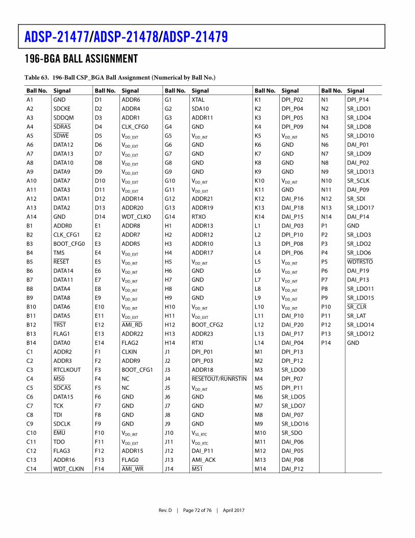
Rev. D | Page 72 of 76 | April 2017
ADSP-21477/ADSP-21478/ADSP-21479196-BGA BALL ASSIGNMENTTable 63. 196-Ball CSP_BGA Ball Assignment (Numerical by Ball No.)
Ball No. Signal Ball No. Signal Ball No. Signal Ball No. Signal Ball No. Signal A1 GND D1 ADDR6 G1 XTAL K1 DPI_P02 N1 DPI_P14A2 SDCKE D2 ADDR4 G2 SDA10 K2 DPI_P04 N2 SR_LDO1A3 SDDQM D3 ADDR1 G3 ADDR11 K3 DPI_P05 N3 SR_LDO4A4 SDRAS D4 CLK_CFG0 G4 GND K4 DPI_P09 N4 SR_LDO8A5 SDWE D5 VDD_EXT G5 VDD_INT K5 VDD_INT N5 SR_LDO10A6 DATA12 D6 VDD_EXT G6 GND K6 GND N6 DAI_P01A7 DATA13 D7 VDD_EXT G7 GND K7 GND N7 SR_LDO9A8 DATA10 D8 VDD_EXT G8 GND K8 GND N8 DAI_P02A9 DATA9 D9 VDD_EXT G9 GND K9 GND N9 SR_LDO13A10 DATA7 D10 VDD_EXT G10 VDD_INT K10 VDD_INT N10 SR_SCLKA11 DATA3 D11 VDD_EXT G11 VDD_EXT K11 GND N11 DAI_P09A12 DATA1 D12 ADDR14 G12 ADDR21 K12 DAI_P16 N12 SR_SDIA13 DATA2 D13 ADDR20 G13 ADDR19 K13 DAI_P18 N13 SR_LDO17A14 GND D14 WDT_CLKO G14 RTXO K14 DAI_P15 N14 DAI_P14B1 ADDR0 E1 ADDR8 H1 ADDR13 L1 DAI_P03 P1 GNDB2 CLK_CFG1 E2 ADDR7 H2 ADDR12 L2 DPI_P10 P2 SR_LDO3B3 BOOT_CFG0 E3 ADDR5 H3 ADDR10 L3 DPI_P08 P3 SR_LDO2B4 TMS E4 VDD_EXT H4 ADDR17 L4 DPI_P06 P4 SR_LDO6B5 RESET E5 VDD_INT H5 VDD_INT L5 VDD_INT P5 WDTRSTOB6 DATA14 E6 VDD_INT H6 GND L6 VDD_INT P6 DAI_P19B7 DATA11 E7 VDD_INT H7 GND L7 VDD_INT P7 DAI_P13B8 DATA4 E8 VDD_INT H8 GND L8 VDD_INT P8 SR_LDO11B9 DATA8 E9 VDD_INT H9 GND L9 VDD_INT P9 SR_LDO15B10 DATA6 E10 VDD_INT H10 VDD_INT L10 VDD_INT P10 SR_CLRB11 DATA5 E11 VDD_EXT H11 VDD_EXT L11 DAI_P10 P11 SR_LATB12 TRST E12 AMI_RD H12 BOOT_CFG2 L12 DAI_P20 P12 SR_LDO14B13 FLAG1 E13 ADDR22 H13 ADDR23 L13 DAI_P17 P13 SR_LDO12B14 DATA0 E14 FLAG2 H14 RTXI L14 DAI_P04 P14 GNDC1 ADDR2 F1 CLKIN J1 DPI_P01 M1 DPI_P13C2 ADDR3 F2 ADDR9 J2 DPI_P03 M2 DPI_P12C3 RTCLKOUT F3 BOOT_CFG1 J3 ADDR18 M3 SR_LDO0C4 MS0 F4 NC J4 RESETOUT/RUNRSTIN M4 DPI_P07C5 SDCAS F5 NC J5 VDD_INT M5 DPI_P11C6 DATA15 F6 GND J6 GND M6 SR_LDO5C7 TCK F7 GND J7 GND M7 SR_LDO7C8 TDI F8 GND J8 GND M8 DAI_P07C9 SDCLK F9 GND J9 GND M9 SR_LDO16C10 EMU F10 VDD_INT J10 VSS_RTC M10 SR_SDOC11 TDO F11 VDD_EXT J11 VDD_RTC M11 DAI_P06C12 FLAG3 F12 ADDR15 J12 DAI_P11 M12 DAI_P05C13 ADDR16 F13 FLAG0 J13 AMI_ACK M13 DAI_P08C14 WDT_CLKIN F14 AMI_WR J14 MS1 M14 DAI_P12

ADSP-21477/ADSP-21478/ADSP-21479
Rev. D | Page 73 of 76 | April 2017
OUTLINE DIMENSIONSThe processors are available in 88-lead LFCSP_VQ, 100-lead LQFP_EP and 196-ball CSP_BGA RoHS compliant packages. For package assignment by model, see Ordering Guide.
Figure 57. 88-Lead Lead Frame Chip Scale Package [LFCSP_VQ1](CP-88-5)
Dimensions Shown in Millimeters1 For information relating to the exposed pad on the CP-88-5 package, see the table endnote on Page 68.
*COMPLIANT TO JEDEC STANDARDS MO-220-VRRDEXCEPT FOR MINIMUM THICKNESS AND LEAD COUNT.
1
22
66
452344
8867
0.500.400.30
0.300.230.18
10.50REF
0.60 MAX0.60MAX
0.50BSC
0.138~0.194 REF
12° MAX
SEATINGPLANE
0.700.650.60 0.045
0.0250.005
PIN 1INDICATOR
12.1012.00 SQ11.90
11.8511.75 SQ11.65
*0.900.850.75
FOR PROPER CONNECTION OF THE EXPOSED PAD, REFER TO THE PIN CONFIGURATION AND FUNCTION DESCRIPTIONS SECTION OF THIS DATA SHEET.COPLANARITY
0.08
6.806.70 SQ6.60
PIN 1INDICATOR
TOP VIEW
EXPOSEDPAD
BOTTOM VIEW

Rev. D | Page 74 of 76 | April 2017
ADSP-21477/ADSP-21478/ADSP-21479
Figure 58. 100-Lead Low Profile Quad Flat Package, Exposed Pad [LQFP_EP1](SW-100-2)
Dimensions shown in millimeters1 For information relating to the exposed pad on the SW-100-2 package, see the table endnote on Page 70.
Figure 59. 196-Ball Chip Scale Package, Ball Grid Array [CSP_BGA](BC-196-8)
Dimensions shown in millimeters
COMPLIANT TO JEDEC STANDARDS MS-026-BED-HD
TOP VIEW(PINS DOWN)
BOTTOM VIEW(PINS UP)
EXPOSEDPAD
1 1
25 2526 2650 50
76 76100 100
75 75
51 51
0.270.220.17
0.50BSC
LEAD PITCH
PIN 1
16.2016.00 SQ15.80 14.20
14.00 SQ13.80
6.00 BSCSQ
12.00 REF
FOR PROPER CONNECTION OF THE EXPOSED PAD, REFER TO THE PIN CONFIGURATION AND FUNCTION DESCRIPTIONS SECTION OF THIS DATA SHEET.
0.150.05 0.08
COPLANARITY
7°0°
0.200.09
VIEW A ROTATED 90° CCW
1.451.401.35
VIEW A
1.60MAX
SEATINGPLANE
0.750.600.45
1.00 REF
COMPLIANT TO JEDEC STANDARDS MO-275-GGAB-1.
0.80BSC
0.80REF
0.70REF
0.36REF
ABCDEFG
910 811121314 7 56 4 23 1
BOTTOM VIEW
10.40BSC SQ
HJKLMNP
DETAIL A
TOP VIEW
DETAIL A
COPLANARITY0.12
0.500.450.40
BALL DIAMETER
SEATINGPLANE
12.1012.00 SQ11.90A1 BALL
CORNER
A1 BALLCORNER
0.35 NOM0.30 MIN
1.501.411.32
1.131.060.99

ADSP-21477/ADSP-21478/ADSP-21479
Rev. D | Page 75 of 76 | April 2017
SURFACE-MOUNT DESIGNFor industry-standard design recommendations, refer to IPC-7351, Generic Requirements for Surface-Mount Design and Land Pattern Standard.
AUTOMOTIVE PRODUCTSThe ADSP-21477, ADSP-21478, and ADSP-21479 are available with controlled manufacturing to support the quality and reli-ability requirements of automotive applications. Note that these automotive models may have specifications that differ from the commercial models, and designers should review the product Specifications section of this data sheet carefully. Only the automotive grade products shown in Table 64 are available for use in automotive applications. Contact your local ADI account representative for specific product ordering infor-mation and to obtain the specific Automotive Reliability reports for these models.
Table 64. Automotive Product Models
Model1 Temperature Range2
On-Chip SRAM
Processor Instruction Rate (Max) Package Description
Package Option Notes
AD21477WYCPZ1Axx –40°C to +105°C 2M bits 200 MHz 88-Lead LFCSP_VQ CP-88-5
AD21477WYSWZ1Axx –40°C to +105°C 2M bits 200 MHz 100-Lead LQFP_EP SW-100-2
AD21478WYBCZ2Axx –40°C to +105°C 3M bits 200 MHz 196-Ball CSP_BGA BC-196-8
AD21478WYCPZ1Axx –40°C to +105°C 3M bits 200 MHz 88-Lead LFCSP_VQ CP-88-5
AD21478WYSWZ2Axx –40°C to +105°C 3M bits 266 MHz 100-Lead LQFP_EP SW-100-2
AD21478WYSWZ2Bxx –40°C to +105°C 3M bits 266 MHz 100-Lead LQFP_EP SW-100-2 3, 4
AD21479WYCPZ1Axx –40°C to +105°C 5M bits 200 MHz 88-Lead LFCSP_VQ CP-88-5
AD21479WYCPZ1Bxx –40°C to +105°C 5M bits 200MHz 88-Lead LFCSP_VQ CP-88-5 3, 4
AD21479WYSWZ2Axx –40°C to +105°C 5M bits 266 MHz 100-Lead LQFP_EP SW-100-2
AD21479WYSWZ2Bxx –40°C to +105°C 5M bits 266 MHz 100-Lead LQFP_EP SW-100-2 3, 4
1 Z = RoHS compliant part.2 Referenced temperature is ambient temperature. The ambient temperature is not a specification. Please see Operating Conditions for junction temperature (TJ)specification, which is the only temperature specification.3 Contains multichannel audio decoders from Dolby and DTS. Users must have current licenses from Dolby and DTS to order this product.4 Contains Digital Transmission Content Protection (DTCP) from DTLA. User must have current license from DTLA to order this product.

Rev. D | Page 76 of 76 | April 2017
ADSP-21477/ADSP-21478/ADSP-21479
©2017 Analog Devices, Inc. All rights reserved. Trademarks andregistered trademarks are the property of their respective owners.
D09017-0-4/17(D)
ORDERING GUIDE
Model1
1 Z =RoHS compliant part.
Temperature Range2
2 Referenced temperature is ambient temperature. The ambient temperature is not a specification. Please see Operating Conditions for junction temperature (TJ)specification, which is the only temperature specification.
On-Chip SRAM
Processor Instruction Rate (Max) Package Description
Package Option
ADSP-21477KCPZ-1A 0°C to +70°C 2M Bits 200 MHz 88-Lead LFCSP_VQ CP-88-5ADSP-21477KSWZ-1A 0°C to +70°C 2M Bits 200 MHz 100-Lead LQFP_EP SW-100-2ADSP-21477BCPZ-1A –40C to +85C 2M Bits 200 MHz 88-Lead LFCSP_VQ CP-88-5ADSP-21478KCPZ-1A 0°C to +70°C 3M Bits 200 MHz 88-Lead LFCSP_VQ CP-88-5ADSP-21478BCPZ-1A –40C to +85C 3M Bits 200 MHz 88-Lead LFCSP_VQ CP-88-5ADSP-21478BBCZ-2A –40°C to +85°C 3M Bits 266 MHz 196-Ball CSP_BGA BC-196-8ADSP-21478BSWZ-2A –40°C to +85°C 3M Bits 266 MHz 100-Lead LQFP_EP SW-100-2ADSP-21478KBCZ-1A 0°C to +70°C 3M Bits 200 MHz 196-Ball CSP_BGA BC-196-8ADSP-21478KBCZ-2A 0°C to +70°C 3M Bits 266 MHz 196-Ball CSP_BGA BC-196-8ADSP-21478KBCZ-3A 0°C to +70°C 3M Bits 300 MHz 196-Ball CSP_BGA BC-196-8ADSP-21478KSWZ-1A 0°C to +70°C 3M Bits 200 MHz 100-Lead LQFP_EP SW-100-2ADSP-21478KSWZ-2A 0°C to +70°C 3M Bits 266 MHz 100-Lead LQFP_EP SW-100-2ADSP-21479KCPZ-1A 0°C to +70°C 5M Bits 200 MHz 88-Lead LFCSP_VQ CP-88-5ADSP-21479BCPZ-1A –40C to +85C 5M Bits 200 MHz 88-Lead LFCSP_VQ CP-88-5ADSP-21479BBCZ-2A –40°C to +85°C 5M Bits 266 MHz 196-Ball CSP_BGA BC-196-8ADSP-21479BSWZ-2A –40°C to +85°C 5M Bits 266 MHz 100-Lead LQFP_EP SW-100-2ADSP-21479KBCZ-1A 0°C to +70°C 5M Bits 200 MHz 196-Ball CSP_BGA BC-196-8ADSP-21479KBCZ-2A 0°C to +70°C 5M Bits 266 MHz 196-Ball CSP_BGA BC-196-8ADSP-21479KBCZ-3A 0°C to +70°C 5M Bits 300 MHz 196-Ball CSP_BGA BC-196-8ADSP-21479KSWZ-1A 0°C to +70°C 5M Bits 200 MHz 100-Lead LQFP_EP SW-100-2ADSP-21479KSWZ-2A 0°C to +70°C 5M Bits 266 MHz 100-Lead LQFP_EP SW-100-2
Top Related