


Languages
Pages
Legal


Sebastian Lourdudoss
Semiconductor Optoelectronics – Lecture 14
General principles
Photodetectors: p-n and p-i-n diodes
Solar cells
Light Emitting Diodes and Laser Diodes
References other than your book, Singh
1. S.O.Kasap, Optoelectronics and Photonics, Principles and Practices, Prentice-
Hall International, NJ, USA, 2001.
2. S.M.Sze, Semiconductor Devices, Physics and Technology, 2nd edition, John
Wiley & Sons, Inc., NY, USA, 2002.
3. Jenny Nelson, The physics of solar cells, Imperial College Press, London,
2003

Sebastian Lourdudoss
From Wikipedia
Legend
Y = Gamma rays
HX = Hard X-rays
SX = Soft X-rays
EUV = Extreme ultraviolet
NUV = Near ultraviolet visible light
NIR = Near infrared
MIR = Mid infrared
FIR = Far infrared radiowaves
EHF = Extremely high frequency
SHF = Super high frequency
UHF = Ultra high frequency
VHF = Very high frequency
HF = High frequency
MF = Medium frequency
LF = Low frequency
VLF = Very low frequency
VF/ULF = Voice frequency
SLF = Super low frequency
ELF = Extremely low frequency
Electromagnetic spectrum (1)

Sebastian Lourdudoss
From Wikipedia
Electromagnetic spectrum (2)

Sebastian Lourdudoss
Which wavelength do you want?
Here is the smörgåsbord of the materials for the
wavelength of your choice!
Sebastian Lourdudoss
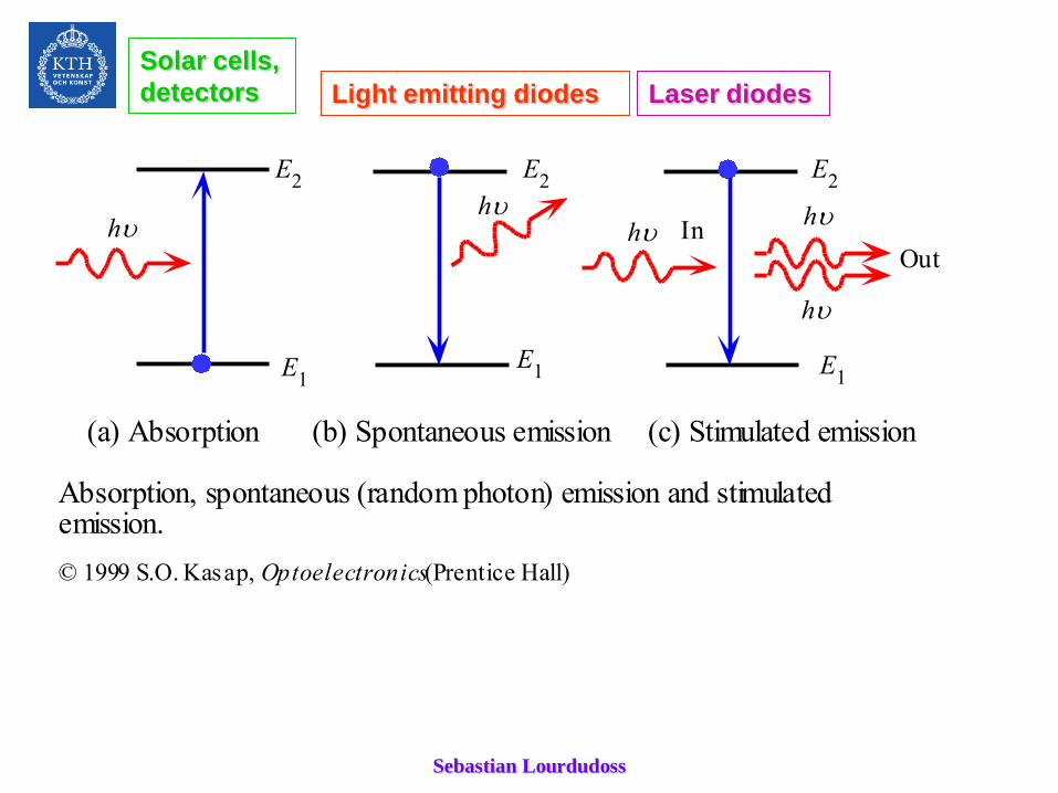
E1
E2
h
(a) Absorption
h
(b) Spontaneous emission
h
(c) Stimulated emission
Inh
Out
h
E2
E2
E1 E
1
Absorption, spontaneous (random photon) emission and stimulatedemission.
© 1999 S.O. Kasap, Optoelectronics (Prentice Hall)
Solar cells,
detectors Light emitting diodes Laser diodes

Sebastian Lourdudoss
DETECTORS

Sebastian Lourdudoss Source: Kasap
Absorption coefficient, an important parameter for
detectors

Sebastian Lourdudoss
At equilibrium
G, Generation rate of e-h pairs ( m-3 s-1)
= α Jph(x)
= n /τ = recombination rate
(n= no. of pairs/volume; τ = recombination life time)
Source: Sze
τpG
p(t)
p(0)
τp tpn
Decay of minority carriers
(holes) with time in n-type
semiconductor

Sebastian Lourdudoss
Photodetector
hν
Detector :
Conductivity change due to e-h pair generation
Generation of a voltage signal
No field? e-h pairs are useless since they will recombine; hence use an
applied field or make use of a p-n junction’s built-in field!

Sebastian Lourdudoss
p-n diode
Source: Singh

Sebastian Lourdudoss
Total current in a photodiode =
Current in the depletion region (prompt current)
+
Currents in the neutral region
+
Dark current
Remember:
The photocurrent direction is in the direction of the reverse current
of the diode

Sebastian Lourdudoss
Rph, Responsivity of a detector (A/W)
= Current density/Optical Intensity
= (IL/Area)/(W/area) = JL/Pop
L represents total active length of the detector
= Depletion width + Ln + Lp
η, Quantum efficiency (carriers collected per photon)
= (JL/e)/(Pop/ħω)
= Rph (ħω/e)

Sebastian Lourdudoss
P-I-N DIODE
Need for the P-I-N diode:
• P-N diode limited by
reverse current breakdown;
use i-region
• i-region completely
depleted = Large depletion
region
=> Large prompt
current = high frequency
and high quantum
efficiency

Sebastian Lourdudoss
SOLAR CELLS

Sebastian Lourdudoss
SOLAR CELLS
Dark? Nothing happens in (a)
Illuminated? Behaves like (b) as if there is a battery
Two extreme cases:
* Terminals isolated (open circuit, oc) = Infinite load resistance:
V = Voc and I = 0
* Terminals closed (short circuit, sc) = zero load resistance:
V= 0 and I = Isc
For any intermediate load resistance, RL, the cell develops a voltage 0- Voc and
current I such that I = V/ RL
Source: Nelson
Sebastian Lourdudoss
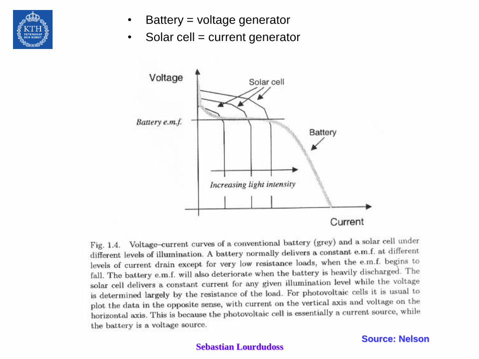
• Battery = voltage generator
• Solar cell = current generator
Source: Nelson

Sebastian Lourdudoss
Source: Sze
IL = Current resulting from solar radiation; Is = Saturation current
Constant
curent
source ILin parallel
with the
junction

Sebastian Lourdudoss
Source: Nelson
Ideal I-V curve of the device in the previous slide:
I = Is [exp (eV/kT)-1] – IL where Is is expressed as
)/exp(11
kTED
N
D
NNeN
A
IJ g
p
p
Dn
n
A
VCs
s
Plot of I vs. V gives the curve in the next slide

Sebastian Lourdudoss
Source: Nelson
Sebastian Lourdudoss
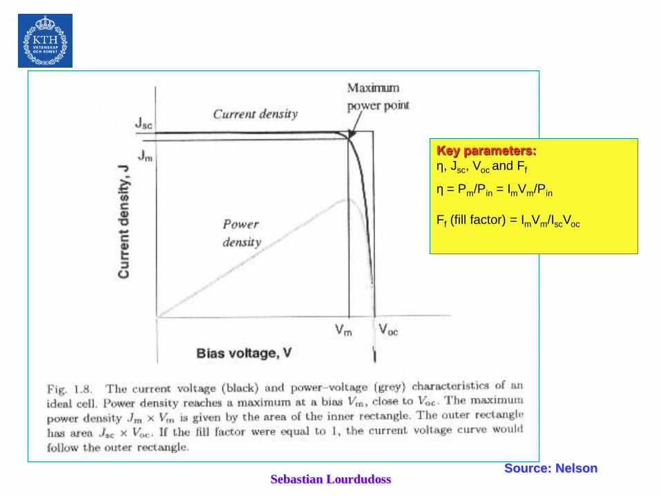
Key parameters:
η, Jsc, Voc and Ff
η = Pm/Pin = ImVm/Pin
Ff (fill factor) = ImVm/IscVoc
Source: Nelson
Sebastian Lourdudoss
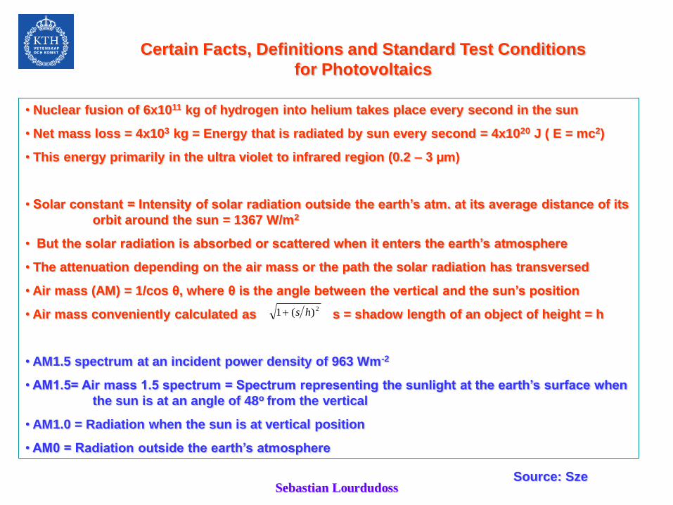
• Nuclear fusion of 6x10¹¹ kg of hydrogen into helium takes place every second in the sun
• Net mass loss = 4x10³ kg = Energy that is radiated by sun every second = 4x10²⁰ J ( E = mc2)
• This energy primarily in the ultra violet to infrared region (0.2 – 3 µm)
• Solar constant = Intensity of solar radiation outside the earth’s atm. at its average distance of its
orbit around the sun = 1367 W/m2
• But the solar radiation is absorbed or scattered when it enters the earth’s atmosphere
• The attenuation depending on the air mass or the path the solar radiation has transversed
• Air mass (AM) = 1/cos θ, where θ is the angle between the vertical and the sun’s position
• Air mass conveniently calculated as s = shadow length of an object of height = h
• AM1.5 spectrum at an incident power density of 963 Wm-2
• AM1.5= Air mass 1.5 spectrum = Spectrum representing the sunlight at the earth’s surface when
the sun is at an angle of 48o from the vertical
• AM1.0 = Radiation when the sun is at vertical position
• AM0 = Radiation outside the earth’s atmosphere
Source: Sze
Certain Facts, Definitions and Standard Test Conditions
for Photovoltaics
2)(1 hs

Sebastian Lourdudoss
Source: Nelson

Sebastian Lourdudoss
Source: Nelson

Sebastian Lourdudoss
Increasing the efficiency
Multiple junction or Tandem solar cells:
• Two or more bandgaps together
• Light not absorbed in high bandgap
material will be absorbed in the low bandgap
material
=> Increased efficiency
Eg1
Eg2
Eg3
Eg1 > Eg2 >Eg3

Sebastian Lourdudoss
Semiconductor combinations for multi-junction solar cells
4 terminals to 2 terminals
GaInP
based
GaAs
based

Sebastian Lourdudoss
Several combinations:
GaAs/InGaP and Ge/InGaAsN
InP/InAlAs and InP/InGaAs
GaN/InGaN to cover almost the whole range

Sebastian Lourdudoss
The solar spectrum AM0 peaks at 500 nm but extends to beyond 3 µm. The
unconcentrated triple-junction solar cell GaInP/GaAs/Ge, which has bandgaps
of 1.88, 1.42 and 0.67 eV, respectively, can absorb a high proportion of this
radiation and deliver an efficiency of almost 30%.
Ref: http://compoundsemiconductor.net/cws/article/magazine/31311
Sebastian Lourdudoss
LIGHT EMITTING DIODES

Sebastian Lourdudoss
LIGHT EMITTING DIODES
Source: Singh

Sebastian Lourdudoss
LIGHT EMITTING DIODES
ELECTRON-HOLE RECOMBINATION TIMES
Source: Singh
Sebastian Lourdudoss
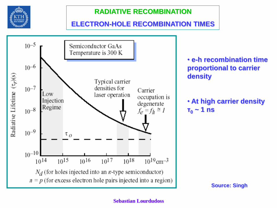
RADIATIVE RECOMBINATION
ELECTRON-HOLE RECOMBINATION TIMES
• e-h recombination time
proportional to carrier
density
• At high carrier density
τ0 ~ 1 ns
Source: Singh

Sebastian Lourdudoss
Ec
Ev
Ec
EFp
M
EFn
eVo
p nE
o
Evnp
(a)
VI
np
Eo–E
e(Vo–V)
eV
Ec
EFn
Ev
Ev
Ec
EFp
(b)
(c)
Vr
np
e(Vo+Vr)
Ec
EFn
Ev
Ev
Ec
EFp
Eo+E (d)
I = Very SmallV
r
np
Thermalgeneration
Ec
EFn
Ev
Ec
EFp
Ev
e(Vo+Vr)
Eo+E
Energy band diagrams for a pn junction under (a) open circuit, (b) forwardbias and (c) reverse bias conditions. (d) Thermal generation of electron holepairs in the depletion region results in a small reverse current.
SCL
© 1999 S.O. Kasap, Optoelectronics (Prentice Hall)

Sebastian Lourdudoss
h Eg
Eg (b)
V
(a)
p n+
Eg
eVo
EF
p n+
Electron in CB
Hole in VB
Ec
Ev
Ec
Ev
EF
eVo
Electron energy
Distance into device
(a) The energy band diagram of a p-n+ (heavily n-type doped) junction without any bias.Built-in potential Vo prevents electrons from diffusing from n+ to p side. (b) The applied
bias reduces Vo and thereby allows electrons to diffuse, be injected, into the p-side.
Recombination around the junction and within the diffusion length of the electrons in thep-side leads to photon emission.
© 1999 S.O. Kasap, Optoelectronics (Prentice Hall)

Sebastian Lourdudoss
A schematic illustration of typical planar surface emitting LED devices. (a) p-layer grown epixially on an n+ Substrate (b) First n+ is epitaxially
grown and then p-region is formed by dopant diffusion into the epitaxial layer
Light output
Insulator (oxide)p
n + Epitaxial layer
Light output
pEpitaxial layers
(a ) (b )
n +
Substrate Substrate
n +
n +
Metal electrode
© 1999 S.O. Kasap, Optoelectronics (Prentice Hall)

Sebastian Lourdudoss
Light output
p
Electrodes
Light
Plastic dome
Electrodes
Domed
semiconductor
pn Junction
(a) (b) (c)
n+
n+
(a) Some light suffers total internal reflection and cannot escape. (b) Internal reflectionscan be reduced and hence more light can be collected by shaping the semiconductor into adome so that the angles of incidence at the semiconductor-air surface are smaller than thecritical angle. (b) An economic method of allowing more light to escape from the LED isto encapsulate it in a transparent plastic dome.
Substrate
© 1999 S.O. Kasap, Optoelectronics (Prentice Hall)

Sebastian Lourdudoss
2 eV
2 eVeVo
Holes in VB
Electrons in CB
1.4 eVNo bias
With
forward
bias
Ec
EvEc
Ev
EFEF
(a)
(b)
(c)
(d)
pn+ p
Ec
GaAs AlGaAsAlGaAs
ppn+
~ 0.2 m
AlGaAsAlGaAs
(a) A doubleheterostructure diode hastwo junctions which arebetween two differentbandgap semiconductors(GaAs and AlGaAs)
(b) A simplified energyband diagram withexaggerated features. EF
must be uniform.
(c) Forward biasedsimplified energy banddiagram.
(d) Forward biased LED.Schematic illustration ofphotons escapingreabsorption in theAlGaAs layer and beingemitted from the device.
© 1999 S.O. Kasap, Optoelectronics (Prentice Hall)
GaAs

Sebastian Lourdudoss
(a) Surface emitting LED (b) Edge emitting LED
Double
heterostructure
Light
Light
© 1999 S.O. Kasap, Optoelectronics (Prentice Hall)
Electrode
SiO2 (insulator)
Electrode
Fiber (mult imode)
Epoxy resin
Etched well
Double heterostructure
Light is coupled from a surface emitting LEDinto a multimode fiber using an index matchingepoxy. The fiber is bonded to the LEDstructure.
(a)
Fiber
A microlens focuses diverging light from a surfaceemitting LED into a multimode optical fiber.
Microlens (Ti2O3:SiO2 glass)
(b)
© 1999 S.O. Kasap, Optoelectronics (Prentice Hall)

Sebastian Lourdudoss
Phosphor
concentration
Chip
wavelength
Color coordinate
+
400 500 600 700nm
White Light by Phosphor Conversion
Blue LED Yellow
phosphor
Courtesy: Klaus Streubel,
Osram

Sebastian Lourdudoss
White LEDs
+ +
400 500 600 700nm
+
+ +
+ +
+Blue chip +
Yellow
phosphor
Blue + red chip +
Yellow phosphor
Blue + red + green chip
Blue + phosphor mix
UV chip + phosphor mix
Courtesy: Klaus Streubel,
Osram

Sebastian Lourdudoss
LASERS

Sebastian Lourdudoss
• Under thermal eqm. and for (E2-E1) >3kT:
n2/n1 = exp –[(E2-E1)/kT] = exp –(hν/kT)
i.e., at thermal eqm., low lying levels are more populated ( n1>n2 )
• Under steady state conditions:
Stimulated emission rate + Spontaneous emission rate = Absorption rate
B21n2ρ(hν12) + A21n2 = B12n1 ρ(hν12)
A’s and B’s are constants
ρ(hν12) = photon field energy density, i.e., the total energy in the radiation
field per unit volume per unit frequecy
Stimulated emission rate/Spontaneous emission rate = (B21/A21) ρ(hν12)
To enhance stimulated emission, large ρ(hν12) is necessary
Stimulated emission rate / Absorption rate = (B21/B12) (n2/n1)
To enhance stimuated emission, n2>n1 i.e., population inversion
necessary
CONDITIONS FOR STIMULATED EMISSION

Sebastian Lourdudoss
p+ n+
EF n
(a)
Eg
Ev
Ec
Ev
Holes in V B
Electrons in C B
Junction
ElectronsE
c
p+
Eg
V
n+
(b)
EF n
eV
EF p
The energy band diagram of a degenerately doped p-n with no bias. (b) Banddiagram with a sufficiently large forward bias to cause population inversion andhence stimulated emission.
Invers ionreg ion
EF p
Ec
Ec
eVo
© 1999 S.O. Kasap, Optoelectronics (Prentice Hall)
POPULATION INVERSION AND STIMULATED EMISSION

Sebastian Lourdudoss
History of Heterostructure Lasers
10
100
1000
10000
100000
1000000
1960 1970 1980 1990 2000 2010Year
Th
res
ho
ld C
urr
en
t D
en
sit
y (
A/c
m2)
GaAs pn
QW Miller et. al.
QD Kamath et. al.
Mirin et. al.
Shoji et. al.
QD Ledenstov et. al.
QD Liu et. al.
QW Dupuis et. al.
QW Tsang
QW Alferov et. al.
Chand et. al.
DHS
Alferov
et. al.
DHS QW
Alferov et. al.
Hayashi et. al.
T=300K
DHS - Diode Heterostructure
QW - Quantum Well
QD - Quantum Dot
Courtesy:
P.Bhattacharya,
University of
Michigan

Sebastian Lourdudoss
POPULATION INVERSION AND STIMULATED EMISSION
h
Eg
Optical gainE
F n E
F p
Optical absorption
0
Energy
Ec
Ev
CB
VB
(a) The density of states and energy distribution of electrons and holes inthe conduction and valence bands respectively at T 0 in the SCLunder forward bias such that EFn EFp > Eg. Holes in the VB are emptystates. (b) Gain vs. photon energy.
Density of states
Electrons
in CB
Holes in VB
= Empty states
EF n
EF p
eV
At T > 0
At T = 0
(a) (b)
© 1999 S.O. Kasap, Optoelectronics (Prentice Hall)SCL =space charge layer
= depletion layer

Sebastian Lourdudoss
Fn-Fv
Increasing
carrier
density
Eg
• Photon with energy <
Eg cannot excite an
electron and hence are
transparent => No gain!
• Photon with energy
between Eg and Fn-Fv
can stimulate
recombination
=> Hence gain!
• Photon with energy
> Fn-Fv will only be
absorbed!
=> No gain - only loss!
Gain or loss? When?
To get good
lasers:
Optimise
Confinement
Cavity gain
Cavity loss
Mirror loss
Source: Singh

Sebastian Lourdudoss
LElectrode
Current
GaAs
GaAsn+
p+
Cleaved surface mirror
Electrode
Active region(stimulated emission region)
A schematic illustration of a GaAs homojunction laserdiode. The cleaved surfaces act as reflecting mirrors.
L
© 1999 S.O. Kasap, Optoelectronics (Prentice Hall)
Optical cavity,
produced by
cleaving the crystal
causes photons to
be reflected back
into the cavity. The
photon build-up
starts the
stimulated
emission
responsible for
lasing
No optical
confinement and
no carrier
confinement in
homojunctions!

Sebastian Lourdudoss
Refractiveindex
Photondensity
Active
region
n ~ 5%
2 eV
Holes in VB
Electrons in CB
AlGaAsAlGaAs
1.4 eV
Ec
Ev
Ec
Ev
(a)
(b)
pn p
Ec
(a) A doubleheterostructure diode hastwo junctions which arebetween two differentbandgap semiconductors(GaAs and AlGaAs).
2 eV
(b) Simplified energyband diagram under alarge forward bias.Lasing recombinationtakes place in the p-GaAs layer, theactive layer
(~0.1 m)
(c) Higher bandgapmaterials have alower refractiveindex
(d) AlGaAs layersprovide lateral opticalconfinement.
(c)
(d)
© 1999 S.O. Kasap, Optoelectronics (Prentice Hall)
GaAs

Sebastian Lourdudoss
The resonant modes supported by the cavity are those that satisfy
L = m λ/2
m = integer; λ = light wavelength in the material = λ0/ref.index
L
Source: Singh

Sebastian Lourdudoss
Typical output optical power vs. diode current ( I) characteristics and the correspondingoutput spectrum of a laser diode.
Laser
LaserOptical Power
Optical Power
I0
LEDOptical Power
Ith
Spontaneous
emission
Stimulated
emission
Op tical Power
© 1999 S.O. Kasap, Optoelectronics (Prentice Hall)
Sebastian Lourdudoss
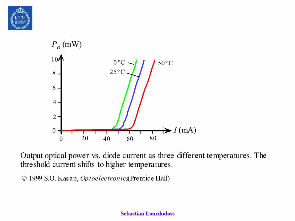
0 20 40 60 80
0
2
4
6
8
10
Po (mW)
I (mA)
0 C
25 C
50 C
Output optical power vs. diode current as three different temperatures. Thethreshold current shifts to higher temperatures.
© 1999 S.O. Kasap, Optoelectronics (Prentice Hall)
Sebastian Lourdudoss
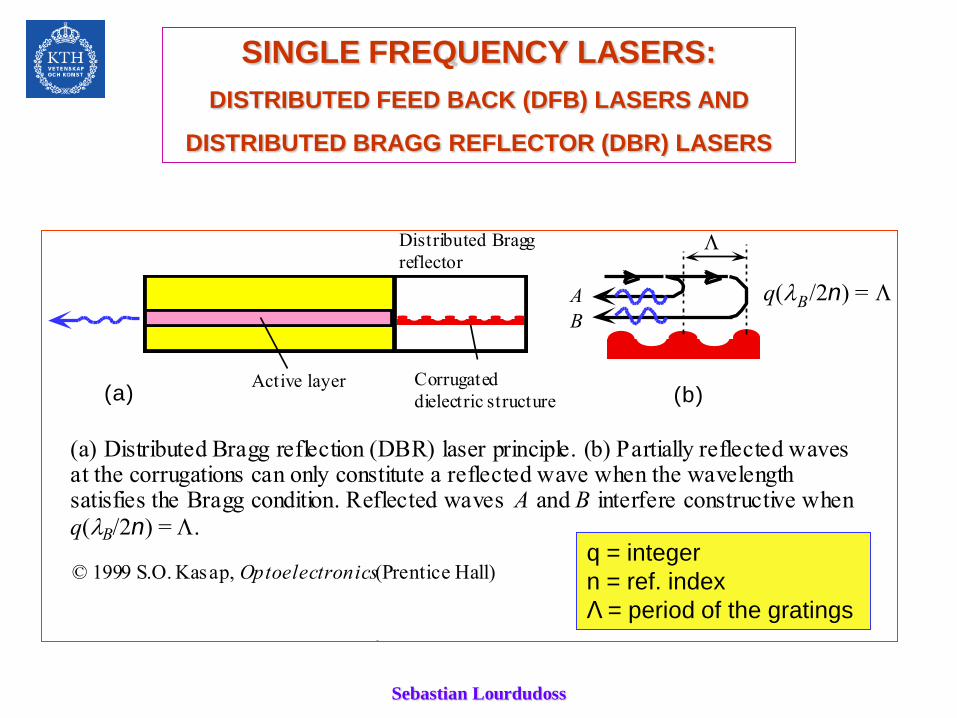
SINGLE FREQUENCY LASERS:
DISTRIBUTED FEED BACK (DFB) LASERS AND
DISTRIBUTED BRAGG REFLECTOR (DBR) LASERS
Corrugated
dielectric structure
Distributed Bragg
reflector
(a) (b)
A
B
q(B/2n) =
Active layer
(a) Distributed Bragg reflection (DBR) laser principle. (b) Partially reflected wavesat the corrugations can only constitute a reflected wave when the wavelengthsatisfies the Bragg condition. Reflected waves A and B interfere constructive when
q(B/2n) = .
© 1999 S.O. Kasap, Optoelectronics (Prentice Hall)q = integer
n = ref. index
Λ = period of the gratings

Sebastian Lourdudoss
Active layer
Corrugated grating
Guiding layer
(a)
(a) Distributed feedback (DFB) laser structure. (b) Ideal lasing emission output. (c)Typical output spectrum from a DFB laser.
Optical power
(nm)
0.1 nm
Ideal lasing emission
B(b) (c)
© 1999 S.O. Kasap, Optoelectronics (Prentice Hall)

Sebastian Lourdudoss
A simplified schematic illustration of a vertical cavitysurface emitting laser (VCSEL).
Contact
Surface emission
Dielectric mirror
Contact
Substrate
/4n1
Active layer
/4n2 Dielectric mirror
© 1999 S.O. Kasap, Optoelectronics (Prentice Hall)

Sebastian Lourdudoss
n1 n2
AB
n1 n2
C
Schematic illustration of the principle of the dielectric mirror with many low and highrefractive index layers and its reflectance.
Reflectance
(nm)
330 550 770
1 2 21
o
1/4 2/4
© 1999 S.O. Kasap, Optoelectronics (Prentice Hall)

Sebastian Lourdudoss
0 1 2 3 4 5 6 7 8
0.0
0.2
0.4
0.6
0.8
1.0
1.2 Marion 34
130_124_A1
Po
we
r [m
W]
Current [mA]
0
2
4
6
8
140°C
10°C
Fo
rwa
rd v
olta
ge
[V
]
10 Gb/s 1.3-m InGaAs/GaAs VCSELs
fabricated at KTH
Performance at 10-140°C:•Wavelength: 1265-1280 nm
•SM across whole current range
•SMSR > 30dB
•Output power > 0.5mW
•Threshold Current < 2mA
•10 Gbit/s data transmission

Sebastian Lourdudoss
BH-VCSELs fabricated at KTH
0 2 4 6 8 10 12 14 16 18 20 22 24 26 28 300
1
2
3
4
5
CW
97 oC
93 oC
84 oC
74 oC
63 oC
54 oC
43 oC
34 oC
22 oC
8 oC
Lig
ht
Outp
ut
Pow
er
(mW
)
Current (mA)
Regrowth by Hydride
Vapour Phase Epitaxy CW operation up to 97°C
Single mode operation
up to 0.7 mW
GaAs/AlGaAs BH-VCSELs with SI-GaInP Regrowth
Top Related