


![Direct Inkjet Printing of Silver Source/Drain Electrodes ...€¦ · (AMLCD) and an active matrix organic light emitting diode (AMOLED) [1–3]. In recent years, printing technology](https://static.fdocuments.in/doc/165x107/5e8d3a3228ccd304620ab25d/direct-inkjet-printing-of-silver-sourcedrain-electrodes-amlcd-and-an-active.jpg)
Languages
Pages
Legal


Doc . No LMS350DF01-001 Rev.No 001 Page 4 /28
Preliminary
DATE : April. 21. 2008
AMLCD DIVISION
Samsung Electronics Co. , LTD.
SAMSUNG TFT-LCD

Doc . No LMS350DF01-001 Rev.No 001 Page 2 /28
PreliminaryContents
Revision History -------------------------- (3)General Description -------------------------- (4)1. Absolute Maximum Ratings -------------------------- (5)
1.1 Absolute Ratings Of Environment1.2 Electrical Absolute Ratings
2. Optical Characteristics -------------------------- (7)3. Electrical Characteristics ------------------------ (10)
3.1 TFT-LCD Module3.2 Back-light Unit
4. Block Diagram ------------------------- (11)4.1 TFT-LCD Module with Back Light Unit4.2 Back Light Unit
5. Input Terminal Pin Assignment ------------------------- (12)5.1 Input Signal & Power5.2 Input Signal, Basic Display Colors and Gray Scale of Each Colors
6. Operation Specifications ------------------------ (14)6.1 Dot Formation6.2 Data Format for 24 bit RGB interface
7. Interface Timing ------------------------- (15)7.1 24bit RGB Interface Timing7.2 Serial Peripheral Interface
8. Electrical Specifications -------------------------- (17)9. Power Sequence ------------------------- (19)
9.1 Power on Sequence9.2 Power off Sequence9.3 Standby In / Out Sequence
10. Application Circuit --------------------------- (23)11. Module Outline Dimension --------------------------- (24)12. Packing --------------------------- (25)13. Marking and Others ------------------------- (26)14. General Precaution ------------------------- (27)
14.1 Handling14.2 Storage14.3 Operation14.4 Others

Doc . No LMS350DF01-001 Rev.No 001 Page 3 /28
PreliminaryData Rev.
No. Page Summary
Jan. 08. 2008Jan. 30. 2008
.
000001
Rev.000 was first issued.Power sequence added.Electrical Characteristics revised.
Component description added.Optical specification updated.Power sequence revised.Outline Dimension revised. (FPC length incresed 0.2mm.)
Revision History

Doc . No LMS350DF01-001 Rev.No 001 Page 4 /28
PreliminaryGeneral Description
* Description
LMS350DF01-001 is a TMR(Transmissive with Micro Reflective) type color active
matrix TFT (Thin Film Transistor) liquid crystal display (LCD) that uses
amorphous silicon TFT as a switching devices. This model is composed of a TFT-
LCD module, a driver circuit and a back-light unit. The resolution of a 3.5"
contains 320 x 480 dots and can display up to 16,777,216 colors.
* Features
- Transmissive with Micro Reflective type and back-light with 5LEDs.
- mPVA mode (Normally Black).
- Wide Viewing Angle.
- Stripe Pixel structure.
- 24bit RGB Interface + Serial Peripheral Interface (SPI)
- Gate Driver IC embeded on Panel
- Low Power consumption.
* Applications
- Display terminals for MP3, PMP application products.
* General informationItems Specification Unit Note
Display Area 48.96(H) x 73.44(V) mm -Driver Element a-Si TFT active matrix - -Display Colors 16.7 M color -
Number of Pixels 320(H) x 480(V) pixel -Pixel Arrangement Stripe Structure - -
Pixel Pitch 0.153(H) x 0.153(V) mm -Display Mode Normally Black - -
Gray Inversion Angle No Gray Inversion o'clock -
* Mechanical information
Item Min. Typ. Max. Unit Note
Modulesize
Horizontal(H) 52.76 54.76 54.96 mm (1)Vertical(V) 81.24 83.24 83.44 mm (1)Depth(D) 1.63 1.83 2.03 mm (1)
Weight - 13 - g (2)
Note (1) : Not include FPCNote (2) : Included FPC

Doc . No LMS350DF01-001 Rev.No 001 Page 5 /28
Preliminary1. Absolute Maximum Ratings
1.1 Absolute Ratings of Environment
Item Symbol Min. Max. Unit Note
Storage temperature TSTG -30 70 ℃ (1)
Operating temperature(Ambient temperature)
TOPR -20 60 ℃ (1),(2)
Note (1) 90 % RH Max. ( 50°C ³ Ta )Maximum wet-bulb temperature at 49°C or less. (Ta > 50°C)No condensation.
(2) In case of below 0°, the response time of liquid crystal (LC) becomesslower and the color of panel becomes darker than normal one. Levelof retardation depends on temperature, because of LC's characteristics.
(3) If any fixed pattern is displayed on LCD for minutes, image-stickingphenomenon may occur.

Doc . No LMS350DF01-001 Rev.No 001 Page 6 /28
Preliminary1.2 Electrical Absolute Ratings
(1) TFT-LCD Module(Ta = 25°C ± 2°C, GND=0V)
Characteristics Symbol Min. Max. Unit Note
Logic Input Voltage VDD3 -0.3 5.0 V (1)
Analog Input Voltage VCI -0.3 5.0 V (1)
(2) Back-Light Unit(Ta = 25 ± 2°C)
Item Symbol Min. Max. Unit. Note
Current IB - 30 mA (1)
Note (1) Permanent damage to the device may occur if maximum values are exceededor reverse voltage is loaded.Functional operation should be restricted to the conditions described undernormal operating conditions.

Doc . No LMS350DF01-001 Rev.No 001 Page 7 /28
Preliminary2. Optical Characteristics
The following items are measured under stable conditions. The opticalcharacteristics should be measured in a dark room or equivalent state withthe methods shown in Note (1). Measuring equipment: SR-3, BM-7, EZ-Contrast
(Ta = 25 ± 2°C, VDD3 = VCI = 3.3V, IB = 20mA)
Item Symbol Condition Min. Typ. Max. Unit Note
Contrast ratio
(Center point)C/R
Note
(1),(6)
Φ = 0
θ = 0
Normal
Viewing
Angle
B/L On
500 - -(2)
SR-3
Luminance of white
(Center point)YL - (380) - cd/m2
(3)
SR-3
Response
time
Rising:Tr
Tr+Tf - 25 30 msec(4)
BM-7Falling:Tf
Color
chromaticity
(CIE 1931)
WhiteWx (0.318)
-(5)
SR-3
Wy (0.344)
RedRx (0.603)
Ry (0.326)
GreenGx (0.329)
Gy (0.585)
BlueBx (0.153)
By (0.106)
Viewing
angle
Hor.θL
C/R≥10
B/L On
80
Degrees
(6)
Ez -
Contrast
θR 80
Ver.ΦH 80
ΦL 80

Doc . No LMS350DF01-001 Rev.No 001 Page 8 /28
Preliminary
Note (1) Test Equipment Setup
After stabilizing and leaving the panel alone at a given temperature for 30 min,the measurement should be executed. Measurement should be executedin a stable, windless, and dark room. 30 min after lighting the back-light.This should be measured in the center of screen.
- Environment condition : Ta = 25 ± 2 °C- Back-Light On condition
d= 50Cm
θ=90°± 0.3°
LCD
LMD
Note (2) Definition of Contrast Ratio (C/R) : Ratio of gray max (Gmax) &gray min (Gmin) at the center point
C R GG
=m a xm in
* Gmax : Luminance with all dots white* Gmin : Luminance with all dots black
LMD : Ligh Mesurement Devices

Doc . No LMS350DF01-001 Rev.No 001 Page 9 /28
Preliminary
Note (3) Definition of Luminance of White (YL): Luminance of white at the center point
Note (4) Definition of Response time : Sum of Tr and Tf (Field : 1°)
Note (5) Definition of Color Chromaticity (CIE 1931)Color coordinate of white & red, green, blue at center point.
Note (6) Definition of Viewing Angle : Viewing angle range (CR≥10)
6 o’clockdirection
Normal Line
θ Lθ R
φ Hφ L 12 o’clockdirection
θR =90o
θ L =90o
φ = 0o,
x
x'y'
y
θ = 0o
φ H = 90o
φ L= 90o

Doc . No LMS350DF01-001 Rev.No 001 Page 10/28
Preliminary3. Electrical Characteristics
3.1 TFT-LCD ModuleTa = 25 ± 2°C
Characteristics Symbol Min. Typ. Max. Unit Note
Logic Input Voltage VDD3 3.25 3.3 3.35 V -
Analog Input Voltage VCI 3.25 3.3 3.35 V -
Power DissipationIFULL - 20 25 mA
(1),(2)Istandby 25 30 uA
Frame frequency fFrame - 60 - Hz -
Dot Clock DCK - 10 - MHz -
Serial Clock XSCK - - 10 MHz -
* To prevent a latch-up or DC operation of the LCD module, the power on/off sequence should beas the Chapter 10. Power On/Off Sequence.
Note (1) VDD3 = VCI = 3.3V fFrame = 60 Hz(2) Dissipation current check pattern
▶ Black pattern

Doc . No LMS350DF01-001 Rev.No 001 Page 11/28
Preliminary
3.2 Back-Light unit
The back-light system is an edge-lighting type with three white LED (Light EmittingDiode)s.
(Ta=25 ± 2°C)
Item Symbol Min. Typ. Max. Unit Note
Current IB - 20 - mA (1)
Power Consumption PBL - TBD - mW -
Note (1) Five LEDs serial type.
4. Block Diagram4.1 TFT-LCD Module (Interface System Structure)
4.2 Back Light Unit

Doc . No LMS350DF01-001 Rev.No 001 Page 12/28
Preliminary5. Input Terminal Pin Assignment
5.1 Input Signal & Power (BTB Connector: DF30FC-70DS-0.4V)
PinNo Symbol Description I/O
Pin
NoSymbol Description I/O
1 LED+ LED Anode I 36 VCI Analog Input Voltage I
2 GND Ground I 37 PD10 GREEN 2 I
3 NC No Connectior - 38 VCI Analog Input Voltage I
4 VGOFFL Power Output for ASG driver O 39 PD9 GREEN 1 I
5 LED- LED Cathode I 40 C23M Charge Pumping Capacitor O
6 GND Ground I 41 PD8 GREEN 0 I
7 GND Ground I 42 C23P Charge Pumping Capacitor O
8 VGL Gate Off Voltage O 43 GND Ground I
9 PD23 RED 7 I 44 VCL Power Supply for Generating VCOML O
10 GND Ground I 45 PD7 BLUE 7 I
11 PD22 RED 6 I 46 VSSA Ground I
12 VGH Gate On Voltage O 47 PD6 BLUE 6 I
13 PD21 RED 5 I 48 VCOMH VCOM High Level O
14 C22P Charge Pumping Capacitor O 49 PD5 BLUE 5 I
15 PD20 RED 4 I 50 VCOML VCOM Low Level O
16 C22M Charge Pumping Capacitor O 51 PD4 BLUE 4 I
17 PD19 RED 3 I 52 GVDD Gamma Voltage Generator O
18 C21P Charge Pumping Capacitor O 53 PD3 BLUE 3 I
19 PD18 RED 2 I 54 RVDD Regulated VDD output O
20 C21M Charge Pumping Capacitor O 55 PD2 BLUE 2 I
21 PD17 RED 1 I 56 VDD3 Logic Input Voltage I
22 AVDD Power Output for Source Driver O 57 PD1 BLUE 1 I
23 PD16 RED 0 I 58 VDD3 Logic Input Voltage I
24 C11Pb Charge Pumping Capacitor O 59 PD0 BLUE 0 I
25 GND Ground I 60 VSYNC Vsync I
26 C11Mb Charge Pumping Capacitor O 61 GND Ground I
27 PD15 GREEN 7 I 62 HSYNC Hsync I
28 C11P Charge Pumping Capacitor O 63 DOTCLK Dotclk I
29 PD14 GREEN 6 I 64 SCL Serial Clock I
30 C11M Charge Pumping Capacitor O 65 SDI Serial Data Input I
31 PD13 GREEN 5 I 66 CSB Chip Select I
32 VSSC Ground I 67 ENABLE Ground I
33 PD12 GREEN 4 I 68 RESETB Reset I
34 VCI1 Reference Voltage In Step Up Circuit O 69 GND Ground I
35 PD11 GREEN 3 I 70 GND Ground I

Doc . No LMS350DF01-001 Rev.No 001 Page 13/28
Preliminary5.2 Input Signal, Basic Display Colors and Gray Scale of Each Colors
COLOR DISPLAY
DATA SIGNALGRAY
SCALE
LEVELRED GREEN BLUE
R0 R1 R2 R3 R4 R5 R6 R7 G0 G1 G2 G3 G4 G5 G6 G7 B0 B1 B2 B3 B4 B5 B6 B7
BASIC
COLOR
BLACK 0 0 0 0 0 0 0 0 0 0 0 0 0 0 0 0 0 0 0 0 0 0 0 0 -
BLUE 0 0 0 0 0 0 0 0 0 0 0 0 0 0 0 0 1 1 1 1 1 1 1 1 -
GREEN 0 0 0 0 0 0 0 0 1 1 1 1 1 1 1 1 0 0 0 0 0 0 0 0 -
CYAN 0 0 0 0 0 0 0 0 1 1 1 1 1 1 1 1 1 1 1 1 1 1 1 1 -
RED 1 1 1 1 1 1 1 1 0 0 0 0 0 0 0 0 0 0 0 0 0 0 0 0 -
MAGENTA 1 1 1 1 1 1 1 1 0 0 0 0 0 0 0 0 1 1 1 1 1 1 1 1 -
YELLOW 1 1 1 1 1 1 1 1 1 1 1 1 1 1 1 1 0 0 0 0 0 0 0 0 -
WHITE 1 1 1 1 1 1 1 1 1 1 1 1 1 1 1 1 1 1 1 1 1 1 1 1 -
GRAY
SCALE
OF
RED
BLACK 0 0 0 0 0 0 0 0 0 0 0 0 0 0 0 0 0 0 0 0 0 0 0 0 R0
DARK
↑
↓
LIGHT
1 0 0 0 0 0 0 0 0 0 0 0 0 0 0 0 0 0 0 0 0 0 0 0 R1
0 1 0 0 0 0 0 0 0 0 0 0 0 0 0 0 0 0 0 0 0 0 0 0 R2
: : : : : : : : : : : : : : : : : : : : : : : :R3~R252
: : : : : : : : : : : : : : : : : : : : : : : :
1 0 1 1 1 1 1 1 0 0 0 0 0 0 0 0 0 0 0 0 0 0 0 0 R253
0 1 1 1 1 1 1 1 0 0 0 0 0 0 0 0 0 0 0 0 0 0 0 0 R254
RED 1 1 1 1 1 1 1 1 0 0 0 0 0 0 0 0 0 0 0 0 0 0 0 0 R255
GRAY
SCALE
OF
GREEN
BLACK 0 0 0 0 0 0 0 0 0 0 0 0 0 0 0 0 0 0 0 0 0 0 0 0 G0
DARK
↑
↓
LIGHT
0 0 0 0 0 0 0 0 1 0 0 0 0 0 0 0 0 0 0 0 0 0 0 0 G1
0 0 0 0 0 0 0 0 0 1 0 0 0 0 0 0 0 0 0 0 0 0 0 0 G2
: : : : : : : : : : : : : : : : : :G3~G252
: : : : : : : : : : : : : : : : : :
0 0 0 0 0 0 0 0 1 0 1 1 1 1 1 1 0 0 0 0 0 0 0 0 G253
0 0 0 0 0 0 0 0 0 1 1 1 1 1 1 1 0 0 0 0 0 0 0 0 G254
GREEN 0 0 0 0 0 0 0 0 1 1 1 1 1 1 1 1 0 0 0 0 0 0 0 0 G255
GRAY
SCALE
OF
BLUE
BLACK 0 0 0 0 0 0 0 0 0 0 0 0 0 0 0 0 0 0 0 0 0 0 0 0 B0
DARK
↑
↓
LIGHT
0 0 0 0 0 0 0 0 0 0 0 0 0 0 0 0 1 0 0 0 0 0 0 0 B1
0 0 0 0 0 0 0 0 0 0 0 0 0 0 0 0 0 1 0 0 0 0 0 0 B2
: : : : : : : : : : : : : : : : : : : : : : : :B3~B252
: : : : : : : : : : : : : : : : : : : : : : : :
0 0 0 0 0 0 0 0 0 0 0 0 0 0 0 0 1 0 1 1 1 1 1 1 B253
0 0 0 0 0 0 0 0 0 0 0 0 0 0 0 0 0 1 1 1 1 1 1 1 B254
BLUE 0 0 0 0 0 0 0 0 0 0 0 0 0 0 0 0 1 1 1 1 1 1 1 1 B255
Note) Definition of Gray :Rn : Red Gray, Gn : Green Gray, Bn : Blue Gray (n = Gray level)Input Signal : 0 = Low level voltage, 1 = High level voltage

Doc . No LMS350DF01-001 Rev.No 001 Page 14/28
Preliminary6. Operation Specifications
6.1 Pixel Formation (Stripe Pixel Structure)
6.2 Data Format for 24bit RGB Interface
D23 D22 D21 D20 D19 D18 D17 D16 D15 D14 D13 D12 D11 D10 D9 D8 D7 D6 D5 D4 D3 D2 D1 D0
R7 R6 R5 R4 R3 R2 R1 R0 G7 G6 G5 G4 G3 G2 G1 G0 B7 B6 B5 B4 B3 B2 B1 B0
Input
RGBAssingment

Doc . No LMS350DF01-001 Rev.No 001 Page 15/28
Preliminary7. Interface Timing
7.1 24bit RGB Interface Timing
DATA[23:0]
HSYNC
HLW
DOTCLK
HBP[8:0] > HLW HFP
1
Valid Data transfer area
1 Period(1Frame)
480H
HSYNC
VSYNC VLW
1 Horizontal Period
320 dotclk
VBP[7:0] > VLW
2 320319
* DOTCLK = fframe × (480 + VBP + VFP) × (320 + HBP + HFP)= (TBD)Hz × (480 + VBP + VFP) × (320 + HBP + HFP)
* VBP ≥ 3 , VBP > VLW ≥ 2* HBP ≥ 8 , HBP > HLW ≥ 2

Doc . No LMS350DF01-001 Rev.No 001 Page 16/28
Preliminary
7.2 Serial Peripheral Interface
(Note) RS="0": Index data
RS="1": Instruction data
1 2 3 4 5 76 8 9 10 11 12 13 14 15 16 17 18 19 20 21 22 23 24
RSDB15
DB14
DB13
DB12
DB11
DB10
DB9DB8DB7
DB4
DB6DB5
DB3DB2DB10 DB
011110
Transfer start Transfer end
LSBMSB
Device ID code RS R/W
Start byte Index register setting, instruction
/CS(Input)
SCL(Input)
SDI(Input)
0

Doc . No LMS350DF01-001 Rev.No 001 Page 17/28
Preliminary8. Electrical Specifications
VCI = 3.3V, Ta = 25℃ ± 2℃
Item Symbol Min. Max. Unit
Serial Clock Cycle Time(write) tSCYCW 100 -
ns
Serial Clock rise/fall time tR,tF - 10
Pulse width high for write tSCHW 30 -
Pulse width low for write tSCLW 50
Chip Select Setup Time tCSS 20 -
Chip Select Hold Time tCSH 90 -
Serial Input Data Setup Time tSIDS 30 -
Serial Input Data Hold Time tSIDH 30 -
Serial Output Data delay Time tSODD - 200
Serial Output Data Hold Time tSODH 5 -
Reset Low Pulse Width tRES 30 -us
CSB Low Pulse Width for Wake up tCSBR 12 -

Doc . No LMS350DF01-001 Rev.No 001 Page 18/28
Preliminary
VCI = 3.3V, Ta = 25℃ ± 2℃
Item Symbol Min. Max. Unit
Vsync/Hsync Setup Time TvsysThsvs 20 -
ns
Vsync/Hsync Hold Time TvsyhThsyh 20 -
Dotclk Low Level Pulse Width tDCLW 50 -
Dotclk High Level Pulse Width tDCHW 50 -
Dotclk Cycle Time tDCYC 100 -
PD(Data) Setup Time tPDS 40 -
PD(Data) Hold Time tPDH 40 -
Dotclk Rise/Fall Time tR, tF - 10
tF tR

Doc . No LMS350DF01-001 Rev.No 001 Page 19/28
Preliminary. Power On/Off Sequence (*Can be changed for better quality)
9.1 Power On Sequence (TBD)
Display ON
Power OFF
R07h = 0101
R076h = 2213R1Ch = 7770R0B = 33E1R76h = 0000R07h = 0103
/ RESETR07h = 0000
Wait 1ms
Wait more than 10ms
Wait more than 6frames
R01h = 0B3B (note1)R02h = 0300
R03h = C040(note2)R08h = 0004(note3)R09h = 0008(note4)
R76h = 2213R0Bh = 33E0R0Ch = 0020R76h = 0000R0Dh = 0007R0Eh = 0500R14h = 0000R15h = 0803R16h = 0000R30h = 0005R31h = 0300R32h = 0300R33h = 0003R34h = 090CR35h = 0505R36h = 0001R37h = 0303R38h = 0F09R39h = 0101
Wait more than 2frame
Wait more than 5frames
POWER ON Sequence
Wait more than 1frame
R07h = 0001
R11h = 333FR12h = 0F00R13h = 7FE2R10h = 460C
R12h = 1663
DISPLAY ON Sequence

Doc . No LMS350DF01-001 Rev.No 001 Page 20/28
Preliminary9.2 Power Off Sequence (TBD)
9.3 Standby In / Out Sequence (TBD)
R07h = 0000R12h = 0000R10h = 0100
Wait more than 2frames
R10h = 0001
Display Off Sequence
Display On Status
Standby IN
R10h = 0000
Power On Sequence
Standby In Status
Standby OUT
Display On Sequence
Power OFF
R10h = 0001R0Bh = 30E1R07h = 0102
Doc . No LMS350DF01-001 Rev.No 001 Page 21/28
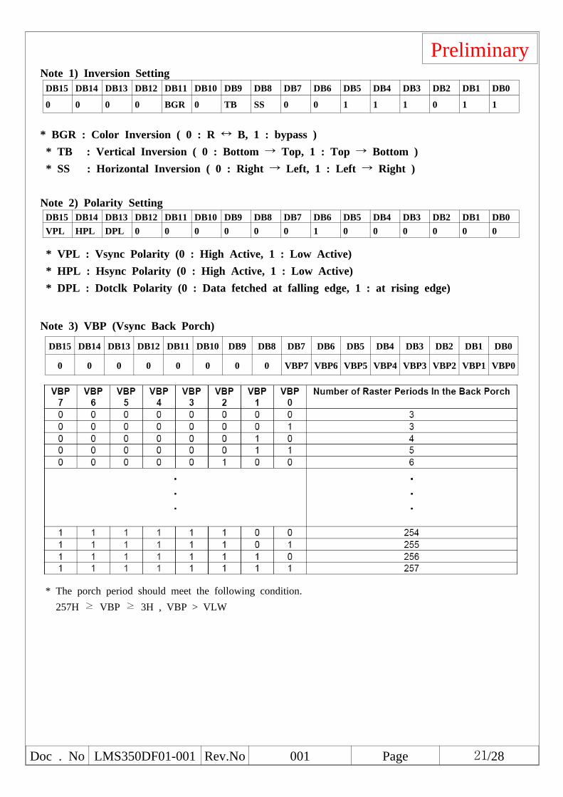
PreliminaryNote 1) Inversion Setting
* BGR : Color Inversion ( 0 : R ↔ B, 1 : bypass )* TB : Vertical Inversion ( 0 : Bottom → Top, 1 : Top → Bottom )* SS : Horizontal Inversion ( 0 : Right → Left, 1 : Left → Right )
Note 2) Polarity Setting
* VPL : Vsync Polarity (0 : High Active, 1 : Low Active)* HPL : Hsync Polarity (0 : High Active, 1 : Low Active)* DPL : Dotclk Polarity (0 : Data fetched at falling edge, 1 : at rising edge)
Note 3) VBP (Vsync Back Porch)
DB15 DB14 DB13 DB12 DB11 DB10 DB9 DB8 DB7 DB6 DB5 DB4 DB3 DB2 DB1 DB0
0 0 0 0 0 0 0 0 VBP7 VBP6 VBP5 VBP4 VBP3 VBP2 VBP1 VBP0
* The porch period should meet the following condition.257H ≥ VBP ≥ 3H , VBP > VLW
DB15 DB14 DB13 DB12 DB11 DB10 DB9 DB8 DB7 DB6 DB5 DB4 DB3 DB2 DB1 DB0VPL HPL DPL 0 0 0 0 0 0 1 0 0 0 0 0 0
DB15 DB14 DB13 DB12 DB11 DB10 DB9 DB8 DB7 DB6 DB5 DB4 DB3 DB2 DB1 DB0
0 0 0 0 BGR 0 TB SS 0 0 1 1 1 0 1 1

Doc . No LMS350DF01-001 Rev.No 001 Page 22/28
PreliminaryNote 4) HBP (Hsync Back Porch)
DB15 DB14 DB13 DB12 DB11 DB10 DB9 DB8 DB7 DB6 DB5 DB4 DB3 DB2 DB1 DB0
0 0 0 0 0 0 0 HBP8 HBP7 HBP6 HBP5 HBP4 HBP3 HBP2 HBP1 HBP0
* The porch period should meet the following condition.511dck ≥ HBP ≥ 8dck , HBP > HLW
Note 5) RIM
DB15 DB14 DB13 DB12 DB11 DB10 DB9 DB8 DB7 DB6 DB5 DB4 DB3 DB2 DB1 DB0
0 0 0 0 0 0 0 RIM4 RIM3 RIM2 RIM1 RIM0

Preliminary
Doc . No LMS350DF01-001 Rev.No 001 Page 23/28
10. Application Circuit (TBD)
※ Recommands1. All components would better be close toFPC connector as possible.
2. Schottky diode's low F/V(forward voltage)makes internal circuit more stable.
Name Device ValueMaximum Ratings
VoltageC1 VGOFFL Capacitor 1uF 16.5VC2 VGL Capacitor 1uF 20VC3 VGH Capacitor 1uF 25VC4 C22 Capacitor 1uF 25VC5 C21 Capacitor 1uF 16.5VC6 AVDD Capacitor 1uF 10VC7 C11b Capacitor 1uF 10VC8 C11 Capacitor 1uF 10VC9 VCI1 Capacitor 1uF 10VC10 C23 Capacitor 1uF 10VC11 VCL Capacitor 1uF 10VC12 VCOMH Capacitor 1uF 10VC13 VCOML Capacitor 1uF 10VC14 GVDD Capacitor 1uF 10VC15 RVDD Capacitor 1uF 10VD1 VGL Diode Vf ≤ 0.28V (@IF
=20mA, Ta = 25℃)VR ≥ max.25V)D2 VGH Diode

Preliminary
Doc . No LMS350DF01-001 Rev.No 001 Page 24/28
11. Module outline Dimension (TBD)

Doc . No LMS350DF01-001 Rev.No 001 Page 25/28
Preliminary12. Packing
Note (1) Packing Box Weight : Approx. TBD Kg(2) Packing Box Size : 505(W) x 355(D) x 208(H)(3) Place the panels in the tray facing the direction shown in the figure.(4) Place 25 tray and 1 cover tray and 2 pads inside the packing-box(5) Affix the label-safety, label-paper.
26
10
260
Doc . No LMS350DF01-001 Rev.No 001 Page 26/28
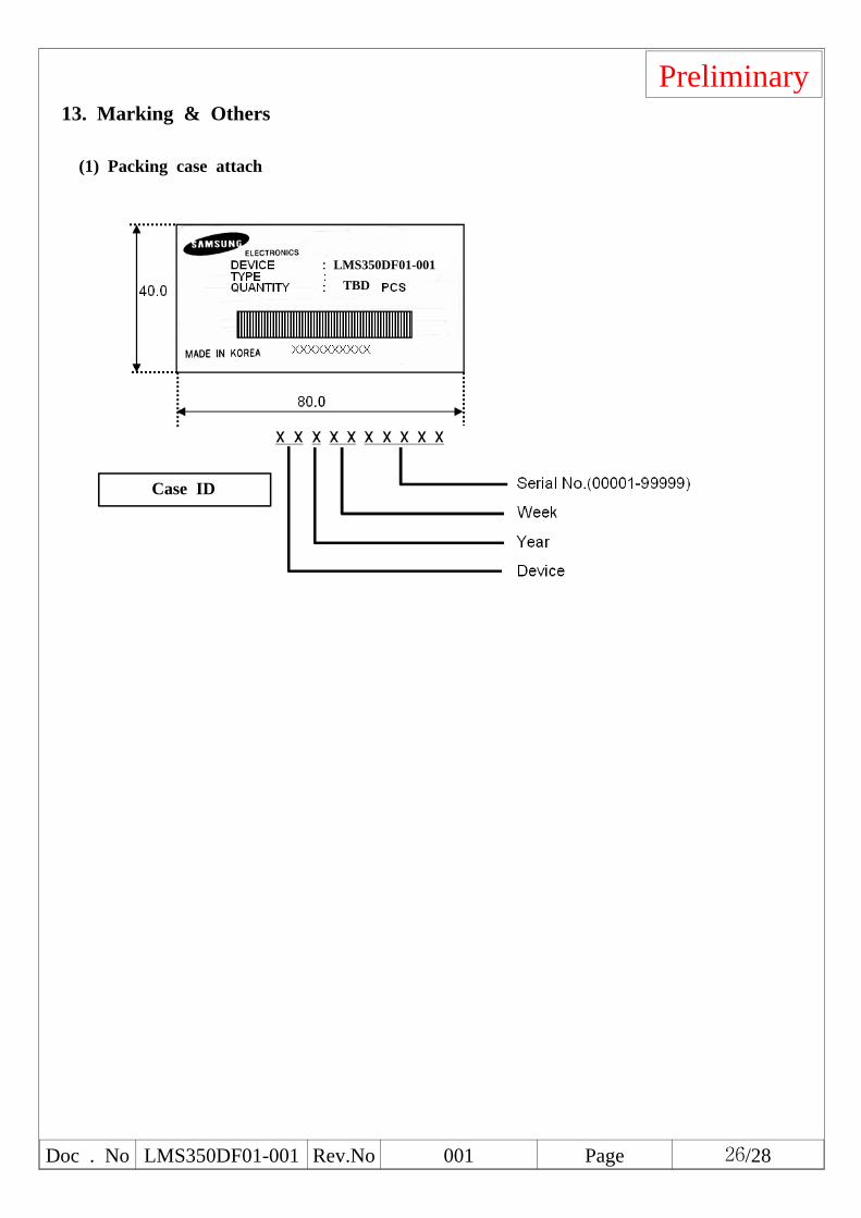
Preliminary13. Marking & Others
(1) Packing case attach
Case ID
TBDLMS350DF01-001

Doc . No LMS350DF01-001 Rev.No 001 Page 27/28
Preliminary14. General Precautions
14.1 Handling
(a) When the module is assembled, it should be attached to the system firmly. Becareful not to twist and bend the module.
(b) Refrain from strong mechanical shock and / or any force to the module. Inaddition to damage, this may cause improper operation or damage to the moduleand back-light unit.
(c) Note that polarizers are very fragile and could be easily damaged. Do not press orscratch the surface harder than a HB pencil lead.
(d) Wipe off water droplets or oil immediately. If you leave the droplets for a longtime, Staining and discoloration may occur.
(e) If the surface of the polarizer is dirty, clean it using some absorbent cotton orsoft cloth.
(f) The desirable cleaners are water, IPA(Isopropyl Alcohol) or Hexane. Do not useKetone type materials(ex. Acetone), Ethyl alcohol, Toluene, Ethyl acid or Methylchloride. It might permanent damage to the polarizer due to chemical reaction.
(g) If the liquid crystal material leaks from the panel, it should be kept away fromthe eyes or mouth. In case of contact with hands, legs or clothes, it must bewashed away thoroughly with soap.
(h) Protect the module from static, it may cause damage to the Integrated GateCircuit.
(i) Use finger-stalls with soft gloves in order to keep display clean during the incominginspection and assembly process.
(j) Do not disassemble the module.
(k) Protection film for polarizer on the module shall be slowly peeled off just beforeuse so that the electrostatic charge can be minimized.
(l) Pins of I/F connector shall not be touched directly with bare hands

Doc . No LMS350DF01-001 Rev.No 001 Page 28/28
Preliminary14.2 Storage
(a) Do not leave the panel in high temperature, and high humidity for a long time. Itis highly recommended to store the module with temperature from 0 to 35°C andrelative humidity of less than 70%.
(b) Do not store the TFT-LCD module in direct sunlight.
(c) The module shall be stored in a dark place. It is prohibited to apply sunlight orfluorescent light during the store.
14.3 Operation
(a) Do not connect, disconnect the module in the "Power On" condition.
(b) Power supply should always be turned on/off by the "Power on/off sequence"
14.4 Others
(a) The Liquid crystal is deteriorated by ultraviolet, do not leave it in direct sunlightand strong ultraviolet ray for many hours.
(b) Avoid condensation of water. It may result in improper operation or disconnectionof electrode.
(c) Do not exceed the absolute maximum rating value. ( the supply voltage variation,input voltage variation, variation in part contents and environmental temperature,and so on) Otherwise the panel may be damaged.
(d) If the panel displays the same pattern continuously for a long period of time, itcan be the situation when the image "Sticks" to the screen.
(e) This panel has its circuitry FPC on the bottom side and should be handledcarefully in order not to be stressed.
Top Related