


Languages
Pages
Legal


S-8215A Series
www.ablic.comBATTERY PROTECTION IC FOR 3-SERIAL TO 5-SERIAL CELL PACK
(SECONDARY PROTECTION)© ABLIC Inc., 2010-2019 Rev.2.6_00
1
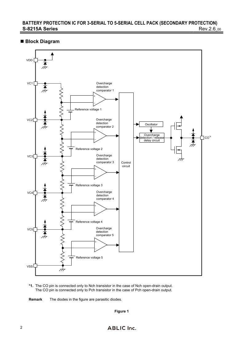
The S-8215A Series is used for secondary protection of lithium-ion rechargeable batteries, and incorporates high-accuracy voltage detection circuits and delay circuits. Short-circuiting between cells makes it possible for serial connection of three cells to five cells. Features
• High-accuracy voltage detection circuit for each cell Overcharge detection voltage n (n = 1 to 5)
3.600 V to 4.700 V (50 mV step) Accuracy ±25 mV (Ta = +25°C) Accuracy ±30 mV (Ta = −5°C to +55°C)
Overcharge hysteresis voltage n (n = 1 to 5) 0.0 mV to −550 mV (50 mV step)
−300 mV to −550 mV Accuracy ±20% −100 mV to −250 mV Accuracy ±50 mV 0.0 mV to −50 mV Accuracy ±25 mV
• Delay times for overcharge detection can be set by an internal circuit only (External capacitors are unnecessary). • Output form is selectable: CMOS output, Nch open-drain output, Pch open-drain output • Output logic is selectable: Active "H", active "L" • High-withstand voltage: Absolute maximum rating 28 V • Wide operation voltage range: 3.6 V to 26 V • Wide operation temperature range: Ta = −40°C to +85°C • Low current consumption
At VCUn − 1.0 V for each cell: 3.0 μA max. (Ta = +25°C) At 2.3 V for each cell: 1.7 μA max. (Ta = +25°C)
• Lead-free (Sn 100%), halogen-free
Application
• Lithium-ion rechargeable battery pack (for secondary protection) Packages
• TMSOP-8 • SNT-8A
BATTERY PROTECTION IC FOR 3-SERIAL TO 5-SERIAL CELL PACK (SECONDARY PROTECTION) S-8215A Series Rev.2.6_00
2
Block Diagram
VC4
VC3
VC2
−
+
CO*1
−
+
−
+
−
+
VC1
VSS
VDD
Overcharge detection comparator 1
Overcharge detection comparator 2
Overcharge detection comparator 3
Overcharge detection comparator 5
Reference voltage 1
Reference voltage 2
Reference voltage 3
Reference voltage 5
Oscillator
Overcharge detection / release
delay circuit
−
+
VC5
Overcharge detection comparator 4
Reference voltage 4
Control circuit
*1. The CO pin is connected only to Nch transistor in the case of Nch open-drain output. The CO pin is connected only to Pch transistor in the case of Pch open-drain output.
Remark The diodes in the figure are parasitic diodes.
Figure 1
BATTERY PROTECTION IC FOR 3-SERIAL TO 5-SERIAL CELL PACK (SECONDARY PROTECTION) Rev.2.6_00 S-8215A Series
3
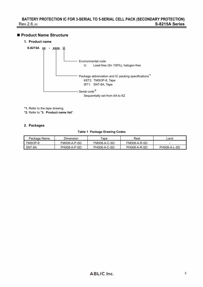
Product Name Structure 1. Product name
S-8215A xx - xxxx U
Package abbreviation and IC packing specifications*1 K8T2: TMSOP-8, Tape
I8T1: SNT-8A, Tape
Serial code*2 Sequentially set from AA to AZ
Environmental code U: Lead-free (Sn 100%), halogen-free
*1. Refer to the tape drawing. *2. Refer to "3. Product name list".
2. Packages
Table 1 Package Drawing Codes
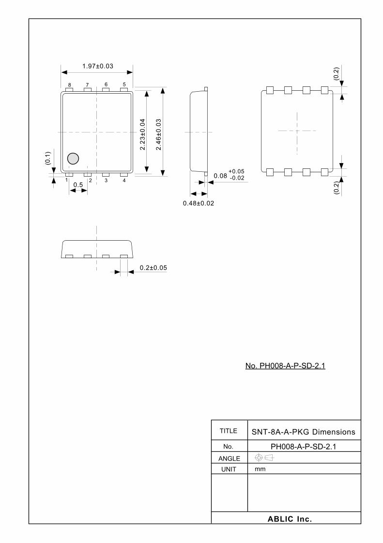
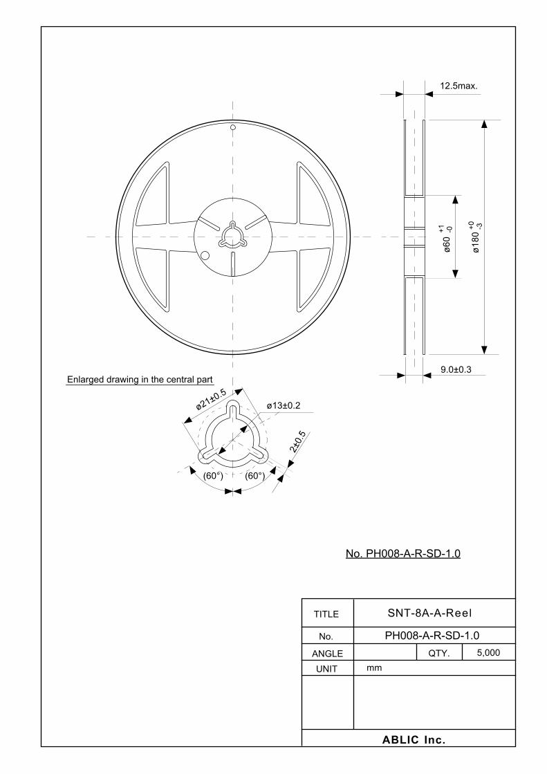
Package Name Dimension Tape Reel Land TMSOP-8 FM008-A-P-SD FM008-A-C-SD FM008-A-R-SD − SNT-8A PH008-A-P-SD PH008-A-C-SD PH008-A-R-SD PH008-A-L-SD

BATTERY PROTECTION IC FOR 3-SERIAL TO 5-SERIAL CELL PACK (SECONDARY PROTECTION) S-8215A Series Rev.2.6_00
4
3. Product name list 3. 1 TMSOP-8
Table 2
Product Name
Overcharge Detection Voltage
[VCU]
Overcharge Hysteresis
Voltage [VHC]
Overcharge Detection
Delay Time [tCU]
Output Form Output Logic
S-8215AAA-K8T2U 4.300 V −0.300 V 4.0 s CMOS output Active "H" S-8215AAB-K8T2U 4.275 V −0.050 V 2.0 s Nch open-drain output Active "L" S-8215AAC-K8T2U 4.150 V −0.250 V 1.0 s CMOS output Active "H" S-8215AAD-K8T2U 4.350 V −0.250 V 2.0 s CMOS output Active "H" S-8215AAE-K8T2U 4.325 V −0.050 V 1.0 s Nch open-drain output Active "L" S-8215AAF-K8T2U 4.220 V −0.100 V 1.0 s CMOS output Active "H" S-8215AAH-K8T2U 4.325 V −0.300 V 1.0 s Nch open-drain output Active "L" S-8215AAI-K8T2U 4.250 V −0.250 V 1.0 s CMOS output Active "H" S-8215AAJ-K8T2U 4.400 V −0.100 V 2.0 s CMOS output Active "H" S-8215AAK-K8T2U 4.150 V −0.050 V 2.0 s Nch open-drain output Active "L" S-8215AAL-K8T2U 4.150 V −0.500 V 2.0 s Nch open-drain output Active "L" S-8215AAM-K8T2U 4.150 V −0.050 V 2.0 s CMOS output Active "L" S-8215AAN-K8T2U 4.150 V −0.500 V 2.0 s CMOS output Active "L" S-8215AAO-K8T2U 4.350 V −0.250 V 4.0 s CMOS output Active "H" S-8215AAP-K8T2U 4.275 V −0.500 V 1.0 s CMOS output Active "H" S-8215AAQ-K8T2U 4.275 V −0.050 V 1.0 s CMOS output Active "H" S-8215AAR-K8T2U 4.500 V −0.100 V 4.0 s CMOS output Active "H" S-8215AAS-K8T2U 4.275 V −0.200 V 2.0 s CMOS output Active "L" S-8215AAT-K8T2U 4.275 V −0.050 V 2.0 s CMOS output Active "L" S-8215AAU-K8T2U 3.750 V −0.100 V 1.0 s CMOS output Active "H" S-8215AAV-K8T2U 4.300 V −0.300 V 1.0 s CMOS output Active "H" S-8215AAW-K8T2U 4.325 V −0.050 V 8.0 s CMOS output Active "H" S-8215AAX-K8T2U 4.325 V −0.300 V 8.0 s CMOS output Active "H" S-8215AAY-K8T2U 4.325 V −0.400 V 8.0 s CMOS output Active "H" S-8215AAZ-K8T2U 4.275 V −0.050 V 1.0 s Nch open-drain output Active "L" Remark Please contact our sales office for products other than the above.
3. 2 SNT-8A Table 3
Product Name
Overcharge Detection Voltage
[VCU]
Overcharge Hysteresis
Voltage [VHC]
Overcharge Detection
Delay Time [tCU]
Output Form Output Logic
S-8215AAA-I8T1U 4.300 V −0.300 V 4.0 s CMOS output Active "H" S-8215AAG-I8T1U 4.220 V −0.050 V 1.0 s CMOS output Active "H" S-8215AAV-I8T1U 4.300 V −0.300 V 1.0 s CMOS output Active "H" Remark Please contact our sales office for products other than the above.

BATTERY PROTECTION IC FOR 3-SERIAL TO 5-SERIAL CELL PACK (SECONDARY PROTECTION) Rev.2.6_00 S-8215A Series
5
Pin Configurations
1. TMSOP-8
765
8234
1
Top view
Figure 2
Table 4 Pin No. Symbol Description
1 VDD Input pin for positive power supply 2 VC1 Positive voltage connection pin of battery 1
3 VC2 Negative voltage connection pin of battery 1 Positive voltage connection pin of battery 2
4 VC3 Negative voltage connection pin of battery 2 Positive voltage connection pin of battery 3
5 VC4 Negative voltage connection pin of battery 3 Positive voltage connection pin of battery 4
6 VC5 Negative voltage connection pin of battery 4 Positive voltage connection pin of battery 5
7 VSS Input pin for negative power supply Negative voltage connection pin of battery 5
8 CO FET gate connection pin for charge control
2. SNT-8A
765
8234
1
Top view
Figure 3
Table 5 Pin No. Symbol Description
1 VDD Input pin for positive power supply 2 VC1 Positive voltage connection pin of battery 1
3 VC2 Negative voltage connection pin of battery 1 Positive voltage connection pin of battery 2
4 VC3 Negative voltage connection pin of battery 2 Positive voltage connection pin of battery 3
5 VC4 Negative voltage connection pin of battery 3 Positive voltage connection pin of battery 4
6 VC5 Negative voltage connection pin of battery 4 Positive voltage connection pin of battery 5
7 VSS Input pin for negative power supply Negative voltage connection pin of battery 5
8 CO FET gate connection pin for charge control

BATTERY PROTECTION IC FOR 3-SERIAL TO 5-SERIAL CELL PACK (SECONDARY PROTECTION) S-8215A Series Rev.2.6_00
6
Absolute Maximum Ratings
Table 6 (Ta = +25°C unless otherwise specified)
Item Symbol Applied Pin Absolute Maximum Rating Unit Input voltage between VDD pin and VSS pin VDS VDD VSS − 0.3 to VSS + 28 V Input pin voltage VIN VC1, VC2, VC3, VC4, VC5 VSS − 0.3 to VDD + 0.3 V
CO pin output voltage
CMOS output product VCO CO
VSS − 0.3 to VDD + 0.3 V Nch open-drain output product VSS − 0.3 to VSS + 28 V Pch open-drain output product VDD − 28 to VDD + 0.3 V
Power dissipation
TMSOP-8 PD −
650*1 mW SNT-8A 450*1 mW
Operation ambient temperature Topr − −40 to +85 °C Storage temperature Tstg − −40 to +125 °C *1. When mounted on board
[Mounted board] (1) Board size: 114.3 mm × 76.2 mm × t1.6 mm (2) Name: JEDEC STANDARD51-7
Caution The absolute maximum ratings are rated values exceeding which the product could suffer physical damage. These values must therefore not be exceeded under any conditions.
0 50 100 150
800
0
Pow
er D
issi
patio
n (P
D) [
mW
]
Ambient Temperature (Ta) [°C]
TMSOP-8
400
600
200
SNT-8A
Figure 4 Power Dissipation of Package (When Mounted on Board)

BATTERY PROTECTION IC FOR 3-SERIAL TO 5-SERIAL CELL PACK (SECONDARY PROTECTION) Rev.2.6_00 S-8215A Series
7
Electrical Characteristics Table 7
(Ta = +25°C unless otherwise specified) Item Symbol Condition Min. Typ. Max. Unit Test
Circuit Detection Voltage
Overcharge detection voltage n (n = 1, 2, 3, 4, 5) VCUn
− VCU − 0.025 VCU VCU
+ 0.025 V 1
Ta = −5°C to +55°C*1 VCU − 0.030 VCU VCU
+ 0.030 V 1
Overcharge hysteresis voltage n (n = 1, 2, 3, 4, 5) VHCn
−550 mV ≤ VHC ≤ −300 mV VHC × 0.8 VHC VHC × 1.2 V 1
−250 mV ≤ VHC ≤ −100 mV VHC − 0.050 VHC VHC
+ 0.050 V 1
VHC = −50 mV, 0 mV VHC − 0.025 VHC VHC
+ 0.025 V 1
Input Voltage Operation voltage between VDD pin and VSS pin VDSOP − 3.6 − 26 V −
Input Current Current consumption during operation IOPE V1 = V2 = V3 = V4 = V5 = VCU − 1.0 V − 1.6 3.0 μA 3
Current consumption during overdischarge IOPED V1 = V2 = V3 = V4 = V5 = 2.3 V − 0.8 1.7 μA 3
VC1 pin current IVC1 V1 = V2 = V3 = V4 = V5 = VCU − 1.0 V − 0.2 0.4 μA 4 VCn pin current (n = 2, 3, 4, 5) IVCn V1 = V2 = V3 = V4 = V5 = VCU − 1.0 V −0.3 0 0.3 μA 4
Output Current (CMOS Output Product) CO pin sink current ICOL − 0.4 − − mA 5 CO pin source current ICOH − 20 − − μA 5 Output Current (Nch Open-drain Output Product) CO pin sink current ICOL − 0.4 − − mA 5 CO pin leakage current "L" ICOLL − − − 0.1 μA 5 Output Current (Pch Open-drain Output Product) CO pin source current ICOH − 20 − − μA 5 CO pin leakage current "H" ICOLH − − − 0.1 μA 5 Delay Time Overcharge detection delay time tCU − tCU × 0.8 tCU tCU × 1.2 s 1
Overcharge timer reset delay time tTR − 6 12 20 ms 1
Transition time to test mode tTST − − − 80 ms 2 *1. Since products are not screened at high and low temperature, the specification for this temperature range is guaranteed
by design, not tested in production.
BATTERY PROTECTION IC FOR 3-SERIAL TO 5-SERIAL CELL PACK (SECONDARY PROTECTION) S-8215A Series Rev.2.6_00
8
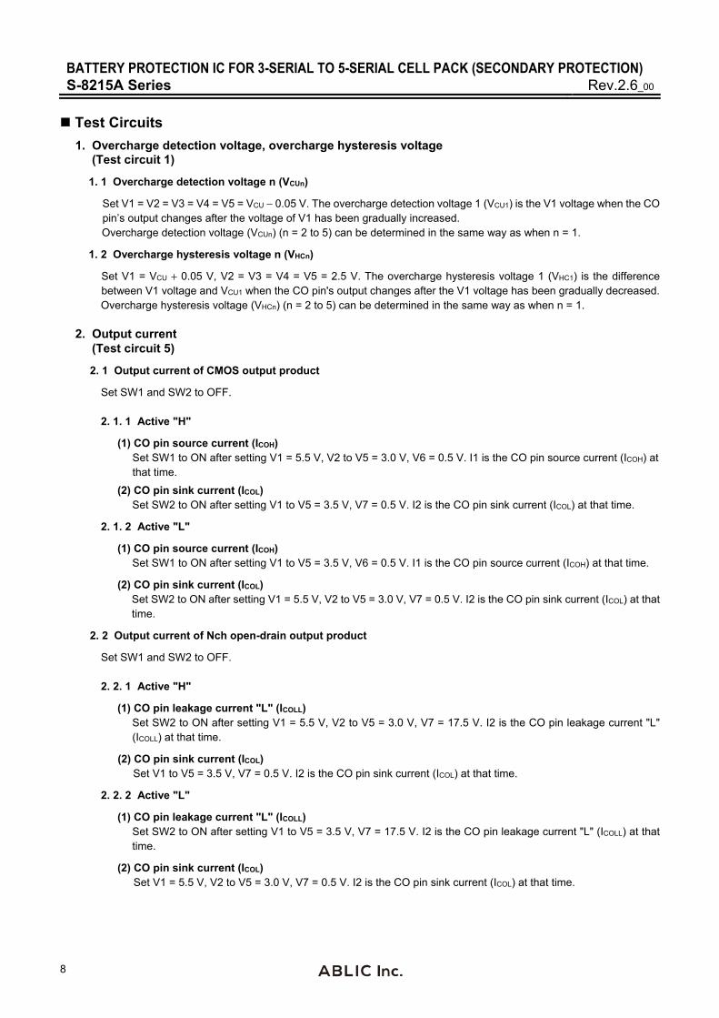
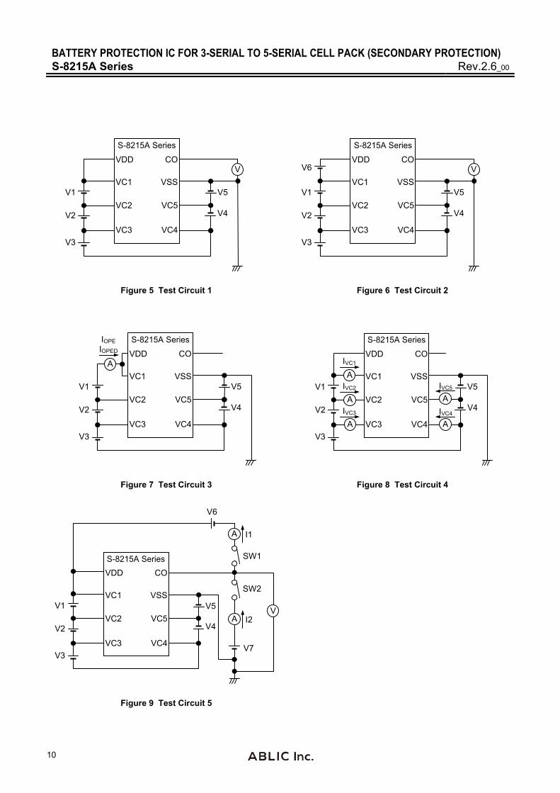
Test Circuits 1. Overcharge detection voltage, overcharge hysteresis voltage
(Test circuit 1)
1. 1 Overcharge detection voltage n (VCUn)
Set V1 = V2 = V3 = V4 = V5 = VCU − 0.05 V. The overcharge detection voltage 1 (VCU1) is the V1 voltage when the CO pin’s output changes after the voltage of V1 has been gradually increased. Overcharge detection voltage (VCUn) (n = 2 to 5) can be determined in the same way as when n = 1.
1. 2 Overcharge hysteresis voltage n (VHCn)
Set V1 = VCU + 0.05 V, V2 = V3 = V4 = V5 = 2.5 V. The overcharge hysteresis voltage 1 (VHC1) is the difference between V1 voltage and VCU1 when the CO pin's output changes after the V1 voltage has been gradually decreased. Overcharge hysteresis voltage (VHCn) (n = 2 to 5) can be determined in the same way as when n = 1.
2. Output current
(Test circuit 5)
2. 1 Output current of CMOS output product
Set SW1 and SW2 to OFF. 2. 1. 1 Active "H"
(1) CO pin source current (ICOH) Set SW1 to ON after setting V1 = 5.5 V, V2 to V5 = 3.0 V, V6 = 0.5 V. I1 is the CO pin source current (ICOH) at that time.
(2) CO pin sink current (ICOL) Set SW2 to ON after setting V1 to V5 = 3.5 V, V7 = 0.5 V. I2 is the CO pin sink current (ICOL) at that time.
2. 1. 2 Active "L"
(1) CO pin source current (ICOH) Set SW1 to ON after setting V1 to V5 = 3.5 V, V6 = 0.5 V. I1 is the CO pin source current (ICOH) at that time.
(2) CO pin sink current (ICOL) Set SW2 to ON after setting V1 = 5.5 V, V2 to V5 = 3.0 V, V7 = 0.5 V. I2 is the CO pin sink current (ICOL) at that time.
2. 2 Output current of Nch open-drain output product
Set SW1 and SW2 to OFF. 2. 2. 1 Active "H"
(1) CO pin leakage current "L" (ICOLL) Set SW2 to ON after setting V1 = 5.5 V, V2 to V5 = 3.0 V, V7 = 17.5 V. I2 is the CO pin leakage current "L" (ICOLL) at that time.
(2) CO pin sink current (ICOL) Set V1 to V5 = 3.5 V, V7 = 0.5 V. I2 is the CO pin sink current (ICOL) at that time.
2. 2. 2 Active "L"
(1) CO pin leakage current "L" (ICOLL) Set SW2 to ON after setting V1 to V5 = 3.5 V, V7 = 17.5 V. I2 is the CO pin leakage current "L" (ICOLL) at that time.
(2) CO pin sink current (ICOL) Set V1 = 5.5 V, V2 to V5 = 3.0 V, V7 = 0.5 V. I2 is the CO pin sink current (ICOL) at that time.
BATTERY PROTECTION IC FOR 3-SERIAL TO 5-SERIAL CELL PACK (SECONDARY PROTECTION) Rev.2.6_00 S-8215A Series
9
2. 3 Output current of Pch open-drain output product
Set SW1 and SW2 to OFF.
2. 3. 1 Active "H"
(1) CO pin source current (ICOH) Set SW1 to ON after setting V1 = 5.5 V, V2 to V5 = 3.0 V, V6 = 0.5 V. I1 is the CO pin source current (ICOH) at that time.
(2) CO pin leakage current "H" (ICOLH) Set V1 to V5 = 3.5 V, V6 = 17.5 V. I1 is the CO pin leakage current "H" (ICOLH) at that time.
2. 3. 2 Active "L"
(1) CO pin source current (ICOH) Set SW1 to ON after setting V1 to V5 = 3.5 V, V6 = 0.5 V. I1 is the CO pin source current (ICOH) at that time.
(2) CO pin leakage current "H" (ICOLH) Set V1 = 5.5 V, V2 to V5 = 3.0 V, V6 = 17.5 V. I1 is the CO pin leakage current "H" (ICOLH) at that time.
3. Overcharge detection delay time (tCU) (Test circuit 1)
Increase V1 up to 5.0 V after setting V1 = V2 = V3 = V4 = V5 = 3.5 V. The overcharge detection delay time (tCU) is the time period until the CO pin output changes.
4. Overcharge timer reset delay time (tTR)
(Test circuit 1)
Increase V1 up to 5.0 V (first rise), and decrease V1 down to 3.5 V within tCU after setting V1 = V2 = V3 = V4 = V5 = 3.5 V. After that, increase V1 up to 5.0 V again (second rise), and detect the time period till the CO pin output changes. When the period from when V1 has fallen to the second rise is short, CO pin output changes after tCU has elapsed since the first rise. If the period is gradually made longer, CO pin output changes after tCU has elapsed since the second rise. The overcharge timer reset delay time (tTR) is the period from V1 fall till the second rise at that time.
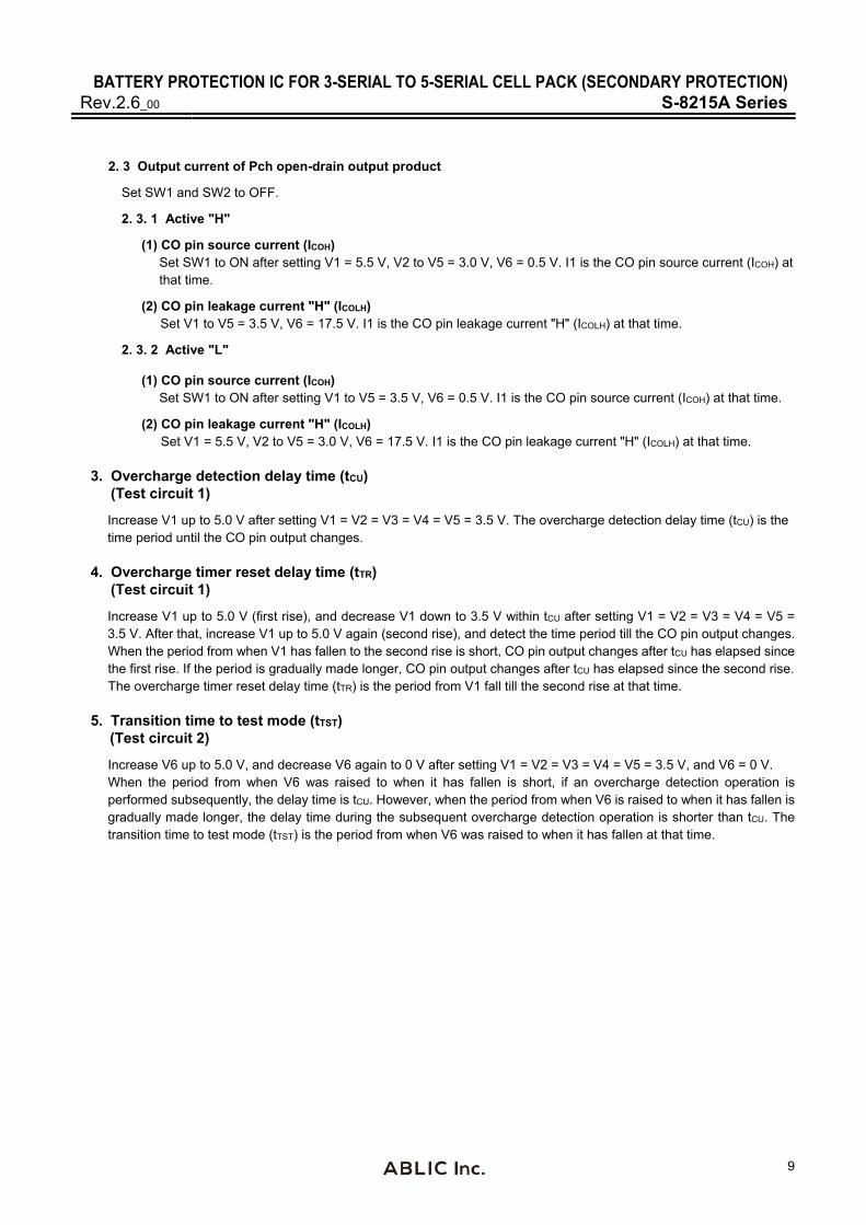
5. Transition time to test mode (tTST) (Test circuit 2)
Increase V6 up to 5.0 V, and decrease V6 again to 0 V after setting V1 = V2 = V3 = V4 = V5 = 3.5 V, and V6 = 0 V. When the period from when V6 was raised to when it has fallen is short, if an overcharge detection operation is performed subsequently, the delay time is tCU. However, when the period from when V6 is raised to when it has fallen is gradually made longer, the delay time during the subsequent overcharge detection operation is shorter than tCU. The transition time to test mode (tTST) is the period from when V6 was raised to when it has fallen at that time.
BATTERY PROTECTION IC FOR 3-SERIAL TO 5-SERIAL CELL PACK (SECONDARY PROTECTION) S-8215A Series Rev.2.6_00
10
V5 V1
V2
V3
V4
S-8215A Series VDD
VC1
VC2
VC3
CO
VSS
VC5
VC4
V
V5 V1
V2
V3
V4
S-8215A Series VDD
VC1
VC2
VC3
CO
VSS
VC5
VC4
V V6
Figure 5 Test Circuit 1 Figure 6 Test Circuit 2
V5 V1
V2
V3
V4
VDD
VC1
VC2
VC3
CO
VSS
VC5
VC4
A
S-8215A Series IOPED IOPE
V1
V2
V3
V4
VDD
VC1
VC2
VC3
CO
VSS
VC5
VC4
A IVC1
A
A A
A
S-8215A Series
V5 IVC2
IVC3 IVC4
IVC5
Figure 7 Test Circuit 3 Figure 8 Test Circuit 4
V6
V1
V2
V3
V4
SW2
SW1
VDD
VC1
VC2
VC3
CO
VSS
VC5
VC4 V7
V
A I1
A I2
S-8215A Series
V5
Figure 9 Test Circuit 5
BATTERY PROTECTION IC FOR 3-SERIAL TO 5-SERIAL CELL PACK (SECONDARY PROTECTION) Rev.2.6_00 S-8215A Series
11
Operation Remark Refer to " Battery Protection IC Connection Examples".
1. Normal status
If the voltage of each of the batteries is lower than "the overcharge detection voltage n (VCUn) + the overcharge hysteresis voltage n (VHCn)", the CO pin output changes to "L" (Active "H") or "H" (Active L"). This is called normal status.
2. Overcharge status
When the voltage of one of the batteries exceeds VCUn during charging under normal status and the status is retained for the overcharge detection delay time (tCU) or longer, the CO pin output changes. This is called overcharge status. Connecting FET to the CO pin provides charge control and a second protection. If the voltage of each of the batteries is lower than VCUn + VHCn and the status is retained for 2.0 ms typ. or longer, the S-8215A Series returns to normal status.
3. Overcharge timer reset function
When an overcharge release noise that forces the voltage of one of the batteries temporarily below VCUn is input during tCU from when VCUn is exceeded to when charging is stopped, tCU is continuously counted if the time the overcharge release noise persists is shorter than the overcharge timer reset delay time (tTR). Under the same conditions, if the time the overcharge release noise persists is tTR or longer, counting of tCU is reset once. After that, when VCUn has been exceeded, counting tCU resumes.
BATTERY PROTECTION IC FOR 3-SERIAL TO 5-SERIAL CELL PACK (SECONDARY PROTECTION) S-8215A Series Rev.2.6_00
12
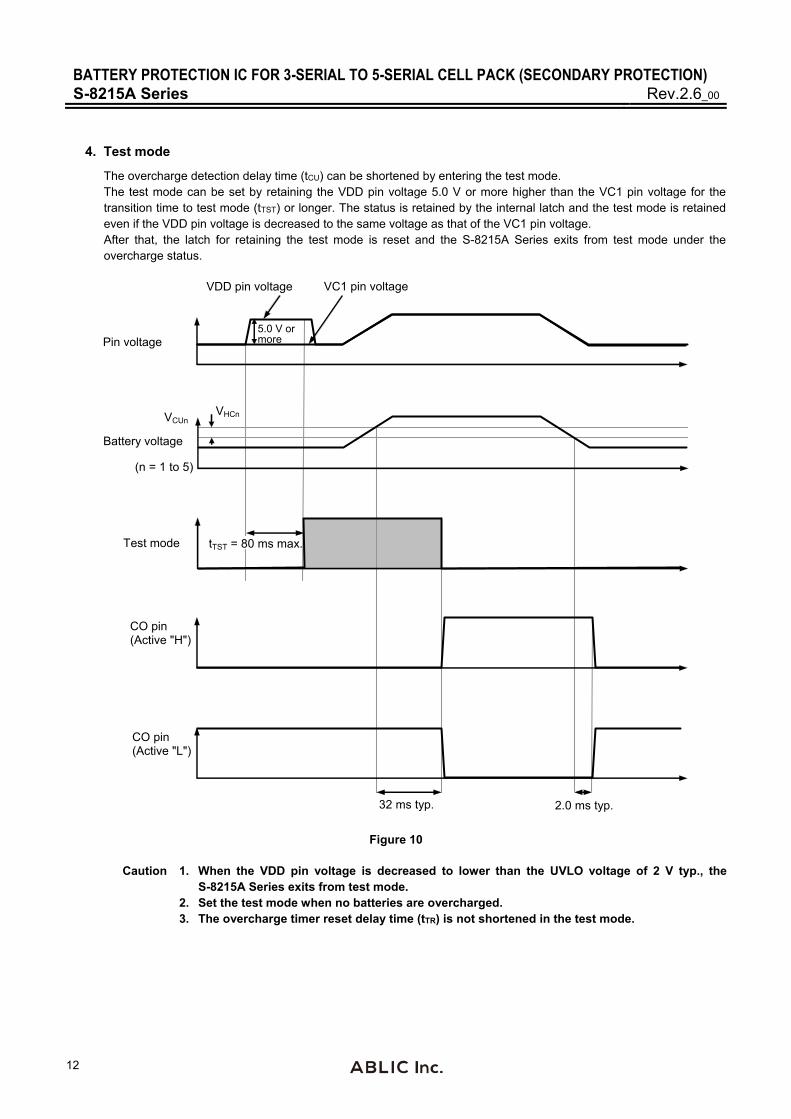
4. Test mode
The overcharge detection delay time (tCU) can be shortened by entering the test mode. The test mode can be set by retaining the VDD pin voltage 5.0 V or more higher than the VC1 pin voltage for the transition time to test mode (tTST) or longer. The status is retained by the internal latch and the test mode is retained even if the VDD pin voltage is decreased to the same voltage as that of the VC1 pin voltage. After that, the latch for retaining the test mode is reset and the S-8215A Series exits from test mode under the overcharge status.
VCUn
Pin voltage
CO pin (Active "H")
Test mode
VDD pin voltage
5.0 V or more
Battery voltage
VHCn
tTST = 80 ms max.
VC1 pin voltage
(n = 1 to 5)
32 ms typ.
CO pin (Active "L")
2.0 ms typ.
Figure 10
Caution 1. When the VDD pin voltage is decreased to lower than the UVLO voltage of 2 V typ., the
S-8215A Series exits from test mode. 2. Set the test mode when no batteries are overcharged. 3. The overcharge timer reset delay time (tTR) is not shortened in the test mode.

BATTERY PROTECTION IC FOR 3-SERIAL TO 5-SERIAL CELL PACK (SECONDARY PROTECTION) Rev.2.6_00 S-8215A Series
13
Timing Charts
1. Overcharge detection operation
VCUn
Battery voltage
CO pin (Active "H")
VHCn
(n = 1 to 5)
tCU
tCU or shorter
tTR or shorter tTR or longer
CO pin (Active "L")
2.0 ms typ.
Figure 11

BATTERY PROTECTION IC FOR 3-SERIAL TO 5-SERIAL CELL PACK (SECONDARY PROTECTION) S-8215A Series Rev.2.6_00
14
2. Overcharge timer reset operation
VCUn
Battery voltage
CO pin (Active "H")
tCU
VHCn
tCU or shorter
tTR
tTR or shorter
Timer reset
tTR or shorter tTR or longer
(n = 1 to 5)
CO pin (Active "L")
Figure 12
BATTERY PROTECTION IC FOR 3-SERIAL TO 5-SERIAL CELL PACK (SECONDARY PROTECTION) Rev.2.6_00 S-8215A Series
15
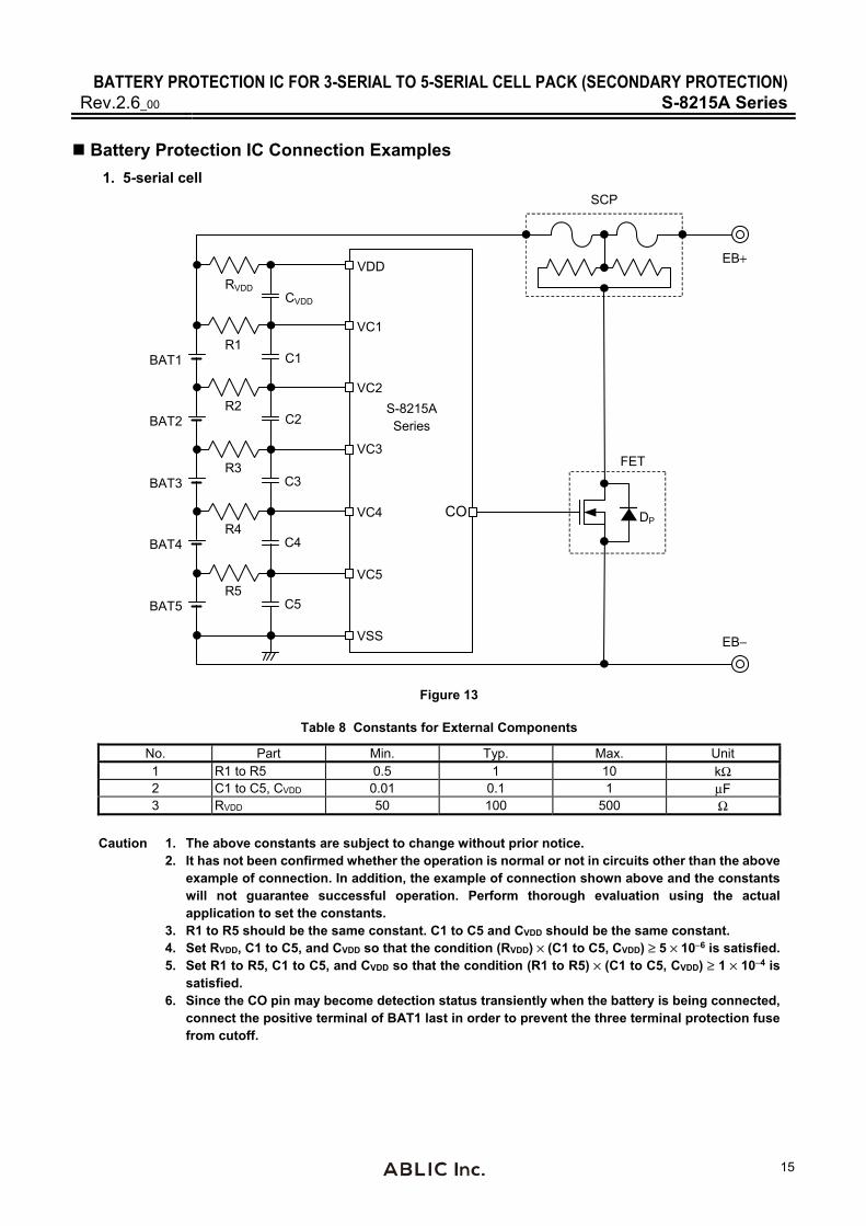
Battery Protection IC Connection Examples 1. 5-serial cell
SCP
EB−
C1
C2
C3
C4
EB+
R1
R2
R3
R4
BAT1
BAT2
BAT3
BAT4
FET
CVDD RVDD
DP
VC5
VC1
VC2
VC3
VC4 CO
VDD
S-8215A Series
VSS
C5 R5
BAT5
Figure 13
Table 8 Constants for External Components
No. Part Min. Typ. Max. Unit 1 R1 to R5 0.5 1 10 kΩ 2 C1 to C5, CVDD 0.01 0.1 1 μF 3 RVDD 50 100 500 Ω
Caution 1. The above constants are subject to change without prior notice. 2. It has not been confirmed whether the operation is normal or not in circuits other than the above
example of connection. In addition, the example of connection shown above and the constants will not guarantee successful operation. Perform thorough evaluation using the actual application to set the constants.
3. R1 to R5 should be the same constant. C1 to C5 and CVDD should be the same constant. 4. Set RVDD, C1 to C5, and CVDD so that the condition (RVDD) × (C1 to C5, CVDD) ≥ 5 × 10⁻⁶ is satisfied. 5. Set R1 to R5, C1 to C5, and CVDD so that the condition (R1 to R5) × (C1 to C5, CVDD) ≥ 1 × 10⁻⁴ is
satisfied. 6. Since the CO pin may become detection status transiently when the battery is being connected,
connect the positive terminal of BAT1 last in order to prevent the three terminal protection fuse from cutoff.

BATTERY PROTECTION IC FOR 3-SERIAL TO 5-SERIAL CELL PACK (SECONDARY PROTECTION) S-8215A Series Rev.2.6_00
16
2. 4-serial cell
SCP
EB−
C1
C2
C3
C4
EB+
R1
R2
R3
R4
BAT1
BAT2
BAT3
BAT4
FET
CVDD RVDD
DP
VC5
VC1
VC2
VC3
VC4 CO
VDD
S-8215A Series
VSS
Figure 14
Table 9 Constants for External Components
No. Part Min. Typ. Max. Unit 1 R1 to R4 0.5 1 10 kΩ 2 C1 to C4, CVDD 0.01 0.1 1 μF 3 RVDD 50 100 500 Ω
Caution 1. The above constants are subject to change without prior notice. 2. It has not been confirmed whether the operation is normal or not in circuits other than the above
example of connection. In addition, the example of connection shown above and the constants will not guarantee successful operation. Perform thorough evaluation using the actual application to set the constants.
3. R1 to R4 should be the same constant. C1 to C4 and CVDD should be the same constant. 4. Set RVDD, C1 to C4, and CVDD so that the condition (RVDD) × (C1 to C4, CVDD) ≥ 5 × 10⁻⁶ is satisfied. 5. Set R1 to R4, C1 to C4, and CVDD so that the condition (R1 to R4) × (C1 to C4, CVDD) ≥ 1 × 10⁻⁴ is
satisfied. 6. Since the CO pin may become detection status transiently when the battery is being connected,
connect the positive terminal of BAT1 last in order to prevent the three terminal protection fuse from cutoff.
BATTERY PROTECTION IC FOR 3-SERIAL TO 5-SERIAL CELL PACK (SECONDARY PROTECTION) Rev.2.6_00 S-8215A Series
17
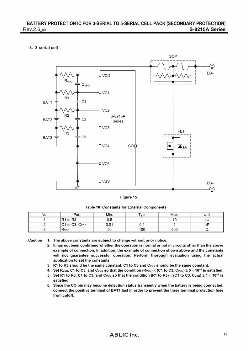
3. 3-serial cell
SCP
EB−
C1
C2
C3
EB+
R1
R2
R3
BAT1
BAT2
BAT3 FET
CVDD RVDD
DP
VC5
VC1
VC2
VC3
VC4 CO
VDD
S-8215A Series
VSS
Figure 15
Table 10 Constants for External Components
No. Part Min. Typ. Max. Unit 1 R1 to R3 0.5 1 10 kΩ 2 C1 to C3, CVDD 0.01 0.1 1 μF 3 RVDD 50 100 500 Ω
Caution 1. The above constants are subject to change without prior notice. 2. It has not been confirmed whether the operation is normal or not in circuits other than the above
example of connection. In addition, the example of connection shown above and the constants will not guarantee successful operation. Perform thorough evaluation using the actual application to set the constants.
3. R1 to R3 should be the same constant. C1 to C3 and CVDD should be the same constant. 4. Set RVDD, C1 to C3, and CVDD so that the condition (RVDD) × (C1 to C3, CVDD) ≥ 5 × 10⁻⁶ is satisfied. 5. Set R1 to R3, C1 to C3, and CVDD so that the condition (R1 to R3) × (C1 to C3, CVDD) ≥ 1 × 10⁻⁴ is
satisfied. 6. Since the CO pin may become detection status transiently when the battery is being connected,
connect the positive terminal of BAT1 last in order to prevent the three terminal protection fuse from cutoff.
BATTERY PROTECTION IC FOR 3-SERIAL TO 5-SERIAL CELL PACK (SECONDARY PROTECTION) S-8215A Series Rev.2.6_00
18
[For SCP, contact]
Global Sales & Marketing Division, Dexerials Corporation Gate City Osaki East Tower 8F, 1-11-2 Osaki, Shinagawa-ku, Tokyo, 141-0032, Japan TEL +81-3-5435-3946 Contact Us: http://www.dexerials.jp/en/
Precautions
• Do not connect batteries charged with VCUn + VHCn or higher. If the connected batteries include a battery charged with VCUn + VHCn or higher, the S-8215A series may become overcharge status after all pins are connected.
• In some application circuits, even if an overcharged battery is not included, the order of connecting batteries may be restricted to prevent transient output of CO detection pulses when the batteries are connected. Perform thorough evaluation with the actual application circuit.
• Before the battery connection, short-circuit the battery side pins RVDD and R1, shown in the figure in " Battery Protection IC Connection Examples".
• The application conditions for the input voltage, output voltage, and load current should not exceed the package power dissipation.
• Do not apply to this IC an electrostatic discharge that exceeds the performance ratings of the built-in electrostatic protection circuit.
• ABLIC Inc. claims no responsibility for any disputes arising out of or in connection with any infringement of patents owned by a third party by products including this IC.
BATTERY PROTECTION IC FOR 3-SERIAL TO 5-SERIAL CELL PACK (SECONDARY PROTECTION) Rev.2.6_00 S-8215A Series
19
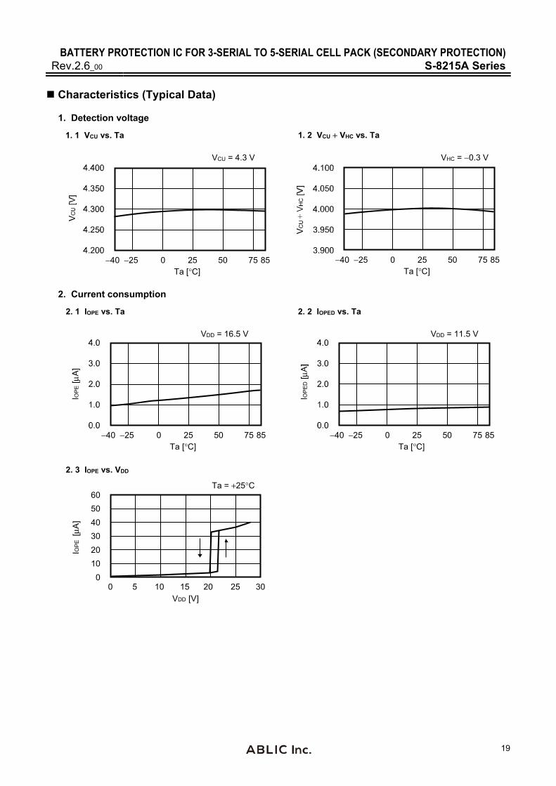
Characteristics (Typical Data)
1. Detection voltage
1. 1 VCU vs. Ta
VCU = 4.3 V
1. 2 VCU + VHC vs. Ta
VHC = −0.3 V
−40 −25 25 50 75 85Ta [°C]
0
+
−40 −25 25 50 75 85Ta [°C]
0
2. Current consumption
2. 1 IOPE vs. Ta
VDD = 16.5 V
2. 2 IOPED vs. Ta
VDD = 11.5 V
μ
−40 −25 25 50 75 85Ta [°C]
0
μ
−40 −25 25 50 75 85Ta [°C]
0
2. 3 IOPE vs. VDD
Ta = +25°C
010203040
6050
VDD [V]
IOPE
[μA]
0 105 15 20 25 30

BATTERY PROTECTION IC FOR 3-SERIAL TO 5-SERIAL CELL PACK (SECONDARY PROTECTION) S-8215A Series Rev.2.6_00
20
3. Delay time
3. 1 tCU vs. Ta
VDD = 19 V
−40 −25 25 50 75 85Ta [°C]
0
4. Output current
4. 1 ICOL vs. VDD
Ta = +25°C
4. 2 ICOH vs. VDD
Ta = +25°C
0.0
2.5
5.0
7.5
10.0
VDD [V]
ICO
L [m
A]
0 105 15 20 25 30
0
250
500
750
1000
VDD [V]
ICO
H [μ
A]
0 105 15 20 25 30

BATTERY PROTECTION IC FOR 3-SERIAL TO 5-SERIAL CELL PACK (SECONDARY PROTECTION) Rev.2.6_00 S-8215A Series
21
Marking Specifications
1. TMSOP-8 Top view
1 432
8 567
(1) (2) (3) (4)
(5) (6) (7) (8)
(1): Blank (2) to (4): Product code (Refer to Product name vs. Product code) (5): Blank (6) to (8): Lot number
Product name vs. Product code
Product Name Product Code
(2) (3) (4) S-8215AAA-K8T2U V 6 A S-8215AAB-K8T2U V 6 B S-8215AAC-K8T2U V 6 C S-8215AAD-K8T2U V 6 D S-8215AAE-K8T2U V 6 E S-8215AAF-K8T2U V 6 F S-8215AAH-K8T2U V 6 H S-8215AAI-K8T2U V 6 I S-8215AAJ-K8T2U V 6 J S-8215AAK-K8T2U V 6 K S-8215AAL-K8T2U V 6 L S-8215AAM-K8T2U V 6 M
Product Name Product Code
(2) (3) (4) S-8215AAN-K8T2U V 6 N S-8215AAO-K8T2U V 6 O S-8215AAP-K8T2U V 6 P S-8215AAQ-K8T2U V 6 Q S-8215AAR-K8T2U V 6 R S-8215AAS-K8T2U V 6 S S-8215AAT-K8T2U V 6 T S-8215AAU-K8T2U V 6 U S-8215AAV-K8T2U V 6 V S-8215AAW-K8T2U V 6 W S-8215AAX-K8T2U V 6 X S-8215AAY-K8T2U V 6 Y S-8215AAZ-K8T2U V 6 Z
2. SNT-8A
Top view
1 432
8 567
(1) (2) (3) (4)
(5) (6) (7) (8)
(9) (10) (11)
(1): Blank (2) to (4): Product code (Refer to Product name vs. Product code) (5), (6): Blank (7) to (11): Lot number
Product name vs. Product code
Product Name Product Code
(2) (3) (4) S-8215AAA-I8T1U V 6 A S-8215AAG-I8T1U V 6 G S-8215AAV-I8T1U V 6 V
���
�����
���
����
������ ��
�� �����
� �
�������
��������
��������
� �
��������������� !"��!"
����#��������������
#��������������
��
���
�����
���
����
������ ��
���������
��������
���������
���
���������
��������
���������
��������
��
� �
��������$%&& � & � �%'
# (�(�& )*��!
����#������$�������
#������$�������
+������
��
���
�����
���
����
������ ��
�����%,�
��������
-�.� �/���
0��120��12
������
�!3%&4 (�(&%5�!4��!�*6 �) !*&%3�'%&*
��������7 3
����#������7�������
#������7�������
��
���
�����
���
����
������ ��
�� ������
��������
���������
����
��
���������������� ���
�!�������������
�����!�������������
���
"���������� � � �
�#��

���
�����
���
����
������ ��
��
�!�����$�������
�������$%&& ��& � �%'�
�����!�����$�������
(��)�)�&�*+���
���������������
�������
,���"���
���
,����������������
��#������
���������
� ���
� �#�
���
�����
���
����
������ ��
�����%-�
������
,������
.#�/0 .#�/0
��1%&2�)�)&%3��2����+4��*��+&%1�'%&+
5�6�
�!�����7�������
��
�������7��1
�����!�����7�������
�8���

���
�����
���
����
������ ��
��
��������������%�)�7�*�����)%+���
�!�������������
������
����
����
����
�����!�������������
��� ��� ������� ������������������ ������������������� ���������� ����������������� ���������
������ ����������� ��������������� ���� ���������� ���������� ����������������� ��!!"���
�������������� ���������� ����������
"�#� �� ������������ ������$���������� �������� ������ �� ���������� ���
%�&����� ��'()��*������+���,��-����'������� ����
��� .�������������A���������+?'�0��� �.�� #����B����#���0
�
� !!"���
"
% ()�
����%?�%++��+����+��+4��1%�)�'%++�&��3�)+4�.�������������A���������+?'�0���������+�3�)���+4��1%�)�'%++�&��+��+4��*��+�&��=�+4��'%*:%2��.�� #����+�����#��0�
�
�
��
��� .�� #����B����#���0
.�������������A���������+?'�0

Disclaimers (Handling Precautions)
1. All the information described herein (product data, specifications, figures, tables, programs, algorithms and application circuit examples, etc.) is current as of publishing date of this document and is subject to change without notice.
2. The circuit examples and the usages described herein are for reference only, and do not guarantee the success of any specific mass-production design. ABLIC Inc. is not responsible for damages caused by the reasons other than the products described herein (hereinafter "the products") or infringement of third-party intellectual property right and any other right due to the use of the information described herein.
3. ABLIC Inc. is not responsible for damages caused by the incorrect information described herein.
4. Be careful to use the products within their specified ranges. Pay special attention to the absolute maximum ratings, operation voltage range and electrical characteristics, etc. ABLIC Inc. is not responsible for damages caused by failures and / or accidents, etc. that occur due to the use of the products outside their specified ranges.
5. When using the products, confirm their applications, and the laws and regulations of the region or country where they are used and verify suitability, safety and other factors for the intended use.
6. When exporting the products, comply with the Foreign Exchange and Foreign Trade Act and all other export-related laws, and follow the required procedures.
7. The products must not be used or provided (exported) for the purposes of the development of weapons of mass destruction or military use. ABLIC Inc. is not responsible for any provision (export) to those whose purpose is to develop, manufacture, use or store nuclear, biological or chemical weapons, missiles, or other military use.
8. The products are not designed to be used as part of any device or equipment that may affect the human body, human life, or assets (such as medical equipment, disaster prevention systems, security systems, combustion control systems, infrastructure control systems, vehicle equipment, traffic systems, in-vehicle equipment, aviation equipment, aerospace equipment, and nuclear-related equipment), excluding when specified for in-vehicle use or other uses. Do not apply the products to the above listed devices and equipments without prior written permission by ABLIC Inc. Especially, the products cannot be used for life support devices, devices implanted in the human body and devices that directly affect human life, etc. Prior consultation with our sales office is required when considering the above uses. ABLIC Inc. is not responsible for damages caused by unauthorized or unspecified use of our products.
9. Semiconductor products may fail or malfunction with some probability. The user of the products should therefore take responsibility to give thorough consideration to safety design including redundancy, fire spread prevention measures, and malfunction prevention to prevent accidents causing injury or death, fires and social damage, etc. that may ensue from the products' failure or malfunction. The entire system must be sufficiently evaluated and applied on customer's own responsibility.
10. The products are not designed to be radiation-proof. The necessary radiation measures should be taken in the product design by the customer depending on the intended use.
11. The products do not affect human health under normal use. However, they contain chemical substances and heavy metals and should therefore not be put in the mouth. The fracture surfaces of wafers and chips may be sharp. Be careful when handling these with the bare hands to prevent injuries, etc.
12. When disposing of the products, comply with the laws and ordinances of the country or region where they are used.
13. The information described herein contains copyright information and know-how of ABLIC Inc. The information described herein does not convey any license under any intellectual property rights or any other rights belonging to ABLIC Inc. or a third party. Reproduction or copying of the information from this document or any part of this document described herein for the purpose of disclosing it to a third-party without the express permission of ABLIC Inc. is strictly prohibited.
14. For more details on the information described herein, contact our sales office.
2.2-2018.06
www.ablic.com
Top Related