


Languages
Pages
Legal

Institute ofMicroelectronicSystems
9. Memory Elements and Dynamic Logic
2
Institute ofMicroelectronicSystems
9: Memory Elements & Dynamic Logic
RS Flipflop
The RS-flipflop is a bistable element with two inputs:
• Reset (R), resets the output Q to 0
• Set (S), sets the output Q to 1

3
Institute ofMicroelectronicSystems
9: Memory Elements & Dynamic Logic
RS-Flipflops
There are two ways to implement a RS-flipflop:
• based on NOR-gates: positive logic
• based on NAND-gates: negative logic
4
Institute ofMicroelectronicSystems
9: Memory Elements & Dynamic Logic
Clocked RS-Latch
To achieve a synchronous operation, we can add a clock signal
• Clock= 0: R and S have no influence upon the state of the circuit
• Clock= 1: R and S can change the state of the circuit
5
Institute ofMicroelectronicSystems
9: Memory Elements & Dynamic Logic
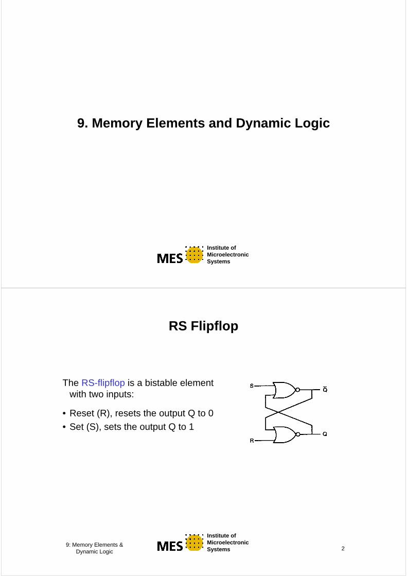
D-Latch
For storing data it is more convenient to have a data input. This is realized by using the data input as set signal and the inverted data input as reset signal.
• Clock= 0: Q unchanged
• Clock= 1: Q= D
6
Institute ofMicroelectronicSystems
9: Memory Elements & Dynamic Logic
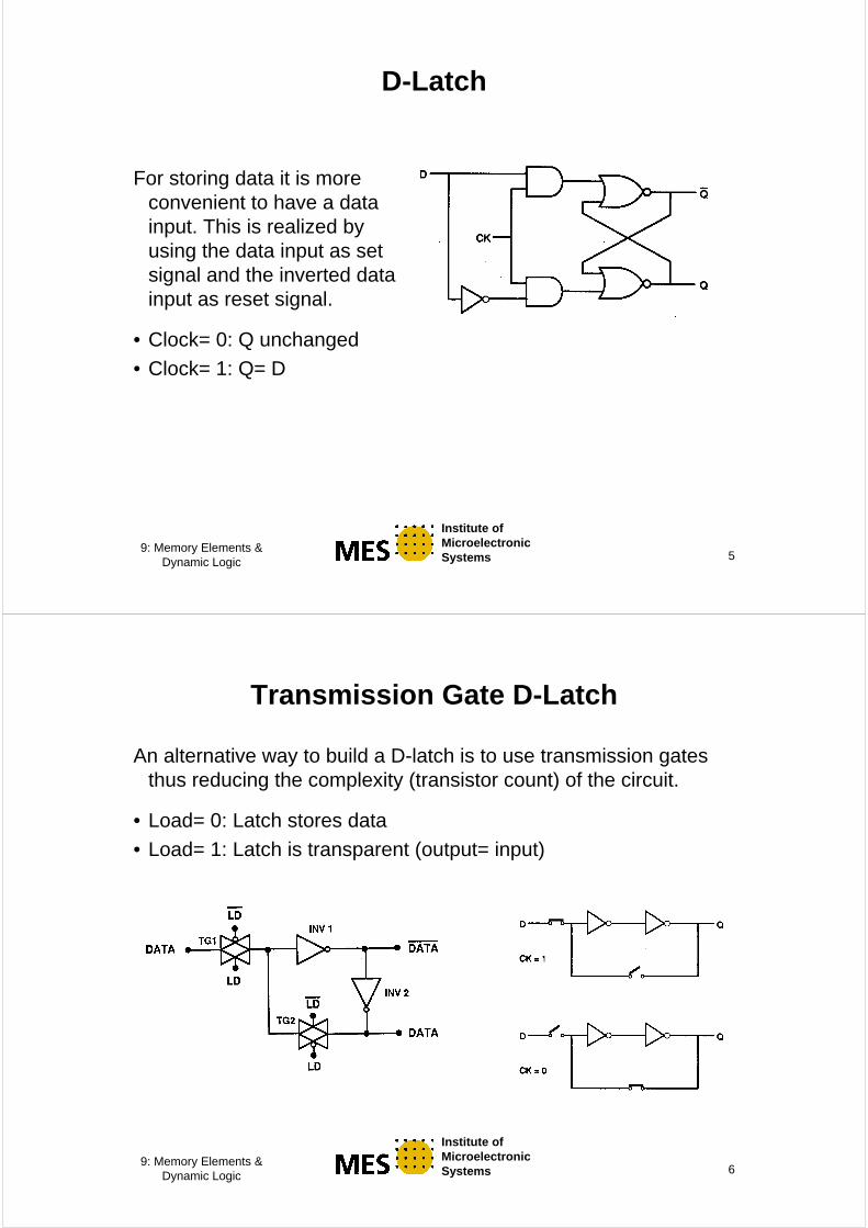
Transmission Gate D-Latch
An alternative way to build a D-latch is to use transmission gates thus reducing the complexity (transistor count) of the circuit.
• Load= 0: Latch stores data
• Load= 1: Latch is transparent (output= input)
7
Institute ofMicroelectronicSystems
9: Memory Elements & Dynamic Logic
Clocked JK-Latch
An other extension of a simple RS-flipflop is a JK-Latch
• J: enables/disables the low to high transition of the latch
• K: enables/disables the high to low transition of the latch
8
Institute ofMicroelectronicSystems
9: Memory Elements & Dynamic Logic
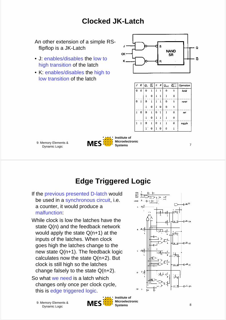
Edge Triggered Logic
If the previous presented D-latch would be used in a synchronous circuit, i.e. a counter, it would produce a malfunction:
While clock is low the latches have the state Q(n) and the feedback network would apply the state Q(n+1) at the inputs of the latches. When clock goes high the latches change to the new state Q(n+1). The feedback logic calculates now the state Q(n+2). But clock is still high so the latches change falsely to the state Q(n+2).
So what we need is a latch which changes only once per clock cycle, this is edge triggered logic.

9
Institute ofMicroelectronicSystems
9: Memory Elements & Dynamic Logic
Edge Triggered JK-Flipflop
A straight forward way to implement an edge-triggered JK-flipflop is to use a master-slave flipflop.
• Clock= 1: The master (left latch) is changeable, the slave (right latch) is locked and holds the output at the current state
• Clock= 0: The master is locked and the slave is changes its state if necessary
The output value is the state of the master at the falling edge of the clock signal
10
Institute ofMicroelectronicSystems
9: Memory Elements & Dynamic Logic
Edge Triggered TG D-Flipflop
Circuitry of an edge-triggered flipflop
• Clk= 0: First stage is loaded, second stage is locked and stores data
• Clk= 1: First stage is locked, second stage is loaded
With the rising edge (low to high transition) the new value is available a the output

11
Institute ofMicroelectronicSystems
9: Memory Elements & Dynamic Logic
Transmission Gate JK- Flipflop
It is also possible to build a JK-flipflop with transmission gates as a edge-triggered flipflop.
This achieves that the output state can only change at the rising edge of the clock signal
12
Institute ofMicroelectronicSystems
9: Memory Elements & Dynamic Logic
Dynamic D-Flipflop
Dynamic logic utilizes the parasitic capacitances of transistors and interconnect to store the current state. This reduces the transistor count but forbids a static operation. An application of dynamic circuits is the dynamic D-flipflop.
13
Institute ofMicroelectronicSystems
9: Memory Elements & Dynamic Logic
Dynamic Shift Register
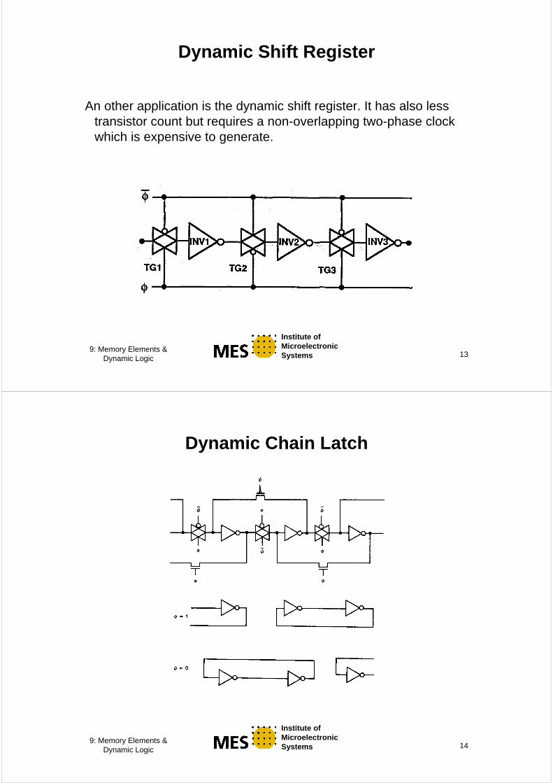
An other application is the dynamic shift register. It has also less transistor count but requires a non-overlapping two-phase clock which is expensive to generate.
14
Institute ofMicroelectronicSystems
9: Memory Elements & Dynamic Logic
Dynamic Chain Latch

15
Institute ofMicroelectronicSystems
9: Memory Elements & Dynamic Logic
Dynamic RAM
A special kind of memory is dynamic RAM. The major advantage is the low transistor count, DRAM requires only one transistor and one (small) capacitor per bit.
The first disadvantage is the destructive read. After reading a cell the red value must be written back to keep the data in the RAM.
The second disadvantage is the limited duration of storage. After some milliseconds the cell must be refreshed (read and written back).
16
Institute ofMicroelectronicSystems
9: Memory Elements & Dynamic Logic
Dynamic RAM
17
Institute ofMicroelectronicSystems
9: Memory Elements & Dynamic Logic
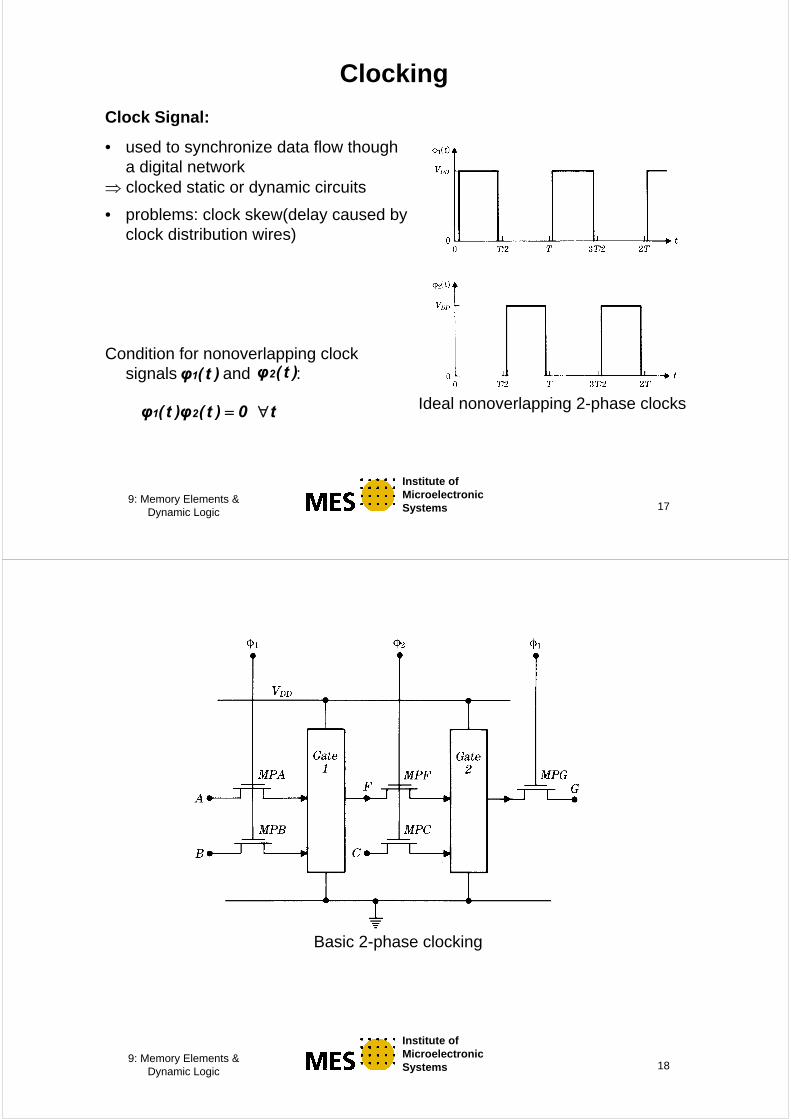
Clock Signal:
• used to synchronize data flow though a digital network
⇒ clocked static or dynamic circuits
• problems: clock skew(delay caused by clock distribution wires)
Condition for nonoverlapping clock signals and :)t(φ2
Clocking
Ideal nonoverlapping 2-phase clocks
)t(φ1
0)t(φ)t(φ 21 = t∀
18
Institute ofMicroelectronicSystems
9: Memory Elements & Dynamic Logic
Basic 2-phase clocking
19
Institute ofMicroelectronicSystems
9: Memory Elements & Dynamic Logic
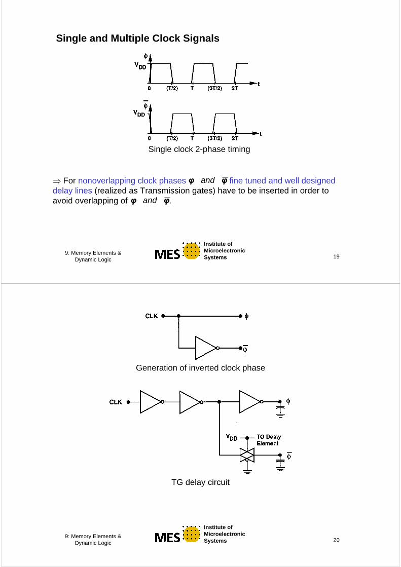
Single and Multiple Clock Signals
⇒ For nonoverlapping clock phases fine tuned and well designed delay lines (realized as Transmission gates) have to be inserted in order to avoid overlapping of .
φφ and
φφ and
Single clock 2-phase timing
20
Institute ofMicroelectronicSystems
9: Memory Elements & Dynamic Logic
Generation of inverted clock phase
TG delay circuit
21
Institute ofMicroelectronicSystems
9: Memory Elements & Dynamic Logic
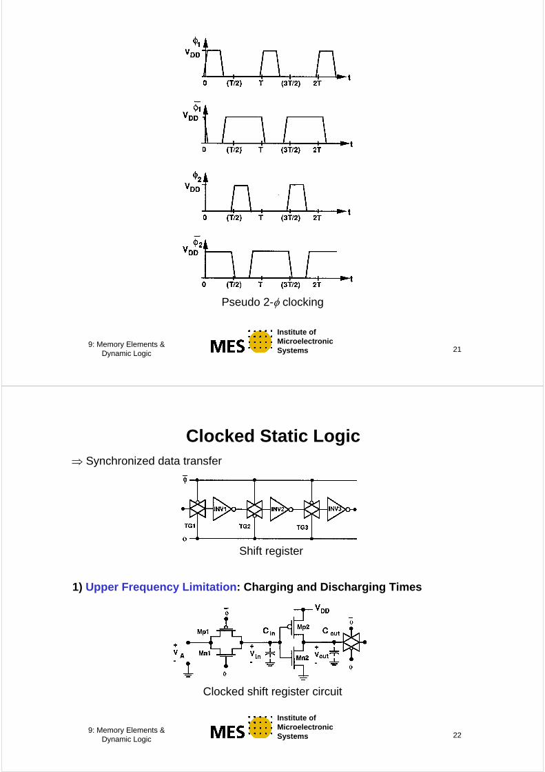
Pseudo 2-φ clocking
22
Institute ofMicroelectronicSystems
9: Memory Elements & Dynamic Logic
Clocked Static Logic⇒ Synchronized data transfer
Shift register
1) Upper Frequency Limitation: Charging and Discharging Times
Clocked shift register circuit

23
Institute ofMicroelectronicSystems
9: Memory Elements & Dynamic Logic
Time constant for charging and discharging:LTGTG CR=τ
wherelineinTGL CCCC ++=
VA=VDD: (Vin(0)=0)
⎥⎦⎤
⎢⎣⎡ τ−−≅ TGDDin
/te1V)t(V
Inverter is switched, when Vin=VIH which occurs after
( ) ( )[ ]pnoxin
DD
IHTG1
WLWLCC
VV
1lnt
+=
⎥⎦⎤
⎢⎣⎡ −τ−≅ϕ
VA=0: (Vin(0)= VDD)
TGDDin/teV)t(V τ−⋅≅
The time until Vin reaches VIL is given by
⎥⎦⎤
⎢⎣⎡τ−≅
IL
DDTG0
VV
lnt
24
Institute ofMicroelectronicSystems
9: Memory Elements & Dynamic Logic
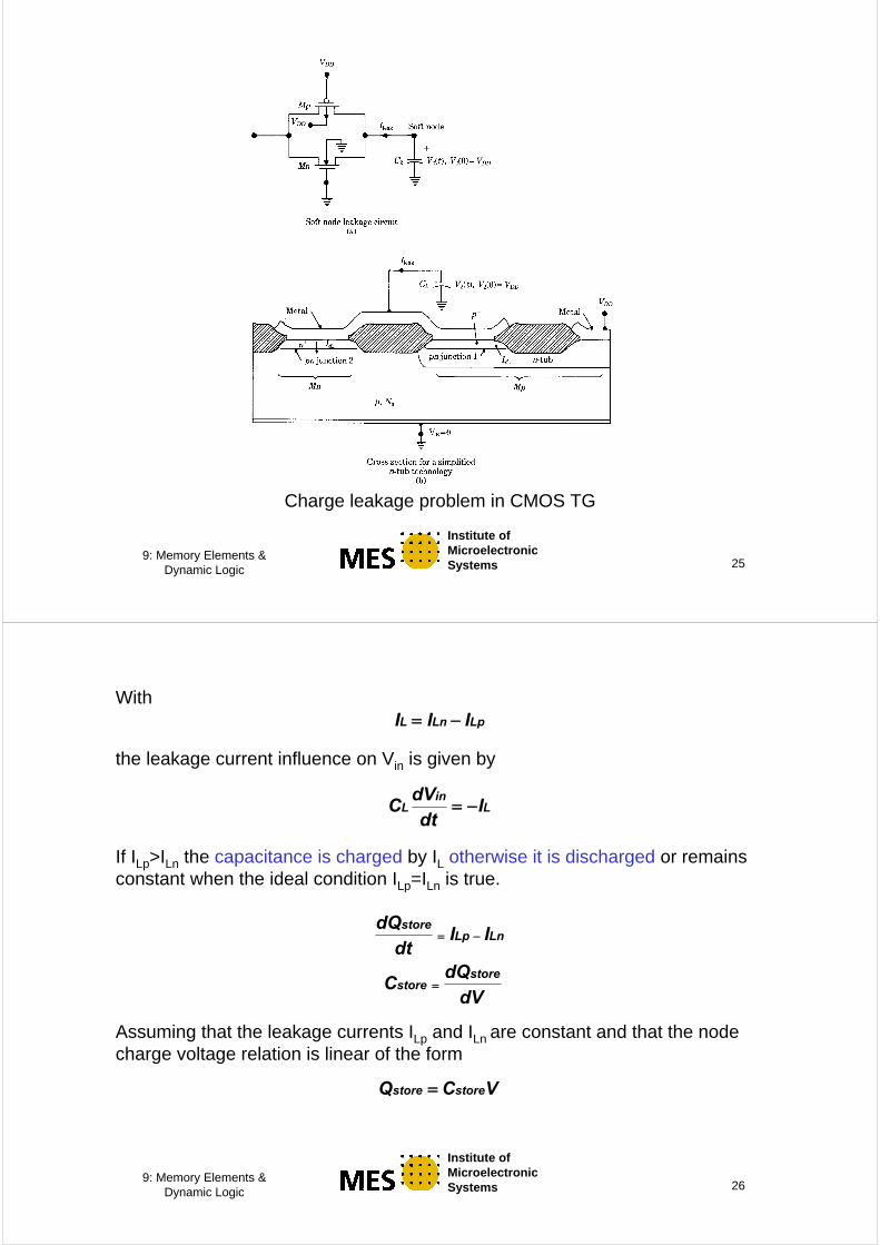
2) Lower Frequency Limitation: Charge Leakage
Leakage patch in a CMOS TG
The load capacitance, seen by the transmission gate (TG) is
inlineTGL CCCC ++=
The depletion capacitance contributions to CL are due to the reversed pnjunctions in the MOS transistors. As shown in fig. above a leakage current flow exists across the reverse biased pn junctions. The influence of this leakage current on the charge stored in CL depends on the values of ILp and ILn.
25
Institute ofMicroelectronicSystems
9: Memory Elements & Dynamic Logic
Charge leakage problem in CMOS TG
26
Institute ofMicroelectronicSystems
9: Memory Elements & Dynamic Logic
WithLpLnL III −=
the leakage current influence on Vin is given by
Lin
L IdtdV
C −=
If ILp>ILn the capacitance is charged by IL otherwise it is discharged or remains constant when the ideal condition ILp=ILn is true.
dVdQ
C
IIdt
dQ
storestore
LnLpstore
=
−=
Assuming that the leakage currents ILp and ILn are constant and that the node charge voltage relation is linear of the form
VCQ storestore =
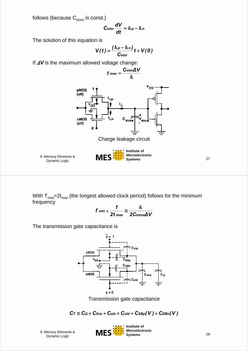
27
Institute ofMicroelectronicSystems
9: Memory Elements & Dynamic Logic
follows (because Cstore is const.)
LnLpstor IIdtdV
C −=
The solution of this equation is
)0(VtC
)II()t(V
stor
LnLp+
−=
If ∆V is the maximum allowed voltage change:
L
stormax
IV∆C
t =
Charge leakage circuit
28
Institute ofMicroelectronicSystems
9: Memory Elements & Dynamic Logic
With Tmax=2tmax (the longest allowed clock period) follows for the minimum frequency
V∆C2I
t21
fstore
L
maxmin ≅≅
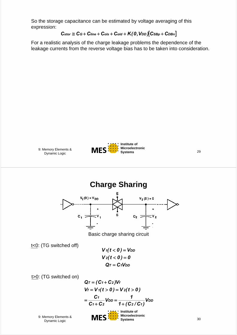
The transmission gate capacitance is
Transmission gate capacitance
)V(C)V(CCCCCC DBnSBpoldolslineGT +++++≅
29
Institute ofMicroelectronicSystems
9: Memory Elements & Dynamic Logic
So the storage capacitance can be estimated by voltage averaging of this expression:
[ ]DBnSBpDDoldolslineGstor CC)V,0(KCCCCC +++++≅
For a realistic analysis of the charge leakage problems the dependence of the leakage currents from the reverse voltage bias has to be taken into consideration.
30
Institute ofMicroelectronicSystems
9: Memory Elements & Dynamic Logic
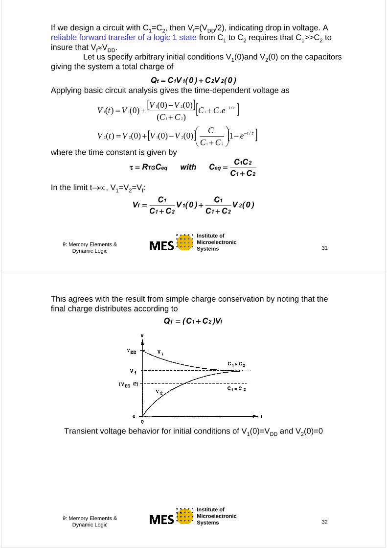
Charge Sharing
Basic charge sharing circuit
t<0: (TG switched off)
DD1T
2
DD1
VCQ
0)0t(V
V)0t(V
==<=<
t>0: (TG switched on)
DD12
DD21
1
21f
f21T
V)C/C(1
1V
CCC
)0t(V)0t(VV
V)CC(Q
+=
+=
>=>=+=
31
Institute ofMicroelectronicSystems
9: Memory Elements & Dynamic Logic
If we design a circuit with C1=C2, then Vf=(VDD/2), indicating drop in voltage. A reliable forward transfer of a logic 1 state from C1 to C2 requires that C1>>C2 to insure that Vf≈VDD.
Let us specify arbitrary initial conditions V1(0)and V2(0) on the capacitors giving the system a total charge of
)0(VC)0(VCQ 2211t +=Applying basic circuit analysis gives the time-dependent voltage as
[ ][ ]
[ ] [ ]τ
τ
/
/
1)0()0()0()(
)(
)0()0()0()(
21
1
2122
21
21
21
11
t
t
eCC
CVVVtV
eCCCC
VVVtV
−
−
−⎟⎠⎞
⎜⎝⎛
+−+=
++−
+=
where the time constant is given by
21
21eqeqTG
CCCC
CwithCR+
==τ
In the limit t→∝, V1=V2=Vf:
)0(VCC
C)0(V
CCC
V 221
11
21
1f
++
+=
32
Institute ofMicroelectronicSystems
9: Memory Elements & Dynamic Logic
This agrees with the result from simple charge conservation by noting that the final charge distributes according to
f21T V)CC(Q +=
Transient voltage behavior for initial conditions of V1(0)=VDD and V2(0)=0
33
Institute ofMicroelectronicSystems
9: Memory Elements & Dynamic Logic
Charge sharing among N TG-connected capacitors
Initial charge: ∑==
N
1iiiT )0(VCQ
After connecting nodes: fN
1iiT VCQ ⎟⎠⎞
⎜⎝⎛ ∑=
=
Final voltage:∑
∑==
=N1i i
N1i ii
fC
)0(VCV
34
Institute ofMicroelectronicSystems
9: Memory Elements & Dynamic Logic
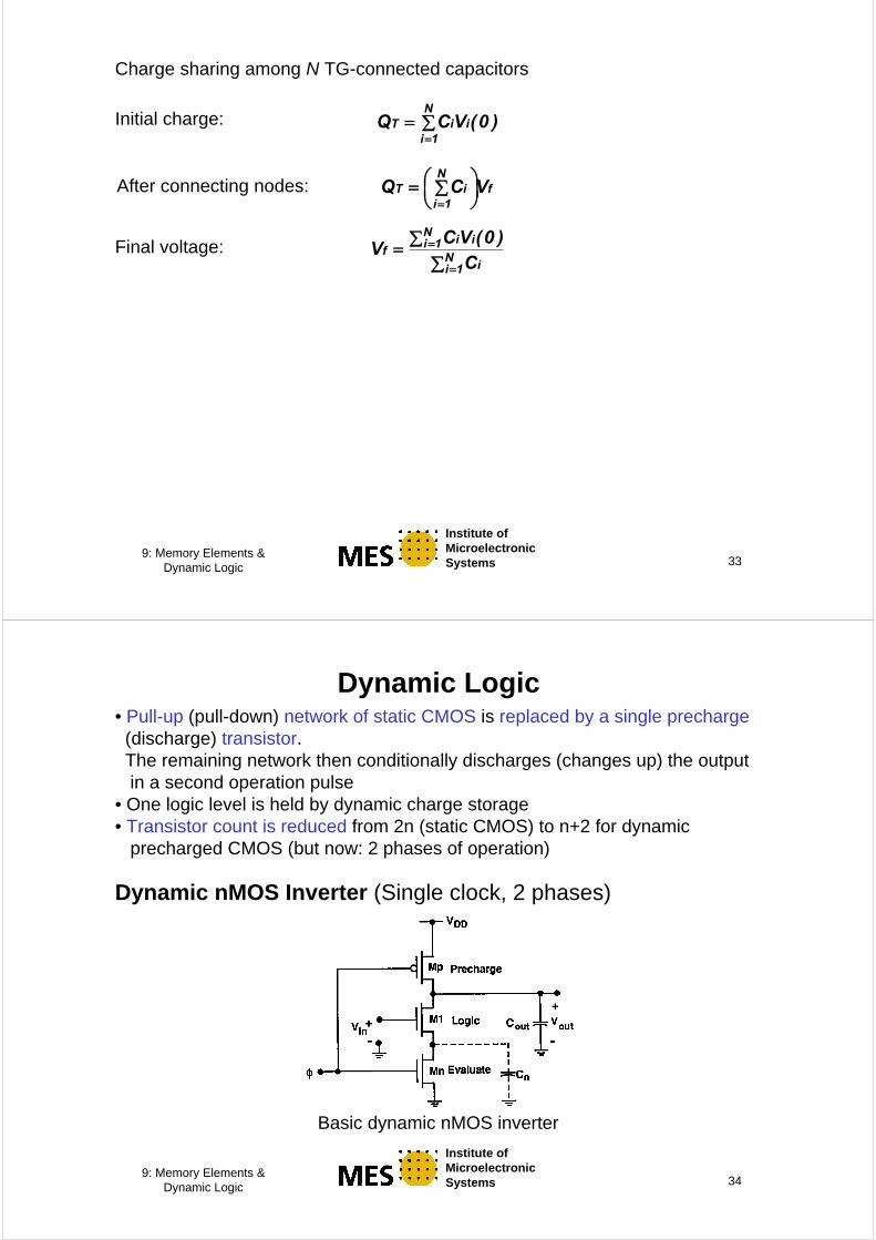
Dynamic Logic• Pull-up (pull-down) network of static CMOS is replaced by a single precharge(discharge) transistor.The remaining network then conditionally discharges (changes up) the output in a second operation pulse
• One logic level is held by dynamic charge storage• Transistor count is reduced from 2n (static CMOS) to n+2 for dynamic
precharged CMOS (but now: 2 phases of operation)
Dynamic nMOS Inverter (Single clock, 2 phases)
Basic dynamic nMOS inverter

35
Institute ofMicroelectronicSystems
9: Memory Elements & Dynamic Logic
Precharge Phase
If Vin=0 then
outpTpDDp
outch CR
)VV(C
=−β
=τ
WORST case (Vin=VDD):
⎥⎥⎥
⎦
⎤
⎢⎢⎢
⎣
⎡
⎟⎟⎟
⎠
⎞
⎜⎜⎜
⎝
⎛=
=
−−
+−
τ
+=τ
1V
)VV(2ln
)VV(
V2
t
)CC(R
0
TpDD
TpDD
Tpmax,ch
max,ch
noutpmax,ch
Dynamic nMOS inverter: precharge and evaluate
36
Institute ofMicroelectronicSystems
9: Memory Elements & Dynamic Logic
Evaluation Phase
For the case that M1 is switched on and identically designed channel width for M1and Mn the discharge time constant is given by
)VV(WkC)LL(
TnDDn
outn1dis
−′+
=τ
Precharge network for worst case

37
Institute ofMicroelectronicSystems
9: Memory Elements & Dynamic Logic
Evaluation discharge network
⎥⎥⎥
⎦
⎤
⎢⎢⎢
⎣
⎡
⎟⎟⎟
⎠
⎞
⎜⎜⎜
⎝
⎛= −
−+
−τ 1
V)VV(2
ln)VV(
V2t0
TnDD
TnDD
Tndisdis
Maximum clock frequency
Mmax
dismax,chM
t21
f
)t,tmax(t
≅
=
38
Institute ofMicroelectronicSystems
9: Memory Elements & Dynamic Logic
Dynamic pMOS Inverter
Basic dynamic pMOS inverter
Dynamic CMOS Properties and Conditions• single phase clock
• input should change during precharge only
• input must be stable at the end of the precharge phase
• in the evaluation phase the output remains HIGH (LOW) or is optionally
discharged (charged)
φ=1 Prechargeφ=0 Evaluate
39
Institute ofMicroelectronicSystems
9: Memory Elements & Dynamic Logic
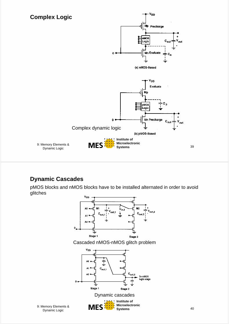
Complex Logic
Complex dynamic logic
40
Institute ofMicroelectronicSystems
9: Memory Elements & Dynamic Logic
Dynamic CascadespMOS blocks and nMOS blocks have to be installed alternated in order to avoid glitches
Cascaded nMOS-nMOS glitch problem
Dynamic cascades

41
Institute ofMicroelectronicSystems
9: Memory Elements & Dynamic Logic
Domino CMOS Logic
Basic domino logic circuit
42
Institute ofMicroelectronicSystems
9: Memory Elements & Dynamic Logic
• Domino Logic: design method for glitch-free cascading of nMOS logic blocks• Each stage is driven by φ
- Precharge during φ = 0- Evaluation when φ = 1
• Domino logic blocks consists of a precharge/ evaluation block and an output inverter
Precharge Phase: The gate output is precharged to logic 1 and the inverter output is going to logic 0. Logic transmission errors are avoided by providing a logic 0 at the inverter output (avoiding discharge of the next logic state).
Evaluation Phase: The inverter output stays according to the actual input values at logic 0 or is set to logic 1. The correct result signal is provided at the end of the domino cascade after stabilization of all stages.

43
Institute ofMicroelectronicSystems
9: Memory Elements & Dynamic Logic
Domino AND gate
Cascaded domino logic
44
Institute ofMicroelectronicSystems
9: Memory Elements & Dynamic Logic
Visualization of domino effect
Domino timing

45
Institute ofMicroelectronicSystems
9: Memory Elements & Dynamic Logic
Cascaded domino circuit with fanout = 2
46
Institute ofMicroelectronicSystems
9: Memory Elements & Dynamic Logic
Domino Logic Properties
Cascaded domino logic
• Domino logic consists of either n-type or p-type blocks• small load capacity to by driven by logic (one inverter only) ⇒ low dimensions of
transistors• only one clock signal required• only positive logic realizations possible because of the input inverters ⇒ domino logic is noninverting
Functions as
cannot be directly realized in a domino chain
47
Institute ofMicroelectronicSystems
9: Memory Elements & Dynamic Logic
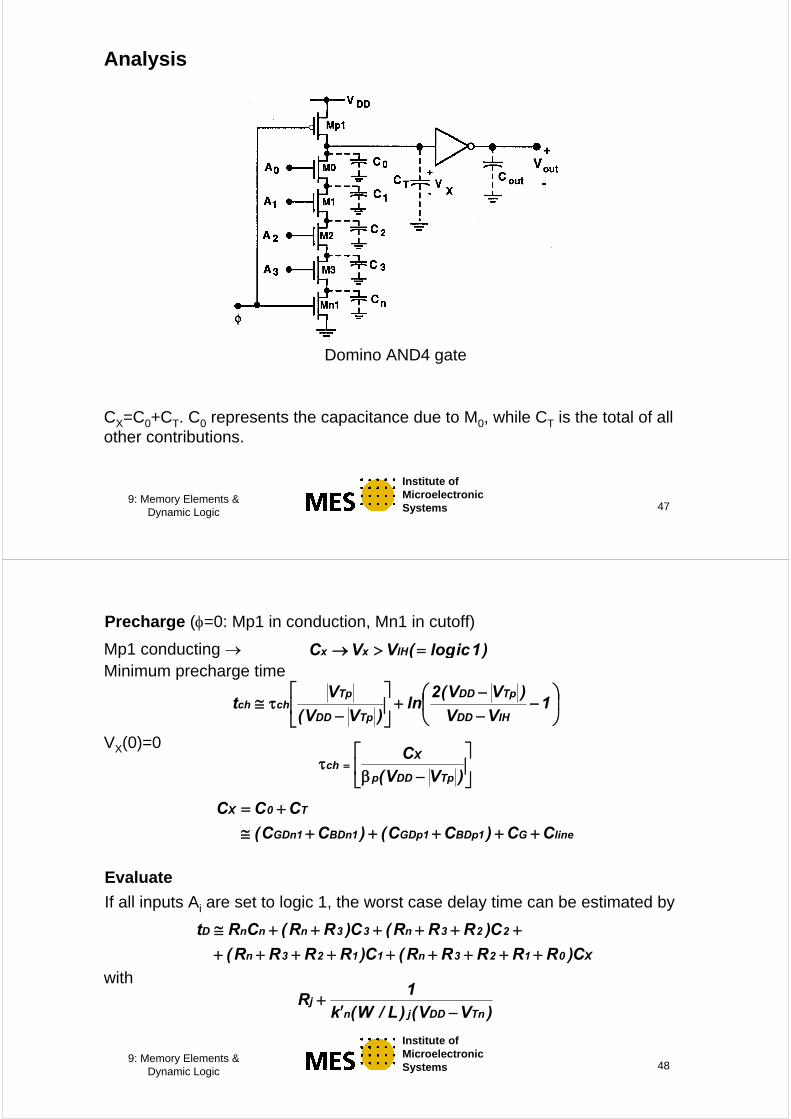
Analysis
Domino AND4 gate
CX=C0+CT. C0 represents the capacitance due to M0, while CT is the total of all other contributions.
48
Institute ofMicroelectronicSystems
9: Memory Elements & Dynamic Logic
Precharge (φ=0: Mp1 in conduction, Mn1 in cutoff)
lineG1BDp1GDp1BDn1GDn
T0X
CC)CC()CC(
CCC
+++++≅+=
Evaluate
If all inputs Ai are set to logic 1, the worst case delay time can be estimated by
X0123n1123n
223n33nnnD
C)RRRRR(C)RRRR(
C)RRR(C)RR(CRt
+++++++++++++++≅
with
)VV()L/W(k1
RTnDDjn
j−′
+
Mp1 conducting → )1iclog(VVC IHxx =>→Minimum precharge time
⎟⎠
⎞⎜⎝
⎛−
−−
+⎥⎦
⎤⎢⎣
⎡−
τ≅ 1VV
)VV(2ln
)VV(
Vt
IHDD
TpDD
TpDD
Tpchch
VX(0)=0
⎥⎦
⎤⎢⎣
⎡−β
τ =)VV(
CTpDDp
Xch

49
Institute ofMicroelectronicSystems
9: Memory Elements & Dynamic Logic
Charge Leakage and Charge Sharing
Domino stage with pull-up MOSFET
50
Institute ofMicroelectronicSystems
9: Memory Elements & Dynamic Logic
Charge sharing in a domino chain
Cout,1>>Cx1+Cx2

51
Institute ofMicroelectronicSystems
9: Memory Elements & Dynamic Logic
Use of feedback to control a pull-up MOSFET for charge sharing problem
52
Institute ofMicroelectronicSystems
9: Memory Elements & Dynamic Logic
NORA Logic
(NORA = NO RAce)
NORA Properties
• NORA is very insensitive to clock delay• one clock signal and the inverted clock signal with short slopes rise times are
sufficient • no inverter is needed between the logic stages, because of alternate use of
n-type and p-type blocks• the last stage is a clocked inverter, a C2MOS latch• ideal to clock pipelined logic systems

53
Institute ofMicroelectronicSystems
9: Memory Elements & Dynamic Logic
The Signal Race Problem
Signal race problem
The signal race problem can be seen: a signal race can arise, when both transmission gates conduct at the same time. If the new input from TG1 reaches the input of TG2 while TG2 is still transmitting the output, the output information will be lost. Imperfect TG synchronization occurs because of normal transmission intervals or clock skew.
54
Institute ofMicroelectronicSystems
9: Memory Elements & Dynamic Logic
Clock skew
tp>>tr,tf → no problems
Tskew=tp → race result critical
55
Institute ofMicroelectronicSystems
9: Memory Elements & Dynamic Logic
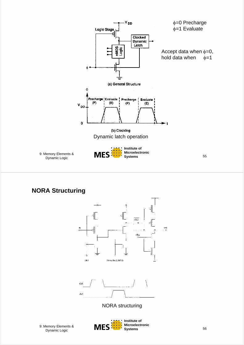
Dynamic latch operation
φ=0 Prechargeφ=1 Evaluate
Accept data when φ=0,hold data when φ=1
56
Institute ofMicroelectronicSystems
9: Memory Elements & Dynamic Logic
NORA Structuring
NORA structuring
clk2

57
Institute ofMicroelectronicSystems
9: Memory Elements & Dynamic Logic
tionssecφandφNORA
58
Institute ofMicroelectronicSystems
9: Memory Elements & Dynamic Logic
C2MOS latch
NORA pipelined logic
φ=1 Prechargeφ=0 Evaluate
59
Institute ofMicroelectronicSystems
9: Memory Elements & Dynamic Logic
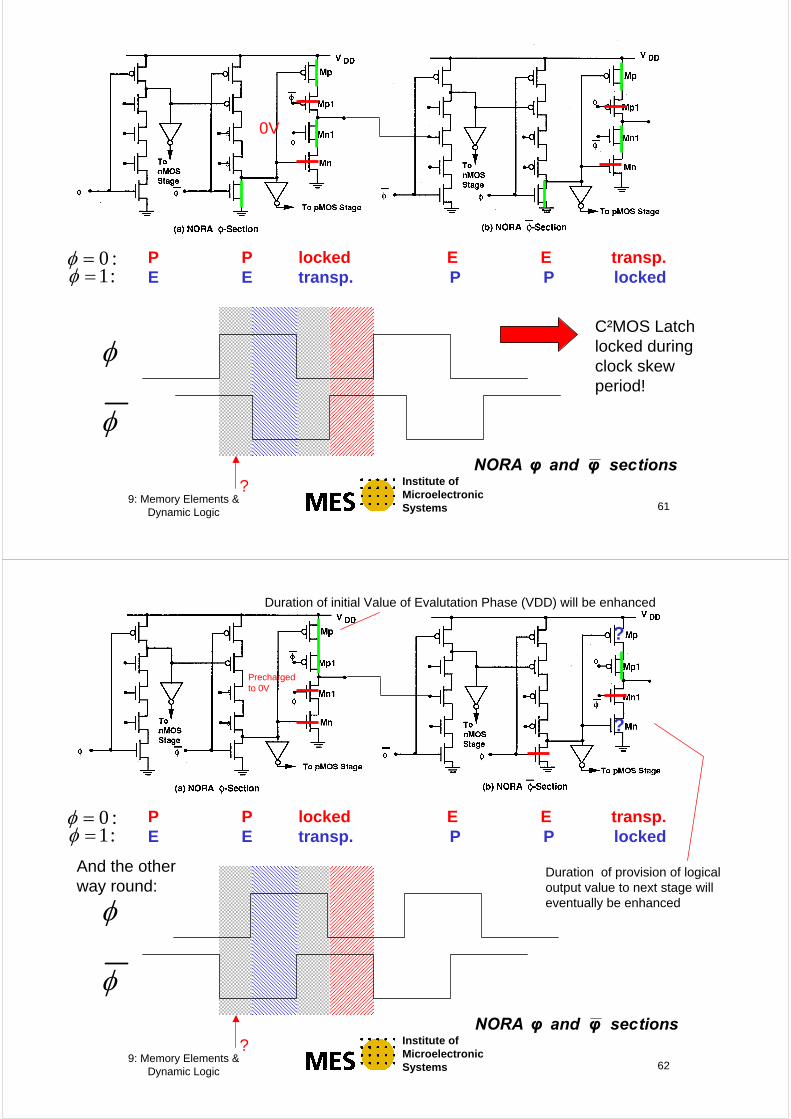
tionssecφandφNORA
:0=φ P P locked E E transp.E E transp. P P locked:1=φ
φ
φ
60
Institute ofMicroelectronicSystems
9: Memory Elements & Dynamic Logic
tionssecφandφNORA
:0=φ P P locked E E transp.E E transp. P P locked:1=φ
φ
φ
?
0V
?
?
61
Institute ofMicroelectronicSystems
9: Memory Elements & Dynamic Logic
tionssecφandφNORA
:0=φ P P locked E E transp.E E transp. P P locked:1=φ
φ
φ
?
0V
C²MOS Latchlocked duringclock skewperiod!
62
Institute ofMicroelectronicSystems
9: Memory Elements & Dynamic Logic
tionssecφandφNORA
:0=φ P P locked E E transp.E E transp. P P locked:1=φ
φ
φ
Prechargedto 0V
Duration of initial Value of Evalutation Phase (VDD) will be enhanced
?
?
Duration of provision of logicaloutput value to next stage willeventually be enhanced
And the other way round:
?
Top Related