


Languages
Pages
Legal

DAC34H84
16-bit DAC
16-bit DAC
16-bit DAC
16-bit DAC
Co
mp
lex
Mix
er
(32
-bit
NC
O)
xN
xN
Co
mp
lex
Mix
er
(32
-bit
NC
O)
xN
xN
32
-Bit
LV
DS
In
pu
t D
ata
Bu
s
RF
RF
LVD
S I
nte
rfa
ce
Product
Folder
Sample &Buy
Technical
Documents
Tools &
Software
Support &Community
ReferenceDesign
DAC34H84SLAS751D –MARCH 2011–REVISED SEPTEMBER 2015
DAC34H84 Quad-Channel, 16-Bit, 1.25 GSPS Digital-to-Analog Converter (DAC)A high-performance low jitter clock multiplier1 Featuressimplifies clocking of the device without significant
1• Very Low Power: 1.4 W at 1.25 GSPS impact on the dynamic range. The digital Quadrature• Multi-DAC Synchronization Modulator Correction (QMC) enables complete IQ
compensation for gain, offset, phase and group delay• Selectable 2x, 4x, 8x, 16x Interpolation Filterbetween channels in direct up-conversion– Stop-Band Attenuation > 90 dBc applications.
• Flexible On-chip Complex MixingDigital data is input to the device through a 32-bit– Two Independent Fine Mixers with 32-bit wide LVDS data bus with on-chip termination. The
NCOs wide bus allows the processing of very high– Power Saving Coarse Mixers: ± n×Fs/8 bandwidth signals. The device includes a FIFO, data
pattern checker and parity test to ease the input• High Performance, Low Jitter Clock Multiplyinginterface. The interface also allows fullPLLsynchronization of multiple devices.• Digital I and Q CorrectionThe device is characterized for operation over the– Gain, Phase, Offset, and Group Delayentire industrial temperature range of –40°C to 85°CCorrection and is available in a 196-ball, 12x12mm, 0.8mm pitch
• Digital Inverse Sinc Filters BGA package.• 32-Bit DDR Flexible LVDS Input Data Bus The DAC34H84 very low power, high bandwidth
– 8 Sample Input FIFO support, superior crosstalk, high dynamic range andfeatures are an ideal fit for next generation– Supports Data Rates up to 625 MSPScommunication systems.– Data Pattern Checker
– Parity Check Device Information(1)
• Temperature Sensor PART NUMBER PACKAGE BODY SIZE (NOM)• Differential Scalable Output: 10mA to 30mA DAC34H84 NFBGA (196) 12.00 mm x 12.00 mm
• 196-Ball, 12x12mm NFBGA (GREEN / Pb-Free) (1) For all available packages, see the orderable addendum atthe end of the data sheet.
2 ApplicationsSimplified Schematic
• Cellular Base Stations• Diversity Transmit• Wideband Communications
3 DescriptionThe DAC34H84 is a very low power, high dynamicrange, quad-channel, 16-bit digital-to-analogconverter (DAC) with a sample rate as high as 1.25GSPS.
The device includes features that simplify the designof complex transmit architectures: 2x to 16x digitalinterpolation filters with over 90 dB of stop-bandattenuation simplify the data interface andreconstruction filters. Independent complex mixersallow flexible carrier placement.
1
An IMPORTANT NOTICE at the end of this data sheet addresses availability, warranty, changes, use in safety-critical applications,intellectual property matters and other important disclaimers. PRODUCTION DATA.
DAC34H84SLAS751D –MARCH 2011–REVISED SEPTEMBER 2015 www.ti.com
Table of Contents7.3 Feature Description................................................. 241 Features .................................................................. 17.4 Device Functional Modes........................................ 522 Applications ........................................................... 17.5 Programming........................................................... 563 Description ............................................................. 17.6 Register Map........................................................... 604 Revision History..................................................... 2
8 Application and Implementation ........................ 775 Pin Configuration and Functions ......................... 48.1 Application Information............................................ 776 Specifications......................................................... 78.2 Typical Applications ............................................... 786.1 Absolute Maximum Ratings ...................................... 7
9 Power Supply Recommendations ...................... 846.2 ESD Ratings ............................................................ 710 Layout................................................................... 856.3 Recommended Operating Conditions....................... 8
10.1 Layout Guidelines ................................................. 856.4 Thermal Information .................................................. 810.2 Layout Examples................................................... 866.5 Electrical Characteristics – DC Specifications .......... 8
11 Device and Documentation Support ................. 896.6 Electrical Characteristics – Digital Specifications ... 1011.1 Device Support .................................................... 896.7 Electrical Characteristics – AC Specifications ........ 1111.2 Documentation Support ....................................... 896.8 Timing Requirements – Digital Specifications......... 1111.3 Community Resources.......................................... 906.9 Switching Characteristics – AC Specifications........ 1311.4 Trademarks ........................................................... 906.10 Typical Characteristics .......................................... 1411.5 Electrostatic Discharge Caution............................ 907 Detailed Description ............................................ 2211.6 Glossary ................................................................ 907.1 Overview ................................................................. 22
12 Mechanical, Packaging, and Orderable7.2 Functional Block Diagram ....................................... 23Information ........................................................... 90
4 Revision HistoryNOTE: Page numbers for previous revisions may differ from page numbers in the current version.
Changes from Revision C (August 2012) to Revision D Page
• Added ESD Ratings table, Feature Description section, Device Functional Modes, Application and Implementationsection, Power Supply Recommendations section, Layout section, Device and Documentation Support section, andMechanical, Packaging, and Orderable Information section. ................................................................................................ 1
Changes from Revision B (August 2011) to Revision C Page
• Added thermal information to the Absolute Maximum Ratings table ..................................................................................... 7• Added Recommended Operating Conditions table ................................................................................................................ 8• Deleted TJ row from top of thermal table................................................................................................................................ 8• Deleted OPERATING RANGE section from bottom of Electrical Characteristics – DC Specifications ............................... 10
Changes from Revision A (June 2011) to Revision B Page
• Changed ALARM description ................................................................................................................................................. 5• Added notes to Electrical Characteristics – DC Specifications .............................................................................................. 9• Deleted t(align) from Electrical Characteristics – Digital Specifications .................................................................................. 10• Added fDAC PLL ON MIN of 1000 MSPS in Electrical Characteristics – AC Specifications ................................................. 11• Changed DIGITAL INPUT TIMING SPECIFICATIONS in Timing Requirements - Digital Specifications............................ 11• Changed DAC Wake-up Time in Switching Characteristics – AC Specifications ................................................................ 13• Added information to SINGLE SYNC SOURCE MODE section .......................................................................................... 29• Deleted t(align) from BYPASS MODE section ......................................................................................................................... 29• Changed 1.2288GHz to 983.04MHz in PLL MODE description........................................................................................... 31• Changed data in Table 4 ...................................................................................................................................................... 31• Deleted 2x in Table 6............................................................................................................................................................ 35
2 Submit Documentation Feedback Copyright © 2011–2015, Texas Instruments Incorporated
Product Folder Links: DAC34H84
DAC34H84www.ti.com SLAS751D –MARCH 2011–REVISED SEPTEMBER 2015
• Changed EXAMPLE START-UP ROUTINE information ...................................................................................................... 57• Changed Table 10 ................................................................................................................................................................ 58• Changed register version default value from 0x5408 to 0x5409 in Register Map ............................................................... 61• Deleted t(align) from register config0 description .................................................................................................................... 62• Added SIF SYNC to register config32 description ............................................................................................................... 73• Changed B40 to N11 in register config35 description.......................................................................................................... 74• Changed register config 45 default value............................................................................................................................. 75• Changed register version default value from 0x5408 to 0x5409.......................................................................................... 76
Changes from Original (March 2011) to Revision A Page
• Changed from PRODUCT PREVIEW to PRODUCTION DATA ............................................................................................ 1
Copyright © 2011–2015, Texas Instruments Incorporated Submit Documentation Feedback 3
Product Folder Links: DAC34H84
GND
GND
GND
OSTRN
GND
SYNCN
DAB15N
DAB14N
DAB13N
DAB12N
DAB11N
DAB10N
DAB9N
OSTRP
SYNCP
GND
DACCLKP
DACCLKN
GND
DAB15P
DAB14P
DAB13P
DAB12P
DAB11P
DAB10P
DAB9P
GNDIOUTAP
IOUTAN
GNDIOUTBN
IOUTBP
GND GNDIOUTCP
IOUTCN
GNDIOUTDN
IOUTDP
GND
GND GND GND GND GND GND GND GND GND GND GND GND
PLLAVDD
LPF GND GND EXTIO BIASJ GNDIO
VDD2GND ALARM SDO
AVDD AVDD AVDD AVDD AVDD AVDDTESTMODE
RESETB
SDENBAVDDDACVDD
DACVDD
DACVDD
DACVDD
DACVDD
DACVDD
AVDD GND
TXENA SCLKDACVDD
DACVDD
GND GND GNDDACVDD
DACVDD
GND
PLLAVDD
CLKVDD
GND
GND GND
GND
SLEEP SDIO
GND GND GND GND GND GND GND GND GND
VFUSEDIGVDD
GND GND GNDDIGVDD
VFUSE GNDGND GND
GNDPARITY
CDPPARITY
CDN
DCD0P
DCD0N
GNDIO
VDDDIGVDD
GND GNDGND GNDDIGVDD
IOVDD
GNDDCD1P
DCD1N
GNDIO
VDDDIGVDD
DIGVDD
IOVDD
IOVDD
DIGVDD
DIGVDD
IOVDD
GNDDCD2P
DCD2N
DAB8P
DAB6P
DAB8N
DAB6N
DAB7P
DAB5P
DAB7N
DAB5N
DAB4P
DAB2P
DAB4N
DAB2N
DAB3P
DAB1P
DAB3N
DAB1N
DAB0P
DAB0N
DCD15P
DCD15N
DCD14P
DCD12P
DCD14N
DCD12N
DCD13P
DCD11P
DCD13N
DCD11N
DCD10P
DCD8P
DCD10N
DCD8N
DCD9P
DCD7P
DCD9N
DCD7N
DCD3P
DCD3N
DCD4P
DCD4N
DCD5P
DCD5N
DCD6P
DCD6N
DATACLKP
DATACLKN
ISTR/PARITY
ABP
ISTR/PARITY
ABN
A B C D E F G H J K L M N P
14
13
12
11
10
9
8
7
6
5
4
3
2
1
DAC Output
Clock Input
Sync/Parity Input
Data Input
CMOS Pins
Miscellaneous
3.3V Supply
Ground
P0134-01
CLKVDD
1.2V Supply(except for IOVDD2)
DAC34H84SLAS751D –MARCH 2011–REVISED SEPTEMBER 2015 www.ti.com
5 Pin Configuration and Functions
ZAY Package196-Pin NFBGA
Top View
4 Submit Documentation Feedback Copyright © 2011–2015, Texas Instruments Incorporated
Product Folder Links: DAC34H84
DAC34H84www.ti.com SLAS751D –MARCH 2011–REVISED SEPTEMBER 2015
Pin FunctionsPIN
I/O DESCRIPTIONNAME NO.
D10, E11,F11, G11,AVDD I Analog supply voltage. (3.3 V)H11, J11,K11, L10
CMOS output for ALARM condition. The ALARM output functionality is defined through the config7ALARM N12 O register. Default polarity is active high, but can be changed to active low via config0 alarm_out_pol
control bit.Full-scale output current bias. For 30-mA full-scale output current, connect 1.28 kΩ to ground.BIASJ H12 O Change the full-scale output current through coarse_dac(3:0) in config3, bit<15:12>Internal clock buffer supply voltage. (1.2 V). It is recommended to isolate this supply from DIGVDDCLKVDD C12, K12 I and DACVDD.LVDS positive input data bits 0 through 15 for the AB-channel path. Internal 100-Ω terminationA7, A6, A5,resistor. Data format relative to DATACLKP/N clock is Double Data Rate (DDR).A4, A3, A2,
A1, C4, C2, DAB15P is most significant data bit (MSB)DAB[15..0]P ID4, D2, E4, DAB0P is least significant data bit (LSB)E2, F4, F2,G4 The order of the bus can be reversed via config2 revbus bit.
B7, B6, B5,B4, B3, B2,B1, C3, C1, LVDS negative input data bits 0 through 15 for the AB-channel path. (See DAB[15:0]P descriptionDAB[15..0]N ID3, D1, E3, above)E1, F3, F1,
G3H4, J4, J2, LVDS positive input data bits 0 through 15 for the CD-channel path. Internal 100-Ω terminationK4, K2, L4, resistor. Data format relative to DATACLKP/N clock is Double Data Rate (DDR).L2, M4, M2, DCD15P is most significant data bit (MSB)DCD[15..0]P IN1, N2, N3, DCD0P is least significant data bit (LSB)N4, N5, N6,
The order of the bus can be reversed via config2 revbus bit.N7H3, J3, J1,K3, K1, L3,L1, M3, M1, LVDS negative input data bits 0 through 15 for the CD-channel path. (See DCD[15:0]P descriptionDCD[15..0]N IP1, P2, P3, above)P4, P5, P6,
P7DACCLKP A12 I Positive external LVPECL clock input for DAC core with a self-bias.DACCLKN A11 I Complementary external LVPECL clock input for DAC core. (see the DACCLKP description)
D9, E9, E10,F10, G10, DAC core supply voltage. (1.2 V). It is recommended to isolate this supply from CLKVDD andDACVDD IH10, J10, DIGVDD.
K10, K9, L9LVDS positive input data clock. Internal 100-Ω termination resistor. Input data DAB[15:0]P/N andDATACLKP G2 I DCD[15:0]P/N are latched on both edges of DATACLKP/N (Double Data Rate).
DATACLKN G1 I LVDS negative input data clock. (See DATACLKP description)E5, E6, E7,
DIGVDD F5, J5, K5, I Digital supply voltage. (1.2 V). It is recommended to isolate this supply from CLKVDD and DACVDD.K6, K7
Used as external reference input when internal reference is disabled through config27 extref_ena =EXTIO G12 I/O 1b. Used as internal reference output when config27 extref_ena = 0b (default). Requires a 0.1-μF
decoupling capacitor to AGND when used as reference output.LVDS input strobe positive input. Internal 100-Ω termination resistor.The main functions of this input are to sync the FIFO pointer, to provide a sync source to the digitalblocks, and/or to act as a parity input for the AB-data bus.ISTRP/ H2 I These functions are captured with the rising edge of DATACLKP/N. This signal should be edge-PARITYABP aligned with DAB[15:0]P/N and DCD[15:0]P/N.The PARITY, SYNC, and ISTR inputs are rotated to allow complete reversal of the data interfacewhen setting the rev_interface bit in register config1.
ISTRN/ H1 I LVDS input strope negative input. (See the ISTRP/PARITYABP description)PARITYABN
Copyright © 2011–2015, Texas Instruments Incorporated Submit Documentation Feedback 5
Product Folder Links: DAC34H84
DAC34H84SLAS751D –MARCH 2011–REVISED SEPTEMBER 2015 www.ti.com
Pin Functions (continued)PIN
I/O DESCRIPTIONNAME NO.
A10, A13,A14, B10,B11, B12,
B13, C5, C6,C7, C8, C9,C10, C13,D8, D13,D14, E8,E12, E13,F6, F7, F8,
F9, F12, F13,G6, G7, G8,
GND G9, G13, I These pins are ground for all supplies.G14, H6, H7,H8, H9, H13,H14, J6, J7,J8, J9, J12,
J13, K8, K13,L8, L13, L14,M5, M6, M7,
M8, M9,M10, M11,M12, M13,N13, P13,
P14IOUTAP B14 O A-Channel DAC current output. Connect directly to ground if unused.IOUTAN C14 O A-Channel DAC complementary current output. Connect directly to ground if unused.IOUTBP F14 O B-Channel DAC current output. Connect directly to ground if unused.IOUTBN E14 O B-Channel DAC complementary current output. Connect directly to ground if unused.IOUTCP J14 O C-Channel DAC current output. Connect directly to ground if unused.IOUTCN K14 O C-Channel DAC complementary current output. Connect directly to ground if unused.IOUTDP N14 O D-Channel DAC current output. Connect directly to ground if unused.IOUTDN M14 O D-Channel DAC complementary current output. Connect directly to ground if unused.
D5, D6, G5,IOVDD I Supply voltage for all LVDS I/O. (3.3 V)H5, L5. L6Supply voltage for all CMOS I/O. (1.8 to 3.3 V) This supply can range from 1.8 V to 3.3 V to changeIOVDD2 L12 I the input and output level of the CMOS I/O.
LPF D12 I/O PLL loop filter connection. If not using the clock multiplying PLL, the LPF pin can be left unconnected.Optional LVPECL output strobe positive input. This positive/negative pair is captured with the rising
OSTRP A9 I edge of DACCLKP/N. It is used to sync the divided-down clocks and FIFO output pointer in Dual SyncSources Mode. If unused it can be left unconnected.
OSTRN B9 I Optional LVPECL output strobe negative input. (See the OSTRP description)Optional LVDS positive input parity bit for the CD-data bus. The PARITYCDP/N LVDS pair has aninternal 100-Ω termination resistor. If unused it can be left unconnected.PARITYCDP N8 I The PARITY, SYNC, and ISTR inputs are rotated to allow complete reversal of the data interfacewhen setting the rev_interface bit in register config1.
PARITYCDN P8 I Optional LVDS negative input parity bit for the CD-data bus.PLLAVDD C11, D11 I PLL analog supply voltage. (3.3 V)SCLK P9 I Serial interface clock. Internal pull-down.SDENB P10 I Active low serial data enable, always an input to the DAC34H84. Internal pull-up.
Serial interface data. Bi-directional in 3-pin mode (default) and uni-directional 4-pin mode. InternalSDIO P11 1/O pull-down.Uni-directional serial interface data in 4-pin mode. The SDO pin is tri-stated in 3-pin interface modeSDO P12 O (default).
SLEEP N11 I Active high asynchronous hardware power-down input. Internal pull-down.
6 Submit Documentation Feedback Copyright © 2011–2015, Texas Instruments Incorporated
Product Folder Links: DAC34H84
DAC34H84www.ti.com SLAS751D –MARCH 2011–REVISED SEPTEMBER 2015
Pin Functions (continued)PIN
I/O DESCRIPTIONNAME NO.
LVDS SYNC positive input. Internal 100-Ω termination resistor. If unused it can be left unconnected.SYNCP A8 I The PARITY, SYNC, and ISTR inputs are rotated to allow complete reversal of the data interface
when setting the rev_interface bit in register config1.SYNCN B8 I LVDS SYNC negative input.RESETB N10 I Active low input for chip RESET. Internal pull-up.
Transmit enable active high input. Internal pull-down.To enable analog output data transmission, set sif_txenable in register config3 to 1b or pull CMOS
TXENA N9 I TXENA pin to high.To disable analog output, set sif_txenable to 0b and pull CMOS TXENA pin to low. The DAC output isforced to midscale.
TESTMODE L11 I This pin is used for factory testing. Internal pull-down. Leave unconnected for normal operation.Digital supply voltage. This supply pin is also used for factory fuse programming. Connect toVFUSE D7, L7 I DACVDD or DIGVDD for normal operation.
6 Specifications
6.1 Absolute Maximum Ratingsover operating free-air temperature range (unless otherwise noted) (1)
MIN MAX UNITDACVDD, DIGVDD, CLKVDD –0.5 1.5 VVFUSE –0.5 1.5 VSupply voltage
range (2) IOVDD, IOVDD2 –0.5 4 VAVDD, PLLAVDD –0.5 4 VDAB[15..0]P/N, DCD[15..0]P/N, DATACLKP/N, ISTRP/N, PARITYCDP/N, –0.5 IOVDD + 0.5 VSYNCP/NDACCLKP/N, OSTRP/N –0.5 CLKVDD + 0.5 VALARM, SDO, SDIO, SCLK, SDENB, SLEEP, RESETB, TESTMODE, –0.5 IOVDD2 + 0.5 VPin voltage range (2)TXENAIOUTAP/N, IOUTBP/N, IOUTCP/N, IOUTDP/N –1.0 AVDD + 0.5 VEXTIO, BIASJ –0.5 AVDD + 0.5 VLPF –0.5 PLLAVDD + 0.5 V
Peak input current (any input) 20 mAPeak total input current (all inputs) –30 mAOperating free-air temperature range, TA: DAC34H84 –40 85 °CAbsolute maximum junction temperature, TJ 150 °CStorage temperature range, Tstg –65 150 °C
(1) Stresses beyond those listed under absolute maximum ratings may cause permanent damage to the device. These are stress ratingsonly and functional operation of these or any other conditions beyond those indicated under “recommended operating conditions” is notimplied. Exposure to absolute-maximum-rated conditions for extended periods may affect device reliability.
(2) Measured with respect to GND.
6.2 ESD RatingsVALUE UNIT
Human-body model (HBM), per ANSI/ESDA/JEDEC JS-001 (1) ±2000V(ESD) Electrostatic discharge VCharged-device model (CDM), per JEDEC specification JESD22- ±500C101 (2)
(1) JEDEC document JEP155 states that 500-V HBM allows safe manufacturing with a standard ESD control process.(2) JEDEC document JEP157 states that 250-V CDM allows safe manufacturing with a standard ESD control process.
Copyright © 2011–2015, Texas Instruments Incorporated Submit Documentation Feedback 7
Product Folder Links: DAC34H84
DAC34H84SLAS751D –MARCH 2011–REVISED SEPTEMBER 2015 www.ti.com
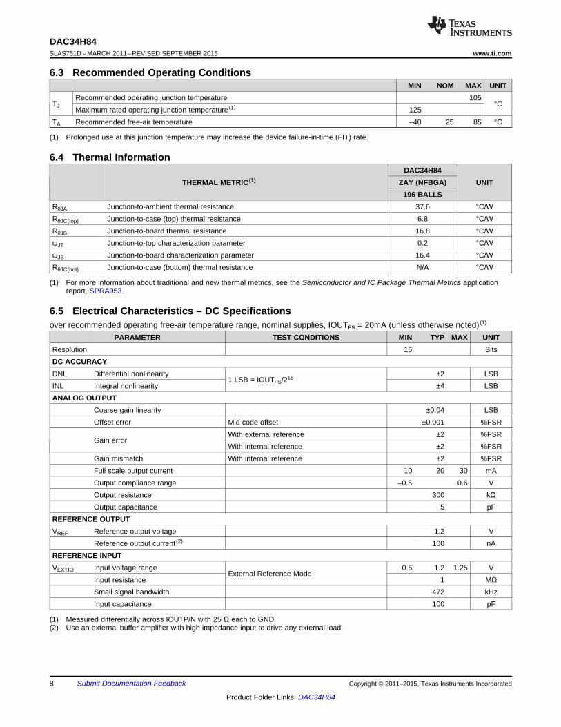
6.3 Recommended Operating ConditionsMIN NOM MAX UNIT
Recommended operating junction temperature 105TJ °C
Maximum rated operating junction temperature (1) 125TA Recommended free-air temperature –40 25 85 °C
(1) Prolonged use at this junction temperature may increase the device failure-in-time (FIT) rate.
6.4 Thermal InformationDAC34H84
THERMAL METRIC (1) ZAY (NFBGA) UNIT196 BALLS
RθJA Junction-to-ambient thermal resistance 37.6 °C/WRθJC(top) Junction-to-case (top) thermal resistance 6.8 °C/WRθJB Junction-to-board thermal resistance 16.8 °C/WψJT Junction-to-top characterization parameter 0.2 °C/WψJB Junction-to-board characterization parameter 16.4 °C/WRθJC(bot) Junction-to-case (bottom) thermal resistance N/A °C/W
(1) For more information about traditional and new thermal metrics, see the Semiconductor and IC Package Thermal Metrics applicationreport, SPRA953.
6.5 Electrical Characteristics – DC Specificationsover recommended operating free-air temperature range, nominal supplies, IOUTFS = 20mA (unless otherwise noted) (1)
PARAMETER TEST CONDITIONS MIN TYP MAX UNITResolution 16 BitsDC ACCURACYDNL Differential nonlinearity ±2 LSB
1 LSB = IOUTFS/216INL Integral nonlinearity ±4 LSBANALOG OUTPUT
Coarse gain linearity ±0.04 LSBOffset error Mid code offset ±0.001 %FSR
With external reference ±2 %FSRGain error
With internal reference ±2 %FSRGain mismatch With internal reference ±2 %FSRFull scale output current 10 20 30 mAOutput compliance range –0.5 0.6 VOutput resistance 300 kΩOutput capacitance 5 pF
REFERENCE OUTPUTVREF Reference output voltage 1.2 V
Reference output current (2) 100 nAREFERENCE INPUTVEXTIO Input voltage range 0.6 1.2 1.25 V
External Reference ModeInput resistance 1 MΩSmall signal bandwidth 472 kHzInput capacitance 100 pF
(1) Measured differentially across IOUTP/N with 25 Ω each to GND.(2) Use an external buffer amplifier with high impedance input to drive any external load.
8 Submit Documentation Feedback Copyright © 2011–2015, Texas Instruments Incorporated
Product Folder Links: DAC34H84
DAC34H84www.ti.com SLAS751D –MARCH 2011–REVISED SEPTEMBER 2015
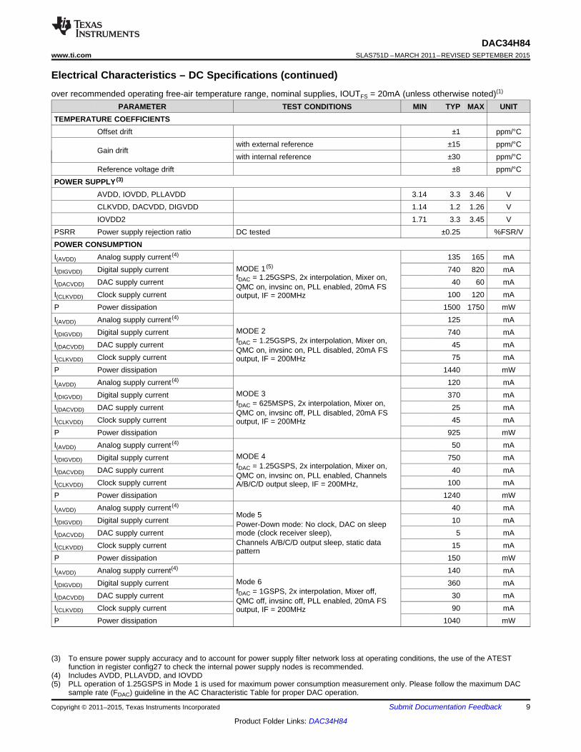
Electrical Characteristics – DC Specifications (continued)over recommended operating free-air temperature range, nominal supplies, IOUTFS = 20mA (unless otherwise noted)(1)
PARAMETER TEST CONDITIONS MIN TYP MAX UNITTEMPERATURE COEFFICIENTS
Offset drift ±1 ppm/°Cwith external reference ±15 ppm/°C
Gain driftwith internal reference ±30 ppm/°C
Reference voltage drift ±8 ppm/°CPOWER SUPPLY (3)
AVDD, IOVDD, PLLAVDD 3.14 3.3 3.46 VCLKVDD, DACVDD, DIGVDD 1.14 1.2 1.26 VIOVDD2 1.71 3.3 3.45 V
PSRR Power supply rejection ratio DC tested ±0.25 %FSR/VPOWER CONSUMPTIONI(AVDD) Analog supply current (4) 135 165 mA
MODE 1 (5)I(DIGVDD) Digital supply current 740 820 mAfDAC = 1.25GSPS, 2x interpolation, Mixer on,I(DACVDD) DAC supply current 40 60 mAQMC on, invsinc on, PLL enabled, 20mA FS
I(CLKVDD) Clock supply current 100 120 mAoutput, IF = 200MHzP Power dissipation 1500 1750 mWI(AVDD) Analog supply current (4) 125 mA
MODE 2I(DIGVDD) Digital supply current 740 mAfDAC = 1.25GSPS, 2x interpolation, Mixer on,I(DACVDD) DAC supply current 45 mAQMC on, invsinc on, PLL disabled, 20mA FS
I(CLKVDD) Clock supply current 75 mAoutput, IF = 200MHzP Power dissipation 1440 mWI(AVDD) Analog supply current (4) 120 mA
MODE 3I(DIGVDD) Digital supply current 370 mAfDAC = 625MSPS, 2x interpolation, Mixer on,I(DACVDD) DAC supply current 25 mAQMC on, invsinc off, PLL disabled, 20mA FS
I(CLKVDD) Clock supply current 45 mAoutput, IF = 200MHzP Power dissipation 925 mWI(AVDD) Analog supply current (4) 50 mA
MODE 4I(DIGVDD) Digital supply current 750 mAfDAC = 1.25GSPS, 2x interpolation, Mixer on,I(DACVDD) DAC supply current 40 mAQMC on, invsinc on, PLL enabled, Channels
I(CLKVDD) Clock supply current 100 mAA/B/C/D output sleep, IF = 200MHz,P Power dissipation 1240 mWI(AVDD) Analog supply current (4) 40 mA
Mode 5I(DIGVDD) Digital supply current 10 mAPower-Down mode: No clock, DAC on sleepI(DACVDD) DAC supply current mode (clock receiver sleep), 5 mA
Channels A/B/C/D output sleep, static dataI(CLKVDD) Clock supply current 15 mApattern
P Power dissipation 150 mWI(AVDD) Analog supply current(4) 140 mA
Mode 6I(DIGVDD) Digital supply current 360 mAfDAC = 1GSPS, 2x interpolation, Mixer off,I(DACVDD) DAC supply current 30 mAQMC off, invsinc off, PLL enabled, 20mA FS
I(CLKVDD) Clock supply current 90 mAoutput, IF = 200MHzP Power dissipation 1040 mW
(3) To ensure power supply accuracy and to account for power supply filter network loss at operating conditions, the use of the ATESTfunction in register config27 to check the internal power supply nodes is recommended.
(4) Includes AVDD, PLLAVDD, and IOVDD(5) PLL operation of 1.25GSPS in Mode 1 is used for maximum power consumption measurement only. Please follow the maximum DAC
sample rate (FDAC) guideline in the AC Characteristic Table for proper DAC operation.
Copyright © 2011–2015, Texas Instruments Incorporated Submit Documentation Feedback 9
Product Folder Links: DAC34H84
DAC34H84SLAS751D –MARCH 2011–REVISED SEPTEMBER 2015 www.ti.com
Electrical Characteristics – DC Specifications (continued)over recommended operating free-air temperature range, nominal supplies, IOUTFS = 20mA (unless otherwise noted)(1)
PARAMETER TEST CONDITIONS MIN TYP MAX UNITI(AVDD) Analog supply current(4) 120 mA
Mode 7I(DIGVDD) Digital supply current 370 mAfDAC = 1GSPS, 2x interpolation, Mixer off,I(DACVDD) DAC supply current 30 mAQMC off, invsinc off, PLL disabled, 20mA FS
I(CLKVDD) Clock supply current 65 mAoutput, IF = 200MHzP Power dissipation 960 mW
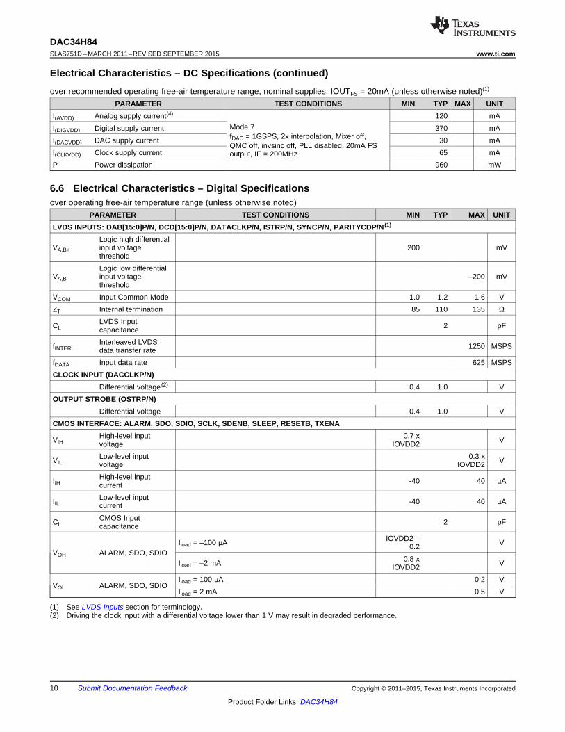
6.6 Electrical Characteristics – Digital Specificationsover operating free-air temperature range (unless otherwise noted)
PARAMETER TEST CONDITIONS MIN TYP MAX UNITLVDS INPUTS: DAB[15:0]P/N, DCD[15:0]P/N, DATACLKP/N, ISTRP/N, SYNCP/N, PARITYCDP/N (1)
Logic high differentialVA,B+ input voltage 200 mV
thresholdLogic low differential
VA,B– input voltage –200 mVthreshold
VCOM Input Common Mode 1.0 1.2 1.6 VZT Internal termination 85 110 135 Ω
LVDS InputCL 2 pFcapacitanceInterleaved LVDSfINTERL 1250 MSPSdata transfer rate
fDATA Input data rate 625 MSPSCLOCK INPUT (DACCLKP/N)
Differential voltage (2) 0.4 1.0 VOUTPUT STROBE (OSTRP/N)
Differential voltage 0.4 1.0 VCMOS INTERFACE: ALARM, SDO, SDIO, SCLK, SDENB, SLEEP, RESETB, TXENA
High-level input 0.7 xVIH Vvoltage IOVDD2Low-level input 0.3 xVIL Vvoltage IOVDD2High-level inputIIH -40 40 µAcurrentLow-level inputIIL -40 40 µAcurrentCMOS InputCI 2 pFcapacitance
IOVDD2 –Iload = –100 μA V0.2VOH ALARM, SDO, SDIO
0.8 xIload = –2 mA VIOVDD2Iload = 100 μA 0.2 V
VOL ALARM, SDO, SDIOIload = 2 mA 0.5 V
(1) See LVDS Inputs section for terminology.(2) Driving the clock input with a differential voltage lower than 1 V may result in degraded performance.
10 Submit Documentation Feedback Copyright © 2011–2015, Texas Instruments Incorporated
Product Folder Links: DAC34H84

DAC34H84www.ti.com SLAS751D –MARCH 2011–REVISED SEPTEMBER 2015
6.7 Electrical Characteristics – AC Specificationsover recommended operating free-air temperature range, nominal supplies, IOUTFS = 20mA (unless otherwise noted)
PARAMETER TEST CONDITIONS MIN TYP MAX UNIT
ANALOG OUTPUT (1)
PLL OFF 1250fDAC Maximum DAC rate MSPS
PLL ON 1000
AC PERFORMANCE (2)
fDAC = 1.25 GSPS, fOUT = 20 MHz 73Spurious free dynamic rangeSFDR fDAC = 1.25 GSPS, fOUT = 50 MHz 70 dBc(0 to fDAC/2) Tone at 0 dBFS
fDAC = 1.25 GSPS, fOUT = 70 MHz 66
fDAC = 1.25 MSPS, fOUT = 30 ± 0.5 MHz 87Third-order two-tone intermodulationdistortionIMD3 fDAC = 1.25 GSPS, fOUT = 50 ± 0.5 MHz 85 dBcEach tone at –12 dBFS fDAC = 1.25 GSPS, fOUT = 100 ± 0.5 MHz 78
fDAC = 1.25 GSPS, fOUT = 10 MHz 160Noise Spectral Density (3)NSD dBc/HzTone at 0dBFS fDAC = 1.25 GSPS, fOUT = 80 MHz 155
fDAC = 1.2288 GSPS, fOUT = 30.72 MHz 77Adjacent channel leakage ratio, singlecarrier fDAC = 1.2288 GSPS, fOUT = 153.6 MHz 74
ACLR (3) dBcfDAC = 1.2288 GSPS, fOUT = 30.72 MHz 82Alternate channel leakage ratio, single
carrier fDAC = 1.2288 GSPS, fOUT = 153.6 MHz 80
Channel Isolation fDAC = 1.25 GSPS, fOUT = 10 MHz 95 dBc
(1) Measured single ended into 50 Ω load.(2) 4:1 transformer output termination, 50 Ω doubly terminated load(3) Single carrier, W-CDMA with 3.84 MHz BW, 5-MHz spacing, centered at IF, PAR = 12dB. TESTMODEL 1, 10 ms
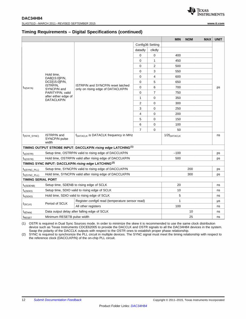
6.8 Timing Requirements – Digital SpecificationsMIN NOM MAX UNIT
CLOCK INPUT (DACCLKP/N)Duty cycle 40% 60%DACCLKP/N input frequency 1250 MHz
OUTPUT STROBE (OSTRP/N)fOSTR = fDACCLK / (n x 8 x Interp) where n is any positive fDACCLK /fOSTR Frequency MHzinteger, fDACCLK is DACCLK frequency in MHz (8 x interp)
Duty cycle 50%DIGITAL INPUT TIMING SPECIFICATIONSTiming LVDS inputs: D[15:0]P/N, FRAMEP/N, SYNCP/N, PARITYP/N, double edge latching
Config36 Settingdatadly clkdly
0 0 1500 1 1000 2 500 3 0
Setup time, 0 4 -50DAB[15:0]P/N,DCD[15:0]P/N, 0 5 -100ISTRP/N, ISTRP/N and SYNCP/N reset latchedts(DATA) 0 6 -150SYNCP/N and only on rising edge of DATACLKP/N
0 7 -200 psPARITYP/N, validto either edge of 1 0 200DATACLKP/N
2 0 2503 0 3004 0 3505 0 4006 0 4507 0 500
Copyright © 2011–2015, Texas Instruments Incorporated Submit Documentation Feedback 11
Product Folder Links: DAC34H84
DAC34H84SLAS751D –MARCH 2011–REVISED SEPTEMBER 2015 www.ti.com
Timing Requirements – Digital Specifications (continued)MIN NOM MAX UNIT
Config36 Settingdatadly clkdly
0 0 4000 1 4500 2 5000 3 550
Hold time, 0 4 600DAB[15:0]P/N,DCD[15:0]P/N, 0 5 650ISTRP/N, ISTRP/N and SYNCP/N reset latchedth(DATA) 0 6 700 psSYNCP/N and only on rising edge of DATACLKP/N
0 7 750PARITYP/N, validafter either edge of 1 0 350DATACLKP/N
2 0 3003 0 2504 0 2005 0 1506 0 1007 0 50
t(ISTR_SYNC) ISTRP/N and fDATACLK is DATACLK frequency in MHz 1/2fDATACLK nsSYNCP/N pulsewidth
TIMING OUTPUT STROBE INPUT: DACCLKP/N rising edge LATCHING (1)
ts(OSTR) Setup time, OSTRP/N valid to rising edge of DACCLKP/N –100 psth(OSTR) Hold time, OSTRP/N valid after rising edge of DACCLKP/N 500 psTIMING SYNC INPUT: DACCLKP/N rising edge LATCHING (2)
ts(SYNC_PLL) Setup time, SYNCP/N valid to rising edge of DACCLKP/N 200 psth(SYNC_PLL) Hold time, SYNCP/N valid after rising edge of DACCLKP/N 300 psTIMING SERIAL PORTts(SDENB) Setup time, SDENB to rising edge of SCLK 20 nsts(SDIO) Setup time, SDIO valid to rising edge of SCLK 10 nsth(SDIO) Hold time, SDIO valid to rising edge of SCLK 5 ns
Register config6 read (temperature sensor read) 1 µst(SCLK) Period of SCLK
All other registers 100 nstd(Data) Data output delay after falling edge of SCLK 10 nstRESET Minimum RESETB pulse width 25 ns
(1) OSTR is required in Dual Sync Sources mode. In order to minimize the skew it is recommended to use the same clock distributiondevice such as Texas Instruments CDCE62005 to provide the DACCLK and OSTR signals to all the DAC34H84 devices in the system.Swap the polarity of the DACCLK outputs with respect to the OSTR ones to establish proper phase relationship.
(2) SYNC is required to synchronize the PLL circuit in multiple devices. The SYNC signal must meet the timing relationship with respect tothe reference clock (DACCLKP/N) of the on-chip PLL circuit.
12 Submit Documentation Feedback Copyright © 2011–2015, Texas Instruments Incorporated
Product Folder Links: DAC34H84
DAC34H84www.ti.com SLAS751D –MARCH 2011–REVISED SEPTEMBER 2015
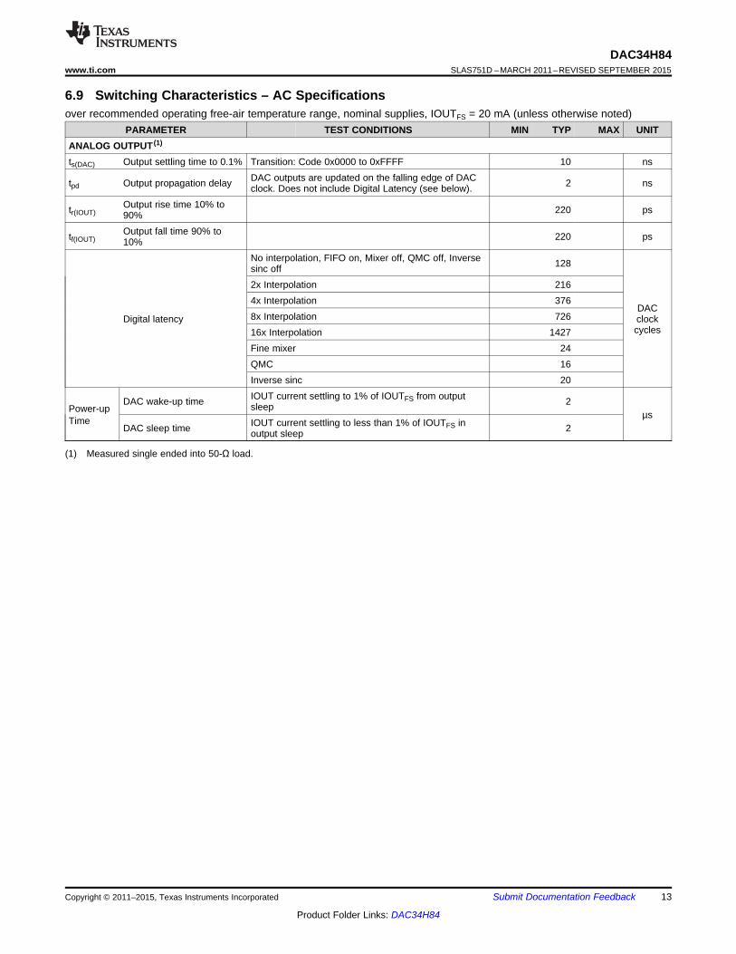
6.9 Switching Characteristics – AC Specificationsover recommended operating free-air temperature range, nominal supplies, IOUTFS = 20 mA (unless otherwise noted)
PARAMETER TEST CONDITIONS MIN TYP MAX UNITANALOG OUTPUT (1)
ts(DAC) Output settling time to 0.1% Transition: Code 0x0000 to 0xFFFF 10 nsDAC outputs are updated on the falling edge of DACtpd Output propagation delay 2 nsclock. Does not include Digital Latency (see below).
Output rise time 10% totr(IOUT) 220 ps90%Output fall time 90% totf(IOUT) 220 ps10%
No interpolation, FIFO on, Mixer off, QMC off, Inverse 128sinc off2x Interpolation 2164x Interpolation 376
DAC8x Interpolation 726Digital latency clock
cycles16x Interpolation 1427Fine mixer 24QMC 16Inverse sinc 20IOUT current settling to 1% of IOUTFS from outputDAC wake-up time 2sleepPower-up µsTime IOUT current settling to less than 1% of IOUTFS inDAC sleep time 2output sleep
(1) Measured single ended into 50-Ω load.
Copyright © 2011–2015, Texas Instruments Incorporated Submit Documentation Feedback 13
Product Folder Links: DAC34H84
30
40
50
60
70
80
90
100
0 100 200 300 400 500 600Output Frequency (MHz)
Thi
rd H
arm
onic
Dis
tort
ion
(dB
c)
0 dBFS−6 dBFS−12 dBFS
30
40
50
60
70
80
90
100
0 100 200 300 400 500 600Output Frequency (MHz)
SF
DR
(dB
c)
fDATA = 625 MSPS, 1x InterpolationfDATA = 625 MSPS, 2x InterpolationfDATA = 312.5 MSPS, 4x InterpolationfDATA = 156.25MSPS, 8x InterpolationfDATA = 78.125MSPS, 16x Interpolation
30
40
50
60
70
80
90
100
0 100 200 300 400 500 600Output Frequency (MHz)
SF
DR
(dB
c)
0 dBFS−6 dBFS−12 dBFS
30
40
50
60
70
80
90
100
0 100 200 300 400 500 600Output Frequency (MHz)
Sec
ond
Har
mon
ic D
isto
rtio
n (d
Bc)
0 dBFS−6 dBFS−12 dBFS
−6
−5
−4
−3
−2
−1
0
1
2
3
4
5
6
0 10k 20k 30k 40k 50k 60kCode
Inte
gral
Non
linea
rity
Err
or (
LSB
)
−5
−4
−3
−2
−1
0
1
2
3
4
5
0 10k 20k 30k 40k 50k 60kCode
Diff
eren
tial N
onlin
earit
y E
rror
(LS
B)
DAC34H84SLAS751D –MARCH 2011–REVISED SEPTEMBER 2015 www.ti.com
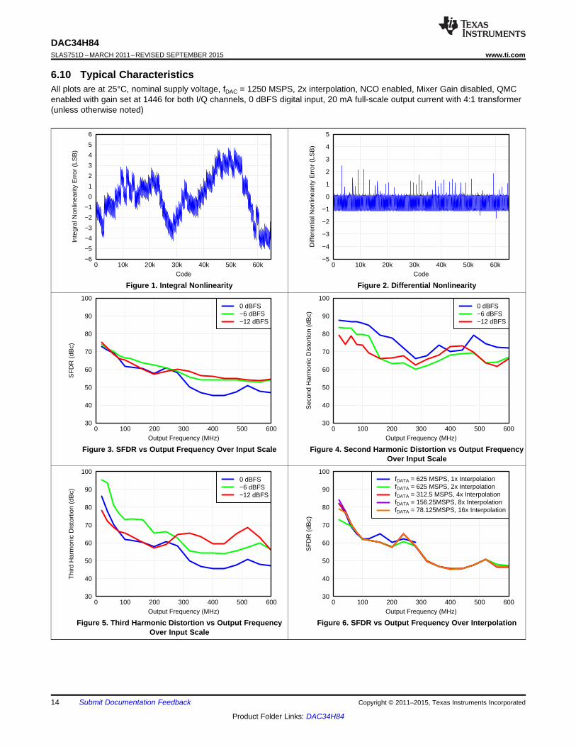
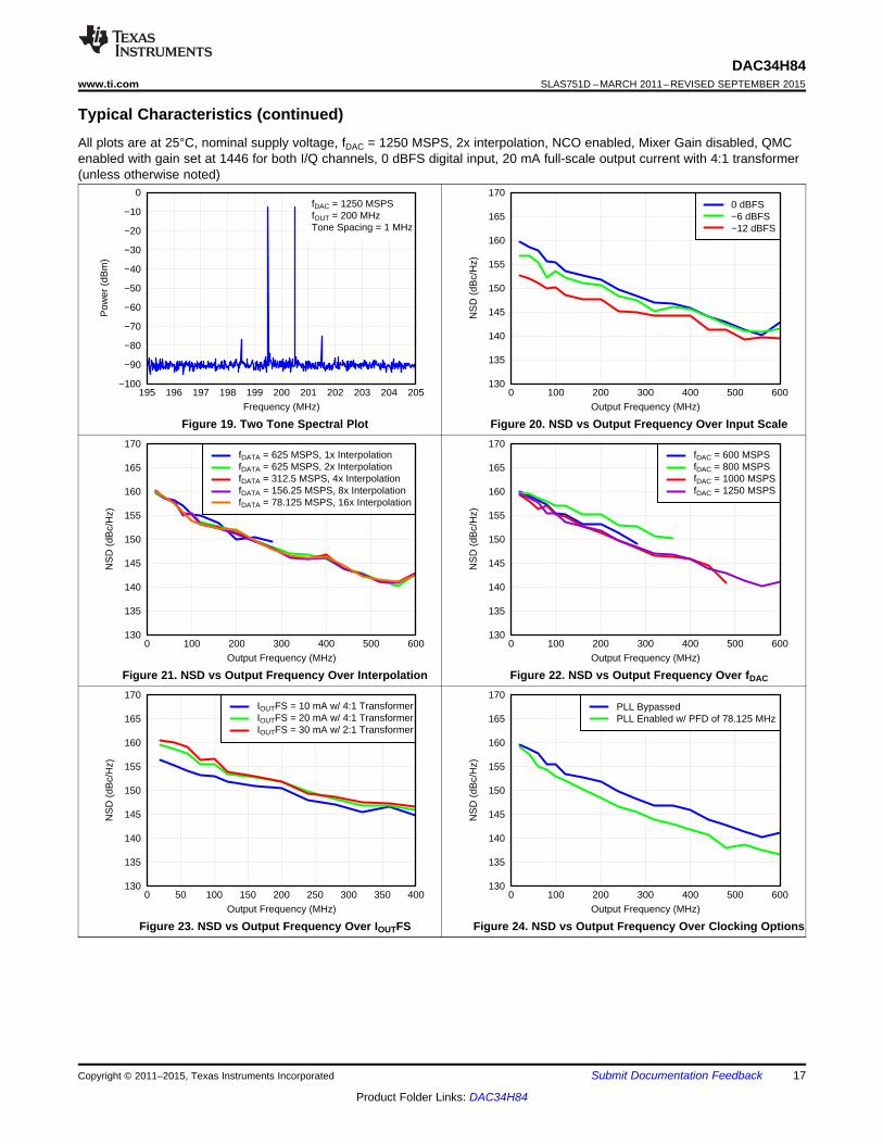
6.10 Typical CharacteristicsAll plots are at 25°C, nominal supply voltage, fDAC = 1250 MSPS, 2x interpolation, NCO enabled, Mixer Gain disabled, QMCenabled with gain set at 1446 for both I/Q channels, 0 dBFS digital input, 20 mA full-scale output current with 4:1 transformer(unless otherwise noted)
Figure 1. Integral Nonlinearity Figure 2. Differential Nonlinearity
Figure 3. SFDR vs Output Frequency Over Input Scale Figure 4. Second Harmonic Distortion vs Output FrequencyOver Input Scale
Figure 5. Third Harmonic Distortion vs Output Frequency Figure 6. SFDR vs Output Frequency Over InterpolationOver Input Scale
14 Submit Documentation Feedback Copyright © 2011–2015, Texas Instruments Incorporated
Product Folder Links: DAC34H84
−90
−80
−70
−60
−50
−40
−30
−20
−10
0
10
0 100 200 300 400 500 600Frequency (MHz)
Pow
er (
dBm
)
fDAC = 1250 MSPSfOUT = 150 MHz
−90
−80
−70
−60
−50
−40
−30
−20
−10
0
10
10 110 210 310 410 510 610Frequency (MHz)
Pow
er (
dBm
)
fDAC = 1250 MSPSfOUT = 200 MHz
−90
−80
−70
−60
−50
−40
−30
−20
−10
0
10
0 100 200 300 400 500 600Frequency (MHz)
Pow
er (
dBm
)
NCO BypassedQMC BypassedfDAC = 1250 MSPSfOUT = 20 MHz
−90
−80
−70
−60
−50
−40
−30
−20
−10
0
10
0 100 200 300 400 500 600Frequency (MHz)
Pow
er (
dBm
)
NCO BypassedQMC BypassedfDAC = 1250 MSPSfOUT = 70 MHz
30
40
50
60
70
80
90
100
0 100 200 300 400 500 600Output Frequency (MHz)
SF
DR
(dB
c)
fDAC = 600 MSPSfDAC = 800 MSPSfDAC = 1000 MSPSfDAC = 1250 MSPS
30
40
50
60
70
80
90
100
0 50 100 150 200 250 300 350 400Output Frequency (MHz)
SF
DR
(dB
c)
IOUTFS = 10 mA w/ 4:1 TransformerIOUTFS = 20 mA w/ 4:1 TransformerIOUTFS = 30 mA w/ 2:1 Transformer
DAC34H84www.ti.com SLAS751D –MARCH 2011–REVISED SEPTEMBER 2015
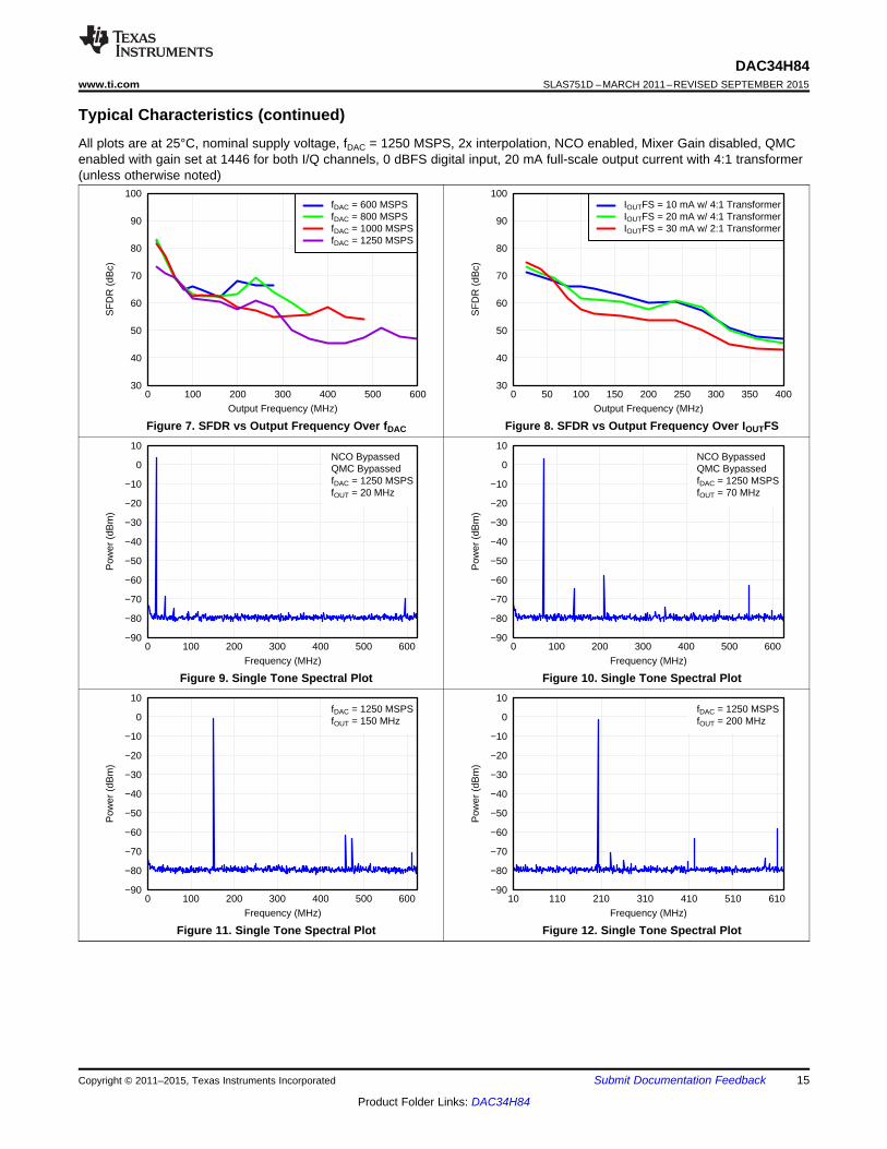
Typical Characteristics (continued)All plots are at 25°C, nominal supply voltage, fDAC = 1250 MSPS, 2x interpolation, NCO enabled, Mixer Gain disabled, QMCenabled with gain set at 1446 for both I/Q channels, 0 dBFS digital input, 20 mA full-scale output current with 4:1 transformer(unless otherwise noted)
Figure 7. SFDR vs Output Frequency Over fDAC Figure 8. SFDR vs Output Frequency Over IOUTFS
Figure 9. Single Tone Spectral Plot Figure 10. Single Tone Spectral Plot
Figure 11. Single Tone Spectral Plot Figure 12. Single Tone Spectral Plot
Copyright © 2011–2015, Texas Instruments Incorporated Submit Documentation Feedback 15
Product Folder Links: DAC34H84
30
40
50
60
70
80
90
100
0 50 100 150 200 250 300 350 400Output Frequency (MHz)
IMD
3 (d
Bc)
IOUTFS = 10 mA w/ 4:1 TransformerIOUTFS = 20 mA w/ 4:1 TransformerIOUTFS = 30 mA w/ 2:1 Transformer
−100
−90
−80
−70
−60
−50
−40
−30
−20
−10
0
65 66 67 68 69 70 71 72 73 74 75Frequency (MHz)
Pow
er (
dBm
)
NCO BypassedQMC BypassedfDAC = 1250 MSPSfOUT = 70 MHzTone Spacing = 1 MHz
30
40
50
60
70
80
90
100
0 100 200 300 400 500 600Output Frequency (MHz)
SF
DR
(dB
c)
fDATA = 625 MSPS, 1x InterpolationfDATA = 625 MSPS, 2x InterpolationfDATA = 312.5 MSPS, 4x InterpolationfDATA = 156.25 MSPS, 8x InterpolationfDATA = 78.125 MSPS, 16x Interpolation
30
40
50
60
70
80
90
100
0 100 200 300 400 500 600Output Frequency (MHz)
IMD
3 (d
Bc)
fDAC = 600 MSPSfDAC = 800 MSPSfDAC = 1000 MSPSfDAC = 1250 MSPS
−90
−80
−70
−60
−50
−40
−30
−20
−10
0
10
10 110 210 310 410 510 610Frequency (MHz)
Pow
er (
dBm
)
PLL Enabled w/ PFD of 78.125 MHzfDAC = 1250 MSPSfOUT = 200 MHz
30
40
50
60
70
80
90
100
0 100 200 300 400 500 600Output Frequency (MHz)
IMD
3 (d
Bc)
0 dBFS−6 dBFS−12 dBFS
DAC34H84SLAS751D –MARCH 2011–REVISED SEPTEMBER 2015 www.ti.com
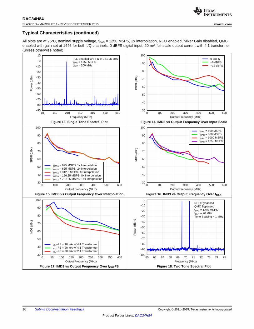
Typical Characteristics (continued)All plots are at 25°C, nominal supply voltage, fDAC = 1250 MSPS, 2x interpolation, NCO enabled, Mixer Gain disabled, QMCenabled with gain set at 1446 for both I/Q channels, 0 dBFS digital input, 20 mA full-scale output current with 4:1 transformer(unless otherwise noted)
Figure 13. Single Tone Spectral Plot Figure 14. IMD3 vs Output Frequency Over Input Scale
Figure 15. IMD3 vs Output Frequency Over Interpolation Figure 16. IMD3 vs Output Frequency Over fDAC
Figure 17. IMD3 vs Output Frequency Over IOUTFS Figure 18. Two Tone Spectral Plot
16 Submit Documentation Feedback Copyright © 2011–2015, Texas Instruments Incorporated
Product Folder Links: DAC34H84
130
135
140
145
150
155
160
165
170
0 50 100 150 200 250 300 350 400Output Frequency (MHz)
NS
D (
dBc/
Hz)
IOUTFS = 10 mA w/ 4:1 TransformerIOUTFS = 20 mA w/ 4:1 TransformerIOUTFS = 30 mA w/ 2:1 Transformer
130
135
140
145
150
155
160
165
170
0 100 200 300 400 500 600Output Frequency (MHz)
NS
D (
dBc/
Hz)
PLL BypassedPLL Enabled w/ PFD of 78.125 MHz
130
135
140
145
150
155
160
165
170
0 100 200 300 400 500 600Output Frequency (MHz)
NS
D (
dBc/
Hz)
fDATA = 625 MSPS, 1x InterpolationfDATA = 625 MSPS, 2x InterpolationfDATA = 312.5 MSPS, 4x InterpolationfDATA = 156.25 MSPS, 8x InterpolationfDATA = 78.125 MSPS, 16x Interpolation
130
135
140
145
150
155
160
165
170
0 100 200 300 400 500 600Output Frequency (MHz)
NS
D (
dBc/
Hz)
fDAC = 600 MSPSfDAC = 800 MSPSfDAC = 1000 MSPSfDAC = 1250 MSPS
−100
−90
−80
−70
−60
−50
−40
−30
−20
−10
0
195 196 197 198 199 200 201 202 203 204 205Frequency (MHz)
Pow
er (
dBm
)
fDAC = 1250 MSPSfOUT = 200 MHzTone Spacing = 1 MHz
130
135
140
145
150
155
160
165
170
0 100 200 300 400 500 600Output Frequency (MHz)
NS
D (
dBc/
Hz)
0 dBFS−6 dBFS−12 dBFS
DAC34H84www.ti.com SLAS751D –MARCH 2011–REVISED SEPTEMBER 2015
Typical Characteristics (continued)All plots are at 25°C, nominal supply voltage, fDAC = 1250 MSPS, 2x interpolation, NCO enabled, Mixer Gain disabled, QMCenabled with gain set at 1446 for both I/Q channels, 0 dBFS digital input, 20 mA full-scale output current with 4:1 transformer(unless otherwise noted)
Figure 19. Two Tone Spectral Plot Figure 20. NSD vs Output Frequency Over Input Scale
Figure 21. NSD vs Output Frequency Over Interpolation Figure 22. NSD vs Output Frequency Over fDAC
Figure 23. NSD vs Output Frequency Over IOUTFS Figure 24. NSD vs Output Frequency Over Clocking Options
Copyright © 2011–2015, Texas Instruments Incorporated Submit Documentation Feedback 17
Product Folder Links: DAC34H84
2x Interpolation, 0 dBFSf = 1228.8 MSPS
f = 70 MHzDAC
OUT2x Interpolation, 0 dBFSf = 1228.8 MSPS
f = 200 MHzDAC
OUT
2x Interpolation, 0 dBFSf = 1228.8 MSPS
f = 70 MHzDAC
OUT
2x Interpolation, 0 dBFSf = 1228.8 MSPS
f = 120 MHzDAC
OUT
55
60
65
70
75
80
85
0 100 200 300 400 500 600Output Frequency (MHz)
AC
LR (
dBc)
PLL DisabledPLL Enabled
55
60
65
70
75
80
85
0 100 200 300 400 500 600Output Frequency (MHz)
AC
LR (
dBc)
PLL DisabledPLL Enabled
DAC34H84SLAS751D –MARCH 2011–REVISED SEPTEMBER 2015 www.ti.com
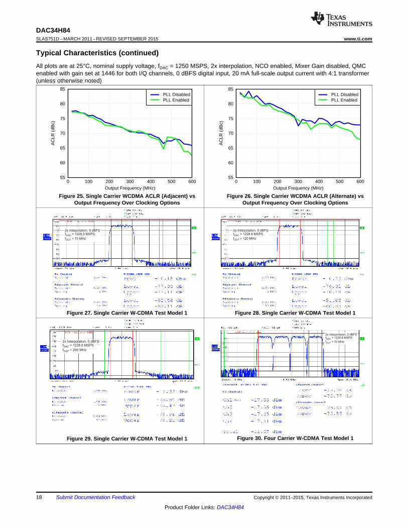
Typical Characteristics (continued)All plots are at 25°C, nominal supply voltage, fDAC = 1250 MSPS, 2x interpolation, NCO enabled, Mixer Gain disabled, QMCenabled with gain set at 1446 for both I/Q channels, 0 dBFS digital input, 20 mA full-scale output current with 4:1 transformer(unless otherwise noted)
Figure 25. Single Carrier WCDMA ACLR (Adjacent) vs Figure 26. Single Carrier WCDMA ACLR (Alternate) vsOutput Frequency Over Clocking Options Output Frequency Over Clocking Options
Figure 27. Single Carrier W-CDMA Test Model 1 Figure 28. Single Carrier W-CDMA Test Model 1
Figure 30. Four Carrier W-CDMA Test Model 1Figure 29. Single Carrier W-CDMA Test Model 1
18 Submit Documentation Feedback Copyright © 2011–2015, Texas Instruments Incorporated
Product Folder Links: DAC34H84
2x Interpolation, 0 dBFSf = 1228.8 MSPS
f = 140 MHzDAC
OUT
2x Interpolation, 0 dBFSf = 1228.8 MSPS
f = 240 MHzDAC
OUT
2x Interpolation, 0 dBFSf = 1228.8 MSPS
f = 140 MHzDAC
OUT
2x Interpolation, 0 dBFSf = 1228.8 MSPS
f = 240 MHzDAC
OUT
2x Interpolation, 0 dBFSf = 1228.8 MSPS
f = 120 MHzDAC
OUT
2x Interpolation, 0 dBFSf = 1228.8 MSPS
f = 200 MHzDAC
OUT
DAC34H84www.ti.com SLAS751D –MARCH 2011–REVISED SEPTEMBER 2015
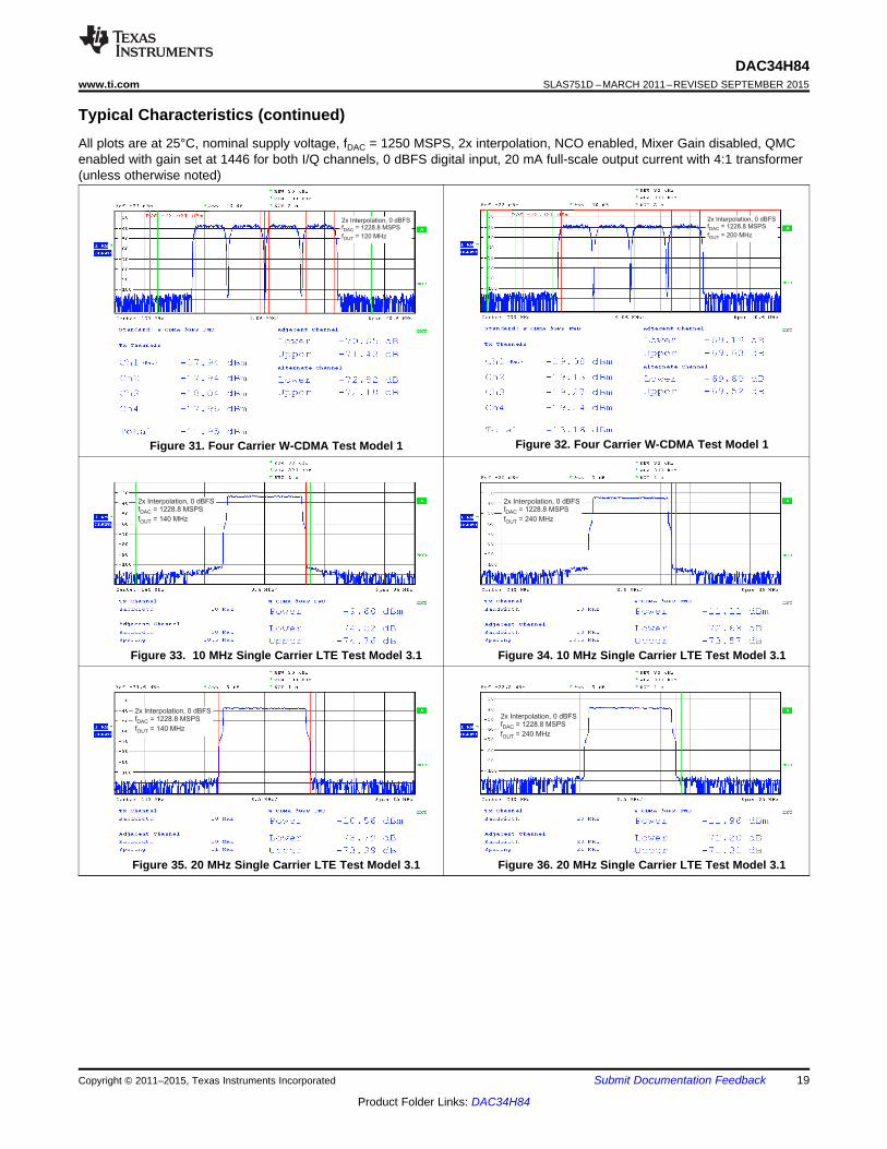
Typical Characteristics (continued)All plots are at 25°C, nominal supply voltage, fDAC = 1250 MSPS, 2x interpolation, NCO enabled, Mixer Gain disabled, QMCenabled with gain set at 1446 for both I/Q channels, 0 dBFS digital input, 20 mA full-scale output current with 4:1 transformer(unless otherwise noted)
Figure 32. Four Carrier W-CDMA Test Model 1Figure 31. Four Carrier W-CDMA Test Model 1
Figure 33. 10 MHz Single Carrier LTE Test Model 3.1 Figure 34. 10 MHz Single Carrier LTE Test Model 3.1
Figure 35. 20 MHz Single Carrier LTE Test Model 3.1 Figure 36. 20 MHz Single Carrier LTE Test Model 3.1
Copyright © 2011–2015, Texas Instruments Incorporated Submit Documentation Feedback 19
Product Folder Links: DAC34H84
0
100
200
300
400
500
600
700
0 200 400 600 800 1000 1200
fDAC (MSPS)
DIG
VD
D C
urre
nt (
mA
)
1x Interpolation2x Interpolation4x Interpolation8x Interpolation16x Interpolation
Bandbase Input = 0 MHzNCO Enabled w/ 5 MHz MixingQMC Enabled
0
20
40
60
80
100
120
140
160
0 200 400 600 800 1000 1200
fDAC (MSPS)
DIG
VD
D C
urre
nt (
mA
)
NCO EnabledQMC Enabled
0
20
40
60
80
100
120
140
160
0 200 400 600 800 1000 1200
fDAC (MSPS)
Pow
er C
onsu
mpt
ion
(mW
)
NCO EnabledQMC Enabled
0
100
200
300
400
500
600
700
0 200 400 600 800 1000 1200
fDAC (MSPS)
DIG
VD
D C
urre
nt (
mA
)
1x Interpolation2x Interpolation4x Interpolation8x Interpolation16x Interpolation
Bandbase Input = 5 MHzNCO DisabledQMC DisabledCMIX Disabled
200
400
600
800
1000
1200
1400
0 200 400 600 800 1000 1200
fDAC (MSPS)
Pow
er C
onsu
mpt
ion
(mW
)
1x Interpolation2x Interpolation4x Interpolation8x Interpolation16x Interpolation
Bandbase Input = 5 MHzNCO DisabledQMC DisabledCMIX Disabled
200
400
600
800
1000
1200
1400
0 200 400 600 800 1000 1200
fDAC (MSPS)
Pow
er C
onsu
mpt
ion
(mW
)
1x Interpolation2x Interpolation4x Interpolation8x Interpolation16x Interpolation
Bandbase Input = 0 MHzNCO Enabled w/ 5 MHz MixingQMC Enabled
DAC34H84SLAS751D –MARCH 2011–REVISED SEPTEMBER 2015 www.ti.com
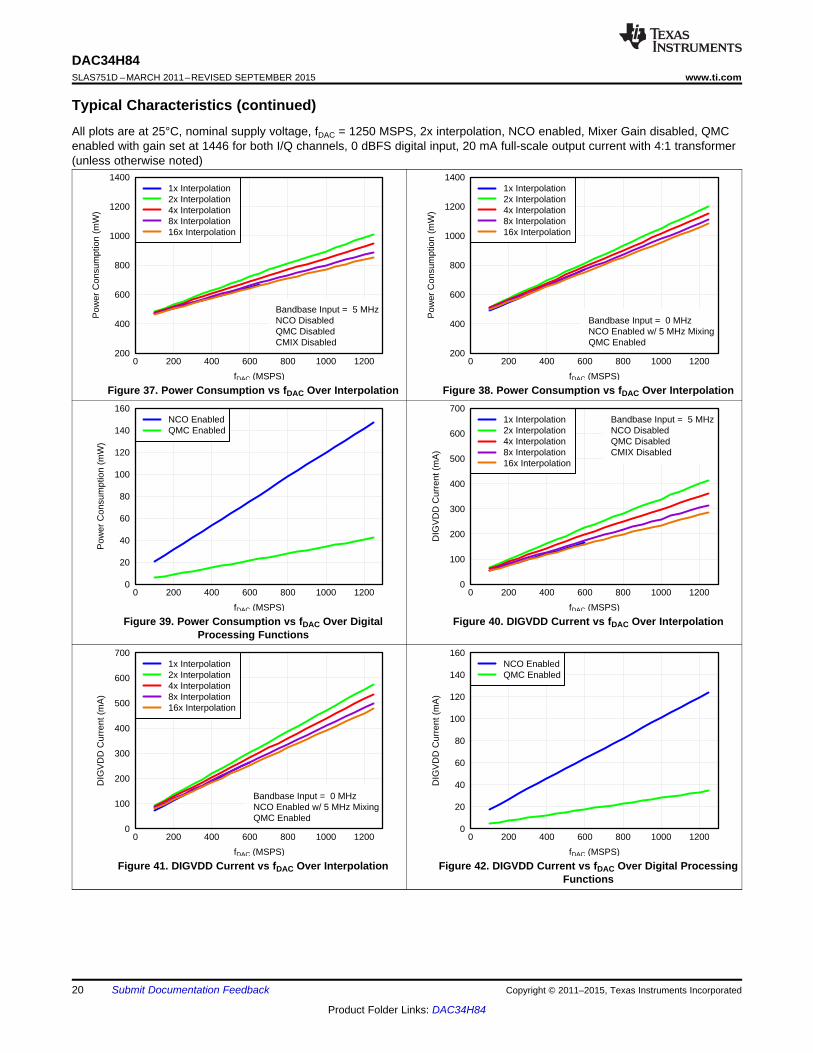
Typical Characteristics (continued)All plots are at 25°C, nominal supply voltage, fDAC = 1250 MSPS, 2x interpolation, NCO enabled, Mixer Gain disabled, QMCenabled with gain set at 1446 for both I/Q channels, 0 dBFS digital input, 20 mA full-scale output current with 4:1 transformer(unless otherwise noted)
Figure 37. Power Consumption vs fDAC Over Interpolation Figure 38. Power Consumption vs fDAC Over Interpolation
Figure 39. Power Consumption vs fDAC Over Digital Figure 40. DIGVDD Current vs fDAC Over InterpolationProcessing Functions
Figure 41. DIGVDD Current vs fDAC Over Interpolation Figure 42. DIGVDD Current vs fDAC Over Digital ProcessingFunctions
20 Submit Documentation Feedback Copyright © 2011–2015, Texas Instruments Incorporated
Product Folder Links: DAC34H84
40
50
60
70
80
90
100
110
120
0 100 200 300 400 500 600Output Frequency (MHz)
Inte
rfer
ence
Lev
el (
dBc)
Channel CChannel D
Channel C/D OffChannel A/B Active
0
10
20
30
40
50
60
70
80
90
100
110
0 32 64 96 128 160 192 224 256Step Code
Gro
up D
elay
(ps
)
Channel AChannel BChannel CChannel D
fDAC = 614.4 MSPSfOUT = 138.4 MHz
0
20
40
60
80
100
120
140
0 200 400 600 800 1000 1200
fDAC (MSPS)
AV
DD
Cur
rent
(m
A)
40
50
60
70
80
90
100
110
120
0 100 200 300 400 500 600Output Frequency (MHz)
Inte
rfer
ence
Lev
el (
dBc)
Channel AChannel B
Channel A/B OffChannel C/D Active
0
5
10
15
20
25
30
35
40
0 200 400 600 800 1000 1200
fDAC (MSPS)
DA
CV
DD
Cur
rent
(m
A)
0
10
20
30
40
50
60
70
80
90
100
0 200 400 600 800 1000 1200
fDAC (MSPS)
CLK
VD
D C
urre
nt (
mA
)
DAC34H84www.ti.com SLAS751D –MARCH 2011–REVISED SEPTEMBER 2015
Typical Characteristics (continued)All plots are at 25°C, nominal supply voltage, fDAC = 1250 MSPS, 2x interpolation, NCO enabled, Mixer Gain disabled, QMCenabled with gain set at 1446 for both I/Q channels, 0 dBFS digital input, 20 mA full-scale output current with 4:1 transformer(unless otherwise noted)
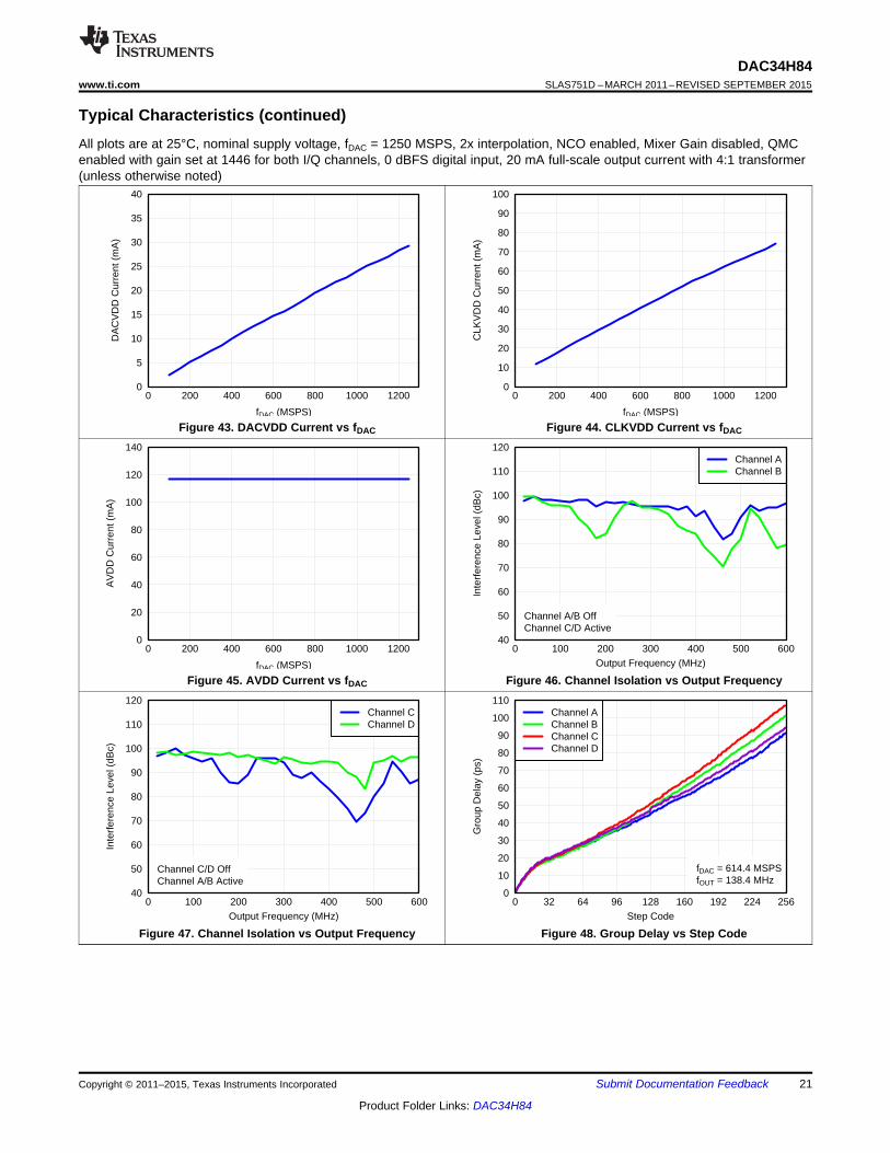
Figure 43. DACVDD Current vs fDAC Figure 44. CLKVDD Current vs fDAC
Figure 45. AVDD Current vs fDAC Figure 46. Channel Isolation vs Output Frequency
Figure 47. Channel Isolation vs Output Frequency Figure 48. Group Delay vs Step Code
Copyright © 2011–2015, Texas Instruments Incorporated Submit Documentation Feedback 21
Product Folder Links: DAC34H84
DAC34H84SLAS751D –MARCH 2011–REVISED SEPTEMBER 2015 www.ti.com
7 Detailed Description
7.1 OverviewThe DAC34H84 includes a quad-channel, 16-bit digital-to-analog converter (DAC) with up to 1.25 GSPS samplerate, a 32-bit LVDS data bus with on-chip termination, FIFO, data pattern checker, and parity test. The deviceincludes 2x to 16x digital interpolation filters with over 90dB of stop-band attenuation, reconstruction filters,independent complex mixers, a low jitter clock multiplier, and digital Quadrature Modulator Correction (QMC).
Full synchronization of multiple devices is possible with the DAC3484. It is an ideal device for next generationcommunication systems.
22 Submit Documentation Feedback Copyright © 2011–2015, Texas Instruments Incorporated
Product Folder Links: DAC34H84
10
01
00
Pa
tte
rnTe
st
Pa
tte
rnTe
st
De
-in
terle
ave
16
16
16
10
01
00
Control InterfaceTemp
Sensor
B0460-01
DCD15P
DCD15N
•••
•••
•••
•••
•••
•••
DCD0P
DCD0N
ISTR/PARITYABP
PARITYCDP
CD
-Da
ta B
us
AB
-Da
ta B
us
ISTR/PARITYABN
PARITYCDN
OSTRP
OSTRN
SD
O
SD
IO
SD
EN
B
SC
LK
TX
EN
B
RE
SE
TB
AVDD
GN
D
LVDS
LVPECL
LVDS
LVDS
LVDS
8 S
am
ple
FIF
O
16
AL
AR
M
SL
EE
P
10
0
SYNCP
SYNCN
LVDS
10
01
00
DAB0P
DAB15P
DAB0N
DAB15N
LVDS
LVDS
Pro
gra
mm
ab
le D
ela
y
TE
ST
MO
DE
IOV
DD
IOV
DD
2
Co
mp
lex M
ixe
r(F
MIX
or
CM
IX)
AB
-QM
CG
ain
an
d P
ha
se
16-bDACB
16-bDACA
IOUTA1
IOUTA2
IOUTB1
IOUTB2
QMCB-offset
QMCA-offset
x2 x2 x2 x2
x2 x2 x2 x2
FIR1FIR0
x
sin(x)
x
sin(x)
DACGain
FIR3FIR2
AB-Channel
FIR4
2x–16x Interpolation
AB32-Bit NCO
cos sin
CMIX Control(±n*Fs/8)
59 taps 23 taps 11 taps 11 taps 9 taps
A-GroupDelay
B-GroupDelay
Clock DistributionEXTIO
BIASJ
DACCLKP
DACCLKN
DATACLKP
DATACLKN
CL
KV
DD
DIG
VD
D
VF
US
E
DA
CV
DD
LVPECL
10
0
LVDS
ProgrammableDelay
Low JitterPLL
LP
F
PL
LA
VD
D
1.2-VReference
CD32-Bit NCO
cos sin
Co
mp
lex M
ixe
r(F
MIX
or
CM
IX)
CD
-QM
CG
ain
an
d P
ha
se
16-bDACD
16-bDACC
IOUTC1
IOUTC2
IOUTD1
IOUTD2
QMCD-offset
QMCC-offset
x2 x2 x2 x2
x2 x2 x2 x2
FIR1FIR0
x
sin(x)
x
sin(x)
FIR3FIR2
CD-Channel
FIR4
59 taps 23 taps 11 taps 11 taps 9 taps
C-GroupDelay
D-GroupDelay
DAC34H84www.ti.com SLAS751D –MARCH 2011–REVISED SEPTEMBER 2015
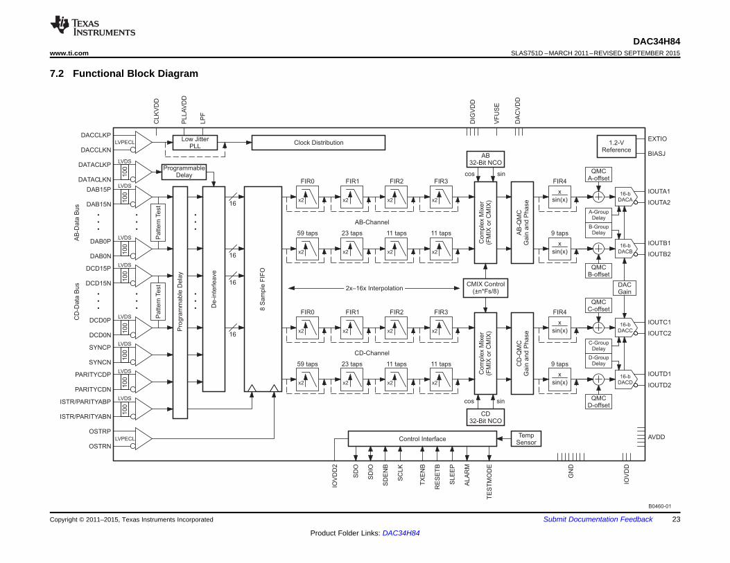
7.2 Functional Block Diagram
Copyright © 2011–2015, Texas Instruments Incorporated Submit Documentation Feedback 23
Product Folder Links: DAC34H84
rwb A6 A5 A4 A3 A2 A1 A0 D15 D14 D13 D12 D11 D10 D9 D8 D7 D6 D5 D4 D3 D2 D1 D0
tS(SDENB)
tH(SDIO)
tS(SDIO)
SDENB
SCLK
SDIO
SDENB
SCLK
SDIO
Instruction Cycle Data Transfer Cycle
T0521-01
t(SCLK)
DAC34H84SLAS751D –MARCH 2011–REVISED SEPTEMBER 2015 www.ti.com
7.3 Feature Description
7.3.1 Serial InterfaceThe serial port of the DAC34H84 is a flexible serial interface which communicates with industry standardmicroprocessors and microcontrollers. The interface provides read/write access to all registers used to define theoperating modes of DAC34H84. It is compatible with most synchronous transfer formats and can be configuredas a 3 or 4 pin interface by sif4_ena in register config2. In both configurations, SCLK is the serial interface inputclock and SDENB is serial interface enable. For 3 pin configuration, SDIO is a bidirectional pin for both data inand data out. For 4 pin configuration, SDIO is data in only and SDO is data out only. Data is input into the devicewith the rising edge of SCLK. Data is output from the device on the falling edge of SCLK.
Each read/write operation is framed by signal SDENB (Serial Data Enable Bar) asserted low. The first frame byteis the instruction cycle which identifies the following data transfer cycle as read or write as well as the 7-bitaddress to be accessed. Table 1 indicates the function of each bit in the instruction cycle and is followed by adetailed description of each bit. The data transfer cycle consists of two bytes
Table 1. Instruction Byte of the Serial InterfaceBIT 7 (MSB) 6 5 4 3 2 1 0 (LSB)
Description R/W A6 A5 A4 A3 A2 A1 A0
R/W Identifies the following data transfer cycle as a read or write operation. A high indicates a readoperation from DAC34H84 and a low indicates a write operation to DAC34H84.
[A6 : A0] Identifies the address of the register to be accessed during the read or write operation.
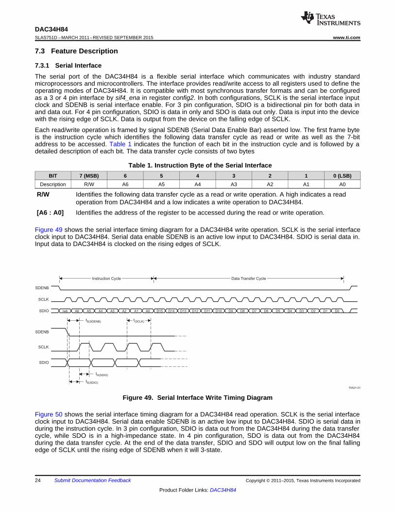
Figure 49 shows the serial interface timing diagram for a DAC34H84 write operation. SCLK is the serial interfaceclock input to DAC34H84. Serial data enable SDENB is an active low input to DAC34H84. SDIO is serial data in.Input data to DAC34H84 is clocked on the rising edges of SCLK.
Figure 49. Serial Interface Write Timing Diagram
Figure 50 shows the serial interface timing diagram for a DAC34H84 read operation. SCLK is the serial interfaceclock input to DAC34H84. Serial data enable SDENB is an active low input to DAC34H84. SDIO is serial data induring the instruction cycle. In 3 pin configuration, SDIO is data out from the DAC34H84 during the data transfercycle, while SDO is in a high-impedance state. In 4 pin configuration, SDO is data out from the DAC34H84during the data transfer cycle. At the end of the data transfer, SDIO and SDO will output low on the final fallingedge of SCLK until the rising edge of SDENB when it will 3-state.
24 Submit Documentation Feedback Copyright © 2011–2015, Texas Instruments Incorporated
Product Folder Links: DAC34H84
rwb A6 A5 A4 A3 A2 A1 A0 D15 D14 D13 D12 D11 D10 D9 D8 D7 D6 D5 D4 D3 D2 D1 D0
D15 D14 D13 D12 D11 D10 D9 D8 D7 D6 D5 D4 D3 D2 D1 D0
td(Data)
SDENB
SCLK
SDIO
SDO
SDENB
SCLK
Instruction Cycle Data Transfer Cycle
T0522-01
SDIOSDO
Data n – 1Data n
DAC34H84www.ti.com SLAS751D –MARCH 2011–REVISED SEPTEMBER 2015
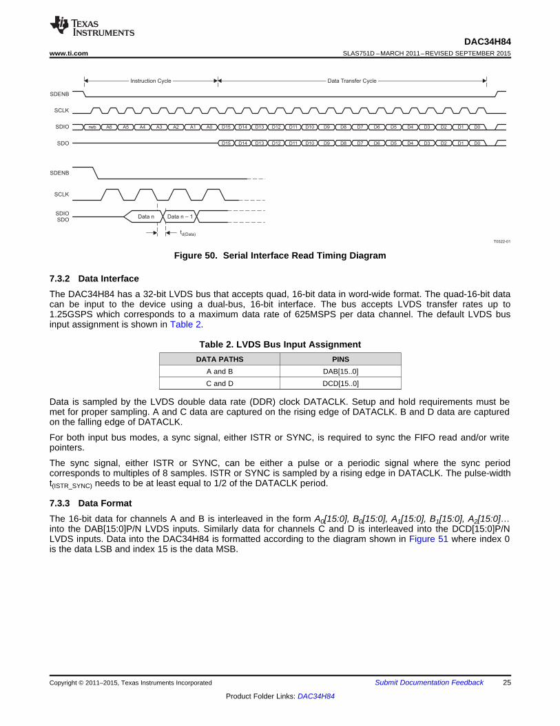
Figure 50. Serial Interface Read Timing Diagram
7.3.2 Data InterfaceThe DAC34H84 has a 32-bit LVDS bus that accepts quad, 16-bit data in word-wide format. The quad-16-bit datacan be input to the device using a dual-bus, 16-bit interface. The bus accepts LVDS transfer rates up to1.25GSPS which corresponds to a maximum data rate of 625MSPS per data channel. The default LVDS businput assignment is shown in Table 2.
Table 2. LVDS Bus Input AssignmentDATA PATHS PINS
A and B DAB[15..0]C and D DCD[15..0]
Data is sampled by the LVDS double data rate (DDR) clock DATACLK. Setup and hold requirements must bemet for proper sampling. A and C data are captured on the rising edge of DATACLK. B and D data are capturedon the falling edge of DATACLK.
For both input bus modes, a sync signal, either ISTR or SYNC, is required to sync the FIFO read and/or writepointers.
The sync signal, either ISTR or SYNC, can be either a pulse or a periodic signal where the sync periodcorresponds to multiples of 8 samples. ISTR or SYNC is sampled by a rising edge in DATACLK. The pulse-widtht(ISTR_SYNC) needs to be at least equal to 1/2 of the DATACLK period.
7.3.3 Data FormatThe 16-bit data for channels A and B is interleaved in the form A0[15:0], B0[15:0], A1[15:0], B1[15:0], A2[15:0]…into the DAB[15:0]P/N LVDS inputs. Similarly data for channels C and D is interleaved into the DCD[15:0]P/NLVDS inputs. Data into the DAC34H84 is formatted according to the diagram shown in Figure 51 where index 0is the data LSB and index 15 is the data MSB.
Copyright © 2011–2015, Texas Instruments Incorporated Submit Documentation Feedback 25
Product Folder Links: DAC34H84
DCD[15:0]P/N
DAB[15:0]P/N
ISTRP/N
SAMPLE 0 SAMPLE 1 SAMPLE 2 SAMPLE 3
SYNCP/N
T0530-01
t(ISTR_SYNC)
t(ISTR_SYNC)
DATACLKP/N (DDR)
SyncOption #1
SyncOption #2
C
[15:0]0
A
[15:0]0
C
[15:0]1
A
[15:0]1
C
[15:0]2
A
[15:0]2
C
[15:0]3
A
[15:0]3
D
[15:0]0
B
[15:0]0
D
[15:0]1
B
[15:0]1
D
[15:0]2
B
[15:0]2
D
[15:0]3
B
[15:0]3
DAC34H84SLAS751D –MARCH 2011–REVISED SEPTEMBER 2015 www.ti.com
Figure 51. Data Transmission Format
The FIFO read and write pointer can also be synced by SIF SYNC as the third sync option if multi-devicesynchronization is not needed. In this sync mode, the syncsel_fifoin(3:0) and syncsel_fifoout(3:0) in registerconfig32 need to be both set to 1000b for the SIF SYNC option.
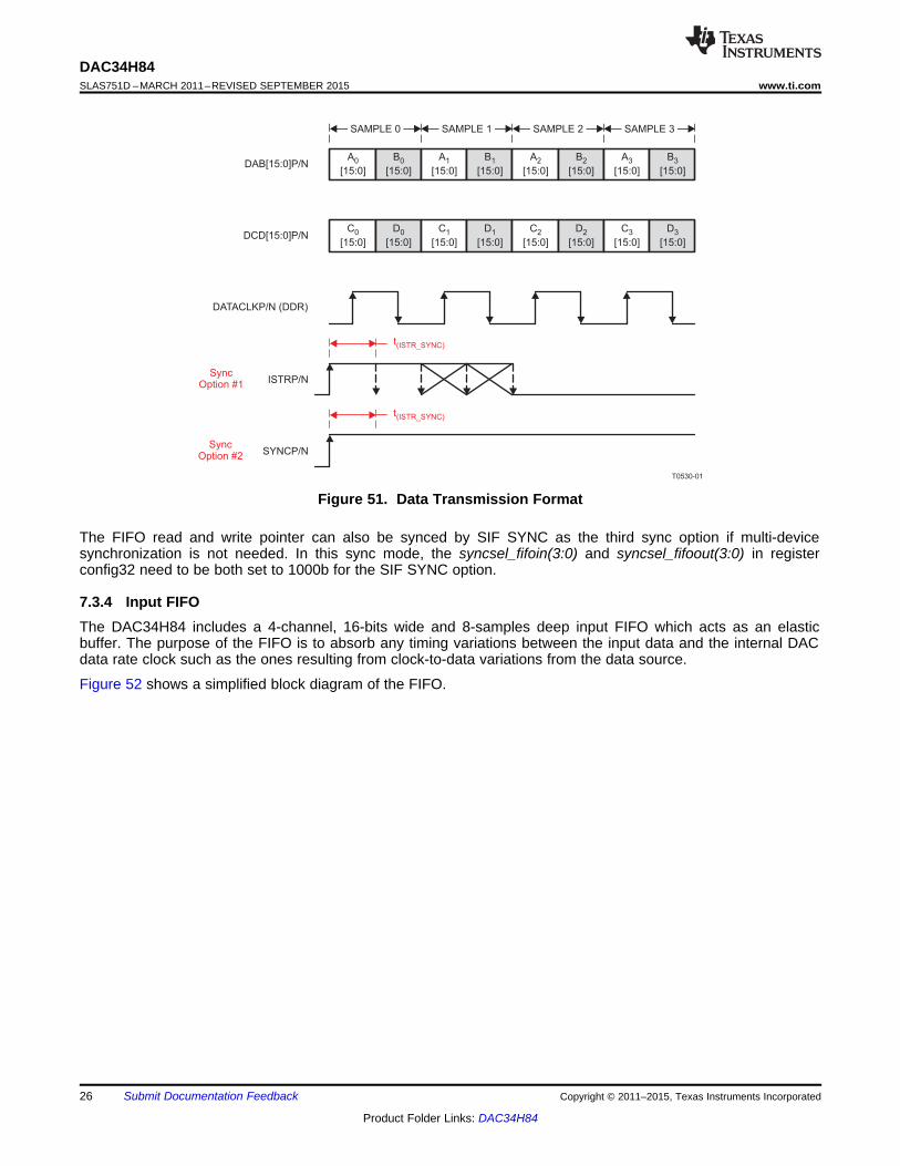
7.3.4 Input FIFOThe DAC34H84 includes a 4-channel, 16-bits wide and 8-samples deep input FIFO which acts as an elasticbuffer. The purpose of the FIFO is to absorb any timing variations between the input data and the internal DACdata rate clock such as the ones resulting from clock-to-data variations from the data source.
Figure 52 shows a simplified block diagram of the FIFO.
26 Submit Documentation Feedback Copyright © 2011–2015, Texas Instruments Incorporated
Product Folder Links: DAC34H84
FIFO Reset
De-Interleave
DCD[15:0]
DAB[15:0]
FIFO A Output
FIFO B Output
Clock Handoff
64-Bit64-Bit
A-Data, 16-Bit
16-Bit
16-Bit
16-Bit
16-BitB-Data, 16-Bit
C-Data, 16-Bit
D-Data, 16-Bit
16-Bit
16-Bit
16-Bit
16-Bit
Write Pointer Reset Read Pointer Reset
FIFO C Output
FIFO D Output
OSTR
B0461-01
syncsel_fifoin
syncsel_fifooutS M
fifo_offset(2:0)
ISTR/SYNC
Input SideClocked by DATACLK
0 .
.. 7
Write
Po
inte
r
0 .
.. 7
Re
ad
Po
inte
r
S (Single Sync Sources Mode): Reset handoff frominput side to output sideM (Dual Sync Source Mode): OSTR resets readpointer. Allows Multi-DAC synchronization
InitialPosition
InitialPosition
FIFO:4 x 16-Bits Wide8-Samples deep
Output SideClocked by FIFO Out Clock
( )DACCLK/Interpolation Factor
0
1
2
3
4
5
6
7
0
1
2
3
4
5
6
7
Sample 0A [15:0], B [15:0], C0 0 0 0[15:0], D [15:0]
Sample 0A [15:0], B [15:0], C1 1 1 1[15:0], D [15:0]
Sample 0A [15:0], B [15:0], C2 2 2 2[15:0], D [15:0]
Sample 0A [15:0], B [15:0], C3 3 3 3[15:0], D [15:0]
Sample 0A [15:0], B [15:0], C4 4 4 4[15:0], D [15:0]
Sample 0A [15:0], B [15:0], C5 5 5 5[15:0], D [15:0]
Sample 0A [15:0], B [15:0], C6 6 6 6[15:0], D [15:0]
Sample 0A [15:0], B [15:0], C7 7 7 7[15:0], D [15:0]
DAC34H84www.ti.com SLAS751D –MARCH 2011–REVISED SEPTEMBER 2015
Figure 52. DAC34H84 FIFO Block Diagram
Data is written to the device 32-bits at a time on the rising and falling edges of DATACLK. In order to form acomplete 64-bit wide sample (16-bit A-data, 16-bit B-data, 16-bit C-data, and 16-bit D-data) one DATACLKperiod is required. Each 64-bit wide sample is written into the FIFO at the address indicated by the write pointer.Similarly, data from the FIFO is read by the FIFO Out Clock 64-bits at a time from the address indicated by theread pointer. The FIFO Out Clock is generated internally from the DACCLK signal and its rate is equal toDACCLK/Interpolation. Each time a FIFO write or FIFO read is done the corresponding pointer moves to the nextaddress.
The reset position for the FIFO read and write pointers is set by default to addresses 0 and 4 as shown inFigure 52. This offset gives optimal margin within the FIFO. The default read pointer location can be set toanother value using fifo_offset(2:0) in register config3 (address 4 by default). Under normal conditions data iswritten-to and read-from the FIFO at the same rate and consequently the write and read pointer gap remainsconstant. If the FIFO write and read rates are different, the corresponding pointers will be cycling at differentspeeds which could result in pointer collision. Under this condition the FIFO attempts to read and write data fromthe same address at the same time which will result in errors and thus must be avoided.
The write pointer sync source is selected by syncsel_fifoin(3:0) in register config32. In most applications eitherISTR or SYNC are used to reset the write pointer. Unlike DATA, the sync signal is latched only on the risingedges of DATACLK. A rising edge on the sync signal source causes the pointer to return to its original position.
Similarly, the read pointer sync source is selected by syncsel_fifoout(3:0). The write pointer sync source can beset to reset the read pointer as well. In this case, the FIFO Out clock will recapture the write pointer sync signalto reset the read pointer. This clock domain transfer (DATACLK to FIFO Out Clock) results in phase ambiguity ofthe sync signal. This limits the precise control of the output timing and makes full synchronization of multipledevices difficult.
Copyright © 2011–2015, Texas Instruments Incorporated Submit Documentation Feedback 27
Product Folder Links: DAC34H84
T0531-01
Resets Write Pointer to Position 0
Resets Read Pointer to PositionSet by fifo_offset (4 by Default)
DATACLKP/N(DDR)
ISTRP/NSYNCP/N
DACCLKP/N2x Interpolation
OSTRP/N(optionally internal
sync from Write Reset)
D[15:0]P/N
LV
DS
Pairs (
Data
Sourc
e)
LV
PE
CL
Pairs (
Clo
ck S
ourc
e)
tS(OSTR)
tH(DATA)
tH(DATA) tH(DATA)
tH(OSTR)
tS(DATA)
tS(DATA) tS(DATA)
DAC34H84SLAS751D –MARCH 2011–REVISED SEPTEMBER 2015 www.ti.com
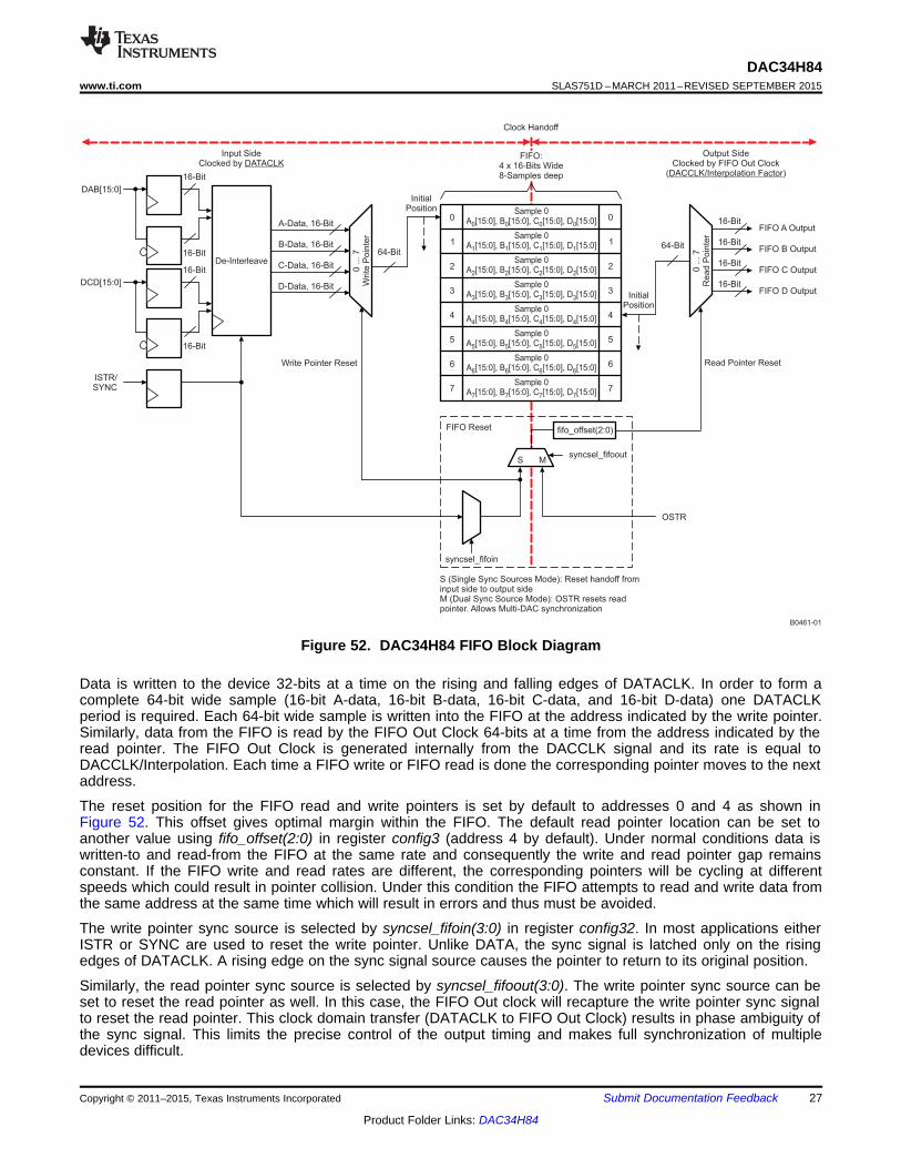
To alleviate this, the device offers the alternative of resetting the FIFO read pointer independently of the writepointer by using the OSTR signal. The OSTR signal is sampled by DACCLK and must satisfy the timingrequirements in the specifications table. In order to minimize the skew it is recommended to use the same clockdistribution device such as Texas Instruments CDCE62005 to provide the DACCLK and OSTR signals to all theDAC34H84 devices in the system. Swapping the polarity of the DACCLK outputs with respect to the OSTR onesestablishes proper phase relationship.
The FIFO pointers reset procedure can be done periodically or only once during initialization as the pointersautomatically return to the initial position when the FIFO has been filled. To reset the FIFO periodically, it isnecessary to have the ISTR, SYNC, and OSTR signals to repeat at multiples of 8 FIFO samples. To disableFIFO reset, set syncsel_fifoin(3:0) and syncsel_fifoout(3:0) to “0000”.
The frequency limitation for ISTR and SYNC signals are the following:
fsync = fDATACLK/(n x 8) where n = 1, 2, …
The frequency limitation for the OSTR signal is the following:
fOSTR = fDAC/(n x interpolation x 8) where n = 1, 2, …
The frequencies above are at maximum when n = 1. This is when the ISTR, SYNC, or OSTR have a rising edgetransition every 8 FIFO samples. The occurrence can be made less frequent by setting n > 1, for example, everyn × 8 FIFO samples.
Figure 53. FIFO Write and Read Descriptions
7.3.5 FIFO Modes of OperationThe DAC34H84 input FIFO can be completely bypassed through registers config0 and config32. The registerconfiguration for each mode is described in Table 3.
Register Control Bitsconfig0 fifo_enaconfig32 syncsel_fifoout(3:0)
28 Submit Documentation Feedback Copyright © 2011–2015, Texas Instruments Incorporated
Product Folder Links: DAC34H84
DAC34H84www.ti.com SLAS751D –MARCH 2011–REVISED SEPTEMBER 2015
Table 3. FIFO Operation Modesconfig0 AND config32 FIFO BITS
FIFO MODE syncsel_fifooutfifo_ena
BIT 3: sif_sync BIT 2: OSTR BIT 1: ISTR BIT 0: SYNCDual Sync Sources 1 0 1 0 0
Single Sync 1 or 0 Depends on the sync 1 or 0 Depends on the1 0 0Source source sync sourceBypass 0 X X X X
7.3.5.1 Dual Sync Sources ModeThis is the recommended mode of operation for those applications that require precise control of the outputtiming. In Dual Sync Sources mode, the FIFO write and read pointers are reset independently. The FIFO writepointer is reset using the LVDS ISTR or SYNC signal, and the FIFO read pointer is reset using the LVPECLOSTR signal. This allows LVPECL OSTR signal to control the phase of the output for either a single chip ormultiple chips. Multiple devices can be fully synchronized in this mode.
7.3.5.2 Single Sync Source ModeIn Single Sync Source mode, the FIFO write and read pointers are reset from the same source, either LVDSISTR or LVDS SYNC signal. This mode has a possibility of up to 2 DAC clocks offset between the multiple DACoutputs. Applications requiring exact output timing control will need Dual Sync Sources mode instead of SingleSync Source Mode. A single rising edge for FIFO and clock divider sync is recommended. Periodic sync signal isnot recommended due to the non-deterministic latency of the sync signal through the clock domain transfer.
In this mode, there is a chance for FIFO pointers 2 away alarm (or possibly 1 away alarm) to occur at initialsetup/syncing. This is the result of Single Sync Source mode having 0 to 3 address location slip, which is causedby the asynchronous handoff of the sync signal occurring between the DATACLK zone and DACCLK zone. Theasynchronous relationship between the clock domains means there could be a slip (from nominal) in the READand Write pointers at initial syncing. For example, with the default programming of FIFO Offset of 4, the actualFIFO Offset may be 3, 2, or in some instances, 1. Please note that in this mode, the nominal address locationslip is 0 with the possibility getting less for each increase in slip amount. Also, the slip does not continue to occuras the device functions, but the READ/WRITE pointers may not be at optimal settings. In situation of alarmoccurrence:1. Adjust the FIFO offset accordingly and resynchronize the FIFO, data formatter, etc such that there are no
alarm reported or at least only 2 away alarm is reported.2. The FIFO collision alarm is a warning of the system since the read and write processes occur at the same
pointer. However, the FIFO 1 away or 2 away alarms are informational for the system designer. Theimportant thing for these two alarms is that the alarm should not get closer to collision during normaloperation. If 1 away alarm and alarm collision starts to occur, it is a warning to check for system errors. Thesystem should have an interrupt or algorithm to fix the error and resynchronize the alarm appropriately.
7.3.5.3 Bypass ModeIn FIFO bypass mode, the FIFO block is not used. As a result the input data is handed off from the DATACLK tothe DACCLK domain without any compensation. In this mode the relationship between DATACLK and DACCLKis critical and used as a synchronizing mechanism for the internal logic. Due to this constraint this mode is notrecommended. In bypass mode the pointers have no effect on the data path or handoff.
7.3.6 Clocking ModesThe DAC34H84 has a dual clock setup in which a DAC clock signal is used to clock the DAC cores and internaldigital logic and a separate DATA clock is used to clock the input LVDS receivers and FIFO input. TheDAC34H84 DAC clock signal can be sourced directly or generated through an on-chip low-jitter phase-lockedloop (PLL).
In those applications requiring extremely low noise it is recommended to bypass the PLL and source the DACclock directly from a high-quality external clock to the DACCLK input. In most applications system clocking canbe simplified by using the on-chip PLL to generate the DAC core clock while still satisfying performancerequirements. In this case the DACCLK pins are used as the reference frequency input to the PLL.
Copyright © 2011–2015, Texas Instruments Incorporated Submit Documentation Feedback 29
Product Folder Links: DAC34H84
SYNCP
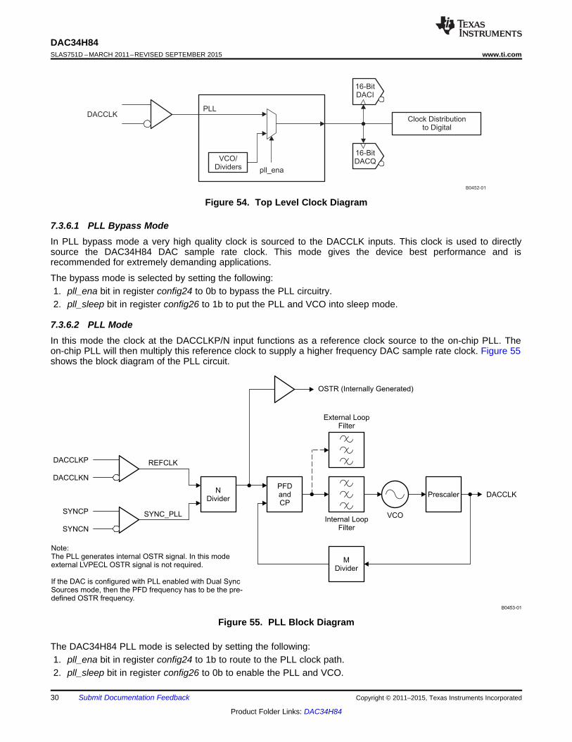
DACCLKP
NDivider
PFDandCP
SYNCN
DACCLKN
External LoopFilter
Internal LoopFilter
VCO
B0453-01
Prescaler
MDivider
DACCLK
REFCLK
SYNC_PLL
OSTR (Internally Generated)
Note:The PLL generates internal OSTR signal. In this modeexternal LVPECL OSTR signal is not required.
If the DAC is configured with PLL enabled with Dual SyncSources mode, then the PFD frequency has to be the pre-defined OSTR frequency.
DACCLK
pll_ena
Clock Distributionto Digital
VCO/Dividers
PLL
16-BitDACI
16-BitDACQ
B0452-01
DAC34H84SLAS751D –MARCH 2011–REVISED SEPTEMBER 2015 www.ti.com
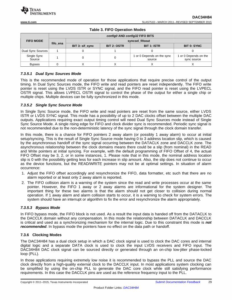
Figure 54. Top Level Clock Diagram
7.3.6.1 PLL Bypass ModeIn PLL bypass mode a very high quality clock is sourced to the DACCLK inputs. This clock is used to directlysource the DAC34H84 DAC sample rate clock. This mode gives the device best performance and isrecommended for extremely demanding applications.
The bypass mode is selected by setting the following:1. pll_ena bit in register config24 to 0b to bypass the PLL circuitry.2. pll_sleep bit in register config26 to 1b to put the PLL and VCO into sleep mode.
7.3.6.2 PLL ModeIn this mode the clock at the DACCLKP/N input functions as a reference clock source to the on-chip PLL. Theon-chip PLL will then multiply this reference clock to supply a higher frequency DAC sample rate clock. Figure 55shows the block diagram of the PLL circuit.
Figure 55. PLL Block Diagram
The DAC34H84 PLL mode is selected by setting the following:1. pll_ena bit in register config24 to 1b to route to the PLL clock path.2. pll_sleep bit in register config26 to 0b to enable the PLL and VCO.
30 Submit Documentation Feedback Copyright © 2011–2015, Texas Instruments Incorporated
Product Folder Links: DAC34H84
3300
3400
3500
3600
3700
3800
3900
4000
0 8 16 24 32 40 48 56 64
Coarse-Tuning Bits
VC
O F
requency (
MH
z)
( )VCO Frequency MHz 3253Coarse-Tuning Bits
11.6
-@
DAC34H84www.ti.com SLAS751D –MARCH 2011–REVISED SEPTEMBER 2015
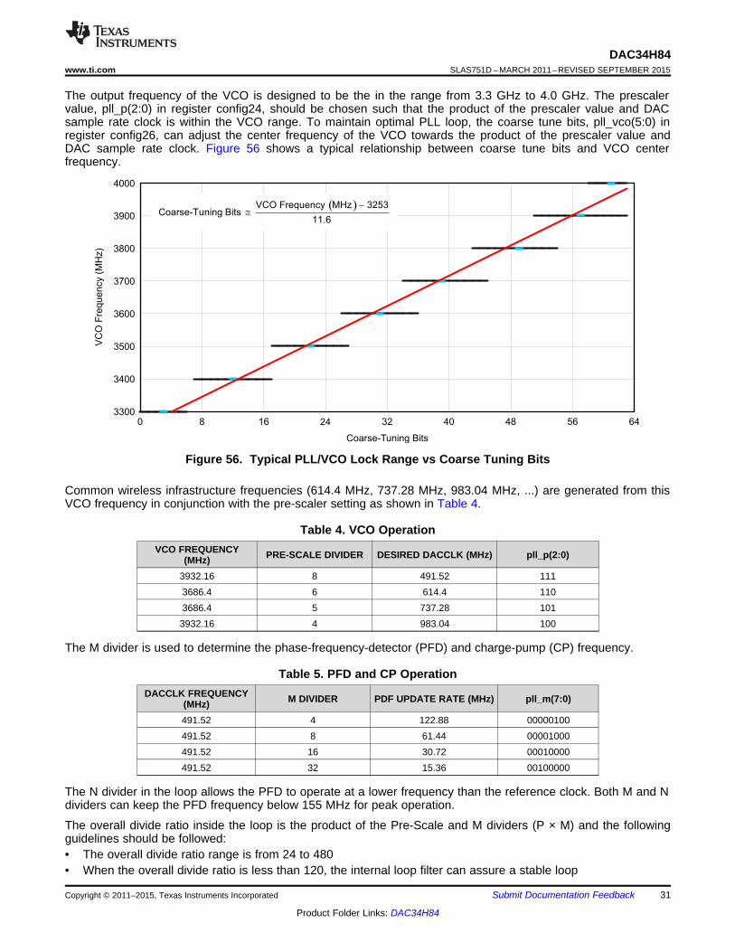
The output frequency of the VCO is designed to be the in the range from 3.3 GHz to 4.0 GHz. The prescalervalue, pll_p(2:0) in register config24, should be chosen such that the product of the prescaler value and DACsample rate clock is within the VCO range. To maintain optimal PLL loop, the coarse tune bits, pll_vco(5:0) inregister config26, can adjust the center frequency of the VCO towards the product of the prescaler value andDAC sample rate clock. Figure 56 shows a typical relationship between coarse tune bits and VCO centerfrequency.
Figure 56. Typical PLL/VCO Lock Range vs Coarse Tuning Bits
Common wireless infrastructure frequencies (614.4 MHz, 737.28 MHz, 983.04 MHz, ...) are generated from thisVCO frequency in conjunction with the pre-scaler setting as shown in Table 4.
Table 4. VCO OperationVCO FREQUENCY PRE-SCALE DIVIDER DESIRED DACCLK (MHz) pll_p(2:0)(MHz)
3932.16 8 491.52 1113686.4 6 614.4 1103686.4 5 737.28 1013932.16 4 983.04 100
The M divider is used to determine the phase-frequency-detector (PFD) and charge-pump (CP) frequency.
Table 5. PFD and CP OperationDACCLK FREQUENCY M DIVIDER PDF UPDATE RATE (MHz) pll_m(7:0)(MHz)
491.52 4 122.88 00000100491.52 8 61.44 00001000491.52 16 30.72 00010000491.52 32 15.36 00100000
The N divider in the loop allows the PFD to operate at a lower frequency than the reference clock. Both M and Ndividers can keep the PFD frequency below 155 MHz for peak operation.
The overall divide ratio inside the loop is the product of the Pre-Scale and M dividers (P × M) and the followingguidelines should be followed:• The overall divide ratio range is from 24 to 480• When the overall divide ratio is less than 120, the internal loop filter can assure a stable loop
Copyright © 2011–2015, Texas Instruments Incorporated Submit Documentation Feedback 31
Product Folder Links: DAC34H84
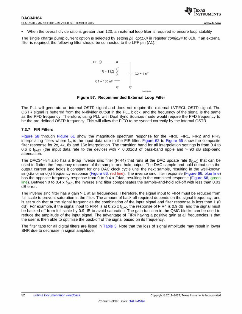
LPF
S0514-01
R = 1 kΩ
C1 = 100 nF
C2 = 1 nF
DAC34H84SLAS751D –MARCH 2011–REVISED SEPTEMBER 2015 www.ti.com
• When the overall divide ratio is greater than 120, an external loop filter is required to ensure loop stability
The single charge pump current option is selected by setting pll_cp(1:0) in register config24 to 01b. If an externalfilter is required, the following filter should be connected to the LPF pin (A1):
Figure 57. Recommended External Loop Filter
The PLL will generate an internal OSTR signal and does not require the external LVPECL OSTR signal. TheOSTR signal is buffered from the N-divider output in the PLL block, and the frequency of the signal is the sameas the PFD frequency. Therefore, using PLL with Dual Sync Sources mode would require the PFD frequency tobe the pre-defined OSTR frequency. This will allow the FIFO to be synced correctly by the internal OSTR.
7.3.7 FIR FiltersFigure 58 through Figure 61 show the magnitude spectrum response for the FIR0, FIR1, FIR2 and FIR3interpolating filters where fIN is the input data rate to the FIR filter. Figure 62 to Figure 65 show the compositefilter response for 2x, 4x, 8x and 16x interpolation. The transition band for all interpolation settings is from 0.4 to0.6 x fDATA (the input data rate to the device) with < 0.001dB of pass-band ripple and > 90 dB stop-bandattenuation.
The DAC34H84 also has a 9-tap inverse sinc filter (FIR4) that runs at the DAC update rate (fDAC) that can beused to flatten the frequency response of the sample-and-hold output. The DAC sample-and-hold output sets theoutput current and holds it constant for one DAC clock cycle until the next sample, resulting in the well-knownsin(x)/x or sinc(x) frequency response (Figure 66, red line). The inverse sinc filter response (Figure 66, blue line)has the opposite frequency response from 0 to 0.4 x Fdac, resulting in the combined response (Figure 66, greenline). Between 0 to 0.4 x fDAC, the inverse sinc filter compensates the sample-and-hold roll-off with less than 0.03dB error.
The inverse sinc filter has a gain > 1 at all frequencies. Therefore, the signal input to FIR4 must be reduced fromfull scale to prevent saturation in the filter. The amount of back-off required depends on the signal frequency, andis set such that at the signal frequencies the combination of the input signal and filter response is less than 1 (0dB). For example, if the signal input to FIR4 is at 0.25 x fDAC, the response of FIR4 is 0.9 dB, and the signal mustbe backed off from full scale by 0.9 dB to avoid saturation. The gain function in the QMC blocks can be used toreduce the amplitude of the input signal. The advantage of FIR4 having a positive gain at all frequencies is thatthe user is then able to optimize the back-off of the signal based on its frequency.
The filter taps for all digital filters are listed in Table 3. Note that the loss of signal amplitude may result in lowerSNR due to decrease in signal amplitude.
32 Submit Documentation Feedback Copyright © 2011–2015, Texas Instruments Incorporated
Product Folder Links: DAC34H84
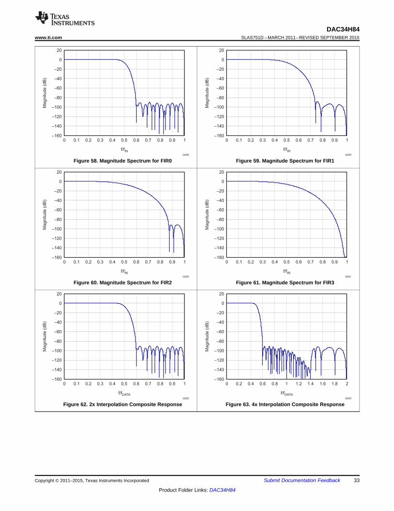
0 0.1 0.2 0.3 0.4 0.5 0.6 0.7 0.8 0.9 1–160
–140
–120
–100
–80
–60
–40
–20
0
20
f/fDATA
Ma
gn
itu
de (
dB
)
G052
0 0.2 0.4 0.6 0.8 1 1.2 1.4 1.6 1.8 2–160
–140
–120
–100
–80
–60
–40
–20
0
20
f/fDATA
Mag
nitud
e (
dB
)
G053
0 0.1 0.2 0.3 0.4 0.5 0.6 0.7 0.8 0.9 1–160
–140
–120
–100
–80
–60
–40
–20
0
20
f/fIN
Ma
gn
itu
de (
dB
)
G050
0 0.1 0.2 0.3 0.4 0.5 0.6 0.7 0.8 0.9 1–160
–140
–120
–100
–80
–60
–40
–20
0
20
f/fIN
Ma
gn
itu
de (
dB
)
G051
0 0.1 0.2 0.3 0.4 0.5 0.6 0.7 0.8 0.9 1–160
–140
–120
–100
–80
–60
–40
–20
0
20
f/fIN
Ma
gn
itu
de
(dB
)
G048
0 0.1 0.2 0.3 0.4 0.5 0.6 0.7 0.8 0.9 1–160
–140
–120
–100
–80
–60
–40
–20
0
20
f/fIN
Ma
gn
itu
de
(dB
)
G049
DAC34H84www.ti.com SLAS751D –MARCH 2011–REVISED SEPTEMBER 2015
Figure 58. Magnitude Spectrum for FIR0 Figure 59. Magnitude Spectrum for FIR1
Figure 60. Magnitude Spectrum for FIR2 Figure 61. Magnitude Spectrum for FIR3
Figure 62. 2x Interpolation Composite Response Figure 63. 4x Interpolation Composite Response
Copyright © 2011–2015, Texas Instruments Incorporated Submit Documentation Feedback 33
Product Folder Links: DAC34H84
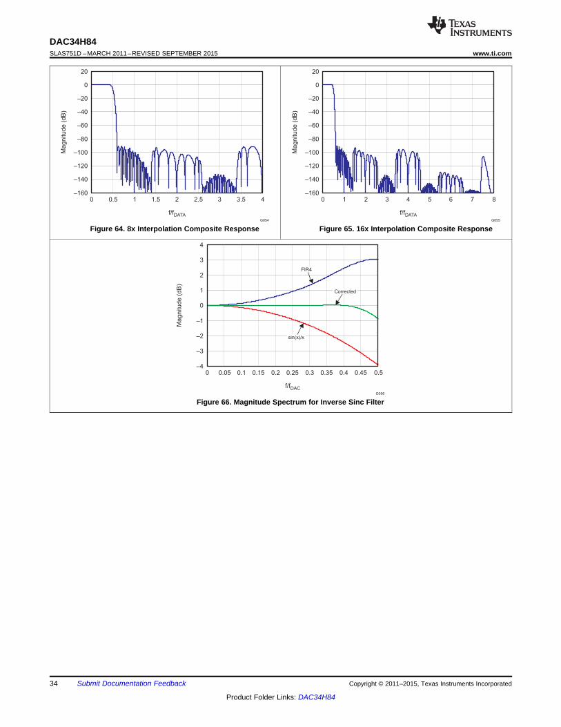
0 0.05 0.1 0.15 0.2 0.25 0.3 0.35 0.4 0.45 0.5–4
–3
–2
–1
0
1
2
3
4
f/fDAC
Ma
gn
itu
de (
dB
)
G056
sin(x)/x
Corrected
FIR4
0 0.5 1 1.5 2 2.5 3 3.5 4–160
–140
–120
–100
–80
–60
–40
–20
0
20
f/fDATA
Ma
gn
itu
de
(dB
)
G054
0 1 2 3 4 5 6 7 8–160
–140
–120
–100
–80
–60
–40
–20
0
20
f/fDATA
Ma
gn
itu
de
(dB
)
G055
DAC34H84SLAS751D –MARCH 2011–REVISED SEPTEMBER 2015 www.ti.com
Figure 64. 8x Interpolation Composite Response Figure 65. 16x Interpolation Composite Response
Figure 66. Magnitude Spectrum for Inverse Sinc Filter
34 Submit Documentation Feedback Copyright © 2011–2015, Texas Instruments Incorporated
Product Folder Links: DAC34H84
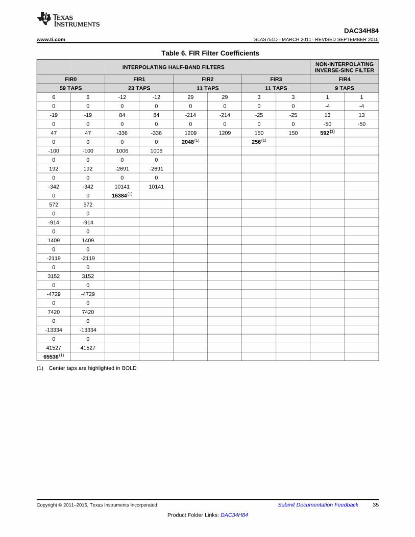
DAC34H84www.ti.com SLAS751D –MARCH 2011–REVISED SEPTEMBER 2015
Table 6. FIR Filter CoefficientsNON-INTERPOLATINGINTERPOLATING HALF-BAND FILTERS INVERSE-SINC FILTER
FIR0 FIR1 FIR2 FIR3 FIR459 TAPS 23 TAPS 11 TAPS 11 TAPS 9 TAPS
6 6 -12 -12 29 29 3 3 1 10 0 0 0 0 0 0 0 -4 -4
-19 -19 84 84 -214 -214 -25 -25 13 130 0 0 0 0 0 0 0 -50 -5047 47 -336 -336 1209 1209 150 150 592 (1)
0 0 0 0 2048 (1) 256 (1)
-100 -100 1006 10060 0 0 0
192 192 -2691 -26910 0 0 0
-342 -342 10141 101410 0 16384 (1)
572 5720 0
-914 -9140 0
1409 14090 0
-2119 -21190 0
3152 31520 0
-4729 -47290 0
7420 74200 0
-13334 -133340 0
41527 4152765536 (1)
(1) Center taps are highlighted in BOLD
Copyright © 2011–2015, Texas Instruments Incorporated Submit Documentation Feedback 35
Product Folder Links: DAC34H84
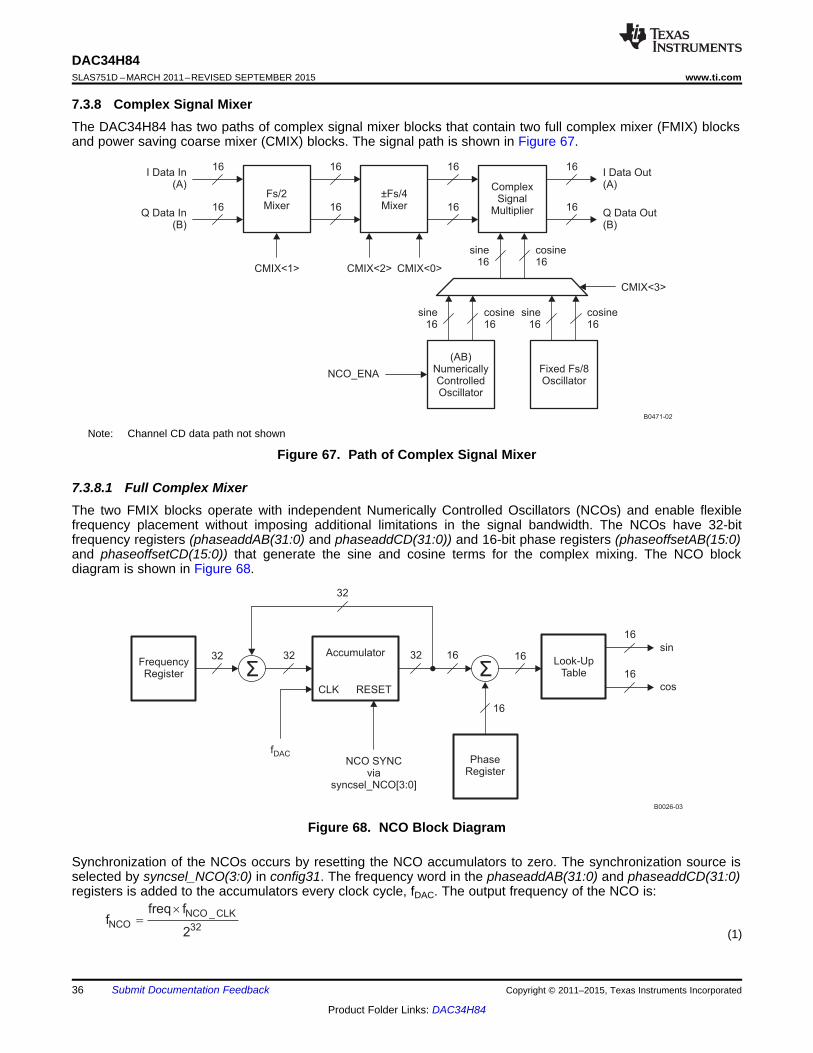
NCO _ CLKNCO 32
freq ff
2
´
=
FrequencyRegister
32 Accumulator32
RESETCLK
NCO SYNCvia
syncsel_NCO[3:0]
32
32
PhaseRegister
16
16
16 Look-UpTable
sin
cos
ΣΣ
16
16
fDAC
B0026-03
B0471-02
16 16 16 16
16 16 16 16
sine16
sine16
sine16
cosine16
cosine16
cosine16
Fs/2Mixer
±Fs/4Mixer
ComplexSignal
Multiplier
(AB)NumericallyControlledOscillator
Fixed Fs/8Oscillator
I Data In(A)
Q Data In(B)
I Data Out(A)
Q Data Out(B)
CMIX<1> CMIX<2> CMIX<0>
CMIX<3>
NCO_ENA
DAC34H84SLAS751D –MARCH 2011–REVISED SEPTEMBER 2015 www.ti.com
7.3.8 Complex Signal MixerThe DAC34H84 has two paths of complex signal mixer blocks that contain two full complex mixer (FMIX) blocksand power saving coarse mixer (CMIX) blocks. The signal path is shown in Figure 67.
Note: Channel CD data path not shown
Figure 67. Path of Complex Signal Mixer
7.3.8.1 Full Complex MixerThe two FMIX blocks operate with independent Numerically Controlled Oscillators (NCOs) and enable flexiblefrequency placement without imposing additional limitations in the signal bandwidth. The NCOs have 32-bitfrequency registers (phaseaddAB(31:0) and phaseaddCD(31:0)) and 16-bit phase registers (phaseoffsetAB(15:0)and phaseoffsetCD(15:0)) that generate the sine and cosine terms for the complex mixing. The NCO blockdiagram is shown in Figure 68.
Figure 68. NCO Block Diagram
Synchronization of the NCOs occurs by resetting the NCO accumulators to zero. The synchronization source isselected by syncsel_NCO(3:0) in config31. The frequency word in the phaseaddAB(31:0) and phaseaddCD(31:0)registers is added to the accumulators every clock cycle, fDAC. The output frequency of the NCO is:
(1)
36 Submit Documentation Feedback Copyright © 2011–2015, Texas Instruments Incorporated
Product Folder Links: DAC34H84
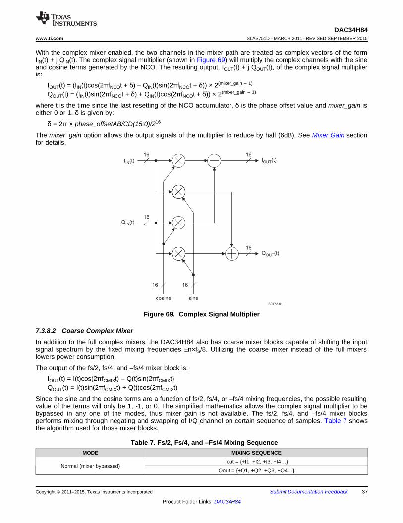
I (t)INI (t)OUT
Q (t)IN
Q (t)OUT
16 16
16
16
cosine sineB0472-01
1616
DAC34H84www.ti.com SLAS751D –MARCH 2011–REVISED SEPTEMBER 2015
With the complex mixer enabled, the two channels in the mixer path are treated as complex vectors of the formIIN(t) + j QIN(t). The complex signal multiplier (shown in Figure 69) will multiply the complex channels with the sineand cosine terms generated by the NCO. The resulting output, IOUT(t) + j QOUT(t), of the complex signal multiplieris:
IOUT(t) = (IIN(t)cos(2πfNCOt + δ) – QIN(t)sin(2πfNCOt + δ)) × 2(mixer_gain – 1)
QOUT(t) = (IIN(t)sin(2πfNCOt + δ) + QIN(t)cos(2πfNCOt + δ)) × 2(mixer_gain – 1)
where t is the time since the last resetting of the NCO accumulator, δ is the phase offset value and mixer_gain iseither 0 or 1. δ is given by:
δ = 2π × phase_offsetAB/CD(15:0)/216
The mixer_gain option allows the output signals of the multiplier to reduce by half (6dB). See Mixer Gain sectionfor details.
Figure 69. Complex Signal Multiplier
7.3.8.2 Coarse Complex MixerIn addition to the full complex mixers, the DAC34H84 also has coarse mixer blocks capable of shifting the inputsignal spectrum by the fixed mixing frequencies ±n×fS/8. Utilizing the coarse mixer instead of the full mixerslowers power consumption.
The output of the fs/2, fs/4, and –fs/4 mixer block is:
IOUT(t) = I(t)cos(2πfCMIXt) – Q(t)sin(2πfCMIXt)QOUT(t) = I(t)sin(2πfCMIXt) + Q(t)cos(2πfCMIXt)
Since the sine and the cosine terms are a function of fs/2, fs/4, or –fs/4 mixing frequencies, the possible resultingvalue of the terms will only be 1, -1, or 0. The simplified mathematics allows the complex signal multiplier to bebypassed in any one of the modes, thus mixer gain is not available. The fs/2, fs/4, and –fs/4 mixer blocksperforms mixing through negating and swapping of I/Q channel on certain sequence of samples. Table 7 showsthe algorithm used for those mixer blocks.
Table 7. Fs/2, Fs/4, and –Fs/4 Mixing SequenceMODE MIXING SEQUENCE
Iout = +I1, +I2, +I3, +I4…Normal (mixer bypassed)
Qout = +Q1, +Q2, +Q3, +Q4…
Copyright © 2011–2015, Texas Instruments Incorporated Submit Documentation Feedback 37
Product Folder Links: DAC34H84
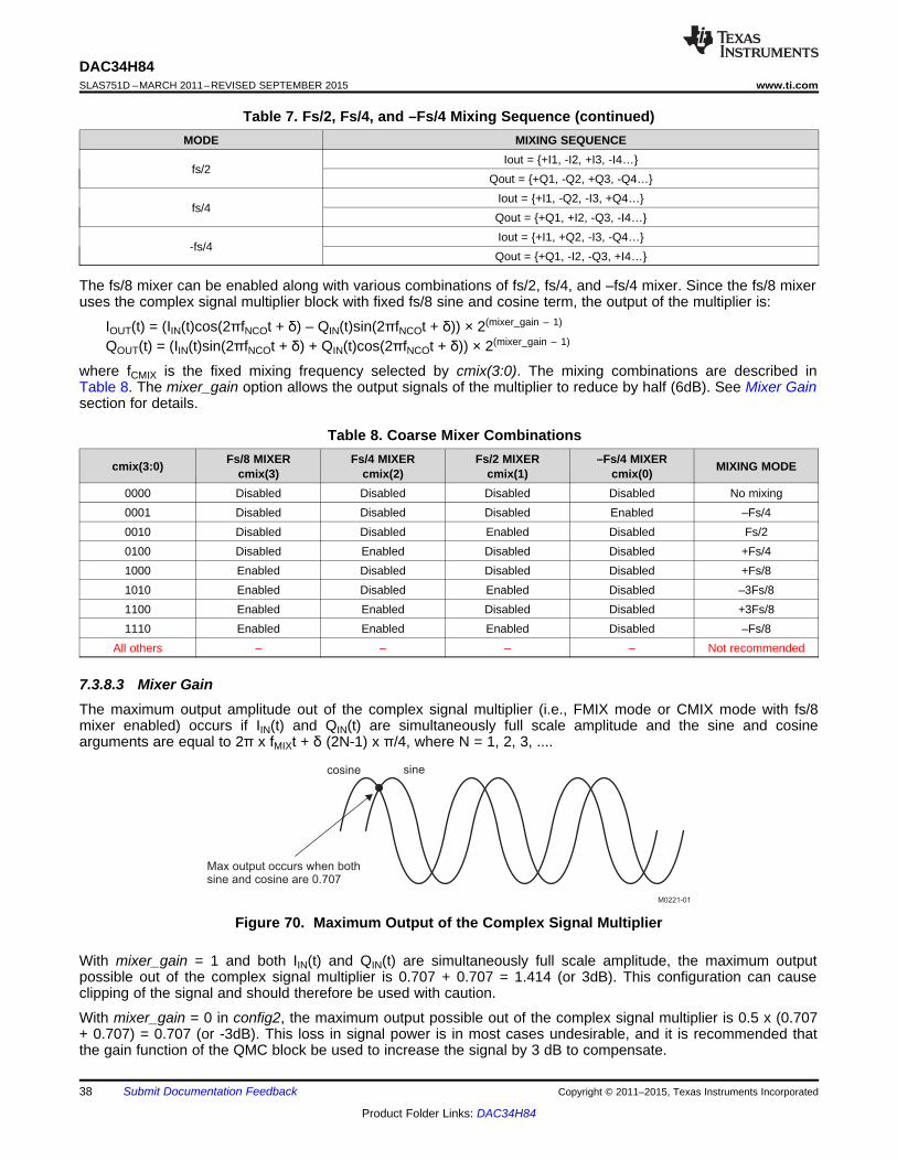
M0221-01
Max output occurs when bothsine and cosine are 0.707
cosine sine
DAC34H84SLAS751D –MARCH 2011–REVISED SEPTEMBER 2015 www.ti.com
Table 7. Fs/2, Fs/4, and –Fs/4 Mixing Sequence (continued)MODE MIXING SEQUENCE
Iout = +I1, -I2, +I3, -I4…fs/2
Qout = +Q1, -Q2, +Q3, -Q4…Iout = +I1, -Q2, -I3, +Q4…
fs/4Qout = +Q1, +I2, -Q3, -I4…Iout = +I1, +Q2, -I3, -Q4…
-fs/4Qout = +Q1, -I2, -Q3, +I4…
The fs/8 mixer can be enabled along with various combinations of fs/2, fs/4, and –fs/4 mixer. Since the fs/8 mixeruses the complex signal multiplier block with fixed fs/8 sine and cosine term, the output of the multiplier is:
IOUT(t) = (IIN(t)cos(2πfNCOt + δ) – QIN(t)sin(2πfNCOt + δ)) × 2(mixer_gain – 1)
QOUT(t) = (IIN(t)sin(2πfNCOt + δ) + QIN(t)cos(2πfNCOt + δ)) × 2(mixer_gain – 1)
where fCMIX is the fixed mixing frequency selected by cmix(3:0). The mixing combinations are described inTable 8. The mixer_gain option allows the output signals of the multiplier to reduce by half (6dB). See Mixer Gainsection for details.
Table 8. Coarse Mixer CombinationsFs/8 MIXER Fs/4 MIXER Fs/2 MIXER –Fs/4 MIXERcmix(3:0) MIXING MODEcmix(3) cmix(2) cmix(1) cmix(0)
0000 Disabled Disabled Disabled Disabled No mixing0001 Disabled Disabled Disabled Enabled –Fs/40010 Disabled Disabled Enabled Disabled Fs/20100 Disabled Enabled Disabled Disabled +Fs/41000 Enabled Disabled Disabled Disabled +Fs/81010 Enabled Disabled Enabled Disabled –3Fs/81100 Enabled Enabled Disabled Disabled +3Fs/81110 Enabled Enabled Enabled Disabled –Fs/8
All others – – – – Not recommended
7.3.8.3 Mixer GainThe maximum output amplitude out of the complex signal multiplier (i.e., FMIX mode or CMIX mode with fs/8mixer enabled) occurs if IIN(t) and QIN(t) are simultaneously full scale amplitude and the sine and cosinearguments are equal to 2π x fMIXt + δ (2N-1) x π/4, where N = 1, 2, 3, ....
Figure 70. Maximum Output of the Complex Signal Multiplier
With mixer_gain = 1 and both IIN(t) and QIN(t) are simultaneously full scale amplitude, the maximum outputpossible out of the complex signal multiplier is 0.707 + 0.707 = 1.414 (or 3dB). This configuration can causeclipping of the signal and should therefore be used with caution.
With mixer_gain = 0 in config2, the maximum output possible out of the complex signal multiplier is 0.5 x (0.707+ 0.707) = 0.707 (or -3dB). This loss in signal power is in most cases undesirable, and it is recommended thatthe gain function of the QMC block be used to increase the signal by 3 dB to compensate.
38 Submit Documentation Feedback Copyright © 2011–2015, Texas Instruments Incorporated
Product Folder Links: DAC34H84
DAC34H84www.ti.com SLAS751D –MARCH 2011–REVISED SEPTEMBER 2015
7.3.8.4 Real Channel UpconversionThe mixer in the DAC34H84 treats the A, B, C, and D inputs are complex input data and produces a complexoutput for most mixing frequencies. The real input data for each channel can be isolated only when the mixingfrequency is set to normal mode or fs/2 mode. Refer to Table 7 for details.
7.3.9 Quadrature Modulation Correction (QMC)
7.3.9.1 Gain and Phase CorrectionThe DAC34H84 includes a Quadrature Modulator Correction (QMC) block. The QMC blocks provide a mean forchanging the gain and phase of the complex signals to compensate for any I and Q imbalances present in ananalog quadrature modulator. The block diagram for the QMC block is shown in Figure 71. The QMC blockcontains 3 programmable parameters.
Registers qmc_gainA/B(10:0) and qmc_gainC/D(10:0) controls the I and Q path gains and is an 11-bit unsignedvalue with a range of 0 to 1.9990 and the default gain is 1.0000. The implied decimal point for the multiplicationis between bit 9 and bit 10.
Register qmc_phaseAB/CD(11:0) control the phase imbalance between I and Q and are a 12-bit values with arange of –0.5 to approximately 0.49975. The QMC phase term is not a direct phase rotation but a constant that ismultiplied by each "Q" sample then summed into the "I" sample path. This is an approximation of a true phaserotation in order to keep the implementation simple.
LO feed-through can be minimized by adjusting the DAC offset feature described below.
Copyright © 2011–2015, Texas Instruments Incorporated Submit Documentation Feedback 39
Product Folder Links: DAC34H84
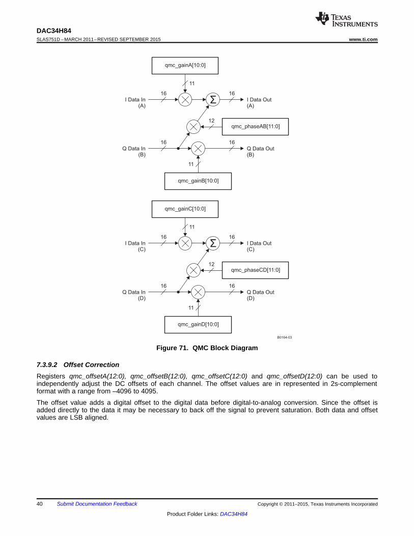
Σ
B0164-03
I Data In(C)
Q Data In(D)
I Data Out(C)
Q Data Out(D)
11
11
12
16
16
16
16
qmc_gainC[10:0]
qmc_gainD[10:0]
qmc_phaseCD[11:0]
I Data In(A)
Q Data In(B)
I Data Out(A)
Q Data Out(B)
11
11
12
16
16
16
16
qmc_gainA[10:0]
qmc_gainB[10:0]
qmc_phaseAB[11:0]
Σ
DAC34H84SLAS751D –MARCH 2011–REVISED SEPTEMBER 2015 www.ti.com
Figure 71. QMC Block Diagram
7.3.9.2 Offset CorrectionRegisters qmc_offsetA(12:0), qmc_offsetB(12:0), qmc_offsetC(12:0) and qmc_offsetD(12:0) can be used toindependently adjust the DC offsets of each channel. The offset values are in represented in 2s-complementformat with a range from –4096 to 4095.
The offset value adds a digital offset to the digital data before digital-to-analog conversion. Since the offset isadded directly to the data it may be necessary to back off the signal to prevent saturation. Both data and offsetvalues are LSB aligned.
40 Submit Documentation Feedback Copyright © 2011–2015, Texas Instruments Incorporated
Product Folder Links: DAC34H84
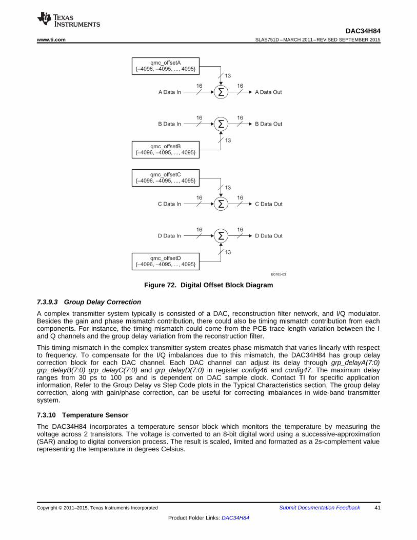
C Data In
A Data In
D Data In
B Data In
C Data Out
A Data Out
D Data Out
B Data Out
13
13
13
13
16
16
16
16
16
16
16
16
qmc_offsetC–4096, –4095, ..., 4095
qmc_offsetA–4096, –4095, ..., 4095
qmc_offsetD–4096, –4095, ..., 4095
qmc_offsetB–4096, –4095, ..., 4095
B0165-03
Σ
Σ
Σ
Σ
DAC34H84www.ti.com SLAS751D –MARCH 2011–REVISED SEPTEMBER 2015
Figure 72. Digital Offset Block Diagram
7.3.9.3 Group Delay CorrectionA complex transmitter system typically is consisted of a DAC, reconstruction filter network, and I/Q modulator.Besides the gain and phase mismatch contribution, there could also be timing mismatch contribution from eachcomponents. For instance, the timing mismatch could come from the PCB trace length variation between the Iand Q channels and the group delay variation from the reconstruction filter.
This timing mismatch in the complex transmitter system creates phase mismatch that varies linearly with respectto frequency. To compensate for the I/Q imbalances due to this mismatch, the DAC34H84 has group delaycorrection block for each DAC channel. Each DAC channel can adjust its delay through grp_delayA(7:0)grp_delayB(7:0) grp_delayC(7:0) and grp_delayD(7:0) in register config46 and config47. The maximum delayranges from 30 ps to 100 ps and is dependent on DAC sample clock. Contact TI for specific applicationinformation. Refer to the Group Delay vs Step Code plots in the Typical Characteristics section. The group delaycorrection, along with gain/phase correction, can be useful for correcting imbalances in wide-band transmittersystem.
7.3.10 Temperature SensorThe DAC34H84 incorporates a temperature sensor block which monitors the temperature by measuring thevoltage across 2 transistors. The voltage is converted to an 8-bit digital word using a successive-approximation(SAR) analog to digital conversion process. The result is scaled, limited and formatted as a 2s-complement valuerepresenting the temperature in degrees Celsius.
Copyright © 2011–2015, Texas Instruments Incorporated Submit Documentation Feedback 41
Product Folder Links: DAC34H84
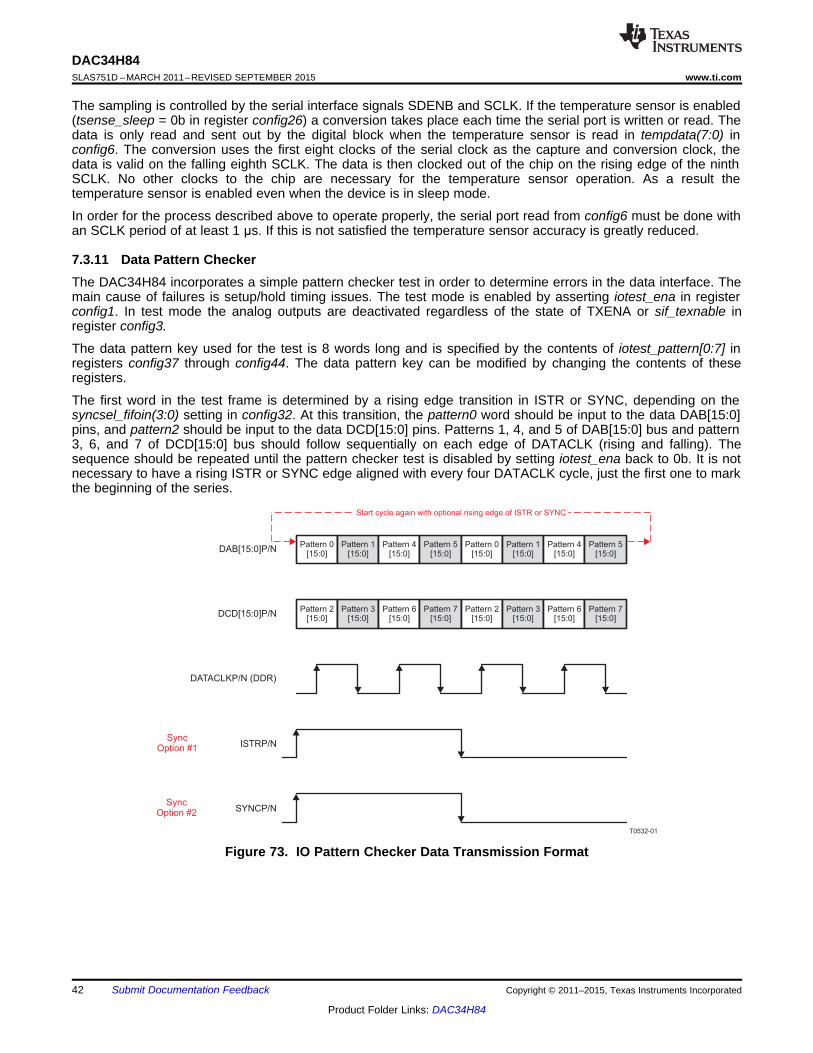
DCD[15:0]P/N
DAB[15:0]P/N
ISTRP/N
SYNCP/N
T0532-01
DATACLKP/N (DDR)
SyncOption #1
SyncOption #2
Pattern 2[15:0]
Pattern 0[15:0]
Pattern 3[15:0]
Pattern 1[15:0]
Pattern 6[15:0]
Pattern 4[15:0]
Pattern 7[15:0]
Pattern 5[15:0]
Pattern 2[15:0]
Pattern 0[15:0]
Pattern 3[15:0]
Pattern 1[15:0]
Pattern 6[15:0]
Pattern 4[15:0]
Pattern 7[15:0]
Pattern 5[15:0]
Start cycle again with optional rising edge of ISTR or SYNC
DAC34H84SLAS751D –MARCH 2011–REVISED SEPTEMBER 2015 www.ti.com
The sampling is controlled by the serial interface signals SDENB and SCLK. If the temperature sensor is enabled(tsense_sleep = 0b in register config26) a conversion takes place each time the serial port is written or read. Thedata is only read and sent out by the digital block when the temperature sensor is read in tempdata(7:0) inconfig6. The conversion uses the first eight clocks of the serial clock as the capture and conversion clock, thedata is valid on the falling eighth SCLK. The data is then clocked out of the chip on the rising edge of the ninthSCLK. No other clocks to the chip are necessary for the temperature sensor operation. As a result thetemperature sensor is enabled even when the device is in sleep mode.
In order for the process described above to operate properly, the serial port read from config6 must be done withan SCLK period of at least 1 μs. If this is not satisfied the temperature sensor accuracy is greatly reduced.
7.3.11 Data Pattern CheckerThe DAC34H84 incorporates a simple pattern checker test in order to determine errors in the data interface. Themain cause of failures is setup/hold timing issues. The test mode is enabled by asserting iotest_ena in registerconfig1. In test mode the analog outputs are deactivated regardless of the state of TXENA or sif_texnable inregister config3.
The data pattern key used for the test is 8 words long and is specified by the contents of iotest_pattern[0:7] inregisters config37 through config44. The data pattern key can be modified by changing the contents of theseregisters.
The first word in the test frame is determined by a rising edge transition in ISTR or SYNC, depending on thesyncsel_fifoin(3:0) setting in config32. At this transition, the pattern0 word should be input to the data DAB[15:0]pins, and pattern2 should be input to the data DCD[15:0] pins. Patterns 1, 4, and 5 of DAB[15:0] bus and pattern3, 6, and 7 of DCD[15:0] bus should follow sequentially on each edge of DATACLK (rising and falling). Thesequence should be repeated until the pattern checker test is disabled by setting iotest_ena back to 0b. It is notnecessary to have a rising ISTR or SYNC edge aligned with every four DATACLK cycle, just the first one to markthe beginning of the series.
Figure 73. IO Pattern Checker Data Transmission Format
42 Submit Documentation Feedback Copyright © 2011–2015, Texas Instruments Incorporated
Product Folder Links: DAC34H84
DAC34H84www.ti.com SLAS751D –MARCH 2011–REVISED SEPTEMBER 2015
The test mode determines if the all the patterns on the two 16-bit LVDS data buses (DAB[15:0]P/N andDCD[15:0]P/N) were received correctly by comparing the received data against the data pattern key. If any bits ineither of the two 16-bit data buses were received incorrectly, the corresponding bits in iotest_results(15:0) inregister config4 will be set to 1b to indicate bit error location. The user can check the corresponding bit locationon both 16-bit data buses and implement the fix accordingly. Furthermore, the error condition will trigger thealarm_from_iotest bit in register config5 to indicate a general error in the data interface. When data patternchecker mode is enabled, this alarm in register config5, bit7 is the only valid alarm. Other alarms in registerconfig5 are not valid and can be disregarded.
For instance, pattern0 is programmed to the default of 0x7A7A. If the received Pattern 0 is 0x7A7B, then bit 0 iniotest_results(15:0) will be set to 1b to indicate an error in bit 0 location. The alarm_from_iotest will also be set to1b to report the data transfer error. Note that iotest_results(15:0) does not indicate which of the 16-bit buses hasthe error. The user needs to check both 16-bit buses and then narrow down the error from the bit locationinformation.
The alarms can be cleared by writing 0x0000 to iotest_results(15:0) and 0b to alarm_from_iotest through theserial interface. The serial interface will read back 0s if there are no errors or if the errors are cleared. Thecorresponding alarm bit will remain a 1b if the errors remain.
It is recommended to enable the pattern checker and then run the pattern sequence for 100 or more completecycles before clearing the iotest_results(15:0) and alarm_from_iotest. This will eliminate the possibility of falsealarms generated during the setup sequence.
Copyright © 2011–2015, Texas Instruments Incorporated Submit Documentation Feedback 43
Product Folder Links: DAC34H84
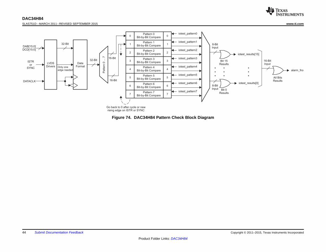
Pattern
0 ... 7
32-Bit
32-Bit
16-Bit
16-BitDATACLK
iotest_results[15]
iotest_results[0]
B0462-01
alarm_from_iotestOnly oneedge needed
ISTRor
SYNC
LVDSDrivers
Go back to 0 after cycle or newrising edge on ISTR or SYNC
Pattern 0Bit-by-Bit Compare
Pattern 1Bit-by-Bit Compare
Pattern 2Bit-by-Bit Compare
Pattern 3Bit-by-Bit Compare
Pattern 4Bit-by-Bit Compare
Pattern 5Bit-by-Bit Compare
Pattern 6Bit-by-Bit Compare
Pattern 7Bit-by-Bit Compare
0
1
2
3
4
5
6
7
0
1
2
3
4
5
6
7
8-BitInput
16-BitInput
8-BitInput
Bit 15Results
Bit 0Results
•••
•••
•••
All BitsResults
iotest_pattern0
iotest_pattern1
iotest_pattern2
iotest_pattern3
iotest_pattern4
iotest_pattern5
iotest_pattern6
iotest_pattern7
DataFormat
DAB[15:0]DCD[15:0]
DAC34H84SLAS751D –MARCH 2011–REVISED SEPTEMBER 2015 www.ti.com
Figure 74. DAC34H84 Pattern Check Block Diagram
44 Submit Documentation Feedback Copyright © 2011–2015, Texas Instruments Incorporated
Product Folder Links: DAC34H84
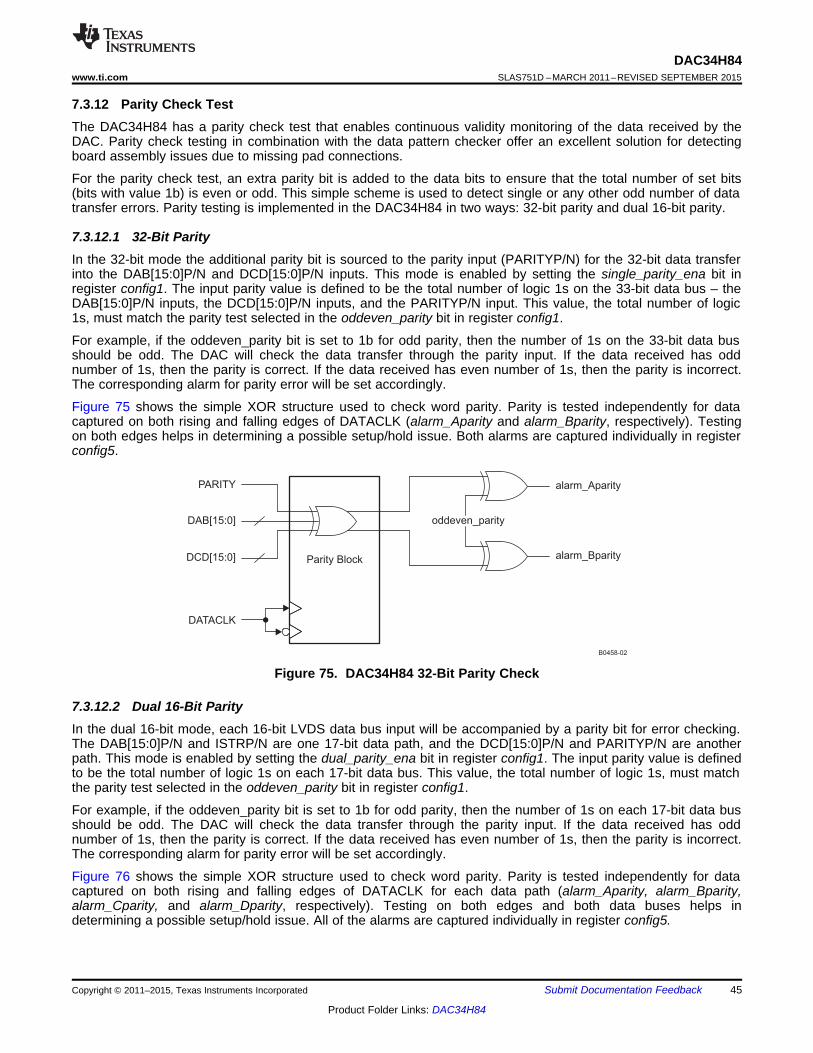
DATACLK
alarm_Aparity
alarm_Bparity
B0458-02
Parity Block
oddeven_parity
PARITY
DAB[15:0]
DCD[15:0]
DAC34H84www.ti.com SLAS751D –MARCH 2011–REVISED SEPTEMBER 2015
7.3.12 Parity Check TestThe DAC34H84 has a parity check test that enables continuous validity monitoring of the data received by theDAC. Parity check testing in combination with the data pattern checker offer an excellent solution for detectingboard assembly issues due to missing pad connections.
For the parity check test, an extra parity bit is added to the data bits to ensure that the total number of set bits(bits with value 1b) is even or odd. This simple scheme is used to detect single or any other odd number of datatransfer errors. Parity testing is implemented in the DAC34H84 in two ways: 32-bit parity and dual 16-bit parity.
7.3.12.1 32-Bit ParityIn the 32-bit mode the additional parity bit is sourced to the parity input (PARITYP/N) for the 32-bit data transferinto the DAB[15:0]P/N and DCD[15:0]P/N inputs. This mode is enabled by setting the single_parity_ena bit inregister config1. The input parity value is defined to be the total number of logic 1s on the 33-bit data bus – theDAB[15:0]P/N inputs, the DCD[15:0]P/N inputs, and the PARITYP/N input. This value, the total number of logic1s, must match the parity test selected in the oddeven_parity bit in register config1.
For example, if the oddeven_parity bit is set to 1b for odd parity, then the number of 1s on the 33-bit data busshould be odd. The DAC will check the data transfer through the parity input. If the data received has oddnumber of 1s, then the parity is correct. If the data received has even number of 1s, then the parity is incorrect.The corresponding alarm for parity error will be set accordingly.
Figure 75 shows the simple XOR structure used to check word parity. Parity is tested independently for datacaptured on both rising and falling edges of DATACLK (alarm_Aparity and alarm_Bparity, respectively). Testingon both edges helps in determining a possible setup/hold issue. Both alarms are captured individually in registerconfig5.
Figure 75. DAC34H84 32-Bit Parity Check
7.3.12.2 Dual 16-Bit ParityIn the dual 16-bit mode, each 16-bit LVDS data bus input will be accompanied by a parity bit for error checking.The DAB[15:0]P/N and ISTRP/N are one 17-bit data path, and the DCD[15:0]P/N and PARITYP/N are anotherpath. This mode is enabled by setting the dual_parity_ena bit in register config1. The input parity value is definedto be the total number of logic 1s on each 17-bit data bus. This value, the total number of logic 1s, must matchthe parity test selected in the oddeven_parity bit in register config1.
For example, if the oddeven_parity bit is set to 1b for odd parity, then the number of 1s on each 17-bit data busshould be odd. The DAC will check the data transfer through the parity input. If the data received has oddnumber of 1s, then the parity is correct. If the data received has even number of 1s, then the parity is incorrect.The corresponding alarm for parity error will be set accordingly.
Figure 76 shows the simple XOR structure used to check word parity. Parity is tested independently for datacaptured on both rising and falling edges of DATACLK for each data path (alarm_Aparity, alarm_Bparity,alarm_Cparity, and alarm_Dparity, respectively). Testing on both edges and both data buses helps indetermining a possible setup/hold issue. All of the alarms are captured individually in register config5.
Copyright © 2011–2015, Texas Instruments Incorporated Submit Documentation Feedback 45
Product Folder Links: DAC34H84
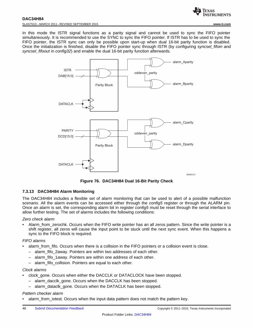
DATACLK
DATACLK
alarm_Cparity
alarm_Aparity
alarm_Dparity
alarm_Bparity
B0463-01
Parity Block
Parity Block
oddeven_parity
oddeven_parity
PARITY
ISTR
DCD[15:0]
DAB[15:0]
DAC34H84SLAS751D –MARCH 2011–REVISED SEPTEMBER 2015 www.ti.com
In this mode the ISTR signal functions as a parity signal and cannot be used to sync the FIFO pointersimultaneously. It is recommended to use the SYNC to sync the FIFO pointer. If ISTR has to be used to sync theFIFO pointer, the ISTR sync can only be possible upon start-up when dual 16-bit parity function is disabled.Once the initialization is finished, disable the FIFO pointer sync through ISTR (by configuring syncsel_fifoin andsyncsel_fifoout in config32) and enable the dual 16-bit parity function afterwards.
Figure 76. DAC34H84 Dual 16-Bit Parity Check
7.3.13 DAC34H84 Alarm MonitoringThe DAC34H84 includes a flexible set of alarm monitoring that can be used to alert of a possible malfunctionscenario. All the alarm events can be accessed either through the config5 register or through the ALARM pin.Once an alarm is set, the corresponding alarm bit in register config5 must be reset through the serial interface toallow further testing. The set of alarms includes the following conditions:
Zero check alarm• Alarm_from_zerochk. Occurs when the FIFO write pointer has an all zeros pattern. Since the write pointer is a
shift register, all zeros will cause the input point to be stuck until the next sync event. When this happens async to the FIFO block is required.
FIFO alarms• alarm_from_fifo. Occurs when there is a collision in the FIFO pointers or a collision event is close.
– alarm_fifo_2away. Pointers are within two addresses of each other.– alarm_fifo_1away. Pointers are within one address of each other.– alarm_fifo_collision. Pointers are equal to each other.
Clock alarms• clock_gone. Occurs when either the DACCLK or DATACLOCK have been stopped.
– alarm_dacclk_gone. Occurs when the DACCLK has been stopped.– alarm_dataclk_gone. Occurs when the DATACLK has been stopped.
Pattern checker alarm• alarm_from_iotest. Occurs when the input data pattern does not match the pattern key.
46 Submit Documentation Feedback Copyright © 2011–2015, Texas Instruments Incorporated
Product Folder Links: DAC34H84
DAC34H84www.ti.com SLAS751D –MARCH 2011–REVISED SEPTEMBER 2015
PLL alarm• alarm_from_pll. Occurs when the PLL is out of lock.
Parity alarms• alarm_Aparity: In dual parity mode, alarm indicating a parity error on the A word. In single parity mode, alarm
on the 32-bit data captured on the rising edge of DATACLKP/N.• alarm_Bparity: In dual parity mode, alarm indicating a parity error on the B word. In single parity mode, alarm
on the 32-bit data captured on the falling edge of DATACLKP/N.• alarm_Cparity: In dual parity mode, alarm indicating a parity error on the C word.• alarm_Dparity: In dual parity mode, alarm indicating a parity error on the D word.
To prevent unexpected DAC outputs from propagating into the transmit channel chain, the clock and alarm_fifo_collision alarms can be set in config2 to shut-off the DAC output automatically regardless of the state ofTXENA or sif_txenable.
Alarm monitoring is implemented as follows:• Power up the device using the recommended power-up sequence.• Clear all the alarms in config5 by setting them to zeros.• Unmask those alarms that will generate a hardware interrupt through the ALARM pin in config7.• Enable automatic DAC shut-off in register config2 if required.• In the case of an alarm event, the ALARM pin will trigger. If automatic DAC shut-off has been enabled the
DAC outputs will be disabled.• Read registers config5 to determine which alarm triggered the ALARM pin.• Correct the error condition and re-synchronize the FIFO.• Clear the alarms in config5.• Re-read config5 to ensure the alarm event has been corrected.• Keep clearing and reading config5 until no error is reported.
Copyright © 2011–2015, Texas Instruments Incorporated Submit Documentation Feedback 47
Product Folder Links: DAC34H84
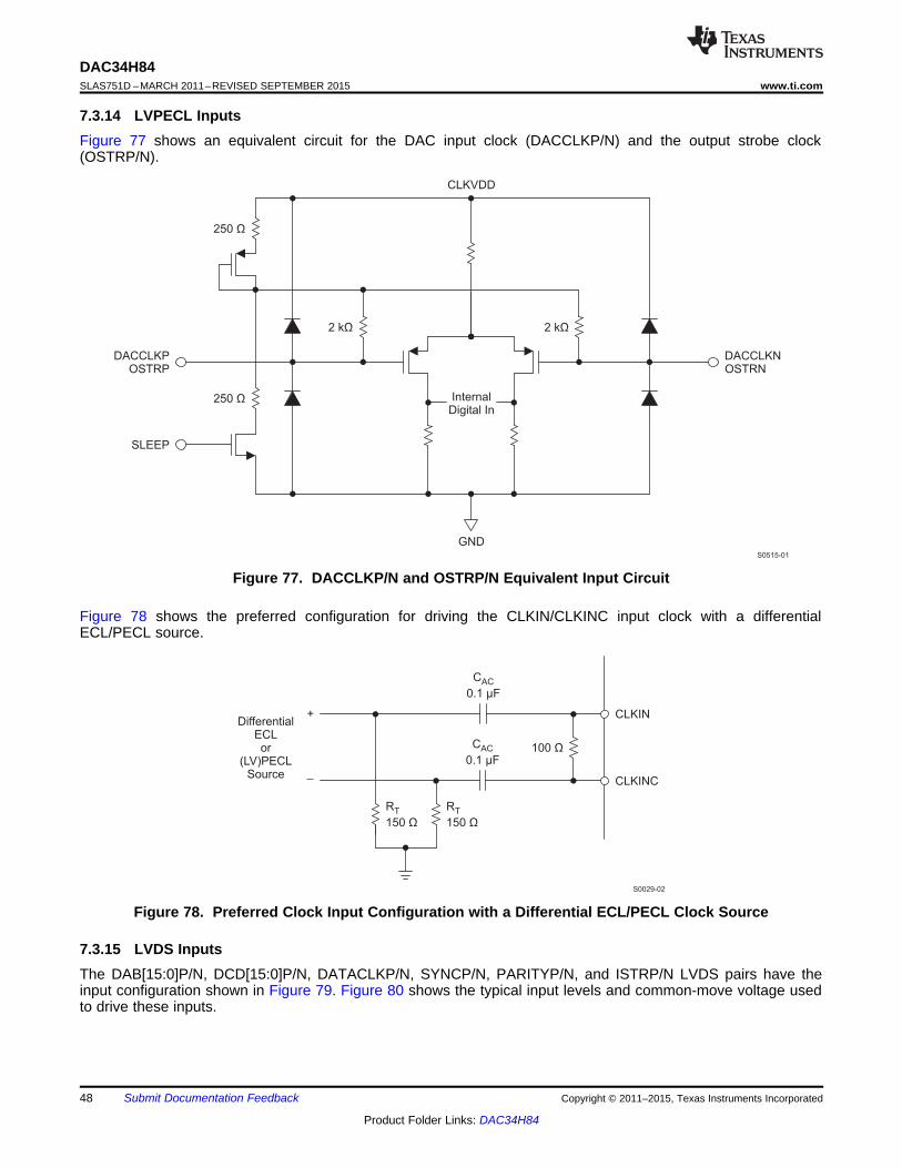
C
0.1 FAC
μ
C
0.1 FAC
μ
DifferentialECLor
(LV)PECLSource
+
–
CLKIN
CLKINC
S0029-02
100 Ω
R
150T
Ω
R
150T
Ω
GND
CLKVDD
InternalDigital In
DACCLKNOSTRN
S0515-01
DACCLKPOSTRP
SLEEP
250 Ω
250 Ω
2 kΩ 2 kΩ
DAC34H84SLAS751D –MARCH 2011–REVISED SEPTEMBER 2015 www.ti.com
7.3.14 LVPECL InputsFigure 77 shows an equivalent circuit for the DAC input clock (DACCLKP/N) and the output strobe clock(OSTRP/N).
Figure 77. DACCLKP/N and OSTRP/N Equivalent Input Circuit
Figure 78 shows the preferred configuration for driving the CLKIN/CLKINC input clock with a differentialECL/PECL source.
Figure 78. Preferred Clock Input Configuration with a Differential ECL/PECL Clock Source
7.3.15 LVDS InputsThe DAB[15:0]P/N, DCD[15:0]P/N, DATACLKP/N, SYNCP/N, PARITYP/N, and ISTRP/N LVDS pairs have theinput configuration shown in Figure 79. Figure 80 shows the typical input levels and common-move voltage usedto drive these inputs.
48 Submit Documentation Feedback Copyright © 2011–2015, Texas Instruments Incorporated
Product Folder Links: DAC34H84
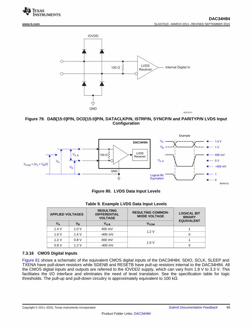
LVDSReceiver
DAC34H84
GND
B0459-02
100 Ω
VB
VB
VA
VA 1.4 V
1 V
400 mV
0 V
–400 mV
1
0
V = (V + V )/2COM A B
VA, B
VA, B
Logical BitEquivalent
Example
GND
Internal Digital In
IOVDD
LVDSReceiver
S0516-01
100 Ω
DAC34H84www.ti.com SLAS751D –MARCH 2011–REVISED SEPTEMBER 2015
Figure 79. DAB[15:0]P/N, DCD[15:0]P/N, DATACLKP/N, ISTRP/N, SYNCP/N and PARITYP/N LVDS InputConfiguration
Figure 80. LVDS Data Input Levels
Table 9. Example LVDS Data Input LevelsRESULTING RESULTING COMMON- LOGICAL BITAPPLIED VOLTAGES DIFFERENTIAL MODE VOLTAGE BINARYVOLTAGE
EQUIVALENTVA VB VA,B VCOM
1.4 V 1.0 V 400 mV 11.2 V
1.0 V 1.4 V -400 mV 01.2 V 0.8 V 400 mV 1
1.0 V0.8 V 1.2 V -400 mV 0
7.3.16 CMOS Digital InputsFigure 81 shows a schematic of the equivalent CMOS digital inputs of the DAC34H84. SDIO, SCLK, SLEEP andTXENA have pull-down resistors while SDENB and RESETB have pull-up resistors internal to the DAC34H84. Allthe CMOS digital inputs and outputs are referred to the IOVDD2 supply, which can vary from 1.8 V to 3.3 V. Thisfacilitates the I/O interface and eliminates the need of level translation. See the specification table for logicthresholds. The pull-up and pull-down circuitry is approximately equivalent to 100 kΩ.
Copyright © 2011–2015, Texas Instruments Incorporated Submit Documentation Feedback 49
Product Folder Links: DAC34H84
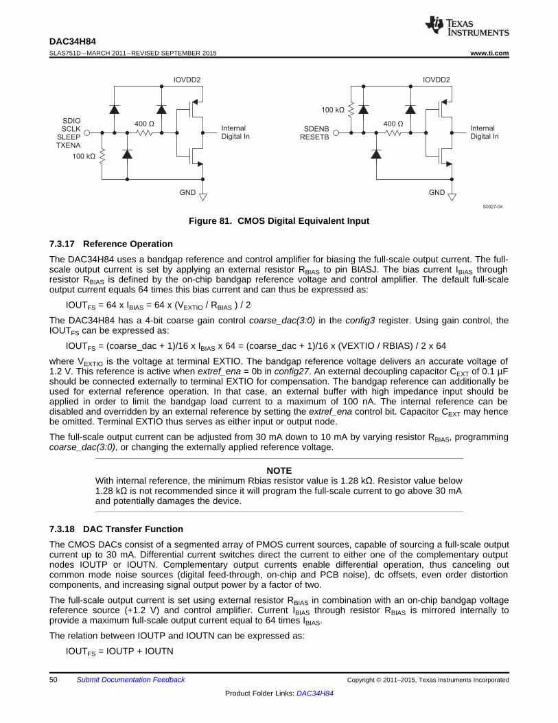
SDIOSCLK
SLEEPTXENA
InternalDigital In
GND
400 Ω 400 Ω
100 kΩ
100 kΩ
GND
IOVDD2 IOVDD2
SDENBRESETB
InternalDigital In
S0027-04
DAC34H84SLAS751D –MARCH 2011–REVISED SEPTEMBER 2015 www.ti.com
Figure 81. CMOS Digital Equivalent Input
7.3.17 Reference OperationThe DAC34H84 uses a bandgap reference and control amplifier for biasing the full-scale output current. The full-scale output current is set by applying an external resistor RBIAS to pin BIASJ. The bias current IBIAS throughresistor RBIAS is defined by the on-chip bandgap reference voltage and control amplifier. The default full-scaleoutput current equals 64 times this bias current and can thus be expressed as:
IOUTFS = 64 x IBIAS = 64 x (VEXTIO / RBIAS ) / 2
The DAC34H84 has a 4-bit coarse gain control coarse_dac(3:0) in the config3 register. Using gain control, theIOUTFS can be expressed as:
IOUTFS = (coarse_dac + 1)/16 x IBIAS x 64 = (coarse_dac + 1)/16 x (VEXTIO / RBIAS) / 2 x 64
where VEXTIO is the voltage at terminal EXTIO. The bandgap reference voltage delivers an accurate voltage of1.2 V. This reference is active when extref_ena = 0b in config27. An external decoupling capacitor CEXT of 0.1 µFshould be connected externally to terminal EXTIO for compensation. The bandgap reference can additionally beused for external reference operation. In that case, an external buffer with high impedance input should beapplied in order to limit the bandgap load current to a maximum of 100 nA. The internal reference can bedisabled and overridden by an external reference by setting the extref_ena control bit. Capacitor CEXT may hencebe omitted. Terminal EXTIO thus serves as either input or output node.
The full-scale output current can be adjusted from 30 mA down to 10 mA by varying resistor RBIAS, programmingcoarse_dac(3:0), or changing the externally applied reference voltage.
NOTEWith internal reference, the minimum Rbias resistor value is 1.28 kΩ. Resistor value below1.28 kΩ is not recommended since it will program the full-scale current to go above 30 mAand potentially damages the device.
7.3.18 DAC Transfer FunctionThe CMOS DACs consist of a segmented array of PMOS current sources, capable of sourcing a full-scale outputcurrent up to 30 mA. Differential current switches direct the current to either one of the complementary outputnodes IOUTP or IOUTN. Complementary output currents enable differential operation, thus canceling outcommon mode noise sources (digital feed-through, on-chip and PCB noise), dc offsets, even order distortioncomponents, and increasing signal output power by a factor of two.
The full-scale output current is set using external resistor RBIAS in combination with an on-chip bandgap voltagereference source (+1.2 V) and control amplifier. Current IBIAS through resistor RBIAS is mirrored internally toprovide a maximum full-scale output current equal to 64 times IBIAS.
The relation between IOUTP and IOUTN can be expressed as:
IOUTFS = IOUTP + IOUTN
50 Submit Documentation Feedback Copyright © 2011–2015, Texas Instruments Incorporated
Product Folder Links: DAC34H84
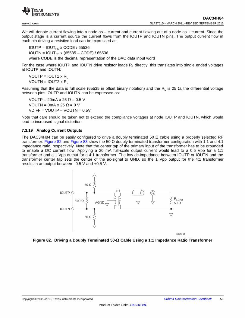
IOUTP1:1
IOUTN
AGND
50 Ω
R
50 Ω
LOAD
50 Ω
100 Ω
S0517-01
DAC34H84www.ti.com SLAS751D –MARCH 2011–REVISED SEPTEMBER 2015
We will denote current flowing into a node as – current and current flowing out of a node as + current. Since theoutput stage is a current source the current flows from the IOUTP and IOUTN pins. The output current flow ineach pin driving a resistive load can be expressed as:
IOUTP = IOUTFS x CODE / 65536IOUTN = IOUTFS x (65535 – CODE) / 65536where CODE is the decimal representation of the DAC data input word
For the case where IOUTP and IOUTN drive resistor loads RL directly, this translates into single ended voltagesat IOUTP and IOUTN:
VOUTP = IOUT1 x RLVOUTN = IOUT2 x RL
Assuming that the data is full scale (65535 in offset binary notation) and the RL is 25 Ω, the differential voltagebetween pins IOUTP and IOUTN can be expressed as:
VOUTP = 20mA x 25 Ω = 0.5 VVOUTN = 0mA x 25 Ω = 0 VVDIFF = VOUTP – VOUTN = 0.5V
Note that care should be taken not to exceed the compliance voltages at node IOUTP and IOUTN, which wouldlead to increased signal distortion.
7.3.19 Analog Current OutputsThe DAC34H84 can be easily configured to drive a doubly terminated 50 Ω cable using a properly selected RFtransformer. Figure 82 and Figure 83 show the 50 Ω doubly terminated transformer configuration with 1:1 and 4:1impedance ratio, respectively. Note that the center tap of the primary input of the transformer has to be groundedto enable a DC current flow. Applying a 20 mA full-scale output current would lead to a 0.5 Vpp for a 1:1transformer and a 1 Vpp output for a 4:1 transformer. The low dc-impedance between IOUTP or IOUTN and thetransformer center tap sets the center of the ac-signal to GND, so the 1 Vpp output for the 4:1 transformerresults in an output between –0.5 V and +0.5 V.
Figure 82. Driving a Doubly Terminated 50-Ω Cable Using a 1:1 Impedance Ratio Transformer
Copyright © 2011–2015, Texas Instruments Incorporated Submit Documentation Feedback 51
Product Folder Links: DAC34H84
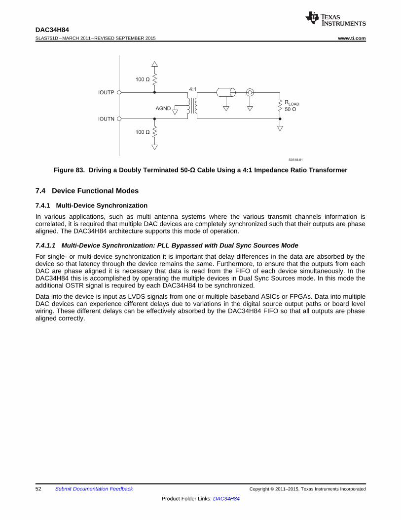
IOUTP4:1
IOUTN
AGND
100 Ω
R
50 Ω
LOAD
100 Ω
S0518-01
DAC34H84SLAS751D –MARCH 2011–REVISED SEPTEMBER 2015 www.ti.com
Figure 83. Driving a Doubly Terminated 50-Ω Cable Using a 4:1 Impedance Ratio Transformer
7.4 Device Functional Modes
7.4.1 Multi-Device SynchronizationIn various applications, such as multi antenna systems where the various transmit channels information iscorrelated, it is required that multiple DAC devices are completely synchronized such that their outputs are phasealigned. The DAC34H84 architecture supports this mode of operation.
7.4.1.1 Multi-Device Synchronization: PLL Bypassed with Dual Sync Sources ModeFor single- or multi-device synchronization it is important that delay differences in the data are absorbed by thedevice so that latency through the device remains the same. Furthermore, to ensure that the outputs from eachDAC are phase aligned it is necessary that data is read from the FIFO of each device simultaneously. In theDAC34H84 this is accomplished by operating the multiple devices in Dual Sync Sources mode. In this mode theadditional OSTR signal is required by each DAC34H84 to be synchronized.
Data into the device is input as LVDS signals from one or multiple baseband ASICs or FPGAs. Data into multipleDAC devices can experience different delays due to variations in the digital source output paths or board levelwiring. These different delays can be effectively absorbed by the DAC34H84 FIFO so that all outputs are phasealigned correctly.
52 Submit Documentation Feedback Copyright © 2011–2015, Texas Instruments Incorporated
Product Folder Links: DAC34H84
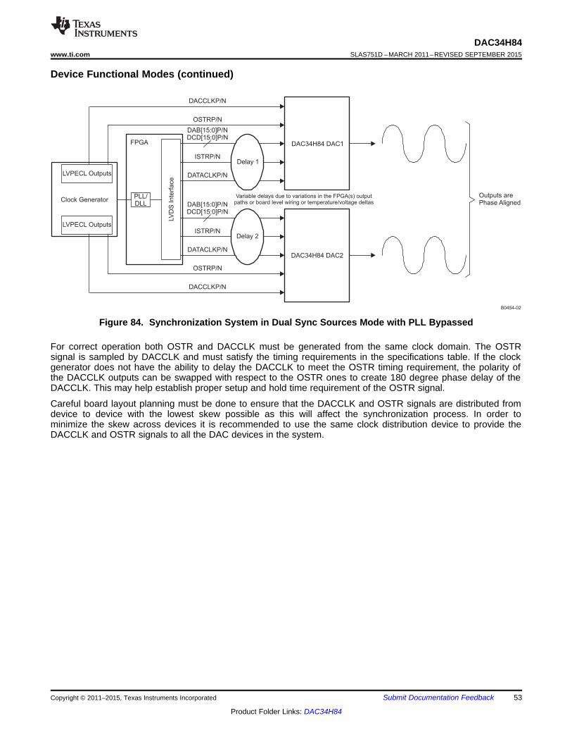
Clock Generator
DATACLKP/N
ISTRP/N
FPGA
DAB[15:0]P/NDCD[15:0]P/N
DAB[15:0]P/NDCD[15:0]P/N
DATACLKP/N
ISTRP/N
DACCLKP/N
B0454-02
LVPECL OutputsLV
DS
Inte
rface
OSTRP/N
LVPECL Outputs
DACCLKP/N
OSTRP/N
PLL/DLL
DAC34H84 DAC1
Delay 1
Delay 2
Outputs arePhase Aligned
DAC34H84 DAC2
Variable delays due to variations in the FPGA(s) outputpaths or board level wiring or temperature/voltage deltas
DAC34H84www.ti.com SLAS751D –MARCH 2011–REVISED SEPTEMBER 2015
Device Functional Modes (continued)
Figure 84. Synchronization System in Dual Sync Sources Mode with PLL Bypassed
For correct operation both OSTR and DACCLK must be generated from the same clock domain. The OSTRsignal is sampled by DACCLK and must satisfy the timing requirements in the specifications table. If the clockgenerator does not have the ability to delay the DACCLK to meet the OSTR timing requirement, the polarity ofthe DACCLK outputs can be swapped with respect to the OSTR ones to create 180 degree phase delay of theDACCLK. This may help establish proper setup and hold time requirement of the OSTR signal.
Careful board layout planning must be done to ensure that the DACCLK and OSTR signals are distributed fromdevice to device with the lowest skew possible as this will affect the synchronization process. In order tominimize the skew across devices it is recommended to use the same clock distribution device to provide theDACCLK and OSTR signals to all the DAC devices in the system.
Copyright © 2011–2015, Texas Instruments Incorporated Submit Documentation Feedback 53
Product Folder Links: DAC34H84
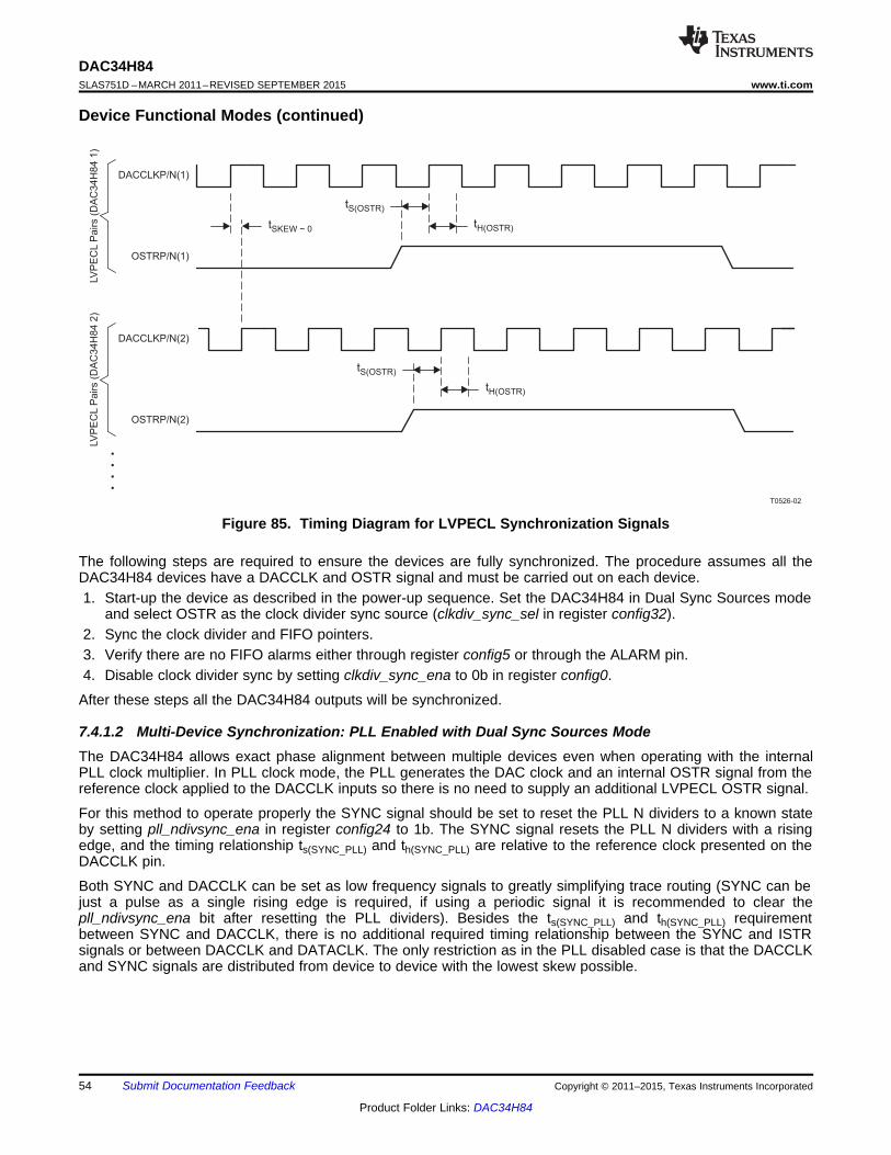
T0526-02
DACCLKP/N(2)
DACCLKP/N(1)
••••
OSTRP/N(2)
OSTRP/N(1)
LV
PE
CL
Pairs (
DA
C34H
84 2
)LV
PE
CL
Pairs (
DA
C34H
84 1
)
tS(OSTR)
tS(OSTR)
tSKEW ~ 0tH(OSTR)
tH(OSTR)
DAC34H84SLAS751D –MARCH 2011–REVISED SEPTEMBER 2015 www.ti.com
Device Functional Modes (continued)
Figure 85. Timing Diagram for LVPECL Synchronization Signals
The following steps are required to ensure the devices are fully synchronized. The procedure assumes all theDAC34H84 devices have a DACCLK and OSTR signal and must be carried out on each device.1. Start-up the device as described in the power-up sequence. Set the DAC34H84 in Dual Sync Sources mode
and select OSTR as the clock divider sync source (clkdiv_sync_sel in register config32).2. Sync the clock divider and FIFO pointers.3. Verify there are no FIFO alarms either through register config5 or through the ALARM pin.4. Disable clock divider sync by setting clkdiv_sync_ena to 0b in register config0.
After these steps all the DAC34H84 outputs will be synchronized.
7.4.1.2 Multi-Device Synchronization: PLL Enabled with Dual Sync Sources ModeThe DAC34H84 allows exact phase alignment between multiple devices even when operating with the internalPLL clock multiplier. In PLL clock mode, the PLL generates the DAC clock and an internal OSTR signal from thereference clock applied to the DACCLK inputs so there is no need to supply an additional LVPECL OSTR signal.
For this method to operate properly the SYNC signal should be set to reset the PLL N dividers to a known stateby setting pll_ndivsync_ena in register config24 to 1b. The SYNC signal resets the PLL N dividers with a risingedge, and the timing relationship ts(SYNC_PLL) and th(SYNC_PLL) are relative to the reference clock presented on theDACCLK pin.
Both SYNC and DACCLK can be set as low frequency signals to greatly simplifying trace routing (SYNC can bejust a pulse as a single rising edge is required, if using a periodic signal it is recommended to clear thepll_ndivsync_ena bit after resetting the PLL dividers). Besides the ts(SYNC_PLL) and th(SYNC_PLL) requirementbetween SYNC and DACCLK, there is no additional required timing relationship between the SYNC and ISTRsignals or between DACCLK and DATACLK. The only restriction as in the PLL disabled case is that the DACCLKand SYNC signals are distributed from device to device with the lowest skew possible.
54 Submit Documentation Feedback Copyright © 2011–2015, Texas Instruments Incorporated
Product Folder Links: DAC34H84
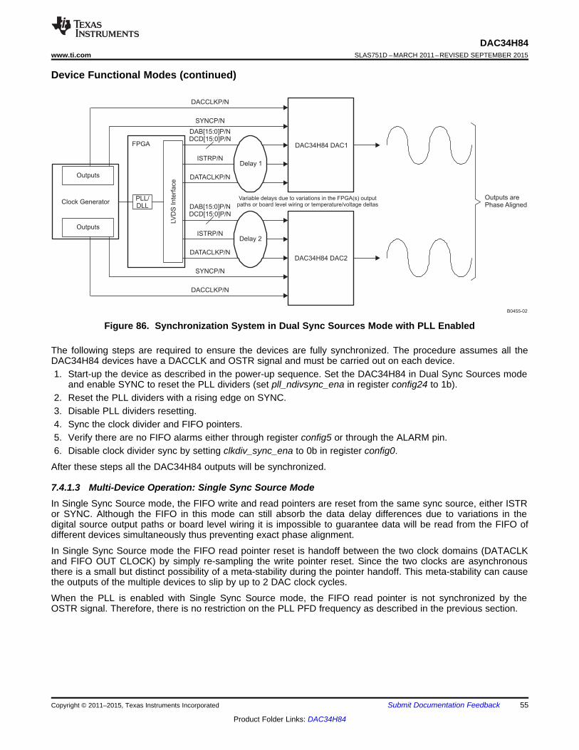
SYNCP/N
SYNCP/N
Clock Generator
DATACLKP/N
ISTRP/N
FPGA
DAB[15:0]P/NDCD[15:0]P/N
DAB[15:0]P/NDCD[15:0]P/N
DATACLKP/N
ISTRP/N
DACCLKP/N
B0455-02
LV
DS
Inte
rface
DACCLKP/N
PLL/DLL
DAC34H84 DAC1
Delay 1
Delay 2
Outputs arePhase Aligned
DAC34H84 DAC2
Outputs
Outputs
Variable delays due to variations in the FPGA(s) outputpaths or board level wiring or temperature/voltage deltas
DAC34H84www.ti.com SLAS751D –MARCH 2011–REVISED SEPTEMBER 2015
Device Functional Modes (continued)
Figure 86. Synchronization System in Dual Sync Sources Mode with PLL Enabled
The following steps are required to ensure the devices are fully synchronized. The procedure assumes all theDAC34H84 devices have a DACCLK and OSTR signal and must be carried out on each device.1. Start-up the device as described in the power-up sequence. Set the DAC34H84 in Dual Sync Sources mode
and enable SYNC to reset the PLL dividers (set pll_ndivsync_ena in register config24 to 1b).2. Reset the PLL dividers with a rising edge on SYNC.3. Disable PLL dividers resetting.4. Sync the clock divider and FIFO pointers.5. Verify there are no FIFO alarms either through register config5 or through the ALARM pin.6. Disable clock divider sync by setting clkdiv_sync_ena to 0b in register config0.
After these steps all the DAC34H84 outputs will be synchronized.
7.4.1.3 Multi-Device Operation: Single Sync Source ModeIn Single Sync Source mode, the FIFO write and read pointers are reset from the same sync source, either ISTRor SYNC. Although the FIFO in this mode can still absorb the data delay differences due to variations in thedigital source output paths or board level wiring it is impossible to guarantee data will be read from the FIFO ofdifferent devices simultaneously thus preventing exact phase alignment.
In Single Sync Source mode the FIFO read pointer reset is handoff between the two clock domains (DATACLKand FIFO OUT CLOCK) by simply re-sampling the write pointer reset. Since the two clocks are asynchronousthere is a small but distinct possibility of a meta-stability during the pointer handoff. This meta-stability can causethe outputs of the multiple devices to slip by up to 2 DAC clock cycles.
When the PLL is enabled with Single Sync Source mode, the FIFO read pointer is not synchronized by theOSTR signal. Therefore, there is no restriction on the PLL PFD frequency as described in the previous section.
Copyright © 2011–2015, Texas Instruments Incorporated Submit Documentation Feedback 55
Product Folder Links: DAC34H84
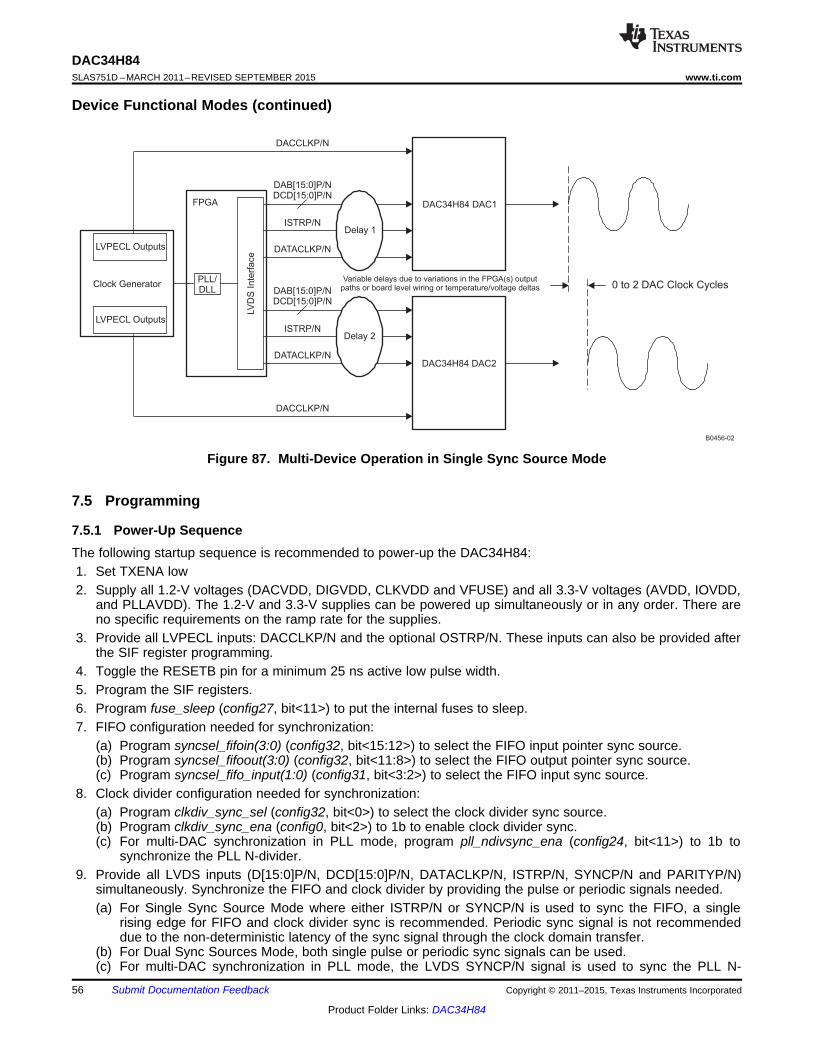
B0456-02
LVPECL Outputs
LVPECL Outputs
0 to 2 DAC Clock CyclesClock Generator
DATACLKP/N
ISTRP/N
FPGA
DAB[15:0]P/NDCD[15:0]P/N
DAB[15:0]P/NDCD[15:0]P/N
DATACLKP/N
ISTRP/N
DACCLKP/N
LV
DS
Inte
rface
DACCLKP/N
PLL/DLL
DAC34H84 DAC1
Delay 1
Delay 2
Variable delays due to variations in the FPGA(s) outputpaths or board level wiring or temperature/voltage deltas
DAC34H84 DAC2
DAC34H84SLAS751D –MARCH 2011–REVISED SEPTEMBER 2015 www.ti.com
Device Functional Modes (continued)
Figure 87. Multi-Device Operation in Single Sync Source Mode
7.5 Programming
7.5.1 Power-Up SequenceThe following startup sequence is recommended to power-up the DAC34H84:1. Set TXENA low2. Supply all 1.2-V voltages (DACVDD, DIGVDD, CLKVDD and VFUSE) and all 3.3-V voltages (AVDD, IOVDD,
and PLLAVDD). The 1.2-V and 3.3-V supplies can be powered up simultaneously or in any order. There areno specific requirements on the ramp rate for the supplies.
3. Provide all LVPECL inputs: DACCLKP/N and the optional OSTRP/N. These inputs can also be provided afterthe SIF register programming.
4. Toggle the RESETB pin for a minimum 25 ns active low pulse width.5. Program the SIF registers.6. Program fuse_sleep (config27, bit<11>) to put the internal fuses to sleep.7. FIFO configuration needed for synchronization:
(a) Program syncsel_fifoin(3:0) (config32, bit<15:12>) to select the FIFO input pointer sync source.(b) Program syncsel_fifoout(3:0) (config32, bit<11:8>) to select the FIFO output pointer sync source.(c) Program syncsel_fifo_input(1:0) (config31, bit<3:2>) to select the FIFO input sync source.
8. Clock divider configuration needed for synchronization:(a) Program clkdiv_sync_sel (config32, bit<0>) to select the clock divider sync source.(b) Program clkdiv_sync_ena (config0, bit<2>) to 1b to enable clock divider sync.(c) For multi-DAC synchronization in PLL mode, program pll_ndivsync_ena (config24, bit<11>) to 1b to
synchronize the PLL N-divider.9. Provide all LVDS inputs (D[15:0]P/N, DCD[15:0]P/N, DATACLKP/N, ISTRP/N, SYNCP/N and PARITYP/N)
simultaneously. Synchronize the FIFO and clock divider by providing the pulse or periodic signals needed.(a) For Single Sync Source Mode where either ISTRP/N or SYNCP/N is used to sync the FIFO, a single
rising edge for FIFO and clock divider sync is recommended. Periodic sync signal is not recommendeddue to the non-deterministic latency of the sync signal through the clock domain transfer.
(b) For Dual Sync Sources Mode, both single pulse or periodic sync signals can be used.(c) For multi-DAC synchronization in PLL mode, the LVDS SYNCP/N signal is used to sync the PLL N-
56 Submit Documentation Feedback Copyright © 2011–2015, Texas Instruments Incorporated
Product Folder Links: DAC34H84
DAC34H84www.ti.com SLAS751D –MARCH 2011–REVISED SEPTEMBER 2015
Programming (continued)divider and can be sourced from either the FPGA/ASIC pattern generator or clock distribution circuit aslong as the t(SYNC_PLL) setup and hold timing requirement is met with respect to the reference clocksource at DACCLKP/N pins. The LVDS SYNCP/N signal can be provided at this point.
10. FIFO and clock divider configurations after all the sync signals have provided the initial sync pulses neededfor synchronization:(a) For Single Sync Source Mode where the clock divider sync source is either ISTRP/N or SYNCP/N, clock
divider syncing must be disabled after DAC34H84 initialization and before the data transmission bysetting clkdiv_sync_ena (config0, bit 2) to 0b.
(b) For Dual Sync Sources Mode, where the clock divider sync source is from the OSTR signal (either fromexternal OSTRP/N or internal PLL N divider output), the clock divider syncing may be enabled at all time.
(c) Optionally, to prevent accidental syncing of the FIFO when sending the ISTRP/N or SYNCP/N pulse toother digital blocks such as NCO, QMC, ..., disable FIFO syncing by setting syncsel_fifoin(3:0) andsyncsel_fifoout(3:0) to 0000b after the FIFO input and output pointers are initialized. If the FIFO and syncremain enabled after initialization, the ISTRP/N or SYNCP/N pulse must occur in ways to not disturb theFIFO operation. Refer to the INPUT FIFO section for detail.
(d) Disable PLL N-divider syncing by setting pll_ndivsync_ena (config24, bit<11>) to 0b.11. Enable transmit of data by asserting the TXENA pin or set sif_txenable to 1b.12. At any time, if any of the clocks (for example, DATACLK or DACCLK) is lost or a FIFO collision alarm is
detected, a complete resynchronization of the DAC is necessary. Set TXENABLE low and repeat steps 7through 11. Program the FIFO configuration and clock divider configuration per steps 7 and 8 appropriatelyto accept the new sync pulse or pulses for the synchronization.
7.5.2 Example Start-Up Routine
7.5.2.1 Device Configuration
fDATA = 491.52 MSPSInterpolation = 2xInput data = baseband datafOUT = 122.88 MHzPLL = EnabledFull Mixer = EnabledDual Sync Sources Mode
7.5.2.2 PLL Configuration
fREFCLK = 491.52 MHz at the DACCLKP/N LVPECL pinsfDACCLK = fDATA x Interpolation = 983.04 MHzfVCO = 4 x fDACCLK = 3932.16 MHz (keep fVCO between 3.3 GHz to 4 GHz)PFD = fOSTR = 30.72 MHzN = 16, M = 32, P = 4, single charge pumppll_vco(5:0) = 111011b (59)
7.5.2.3 NCO Configuration
fNCO = 122.88 MHzfNCO_CLK = 983.04 MHzfreq = fNCO x 2^32 / 983.04 = 536870912 = 0x20000000
Copyright © 2011–2015, Texas Instruments Incorporated Submit Documentation Feedback 57
Product Folder Links: DAC34H84
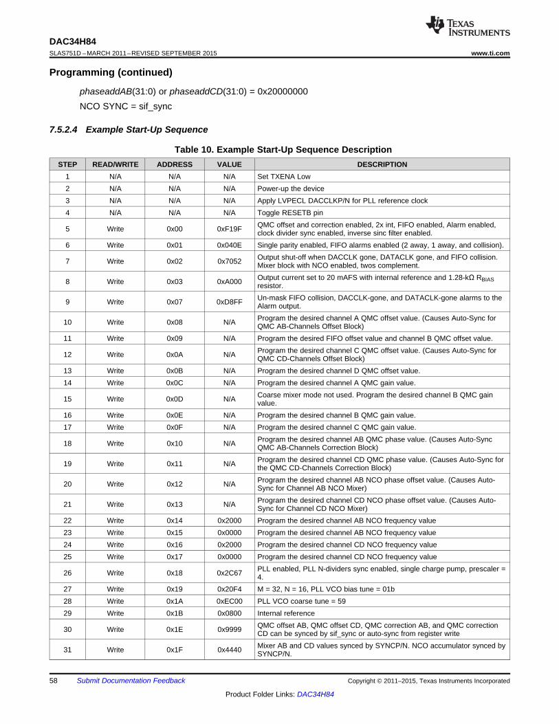
DAC34H84SLAS751D –MARCH 2011–REVISED SEPTEMBER 2015 www.ti.com
Programming (continued)
phaseaddAB(31:0) or phaseaddCD(31:0) = 0x20000000NCO SYNC = sif_sync
7.5.2.4 Example Start-Up Sequence
Table 10. Example Start-Up Sequence DescriptionSTEP READ/WRITE ADDRESS VALUE DESCRIPTION
1 N/A N/A N/A Set TXENA Low2 N/A N/A N/A Power-up the device3 N/A N/A N/A Apply LVPECL DACCLKP/N for PLL reference clock4 N/A N/A N/A Toggle RESETB pin
QMC offset and correction enabled, 2x int, FIFO enabled, Alarm enabled,5 Write 0x00 0xF19F clock divider sync enabled, inverse sinc filter enabled.6 Write 0x01 0x040E Single parity enabled, FIFO alarms enabled (2 away, 1 away, and collision).
Output shut-off when DACCLK gone, DATACLK gone, and FIFO collision.7 Write 0x02 0x7052 Mixer block with NCO enabled, twos complement.Output current set to 20 mAFS with internal reference and 1.28-kΩ RBIAS8 Write 0x03 0xA000 resistor.Un-mask FIFO collision, DACCLK-gone, and DATACLK-gone alarms to the9 Write 0x07 0xD8FF Alarm output.Program the desired channel A QMC offset value. (Causes Auto-Sync for10 Write 0x08 N/A QMC AB-Channels Offset Block)
11 Write 0x09 N/A Program the desired FIFO offset value and channel B QMC offset value.Program the desired channel C QMC offset value. (Causes Auto-Sync for12 Write 0x0A N/A QMC CD-Channels Offset Block)
13 Write 0x0B N/A Program the desired channel D QMC offset value.14 Write 0x0C N/A Program the desired channel A QMC gain value.
Coarse mixer mode not used. Program the desired channel B QMC gain15 Write 0x0D N/A value.16 Write 0x0E N/A Program the desired channel B QMC gain value.17 Write 0x0F N/A Program the desired channel C QMC gain value.
Program the desired channel AB QMC phase value. (Causes Auto-Sync18 Write 0x10 N/A QMC AB-Channels Correction Block)Program the desired channel CD QMC phase value. (Causes Auto-Sync for19 Write 0x11 N/A the QMC CD-Channels Correction Block)Program the desired channel AB NCO phase offset value. (Causes Auto-20 Write 0x12 N/A Sync for Channel AB NCO Mixer)Program the desired channel CD NCO phase offset value. (Causes Auto-21 Write 0x13 N/A Sync for Channel CD NCO Mixer)
22 Write 0x14 0x2000 Program the desired channel AB NCO frequency value23 Write 0x15 0x0000 Program the desired channel AB NCO frequency value24 Write 0x16 0x2000 Program the desired channel CD NCO frequency value25 Write 0x17 0x0000 Program the desired channel CD NCO frequency value
PLL enabled, PLL N-dividers sync enabled, single charge pump, prescaler =26 Write 0x18 0x2C67 4.27 Write 0x19 0x20F4 M = 32, N = 16, PLL VCO bias tune = 01b28 Write 0x1A 0xEC00 PLL VCO coarse tune = 5929 Write 0x1B 0x0800 Internal reference
QMC offset AB, QMC offset CD, QMC correction AB, and QMC correction30 Write 0x1E 0x9999 CD can be synced by sif_sync or auto-sync from register writeMixer AB and CD values synced by SYNCP/N. NCO accumulator synced by31 Write 0x1F 0x4440 SYNCP/N.
58 Submit Documentation Feedback Copyright © 2011–2015, Texas Instruments Incorporated
Product Folder Links: DAC34H84
DAC34H84www.ti.com SLAS751D –MARCH 2011–REVISED SEPTEMBER 2015
Programming (continued)Table 10. Example Start-Up Sequence Description (continued)
STEP READ/WRITE ADDRESS VALUE DESCRIPTIONFIFO Input Pointer Sync Source = ISTR FIFO Output Pointer Sync Source =32 Write 0x20 0x2400 OSTR (from PLL N-divider output) Clock Divider Sync Source = OSTRProvide all the LVDS DATA and DATACLK Provide rising edge ISTRP/N
33 N/A N/A N/A and rising edge SYNCP/N to sync the FIFO input pointer and PLL N-dividers.Read back pll_lfvolt(2:0). If the value is not optimal, adjust pll_vco(5:0) in34 Read 0x18 N/A 0x1A.
35 Write 0x05 0x0000 Clear all alarms in 0x05.Read back all alarms in 0x05. Check for PLL lock, FIFO collision, DACCLK-
36 Read 0x05 N/A gone, DATACLK-gone, .... Fix the error appropriately. Repeat step 34 and35 as necessary.Sync all the QMC blocks using sif_sync. These blocks can also be synced37 Write 0x1F 0x4442 via auto-sync through appropriate register writes.
38 Write 0x00 0xF19B Disable clock divider sync.39 Write 0x1F 0x4448 Set sif_sync to 0b for the next sif_sync event.40 Write 0x20 0x0000 Disable FIFO input and output pointer sync.41 Write 0x18 0x2467 Disable PLL N-dividers sync.42 N/A N/A N/A Set TXENA high. Enable data transmission.
Copyright © 2011–2015, Texas Instruments Incorporated Submit Documentation Feedback 59
Product Folder Links: DAC34H84
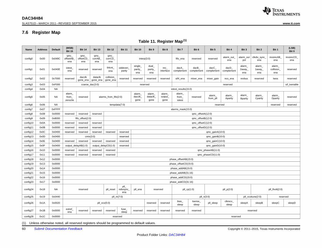
DAC34H84SLAS751D –MARCH 2011–REVISED SEPTEMBER 2015 www.ti.com
7.6 Register Map
Table 11. Register Map (1)
(MSB) (LSB)Name Address Default Bit 14 Bit 13 Bit 12 Bit 11 Bit 10 Bit 9 Bit 8 Bit 7 Bit 6 Bit 5 Bit 4 Bit 3 Bit 2 Bit 1Bit 15 Bit 0
qmc_ qmc_ qmc_ qmc_ alarm_out_ alarm_out clkdiv_sync_ invsincAB_ invsincCD_config0 0x00 0x049C offsetAB_ offsetCD_ corrAB_ corrCD_ interp(3:0) fifo_ena reserved reserved ena pol ena ena enaena ena ena ena
single_ dual_ alarm_ alarm_ alarm_64cnt_iotest_ oddeven_ rev_ dacA_ dacB_ dacC_ dacD_config1 0x01 0x040E reserved reserved parity_ parity_ 2away_ 1away_ collision_ reservedena parity interface complement complement complement complementena
ena ena ena ena ena
dacclk dataclk collision_config2 0x02 0x7000 reserved reserved reserved reserved reserved sif4_ena mixer_ena mixer_gain nco_ena revbus reserved twos reservedgone_ena gone_ena gone_ena
config3 0x03 0xF000 coarse_dac(3:0) reserved reserved sif_txenable
config4 0x04 NA iotest_results(15:0)
alarm_ alarm_alarm_ alarm_ alarm_ alarm_alarm_ alarm_ alarm_ alarm_dacclk_ dataclk_ output_config5 0x05 NA from_ reserved alarms_from_fifo(2:0) from_ reserved reservedfrom_pll Aparity Cparity DparityBparitygone gone gonezerochk iotest
config6 0x06 NA tempdata(7:0) reserved reserved reserved
config7 0x07 0xFFFF alarms_mask(15:0)
config8 0x08 0x0000 reserved reserved reserved qmc_offsetA(12:0)
config9 0x09 0x8000 fifo_offset(2:0) qmc_offsetB(12:0)
config10 0x0A 0x0000 reserved reserved reserved qmc_offsetC(12:0)
config11 0x0B 0x0000 reserved reserved reserved qmc_offsetD(12:0)
config12 0x0C 0x0400 reserved reserved reserved reserved reserved qmc_gainA(10:0)
config13 0x0D 0x0400 cmix(3:0) reserved qmc_gainB(10:0)
config14 0x0E 0x0400 reserved reserved reserved reserved reserved qmc_gainC(10:0)
config15 0x0F 0x0400 output_delayAB(1:0) output_delayCD(1:0) reserved qmc_gainD(10:0)
config16 0x10 0x0000 reserved reserved reserved reserved qmc_phaseAB(11:0)
config17 0x11 0x0000 reserved reserved reserved reserved qmc_phaseCD(11:0)
config18 0x12 0x0000 phase_offsetAB(15:0)
config19 0x13 0x0000 phase_offsetCD(15:0)
config20 0x14 0x0000 phase_addAB(15:0)
config21 0x15 0x0000 phase_addAB(31:16)
config22 0x16 0x0000 phase_addCD(15:0)
config23 0x17 0x0000 phase_addCD(31:16)
pll_config24 0x18 NA reserved pll_reset ndivsync_ pll_ena reserved pll_cp(1:0) pll_p(2:0) pll_lfvolt(2:0)
ena
config25 0x19 0x0440 pll_m(7:0) pll_n(3:0) pll_vcoitune(2:0) reserved
bias_ tsense_ clkrecv_config26 0x1A 0x0020 pll_vco(5:0) reserved reserved pll_sleep sleepA sleepB sleepC sleepD
sleep sleep sleep
extref_ fuse_config27 0x1B 0x0000 reserved reserved reserved reserved reserved reserved reserved reserved reservedena sleep
config28 0x1C 0x0000 reserved reserved
(1) Unless otherwise noted, all reserved registers should be programmed to default values.
60 Submit Documentation Feedback Copyright © 2011–2015, Texas Instruments Incorporated
Product Folder Links: DAC34H84
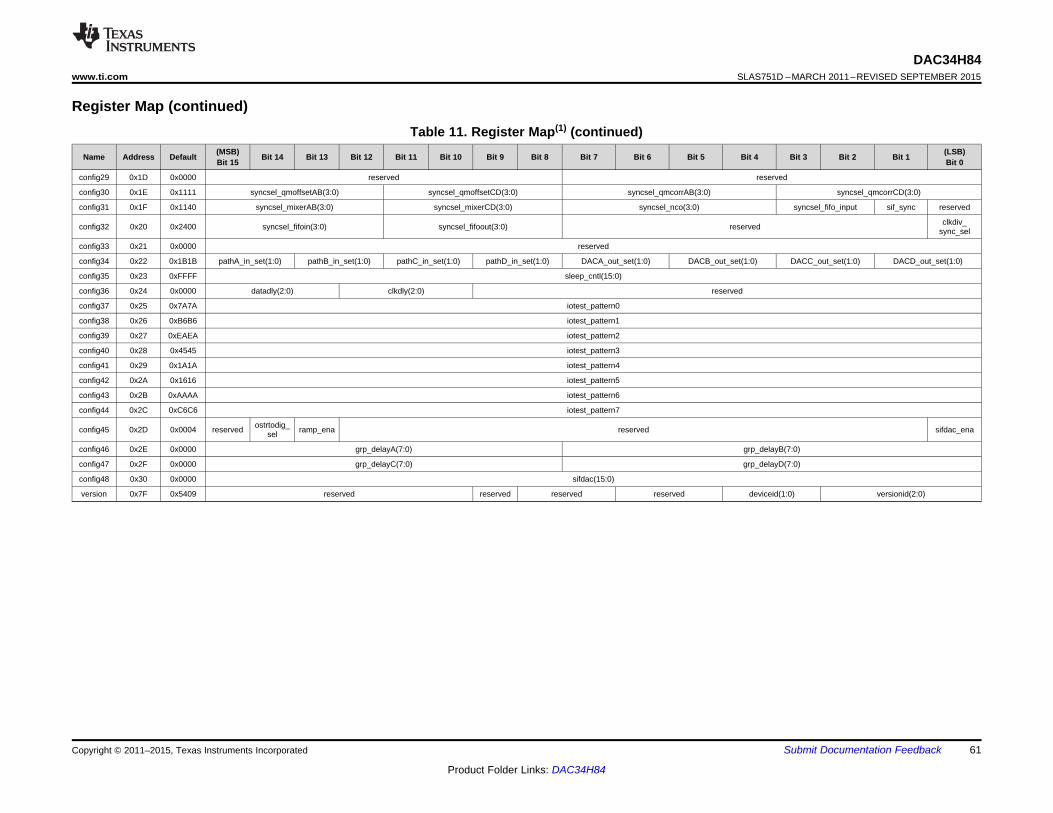
DAC34H84www.ti.com SLAS751D –MARCH 2011–REVISED SEPTEMBER 2015
Register Map (continued)Table 11. Register Map(1) (continued)
(MSB) (LSB)Name Address Default Bit 14 Bit 13 Bit 12 Bit 11 Bit 10 Bit 9 Bit 8 Bit 7 Bit 6 Bit 5 Bit 4 Bit 3 Bit 2 Bit 1Bit 15 Bit 0
config29 0x1D 0x0000 reserved reserved
config30 0x1E 0x1111 syncsel_qmoffsetAB(3:0) syncsel_qmoffsetCD(3:0) syncsel_qmcorrAB(3:0) syncsel_qmcorrCD(3:0)
config31 0x1F 0x1140 syncsel_mixerAB(3:0) syncsel_mixerCD(3:0) syncsel_nco(3:0) syncsel_fifo_input sif_sync reserved
clkdiv_config32 0x20 0x2400 syncsel_fifoin(3:0) syncsel_fifoout(3:0) reserved sync_sel
config33 0x21 0x0000 reserved
config34 0x22 0x1B1B pathA_in_set(1:0) pathB_in_set(1:0) pathC_in_set(1:0) pathD_in_set(1:0) DACA_out_set(1:0) DACB_out_set(1:0) DACC_out_set(1:0) DACD_out_set(1:0)
config35 0x23 0xFFFF sleep_cntl(15:0)
config36 0x24 0x0000 datadly(2:0) clkdly(2:0) reserved
config37 0x25 0x7A7A iotest_pattern0
config38 0x26 0xB6B6 iotest_pattern1
config39 0x27 0xEAEA iotest_pattern2
config40 0x28 0x4545 iotest_pattern3
config41 0x29 0x1A1A iotest_pattern4
config42 0x2A 0x1616 iotest_pattern5
config43 0x2B 0xAAAA iotest_pattern6
config44 0x2C 0xC6C6 iotest_pattern7
ostrtodig_config45 0x2D 0x0004 reserved ramp_ena reserved sifdac_enasel
config46 0x2E 0x0000 grp_delayA(7:0) grp_delayB(7:0)
config47 0x2F 0x0000 grp_delayC(7:0) grp_delayD(7:0)
config48 0x30 0x0000 sifdac(15:0)
version 0x7F 0x5409 reserved reserved reserved reserved deviceid(1:0) versionid(2:0)
Copyright © 2011–2015, Texas Instruments Incorporated Submit Documentation Feedback 61
Product Folder Links: DAC34H84
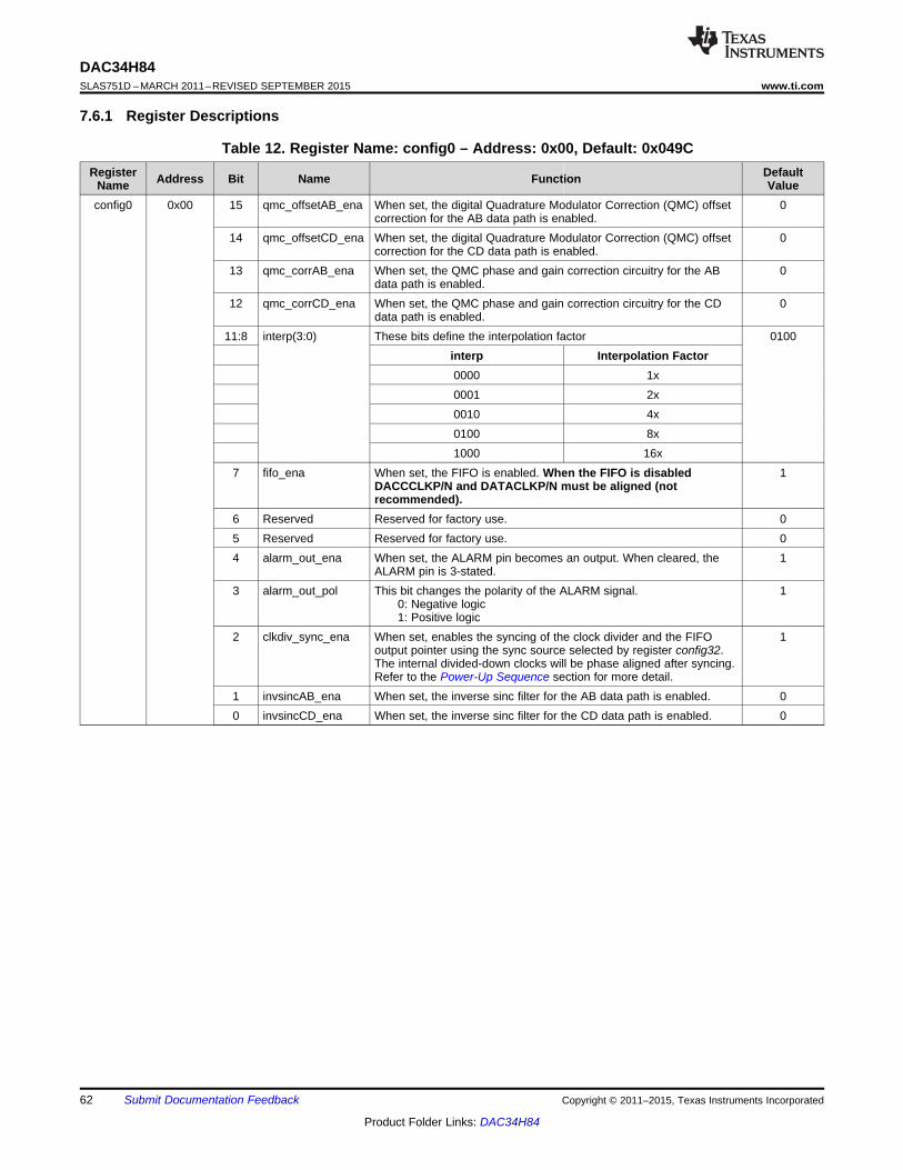
DAC34H84SLAS751D –MARCH 2011–REVISED SEPTEMBER 2015 www.ti.com
7.6.1 Register Descriptions
Table 12. Register Name: config0 – Address: 0x00, Default: 0x049CRegister DefaultAddress Bit Name FunctionName Valueconfig0 0x00 15 qmc_offsetAB_ena When set, the digital Quadrature Modulator Correction (QMC) offset 0
correction for the AB data path is enabled.14 qmc_offsetCD_ena When set, the digital Quadrature Modulator Correction (QMC) offset 0
correction for the CD data path is enabled.13 qmc_corrAB_ena When set, the QMC phase and gain correction circuitry for the AB 0
data path is enabled.12 qmc_corrCD_ena When set, the QMC phase and gain correction circuitry for the CD 0
data path is enabled.11:8 interp(3:0) These bits define the interpolation factor 0100
interp Interpolation Factor0000 1x0001 2x0010 4x0100 8x1000 16x
7 fifo_ena When set, the FIFO is enabled. When the FIFO is disabled 1DACCCLKP/N and DATACLKP/N must be aligned (notrecommended).
6 Reserved Reserved for factory use. 05 Reserved Reserved for factory use. 04 alarm_out_ena When set, the ALARM pin becomes an output. When cleared, the 1
ALARM pin is 3-stated.3 alarm_out_pol This bit changes the polarity of the ALARM signal. 1
MM 0: Negative logicMM 1: Positive logic
2 clkdiv_sync_ena When set, enables the syncing of the clock divider and the FIFO 1output pointer using the sync source selected by register config32.The internal divided-down clocks will be phase aligned after syncing.Refer to the Power-Up Sequence section for more detail.
1 invsincAB_ena When set, the inverse sinc filter for the AB data path is enabled. 00 invsincCD_ena When set, the inverse sinc filter for the CD data path is enabled. 0
62 Submit Documentation Feedback Copyright © 2011–2015, Texas Instruments Incorporated
Product Folder Links: DAC34H84
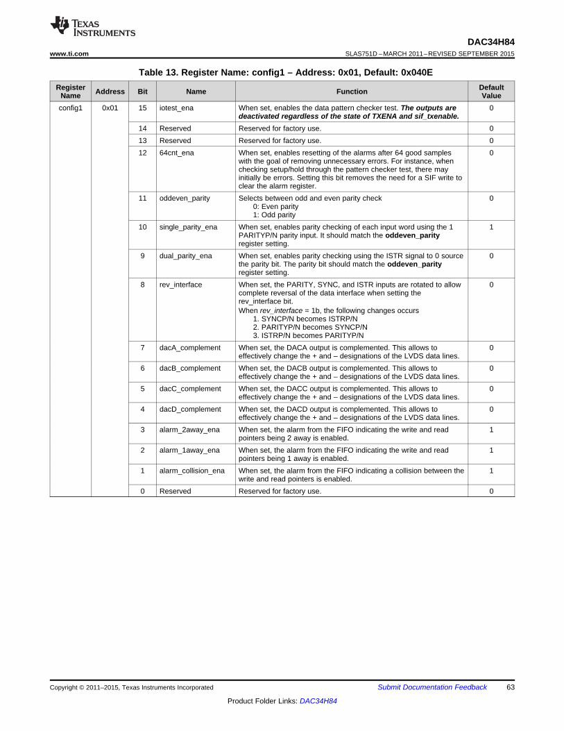
DAC34H84www.ti.com SLAS751D –MARCH 2011–REVISED SEPTEMBER 2015
Table 13. Register Name: config1 – Address: 0x01, Default: 0x040ERegister DefaultAddress Bit Name FunctionName Valueconfig1 0x01 15 iotest_ena When set, enables the data pattern checker test. The outputs are 0
deactivated regardless of the state of TXENA and sif_txenable.14 Reserved Reserved for factory use. 013 Reserved Reserved for factory use. 012 64cnt_ena When set, enables resetting of the alarms after 64 good samples 0
with the goal of removing unnecessary errors. For instance, whenchecking setup/hold through the pattern checker test, there mayinitially be errors. Setting this bit removes the need for a SIF write toclear the alarm register.
11 oddeven_parity Selects between odd and even parity check 0MM 0: Even parityMM 1: Odd parity
10 single_parity_ena When set, enables parity checking of each input word using the 1 1PARITYP/N parity input. It should match the oddeven_parityregister setting.
9 dual_parity_ena When set, enables parity checking using the ISTR signal to 0 source 0the parity bit. The parity bit should match the oddeven_parityregister setting.
8 rev_interface When set, the PARITY, SYNC, and ISTR inputs are rotated to allow 0complete reversal of the data interface when setting therev_interface bit.When rev_interface = 1b, the following changes occursMM 1. SYNCP/N becomes ISTRP/NMM 2. PARITYP/N becomes SYNCP/NMM 3. ISTRP/N becomes PARITYP/N
7 dacA_complement When set, the DACA output is complemented. This allows to 0effectively change the + and – designations of the LVDS data lines.
6 dacB_complement When set, the DACB output is complemented. This allows to 0effectively change the + and – designations of the LVDS data lines.
5 dacC_complement When set, the DACC output is complemented. This allows to 0effectively change the + and – designations of the LVDS data lines.
4 dacD_complement When set, the DACD output is complemented. This allows to 0effectively change the + and – designations of the LVDS data lines.
3 alarm_2away_ena When set, the alarm from the FIFO indicating the write and read 1pointers being 2 away is enabled.
2 alarm_1away_ena When set, the alarm from the FIFO indicating the write and read 1pointers being 1 away is enabled.
1 alarm_collision_ena When set, the alarm from the FIFO indicating a collision between the 1write and read pointers is enabled.
0 Reserved Reserved for factory use. 0
Copyright © 2011–2015, Texas Instruments Incorporated Submit Documentation Feedback 63
Product Folder Links: DAC34H84
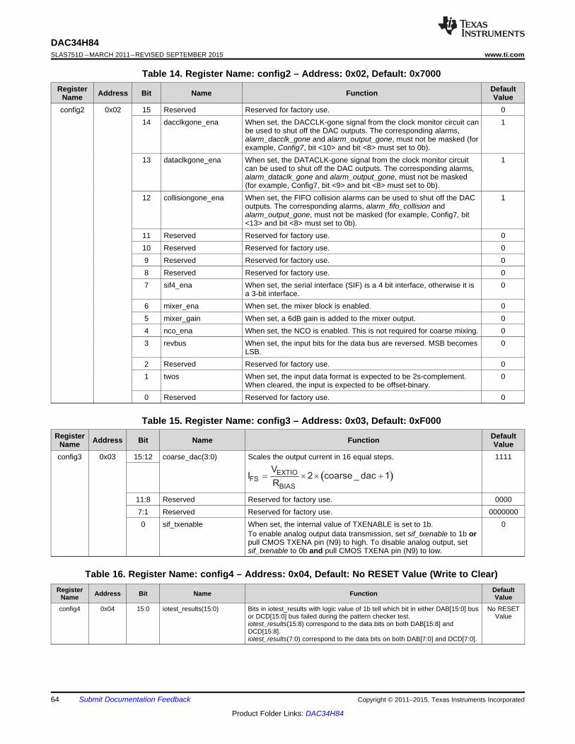
( )EXTIOFS
BIAS
VI 2 coarse _ dac 1
R= ´ ´ +
DAC34H84SLAS751D –MARCH 2011–REVISED SEPTEMBER 2015 www.ti.com
Table 14. Register Name: config2 – Address: 0x02, Default: 0x7000Register DefaultAddress Bit Name FunctionName Valueconfig2 0x02 15 Reserved Reserved for factory use. 0
14 dacclkgone_ena When set, the DACCLK-gone signal from the clock monitor circuit can 1be used to shut off the DAC outputs. The corresponding alarms,alarm_dacclk_gone and alarm_output_gone, must not be masked (forexample, Config7, bit <10> and bit <8> must set to 0b).
13 dataclkgone_ena When set, the DATACLK-gone signal from the clock monitor circuit 1can be used to shut off the DAC outputs. The corresponding alarms,alarm_dataclk_gone and alarm_output_gone, must not be masked(for example, Config7, bit <9> and bit <8> must set to 0b).
12 collisiongone_ena When set, the FIFO collision alarms can be used to shut off the DAC 1outputs. The corresponding alarms, alarm_fifo_collision andalarm_output_gone, must not be masked (for example, Config7, bit<13> and bit <8> must set to 0b).
11 Reserved Reserved for factory use. 010 Reserved Reserved for factory use. 09 Reserved Reserved for factory use. 08 Reserved Reserved for factory use. 07 sif4_ena When set, the serial interface (SIF) is a 4 bit interface, otherwise it is 0
a 3-bit interface.6 mixer_ena When set, the mixer block is enabled. 05 mixer_gain When set, a 6dB gain is added to the mixer output. 04 nco_ena When set, the NCO is enabled. This is not required for coarse mixing. 03 revbus When set, the input bits for the data bus are reversed. MSB becomes 0
LSB.2 Reserved Reserved for factory use. 01 twos When set, the input data format is expected to be 2s-complement. 0
When cleared, the input is expected to be offset-binary.0 Reserved Reserved for factory use. 0
Table 15. Register Name: config3 – Address: 0x03, Default: 0xF000Register DefaultAddress Bit Name FunctionName Valueconfig3 0x03 15:12 coarse_dac(3:0) Scales the output current in 16 equal steps. 1111
11:8 Reserved Reserved for factory use. 00007:1 Reserved Reserved for factory use. 00000000 sif_txenable When set, the internal value of TXENABLE is set to 1b. 0
To enable analog output data transmission, set sif_txenable to 1b orpull CMOS TXENA pin (N9) to high. To disable analog output, setsif_txenable to 0b and pull CMOS TXENA pin (N9) to low.
Table 16. Register Name: config4 – Address: 0x04, Default: No RESET Value (Write to Clear)Register DefaultAddress Bit Name FunctionName Value
config4 0x04 15:0 iotest_results(15:0) Bits in iotest_results with logic value of 1b tell which bit in either DAB[15:0] bus No RESETor DCD[15:0] bus failed during the pattern checker test. Valueiotest_results(15:8) correspond to the data bits on both DAB[15:8] andDCD[15:8].iotest_results(7:0) correspond to the data bits on both DAB[7:0] and DCD[7:0].
64 Submit Documentation Feedback Copyright © 2011–2015, Texas Instruments Incorporated
Product Folder Links: DAC34H84
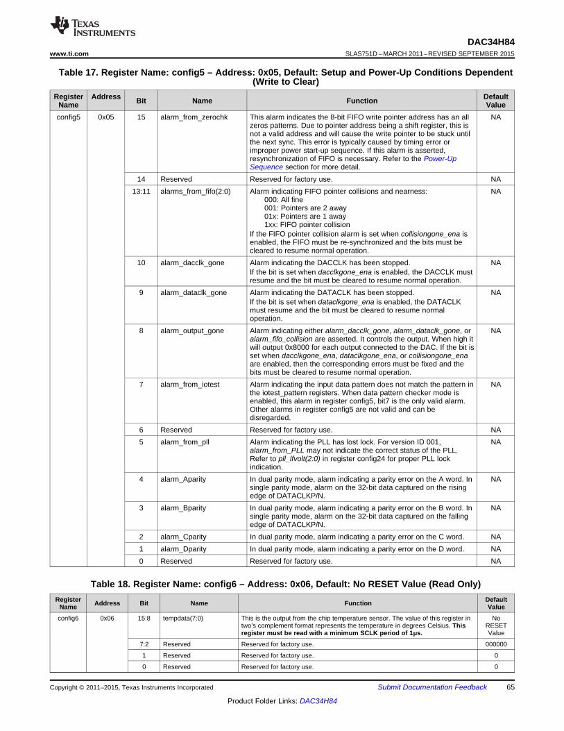
DAC34H84www.ti.com SLAS751D –MARCH 2011–REVISED SEPTEMBER 2015
Table 17. Register Name: config5 – Address: 0x05, Default: Setup and Power-Up Conditions Dependent(Write to Clear)
Register Address DefaultBit Name FunctionName Valueconfig5 0x05 15 alarm_from_zerochk This alarm indicates the 8-bit FIFO write pointer address has an all NA
zeros patterns. Due to pointer address being a shift register, this isnot a valid address and will cause the write pointer to be stuck untilthe next sync. This error is typically caused by timing error orimproper power start-up sequence. If this alarm is asserted,resynchronization of FIFO is necessary. Refer to the Power-UpSequence section for more detail.
14 Reserved Reserved for factory use. NA13:11 alarms_from_fifo(2:0) Alarm indicating FIFO pointer collisions and nearness: NA
MM 000: All fineMM 001: Pointers are 2 awayMM 01x: Pointers are 1 awayMM 1xx: FIFO pointer collisionIf the FIFO pointer collision alarm is set when collisiongone_ena isenabled, the FIFO must be re-synchronized and the bits must becleared to resume normal operation.
10 alarm_dacclk_gone Alarm indicating the DACCLK has been stopped. NAIf the bit is set when dacclkgone_ena is enabled, the DACCLK mustresume and the bit must be cleared to resume normal operation.
9 alarm_dataclk_gone Alarm indicating the DATACLK has been stopped. NAIf the bit is set when dataclkgone_ena is enabled, the DATACLKmust resume and the bit must be cleared to resume normaloperation.
8 alarm_output_gone Alarm indicating either alarm_dacclk_gone, alarm_dataclk_gone, or NAalarm_fifo_collision are asserted. It controls the output. When high itwill output 0x8000 for each output connected to the DAC. If the bit isset when dacclkgone_ena, dataclkgone_ena, or collisiongone_enaare enabled, then the corresponding errors must be fixed and thebits must be cleared to resume normal operation.
7 alarm_from_iotest Alarm indicating the input data pattern does not match the pattern in NAthe iotest_pattern registers. When data pattern checker mode isenabled, this alarm in register config5, bit7 is the only valid alarm.Other alarms in register config5 are not valid and can bedisregarded.
6 Reserved Reserved for factory use. NA5 alarm_from_pll Alarm indicating the PLL has lost lock. For version ID 001, NA
alarm_from_PLL may not indicate the correct status of the PLL.Refer to pll_lfvolt(2:0) in register config24 for proper PLL lockindication.
4 alarm_Aparity In dual parity mode, alarm indicating a parity error on the A word. In NAsingle parity mode, alarm on the 32-bit data captured on the risingedge of DATACLKP/N.
3 alarm_Bparity In dual parity mode, alarm indicating a parity error on the B word. In NAsingle parity mode, alarm on the 32-bit data captured on the fallingedge of DATACLKP/N.
2 alarm_Cparity In dual parity mode, alarm indicating a parity error on the C word. NA1 alarm_Dparity In dual parity mode, alarm indicating a parity error on the D word. NA0 Reserved Reserved for factory use. NA
Table 18. Register Name: config6 – Address: 0x06, Default: No RESET Value (Read Only)Register DefaultAddress Bit Name FunctionName Value
config6 0x06 15:8 tempdata(7:0) This is the output from the chip temperature sensor. The value of this register in Notwo’s complement format represents the temperature in degrees Celsius. This RESETregister must be read with a minimum SCLK period of 1μs. Value
7:2 Reserved Reserved for factory use. 000000
1 Reserved Reserved for factory use. 0
0 Reserved Reserved for factory use. 0
Copyright © 2011–2015, Texas Instruments Incorporated Submit Documentation Feedback 65
Product Folder Links: DAC34H84
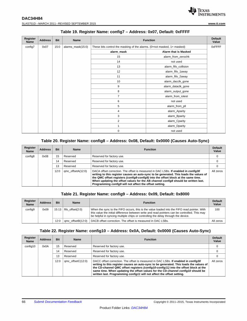
DAC34H84SLAS751D –MARCH 2011–REVISED SEPTEMBER 2015 www.ti.com
Table 19. Register Name: config7 – Address: 0x07, Default: 0xFFFFRegister DefaultAddress Bit Name FunctionName Value
config7 0x07 15:0 alarms_mask(15:0) These bits control the masking of the alarms. (0=not masked, 1= masked) 0xFFFF
alarm_mask Alarm that is Masked
15 alarm_from_zerochk
14 not used
13 alarm_fifo_collision
12 alarm_fifo_1away
11 alarm_fifo_2away
10 alarm_dacclk_gone
9 alarm_dataclk_gone
8 alarm_output_gone
7 alarm_from_iotest
6 not used
5 alarm_from_pll
4 alarm_Aparity
3 alarm_Bparity
2 alarm_Cparity
1 alarm_Dparity
0 not used
Table 20. Register Name: config8 – Address: 0x08, Default: 0x0000 (Causes Auto-Sync)Register DefaultAddress Bit Name Function ValueName
config8 0x08 15 Reserved Reserved for factory use. 0
14 Reserved Reserved for factory use. 0
13 Reserved Reserved for factory use. 0
12:0 qmc_offsetA(12:0) DACA offset correction. The offset is measured in DAC LSBs. If enabled in config30 All zeroswriting to this register causes an auto-sync to be generated. This loads the values ofthe QMC offset registers (config8-config9) into the offset block at the same time.When updating the offset values for the AB channel config8 should be written last.Programming config9 will not affect the offset setting.
Table 21. Register Name: config9 – Address: 0x09, Default: 0x8000Register DefaultAddress Bit Name Function ValueName
config9 0x09 15:13 fifo_offset(2:0) When the sync to the FIFO occurs, this is the value loaded into the FIFO read pointer. With 100this value the initial difference between write and read pointers can be controlled. This maybe helpful in syncing multiple chips or controlling the delay through the device.
12:0 qmc_offsetB(12:0) DACB offset correction. The offset is measured in DAC LSBs. All zeros
Table 22. Register Name: config10 – Address: 0x0A, Default: 0x0000 (Causes Auto-Sync)Register DefaultAddress Bit Name Function ValueName
config10 0x0A 15 Reserved Reserved for factory use. 0
14 Reserved Reserved for factory use. 0
13 Reserved Reserved for factory use. 0
12:0 qmc_offsetC(12:0) DACC offset correction. The offset is measured in DAC LSBs. If enabled in config30 All zeroswriting to this register causes an auto-sync to be generated. This loads the values ofthe CD-channel QMC offset registers (config10-config11) into the offset block at thesame time. When updating the offset values for the CD-channel config10 should bewritten last. Programming config11 will not affect the offset setting.
66 Submit Documentation Feedback Copyright © 2011–2015, Texas Instruments Incorporated
Product Folder Links: DAC34H84
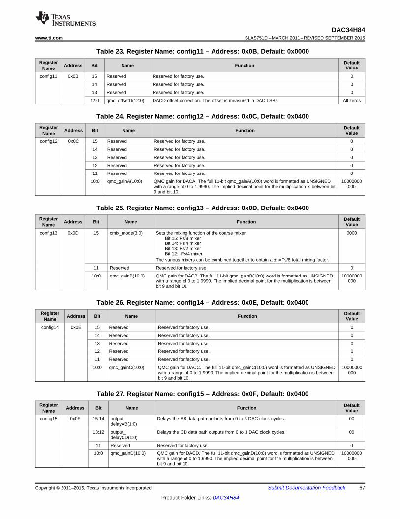
DAC34H84www.ti.com SLAS751D –MARCH 2011–REVISED SEPTEMBER 2015
Table 23. Register Name: config11 – Address: 0x0B, Default: 0x0000Register DefaultAddress Bit Name Function ValueName
config11 0x0B 15 Reserved Reserved for factory use. 0
14 Reserved Reserved for factory use. 0
13 Reserved Reserved for factory use. 0
12:0 qmc_offsetD(12:0) DACD offset correction. The offset is measured in DAC LSBs. All zeros
Table 24. Register Name: config12 – Address: 0x0C, Default: 0x0400Register DefaultAddress Bit Name Function ValueName
config12 0x0C 15 Reserved Reserved for factory use. 0
14 Reserved Reserved for factory use. 0
13 Reserved Reserved for factory use. 0
12 Reserved Reserved for factory use. 0
11 Reserved Reserved for factory use. 0
10:0 qmc_gainA(10:0) QMC gain for DACA. The full 11-bit qmc_gainA(10:0) word is formatted as UNSIGNED 10000000with a range of 0 to 1.9990. The implied decimal point for the multiplication is between bit 0009 and bit 10.
Table 25. Register Name: config13 – Address: 0x0D, Default: 0x0400Register DefaultAddress Bit Name Function ValueName
config13 0x0D 15 cmix_mode(3:0) Sets the mixing function of the coarse mixer. 0000MM Bit 15: Fs/8 mixerMM Bit 14: Fs/4 mixerMM Bit 13: Fs/2 mixerMM Bit 12: -Fs/4 mixerThe various mixers can be combined together to obtain a ±n×Fs/8 total mixing factor.
11 Reserved Reserved for factory use. 0
10:0 qmc_gainB(10:0) QMC gain for DACB. The full 11-bit qmc_gainB(10:0) word is formatted as UNSIGNED 10000000with a range of 0 to 1.9990. The implied decimal point for the multiplication is between 000bit 9 and bit 10.
Table 26. Register Name: config14 – Address: 0x0E, Default: 0x0400Register DefaultAddress Bit Name Function ValueName
config14 0x0E 15 Reserved Reserved for factory use. 0
14 Reserved Reserved for factory use. 0
13 Reserved Reserved for factory use. 0
12 Reserved Reserved for factory use. 0
11 Reserved Reserved for factory use. 0
10:0 qmc_gainC(10:0) QMC gain for DACC. The full 11-bit qmc_gainC(10:0) word is formatted as UNSIGNED 10000000with a range of 0 to 1.9990. The implied decimal point for the multiplication is between 000bit 9 and bit 10.
Table 27. Register Name: config15 – Address: 0x0F, Default: 0x0400Register DefaultAddress Bit Name Function ValueName
config15 0x0F 15:14 output_ Delays the AB data path outputs from 0 to 3 DAC clock cycles. 00delayAB(1:0)
13:12 output_ Delays the CD data path outputs from 0 to 3 DAC clock cycles. 00delayCD(1:0)
11 Reserved Reserved for factory use. 0
10:0 qmc_gainD(10:0) QMC gain for DACD. The full 11-bit qmc_gainD(10:0) word is formatted as UNSIGNED 10000000with a range of 0 to 1.9990. The implied decimal point for the multiplication is between 000bit 9 and bit 10.
Copyright © 2011–2015, Texas Instruments Incorporated Submit Documentation Feedback 67
Product Folder Links: DAC34H84
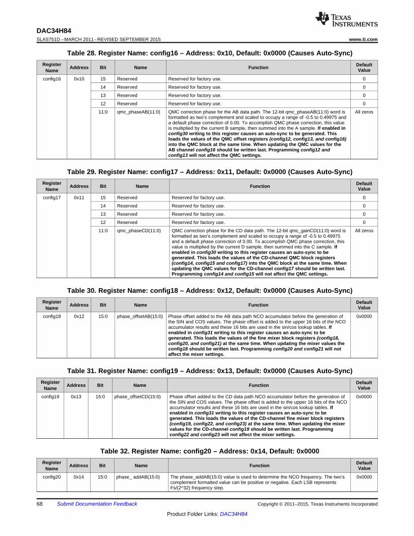
DAC34H84SLAS751D –MARCH 2011–REVISED SEPTEMBER 2015 www.ti.com
Table 28. Register Name: config16 – Address: 0x10, Default: 0x0000 (Causes Auto-Sync)Register DefaultAddress Bit Name Function ValueName
config16 0x10 15 Reserved Reserved for factory use. 0
14 Reserved Reserved for factory use. 0
13 Reserved Reserved for factory use. 0
12 Reserved Reserved for factory use. 0
11:0 qmc_phaseAB(11:0) QMC correction phase for the AB data path. The 12-bit qmc_phaseAB(11:0) word is All zerosformatted as two’s complement and scaled to occupy a range of -0.5 to 0.49975 anda default phase correction of 0.00. To accomplish QMC phase correction, this valueis multiplied by the current B sample, then summed into the A sample. If enabled inconfig30 writing to this register causes an auto-sync to be generated. Thisloads the values of the QMC offset registers (config12, config13, and config16)into the QMC block at the same time. When updating the QMC values for theAB channel config16 should be written last. Programming config12 andconfig13 will not affect the QMC settings.
Table 29. Register Name: config17 – Address: 0x11, Default: 0x0000 (Causes Auto-Sync)Register DefaultAddress Bit Name Function ValueName
config17 0x11 15 Reserved Reserved for factory use. 0
14 Reserved Reserved for factory use. 0
13 Reserved Reserved for factory use. 0
12 Reserved Reserved for factory use. 0
11:0 qmc_phaseCD(11:0) QMC correction phase for the CD data path. The 12-bit qmc_gainCD(11:0) word is All zerosformatted as two’s complement and scaled to occupy a range of -0.5 to 0.49975and a default phase correction of 0.00. To accomplish QMC phase correction, thisvalue is multiplied by the current D sample, then summed into the C sample. Ifenabled in config30 writing to this register causes an auto-sync to begenerated. This loads the values of the CD-channel QMC block registers(config14, config15 and config17) into the QMC block at the same time. Whenupdating the QMC values for the CD-channel config17 should be written last.Programming config14 and config15 will not affect the QMC settings.
Table 30. Register Name: config18 – Address: 0x12, Default: 0x0000 (Causes Auto-Sync)Register DefaultAddress Bit Name Function ValueName
config18 0x12 15:0 phase_offsetAB(15:0) Phase offset added to the AB data path NCO accumulator before the generation of 0x0000the SIN and COS values. The phase offset is added to the upper 16 bits of the NCOaccumulator results and these 16 bits are used in the sin/cos lookup tables. Ifenabled in config31 writing to this register causes an auto-sync to begenerated. This loads the values of the fine mixer block registers (config18,config20, and config21) at the same time. When updating the mixer values theconfig18 should be written last. Programming config20 and config21 will notaffect the mixer settings.
Table 31. Register Name: config19 – Address: 0x13, Default: 0x0000 (Causes Auto-Sync)Register DefaultAddress Bit Name Function ValueName
config19 0x13 15:0 phase_offsetCD(15:0) Phase offset added to the CD data path NCO accumulator before the generation of 0x0000the SIN and COS values. The phase offset is added to the upper 16 bits of the NCOaccumulator results and these 16 bits are used in the sin/cos lookup tables. Ifenabled in config31 writing to this register causes an auto-sync to begenerated. This loads the values of the CD-channel fine mixer block registers(config19, config22, and config23) at the same time. When updating the mixervalues for the CD-channel config19 should be written last. Programmingconfig22 and config23 will not affect the mixer settings.
Table 32. Register Name: config20 – Address: 0x14, Default: 0x0000Register DefaultAddress Bit Name Function ValueName
config20 0x14 15:0 phase_ addAB(15:0) The phase_addAB(15:0) value is used to determine the NCO frequency. The two’s 0x0000complement formatted value can be positive or negative. Each LSB representsFs/(2^32) frequency step.
68 Submit Documentation Feedback Copyright © 2011–2015, Texas Instruments Incorporated
Product Folder Links: DAC34H84
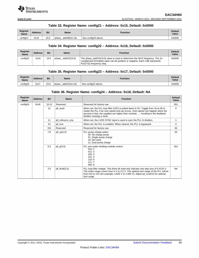
DAC34H84www.ti.com SLAS751D –MARCH 2011–REVISED SEPTEMBER 2015
Table 33. Register Name: config21 – Address: 0x15, Default: 0x0000Register DefaultAddress Bit Name Function ValueName
config21 0x15 15:0 phase_ addAB(31:16) See config20 above. 0x0000
Table 34. Register Name: config22 – Address: 0x16, Default: 0x0000Register DefaultAddress Bit Name Function ValueName
config22 0x16 15:0 phase_ addCD(15:0) The phase_addCD(15:0) value is used to determine the NCO frequency. The 2s- 0x0000complement formatted value can be positive or negative. Each LSB representsFs/(2^32) frequency step.
Table 35. Register Name: config23 – Address: 0x17, Default: 0x0000Register DefaultAddress Bit Name Function ValueName
config23 0x17 15:0 phase_ addCD(31:16) See config22 above. 0x0000
Table 36. Register Name: config24 – Address: 0x18, Default: NARegister DefaultAddress Bit Name Function ValueName
config24 0x18 15:13 Reserved Reserved for factory use. 001
12 pll_reset When set, the PLL loop filter (LPF) is pulled down to 0V. Toggle from 1b to 0b to 0restart the PLL if an over-speed lock-up occurs. Over-speed can happen when theprocess is fast, the supplies are higher than nominal, .... resulting in the feedbackdividers missing a clock.
11 pll_ndivsync_ena When set, the LVDS SYNC input is used to sync the PLL N dividers. 1
10 pll_ena When set, the PLL is enabled. When cleared, the PLL is bypassed. 0
9:8 Reserved Reserved for factory use. 00
7:6 pll_cp(1:0) PLL pump charge select 00MM 00: No charge pumpMM 01: Single pump chargeMM 10: Not usedMM 11: Dual pump charge
5:3 pll_p(2:0) PLL pre-scaler dividing module control. 001MM 010: 2MM 011: 3MM 100: 4MM 101: 5MM 110: 6MM 111: 7MM 000: 8
2:0 pll_lfvolt(2:0) PLL loop filter voltage. This three bit read-only indicator has step size of 0.4125 V. NAThe entire range covers from 0 V to 3.3 V. The optimal lock range of the PLL will befrom 010 to 101 (for example, 0.825 V to 2.063 V). Adjust pll_vco(5:0) for optimallock range.
Copyright © 2011–2015, Texas Instruments Incorporated Submit Documentation Feedback 69
Product Folder Links: DAC34H84
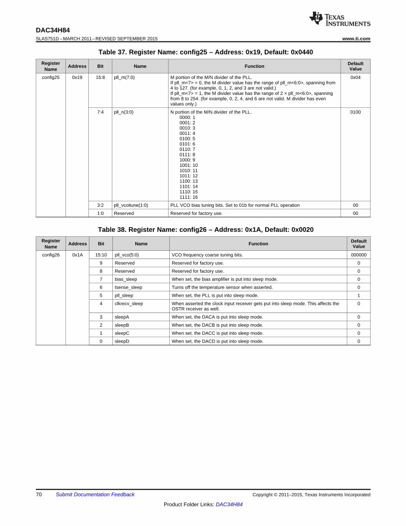
DAC34H84SLAS751D –MARCH 2011–REVISED SEPTEMBER 2015 www.ti.com
Table 37. Register Name: config25 – Address: 0x19, Default: 0x0440Register DefaultAddress Bit Name Function ValueName
config25 0x19 15:8 pll_m(7:0) M portion of the M/N divider of the PLL. 0x04If pll_m<7> = 0, the M divider value has the range of pll_m<6:0>, spanning from4 to 127. (for example, 0, 1, 2, and 3 are not valid.)If pll_m<7> = 1, the M divider value has the range of 2 × pll_m<6:0>, spanningfrom 8 to 254. (for example, 0, 2, 4, and 6 are not valid. M divider has evenvalues only.)
7:4 pll_n(3:0) N portion of the M/N divider of the PLL. 0100MM 0000: 1MM 0001: 2MM 0010: 3MM 0011: 4MM 0100: 5MM 0101: 6MM 0110: 7MM 0111: 8MM 1000: 9MM 1001: 10MM 1010: 11MM 1011: 12MM 1100: 13MM 1101: 14MM 1110: 15MM 1111: 16
3:2 pll_vcoitune(1:0) PLL VCO bias tuning bits. Set to 01b for normal PLL operation 00
1:0 Reserved Reserved for factory use. 00
Table 38. Register Name: config26 – Address: 0x1A, Default: 0x0020Register DefaultAddress Bit Name Function ValueName
config26 0x1A 15:10 pll_vco(5:0) VCO frequency coarse tuning bits. 000000
9 Reserved Reserved for factory use. 0
8 Reserved Reserved for factory use. 0
7 bias_sleep When set, the bias amplifier is put into sleep mode. 0
6 tsense_sleep Turns off the temperature sensor when asserted. 0
5 pll_sleep When set, the PLL is put into sleep mode. 1
4 clkrecv_sleep When asserted the clock input receiver gets put into sleep mode. This affects the 0OSTR receiver as well.
3 sleepA When set, the DACA is put into sleep mode. 0
2 sleepB When set, the DACB is put into sleep mode. 0
1 sleepC When set, the DACC is put into sleep mode. 0
0 sleepD When set, the DACD is put into sleep mode. 0
70 Submit Documentation Feedback Copyright © 2011–2015, Texas Instruments Incorporated
Product Folder Links: DAC34H84
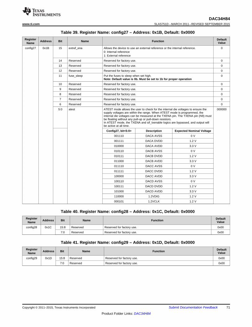
DAC34H84www.ti.com SLAS751D –MARCH 2011–REVISED SEPTEMBER 2015
Table 39. Register Name: config27 – Address: 0x1B, Default: 0x0000Register DefaultAddress Bit Name Function ValueName
config27 0x1B 15 extref_ena Allows the device to use an external reference or the internal reference. 00: Internal reference1: External reference
14 Reserved Reserved for factory use. 0
13 Reserved Reserved for factory use. 0
12 Reserved Reserved for factory use. 0
11 fuse_sleep Put the fuses to sleep when set high. 0Note: Default value is 0b. Must be set to 1b for proper operation
10 Reserved Reserved for factory use. 0
9 Reserved Reserved for factory use. 0
8 Reserved Reserved for factory use. 0
7 Reserved Reserved for factory use. 0
6 Reserved Reserved for factory use. 0
5:0 atest ATEST mode allows the user to check for the internal die voltages to ensure the 000000supply voltages are within the range. When ATEST mode is programmed, theinternal die voltages can be measured at the TXENA pin. The TXENA pin (N9) mustbe floating without any pull-up or pull-down resistors.In ATEST mode, the TXENA and sif_txenable logics are bypassed, and output willbe active at all time.
Config27, bit<5:0> Description Expected Nominal Voltage
001110 DACA AVSS 0 V
001111 DACA DVDD 1.2 V
010000 DACA AVDD 3.3 V
010110 DACB AVSS 0 V
010111 DACB DVDD 1.2 V
011000 DACB AVDD 3.3 V
011110 DACC AVSS 0 V
011111 DACC DVDD 1.2 V
100000 DACC AVDD 3.3 V
100110 DACD AVSS 0 V
100111 DACD DVDD 1.2 V
101000 DACD AVDD 3.3 V
110000 1.2VDIG 1.2 V
000101 1.2VCLK 1.2 V
Table 40. Register Name: config28 – Address: 0x1C, Default: 0x0000Register DefaultAddress Bit Name Function ValueName
config28 0x1C 15:8 Reserved Reserved for factory use. 0x00
7:0 Reserved Reserved for factory use. 0x00
Table 41. Register Name: config29 – Address: 0x1D, Default: 0x0000Register DefaultAddress Bit Name Function ValueName
config29 0x1D 15:8 Reserved Reserved for factory use. 0x00
7:0 Reserved Reserved for factory use. 0x00
Copyright © 2011–2015, Texas Instruments Incorporated Submit Documentation Feedback 71
Product Folder Links: DAC34H84
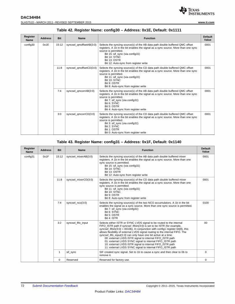
DAC34H84SLAS751D –MARCH 2011–REVISED SEPTEMBER 2015 www.ti.com
Table 42. Register Name: config30 – Address: 0x1E, Default: 0x1111Register DefaultAddress Bit Name Function ValueName
config30 0x1E 15:12 syncsel_qmoffsetAB(3:0) Selects the syncing source(s) of the AB data path double buffered QMC offset 0001registers. A 1b in the bit enables the signal as a sync source. More than one syncsource is permitted.MM Bit 15: sif_sync (via config31)MM Bit 14: SYNCMM Bit 13: OSTRMM Bit 12: Auto-sync from register write
11:8 syncsel_qmoffsetCD(3:0) Selects the syncing source(s) of the CD data path double buffered QMC offset 0001registers. A 1b in the bit enables the signal as a sync source. More than one syncsource is permitted.MM Bit 11: sif_sync (via config31)MM Bit 10: SYNCMM Bit 9: OSTRMM Bit 8: Auto-sync from register write
7:4 syncsel_qmcorrAB(3:0) Selects the syncing source(s) of the AB data path double buffered QMC offset 0001registers. A 1b in the bit enables the signal as a sync source. More than one syncsource is permitted.MM Bit 7: sif_sync (via config31)MM Bit 6: SYNCMM Bit 5: OSTRMM Bit 4: Auto-sync from register write
3:0 syncsel_qmcorrCD(3:0) Selects the syncing source(s) of the CD data path double buffered QMC offset 0001registers. A 1b in the bit enables the signal as a sync source. More than one syncsource is permitted.MM Bit 3: sif_sync (via config31)MM Bit 2: SYNCMM Bit 1: OSTRMM Bit 0: Auto-sync from register write
Table 43. Register Name: config31 – Address: 0x1F, Default: 0x1140Register DefaultAddress Bit Name Function ValueName
config31 0x1F 15:12 syncsel_mixerAB(3:0) Selects the syncing source(s) of the AB data path double buffered mixer 0001registers. A 1b in the bit enables the signal as a sync source. More than onesync source is permitted.MM Bit 15: sif_sync (via config31)MM Bit 14: SYNCMM Bit 13: OSTRMM Bit 12: Auto-sync from register write
11:8 syncsel_mixerCD(3:0) Selects the syncing source(s) of the CD data path double buffered mixer 0001registers. A 1b in the bit enables the signal as a sync source. More than onesync source is permitted.MM Bit 11: sif_sync (via config31)MM Bit 10: SYNCMM Bit 9: OSTRMM Bit 8: Auto-sync from register write
7:4 syncsel_nco(3:0) Selects the syncing source(s) of the two NCO accumulators. A 1b in the bit 0100enables the signal as a sync source. More than one sync source is permitted.MM Bit 7: sif_sync (via config31)MM Bit 6: SYNCMM Bit 5: OSTRMM Bit 4: ISTR
3:2 syncsel_fifo_input Selects either ISTR or SYNC LVDS signal to be routed to the internal 00FIFO_ISTR path if syncsel_fifoin(3:0) is set to be ISTR (for example,syncsel_fifoin(3:0) = 0010b). In conjunction with config1 register bit(8), thisallows flexibility of external LVDS signal routing to the internal FIFO. Thesyncsel_fifo_input(1:0) can only have one bit active at a time.MM 00: external LVDS ISTR signal to internal FIFO_ISTR pathMM 01: external LVDS SYNC signal to internal FIFO_ISTR pathMM 10: external LVDS ISTR signal to internal FIFO_ISTR pathMM 11: external LVDS SYNC signal to internal FIFO_ISTR path
1 sif_sync SIF created sync signal. Set to 1b to cause a sync and then clear to 0b to 0remove it.
0 Reserved Reserved for factory use. 0
72 Submit Documentation Feedback Copyright © 2011–2015, Texas Instruments Incorporated
Product Folder Links: DAC34H84
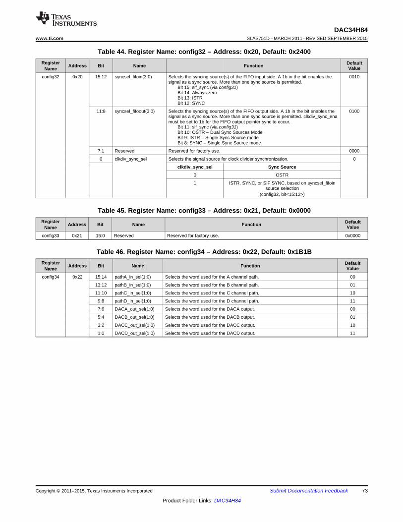
DAC34H84www.ti.com SLAS751D –MARCH 2011–REVISED SEPTEMBER 2015
Table 44. Register Name: config32 – Address: 0x20, Default: 0x2400Register DefaultAddress Bit Name Function ValueName
config32 0x20 15:12 syncsel_fifoin(3:0) Selects the syncing source(s) of the FIFO input side. A 1b in the bit enables the 0010signal as a sync source. More than one sync source is permitted.MM Bit 15: sif_sync (via config31)MM Bit 14: Always zeroMM Bit 13: ISTRMM Bit 12: SYNC
11:8 syncsel_fifoout(3:0) Selects the syncing source(s) of the FIFO output side. A 1b in the bit enables the 0100signal as a sync source. More than one sync source is permitted. clkdiv_sync_enamust be set to 1b for the FIFO output pointer sync to occur.MM Bit 11: sif_sync (via config31)MM Bit 10: OSTR – Dual Sync Sources ModeMM Bit 9: ISTR – Single Sync Source modeMM Bit 8: SYNC – Single Sync Source mode
7:1 Reserved Reserved for factory use. 0000
0 clkdiv_sync_sel Selects the signal source for clock divider synchronization. 0
clkdiv_sync_sel Sync Source
0 OSTR
1 ISTR, SYNC, or SIF SYNC, based on syncsel_fifoinsource selection
(config32, bit<15:12>)
Table 45. Register Name: config33 – Address: 0x21, Default: 0x0000Register DefaultAddress Bit Name Function ValueName
config33 0x21 15:0 Reserved Reserved for factory use. 0x0000
Table 46. Register Name: config34 – Address: 0x22, Default: 0x1B1BRegister DefaultAddress Bit Name Function ValueName
config34 0x22 15:14 pathA_in_sel(1:0) Selects the word used for the A channel path. 00
13:12 pathB_in_sel(1:0) Selects the word used for the B channel path. 01
11:10 pathC_in_sel(1:0) Selects the word used for the C channel path. 10
9:8 pathD_in_sel(1:0) Selects the word used for the D channel path. 11
7:6 DACA_out_sel(1:0) Selects the word used for the DACA output. 00
5:4 DACB_out_sel(1:0) Selects the word used for the DACB output. 01
3:2 DACC_out_sel(1:0) Selects the word used for the DACC output. 10
1:0 DACD_out_sel(1:0) Selects the word used for the DACD output. 11
Copyright © 2011–2015, Texas Instruments Incorporated Submit Documentation Feedback 73
Product Folder Links: DAC34H84
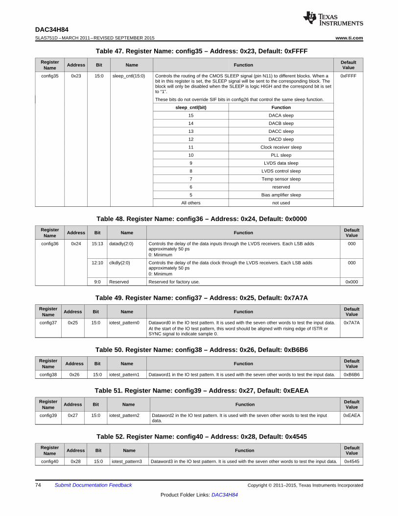
DAC34H84SLAS751D –MARCH 2011–REVISED SEPTEMBER 2015 www.ti.com
Table 47. Register Name: config35 – Address: 0x23, Default: 0xFFFFRegister DefaultAddress Bit Name Function ValueName
config35 0x23 15:0 sleep_cntl(15:0) Controls the routing of the CMOS SLEEP signal (pin N11) to different blocks. When a 0xFFFFbit in this register is set, the SLEEP signal will be sent to the corresponding block. Theblock will only be disabled when the SLEEP is logic HIGH and the correspond bit is setto “1”.
These bits do not override SIF bits in config26 that control the same sleep function.
sleep_cntl(bit) Function
15 DACA sleep
14 DACB sleep
13 DACC sleep
12 DACD sleep
11 Clock receiver sleep
10 PLL sleep
9 LVDS data sleep
8 LVDS control sleep
7 Temp sensor sleep
6 reserved
5 Bias amplifier sleep
All others not used
Table 48. Register Name: config36 – Address: 0x24, Default: 0x0000Register DefaultAddress Bit Name Function ValueName
config36 0x24 15:13 datadly(2:0) Controls the delay of the data inputs through the LVDS receivers. Each LSB adds 000approximately 50 ps0: Minimum
12:10 clkdly(2:0) Controls the delay of the data clock through the LVDS receivers. Each LSB adds 000approximately 50 ps0: Minimum
9:0 Reserved Reserved for factory use. 0x000
Table 49. Register Name: config37 – Address: 0x25, Default: 0x7A7ARegister DefaultAddress Bit Name Function ValueName
config37 0x25 15:0 iotest_pattern0 Dataword0 in the IO test pattern. It is used with the seven other words to test the input data. 0x7A7AAt the start of the IO test pattern, this word should be aligned with rising edge of ISTR orSYNC signal to indicate sample 0.
Table 50. Register Name: config38 – Address: 0x26, Default: 0xB6B6Register DefaultAddress Bit Name Function ValueName
config38 0x26 15:0 iotest_pattern1 Dataword1 in the IO test pattern. It is used with the seven other words to test the input data. 0xB6B6
Table 51. Register Name: config39 – Address: 0x27, Default: 0xEAEARegister DefaultAddress Bit Name Function ValueName
config39 0x27 15:0 iotest_pattern2 Dataword2 in the IO test pattern. It is used with the seven other words to test the input 0xEAEAdata.
Table 52. Register Name: config40 – Address: 0x28, Default: 0x4545Register DefaultAddress Bit Name Function ValueName
config40 0x28 15:0 iotest_pattern3 Dataword3 in the IO test pattern. It is used with the seven other words to test the input data. 0x4545
74 Submit Documentation Feedback Copyright © 2011–2015, Texas Instruments Incorporated
Product Folder Links: DAC34H84
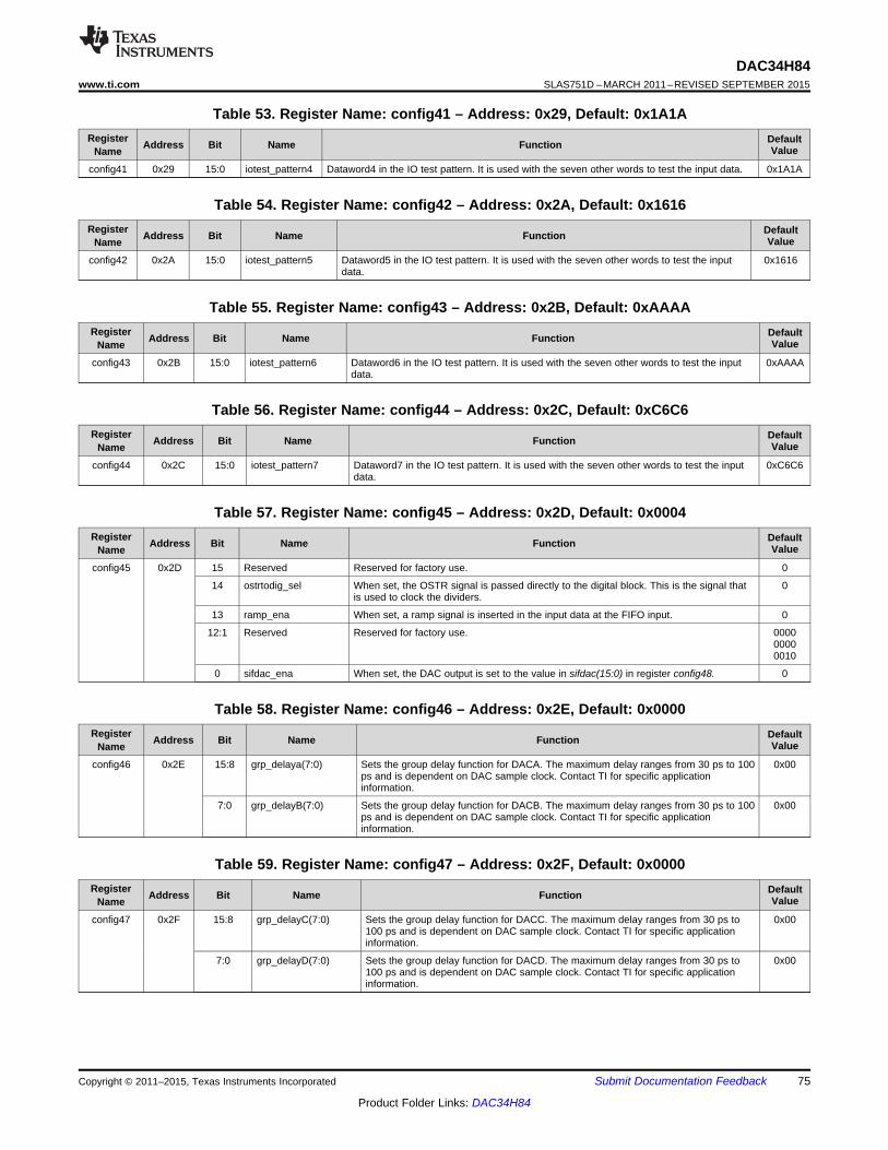
DAC34H84www.ti.com SLAS751D –MARCH 2011–REVISED SEPTEMBER 2015
Table 53. Register Name: config41 – Address: 0x29, Default: 0x1A1ARegister DefaultAddress Bit Name Function ValueName
config41 0x29 15:0 iotest_pattern4 Dataword4 in the IO test pattern. It is used with the seven other words to test the input data. 0x1A1A
Table 54. Register Name: config42 – Address: 0x2A, Default: 0x1616Register DefaultAddress Bit Name Function ValueName
config42 0x2A 15:0 iotest_pattern5 Dataword5 in the IO test pattern. It is used with the seven other words to test the input 0x1616data.
Table 55. Register Name: config43 – Address: 0x2B, Default: 0xAAAARegister DefaultAddress Bit Name Function ValueName
config43 0x2B 15:0 iotest_pattern6 Dataword6 in the IO test pattern. It is used with the seven other words to test the input 0xAAAAdata.
Table 56. Register Name: config44 – Address: 0x2C, Default: 0xC6C6Register DefaultAddress Bit Name Function ValueName
config44 0x2C 15:0 iotest_pattern7 Dataword7 in the IO test pattern. It is used with the seven other words to test the input 0xC6C6data.
Table 57. Register Name: config45 – Address: 0x2D, Default: 0x0004Register DefaultAddress Bit Name Function ValueName
config45 0x2D 15 Reserved Reserved for factory use. 0
14 ostrtodig_sel When set, the OSTR signal is passed directly to the digital block. This is the signal that 0is used to clock the dividers.
13 ramp_ena When set, a ramp signal is inserted in the input data at the FIFO input. 0
12:1 Reserved Reserved for factory use. 000000000010
0 sifdac_ena When set, the DAC output is set to the value in sifdac(15:0) in register config48. 0
Table 58. Register Name: config46 – Address: 0x2E, Default: 0x0000Register DefaultAddress Bit Name Function ValueName
config46 0x2E 15:8 grp_delaya(7:0) Sets the group delay function for DACA. The maximum delay ranges from 30 ps to 100 0x00ps and is dependent on DAC sample clock. Contact TI for specific applicationinformation.
7:0 grp_delayB(7:0) Sets the group delay function for DACB. The maximum delay ranges from 30 ps to 100 0x00ps and is dependent on DAC sample clock. Contact TI for specific applicationinformation.
Table 59. Register Name: config47 – Address: 0x2F, Default: 0x0000Register DefaultAddress Bit Name Function ValueName
config47 0x2F 15:8 grp_delayC(7:0) Sets the group delay function for DACC. The maximum delay ranges from 30 ps to 0x00100 ps and is dependent on DAC sample clock. Contact TI for specific applicationinformation.
7:0 grp_delayD(7:0) Sets the group delay function for DACD. The maximum delay ranges from 30 ps to 0x00100 ps and is dependent on DAC sample clock. Contact TI for specific applicationinformation.
Copyright © 2011–2015, Texas Instruments Incorporated Submit Documentation Feedback 75
Product Folder Links: DAC34H84
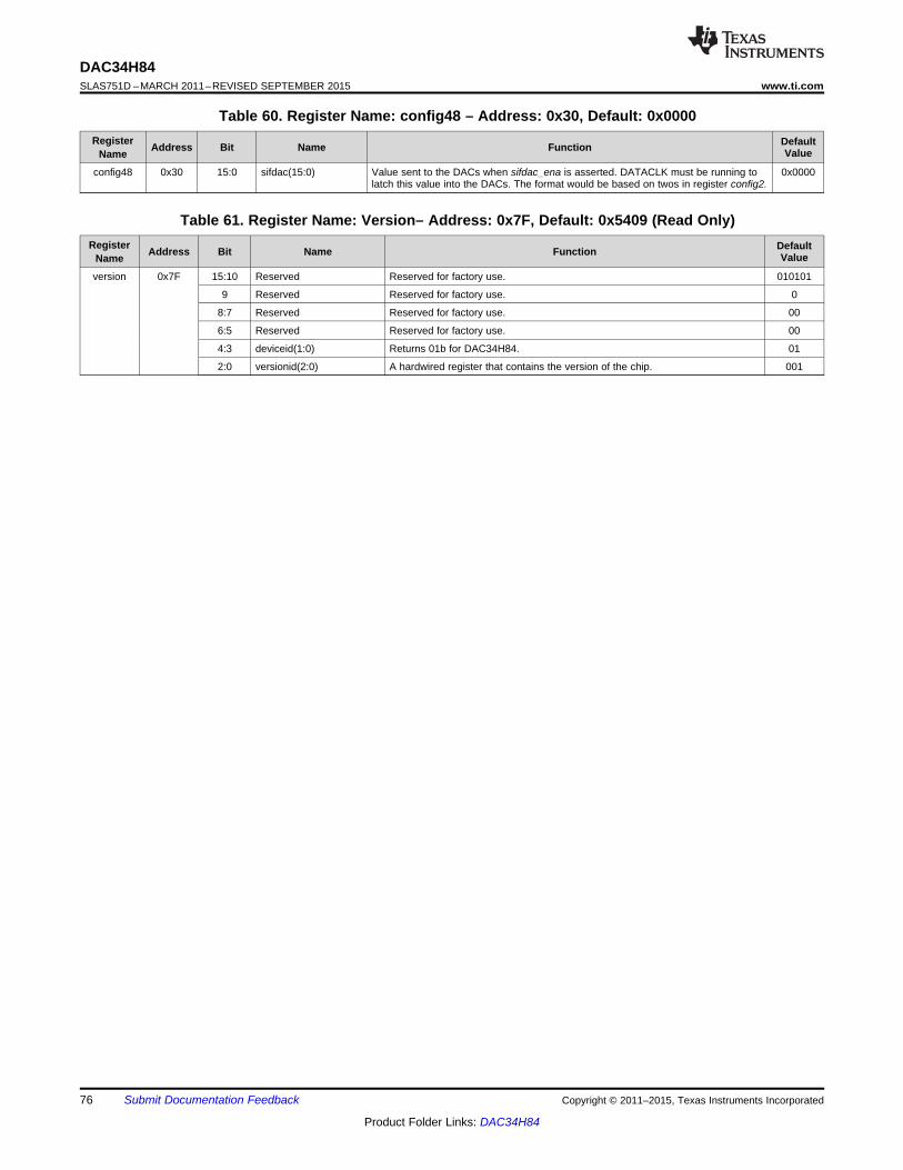
DAC34H84SLAS751D –MARCH 2011–REVISED SEPTEMBER 2015 www.ti.com
Table 60. Register Name: config48 – Address: 0x30, Default: 0x0000Register DefaultAddress Bit Name Function ValueName
config48 0x30 15:0 sifdac(15:0) Value sent to the DACs when sifdac_ena is asserted. DATACLK must be running to 0x0000latch this value into the DACs. The format would be based on twos in register config2.
Table 61. Register Name: Version– Address: 0x7F, Default: 0x5409 (Read Only)Register DefaultAddress Bit Name Function ValueName
version 0x7F 15:10 Reserved Reserved for factory use. 010101
9 Reserved Reserved for factory use. 0
8:7 Reserved Reserved for factory use. 00
6:5 Reserved Reserved for factory use. 00
4:3 deviceid(1:0) Returns 01b for DAC34H84. 01
2:0 versionid(2:0) A hardwired register that contains the version of the chip. 001
76 Submit Documentation Feedback Copyright © 2011–2015, Texas Instruments Incorporated
Product Folder Links: DAC34H84
DAC34H84www.ti.com SLAS751D –MARCH 2011–REVISED SEPTEMBER 2015
8 Application and Implementation
NOTEInformation in the following applications sections is not part of the TI componentspecification, and TI does not warrant its accuracy or completeness. TI’s customers areresponsible for determining suitability of components for their purposes. Customers shouldvalidate and test their design implementation to confirm system functionality.
8.1 Application InformationThe DAC34H84 is a quad 16-bit DAC with max input data rate of up to 625 MSPS per DAC and max DACupdate rate of 1.25 GSPS after the final, selectable interpolation stages. With build-in interpolation filter of 2x, 4x,8x, and 16x options, the lower input data rate can be interpolated all the way to 1.25 GSPS. This allows the DACto update the samples at higher rate, and pushes the DAC images further away to relax anti-image filerspecification due to the increased Nyquist bandwidth. With integrated coarse and fine mixers, baseband signalcan be upconverted to an intermediate frequency (IF) signal between the baseband processor and post-DACanalog signal chains.
The DAC can output baseband or IF when connected to post-DAC analog signals chain components such astransformers or IF amplifiers. When used in conjunction with TI RF quadrature modulator such as the TRF3705,the DAC and RF modulator can function as a set of baseband or IF upconverter. With integrated QMC circuits,the LO offset and the sideband artifacts can be properly corrected in the direct up-conversion applications. TheDAC34H84 provides the bandwidth, performance, small footprint, and lower power consumption needed formulti-mode 2G/3G/4G cellular base stations to migrate to more advanced technologies, such as LTE-Advancedand carrier aggregation on multiple antennas.
Copyright © 2011–2015, Texas Instruments Incorporated Submit Documentation Feedback 77
Product Folder Links: DAC34H84
DAC34H84
Co
mp
lex
Mix
er
(48
-bit
NC
O)
xN
xN
Co
mp
lex
Mix
er
(48
-bit
NC
O)
xN
xN
LVD
S I
nte
rfa
ce
FPGA
RF
Clock Distribution
LMK04828
TRF3765
PLL
DACCLK SYSREF
16-bit DAC
16-bit DAC
TRF3705
RFTRF3705
16-bit DAC
16-bit DAC
DAC34H84SLAS751D –MARCH 2011–REVISED SEPTEMBER 2015 www.ti.com
8.2 Typical Applications
8.2.1 IF Based LTE TransmitterFigure 88 shows an example block diagram for a direct conversion radio. The design requires a single carrier,20-MHz LTE signal. The system has digital-predication (DPD) to correct up to 5th order distortion so the totalDAC output bandwidth is 100 MHz. Interpolation is used to output the signal at highest sampling rate possible tosimplify the analog filter requirements and move high order harmonics out of band (due to wider Nyquist zone).The internal PLL is used to generate the final DAC output clock from a reference clock of 491.52 MHz.
Figure 88. Dual Low-IF Wideband LTE Transmitter Diagram
8.2.1.1 Design RequirementsFor this design example, use the parameters listed in Table 62 as the input parameters.
Table 62. Design ParametersDESIGN PARAMETER EXAMPLE VALUE
Signal Bandwidth (BWsignal) 20 MHzTotal DAC Output Bandwidth (BWtotal) 100 MHz
DAC PLL OnDAC PLL Reference Frequency 491.52 MHz
Maximum FPGA LVDS Rate 491.52 Mbps
78 Submit Documentation Feedback Copyright © 2011–2015, Texas Instruments Incorporated
Product Folder Links: DAC34H84
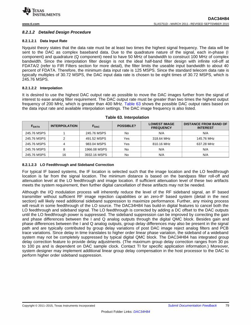
DAC34H84www.ti.com SLAS751D –MARCH 2011–REVISED SEPTEMBER 2015
8.2.1.2 Detailed Design Procedure
8.2.1.2.1 Data Input Rate
Nyquist theory states that the data rate must be at least two times the highest signal frequency. The data will besent to the DAC as complex baseband data. Due to the quadrature nature of the signal, each in-phase (Icomponent) and quadrature (Q component) need to have 50 MHz of bandwidth to construct 100 MHz of complexbandwidth. Since the interpolation filter design is not the ideal half-band filter design with infinite roll-off atFDATA/2 (refer to FIR Filters section for more detail), the filter limits the useable input bandwidth to about 40percent of FDATA. Therefore, the minimum data input rate is 125 MSPS. Since the standard telecom data rate istypically multiples of 30.72 MSPS, the DAC input data rate is chosen to be eight times of 30.72 MSPS, which is245.76 MSPS.
8.2.1.2.2 Interpolation
It is desired to use the highest DAC output rate as possible to move the DAC images further from the signal ofinterest to ease analog filter requirement. The DAC output rate must be greater than two times the highest outputfrequency of 200 MHz, which is greater than 400 MHz. Table 63 shows the possible DAC output rates based onthe data input rate and available interpolation settings. The DAC image frequency is also listed.
Table 63. InterpolationLOWEST IMAGE DISTANCE FROM BAND OFFDATA INTERPOLATION FDAC POSSIBLE? FREQUENCY INTEREST
245.76 MSPS 1 245.76 MSPS No N/A N/A245.76 MSPS 2 491.52 MSPS Yes 318.64 MHz 145.76 MHz245.76 MSPS 4 983.04 MSPS Yes 810.16 MHz 637.28 MHz245.76 MSPS 8 1966.08 MSPS No N/A N/A245.76 MSPS 16 3932.16 MSPS No N/A N/A
8.2.1.2.3 LO Feedthrough and Sideband Correction
For typical IF based systems, the IF location is selected such that the image location and the LO feedthroughlocation is far from the signal location. The minimum distance is based on the bandpass filter roll-off andattenuation level at the LO feedthrough and image location. If sufficient attenuation level of these two artifactsmeets the system requirement, then further digital cancellation of these artifacts may not be needed.
Although the I/Q modulation process will inherently reduce the level of the RF sideband signal, an IF basedtransmitter without sufficient RF image rejection capabilities or an zero-IF based system (detail in the nextsection) will likely need additional sideband suppression to maximize performance. Further, any mixing processwill result in some feedthrough of the LO source. The DAC34H84 has build-in digital features to cancel both theLO feedthrough and sideband signal. The LO feedthrough is corrected by adding a DC offset to the DAC outputsuntil the LO feedthrough power is suppressed. The sideband suppression can be improved by correcting the gainand phase differences between the I and Q analog outputs through the digital QMC block. Besides gain andphase differences between the I and Q analog outputs, group delay differences may also be present in the signalpath and are typically contributed by group delay variations of post DAC image reject analog filters and PCBtrace variations. Since delay in time translates to higher order linear phase variation, the sideband of a widebandsystem may not be completely suppressed by typical digital QMC block. The DAC34H84 has integrated groupdelay correction feature to provide delay adjustments. (The maximum group delay correction ranges from 30 psto 100 ps and is dependent on DAC sample clock. Contact TI for specific application information.) Moreover,system designer may implement additional linear group delay compensation in the host processor to the DAC toperform higher order sideband suppression.
Copyright © 2011–2015, Texas Instruments Incorporated Submit Documentation Feedback 79
Product Folder Links: DAC34H84
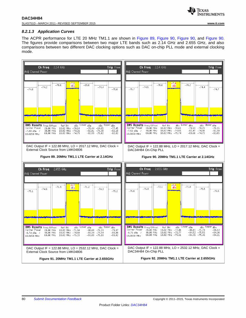
DAC34H84SLAS751D –MARCH 2011–REVISED SEPTEMBER 2015 www.ti.com
8.2.1.3 Application CurvesThe ACPR performance for LTE 20 MHz TM1.1 are shown in Figure 89, Figure 90, Figure 90, and Figure 90.The figures provide comparisons between two major LTE bands such as 2.14 GHz and 2.655 GHz, and alsocomparisons between two different DAC clocking options such as DAC on-chip PLL mode and external clockingmode.
DAC Output IF = 122.88 MHz, LO = 2017.12 MHz, DAC Clock = DAC Output IF = 122.88 MHz, LO = 2017.12 MHz, DAC Clock =External Clock Source from LMK04806 DAC34H84 On-Chip PLL
Figure 89. 20MHz TM1.1 LTE Carrier at 2.14GHz Figure 90. 20MHz TM1.1 LTE Carrier at 2.14GHz
DAC Output IF = 122.88 MHz, LO = 2532.12 MHz, DAC Clock =DAC Output IF = 122.88 MHz, LO = 2532.12 MHz, DAC Clock =DAC34H84 On-Chip PLLExternal Clock Source from LMK04806
Figure 92. 20MHz TM1.1 LTE Carrier at 2.655GHzFigure 91. 20MHz TM1.1 LTE Carrier at 2.655GHz
80 Submit Documentation Feedback Copyright © 2011–2015, Texas Instruments Incorporated
Product Folder Links: DAC34H84
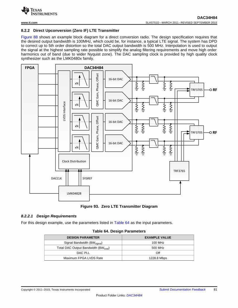
DAC34H84
QM
C G
ain
, P
ha
se,
Off
set
xN
xN QM
C G
ain
, P
ha
se,
Off
set
xN
xN
LV
DS
In
terf
ace
FPGA
RF
Clock Distribution
LMK04828
TRF3765
DACCLK SYSREF
16-bit DAC
16-bit DAC
TRF3705
RFTRF3705
16-bit DAC
16-bit DAC
DAC34H84www.ti.com SLAS751D –MARCH 2011–REVISED SEPTEMBER 2015
8.2.2 Direct Upconversion (Zero IF) LTE TransmitterFigure 88 shows an example block diagram for a direct conversion radio. The design specification requires thatthe desired output bandwidth is 100MHz, which could be, for instance, a typical LTE signal. The system has DPDto correct up to 5th order distortion so the total DAC output bandwidth is 500 MHz. Interpolation is used to outputthe signal at the highest sampling rate possible to simplify the analog filtering requirements and move high orderharmonics out of band (due to wider Nyquist zone). The DAC sampling clock is provided by high quality clocksynthesizer such as the LMK0480x family.
Figure 93. Zero LTE Transmitter Diagram
8.2.2.1 Design RequirementsFor this design example, use the parameters listed in Table 64 as the input parameters.
Table 64. Design ParametersDESIGN PARAMETER EXAMPLE VALUE
Signal Bandwidth (BWsignal) 100 MHzTotal DAC Output Bandwidth (BWtotal) 500 MHz
DAC PLL OffMaximum FPGA LVDS Rate 1228.8 Mbps
Copyright © 2011–2015, Texas Instruments Incorporated Submit Documentation Feedback 81
Product Folder Links: DAC34H84
DAC34H84SLAS751D –MARCH 2011–REVISED SEPTEMBER 2015 www.ti.com
8.2.2.2 Detailed Design Procedure
8.2.2.2.1 Data Input Rate
Nyquist theory states that the data rate must be at least two times the highest signal frequency. The data will besent to the DAC as complex baseband data. Due to the quadrature nature of the signal, each in-phase (Icomponent) and quadrature (Q component) need to have 250 MHz of bandwidth to construct 500 MHz ofcomplex bandwidth. Since the interpolation filter design is not the ideal half-band filter design with infinite roll-offat FDATA/2 (refer to FIR Filters section for more detail), the filter limits the useable input bandwidth to about 44percent of FDATA with less than 0.1dB of FIR filter roll-off. Therefore, the minimum data input rate is 568 MSPS.Since the standard telecom data rate is typically multiples of 30.72 MSPS, the DAC input data rate is chosen tobe 20 times of 30.72 MSPS, which is 614.4 MSPS.
8.2.2.2.2 Interpolation
It is desired to use the highest DAC output rate as possible to move the DAC images further from the signal ofinterest to ease analog filter requirement. The DAC output rate must be greater than two times the highest outputfrequency of 250 MHz, which is greater than 500 MHz. The table below shows the possible DAC output ratesbased on the data input rate and available interpolation settings. The DAC image frequency is also listed.
Table 65. InterpolationLOWEST IMAGE DISTANCE FROM BAND OFFDATA INTERPOLATION FDAC POSSIBLE? FREQUENCY INTEREST
614.4 MSPS 1 614.4 MSPS Yes 364.4 MHz 114.4 MHz614.4 MSPS 2 1228.8 MSPS Yes 978.8 MHz 728.8 MHz614.4 MSPS 4 2457.6 MSPS No N/A N/A614.4 MSPS 8 4915.2 MSPS No N/A N/A614.4 MSPS 16 9830.4 MSPS No N/A N/A
8.2.2.2.3 LO Feedthrough and Sideband Correction
Refer to LO Feedthrough and Sideband Correction section of IF based LTE Transmitter design.
82 Submit Documentation Feedback Copyright © 2011–2015, Texas Instruments Incorporated
Product Folder Links: DAC34H84
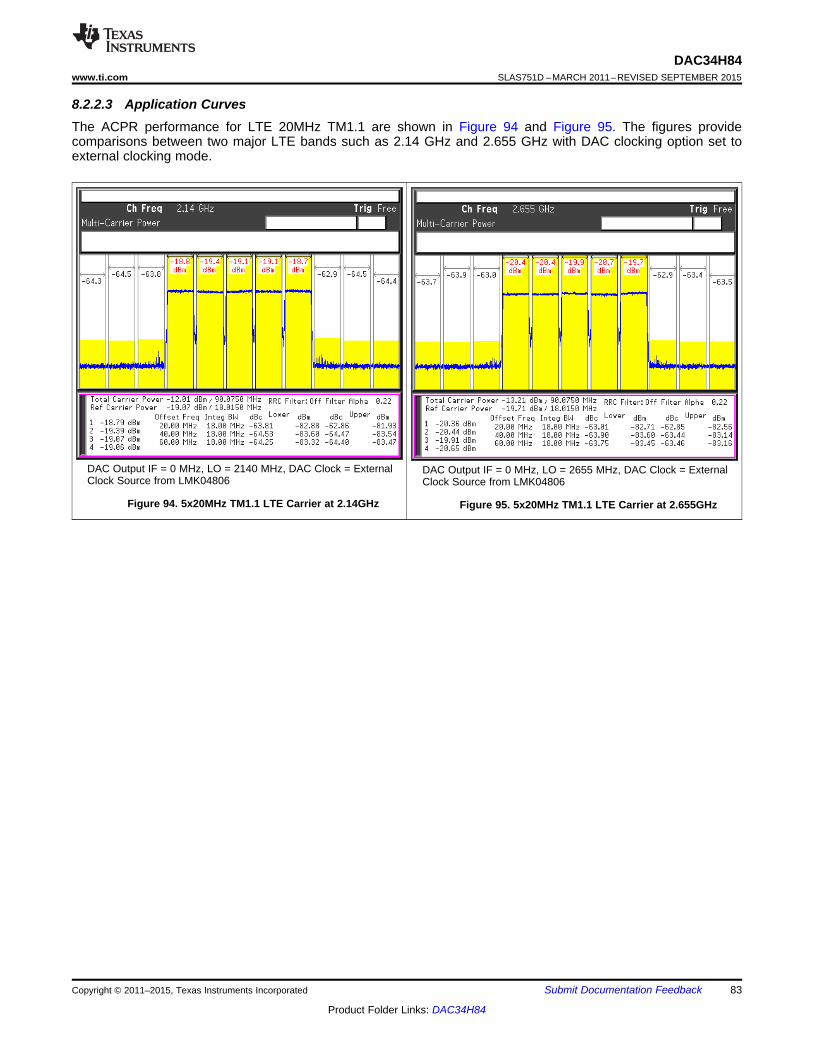
DAC34H84www.ti.com SLAS751D –MARCH 2011–REVISED SEPTEMBER 2015
8.2.2.3 Application CurvesThe ACPR performance for LTE 20MHz TM1.1 are shown in Figure 94 and Figure 95. The figures providecomparisons between two major LTE bands such as 2.14 GHz and 2.655 GHz with DAC clocking option set toexternal clocking mode.
DAC Output IF = 0 MHz, LO = 2140 MHz, DAC Clock = External DAC Output IF = 0 MHz, LO = 2655 MHz, DAC Clock = ExternalClock Source from LMK04806 Clock Source from LMK04806
Figure 94. 5x20MHz TM1.1 LTE Carrier at 2.14GHz Figure 95. 5x20MHz TM1.1 LTE Carrier at 2.655GHz
Copyright © 2011–2015, Texas Instruments Incorporated Submit Documentation Feedback 83
Product Folder Links: DAC34H84
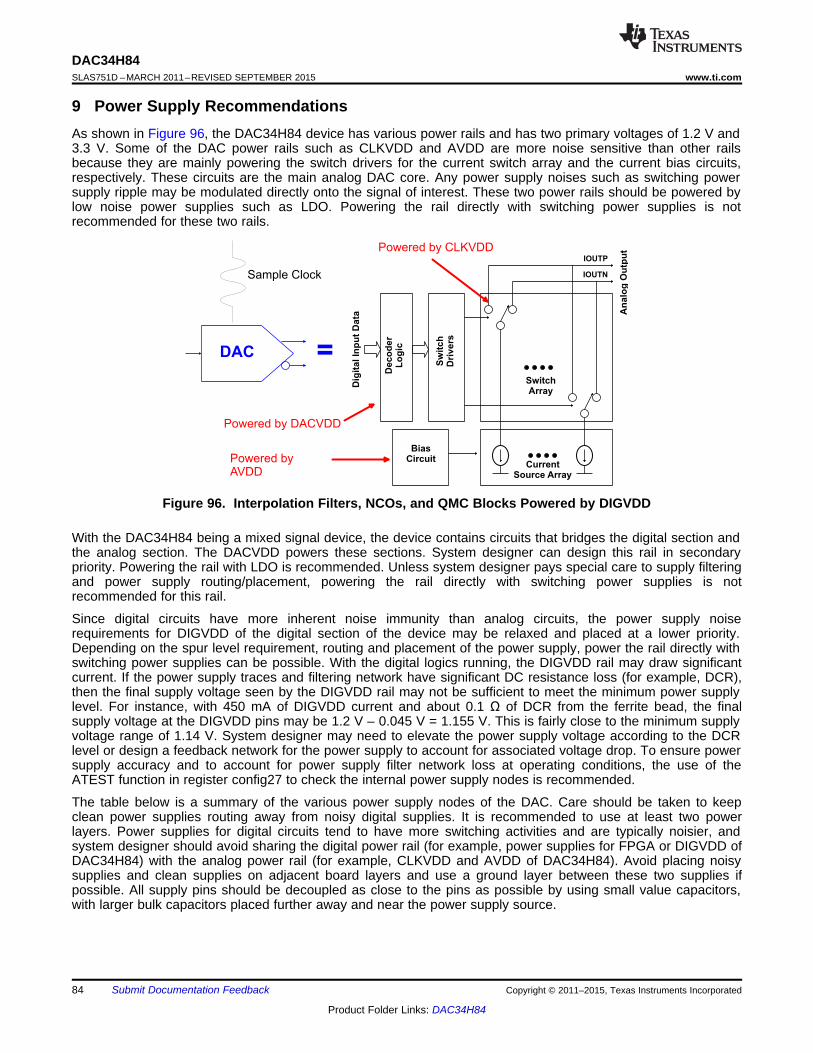
Deco
der
Lo
gic
Dig
italIn
pu
t D
ata
Sw
itch
Dri
vers
CurrentSource Array
BiasCircuit
IOUTP
SwitchArray
IOUTN
An
alo
gO
utp
ut
DAC =
Sample Clock
Powered by DACVDD
Powered byAVDD
Powered by CLKVDD
DAC34H84SLAS751D –MARCH 2011–REVISED SEPTEMBER 2015 www.ti.com
9 Power Supply RecommendationsAs shown in Figure 96, the DAC34H84 device has various power rails and has two primary voltages of 1.2 V and3.3 V. Some of the DAC power rails such as CLKVDD and AVDD are more noise sensitive than other railsbecause they are mainly powering the switch drivers for the current switch array and the current bias circuits,respectively. These circuits are the main analog DAC core. Any power supply noises such as switching powersupply ripple may be modulated directly onto the signal of interest. These two power rails should be powered bylow noise power supplies such as LDO. Powering the rail directly with switching power supplies is notrecommended for these two rails.
Figure 96. Interpolation Filters, NCOs, and QMC Blocks Powered by DIGVDD
With the DAC34H84 being a mixed signal device, the device contains circuits that bridges the digital section andthe analog section. The DACVDD powers these sections. System designer can design this rail in secondarypriority. Powering the rail with LDO is recommended. Unless system designer pays special care to supply filteringand power supply routing/placement, powering the rail directly with switching power supplies is notrecommended for this rail.
Since digital circuits have more inherent noise immunity than analog circuits, the power supply noiserequirements for DIGVDD of the digital section of the device may be relaxed and placed at a lower priority.Depending on the spur level requirement, routing and placement of the power supply, power the rail directly withswitching power supplies can be possible. With the digital logics running, the DIGVDD rail may draw significantcurrent. If the power supply traces and filtering network have significant DC resistance loss (for example, DCR),then the final supply voltage seen by the DIGVDD rail may not be sufficient to meet the minimum power supplylevel. For instance, with 450 mA of DIGVDD current and about 0.1 Ω of DCR from the ferrite bead, the finalsupply voltage at the DIGVDD pins may be 1.2 V – 0.045 V = 1.155 V. This is fairly close to the minimum supplyvoltage range of 1.14 V. System designer may need to elevate the power supply voltage according to the DCRlevel or design a feedback network for the power supply to account for associated voltage drop. To ensure powersupply accuracy and to account for power supply filter network loss at operating conditions, the use of theATEST function in register config27 to check the internal power supply nodes is recommended.
The table below is a summary of the various power supply nodes of the DAC. Care should be taken to keepclean power supplies routing away from noisy digital supplies. It is recommended to use at least two powerlayers. Power supplies for digital circuits tend to have more switching activities and are typically noisier, andsystem designer should avoid sharing the digital power rail (for example, power supplies for FPGA or DIGVDD ofDAC34H84) with the analog power rail (for example, CLKVDD and AVDD of DAC34H84). Avoid placing noisysupplies and clean supplies on adjacent board layers and use a ground layer between these two supplies ifpossible. All supply pins should be decoupled as close to the pins as possible by using small value capacitors,with larger bulk capacitors placed further away and near the power supply source.
84 Submit Documentation Feedback Copyright © 2011–2015, Texas Instruments Incorporated
Product Folder Links: DAC34H84
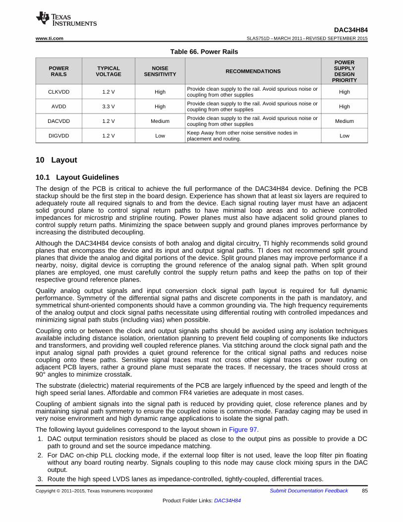
DAC34H84www.ti.com SLAS751D –MARCH 2011–REVISED SEPTEMBER 2015
Table 66. Power RailsPOWER
POWER TYPICAL NOISE SUPPLYRECOMMENDATIONSRAILS VOLTAGE SENSITIVITY DESIGNPRIORITY
Provide clean supply to the rail. Avoid spurious noise orCLKVDD 1.2 V High Highcoupling from other suppliesProvide clean supply to the rail. Avoid spurious noise orAVDD 3.3 V High Highcoupling from other suppliesProvide clean supply to the rail. Avoid spurious noise orDACVDD 1.2 V Medium Mediumcoupling from other suppliesKeep Away from other noise sensitive nodes inDIGVDD 1.2 V Low Lowplacement and routing.
10 Layout
10.1 Layout GuidelinesThe design of the PCB is critical to achieve the full performance of the DAC34H84 device. Defining the PCBstackup should be the first step in the board design. Experience has shown that at least six layers are required toadequately route all required signals to and from the device. Each signal routing layer must have an adjacentsolid ground plane to control signal return paths to have minimal loop areas and to achieve controlledimpedances for microstrip and stripline routing. Power planes must also have adjacent solid ground planes tocontrol supply return paths. Minimizing the space between supply and ground planes improves performance byincreasing the distributed decoupling.
Although the DAC34H84 device consists of both analog and digital circuitry, TI highly recommends solid groundplanes that encompass the device and its input and output signal paths. TI does not recommend split groundplanes that divide the analog and digital portions of the device. Split ground planes may improve performance if anearby, noisy, digital device is corrupting the ground reference of the analog signal path. When split groundplanes are employed, one must carefully control the supply return paths and keep the paths on top of theirrespective ground reference planes.
Quality analog output signals and input conversion clock signal path layout is required for full dynamicperformance. Symmetry of the differential signal paths and discrete components in the path is mandatory, andsymmetrical shunt-oriented components should have a common grounding via. The high frequency requirementsof the analog output and clock signal paths necessitate using differential routing with controlled impedances andminimizing signal path stubs (including vias) when possible.
Coupling onto or between the clock and output signals paths should be avoided using any isolation techniquesavailable including distance isolation, orientation planning to prevent field coupling of components like inductorsand transformers, and providing well coupled reference planes. Via stitching around the clock signal path and theinput analog signal path provides a quiet ground reference for the critical signal paths and reduces noisecoupling onto these paths. Sensitive signal traces must not cross other signal traces or power routing onadjacent PCB layers, rather a ground plane must separate the traces. If necessary, the traces should cross at90° angles to minimize crosstalk.
The substrate (dielectric) material requirements of the PCB are largely influenced by the speed and length of thehigh speed serial lanes. Affordable and common FR4 varieties are adequate in most cases.
Coupling of ambient signals into the signal path is reduced by providing quiet, close reference planes and bymaintaining signal path symmetry to ensure the coupled noise is common-mode. Faraday caging may be used invery noise environment and high dynamic range applications to isolate the signal path.
The following layout guidelines correspond to the layout shown in Figure 97.1. DAC output termination resistors should be placed as close to the output pins as possible to provide a DC
path to ground and set the source impedance matching.2. For DAC on-chip PLL clocking mode, if the external loop filter is not used, leave the loop filter pin floating
without any board routing nearby. Signals coupling to this node may cause clock mixing spurs in the DACoutput.
3. Route the high speed LVDS lanes as impedance-controlled, tightly-coupled, differential traces.
Copyright © 2011–2015, Texas Instruments Incorporated Submit Documentation Feedback 85
Product Folder Links: DAC34H84
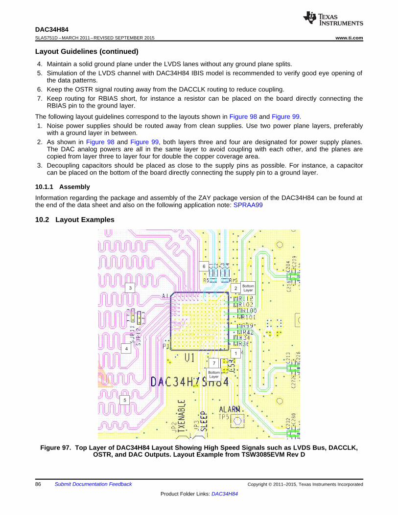
1
2
6
7
4
3
5
BottomLayer
BottomLayer
DAC34H84SLAS751D –MARCH 2011–REVISED SEPTEMBER 2015 www.ti.com
Layout Guidelines (continued)4. Maintain a solid ground plane under the LVDS lanes without any ground plane splits.5. Simulation of the LVDS channel with DAC34H84 IBIS model is recommended to verify good eye opening of
the data patterns.6. Keep the OSTR signal routing away from the DACCLK routing to reduce coupling.7. Keep routing for RBIAS short, for instance a resistor can be placed on the board directly connecting the
RBIAS pin to the ground layer.
The following layout guidelines correspond to the layouts shown in Figure 98 and Figure 99.1. Noise power supplies should be routed away from clean supplies. Use two power plane layers, preferably
with a ground layer in between.2. As shown in Figure 98 and Figure 99, both layers three and four are designated for power supply planes.
The DAC analog powers are all in the same layer to avoid coupling with each other, and the planes arecopied from layer three to layer four for double the copper coverage area.
3. Decoupling capacitors should be placed as close to the supply pins as possible. For instance, a capacitorcan be placed on the bottom of the board directly connecting the supply pin to a ground layer.
10.1.1 AssemblyInformation regarding the package and assembly of the ZAY package version of the DAC34H84 can be found atthe end of the data sheet and also on the following application note: SPRAA99
10.2 Layout Examples
Figure 97. Top Layer of DAC34H84 Layout Showing High Speed Signals such as LVDS Bus, DACCLK,OSTR, and DAC Outputs. Layout Example from TSW3085EVM Rev D
86 Submit Documentation Feedback Copyright © 2011–2015, Texas Instruments Incorporated
Product Folder Links: DAC34H84
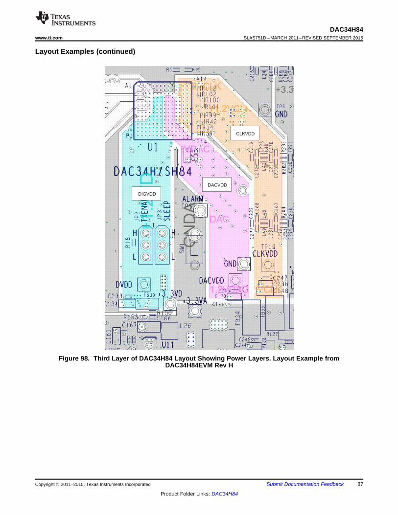
DIGVDD
DACVDD
CLKVDD
DAC34H84www.ti.com SLAS751D –MARCH 2011–REVISED SEPTEMBER 2015
Layout Examples (continued)
Figure 98. Third Layer of DAC34H84 Layout Showing Power Layers. Layout Example fromDAC34H84EVM Rev H
Copyright © 2011–2015, Texas Instruments Incorporated Submit Documentation Feedback 87
Product Folder Links: DAC34H84
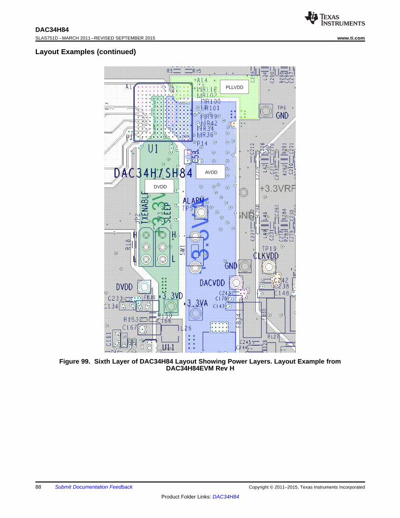
AVDD
PLLVDD
DVDD
DAC34H84SLAS751D –MARCH 2011–REVISED SEPTEMBER 2015 www.ti.com
Layout Examples (continued)
Figure 99. Sixth Layer of DAC34H84 Layout Showing Power Layers. Layout Example fromDAC34H84EVM Rev H
88 Submit Documentation Feedback Copyright © 2011–2015, Texas Instruments Incorporated
Product Folder Links: DAC34H84
DAC34H84www.ti.com SLAS751D –MARCH 2011–REVISED SEPTEMBER 2015
11 Device and Documentation Support
11.1 Device Support
11.1.1 Third-Party Products DisclaimerTI'S PUBLICATION OF INFORMATION REGARDING THIRD-PARTY PRODUCTS OR SERVICES DOES NOTCONSTITUTE AN ENDORSEMENT REGARDING THE SUITABILITY OF SUCH PRODUCTS OR SERVICESOR A WARRANTY, REPRESENTATION OR ENDORSEMENT OF SUCH PRODUCTS OR SERVICES, EITHERALONE OR IN COMBINATION WITH ANY TI PRODUCT OR SERVICE.
11.1.2 Device Nomenclature
11.1.2.1 Definition of SpecificationsAdjacent Carrier Leakage Ratio (ACLR): Defined for a 3.84Mcps 3GPP W-CDMA input signal measured in a3.84MHz bandwidth at a 5MHz offset from the carrier with a 12dB peak-to-average ratio.
Analog and Digital Power Supply Rejection Ratio (APSSR, DPSSR): Defined as the percentage error in theratio of the delta IOUT and delta supply voltage normalized with respect to the ideal IOUT current.
Differential Nonlinearity (DNL): Defined as the variation in analog output associated with an ideal 1 LSBchange in the digital input code.
Gain Drift: Defined as the maximum change in gain, in terms of ppm of full-scale range (FSR) per °C, from thevalue at ambient (25°C) to values over the full operating temperature range.
Gain Error: Defined as the percentage error (in FSR%) for the ratio between the measured full-scale outputcurrent and the ideal full-scale output current.
Integral Nonlinearity (INL): Defined as the maximum deviation of the actual analog output from the ideal output,determined by a straight line drawn from zero scale to full scale.
Intermodulation Distortion (IMD3): The two-tone IMD3 is defined as the ratio (in dBc) of the 3rd-orderintermodulation distortion product to either fundamental output tone.
Offset Drift: Defined as the maximum change in DC offset, in terms of ppm of full-scale range (FSR) per °C,from the value at ambient (25°C) to values over the full operating temperature range.
Offset Error: Defined as the percentage error (in FSR%) for the ratio between the measured mid-scale outputcurrent and the ideal mid-scale output current.
Output Compliance Range: Defined as the minimum and maximum allowable voltage at the output of thecurrent-output DAC. Exceeding this limit may result reduced reliability of the device or adversely affectingdistortion performance.
Reference Voltage Drift: Defined as the maximum change of the reference voltage in ppm per degree Celsiusfrom value at ambient (25°C) to values over the full operating temperature range.
Spurious Free Dynamic Range (SFDR): Defined as the difference (in dBc) between the peak amplitude of theoutput signal and the peak spurious signal within the first Nyquist zone.
Noise Spectral Density (NSD): Defined as the difference of power (in dBc) between the output tone signalpower and the noise floor of 1Hz bandwidth within the first Nyquist zone.
11.2 Documentation Support
11.2.1 Related Documentation• DAC34H84 EVM User's Guide (SLAU338)• nFBGA Packaging Application Report (SPRAA99)
Copyright © 2011–2015, Texas Instruments Incorporated Submit Documentation Feedback 89
Product Folder Links: DAC34H84
DAC34H84SLAS751D –MARCH 2011–REVISED SEPTEMBER 2015 www.ti.com
11.3 Community ResourcesThe following links connect to TI community resources. Linked contents are provided "AS IS" by the respectivecontributors. They do not constitute TI specifications and do not necessarily reflect TI's views; see TI's Terms ofUse.
TI E2E™ Online Community TI's Engineer-to-Engineer (E2E) Community. Created to foster collaborationamong engineers. At e2e.ti.com, you can ask questions, share knowledge, explore ideas and helpsolve problems with fellow engineers.
Design Support TI's Design Support Quickly find helpful E2E forums along with design support tools andcontact information for technical support.
11.4 TrademarksE2E is a trademark of Texas Instruments.All other trademarks are the property of their respective owners.
11.5 Electrostatic Discharge CautionThese devices have limited built-in ESD protection. The leads should be shorted together or the device placed in conductive foamduring storage or handling to prevent electrostatic damage to the MOS gates.
11.6 GlossarySLYZ022 — TI Glossary.
This glossary lists and explains terms, acronyms, and definitions.
12 Mechanical, Packaging, and Orderable InformationThe following pages include mechanical, packaging, and orderable information. This information is the mostcurrent data available for the designated devices. This data is subject to change without notice and revision ofthis document. For browser-based versions of this data sheet, refer to the left-hand navigation.
90 Submit Documentation Feedback Copyright © 2011–2015, Texas Instruments Incorporated
Product Folder Links: DAC34H84
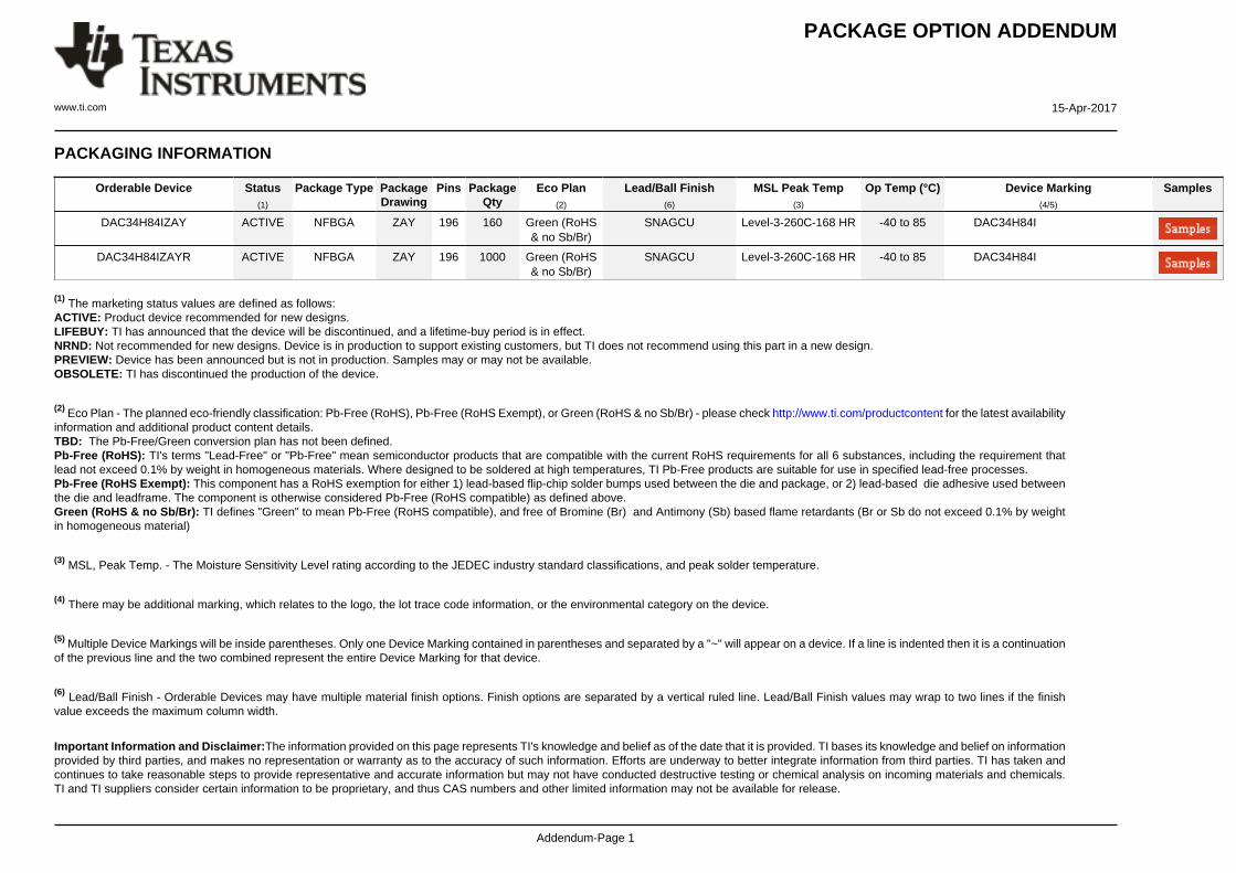
PACKAGE OPTION ADDENDUM
www.ti.com 15-Apr-2017
Addendum-Page 1
PACKAGING INFORMATION
Orderable Device Status(1)
Package Type PackageDrawing
Pins PackageQty
Eco Plan(2)
Lead/Ball Finish(6)
MSL Peak Temp(3)
Op Temp (°C) Device Marking(4/5)
Samples
DAC34H84IZAY ACTIVE NFBGA ZAY 196 160 Green (RoHS& no Sb/Br)
SNAGCU Level-3-260C-168 HR -40 to 85 DAC34H84I
DAC34H84IZAYR ACTIVE NFBGA ZAY 196 1000 Green (RoHS& no Sb/Br)
SNAGCU Level-3-260C-168 HR -40 to 85 DAC34H84I
(1) The marketing status values are defined as follows:ACTIVE: Product device recommended for new designs.LIFEBUY: TI has announced that the device will be discontinued, and a lifetime-buy period is in effect.NRND: Not recommended for new designs. Device is in production to support existing customers, but TI does not recommend using this part in a new design.PREVIEW: Device has been announced but is not in production. Samples may or may not be available.OBSOLETE: TI has discontinued the production of the device.
(2) Eco Plan - The planned eco-friendly classification: Pb-Free (RoHS), Pb-Free (RoHS Exempt), or Green (RoHS & no Sb/Br) - please check http://www.ti.com/productcontent for the latest availabilityinformation and additional product content details.TBD: The Pb-Free/Green conversion plan has not been defined.Pb-Free (RoHS): TI's terms "Lead-Free" or "Pb-Free" mean semiconductor products that are compatible with the current RoHS requirements for all 6 substances, including the requirement thatlead not exceed 0.1% by weight in homogeneous materials. Where designed to be soldered at high temperatures, TI Pb-Free products are suitable for use in specified lead-free processes.Pb-Free (RoHS Exempt): This component has a RoHS exemption for either 1) lead-based flip-chip solder bumps used between the die and package, or 2) lead-based die adhesive used betweenthe die and leadframe. The component is otherwise considered Pb-Free (RoHS compatible) as defined above.Green (RoHS & no Sb/Br): TI defines "Green" to mean Pb-Free (RoHS compatible), and free of Bromine (Br) and Antimony (Sb) based flame retardants (Br or Sb do not exceed 0.1% by weightin homogeneous material)
(3) MSL, Peak Temp. - The Moisture Sensitivity Level rating according to the JEDEC industry standard classifications, and peak solder temperature.
(4) There may be additional marking, which relates to the logo, the lot trace code information, or the environmental category on the device.
(5) Multiple Device Markings will be inside parentheses. Only one Device Marking contained in parentheses and separated by a "~" will appear on a device. If a line is indented then it is a continuationof the previous line and the two combined represent the entire Device Marking for that device.
(6) Lead/Ball Finish - Orderable Devices may have multiple material finish options. Finish options are separated by a vertical ruled line. Lead/Ball Finish values may wrap to two lines if the finishvalue exceeds the maximum column width.
Important Information and Disclaimer:The information provided on this page represents TI's knowledge and belief as of the date that it is provided. TI bases its knowledge and belief on informationprovided by third parties, and makes no representation or warranty as to the accuracy of such information. Efforts are underway to better integrate information from third parties. TI has taken andcontinues to take reasonable steps to provide representative and accurate information but may not have conducted destructive testing or chemical analysis on incoming materials and chemicals.TI and TI suppliers consider certain information to be proprietary, and thus CAS numbers and other limited information may not be available for release.
PACKAGE OPTION ADDENDUM
www.ti.com 15-Apr-2017
Addendum-Page 2
In no event shall TI's liability arising out of such information exceed the total purchase price of the TI part(s) at issue in this document sold by TI to Customer on an annual basis.
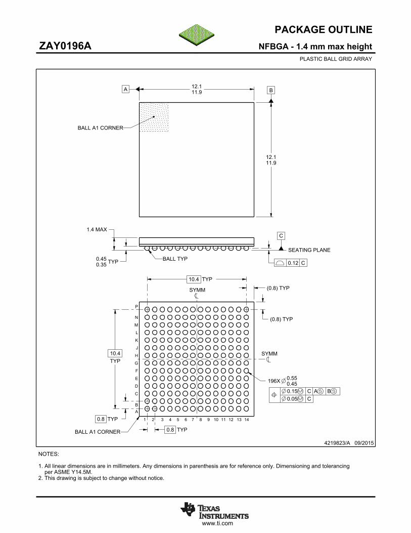
www.ti.com
PACKAGE OUTLINE
C1.4 MAX
TYP0.450.35
10.4TYP
10.4 TYP
0.8 TYP
0.8 TYP
196X 0.550.45
A 12.111.9 B
12.111.9
(0.8) TYP
(0.8) TYP
NFBGA - 1.4 mm max heightZAY0196APLASTIC BALL GRID ARRAY
4219823/A 09/2015
NOTES: 1. All linear dimensions are in millimeters. Any dimensions in parenthesis are for reference only. Dimensioning and tolerancing per ASME Y14.5M. 2. This drawing is subject to change without notice.
BALL A1 CORNER
SEATING PLANEBALL TYP
0.12 C
0.15 C A B0.05 C
SYMM
SYMM
BALL A1 CORNER
P
C
D
E
F
G
H
J
K
L
M
N
1 2 3 4 5 6 7 8 9 10 11
AB
12 13 14
SCALE 1.100
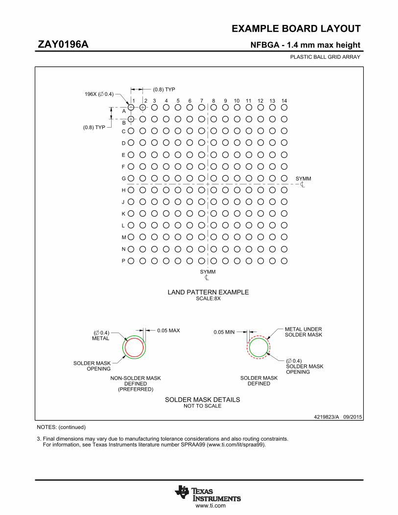
www.ti.com
EXAMPLE BOARD LAYOUT
196X ( )0.4(0.8) TYP
(0.8) TYP
( )METAL
0.4 0.05 MAX
SOLDER MASKOPENING
METAL UNDERSOLDER MASK
( )SOLDER MASKOPENING
0.4
0.05 MIN
NFBGA - 1.4 mm max heightZAY0196APLASTIC BALL GRID ARRAY
4219823/A 09/2015
NOTES: (continued) 3. Final dimensions may vary due to manufacturing tolerance considerations and also routing constraints. For information, see Texas Instruments literature number SPRAA99 (www.ti.com/lit/spraa99).
SYMM
SYMM
LAND PATTERN EXAMPLESCALE:8X
1 2 3 4 5 6 7 8 9 10 11
B
A
C
D
E
F
G
H
J
K
L
M
N
P
12 13 14
NON-SOLDER MASKDEFINED
(PREFERRED)
SOLDER MASK DETAILSNOT TO SCALE
SOLDER MASKDEFINED

www.ti.com
EXAMPLE STENCIL DESIGN
(0.8) TYP
(0.8) TYP ( ) TYP0.4
NFBGA - 1.4 mm max heightZAY0196APLASTIC BALL GRID ARRAY
4219823/A 09/2015
NOTES: (continued) 4. Laser cutting apertures with trapezoidal walls and rounded corners may offer better paste release.
SOLDER PASTE EXAMPLEBASED ON 0.15 mm THICK STENCIL
SCALE:8X
SYMM
SYMM
1 2 3 4 5 6 7 8 9 10 11
B
A
C
D
E
F
G
H
J
K
L
M
N
P
12 13 14
IMPORTANT NOTICE
Texas Instruments Incorporated (TI) reserves the right to make corrections, enhancements, improvements and other changes to itssemiconductor products and services per JESD46, latest issue, and to discontinue any product or service per JESD48, latest issue. Buyersshould obtain the latest relevant information before placing orders and should verify that such information is current and complete.TI’s published terms of sale for semiconductor products (http://www.ti.com/sc/docs/stdterms.htm) apply to the sale of packaged integratedcircuit products that TI has qualified and released to market. Additional terms may apply to the use or sale of other types of TI products andservices.Reproduction of significant portions of TI information in TI data sheets is permissible only if reproduction is without alteration and isaccompanied by all associated warranties, conditions, limitations, and notices. TI is not responsible or liable for such reproduceddocumentation. Information of third parties may be subject to additional restrictions. Resale of TI products or services with statementsdifferent from or beyond the parameters stated by TI for that product or service voids all express and any implied warranties for theassociated TI product or service and is an unfair and deceptive business practice. TI is not responsible or liable for any such statements.Buyers and others who are developing systems that incorporate TI products (collectively, “Designers”) understand and agree that Designersremain responsible for using their independent analysis, evaluation and judgment in designing their applications and that Designers havefull and exclusive responsibility to assure the safety of Designers' applications and compliance of their applications (and of all TI productsused in or for Designers’ applications) with all applicable regulations, laws and other applicable requirements. Designer represents that, withrespect to their applications, Designer has all the necessary expertise to create and implement safeguards that (1) anticipate dangerousconsequences of failures, (2) monitor failures and their consequences, and (3) lessen the likelihood of failures that might cause harm andtake appropriate actions. Designer agrees that prior to using or distributing any applications that include TI products, Designer willthoroughly test such applications and the functionality of such TI products as used in such applications.TI’s provision of technical, application or other design advice, quality characterization, reliability data or other services or information,including, but not limited to, reference designs and materials relating to evaluation modules, (collectively, “TI Resources”) are intended toassist designers who are developing applications that incorporate TI products; by downloading, accessing or using TI Resources in anyway, Designer (individually or, if Designer is acting on behalf of a company, Designer’s company) agrees to use any particular TI Resourcesolely for this purpose and subject to the terms of this Notice.TI’s provision of TI Resources does not expand or otherwise alter TI’s applicable published warranties or warranty disclaimers for TIproducts, and no additional obligations or liabilities arise from TI providing such TI Resources. TI reserves the right to make corrections,enhancements, improvements and other changes to its TI Resources. TI has not conducted any testing other than that specificallydescribed in the published documentation for a particular TI Resource.Designer is authorized to use, copy and modify any individual TI Resource only in connection with the development of applications thatinclude the TI product(s) identified in such TI Resource. NO OTHER LICENSE, EXPRESS OR IMPLIED, BY ESTOPPEL OR OTHERWISETO ANY OTHER TI INTELLECTUAL PROPERTY RIGHT, AND NO LICENSE TO ANY TECHNOLOGY OR INTELLECTUAL PROPERTYRIGHT OF TI OR ANY THIRD PARTY IS GRANTED HEREIN, including but not limited to any patent right, copyright, mask work right, orother intellectual property right relating to any combination, machine, or process in which TI products or services are used. Informationregarding or referencing third-party products or services does not constitute a license to use such products or services, or a warranty orendorsement thereof. Use of TI Resources may require a license from a third party under the patents or other intellectual property of thethird party, or a license from TI under the patents or other intellectual property of TI.TI RESOURCES ARE PROVIDED “AS IS” AND WITH ALL FAULTS. TI DISCLAIMS ALL OTHER WARRANTIES ORREPRESENTATIONS, EXPRESS OR IMPLIED, REGARDING RESOURCES OR USE THEREOF, INCLUDING BUT NOT LIMITED TOACCURACY OR COMPLETENESS, TITLE, ANY EPIDEMIC FAILURE WARRANTY AND ANY IMPLIED WARRANTIES OFMERCHANTABILITY, FITNESS FOR A PARTICULAR PURPOSE, AND NON-INFRINGEMENT OF ANY THIRD PARTY INTELLECTUALPROPERTY RIGHTS. TI SHALL NOT BE LIABLE FOR AND SHALL NOT DEFEND OR INDEMNIFY DESIGNER AGAINST ANY CLAIM,INCLUDING BUT NOT LIMITED TO ANY INFRINGEMENT CLAIM THAT RELATES TO OR IS BASED ON ANY COMBINATION OFPRODUCTS EVEN IF DESCRIBED IN TI RESOURCES OR OTHERWISE. IN NO EVENT SHALL TI BE LIABLE FOR ANY ACTUAL,DIRECT, SPECIAL, COLLATERAL, INDIRECT, PUNITIVE, INCIDENTAL, CONSEQUENTIAL OR EXEMPLARY DAMAGES INCONNECTION WITH OR ARISING OUT OF TI RESOURCES OR USE THEREOF, AND REGARDLESS OF WHETHER TI HAS BEENADVISED OF THE POSSIBILITY OF SUCH DAMAGES.Unless TI has explicitly designated an individual product as meeting the requirements of a particular industry standard (e.g., ISO/TS 16949and ISO 26262), TI is not responsible for any failure to meet such industry standard requirements.Where TI specifically promotes products as facilitating functional safety or as compliant with industry functional safety standards, suchproducts are intended to help enable customers to design and create their own applications that meet applicable functional safety standardsand requirements. Using products in an application does not by itself establish any safety features in the application. Designers mustensure compliance with safety-related requirements and standards applicable to their applications. Designer may not use any TI products inlife-critical medical equipment unless authorized officers of the parties have executed a special contract specifically governing such use.Life-critical medical equipment is medical equipment where failure of such equipment would cause serious bodily injury or death (e.g., lifesupport, pacemakers, defibrillators, heart pumps, neurostimulators, and implantables). Such equipment includes, without limitation, allmedical devices identified by the U.S. Food and Drug Administration as Class III devices and equivalent classifications outside the U.S.TI may expressly designate certain products as completing a particular qualification (e.g., Q100, Military Grade, or Enhanced Product).Designers agree that it has the necessary expertise to select the product with the appropriate qualification designation for their applicationsand that proper product selection is at Designers’ own risk. Designers are solely responsible for compliance with all legal and regulatoryrequirements in connection with such selection.Designer will fully indemnify TI and its representatives against any damages, costs, losses, and/or liabilities arising out of Designer’s non-compliance with the terms and provisions of this Notice.
Mailing Address: Texas Instruments, Post Office Box 655303, Dallas, Texas 75265Copyright © 2017, Texas Instruments Incorporated
Top Related