


Languages
Pages
Legal


Power Semiconductor Switching Devices
EE 442-642
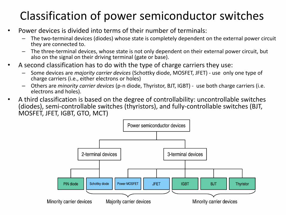
Classification of power semiconductor switches • Power devices is divided into terms of their number of terminals:
– The two-terminal devices (diodes) whose state is completely dependent on the external power circuit they are connected to.
– The three-terminal devices, whose state is not only dependent on their external power circuit, but also on the signal on their driving terminal (gate or base).
• A second classification has to do with the type of charge carriers they use: – Some devices are majority carrier devices (Schottky diode, MOSFET, JFET) - use only one type of
charge carriers (i.e., either electrons or holes) – Others are minority carrier devices (p-n diode, Thyristor, BJT, IGBT) - use both charge carriers (i.e.
electrons and holes).
• A third classification is based on the degree of controllability: uncontrollable switches (diodes), semi-controllable switches (thyristors), and fully-controllable switches (BJT, MOSFET, JFET, IGBT, GTO, MCT)
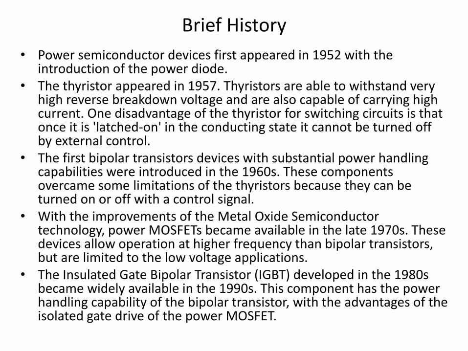
Brief History
• Power semiconductor devices first appeared in 1952 with the introduction of the power diode.
• The thyristor appeared in 1957. Thyristors are able to withstand very high reverse breakdown voltage and are also capable of carrying high current. One disadvantage of the thyristor for switching circuits is that once it is 'latched-on' in the conducting state it cannot be turned off by external control.
• The first bipolar transistors devices with substantial power handling capabilities were introduced in the 1960s. These components overcame some limitations of the thyristors because they can be turned on or off with a control signal.
• With the improvements of the Metal Oxide Semiconductor technology, power MOSFETs became available in the late 1970s. These devices allow operation at higher frequency than bipolar transistors, but are limited to the low voltage applications.
• The Insulated Gate Bipolar Transistor (IGBT) developed in the 1980s became widely available in the 1990s. This component has the power handling capability of the bipolar transistor, with the advantages of the isolated gate drive of the power MOSFET.
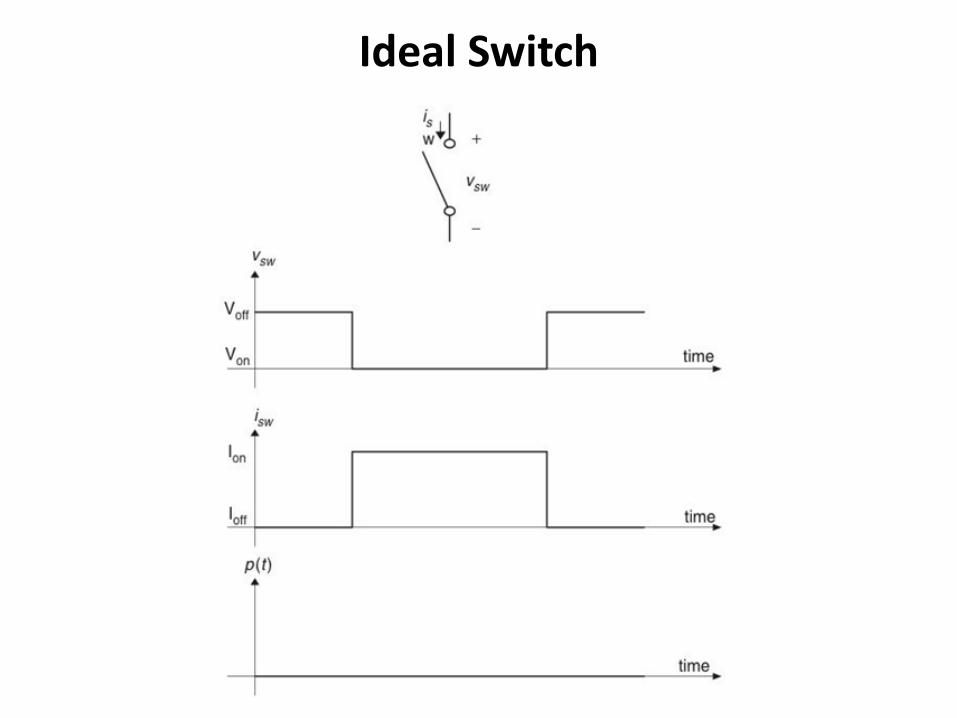
Ideal Switch
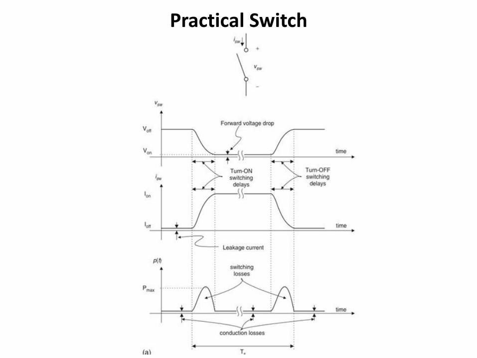
Practical Switch
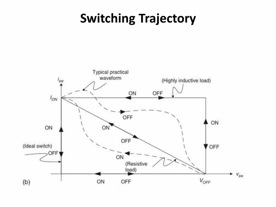
Switching Trajectory
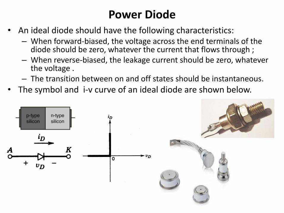
Power Diode • An ideal diode should have the following characteristics:
– When forward-biased, the voltage across the end terminals of the diode should be zero, whatever the current that flows through ;
– When reverse-biased, the leakage current should be zero, whatever the voltage .
– The transition between on and off states should be instantaneous.
• The symbol and i-v curve of an ideal diode are shown below.
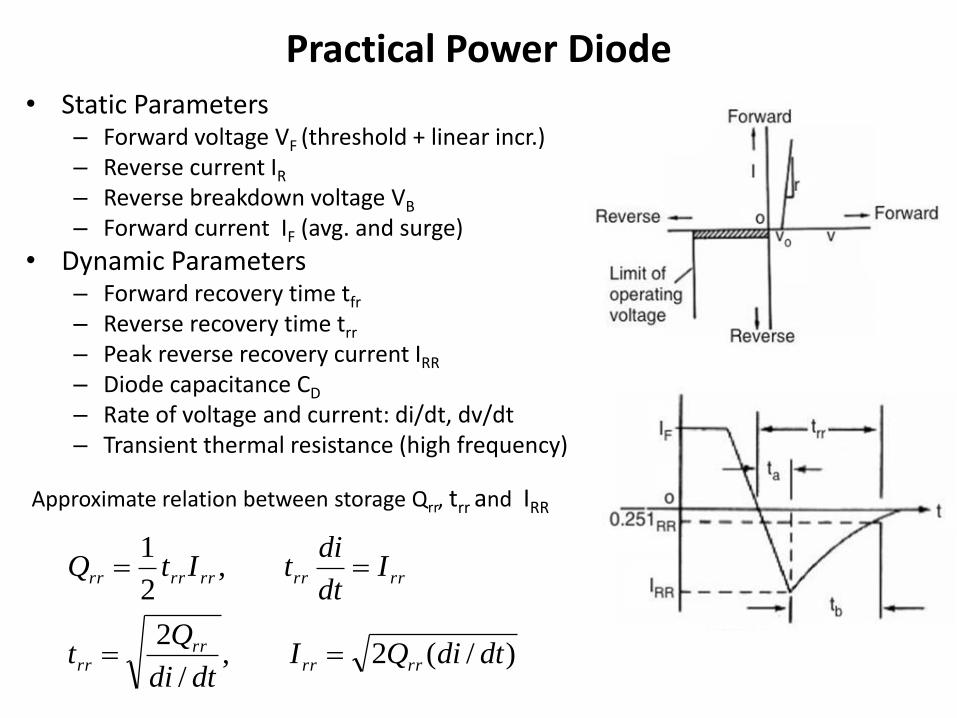
Practical Power Diode • Static Parameters
– Forward voltage VF (threshold + linear incr.)
– Reverse current IR
– Reverse breakdown voltage VB
– Forward current IF (avg. and surge)
• Dynamic Parameters – Forward recovery time tfr
– Reverse recovery time trr
– Peak reverse recovery current IRR
– Diode capacitance CD
– Rate of voltage and current: di/dt, dv/dt – Transient thermal resistance (high frequency)
)/(2,/
2
,2
1
dtdiQIdtdi
Qt
Idt
ditItQ
rrrrrr
rr
rrrrrrrrrr
Approximate relation between storage Qrr, trr and IRR
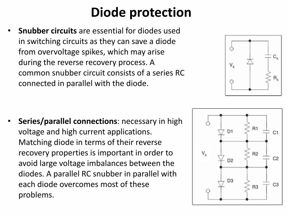
Diode protection • Snubber circuits are essential for diodes used
in switching circuits as they can save a diode from overvoltage spikes, which may arise during the reverse recovery process. A common snubber circuit consists of a series RC connected in parallel with the diode.
• Series/parallel connections: necessary in high voltage and high current applications. Matching diode in terms of their reverse recovery properties is important in order to avoid large voltage imbalances between the diodes. A parallel RC snubber in parallel with each diode overcomes most of these problems.
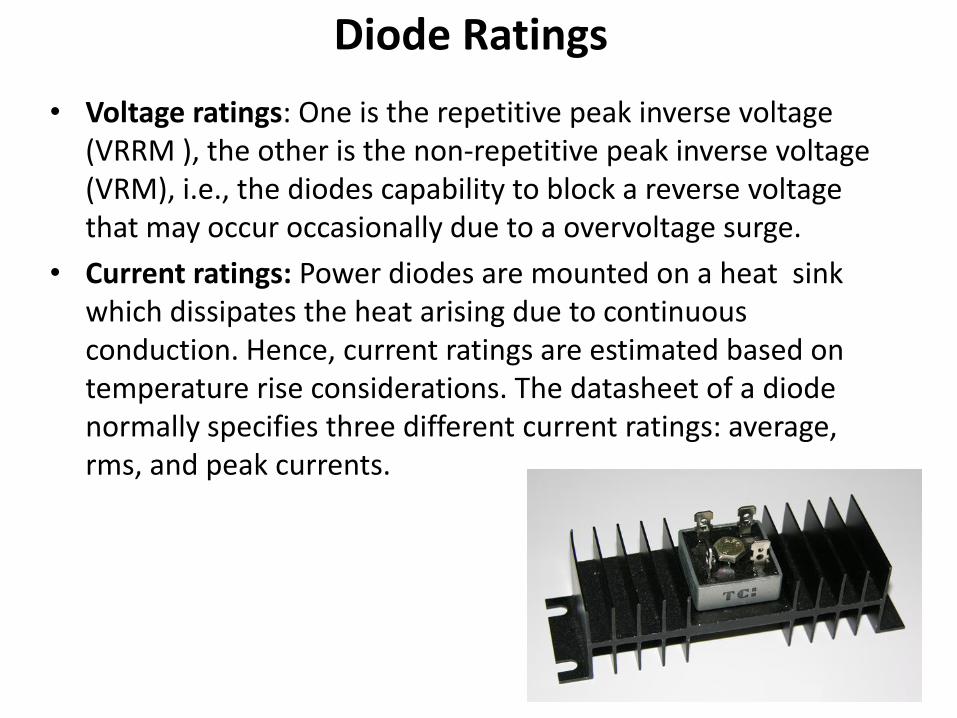
Diode Ratings
• Voltage ratings: One is the repetitive peak inverse voltage (VRRM ), the other is the non-repetitive peak inverse voltage (VRM), i.e., the diodes capability to block a reverse voltage that may occur occasionally due to a overvoltage surge.
• Current ratings: Power diodes are mounted on a heat sink which dissipates the heat arising due to continuous conduction. Hence, current ratings are estimated based on temperature rise considerations. The datasheet of a diode normally specifies three different current ratings: average, rms, and peak currents.
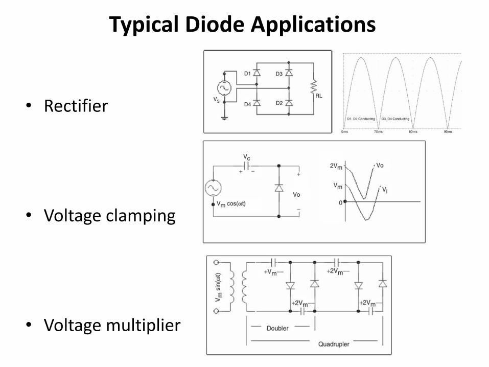
Typical Diode Applications
• Rectifier
• Voltage clamping
• Voltage multiplier
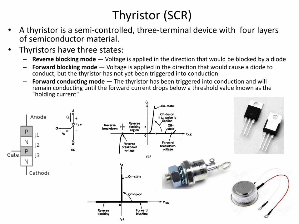
Thyristor (SCR) • A thyristor is a semi-controlled, three-terminal device with four layers
of semiconductor material. • Thyristors have three states:
– Reverse blocking mode — Voltage is applied in the direction that would be blocked by a diode – Forward blocking mode — Voltage is applied in the direction that would cause a diode to
conduct, but the thyristor has not yet been triggered into conduction – Forward conducting mode — The thyristor has been triggered into conduction and will
remain conducting until the forward current drops below a threshold value known as the "holding current"
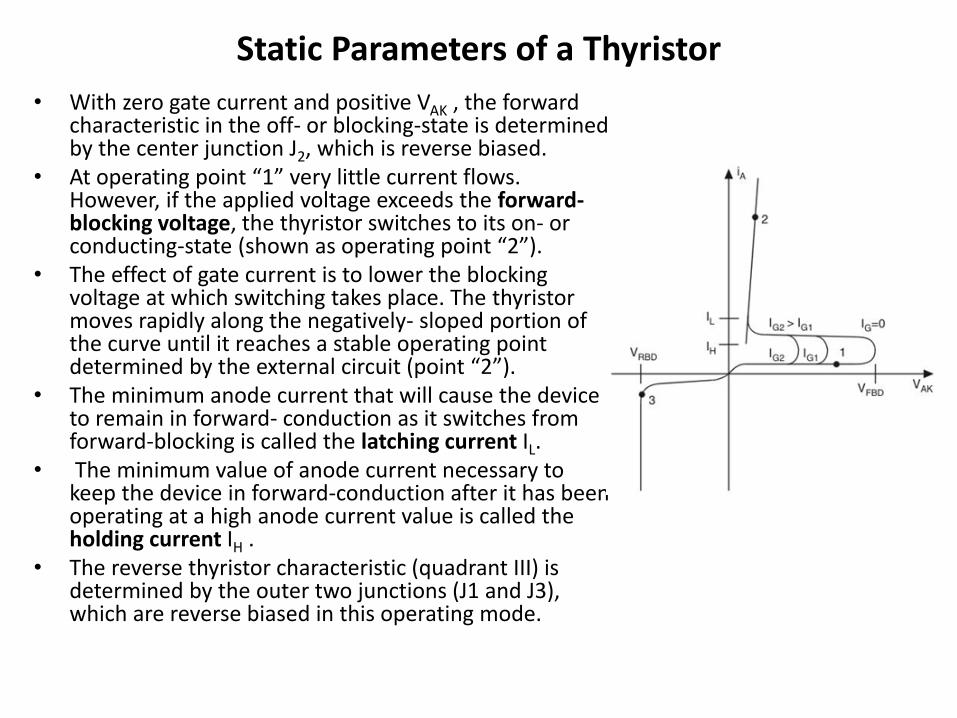
Static Parameters of a Thyristor
• With zero gate current and positive VAK , the forward characteristic in the off- or blocking-state is determined by the center junction J2, which is reverse biased.
• At operating point “1” very little current flows. However, if the applied voltage exceeds the forward-blocking voltage, the thyristor switches to its on- or conducting-state (shown as operating point “2”).
• The effect of gate current is to lower the blocking voltage at which switching takes place. The thyristor moves rapidly along the negatively- sloped portion of the curve until it reaches a stable operating point determined by the external circuit (point “2”).
• The minimum anode current that will cause the device to remain in forward- conduction as it switches from forward-blocking is called the latching current IL.
• The minimum value of anode current necessary to keep the device in forward-conduction after it has been operating at a high anode current value is called the holding current IH .
• The reverse thyristor characteristic (quadrant III) is determined by the outer two junctions (J1 and J3), which are reverse biased in this operating mode.
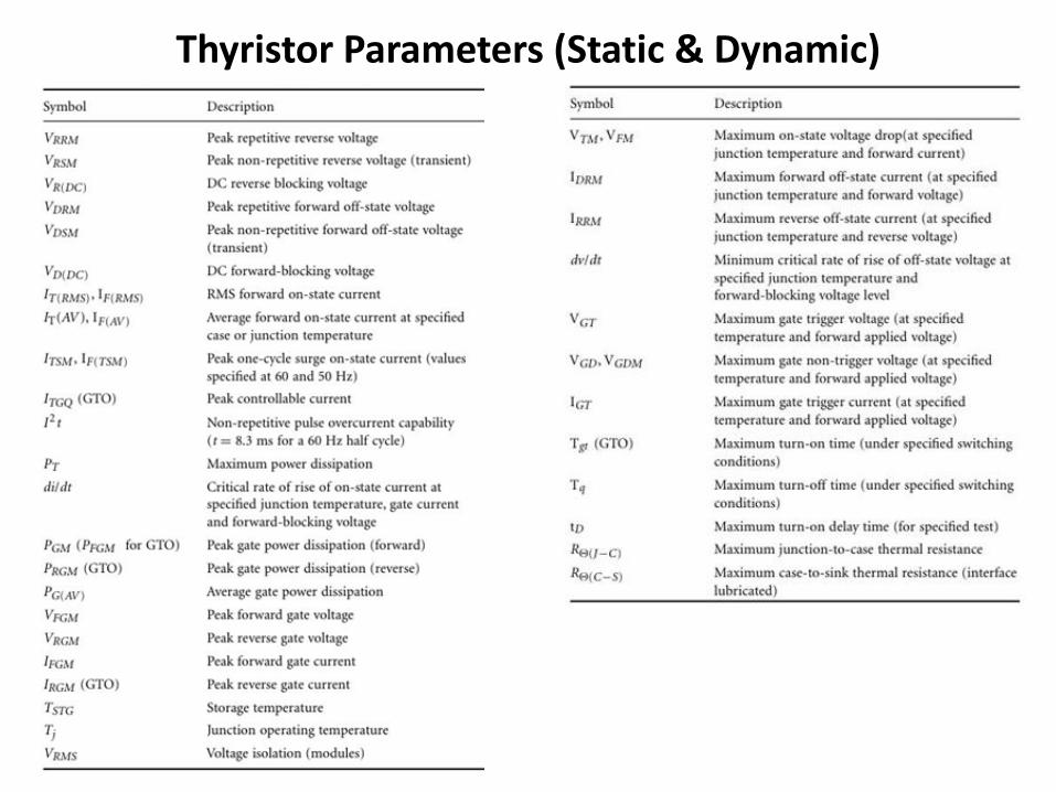
Thyristor Parameters (Static & Dynamic)
Thyristor Protection and Gate Drive Circuits
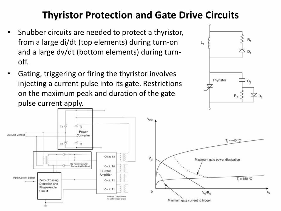
• Snubber circuits are needed to protect a thyristor, from a large di/dt (top elements) during turn-on and a large dv/dt (bottom elements) during turn-off.
• Gating, triggering or firing the thyristor involves injecting a current pulse into its gate. Restrictions on the maximum peak and duration of the gate pulse current apply.
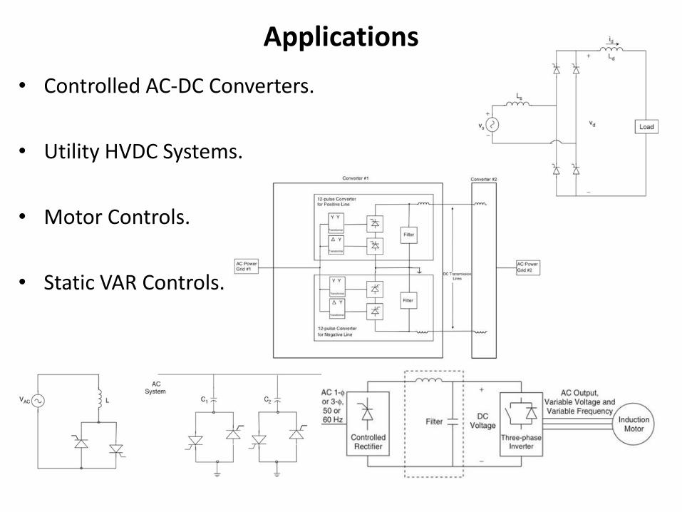
Applications
• Controlled AC-DC Converters.
• Utility HVDC Systems.
• Motor Controls.
• Static VAR Controls.
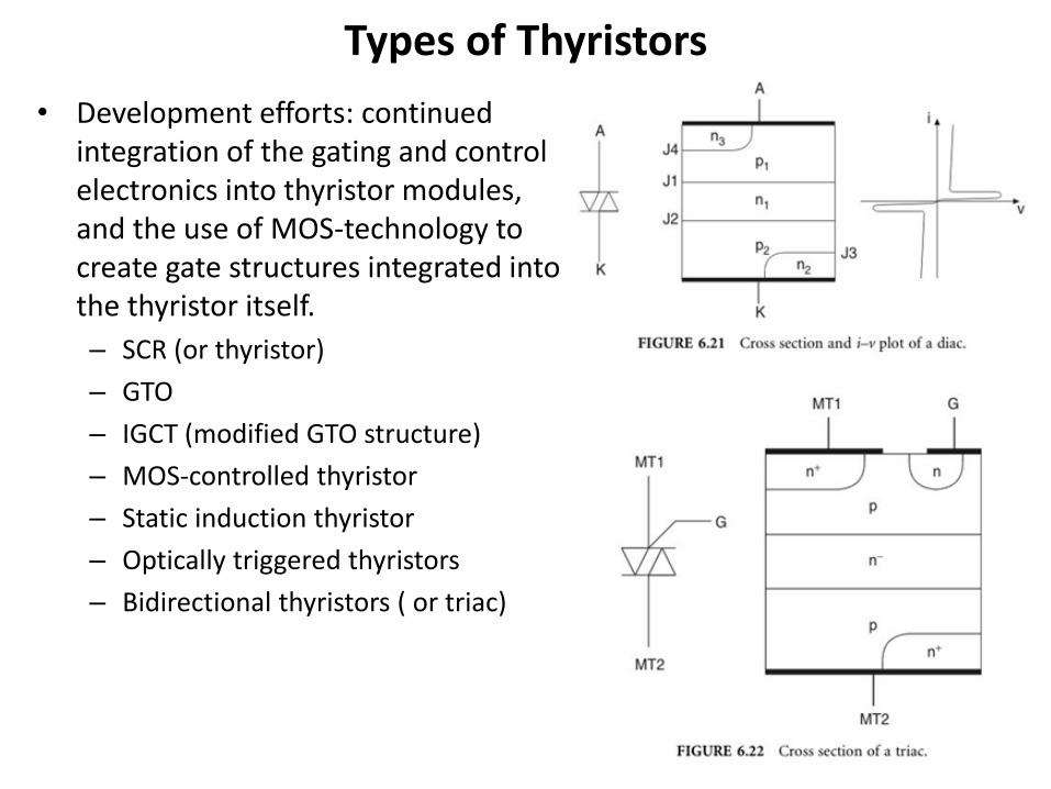
Types of Thyristors
• Development efforts: continued integration of the gating and control electronics into thyristor modules, and the use of MOS-technology to create gate structures integrated into the thyristor itself.
– SCR (or thyristor)
– GTO
– IGCT (modified GTO structure)
– MOS-controlled thyristor
– Static induction thyristor
– Optically triggered thyristors
– Bidirectional thyristors ( or triac)
Triac
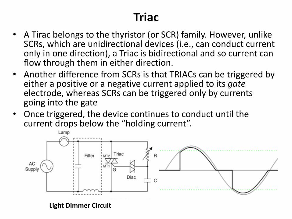
• A Tirac belongs to the thyristor (or SCR) family. However, unlike SCRs, which are unidirectional devices (i.e., can conduct current only in one direction), a Triac is bidirectional and so current can flow through them in either direction.
• Another difference from SCRs is that TRIACs can be triggered by either a positive or a negative current applied to its gate electrode, whereas SCRs can be triggered only by currents going into the gate
• Once triggered, the device continues to conduct until the current drops below the “holding current”.
Light Dimmer Circuit

Assignment 2: Light Dimmer
In the previous slide, the amount of power delivered to the incandescent
light bulb is controlled by adjusting the firing angle through the variable
resistor. Assume the controllable switch is ideal and without filtering, the
lamp resistance is 120 Ohms, and the source voltage is 120 V (rms) with
a frequency of 60 Hz. Determine the following (using any tool you wish)
for a firing angle of 60 degrees.
1. Average (active) power supplied by source P = …………….W
2. RMS value of current = ……………A
3. RMS value of fundamental current = ……………..A
4. Phase angle of fundamental current = ………. deg
5. RMS Value of distortion current = …………………A
6. Apparent power S = …………………..VA
7. Non-active power = …………
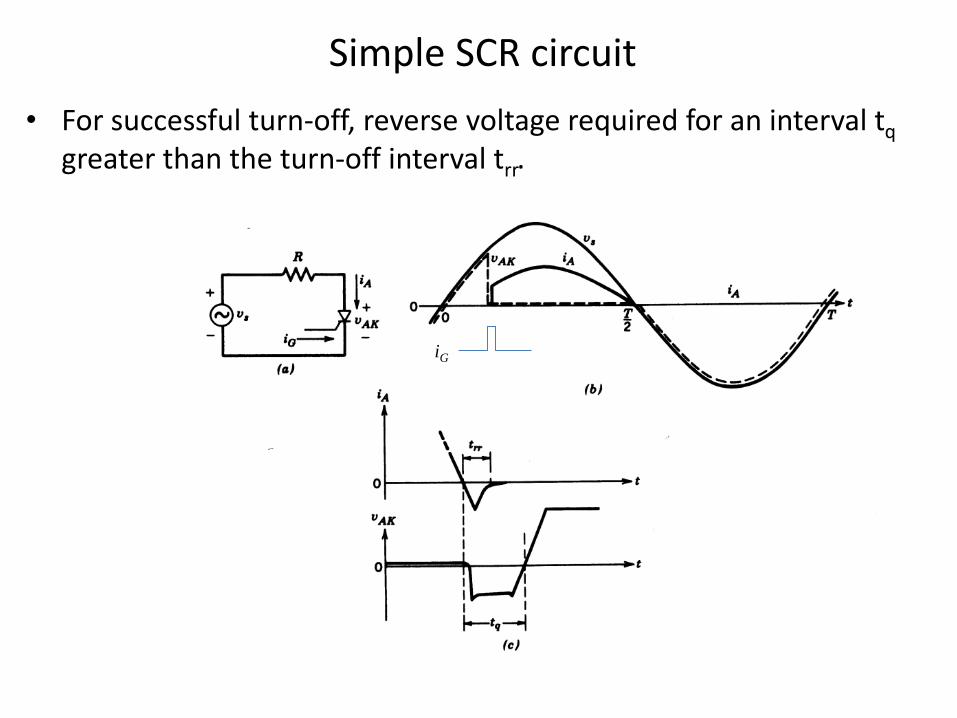
Simple SCR circuit
• For successful turn-off, reverse voltage required for an interval tq greater than the turn-off interval trr.
iG
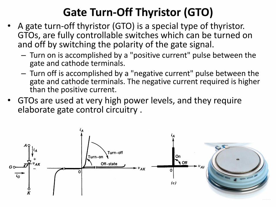
Gate Turn-Off Thyristor (GTO) • A gate turn-off thyristor (GTO) is a special type of thyristor.
GTOs, are fully controllable switches which can be turned on and off by switching the polarity of the gate signal. – Turn on is accomplished by a "positive current" pulse between the
gate and cathode terminals. – Turn off is accomplished by a "negative current" pulse between the
gate and cathode terminals. The negative current required is higher than the positive current.
• GTOs are used at very high power levels, and they require elaborate gate control circuitry .
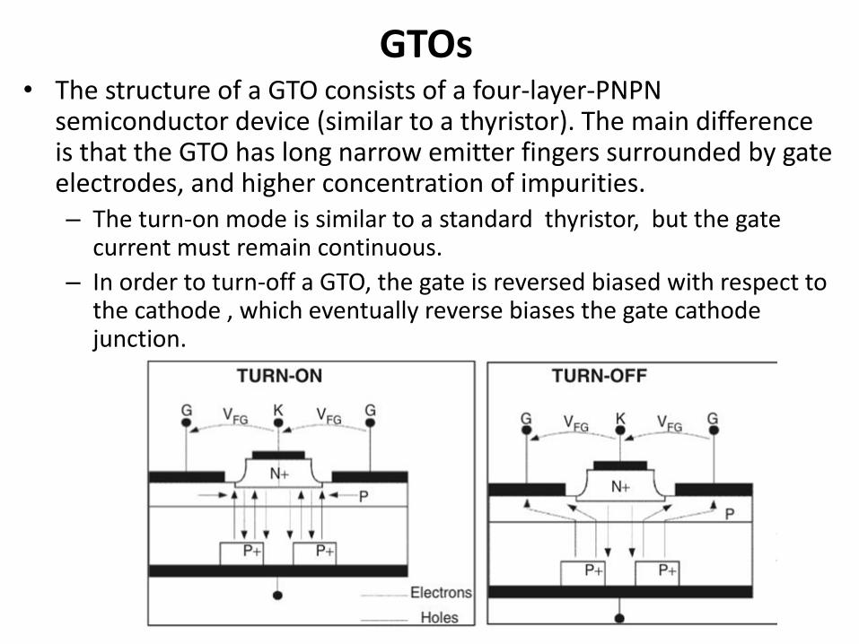
GTOs • The structure of a GTO consists of a four-layer-PNPN
semiconductor device (similar to a thyristor). The main difference is that the GTO has long narrow emitter fingers surrounded by gate electrodes, and higher concentration of impurities. – The turn-on mode is similar to a standard thyristor, but the gate
current must remain continuous.
– In order to turn-off a GTO, the gate is reversed biased with respect to the cathode , which eventually reverse biases the gate cathode junction.
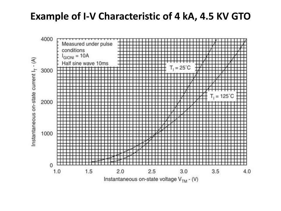
Example of I-V Characteristic of 4 kA, 4.5 KV GTO
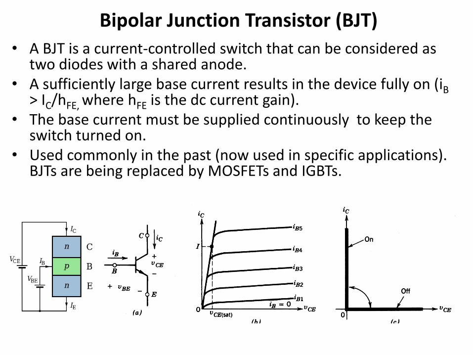
Bipolar Junction Transistor (BJT)
• A BJT is a current-controlled switch that can be considered as two diodes with a shared anode.
• A sufficiently large base current results in the device fully on (iB > IC/hFE, where hFE is the dc current gain).
• The base current must be supplied continuously to keep the switch turned on.
• Used commonly in the past (now used in specific applications). BJTs are being replaced by MOSFETs and IGBTs.
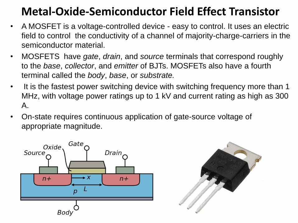
Metal-Oxide-Semiconductor Field Effect Transistor • A MOSFET is a voltage-controlled device - easy to control. It uses an electric
field to control the conductivity of a channel of majority-charge-carriers in the
semiconductor material.
• MOSFETS have gate, drain, and source terminals that correspond roughly
to the base, collector, and emitter of BJTs. MOSFETs also have a fourth
terminal called the body, base, or substrate.
• It is the fastest power switching device with switching frequency more than 1
MHz, with voltage power ratings up to 1 kV and current rating as high as 300
A.
• On-state requires continuous application of gate-source voltage of
appropriate magnitude.
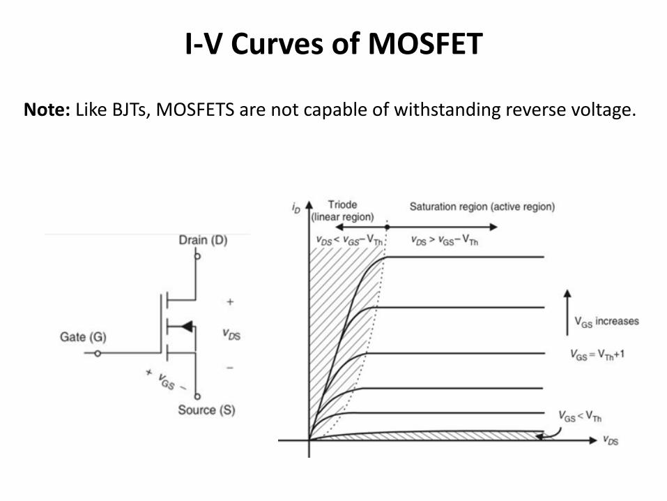
I-V Curves of MOSFET
Note: Like BJTs, MOSFETS are not capable of withstanding reverse voltage.
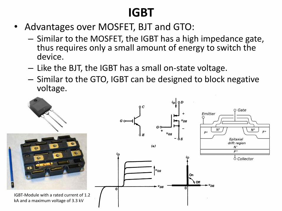
IGBT • Advantages over MOSFET, BJT and GTO:
– Similar to the MOSFET, the IGBT has a high impedance gate, thus requires only a small amount of energy to switch the device.
– Like the BJT, the IGBT has a small on-state voltage. – Similar to the GTO, IGBT can be designed to block negative
voltage.
IGBT-Module with a rated current of 1.2 kA and a maximum voltage of 3.3 kV
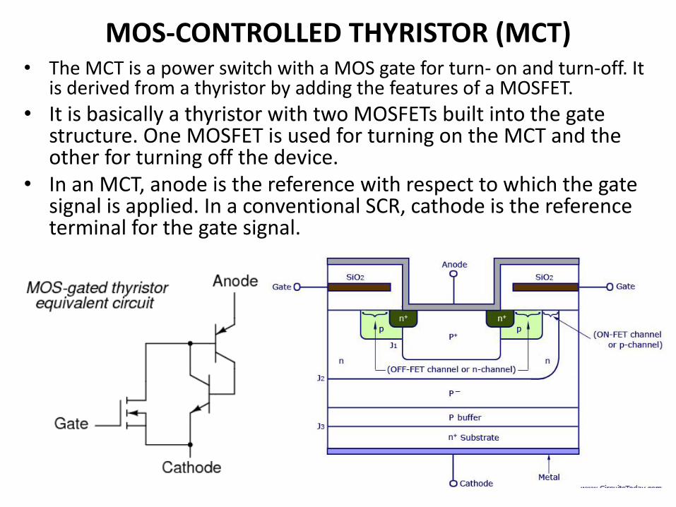
MOS-CONTROLLED THYRISTOR (MCT) • The MCT is a power switch with a MOS gate for turn- on and turn-off. It
is derived from a thyristor by adding the features of a MOSFET.
• It is basically a thyristor with two MOSFETs built into the gate structure. One MOSFET is used for turning on the MCT and the other for turning off the device.
• In an MCT, anode is the reference with respect to which the gate signal is applied. In a conventional SCR, cathode is the reference terminal for the gate signal.
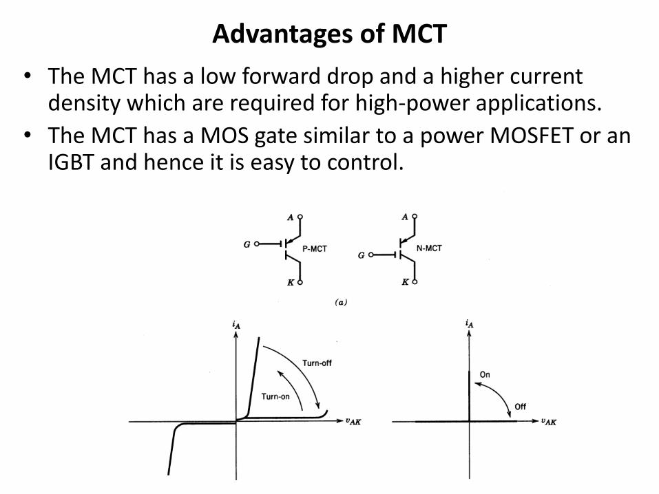
Advantages of MCT
• The MCT has a low forward drop and a higher current density which are required for high-power applications.
• The MCT has a MOS gate similar to a power MOSFET or an IGBT and hence it is easy to control.
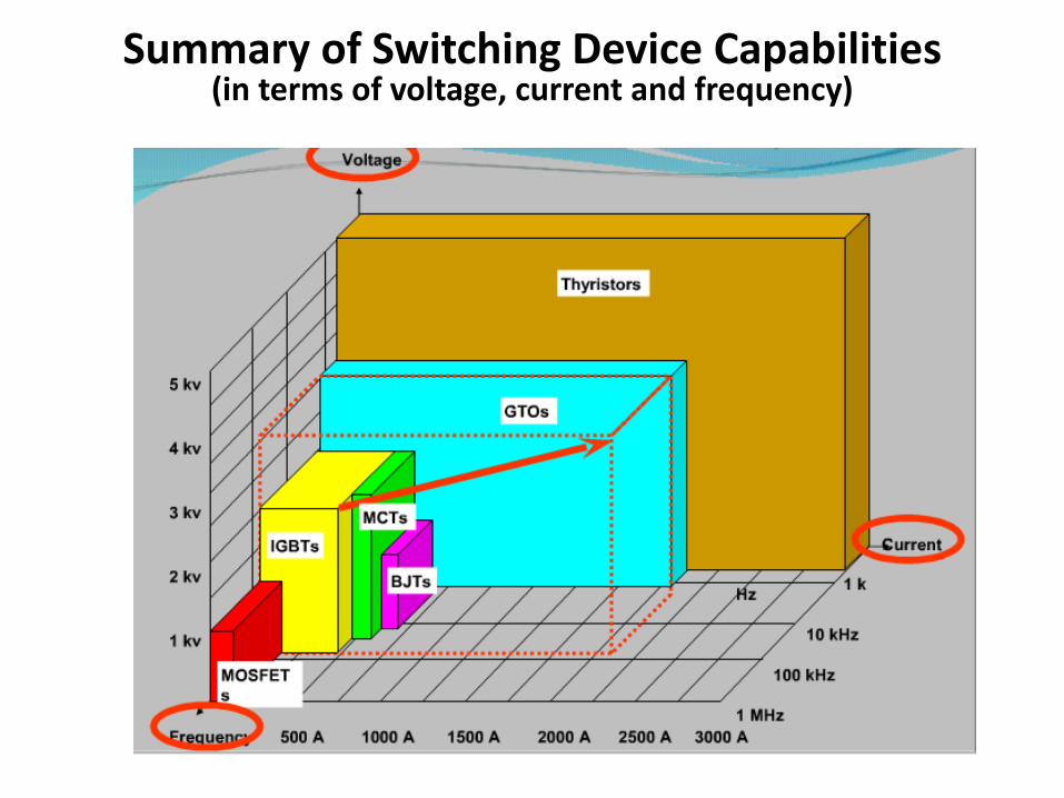
Summary of Switching Device Capabilities (in terms of voltage, current and frequency)
Top Related