


Languages
Pages
Legal

Birck Nanotechnology Center
Plasmonic Photovoltaic
Justus C. Ndukaife, Arthur Teng
Birck Nanotechnology Center
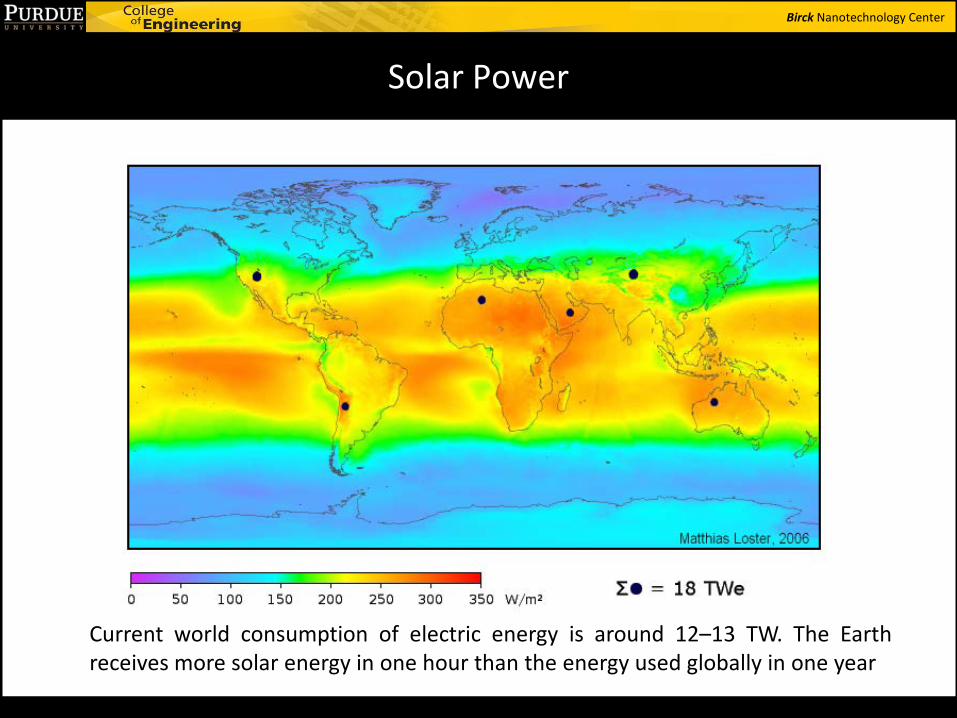
Solar Power
Current world consumption of electric energy is around 12–13 TW. The Earth receives more solar energy in one hour than the energy used globally in one year
Birck Nanotechnology Center
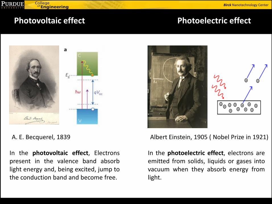
Photovoltaic effect Photoelectric effect
In the photoelectric effect, electrons are emitted from solids, liquids or gases into vacuum when they absorb energy from light.
A. E. Becquerel, 1839 Albert Einstein, 1905 ( Nobel Prize in 1921)
In the photovoltaic effect, Electrons present in the valence band absorb light energy and, being excited, jump to the conduction band and become free.
Birck Nanotechnology Center
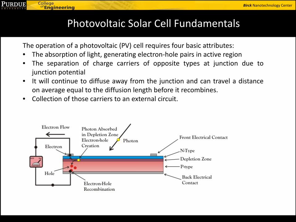
The operation of a photovoltaic (PV) cell requires four basic attributes: • The absorption of light, generating electron-hole pairs in active region • The separation of charge carriers of opposite types at junction due to
junction potential • It will continue to diffuse away from the junction and can travel a distance
on average equal to the diffusion length before it recombines. • Collection of those carriers to an external circuit.
Photovoltaic Solar Cell Fundamentals
Birck Nanotechnology Center
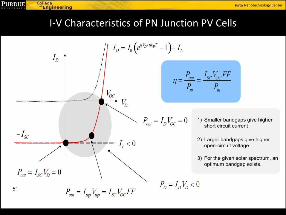
I-V Characteristics of PN Junction PV Cells
Birck Nanotechnology Center
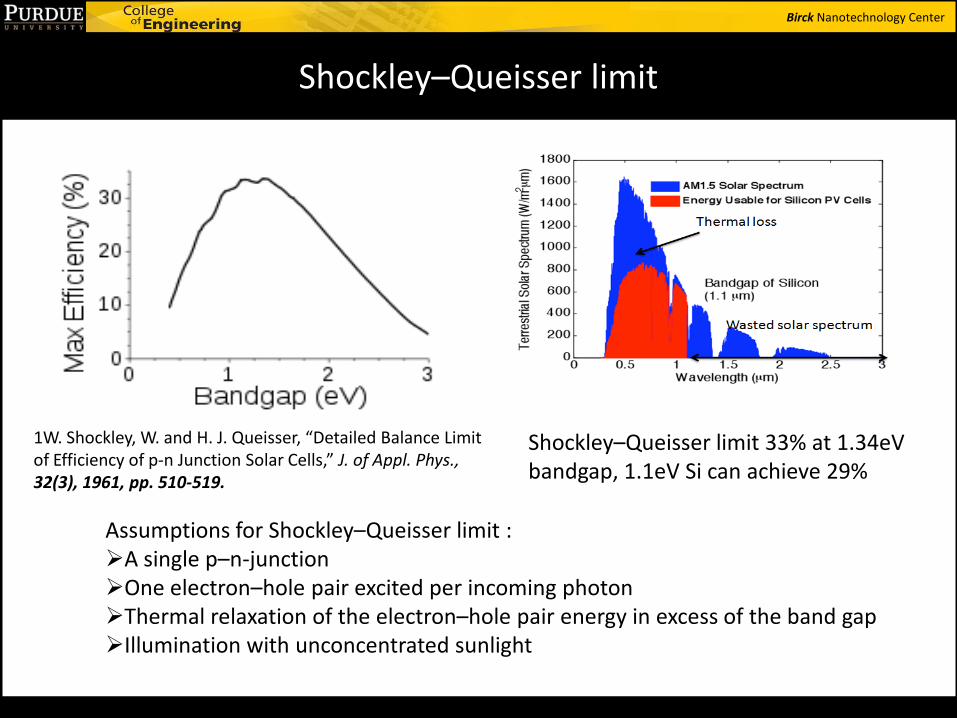
Shockley–Queisser limit
Shockley–Queisser limit 33% at 1.34eV bandgap, 1.1eV Si can achieve 29%
Assumptions for Shockley–Queisser limit : A single p–n-junction One electron–hole pair excited per incoming photon Thermal relaxation of the electron–hole pair energy in excess of the band gap Illumination with unconcentrated sunlight
1W. Shockley, W. and H. J. Queisser, “Detailed Balance Limit of Efficiency of p-n Junction Solar Cells,” J. of Appl. Phys., 32(3), 1961, pp. 510-519.
Birck Nanotechnology Center
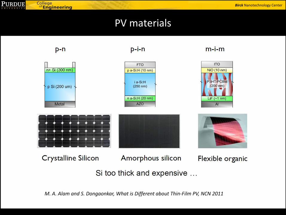
PV materials
M. A. Alam and S. Dongaonkar, What is Different about Thin-Film PV, NCN 2011
Birck Nanotechnology Center
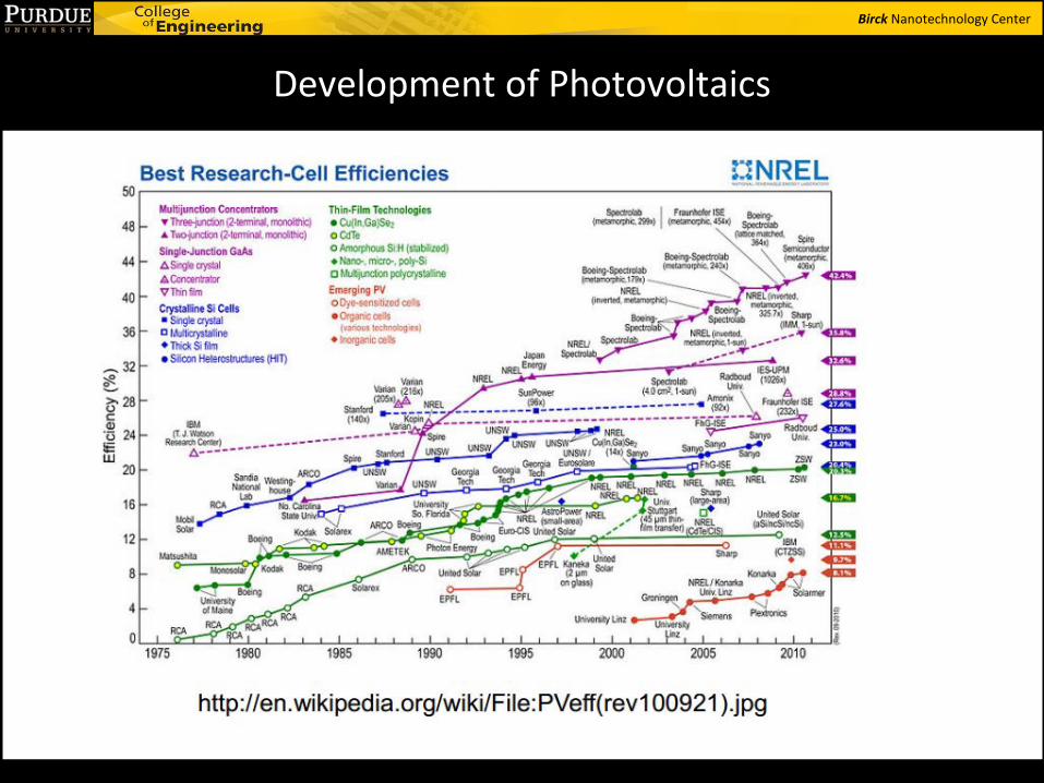
Development of Photovoltaics
Birck Nanotechnology Center
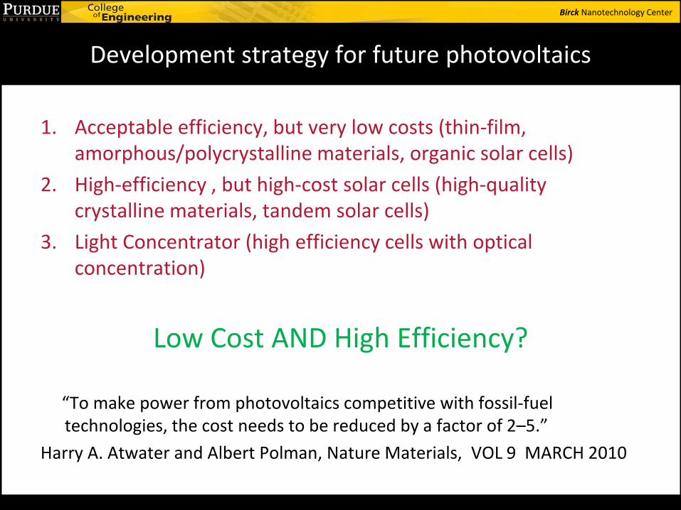
1. Acceptable efficiency, but very low costs (thin-film, amorphous/polycrystalline materials, organic solar cells)
2. High-efficiency , but high-cost solar cells (high-quality crystalline materials, tandem solar cells)
3. Light Concentrator (high efficiency cells with optical concentration)
Low Cost AND High Efficiency? “To make power from photovoltaics competitive with fossil-fuel
technologies, the cost needs to be reduced by a factor of 2–5.”
Harry A. Atwater and Albert Polman, Nature Materials, VOL 9 MARCH 2010
Development strategy for future photovoltaics
Birck Nanotechnology Center
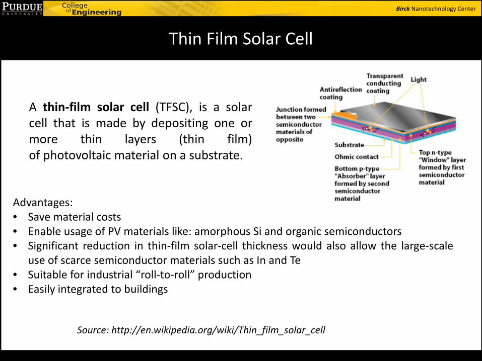
Thin Film Solar Cell
Advantages: • Save material costs • Enable usage of PV materials like: amorphous Si and organic semiconductors • Significant reduction in thin-film solar-cell thickness would also allow the large-scale
use of scarce semiconductor materials such as In and Te • Suitable for industrial “roll-to-roll” production • Easily integrated to buildings
A thin-film solar cell (TFSC), is a solar cell that is made by depositing one or more thin layers (thin film) of photovoltaic material on a substrate.
Source: http://en.wikipedia.org/wiki/Thin_film_solar_cell
Birck Nanotechnology Center
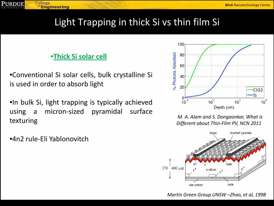
Light Trapping in thick Si vs thin film Si
•Thick Si solar cell
•Conventional Si solar cells, bulk crystalline Si is used in order to absorb light •In bulk Si, light trapping is typically achieved using a micron-sized pyramidal surface texturing
•4n2 rule-Eli Yablonovitch
Martin Green Group UNSW –Zhao, et al, 1998
M. A. Alam and S. Dongaonkar, What is Different about Thin-Film PV, NCN 2011

Birck Nanotechnology Center
•Absorption coefficient is smaller for long wavelength hence requires longer propagation length before being absorbed
•Thin film cannot absorb red light efficiently
•In thin film Si (only few um thick), light trapping requires alterative methods
•Texturing surface of thins films increases surface recombination
Beer–Lambert law
Light Trapping in thick Si vs thin film Si

Birck Nanotechnology Center
Light Trapping with Nano-plasmonic Structures
Birck Nanotechnology Center
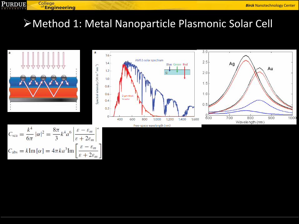
Method 1: Metal Nanoparticle Plasmonic Solar Cell
Total scattering cross section (black lines), cross-section for light scattered into the substrate (red lines), and absorption cross-section (blue lines), all normalized to geometrical cross section, for 100 nm diameter hemispherical particles of Ag (solid lines) and Au (dashed lines)
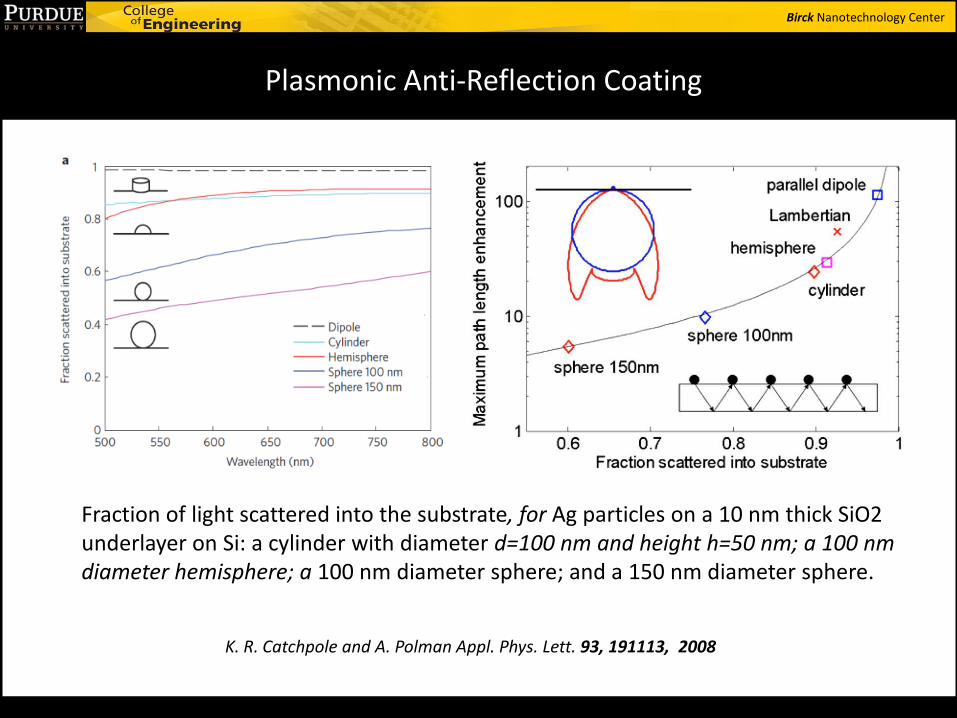
K. R. Catchpole and A. Polman Appl. Phys. Lett. 93, 191113, 2008
MAIER, S. A. (2007). PLASMONICS: FUNDAMENTALS AND APPLICATIONS. Springer. p70
Birck Nanotechnology Center
K. R. Catchpole and A. Polman Appl. Phys. Lett. 93, 191113, 2008
Plasmonic Anti-Reflection Coating
Fraction of light scattered into the substrate, for Ag particles on a 10 nm thick SiO2 underlayer on Si: a cylinder with diameter d=100 nm and height h=50 nm; a 100 nm diameter hemisphere; a 100 nm diameter sphere; and a 150 nm diameter sphere.
Birck Nanotechnology Center
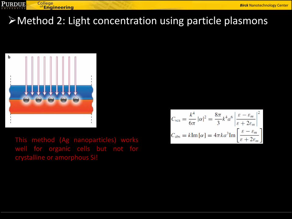
Method 2: Light concentration using particle plasmons
This works particularly well for small (below 50nm diameters) particles since absorption cross-section becomes much larger than scattering cross-section. NP works like optical antennas!
MAIER, S. A. (2007). PLASMONICS: FUNDAMENTALS AND APPLICATIONS. Springer. p70
P. Spinelli and A. Polman, 2012 / Vol. 20, No. S5 / OPTICS EXPRESS
This method (Ag nanoparticles) works well for organic cells but not for crystalline or amorphous Si!
Birck Nanotechnology Center
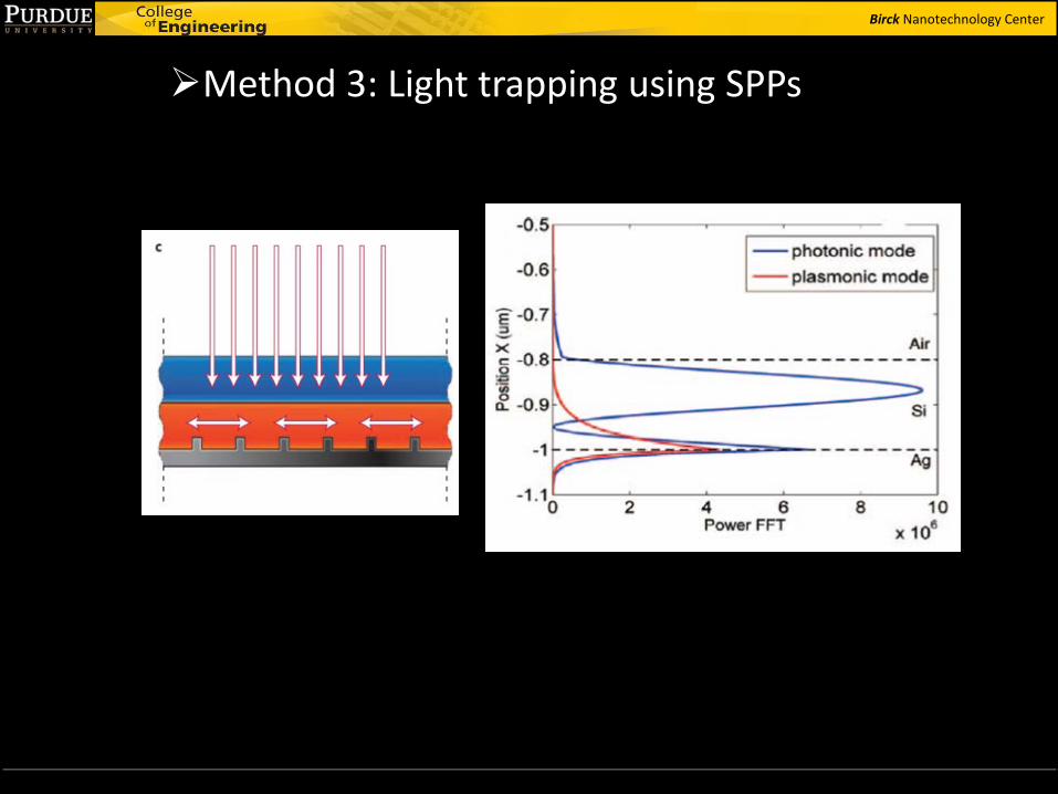
Method 3: Light trapping using SPPs
Vivian E. Ferry, Luke A. Sweatlock, Domenico Pacifici, and Harry A. Atwater, NANO LETTERS 2008 Vol. 8, No. 12 4391-4397

Birck Nanotechnology Center
Photon Management for High Efficiency Solar Cells: Improving efficiency beyond the SQ limit

Birck Nanotechnology Center
Cost reduction target
Birck Nanotechnology Center
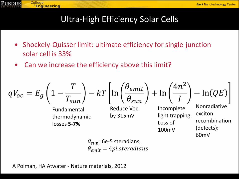
Ultra-High Efficiency Solar Cells
• Shockely-Quisser limit: ultimate efficiency for single-junction solar cell is 33%
• Can we increase the efficiency above this limit?
Reduce Voc by 315mV
Incomplete light trapping: Loss of 100mV
Nonradiative exciton recombination (defects): 60mV
Fundamental thermodynamic losses 5-7%
A Polman, HA Atwater - Nature materials, 2012
Birck Nanotechnology Center
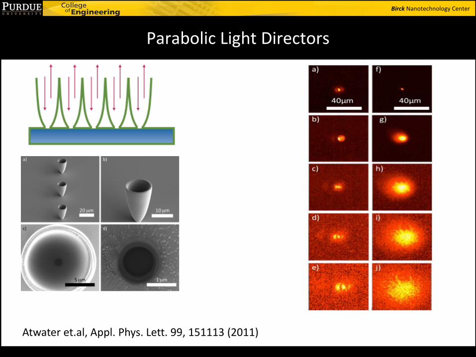
Parabolic Light Directors
Atwater et.al, Appl. Phys. Lett. 99, 151113 (2011)
Birck Nanotechnology Center
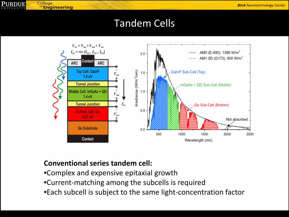
Tandem Cells
Conventional series tandem cell: •Complex and expensive epitaxial growth •Current-matching among the subcells is required •Each subcell is subject to the same light-concentration factor
Birck Nanotechnology Center
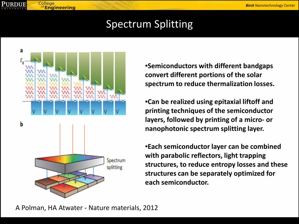
Spectrum Splitting
A Polman, HA Atwater - Nature materials, 2012
•Semiconductors with different bandgaps convert different portions of the solar spectrum to reduce thermalization losses.
•Can be realized using epitaxial liftoff and printing techniques of the semiconductor layers, followed by printing of a micro- or nanophotonic spectrum splitting layer.
•Each semiconductor layer can be combined with parabolic reflectors, light trapping structures, to reduce entropy losses and these structures can be separately optimized for each semiconductor.
Birck Nanotechnology Center
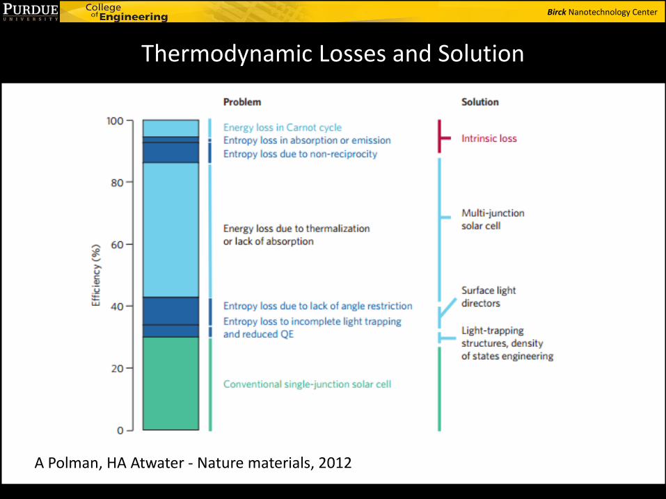
Thermodynamic Losses and Solution
A Polman, HA Atwater - Nature materials, 2012
Birck Nanotechnology Center
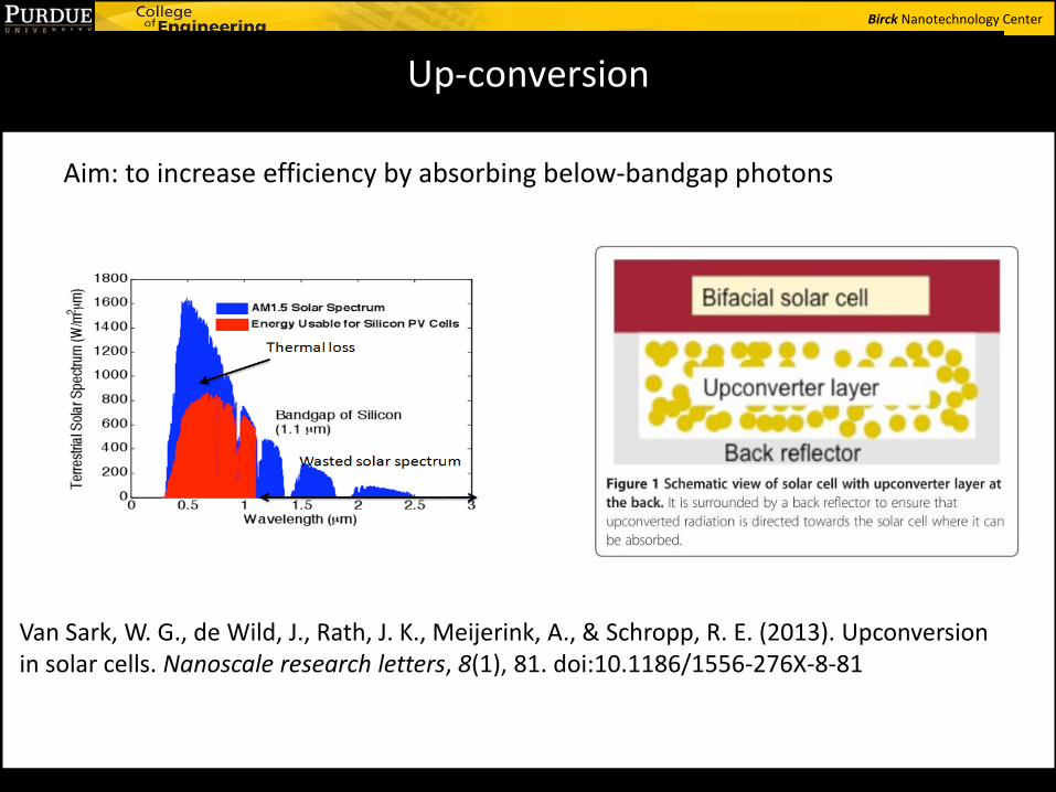
Up-conversion
Van Sark, W. G., de Wild, J., Rath, J. K., Meijerink, A., & Schropp, R. E. (2013). Upconversion in solar cells. Nanoscale research letters, 8(1), 81. doi:10.1186/1556-276X-8-81
Aim: to increase efficiency by absorbing below-bandgap photons
Birck Nanotechnology Center
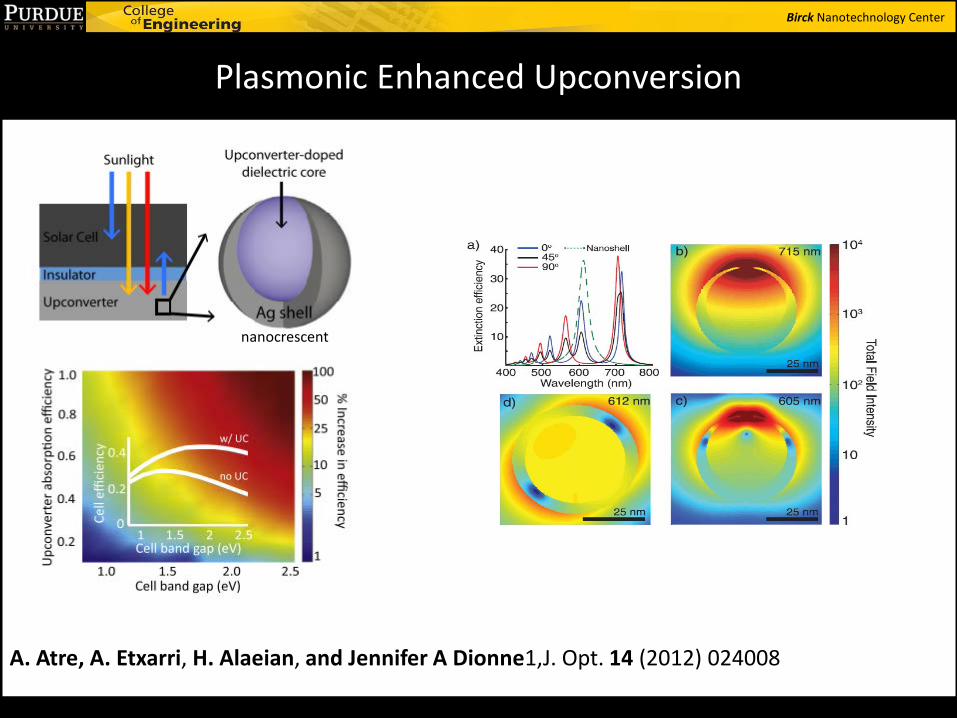
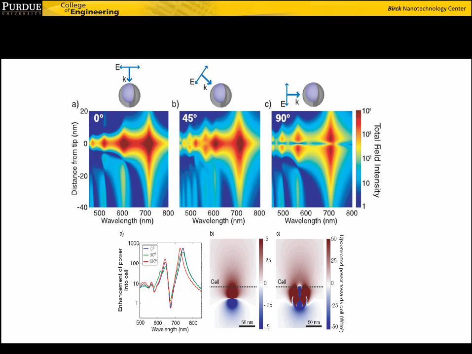
Plasmonic Enhanced Upconversion
A. Atre, A. Etxarri, H. Alaeian, and Jennifer A Dionne1,J. Opt. 14 (2012) 024008
nanocrescent
Birck Nanotechnology Center

Birck Nanotechnology Center
Is Thin film Photovoltaics the answer?
M. A. Alam and S. Dongaonkar, What is Different about Thin-Film PV, NCN 2011
Source -www.nrel.gov/pv/performance_reliability/pdfs/failure_references.pdf
Reliability is also very important!
Birck Nanotechnology Center
Summary
PN junction solar cell fundamentals Thin film solar cell
Plasmonic enhanced light trapping
Photon Management
Plasmonic enhanced Upconversion
Thin film cells reliability issues
Top Related