


Languages
Pages
Legal

PIC32MZ EMBEDDEDCONNECTIVITY (EC)
PIC32MZ Embedded Connectivity (EC) Family Silicon Errata and Data Sheet Clarification
The PIC32MZ Embedded Connectivity (EC) family ofdevices that you have received conform functionally tothe current Device Data Sheet (DS60001191G), exceptfor the anomalies described in this document.
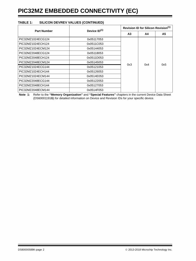
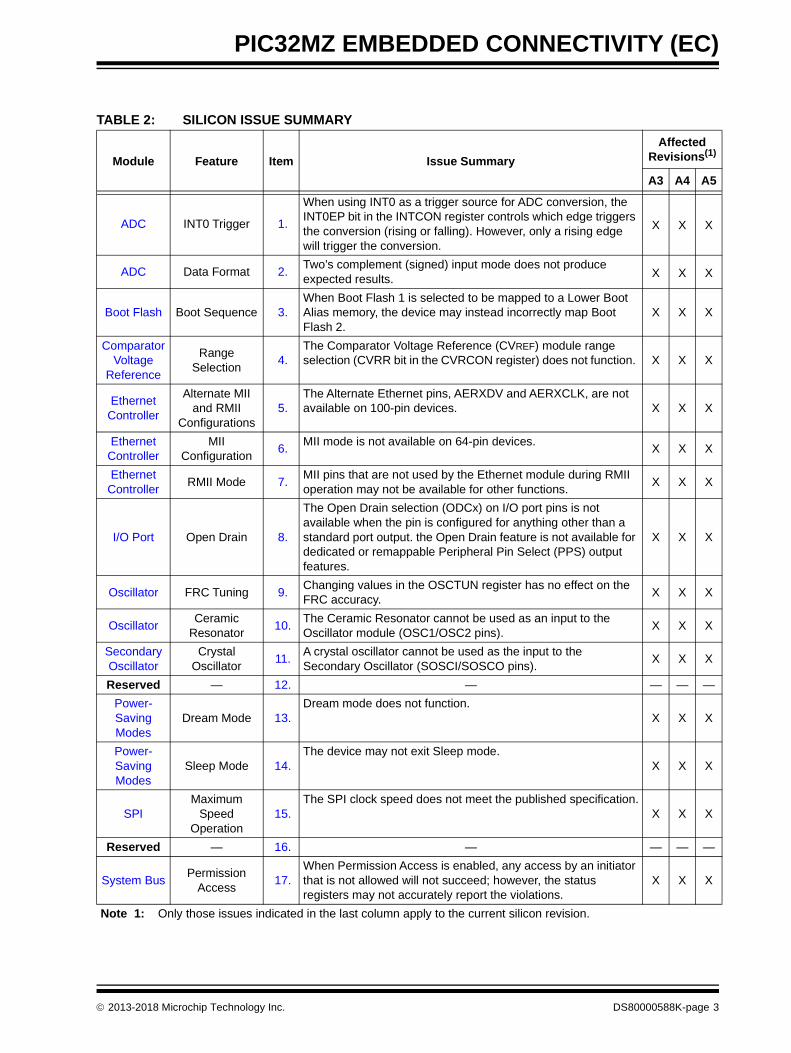
The silicon issues discussed in the following pages arefor silicon revisions with the Device and Revision IDslisted in Table 1. The silicon issues are summarized inTable 2.
The errata described in this document will be addressedin future revisions of the PIC32MZ EmbeddedConnectivity (EC) family silicon.
Data Sheet clarifications and corrections (if applicable)start on page 19, following the discussion of siliconissues.
The silicon revision level can be identified using thecurrent version of MPLAB® X IDE and Microchip’sprogrammers, debuggers and emulation tools, whichare available at the Microchip corporate web sitewww.microchip.com.
For example, to identify the silicon revision levelusing MPLAB X IDE in conjunction with a hardwaredebugger, follow these steps:
1. Using the appropriate interface, connect thedevice to the hardware debugger.
2. Open an MPLAB X IDE project.3. Configure the MPLAB X IDE project for the
appropriate device and hardware debugger.4. Select Window > Dashboard, and then click
the Refresh Debug Tool Status icon( ).
5. The part number, and the Device andRevision ID values appear in the Outputwindow.
The Device and Revision ID values for the variousPIC32MZ Embedded Connectivity (EC) family siliconrevisions are shown in Table 1.
Note: This document summarizes all siliconerrata issues from all revisions of silicon,previous as well as current. Only theissues indicated in the last column ofTable 2 apply to the current siliconrevision (A5).
Note: If you are unable to extract the siliconrevision level, please contact your localMicrochip sales office for assistance.
TABLE 1: SILICON DEVREV VALUES
Part Number Device ID(1)Revision ID for Silicon Revision(1)
A3 A4 A5
PIC32MZ1024ECG064 0x05103053
0x3 0x4 0x5
PIC32MZ1024ECH064 0x05108053
PIC32MZ1024ECM064 0x05130053
PIC32MZ2048ECG064 0x05104053
PIC32MZ2048ECH064 0x05109053
PIC32MZ2048ECM064 0x05131053
PIC32MZ1024ECG100 0x0510D053
PIC32MZ1024ECH100 0x05112053
PIC32MZ1024ECM100 0x0513A053
PIC32MZ2048ECG100 0x0510E053
PIC32MZ2048ECH100 0x05113053
PIC32MZ2048ECM100 0x0513B053
Note 1: Refer to the “Memory Organization” and “Special Features” chapters in the current Device Data Sheet (DS60001191G) for detailed information on Device and Revision IDs for your specific device.
2013-2018 Microchip Technology Inc. DS80000588K-page 1
PIC32MZ EMBEDDED CONNECTIVITY (EC)
PIC32MZ1024ECG124 0x05117053
0x3 0x4 0x5
PIC32MZ1024ECH124 0x0511C053
PIC32MZ1024ECM124 0x05144053
PIC32MZ2048ECG124 0x05118053
PIC32MZ2048ECH124 0x0511D053
PIC32MZ2048ECM124 0x05145053
PIC32MZ1024ECG144 0x05121053
PIC32MZ1024ECH144 0x05126053
PIC32MZ1024ECM144 0x0514E053
PIC32MZ2048ECG144 0x05122053
PIC32MZ2048ECH144 0x05127053
PIC32MZ2048ECM144 0x0514F053
TABLE 1: SILICON DEVREV VALUES (CONTINUED)
Part Number Device ID(1)Revision ID for Silicon Revision(1)
A3 A4 A5
Note 1: Refer to the “Memory Organization” and “Special Features” chapters in the current Device Data Sheet (DS60001191G) for detailed information on Device and Revision IDs for your specific device.
DS80000588K-page 2 2013-2018 Microchip Technology Inc.
PIC32MZ EMBEDDED CONNECTIVITY (EC)
TABLE 2: SILICON ISSUE SUMMARY
Module Feature Item Issue Summary
Affected Revisions(1)
A3 A4 A5
ADC INT0 Trigger 1.
When using INT0 as a trigger source for ADC conversion, the INT0EP bit in the INTCON register controls which edge triggers the conversion (rising or falling). However, only a rising edge will trigger the conversion.
X X X
ADC Data Format 2.Two’s complement (signed) input mode does not produce expected results. X X X
Boot Flash Boot Sequence 3.When Boot Flash 1 is selected to be mapped to a Lower Boot Alias memory, the device may instead incorrectly map Boot Flash 2.
X X X
Comparator Voltage
Reference
Range Selection
4.The Comparator Voltage Reference (CVREF) module range selection (CVRR bit in the CVRCON register) does not function. X X X
Ethernet Controller
Alternate MII and RMII
Configurations5.
The Alternate Ethernet pins, AERXDV and AERXCLK, are not available on 100-pin devices. X X X
Ethernet Controller
MII Configuration
6.MII mode is not available on 64-pin devices.
X X X
Ethernet Controller
RMII Mode 7.MII pins that are not used by the Ethernet module during RMII operation may not be available for other functions.
X X X
I/O Port Open Drain 8.
The Open Drain selection (ODCx) on I/O port pins is not available when the pin is configured for anything other than a standard port output. the Open Drain feature is not available for dedicated or remappable Peripheral Pin Select (PPS) output features.
X X X
Oscillator FRC Tuning 9.Changing values in the OSCTUN register has no effect on the FRC accuracy.
X X X
OscillatorCeramic
Resonator10.
The Ceramic Resonator cannot be used as an input to the Oscillator module (OSC1/OSC2 pins).
X X X
Secondary Oscillator
Crystal Oscillator
11.A crystal oscillator cannot be used as the input to the Secondary Oscillator (SOSCI/SOSCO pins).
X X X
Reserved — 12. — — — —
Power-Saving Modes
Dream Mode 13.Dream mode does not function.
X X X
Power-Saving Modes
Sleep Mode 14.The device may not exit Sleep mode.
X X X
SPIMaximum
Speed Operation
15.The SPI clock speed does not meet the published specification.
X X X
Reserved — 16. — — — —
System BusPermission
Access17.
When Permission Access is enabled, any access by an initiator that is not allowed will not succeed; however, the status registers may not accurately report the violations.
X X X
Note 1: Only those issues indicated in the last column apply to the current silicon revision.
2013-2018 Microchip Technology Inc. DS80000588K-page 3
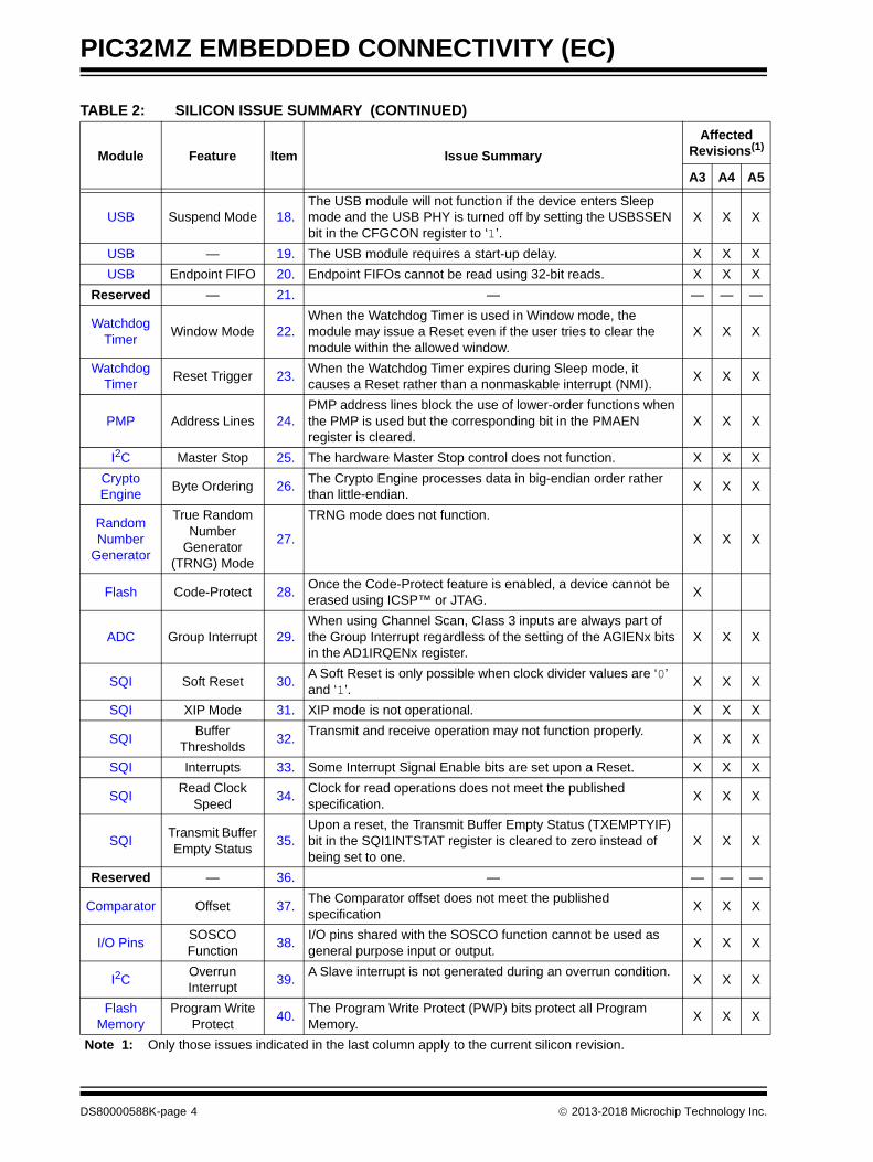
PIC32MZ EMBEDDED CONNECTIVITY (EC)
USB Suspend Mode 18.The USB module will not function if the device enters Sleep mode and the USB PHY is turned off by setting the USBSSEN bit in the CFGCON register to ‘1’.
X X X
USB — 19. The USB module requires a start-up delay. X X X
USB Endpoint FIFO 20. Endpoint FIFOs cannot be read using 32-bit reads. X X X
Reserved — 21. — — — —
Watchdog Timer
Window Mode 22.When the Watchdog Timer is used in Window mode, the module may issue a Reset even if the user tries to clear the module within the allowed window.
X X X
Watchdog Timer
Reset Trigger 23.When the Watchdog Timer expires during Sleep mode, it causes a Reset rather than a nonmaskable interrupt (NMI).
X X X
PMP Address Lines 24.PMP address lines block the use of lower-order functions when the PMP is used but the corresponding bit in the PMAEN register is cleared.
X X X
I2C Master Stop 25. The hardware Master Stop control does not function. X X X
Crypto Engine
Byte Ordering 26.The Crypto Engine processes data in big-endian order rather than little-endian.
X X X
Random Number
Generator
True Random Number
Generator (TRNG) Mode
27.
TRNG mode does not function.
X X X
Flash Code-Protect 28.Once the Code-Protect feature is enabled, a device cannot be erased using ICSP™ or JTAG.
X
ADC Group Interrupt 29.When using Channel Scan, Class 3 inputs are always part of the Group Interrupt regardless of the setting of the AGIENx bits in the AD1IRQENx register.
X X X
SQI Soft Reset 30.A Soft Reset is only possible when clock divider values are ‘0’ and ‘1’.
X X X
SQI XIP Mode 31. XIP mode is not operational. X X X
SQIBuffer
Thresholds32.
Transmit and receive operation may not function properly.X X X
SQI Interrupts 33. Some Interrupt Signal Enable bits are set upon a Reset. X X X
SQIRead Clock
Speed34.
Clock for read operations does not meet the published specification.
X X X
SQITransmit Buffer Empty Status
35.Upon a reset, the Transmit Buffer Empty Status (TXEMPTYIF) bit in the SQI1INTSTAT register is cleared to zero instead of being set to one.
X X X
Reserved — 36. — — — —
Comparator Offset 37.The Comparator offset does not meet the published specification
X X X
I/O PinsSOSCO Function
38.I/O pins shared with the SOSCO function cannot be used as general purpose input or output.
X X X
I2COverrun Interrupt
39.A Slave interrupt is not generated during an overrun condition.
X X X
Flash Memory
Program Write Protect
40.The Program Write Protect (PWP) bits protect all Program Memory.
X X X
TABLE 2: SILICON ISSUE SUMMARY (CONTINUED)
Module Feature Item Issue Summary
Affected Revisions(1)
A3 A4 A5
Note 1: Only those issues indicated in the last column apply to the current silicon revision.
DS80000588K-page 4 2013-2018 Microchip Technology Inc.

PIC32MZ EMBEDDED CONNECTIVITY (EC)
Oscillator POSC 41.A crystal oscillator cannot be used as an input to the Primary Oscillator (OSC1/OSC2 pins).
X X
5V Tolerant I/O Pins
Pull-ups 42.Internal pull-up resistors may not guarantee a logical ‘1’ on digital inputs on 5V tolerant pins.
X X X
ADC — 43. Certain ADC operating modes are not supported. X X X
ADC — 44. The ADC module does not meet published specifications. X X X
Prefetch Module Disable 45. Disabling the Prefetch does not invalidate contents. X X X
Oscillator Clock Switch 46.Switching the System Clock (SYSCLK) to the Secondary PLL (SPLL) causes a device Reset. This affects both software and hardware (IESO) clock switching.
X X X
DMA Interrupt Trigger 47.A UART6 Transfer Done interrupt cannot be used to trigger DMA activity.
X X X
UART Auto-baud 48.The Automatic Baud Rate feature does not function to set the baud rate.
X X X
Reserved — 49. — — — —
Oscillator POSC Crystal 50.Crystal support for the Primary Oscillator does not meet published specifications for frequency and voltage.
X X X
Reserved — 51. — — — —
I2C SDA Hold Time 52.Lengthening the SDA hold time causes bus collisions in 1 MHz mode.
X X X
System BusSimultaneous
Access53.
CAN data may become corrupted during simultaneous operation.
X X X
Reserved — 54. — — — —
OscillatorReference
Clock55.
The Reference Clock cannot use input frequencies greater than 100 MHz.
X X X
UART Synchronization 56.On a RX FIFO overflow, shift registers stop receiving data, which causes the UART to lose synchronization.
X X X
Timer1 Prescaler 57.Timer1 will not generate interrupts with an external asynchronous clock input and prescaler other than 1:1.
X X X
PMP Read 58.A PMP read does not generate an interrupt when the WAITE bit = 0.
X X X
PMP Wait Cycle 59.The pulse width of WAITE is ‘0’ when the WAITM<3:0> bits = 0000.
X X X
Reserved — 60. — — — —
Watchdog Timer
Clearing 61.Clearing the Watchdog Timer does not function as specified in the data sheet.
X X X
Flash Panel Swap 62.The NVMKEY unlock sequence is not required to change the Flash panel order.
X X X
Resets SWNMI bit 63.The software nonmaskable interrupt (NMI) feature does not function.
X X X
Crypto Engine
Partial Packet 64.The Crypto engine does not support partial packet processing.
X X X
Crypto Engine
Zero Length Packet
65.Zero length packet fails to process as the Crypto engine does not support an empty string hash.
X X X
TABLE 2: SILICON ISSUE SUMMARY (CONTINUED)
Module Feature Item Issue Summary
Affected Revisions(1)
A3 A4 A5
Note 1: Only those issues indicated in the last column apply to the current silicon revision.
2013-2018 Microchip Technology Inc. DS80000588K-page 5

PIC32MZ EMBEDDED CONNECTIVITY (EC)
Silicon Errata Issues
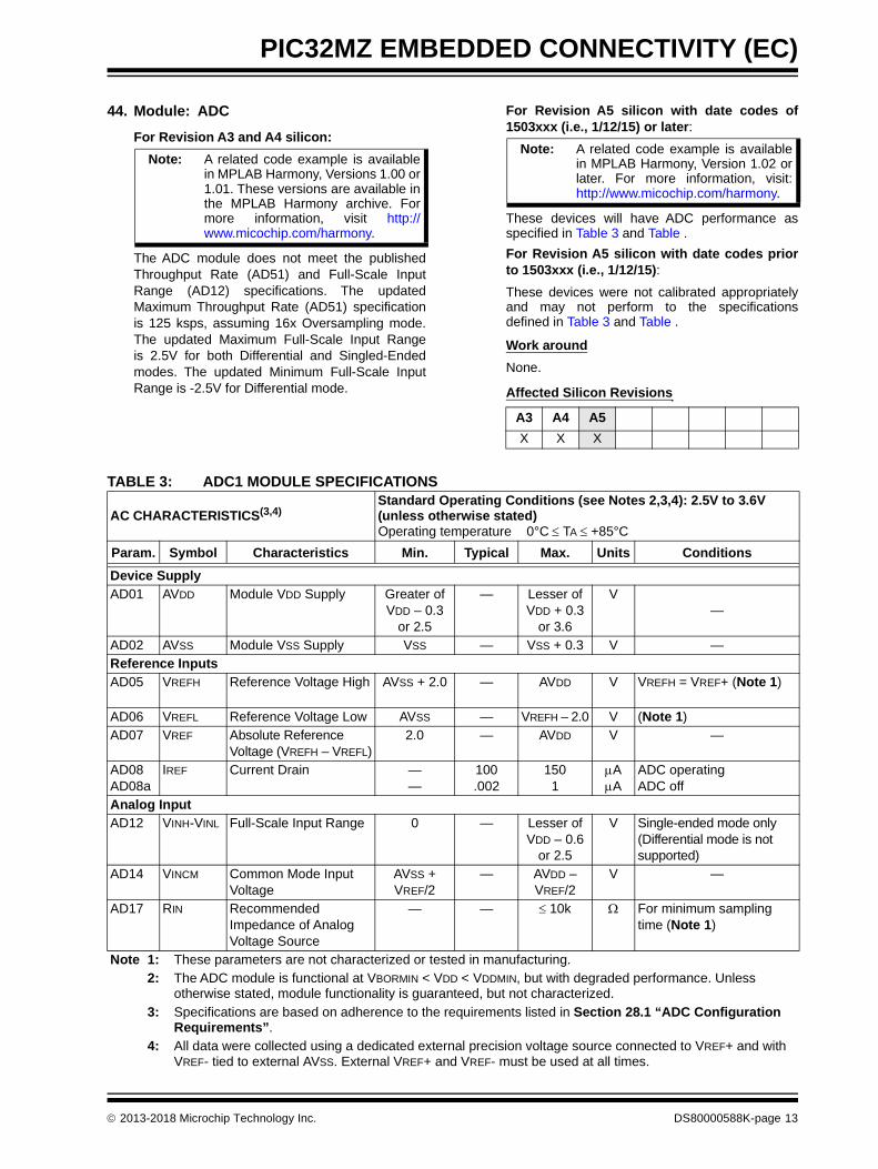
1. Module: ADC
When using INT0 as a trigger source for ADCconversion, the INT0EP bit in the INTCON registercontrols which edge triggers the conversion (risingor falling). However, only a rising edge will triggerthe conversion.
Work around
None.
Affected Silicon Revisions
2. Module: ADC
Two’s complement (signed) input mode does notproduce the expected results. Signed modeselections are SHxMOD<1:0> = 01 for single-ended or SHxMOD<1:0> = 11 for differentialinputs.
Work arounds:
Work around 1
Use two's complement format for all inputs. TheTwo's complement format works properly when allsample and holds are set for this format. Single-ended or Differential mode can still be selectedindependently. Use any one of the followingsettings for SH0MOD through SH5MOD:
• SHxMOD<1:0> = 01 for signed single-ended
• SHxMOD<1:0> = 11 for signed differential inputs
Work around 2
Use unipolar (unsigned) mode selections for allsample and holds. Where needed, convert theunsigned results to signed values. Unsigned 12-bitresults can be converted to signed values bysubtracting 2048 from the signed result. Use anyone of the following settings for SH0MOD throughSH5MOD:
• SHxMOD<1:0> = 00 for unsigned single-ended
• SHxMOD<1:0> = 10 for unsigned differential inputs
Affected Silicon Revisions
3. Module: Boot Flash
When Boot Flash 1 is selected to be mapped to aLower Boot Alias memory, the device may insteadincorrectly map Boot Flash 2.
Work around
Program an invalid sequence number, such as0xFFFFFFFF or 0x00000000 into Boot Flash 2.This will force the device to map Boot Flash 1 intothe Lower Boot Alias memory.
Affected Silicon Revisions
4. Module: Comparator Voltage Reference
The Comparator Voltage Reference (CVREF)module range selection (CVRR bit in the CVRCONregister) does not function. The default setting ofthe CVREF Range Selection bit (CVRR) is set to0 to 0.67 CVRSRC, with a step size of CVRSRC/24,and cannot be changed.
Work around
Use an External Voltage Reference and adjust itappropriately to achieve the desired CVREF output.
Affected Silicon Revisions
Note: This document summarizes all siliconerrata issues from all revisions of silicon,previous as well as current. Only theissues indicated by the shaded column inthe following tables apply to the currentsilicon revision (A5).
A3 A4 A5
X X X
A3 A4 A5
X X X
A3 A4 A5
X X X
A3 A4 A5
X X X
DS80000588K-page 6 2013-2018 Microchip Technology Inc.

PIC32MZ EMBEDDED CONNECTIVITY (EC)
5. Module: Ethernet Controller
The Alternate Ethernet pins, AERXDV andAERXCLK, are not available on 100-pin devices.
Work around
Only use either the MII or RMII configuration.
Affected Silicon Revisions
6. Module: Ethernet Controller
MII mode is not available on 64-pin devices. In thismode, the Ethernet pin ERXD2, is not available.
Work around
Use the RMII or Alternate RMII configurations.
Affected Silicon Revisions
7. Module: Ethernet Controller
MII pins that are not used by the Ethernet moduleduring RMII operation are not released, andtherefore, lower priority functions on these pins arenot available in this mode. However, higher priorityfunctions on these pins, such as EBI and analoginputs (for ADC and Comparators), can still beused.
Work around
None.
Affected Silicon Revisions
8. Module: I/O Port
The Open Drain selection (ODCx) on I/O port pinsis not available when the pin is configured foranything other than a standard port output. theOpen Drain feature is not available for dedicatedor remappable Peripheral Pin Select (PPS) outputfeatures.
Work around
None.
Affected Silicon Revisions
9. Module: Oscillator
Changing values in the OSCTUN register has noeffect on the FRC accuracy.
Work around
None.
Affected Silicon Revisions
10. Module: Oscillator
The Ceramic Resonator cannot be used as aninput to the Oscillator module (OSC1/OSC2 pins).
Work around
Instead, use either a crystal oscillator or theexternal clock.
Affected Silicon Revisions
11. Module: Secondary Oscillator
A crystal oscillator cannot be used as the input tothe Secondary Oscillator (SOSCI/SOSCO pins).
Work around
Instead, use the external clock.
Affected Silicon Revisions
12. Module: Reserved
The issue previously reported in a prior revision ofthis errata is no longer relevant and was removed.
13. Module: Power-Saving Modes
Dream mode is intended as a feature allowingDMA operation while the CPU is in Idle mode;however, Dream mode does not function.
Work around
None.
Affected Silicon Revisions
A3 A4 A5
X X X
A3 A4 A5
X X X
A3 A4 A5
X X X
A3 A4 A5
X X X
A3 A4 A5
X X X
A3 A4 A5
X X X
A3 A4 A5
X X X
A3 A4 A5
X X X
2013-2018 Microchip Technology Inc. DS80000588K-page 7

PIC32MZ EMBEDDED CONNECTIVITY (EC)
14. Module: Power-Saving Modes
The device may not exit Sleep mode.
Work arounds
Enable Flash in Sleep mode by clearing the FlashSleep Mode Configuration bit, FSLEEP, in theDEVCFG0/ADEVCFG0 configuration register.
Affected Silicon Revisions
15. Module: SPI
The SPI clock speed does not meet the publishedspecification. The maximum supported SPI clockspeed is 27 MHz.
Work around
None.
Affected Silicon Revisions
16. Module: Reserved
The issue previously reported in a prior revision ofthis errata is no longer relevant and was removed.
17. Module: System Bus
When Permission Access is enabled, any accessby an initiator that is not allowed will not succeed;however, the status registers may not accuratelyreport the violations.
Work around
None.
Affected Silicon Revisions
18. Module: USB
The USB module will not function if the deviceenters Sleep mode and the USB PHY is turned offby setting the USBSSEN bit in the CFGCONregister to ‘1’.
Work around
Keep the USB PHY operational in Sleep mode bysetting the USBSSEN bit to ‘0’.
Affected Silicon Revisions
19. Module: USB
The USB module requires a start-up delay.
Work around
When enabling the USB PLL, add a three seconddelay before turning on the USB module.
Affected Silicon Revisions
20. Module: USB
Endpoint FIFOs cannot be read using 32-bit reads.
Work around
Use 8-bit reads, reading each portion and copyinginto a 32-bit value.
Affected Silicon Revisions
21. Module: Reserved
The issue previously reported in a prior revision ofthis errata is no longer relevant and was removed.
22. Module: Watchdog Timer
When the Watchdog Timer is used in Windowmode, the module may issue a Reset even if theuser tries to clear the module within the allowedwindow.
Work around
None.
Affected Silicon Revisions
A3 A4 A5
X X X
A3 A4 A5
X X X
A3 A4 A5
X X X
A3 A4 A5
X X X
A3 A4 A5
X X X
A3 A4 A5
X X X
A3 A4 A5
X X X
DS80000588K-page 8 2013-2018 Microchip Technology Inc.

PIC32MZ EMBEDDED CONNECTIVITY (EC)
23. Module: Watchdog Timer
When the Watchdog Timer expires during Sleepmode, it causes a Reset rather than anonmaskable interrupt (NMI).
Work around
None.
Affected Silicon Revisions
24. Module: PMP
PMP address lines block the use of lower-orderfunctions when the PMP is used but thecorresponding bit in the PMAEN register iscleared. For example, on 100-pin devices, pin 2 isEBIA5/AN34/PMA5/RA5; however, clearing bit 5of the PMAEN register does not allow RA5 tofunction as GPIO even though PMA5 is not to beused with the PMP.
Work around
Higher-order functions are available and should beused instead. As described in the previousexample, EBIA5 and AN34 are available.
Affected Silicon Revisions
25. Module: I2C
The hardware Master Stop control (PEN bit) doesnot function.
Work around
Instead of hardware, use software to create theStop condition, which involves execution of twoseparate steps.
Step 1:
During I2C software initialization, perform thefollowing actions:
1. Clear the LAT bit of the SDA pin.
2. Clear the TRIS bit of the SDA pin to beconfigured as an output.
3. Set the LAT bit of the SCL pin.
4. Set the TRIS bit of the SCL pin to beconfigured as an input.
5. Enable the I2C module by setting the ON bitin the I2CxCON register.
6. To avoid using software delay loops, set upa Timer module with an interval equivalentto 1 BRG time. Load the Period register withthe value equivalent to 1 BRG time. TheTimer interrupt will occur for every 1 BRGtime period.
Step 2:
To create the Stop condition on the I2C bus, donot set the PEN bit in the I2CxCON register.Instead, a software routine should be invoked toprovide delays and manipulate the GPIO (bit-bang) that the I2C pins share that would createa Stop condition. A Stop condition occurs whenSDA goes high 1 BRG time after SCL goeshigh. SCL goes high at least 1 BRG time afterreceiving ACK or NACK from the slave.
When the Mater is ready to send a Stopcondition, perform the following steps to createthe Stop condition:
1. Start the Timer module.
2. After 1 BRG time period has elapsed,disable the I2C module by clearing the ONbit in the I2CxCON register.
3. After 1 more additional BRG time periodshave elapsed, change the direction of theSDA pin to an input by setting the corre-sponding TRIS bit.
4. After 2 more additional BRG time periodshave elapsed, enable the I2C module bysetting the ON bit in the I2CxCON register.
5. Clear the LAT bit of the SDA pin.
6. Clear the TRIS bit of the SDA pin to beconfigured as an output.
7. Set the LAT bit of the SCL pin.
8. Set the TRIS bit of the SCL pin to beconfigured as input.
9. Stop the Timer module.
Disabling the I2C module
When users want to disable the I2C module forsaving power, the following steps must beperformed:
1. Set the LAT bit of the SDA pin.
2. Set the TRIS bit of the SDA pin to be con-figured as an input.
3. Turn OFF the I2C module by clearing theON bit in the I2CxCON register.
Affected Silicon Revisions
A3 A4 A5
X X X
A3 A4 A5
X X X
A3 A4 A5
X X X
2013-2018 Microchip Technology Inc. DS80000588K-page 9

PIC32MZ EMBEDDED CONNECTIVITY (EC)
26. Module: Crypto Engine
The Crypto Engine processes data in big-endianorder rather than little-endian.
Use the SWAPEN bit (CECON<5>) to byte-reverse the data on input. After the data isprocessed, it must be byte-reversed by software orprogrammable DMA.
Affected Silicon Revisions
27. Module: Random Number Generator
True RNG mode does not function.
Work around
Instead, use Pseudo-Random Number Generator(PRNG) mode.
Affected Silicon Revisions
28. Module: Flash
Under normal conditions, once the Code-Protectfeature is enabled, a device cannot be accessed(read/write) through external interfaces, such asICSP™ or JTAG. To gain access through theseinterfaces, the Code-Protect bit must be erasedeither by issuing an erase command (usingICSP or JTAG) or with the help of RTSP code.However, the device erase command usingICSP or JTAG does not function once the Code-Protect feature is enabled.
Work arounds:
Work around 1
Use the RTSP method to update code in aCode-Protect enabled device. In this mode,Flash memory can be erased and programmedwith desired data.
Work around 2
Use the RTSP method with the Live-Updatefeature of the device to erase the Code-Protect bit.Using this method, the application will erase theCode-Protect bit located in the inactive Boot Flashmemory, and update this Boot Flash sequence toa higher number versus the active Boot Flashmemory. On the next POR, Boot Flash memorywith the erased Code-Protect bit will be used toconfigure the device, including Code-Protectconfiguration.
Affected Silicon Revisions
29. Module: ADC
When using Channel Scan, Class 3 inputs arealways part of the group interrupt regardless of thesetting of the AGIENx bits in the AD1IRQENxregister. Conversions should only be part of theGroup interrupt if a AGIENx bit is set.
Work around
None.
Affected Silicon Revisions
A3 A4 A5
X X X
A3 A4 A5
X X X
A3 A4 A5
X
A3 A4 A5
X X X
DS80000588K-page 10 2013-2018 Microchip Technology Inc.

PIC32MZ EMBEDDED CONNECTIVITY (EC)
30. Module: SQI
A SQI Soft Reset, which is controlled by theRESET bit in the SQI1CFG register, does not workwhen the CLKDIV<7:0> bits in the SQI1CLKCONregister have a value of two or higher.
Work around
Set the CLKDIV<7:0> bits to a value of zero orone.
Affected Silicon Revisions
31. Module: SQI
XIP mode is not operational (MODE<2:0> bits =011 in the SQI1CFG register).
Work around
Use PIO mode (MODE<2:0> bits = 001) or DMAmode (MODE<2:0> bits = 010).
Affected Silicon Revisions
32. Module: SQI
Transmit and receive operation may not functionproperly.
Work around
Set the TXCMDTHR<5:0> and RXCMDTHR<5:0>bits in the SQI1CMDTHR register to multiples of4 (32-bit aligned data buffers).
Affected Silicon Revisions
33. Module: SQI
The TXEMPTYISE, TXTHRISE, RXEMPTYISE,RXTHRISE, and CONEMPTYISE Interrupt SignalEnable bits in the SQI1INTSEN register areenabled on a device Reset.
Work around
Clear these bits by software.
Affected Silicon Revisions
34. Module: SQI
Clock speed for read operations does not meet themaximum specification (SQ10) of 50 MHz. Forread operations, the maximum clock is 25 MHz.
Work around
None.
Affected Silicon Revisions
35. Module: SQI
For all resets, the Transmit Buffer Empty Status(TXEMPTYIF) bit in the SQI1INTSTAT register iscleared to zero instead of being set to one.
Work around
None.
Affected Silicon Revisions
36. Module: Reserved
The issue previously reported in a prior revision ofthis errata is no longer relevant and was removed.
37. Module: Comparator
The Input Offset Voltage parameter (D300) is notwithin the published data sheet specification. Thetypical value is ±30 mV.
Work around
None.
Affected Silicon Revisions
38. Module: I/O Pins
When the Secondary Oscillator is disabledthrough the FSOSCEN bit (DEVCFG1<6>), theSOSCO pin does not tri-state and is driven to Vss.An I/O pin shared with the SOSCO function cannotbe used as a general purpose input or output.
Work around
None.
Affected Silicon Revisions
A3 A4 A5
X X X
A3 A4 A5
X X X
A3 A4 A5
X X X
A3 A4 A5
X X X
A3 A4 A5
X X X
A3 A4 A5
X X X
A3 A4 A5
X X X
A3 A4 A5
X X X
2013-2018 Microchip Technology Inc. DS80000588K-page 11

PIC32MZ EMBEDDED CONNECTIVITY (EC)
39. Module: I2C
When operating in Slave mode, the I2C moduledoes not trigger an interrupt when an overruncondition occurs.
Work around
Monitor the I2COV bit in the I2CxSTAT registerusing software.
Affected Silicon Revisions
40. Module: Flash Memory
Under normal conditions, setting the ProgramWrite Protect (PWP) bits sets a mark below whichthe program memory is protected. Memory abovethis setting may be erased or written. However, thedevice protects all of program memory when anyPWP bits are set.
Work around
None.
Affected Silicon Revisions
41. Module: Oscillator
Depending on the revision of the silicon, a crystaloscillator cannot be used as the input to thePrimary Oscillator (OSC1/OSC2 pins).
Work around
For Revision A3 and A4 silicon:
Use an external clock or an internal FRC.
For Revision A5 silicon:
See Data Sheet Clarification 1: Primary Oscillator.
Affected Silicon Revisions
42. Module: 5V Tolerant I/O Pins
When internal pull-ups are enabled on 5V-tolerantI/O pins, the level as measured on the pin andavailable to external device inputs may not exceedthe minimum value of VIH, and therefore qualify asa logic “high”. However, with respect to the PIC32device, as long as VDD 3V and the load doesn'texceed -50 µA, the internal pull-ups areguaranteed to be recognized as a logic “high”internally to the device.
Work around
It is recommend to only use external pull-ups:
• To guarantee a logic “high” for external logic input circuits outside of the PIC32 device
• For PIC32 device inputs, if the external load exceeds -50 µA or VDD < 3V
Affected Silicon Revisions
43. Module: ADC
The following ADC operating modes are notsupported:
• Software polling of ADC status bits
• Manual software ADC triggering
• ADC interrupt modes (use DMA Interrupt mode)
• ADC SFR accesses by the CPU while ADC is operating
• ADC Boost or Low-Power mode.
• Individual ADC Input Conversion Requests (i.e., RQCNVRT bit in the ADCCON3 register)
• Use of ADC S&H Channels 0-4 except for calibration
• Any ADC references other than external VREF+ and VREF- pins
• ADC Differential mode
Work around
None.
Affected Silicon Revisions
A3 A4 A5
X X X
A3 A4 A5
X X X
A3 A4 A5
X X
A3 A4 A5
X X X
Note: A related code example is availablein MPLAB Harmony, 1.02 or laterversion. For more information, visithttp://www.micochip.com/harmony.
A3 A4 A5
X X X
DS80000588K-page 12 2013-2018 Microchip Technology Inc.
PIC32MZ EMBEDDED CONNECTIVITY (EC)
44. Module: ADC
For Revision A3 and A4 silicon:
The ADC module does not meet the publishedThroughput Rate (AD51) and Full-Scale InputRange (AD12) specifications. The updatedMaximum Throughput Rate (AD51) specificationis 125 ksps, assuming 16x Oversampling mode.The updated Maximum Full-Scale Input Rangeis 2.5V for both Differential and Singled-Endedmodes. The updated Minimum Full-Scale InputRange is -2.5V for Differential mode.
For Revision A5 silicon with date codes of1503xxx (i.e., 1/12/15) or later:
These devices will have ADC performance asspecified in Table 3 and Table .
For Revision A5 silicon with date codes priorto 1503xxx (i.e., 1/12/15):
These devices were not calibrated appropriatelyand may not perform to the specificationsdefined in Table 3 and Table .
Work around
None.
Affected Silicon Revisions
Note: A related code example is availablein MPLAB Harmony, Versions 1.00 or1.01. These versions are available inthe MPLAB Harmony archive. Formore information, visit http://www.micochip.com/harmony.
Note: A related code example is availablein MPLAB Harmony, Version 1.02 orlater. For more information, visit:http://www.micochip.com/harmony.
A3 A4 A5
X X X
TABLE 3: ADC1 MODULE SPECIFICATIONS
AC CHARACTERISTICS(3,4)Standard Operating Conditions (see Notes 2,3,4): 2.5V to 3.6V(unless otherwise stated)Operating temperature 0°C TA +85°C
Param. Symbol Characteristics Min. Typical Max. Units Conditions
Device SupplyAD01 AVDD Module VDD Supply Greater of
VDD – 0.3or 2.5
— Lesser ofVDD + 0.3
or 3.6
V—
AD02 AVSS Module VSS Supply VSS — VSS + 0.3 V —Reference Inputs AD05 VREFH Reference Voltage High AVSS + 2.0 — AVDD V VREFH = VREF+ (Note 1)
AD06 VREFL Reference Voltage Low AVSS — VREFH – 2.0 V (Note 1)AD07 VREF Absolute Reference
Voltage (VREFH – VREFL)2.0 — AVDD V —
AD08AD08a
IREF Current Drain ——
100.002
1501
AA
ADC operatingADC off
Analog InputAD12 VINH-VINL Full-Scale Input Range 0 — Lesser of
VDD – 0.6or 2.5
V Single-ended mode only (Differential mode is not supported)
AD14 VINCM Common Mode Input Voltage
AVSS + VREF/2
— AVDD – VREF/2
V —
AD17 RIN Recommended Impedance of Analog Voltage Source
— — 10k For minimum sampling time (Note 1)
Note 1: These parameters are not characterized or tested in manufacturing.2: The ADC module is functional at VBORMIN < VDD < VDDMIN, but with degraded performance. Unless
otherwise stated, module functionality is guaranteed, but not characterized.
3: Specifications are based on adherence to the requirements listed in Section 28.1 “ADC Configuration Requirements”.
4: All data were collected using a dedicated external precision voltage source connected to VREF+ and with VREF- tied to external AVSS. External VREF+ and VREF- must be used at all times.
2013-2018 Microchip Technology Inc. DS80000588K-page 13

PIC32MZ EMBEDDED CONNECTIVITY (EC)
ADC Accuracy – Measurements with External VREF+/VREF-AD20c Nr Resolution 8 data bits bits —AD21c INL Integral Nonlinearity -5 ±3 +5 LSb VINL = VREF- = VREFL = 0V,
VREF+ = VREFH = 2.5VAD22c DNL Differential Nonlinearity -1 ±1 +2 LSb VINL = VREF- = VREFL = 0V,
VREF+ = VREFH = 2.5V
AD23c GERR Gain Error -10 ±3 +10 LSb VINL = VREF- = VREFL = 0V, VREF+ = VREFH = 2.5V
AD24c EOFF Offset Error -9 ±1 +9 LSb VINL = VREF- = VREFL = 0V, VREF+ = VREFH = 2.5V
AD25e — Monotonicity — — — — GuaranteedDynamic Performance
AD31b SINAD Signal to Noise and Distortion
— 42 — dB —
AD34b ENOB Effective Number of bits — 7 — bits —
TABLE 3: ADC1 MODULE SPECIFICATIONS (CONTINUED)
AC CHARACTERISTICS(3,4)Standard Operating Conditions (see Notes 2,3,4): 2.5V to 3.6V(unless otherwise stated)Operating temperature 0°C TA +85°C
Param. Symbol Characteristics Min. Typical Max. Units Conditions
Note 1: These parameters are not characterized or tested in manufacturing.2: The ADC module is functional at VBORMIN < VDD < VDDMIN, but with degraded performance. Unless
otherwise stated, module functionality is guaranteed, but not characterized.3: Specifications are based on adherence to the requirements listed in Section 28.1 “ADC Configuration
Requirements”.4: All data were collected using a dedicated external precision voltage source connected to VREF+ and with
VREF- tied to external AVSS. External VREF+ and VREF- must be used at all times.
DS80000588K-page 14 2013-2018 Microchip Technology Inc.
PIC32MZ EMBEDDED CONNECTIVITY (EC)
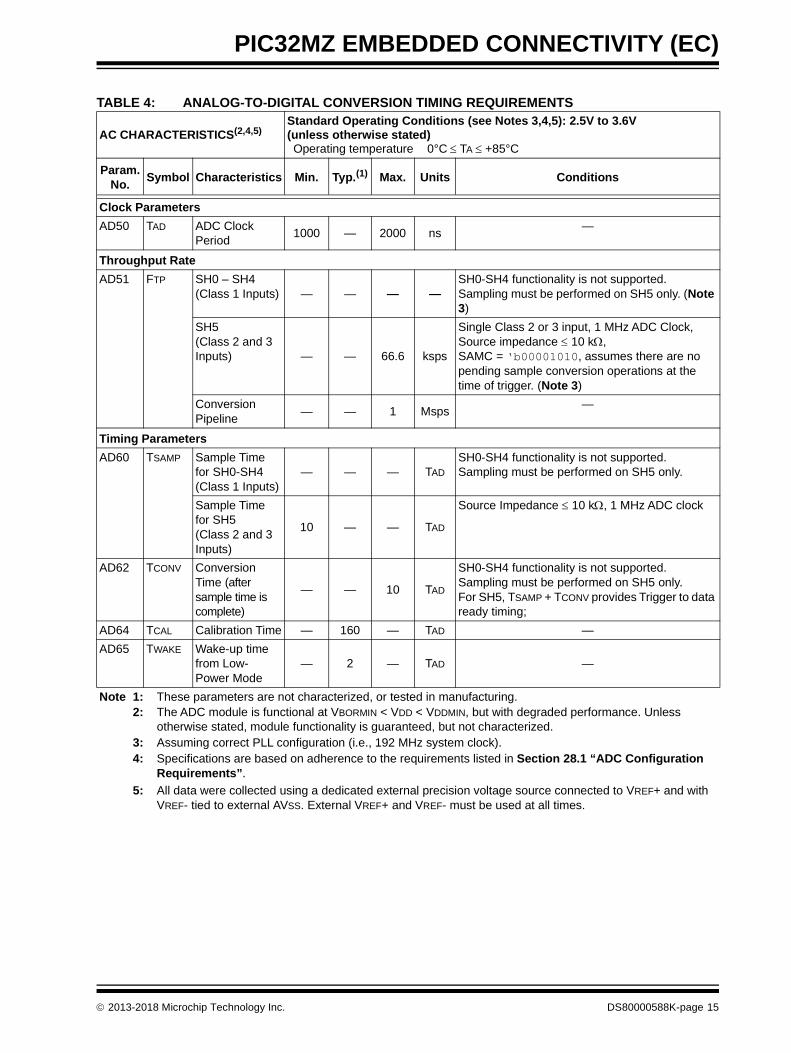
TABLE 4: ANALOG-TO-DIGITAL CONVERSION TIMING REQUIREMENTS
AC CHARACTERISTICS(2,4,5)Standard Operating Conditions (see Notes 3,4,5): 2.5V to 3.6V(unless otherwise stated)Operating temperature 0°C TA +85°C
Param. No.
Symbol Characteristics Min. Typ.(1) Max. Units Conditions
Clock Parameters
AD50 TAD ADC Clock Period
1000 — 2000 ns—
Throughput Rate
AD51 FTP SH0 – SH4(Class 1 Inputs) — — — —
SH0-SH4 functionality is not supported. Sampling must be performed on SH5 only. (Note 3)
SH5(Class 2 and 3 Inputs) — — 66.6 ksps
Single Class 2 or 3 input, 1 MHz ADC Clock, Source impedance 10 k, SAMC = ‘b00001010, assumes there are no pending sample conversion operations at the time of trigger. (Note 3)
Conversion Pipeline
— — 1 Msps—
Timing Parameters
AD60 TSAMP Sample Time for SH0-SH4(Class 1 Inputs)
— — — TAD
SH0-SH4 functionality is not supported. Sampling must be performed on SH5 only.
Sample Time for SH5(Class 2 and 3 Inputs)
10 — — TAD
Source Impedance 10 k, 1 MHz ADC clock
AD62 TCONV Conversion Time (after sample time is complete)
— — 10 TAD
SH0-SH4 functionality is not supported. Sampling must be performed on SH5 only.For SH5, TSAMP + TCONV provides Trigger to data ready timing;
AD64 TCAL Calibration Time — 160 — TAD —
AD65 TWAKE Wake-up time from Low-Power Mode
— 2 — TAD —
Note 1: These parameters are not characterized, or tested in manufacturing.2: The ADC module is functional at VBORMIN < VDD < VDDMIN, but with degraded performance. Unless
otherwise stated, module functionality is guaranteed, but not characterized.3: Assuming correct PLL configuration (i.e., 192 MHz system clock).4: Specifications are based on adherence to the requirements listed in Section 28.1 “ADC Configuration
Requirements”.
5: All data were collected using a dedicated external precision voltage source connected to VREF+ and with VREF- tied to external AVSS. External VREF+ and VREF- must be used at all times.
2013-2018 Microchip Technology Inc. DS80000588K-page 15

PIC32MZ EMBEDDED CONNECTIVITY (EC)
45. Module: Prefetch
The Prefetch module does not invalidate buffercontents when the module is disabled by settingthe PREFEN<1:0> bits to ‘b00.
Work around
To disable the Prefetch module, execute four32-bit NOP commands before and after settingthe PREFEN<1:0> bits to ‘b00.
Affected Silicon Revisions
46. Module: Oscillator
Switching the System Clock (SYSCLK) to theSystem PLL (SPLL) causes a device Reset. Thisaffects both software and hardware (IESO) clockswitching.
Work around
To switch the clock source, disable IESO andexecute the following steps in software:
1. Reduce the speed of all peripheral buses to128:1 through PBCLKx (where ‘x’ 7) andreduce the speed of the CPU bus to 128:1through PBCLK7.
2. Perform the clock switch.
3. Set the speed of the CPU bus to theprevious clock switch divisor and set thespeed of the peripheral buses to theirprevious clock switch divisor.
Affected Silicon Revisions
47. Module: DMA
The UART6 Transfer Done Interrupt (190) cannotbe used to trigger a DMA activity, such as a start ora stop.
Work around
None.
Affected Silicon Revisions
48. Module: UART
The UART Automatic baud rate feature is intendedto set the baud rate during run-time based onexternal data input. However, this feature does notfunction.
Work around
None.
Affected Silicon Revisions
49. Module: Reserved
The issue previously reported in a prior revision ofthis errata is no longer relevant and was removed.
50. Module: Oscillator
The Primary Oscillator does not meet thepublished specifications for crystal support.
Work around
To use a crystal with the Primary Oscillator, thefollowing limitations on voltage and frequencymust be observed:
• 2.4V VDD 3.6V
• Crystal Speed = 12 MHz
Additional details can be found in Data SheetClarification 1: Primary Oscillator.
Affected Silicon Revisions
51. Module: Reserved
The issue previously reported in a prior revision ofthis errata is no longer relevant and was removed.
A3 A4 A5
X X X
A3 A4 A5
X X X
A3 A4 A5
X X X
A3 A4 A5
X X X
A3 A4 A5
X X X
DS80000588K-page 16 2013-2018 Microchip Technology Inc.
PIC32MZ EMBEDDED CONNECTIVITY (EC)
52. Module: I2C
Setting the SDAHT bit in the I2C module lengthensthe time that the SDAx pin is held after SCLx fallsto 300 ns from 100 ns. However, the actual holdtime is longer than 300 ns, and as a result, itcauses a bus collision when operating at 1 MHz.
Work around
Do not set the SDAHT bit when operating the I2Cmodule at 1 MHz.
Affected Silicon Revisions
53. Module: System Bus
When operating the system bus at 8 MHz, havingthe CAN module access one RAM bank while theCrypto module accesses the other RAM bank cancause the CAN data to become corrupted.
Work around
Operate the system bus at frequencies faster than8 MHz.
Affected Silicon Revisions
54. Module: Reserved
The issue previously reported in a prior revision ofthis errata is no longer relevant and was removed.
55. Module: Oscillator
The Reference Clock Module cannot accept inputfrequencies greater than 100 MHz. Therefore,SYSCLK cannot be used as an input if theSYSCLK operates at frequencies greater than100 MHz.
Work around
Instead of using SYSCLK, use PBCLK1 as theinput, which is limited to 100 MHz and issynchronized to SYSCLK.
Affected Silicon Revisions
56. Module: UART
During a RX FIFO overflow condition, the shiftregister stops receiving data. This causes theUART to lose synchronization with the serial datastream. The only way to recover from this is to turnthe UART OFF and ON until it synchronizes. Thiscould require several OFF/ON sequences.
Work arounds
Work around 1:
Avoid the RX overrun condition by ensuring thatthe UARTx module has a high enough interruptpriority such that other peripheral interruptprocessing latencies do not exceed the time tooverrun the UART RX buffer based on theapplication baud rate. Alternately or in addition to,set the URXISEL bits in the UxSTA register togenerate an earlier RX interrupt based on RXFIFO fill status to buy more time for interruptlatency processing requirements.
Work around 2:
If avoiding RX FIFO overruns is not possible,implement a ACK/NAK software handshakeprotocol to repeat lost packet transfers afterrestoring UART synchronization.
Affected Silicon Revisions
57. Module: Timer1
Timer1 will not generate interrupts with an externalasynchronous clock input and prescaler other than1:1.
Work around
With External Clock Asynchronous mode, use the1:1 Prescaler mode with a software timer overflowvariable to keep track of the desired equivalent ofthe greater than 1:1 prescaler setting.
Alternately, use External Synchronous Clockmode if this is an option for the application
Affected Silicon Revisions
A3 A4 A5
X X X
A3 A4 A5
X X X
A3 A4 A5
X X X
A3 A4 A5
X X X
A3 A4 A5
X X X
2013-2018 Microchip Technology Inc. DS80000588K-page 17

PIC32MZ EMBEDDED CONNECTIVITY (EC)
58. Module: PMP
When the PMP is set to Master mode, and theWAITE bit is set to ‘0’ to have no wait states afterthe read strobe, a read operation does notgenerate an interrupt.
Work around
None.
Affected Silicon Revisions
59. Module: PMP
If the WAITM<3:0> bits = 0000, the end phaseshould be 1 TPB. However, the end phase does notdelay.
Work around
None
Affected Silicon Revisions
60. Module: Reserved
The issue previously reported in a prior revision ofthis errata is no longer relevant and was removed.
61. Module: Watchdog Timer
The data sheet specifies that a 16-bit write to theWDTCLRKEY<15:0> bits is required to clear theWatchdog Timer. However, a 16-bit write does notwork. In addition, writing to the WDTCONCLR,WDTCONSET, and WDTCONINV registers clearsthe Watchdog Timer, which should not occur.
Work around
Use a 32-bit write to the WDTCON register to clearthe Watchdog Timer.
Affected Silicon Revisions
62. Module: Flash
The SWAP bit (NVMCON<7>) can be changedwithout executing the NVMKEY unlock sequence.
Work around
None.
Affected Silicon Revisions
63. Module: Resets
The SWNMI bit (RNMICON<23>) in theNonmaskable Interrupt (NMI) Control registerdoes not function to trigger the NMI throughsoftware control.
Work around
None.
Affected Silicon Revisions
64. Module: Crypto Engine
The output digest of a partial message cannot beused as the Initial Vector for continuing thecryptographic operation on the rest of themessage. The full message must be processed inone operation.
Work around
None.
Affected Silicon Revisions
65. Module: Crypto Engine
The Crypto DMA does not support the hashoperation on an empty string (i.e., string with zerolength). The Crypto DMA times out and does notreturn a valid hash.
Work around
Use the fixed known hash of the empty string.
Affected Silicon Revisions
A3 A4 A5
X X X
A3 A4 A5
X X X
A3 A4 A5
X X X
A3 A4 A5
X X X
A3 A4 A5
X X X
A3 A4 A5
X X X
A3 A4 A5
X X X
DS80000588K-page 18 2013-2018 Microchip Technology Inc.
PIC32MZ EMBEDDED CONNECTIVITY (EC)
Data Sheet Clarifications
The following typographic corrections and clarificationsare to be noted for the latest version of the device datasheet (DS60001191G):
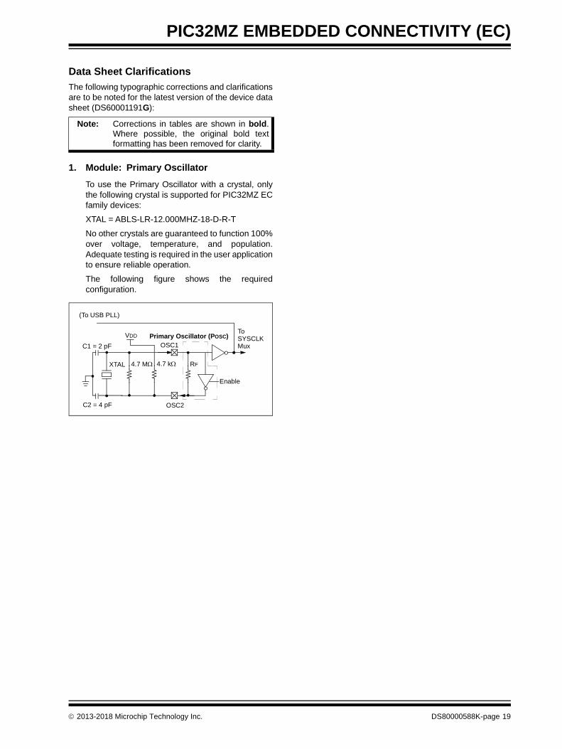
1. Module: Primary Oscillator
To use the Primary Oscillator with a crystal, onlythe following crystal is supported for PIC32MZ ECfamily devices:
XTAL = ABLS-LR-12.000MHZ-18-D-R-T
No other crystals are guaranteed to function 100%over voltage, temperature, and population.Adequate testing is required in the user applicationto ensure reliable operation.
The following figure shows the requiredconfiguration.
Note: Corrections in tables are shown in bold.Where possible, the original bold textformatting has been removed for clarity.
(To USB PLL)
C1 = 2 pF
C2 = 4 pF
XTAL
Enable
OSC2
OSC1
RF
Primary Oscillator (POSC)
4.7 M 4.7 k
VDDToSYSCLKMux
2013-2018 Microchip Technology Inc. DS80000588K-page 19
PIC32MZ EMBEDDED CONNECTIVITY (EC)
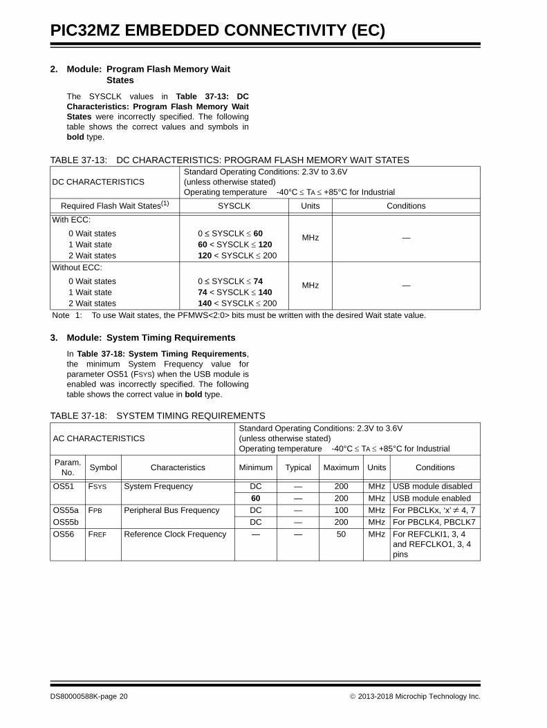
2. Module: Program Flash Memory Wait States
The SYSCLK values in Table 37-13: DCCharacteristics: Program Flash Memory WaitStates were incorrectly specified. The followingtable shows the correct values and symbols inbold type.
3. Module: System Timing Requirements
In Table 37-18: System Timing Requirements,the minimum System Frequency value forparameter OS51 (FSYS) when the USB module isenabled was incorrectly specified. The followingtable shows the correct value in bold type.
TABLE 37-18: SYSTEM TIMING REQUIREMENTS
TABLE 37-13: DC CHARACTERISTICS: PROGRAM FLASH MEMORY WAIT STATES
DC CHARACTERISTICSStandard Operating Conditions: 2.3V to 3.6V(unless otherwise stated)Operating temperature -40°C TA +85°C for Industrial
Required Flash Wait States(1) SYSCLK Units Conditions
With ECC:
0 Wait states1 Wait state2 Wait states
0 SYSCLK 6060 < SYSCLK 120120 < SYSCLK 200
MHz —
Without ECC:
0 Wait states1 Wait state2 Wait states
0 SYSCLK 7474 < SYSCLK 140140 < SYSCLK 200
MHz —
Note 1: To use Wait states, the PFMWS<2:0> bits must be written with the desired Wait state value.
AC CHARACTERISTICSStandard Operating Conditions: 2.3V to 3.6V(unless otherwise stated)Operating temperature -40°C TA +85°C for Industrial
Param.No.
Symbol Characteristics Minimum Typical Maximum Units Conditions
OS51 FSYS System Frequency DC — 200 MHz USB module disabled
60 — 200 MHz USB module enabled
OS55a FPB Peripheral Bus Frequency DC — 100 MHz For PBCLKx, ‘x’ 4, 7
OS55b DC — 200 MHz For PBCLK4, PBCLK7
OS56 FREF Reference Clock Frequency — — 50 MHz For REFCLKI1, 3, 4 and REFCLKO1, 3, 4 pins
DS80000588K-page 20 2013-2018 Microchip Technology Inc.
PIC32MZ EMBEDDED CONNECTIVITY (EC)
APPENDIX A: REVISION HISTORY
Rev A Document (11/2013)
Initial release of this document, issued for revision A3silicon.
This version includes the following issues: 1 (ADC),2 (ADC), 3 (Boot Flash), 4 (Comparator VoltageReference), 5 (Ethernet Controller), 6 (EthernetController), 7 (Ethernet Controller), 8 (I/O Port),9 (Oscillator), 10 (Oscillator), 11 (Secondary Oscillator),12 (LPRC Oscillator), 13 (Power-Saving Modes),14 (Power-Saving Modes), 15 (SPI), 16 (SQI),17 (System Bus), 18 (USB), 19 (USB), 20 (USB),21 (USB), 22 (Watchdog Timer), 23 (Watchdog Timer),24 (PMP), 25 (I2C), 26 (Crypto Engine), and27 (Random Number Generator).
Rev B Document (12/2013)
Updated issues 7 (Ethernet Controller) and14 (Power-Saving Modes).
Content in issue 21, which was included in aprevious errata version, was removed and this issuehas been marked as Reserved.
Added data sheet clarification issues 1 (Power-DownCurrent) and 2 (Operating Conditions), and siliconissues 28 (Flash) and 29 (ADC).
Rev C Document (4/2014)
Updated for revision A4 silicon.
Content in issues 12 and 16, which was included ina previous errata version, was removed and theseissues have been marked as Reserved.
Added silicon issues 30 (SQI), 31 (SQI), 32 (SQI),33 (SQI), 34 (SQI), 35 (SQI), 36 (Comparator),37 (Comparator), 38 (I/O Pins), 39 (I2C), 40 (FlashMemory), 41 (Oscillator), 42 (5V Tolerant I/O Pins),43 (ADC), 44 (ADC), and 45 (Prefetch).
Added data sheet clarification issues 3 (Internal FRCAccuracy), 4 (Internal LPRC Accuracy), 5 (InternalBackup FRC (BFRC) Accuracy), 6 (ADC1 ModuleSpecifications and Timing Requirements), 7 (ADCConfiguration Requirements), 8 (SQI TimingRequirements), 9 (DC Temperature and VoltageSpecifications.), 10 (Recommended MinimumConnection), and 11 (I/O Ports).
Rev D Document (5/2014)
Updated silicon issues 43 (ADC) and 44 (ADC) anddata sheet clarifications 6 (ADC1 ModuleSpecifications and Timing Requirements) and 7 (ADCConfiguration Requirements).
Rev E Document (9/2014)
Updated for revision A5 silicon.
Updated silicon issues 24 (PMP), 25 (I2C), and41 (Oscillator).
Added silicon issues 46 (Oscillator), 47 (DMA),48 (UART), 49 (Deadman Timer), 50 (Oscillator), and51 (ADC).
Removed data sheet clarifications 1 through 6 and 8through 11. Issue 7 was retained, which is nowissue 1 (ADC Configuration Requirements).
Added data sheet clarifications 2 (I/O Ports) and3 (Primary Oscillator).
Rev F Document (10/2014)
Content in issue 51, which was included in theprevious errata version, was removed and this issuehave been marked as Reserved.
Updated issue 44 (ADC).
Added data sheet clarification 4 (Internal FRCOscillator.).
Rev G Document (12/2014)
Updated silicon issues 25 (I2C), 30 (SQI), 43 (ADC),44 (ADC), and 50 (Oscillator).
Updated Data Sheet Clarification 1 (ADC ConfigurationRequirements) and 3 (Primary Oscillator).
Added silicon issues 52 (I2C), 53 (System Bus),54 (Power-Saving Modes), 55 (Oscillator), and56 (UART).
Added Data Sheet Clarification 5 (Internal LPRCOscillator).
Rev H Document (7/2015)
Content in issues 36, 49, and 54, which was includedin the previous errata version, has been removed andthese issues have been marked as Reserved.
Updated silicon issue 50 (Oscillator).
Added silicon issues 57 (Timer1), 58 (PMP),59 (PMP), 60 (Oscillator), 61 (Watchdog Timer), and62 (Flash).
Removed data sheet clarification 1 (ADCConfiguration Requirements), 2 (I/O Ports), 3 (InternalFRC Oscillator), 4 (Internal LPRC Oscillator), and 5(USB).
Updated data sheet clarification issue 2 (PrimaryOscillator), which is now issue 2.
Added data sheet clarification 1 (System BusArbitration).
Rev J Document (9/2015)
Removed silicon issue 60 (Oscillator), which is nowmarked Reserved.
2013-2018 Microchip Technology Inc. DS80000588K-page 21
PIC32MZ EMBEDDED CONNECTIVITY (EC)
Rev K Document (1/2018)
Removed data sheet clarification 1 (System BusArbitration).
Added silicon issues 63 (Resets), 64 (Crypto Engine)and 65 (Crypto Engine)
Added data sheet clarifications 2 (Program FlashMemory Wait States) and 3 (System TimingRequirements).
DS80000588K-page 22 2013-2018 Microchip Technology Inc.
PIC32MZ Graphics (DA) Family
Note the following details of the code protection feature on Microchip devices:
• Microchip products meet the specification contained in their particular Microchip Data Sheet.
• Microchip believes that its family of products is one of the most secure families of its kind on the market today, when used in the intended manner and under normal conditions.
• There are dishonest and possibly illegal methods used to breach the code protection feature. All of these methods, to our knowledge, require using the Microchip products in a manner outside the operating specifications contained in Microchip’s Data Sheets. Most likely, the person doing so is engaged in theft of intellectual property.
• Microchip is willing to work with the customer who is concerned about the integrity of their code.
• Neither Microchip nor any other semiconductor manufacturer can guarantee the security of their code. Code protection does not mean that we are guaranteeing the product as “unbreakable.”
Code protection is constantly evolving. We at Microchip are committed to continuously improving the code protection features of ourproducts. Attempts to break Microchip’s code protection feature may be a violation of the Digital Millennium Copyright Act. If such actsallow unauthorized access to your software or other copyrighted work, you may have a right to sue for relief under that Act.
Information contained in this publication regarding deviceapplications and the like is provided only for your convenienceand may be superseded by updates. It is your responsibility toensure that your application meets with your specifications.MICROCHIP MAKES NO REPRESENTATIONS ORWARRANTIES OF ANY KIND WHETHER EXPRESS ORIMPLIED, WRITTEN OR ORAL, STATUTORY OROTHERWISE, RELATED TO THE INFORMATION,INCLUDING BUT NOT LIMITED TO ITS CONDITION,QUALITY, PERFORMANCE, MERCHANTABILITY ORFITNESS FOR PURPOSE. Microchip disclaims all liabilityarising from this information and its use. Use of Microchipdevices in life support and/or safety applications is entirely atthe buyer’s risk, and the buyer agrees to defend, indemnify andhold harmless Microchip from any and all damages, claims,suits, or expenses resulting from such use. No licenses areconveyed, implicitly or otherwise, under any Microchipintellectual property rights unless otherwise stated.
2013-2018 Microchip Technology Inc.
Microchip received ISO/TS-16949:2009 certification for its worldwide headquarters, design and wafer fabrication facilities in Chandler and Tempe, Arizona; Gresham, Oregon and design centers in California and India. The Company’s quality system processes and procedures are for its PIC® MCUs and dsPIC® DSCs, KEELOQ® code hopping devices, Serial EEPROMs, microperipherals, nonvolatile memory and analog products. In addition, Microchip’s quality system for the design and manufacture of development systems is ISO 9001:2000 certified.
QUALITY MANAGEMENT SYSTEM CERTIFIED BY DNV
== ISO/TS 16949 ==
Trademarks
The Microchip name and logo, the Microchip logo, AnyRate, AVR, AVR logo, AVR Freaks, BeaconThings, BitCloud, CryptoMemory, CryptoRF, dsPIC, FlashFlex, flexPWR, Heldo, JukeBlox, KEELOQ, KEELOQ logo, Kleer, LANCheck, LINK MD, maXStylus, maXTouch, MediaLB, megaAVR, MOST, MOST logo, MPLAB, OptoLyzer, PIC, picoPower, PICSTART, PIC32 logo, Prochip Designer, QTouch, RightTouch, SAM-BA, SpyNIC, SST, SST Logo, SuperFlash, tinyAVR, UNI/O, and XMEGA are registered trademarks of Microchip Technology Incorporated in the U.S.A. and other countries.
ClockWorks, The Embedded Control Solutions Company, EtherSynch, Hyper Speed Control, HyperLight Load, IntelliMOS, mTouch, Precision Edge, and Quiet-Wire are registered trademarks of Microchip Technology Incorporated in the U.S.A.
Adjacent Key Suppression, AKS, Analog-for-the-Digital Age, Any Capacitor, AnyIn, AnyOut, BodyCom, chipKIT, chipKIT logo, CodeGuard, CryptoAuthentication, CryptoCompanion, CryptoController, dsPICDEM, dsPICDEM.net, Dynamic Average Matching, DAM, ECAN, EtherGREEN, In-Circuit Serial Programming, ICSP, Inter-Chip Connectivity, JitterBlocker, KleerNet, KleerNet logo, Mindi, MiWi, motorBench, MPASM, MPF, MPLAB Certified logo, MPLIB, MPLINK, MultiTRAK, NetDetach, Omniscient Code Generation, PICDEM, PICDEM.net, PICkit, PICtail, PureSilicon, QMatrix, RightTouch logo, REAL ICE, Ripple Blocker, SAM-ICE, Serial Quad I/O, SMART-I.S., SQI, SuperSwitcher, SuperSwitcher II, Total Endurance, TSHARC, USBCheck, VariSense, ViewSpan, WiperLock, Wireless DNA, and ZENA are trademarks of Microchip Technology Incorporated in the U.S.A. and other countries.
SQTP is a service mark of Microchip Technology Incorporated in the U.S.A.
Silicon Storage Technology is a registered trademark of Microchip Technology Inc. in other countries.
GestIC is a registered trademark of Microchip Technology Germany II GmbH & Co. KG, a subsidiary of Microchip Technology Inc., in other countries.
All other trademarks mentioned herein are property of their respective companies.
© 2013-2018, Microchip Technology Incorporated, All Rights Reserved.
ISBN: 978-1-5224-2592-2
DS80000588K-page 23
DS80000588K-page 24 2013-2018 Microchip Technology Inc.
AMERICASCorporate Office2355 West Chandler Blvd.Chandler, AZ 85224-6199Tel: 480-792-7200 Fax: 480-792-7277Technical Support: http://www.microchip.com/supportWeb Address: www.microchip.com
AtlantaDuluth, GA Tel: 678-957-9614 Fax: 678-957-1455
Austin, TXTel: 512-257-3370
BostonWestborough, MA Tel: 774-760-0087 Fax: 774-760-0088
ChicagoItasca, IL Tel: 630-285-0071 Fax: 630-285-0075
DallasAddison, TX Tel: 972-818-7423 Fax: 972-818-2924
DetroitNovi, MI Tel: 248-848-4000
Houston, TX Tel: 281-894-5983
IndianapolisNoblesville, IN Tel: 317-773-8323Fax: 317-773-5453Tel: 317-536-2380
Los AngelesMission Viejo, CA Tel: 949-462-9523Fax: 949-462-9608Tel: 951-273-7800
Raleigh, NC Tel: 919-844-7510
New York, NY Tel: 631-435-6000
San Jose, CA Tel: 408-735-9110Tel: 408-436-4270
Canada - TorontoTel: 905-695-1980 Fax: 905-695-2078
ASIA/PACIFICAustralia - SydneyTel: 61-2-9868-6733
China - BeijingTel: 86-10-8569-7000
China - ChengduTel: 86-28-8665-5511
China - ChongqingTel: 86-23-8980-9588
China - DongguanTel: 86-769-8702-9880
China - GuangzhouTel: 86-20-8755-8029
China - HangzhouTel: 86-571-8792-8115
China - Hong Kong SARTel: 852-2943-5100
China - NanjingTel: 86-25-8473-2460
China - QingdaoTel: 86-532-8502-7355
China - ShanghaiTel: 86-21-3326-8000
China - ShenyangTel: 86-24-2334-2829
China - ShenzhenTel: 86-755-8864-2200
China - SuzhouTel: 86-186-6233-1526
China - WuhanTel: 86-27-5980-5300
China - XianTel: 86-29-8833-7252
China - XiamenTel: 86-592-2388138
China - ZhuhaiTel: 86-756-3210040
ASIA/PACIFICIndia - BangaloreTel: 91-80-3090-4444
India - New DelhiTel: 91-11-4160-8631
India - PuneTel: 91-20-4121-0141
Japan - OsakaTel: 81-6-6152-7160
Japan - TokyoTel: 81-3-6880- 3770
Korea - DaeguTel: 82-53-744-4301
Korea - SeoulTel: 82-2-554-7200
Malaysia - Kuala LumpurTel: 60-3-7651-7906
Malaysia - PenangTel: 60-4-227-8870
Philippines - ManilaTel: 63-2-634-9065
SingaporeTel: 65-6334-8870
Taiwan - Hsin ChuTel: 886-3-577-8366
Taiwan - KaohsiungTel: 886-7-213-7830
Taiwan - TaipeiTel: 886-2-2508-8600
Thailand - BangkokTel: 66-2-694-1351
Vietnam - Ho Chi MinhTel: 84-28-5448-2100
EUROPEAustria - WelsTel: 43-7242-2244-39Fax: 43-7242-2244-393
Denmark - CopenhagenTel: 45-4450-2828 Fax: 45-4485-2829
Finland - EspooTel: 358-9-4520-820
France - ParisTel: 33-1-69-53-63-20 Fax: 33-1-69-30-90-79
Germany - GarchingTel: 49-8931-9700
Germany - HaanTel: 49-2129-3766400
Germany - HeilbronnTel: 49-7131-67-3636
Germany - KarlsruheTel: 49-721-625370
Germany - MunichTel: 49-89-627-144-0 Fax: 49-89-627-144-44
Germany - RosenheimTel: 49-8031-354-560
Israel - Ra’anana Tel: 972-9-744-7705
Italy - Milan Tel: 39-0331-742611 Fax: 39-0331-466781
Italy - PadovaTel: 39-049-7625286
Netherlands - DrunenTel: 31-416-690399 Fax: 31-416-690340
Norway - TrondheimTel: 47-7289-7561
Poland - WarsawTel: 48-22-3325737
Romania - BucharestTel: 40-21-407-87-50
Spain - MadridTel: 34-91-708-08-90Fax: 34-91-708-08-91
Sweden - GothenbergTel: 46-31-704-60-40
Sweden - StockholmTel: 46-8-5090-4654
UK - WokinghamTel: 44-118-921-5800Fax: 44-118-921-5820
Worldwide Sales and Service
10/25/17
Top Related