


Languages
Pages
Legal

© 2006 Microchip Technology Inc. DS41202D
PIC16F684Data Sheet
14-Pin Flash-Based, 8-Bit
CMOS Microcontrollers withnanoWatt Technology
Note the following details of the code protection feature on Microchip devices:
• Microchip products meet the specification contained in their particular Microchip Data Sheet.
• Microchip believes that its family of products is one of the most secure families of its kind on the market today, when used in the intended manner and under normal conditions.
• There are dishonest and possibly illegal methods used to breach the code protection feature. All of these methods, to our knowledge, require using the Microchip products in a manner outside the operating specifications contained in Microchip’s Data Sheets. Most likely, the person doing so is engaged in theft of intellectual property.
• Microchip is willing to work with the customer who is concerned about the integrity of their code.
• Neither Microchip nor any other semiconductor manufacturer can guarantee the security of their code. Code protection does not mean that we are guaranteeing the product as “unbreakable.”
Code protection is constantly evolving. We at Microchip are committed to continuously improving the code protection features of ourproducts. Attempts to break Microchip’s code protection feature may be a violation of the Digital Millennium Copyright Act. If such actsallow unauthorized access to your software or other copyrighted work, you may have a right to sue for relief under that Act.
Information contained in this publication regarding deviceapplications and the like is provided only for your convenienceand may be superseded by updates. It is your responsibility toensure that your application meets with your specifications.MICROCHIP MAKES NO REPRESENTATIONS OR WAR-RANTIES OF ANY KIND WHETHER EXPRESS OR IMPLIED,WRITTEN OR ORAL, STATUTORY OR OTHERWISE,RELATED TO THE INFORMATION, INCLUDING BUT NOTLIMITED TO ITS CONDITION, QUALITY, PERFORMANCE,MERCHANTABILITY OR FITNESS FOR PURPOSE.Microchip disclaims all liability arising from this information andits use. Use of Microchip devices in life support and/or safetyapplications is entirely at the buyer’s risk, and the buyer agreesto defend, indemnify and hold harmless Microchip from any andall damages, claims, suits, or expenses resulting from suchuse. No licenses are conveyed, implicitly or otherwise, underany Microchip intellectual property rights.
DS41202D-page ii
Trademarks
The Microchip name and logo, the Microchip logo, Accuron, dsPIC, KEELOQ, microID, MPLAB, PIC, PICmicro, PICSTART, PRO MATE, PowerSmart, rfPIC and SmartShunt are registered trademarks of Microchip Technology Incorporated in the U.S.A. and other countries.
AmpLab, FilterLab, Migratable Memory, MXDEV, MXLAB, SEEVAL, SmartSensor and The Embedded Control Solutions Company are registered trademarks of Microchip Technology Incorporated in the U.S.A.
Analog-for-the-Digital Age, Application Maestro, dsPICDEM, dsPICDEM.net, dsPICworks, ECAN, ECONOMONITOR, FanSense, FlexROM, fuzzyLAB, In-Circuit Serial Programming, ICSP, ICEPIC, Linear Active Thermistor, MPASM, MPLIB, MPLINK, MPSIM, PICkit, PICDEM, PICDEM.net, PICLAB, PICtail, PowerCal, PowerInfo, PowerMate, PowerTool, REAL ICE, rfLAB, rfPICDEM, Select Mode, Smart Serial, SmartTel, Total Endurance, UNI/O, WiperLock and Zena are trademarks of Microchip Technology Incorporated in the U.S.A. and other countries.
SQTP is a service mark of Microchip Technology Incorporated in the U.S.A.
All other trademarks mentioned herein are property of their respective companies.
© 2006, Microchip Technology Incorporated, Printed in the U.S.A., All Rights Reserved.
Printed on recycled paper.
© 2006 Microchip Technology Inc.
Microchip received ISO/TS-16949:2002 quality system certification for its worldwide headquarters, design and wafer fabrication facilities in Chandler and Tempe, Arizona and Mountain View, California in October 2003. The Company’s quality system processes and procedures are for its PICmicro® 8-bit MCUs, KEELOQ® code hopping devices, Serial EEPROMs, microperipherals, nonvolatile memory and analog products. In addition, Microchip’s quality system for the design and manufacture of development systems is ISO 9001:2000 certified.
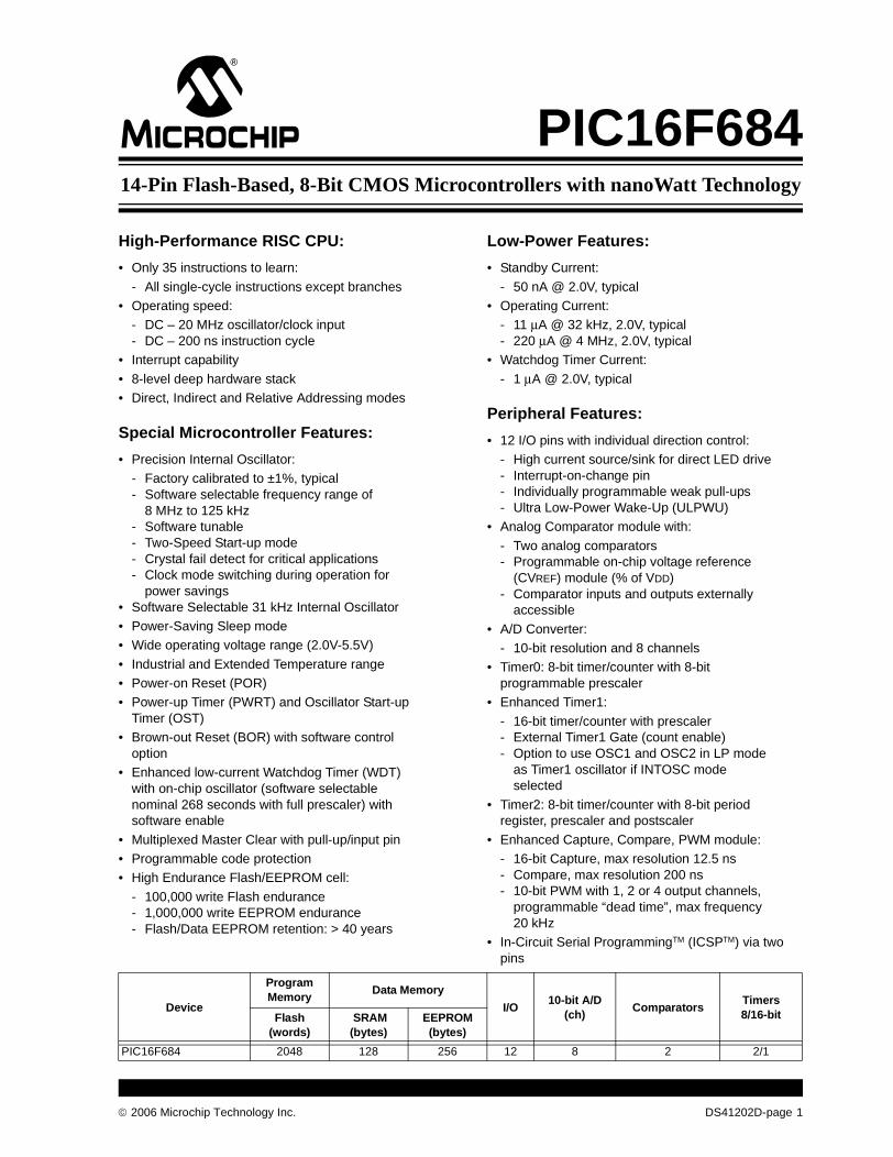
PIC16F68414-Pin Flash-Based, 8-Bit CMOS Microcontrollers with nanoWatt Technology
High-Performance RISC CPU:
• Only 35 instructions to learn:
- All single-cycle instructions except branches• Operating speed:
- DC – 20 MHz oscillator/clock input- DC – 200 ns instruction cycle
• Interrupt capability
• 8-level deep hardware stack• Direct, Indirect and Relative Addressing modes
Special Microcontroller Features:
• Precision Internal Oscillator:- Factory calibrated to ±1%, typical- Software selectable frequency range of
8 MHz to 125 kHz- Software tunable- Two-Speed Start-up mode- Crystal fail detect for critical applications- Clock mode switching during operation for
power savings• Software Selectable 31 kHz Internal Oscillator• Power-Saving Sleep mode• Wide operating voltage range (2.0V-5.5V)
• Industrial and Extended Temperature range• Power-on Reset (POR)• Power-up Timer (PWRT) and Oscillator Start-up
Timer (OST)• Brown-out Reset (BOR) with software control
option• Enhanced low-current Watchdog Timer (WDT)
with on-chip oscillator (software selectable nominal 268 seconds with full prescaler) with software enable
• Multiplexed Master Clear with pull-up/input pin• Programmable code protection• High Endurance Flash/EEPROM cell:
- 100,000 write Flash endurance- 1,000,000 write EEPROM endurance- Flash/Data EEPROM retention: > 40 years
Low-Power Features:
• Standby Current:
- 50 nA @ 2.0V, typical• Operating Current:
- 11 μA @ 32 kHz, 2.0V, typical- 220 μA @ 4 MHz, 2.0V, typical
• Watchdog Timer Current:
- 1 μA @ 2.0V, typical
Peripheral Features:
• 12 I/O pins with individual direction control:- High current source/sink for direct LED drive- Interrupt-on-change pin- Individually programmable weak pull-ups- Ultra Low-Power Wake-Up (ULPWU)
• Analog Comparator module with:
- Two analog comparators- Programmable on-chip voltage reference
(CVREF) module (% of VDD)- Comparator inputs and outputs externally
accessible
• A/D Converter:- 10-bit resolution and 8 channels
• Timer0: 8-bit timer/counter with 8-bit programmable prescaler
• Enhanced Timer1:
- 16-bit timer/counter with prescaler- External Timer1 Gate (count enable)- Option to use OSC1 and OSC2 in LP mode
as Timer1 oscillator if INTOSC mode selected
• Timer2: 8-bit timer/counter with 8-bit period register, prescaler and postscaler
• Enhanced Capture, Compare, PWM module:- 16-bit Capture, max resolution 12.5 ns- Compare, max resolution 200 ns- 10-bit PWM with 1, 2 or 4 output channels,
programmable “dead time”, max frequency 20 kHz
• In-Circuit Serial ProgrammingTM (ICSPTM) via two pins
Device
Program Memory
Data Memory
I/O10-bit A/D
(ch)Comparators
Timers8/16-bitFlash
(words) SRAM (bytes)
EEPROM (bytes)
PIC16F684 2048 128 256 12 8 2 2/1
© 2006 Microchip Technology Inc. DS41202D-page 1
PIC16F684
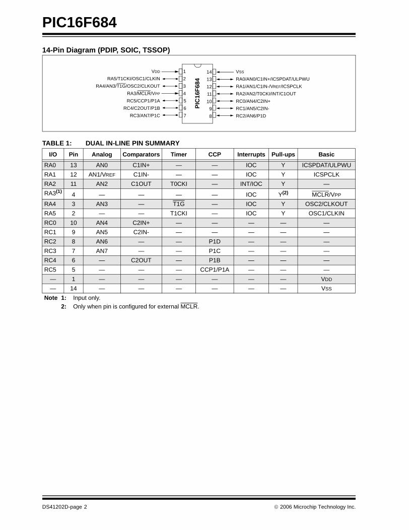
14-Pin Diagram (PDIP, SOIC, TSSOP)
TABLE 1: DUAL IN-LINE PIN SUMMARY
I/O Pin Analog Comparators Timer CCP Interrupts Pull-ups Basic
RA0 13 AN0 C1IN+ — — IOC Y ICSPDAT/ULPWU
RA1 12 AN1/VREF C1IN- — — IOC Y ICSPCLK
RA2 11 AN2 C1OUT T0CKI — INT/IOC Y —
RA3(1)4 — — — — IOC Y(2) MCLR/VPP
RA4 3 AN3 — T1G — IOC Y OSC2/CLKOUT
RA5 2 — — T1CKI — IOC Y OSC1/CLKIN
RC0 10 AN4 C2IN+ — — — — —
RC1 9 AN5 C2IN- — — — — —
RC2 8 AN6 — — P1D — — —
RC3 7 AN7 — — P1C — — —
RC4 6 — C2OUT — P1B — — —
RC5 5 — — — CCP1/P1A — — —
— 1 — — — — — — VDD
— 14 — — — — — — VSS
Note 1: Input only.2: Only when pin is configured for external MCLR.
VDD
RA5/T1CKI/OSC1/CLKIN
RA4/AN3/T1G/OSC2/CLKOUT
RA3/MCLR/VPP
RC5/CCP1/P1A
RC4/C2OUT/P1B
RC3/AN7/P1C
VSS
RA0/AN0/C1IN+/ICSPDAT/ULPWU
RA1/AN1/C1IN-/VREF/ICSPCLK
RA2/AN2/T0CKI/INT/C1OUT
RC0/AN4/C2IN+
RC1/AN5/C2IN-
RC2/AN6/P1D
PIC
16F
684
1
2
3
4
5
6
7
14
13
12
9
11
10
8
DS41202D-page 2 © 2006 Microchip Technology Inc.
PIC16F684
16-Pin Diagram (QFN)
TABLE 2: QFN PIN SUMMARY
I/O Pin Analog Comparators Timers CCP Interrupts Pull-ups Basic
RA0 12 AN0 C1IN+ — — IOC Y ICSPDAT/ULPWU
RA1 11 AN1/VREF C1IN- — — IOC Y ICSPCLK
RA2 10 AN2 C1OUT T0CKI — INT/IOC Y —
RA3(1)3 — — — — IOC Y(2) MCLR/VPP
RA4 2 AN3 — T1G — IOC Y OSC2/CLKOUT
RA5 1 — — T1CKI — IOC Y OSC1/CLKIN
RC0 9 AN4 C2IN+ — — — — —
RC1 8 AN5 C2IN- — — — — —
RC2 7 AN6 — — P1D — — —
RC3 6 AN7 — — P1C — — —
RC4 5 — C2OUT — P1B — — —
RC5 4 — — — CCP1/P1A — — —
— 16 — — — — — — VDD
— 13 — — — — — — VSS
Note 1: Input only.2: Only when pin is configured for external MCLR.
1
2
3
4 9
10
11
12
5 6 7 8
16 15 14 13
PIC16F684
RA5/T1CKI/OSC1/CLKIN
RA4/AN3/T1G/OSC2/CLKOUT
RA3/MCLR/VPP
RC5/CCP1/P1A
VD
D
NC
NC
VS
S
RA0/AN0/C1IN+/ICSPDAT/ULPWU
RA1/AN1/C1IN-/VREF/ICSPCLK
RA2/AN2/T0CKI/INT/C1OUT
RC0/AN4/C2IN+
RC
4/C
2OU
T/P
1B
RC
3/A
N7/
P1C
RC
2/A
N6/
P1D
RC
1/A
N5/
C2I
N-
© 2006 Microchip Technology Inc. DS41202D-page 3
PIC16F684
Table of Contents1.0 Device Overview .......................................................................................................................................................................... 52.0 Memory Organization ................................................................................................................................................................... 73.0 Oscillator Module (With Fail-Safe Clock Monitor)....................................................................................................................... 194.0 I/O Ports ..................................................................................................................................................................................... 315.0 Timer0 Module ........................................................................................................................................................................... 436.0 Timer1 Module with Gate Control............................................................................................................................................... 477.0 Timer2 Module ........................................................................................................................................................................... 538.0 Comparator Module.................................................................................................................................................................... 559.0 Analog-to-Digital Converter (ADC) Module ................................................................................................................................ 6510.0 Data EEPROM Memory ............................................................................................................................................................. 7511.0 Enhanced Capture/Compare/PWM (With Auto-Shutdown and Dead Band) Module................................................................. 7912.0 Special Features of the CPU...................................................................................................................................................... 9713.0 Instruction Set Summary .......................................................................................................................................................... 11514.0 Development Support............................................................................................................................................................... 12515.0 Electrical Specifications............................................................................................................................................................ 12916.0 DC and AC Characteristics Graphs and Tables....................................................................................................................... 15117.0 Packaging Information.............................................................................................................................................................. 173Appendix A: Data Sheet Revision History.......................................................................................................................................... 179Appendix B: Migrating from other PICmicro® Devices ...................................................................................................................... 179Index .................................................................................................................................................................................................. 181The Microchip Web Site ..................................................................................................................................................................... 187Customer Change Notification Service .............................................................................................................................................. 187Customer Support .............................................................................................................................................................................. 187Reader Response .............................................................................................................................................................................. 188Product Identification System............................................................................................................................................................. 189
TO OUR VALUED CUSTOMERS
It is our intention to provide our valued customers with the best documentation possible to ensure successful use of your Microchipproducts. To this end, we will continue to improve our publications to better suit your needs. Our publications will be refined andenhanced as new volumes and updates are introduced.
If you have any questions or comments regarding this publication, please contact the Marketing Communications Department via E-mail at [email protected] or fax the Reader Response Form in the back of this data sheet to (480) 792-4150. We welcome your feedback.
Most Current Data SheetTo obtain the most up-to-date version of this data sheet, please register at our Worldwide Web site at:
http://www.microchip.com
You can determine the version of a data sheet by examining its literature number found on the bottom outside corner of any page.The last character of the literature number is the version number, (e.g., DS30000A is version A of document DS30000).
ErrataAn errata sheet, describing minor operational differences from the data sheet and recommended workarounds, may exist for currentdevices. As device/documentation issues become known to us, we will publish an errata sheet. The errata will specify the revision ofsilicon and revision of document to which it applies.
To determine if an errata sheet exists for a particular device, please check with one of the following:
• Microchip’s Worldwide Web site; http://www.microchip.com• Your local Microchip sales office (see last page)When contacting a sales office, please specify which device, revision of silicon and data sheet (include literature number) you areusing.
Customer Notification SystemRegister on our web site at www.microchip.com to receive the most current information on all of our products.
DS41202D-page 4 © 2006 Microchip Technology Inc.
PIC16F684
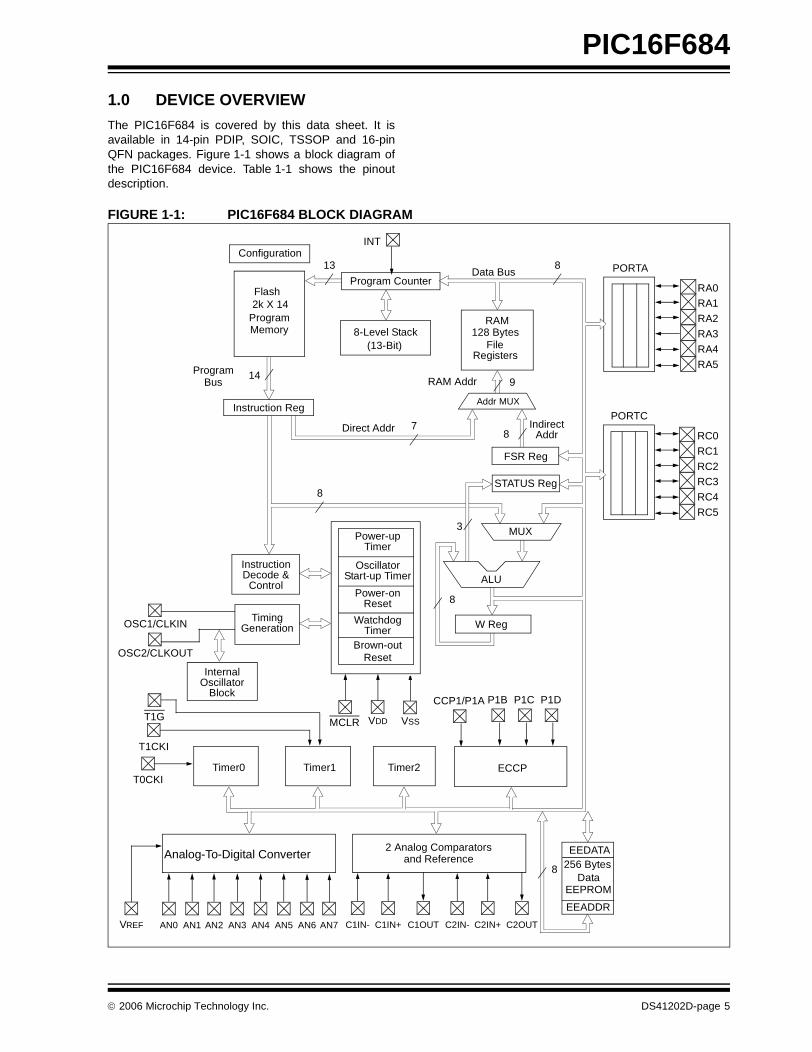
1.0 DEVICE OVERVIEW
The PIC16F684 is covered by this data sheet. It isavailable in 14-pin PDIP, SOIC, TSSOP and 16-pinQFN packages. Figure 1-1 shows a block diagram ofthe PIC16F684 device. Table 1-1 shows the pinoutdescription.
FIGURE 1-1: PIC16F684 BLOCK DIAGRAM
Flash
ProgramMemory
13Data Bus
8
14ProgramBus
Instruction Reg
Program Counter
RAM
FileRegisters
Direct Addr 7
RAM Addr 9
Addr MUX
IndirectAddr
FSR Reg
STATUS Reg
MUX
ALU
W Reg
InstructionDecode &
Control
TimingGenerationOSC1/CLKIN
OSC2/CLKOUT
PORTA
8
8
8
3
8-Level Stack 128 Bytes
2k X 14
(13-Bit)
Power-upTimer
OscillatorStart-up Timer
Power-onReset
WatchdogTimer
MCLR VSS
Brown-outReset
Timer0 Timer1
DataEEPROM
256 BytesEEDATA
EEADDR
RA0RA1
RA2
RA3
RA4
RA5
2 Analog ComparatorsAnalog-To-Digital Converter
AN0 AN1 AN2 AN3 C1IN- C1IN+ C1OUT
T0CKI
INT
T1CKI
Configuration
InternalOscillator
VREF
and Reference
T1G
PORTC
RC0
RC1
RC2RC3
RC4
RC5
AN4 AN5 AN6 AN7
VDD
8
Timer2
C2IN- C2IN+ C2OUT
ECCP
BlockCCP1/P1A P1B P1C P1D
© 2006 Microchip Technology Inc. DS41202D-page 5
PIC16F684
TABLE 1-1: PIC16F684 PINOUT DESCRIPTION
Name FunctionInput Type
Output Type
Description
RA0/AN0/C1IN+/ICSPDAT/ULPWU RA0 TTL CMOS PORTA I/O with prog. pull-up and interrupt-on-change
AN0 AN — A/D Channel 0 input
C1IN+ AN — Comparator 1 non-inverting input
ICSPDAT TTL CMOS Serial Programming Data I/O
ULPWU AN — Ultra Low-Power Wake-Up input
RA1/AN1/C1IN-/VREF/ICSPCLK RA1 TTL CMOS PORTA I/O with prog. pull-up and interrupt-on-change
AN1 AN — A/D Channel 1 input
C1IN- AN — Comparator 1 inverting input
VREF AN — External Voltage Reference for A/D
ICSPCLK ST — Serial Programming Clock
RA2/AN2/T0CKI/INT/C1OUT RA2 ST CMOS PORTA I/O with prog. pull-up and interrupt-on-change
AN2 AN — A/D Channel 2 input
T0CKI ST — Timer0 clock input
INT ST — External Interrupt
C1OUT — CMOS Comparator 1 output
RA3/MCLR/VPP RA3 TTL — PORTA input with interrupt-on-change
MCLR ST — Master Clear w/internal pull-up
VPP HV — Programming voltage
RA4/AN3/T1G/OSC2/CLKOUT RA4 TTL CMOS PORTA I/O with prog. pull-up and interrupt-on-change
AN3 AN — A/D Channel 3 input
T1G ST — Timer1 gate (count enable)
OSC2 — XTAL Crystal/Resonator
CLKOUT — CMOS FOSC/4 output
RA5/T1CKI/OSC1/CLKIN RA5 TTL CMOS PORTA I/O with prog. pull-up and interrupt-on-change
T1CKI ST — Timer1 clock
OSC1 XTAL — Crystal/Resonator
CLKIN ST — External clock input/RC oscillator connection
RC0/AN4/C2IN+ RC0 TTL CMOS PORTC I/O
AN4 AN — A/D Channel 4 input
C2IN+ AN — Comparator 2 non-inverting input
RC1/AN5/C2IN- RC1 TTL CMOS PORTC I/O
AN5 AN — A/D Channel 5 input
C2IN- AN — Comparator 2 inverting input
RC2/AN6/P1D RC2 TTL CMOS PORTC I/O
AN6 AN — A/D Channel 6 input
P1D — CMOS PWM output
RC3/AN7/P1C RC3 TTL CMOS PORTC I/O
AN7 AN — A/D Channel 7 input
P1C — CMOS PWM output
RC4/C2OUT/P1B RC4 TTL CMOS PORTC I/O
C2OUT — CMOS Comparator 2 output
P1B — CMOS PWM output
RC5/CCP1/P1A RC5 TTL CMOS PORTC I/O
CCP1 ST CMOS Capture input/Compare output
P1A — CMOS PWM output
VDD VDD Power — Positive supply
VSS VSS Power — Ground reference
Legend: AN = Analog input or output CMOS= CMOS compatible input or output HV = High VoltageST = Schmitt Trigger input with CMOS levels TTL = TTL compatible input XTAL = Crystal
DS41202D-page 6 © 2006 Microchip Technology Inc.
PIC16F684
2.0 MEMORY ORGANIZATION
2.1 Program Memory Organization
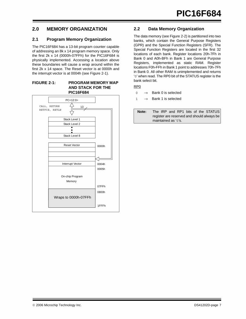
The PIC16F684 has a 13-bit program counter capableof addressing an 8k x 14 program memory space. Onlythe first 2k x 14 (0000h-07FFh) for the PIC16F684 isphysically implemented. Accessing a location abovethese boundaries will cause a wrap around within thefirst 2k x 14 space. The Reset vector is at 0000h andthe interrupt vector is at 0004h (see Figure 2-1).
FIGURE 2-1: PROGRAM MEMORY MAP AND STACK FOR THE PIC16F684
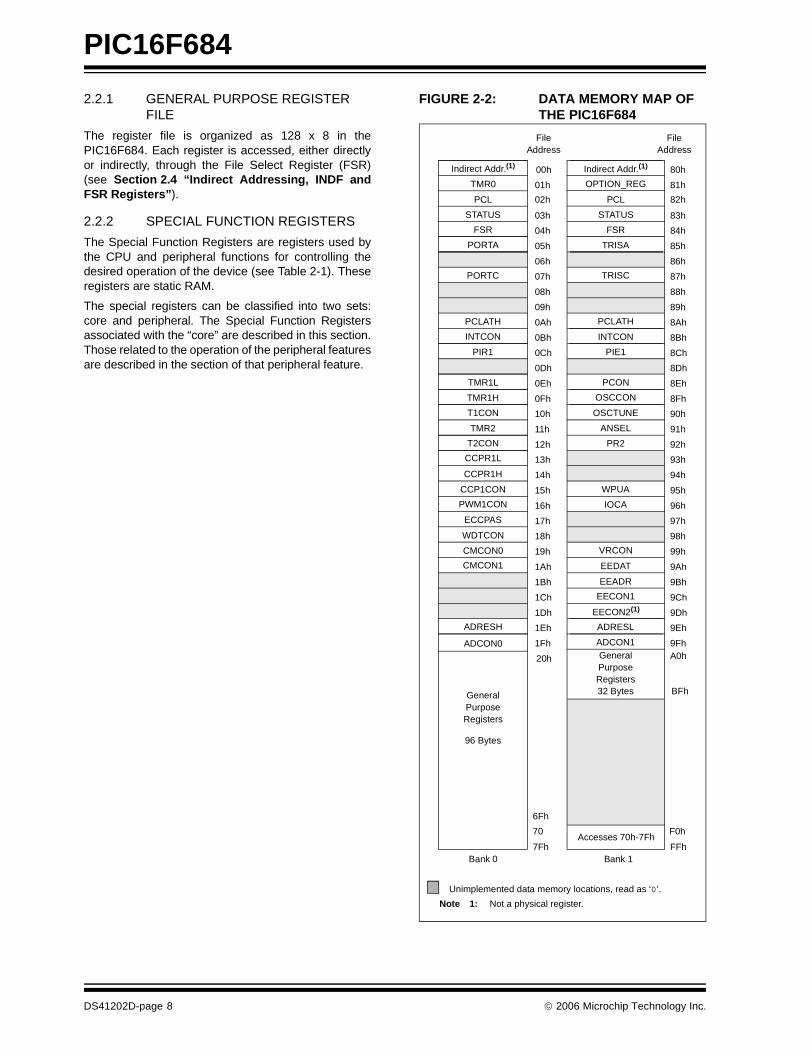
2.2 Data Memory Organization
The data memory (see Figure 2-2) is partitioned into twobanks, which contain the General Purpose Registers(GPR) and the Special Function Registers (SFR). TheSpecial Function Registers are located in the first 32locations of each bank. Register locations 20h-7Fh inBank 0 and A0h-BFh in Bank 1 are General PurposeRegisters, implemented as static RAM. Registerlocations F0h-FFh in Bank 1 point to addresses 70h-7Fhin Bank 0. All other RAM is unimplemented and returns‘0’ when read. The RP0 bit of the STATUS register is thebank select bit.
RP0
0 → Bank 0 is selected
1 → Bank 1 is selectedPC<12:0>
13
0000h
0004h
0005h
07FFh
0800h
1FFFh
Stack Level 1
Stack Level 8
Reset Vector
Interrupt Vector
On-chip Program
Memory
CALL, RETURNRETFIE, RETLW
Stack Level 2
Wraps to 0000h-07FFh
Note: The IRP and RP1 bits of the STATUSregister are reserved and should always bemaintained as ‘0’s.
© 2006 Microchip Technology Inc. DS41202D-page 7
PIC16F684
2.2.1 GENERAL PURPOSE REGISTER FILE
The register file is organized as 128 x 8 in thePIC16F684. Each register is accessed, either directlyor indirectly, through the File Select Register (FSR)(see Section 2.4 “Indirect Addressing, INDF andFSR Registers”).
2.2.2 SPECIAL FUNCTION REGISTERS
The Special Function Registers are registers used bythe CPU and peripheral functions for controlling thedesired operation of the device (see Table 2-1). Theseregisters are static RAM.
The special registers can be classified into two sets:core and peripheral. The Special Function Registersassociated with the “core” are described in this section.Those related to the operation of the peripheral featuresare described in the section of that peripheral feature.
FIGURE 2-2: DATA MEMORY MAP OF THE PIC16F684
Indirect Addr.(1)
TMR0
PCL
STATUS
FSR
PORTA
PCLATH
INTCON
PIR1
TMR1L
TMR1H
T1CON
00h
01h
02h
03h
04h
05h
06h
07h
08h
09h
0Ah
0Bh
0Ch
0Dh
0Eh
0Fh
10h
11h
12h
13h
14h
15h
16h
17h
18h
19h
1Ah
1Bh
1Ch
1Dh
1Eh
1Fh
20h
7FhBank 0
Unimplemented data memory locations, read as ‘0’.
Note 1: Not a physical register.
CMCON0 VRCON
GeneralPurposeRegisters
96 Bytes
EEDAT
EEADR
EECON2(1)
FileAddress
FileAddress
WPUA
IOCA
Indirect Addr.(1)
OPTION_REG
PCL
STATUS
FSR
TRISA
PCLATH
INTCON
PIE1
PCON
80h
81h
82h
83h
84h
85h
86h
87h
88h
89h
8Ah
8Bh
8Ch
8Dh
8Eh
8Fh
90h
91h
92h
93h
94h
95h
96h
97h
98h
99h
9Ah
9Bh
9Ch
9Dh
9Eh
9FhA0h
FFhBank 1
ADRESH
ADCON0
EECON1
ADRESL
ADCON1
ANSEL
TRISCPORTC
BFh
GeneralPurposeRegisters32 Bytes
Accesses 70h-7FhF0h
TMR2
T2CON
CCPR1L
CCPR1H
CCP1CON
PWM1CON
ECCPAS
WDTCON
CMCON1
OSCCON
OSCTUNE
PR2
70
6Fh
DS41202D-page 8 © 2006 Microchip Technology Inc.
PIC16F684
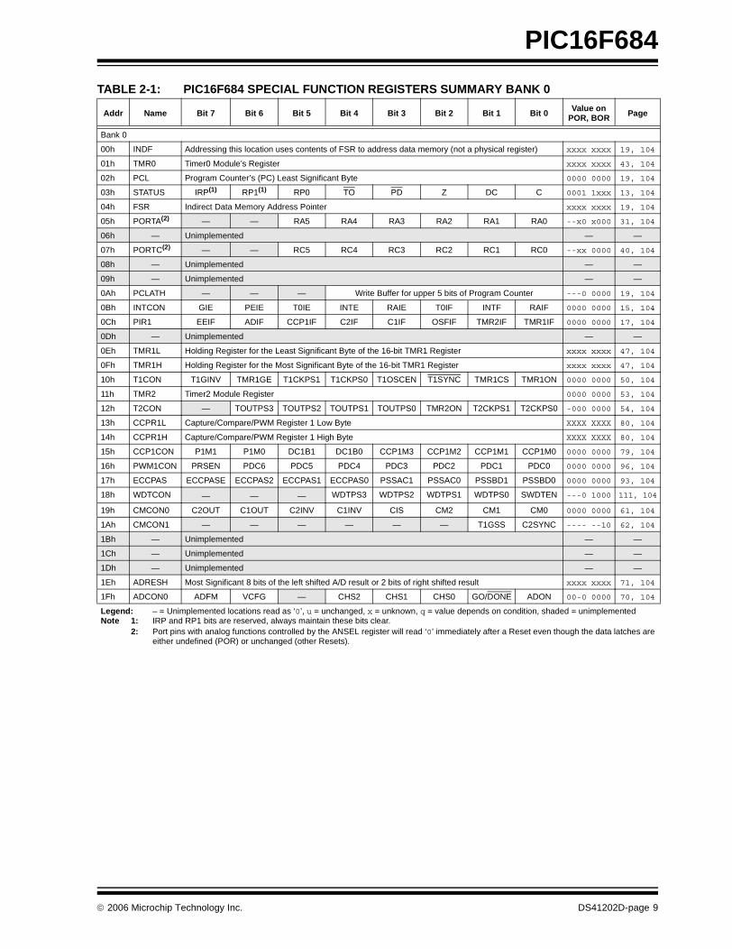
TABLE 2-1: PIC16F684 SPECIAL FUNCTION REGISTERS SUMMARY BANK 0
Addr Name Bit 7 Bit 6 Bit 5 Bit 4 Bit 3 Bit 2 Bit 1 Bit 0 Value on POR, BOR Page
Bank 0
00h INDF Addressing this location uses contents of FSR to address data memory (not a physical register) xxxx xxxx 19, 104
01h TMR0 Timer0 Module’s Register xxxx xxxx 43, 104
02h PCL Program Counter’s (PC) Least Significant Byte 0000 0000 19, 104
03h STATUS IRP(1) RP1(1) RP0 TO PD Z DC C 0001 1xxx 13, 104
04h FSR Indirect Data Memory Address Pointer xxxx xxxx 19, 104
05h PORTA(2) — — RA5 RA4 RA3 RA2 RA1 RA0 --x0 x000 31, 104
06h — Unimplemented — —
07h PORTC(2) — — RC5 RC4 RC3 RC2 RC1 RC0 --xx 0000 40, 104
08h — Unimplemented — —
09h — Unimplemented — —
0Ah PCLATH — — — Write Buffer for upper 5 bits of Program Counter ---0 0000 19, 104
0Bh INTCON GIE PEIE T0IE INTE RAIE T0IF INTF RAIF 0000 0000 15, 104
0Ch PIR1 EEIF ADIF CCP1IF C2IF C1IF OSFIF TMR2IF TMR1IF 0000 0000 17, 104
0Dh — Unimplemented — —
0Eh TMR1L Holding Register for the Least Significant Byte of the 16-bit TMR1 Register xxxx xxxx 47, 104
0Fh TMR1H Holding Register for the Most Significant Byte of the 16-bit TMR1 Register xxxx xxxx 47, 104
10h T1CON T1GINV TMR1GE T1CKPS1 T1CKPS0 T1OSCEN T1SYNC TMR1CS TMR1ON 0000 0000 50, 104
11h TMR2 Timer2 Module Register 0000 0000 53, 104
12h T2CON — TOUTPS3 TOUTPS2 TOUTPS1 TOUTPS0 TMR2ON T2CKPS1 T2CKPS0 -000 0000 54, 104
13h CCPR1L Capture/Compare/PWM Register 1 Low Byte XXXX XXXX 80, 104
14h CCPR1H Capture/Compare/PWM Register 1 High Byte XXXX XXXX 80, 104
15h CCP1CON P1M1 P1M0 DC1B1 DC1B0 CCP1M3 CCP1M2 CCP1M1 CCP1M0 0000 0000 79, 104
16h PWM1CON PRSEN PDC6 PDC5 PDC4 PDC3 PDC2 PDC1 PDC0 0000 0000 96, 104
17h ECCPAS ECCPASE ECCPAS2 ECCPAS1 ECCPAS0 PSSAC1 PSSAC0 PSSBD1 PSSBD0 0000 0000 93, 104
18h WDTCON — — — WDTPS3 WDTPS2 WDTPS1 WDTPS0 SWDTEN ---0 1000 111, 104
19h CMCON0 C2OUT C1OUT C2INV C1INV CIS CM2 CM1 CM0 0000 0000 61, 104
1Ah CMCON1 — — — — — — T1GSS C2SYNC ---- --10 62, 104
1Bh — Unimplemented — —
1Ch — Unimplemented — —
1Dh — Unimplemented — —
1Eh ADRESH Most Significant 8 bits of the left shifted A/D result or 2 bits of right shifted result xxxx xxxx 71, 104
1Fh ADCON0 ADFM VCFG — CHS2 CHS1 CHS0 GO/DONE ADON 00-0 0000 70, 104
Legend: – = Unimplemented locations read as ‘0’, u = unchanged, x = unknown, q = value depends on condition, shaded = unimplementedNote 1: IRP and RP1 bits are reserved, always maintain these bits clear.
2: Port pins with analog functions controlled by the ANSEL register will read ‘0’ immediately after a Reset even though the data latches are either undefined (POR) or unchanged (other Resets).
© 2006 Microchip Technology Inc. DS41202D-page 9
PIC16F684
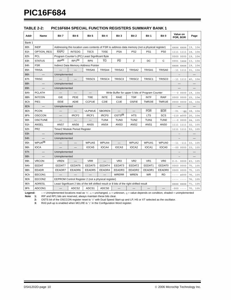
TABLE 2-2: PIC16F684 SPECIAL FUNCTION REGISTERS SUMMARY BANK 1
Addr Name Bit 7 Bit 6 Bit 5 Bit 4 Bit 3 Bit 2 Bit 1 Bit 0 Value on POR, BOR Page
Bank 1
80h INDF Addressing this location uses contents of FSR to address data memory (not a physical register) xxxx xxxx 19, 104
81h OPTION_REG RAPU INTEDG T0CS T0SE PSA PS2 PS1 PS0 1111 1111 14, 104
82h PCL Program Counter’s (PC) Least Significant Byte 0000 0000 19, 104
83h STATUS IRP(1) RP1(1) RP0 TO PD Z DC C 0001 1xxx 13, 104
84h FSR Indirect Data Memory Address Pointer xxxx xxxx 19, 104
85h TRISA — — TRISA5 TRISA4 TRISA3 TRISA2 TRISA1 TRISA0 --11 1111 31, 104
86h — Unimplemented — —
87h TRISC — — TRISC5 TRISC4 TRISC3 TRISC2 TRISC1 TRISC0 --11 1111 40, 104
88h — Unimplemented — —
89h — Unimplemented — —
8Ah PCLATH — — — Write Buffer for upper 5 bits of Program Counter ---0 0000 19, 104
8Bh INTCON GIE PEIE T0IE INTE RAIE T0IF INTF RAIF 0000 0000 15, 104
8Ch PIE1 EEIE ADIE CCP1IE C2IE C1IE OSFIE TMR2IE TMR1IE 0000 0000 16, 104
8Dh — Unimplemented — —
8Eh PCON — — ULPWUE SBOREN — — POR BOR --01 --qq 18, 104
8Fh OSCCON — IRCF2 IRCF1 IRCF0 OSTS(2) HTS LTS SCS -110 x000 20, 104
90h OSCTUNE — — — TUN4 TUN3 TUN2 TUN1 TUN0 ---0 0000 24, 105
91h ANSEL ANS7 ANS6 ANS5 ANS4 ANS3 ANS2 ANS1 ANS0 1111 1111 32, 105
92h PR2 Timer2 Module Period Register 1111 1111 53, 105
93h — Unimplemented — —
94h — Unimplemented — —
95h WPUA(3) — — WPUA5 WPUA4 — WPUA2 WPUA1 WPUA0 --11 -111 33, 105
96h IOCA — — IOCA5 IOCA4 IOCA3 IOCA2 IOCA1 IOCA0 --00 0000 33, 105
97h — Unimplemented — —
98h — Unimplemented — —
99h VRCON VREN — VRR — VR3 VR2 VR1 VR0 0-0- 0000 63, 105
9Ah EEDAT EEDAT7 EEDAT6 EEDAT5 EEDAT4 EEDAT3 EEDAT2 EEDAT1 EEDAT0 0000 0000 75, 105
9Bh EEADR EEADR7 EEADR6 EEADR5 EEADR4 EEADR3 EEADR2 EEADR1 EEADR0 0000 0000 75, 105
9Ch EECON1 — — — — WRERR WREN WR RD ---- x000 76, 105
9Dh EECON2 EEPROM Control Register 2 (not a physical register) ---- ---- 76, 105
9Eh ADRESL Least Significant 2 bits of the left shifted result or 8 bits of the right shifted result xxxx xxxx 71, 105
9Fh ADCON1 — ADCS2 ADCS1 ADCS0 — — — — -000 ---- 70, 105
Legend: – = Unimplemented locations read as ‘0’, u = unchanged, x = unknown, q = value depends on condition, shaded = unimplementedNote 1: IRP and RP1 bits are reserved, always maintain these bits clear.
2: OSTS bit of the OSCCON register reset to ‘0’ with Dual Speed Start-up and LP, HS or XT selected as the oscillator.3: RA3 pull-up is enabled when MCLRE is ‘1’ in the Configuration Word register.
DS41202D-page 10 © 2006 Microchip Technology Inc.
PIC16F684
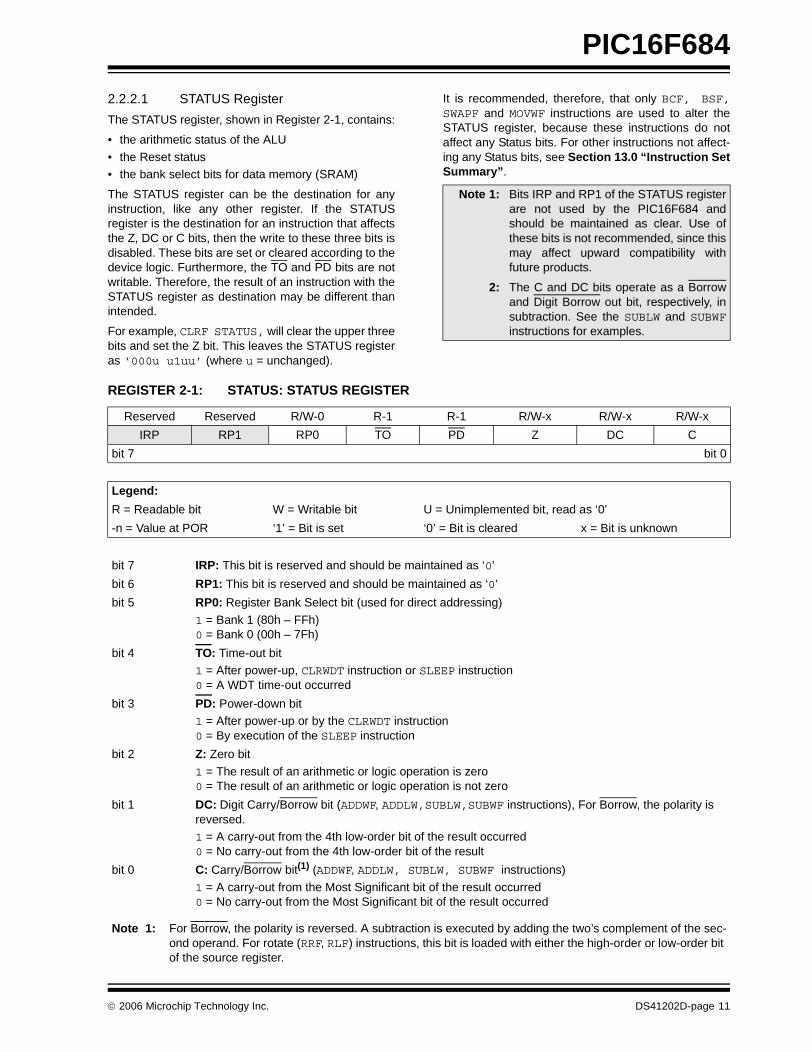
2.2.2.1 STATUS Register
The STATUS register, shown in Register 2-1, contains:
• the arithmetic status of the ALU
• the Reset status• the bank select bits for data memory (SRAM)
The STATUS register can be the destination for anyinstruction, like any other register. If the STATUSregister is the destination for an instruction that affectsthe Z, DC or C bits, then the write to these three bits isdisabled. These bits are set or cleared according to thedevice logic. Furthermore, the TO and PD bits are notwritable. Therefore, the result of an instruction with theSTATUS register as destination may be different thanintended.
For example, CLRF STATUS, will clear the upper threebits and set the Z bit. This leaves the STATUS registeras ‘000u u1uu’ (where u = unchanged).
It is recommended, therefore, that only BCF, BSF,SWAPF and MOVWF instructions are used to alter theSTATUS register, because these instructions do notaffect any Status bits. For other instructions not affect-ing any Status bits, see Section 13.0 “Instruction SetSummary”.
Note 1: Bits IRP and RP1 of the STATUS registerare not used by the PIC16F684 andshould be maintained as clear. Use ofthese bits is not recommended, since thismay affect upward compatibility withfuture products.
2: The C and DC bits operate as a Borrowand Digit Borrow out bit, respectively, insubtraction. See the SUBLW and SUBWFinstructions for examples.
REGISTER 2-1: STATUS: STATUS REGISTER
Reserved Reserved R/W-0 R-1 R-1 R/W-x R/W-x R/W-x
IRP RP1 RP0 TO PD Z DC C
bit 7 bit 0
Legend:
R = Readable bit W = Writable bit U = Unimplemented bit, read as ‘0’
-n = Value at POR ‘1’ = Bit is set ‘0’ = Bit is cleared x = Bit is unknown
bit 7 IRP: This bit is reserved and should be maintained as ‘0’
bit 6 RP1: This bit is reserved and should be maintained as ‘0’
bit 5 RP0: Register Bank Select bit (used for direct addressing)
1 = Bank 1 (80h – FFh)0 = Bank 0 (00h – 7Fh)
bit 4 TO: Time-out bit1 = After power-up, CLRWDT instruction or SLEEP instruction0 = A WDT time-out occurred
bit 3 PD: Power-down bit1 = After power-up or by the CLRWDT instruction0 = By execution of the SLEEP instruction
bit 2 Z: Zero bit
1 = The result of an arithmetic or logic operation is zero0 = The result of an arithmetic or logic operation is not zero
bit 1 DC: Digit Carry/Borrow bit (ADDWF, ADDLW,SUBLW,SUBWF instructions), For Borrow, the polarity is reversed.1 = A carry-out from the 4th low-order bit of the result occurred0 = No carry-out from the 4th low-order bit of the result
bit 0 C: Carry/Borrow bit(1) (ADDWF, ADDLW, SUBLW, SUBWF instructions)
1 = A carry-out from the Most Significant bit of the result occurred0 = No carry-out from the Most Significant bit of the result occurred
Note 1: For Borrow, the polarity is reversed. A subtraction is executed by adding the two’s complement of the sec-ond operand. For rotate (RRF, RLF) instructions, this bit is loaded with either the high-order or low-order bit of the source register.
© 2006 Microchip Technology Inc. DS41202D-page 11
PIC16F684
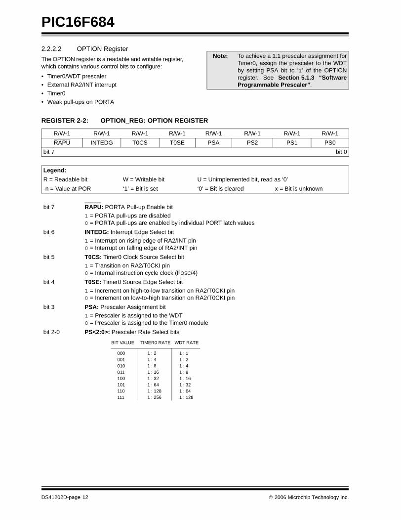
2.2.2.2 OPTION Register
The OPTION register is a readable and writable register,which contains various control bits to configure:
• Timer0/WDT prescaler• External RA2/INT interrupt
• Timer0• Weak pull-ups on PORTA
Note: To achieve a 1:1 prescaler assignment forTimer0, assign the prescaler to the WDTby setting PSA bit to ‘1’ of the OPTIONregister. See Section 5.1.3 “SoftwareProgrammable Prescaler”.
REGISTER 2-2: OPTION_REG: OPTION REGISTER
R/W-1 R/W-1 R/W-1 R/W-1 R/W-1 R/W-1 R/W-1 R/W-1
RAPU INTEDG T0CS T0SE PSA PS2 PS1 PS0
bit 7 bit 0
Legend:
R = Readable bit W = Writable bit U = Unimplemented bit, read as ‘0’
-n = Value at POR ‘1’ = Bit is set ‘0’ = Bit is cleared x = Bit is unknown
bit 7 RAPU: PORTA Pull-up Enable bit
1 = PORTA pull-ups are disabled0 = PORTA pull-ups are enabled by individual PORT latch values
bit 6 INTEDG: Interrupt Edge Select bit1 = Interrupt on rising edge of RA2/INT pin0 = Interrupt on falling edge of RA2/INT pin
bit 5 T0CS: Timer0 Clock Source Select bit1 = Transition on RA2/T0CKI pin0 = Internal instruction cycle clock (FOSC/4)
bit 4 T0SE: Timer0 Source Edge Select bit
1 = Increment on high-to-low transition on RA2/T0CKI pin0 = Increment on low-to-high transition on RA2/T0CKI pin
bit 3 PSA: Prescaler Assignment bit1 = Prescaler is assigned to the WDT0 = Prescaler is assigned to the Timer0 module
bit 2-0 PS<2:0>: Prescaler Rate Select bits
000001010011100101110111
1 : 21 : 41 : 81 : 161 : 321 : 641 : 1281 : 256
1 : 11 : 21 : 41 : 81 : 161 : 321 : 641 : 128
BIT VALUE TIMER0 RATE WDT RATE
DS41202D-page 12 © 2006 Microchip Technology Inc.
PIC16F684
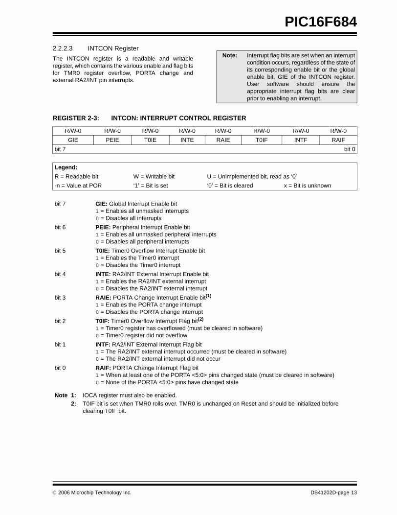
2.2.2.3 INTCON Register
The INTCON register is a readable and writableregister, which contains the various enable and flag bitsfor TMR0 register overflow, PORTA change andexternal RA2/INT pin interrupts.
Note: Interrupt flag bits are set when an interruptcondition occurs, regardless of the state ofits corresponding enable bit or the globalenable bit, GIE of the INTCON register.User software should ensure theappropriate interrupt flag bits are clearprior to enabling an interrupt.
REGISTER 2-3: INTCON: INTERRUPT CONTROL REGISTER
R/W-0 R/W-0 R/W-0 R/W-0 R/W-0 R/W-0 R/W-0 R/W-0
GIE PEIE T0IE INTE RAIE T0IF INTF RAIF
bit 7 bit 0
Legend:
R = Readable bit W = Writable bit U = Unimplemented bit, read as ‘0’
-n = Value at POR ‘1’ = Bit is set ‘0’ = Bit is cleared x = Bit is unknown
bit 7 GIE: Global Interrupt Enable bit1 = Enables all unmasked interrupts0 = Disables all interrupts
bit 6 PEIE: Peripheral Interrupt Enable bit1 = Enables all unmasked peripheral interrupts0 = Disables all peripheral interrupts
bit 5 T0IE: Timer0 Overflow Interrupt Enable bit1 = Enables the Timer0 interrupt0 = Disables the Timer0 interrupt
bit 4 INTE: RA2/INT External Interrupt Enable bit1 = Enables the RA2/INT external interrupt0 = Disables the RA2/INT external interrupt
bit 3 RAIE: PORTA Change Interrupt Enable bit(1)
1 = Enables the PORTA change interrupt0 = Disables the PORTA change interrupt
bit 2 T0IF: Timer0 Overflow Interrupt Flag bit(2)
1 = Timer0 register has overflowed (must be cleared in software)0 = Timer0 register did not overflow
bit 1 INTF: RA2/INT External Interrupt Flag bit1 = The RA2/INT external interrupt occurred (must be cleared in software)0 = The RA2/INT external interrupt did not occur
bit 0 RAIF: PORTA Change Interrupt Flag bit1 = When at least one of the PORTA <5:0> pins changed state (must be cleared in software)0 = None of the PORTA <5:0> pins have changed state
Note 1: IOCA register must also be enabled.2: T0IF bit is set when TMR0 rolls over. TMR0 is unchanged on Reset and should be initialized before
clearing T0IF bit.
© 2006 Microchip Technology Inc. DS41202D-page 13
PIC16F684
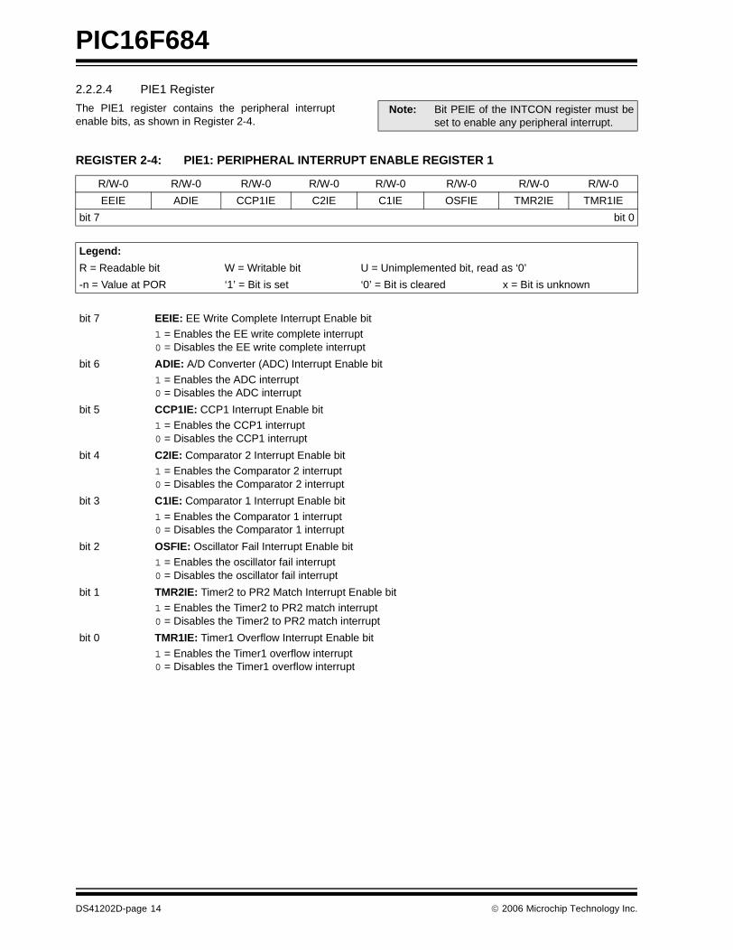
2.2.2.4 PIE1 Register
The PIE1 register contains the peripheral interruptenable bits, as shown in Register 2-4.
Note: Bit PEIE of the INTCON register must beset to enable any peripheral interrupt.
REGISTER 2-4: PIE1: PERIPHERAL INTERRUPT ENABLE REGISTER 1
R/W-0 R/W-0 R/W-0 R/W-0 R/W-0 R/W-0 R/W-0 R/W-0
EEIE ADIE CCP1IE C2IE C1IE OSFIE TMR2IE TMR1IE
bit 7 bit 0
Legend:
R = Readable bit W = Writable bit U = Unimplemented bit, read as ‘0’
-n = Value at POR ‘1’ = Bit is set ‘0’ = Bit is cleared x = Bit is unknown
bit 7 EEIE: EE Write Complete Interrupt Enable bit1 = Enables the EE write complete interrupt0 = Disables the EE write complete interrupt
bit 6 ADIE: A/D Converter (ADC) Interrupt Enable bit
1 = Enables the ADC interrupt0 = Disables the ADC interrupt
bit 5 CCP1IE: CCP1 Interrupt Enable bit1 = Enables the CCP1 interrupt0 = Disables the CCP1 interrupt
bit 4 C2IE: Comparator 2 Interrupt Enable bit1 = Enables the Comparator 2 interrupt0 = Disables the Comparator 2 interrupt
bit 3 C1IE: Comparator 1 Interrupt Enable bit
1 = Enables the Comparator 1 interrupt0 = Disables the Comparator 1 interrupt
bit 2 OSFIE: Oscillator Fail Interrupt Enable bit1 = Enables the oscillator fail interrupt0 = Disables the oscillator fail interrupt
bit 1 TMR2IE: Timer2 to PR2 Match Interrupt Enable bit1 = Enables the Timer2 to PR2 match interrupt0 = Disables the Timer2 to PR2 match interrupt
bit 0 TMR1IE: Timer1 Overflow Interrupt Enable bit
1 = Enables the Timer1 overflow interrupt0 = Disables the Timer1 overflow interrupt
DS41202D-page 14 © 2006 Microchip Technology Inc.
PIC16F684
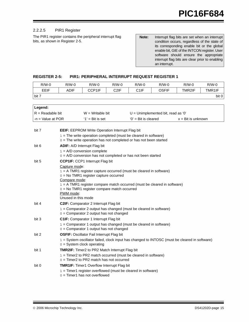
2.2.2.5 PIR1 Register
The PIR1 register contains the peripheral interrupt flagbits, as shown in Register 2-5.
Note: Interrupt flag bits are set when an interruptcondition occurs, regardless of the state ofits corresponding enable bit or the globalenable bit, GIE of the INTCON register. Usersoftware should ensure the appropriateinterrupt flag bits are clear prior to enablingan interrupt.
REGISTER 2-5: PIR1: PERIPHERAL INTERRUPT REQUEST REGISTER 1
R/W-0 R/W-0 R/W-0 R/W-0 R/W-0 R/W-0 R/W-0 R/W-0
EEIF ADIF CCP1IF C2IF C1IF OSFIF TMR2IF TMR1IF
bit 7 bit 0
Legend:
R = Readable bit W = Writable bit U = Unimplemented bit, read as ‘0’
-n = Value at POR ‘1’ = Bit is set ‘0’ = Bit is cleared x = Bit is unknown
bit 7 EEIF: EEPROM Write Operation Interrupt Flag bit1 = The write operation completed (must be cleared in software)0 = The write operation has not completed or has not been started
bit 6 ADIF: A/D Interrupt Flag bit 1 = A/D conversion complete0 = A/D conversion has not completed or has not been started
bit 5 CCP1IF: CCP1 Interrupt Flag bit
Capture mode:1 = A TMR1 register capture occurred (must be cleared in software)0 = No TMR1 register capture occurredCompare mode:1 = A TMR1 register compare match occurred (must be cleared in software)0 = No TMR1 register compare match occurredPWM mode:Unused in this mode
bit 4 C2IF: Comparator 2 Interrupt Flag bit1 = Comparator 2 output has changed (must be cleared in software)0 = Comparator 2 output has not changed
bit 3 C1IF: Comparator 1 Interrupt Flag bit1 = Comparator 1 output has changed (must be cleared in software)0 = Comparator 1 output has not changed
bit 2 OSFIF: Oscillator Fail Interrupt Flag bit
1 = System oscillator failed, clock input has changed to INTOSC (must be cleared in software)0 = System clock operating
bit 1 TMR2IF: Timer2 to PR2 Match Interrupt Flag bit1 = Timer2 to PR2 match occurred (must be cleared in software)0 = Timer2 to PR2 match has not occurred
bit 0 TMR1IF: Timer1 Overflow Interrupt Flag bit1 = Timer1 register overflowed (must be cleared in software)0 = Timer1 has not overflowed
© 2006 Microchip Technology Inc. DS41202D-page 15
PIC16F684
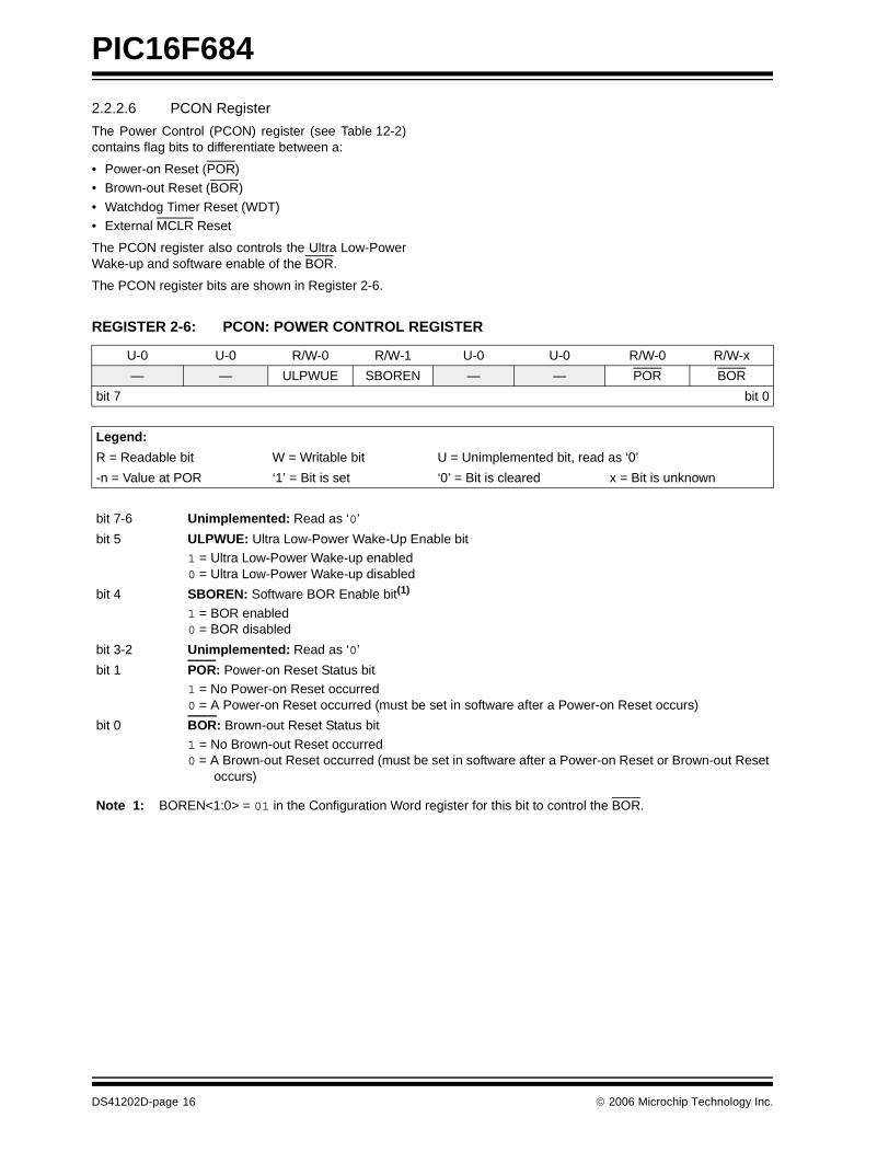
2.2.2.6 PCON Register
The Power Control (PCON) register (see Table 12-2)contains flag bits to differentiate between a:
• Power-on Reset (POR)• Brown-out Reset (BOR)
• Watchdog Timer Reset (WDT)• External MCLR Reset
The PCON register also controls the Ultra Low-PowerWake-up and software enable of the BOR.
The PCON register bits are shown in Register 2-6.
REGISTER 2-6: PCON: POWER CONTROL REGISTER
U-0 U-0 R/W-0 R/W-1 U-0 U-0 R/W-0 R/W-x
— — ULPWUE SBOREN — — POR BOR
bit 7 bit 0
Legend:
R = Readable bit W = Writable bit U = Unimplemented bit, read as ‘0’
-n = Value at POR ‘1’ = Bit is set ‘0’ = Bit is cleared x = Bit is unknown
bit 7-6 Unimplemented: Read as ‘0’
bit 5 ULPWUE: Ultra Low-Power Wake-Up Enable bit1 = Ultra Low-Power Wake-up enabled0 = Ultra Low-Power Wake-up disabled
bit 4 SBOREN: Software BOR Enable bit(1)
1 = BOR enabled0 = BOR disabled
bit 3-2 Unimplemented: Read as ‘0’
bit 1 POR: Power-on Reset Status bit1 = No Power-on Reset occurred0 = A Power-on Reset occurred (must be set in software after a Power-on Reset occurs)
bit 0 BOR: Brown-out Reset Status bit
1 = No Brown-out Reset occurred0 = A Brown-out Reset occurred (must be set in software after a Power-on Reset or Brown-out Reset
occurs)
Note 1: BOREN<1:0> = 01 in the Configuration Word register for this bit to control the BOR.
DS41202D-page 16 © 2006 Microchip Technology Inc.
PIC16F684
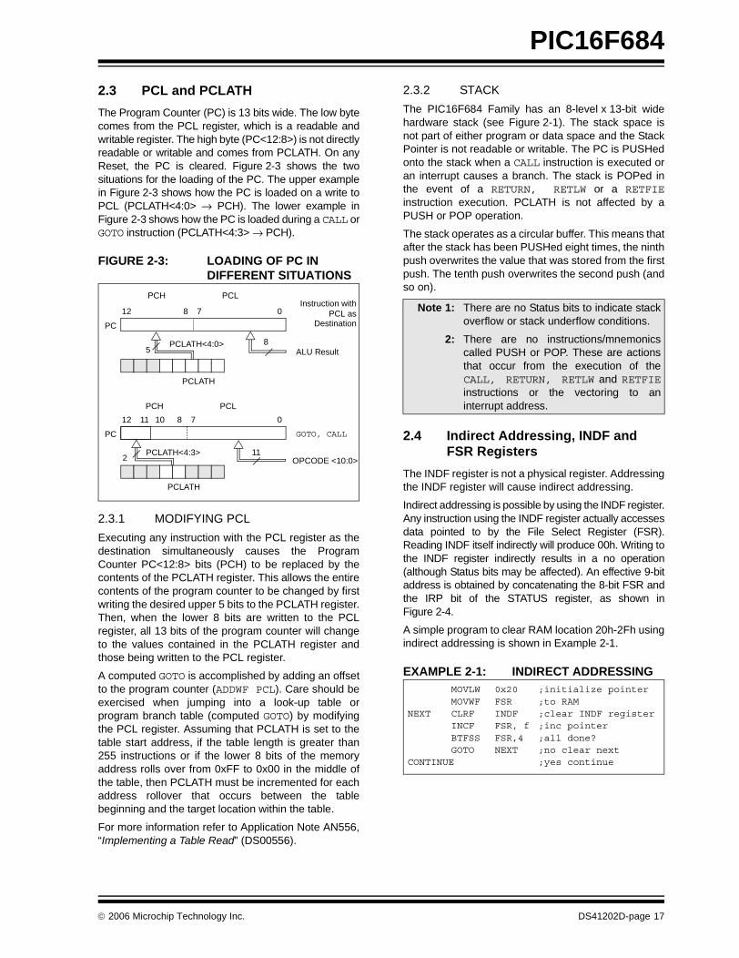
2.3 PCL and PCLATH
The Program Counter (PC) is 13 bits wide. The low bytecomes from the PCL register, which is a readable andwritable register. The high byte (PC<12:8>) is not directlyreadable or writable and comes from PCLATH. On anyReset, the PC is cleared. Figure 2-3 shows the twosituations for the loading of the PC. The upper examplein Figure 2-3 shows how the PC is loaded on a write toPCL (PCLATH<4:0> → PCH). The lower example inFigure 2-3 shows how the PC is loaded during a CALL orGOTO instruction (PCLATH<4:3> → PCH).
FIGURE 2-3: LOADING OF PC IN DIFFERENT SITUATIONS
2.3.1 MODIFYING PCL
Executing any instruction with the PCL register as thedestination simultaneously causes the ProgramCounter PC<12:8> bits (PCH) to be replaced by thecontents of the PCLATH register. This allows the entirecontents of the program counter to be changed by firstwriting the desired upper 5 bits to the PCLATH register.Then, when the lower 8 bits are written to the PCLregister, all 13 bits of the program counter will changeto the values contained in the PCLATH register andthose being written to the PCL register.
A computed GOTO is accomplished by adding an offsetto the program counter (ADDWF PCL). Care should beexercised when jumping into a look-up table orprogram branch table (computed GOTO) by modifyingthe PCL register. Assuming that PCLATH is set to thetable start address, if the table length is greater than255 instructions or if the lower 8 bits of the memoryaddress rolls over from 0xFF to 0x00 in the middle ofthe table, then PCLATH must be incremented for eachaddress rollover that occurs between the tablebeginning and the target location within the table.
For more information refer to Application Note AN556,“Implementing a Table Read” (DS00556).
2.3.2 STACK
The PIC16F684 Family has an 8-level x 13-bit widehardware stack (see Figure 2-1). The stack space isnot part of either program or data space and the StackPointer is not readable or writable. The PC is PUSHedonto the stack when a CALL instruction is executed oran interrupt causes a branch. The stack is POPed inthe event of a RETURN, RETLW or a RETFIEinstruction execution. PCLATH is not affected by aPUSH or POP operation.
The stack operates as a circular buffer. This means thatafter the stack has been PUSHed eight times, the ninthpush overwrites the value that was stored from the firstpush. The tenth push overwrites the second push (andso on).
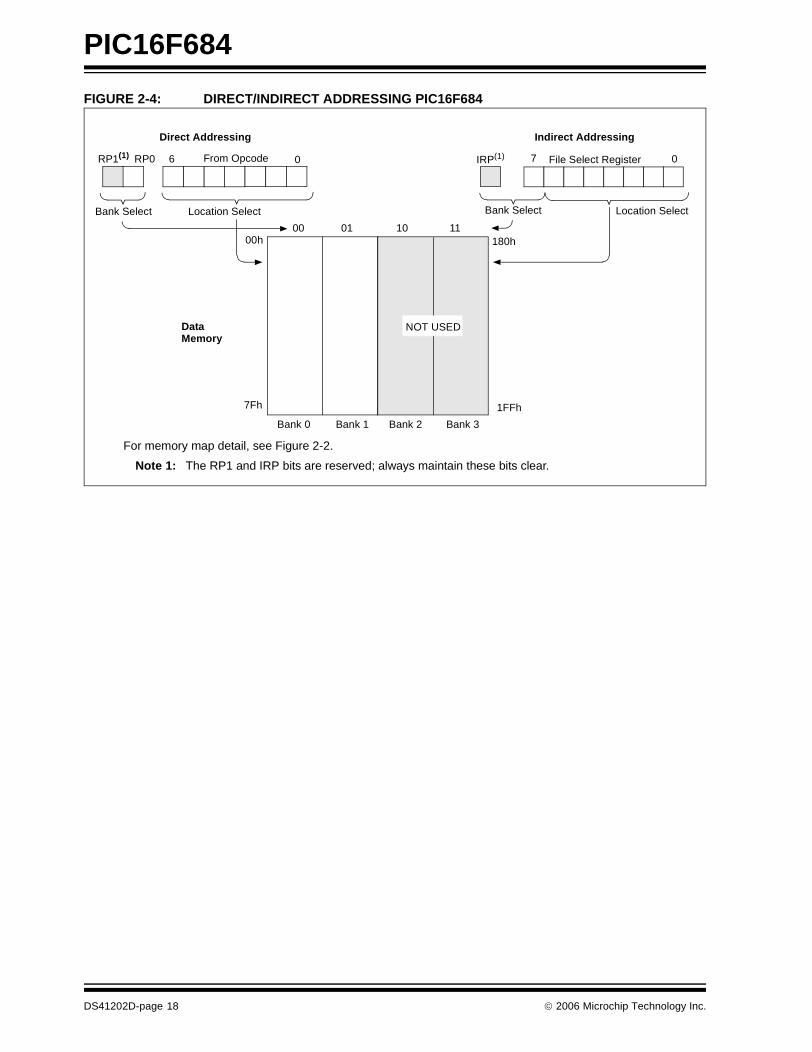
2.4 Indirect Addressing, INDF and FSR Registers
The INDF register is not a physical register. Addressingthe INDF register will cause indirect addressing.
Indirect addressing is possible by using the INDF register.Any instruction using the INDF register actually accessesdata pointed to by the File Select Register (FSR).Reading INDF itself indirectly will produce 00h. Writing tothe INDF register indirectly results in a no operation(although Status bits may be affected). An effective 9-bitaddress is obtained by concatenating the 8-bit FSR andthe IRP bit of the STATUS register, as shown inFigure 2-4.
A simple program to clear RAM location 20h-2Fh usingindirect addressing is shown in Example 2-1.
EXAMPLE 2-1: INDIRECT ADDRESSING
PC
12 8 7 0
5PCLATH<4:0>
PCLATH
Instruction with
ALU Result
GOTO, CALL
OPCODE <10:0>
8
PC
12 11 10 0
11PCLATH<4:3>
PCH PCL
8 7
2
PCLATH
PCH PCL
PCL as Destination
Note 1: There are no Status bits to indicate stackoverflow or stack underflow conditions.
2: There are no instructions/mnemonicscalled PUSH or POP. These are actionsthat occur from the execution of theCALL, RETURN, RETLW and RETFIEinstructions or the vectoring to aninterrupt address.
MOVLW 0x20 ;initialize pointerMOVWF FSR ;to RAM
NEXT CLRF INDF ;clear INDF registerINCF FSR, f ;inc pointerBTFSS FSR,4 ;all done?GOTO NEXT ;no clear next
CONTINUE ;yes continue
© 2006 Microchip Technology Inc. DS41202D-page 17
PIC16F684
FIGURE 2-4: DIRECT/INDIRECT ADDRESSING PIC16F684
For memory map detail, see Figure 2-2.
Note 1: The RP1 and IRP bits are reserved; always maintain these bits clear.
DataMemory
Indirect AddressingDirect Addressing
Bank Select Location Select
RP1(1) RP0 6 0From Opcode IRP(1) File Select Register7 0
Bank Select Location Select
00 01 10 11180h
1FFh
00h
7Fh
Bank 0 Bank 1 Bank 2 Bank 3
NOT USED
DS41202D-page 18 © 2006 Microchip Technology Inc.
PIC16F684
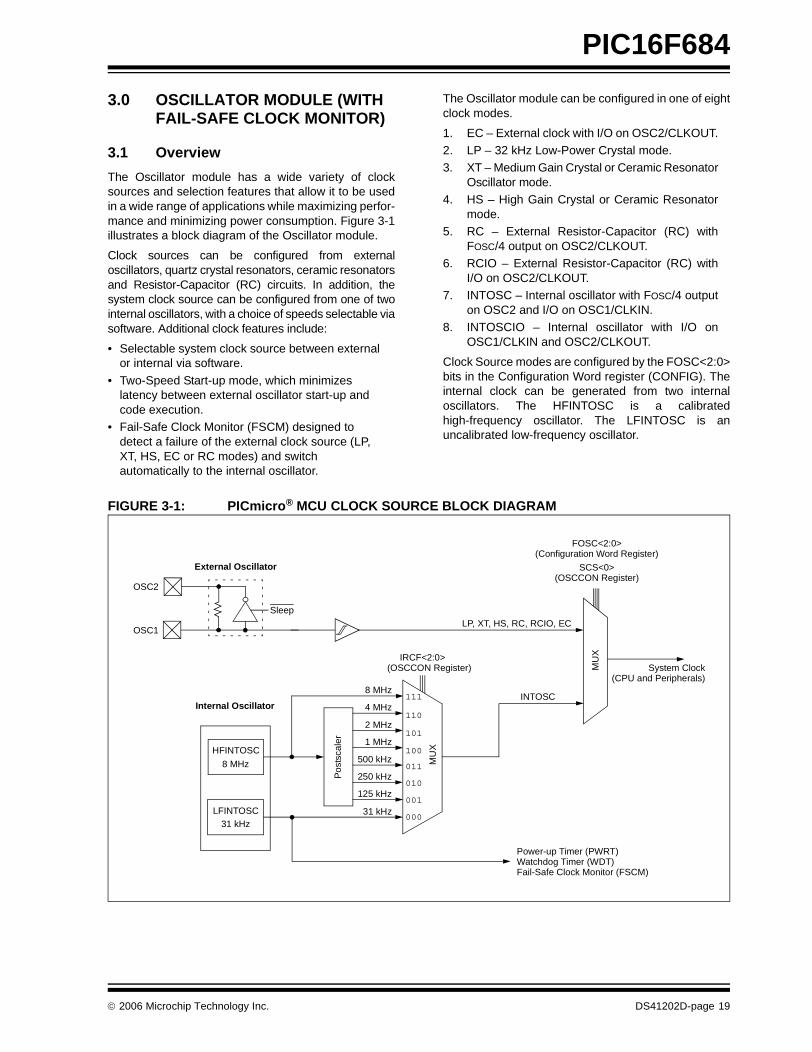
3.0 OSCILLATOR MODULE (WITH FAIL-SAFE CLOCK MONITOR)
3.1 Overview
The Oscillator module has a wide variety of clocksources and selection features that allow it to be usedin a wide range of applications while maximizing perfor-mance and minimizing power consumption. Figure 3-1illustrates a block diagram of the Oscillator module.
Clock sources can be configured from externaloscillators, quartz crystal resonators, ceramic resonatorsand Resistor-Capacitor (RC) circuits. In addition, thesystem clock source can be configured from one of twointernal oscillators, with a choice of speeds selectable viasoftware. Additional clock features include:
• Selectable system clock source between external or internal via software.
• Two-Speed Start-up mode, which minimizes latency between external oscillator start-up and code execution.
• Fail-Safe Clock Monitor (FSCM) designed to detect a failure of the external clock source (LP, XT, HS, EC or RC modes) and switch automatically to the internal oscillator.
The Oscillator module can be configured in one of eightclock modes.
1. EC – External clock with I/O on OSC2/CLKOUT.2. LP – 32 kHz Low-Power Crystal mode.3. XT – Medium Gain Crystal or Ceramic Resonator
Oscillator mode.4. HS – High Gain Crystal or Ceramic Resonator
mode.5. RC – External Resistor-Capacitor (RC) with
FOSC/4 output on OSC2/CLKOUT.6. RCIO – External Resistor-Capacitor (RC) with
I/O on OSC2/CLKOUT.7. INTOSC – Internal oscillator with FOSC/4 output
on OSC2 and I/O on OSC1/CLKIN.8. INTOSCIO – Internal oscillator with I/O on
OSC1/CLKIN and OSC2/CLKOUT.
Clock Source modes are configured by the FOSC<2:0>bits in the Configuration Word register (CONFIG). Theinternal clock can be generated from two internaloscillators. The HFINTOSC is a calibratedhigh-frequency oscillator. The LFINTOSC is anuncalibrated low-frequency oscillator.
FIGURE 3-1: PICmicro® MCU CLOCK SOURCE BLOCK DIAGRAM
(CPU and Peripherals)
OSC1
OSC2
Sleep
External Oscillator
LP, XT, HS, RC, RCIO, EC
System Clock
Pos
tsca
ler
MU
X
MU
X
8 MHz
4 MHz
2 MHz
1 MHz
500 kHz
125 kHz
250 kHz
IRCF<2:0>
111
110
101
100
011
010
001
00031 kHz
Power-up Timer (PWRT)
FOSC<2:0>(Configuration Word Register)
SCS<0>(OSCCON Register)
Internal Oscillator
(OSCCON Register)
Watchdog Timer (WDT)Fail-Safe Clock Monitor (FSCM)
HFINTOSC
8 MHz
LFINTOSC31 kHz
INTOSC
© 2006 Microchip Technology Inc. DS41202D-page 19
PIC16F684
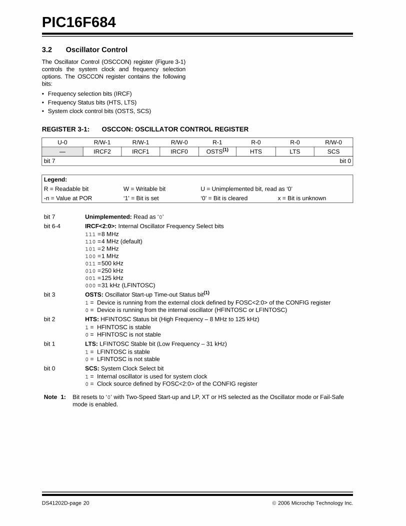
3.2 Oscillator Control
The Oscillator Control (OSCCON) register (Figure 3-1)controls the system clock and frequency selectionoptions. The OSCCON register contains the followingbits:
• Frequency selection bits (IRCF)
• Frequency Status bits (HTS, LTS)• System clock control bits (OSTS, SCS)
REGISTER 3-1: OSCCON: OSCILLATOR CONTROL REGISTER
U-0 R/W-1 R/W-1 R/W-0 R-1 R-0 R-0 R/W-0
— IRCF2 IRCF1 IRCF0 OSTS(1) HTS LTS SCS
bit 7 bit 0
Legend:
R = Readable bit W = Writable bit U = Unimplemented bit, read as ‘0’
-n = Value at POR ‘1’ = Bit is set ‘0’ = Bit is cleared x = Bit is unknown
bit 7 Unimplemented: Read as ‘0’
bit 6-4 IRCF<2:0>: Internal Oscillator Frequency Select bits111 =8 MHz110 =4 MHz (default)101 =2 MHz100 =1 MHz011 =500 kHz010 =250 kHz001 =125 kHz000 =31 kHz (LFINTOSC)
bit 3 OSTS: Oscillator Start-up Time-out Status bit(1)
1 = Device is running from the external clock defined by FOSC<2:0> of the CONFIG register0 = Device is running from the internal oscillator (HFINTOSC or LFINTOSC)
bit 2 HTS: HFINTOSC Status bit (High Frequency – 8 MHz to 125 kHz)1 = HFINTOSC is stable0 = HFINTOSC is not stable
bit 1 LTS: LFINTOSC Stable bit (Low Frequency – 31 kHz)1 = LFINTOSC is stable0 = LFINTOSC is not stable
bit 0 SCS: System Clock Select bit1 = Internal oscillator is used for system clock0 = Clock source defined by FOSC<2:0> of the CONFIG register
Note 1: Bit resets to ‘0’ with Two-Speed Start-up and LP, XT or HS selected as the Oscillator mode or Fail-Safe mode is enabled.
DS41202D-page 20 © 2006 Microchip Technology Inc.
PIC16F684
3.3 Clock Source Modes
Clock Source modes can be classified as external orinternal.
• External Clock modes rely on external circuitry for the clock source. Examples are: Oscillator mod-ules (EC mode), quartz crystal resonators or ceramic resonators (LP, XT and HS modes) and Resistor-Capacitor (RC) mode circuits.
• Internal clock sources are contained internally within the Oscillator module. The Oscillator module has two internal oscillators: the 8 MHz High-Frequency Internal Oscillator (HFINTOSC) and the 31 kHz Low-Frequency Internal Oscillator (LFINTOSC).
The system clock can be selected between external orinternal clock sources via the System Clock Select(SCS) bit of the OSCCON register. See Section 3.6“Clock Switching” for additional information.
3.4 External Clock Modes
3.4.1 OSCILLATOR START-UP TIMER (OST)
If the Oscillator module is configured for LP, XT or HSmodes, the Oscillator Start-up Timer (OST) counts1024 oscillations from OSC1. This occurs following aPower-on Reset (POR) and when the Power-up Timer(PWRT) has expired (if configured), or a wake-up fromSleep. During this time, the program counter does notincrement and program execution is suspended. TheOST ensures that the oscillator circuit, using a quartzcrystal resonator or ceramic resonator, has started andis providing a stable system clock to the Oscillatormodule. When switching between clock sources, adelay is required to allow the new clock to stabilize.These oscillator delays are shown in Table 3-1.
In order to minimize latency between external oscillatorstart-up and code execution, the Two-Speed ClockStart-up mode can be selected (see Section 3.7“Two-Speed Clock Start-up Mode”).
TABLE 3-1: OSCILLATOR DELAY EXAMPLES
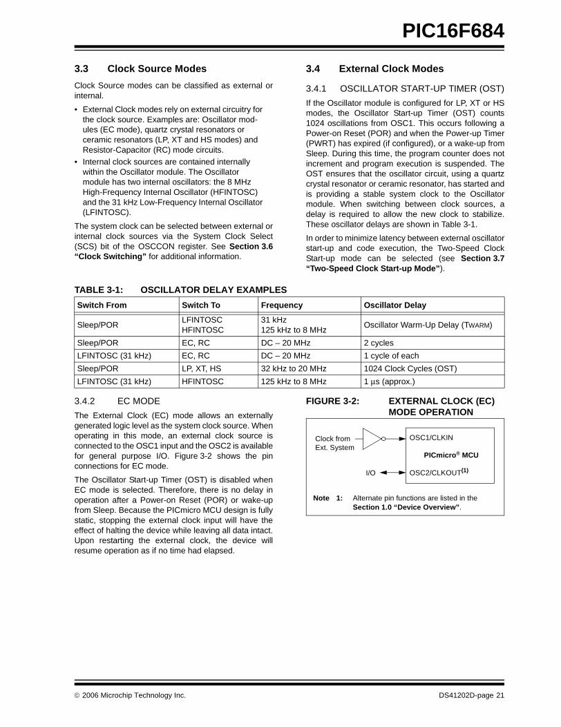
3.4.2 EC MODE
The External Clock (EC) mode allows an externallygenerated logic level as the system clock source. Whenoperating in this mode, an external clock source isconnected to the OSC1 input and the OSC2 is availablefor general purpose I/O. Figure 3-2 shows the pinconnections for EC mode.
The Oscillator Start-up Timer (OST) is disabled whenEC mode is selected. Therefore, there is no delay inoperation after a Power-on Reset (POR) or wake-upfrom Sleep. Because the PICmicro MCU design is fullystatic, stopping the external clock input will have theeffect of halting the device while leaving all data intact.Upon restarting the external clock, the device willresume operation as if no time had elapsed.
FIGURE 3-2: EXTERNAL CLOCK (EC) MODE OPERATION
Switch From Switch To Frequency Oscillator Delay
Sleep/PORLFINTOSCHFINTOSC
31 kHz125 kHz to 8 MHz
Oscillator Warm-Up Delay (TWARM)
Sleep/POR EC, RC DC – 20 MHz 2 cycles
LFINTOSC (31 kHz) EC, RC DC – 20 MHz 1 cycle of each
Sleep/POR LP, XT, HS 32 kHz to 20 MHz 1024 Clock Cycles (OST)
LFINTOSC (31 kHz) HFINTOSC 125 kHz to 8 MHz 1 μs (approx.)
OSC1/CLKIN
OSC2/CLKOUT(1)I/O
Clock fromExt. System
PICmicro® MCU
Note 1: Alternate pin functions are listed in the Section 1.0 “Device Overview”.
© 2006 Microchip Technology Inc. DS41202D-page 21
PIC16F684
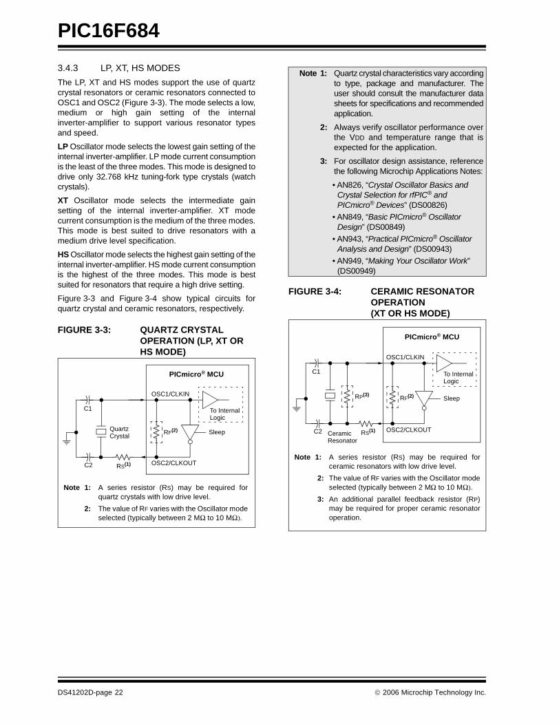
3.4.3 LP, XT, HS MODES
The LP, XT and HS modes support the use of quartzcrystal resonators or ceramic resonators connected toOSC1 and OSC2 (Figure 3-3). The mode selects a low,medium or high gain setting of the internalinverter-amplifier to support various resonator typesand speed.
LP Oscillator mode selects the lowest gain setting of theinternal inverter-amplifier. LP mode current consumptionis the least of the three modes. This mode is designed todrive only 32.768 kHz tuning-fork type crystals (watchcrystals).
XT Oscillator mode selects the intermediate gainsetting of the internal inverter-amplifier. XT modecurrent consumption is the medium of the three modes.This mode is best suited to drive resonators with amedium drive level specification.
HS Oscillator mode selects the highest gain setting of theinternal inverter-amplifier. HS mode current consumptionis the highest of the three modes. This mode is bestsuited for resonators that require a high drive setting.
Figure 3-3 and Figure 3-4 show typical circuits forquartz crystal and ceramic resonators, respectively.
FIGURE 3-3: QUARTZ CRYSTAL OPERATION (LP, XT OR HS MODE)
FIGURE 3-4: CERAMIC RESONATOR OPERATION(XT OR HS MODE)
Note 1: A series resistor (RS) may be required forquartz crystals with low drive level.
2: The value of RF varies with the Oscillator modeselected (typically between 2 MΩ to 10 MΩ).
C1
C2
Quartz
RS(1)
OSC1/CLKIN
RF(2) Sleep
To Internal Logic
PICmicro® MCU
Crystal
OSC2/CLKOUT
Note 1: Quartz crystal characteristics vary accordingto type, package and manufacturer. Theuser should consult the manufacturer datasheets for specifications and recommendedapplication.
2: Always verify oscillator performance overthe VDD and temperature range that isexpected for the application.
3: For oscillator design assistance, referencethe following Microchip Applications Notes:
• AN826, “Crystal Oscillator Basics and Crystal Selection for rfPIC® and PICmicro® Devices” (DS00826)
• AN849, “Basic PICmicro® Oscillator Design” (DS00849)
• AN943, “Practical PICmicro® Oscillator Analysis and Design” (DS00943)
• AN949, “Making Your Oscillator Work” (DS00949)
Note 1: A series resistor (RS) may be required forceramic resonators with low drive level.
2: The value of RF varies with the Oscillator modeselected (typically between 2 MΩ to 10 MΩ).
3: An additional parallel feedback resistor (RP)may be required for proper ceramic resonatoroperation.
C1
C2 Ceramic RS(1)
OSC1/CLKIN
RF(2) Sleep
To Internal Logic
PICmicro® MCU
RP(3)
Resonator
OSC2/CLKOUT
DS41202D-page 22 © 2006 Microchip Technology Inc.
PIC16F684
3.4.4 EXTERNAL RC MODES
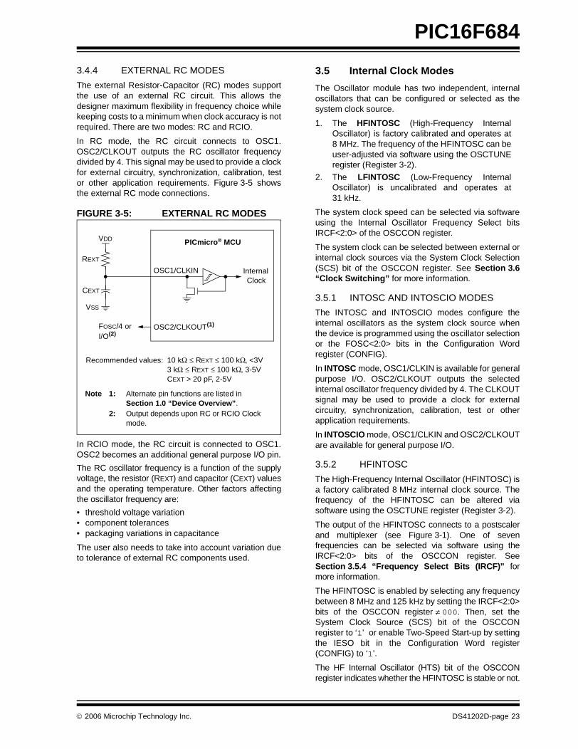
The external Resistor-Capacitor (RC) modes supportthe use of an external RC circuit. This allows thedesigner maximum flexibility in frequency choice whilekeeping costs to a minimum when clock accuracy is notrequired. There are two modes: RC and RCIO.
In RC mode, the RC circuit connects to OSC1.OSC2/CLKOUT outputs the RC oscillator frequencydivided by 4. This signal may be used to provide a clockfor external circuitry, synchronization, calibration, testor other application requirements. Figure 3-5 showsthe external RC mode connections.
FIGURE 3-5: EXTERNAL RC MODES
In RCIO mode, the RC circuit is connected to OSC1.OSC2 becomes an additional general purpose I/O pin.
The RC oscillator frequency is a function of the supplyvoltage, the resistor (REXT) and capacitor (CEXT) valuesand the operating temperature. Other factors affectingthe oscillator frequency are:
• threshold voltage variation• component tolerances• packaging variations in capacitance
The user also needs to take into account variation dueto tolerance of external RC components used.
3.5 Internal Clock Modes
The Oscillator module has two independent, internaloscillators that can be configured or selected as thesystem clock source.
1. The HFINTOSC (High-Frequency InternalOscillator) is factory calibrated and operates at8 MHz. The frequency of the HFINTOSC can beuser-adjusted via software using the OSCTUNEregister (Register 3-2).
2. The LFINTOSC (Low-Frequency InternalOscillator) is uncalibrated and operates at31 kHz.
The system clock speed can be selected via softwareusing the Internal Oscillator Frequency Select bitsIRCF<2:0> of the OSCCON register.
The system clock can be selected between external orinternal clock sources via the System Clock Selection(SCS) bit of the OSCCON register. See Section 3.6“Clock Switching” for more information.
3.5.1 INTOSC AND INTOSCIO MODES
The INTOSC and INTOSCIO modes configure theinternal oscillators as the system clock source whenthe device is programmed using the oscillator selectionor the FOSC<2:0> bits in the Configuration Wordregister (CONFIG).
In INTOSC mode, OSC1/CLKIN is available for generalpurpose I/O. OSC2/CLKOUT outputs the selectedinternal oscillator frequency divided by 4. The CLKOUTsignal may be used to provide a clock for externalcircuitry, synchronization, calibration, test or otherapplication requirements.
In INTOSCIO mode, OSC1/CLKIN and OSC2/CLKOUTare available for general purpose I/O.
3.5.2 HFINTOSC
The High-Frequency Internal Oscillator (HFINTOSC) isa factory calibrated 8 MHz internal clock source. Thefrequency of the HFINTOSC can be altered viasoftware using the OSCTUNE register (Register 3-2).
The output of the HFINTOSC connects to a postscalerand multiplexer (see Figure 3-1). One of sevenfrequencies can be selected via software using theIRCF<2:0> bits of the OSCCON register. SeeSection 3.5.4 “Frequency Select Bits (IRCF)” formore information.
The HFINTOSC is enabled by selecting any frequencybetween 8 MHz and 125 kHz by setting the IRCF<2:0>bits of the OSCCON register ≠ 000. Then, set theSystem Clock Source (SCS) bit of the OSCCONregister to ‘1’ or enable Two-Speed Start-up by settingthe IESO bit in the Configuration Word register(CONFIG) to ‘1’.
The HF Internal Oscillator (HTS) bit of the OSCCONregister indicates whether the HFINTOSC is stable or not.
OSC2/CLKOUT(1)
CEXT
REXT
PICmicro® MCU
OSC1/CLKIN
FOSC/4 or
InternalClock
VDD
VSS
Recommended values: 10 kΩ ≤ REXT ≤ 100 kΩ, <3V3 kΩ ≤ REXT ≤ 100 kΩ, 3-5VCEXT > 20 pF, 2-5V
Note 1: Alternate pin functions are listed in Section 1.0 “Device Overview”.
2: Output depends upon RC or RCIO Clock mode.
I/O(2)
© 2006 Microchip Technology Inc. DS41202D-page 23
PIC16F684
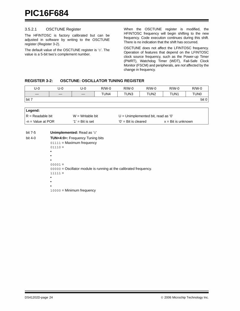
3.5.2.1 OSCTUNE Register
The HFINTOSC is factory calibrated but can beadjusted in software by writing to the OSCTUNEregister (Register 3-2).
The default value of the OSCTUNE register is ‘0’. Thevalue is a 5-bit two’s complement number.
When the OSCTUNE register is modified, theHFINTOSC frequency will begin shifting to the newfrequency. Code execution continues during this shift.There is no indication that the shift has occurred.
OSCTUNE does not affect the LFINTOSC frequency.Operation of features that depend on the LFINTOSCclock source frequency, such as the Power-up Timer(PWRT), Watchdog Timer (WDT), Fail-Safe ClockMonitor (FSCM) and peripherals, are not affected by thechange in frequency.
REGISTER 3-2: OSCTUNE: OSCILLATOR TUNING REGISTER
U-0 U-0 U-0 R/W-0 R/W-0 R/W-0 R/W-0 R/W-0
— — — TUN4 TUN3 TUN2 TUN1 TUN0
bit 7 bit 0
Legend:
R = Readable bit W = Writable bit U = Unimplemented bit, read as ‘0’
-n = Value at POR ‘1’ = Bit is set ‘0’ = Bit is cleared x = Bit is unknown
bit 7-5 Unimplemented: Read as ‘0’
bit 4-0 TUN<4:0>: Frequency Tuning bits01111 = Maximum frequency01110 = •••00001 = 00000 = Oscillator module is running at the calibrated frequency.11111 = •••10000 = Minimum frequency
DS41202D-page 24 © 2006 Microchip Technology Inc.
PIC16F684
3.5.3 LFINTOSC
The Low-Frequency Internal Oscillator (LFINTOSC) isan uncalibrated 31 kHz internal clock source.
The output of the LFINTOSC connects to a postscalerand multiplexer (see Figure 3-1). Select 31 kHz, viasoftware, using the IRCF<2:0> bits of the OSCCONregister. See Section 3.5.4 “Frequency Select Bits(IRCF)” for more information. The LFINTOSC is also thefrequency for the Power-up Timer (PWRT), WatchdogTimer (WDT) and Fail-Safe Clock Monitor (FSCM).
The LFINTOSC is enabled by selecting 31 kHz(IRCF<2:0> bits of the OSCCON register = 000) as thesystem clock source (SCS bit of the OSCCONregister = 1), or when any of the following are enabled:
• Two-Speed Start-up IESO bit of the Configuration Word register = 1 and IRCF<2:0> bits of the OSCCON register = 000
• Power-up Timer (PWRT)• Watchdog Timer (WDT)• Fail-Safe Clock Monitor (FSCM)
The LF Internal Oscillator (LTS) bit of the OSCCONregister indicates whether the LFINTOSC is stable ornot.
3.5.4 FREQUENCY SELECT BITS (IRCF)
The output of the 8 MHz HFINTOSC and 31 kHzLFINTOSC connects to a postscaler and multiplexer(see Figure 3-1). The Internal Oscillator FrequencySelect bits IRCF<2:0> of the OSCCON register selectthe frequency output of the internal oscillators. One ofeight frequencies can be selected via software:
• 8 MHz• 4 MHz (Default after Reset)
• 2 MHz• 1 MHz• 500 kHz
• 250 kHz• 125 kHz• 31 kHz (LFINTOSC)
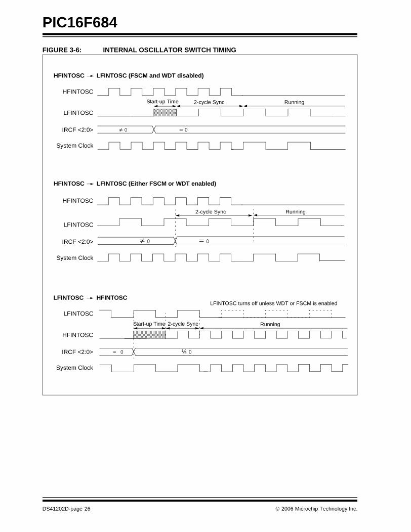
3.5.5 HFINTOSC AND LFINTOSC CLOCK SWITCH TIMING
When switching between the LFINTOSC and theHFINTOSC, the new oscillator may already be shutdown to save power (see Figure 3-6). If this is the case,there is a delay after the IRCF<2:0> bits of theOSCCON register are modified before the frequencyselection takes place. The LTS and HTS bits of theOSCCON register will reflect the current active statusof the LFINTOSC and HFINTOSC oscillators. Thetiming of a frequency selection is as follows:
1. IRCF<2:0> bits of the OSCCON register aremodified.
2. If the new clock is shut down, a clock start-updelay is started.
3. Clock switch circuitry waits for a falling edge ofthe current clock.
4. CLKOUT is held low and the clock switchcircuitry waits for a rising edge in the new clock.
5. CLKOUT is now connected with the new clock.LTS and HTS bits of the OSCCON register areupdated as required.
6. Clock switch is complete.
See Figure 3-1 for more details.
If the internal oscillator speed selected is between8 MHz and 125 kHz, there is no start-up delay beforethe new frequency is selected. This is because the oldand new frequencies are derived from the HFINTOSCvia the postscaler and multiplexer.
Start-up delay specifications are located in theoscillator tables of Section 15.0 “ElectricalSpecifications”.
Note: Following any Reset, the IRCF<2:0> bits ofthe OSCCON register are set to ‘110’ andthe frequency selection is set to 4 MHz.The user can modify the IRCF bits toselect a different frequency.
© 2006 Microchip Technology Inc. DS41202D-page 25
PIC16F684
FIGURE 3-6: INTERNAL OSCILLATOR SWITCH TIMING
HFINTOSC
LFINTOSC
IRCF <2:0>
System Clock
HFINTOSC
LFINTOSC
IRCF <2:0>
System Clock
≠ 0 = 0
≠ 0 = 0
Start-up Time 2-cycle Sync Running
2-cycle Sync Running
HFINTOSC LFINTOSC (FSCM and WDT disabled)
HFINTOSC LFINTOSC (Either FSCM or WDT enabled)
LFINTOSC
HFINTOSC
IRCF <2:0>
System Clock
= 0 ¼ 0
Start-up Time 2-cycle Sync Running
LFINTOSC HFINTOSCLFINTOSC turns off unless WDT or FSCM is enabled
DS41202D-page 26 © 2006 Microchip Technology Inc.
PIC16F684
3.6 Clock Switching
The system clock source can be switched betweenexternal and internal clock sources via software usingthe System Clock Select (SCS) bit of the OSCCONregister.
3.6.1 SYSTEM CLOCK SELECT (SCS) BIT
The System Clock Select (SCS) bit of the OSCCONregister selects the system clock source that is used forthe CPU and peripherals.
• When the SCS bit of the OSCCON register = 0, the system clock source is determined by configuration of the FOSC<2:0> bits in the Configuration Word register (CONFIG).
• When the SCS bit of the OSCCON register = 1, the system clock source is chosen by the internal oscillator frequency selected by the IRCF<2:0> bits of the OSCCON register. After a Reset, the SCS bit of the OSCCON register is always cleared.
3.6.2 OSCILLATOR START-UP TIME-OUT STATUS (OSTS) BIT
The Oscillator Start-up Time-out Status (OSTS) bit ofthe OSCCON register indicates whether the systemclock is running from the external clock source, asdefined by the FOSC<2:0> bits in the ConfigurationWord register (CONFIG), or from the internal clocksource. In particular, OSTS indicates that the OscillatorStart-up Timer (OST) has timed out for LP, XT or HSmodes.
3.7 Two-Speed Clock Start-up Mode
Two-Speed Start-up mode provides additional powersavings by minimizing the latency between externaloscillator start-up and code execution. In applicationsthat make heavy use of the Sleep mode, Two-SpeedStart-up will remove the external oscillator start-uptime from the time spent awake and can reduce theoverall power consumption of the device.
This mode allows the application to wake-up fromSleep, perform a few instructions using the INTOSCas the clock source and go back to Sleep withoutwaiting for the primary oscillator to become stable.
When the Oscillator module is configured for LP, XT orHS modes, the Oscillator Start-up Timer (OST) isenabled (see Section 3.4.1 “Oscillator Start-up Timer(OST)”). The OST will suspend program execution until1024 oscillations are counted. Two-Speed Start-upmode minimizes the delay in code execution byoperating from the internal oscillator as the OST iscounting. When the OST count reaches 1024 and theOSTS bit of the OSCCON register is set, programexecution switches to the external oscillator.
3.7.1 TWO-SPEED START-UP MODE CONFIGURATION
Two-Speed Start-up mode is configured by thefollowing settings:
• IESO (of the Configuration Word register) = 1; Internal/External Switchover bit (Two-Speed Start-up mode enabled).
• SCS (of the OSCCON register) = 0.
• FOSC<2:0> bits in the Configuration Word register (CONFIG) configured for LP, XT or HS mode.
Two-Speed Start-up mode is entered after:
• Power-on Reset (POR) and, if enabled, after Power-up Timer (PWRT) has expired, or
• Wake-up from Sleep.
If the external clock oscillator is configured to beanything other than LP, XT or HS mode, thenTwo-Speed Start-up is disabled. This is because theexternal clock oscillator does not require anystabilization time after POR or an exit from Sleep.
3.7.2 TWO-SPEED START-UP SEQUENCE
1. Wake-up from Power-on Reset or Sleep.2. Instructions begin execution by the internal
oscillator at the frequency set in the IRCF<2:0>bits of the OSCCON register.
3. OST enabled to count 1024 clock cycles.4. OST timed out, wait for falling edge of the
internal oscillator.5. OSTS is set.6. System clock held low until the next falling edge
of new clock (LP, XT or HS mode).7. System clock is switched to external clock
source.
Note: Any automatic clock switch, which mayoccur from Two-Speed Start-up or Fail-SafeClock Monitor, does not update the SCS bitof the OSCCON register. The user canmonitor the OSTS bit of the OSCCONregister to determine the current systemclock source.
Note: Executing a SLEEP instruction will abortthe oscillator start-up time and will causethe OSTS bit of the OSCCON register toremain clear.
© 2006 Microchip Technology Inc. DS41202D-page 27
PIC16F684
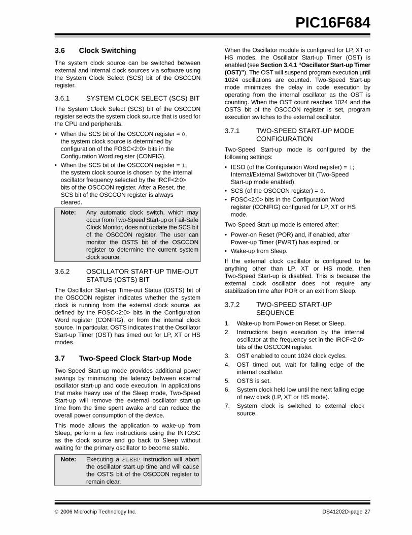
3.7.3 CHECKING TWO-SPEED CLOCK STATUS
Checking the state of the OSTS bit of the OSCCONregister will confirm if the microcontroller is runningfrom the external clock source, as defined by theFOSC<2:0> bits in the Configuration Word register(CONFIG), or the internal oscillator.
FIGURE 3-7: TWO-SPEED START-UP
0 1 1022 1023
PC + 1
TOSTT
HFINTOSC
OSC1
OSC2
Program Counter
System Clock
PC - N PC
DS41202D-page 28 © 2006 Microchip Technology Inc.
PIC16F684
3.8 Fail-Safe Clock Monitor
The Fail-Safe Clock Monitor (FSCM) allows the deviceto continue operating should the external oscillator fail.The FSCM can detect oscillator failure any time afterthe Oscillator Start-up Timer (OST) has expired. TheFSCM is enabled by setting the FCMEN bit in theConfiguration Word register (CONFIG). The FSCM isapplicable to all external oscillator modes (LP, XT, HS,EC, RC and RCIO).
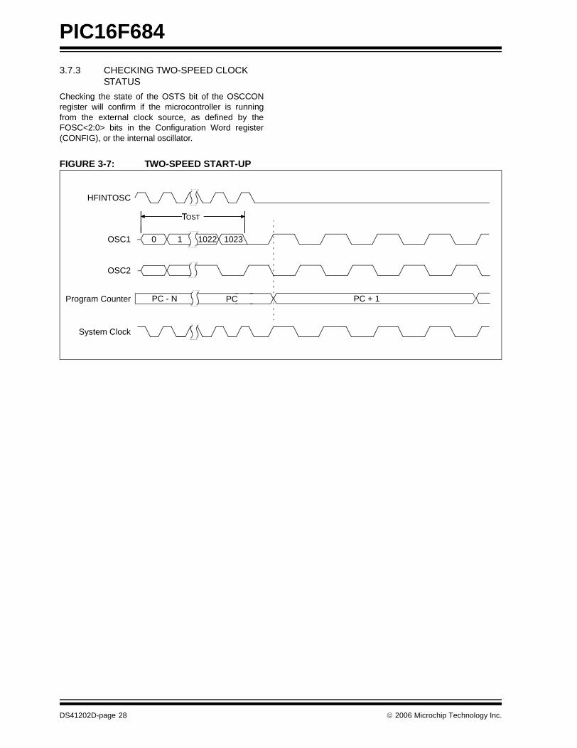
FIGURE 3-8: FSCM BLOCK DIAGRAM
3.8.1 FAIL-SAFE DETECTION
The FSCM module detects a failed oscillator bycomparing the external oscillator to the FSCM sampleclock. The sample clock is generated by dividing theLFINTOSC by 64. See Figure 3-8. Inside the faildetector block is a latch. The external clock sets thelatch on each falling edge of the external clock. Thesample clock clears the latch on each rising edge of thesample clock. A failure is detected when an entirehalf-cycle of the sample clock elapses before theprimary clock goes low.
3.8.2 FAIL-SAFE OPERATION
When the external clock fails, the FSCM switches thedevice clock to an internal clock source and sets the bitflag OSFIF of the PIR1 register. Setting this flag willgenerate an interrupt if the OSFIE bit of the PIE1register is also set. The device firmware can then takesteps to mitigate the problems that may arise from afailed clock. The system clock will continue to besourced from the internal clock source until the devicefirmware successfully restarts the external oscillatorand switches back to external operation.
The internal clock source chosen by the FSCM isdetermined by the IRCF<2:0> bits of the OSCCONregister. This allows the internal oscillator to beconfigured before a failure occurs.
3.8.3 FAIL-SAFE CONDITION CLEARING
The Fail-Safe condition is cleared after a Reset,executing a SLEEP instruction or toggling the SCS bitof the OSCCON register. When the SCS bit is toggled,the OST is restarted. While the OST is running, thedevice continues to operate from the INTOSC selectedin OSCCON. When the OST times out, the Fail-Safecondition is cleared and the device will be operatingfrom the external clock source. The Fail-Safe conditionmust be cleared before the OSFIF flag can be cleared.
3.8.4 RESET OR WAKE-UP FROM SLEEP
The FSCM is designed to detect an oscillator failureafter the Oscillator Start-up Timer (OST) has expired.The OST is used after waking up from Sleep and afterany type of Reset. The OST is not used with the EC orRC Clock modes so that the FSCM will be active assoon as the Reset or wake-up has completed. Whenthe FSCM is enabled, the Two-Speed Start-up is alsoenabled. Therefore, the device will always be executingcode while the OST is operating.
External
LFINTOSC÷ 64
S
R
Q
31 kHz(~32 μs)
488 Hz(~2 ms)
Clock MonitorLatch
ClockFailure
Detected
Oscillator
Clock
Q
Sample ClockNote: Due to the wide range of oscillator start-up
times, the Fail-Safe circuit is not activeduring oscillator start-up (i.e., after exitingReset or Sleep). After an appropriateamount of time, the user should check theOSTS bit of the OSCCON register to verifythe oscillator start-up and that the systemclock switchover has successfullycompleted.
© 2006 Microchip Technology Inc. DS41202D-page 29
PIC16F684
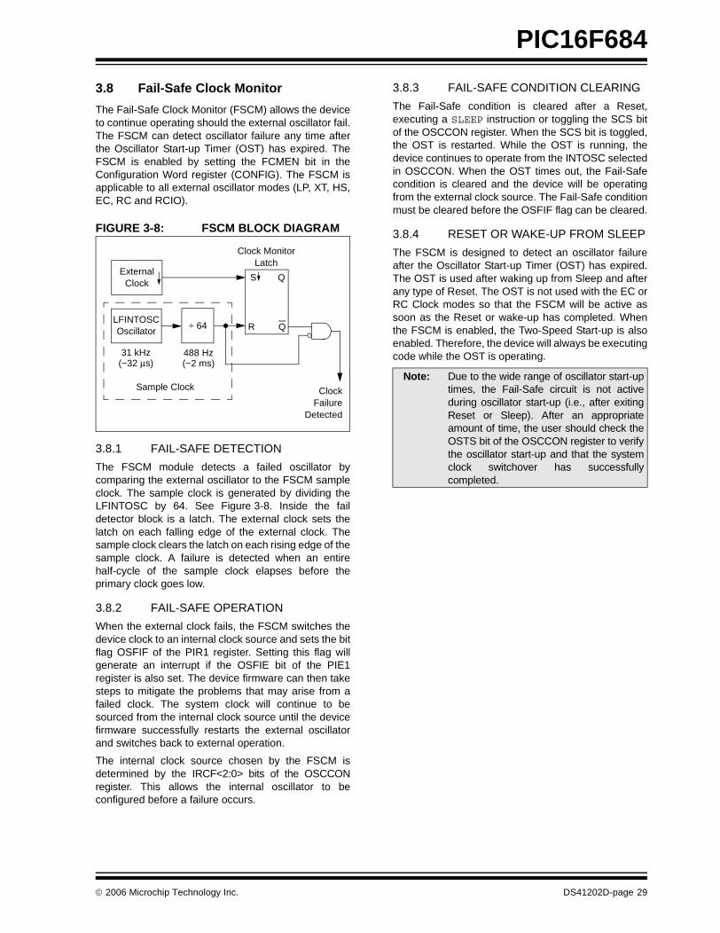
FIGURE 3-9: FSCM TIMING DIAGRAM
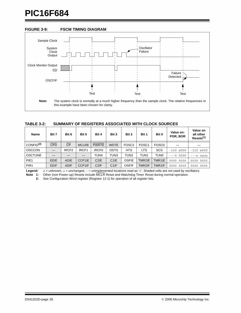
TABLE 3-2: SUMMARY OF REGISTERS ASSOCIATED WITH CLOCK SOURCES
OSCFIF
SystemClock
Output
Sample Clock
FailureDetected
OscillatorFailure
Note: The system clock is normally at a much higher frequency than the sample clock. The relative frequencies inthis example have been chosen for clarity.
(Q)
Test Test Test
Clock Monitor Output
Name Bit 7 Bit 6 Bit 5 Bit 4 Bit 3 Bit 2 Bit 1 Bit 0Value on: POR, BOR
Value on all other Resets(1)
CONFIG(2) CPD CP MCLRE PWRTE WDTE FOSC2 FOSC1 FOSC0 — —
OSCCON — IRCF2 IRCF1 IRCF0 OSTS HTS LTS SCS -110 x000 -110 x000
OSCTUNE — — — TUN4 TUN3 TUN2 TUN1 TUN0 ---0 0000 ---u uuuu
PIE1 EEIE ADIE CCP1IE C2IE C1IE OSFIE TMR2IE TMR1IE 0000 0000 0000 0000
PIR1 EEIF ADIF CCP1IF C2IF C1IF OSFIF TMR2IF TMR1IF 0000 0000 0000 0000
Legend: x = unknown, u = unchanged, – = unimplemented locations read as ‘0’. Shaded cells are not used by oscillators.Note 1: Other (non Power-up) Resets include MCLR Reset and Watchdog Timer Reset during normal operation.
2: See Configuration Word register (Register 12-1) for operation of all register bits.
DS41202D-page 30 © 2006 Microchip Technology Inc.
PIC16F684
4.0 I/O PORTS
There are as many as twelve general purpose I/O pinsavailable. Depending on which peripherals are enabled,some or all of the pins may not be available as generalpurpose I/O. In general, when a peripheral is enabled,the associated pin may not be used as a generalpurpose I/O pin.
4.1 PORTA and the TRISA Registers
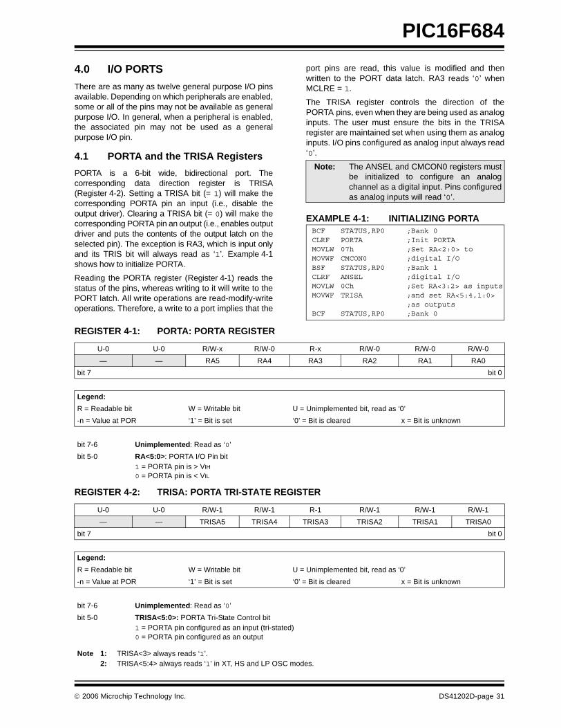
PORTA is a 6-bit wide, bidirectional port. Thecorresponding data direction register is TRISA(Register 4-2). Setting a TRISA bit (= 1) will make thecorresponding PORTA pin an input (i.e., disable theoutput driver). Clearing a TRISA bit (= 0) will make thecorresponding PORTA pin an output (i.e., enables outputdriver and puts the contents of the output latch on theselected pin). The exception is RA3, which is input onlyand its TRIS bit will always read as ‘1’. Example 4-1shows how to initialize PORTA.
Reading the PORTA register (Register 4-1) reads thestatus of the pins, whereas writing to it will write to thePORT latch. All write operations are read-modify-writeoperations. Therefore, a write to a port implies that the
port pins are read, this value is modified and thenwritten to the PORT data latch. RA3 reads ‘0’ whenMCLRE = 1.
The TRISA register controls the direction of thePORTA pins, even when they are being used as analoginputs. The user must ensure the bits in the TRISAregister are maintained set when using them as analoginputs. I/O pins configured as analog input always read‘0’.
EXAMPLE 4-1: INITIALIZING PORTA
Note: The ANSEL and CMCON0 registers mustbe initialized to configure an analogchannel as a digital input. Pins configuredas analog inputs will read ‘0’.
BCF STATUS,RP0 ;Bank 0 CLRF PORTA ;Init PORTA MOVLW 07h ;Set RA<2:0> to MOVWF CMCON0 ;digital I/O BSF STATUS,RP0 ;Bank 1 CLRF ANSEL ;digital I/O MOVLW 0Ch ;Set RA<3:2> as inputs MOVWF TRISA ;and set RA<5:4,1:0>
;as outputs BCF STATUS,RP0 ;Bank 0
REGISTER 4-1: PORTA: PORTA REGISTER
U-0 U-0 R/W-x R/W-0 R-x R/W-0 R/W-0 R/W-0
— — RA5 RA4 RA3 RA2 RA1 RA0
bit 7 bit 0
Legend:
R = Readable bit W = Writable bit U = Unimplemented bit, read as ‘0’
-n = Value at POR ‘1’ = Bit is set ‘0’ = Bit is cleared x = Bit is unknown
bit 7-6 Unimplemented: Read as ‘0’
bit 5-0 RA<5:0>: PORTA I/O Pin bit1 = PORTA pin is > VIH
0 = PORTA pin is < VIL
REGISTER 4-2: TRISA: PORTA TRI-STATE REGISTER
U-0 U-0 R/W-1 R/W-1 R-1 R/W-1 R/W-1 R/W-1
— — TRISA5 TRISA4 TRISA3 TRISA2 TRISA1 TRISA0
bit 7 bit 0
Legend:
R = Readable bit W = Writable bit U = Unimplemented bit, read as ‘0’
-n = Value at POR ‘1’ = Bit is set ‘0’ = Bit is cleared x = Bit is unknown
bit 7-6 Unimplemented: Read as ‘0’
bit 5-0 TRISA<5:0>: PORTA Tri-State Control bit1 = PORTA pin configured as an input (tri-stated)0 = PORTA pin configured as an output
Note 1: TRISA<3> always reads ‘1’.2: TRISA<5:4> always reads ‘1’ in XT, HS and LP OSC modes.
© 2006 Microchip Technology Inc. DS41202D-page 31

PIC16F684
4.2 Additional Pin Functions
Every PORTA pin on the PIC16F684 has aninterrupt-on-change option and a weak pull-up option.RA0 has an Ultra Low-Power Wake-up option. The nextthree sections describe these functions.
4.2.1 ANSEL REGISTER
The ANSEL register is used to configure the Inputmode of an I/O pin to analog. Setting the appropriateANSEL bit high will cause all digital reads on the pin tobe read as ‘0’ and allow analog functions on the pin tooperate correctly.
The state of the ANSEL bits has no affect on digitaloutput functions. A pin with TRIS clear and ANSEL setwill still operate as a digital output, but the Input modewill be analog. This can cause unexpected behaviorwhen executing read-modify-write instructions on theaffected port.
4.2.2 WEAK PULL-UPS
Each of the PORTA pins, except RA3, has anindividually configurable internal weak pull-up. Controlbits WPUAx enable or disable each pull-up. Refer toRegister 4-4. Each weak pull-up is automatically turnedoff when the port pin is configured as an output. Thepull-ups are disabled on a Power-on Reset by theRAPU bit of the OPTION register). A weak pull-up isautomatically enabled for RA3 when configured asMCLR and disabled when RA3 is an I/O. There is nosoftware control of the MCLR pull-up.
4.2.3 INTERRUPT-ON-CHANGE
Each of the PORTA pins is individually configurable asan interrupt-on-change pin. Control bits IOCAx enableor disable the interrupt function for each pin. Refer toRegister 4-5. The interrupt-on-change is disabled on aPower-on Reset.
For enabled interrupt-on-change pins, the values arecompared with the old value latched on the last read ofPORTA. The ‘mismatch’ outputs of the last read areOR’d together to set the PORTA Change Interrupt Flagbit (RAIF) in the INTCON register (Register 2-3).
This interrupt can wake the device from Sleep. Theuser, in the Interrupt Service Routine, clears the inter-rupt by:
a) Any read or write of PORTA. This will end themismatch condition, then,
b) Clear the flag bit RAIF.
A mismatch condition will continue to set flag bit RAIF.Reading PORTA will end the mismatch condition andallow flag bit RAIF to be cleared. The latch holding thelast read value is not affected by a MCLR norBrown-out Reset. After these resets, the RAIF flag willcontinue to be set if a mismatch is present.
Note: If a change on the I/O pin should occurwhen any PORTA operation is beingexecuted, then the RAIF interrupt flag maynot get set.
REGISTER 4-3: ANSEL: ANALOG SELECT REGISTER
R/W-1 R/W-1 R/W-1 R/W-1 R/W-1 R/W-1 R/W-1 R/W-1
ANS7 ANS6 ANS5 ANS4 ANS3 ANS2 ANS1 ANS0
bit 7 bit 0
Legend:
R = Readable bit W = Writable bit U = Unimplemented bit, read as ‘0’
-n = Value at POR ‘1’ = Bit is set ‘0’ = Bit is cleared x = Bit is unknown
bit 7-0 ANS<7:0>: Analog Select bitsAnalog select between analog or digital function on pins AN<7:0>, respectively.1 = Analog input. Pin is assigned as analog input(1).0 = Digital I/O. Pin is assigned to port or special function.
Note 1: Setting a pin to an analog input automatically disables the digital input circuitry, weak pull-ups and interrupt-on-change, if available. The corresponding TRIS bit must be set to Input mode in order to allow external control of the voltage on the pin.
DS41202D-page 32 © 2006 Microchip Technology Inc.

PIC16F684
REGISTER 4-4: WPUA: WEAK PULL-UP PORTA REGISTER
U-0 U-0 R/W-1 R/W-1 U-0 R/W-1 R/W-1 R/W-1
— — WPUA5 WPUA4 — WPUA2 WPUA1 WPUA0
bit 7 bit 0
Legend:
R = Readable bit W = Writable bit U = Unimplemented bit, read as ‘0’
-n = Value at POR ‘1’ = Bit is set ‘0’ = Bit is cleared x = Bit is unknown
bit 7-6 Unimplemented: Read as ‘0’
bit 5-4 WPUA<5:4>: Weak Pull-up Control bits1 = Pull-up enabled0 = Pull-up disabled
bit 3 Unimplemented: Read as ‘0’
bit 2-0 WPUA<2:0>: Weak Pull-up Control bits
1 = Pull-up enabled0 = Pull-up disabled
Note 1: Global RAPU must be enabled for individual pull-ups to be enabled.2: The weak pull-up device is automatically disabled if the pin is in Output mode (TRISA = 0).
3: The RA3 pull-up is enabled when configured as MCLR and disabled as an I/O in the Configuration Word.4: WPUA<5:4> always reads ‘1’ in XT, HS and LP OSC modes.
REGISTER 4-5: IOCA: INTERRUPT-ON-CHANGE PORTA REGISTER
U-0 U-0 R/W-0 R/W-0 R/W-0 R/W-0 R/W-0 R/W-0
— — IOCA5 IOCA4 IOCA3 IOCA2 IOCA1 IOCA0
bit 7 bit 0
Legend:
R = Readable bit W = Writable bit U = Unimplemented bit, read as ‘0’
-n = Value at POR ‘1’ = Bit is set ‘0’ = Bit is cleared x = Bit is unknown
bit 7-6 Unimplemented: Read as ‘0’
bit 5-0 IOCA<5:0>: Interrupt-on-change PORTA Control bit
1 = Interrupt-on-change enabled0 = Interrupt-on-change disabled
Note 1: Global Interrupt Enable (GIE) must be enabled for individual interrupts to be recognized.2: IOCA<5:4> always reads ‘1’ in XT, HS and LP OSC modes.
© 2006 Microchip Technology Inc. DS41202D-page 33
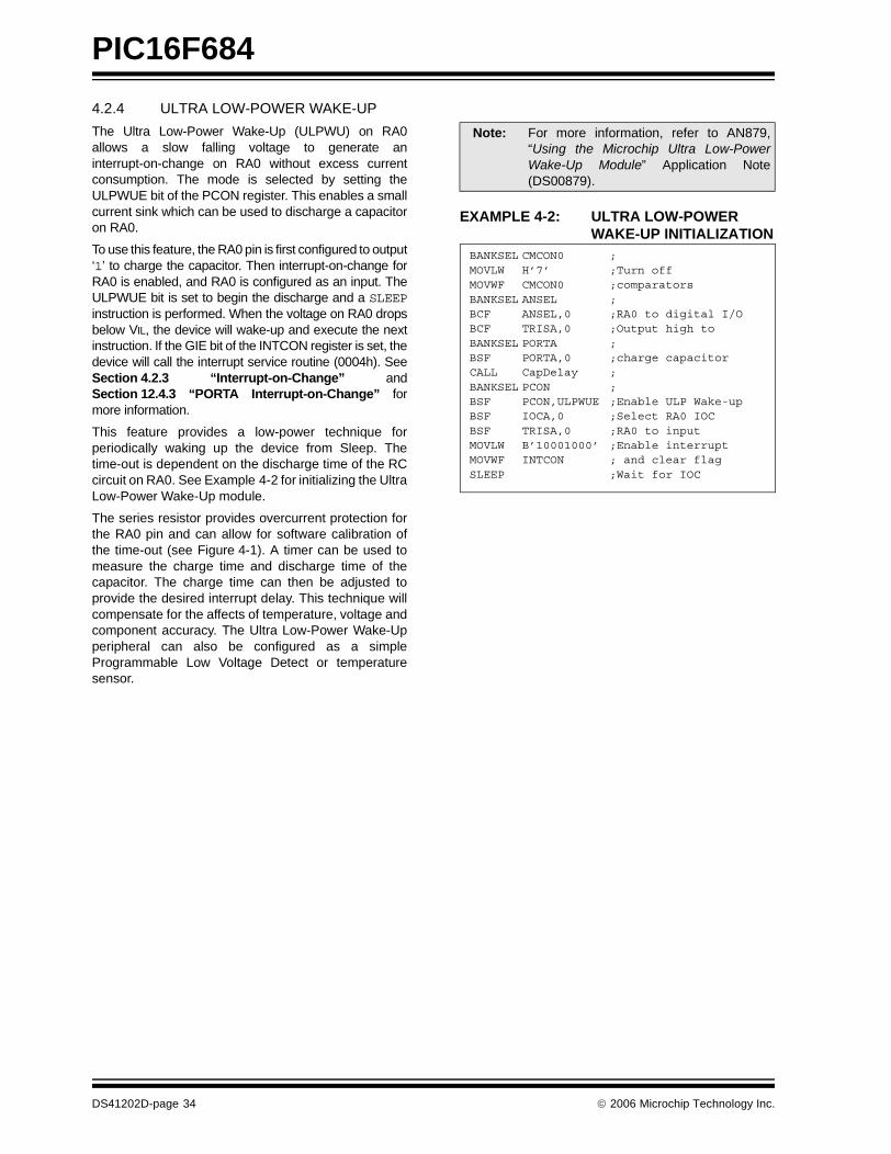
PIC16F684
4.2.4 ULTRA LOW-POWER WAKE-UP
The Ultra Low-Power Wake-Up (ULPWU) on RA0allows a slow falling voltage to generate aninterrupt-on-change on RA0 without excess currentconsumption. The mode is selected by setting theULPWUE bit of the PCON register. This enables a smallcurrent sink which can be used to discharge a capacitoron RA0.
To use this feature, the RA0 pin is first configured to output‘1’ to charge the capacitor. Then interrupt-on-change forRA0 is enabled, and RA0 is configured as an input. TheULPWUE bit is set to begin the discharge and a SLEEPinstruction is performed. When the voltage on RA0 dropsbelow VIL, the device will wake-up and execute the nextinstruction. If the GIE bit of the INTCON register is set, thedevice will call the interrupt service routine (0004h). SeeSection 4.2.3 “Interrupt-on-Change” andSection 12.4.3 “PORTA Interrupt-on-Change” formore information.
This feature provides a low-power technique forperiodically waking up the device from Sleep. Thetime-out is dependent on the discharge time of the RCcircuit on RA0. See Example 4-2 for initializing the UltraLow-Power Wake-Up module.
The series resistor provides overcurrent protection forthe RA0 pin and can allow for software calibration ofthe time-out (see Figure 4-1). A timer can be used tomeasure the charge time and discharge time of thecapacitor. The charge time can then be adjusted toprovide the desired interrupt delay. This technique willcompensate for the affects of temperature, voltage andcomponent accuracy. The Ultra Low-Power Wake-Upperipheral can also be configured as a simpleProgrammable Low Voltage Detect or temperaturesensor.
EXAMPLE 4-2: ULTRA LOW-POWER WAKE-UP INITIALIZATION
Note: For more information, refer to AN879,“Using the Microchip Ultra Low-PowerWake-Up Module” Application Note(DS00879).
BANKSEL CMCON0 ;MOVLW H’7’ ;Turn offMOVWF CMCON0 ;comparatorsBANKSEL ANSEL ;BCF ANSEL,0 ;RA0 to digital I/OBCF TRISA,0 ;Output high toBANKSEL PORTA ;BSF PORTA,0 ;charge capacitorCALL CapDelay ;BANKSEL PCON ;BSF PCON,ULPWUE ;Enable ULP Wake-upBSF IOCA,0 ;Select RA0 IOCBSF TRISA,0 ;RA0 to inputMOVLW B’10001000’ ;Enable interruptMOVWF INTCON ; and clear flagSLEEP ;Wait for IOC
DS41202D-page 34 © 2006 Microchip Technology Inc.

PIC16F684
4.2.5 PIN DESCRIPTIONS AND DIAGRAMS
Each PORTA pin is multiplexed with other functions.The pins and their combined functions are brieflydescribed here. For specific information aboutindividual functions such as the Comparator or theADC, refer to the appropriate section in this data sheet.
4.2.5.1 RA0/AN0/C1IN+/ICSPDAT/ULPWU
Figure 4-1 shows the diagram for this pin. The RA0 pinis configurable to function as one of the following:
• a general purpose I/O• an analog input for the ADC• an analog non-inverting input to the comparator
• In-Circuit Serial Programming data• an analog input for the Ultra Low-Power Wake-Up
4.2.5.2 RA1/AN1/C1IN-/VREF/ICSPCLK
Figure 4-2 shows the diagram for this pin. The RA1 pinis configurable to function as one of the following:
• a general purpose I/O• an analog input for the ADC
• an analog inverting input to the comparator• a voltage reference input for the ADC• In-Circuit Serial Programming clock
FIGURE 4-1: BLOCK DIAGRAM OF RA0
VDD
VSS
D
QCK
Q
D
QCK
Q
D
QCK
Q
D
QCK
Q
VDD
D
EN
Q
D
EN
Q
Weak
RD PORTA
RD
WR
WR
RD
WRIOCA
RDIOCA
Interrupt-on-
To Comparator
Analog(1)
Input Mode
RAPU
Analog(1)
Input Mode
Change
Q3
WR
RD
0 1
IULP
WPUA
Data Bus
WPUA
PORTA
TRISA
TRISA
PORTA
Note 1: Comparator mode and ANSEL determines Analog Input mode.
-+ VT
ULPWUE
To A/D Converter
VSS
I/O Pin
© 2006 Microchip Technology Inc. DS41202D-page 35
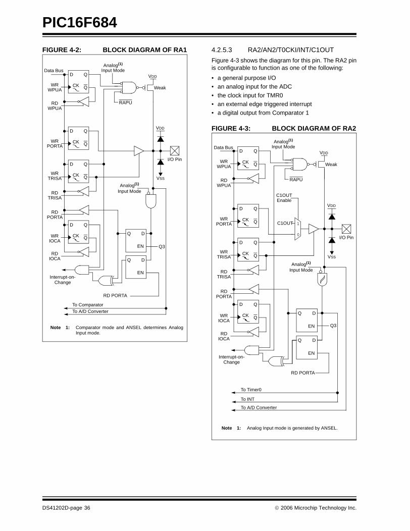
PIC16F684
FIGURE 4-2: BLOCK DIAGRAM OF RA1 4.2.5.3 RA2/AN2/T0CKI/INT/C1OUT
Figure 4-3 shows the diagram for this pin. The RA2 pinis configurable to function as one of the following:
• a general purpose I/O• an analog input for the ADC
• the clock input for TMR0• an external edge triggered interrupt• a digital output from Comparator 1
FIGURE 4-3: BLOCK DIAGRAM OF RA2VDD
VSS
D
QCK
Q
D
QCK
Q
D
QCK
Q
D
QCK
Q
VDD
D
EN
Q
D
EN
Q
Weak
Data Bus
WRWPUA
RDWPUA
RD PORTA
RDPORTA
WRPORTA
WRTRISA
RDTRISA
WRIOCA
RDIOCA
Interrupt-on-
To Comparator
Analog(1)
Input Mode
RAPU
Analog(1)
Input Mode
Change
Q3
Note 1: Comparator mode and ANSEL determines AnalogInput mode.
To A/D Converter
I/O Pin
VDD
VSS
D
QCK
Q
D
QCK
Q
D
QCK
Q
D
QCK
Q
VDD
D
EN
Q
D
EN
Q
Weak
Analog(1)
Input Mode
Data Bus
WRWPUA
RDWPUA
RDPORTA
WRPORTA
WRTRISA
RDTRISA
WRIOCA
RDIOCA
To A/D Converter
0
1C1OUT
C1OUTEnable
To INT
To Timer0
Analog(1)
Input Mode
RAPU
RD PORTA
Interrupt-on-Change
Q3
Note 1: Analog Input mode is generated by ANSEL.
I/O Pin
DS41202D-page 36 © 2006 Microchip Technology Inc.
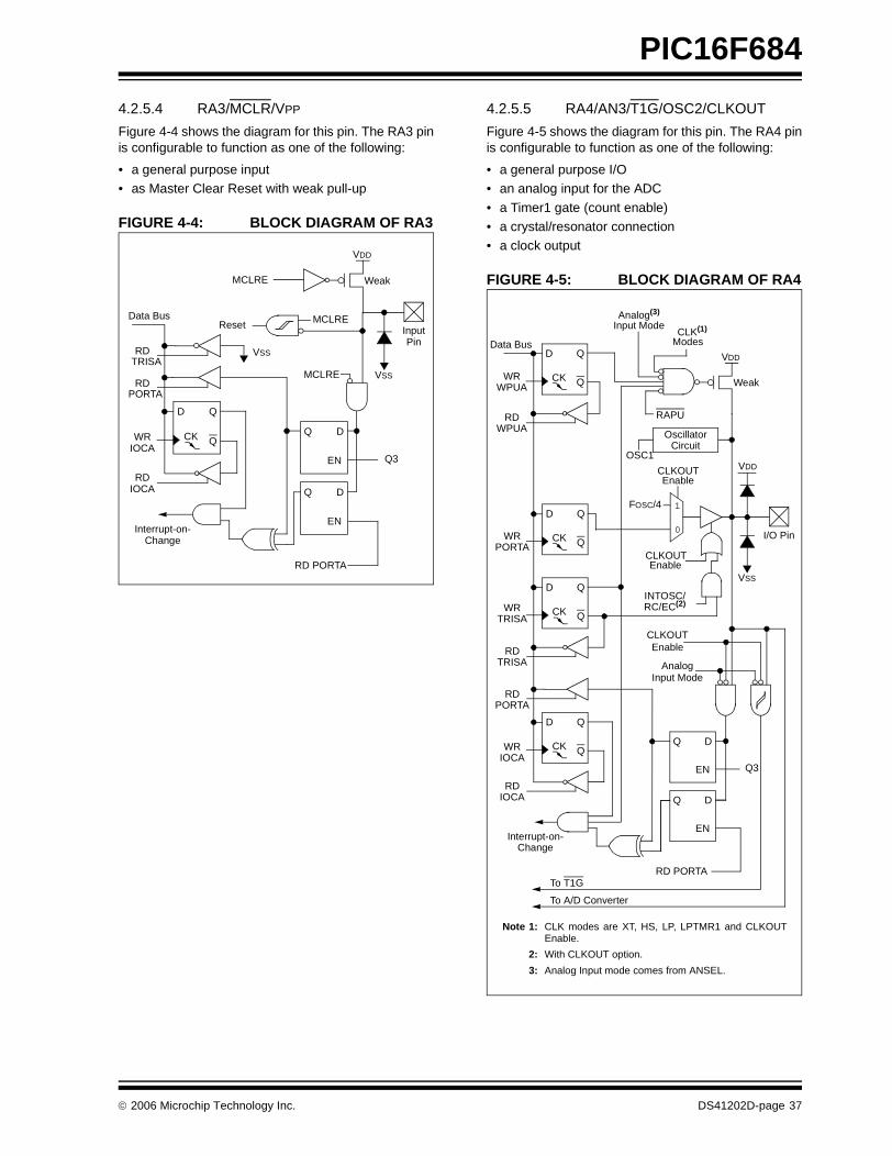
PIC16F684
4.2.5.4 RA3/MCLR/VPP
Figure 4-4 shows the diagram for this pin. The RA3 pinis configurable to function as one of the following:
• a general purpose input• as Master Clear Reset with weak pull-up
FIGURE 4-4: BLOCK DIAGRAM OF RA3
4.2.5.5 RA4/AN3/T1G/OSC2/CLKOUT
Figure 4-5 shows the diagram for this pin. The RA4 pinis configurable to function as one of the following:
• a general purpose I/O• an analog input for the ADC
• a Timer1 gate (count enable)• a crystal/resonator connection• a clock output
FIGURE 4-5: BLOCK DIAGRAM OF RA4
VSS
D
QCK
Q
D
EN
Q
Data Bus
RD PORTA
RDPORTA
WRIOCA
RDIOCA
Reset MCLRE
RDTRISA
VSS
D
EN
Q
MCLRE
VDD
WeakMCLRE
Interrupt-on-Change
Q3
InputPin
VDD
VSS
D
QCK
Q
D
QCK
Q
D
QCK
Q
D
QCK
Q
VDD
D
EN
Q
D
EN
Q
Weak
AnalogInput Mode
Data Bus
WRWPUA
RDWPUA
RDPORTA
WRPORTA
WRTRISA
RDTRISA
WRIOCA
RDIOCA
FOSC/4
To A/D Converter
OscillatorCircuit
OSC1
CLKOUT
0
1
CLKOUTEnable
Enable
Analog(3)
Input Mode
RAPU
RD PORTA To T1G
INTOSC/RC/EC(2)
CLK(1)
Modes
CLKOUTEnable
Note 1: CLK modes are XT, HS, LP, LPTMR1 and CLKOUTEnable.
2: With CLKOUT option.
3: Analog Input mode comes from ANSEL.
Interrupt-on-Change
Q3
I/O Pin
© 2006 Microchip Technology Inc. DS41202D-page 37
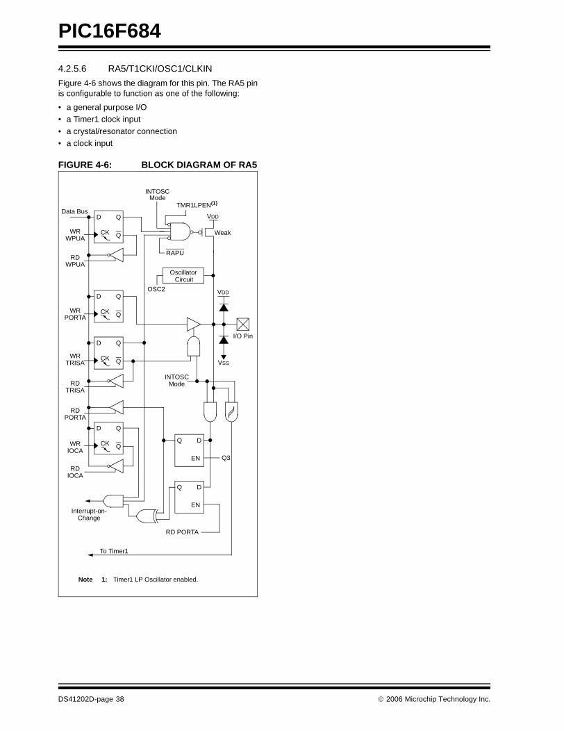
PIC16F684
4.2.5.6 RA5/T1CKI/OSC1/CLKIN
Figure 4-6 shows the diagram for this pin. The RA5 pinis configurable to function as one of the following:
• a general purpose I/O• a Timer1 clock input
• a crystal/resonator connection• a clock input
FIGURE 4-6: BLOCK DIAGRAM OF RA5
VDD
VSS
D
QCK
Q
D
QCK
Q
D
QCK
Q
D
QCK
Q
VDD
D
EN
Q
D
EN
Q
Weak
Data Bus
WRWPUA
RDWPUA
RDPORTA
WRPORTA
WRTRISA
RDTRISA
WRIOCA
RDIOCA
To Timer1
INTOSCMode
RD PORTA
INTOSCMode
RAPU
OSC2
Note 1: Timer1 LP Oscillator enabled.
TMR1LPEN(1)
Interrupt-on-Change
OscillatorCircuit
Q3
I/O Pin
DS41202D-page 38 © 2006 Microchip Technology Inc.
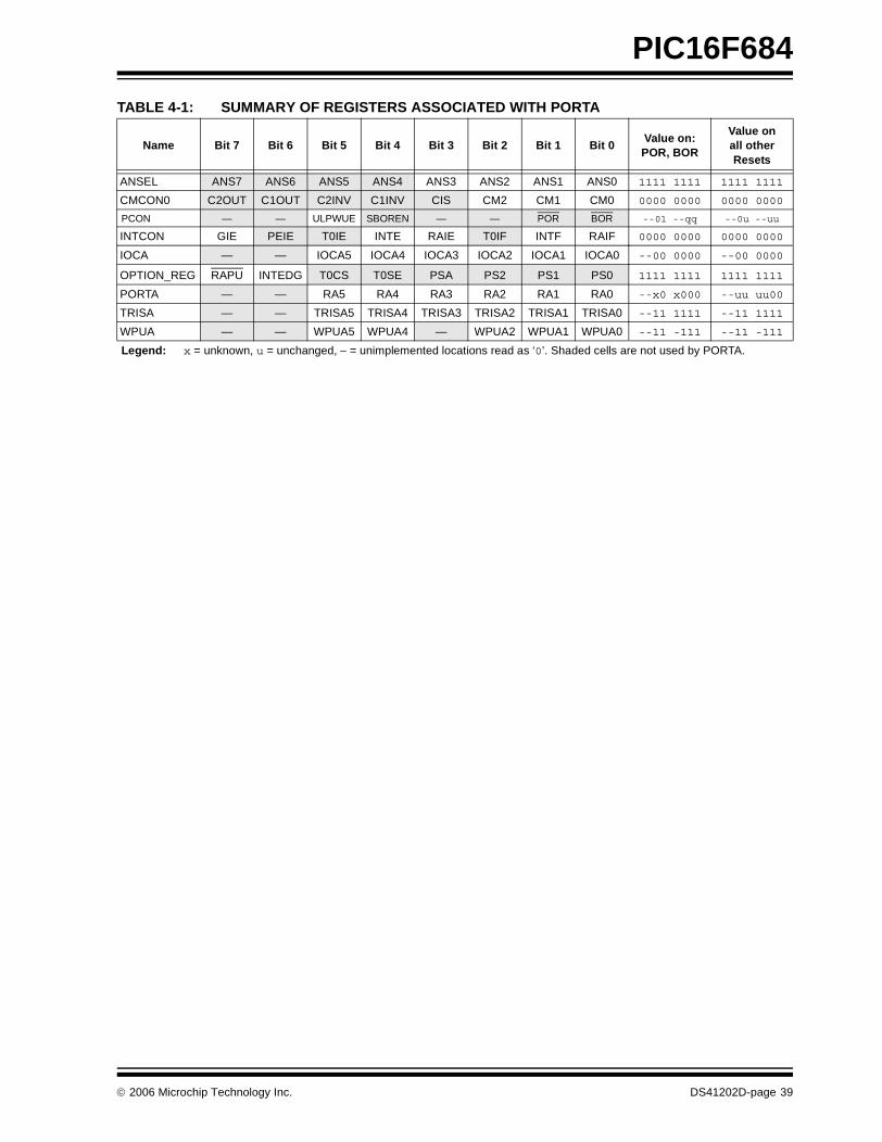
PIC16F684
TABLE 4-1: SUMMARY OF REGISTERS ASSOCIATED WITH PORTA
Name Bit 7 Bit 6 Bit 5 Bit 4 Bit 3 Bit 2 Bit 1 Bit 0Value on: POR, BOR
Value on all other Resets
ANSEL ANS7 ANS6 ANS5 ANS4 ANS3 ANS2 ANS1 ANS0 1111 1111 1111 1111
CMCON0 C2OUT C1OUT C2INV C1INV CIS CM2 CM1 CM0 0000 0000 0000 0000
PCON — — ULPWUE SBOREN — — POR BOR --01 --qq --0u --uu
INTCON GIE PEIE T0IE INTE RAIE T0IF INTF RAIF 0000 0000 0000 0000
IOCA — — IOCA5 IOCA4 IOCA3 IOCA2 IOCA1 IOCA0 --00 0000 --00 0000
OPTION_REG RAPU INTEDG T0CS T0SE PSA PS2 PS1 PS0 1111 1111 1111 1111
PORTA — — RA5 RA4 RA3 RA2 RA1 RA0 --x0 x000 --uu uu00
TRISA — — TRISA5 TRISA4 TRISA3 TRISA2 TRISA1 TRISA0 --11 1111 --11 1111
WPUA — — WPUA5 WPUA4 — WPUA2 WPUA1 WPUA0 --11 -111 --11 -111
Legend: x = unknown, u = unchanged, – = unimplemented locations read as ‘0’. Shaded cells are not used by PORTA.
© 2006 Microchip Technology Inc. DS41202D-page 39
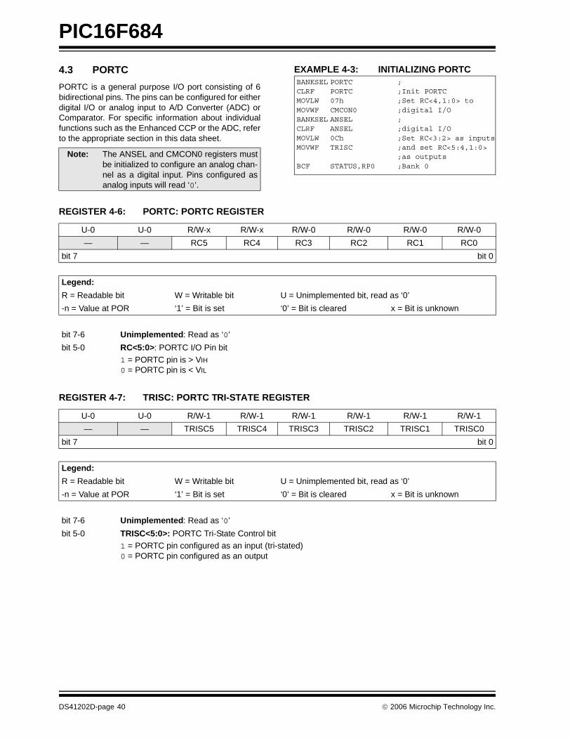
PIC16F684
4.3 PORTC
PORTC is a general purpose I/O port consisting of 6bidirectional pins. The pins can be configured for eitherdigital I/O or analog input to A/D Converter (ADC) orComparator. For specific information about individualfunctions such as the Enhanced CCP or the ADC, referto the appropriate section in this data sheet.
EXAMPLE 4-3: INITIALIZING PORTC
Note: The ANSEL and CMCON0 registers mustbe initialized to configure an analog chan-nel as a digital input. Pins configured asanalog inputs will read ‘0’.
BANKSEL PORTC ;CLRF PORTC ;Init PORTCMOVLW 07h ;Set RC<4,1:0> to MOVWF CMCON0 ;digital I/OBANKSEL ANSEL ;CLRF ANSEL ;digital I/OMOVLW 0Ch ;Set RC<3:2> as inputsMOVWF TRISC ;and set RC<5:4,1:0>
;as outputsBCF STATUS,RP0 ;Bank 0
REGISTER 4-6: PORTC: PORTC REGISTER
U-0 U-0 R/W-x R/W-x R/W-0 R/W-0 R/W-0 R/W-0
— — RC5 RC4 RC3 RC2 RC1 RC0
bit 7 bit 0
Legend:
R = Readable bit W = Writable bit U = Unimplemented bit, read as ‘0’
-n = Value at POR ‘1’ = Bit is set ‘0’ = Bit is cleared x = Bit is unknown
bit 7-6 Unimplemented: Read as ‘0’
bit 5-0 RC<5:0>: PORTC I/O Pin bit
1 = PORTC pin is > VIH
0 = PORTC pin is < VIL
REGISTER 4-7: TRISC: PORTC TRI-STATE REGISTER
U-0 U-0 R/W-1 R/W-1 R/W-1 R/W-1 R/W-1 R/W-1
— — TRISC5 TRISC4 TRISC3 TRISC2 TRISC1 TRISC0
bit 7 bit 0
Legend:
R = Readable bit W = Writable bit U = Unimplemented bit, read as ‘0’
-n = Value at POR ‘1’ = Bit is set ‘0’ = Bit is cleared x = Bit is unknown
bit 7-6 Unimplemented: Read as ‘0’
bit 5-0 TRISC<5:0>: PORTC Tri-State Control bit1 = PORTC pin configured as an input (tri-stated)0 = PORTC pin configured as an output
DS41202D-page 40 © 2006 Microchip Technology Inc.
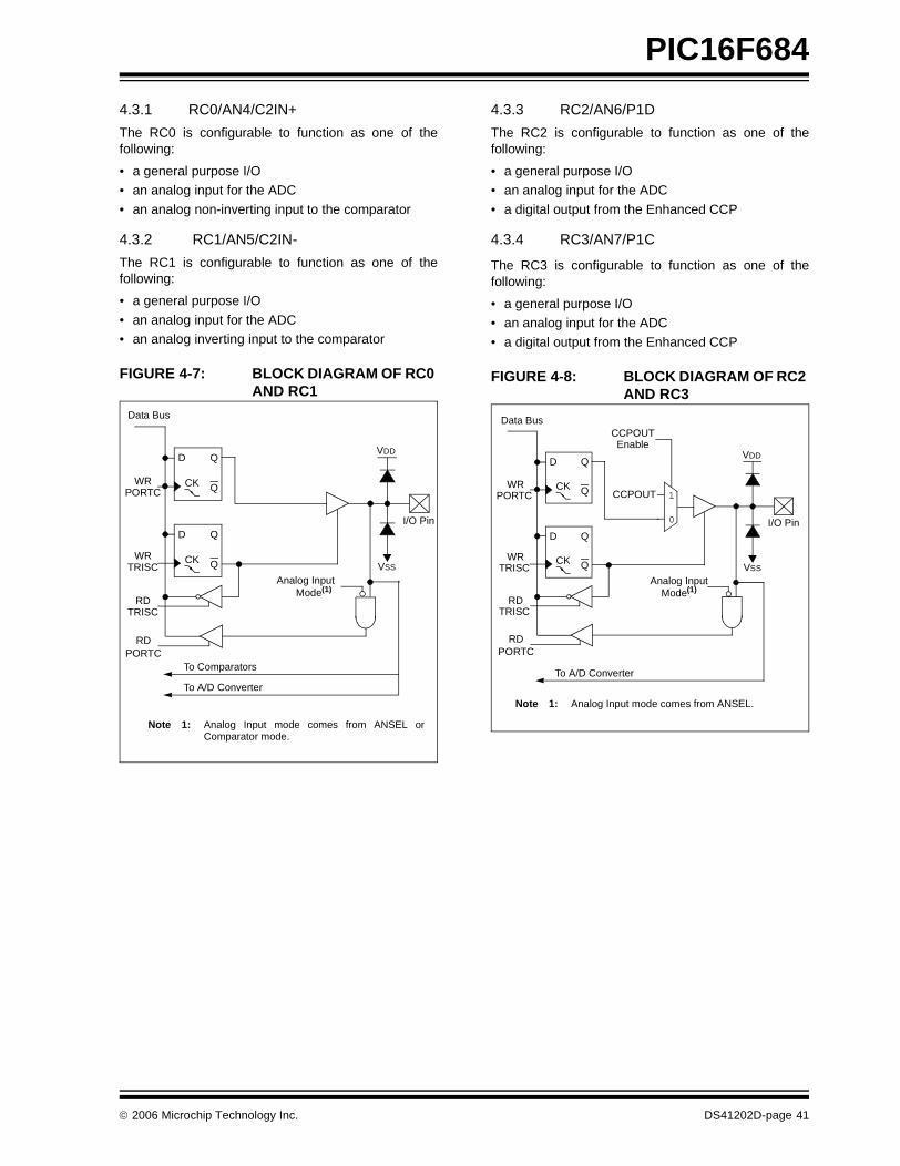
PIC16F684
4.3.1 RC0/AN4/C2IN+
The RC0 is configurable to function as one of thefollowing:
• a general purpose I/O• an analog input for the ADC
• an analog non-inverting input to the comparator
4.3.2 RC1/AN5/C2IN-
The RC1 is configurable to function as one of thefollowing:
• a general purpose I/O
• an analog input for the ADC• an analog inverting input to the comparator
FIGURE 4-7: BLOCK DIAGRAM OF RC0 AND RC1
4.3.3 RC2/AN6/P1D
The RC2 is configurable to function as one of thefollowing:
• a general purpose I/O• an analog input for the ADC
• a digital output from the Enhanced CCP
4.3.4 RC3/AN7/P1C
The RC3 is configurable to function as one of thefollowing:
• a general purpose I/O• an analog input for the ADC
• a digital output from the Enhanced CCP
FIGURE 4-8: BLOCK DIAGRAM OF RC2 AND RC3
I/O Pin
VDD
VSS
D
QCK
Q
D
QCK
Q
Data Bus
WRPORTC
WRTRISC
RDTRISC
To A/D Converter
RDPORTC
Analog InputMode(1)
To Comparators
Note 1: Analog Input mode comes from ANSEL orComparator mode.
I/O Pin
VDD
VSS
D
QCK
Q
D
QCK
Q
Data Bus
WRPORTC
WRTRISC
RDTRISC
To A/D Converter
RDPORTC
Analog InputMode(1)
0
1CCPOUT
CCPOUTEnable
Note 1: Analog Input mode comes from ANSEL.
© 2006 Microchip Technology Inc. DS41202D-page 41
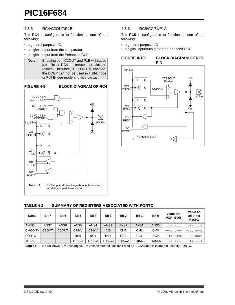
PIC16F684
4.3.5 RC4/C2OUT/P1B
The RC4 is configurable to function as one of thefollowing:
• a general purpose I/O• a digital output from the comparator
• a digital output from the Enhanced CCP
FIGURE 4-9: BLOCK DIAGRAM OF RC4
4.3.6 RC5/CCP1/P1A
The RC5 is configurable to function as one of thefollowing:
• a general purpose I/O• a digital input/output for the Enhanced CCP
FIGURE 4-10: BLOCK DIAGRAM OF RC5 PIN
TABLE 4-2: SUMMARY OF REGISTERS ASSOCIATED WITH PORTC
Note: Enabling both C2OUT and P1B will causea conflict on RC4 and create unpredictableresults. Therefore, if C2OUT is enabled,the ECCP can not be used in Half-Bridgeor Full-Bridge mode and vice-versa.
I/O Pin
VDD
VSS
D
QCK
Q
D
QCK
Q
Data Bus
WRPORTC
WRTRISC
RDTRISC
RDPORTC
0
1
Note 1: Port/Peripheral Select signals selects between port data and peripheral output.
C2OUT ENCCPOUT EN
C2OUT ENC2OUT
CCPOUT ENCCPOUT
I/O Pin
VDD
VSS
D
QCK
Q
D
QCK
Q
Data bus
WRPORTC
WRTRISC
RDTRISC
To Enhanced CCP
RDPORTC
0
1CCP1OUT
CCP1OUTEnable
Name Bit 7 Bit 6 Bit 5 Bit 4 Bit 3 Bit 2 Bit 1 Bit 0Value on: POR, BOR
Value on all other Resets
ANSEL ANS7 ANS6 ANS5 ANS4 ANS3 ANS2 ANS1 ANS0 1111 1111 1111 1111
CMCON0 C2OUT C1OUT C2INV C1INV CIS CM2 CM1 CM0 0000 0000 0000 0000
PORTC — — RC5 RC4 RC3 RC2 RC1 RC0 --xx 0000 --uu uu00
TRISC — — TRISC5 TRISC4 TRISC3 TRISC2 TRISC1 TRISC0 --11 1111 --11 1111
Legend: x = unknown, u = unchanged, – = unimplemented locations read as ‘0’. Shaded cells are not used by PORTC.
DS41202D-page 42 © 2006 Microchip Technology Inc.

PIC16F684
5.0 TIMER0 MODULE
The Timer0 module is an 8-bit timer/counter with thefollowing features:
• 8-bit timer/counter register (TMR0)
• 8-bit prescaler (shared with Watchdog Timer)• Programmable internal or external clock source• Programmable external clock edge selection
• Interrupt on overflow
Figure 5-1 is a block diagram of the Timer0 module.
5.1 Timer0 Operation
When used as a timer, the Timer0 module can be usedas either an 8-bit timer or an 8-bit counter.
5.1.1 8-BIT TIMER MODE
When used as a timer, the Timer0 module willincrement every instruction cycle (without prescaler).Timer mode is selected by clearing the T0CS bit of theOPTION register to ‘0’.
When TMR0 is written, the increment is inhibited fortwo instruction cycles immediately following the write.
5.1.2 8-BIT COUNTER MODE
When used as a counter, the Timer0 module willincrement on every rising or falling edge of the T0CKIpin. The incrementing edge is determined by the T0SEbit of the OPTION register. Counter mode is selected bysetting the T0CS bit of the OPTION register to ‘1’.
FIGURE 5-1: BLOCK DIAGRAM OF THE TIMER0/WDT PRESCALER
Note: The value written to the TMR0 register canbe adjusted, in order to account for the twoinstruction cycle delay when TMR0 iswritten.
T0CKI
T0SEpin
TMR0
WatchdogTimer
WDTTime-out
PS<2:0>
WDTE
Data Bus
Set Flag bit T0IFon Overflow
T0CS
Note 1: T0SE, T0CS, PSA, PS<2:0> are bits in the OPTION register.
2: SWDTEN and WDTPS<3:0> are bits in the WDTCON register.
3: WDTE bit is in the Configuration Word register.
0
1
0
1
0
1
Sync 2cycles
8
8
8-bitPrescaler
0
1
FOSC/4
PSA
PSA
PSA
16-bitPrescaler 16
WDTPS<3:0>
31 kHzINTOSC
SWDTEN3
© 2006 Microchip Technology Inc. DS41202D-page 43
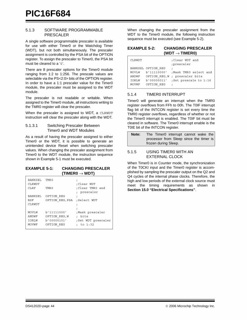
PIC16F684
5.1.3 SOFTWARE PROGRAMMABLE PRESCALER
A single software programmable prescaler is availablefor use with either Timer0 or the Watchdog Timer(WDT), but not both simultaneously. The prescalerassignment is controlled by the PSA bit of the OPTIONregister. To assign the prescaler to Timer0, the PSA bitmust be cleared to a ‘0’.
There are 8 prescaler options for the Timer0 moduleranging from 1:2 to 1:256. The prescale values areselectable via the PS<2:0> bits of the OPTION register.In order to have a 1:1 prescaler value for the Timer0module, the prescaler must be assigned to the WDTmodule.
The prescaler is not readable or writable. Whenassigned to the Timer0 module, all instructions writing tothe TMR0 register will clear the prescaler.
When the prescaler is assigned to WDT, a CLRWDTinstruction will clear the prescaler along with the WDT.
5.1.3.1 Switching Prescaler Between Timer0 and WDT Modules
As a result of having the prescaler assigned to eitherTimer0 or the WDT, it is possible to generate anunintended device Reset when switching prescalervalues. When changing the prescaler assignment fromTimer0 to the WDT module, the instruction sequenceshown in Example 5-1 must be executed.
EXAMPLE 5-1: CHANGING PRESCALER (TIMER0 → WDT)
When changing the prescaler assignment from theWDT to the Timer0 module, the following instructionsequence must be executed (see Example 5-2).
EXAMPLE 5-2: CHANGING PRESCALER (WDT → TIMER0)
5.1.4 TIMER0 INTERRUPT
Timer0 will generate an interrupt when the TMR0register overflows from FFh to 00h. The T0IF interruptflag bit of the INTCON register is set every time theTMR0 register overflows, regardless of whether or notthe Timer0 interrupt is enabled. The T0IF bit must becleared in software. The Timer0 interrupt enable is theT0IE bit of the INTCON register.
5.1.5 USING TIMER0 WITH AN EXTERNAL CLOCK
When Timer0 is in Counter mode, the synchronizationof the T0CKI input and the Timer0 register is accom-plished by sampling the prescaler output on the Q2 andQ4 cycles of the internal phase clocks. Therefore, thehigh and low periods of the external clock source mustmeet the timing requirements as shown inSection 15.0 “Electrical Specifications”.
BANKSEL TMR0 ;CLRWDT ;Clear WDTCLRF TMR0 ;Clear TMR0 and
; prescalerBANKSEL OPTION_REG ;BSF OPTION_REG,PSA ;Select WDTCLRWDT ;
;MOVLW b’11111000’ ;Mask prescalerANDWF OPTION_REG,W ; bitsIORLW b’00000101’ ;Set WDT prescalerMOVWF OPTION_REG ; to 1:32
Note: The Timer0 interrupt cannot wake theprocessor from Sleep since the timer isfrozen during Sleep.
CLRWDT ;Clear WDT and;prescaler
BANKSEL OPTION_REG ;MOVLW b’11110000’ ;Mask TMR0 select andANDWF OPTION_REG,W ; prescaler bits IORLW b’00000011’ ;Set prescale to 1:16 MOVWF OPTION_REG ;
DS41202D-page 44 © 2006 Microchip Technology Inc.
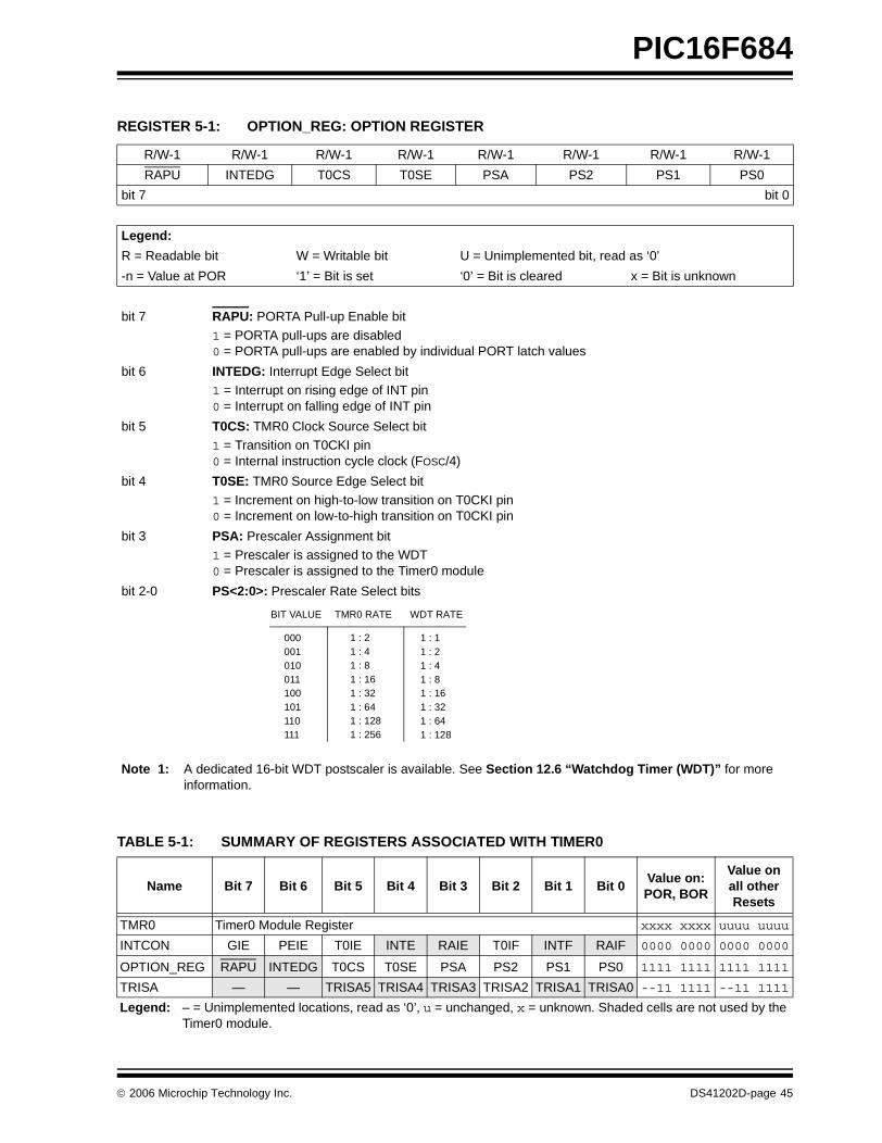
PIC16F684
TABLE 5-1: SUMMARY OF REGISTERS ASSOCIATED WITH TIMER0
REGISTER 5-1: OPTION_REG: OPTION REGISTER
R/W-1 R/W-1 R/W-1 R/W-1 R/W-1 R/W-1 R/W-1 R/W-1
RAPU INTEDG T0CS T0SE PSA PS2 PS1 PS0
bit 7 bit 0
Legend:
R = Readable bit W = Writable bit U = Unimplemented bit, read as ‘0’
-n = Value at POR ‘1’ = Bit is set ‘0’ = Bit is cleared x = Bit is unknown
bit 7 RAPU: PORTA Pull-up Enable bit
1 = PORTA pull-ups are disabled0 = PORTA pull-ups are enabled by individual PORT latch values
bit 6 INTEDG: Interrupt Edge Select bit1 = Interrupt on rising edge of INT pin0 = Interrupt on falling edge of INT pin
bit 5 T0CS: TMR0 Clock Source Select bit1 = Transition on T0CKI pin0 = Internal instruction cycle clock (FOSC/4)
bit 4 T0SE: TMR0 Source Edge Select bit
1 = Increment on high-to-low transition on T0CKI pin0 = Increment on low-to-high transition on T0CKI pin
bit 3 PSA: Prescaler Assignment bit1 = Prescaler is assigned to the WDT0 = Prescaler is assigned to the Timer0 module
bit 2-0 PS<2:0>: Prescaler Rate Select bits
Note 1: A dedicated 16-bit WDT postscaler is available. See Section 12.6 “Watchdog Timer (WDT)” for more information.
000001010011100101110111
1 : 21 : 41 : 81 : 161 : 321 : 641 : 1281 : 256
1 : 11 : 21 : 41 : 81 : 161 : 321 : 641 : 128
BIT VALUE TMR0 RATE WDT RATE
Name Bit 7 Bit 6 Bit 5 Bit 4 Bit 3 Bit 2 Bit 1 Bit 0Value on: POR, BOR
Value onall otherResets
TMR0 Timer0 Module Register xxxx xxxx uuuu uuuu
INTCON GIE PEIE T0IE INTE RAIE T0IF INTF RAIF 0000 0000 0000 0000
OPTION_REG RAPU INTEDG T0CS T0SE PSA PS2 PS1 PS0 1111 1111 1111 1111
TRISA — — TRISA5 TRISA4 TRISA3 TRISA2 TRISA1 TRISA0 --11 1111 --11 1111
Legend: – = Unimplemented locations, read as ‘0’, u = unchanged, x = unknown. Shaded cells are not used by the Timer0 module.
© 2006 Microchip Technology Inc. DS41202D-page 45

PIC16F684
NOTES:
DS41202D-page 46 © 2006 Microchip Technology Inc.
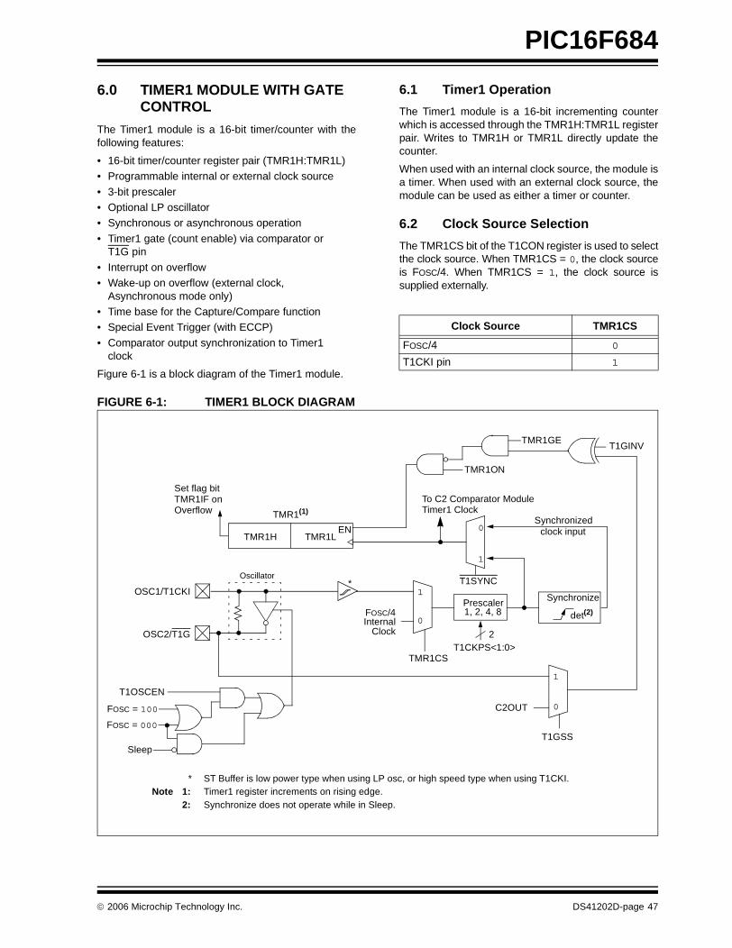
PIC16F684
6.0 TIMER1 MODULE WITH GATE CONTROL
The Timer1 module is a 16-bit timer/counter with thefollowing features:
• 16-bit timer/counter register pair (TMR1H:TMR1L)• Programmable internal or external clock source
• 3-bit prescaler• Optional LP oscillator• Synchronous or asynchronous operation
• Timer1 gate (count enable) via comparator or T1G pin
• Interrupt on overflow• Wake-up on overflow (external clock,
Asynchronous mode only)• Time base for the Capture/Compare function• Special Event Trigger (with ECCP)
• Comparator output synchronization to Timer1 clock
Figure 6-1 is a block diagram of the Timer1 module.
6.1 Timer1 Operation
The Timer1 module is a 16-bit incrementing counterwhich is accessed through the TMR1H:TMR1L registerpair. Writes to TMR1H or TMR1L directly update thecounter.
When used with an internal clock source, the module isa timer. When used with an external clock source, themodule can be used as either a timer or counter.
6.2 Clock Source Selection
The TMR1CS bit of the T1CON register is used to selectthe clock source. When TMR1CS = 0, the clock sourceis FOSC/4. When TMR1CS = 1, the clock source issupplied externally.
FIGURE 6-1: TIMER1 BLOCK DIAGRAM
Clock Source TMR1CS
FOSC/4 0
T1CKI pin 1
TMR1H TMR1L
OscillatorT1SYNC
T1CKPS<1:0>
Prescaler1, 2, 4, 8
Synchronize
det(2)
1
0
0
1
Synchronizedclock input
2
Set flag bitTMR1IF onOverflow TMR1(1)
TMR1GE
TMR1ON
T1OSCEN
1
0C2OUT
T1GSS
T1GINV
To C2 Comparator ModuleTimer1 Clock
TMR1CS
OSC2/T1G
OSC1/T1CKI
* ST Buffer is low power type when using LP osc, or high speed type when using T1CKI.Note 1: Timer1 register increments on rising edge.
2: Synchronize does not operate while in Sleep.
*
EN
FOSC/4Internal
Clock
FOSC = 100
FOSC = 000
Sleep
© 2006 Microchip Technology Inc. DS41202D-page 47
PIC16F684
6.2.1 INTERNAL CLOCK SOURCE
When the internal clock source is selected, theTMR1H:TMR1L register pair will increment on multiplesof FOSC as determined by the Timer1 prescaler.
6.2.2 EXTERNAL CLOCK SOURCE
When the external clock source is selected, the Timer1module may work as a timer or a counter.
When counting, Timer1 is incremented on the risingedge of the external clock input T1CKI. In addition, theCounter mode clock can be synchronized to themicrocontroller system clock or run asynchronously.
If an external clock oscillator is needed (and themicrocontroller is using the INTOSC without CLKOUT),Timer1 can use the LP oscillator as a clock source.
6.3 Timer1 Prescaler
Timer1 has four prescaler options allowing 1, 2, 4 or 8divisions of the clock input. The T1CKPS bits of theT1CON register control the prescale counter. Theprescale counter is not directly readable or writable;however, the prescaler counter is cleared upon a write toTMR1H or TMR1L.
6.4 Timer1 Oscillator
A low-power 32.768 kHz crystal oscillator is built-inbetween pins OSC1 (input) and OSC2 (amplifieroutput). The oscillator is enabled by setting theT1OSCEN control bit of the T1CON register. Theoscillator will continue to run during Sleep.
The Timer1 oscillator is shared with the system LPoscillator. Thus, Timer1 can use this mode only whenthe primary system clock is derived from the internaloscillator or when the oscillator is in the LP mode. Theuser must provide a software time delay to ensureproper oscillator start-up.
TRISA5 and TRISA4 bits are set when the Timer1oscillator is enabled. RA5 and RA4 bits read as ‘0’ andTRISA5 and TRISA4 bits read as ‘1’.
6.5 Timer1 Operation in Asynchronous Counter Mode
If control bit T1SYNC of the T1CON register is set, theexternal clock input is not synchronized. The timerincrements asynchronously to the internal phaseclocks. If external clock source is selected then thetimer will continue to run during Sleep and cangenerate an interrupt on overflow, which will wake-upthe processor. However, special precautions insoftware are needed to read/write the timer (seeSection 6.5.1 “Reading and Writing Timer1 inAsynchronous Counter Mode”).
6.5.1 READING AND WRITING TIMER1 IN ASYNCHRONOUS COUNTER MODE
Reading TMR1H or TMR1L while the timer is runningfrom an external asynchronous clock will ensure a validread (taken care of in hardware). However, the usershould keep in mind that reading the 16-bit timer in two8-bit values itself, poses certain problems, since thetimer may overflow or carry out of TMR1L to TMR1Hbetween the reads.
For writes, it is recommended that the user simply stopthe timer and write the desired values. A writecontention may occur by writing to the timer registers,while the register is incrementing. This may produce anunpredictable value in the TMR1H:TMR1L register pair.
Note: In Counter mode, a falling edge must beregistered by the counter prior to the firstincrementing rising edge after any one ormore of the following conditions:
• Timer1 enabled after POR reset
• Write to TMR1H or TMR1L• Timer1 is disabled• Timer1 is disabled (TMR1ON 0) when
T1CKI is high then Timer1 is enabled (TMR1ON=1) when T1CKI is low.
See Figure 6-2
Note: The oscillator requires a start-up andstabilization time before use. Thus,T1OSCEN should be set and a suitabledelay observed prior to enabling Timer1.
Note: When switching from synchronous toasynchronous operation, it is possible toskip an increment. When switching fromasynchronous to synchronous operation,it is possible to produce an additionalincrement.
DS41202D-page 48 © 2006 Microchip Technology Inc.
PIC16F684
6.6 Timer1 Gate
Timer1 gate source is software configurable to be theT1G pin or the output of Comparator 2. This allows thedevice to directly time external events using T1G oranalog events using Comparator 2. See the CMCON1register (Register 8-2) for selecting the Timer1 gatesource. This feature can simplify the software for aDelta-Sigma A/D converter and many other applications.For more information on Delta-Sigma A/D converters,see the Microchip web site (www.microchip.com).
Timer1 gate can be inverted using the T1GINV bit ofthe T1CON register, whether it originates from the T1Gpin or Comparator 2 output. This configures Timer1 tomeasure either the active-high or active-low timebetween events.
6.7 Timer1 Interrupt
The Timer1 register pair (TMR1H:TMR1L) incrementsto FFFFh and rolls over to 0000h. When Timer1 rollsover, the Timer1 interrupt flag bit of the PIR1 register isset. To enable the interrupt on rollover, you must setthese bits:
• TMR1ON bit or the T1CON register• TMR1IE bit of the PIE1 register• PEIE bit of the INTCON register
• GIE bit of the INTCON register
The interrupt is cleared by clearing the TMR1IF bit inthe Interrupt Service Routine.
6.8 Timer1 Operation During Sleep
Timer1 can only operate during Sleep when setup inAsynchronous Counter mode. In this mode, an externalcrystal or clock source can be used to increment thecounter. To set up the timer to wake the device:
• TMR1ON bit of the T1CON register must be set• TMR1IE bit of the PIE1 register must be set• PEIE bit of the INTCON register must be set
• T1SYNC bit of the T1CON register• TMR1CS bit of the T1CON register• T1OSCEN bit of the T1CON register (can be set)
The device will wake-up on an overflow and executethe next instruction. If the GIE bit of the INTCONregister is set, the device will call the Interrupt ServiceRoutine (0004h).
6.9 ECCP Capture/Compare Time Base
The ECCP module uses the TMR1H:TMR1L registerpair as the time base when operating in Capture orCompare mode.
In Capture mode, the value in the TMR1H:TMR1Lregister pair is copied into the CCPR1H:CCPR1Lregister pair on a configured event.
In Compare mode, an event is triggered when the valueCCPR1H:CCPR1L register pair matches the value inthe TMR1H:TMR1L register pair. This event can be aSpecial Event Trigger.
For more information, see Section 11.0 “EnhancedCapture/Compare/PWM (With Auto-Shutdown andDead Band) Module”.
6.10 ECCP Special Event Trigger
When the ECCP is configured to trigger a specialevent, the trigger will clear the TMR1H:TMR1L registerpair. This special event does not cause a Timer1interrupt. The ECCP module may still be configured togenerate a ECCP interrupt.
In this mode of operation, the CCPR1H:CCPR1Lregister pair effectively becomes the period register forTimer1.
Timer1 should be synchronized to the FOSC to utilizethe Special Event Trigger. Asynchronous operation ofTimer1 can cause a Special Event Trigger to bemissed.
In the event that a write to TMR1H or TMR1L coincideswith a Special Event Trigger from the ECCP, the writewill take precedence.
For more information, see Section 11.2.4 “SpecialEvent Trigger”.
6.11 Comparator Synchronization
The same clock used to increment Timer1 can also beused to synchronize the comparator output. Thisfeature is enabled in the Comparator module.
When using the comparator for Timer1 gate, thecomparator output should be synchronized to Timer1.This ensures Timer1 does not miss an increment if thecomparator changes.
For more information, see Section 8.9 “SynchronizingComparator C2 Output to Timer1”.
Note: TMR1GE bit of the T1CON register mustbe set to use either T1G or C2OUT as theTimer1 gate source. See the CMCON1register (Register 8-2) for more informa-tion on selecting the Timer1 gate source.
Note: The TMR1H:TTMR1L register pair and theTMR1IF bit should be cleared beforeenabling interrupts.
© 2006 Microchip Technology Inc. DS41202D-page 49
PIC16F684
FIGURE 6-2: TIMER1 INCREMENTING EDGE
6.12 Timer1 Control Register
The Timer1 Control register (T1CON), shown inRegister 6-1, is used to control Timer1 and select thevarious features of the Timer1 module.
T1CKI = 1
when TMR1Enabled
T1CKI = 0
when TMR1Enabled
Note 1: Arrows indicate counter increments.
2: In Counter mode, a falling edge must be registered by the counter prior to the first incrementing rising edge of the clock.
REGISTER 6-1: T1CON: TIMER 1 CONTROL REGISTER
R/W-0 R/W-0 R/W-0 R/W-0 R/W-0 R/W-0 R/W-0 R/W-0
T1GINV(1) TMR1GE(2) T1CKPS1 T1CKPS0 T1OSCEN T1SYNC TMR1CS TMR1ON
bit 7 bit 0
Legend:
R = Readable bit W = Writable bit U = Unimplemented bit, read as ‘0’
-n = Value at POR ‘1’ = Bit is set ‘0’ = Bit is cleared x = Bit is unknown
bit 7 T1GINV: Timer1 Gate Invert bit(1)
1 = Timer1 gate is active high (Timer1 counts when gate is high)0 = Timer1 gate is active low (Timer1 counts when gate is low)
bit 6 TMR1GE: Timer1 Gate Enable bit(2)
If TMR1ON = 0:This bit is ignoredIf TMR1ON = 1:1 = Timer1 is on if Timer1 gate is not active0 = Timer1 is on
bit 5-4 T1CKPS<1:0>: Timer1 Input Clock Prescale Select bits11 = 1:8 Prescale Value10 = 1:4 Prescale Value01 = 1:2 Prescale Value00 = 1:1 Prescale Value
bit 3 T1OSCEN: LP Oscillator Enable Control bitIf INTOSC without CLKOUT oscillator is active:1 = LP oscillator is enabled for Timer1 clock0 = LP oscillator is offElse:This bit is ignored
DS41202D-page 50 © 2006 Microchip Technology Inc.
PIC16F684
TABLE 6-1: SUMMARY OF REGISTERS ASSOCIATED WITH TIMER1
bit 2 T1SYNC: Timer1 External Clock Input Synchronization Control bitTMR1CS = 1:1 = Do not synchronize external clock input0 = Synchronize external clock inputTMR1CS = 0:This bit is ignored. Timer1 uses the internal clock
bit 1 TMR1CS: Timer1 Clock Source Select bit
1 = External clock from T1CKI pin (on the rising edge)0 = Internal clock (FOSC/4)
bit 0 TMR1ON: Timer1 On bit1 = Enables Timer10 = Stops Timer1
Note 1: T1GINV bit inverts the Timer1 gate logic, regardless of source.2: TMR1GE bit must be set to use either T1G pin or C2OUT, as selected by the T1GSS bit of the CMCON1
register, as a Timer1 gate source.
Name Bit 7 Bit 6 Bit 5 Bit 4 Bit 3 Bit 2 Bit 1 Bit 0 Value on: POR, BOR
Value on all other Resets
CMCON1 — — — — — — T1GSS C2SYNC ---- --10 ---- --10
INTCON GIE PEIE T0IE INTE RAIE T0IF INTF RAIF 0000 0000 0000 0000
PIE1 EEIE ADIE CCP1IE C2IE C1IE OSFIE TMR2IE TMR1IE 0000 0000 0000 0000
PIR1 EEIF ADIF CCP1IF C2IF C1IF OSFIF TMR2IF TMR1IF 0000 0000 0000 0000
TMR1H Holding Register for the Most Significant Byte of the 16-bit TMR1 Register xxxx xxxx uuuu uuuu
TMR1L Holding Register for the Least Significant Byte of the 16-bit TMR1 Register xxxx xxxx uuuu uuuu
T1CON T1GINV TMR1GE T1CKPS1 T1CKPS0 T1OSCEN T1SYNC TMR1CS TMR1ON 0000 0000 uuuu uuuu
Legend: x = unknown, u = unchanged, — = unimplemented, read as ‘0’. Shaded cells are not used by the Timer1 module.
REGISTER 6-1: T1CON: TIMER 1 CONTROL REGISTER (CONTINUED)
© 2006 Microchip Technology Inc. DS41202D-page 51

PIC16F684
NOTES:
DS41202D-page 52 © 2006 Microchip Technology Inc.
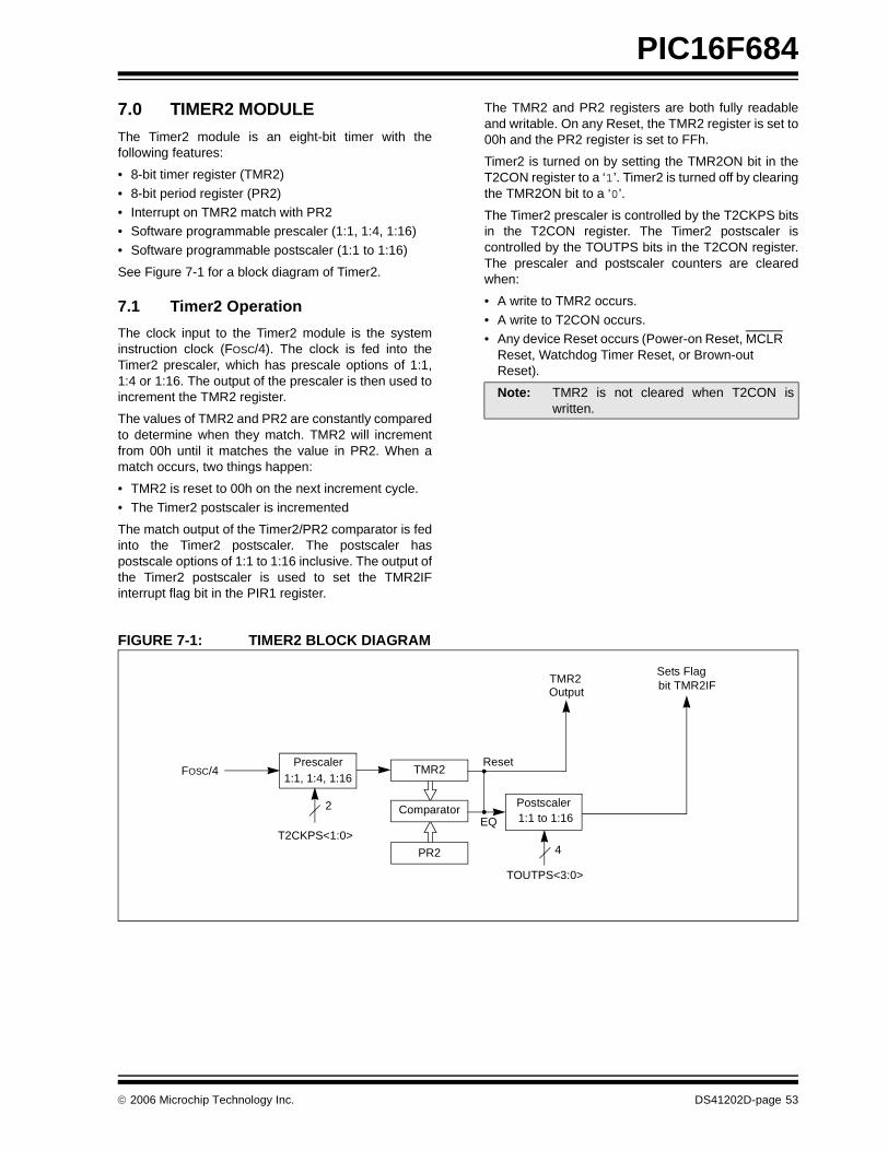
PIC16F684
7.0 TIMER2 MODULE
The Timer2 module is an eight-bit timer with thefollowing features:
• 8-bit timer register (TMR2)
• 8-bit period register (PR2)• Interrupt on TMR2 match with PR2• Software programmable prescaler (1:1, 1:4, 1:16)
• Software programmable postscaler (1:1 to 1:16)
See Figure 7-1 for a block diagram of Timer2.
7.1 Timer2 Operation
The clock input to the Timer2 module is the systeminstruction clock (FOSC/4). The clock is fed into theTimer2 prescaler, which has prescale options of 1:1,1:4 or 1:16. The output of the prescaler is then used toincrement the TMR2 register.
The values of TMR2 and PR2 are constantly comparedto determine when they match. TMR2 will incrementfrom 00h until it matches the value in PR2. When amatch occurs, two things happen:
• TMR2 is reset to 00h on the next increment cycle.
• The Timer2 postscaler is incremented
The match output of the Timer2/PR2 comparator is fedinto the Timer2 postscaler. The postscaler haspostscale options of 1:1 to 1:16 inclusive. The output ofthe Timer2 postscaler is used to set the TMR2IFinterrupt flag bit in the PIR1 register.
The TMR2 and PR2 registers are both fully readableand writable. On any Reset, the TMR2 register is set to00h and the PR2 register is set to FFh.
Timer2 is turned on by setting the TMR2ON bit in theT2CON register to a ‘1’. Timer2 is turned off by clearingthe TMR2ON bit to a ‘0’.
The Timer2 prescaler is controlled by the T2CKPS bitsin the T2CON register. The Timer2 postscaler iscontrolled by the TOUTPS bits in the T2CON register.The prescaler and postscaler counters are clearedwhen:
• A write to TMR2 occurs.
• A write to T2CON occurs.• Any device Reset occurs (Power-on Reset, MCLR
Reset, Watchdog Timer Reset, or Brown-out Reset).
FIGURE 7-1: TIMER2 BLOCK DIAGRAM
Note: TMR2 is not cleared when T2CON iswritten.
Comparator
TMR2Sets Flag
TMR2
Output
Reset
Postscaler
Prescaler
PR2
2
FOSC/4
1:1 to 1:16
1:1, 1:4, 1:16
EQ
4
bit TMR2IF
TOUTPS<3:0>
T2CKPS<1:0>
© 2006 Microchip Technology Inc. DS41202D-page 53
PIC16F684
TABLE 7-1: SUMMARY OF ASSOCIATED TIMER2 REGISTERS
REGISTER 7-1: T2CON: TIMER 2 CONTROL REGISTER
U-0 R/W-0 R/W-0 R/W-0 R/W-0 R/W-0 R/W-0 R/W-0
— TOUTPS3 TOUTPS2 TOUTPS1 TOUTPS0 TMR2ON T2CKPS1 T2CKPS0
bit 7 bit 0
Legend:
R = Readable bit W = Writable bit U = Unimplemented bit, read as ‘0’
-n = Value at POR ‘1’ = Bit is set ‘0’ = Bit is cleared x = Bit is unknown
bit 7 Unimplemented: Read as ‘0’
bit 6-3 TOUTPS<3:0>: Timer2 Output Postscaler Select bits0000 = 1:1 Postscaler0001 = 1:2 Postscaler0010 = 1:3 Postscaler0011 = 1:4 Postscaler0100 = 1:5 Postscaler0101 = 1:6 Postscaler0110 = 1:7 Postscaler0111 = 1:8 Postscaler1000 = 1:9 Postscaler1001 = 1:10 Postscaler1010 = 1:11 Postscaler1011 = 1:12 Postscaler1100 = 1:13 Postscaler1101 = 1:14 Postscaler1110 = 1:15 Postscaler1111 = 1:16 Postscaler
bit 2 TMR2ON: Timer2 On bit1 = Timer2 is on0 = Timer2 is off
bit 1-0 T2CKPS<1:0>: Timer2 Clock Prescale Select bits00 = Prescaler is 101 = Prescaler is 41x = Prescaler is 16
Name Bit 7 Bit 6 Bit 5 Bit 4 Bit 3 Bit 2 Bit 1 Bit 0Value on: POR, BOR
Value on all other Resets
INTCON GIE PEIE T0IE INTE RAIE T0IF INTF RAIF 0000 0000 0000 0000
PIE1 EEIE ADIE CCP1IE C2IE C1IE OSFIE TMR2IE TMR1IE 0000 0000 0000 0000
PIR1 EEIF ADIF CCP1IF C2IF C1IF OSFIF TMR2IF TMR1IF 0000 0000 0000 0000
PR2 Timer2 Module Period Register 1111 1111 1111 1111
TMR2 Holding Register for the 8-bit TMR2 Register 0000 0000 0000 0000
T2CON — TOUTPS3 TOUTPS2 TOUTPS1 TOUTPS0 TMR2ON T2CKPS1 T2CKPS0 -000 0000 -000 0000
Legend: x = unknown, u = unchanged, — = unimplemented read as ‘0’. Shaded cells are not used for Timer2 module.
DS41202D-page 54 © 2006 Microchip Technology Inc.
PIC16F684
8.0 COMPARATOR MODULE
Comparators are used to interface analog circuits to adigital circuit by comparing two analog voltages andproviding a digital indication of their relative magnitudes.The comparators are very useful mixed signal buildingblocks because they provide analog functionalityindependent of the device program execution. Theanalog Comparator module includes the followingfeatures:
• Dual comparators
• Multiple comparator configurations• Comparator outputs are available internally/
externally• Programmable output polarity• Interrupt-on-change
• Wake-up from Sleep• Timer1 gate (count enable)• Output synchronization to Timer1 clock input
• Programmable voltage reference
8.1 Comparator Overview
A comparator is shown in Figure 8-1 along with therelationship between the analog input levels and thedigital output. When the analog voltage at VIN+ is lessthan the analog voltage at VIN-, the output of thecomparator is a digital low level. When the analogvoltage at VIN+ is greater than the analog voltage atVIN-, the output of the comparator is a digital high level.
FIGURE 8-1: SINGLE COMPARATOR
This device contains two comparators as shown inFigure 8-2 and Figure 8-3. The comparators are notindependently configurable.
Note: Only Comparator C2 can be linked toTimer1.
–
+VIN+
VIN-Output
Output
VIN+VIN-
Note: The black areas of the output of thecomparator represents the uncertaintydue to input offsets and response time.
© 2006 Microchip Technology Inc. DS41202D-page 55
PIC16F684
FIGURE 8-2: COMPARATOR C1 OUTPUT BLOCK DIAGRAM
FIGURE 8-3: COMPARATOR C2 OUTPUT BLOCK DIAGRAM
D Q
EN
To C1OUT pin
RD CMCON0
Set C1IF bit
MU
LTIP
LEX
Port P
ins
Q3*RD CMCON0
Reset
To Data Bus
C1INV
D Q
ENCL
Q1
Note 1: Q1 and Q3 are phases of the four-phase system clock (FOSC).
2: Q1 is held high during Sleep mode.
C1
C2SYNC
D Q
EN
To C2OUT pin
RD CMCON0
Set C2IF bit
MU
LTIP
LEX
Port P
ins
Q3*RD CMCON0
Reset
To Data Bus
C2INV
Timer1clock source(1)
0
1
To Timer1 Gate
D Q
D Q
ENCL
Q1
Note 1: Comparator output is latched on falling edge of Timer1 clock source.
2: Q1 and Q3 are phases of the four-phase system clock (FOSC).
3: Q1 is held high during Sleep mode.
C2
DS41202D-page 56 © 2006 Microchip Technology Inc.
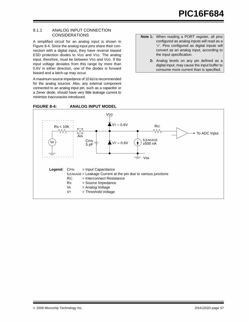
PIC16F684
8.1.1 ANALOG INPUT CONNECTION CONSIDERATIONS
A simplified circuit for an analog input is shown inFigure 8-4. Since the analog input pins share their con-nection with a digital input, they have reverse biasedESD protection diodes to VDD and VSS. The analoginput, therefore, must be between VSS and VDD. If theinput voltage deviates from this range by more than0.6V in either direction, one of the diodes is forwardbiased and a latch-up may occur.
A maximum source impedance of 10 kΩ is recommendedfor the analog sources. Also, any external componentconnected to an analog input pin, such as a capacitor ora Zener diode, should have very little leakage current tominimize inaccuracies introduced.
FIGURE 8-4: ANALOG INPUT MODEL
Note 1: When reading a PORT register, all pinsconfigured as analog inputs will read as a‘0’. Pins configured as digital inputs willconvert as an analog input, according tothe input specification.
2: Analog levels on any pin defined as adigital input, may cause the input buffer toconsume more current than is specified.
VA
Rs < 10K
CPIN5 pF
VDD
VT ≈ 0.6V
VT ≈ 0.6V
RIC
ILEAKAGE±500 nA
Vss
AIN
Legend: CPIN = Input CapacitanceILEAKAGE = Leakage Current at the pin due to various junctionsRIC = Interconnect ResistanceRS = Source ImpedanceVA = Analog VoltageVT = Threshold Voltage
To ADC Input
© 2006 Microchip Technology Inc. DS41202D-page 57
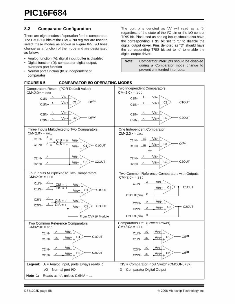
PIC16F684
8.2 Comparator Configuration
There are eight modes of operation for the comparator.The CM<2:0> bits of the CMCON0 register are used toselect these modes as shown in Figure 8-5. I/O lineschange as a function of the mode and are designatedas follows:
• Analog function (A): digital input buffer is disabled• Digital function (D): comparator digital output,
overrides port function• Normal port function (I/O): independent of
comparator
The port pins denoted as “A” will read as a ‘0’regardless of the state of the I/O pin or the I/O controlTRIS bit. Pins used as analog inputs should also havethe corresponding TRIS bit set to ‘1’ to disable thedigital output driver. Pins denoted as “D” should havethe corresponding TRIS bit set to ‘0’ to enable thedigital output driver.
FIGURE 8-5: COMPARATOR I/O OPERATING MODES
Note: Comparator interrupts should be disabledduring a Comparator mode change toprevent unintended interrupts.
C1C1IN- VIN-
VIN+C1IN+Off(1)
Comparators Reset (POR Default Value)
A
A
CM<2:0> = 000
C2C2IN- VIN-
VIN+C2IN+Off(1)
A
A
C1C1IN- VIN-
VIN+C1IN+C1OUT
Two Independent Comparators
A
A
CM<2:0> = 100
C2C2IN- VIN-
VIN+C2IN+C2OUT
A
A
C1C1IN- VIN-
VIN+C1IN+C1OUT
Two Common Reference Comparators
A
I/O
CM<2:0> = 011
C2C2IN- VIN-
VIN+C2IN+C2OUT
A
A
C1C1IN- VIN-
VIN+C1IN+Off(1)
One Independent Comparator
I/O
I/O
CM<2:0> = 101
C2C2IN- VIN-
VIN+C2IN+C2OUT
A
A
C1C1IN- VIN-
VIN+C1IN+Off(1)
Comparators Off (Lowest Power)
I/O
I/O
CM<2:0> = 111
C2C2IN- VIN-
VIN+C2IN+Off(1)
I/O
I/O
C1
C1IN- VIN-
VIN+C1IN+ C1OUT
Four Inputs Multiplexed to Two Comparators
A
A
CM<2:0> = 010
C2
C2IN- VIN-
VIN+C2IN+ C2OUT
A
A
From CVREF Module
CIS = 0CIS = 1
CIS = 0CIS = 1
C1C1IN- VIN-
VIN+
C1OUT(pin)
C1OUT
Two Common Reference Comparators with Outputs
A
D
CM<2:0> = 110
C2C2IN- VIN-
VIN+C2IN+C2OUT
A
A
C2OUT(pin)
C1
C1IN- VIN-
VIN+C1IN+ C1OUT
Three Inputs Multiplexed to Two Comparators
A
A
CM<2:0> = 001
C2C2IN- VIN-
VIN+C2IN+C2OUT
A
A
CIS = 0CIS = 1
D
Legend: A = Analog Input, ports always reads ‘0’ CIS = Comparator Input Switch (CMCON0<3>)
I/O = Normal port I/O D = Comparator Digital Output
Note 1: Reads as ‘0’, unless CxINV = 1.
DS41202D-page 58 © 2006 Microchip Technology Inc.
PIC16F684
8.3 Comparator Control
The CMCON0 register (Register 8-1) provides accessto the following comparator features:
• Mode selection• Output state
• Output polarity• Input switch
8.3.1 COMPARATOR OUTPUT STATE
Each comparator state can always be read internallyvia the associated CxOUT bit of the CMCON0 register.The comparator outputs are directed to the CxOUTpins when CM<2:0> = 110. When this mode isselected, the TRIS bits for the associated CxOUT pinsmust be cleared to enable the output drivers.
8.3.2 COMPARATOR OUTPUT POLARITY
Inverting the output of a comparator is functionallyequivalent to swapping the comparator inputs. Thepolarity of a comparator output can be inverted by set-ting the CxINV bits of the CMCON0 register. ClearingCxINV results in a non-inverted output. A completetable showing the output state versus input conditionsand the polarity bit is shown in Table 8-1.
TABLE 8-1: OUTPUT STATE VS. INPUT CONDITIONS
8.3.3 COMPARATOR INPUT SWITCH
The inverting input of the comparators may be switchedbetween two analog pins in the following modes:
• CM<2:0> = 001 (Comparator C1 only)
• CM<2:0> = 010 (Comparators C1 and C2)
In the above modes, both pins remain in Analog moderegardless of which pin is selected as the input. The CISbit of the CMCON0 register controls the comparatorinput switch.
8.4 Comparator Response Time
The comparator output is indeterminate for a period oftime after the change of an input source or the selectionof a new reference voltage. This period is referred to asthe response time. The response time of thecomparator differs from the settling time of the voltagereference. Therefore, both of these times must beconsidered when determining the total response timeto a comparator input change. See Comparator andVoltage Reference specifications of Section 15.0“Electrical Specifications” for more details.
8.5 Comparator Interrupt Operation
The comparator interrupt flag is set whenever there isa change in the output value of the comparator.Changes are recognized by means of a mismatchcircuit which consists of two latches and an exclusive-or gate (see Figure 8-2 and Figure 8-3). One latch isupdated with the comparator output level when theCMCON0 register is read. This latch retains the valueuntil the next read of the CMCON0 register or theoccurrence of a reset. The other latch of the mismatchcircuit is updated on every Q1 system clock. Amismatch condition will occur when a comparatoroutput change is clocked through the second latch onthe Q1 clock cycle. The mismatch condition will persist,holding the CxIF bit of the PIR1 register true, until eitherthe CMCON0 register is read or the comparator outputreturns to the previous state.
Software will need to maintain information about thestatus of the comparator output to determine the actualchange that has occurred.
The CxIF bit of the PIR1 register is the comparatorinterrupt flag. This bit must be reset in software byclearing it to ‘0’. Since it is also possible to write a ‘1’ tothis register, a simulated interrupt may be initiated.
The CxIE bit of the PIE1 register and the PEIE and GIEbits of the INTCON register must all be set to enablecomparator interrupts. If any of these bits are cleared,the interrupt is not enabled, although the CxIF bit of thePIR1 register will still be set if an interrupt conditionoccurs.
The user, in the Interrupt Service Routine, can clear theinterrupt in the following manner:
a) Any read or write of CMCON0. This will end themismatch condition.
b) Clear the CxIF interrupt flag.
Input Conditions CxINV CxOUT
VIN- > VIN+ 0 0
VIN- < VIN+ 0 1
VIN- > VIN+ 1 1
VIN- < VIN+ 1 0
Note: CxOUT refers to both the register bit andoutput pin.
Note: A write operation to the CMCON0 registerwill also clear the mismatch conditionbecause all writes include a readoperation at the beginning of the writecycle.
© 2006 Microchip Technology Inc. DS41202D-page 59
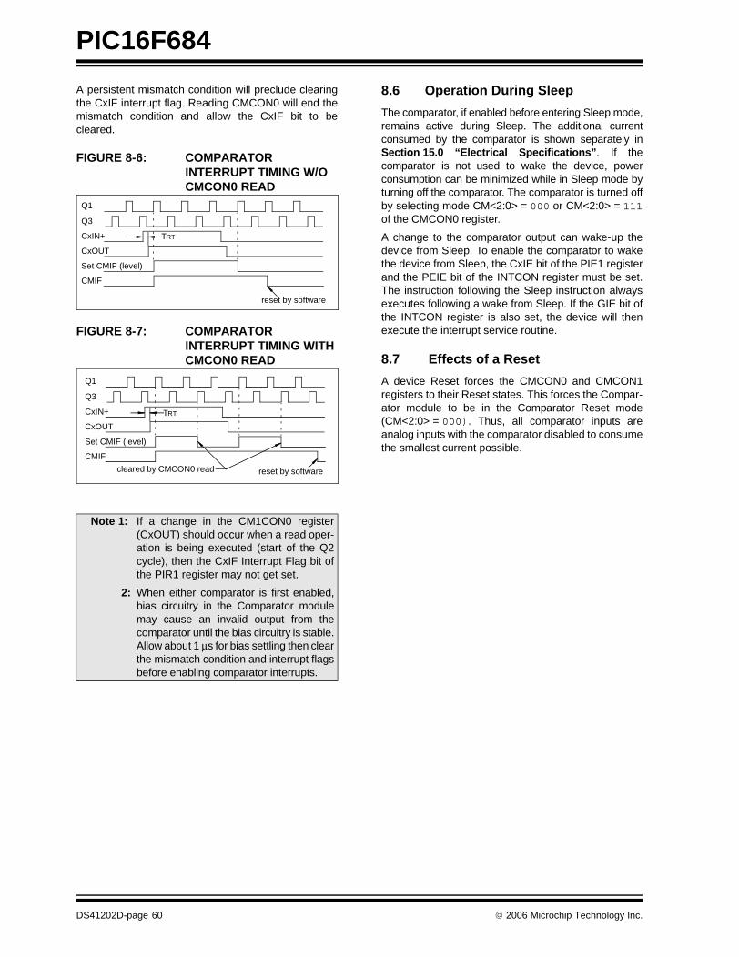
PIC16F684
A persistent mismatch condition will preclude clearingthe CxIF interrupt flag. Reading CMCON0 will end themismatch condition and allow the CxIF bit to becleared.
FIGURE 8-6: COMPARATOR INTERRUPT TIMING W/O CMCON0 READ
FIGURE 8-7: COMPARATOR INTERRUPT TIMING WITH CMCON0 READ
8.6 Operation During Sleep
The comparator, if enabled before entering Sleep mode,remains active during Sleep. The additional currentconsumed by the comparator is shown separately inSection 15.0 “Electrical Specifications”. If thecomparator is not used to wake the device, powerconsumption can be minimized while in Sleep mode byturning off the comparator. The comparator is turned offby selecting mode CM<2:0> = 000 or CM<2:0> = 111of the CMCON0 register.
A change to the comparator output can wake-up thedevice from Sleep. To enable the comparator to wakethe device from Sleep, the CxIE bit of the PIE1 registerand the PEIE bit of the INTCON register must be set.The instruction following the Sleep instruction alwaysexecutes following a wake from Sleep. If the GIE bit ofthe INTCON register is also set, the device will thenexecute the interrupt service routine.
8.7 Effects of a Reset
A device Reset forces the CMCON0 and CMCON1registers to their Reset states. This forces the Compar-ator module to be in the Comparator Reset mode(CM<2:0> = 000). Thus, all comparator inputs areanalog inputs with the comparator disabled to consumethe smallest current possible.
Note 1: If a change in the CM1CON0 register(CxOUT) should occur when a read oper-ation is being executed (start of the Q2cycle), then the CxIF Interrupt Flag bit ofthe PIR1 register may not get set.
2: When either comparator is first enabled,bias circuitry in the Comparator modulemay cause an invalid output from thecomparator until the bias circuitry is stable.Allow about 1 μs for bias settling then clearthe mismatch condition and interrupt flagsbefore enabling comparator interrupts.
Q1
Q3
CxIN+
CxOUT
Set CMIF (level)
CMIF
TRT
reset by software
Q1
Q3
CxIN+
CxOUT
Set CMIF (level)
CMIF
TRT
reset by softwarecleared by CMCON0 read
DS41202D-page 60 © 2006 Microchip Technology Inc.
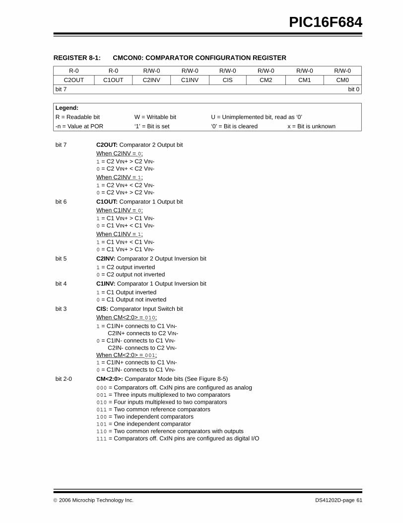
PIC16F684
REGISTER 8-1: CMCON0: COMPARATOR CONFIGURATION REGISTER
R-0 R-0 R/W-0 R/W-0 R/W-0 R/W-0 R/W-0 R/W-0
C2OUT C1OUT C2INV C1INV CIS CM2 CM1 CM0
bit 7 bit 0
Legend:
R = Readable bit W = Writable bit U = Unimplemented bit, read as ‘0’
-n = Value at POR ‘1’ = Bit is set ‘0’ = Bit is cleared x = Bit is unknown
bit 7 C2OUT: Comparator 2 Output bit
When C2INV = 0:1 = C2 VIN+ > C2 VIN-0 = C2 VIN+ < C2 VIN-
When C2INV = 1:1 = C2 VIN+ < C2 VIN-0 = C2 VIN+ > C2 VIN-
bit 6 C1OUT: Comparator 1 Output bitWhen C1INV = 0:1 = C1 VIN+ > C1 VIN-0 = C1 VIN+ < C1 VIN-When C1INV = 1:1 = C1 VIN+ < C1 VIN-0 = C1 VIN+ > C1 VIN-
bit 5 C2INV: Comparator 2 Output Inversion bit1 = C2 output inverted0 = C2 output not inverted
bit 4 C1INV: Comparator 1 Output Inversion bit
1 = C1 Output inverted0 = C1 Output not inverted
bit 3 CIS: Comparator Input Switch bitWhen CM<2:0> = 010:
1 = C1IN+ connects to C1 VIN- C2IN+ connects to C2 VIN-0 = C1IN- connects to C1 VIN- C2IN- connects to C2 VIN-When CM<2:0> = 001:1 = C1IN+ connects to C1 VIN-0 = C1IN- connects to C1 VIN-
bit 2-0 CM<2:0>: Comparator Mode bits (See Figure 8-5)
000 = Comparators off. CxIN pins are configured as analog001 = Three inputs multiplexed to two comparators010 = Four inputs multiplexed to two comparators011 = Two common reference comparators100 = Two independent comparators101 = One independent comparator110 = Two common reference comparators with outputs111 = Comparators off. CxIN pins are configured as digital I/O
© 2006 Microchip Technology Inc. DS41202D-page 61
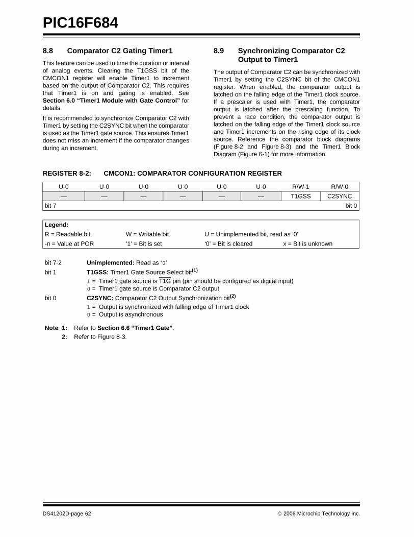
PIC16F684
8.8 Comparator C2 Gating Timer1
This feature can be used to time the duration or intervalof analog events. Clearing the T1GSS bit of theCMCON1 register will enable Timer1 to incrementbased on the output of Comparator C2. This requiresthat Timer1 is on and gating is enabled. SeeSection 6.0 “Timer1 Module with Gate Control” fordetails.
It is recommended to synchronize Comparator C2 withTimer1 by setting the C2SYNC bit when the comparatoris used as the Timer1 gate source. This ensures Timer1does not miss an increment if the comparator changesduring an increment.
8.9 Synchronizing Comparator C2 Output to Timer1
The output of Comparator C2 can be synchronized withTimer1 by setting the C2SYNC bit of the CMCON1register. When enabled, the comparator output islatched on the falling edge of the Timer1 clock source.If a prescaler is used with Timer1, the comparatoroutput is latched after the prescaling function. Toprevent a race condition, the comparator output islatched on the falling edge of the Timer1 clock sourceand Timer1 increments on the rising edge of its clocksource. Reference the comparator block diagrams(Figure 8-2 and Figure 8-3) and the Timer1 BlockDiagram (Figure 6-1) for more information.
REGISTER 8-2: CMCON1: COMPARATOR CONFIGURATION REGISTER
U-0 U-0 U-0 U-0 U-0 U-0 R/W-1 R/W-0
— — — — — — T1GSS C2SYNC
bit 7 bit 0
Legend:
R = Readable bit W = Writable bit U = Unimplemented bit, read as ‘0’
-n = Value at POR ‘1’ = Bit is set ‘0’ = Bit is cleared x = Bit is unknown
bit 7-2 Unimplemented: Read as ‘0’
bit 1 T1GSS: Timer1 Gate Source Select bit(1)
1 = Timer1 gate source is T1G pin (pin should be configured as digital input)0 = Timer1 gate source is Comparator C2 output
bit 0 C2SYNC: Comparator C2 Output Synchronization bit(2)
1 = Output is synchronized with falling edge of Timer1 clock0 = Output is asynchronous
Note 1: Refer to Section 6.6 “Timer1 Gate”.
2: Refer to Figure 8-3.
DS41202D-page 62 © 2006 Microchip Technology Inc.
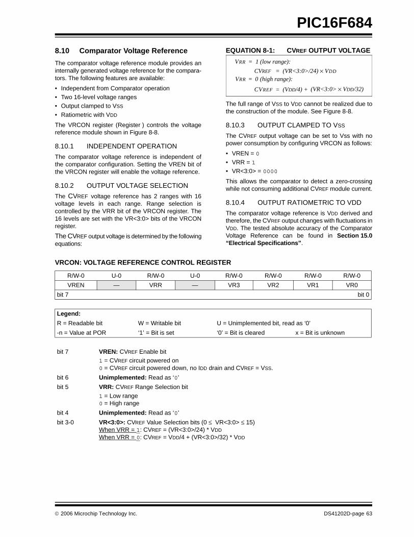
PIC16F684
8.10 Comparator Voltage Reference
The comparator voltage reference module provides aninternally generated voltage reference for the compara-tors. The following features are available:
• Independent from Comparator operation• Two 16-level voltage ranges• Output clamped to VSS
• Ratiometric with VDD
The VRCON register (Register ) controls the voltagereference module shown in Figure 8-8.
8.10.1 INDEPENDENT OPERATION
The comparator voltage reference is independent ofthe comparator configuration. Setting the VREN bit ofthe VRCON register will enable the voltage reference.
8.10.2 OUTPUT VOLTAGE SELECTION
The CVREF voltage reference has 2 ranges with 16voltage levels in each range. Range selection iscontrolled by the VRR bit of the VRCON register. The16 levels are set with the VR<3:0> bits of the VRCONregister.
The CVREF output voltage is determined by the followingequations:
EQUATION 8-1: CVREF OUTPUT VOLTAGE
The full range of VSS to VDD cannot be realized due tothe construction of the module. See Figure 8-8.
8.10.3 OUTPUT CLAMPED TO VSS
The CVREF output voltage can be set to Vss with nopower consumption by configuring VRCON as follows:
• VREN = 0
• VRR = 1
• VR<3:0> = 0000
This allows the comparator to detect a zero-crossingwhile not consuming additional CVREF module current.
8.10.4 OUTPUT RATIOMETRIC TO VDD
The comparator voltage reference is VDD derived andtherefore, the CVREF output changes with fluctuations inVDD. The tested absolute accuracy of the ComparatorVoltage Reference can be found in Section 15.0“Electrical Specifications”.
VRR 1 (low range):=
VRR 0 (high range):=
CVREF (VDD/4) + =
CVREF (VR<3:0>/24) VDD×=
(VR<3:0> VDD/32)×
VRCON: VOLTAGE REFERENCE CONTROL REGISTER
R/W-0 U-0 R/W-0 U-0 R/W-0 R/W-0 R/W-0 R/W-0
VREN — VRR — VR3 VR2 VR1 VR0
bit 7 bit 0
Legend:
R = Readable bit W = Writable bit U = Unimplemented bit, read as ‘0’
-n = Value at POR ‘1’ = Bit is set ‘0’ = Bit is cleared x = Bit is unknown
bit 7 VREN: CVREF Enable bit1 = CVREF circuit powered on0 = CVREF circuit powered down, no IDD drain and CVREF = VSS.
bit 6 Unimplemented: Read as ‘0’
bit 5 VRR: CVREF Range Selection bit
1 = Low range0 = High range
bit 4 Unimplemented: Read as ‘0’
bit 3-0 VR<3:0>: CVREF Value Selection bits (0 ≤ VR<3:0> ≤ 15)When VRR = 1: CVREF = (VR<3:0>/24) * VDD
When VRR = 0: CVREF = VDD/4 + (VR<3:0>/32) * VDD
© 2006 Microchip Technology Inc. DS41202D-page 63
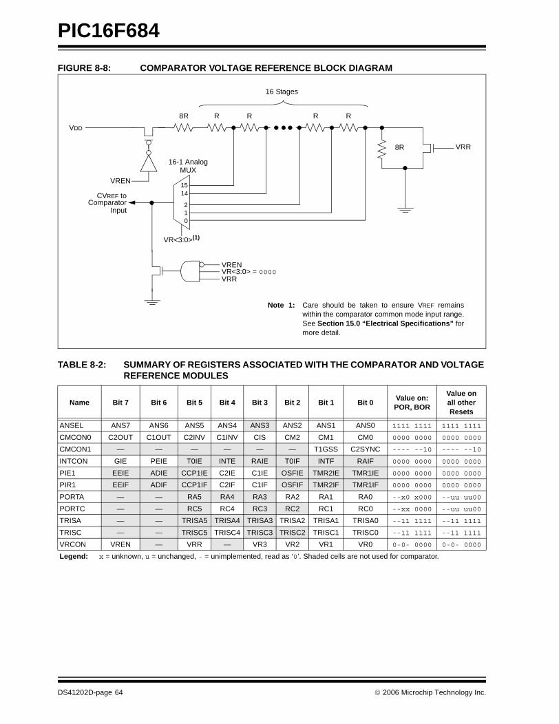
PIC16F684
FIGURE 8-8: COMPARATOR VOLTAGE REFERENCE BLOCK DIAGRAM
TABLE 8-2: SUMMARY OF REGISTERS ASSOCIATED WITH THE COMPARATOR AND VOLTAGE REFERENCE MODULES
Name Bit 7 Bit 6 Bit 5 Bit 4 Bit 3 Bit 2 Bit 1 Bit 0Value on: POR, BOR
Value onall otherResets
ANSEL ANS7 ANS6 ANS5 ANS4 ANS3 ANS2 ANS1 ANS0 1111 1111 1111 1111
CMCON0 C2OUT C1OUT C2INV C1INV CIS CM2 CM1 CM0 0000 0000 0000 0000
CMCON1 — — — — — — T1GSS C2SYNC ---- --10 ---- --10
INTCON GIE PEIE T0IE INTE RAIE T0IF INTF RAIF 0000 0000 0000 0000
PIE1 EEIE ADIE CCP1IE C2IE C1IE OSFIE TMR2IE TMR1IE 0000 0000 0000 0000
PIR1 EEIF ADIF CCP1IF C2IF C1IF OSFIF TMR2IF TMR1IF 0000 0000 0000 0000
PORTA — — RA5 RA4 RA3 RA2 RA1 RA0 --x0 x000 --uu uu00
PORTC — — RC5 RC4 RC3 RC2 RC1 RC0 --xx 0000 --uu uu00
TRISA — — TRISA5 TRISA4 TRISA3 TRISA2 TRISA1 TRISA0 --11 1111 --11 1111
TRISC — — TRISC5 TRISC4 TRISC3 TRISC2 TRISC1 TRISC0 --11 1111 --11 1111
VRCON VREN — VRR — VR3 VR2 VR1 VR0 0-0- 0000 0-0- 0000
Legend: x = unknown, u = unchanged, - = unimplemented, read as ‘0’. Shaded cells are not used for comparator.
VRR8R
VR<3:0>(1)
16-1 Analog
8R R R R R
CVREF to
16 Stages
ComparatorInput
VREN
VDD
MUX
VR<3:0> = 0000VREN
VRR
012
1415
Note 1: Care should be taken to ensure VREF remainswithin the comparator common mode input range.See Section 15.0 “Electrical Specifications” formore detail.
DS41202D-page 64 © 2006 Microchip Technology Inc.
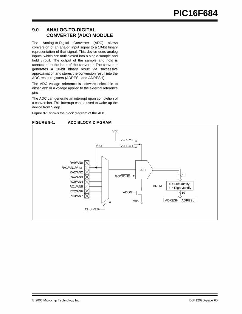
PIC16F684
9.0 ANALOG-TO-DIGITAL CONVERTER (ADC) MODULE
The Analog-to-Digital Converter (ADC) allowsconversion of an analog input signal to a 10-bit binaryrepresentation of that signal. This device uses analoginputs, which are multiplexed into a single sample andhold circuit. The output of the sample and hold isconnected to the input of the converter. The convertergenerates a 10-bit binary result via successiveapproximation and stores the conversion result into theADC result registers (ADRESL and ADRESH).
The ADC voltage reference is software selectable toeither VDD or a voltage applied to the external referencepins.
The ADC can generate an interrupt upon completion ofa conversion. This interrupt can be used to wake-up thedevice from Sleep.
Figure 9-1 shows the block diagram of the ADC.
FIGURE 9-1: ADC BLOCK DIAGRAM
RA0/AN0
A/DRA1/AN1/VREF
RA2/AN2
RC0/AN4
VDD
VREF
ADON
GO/DONE
VCFG = 1
VCFG = 0
CHS <3:0>
VSS
RC1/AN5
RC2/AN6
RC3/AN7
RA4/AN3
ADRESH ADRESL
10
10
ADFM0 = Left Justify1 = Right Justify
4
© 2006 Microchip Technology Inc. DS41202D-page 65
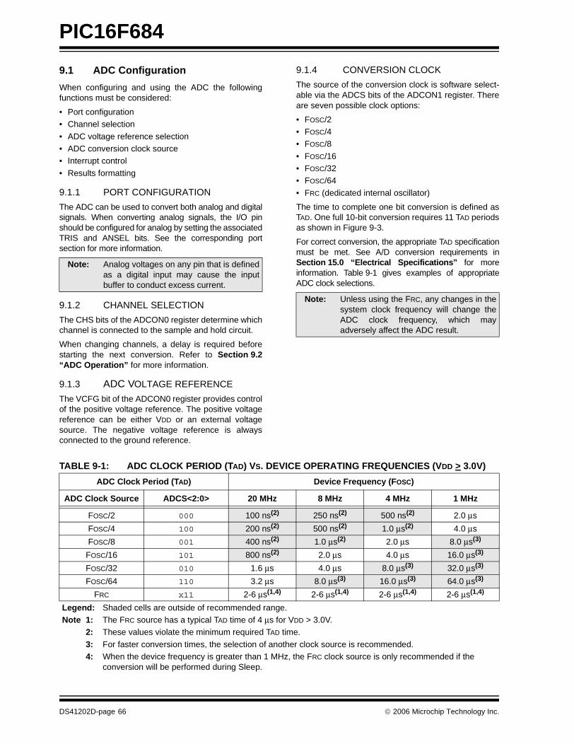
PIC16F684
9.1 ADC Configuration
When configuring and using the ADC the followingfunctions must be considered:
• Port configuration• Channel selection
• ADC voltage reference selection• ADC conversion clock source• Interrupt control
• Results formatting
9.1.1 PORT CONFIGURATION
The ADC can be used to convert both analog and digitalsignals. When converting analog signals, the I/O pinshould be configured for analog by setting the associatedTRIS and ANSEL bits. See the corresponding portsection for more information.
9.1.2 CHANNEL SELECTION
The CHS bits of the ADCON0 register determine whichchannel is connected to the sample and hold circuit.
When changing channels, a delay is required beforestarting the next conversion. Refer to Section 9.2“ADC Operation” for more information.
9.1.3 ADC VOLTAGE REFERENCE
The VCFG bit of the ADCON0 register provides controlof the positive voltage reference. The positive voltagereference can be either VDD or an external voltagesource. The negative voltage reference is alwaysconnected to the ground reference.
9.1.4 CONVERSION CLOCK
The source of the conversion clock is software select-able via the ADCS bits of the ADCON1 register. Thereare seven possible clock options:
• FOSC/2• FOSC/4• FOSC/8
• FOSC/16• FOSC/32• FOSC/64
• FRC (dedicated internal oscillator)
The time to complete one bit conversion is defined asTAD. One full 10-bit conversion requires 11 TAD periodsas shown in Figure 9-3.
For correct conversion, the appropriate TAD specificationmust be met. See A/D conversion requirements inSection 15.0 “Electrical Specifications” for moreinformation. Table 9-1 gives examples of appropriateADC clock selections.
TABLE 9-1: ADC CLOCK PERIOD (TAD) VS. DEVICE OPERATING FREQUENCIES (VDD > 3.0V)
Note: Analog voltages on any pin that is definedas a digital input may cause the inputbuffer to conduct excess current.
Note: Unless using the FRC, any changes in thesystem clock frequency will change theADC clock frequency, which mayadversely affect the ADC result.
ADC Clock Period (TAD) Device Frequency (FOSC)
ADC Clock Source ADCS<2:0> 20 MHz 8 MHz 4 MHz 1 MHz
FOSC/2 000 100 ns(2) 250 ns(2) 500 ns(2) 2.0 μs
FOSC/4 100 200 ns(2) 500 ns(2) 1.0 μs(2) 4.0 μs
FOSC/8 001 400 ns(2) 1.0 μs(2) 2.0 μs 8.0 μs(3)
FOSC/16 101 800 ns(2) 2.0 μs 4.0 μs 16.0 μs(3)
FOSC/32 010 1.6 μs 4.0 μs 8.0 μs(3) 32.0 μs(3)
FOSC/64 110 3.2 μs 8.0 μs(3) 16.0 μs(3) 64.0 μs(3)
FRC x11 2-6 μs(1,4) 2-6 μs(1,4) 2-6 μs(1,4) 2-6 μs(1,4)
Legend: Shaded cells are outside of recommended range.Note 1: The FRC source has a typical TAD time of 4 μs for VDD > 3.0V.
2: These values violate the minimum required TAD time.
3: For faster conversion times, the selection of another clock source is recommended.4: When the device frequency is greater than 1 MHz, the FRC clock source is only recommended if the
conversion will be performed during Sleep.
DS41202D-page 66 © 2006 Microchip Technology Inc.
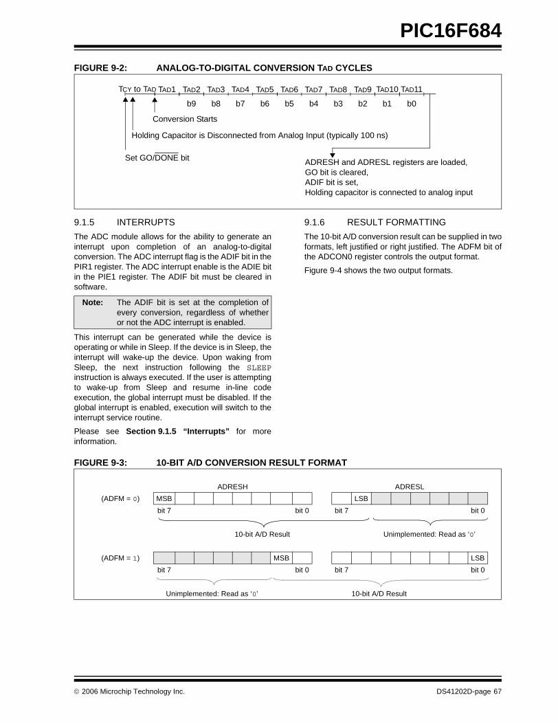
PIC16F684
FIGURE 9-2: ANALOG-TO-DIGITAL CONVERSION TAD CYCLES
9.1.5 INTERRUPTS
The ADC module allows for the ability to generate aninterrupt upon completion of an analog-to-digitalconversion. The ADC interrupt flag is the ADIF bit in thePIR1 register. The ADC interrupt enable is the ADIE bitin the PIE1 register. The ADIF bit must be cleared insoftware.
This interrupt can be generated while the device isoperating or while in Sleep. If the device is in Sleep, theinterrupt will wake-up the device. Upon waking fromSleep, the next instruction following the SLEEPinstruction is always executed. If the user is attemptingto wake-up from Sleep and resume in-line codeexecution, the global interrupt must be disabled. If theglobal interrupt is enabled, execution will switch to theinterrupt service routine.
Please see Section 9.1.5 “Interrupts” for moreinformation.
9.1.6 RESULT FORMATTING
The 10-bit A/D conversion result can be supplied in twoformats, left justified or right justified. The ADFM bit ofthe ADCON0 register controls the output format.
Figure 9-4 shows the two output formats.
FIGURE 9-3: 10-BIT A/D CONVERSION RESULT FORMAT
TAD1 TAD2 TAD3 TAD4 TAD5 TAD6 TAD7 TAD8 TAD9
Set GO/DONE bit
Holding Capacitor is Disconnected from Analog Input (typically 100 ns)
b9 b8 b7 b6 b5 b4 b3 b2
TAD10 TAD11
b1 b0
TCY to TAD
Conversion Starts
ADRESH and ADRESL registers are loaded,GO bit is cleared,ADIF bit is set,Holding capacitor is connected to analog input
Note: The ADIF bit is set at the completion ofevery conversion, regardless of whetheror not the ADC interrupt is enabled.
ADRESH ADRESL
(ADFM = 0) MSB LSB
bit 7 bit 0 bit 7 bit 0
10-bit A/D Result Unimplemented: Read as ‘0’
(ADFM = 1) MSB LSB
bit 7 bit 0 bit 7 bit 0
Unimplemented: Read as ‘0’ 10-bit A/D Result
© 2006 Microchip Technology Inc. DS41202D-page 67
PIC16F684
9.2 ADC Operation
9.2.1 STARTING A CONVERSION
To enable the ADC module, the ADON bit of theADCON0 register must be set to a ‘1’. Setting theGO/DONE bit of the ADCON0 register to a ‘1’ will startthe analog-to-digital conversion.
9.2.2 COMPLETION OF A CONVERSION
When the conversion is complete, the ADC module will:
• Clear the GO/DONE bit • Set the ADIF flag bit• Update the ADRESH:ADRESL registers with new
conversion result
9.2.3 TERMINATING A CONVERSION
If a conversion must be terminated before completion,the GO/DONE bit can be cleared in software. TheADRESH:ADRESL registers will not be updated withthe partially complete analog-to-digital conversionsample. Instead, the ADRESH:ADRESL register pairwill retain the value of the previous conversion. Addi-tionally, a 2 TAD delay is required before another acqui-sition can be initiated. Following this delay, an inputacquisition is automatically started on the selectedchannel.
9.2.4 ADC OPERATION DURING SLEEP
The ADC module can operate during Sleep. Thisrequires the ADC clock source to be set to the FRC
option. When the FRC clock source is selected, theADC waits one additional instruction before starting theconversion. This allows the SLEEP instruction to beexecuted, which can reduce system noise during theconversion. If the ADC interrupt is enabled, the devicewill wake-up from Sleep when the conversioncompletes. If the ADC interrupt is disabled, the ADCmodule is turned off after the conversion completes,although the ADON bit remains set.
When the ADC clock source is something other thanFRC, a SLEEP instruction causes the present conver-sion to be aborted and the ADC module is turned off,although the ADON bit remains set.
9.2.5 SPECIAL EVENT TRIGGER
The ECCP Special Event Trigger allows periodic ADCmeasurements without software intervention. Whenthis trigger occurs, the GO/DONE bit is set by hardwareand the Timer1 counter resets to zero.
Using the Special Event Trigger does not ensureproper ADC timing. It is the user’s responsibility toensure that the ADC timing requirements are met.
See Section 11.0 “Enhanced Capture/Com-pare/PWM (With Auto-Shutdown and Dead Band)Module” for more information.
9.2.6 A/D CONVERSION PROCEDURE
This is an example procedure for using the ADC toperform an Analog-to-Digital conversion:
1. Configure Port:• Disable pin output driver (See TRIS register)• Configure pin as analog
2. Configure the ADC module:• Select ADC conversion clock• Configure voltage reference
• Select ADC input channel• Select result format• Turn on ADC module
3. Configure ADC interrupt (optional):• Clear ADC interrupt flag • Enable ADC interrupt
• Enable peripheral interrupt• Enable global interrupt(1)
4. Wait the required acquisition time(2).
5. Start conversion by setting the GO/DONE bit.6. Wait for ADC conversion to complete by one of
the following:• Polling the GO/DONE bit• Waiting for the ADC interrupt (interrupts
enabled)7. Read ADC Result
8. Clear the ADC interrupt flag (required if interruptis enabled).
Note: The GO/DONE bit should not be set in thesame instruction that turns on the ADC.Refer to Section 9.2.6 “A/D ConversionProcedure”.
Note: A device Reset forces all registers to theirReset state. Thus, the ADC module isturned off and any pending conversion isterminated.
Note 1: The global interrupt can be disabled if theuser is attempting to wake-up from Sleepand resume in-line code execution.
2: See Section 9.3 “A/D AcquisitionRequirements”.
DS41202D-page 68 © 2006 Microchip Technology Inc.
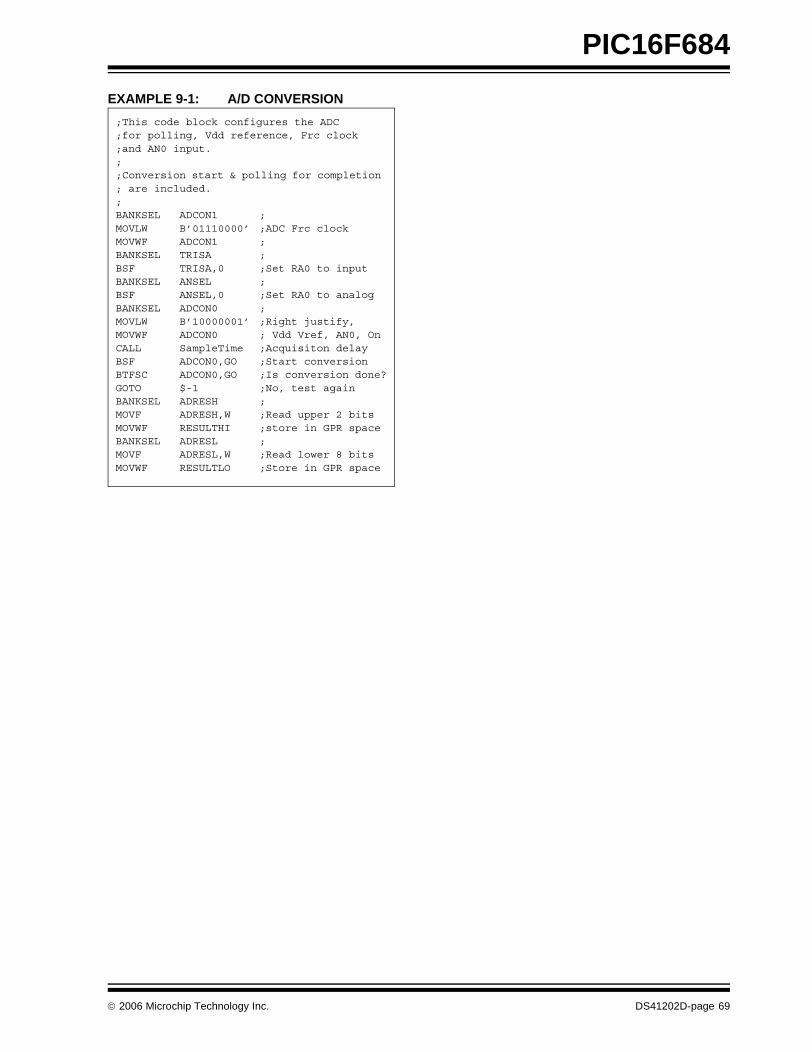
PIC16F684
EXAMPLE 9-1: A/D CONVERSION
;This code block configures the ADC;for polling, Vdd reference, Frc clock;and AN0 input.;;Conversion start & polling for completion ; are included.;BANKSEL ADCON1 ;MOVLW B’01110000’ ;ADC Frc clockMOVWF ADCON1 ;BANKSEL TRISA ;BSF TRISA,0 ;Set RA0 to inputBANKSEL ANSEL ;BSF ANSEL,0 ;Set RA0 to analogBANKSEL ADCON0 ;MOVLW B’10000001’ ;Right justify,MOVWF ADCON0 ; Vdd Vref, AN0, OnCALL SampleTime ;Acquisiton delayBSF ADCON0,GO ;Start conversionBTFSC ADCON0,GO ;Is conversion done?GOTO $-1 ;No, test againBANKSEL ADRESH ;MOVF ADRESH,W ;Read upper 2 bitsMOVWF RESULTHI ;store in GPR spaceBANKSEL ADRESL ;MOVF ADRESL,W ;Read lower 8 bitsMOVWF RESULTLO ;Store in GPR space
© 2006 Microchip Technology Inc. DS41202D-page 69
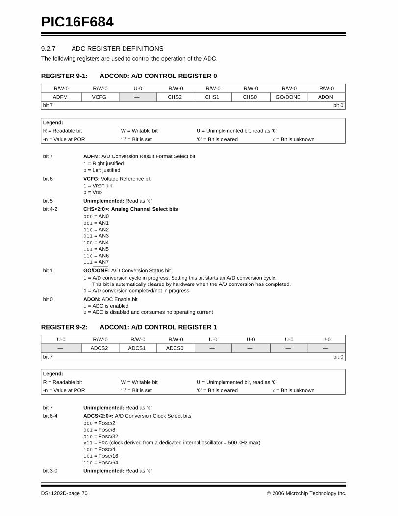
PIC16F684
9.2.7 ADC REGISTER DEFINITIONS
The following registers are used to control the operation of the ADC.
REGISTER 9-1: ADCON0: A/D CONTROL REGISTER 0
R/W-0 R/W-0 U-0 R/W-0 R/W-0 R/W-0 R/W-0 R/W-0
ADFM VCFG — CHS2 CHS1 CHS0 GO/DONE ADON
bit 7 bit 0
Legend:
R = Readable bit W = Writable bit U = Unimplemented bit, read as ‘0’
-n = Value at POR ‘1’ = Bit is set ‘0’ = Bit is cleared x = Bit is unknown
bit 7 ADFM: A/D Conversion Result Format Select bit1 = Right justified0 = Left justified
bit 6 VCFG: Voltage Reference bit1 = VREF pin0 = VDD
bit 5 Unimplemented: Read as ‘0’
bit 4-2 CHS<2:0>: Analog Channel Select bits000 = AN0001 = AN1010 = AN2011 = AN3100 = AN4101 = AN5110 = AN6111 = AN7
bit 1 GO/DONE: A/D Conversion Status bit1 = A/D conversion cycle in progress. Setting this bit starts an A/D conversion cycle. This bit is automatically cleared by hardware when the A/D conversion has completed.0 = A/D conversion completed/not in progress
bit 0 ADON: ADC Enable bit1 = ADC is enabled0 = ADC is disabled and consumes no operating current
REGISTER 9-2: ADCON1: A/D CONTROL REGISTER 1
U-0 R/W-0 R/W-0 R/W-0 U-0 U-0 U-0 U-0
— ADCS2 ADCS1 ADCS0 — — — —
bit 7 bit 0
Legend:
R = Readable bit W = Writable bit U = Unimplemented bit, read as ‘0’
-n = Value at POR ‘1’ = Bit is set ‘0’ = Bit is cleared x = Bit is unknown
bit 7 Unimplemented: Read as ‘0’
bit 6-4 ADCS<2:0>: A/D Conversion Clock Select bits000 = FOSC/2001 = FOSC/8010 = FOSC/32x11 = FRC (clock derived from a dedicated internal oscillator = 500 kHz max)100 = FOSC/4101 = FOSC/16110 = FOSC/64
bit 3-0 Unimplemented: Read as ‘0’
DS41202D-page 70 © 2006 Microchip Technology Inc.
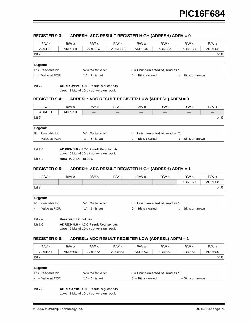
PIC16F684
REGISTER 9-3: ADRESH: ADC RESULT REGISTER HIGH (ADRESH) ADFM = 0
R/W-x R/W-x R/W-x R/W-x R/W-x R/W-x R/W-x R/W-x
ADRES9 ADRES8 ADRES7 ADRES6 ADRES5 ADRES4 ADRES3 ADRES2
bit 7 bit 0
Legend:
R = Readable bit W = Writable bit U = Unimplemented bit, read as ‘0’
-n = Value at POR ‘1’ = Bit is set ‘0’ = Bit is cleared x = Bit is unknown
bit 7-0 ADRES<9:2>: ADC Result Register bitsUpper 8 bits of 10-bit conversion result
REGISTER 9-4: ADRESL: ADC RESULT REGISTER LOW (ADRESL) ADFM = 0
R/W-x R/W-x R/W-x R/W-x R/W-x R/W-x R/W-x R/W-x
ADRES1 ADRES0 — — — — — —
bit 7 bit 0
Legend:
R = Readable bit W = Writable bit U = Unimplemented bit, read as ‘0’
-n = Value at POR ‘1’ = Bit is set ‘0’ = Bit is cleared x = Bit is unknown
bit 7-6 ADRES<1:0>: ADC Result Register bitsLower 2 bits of 10-bit conversion result
bit 5-0 Reserved: Do not use.
REGISTER 9-5: ADRESH: ADC RESULT REGISTER HIGH (ADRESH) ADFM = 1
R/W-x R/W-x R/W-x R/W-x R/W-x R/W-x R/W-x R/W-x
— — — — — — ADRES9 ADRES8
bit 7 bit 0
Legend:
R = Readable bit W = Writable bit U = Unimplemented bit, read as ‘0’
-n = Value at POR ‘1’ = Bit is set ‘0’ = Bit is cleared x = Bit is unknown
bit 7-2 Reserved: Do not use.
bit 1-0 ADRES<9:8>: ADC Result Register bitsUpper 2 bits of 10-bit conversion result
REGISTER 9-6: ADRESL: ADC RESULT REGISTER LOW (ADRESL) ADFM = 1
R/W-x R/W-x R/W-x R/W-x R/W-x R/W-x R/W-x R/W-x
ADRES7 ADRES6 ADRES5 ADRES4 ADRES3 ADRES2 ADRES1 ADRES0
bit 7 bit 0
Legend:
R = Readable bit W = Writable bit U = Unimplemented bit, read as ‘0’
-n = Value at POR ‘1’ = Bit is set ‘0’ = Bit is cleared x = Bit is unknown
bit 7-0 ADRES<7:0>: ADC Result Register bitsLower 8 bits of 10-bit conversion result
© 2006 Microchip Technology Inc. DS41202D-page 71
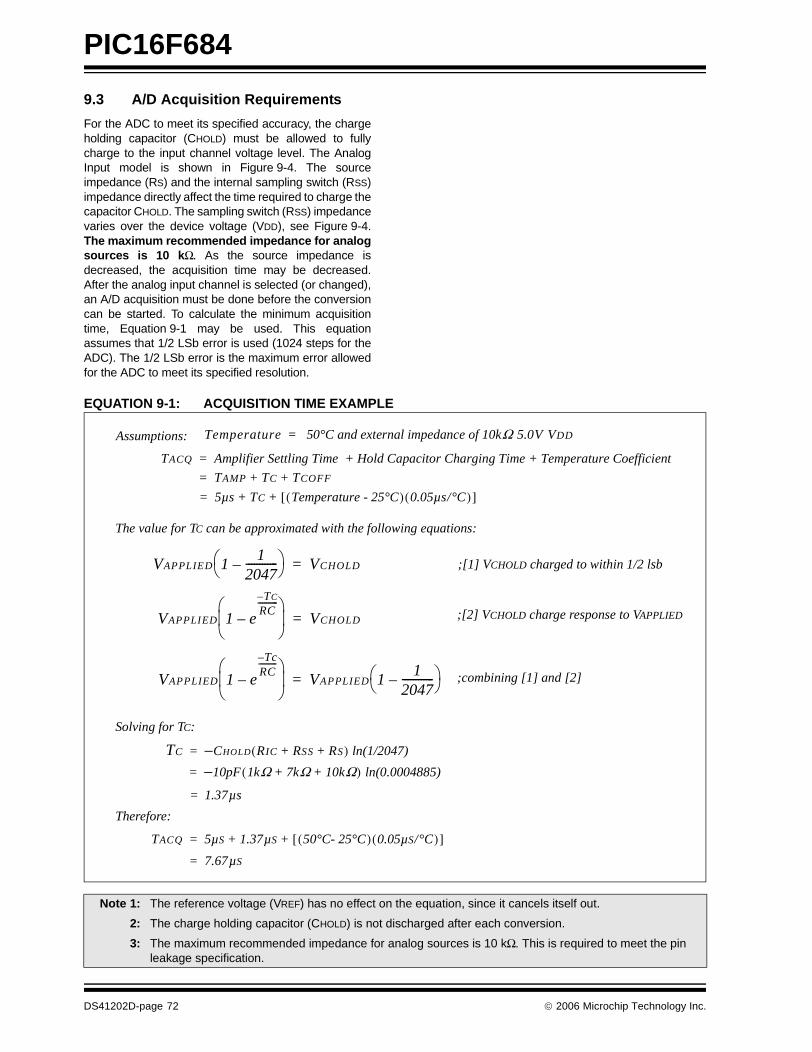
PIC16F684
9.3 A/D Acquisition Requirements
For the ADC to meet its specified accuracy, the chargeholding capacitor (CHOLD) must be allowed to fullycharge to the input channel voltage level. The AnalogInput model is shown in Figure 9-4. The sourceimpedance (RS) and the internal sampling switch (RSS)impedance directly affect the time required to charge thecapacitor CHOLD. The sampling switch (RSS) impedancevaries over the device voltage (VDD), see Figure 9-4.The maximum recommended impedance for analogsources is 10 kΩ. As the source impedance isdecreased, the acquisition time may be decreased.After the analog input channel is selected (or changed),an A/D acquisition must be done before the conversioncan be started. To calculate the minimum acquisitiontime, Equation 9-1 may be used. This equationassumes that 1/2 LSb error is used (1024 steps for theADC). The 1/2 LSb error is the maximum error allowedfor the ADC to meet its specified resolution.
EQUATION 9-1: ACQUISITION TIME EXAMPLE
TACQ Amplifier Settling Time Hold Capacitor Charging Time Temperature Coefficient+ +=
TAMP TC TCOFF+ +=
5µs TC Temperature - 25°C( ) 0.05µs/°C( )[ ]+ +=
TC CHOLD RIC RSS RS+ +( ) ln(1/2047)–=
10pF 1kΩ 7kΩ 10kΩ+ +( )– ln(0.0004885)=
1.37= µs
TACQ 5µS 1.37µS 50°C- 25°C( ) 0.05µS/°C( )[ ]+ +=
7.67µS=
VAPPLIED 1 e
Tc–RC---------
–⎝ ⎠⎜ ⎟⎛ ⎞
VAPPLIED 11
2047------------–⎝ ⎠
⎛ ⎞=
VAPPLIED 11
2047------------–⎝ ⎠
⎛ ⎞ VCHOLD=
VAPPLIED 1 e
TC–RC----------
–⎝ ⎠⎜ ⎟⎛ ⎞
VCHOLD=
;[1] VCHOLD charged to within 1/2 lsb
;[2] VCHOLD charge response to VAPPLIED
;combining [1] and [2]
The value for TC can be approximated with the following equations:
Solving for TC:
Therefore:
Temperature 50°C and external impedance of 10kΩ 5.0V VDD=Assumptions:
Note 1: The reference voltage (VREF) has no effect on the equation, since it cancels itself out.
2: The charge holding capacitor (CHOLD) is not discharged after each conversion.
3: The maximum recommended impedance for analog sources is 10 kΩ. This is required to meet the pin leakage specification.
DS41202D-page 72 © 2006 Microchip Technology Inc.
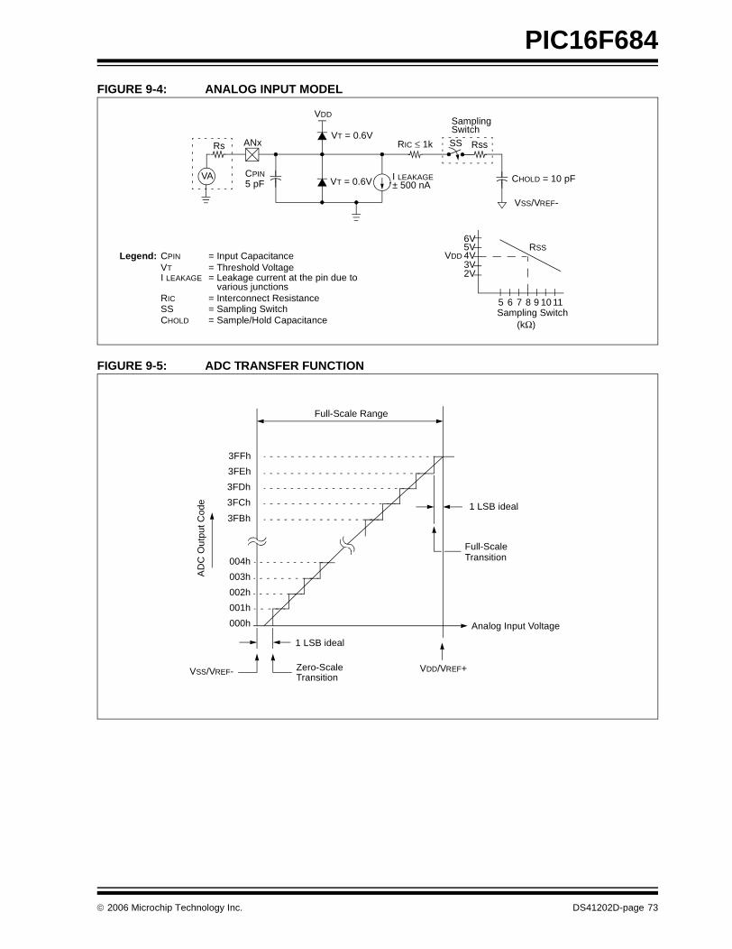
PIC16F684
FIGURE 9-4: ANALOG INPUT MODEL
FIGURE 9-5: ADC TRANSFER FUNCTION
CPINVA
Rs ANx
5 pF
VDD
VT = 0.6V
VT = 0.6V I LEAKAGE
RIC ≤ 1k
SamplingSwitchSS Rss
CHOLD = 10 pF
VSS/VREF-
6V
Sampling Switch
5V4V3V2V
5 6 7 8 9 10 11
(kΩ)
VDD
± 500 nA
Legend: CPIN
VTI LEAKAGE
RICSSCHOLD
= Input Capacitance= Threshold Voltage= Leakage current at the pin due to
= Interconnect Resistance= Sampling Switch= Sample/Hold Capacitance
various junctions
RSS
3FFh
3FEh
AD
C O
utpu
t Cod
e
3FDh
3FCh
004h
003h
002h
001h
000h
Full-Scale
3FBh
1 LSB ideal
VSS/VREF- Zero-ScaleTransition
VDD/VREF+
Transition
1 LSB ideal
Full-Scale Range
Analog Input Voltage
© 2006 Microchip Technology Inc. DS41202D-page 73
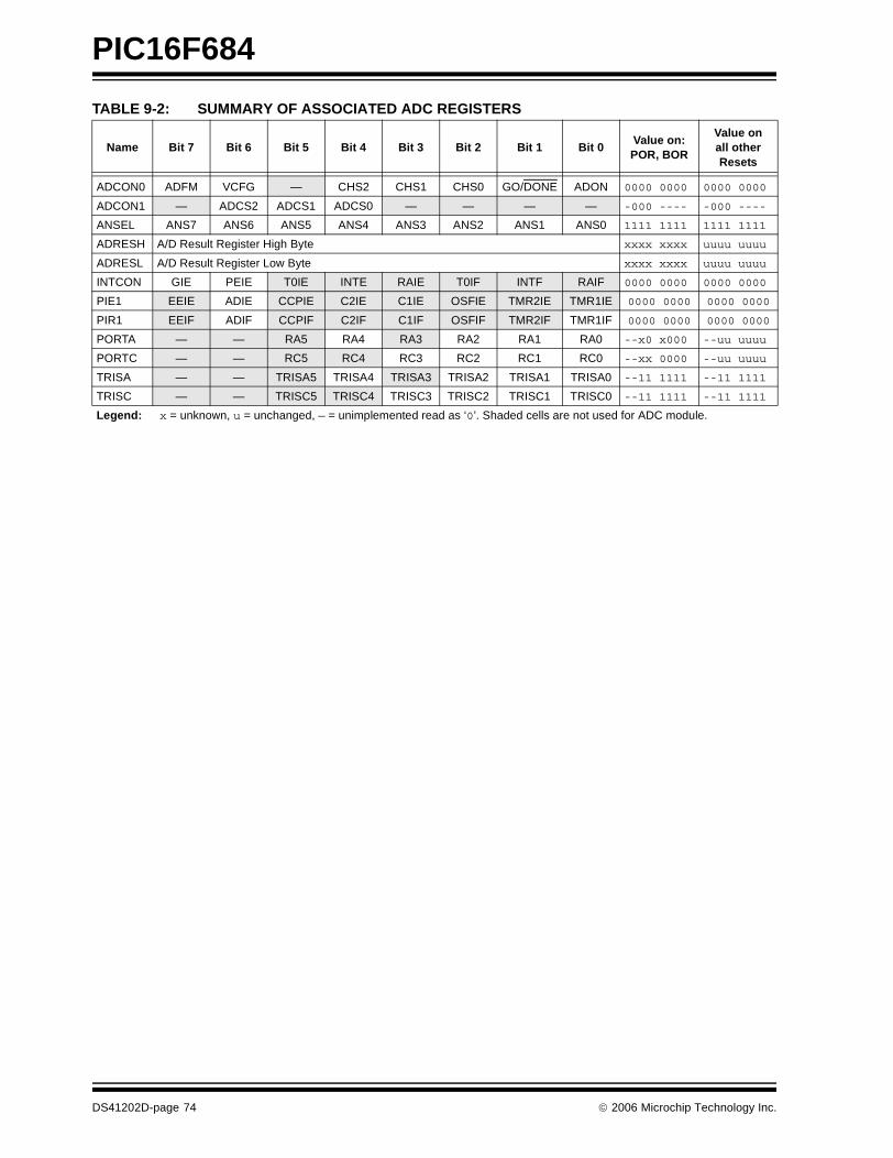
PIC16F684
TABLE 9-2: SUMMARY OF ASSOCIATED ADC REGISTERS
Name Bit 7 Bit 6 Bit 5 Bit 4 Bit 3 Bit 2 Bit 1 Bit 0Value on: POR, BOR
Value on all other Resets
ADCON0 ADFM VCFG — CHS2 CHS1 CHS0 GO/DONE ADON 0000 0000 0000 0000
ADCON1 — ADCS2 ADCS1 ADCS0 — — — — -000 ---- -000 ----
ANSEL ANS7 ANS6 ANS5 ANS4 ANS3 ANS2 ANS1 ANS0 1111 1111 1111 1111
ADRESH A/D Result Register High Byte xxxx xxxx uuuu uuuu
ADRESL A/D Result Register Low Byte xxxx xxxx uuuu uuuu
INTCON GIE PEIE T0IE INTE RAIE T0IF INTF RAIF 0000 0000 0000 0000
PIE1 EEIE ADIE CCPIE C2IE C1IE OSFIE TMR2IE TMR1IE 0000 0000 0000 0000
PIR1 EEIF ADIF CCPIF C2IF C1IF OSFIF TMR2IF TMR1IF 0000 0000 0000 0000
PORTA — — RA5 RA4 RA3 RA2 RA1 RA0 --x0 x000 --uu uuuu
PORTC — — RC5 RC4 RC3 RC2 RC1 RC0 --xx 0000 --uu uuuu
TRISA — — TRISA5 TRISA4 TRISA3 TRISA2 TRISA1 TRISA0 --11 1111 --11 1111
TRISC — — TRISC5 TRISC4 TRISC3 TRISC2 TRISC1 TRISC0 --11 1111 --11 1111
Legend: x = unknown, u = unchanged, — = unimplemented read as ‘0’. Shaded cells are not used for ADC module.
DS41202D-page 74 © 2006 Microchip Technology Inc.
PIC16F684
10.0 DATA EEPROM MEMORY
The EEPROM data memory is readable and writableduring normal operation (full VDD range). This memoryis not directly mapped in the register file space.Instead, it is indirectly addressed through the SpecialFunction Registers. There are four SFRs used to readand write this memory:
• EECON1• EECON2 (not a physically implemented register)
• EEDAT• EEADR
EEDAT holds the 8-bit data for read/write, and EEADRholds the address of the EEPROM location beingaccessed. PIC16F684 has 256 bytes of data EEPROMwith an address range from 0h to FFh.
The EEPROM data memory allows byte read and write.A byte write automatically erases the location andwrites the new data (erase before write). The EEPROMdata memory is rated for high erase/write cycles. Thewrite time is controlled by an on-chip timer. The writetime will vary with voltage and temperature as well asfrom chip-to-chip. Please refer to AC Specifications inSection 15.0 “Electrical Specifications” for exactlimits.
When the data memory is code-protected, the CPUmay continue to read and write the data EEPROMmemory. The device programmer can no longer accessthe data EEPROM data and will read zeroes.
REGISTER 10-1: EEDAT: EEPROM DATA REGISTER
R/W-0 R/W-0 R/W-0 R/W-0 R/W-0 R/W-0 R/W-0 R/W-0
EEDAT7 EEDAT6 EEDAT5 EEDAT4 EEDAT3 EEDAT2 EEDAT1 EEDAT0
bit 7 bit 0
Legend:
R = Readable bit W = Writable bit U = Unimplemented bit, read as ‘0’
-n = Value at POR ‘1’ = Bit is set ‘0’ = Bit is cleared x = Bit is unknown
bit 7-0 EEDATn: Byte Value to Write To or Read From Data EEPROM bits
REGISTER 10-2: EEADR: EEPROM ADDRESS REGISTER
R/W-0 R/W-0 R/W-0 R/W-0 R/W-0 R/W-0 R/W-0 R/W-0
EEADR7 EEADR6 EEADR5 EEADR4 EEADR3 EEADR2 EEADR1 EEADR0
bit 7 bit 0
Legend:
R = Readable bit W = Writable bit U = Unimplemented bit, read as ‘0’
-n = Value at POR ‘1’ = Bit is set ‘0’ = Bit is cleared x = Bit is unknown
bit 7-0 EEADR: Specifies One of 256 Locations for EEPROM Read/Write Operation bits
© 2006 Microchip Technology Inc. DS41202D-page 75
PIC16F684
10.1 EECON1 and EECON2 Registers
EECON1 is the control register with four low-order bitsphysically implemented. The upper four bits arenon-implemented and read as ‘0’s.
Control bits RD and WR initiate read and write,respectively. These bits cannot be cleared, only set insoftware. They are cleared in hardware at completionof the read or write operation. The inability to clear theWR bit in software prevents the accidental, prematuretermination of a write operation.
The WREN bit, when set, will allow a write operation.On power-up, the WREN bit is clear. The WRERR bit isset when a write operation is interrupted by a MCLRReset, or a WDT Time-out Reset during normal
operation. In these situations, following Reset, the usercan check the WRERR bit, clear it and rewrite thelocation. The data and address will be cleared.Therefore, the EEDAT and EEADR registers will needto be re-initialized.
Interrupt flag, EEIF bit of the PIR1 register, is set whenwrite is complete. This bit must be cleared in software.
EECON2 is not a physical register. Reading EECON2will read all ‘0’s. The EECON2 register is usedexclusively in the data EEPROM write sequence.
Note: The EECON1, EEDAT and EEADRregisters should not be modified during adata EEPROM write (WR bit = 1).
REGISTER 10-3: EECON1: EEPROM CONTROL REGISTER
U-0 U-0 U-0 U-0 R/W-x R/W-0 R/S-0 R/S-0
— — — — WRERR WREN WR RD
bit 7 bit 0
Legend:
S = Bit can only be set
R = Readable bit W = Writable bit U = Unimplemented bit, read as ‘0’
-n = Value at POR ‘1’ = Bit is set ‘0’ = Bit is cleared x = Bit is unknown
bit 7-4 Unimplemented: Read as ‘0’
bit 3 WRERR: EEPROM Error Flag bit1 = A write operation is prematurely terminated (any MCLR Reset, any WDT Reset during
normal operation or BOR Reset)0 = The write operation completed
bit 2 WREN: EEPROM Write Enable bit
1 = Allows write cycles0 = Inhibits write to the data EEPROM
bit 1 WR: Write Control bit1 = Initiates a write cycle (The bit is cleared by hardware once write is complete. The WR bit can only
be set, not cleared, in software.)0 = Write cycle to the data EEPROM is complete
bit 0 RD: Read Control bit
1 = Initiates an EEPROM read (Read takes one cycle. RD is cleared in hardware. The RD bit can onlybe set, not cleared, in software.)
0 = Does not initiate an EEPROM read
DS41202D-page 76 © 2006 Microchip Technology Inc.
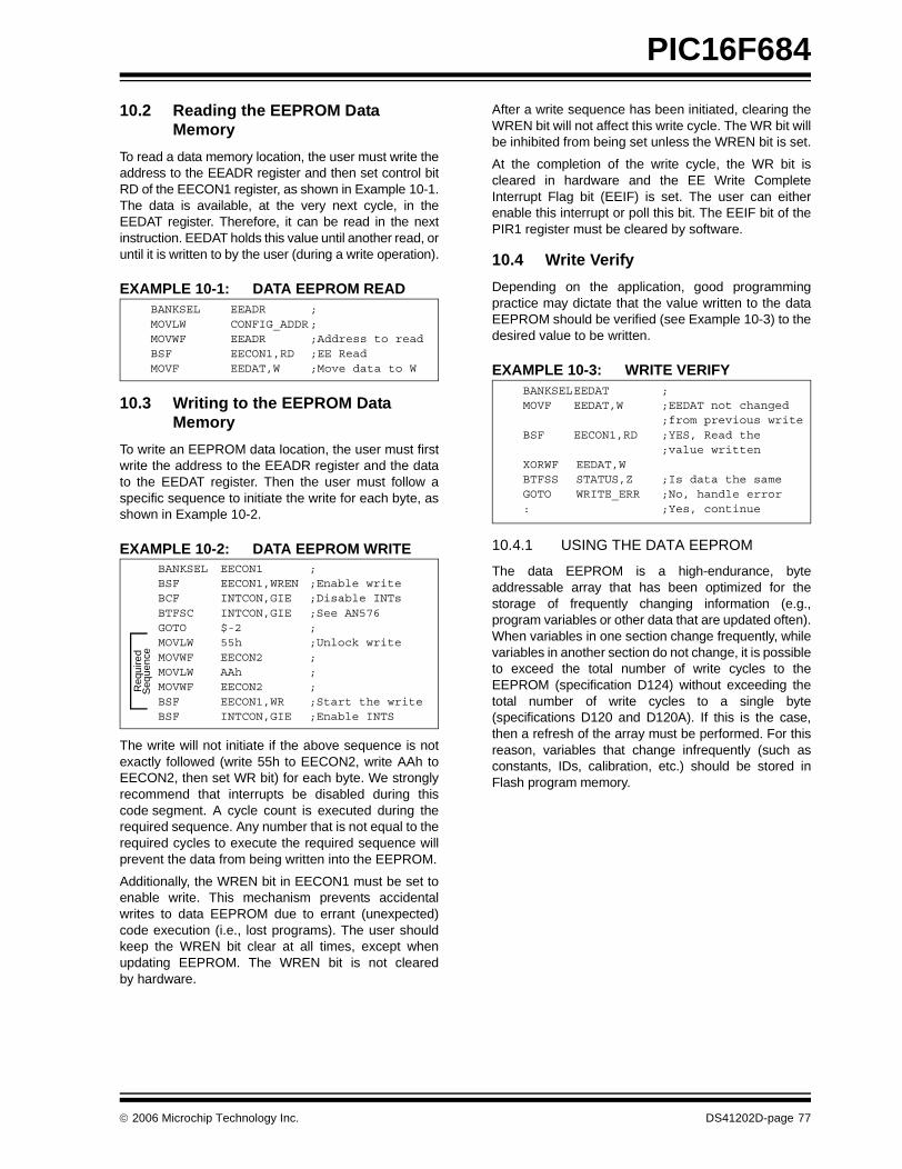
PIC16F684
10.2 Reading the EEPROM Data Memory
To read a data memory location, the user must write theaddress to the EEADR register and then set control bitRD of the EECON1 register, as shown in Example 10-1.The data is available, at the very next cycle, in theEEDAT register. Therefore, it can be read in the nextinstruction. EEDAT holds this value until another read, oruntil it is written to by the user (during a write operation).
EXAMPLE 10-1: DATA EEPROM READ
10.3 Writing to the EEPROM Data Memory
To write an EEPROM data location, the user must firstwrite the address to the EEADR register and the datato the EEDAT register. Then the user must follow aspecific sequence to initiate the write for each byte, asshown in Example 10-2.
EXAMPLE 10-2: DATA EEPROM WRITE
The write will not initiate if the above sequence is notexactly followed (write 55h to EECON2, write AAh toEECON2, then set WR bit) for each byte. We stronglyrecommend that interrupts be disabled during thiscode segment. A cycle count is executed during therequired sequence. Any number that is not equal to therequired cycles to execute the required sequence willprevent the data from being written into the EEPROM.
Additionally, the WREN bit in EECON1 must be set toenable write. This mechanism prevents accidentalwrites to data EEPROM due to errant (unexpected)code execution (i.e., lost programs). The user shouldkeep the WREN bit clear at all times, except whenupdating EEPROM. The WREN bit is not clearedby hardware.
After a write sequence has been initiated, clearing theWREN bit will not affect this write cycle. The WR bit willbe inhibited from being set unless the WREN bit is set.
At the completion of the write cycle, the WR bit iscleared in hardware and the EE Write CompleteInterrupt Flag bit (EEIF) is set. The user can eitherenable this interrupt or poll this bit. The EEIF bit of thePIR1 register must be cleared by software.
10.4 Write Verify
Depending on the application, good programmingpractice may dictate that the value written to the dataEEPROM should be verified (see Example 10-3) to thedesired value to be written.
EXAMPLE 10-3: WRITE VERIFY
10.4.1 USING THE DATA EEPROM
The data EEPROM is a high-endurance, byteaddressable array that has been optimized for thestorage of frequently changing information (e.g.,program variables or other data that are updated often).When variables in one section change frequently, whilevariables in another section do not change, it is possibleto exceed the total number of write cycles to theEEPROM (specification D124) without exceeding thetotal number of write cycles to a single byte(specifications D120 and D120A). If this is the case,then a refresh of the array must be performed. For thisreason, variables that change infrequently (such asconstants, IDs, calibration, etc.) should be stored inFlash program memory.
BANKSEL EEADR ;MOVLW CONFIG_ADDR;MOVWF EEADR ;Address to readBSF EECON1,RD ;EE ReadMOVF EEDAT,W ;Move data to W
BANKSEL EECON1 ;BSF EECON1,WREN ;Enable writeBCF INTCON,GIE ;Disable INTsBTFSC INTCON,GIE ;See AN576GOTO $-2 ;MOVLW 55h ;Unlock writeMOVWF EECON2 ;MOVLW AAh ;MOVWF EECON2 ;BSF EECON1,WR ;Start the writeBSF INTCON,GIE ;Enable INTS
Req
uire
dS
eque
nce
BANKSELEEDAT ;MOVF EEDAT,W ;EEDAT not changed
;from previous writeBSF EECON1,RD ;YES, Read the
;value writtenXORWF EEDAT,WBTFSS STATUS,Z ;Is data the sameGOTO WRITE_ERR ;No, handle error: ;Yes, continue
© 2006 Microchip Technology Inc. DS41202D-page 77
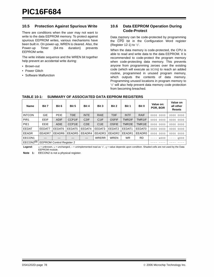
PIC16F684
10.5 Protection Against Spurious Write
There are conditions when the user may not want towrite to the data EEPROM memory. To protect againstspurious EEPROM writes, various mechanisms havebeen built in. On power-up, WREN is cleared. Also, thePower-up Timer (64 ms duration) preventsEEPROM write.
The write initiate sequence and the WREN bit togetherhelp prevent an accidental write during:
• Brown-out
• Power Glitch• Software Malfunction
10.6 Data EEPROM Operation During Code-Protect
Data memory can be code-protected by programmingthe CPD bit in the Configuration Word register(Register 12-1) to ‘0’.
When the data memory is code-protected, the CPU isable to read and write data to the data EEPROM. It isrecommended to code-protect the program memorywhen code-protecting data memory. This preventsanyone from programming zeroes over the existingcode (which will execute as NOPs) to reach an addedroutine, programmed in unused program memory,which outputs the contents of data memory.Programming unused locations in program memory to‘0’ will also help prevent data memory code protectionfrom becoming breached.
TABLE 10-1: SUMMARY OF ASSOCIATED DATA EEPROM REGISTERS
Name Bit 7 Bit 6 Bit 5 Bit 4 Bit 3 Bit 2 Bit 1 Bit 0Value on: POR, BOR
Value on all other Resets
INTCON GIE PEIE T0IE INTE RAIE T0IF INTF RAIF 0000 0000 0000 0000
PIR1 EEIF ADIF CCP1IF C2IF C1IF OSFIF TMR2IF TMR1IF 0000 0000 0000 0000
PIE1 EEIE ADIE CCP1IE C2IE C1IE OSFIE TMR2IE TMR1IE 0000 0000 0000 0000
EEDAT EEDAT7 EEDAT6 EEDAT5 EEDAT4 EEDAT3 EEDAT2 EEDAT1 EEDAT0 0000 0000 0000 0000
EEADR EEADR7 EEADR6 EEADR5 EEADR4 EEADR3 EEADR2 EEADR1 EEADR0 0000 0000 0000 0000
EECON1 — — — — WRERR WREN WR RD ---- x000 ---- q000
EECON2(1) EEPROM Control Register 2 ---- ---- ---- ----
Legend: x = unknown, u = unchanged, – = unimplemented read as ‘0’, q = value depends upon condition. Shaded cells are not used by the Data EEPROM module.
Note 1: EECON2 is not a physical register.
DS41202D-page 78 © 2006 Microchip Technology Inc.
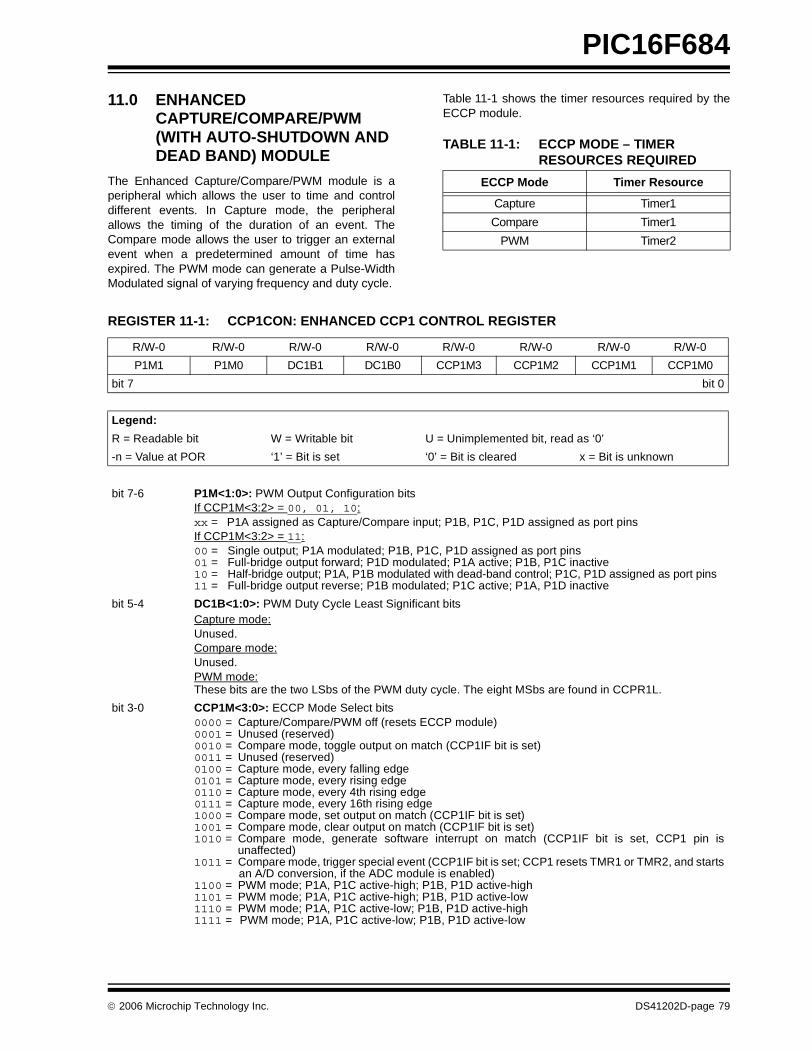
PIC16F684
11.0 ENHANCED CAPTURE/COMPARE/PWM (WITH AUTO-SHUTDOWN AND DEAD BAND) MODULE
The Enhanced Capture/Compare/PWM module is aperipheral which allows the user to time and controldifferent events. In Capture mode, the peripheralallows the timing of the duration of an event. TheCompare mode allows the user to trigger an externalevent when a predetermined amount of time hasexpired. The PWM mode can generate a Pulse-WidthModulated signal of varying frequency and duty cycle.
Table 11-1 shows the timer resources required by theECCP module.
TABLE 11-1: ECCP MODE – TIMER RESOURCES REQUIRED
ECCP Mode Timer Resource
Capture Timer1
Compare Timer1
PWM Timer2
REGISTER 11-1: CCP1CON: ENHANCED CCP1 CONTROL REGISTER
R/W-0 R/W-0 R/W-0 R/W-0 R/W-0 R/W-0 R/W-0 R/W-0
P1M1 P1M0 DC1B1 DC1B0 CCP1M3 CCP1M2 CCP1M1 CCP1M0
bit 7 bit 0
Legend:
R = Readable bit W = Writable bit U = Unimplemented bit, read as ‘0’
-n = Value at POR ‘1’ = Bit is set ‘0’ = Bit is cleared x = Bit is unknown
bit 7-6 P1M<1:0>: PWM Output Configuration bitsIf CCP1M<3:2> = 00, 01, 10:xx = P1A assigned as Capture/Compare input; P1B, P1C, P1D assigned as port pinsIf CCP1M<3:2> = 11:00 = Single output; P1A modulated; P1B, P1C, P1D assigned as port pins01 = Full-bridge output forward; P1D modulated; P1A active; P1B, P1C inactive10 = Half-bridge output; P1A, P1B modulated with dead-band control; P1C, P1D assigned as port pins11 = Full-bridge output reverse; P1B modulated; P1C active; P1A, P1D inactive
bit 5-4 DC1B<1:0>: PWM Duty Cycle Least Significant bitsCapture mode:Unused.Compare mode:Unused.PWM mode:These bits are the two LSbs of the PWM duty cycle. The eight MSbs are found in CCPR1L.
bit 3-0 CCP1M<3:0>: ECCP Mode Select bits0000 = Capture/Compare/PWM off (resets ECCP module)0001 = Unused (reserved)0010 = Compare mode, toggle output on match (CCP1IF bit is set)0011 = Unused (reserved)0100 = Capture mode, every falling edge0101 = Capture mode, every rising edge0110 = Capture mode, every 4th rising edge0111 = Capture mode, every 16th rising edge1000 = Compare mode, set output on match (CCP1IF bit is set)1001 = Compare mode, clear output on match (CCP1IF bit is set)1010 = Compare mode, generate software interrupt on match (CCP1IF bit is set, CCP1 pin is
unaffected)1011 = Compare mode, trigger special event (CCP1IF bit is set; CCP1 resets TMR1 or TMR2, and starts
an A/D conversion, if the ADC module is enabled)1100 = PWM mode; P1A, P1C active-high; P1B, P1D active-high1101 = PWM mode; P1A, P1C active-high; P1B, P1D active-low1110 = PWM mode; P1A, P1C active-low; P1B, P1D active-high1111 = PWM mode; P1A, P1C active-low; P1B, P1D active-low
© 2006 Microchip Technology Inc. DS41202D-page 79
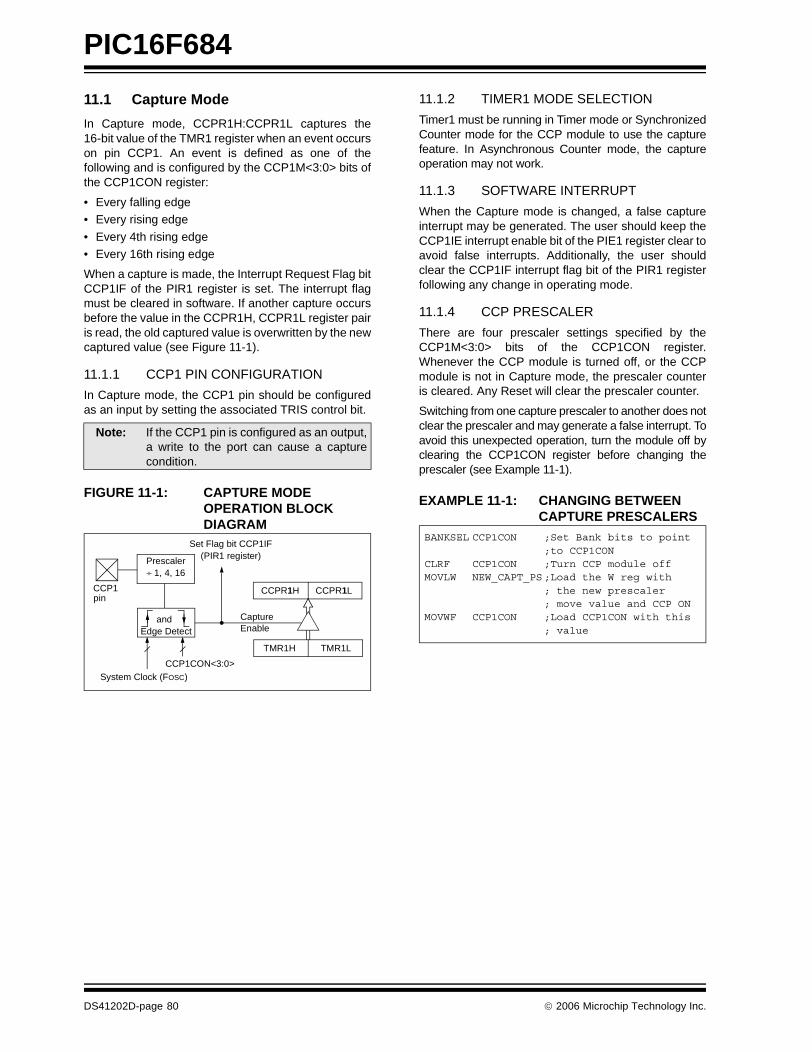
PIC16F684
11.1 Capture Mode
In Capture mode, CCPR1H:CCPR1L captures the16-bit value of the TMR1 register when an event occurson pin CCP1. An event is defined as one of thefollowing and is configured by the CCP1M<3:0> bits ofthe CCP1CON register:
• Every falling edge• Every rising edge
• Every 4th rising edge• Every 16th rising edge
When a capture is made, the Interrupt Request Flag bitCCP1IF of the PIR1 register is set. The interrupt flagmust be cleared in software. If another capture occursbefore the value in the CCPR1H, CCPR1L register pairis read, the old captured value is overwritten by the newcaptured value (see Figure 11-1).
11.1.1 CCP1 PIN CONFIGURATION
In Capture mode, the CCP1 pin should be configuredas an input by setting the associated TRIS control bit.
FIGURE 11-1: CAPTURE MODE OPERATION BLOCK DIAGRAM
11.1.2 TIMER1 MODE SELECTION
Timer1 must be running in Timer mode or SynchronizedCounter mode for the CCP module to use the capturefeature. In Asynchronous Counter mode, the captureoperation may not work.
11.1.3 SOFTWARE INTERRUPT
When the Capture mode is changed, a false captureinterrupt may be generated. The user should keep theCCP1IE interrupt enable bit of the PIE1 register clear toavoid false interrupts. Additionally, the user shouldclear the CCP1IF interrupt flag bit of the PIR1 registerfollowing any change in operating mode.
11.1.4 CCP PRESCALER
There are four prescaler settings specified by theCCP1M<3:0> bits of the CCP1CON register.Whenever the CCP module is turned off, or the CCPmodule is not in Capture mode, the prescaler counteris cleared. Any Reset will clear the prescaler counter.
Switching from one capture prescaler to another does notclear the prescaler and may generate a false interrupt. Toavoid this unexpected operation, turn the module off byclearing the CCP1CON register before changing theprescaler (see Example 11-1).
EXAMPLE 11-1: CHANGING BETWEEN CAPTURE PRESCALERS
Note: If the CCP1 pin is configured as an output,a write to the port can cause a capturecondition.
CCPR1H CCPR1L
TMR1H TMR1L
Set Flag bit CCP1IF(PIR1 register)
CaptureEnable
CCP1CON<3:0>
Prescaler÷ 1, 4, 16
andEdge Detect
pinCCP1
System Clock (FOSC)
BANKSEL CCP1CON ;Set Bank bits to point;to CCP1CON
CLRF CCP1CON ;Turn CCP module offMOVLW NEW_CAPT_PS;Load the W reg with
; the new prescaler; move value and CCP ON
MOVWF CCP1CON ;Load CCP1CON with this; value
DS41202D-page 80 © 2006 Microchip Technology Inc.
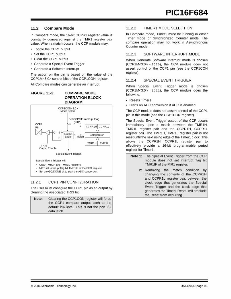
PIC16F684
11.2 Compare Mode
In Compare mode, the 16-bit CCPR1 register value isconstantly compared against the TMR1 register pairvalue. When a match occurs, the CCP module may:
• Toggle the CCP1 output• Set the CCP1 output• Clear the CCP1 output
• Generate a Special Event Trigger• Generate a Software Interrupt
The action on the pin is based on the value of theCCP1M<3:0> control bits of the CCP1CON register.
All Compare modes can generate an interrupt.
FIGURE 11-2: COMPARE MODE OPERATION BLOCK DIAGRAM
11.2.1 CCP1 PIN CONFIGURATION
The user must configure the CCP1 pin as an output byclearing the associated TRIS bit.
11.2.2 TIMER1 MODE SELECTION
In Compare mode, Timer1 must be running in eitherTimer mode or Synchronized Counter mode. Thecompare operation may not work in AsynchronousCounter mode.
11.2.3 SOFTWARE INTERRUPT MODE
When Generate Software Interrupt mode is chosen(CCP1M<3:0> = 1010), the CCP module does notassert control of the CCP1 pin (see the CCP1CONregister).
11.2.4 SPECIAL EVENT TRIGGER
When Special Event Trigger mode is chosen(CCP1M<3:0> = 1011), the CCP module does thefollowing:
• Resets Timer1• Starts an ADC conversion if ADC is enabled
The CCP module does not assert control of the CCP1pin in this mode (see the CCP1CON register).
The Special Event Trigger output of the CCP occursimmediately upon a match between the TMR1H,TMR1L register pair and the CCPR1H, CCPR1Lregister pair. The TMR1H, TMR1L register pair is notreset until the next rising edge of the Timer1 clock. Thisallows the CCPR1H, CCPR1L register pair toeffectively provide a 16-bit programmable periodregister for Timer1.
Note: Clearing the CCP1CON register will forcethe CCP1 compare output latch to thedefault low level. This is not the port I/Odata latch.
CCPR1H CCPR1L
TMR1H TMR1L
ComparatorQ S
R
OutputLogic
Special Event Trigger
Set CCP1IF Interrupt Flag(PIR1)
Match
TRIS
CCP1CON<3:0>Mode Select
Output Enable
Pin
Special Event Trigger will:
• Clear TMR1H and TMR1L registers.• NOT set interrupt flag bit TMR1IF of the PIR1 register.• Set the GO/DONE bit to start the ADC conversion.
CCP1 4
Note 1: The Special Event Trigger from the CCPmodule does not set interrupt flag bitTMR1IF of the PIR1 register.
2: Removing the match condition bychanging the contents of the CCPR1Hand CCPR1L register pair, between theclock edge that generates the SpecialEvent Trigger and the clock edge thatgenerates the Timer1 Reset, will precludethe Reset from occurring.
© 2006 Microchip Technology Inc. DS41202D-page 81
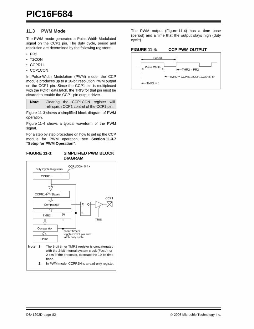
PIC16F684
11.3 PWM Mode
The PWM mode generates a Pulse-Width Modulatedsignal on the CCP1 pin. The duty cycle, period andresolution are determined by the following registers:
• PR2• T2CON• CCPR1L
• CCP1CON
In Pulse-Width Modulation (PWM) mode, the CCPmodule produces up to a 10-bit resolution PWM outputon the CCP1 pin. Since the CCP1 pin is multiplexedwith the PORT data latch, the TRIS for that pin must becleared to enable the CCP1 pin output driver.
Figure 11-3 shows a simplified block diagram of PWMoperation.
Figure 11-4 shows a typical waveform of the PWMsignal.
For a step by step procedure on how to set up the CCPmodule for PWM operation, see Section 11.3.7“Setup for PWM Operation”.
FIGURE 11-3: SIMPLIFIED PWM BLOCK DIAGRAM
The PWM output (Figure 11-4) has a time base(period) and a time that the output stays high (dutycycle).
FIGURE 11-4: CCP PWM OUTPUT
Note: Clearing the CCP1CON register willrelinquish CCP1 control of the CCP1 pin.
CCPR1L
CCPR1H(2) (Slave)
Comparator
TMR2
PR2
(1)
R Q
S
Duty Cycle RegistersCCP1CON<5:4>
Clear Timer2,toggle CCP1 pin and latch duty cycle
Note 1: The 8-bit timer TMR2 register is concatenated with the 2-bit internal system clock (FOSC), or 2 bits of the prescaler, to create the 10-bit time base.
2: In PWM mode, CCPR1H is a read-only register.
TRIS
CCP1
Comparator
Period
Pulse Width
TMR2 = 0
TMR2 = CCPR1L:CCP1CON<5:4>
TMR2 = PR2
DS41202D-page 82 © 2006 Microchip Technology Inc.
PIC16F684
11.3.1 PWM PERIOD
The PWM period is specified by the PR2 register ofTimer2. The PWM period can be calculated using theformula of Equation 11-1.
EQUATION 11-1: PWM PERIOD
When TMR2 is equal to PR2, the following three eventsoccur on the next increment cycle:
• TMR2 is cleared• The CCP1 pin is set. (Exception: If the PWM duty
cycle = 0%, the pin will not be set.)• The PWM duty cycle is latched from CCPR1L into
CCPR1H.
11.3.2 PWM DUTY CYCLE
The PWM duty cycle is specified by writing a 10-bitvalue to multiple registers: CCPR1L register andCCP1<1:0> bits of the CCP1CON register. TheCCPR1L contains the eight MSbs and the CCP1<1:0>bits of the CCP1CON register contain the two LSbs.CCPR1L and CCP1<1:0> bits of the CCP1CONregister can be written to at any time. The duty cyclevalue is not latched into CCPR1H until after the periodcompletes (i.e., a match between PR2 and TMR2registers occurs). While using the PWM, the CCPR1Hregister is read-only.
Equation 11-2 is used to calculate the PWM pulsewidth.
Equation 11-3 is used to calculate the PWM duty cycleratio.
EQUATION 11-2: PULSE WIDTH
EQUATION 11-3: DUTY CYCLE RATIO
The CCPR1H register and a 2-bit internal latch areused to double buffer the PWM duty cycle. This doublebuffering is essential for glitchless PWM operation.
The 8-bit timer TMR2 register is concatenated witheither the 2-bit internal system clock (FOSC), or 2 bits ofthe prescaler, to create the 10-bit time base. The systemclock is used if the Timer2 prescaler is set to 1:1.
When the 10-bit time base matches the CCPR1H and2-bit latch, then the CCP1 pin is cleared (seeFigure 11-3).
11.3.3 PWM RESOLUTION
The resolution determines the number of available dutycycles for a given period. For example, a 10-bit resolutionwill result in 1024 discrete duty cycles, whereas an 8-bitresolution will result in 256 discrete duty cycles.
The maximum PWM resolution is 10 bits when PR2 is255. The resolution is a function of the PR2 registervalue as shown by Equation 11-4.
EQUATION 11-4: PWM RESOLUTION
TABLE 11-2: EXAMPLE PWM FREQUENCIES AND RESOLUTIONS (FOSC = 20 MHz)
TABLE 11-3: EXAMPLE PWM FREQUENCIES AND RESOLUTIONS (FOSC = 8 MHz)
Note: The Timer2 postscaler (see Section 7.1“Timer2 Operation”) is not used in thedetermination of the PWM frequency.
PWM Period PR2( ) 1+[ ] 4 TOSC •••=
(TMR2 Prescale Value)
Note: If the pulse width value is greater than theperiod the assigned PWM pin(s) willremain unchanged.
Pulse Width CCPR1L:CCP1CON<5:4>( ) •=
TOSC • (TMR2 Prescale Value)
Duty Cycle Ratio CCPR1L:CCP1CON<5:4>( )4 PR2 1+( )
-----------------------------------------------------------------------=
Resolution 4 PR2 1+( )[ ]log2( )log
------------------------------------------ bits=
PWM Frequency 1.22 kHz 4.88 kHz 19.53 kHz 78.12 kHz 156.3 kHz 208.3 kHz
Timer Prescale (1, 4, 16) 16 4 1 1 1 1
PR2 Value 0xFF 0xFF 0xFF 0x3F 0x1F 0x17
Maximum Resolution (bits) 10 10 10 8 7 6.6
PWM Frequency 1.22 kHz 4.90 kHz 19.61 kHz 76.92 kHz 153.85 kHz 200.0 kHz
Timer Prescale (1, 4, 16) 16 4 1 1 1 1
PR2 Value 0x65 0x65 0x65 0x19 0x0C 0x09
Maximum Resolution (bits) 8 8 8 6 5 5
© 2006 Microchip Technology Inc. DS41202D-page 83
PIC16F684
11.3.4 OPERATION IN SLEEP MODE
In Sleep mode, the TMR2 register will not incrementand the state of the module will not change. If the CCP1pin is driving a value, it will continue to drive that value.When the device wakes up, TMR2 will continue from itsprevious state.
11.3.5 CHANGES IN SYSTEM CLOCK FREQUENCY
The PWM frequency is derived from the system clockfrequency. Any changes in the system clock frequencywill result in changes to the PWM frequency. SeeSection 3.0 “Oscillator Module (With Fail-SafeClock Monitor)” for additional details.
11.3.6 EFFECTS OF RESET
Any Reset will force all ports to Input mode and theCCP registers to their Reset states.
11.3.7 SETUP FOR PWM OPERATION
The following steps should be taken when configuringthe CCP module for PWM operation:
1. Disable the PWM pin (CCP1) output driver bysetting the associated TRIS bit.
2. Set the PWM period by loading the PR2 register.3. Configure the CCP module for the PWM mode
by loading the CCP1CON register with theappropriate values.
4. Set the PWM duty cycle by loading the CCPR1Lregister and CCP1 bits of the CCP1CON register.
5. Configure and start Timer2:• Clear the TMR2IF interrupt flag bit of the
PIR1 register.• Set the Timer2 prescale value by loading the
T2CKPS bits of the T2CON register.• Enable Timer2 by setting the TMR2ON bit of
the T2CON register.6. Enable PWM output after a new PWM cycle has
started:• Wait until Timer2 overflows (TMR2IF bit of
the PIR1 register is set).• Enable the CCP1 pin output driver by clearing
the associated TRIS bit.
DS41202D-page 84 © 2006 Microchip Technology Inc.
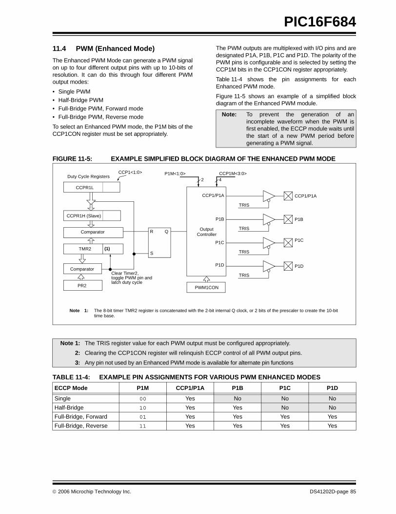
PIC16F684
11.4 PWM (Enhanced Mode)
The Enhanced PWM Mode can generate a PWM signalon up to four different output pins with up to 10-bits ofresolution. It can do this through four different PWMoutput modes:
• Single PWM
• Half-Bridge PWM• Full-Bridge PWM, Forward mode• Full-Bridge PWM, Reverse mode
To select an Enhanced PWM mode, the P1M bits of theCCP1CON register must be set appropriately.
The PWM outputs are multiplexed with I/O pins and aredesignated P1A, P1B, P1C and P1D. The polarity of thePWM pins is configurable and is selected by setting theCCP1M bits in the CCP1CON register appropriately.
Table 11-4 shows the pin assignments for eachEnhanced PWM mode.
Figure 11-5 shows an example of a simplified blockdiagram of the Enhanced PWM module.
FIGURE 11-5: EXAMPLE SIMPLIFIED BLOCK DIAGRAM OF THE ENHANCED PWM MODE
TABLE 11-4: EXAMPLE PIN ASSIGNMENTS FOR VARIOUS PWM ENHANCED MODES
Note: To prevent the generation of anincomplete waveform when the PWM isfirst enabled, the ECCP module waits untilthe start of a new PWM period beforegenerating a PWM signal.
CCPR1L
CCPR1H (Slave)
Comparator
TMR2
Comparator
PR2
(1)
R Q
S
Duty Cycle RegistersCCP1<1:0>
Clear Timer2,toggle PWM pin and latch duty cycle
Note 1: The 8-bit timer TMR2 register is concatenated with the 2-bit internal Q clock, or 2 bits of the prescaler to create the 10-bittime base.
TRIS
CCP1/P1A
TRIS
P1B
TRIS
P1C
TRIS
P1D
OutputController
P1M<1:0>2
CCP1M<3:0>4
PWM1CON
CCP1/P1A
P1B
P1C
P1D
Note 1: The TRIS register value for each PWM output must be configured appropriately.
2: Clearing the CCP1CON register will relinquish ECCP control of all PWM output pins.
3: Any pin not used by an Enhanced PWM mode is available for alternate pin functions
ECCP Mode P1M CCP1/P1A P1B P1C P1D
Single 00 Yes No No No
Half-Bridge 10 Yes Yes No No
Full-Bridge, Forward 01 Yes Yes Yes Yes
Full-Bridge, Reverse 11 Yes Yes Yes Yes
© 2006 Microchip Technology Inc. DS41202D-page 85
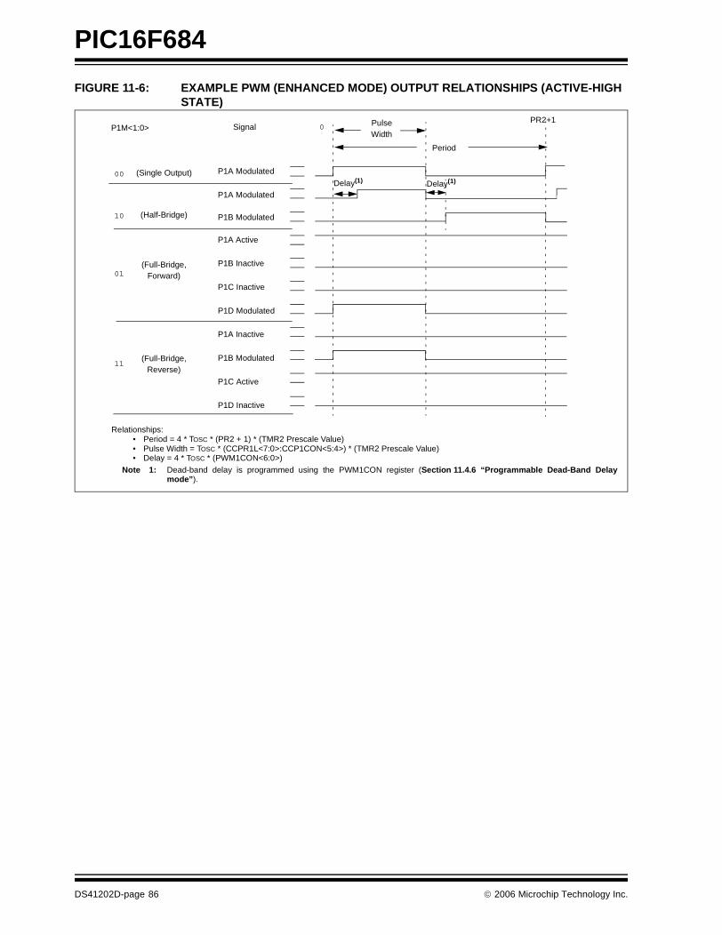
PIC16F684
FIGURE 11-6: EXAMPLE PWM (ENHANCED MODE) OUTPUT RELATIONSHIPS (ACTIVE-HIGH STATE)
0
Period
00
10
01
11
SignalPR2+1
P1M<1:0>
P1A Modulated
P1A Modulated
P1B Modulated
P1A Active
P1B Inactive
P1C Inactive
P1D Modulated
P1A Inactive
P1B Modulated
P1C Active
P1D Inactive
PulseWidth
(Single Output)
(Half-Bridge)
(Full-Bridge,Forward)
(Full-Bridge,Reverse)
Delay(1) Delay(1)
Relationships:• Period = 4 * TOSC * (PR2 + 1) * (TMR2 Prescale Value)• Pulse Width = TOSC * (CCPR1L<7:0>:CCP1CON<5:4>) * (TMR2 Prescale Value)• Delay = 4 * TOSC * (PWM1CON<6:0>)
Note 1: Dead-band delay is programmed using the PWM1CON register (Section 11.4.6 “Programmable Dead-Band Delaymode”).
DS41202D-page 86 © 2006 Microchip Technology Inc.
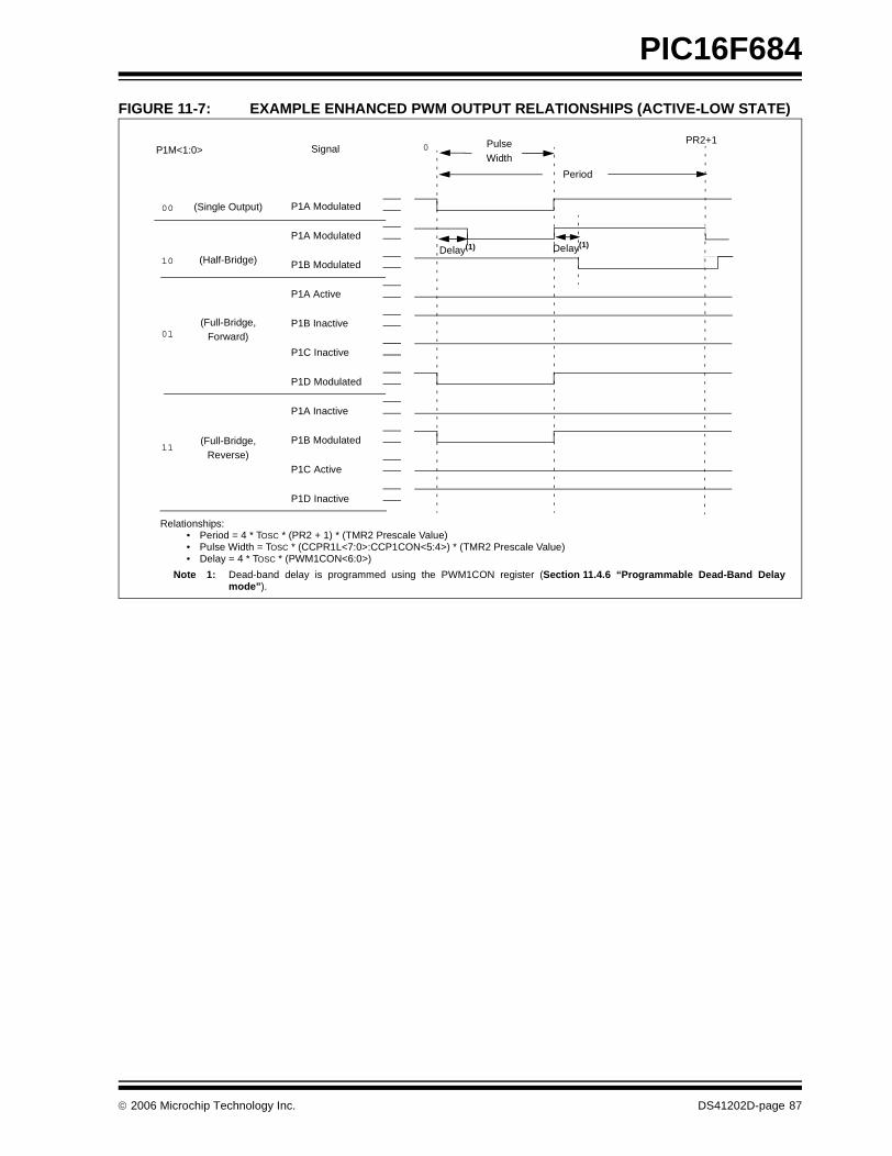
PIC16F684
FIGURE 11-7: EXAMPLE ENHANCED PWM OUTPUT RELATIONSHIPS (ACTIVE-LOW STATE)
0
Period
00
10
01
11
SignalPR2+1
P1M<1:0>
P1A Modulated
P1A Modulated
P1B Modulated
P1A Active
P1B Inactive
P1C Inactive
P1D Modulated
P1A Inactive
P1B Modulated
P1C Active
P1D Inactive
PulseWidth
(Single Output)
(Half-Bridge)
(Full-Bridge,Forward)
(Full-Bridge,Reverse)
Delay(1) Delay(1)
Relationships:• Period = 4 * TOSC * (PR2 + 1) * (TMR2 Prescale Value)• Pulse Width = TOSC * (CCPR1L<7:0>:CCP1CON<5:4>) * (TMR2 Prescale Value)• Delay = 4 * TOSC * (PWM1CON<6:0>)
Note 1: Dead-band delay is programmed using the PWM1CON register (Section 11.4.6 “Programmable Dead-Band Delaymode”).
© 2006 Microchip Technology Inc. DS41202D-page 87
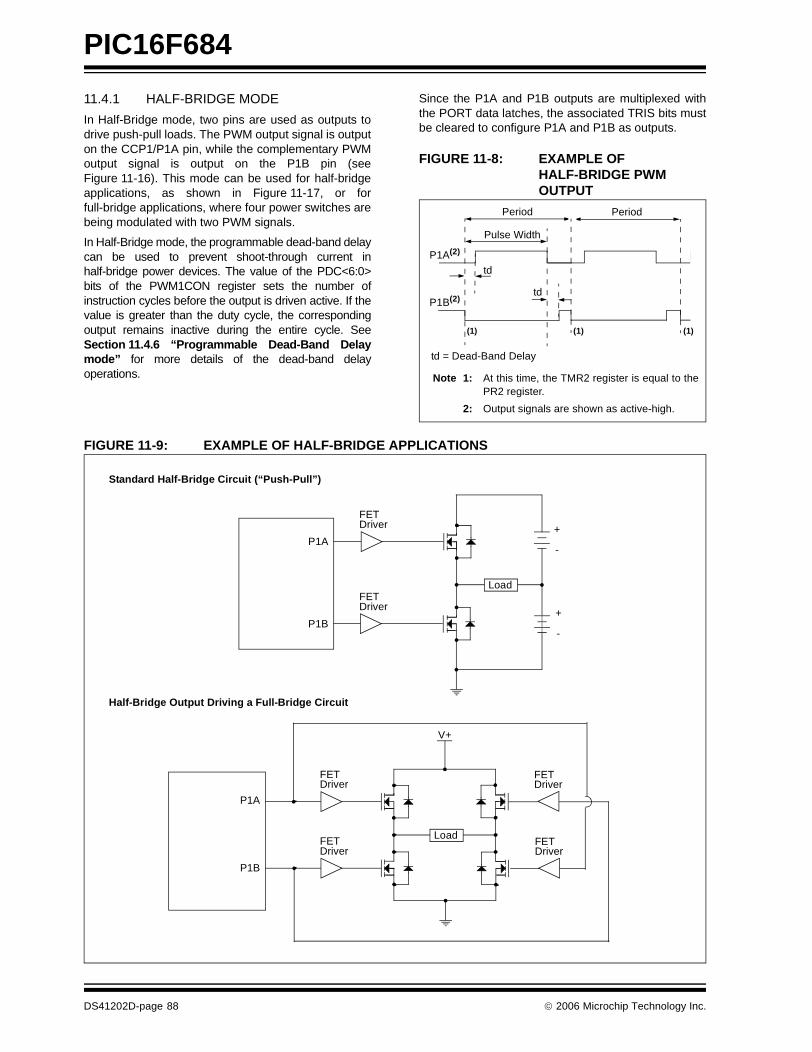
PIC16F684
11.4.1 HALF-BRIDGE MODE
In Half-Bridge mode, two pins are used as outputs todrive push-pull loads. The PWM output signal is outputon the CCP1/P1A pin, while the complementary PWMoutput signal is output on the P1B pin (seeFigure 11-16). This mode can be used for half-bridgeapplications, as shown in Figure 11-17, or forfull-bridge applications, where four power switches arebeing modulated with two PWM signals.
In Half-Bridge mode, the programmable dead-band delaycan be used to prevent shoot-through current inhalf-bridge power devices. The value of the PDC<6:0>bits of the PWM1CON register sets the number ofinstruction cycles before the output is driven active. If thevalue is greater than the duty cycle, the correspondingoutput remains inactive during the entire cycle. SeeSection 11.4.6 “Programmable Dead-Band Delaymode” for more details of the dead-band delayoperations.
Since the P1A and P1B outputs are multiplexed withthe PORT data latches, the associated TRIS bits mustbe cleared to configure P1A and P1B as outputs.
FIGURE 11-8: EXAMPLE OF HALF-BRIDGE PWM OUTPUT
FIGURE 11-9: EXAMPLE OF HALF-BRIDGE APPLICATIONS
Period
Pulse Width
td
td
(1)
P1A(2)
P1B(2)
td = Dead-Band Delay
Period
(1) (1)
Note 1: At this time, the TMR2 register is equal to thePR2 register.
2: Output signals are shown as active-high.
P1A
P1B
FETDriver
FETDriver
Load
+
-
+
-
FETDriver
FETDriver
V+
Load
FETDriver
FETDriver
P1A
P1B
Standard Half-Bridge Circuit (“Push-Pull”)
Half-Bridge Output Driving a Full-Bridge Circuit
DS41202D-page 88 © 2006 Microchip Technology Inc.
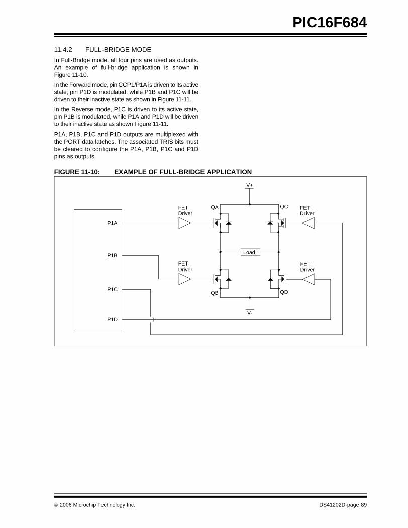
PIC16F684
11.4.2 FULL-BRIDGE MODE
In Full-Bridge mode, all four pins are used as outputs.An example of full-bridge application is shown inFigure 11-10.
In the Forward mode, pin CCP1/P1A is driven to its activestate, pin P1D is modulated, while P1B and P1C will bedriven to their inactive state as shown in Figure 11-11.
In the Reverse mode, P1C is driven to its active state,pin P1B is modulated, while P1A and P1D will be drivento their inactive state as shown Figure 11-11.
P1A, P1B, P1C and P1D outputs are multiplexed withthe PORT data latches. The associated TRIS bits mustbe cleared to configure the P1A, P1B, P1C and P1Dpins as outputs.
FIGURE 11-10: EXAMPLE OF FULL-BRIDGE APPLICATION
P1A
P1C
FETDriver
FETDriver
V+
V-
Load
FETDriver
FETDriver
P1B
P1D
QA
QB QD
QC
© 2006 Microchip Technology Inc. DS41202D-page 89
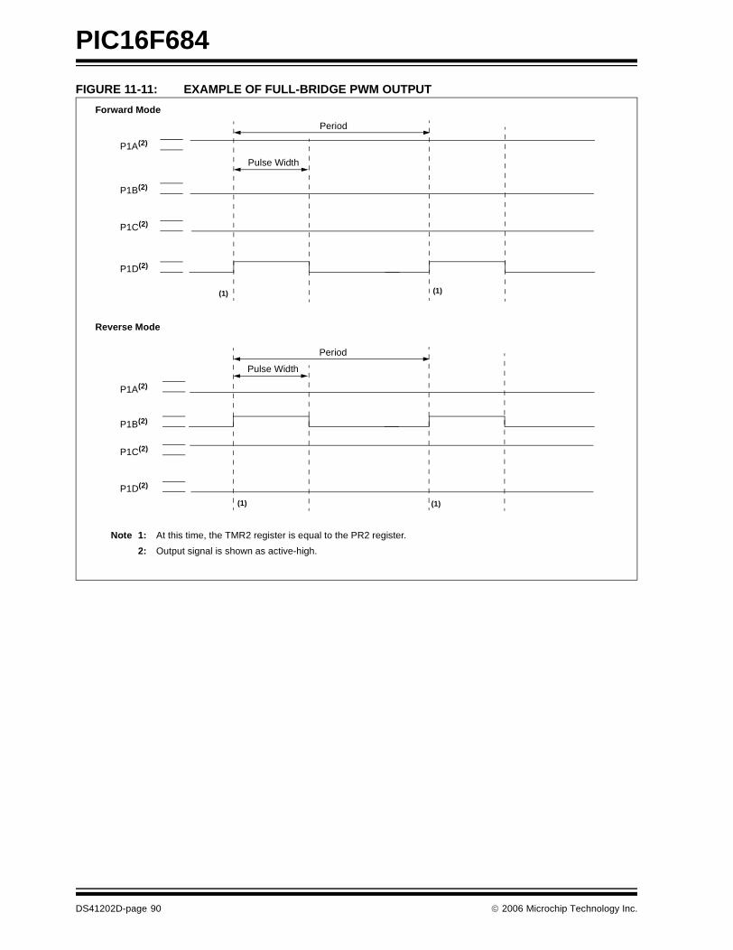
PIC16F684
FIGURE 11-11: EXAMPLE OF FULL-BRIDGE PWM OUTPUT
Period
Pulse Width
P1A(2)
P1B(2)
P1C(2)
P1D(2)
Forward Mode
(1)
Period
Pulse Width
P1A(2)
P1C(2)
P1D(2)
P1B(2)
Reverse Mode
(1)
(1)(1)
Note 1: At this time, the TMR2 register is equal to the PR2 register.
2: Output signal is shown as active-high.
DS41202D-page 90 © 2006 Microchip Technology Inc.
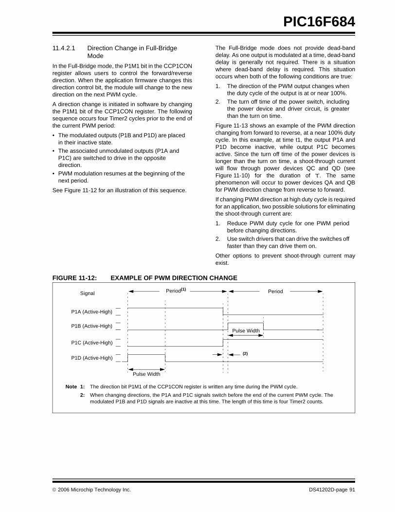
PIC16F684
11.4.2.1 Direction Change in Full-Bridge Mode
In the Full-Bridge mode, the P1M1 bit in the CCP1CONregister allows users to control the forward/reversedirection. When the application firmware changes thisdirection control bit, the module will change to the newdirection on the next PWM cycle.
A direction change is initiated in software by changingthe P1M1 bit of the CCP1CON register. The followingsequence occurs four Timer2 cycles prior to the end ofthe current PWM period:
• The modulated outputs (P1B and P1D) are placed in their inactive state.
• The associated unmodulated outputs (P1A and P1C) are switched to drive in the opposite direction.
• PWM modulation resumes at the beginning of the next period.
See Figure 11-12 for an illustration of this sequence.
The Full-Bridge mode does not provide dead-banddelay. As one output is modulated at a time, dead-banddelay is generally not required. There is a situationwhere dead-band delay is required. This situationoccurs when both of the following conditions are true:
1. The direction of the PWM output changes whenthe duty cycle of the output is at or near 100%.
2. The turn off time of the power switch, includingthe power device and driver circuit, is greaterthan the turn on time.
Figure 11-13 shows an example of the PWM directionchanging from forward to reverse, at a near 100% dutycycle. In this example, at time t1, the output P1A andP1D become inactive, while output P1C becomesactive. Since the turn off time of the power devices islonger than the turn on time, a shoot-through currentwill flow through power devices QC and QD (seeFigure 11-10) for the duration of ‘t’. The samephenomenon will occur to power devices QA and QBfor PWM direction change from reverse to forward.
If changing PWM direction at high duty cycle is requiredfor an application, two possible solutions for eliminatingthe shoot-through current are:
1. Reduce PWM duty cycle for one PWM periodbefore changing directions.
2. Use switch drivers that can drive the switches offfaster than they can drive them on.
Other options to prevent shoot-through current mayexist.
FIGURE 11-12: EXAMPLE OF PWM DIRECTION CHANGE
Pulse Width
Period(1)Signal
Note 1: The direction bit P1M1 of the CCP1CON register is written any time during the PWM cycle.
2: When changing directions, the P1A and P1C signals switch before the end of the current PWM cycle. Themodulated P1B and P1D signals are inactive at this time. The length of this time is four Timer2 counts.
Period
(2)
P1A (Active-High)
P1B (Active-High)
P1C (Active-High)
P1D (Active-High)
Pulse Width
© 2006 Microchip Technology Inc. DS41202D-page 91
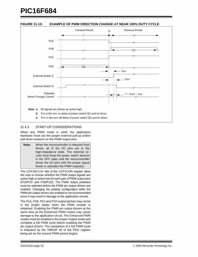
PIC16F684
FIGURE 11-13: EXAMPLE OF PWM DIRECTION CHANGE AT NEAR 100% DUTY CYCLE
11.4.3 START-UP CONSIDERATIONS
When any PWM mode is used, the applicationhardware must use the proper external pull-up and/orpull-down resistors on the PWM output pins.
The CCP1M<1:0> bits of the CCP1CON register allowthe user to choose whether the PWM output signals areactive-high or active-low for each pair of PWM output pins(P1A/P1C and P1B/P1D). The PWM output polaritiesmust be selected before the PWM pin output drivers areenabled. Changing the polarity configuration while thePWM pin output drivers are enabled is not recommendedsince it may result in damage to the application circuits.
The P1A, P1B, P1C and P1D output latches may not bein the proper states when the PWM module isinitialized. Enabling the PWM pin output drivers at thesame time as the Enhanced PWM modes may causedamage to the application circuit. The Enhanced PWMmodes must be enabled in the proper Output mode andcomplete a full PWM cycle before enabling the PWMpin output drivers. The completion of a full PWM cycleis indicated by the TMR2IF bit of the PIR1 registerbeing set as the second PWM period begins.
Forward Period Reverse Period
P1A
TON
TOFF
T = TOFF – TON
P1B
P1C
P1D
External Switch D
PotentialShoot-Through Current
Note 1: All signals are shown as active-high.
2: TON is the turn on delay of power switch QC and its driver.
3: TOFF is the turn off delay of power switch QD and its driver.
External Switch C
t1
DC
PW
Note: When the microcontroller is released fromReset, all of the I/O pins are in thehigh-impedance state. The external cir-cuits must keep the power switch devicesin the OFF state until the microcontrollerdrives the I/O pins with the proper signallevels or activates the PWM output(s).
DS41202D-page 92 © 2006 Microchip Technology Inc.
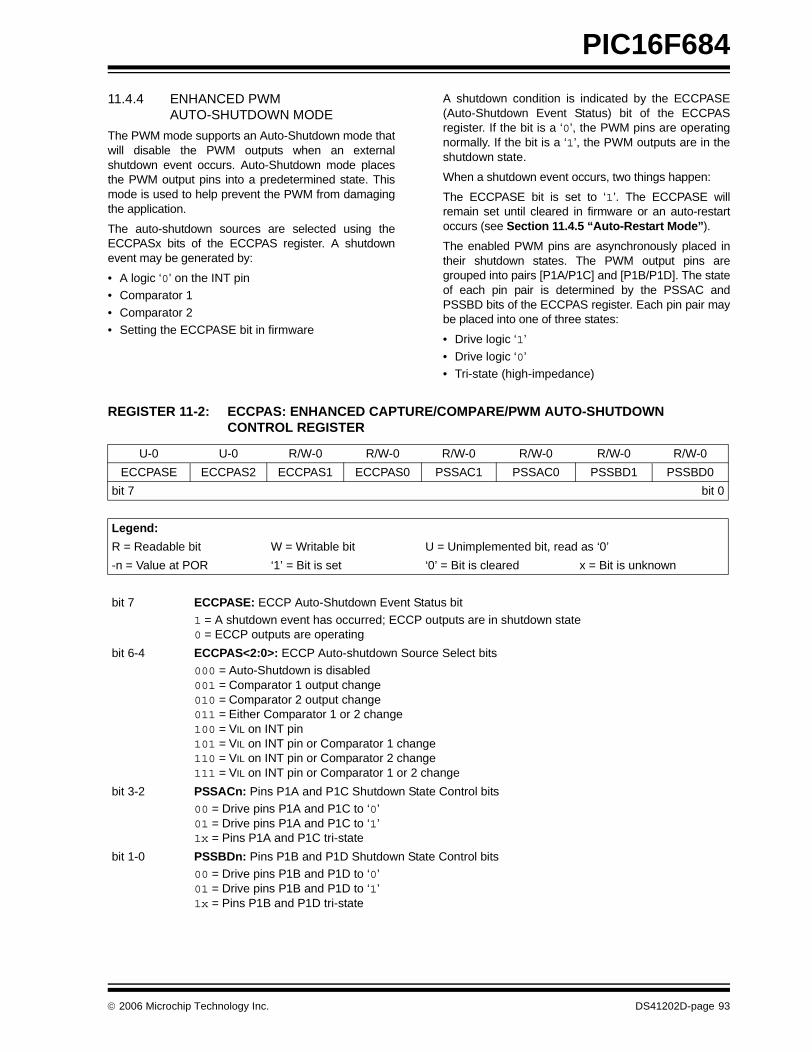
PIC16F684
11.4.4 ENHANCED PWM AUTO-SHUTDOWN MODE
The PWM mode supports an Auto-Shutdown mode thatwill disable the PWM outputs when an externalshutdown event occurs. Auto-Shutdown mode placesthe PWM output pins into a predetermined state. Thismode is used to help prevent the PWM from damagingthe application.
The auto-shutdown sources are selected using theECCPASx bits of the ECCPAS register. A shutdownevent may be generated by:
• A logic ‘0’ on the INT pin• Comparator 1
• Comparator 2• Setting the ECCPASE bit in firmware
A shutdown condition is indicated by the ECCPASE(Auto-Shutdown Event Status) bit of the ECCPASregister. If the bit is a ‘0’, the PWM pins are operatingnormally. If the bit is a ‘1’, the PWM outputs are in theshutdown state.
When a shutdown event occurs, two things happen:
The ECCPASE bit is set to ‘1’. The ECCPASE willremain set until cleared in firmware or an auto-restartoccurs (see Section 11.4.5 “Auto-Restart Mode”).
The enabled PWM pins are asynchronously placed intheir shutdown states. The PWM output pins aregrouped into pairs [P1A/P1C] and [P1B/P1D]. The stateof each pin pair is determined by the PSSAC andPSSBD bits of the ECCPAS register. Each pin pair maybe placed into one of three states:
• Drive logic ‘1’
• Drive logic ‘0’• Tri-state (high-impedance)
REGISTER 11-2: ECCPAS: ENHANCED CAPTURE/COMPARE/PWM AUTO-SHUTDOWN CONTROL REGISTER
U-0 U-0 R/W-0 R/W-0 R/W-0 R/W-0 R/W-0 R/W-0
ECCPASE ECCPAS2 ECCPAS1 ECCPAS0 PSSAC1 PSSAC0 PSSBD1 PSSBD0
bit 7 bit 0
Legend:
R = Readable bit W = Writable bit U = Unimplemented bit, read as ‘0’
-n = Value at POR ‘1’ = Bit is set ‘0’ = Bit is cleared x = Bit is unknown
bit 7 ECCPASE: ECCP Auto-Shutdown Event Status bit
1 = A shutdown event has occurred; ECCP outputs are in shutdown state0 = ECCP outputs are operating
bit 6-4 ECCPAS<2:0>: ECCP Auto-shutdown Source Select bits000 = Auto-Shutdown is disabled001 = Comparator 1 output change010 = Comparator 2 output change011 = Either Comparator 1 or 2 change100 = VIL on INT pin101 = VIL on INT pin or Comparator 1 change110 = VIL on INT pin or Comparator 2 change111 = VIL on INT pin or Comparator 1 or 2 change
bit 3-2 PSSACn: Pins P1A and P1C Shutdown State Control bits00 = Drive pins P1A and P1C to ‘0’01 = Drive pins P1A and P1C to ‘1’1x = Pins P1A and P1C tri-state
bit 1-0 PSSBDn: Pins P1B and P1D Shutdown State Control bits00 = Drive pins P1B and P1D to ‘0’01 = Drive pins P1B and P1D to ‘1’1x = Pins P1B and P1D tri-state
© 2006 Microchip Technology Inc. DS41202D-page 93
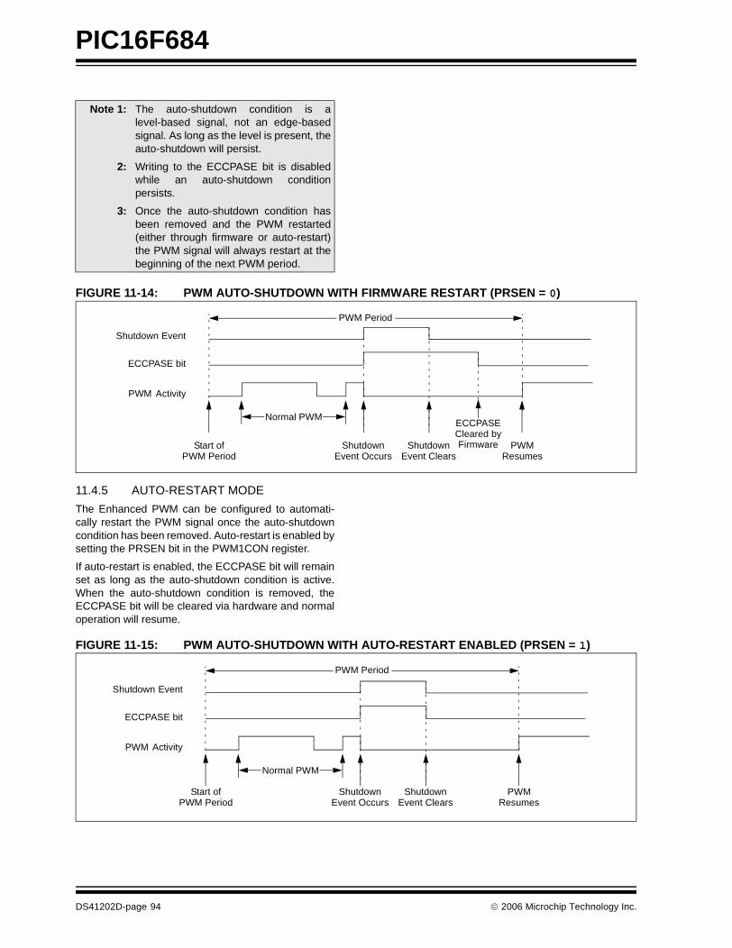
PIC16F684
FIGURE 11-14: PWM AUTO-SHUTDOWN WITH FIRMWARE RESTART (PRSEN = 0)
11.4.5 AUTO-RESTART MODE
The Enhanced PWM can be configured to automati-cally restart the PWM signal once the auto-shutdowncondition has been removed. Auto-restart is enabled bysetting the PRSEN bit in the PWM1CON register.
If auto-restart is enabled, the ECCPASE bit will remainset as long as the auto-shutdown condition is active.When the auto-shutdown condition is removed, theECCPASE bit will be cleared via hardware and normaloperation will resume.
FIGURE 11-15: PWM AUTO-SHUTDOWN WITH AUTO-RESTART ENABLED (PRSEN = 1)
Note 1: The auto-shutdown condition is alevel-based signal, not an edge-basedsignal. As long as the level is present, theauto-shutdown will persist.
2: Writing to the ECCPASE bit is disabledwhile an auto-shutdown conditionpersists.
3: Once the auto-shutdown condition hasbeen removed and the PWM restarted(either through firmware or auto-restart)the PWM signal will always restart at thebeginning of the next PWM period.
Shutdown
PWM
ECCPASE bit
Activity
Event
ShutdownEvent Occurs
ShutdownEvent Clears
PWMResumes
Normal PWM
Start ofPWM Period
ECCPASECleared byFirmware
PWM Period
Shutdown
PWM
ECCPASE bit
Activity
Event
ShutdownEvent Occurs
ShutdownEvent Clears
PWMResumes
Normal PWM
Start ofPWM Period
PWM Period
DS41202D-page 94 © 2006 Microchip Technology Inc.
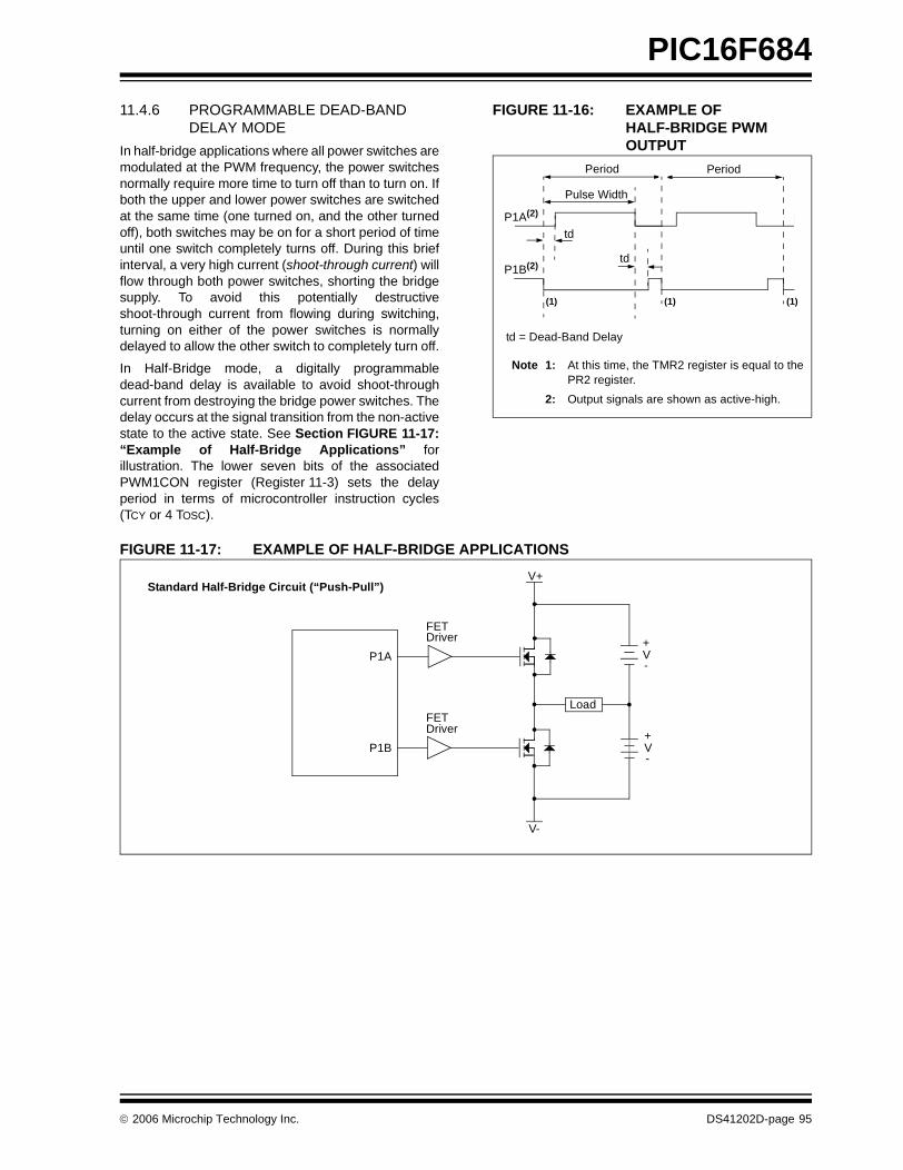
PIC16F684
11.4.6 PROGRAMMABLE DEAD-BAND DELAY MODE
In half-bridge applications where all power switches aremodulated at the PWM frequency, the power switchesnormally require more time to turn off than to turn on. Ifboth the upper and lower power switches are switchedat the same time (one turned on, and the other turnedoff), both switches may be on for a short period of timeuntil one switch completely turns off. During this briefinterval, a very high current (shoot-through current) willflow through both power switches, shorting the bridgesupply. To avoid this potentially destructiveshoot-through current from flowing during switching,turning on either of the power switches is normallydelayed to allow the other switch to completely turn off.
In Half-Bridge mode, a digitally programmabledead-band delay is available to avoid shoot-throughcurrent from destroying the bridge power switches. Thedelay occurs at the signal transition from the non-activestate to the active state. See Section FIGURE 11-17:“Example of Half-Bridge Applications” forillustration. The lower seven bits of the associatedPWM1CON register (Register 11-3) sets the delayperiod in terms of microcontroller instruction cycles(TCY or 4 TOSC).
FIGURE 11-16: EXAMPLE OF HALF-BRIDGE PWM OUTPUT
FIGURE 11-17: EXAMPLE OF HALF-BRIDGE APPLICATIONS
Period
Pulse Width
td
td
(1)
P1A(2)
P1B(2)
td = Dead-Band Delay
Period
(1) (1)
Note 1: At this time, the TMR2 register is equal to thePR2 register.
2: Output signals are shown as active-high.
P1A
P1B
FETDriver
FETDriver
V+
V-
Load
+V-
+V-
Standard Half-Bridge Circuit (“Push-Pull”)
© 2006 Microchip Technology Inc. DS41202D-page 95
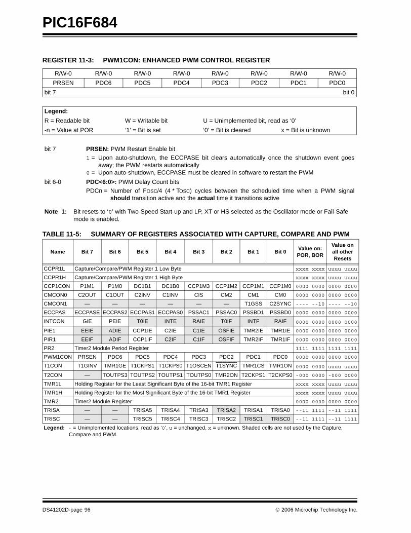
PIC16F684
TABLE 11-5: SUMMARY OF REGISTERS ASSOCIATED WITH CAPTURE, COMPARE AND PWM
REGISTER 11-3: PWM1CON: ENHANCED PWM CONTROL REGISTER
R/W-0 R/W-0 R/W-0 R/W-0 R/W-0 R/W-0 R/W-0 R/W-0
PRSEN PDC6 PDC5 PDC4 PDC3 PDC2 PDC1 PDC0
bit 7 bit 0
Legend:
R = Readable bit W = Writable bit U = Unimplemented bit, read as ‘0’
-n = Value at POR ‘1’ = Bit is set ‘0’ = Bit is cleared x = Bit is unknown
bit 7 PRSEN: PWM Restart Enable bit1 = Upon auto-shutdown, the ECCPASE bit clears automatically once the shutdown event goes
away; the PWM restarts automatically0 = Upon auto-shutdown, ECCPASE must be cleared in software to restart the PWM
bit 6-0 PDC<6:0>: PWM Delay Count bits
PDCn = Number of FOSC/4 (4 * TOSC) cycles between the scheduled time when a PWM signalshould transition active and the actual time it transitions active
Note 1: Bit resets to ‘0’ with Two-Speed Start-up and LP, XT or HS selected as the Oscillator mode or Fail-Safe mode is enabled.
Name Bit 7 Bit 6 Bit 5 Bit 4 Bit 3 Bit 2 Bit 1 Bit 0Value on:POR, BOR
Value onall otherResets
CCPR1L Capture/Compare/PWM Register 1 Low Byte xxxx xxxx uuuu uuuu
CCPR1H Capture/Compare/PWM Register 1 High Byte xxxx xxxx uuuu uuuu
CCP1CON P1M1 P1M0 DC1B1 DC1B0 CCP1M3 CCP1M2 CCP1M1 CCP1M0 0000 0000 0000 0000
CMCON0 C2OUT C1OUT C2INV C1INV CIS CM2 CM1 CM0 0000 0000 0000 0000
CMCON1 — — — — — — T1GSS C2SYNC ---- --10 ---- --10
ECCPAS ECCPASE ECCPAS2 ECCPAS1 ECCPAS0 PSSAC1 PSSAC0 PSSBD1 PSSBD0 0000 0000 0000 0000
INTCON GIE PEIE T0IE INTE RAIE T0IF INTF RAIF 0000 0000 0000 0000
PIE1 EEIE ADIE CCP1IE C2IE C1IE OSFIE TMR2IE TMR1IE 0000 0000 0000 0000
PIR1 EEIF ADIF CCP1IF C2IF C1IF OSFIF TMR2IF TMR1IF 0000 0000 0000 0000
PR2 Timer2 Module Period Register 1111 1111 1111 1111
PWM1CON PRSEN PDC6 PDC5 PDC4 PDC3 PDC2 PDC1 PDC0 0000 0000 0000 0000
T1CON T1GINV TMR1GE T1CKPS1 T1CKPS0 T1OSCEN T1SYNC TMR1CS TMR1ON 0000 0000 uuuu uuuu
T2CON — TOUTPS3 TOUTPS2 TOUTPS1 TOUTPS0 TMR2ON T2CKPS1 T2CKPS0 -000 0000 -000 0000
TMR1L Holding Register for the Least Significant Byte of the 16-bit TMR1 Register xxxx xxxx uuuu uuuu
TMR1H Holding Register for the Most Significant Byte of the 16-bit TMR1 Register xxxx xxxx uuuu uuuu
TMR2 Timer2 Module Register 0000 0000 0000 0000
TRISA — — TRISA5 TRISA4 TRISA3 TRISA2 TRISA1 TRISA0 --11 1111 --11 1111
TRISC — — TRISC5 TRISC4 TRISC3 TRISC2 TRISC1 TRISC0 --11 1111 --11 1111
Legend: - = Unimplemented locations, read as ‘0’, u = unchanged, x = unknown. Shaded cells are not used by the Capture, Compare and PWM.
DS41202D-page 96 © 2006 Microchip Technology Inc.
PIC16F684
12.0 SPECIAL FEATURES OF THE CPU
The PIC16F684 has a host of features intended tomaximize system reliability, minimize cost throughelimination of external components, provide powersaving features and offer code protection.
These features are:
• Reset
- Power-on Reset (POR)- Power-up Timer (PWRT)- Oscillator Start-up Timer (OST)
- Brown-out Reset (BOR)• Interrupts• Watchdog Timer (WDT)
• Oscillator selection• Sleep• Code protection
• ID Locations• In-Circuit Serial Programming
The PIC16F684 has two timers that offer necessarydelays on power-up. One is the Oscillator Start-upTimer (OST), intended to keep the chip in Reset untilthe crystal oscillator is stable. The other is thePower-up Timer (PWRT), which provides a fixed delayof 64 ms (nominal) on power-up only, designed to keepthe part in Reset while the power supply stabilizes.There is also circuitry to reset the device if a brown-outoccurs, which can use the Power-up Timer to provideat least a 64 ms Reset. With these threefunctions-on-chip, most applications need no externalReset circuitry.
The Sleep mode is designed to offer a very low-currentPower-Down mode. The user can wake-up from Sleepthrough:
• External Reset• Watchdog Timer Wake-up• An interrupt
Several oscillator options are also made available toallow the part to fit the application. The INTOSC optionsaves system cost while the LP crystal option savespower. A set of configuration bits are used to selectvarious options (see Register 12-1).
12.1 Configuration Bits
The Configuration bits can be programmed (read as‘0’), or left unprogrammed (read as ‘1’) to select variousdevice configurations as shown in Register 12-1.These bits are mapped in program memory location2007h.
Note: Address 2007h is beyond the user programmemory space. It belongs to the specialconfiguration memory space(2000h-3FFFh), which can be accessedonly during programming. See“PIC12F6XX/16F6XX Memory Program-ming Specification” (DS41204) for moreinformation.
© 2006 Microchip Technology Inc. DS41202D-page 97
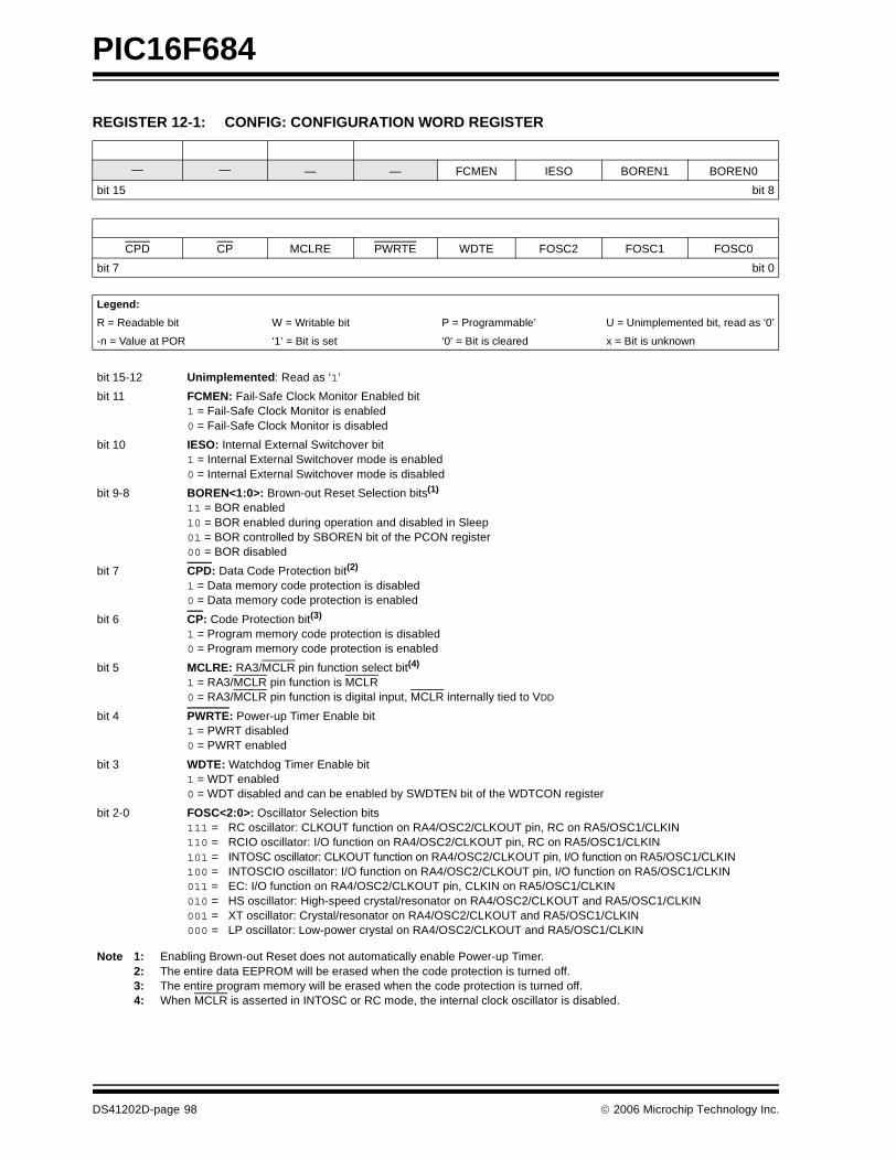
PIC16F684
REGISTER 12-1: CONFIG: CONFIGURATION WORD REGISTER
— — — — FCMEN IESO BOREN1 BOREN0
bit 15 bit 8
CPD CP MCLRE PWRTE WDTE FOSC2 FOSC1 FOSC0
bit 7 bit 0
Legend:
R = Readable bit W = Writable bit P = Programmable’ U = Unimplemented bit, read as ‘0’
-n = Value at POR ‘1’ = Bit is set ‘0’ = Bit is cleared x = Bit is unknown
bit 15-12 Unimplemented: Read as ‘1’
bit 11 FCMEN: Fail-Safe Clock Monitor Enabled bit1 = Fail-Safe Clock Monitor is enabled0 = Fail-Safe Clock Monitor is disabled
bit 10 IESO: Internal External Switchover bit1 = Internal External Switchover mode is enabled0 = Internal External Switchover mode is disabled
bit 9-8 BOREN<1:0>: Brown-out Reset Selection bits(1)
11 = BOR enabled10 = BOR enabled during operation and disabled in Sleep01 = BOR controlled by SBOREN bit of the PCON register00 = BOR disabled
bit 7 CPD: Data Code Protection bit(2)
1 = Data memory code protection is disabled0 = Data memory code protection is enabled
bit 6 CP: Code Protection bit(3)
1 = Program memory code protection is disabled0 = Program memory code protection is enabled
bit 5 MCLRE: RA3/MCLR pin function select bit(4)
1 = RA3/MCLR pin function is MCLR0 = RA3/MCLR pin function is digital input, MCLR internally tied to VDD
bit 4 PWRTE: Power-up Timer Enable bit1 = PWRT disabled0 = PWRT enabled
bit 3 WDTE: Watchdog Timer Enable bit1 = WDT enabled0 = WDT disabled and can be enabled by SWDTEN bit of the WDTCON register
bit 2-0 FOSC<2:0>: Oscillator Selection bits111 = RC oscillator: CLKOUT function on RA4/OSC2/CLKOUT pin, RC on RA5/OSC1/CLKIN110 = RCIO oscillator: I/O function on RA4/OSC2/CLKOUT pin, RC on RA5/OSC1/CLKIN101 = INTOSC oscillator: CLKOUT function on RA4/OSC2/CLKOUT pin, I/O function on RA5/OSC1/CLKIN100 = INTOSCIO oscillator: I/O function on RA4/OSC2/CLKOUT pin, I/O function on RA5/OSC1/CLKIN011 = EC: I/O function on RA4/OSC2/CLKOUT pin, CLKIN on RA5/OSC1/CLKIN010 = HS oscillator: High-speed crystal/resonator on RA4/OSC2/CLKOUT and RA5/OSC1/CLKIN001 = XT oscillator: Crystal/resonator on RA4/OSC2/CLKOUT and RA5/OSC1/CLKIN000 = LP oscillator: Low-power crystal on RA4/OSC2/CLKOUT and RA5/OSC1/CLKIN
Note 1: Enabling Brown-out Reset does not automatically enable Power-up Timer.2: The entire data EEPROM will be erased when the code protection is turned off.3: The entire program memory will be erased when the code protection is turned off.4: When MCLR is asserted in INTOSC or RC mode, the internal clock oscillator is disabled.
DS41202D-page 98 © 2006 Microchip Technology Inc.
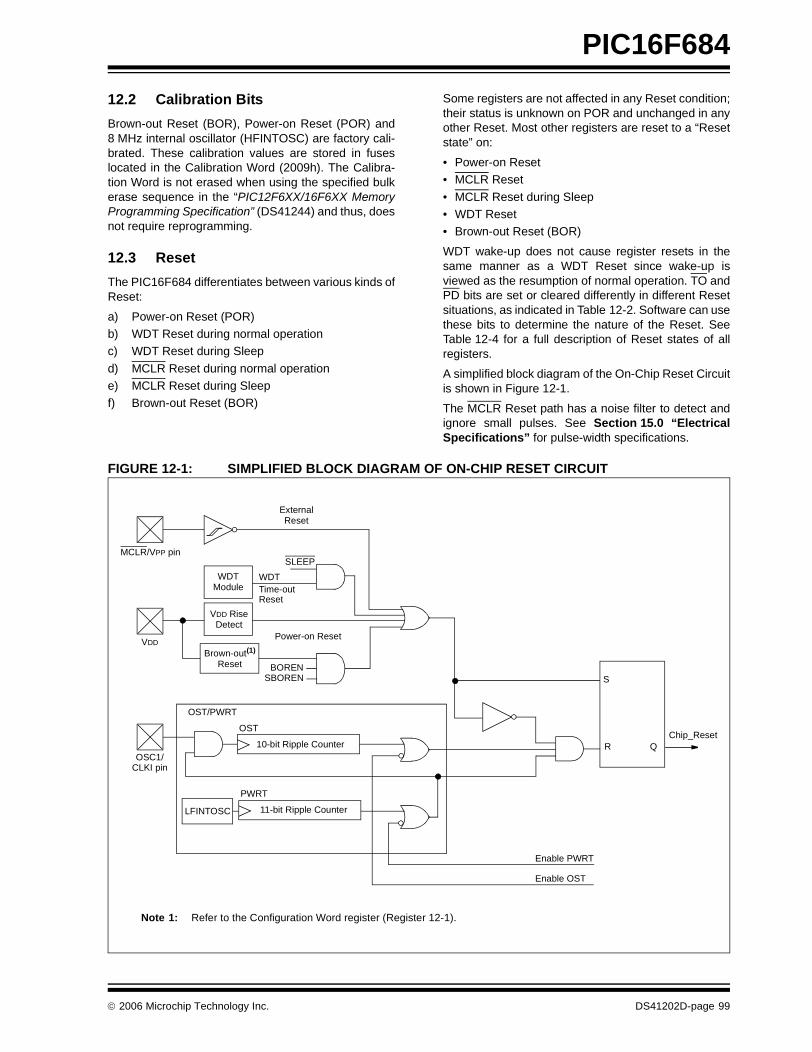
PIC16F684
12.2 Calibration Bits
Brown-out Reset (BOR), Power-on Reset (POR) and8 MHz internal oscillator (HFINTOSC) are factory cali-brated. These calibration values are stored in fuseslocated in the Calibration Word (2009h). The Calibra-tion Word is not erased when using the specified bulkerase sequence in the “PIC12F6XX/16F6XX MemoryProgramming Specification” (DS41244) and thus, doesnot require reprogramming.
12.3 Reset
The PIC16F684 differentiates between various kinds ofReset:
a) Power-on Reset (POR) b) WDT Reset during normal operationc) WDT Reset during Sleep
d) MCLR Reset during normal operatione) MCLR Reset during Sleepf) Brown-out Reset (BOR)
Some registers are not affected in any Reset condition;their status is unknown on POR and unchanged in anyother Reset. Most other registers are reset to a “Resetstate” on:
• Power-on Reset• MCLR Reset
• MCLR Reset during Sleep• WDT Reset• Brown-out Reset (BOR)
WDT wake-up does not cause register resets in thesame manner as a WDT Reset since wake-up isviewed as the resumption of normal operation. TO andPD bits are set or cleared differently in different Resetsituations, as indicated in Table 12-2. Software can usethese bits to determine the nature of the Reset. SeeTable 12-4 for a full description of Reset states of allregisters.
A simplified block diagram of the On-Chip Reset Circuitis shown in Figure 12-1.
The MCLR Reset path has a noise filter to detect andignore small pulses. See Section 15.0 “ElectricalSpecifications” for pulse-width specifications.
FIGURE 12-1: SIMPLIFIED BLOCK DIAGRAM OF ON-CHIP RESET CIRCUIT
S
R Q
ExternalReset
MCLR/VPP pin
VDD
OSC1/
WDTModule
VDD RiseDetect
OST/PWRT
LFINTOSC
WDTTime-out
Power-on Reset
OST
10-bit Ripple Counter
PWRT
Chip_Reset
11-bit Ripple Counter
Reset
Enable OST
Enable PWRT
SLEEP
Brown-out(1)
Reset
SBORENBOREN
CLKI pin
Note 1: Refer to the Configuration Word register (Register 12-1).
© 2006 Microchip Technology Inc. DS41202D-page 99
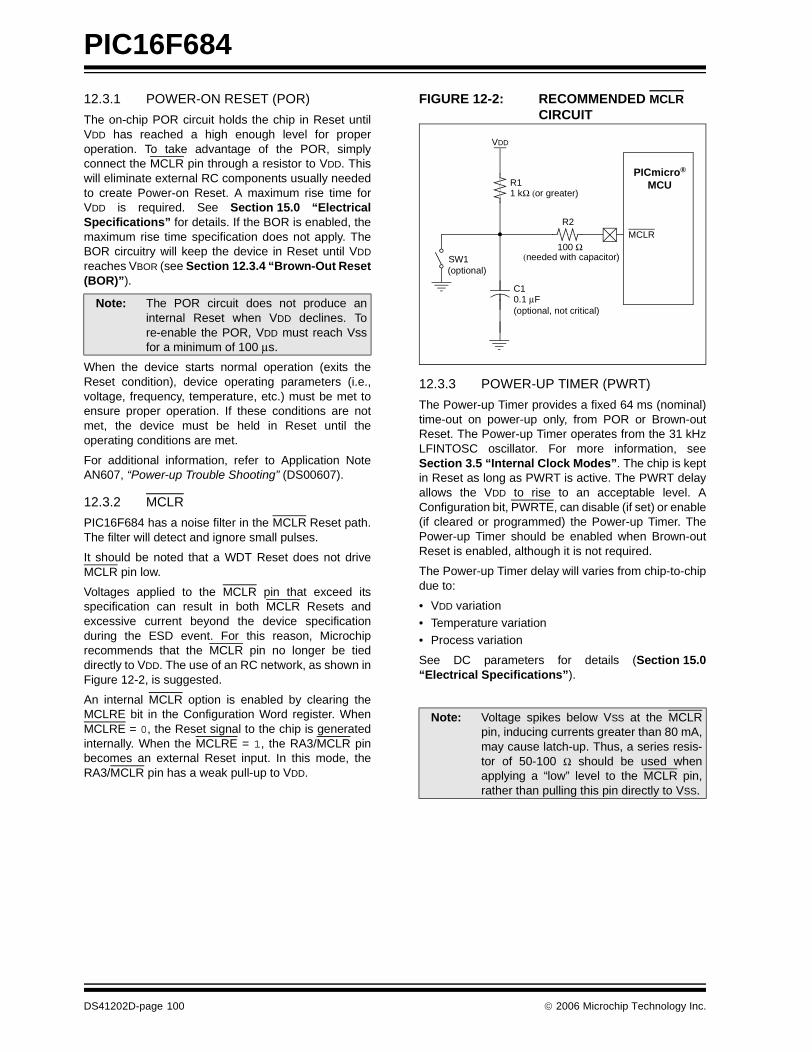
PIC16F684
12.3.1 POWER-ON RESET (POR)
The on-chip POR circuit holds the chip in Reset untilVDD has reached a high enough level for properoperation. To take advantage of the POR, simplyconnect the MCLR pin through a resistor to VDD. Thiswill eliminate external RC components usually neededto create Power-on Reset. A maximum rise time forVDD is required. See Section 15.0 “ElectricalSpecifications” for details. If the BOR is enabled, themaximum rise time specification does not apply. TheBOR circuitry will keep the device in Reset until VDD
reaches VBOR (see Section 12.3.4 “Brown-Out Reset(BOR)”).
When the device starts normal operation (exits theReset condition), device operating parameters (i.e.,voltage, frequency, temperature, etc.) must be met toensure proper operation. If these conditions are notmet, the device must be held in Reset until theoperating conditions are met.
For additional information, refer to Application NoteAN607, “Power-up Trouble Shooting” (DS00607).
12.3.2 MCLR
PIC16F684 has a noise filter in the MCLR Reset path.The filter will detect and ignore small pulses.
It should be noted that a WDT Reset does not driveMCLR pin low.
Voltages applied to the MCLR pin that exceed itsspecification can result in both MCLR Resets andexcessive current beyond the device specificationduring the ESD event. For this reason, Microchiprecommends that the MCLR pin no longer be tieddirectly to VDD. The use of an RC network, as shown inFigure 12-2, is suggested.
An internal MCLR option is enabled by clearing theMCLRE bit in the Configuration Word register. WhenMCLRE = 0, the Reset signal to the chip is generatedinternally. When the MCLRE = 1, the RA3/MCLR pinbecomes an external Reset input. In this mode, theRA3/MCLR pin has a weak pull-up to VDD.
FIGURE 12-2: RECOMMENDED MCLR CIRCUIT
12.3.3 POWER-UP TIMER (PWRT)
The Power-up Timer provides a fixed 64 ms (nominal)time-out on power-up only, from POR or Brown-outReset. The Power-up Timer operates from the 31 kHzLFINTOSC oscillator. For more information, seeSection 3.5 “Internal Clock Modes”. The chip is keptin Reset as long as PWRT is active. The PWRT delayallows the VDD to rise to an acceptable level. AConfiguration bit, PWRTE, can disable (if set) or enable(if cleared or programmed) the Power-up Timer. ThePower-up Timer should be enabled when Brown-outReset is enabled, although it is not required.
The Power-up Timer delay will varies from chip-to-chipdue to:
• VDD variation• Temperature variation• Process variation
See DC parameters for details (Section 15.0“Electrical Specifications”).
Note: The POR circuit does not produce aninternal Reset when VDD declines. Tore-enable the POR, VDD must reach Vssfor a minimum of 100 μs.
Note: Voltage spikes below VSS at the MCLRpin, inducing currents greater than 80 mA,may cause latch-up. Thus, a series resis-tor of 50-100 Ω should be used whenapplying a “low” level to the MCLR pin,rather than pulling this pin directly to VSS.
VDD
PICmicro®
MCLR
R11 kΩ (or greater)
C10.1 μF(optional, not critical)
R2
100 Ω(needed with capacitor)SW1
(optional)
MCU
DS41202D-page 100 © 2006 Microchip Technology Inc.
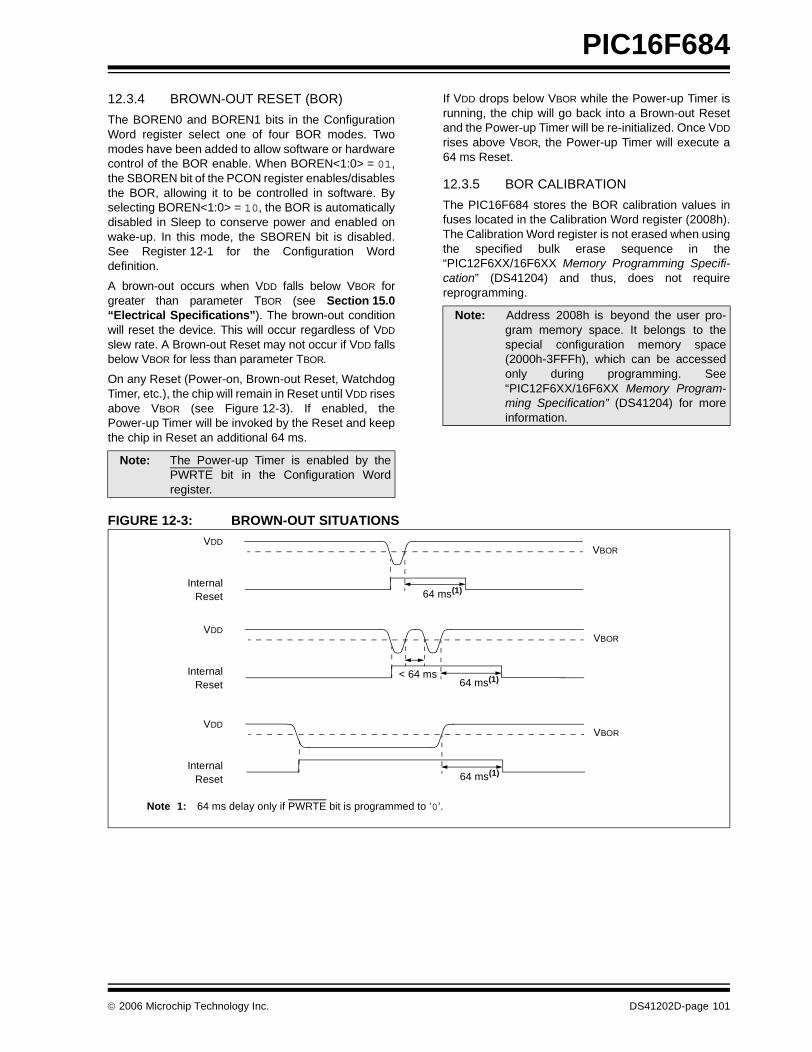
PIC16F684
12.3.4 BROWN-OUT RESET (BOR)
The BOREN0 and BOREN1 bits in the ConfigurationWord register select one of four BOR modes. Twomodes have been added to allow software or hardwarecontrol of the BOR enable. When BOREN<1:0> = 01,the SBOREN bit of the PCON register enables/disablesthe BOR, allowing it to be controlled in software. Byselecting BOREN<1:0> = 10, the BOR is automaticallydisabled in Sleep to conserve power and enabled onwake-up. In this mode, the SBOREN bit is disabled.See Register 12-1 for the Configuration Worddefinition.
A brown-out occurs when VDD falls below VBOR forgreater than parameter TBOR (see Section 15.0“Electrical Specifications”). The brown-out conditionwill reset the device. This will occur regardless of VDD
slew rate. A Brown-out Reset may not occur if VDD fallsbelow VBOR for less than parameter TBOR.
On any Reset (Power-on, Brown-out Reset, WatchdogTimer, etc.), the chip will remain in Reset until VDD risesabove VBOR (see Figure 12-3). If enabled, thePower-up Timer will be invoked by the Reset and keepthe chip in Reset an additional 64 ms.
If VDD drops below VBOR while the Power-up Timer isrunning, the chip will go back into a Brown-out Resetand the Power-up Timer will be re-initialized. Once VDD
rises above VBOR, the Power-up Timer will execute a64 ms Reset.
12.3.5 BOR CALIBRATION
The PIC16F684 stores the BOR calibration values infuses located in the Calibration Word register (2008h).The Calibration Word register is not erased when usingthe specified bulk erase sequence in the“PIC12F6XX/16F6XX Memory Programming Specifi-cation” (DS41204) and thus, does not requirereprogramming.
FIGURE 12-3: BROWN-OUT SITUATIONS
Note: The Power-up Timer is enabled by thePWRTE bit in the Configuration Wordregister.
Note: Address 2008h is beyond the user pro-gram memory space. It belongs to thespecial configuration memory space(2000h-3FFFh), which can be accessedonly during programming. See“PIC12F6XX/16F6XX Memory Program-ming Specification” (DS41204) for moreinformation.
64 ms(1)
VBOR VDD
InternalReset
VBOR VDD
InternalReset 64 ms(1)< 64 ms
64 ms(1)
VBOR VDD
InternalReset
Note 1: 64 ms delay only if PWRTE bit is programmed to ‘0’.
© 2006 Microchip Technology Inc. DS41202D-page 101
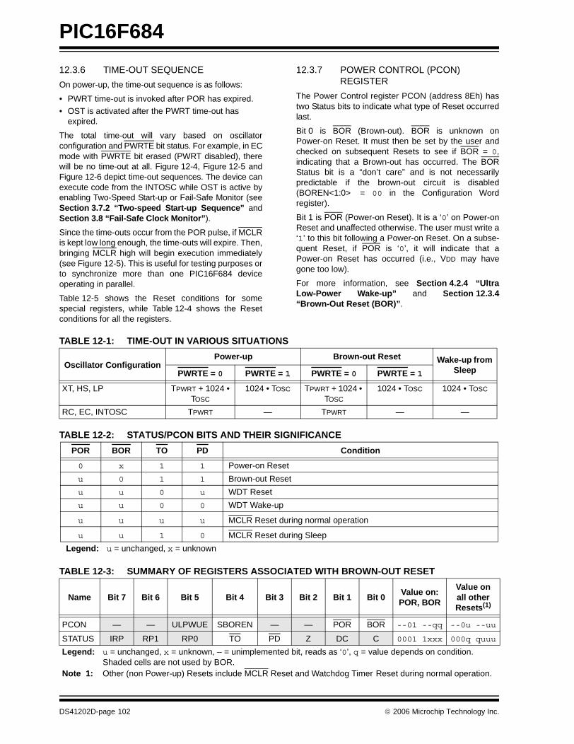
PIC16F684
12.3.6 TIME-OUT SEQUENCE
On power-up, the time-out sequence is as follows:
• PWRT time-out is invoked after POR has expired.
• OST is activated after the PWRT time-out has expired.
The total time-out will vary based on oscillatorconfiguration and PWRTE bit status. For example, in ECmode with PWRTE bit erased (PWRT disabled), therewill be no time-out at all. Figure 12-4, Figure 12-5 andFigure 12-6 depict time-out sequences. The device canexecute code from the INTOSC while OST is active byenabling Two-Speed Start-up or Fail-Safe Monitor (seeSection 3.7.2 “Two-speed Start-up Sequence” andSection 3.8 “Fail-Safe Clock Monitor”).
Since the time-outs occur from the POR pulse, if MCLRis kept low long enough, the time-outs will expire. Then,bringing MCLR high will begin execution immediately(see Figure 12-5). This is useful for testing purposes orto synchronize more than one PIC16F684 deviceoperating in parallel.
Table 12-5 shows the Reset conditions for somespecial registers, while Table 12-4 shows the Resetconditions for all the registers.
12.3.7 POWER CONTROL (PCON) REGISTER
The Power Control register PCON (address 8Eh) hastwo Status bits to indicate what type of Reset occurredlast.
Bit 0 is BOR (Brown-out). BOR is unknown onPower-on Reset. It must then be set by the user andchecked on subsequent Resets to see if BOR = 0,indicating that a Brown-out has occurred. The BORStatus bit is a “don’t care” and is not necessarilypredictable if the brown-out circuit is disabled(BOREN<1:0> = 00 in the Configuration Wordregister).
Bit 1 is POR (Power-on Reset). It is a ‘0’ on Power-onReset and unaffected otherwise. The user must write a‘1’ to this bit following a Power-on Reset. On a subse-quent Reset, if POR is ‘0’, it will indicate that aPower-on Reset has occurred (i.e., VDD may havegone too low).
For more information, see Section 4.2.4 “UltraLow-Power Wake-up” and Section 12.3.4“Brown-Out Reset (BOR)”.
TABLE 12-1: TIME-OUT IN VARIOUS SITUATIONS
TABLE 12-2: STATUS/PCON BITS AND THEIR SIGNIFICANCE
TABLE 12-3: SUMMARY OF REGISTERS ASSOCIATED WITH BROWN-OUT RESET
Oscillator ConfigurationPower-up Brown-out Reset Wake-up from
SleepPWRTE = 0 PWRTE = 1 PWRTE = 0 PWRTE = 1
XT, HS, LP TPWRT + 1024 • TOSC
1024 • TOSC TPWRT + 1024 • TOSC
1024 • TOSC 1024 • TOSC
RC, EC, INTOSC TPWRT — TPWRT — —
POR BOR TO PD Condition
0 x 1 1 Power-on Reset
u 0 1 1 Brown-out Reset
u u 0 u WDT Reset
u u 0 0 WDT Wake-up
u u u u MCLR Reset during normal operation
u u 1 0 MCLR Reset during Sleep
Legend: u = unchanged, x = unknown
Name Bit 7 Bit 6 Bit 5 Bit 4 Bit 3 Bit 2 Bit 1 Bit 0Value on: POR, BOR
Value on all other Resets(1)
PCON — — ULPWUE SBOREN — — POR BOR --01 --qq --0u --uu
STATUS IRP RP1 RP0 TO PD Z DC C 0001 1xxx 000q quuu
Legend: u = unchanged, x = unknown, – = unimplemented bit, reads as ‘0’, q = value depends on condition. Shaded cells are not used by BOR.
Note 1: Other (non Power-up) Resets include MCLR Reset and Watchdog Timer Reset during normal operation.
DS41202D-page 102 © 2006 Microchip Technology Inc.
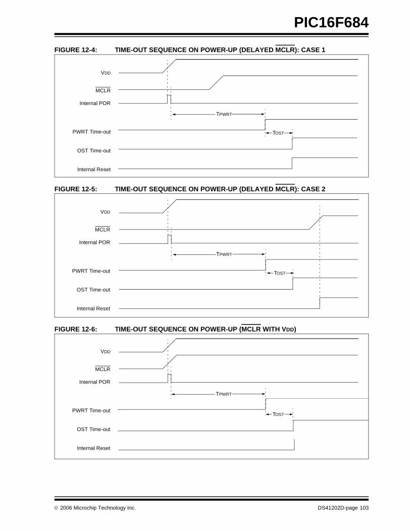
PIC16F684
FIGURE 12-4: TIME-OUT SEQUENCE ON POWER-UP (DELAYED MCLR): CASE 1
FIGURE 12-5: TIME-OUT SEQUENCE ON POWER-UP (DELAYED MCLR): CASE 2
FIGURE 12-6: TIME-OUT SEQUENCE ON POWER-UP (MCLR WITH VDD)
TPWRT
TOST
VDD
MCLR
Internal POR
PWRT Time-out
OST Time-out
Internal Reset
VDD
MCLR
Internal POR
PWRT Time-out
OST Time-out
Internal Reset
TPWRT
TOST
TOST
VDD
MCLR
Internal POR
PWRT Time-out
OST Time-out
Internal Reset
TPWRT
© 2006 Microchip Technology Inc. DS41202D-page 103
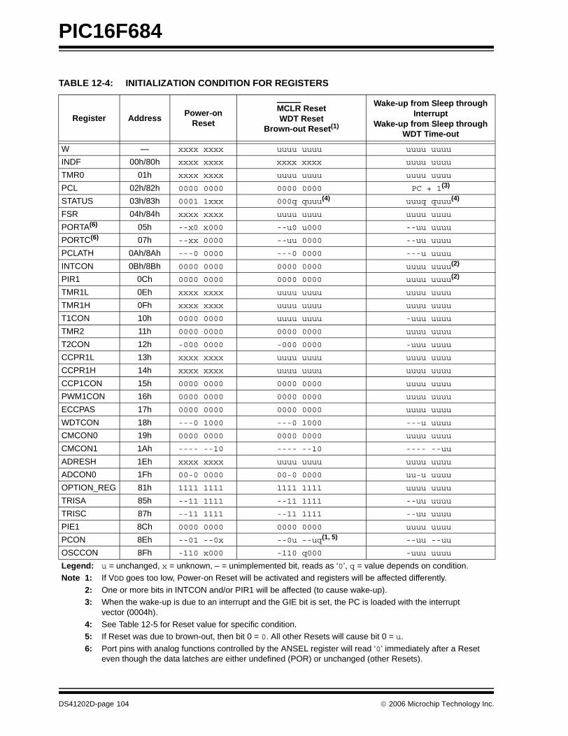
PIC16F684
TABLE 12-4: INITIALIZATION CONDITION FOR REGISTERS
Register AddressPower-on
Reset
MCLR ResetWDT Reset
Brown-out Reset(1)
Wake-up from Sleep through Interrupt
Wake-up from Sleep through WDT Time-out
W — xxxx xxxx uuuu uuuu uuuu uuuu
INDF 00h/80h xxxx xxxx xxxx xxxx uuuu uuuu
TMR0 01h xxxx xxxx uuuu uuuu uuuu uuuu
PCL 02h/82h 0000 0000 0000 0000 PC + 1(3)
STATUS 03h/83h 0001 1xxx 000q quuu(4) uuuq quuu(4)
FSR 04h/84h xxxx xxxx uuuu uuuu uuuu uuuu
PORTA(6) 05h --x0 x000 --u0 u000 --uu uuuu
PORTC(6) 07h --xx 0000 --uu 0000 --uu uuuu
PCLATH 0Ah/8Ah ---0 0000 ---0 0000 ---u uuuu
INTCON 0Bh/8Bh 0000 0000 0000 0000 uuuu uuuu(2)
PIR1 0Ch 0000 0000 0000 0000 uuuu uuuu(2)
TMR1L 0Eh xxxx xxxx uuuu uuuu uuuu uuuu
TMR1H 0Fh xxxx xxxx uuuu uuuu uuuu uuuu
T1CON 10h 0000 0000 uuuu uuuu -uuu uuuu
TMR2 11h 0000 0000 0000 0000 uuuu uuuu
T2CON 12h -000 0000 -000 0000 -uuu uuuu
CCPR1L 13h xxxx xxxx uuuu uuuu uuuu uuuu
CCPR1H 14h xxxx xxxx uuuu uuuu uuuu uuuu
CCP1CON 15h 0000 0000 0000 0000 uuuu uuuu
PWM1CON 16h 0000 0000 0000 0000 uuuu uuuu
ECCPAS 17h 0000 0000 0000 0000 uuuu uuuu
WDTCON 18h ---0 1000 ---0 1000 ---u uuuu
CMCON0 19h 0000 0000 0000 0000 uuuu uuuu
CMCON1 1Ah ---- --10 ---- --10 ---- --uu
ADRESH 1Eh xxxx xxxx uuuu uuuu uuuu uuuu
ADCON0 1Fh 00-0 0000 00-0 0000 uu-u uuuu
OPTION_REG 81h 1111 1111 1111 1111 uuuu uuuu
TRISA 85h --11 1111 --11 1111 --uu uuuu
TRISC 87h --11 1111 --11 1111 --uu uuuu
PIE1 8Ch 0000 0000 0000 0000 uuuu uuuu
PCON 8Eh --01 --0x --0u --uq(1, 5) --uu --uu
OSCCON 8Fh -110 x000 -110 q000 -uuu uuuu
Legend: u = unchanged, x = unknown, – = unimplemented bit, reads as ‘0’, q = value depends on condition.Note 1: If VDD goes too low, Power-on Reset will be activated and registers will be affected differently.
2: One or more bits in INTCON and/or PIR1 will be affected (to cause wake-up).3: When the wake-up is due to an interrupt and the GIE bit is set, the PC is loaded with the interrupt
vector (0004h).4: See Table 12-5 for Reset value for specific condition.5: If Reset was due to brown-out, then bit 0 = 0. All other Resets will cause bit 0 = u.
6: Port pins with analog functions controlled by the ANSEL register will read ‘0’ immediately after a Reset even though the data latches are either undefined (POR) or unchanged (other Resets).
DS41202D-page 104 © 2006 Microchip Technology Inc.
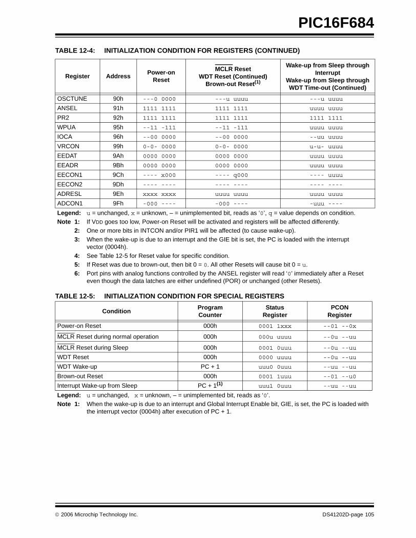
PIC16F684
TABLE 12-5: INITIALIZATION CONDITION FOR SPECIAL REGISTERS
OSCTUNE 90h ---0 0000 ---u uuuu ---u uuuu
ANSEL 91h 1111 1111 1111 1111 uuuu uuuu
PR2 92h 1111 1111 1111 1111 1111 1111
WPUA 95h --11 -111 --11 -111 uuuu uuuu
IOCA 96h --00 0000 --00 0000 --uu uuuu
VRCON 99h 0-0- 0000 0-0- 0000 u-u- uuuu
EEDAT 9Ah 0000 0000 0000 0000 uuuu uuuu
EEADR 9Bh 0000 0000 0000 0000 uuuu uuuu
EECON1 9Ch ---- x000 ---- q000 ---- uuuu
EECON2 9Dh ---- ---- ---- ---- ---- ----
ADRESL 9Eh xxxx xxxx uuuu uuuu uuuu uuuu
ADCON1 9Fh -000 ---- -000 ---- -uuu ----
ConditionProgramCounter
StatusRegister
PCONRegister
Power-on Reset 000h 0001 1xxx --01 --0x
MCLR Reset during normal operation 000h 000u uuuu --0u --uu
MCLR Reset during Sleep 000h 0001 0uuu --0u --uu
WDT Reset 000h 0000 uuuu --0u --uu
WDT Wake-up PC + 1 uuu0 0uuu --uu --uu
Brown-out Reset 000h 0001 1uuu --01 --u0
Interrupt Wake-up from Sleep PC + 1(1) uuu1 0uuu --uu --uu
Legend: u = unchanged, x = unknown, – = unimplemented bit, reads as ‘0’.Note 1: When the wake-up is due to an interrupt and Global Interrupt Enable bit, GIE, is set, the PC is loaded with
the interrupt vector (0004h) after execution of PC + 1.
TABLE 12-4: INITIALIZATION CONDITION FOR REGISTERS (CONTINUED)
Register AddressPower-on
Reset
MCLR ResetWDT Reset (Continued)
Brown-out Reset(1)
Wake-up from Sleep through Interrupt
Wake-up from Sleep through WDT Time-out (Continued)
Legend: u = unchanged, x = unknown, – = unimplemented bit, reads as ‘0’, q = value depends on condition.Note 1: If VDD goes too low, Power-on Reset will be activated and registers will be affected differently.
2: One or more bits in INTCON and/or PIR1 will be affected (to cause wake-up).
3: When the wake-up is due to an interrupt and the GIE bit is set, the PC is loaded with the interrupt vector (0004h).
4: See Table 12-5 for Reset value for specific condition.5: If Reset was due to brown-out, then bit 0 = 0. All other Resets will cause bit 0 = u.6: Port pins with analog functions controlled by the ANSEL register will read ‘0’ immediately after a Reset
even though the data latches are either undefined (POR) or unchanged (other Resets).
© 2006 Microchip Technology Inc. DS41202D-page 105
PIC16F684
12.4 Interrupts
The PIC16F684 has 11 sources of interrupt:
• External Interrupt RA2/INT
• Timer0 Overflow Interrupt• PORTA Change Interrupts• 2 Comparator Interrupts
• A/D Interrupt• Timer1 Overflow Interrupt• Timer2 Match Interrupt
• EEPROM Data Write Interrupt• Fail-Safe Clock Monitor Interrupt• Enhanced CCP Interrupt
The Interrupt Control register (INTCON) and PeripheralInterrupt Request Register 1 (PIR1) record individualinterrupt requests in flag bits. The INTCON registeralso has individual and global interrupt enable bits.
The Global Interrupt Enable bit, GIE of the INTCONregister, enables (if set) all unmasked interrupts, ordisables (if cleared) all interrupts. Individual interruptscan be disabled through their corresponding enablebits in the INTCON register and PIE1 register. GIE iscleared on Reset.
When an interrupt is serviced, the following actionsoccur automatically:
• The GIE is cleared to disable any further interrupt.
• The return address is pushed onto the stack.• The PC is loaded with 0004h.
The Return from Interrupt instruction, RETFIE, exitsthe interrupt routine, as well as sets the GIE bit, whichre-enables unmasked interrupts.
The following interrupt flags are contained in theINTCON register:
• INT Pin Interrupt• PORTA Change Interrupt
• Timer0 Overflow Interrupt
The peripheral interrupt flags are contained in the PIR1register. The corresponding interrupt enable bit iscontained in the PIE1 register.
The following interrupt flags are contained in the PIR1register:
• EEPROM Data Write Interrupt• A/D Interrupt• 2 Comparator Interrupts
• Timer1 Overflow Interrupt• Timer2 Match Interrupt• Fail-Safe Clock Monitor Interrupt
• Enhanced CCP Interrupt
For external interrupt events, such as the INT pin orPORTA change interrupt, the interrupt latency will bethree or four instruction cycles. The exact latencydepends upon when the interrupt event occurs (seeFigure 12-8). The latency is the same for one ortwo-cycle instructions. Once in the Interrupt ServiceRoutine, the source(s) of the interrupt can bedetermined by polling the interrupt flag bits. Theinterrupt flag bit(s) must be cleared in software beforere-enabling interrupts to avoid multiple interruptrequests.
For additional information on Timer1, Timer2,comparators, ADC, data EEPROM or Enhanced CCPmodules, refer to the respective peripheral section.
12.4.1 RA2/INT INTERRUPT
The external interrupt on the RA2/INT pin isedge-triggered; either on the rising edge if the INTEDGbit of the OPTION register is set, or the falling edge, ifthe INTEDG bit is clear. When a valid edge appears onthe RA2/INT pin, the INTF bit of the INTCON register isset. This interrupt can be disabled by clearing the INTEcontrol bit of the INTCON register. The INTF bit mustbe cleared by software in the Interrupt Service Routinebefore re-enabling this interrupt. The RA2/INT interruptcan wake-up the processor from Sleep, if the INTE bitwas set prior to going into Sleep. See Section 12.7“Power-Down Mode (Sleep)” for details on Sleep andFigure 12-10 for timing of wake-up from Sleep throughRA2/INT interrupt.
Note 1: Individual interrupt flag bits are set,regardless of the status of theircorresponding mask bit or the GIE bit.
2: When an instruction that clears the GIEbit is executed, any interrupts that werepending for execution in the next cycleare ignored. The interrupts, which wereignored, are still pending to be servicedwhen the GIE bit is set again.
Note: The ANSEL and CMCON0 registers mustbe initialized to configure an analogchannel as a digital input. Pins configuredas analog inputs will read ‘0’ and cannotgenerate an interrupt.
DS41202D-page 106 © 2006 Microchip Technology Inc.

PIC16F684
12.4.2 TIMER0 INTERRUPT
An overflow (FFh → 00h) in the TMR0 register will setthe T0IF bit of the INTCON register. The interrupt canbe enabled/disabled by setting/clearing T0IE bit of theINTCON register. See Section 5.0 “Timer0 Module”for operation of the Timer0 module.
12.4.3 PORTA INTERRUPT-ON-CHANGE
An input change on PORTA sets the RAIF bit of theINTCON register. The interrupt can beenabled/disabled by setting/clearing the RAIE bit of theINTCON register. Plus, individual pins can beconfigured through the IOCA register.
FIGURE 12-7: INTERRUPT LOGIC
Note: If a change on the I/O pin should occurwhen any PORTA operation is beingexecuted, then the RAIF interrupt flag maynot get set.
TMR1IFTMR1IE
C1IFC1IE
T0IFT0IE
INTFINTERAIF
RAIE
GIE
PEIE
Wake-up (If in Sleep mode)(1)
Interrupt to CPU
EEIEEEIF
ADIFADIE
IOC-RA0IOCA0
IOC-RA1IOCA1
IOC-RA2IOCA2
IOC-RA3IOCA3
IOC-RA4IOCA4
IOC-RA5IOCA5
TMR2IFTMR2IE
CCP1IFCCP1IE
OSFIFOSFIE
C2IFC2IE
Note 1: Some peripherals depend upon the system clock foroperation. Since the system clock is suspended during Sleep, only those peripherals which do not depend upon the system clock will wake the part from Sleep. See Section 12.7.1 “Wake-up from Sleep”.
© 2006 Microchip Technology Inc. DS41202D-page 107
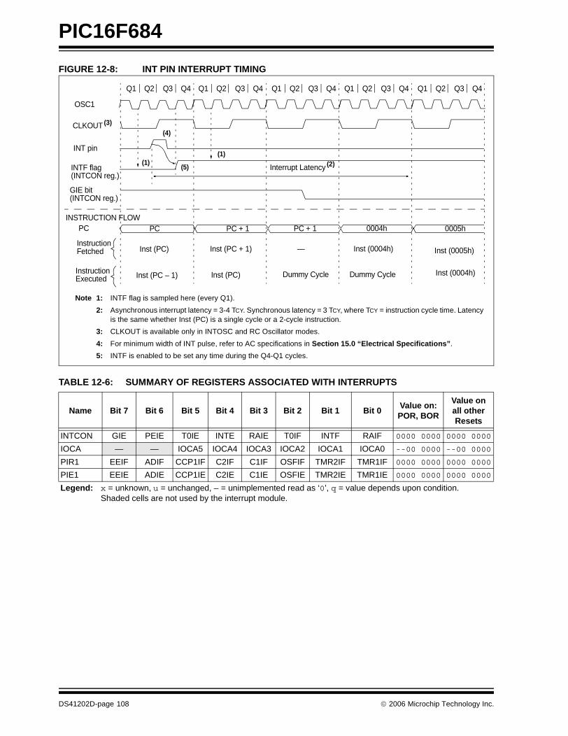
PIC16F684
FIGURE 12-8: INT PIN INTERRUPT TIMING
TABLE 12-6: SUMMARY OF REGISTERS ASSOCIATED WITH INTERRUPTS
Name Bit 7 Bit 6 Bit 5 Bit 4 Bit 3 Bit 2 Bit 1 Bit 0Value on: POR, BOR
Value onall otherResets
INTCON GIE PEIE T0IE INTE RAIE T0IF INTF RAIF 0000 0000 0000 0000
IOCA — — IOCA5 IOCA4 IOCA3 IOCA2 IOCA1 IOCA0 --00 0000 --00 0000
PIR1 EEIF ADIF CCP1IF C2IF C1IF OSFIF TMR2IF TMR1IF 0000 0000 0000 0000
PIE1 EEIE ADIE CCP1IE C2IE C1IE OSFIE TMR2IE TMR1IE 0000 0000 0000 0000
Legend: x = unknown, u = unchanged, – = unimplemented read as ‘0’, q = value depends upon condition. Shaded cells are not used by the interrupt module.
Q2Q1 Q3 Q4 Q2Q1 Q3 Q4 Q2Q1 Q3 Q4 Q2Q1 Q3 Q4 Q2Q1 Q3 Q4
OSC1
CLKOUT
INT pin
INTF flag(INTCON reg.)
GIE bit(INTCON reg.)
INSTRUCTION FLOWPC
InstructionFetched
InstructionExecuted
Interrupt Latency
PC PC + 1 PC + 1 0004h 0005h
Inst (0004h) Inst (0005h)
Dummy Cycle
Inst (PC) Inst (PC + 1)
Inst (PC – 1) Inst (0004h)Dummy CycleInst (PC)
—
Note 1: INTF flag is sampled here (every Q1).
2: Asynchronous interrupt latency = 3-4 TCY. Synchronous latency = 3 TCY, where TCY = instruction cycle time. Latencyis the same whether Inst (PC) is a single cycle or a 2-cycle instruction.
3: CLKOUT is available only in INTOSC and RC Oscillator modes.
4: For minimum width of INT pulse, refer to AC specifications in Section 15.0 “Electrical Specifications”.
5: INTF is enabled to be set any time during the Q4-Q1 cycles.
(1)(2)
(3)(4)
(5)(1)
DS41202D-page 108 © 2006 Microchip Technology Inc.
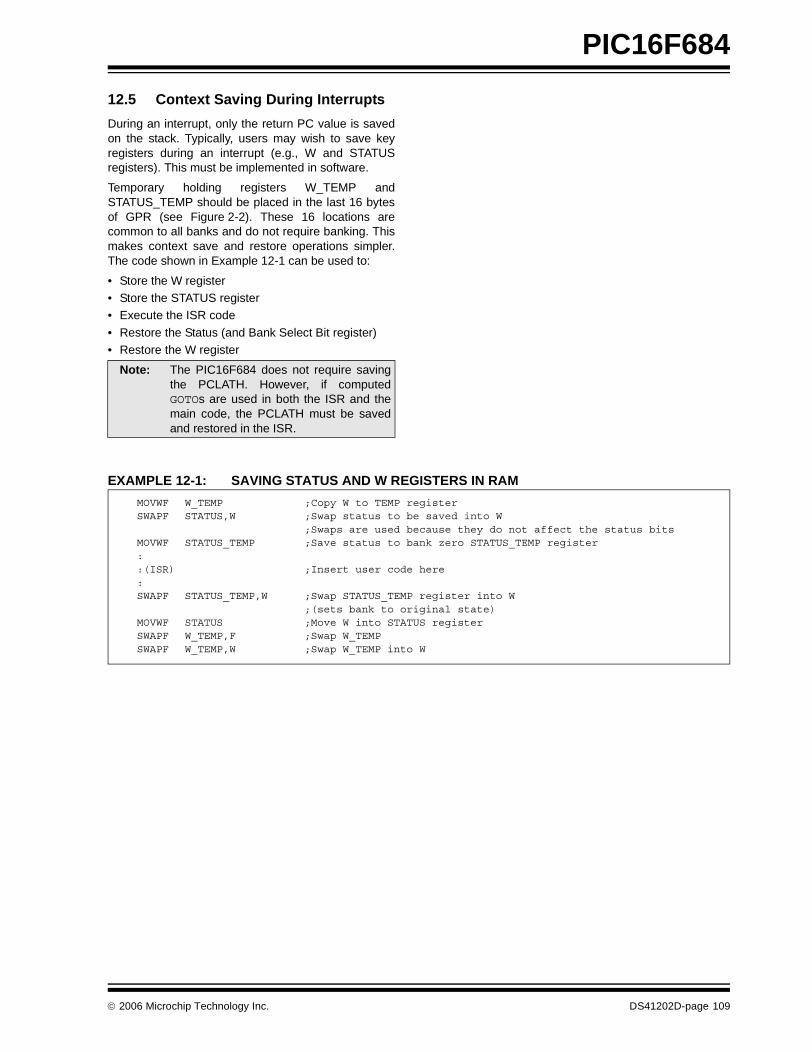
PIC16F684
12.5 Context Saving During Interrupts
During an interrupt, only the return PC value is savedon the stack. Typically, users may wish to save keyregisters during an interrupt (e.g., W and STATUSregisters). This must be implemented in software.
Temporary holding registers W_TEMP andSTATUS_TEMP should be placed in the last 16 bytesof GPR (see Figure 2-2). These 16 locations arecommon to all banks and do not require banking. Thismakes context save and restore operations simpler.The code shown in Example 12-1 can be used to:
• Store the W register• Store the STATUS register• Execute the ISR code
• Restore the Status (and Bank Select Bit register)• Restore the W register
EXAMPLE 12-1: SAVING STATUS AND W REGISTERS IN RAM
Note: The PIC16F684 does not require savingthe PCLATH. However, if computedGOTOs are used in both the ISR and themain code, the PCLATH must be savedand restored in the ISR.
MOVWF W_TEMP ;Copy W to TEMP registerSWAPF STATUS,W ;Swap status to be saved into W
;Swaps are used because they do not affect the status bitsMOVWF STATUS_TEMP ;Save status to bank zero STATUS_TEMP register::(ISR) ;Insert user code here:SWAPF STATUS_TEMP,W ;Swap STATUS_TEMP register into W
;(sets bank to original state)MOVWF STATUS ;Move W into STATUS registerSWAPF W_TEMP,F ;Swap W_TEMPSWAPF W_TEMP,W ;Swap W_TEMP into W
© 2006 Microchip Technology Inc. DS41202D-page 109

PIC16F684
12.6 Watchdog Timer (WDT)
The WDT has the following features:
• Operates from the LFINTOSC (31 kHz)
• Contains a 16-bit prescaler• Shares an 8-bit prescaler with Timer0• Time-out period is from 1 ms to 268 seconds
• Configuration bit and software controlled
WDT is cleared under certain conditions described inTable 12-7.
12.6.1 WDT OSCILLATOR
The WDT derives its time base from the 31 kHzLFINTOSC. The LTS bit of the OSCCON register doesnot reflect that the LFINTOSC is enabled.
The value of WDTCON is ‘---0 1000’ on all Resets.This gives a nominal time base of 17 ms.
12.6.2 WDT CONTROL
The WDTE bit is located in the Configuration Wordregister. When set, the WDT runs continuously.
When the WDTE bit in the Configuration Word registeris set, the SWDTEN bit of the WDTCON register has noeffect. If WDTE is clear, then the SWDTEN bit can beused to enable and disable the WDT. Setting the bit willenable it and clearing the bit will disable it.
The PSA and PS<2:0> bits of the OPTION registerhave the same function as in previous versions of thePIC16F684 Family of microcontrollers. SeeSection 5.0 “Timer0 Module” for more information.
FIGURE 12-9: WATCHDOG TIMER BLOCK DIAGRAM
Note: When the Oscillator Start-up Timer (OST)is invoked, the WDT is held in Reset,because the WDT Ripple Counter is usedby the OST to perform the oscillator delaycount. When the OST count has expired,the WDT will begin counting (if enabled).
TABLE 12-7: WDT STATUS
Conditions WDT
WDTE = 0
ClearedCLRWDT Command
Oscillator Fail Detected
Exit Sleep + System Clock = T1OSC, EXTRC, INTRC, EXTCLK
Exit Sleep + System Clock = XT, HS, LP Cleared until the end of OST
31 kHz
PSA
16-bit WDT Prescaler
From Timer0 Clock Source
Prescaler(1)
8
PS<2:0>
PSA
WDT Time-out
To Timer0WDTPS<3:0>
WDTE from the Configuration Word Register
1
10
0
SWDTEN from WDTCON
LFINTOSC Clock
Note 1: This is the shared Timer0/WDT prescaler. See Section 5.0 “Timer0 Module” for more information.
DS41202D-page 110 © 2006 Microchip Technology Inc.
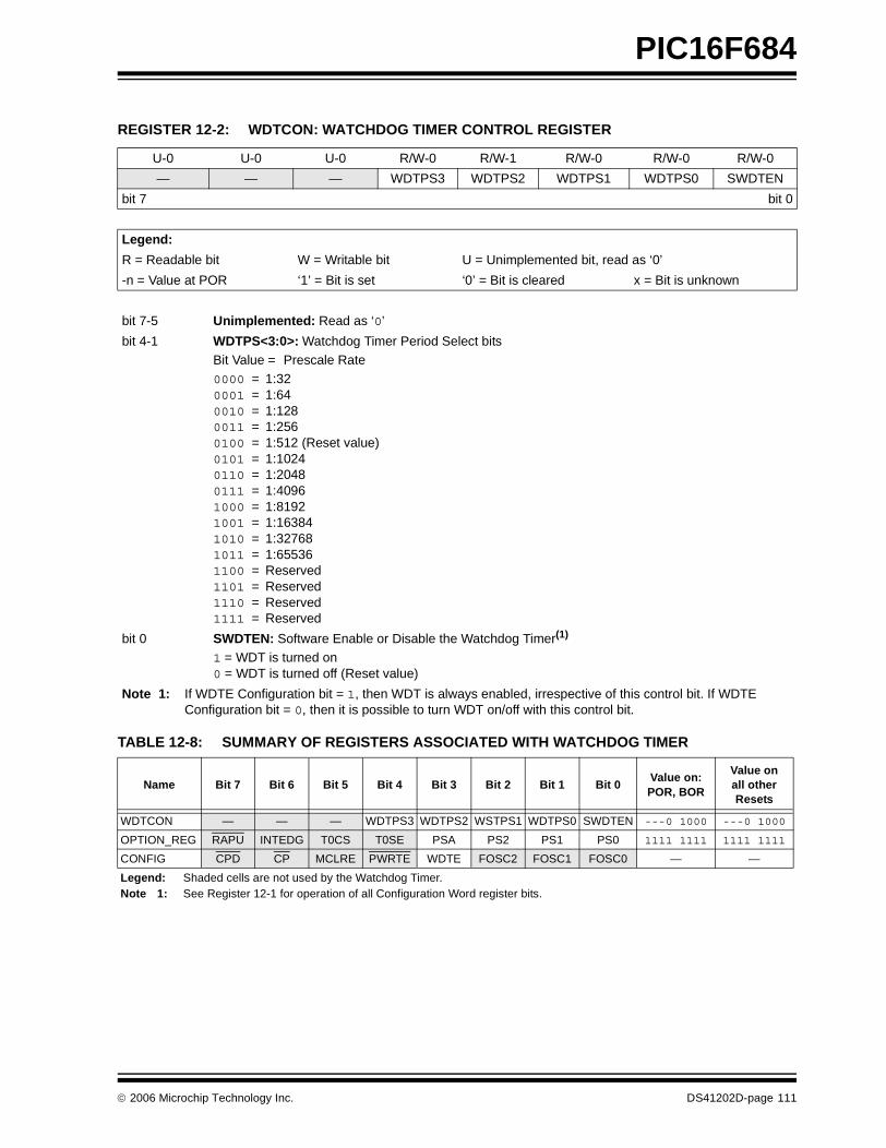
PIC16F684
TABLE 12-8: SUMMARY OF REGISTERS ASSOCIATED WITH WATCHDOG TIMER
REGISTER 12-2: WDTCON: WATCHDOG TIMER CONTROL REGISTER
U-0 U-0 U-0 R/W-0 R/W-1 R/W-0 R/W-0 R/W-0
— — — WDTPS3 WDTPS2 WDTPS1 WDTPS0 SWDTEN
bit 7 bit 0
Legend:
R = Readable bit W = Writable bit U = Unimplemented bit, read as ‘0’
-n = Value at POR ‘1’ = Bit is set ‘0’ = Bit is cleared x = Bit is unknown
bit 7-5 Unimplemented: Read as ‘0’
bit 4-1 WDTPS<3:0>: Watchdog Timer Period Select bitsBit Value = Prescale Rate0000 = 1:320001 = 1:640010 = 1:1280011 = 1:2560100 = 1:512 (Reset value)0101 = 1:10240110 = 1:20480111 = 1:40961000 = 1:81921001 = 1:163841010 = 1:327681011 = 1:655361100 = Reserved1101 = Reserved1110 = Reserved1111 = Reserved
bit 0 SWDTEN: Software Enable or Disable the Watchdog Timer(1)
1 = WDT is turned on0 = WDT is turned off (Reset value)
Note 1: If WDTE Configuration bit = 1, then WDT is always enabled, irrespective of this control bit. If WDTE Configuration bit = 0, then it is possible to turn WDT on/off with this control bit.
Name Bit 7 Bit 6 Bit 5 Bit 4 Bit 3 Bit 2 Bit 1 Bit 0Value on: POR, BOR
Value onall otherResets
WDTCON — — — WDTPS3 WDTPS2 WSTPS1 WDTPS0 SWDTEN ---0 1000 ---0 1000
OPTION_REG RAPU INTEDG T0CS T0SE PSA PS2 PS1 PS0 1111 1111 1111 1111
CONFIG CPD CP MCLRE PWRTE WDTE FOSC2 FOSC1 FOSC0 — —
Legend: Shaded cells are not used by the Watchdog Timer.Note 1: See Register 12-1 for operation of all Configuration Word register bits.
© 2006 Microchip Technology Inc. DS41202D-page 111
PIC16F684
12.7 Power-Down Mode (Sleep)
The Power-down mode is entered by executing aSLEEP instruction.
If the Watchdog Timer is enabled:
• WDT will be cleared but keeps running.• PD bit in the STATUS register is cleared.
• TO bit is set.• Oscillator driver is turned off.• I/O ports maintain the status they had before SLEEP
was executed (driving high, low or high-impedance).
For lowest current consumption in this mode, all I/O pinsshould be either at VDD or VSS, with no external circuitrydrawing current from the I/O pin and the comparatorsand CVREF should be disabled. I/O pins that arehigh-impedance inputs should be pulled high or lowexternally to avoid switching currents caused by floatinginputs. The T0CKI input should also be at VDD or VSS forlowest current consumption. The contribution fromon-chip pull-ups on PORTA should be considered.
The MCLR pin must be at a logic high level.
12.7.1 WAKE-UP FROM SLEEP
The device can wake-up from Sleep through one of thefollowing events:
1. External Reset input on MCLR pin.
2. Watchdog Timer wake-up (if WDT wasenabled).
3. Interrupt from RA2/INT pin, PORTA change or aperipheral interrupt.
The first event will cause a device Reset. The two latterevents are considered a continuation of programexecution. The TO and PD bits in the STATUS registercan be used to determine the cause of a device Reset.The PD bit, which is set on power-up, is cleared whenSleep is invoked. TO bit is cleared if WDT wake-upoccurred.
The following peripheral interrupts can wake the devicefrom Sleep:
1. Timer1 interrupt. Timer1 must be operating asan asynchronous counter.
2. ECCP Capture mode interrupt.3. A/D conversion (when A/D clock source is FRC).
4. EEPROM write operation completion.5. Comparator output changes state.6. Interrupt-on-change.
7. External Interrupt from INT pin.
Other peripherals cannot generate interrupts sinceduring Sleep, no on-chip clocks are present.
When the SLEEP instruction is being executed, the nextinstruction (PC + 1) is prefetched. For the device towake-up through an interrupt event, the correspondinginterrupt enable bit must be set (enabled). Wake-upoccurs regardless of the state of the GIE bit. If the GIEbit is clear (disabled), the device continues execution atthe instruction after the SLEEP instruction. If the GIE bitis set (enabled), the device executes the instructionafter the SLEEP instruction, then branches to the inter-rupt address (0004h). In cases where the execution ofthe instruction following SLEEP is not desirable, theuser should have a NOP after the SLEEP instruction.
The WDT is cleared when the device wakes up fromSleep, regardless of the source of wake-up.
12.7.2 WAKE-UP USING INTERRUPTS
When global interrupts are disabled (GIE cleared) andany interrupt source has both its interrupt enable bitand interrupt flag bit set, one of the following will occur:
• If the interrupt occurs before the execution of a SLEEP instruction, the SLEEP instruction will complete as a NOP. Therefore, the WDT and WDT prescaler and postscaler (if enabled) will not be cleared, the TO bit will not be set and the PD bit will not be cleared.
• If the interrupt occurs during or after the execution of a SLEEP instruction, the device will Immediately wake-up from Sleep. The SLEEP instruction is executed. Therefore, the WDT and WDT prescaler and postscaler (if enabled) will be cleared, the TO bit will be set and the PD bit will be cleared.
Even if the flag bits were checked before executing aSLEEP instruction, it may be possible for flag bits tobecome set before the SLEEP instruction completes. Todetermine whether a SLEEP instruction executed, testthe PD bit. If the PD bit is set, the SLEEP instructionwas executed as a NOP.
To ensure that the WDT is cleared, a CLRWDT instructionshould be executed before a SLEEP instruction. SeeFigure 12-10 for more details.
Note: It should be noted that a Reset generatedby a WDT time-out does not drive MCLRpin low.
Note: If the global interrupts are disabled (GIE iscleared) and any interrupt source has bothits interrupt enable bit and the correspond-ing interrupt flag bits set, the device willimmediately wake-up from Sleep.
DS41202D-page 112 © 2006 Microchip Technology Inc.
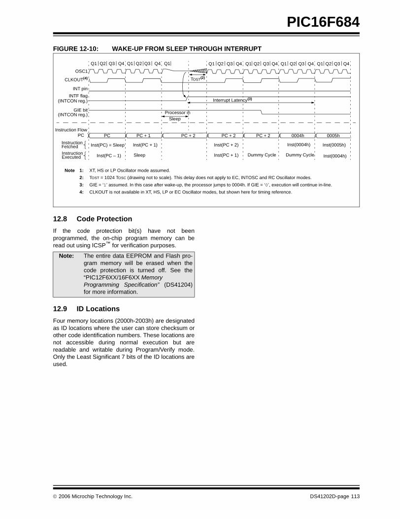
PIC16F684
FIGURE 12-10: WAKE-UP FROM SLEEP THROUGH INTERRUPT
12.8 Code Protection
If the code protection bit(s) have not beenprogrammed, the on-chip program memory can beread out using ICSP™ for verification purposes.
12.9 ID Locations
Four memory locations (2000h-2003h) are designatedas ID locations where the user can store checksum orother code identification numbers. These locations arenot accessible during normal execution but arereadable and writable during Program/Verify mode.Only the Least Significant 7 bits of the ID locations areused.
Q1 Q2 Q3 Q4 Q1 Q2 Q3 Q4 Q1 Q1 Q2 Q3 Q4 Q1 Q2 Q3 Q4 Q1 Q2 Q3 Q4 Q1 Q2 Q3 Q4
OSC1
CLKOUT(4)
INT pin
INTF flag(INTCON reg.)
GIE bit(INTCON reg.)
Instruction FlowPC
InstructionFetchedInstructionExecuted
PC PC + 1 PC + 2
Inst(PC) = Sleep
Inst(PC – 1)
Inst(PC + 1)
Sleep
Processor inSleep
Interrupt Latency(3)
Inst(PC + 2)
Inst(PC + 1)
Inst(0004h) Inst(0005h)
Inst(0004h)Dummy Cycle
PC + 2 0004h 0005h
Dummy Cycle
TOST(2)
PC + 2
Note 1: XT, HS or LP Oscillator mode assumed.
2: TOST = 1024 TOSC (drawing not to scale). This delay does not apply to EC, INTOSC and RC Oscillator modes.
3: GIE = ‘1’ assumed. In this case after wake-up, the processor jumps to 0004h. If GIE = ‘0’, execution will continue in-line.
4: CLKOUT is not available in XT, HS, LP or EC Oscillator modes, but shown here for timing reference.
Note: The entire data EEPROM and Flash pro-gram memory will be erased when thecode protection is turned off. See the“PIC12F6XX/16F6XX MemoryProgramming Specification” (DS41204)for more information.
© 2006 Microchip Technology Inc. DS41202D-page 113
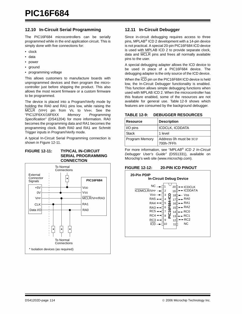
PIC16F684
12.10 In-Circuit Serial Programming
The PIC16F684 microcontrollers can be seriallyprogrammed while in the end application circuit. This issimply done with five connections for:
• clock• data• power
• ground• programming voltage
This allows customers to manufacture boards withunprogrammed devices and then program the micro-controller just before shipping the product. This alsoallows the most recent firmware or a custom firmwareto be programmed.
The device is placed into a Program/Verify mode byholding the RA0 and RA1 pins low, while raising theMCLR (VPP) pin from VIL to VIHH. See the“PIC12F6XX/16F6XX Memory ProgrammingSpecification” (DS41204) for more information. RA0becomes the programming data and RA1 becomes theprogramming clock. Both RA0 and RA1 are SchmittTrigger inputs in Program/Verify mode.
A typical In-Circuit Serial Programming connection isshown in Figure 12-11.
FIGURE 12-11: TYPICAL IN-CIRCUIT SERIAL PROGRAMMING CONNECTION
12.11 In-Circuit Debugger
Since in-circuit debugging requires access to threepins, MPLAB® ICD 2 development with a 14-pin deviceis not practical. A special 20-pin PIC16F684 ICD deviceis used with MPLAB ICD 2 to provide separate clock,data and MCLR pins and frees all normally availablepins to the user.
A special debugging adapter allows the ICD device tobe used in place of a PIC16F684 device. Thedebugging adapter is the only source of the ICD device.
When the ICD pin on the PIC16F684 ICD device is heldlow, the In-Circuit Debugger functionality is enabled.This function allows simple debugging functions whenused with MPLAB ICD 2. When the microcontroller hasthis feature enabled, some of the resources are notavailable for general use. Table 12-9 shows whichfeatures are consumed by the background debugger.
TABLE 12-9: DEBUGGER RESOURCES
For more information, see “MPLAB® ICD 2 In-CircuitDebugger User’s Guide” (DS51331), available onMicrochip’s web site (www.microchip.com).
FIGURE 12-12: 20-PIN ICD PINOUT
ExternalConnectorSignals
To NormalConnections
To NormalConnections
PIC16F684
VDD
VSS
MCLR/VPP/RA3
RA1
RA0
+5V
0V
VPP
CLK
Data I/O
* * *
*
* Isolation devices (as required)
Resource Description
I/O pins ICDCLK, ICDDATA
Stack 1 level
Program Memory Address 0h must be NOP700h-7FFh
20-Pin PDIPP
IC16
F68
4-IC
D
In-Circuit Debug Device
NC
ICDMCLR/VPP
VDD
RA5RA4RA3
ICDCLKICDDATA
VssRA0
ICD NC
RA1RA2
RC5RC4RC3
RC0RC1RC2
1
2
3
45
6
7
8
910
20
19
18
1716
15
14
13
1211
DS41202D-page 114 © 2006 Microchip Technology Inc.
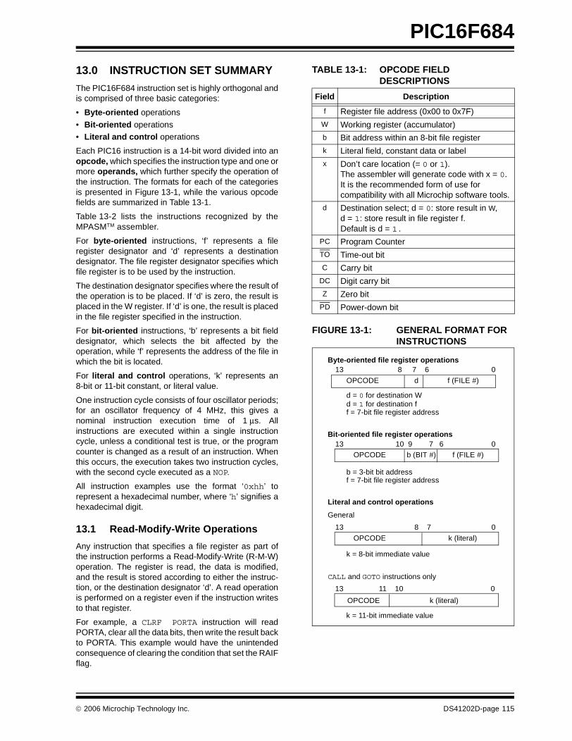
PIC16F684
13.0 INSTRUCTION SET SUMMARY
The PIC16F684 instruction set is highly orthogonal andis comprised of three basic categories:
• Byte-oriented operations
• Bit-oriented operations• Literal and control operations
Each PIC16 instruction is a 14-bit word divided into anopcode, which specifies the instruction type and one ormore operands, which further specify the operation ofthe instruction. The formats for each of the categoriesis presented in Figure 13-1, while the various opcodefields are summarized in Table 13-1.
Table 13-2 lists the instructions recognized by theMPASMTM assembler.
For byte-oriented instructions, ‘f’ represents a fileregister designator and ‘d’ represents a destinationdesignator. The file register designator specifies whichfile register is to be used by the instruction.
The destination designator specifies where the result ofthe operation is to be placed. If ‘d’ is zero, the result isplaced in the W register. If ‘d’ is one, the result is placedin the file register specified in the instruction.
For bit-oriented instructions, ‘b’ represents a bit fielddesignator, which selects the bit affected by theoperation, while ‘f’ represents the address of the file inwhich the bit is located.
For literal and control operations, ‘k’ represents an8-bit or 11-bit constant, or literal value.
One instruction cycle consists of four oscillator periods;for an oscillator frequency of 4 MHz, this gives anominal instruction execution time of 1 μs. Allinstructions are executed within a single instructioncycle, unless a conditional test is true, or the programcounter is changed as a result of an instruction. Whenthis occurs, the execution takes two instruction cycles,with the second cycle executed as a NOP.
All instruction examples use the format ‘0xhh’ torepresent a hexadecimal number, where ‘h’ signifies ahexadecimal digit.
13.1 Read-Modify-Write Operations
Any instruction that specifies a file register as part ofthe instruction performs a Read-Modify-Write (R-M-W)operation. The register is read, the data is modified,and the result is stored according to either the instruc-tion, or the destination designator ‘d’. A read operationis performed on a register even if the instruction writesto that register.
For example, a CLRF PORTA instruction will readPORTA, clear all the data bits, then write the result backto PORTA. This example would have the unintendedconsequence of clearing the condition that set the RAIFflag.
TABLE 13-1: OPCODE FIELD DESCRIPTIONS
FIGURE 13-1: GENERAL FORMAT FOR INSTRUCTIONS
Field Description
f Register file address (0x00 to 0x7F)
W Working register (accumulator)
b Bit address within an 8-bit file register
k Literal field, constant data or label
x Don’t care location (= 0 or 1). The assembler will generate code with x = 0. It is the recommended form of use for compatibility with all Microchip software tools.
d Destination select; d = 0: store result in W,d = 1: store result in file register f. Default is d = 1.
PC Program Counter
TO Time-out bit
C Carry bit
DC Digit carry bit
Z Zero bit
PD Power-down bit
Byte-oriented file register operations13 8 7 6 0
d = 0 for destination W
OPCODE d f (FILE #)
d = 1 for destination ff = 7-bit file register address
Bit-oriented file register operations13 10 9 7 6 0
OPCODE b (BIT #) f (FILE #)
b = 3-bit bit addressf = 7-bit file register address
Literal and control operations
13 8 7 0
OPCODE k (literal)
k = 8-bit immediate value
13 11 10 0
OPCODE k (literal)
k = 11-bit immediate value
General
CALL and GOTO instructions only
© 2006 Microchip Technology Inc. DS41202D-page 115
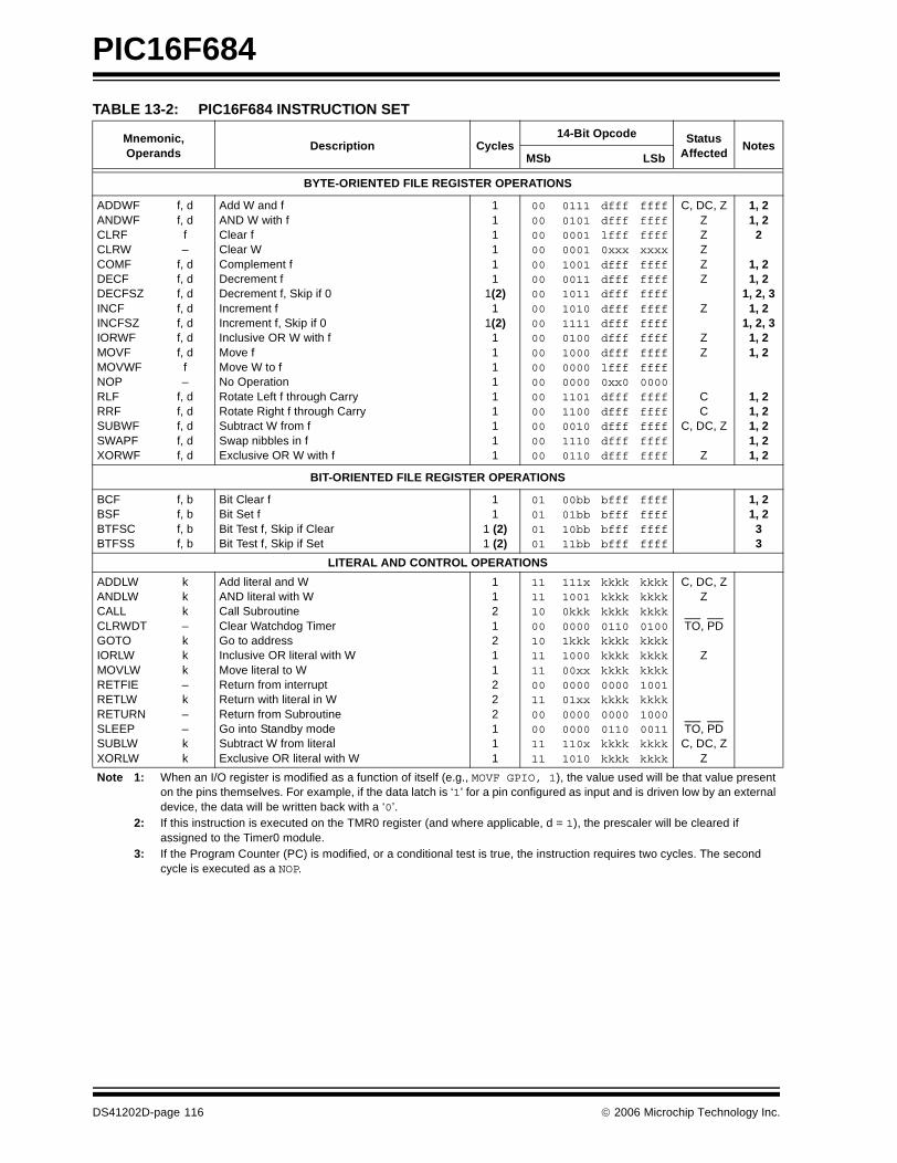
PIC16F684
TABLE 13-2: PIC16F684 INSTRUCTION SET
Mnemonic,Operands
Description Cycles14-Bit Opcode Status
AffectedNotes
MSb LSb
BYTE-ORIENTED FILE REGISTER OPERATIONS
ADDWFANDWFCLRFCLRWCOMFDECFDECFSZINCFINCFSZIORWFMOVFMOVWFNOPRLFRRFSUBWFSWAPFXORWF
f, df, d
f–
f, df, df, df, df, df, df, d
f–
f, df, df, df, df, d
Add W and fAND W with fClear fClear WComplement fDecrement fDecrement f, Skip if 0Increment fIncrement f, Skip if 0Inclusive OR W with fMove fMove W to fNo OperationRotate Left f through CarryRotate Right f through CarrySubtract W from fSwap nibbles in fExclusive OR W with f
111111
1(2)1
1(2)111111111
000000000000000000000000000000000000
011101010001000110010011101110101111010010000000000011011100001011100110
dfffdffflfff0xxxdfffdfffdfffdfffdfffdfffdffflfff0xx0dfffdfffdfffdfffdfff
ffffffffffffxxxxffffffffffffffffffffffffffffffff0000ffffffffffffffffffff
C, DC, ZZZZZZ
Z
ZZ
CC
C, DC, Z
Z
1, 21, 2
2
1, 21, 2
1, 2, 31, 2
1, 2, 31, 21, 2
1, 21, 21, 21, 21, 2
BIT-ORIENTED FILE REGISTER OPERATIONS
BCFBSFBTFSCBTFSS
f, bf, bf, bf, b
Bit Clear fBit Set fBit Test f, Skip if ClearBit Test f, Skip if Set
11
1 (2)1 (2)
01010101
00bb01bb10bb11bb
bfffbfffbfffbfff
ffffffffffffffff
1, 21, 2
33
LITERAL AND CONTROL OPERATIONS
ADDLWANDLWCALLCLRWDTGOTOIORLWMOVLWRETFIERETLWRETURNSLEEPSUBLWXORLW
kkk–kkk–k––kk
Add literal and WAND literal with WCall SubroutineClear Watchdog TimerGo to addressInclusive OR literal with WMove literal to WReturn from interruptReturn with literal in WReturn from SubroutineGo into Standby modeSubtract W from literalExclusive OR literal with W
1121211222111
11111000101111001100001111
111x10010kkk00001kkk100000xx000001xx00000000110x1010
kkkkkkkkkkkk0110kkkkkkkkkkkk0000kkkk00000110kkkkkkkk
kkkkkkkkkkkk0100kkkkkkkkkkkk1001kkkk10000011kkkkkkkk
C, DC, ZZ
TO, PD
Z
TO, PDC, DC, Z
Z
Note 1: When an I/O register is modified as a function of itself (e.g., MOVF GPIO, 1), the value used will be that value present on the pins themselves. For example, if the data latch is ‘1’ for a pin configured as input and is driven low by an external device, the data will be written back with a ‘0’.
2: If this instruction is executed on the TMR0 register (and where applicable, d = 1), the prescaler will be cleared if assigned to the Timer0 module.
3: If the Program Counter (PC) is modified, or a conditional test is true, the instruction requires two cycles. The second cycle is executed as a NOP.
DS41202D-page 116 © 2006 Microchip Technology Inc.
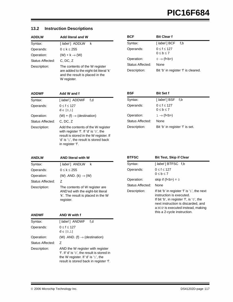
PIC16F684
13.2 Instruction Descriptions
ADDLW Add literal and W
Syntax: [ label ] ADDLW k
Operands: 0 ≤ k ≤ 255
Operation: (W) + k → (W)
Status Affected: C, DC, Z
Description: The contents of the W register are added to the eight-bit literal ‘k’ and the result is placed in the W register.
ADDWF Add W and f
Syntax: [ label ] ADDWF f,d
Operands: 0 ≤ f ≤ 127d ∈ [0,1]
Operation: (W) + (f) → (destination)
Status Affected: C, DC, Z
Description: Add the contents of the W register with register ‘f’. If ‘d’ is ‘0’, the result is stored in the W register. If ‘d’ is ‘1’, the result is stored back in register ‘f’.
ANDLW AND literal with W
Syntax: [ label ] ANDLW k
Operands: 0 ≤ k ≤ 255
Operation: (W) .AND. (k) → (W)
Status Affected: Z
Description: The contents of W register are AND’ed with the eight-bit literal ‘k’. The result is placed in the W register.
ANDWF AND W with f
Syntax: [ label ] ANDWF f,d
Operands: 0 ≤ f ≤ 127d ∈ [0,1]
Operation: (W) .AND. (f) → (destination)
Status Affected: Z
Description: AND the W register with register ‘f’. If ‘d’ is ‘0’, the result is stored in the W register. If ‘d’ is ‘1’, the result is stored back in register ‘f’.
BCF Bit Clear f
Syntax: [ label ] BCF f,b
Operands: 0 ≤ f ≤ 1270 ≤ b ≤ 7
Operation: 0 → (f<b>)
Status Affected: None
Description: Bit ‘b’ in register ‘f’ is cleared.
BSF Bit Set f
Syntax: [ label ] BSF f,b
Operands: 0 ≤ f ≤ 1270 ≤ b ≤ 7
Operation: 1 → (f<b>)
Status Affected: None
Description: Bit ‘b’ in register ‘f’ is set.
BTFSC Bit Test, Skip if Clear
Syntax: [ label ] BTFSC f,b
Operands: 0 ≤ f ≤ 1270 ≤ b ≤ 7
Operation: skip if (f<b>) = 0
Status Affected: None
Description: If bit ‘b’ in register ‘f’ is ‘1’, the next instruction is executed.If bit ‘b’, in register ‘f’, is ‘0’, the next instruction is discarded, and a NOP is executed instead, making this a 2-cycle instruction.
© 2006 Microchip Technology Inc. DS41202D-page 117
PIC16F684
BTFSS Bit Test f, Skip if Set
Syntax: [ label ] BTFSS f,b
Operands: 0 ≤ f ≤ 1270 ≤ b < 7
Operation: skip if (f<b>) = 1
Status Affected: None
Description: If bit ‘b’ in register ‘f’ is ‘0’, the next instruction is executed.If bit ‘b’ is ‘1’, then the nextinstruction is discarded and a NOP is executed instead, making this a 2-cycle instruction.
CALL Call Subroutine
Syntax: [ label ] CALL k
Operands: 0 ≤ k ≤ 2047
Operation: (PC)+ 1→ TOS,k → PC<10:0>,(PCLATH<4:3>) → PC<12:11>
Status Affected: None
Description: Call Subroutine. First, return address (PC + 1) is pushed onto the stack. The eleven-bit immediate address is loaded into PC bits <10:0>. The upper bits of the PC are loaded from PCLATH. CALL is a two-cycle instruction.
CLRF Clear f
Syntax: [ label ] CLRF f
Operands: 0 ≤ f ≤ 127
Operation: 00h → (f)1 → Z
Status Affected: Z
Description: The contents of register ‘f’ are cleared and the Z bit is set.
CLRW Clear W
Syntax: [ label ] CLRW
Operands: None
Operation: 00h → (W)1 → Z
Status Affected: Z
Description: W register is cleared. Zero bit (Z) is set.
CLRWDT Clear Watchdog Timer
Syntax: [ label ] CLRWDT
Operands: None
Operation: 00h → WDT0 → WDT prescaler,1 → TO1 → PD
Status Affected: TO, PD
Description: CLRWDT instruction resets the Watchdog Timer. It also resets the prescaler of the WDT. Status bits TO and PD are set.
COMF Complement f
Syntax: [ label ] COMF f,d
Operands: 0 ≤ f ≤ 127d ∈ [0,1]
Operation: (f) → (destination)
Status Affected: Z
Description: The contents of register ‘f’ are complemented. If ‘d’ is ‘0’, the result is stored in W. If ‘d’ is ‘1’, the result is stored back inregister ‘f’.
DECF Decrement f
Syntax: [ label ] DECF f,d
Operands: 0 ≤ f ≤ 127d ∈ [0,1]
Operation: (f) - 1 → (destination)
Status Affected: Z
Description: Decrement register ‘f’. If ‘d’ is ‘0’, the result is stored in the W register. If ‘d’ is ‘1’, the result is stored back in register ‘f’.
DS41202D-page 118 © 2006 Microchip Technology Inc.
PIC16F684
DECFSZ Decrement f, Skip if 0
Syntax: [ label ] DECFSZ f,d
Operands: 0 ≤ f ≤ 127d ∈ [0,1]
Operation: (f) - 1 → (destination); skip if result = 0
Status Affected: None
Description: The contents of register ‘f’ are decremented. If ‘d’ is ‘0’, the result is placed in the W register. If ‘d’ is ‘1’, the result is placed back in register ‘f’. If the result is ‘1’, the next instruction is executed. If the result is ‘0’, then a NOP is executed instead, making it a 2-cycle instruction.
GOTO Unconditional Branch
Syntax: [ label ] GOTO k
Operands: 0 ≤ k ≤ 2047
Operation: k → PC<10:0>PCLATH<4:3> → PC<12:11>
Status Affected: None
Description: GOTO is an unconditional branch. The eleven-bit immediate value is loaded into PC bits <10:0>. The upper bits of PC are loaded from PCLATH<4:3>. GOTO is a two-cycle instruction.
INCF Increment f
Syntax: [ label ] INCF f,d
Operands: 0 ≤ f ≤ 127d ∈ [0,1]
Operation: (f) + 1 → (destination)
Status Affected: Z
Description: The contents of register ‘f’ are incremented. If ‘d’ is ‘0’, the result is placed in the W register. If ‘d’ is ‘1’, the result is placed back in register ‘f’.
INCFSZ Increment f, Skip if 0
Syntax: [ label ] INCFSZ f,d
Operands: 0 ≤ f ≤ 127d ∈ [0,1]
Operation: (f) + 1 → (destination), skip if result = 0
Status Affected: None
Description: The contents of register ‘f’ are incremented. If ‘d’ is ‘0’, the result is placed in the W register. If ‘d’ is ‘1’, the result is placed back in register ‘f’.If the result is ‘1’, the next instruction is executed. If the result is ‘0’, a NOP is executed instead, making it a 2-cycle instruction.
IORLW Inclusive OR literal with W
Syntax: [ label ] IORLW k
Operands: 0 ≤ k ≤ 255
Operation: (W) .OR. k → (W)
Status Affected: Z
Description: The contents of the W register are OR’ed with the eight-bit literal ‘k’. The result is placed in the W register.
IORWF Inclusive OR W with f
Syntax: [ label ] IORWF f,d
Operands: 0 ≤ f ≤ 127d ∈ [0,1]
Operation: (W) .OR. (f) → (destination)
Status Affected: Z
Description: Inclusive OR the W register with register ‘f’. If ‘d’ is ‘0’, the result is placed in the W register. If ‘d’ is ‘1’, the result is placed back in register ‘f’.
© 2006 Microchip Technology Inc. DS41202D-page 119
PIC16F684
MOVF Move f
Syntax: [ label ] MOVF f,d
Operands: 0 ≤ f ≤ 127d ∈ [0,1]
Operation: (f) → (dest)
Status Affected: Z
Description: The contents of register f is moved to a destination dependent upon the status of d. If d = 0,destination is W register. If d = 1, the destination is file register f itself. d = 1 is useful to test a file register since status flag Z is affected.
Words: 1
Cycles: 1
Example: MOVF FSR, 0
After InstructionW = value in FSR registerZ = 1
MOVLW Move literal to W
Syntax: [ label ] MOVLW k
Operands: 0 ≤ k ≤ 255
Operation: k → (W)
Status Affected: None
Description: The eight-bit literal ‘k’ is loaded into W register. The “don’t cares” will assemble as ‘0’s.
Words: 1
Cycles: 1
Example: MOVLW 0x5A
After InstructionW = 0x5A
MOVWF Move W to f
Syntax: [ label ] MOVWF f
Operands: 0 ≤ f ≤ 127
Operation: (W) → (f)
Status Affected: None
Description: Move data from W register toregister ‘f’.
Words: 1
Cycles: 1
Example: MOVWF
OPTION
Before InstructionOPTION = 0xFFW = 0x4F
After InstructionOPTION = 0x4FW = 0x4F
NOP No Operation
Syntax: [ label ] NOP
Operands: None
Operation: No operation
Status Affected: None
Description: No operation.
Words: 1
Cycles: 1
Example: NOP
DS41202D-page 120 © 2006 Microchip Technology Inc.
PIC16F684
RETFIE Return from Interrupt
Syntax: [ label ] RETFIE
Operands: None
Operation: TOS → PC,1 → GIE
Status Affected: None
Description: Return from Interrupt. Stack is POPed and Top-of-Stack (TOS) is loaded in the PC. Interrupts are enabled by setting GlobalInterrupt Enable bit, GIE (INTCON<7>). This is a two-cycle instruction.
Words: 1
Cycles: 2
Example: RETFIE
After InterruptPC = TOSGIE = 1
RETLW Return with literal in W
Syntax: [ label ] RETLW k
Operands: 0 ≤ k ≤ 255
Operation: k → (W); TOS → PC
Status Affected: None
Description: The W register is loaded with the eight bit literal ‘k’. The program counter is loaded from the top of the stack (the return address). This is a two-cycle instruction.
Words: 1
Cycles: 2
Example:
TABLE
CALL TABLE;W contains table
;offset value• ;W now has table value••ADDWF PC ;W = offsetRETLW k1 ;Begin tableRETLW k2 ;•••RETLW kn ; End of table
Before InstructionW = 0x07
After InstructionW = value of k8
RETURN Return from Subroutine
Syntax: [ label ] RETURN
Operands: None
Operation: TOS → PC
Status Affected: None
Description: Return from subroutine. The stack is POPed and the top of the stack (TOS) is loaded into the program counter. This is a two-cycle instruction.
© 2006 Microchip Technology Inc. DS41202D-page 121
PIC16F684
RLF Rotate Left f through Carry
Syntax: [ label ] RLF f,d
Operands: 0 ≤ f ≤ 127d ∈ [0,1]
Operation: See description below
Status Affected: C
Description: The contents of register ‘f’ are rotated one bit to the left through the Carry flag. If ‘d’ is ‘0’, the result is placed in the W register. If ‘d’ is ‘1’, the result is stored back in register ‘f’.
Words: 1
Cycles: 1
Example: RLF REG1,0
Before InstructionREG1 = 1110 0110C = 0
After InstructionREG1 = 1110 0110W = 1100 1100C = 1
RRF Rotate Right f through Carry
Syntax: [ label ] RRF f,d
Operands: 0 ≤ f ≤ 127d ∈ [0,1]
Operation: See description below
Status Affected: C
Description: The contents of register ‘f’ are rotated one bit to the right through the Carry flag. If ‘d’ is ‘0’, the result is placed in the W register. If ‘d’ is ‘1’, the result is placed back in register ‘f’.
Register fC
Register fC
SLEEP Enter Sleep mode
Syntax: [ label ] SLEEP
Operands: None
Operation: 00h → WDT,0 → WDT prescaler,1 → TO,0 → PD
Status Affected: TO, PD
Description: The power-down Status bit, PD is cleared. Time-out Status bit, TO is set. Watchdog Timer and its prescaler are cleared.The processor is put into Sleep mode with the oscillator stopped.
SUBLW Subtract W from literal
Syntax: [ label ] SUBLW k
Operands: 0 ≤ k ≤ 255
Operation: k - (W) → (W)
Status Affected: C, DC, Z
Description: The W register is subtracted (2’s complement method) from the eight-bit literal ‘k’. The result is placed in the W register.
C = 0 W > k
C = 1 W ≤ k
DC = 0 W<3:0> > k<3:0>
DC = 1 W<3:0> ≤ k<3:0>
DS41202D-page 122 © 2006 Microchip Technology Inc.
PIC16F684
SUBWF Subtract W from f
Syntax: [ label ] SUBWF f,d
Operands: 0 ≤ f ≤ 127d ∈ [0,1]
Operation: (f) - (W) → (destination)
Status Affected: C, DC, Z
Description: Subtract (2’s complement method) W register from register ‘f’. If ‘d’ is ‘0’, the result is stored in the W register. If ‘d’ is ‘1’, the result is stored back in register ‘f.
SWAPF Swap Nibbles in f
Syntax: [ label ] SWAPF f,d
Operands: 0 ≤ f ≤ 127d ∈ [0,1]
Operation: (f<3:0>) → (destination<7:4>),(f<7:4>) → (destination<3:0>)
Status Affected: None
Description: The upper and lower nibbles of register ‘f’ are exchanged. If ‘d’ is ‘0’, the result is placed in the W register. If ‘d’ is ‘1’, the result is placed in register ‘f’.
C = 0 W > f
C = 1 W ≤ f
DC = 0 W<3:0> > f<3:0>
DC = 1 W<3:0> ≤ f<3:0>
XORLW Exclusive OR literal with W
Syntax: [ label ] XORLW k
Operands: 0 ≤ k ≤ 255
Operation: (W) .XOR. k → (W)
Status Affected: Z
Description: The contents of the W register are XOR’ed with the eight-bitliteral ‘k’. The result is placed in the W register.
XORWF Exclusive OR W with f
Syntax: [ label ] XORWF f,d
Operands: 0 ≤ f ≤ 127d ∈ [0,1]
Operation: (W) .XOR. (f) → (destination)
Status Affected: Z
Description: Exclusive OR the contents of the W register with register ‘f’. If ‘d’ is ‘0’, the result is stored in the W register. If ‘d’ is ‘1’, the result is stored back in register ‘f’.
© 2006 Microchip Technology Inc. DS41202D-page 123

PIC16F684
NOTES:
DS41202D-page 124 © 2006 Microchip Technology Inc.
PIC16F684
14.0 DEVELOPMENT SUPPORT
The PICmicro® microcontrollers are supported with afull range of hardware and software development tools:
• Integrated Development Environment
- MPLAB® IDE Software• Assemblers/Compilers/Linkers
- MPASMTM Assembler
- MPLAB C18 and MPLAB C30 C Compilers- MPLINKTM Object Linker/
MPLIBTM Object Librarian- MPLAB ASM30 Assembler/Linker/Library
• Simulators
- MPLAB SIM Software Simulator• Emulators
- MPLAB ICE 2000 In-Circuit Emulator
- MPLAB ICE 4000 In-Circuit Emulator• In-Circuit Debugger
- MPLAB ICD 2
• Device Programmers- PICSTART® Plus Development Programmer- MPLAB PM3 Device Programmer
- PICkit™ 2 Development Programmer• Low-Cost Demonstration and Development
Boards and Evaluation Kits
14.1 MPLAB Integrated Development Environment Software
The MPLAB IDE software brings an ease of softwaredevelopment previously unseen in the 8/16-bit micro-controller market. The MPLAB IDE is a Windows®
operating system-based application that contains:
• A single graphical interface to all debugging tools- Simulator- Programmer (sold separately)
- Emulator (sold separately)- In-Circuit Debugger (sold separately)
• A full-featured editor with color-coded context
• A multiple project manager• Customizable data windows with direct edit of
contents• High-level source code debugging• Visual device initializer for easy register
initialization• Mouse over variable inspection
• Drag and drop variables from source to watch windows
• Extensive on-line help• Integration of select third party tools, such as
HI-TECH Software C Compilers and IAR C Compilers
The MPLAB IDE allows you to:
• Edit your source files (either assembly or C)
• One touch assemble (or compile) and download to PICmicro MCU emulator and simulator tools (automatically updates all project information)
• Debug using:
- Source files (assembly or C)- Mixed assembly and C- Machine code
MPLAB IDE supports multiple debugging tools in asingle development paradigm, from the cost-effectivesimulators, through low-cost in-circuit debuggers, tofull-featured emulators. This eliminates the learningcurve when upgrading to tools with increased flexibilityand power.
© 2006 Microchip Technology Inc. DS41202D-page 125
PIC16F684
14.2 MPASM Assembler
The MPASM Assembler is a full-featured, universalmacro assembler for all PICmicro MCUs.
The MPASM Assembler generates relocatable objectfiles for the MPLINK Object Linker, Intel® standard HEXfiles, MAP files to detail memory usage and symbolreference, absolute LST files that contain source linesand generated machine code and COFF files fordebugging.
The MPASM Assembler features include:
• Integration into MPLAB IDE projects
• User-defined macros to streamline assembly code
• Conditional assembly for multi-purpose source files
• Directives that allow complete control over the assembly process
14.3 MPLAB C18 and MPLAB C30 C Compilers
The MPLAB C18 and MPLAB C30 Code DevelopmentSystems are complete ANSI C compilers forMicrochip’s PIC18 family of microcontrollers and thedsPIC30, dsPIC33 and PIC24 family of digital signalcontrollers. These compilers provide powerful integra-tion capabilities, superior code optimization and easeof use not found with other compilers.
For easy source level debugging, the compilers providesymbol information that is optimized to the MPLAB IDEdebugger.
14.4 MPLINK Object Linker/MPLIB Object Librarian
The MPLINK Object Linker combines relocatableobjects created by the MPASM Assembler and theMPLAB C18 C Compiler. It can link relocatable objectsfrom precompiled libraries, using directives from alinker script.
The MPLIB Object Librarian manages the creation andmodification of library files of precompiled code. Whena routine from a library is called from a source file, onlythe modules that contain that routine will be linked inwith the application. This allows large libraries to beused efficiently in many different applications.
The object linker/library features include:
• Efficient linking of single libraries instead of many smaller files
• Enhanced code maintainability by grouping related modules together
• Flexible creation of libraries with easy module listing, replacement, deletion and extraction
14.5 MPLAB ASM30 Assembler, Linker and Librarian
MPLAB ASM30 Assembler produces relocatablemachine code from symbolic assembly language fordsPIC30F devices. MPLAB C30 C Compiler uses theassembler to produce its object file. The assemblergenerates relocatable object files that can then bearchived or linked with other relocatable object files andarchives to create an executable file. Notable featuresof the assembler include:
• Support for the entire dsPIC30F instruction set
• Support for fixed-point and floating-point data• Command line interface• Rich directive set
• Flexible macro language• MPLAB IDE compatibility
14.6 MPLAB SIM Software Simulator
The MPLAB SIM Software Simulator allows codedevelopment in a PC-hosted environment by simulat-ing the PICmicro MCUs and dsPIC® DSCs on aninstruction level. On any given instruction, the dataareas can be examined or modified and stimuli can beapplied from a comprehensive stimulus controller.Registers can be logged to files for further run-timeanalysis. The trace buffer and logic analyzer displayextend the power of the simulator to record and trackprogram execution, actions on I/O, most peripheralsand internal registers.
The MPLAB SIM Software Simulator fully supportssymbolic debugging using the MPLAB C18 andMPLAB C30 C Compilers, and the MPASM andMPLAB ASM30 Assemblers. The software simulatoroffers the flexibility to develop and debug code outsideof the hardware laboratory environment, making it anexcellent, economical software development tool.
DS41202D-page 126 © 2006 Microchip Technology Inc.
PIC16F684
14.7 MPLAB ICE 2000 High-Performance In-Circuit Emulator
The MPLAB ICE 2000 In-Circuit Emulator is intendedto provide the product development engineer with acomplete microcontroller design tool set for PICmicromicrocontrollers. Software control of the MPLAB ICE2000 In-Circuit Emulator is advanced by the MPLABIntegrated Development Environment, which allowsediting, building, downloading and source debuggingfrom a single environment.
The MPLAB ICE 2000 is a full-featured emulatorsystem with enhanced trace, trigger and data monitor-ing features. Interchangeable processor modules allowthe system to be easily reconfigured for emulation ofdifferent processors. The architecture of the MPLABICE 2000 In-Circuit Emulator allows expansion tosupport new PICmicro microcontrollers.
The MPLAB ICE 2000 In-Circuit Emulator system hasbeen designed as a real-time emulation system withadvanced features that are typically found on moreexpensive development tools. The PC platform andMicrosoft® Windows® 32-bit operating system werechosen to best make these features available in asimple, unified application.
14.8 MPLAB ICE 4000 High-Performance In-Circuit Emulator
The MPLAB ICE 4000 In-Circuit Emulator is intended toprovide the product development engineer with acomplete microcontroller design tool set for high-endPICmicro MCUs and dsPIC DSCs. Software control ofthe MPLAB ICE 4000 In-Circuit Emulator is provided bythe MPLAB Integrated Development Environment,which allows editing, building, downloading and sourcedebugging from a single environment.
The MPLAB ICE 4000 is a premium emulator system,providing the features of MPLAB ICE 2000, but withincreased emulation memory and high-speed perfor-mance for dsPIC30F and PIC18XXXX devices. Itsadvanced emulator features include complex triggeringand timing, and up to 2 Mb of emulation memory.
The MPLAB ICE 4000 In-Circuit Emulator system hasbeen designed as a real-time emulation system withadvanced features that are typically found on moreexpensive development tools. The PC platform andMicrosoft Windows 32-bit operating system werechosen to best make these features available in asimple, unified application.
14.9 MPLAB ICD 2 In-Circuit Debugger
Microchip’s In-Circuit Debugger, MPLAB ICD 2, is apowerful, low-cost, run-time development tool,connecting to the host PC via an RS-232 or high-speedUSB interface. This tool is based on the Flash PICmicroMCUs and can be used to develop for these and otherPICmicro MCUs and dsPIC DSCs. The MPLAB ICD 2utilizes the in-circuit debugging capability built intothe Flash devices. This feature, along with Microchip’sIn-Circuit Serial ProgrammingTM (ICSPTM) protocol,offers cost-effective, in-circuit Flash debugging from thegraphical user interface of the MPLAB IntegratedDevelopment Environment. This enables a designer todevelop and debug source code by setting breakpoints,single stepping and watching variables, and CPUstatus and peripheral registers. Running at full speedenables testing hardware and applications in realtime. MPLAB ICD 2 also serves as a developmentprogrammer for selected PICmicro devices.
14.10 MPLAB PM3 Device Programmer
The MPLAB PM3 Device Programmer is a universal,CE compliant device programmer with programmablevoltage verification at VDDMIN and VDDMAX formaximum reliability. It features a large LCD display(128 x 64) for menus and error messages and a modu-lar, detachable socket assembly to support variouspackage types. The ICSP™ cable assembly is includedas a standard item. In Stand-Alone mode, the MPLABPM3 Device Programmer can read, verify and programPICmicro devices without a PC connection. It can alsoset code protection in this mode. The MPLAB PM3connects to the host PC via an RS-232 or USB cable.The MPLAB PM3 has high-speed communications andoptimized algorithms for quick programming of largememory devices and incorporates an SD/MMC card forfile storage and secure data applications.
© 2006 Microchip Technology Inc. DS41202D-page 127
PIC16F684
14.11 PICSTART Plus Development Programmer
The PICSTART Plus Development Programmer is aneasy-to-use, low-cost, prototype programmer. Itconnects to the PC via a COM (RS-232) port. MPLABIntegrated Development Environment software makesusing the programmer simple and efficient. ThePICSTART Plus Development Programmer supportsmost PICmicro devices in DIP packages up to 40 pins.Larger pin count devices, such as the PIC16C92X andPIC17C76X, may be supported with an adapter socket.The PICSTART Plus Development Programmer is CEcompliant.
14.12 PICkit 2 Development Programmer
The PICkit™ 2 Development Programmer is a low-costprogrammer with an easy-to-use interface for pro-gramming many of Microchip’s baseline, mid-rangeand PIC18F families of Flash memory microcontrollers.The PICkit 2 Starter Kit includes a prototyping develop-ment board, twelve sequential lessons, software andHI-TECH’s PICC Lite C compiler, and is designed tohelp get up to speed quickly using PIC® micro-controllers. The kit provides everything needed toprogram, evaluate and develop applications usingMicrochip’s powerful, mid-range Flash memory familyof microcontrollers.
14.13 Demonstration, Development and Evaluation Boards
A wide variety of demonstration, development andevaluation boards for various PICmicro MCUs and dsPICDSCs allows quick application development on fully func-tional systems. Most boards include prototyping areas foradding custom circuitry and provide application firmwareand source code for examination and modification.
The boards support a variety of features, including LEDs,temperature sensors, switches, speakers, RS-232interfaces, LCD displays, potentiometers and additionalEEPROM memory.
The demonstration and development boards can beused in teaching environments, for prototyping customcircuits and for learning about various microcontrollerapplications.
In addition to the PICDEM™ and dsPICDEM™ demon-stration/development board series of circuits, Microchiphas a line of evaluation kits and demonstration softwarefor analog filter design, KEELOQ® security ICs, CAN,IrDA®, PowerSmart® battery management, SEEVAL®
evaluation system, Sigma-Delta ADC, flow ratesensing, plus many more.
Check the Microchip web page (www.microchip.com)and the latest “Product Selector Guide” (DS00148) forthe complete list of demonstration, development andevaluation kits.
DS41202D-page 128 © 2006 Microchip Technology Inc.
PIC16F684
15.0 ELECTRICAL SPECIFICATIONS
Absolute Maximum Ratings(†)
Ambient temperature under bias..........................................................................................................-40° to +125°C
Storage temperature ........................................................................................................................ -65°C to +150°C
Voltage on VDD with respect to VSS ................................................................................................... -0.3V to +6.5V
Voltage on MCLR with respect to Vss ............................................................................................... -0.3V to +13.5V
Voltage on all other pins with respect to VSS ........................................................................... -0.3V to (VDD + 0.3V)
Total power dissipation(1) ............................................................................................................................... 800 mW
Maximum current out of VSS pin ...................................................................................................................... 95 mA
Maximum current into VDD pin ......................................................................................................................... 95 mA
Input clamp current, IIK (VI < 0 or VI > VDD)...............................................................................................................± 20 mA
Output clamp current, IOK (Vo < 0 or Vo >VDD) .........................................................................................................± 20 mA
Maximum output current sunk by any I/O pin.................................................................................................... 25 mA
Maximum output current sourced by any I/O pin .............................................................................................. 25 mA
Maximum current sunk by PORTA and PORTC (combined) ........................................................................... 90 mA
Maximum current sourced PORTA and PORTC (combined) ........................................................................... 90 mA
Note 1: Power dissipation is calculated as follows: PDIS = VDD x {IDD – ∑ IOH} + ∑ {(VDD – VOH) x IOH} + ∑(VOl x IOL).
† NOTICE: Stresses above those listed under “Absolute Maximum Ratings” may cause permanent damage to the device. This is a stress rating only and functional operation of the device at those or any other conditions above those indicated in the operation listings of this specification is not implied. Exposure above maximum rating conditions for extended periods may affect device reliability.
© 2006 Microchip Technology Inc. DS41202D-page 129
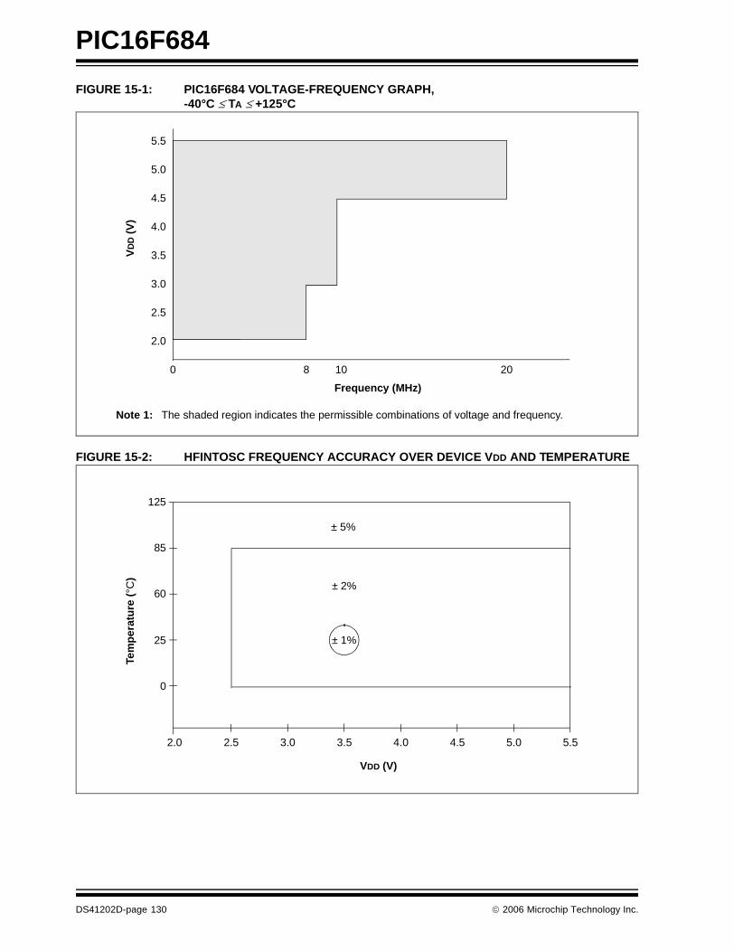
PIC16F684
FIGURE 15-1: PIC16F684 VOLTAGE-FREQUENCY GRAPH, -40°C ≤ TA ≤ +125°C
FIGURE 15-2: HFINTOSC FREQUENCY ACCURACY OVER DEVICE VDD AND TEMPERATURE
5.5
2.0
3.5
2.5
0
3.0
4.0
4.5
5.0
Frequency (MHz)
VD
D (
V)
Note 1: The shaded region indicates the permissible combinations of voltage and frequency.
8 2010
125
25
2.0
0
60
85
VDD (V)
4.0 5.04.5
Tem
per
atu
re (
°C)
2.5 3.0 3.5 5.5
± 1%
± 2%
± 5%
DS41202D-page 130 © 2006 Microchip Technology Inc.
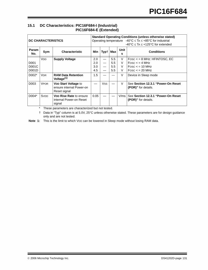
PIC16F684
15.1 DC Characteristics: PIC16F684-I (Industrial) PIC16F684-E (Extended)
DC CHARACTERISTICSStandard Operating Conditions (unless otherwise stated)Operating temperature -40°C ≤ TA ≤ +85°C for industrial
-40°C ≤ TA ≤ +125°C for extended
Param No.
Sym Characteristic Min Typ† MaxUnit
sConditions
D001D001CD001D
VDD Supply Voltage 2.02.03.04.5
————
5.55.55.55.5
VVVV
FOSC < = 8 MHz: HFINTOSC, ECFOSC < = 4 MHzFOSC < = 10 MHzFOSC < = 20 MHz
D002* VDR RAM Data Retention Voltage(1)
1.5 — — V Device in Sleep mode
D003 VPOR VDD Start Voltage to ensure internal Power-on Reset signal
— VSS — V See Section 12.3.1 “Power-On Reset (POR)” for details.
D004* SVDD VDD Rise Rate to ensure internal Power-on Reset signal
0.05 — — V/ms See Section 12.3.1 “Power-On Reset (POR)” for details.
* These parameters are characterized but not tested.† Data in “Typ” column is at 5.0V, 25°C unless otherwise stated. These parameters are for design guidance
only and are not tested.Note 1: This is the limit to which VDD can be lowered in Sleep mode without losing RAM data.
© 2006 Microchip Technology Inc. DS41202D-page 131
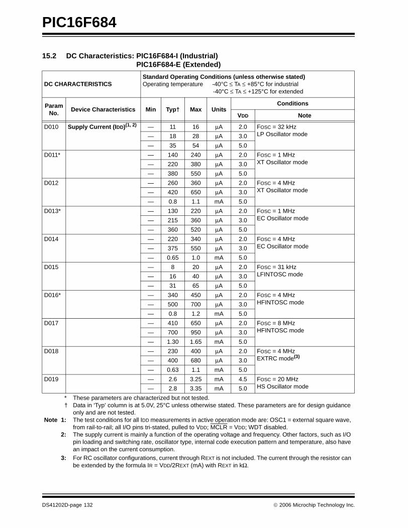
PIC16F684
15.2 DC Characteristics: PIC16F684-I (Industrial)PIC16F684-E (Extended)
DC CHARACTERISTICSStandard Operating Conditions (unless otherwise stated)Operating temperature -40°C ≤ TA ≤ +85°C for industrial
-40°C ≤ TA ≤ +125°C for extended
ParamNo.
Device Characteristics Min Typ† Max UnitsConditions
VDD Note
D010 Supply Current (IDD)(1, 2) — 11 16 μA 2.0 FOSC = 32 kHzLP Oscillator mode— 18 28 μA 3.0
— 35 54 μA 5.0
D011* — 140 240 μA 2.0 FOSC = 1 MHzXT Oscillator mode— 220 380 μA 3.0
— 380 550 μA 5.0
D012 — 260 360 μA 2.0 FOSC = 4 MHzXT Oscillator mode— 420 650 μA 3.0
— 0.8 1.1 mA 5.0
D013* — 130 220 μA 2.0 FOSC = 1 MHzEC Oscillator mode— 215 360 μA 3.0
— 360 520 μA 5.0
D014 — 220 340 μA 2.0 FOSC = 4 MHzEC Oscillator mode— 375 550 μA 3.0
— 0.65 1.0 mA 5.0
D015 — 8 20 μA 2.0 FOSC = 31 kHzLFINTOSC mode— 16 40 μA 3.0
— 31 65 μA 5.0
D016* — 340 450 μA 2.0 FOSC = 4 MHzHFINTOSC mode— 500 700 μA 3.0
— 0.8 1.2 mA 5.0
D017 — 410 650 μA 2.0 FOSC = 8 MHzHFINTOSC mode— 700 950 μA 3.0
— 1.30 1.65 mA 5.0
D018 — 230 400 μA 2.0 FOSC = 4 MHzEXTRC mode(3)
— 400 680 μA 3.0
— 0.63 1.1 mA 5.0
D019 — 2.6 3.25 mA 4.5 FOSC = 20 MHzHS Oscillator mode— 2.8 3.35 mA 5.0
* These parameters are characterized but not tested.† Data in ‘Typ’ column is at 5.0V, 25°C unless otherwise stated. These parameters are for design guidance
only and are not tested.Note 1: The test conditions for all IDD measurements in active operation mode are: OSC1 = external square wave,
from rail-to-rail; all I/O pins tri-stated, pulled to VDD; MCLR = VDD; WDT disabled.2: The supply current is mainly a function of the operating voltage and frequency. Other factors, such as I/O
pin loading and switching rate, oscillator type, internal code execution pattern and temperature, also have an impact on the current consumption.
3: For RC oscillator configurations, current through REXT is not included. The current through the resistor can be extended by the formula IR = VDD/2REXT (mA) with REXT in kΩ.
DS41202D-page 132 © 2006 Microchip Technology Inc.
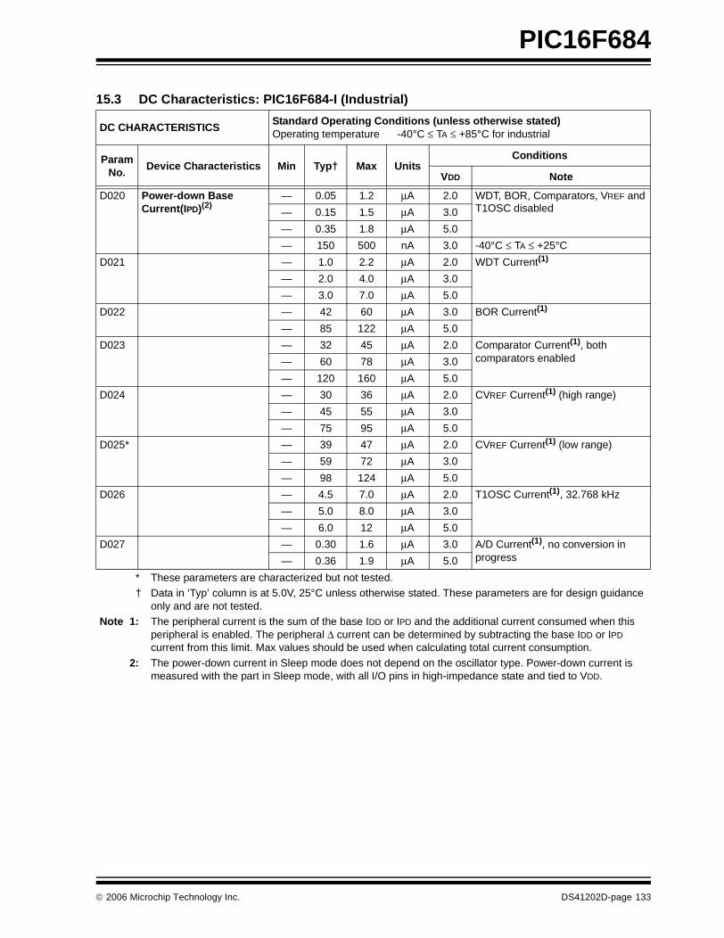
PIC16F684
15.3 DC Characteristics: PIC16F684-I (Industrial)
DC CHARACTERISTICSStandard Operating Conditions (unless otherwise stated)Operating temperature -40°C ≤ TA ≤ +85°C for industrial
ParamNo.
Device Characteristics Min Typ† Max UnitsConditions
VDD Note
D020 Power-down Base Current(IPD)(2)
— 0.05 1.2 μA 2.0 WDT, BOR, Comparators, VREF andT1OSC disabled— 0.15 1.5 μA 3.0
— 0.35 1.8 μA 5.0
— 150 500 nA 3.0 -40°C ≤ TA ≤ +25°C
D021 — 1.0 2.2 μA 2.0 WDT Current(1)
— 2.0 4.0 μA 3.0
— 3.0 7.0 μA 5.0
D022 — 42 60 μA 3.0 BOR Current(1)
— 85 122 μA 5.0
D023 — 32 45 μA 2.0 Comparator Current(1), both comparators enabled— 60 78 μA 3.0
— 120 160 μA 5.0
D024 — 30 36 μA 2.0 CVREF Current(1) (high range)
— 45 55 μA 3.0
— 75 95 μA 5.0
D025* — 39 47 μA 2.0 CVREF Current(1) (low range)
— 59 72 μA 3.0
— 98 124 μA 5.0
D026 — 4.5 7.0 μA 2.0 T1OSC Current(1), 32.768 kHz
— 5.0 8.0 μA 3.0
— 6.0 12 μA 5.0
D027 — 0.30 1.6 μA 3.0 A/D Current(1), no conversion in progress— 0.36 1.9 μA 5.0
* These parameters are characterized but not tested.† Data in ‘Typ’ column is at 5.0V, 25°C unless otherwise stated. These parameters are for design guidance
only and are not tested.Note 1: The peripheral current is the sum of the base IDD or IPD and the additional current consumed when this
peripheral is enabled. The peripheral Δ current can be determined by subtracting the base IDD or IPD current from this limit. Max values should be used when calculating total current consumption.
2: The power-down current in Sleep mode does not depend on the oscillator type. Power-down current is measured with the part in Sleep mode, with all I/O pins in high-impedance state and tied to VDD.
© 2006 Microchip Technology Inc. DS41202D-page 133
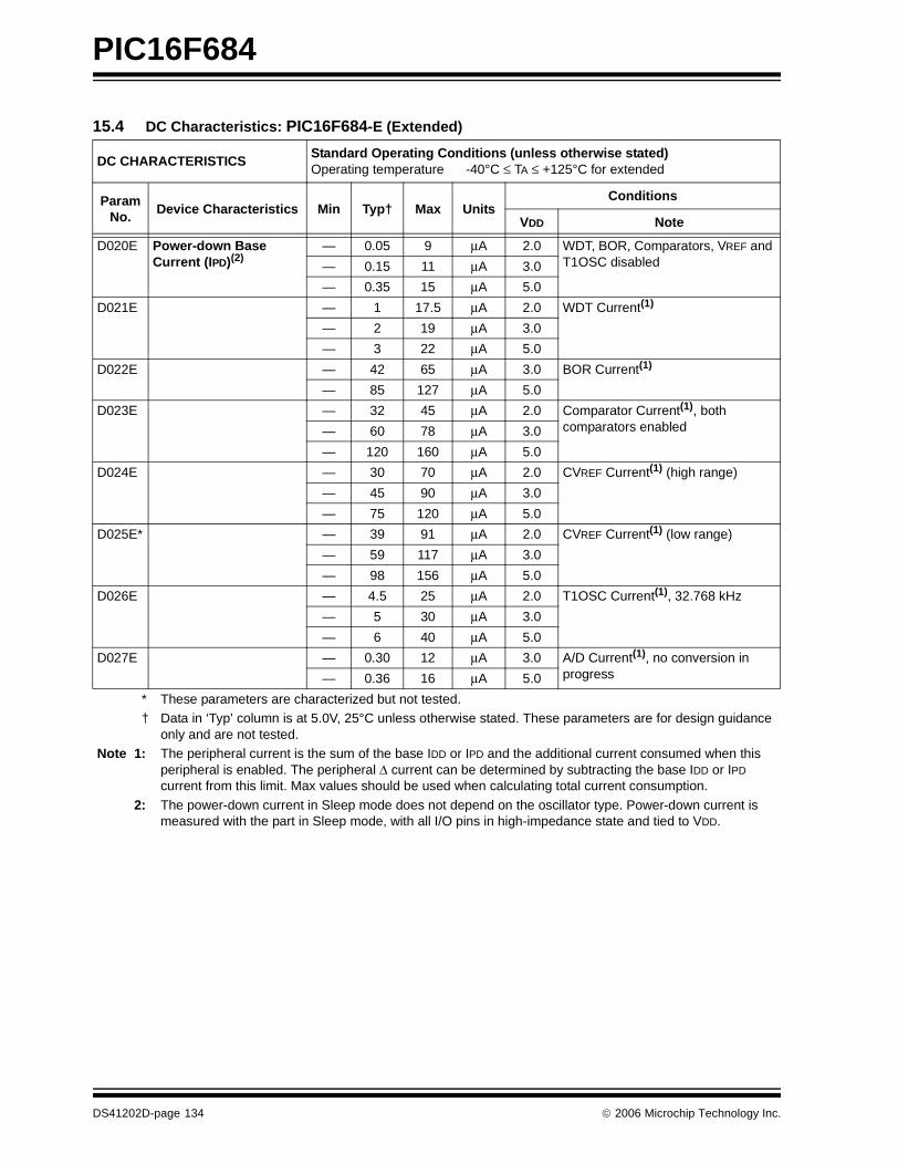
PIC16F684
15.4 DC Characteristics: PIC16F684-E (Extended)
DC CHARACTERISTICSStandard Operating Conditions (unless otherwise stated)Operating temperature -40°C ≤ TA ≤ +125°C for extended
ParamNo.
Device Characteristics Min Typ† Max UnitsConditions
VDD Note
D020E Power-down Base Current (IPD)(2)
— 0.05 9 μA 2.0 WDT, BOR, Comparators, VREF and T1OSC disabled— 0.15 11 μA 3.0
— 0.35 15 μA 5.0
D021E — 1 17.5 μA 2.0 WDT Current(1)
— 2 19 μA 3.0
— 3 22 μA 5.0
D022E — 42 65 μA 3.0 BOR Current(1)
— 85 127 μA 5.0
D023E — 32 45 μA 2.0 Comparator Current(1), both comparators enabled— 60 78 μA 3.0
— 120 160 μA 5.0
D024E — 30 70 μA 2.0 CVREF Current(1) (high range)
— 45 90 μA 3.0
— 75 120 μA 5.0
D025E* — 39 91 μA 2.0 CVREF Current(1) (low range)
— 59 117 μA 3.0
— 98 156 μA 5.0
D026E — 4.5 25 μA 2.0 T1OSC Current(1), 32.768 kHz
— 5 30 μA 3.0
— 6 40 μA 5.0
D027E — 0.30 12 μA 3.0 A/D Current(1), no conversion in progress— 0.36 16 μA 5.0
* These parameters are characterized but not tested.† Data in ‘Typ’ column is at 5.0V, 25°C unless otherwise stated. These parameters are for design guidance
only and are not tested.Note 1: The peripheral current is the sum of the base IDD or IPD and the additional current consumed when this
peripheral is enabled. The peripheral Δ current can be determined by subtracting the base IDD or IPD current from this limit. Max values should be used when calculating total current consumption.
2: The power-down current in Sleep mode does not depend on the oscillator type. Power-down current is measured with the part in Sleep mode, with all I/O pins in high-impedance state and tied to VDD.
DS41202D-page 134 © 2006 Microchip Technology Inc.
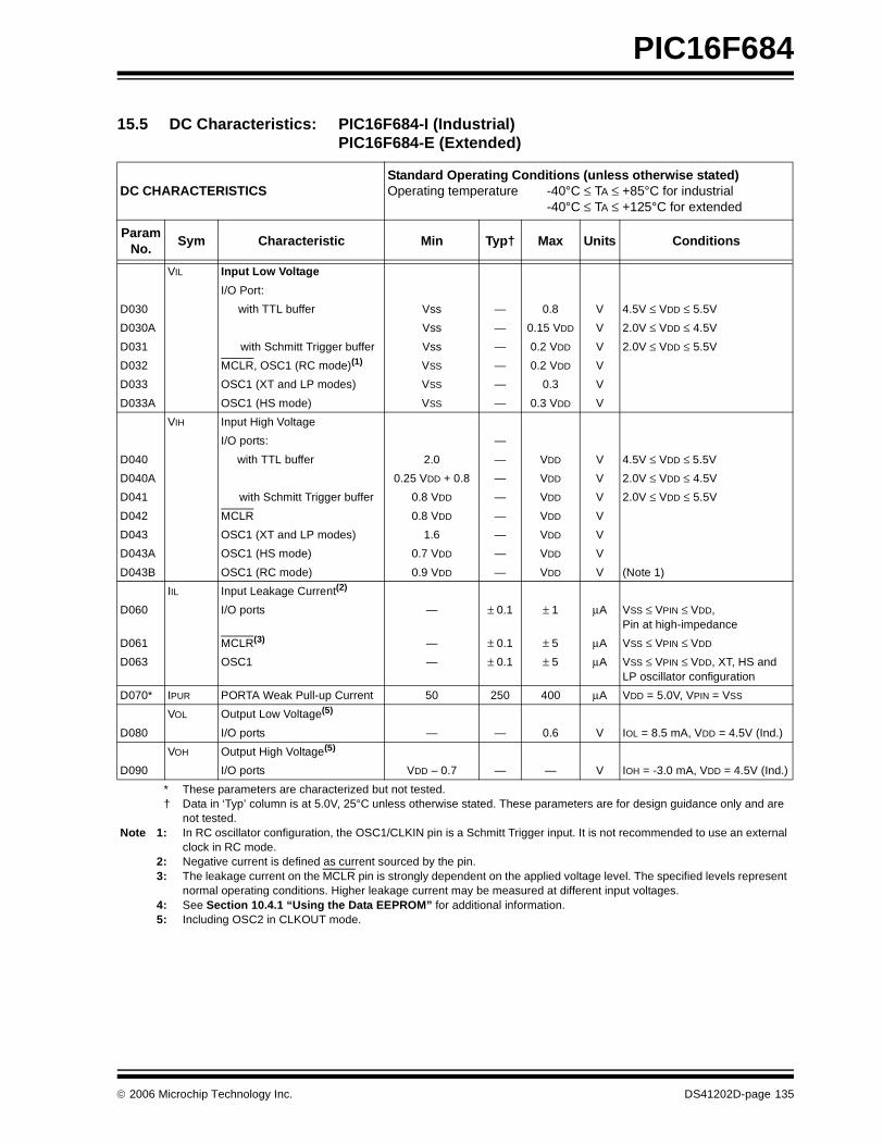
PIC16F684
15.5 DC Characteristics: PIC16F684-I (Industrial)
PIC16F684-E (Extended)
DC CHARACTERISTICSStandard Operating Conditions (unless otherwise stated)Operating temperature -40°C ≤ TA ≤ +85°C for industrial
-40°C ≤ TA ≤ +125°C for extended
ParamNo.
Sym Characteristic Min Typ† Max Units Conditions
VIL Input Low Voltage
I/O Port:
D030 with TTL buffer Vss — 0.8 V 4.5V ≤ VDD ≤ 5.5V
D030A Vss — 0.15 VDD V 2.0V ≤ VDD ≤ 4.5V
D031 with Schmitt Trigger buffer Vss — 0.2 VDD V 2.0V ≤ VDD ≤ 5.5V
D032 MCLR, OSC1 (RC mode)(1) VSS — 0.2 VDD V
D033 OSC1 (XT and LP modes) VSS — 0.3 V
D033A OSC1 (HS mode) VSS — 0.3 VDD V
VIH Input High Voltage
I/O ports: —
D040 with TTL buffer 2.0 — VDD V 4.5V ≤ VDD ≤ 5.5V
D040A 0.25 VDD + 0.8 — VDD V 2.0V ≤ VDD ≤ 4.5V
D041 with Schmitt Trigger buffer 0.8 VDD — VDD V 2.0V ≤ VDD ≤ 5.5V
D042 MCLR 0.8 VDD — VDD V
D043 OSC1 (XT and LP modes) 1.6 — VDD V
D043A OSC1 (HS mode) 0.7 VDD — VDD V
D043B OSC1 (RC mode) 0.9 VDD — VDD V (Note 1)
IIL Input Leakage Current(2)
D060 I/O ports — ± 0.1 ± 1 μA VSS ≤ VPIN ≤ VDD, Pin at high-impedance
D061 MCLR(3) — ± 0.1 ± 5 μA VSS ≤ VPIN ≤ VDD
D063 OSC1 — ± 0.1 ± 5 μA VSS ≤ VPIN ≤ VDD, XT, HS and LP oscillator configuration
D070* IPUR PORTA Weak Pull-up Current 50 250 400 μA VDD = 5.0V, VPIN = VSS
VOL Output Low Voltage(5)
D080 I/O ports — — 0.6 V IOL = 8.5 mA, VDD = 4.5V (Ind.)
VOH Output High Voltage(5)
D090 I/O ports VDD – 0.7 — — V IOH = -3.0 mA, VDD = 4.5V (Ind.)
* These parameters are characterized but not tested.† Data in ‘Typ’ column is at 5.0V, 25°C unless otherwise stated. These parameters are for design guidance only and are
not tested.Note 1: In RC oscillator configuration, the OSC1/CLKIN pin is a Schmitt Trigger input. It is not recommended to use an external
clock in RC mode.2: Negative current is defined as current sourced by the pin.3: The leakage current on the MCLR pin is strongly dependent on the applied voltage level. The specified levels represent
normal operating conditions. Higher leakage current may be measured at different input voltages.4: See Section 10.4.1 “Using the Data EEPROM” for additional information.5: Including OSC2 in CLKOUT mode.
© 2006 Microchip Technology Inc. DS41202D-page 135
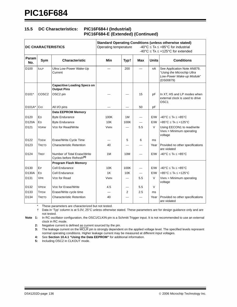
PIC16F684
D100 IULP Ultra Low-Power Wake-Up Current
— 200 — nA See Application Note AN879, “Using the Microchip UltraLow-Power Wake-up Module” (DS00879)
Capacitive Loading Specs on Output Pins
D101* COSC2 OSC2 pin — — 15 pF In XT, HS and LP modes when external clock is used to drive OSC1
D101A* CIO All I/O pins — — 50 pF
Data EEPROM Memory
D120 ED Byte Endurance 100K 1M — E/W -40°C ≤ TA ≤ +85°C
D120A ED Byte Endurance 10K 100K — E/W +85°C ≤ TA ≤ +125°C
D121 VDRW VDD for Read/Write VMIN — 5.5 V Using EECON1 to read/writeVMIN = Minimum operating voltage
D122 TDEW Erase/Write Cycle Time — 5 6 ms
D123 TRETD Characteristic Retention 40 — — Year Provided no other specifications are violated
D124 TREF Number of Total Erase/Write Cycles before Refresh(4)
1M 10M — E/W -40°C ≤ TA ≤ +85°C
Program Flash Memory
D130 EP Cell Endurance 10K 100K — E/W -40°C ≤ TA ≤ +85°C
D130A ED Cell Endurance 1K 10K — E/W +85°C ≤ TA ≤ +125°C
D131 VPR VDD for Read VMIN — 5.5 V VMIN = Minimum operating voltage
D132 VPEW VDD for Erase/Write 4.5 — 5.5 V
D133 TPEW Erase/Write cycle time — 2 2.5 ms
D134 TRETD Characteristic Retention 40 — — Year Provided no other specifications are violated
15.5 DC Characteristics: PIC16F684-I (Industrial) PIC16F684-E (Extended) (Continued)
DC CHARACTERISTICSStandard Operating Conditions (unless otherwise stated)Operating temperature -40°C ≤ TA ≤ +85°C for industrial
-40°C ≤ TA ≤ +125°C for extended
ParamNo.
Sym Characteristic Min Typ† Max Units Conditions
* These parameters are characterized but not tested.† Data in ‘Typ’ column is at 5.0V, 25°C unless otherwise stated. These parameters are for design guidance only and are
not tested.Note 1: In RC oscillator configuration, the OSC1/CLKIN pin is a Schmitt Trigger input. It is not recommended to use an external
clock in RC mode.2: Negative current is defined as current sourced by the pin.3: The leakage current on the MCLR pin is strongly dependent on the applied voltage level. The specified levels represent
normal operating conditions. Higher leakage current may be measured at different input voltages.4: See Section 10.4.1 “Using the Data EEPROM” for additional information.5: Including OSC2 in CLKOUT mode.
DS41202D-page 136 © 2006 Microchip Technology Inc.
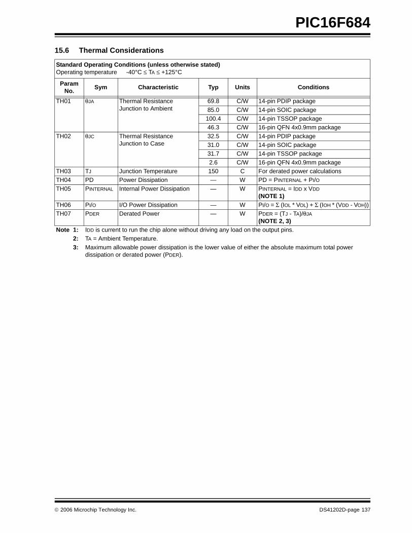
PIC16F684
15.6 Thermal Considerations
Standard Operating Conditions (unless otherwise stated)Operating temperature -40°C ≤ TA ≤ +125°C
ParamNo.
Sym Characteristic Typ Units Conditions
TH01 θJA Thermal Resistance Junction to Ambient
69.8 C/W 14-pin PDIP package
85.0 C/W 14-pin SOIC package100.4 C/W 14-pin TSSOP package46.3 C/W 16-pin QFN 4x0.9mm package
TH02 θJC Thermal Resistance Junction to Case
32.5 C/W 14-pin PDIP package31.0 C/W 14-pin SOIC package31.7 C/W 14-pin TSSOP package
2.6 C/W 16-pin QFN 4x0.9mm packageTH03 TJ Junction Temperature 150 C For derated power calculationsTH04 PD Power Dissipation — W PD = PINTERNAL + PI/O
TH05 PINTERNAL Internal Power Dissipation — W PINTERNAL = IDD x VDD
(NOTE 1)TH06 PI/O I/O Power Dissipation — W PI/O = Σ (IOL * VOL) + Σ (IOH * (VDD - VOH))TH07 PDER Derated Power — W PDER = (TJ - TA)/θJA
(NOTE 2, 3)Note 1: IDD is current to run the chip alone without driving any load on the output pins.
2: TA = Ambient Temperature.
3: Maximum allowable power dissipation is the lower value of either the absolute maximum total power dissipation or derated power (PDER).
© 2006 Microchip Technology Inc. DS41202D-page 137

PIC16F684
15.7 Timing Parameter Symbology
The timing parameter symbols have been created withone of the following formats:
FIGURE 15-3: LOAD CONDITIONS
1. TppS2ppS
2. TppST
F Frequency T Time
Lowercase letters (pp) and their meanings:pp
cc CCP1 osc OSC1
ck CLKOUT rd RDcs CS rw RD or WRdi SDI sc SCK
do SDO ss SSdt Data in t0 T0CKIio I/O PORT t1 T1CKI
mc MCLR wr WRUppercase letters and their meanings:
SF Fall P PeriodH High R RiseI Invalid (High-impedance) V Valid
L Low Z High-impedance
VSS
CL
Legend: CL = 50 pF for all pins
15 pF for OSC2 output
Load Condition
Pin
DS41202D-page 138 © 2006 Microchip Technology Inc.
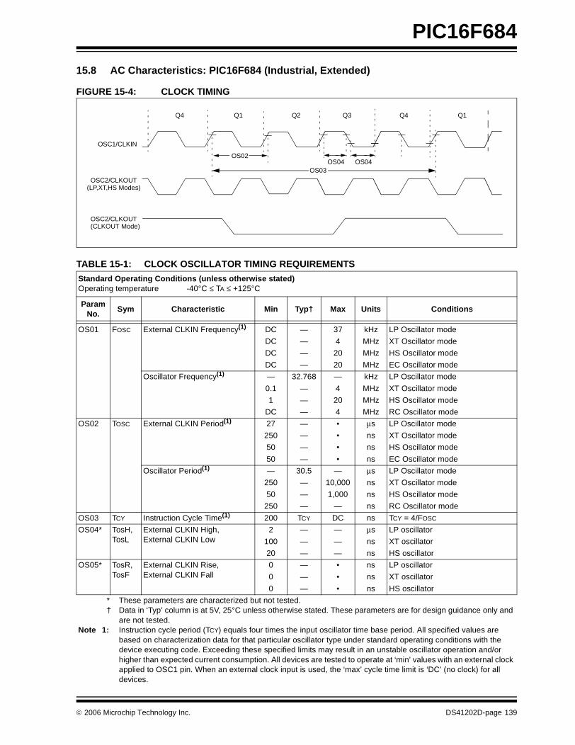
PIC16F684
15.8 AC Characteristics: PIC16F684 (Industrial, Extended)
FIGURE 15-4: CLOCK TIMING
TABLE 15-1: CLOCK OSCILLATOR TIMING REQUIREMENTS
Standard Operating Conditions (unless otherwise stated)Operating temperature -40°C ≤ TA ≤ +125°C
ParamNo.
Sym Characteristic Min Typ† Max Units Conditions
OS01 FOSC External CLKIN Frequency(1) DC — 37 kHz LP Oscillator mode
DC — 4 MHz XT Oscillator mode
DC — 20 MHz HS Oscillator mode
DC — 20 MHz EC Oscillator mode
Oscillator Frequency(1) — 32.768 — kHz LP Oscillator mode
0.1 — 4 MHz XT Oscillator mode
1 — 20 MHz HS Oscillator mode
DC — 4 MHz RC Oscillator mode
OS02 TOSC External CLKIN Period(1) 27 — • μs LP Oscillator mode
250 — • ns XT Oscillator mode
50 — • ns HS Oscillator mode
50 — • ns EC Oscillator mode
Oscillator Period(1) — 30.5 — μs LP Oscillator mode
250 — 10,000 ns XT Oscillator mode
50 — 1,000 ns HS Oscillator mode
250 — — ns RC Oscillator mode
OS03 TCY Instruction Cycle Time(1) 200 TCY DC ns TCY = 4/FOSC
OS04* TosH,TosL
External CLKIN High,External CLKIN Low
2 — — μs LP oscillator
100 — — ns XT oscillator
20 — — ns HS oscillator
OS05* TosR,TosF
External CLKIN Rise,External CLKIN Fall
0 — • ns LP oscillator
0 — • ns XT oscillator
0 — • ns HS oscillator
* These parameters are characterized but not tested.† Data in ‘Typ’ column is at 5V, 25°C unless otherwise stated. These parameters are for design guidance only and
are not tested.Note 1: Instruction cycle period (TCY) equals four times the input oscillator time base period. All specified values are
based on characterization data for that particular oscillator type under standard operating conditions with the device executing code. Exceeding these specified limits may result in an unstable oscillator operation and/or higher than expected current consumption. All devices are tested to operate at ‘min’ values with an external clock applied to OSC1 pin. When an external clock input is used, the ‘max’ cycle time limit is ‘DC’ (no clock) for all devices.
OSC1/CLKIN
OSC2/CLKOUT
Q4 Q1 Q2 Q3 Q4 Q1
OS02
OS03OS04 OS04
OSC2/CLKOUT(LP,XT,HS Modes)
(CLKOUT Mode)
© 2006 Microchip Technology Inc. DS41202D-page 139
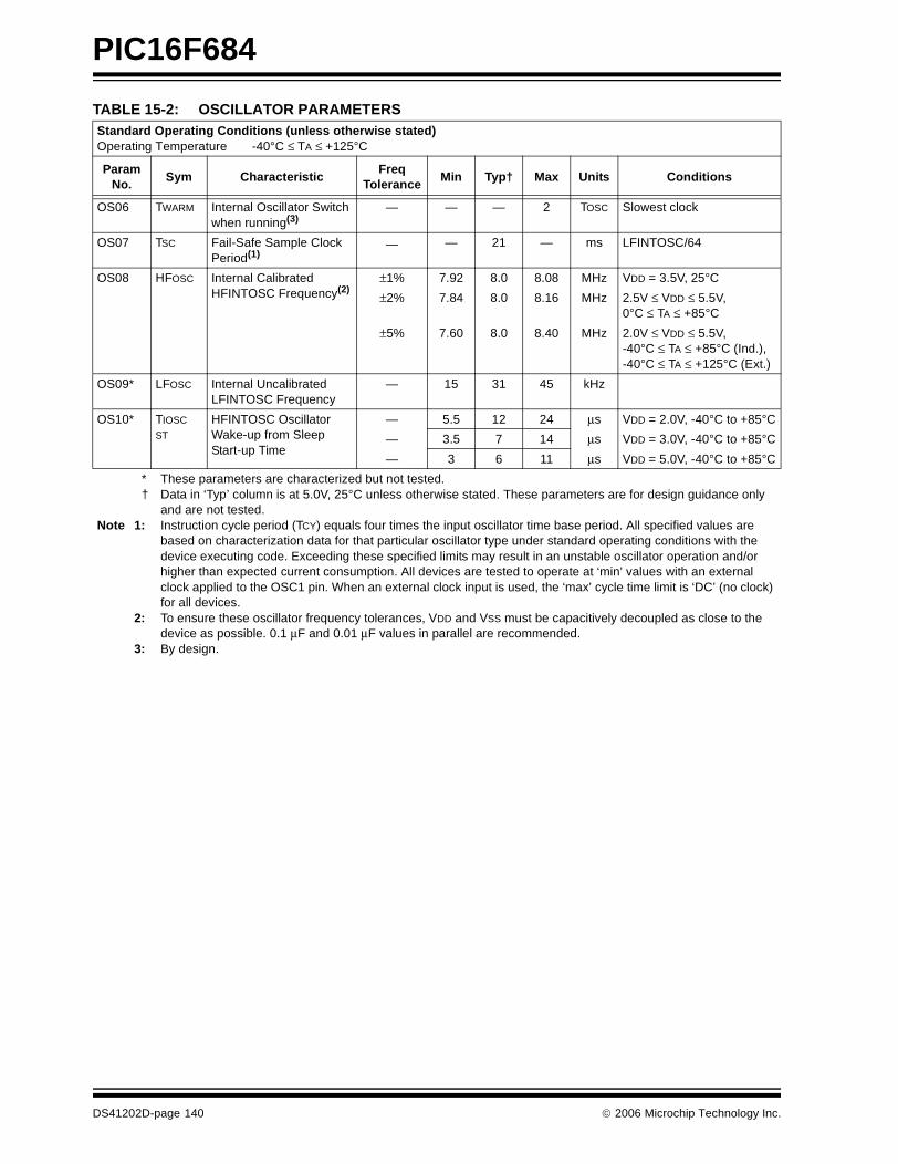
PIC16F684
TABLE 15-2: OSCILLATOR PARAMETERS Standard Operating Conditions (unless otherwise stated)Operating Temperature -40°C ≤ TA ≤ +125°C
Param No.
Sym CharacteristicFreq
ToleranceMin Typ† Max Units Conditions
OS06 TWARM Internal Oscillator Switch when running(3)
— — — 2 TOSC Slowest clock
OS07 TSC Fail-Safe Sample Clock Period(1)
— — 21 — ms LFINTOSC/64
OS08 HFOSC Internal CalibratedHFINTOSC Frequency(2)
±1% 7.92 8.0 8.08 MHz VDD = 3.5V, 25°C
±2% 7.84 8.0 8.16 MHz 2.5V ≤ VDD ≤ 5.5V,0°C ≤ TA ≤ +85°C
±5% 7.60 8.0 8.40 MHz 2.0V ≤ VDD ≤ 5.5V,-40°C ≤ TA ≤ +85°C (Ind.),-40°C ≤ TA ≤ +125°C (Ext.)
OS09* LFOSC Internal UncalibratedLFINTOSC Frequency
— 15 31 45 kHz
OS10* TIOSC ST
HFINTOSC Oscillator Wake-up from SleepStart-up Time
— 5.5 12 24 μs VDD = 2.0V, -40°C to +85°C
— 3.5 7 14 μs VDD = 3.0V, -40°C to +85°C
— 3 6 11 μs VDD = 5.0V, -40°C to +85°C
* These parameters are characterized but not tested.† Data in ‘Typ’ column is at 5.0V, 25°C unless otherwise stated. These parameters are for design guidance only
and are not tested.Note 1: Instruction cycle period (TCY) equals four times the input oscillator time base period. All specified values are
based on characterization data for that particular oscillator type under standard operating conditions with the device executing code. Exceeding these specified limits may result in an unstable oscillator operation and/or higher than expected current consumption. All devices are tested to operate at ‘min’ values with an external clock applied to the OSC1 pin. When an external clock input is used, the ‘max’ cycle time limit is ‘DC’ (no clock) for all devices.
2: To ensure these oscillator frequency tolerances, VDD and VSS must be capacitively decoupled as close to the device as possible. 0.1 μF and 0.01 μF values in parallel are recommended.
3: By design.
DS41202D-page 140 © 2006 Microchip Technology Inc.
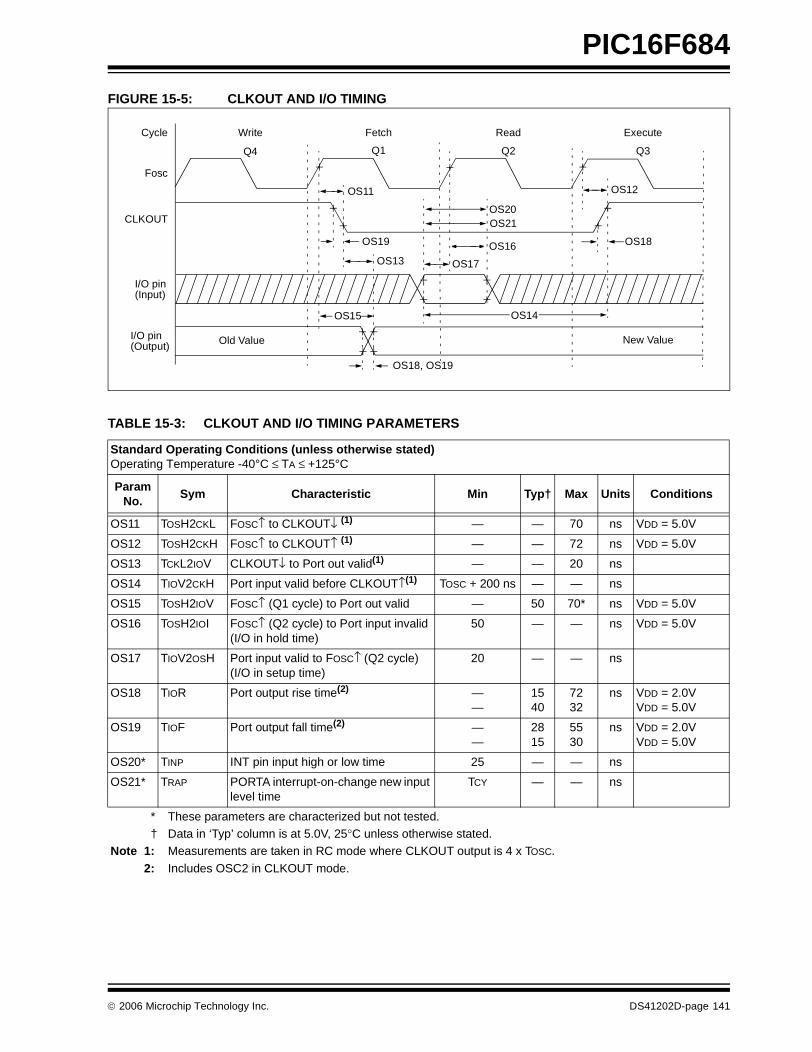
PIC16F684
FIGURE 15-5: CLKOUT AND I/O TIMING
Fosc
CLKOUT
I/O pin(Input)
I/O pin(Output)
Q4 Q1 Q2 Q3
OS11
OS19
OS13
OS15
OS18, OS19
OS20OS21
OS17
OS16
OS14
OS12
OS18
Old Value New Value
Write Fetch Read ExecuteCycle
TABLE 15-3: CLKOUT AND I/O TIMING PARAMETERS
Standard Operating Conditions (unless otherwise stated)Operating Temperature -40°C ≤ TA ≤ +125°C
Param No.
Sym Characteristic Min Typ† Max Units Conditions
OS11 TOSH2CKL FOSC↑ to CLKOUT↓ (1) — — 70 ns VDD = 5.0V
OS12 TOSH2CKH FOSC↑ to CLKOUT↑ (1) — — 72 ns VDD = 5.0V
OS13 TCKL2IOV CLKOUT↓ to Port out valid(1) — — 20 ns
OS14 TIOV2CKH Port input valid before CLKOUT↑(1) TOSC + 200 ns — — ns
OS15 TOSH2IOV FOSC↑ (Q1 cycle) to Port out valid — 50 70* ns VDD = 5.0V
OS16 TOSH2IOI FOSC↑ (Q2 cycle) to Port input invalid (I/O in hold time)
50 — — ns VDD = 5.0V
OS17 TIOV2OSH Port input valid to FOSC↑ (Q2 cycle)(I/O in setup time)
20 — — ns
OS18 TIOR Port output rise time(2) ——
1540
7232
ns VDD = 2.0VVDD = 5.0V
OS19 TIOF Port output fall time(2) ——
2815
5530
ns VDD = 2.0VVDD = 5.0V
OS20* TINP INT pin input high or low time 25 — — ns
OS21* TRAP PORTA interrupt-on-change new input level time
TCY — — ns
* These parameters are characterized but not tested.† Data in ‘Typ’ column is at 5.0V, 25°C unless otherwise stated.
Note 1: Measurements are taken in RC mode where CLKOUT output is 4 x TOSC.
2: Includes OSC2 in CLKOUT mode.
© 2006 Microchip Technology Inc. DS41202D-page 141
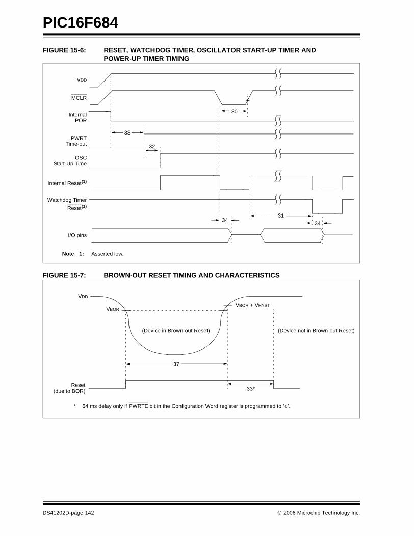
PIC16F684
FIGURE 15-6: RESET, WATCHDOG TIMER, OSCILLATOR START-UP TIMER AND POWER-UP TIMER TIMING
FIGURE 15-7: BROWN-OUT RESET TIMING AND CHARACTERISTICS
VDD
MCLR
InternalPOR
PWRTTime-out
OSCStart-Up Time
Internal Reset(1)
Watchdog Timer
33
32
30
3134
I/O pins
34
Note 1: Asserted low.
Reset(1)
VBOR
VDD
(Device in Brown-out Reset) (Device not in Brown-out Reset)
33*
37
* 64 ms delay only if PWRTE bit in the Configuration Word register is programmed to ‘0’.
Reset(due to BOR)
VBOR + VHYST
DS41202D-page 142 © 2006 Microchip Technology Inc.
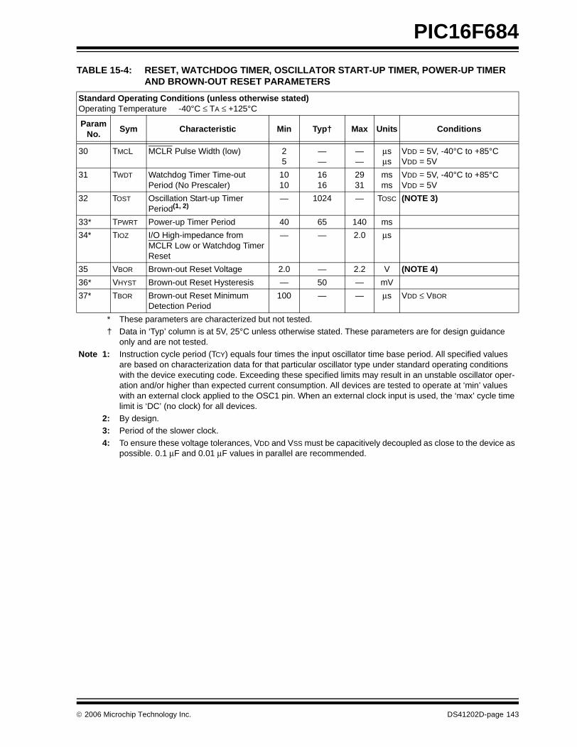
PIC16F684
TABLE 15-4: RESET, WATCHDOG TIMER, OSCILLATOR START-UP TIMER, POWER-UP TIMER AND BROWN-OUT RESET PARAMETERS
Standard Operating Conditions (unless otherwise stated)Operating Temperature -40°C ≤ TA ≤ +125°C
Param No.
Sym Characteristic Min Typ† Max Units Conditions
30 TMCL MCLR Pulse Width (low) 2 5
——
——
μsμs
VDD = 5V, -40°C to +85°CVDD = 5V
31 TWDT Watchdog Timer Time-out Period (No Prescaler)
1010
1616
2931
msms
VDD = 5V, -40°C to +85°CVDD = 5V
32 TOST Oscillation Start-up Timer Period(1, 2)
— 1024 — TOSC (NOTE 3)
33* TPWRT Power-up Timer Period 40 65 140 ms
34* TIOZ I/O High-impedance from MCLR Low or Watchdog Timer Reset
— — 2.0 μs
35 VBOR Brown-out Reset Voltage 2.0 — 2.2 V (NOTE 4)
36* VHYST Brown-out Reset Hysteresis — 50 — mV
37* TBOR Brown-out Reset Minimum Detection Period
100 — — μs VDD ≤ VBOR
* These parameters are characterized but not tested.† Data in ‘Typ’ column is at 5V, 25°C unless otherwise stated. These parameters are for design guidance
only and are not tested.Note 1: Instruction cycle period (TCY) equals four times the input oscillator time base period. All specified values
are based on characterization data for that particular oscillator type under standard operating conditions with the device executing code. Exceeding these specified limits may result in an unstable oscillator oper-ation and/or higher than expected current consumption. All devices are tested to operate at ‘min’ values with an external clock applied to the OSC1 pin. When an external clock input is used, the ‘max’ cycle time limit is ‘DC’ (no clock) for all devices.
2: By design.3: Period of the slower clock.
4: To ensure these voltage tolerances, VDD and VSS must be capacitively decoupled as close to the device as possible. 0.1 μF and 0.01 μF values in parallel are recommended.
© 2006 Microchip Technology Inc. DS41202D-page 143
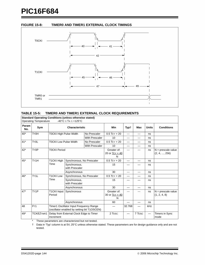
PIC16F684
FIGURE 15-8: TIMER0 AND TIMER1 EXTERNAL CLOCK TIMINGS
TABLE 15-5: TIMER0 AND TIMER1 EXTERNAL CLOCK REQUIREMENTSStandard Operating Conditions (unless otherwise stated)Operating Temperature -40°C ≤ TA ≤ +125°C
Param No.
Sym Characteristic Min Typ† Max Units Conditions
40* TT0H T0CKI High Pulse Width No Prescaler 0.5 TCY + 20 — — ns
With Prescaler 10 — — ns
41* TT0L T0CKI Low Pulse Width No Prescaler 0.5 TCY + 20 — — ns
With Prescaler 10 — — ns
42* TT0P T0CKI Period Greater of:20 or TCY + 40
N
— — ns N = prescale value (2, 4, ..., 256)
45* TT1H T1CKI High Time
Synchronous, No Prescaler 0.5 TCY + 20 — — ns
Synchronous, with Prescaler
15 — — ns
Asynchronous 30 — — ns
46* TT1L T1CKI Low Time
Synchronous, No Prescaler 0.5 TCY + 20 — — ns
Synchronous, with Prescaler
15 — — ns
Asynchronous 30 — — ns
47* TT1P T1CKI Input Period
Synchronous Greater of:30 or TCY + 40
N
— — ns N = prescale value (1, 2, 4, 8)
Asynchronous 60 — — ns
48 FT1 Timer1 Oscillator Input Frequency Range (oscillator enabled by setting bit T1OSCEN)
— 32.768 — kHz
49* TCKEZTMR1 Delay from External Clock Edge to Timer Increment
2 TOSC — 7 TOSC — Timers in Sync mode
* These parameters are characterized but not tested.† Data in ‘Typ’ column is at 5V, 25°C unless otherwise stated. These parameters are for design guidance only and are not
tested.
T0CKI
T1CKI
40 41
42
45 46
47 49
TMR0 orTMR1
DS41202D-page 144 © 2006 Microchip Technology Inc.
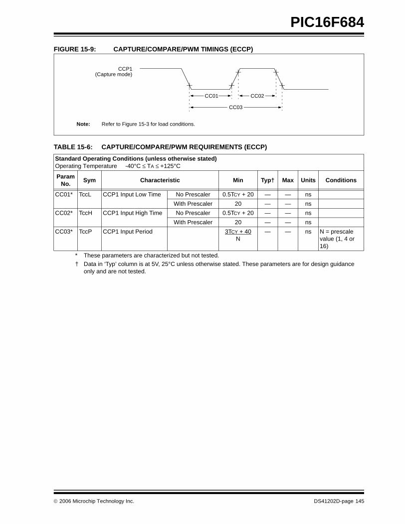
PIC16F684
FIGURE 15-9: CAPTURE/COMPARE/PWM TIMINGS (ECCP)
TABLE 15-6: CAPTURE/COMPARE/PWM REQUIREMENTS (ECCP)
Standard Operating Conditions (unless otherwise stated)Operating Temperature -40°C ≤ TA ≤ +125°C
Param No.
Sym Characteristic Min Typ† Max Units Conditions
CC01* TccL CCP1 Input Low Time No Prescaler 0.5TCY + 20 — — ns
With Prescaler 20 — — ns
CC02* TccH CCP1 Input High Time No Prescaler 0.5TCY + 20 — — ns
With Prescaler 20 — — ns
CC03* TccP CCP1 Input Period 3TCY + 40N
— — ns N = prescale value (1, 4 or 16)
* These parameters are characterized but not tested.† Data in ‘Typ’ column is at 5V, 25°C unless otherwise stated. These parameters are for design guidance
only and are not tested.
Note: Refer to Figure 15-3 for load conditions.
(Capture mode)
CC01 CC02
CC03
CCP1
© 2006 Microchip Technology Inc. DS41202D-page 145
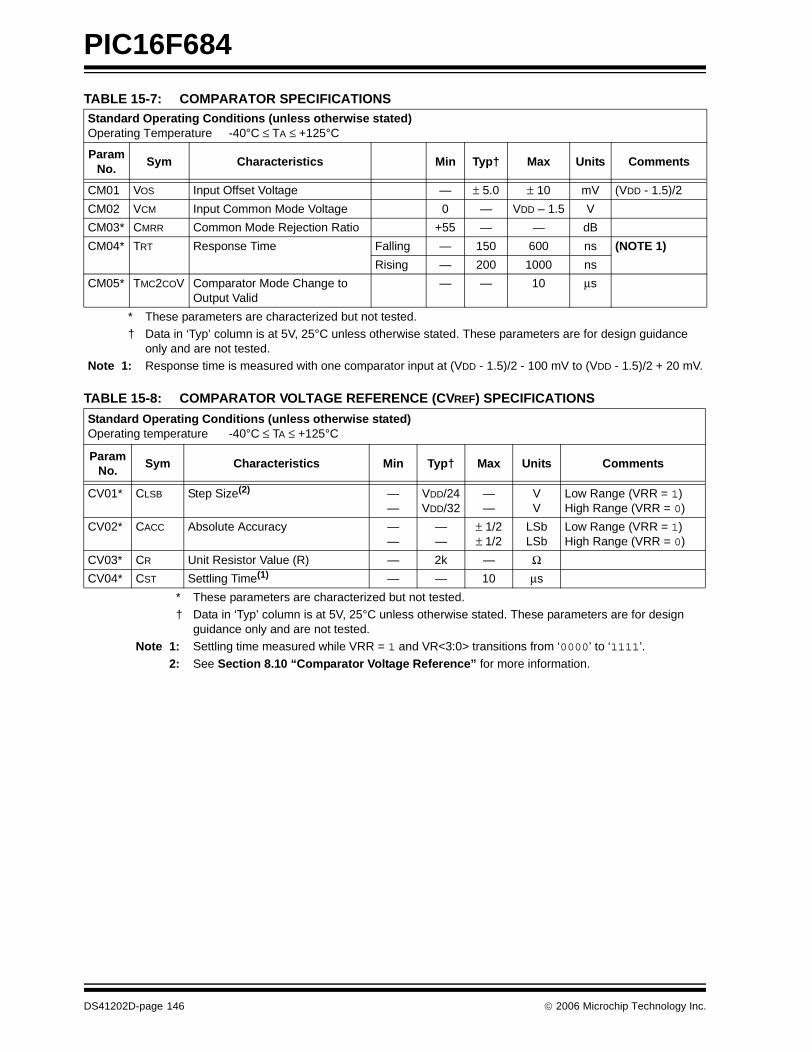
PIC16F684
TABLE 15-7: COMPARATOR SPECIFICATIONS
TABLE 15-8: COMPARATOR VOLTAGE REFERENCE (CVREF) SPECIFICATIONS
Standard Operating Conditions (unless otherwise stated)Operating Temperature -40°C ≤ TA ≤ +125°C
Param No.
Sym Characteristics Min Typ† Max Units Comments
CM01 VOS Input Offset Voltage — ± 5.0 ± 10 mV (VDD - 1.5)/2
CM02 VCM Input Common Mode Voltage 0 — VDD – 1.5 V
CM03* CMRR Common Mode Rejection Ratio +55 — — dB
CM04* TRT Response Time Falling — 150 600 ns (NOTE 1)
Rising — 200 1000 ns
CM05* TMC2COV Comparator Mode Change to Output Valid
— — 10 μs
* These parameters are characterized but not tested.† Data in ‘Typ’ column is at 5V, 25°C unless otherwise stated. These parameters are for design guidance
only and are not tested.Note 1: Response time is measured with one comparator input at (VDD - 1.5)/2 - 100 mV to (VDD - 1.5)/2 + 20 mV.
Standard Operating Conditions (unless otherwise stated)Operating temperature -40°C ≤ TA ≤ +125°C
Param No.
Sym Characteristics Min Typ† Max Units Comments
CV01* CLSB Step Size(2) ——
VDD/24VDD/32
——
VV
Low Range (VRR = 1)High Range (VRR = 0)
CV02* CACC Absolute Accuracy ——
——
± 1/2± 1/2
LSbLSb
Low Range (VRR = 1)High Range (VRR = 0)
CV03* CR Unit Resistor Value (R) — 2k — ΩCV04* CST Settling Time(1) — — 10 μs
* These parameters are characterized but not tested.† Data in ‘Typ’ column is at 5V, 25°C unless otherwise stated. These parameters are for design
guidance only and are not tested.Note 1: Settling time measured while VRR = 1 and VR<3:0> transitions from ‘0000’ to ‘1111’.
2: See Section 8.10 “Comparator Voltage Reference” for more information.
DS41202D-page 146 © 2006 Microchip Technology Inc.
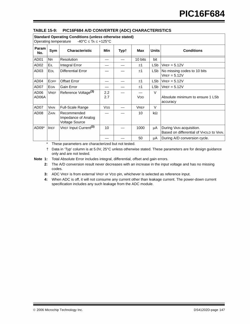
PIC16F684
TABLE 15-9: PIC16F684 A/D CONVERTER (ADC) CHARACTERISTICS
Standard Operating Conditions (unless otherwise stated)Operating temperature -40°C ≤ TA ≤ +125°C
Param No.
Sym Characteristic Min Typ† Max Units Conditions
AD01 NR Resolution — — 10 bits bit
AD02 EIL Integral Error — — ±1 LSb VREF = 5.12V
AD03 EDL Differential Error — — ±1 LSb No missing codes to 10 bitsVREF = 5.12V
AD04 EOFF Offset Error — — ±1 LSb VREF = 5.12V
AD07 EGN Gain Error — — ±1 LSb VREF = 5.12V
AD06AD06A
VREF Reference Voltage(3) 2.22.7
— —VDD
VAbsolute minimum to ensure 1 LSb accuracy
AD07 VAIN Full-Scale Range VSS — VREF V
AD08 ZAIN Recommended Impedance of Analog Voltage Source
— — 10 kΩ
AD09* IREF VREF Input Current(3) 10 — 1000 μA During VAIN acquisition. Based on differential of VHOLD to VAIN.
— — 50 μA During A/D conversion cycle.
* These parameters are characterized but not tested.
† Data in ‘Typ’ column is at 5.0V, 25°C unless otherwise stated. These parameters are for design guidance only and are not tested.
Note 1: Total Absolute Error includes integral, differential, offset and gain errors.2: The A/D conversion result never decreases with an increase in the input voltage and has no missing
codes.3: ADC VREF is from external VREF or VDD pin, whichever is selected as reference input.4: When ADC is off, it will not consume any current other than leakage current. The power-down current
specification includes any such leakage from the ADC module.
© 2006 Microchip Technology Inc. DS41202D-page 147
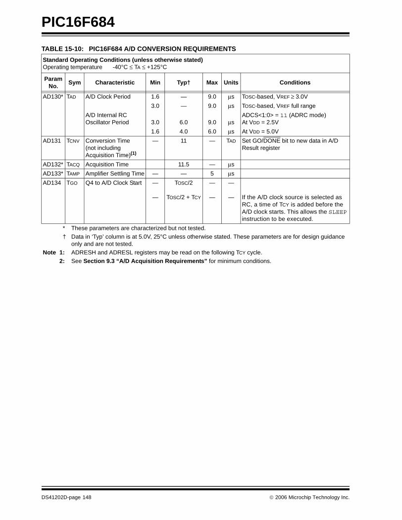
PIC16F684
TABLE 15-10: PIC16F684 A/D CONVERSION REQUIREMENTS
Standard Operating Conditions (unless otherwise stated)Operating temperature -40°C ≤ TA ≤ +125°C
ParamNo.
Sym Characteristic Min Typ† Max Units Conditions
AD130* TAD A/D Clock Period 1.6 — 9.0 μs TOSC-based, VREF ≥ 3.0V
3.0 — 9.0 μs TOSC-based, VREF full range
A/D Internal RC Oscillator Period 3.0 6.0 9.0 μs
ADCS<1:0> = 11 (ADRC mode)At VDD = 2.5V
1.6 4.0 6.0 μs At VDD = 5.0V
AD131 TCNV Conversion Time(not including Acquisition Time)(1)
— 11 — TAD Set GO/DONE bit to new data in A/D Result register
AD132* TACQ Acquisition Time 11.5 — μs
AD133* TAMP Amplifier Settling Time — — 5 μs
AD134 TGO Q4 to A/D Clock Start —
—
TOSC/2
TOSC/2 + TCY
—
—
—
— If the A/D clock source is selected as RC, a time of TCY is added before the A/D clock starts. This allows the SLEEP instruction to be executed.
* These parameters are characterized but not tested.† Data in ‘Typ’ column is at 5.0V, 25°C unless otherwise stated. These parameters are for design guidance
only and are not tested.Note 1: ADRESH and ADRESL registers may be read on the following TCY cycle.
2: See Section 9.3 “A/D Acquisition Requirements” for minimum conditions.
DS41202D-page 148 © 2006 Microchip Technology Inc.
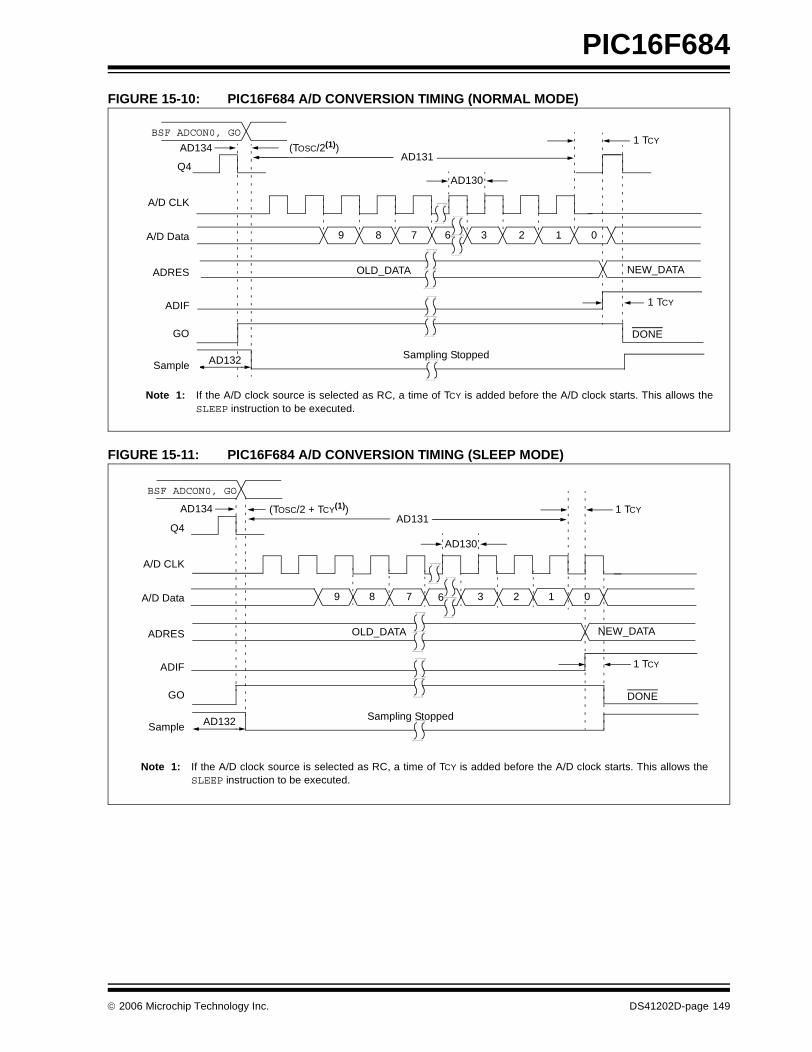
PIC16F684
FIGURE 15-10: PIC16F684 A/D CONVERSION TIMING (NORMAL MODE)
FIGURE 15-11: PIC16F684 A/D CONVERSION TIMING (SLEEP MODE)
AD131
AD130
BSF ADCON0, GO
Q4
A/D CLK
A/D Data
ADRES
ADIF
GO
Sample
OLD_DATA
Sampling Stopped
DONE
NEW_DATA
9 8 7 3 2 1 0
Note 1: If the A/D clock source is selected as RC, a time of TCY is added before the A/D clock starts. This allows theSLEEP instruction to be executed.
1 TCY
6
AD134 (TOSC/2(1))
1 TCY
AD132
AD132
AD131
AD130
BSF ADCON0, GO
Q4
A/D CLK
A/D Data
ADRES
ADIF
GO
Sample
OLD_DATA
Sampling Stopped
DONE
NEW_DATA
9 7 3 2 1 0
Note 1: If the A/D clock source is selected as RC, a time of TCY is added before the A/D clock starts. This allows theSLEEP instruction to be executed.
AD134
68
1 TCY(TOSC/2 + TCY(1))
1 TCY
© 2006 Microchip Technology Inc. DS41202D-page 149

PIC16F684
NOTES:
DS41202D-page 150 © 2006 Microchip Technology Inc.
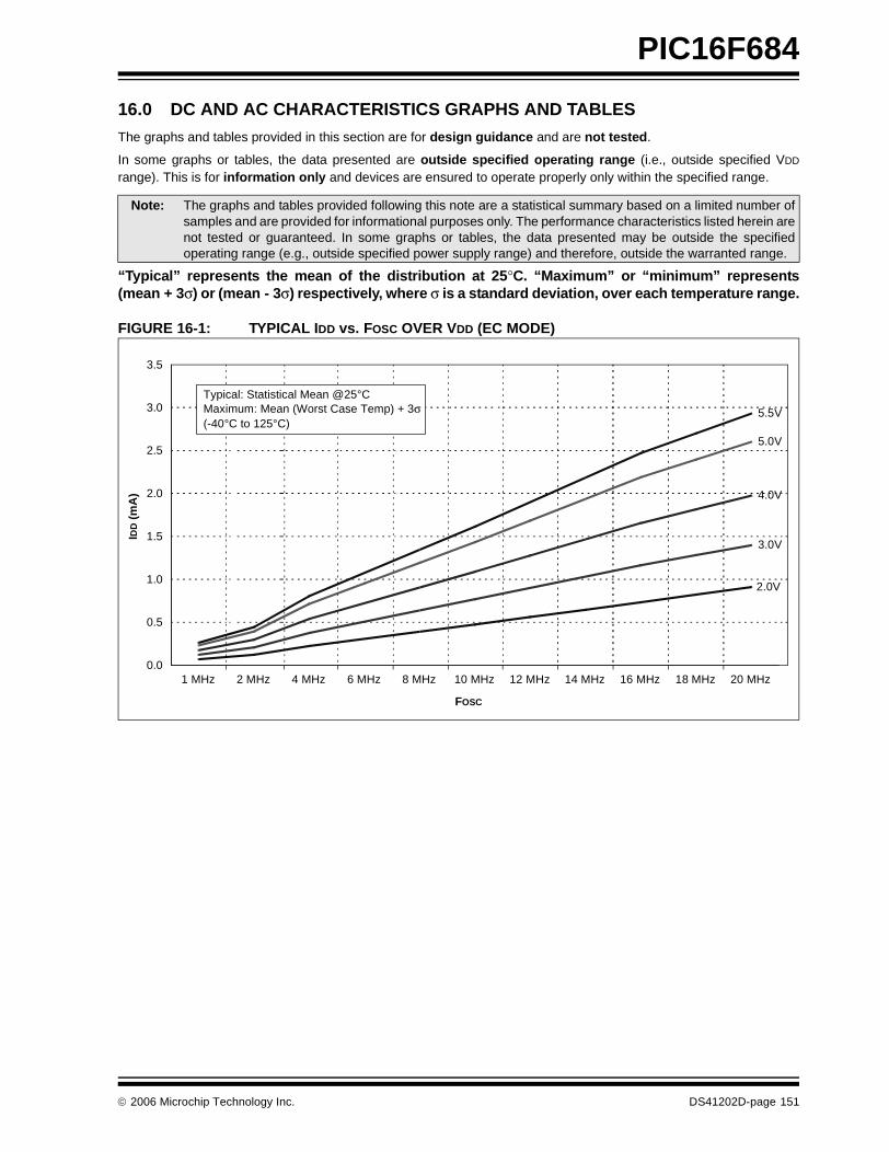
PIC16F684
16.0 DC AND AC CHARACTERISTICS GRAPHS AND TABLES
The graphs and tables provided in this section are for design guidance and are not tested.
In some graphs or tables, the data presented are outside specified operating range (i.e., outside specified VDD
range). This is for information only and devices are ensured to operate properly only within the specified range.
“Typical” represents the mean of the distribution at 25°C. “Maximum” or “minimum” represents(mean + 3σ) or (mean - 3σ) respectively, where σ is a standard deviation, over each temperature range.
FIGURE 16-1: TYPICAL IDD vs. FOSC OVER VDD (EC MODE)
Note: The graphs and tables provided following this note are a statistical summary based on a limited number ofsamples and are provided for informational purposes only. The performance characteristics listed herein arenot tested or guaranteed. In some graphs or tables, the data presented may be outside the specifiedoperating range (e.g., outside specified power supply range) and therefore, outside the warranted range.
3.0V
4.0V
5.0V
5.5V
2.0V
0.0
0.5
1.0
1.5
2.0
2.5
3.0
3.5
1 MHz 2 MHz 4 MHz 6 MHz 8 MHz 10 MHz 12 MHz 14 MHz 16 MHz 18 MHz 20 MHz
FOSC
IDD
(m
A)
Typical: Statistical Mean @25°CMaximum: Mean (Worst Case Temp) + 3σ(-40°C to 125°C)
© 2006 Microchip Technology Inc. DS41202D-page 151
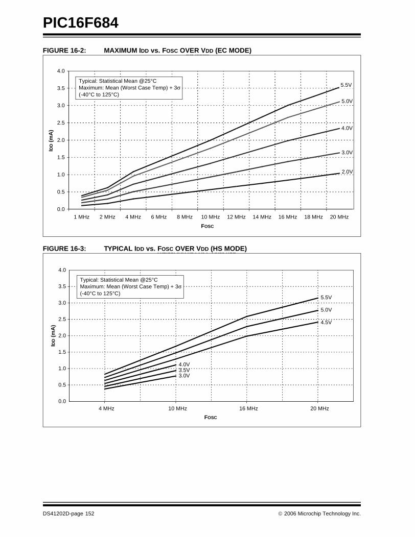
PIC16F684
FIGURE 16-2: MAXIMUM IDD vs. FOSC OVER VDD (EC MODE)
FIGURE 16-3: TYPICAL IDD vs. FOSC OVER VDD (HS MODE)
EC Mode
3.0V
4.0V
5.0V
2.0V
0.0
0.5
1.0
1.5
2.0
2.5
3.0
3.5
4.0
1 MHz 2 MHz 4 MHz 6 MHz 8 MHz 10 MHz 12 MHz 14 MHz 16 MHz 18 MHz 20 MHz
FOSC
IDD
(m
A)
5.5V
Typical: Statistical Mean @25°CMaximum: Mean (Worst Case Temp) + 3σ(-40°C to 125°C)
Typical IDD vs FOSC Over VddHS Mode
3.0V3.5V4.0V
4.5V
5.0V
5.5V
0.0
0.5
1.0
1.5
2.0
2.5
3.0
3.5
4.0
4 MHz 10 MHz 16 MHz 20 MHz
FOSC
IDD
(m
A)
Typical: Statistical Mean @25°CMaximum: Mean (Worst Case Temp) + 3σ(-40°C to 125°C)
DS41202D-page 152 © 2006 Microchip Technology Inc.
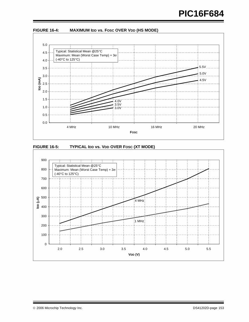
PIC16F684
FIGURE 16-4: MAXIMUM IDD vs. FOSC OVER VDD (HS MODE)
FIGURE 16-5: TYPICAL IDD vs. VDD OVER FOSC (XT MODE)
Maximum IDD vs FOSC Over VddHS Mode
3.5V4.0V
4.5V
5.0V
0.0
0.5
1.0
1.5
2.0
2.5
3.0
3.5
4.0
4.5
5.0
4 MHz 10 MHz 16 MHz 20 MHz
FOSC
IDD
(m
A)
Typical: Statistical Mean @25°CMaximum: Mean (Worst Case Temp) + 3σ(-40°C to 125°C)
3.0V
5.5V
XT Mode
0
100
200
300
400
500
600
700
800
900
2.0 2.5 3.0 3.5 4.0 4.5 5.0 5.5
VDD (V)
IDD
(μA
)
Typical: Statistical Mean @25°CMaximum: Mean (Worst Case Temp) + 3σ(-40°C to 125°C)
4 MHz
1 MHz
© 2006 Microchip Technology Inc. DS41202D-page 153
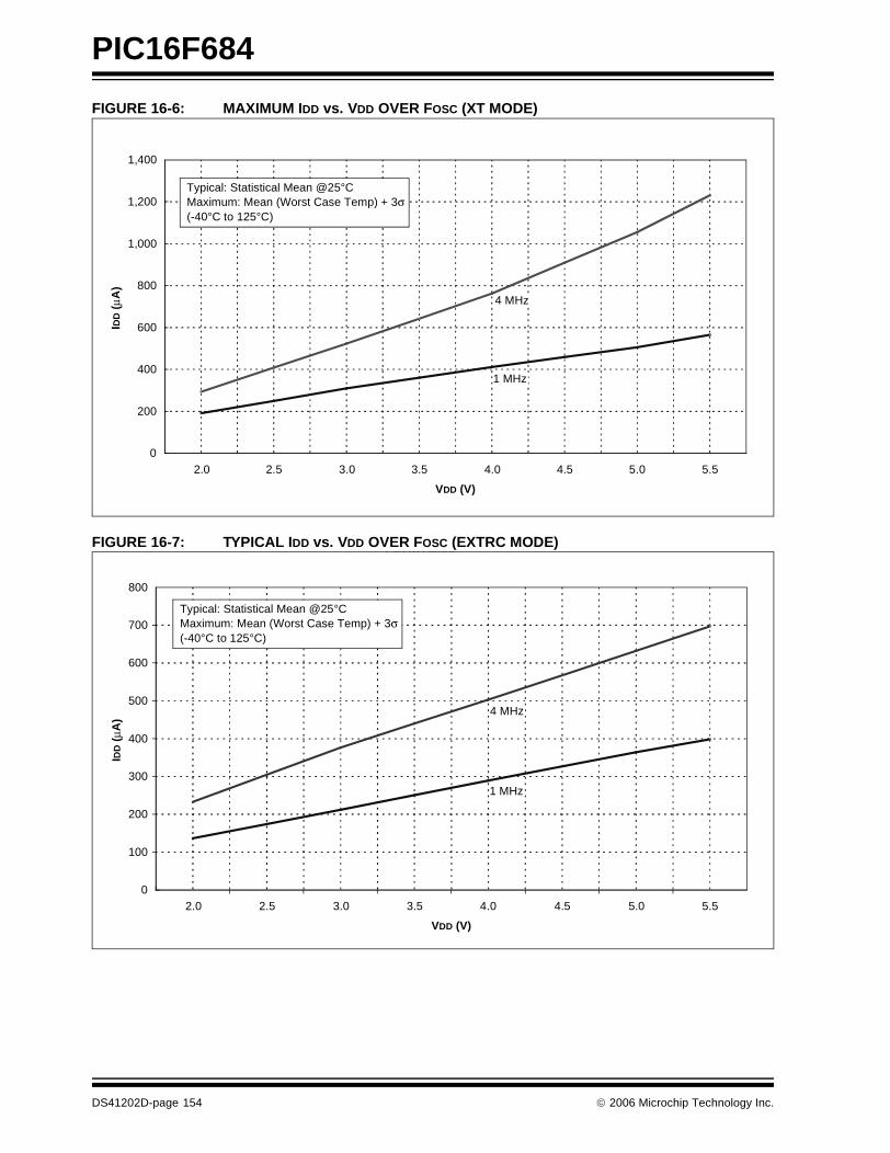
PIC16F684
FIGURE 16-6: MAXIMUM IDD vs. VDD OVER FOSC (XT MODE)
FIGURE 16-7: TYPICAL IDD vs. VDD OVER FOSC (EXTRC MODE)
XT Mode
0
200
400
600
800
1,000
1,200
1,400
2.0 2.5 3.0 3.5 4.0 4.5 5.0 5.5
VDD (V)
IDD
(μA
)
Typical: Statistical Mean @25°CMaximum: Mean (Worst Case Temp) + 3σ(-40°C to 125°C)
4 MHz
1 MHz
EXTRC Mode
0
100
200
300
400
500
600
700
800
2.0 2.5 3.0 3.5 4.0 4.5 5.0 5.5
VDD (V)
IDD
(μA
)
1 MHz
Typical: Statistical Mean @25°CMaximum: Mean (Worst Case Temp) + 3σ(-40°C to 125°C)
4 MHz
DS41202D-page 154 © 2006 Microchip Technology Inc.
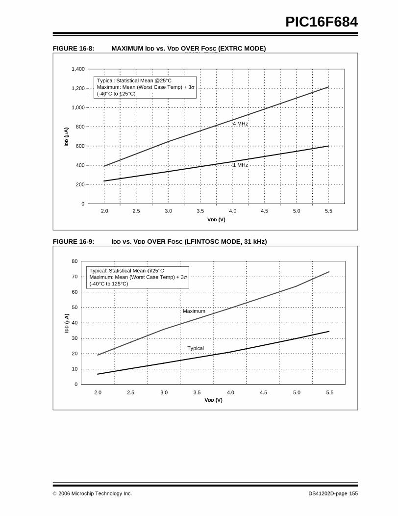
PIC16F684
FIGURE 16-8: MAXIMUM IDD vs. VDD OVER FOSC (EXTRC MODE)
FIGURE 16-9: IDD vs. VDD OVER FOSC (LFINTOSC MODE, 31 kHz)
EXTRC Mode
0
200
400
600
800
1,000
1,200
1,400
2.0 2.5 3.0 3.5 4.0 4.5 5.0 5.5
VDD (V)
IDD
(μA
)
Typical: Statistical Mean @25°CMaximum: Mean (Worst Case Temp) + 3σ(-40°C to 125°C)
4 MHz
1 MHz
LFINTOSC Mode, 31KHZ
Typical
Maximum
0
10
20
30
40
50
60
70
80
VDD (V)
IDD
(μA
)
Typical: Statistical Mean @25°CMaximum: Mean (Worst Case Temp) + 3σ(-40°C to 125°C)
2.0 2.5 3.0 3.5 4.0 4.5 5.0 5.5
© 2006 Microchip Technology Inc. DS41202D-page 155
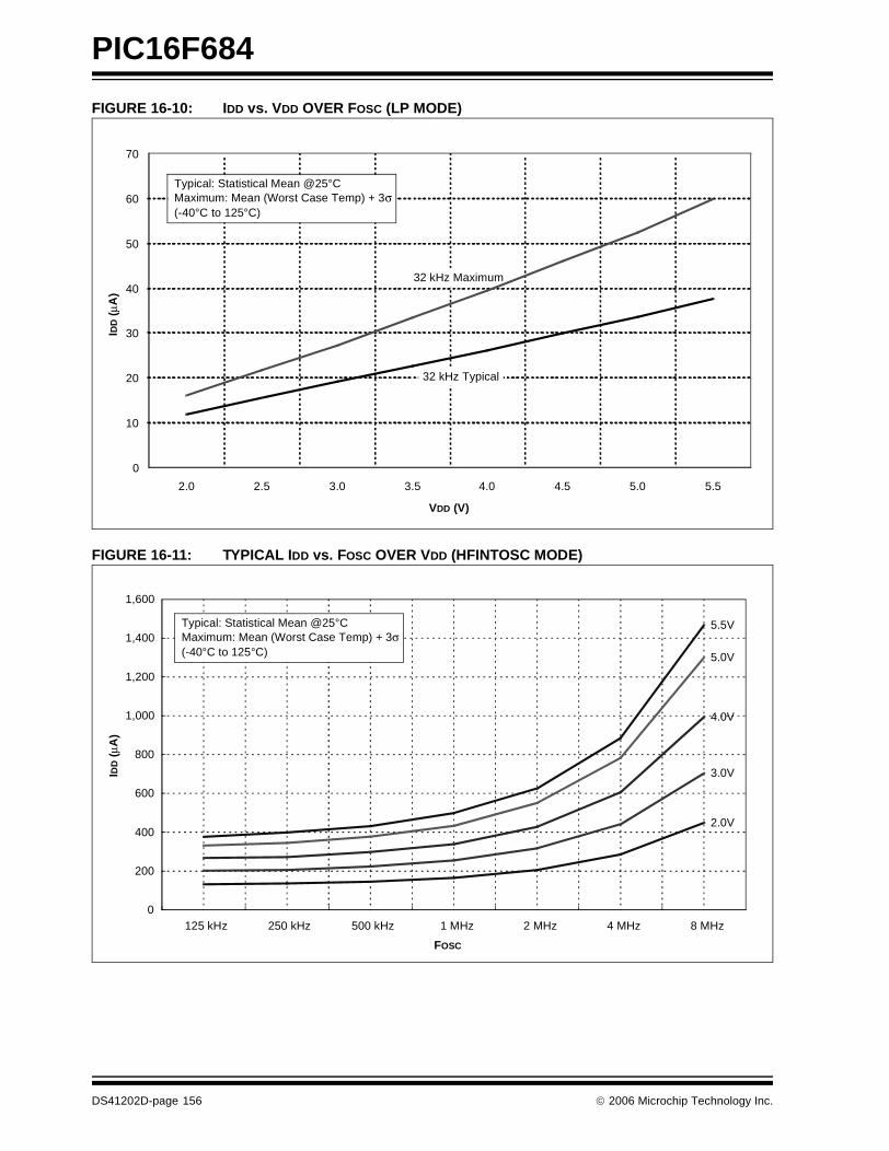
PIC16F684
FIGURE 16-10: IDD vs. VDD OVER FOSC (LP MODE)
FIGURE 16-11: TYPICAL IDD vs. FOSC OVER VDD (HFINTOSC MODE)
LP Mode
0
10
20
30
40
50
60
70
2.0 2.5 3.0 3.5 4.0 4.5 5.0 5.5
VDD (V)
IDD
(μA
)
Typical: Statistical Mean @25°CMaximum: Mean (Worst Case Temp) + 3σ(-40°C to 125°C)
32 kHz Maximum
32 kHz Typical
HFINTOSC
2.0V
3.0V
4.0V
5.0V
5.5V
0
200
400
600
800
1,000
1,200
1,400
1,600
125 kHz 250 kHz 500 kHz 1 MHz 2 MHz 4 MHz 8 MHz
FOSC
IDD
(μA
)
Typical: Statistical Mean @25°CMaximum: Mean (Worst Case Temp) + 3σ(-40°C to 125°C)
DS41202D-page 156 © 2006 Microchip Technology Inc.
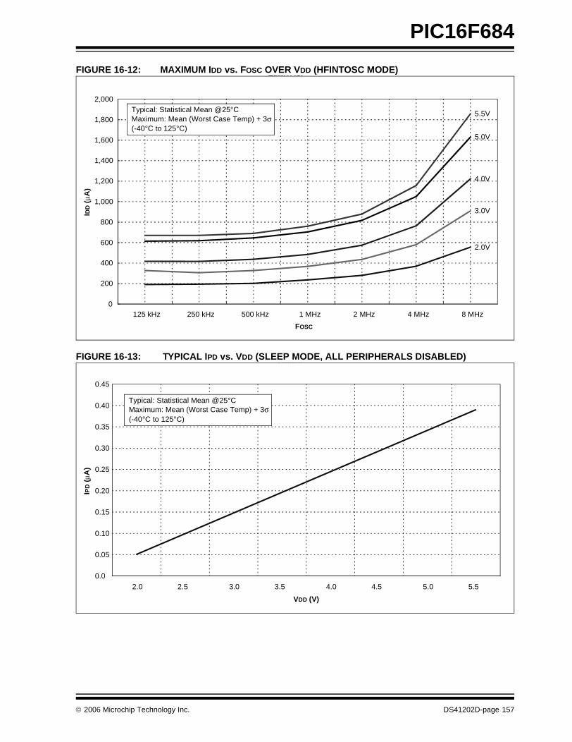
PIC16F684
FIGURE 16-12: MAXIMUM IDD vs. FOSC OVER VDD (HFINTOSC MODE)
FIGURE 16-13: TYPICAL IPD vs. VDD (SLEEP MODE, ALL PERIPHERALS DISABLED)
HFINTOSC
2.0V
3.0V
4.0V
5.0V
5.5V
0
200
400
600
800
1,000
1,200
1,400
1,600
1,800
2,000
125 kHz 250 kHz 500 kHz 1 MHz 2 MHz 4 MHz 8 MHz
FOSC
IDD
(μA
)
Typical: Statistical Mean @25°CMaximum: Mean (Worst Case Temp) + 3σ(-40°C to 125°C)
Typical(Sleep Mode all Peripherals Disabled)
0.0
0.05
0.10
0.15
0.20
0.25
0.30
0.35
0.40
0.45
2.0 2.5 3.0 3.5 4.0 4.5 5.0 5.5
VDD (V)
IPD
(μA
)
Typical: Statistical Mean @25°CMaximum: Mean (Worst Case Temp) + 3σ(-40°C to 125°C)
© 2006 Microchip Technology Inc. DS41202D-page 157
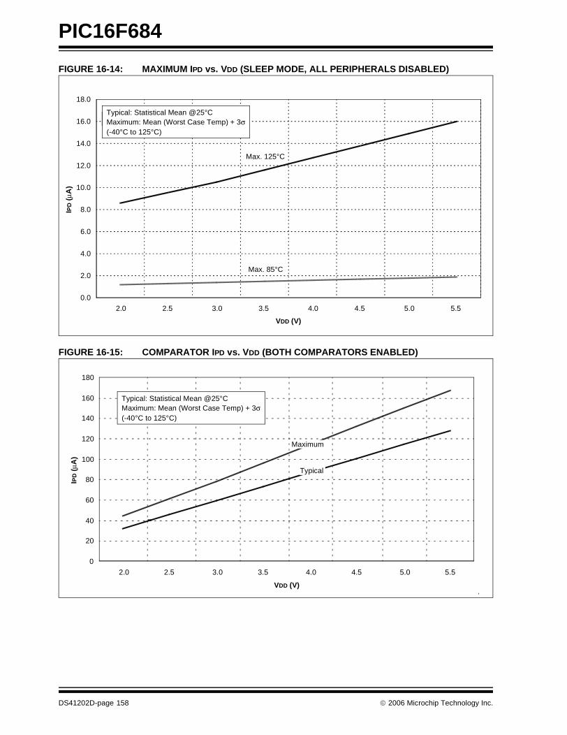
PIC16F684
FIGURE 16-14: MAXIMUM IPD vs. VDD (SLEEP MODE, ALL PERIPHERALS DISABLED)
FIGURE 16-15: COMPARATOR IPD vs. VDD (BOTH COMPARATORS ENABLED)
Maximum(Sleep Mode all Peripherals Disabled)
Max. 125°C
Max. 85°C
0.0
2.0
4.0
6.0
8.0
10.0
12.0
14.0
16.0
18.0
2.0 2.5 3.0 3.5 4.0 4.5 5.0 5.5
VDD (V)
IPD
(μA
)
Maximum: Mean + 3σTypical: Statistical Mean @25°CMaximum: Mean (Worst Case Temp) + 3σ(-40°C to 125°C)
0
20
40
60
80
100
120
140
160
180
2.0 2.5 3.0 3.5 4.0 4.5 5.0 5.5
VDD (V)
IPD
(μA
)
Maximum
Typical
Typical: Statistical Mean @25°CMaximum: Mean (Worst Case Temp) + 3σ(-40°C to 125°C)
DS41202D-page 158 © 2006 Microchip Technology Inc.
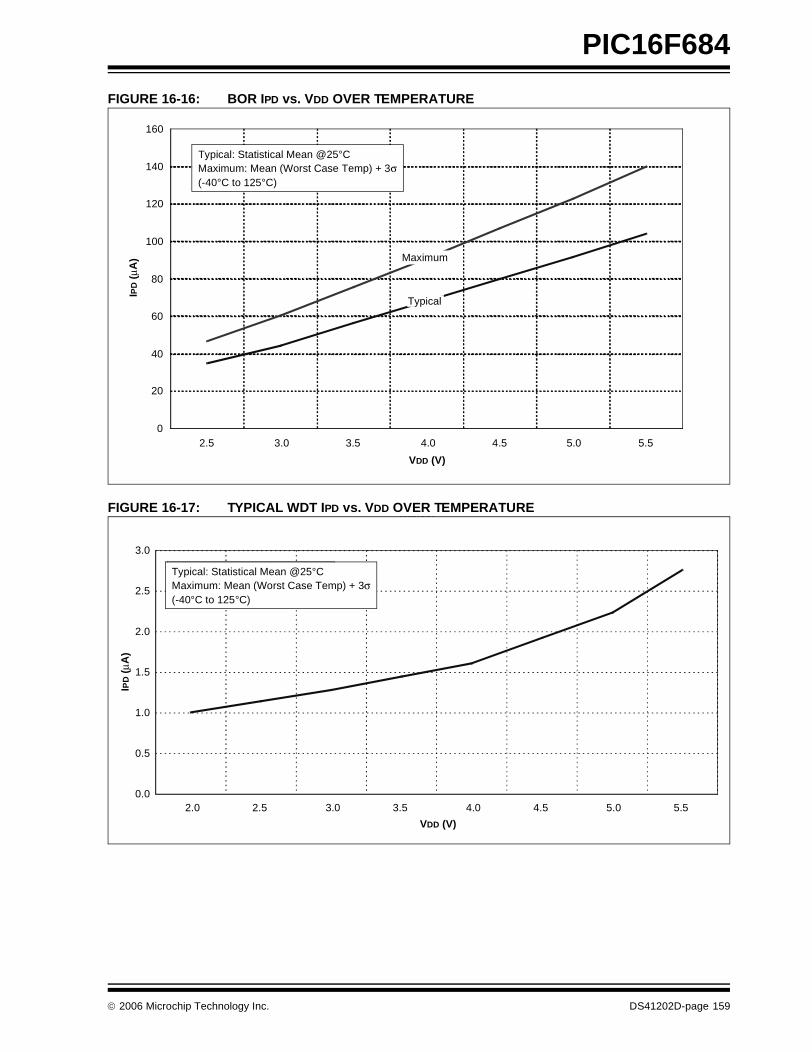
PIC16F684
FIGURE 16-16: BOR IPD vs. VDD OVER TEMPERATURE
FIGURE 16-17: TYPICAL WDT IPD vs. VDD OVER TEMPERATURE
0
20
40
60
80
100
120
140
160
2.5 3.0 3.5 4.0 4.5 5.0 5.5
VDD (V)
IPD
(μA
)
Typical: Statistical Mean @25°CMaximum: Mean (Worst Case Temp) + 3σ(-40°C to 125°C)
Maximum
Typical
Typical
0.0
0.5
1.0
1.5
2.0
2.5
3.0
2.0 2.5 3.0 3.5 4.0 4.5 5.0 5.5
VDD (V)
IPD
(μA
)
Typical: Statistical Mean @25°CTypical: Statistical Mean @25°CMaximum: Mean (Worst Case Temp) + 3σ(-40°C to 125°C)
© 2006 Microchip Technology Inc. DS41202D-page 159
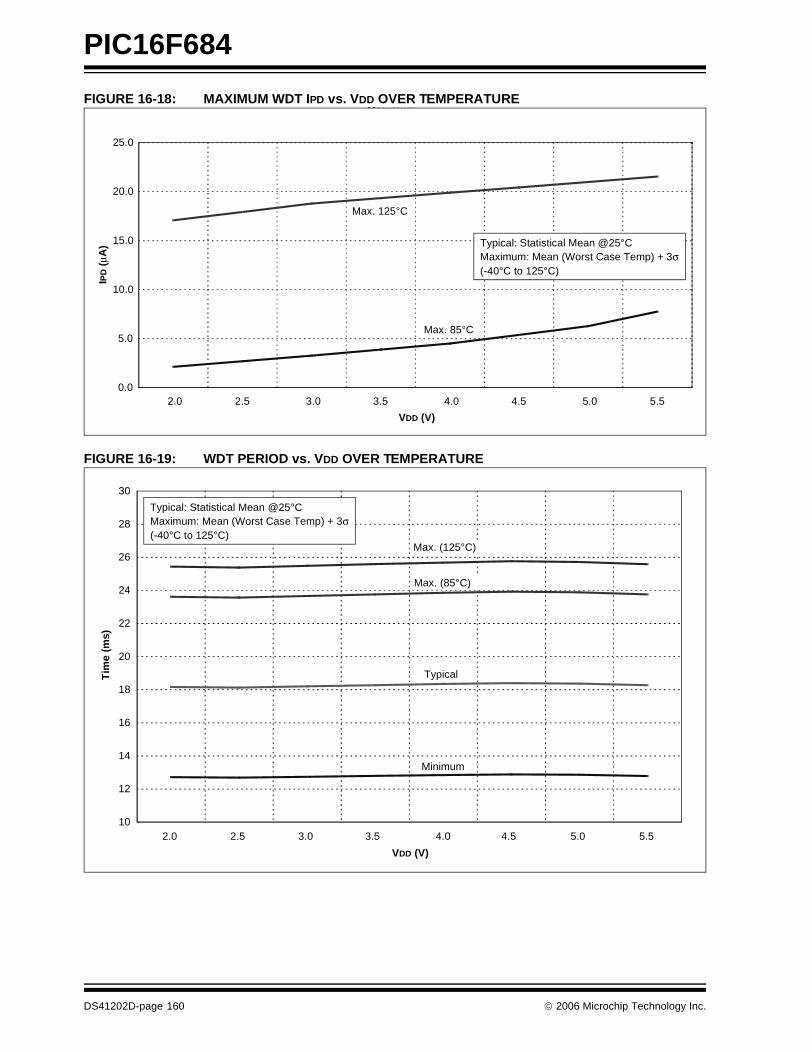
PIC16F684
FIGURE 16-18: MAXIMUM WDT IPD vs. VDD OVER TEMPERATURE
FIGURE 16-19: WDT PERIOD vs. VDD OVER TEMPERATURE
Maximum
Max. 125°C
Max. 85°C
0.0
5.0
10.0
15.0
20.0
25.0
2.0 2.5 3.0 3.5 4.0 4.5 5.0 5.5
VDD (V)
IPD
(μA
) Typical: Statistical Mean @25°CMaximum: Mean (Worst Case Temp) + 3σ(-40°C to 125°C)
Minimum
Typical
10
12
14
16
18
20
22
24
26
28
30
2.0 2.5 3.0 3.5 4.0 4.5 5.0 5.5
VDD (V)
Tim
e (m
s)
Typical: Statistical Mean @25°CMaximum: Mean (Worst Case Temp) + 3σ(-40°C to 125°C)
Max. (125°C)
Max. (85°C)
DS41202D-page 160 © 2006 Microchip Technology Inc.
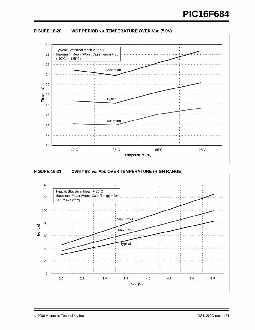
PIC16F684
FIGURE 16-20: WDT PERIOD vs. TEMPERATURE OVER VDD (5.0V)
FIGURE 16-21: CVREF IPD vs. VDD OVER TEMPERATURE (HIGH RANGE)
Vdd = 5V
10
12
14
16
18
20
22
24
26
28
30
-40°C 25°C 85°C 125°C
Temperature (°C)
Tim
e (m
s)
Typical: Statistical Mean @25°CMaximum: Mean (Worst Case Temp) + 3σ(-40°C to 125°C)
Maximum
Typical
Minimum
High Range
Typical
Max. 85°C
0
20
40
60
80
100
120
140
2.0 2.5 3.0 3.5 4.0 4.5 5.0 5.5
VDD (V)
IPD
(μA
)
Max. 125°C
Typical: Statistical Mean @25°CMaximum: Mean (Worst Case Temp) + 3σ(-40°C to 125°C)
© 2006 Microchip Technology Inc. DS41202D-page 161
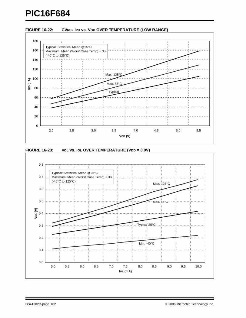
PIC16F684
FIGURE 16-22: CVREF IPD vs. VDD OVER TEMPERATURE (LOW RANGE)
FIGURE 16-23: VOL vs. IOL OVER TEMPERATURE (VDD = 3.0V)
Typical
Max. 85°C
0
20
40
60
80
100
120
140
160
180
2.0 2.5 3.0 3.5 4.0 4.5 5.0 5.5
VDD (V)
IPD
(μA
)
Max. 125°C
Typical: Statistical Mean @25°CMaximum: Mean (Worst Case Temp) + 3σ(-40°C to 125°C)
(VDD = 3V, -40×C TO 125×C)
0.0
0.1
0.2
0.3
0.4
0.5
0.6
0.7
0.8
5.0 5.5 6.0 6.5 7.0 7.5 8.0 8.5 9.0 9.5 10.0
IOL (mA)
VO
L (
V)
Max. 85°C
Max. 125°C
Typical 25°C
Min. -40°C
Typical: Statistical Mean @25°CMaximum: Mean (Worst Case Temp) + 3σ(-40°C to 125°C)
DS41202D-page 162 © 2006 Microchip Technology Inc.
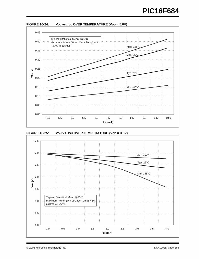
PIC16F684
FIGURE 16-24: VOL vs. IOL OVER TEMPERATURE (VDD = 5.0V)
FIGURE 16-25: VOH vs. IOH OVER TEMPERATURE (VDD = 3.0V)
0.00
0.05
0.10
0.15
0.20
0.25
0.30
0.35
0.40
0.45
5.0 5.5 6.0 6.5 7.0 7.5 8.0 8.5 9.0 9.5 10.0
IOL (mA)
VO
L (
V)
Typical: Statistical Mean @25×CMaximum: Meas + 3 (-40×C to 125×C)
Typical: Statistical Mean @25°CMaximum: Mean (Worst Case Temp) + 3σ(-40°C to 125°C)
Max. 85°C
Typ. 25°C
Min. -40°C
Max. 125°C
0.0
0.5
1.0
1.5
2.0
2.5
3.0
3.5
-4.0-3.5-3.0-2.5-2.0-1.5-1.0-0.50.0
IOH (mA)
VO
H (
V)
Typ. 25°C
Max. -40°C
Min. 125°C
Typical: Statistical Mean @25°CMaximum: Mean (Worst Case Temp) + 3σ(-40°C to 125°C)
© 2006 Microchip Technology Inc. DS41202D-page 163
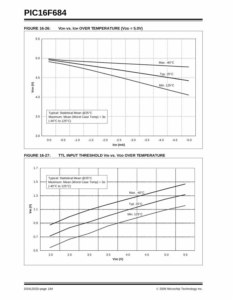
PIC16F684
FIGURE 16-26: VOH vs. IOH OVER TEMPERATURE (VDD = 5.0V)
FIGURE 16-27: TTL INPUT THRESHOLD VIN vs. VDD OVER TEMPERATURE
(VDD = 5V, -40×C TO 125×C)
3.0
3.5
4.0
4.5
5.0
5.5
-5.0-4.5-4.0-3.5-3.0-2.5-2.0-1.5-1.0-0.50.0
IOH (mA)
VO
H (
V)
Max. -40°C
Typ. 25°C
Min. 125°C
Typical: Statistical Mean @25°CMaximum: Mean (Worst Case Temp) + 3σ(-40°C to 125°C)
(TTL Input, -40×C TO 125×C)
0.5
0.7
0.9
1.1
1.3
1.5
1.7
2.0 2.5 3.0 3.5 4.0 4.5 5.0 5.5
VDD (V)
VIN
(V
) Typ. 25°C
Max. -40°C
Min. 125°C
Typical: Statistical Mean @25°CMaximum: Mean (Worst Case Temp) + 3σ(-40°C to 125°C)
DS41202D-page 164 © 2006 Microchip Technology Inc.
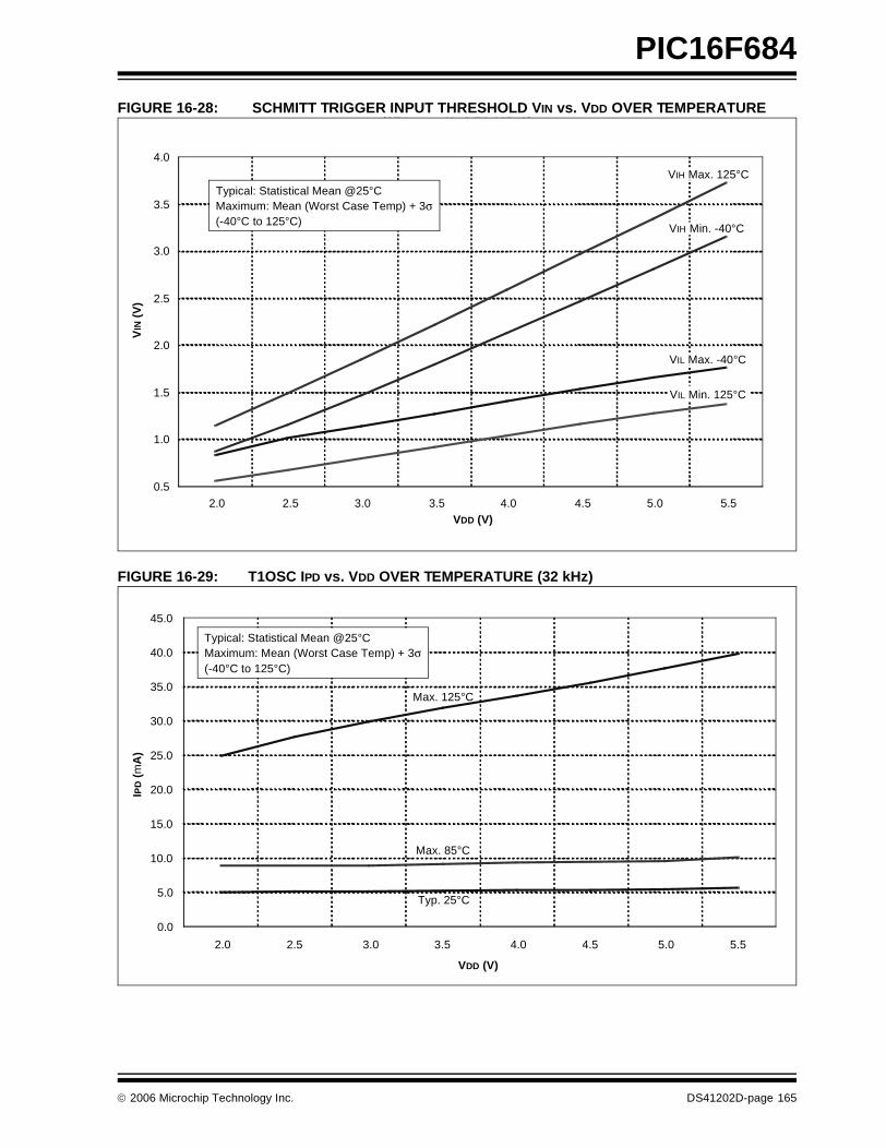
PIC16F684
FIGURE 16-28: SCHMITT TRIGGER INPUT THRESHOLD VIN vs. VDD OVER TEMPERATURE
FIGURE 16-29: T1OSC IPD vs. VDD OVER TEMPERATURE (32 kHz)
(ST Input, -40×C TO 125×C)
0.5
1.0
1.5
2.0
2.5
3.0
3.5
4.0
2.0 2.5 3.0 3.5 4.0 4.5 5.0 5.5VDD (V)
VIN
(V
)
VIH Max. 125°C
VIH Min. -40°C
VIL Min. 125°C
VIL Max. -40°C
Typical: Statistical Mean @25°CMaximum: Mean (Worst Case Temp) + 3σ(-40°C to 125°C)
Typ. 25°C
Max. 85°C
Max. 125°C
0.0
5.0
10.0
15.0
20.0
25.0
30.0
35.0
40.0
45.0
2.0 2.5 3.0 3.5 4.0 4.5 5.0 5.5
VDD (V)
IPD
(m
A)
Maximum: Mean + 3 (-40×C to 125×C)
Typical: Statistical Mean @25°CMaximum: Mean (Worst Case Temp) + 3σ(-40°C to 125°C)
© 2006 Microchip Technology Inc. DS41202D-page 165
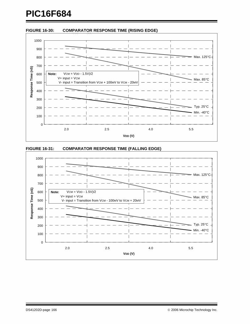
PIC16F684
FIGURE 16-30: COMPARATOR RESPONSE TIME (RISING EDGE)
FIGURE 16-31: COMPARATOR RESPONSE TIME (FALLING EDGE)
531 806
0
100
200
300
400
500
600
700
800
900
1000
2.0 2.5 4.0 5.5
VDD (V)
Res
po
nse
Tim
e (n
S)
Max. 85°C
Typ. 25°C
Min. -40°C
Max. 125°C
Note:
V- input = Transition from VCM + 100MV to VCM - 20MV V+ input = VCM
VCM = VDD - 1.5V)/2
0
100
200
300
400
500
600
700
800
900
1000
2.0 2.5 4.0 5.5
VDD (V)
Res
po
nse
Tim
e (n
S)
Max. 85°C
Typ. 25°C
Min. -40°C
Max. 125°C
Note:
V- input = Transition from VCM - 100MV to VCM + 20MV V+ input = VCM
VCM = VDD - 1.5V)/2
DS41202D-page 166 © 2006 Microchip Technology Inc.
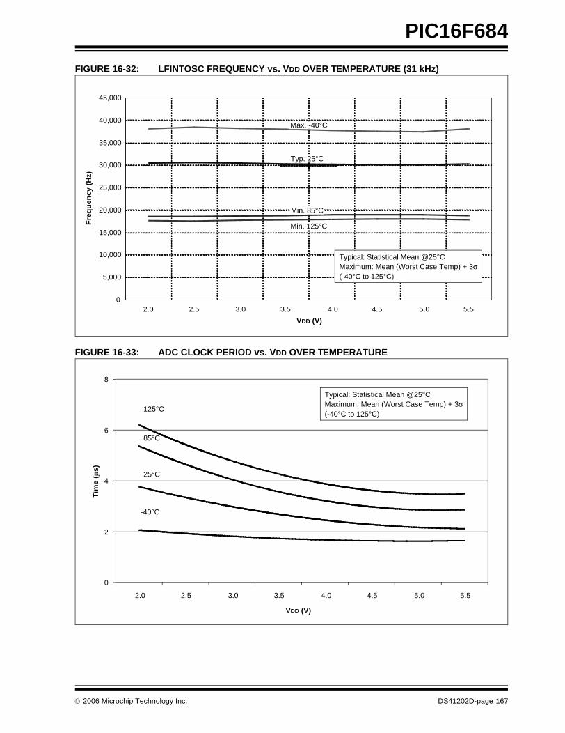
PIC16F684
FIGURE 16-32: LFINTOSC FREQUENCY vs. VDD OVER TEMPERATURE (31 kHz)
FIGURE 16-33: ADC CLOCK PERIOD vs. VDD OVER TEMPERATURE
LFINTOSC 31Khz
0
5,000
10,000
15,000
20,000
25,000
30,000
35,000
40,000
45,000
2.0 2.5 3.0 3.5 4.0 4.5 5.0 5.5
VDD (V)
Fre
qu
ency
(H
z)
Max. -40°C
Typ. 25°C
Min. 85°C
Min. 125°C
Typical: Statistical Mean @25°CMaximum: Mean (Worst Case Temp) + 3σ(-40°C to 125°C)
0
2
4
6
8
2.0 2.5 3.0 3.5 4.0 4.5 5.0 5.5
VDD (V)
Tim
e (μ
s)
25°C
85°C
125°C
-40°C
Typical: Statistical Mean @25°CMaximum: Mean (Worst Case Temp) + 3σ(-40°C to 125°C)
© 2006 Microchip Technology Inc. DS41202D-page 167
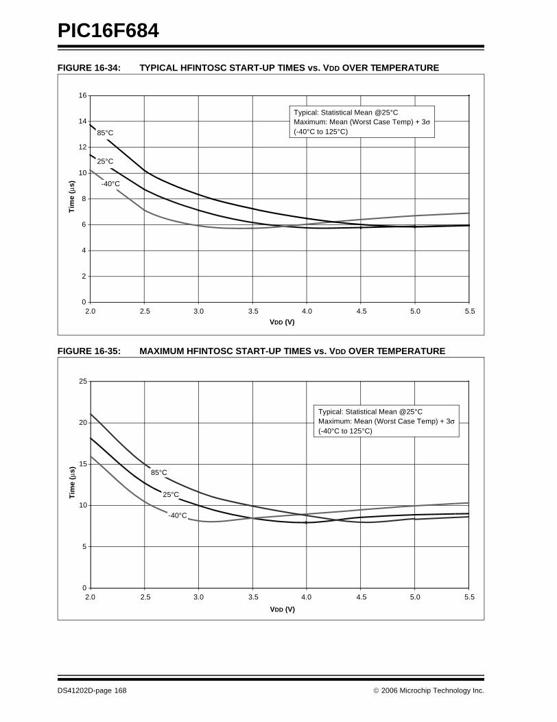
PIC16F684
FIGURE 16-34: TYPICAL HFINTOSC START-UP TIMES vs. VDD OVER TEMPERATURE
FIGURE 16-35: MAXIMUM HFINTOSC START-UP TIMES vs. VDD OVER TEMPERATURE
0
2
4
6
8
10
12
14
16
2.0 2.5 3.0 3.5 4.0 4.5 5.0 5.5
VDD (V)
Tim
e (μ
s)
85°C
25°C
-40°C
Typical: Statistical Mean @25°CMaximum: Mean (Worst Case Temp) + 3σ(-40°C to 125°C)
-40C to +85C
0
5
10
15
20
25
2.0 2.5 3.0 3.5 4.0 4.5 5.0 5.5
VDD (V)
Tim
e (μ
s)
-40°C
85°C
25°C
Typical: Statistical Mean @25°CMaximum: Mean (Worst Case Temp) + 3σ(-40°C to 125°C)
DS41202D-page 168 © 2006 Microchip Technology Inc.
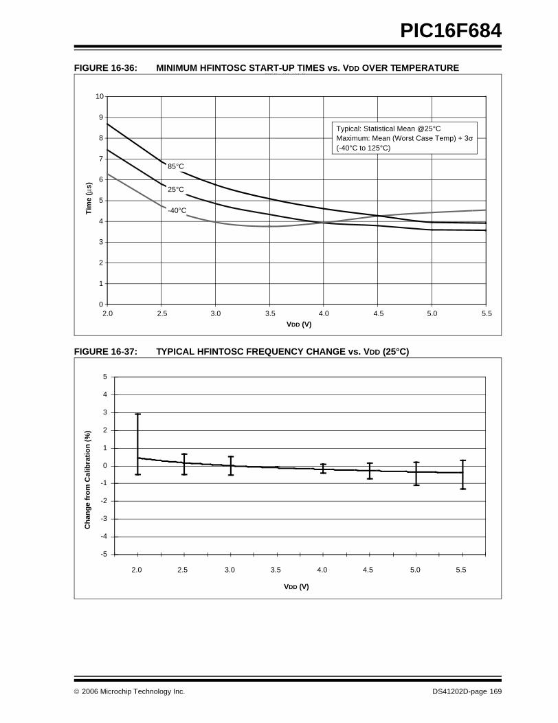
PIC16F684
FIGURE 16-36: MINIMUM HFINTOSC START-UP TIMES vs. VDD OVER TEMPERATURE
FIGURE 16-37: TYPICAL HFINTOSC FREQUENCY CHANGE vs. VDD (25°C)
-40C to +85C
0
1
2
3
4
5
6
7
8
9
10
2.0 2.5 3.0 3.5 4.0 4.5 5.0 5.5
VDD (V)
Tim
e (μ
s)
-40°C
25°C
85°C
Typical: Statistical Mean @25°CMaximum: Mean (Worst Case Temp) + 3σ(-40°C to 125°C)
-5
-4
-3
-2
-1
0
1
2
3
4
5
2.0 2.5 3.0 3.5 4.0 4.5 5.0 5.5
VDD (V)
Ch
ang
e fr
om
Cal
ibra
tio
n (
%)
© 2006 Microchip Technology Inc. DS41202D-page 169
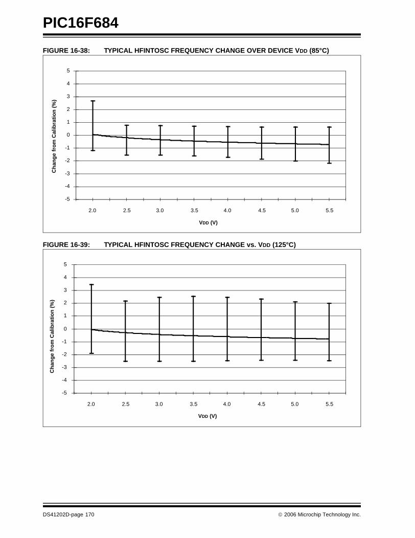
PIC16F684
FIGURE 16-38: TYPICAL HFINTOSC FREQUENCY CHANGE OVER DEVICE VDD (85°C)
FIGURE 16-39: TYPICAL HFINTOSC FREQUENCY CHANGE vs. VDD (125°C)
-5
-4
-3
-2
-1
0
1
2
3
4
5
2.0 2.5 3.0 3.5 4.0 4.5 5.0 5.5
VDD (V)
Ch
ang
e fr
om
Cal
ibra
tio
n (
%)
-5
-4
-3
-2
-1
0
1
2
3
4
5
2.0 2.5 3.0 3.5 4.0 4.5 5.0 5.5
VDD (V)
Ch
ang
e fr
om
Cal
ibra
tio
n (
%)
DS41202D-page 170 © 2006 Microchip Technology Inc.
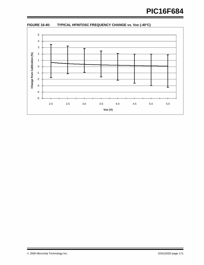
PIC16F684
FIGURE 16-40: TYPICAL HFINTOSC FREQUENCY CHANGE vs. VDD (-40°C)
-5
-4
-3
-2
-1
0
1
2
3
4
5
2.0 2.5 3.0 3.5 4.0 4.5 5.0 5.5
VDD (V)
Ch
ang
e fr
om
Cal
ibra
tio
n (
%)
© 2006 Microchip Technology Inc. DS41202D-page 171

PIC16F684
NOTES:
DS41202D-page 172 © 2006 Microchip Technology Inc.
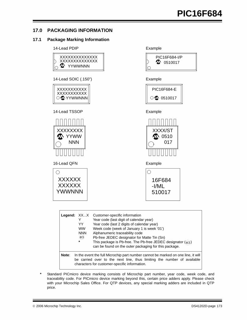
PIC16F684
17.0 PACKAGING INFORMATION
17.1 Package Marking Information
* Standard PICmicro device marking consists of Microchip part number, year code, week code, andtraceability code. For PICmicro device marking beyond this, certain price adders apply. Please checkwith your Microchip Sales Office. For QTP devices, any special marking adders are included in QTPprice.
XXXXXX
16-Lead QFN
XXXXXXYWWNNN
16F684
Example
-I/ML510017
14-Lead PDIP
XXXXXXXXXXXXXXXXXXXXXXXXXXXX
YYWWNNN
Example
PIC16F684-I/P0510017
14-Lead SOIC (.150”)
XXXXXXXXXXXXXXXXXXXXXX
YYWWNNN
Example
PIC16F684-E
0510017
14-Lead TSSOP
XXXXXXXXYYWWNNN
Example
XXXX/ST0510017
Legend: XX...X Customer-specific informationY Year code (last digit of calendar year)YY Year code (last 2 digits of calendar year)WW Week code (week of January 1 is week ‘01’)NNN Alphanumeric traceability code Pb-free JEDEC designator for Matte Tin (Sn)* This package is Pb-free. The Pb-free JEDEC designator ( )
can be found on the outer packaging for this package.
Note: In the event the full Microchip part number cannot be marked on one line, it willbe carried over to the next line, thus limiting the number of availablecharacters for customer-specific information.
3e
3e
© 2006 Microchip Technology Inc. DS41202D-page 173
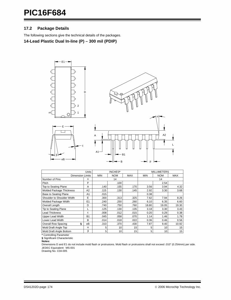
PIC16F684
17.2 Package Details
The following sections give the technical details of the packages.
14-Lead Plastic Dual In-line (P) – 300 mil (PDIP)
E1
n
D
1
2
eB
β
E
c
A
A1
B
B1
L
A2
p
α
Units INCHES* MILLIMETERSDimension Limits MIN NOM MAX MIN NOM MAX
Number of Pins n 14 14Pitch p .100 2.54Top to Seating Plane A .140 .155 .170 3.56 3.94 4.32Molded Package Thickness A2 .115 .130 .145 2.92 3.30 3.68Base to Seating Plane A1 .015 0.38Shoulder to Shoulder Width E .300 .313 .325 7.62 7.94 8.26Molded Package Width E1 .240 .250 .260 6.10 6.35 6.60Overall Length D .740 .750 .760 18.80 19.05 19.30Tip to Seating Plane L .125 .130 .135 3.18 3.30 3.43Lead Thickness c .008 .012 .015 0.20 0.29 0.38Upper Lead Width B1 .045 .058 .070 1.14 1.46 1.78Lower Lead Width B .014 .018 .022 0.36 0.46 0.56Overall Row Spacing § eB .310 .370 .430 7.87 9.40 10.92Mold Draft Angle Top α 5 10 15 5 10 15
β 5 10 15 5 10 15Mold Draft Angle Bottom* Controlling Parameter
Notes:Dimensions D and E1 do not include mold flash or protrusions. Mold flash or protrusions shall not exceed .010” (0.254mm) per side. JEDEC Equivalent: MS-001Drawing No. C04-005
§ Significant Characteristic
DS41202D-page 174 © 2006 Microchip Technology Inc.
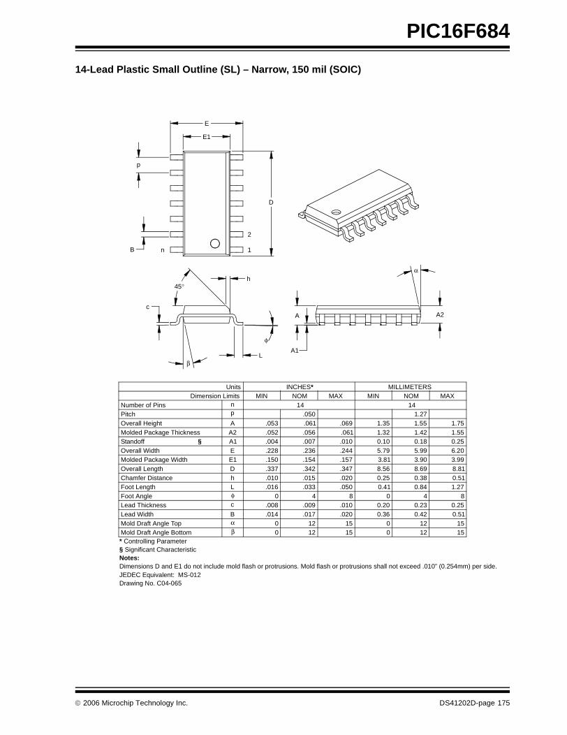
PIC16F684
14-Lead Plastic Small Outline (SL) – Narrow, 150 mil (SOIC)
Foot Angle φ 0 4 8 0 4 8
1512015120βMold Draft Angle Bottom1512015120αMold Draft Angle Top
0.510.420.36.020.017.014BLead Width0.250.230.20.010.009.008cLead Thickness
1.270.840.41.050.033.016LFoot Length0.510.380.25.020.015.010hChamfer Distance8.818.698.56.347.342.337DOverall Length3.993.903.81.157.154.150E1Molded Package Width6.205.995.79.244.236.228EOverall Width0.250.180.10.010.007.004A1Standoff §1.551.421.32.061.056.052A2Molded Package Thickness1.751.551.35.069.061.053AOverall Height
1.27.050pPitch1414nNumber of Pins
MAXNOMMINMAXNOMMINDimension LimitsMILLIMETERSINCHES*Units
2
1
D
p
nB
E
E1
h
L
c
β
45°
φ
α
A2A
A1
* Controlling Parameter
Notes:Dimensions D and E1 do not include mold flash or protrusions. Mold flash or protrusions shall not exceed .010” (0.254mm) per side. JEDEC Equivalent: MS-012Drawing No. C04-065
§ Significant Characteristic
© 2006 Microchip Technology Inc. DS41202D-page 175
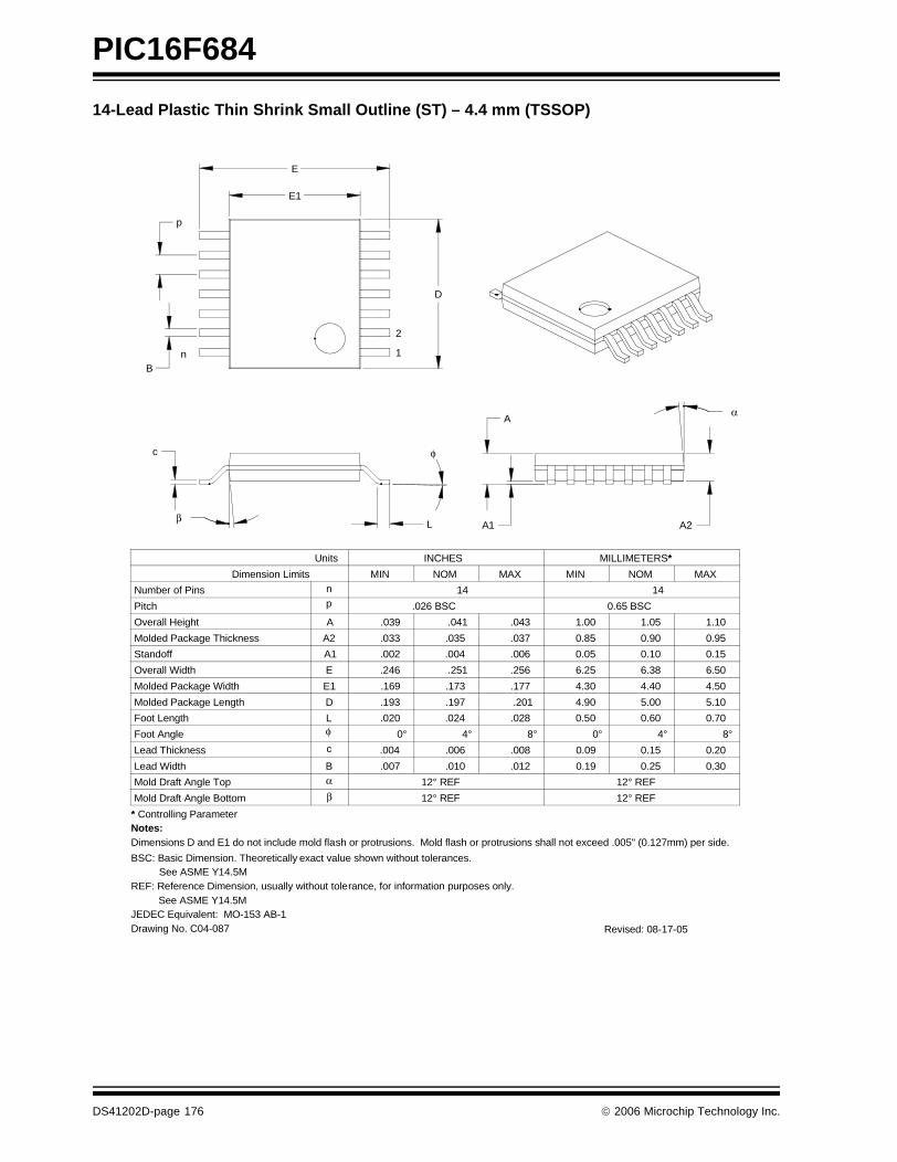
PIC16F684
14-Lead Plastic Thin Shrink Small Outline (ST) – 4.4 mm (TSSOP)
Lβ
c φ
2
1
D
nB
p
E1
E
α
A2A1
A
8°4°0°8°4°0°φFoot Angle
βMold Draft Angle Bottom
12° REFαMold Draft Angle Top
0.300.250.19.012.010.007BLead Width
0.200.150.09.008.006.004cLead Thickness
0.700.600.50.028.024.020LFoot Length
5.105.004.90.201.197.193DMolded Package Length
4.504.404.30.177.173.169E1Molded Package Width
6.506.386.25.256.251.246EOverall Width
0.150.100.05.006.004.002A1Standoff
0.950.900.85.037.035.033A2Molded Package Thickness
1.101.051.00.043.041.039AOverall Height
0.65 BSC.026 BSCpPitch
1414nNumber of Pins
MAXNOMMINMAXNOMMINDimension Limits
MILLIMETERS*INCHESUnits
Dimensions D and E1 do not include mold flash or protrusions. Mold flash or protrusions shall not exceed .005" (0.127mm) per side.Notes:
JEDEC Equivalent: MO-153 AB-1
Revised: 08-17-05
* Controlling Parameter
BSC: Basic Dimension. Theoretically exact value shown without tolerances.
REF: Reference Dimension, usually without tolerance, for information purposes only.See ASME Y14.5M
See ASME Y14.5M
Drawing No. C04-087
12° REF
12° REF
12° REF
DS41202D-page 176 © 2006 Microchip Technology Inc.
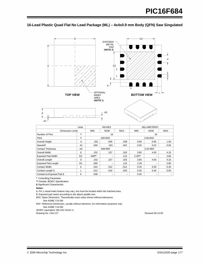
PIC16F684
16-Lead Plastic Quad Flat No Lead Package (ML) – 4x4x0.9 mm Body (QFN) Saw Singulated
2
1
n
D
E E2
D2
e
b
L
A A3
EXPOSEDMETAL
PAD
OPTIONALINDEXAREA
TOP VIEW BOTTOM VIEW
(NOTE 2)
(NOTE 1)
A1
K
BSC: Basic Dimension. Theoretically exact value shown without tolerances.
REF: Reference Dimension, usually without tolerance, for information purposes only.
JEDEC equivalent: M0-220 VGGC-3
See ASME Y14.5M
See ASME Y14.5M
* Controlling Parameter
Notes:
INCHES
NOM
.026 BSC
.008 REF
Number of Pins
Overall Height
Overall Width
Contact Width
Overall Length
Contact-to-Exposed Pad §
Exposed Pad Width
Exposed Pad Length
Contact Thickness
Pitch
Standoff
Units
Dimension Limits
e
E2
b
K
D2
D
A3
E
A1
A
.090**
.010
.008
.152
.090
.152
.000
.031
MINn
MIN
–
.157
.012
–
–
.035
.157
.001
.110
.014
.163
.110
–
.039
.163
.002
MAX
16
0.65 BSC
0.20 REF
2.29**
3.85
0.25
2.29
0.20
0.80
3.85
0.00
–
0.30
4.00
–
–
0.90
4.00
0.02
NOM
MILLIMETERS*
16
2.80
0.35
4.15
2.80
–
1.00
4.15
0.05
MAX
2. Exposed pad varies according to die attach paddle size.1. Pin 1 visual index feature may vary, but must be located within the hatched area.
§ Significant Characteristic
Contact Length § L .012 .016 0.30.020 0.40 0.50
** Outside JEDEC Specification
Drawing No. C04-127 Revised 09-13-05
© 2006 Microchip Technology Inc. DS41202D-page 177

PIC16F684
NOTES:
DS41202D-page 178 © 2006 Microchip Technology Inc.

PIC16F684
APPENDIX A: DATA SHEET REVISION HISTORY
Revision A
This is a new data sheet.
Revision B
Rewrites of the Oscillator and Special Features of theCPU Sections. General corrections to Figures andformatting.
Revision C
Revision D
Added Characterization Data. Updated ElectricalSpecifications. Incorporated Golden Chapter Sectionsfor the following:
• Section 3.0 “Oscillator Module (With Fail-Safe Clock Monitor)”
• Section 5.0 “Timer0 Module”• Section 6.0 “Timer1 Module with Gate Control”• Section 7.0 “Timer2 Module”• Section 8.0 “Comparator Module”• Section 9.0 “Analog-to-Digital Converter (ADC)
Module”• Section 11.0 “Enhanced Capture/Compare/PWM
(With Auto-Shutdown and Dead Band) Module”
APPENDIX B: MIGRATING FROM OTHER PICmicro® DEVICES
This discusses some of the issues in migrating fromother PICmicro devices to the PIC16F6XX Family ofdevices.
B.1 PIC16F676 to PIC16F684
TABLE B-1: FEATURE COMPARISON
Feature PIC16F676 PIC16F684
Max Operating Speed
20 MHz 20 MHz
Max Program Memory (Words)
1024 2048
SRAM (bytes) 64 128
A/D Resolution 10-bit 10-bit
Data EEPROM (Bytes)
128 256
Timers (8/16-bit) 1/1 2/1
Oscillator Modes 8 8
Brown-out Reset Y Y
Internal Pull-ups RA0/1/2/4/5 RA0/1/2/4/5, MCLR
Interrupt-on-change RA0/1/2/3/4/5 RA0/1/2/3/4/5
Comparator 1 2
ECCP N Y
Ultra Low-Power Wake-Up
N Y
Extended WDT N Y
Software Control Option of WDT/BOR
N Y
INTOSC Frequencies
4 MHz 32 kHz-8 MHz
Clock Switching N Y
Note: This device has been designed to performto the parameters of its data sheet. It hasbeen tested to an electrical specificationdesigned to determine its conformancewith these parameters. Due to processdifferences in the manufacture of thisdevice, this device may have differentperformance characteristics than its earlierversion. These differences may cause thisdevice to perform differently in yourapplication than the earlier version of thisdevice.
© 2006 Microchip Technology Inc. DS41202D-page 179

PIC16F684
NOTES:
DS41202D-page 180 © 2006 Microchip Technology Inc.
PIC16F684
INDEX
AA/D
Specifications.................................................... 149, 150Absolute Maximum Ratings .............................................. 131AC Characteristics
Industrial and Extended ............................................ 141Load Conditions ........................................................ 140
ADC .................................................................................... 67Acquisition Requirements ........................................... 74Associated registers.................................................... 76Block Diagram............................................................. 67Calculating Acquisition Time....................................... 74Channel Selection....................................................... 68Configuration............................................................... 68Configuring Interrupt ................................................... 70Conversion Clock........................................................ 68Conversion Procedure ................................................ 70Internal Sampling Switch (RSS) Impedance................ 74Interrupts..................................................................... 69Operation .................................................................... 70Operation During Sleep .............................................. 70Port Configuration ....................................................... 68Reference Voltage (VREF)........................................... 68Result Formatting........................................................ 69Source Impedance...................................................... 74Special Event Trigger.................................................. 70Starting an A/D Conversion ........................................ 69
ADCON0 Register............................................................... 72ADCON1 Register............................................................... 72ADRESH Register (ADFM = 0) ........................................... 73ADRESH Register (ADFM = 1) ........................................... 73ADRESL Register (ADFM = 0)............................................ 73ADRESL Register (ADFM = 1)............................................ 73Analog Input Connection Considerations............................ 58Analog-to-Digital Converter. See ADCANSEL Register .................................................................. 32Assembler
MPASM Assembler................................................... 128
BBlock Diagrams
(CCP) Capture Mode Operation ................................. 82ADC ............................................................................ 67ADC Transfer Function ............................................... 75Analog Input Model ............................................... 58, 75CCP PWM................................................................... 84Clock Source............................................................... 19Comparator 1 .............................................................. 57Comparator 2 .............................................................. 57Comparator Modes ..................................................... 59Compare ..................................................................... 83Crystal Operation ........................................................ 22External RC Mode....................................................... 23Fail-Safe Clock Monitor (FSCM) ................................. 29In-Circuit Serial Programming Connections.............. 116Interrupt Logic ........................................................... 109MCLR Circuit............................................................. 102On-Chip Reset Circuit ............................................... 101PIC16F684.................................................................... 5PWM (Enhanced)........................................................ 87RA0 Pins ..................................................................... 35RA1 Pins ..................................................................... 36RA2 Pin....................................................................... 36RA3 Pin....................................................................... 37
RA4 Pin ...................................................................... 37RA5 Pin ...................................................................... 38RC0 and RC1 Pins ..................................................... 41RC2 and RC3 Pins ..................................................... 41RC4 Pin ...................................................................... 42RC5 Pin ...................................................................... 42Resonator Operation .................................................. 22Timer1 ........................................................................ 47Timer2 ........................................................................ 54TMR0/WDT Prescaler ................................................ 43Watchdog Timer (WDT)............................................ 112
Brown-out Reset (BOR).................................................... 103Associated ................................................................ 104Calibration ................................................................ 103Specifications ........................................................... 145Timing and Characteristics ....................................... 144
CC Compilers
MPLAB C18.............................................................. 128MPLAB C30.............................................................. 128
Calibration Bits.................................................................. 101Capture Module. See Enhanced
Capture/Compare/PWM (ECCP)Capture/Compare/PWM (CCP)
Associated registers w/ Capture/Compare/PWM ....... 98Capture Mode............................................................. 82CCP1 Pin Configuration ............................................. 82Compare Mode........................................................... 83
CCP1 Pin Configuration ..................................... 83Software Interrupt Mode............................... 82, 83Special Event Trigger ......................................... 83Timer1 Mode Selection................................. 82, 83
Prescaler .................................................................... 82PWM Mode................................................................. 84
Duty Cycle .......................................................... 85Effects of Reset .................................................. 86Example PWM Frequencies and
Resolutions, 20 MHZ.................................. 85Example PWM Frequencies and
Resolutions, 8 MHz .................................... 85Operation in Sleep Mode.................................... 86Setup for Operation ............................................ 86System Clock Frequency Changes .................... 86
PWM Period ............................................................... 85Setup for PWM Operation .......................................... 86
CCP1CON (Enhanced) Register ........................................ 81Clock Sources
External Modes........................................................... 21EC ...................................................................... 21HS ...................................................................... 22LP ....................................................................... 22OST .................................................................... 21RC ...................................................................... 23XT....................................................................... 22
Internal Modes............................................................ 23Frequency Selection........................................... 25HFINTOSC ......................................................... 23HFINTOSC/LFINTOSC Switch Timing ............... 25INTOSC.............................................................. 23INTOSCIO .......................................................... 23LFINTOSC.......................................................... 25
Clock Switching .................................................................. 27CMCON0 Register.............................................................. 62
© 2006 Microchip Technology Inc. DS41202D-page 181
PIC16F684
CMCON1 Register .............................................................. 63Code Examples
A/D Conversion........................................................... 71Assigning Prescaler to Timer0 .................................... 44Assigning Prescaler to WDT ....................................... 44Changing Between Capture Prescalers ...................... 82Data EEPROM Read .................................................. 79Data EEPROM Write .................................................. 79Indirect Addressing ..................................................... 19Initializing PORTA....................................................... 31Initializing PORTC....................................................... 40Saving Status and W Registers in RAM ................... 111Ultra Low-Power Wake-Up Initialization...................... 34Write Verify ................................................................. 79
Code Protection ................................................................ 115Comparator ......................................................................... 56
C2OUT as T1 Gate ..................................................... 63Configurations............................................................. 59Interrupts..................................................................... 60Operation .................................................................... 60Operation During Sleep .............................................. 61Overview ..................................................................... 56Response Time........................................................... 60Synchronizing COUT w/Timer1 .................................. 63
Comparator ModuleAssociated Registers .................................................. 65
Comparator Voltage Reference (CVREF)Response Time........................................................... 60
Comparator Voltage Reference (CVREF) ............................ 64Effects of a Reset........................................................ 61Specifications............................................................ 148
ComparatorsC2OUT as T1 Gate ..................................................... 49Effects of a Reset........................................................ 61Specifications............................................................ 148
Compare Module. See Enhanced Capture/Compare/PWM (ECCP)
CONFIG Register.............................................................. 100Configuration Bits................................................................ 99CPU Features ..................................................................... 99Customer Change Notification Service ............................. 189Customer Notification Service........................................... 189Customer Support ............................................................. 189
DData EEPROM Memory
Associated Registers .................................................. 80Code Protection .................................................... 77, 80
Data Memory......................................................................... 7DC and AC Characteristics
Graphs and Tables ................................................... 153DC Characteristics
Extended and Industrial ............................................ 137Industrial and Extended ............................................ 133
Development Support ....................................................... 127Device Overview ................................................................... 5
EECCP. See Enhanced Capture/Compare/PWMECCPAS Register ............................................................... 95EEADR Register ................................................................. 77EECON1 Register ............................................................... 78EECON2 Register ............................................................... 78EEDAT Register.................................................................. 77EEPROM Data Memory
Avoiding Spurious Write.............................................. 80
Reading ...................................................................... 79Write Verify ................................................................. 79Writing ........................................................................ 79
Effects of ResetPWM mode................................................................. 86
Electrical Specifications .................................................... 131Enhanced Capture/Compare/PWM .................................... 81Enhanced Capture/Compare/PWM (ECCP)
Enhanced PWM Mode................................................ 87Auto-Restart ....................................................... 96Auto-shutdown.................................................... 95Direction Change in Full-Bridge Output Mode.... 93Full-Bridge Application........................................ 91Full-Bridge Mode ................................................ 91Half-Bridge Application ....................................... 90Half-Bridge Application Examples ...................... 97Half-Bridge Mode................................................ 90Output Relationships (Active-High and
Active-Low)................................................. 88Output Relationships Diagram............................ 89Programmable Dead-Band Delay....................... 97Shoot-through Current........................................ 97Start-up Considerations...................................... 94
Specifications ........................................................... 147Timer Resources ........................................................ 81
Errata .................................................................................... 4
FFail-Safe Clock Monitor ...................................................... 29
Fail-Safe Condition Clearing....................................... 29Fail-Safe Detection ..................................................... 29Fail-Safe Operation..................................................... 29Reset or Wake-up from Sleep .................................... 29
Firmware Instructions ....................................................... 117Fuses. See Configuration Bits
GGeneral Purpose Register File ............................................. 8
IID Locations...................................................................... 115In-Circuit Debugger........................................................... 116In-Circuit Serial Programming (ICSP)............................... 116Indirect Addressing, INDF and FSR registers..................... 19Instruction Format............................................................. 117Instruction Set................................................................... 117
ADDLW..................................................................... 119ADDWF..................................................................... 119ANDLW..................................................................... 119ANDWF..................................................................... 119BCF .......................................................................... 119BSF........................................................................... 119BTFSC...................................................................... 119BTFSS ...................................................................... 120CALL......................................................................... 120CLRF ........................................................................ 120CLRW ....................................................................... 120CLRWDT .................................................................. 120COMF ....................................................................... 120DECF........................................................................ 120DECFSZ ................................................................... 121GOTO ....................................................................... 121INCF ......................................................................... 121INCFSZ..................................................................... 121IORLW...................................................................... 121IORWF...................................................................... 121
DS41202D-page 182 © 2006 Microchip Technology Inc.
PIC16F684
MOVF........................................................................ 122MOVLW .................................................................... 122MOVWF .................................................................... 122NOP .......................................................................... 122RETFIE ..................................................................... 123RETLW ..................................................................... 123RETURN ................................................................... 123RLF ........................................................................... 124RRF........................................................................... 124SLEEP ...................................................................... 124SUBLW ..................................................................... 124SUBWF..................................................................... 125SWAPF ..................................................................... 125XORLW..................................................................... 125XORWF..................................................................... 125Summary Table......................................................... 118
INTCON Register ................................................................ 15Internal Oscillator Block
INTOSCSpecifications............................................ 142, 143
Internal Sampling Switch (RSS) Impedance........................ 74Internet Address................................................................ 189Interrupts........................................................................... 108
ADC ............................................................................ 70Associated Registers ................................................ 110Comparator ................................................................. 60Context Saving.......................................................... 111Data EEPROM Memory Write .................................... 78Interrupt-on-Change.................................................... 32PORTA Interrupt-on-Change .................................... 109RA2/INT .................................................................... 108Timer0....................................................................... 109TMR1 .......................................................................... 49
INTOSC Specifications ............................................. 142, 143IOCA Register ..................................................................... 33
LLoad Conditions ................................................................ 140
MMCLR................................................................................ 102
Internal ...................................................................... 102Memory Organization............................................................ 7
Data .............................................................................. 7Data EEPROM Memory.............................................. 77Program ........................................................................ 7
Microchip Internet Web Site .............................................. 189Migrating from other PICmicro Devices ............................ 181MPLAB ASM30 Assembler, Linker, Librarian ................... 128MPLAB ICD 2 In-Circuit Debugger ................................... 129MPLAB ICE 2000 High-Performance Universal
In-Circuit Emulator .................................................... 129MPLAB ICE 4000 High-Performance Universal
In-Circuit Emulator .................................................... 129MPLAB Integrated Development Environment Software .. 127MPLAB PM3 Device Programmer .................................... 129MPLINK Object Linker/MPLIB Object Librarian ................ 128
OOPCODE Field Descriptions ............................................. 117OPTION Register .......................................................... 14, 45OSCCON Register .............................................................. 20Oscillator
Associated registers.............................................. 30, 52Oscillator Module ................................................................ 19
EC ............................................................................... 19
HFINTOSC ................................................................. 19HS............................................................................... 19INTOSC ...................................................................... 19INTOSCIO .................................................................. 19LFINTOSC.................................................................. 19LP ............................................................................... 19RC .............................................................................. 19RCIO........................................................................... 19XT ............................................................................... 19
Oscillator Parameters ....................................................... 142Oscillator Specifications.................................................... 141Oscillator Start-up Timer (OST)
Specifications ........................................................... 145Oscillator Switching
Fail-Safe Clock Monitor .............................................. 29Two-Speed Clock Start-up ......................................... 27
OSCTUNE Register............................................................ 24
PP1A/P1B/P1C/P1D.See Enhanced
Capture/Compare/PWM (ECCP)................................ 87Packaging......................................................................... 175
Marking..................................................................... 175PDIP Details ............................................................. 176
PCL and PCLATH............................................................... 19Stack........................................................................... 19
PCON Register ........................................................... 18, 104PICSTART Plus Development Programmer..................... 130PIE1 Register ..................................................................... 16Pin Diagram
PDIP, SOIC, TSSOP .................................................... 2QFN .............................................................................. 3
Pinout DescriptionsPIC16F684 ................................................................... 6
PIR1 Register ..................................................................... 17PORTA ............................................................................... 31
Additional Pin Functions ............................................. 32ANSEL Register ................................................. 32Interrupt-on-Change ........................................... 32Ultra Low-Power Wake-Up........................... 32, 34Weak Pull-up ...................................................... 32
Associated registers ................................................... 39Pin Descriptions and Diagrams .................................. 35RA0............................................................................. 35RA1............................................................................. 35RA2............................................................................. 36RA3............................................................................. 37RA4............................................................................. 37RA5............................................................................. 38Specifications ........................................................... 143
PORTA Register ................................................................. 31PORTC ............................................................................... 40
Associated registers ................................................... 42P1A/P1B/P1C/P1D.See Enhanced
Capture/Compare/PWM (ECCP)........................ 40Specifications ........................................................... 143
PORTC Register................................................................. 40Power-Down Mode (Sleep)............................................... 114Power-on Reset (POR)..................................................... 102Power-up Timer (PWRT) .................................................. 102
Specifications ........................................................... 145Precision Internal Oscillator Parameters .......................... 143Prescaler
Shared WDT/Timer0................................................... 44Switching Prescaler Assignment ................................ 44
Program Memory .................................................................. 7
© 2006 Microchip Technology Inc. DS41202D-page 183
PIC16F684
Map and Stack .............................................................. 7Programming, Device Instructions .................................... 117PWM Mode. See Enhanced Capture/Compare/PWM ........ 87PWM1CON Register ........................................................... 98
RReader Response ............................................................. 190Read-Modify-Write Operations.......................................... 117Registers
ADCON0 (ADC Control 0) .......................................... 72ADCON1 (ADC Control 1) .......................................... 72ADRESH (ADC Result High) with ADFM = 0)............. 73ADRESH (ADC Result High) with ADFM = 1)............. 73ADRESL (ADC Result Low) with ADFM = 0) .............. 73ADRESL (ADC Result Low) with ADFM = 1) .............. 73ANSEL (Analog Select)............................................... 32CCP1CON (Enhanced CCP1 Control)........................ 81CMCON0 (Comparator Control 0) .............................. 62CMCON1 (Comparator Control 1) .............................. 63CONFIG (Configuration Word).................................. 100Data Memory Map ........................................................ 8ECCPAS (Enhanced CCP Auto-shutdown Control) ... 95EEADR (EEPROM Address) ...................................... 77EECON1 (EEPROM Control 1)................................... 78EECON2 (EEPROM Control 2)................................... 78EEDAT (EEPROM Data) ............................................ 77INTCON (Interrupt Control) ......................................... 15IOCA (Interrupt-on-Change PORTA) .......................... 33OPTION_REG (OPTION) ..................................... 14, 45OSCCON (Oscillator Control) ..................................... 20OSCTUNE (Oscillator Tuning) .................................... 24PCON (Power Control Register) ................................. 18PCON (Power Control) ............................................. 104PIE1 (Peripheral Interrupt Enable 1) ........................... 16PIR1 (Peripheral Interrupt Register 1) ........................ 17PORTA........................................................................ 31PORTC ....................................................................... 40PWM1CON (Enhanced PWM Control) ....................... 98Reset Values............................................................. 106Reset Values (Special Registers) ............................. 107Special Function Registers ........................................... 8Special Register Summary ......................................... 11STATUS...................................................................... 13T1CON........................................................................ 50T2CON........................................................................ 55TRISA (Tri-State PORTA) ........................................... 31TRISC (Tri-State PORTC) .......................................... 40VRCON (Voltage Reference Control) ......................... 64WDTCON (Watchdog Timer Control)........................ 113WPUA (Weak Pull-Up PORTA) .................................. 33
Reset................................................................................. 101Revision History ................................................................ 181
SShoot-through Current ........................................................ 97Sleep
Power-Down Mode ................................................... 114Wake-up.................................................................... 114Wake-up Using Interrupts ......................................... 114
Software Simulator (MPLAB SIM)..................................... 128Special Event Trigger.......................................................... 70Special Function Registers ................................................... 8STATUS Register................................................................ 13
TT1CON Register ................................................................. 50T2CON Register ................................................................. 55Thermal Considerations.................................................... 139Time-out Sequence .......................................................... 104Timer0................................................................................. 43
Associated Registers .................................................. 45External Clock............................................................. 44Interrupt ...................................................................... 45Operation .............................................................. 43, 47Specifications ........................................................... 146T0CKI ......................................................................... 44
Timer1................................................................................. 47Associated registers ................................................... 52Asynchronous Counter Mode ..................................... 48
Reading and Writing ........................................... 48Interrupt ...................................................................... 49Modes of Operation .................................................... 47Operation During Sleep .............................................. 49Oscillator..................................................................... 48Prescaler .................................................................... 48Specifications ........................................................... 146Timer1 Gate
Inverting Gate ..................................................... 49Selecting Source .......................................... 49, 63Synchronizing COUT w/Timer1 .......................... 63
TMR1H Register ......................................................... 47TMR1L Register.......................................................... 47
Timer2Associated registers ................................................... 55
TimersTimer1
T1CON ............................................................... 50Timer2
T2CON ............................................................... 55Timing Diagrams
A/D Conversion......................................................... 151A/D Conversion (Sleep Mode) .................................. 151Brown-out Reset (BOR)............................................ 144Brown-out Reset Situations ...................................... 103CLKOUT and I/O ...................................................... 143Clock Timing............................................................. 141Comparator Output ..................................................... 56Enhanced Capture/Compare/PWM (ECCP)............. 147Fail-Safe Clock Monitor (FSCM)................................. 30Full-Bridge PWM Output............................................. 92Half-Bridge PWM Output ...................................... 90, 97INT Pin Interrupt ....................................................... 110Internal Oscillator Switch Timing ................................ 26PWM Auto-shutdown
Auto-restart Enabled........................................... 96Firmware Restart ................................................ 96
PWM Direction Change .............................................. 93PWM Direction Change at Near 100% Duty Cycle..... 94PWM Output (Active-High) ......................................... 88PWM Output (Active-Low) .......................................... 89Reset, WDT, OST and Power-up Timer ................... 144Time-out Sequence
Case 1 .............................................................. 105Case 2 .............................................................. 105Case 3 .............................................................. 105
Timer0 and Timer1 External Clock ........................... 146Two Speed Start-up.................................................... 28Wake-up from Interrupt............................................. 115
Timing Parameter Symbology .......................................... 140
DS41202D-page 184 © 2006 Microchip Technology Inc.
PIC16F684
TRISA Register ................................................................... 31TRISC Register ................................................................... 40Two-Speed Clock Start-up Mode........................................ 27
UUltra Low-Power Wake-Up ....................................... 6, 32, 34
VVoltage Reference. See Comparator Voltage Reference
(CVREF)Voltage References
Associated Registers .................................................. 65VREF. SEE ADC Reference Voltage
WWake-up Using Interrupts ................................................. 114Watchdog Timer (WDT) .................................................... 112
Associated Registers ................................................ 113Clock Source............................................................. 112Modes ....................................................................... 112Period........................................................................ 112Specifications............................................................ 145
WDTCON Register ........................................................... 113WPUA Register ................................................................... 33WWW Address.................................................................. 189WWW, On-Line Support ....................................................... 4
© 2006 Microchip Technology Inc. DS41202D-page 185

PIC16F684
NOTES:
DS41202D-page 186 © 2006 Microchip Technology Inc.
PIC16F684
THE MICROCHIP WEB SITE
Microchip provides online support via our WWW site atwww.microchip.com. This web site is used as a meansto make files and information easily available tocustomers. Accessible by using your favorite Internetbrowser, the web site contains the followinginformation:
• Product Support – Data sheets and errata, application notes and sample programs, design resources, user’s guides and hardware support documents, latest software releases and archived software
• General Technical Support – Frequently Asked Questions (FAQ), technical support requests, online discussion groups, Microchip consultant program member listing
• Business of Microchip – Product selector and ordering guides, latest Microchip press releases, listing of seminars and events, listings of Microchip sales offices, distributors and factory representatives
CUSTOMER CHANGE NOTIFICATION SERVICE
Microchip’s customer notification service helps keepcustomers current on Microchip products. Subscriberswill receive e-mail notification whenever there arechanges, updates, revisions or errata related to aspecified product family or development tool of interest.
To register, access the Microchip web site atwww.microchip.com, click on Customer ChangeNotification and follow the registration instructions.
CUSTOMER SUPPORT
Users of Microchip products can receive assistancethrough several channels:
• Distributor or Representative
• Local Sales Office• Field Application Engineer (FAE)• Technical Support
• Development Systems Information Line
Customers should contact their distributor,representative or field application engineer (FAE) forsupport. Local sales offices are also available to helpcustomers. A listing of sales offices and locations isincluded in the back of this document.
Technical support is available through the web siteat: http://support.microchip.com
© 2006 Microchip Technology Inc. DS41202D-page 187

PIC16F684
READER RESPONSE
It is our intention to provide you with the best documentation possible to ensure successful use of your Microchip prod-uct. If you wish to provide your comments on organization, clarity, subject matter, and ways in which our documentationcan better serve you, please FAX your comments to the Technical Publications Manager at (480) 792-4150.
Please list the following information, and use this outline to provide us with your comments about this document.
To: Technical Publications Manager
RE: Reader Response
Total Pages Sent ________
From: Name
Company
Address
City / State / ZIP / Country
Telephone: (_______) _________ - _________
Application (optional):
Would you like a reply? Y N
Device: Literature Number:
Questions:
FAX: (______) _________ - _________
DS41202DPIC16F684
1. What are the best features of this document?
2. How does this document meet your hardware and software development needs?
3. Do you find the organization of this document easy to follow? If not, why?
4. What additions to the document do you think would enhance the structure and subject?
5. What deletions from the document could be made without affecting the overall usefulness?
6. Is there any incorrect or misleading information (what and where)?
7. How would you improve this document?
DS41202D-page 188 © 2006 Microchip Technology Inc.
© 2006 Microchip Technology Inc. DS41202D-page 189
PIC16F684
PRODUCT IDENTIFICATION SYSTEM
To order or obtain information, e.g., on pricing or delivery, refer to the factory or the listed sales office.
PART NO. X /XX XXX
PatternPackageTemperatureRange
Device
Device: PIC16F684, PIC16F684T(1)
VDD range 2.0V to 5.5V
Temperature Range:
I = -40°C to +85°C (Industrial)E = -40°C to +125°C (Extended)
Package: ML = Quad Flat No Leads (QFN)P = Plastic DIPSL = 14-lead Small Outline (150 mil)ST = Thin Shrink Small Outline (4.4 mm)
Pattern: QTP, SQTPSM or ROM Code; Special Requirements (blank otherwise)
Examples:
a) PIC16F684-E/P 301 = Extended Temp., PDIPpackage, 20 MHz, QTP pattern #301
b) PIC16F684-I/SO = Industrial Temp., SOICpackage, 20 MHz
Note 1: T = in tape and reel TSSOP, SOIC andQFN packages only.

DS41202D-page 190 © 2006 Microchip Technology Inc.
AMERICASCorporate Office2355 West Chandler Blvd.Chandler, AZ 85224-6199Tel: 480-792-7200 Fax: 480-792-7277Technical Support: http://support.microchip.comWeb Address: www.microchip.com
AtlantaAlpharetta, GA Tel: 770-640-0034 Fax: 770-640-0307
BostonWestborough, MA Tel: 774-760-0087 Fax: 774-760-0088
ChicagoItasca, IL Tel: 630-285-0071 Fax: 630-285-0075
DallasAddison, TX Tel: 972-818-7423 Fax: 972-818-2924
DetroitFarmington Hills, MI Tel: 248-538-2250Fax: 248-538-2260
KokomoKokomo, IN Tel: 765-864-8360Fax: 765-864-8387
Los AngelesMission Viejo, CA Tel: 949-462-9523 Fax: 949-462-9608
San JoseMountain View, CA Tel: 650-215-1444Fax: 650-961-0286
TorontoMississauga, Ontario, CanadaTel: 905-673-0699 Fax: 905-673-6509
ASIA/PACIFICAustralia - SydneyTel: 61-2-9868-6733 Fax: 61-2-9868-6755
China - BeijingTel: 86-10-8528-2100 Fax: 86-10-8528-2104
China - ChengduTel: 86-28-8676-6200 Fax: 86-28-8676-6599
China - FuzhouTel: 86-591-8750-3506 Fax: 86-591-8750-3521
China - Hong Kong SARTel: 852-2401-1200 Fax: 852-2401-3431
China - QingdaoTel: 86-532-8502-7355Fax: 86-532-8502-7205
China - ShanghaiTel: 86-21-5407-5533 Fax: 86-21-5407-5066
China - ShenyangTel: 86-24-2334-2829Fax: 86-24-2334-2393
China - ShenzhenTel: 86-755-8203-2660 Fax: 86-755-8203-1760
China - ShundeTel: 86-757-2839-5507 Fax: 86-757-2839-5571
China - WuhanTel: 86-27-5980-5300Fax: 86-27-5980-5118
China - XianTel: 86-29-8833-7250Fax: 86-29-8833-7256
ASIA/PACIFICIndia - BangaloreTel: 91-80-4182-8400 Fax: 91-80-4182-8422
India - New DelhiTel: 91-11-5160-8631Fax: 91-11-5160-8632
India - PuneTel: 91-20-2566-1512Fax: 91-20-2566-1513
Japan - YokohamaTel: 81-45-471- 6166 Fax: 81-45-471-6122
Korea - GumiTel: 82-54-473-4301Fax: 82-54-473-4302
Korea - SeoulTel: 82-2-554-7200Fax: 82-2-558-5932 or 82-2-558-5934
Malaysia - PenangTel: 60-4-646-8870Fax: 60-4-646-5086
Philippines - ManilaTel: 63-2-634-9065Fax: 63-2-634-9069
SingaporeTel: 65-6334-8870Fax: 65-6334-8850
Taiwan - Hsin ChuTel: 886-3-572-9526Fax: 886-3-572-6459
Taiwan - KaohsiungTel: 886-7-536-4818Fax: 886-7-536-4803
Taiwan - TaipeiTel: 886-2-2500-6610 Fax: 886-2-2508-0102
Thailand - BangkokTel: 66-2-694-1351Fax: 66-2-694-1350
EUROPEAustria - WelsTel: 43-7242-2244-399Fax: 43-7242-2244-393Denmark - CopenhagenTel: 45-4450-2828 Fax: 45-4485-2829
France - ParisTel: 33-1-69-53-63-20 Fax: 33-1-69-30-90-79
Germany - MunichTel: 49-89-627-144-0 Fax: 49-89-627-144-44
Italy - Milan Tel: 39-0331-742611 Fax: 39-0331-466781
Netherlands - DrunenTel: 31-416-690399 Fax: 31-416-690340
Spain - MadridTel: 34-91-708-08-90Fax: 34-91-708-08-91
UK - WokinghamTel: 44-118-921-5869Fax: 44-118-921-5820
WORLDWIDE SALES AND SERVICE
02/16/06
Top Related