


Languages
Pages
Legal


Sri Shanmuka Matric Hr.Sec.SchoolMannargudi
+2Name …………………………………………………….
Roll No…..…………….. Std……………Sec…………
PRACTICAL WORK BOOK
1 Sri Shanmuka Matric Mannai
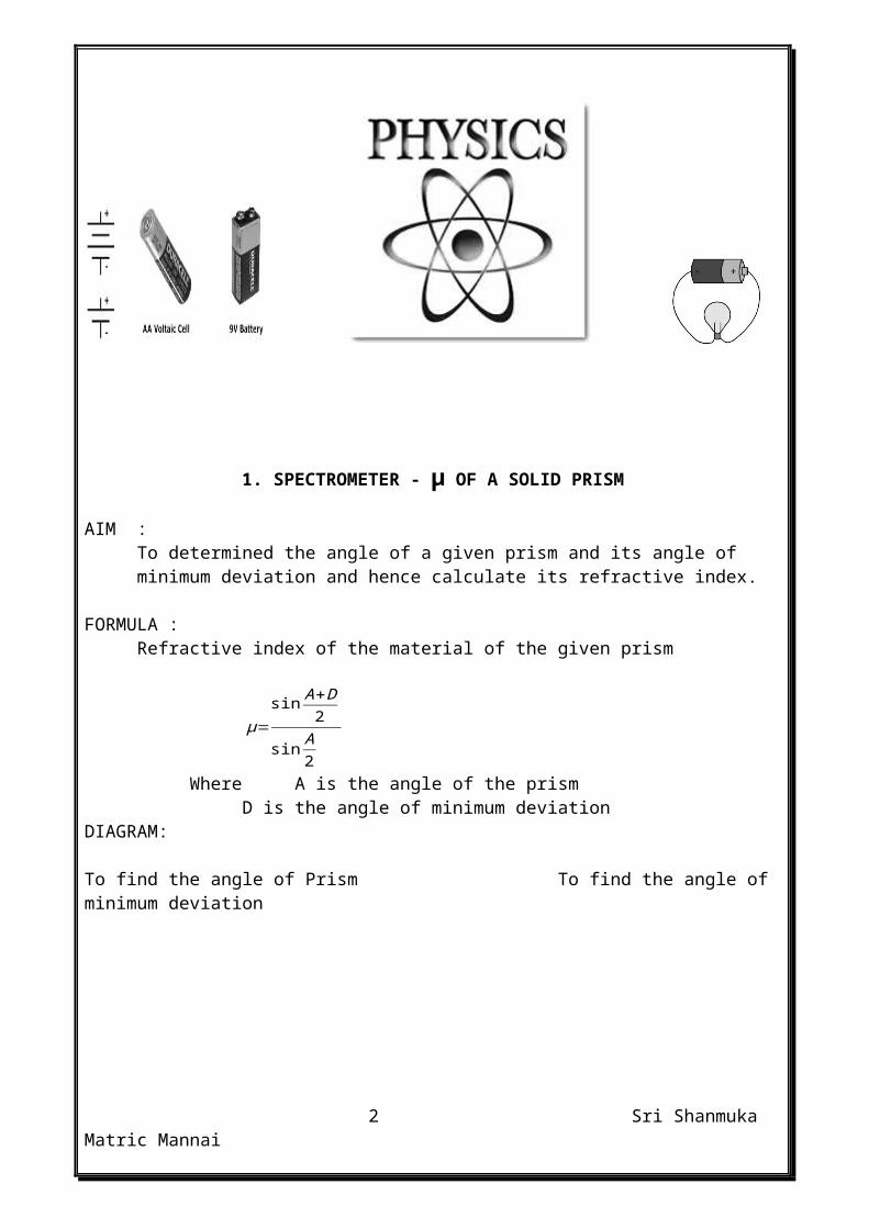
1. SPECTROMETER - µ OF A SOLID PRISM
AIM : To determined the angle of a given prism and its angle of minimum deviation and hence calculate its refractive index.
FORMULA :Refractive index of the material of the given prism
μ=sin A+D
2
sin A2
Where A is the angle of the prismD is the angle of minimum deviation
DIAGRAM:
To find the angle of Prism To find the angle of minimum deviation
2 Sri Shanmuka Matric Mannai

PROCEDURE
ANGLE OF THE PRISM
After making preliminary adjustments, the prism is placed on the prism table. The slit is
illuminated by a monochromatic source of light say, sodium vapour lamp.
Both the faces AB and AC receive parallel rays from the collimator. The telescope is
rotated until the image of the slit formed by reflection at the face AB is made to coincide with the
vertical cross wire of the telescope in the position T1 The reading of the verniers are noted. The
telescope is then rotated to the position T2 where the image of the slit formed by reflection at the
face AC coincides with the vertical cross wire. The readings corresponding to the verniers are
again noted.
The difference between these two reading give twice the angle of the prism. Half of this
gives the angle of the prism.
ANGLE OF MINIMUM DEVIATION
The prism is placed on the prism table so that light from the collimator falls on one
refracting face. The refracted image is observed through the telescope. The prism table is now
rotated so that the refracted image moves towards the direct ray. If necessary the telescope is
rotated so as to follow the image. It will be found that, as the prism table is rotated in the same
direction, the image moves towards the direct ray upto a point and then turns back. The position
of the image where it turns back is the minimum deviation position and the prism table is fixed in
this position. The telescope is now adjusted so that its vertical cross wire coincides with the
image and reading of the verniers are noted. Now the prism is removed and the telescope is
turned to receive the direct ray and vertical cross wire is adjusted to coincide with the image.
The reading of the verniers are noted.
The difference between the two readings give the angle of minimum deviation (D).
The refractive idex of the material of the prism is calculated using the formula
μ=sin A+D
2
sin A2
3 Sri Shanmuka Matric Mannai

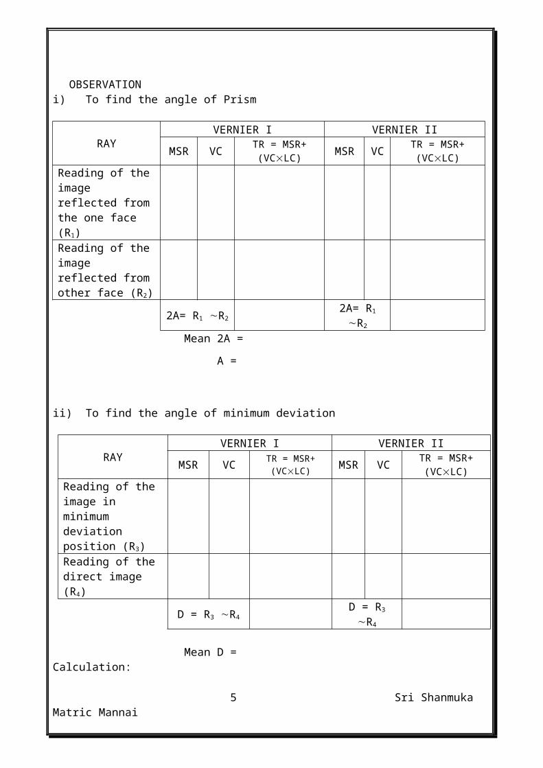
OBSERVATIONi) To find the angle of Prism
RAYVERNIER I VERNIER II
MSR VC TR = MSR+ (VCLC) MSR VC TR = MSR+ (VCLC)
Reading of the image reflected from the one face (R1)Reading of the image reflected from other face (R2)
2A= R1 R2 2A= R1 R2
Mean 2A =
A =
ii) To find the angle of minimum deviation
RAYVERNIER I VERNIER II
MSR VC TR = MSR+ (VCLC) MSR VC TR = MSR+
(VCLC)Reading of the image in minimum deviation position (R3)Reading of the direct image (R4)
D = R3 R4 D = R3 R4
Mean D =Calculation:
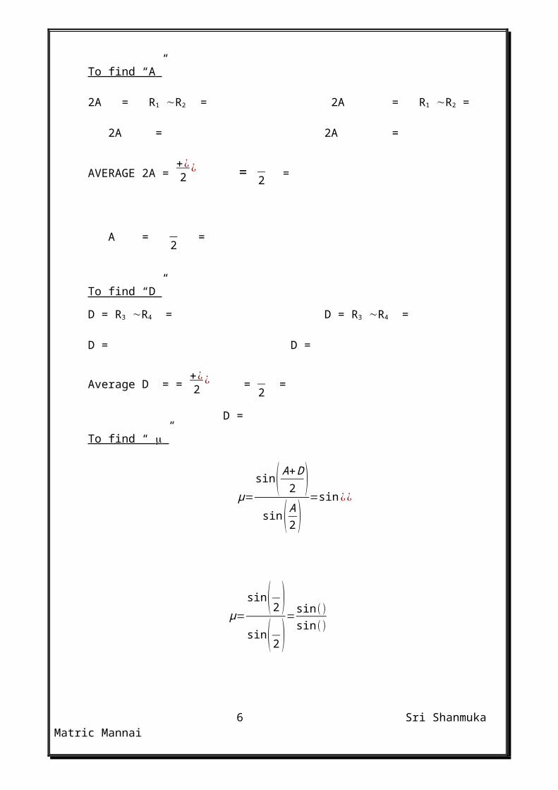
To find “A ” 2A = R1 R2 = 2A = R1 R2 =
2A = 2A =
AVERAGE 2A = +¿2¿ = 2 =
A = 2 =
4 Sri Shanmuka Matric Mannai
To find “D”
D = R3 R4 = D = R3 R4 =
D = D =
Average D = = +¿2¿ = 2 =
D =
To find “ ”
μ=sin( A+D
2 )sin ( A
2 )=sin ¿¿
μ=sin( 2 )sin( 2 )
=sin ()sin ()
μ= =
=
RESULT:i) The angle of the prism A = (degree)
ii) The angle of minimum deviation D = (degree)
5 Sri Shanmuka Matric Mannai
iii) Refractive index of the material of the given prism µ = (no unit)
2. SPECTROMETER – GRATING – WAVELENGTH OF COMPOSITE LIGHT
AIM :
To determine the wavelength of the composite light using a diffraction grating and a spectrometer
FORMULA :
The wavelength () of a spectral line using normal incidence arrangement of the grating is
given by
λ=sin θm N
Where
is the angle of diffraction
m is the order
N is the number of lines per unit length drawn on the grating
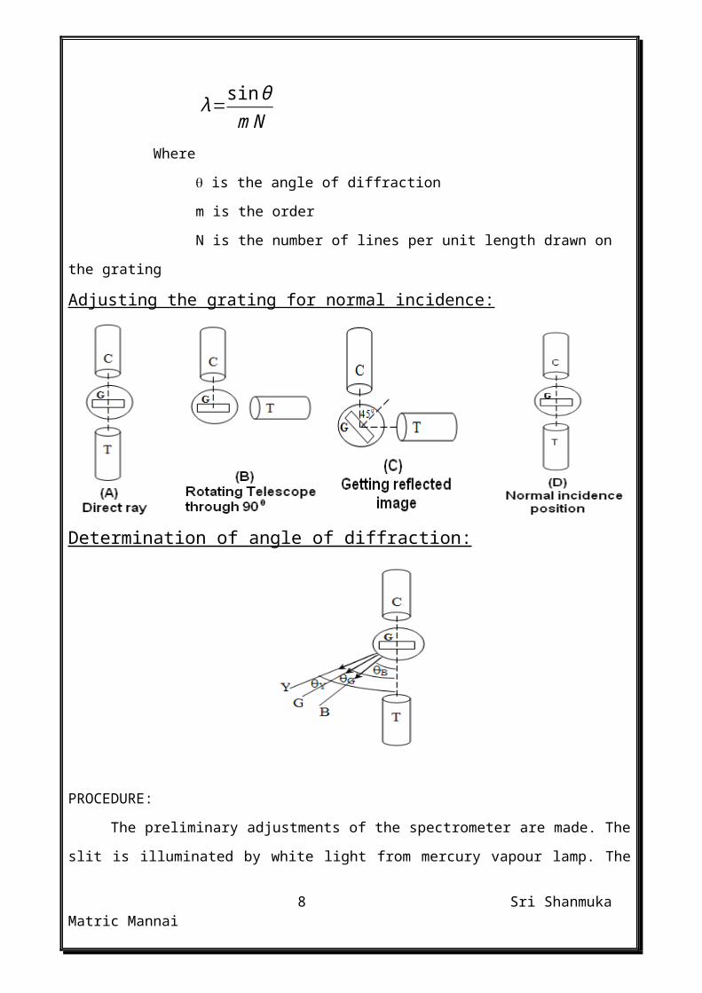
Adjusting the grating for normal incidence:
Determination of angle of diffraction:
6 Sri Shanmuka Matric Mannai

PROCEDURE:
The preliminary adjustments of the spectrometer are made. The slit is illuminated by
white light from mercury vapour lamp. The grating is mounted on the prism table. The direct
image (white) of the slit is adjusted to be 00 — 1800. Telescope is then rotated through 90° and
fixed. Prism table is rotated to get the reflected image which is made to coincide with the
vertical cross wire. Keeping the platform fixed, vernier table is rotated through 45° so that the
light rays from the collimator fall on the .grating. Now the grating is in normal incidence position.
The direct reading RI is measured.
Now the telescope is released to get the first order (n= 1) diffracted image of the slit in the
left side. It is adjusted so that the vertical cross wire coincides with violet spectral line. Readings
corresponding to both the verniers are taken as R2. The angle of diffraction is found as R1
R2. The experiment is repeated for green and yellow spectral lines also. Number of lines per unit
length of the grating is N. Wavelength of the spectral line is calculated from the formula
λ=sin θm N
OBSERVATION
RAY
VERNIER I VERNIER II
MSR VC TR = MSR+ (VCLC) MSR VC TR = MSR+ (VCLC)
7 Sri Shanmuka Matric Mannai
Direct readingRD1 RD2
Diffr
acte
d ra
y BLUERB1 RB2
GREENRG1 RG2
YELLOWRY1 RY2
8 Sri Shanmuka Matric Mannai

TO FIND THE “”
RD1 – R1 RD2 – R2
BLUE B
GREEN G
YELLOW Y
m = 1
N = 6 105
Calculation:
RD1 – RB1 = RD2 – RB2 =
B = B =
Average B = +¿2¿ =
RD1 –RG1 = RD2 – RG2 =
G = G =
Average B = +¿2¿ =
9 Sri Shanmuka Matric Mannai
RD1 – RY1 = RD2 – RY1 =
Y = Y =
Average Y = +¿2¿ =
λB=sin θB
m N=
sin ( )1×6×105= 6×105 = ×10−7 m
λG=sin θG
m N=
sin( )1×6×105 = 6×105 = ×10−7 m
λY=sin θY
m N=
sin( )1×6×105= 6×105 = ×10−7 m
RESULT :
i) wavelength of blue colour B = 10–7m
ii) wavelength of green colour G = 10–7m
iii) wavelength of yellow colour Y = 10–7m
3. METRE BRIDGE – DETERMINATION OF RESISTANCE AND SPECIFICE RESISTANCE
10 Sri Shanmuka Matric Mannai

AIM: To determine the resistance of the given coil of wire using a meter bridge and to calculate the specific resistance of the material of the wire.
FORMULA
Resistance of the wire X=R
lX
lR
Specific resistance of the material of the wire ρ=π r2 X
lWhere R is known resistance
lR is the balancing length of RlX is the balancing length of Xr is the radius of the wirel is the length of the wire
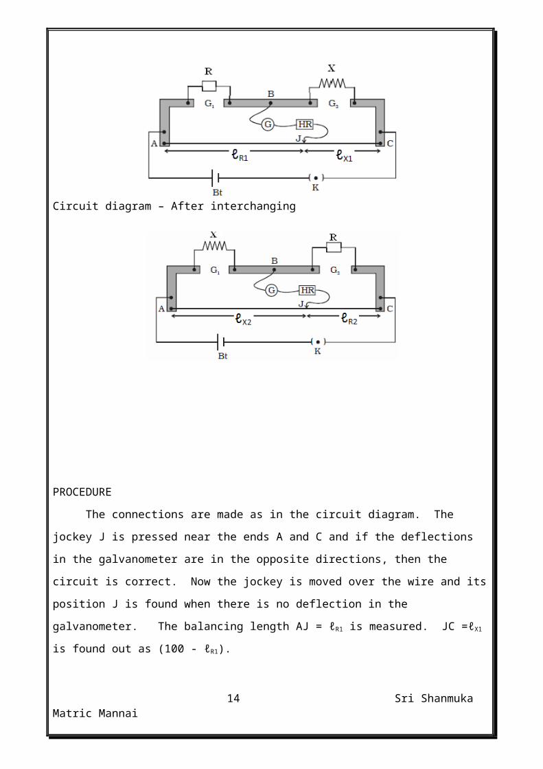
Circuit diagram – Before interchanging
Circuit diagram – After interchanging
11 Sri Shanmuka Matric Mannai
PROCEDURE
The connections are made as in the circuit diagram. The jockey J is pressed near the ends
A and C and if the deflections in the galvanometer are in the opposite directions, then the circuit
is correct. Now the jockey is moved over the wire and its position J is found when there is no
deflection in the galvanometer. The balancing length AJ = ℓR1 is measured. JC =ℓX1 is found out
as (100 - ℓR1).
The experiment is repeated four more times by increasing the value of R in steps of 1
ohm.
Then the resistance box R and coil X are interchanged in the gaps G1 and G2. For the same
values of R as in the previous part of the experiment the balancing length AJ =ℓX2 are measured.
The balancing length JC =ℓR2 are found out as (100- ℓX2). The values of ℓX and ℓR are calculated
from
ℓ X=ℓX 1+ℓX 2
2 ℓR=
ℓR 1+ℓR 2
2
The resistance of the coil is found by substituting in the formula X=RlX
lR
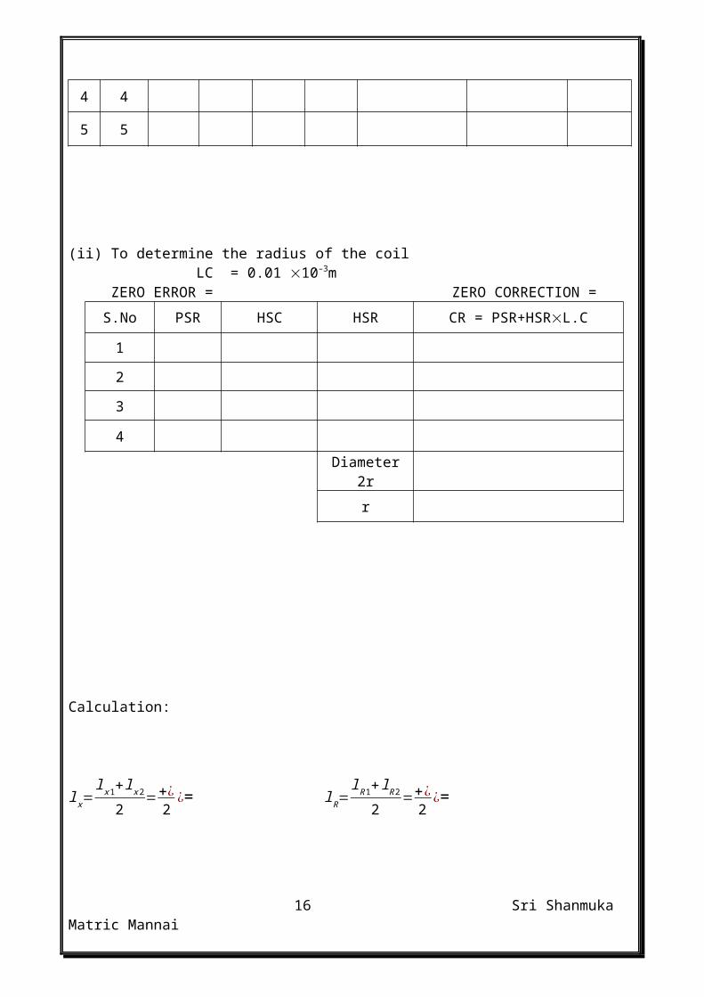
The length (ℓ) of the coil is measured using scale and radius(r) of the coil is measured using screw
gauge. The specific resistance of the coil is calculated using the formula
ρ=π r2 Xl
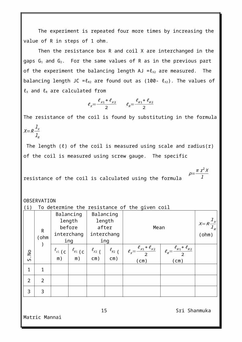
OBSERVATION(i) To determine the resistance of the given coil
S.N
o
R (ohm)
Balancing length before interchanging
Balancing length after
interchangingMean
X=RlX
lR (ohm)
ℓ x1(cm)
ℓR 1(cm)
ℓ X 2(cm)
ℓR 2(cm)
ℓ X=ℓX 1+ℓX 2
2(cm)
ℓR=ℓR 1+ℓR 2
2 (cm)
1 1
2 2
3 3
12 Sri Shanmuka Matric Mannai

4 4
5 5
(ii) To determine the radius of the coilLC = 0.01 10–3m
ZERO ERROR = ZERO CORRECTION =
S.No PSR HSC HSR CR = PSR+HSRL.C
1
2
3
4
Diameter 2r
r
Calculation:
lx=l x1+lx 2
2=+¿
2¿= lR=
lR1+lR2
2=+¿
2¿=
lx=l x1+lx 2
2=+¿
2¿= lR=
lR1+lR2
2=+¿
2¿=
13 Sri Shanmuka Matric Mannai
lx=l x1+lx 2
2=+¿
2¿= lR=
lR1+lR2
2=+¿
2¿=
lx=l x1+lx 2
2=+¿
2¿= lR=
lR1+lR2
2=+¿
2¿=
14 Sri Shanmuka Matric Mannai
Calculation for X
X=Rlx
lR =
X=Rlx
lR =
X=Rlx
lR =
X=Rlx
lR =
X=Rlx
lR =
Mean X = 5=
Calculation for :
ρ=π r2 Xl
=3.14 ××10−3×× 10−3 ×1
=
RESULT:Resistance of the wire X = Specific resistance of the material of the wire = m
15 Sri Shanmuka Matric Mannai
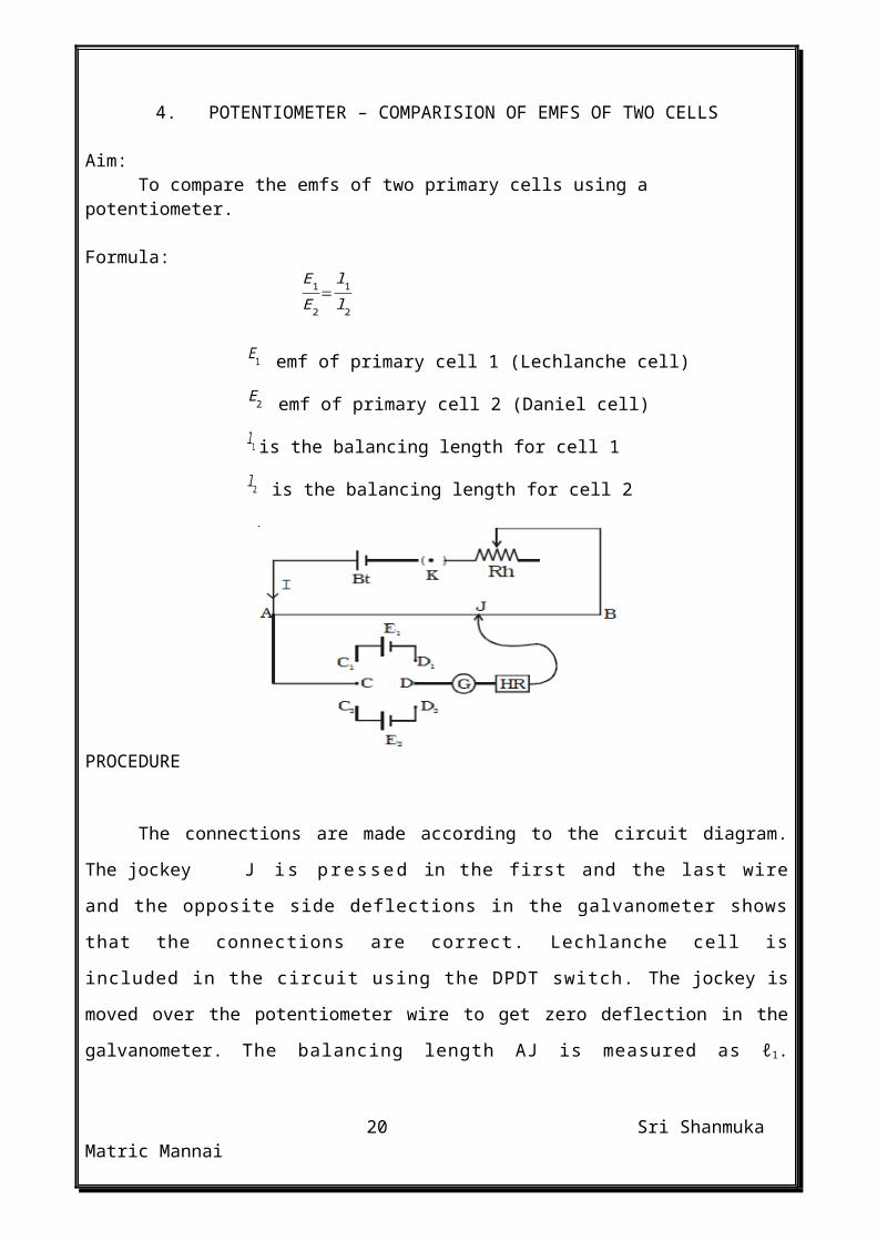
4. POTENTIOMETER – COMPARISION OF EMFS OF TWO CELLS
Aim:To compare the emfs of two primary cells using a potentiometer.
Formula:E1
E2=
l1
l2
E1 emf of primary cell 1 (Lechlanche cell)
E2 emf of primary cell 2 (Daniel cell)
l1 is the balancing length for cell 1
l2 is the balancing length for cell 2
PROCEDURE
The connections are made according to the circuit diagram. The jockey J i s p r e s s e d
in the first and the last wire and the opposite side deflections in the galvanometer
shows that the connections are correct. Lechlanche cell is included in the circuit
using the DPDT switch. The jockey is moved over the potentiometer wire to get zero
deflection in the galvanometer. The balancing length AJ is measured as ℓ1. Daniel cell is
included in the circuit using the DPDT switch, and the balancing length is measured as
ℓ2. The experiment is repeated for six times by moving rheostat in one direction for changing the
current in the circuit.
The ratio of the emf of the two cells is found from the formula
E1
E2=
l1
l2
16 Sri Shanmuka Matric Mannai

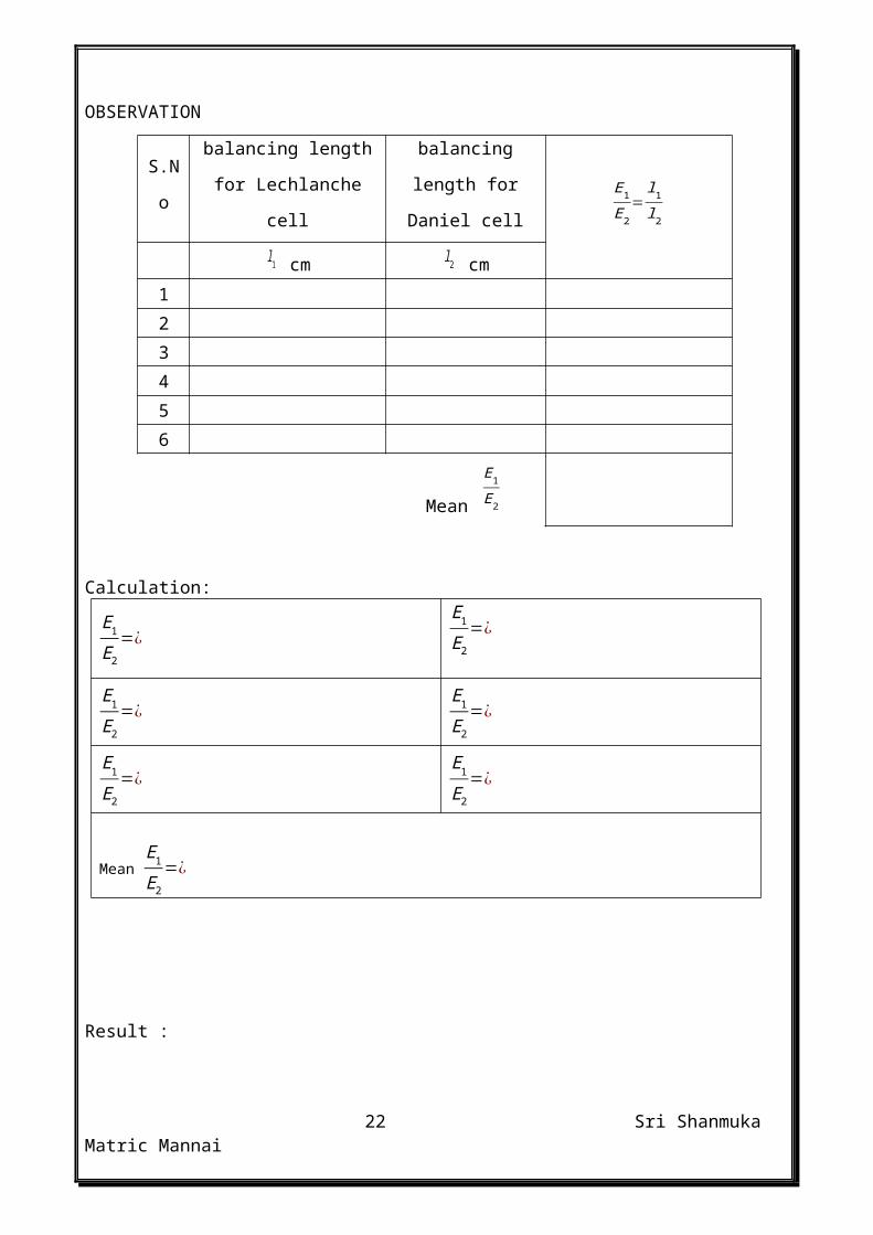
OBSERVATION
S.Nobalancing length for
Lechlanche cell
balancing length for
Daniel cellE1
E2=
l1
l2
l1 cm l2 cm
1
2
3
4
5
6
Mean
E1
E2
Calculation:
E1
E2=¿
E1
E2=¿
E1
E2=¿
E1
E2=¿
E1
E2=¿
E1
E2=¿
Mean E1
E2=¿
Result :
The mean ratio of emf of the two cells = (no unit)
17 Sri Shanmuka Matric Mannai

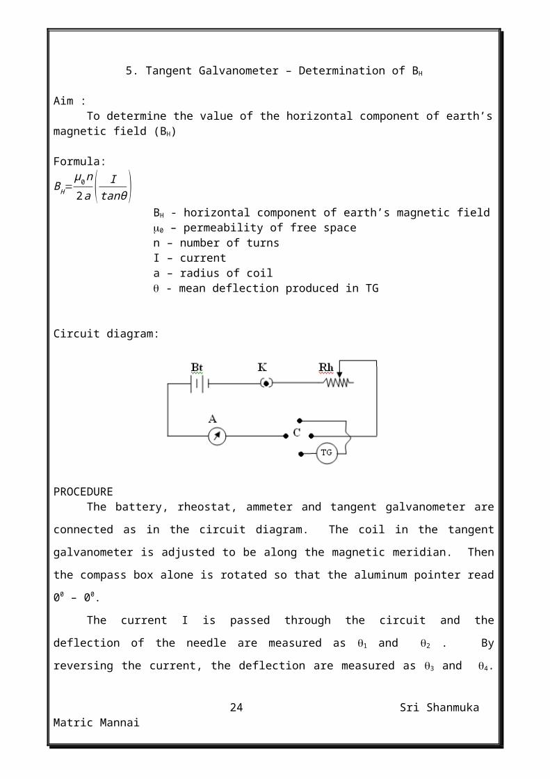
5. Tangent Galvanometer – Determination of BH
Aim : To determine the value of the horizontal component of earth’s magnetic field (BH)
Formula:
BH=μ0n2a ( I
tanθ )BH - horizontal component of earth’s magnetic field0 – permeability of free spacen – number of turnsI – currenta – radius of coil - mean deflection produced in TG
Circuit diagram:
PROCEDUREThe battery, rheostat, ammeter and tangent galvanometer are connected as in the circuit
diagram. The coil in the tangent galvanometer is adjusted to be along the magnetic meridian.
Then the compass box alone is rotated so that the aluminum pointer read 00 – 00.
The current I is passed through the circuit and the deflection of the needle are measured
as 1 and 2 . By reversing the current, the deflection are measured as 3 and 4. The average
deflection is found out. The experiment is repeated by varying current. The average value of
Itanθ is found out. The radius R of the coil is found out by measuring its circumference. The
number of turns “n” of the coil is noted.
The Horizontal component of earth’s magnetic induction is calculated by substituting in the
formula
BH=μ0n2a ( I
tanθ )
18 Sri Shanmuka Matric Mannai
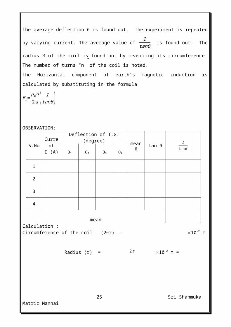
OBSERVATION:
S.No CurrentI (A)
Deflection of T.G. (degree)mean Tan
Itanθ
1 2 3 4
1
2
3
4
mean
Calculation :Circumference of the coil (2r) = 10–2 m
Radius (r) = 2π 10–2 m =
Itan θ
=¿ Itan θ
=¿
Itan θ
=¿ Itan θ
=¿
Mean I
tan θ=¿
BH=μ0n2a ( I
tanθ )=4 π ×10−7× 5×2×
¿
Result:
19 Sri Shanmuka Matric Mannai
The horizontal component of earth’s magnetic field (BH) = Tesla
20 Sri Shanmuka Matric Mannai

6. SONOMETER – FREQUENCY OF ACAim:-
To determine the frequency of the ac main using a sonometerFormula:-
The frequency of the ac main
n=12
× √Tl
× 1√m
where T is the tension of the sonometer wireℓ is the resonating lengthm is the linear density of the wire
PROCEDUREThe ac mains voltage is brought down to 6 V by means of step down transformer. The
secondary of the transformer is connected to the ends of the sonometer wire. A bar magnet is held below the sonometer wire at the centre. The magnetic field is horizontal and at right angles to the length of the wire.
With 200 gms (M) added to the weight hanger, the a.c. current is passed through the wire. Now the wire is set into forced vibrations. The length between the two knife edges is adjusted so that it vibrates in one segment. The length between the knife edges is measured as ℓ1. The same procedure is repeated and ℓ2 is measured. The average ℓ1 and ℓ2 is ℓ. The experiment is repeated for the loads 400gm, 600 gm and 800 gm.
The radius of the wire r is measured using screw gauge. The linear density of the wire is m = r2, where is its density. The frequency of the a.c. mains is calculated from the formula
n=12
× √Tl
× 1√m
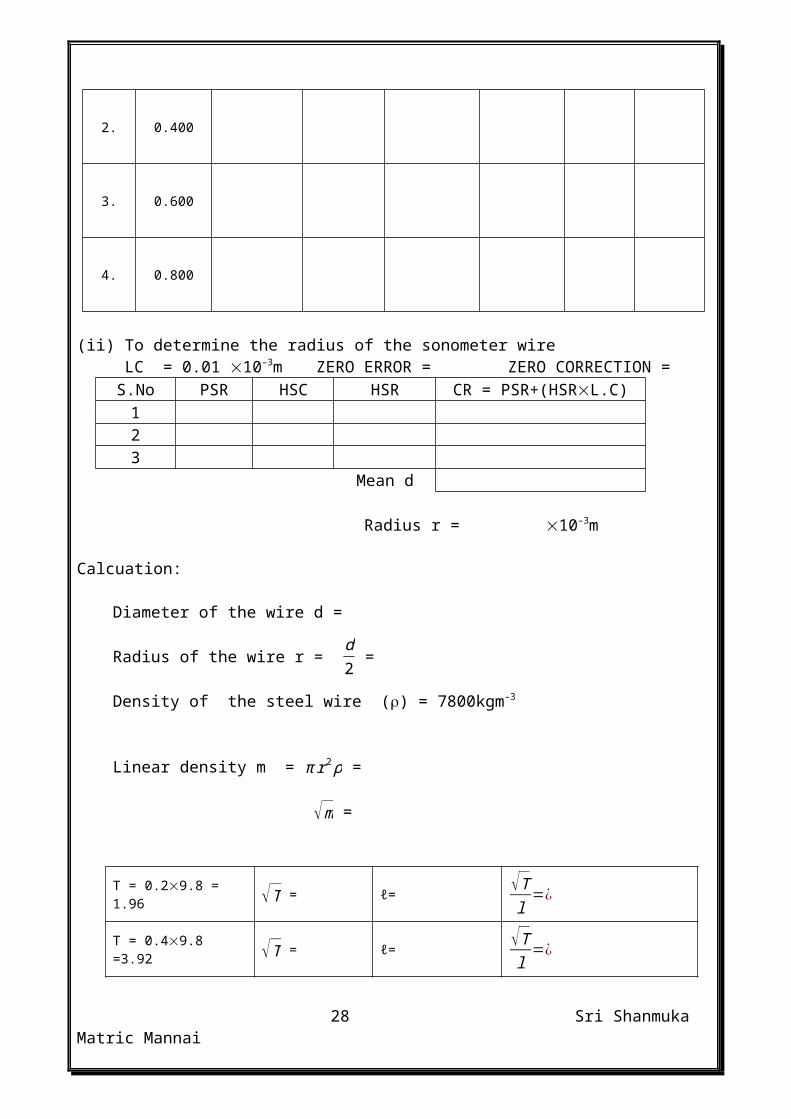
Observation
S.No: Load Length of the vibrating segment Mean T = Mg
√T √Tl
M (kg) ℓ1(cm) ℓ2(cm) ℓ (cm) (newton)
1. 0.200
2. 0.400
3. 0.600
4. 0.800
21 Sri Shanmuka Matric Mannai
(ii) To determine the radius of the sonometer wireLC = 0.01 10–3m ZERO ERROR = ZERO CORRECTION =
S.No PSR HSC HSR CR = PSR+(HSRL.C)123
Mean d
Radius r = 10–3m
Calcuation:
Diameter of the wire d =
Radius of the wire r = d2 =
Density of the steel wire () = 7800kgm–3
Linear density m = π r2 ρ =
√m =
T = 0.29.8 = 1.96 √T = ℓ= √Tl=¿
T = 0.49.8 =3.92 √T = ℓ= √Tl=¿
T = 0.69.8 =5.88 √T = ℓ= √Tl=¿
T = 0.89.8 =7.84 √T = ℓ= √Tl=¿
Mean √Tl=
4 =
n=12
× √Tl
× 1√m
=¿
Result :The frequency of the ac main n = Hz
22 Sri Shanmuka Matric Mannai

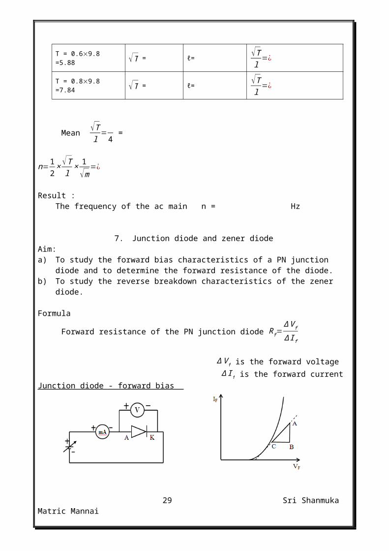
7. Junction diode and zener diodeAim: a) To study the forward bias characteristics of a PN junction diode and to determine the
forward resistance of the diode.b) To study the reverse breakdown characteristics of the zener diode.
Formula
Forward resistance of the PN junction diode R f=∆ V f
∆ I f
∆ V f is the forward voltage ∆ I f is the forward currentJunction diode - forward bias
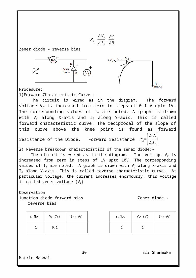
R f=∆ V f
∆ I f=BC
ABZener diode – reverse bias
Procedure:1)Forward Characteristic Curve :-
The circuit is wired as in the diagram. The forward voltage Vf is increased from zero in steps of 0.1 V upto 1V. The corresponding values of I f are noted. A graph is drawn with Vf
along X-axis and If along Y-axis. This is called forward characteristic curve. The reciprocal of the slope of this curve above the knee point is found as forward resistance of the
Diode. Forward resistance ri=(∆ V f
∆ I f)
2) Reverse breakdown characteristics of the zener diode:-The circuit is wired as in the diagram. The voltage VO is increased from zero in steps of
1V upto 10V. The corresponding values of IZ are noted. A graph is drawn with VO along X-axis
23 Sri Shanmuka Matric Mannai
and IZ along Y-axis. This is called reverse characteristic curve. At particular voltage, the current increases enormously, this voltage is called zener voltage (VZ)
ObservationJunction diode forward bias Zener diode -reverse bias
s.No: VF (V) IF (mA) s.No: Vo (V) IZ (mA)
1 0.1 1 1
2 0.2 2 2
3 0.3 3 3
4 0.4 4 4
5 0.5 5 5
6 0.6 6 6
7 0.7 7 7
8 0.8 8 8
9 0.9 9 9
10 1.0 10 10
Calculation:
R f=∆V f
∆ I f=BC
AB= =¿
Result:i) The forward resistance of the junction diode = ii) The zener breakdown voltage =
24 Sri Shanmuka Matric Mannai
8. Common Emitter NPN Transistor Characteristics
Aim:To study the characteristics of a common Emitter NPN transistor and to determine its input impedance, output impedance and current gain.
Formula:
(i) input impedance ri=(∆ V BE
∆ IB)
(ii) output impedance ro=(∆V CE
∆IC)
(iii) current gain β=(∆ IC
∆ IB)
∆V BEis the change in base emitter voltage∆ IB is the change in base current∆V CE is the change in collector emitter voltage∆ IC is the change in collector current
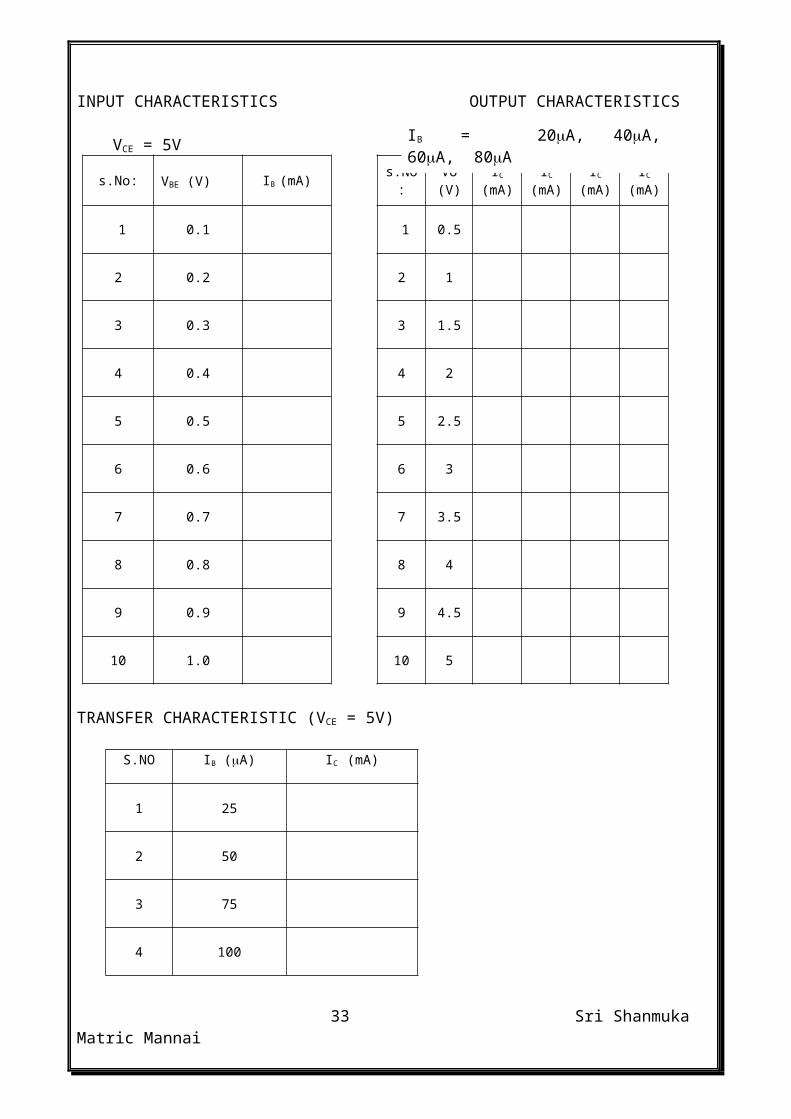
INPUT CHARACTERISTICS OUTPUT CHARACTERISTICS
25 Sri Shanmuka Matric Mannai
IB = 20A, 40A, 60A, 80A

VCE = 5V
s.No: VBE (V) IB (mA) s.No: Vo (V)
IC
(mA)IC
(mA)IC
(mA)IC
(mA)
1 0.1 1 0.5
2 0.2 2 1
3 0.3 3 1.5
4 0.4 4 2
5 0.5 5 2.5
6 0.6 6 3
7 0.7 7 3.5
8 0.8 8 4
9 0.9 9 4.5
10 1.0 10 5
TRANSFER CHARACTERISTIC (VCE = 5V)
S.NO IB (A) IC (mA)
1 25
2 50
3 75
4 100
Calculation:
26 Sri Shanmuka Matric Mannai

r i=(∆ V BE
∆ IB)=BC
AB=¿
ro=(∆ V CE
∆IC)=BC
AB=¿
β=(∆ IC
∆ IB)= AB
BC=¿
PROCEDURE:The circuit is wired as in the diagram.1.INPUT CHARACTERISTIC CURVE :-
The collector emitter voltage VCE is kept at a constant value. The base emitter voltage VBE is increased from zero in steps of 0.1 V upto 1V. The corresponding values of IB are noted.A graph is drawn with VBE along X-axis and IB along Y-axis. This is called input characteristic curve. The reciprocal of the slope of this curve above the knee point is found as input impedance of the transistor.
Input impedance r i=(∆ V BE
∆ IB)
2. TRANSFER CHARACTERISTIC CURVE :-The collector emitter voltage VCE is kept at a constant value (5V). IB is increased in steps of 25 µA from 25 µA to 100µA. The corresponding values of IC are noted. A graph is drawn with IB along X-axis and Ic along Y-axis. This is called transfer characteristic curve. The slope of this curve gives the current gain of the transistor.
Current gain β=(∆ IC
∆ IB)
3. OUTPUT CHARACTERISTIC CURVE :-The base current IB is kept at a constant value. VCE is increased in steps of 0.5 V from Zero. The corresponding values of IC are noted. A graph is drawn with VCE along X-axis and IC along Y-axis. This is called output characteristic curve. The reciprocal of the slope of the output characteristic curve near horizontal part gives the output impedance (r0).
Output impedance ro=(∆V CE
∆IC)
Result:
i) The static characteristic curves of the transistor in CE configuration are drawn.
ii) The input impedance ri =
iii) The output impedance r0 =
iv) The current gain =
27 Sri Shanmuka Matric Mannai
9. OPERATIONAL AMPLIFIER
Aim : To construct the following basic amplifiers using OP-AMP IC741.i) Inverting amplifierii) Non inverting amplifieriii) Summing amplifier
Formula :
i) Voltage gain of the inverting amplifier, AV=(V O
V ¿)=−(R f
R s)
ii) Voltage gain of the non inverting amplifier, AV=(V O
V ¿)=1+( R f
R s)
iii) The output voltage of the inverting summing amplifier, V0 = –(V1 +V2)
Where V0 output voltageVin, V1 and V2 are the input voltagesRf and Rs are the external resistances
INVERTING AMPLIFIER
SET S.NO Rs () Rf () Vin(V) Vout(V)
Experimental Gain
AV=(V O
V ¿)
Theoretical Gain
AV=−( R f
R s)
I
1 10K 22K 1 -2.2
2 10K 22K 1.5 -2.2
3 10K 22K 2 -2.2
4 10K 22K 2.5 -2.2
II
1 10K 10K 1 -1.0
2 10K 22K 1 -2.2
3 10K 33K 1 -3.3
4 10K 47K 1 -4.7
28 Sri Shanmuka Matric Mannai
NON-INVERTING AMPLIFIER
SET S.NO Rs () Rf () Vin(V) Vout(V)
Experimental Gain
AV=(V O
V ¿)
Theoretical Gain
AV=1+( R f
R s)
I
1 10K 22K 1.0 3.2
2 10K 22K 1.5 3.2
3 10K 22K 2.0 3.2
4 10K 22K 2.5 3.2
II
1 10K 10K 1.0 2.0
2 10K 22K 1.0 3.2
3 10K 33K 1.0 4.3
4 10K 47K 1.0 5.7
SUMMING AMPLIFIER
R1 = R2 = Rf = 10K
S.NO V1 (Volt) V2
(Volt)Experimental Output
voltage V0 (Volt)Theoretical output voltage V0 = -
(V1 + V2) (Volt)
1 1.0 0.5 1.5
2 1.0 1.0 2.0
29 Sri Shanmuka Matric Mannai
3 1.0 1.5 2.5
4 1.0 2.0 3.0
BASIC AMPLIFIERS USING OP-AMP
INVERTING AMPLIFIER:-
The circuit is wired as shown in the diagram using OP-AMP IC 741. R S is kept as 10 KΩ and RF
as 22 KΩ. The input voltage Vin is kept as 1V and output voltage Vo is measured from the digital
voltmeter. Then the experiment is repeated for input values V in = 1.5 V, 2V and 2.5 V. Second
Set of readings is taken by keeping Vin = 1 V and Rs = 10 KΩ and changing RF as 10 KΩ,22KΩ,33 KΩ &
47 KΩ. Experimental gain is found as AV=(V O
V ¿)
Theoretical gain is found from AV=−( R f
R s)
Both the AV values are compared and found to be equal.
NON-INVERTING AMPLIFIER:-
The circuit is wired as shown in the diagram using OP-AMP IC 741. R S is kept as 10 KΩ and RF
as 22 KΩ. The input voltage Vin is kept as 1V and output voltage Vo is measured from the digital
voltmeter. Then the experiment is repeated for input values V in = 1.5 V, 2V and 2.5V. Second
Set of readings is taken by keeping Vin = 1 V and Rs = 10 KΩ and changing RF as 10 KΩ,22KΩ,33 KΩ &
47 KΩ. Experimental gain is found as AV=(V O
V ¿)
Theoretical gain is found from AV=1+( R f
R s)
Both the AV values are compared and found to be equal.
SUMMING AMPLIFIER:-
The circuit is wired as shown in the diagram using OP AMP IC 741, The values of R1, R2 and RF
are kept as 10 K Ω. The input voltages are kept as VI = 1V and V2 = 0.5V and the output voltage Vo is measured using the digital voltmeter Then the experiment is repeated for different sets of values for V1 and V2. Theoretical output v o l t a g e i s found from V0 = -(V1 + V2). Since this is equal to experimental output voltage the summing action of the amplifier is verified.
30 Sri Shanmuka Matric Mannai

Calculation:Inverting amplifier
AV=(V O
V ¿)=¿ AV=−( R f
R s)
AV=(V O
V ¿)=¿ AV=−( R f
R s)=¿
AV=(V O
V ¿)=¿ AV=−( R f
R s)=¿
AV=(V O
V ¿)=¿ AV=−( R f
R s)=¿
AV=(V O
V ¿)=¿ AV=−( R f
R s)=¿
AV=(V O
V ¿)=¿ AV=−( R f
R s)=¿
AV=(V O
V ¿)=¿ AV=−( R f
R s)=¿
AV=(V O
V ¿)=¿ AV=−( R f
R s)=¿
31 Sri Shanmuka Matric Mannai

Non inverting amplifier
AV=(V O
V ¿)=¿ AV=1+( R f
R s)
AV=(V O
V ¿)=¿ AV=1+( R f
R s)=¿
AV=(V O
V ¿)=¿ AV=1+( R f
R s)=¿
AV=(V O
V ¿)=¿ AV=1+( R f
R s)=¿
AV=(V O
V ¿)=¿ AV=1+( R f
R s)=¿
AV=(V O
V ¿)=¿ AV=1+( R f
R s)=¿
AV=(V O
V ¿)=¿ AV=1+( R f
R s)=¿
AV=(V O
V ¿)=¿ AV=1+( R f
R s)=¿
Summing amplifier
1) Vo = –(V1 + V2) =
2) Vo = –(V1 + V2) =
3) Vo = –(V1 + V2) =
4) Vo = –(V1 + V2) =
Result :i) The inverting amplifier and non-inverting amplifier are constructed using OP-AMP
and gain is determined.ii) The inverting summing amplifier is constructed and the output voltage is found to be
the sum of the applied input voltages
32 Sri Shanmuka Matric Mannai
10 INTEGRATED LOGIC GATE CIRCUITSAim:
To study the Truth Table of integrated Logic Gates IC 7400(NAND), 7408(AND), 7402 (NOR), 7432 (OR), 7404 (NOT) and 7486 (EXOR)
1)For IC’s 7400 (NAND), 7408(AND), 7432(OR) & 7486(EX-OR)
2) For IC 7402(NOR) - Quad 2 input Hex inverter NOT (7404)
POSITIVE LOGIC SYSTEM :-
Logic 1 represents TRUE or high voltage 5V or LED ON
Logic 0 represents FALSE or low voltage 0V or LED OFF
OR function When any one input or all inputs are true, output-is-true
Y =A + B
AND function Only when all inputs are true, output is true
Y = AB
NOT function Output is the complement of input
Y = A
NOR function Only when all inputs are false, output is true
Y = A+B
NAND function When any one of the inputs is false, output is true
Y= A ∙B
EXOR function Only when the inputs are different, output is true
Y=A⨁B=A B+A B
33 Sri Shanmuka Matric Mannai

NAND gate:-Power supply +5V is connected to pin 14 and gnd to pin 7 of the IC. Inputs A & B are connected to pins 1 & 2 of the IC. Output pin 3 of the IC is connected to logic level indicator. Both inputs A & B are kept at logic 0 and output LED is observed, Then the inputs are changed as logic 0 & logic 1, logic 1 & logic 0 and logic 1 & logic 1 and the outputs are observed each time. The inputs and outputs are tabulated in the truth table. AND, OR and EXOR gates:-ICs 7408 (AND), 7432 (OR) and 7486 (EXOR) are placed on the board arid the same procedure is followed as for NAND gate and outputs are tabulated in the truth table.NOR gate :-IC 7402 is placed on the board. Power supply and gnd are connected as before. The inputs are connected to pins 2 & 3 and the output to pin 1 of IC. Then the same procedure is repeated and tabulation is done in the truth table.NOT gate :-IC 7404 is placed on the board. One input A is connected to pin 1 and the output to pin 2 of IC. Input is kept at logic 1 and then at logic 0 and the outputs are found and tabulated in the truth table.IC 7432(OR) Truth Table (OR)
IC 7408 (AND) Truth Table (AND)A B Y = AB0 00 11 01 1
IC 7404 (NOT) Truth Table (NOT)
A Y=A01
34 Sri Shanmuka Matric Mannai
A B Y = A+B0 00 11 01 1
IC 7402(NOR) Truth Table (NOR)
IC 7400 (NAND) Truth Table (NAND)
IC 7486( EX-OR) Truth Table (EX-OR)
Calculation:
OR AND
NOT NOR
NAND
EX-OR
35 Sri Shanmuka Matric Mannai
A B Y = A+B0 00 11 0
1 1
A B Y = A ∙B0 00 11 01 1
A B Y = AB0 00 11 01 1

Result:The performance of digital gates OR, AND, NOT, NAND, NOR and EX-OR are verified using IC chips.
36 Sri Shanmuka Matric Mannai
Top Related