


Languages
Pages
Legal

PCI Express® Base Specification
Revision 2.0
December 20, 2006

2
Revision Revision History DATE 1.0 Initial release. 07/22/02
1.0a Incorporated Errata C1-C66 and E1-E4.17. 04/15/03
1.1 Incorporated approved Errata and ECNs. 03/28/05
2.0 Added 5.0 GT/s data rate and incorporated approved Errata and ECNs.
12/20/06
PCI-SIG® disclaims all warranties and liability for the use of this document and the information contained herein and assumes no responsibility for any errors that may appear in this document, nor does PCI-SIG make a commitment to update the information contained herein. Contact the PCI-SIG office to obtain the latest revision of this specification. Questions regarding the PCI Express Base Specification or membership in PCI-SIG may be forwarded to:
Membership Services www.pcisig.com E-mail: [email protected] Phone: 503-619-0569 Fax: 503-644-6708
Technical Support [email protected]
DISCLAIMER This PCI Express Base Specification is provided “as is” with no warranties whatsoever, including any warranty of merchantability, noninfringement, fitness for any particular purpose, or any warranty otherwise arising out of any proposal, specification, or sample. PCI-SIG disclaims all liability for infringement of proprietary rights, relating to use of information in this specification. No license, express or implied, by estoppel or otherwise, to any intellectual property rights is granted herein.
PCI, PCI Express, PCIe, and PCI-SIG are trademarks or registered trademarks of PCI-SIG. All other product names are trademarks, registered trademarks, or servicemarks of their respective owners.
Copyright © 2002-2006 PCI-SIG
PCI EXPRESS BASE SPECIFICATION, REV. 2.0
3
Contents
OBJECTIVE OF THE SPECIFICATION............................................................................... 21
DOCUMENT ORGANIZATION.............................................................................................. 21
DOCUMENTATION CONVENTIONS................................................................................... 22
TERMS AND ACRONYMS ...................................................................................................... 23
REFERENCE DOCUMENTS................................................................................................... 29
1. INTRODUCTION............................................................................................................... 31 1.1. A THIRD GENERATION I/O INTERCONNECT ................................................................... 31 1.2. PCI EXPRESS LINK......................................................................................................... 33 1.3. PCI EXPRESS FABRIC TOPOLOGY .................................................................................. 34
1.3.1. Root Complex........................................................................................................ 35 1.3.2. Endpoints .............................................................................................................. 36 1.3.3. Switch.................................................................................................................... 38 1.3.4. Root Complex Event Collector.............................................................................. 39 1.3.5. PCI Express to PCI/PCI-X Bridge........................................................................ 40
1.4. PCI EXPRESS FABRIC TOPOLOGY CONFIGURATION ....................................................... 40 1.5. PCI EXPRESS LAYERING OVERVIEW.............................................................................. 40
1.5.1. Transaction Layer................................................................................................. 42 1.5.2. Data Link Layer .................................................................................................... 42 1.5.3. Physical Layer ...................................................................................................... 42 1.5.4. Layer Functions and Services............................................................................... 43
2. TRANSACTION LAYER SPECIFICATION ................................................................. 47 2.1. TRANSACTION LAYER OVERVIEW.................................................................................. 47
2.1.1. Address Spaces, Transaction Types, and Usage................................................... 48 2.1.2. Packet Format Overview ...................................................................................... 50
2.2. TRANSACTION LAYER PROTOCOL - PACKET DEFINITION............................................... 51 2.2.1. Common Packet Header Fields ............................................................................ 51 2.2.2. TLPs with Data Payloads - Rules ......................................................................... 54 2.2.3. TLP Digest Rules .................................................................................................. 56 2.2.4. Routing and Addressing Rules .............................................................................. 56 2.2.5. First/Last DW Byte Enables Rules........................................................................ 59 2.2.6. Transaction Descriptor......................................................................................... 61 2.2.7. Memory, I/O, and Configuration Request Rules................................................... 66 2.2.8. Message Request Rules ......................................................................................... 69 2.2.9. Completion Rules .................................................................................................. 81
2.3. HANDLING OF RECEIVED TLPS...................................................................................... 83 2.3.1. Request Handling Rules........................................................................................ 86
PCI EXPRESS BASE SPECIFICATION, REV. 2.0
4
2.3.2. Completion Handling Rules.................................................................................. 99 2.4. TRANSACTION ORDERING............................................................................................ 101
2.4.1. Transaction Ordering Rules ............................................................................... 101 2.4.2. Update Ordering and Granularity Observed by a Read Transaction ................ 105 2.4.3. Update Ordering and Granularity Provided by a Write Transaction ................ 106
2.5. VIRTUAL CHANNEL (VC) MECHANISM........................................................................ 106 2.5.1. Virtual Channel Identification (VC ID) .............................................................. 109 2.5.2. TC to VC Mapping .............................................................................................. 109 2.5.3. VC and TC Rules................................................................................................. 111
2.6. ORDERING AND RECEIVE BUFFER FLOW CONTROL ..................................................... 112 2.6.1. Flow Control Rules ............................................................................................. 113
2.7. DATA INTEGRITY ......................................................................................................... 122 2.7.1. ECRC Rules ........................................................................................................ 123 2.7.2. Error Forwarding ............................................................................................... 128
2.8. COMPLETION TIMEOUT MECHANISM ........................................................................... 130 2.9. LINK STATUS DEPENDENCIES ...................................................................................... 131
2.9.1. Transaction Layer Behavior in DL_Down Status............................................... 131 2.9.2. Transaction Layer Behavior in DL_Up Status ................................................... 132
3. DATA LINK LAYER SPECIFICATION ...................................................................... 133 3.1. DATA LINK LAYER OVERVIEW .................................................................................... 133 3.2. DATA LINK CONTROL AND MANAGEMENT STATE MACHINE ...................................... 135
3.2.1. Data Link Control and Management State Machine Rules ................................ 136 3.3. FLOW CONTROL INITIALIZATION PROTOCOL ............................................................... 138
3.3.1. Flow Control Initialization State Machine Rules ............................................... 138 3.4. DATA LINK LAYER PACKETS (DLLPS)........................................................................ 142
3.4.1. Data Link Layer Packet Rules ............................................................................ 142 3.5. DATA INTEGRITY ......................................................................................................... 147
3.5.1. Introduction......................................................................................................... 147 3.5.2. LCRC, Sequence Number, and Retry Management (TLP Transmitter).............. 147 3.5.3. LCRC and Sequence Number (TLP Receiver) .................................................... 160
4. PHYSICAL LAYER SPECIFICATION ........................................................................ 168 4.1. INTRODUCTION ............................................................................................................ 168 4.2. LOGICAL SUB-BLOCK................................................................................................... 168
4.2.1. Symbol Encoding ................................................................................................ 169 4.2.2. Framing and Application of Symbols to Lanes................................................... 172 4.2.3. Data Scrambling ................................................................................................. 175 4.2.4. Link Initialization and Training.......................................................................... 177 4.2.5. Link Training and Status State Machine (LTSSM) Descriptions........................ 190 4.2.6. Link Training and Status State Rules.................................................................. 193 4.2.7. Clock Tolerance Compensation.......................................................................... 242 4.2.8. Compliance Pattern ............................................................................................ 243 4.2.9. Modified Compliance Pattern............................................................................. 245
4.3. ELECTRICAL SUB-BLOCK ............................................................................................. 246 4.3.1. Maintaining Backwards Compatibility ............................................................... 246 4.3.2. Jitter Budgeting and Measurement..................................................................... 248
PCI EXPRESS BASE SPECIFICATION, REV. 2.0
5
4.3.3. Transmitter Specification.................................................................................... 249 4.3.4. Receiver Specification......................................................................................... 265 4.3.5. Transmitter and Receiver DC Specifications...................................................... 279 4.3.6. Channel Specifications........................................................................................ 284 4.3.7. Reference Clock Specifications........................................................................... 290
5. POWER MANAGEMENT .............................................................................................. 317 5.1. OVERVIEW ................................................................................................................... 317
5.1.1. Statement of Requirements.................................................................................. 318 5.2. LINK STATE POWER MANAGEMENT............................................................................. 318 5.3. PCI-PM SOFTWARE COMPATIBLE MECHANISMS......................................................... 323
5.3.1. Device Power Management States (D-States) of a Function.............................. 323 5.3.2. PM Software Control of the Link Power Management State.............................. 327 5.3.3. Power Management Event Mechanisms ............................................................. 333
5.4. NATIVE PCI EXPRESS POWER MANAGEMENT MECHANISMS....................................... 340 5.4.1. Active State Power Management (ASPM) .......................................................... 340
5.5. AUXILIARY POWER SUPPORT....................................................................................... 356 5.5.1. Auxiliary Power Enabling................................................................................... 356
5.6. POWER MANAGEMENT SYSTEM MESSAGES AND DLLPS............................................. 357
6. SYSTEM ARCHITECTURE .......................................................................................... 359 6.1. INTERRUPT AND PME SUPPORT ................................................................................... 359
6.1.1. Rationale for PCI Express Interrupt Model........................................................ 359 6.1.2. PCI Compatible INTx Emulation........................................................................ 360 6.1.3. INTx Emulation Software Model ........................................................................ 360 6.1.4. Message Signaled Interrupt (MSI/MSI-X) Support............................................. 360 6.1.5. PME Support....................................................................................................... 362 6.1.6. Native PME Software Model .............................................................................. 362 6.1.7. Legacy PME Software Model ............................................................................. 363 6.1.8. Operating System Power Management Notification........................................... 363 6.1.9. PME Routing Between PCI Express and PCI Hierarchies ................................ 363
6.2. ERROR SIGNALING AND LOGGING................................................................................ 364 6.2.1. Scope ................................................................................................................... 364 6.2.2. Error Classification ............................................................................................ 364 6.2.3. Error Signaling ................................................................................................... 366 6.2.4. Error Logging ..................................................................................................... 373 6.2.5. Sequence of Device Error Signaling and Logging Operations .......................... 376 6.2.6. Error Message Controls ..................................................................................... 378 6.2.7. Error Listing and Rules ...................................................................................... 379 6.2.8. Virtual PCI Bridge Error Handling.................................................................... 384
6.3. VIRTUAL CHANNEL SUPPORT ...................................................................................... 385 6.3.1. Introduction and Scope ....................................................................................... 385 6.3.2. TC/VC Mapping and Example Usage................................................................. 386 6.3.3. VC Arbitration .................................................................................................... 388 6.3.4. Isochronous Support ........................................................................................... 396
6.4. DEVICE SYNCHRONIZATION......................................................................................... 399 6.5. LOCKED TRANSACTIONS.............................................................................................. 400
PCI EXPRESS BASE SPECIFICATION, REV. 2.0
6
6.5.1. Introduction......................................................................................................... 400 6.5.2. Initiation and Propagation of Locked Transactions - Rules............................... 401 6.5.3. Switches and Lock - Rules................................................................................... 402 6.5.4. PCI Express/PCI Bridges and Lock - Rules ....................................................... 402 6.5.5. Root Complex and Lock - Rules.......................................................................... 403 6.5.6. Legacy Endpoints................................................................................................ 403 6.5.7. PCI Express Endpoints ....................................................................................... 403
6.6. PCI EXPRESS RESET - RULES....................................................................................... 403 6.6.1. Conventional Reset ............................................................................................. 404 6.6.2. Function-Level Reset (FLR)................................................................................ 406
6.7. PCI EXPRESS HOT-PLUG SUPPORT .............................................................................. 409 6.7.1. Elements of Hot-Plug.......................................................................................... 409 6.7.2. Registers Grouped by Hot-Plug Element Association ........................................ 415 6.7.3. PCI Express Hot-Plug Events............................................................................. 418 6.7.4. Firmware Support for Hot-Plug ......................................................................... 421
6.8. POWER BUDGETING CAPABILITY ................................................................................. 421 6.8.1. System Power Budgeting Process Recommendations......................................... 422
6.9. SLOT POWER LIMIT CONTROL ..................................................................................... 422 6.10. ROOT COMPLEX TOPOLOGY DISCOVERY ................................................................. 425 6.11. LINK SPEED MANAGEMENT ..................................................................................... 427 6.12. ACCESS CONTROL SERVICES (ACS) ........................................................................ 428
6.12.1. ACS Component Capability Requirements ......................................................... 429 6.12.2. Interoperability ................................................................................................... 433 6.12.3. ACS Peer-to-Peer Control Interactions.............................................................. 433 6.12.4. ACS Violation Error Handling ........................................................................... 434 6.12.5. ACS Redirection Impacts on Ordering Rules ..................................................... 435
7. SOFTWARE INITIALIZATION AND CONFIGURATION...................................... 438 7.1. CONFIGURATION TOPOLOGY........................................................................................ 438 7.2. PCI EXPRESS CONFIGURATION MECHANISMS ............................................................. 439
7.2.1. PCI 3.0 Compatible Configuration Mechanism ................................................. 440 7.2.2. PCI Express Enhanced Configuration Access Mechanism (ECAM).................. 441 7.2.3. Root Complex Register Block ............................................................................. 445
7.3. CONFIGURATION TRANSACTION RULES....................................................................... 446 7.3.1. Device Number.................................................................................................... 446 7.3.2. Configuration Transaction Addressing............................................................... 446 7.3.3. Configuration Request Routing Rules................................................................. 447 7.3.4. PCI Special Cycles.............................................................................................. 448
7.4. CONFIGURATION REGISTER TYPES .............................................................................. 449 7.5. PCI-COMPATIBLE CONFIGURATION REGISTERS........................................................... 450
7.5.1. Type 0/1 Common Configuration Space ............................................................. 450 7.5.2. Type 0 Configuration Space Header................................................................... 458 7.5.3. Type 1 Configuration Space Header................................................................... 460
7.6. PCI POWER MANAGEMENT CAPABILITY STRUCTURE.................................................. 464 7.7. MSI AND MSI-X CAPABILITY STRUCTURES ................................................................ 466 7.8. PCI EXPRESS CAPABILITY STRUCTURE........................................................................ 466
7.8.1. PCI Express Capability List Register (Offset 00h) ............................................. 468
PCI EXPRESS BASE SPECIFICATION, REV. 2.0
7
7.8.2. PCI Express Capabilities Register (Offset 02h) ................................................. 469 7.8.3. Device Capabilities Register (Offset 04h) .......................................................... 472 7.8.4. Device Control Register (Offset 08h) ................................................................. 477 7.8.5. Device Status Register (Offset 0Ah).................................................................... 484 7.8.6. Link Capabilities Register (Offset 0Ch).............................................................. 487 7.8.7. Link Control Register (Offset 10h) ..................................................................... 491 7.8.8. Link Status Register (Offset 12h) ........................................................................ 498 7.8.9. Slot Capabilities Register (Offset 14h) ............................................................... 500 7.8.10. Slot Control Register (Offset 18h) ...................................................................... 503 7.8.11. Slot Status Register (Offset 1Ah)......................................................................... 507 7.8.12. Root Control Register (Offset 1Ch) .................................................................... 509 7.8.13. Root Capabilities Register (Offset 1Eh) ............................................................. 511 7.8.14. Root Status Register (Offset 20h)........................................................................ 511 7.8.15. Device Capabilities 2 Register (Offset 24h) ....................................................... 512 7.8.16. Device Control 2 Register (Offset 28h) .............................................................. 514 7.8.17. Device Status 2 Register (Offset 2Ah)................................................................. 516 7.8.18. Link Capabilities 2 Register (Offset 2Ch)........................................................... 516 7.8.19. Link Control 2 Register (Offset 30h) .................................................................. 517 7.8.20. Link Status 2 Register (Offset 32h) ..................................................................... 522 7.8.21. Slot Capabilities 2 Register (Offset 34h) ............................................................ 523 7.8.22. Slot Control 2 Register (Offset 38h) ................................................................... 523 7.8.23. Slot Status 2 Register (Offset 3Ah)...................................................................... 523
7.9. PCI EXPRESS EXTENDED CAPABILITIES....................................................................... 523 7.9.1. Extended Capabilities in Configuration Space................................................... 524 7.9.2. Extended Capabilities in the Root Complex Register Block............................... 524 7.9.3. PCI Express Enhanced Capability Header......................................................... 524
7.10. ADVANCED ERROR REPORTING CAPABILITY ........................................................... 525 7.10.1. Advanced Error Reporting Enhanced Capability Header (Offset 00h).............. 527 7.10.2. Uncorrectable Error Status Register (Offset 04h).............................................. 528 7.10.3. Uncorrectable Error Mask Register (Offset 08h)............................................... 529 7.10.4. Uncorrectable Error Severity Register (Offset 0Ch) .......................................... 530 7.10.5. Correctable Error Status Register (Offset 10h).................................................. 533 7.10.6. Correctable Error Mask Register (Offset 14h)................................................... 534 7.10.7. Advanced Error Capabilities and Control Register (Offset 18h) ....................... 535 7.10.8. Header Log Register (Offset 1Ch) ...................................................................... 536 7.10.9. Root Error Command Register (Offset 2Ch) ...................................................... 537 7.10.10. Root Error Status Register (Offset 30h).......................................................... 538 7.10.11. Error Source Identification Register (Offset 34h) .......................................... 541
7.11. VIRTUAL CHANNEL CAPABILITY ............................................................................. 542 7.11.1. Virtual Channel Enhanced Capability Header................................................... 544 7.11.2. Port VC Capability Register 1 ............................................................................ 545 7.11.3. Port VC Capability Register 2 ............................................................................ 546 7.11.4. Port VC Control Register.................................................................................... 547 7.11.5. Port VC Status Register ...................................................................................... 548 7.11.6. VC Resource Capability Register ....................................................................... 549 7.11.7. VC Resource Control Register............................................................................ 551
PCI EXPRESS BASE SPECIFICATION, REV. 2.0
8
7.11.8. VC Resource Status Register .............................................................................. 554 7.11.9. VC Arbitration Table .......................................................................................... 555 7.11.10. Port Arbitration Table .................................................................................... 556
7.12. DEVICE SERIAL NUMBER CAPABILITY..................................................................... 557 7.12.1. Device Serial Number Enhanced Capability Header (Offset 00h)..................... 558 7.12.2. Serial Number Register (Offset 04h)................................................................... 559
7.13. PCI EXPRESS ROOT COMPLEX LINK DECLARATION CAPABILITY ............................ 560 7.13.1. Root Complex Link Declaration Enhanced Capability Header ......................... 561 7.13.2. Element Self Description..................................................................................... 562 7.13.3. Link Entries......................................................................................................... 563
7.14. PCI EXPRESS ROOT COMPLEX INTERNAL LINK CONTROL CAPABILITY................... 568 7.14.1. Root Complex Internal Link Control Enhanced Capability Header .................. 568 7.14.2. Root Complex Link Capabilities Register........................................................... 569 7.14.3. Root Complex Link Control Register.................................................................. 571 7.14.4. Root Complex Link Status Register..................................................................... 573
7.15. POWER BUDGETING CAPABILITY ............................................................................. 574 7.15.1. Power Budgeting Enhanced Capability Header (Offset 00h)............................. 574 7.15.2. Data Select Register (Offset 04h) ....................................................................... 575 7.15.3. Data Register (Offset 08h) .................................................................................. 575 7.15.4. Power Budget Capability Register (Offset 0Ch)................................................. 578
7.16. ACS EXTENDED CAPABILITY .................................................................................. 578 7.16.1. ACS Extended Capability Header (Offset 00h) .................................................. 579 7.16.2. ACS Capability Register (Offset 04h) ................................................................. 580 7.16.3. ACS Control Register (Offset 06h) ..................................................................... 581 7.16.4. Egress Control Vector (Offset 08h) .................................................................... 583
7.17. PCI EXPRESS ROOT COMPLEX EVENT COLLECTOR ENDPOINT ASSOCIATION CAPABILITY ............................................................................................................................. 584
7.17.1. Root Complex Event Collector Endpoint Association Enhanced Capability Header 585 7.17.2. Association Bitmap for Root Complex Integrated Endpoints ............................. 586
7.18. MULTI-FUNCTION VIRTUAL CHANNEL CAPABILITY ................................................ 586 7.18.1. MFVC Enhanced Capability Header.................................................................. 587 7.18.2. Port VC Capability Register 1 ............................................................................ 588 7.18.3. Port VC Capability Register 2 ............................................................................ 591 7.18.4. Port VC Control Register.................................................................................... 592 7.18.5. Port VC Status Register ...................................................................................... 593 7.18.6. VC Resource Capability Register ....................................................................... 593 7.18.7. VC Resource Control Register............................................................................ 595 7.18.8. VC Resource Status Register .............................................................................. 597 7.18.9. VC Arbitration Table .......................................................................................... 598 7.18.10. Function Arbitration Table ............................................................................. 598
7.19. VENDOR-SPECIFIC CAPABILITY ............................................................................... 600 7.19.1. Vendor-Specific Enhanced Capability Header (Offset 00h)............................... 601 7.19.2. Vendor-Specific Header (Offset 04h).................................................................. 602
7.20. RCRB HEADER CAPABILITY ................................................................................... 603 7.20.1. RCRB Header Enhanced Capability Header (Offset 00h) ................................. 603
PCI EXPRESS BASE SPECIFICATION, REV. 2.0
9
7.20.2. Vendor ID (Offset 04h) and Device ID (Offset 06h)........................................... 604 7.20.3. RCRB Capabilities (Offset 08h).......................................................................... 605 7.20.4. RCRB Control (Offset 0Ch) ................................................................................ 605
A. ISOCHRONOUS APPLICATIONS................................................................................... 621
A.1. INTRODUCTION ............................................................................................................ 621 A.2. ISOCHRONOUS CONTRACT AND CONTRACT PARAMETERS ........................................... 623
A.2.1. Isochronous Time Period and Isochronous Virtual Timeslot ............................. 624 A.2.2. Isochronous Payload Size ................................................................................... 625 A.2.3. Isochronous Bandwidth Allocation..................................................................... 625 A.2.4. Isochronous Transaction Latency....................................................................... 626 A.2.5. An Example Illustrating Isochronous Parameters.............................................. 627
A.3. ISOCHRONOUS TRANSACTION RULES........................................................................... 628 A.4. TRANSACTION ORDERING............................................................................................ 628 A.5. ISOCHRONOUS DATA COHERENCY............................................................................... 628 A.6. FLOW CONTROL........................................................................................................... 629 A.7. CONSIDERATIONS FOR BANDWIDTH ALLOCATION....................................................... 629
A.7.1. Isochronous Bandwidth of PCI Express Links.................................................... 629 A.7.2. Isochronous Bandwidth of Endpoints ................................................................. 629 A.7.3. Isochronous Bandwidth of Switches ................................................................... 629 A.7.4. Isochronous Bandwidth of Root Complex........................................................... 630
A.8. CONSIDERATIONS FOR PCI EXPRESS COMPONENTS..................................................... 630 A.8.1. An Endpoint as a Requester................................................................................ 630 A.8.2. An Endpoint as a Completer ............................................................................... 630 A.8.3. Switches............................................................................................................... 631 A.8.4. Root Complex...................................................................................................... 632
B. SYMBOL ENCODING ...................................................................................................... 633
C. PHYSICAL LAYER APPENDIX ...................................................................................... 643
C.1. DATA SCRAMBLING ..................................................................................................... 643
D. REQUEST DEPENDENCIES............................................................................................ 649
ACKNOWLEDGEMENTS ..................................................................................................... 653
PCI EXPRESS BASE SPECIFICATION, REV. 2.0
10
Figures FIGURE 1-1: PCI EXPRESS LINK.................................................................................................... 33 FIGURE 1-2: EXAMPLE TOPOLOGY ................................................................................................ 35 FIGURE 1-3: LOGICAL BLOCK DIAGRAM OF A SWITCH ................................................................. 39 FIGURE 1-4: HIGH-LEVEL LAYERING DIAGRAM ........................................................................... 41 FIGURE 1-5: PACKET FLOW THROUGH THE LAYERS ..................................................................... 41 FIGURE 2-1: LAYERING DIAGRAM HIGHLIGHTING THE TRANSACTION LAYER.............................. 47 FIGURE 2-2: SERIAL VIEW OF A TLP............................................................................................. 50 FIGURE 2-3: GENERIC TLP FORMAT............................................................................................. 50 FIGURE 2-4: FIELDS PRESENT IN ALL TLPS .................................................................................. 52 FIGURE 2-5: 64-BIT ADDRESS ROUTING........................................................................................ 56 FIGURE 2-6: 32-BIT ADDRESS ROUTING........................................................................................ 57 FIGURE 2-7: ID ROUTING WITH 4 DW HEADER ............................................................................ 58 FIGURE 2-8: ID ROUTING WITH 3 DW HEADER ............................................................................ 59 FIGURE 2-9: LOCATION OF BYTE ENABLES IN TLP HEADER......................................................... 59 FIGURE 2-10: TRANSACTION DESCRIPTOR .................................................................................... 61 FIGURE 2-11: TRANSACTION ID.................................................................................................... 62 FIGURE 2-12: ATTRIBUTES FIELD OF TRANSACTION DESCRIPTOR ................................................ 64 FIGURE 2-13: REQUEST HEADER FORMAT FOR 64-BIT ADDRESSING OF MEMORY........................ 66 FIGURE 2-14: REQUEST HEADER FORMAT FOR 32-BIT ADDRESSING OF MEMORY ........................ 67 FIGURE 2-15: REQUEST HEADER FORMAT FOR I/O TRANSACTIONS.............................................. 68 FIGURE 2-16: REQUEST HEADER FORMAT FOR CONFIGURATION TRANSACTIONS ........................ 68 FIGURE 2-17: MESSAGE REQUEST HEADER .................................................................................. 69 FIGURE 2-18: HEADER FOR VENDOR-DEFINED MESSAGES ........................................................... 79 FIGURE 2-19: COMPLETION HEADER FORMAT .............................................................................. 82 FIGURE 2-20: COMPLETER ID ....................................................................................................... 82 FIGURE 2-21: FLOWCHART FOR HANDLING OF RECEIVED TLPS ................................................... 84 FIGURE 2-22: FLOWCHART FOR SWITCH HANDLING OF TLPS....................................................... 86 FIGURE 2-23: FLOWCHART FOR HANDLING OF RECEIVED REQUEST ............................................. 91 FIGURE 2-24: VIRTUAL CHANNEL CONCEPT – AN ILLUSTRATION .............................................. 107 FIGURE 2-25: VIRTUAL CHANNEL CONCEPT – SWITCH INTERNALS (UPSTREAM FLOW) ............. 108 FIGURE 2-26: AN EXAMPLE OF TC/VC CONFIGURATIONS.......................................................... 110 FIGURE 2-27: RELATIONSHIP BETWEEN REQUESTER AND ULTIMATE COMPLETER..................... 112 FIGURE 2-28: CALCULATION OF 32-BIT ECRC FOR TLP END TO END DATA INTEGRITY
PROTECTION ........................................................................................................................ 127 FIGURE 3-1: LAYERING DIAGRAM HIGHLIGHTING THE DATA LINK LAYER ................................ 133 FIGURE 3-2: DATA LINK CONTROL AND MANAGEMENT STATE MACHINE.................................. 135 FIGURE 3-3: VC0 FLOW CONTROL INITIALIZATION EXAMPLE .................................................... 141 FIGURE 3-4: DLLP TYPE AND CRC FIELDS ................................................................................ 142 FIGURE 3-5: DATA LINK LAYER PACKET FORMAT FOR ACK AND NAK....................................... 144 FIGURE 3-6: DATA LINK LAYER PACKET FORMAT FOR INITFC1 ................................................ 144 FIGURE 3-7: DATA LINK LAYER PACKET FORMAT FOR INITFC2 ................................................ 144 FIGURE 3-8: DATA LINK LAYER PACKET FORMAT FOR UPDATEFC............................................ 144 FIGURE 3-9: PM DATA LINK LAYER PACKET FORMAT ............................................................... 145
PCI EXPRESS BASE SPECIFICATION, REV. 2.0
11
FIGURE 3-10: VENDOR SPECIFIC DATA LINK LAYER PACKET FORMAT ...................................... 145 FIGURE 3-11: DIAGRAM OF CRC CALCULATION FOR DLLPS ..................................................... 146 FIGURE 3-12: TLP WITH LCRC AND SEQUENCE NUMBER APPLIED ........................................... 147 FIGURE 3-13: TLP FOLLOWING APPLICATION OF SEQUENCE NUMBER AND RESERVED BITS ..... 149 FIGURE 3-14: CALCULATION OF LCRC ...................................................................................... 151 FIGURE 3-15: RECEIVED DLLP ERROR CHECK FLOWCHART...................................................... 158 FIGURE 3-16: ACK/NAK DLLP PROCESSING FLOWCHART.......................................................... 159 FIGURE 3-17: RECEIVE DATA LINK LAYER HANDLING OF TLPS ................................................ 163 FIGURE 4-1: LAYERING DIAGRAM HIGHLIGHTING PHYSICAL LAYER.......................................... 168 FIGURE 4-2: CHARACTER TO SYMBOL MAPPING......................................................................... 169 FIGURE 4-3: BIT TRANSMISSION ORDER ON PHYSICAL LANES - X1 EXAMPLE ............................ 170 FIGURE 4-4: BIT TRANSMISSION ORDER ON PHYSICAL LANES - X4 EXAMPLE ............................ 170 FIGURE 4-5: TLP WITH FRAMING SYMBOLS APPLIED ................................................................. 174 FIGURE 4-6: DLLP WITH FRAMING SYMBOLS APPLIED .............................................................. 174 FIGURE 4-7: FRAMED TLP ON A X1 LINK.................................................................................... 174 FIGURE 4-8: FRAMED TLP ON A X2 LINK.................................................................................... 175 FIGURE 4-9: FRAMED TLP ON A X4 LINK.................................................................................... 175 FIGURE 4-10: LFSR WITH SCRAMBLING POLYNOMIAL ............................................................... 177 FIGURE 4-11: MAIN STATE DIAGRAM FOR LINK TRAINING AND STATUS STATE MACHINE ........ 196 FIGURE 4-12: DETECT SUBSTATE MACHINE ............................................................................... 198 FIGURE 4-13: POLLING SUBSTATE MACHINE .............................................................................. 204 FIGURE 4-14: CONFIGURATION SUBSTATE MACHINE.................................................................. 218 FIGURE 4-15: RECOVERY SUBSTATE MACHINE........................................................................... 227 FIGURE 4-16: L0S SUBSTATE MACHINE ...................................................................................... 232 FIGURE 4-17: L1 SUBSTATE MACHINE........................................................................................ 234 FIGURE 4-18: L2 SUBSTATE MACHINE........................................................................................ 235 FIGURE 4-19: LOOPBACK SUBSTATE MACHINE........................................................................... 241 FIGURE 4-20: TRANSMITTER, CHANNEL, AND RECEIVER BOUNDARIES ...................................... 247 FIGURE 4-21: PLOT OF TRANSMITTER HPF FILTER FUNCTIONS .................................................. 250 FIGURE 4-22: TRANSMITTER MARGINING VOLTAGE LEVELS AND CODES .................................. 251 FIGURE 4-23: REQUIRED SETUP FOR CHARACTERIZING A 5.0 GT/S TRANSMITTER..................... 256 FIGURE 4-24: ALLOWABLE SETUP FOR CHARACTERIZING A 2.5 GT/S TRANSMITTER ................. 257 FIGURE 4-25: SINGLE-ENDED AND DIFFERENTIAL LEVELS.......................................................... 258 FIGURE 4-26: FULL SWING SIGNALING VOLTAGE PARAMETERS SHOWING -6 DB DE-EMPHASIS 259 FIGURE 4-27: LOW SWING TX PARAMETERS............................................................................... 259 FIGURE 4-28: RISE AND FALL TIME DEFINITIONS ....................................................................... 260 FIGURE 4-29: MINIMUM PULSE WIDTH DEFINITION ................................................................... 260 FIGURE 4-30: FULL SWING TX PARAMETERS SHOWING DE-EMPHASIS ....................................... 261 FIGURE 4-31: MEASURING FULL SWING/DE-EMPHASIZED VOLTAGES FROM EYE DIAGRAM...... 262 FIGURE 4-32: ALGORITHM TO REMOVE DE-EMPHASIS INDUCED JITTER..................................... 263 FIGURE 4-33: EXAMPLE OF DE-EMPHASIS JITTER REMOVAL....................................................... 263 FIGURE 4-34: TX PACKAGE PLUS DIE RETURN LOSS S11 ............................................................. 265 FIGURE 4-35: SETUP FOR CALIBRATING RECEIVER TEST CIRCUIT INTO A REFERENCE LOAD ..... 267 FIGURE 4-36: SETUP FOR TESTING RECEIVER ............................................................................. 267 FIGURE 4-37: CALIBRATION CHANNEL VALIDATION .................................................................. 270 FIGURE 4-38: CALIBRATION CHANNEL SHOWING TMIN-PULSE...................................................... 270
PCI EXPRESS BASE SPECIFICATION, REV. 2.0
12
FIGURE 4-39: CALIBRATION CHANNEL |S11| PLOT WITH TOLERANCE LIMITS .............................. 271 FIGURE 4-40: RECEIVER RETURN LOSS MASK FOR 5.0 GT/S ..................................................... 275 FIGURE 4-41: RECEIVER EYE MARGINS ...................................................................................... 276 FIGURE 4-42: SIGNAL AT RECEIVER REFERENCE LOAD SHOWING MIN/MAX SWING.................. 277 FIGURE 4-43: EXIT FROM IDLE VOLTAGE AND TIME MARGINS................................................... 278 FIGURE 4-44: A 30 KHZ BEACON SIGNALING THROUGH A 75 NF CAPACITOR............................ 283 FIGURE 4-45: BEACON, WHICH INCLUDES A 2-NS PULSE THROUGH A 75 NF CAPACITOR........... 284 FIGURE 4-46: SIMULATION ENVIRONMENT FOR CHARACTERIZING CHANNEL............................. 286 FIGURE 4-47: EXTRACTING EYE MARGINS FROM CHANNEL SIMULATION RESULTS ................... 289 FIGURE 4-48: MULTI-SEGMENT CHANNEL EXAMPLE .................................................................. 290 FIGURE 4-49: COMMON REFCLK RX ARCHITECTURE.................................................................. 292 FIGURE 4-50: REFCLK TRANSPORT DELAY PATHS FOR A COMMON REFCLK RX ARCHITECTURE 293 FIGURE 4-51: DATA DRIVING ARCHITECTURE ............................................................................ 295 FIGURE 4-52: REFCLK TEST SETUP ............................................................................................. 297 FIGURE 4-53: SEPARATE REFCLK ARCHITECTURE ...................................................................... 298 FIGURE 5-1: LINK POWER MANAGEMENT STATE FLOW DIAGRAM ............................................. 321 FIGURE 5-2: ENTRY INTO THE L1 LINK STATE ............................................................................ 329 FIGURE 5-3: EXIT FROM L1 LINK STATE INITIATED BY UPSTREAM COMPONENT........................ 332 FIGURE 5-4: CONCEPTUAL DIAGRAMS SHOWING TWO EXAMPLE CASES OF WAKE# ROUTING. 335 FIGURE 5-5: A CONCEPTUAL PME CONTROL STATE MACHINE.................................................. 339 FIGURE 5-6: L1 TRANSITION SEQUENCE ENDING WITH A REJECTION (L0S ENABLED)................ 349 FIGURE 5-7: L1 SUCCESSFUL TRANSITION SEQUENCE ................................................................ 350 FIGURE 5-8: EXAMPLE OF L1 EXIT LATENCY COMPUTATION ..................................................... 351 FIGURE 6-1: ERROR CLASSIFICATION.......................................................................................... 365 FIGURE 6-2: FLOWCHART SHOWING SEQUENCE OF DEVICE ERROR SIGNALING AND LOGGING
OPERATIONS ........................................................................................................................ 377 FIGURE 6-3: PSEUDO LOGIC DIAGRAM FOR ERROR MESSAGE CONTROLS .................................. 378 FIGURE 6-4: TC FILTERING EXAMPLE......................................................................................... 387 FIGURE 6-5: TC TO VC MAPPING EXAMPLE ............................................................................... 387 FIGURE 6-6: AN EXAMPLE OF TRAFFIC FLOW ILLUSTRATING INGRESS AND EGRESS.................. 389 FIGURE 6-7: AN EXAMPLE OF DIFFERENTIATED TRAFFIC FLOW THROUGH A SWITCH................ 389 FIGURE 6-8: SWITCH ARBITRATION STRUCTURE......................................................................... 390 FIGURE 6-9: VC ID AND PRIORITY ORDER – AN EXAMPLE......................................................... 392 FIGURE 6-10: MULTI-FUNCTION ARBITRATION MODEL.............................................................. 395 FIGURE 6-11: ROOT COMPLEX REPRESENTED AS A SINGLE COMPONENT ................................... 426 FIGURE 6-12: ROOT COMPLEX REPRESENTED AS MULTIPLE COMPONENTS ................................ 427 FIGURE 7-1: PCI EXPRESS ROOT COMPLEX DEVICE MAPPING ................................................... 439 FIGURE 7-2: PCI EXPRESS SWITCH DEVICE MAPPING ................................................................ 439 FIGURE 7-3: PCI EXPRESS CONFIGURATION SPACE LAYOUT...................................................... 440 FIGURE 7-4: COMMON CONFIGURATION SPACE HEADER............................................................ 451 FIGURE 7-5: TYPE 0 CONFIGURATION SPACE HEADER................................................................ 459 FIGURE 7-6: TYPE 1 CONFIGURATION SPACE HEADER................................................................ 460 FIGURE 7-7: POWER MANAGEMENT CAPABILITIES REGISTER..................................................... 465 FIGURE 7-8: POWER MANAGEMENT STATUS/CONTROL REGISTER.............................................. 465 FIGURE 7-9: PCI EXPRESS CAPABILITY STRUCTURE................................................................... 468 FIGURE 7-10: PCI EXPRESS CAPABILITY LIST REGISTER ............................................................ 468
PCI EXPRESS BASE SPECIFICATION, REV. 2.0
13
FIGURE 7-11: PCI EXPRESS CAPABILITIES REGISTER ................................................................. 469 FIGURE 7-12: DEVICE CAPABILITIES REGISTER .......................................................................... 473 FIGURE 7-13: DEVICE CONTROL REGISTER................................................................................. 477 FIGURE 7-14: DEVICE STATUS REGISTER.................................................................................... 484 FIGURE 7-15: LINK CAPABILITIES REGISTER............................................................................... 487 FIGURE 7-16: LINK CONTROL REGISTER..................................................................................... 491 FIGURE 7-17: LINK STATUS REGISTER........................................................................................ 498 FIGURE 7-18: SLOT CAPABILITIES REGISTER .............................................................................. 501 FIGURE 7-19: SLOT CONTROL REGISTER..................................................................................... 503 FIGURE 7-20: SLOT STATUS REGISTER ....................................................................................... 507 FIGURE 7-21: ROOT CONTROL REGISTER.................................................................................... 509 FIGURE 7-22: ROOT CAPABILITIES REGISTER.............................................................................. 511 FIGURE 7-23: ROOT STATUS REGISTER....................................................................................... 511 FIGURE 7-24: DEVICE CAPABILITIES 2 REGISTER........................................................................ 512 FIGURE 7-25: DEVICE CONTROL 2 REGISTER .............................................................................. 514 FIGURE 7-26: LINK CONTROL 2 REGISTER .................................................................................. 517 FIGURE 7-27: LINK STATUS 2 REGISTER ..................................................................................... 522 FIGURE 7-28: PCI EXPRESS EXTENDED CONFIGURATION SPACE LAYOUT.................................. 524 FIGURE 7-29: PCI EXPRESS ENHANCED CAPABILITY HEADER.................................................... 525 FIGURE 7-30: PCI EXPRESS ADVANCED ERROR REPORTING EXTENDED CAPABILITY STRUCTURE
............................................................................................................................................. 526 FIGURE 7-31: ADVANCED ERROR REPORTING ENHANCED CAPABILITY HEADER ....................... 527 FIGURE 7-32: UNCORRECTABLE ERROR STATUS REGISTER ........................................................ 528 FIGURE 7-33: UNCORRECTABLE ERROR MASK REGISTER........................................................... 529 FIGURE 7-34: UNCORRECTABLE ERROR SEVERITY REGISTER..................................................... 531 FIGURE 7-35: CORRECTABLE ERROR STATUS REGISTER............................................................. 533 FIGURE 7-36: CORRECTABLE ERROR MASK REGISTER ............................................................... 534 FIGURE 7-37: ADVANCED ERROR CAPABILITIES AND CONTROL REGISTER ................................ 535 FIGURE 7-38: HEADER LOG REGISTER ........................................................................................ 536 FIGURE 7-39: ROOT ERROR COMMAND REGISTER ...................................................................... 537 FIGURE 7-40: ROOT ERROR STATUS REGISTER ........................................................................... 539 FIGURE 7-41: ERROR SOURCE IDENTIFICATION REGISTER .......................................................... 541 FIGURE 7-42: PCI EXPRESS VIRTUAL CHANNEL CAPABILITY STRUCTURE ................................. 543 FIGURE 7-43: VIRTUAL CHANNEL ENHANCED CAPABILITY HEADER.......................................... 544 FIGURE 7-44: PORT VC CAPABILITY REGISTER 1 ....................................................................... 545 FIGURE 7-45: PORT VC CAPABILITY REGISTER 2 ....................................................................... 546 FIGURE 7-46: PORT VC CONTROL REGISTER .............................................................................. 547 FIGURE 7-47: PORT VC STATUS REGISTER ................................................................................. 548 FIGURE 7-48: VC RESOURCE CAPABILITY REGISTER.................................................................. 549 FIGURE 7-49: VC RESOURCE CONTROL REGISTER...................................................................... 551 FIGURE 7-50: VC RESOURCE STATUS REGISTER......................................................................... 554 FIGURE 7-51: EXAMPLE VC ARBITRATION TABLE WITH 32 PHASES........................................... 555 FIGURE 7-52: EXAMPLE PORT ARBITRATION TABLE WITH 128 PHASES AND 2-BIT TABLE ENTRIES
............................................................................................................................................. 557 FIGURE 7-53: PCI EXPRESS DEVICE SERIAL NUMBER CAPABILITY STRUCTURE......................... 558 FIGURE 7-54: DEVICE SERIAL NUMBER ENHANCED CAPABILITY HEADER ................................. 558
PCI EXPRESS BASE SPECIFICATION, REV. 2.0
14
FIGURE 7-55: SERIAL NUMBER REGISTER................................................................................... 559 FIGURE 7-56: PCI EXPRESS ROOT COMPLEX LINK DECLARATION CAPABILITY ......................... 561 FIGURE 7-57: ROOT COMPLEX LINK DECLARATION ENHANCED CAPABILITY HEADER .............. 561 FIGURE 7-58: ELEMENT SELF DESCRIPTION REGISTER ............................................................... 562 FIGURE 7-59: LINK ENTRY.......................................................................................................... 563 FIGURE 7-60: LINK DESCRIPTION REGISTER ............................................................................... 564 FIGURE 7-61: LINK ADDRESS FOR LINK TYPE 0 .......................................................................... 565 FIGURE 7-62: LINK ADDRESS FOR LINK TYPE 1 .......................................................................... 566 FIGURE 7-63: ROOT COMPLEX INTERNAL LINK CONTROL CAPABILITY...................................... 568 FIGURE 7-64: ROOT INTERNAL LINK CONTROL ENHANCED CAPABILITY HEADER ..................... 568 FIGURE 7-65: ROOT COMPLEX LINK CAPABILITIES REGISTER .................................................... 569 FIGURE 7-66: ROOT COMPLEX LINK CONTROL REGISTER .......................................................... 571 FIGURE 7-67: ROOT COMPLEX LINK STATUS REGISTER.............................................................. 573 FIGURE 7-68: PCI EXPRESS POWER BUDGETING CAPABILITY STRUCTURE................................. 574 FIGURE 7-69: POWER BUDGETING ENHANCED CAPABILITY HEADER ......................................... 574 FIGURE 7-70: POWER BUDGETING DATA REGISTER.................................................................... 576 FIGURE 7-71: POWER BUDGET CAPABILITY REGISTER ............................................................... 578 FIGURE 7-72: ACS EXTENDED CAPABILITY................................................................................ 578 FIGURE 7-73: ACS EXTENDED CAPABILITY HEADER ................................................................. 579 FIGURE 7-74: ACS CAPABILITY REGISTER................................................................................. 580 FIGURE 7-75: ACS CONTROL REGISTER .................................................................................... 581 FIGURE 7-76: EGRESS CONTROL VECTOR REGISTER................................................................... 583 FIGURE 7-77: ROOT COMPLEX EVENT COLLECTOR ENDPOINT ASSOCIATION CAPABILITY......... 585 FIGURE 7-78: ROOT COMPLEX EVENT COLLECTOR ENDPOINT ASSOCIATION ENHANCED
CAPABILITY HEADER........................................................................................................... 585 FIGURE 7-79: PCI EXPRESS MFVC CAPABILITY STRUCTURE..................................................... 587 FIGURE 7-80: MFVC ENHANCED CAPABILITY HEADER ............................................................. 588 FIGURE 7-81: PORT VC CAPABILITY REGISTER 1 ....................................................................... 589 FIGURE 7-82: PORT VC CAPABILITY REGISTER 2 ....................................................................... 591 FIGURE 7-83: PORT VC CONTROL REGISTER .............................................................................. 592 FIGURE 7-84: PORT VC STATUS REGISTER ................................................................................. 593 FIGURE 7-85: VC RESOURCE CAPABILITY REGISTER.................................................................. 593 FIGURE 7-86: VC RESOURCE CONTROL REGISTER...................................................................... 595 FIGURE 7-87: VC RESOURCE STATUS REGISTER......................................................................... 597 FIGURE 7-88: PCI EXPRESS VSEC STRUCTURE .......................................................................... 600 FIGURE 7-89: VENDOR-SPECIFIC ENHANCED CAPABILITY HEADER............................................ 601 FIGURE 7-90: VENDOR-SPECIFIC HEADER .................................................................................. 602 FIGURE 7-91: ROOT COMPLEX FEATURES CAPABILITY STRUCTURE ........................................... 603 FIGURE 7-92: RCRB HEADER ENHANCED CAPABILITY HEADER................................................ 603 FIGURE 7-93: VENDOR ID AND DEVICE ID ................................................................................. 605 FIGURE 7-94: RCRB CAPABILITIES ............................................................................................ 605 FIGURE 7-95: RCRB CONTROL................................................................................................... 606 FIGURE A-1: AN EXAMPLE SHOWING ENDPOINT-TO-ROOT-COMPLEX AND PEER-TO-PEER
COMMUNICATION MODELS.................................................................................................. 622 FIGURE A-2: TWO BASIC BANDWIDTH RESOURCING PROBLEMS: OVER-SUBSCRIPTION AND
CONGESTION........................................................................................................................ 623

PCI EXPRESS BASE SPECIFICATION, REV. 2.0
15
FIGURE A-3: A SIMPLIFIED EXAMPLE ILLUSTRATING PCI EXPRESS ISOCHRONOUS PARAMETERS............................................................................................................................................. 628
FIGURE C-1: SCRAMBLING SPECTRUM FOR DATA VALUE OF 0 ................................................... 647
PCI EXPRESS BASE SPECIFICATION, REV. 2.0
16
Tables TABLE 2-1: TRANSACTION TYPES FOR DIFFERENT ADDRESS SPACES........................................... 48 TABLE 2-2: FMT[1:0] FIELD VALUES ............................................................................................ 52 TABLE 2-3: FMT[1:0] AND TYPE[4:0] FIELD ENCODINGS.............................................................. 53 TABLE 2-4: LENGTH[9:0] FIELD ENCODING .................................................................................. 54 TABLE 2-5: ADDRESS TYPE (AT) FIELD ENCODINGS .................................................................... 57 TABLE 2-6: ADDRESS FIELD MAPPING.......................................................................................... 57 TABLE 2-7: HEADER FIELD LOCATIONS FOR ID ROUTING............................................................. 58 TABLE 2-8: BYTE ENABLES LOCATION AND CORRESPONDENCE ................................................... 60 TABLE 2-9: ORDERING ATTRIBUTES ............................................................................................. 64 TABLE 2-10: CACHE COHERENCY MANAGEMENT ATTRIBUTE...................................................... 65 TABLE 2-11: DEFINITION OF TC FIELD ENCODINGS...................................................................... 65 TABLE 2-12: MESSAGE ROUTING.................................................................................................. 70 TABLE 2-13: INTX MECHANISM MESSAGES ................................................................................. 71 TABLE 2-14: BRIDGE MAPPING FOR INTX VIRTUAL WIRES ......................................................... 73 TABLE 2-15: POWER MANAGEMENT MESSAGES ........................................................................... 75 TABLE 2-16: ERROR SIGNALING MESSAGES ................................................................................. 75 TABLE 2-17 UNLOCK MESSAGE .................................................................................................... 77 TABLE 2-18: SET_SLOT_POWER_LIMIT MESSAGE ....................................................................... 77 TABLE 2-19: VENDOR_DEFINED MESSAGES ................................................................................. 79 TABLE 2-20: IGNORED MESSAGES ................................................................................................ 80 TABLE 2-21: COMPLETION STATUS FIELD VALUES....................................................................... 82 TABLE 2-22: CALCULATING BYTE COUNT FROM LENGTH AND BYTE ENABLES............................ 96 TABLE 2-23: CALCULATING LOWER ADDRESS FROM 1ST DW BE ................................................. 97 TABLE 2-24: ORDERING RULES SUMMARY TABLE...................................................................... 102 TABLE 2-25: TC TO VC MAPPING EXAMPLE .............................................................................. 110 TABLE 2-26: FLOW CONTROL CREDIT TYPES ............................................................................. 113 TABLE 2-27: TLP FLOW CONTROL CREDIT CONSUMPTION ........................................................ 114 TABLE 2-28: MINIMUM INITIAL FLOW CONTROL ADVERTISEMENTS .......................................... 115 TABLE 2-29: UPDATEFC TRANSMISSION LATENCY GUIDELINES FOR 2.5 GT/S MODE OPERATION
BY LINK WIDTH AND MAX PAYLOAD (SYMBOL TIMES) ...................................................... 122 TABLE 2-30: UPDATEFC TRANSMISSION LATENCY GUIDELINES FOR 5.0 GT/S MODE OPERATION
BY LINK WIDTH AND MAX PAYLOAD (SYMBOL TIMES) ...................................................... 122 TABLE 2-31: MAPPING OF BITS INTO ECRC FIELD ..................................................................... 125 TABLE 3-1: DLLP TYPE ENCODINGS .......................................................................................... 143 TABLE 3-2: MAPPING OF BITS INTO CRC FIELD.......................................................................... 146 TABLE 3-3: MAPPING OF BITS INTO LCRC FIELD ....................................................................... 150 TABLE 3-4: UNADJUSTED REPLAY_TIMER LIMITS FOR 2.5 GT/S MODE OPERATION BY LINK
WIDTH AND MAX_PAYLOAD_SIZE (SYMBOL TIMES) TOLERANCE: -0%/+100%................. 155 TABLE 3-5: UNADJUSTED REPLAY_TIMER LIMITS FOR 5.0 GT/S MODE OPERATION BY LINK
WIDTH AND MAX_PAYLOAD_SIZE (SYMBOL TIMES) TOLERANCE: -0%/+100%................. 155 TABLE 3-6: ACK TRANSMISSION LATENCY LIMIT AND ACKFACTOR FOR 2.5 GT/S MODE
OPERATION BY LINK WIDTH AND MAX PAYLOAD (SYMBOL TIMES) ................................... 166
PCI EXPRESS BASE SPECIFICATION, REV. 2.0
17
TABLE 3-7: ACK TRANSMISSION LATENCY LIMIT AND ACKFACTOR FOR 5.0 GT/S MODE OPERATION BY LINK WIDTH AND MAX PAYLOAD (SYMBOL TIMES) ................................... 166
TABLE 4-1: SPECIAL SYMBOLS ................................................................................................... 171 TABLE 4-2: TS1 ORDERED SET ................................................................................................... 178 TABLE 4-3: TS2 ORDERED SET ................................................................................................... 181 TABLE 4-4: ELECTRICAL IDLE ORDERED SET (EIOS) ................................................................ 183 TABLE 4-5: ELECTRICAL IDLE EXIT SEQUENCE ORDERED SET (EIEOS) FOR DATA RATES
GREATER THAN 2.5 GT/S) ................................................................................................... 184 TABLE 4-6: ELECTRICAL IDLE INFERENCE CONDITIONS.............................................................. 185 TABLE 4-7: LINK STATUS MAPPED TO THE LTSSM................................................................... 193 TABLE 4-8: PCI EXPRESS 2.5 GT/S / 5.0 GT/S INTEROPERABILITY MATRIX ............................... 246 TABLE 4-9: 2.5 AND 5.0 GT/S TRANSMITTER SPECIFICATIONS ................................................... 252 TABLE 4-10: 5.0 GT/S LIMITS FOR COMMON REFCLK RX ARCHITECTURE.................................. 268 TABLE 4-11: 5.0 GT/S TOLERANCING LIMITS FOR DATA CLOCKED RX ARCHITECTURE............ 269 TABLE 4-12: 2.5 AND 5.0 GT/S RECEIVER SPECIFICATIONS ........................................................ 271 TABLE 4-13: WORST CASE TX CORNERS FOR CHANNEL SIMULATION........................................ 287 TABLE 4-14: FILTERING FUNCTIONS APPLIED TO REFCLK MEASUREMENTS .............................. 292 TABLE 4-15: DIFFERENCE FUNCTION PARAMETERS APPLIED TO REFCLK MEASUREMENT ......... 294 TABLE 4-16: REFCLK PARAMETERS FOR COMMON REFCLK RX ARCHITECTURE AT 5.0 GT/S..... 294 TABLE 4-17: PLL PARAMETERS FOR DATA CLOCKED RX ARCHITECTURE ................................. 296 TABLE 4-18: REFCLK PARAMETERS FOR DATA CLOCKED RX ARCHITECTURE ........................... 296 TABLE 5-1: SUMMARY OF PCI EXPRESS LINK POWER MANAGEMENT STATES ........................... 322 TABLE 5-2: RELATION BETWEEN POWER MANAGEMENT STATES OF LINK AND COMPONENTS .. 327 TABLE 5-3: ENCODING OF THE ASPM SUPPORT FIELD ............................................................... 352 TABLE 5-4: DESCRIPTION OF THE SLOT CLOCK CONFIGURATION BIT ......................................... 353 TABLE 5-5: DESCRIPTION OF THE COMMON CLOCK CONFIGURATION BIT .................................. 353 TABLE 5-6: ENCODING OF THE L0S EXIT LATENCY FIELD .......................................................... 353 TABLE 5-7: ENCODING OF THE L1 EXIT LATENCY FIELD ............................................................ 354 TABLE 5-8: ENCODING OF THE ENDPOINT L0S ACCEPTABLE LATENCY FIELD............................ 354 TABLE 5-9: ENCODING OF THE ENDPOINT L1 ACCEPTABLE LATENCY FIELD.............................. 355 TABLE 5-10: ENCODING OF THE ASPM CONTROL FIELD............................................................ 355 TABLE 5-11: POWER MANAGEMENT SYSTEM MESSAGES AND DLLPS ....................................... 357 TABLE 6-1: ERROR MESSAGES.................................................................................................... 367 TABLE 6-2: PHYSICAL LAYER ERROR LIST ................................................................................. 379 TABLE 6-3: DATA LINK LAYER ERROR LIST ............................................................................... 379 TABLE 6-4: TRANSACTION LAYER ERROR LIST .......................................................................... 380 TABLE 6-5: ELEMENTS OF HOT-PLUG ......................................................................................... 410 TABLE 6-6: ATTENTION INDICATOR STATES ............................................................................... 411 TABLE 6-7: POWER INDICATOR STATES ...................................................................................... 412 TABLE 6-8: ACS P2P REQUEST REDIRECT AND ACS P2P EGRESS CONTROL INTERACTIONS..... 434 TABLE 7-1: ENHANCED CONFIGURATION ADDRESS MAPPING .................................................... 442 TABLE 7-2: REGISTER AND REGISTER BIT-FIELD TYPES ............................................................. 449 TABLE 7-3: COMMAND REGISTER ............................................................................................... 452 TABLE 7-4: STATUS REGISTER .................................................................................................... 455 TABLE 7-5: SECONDARY STATUS REGISTER ............................................................................... 462 TABLE 7-6: BRIDGE CONTROL REGISTER.................................................................................... 463
PCI EXPRESS BASE SPECIFICATION, REV. 2.0
18
TABLE 7-7: POWER MANAGEMENT CAPABILITIES REGISTER ADDED REQUIREMENTS ............... 465 TABLE 7-8: POWER MANAGEMENT STATUS/CONTROL REGISTER ADDED REQUIREMENTS ........ 466 TABLE 7-9: PCI EXPRESS CAPABILITY LIST REGISTER ............................................................... 468 TABLE 7-10: PCI EXPRESS CAPABILITIES REGISTER................................................................... 470 TABLE 7-11: DEVICE CAPABILITIES REGISTER............................................................................ 473 TABLE 7-12: DEVICE CONTROL REGISTER .................................................................................. 478 TABLE 7-13: DEVICE STATUS REGISTER ..................................................................................... 484 TABLE 7-14: LINK CAPABILITIES REGISTER................................................................................ 487 TABLE 7-15: LINK CONTROL REGISTER ...................................................................................... 492 TABLE 7-16: LINK STATUS REGISTER ......................................................................................... 498 TABLE 7-17: SLOT CAPABILITIES REGISTER ............................................................................... 501 TABLE 7-18: SLOT CONTROL REGISTER...................................................................................... 504 TABLE 7-19: SLOT STATUS REGISTER......................................................................................... 507 TABLE 7-20: ROOT CONTROL REGISTER ..................................................................................... 509 TABLE 7-21: ROOT CAPABILITIES REGISTER............................................................................... 511 TABLE 7-22: ROOT STATUS REGISTER........................................................................................ 512 TABLE 7-23: DEVICE CAPABILITIES 2 REGISTER......................................................................... 513 TABLE 7-24: DEVICE CONTROL 2 REGISTER ................................................................................ 515 TABLE 7-25: LINK CONTROL 2 REGISTER ................................................................................... 517 TABLE 7-26: LINK STATUS 2 REGISTER ...................................................................................... 523 TABLE 7-27: PCI EXPRESS ENHANCED CAPABILITY HEADER..................................................... 525 TABLE 7-28: ADVANCED ERROR REPORTING ENHANCED CAPABILITY HEADER......................... 527 TABLE 7-29: UNCORRECTABLE ERROR STATUS REGISTER ......................................................... 528 TABLE 7-30: UNCORRECTABLE ERROR MASK REGISTER............................................................ 529 TABLE 7-31: UNCORRECTABLE ERROR SEVERITY REGISTER ...................................................... 532 TABLE 7-32: CORRECTABLE ERROR STATUS REGISTER .............................................................. 533 TABLE 7-33: CORRECTABLE ERROR MASK REGISTER................................................................. 534 TABLE 7-34: ADVANCED ERROR CAPABILITIES AND CONTROL REGISTER.................................. 535 TABLE 7-35: HEADER LOG REGISTER ......................................................................................... 536 TABLE 7-36: ROOT ERROR COMMAND REGISTER ....................................................................... 537 TABLE 7-37: ROOT ERROR STATUS REGISTER ............................................................................ 539 TABLE 7-38: ERROR SOURCE IDENTIFICATION REGISTER ........................................................... 541 TABLE 7-39: VIRTUAL CHANNEL ENHANCED CAPABILITY HEADER........................................... 544 TABLE 7-40: PORT VC CAPABILITY REGISTER 1......................................................................... 545 TABLE 7-41: PORT VC CAPABILITY REGISTER 2......................................................................... 547 TABLE 7-42: PORT VC CONTROL REGISTER ............................................................................... 548 TABLE 7-43: PORT VC STATUS REGISTER .................................................................................. 549 TABLE 7-44: VC RESOURCE CAPABILITY REGISTER................................................................... 549 TABLE 7-45: VC RESOURCE CONTROL REGISTER....................................................................... 551 TABLE 7-46: VC RESOURCE STATUS REGISTER.......................................................................... 554 TABLE 7-47: DEFINITION OF THE 4-BIT ENTRIES IN THE VC ARBITRATION TABLE ..................... 555 TABLE 7-48: LENGTH OF THE VC ARBITRATION TABLE ............................................................. 555 TABLE 7-49: LENGTH OF PORT ARBITRATION TABLE ................................................................. 557 TABLE 7-50: DEVICE SERIAL NUMBER ENHANCED CAPABILITY HEADER .................................. 558 TABLE 7-51: SERIAL NUMBER REGISTER .................................................................................... 559 TABLE 7-52: ROOT COMPLEX LINK DECLARATION ENHANCED CAPABILITY HEADER ............... 562
PCI EXPRESS BASE SPECIFICATION, REV. 2.0
19
TABLE 7-53: ELEMENT SELF DESCRIPTION REGISTER ................................................................. 563 TABLE 7-54: LINK DESCRIPTION REGISTER ................................................................................ 564 TABLE 7-55: LINK ADDRESS FOR LINK TYPE 1 ........................................................................... 566 TABLE 7-56: ROOT COMPLEX INTERNAL LINK CONTROL ENHANCED CAPABILITY HEADER ...... 569 TABLE 7-57: ROOT COMPLEX LINK CAPABILITIES REGISTER ..................................................... 570 TABLE 7-58: ROOT COMPLEX LINK CONTROL REGISTER............................................................ 572 TABLE 7-59: ROOT COMPLEX LINK STATUS REGISTER............................................................... 573 TABLE 7-60: POWER BUDGETING ENHANCED CAPABILITY HEADER .......................................... 575 TABLE 7-61: POWER BUDGETING DATA REGISTER..................................................................... 576 TABLE 7-62: POWER BUDGET CAPABILITY REGISTER................................................................. 578 TABLE 7-63: ACS EXTENDED CAPABILITY HEADER................................................................... 579 TABLE 7-64: ACS CAPABILITY REGISTER................................................................................... 580 TABLE 7-65: ACS CONTROL REGISTER ...................................................................................... 581 TABLE 7-66: EGRESS CONTROL VECTOR .................................................................................... 583 TABLE 7-67: ROOT COMPLEX EVENT COLLECTOR ENDPOINT ASSOCIATION ENHANCED
CAPABILITY HEADER........................................................................................................... 585 TABLE 7-68: MFVC ENHANCED CAPABILITY HEADER............................................................... 588 TABLE 7-69: PORT VC CAPABILITY REGISTER 1......................................................................... 590 TABLE 7-70: PORT VC CAPABILITY REGISTER 2......................................................................... 591 TABLE 7-71: PORT VC CONTROL REGISTER ............................................................................... 592 TABLE 7-72: PORT VC STATUS REGISTER .................................................................................. 593 TABLE 7-73: VC RESOURCE CAPABILITY REGISTER................................................................... 594 TABLE 7-74: VC RESOURCE CONTROL REGISTER....................................................................... 595 TABLE 7-75: VC RESOURCE STATUS REGISTER.......................................................................... 598 TABLE 7-76: LENGTH OF FUNCTION ARBITRATION TABLE ......................................................... 599 TABLE 7-77: VENDOR-SPECIFIC ENHANCED CAPABILITY HEADER............................................. 601 TABLE 7-78: VENDOR-SPECIFIC HEADER.................................................................................... 602 TABLE 7-79: RCRB HEADER ENHANCED CAPABILITY HEADER................................................. 604 TABLE 7-80: VENDOR ID AND DEVICE ID................................................................................... 605 TABLE 7-81: RCRB CAPABILITIES.............................................................................................. 605 TABLE 7-82: RCRB CONTROL .................................................................................................... 606 TABLE A-1: ISOCHRONOUS BANDWIDTH RANGES AND GRANULARITIES .................................... 625 TABLE B-1: 8B/10B DATA SYMBOL CODES................................................................................. 633 TABLE B-2: 8B/10B SPECIAL CHARACTER SYMBOL CODES ........................................................ 641

PCI EXPRESS BASE SPECIFICATION, REV. 2.0
20
PCI EXPRESS 2.0 BASE SPECIFICATION, REV. 12.0
21
Objective of the Specification This specification describes the PCI Express® architecture, interconnect attributes, fabric management, and the programming interface required to design and build systems and peripherals that are compliant with the PCI Express Specification.
The goal is to enable such devices from different vendors to inter-operate in an open architecture. The specification is intended as an enhancement to the PCI™ architecture spanning multiple market 5 segments; Clients (Desktops and Mobile), Servers (Standard and Enterprise), and Embedded and Communication devices. The specification allows system OEMs and peripheral developers adequate room for product versatility and market differentiation without the burden of carrying obsolete interfaces or losing compatibility.
Document Organization The PCI Express Specification is organized as a base specification and a set of companion 10 documents. At this time, the PCI Express Base Specification and the PCI Express Card Electromechanical Specification are being published. As the PCI Express definition evolves, other companion documents will be published.
The PCI Express Base Specification contains the technical details of the architecture, protocol, Link Layer, Physical Layer, and software interface. The PCI Express Base Specification is applicable to all 15 variants of PCI Express.
The PCI Express Card Electromechanical Specification focuses on information necessary to implementing an evolutionary strategy with the current PCI desktop/server mechanicals as well as electricals. The mechanical chapters of the specification contain a definition of evolutionary PCI Express card edge connectors while the electrical chapters cover auxiliary signals, power delivery, and the adapter 20 interconnect electrical budget.
PCI EXPRESS 2.0 BASE SPECIFICATION, REV. 21.0
22
Documentation Conventions Capitalization
Some terms are capitalized to distinguish their definition in the context of this document from their common English meaning. Words not capitalized have their common English meaning. When terms such as “memory write” or “memory read” appear completely in lower case, they include all transactions of that type.
Register names and the names of fields and bits in registers and headers are presented with the first letter capitalized and the remainder in lower case.
Numbers and Number Bases
Hexadecimal numbers are written with a lower case “h” suffix, e.g., FFFh and 80h. Hexadecimal numbers larger than four digits are represented with a space dividing each group of four digits, as in 1E FFFF FFFFh. Binary numbers are written with a lower case “b” suffix, e.g., 1001b and 10b. Binary numbers larger than four digits are written with a space dividing each group of four digits, as in 1000 0101 0010b.
All other numbers are decimal.
Implementation Notes
Implementation Notes should not be considered to be part of this specification. They are included for clarification and illustration only.
PCI EXPRESS 2.0 BASE SPECIFICATION, REV. 12.0
23
Terms and Acronyms 8b/10b The data encoding scheme1 used in the PCI Express Version 1.0 Physical Layer.
Access Control Services, ACS A set of capabilities and control registers used to implement access control over
routing within a PCI Express component.
ACS Violation An error that applies to a Posted or Non-Posted Request when the Completer detects an access control violation.
adapter Used generically to refer to an add-in card or module.
advertise (Credits) Used in the context of Flow Control, the act of a Receiver sending information regarding its Flow Control Credit availability.
AER Advanced Error Reporting (see Section 7.10)
asserted The active logical state of a conceptual or actual signal.
attribute Transaction handling preferences indicated by specified Packet header bits and fields (for example, non-snoop).
Beacon An optional 30 kHz–500 MHz in-band signal used to exit the L2 Link power management state. One of two defined mechanisms for waking up a Link in L2 (see also wakeup).
Bridge One of several defined System Elements. A device Function that virtually or actually connects a PCI/PCI-X segment or PCI Express Port with an internal component interconnect or with another PCI/PCI-X bus segment or PCI Express Port. A virtual Bridge in a Root Complex or Switch must use the software configuration interface described in this specification.
by-1, x1 A Link or Port with one Physical Lane.
by-8, x8 A Link or Port with eight Physical Lanes.
by-N, xN A Link with “N” Physical Lanes.
Character An 8-bit quantity treated as an atomic entity; a byte.
Clear A bit is Clear when its value is 0b.
cold reset A Fundamental Reset following the application of power.
Completer The Function that terminates or “completes” a given Request, and generates a Completion if appropriate. Generally the Function targeted by the Request serves as the Completer. For cases when an uncorrectable error prevents the Request from reaching its targeted Function, the Function that detects and handles the error serves as the Completer.The logical device addressed by a Request.
Completer Abort, CA 1. A status that applies to a posted or non-posted Request that the Completer is permanently unable to complete successfully, due to a violation of the Completer’s programming model or to an unrecoverable error associated with the Completer. 2. A status indication returned with a Completion for a non-posted Request that suffered a Completer Abort at the Completer.
1 IBM Journal of Research and Development, Vol. 27, #5, September 1983 “A DC-Balanced, Partitioned-Block 8B/10B Transmission Code” by Widmer and Franaszek.
PCI EXPRESS 2.0 BASE SPECIFICATION, REV. 21.0
24
Completer ID The combination of a Completer's Bus Number, Device Number, and Function Number that uniquely identifies the Completer of the Request.
Completion A Packet used to terminate, or to partially terminate, a transaction sequence. A Completion always corresponds to a preceding Request, and, in some cases, includes data.
component A physical device (a single package).
Configuration Space One of the four address spaces within the PCI Express architecture. Packets with a Configuration Space address are used to configure a Function within a device.
conventional PCI Behavior or features that conform to the PCI Local Bus Specification, Revision 3.0.
Conventional Reset A Hot, Warm, or Cold reset. Distinct from Function Level Reset (FLR).
Data Link Layer The intermediate Layer that is between the Transaction Layer and the Physical Layer.
Data Link Layer Packet, DLLP A Packet generated in the Data Link Layer to support Link management
functions.
data payload Information following the header in some packets that is destined for consumption by the logical devicetargeted Function receiving the Packet (for example, Write Requests or Read Completions).
deasserted The inactive logical state of a conceptual or actual signal.
device 1. A physical or logical entity that performs a specific type of I/O. 2. A component on either end of a PCI Express Link. 3. A common imprecise synonym for Function, particularly when a device has a single Function.A logical device, corresponding to a PCI device configuration space. May be either a single or multi-function device.
Device A collection of one or more Functions identified by common Bus Number and Device Number.
DFT Design for Testability.
Downstream 1. The relative position of an interconnect/system System element Element (Port/component) that is farther from the Root Complex. The Ports on a Switch that are not the Upstream Port are Downstream Ports. All Ports on a Root Complex are Downstream Ports. The Downstream component on a Link is the component farther from the Root Complex. 2. A direction of information flow where the information is flowing away from the Root Complex.
DWORD, DW Four bytes. Used in the context of a data payload, the 4 bytes of data must be on a naturally aligned four4-byte boundary (the least significant two 2 bits of the byte address are 00b).
Egress Port The transmitting Port; that is, the Port that sends outgoing traffic.
Electrical Idle The state of the output driver in which both lines, D+ and D-, are driven to the DC common mode voltage.
Endpoint One of several defined System Elements. A device withFunction that has a Type 00h Configuration Space header.
error detection Mechanisms that determine that an error exists, either by the first agent to discover the error (e.g., Malformed TLP) or by the recipient of a signaled error (e.g., receiver of a poisoned TLP).
PCI EXPRESS 2.0 BASE SPECIFICATION, REV. 12.0
25
error logging A detector setting one or more bits in architected registers based on the detection of an error. The detector might be the original discoverer of an error or a recipient of a signaled error.
error reporting In a broad context, the general notification of errors. In the context of the Device Control register, sending an Error Message. In the context of the Root Error Command register, signaling an interrupt as a result of receiving an Error Message.
error signaling One agent notifying another agent of an error either by (1) sending an Error Message, (2) sending a Completion with UR/CA Status, or (3) poisoning a TLP.
Flow Control The method for communicating receive buffer status from a Receiver to a Transmitter to prevent receive buffer overflow and allow Transmitter compliance with ordering rules.
FCP or Flow Control Packet A DLLP used to send Flow Control information from the Transaction Layer in one
component to the Transaction Layer in another component.
functionFunction An addressable entity in Configuration Space associated with a single Function Number.A logical function corresponding to a PCI function configuration spaceConfiguration Space. May be used to refer to one function Function of a multi-function Function device, or to the only function Function in a single-function Function device.
FLR or Function Level Reset A mechanism for resetting a specific Endpoint Function (see Section 6.6.2).
Fundamental Reset A hardware mechanism for setting or returning all Port states to the initial conditions specified in this document (see Section 6.6).
header A set of fields that appear at the front of a Packet that contain the information required to determine the characteristics and purpose of the Packet.
Hierarchy The tree structured PCI Express I/O interconnect topology.
hierarchy domain The part of a Hierarchy originating from a single Root Port.
Host Bridge The part of a Root Complex that connects a host CPU or CPUs to a Hierarchy.
hot reset A reset propagated in-band across a Link using a Physical Layer mechanism.
in-band signaling A method for signaling events and conditions using the Link between two components, as opposed to the use of separate physical (sideband) signals. All mechanisms defined in this document can be implemented using in-band signaling, although in some form factors sideband signaling may be used instead.
Ingress Port Receiving Port; that is, the Port that accepts incoming traffic.
I/O Space One of the four address spaces of the PCI Express architecture. Identical to the I/O space Space defined in the PCI Local Bus Specification, Revision 3.0.
isochronous Data associated with time-sensitive applications, such as audio or video applications.
invariant A field of a TLP header that contains a value that cannot legally be modified as the TLP flows through the PCI Express fabric.
Lane A set of differential signal pairs, one pair for transmission and one pair for reception. A by-N Link is composed of N Lanes.
Layer A unit of distinction applied to this specification to help clarify the behavior of key elements. The use of the term Layer does not imply a specific implementation.
PCI EXPRESS 2.0 BASE SPECIFICATION, REV. 21.0
26
Link The collection of two Ports and their interconnecting Lanes. A Link is a dual-simplex communications path between two components.
Logical Bus The logical connection among a collection of devices Devices that have the same bus Bus number Number in Configuration Space.
logical device An element of a PCI Express system that responds to a unique device number in Configuration Space. Logical devices are either a single function or multi-function devices. Logical device requirements apply to both single function logical devices as well as to each function individually of a multi-function logical device.
Logical Idle A period of one or more Symbol Times when no information (TLPs, DLLPs, or any special Symbol) is being transmitted or received. Unlike Electrical Idle, during Logical Idle the idle character Symbol is being transmitted and received.
Malformed Packet A TLP that violates specific TLP formation rules as defined in this specification.
Memory Space One of the four address spaces of the PCI Express architecture. Identical to the Memory Space defined in PCI 3.0.
Message A TLP used to communicate information outside of the Memory, I/O, and Configuration spacesSpaces.
Message Signaled Interrupt (MSI/MSI-X) Two similar but separate mechanisms that enable a device Function to request
service by writing a system-specified DWORD of data to a system-specified address using a Memory Write Request. Compared to MSI, MSI-X supports a larger maximum number of vectors and independent message address and data for each vector.
Message Space One of the four address spaces of the PCI Express architecture.
naturally aligned A data payload with a starting address equal to an integer multiple of a power of two, usually a specific power of two. For example, 64-byte naturally aligned means the least significant 6 bits of the byte address are 00 0000b.
P2P Peer-to-peer.
Packet A fundamental unit of information transfer consisting of a header that, in some cases, is followed by a data payload.
PCI bus The PCI Local Bus, as specified in the PCI Local Bus Specification, Revision 3.0 and the PCI-X Addendum to the PCI Local Bus Specification, Revision 2.0.
PCI Software Model The software model necessary to initialize, discover, configure, and use a PCI device, as specified in the PCI Local Bus Specification, Revision 3.0, the PCI-X Addendum to the PCI Local Bus Specification, Revision 2.0, and the PCI BIOS Specification.
Phantom Function Number, PFN An unclaimed function Function number Number that may be used to expand the
number of outstanding transaction identifiers by logically combining the PFN with the Tag identifier to create a unique transaction identifier.
Physical Lane See Lane.
Physical Layer The Layer that directly interacts with the communication medium between two components.
Port 1. Logically, an interface between a component and a PCI Express Link. 2. Physically, a group of Transmitters and Receivers located on the same chip that define a Link.
PCI EXPRESS 2.0 BASE SPECIFICATION, REV. 12.0
27
PPMppm Parts per Million. Applied to frequency, the difference, in millionths of a Hertz, between a stated ideal frequency, and the measured long-term average of a frequency.
Quality of Service, QoS Attributes affecting the bandwidth, latency, jitter, relative priority, etc., for
differentiated classes of traffic.
QWORD, QW Eight bytes. Used in the context of a data payload, the 8 bytes of data must be on a naturally aligned 8-byte boundary (the least significant three 3 bits of the address are 000b).
Receiver The component that receives Packet information across a Link.
Receiving Port In the context of a specific TLP or DLLP, the Port that receives the Packet on a given Link.
Reported Error An error subject to the logging and signaling requirements architecturally defined in this document
Request A Packet used to initiate a transaction sequence. A Request includes operation code and, in some cases, address and length, data, or other information.
Requester A logical deviceThe Function that first introduces a transaction sequence into the PCI Express domain.
Requester ID The combination of a Requester's Bus Number, Device Number, and Function Number that uniquely identifies the Requester.
reserved The contents, states, or information are not defined at this time. Using any reserved area (for example, packet header bit-fields, configuration register bits) is not permitted. Reserved register fields must be read only and must return 0 (all 0’s for multi-bit fields) when read. Reserved encodings for register and packet fields must not be used. Any implementation dependence on a reserved field value or encoding will result in an implementation that is not PCI Express-compliant. The functionality of such an implementation cannot be guaranteed in this or any future revision of this specification.
Root Complex, RC An entityA defined System Element that includes a Host Bridge, zero or more Root Complex Integrated Endpoints, zero or more Root Complex Event Collectors, and one or more Root Ports.
Root Complex Component A logical aggregation of Root Ports, Root Complex Register Blocks, and Root
Complex Integrated DevicesEndpoints.
Root Port A PCI Express Port on a Root Complex that maps a portion of the Hierarchy through an associated virtual PCI-PCI Bridge.
Set A bit is Set when its value is 1b.
sideband signaling A method for signaling events and conditions using physical signals separate from the signals forming the Link between two components. All mechanisms defined in this document can be implemented using in-band signaling, although in some form factors sideband signaling may be used instead.
slot Used generically to refer to an add-in card slot or module bay.
Split Transaction A single logical transfer containing an initial transaction (the Request) terminated at the target (the Completer), followed by one or more transactions initiated by the Completer in response to the Request.
PCI EXPRESS 2.0 BASE SPECIFICATION, REV. 21.0
28
Switch A defined system System element Element that connects two or more Ports to allow Packets to be routed from one Port to another. To configuration software, a Switch appears as a collection of virtual PCI-to-PCI Bridges.
Symbol A 10-bit quantity produced as the result of 8b/10b encoding.
Symbol Time The period of time required to place a Symbol on a Lane (10 times the Unit Interval).
system System elementElement Logical devices or groups of devices that operateA defined Device or collection of devices that operate according to distinct sets of rules. The following system System elements Elements are defined: Root Complex, Endpoint, Switch, and Bridge.
Tag A number assigned to a given Non-posted Request to distinguish Completions for that Request from other Requests.
Transaction Descriptor An element of a Packet header that, in addition to Address, Length, and Type, describes the properties of the Transaction.
Transaction ID A component of the Transaction Descriptor including Requester ID and Tag.
Transaction Layer The Layer that operates at the level of transactions (for example, read, write).
Transaction Layer Packet, TLP A Packet generated in the Transaction Layer to convey a Request or Completion.
transaction sequence A single Request and zero or more Completions associated with carrying out a single logical transfer by a Requester.
Transceiver The physical Transmitter and Receiver pair on a single chip.
Transmitter The component sending Packet information across a Link.
Transmitting Port In the context of a specific TLP or DLLP, the Port that transmits the Packet on a given Link.
Unit Interval, UI Given a data stream of a repeating pattern of alternating 1 and 0 values, the Unit Interval is the value measured by averaging the time interval between voltage transitions, over a time interval long enough to make all intentional frequency modulation of the source clock negligible.
Unsupported Request, UR 1. A status that applies to a posted or non-posted Request that specifies some
action or access to some space that is not supported by the Completer. 2. A status indication returned with a Completion for a non-posted Request that suffered an Unsupported Request at the Completer.
Upstream 1. The relative position of an interconnect/system System element Element (Port/component) that is closer to the Root Complex. The Port on a Switch that is closest topologically to the Root Complex is the Upstream Port. The Port on a component that contains only an Endpoint or Bridge component Functions is an Upstream Port. The Upstream component on a Link is the component closer to the Root Complex. 2. A direction of information flow where the information is flowing towards the Root Complex.
variant A field of a TLP header that contains a value that is subject to possible modification according to the rules of this specification as the TLP flows through the PCI Express fabric.
wakeup An optional mechanism used by a component to request the reapplication of main power when in the L2 Link state. Two such mechanisms are defined: Beacon (using in-band signaling) and WAKE# (using sideband signaling).
PCI EXPRESS 2.0 BASE SPECIFICATION, REV. 12.0
29
warm reset A Fundamental Reset without cycling the supplied power.
Reference Documents PCI Express Card Electromechanical Specification, Revision 1.12.0 PCI Express to PCI/PCI-X Bridge Specification, Revision 1.0 PCI Express Mini Card Electromechanical Specification, Revision 1.1 PCI Local Bus Specification, Revision 3.0 PCI-X Addendum to the PCI Local Bus Specification, Revision 2.0 PCI Hot-Plug Specification, Revision 1.1 PCI Standard Hot-Plug Controller and Subsystem Specification, Revision 1.0 PCI-to-PCI Bridge Architecture Specification, Revision 1.2 PCI Bus Power Management Interface Specification, Revision 1.2 Advanced Configuration and Power Interface Specification, Revision 2.03.0b Guidelines for 64-bit Global Identifier (EUI-64) Registration Authority

PCI EXPRESS 2.0 BASE SPECIFICATION, REV. 21.0
30
PCI EXPRESS 2.0 BASE SPECIFICATION, REV. 12.0
31
1. Introduction This chapter presents an overview of the PCI Express architecture and key concepts. PCI Express is a high performance, general purpose I/O interconnect defined for a wide variety of future computing and communication platforms. Key PCI attributes, such as its usage model, load-store architecture, and software interfaces, are maintained, whereas its parallel bus implementation is replaced by a highly scalable, fully serial interface. PCI Express takes advantage of recent advances 5 in point-to-point interconnects, Switch-based technology, and packetized protocol to deliver new levels of performance and features. Power Management, Quality Of Service (QoS), Hot-Plug/Hot-Swap support, Data Integrity, and Error Handling are among some of the advanced features supported by PCI Express.
1.1. A Third Generation I/O Interconnect The high-level requirements for this third generation I/O interconnect are as follows: 10
Supports multiple market segments and emerging applications:
• Unifying I/O architecture for desktop, mobile, workstation, server, communications platforms, and embedded devices
Ability to deliver low cost, high volume solutions:
• Cost at or below PCI cost structure at the system level 15
Support multiple platform interconnect usages:
• Chip-to-chip, board-to-board via connector or cabling
New mechanical form factors:
• Mobile, PCI-like form factor and modular, cartridge form factor
1
PCI EXPRESS 2.0 BASE SPECIFICATION, REV. 21.0
32
PCI compatible software model:
• Ability to enumerate and configure PCI Express hardware using PCI system configuration software implementations with no modifications
• Ability to boot existing operating systems with no modifications
• Ability to support existing I/O device drivers with no modifications 5
• Ability to configure/enable new PCI Express functionality by adopting the PCI configuration paradigm
Performance:
• Low-overhead, low-latency communications to maximize application payload bandwidth and Link efficiency 10
• High-bandwidth per pin to minimize pin count per device and connector interface
• Scalable performance via aggregated Lanes and signaling frequency
Advanced features:
• Comprehend different data types and ordering rules
• Power management and budgeting 15
♦ Ability to identify power management capabilities of a given functionFunction
♦ Ability to transition a function Function into a specific power state
♦ Ability to receive notification of the current power state of a functionFunction
♦ Ability to generate a request to wakeup from a power-off state of the main power supply
♦ Ability to sequence device power-up to allow graceful platform policy in power 20 budgeting.
• Ability to support differentiated services, i.e., different qualities of service (QoS)
♦ Ability to have dedicated Link resources per QoS data flow to improve fabric efficiency and effective application-level performance in the face of head-of-line blocking
♦ Ability to configure fabric QoS arbitration policies within every component 25
♦ Ability to tag end-to-end QoS with each packet
♦ Ability to create end-to-end isochronous (time-based, injection rate control) solutions
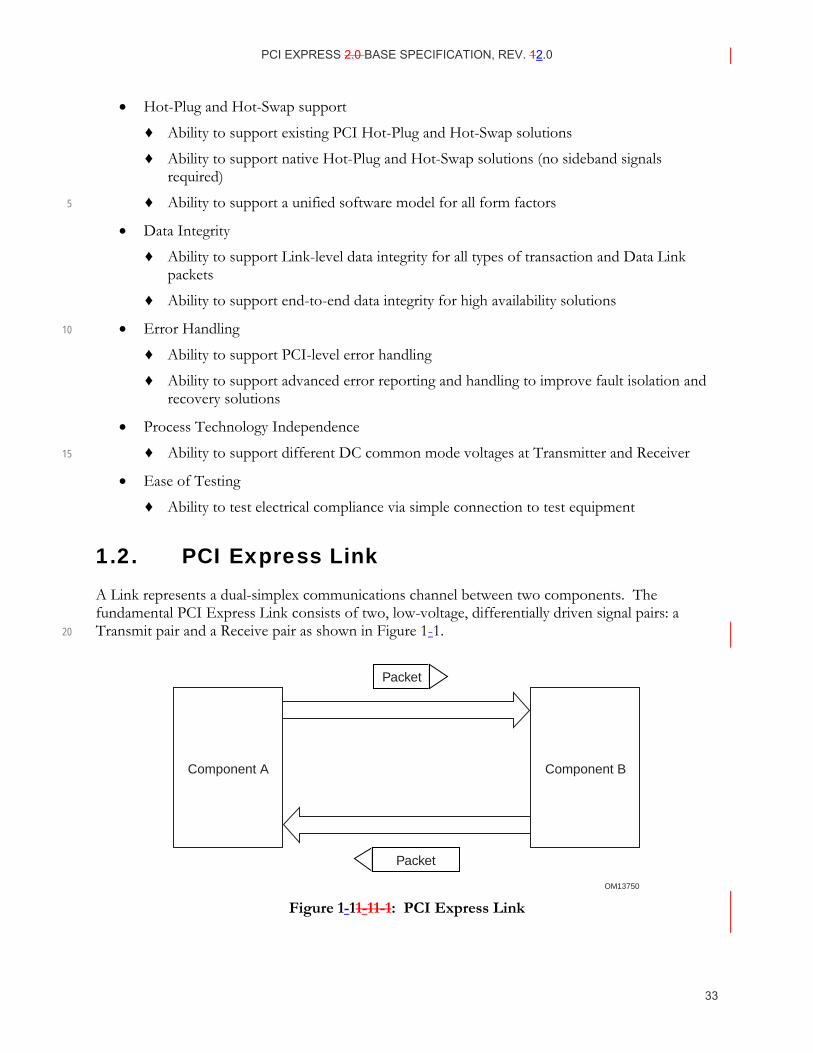
PCI EXPRESS 2.0 BASE SPECIFICATION, REV. 12.0
33
• Hot-Plug and Hot-Swap support
♦ Ability to support existing PCI Hot-Plug and Hot-Swap solutions
♦ Ability to support native Hot-Plug and Hot-Swap solutions (no sideband signals required)
♦ Ability to support a unified software model for all form factors 5
• Data Integrity
♦ Ability to support Link-level data integrity for all types of transaction and Data Link packets
♦ Ability to support end-to-end data integrity for high availability solutions
• Error Handling 10
♦ Ability to support PCI-level error handling
♦ Ability to support advanced error reporting and handling to improve fault isolation and recovery solutions
• Process Technology Independence
♦ Ability to support different DC common mode voltages at Transmitter and Receiver 15
• Ease of Testing
♦ Ability to test electrical compliance via simple connection to test equipment
1.2. PCI Express Link A Link represents a dual-simplex communications channel between two components. The fundamental PCI Express Link consists of two, low-voltage, differentially driven signal pairs: a Transmit pair and a Receive pair as shown in Figure 1-1. 20
OM13750
Component A Component B
Packet
Packet
Figure 1-11-1 1-1: PCI Express Link
PCI EXPRESS 2.0 BASE SPECIFICATION, REV. 21.0
34
The primary Link attributes are:
The basic Link – PCI Express Link consists of dual unidirectional differential Links, implemented as a Transmit pair and a Receive pair. A data clock is embedded using an encoding scheme (refer tosee Chapter 4) to achieve very high data rates.
Signaling rate – Once initialized, each Link must only operate at one of the supported signaling 5 levels. For the first generation of PCI Express technology, there is only one signaling rate defined, which provides an effective 2.5 Gigabits/second/Lane/direction of raw bandwidth. The second generation provides an effective 5.0 Gigabits/second/Lane/direction of raw bandwidth. The data rate is expected to increase with technology advances in the future.
Lanes – A Link must support at least one Lane – each Lane represents a set of differential signal 10 pairs (one pair for transmission, one pair for reception). To scale bandwidth, a Link may aggregate multiple Lanes denoted by xN where N may be any of the supported Link widths. An x8 Link represents an aggregate bandwidth of 20 Gigabits/second of raw bandwidth in each direction. This specification describes operations for x1, x2, x4, x8, x12, x16, and x32 Lane widths. 15
Initialization – During hardware initialization, each PCI Express Link is set up following a negotiation of Lane widths and frequency of operation by the two agents at each end of the Link. No firmware or operating system software is involved.
Symmetry – Each Link must support a symmetric number of Lanes in each direction, i.e., a x16 Link indicates there are 16 differential signal pairs in each direction. 20
1.3. PCI Express Fabric Topology A fabric is composed of point-to-point Links that interconnect a set of components – an example fabric topology is shown in Figure 1-2. This figure illustrates a single fabric instance referred to as a hierarchy – composed of a Root Complex (RC), multiple Endpoints (I/O devices), a Switch, and a PCI Express- to PCI/PCI-X Bridge, all interconnected via PCI Express Links.
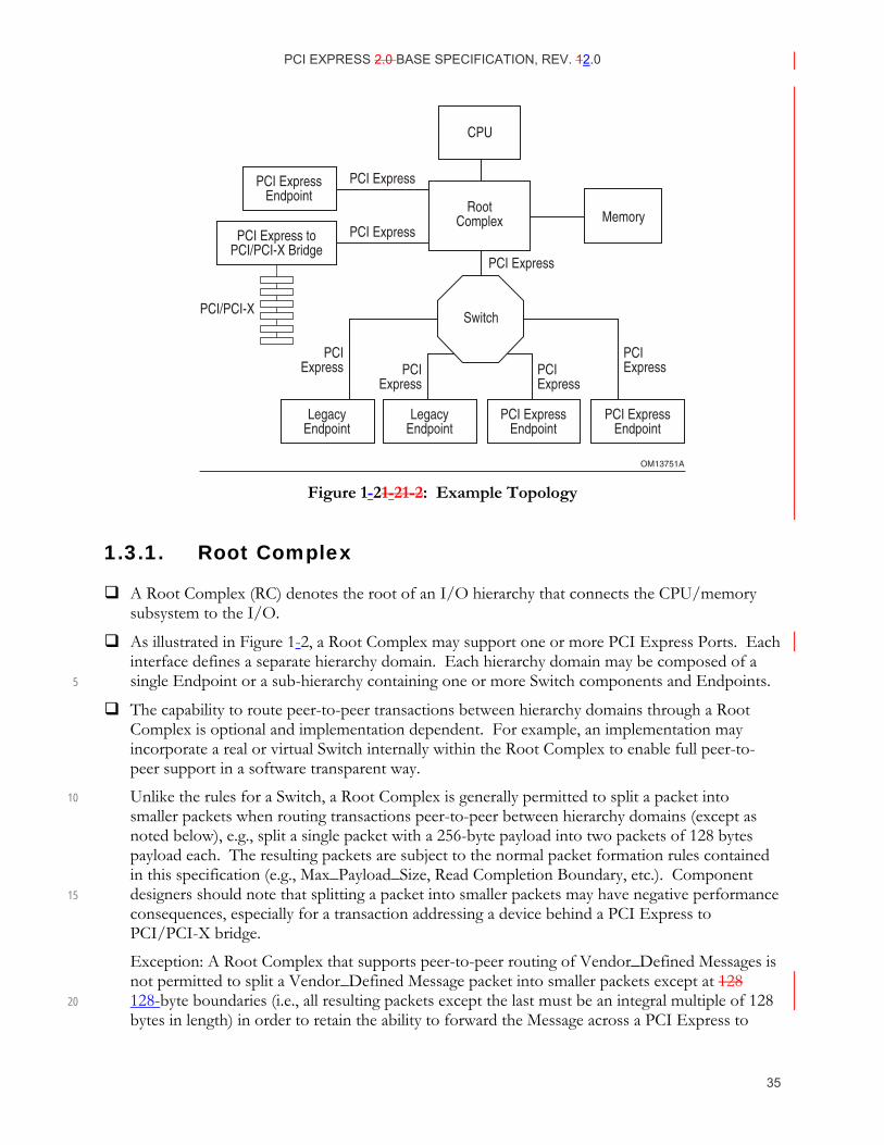
PCI EXPRESS 2.0 BASE SPECIFICATION, REV. 12.0
35
PCI/PCI-X
OM13751A
Switch
Memory
PCI ExpressEndpoint
CPU
RootComplex
PCI Express
PCI Express
PCI Express
PCIExpress
PCIExpressPCI
ExpressPCI
Express
LegacyEndpoint
PCI ExpressEndpoint
PCI ExpressEndpoint
LegacyEndpoint
PCI Express toPCI/PCI-X Bridge
Figure 1-21-2 1-2: Example Topology
1.3.1. Root Complex
A Root Complex (RC) denotes the root of an I/O hierarchy that connects the CPU/memory subsystem to the I/O.
As illustrated in Figure 1-2, a Root Complex may support one or more PCI Express Ports. Each interface defines a separate hierarchy domain. Each hierarchy domain may be composed of a single Endpoint or a sub-hierarchy containing one or more Switch components and Endpoints. 5
The capability to route peer-to-peer transactions between hierarchy domains through a Root Complex is optional and implementation dependent. For example, an implementation may incorporate a real or virtual Switch internally within the Root Complex to enable full peer-to-peer support in a software transparent way.
Unlike the rules for a Switch, a Root Complex is generally permitted to split a packet into 10 smaller packets when routing transactions peer-to-peer between hierarchy domains (except as noted below), e.g., split a single packet with a 256-byte payload into two packets of 128 bytes payload each. The resulting packets are subject to the normal packet formation rules contained in this specification (e.g., Max_Payload_Size, Read Completion Boundary, etc.). Component designers should note that splitting a packet into smaller packets may have negative performance 15 consequences, especially for a transaction addressing a device behind a PCI Express to PCI/PCI-X bridge.
Exception: A Root Complex that supports peer-to-peer routing of Vendor_Defined Messages is not permitted to split a Vendor_Defined Message packet into smaller packets except at 128 128-byte boundaries (i.e., all resulting packets except the last must be an integral multiple of 128 20 bytes in length) in order to retain the ability to forward the Message across a PCI Express to
PCI EXPRESS 2.0 BASE SPECIFICATION, REV. 21.0
36
PCI/PCI-X Bridge. Refer to the PCI Express to PCI/PCI-X Bridge Specification, Revision 1.0 for additional information.
A Root Complex must support generation of configuration requests as a Requester.
A Root Complex is permitted to support the generation of I/O requests as a Requester.
A Root Complex must not support Lock semantics as a Completer. 5
A Root Complex is permitted to support generation of Locked Requests as a Requester.
1.3.2. Endpoints Endpoint refers to a type of device Function that can be the Requester or Completer of a PCI Express transaction either on its own behalf or on behalf of a distinct non-PCI Express device (other than a PCI device or Host CPU), e.g., a PCI Express attached graphics controller or a PCI Express-USB host controller. Endpoints are classified as either legacy, PCI Express, or Root 10 Complex Integrated Endpoints.
1.3.2.1. Legacy Endpoint Rules
A legacy Legacy Endpoint must be a device Function with a Type 00h Configuration Space header.
A legacy Legacy Endpoint must support Configuration Requests as a Completer
A Legacylegacy Endpoint may support I/O Requests as a Completer. 15
A Legacylegacy Endpoint may generate I/O Requests.
A Legacylegacy Endpoint may support Lock memory semantics as a Completer if that is required by the device’s legacy software support requirements.
A legacy Legacy Endpoint must not issue a Locked Request.
A legacy Legacy Endpoint may implement extended Extended configuration spaceConfiguration 20 Space capabilitiesCapabilities, but such capabilities Capabilities may be ignored by software.
A legacy Legacy Endpoint operating as the Requester of a Memory Transaction is not required to be capable of generating addresses 4 GB or greater.
A legacy Legacy Endpoint is required to support MSI or MSI-X or both if an interrupt resource is requested. If MSI is implemented, a legacy Legacy Endpoint is permitted to support either the 25 32-bit or 64-bit Message Address version of the MSI capability Capability structure.
A legacy Legacy Endpoint is permitted to support 32-bit addressing for Base Address registers that request memory resources.
A legacy Legacy Endpoint must appear within one of the hierarchy domains originated by the Root Complex. 30
PCI EXPRESS 2.0 BASE SPECIFICATION, REV. 12.0
37
1.3.2.2. PCI Express Endpoint Rules
A PCI Express Endpoint must be a device Function with a Type 00h Configuration Space header.
A PCI Express Endpoint must support Configuration Requests as a Completer.
A PCI Express Endpoint must not depend on operating system allocation of I/O resources claimed through BAR(s). 5
A PCI Express Endpoint must not generate I/O Requests.
A PCI Express Endpoint must not support Locked Requests as a Completer or generate them as a Requestor. PCI Express-compliant software drivers and applications must be written to prevent the use of lock semantics when accessing a PCI Express Endpoint.
A PCI Express Endpoint operating as the Requester of a Memory Transaction is required to be 10 capable of generating addresses greater than 4 GB.
A PCI Express Endpoint is required to support MSI or MSI-X or both if an interrupt resource is requested., If MSI is implemented, a PCI Express Endpoint must support the 64-bit Message Address version of the MSI capability Capability structure.
A PCI Express Endpoint requesting memory resources through a BAR must set the BAR’s 15 Prefetchable bit unless the range contains locations with read side-effects or locations in which the device Function does not tolerate write merging.
For a PCI Express Endpoint, 64-bit addressing must be supported for all BARs that have the prefetchable bit set. 32-bit addressing is permitted for all BARs that do not have the prefetchable bit set. 20
The minimum memory address range requested by a BAR is 128 bytes.
A PCI Express Endpoint must appear within one of the hierarchy domains originated by the Root Complex.
1.3.2.3. Root Complex Integrated Endpoint Rules
A Root Complex Integrated Endpoint is implemented on internal logic of Root Complexes that contains the Root Ports. 25
A Root Complex Integrated Endpoint must be a device Function with a Type 00h Configuration Space header.
A Root Complex Integrated Endpoint must support Configuration Requests as a Completer
A Root Complex Integrated Endpoint must not require I/O resources claimed through BAR(s).
A Root Complex Integrated Endpoint must not generate I/O Requests. 30
A Root Complex Integrated Endpoint must not support Locked Requests as a Completer or generate them as a Requestor. PCI Express-compliant software drivers and applications must be written to prevent the use of lock semantics when accessing a Root Complex IntegratedPCI Express Endpoint.

PCI EXPRESS 2.0 BASE SPECIFICATION, REV. 21.0
38
A Root Complex Integrated Endpoint operating as the Requester of a Memory Transaction is required to be capable of generating addresses equal to or greater than the Host is capable of handling as a Completer.
A Root Complex Integrated Endpoint is required to support MSI or MSI-X or both if an interrupt resource is requested. If MSI is implemented, a Root Complex Integrated Endpoint is 5 permitted to support either the 32-bit or 64-bit Message Address version of the MSI capability Capability structure.
A Root Complex Integrated Endpoint is permitted to support 32-bit addressing for Base Address registers that request memory resources.
A Root Complex Integrated Endpoint must not implement Link Capabilities/Status/Control 10 registers in the PCI Express Extended Capability.
A Root Complex Integrated Endpoint must signal PME and error conditions through the same mechanisms used on PCI systems. If a Root Complex Event Collector is implemented, a Root Complex Integrated Endpoint may optionally signal PME and error conditions through a Root Complex Event Collector. In this case, a Root Complex Integrated Endpoint must be 15 associated with exactly one Root Complex Event Collector.
A Root Complex Integrated Endpoint does not implement Active State Power Management.
A Root Complex Integrated Endpoint may not be hot-plugged independent of the Root Complex as a whole.
A Root Complex Integrated Endpoint must not appear in any of the hierarchy domains exposed 20 by the Root Complex.
A Root Complex Integrated Endpoint must not appear in Switches.
1.3.3. Switch A Switch is defined as a logical assembly of multiple virtual PCI-to-PCI Bridge devices as illustrated in Figure 1-3. All Switches are governed by the following base rules.
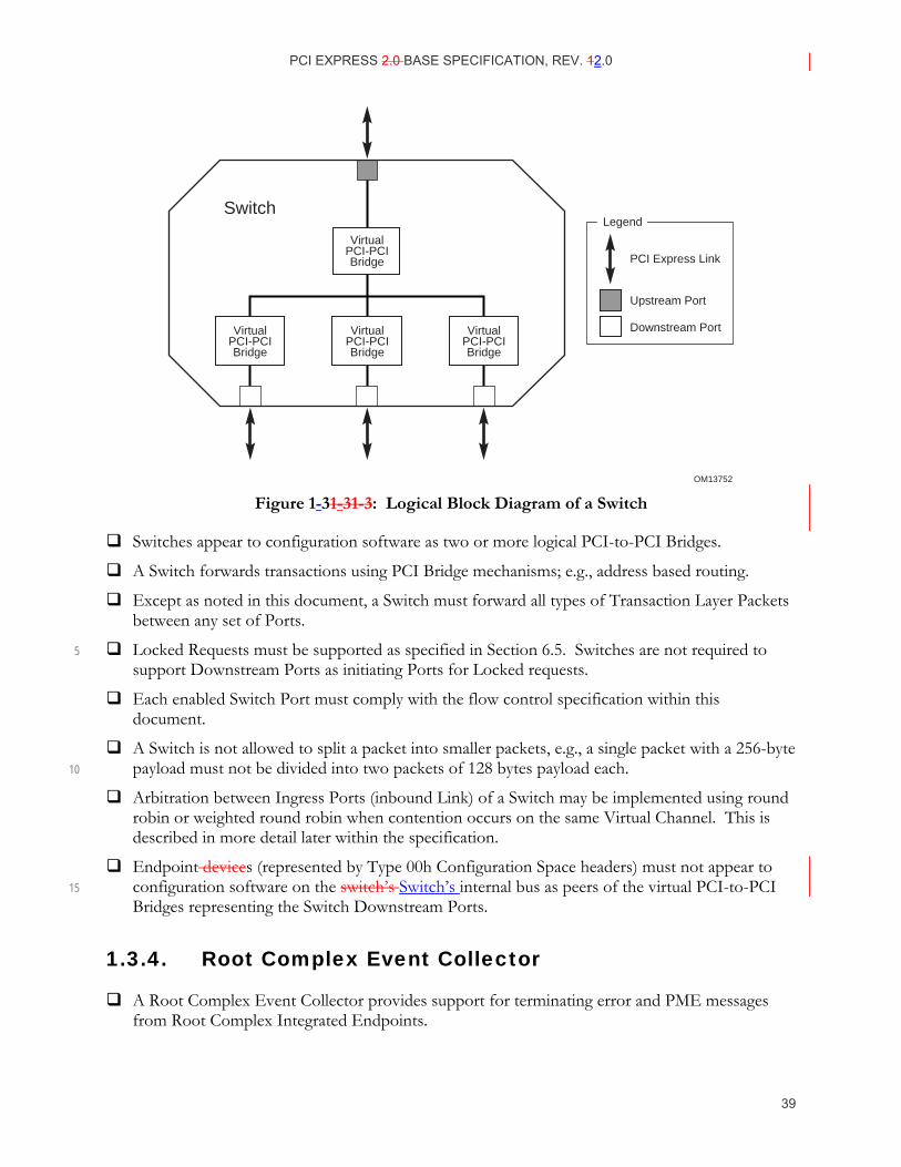
PCI EXPRESS 2.0 BASE SPECIFICATION, REV. 12.0
39
OM13752
VirtualPCI-PCIBridge PCI Express Link
Downstream Port
Upstream Port
LegendSwitch
VirtualPCI-PCIBridge
VirtualPCI-PCIBridge
VirtualPCI-PCIBridge
Figure 1-31-3 1-3: Logical Block Diagram of a Switch
Switches appear to configuration software as two or more logical PCI-to-PCI Bridges.
A Switch forwards transactions using PCI Bridge mechanisms; e.g., address based routing.
Except as noted in this document, a Switch must forward all types of Transaction Layer Packets between any set of Ports.
Locked Requests must be supported as specified in Section 6.5. Switches are not required to 5 support Downstream Ports as initiating Ports for Locked requests.
Each enabled Switch Port must comply with the flow control specification within this document.
A Switch is not allowed to split a packet into smaller packets, e.g., a single packet with a 256-byte payload must not be divided into two packets of 128 bytes payload each. 10
Arbitration between Ingress Ports (inbound Link) of a Switch may be implemented using round robin or weighted round robin when contention occurs on the same Virtual Channel. This is described in more detail later within the specification.
Endpoint devices (represented by Type 00h Configuration Space headers) must not appear to configuration software on the switch’s Switch’s internal bus as peers of the virtual PCI-to-PCI 15 Bridges representing the Switch Downstream Ports.
1.3.4. Root Complex Event Collector
A Root Complex Event Collector provides support for terminating error and PME messages from Root Complex Integrated Endpoints.
PCI EXPRESS 2.0 BASE SPECIFICATION, REV. 21.0
40
A Root Complex Event Collector must follow all rules for a Root Complex Integrated Endpoint.
A Root Complex Event Collector is not required to decode any memory or IO resources.
A Root Complex Event Collector has the Base Class 08h, Sub-Class 05h 06h and Programming Interface 00h. 5
A Root Complex Event Collector resides on the same logical Logical bus Bus as the Root Complex Integrated Endpoints it supports.
A Root Complex Event Collector explicitly declares supported Root Complex Integrated Endpoints through the Root Complex Event Collector Endpoint Association Capability.
Root Complex Event Collectors are optional. 10
1.3.5. PCI Express- to PCI/PCI-X Bridge
A PCI Express- to PCI/PCI-X Bridge provides a connection between a PCI Express fabric and a PCI/PCI-X hierarchy.
PCI Express Port(s) of a PCI Express- to PCI/PCI-X Bridge must comply with the requirements of this document.
1.4. PCI Express Fabric Topology Configuration The PCI Express Configuration model supports two mechanisms: 15
PCI compatible configuration mechanism: The PCI compatible mechanism supports 100% binary compatibility with PCI 3.0 or later operating systems and their corresponding bus enumeration and configuration software.
PCI Express enhanced configuration mechanism: The enhanced mechanism is provided to increase the size of available configuration spaceConfiguration Space and to optimize access 20 mechanisms.
Each PCI Express Link is mapped through a virtual PCI-to-PCI Bridge structure and has a logical PCI bus associated with it. The virtual PCI-to-PCI Bridge structure may be part of a PCI Express Root Complex Port, a Switch Upstream Port, or a Switch Downstream Port. A Root Port is a virtual PCI-to-PCI Bridge structure that originates a PCI Express hierarchy domain from a PCI 25 Express Root Complex. Logical dDevices are mapped into configuration spaceConfiguration Space such that each will respond to a particular device Device numberNumber.
1.5. PCI Express Layering Overview This document specifies the architecture in terms of three discrete logical layers: the Transaction Layer, the Data Link Layer, and the Physical Layer. Each of these layers is divided into two sections: one that processes outbound (to be transmitted) information and one that processes inbound 30 (received) information, as shown in Figure 1-4.
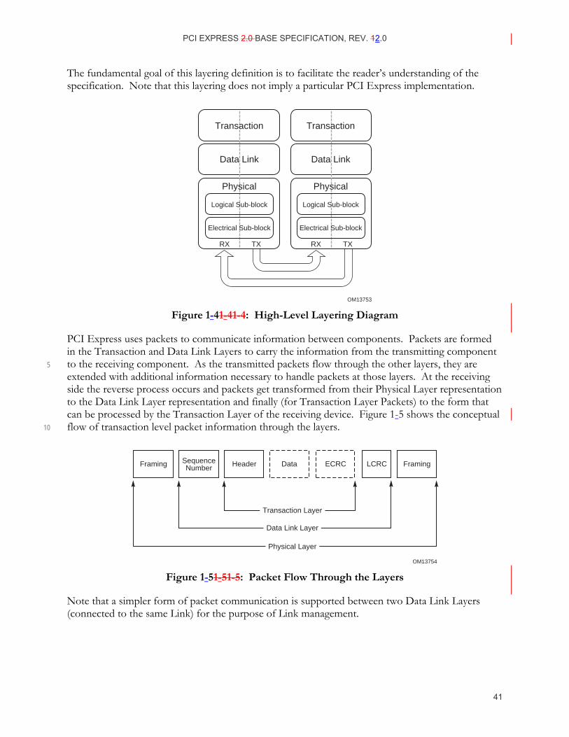
PCI EXPRESS 2.0 BASE SPECIFICATION, REV. 12.0
41
The fundamental goal of this layering definition is to facilitate the reader’s understanding of the specification. Note that this layering does not imply a particular PCI Express implementation.
OM13753
Data Link Data Link
RX TX
Logical Sub-block
Electrical Sub-block
Physical
RX TX
Logical Sub-block
Electrical Sub-block
Physical
Transaction Transaction
Figure 1-41-4 1-4: High-Level Layering Diagram
PCI Express uses packets to communicate information between components. Packets are formed in the Transaction and Data Link Layers to carry the information from the transmitting component to the receiving component. As the transmitted packets flow through the other layers, they are 5 extended with additional information necessary to handle packets at those layers. At the receiving side the reverse process occurs and packets get transformed from their Physical Layer representation to the Data Link Layer representation and finally (for Transaction Layer Packets) to the form that can be processed by the Transaction Layer of the receiving device. Figure 1-5 shows the conceptual flow of transaction level packet information through the layers. 10
OM13754
Framing SequenceNumber Header Data ECRC LCRC Framing
Transaction Layer
Data Link Layer
Physical Layer
Figure 1-51-5 1-5: Packet Flow Through the Layers
Note that a simpler form of packet communication is supported between two Data Link Layers (connected to the same Link) for the purpose of Link management.
PCI EXPRESS 2.0 BASE SPECIFICATION, REV. 21.0
42
1.5.1. Transaction Layer
The upper Layer of the architecture is the Transaction Layer. The Transaction Layer’s primary responsibility is the assembly and disassembly of Transaction Layer Packets (TLPs). TLPs are used to communicate transactions, such as read and write, as well as certain types of events. The Transaction Layer is also responsible for managing credit-based flow control for TLPs.
Every request packet requiring a response packet is implemented as a split transaction. Each packet 5 has a unique identifier that enables response packets to be directed to the correct originator. The packet format supports different forms of addressing depending on the type of the transaction (Memory, I/O, Configuration, and Message). The Packets may also have attributes such as No Snoop and Relaxed Ordering.
The transaction Layer supports four address spaces: it includes the three PCI address spaces 10 (memory, I/O, and configuration) and adds Message Space. This specification uses Message Space to support all prior sideband signals, such as interrupts, power-management requests, and so on, as in-band Message transactions. You could think of PCI Express Message transactions as “virtual wires” since their effect is to eliminate the wide array of sideband signals currently used in a platform implementation. 15
1.5.2. Data Link Layer
The middle Layer in the stack, the Data Link Layer, serves as an intermediate stage between the Transaction Layer and the Physical Layer. The primary responsibilities of the Data Link Layer include Link management and data integrity, including error detection and error correction.
The transmission side of the Data Link Layer accepts TLPs assembled by the Transaction Layer, calculates and applies a data protection code and TLP sequence number, and submits them to 20 Physical Layer for transmission across the Link. The receiving Data Link Layer is responsible for checking the integrity of received TLPs and for submitting them to the Transaction Layer for further processing. On detection of TLP error(s), this Layer is responsible for requesting retransmission of TLPs until information is correctly received, or the Link is determined to have failed. 25
The Data Link Layer also generates and consumes packets that are used for Link management functions. To differentiate these packets from those used by the Transaction Layer (TLP), the term Data Link Layer Packet (DLLP) will be used when referring to packets that are generated and consumed at the Data Link Layer.
1.5.3. Physical Layer
The Physical Layer includes all circuitry for interface operation, including driver and input buffers, 30 parallel-to-serial and serial-to-parallel conversion, PLL(s), and impedance matching circuitry. It includes also logical functions related to interface initialization and maintenance. The Physical Layer exchanges information with the Data Link Layer in an implementation-specific format. This Layer is responsible for converting information received from the Data Link Layer into an appropriate serialized format and transmitting it across the PCI Express Link at a frequency and width 35 compatible with the device connected to the other side of the Link.
PCI EXPRESS 2.0 BASE SPECIFICATION, REV. 12.0
43
The PCI Express architecture has “hooks” to support future performance enhancements via speed upgrades and advanced encoding techniques. The future speeds, encoding techniques or media may only impact the Physical Layer definition.
1.5.4. Layer Functions and Services
1.5.4.1. Transaction Layer Services
The Transaction Layer, in the process of generating and receiving TLPs, exchanges Flow Control information with its complementary Transaction Layer on the other side of the Link. It is also 5 responsible for supporting both software and hardware-initiated power management.
Initialization and configuration functions require the Transaction Layer to:
Store Link configuration information generated by the processor or management device
Store Link capabilities generated by Physical Layer hardware negotiation of width and operational frequency 10
A Transaction Layer’s Packet generation and processing services require it to:
Generate TLPs from device core Requests
Convert received Request TLPs into Requests for the device core
Convert received Completion Packets into a payload, or status information, deliverable to the core 15
Detect unsupported TLPs and invoke appropriate mechanisms for handling them
If end-to-end data integrity is supported, generate the end-to-end data integrity CRC and update the TLP header accordingly.
Flow control services:
The Transaction Layer tracks flow control credits for TLPs across the Link. 20
Transaction credit status is periodically transmitted to the remote Transaction Layer using transport services of the Data Link Layer.
Remote Flow Control information is used to throttle TLP transmission.
Ordering rules:
PCI/PCI-X compliant producer consumer ordering model 25
Extensions to support relaxed ordering
Power management services:
ACPI/PCI power management, as dictated by system software.
Hardware-controlled autonomous power management minimizes power during full-on power states. 30
PCI EXPRESS 2.0 BASE SPECIFICATION, REV. 21.0
44
Virtual Channels and Traffic Class:
The combination of Virtual Channel mechanism and Traffic Class identification is provided to support differentiated services and QoS support for certain classes of applications.
Virtual Channels: Virtual Channels provide a means to support multiple independent logical data flows over given common physical resources of the Link. Conceptually this involves 5 multiplexing different data flows onto a single physical Link.
Traffic Class: The Traffic Class is a Transaction Layer Packet label that is transmitted unmodified end-to-end through the fabric. At every service point (e.g., Switch) within the fabric, Traffic Class labels are used to apply appropriate servicing policies. Each Traffic Class label defines a unique ordering domain - no ordering guarantees are provided for packets that 10 contain different Traffic Class labels.
1.5.4.2. Data Link Layer Services
The Data Link Layer is responsible for reliably exchanging information with its counterpart on the opposite side of the Link.
Initialization and power management services:
Accept power state Requests from the Transaction Layer and convey to the Physical Layer 15
Convey active/reset/disconnected/power managed state to the Transaction Layer
Data protection, error checking, and retry services:
CRC generation
Transmitted TLP storage for Data Link level retry
Error checking 20
TLP acknowledgment and retry Messages
Error indication for error reporting and logging
1.5.4.3. Physical Layer Services
Interface initialization, maintenance control, and status tracking:
Reset/Hot-Plug control/status
Interconnect power management 25
Width and Lane mapping negotiation
Polarity reversal
Symbol and special Ordered Set generation:
8-bit/10-bit8b/10b encoding/decoding
Embedded clock tuning and alignment 30
PCI EXPRESS 2.0 BASE SPECIFICATION, REV. 12.0
45
Symbol transmission and alignment:
Transmission circuits
Reception circuits
Elastic buffer at receiving side
Multi-Lane de-skew (for widths > x1) at receiving side 5
System DFT support features
1.5.4.4. Inter-Layer Interfaces
1.5.4.4.1. Transaction/Data Link Interface
The Transaction to Data Link interface provides:
Byte or multi-byte data to be sent across the Link
• Local TLP-transfer handshake mechanism
• TLP boundary information 10
Requested power state for the Link
The Data Link to Transaction interface provides:
Byte or multi-byte data received from the PCI Express Link
TLP framing information for the received byte
Actual power state for the Link 15
Link status information
1.5.4.4.2. Data Link/Physical Interface
The Data Link to Physical interface provides:
Byte or multi-byte wide data to be sent across the Link
• Data transfer handshake mechanism
• TLP and DLLP boundary information for bytes 20
Requested power state for the Link
The Physical to Data Link interface provides:
Byte or multi-byte wide data received from the PCI Express Link
TLP and DLLP framing information for data
Indication of errors detected by the Physical Layer 25

PCI EXPRESS 2.0 BASE SPECIFICATION, REV. 21.0
46
Actual power state for the Link
Connection status information
5
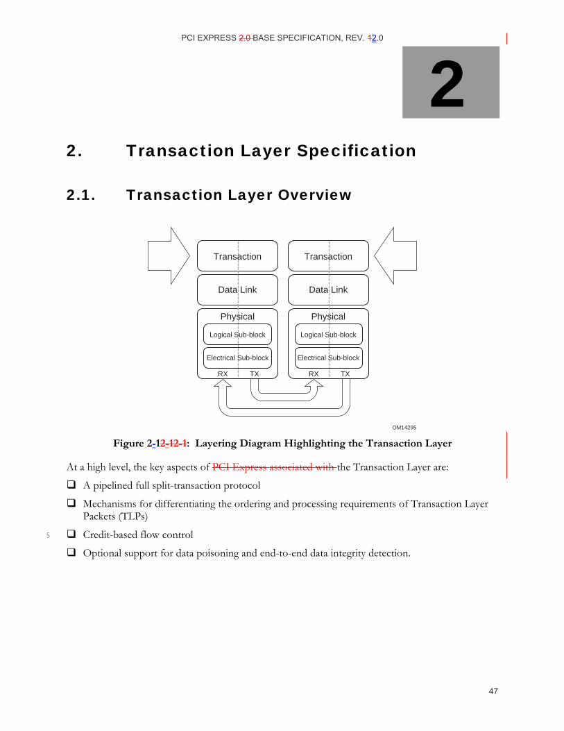
PCI EXPRESS 2.0 BASE SPECIFICATION, REV. 12.0
47
2. Transaction Layer Specification
2.1. Transaction Layer Overview
OM14295
Data Link Data Link
RX TX
Logical Sub-block
Electrical Sub-block
Physical
RX TX
Logical Sub-block
Electrical Sub-block
Physical
Transaction Transaction
Figure 2-12-1 2-1: Layering Diagram Highlighting the Transaction Layer
At a high level, the key aspects of PCI Express associated with the Transaction Layer are:
A pipelined full split-transaction protocol
Mechanisms for differentiating the ordering and processing requirements of Transaction Layer Packets (TLPs)
Credit-based flow control 5
Optional support for data poisoning and end-to-end data integrity detection.
2
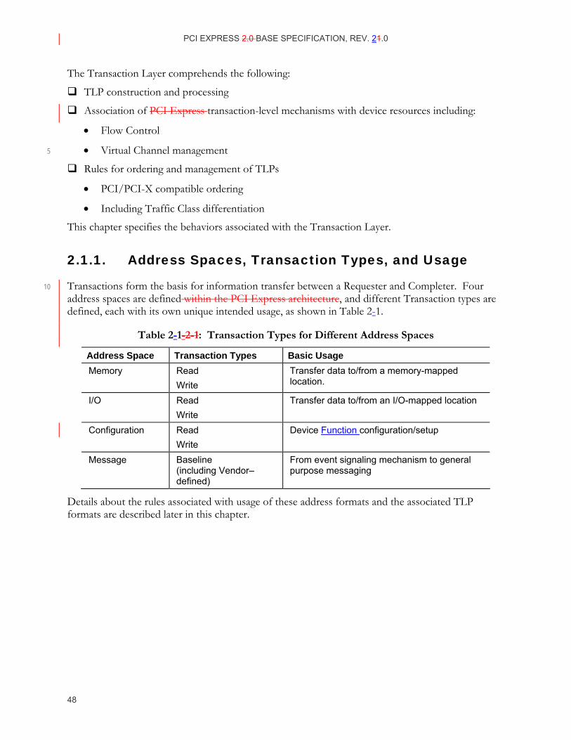
PCI EXPRESS 2.0 BASE SPECIFICATION, REV. 21.0
48
The Transaction Layer comprehends the following:
TLP construction and processing
Association of PCI Express transaction-level mechanisms with device resources including:
• Flow Control
• Virtual Channel management 5
Rules for ordering and management of TLPs
• PCI/PCI-X compatible ordering
• Including Traffic Class differentiation
This chapter specifies the behaviors associated with the Transaction Layer.
2.1.1. Address Spaces, Transaction Types, and Usage
Transactions form the basis for information transfer between a Requester and Completer. Four 10 address spaces are defined within the PCI Express architecture, and different Transaction types are defined, each with its own unique intended usage, as shown in Table 2-1.
Table 2-1- 2-1: Transaction Types for Different Address Spaces
Address Space Transaction Types Basic Usage Memory Read
Write Transfer data to/from a memory-mapped location.
I/O Read Write
Transfer data to/from an I/O-mapped location
Configuration Read Write
Device Function configuration/setup
Message Baseline (including Vendor–defined)
From event signaling mechanism to general purpose messaging
Details about the rules associated with usage of these address formats and the associated TLP formats are described later in this chapter.
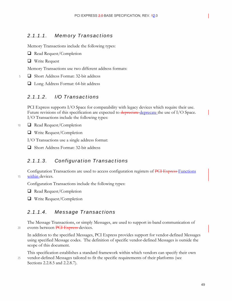
PCI EXPRESS 2.0 BASE SPECIFICATION, REV. 12.0
49
2.1.1.1. Memory Transactions
Memory Transactions include the following types:
Read Request/Completion
Write Request
Memory Transactions use two different address formats:
Short Address Format: 32-bit address 5
Long Address Format: 64-bit address
2.1.1.2. I/O Transactions
PCI Express supports I/O Space for compatability with legacy devices which require their use. Future revisions of this specification are expected to depreciate deprecate the use of I/O Space. I/O Transactions include the following types:
Read Request/Completion 10
Write Request/Completion
I/O Transactions use a single address format:
Short Address Format: 32-bit address
2.1.1.3. Configuration Transactions
Configuration Transactions are used to access configuration registers of PCI Express Functions within devices. 15
Configuration Transactions include the following types:
Read Request/Completion
Write Request/Completion
2.1.1.4. Message Transactions
The Message Transactions, or simply Messages, are used to support in-band communication of events between PCI Express devices. 20
In addition to the specified Messages, PCI Express provides support for vendor-defined Messages using specified Message codes. The definition of specific vendor-defined Messages is outside the scope of this document.
This specification establishes a standard framework within which vendors can specify their own vendor-defined Messages tailored to fit the specific requirements of their platforms (see 25 Sections 2.2.8.5 and 2.2.8.7).
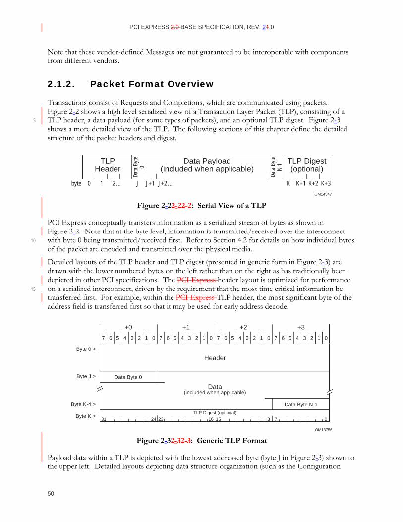
PCI EXPRESS 2.0 BASE SPECIFICATION, REV. 21.0
50
Note that these vendor-defined Messages are not guaranteed to be interoperable with components from different vendors.
2.1.2. Packet Format Overview
Transactions consist of Requests and Completions, which are communicated using packets. Figure 2-2 shows a high level serialized view of a Transaction Layer Packet (TLP), consisting of a TLP header, a data payload (for some types of packets), and an optional TLP digest. Figure 2-3 5 shows a more detailed view of the TLP. The following sections of this chapter define the detailed structure of the packet headers and digest.
OM14547
TLPHeader
Data Payload(included when applicable)
TLP Digest(optional)
K+1 K+2 K+3K
Dat
a By
te0
Dat
a By
teN
-1
J+1 J+2J1 20byte
Figure 2-22-2 2-2: Serial View of a TLP
PCI Express conceptually transfers information as a serialized stream of bytes as shown in Figure 2-2. Note that at the byte level, information is transmitted/received over the interconnect with byte 0 being transmitted/received first. Refer to Section 4.2 for details on how individual bytes 10 of the packet are encoded and transmitted over the physical media.
Detailed layouts of the TLP header and TLP digest (presented in generic form in Figure 2-3) are drawn with the lower numbered bytes on the left rather than on the right as has traditionally been depicted in other PCI specifications. The PCI Express header layout is optimized for performance on a serialized interconnect, driven by the requirement that the most time critical information be 15 transferred first. For example, within the PCI Express TLP header, the most significant byte of the address field is transferred first so that it may be used for early address decode.
OM13756
Header
TLP Digest (optional)
Data(included when applicable)
Data Byte 0
Byte 0 >
Byte J >
Byte K-4 >
Byte K >
Data Byte N-1
7 6 5 4 3 2 1 0 7 6 5 4 3 2 1 0 7 6 5 4 3 2 1 0 7 6 5 4 3 2 1 0
+0 +1 +2 +3
31 24 23 16 15 8 7 0
Figure 2-32-3 2-3: Generic TLP Format
Payload data within a TLP is depicted with the lowest addressed byte (byte J in Figure 2-3) shown to the upper left. Detailed layouts depicting data structure organization (such as the Configuration
PCI EXPRESS 2.0 BASE SPECIFICATION, REV. 12.0
51
Space depictions in Chapter 7) retain the traditional PCI byte layout with the lowest addressed byte shown on the right. Regardless of depiction, all bytes are conceptually transmitted over the Link in increasing byte number order.
Depending on the type of a packet, the header for that packet will include some of the following types of fields: 5
Format of the packet
Type of the packet
Length for any associated data
Transaction Descriptor, including:
• Transaction ID 10
• Attributes
• Traffic Class
Address/routing information
Byte Enables
Message encoding 15
Completion status
2.2. Transaction Layer Protocol - Packet Definition
PCI Express uses a packet based protocol to exchange information between the Transaction Layers of the two components communicating with each other over the Link. PCI Express supports the following basic transaction types: Memory, I/O, Configuration, and Messages. Two addressing formats for Memory Requests are supported: 32 bit and 64 bit. 20
Transactions are carried using Requests and Completions. Completions are used only where required, for example, to return read data, or to acknowledge Completion of I/O and Configuration Write Transactions. Completions are associated with their corresponding Requests by the value in the Transaction ID field of the Packet header.
All TLP fields marked Reserved (sometimes abbreviated as R) must be filled with all 0’s when a TLP 25 is formed. Values in such fields must be ignored by Receivers and forwarded unmodified by Switches. Note that for certain fields there are both specified and reserved values – the handling of reserved values in these cases is specified separately for each case.
2.2.1. Common Packet Header Fields
All Transaction Layer Packet (TLP) headers contain the following fields (see Figure 2-4):
Fmt[1:0] – Format of TLP (see Table 2-2) – bits 6:5 of byte 0 30
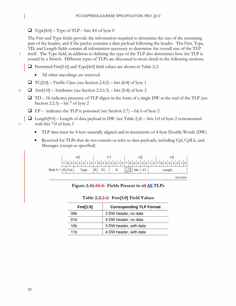
PCI EXPRESS 2.0 BASE SPECIFICATION, REV. 21.0
52
Type[4:0] – Type of TLP – bits 4:0 of byte 0
The Fmt and Type fields provide the information required to determine the size of the remaining part of the header, and if the packet contains a data payload following the header. The Fmt, Type, TD, and Length fields contain all information necessary to determine the overall size of the TLP itself. The Type field, in addition to defining the type of the TLP also determines how the TLP is 5 routed by a Switch. Different types of TLPs are discussed in more detail in the following sections.
Permitted Fmt[1:0] and Type[4:0] field values are shown in Table 2-3.
• All other encodings are reserved.
TC[2:0] – Traffic Class (see Section 2.4.2) – bits [6:4] of byte 1
Attr[1:0] – Attributes (see Section 2.2.6.3) – bits [5:4] of byte 2 10
TD – 1b indicates presence of TLP digest in the form of a single DW at the end of the TLP (see Section 2.2.3) – bit 7 of byte 2
EP – indicates the TLP is poisoned (see Section 2.7) – bit 6 of byte 2
Length[9:0] – Length of data payload in DW (see Table 2-4) – bits 1:0 of byte 2 concatenated with bits 7:0 of byte 3 15
• TLP data must be 4-byte naturally aligned and in increments of 4-byte Double Words (DW).
• Reserved for TLPs that do not contain or refer to data payloads, including Cpl, CplLk, and Messages (except as specified)
OM14540A
7 6 5 4 3 2 1 0 7 6 5 4 3 2 1 0 7 6 5 4 3 2 1 0 7 6 5 4 3 2 1 0
R AttrTD
EP ATTypeFmtR TCR Length
+0 +1 +2 +3
Byte 0 >
Figure 2-42-4 2-4: Fields Present in all All TLPs
Table 2-2- 2-2: Fmt[1:0] Field Values
Fmt[1:0] Corresponding TLP Format 00b 3 DW header, no data 01b 4 DW header, no data 10b 3 DW header, with data 11b 4 DW header, with data
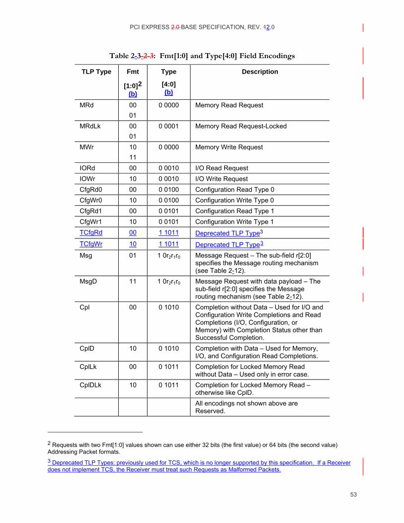
PCI EXPRESS 2.0 BASE SPECIFICATION, REV. 12.0
53
Table 2-3- 2-3: Fmt[1:0] and Type[4:0] Field Encodings
TLP Type Fmt
[1:0]2 (b)
Type
[4:0] (b)
Description
MRd 00 01
0 0000 Memory Read Request
MRdLk 00 01
0 0001 Memory Read Request-Locked
MWr 10 11
0 0000 Memory Write Request
IORd 00 0 0010 I/O Read Request IOWr 10 0 0010 I/O Write Request CfgRd0 00 0 0100 Configuration Read Type 0 CfgWr0 10 0 0100 Configuration Write Type 0 CfgRd1 00 0 0101 Configuration Read Type 1 CfgWr1 10 0 0101 Configuration Write Type 1 TCfgRd 00 1 1011 Deprecated TLP Type3 TCfgWr 10 1 1011 Deprecated TLP Type3 Msg 01
1 0r2r1r0 Message Request – The sub-field r[2:0]
specifies the Message routing mechanism (see Table 2-12).
MsgD 11
1 0r2r1r0 Message Request with data payload – The sub-field r[2:0] specifies the Message routing mechanism (see Table 2-12).
Cpl 00 0 1010 Completion without Data – Used for I/O and Configuration Write Completions and Read Completions (I/O, Configuration, or Memory) with Completion Status other than Successful Completion.
CplD 10 0 1010 Completion with Data – Used for Memory, I/O, and Configuration Read Completions.
CplLk 00 0 1011 Completion for Locked Memory Read without Data – Used only in error case.
CplDLk 10 0 1011 Completion for Locked Memory Read – otherwise like CplD.
All encodings not shown above are Reserved.
2 Requests with two Fmt[1:0] values shown can use either 32 bits (the first value) or 64 bits (the second value) Addressing Packet formats. 3 Deprecated TLP Types: previously used for TCS, which is no longer supported by this specification. If a Receiver does not implement TCS, the Receiver must treat such Requests as Malformed Packets.
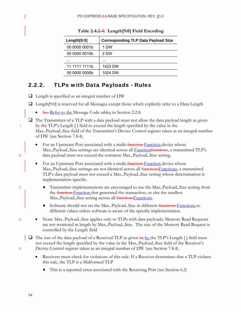
PCI EXPRESS 2.0 BASE SPECIFICATION, REV. 21.0
54
Table 2-4- 2-4: Length[9:0] Field Encoding
Length[9:0] Corresponding TLP Data Payload Size 00 0000 0001b 1 DW 00 0000 0010b 2 DW ... ... 11 1111 1111b 1023 DW 00 0000 0000b 1024 DW
2.2.2. TLPs with Data Payloads - Rules
Length is specified as an integral number of DW
Length[9:0] is reserved for all Messages except those which explicitly refer to a Data Length
• See Refer to the Message Code tables in Section 2.2.8.
The Transmitter of a TLP with a data payload must not allow the data payload length as given by the TLP’s Length [ ] field to exceed the length specified by the value in the 5 Max_Payload_Size field of the Transmitter’s Device Control register taken as an integral number of DW (see Section 7.8.4).
• For an Upstream Port associated with a multi-function Function device whose Max_Payload_Size settings are identical across all Functionfunctions, a transmitted TLP’s data payload must not exceed the common Max_Payload_Size setting. 10
• For an Upstream Port associated with a multi-function Function device whose Max_Payload_Size settings are not identical across all functionsFunctions, a transmitted TLP’s data payload must not exceed a Max_Payload_Size setting whose determination is implementation specific.
♦ Transmitter implementations are encouraged to use the Max_Payload_Size setting from 15 the function Function that generated the transaction, or else the smallest Max_Payload_Size setting across all functionsFunctions.
♦ Software should not set the Max_Payload_Size in different functions Functions to different values unless software is aware of the specific implementation.
• Note: Max_Payload_Size applies only to TLPs with data payloads; Memory Read Requests 20 are not restricted in length by Max_Payload_Size. The size of the Memory Read Request is controlled by the Length field
The size of the data payload of a Received TLP as given be by the TLP’s Length [ ] field must not exceed the length specified by the value in the Max_Payload_Size field of the Receiver’s Device Control register taken as an integral number of DW (see Section 7.8.4). 25
• Receivers must check for violations of this rule. If a Receiver determines that a TLP violates this rule, the TLP is a Malformed TLP
♦ This is a reported error associated with the Receiving Port (see Section 6.2)
PCI EXPRESS 2.0 BASE SPECIFICATION, REV. 12.0
55
• For an Upstream Port associated with a multi-function Function device whose Max_Payload_Size settings are identical across all functionsFunctions, the Receiver is required to check the TLP’s data payload size against the common Max_Payload_Size setting.
• For an Upstream Port associated with a multi-function Function device whose 5 Max_Payload_Size settings are not identical across all functionsFunctions, the Receiver is required to check the TLP’s data payload against a Max_Payload_Size setting whose determination is implementation specific.
♦ Receiver implementations are encouraged to use the Max_Payload_Size setting from the function Function targeted by the transaction, or else the largest Max_Payload_Size 10 setting across all functionsFunctions.
♦ Software should not set the Max_Payload_Size in different functions Functions to different values unless software is aware of the specific implementation.
For TLPs, that include data, the value in the Length field and the actual amount of data included in the TLP must match. 15
• Receivers must check for violations of this rule. If a Receiver determines that a TLP violates this rule, the TLP is a Malformed TLP
♦ This is a reported error associated with the Receiving Port (see Section 6.2)
The value in the Length field applies only to data – the TLP Digest is not included in the Length
When a data payload is included in a TLP, the first byte of data following the header 20 corresponds to the byte address closest to zero and the succeeding bytes are in increasing byte address sequence.
• Example: For a 16-byte write to location 100h, the first byte following the header would be the byte to be written to location 100h, and the second byte would be written to location 101h, and so on, with the final byte written to location 10Fh. 25
IMPLEMENTATION NOTE Maintaining Alignment in Data Payloads Section 2.3.1.1 discusses rules for forming Read Completions respecting certain natural address boundaries. Memory Write performance can be significantly improved by respecting similar address boundaries in the formation of the Write Request. Specifically, forming Write Requests such that natural address boundaries of 64 or 128 bytes are respected will help to improve system performance. 30
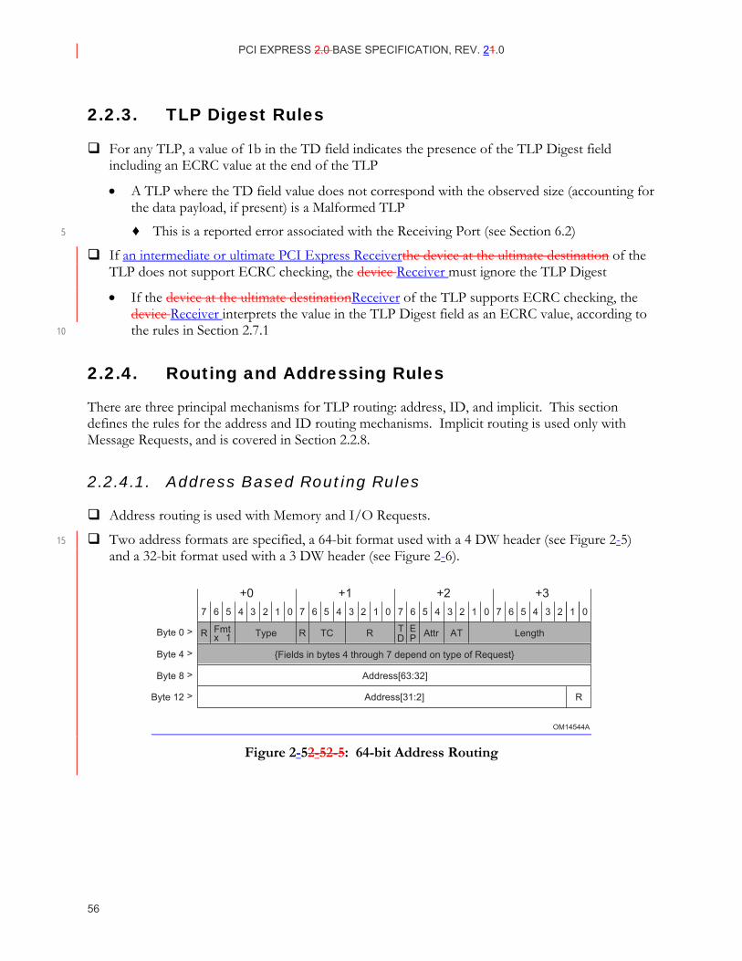
PCI EXPRESS 2.0 BASE SPECIFICATION, REV. 21.0
56
2.2.3. TLP Digest Rules
For any TLP, a value of 1b in the TD field indicates the presence of the TLP Digest field including an ECRC value at the end of the TLP
• A TLP where the TD field value does not correspond with the observed size (accounting for the data payload, if present) is a Malformed TLP
♦ This is a reported error associated with the Receiving Port (see Section 6.2) 5
If an intermediate or ultimate PCI Express Receiverthe device at the ultimate destination of the TLP does not support ECRC checking, the device Receiver must ignore the TLP Digest
• If the device at the ultimate destinationReceiver of the TLP supports ECRC checking, the device Receiver interprets the value in the TLP Digest field as an ECRC value, according to the rules in Section 2.7.1 10
2.2.4. Routing and Addressing Rules
There are three principal mechanisms for TLP routing: address, ID, and implicit. This section defines the rules for the address and ID routing mechanisms. Implicit routing is used only with Message Requests, and is covered in Section 2.2.8.
2.2.4.1. Address Based Routing Rules
Address routing is used with Memory and I/O Requests.
Two address formats are specified, a 64-bit format used with a 4 DW header (see Figure 2-5) 15 and a 32-bit format used with a 3 DW header (see Figure 2-6).
OM14544A
7 6 5
x 1
4 3 2 1 0 7 6 5 4 3 2 1 0 7 6 5 4 3 2 1 0 7 6 5 4 3 2 1 0
R AttrTD
EP ATTypeFmtR TCR
Address[31:2] R
Fields in bytes 4 through 7 depend on type of Request
Address[63:32]
Length
+0 +1 +2 +3
Byte 0 >
Byte 4 >
Byte 8 >
Byte 12 >
Figure 2-52-5 2-5: 64-bit Address Routing
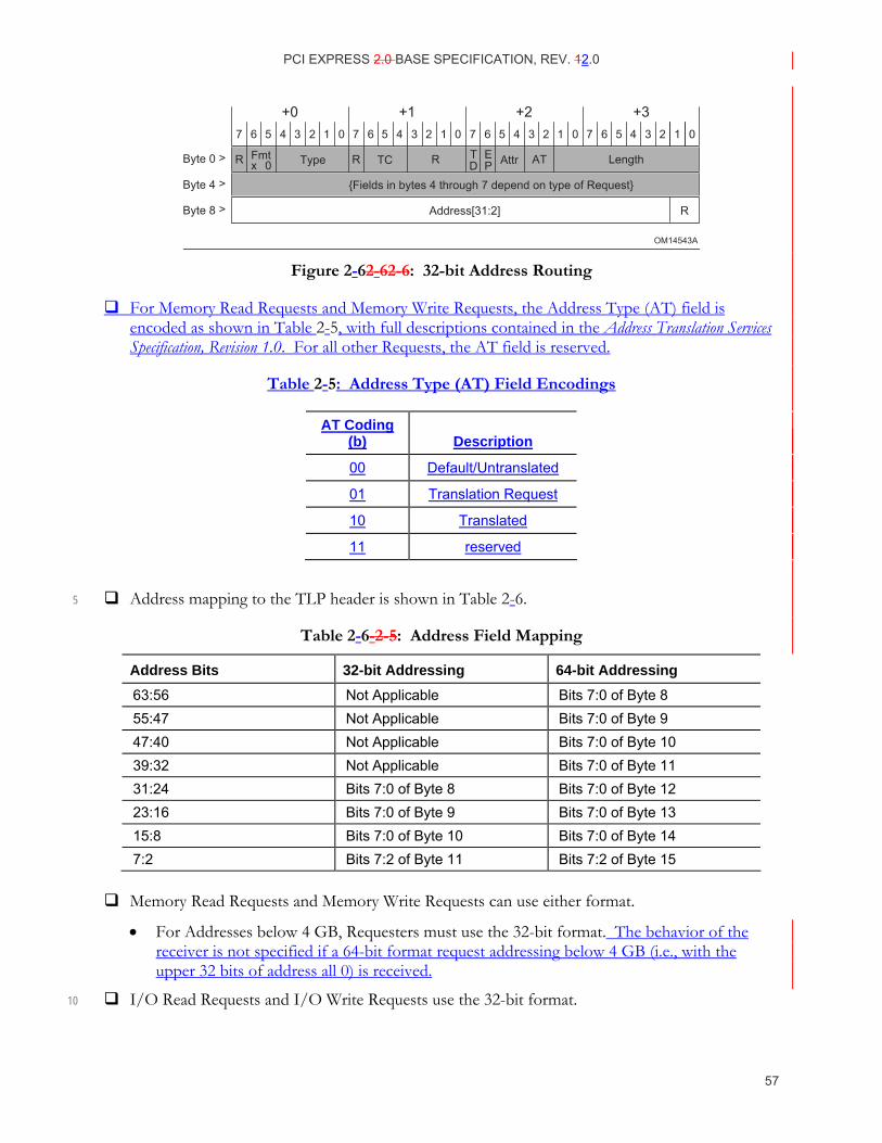
PCI EXPRESS 2.0 BASE SPECIFICATION, REV. 12.0
57
OM14543A
7 6 5 4 3 2 1 0 7 6 5 4 3 2 1 0 7 6 5 4 3 2 1 0 7 6 5 4 3 2 1 0
TD
EP ATTypeR R R
Address[31:2] R
Length
+0 +1 +2 +3
Byte 0 >
Byte 4 >
Byte 8 >
x 0 AttrFmt TC
Fields in bytes 4 through 7 depend on type of Request
Figure 2-62-6 2-6: 32-bit Address Routing
For Memory Read Requests and Memory Write Requests, the Address Type (AT) field is encoded as shown in Table 2-5, with full descriptions contained in the Address Translation Services Specification, Revision 1.0. For all other Requests, the AT field is reserved.
Table 2-5: Address Type (AT) Field Encodings
AT Coding (b) Description
00 Default/Untranslated
01 Translation Request
10 Translated
11 reserved
Address mapping to the TLP header is shown in Table 2-6. 5
Table 2-6- 2-5: Address Field Mapping
Address Bits 32-bit Addressing 64-bit Addressing 63:56 Not Applicable Bits 7:0 of Byte 8 55:47 Not Applicable Bits 7:0 of Byte 9 47:40 Not Applicable Bits 7:0 of Byte 10 39:32 Not Applicable Bits 7:0 of Byte 11 31:24 Bits 7:0 of Byte 8 Bits 7:0 of Byte 12 23:16 Bits 7:0 of Byte 9 Bits 7:0 of Byte 13 15:8 Bits 7:0 of Byte 10 Bits 7:0 of Byte 14 7:2 Bits 7:2 of Byte 11 Bits 7:2 of Byte 15
Memory Read Requests and Memory Write Requests can use either format.
• For Addresses below 4 GB, Requesters must use the 32-bit format. The behavior of the receiver is not specified if a 64-bit format request addressing below 4 GB (i.e., with the upper 32 bits of address all 0) is received.
I/O Read Requests and I/O Write Requests use the 32-bit format. 10
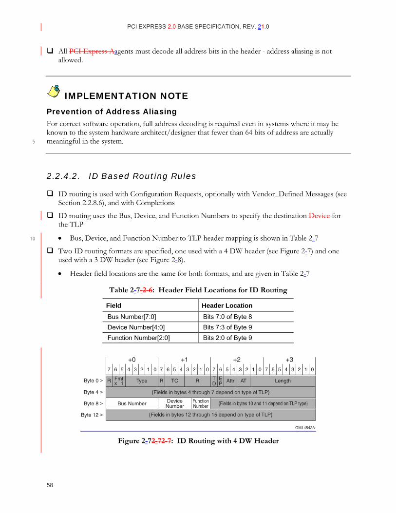
PCI EXPRESS 2.0 BASE SPECIFICATION, REV. 21.0
58
All PCI Express Aagents must decode all address bits in the header - address aliasing is not allowed.
IMPLEMENTATION NOTE Prevention of Address Aliasing For correct software operation, full address decoding is required even in systems where it may be known to the system hardware architect/designer that fewer than 64 bits of address are actually meaningful in the system. 5
2.2.4.2. ID Based Routing Rules
ID routing is used with Configuration Requests, optionally with Vendor_Defined Messages (see Section 2.2.8.6), and with Completions
ID routing uses the Bus, Device, and Function Numbers to specify the destination Device for the TLP
• Bus, Device, and Function Number to TLP header mapping is shown in Table 2-7 10
Two ID routing formats are specified, one used with a 4 DW header (see Figure 2-7) and one used with a 3 DW header (see Figure 2-8).
• Header field locations are the same for both formats, and are given in Table 2-7
Table 2-7- 2-6: Header Field Locations for ID Routing
Field Header Location Bus Number[7:0] Bits 7:0 of Byte 8 Device Number[4:0] Bits 7:3 of Byte 9 Function Number[2:0] Bits 2:0 of Byte 9
OM14542A
7 6 5
x 1
4 3 2 1 0 7 6 5 4 3 2 1 0 7 6 5 4 3 2 1 0 7 6 5 4 3 2 1 0
R Attr ATTD
EPTypeFmtR TCR
Fields in bytes 12 through 15 depend on type of TLP
Fields in bytes 4 through 7 depend on type of TLP
Fields in bytes 10 and 11 depend on TLP typeBus Number DeviceNumber
FunctionNumber
Length
+0 +1 +2 +3
Byte 0 >
Byte 4 >
Byte 8 >
Byte 12 >
Figure 2-72-7 2-7: ID Routing with 4 DW Header
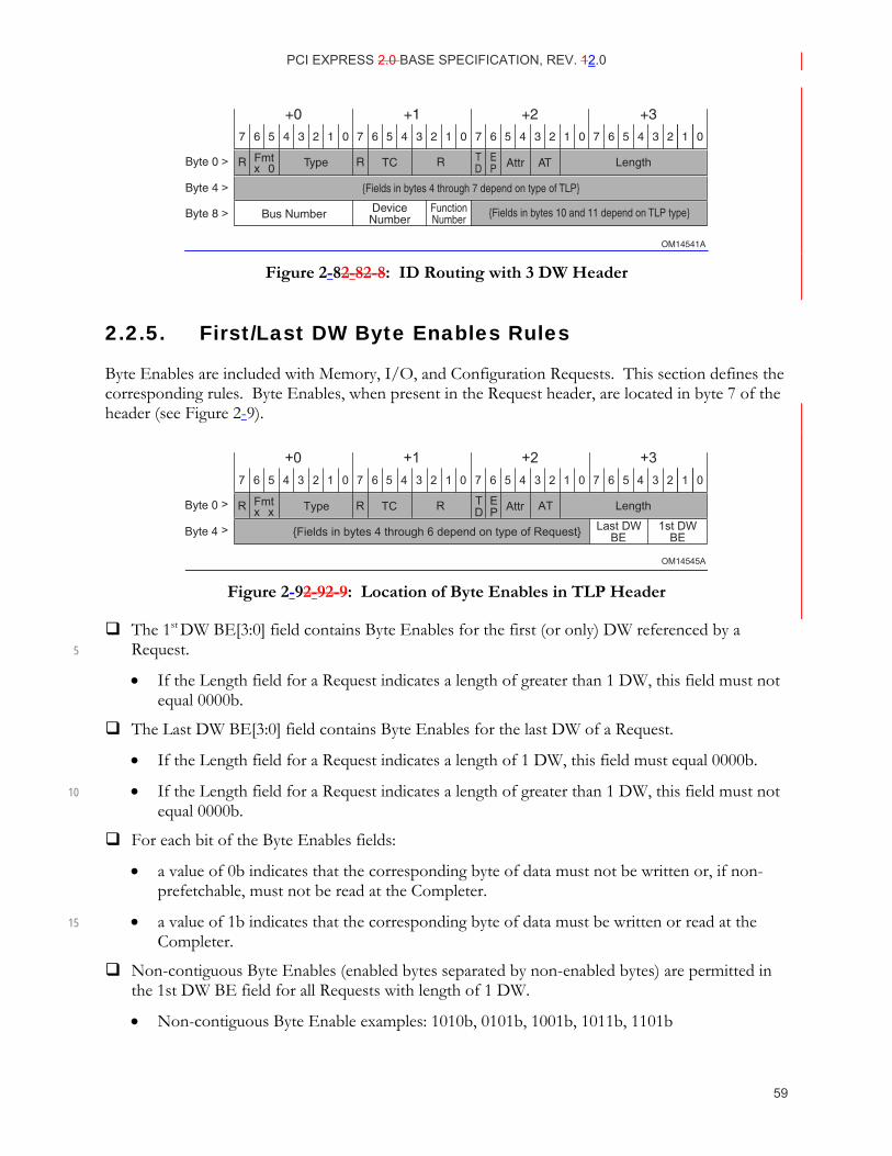
PCI EXPRESS 2.0 BASE SPECIFICATION, REV. 12.0
59
OM14541A
7 6 5 4 3 2 1 0 7 6 5 4 3 2 1 0 7 6 5 4 3 2 1 0 7 6 5 4 3 2 1 0
TD
EPTypeR R R
Bus Number Fields in bytes 10 and 11 depend on TLP typeDeviceNumber
FunctionNumber
Length
+0 +1 +2 +3
Byte 0 >
Byte 4 >
Byte 8 >
x 0 Attr ATFmt TC
Fields in bytes 4 through 7 depend on type of TLP
Figure 2-82-8 2-8: ID Routing with 3 DW Header
2.2.5. First/Last DW Byte Enables Rules
Byte Enables are included with Memory, I/O, and Configuration Requests. This section defines the corresponding rules. Byte Enables, when present in the Request header, are located in byte 7 of the header (see Figure 2-9).
OM14545A
7 6 5 4 3 2 1 0 7 6 5 4 3 2 1 0 7 6 5 4 3 2 1 0 7 6 5 4 3 2 1 0
TD
EP ATTypeR R R Length
+0 +1 +2 +3
Byte 0 >
Byte 4 >x x AttrFmt TC
Fields in bytes 4 through 6 depend on type of Request Last DWBE
1st DWBE
Figure 2-92-9 2-9: Location of Byte Enables in TLP Header
The 1st DW BE[3:0] field contains Byte Enables for the first (or only) DW referenced by a Request. 5
• If the Length field for a Request indicates a length of greater than 1 DW, this field must not equal 0000b.
The Last DW BE[3:0] field contains Byte Enables for the last DW of a Request.
• If the Length field for a Request indicates a length of 1 DW, this field must equal 0000b.
• If the Length field for a Request indicates a length of greater than 1 DW, this field must not 10 equal 0000b.
For each bit of the Byte Enables fields:
• a value of 0b indicates that the corresponding byte of data must not be written or, if non-prefetchable, must not be read at the Completer.
• a value of 1b indicates that the corresponding byte of data must be written or read at the 15 Completer.
Non-contiguous Byte Enables (enabled bytes separated by non-enabled bytes) are permitted in the 1st DW BE field for all Requests with length of 1 DW.
• Non-contiguous Byte Enable examples: 1010b, 0101b, 1001b, 1011b, 1101b
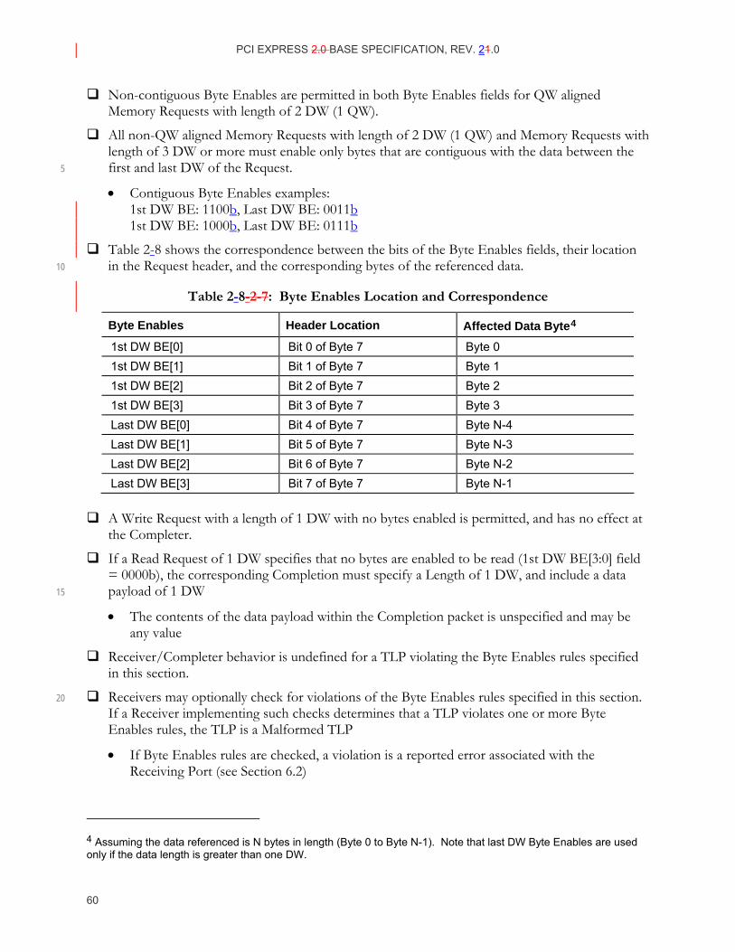
PCI EXPRESS 2.0 BASE SPECIFICATION, REV. 21.0
60
Non-contiguous Byte Enables are permitted in both Byte Enables fields for QW aligned Memory Requests with length of 2 DW (1 QW).
All non-QW aligned Memory Requests with length of 2 DW (1 QW) and Memory Requests with length of 3 DW or more must enable only bytes that are contiguous with the data between the first and last DW of the Request. 5
• Contiguous Byte Enables examples: 1st DW BE: 1100b, Last DW BE: 0011b 1st DW BE: 1000b, Last DW BE: 0111b
Table 2-8 shows the correspondence between the bits of the Byte Enables fields, their location in the Request header, and the corresponding bytes of the referenced data. 10
Table 2-8- 2-7: Byte Enables Location and Correspondence
Byte Enables Header Location Affected Data Byte4 1st DW BE[0] Bit 0 of Byte 7 Byte 0 1st DW BE[1] Bit 1 of Byte 7 Byte 1 1st DW BE[2] Bit 2 of Byte 7 Byte 2 1st DW BE[3] Bit 3 of Byte 7 Byte 3 Last DW BE[0] Bit 4 of Byte 7 Byte N-4 Last DW BE[1] Bit 5 of Byte 7 Byte N-3 Last DW BE[2] Bit 6 of Byte 7 Byte N-2 Last DW BE[3] Bit 7 of Byte 7 Byte N-1
A Write Request with a length of 1 DW with no bytes enabled is permitted, and has no effect at the Completer.
If a Read Request of 1 DW specifies that no bytes are enabled to be read (1st DW BE[3:0] field = 0000b), the corresponding Completion must specify a Length of 1 DW, and include a data payload of 1 DW 15
• The contents of the data payload within the Completion packet is unspecified and may be any value
Receiver/Completer behavior is undefined for a TLP violating the Byte Enables rules specified in this section.
Receivers may optionally check for violations of the Byte Enables rules specified in this section. 20 If a Receiver implementing such checks determines that a TLP violates one or more Byte Enables rules, the TLP is a Malformed TLP
• If Byte Enables rules are checked, a violation is a reported error associated with the Receiving Port (see Section 6.2)
4 Assuming the data referenced is N bytes in length (Byte 0 to Byte N-1). Note that last DW Byte Enables are used only if the data length is greater than one DW.
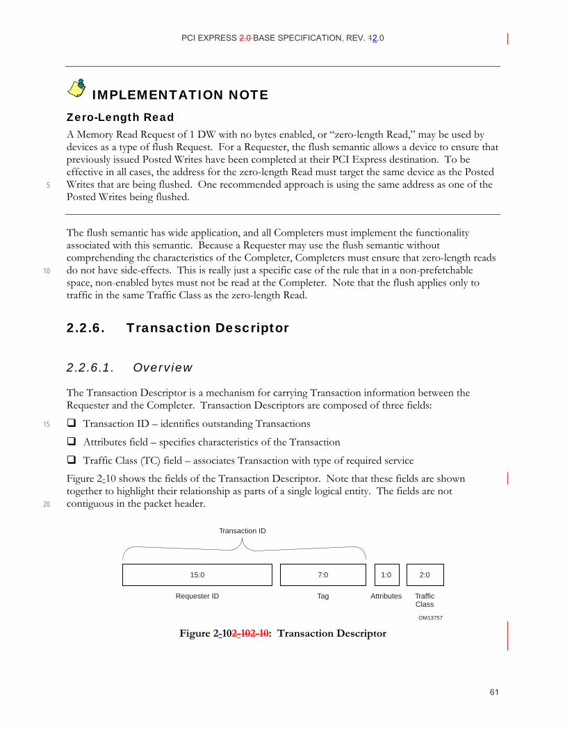
PCI EXPRESS 2.0 BASE SPECIFICATION, REV. 12.0
61
IMPLEMENTATION NOTE Zero-Length Read A Memory Read Request of 1 DW with no bytes enabled, or “zero-length Read,” may be used by devices as a type of flush Request. For a Requester, the flush semantic allows a device to ensure that previously issued Posted Writes have been completed at their PCI Express destination. To be effective in all cases, the address for the zero-length Read must target the same device as the Posted Writes that are being flushed. One recommended approach is using the same address as one of the 5 Posted Writes being flushed.
The flush semantic has wide application, and all Completers must implement the functionality associated with this semantic. Because a Requester may use the flush semantic without comprehending the characteristics of the Completer, Completers must ensure that zero-length reads do not have side-effects. This is really just a specific case of the rule that in a non-prefetchable 10 space, non-enabled bytes must not be read at the Completer. Note that the flush applies only to traffic in the same Traffic Class as the zero-length Read.
2.2.6. Transaction Descriptor
2.2.6.1. Overview
The Transaction Descriptor is a mechanism for carrying Transaction information between the Requester and the Completer. Transaction Descriptors are composed of three fields:
Transaction ID – identifies outstanding Transactions 15
Attributes field – specifies characteristics of the Transaction
Traffic Class (TC) field – associates Transaction with type of required service
Figure 2-10 shows the fields of the Transaction Descriptor. Note that these fields are shown together to highlight their relationship as parts of a single logical entity. The fields are not contiguous in the packet header. 20
OM13757
Requester ID Tag Attributes TrafficClass
15:0 7:0 1:0 2:0
Transaction ID
Figure 2-102-10 2-10: Transaction Descriptor
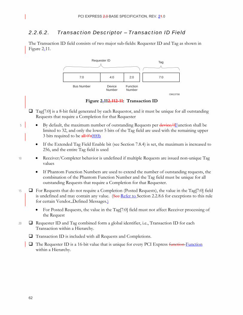
PCI EXPRESS 2.0 BASE SPECIFICATION, REV. 21.0
62
2.2.6.2. Transaction Descriptor – Transaction ID Field
The Transaction ID field consists of two major sub-fields: Requester ID and Tag as shown in Figure 2-11.
OM13758
Bus Number DeviceNumber
7:0
FunctionNumber
7:02:04:0
Requester ID Tag
Figure 2-112-11 2-11: Transaction ID
Tag[7:0] is a 8-bit field generated by each Requestor, and it must be unique for all outstanding Requests that require a Completion for that Requester
• By default, the maximum number of outstanding Requests per device/fFunction shall be 5 limited to 32, and only the lower 5 bits of the Tag field are used with the remaining upper 3 bits required to be all 0’s000b
• If the Extended Tag Field Enable bit (see Section 7.8.4) is set, the maximum is increased to 256, and the entire Tag field is used
• Receiver/Completer behavior is undefined if multiple Requests are issued non-unique Tag 10 values
• If Phantom Function Numbers are used to extend the number of outstanding requests, the combination of the Phantom Function Number and the Tag field must be unique for all outstanding Requests that require a Completion for that Requester.
For Requests that do not require a Completion (Posted Requests), the value in the Tag[7:0] field 15 is undefined and may contain any value. (See Refer to Section 2.2.8.6 for exceptions to this rule for certain Vendor_Defined Messages.)
• For Posted Requests, the value in the Tag[7:0] field must not affect Receiver processing of the Request
Requester ID and Tag combined form a global identifier, i.e., Transaction ID for each 20 Transaction within a Hierarchy.
Transaction ID is included with all Requests and Completions.
The Requester ID is a 16-bit value that is unique for every PCI Express function Function within a Hierarchy.
PCI EXPRESS 2.0 BASE SPECIFICATION, REV. 12.0
63
Functions must capture the Bus and Device Numbers supplied with all Type 0 Configuration Write Requests (Type 0) completed by the function Function and supply these numbers in the Bus and Device Number fields of the Requester ID for all Requests initiated by the deviceDevice/functionFunction.
Exception: The assignment of Bus and Device Numbers to the logical dDevices within a Root 5 Complex, and Device Numbers to the dDownstream ports Ports within a switchSwitch, may be done in an implementation specific way.
Note that the Bus Number and Device Number may be changed at run time, and so it is necessary to re-capture this information with each and every Configuration Write Request.
Example: When a device (or function of a multi-function device) receives a Type 0 10 Configuration Write Request, the device comprehends that it is the intended recipient of the Request because it is a Type 0 Request. The routing information fields of the Write Request include the recipient’s Bus Number and Device Number values (Figure 216). These values are captured by the device and used to generate the Requester and Completer ID field.
When generating Requests on their own behalf (for example, for error reporting), Switches must 15 use the Requester ID associated with the primary side of the bridge logically associated with the Port (see Section 7.1) causing the Request generation.
Prior to the initial Configuration Write to a deviceFunction, the device Function is not permitted to initiate Non-Posted Requests (A valid Requestor IDRequester ID is required to properly route the resulting completions). 20
• Exception: Logical devicesFunctions within a Root Complex are permitted to initiate Requests prior to software-initiated configuration for accesses to system boot device(s).
Note that this rule and the exception are consistent with the existing PCI model for system initialization and configuration.
Each function Function associated with a logical dDevice must be designed to respond to a 25 unique Function Number for Configuration Requests addressing that logical dDevice. Note: Each logical dDevice may contain up to eight logical fFunctions.
A Switch must forward Requests without modifying the Transaction ID
In some circumstances, a PCI Express- to PCI/PCI-X Bridge is required to generate Transaction IDs for requests it forwards from a PCI or PCI-X bus. 30
IMPLEMENTATION NOTE Increasing the Number of Outstanding Requests To increase the maximum possible number of outstanding Requests requiring Completion beyond 256, a device may, if the Phantom Functions Number Enable bit is set (see Section 7.8.4), use Function Numbers not assigned to implemented functions Functions to logically extend the Tag identifier. For a single single-function Function device, this can allow up to an 8-fold increase in the maximum number of outstanding Requests. 35
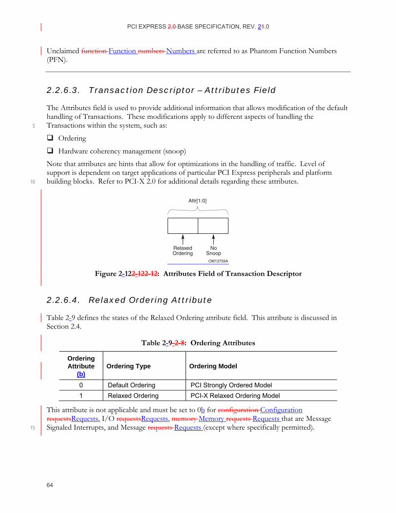
PCI EXPRESS 2.0 BASE SPECIFICATION, REV. 21.0
64
Unclaimed function Function numbers Numbers are referred to as Phantom Function Numbers (PFN).
2.2.6.3. Transaction Descriptor – Attributes Field
The Attributes field is used to provide additional information that allows modification of the default handling of Transactions. These modifications apply to different aspects of handling the Transactions within the system, such as: 5
Ordering
Hardware coherency management (snoop)
Note that attributes are hints that allow for optimizations in the handling of traffic. Level of support is dependent on target applications of particular PCI Express peripherals and platform building blocks. Refer to PCI-X 2.0 for additional details regarding these attributes. 10
OM13759A
Attr[1:0]
NoSnoop
RelaxedOrdering
Figure 2-122-12 2-12: Attributes Field of Transaction Descriptor
2.2.6.4. Relaxed Ordering Attribute
Table 2-9 defines the states of the Relaxed Ordering attribute field. This attribute is discussed in Section 2.4.
Table 2-9- 2-8: Ordering Attributes
Ordering Attribute
(b) Ordering Type Ordering Model
0 Default Ordering PCI Strongly Ordered Model 1 Relaxed Ordering PCI-X Relaxed Ordering Model
This attribute is not applicable and must be set to 0b for configuration Configuration requestsRequests, I/O requestsRequests, memory Memory requests Requests that are Message Signaled Interrupts, and Message requests Requests (except where specifically permitted). 15
PCI EXPRESS 2.0 BASE SPECIFICATION, REV. 12.0
65
2.2.6.5. No Snoop Attribute
Table 2-10 defines the states of the No Snoop attribute field. Note that the No Snoop attribute does not alter Transaction ordering.
Table 2-10- 2-9: Cache Coherency Management Attribute
No Snoop Attribute (b)
Cache Coherency Management Type Coherency Model
0 Default Hardware enforced cache coherency expected
1 No Snoop Hardware enforced cache coherency not expected
This attribute is not applicable and must be set to 0b for configuration Configuration requestsRequests, I/O requestsRequests, memory Memory requests Requests that are Message Signaled Interrupts, and Message requests Requests (except where specifically permitted). 5
2.2.6.6. Transaction Descriptor – Traffic Class Field
The Traffic Class (TC) is a 3-bit field that allows differentiation of transactions into eight traffic classes.
Together with the PCI Express Virtual Channel support, the TC mechanism is a fundamental element for enabling differentiated traffic servicing. Every PCI Express Transaction Layer Packet uses TC information as an invariant label that is carried end to end within the PCI Express fabric. 10 As the packet traverses across the fabric, this information is used at every Link and within each Switch element to make decisions with regards to proper servicing of the traffic. A key aspect of servicing is the routing of the packets based on their TC labels through corresponding Virtual Channels. Section 2.5 covers the details of the VC mechanism.
Table 2-11 defines the TC encodings. 15
Table 2-11- 2-10: Definition of TC Field Encodings
TC Field Value (b)
Definition
000 TC0: Best Effort service class (General Purpose I/O)
(Default TC – must be supported by every PCI Express device)
001 – 111 TC1-TC7: Differentiated service classes
(Differentiation based on Weighted-Round-Robin and/or Priority)
It is up to the system software to determine TC labeling and TC/VC mapping in order to provide differentiated services that meet target platform requirements.
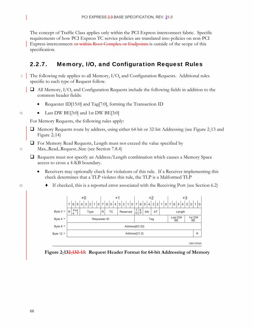
PCI EXPRESS 2.0 BASE SPECIFICATION, REV. 21.0
66
The concept of Traffic Class applies only within the PCI Express interconnect fabric. Specific requirements of how PCI Express TC service policies are translated into policies on non-PCI Express interconnects or within Root Complex or Endpoints is outside of the scope of this specification.
2.2.7. Memory, I/O, and Configuration Request Rules
The following rule applies to all Memory, I/O, and Configuration Requests. Additional rules 5 specific to each type of Request follow.
All Memory, I/O, and Configuration Requests include the following fields in addition to the common header fields:
• Requester ID[15:0] and Tag[7:0], forming the Transaction ID
• Last DW BE[3:0] and 1st DW BE[3:0] 10
For Memory Requests, the following rules apply:
Memory Requests route by address, using either 64-bit or 32-bit Addressing (see Figure 2-13 and Figure 2-14)
For Memory Read Requests, Length must not exceed the value specified by Max_Read_Request_Size (see Section 7.8.4) 15
Requests must not specify an Address/Length combination which causes a Memory Space access to cross a 4-KB boundary.
• Receivers may optionally check for violations of this rule. If a Receiver implementing this check determines that a TLP violates this rule, the TLP is a Malformed TLP
♦ If checked, this is a reported error associated with the Receiving Port (see Section 6.2) 20
OM13764A
7 6 5
x 1
4 3 2 1 0 7 6 5 4 3 2 1 0 7 6 5 4 3 2 1 0 7 6 5 4 3 2 1 0
Reserved AttrTD
EP AT
R
TypeFmtR TCR
Requester ID
Address[31:2]
Address[63:32]
Tag Last DWBE
1st DWBE
Length
+0 +1 +2 +3
Byte 0 >
Byte 4 >
Byte 8 >
Byte 12 >
Figure 2-132-13 2-13: Request Header Format for 64-bit Addressing of Memory
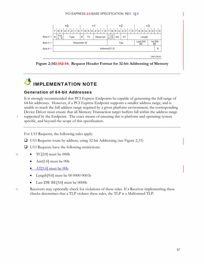
PCI EXPRESS 2.0 BASE SPECIFICATION, REV. 12.0
67
OM13763A
7 6 5
x 0
4 3 2 1 0 7 6 5 4 3 2 1 0 7 6 5 4 3 2 1 0 7 6 5 4 3 2 1 0
Reserved Attr ATTypeFmt TD
EPR TCR
Requester ID
Address[31:2]
Tag Last DWBE
1st DWBE
Length
+0 +1 +2 +3
Byte 0 >
Byte 4 >
Byte 8 > R
Figure 2-142-14 2-14: Request Header Format for 32-bit Addressing of Memory
IMPLEMENTATION NOTE Generation of 64-bit Addresses It is strongly recommended that PCI Express Endpoints be capable of generating the full range of 64-bit addresses. However, if a PCI Express Endpoint supports a smaller address range, and is unable to reach the full address range required by a given platform environment, the corresponding Device Driver must ensure that all Memory Transaction target buffers fall within the address range supported by the Endpoint. The exact means of ensuring this is platform and operating system 5 specific, and beyond the scope of this specification.
For I/O Requests, the following rules apply:
I/O Requests route by address, using 32-bit Addressing (see Figure 2-15)
I/O Requests have the following restrictions:
• TC[2:0] must be 000b 10
• Attr[1:0] must be 00b
• AT[1:0] must be 00b
• Length[9:0] must be 00 0000 0001b
• Last DW BE[3:0] must be 0000b
Receivers may optionally check for violations of these rules. If a Receiver implementing these 15 checks determines that a TLP violates these rules, the TLP is a Malformed TLP.
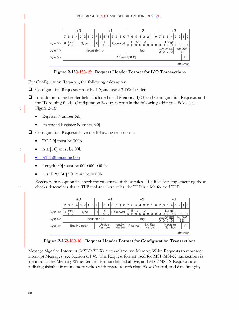
PCI EXPRESS 2.0 BASE SPECIFICATION, REV. 21.0
68
OM13765A
7 6 5
x 0
4 3 2 1 0 7 6 5 4
0 0 0 0 0
3 2 1 0 7 6 5 4 3 2 1 0 7 6 5 4 3 2 1 0
0 0 0 0 0 0
0 0 0 0
0 0 0 1Reserved Attr0 0ATT
DEPTypeFmtR TCR
Requester ID
Address[31:2]
Tag Last DW BE 1st DWBE
Length
+0 +1 +2 +3
Byte 0 >
Byte 4 >
Byte 8 > R
Figure 2-152-15 2-15: Request Header Format for I/O Transactions
For Configuration Requests, the following rules apply:
Configuration Requests route by ID, and use a 3 DW header
In addition to the header fields included in all Memory, I/O, and Configuration Requests and the ID routing fields, Configuration Requests contain the following additional fields (see Figure 2-16) 5
• Register Number[5:0]
• Extended Register Number[3:0]
Configuration Requests have the following restrictions:
• TC[2:0] must be 000b
• Attr[1:0] must be 00b 10
• AT[1:0] must be 00b
• Length[9:0] must be 00 0000 0001b
• Last DW BE[3:0] must be 0000b
Receivers may optionally check for violations of these rules. If a Receiver implementing these checks determines that a TLP violates these rules, the TLP is a Malformed TLP. 15
OM13766A
7 6 5 4 3 2 1 0 7 6 5 4 3 2 1 0 7 6 5 4 3 2 1 0 7 6 5 4 3 2 1 0
TD
EPTypeR R Reserved
Requester ID
Bus Number ReservedDeviceNumber
Ext. Reg.Number
RegisterNumber
FunctionNumber R
Tag 1st DWBE
Length
+0 +1 +2 +3
Byte 0 >
Byte 4 >
Byte 8 >
x 0 0 0 0 0 0 0 0 0 0 0 0
0 0 0 0
0 0 0 1Attr
0 0ATFmt TC
Last DW BE
Figure 2-162-16 2-16: Request Header Format for Configuration Transactions
Message Signaled Interrupt (MSI/MSI-X) mechanisms use Memory Write Requests to represent interrupt Messages (see Section 6.1.4). The Request format used for MSI/MSI-X transactions is identical to the Memory Write Request format defined above, and MSI/MSI-X Requests are indistinguishable from memory writes with regard to ordering, Flow Control, and data integrity.
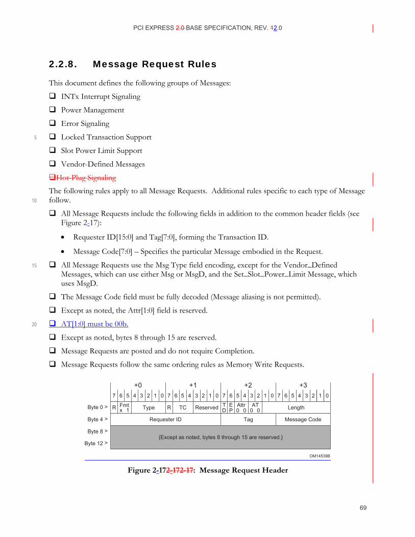
PCI EXPRESS 2.0 BASE SPECIFICATION, REV. 12.0
69
2.2.8. Message Request Rules
This document defines the following groups of Messages:
INTx Interrupt Signaling
Power Management
Error Signaling
Locked Transaction Support 5
Slot Power Limit Support
Vendor-Defined Messages
Hot-Plug Signaling
The following rules apply to all Message Requests. Additional rules specific to each type of Message follow. 10
All Message Requests include the following fields in addition to the common header fields (see Figure 2-17):
• Requester ID[15:0] and Tag[7:0], forming the Transaction ID.
• Message Code[7:0] – Specifies the particular Message embodied in the Request.
All Message Requests use the Msg Type field encoding, except for the Vendor_Defined 15 Messages, which can use either Msg or MsgD, and the Set_Slot_Power_Limit Message, which uses MsgD.
The Message Code field must be fully decoded (Message aliasing is not permitted).
Except as noted, the Attr[1:0] field is reserved.
AT[1:0] must be 00b. 20
Except as noted, bytes 8 through 15 are reserved.
Message Requests are posted and do not require Completion.
Message Requests follow the same ordering rules as Memory Write Requests.
OM14539B
7 6 5
x 1
4 3 2 1 0 7 6 5 4 3 2 1 0 7 6 5 4
0 0
3 2 1 0 7 6 5 4 3 2 1 0
Reserved Attr0 0ATT
DEPTypeFmtR TCR
Requester ID
Except as noted, bytes 8 through 15 are reserved.
Tag Message Code
Length
+0 +1 +2 +3
Byte 0 >
Byte 4 >
Byte 8 >
Byte 12 >
Figure 2-172-17 2-17: Message Request Header
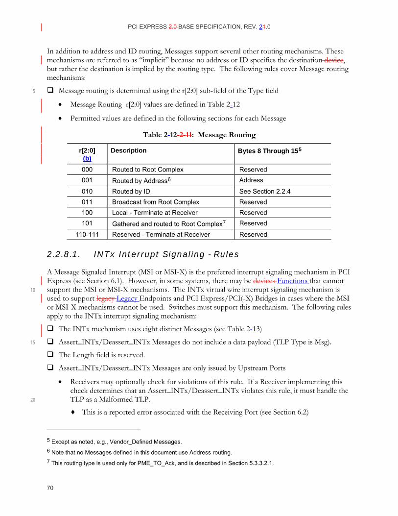
PCI EXPRESS 2.0 BASE SPECIFICATION, REV. 21.0
70
In addition to address and ID routing, Messages support several other routing mechanisms. These mechanisms are referred to as “implicit” because no address or ID specifies the destination device, but rather the destination is implied by the routing type. The following rules cover Message routing mechanisms:
Message routing is determined using the r[2:0] sub-field of the Type field 5
• Message Routing r[2:0] values are defined in Table 2-12
• Permitted values are defined in the following sections for each Message
Table 2-12- 2-11: Message Routing
r[2:0] (b)
Description Bytes 8 Through 155
000 Routed to Root Complex Reserved 001 Routed by Address6 Address
010 Routed by ID See Section 2.2.4 011 Broadcast from Root Complex Reserved 100 Local - Terminate at Receiver Reserved 101 Gathered and routed to Root Complex7 Reserved
110-111 Reserved - Terminate at Receiver Reserved
2.2.8.1. INTx Interrupt Signaling - Rules
A Message Signaled Interrupt (MSI or MSI-X) is the preferred interrupt signaling mechanism in PCI Express (see Section 6.1). However, in some systems, there may be devices Functions that cannot support the MSI or MSI-X mechanisms. The INTx virtual wire interrupt signaling mechanism is 10 used to support legacy Legacy Endpoints and PCI Express/PCI(-X) Bridges in cases where the MSI or MSI-X mechanisms cannot be used. Switches must support this mechanism. The following rules apply to the INTx interrupt signaling mechanism:
The INTx mechanism uses eight distinct Messages (see Table 2-13)
Assert_INTx/Deassert_INTx Messages do not include a data payload (TLP Type is Msg). 15
The Length field is reserved.
Assert_INTx/Deassert_INTx Messages are only issued by Upstream Ports
• Receivers may optionally check for violations of this rule. If a Receiver implementing this check determines that an Assert_INTx/Deassert_INTx violates this rule, it must handle the TLP as a Malformed TLP. 20
♦ This is a reported error associated with the Receiving Port (see Section 6.2)
5 Except as noted, e.g., Vendor_Defined Messages. 6 Note that no Messages defined in this document use Address routing. 7 This routing type is used only for PME_TO_Ack, and is described in Section 5.3.3.2.1.
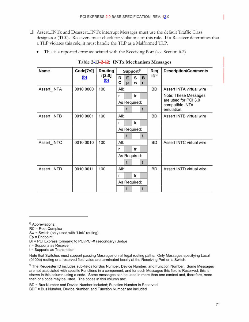
PCI EXPRESS 2.0 BASE SPECIFICATION, REV. 12.0
71
Assert_INTx and Deassert_INTx interrupt Messages must use the default Traffic Class designator (TC0). Receivers must check for violations of this rule. If a Receiver determines that a TLP violates this rule, it must handle the TLP as a Malformed TLP.
• This is a reported error associated with the Receiving Port (see Section 6.2)
Table 2-13- 2-12: INTx Mechanism Messages
Support8 Name Code[7:0] (b)
Routing r[2:0]
(b) RC
Ep
Sw
Br
Req ID9
Description/Comments
All: r tr As Required:
Assert_INTA 0010 0000 100
t t
BD Assert INTA virtual wire Note: These Messages are used for PCI 3.0 compatible INTx emulation.
All: r tr As Required:
Assert_INTB 0010 0001 100
t t
BD Assert INTB virtual wire
All: r tr As Required:
Assert_INTC 0010 0010 100
t t
BD Assert INTC virtual wire
All: r tr As Required:
Assert_INTD 0010 0011 100
t t
BD Assert INTD virtual wire
8 Abbreviations: RC = Root Complex Sw = Switch (only used with “Link” routing) Ep = Endpoint Br = PCI Express (primary) to PCI/PCI-X (secondary) Bridge r = Supports as Receiver t = Supports as Transmitter Note that Switches must support passing Messages on all legal routing paths. Only Messages specifying Local (0100b) routing or a reserved field value are terminated locally at the Receiving Port on a Switch. 9 The Requester ID includes sub-fields for Bus Number, Device Number, and Function Number. Some Messages are not associated with specific Functions in a component, and for such Messages this field is Reserved; this is shown in this column using a code. Some messages can be used in more than one context and, therefore, more than one code may be listed. The codes in this column are: BD = Bus Number and Device Number included; Function Number is Reserved BDF = Bus Number, Device Number, and Function Number are included
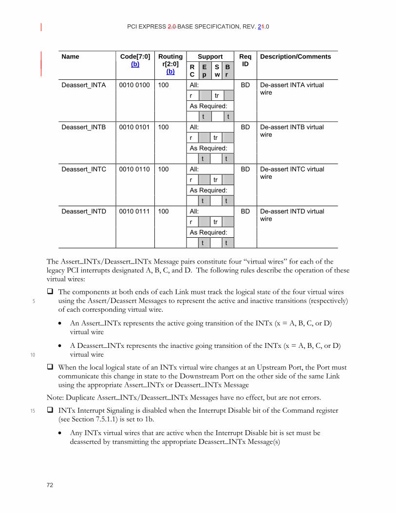
PCI EXPRESS 2.0 BASE SPECIFICATION, REV. 21.0
72
Support Name Code[7:0] (b)
Routing r[2:0]
(b) RC
Ep
Sw
Br
Req ID
Description/Comments
All: r tr As Required:
Deassert_INTA 0010 0100 100
t t
BD De-assert INTA virtual wire
All: r tr As Required:
Deassert_INTB 0010 0101 100
t t
BD De-assert INTB virtual wire
All: r tr As Required:
Deassert_INTC 0010 0110 100
t t
BD De-assert INTC virtual wire
All: r tr As Required:
Deassert_INTD 0010 0111 100
t t
BD De-assert INTD virtual wire
The Assert_INTx/Deassert_INTx Message pairs constitute four “virtual wires” for each of the legacy PCI interrupts designated A, B, C, and D. The following rules describe the operation of these virtual wires:
The components at both ends of each Link must track the logical state of the four virtual wires using the Assert/Deassert Messages to represent the active and inactive transitions (respectively) 5 of each corresponding virtual wire.
• An Assert_INTx represents the active going transition of the INTx (x = A, B, C, or D) virtual wire
• A Deassert_INTx represents the inactive going transition of the INTx (x = A, B, C, or D) virtual wire 10
When the local logical state of an INTx virtual wire changes at an Upstream Port, the Port must communicate this change in state to the Downstream Port on the other side of the same Link using the appropriate Assert_INTx or Deassert_INTx Message
Note: Duplicate Assert_INTx/Deassert_INTx Messages have no effect, but are not errors.
INTx Interrupt Signaling is disabled when the Interrupt Disable bit of the Command register 15 (see Section 7.5.1.1) is set to 1b.
• Any INTx virtual wires that are active when the Interrupt Disable bit is set must be deasserted by transmitting the appropriate Deassert_INTx Message(s)

PCI EXPRESS 2.0 BASE SPECIFICATION, REV. 12.0
73
Virtual and actual PCI to PCI Bridges must map the virtual wires tracked on the secondary side of the Bridge according to the Device Number of the Device device on the secondary side of the Bridge, as shown in Table 2-14
Switches must track the state of the four virtual wires independently for each Downstream Port, and present a “collapsed” set of virtual wires on its Upstream Port 5
If a Downstream Port goes to DL_Down status, the INTx virtual wires associated with that Port must be deasserted, and the Upstream Port virtual wire state updated accordingly.
• If this results in de-assertion of any Upstream INTx virtual wires, the appropriate Deassert_INTx Message(s) must be sent by the Upstream Port.
The Root Complex must track the state of the four INTx virtual wires independently for each of 10 its Downstream Ports, and map these virtual signals to system interrupt resources.
• Details of this mapping are system implementation specific.
If a Downstream Port of the Root Complex goes to DL_Down status, the INTx virtual wires associated with that Port must be deasserted, and any associated system interrupt resource request(s) must be discarded. 15
Table 2-14- 2-13: Bridge Mapping for INTx Virtual Wires
Device Number for Device on Secondary Side of Bridge (Interrupt Source)
INTx Virtual Wire on Secondary Side of Bridge
Mapping to INTx Virtual Wire on Primary Side of Bridge
INTA INTA INTB INTB INTC INTC
0,4,8,12,16,20,24,28
INTD INTD INTA INTB INTB INTC INTC INTD
1,5,9,13,17,21,25,29
INTD INTA INTA INTC INTB INTD INTC INTA
2,6,10,14,18,22,26,30
INTD INTB INTA INTD INTB INTA INTC INTB
3,7,11,15,19,23,27,31
INTD INTC
Note that the Requester ID of an Assert_INTx/Deassert_INTx Message will correspond to the Transmitter of the Message on that Link, and not necessarily to the original source of the interrupt.

PCI EXPRESS 2.0 BASE SPECIFICATION, REV. 21.0
74
IMPLEMENTATION NOTE System Interrupt Mapping Note that system software (including BIOS and operating system) needs to comprehend the remapping of legacy interrupts (INTx mechanism) in the entire topology of the system (including hierarchically connected Switches and subordinate PCI Express/PCI Bridges) to establish proper correlation between PCI Express device interrupt and associated interrupt resources in the system interrupt controller. The remapping described by Table 2-14 is applied hierarchically at every 5 Switch. In addition, PCI Express/PCI and PCI/PCI Bridges perform a similar mapping function.
2.2.8.2. Power Management Messages
These Messages are used to support PCI Express power management, which is described in detail in Chapter 5. The following rules define the Power Management Messages:
Table 2-15 defines the Power Management Messages.
Power Management Messages do not include a data payload (TLP Type is Msg). 10
The Length field is reserved.
Power Management Messages must use the default Traffic Class designator (TC0). Receivers must check for violations of this rule. If a Receiver determines that a TLP violates this rule, it must handle the TLP as a Malformed TLP.
• This is a reported error associated with the Receiving Port (see Section 6.2) 15
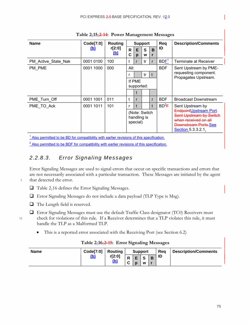
PCI EXPRESS 2.0 BASE SPECIFICATION, REV. 12.0
75
Table 2-15- 2-14: Power Management Messages
Support Name Code[7:0] (b)
Routing r[2:0]
(b) RC
Ep
Sw
Br
Req ID
Description/Comments
PM_Active_State_Nak 0001 0100 100 t r tr r BDF1 Terminate at Receiver All: r tr t If PME supported:
PM_PME 0001 1000 000
t
BDF Sent Upstream by PME-requesting component. Propagates Upstream.
PME_Turn_Off 0001 1001 011 t r r BDF Broadcast Downstream r t t PME_TO_Ack 0001 1011 101 (Note: Switch handling is special)
BD2F Sent Upstream by EndpointUpstream Port. Sent Upstream by Switch when received on all Downstream Ports.See Section 5.3.3.2.1.
1 Also permitted to be BD for compatibility with earlier revisions of this specification. 2 Also permitted to be BDF for compatibility with earlier revisions of this specification.
2.2.8.3. Error Signaling Messages
Error Signaling Messages are used to signal errors that occur on specific transactions and errors that are not necessarily associated with a particular transaction. These Messages are initiated by the agent that detected the error. 5
Table 2-16 defines the Error Signaling Messages.
Error Signaling Messages do not include a data payload (TLP Type is Msg).
The Length field is reserved.
Error Signaling Messages must use the default Traffic Class designator (TC0) Receivers must check for violations of this rule. If a Receiver determines that a TLP violates this rule, it must 10 handle the TLP as a Malformed TLP.
• This is a reported error associated with the Receiving Port (see Section 6.2)
Table 2-16- 2-15: Error Signaling Messages
Support Name Code[7:0](b)
Routing r[2:0]
(b) RC
Ep
Sw
Br
Req ID
Description/Comments
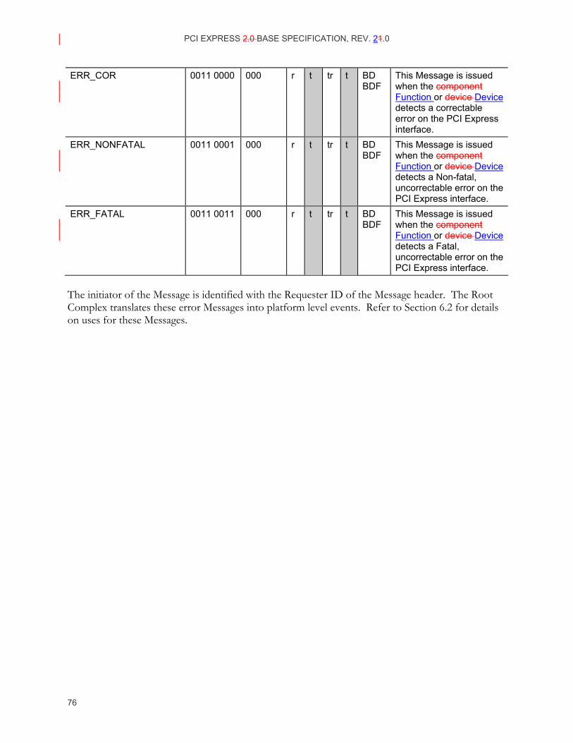
PCI EXPRESS 2.0 BASE SPECIFICATION, REV. 21.0
76
ERR_COR 0011 0000 000 r t tr t BD BDF
This Message is issued when the component Function or device Device detects a correctable error on the PCI Express interface.
ERR_NONFATAL 0011 0001 000 r t tr t BD BDF
This Message is issued when the component Function or device Device detects a Non-fatal, uncorrectable error on the PCI Express interface.
ERR_FATAL 0011 0011 000 r t tr t BD BDF
This Message is issued when the component Function or device Device detects a Fatal, uncorrectable error on the PCI Express interface.
The initiator of the Message is identified with the Requester ID of the Message header. The Root Complex translates these error Messages into platform level events. Refer to Section 6.2 for details on uses for these Messages.
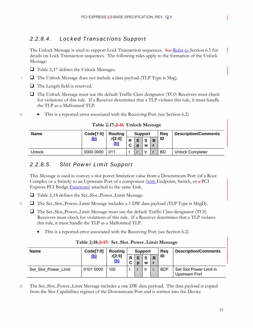
PCI EXPRESS 2.0 BASE SPECIFICATION, REV. 12.0
77
2.2.8.4. Locked Transactions Support
The Unlock Message is used to support Lock Transaction sequences. See Refer to Section 6.5 for details on Lock Transaction sequences. The following rules apply to the formation of the Unlock Message:
Table 2-17 defines the Unlock Messages.
The Unlock Message does not include a data payload (TLP Type is Msg). 5
The Length field is reserved.
The Unlock Message must use the default Traffic Class designator (TC0) Receivers must check for violations of this rule. If a Receiver determines that a TLP violates this rule, it must handle the TLP as a Malformed TLP.
• This is a reported error associated with the Receiving Port (see Section 6.2) 10
Table 2-17- 2-16 Unlock Message
Support Name Code[7:0] (b)
Routing r[2:0]
(b) RC
Ep
Sw
Br
Req ID
Description/Comments
Unlock 0000 0000 011 t r tr r BD Unlock Completer
2.2.8.5. Slot Power Limit Support
This Message is used to convey a slot power limitation value from a Downstream Port (of a Root Complex or a Switch) to an Upstream Port of a component (with Endpoint, Switch, or a PCI Express-PCI Bridge Functions) attached to the same Link.
Table 2-18 defines the Set_Slot_Power_Limit Message.
The Set_Slot_Power_Limit Message includes a 1 DW data payload (TLP Type is MsgD). 15
The Set_Slot_Power_Limit Message must use the default Traffic Class designator (TC0) Receivers must check for violations of this rule. If a Receiver determines that a TLP violates this rule, it must handle the TLP as a Malformed TLP.
• This is a reported error associated with the Receiving Port (see Section 6.2)
Table 2-18- 2-17: Set_Slot_Power_Limit Message
Support Name Code[7:0] (b)
Routing r[2:0]
(b) RC
Ep
Sw
Br
Req ID
Description/Comments
Set_Slot_Power_Limit 0101 0000 100 t r tr r BDF Set Slot Power Limit in Upstream Port
The Set_Slot_Power_Limit Message includes a one DW data payload. The data payload is copied 20 from the Slot Capabilities register of the Downstream Port and is written into the Device
PCI EXPRESS 2.0 BASE SPECIFICATION, REV. 21.0
78
Capabilities register of the Upstream Port on the other side of the Link. Bits 1:0 of Byte one 1 of the data payload map to the Slot Power Limit Scale field and bits 7:0 of Byte zero 0 map to the Slot Power Limit Value field. Bits 7:0 of Byte three3, 7:0 of Byte two2, and 7:2 of Byte one 1 of the data payload must be set to all 0’s by the Transmitter and ignored by the Receiver. This Message must be sent automatically by the Downstream Port (of a Root Complex or a Switch) when one of the 5 following events occurs:
On a Configuration Write to the Slot Capabilities register (see Section 7.8.9) when the Data Link Layer reports DL_Up status.
Any time when a Link transitions from a non-DL_Up status to a DL_Up status (see Section 2.9.2). This Transmission is optional if the Slot Capabilities register has not yet been 10 initialized.
The component on the other side of the Link (with Endpoint, Switch, or Bridge Functions) that receives Set_Slot_Power_Limit Message must copy the values in the data payload into the Device Capabilities register associated with the component’s Upstream Port. PCI Express components that are targeted exclusively for integration on the system planar (e.g., system board) as well as 15 components that are targeted for integration on a card/module where power consumption of the entire card/module is below the lowest power limit specified for the card/module form factor (as defined in the corresponding form factor specification) are permitted to hardwire the value 0b in the Slot Power Limit Scale and Slot Power Limit Value fields of the Device Capabilities register, and are not required to copy the Set_Slot_Power limit payload into that register. 20
For more details on Power Limit control mechanism see Section 6.9.
2.2.8.6. Vendor_Defined Messages
The Vendor_Defined Messages allow expansion of PCI Express messaging capabilities, either as a general extension to the PCI Express Specification or a vendor-specific extension. Such extensions are not covered specifically in this document, although future revisions of this specification may use this mechanism to define new Messages (see below). This section defines the rules associated with 25 these Messages generically.
The Vendor_Defined Messages (see Table 2-19) use the header format shown in Figure 2-18.
• If the Route by ID routing is used, bytes 8 and 9 form a 16-bit field for the destination ID
♦ otherwise these bytes are Reserved
• Bytes 10 and 11 form a 16-bit field for the Vendor ID, as defined by PCI-SIG®, of the 30 vendor defining the Message
• Bytes 12 through 15 are available for vendor definition
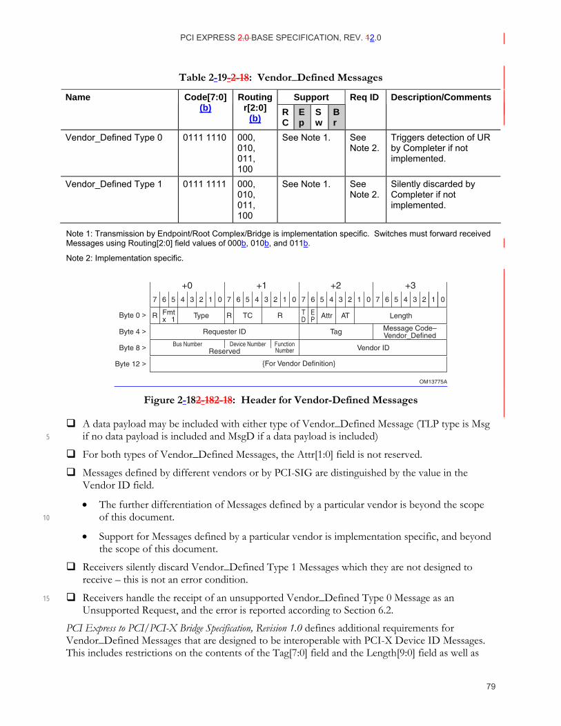
PCI EXPRESS 2.0 BASE SPECIFICATION, REV. 12.0
79
Table 2-19- 2-18: Vendor_Defined Messages
Support Name Code[7:0] (b)
Routing r[2:0]
(b) RC
Ep
Sw
Br
Req ID Description/Comments
Vendor_Defined Type 0 0111 1110 000, 010, 011, 100
See Note 1. See Note 2.
Triggers detection of UR by Completer if not implemented.
Vendor_Defined Type 1 0111 1111 000, 010, 011, 100
See Note 1. See Note 2.
Silently discarded by Completer if not implemented.
Note 1: Transmission by Endpoint/Root Complex/Bridge is implementation specific. Switches must forward received Messages using Routing[2:0] field values of 000b, 010b, and 011b.
Note 2: Implementation specific.
OM13775A
7 6 5
x 1
4 3 2 1 0 7 6 5 4 3 2 1 0 7 6 5 4 3 2 1 0 7 6 5 4 3 2 1 0
R TD
EP Attr ATTypeFmtR TCR
Requester ID
Reserved
For Vendor Definition
Vendor IDBus Number FunctionNumber
Device Number
Tag Message Code–Vendor_Defined
Length
+0 +1 +2 +3
Byte 0 >
Byte 4 >
Byte 8 >
Byte 12 >
Figure 2-182-18 2-18: Header for Vendor-Defined Messages
A data payload may be included with either type of Vendor_Defined Message (TLP type is Msg if no data payload is included and MsgD if a data payload is included) 5
For both types of Vendor_Defined Messages, the Attr[1:0] field is not reserved.
Messages defined by different vendors or by PCI-SIG are distinguished by the value in the Vendor ID field.
• The further differentiation of Messages defined by a particular vendor is beyond the scope of this document. 10
• Support for Messages defined by a particular vendor is implementation specific, and beyond the scope of this document.
Receivers silently discard Vendor_Defined Type 1 Messages which they are not designed to receive – this is not an error condition.
Receivers handle the receipt of an unsupported Vendor_Defined Type 0 Message as an 15 Unsupported Request, and the error is reported according to Section 6.2.
PCI Express to PCI/PCI-X Bridge Specification, Revision 1.0 defines additional requirements for Vendor_Defined Messages that are designed to be interoperable with PCI-X Device ID Messages. This includes restrictions on the contents of the Tag[7:0] field and the Length[9:0] field as well as

PCI EXPRESS 2.0 BASE SPECIFICATION, REV. 21.0
80
specific use of Bytes 12 through 15 of the message header. Vendor_Defined Messages intended for use solely within a PCI Express environment (i.e., not intended to address targets behind a PCI Express to PCI/PCI-X Bridge) are not subject to the additional rules. See Refer to PCI Express to PCI/PCI-X Bridge Specification, Revision 1.0 for details.
2.2.8.7. Ignored Messages
The messages listed in Table 2-20 were previously used for a mechanism (Hot-Plug Signaling) that is 5 no longer supported. Transmitters are strongly encouraged not to transmit these messages, but if message transmission is implemented, it must conform to the requirements of the 1.0a version of this specification.
Receivers are strongly encouraged to ignore receipt of these messages, but are allowed to process these messages in conformance with the requirements of 1.0a version of this specification. 10
Ignored messages listed in Table 2-20 are handled by the Receiver as follows:
The Physical and Data Link Layers must handle these messages identical to handling any other TLP
The Transaction layer must account for flow control credit but take no other action in response to these messages 15
Table 2-20- 2-19: Ignored Messages
Support Name Code[7:0] (b)
Routing r[2:0]
(b) RC
Ep
Sw
Br
Req ID Description/Comments
Ignored Message 0100 0001 100 Ignored Message 0100 0011 100 Ignored Message 0100 0000 100 Ignored Message 0100 0101 100 Ignored Message 0100 0111 100 Ignored Message 0100 0100 100 Ignored Message 0100 1000 100
PCI EXPRESS 2.0 BASE SPECIFICATION, REV. 12.0
81
2.2.9. Completion Rules
All Read Requests and Non-Posted Write Requests require Completion. Completions include a Completion header that, for some types of Completions, will be followed by some number of DW of data. The rules for each of the fields of the Completion header are defined in the following sections.
Completions route by ID, and use a 3 DW header 5
• Note that the routing ID fields correspond directly to the Requester ID supplied with the corresponding Request. Thus for Completions these fields will be referred to collectively as the Requester ID instead of the distinct fields used generically for ID routing.
In addition to the header fields included in all TLPs and the ID routing fields, Completions contain the following additional fields (see Figure 2-19) 10
• Completer ID[15:0] – Identifies the Completer – described in detail below
• Completion Status[2:0] – Indicates the status for a Completion (see Table 2-21)
♦ Rules for determining the value in the Completion Status[2:0] field are in Section 2.3.1
• BCM – Byte Count Modified – this bit must not set by PCI Express Completers, and may only be set by PCI-X completers 15
• Byte Count[11:0] – The remaining byte count for Request
♦ The Byte Count value is specified as a binary number, with 0000 0000 0001b indicating 1 byte, 1111 1111 1111b indicating 4095 bytes, and 0000 0000 0000b indicating 4096 bytes
♦ For Memory Read Completions, Byte Count[11:0] is set according to the rules in Section 2.3.1.1. 20
♦ For all other types of Completions, the Byte Count field must be 4.
• Tag[7:0] – in combination with the Requester ID field, corresponds to the Transaction ID
• Lower Address[6:0] – lower byte address for starting byte of Completion
♦ For Memory Read Completions, the value in this field is the byte address for the first enabled byte of data returned with the Completion (see the rules in Section 2.3.1.1) 25
♦ This field is set to all 0’s for all types of Completions other than Memory Read Completions
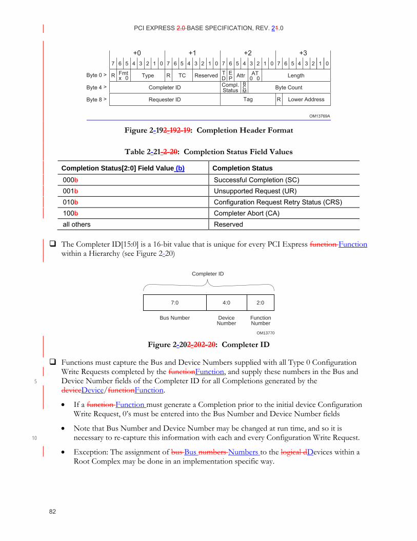
PCI EXPRESS 2.0 BASE SPECIFICATION, REV. 21.0
82
OM13769A
7 6 5
x 0
4 3 2 1 0 7 6 5 4 3 2 1 0 7 6 5 4 3 2 1 0 7 6 5 4 3 2 1 0
Reserved TD
EP AttrTypeFmtR TCR
Completer ID
Requester ID Tag Lower AddressR
Byte CountCompl.Status
BCM
Length
+0 +1 +2 +3
Byte 0 >
Byte 4 >
Byte 8 >
0 0AT
Figure 2-192-19 2-19: Completion Header Format
Table 2-21- 2-20: Completion Status Field Values
Completion Status[2:0] Field Value (b) Completion Status 000b Successful Completion (SC) 001b Unsupported Request (UR) 010b Configuration Request Retry Status (CRS) 100b Completer Abort (CA) all others Reserved
The Completer ID[15:0] is a 16-bit value that is unique for every PCI Express function Function within a Hierarchy (see Figure 2-20)
OM13770
Bus Number DeviceNumber
7:0
FunctionNumber
2:04:0
Completer ID
Figure 2-202-20 2-20: Completer ID
Functions must capture the Bus and Device Numbers supplied with all Type 0 Configuration Write Requests completed by the functionFunction, and supply these numbers in the Bus and Device Number fields of the Completer ID for all Completions generated by the 5 deviceDevice/functionFunction.
• If a function Function must generate a Completion prior to the initial device Configuration Write Request, 0’s must be entered into the Bus Number and Device Number fields
• Note that Bus Number and Device Number may be changed at run time, and so it is necessary to re-capture this information with each and every Configuration Write Request. 10
• Exception: The assignment of bus Bus numbers Numbers to the logical dDevices within a Root Complex may be done in an implementation specific way.
PCI EXPRESS 2.0 BASE SPECIFICATION, REV. 12.0
83
In some cases, a Completion with the UR status may be generated by a multi-function Function device without associating the Completion with a specific function Function within the device – in this case, the Function Number field is Reserved.
• Example: A multi-function Function device receives a Read Request which does not target any resource associated with any of the functions Functions of the device – the device 5 generates a Completion with UR status and sets a value of all 0’s in the Function Number field of the Completer ID.
Completion headers must supply the same values for the Requester ID, Tag, Attribute, and Traffic Class as were supplied in the header of the corresponding Request.
AT[1:0] must be 00b. 10
The Completion ID field is not meaningful prior to the software initialization and configuration of the completing device (using at least one Configuration Write Request), and the Requestor Requester must ignore the value returned in the Completer ID field.
A Completion including data must specify the actual amount of data returned in that Completion, and must include the amount of data specified. 15
• It is a TLP formation error to include more or less data than specified in the Length field, and the resulting TLP is a malformed Malformed TLP.
Note: This is simply a specific case of the general rule requiring TLP data payload length match the value in the Length field.
2.3. Handling of Received TLPs This section describes how all Received TLPs are handled when they are delivered to the Receive 20 Transaction Layer from the Receive Data Link Layer, after the Data Link Layer has validated the integrity of the received TLP. The rules are diagramed in the flowchart shown in Figure 2-21.
Values in Reserved fields must be ignored by the Receiver.
All Received TLPs which use undefined Type field values are Malformed TLPs.
This is a reported error associated with the Receiving Port (see Section 6.2) 25
All Received Malformed TLPs must be discarded.
• Received Malformed TLPs that are ambiguous with respect to which buffer to release or are mapped to an uninitialized virtual Virtual channel Channel must be discarded without updating Receiver Flow Control information.
• All other Received Malformed TLPs must be discarded, optionally not updating Receiver 30 Flow Control information.
Otherwise, update Receiver Flow Control tracking information (see Section 2.6)
If the value in the Type field indicates the TLP is a Request, handle according to Request Handling Rules, otherwise, the TLP is a Completion – handle according to Completion Handling Rules (following sections) 35
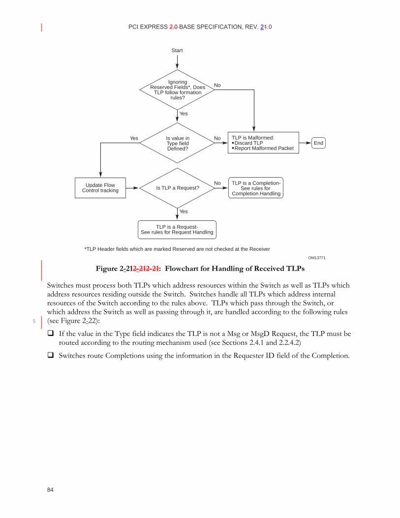
PCI EXPRESS 2.0 BASE SPECIFICATION, REV. 21.0
84
Is value inType fieldDefined?
Is TLP a Request?
Start
*TLP Header fields which are marked Reserved are not checked at the Receiver
IgnoringReserved Fields*, Does
TLP follow formationrules?
TLP is a Request-See rules for Request Handling
TLP is a Completion-See rules for
Completion Handling
Update FlowControl tracking
Yes
Yes
Yes
No
No
End
No
TLP is Malformed: Discard TLP Report Malformed Packet
OM13771 Figure 2-212-21 2-21: Flowchart for Handling of Received TLPs
Switches must process both TLPs which address resources within the Switch as well as TLPs which address resources residing outside the Switch. Switches handle all TLPs which address internal resources of the Switch according to the rules above. TLPs which pass through the Switch, or which address the Switch as well as passing through it, are handled according to the following rules (see Figure 2-22): 5
If the value in the Type field indicates the TLP is not a Msg or MsgD Request, the TLP must be routed according to the routing mechanism used (see Sections 2.4.1 and 2.2.4.2)
Switches route Completions using the information in the Requester ID field of the Completion.
PCI EXPRESS 2.0 BASE SPECIFICATION, REV. 12.0
85
If the value in the Type field indicates the TLP is a Msg or MsgD Request, route the Request according to the routing mechanism indicated in the r[2:0] sub-field of the Type field
• If the value in r[2:0] indicates the Msg/MsgD is routed to the Root Complex (000b), the Switch must route the Msg/MsgD to the Upstream Port of the Switch
♦ It is an error to receive a Msg/MsgD Request specifying 000b routing at the Upstream 5 Port of a Switch. Switches may check for violations of this rule – TLPs in violation are Malformed TLPs. If checked, this is a reported error associated with the Receiving Port (see Section 6.2)
• If the value in r[2:0] indicates the Msg/MsgD is routed by address (001b), the Switch must route the Msg/MsgD in the same way it would route a Memory Request by address 10
• If the value in r[2:0] indicates the Msg/MsgD is routed by ID (010b), the Switch must route the Msg/MsgD in the same way it would route a Completion by ID
• If the value in r[2:0] indicates the Msg/MsgD is a broadcast from the Root Complex (011b), the Switch must route the Msg/MsgD to all Downstream Ports of the Switch
♦ It is an error to receive a Msg/MsgD Request specifying 011b routing at the 15 Downstream Port of a Switch. Switches may check for violations of this rule – TLPs in violation are Malformed TLPs. If checked, this is a reported error associated with the Receiving Port (see Section 6.2)
• If the value in r[2:0] indicates the Msg/MsgD terminates at the Receiver (100b or a reserved value), or if the Message Code field value is defined and corresponds to a Message which 20 must be comprehended by the Switch, the Switch must process the Message according to the Message processing rules
• If the value in r[2:0] indicates Gathered and routed to Root Complex (101b), see Section 5.3.3.2.1 for Message handling rules
• It is an error to receive any Msg/MsgD Request other than a PME_TO_Ack that specifies 25 101b routing. It is an error to receive a PME_TO_Ack at the Upstream Port of a Switch. Switches may check for violations of these rules – TLPs in violation are Malformed TLPs. If checked, this is a reported error associated with the Receiving Port (see Section 6.2)
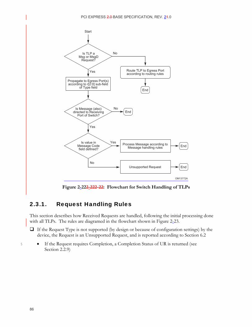
PCI EXPRESS 2.0 BASE SPECIFICATION, REV. 21.0
86
Is Message (also)directed to Receiving
Port of Switch?
Is value inMessage Codefield defined?
Start
Is TLP aMsg or MsgD
Request?
Route TLP to Egress Portaccording to routing rules
Process Message according toMessage handling rules
No
Yes
Yes
No
No
End
Propagate to Egress Port(s)according to r[2:0] sub-field
of Type fieldEnd
End
Unsupported Request End
OM13772A
Yes
Figure 2-222-22 2-22: Flowchart for Switch Handling of TLPs
2.3.1. Request Handling Rules
This section describes how Received Requests are handled, following the initial processing done with all TLPs. The rules are diagramed in the flowchart shown in Figure 2-23.
If the Request Type is not supported (by design or because of configuration settings) by the device, the Request is an Unsupported Request, and is reported according to Section 6.2
• If the Request requires Completion, a Completion Status of UR is returned (see 5 Section 2.2.9)
PCI EXPRESS 2.0 BASE SPECIFICATION, REV. 12.0
87
IMPLEMENTATION NOTE When Requests are Terminated Using Unsupported Request In Conventional PCI, a device “claims” a request on the bus by asserting DEVSEL#. If no device claims a request after a set number of clocks, the request is terminated as a Master Abort. Because PCI Express is a point to point interconnect, there is no equivalent mechanism for claiming a request on a Link, since all transmissions by one component are always sent to the other component on the Link. Therefore, it is necessary for the receiver of a request to determine if the request 5 should be “claimed.” If the request is not claimed, then it is handled as an Unsupported Request, which is the PCI Express equivalent of conventional PCI’s Master Abort termination. In general, one can determine the correct behavior by asking the question: Would the device assert DEVSEL# for this request in conventional PCI? For device Functions with Type 0 headers (all types of Endpoints), it is relatively simple to answer 10 this question. For Memory and I/O Requests, this determination is based on the address ranges the Function has been programmed to respond to. For Configuration requests, the Type 0 request format indicates the device is by definition the “target”, although the device will still not claim the Configuration Request if it addresses an unimplemented Function.
For device Functions with Type 1 headers (Root Ports, Switches and Bridges), the same question 15 can generally be applied, but since the behavior of a conventional PCI bridge is more complicated than that of a Type 0 Function, it is somewhat more difficult to determine the answers. One must consider Root Ports and Switch Ports as if they were actually composed of conventional PCI to PCI bridges, and then at each stage consider the configuration settings of the virtual bridge to determine the correct behavior. 20
PCI Express Messages do not exist in conventional PCI, so the above guideline cannot be applied. This specification describes specifically for each type of Message when a device must handle the request as an Unsupported Request. Messages pass through Root and Switch Ports unaffected by conventional PCI control mechanisms including Bus Master Enable and power state setting.
Note that Completer Abort, which is the PCI Express equivalent to Target Abort, is used only to 25 indicate a serious error that makes the completer permanently unable to respond to a request that it would otherwise have normally responded to. Because Target Abort is used in conventional PCI only when a target has asserted DEVSEL#, is incorrect to use Completer Abort for any case where a conventional PCI target would have ignored a request by not asserting DEVSEL#.
If the Request is a Message, and the Message Code specifies a value that is undefined, or that 30 corresponds to a Message not supported by the device Function, (other than Vendor_Defined Type 1 which is not treated as an error – see Section 2.2.8.6), the Request is an Unsupported Request, and is reported according to Section 6.2
• If the Message Code is a supported value, process the Message according to the corresponding Message processing rules; if the Message Code is an ignored Message, ignore 35 the Message without reporting any error (see Section 2.2.8.7)
PCI EXPRESS 2.0 BASE SPECIFICATION, REV. 21.0
88
If the Request is not a Message, and is a supported Type, specific implementations may be optimized based on a defined programming model which ensures that certain types of (otherwise legal) Requests will never occur. Such implementations may take advantage of the following rule:
If the Request violates the programming model of the device Function, the device Function may optionally treat the Request as a Completer Abort, instead of handling the Request normally 5
• If the Request is treated as a Completer Abort, this is a reported error associated with the device/fFunction (see Section 6.2)
• If the Request requires Completion, a Completion Status of CA is returned (see Section 2.2.9)
IMPLEMENTATION NOTE Optimizations Based on Restricted Programming Model When a device’s programming model restricts (vs. what is otherwise permitted in PCI Express) the 10 characteristics of a Request, that device is permitted to “Completer Abort” any Requests which violate the programming model. Examples include unaligned or wrong-size access to a register block and unsupported size of request to a memory Memory spaceSpace.
Generally, devices are able to assume a restricted programming model when all communication will be between the device’s driver software and the device itself. Devices which may be accessed 15 directly by operating system software or by applications which may not comprehend the restricted programming model of the device (typically devices which implement legacy capabilities) should be designed to support all types of Requests which are possible in the existing usage model for the device. If this is not done, the device may fail to operate with existing software.
If the Request arrives between the time an FLR has been initiated and the completion of the FLR by 20 the targeted Function, the Request is permitted to be silently discarded (following update of flow control credits) without logging or signaling it as an error. It is recommended that the Request be handled as an Unsupported Request (UR).
Otherwise (supported Request Type, not a Message), process the Request
• If the Completer is permanently unable to process the Request due to a device-specific error 25 condition the Completer must, if possible, handle the Request as a Completer Abort
♦ This is a reported error associated with the Receiving device/fFunction, if the error can be isolated to a specific device/fFunction in the component, or to the Receiving Port if the error cannot be isolated (see Section 6.2)
PCI EXPRESS 2.0 BASE SPECIFICATION, REV. 12.0
89
• For Configuration Requests only, following reset it is possible for a device to terminate the request but indicate that it is temporarily unable to process the Request, but will be able to process the Request in the future – in this case, the Configuration Request Retry Status (CRS) Completion Status is used (see Section 6.6). Valid reset conditions after which a device is permitted to return CRS are: 5
♦ Cold, Warm, and Hot Link Resets
♦ FLRs
♦ as well asA reset initiated in response to a D3hot to D0uninitialized device state transition. A device Function is explicitly not permitted to return CRS following a software-initiated reset (other than an FLR) of the device, e.g., by the device’s software driver writing to a 10 device-specific reset bit. Additionally, a device Function is not permitted to return CRS after having previously returned a Successful Completion without an intervening valid reset (i.e., FLR or Conventional Reset) condition.
• In the process of servicing the Request, the Completer may determine that the (otherwise acceptable) Request must be handled as an error, in which case the Request is handled 15 according to the type of the error
♦ Example: A PCI Express/PCI Bridge may initially accept a Request because it specifies a memory Memory Space range mapped to the secondary side of the Bridge, but the Request may Master Abort or Target Abort on the PCI side of the Bridge. From the PCI Express perspective, the status of the Request in this case is UR (for Master Abort) 20 or CA (for Target Abort). If the Request requires Completion on PCI Express, the corresponding Completion Status is returned.
If the Request is a type which requires a Completion to be returned, generate a Completion according to the rules for Completion Formation (see Section 2.2.9)
• The Completion Status is determined by the result of handling the Request 25
Under normal operating conditions, PCI Express Endpoints and Legacy Endpoints must never delay the acceptance of a Posted Request for more than 10 µs, which is called the Posted Request Acceptance Limit. The device must either (a) be designed to process received Posted Requests and return associated Flow Control credits within the necessary time limit, or (b) rely on a restricted programming model to ensure that a Posted Request is never sent to the device 30 either by software or by other devices while the device is unable to accept a new Posted Request within the necessary time limit.
• The following are not considered normal operating conditions under which the Posted Request Acceptance Limit applies:
♦ The period immediately following a Fundamental Reset (see Section 6.6) 35
♦ TLP retransmissions or Link retraining
♦ One or more dropped FCPs
♦ The device being in a diagnostic mode
♦ The device being in a device-specific mode that is not intended for normal use
PCI EXPRESS 2.0 BASE SPECIFICATION, REV. 21.0
90
• The following are considered normal operating conditions, but any delays they cause do not count against the Posted Request Acceptance Limit:
♦ Upstream TLP traffic delaying upstream Upstream FCPs.
♦ The linkLink coming out of a low-power state.
♦ Arbitration with traffic on other VCs. 5
♦ Though not a requirement, it is strongly recommended that Root Complex Integrated Endpoints also honor the Posted Request Acceptance Limit.
• If the device supports being a target for I/O writes, which are Non-Posted Requests, it is strongly recommended that each associated Completion be returned within the same time limit as for Posted Request acceptance, although this is not a requirement. 10
IMPLEMENTATION NOTE Restricted Programming Model for Meeting the Posted Request Acceptance Limit Some hardware designs may not be able to process every Posted Request within the required acceptance time limit. An example is writing to a command queue where commands can take longer than the acceptance time limit to complete. Subsequent writes to such a device when it is currently processing a previous write could experience acceptance delays that exceed the limit. Such devices may rely on a restricted programming model, where the device driver limits the rate of memory 15 writes to the device, the driver polls the device to determine buffer availability before issuing the write transaction, or the driver implements some other software-based flow control mechanism.
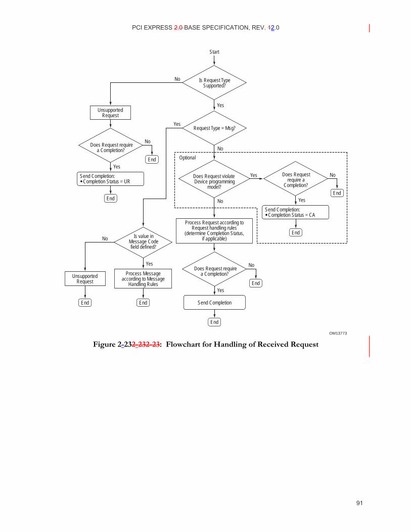
PCI EXPRESS 2.0 BASE SPECIFICATION, REV. 12.0
91
OM13773
Does Request requirea Completion?
Start
Is Request TypeSupported?
Request Type = Msg?
Yes
Yes
Yes
YesDoes Request violate Device programming
model?
No
Optional
No
No
End
End
UnsupportedRequest
Send Completion: Completion Status = UR
No
Does Request require a
Completion?
YesEnd
End
Send Completion: Completion Status = CA
No
Process Request according toRequest handling rules
(determine Completion Status,if applicable)
Does Request requirea Completion?
YesEnd
End
Send Completion
No
EndEnd
Process Messageaccording to Message
Handling Rules
UnsupportedRequest
No Is value inMessage Codefield defined?
Yes
Figure 2-232-23 2-23: Flowchart for Handling of Received Request
PCI EXPRESS 2.0 BASE SPECIFICATION, REV. 21.0
92
IMPLEMENTATION NOTE Configuration Request Retry Status Some devices require a lengthy self-initialization sequence to complete before they are able to service Configuration Requests (common with intelligent I/O solutions on PCI). PCI/PCI-X architecture has specified a 225 (PCI) or 226 (PCI-X) clock “recovery time” Trhfa following reset to provide the required self-initialization time for such devices. PCI Express “softens” the need for this time based recovery period by implementing a Configuration Request Retry Status (CRS) Completion Status. A 5 device in receipt of a Configuration Request following a valid reset condition may respond with a CRS Completion Status to terminate the Request, and thus effectively stall the Configuration Request until such time that the subsystem has completed local initialization and is ready to communicate with the host. Note that it is only legal to respond with a CRS Completion Status in response to a Configuration Request. Sending this Completion Status in response to any other 10 Request type is illegal (see Section 2.3.2).
Receipt by the Requestor Requester of a Completion with CRS Completion Status terminates the Configuration Request on PCI Express. Further action by the Root Complex regarding the original Configuration Request is specified in Section 2.3.2.
Root Complexes that implement CRS Software Visibility have the ability to report the receipt of 15 CRS Completion Status to software, enabling software to attend to other tasks rather than being stalled while the device completes its self-initialization. Software that intends to take advantage of this mechanism must ensure that the first access made to a device following a valid reset condition is a Configuration Read Request accessing both bytes of the Vendor ID field in the device’s configuration spaceConfiguration Space header. For this case only, the Root Complex, if enabled, 20 will synthesize a special read-data value for the Vendor ID field to indicate to software that CRS Completion Status has been returned by the device. For other Configuration Requests, or when CRS Software Visibility is not enabled, the Root Complex will generally re-issue the Configuration Request until it completes with a status other than CRS as described in Section 2.3.2.
When used in systems including PCI Express to PCI/PCI-X Bridges, system software and/or the 25 Root Complex must comprehend the limit Trhfa for PCI/PCI-X agents as described in Sections 2.8 and 6.6. Similarly, systems using PCI Express components which require additional self initialization time beyond the minimum guaranteed must provide some mechanism for re-issuing Configuration Requests terminated with CRS status. In systems running legacy PCI/PCI-X based software, the Root Complex must re-issue the Configuration Request using a hardware mechanism to ensure 30 proper enumeration of the system.
See Refer to Section 6.6 for more information on reset.
PCI EXPRESS 2.0 BASE SPECIFICATION, REV. 12.0
93
2.3.1.1. Data Return for Read Requests
Individual Completions for Memory Read Requests may provide less than the full amount of data Requested so long as all Completions for a given Request when combined return exactly the amount of data Requested in the Read Request.
• Completions for different Requests cannot be combined.
• I/O and Configuration Reads must be completed with exactly one Completion. 5
• The Completion Status for a Completion corresponds only to the status associated with the data returned with that Completion
♦ A Completion with status other than Successful Completion terminates the Completions for a single Read Request
In this case, the value in the Length field is undefined, and must be ignored by the 10 Receiver
Completions must not include more data than permitted by the Max_Payload_Size parameter.
• Receivers must check for violations of this rule. See Refer to Section 2.2.
Note: This is simply a specific case of the rules which apply to all TLPs with data payloads
Memory Read Requests may be completed with one, or in some cases, multiple Completions 15
The Read Completion Boundary (RCB) parameter determines the naturally aligned address boundaries on which a Read Request may be serviced with multiple Completions
• For a Root Complex, RCB is 64 bytes or 128 bytes
♦ This value is reported through a configuration register (see Section 7.8)
Note: Bridges and Endpoints may implement a corresponding command bit which may be 20 set by system software to indicate the RCB value for the Root Complex, allowing the Bridge/Endpoint to optimize its behavior when the Root Complex’s RCB is 128 bytes.
• For all other system System elementsElements, RCB is 128 bytes
Completions for Requests which do not cross the naturally aligned address boundaries at integer multiples of RCB bytes must include all data specified in the Request 25
PCI EXPRESS 2.0 BASE SPECIFICATION, REV. 21.0
94
Requests which do cross the address boundaries at integer multiples of RCB bytes may be completed using more than one Completion, but the data must not be fragmented except along the following address boundaries:
• The first Completion must start with the address specified in the Request, and must end at one of the following: 5
♦ the address specified in the Request plus the length specified by the Request (i.e., the entire Request)
♦ an address boundary between the start and end of the Request at an integer multiple of RCB bytes
• The final Completion must end with the address specified in the Request plus the length 10 specified by the Request
• All Completions between, but not including, the first and final Completions must be an integer multiple of RCB bytes in length
Receivers may optionally check for violations of RCB. If a Receiver implementing this check determines that a Completion violates this rule, it must handle the Completion as a Malformed 15 TLP
• This is a reported error associated with the Receiving Port (see Section 6.2)
Multiple Memory Read Completions for a single Read Request must return data in increasing address order.
For each Memory Read Completion, the Byte Count field must indicate the remaining number 20 of bytes required to complete the Request including the number of bytes returned with the Completion, except when the BCM field is 1b.10
• The total number of bytes required to complete a Memory Read Request is calculated as shown in Table 2-22
• If a Memory Read Request is completed using multiple Completions, the Byte Count value 25 for each successive Completion is the value indicated by the preceding Completion minus the number of bytes returned with the preceding Completion.
10 Only PCI-X completers set the BCM bit to 1b.
PCI EXPRESS 2.0 BASE SPECIFICATION, REV. 12.0
95
IMPLEMENTATION NOTE BCM Bit Usage To satisfy certain PCI-X protocol constraints, a PCI-X Bridge or PCI-X Completer for a PCI-X burst read in some cases will set the Byte Count field in the first PCI-X transaction of the Split Completion sequence to indicate the size of just that first transaction instead of the entire burst read. When this occurs, the PCI-X Bridge/PCI-X Completer will also set the BCM bit in that first PCI-X transaction, to indicate that the Byte Count field has been modified from its normal usage. Refer to 5 the PCI-X Addendum to the PCI Local Bus Specification, Revision 2.0 for further details.
A PCI Express Memory Read Requester needs to correctly handle the case when a PCI-X Bridge/PCI-X Completer sets the BCM bit. When this occurs, the first Read Completion packet returned to the Requestor Requester will have the BCM bit set, indicating that the Byte Count field reports the size of just that first packet instead of the entire remaining byte count. The Requester 10 should not conclude at this point that other packets of the Read Completion are missing.
The BCM bit will never be set in subsequent packets of the Read Completion, so the Byte Count field in those subsequent packets will always indicate the remaining byte count in each instance. Thus, the Requester can use the Byte Count field in these packets to determine if other packets of the Read Completion are missing. 15
PCI Express Completers will never set the BCM bit.
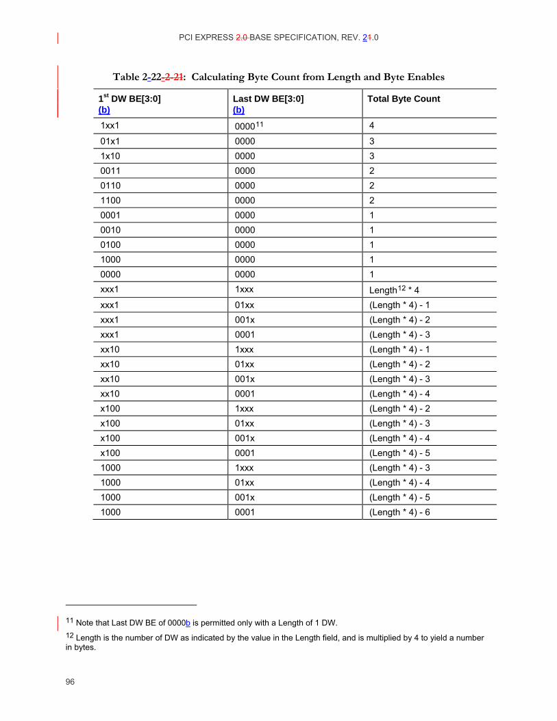
PCI EXPRESS 2.0 BASE SPECIFICATION, REV. 21.0
96
Table 2-22- 2-21: Calculating Byte Count from Length and Byte Enables
1st DW BE[3:0] (b)
Last DW BE[3:0] (b)
Total Byte Count
1xx1 000011 4
01x1 0000 3 1x10 0000 3 0011 0000 2 0110 0000 2 1100 0000 2 0001 0000 1 0010 0000 1 0100 0000 1 1000 0000 1 0000 0000 1 xxx1 1xxx Length12 * 4 xxx1 01xx (Length * 4) - 1 xxx1 001x (Length * 4) - 2 xxx1 0001 (Length * 4) - 3 xx10 1xxx (Length * 4) - 1 xx10 01xx (Length * 4) - 2 xx10 001x (Length * 4) - 3 xx10 0001 (Length * 4) - 4 x100 1xxx (Length * 4) - 2 x100 01xx (Length * 4) - 3 x100 001x (Length * 4) - 4 x100 0001 (Length * 4) - 5 1000 1xxx (Length * 4) - 3 1000 01xx (Length * 4) - 4 1000 001x (Length * 4) - 5 1000 0001 (Length * 4) - 6
11 Note that Last DW BE of 0000b is permitted only with a Length of 1 DW. 12 Length is the number of DW as indicated by the value in the Length field, and is multiplied by 4 to yield a number in bytes.
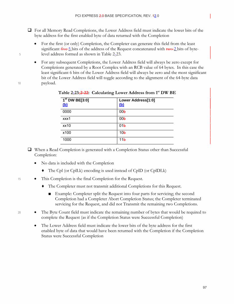
PCI EXPRESS 2.0 BASE SPECIFICATION, REV. 12.0
97
For all Memory Read Completions, the Lower Address field must indicate the lower bits of the byte address for the first enabled byte of data returned with the Completion
• For the first (or only) Completion, the Completer can generate this field from the least significant five 5 bits of the address of the Request concatenated with two 2 bits of byte-level address formed as shown in Table 2-23. 5
• For any subsequent Completions, the Lower Address field will always be zero except for Completions generated by a Root Complex with an RCB value of 64 bytes. In this case the least significant 6 bits of the Lower Address field will always be zero and the most significant bit of the Lower Address field will toggle according to the alignment of the 64-byte data payload. 10
Table 2-23- 2-22: Calculating Lower Address from 1st DW BE
1st DW BE[3:0] (b)
Lower Address[1:0] (b)
0000 00b
xxx1 00b
xx10 01b
x100 10b
1000 11b
When a Read Completion is generated with a Completion Status other than Successful Completion:
• No data is included with the Completion
♦ The Cpl (or CplLk) encoding is used instead of CplD (or CplDLk)
• This Completion is the final Completion for the Request. 15
♦ The Completer must not transmit additional Completions for this Request.
Example: Completer split the Request into four parts for servicing; the second Completion had a Completer Abort Completion Status; the Completer terminated servicing for the Request, and did not Transmit the remaining two Completions.
• The Byte Count field must indicate the remaining number of bytes that would be required to 20 complete the Request (as if the Completion Status were Successful Completion)
• The Lower Address field must indicate the lower bits of the byte address for the first enabled byte of data that would have been returned with the Completion if the Completion Status were Successful Completion

PCI EXPRESS 2.0 BASE SPECIFICATION, REV. 21.0
98
IMPLEMENTATION NOTE Restricted Programming Model When a device’s programming model restricts (vs. what is otherwise permitted in PCI Express) the size and/or alignment of Read Requests directed to the device, that device is permitted to use a Completer Abort Completion Status for Read Requests which violate the programming model. An implication of this is that such devices, generally devices where all communication will be between the device’s driver software and the device itself, need not necessarily implement the buffering 5 required to generate Completions of length RCB. However, in all cases, the boundaries specified by RCB must be respected for all reads which the device will Complete with Successful Completion status. Examples: 1. Memory Read Request with Address of 1 0000h and Length of C0h bytes (192 decimal) could be 10 completed by a Root Complex with an RCB value of 64 bytes with one of the following combinations of Completions (bytes): 192 –or– 128, 64 –or– 64, 128 –or– 64, 64, 64
2. Memory Read Request with Address of 1 0000h and Length of C0h bytes (192 decimal) could be completed by a Root Complex with an RCB value of 128 bytes in one of the following combinations 15 of Completions (bytes): 192 –or– 128, 64
3. Memory Read Request with Address of 1 0020h and Length of 100h bytes (256 decimal) could be completed by a Root Complex with an RCB value of 64 bytes in one of the following combinations of Completions (bytes): 20 256 –or– 32, 224 –or– 32, 64, 160 –or– 32, 64, 64, 96 –or– 32, 64, 64, 64, 32 –or– 32, 64, 128, 32 –or– 32, 128, 96 –or– 32, 128, 64, 32 –or– 96, 160 –or– 96, 128, 32 –or– 96, 64, 96 –or– 96, 64, 64, 32 –or– 160, 96 –or– 160, 64, 32 –or– 224, 32 25
4. Memory Read Request with Address of 1 0020h and Length of 100h bytes (256 decimal) could be completed by an Endpoint in one of the following combinations of Completions (bytes): 256 –or– 96, 160 –or– 96, 128, 32 –or– 224, 32
PCI EXPRESS 2.0 BASE SPECIFICATION, REV. 12.0
99
2.3.2. Completion Handling Rules
When a device receives a Completion which does not correspond tomatch the Transaction ID for any of the outstanding Requests issued by that device, the Completion is called an “Unexpected Completion.”
If a received Completion is not malformed and matches the Transaction ID of an outstanding Request, but in some other way does not match the corresponding Request, it is permitted for 5 the receiver to handle the Completion as an Unexpected Completion
Receipt of an Unexpected Completion is an error and must be handled according to the following rules:
• The Agent agent receiving an Unexpected Completion must discard the Completion.
• An Unexpected Completion is a reported error associated with the Receiving Port (see 10 Section 6.2)
Note: Unexpected Completions are assumed to occur mainly due to Switch misrouting of the Completion. The Requester of the Request may not receive a Completion for its Request in this case, and the Requester’s Completion Timeout mechanism (see Section 2.8) will terminate the Request. 15
Completions with a Completion Status other than Successful Completion, or Configuration Request Retry Status (in response to Configuration Request only) must cause the Requester to:
• Free Completion buffer space and other resources associated with the Request.
• Handle the error via a Requester-specific mechanism (see Section 6.2.3.2.5).
If the Completion arrives between the time an FLR has been initiated and the completion of the 20 FLR by the targeted Function, the Completion is permitted to be handled as an Unexpected Completion or to be silently discarded (following update of flow control credits) without logging or signaling it as an error. Once the FLR has completed, received Completions corresponding to Requests issued prior to the FLR must be handled as Unexpected Completions, unless the Function has been re-enabled to issue Requests. 25
Root Complex handling of a Completion with Configuration Request Retry Status for a Configuration Request is implementation specific, except for the period following system reset (see Section 6.6). For Root Complexes that support CRS Software Visibility, the following rules apply:
• If CRS Software Visibility is not enabled, the Root Complex must re-issue the Configuration 30 Request as a new Request.
• If CRS Software Visibility is enabled (see below):
♦ For a Configuration Read Request that includes both bytes of the Vendor ID field of a device Function’s Configuration Space Header, the Root Complex must complete the Request to the host by returning a read-data value of 0001h for the Vendor ID field and 35 all ‘1’s for any additional bytes included in the request. This read-data value has been reserved specifically for this use by the PCI-SIG and does not correspond to any assigned Vendor ID.
PCI EXPRESS 2.0 BASE SPECIFICATION, REV. 21.0
100
♦ For a Configuration Write Request or for any other Configuration Read Request, the Root Complex must re-issue the Configuration Request as a new Request.
A Root Complex implementation may choose to limit the number of Configuration Request/CRS Completion Status loops before determining that something is wrong with the target of the Request and taking appropriate action, e.g., complete the Request to the host as a 5 failed transaction.
CRS Software Visibility may be enabled through the CRS Software Visibility Enable bit in the Root Control register (see Section 7.8.12) to control Root Complex behavior on an individual Root Port basis. Alternatively, Root Complex behavior may be managed through the CRS Software Visibility Enable bit in an RCRB Header Capability as described in Section 7.8.12, 10 permitting the behavior of one or more Root Ports or Root Complex Integrated Endpoints to be controledcontrolled by a single Enable bit. For this alternate case, each Root Port or Integrated Endpoint declares its association with a particular Enable bit via an RCRB header association in a Root Complex Link Declaration Capability (see Section 7.13). Each Root Port or Integrated Endpoint is permitted to be controlled by at most one Enable bit. Thus, for 15 example, it is prohibited for a Root Port whose Root Control register contains an Enable bit to declare an RCRB header association to an RCRB that also includes an Enable bit in its RCRB Header Capability. The presence of an Enable bit in a Root Port or RCRB Header Capability is indicated by the corresponding CRS Software Visibility bit (see Sections 7.8.13 and 7.20.3, respectively). 20
Completions with a Configuration Request Retry Status in response to a Request other than a Configuration Request are illegal. Receivers may optionally report these violations as Malformed TLPs
• This is a reported error associated with the Receiving Port (see Section 6.2)
Completions with a Reserved Completion Status value are treated as if the Completion Status 25 was Unsupported Request (UR)
Completions with a Completion Status of Unsupported Request or Completer Abort are reported using the conventional PCI reporting mechanisms (see Section 7.5.1.2)
• Note that the error condition that triggered the generation of such a Completion is reported by the Completer as described in Section 6.2 30
When a Read Completion is received with a Completion Status other than Successful Completion:
• No data is included with the Completion
♦ The Cpl (or CplLk) encoding is used instead of CplD (CplDLk)
• This Completion is the final Completion for the Request. 35
♦ The Requester must consider the Request terminated, and not expect additional Completions.
Handling of partial Completions Received earlier is implementation specific.
Example: The Requester received 32 bytes of Read data for a 128-byte Read Request it had issued, then a Completion with the Completer Abort Completion Status. The 40
PCI EXPRESS 2.0 BASE SPECIFICATION, REV. 12.0
101
Requester then must free the internal resources which had been allocated for that particular Read Request.
IMPLEMENTATION NOTE Read Data Values with UR Completion Status Some system configuration software depends on reading a data value of all 1’s when a Configuration Read Request is terminated as an Unsupported Request, particularly when probing to determine the existence of a device in the system. A Root Complex intended for use with software that depends 5 on a read-data value of all 1’s must synthesize this value when UR Completion Status is returned for a Configuration Read Request.
2.4. Transaction Ordering
2.4.1. Transaction Ordering Rules
Table 2-24 defines the ordering requirements for PCI Express Transactions. The rules defined in this table apply uniformly to all types of Transactions on PCI Express including Memory, I/O, Configuration, and Messages. The ordering rules defined in this table apply within a single Traffic 10 Class (TC). There is no ordering requirement among transactions with different TC labels. Note that this also implies that there is no ordering required between traffic that flows through different Virtual Channels since transactions with the same TC label are not allowed to be mapped to multiple VCs on any PCI Express Link.
For Table 2-24, the columns represent a first issued transaction and the rows represent a 15 subsequently issued transaction. The table entry indicates the ordering relationship between the two transactions. The table entries are defined as follows:
Yes–the second transaction (row) must be allowed to pass the first (column) to avoid deadlock. (When blocking occurs, the second transaction is required to pass the first transaction. Fairness must be comprehended to prevent starvation.) 20
Y/N–there are no requirements. The second transaction may optionally pass the first transaction or be blocked by it.
No–the second transaction must not be allowed to pass the first transaction. This is required to support the Producer-Consumer strong ordering model.
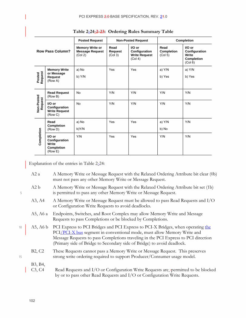
PCI EXPRESS 2.0 BASE SPECIFICATION, REV. 21.0
102
Table 2-24- 2-23: Ordering Rules Summary Table
Posted Request Non-Posted Request Completion
Row Pass Column? Memory Write or Message Request(Col 2)
Read Request (Col 3)
I/O or Configuration Write Request (Col 4)
Read Completion (Col 5)
I/O or Configuration Write Completion (Col 6)
Post
ed
Req
uest
Memory Write or Message Request (Row A)
a) No
b) Y/N
Yes Yes a) Y/N
b) Yes
a) Y/N
b) Yes
Read Request (Row B)
No Y/N Y/N Y/N Y/N
Non
-Pos
ted
Req
uest
I/O or Configuration Write Request (Row C)
No Y/N Y/N Y/N Y/N
Read Completion (Row D)
a) No
b)Y/N
Yes Yes a) Y/N
b) No
Y/N
Com
plet
ion
I/O or Configuration Write Completion (Row E)
Y/N Yes Yes Y/N Y/N
Explanation of the entries in Table 2-24:
A2 a A Memory Write or Message Request with the Relaxed Ordering Attribute bit clear (0b) must not pass any other Memory Write or Message Request.
A2 b A Memory Write or Message Request with the Relaxed Ordering Attribute bit set (1b) is permitted to pass any other Memory Write or Message Request. 5
A3, A4 A Memory Write or Message Request must be allowed to pass Read Requests and I/O or Configuration Write Requests to avoid deadlocks.
A5, A6 a Endpoints, Switches, and Root Complex may allow Memory Write and Message Requests to pass Completions or be blocked by Completions.
A5, A6 b PCI Express to PCI Bridges and PCI Express to PCI-X Bridges, when operating the 10 PCI/PCI-X bus segment in conventional mode, must allow Memory Write and Message Requests to pass Completions traveling in the PCI Express to PCI direction (Primary side of Bridge to Secondary side of Bridge) to avoid deadlock.
B2, C2 These Requests cannot pass a Memory Write or Message Request. This preserves strong write ordering required to support Producer/Consumer usage model. 15
B3, B4, C3, C4 Read Requests and I/O or Configuration Write Requests are permitted to be blocked by or to pass other Read Requests and I/O or Configuration Write Requests.
PCI EXPRESS 2.0 BASE SPECIFICATION, REV. 12.0
103
B5, B6, C5, C6 These Requests are permitted to be blocked by or to pass Completions.
D2 a If the Relaxed Ordering attribute bit is not set, then a Read Completion cannot pass a previously enqueued Memory Write or Message Request.
D2 b If the Relaxed Ordering attribute bit is set, then a Read Completion is permitted to pass 5 a previously enqueued Memory Write or Message Request.
D3, D4, E3, E4 Completions must be allowed to pass Read and I/O or Configuration Write Requests to avoid deadlocks.
D5 a Read Completions associated with different Read Requests are allowed to be blocked 10 by or to pass each other.
D5 b Read Completions for one Request (will have the same Transaction ID) must return in address order.
D6 Read Completions are permitted to be blocked by or to pass I/O or Configuration Write Completions. 15
E2 I/O or Configuration Write Completions are permitted to be blocked by or to pass Memory Write and Message Requests. Such Transactions are actually moving in the opposite direction and, therefore, have no ordering relationship.
E5, E6 I/O or Configuration Write Completions are permitted to be blocked by or to pass Read Completions and other I/O or Configuration Write Completions. 20
Additional Rules:
PCI Express Switches are permitted to allow a Memory Write or Message Request with the Relaxed Ordering bit set to pass any previously posted Memory Write or Message Request moving in the same direction. Switches must forward the Relaxed Ordering attribute unmodified. The Root Complex is also permitted to allow data bytes within the Request to be 25 written to system memory in any order. (The bytes must be written to the correct system memory locations. Only the order in which they are written is unspecified).
For Root Complex and Switch, Memory Write combining (as defined in the PCI Local Bus Specification, Revision 3.0) is prohibited.
Note: This is required so that devices can be permitted to optimize their receive buffer and 30 control logic for Memory Write sizes matching their natural expected sizes, rather than being required to support the maximum possible Memory Write payload size.
Combining of Memory Read Requests, and/or Completions for different Requests is prohibited.
The No Snoop bit does not affect the required ordering behavior.
For Root Ports and Switch Downstream Ports, acceptance of a Posted Request or Completion 35 must not depend upon the transmission of a Non-Posted Request within the same traffic class.13
13 Satisfying the above rules is a necessary, but not sufficient condition to ensure deadlock free operation. Deadlock free operation is dependent upon the system topology, the number of Virtual Channels supported and the configured

PCI EXPRESS 2.0 BASE SPECIFICATION, REV. 21.0
104
For Switch Upstream Ports, acceptance of a Posted Request or Completion must not depend upon the transmission on a Downstream Port of Non-Posted Request within the same traffic class.13
For Endpoint, Bridge, and Switch Upstream Ports, the acceptance of a Posted Request must not depend upon the transmission of any TLP from that same Upstream Port within the same traffic 5 class13.
For Endpoint, Bridge, and Switch Upstream Ports, the acceptance of a Non-posted Request must not depend upon the transmission of a Non-Posted Request from that same Upstream Port within the same traffic class.13
For Endpoint, Bridge, and Switch Upstream Ports, the acceptance of a Completion must not 10 depend upon the transmission of any TLP from that same Upstream Port within the same traffic class.13
• Note that Endpoints are never permitted to block acceptance of a Completion
For Endpoints and Bridges acceptance of a posted or non-posted request must not depend upon the transmission of a posted or non-posted request in the same Traffic Class. 15
Acceptance of a posted request must not depend upon the transmission of a completion in the same Traffic Class.
Completions issued for nonNon-posted Posted requests must be returned in the same Traffic Class as the corresponding nonNon-posted Posted request.
Acceptance of a completion must not depend upon the transmission of a posted or non-posted 20 request or a completion in the same Traffic Class.
Root Complexes that support peer-to-peer operation and Switches must enforce these transaction ordering rules for all forwarded traffic.
To ensure deadlock-free operation, devices should not forward traffic from one virtual Virtual 25 channel Channel to another. The specification of constraints used to avoid deadlock in systems where devices forward or translate transactions between virtual Virtual channels Channels is outside the scope of this document (see Appendix D for a discussion of relevant issues).
IMPLEMENTATION NOTE Large Memory Reads vs. Multiple Smaller Memory Reads Note that the rule associated with entry D5b in Table 2-24 ensures that for a single Memory Read Request serviced with multiple Completions, the Completions will be returned in address order. 30 However, the rule associated with entry D5a permits that different Completions associated with distinct Memory Read Requests may be returned in a different order than the issue order for the Requests. For example, if a device issues a single Memory Read Request for 256 bytes from location
traffic class to Virtual Channel mappings. Specification of platform and system constraints to ensure deadlock free operation is outside the scope of this specification (see Appendix D for a discussion of relevant issues).
PCI EXPRESS 2.0 BASE SPECIFICATION, REV. 12.0
105
1000h, and the Request is returned using two Completions (see Section 2.3.1.1) of 128 bytes each, it is guaranteed that the two Completions will return in the following order:
1st Completion returned: Data from 1000h to 107Fh.
2nd Completion returned: Data from 1080h to 10FFh.
However, if the device issues two Memory Read Requests for 128 bytes each, first to location 1000h, 5 then to location 1080h, the two Completions may return in either order:
1st Completion returned: Data from 1000h to 107Fh.
2nd Completion returned: Data from 1080h to 10FFh.
– or –
1st Completion returned: Data from 1080h to 10FFh. 10
2nd Completion returned: Data from 1000h to 107Fh.
2.4.2. Update Ordering and Granularity Observed by a Read Transaction
If a Requester using a single transaction reads a block of data from a Completer, and the Completer's data buffer is concurrently being updated, the ordering of multiple updates and granularity of each update reflected in the data returned by the read is outside the scope of this specification. This applies both to updates performed by PCI Express write transactions and 15 updates performed by other mechanisms such as host CPUs updating host memory. If a Requester using a single transaction reads a block of data from a Completer, and the Completer's data buffer is concurrently being updated by one or more entities not on the PCI Express fabric, the ordering of multiple updates and granularity of each update reflected in the data returned by the read is outside the scope of this specification. 20
As an example of update ordering, assume that the block of data is in host memory, and a host CPU writes first to location A and then to a different location B. A Requester reading that data block with a single read transaction is not guaranteed to observe those updates in order. In other words, the Requester may observe an updated value in location B and an old value in location A, regardless of the placement of locations A and B within the data block. Unless a Completer makes its own 25 guarantees (outside this specification) with respect to update ordering, a Requester that relies on update ordering must observe the update to location B via one read transaction before initiating a subsequent read to location A to return its updated value.
As an example of update granularity, if a host CPU writes a QWORD to host memory, a Requester reading that QWORD from host memory may observe a portion of the QWORD updated and 30 another portion of it containing the old value.
While not required by this specification, it is strongly recommended that host platforms guarantee that when a host CPU writes aligned DWORDs or aligned QWORDs to host memory, the update granularity observed by a PCI Express read will not be smaller than a DWORD.
PCI EXPRESS 2.0 BASE SPECIFICATION, REV. 21.0
106
IMPLEMENTATION NOTE No Ordering Required Between Cachelines A Root Complex serving as a Completer to a single Memory Read that requests multiple cachelines from host memory is permitted to fetch multiple cachelines concurrently, to help facilitate multi-cacheline completions, subject to Max_Payload_Size. No ordering relationship between these cacheline fetches is required.
2.4.3. Update Ordering and Granularity Provided by a Write Transaction
If a single write transaction containing multiple DWORDs and the Relaxed Ordering bit clear is 5 accepted by a Completer, the observed ordering of the updates to locations within the Completer's data buffer must be in increasing address order. This semantic is required in case a PCI or PCI-X Bridge along the path combines multiple write transactions into the single one. However, the observed granularity of the updates to the Completer's data buffer is outside the scope of this specification. 10
While not required by this specification, it is strongly recommended that host platforms guarantee that when a PCI Express write updates host memory, the update granularity observed by a host CPU will not be smaller than a DWORD.
As an example of update ordering and granularity, if a Requester writes a QWORD to host memory, in some cases a host CPU reading that QWORD from host memory could observe the first 15 DWORD updated and the second DWORD containing the old value.
2.5. Virtual Channel (VC) Mechanism The PCI Express Virtual Channel (VC) mechanism provides support for carrying, throughout the PCI Express fabric, traffic that is differentiated using TC labels. The foundation of VCs are independent fabric resources (queues/buffers and associated control logic). These resources are used to move information across PCI Express Links with fully independent flow-control between 20 different VCs. This is key to solving the problem of flow-control induced blocking where a single traffic flow may create a bottleneck for all traffic within the system.
Traffic is associated with VCs by mapping packets with particular TC labels to their corresponding VCs. The PCI Express VC and MFVC mechanisms allow flexible mapping of TCs onto the VCs. In the simplest form, TCs can be mapped to VCs on a 1:1 basis. To allow performance/cost 25 tradeoffs, PCI Express provides the capability of mapping multiple TCs onto a single VC. Section 2.5.2 covers details of TC to VC mapping.
A Virtual Channel is established when one or multiple TCs are associated with a physical VC resource designated by VC ID. This process is controlled by the PCI Express configuration software as described in Sections 6.3, 7.11, and 7.18. 30
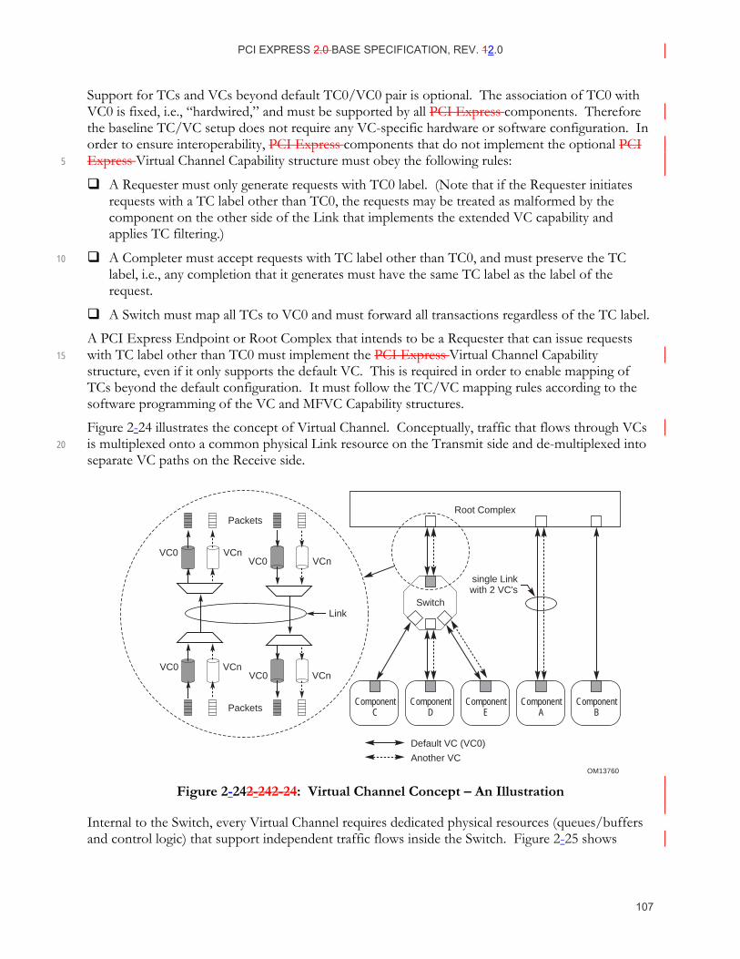
PCI EXPRESS 2.0 BASE SPECIFICATION, REV. 12.0
107
Support for TCs and VCs beyond default TC0/VC0 pair is optional. The association of TC0 with VC0 is fixed, i.e., “hardwired,” and must be supported by all PCI Express components. Therefore the baseline TC/VC setup does not require any VC-specific hardware or software configuration. In order to ensure interoperability, PCI Express components that do not implement the optional PCI Express Virtual Channel Capability structure must obey the following rules: 5
A Requester must only generate requests with TC0 label. (Note that if the Requester initiates requests with a TC label other than TC0, the requests may be treated as malformed by the component on the other side of the Link that implements the extended VC capability and applies TC filtering.)
A Completer must accept requests with TC label other than TC0, and must preserve the TC 10 label, i.e., any completion that it generates must have the same TC label as the label of the request.
A Switch must map all TCs to VC0 and must forward all transactions regardless of the TC label.
A PCI Express Endpoint or Root Complex that intends to be a Requester that can issue requests with TC label other than TC0 must implement the PCI Express Virtual Channel Capability 15 structure, even if it only supports the default VC. This is required in order to enable mapping of TCs beyond the default configuration. It must follow the TC/VC mapping rules according to the software programming of the VC and MFVC Capability structures.
Figure 2-24 illustrates the concept of Virtual Channel. Conceptually, traffic that flows through VCs is multiplexed onto a common physical Link resource on the Transmit side and de-multiplexed into 20 separate VC paths on the Receive side.
OM13760
ComponentC
ComponentD
ComponentE
ComponentA
ComponentB
Switch
Default VC (VC0)
Another VC
Root Complex
single Linkwith 2 VC's
Packets
Packets
VC0 VCn
VC0 VCn
Link
VC0 VCn
VC0 VCn
Figure 2-242-24 2-24: Virtual Channel Concept – An Illustration
Internal to the Switch, every Virtual Channel requires dedicated physical resources (queues/buffers and control logic) that support independent traffic flows inside the Switch. Figure 2-25 shows
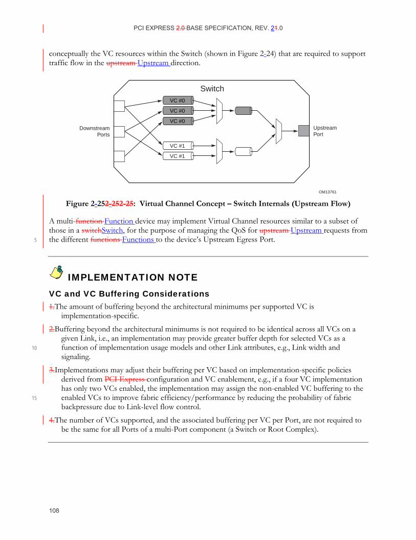
PCI EXPRESS 2.0 BASE SPECIFICATION, REV. 21.0
108
conceptually the VC resources within the Switch (shown in Figure 2-24) that are required to support traffic flow in the upstream Upstream direction.
OM13761
VC #0
VC #0
VC #0
VC #1
VC #1
UpstreamPort
DownstreamPorts
Switch
Figure 2-252-25 2-25: Virtual Channel Concept – Switch Internals (Upstream Flow)
A multi-function Function device may implement Virtual Channel resources similar to a subset of those in a switchSwitch, for the purpose of managing the QoS for upstream Upstream requests from the different functions Functions to the device’s Upstream Egress Port. 5
IMPLEMENTATION NOTE VC and VC Buffering Considerations 1.The amount of buffering beyond the architectural minimums per supported VC is
implementation-specific.
2.Buffering beyond the architectural minimums is not required to be identical across all VCs on a given Link, i.e., an implementation may provide greater buffer depth for selected VCs as a function of implementation usage models and other Link attributes, e.g., Link width and 10 signaling.
3.Implementations may adjust their buffering per VC based on implementation-specific policies derived from PCI Express configuration and VC enablement, e.g., if a four VC implementation has only two VCs enabled, the implementation may assign the non-enabled VC buffering to the enabled VCs to improve fabric efficiency/performance by reducing the probability of fabric 15 backpressure due to Link-level flow control.
4.The number of VCs supported, and the associated buffering per VC per Port, are not required to be the same for all Ports of a multi-Port component (a Switch or Root Complex).
PCI EXPRESS 2.0 BASE SPECIFICATION, REV. 12.0
109
2.5.1. Virtual Channel Identification (VC ID)
Individual PCI Express Ports on a Root Complex, Switch, or DevicePCI Express Ports can support 1-8 Virtual Channels – each Port is independently configured/managed therefore allowing implementations to vary the number of VCs supported per Port based on usage model-specific requirements. These VCs are uniquely identified using the Virtual Channel Identification (VC ID) mechanism. 5
Note that while DLLPs contain VC ID information for Flow Control accounting, TLPs do not. The association of TLPs with VC ID for the purpose of Flow Control accounting is done at each Port of the Link using TC to VC mapping as discussed in Section 2.5.2.
All PCI Express Ports that support more than VC0 must provide at least one VC Capability structure according to the definition in Section 7.11. A multi-function Function device is permitted 10 to implement the MFVC Capability structure, as defined in Section 7.18. Providing these extended structures are optional for Ports that support only the default TC0/VC0 configuration. PCI Express cConfiguration software is responsible for configuring Ports on both sides of the Link for a matching number of VCs. This is accomplished by scanning the PCI Express hierarchy and using VC or MFVC Capability registers associated with Ports (that support more than default VC0) to 15 establish the number of VCs for the Link. Rules for assigning VC ID to VC hardware resources within a PCI Express Port are as follows:
VC ID assignment must be unique per PCI Express Port – The same VC ID cannot be assigned to different VC hardware resources within the same Port.
VC ID assignment must be the same (matching in the terms of numbers of VCs and their IDs) 20 for the two PCI Express Ports on both sides of a PCI Express Link.
If a multi-function Function device implements an MFVC Capability structure, its VC hardware resources are distinct from the VC hardware resources associated with any VC Capability structures of its Functions. The VC ID uniqueness requirement (first bullet above) still applies individually for the MVFC and any VC Capability structures. In addition, the VC ID cross-25 linkLink matching requirement (second bullet above) applies for the MFVC Capability structure, but not the VC Capability structures of the Functions.
VC ID 0 is assigned and fixed to the default VC.
2.5.2. TC to VC Mapping
Every Traffic Class that is supported must be mapped to one of the Virtual Channels. The mapping of TC0 to VC0 is fixed. 30
The mapping of TCs other than TC0 is system software specific. However, the mapping algorithm must obey the following rules:
One or multiple TCs can be mapped to a VC.
One TC must not be mapped to multiple VCs in any PCI Express Port or Endpoint Function.
TC/VC mapping must be identical for PCI Express Ports on both sides of a PCI Express Link. 35
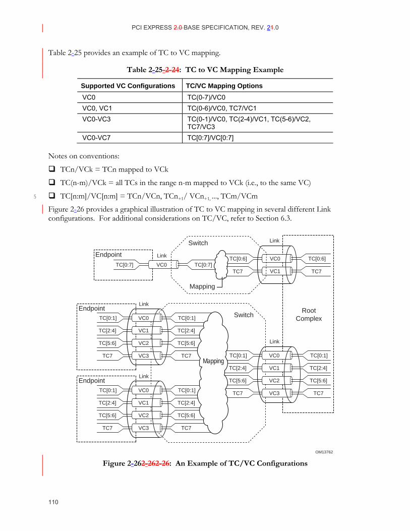
PCI EXPRESS 2.0 BASE SPECIFICATION, REV. 21.0
110
Table 2-25 provides an example of TC to VC mapping.
Table 2-25- 2-24: TC to VC Mapping Example
Supported VC Configurations TC/VC Mapping Options VC0 TC(0-7)/VC0 VC0, VC1 TC(0-6)/VC0, TC7/VC1 VC0-VC3 TC(0-1)/VC0, TC(2-4)/VC1, TC(5-6)/VC2,
TC7/VC3 VC0-VC7 TC[0:7]/VC[0:7]
Notes on conventions:
TCn/VCk = TCn mapped to VCk
TC(n-m)/VCk = all TCs in the range n-m mapped to VCk (i.e., to the same VC)
TC[n:m]/VC[n:m] = TCn/VCn, TCn+1/ VCn+1, ..., TCm/VCm 5
Figure 2-26 provides a graphical illustration of TC to VC mapping in several different Link configurations. For additional considerations on TC/VC, refer to Section 6.3.
OM13762
VC0
VC1
VC2
VC3
TC[0:1]
TC[2:4]
TC[5:6]
TC7
TC[0:1]
TC[2:4]
TC[5:6]
TC7
Endpoint
Endpoint
Link
VC0TC[0:7] TC[0:7]
Link
Switch
Switch
VC0
VC1
VC2
VC3
TC[0:1]
TC[2:4]
TC[5:6]
TC7
TC[0:1]
TC[2:4]
TC[5:6]
TC7
EndpointLink
VC0
VC1
VC2
VC3
TC[0:1]
TC[2:4]
TC[5:6]
TC7
TC[0:1]
TC[2:4]
TC[5:6]
TC7
Link
VC0
VC1
TC[0:6]
TC7
TC[0:6]
TC7
Link
Mapping
RootComplex
Mapping
Figure 2-262-26 2-26: An Example of TC/VC Configurations
PCI EXPRESS 2.0 BASE SPECIFICATION, REV. 12.0
111
2.5.3. VC and TC Rules
Here is a summary of key rules associated with the TC/VC mechanism:
All PCI Express devices must support the general purpose I/O Traffic Class, i.e., TC0 and must implement the default VC0.
Each Virtual Channel (VC) has independent Flow Control. 5
There are no ordering relationships required between different TCs
There are no ordering relationships required between different VCs
A Switch’s peer-to-peer capability applies to all Virtual Channels supported by the Switch.
A multi-function Function device’s peer-to-peer capability between different functions Functions applies to all Virtual Channels supported by the multi-function Function device. 10
Transactions with a TC that is not mapped to any enabled VC in an PCI Express Ingress Port are treated as malformed Malformed transactions TLPs by the receiving device.
For Switches, transactions with a TC that is not mapped to any of the enabled VCs in the target Egress Port are treated as malformed Malformed TLPs.
For a Root Port, transactions with a TC that is not mapped to any of the enabled VCs in the 15 target RCRB are treated as malformed Malformed TLPs.
For multi-function Function devices with an MFVC Capability structure, any transaction with a TC that is not mapped to an enabled VC in the MFVC Capability structure is treated as a malformed Malformed TLP.
Switches must support independent TC/VC mapping configuration for each Port. 20
A Root Complex must support independent TC/VC mapping configuration for each RCRB, the associated Root Ports, and any Root Complex Integrated Endpoints.
For more details on the VC and TC mechanisms, including configuration, mapping, and arbitration, refer to Section 6.3.
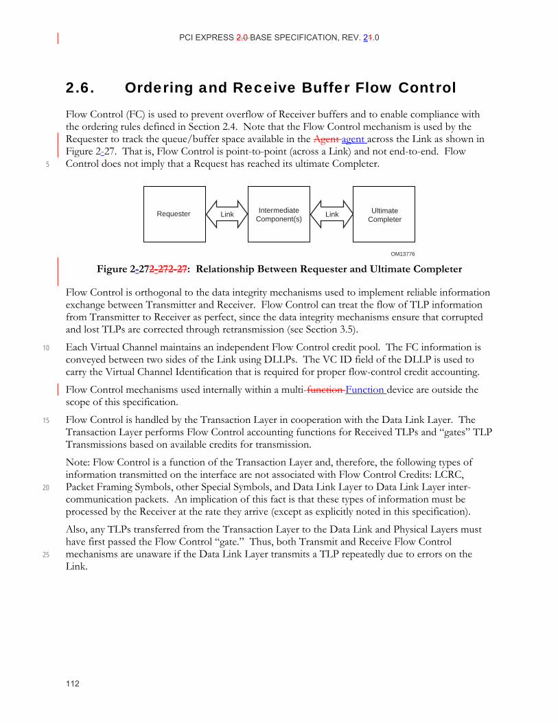
PCI EXPRESS 2.0 BASE SPECIFICATION, REV. 21.0
112
2.6. Ordering and Receive Buffer Flow Control Flow Control (FC) is used to prevent overflow of Receiver buffers and to enable compliance with the ordering rules defined in Section 2.4. Note that the Flow Control mechanism is used by the Requester to track the queue/buffer space available in the Agent agent across the Link as shown in Figure 2-27. That is, Flow Control is point-to-point (across a Link) and not end-to-end. Flow Control does not imply that a Request has reached its ultimate Completer. 5
OM13776
Link LinkRequester IntermediateComponent(s)
UltimateCompleter
Figure 2-272-27 2-27: Relationship Between Requester and Ultimate Completer
Flow Control is orthogonal to the data integrity mechanisms used to implement reliable information exchange between Transmitter and Receiver. Flow Control can treat the flow of TLP information from Transmitter to Receiver as perfect, since the data integrity mechanisms ensure that corrupted and lost TLPs are corrected through retransmission (see Section 3.5).
Each Virtual Channel maintains an independent Flow Control credit pool. The FC information is 10 conveyed between two sides of the Link using DLLPs. The VC ID field of the DLLP is used to carry the Virtual Channel Identification that is required for proper flow-control credit accounting.
Flow Control mechanisms used internally within a multi-function Function device are outside the scope of this specification.
Flow Control is handled by the Transaction Layer in cooperation with the Data Link Layer. The 15 Transaction Layer performs Flow Control accounting functions for Received TLPs and “gates” TLP Transmissions based on available credits for transmission.
Note: Flow Control is a function of the Transaction Layer and, therefore, the following types of information transmitted on the interface are not associated with Flow Control Credits: LCRC, Packet Framing Symbols, other Special Symbols, and Data Link Layer to Data Link Layer inter-20 communication packets. An implication of this fact is that these types of information must be processed by the Receiver at the rate they arrive (except as explicitly noted in this specification).
Also, any TLPs transferred from the Transaction Layer to the Data Link and Physical Layers must have first passed the Flow Control “gate.” Thus, both Transmit and Receive Flow Control mechanisms are unaware if the Data Link Layer transmits a TLP repeatedly due to errors on the 25 Link.
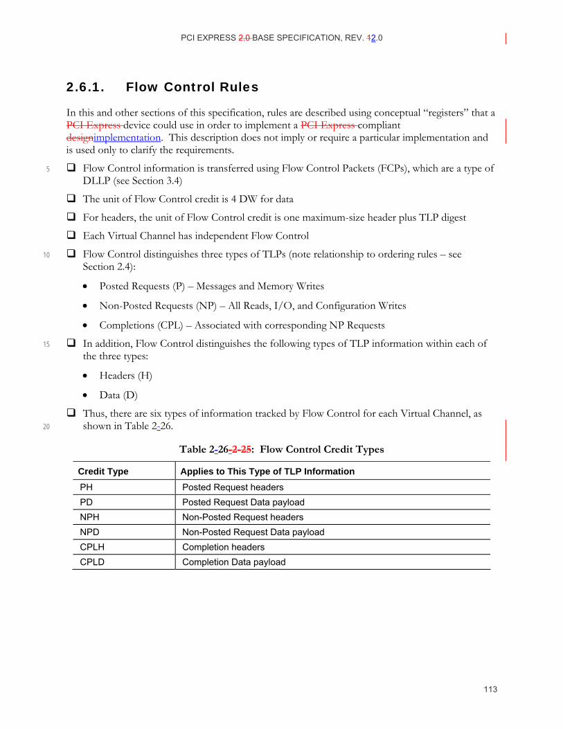
PCI EXPRESS 2.0 BASE SPECIFICATION, REV. 12.0
113
2.6.1. Flow Control Rules
In this and other sections of this specification, rules are described using conceptual “registers” that a PCI Express device could use in order to implement a PCI Express compliant designimplementation. This description does not imply or require a particular implementation and is used only to clarify the requirements.
Flow Control information is transferred using Flow Control Packets (FCPs), which are a type of 5 DLLP (see Section 3.4)
The unit of Flow Control credit is 4 DW for data
For headers, the unit of Flow Control credit is one maximum-size header plus TLP digest
Each Virtual Channel has independent Flow Control
Flow Control distinguishes three types of TLPs (note relationship to ordering rules – see 10 Section 2.4):
• Posted Requests (P) – Messages and Memory Writes
• Non-Posted Requests (NP) – All Reads, I/O, and Configuration Writes
• Completions (CPL) – Associated with corresponding NP Requests
In addition, Flow Control distinguishes the following types of TLP information within each of 15 the three types:
• Headers (H)
• Data (D)
Thus, there are six types of information tracked by Flow Control for each Virtual Channel, as shown in Table 2-26. 20
Table 2-26- 2-25: Flow Control Credit Types
Credit Type Applies to This Type of TLP Information PH Posted Request headers PD Posted Request Data payload NPH Non-Posted Request headers NPD Non-Posted Request Data payload CPLH Completion headers CPLD Completion Data payload
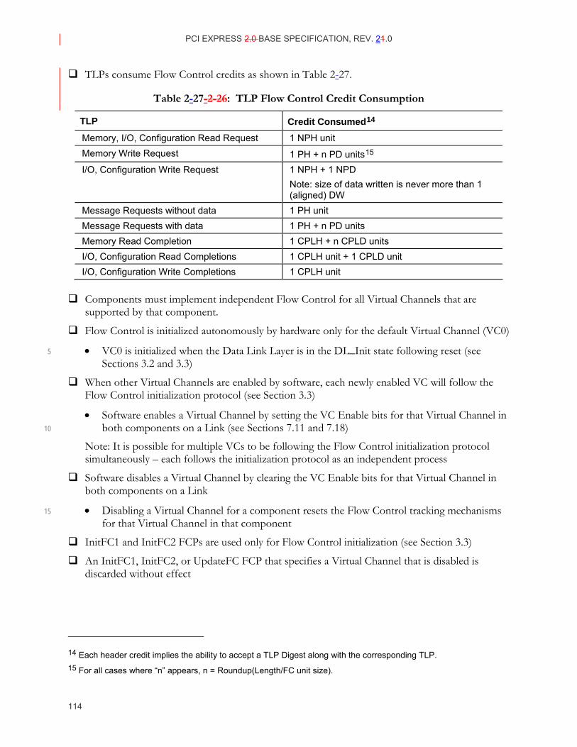
PCI EXPRESS 2.0 BASE SPECIFICATION, REV. 21.0
114
TLPs consume Flow Control credits as shown in Table 2-27.
Table 2-27- 2-26: TLP Flow Control Credit Consumption
TLP Credit Consumed14 Memory, I/O, Configuration Read Request 1 NPH unit Memory Write Request 1 PH + n PD units15 I/O, Configuration Write Request 1 NPH + 1 NPD
Note: size of data written is never more than 1 (aligned) DW
Message Requests without data 1 PH unit Message Requests with data 1 PH + n PD units Memory Read Completion 1 CPLH + n CPLD units I/O, Configuration Read Completions 1 CPLH unit + 1 CPLD unit I/O, Configuration Write Completions 1 CPLH unit
Components must implement independent Flow Control for all Virtual Channels that are supported by that component.
Flow Control is initialized autonomously by hardware only for the default Virtual Channel (VC0)
• VC0 is initialized when the Data Link Layer is in the DL_Init state following reset (see 5 Sections 3.2 and 3.3)
When other Virtual Channels are enabled by software, each newly enabled VC will follow the Flow Control initialization protocol (see Section 3.3)
• Software enables a Virtual Channel by setting the VC Enable bits for that Virtual Channel in both components on a Link (see Sections 7.11 and 7.18) 10
Note: It is possible for multiple VCs to be following the Flow Control initialization protocol simultaneously – each follows the initialization protocol as an independent process
Software disables a Virtual Channel by clearing the VC Enable bits for that Virtual Channel in both components on a Link
• Disabling a Virtual Channel for a component resets the Flow Control tracking mechanisms 15 for that Virtual Channel in that component
InitFC1 and InitFC2 FCPs are used only for Flow Control initialization (see Section 3.3)
An InitFC1, InitFC2, or UpdateFC FCP that specifies a Virtual Channel that is disabled is discarded without effect
14 Each header credit implies the ability to accept a TLP Digest along with the corresponding TLP. 15 For all cases where “n” appears, n = Roundup(Length/FC unit size).

PCI EXPRESS 2.0 BASE SPECIFICATION, REV. 12.0
115
During FC initialization for any Virtual Channel, including the default VC initialized as a part of Link initialization, Receivers must initially advertise VC credit values equal to or greater than those shown in Table 2-28.
•Components may optionally check for violations of this rule. If a component implementing this check determines a violation of this rule, the violation is a Flow Control Protocol Error 5 (FCPE)
♦If checked, this is a reported error associated with the Receiving Port (see Section 6.2)
Table 2-28- 2-27: Minimum Initial Flow Control Advertisements16
Credit Type Minimum Advertisement PH 1 unit – credit value of 01h PD Largest possible setting of the Max_Payload_Size for the
component divided by FC Unit Size. For a multi-function Function device, this includes all functions Functions in the device. Example: If the largest Max_Payload_Size value supported is 1024 bytes, the smallest permitted initial credit value would be 040h.
NPH 1 unit – credit value of 01h NPD 1 unit – credit value of 01h CPLH Root Complex (supporting peer-to-peer traffic between all Root
Ports) and Switch: 1 FC unit - credit value of 01h Root Complex (not supporting peer-to-peer traffic between all Root Ports) and Endpoint: infinite FC units - initial credit value of all 0s17
CPLD Root Complex (supporting peer-to-peer traffic between all Root Ports) and Switch: Largest possible setting of the Max_Payload_Size for the component divided by FC Unit Size., or the size of the largest Read Request the component will ever generate, whichever is smaller. Root Complex (not supporting peer-to-peer traffic between all Root Ports) and Endpoint: infinite FC units - initial credit value of all 0s
A Root Complex that does not support peer-to-peer traffic between all Root Ports must advertise infinite Completion credits.
A Root Complex that supports peer-to-peer traffic between all Root Ports may optionally 10 advertise non-infinite Completion credits. In this case, the Root Complex must ensure that deadlocks are avoided and forward progress is maintained for completions directed towards the Root Complex. Note that temporary stalls of completion traffic (due to a temporary lack of
16 PCI Express to PCI/PCI-X Bridge requirements are addressed in the PCI Express to PCI/PCI-X Bridge Specification, Revision 1.0. 17 This value is interpreted as infinite by the Transmitter, which will, therefore, never throttle.
PCI EXPRESS 2.0 BASE SPECIFICATION, REV. 21.0
116
credit) are possible since Non-Posted requests forwarded by the RC may not have explicitly allocated completion buffer space.
A Receiver must never cumulatively issue more than 2047 outstanding unused credits to the Transmitter for data payload or 127 for header.
• Components may optionally check for violations of this rule. If a component implementing 5 this check determines a violation of this rule, the violation is a Flow Control Protocol Error (FCPE).
♦ If checked, this is a reported error associated with the Receiving Port (see Section 6.2)
If an Infinite Credit advertisement (value of 00h or 000h) has been made during initialization, no Flow Control updates are required following initialization. 10
• If UpdateFC DLLPs are sent, the credit value fields must be set to zero and must be ignored by the Receiver. The Receiver may optionally check for non-zero update values (in violation of this rule). If a component implementing this check determines a violation of this rule, the violation is a Flow Control Protocol Error (FCPE)
♦ If checked, this is a reported error associated with the Receiving Port (see Section 6.2) 15
If only the Data or header advertisement (but not both) for a given type (N, NP, or CPL) has been made with infinite credits during initialization, the transmission of UpdateFC DLLPs is still required, but the credit field corresponding to the Data/header (advertised as infinite) must be set to zero and must be ignored by the Receiver.
• The Receiver may optionally check for non-zero update values (in violation of this rule). If a 20 Receiver implementing this check determines a violation of this rule, the violation is a Flow Control Protocol Error (FCPE)
♦ If checked, this is a reported error associated with the Receiving Port (see Section 6.2)
A received TLP using a VC that is not enabled is a Malformed TLP
• VC0 is always enabled 25
• For VCs 1-7, a VC is considered enabled when the corresponding VC Enable bit in the VC Resource Control register has been set to 1b, and once FC negotiation for that VC has exited the FC_INIT1 state and progressed to the FC_INIT2 state (see Section 3.3)
• This is a reported error associated with the Receiving Port (see Section 6.2)
TLP transmission using any VC 0-7 is not permitted until initialization for that VC has 30 completed by exiting FC_INIT2 state
For VCs 1-7, software must use the VC Negotiation Pending bit in the VC Resource Status register to ensure that a VC is not used until negotiation has completed by exiting the FC_INIT2 state in both components on a linkLink.
PCI EXPRESS 2.0 BASE SPECIFICATION, REV. 12.0
117
2.6.1.1. FC Information Tracked by Transmitter
For each type of information tracked, there are two quantities tracked for Flow Control TLP Transmission gating:
• CREDITS_CONSUMED
♦ Count of the total number of FC units consumed by TLP Transmissions made since Flow Control initialization, modulo 2[Field Size] (where [Field Size] is 8 for PH, NPH, and 5 CPLH and 12 for PD, NPD and CPLD).
♦ Set to all 0’s at interface initialization
♦ Updated for each TLP the Transaction Layer allows to pass the Flow Control gate for Transmission
Updated as shown: 10
CREDITS_CONSUMED :=
(CREDITS_CONSUMED + Increment) mod 2[Field Size]
Where Increment is the size in FC credits of the corresponding part of the TLP passed through the gate, and [Field Size] is 8 for PH, NPH, and CPLH and 12 for PD, NPD, and CPLD 15
• CREDIT_LIMIT
♦ The most recent number of FC units legally advertised by the Receiver. This quantity represents the total number of FC credits made available by the Receiver since Flow Control initialization, , modulo 2[Field Size] (where [Field Size] is 8 for PH, NPH, and CPLH and 12 for PD, NPD, and CPLD). 20
♦ Undefined at interface initialization
♦ Set to the value indicated during Flow Control initialization
♦ For each FC update received,
if CREDIT_LIMIT is not equal to the update value, set CREDIT_LIMIT to update value 25
The Transmitter gating function must determine if sufficient credits have been advertised to permit the transmission of a given TLP. If the Transmitter does not have enough credits to transmit the TLP, it must block the transmission of the TLP, possibly stalling other TLPs that are using the same Virtual Channel. The Transmitter must follow the ordering and deadlock avoidance rules specified in Section 2.4, which require that certain types of TLPs must bypass 30 other specific types of TLPs when the latter are blocked. Note that TLPs using different Virtual Channels have no ordering relationship, and must not block each other.
PCI EXPRESS 2.0 BASE SPECIFICATION, REV. 21.0
118
The Transmitter gating function test is performed as follows:
• For each required type of credit, the number of credits required is calculated as:
CUMULATIVE_CREDITS_REQUIRED =
(CREDITS_CONSUMED + <credit units required for pending TLP>) mod 2[Field Size] 5
• Unless CREDIT_LIMIT was specified as “infinite” during Flow Control initialization, the Transmitter is permitted to Transmit a TLP if, for each type of information in the TLP, the following equation is satisfied (using unsigned arithmetic):
(CREDIT_LIMIT – CUMULATIVE_CREDITS_REQUIRED) mod 2[Field Size] 10
<= 2[Field Size] / 2
If CREDIT_LIMIT was specified as “infinite” during Flow Control initialization, then the gating function is unconditionally satisfied for that type of credit.
Note that some types of Transactions require more than one type of credit. (For example, Memory Write requests require PH and PD credits.) 15
When accounting for credit use and return, information from different TLPs is never mixed within one credit.
When some TLP is blocked from Transmission by a lack of FC Credit, Transmitters must follow the ordering rules specified in Section 2.4 when determining what types of TLPs must be permitted to bypass the stalled TLP. 20
The return of FC credits for a Transaction must not be interpreted to mean that the Transaction has completed or achieved system visibility.
• Flow Control credit return is used for receive buffer management only, and Agents agents must not make any judgment about the Completion status or system visibility of a Transaction based on the return or lack of return of Flow Control information. 25
When a Transmitter sends a nullified TLP (with inverted LCRC and using EDB as the end Symbol), the Transmitter does not modify CREDITS_CONSUMED for that TLP (see Section 3.5.2.1)
2.6.1.2. FC Information Tracked by Receiver
For each type of information tracked, the following quantities are tracked for Flow Control TLP Receiver accounting: 30
• CREDITS_ALLOCATED
♦ Count of the total number of credits granted to the Transmitter since initialization, modulo 2[Field Size] (where [Field Size] is 8 for PH, NPH, and CPLH and 12 for PD, NPD and CPLD)
♦ Initially set according to the buffer size and allocation policies of the Receiver 35
♦ This value is included in the InitFC and UpdateFC DLLPs (see Section 3.4)
PCI EXPRESS 2.0 BASE SPECIFICATION, REV. 12.0
119
♦ Incremented as the Receiver Transaction Layer makes additional receive buffer space available by processing Received TLPs
Updated as shown:
CREDITS_ALLOCATED :=
(CREDITS_ALLOCATED + Increment) mod 2[Field Size] 5
Where Increment corresponds to the credits made available, and [Field Size] is 8 for PH, NPH, and CPLH and 12 for PD, NPD, and CPLD
• CREDITS_RECEIVED (Optional – for optional error check described below)
♦ Count of the total number of FC units consumed by valid TLPs Received since Flow Control initialization, modulo 2[Field Size] (where [Field Size] is 8 for PH, NPH, and CPLH 10 and 12 for PD, NPD and CPLD)
♦ Set to all 0’s at interface initialization
♦ Updated as shown:
CREDITS_RECEIVED :=
(CREDITS_ RECEIVED + Increment) mod 2[Field Size] 15
(Where Increment corresponds to the credits made available, and [Field Size] is 8 for PH, NPH, and CPLH and 12 for PD, NPD, and CPLD)
for each Received TLP, provided that TLP:
passes the Data Link Layer integrity checks
is not malformed or (optionally ) is malformed and is not ambiguous with respect to 20 which buffer to release and is mapped to an initialized virtual Virtual channelChannel
does not consume more credits than have been allocated (see following rule)
If a Receiver implements the CREDITS_RECEIVED counter, then when a nullified TLP (with inverted LCRC and using EDB as the end Symbol) is received, the Receiver does not modify CREDITS_RECEIVED for that TLP (see Section 3.5.2.1) 25
A Receiver may optionally check for Receiver Overflow errors (TLPs exceeding CREDITS_ALLOCATED), by checking the following equation, using unsigned arithmetic:
(CREDITS_ALLOCATED - CREDITS_RECEIVED) mod 2[Field Size]
>= 2[Field Size] /2
If the check is implemented and this equation evaluates as true, the Receiver must: 30
• discard the TLP(s) without modifying the CREDITS_RECEIVED
• de-allocate any resources which it had allocated for the TLP(s)
If checked, this is a reported error associated with the Receiving Port (see Section 6.2)
PCI EXPRESS 2.0 BASE SPECIFICATION, REV. 21.0
120
Note: Following a Receiver Overflow error, Receiver behavior is undefined, but it is encouraged that the Receiver continues to operate, processing Flow Control updates and accepting any TLPs which do not exceed allocated credits.
For non-infinite NPH, NPD, PH, and CPLH types, an UpdateFC FCP must be scheduled for Transmission each time the following sequence of events occurs: 5
• all advertised FC units for a particular type of credit are consumed by TLPs received
• one or more units of that type are made available by TLPs processed
For non-inifinite PD and CPLD types, when the number of available credits is less than Max_Payload_Size, an UpdateFC FCP must be scheduled for Transmission each time one or more units of that type are made available by TLPs processed 10
• For a multi-function Function device whose Max_Payload_Size settings are identical across all functionsFunctions, the common Max_Payload_Size setting or larger must be used.
• For a multi-function Function device whose Max_Payload_Size settings are not identical across all functionsFunctions, the selected Max_Payload_Size setting is implementation specific, but it’ is recommended to use the largest Max_Payload_Size setting across all 15 functionsFunctions.
UpdateFC FCPs may be scheduled for Transmission more frequently than is required
When the Link is in the L0 or L0s Link state, Update FCPs for each enabled type of non-infinite FC credit must be scheduled for transmission at least once every 30 μs (-0%/+50%), except when the Extended Sync bit of the Control Link register is set, in which 20 case the limit is 120 μs (-0%/+50%).
• A timeout mechanism may optionally be implemented. If implemented, such a mechanism must:
♦ be active only when the Link is in the L0 or L0s Link state
♦ use a timer with a limit of 200 μs (-0%/+50%), where the timer is reset by the receipt of 25 any Init or Update FCP. Alternately, the timer may be reset by the receipt of any DLLP (See see Section 3.4)
♦ upon timer expiration, instruct the Physical Layer to retrain the Link (via the LTSSM Recovery state, Section 4.2.6.4)
♦ if an Infinite Credit advertisement has been made during initialization for all three Flow 30 Control classes, this timeout mechanism must be disabled
Note: The implementation of this optional mechanism is strongly encouraged. It is anticipated that future revisions of this specification may change this mechanism from optional to required.
PCI EXPRESS 2.0 BASE SPECIFICATION, REV. 12.0
121
IMPLEMENTATION NOTE Use of “Infinite” FC Advertisement For a given implementation it is possible that not all of the queue types need to be physically implemented in hardware for all Virtual Channels. For example, since Non-Posted Writes are only allowed on Virtual Channel 0, there is no need to implement a Non-Posted Data queue for Virtual Channels other than VC0. For unimplemented queues, the Receiver can eliminate the need to present the appearance of tracking Flow Control credits by advertising infinite Flow Control credits 5 during initialization.
IMPLEMENTATION NOTE
Flow Control Update Frequency For components subject to receiving streams of TLPs, it is desirable to implement receive buffers larger than the minimum size required to prevent Transmitter throttling due to lack of available credits. Likewise, UpdateFC FCPs must be returned such that the time required to send, receive and process the UpdateFC is sufficient. Table 2-29 and Table 2-30 shows recommended values for the 10 frequency of transmission during normal operation based on Link Width and Max_Payload_Size values for operation in 2.5 GT/s mode and 5.0 GT/s mode, respectively. Note that the values given in Table 2-29 and Table 2-30 do not account for any delays caused by the Receiver or Transmitter being in L0s. For improved performance and/or power-saving, it may be desirable to use a Flow Control update policy that is more sophisticated than a simple timer. Any such policy is 15 implementation specific, and beyond the scope of this document. The values are calculated as a function of the largest TLP payload size and Link width. The values are measured at the Port of the TLP Receiver, starting with the time the last Symbol of a TLP in received to the first Symbol of the UpdateFC DLLP being transmitted. The values are calculated using the formula: 20
( ) layInternalDeLinkWidth
FactorUpdatedTLPOverheaSizePayloadMax+
+ *__
where: Max_Payload_Size The value in the Max_Payload_Size field of the Device Control
register. For a multi-function Function device, it is recommended that the smallest Max_Payload_Size setting across all functions 25 Functions is used.
TLP Overhead Represents the additional TLP components which consume Link bandwidth (header, LCRC, framing Symbols) and is treated here as a constant value of 28 Symbols
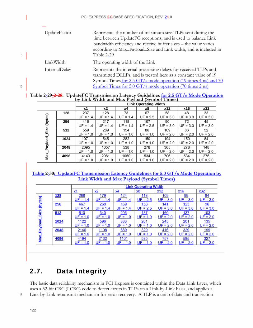
PCI EXPRESS 2.0 BASE SPECIFICATION, REV. 21.0
122
UpdateFactor Represents the number of maximum size TLPs sent during the time between UpdateFC receptions, and is used to balance Link bandwidth efficiency and receive buffer sizes – the value varies according to Max_Payload_Size and Link width, and is included in Table 2-29 5
LinkWidth The operating width of the Link InternalDelay Represents the internal processing delays for received TLPs and
transmitted DLLPs, and is treated here as a constant value of 19 Symbol Times for 2.5 GT/s mode operation (19 times 4 ns) and 70 Symbol Times for 5.0 GT/s mode operation (70 times 2 ns) 10
Table 2-29- 2-28: UpdateFC Transmission Latency Guidelines for 2.5 GT/s Mode Operation
by Link Width and Max Payload (Symbol Times) Link Operating Width
x1 x2 x4 x8 x12 x16 x32 128 237
UF = 1.4 128
UF = 1.4 73
UF = 1.4 67
UF = 2.5 58
UF = 3.0 48
UF = 3.0 33
UF = 3.0 256 416
UF = 1.4 217
UF = 1.4 118
UF = 1.4 107
UF = 2.5 90
UF = 3.0 72
UF = 3.0 45
UF = 3.0 512 559
UF = 1.0 289
UF = 1.0 154
UF = 1.0 86
UF = 1.0 109
UF = 2.0 86
UF = 2.0 52
UF = 2.0 1024 1071
UF = 1.0 545
UF = 1.0 282
UF = 1.0 150
UF = 1.0 194
UF = 2.0 150
UF = 2.0 84
UF = 2.0 2048 2095
UF = 1.0 1057
UF = 1.0 538
UF = 1.0 278
UF = 1.0 365
UF = 2.0 278
UF = 2.0 148
UF = 2.0
Max
_Pay
load
_Siz
e (b
ytes
)
4096 4143 UF = 1.0
2081 UF = 1.0
1050 UF = 1.0
534 UF = 1.0
706 UF = 2.0
534 UF = 2.0
276 UF = 2.0
Table 2-30: UpdateFC Transmission Latency Guidelines for 5.0 GT/s Mode Operation by Link Width and Max Payload (Symbol Times)
Link Operating Width x1 x2 x4 x8 x12 x16 x32
128 288 UF = 1.4
179 UF = 1.4
124 UF = 1.4
118 UF = 2.5
109 UF = 3.0
99 UF = 3.0
84 UF = 3.0
256 467 UF = 1.4
268 UF = 1.4
169 UF = 1.4
158 UF = 2.5
141 UF = 3.0
123 UF = 3.0
96 UF = 3.0
512 610 UF = 1.0
340 UF = 1.0
205 UF = 1.0
137 UF = 1.0
160 UF = 2.0
137 UF = 2.0
103 UF = 2.0
1024 1122 UF = 1.0
596 UF = 1.0
333 UF = 1.0
201 UF = 1.0
245 UF = 2.0
201 UF = 2.0
135 UF = 2.0
2048 2146 UF = 1.0
1108 UF = 1.0
589 UF = 1.0
329 UF = 1.0
416 UF = 2.0
329 UF = 2.0
199 UF = 2.0
Max
_Pay
load
_Siz
e (b
ytes
)
4096 4194 UF = 1.0
2132 UF = 1.0
1101 UF = 1.0
585 UF = 1.0
757 UF = 2.0
585 UF = 2.0
327 UF = 2.0
2.7. Data Integrity The basic data reliability mechanism in PCI Express is contained within the Data Link Layer, which uses a 32-bit CRC (LCRC) code to detect errors in TLPs on a Link-by-Link basis, and applies a Link-by-Link retransmit mechanism for error recovery. A TLP is a unit of data and transaction 15
PCI EXPRESS 2.0 BASE SPECIFICATION, REV. 12.0
123
control that is created by a data-source at the “edge” of the PCI Express domain (such as an Endpoint or Root Complex), potentially routed through intermediate components (i.e., Switches) and consumed by the ultimate PCI Express recipient. As a TLP passes through a Switch, the Switch may need to change some control fields without modifying other fields that should not change as the packet traverses the path. Therefore, the LCRC is regenerated by Switches. Data corruption 5 may occur internally to the Switch, and the regeneration of a good LCRC for corrupted data masks the existence of errors. To ensure end-to-end data integrity detection in systems that require high data reliability, a Transaction Layer end-to-end 32-bit CRC (ECRC) can be placed in the TLP Digest field at the end of a TLP. The ECRC covers all fields that do not change as the TLP traverses the path (invariant fields). The ECRC is generated by the Transaction Layer in the source component, 10 and checked (if supported) in by the destination componentultimate PCI Express Receiver and optionally by intermediate Receivers. A Switch that supports ECRC checking must checks ECRC on TLPs that are destined to a destination withintargeting the Switch itself. Such a Switch can optionally check ECRC on TLPs that it forwards. On all other TLPs a that the Switch forwards, the Switch must preserve the ECRC (forward it untouched) as an integral part of the TLP, regardless of 15 whether the Switch checks the ECRC or if the ECRC check fails.
In some cases, the data in a TLP payload is known to be corrupt at the time the TLP is generated, or may become corrupted while passing through an intermediate component, such as a Switch. In these cases, error forwarding, also known as data poisoning, can be used to indicate the corruption to the device consuming the data. 20
2.7.1. ECRC Rules
The capability to generate and check ECRC is reported to software, and the ability to do so is enabled by software (see Section 7.10.7).
If a device Function is enabled to generate ECRC, it must calculate and apply ECRC for all TLPs originated by the deviceFunction
Switches must pass TLPs with ECRC unchanged from the Ingress Port to the Egress Port 25
If a device supports ECRC generation/checking, at least one of its Functions must supportIf a device reports the capability to check ECRC, it must support Advanced Error Reporting (see Section 6.2)
If a device Function is enabled to check ECRC, it must do so for all TLPs received by the device including ECRCwith ECRC where the device is the ultimate PCI Express Receiver 30
• Note that it is still possible for the device Function to receive TLPs without ECRC, and these are processed normally – this is not an error
Note that a Switch may optionally perform ECRC checking on TLPs passing through the Switch. ECRC Errors detected by the Switch are reported as described in Table 6-4, but do not alter the TLPs’ passage through the Switch. 35
A 32-bit ECRC is calculated for the entire TLP (header and data payload) using the following algorithm and appended to the end of the TLP (see Figure 2-3):
The ECRC value is calculated using the following algorithm (see Figure 2-28).
The polynomial used has coefficients expressed as 04C1 1DB7h
PCI EXPRESS 2.0 BASE SPECIFICATION, REV. 21.0
124
The seed value (initial value for ECRC storage registers) is FFFF FFFFh
All invariant fields of the TLP header and the entire data payload (if present) are included in the ECRC calculation, all bits in variant fields must be set to 1b for ECRC calculations.
• Bit 0 of the Type field is variant18
• The EP field is variant 5
• all other fields are invariant
ECRC calculation starts with bit 0 of byte 0 and proceeds from bit 0 to bit 7 of each byte of the TLP
The result of the ECRC calculation is complemented, and the complemented result bits are mapped into the 32-bit TLP Digest field as shown in Table 2-31. 10
18 Bit 0 of the Type field changes when a Configuration Request is changed from Type 1 to Type 0.
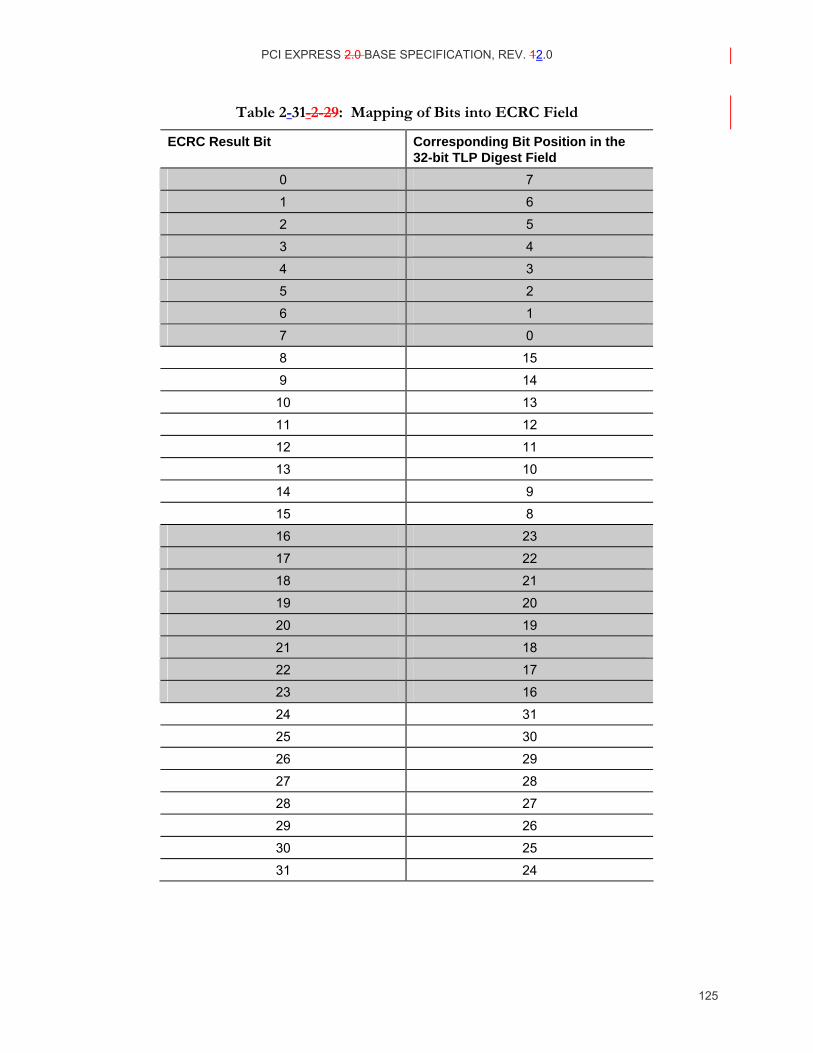
PCI EXPRESS 2.0 BASE SPECIFICATION, REV. 12.0
125
Table 2-31- 2-29: Mapping of Bits into ECRC Field
ECRC Result Bit Corresponding Bit Position in the 32-bit TLP Digest Field
0 7
1 6
2 5
3 4
4 3
5 2
6 1
7 0
8 15
9 14
10 13
11 12
12 11
13 10
14 9
15 8
16 23
17 22
18 21
19 20
20 19
21 18
22 17
23 16
24 31
25 30
26 29
27 28
28 27
29 26
30 25
31 24
PCI EXPRESS 2.0 BASE SPECIFICATION, REV. 21.0
126
The 32-bit ECRC value is placed in the TLP Digest field at the end of the TLP (see Figure 2-3)
For TLPs including a TLP Digest field used for an ECRC value, Receivers which support end-to-end data integrity checking, check the ECRC value in the TLP Digest field by:
• applying the same algorithm used for ECRC calculation (above) to the received TLP, not including the 32-bit TLP Digest field of the received TLP 5
• comparing the calculated result with the value in the TLP Digest field of the received TLP
Receivers which support end-to-end data integrity checks report violations as an ECRC Error. This reported error is associated with the receiving port Port (see Section 6.2).
How the ultimate PCI Express Receivers makes use of the end-to-end data integrity check provided through the ECRC is beyond the scope of this document. Intermediate Receivers are 10 still required to forward TLPs whose ECRC checks fail. A PCI Express-to-PCI/PCI-X Bridge is classified as an ultimate PCI Express Receiver with regard to ECRC checking.
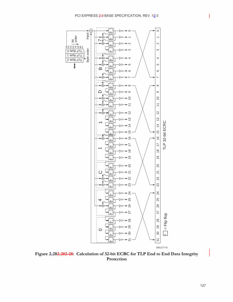
PCI EXPRESS 2.0 BASE SPECIFICATION, REV. 12.0
127
OM13777A
Inpu
t
bit
orde
r
Byt
e or
der
TLP Byte 2
TLP Byte 1
TLP Byte 0
01
23
45
67
89
1011
1213
1415
1617
1819
2021
2223
2425
2627
2829
3031
01
23
45
67
89
1011
1213
1415
16
TLP
32-
bit E
CR
C
1718
1920
2122
2324
2526
2728
2930
31
04
C1
1D
B7
0 1 2 3 4 5 6 7
>>
>>
>>
>>
>>
>>
>>
>>
>>
>>
>>
>>
>>
>>
>>
>>
>=
Flip
flop
Figure 2-282-28 2-28: Calculation of 32-bit ECRC for TLP End to End Data Integrity
Protection
PCI EXPRESS 2.0 BASE SPECIFICATION, REV. 21.0
128
IMPLEMENTATION NOTE
Protection of TD Bit Inside Switches It is of utmost importance that Switches insure and maintain the integrity of the TD bit in TLPs that they receive and forward (i.e., by applying a special internal protection mechanism), since corruption of the TD bit will cause the ultimate target device to misinterpret the presence or absence of the TLP digest field.
Similarly, it is highly recommended that Switches provide internal protection to other variant fields 5 in TLPs that they receive and forward, as the end-to-end integrity of variant fields is not sustained by the ECRC.
IMPLEMENTATION NOTE Data Link Layer Does Not Have Internal TLP Visibility Since the Data Link Layer does not process the TLP header (it determines the start and end of the TLP based on indications from the Physical Layer), it is not aware of the existence of the TLP Digest field, and simply passes it to the Transaction Layer as a part of the TLP. 10
2.7.2. Error Forwarding
Error Forwarding (also known as data poisoning), is indicated by setting the EP field to 1b. The rules for doing this are specified in Section 2.7.2.2. Here are some examples of cases where Error Forwarding might be used:
Example #1: A read from main memory encounters uncorrectable error
Example #2: Parity error on a PCI write to main memory 15
Example #3: Data integrity error on an internal data buffer or cache.
2.7.2.1. Error Forwarding Usage Model
Error Forwarding is only used for Read Completion Data or Write Data, never for the cases when the error is in the “header” (request phase, address/command, etc.). Requests/Completions with header errors cannot be forwarded in general since true destination cannot be positively known and, therefore, forwarding may cause direct or side effects such as 20 data corruption, system failures, etc.
Error Forwarding is used for controlled propagation of errors through the system, system diagnostics, etc.
PCI EXPRESS 2.0 BASE SPECIFICATION, REV. 12.0
129
Note that Error forwarding does not cause Link Layer Retry – Poisoned TLPs will be retried only if there are transmission errors on PCI Expressthe Link as determined by the TLP error detection mechanisms in the Data Link Layer.
• The Poisoned TLP may ultimately cause the originator of the request to re-issue it (at the Transaction Layer or above) in the case of read operation or to take some other action. 5 Such use of Error Forwarding information is beyond the scope of this specification.
2.7.2.2. Rules For Use of Data Poisoning
Support for TLP poisoning in a Transmitter is optional.
Data poisoning applies only to the data within a Write Request (Posted or Non-Posted) or a Read Completion.
• Poisoning of a TLP is indicated by a 1b value in the EP field 10
• Transmitters are permitted to set the EP field to 1b only for TLPs that include a data payload. The behavior of the receiver is not specified if the EP bit is set for any TLP that does not include a data payload.
If a Transmitter supports data poisoning, TLPs that are known to the Transmitter to include bad data must use the poisoning mechanism defined above. 15
Receipt of a Poisoned TLP is a reported error associated with the Receiving device/fFunction (see Section 6.2)
A Poisoned Configuration Write Request must be discarded by the Completer, and a Completion with a Completion Status of UR is returned (see Section 2.2.9).
• A Switch must route a Poisoned Configuration Write Request in the same way it would 20 route a non-Poisoned Configuration Write Request, unless the Request addresses the configuration spaceConfiguration Space of the Switch itself, in which case the Switch is the Completer for the Request and must follow the above rule.
A Poisoned I/O or Memory Write Request, or a Message with data (except for vendor-defined Messages), that addresses a control register or control structure in the Completer must be 25 handled as an Unsupported Request (UR) by the Completer (see Section 2.2.9).
• A Switch must route a Poisoned I/O or Memory Write Request or Message with data in the same way it would route the same Request if it were not poisoned, unless the Request addresses a control register or control structure of the Switch itself, in which case the Switch is the Completer for the Request and must follow the above rule. 30
For some applications it may be desirable for the Completer to use poisoned data in Write Requests which do not target control registers or control structures – such use is not forbidden. Similarly, it may be desirable for the Requester to use data marked poisoned in Completions – such use is also not forbidden. The appropriate use of poisoned information is application specific, and is not discussed in this document. 35
This document does not define any mechanism for determining which part or parts of the data payload of a Poisoned TLP are actually corrupt and which, if any, are not corrupt.
PCI EXPRESS 2.0 BASE SPECIFICATION, REV. 21.0
130
2.8. Completion Timeout Mechanism In any split transaction protocol, there is a risk associated with the failure of a Requester to receive an expected Completion. To allow Requesters to attempt recovery from this situation in a standard manner, the Completion Timeout mechanism is defined. This mechanism is intended to be activated only when there is no reasonable expectation that the Completion will be returned, and should never occur under normal operating conditions. Note that the values specified here do not 5 reflect expected service latencies, and must not be used to estimate typical response times.
PCI Express device Functions that issue Requests requiring Completions must implement the Completion Timeout mechanism. An exception is made for Configuration Requests (see below). The Completion Timeout mechanism is activated for each Request that requires one or more Completions when the Request is transmitted. Since PCI Express Switches do not autonomously 10 initiate Requests that need Completions, the requirement for Completion Timeout support is limited only to Root Complexes, PCI Express-PCI Bridges, and Endpoint devices.
The Completion Timeout mechanism may be disabled by configuration software. The Completion Timeout limit is set in the Completion Timeout Value field of the Device Control 2 register. Refer to Section 7.8.1600. This specification defines the following range for the minimum/maximum 15 acceptable timer values for the Completion Timeout mechanism:
The Completion Timeout timer must not expire (i.e., cause a timeout event) in less than 50 μs. It is strongly recommend that unless an application requires this level of timer granularity the minimum time should not expire in less than 10 ms.
The Completion Timeout timer must expire if a Request is not completed in 50 ms. 20
A Completion Timeout is a reported error associated with the Requestor Requester device/fFunction (see Section 6.2).
Note: A Memory Read Request for which there are multiple Completions must be considered completed only when all Completions have been received by the Requester. If some, but not all, requested data is returned before the Completion Timeout timer expires, the Requestor Requester is 25 permitted to keep or to discard the data that was returned prior to timer expiration.
Completion timeouts for Configuration Requests have special requirements for the support of PCI Express to PCI/PCI -Express bridges. PCI Express to PCI/PCI-X Bridges, by default, are not enabled to return Configuration Request Retry Status (CRS) for Configuration Requests to a PCI/PCI-X device behind the Bridge. This may result in lengthy completion delays that must be 30 comprehended by the Completion Timeout value in the Root Complex. System software may enable PCI Express to PCI/PCI-X Bridges to return Configuration Request Retry Status by setting the Bridge Configuration Retry Enable bit in the Device Control register, subject to the restrictions noted in the PCI Express to PCI/PCI-X Bridge Specification, Revision 1.0.
PCI EXPRESS 2.0 BASE SPECIFICATION, REV. 12.0
131
2.9. Link Status Dependencies
2.9.1. Transaction Layer Behavior in DL_Down Status
DL_Down status indicates that there is no connection with another component on the Link, or that the connection with the other component has been lost and is not recoverable by the Physical or Data Link Layers. This section specifies the Transaction Layer’s behavior when the Data Link Layer reports DL_Down status to the Transaction Layer, indicating that the Link is non-operational.
For a Port with DL_Down status, the Transaction Layer is not required to accept received TLPs 5 from the Data Link Layer, provided that these TLPs have not been acknowledged by the Data Link Layer. Such TLPs do not modify receive Flow Control credits.
For a Root Complex, or any Port on a Switch other than the one closest to the Root ComplexDownstream Port, DL_Down status is handled by:
initializing back to their default state any buffers or internal states associated with outstanding 10 requests transmitted downstreamDownstream
• Note: Port configuration registers must not be affected, except as required to update status associated with the transition to DL_Down
for Non-Posted Requests, forming completions for any Requests submitted by the device core for Transmission, returning Unsupported Request Completion Status, then discarding the 15 Requests
• This is a reported error associated with the device/fFunction for the (virtual) Bridge associated with the Port (see Section 6.2). For Root Ports, the reporting of this error is optional.
• Non-Posted Requests already being processed by the Transaction Layer, for which it may 20 not be practical to return Completions, are discarded
Note: This is equivalent to the case where the Request had been Transmitted but not yet Completed before the Link status became DL_Down
♦ These cases are handled by the Requester using the Completion Timeout mechanism
Note: The point at which a Non-Posted Request becomes “uncompletable” is implementation 25 specific.
The Port must terminate any PME Turn_Off handshake Requests targeting the Port in such a way that the Port is considered to have acknowledged the PME_Turn_Off request (see the Implementation Note in Section 5.3.3.2.1).
for all other Posted Requests, discarding the Requests 30
• This is a reported error associated with the device/fFunction for the (virtual) Bridge associated with the Port (see Section 6.2), and must be reported as an Unsupported Request. For Root Ports, the reporting of this error is optional.
PCI EXPRESS 2.0 BASE SPECIFICATION, REV. 21.0
132
• For a Posted Request already being processed by the Transaction Layer, the Port is permitted not to report it.
Note: This is equivalent to the case where the Request had been Transmitted before the Link status became DL_Down
Note: The point at which a Posted Request becomes “unreportable” is implementation specific. 5
discarding all Completions submitted by the device core for Transmission
For an Upstream Port on an Endpoint, and the Port on a Switch or Bridge that is closest to the Root Complex, DL_Down status is handled as a reset by:
returning all PCI Express-specific registers, state machines and externally observable state to the specified default or initial conditions (except for registers defined as sticky – see Section 7.4) 10
discarding all TLPs being processed
(for Switch and Bridge) propagating hot reset to all other Ports
2.9.2. Transaction Layer Behavior in DL_Up Status
DL_Up status indicates that a connection has been established with another component on the associated Link. This section specifies the Transaction Layer’s behavior when the Data Link Layer reports entry to the DL_Up status to the Transaction Layer, indicating that the Link is 15 operational. The Transaction layer of a Port with DL_Up Status must accept received TLPs that conform to the other rules of this specification.
For a Downstream Port on a Root Complex or a Switch:
When transitioning from a non-DL_Up Status to a DL_Up Status, the Port must initiate the transmission of a Set_Slot_Power_Limit Message to the other component on the Link to convey 20 the value programmed in the Slot Power Limit Scale and Value fields of the Slot Capabilities register. This Transmission is optional if the Slot Capabilities register has not yet been initialized.
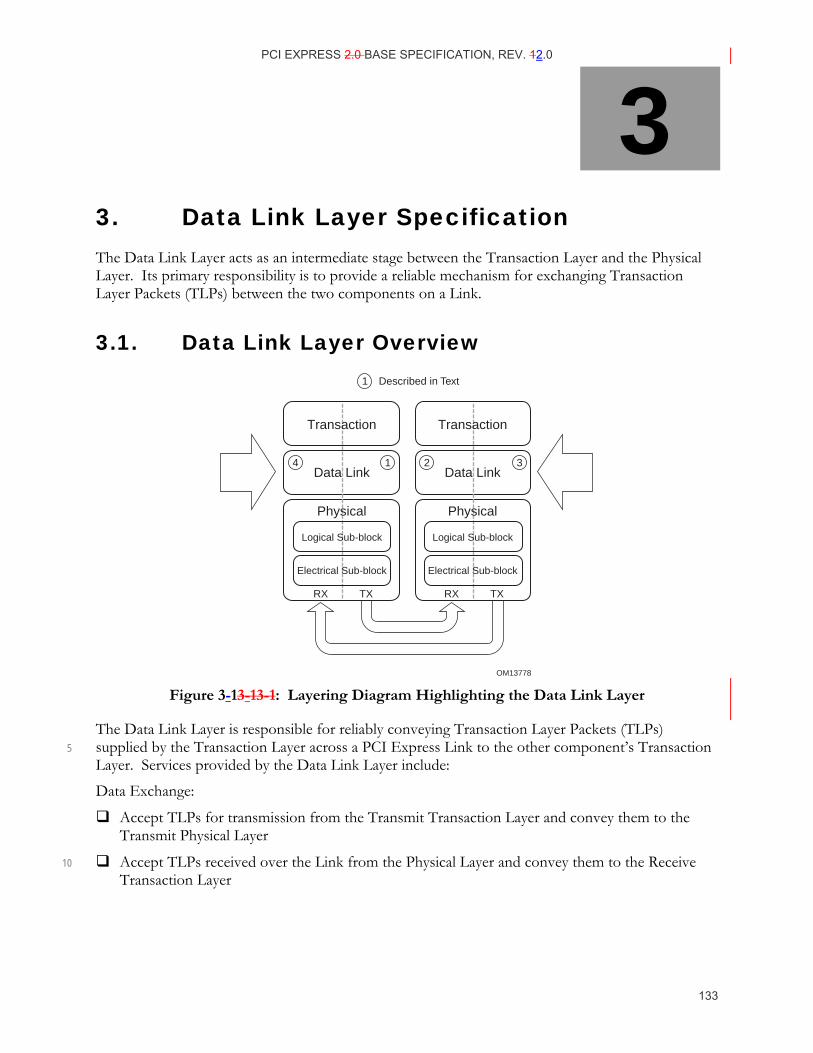
PCI EXPRESS 2.0 BASE SPECIFICATION, REV. 12.0
133
3. Data Link Layer Specification The Data Link Layer acts as an intermediate stage between the Transaction Layer and the Physical Layer. Its primary responsibility is to provide a reliable mechanism for exchanging Transaction Layer Packets (TLPs) between the two components on a Link.
3.1. Data Link Layer Overview
14 32
1 Described in Text
OM13778
Data Link Data Link
RX TX
Logical Sub-block
Electrical Sub-block
Physical
RX TX
Logical Sub-block
Electrical Sub-block
Physical
Transaction Transaction
Figure 3-13-1 3-1: Layering Diagram Highlighting the Data Link Layer
The Data Link Layer is responsible for reliably conveying Transaction Layer Packets (TLPs) supplied by the Transaction Layer across a PCI Express Link to the other component’s Transaction 5 Layer. Services provided by the Data Link Layer include:
Data Exchange:
Accept TLPs for transmission from the Transmit Transaction Layer and convey them to the Transmit Physical Layer
Accept TLPs received over the Link from the Physical Layer and convey them to the Receive 10 Transaction Layer
3
PCI EXPRESS 2.0 BASE SPECIFICATION, REV. 21.0
134
Error Detection and Retry:
TLP Sequence Number and LCRC generation
Transmitted TLP storage for Data Link Layer Retry
Data integrity checking for TLPs and Data Link Layer Packets (DLLPs)
Positive and negative acknowledgement DLLPs 5
Error indications for error reporting and logging mechanisms
Link Acknowledgement Timeout replay mechanism
Initialization and power management services:
Track Link state and convey active/reset/disconnected state to Transaction Layer
Data Link Layer Packets (DLLPs) are: 10
used for Link Management functions including TLP acknowledgement, power management, and exchange of Flow Control information.
transferred between Data Link Layers of the two directly connected components on a Link
DLLPs are sent point-to-point, between the two components on one Link. TLPs are routed from one component to another, potentially through one or more intermediate components. 15
Data Integrity checking for DLLPs and TLPs is done using a CRC included with each packet sent across the Link. DLLPs use a 16 16-bit CRC and TLPs (which can be much longer than DLLPs) use a 32-bit LCRC. TLPs additionally include a sequence number, which is used to detect cases where one or more entire TLPs have been lost.
Received DLLPs which fail the CRC check are discarded. The mechanisms which use DLLPs may 20 suffer a performance penalty from this loss of information, but are self-repairing such that a successive DLLP will supercedesupersede any information lost.
TLPs which fail the data integrity checks (LCRC and sequence number), or which are lost in transmission from one component to another, are re-sent by the Transmitter. The Transmitter stores a copy of all TLPs sent, re-sending these copies when required, and purges the copies only 25 when it receives a positive acknowledgement of error-free receipt from the other component. If a positive acknowledgement has not been received within a specified time period, the Transmitter will automatically start re-transmission. The Receiver can request an immediate re-transmission using a negative acknowledgement.
The Data Link Layer appears as an information conduit with varying latency to the Transaction 30 Layer. On any given individual Link all TLPs fed into the Transmit Data Link Layer (1 and 3) will appear at the output of the Receive Data Link Layer (2 and 4) in the same order at a later time, as illustrated in Figure 3-1. The latency will depend on a number of factors, including pipeline latencies, width and operational frequency of the Link, transmission of electrical signals across the Link, and delays caused by Data Link Layer Retry. Because of these delays, the Transmit Data Link 35 Layer (1 and 3) can apply backpressure to the Transmit Transaction Layer, and the Receive Data Link Layer (2 and 4) communicates the presence or absence of valid information to the Receive Transaction Layer.
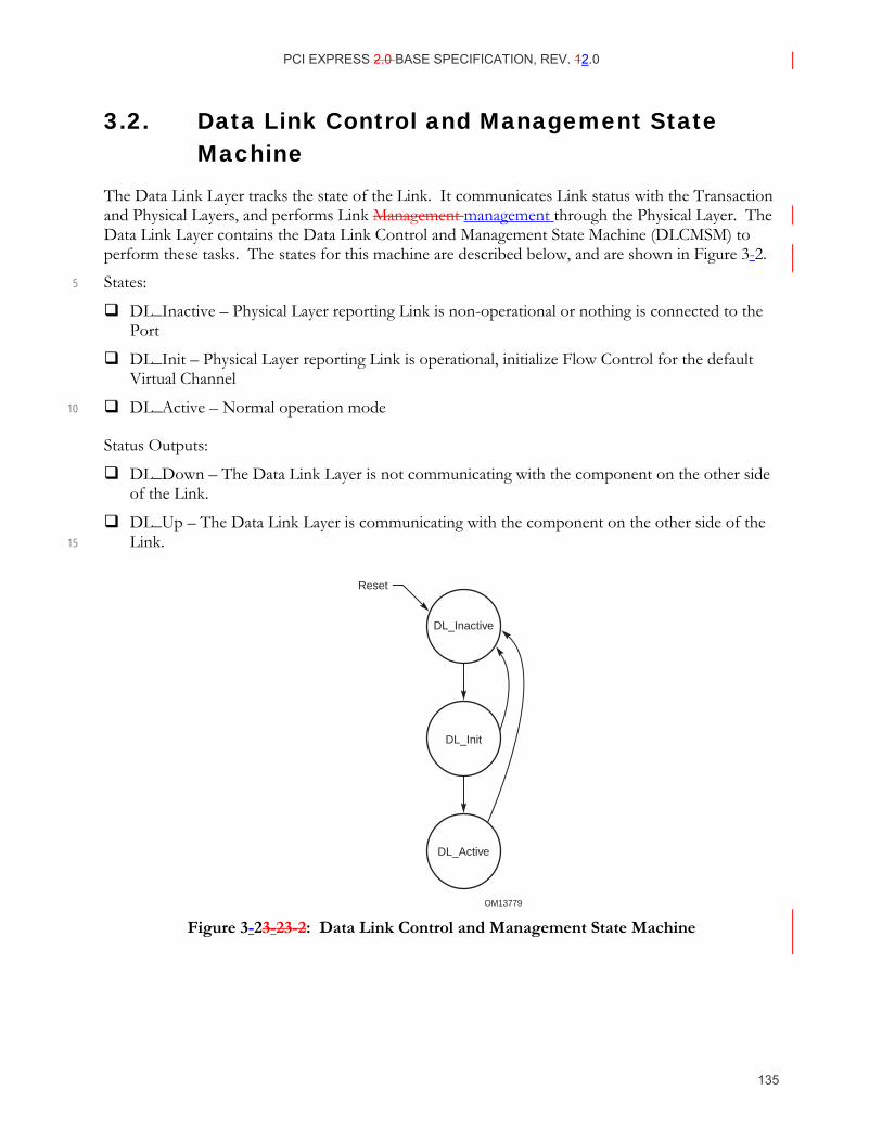
PCI EXPRESS 2.0 BASE SPECIFICATION, REV. 12.0
135
3.2. Data Link Control and Management State Machine
The Data Link Layer tracks the state of the Link. It communicates Link status with the Transaction and Physical Layers, and performs Link Management management through the Physical Layer. The Data Link Layer contains the Data Link Control and Management State Machine (DLCMSM) to perform these tasks. The states for this machine are described below, and are shown in Figure 3-2.
States: 5
DL_Inactive – Physical Layer reporting Link is non-operational or nothing is connected to the Port
DL_Init – Physical Layer reporting Link is operational, initialize Flow Control for the default Virtual Channel
DL_Active – Normal operation mode 10
Status Outputs:
DL_Down – The Data Link Layer is not communicating with the component on the other side of the Link.
DL_Up – The Data Link Layer is communicating with the component on the other side of the Link. 15
OM13779
DL_Inactive
Reset
DL_Active
DL_Init
Figure 3-23-2 3-2: Data Link Control and Management State Machine
PCI EXPRESS 2.0 BASE SPECIFICATION, REV. 21.0
136
3.2.1. Data Link Control and Management State Machine Rules
Rules per state:
DL_Inactive
• Initial state following PCI Express hot, warm, or cold reset (see Section 6.6). Note that DL states are unaffected by an FLR (see Section 6.6).
• Upon entry to DL_Inactive 5
♦ Reset all Data Link Layer state information to default values
♦ Discard the contents of the Data Link Layer Retry Buffer (refer see Section 3.5)
• While in DL_Inactive:
♦ Report DL_Down status to the Transaction Layer as well as to the rest of the Data Link Layer 10
♦Note: This will cause the Transaction Layer to discard any outstanding transactions and to terminate internally any attempts to transmit a TLP. For a Downstream Port on a Root Complex or at the “bottom” of a Switch, this is equivalent to a “Hot-Remove.” For an Upstream Port on an Endpoint or at the “top” of a Switch, having the Link go down is equivalent to a hot reset (see Section 2.9). 15
♦ Discard TLP information from the Transaction and Physical Layers
♦ Do not generate or accept DLLPs
• Exit to DL_Init if:
♦ Indication from the Transaction Layer that the Link is not disabled by software and the Physical Layer reports Physical LinkUp = 1b 20
DL_Init
• While in DL_Init:
♦ Initialize Flow Control for the default Virtual Channel, VC0, following the Flow Control initialization protocol described in Section 3.3
♦ Report DL_Down status while in state FC_INIT1; DL_Up status in state FC_INIT2 25
♦ The Data Link Layer of a Port with DL_Down status is permitted to discard any received TLPs provided that it does not acknowledge those TLPs by sending one or more Ack DLLPs
• Exit to DL_Active if:
♦ Flow Control initialization completes successfully, and the Physical Layer continues to 30 report Physical LinkUp = 1b
• Terminate attempt to initialize Flow Control for VC0 and Exit to DL_Inactive if:
♦ Physical Layer reports Physical LinkUp = 0b
PCI EXPRESS 2.0 BASE SPECIFICATION, REV. 12.0
137
DL_Active
• DL_Active is referred to as the normal operating state
• While in DL_Active:
♦ Accept and transfer TLP information with the Transaction and Physical Layers as specified in this chapter 5
♦ Generate and accept DLLPs as specified in this chapter
♦ Report DL_Up status to the Transaction and Data Link Layers
• Exit to DL_Inactive if:
♦ Physical Layer reports Physical LinkUp = 0b
♦ Upstream components are optionally permitted to treat this transition from DL_Active 10 to DL_Inactive as a Surprise Down error, except in the following cases where this error detection is blocked:
If the Secondary Bus Reset in Bridge Control register has been set to 1b by software, then the subsequent transition to DL_Inactive must not be considered an error.
If the Link Disable bit has been set to 1b by software, then the subsequent transition 15 to DL_Inactive must not be considered an error.
If a PME_Turn_Off Message has been sent through this portPort, then the subsequent transition to DL_Inactive must not be considered an error.
Note that the DL_Inactive transition for this condition will not occur until a power off, a reset, or a request to restore the linkLink is sent to the Physical layer. 20
Note also that in the case where the PME_Turn_Off/PME_TO_Ack handshake fails to complete successfully, a SupriseSurprise Down error may be detected.
If the port Port is associated with a hot-pluggable slot, and the Hot Plug Surprise bit in the Slot Capabilities register is set to 1b, then any transition to DL_Inactive must not be considered an error. 25
If the port Port is associated with a hot-pluggable slot (Hot-Plug Capable bit in the Slot Capabilities register set to 1b), and Power Controller Control bit in Slot Control register is 1b(Off), then any transition to DL Inactive must not be considered an error.
Error blocking initiated by one or more of the above cases must remain in effect until 30 the port Port exits DL_Active and subsequently returns to DL_Active with none of the blocking cases in effect at the time of the return to DL_Active.
Note that the transition out of DL_Active is simply the expected transition as anticipated per the error detection blocking condition.
If implemented, this is a reported error associated with the detecting port Port (see 35 Section 6.2).
PCI EXPRESS 2.0 BASE SPECIFICATION, REV. 21.0
138
IMPLEMENTATION NOTE
Physical Layer Throttling Note that there are conditions where the Physical Layer may be temporarily unable to accept TLPs and DLLPs from the Data Link Layer. The Data Link Layer must comprehend this by providing mechanisms for the Physical Layer to communicate this condition, and for TLPs and DLLPs to be temporarily blocked by the condition.
3.3. Flow Control Initialization Protocol Before starting normal operation following power-up or interconnect Reset, it is necessary to 5 initialize Flow Control for the default Virtual Channel, VC0 (see Section 6.6). In addition, when additional Virtual Channels (VCs) are enabled, the Flow Control initialization process must be completed for each newly enabled VC before it can be used (see Section 2.4.2). This section describes the initialization process that is used for all VCs. Note that since VC0 is enabled before all other VCs, no TLP traffic of any kind will be active prior to initialization of VC0. However, when 10 additional VCs are being initialized there will typically be TLP traffic flowing on other, already enabled, VCs. Such traffic has no direct effect on the initialization process for the additional VC(s).
There are two states in the VC initialization process. These states are:
FC_INIT1
FC_INIT2 15
The rules for this process are given in the following section.
3.3.1. Flow Control Initialization State Machine Rules
If at any time during initialization for VCs 1-7 the VC is disabled, the flow control initialization process for the VC is terminated
Rules for state FC_INIT1:
• Entered when initialization of a VC (VCx) is required 20
♦ Entrance to DL_Init state (VCx = VC0)
♦ When a VC (VCx = VC1-7) is enabled by software (see Sections 7.11 and 7.18)
• While in FC_INIT1:
♦ Transaction Layer must block transmission of TLPs using VCx
PCI EXPRESS 2.0 BASE SPECIFICATION, REV. 12.0
139
♦ Transmit the following three InitFC1 DLLPs for VCx in the following relative order:
InitFC1 – P (first)
InitFC1 – NP (second)
InitFC1 – Cpl (third)
♦ The three InitFC1 DLLPs must be transmitted at least once every 34 μs. 5
Time spent in the Recovery LTSSM state does not contribute to this limit.
It is strongly encouraged that the InitFC1 DLLP transmissions are repeated frequently, particularly when there are no other TLPs or DLLPs available for transmission.
♦ Except as needed to ensure at least the required frequency of InitFC1 DLLP 10 transmission, the Data Link Layer must not block other transmissions
Note that this includes all Physical Layer initiated transmissions (for example, Ordered Sets), Ack and Nak DLLPs (when applicable), and TLPs using VCs that have previously completed initialization (when applicable)
♦ Process received InitFC1 and InitFC2 DLLPs: 15
Record the indicated FC unit values
Set Flag FI1 once FC unit values have been recorded for each of P, NP, and Cpl for VCx
• Exit to FC_INIT2 if:
♦ Flag FI1 has been set indicating that FC unit values have been recorded for each of P, 20 NP, and Cpl for VCx
Rules for state FC_INIT2:
• While in FC_INIT2:
♦ Transaction Layer must block transmission of TLPs using VCx
♦ Transmit the following three InitFC2 DLLPs for VCx in the following relative order: 25
InitFC2 – P (first)
InitFC2 – NP (second)
InitFC2 – Cpl (third)
♦ The three InitFC2 DLLPs must be transmitted at least once every 34 μs.
Time spent in the Recovery LTSSM state does not contribute to this limit. 30
It is strongly encouraged that the InitFC2 DLLP transmissions are repeated frequently, particularly when there are no other TLPs or DLLPs available for transmission.
PCI EXPRESS 2.0 BASE SPECIFICATION, REV. 21.0
140
♦ Except as needed to ensure at least the required frequency of InitFC2 DLLP transmission, the Data Link Layer must not block other transmissions
Note that this includes all Physical Layer initiated transmissions (for example, Ordered Sets), Ack and Nak DLLPs (when applicable), and TLPs using VCs that have previously completed initialization (when applicable) 5
♦ Process received InitFC1 and InitFC2 DLLPs:
Ignore the indicated FC unit values
Set flag FI2 on receipt of any InitFC2 DLLP for VCx
♦ Set flag FI2 on receipt of any TLP on VCx, or any UpdateFC DLLP for VCx
• Signal completion and exit if: 10
♦ Flag FI2 has been set
IMPLEMENTATION NOTE
Example of Flow Control Initialization Figure 3-3 illustrates an example of the Flow Control initialization protocol for VC0 between a Switch and a n EndpointDownstream component. In this example, each component advertises the minimum permitted values for each type of Flow Control credit. For both components the largest Max_Payload_Size value supported is 1024 bytes, corresponding to a data payload credit 15 advertisement of 040h. All DLLPs are shown as received without error.
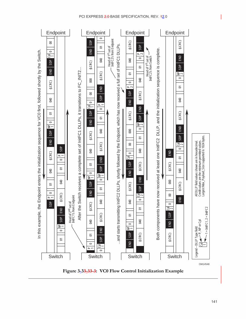
PCI EXPRESS 2.0 BASE SPECIFICATION, REV. 12.0
141
OM14548
EndpointEndpointEndpointEndpoint
SwitchSwitchSwitchSwitch
Hea
d of
1st
set
of
InitF
C2'
s fro
m S
witc
h
Hea
d of
1st
set
of
InitF
C2'
s fro
m E
ndpo
int
Hea
d of
2nd
set
of
InitF
C1'
s fro
m E
ndpo
int
In th
is e
xam
ple,
the
End
poin
t ent
ers
the
initi
aliz
atio
n se
quen
ce fo
r V
C0
first
, fol
low
ed s
hort
ly b
y th
e S
witc
h.
Afte
r th
e S
witc
h re
ceiv
es a
com
plet
e se
t of I
nitF
C1
DLL
Ps,
it tr
ansi
tions
to F
C_I
NIT
2...
Bot
h co
mpo
nent
s ha
ve n
ow r
ecei
ved
at le
ast o
ne In
itFC
2 D
LLP
, and
the
initi
aliz
atio
n se
quen
ce is
com
plet
e.
All D
LLP
field
val
ues
show
n ar
e in
hex
adec
imal
.C
redi
t val
ues
are
the
min
imum
per
mitt
ed v
alue
s.La
rges
t Max
_Pay
load
_Siz
e su
ppor
ted
is 1
024
byte
s.
Lege
nd –
DLL
P Ty
pe fi
eld:
P, N
P or
Cpl
1 =
InitF
C1,
2 =
InitF
C2
Cpl
1
SDP
001
040
LC
RC
01
040
LC
RC
0
NP 100
0Cp
l 1P 1
001
040
LC
RC
01
0NP 1
P 1
SDP
END
SDP
END
SDP
SDP
END
SDP
END
SDP
END
SDP
END
SDP
END
SDP
END
SDP
END
SDP
END
SDP
END
SDP
END
SDP
SDP
END
SDP
END
SDP
END
END
SDP
END
SDP
END
END
001
040
LC
RC
01
040
LC
RC
0
NP 100
000
LC
RC
0
Cpl 1
P 1
004
0L
CR
C
010
Cpl 1
NP 10
040
LC
RC
01
004
0L
CR
C
01P 1
0104
0L
CR
C
0NP 1
0000
0L
CR
C
0Cp
l 101
040
LC
RC
0
P 2
004
0L
CR
C
01Cp
l 20
040
LC
RC
01
NP 20
040
LC
RC
01
P 2
0000
0L
CR
C
LC
RC
0
Cpl 2
004
0L
CR
C
01Cp
l 20
040
LC
RC
L
CR
C
01NP 2
...an
d st
arts
tran
smitt
ing
InitF
C2
DLL
Ps,
sho
rtly
follo
wed
by
the
End
poin
t, w
hich
has
now
rece
ived
a fu
ll se
t of I
nitF
C1
DLL
Ps.
Figure 3-33-3 3-3: VC0 Flow Control Initialization Example
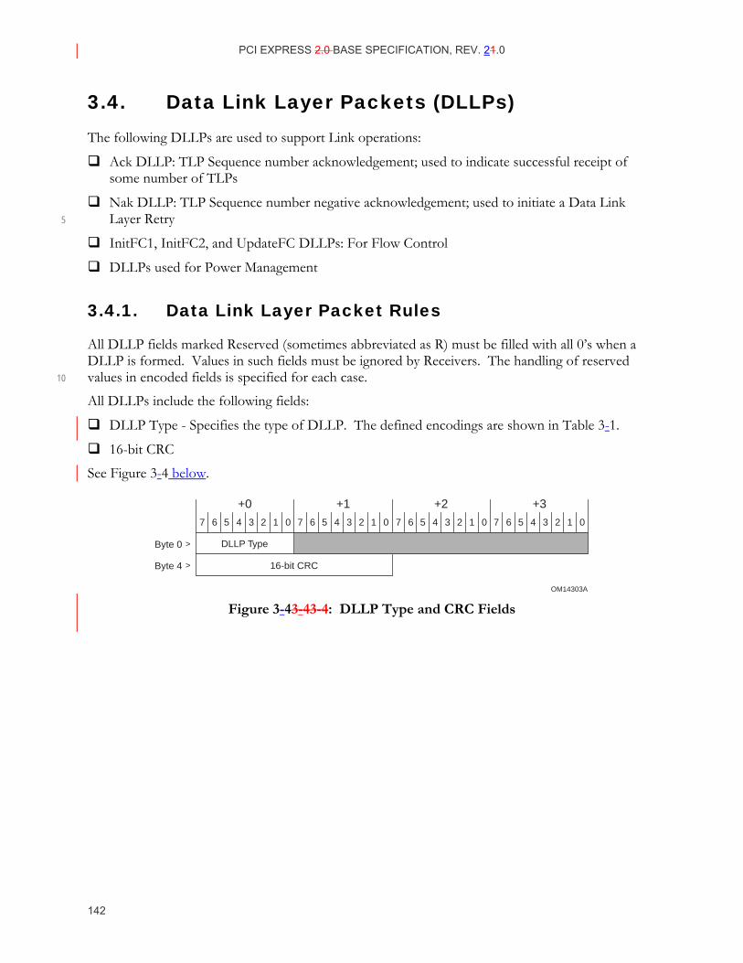
PCI EXPRESS 2.0 BASE SPECIFICATION, REV. 21.0
142
3.4. Data Link Layer Packets (DLLPs) The following DLLPs are used to support Link operations:
Ack DLLP: TLP Sequence number acknowledgement; used to indicate successful receipt of some number of TLPs
Nak DLLP: TLP Sequence number negative acknowledgement; used to initiate a Data Link Layer Retry 5
InitFC1, InitFC2, and UpdateFC DLLPs: For Flow Control
DLLPs used for Power Management
3.4.1. Data Link Layer Packet Rules
All DLLP fields marked Reserved (sometimes abbreviated as R) must be filled with all 0’s when a DLLP is formed. Values in such fields must be ignored by Receivers. The handling of reserved values in encoded fields is specified for each case. 10
All DLLPs include the following fields:
DLLP Type - Specifies the type of DLLP. The defined encodings are shown in Table 3-1.
16-bit CRC
See Figure 3-4 below.
OM14303A
7 6 5 4 3 2 1 0 7 6 5 4 3 2 1 0 7 6 5 4 3 2 1 0 7 6 5 4 3 2 1 0
DLLP Type
16-bit CRC
+0 +1 +2 +3
Byte 0 >
Byte 4 >
Figure 3-43-4 3-4: DLLP Type and CRC Fields
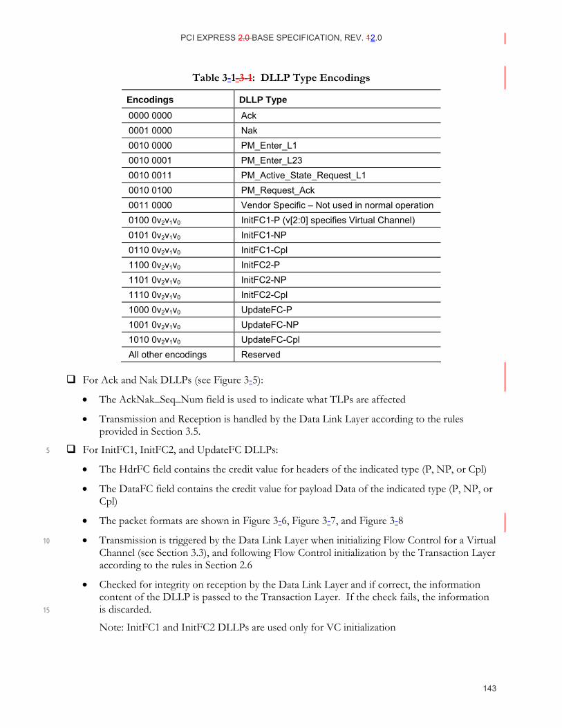
PCI EXPRESS 2.0 BASE SPECIFICATION, REV. 12.0
143
Table 3-1- 3-1: DLLP Type Encodings
Encodings DLLP Type 0000 0000 Ack 0001 0000 Nak 0010 0000 PM_Enter_L1 0010 0001 PM_Enter_L23 0010 0011 PM_Active_State_Request_L1 0010 0100 PM_Request_Ack 0011 0000 Vendor Specific – Not used in normal operation 0100 0v2v1v0 InitFC1-P (v[2:0] specifies Virtual Channel) 0101 0v2v1v0 InitFC1-NP 0110 0v2v1v0 InitFC1-Cpl 1100 0v2v1v0 InitFC2-P 1101 0v2v1v0 InitFC2-NP 1110 0v2v1v0 InitFC2-Cpl 1000 0v2v1v0 UpdateFC-P 1001 0v2v1v0 UpdateFC-NP 1010 0v2v1v0 UpdateFC-Cpl All other encodings Reserved
For Ack and Nak DLLPs (see Figure 3-5):
• The AckNak_Seq_Num field is used to indicate what TLPs are affected
• Transmission and Reception is handled by the Data Link Layer according to the rules provided in Section 3.5.
For InitFC1, InitFC2, and UpdateFC DLLPs: 5
• The HdrFC field contains the credit value for headers of the indicated type (P, NP, or Cpl)
• The DataFC field contains the credit value for payload Data of the indicated type (P, NP, or Cpl)
• The packet formats are shown in Figure 3-6, Figure 3-7, and Figure 3-8
• Transmission is triggered by the Data Link Layer when initializing Flow Control for a Virtual 10 Channel (see Section 3.3), and following Flow Control initialization by the Transaction Layer according to the rules in Section 2.6
• Checked for integrity on reception by the Data Link Layer and if correct, the information content of the DLLP is passed to the Transaction Layer. If the check fails, the information is discarded. 15
Note: InitFC1 and InitFC2 DLLPs are used only for VC initialization
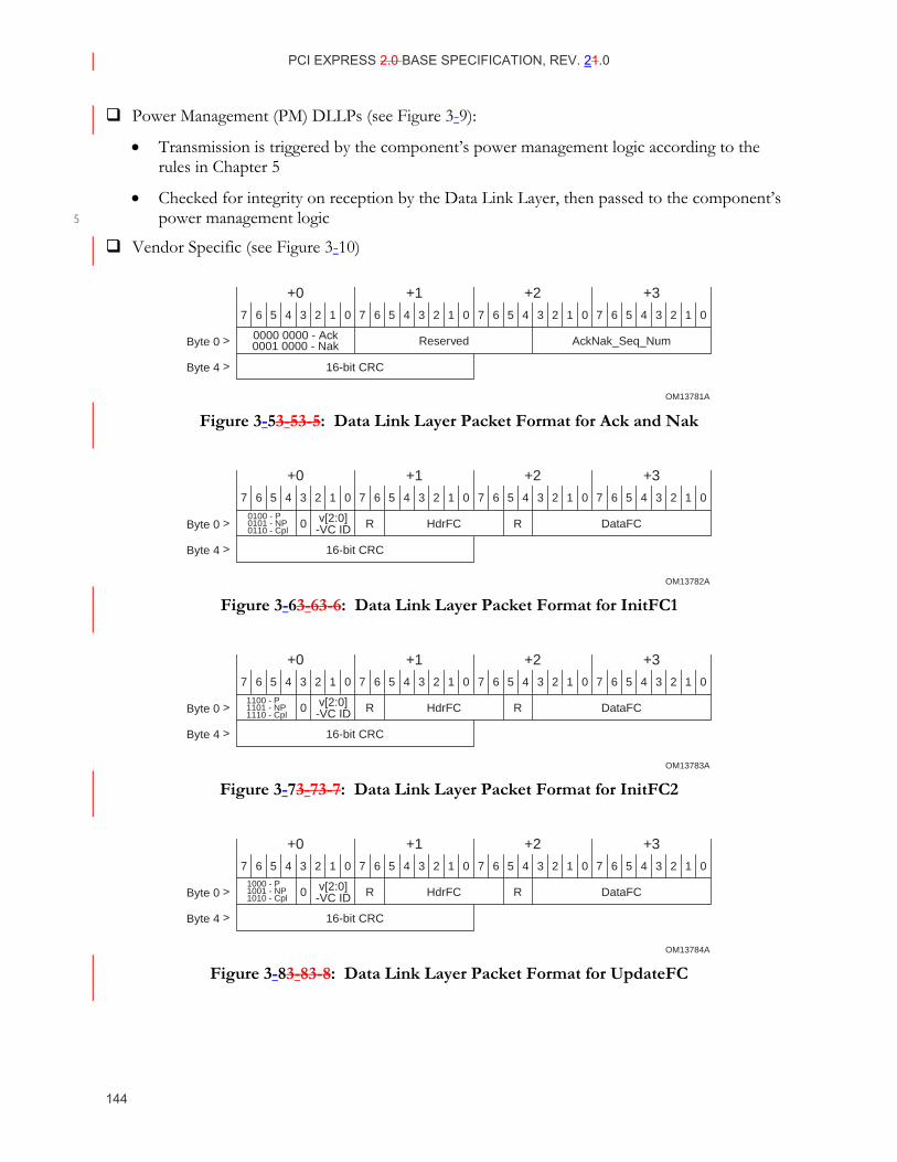
PCI EXPRESS 2.0 BASE SPECIFICATION, REV. 21.0
144
Power Management (PM) DLLPs (see Figure 3-9):
• Transmission is triggered by the component’s power management logic according to the rules in Chapter 5
• Checked for integrity on reception by the Data Link Layer, then passed to the component’s power management logic 5
Vendor Specific (see Figure 3-10)
OM13781A
7 6 5 4 3 2 1 0 7 6 5 4 3 2 1 0 7 6 5 4 3 2 1 0 7 6 5 4 3 2 1 0
Reserved
16-bit CRC
0000 0000 - Ack0001 0000 - Nak AckNak_Seq_Num
+0 +1 +2 +3
Byte 0 >
Byte 4 >
Figure 3-53-5 3-5: Data Link Layer Packet Format for Ack and Nak
OM13782A
7 6 5 4 3 2 1 0 7 6 5 4 3 2 1 0 7 6 5 4 3 2 1 0 7 6 5 4 3 2 1 0
R HdrFCv[2:0]-VC ID0
16-bit CRC
0100 - P0101 - NP0110 - Cpl
R DataFC
+0 +1 +2 +3
Byte 0 >
Byte 4 >
Figure 3-63-6 3-6: Data Link Layer Packet Format for InitFC1
OM13783A
7 6 5 4 3 2 1 0 7 6 5 4 3 2 1 0 7 6 5 4 3 2 1 0 7 6 5 4 3 2 1 0
R HdrFCv[2:0]-VC ID0
16-bit CRC
1100 - P1101 - NP1110 - Cpl
R DataFC
+0 +1 +2 +3
Byte 0 >
Byte 4 >
Figure 3-73-7 3-7: Data Link Layer Packet Format for InitFC2
OM13784A
7 6 5 4 3 2 1 0 7 6 5 4 3 2 1 0 7 6 5 4 3 2 1 0 7 6 5 4 3 2 1 0
R HdrFCv[2:0]-VC ID0
16-bit CRC
1000 - P1001 - NP1010 - Cpl
R DataFC
+0 +1 +2 +3
Byte 0 >
Byte 4 >
Figure 3-83-8 3-8: Data Link Layer Packet Format for UpdateFC
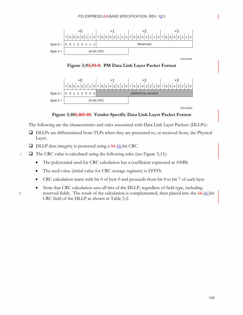
PCI EXPRESS 2.0 BASE SPECIFICATION, REV. 12.0
145
OM14304A
7 6 5 4 3 2 1 0
0 0 1 0 0 x x x
7 6 5 4 3 2 1 0 7 6 5 4 3 2 1 0 7 6 5 4 3 2 1 0
16-bit CRC
Reserved
+0 +1 +2 +3
Byte 0 >
Byte 4 >
Figure 3-93-9 3-9: PM Data Link Layer Packet Format
OM14305A
7 6 5 4 3 2 1 0
0 0 1 1 0 0 0 0
7 6 5 4 3 2 1 0 7 6 5 4 3 2 1 0 7 6 5 4 3 2 1 0
16-bit CRC
defined by vendor
+0 +1 +2 +3
Byte 0 >
Byte 4 >
Figure 3-103-10 3-10: Vendor Specific Data Link Layer Packet Format
The following are the characteristics and rules associated with Data Link Layer Packets (DLLPs):
DLLPs are differentiated from TLPs when they are presented to, or received from, the Physical Layer.
DLLP data integrity is protected using a 16 16-bit CRC
The CRC value is calculated using the following rules (see Figure 3-11): 5
• The polynomial used for CRC calculation has a coefficient expressed as 100Bh
• The seed value (initial value for CRC storage registers) is FFFFh
• CRC calculation starts with bit 0 of byte 0 and proceeds from bit 0 to bit 7 of each byte
• Note that CRC calculation uses all bits of the DLLP, regardless of field type, including reserved fields. The result of the calculation is complemented, then placed into the 16 16-bit 10 CRC field of the DLLP as shown in Table 3-2.
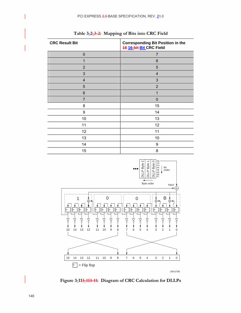
PCI EXPRESS 2.0 BASE SPECIFICATION, REV. 21.0
146
Table 3-2- 3-2: Mapping of Bits into CRC Field
CRC Result Bit Corresponding Bit Position in the 16 16-bit Bit CRC Field
0 7 1 6 2 5 3 4 4 3 5 2 6 1 7 0 8 15 9 14
10 13 11 12 12 11 13 10 14 9 15 8
OM13785
Input
bitorder
Byte order
0123456789101112131415
0123456789101112131415
1 0 0 B
DLL
P B
yte
2
DLL
P B
yte
1
DLL
P B
yte
0 01
23
45
67
> > > > > > > > > > > > > > > >
> = Flip flop
Figure 3-113-11 3-11: Diagram of CRC Calculation for DLLPs
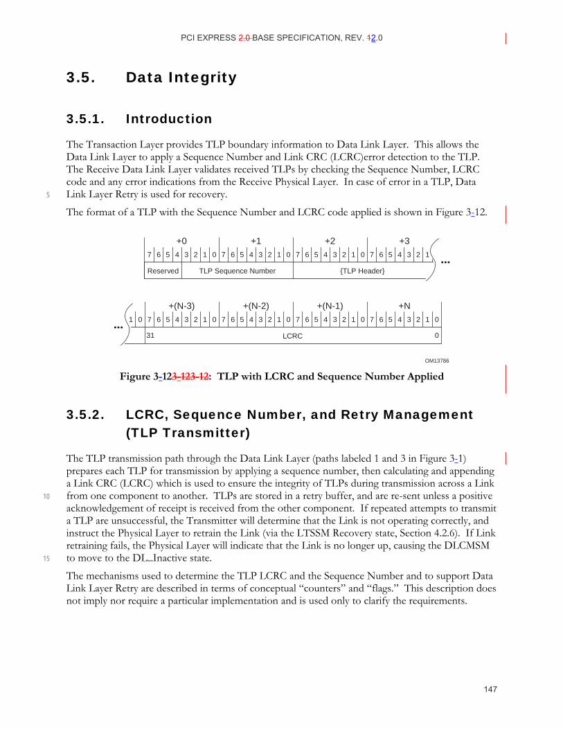
PCI EXPRESS 2.0 BASE SPECIFICATION, REV. 12.0
147
3.5. Data Integrity
3.5.1. Introduction
The Transaction Layer provides TLP boundary information to Data Link Layer. This allows the Data Link Layer to apply a Sequence Number and Link CRC (LCRC)error detection to the TLP. The Receive Data Link Layer validates received TLPs by checking the Sequence Number, LCRC code and any error indications from the Receive Physical Layer. In case of error in a TLP, Data Link Layer Retry is used for recovery. 5
The format of a TLP with the Sequence Number and LCRC code applied is shown in Figure 3-12.
OM13786
7 6 5 4 3 2 1 0 7 6 5 4 3 2 1 0 7 6 5 4 3 2 1 0 7 6 5 4 3 2 1
TLP Sequence NumberReserved TLP Header
+0 +1 +2 +3
7 61 0 5 4 3 2 1 0 7 6 5 4 3 2 1 0 7 6 5 4 3 2 1 0 7 6 5 4 3 2 1 0
31 0LCRC
+(N-3) +(N-2) +(N-1) +N
Figure 3-123-12 3-12: TLP with LCRC and Sequence Number Applied
3.5.2. LCRC, Sequence Number, and Retry Management (TLP Transmitter)
The TLP transmission path through the Data Link Layer (paths labeled 1 and 3 in Figure 3-1) prepares each TLP for transmission by applying a sequence number, then calculating and appending a Link CRC (LCRC) which is used to ensure the integrity of TLPs during transmission across a Link from one component to another. TLPs are stored in a retry buffer, and are re-sent unless a positive 10 acknowledgement of receipt is received from the other component. If repeated attempts to transmit a TLP are unsuccessful, the Transmitter will determine that the Link is not operating correctly, and instruct the Physical Layer to retrain the Link (via the LTSSM Recovery state, Section 4.2.6). If Link retraining fails, the Physical Layer will indicate that the Link is no longer up, causing the DLCMSM to move to the DL_Inactive state. 15
The mechanisms used to determine the TLP LCRC and the Sequence Number and to support Data Link Layer Retry are described in terms of conceptual “counters” and “flags.” This description does not imply nor require a particular implementation and is used only to clarify the requirements.
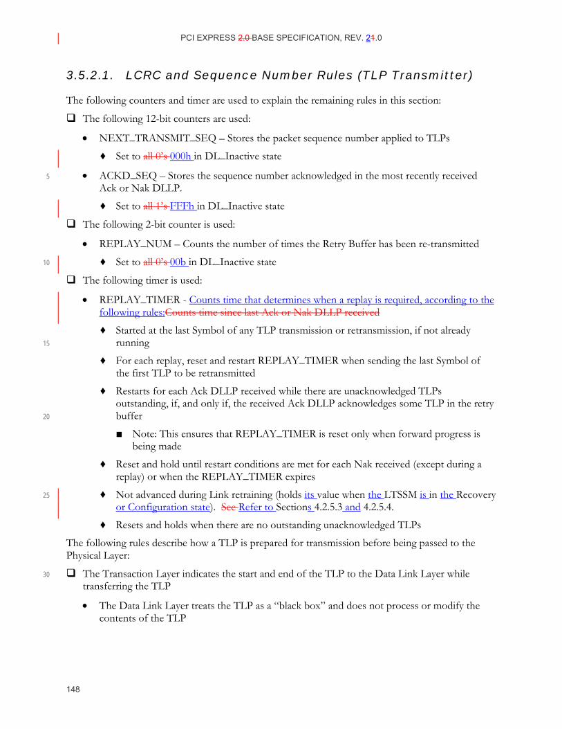
PCI EXPRESS 2.0 BASE SPECIFICATION, REV. 21.0
148
3.5.2.1. LCRC and Sequence Number Rules (TLP Transmitter)
The following counters and timer are used to explain the remaining rules in this section:
The following 12-bit counters are used:
• NEXT_TRANSMIT_SEQ – Stores the packet sequence number applied to TLPs
♦ Set to all 0’s 000h in DL_Inactive state
• ACKD_SEQ – Stores the sequence number acknowledged in the most recently received 5 Ack or Nak DLLP.
♦ Set to all 1’s FFFh in DL_Inactive state
The following 2-bit counter is used:
• REPLAY_NUM – Counts the number of times the Retry Buffer has been re-transmitted
♦ Set to all 0’s 00b in DL_Inactive state 10
The following timer is used:
• REPLAY_TIMER - Counts time that determines when a replay is required, according to the following rules:Counts time since last Ack or Nak DLLP received
♦ Started at the last Symbol of any TLP transmission or retransmission, if not already running 15
♦ For each replay, reset and restart REPLAY_TIMER when sending the last Symbol of the first TLP to be retransmitted
♦ Restarts for each Ack DLLP received while there are unacknowledged TLPs outstanding, if, and only if, the received Ack DLLP acknowledges some TLP in the retry buffer 20
Note: This ensures that REPLAY_TIMER is reset only when forward progress is being made
♦ Reset and hold until restart conditions are met for each Nak received (except during a replay) or when the REPLAY_TIMER expires
♦ Not advanced during Link retraining (holds its value when the LTSSM is in the Recovery 25 or Configuration state). See Refer to Sections 4.2.5.3 and 4.2.5.4.
♦ Resets and holds when there are no outstanding unacknowledged TLPs
The following rules describe how a TLP is prepared for transmission before being passed to the Physical Layer:
The Transaction Layer indicates the start and end of the TLP to the Data Link Layer while 30 transferring the TLP
• The Data Link Layer treats the TLP as a “black box” and does not process or modify the contents of the TLP
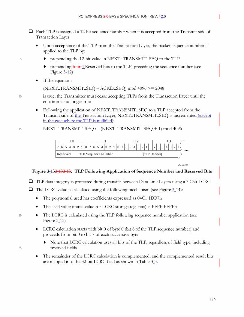
PCI EXPRESS 2.0 BASE SPECIFICATION, REV. 12.0
149
Each TLP is assigned a 12-bit sequence number when it is accepted from the Transmit side of Transaction Layer
• Upon acceptance of the TLP from the Transaction Layer, the packet sequence number is applied to the TLP by:
♦ prepending the 12-bit value in NEXT_TRANSMIT_SEQ to the TLP 5
♦ prepending four 4 Reserved bits to the TLP, preceding the sequence number (see Figure 3-12)
• If the equation:
(NEXT_TRANSMIT_SEQ – ACKD_SEQ) mod 4096 >= 2048
is true, the Transmitter must cease accepting TLPs from the Transaction Layer until the 10 equation is no longer true
• Following the application of NEXT_TRANSMIT_SEQ to a TLP accepted from the Transmit side of the Transaction Layer, NEXT_TRANSMIT_SEQ is incremented (except in the case where the TLP is nullified):
NEXT_TRANSMIT_SEQ := (NEXT_TRANSMIT_SEQ + 1) mod 4096 15
OM13787
7 6 5 4 3 2 1 0 7 6 5 4 3 2 1 0 7 6 5 4 3 2 1 0 7 6 5 4 3 2 1
TLP Sequence NumberReserved [TLP Header]
+0 +1 +2 +3
Figure 3-133-13 3-13: TLP Following Application of Sequence Number and Reserved Bits
TLP data integrity is protected during transfer between Data Link Layers using a 32-bit LCRC
The LCRC value is calculated using the following mechanism (see Figure 3-14):
• The polynomial used has coefficients expressed as 04C1 1DB7h
• The seed value (initial value for LCRC storage registers) is FFFF FFFFh
• The LCRC is calculated using the TLP following sequence number application (see 20 Figure 3-13)
• LCRC calculation starts with bit 0 of byte 0 (bit 8 of the TLP sequence number) and proceeds from bit 0 to bit 7 of each successive byte.
♦ Note that LCRC calculation uses all bits of the TLP, regardless of field type, including reserved fields 25
• The remainder of the LCRC calculation is complemented, and the complemented result bits are mapped into the 32-bit LCRC field as shown in Table 3-3.
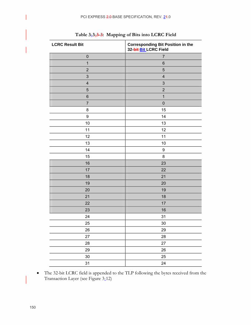
PCI EXPRESS 2.0 BASE SPECIFICATION, REV. 21.0
150
Table 3-3- 3-3: Mapping of Bits into LCRC Field
LCRC Result Bit Corresponding Bit Position in the 32-bit Bit LCRC Field
0 7 1 6 2 5 3 4 4 3 5 2 6 1 7 0 8 15 9 14
10 13 11 12 12 11 13 10 14 9 15 8 16 23 17 22 18 21 19 20 20 19 21 18 22 17 23 16 24 31 25 30 26 29 27 28 28 27 29 26 30 25 31 24
• The 32-bit LCRC field is appended to the TLP following the bytes received from the Transaction Layer (see Figure 3-12)
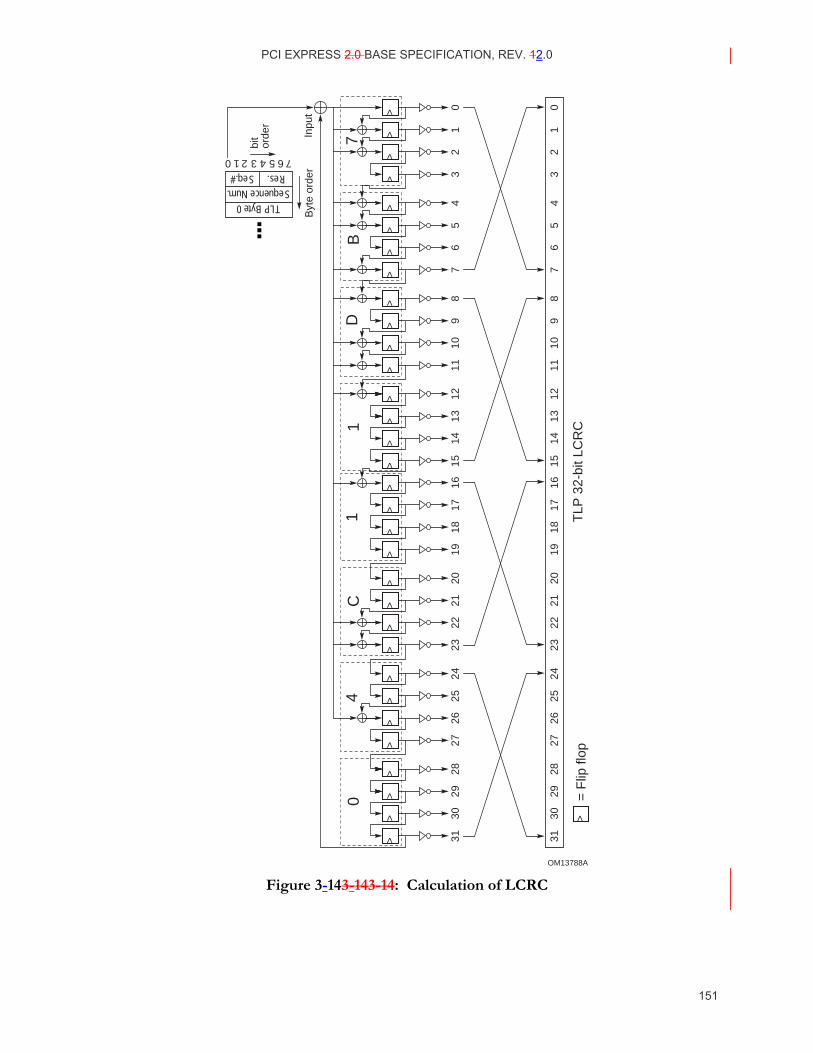
PCI EXPRESS 2.0 BASE SPECIFICATION, REV. 12.0
151
OM13788A
TLP Byte 0Sequence Num.Res.Seq.#
Inpu
t
bit
orde
r
Byt
e or
der
01
23
45
67
89
1011
1213
1415
1617
1819
2021
2223
2425
2627
2829
3031
01
23
45
67
89
1011
1213
1415
16
TLP
32-
bit L
CR
C
1718
1920
2122
2324
2526
2728
2930
31
04
C1
1D
B7
0 1 2 3 4 5 6 7
>>
>>
>>
>>
>>
>>
>>
>>
>>
>>
>>
>>
>>
>>
>>
>>
>=
Flip
flop
Figure 3-143-14 3-14: Calculation of LCRC
PCI EXPRESS 2.0 BASE SPECIFICATION, REV. 21.0
152
To support cut-through routing of TLPs, a Transmitter is permitted to modify a transmitted TLP to indicate that the Receiver must ignore that TLP (“nullify” the TLP).
A Transmitter is permitted to nullify a TLP being transmitted; to do this in a way which will robustly prevent misinterpretation or corruption, the Transmitter must do both of the following:
• use the remainder of the calculated LCRC value without inversion (the logical inverse of the 5 value normally used)
• indicate to the Transmit Physical Layer that the final framing Symbol must be EDB instead of END
When this is done, the Transmitter does not increment NEXT_TRANSMIT_SEQ
The following rules describe the operation of the Data Link Layer Retry Buffer, from which TLPs 10 are re-transmitted when necessary:
Copies of Transmitted TLPs must be stored in the Data Link Layer Retry Buffer, except for nullified TLPs.
When a replay is initiated, either due to reception of a Nak or due to REPLAY_TIMER expiration, the following rules describe the sequence of operations that must be followed: 15
If all TLPs transmitted have been acknowledged (the Retry Buffer is empty), terminate replay, otherwise continue.
Increment REPLAY_NUM.
• If REPLAY_NUM rolls over from 11b to 00b, the Transmitter signals the Physical Layer to retrain the Link, and waits for the completion of retraining before proceeding with the 20 replay. This is a reported error associated with the Port (see Section 6.2).
Note that Data Link Layer state, including the contents of the Retry Buffer, are not reset by this action unless the Physical Layer reports Physical LinkUp = 0b (causing the Data Link Control and Management State Machine to transition to the DL_Inactive state).
• If REPLAY_NUM does not roll over from 11b to 00b, continue with the replay. 25
Block acceptance of new TLPs from the Transmit Transaction Layer.
Complete transmission of any TLP currently being transmitted.
Retransmit unacknowledged TLPs, starting with the oldest unacknowledged TLP and continuing in original transmission order
• Reset and restart REPLAY_TIMER when sending the last Symbol of the first TLP to be 30 retransmitted
• Once all unacknowledged TLPs have been re-transmitted, return to normal operation.
• If any Ack or Nak DLLPs are received during a replay, the Transmitter is permitted to complete the replay without regard to the Ack or Nak DLLP(s), or to skip retransmission of any newly acknowledged TLPs. 35
♦ Once the Transmitter has started to resend a TLP, it must complete transmission of that TLP in all cases.
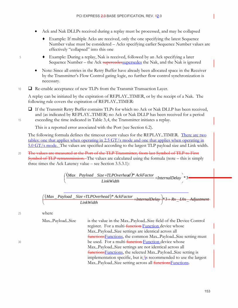
PCI EXPRESS 2.0 BASE SPECIFICATION, REV. 12.0
153
• Ack and Nak DLLPs received during a replay must be processed, and may be collapsed
♦ Example: If multiple Acks are received, only the one specifying the latest Sequence Number value must be considered – Acks specifying earlier Sequence Number values are effectively “collapsed” into this one
♦ Example: During a replay, Nak is received, followed by an Ack specifying a later 5 Sequence Number – the Ack supercedessupersedes the Nak, and the Nak is ignored
• Note: Since all entries in the Retry Buffer have already been allocated space in the Receiver by the Transmitter’s Flow Control gating logic, no further flow control synchronization is necessary.
Re-enable acceptance of new TLPs from the Transmit Transaction Layer. 10
A replay can be initiated by the expiration of REPLAY_TIMER, or by the receipt of a Nak. The following rule covers the expiration of REPLAY_TIMER:
If the Transmit Retry Buffer contains TLPs for which no Ack or Nak DLLP has been received, and (as indicated by REPLAY_TIMER) no Ack or Nak DLLP has been received for a period exceeding the time indicated in Table 3-4, the Transmitter initiates a replay. 15
This is a reported error associated with the Port (see Section 6.2).
The following formula defines the timeout count values for the REPLAY_TIMER. There are two tables: one that applies when operating in 2.5 GT/s mode and one that applies when operating in 5.0 GT/s mode. The values are specified according to the largest TLP payload size and Link width.
The values are measured at the Port of the TLP Transmitter, from last Symbol of TLP to First 20 Symbol of TLP retransmission. The values are calculated using the formula (note – this is simply three times the Ack Latency value – see Section 3.5.3.1):
( )lay InternalDe
LinkWidthFactorAckdTLPOverheaSizePayload Max 3 * *__
⎟ ⎠ ⎞ ⎜
⎝ ⎛ +
+
( ) AdjustmentsLRxlayInternalDeLinkWidth
FactorAckdTLPOverheaSizePayloadMax _0_3**__+⎟
⎠⎞
⎜⎝⎛ +
+
where 25
Max_Payload_Size is the value in the Max_Payload_Size field of the Device Control register. For a multi-function Function device whose Max_Payload_Size settings are identical across all functionsFunctions, the common Max_Payload_Size setting must be used. For a multi-function Function device whose 30 Max_Payload_Size settings are not identical across all functionsFunctions, the selected Max_Payload_Size setting is implementation specific, but it ’is recommended to use the largest Max_Payload_Size setting across all functionsFunctions.
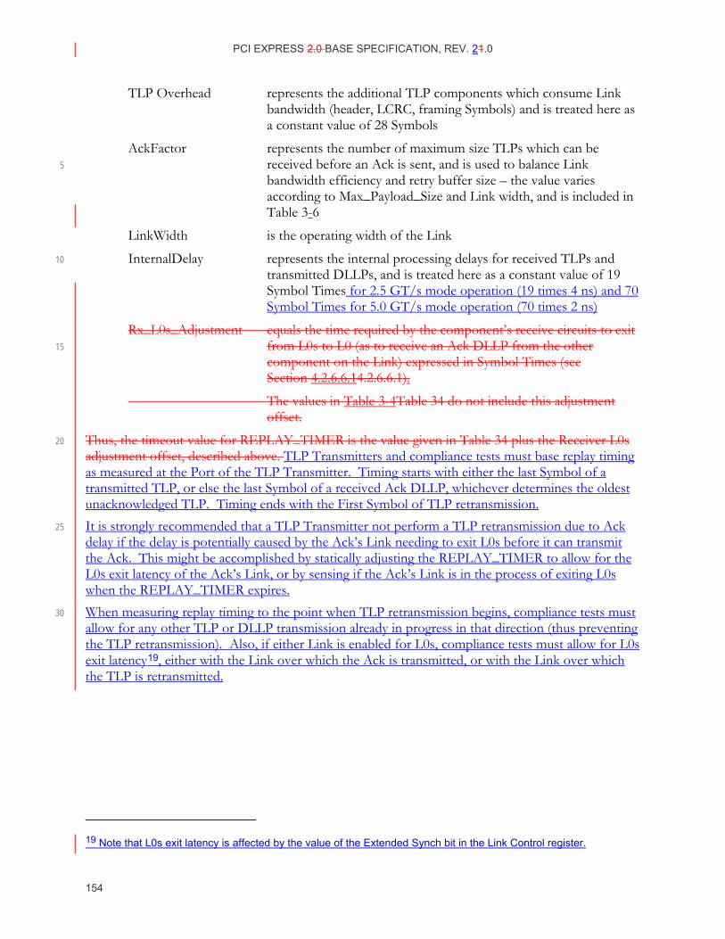
PCI EXPRESS 2.0 BASE SPECIFICATION, REV. 21.0
154
TLP Overhead represents the additional TLP components which consume Link bandwidth (header, LCRC, framing Symbols) and is treated here as a constant value of 28 Symbols
AckFactor represents the number of maximum size TLPs which can be received before an Ack is sent, and is used to balance Link 5 bandwidth efficiency and retry buffer size – the value varies according to Max_Payload_Size and Link width, and is included in Table 3-6
LinkWidth is the operating width of the Link
InternalDelay represents the internal processing delays for received TLPs and 10 transmitted DLLPs, and is treated here as a constant value of 19 Symbol Times for 2.5 GT/s mode operation (19 times 4 ns) and 70 Symbol Times for 5.0 GT/s mode operation (70 times 2 ns)
Rx_L0s_Adjustment equals the time required by the component’s receive circuits to exit from L0s to L0 (as to receive an Ack DLLP from the other 15 component on the Link) expressed in Symbol Times (see Section 4.2.6.6.1 4.2.6.6.1).
The values in Table 3-4Table 34 do not include this adjustment offset.
Thus, the timeout value for REPLAY_TIMER is the value given in Table 34 plus the Receiver L0s 20 adjustment offset, described above. TLP Transmitters and compliance tests must base replay timing as measured at the Port of the TLP Transmitter. Timing starts with either the last Symbol of a transmitted TLP, or else the last Symbol of a received Ack DLLP, whichever determines the oldest unacknowledged TLP. Timing ends with the First Symbol of TLP retransmission. It is strongly recommended that a TLP Transmitter not perform a TLP retransmission due to Ack 25 delay if the delay is potentially caused by the Ack’s Link needing to exit L0s before it can transmit the Ack. This might be accomplished by statically adjusting the REPLAY_TIMER to allow for the L0s exit latency of the Ack’s Link, or by sensing if the Ack’s Link is in the process of exiting L0s when the REPLAY_TIMER expires. When measuring replay timing to the point when TLP retransmission begins, compliance tests must 30 allow for any other TLP or DLLP transmission already in progress in that direction (thus preventing the TLP retransmission). Also, if either Link is enabled for L0s, compliance tests must allow for L0s exit latency19, either with the Link over which the Ack is transmitted, or with the Link over which the TLP is retransmitted.
19 Note that L0s exit latency is affected by the value of the Extended Synch bit in the Link Control register.
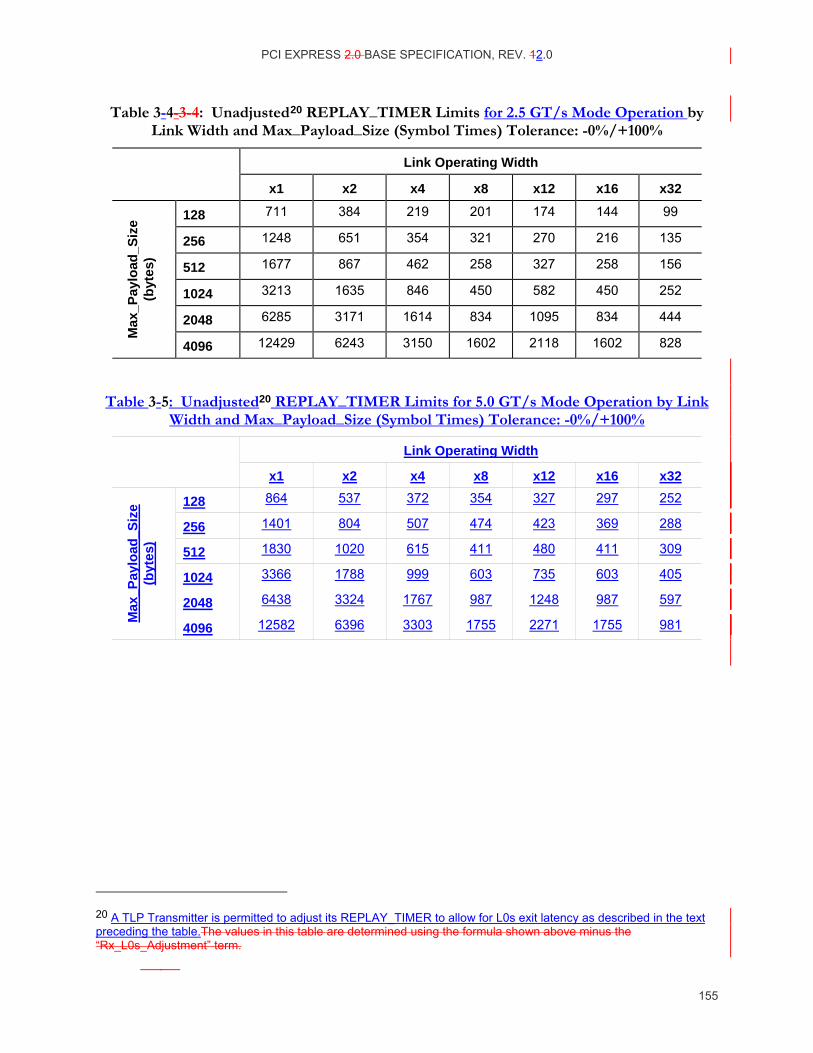
PCI EXPRESS 2.0 BASE SPECIFICATION, REV. 12.0
155
Table 3-4- 3-4: Unadjusted20 REPLAY_TIMER Limits for 2.5 GT/s Mode Operation by Link Width and Max_Payload_Size (Symbol Times) Tolerance: -0%/+100%
Link Operating Width
x1 x2 x4 x8 x12 x16 x32
128 711 384 219 201 174 144 99
256 1248 651 354 321 270 216 135
512 1677 867 462 258 327 258 156
1024 3213 1635 846 450 582 450 252
2048 6285 3171 1614 834 1095 834 444
Max
_Pay
load
_Siz
e (b
ytes
)
4096 12429 6243 3150 1602 2118 1602 828
Table 3-5: Unadjusted20 REPLAY_TIMER Limits for 5.0 GT/s Mode Operation by Link Width and Max_Payload_Size (Symbol Times) Tolerance: -0%/+100%
Link Operating Width
x1 x2 x4 x8 x12 x16 x32
128 864 537 372 354 327 297 252
256 1401 804 507 474 423 369 288
512 1830 1020 615 411 480 411 309
1024 3366 1788 999 603 735 603 405
2048 6438 3324 1767 987 1248 987 597
Max
_Pay
load
_Siz
e (b
ytes
)
4096 12582 6396 3303 1755 2271 1755 981
20 A TLP Transmitter is permitted to adjust its REPLAY_TIMER to allow for L0s exit latency as described in the text preceding the table.The values in this table are determined using the formula shown above minus the “Rx_L0s_Adjustment” term.
PCI EXPRESS 2.0 BASE SPECIFICATION, REV. 21.0
156
IMPLEMENTATION NOTE
Recommended Priority of Scheduled Transmissions When multiple DLLPs of the same type are scheduled for transmission but have not yet been transmitted, it is possible in many cases to “collapse” them into a single DLLP. For example, if a scheduled Ack DLLP transmission is stalled waiting for another transmission to complete, and during this time another Ack is scheduled for transmission, it is only necessary to transmit the second Ack, since the information it provides will supercedesupersede the information in the first 5 Ack.
In addition to any TLP from the Transaction Layer (or the Retry Buffer, if a retry is in progress), Multiple DLLPs of different types may be scheduled for transmission at the same time, and must be prioritized for transmission. The following list shows the preferred priority order for selecting information for transmission. Note that the priority of the vendor specific DLLP is not listed, as 10 this is completely implementation specific, and there is no recommended priority. Note that this priority order is a guideline, and that in all cases a fairness mechanism is highly recommended to ensure that no type of traffic is blocked for an extended or indefinite period of time by any other type of traffic. Note that the Ack Latency value and REPLAY_TIMER limit specify requirements measured at the Port of the component, and the internal arbitration policy of the component must 15 ensure that these externally measured requirements are met.
1) Completion of any transmission (TLP or DLLP) currently in progress (highest priority)
2) Nak DLLP transmissions
3) Ack DLLP transmissions scheduled for transmission as soon as possible due to: receipt of a duplicate TLP –OR– 20 expiration of the Ack latency timer (see Section 3.5.3.1)
4) FC DLLP transmissions required to satisfy Section 2.6
5) Retry Buffer re-transmissions
6) TLPs from the Transaction Layer
7) FC DLLP transmissions other than those required to satisfy Section 2.6 25
8) All other DLLP transmissions (lowest priority)
3.5.2.2. Handling of Received DLLPs
Since Ack/Nak and Flow Control DLLPs affect TLPs flowing in the opposite direction across the Link, the TLP transmission mechanisms in the Data Link Layer are also responsible for Ack/Nak and Flow Control DLLPs received from the other component on the Link. These DLLPs are processed according to the following rules (see Figure 3-15): 30
PCI EXPRESS 2.0 BASE SPECIFICATION, REV. 12.0
157
If the Physical Layer indicates a Receiver Error, discard any DLLP currently being received and free any storage allocated for the DLLP. Note that reporting such errors to software is done by the Physical Layer (and, therefore, not reported by the Data Link Layer).
For all received DLLPs, the CRC value is checked by:
• applying the same algorithm used for calculation of transmitted DLLPs to the received 5 DLLP, not including the 16 16-bit CRC field of the received DLLP
• comparing the calculated result with the value in the CRC field of the received DLLP
♦ if not equal, the DLLP is corrupt
• A corrupt received DLLP is discarded, and is a reported error associated with the Port (see Section 6.2). 10
A received DLLP which is not corrupt, but which uses unsupported DLLP Type encodings is discarded without further action. This is not considered an error.
Non-zero values in Reserved fields are ignored.
Receivers must process all DLLPs received at the rate they are received
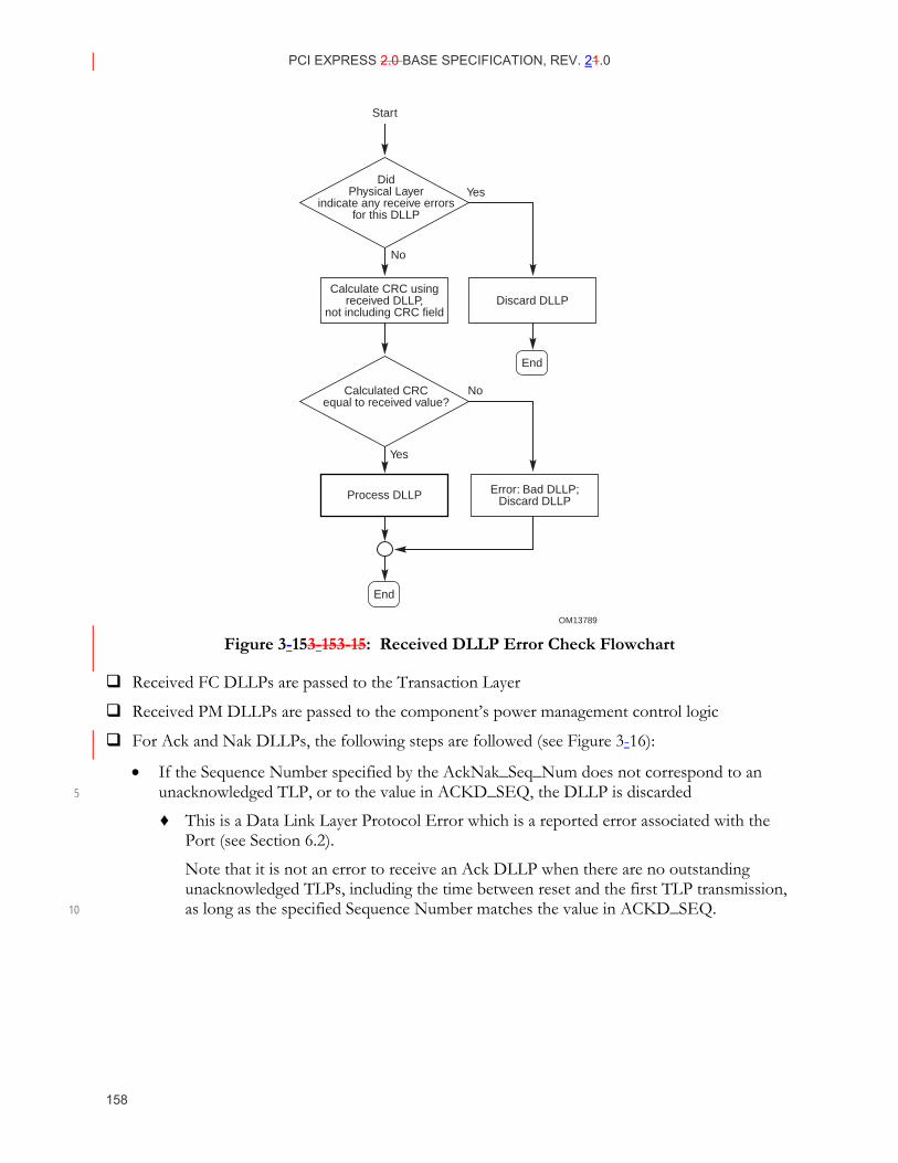
PCI EXPRESS 2.0 BASE SPECIFICATION, REV. 21.0
158
OM13789
DidPhysical Layer
indicate any receive errorsfor this DLLP
Calculated CRCequal to received value?
Start
Calculate CRC usingreceived DLLP,
not including CRC fieldDiscard DLLP
No
Yes
Yes
End
No
End
Error: Bad DLLP;Discard DLLPProcess DLLP
Figure 3-153-15 3-15: Received DLLP Error Check Flowchart
Received FC DLLPs are passed to the Transaction Layer
Received PM DLLPs are passed to the component’s power management control logic
For Ack and Nak DLLPs, the following steps are followed (see Figure 3-16):
• If the Sequence Number specified by the AckNak_Seq_Num does not correspond to an unacknowledged TLP, or to the value in ACKD_SEQ, the DLLP is discarded 5
♦ This is a Data Link Layer Protocol Error which is a reported error associated with the Port (see Section 6.2).
Note that it is not an error to receive an Ack DLLP when there are no outstanding unacknowledged TLPs, including the time between reset and the first TLP transmission, as long as the specified Sequence Number matches the value in ACKD_SEQ. 10
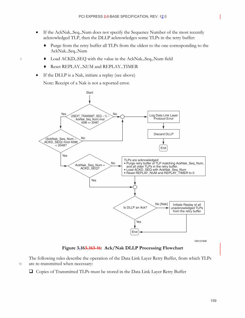
PCI EXPRESS 2.0 BASE SPECIFICATION, REV. 12.0
159
• If the AckNak_Seq_Num does not specify the Sequence Number of the most recently acknowledged TLP, then the DLLP acknowledges some TLPs in the retry buffer:
♦ Purge from the retry buffer all TLPs from the oldest to the one corresponding to the AckNak_Seq_Num
♦ Load ACKD_SEQ with the value in the AckNak_Seq_Num field 5
♦ Reset REPLAY_NUM and REPLAY_TIMER
• If the DLLP is a Nak, initiate a replay (see above)
Note: Receipt of a Nak is not a reported error.
OM13790B
End
End
Initiate Replay of allunacknowledged TLPs
from the retry buffer
Log Data Link LayerProtocol Error
Discard DLLP
TLPs are acknowledged: Purge retry buffer of TLP matching AckNak_Seq_Num, and all older TLPs in the retry buffer. Load ACKD_SEQ with AckNak_Seq_Num Reset REPLAY_NUM and REPLAY_TIMER to 0
Is DLLP an Ack?
AckNak_Seq_Num =ACKD_SEQ?
(AckNak_Seq_Num –ACKD_SEQ) mod 4096
< 2048?
No [Nak]
No
No
((NEXT_TRANSMIT_SEQ – 1) –AckNak_Seq_Num) mod
4096 <= 2048?
NoYes
Yes
Yes
Yes
Start
Figure 3-163-16 3-16: Ack/Nak DLLP Processing Flowchart
The following rules describe the operation of the Data Link Layer Retry Buffer, from which TLPs are re-transmitted when necessary: 10
Copies of Transmitted TLPs must be stored in the Data Link Layer Retry Buffer
PCI EXPRESS 2.0 BASE SPECIFICATION, REV. 21.0
160
3.5.3. LCRC and Sequence Number (TLP Receiver)
The TLP Receive path through the Data Link Layer (paths labeled 2 and 4 in Figure 3-1) processes TLPs received by the Physical Layer by checking the LCRC and sequence number, passing the TLP to the Receive Transaction Layer if OK and requesting a retry if corrupted.
The mechanisms used to check the TLP LCRC and the Sequence Number and to support Data Link Layer Retry are described in terms of conceptual “counters” and “flags.” This description does not 5 imply or require a particular implementation and is used only to clarify the requirements.
3.5.3.1. LCRC and Sequence Number Rules (TLP Receiver)
The following counter, flag, and timer are used to explain the remaining rules in this section:
The following 12-bit counter is used:
• NEXT_RCV_SEQ – Stores the expected Sequence Number for the next TLP
♦ Set to all 0’s 000h in DL_Inactive state 10
The following flag is used:
• NAK_SCHEDULED
♦ Cleared when in DL_Inactive state
The following timer is used:
• AckNak_LATENCY_TIMER – Counts time that determines when an Ack DLLP becomes 15 scheduled for transmission, according to the following rules:Counts time since an Ack or Nak DLLP was scheduled for transmission
♦ Set to 0 in DL_Inactive state
♦ Restart from 0 each time an Ack or Nak DLLP is scheduled for transmission; Reset to 0 when all TLPs received have been acknowledged with an Ack DLLP 20
♦ If there are initially no unacknowledged TLPs and a TLP is then received, the AckNak_LATENCY_TIMER starts counting only when the TLP has been forwarded to the Receive Transaction Layer
The following rules are applied in sequence to describe how received TLPs are processed, and what events trigger the transmission of Ack and Nak DLLPs (see Figure 3-17): 25
If the Physical Layer indicates a Receiver Error, discard any TLP currently being received and free any storage allocated for the TLP. Note that reporting such errors to software is done by the Physical Layer (and so are not reported by the Data Link Layer).
• If a TLP was being received at the time the Receive Error was indicated and the NAK_SCHEDULED flag is clear, 30
♦ schedule a Nak DLLP for transmission immediately
♦ set the NAK_SCHEDULED flag
PCI EXPRESS 2.0 BASE SPECIFICATION, REV. 12.0
161
If the Physical Layer reports that the received TLP end framing Symbol was EDB, and the LCRC is the logical NOT of the calculated value, discard the TLP and free any storage allocated for the TLP. This is not considered an error.
If TLP end framing Symbol was EDB but the LCRC does not match the logical NOT of the calculated value, the TLP is corrupt - discard the TLP and free any storage allocated for the 5 TLP.
• If the NAK_SCHEDULED flag is clear,
♦ schedule a Nak DLLP for transmission immediately
♦ set the NAK_SCHEDULED flag
This is a reported error associated with the Port (see Section 6.2). 10
The LCRC value is checked by:
• applying the same algorithm used for calculation (above) to the received TLP, not including the 32-bit LCRC field of the received TLP
• comparing the calculated result with the value in the LCRC field of the received TLP
♦ if not equal, the TLP is corrupt - discard the TLP and free any storage allocated for the 15 TLP
If the NAK_SCHEDULED flag is clear,
schedule a Nak DLLP for transmission immediately
set the NAK_SCHEDULED flag
This is a reported error associated with the Port (see Section 6.2). 20
If the TLP Sequence Number is not equal to the expected value, stored in NEXT_RCV_SEQ:
• discard the TLP and free any storage allocated for the TLP
• If the TLP Sequence Number satisfies the following equation:
(NEXT_RCV_SEQ - TLP Sequence Number) mod 4096 <= 2048
the TLP is a duplicate, and an Ack DLLP is scheduled for transmission (per transmission 25 priority rules)
• Otherwise, the TLP is out of sequence (indicating one or more lost TLPs):
♦ if the NAK_SCHEDULED flag is clear,
schedule a Nak DLLP for transmission immediately
set the NAK_SCHEDULED flag 30
report TLP missing
This is a reported error associated with the Port (see Section 6.2).
PCI EXPRESS 2.0 BASE SPECIFICATION, REV. 21.0
162
If the TLP Sequence Number is equal to the expected value stored in NEXT_RCV_SEQ:
• The Reserved bits, Sequence Number, and LCRC are removed and the remainder of the TLP is forwarded to the Receive Transaction Layer
♦ The Data Link Layer indicates the start and end of the TLP to the Transaction Layer while transferring the TLP 5
The Data Link Layer treats the TLP as a “black box” and does not process or modify the contents of the TLP
♦ Note that the Receiver Flow Control mechanisms do not account for any received TLPs until the TLP(s) are forwarded to the Receive Transaction Layer
• NEXT_RCV_SEQ is incremented 10
• If setSet, the NAK_SCHEDULED flag is cleared
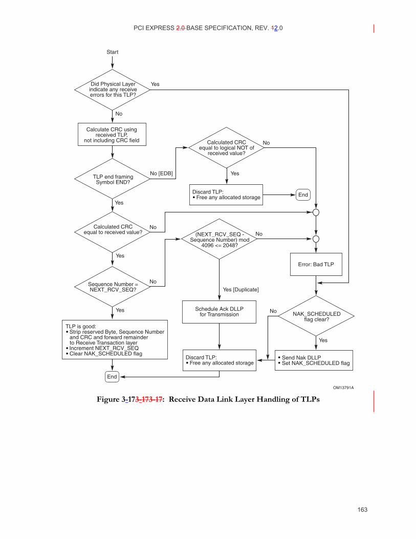
PCI EXPRESS 2.0 BASE SPECIFICATION, REV. 12.0
163
No
OM13791A
End
Calculate CRC usingreceived TLP,
not including CRC field
Schedule Ack DLLPfor Transmission
Send Nak DLLPSet NAK_SCHEDULED flag
TLP is good: Strip reserved Byte, Sequence Number and CRC and forward remainder to Receive Transaction layer Increment NEXT_RCV_SEQ Clear NAK_SCHEDULED flag
Sequence Number =NEXT_RCV_SEQ?
(NEXT_RCV_SEQ -Sequence Number) mod
4096 <= 2048?
Calculated CRCequal to received value?
NoNo
No
Yes [Duplicate]
Yes
Did Physical Layerindicate any receiveerrors for this TLP?
TLP end framingSymbol END?
Yes
No [EDB]
Yes
No
Yes
Start
Yes
Discard TLP: Free any allocated storage End
Discard TLP: Free any allocated storage
Error: Bad TLP
Calculated CRCequal to logical NOT of
received value?
Yes
No NAK_SCHEDULEDflag clear?
Figure 3-173-17 3-17: Receive Data Link Layer Handling of TLPs
PCI EXPRESS 2.0 BASE SPECIFICATION, REV. 21.0
164
A TLP Receiver must schedule An an Ack DLLP must be transmitted such that it will be transmitted no later than when all of the following conditions are true:
• The Data Link Control and Management State Machine is in the DL_Active state
• TLPs have been forwarded to the Receive Transaction Layer, but not yet acknowledged by sending an Ack DLLP 5
• The AckNak_LATENCY_TIMER reaches or exceeds the value specified in Table 3-6 for 2.5 GT/s mode operation and Table 3-7 for 5.0 GT/s mode operation
• The Link used for Ack DLLP transmission is already in L0 or has transitioned to L0
Note: if not already in L0, the Link must transition to L0 in order to transmit the Ack DLLP
• Another TLP or DLLP is not currently being transmitted on the Link used for Ack DLLP 10 transmission
• The NAK_SCHEDULED flag is clear
Note: The AckNak_LATENCY_TIMER must be restarted from 0 each time an Ack or Nak DLLP is scheduled for transmission
Data Link Layer Ack DLLPs may be scheduled for transmission more frequently than required 15
Data Link Layer Ack and Nak DLLPs specify the value (NEXT_RCV_SEQ - 1) in the AckNak_Seq_Num field
Table 3-6 and Table 3-7 defines the threshold values for the AckNak_LATENCY_TIMER timer, which for any specific case is called the Ack Latency. The values are specified according to the largest TLP payload size and Link width. The values are measured at the Port of the TLP Receiver, 20 starting with the time the last Symbol of a TLP is received to the first Symbol of the Ack/Nak DLLP being transmitted. The values are calculated using the formula:
( ) AdjustmentsLTxlayInternalDeLinkWidth
FactorAckdTLPOverheaSizePayloadMax _0_*__++
+
( ) layInternalDeLinkWidth
FactorAckdTLPOverheaSizePayloadMax *__+
+
where 25
Max_Payload_Size is the value in the Max_Payload_Size field of the Device Control register. For a multi-functionFunction device whose Max_Payload_Size settings are identical across all functionFunctions, the common Max_Payload_Size setting must be used. For a multi-functionFunction device whose 30 Max_Payload_Size settings are not identical across all functionFunctions, the selected Max_Payload_Size setting is implementation specific, but it’s it is recommended to use the smallest Max_Payload_Size setting across all functionFunctions.
PCI EXPRESS 2.0 BASE SPECIFICATION, REV. 12.0
165
TLP Overhead represents the additional TLP components which consume Link bandwidth (header, LCRC, framing Symbols) and is treated here as a constant value of 28 Symbols.
AckFactor represents the number of maximum size TLPs which can be received before an Ack is sent, and is used to balance Link 5 bandwidth efficiency and retry buffer size – the value varies according to Max_Payload_Size and Link width, and is defined in Table 3-6.
LinkWidth is the operating width of the Link.
InternalDelay represents the internal processing delays for received TLPs and 10 transmitted DLLPs, and is treated here as a constant value of 19 Symbol Times for 2.5 GT/s mode operation (19 times 4 ns) and 70 Symbol Times for 5.0 GT/s operation (70 times 2 ns).
Tx_L0s_Adjustment if L0s is enabled, the time required for the Transmitter to exit L0s (see Section 4.2.6.6.2 4.2.6.6.2), expressed in Symbol Times, or 0 if 15 L0s is not enabled.
Note that the setting of the Extended Synch bit of the Link Control register affects the exit time from L0s to L0, and must be taken into account in this adjustment.
The values in Table 3-5Table 35 do not include this adjustment 20 offset.
Thus, the Ack Latency is the value given in Table 3-5Table 35 plus the Transmitter L0s adjustment offset, described above. TLP Receivers and compliance tests must base Ack Latency timing as measured at the Port of the TLP Receiver, starting with the time the last Symbol of a TLP is received to the first Symbol of the 25 Ack DLLP being transmitted. When measuring until the Ack DLLP is transmitted, compliance tests must allow for any TLP or other DLLP transmission already in progress in that direction (thus preventing the Ack DLLP transmission). If L0s is enabled, compliance tests must allow for the L0s exit latency of the Link in the direction that the Ack DLLP is being transmitted. If the Extended Synch bit of the Link 30 Control register is Set, compliance tests must also allow for its effect on L0s exit latency. TLP Receivers are not required to adjust their Ack DLLP scheduling based upon L0s exit latency or the value of the Extended Synch bit.
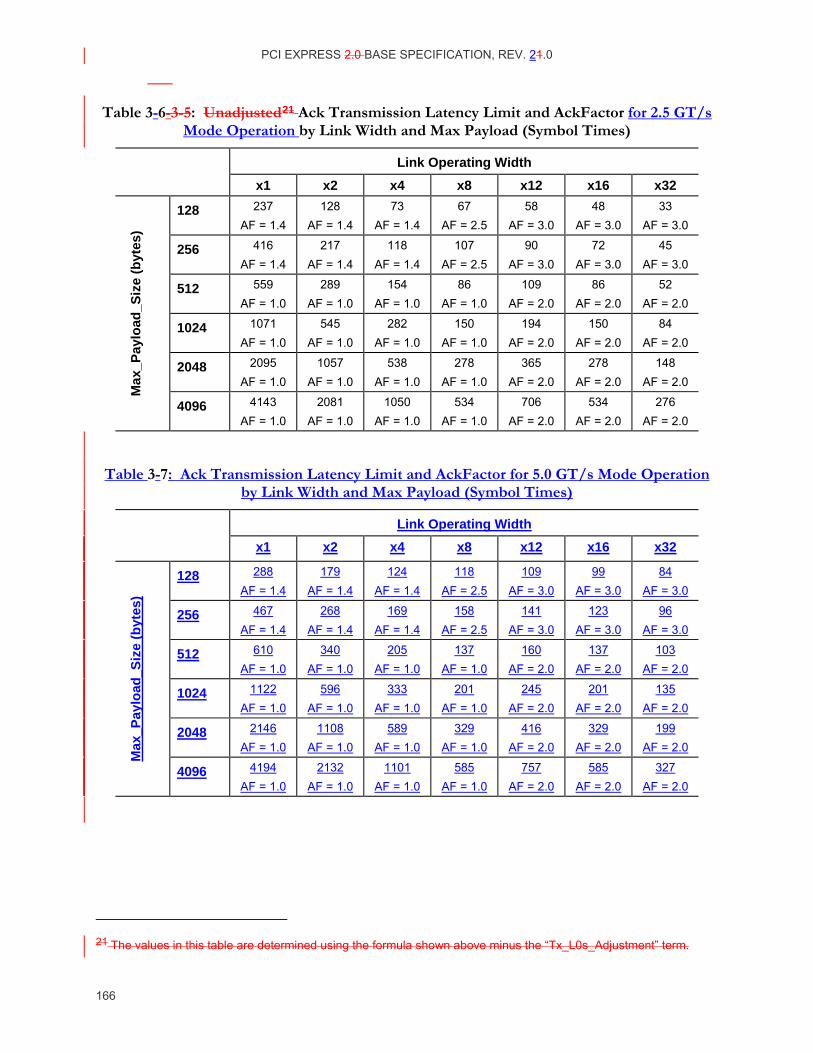
PCI EXPRESS 2.0 BASE SPECIFICATION, REV. 21.0
166
Table 3-6- 3-5: Unadjusted21 Ack Transmission Latency Limit and AckFactor for 2.5 GT/s Mode Operation by Link Width and Max Payload (Symbol Times)
Link Operating Width x1 x2 x4 x8 x12 x16 x32
128 237 AF = 1.4
128 AF = 1.4
73 AF = 1.4
67 AF = 2.5
58 AF = 3.0
48 AF = 3.0
33 AF = 3.0
256 416 AF = 1.4
217 AF = 1.4
118 AF = 1.4
107 AF = 2.5
90 AF = 3.0
72 AF = 3.0
45 AF = 3.0
512 559 AF = 1.0
289 AF = 1.0
154 AF = 1.0
86 AF = 1.0
109 AF = 2.0
86 AF = 2.0
52 AF = 2.0
1024 1071 AF = 1.0
545 AF = 1.0
282 AF = 1.0
150 AF = 1.0
194 AF = 2.0
150 AF = 2.0
84 AF = 2.0
2048 2095 AF = 1.0
1057 AF = 1.0
538 AF = 1.0
278 AF = 1.0
365 AF = 2.0
278 AF = 2.0
148 AF = 2.0
Max
_Pay
load
_Siz
e (b
ytes
)
4096 4143 AF = 1.0
2081 AF = 1.0
1050 AF = 1.0
534 AF = 1.0
706 AF = 2.0
534 AF = 2.0
276 AF = 2.0
Table 3-7: Ack Transmission Latency Limit and AckFactor for 5.0 GT/s Mode Operation by Link Width and Max Payload (Symbol Times)
Link Operating Width x1 x2 x4 x8 x12 x16 x32
128 288 AF = 1.4
179 AF = 1.4
124 AF = 1.4
118 AF = 2.5
109 AF = 3.0
99 AF = 3.0
84 AF = 3.0
256 467 AF = 1.4
268 AF = 1.4
169 AF = 1.4
158 AF = 2.5
141 AF = 3.0
123 AF = 3.0
96 AF = 3.0
512 610 AF = 1.0
340 AF = 1.0
205 AF = 1.0
137 AF = 1.0
160 AF = 2.0
137 AF = 2.0
103 AF = 2.0
1024 1122 AF = 1.0
596 AF = 1.0
333 AF = 1.0
201 AF = 1.0
245 AF = 2.0
201 AF = 2.0
135 AF = 2.0
2048 2146 AF = 1.0
1108 AF = 1.0
589 AF = 1.0
329 AF = 1.0
416 AF = 2.0
329 AF = 2.0
199 AF = 2.0
Max
_Pay
load
_Siz
e (b
ytes
)
4096 4194 AF = 1.0
2132 AF = 1.0
1101 AF = 1.0
585 AF = 1.0
757 AF = 2.0
585 AF = 2.0
327 AF = 2.0
21 The values in this table are determined using the formula shown above minus the “Tx_L0s_Adjustment” term.
PCI EXPRESS 2.0 BASE SPECIFICATION, REV. 12.0
167
IMPLEMENTATION NOTE
Retry Buffer Sizing The Retry Buffer should be large enough to ensure that under normal operating conditions, transmission is never throttled because the retry buffer is full. In determining the optimal buffer size, one must consider the Ack Latency value, any differences between the actual implementation and the internal processing delay used to generate these values Ack delay caused by the Receiver already transmitting another TLP, and the delays caused by the physical Link interconnect, and the 5 time required to process the received Ack DLLP.
Given two components A and B, the L0s exit latency required by A's Receiver should be accounted for when sizing A's transmit retry buffer, as is demonstrated in the following example:The Receiver L0s exit latency (see Section 4.6.2.2.1) should also be accounted for, as is demonstrated with the following example using components A and B: 10
A exits L0s on its Transmit path to B and starts transmitting a long burst of write Requests to B
B initiates L0s exit on its Transmit path to A, but the L0s exit time required by A’s Receiver is large
Meanwhile, B is unable to send Ack DLLPs to A, and A stalls due to lack of Retry Buffer space
The Transmit path from B to A returns to L0, B transmits an Ack DLLP to A, and the stall is 15 resolved
This stall can be avoided by matching the size of a component’s Transmitter Retry Buffer to the L0s exit latency of required by the component’s Receiver, or, conversely, by matching the Receiver L0s exit latency to the desired size of the Retry Buffer.
AckFactor values were chosen to allow implementations to achieve good performance without 20 requiring an uneconomically large retry buffer. To enable consistent performance across a general purpose interconnect with differing implementations and applications, it is necessary to set the same requirements for all components without regard to the application space of any specific component. If a component does not require the full transmission bandwidth of the Link, it may reduce the size of its retry buffer below the minimum size required to maintain available retry buffer space with the 25 Ack Latency values specified.
Note that the Ack Latency values specified ensure that the range of permitted outstanding Sequence Numbers will never be the limiting factor causing transmission stalls.
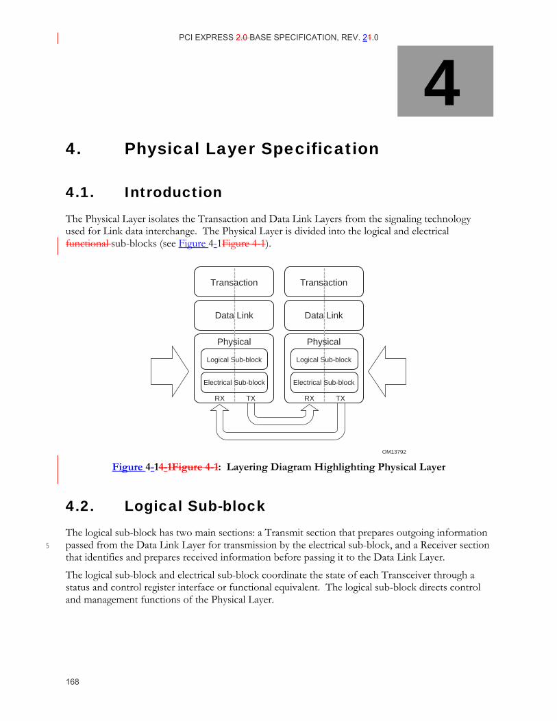
PCI EXPRESS 2.0 BASE SPECIFICATION, REV. 21.0
168
4. Physical Layer Specification
4.1. Introduction The Physical Layer isolates the Transaction and Data Link Layers from the signaling technology used for Link data interchange. The Physical Layer is divided into the logical and electrical functional sub-blocks (see Figure 4-1Figure 4-1).
OM13792
Data Link Data Link
RX TX
Logical Sub-block
Electrical Sub-block
Physical
RX TX
Logical Sub-block
Electrical Sub-block
Physical
Transaction Transaction
Figure 4-14-1Figure 4-1: Layering Diagram Highlighting Physical Layer
4.2. Logical Sub-block The logical sub-block has two main sections: a Transmit section that prepares outgoing information passed from the Data Link Layer for transmission by the electrical sub-block, and a Receiver section 5 that identifies and prepares received information before passing it to the Data Link Layer.
The logical sub-block and electrical sub-block coordinate the state of each Transceiver through a status and control register interface or functional equivalent. The logical sub-block directs control and management functions of the Physical Layer.
4
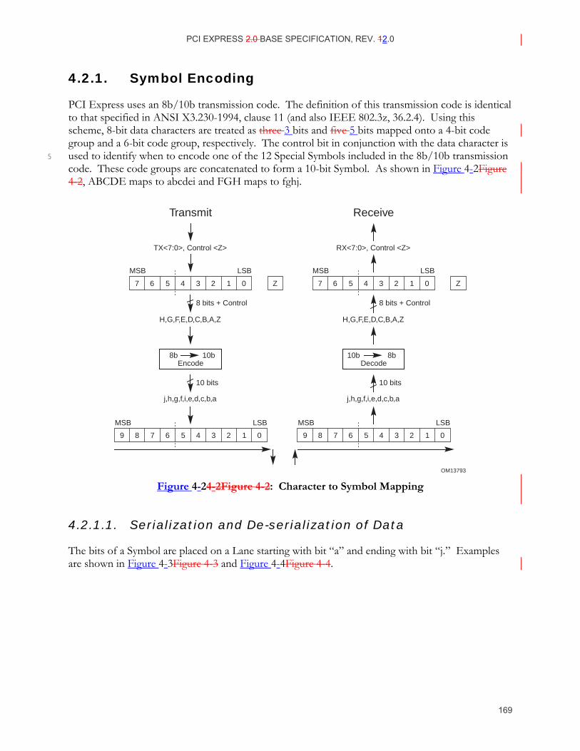
PCI EXPRESS 2.0 BASE SPECIFICATION, REV. 12.0
169
4.2.1. Symbol Encoding
PCI Express uses an 8b/10b transmission code. The definition of this transmission code is identical to that specified in ANSI X3.230-1994, clause 11 (and also IEEE 802.3z, 36.2.4). Using this scheme, 8-bit data characters are treated as three 3 bits and five 5 bits mapped onto a 4-bit code group and a 6-bit code group, respectively. The control bit in conjunction with the data character is used to identify when to encode one of the 12 Special Symbols included in the 8b/10b transmission 5 code. These code groups are concatenated to form a 10-bit Symbol. As shown in Figure 4-2Figure 4-2, ABCDE maps to abcdei and FGH maps to fghj.
OM13793
9
MSB LSB
8 7
j,h,g,f,i,e,d,c,b,a
10 bits
MSB LSB
TX<7:0>, Control <Z>
Transmit
H,G,F,E,D,C,B,A,Z
8 bits + Control
6 5 4 3 2 1 0
7 6 5 4 3 2 1 0 Z
8bEncode
10b
9
MSB LSB
8 7
j,h,g,f,i,e,d,c,b,a
10 bits
MSB LSB
RX<7:0>, Control <Z>
Receive
H,G,F,E,D,C,B,A,Z
8 bits + Control
6 5 4 3 2 1 0
7 6 5 4 3 2 1 0 Z
10bDecode
8b
Figure 4-24-2Figure 4-2: Character to Symbol Mapping
4.2.1.1. Serialization and De-serialization of Data
The bits of a Symbol are placed on a Lane starting with bit “a” and ending with bit “j.” Examples are shown in Figure 4-3Figure 4-3 and Figure 4-4Figure 4-4.
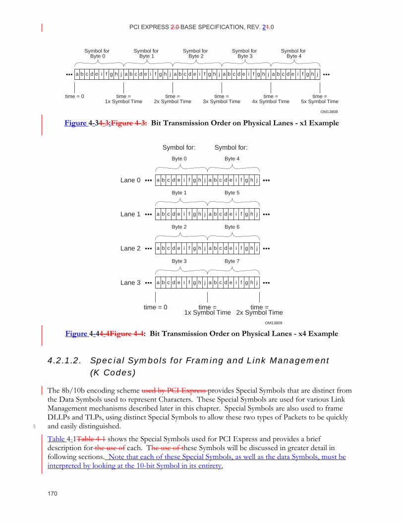
PCI EXPRESS 2.0 BASE SPECIFICATION, REV. 21.0
170
OM13808
a b c d e i f g h j a b c d e i f g h j a b c d e i f g h j a b c d e i f g h j a b c d e i f g h j
Symbol for Byte 0
Symbol for Byte 1
Symbol for Byte 2
Symbol for Byte 3
Symbol for Byte 4
time = 0 time =1x Symbol Time
time =2x Symbol Time
time =3x Symbol Time
time =5x Symbol Time
time =4x Symbol Time
Figure 4-34-3:Figure 4-3: Bit Transmission Order on Physical Lanes - x1 Example
OM13809
Lane 0 a b c d e i f g h j a b c d e i f g h j
Symbol for: Symbol for:
Byte 0 Byte 4
time = 0 time =1x Symbol Time
time =2x Symbol Time
Lane 1 a b c d e i f g h j a b c d e i f g h j
Byte 1 Byte 5
Lane 2 a b c d e i f g h j a b c d e i f g h j
Byte 2 Byte 6
Lane 3 a b c d e i f g h j a b c d e i f g h j
Byte 3 Byte 7
Figure 4-44-4Figure 4-4: Bit Transmission Order on Physical Lanes - x4 Example
4.2.1.2. Special Symbols for Framing and Link Management (K Codes)
The 8b/10b encoding scheme used by PCI Express provides Special Symbols that are distinct from the Data Symbols used to represent Characters. These Special Symbols are used for various Link Management mechanisms described later in this chapter. Special Symbols are also used to frame DLLPs and TLPs, using distinct Special Symbols to allow these two types of Packets to be quickly and easily distinguished. 5
Table 4-1Table 4-1 shows the Special Symbols used for PCI Express and provides a brief description for the use of each. The use of these Symbols will be discussed in greater detail in following sections. Note that each of these Special Symbols, as well as the data Symbols, must be interpreted by looking at the 10-bit Symbol in its entirety.
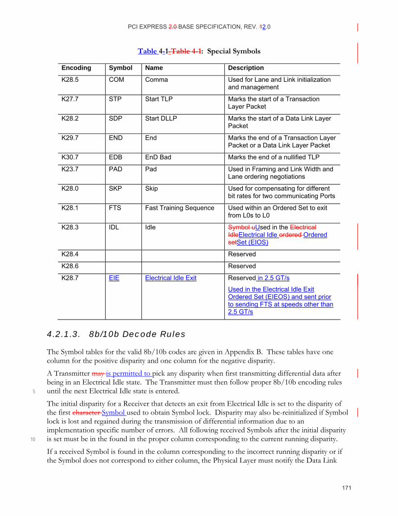
PCI EXPRESS 2.0 BASE SPECIFICATION, REV. 12.0
171
Table 4-1-Table 4-1: Special Symbols
Encoding Symbol Name Description
K28.5 COM Comma Used for Lane and Link initialization and management
K27.7 STP Start TLP Marks the start of a Transaction Layer Packet
K28.2 SDP Start DLLP Marks the start of a Data Link Layer Packet
K29.7 END End Marks the end of a Transaction Layer Packet or a Data Link Layer Packet
K30.7 EDB EnD Bad Marks the end of a nullified TLP
K23.7 PAD Pad Used in Framing and Link Width and Lane ordering negotiations
K28.0 SKP Skip Used for compensating for different bit rates for two communicating Ports
K28.1 FTS Fast Training Sequence Used within an Ordered Set to exit from L0s to L0
K28.3 IDL Idle Symbol uUsed in the Electrical IdleElectrical Idle ordered Ordered setSet (EIOS)
K28.4 Reserved
K28.6 Reserved
K28.7 EIE Electrical Idle Exit Reserved in 2.5 GT/s
Used in the Electrical Idle Exit Ordered Set (EIEOS) and sent prior to sending FTS at speeds other than 2.5 GT/s
4.2.1.3. 8b/10b Decode Rules
The Symbol tables for the valid 8b/10b codes are given in Appendix B. These tables have one column for the positive disparity and one column for the negative disparity.
A Transmitter may is permitted to pick any disparity when first transmitting differential data after being in an Electrical Idle state. The Transmitter must then follow proper 8b/10b encoding rules until the next Electrical Idle state is entered. 5
The initial disparity for a Receiver that detects an exit from Electrical Idle is set to the disparity of the first character Symbol used to obtain Symbol lock. Disparity may also be-reinitialized if Symbol lock is lost and regained during the transmission of differential information due to an implementation specific number of errors. All following received Symbols after the initial disparity is set must be in the found in the proper column corresponding to the current running disparity. 10
If a received Symbol is found in the column corresponding to the incorrect running disparity or if the Symbol does not correspond to either column, the Physical Layer must notify the Data Link
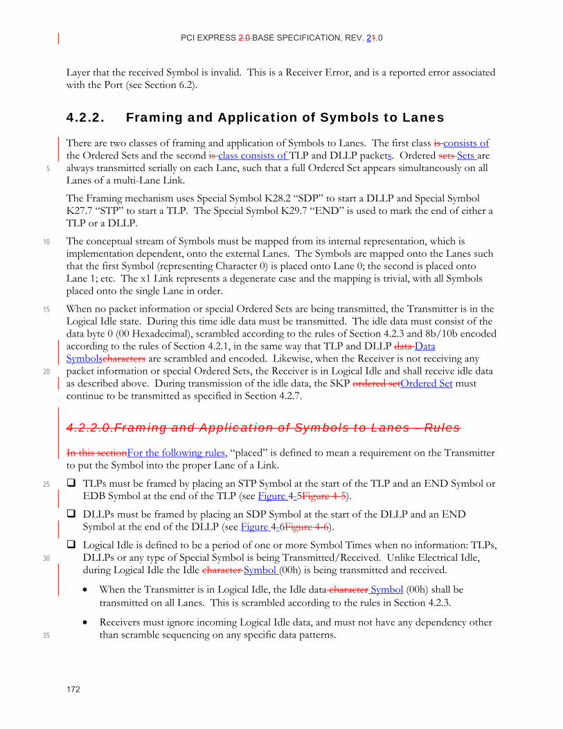
PCI EXPRESS 2.0 BASE SPECIFICATION, REV. 21.0
172
Layer that the received Symbol is invalid. This is a Receiver Error, and is a reported error associated with the Port (see Section 6.2).
4.2.2. Framing and Application of Symbols to Lanes
There are two classes of framing and application of Symbols to Lanes. The first class is consists of the Ordered Sets and the second is class consists of TLP and DLLP packets. Ordered sets Sets are always transmitted serially on each Lane, such that a full Ordered Set appears simultaneously on all 5 Lanes of a multi-Lane Link.
The Framing mechanism uses Special Symbol K28.2 “SDP” to start a DLLP and Special Symbol K27.7 “STP” to start a TLP. The Special Symbol K29.7 “END” is used to mark the end of either a TLP or a DLLP.
The conceptual stream of Symbols must be mapped from its internal representation, which is 10 implementation dependent, onto the external Lanes. The Symbols are mapped onto the Lanes such that the first Symbol (representing Character 0) is placed onto Lane 0; the second is placed onto Lane 1; etc. The x1 Link represents a degenerate case and the mapping is trivial, with all Symbols placed onto the single Lane in order.
When no packet information or special Ordered Sets are being transmitted, the Transmitter is in the 15 Logical Idle state. During this time idle data must be transmitted. The idle data must consist of the data byte 0 (00 Hexadecimal), scrambled according to the rules of Section 4.2.3 and 8b/10b encoded according to the rules of Section 4.2.1, in the same way that TLP and DLLP data Data Symbolscharacters are scrambled and encoded. Likewise, when the Receiver is not receiving any packet information or special Ordered Sets, the Receiver is in Logical Idle and shall receive idle data 20 as described above. During transmission of the idle data, the SKP ordered setOrdered Set must continue to be transmitted as specified in Section 4.2.7.
4.2.2.0.Framing and Application of Symbols to Lanes – Rules
In this sectionFor the following rules, “placed” is defined to mean a requirement on the Transmitter to put the Symbol into the proper Lane of a Link.
TLPs must be framed by placing an STP Symbol at the start of the TLP and an END Symbol or 25 EDB Symbol at the end of the TLP (see Figure 4-5Figure 4-5).
DLLPs must be framed by placing an SDP Symbol at the start of the DLLP and an END Symbol at the end of the DLLP (see Figure 4-6Figure 4-6).
Logical Idle is defined to be a period of one or more Symbol Times when no information: TLPs, DLLPs or any type of Special Symbol is being Transmitted/Received. Unlike Electrical Idle, 30 during Logical Idle the Idle character Symbol (00h) is being transmitted and received.
• When the Transmitter is in Logical Idle, the Idle data character Symbol (00h) shall be transmitted on all Lanes. This is scrambled according to the rules in Section 4.2.3.
• Receivers must ignore incoming Logical Idle data, and must not have any dependency other than scramble sequencing on any specific data patterns. 35
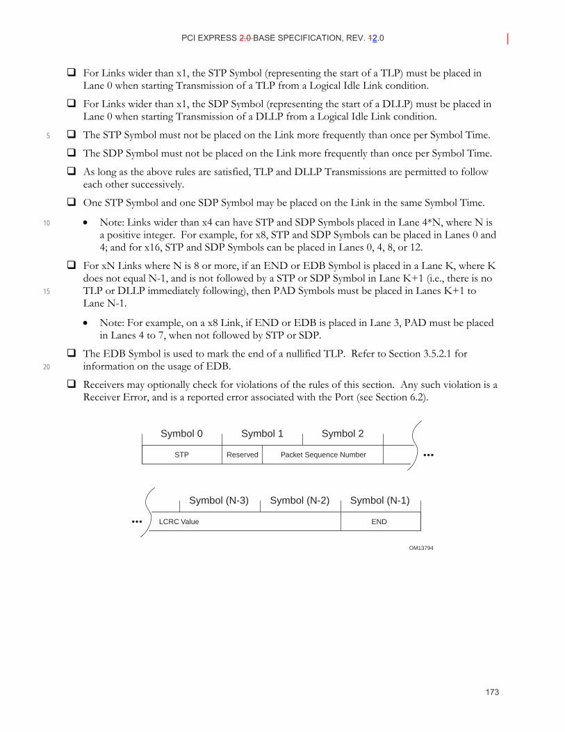
PCI EXPRESS 2.0 BASE SPECIFICATION, REV. 12.0
173
For Links wider than x1, the STP Symbol (representing the start of a TLP) must be placed in Lane 0 when starting Transmission of a TLP from a Logical Idle Link condition.
For Links wider than x1, the SDP Symbol (representing the start of a DLLP) must be placed in Lane 0 when starting Transmission of a DLLP from a Logical Idle Link condition.
The STP Symbol must not be placed on the Link more frequently than once per Symbol Time. 5
The SDP Symbol must not be placed on the Link more frequently than once per Symbol Time.
As long as the above rules are satisfied, TLP and DLLP Transmissions are permitted to follow each other successively.
One STP Symbol and one SDP Symbol may be placed on the Link in the same Symbol Time.
• Note: Links wider than x4 can have STP and SDP Symbols placed in Lane 4*N, where N is 10 a positive integer. For example, for x8, STP and SDP Symbols can be placed in Lanes 0 and 4; and for x16, STP and SDP Symbols can be placed in Lanes 0, 4, 8, or 12.
For xN Links where N is 8 or more, if an END or EDB Symbol is placed in a Lane K, where K does not equal N-1, and is not followed by a STP or SDP Symbol in Lane K+1 (i.e., there is no TLP or DLLP immediately following), then PAD Symbols must be placed in Lanes K+1 to 15 Lane N-1.
• Note: For example, on a x8 Link, if END or EDB is placed in Lane 3, PAD must be placed in Lanes 4 to 7, when not followed by STP or SDP.
The EDB Symbol is used to mark the end of a nullified TLP. Refer to Section 3.5.2.1 for information on the usage of EDB. 20
Receivers may optionally check for violations of the rules of this section. Any such violation is a Receiver Error, and is a reported error associated with the Port (see Section 6.2).
OM13794
STP Reserved Packet Sequence Number
Symbol 0 Symbol 1 Symbol 2
LCRC Value
Symbol (N-3) Symbol (N-2) Symbol (N-1)
END
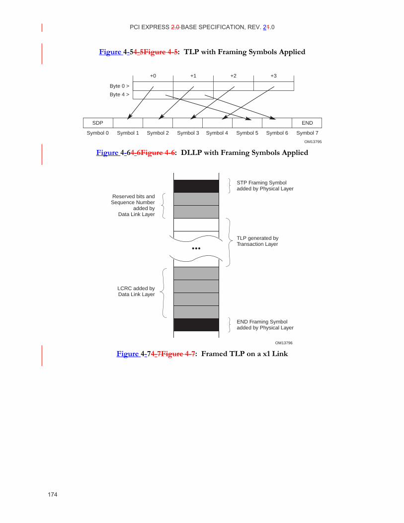
PCI EXPRESS 2.0 BASE SPECIFICATION, REV. 21.0
174
Figure 4-54-5Figure 4-5: TLP with Framing Symbols Applied
OM13795
+0 +1 +2 +3
Byte 0 >
Byte 4 >
Symbol 0 Symbol 1 Symbol 2 Symbol 3 Symbol 4 Symbol 5 Symbol 6 Symbol 7
SDP END
Figure 4-64-6Figure 4-6: DLLP with Framing Symbols Applied
OM13796
TLP generated byTransaction Layer
STP Framing Symboladded by Physical Layer
END Framing Symboladded by Physical Layer
LCRC added byData Link Layer
Reserved bits andSequence Number
added byData Link Layer
Figure 4-74-7Figure 4-7: Framed TLP on a x1 Link
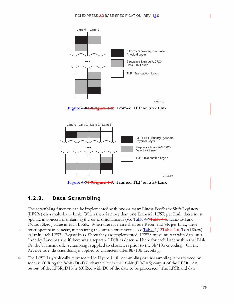
PCI EXPRESS 2.0 BASE SPECIFICATION, REV. 12.0
175
OM13797
STP/END Framing Symbols-Physical Layer
Sequence Number/LCRC-Data Link Layer
TLP - Transaction Layer
Lane 0 Lane 1
Figure 4-84-8Figure 4-8: Framed TLP on a x2 Link
OM13798
STP/END Framing Symbols-Physical Layer
Sequence Number/LCRC-Data Link Layer
TLP - Transaction Layer
Lane 2 Lane 3Lane 0 Lane 1
Figure 4-94-9Figure 4-9: Framed TLP on a x4 Link
4.2.3. Data Scrambling
The scrambling function can be implemented with one or many Linear Feedback Shift Registers (LFSRs) on a multi-Lane Link. When there is more than one Transmit LFSR per Link, these must operate in concert, maintaining the same simultaneous (see Table 4-9Table 4-5, Lane-to-Lane Output Skew) value in each LFSR. When there is more than one Receive LFSR per Link, these must operate in concert, maintaining the same simultaneous (see Table 4-12Table 4-6, Total Skew) 5 value in each LFSR. Regardless of how they are implemented, LFSRs must interact with data on a Lane-by-Lane basis as if there was a separate LFSR as described here for each Lane within that Link. On the Transmit side, scrambling is applied to characters prior to the 8b/10b encoding. On the Receive side, de-scrambling is applied to characters after 8b/10b decoding.
The LFSR is graphically represented in Figure 4-10. Scrambling or unscrambling is performed by 10 serially XORing the 8-bit (D0-D7) character with the 16-bit (D0-D15) output of the LFSR. An output of the LFSR, D15, is XORed with D0 of the data to be processed. The LFSR and data
PCI EXPRESS 2.0 BASE SPECIFICATION, REV. 21.0
176
register are then serially advanced and the output processing is repeated for D1 through D7. The LFSR is advanced after the data is XORed. The LFSR implements the polynomial:
G(X)=X16+X5+X4+X3+1
The mechanism(s) and/or interface(s) utilized by the Data Link Layer to notify the Physical Layer to disable scrambling is implementation specific and beyond the scope of this specification. 5
The data scrambling rules are the following:
The COM character Symbol initializes the LFSR.
The LFSR value is advanced eight serial shifts for each character Symbol except the SKP.
All data characters Symbols (D codes) except those within a Training Sequence ordered setOrdered Sets (e.g., TS1, TS2) and the Compliance Pattern (see Section 4.2.8) are scrambled. 10
All special characters Symbols (K codes) are not scrambled.
The initialized value of an LFSR seed (D0-D15) is FFFFh. Immediately after a COM exits the Transmit LFSR, the LFSR on the Transmit side is initialized. Every time a COM enters the Receive LFSR on any Lane of that Link, the LFSR on the Receive side is initialized.
Scrambling can only be disabled at the end of Configuration (see Section 4.2.6.3.5). 15
Scrambling does not apply to a Loopback loopback Slaveslave.
Scrambling is always enabled in Detect by default.
IMPLEMENTATION NOTE
Disabling Scrambling Disabling scrambling is intended to help simplify test and debug equipment. Control of the exact data patterns is useful in a test and debug environment. Since scrambling is reset at the Physical Layer there is no reasonable way to reliably control the state of the data transitions through 20 software. Thus, the Disable Scrambling bit is provided for these purposes.
The mechanism(s) and/or interface(s) utilized by the Data Link Layer to notify the Physical Layer to disable scrambling is component implementation specific and beyond the scope of this specification.
For more information on scrambling, see Appendix C.
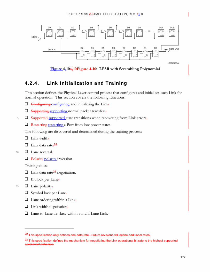
PCI EXPRESS 2.0 BASE SPECIFICATION, REV. 12.0
177
OM13799A
Data OutData In
D0
>D Q
Q
SET
CLR
D1
>D Q
Q
SET
CLR
D5
>D Q
Q
SET
CLR
D6
>D Q
Q
SET
CLR
D14
>D Q
Q
SET
CLR
D15
>D Q
Q
SET
CLR
D2
>D Q
Q
SET
CLR
D3
>D Q
Q
SET
CLR
D4
>D Q
Q
SET
CLR
D6
>D Q
Q
SET
CLR
D5
>D Q
Q
SET
CLR
D4
>D Q
Q
SET
CLR
D3
>D Q
Q
SET
CLR
D2
>D Q
Q
SET
CLR
D1
>D Q
Q
SET
CLR
D0
>D Q
Q
SET
CLR
D7
>D Q
Q
SET
CLR
Clock
Figure 4-104-10Figure 4-10: LFSR with Scrambling Polynomial
4.2.4. Link Initialization and Training
This section defines the Physical Layer control process that configures and initializes each Link for normal operation. This section covers the following functions:
Configuring configuring and initializing the Link.
Supporting supporting normal packet transfers.
Supported supported state transitions when recovering from Link errors. 5
Restarting restarting a Port from low power states.
The following are discovered and determined during the training process:
Link width.
Link data rate.22
Lane reversal. 10
Polarity polarity inversion.
Training does:
Link data rate23 negotiation.
Bit lock per Lane.
Lane polarity. 15
Symbol lock per Lane.
Lane ordering within a Link.
Link width negotiation.
Lane-to-Lane de-skew within a multi-Lane Link.
22 This specification only defines one data rate. Future revisions will define additional rates. 23 This specification defines the mechanism for negotiating the Link operational bit rate to the highest supported operational data rate.
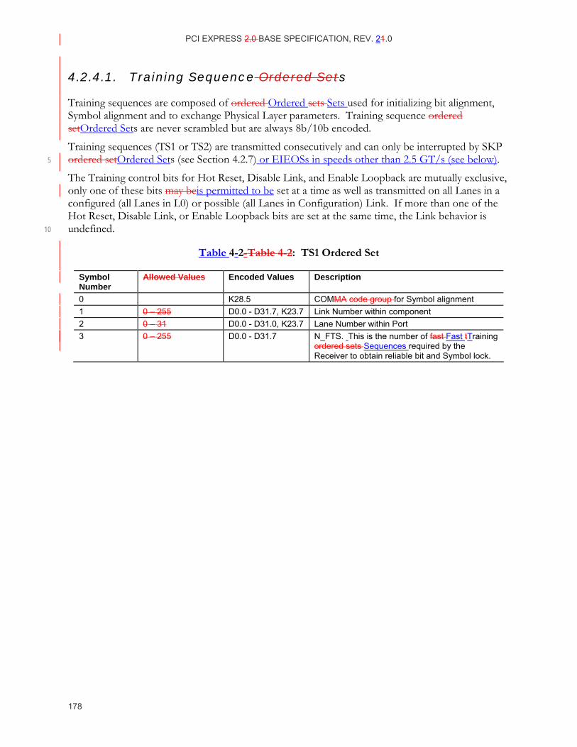
PCI EXPRESS 2.0 BASE SPECIFICATION, REV. 21.0
178
4.2.4.1. Training Sequence Ordered Sets
Training sequences are composed of ordered Ordered sets Sets used for initializing bit alignment, Symbol alignment and to exchange Physical Layer parameters. Training sequence ordered setOrdered Sets are never scrambled but are always 8b/10b encoded.
Training sequences (TS1 or TS2) are transmitted consecutively and can only be interrupted by SKP ordered setOrdered Sets (see Section 4.2.7) or EIEOSs in speeds other than 2.5 GT/s (see below). 5
The Training control bits for Hot Reset, Disable Link, and Enable Loopback are mutually exclusive, only one of these bits may beis permitted to be set at a time as well as transmitted on all Lanes in a configured (all Lanes in L0) or possible (all Lanes in Configuration) Link. If more than one of the Hot Reset, Disable Link, or Enable Loopback bits are set at the same time, the Link behavior is undefined. 10
Table 4-2-Table 4-2: TS1 Ordered Set
Symbol Number
Allowed Values Encoded Values Description
0 K28.5 COMMA code group for Symbol alignment 1 0 – 255 D0.0 - D31.7, K23.7 Link Number within component 2 0 – 31 D0.0 - D31.0, K23.7 Lane Number within Port 3 0 – 255 D0.0 - D31.7 N_FTS. This is the number of fast Fast tTraining
ordered sets Sequences required by the Receiver to obtain reliable bit and Symbol lock.
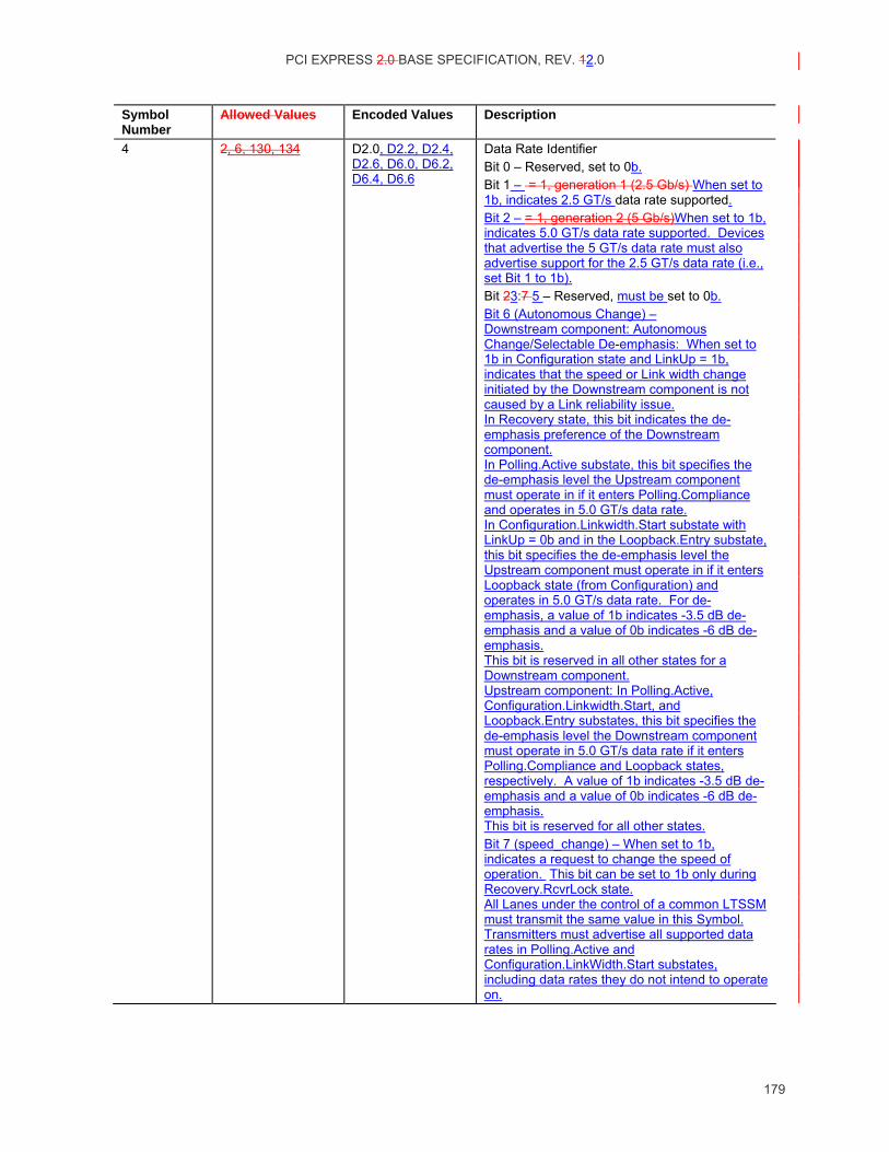
PCI EXPRESS 2.0 BASE SPECIFICATION, REV. 12.0
179
Symbol Number
Allowed Values Encoded Values Description
4 2, 6, 130, 134 D2.0, D2.2, D2.4, D2.6, D6.0, D6.2, D6.4, D6.6
Data Rate Identifier Bit 0 – Reserved, set to 0b. Bit 1 – = 1, generation 1 (2.5 Gb/s) When set to 1b, indicates 2.5 GT/s data rate supported. Bit 2 – = 1, generation 2 (5 Gb/s)When set to 1b, indicates 5.0 GT/s data rate supported. Devices that advertise the 5 GT/s data rate must also advertise support for the 2.5 GT/s data rate (i.e., set Bit 1 to 1b). Bit 23:7 5 – Reserved, must be set to 0b. Bit 6 (Autonomous Change) – Downstream component: Autonomous Change/Selectable De-emphasis: When set to 1b in Configuration state and LinkUp = 1b, indicates that the speed or Link width change initiated by the Downstream component is not caused by a Link reliability issue. In Recovery state, this bit indicates the de-emphasis preference of the Downstream component. In Polling.Active substate, this bit specifies the de-emphasis level the Upstream component must operate in if it enters Polling.Compliance and operates in 5.0 GT/s data rate. In Configuration.Linkwidth.Start substate with LinkUp = 0b and in the Loopback.Entry substate, this bit specifies the de-emphasis level the Upstream component must operate in if it enters Loopback state (from Configuration) and operates in 5.0 GT/s data rate. For de-emphasis, a value of 1b indicates -3.5 dB de-emphasis and a value of 0b indicates -6 dB de-emphasis. This bit is reserved in all other states for a Downstream component. Upstream component: In Polling.Active, Configuration.Linkwidth.Start, and Loopback.Entry substates, this bit specifies the de-emphasis level the Downstream component must operate in 5.0 GT/s data rate if it enters Polling.Compliance and Loopback states, respectively. A value of 1b indicates -3.5 dB de-emphasis and a value of 0b indicates -6 dB de-emphasis. This bit is reserved for all other states. Bit 7 (speed_change) – When set to 1b, indicates a request to change the speed of operation. This bit can be set to 1b only during Recovery.RcvrLock state. All Lanes under the control of a common LTSSM must transmit the same value in this Symbol. Transmitters must advertise all supported data rates in Polling.Active and Configuration.LinkWidth.Start substates, including data rates they do not intend to operate on.
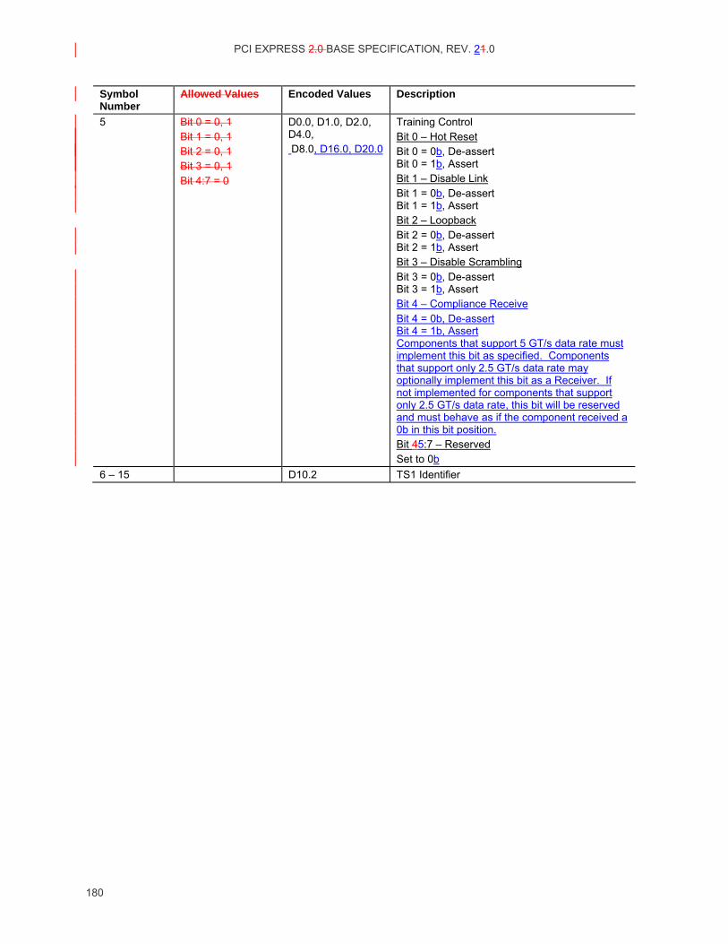
PCI EXPRESS 2.0 BASE SPECIFICATION, REV. 21.0
180
Symbol Number
Allowed Values Encoded Values Description
5 Bit 0 = 0, 1 Bit 1 = 0, 1 Bit 2 = 0, 1 Bit 3 = 0, 1 Bit 4:7 = 0
D0.0, D1.0, D2.0, D4.0, D8.0, D16.0, D20.0
Training Control Bit 0 – Hot Reset Bit 0 = 0b, De-assert Bit 0 = 1b, Assert Bit 1 – Disable Link Bit 1 = 0b, De-assert Bit 1 = 1b, Assert Bit 2 – Loopback Bit 2 = 0b, De-assert Bit 2 = 1b, Assert Bit 3 – Disable Scrambling Bit 3 = 0b, De-assert Bit 3 = 1b, Assert Bit 4 – Compliance Receive Bit 4 = 0b, De-assert Bit 4 = 1b, Assert Components that support 5 GT/s data rate must implement this bit as specified. Components that support only 2.5 GT/s data rate may optionally implement this bit as a Receiver. If not implemented for components that support only 2.5 GT/s data rate, this bit will be reserved and must behave as if the component received a 0b in this bit position. Bit 45:7 – Reserved Set to 0b
6 – 15 D10.2 TS1 Identifier
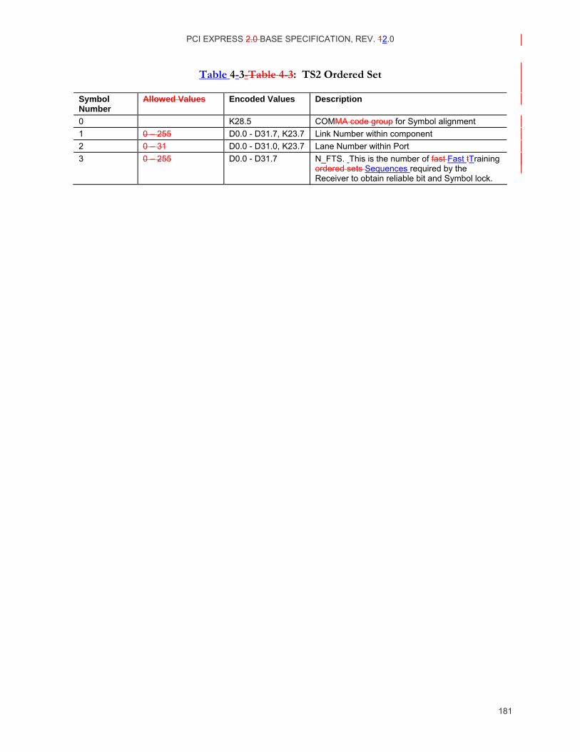
PCI EXPRESS 2.0 BASE SPECIFICATION, REV. 12.0
181
Table 4-3-Table 4-3: TS2 Ordered Set
Symbol Number
Allowed Values Encoded Values Description
0 K28.5 COMMA code group for Symbol alignment 1 0 – 255 D0.0 - D31.7, K23.7 Link Number within component 2 0 – 31 D0.0 - D31.0, K23.7 Lane Number within Port 3 0 – 255 D0.0 - D31.7 N_FTS. This is the number of fast Fast tTraining
ordered sets Sequences required by the Receiver to obtain reliable bit and Symbol lock.
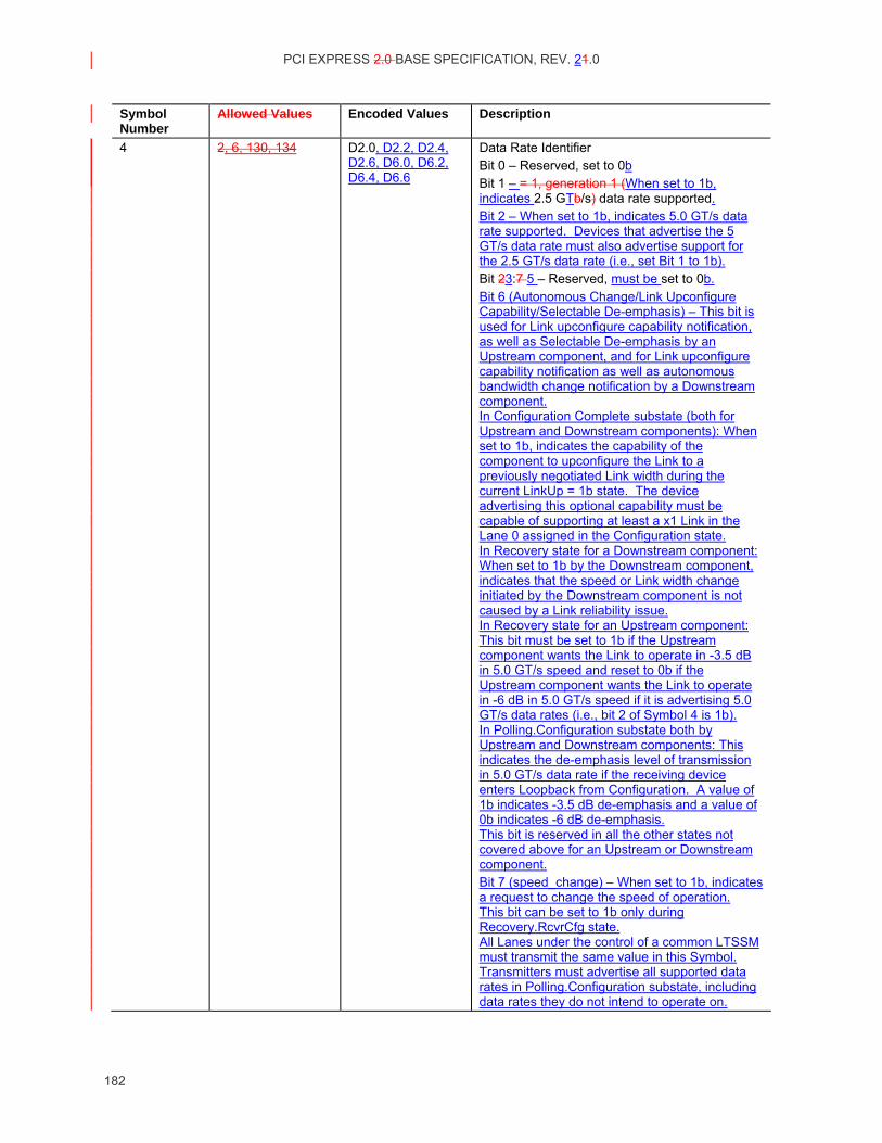
PCI EXPRESS 2.0 BASE SPECIFICATION, REV. 21.0
182
Symbol Number
Allowed Values Encoded Values Description
4 2, 6, 130, 134 D2.0, D2.2, D2.4, D2.6, D6.0, D6.2, D6.4, D6.6
Data Rate Identifier Bit 0 – Reserved, set to 0b Bit 1 – = 1, generation 1 (When set to 1b, indicates 2.5 GTb/s) data rate supported. Bit 2 – When set to 1b, indicates 5.0 GT/s data rate supported. Devices that advertise the 5 GT/s data rate must also advertise support for the 2.5 GT/s data rate (i.e., set Bit 1 to 1b). Bit 23:7 5 – Reserved, must be set to 0b. Bit 6 (Autonomous Change/Link Upconfigure Capability/Selectable De-emphasis) – This bit is used for Link upconfigure capability notification, as well as Selectable De-emphasis by an Upstream component, and for Link upconfigure capability notification as well as autonomous bandwidth change notification by a Downstream component. In Configuration Complete substate (both for Upstream and Downstream components): When set to 1b, indicates the capability of the component to upconfigure the Link to a previously negotiated Link width during the current LinkUp = 1b state. The device advertising this optional capability must be capable of supporting at least a x1 Link in the Lane 0 assigned in the Configuration state. In Recovery state for a Downstream component: When set to 1b by the Downstream component, indicates that the speed or Link width change initiated by the Downstream component is not caused by a Link reliability issue. In Recovery state for an Upstream component: This bit must be set to 1b if the Upstream component wants the Link to operate in -3.5 dB in 5.0 GT/s speed and reset to 0b if the Upstream component wants the Link to operate in -6 dB in 5.0 GT/s speed if it is advertising 5.0 GT/s data rates (i.e., bit 2 of Symbol 4 is 1b). In Polling.Configuration substate both by Upstream and Downstream components: This indicates the de-emphasis level of transmission in 5.0 GT/s data rate if the receiving device enters Loopback from Configuration. A value of 1b indicates -3.5 dB de-emphasis and a value of 0b indicates -6 dB de-emphasis. This bit is reserved in all the other states not covered above for an Upstream or Downstream component. Bit 7 (speed_change) – When set to 1b, indicates a request to change the speed of operation. This bit can be set to 1b only during Recovery.RcvrCfg state. All Lanes under the control of a common LTSSM must transmit the same value in this Symbol. Transmitters must advertise all supported data rates in Polling.Configuration substate, including data rates they do not intend to operate on.
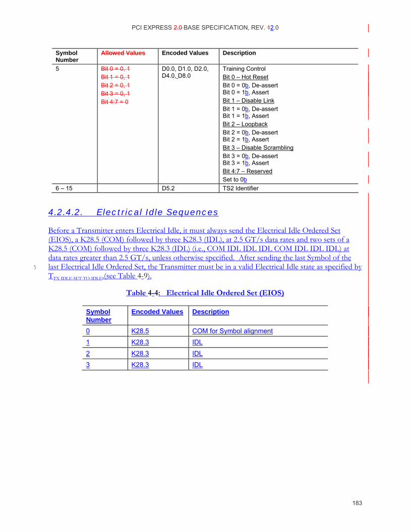
PCI EXPRESS 2.0 BASE SPECIFICATION, REV. 12.0
183
Symbol Number
Allowed Values Encoded Values Description
5 Bit 0 = 0, 1 Bit 1 = 0, 1 Bit 2 = 0, 1 Bit 3 = 0, 1 Bit 4:7 = 0
D0.0, D1.0, D2.0, D4.0, D8.0
Training Control Bit 0 – Hot Reset Bit 0 = 0b, De-assert Bit 0 = 1b, Assert Bit 1 – Disable Link Bit 1 = 0b, De-assert Bit 1 = 1b, Assert Bit 2 – Loopback Bit 2 = 0b, De-assert Bit 2 = 1b, Assert Bit 3 – Disable Scrambling Bit 3 = 0b, De-assert Bit 3 = 1b, Assert Bit 4:7 – Reserved Set to 0b
6 – 15 D5.2 TS2 Identifier
4.2.4.2. Electrical Idle Sequences
Before a Transmitter enters Electrical Idle, it must always send the Electrical Idle Ordered Set (EIOS), a K28.5 (COM) followed by three K28.3 (IDL), at 2.5 GT/s data rates and two sets of a K28.5 (COM) followed by three K28.3 (IDL) (i.e., COM IDL IDL IDL COM IDL IDL IDL) at data rates greater than 2.5 GT/s, unless otherwise specified. After sending the last Symbol of the last Electrical Idle Ordered Set, the Transmitter must be in a valid Electrical Idle state as specified by 5 TTX-IDLE-SET-TO-IDLE.(see Table 4-9).
Table 4-4: Electrical Idle Ordered Set (EIOS)
Symbol Number
Encoded Values Description
0 K28.5 COM for Symbol alignment
1 K28.3 IDL
2 K28.3 IDL
3 K28.3 IDL
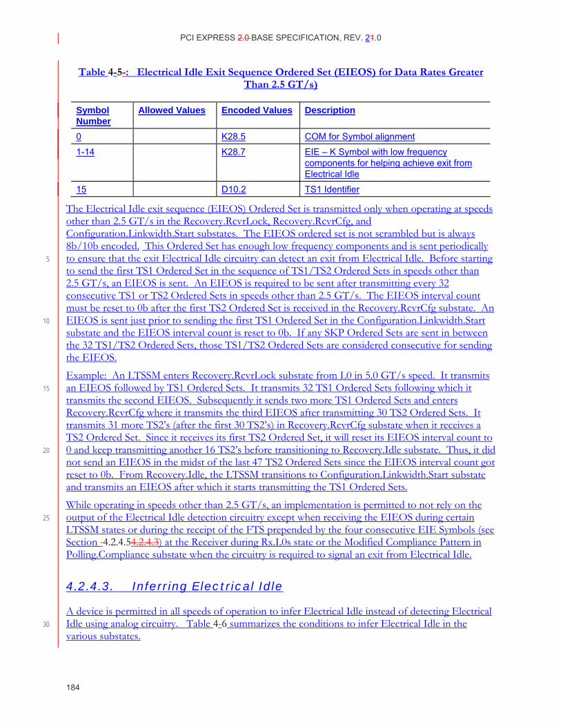
PCI EXPRESS 2.0 BASE SPECIFICATION, REV. 21.0
184
Table 4-5-: Electrical Idle Exit Sequence Ordered Set (EIEOS) for Data Rates Greater Than 2.5 GT/s)
Symbol Number
Allowed Values Encoded Values Description
0 K28.5 COM for Symbol alignment
1-14 K28.7 EIE – K Symbol with low frequency components for helping achieve exit from Electrical Idle
15 D10.2 TS1 Identifier
The Electrical Idle exit sequence (EIEOS) Ordered Set is transmitted only when operating at speeds other than 2.5 GT/s in the Recovery.RcvrLock, Recovery.RcvrCfg, and Configuration.Linkwidth.Start substates. The EIEOS ordered set is not scrambled but is always 8b/10b encoded. This Ordered Set has enough low frequency components and is sent periodically to ensure that the exit Electrical Idle circuitry can detect an exit from Electrical Idle. Before starting 5 to send the first TS1 Ordered Set in the sequence of TS1/TS2 Ordered Sets in speeds other than 2.5 GT/s, an EIEOS is sent. An EIEOS is required to be sent after transmitting every 32 consecutive TS1 or TS2 Ordered Sets in speeds other than 2.5 GT/s. The EIEOS interval count must be reset to 0b after the first TS2 Ordered Set is received in the Recovery.RcvrCfg substate. An EIEOS is sent just prior to sending the first TS1 Ordered Set in the Configuration.Linkwidth.Start 10 substate and the EIEOS interval count is reset to 0b. If any SKP Ordered Sets are sent in between the 32 TS1/TS2 Ordered Sets, those TS1/TS2 Ordered Sets are considered consecutive for sending the EIEOS.
Example: An LTSSM enters Recovery.RcvrLock substate from L0 in 5.0 GT/s speed. It transmits an EIEOS followed by TS1 Ordered Sets. It transmits 32 TS1 Ordered Sets following which it 15 transmits the second EIEOS. Subsequently it sends two more TS1 Ordered Sets and enters Recovery.RcvrCfg where it transmits the third EIEOS after transmitting 30 TS2 Ordered Sets. It transmits 31 more TS2’s (after the first 30 TS2’s) in Recovery.RcvrCfg substate when it receives a TS2 Ordered Set. Since it receives its first TS2 Ordered Set, it will reset its EIEOS interval count to 0 and keep transmitting another 16 TS2’s before transitioning to Recovery.Idle substate. Thus, it did 20 not send an EIEOS in the midst of the last 47 TS2 Ordered Sets since the EIEOS interval count got reset to 0b. From Recovery.Idle, the LTSSM transitions to Configuration.Linkwidth.Start substate and transmits an EIEOS after which it starts transmitting the TS1 Ordered Sets.
While operating in speeds other than 2.5 GT/s, an implementation is permitted to not rely on the output of the Electrical Idle detection circuitry except when receiving the EIEOS during certain 25 LTSSM states or during the receipt of the FTS prepended by the four consecutive EIE Symbols (see Section 4.2.4.54.2.4.3) at the Receiver during Rx.L0s state or the Modified Compliance Pattern in Polling.Compliance substate when the circuitry is required to signal an exit from Electrical Idle.
4.2.4.3. Inferring Electrical Idle
A device is permitted in all speeds of operation to infer Electrical Idle instead of detecting Electrical Idle using analog circuitry. Table 4-6 summarizes the conditions to infer Electrical Idle in the 30 various substates.
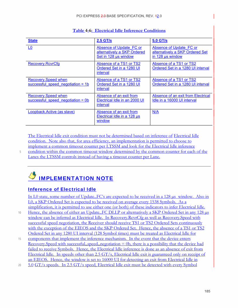
PCI EXPRESS 2.0 BASE SPECIFICATION, REV. 12.0
185
Table 4-6: Electrical Idle Inference Conditions
State 2.5 GT/s 5.0 GT/s
L0 Absence of Update_FC or alternatively a SKP Ordered Set in 128 µs window
Absence of Update_FC or alternatively a SKP Ordered Set in 128 µs window
Recovery.RcvrCfg Absence of a TS1 or TS2 Ordered Set in a 1280 UI interval
Absence of a TS1 or TS2 Ordered Set in a 1280 UI interval
Recovery.Speed when successful_speed_negotiation = 1b
Absence of a TS1 or TS2 Ordered Set in a 1280 UI interval
Absence of a TS1 or TS2 Ordered Set in a 1280 UI interval
Recovery.Speed when successful_speed_negotiation = 0b
Absence of an exit from Electrical Idle in an 2000 UI interval
Absence of an exit from Electrical Idle in a 16000 UI interval
Loopback.Active (as slave) Absence of an exit from Electrical Idle in a 128 µs window
N/A
The Electrical Idle exit condition must not be determined based on inference of Electrical Idle condition. Note also that, for area efficiency, an implementation is permitted to choose to implement a common timeout counter per LTSSM and look for the Electrical Idle inference condition within the common timeout window determined by the common counter for each of the 5 Lanes the LTSSM controls instead of having a timeout counter per Lane.
IMPLEMENTATION NOTE
Inference of Electrical Idle In L0 state, some number of Update_FC’s are expected to be received in a 128 µs window. Also in L0, a SKP Ordered Set is expected to be received on average every 1538 Symbols. As a simplification, it is permitted to use either one (or both) of these indicators to infer Electrical Idle. Hence, the absence of either an Update_FC DLLP or alternatively a SKP Ordered Set in any 128 µs 10 window can be inferred as Electrical Idle. In Recovery.RcvrCfg as well as Recovery.Speed with successful speed negotiation, the Receiver should receive TS1 or TS2 Ordered Sets continuously with the exception of the EIEOS and the SKP Ordered Set. Hence, the absence of a TS1 or TS2 Ordered Set in any 1280 UI interval (128 Symbol times) must be treated as Electrical Idle for components that implement the inference mechanism. In the event that the device enters 15 Recovery.Speed with successful_speed_negotiation = 0b, there is a possibility that the device had failed to receive Symbols. Hence, the Electrical Idle inference is done as an absence of exit from Electrical Idle. In speeds other than 2.5 GT/s, Electrical Idle exit is guaranteed only on receipt of an EIEOS. Hence, the window is set to 16000 UI for detecting an exit from Electrical Idle in 5.0 GT/s speeds. In 2.5 GT/s speed, Electrical Idle exit must be detected with every Symbol 20
PCI EXPRESS 2.0 BASE SPECIFICATION, REV. 21.0
186
received. Hence, absence of Electrical Idle exit in an 2000 UI window constitutes an Electrical Idle condition.
4.2.4.2.4.2.4.4. Lane Polarity Inversion
During the training sequence, the Receiver looks at Symbols 6-15 of TS1 and TS2 as the indicator of Lane polarity inversion (D+ and D- are swapped). If Lane polarity inversion occurs, the TS1 Symbols 6-15 received will be D21.5 as opposed to the expected D10.2. Similarly, if Lane polarity 5 inversion occurs, Symbols 6-15 of the TS2 ordered setOrdered Set will be D26.5 as opposed to the expected D5.2. This provides the clear indication of Lane polarity inversion.
If polarity inversion is detected the Receiver must invert the received data. The Transmitter must never invert the transmitted data. Support for Lane Polarity Inversion is required on all PCI Express Receivers across all Lanes independently. 10
4.2.4.3.4.2.4.5. Fast Training Sequence (FTS)
Fast Training Sequence (FTS) is the mechanism that is used for bit and Symbol lock when transitioning from L0s to L0. The FTS is used by the Receiver to detect the exit from Electrical Idle and align the Receiver’s bit/Symbol receive circuitry to the incoming data. See Refer to Section 4.2.5 for a description of L0 and L0s.
A single FTS training sequence is an ordered set composed comprises of one K28.5 (COM) Symbol 15 and followed by three K28.1 Symbols. The maximum number of FTS ordered sets (N_FTS) that a component can request is 255, providing a bit time lock of 4 * 255 * 10 * UI. If the speed of operation is greater than 2.5 GT/s, four consecutive EIE Symbols are transmitted at valid signal levels prior to transmitting the first FTS. These Symbols will help the Receiver detect exit from Electrical Idle. An implementation that does not guarantee proper signaling levels for up to the 20 allowable time on the Transmitter pins (see Table 4-9) since exiting Electrical Idle condition is required to prepend its first FTS by extra EIE Symbols so that the Receiver can receive at least four EIE Symbols at valid signal levels. Implementations must not transmit more than eight EIE Symbols prior to transmitting the first FTS. A component is permitted to advertise different N_FTS rates at different speeds. For speeds other than 2.5 GT/s, a component may choose to 25 advertise an appropriate N_FTS number considering that it will receive the four EIE Symbols. 4096 FTS ordered sets must be sent when the Extended Synch bit is set in order to provide external Link monitoring tools with enough time to achieve bit and framing synchronization. SKP ordered setOrdered Sets must be scheduled and transmitted between FTS ordered sets as necessary to meet the definitions in Section 4.2.7 with the exception that no SKP ordered setOrdered Sets can be 30 transmitted during the first N_FTS FTS ordered sets. A single SKP ordered setOrdered Set is always sent after the last FTS is transmitted. Note that it is possible that two SKP ordered setOrdered Sets can be transmitted back to back (one SKP ordered setOrdered Set to signify the completion of the 4096 FTSs and one scheduled and transmitted to meet the definitions described in Section 4.2.7). 35
N_FTS defines the number of FTS ordered sets that must be transmitted when transitioning from L0s to L0. At the generation 12.5 GT/s data rate, the value that can be requested by a component corresponds to a Symbol lock time of 16 ns (N_FTS set to 0b and one SKP ordered setOrdered Set)
PCI EXPRESS 2.0 BASE SPECIFICATION, REV. 12.0
187
to ~4 µs (N_FTS set to 255), except when the Extended Synch bit is set, which requires the transmission of 4096 FTS ordered sets resulting in a bit lock time of 64 µs. Note that the N_FTS value reported by a component may change; for example, due to software modifying the value in the Common Clock Configuration bit (Section 7.8.7).
If the N_FTS period of time expires before the Receiver obtains bit lock, Symbol lock, and Lane-to-5 Lane de-skew on all Lanes of the configured Link, the Receiver must transition to the Recovery. This sequence is detailed in the LTSSM in Section 4.2.5.
4.2.4.4.4.2.4.6. Link Error Recovery
Link Errors are defined as 8b/10b decode errors, loss of Symbol lock, Elasticity Buffer Overflow/Underflow, or loss of Lane-to-Lane de-skew.
• Note: 8b/10b decode errors must be checked and trigger a Receiver Error in specified 10
LTSSM states (see Table 4-4), which is a reported error associated with the Port (see Section 6.2). Triggering a Receiver Error on any or all of Framing Error, Loss of Symbol Lock, Lane Deskew Error, and Elasticity Buffer Overflow/Underflow is optional.
On a configured Link, which is in L0, error recovery will at a minimum be managed in a Layer above the Physical Layer (as described in Section 3.5) by directing the Link to transition to 15 Recovery.
• Note: Link Errors may also result in the Physical Layer initiating a LTSSM state transition from L0 to Recovery.
All LTSSM states other than L0 make progress24 when Link Errors occur.
• Note: Link errors that occur, while in LTSSM states other than L0, must not result in the 20 Physical Layer initiating a LTSSM state transition.
If a Lane detects an implementation specific number of 8b/10b errors, Symbol lock must be verified or re-established as soon as possible.25
4.2.4.5.4.2.4.7. Reset
Reset is described from a system point of view in Section 6.6.
4.2.4.5.1.4.2.4.7.1. Fundamental Reset
Fundamental Reset applies only when Main power is present. 25
Fundamental Reset does not apply when no power or Aux power is present.
When Fundamental Reset is asserted:
24 In this context, progress is defined as the LTSSM not remaining indefinitely in one state with the possible exception of Detect. 25 The method to verify and re-establish Symbol lock is implementation specific.
PCI EXPRESS 2.0 BASE SPECIFICATION, REV. 21.0
188
The Receiver terminations are required to only meet ZRX-HIGH-IMP-DC-POS and ZRX-HIGH-IMP-DC-NEG (see Table 4-12Table 4-6).
The Transmitter is required only to meet ITX-SHORT (see Table 4-9Table 4-5).
The Transmitter holds a constant DC common mode voltage.26
When Fundamental Reset is de-asserted: 5
The Port LTSSM (see Section 4.2.5) is initialized (see Section 6.6.1 for additional requirements).
4.2.4.5.2.4.2.4.7.2. Hot Reset
Hot Reset is a protocol reset defined in Section 4.2.5.11.
4.2.4.6.4.2.4.8. Link Data Rate Negotiation
All devices are required to start Link initialization using a generation 12.5 GT/s data rate on each Lane. A field in the training sequence ordered setOrdered Set (see Section 4.2.4) is used to advertise all supported data rates, and any higher speed supported by both sides of the Link will be initiated 10 during Polling.Speed. The Link trains to L0 initially in 2.5 GT/s data rate after which data rate change occurs by going through the Recovery state.
4.2.4.7.4.2.4.9. Link Width and Lane Sequence Negotiation
PCI Express Links must consist of 1, 2, 4, 8, 12, 16, or 32 Lanes in parallel, referred to as x1, x2, x4, x8, x12, x16, and x32 Links, respectively. All Lanes within a Link shall must simultaneously (as defined by LTX-SKEW in Table 4-5) transmit data based on the same frequency with a skew between 15 Lanes not to exceed LTX-SKEW (Table 4-9). The negotiation process is described as a sequence of steps.
The negotiation establishes values for Link number and Lane number for each Lane that is part of a valid Link; each Lane that is not part of a valid Link exits the negotiation to become a separate Link or remains in Electrical Idle. 20
During Link width and Lane number negotiation, the two communicating Ports must accommodate the maximum allowed Lane-to-Lane skew as specified by LRX-SKEW in Table 4-12Table 4-6.
Optional Link negotiation behaviors include Lane reversal, variable width Links, splitting of Ports into multiple Links and the configuration of a crosslink.
Annex specifications to this specification may impose other rules and restrictions that must be 25 comprehended by components compliant to those annex specifications; it is the intent of this specification to comprehend interoperability for a broad range of component capabilities.
26 The common mode being driven does not needis not required to meet the Absolute Delta Between DC Common Mode during L0 and Electrical Idle (VTX-CM-DC-ACTIVE-IDLE-DELTA) specification (see Table 4-9Table 4-5).

PCI EXPRESS 2.0 BASE SPECIFICATION, REV. 12.0
189
4.2.4.7.1.4.2.4.9.1. Required and Optional Port Behavior
The ability for a xN Port to form a xN Link as well as a x1 Link (where N can be 32, 16, 12, 8, 4, 2, and 1) is required.
• Note: Designers must connect Ports between two different components in a way that allows those components to meet the above requirement. If the Ports between components are connected in ways that are not consistent with intended usage as defined by the component’s 5 Port descriptions/data sheets, behavior is undefined.
The ability for a xN Port to form any Link width between N and 1 is optional.
• Note: An example of this behavior includes a x16 Port which can only configure into only one Link, but the width of the Link can be configured to be x12, x8, x4, x2 as well as the required widths of x16 and x1. 10
The ability to split a Port into two or more Links is optional.
• Note: An example of this behavior would be a x16 Port that may be able to configure two x8 Links, four x4 Links, or even 16 x1 Links.
Support for Lane reversal is optional.
• Note:If implemented, Lane reversal must be done for both the Transmitter and Receiver of 15 a given Port for a multi-Lane Link.
• Note: An example of Lane reversal consists of Lane 0 of an Upstream Port attached to Lane N-1 of a Downstream Port where either the Downstream or Upstream device may reverse the Lane order to configure a xN Link.
Support for formation of a crosslink is optional. In this context, a Downstream Port connected to a 20 Downstream Port or an Upstream Port connected to an Upstream Port is a crosslink.
Current and future electromechanical and/or form factor specifications may require the implementation of some optional features listed above. Component designers must read the specifications for the systems that the component(s) they are designing will used in to ensure compliance to those specifications. 25
4.2.4.8.4.2.4.10. Lane-to-Lane De-skew
The Receiver must compensate for the allowable skew between all Lanes within a multi-Lane Link (see Table 4-9Table 4-5 and Table 4-12Table 4-6) before delivering the data and control to the Data Link Layer.
Lane-to-Lane de-skew shall be done across all Lanes within multi-Lane Links. An unambiguous de-skew mechanism is uses the COM Symbol transmitted during training sequence or SKP ordered 30 setOrdered Sets across all Lanes within a configured Link. Other de-skew mechanisms may also be employed. Lane-to-Lane de-skew must be performed during Configuration, Recovery, and L0s in the LTSSM.
PCI EXPRESS 2.0 BASE SPECIFICATION, REV. 21.0
190
4.2.4.9.4.2.4.11. Lane vs. Link Training
The Link initialization process builds unassociated Lanes of a Port into associated Lanes that form a Link. For Lanes to configure properly into a desired Link, the TS1 and TS2 ordered setOrdered Sets must have the appropriate fields (Symbol 3, 4, and 5) set to the same value on all Lanes.
Links are formed at the conclusion of Configuration.
Note: If the optional behavior of a Port being able to configure multiple Links is employed, the 5 following observations can be made:
• A separate LTSSM is needed for the maximum number of Links that are desired to be configured by any given Port.
• The LTSSM Rules are written for configuring one Link. The decision to configure Links in a serial fashion or parallel is implementation specific. 10
4.2.5. Link Training and Status State Machine (LTSSM) Descriptions
The LTSSM states are illustrated in Figure 4-11. These states are described in following sections.
All timeout values specified in the Link Training and Status state machine (LTSSM) timeout values are minus 0 seconds and plus 50% unless explicitly stated otherwise. All timeout values must be set to the specified values after power-on/reset. All counter values must be set to the specified values after power-on/reset. 15
4.2.5.1. Detect
The purpose of this state is to detect when a far end termination is present. This state can be entered at any time if directed.
4.2.5.2. Polling
The Port transmits training ordered setOrdered Sets and responds to the received training ordered setOrdered Sets. In this state, bit lock and Symbol lock are established, and Lane polarity is configured, and Lane data rate is established. 20
The polling state includes Polling.Compliance (see Section 4.2.6.2.2). This state is intended for use with test equipment used to assess if the Transmitter and the interconnect present in the device under test setup is compliant with the voltage and timing specifications in Table 4-9Table 4-5 and Table 4-12Table 4-6.
The Polling.Compliance state also includes a simplified inter-operability testing scheme that is 25 intended to be performed using a wide array of test and measurement equipment (i.e., pattern generator, oscilloscope, BERT, etc.). This portion of the Polling.Compliance state is logically entered by at least one component asserting the Compliance Receive bit (bit 4 in Symbol 5 of TS1) while not asserting the Loopback bit (bit 2 in Symbol 5 of TS1) upon entering Polling.Active. A
PCI EXPRESS 2.0 BASE SPECIFICATION, REV. 12.0
191
provision for changing speeds to the highest common transmitted and received Link speed (Symbol 4 of TS1) is also included to make this behavior scalable to various Link speeds.
IMPLEMENTATION NOTE
Use of Polling.Compliance Polling.Compliance is intended for a compliance test environment and not entered during normal operation and cannot be disabled for any reason. Polling.Compliance is entered based on the physical system environment or configuration register access mechanism as described in Section 5 4.2.6.2.1. Any other mechanism that causes a Transmitter to output the compliance pattern is implementation specific and is beyond the scope of this specification.
4.2.5.3. Configuration
In Configuration, both the Transmitter and Receiver are sending and receiving data at the negotiated data rate. The Lanes of a Port configure into a Link through a width and Lane negotiation sequence. Also, Lane-to-Lane de-skew must occur, scrambling can be disabled, the N_FTS is set, 10 and the Disable or Loopback states can be entered.
4.2.5.4. Recovery
In Recovery, both the Transmitter and Receiver are sending and receiving data using the configured Link and Lane number as well as the previously negotiated supported data rate(s). Recovery allows a configured Link to change the speed of operation if desired, re-establish bit lock, Symbol lock, and Lane-to-Lane de-skew. Recovery is also used to set a new N_FTS and enter the Loopback, Disable, 15 Hot Reset, and Configuration states.
4.2.5.5. L0
L0 is the normal operational state where data and control packets can be transmitted and received. All power management states are entered from this state.
4.2.5.6. L0s
L0s is intended as a power savings state.
L0s allows a Link to quickly enter and recover from a power conservation state without going 20 through Recovery.
The entry to L0s occurs after receiving an Electrical Idle ordered setEIOS.
The exit from L0s to L0 must re-establish bit lock, Symbol lock, and Lane-to-Lane de-skew.
A Transmitter and Receiver Lane pair on a Port are not required to both be in L0s simultaneously.
PCI EXPRESS 2.0 BASE SPECIFICATION, REV. 21.0
192
4.2.5.7. L1
L1 is intended as a power savings state.
The L1 state allows an additional power savings over L0s at the cost of additional resume latency.
The entry to L1 occurs after being directed by the Data Link Layer and receiving an Electrical Idle ordered set.EIOS.
4.2.5.8. L2
Power can be aggressively conserved in L2. Most of the Transmitter and Receiver may be shut 5 off.27 Main power and clocks are not guaranteed, but aux28 power is available.
When Beacon support is required by the associated system or form factor specification, an Upstream Port that supports the wakeup capability must be able to send; and a Downstream Port must be able to receive; a wakeup signal referred to as a Beacon.29.
The entry to L2 occurs after being directed by the Data Link Layer and receiving an Electrical Idle 10 ordered setEIOS.
4.2.5.9. Disabled
The intent of the Disabled state is to allow a configured Link to be disabled until directed or Electrical Idle is exited (i.e., due to a hot removal and insertion) after entering Disabled.
Disabled uses bit 1 (Disable Link) in the Training Control field (see Table 4-2 and Table 4-3) which is sent within the TS1 and TS2 training ordered setOrdered Set. 15
A Link can enter Disabled if directed by a higher Layer. A Link can also reach the Disable state by receiving two consecutive TS1 ordered setOrdered Sets with the Disable Link bit asserted (see Section 4.2.6.9).
4.2.5.10. Loopback
Loopback is intended for test and fault isolation use. Only the entry and exit behavior is specified, all other details are implementation specific. Loopback can operate on either a per Lane or 20 configured Link basis.
A Loopback loopback Master master is the component requesting Loopback.
A Loopback loopback Slave slave is the component looping back the data.
27 The exception is the Receiver termination, which must remain in a low impedance state. 28 In this context, “aux” power means a power source which can be used to drive the Beacon circuitry. 29 Certain form factor specifications require the use of a Beacon for a device to request main power reactivation, for example to wake a system that is in D3cold. See Section 4.3.5.8 4.3.5.8 1.1.1.1 for information on the electrical requirements of the Beacon. Refer to Chapter <> for more information on how a device may use the Beacon as the wakeup mechanism.
PCI EXPRESS 2.0 BASE SPECIFICATION, REV. 12.0
193
Loopback uses bit 2 (Loopback) in the Training Control field (see Table 4-2 and Table 4-3) which is sent within the TS1 and TS2 training ordered setOrdered Set.
The entry mechanism for Loopback loopback Master master is device specific.
The Loopback loopback Slave slave device enters Loopback whenever two consecutive TS1 ordered setOrdered Sets are received with the Loopback bit set. 5
IMPLEMENTATION NOTE
Use of Loopback Once in the Loopback state, the master can send any pattern of Symbols as long as the rules of 8b/10b encoding (including disparity) are followed. Once in Loopback, the concept of data scrambling is no longer relevant; what is sent out is looped back. The mechanism(s) and/or interface(s) utilized by the Data Link Layer to notify the Physical Layer to enter the Loopback state is component implementation specific and beyond the scope of this specification. 10
4.2.5.11. Hot Reset
Hot Reset uses bit 0 (Hot Reset) in the Training Control field (see Table 4-2 and Table 4-3) which is sent within the TS1 and TS2 training ordered setOrdered Set.
A Link can enter Hot Reset if directed by a higher Layer. A Link can also reach the Hot Reset state by receiving two consecutive TS1 ordered setOrdered Sets with the Hot Reset bit asserted (see Section 4.2.6.11). 15
4.2.6. Link Training and Status State Rules
Various Link status bits are monitored through software with the exception of LinkUp which is monitored by the Data Link Layer. Table 4-7Table 4-4 describes how the Link status bits must be handled throughout the LTSSM (for more information, see Section 3.1 for LinkUp; Section 7.8.8 for Link Speed, LinkWidth; and Link Training; Section 6.2 for Receiver Error; and Section 6.7 for In-Band Presence). 20
Table 4-7-Table 4-4: Table of Link Status Mapped to the LTSSM
LTSSM State Link Width Link Speed LinkUp Link
Training Receiver
Error
In-Band Presence
30 Detect Undefined Undefined 0b 0b No action 0b
30 In-band refers to the fact that no sideband signals are used to calculate the presence of a powered up device on the other end of a Link.
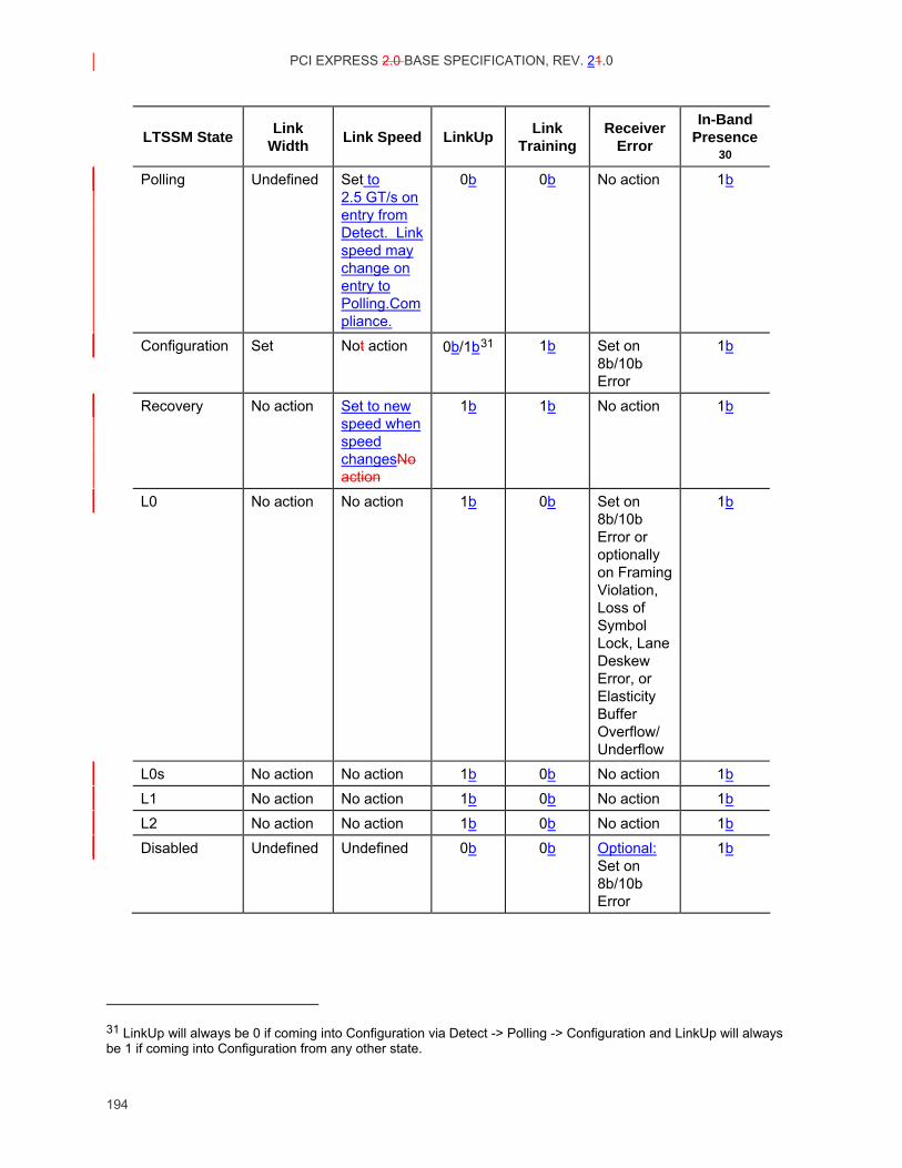
PCI EXPRESS 2.0 BASE SPECIFICATION, REV. 21.0
194
LTSSM State Link Width Link Speed LinkUp Link
Training Receiver
Error
In-Band Presence
30 Polling Undefined Set to
2.5 GT/s on entry from Detect. Link speed may change on entry to Polling.Compliance.
0b 0b No action 1b
Configuration Set Not action 0b/1b31 1b Set on 8b/10b Error
1b
Recovery No action Set to new speed when speed changesNo action
1b 1b No action 1b
L0 No action No action 1b 0b Set on 8b/10b Error or optionally on Framing Violation, Loss of Symbol Lock, Lane Deskew Error, or Elasticity Buffer Overflow/ Underflow
1b
L0s No action No action 1b 0b No action 1b
L1 No action No action 1b 0b No action 1b
L2 No action No action 1b 0b No action 1b
Disabled Undefined Undefined 0b 0b Optional: Set on 8b/10b Error
1b
31 LinkUp will always be 0 if coming into Configuration via Detect -> Polling -> Configuration and LinkUp will always be 1 if coming into Configuration from any other state.
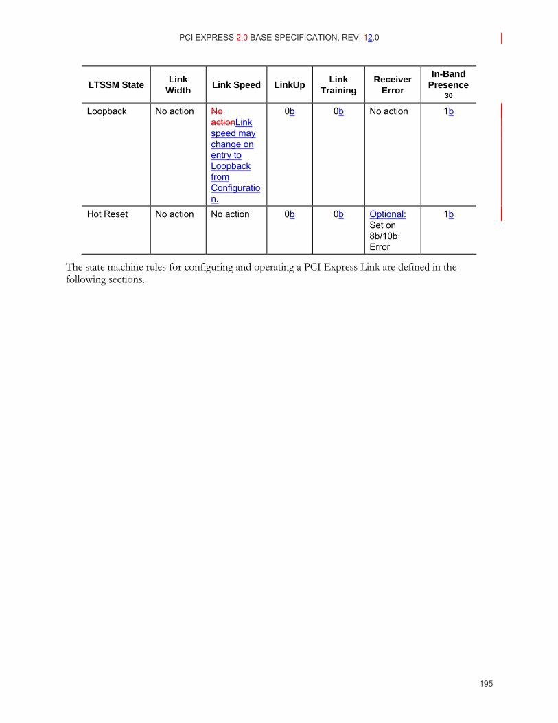
PCI EXPRESS 2.0 BASE SPECIFICATION, REV. 12.0
195
LTSSM State Link Width Link Speed LinkUp Link
Training Receiver
Error
In-Band Presence
30 Loopback No action No
actionLink speed may change on entry to Loopback from Configuration.
0b 0b No action 1b
Hot Reset No action No action 0b 0b Optional: Set on 8b/10b Error
1b
The state machine rules for configuring and operating a PCI Express Link are defined in the following sections.
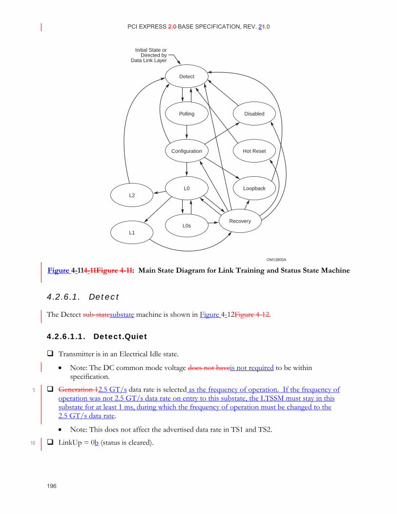
PCI EXPRESS 2.0 BASE SPECIFICATION, REV. 21.0
196
OM13800A
Detect
Polling
Configuration
L0
Disabled
Hot Reset
Loopback
RecoveryL0s
L2
L1
Initial State orDirected by
Data Link Layer
Figure 4-114-11Figure 4-11: Main State Diagram for Link Training and Status State Machine
4.2.6.1. Detect
The Detect sub-statesubstate machine is shown in Figure 4-12Figure 4-12.
4.2.6.1.1. Detect.Quiet
Transmitter is in an Electrical Idle state.
• Note: The DC common mode voltage does not haveis not required to be within specification.
Generation 12.5 GT/s data rate is selected as the frequency of operation. If the frequency of 5 operation was not 2.5 GT/s data rate on entry to this substate, the LTSSM must stay in this substate for at least 1 ms, during which the frequency of operation must be changed to the 2.5 GT/s data rate.
• Note: This does not affect the advertised data rate in TS1 and TS2.
LinkUp = 0b (status is cleared). 10
PCI EXPRESS 2.0 BASE SPECIFICATION, REV. 12.0
197
The directed_speed_change variable is reset to 0b. The upconfigure_capable variable is reset to 0b. The idle_to_rlock_transitioned variable is reset to 0b. The select_deemphasis variable must be set to either 0b or 1b based on platform specific needs for the Downstream component and identical to the Selectable De-emphasis bit in the Link Control 2 register for an Upstream component. 5
θ• Note that since these variables are defined with the 2.0 specification, pre-2.0 devices would not implement these variables and will always take the path as if the directed_speed_change and upconfigure_capable variables are constantly reset to 0b and the idle_to_rlock_transitioned variable is constantly set to 1b.
The next state is Detect.Active after a 12 ms timeout or if Electrical Idle is broken on any Lane. 10
4.2.6.1.2. Detect.Active
The Transmitter performs a Receiver Detection sequence on all un-configured Lanes that can form one or more Links (see Section 4.3.1.8 for more information).
Next state is Polling if a Receiver is detected on all unconfigured Lanes.
Next state is Detect.Quiet if a Receiver is not detected on any Lanes.
If at least one but not all un-configured Lanes detect a Receiver, then: 15
1. Wait for 12 ms.
2. The Transmitter performs a Receiver Detection sequence on all un-configured Lanes that can form one or more Links (see Section 4.3.5.74.3.1.8 for more information),
i)♦ The next state is Polling if exactly the same Lanes detect a Receiver as the first Receiver Detection sequence. 20
Note: Lanes that did not detect a Receiver must:
i) Be associated with a new LTSSM if this optional feature is supported.
or
ii) All Lanes that cannot be associated with an optional new LTSSM must transition to Electrical Idle.32 25
Note: These Lanes must be re-associated with the LTSSM immediately after the LTSSM in progress transitions back to Detect.
Note: An Electrical Idle ordered setEIOS does not need to be sent before transitioning to Electrical Idle.
ii)♦ Otherwise, the next state is Detect.Quiet. 30
32 The common mode being driven does not needis not required to meet the Absolute Delta Between DC Common Mode During L0 and Electrical Idle (VTX-CM-DC-ACTIVE-IDLE-DELTA) specification (see Table 4-9).
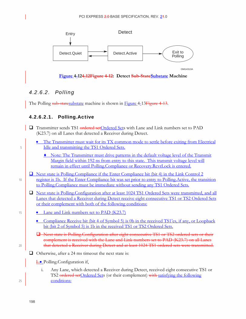
PCI EXPRESS 2.0 BASE SPECIFICATION, REV. 21.0
198
OM14313A
Detect.Quiet Detect.Active
Entry Detect
Exit toPolling
Figure 4-124-12Figure 4-12: Detect Sub-StateSubstate Machine
4.2.6.2. Polling
The Polling sub-statesubstate machine is shown in Figure 4-13Figure 4-13.
4.2.6.2.1. Polling.Active
Transmitter sends TS1 ordered setOrdered Sets with Lane and Link numbers set to PAD (K23.7) on all Lanes that detected a Receiver during Detect.
• The Transmitter must wait for its TX common mode to settle before exiting from Electrical Idle and transmitting the TS1 Ordered Sets. 5
♦ Note: The Transmitter must drive patterns in the default voltage level of the Transmit Margin field within 192 ns from entry to this state. This transmit voltage level will remain in effect until Polling.Compliance or Recovery.RcvrLock is entered.
Next state is Polling.Compliance if the Enter Compliance bit (bit 4) in the Link Control 2 register is 1b. If the Enter Compliance bit was set prior to entry to Polling.Active, the transition 10 to Polling.Compliance must be immediate without sending any TS1 Ordered Sets.
Next state is Polling.Configuration after at least 1024 TS1 Ordered Sets were transmitted, and all Lanes that detected a Receiver during Detect receive eight consecutive TS1 or TS2 Ordered Sets or their complement with both of the following conditions:
• Lane and Link numbers set to PAD (K23.7) 15
• Compliance Receive bit (bit 4 of Symbol 5) is 0b in the received TS1’es, if any, or Loopback bit (bit 2 of Symbol 5) is 1b in the received TS1 or TS2 Ordered Sets.
Next state is Polling.Configuration after eight consecutive TS1 or TS2 ordered sets or their complement is received with the Lane and Link numbers set to PAD (K23.7) on all Lanes that detected a Receiver during Detect and at least 1024 TS1 ordered sets were transmitted. 20
Otherwise, after a 24 ms timeout the next state is:
1.• Polling.Configuration if,
i. Any Lane, which detected a Receiver during Detect, received eight consecutive TS1 or TS2 ordered setOrdered Sets (or their complement) with satisfying the following conditions: 25
PCI EXPRESS 2.0 BASE SPECIFICATION, REV. 12.0
199
1. the Lane and Link numbers set to PAD (K23.7),
2. the Compliance Receive bit (bit 4 of Symbol 5) is 0b or Loopback bit (bit 2 of Symbol 5) is 1b.
and a minimum of 1024 TS1s are transmitted after receiving one TS1.
And 5
ii. All At least a predetermined number of Lanes that detected a Receiver during Detect have detected an exit from Electrical Idle at least once since entering Polling.Active.
b)
• Note: This prevents one or more bad Receivers or Transmitters from holding up a valid Link from being configured, and allows for additional training in 10 Polling.Configuration. The exact number of predetermined Lanes is implementation specific. Note that up to the 1.1 specification this predetermined number was equal to the total number of Lanes that detected a Receiver.
• Note: Any Lane that receives eight consecutive TS1 or TS2 Ordered Sets should have detected an exit from Electrical Idle at least once since entering Polling.Active. 15
• Else Polling.Compliance if either (a) or (b) is true:
(a) at least one less than the predetermined number of Lanes’s from (ii) above Receiver, which detected a Receiver during Detect, haves never detected an exit from Electrical Idle since entering Polling.Active.
(b) any Lane that detected a Receiver during Detect received eight consecutive TS1 Ordered 20 Sets (or their complement) with the Lane and Link numbers set to PAD (K23.7), the Compliance Receive bit (bit 4 of Symbol 5) is 1b, and the Loopback bit (bit 2 of Symbol 5) is 0b.
♦ Note: If a passive test load is applied on all Lanes then the device will go to Polling.Compliance.This indicates the presence of a passive test load on at least one 25 Lane, which will force all Lanes to enter Polling.Compliance.
3.• Else Detect if the conditions to transition to Polling.Configuration or Polling.Compliance are not met no TS1 or TS2 ordered set is received with Link and Lane number set to Pad on any Lane. The highest advertised speed in TS1 and TS2 is lowered (unless generation 1 is the highest advertised speed). 30
4.2.6.2.2. Polling.Compliance
The Transmit Margin field of the Link Control 2 register is sampled on entry to this substate and becomes effective on the transmit package pins within 192 ns of entry to this substate and remain effective through the time the LTSSM is in this substate.
The data rate and de-emphasis level for transmitting the compliance pattern are determined on the transition from Polling.Active to Polling.Compliance using the following algorithm. 35
• If the component is capable of transmitting at the 2.5 GT/s data rate only, the data rate for transmitting the compliance pattern is 2.5 GT/s and the de-emphasis level is -3.5 dB.
PCI EXPRESS 2.0 BASE SPECIFICATION, REV. 21.0
200
• Else if a component entered Polling.Compliance due to detecting eight consecutive TS1 Ordered Sets in Polling.Active with the Compliance Receive bit (bit 4 of Symbol 5) asserted and the Loopback bit (bit 2 of Symbol 5) deasserted then the data rate for transmission is the highest common transmitted and received Link speed (Symbol 4 of the TS1 sequence) advertised on the eight consecutive TS1 Ordered Sets received on any Lane that detected a 5 Receiver during Detect. The select_deemphasis variable must be set equal to the Selectable De-emphasis bit (Symbol 4 bit 6) in the eight consecutive TS1 Ordered Sets it received in Polling.Active substate.
• Else if the Enter Compliance bit in the Link Control 2 register is 1b, the data rate for transmitting the compliance pattern is defined by the Target Link Speed field in the Link 10 Control 2 register. The select_deemphasis variable is set equal to the Compliance De-emphasis bit in the Link Control 2 register.
• Else the data rate and de-emphasis level settings are defined as follows based on the number of times Polling.Compliance has been entered with this entry criteria:
Setting #1: Data Rate = 2.5 GT/s, De-emphasis Level = -3.5 dB 15
Setting #2: Data Rate = 5.0 GT/s, De-emphasis Level = -3.5 dB
Setting #3: Data Rate = 5.0 GT/s, De-emphasis Level = -6 dB
Subsequent entries to Polling.Compliance repeat the above sequence. For example, the state sequence which causes a component to transmit the Compliance pattern at a data rate of 5 GT/s and a de-emphasis level of -6 dB is: Polling.Active, Polling.Compliance (2.5 GT/s and 20 -3.5 dB), Polling.Active, Polling.Compliance (5.0 GT/s and -3.5 dB), Polling.Active, Polling.Compliance (5.0 GT/s and -6 dB).
IMPLEMENTATION NOTE Compliance Load Board Usage to Generate Compliance Patterns It is envisioned that the compliance load (base) board may send a 100 MHz signal for about 1 ms on one leg of a differential pair at 350 mV peak-to-peak on any Lane to cycle the device to the desired speed and de-emphasis level. The device under test is required to cycle through the following 25 settings in order, for each entry to Polling.Compliance from Polling.Active, starting with the first setting on the first entry to Polling.Compliance after the Fundamental Reset:
Data Rate = 2.5 GT/s, De-emphasis Level = -3.5 dB.
Data Rate = 5.0 GT/s, De-emphasis Level = -3.5 dB.
Data Rate = 5.0 GT/s, De-emphasis Level = -6 dB. 30
If the compliance pattern data rate is not 2.5 GT/s and any TS1 Ordered Sets were transmitted in Polling.Active prior to entering Polling.Compliance, the Transmitter sends two consecutive EIOS prior to entering Electrical Idle. If the compliance pattern data rate is not 2.5 GT/s and TS1 Ordered Sets were not transmitted in Polling.Active prior to entering Polling.Compliance, the Transmitter must enter Electrical Idle without transmitting the EIOS. During the period of 35

PCI EXPRESS 2.0 BASE SPECIFICATION, REV. 12.0
201
Electrical Idle, the data rate is changed to the new speed and stabilized. If the frequency of operation will be 5.0 GT/s, the de-emphasis level must be set to -3.5 dB if the select_deemphasis variable is 1b else it must be set to -6 dB. The period of Electrical Idle is greater than 1 ms but it is not to exceed 2 ms.
Behavior during Polling Compliance after the Link speed and de-emphasis level are determined 5 must follow the following rules:
• If a component entered Polling.Compliance due to detecting eight consecutive TS1 Ordered Sets in Polling.Active with the Compliance Receive bit (bit 4 of Symbol 5) asserted and the Loopback bit (bit 2 of Symbol 5) deasserted or both the Enter Compliance bit and the Enter Modified Compliance bit in the Link Control 2 register are set to 1b then the Transmitter 10 sends out the Modified Compliance Pattern (see Section 4.2.9) at the above determined data rate and de-emphasis level with the error status Symbol set to all 0’s on all Lanes that detected a Receiver during Detect.
♦ A particular Lane’s Receiver independently signifies a successful lock to the incoming Modified Compliance Pattern by looking for any one occurrence of the Modified 15 Compliance Pattern and then setting the Pattern Lock bit (bit 8 of the 8 bit error status Symbol) in the same Lane of its own transmitted Modified Compliance Pattern.
Note: The error status Symbols are not to be used for the lock process since they are undefined at any given moment.
Note: An occurrence is defined above as the following sequence of 8b/10b Symbols; 20 K28.5, D21.5, K28.5, and D10.2 or the complement of each of the individual Symbols.
Note: The device under test must set the Pattern Lock bit of the Modified Compliance Pattern it transmits at the Transmitter package pin(s) after successfully locking to the incoming Modified Compliance Pattern within 1 ms of receiving the 25 Modified Compliance Pattern at its Receiver package pin(s).
♦ Once a particular Lane indicates it has locked to the incoming Modified Compliance Pattern the error status Symbol for that particular Lane is incremented every time a Receiver error occurs.
Note: The error status Symbol uses the lower 7 bits as the Receive Error Count field 30 and will remain stuck at all 1’s if the count reaches 127.
The Receiver must not make any assumption about the 10-bit patterns it will receive when in this substate.
♦ If the Enter Compliance bit in the Link Control 2 register is 0b, the next state is Detect if directed 35
♦ Else if the Enter Compliance bit was set to 1b on entry to Polling.Compliance, next state is Polling.Active if any of the following conditions apply:
The Enter Compliance bit in the Link Control 2 register has changed to 0b
The device is a Downstream component and an EIOS is received on any Lane. The Enter Compliance bit is reset to 0b when this condition is true. 40
PCI EXPRESS 2.0 BASE SPECIFICATION, REV. 21.0
202
If the Transmitter was transmitting at a data rate other than 2.5 GT/s, or the Enter Compliance bit in the Link Control 2 register is set to 1b, the Transmitter sends eight consecutive EIOS and enters Electrical Idle prior to transitioning to Polling.Active. During the period of Electrical Idle, the data rate is changed to 2.5 GT/s and stabilized and the de-emphasis level is set to -3.5 dB. The period of Electrical Idle is greater than 5 1 ms but must not exceed 2 ms.
Note: Sending multiple EIOS provides enough robustness such that the other component detects at least one EIOS and exits Polling.Compliance substate when the configuration register mechanism was used for entry.
• Else (i.e., entry to Polling.Compliance is not due to the Compliance Receive bit assertion 10 with Loopback bit deassertion in the received consecutive TS Ordered Sets and not due to the Enter Compliance bit and the Enter Modified Compliance bit in the Link Control 2 register set to 1b)
(a) Transmitter sends out the compliance pattern on all Lanes that detected a Receiver during Detect at the data rate determined above.which was employed upon entry to 15 Polling.Compliance (see Section 4.2.8).
(b) Next state is Polling.Active if any of the following three conditions are true:
1. Electrical Idle exit has been detected at the Receiver of any Lane that detected a Receiver during Detect, and the Enter Compliance bit in the Link Control 2 register is 0b. 20
2. The Enter Compliance bit in the Link Control 2 register has changed to 0b (from 1b) since entering Polling.Compliance.
3. The component is a Downstream component, the Enter Compliance bit in the Link Control 2 register is set to 1b and an EIOS has been detected on any Lane. The Enter Compliance bit is reset to 0b when this condition is true. 25
If the Transmitter is transmitting at a data rate other than 2.5 GT/s, or the Enter Compliance bit in the Link Control 2 register was set to 1b during entry to Polling.Compliance, the Transmitter sends eight consecutive EIOSs and enters Electrical Idle prior to transitioning to Polling.Active. During the period of Electrical Idle, the data rate is changed to 2.5 GT/s and stabilized. The period of 30 Electrical Idle is greater than 1 ms but must not exceed 2 ms.
Note: Sending multiple EIOSs provides enough robustness such that the other component detects at least one EIOS and exits Polling.Compliance substate when the configuration register mechanism was used for entry.
4.2.6.2.3. Polling.Configuration
Receiver must invert polarity if necessary (see Section 4.2.4.44.2.4.2). 35
The Transmit Margin field of the Link Control 2 register must be reset to 000b on entry to this substate.
Transmitter sends TS2 ordered setOrdered Sets with Link and Lane numbers set to PAD (K23.7) on all Lanes that detected a Receiver during Detect.
PCI EXPRESS 2.0 BASE SPECIFICATION, REV. 12.0
203
The next state is Configuration after eight consecutive TS2 ordered setOrdered Sets, with Link and Lane numbers set to PAD (K23.7), are received on any Lanes that detected a Receiver during Detect, and 16 TS2 ordered setOrdered Sets are transmitted after receiving one TS2 ordered setOrdered Set., and none of those same Lanes is transmitting and receiving a higher Data Rate Identifier.33 5
The next state is Polling.Speed after eight consecutive TS2 ordered sets, with Link and Lane numbers set to PAD (K23.7), are received on any Lanes that detected a Receiver during Detect, 16 TS2 ordered sets are transmitted after receiving one TS2 ordered set, and at least one of those same Lanes is transmitting and receiving a higher Data Rate Identifier.34
Otherwise, next state is Detect after a 48 ms timeout. 10
4.2.6.2.4. Polling.Speed
This state is unreachable given that the Link comes up to L0 in 2.5 GT/s speed only and changes speed by entering Recovery.
The Transmitter enters Electrical Idle for a minimum of TTX-IDLE-MIN (see Table 4-5) and no longer than 2 ms.
•Note: Electrical Idle ordered set is sent prior to entering Electrical Idle. 15
•Note: The DC common mode voltage does not have to be within specification.35
Data rate is changed on all Lanes to the highest common data rate supported on both sides of the Link indicated by the training sequence (see Section 4.2.4.1).
Next state is Polling.Active.
IMPLEMENTATION NOTE Support for HigherMultiple Data Rates than Gen12.5 GT/sSupported Within One Port A Link will initially train to L0 state in 2.5 GT/s speed even if both sides are capable of operating at 20 a speed greater than 2.5 GT/s. Supported higher data rates are advertised in the TS Ordered Sets. The other side’s speed capability is registered during the Configuration . Complete substate. There is optional behavior allowed in Polling. Speed. In the event that only some lanes are sending and receiving data rates identifiers with higher data rates (see Table 4-2 and Table 4-3), training may continue with a single LTSSM as described above or optionally, additional LTSSMs can be initiated 25
33 Higher data rate than what is currently being executed. Data rate support on a Link is determined by the highest common speed being transmitted and received in TS1 and TS2 ordered sets. 34 Higher data rate than what is currently being executed. Data rate support on a Link is determined by the highest common speed being transmitted and received in TS1 and TS2 ordered sets. 35 The common mode being driven does not need to meet the Absolute Delta Between DC Common Mode During L0 and Electrical Idle (VTX-CM-DC-ACTIVE-IDLE-DELTA) specification (see Table 4-5).
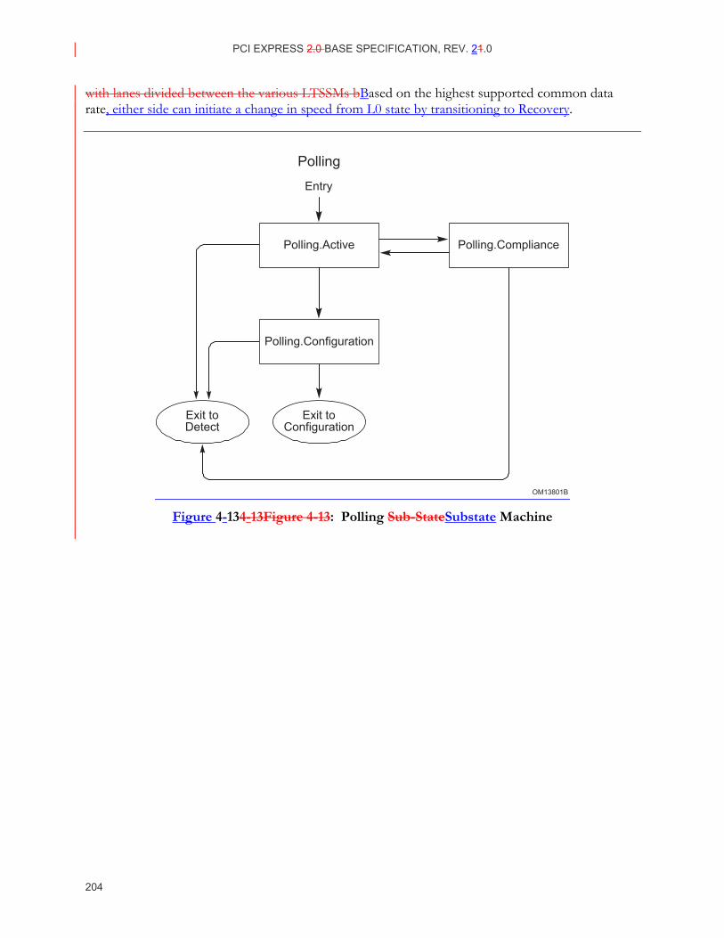
PCI EXPRESS 2.0 BASE SPECIFICATION, REV. 21.0
204
with lanes divided between the various LTSSMs bBased on the highest supported common data rate, either side can initiate a change in speed from L0 state by transitioning to Recovery.
OM13801B
Polling.Active Polling.Compliance
Polling.Configuration
Entry
Polling
Exit toConfiguration
Exit toDetect
Figure 4-134-13Figure 4-13: Polling Sub-StateSubstate Machine

PCI EXPRESS 2.0 BASE SPECIFICATION, REV. 12.0
205
4.2.6.3. Configuration
The Configuration sub-statesubstate machine is shown in Figure 4-14Figure 4-14.
4.2.6.3.1. Configuration.Linkwidth.Start
4.2.6.3.1.1. Downstream Lanes
Next state is Disable if directed.
• Note: “if directed” applies to a Downstream Port that is instructed by a higher Layer to assert the Disable Link bit (TS1 and TS2) on all Lanes that detected a Receiver during Detect. 5
Next state is Loopback if directed to this state, and the Transmitter is capable of being a Loopback loopback Mastermaster, which is determined by implementation specific means.
• Note: “if directed” applies to a Port that is instructed by a higher Layer to assert the Loopback bit (TS1 and TS2) on all Lanes that detected a Receiver during Detect.
In the optional case where a crosslink is supported, the next state is Disable after all Lanes that 10 detected a Receiver during Detect, that are also receiving TS1 ordered sets, receive the Disable bit asserted in two consecutive TS1 ordered sets receive two consecutive TS1 Ordered Sets with the Disable Link bit asserted.
Next state is Loopback after all Lanes that detected a Receiver during Detect, that are also receiving ordered Ordered setsSets, receive the Loopback bit asserted in two consecutive TS1 15 ordered setOrdered Sets.
• Note that the device receiving the ordered Ordered set Set with the Loopback bit set becomes the Loopback loopback Slaveslave.
The Transmitter sends TS1 ordered setOrdered Sets with selected Link numbers and sets Lane numbers to PAD (K23.7) on all the active Downstream Lanes if the LTSSM is not initiating 20 upconfiguration of the Link width. In addition, if upconfigure_capable is set to 1b, and the LTSSM is not initiating upconfiguration of the Link width, the LTSSM sends TS1 Ordered Sets with the selected Link number and sets the Lane number to PAD (K23.7) on each inactive Lane after it detected an exit from Electrical Idle since entering Recovery and has subsequently received two consecutive TS1 Ordered Sets with the Link and Lane numbers each set to PAD 25 (K23.7) while in this substate.
• Note: On transition to this substate from Polling, any Lane that detected a Receiver during Detect is considered an active Lane.
If the LTSSM is initiating upconfiguration of the Link width, initially it transmits TS1 Ordered Sets with both the Link and Lane numbers set to PAD (K23.7) on the current set of active 30 Lanes; the inactive Lanes it intends to activate; and those Lanes where it detected an exit from Electrical Idle since entering Recovery and has received two consecutive TS1 Ordered Sets with the Link and Lane numbers each set to PAD (K23.7). The LTSSM transmits TS1 Ordered Sets
PCI EXPRESS 2.0 BASE SPECIFICATION, REV. 21.0
206
with the selected Link number and the Lane number set to PAD (K23.7) when each of the Lanes transmitting TS1 Ordered Sets receives two consecutive TS1 Ordered Sets with the Link and Lane numbers each set to PAD (K23.7) or 1 ms has expired since entering this substate.
θ• After activating any inactive Lane, the Transmitter must wait for its TX common mode to settle before exiting from Electrical Idle and transmitting the TS1 Ordered Sets.that detected 5 a receiver during Detect.
• Note: Link numbers can are only permitted to be different for groups of Lanes capable of being a unique Link.
• Note: An example of Link number assignments includes a set of eight Lanes on an Upstream component (Downstream Lanes) capable of negotiating to become one x8 Port 10 when connected to one Downstream component (Upstream Lanes) or two x4 Ports when connected to two different Downstream components. The Upstream component (Downstream Lanes) sends out TS1 ordered setOrdered Sets with the Link number set to N on four Lanes and Link number set to N+1 on the other four Lanes. The Lane numbers are all set to PAD (K23.7). 15
If any Lanes first received at least one or more TS1 ordered setOrdered Sets with a Link and Lane number set to PAD (K23.7), the next state is Configuration.Linkwidth.Accept immediately after any of those same Downstream Lanes receive two consecutive TS1 ordered setOrdered Sets with a non-PAD Link number that matches any of the transmitted Link numbers, and with a Lane number set to PAD (K23.7). 20
• Note: If the crosslink configuration is not supported, the condition of first receiving a Link and Lane number set to PAD is always true.
Else: Optionally, if crosslinks are supported, then all Downstream Lanes that detected a Receiver during Detect must first transmit 16-32 TS1s with a non PAD Link number and PAD Lane number and after this occurs if any Downstream Lanes receive two consecutive TS1 ordered 25 setOrdered Sets with a Link number different than PAD (K23.7) and a Lane Number set to PAD, the Downstream Lanes are now designated as Upstream Lanes and a new random cross Link timeout is chosen (see Tcrosslink in Table 4-94-5). The next state is Configuration.Linkwidth.Start as Upstream Lanes.
• Note: This supports the optional crosslink where both sides may try to act as a Downstream 30 Port. This is resolved by making both Ports become Upstream and assigning a random timeout until one side of the Link becomes a Downstream Port and the other side remains an Upstream Port. This timeout must be random even when hooking up two of the same devices so as to eventually break any possible deadlock.
• Note: If crosslinks are supported, receiving a sequence of TS1 ordered setOrdered Sets with 35 a Link number of PAD followed by a Link number of non-PAD that matches the transmitted Link number is only valid when not interrupted by the reception of a TS2 ordered setOrdered Set.
PCI EXPRESS 2.0 BASE SPECIFICATION, REV. 12.0
207
IMPLEMENTATION NOTE
Crosslink Initialization In the case where the Downstream Lanes are connected to both Downstream Lanes (crosslink) and Upstream Lanes, the port Port with the Downstream Lanes may continue with a single LTSSM as described in this section or optionally, split into multiple LTSSMs.
The next state is Detect after a 24 ms timeout.
4.2.6.3.1.2. Upstream Lanes
In the optional case where crosslinks are supported the next state is Disable if directed. 5
• Note: “if directed” only applies to an optional crosslink Port that is instructed by a higher Layer to assert the Disable Link bit (TS1 and TS2) on all Lanes that detected a Receiver during Detect.
Next state is Loopback if directed to this state, and the Transmitter is capable of being a Loopback loopback Mastermaster, which is determined by implementation specific means. 10
• Note: “if directed” applies to a Port that is instructed by a higher Layer to assert the Loopback bit (TS1 and TS2) on all Lanes that detected a Receiver during Detect.
Next state is Disable after any Lanes that detected a Receiver during Detect and are receiving TS1 ordered sets with the Disable Link bit asserted in two consecutive TS1 ordered setsreceive two consecutive TS1 Ordered Sets with the Disable Link bit asserted. 15
• Note: In the optional case where a crosslink is supported, the next state is Disable only after all Lanes that detected a Receiver during Detect, that are also receiving TS1 ordered setOrdered Sets, receive the Disable Link bit asserted in two consecutive TS1 ordered setOrdered Sets.
Next state is Loopback after all Lanes that detected a Receiver during Detect, that are also 20 receiving TS1 ordered setOrdered Sets, receive the Loopback bit asserted in two consecutive TS1 ordered setOrdered Sets.
• Note: The device receiving the ordered Ordered set Set with the Loopback bit set becomes the Loopback loopback Slaveslave.
The Transmitter sends out TS1 ordered setOrdered Sets with Link numbers and Lane numbers 25 set to PAD (K23.7) on all the active Upstream Lanes; the inactive Lanes it is initiating to upconfigure the Link width; and if upconfigure_capable is set to 1b, on each of the inactive Lanes where it detected an exit from Electrical Idle since entering Recovery and has subsequently received two consecutive TS1 Ordered Sets with Link and Lane numbers, each set to PAD (K23.7), in this substate. 30
θ• On transition to this substate from Polling, any Lane that detected a Receiver during Detect is considered an active Lane. that detected a Receiver during Detect.
PCI EXPRESS 2.0 BASE SPECIFICATION, REV. 21.0
208
• On transition to this substate from Recovery, if the transition is not caused by LTSSM timeout, the Transmitter must set the Autonomous Change (Symbol 4 bit 6) to 1b in the TS1 Ordered Sets that it sends while in the Configuration state if the Transmitter intends to change the Link width for autonomous reasons.
If any Lanes receives two consecutive TS1 ordered setOrdered Sets with Link numbers that are 5 different than PAD (K23.7) and Lane number set to PAD(K23.7), a single Link number is selected and Lane number set to PAD are transmitted on all Lanes that both detected a Receiver and also received two consecutive TS1 ordered setOrdered Sets with Link numbers that are different than PAD (K23.7) and Lane number set to PAD (K23.7) (see the note below). Any left over Lanes that detected a Receiver during Detect must transmit TS1 ordered setOrdered 10 Sets with the Link and Lane number set to PAD (K23.7). The next state is Configuration.Linkwidth.Accept.:
• Note: If the LTTSM is initiating upconfiguration of the Link width, it waits until it receives two consecutive TS1 Ordered Sets with a non-PAD (K23.7) Link number and a PAD (K23.7) Lane number on all the inactive Lanes it wants to activate, or, 1 ms after entry to 15 this substate, it receives two consecutive TS1 Ordered Sets on any Lane with a non-PAD (K23.7) Link number and PAD (K23.7) Lane number, whichever occurs earlier, before transmitting TS1 Ordered Sets with selected Link number and Lane number set to PAD (K23.7).
• Note: It is recommended that any possible multi-Lane Link that received an error in a TS1 20 ordered setOrdered Set on a subset of the received Lanes; delay the evaluation listed above by an additional two TS1 ordered setOrdered Sets so as not to prematurely configure a smaller Link than possible.
♦ After activating any inactive Lane, the Transmitter must wait for its TX common mode to settle before exiting Electrical Idle and transmitting the TS1 Ordered Sets. 25
Optionally, if crosslinks are supported, then all Upstream Lanes that detected a Receiver during Detect must first transmit 16–32 TS1s with a PAD Link number and PAD Lane number and after this occurs and if any Upstream Lanes first receive two consecutive TS1 ordered setOrdered Sets with Link and Lane numbers set to PAD (K23.7), then:
• The Transmitter continues to send out TS1 ordered setOrdered Sets with Link numbers and 30 Lane numbers set to PAD (K23.7).
• If any Lanes receive two consecutive TS1 ordered setOrdered Sets with Link numbers that are different than PAD (K23.7) and Lane number set to PAD (K23.7), a single Link number is selected and Lane number set to PAD are transmitted on all Lanes that both detected a Receiver and also received two consecutive TS1 ordered setOrdered Sets with Link numbers 35 that are different than PAD (K23.7) and Lane number set to PAD (K23.7). Any left over Lanes that detected a Receiver during Detect must transmit TS1 ordered setOrdered Sets with the Link and Lane number set to PAD (K23.7). The next state is Configuration.Linkwidth.Accept.
♦ Note: It is recommended that any possible multi-Lane Link that received an error in a 40 TS1 ordered setOrdered Set on a subset of the received Lanes; delay the evaluation listed above by an additional two TS1 ordered setOrdered Sets so as not to prematurely configure a smaller Link than possible.
PCI EXPRESS 2.0 BASE SPECIFICATION, REV. 12.0
209
• Otherwise, after a Tcrosslink timeout, 16-32 TS2 ordered setOrdered Sets with PAD linkLink numbers and PAD laneLane numbers are sent. The Upstream Lanes become Downstream Lanes and the next state is Configuration.Linkwidth.Start as Downstream Lanes.
♦ Note: This optional behavior is required for crosslink behavior where two Ports may start off with Upstream Ports, and one will eventually take the lead as a Downstream 5 Port.
The next state is Detect after a 24 ms timeout.
4.2.6.3.2. Configuration.Linkwidth.Accept
4.2.6.3.2.1. Downstream Lanes
If a configured Link can be formed with at least one group of Lanes that received two consecutive TS1 ordered setOrdered Sets with the same received Link number (non-PAD and matching one that was transmitted by the Downstream Lanes), TS1 ordered setOrdered Sets are 10 transmitted with the same Link number and unique non-PAD Lane numbers are assigned to all theses same Lanes. The next state is Configuration.Lanenum.Wait.
• Note: The assigned non-PAD Lane numbers must range from 0 to n-1, be assigned sequentially to the same grouping of Lanes that are receiving the same Link number Lane numbers, and Downstream Lanes which are not receiving TS1 ordered setOrdered Sets 15 must not disrupt the initial sequential numbering of the widest possible Link. Any left over Lanes must transmit TS1 ordered setOrdered Sets with the Link and Lane number set to PAD (K23.7).
• Note: It is recommended that any possible multi-Lane Link that received an error in a TS1 ordered setOrdered Set on a subset of the received Lanes delay the evaluation listed above 20 by an additional two TS1 ordered setOrdered Sets so as not to prematurely configure a smaller Link than possible.
•Note: A couple of interesting cases to consider here are the following:
1.A x8 Downstream Port, which can be divided into two x4 Links, sends two different Link numbers on to two x4 Upstream Ports. The Upstream Ports respond simultaneously by 25 picking the two Link numbers. The Downstream Port will have to choose one of these sets of Link numbers to configure as a Link, and leave the other for a secondary LTSSM to configure (which will ultimately happen in Configuration.Complete).
2.A x16 Downstream Port, which can be divided into two x8 Links, is hooked up to a x12 Upstream Port that can be configured as a x12 Link or a x8 and a x4 Link. During 30 Configuration.Linkwidth.Start the Upstream Port returned the same Link number on all 12 Lanes. The Downstream Port would then return the same received Link number and assign Lane numbers on the eight Lanes that can form a x8 Link with the remaining four Lanes transmitting a Lane number and a Link number set to PAD (K23.7).
3.A x8 Downstream Port where only seven Lanes are receiving TS1s with the same received 35 Link number (non-PAD and matching one that was transmitted by the Downstream Lanes) and an eighth Lane, which is in the middle or adjacent to those same Lanes, is not
PCI EXPRESS 2.0 BASE SPECIFICATION, REV. 21.0
210
receiving a TS1 ordered-set. In this case, the eighth Lane is treated the same as the other seven Lanes and Lane numbering for a x8 Lane should occur as described above.
The next state is Detect after a 2 ms timeout or if no Link can be configured or if all Lanes receive two consecutive TS1 ordered setOrdered Sets with Link and Lane numbers set to Pad PAD (K23.7). 5
4.2.6.3.2.2. Upstream Lanes
If a configured Link can be formed using Lanes that transmitted a non-PAD Link number which are receiving two consecutive TS1 ordered setOrdered Sets with the same non-PAD Link number and any non-PAD Lane number, TS1 Ordered Sets are transmitted with the same non-PAD Link number and Lane numbers thatand any non-PAD Lane number, TS1 Lane numbers are transmitted that, if possible, match the received Lane numbers or are different, if necessary, 10 (i.e., Lane reversed). The next state is Configuration.Lanenum.Wait.
• Note: The newly assigned Lane numbers must range from 0 to m-1, be assigned sequentially only to some continuous grouping of Lanes that are receiving non-PAD Lane numbers (i.e., Lanes which are not receiving any TS1 ordered setOrdered Sets always disrupt a continuous grouping and must not be included in this grouping), must include either Lane 0 or Lane n-1 15 (largest received Lane number), and m-1 must be equal to or smaller than the largest received Lane number (n-1). Remaining Lanes must transmit TS1 with Link and Lane numbers set to PAD (K23.7).
• Note: It is recommended that any possible multi-Lane Link that received an error in a TS1 Ordered Sets on a subset of the received Lanes delay the evaluation listed above by an 20 additional two TS1 ordered setOrdered Sets so as not to prematurely configure a smaller Link than possible.
•Note: A few interesting cases to consider here are the following:
0.A x8 Upstream Port is presented with Lane numbers that are backward from the preferred numbering. If the optional behavior of Lane reversal is supported by the Upstream 25 Port, the Upstream Port transmits the same Lane numbers back to the Downstream Port. Otherwise the opposite Lane numbers are transmitted back to the Downstream Port, and it will be up to the Downstream Port to optionally fix the Lane ordering or exit Configuration.
Note: Optional Lane reversal behavior is required to configure a Link where the Lane 30 numbers are reversed and the Downstream Port does not support Lane reversal. Specifically, the Upstream Port Lane reversal will accommodate the scenario where the default Upstream sequential Lane numbering (0 to n-1) is receiving a reversed Downstream sequential Lane number (n-1 to 0).
0.A x8 Upstream Port is not receiving TS1 ordered-sets on the Upstream Port Lane 0: 35
a.In the case where the Upstream Port can only support a x8 or x1 Link and the Upstream Port can support Lane reversal. The Upstream Port will assign a Lane 0 to only the received Lane 7 (received Lane number n-1) and the remaining seven Lanes must transmit TS1 with Link and Lane numbers set to PAD (K23.7)
PCI EXPRESS 2.0 BASE SPECIFICATION, REV. 12.0
211
b.In the case where the Upstream Port can only support a x8 or x1 Link and the Upstream Port cannot support Lane reversal. No Link can be formed and the Upstream Port will eventually timeout after 2 ms and exit to Detect.
0.An optional x8 Upstream crosslink Port, which can be divided into two x4 Links, is attached to two x4 Downstream Ports that present the same Link number, and each x4 5 Downstream Port presents Lane numbers simultaneously that were each numbered 0 to 3. The Upstream Port will have to choose one of these sets of Lane numbers to configure as a Link, and leave the other for a second pass through Configuration.
The next state is Detect after a 2 ms timeout or if no Link can be configured or if all Lanes receive two consecutive TS1 ordered setOrdered Sets with Link and Lane numbers set to Pad 10 PAD (K23.7).
IMPLEMENTATION NOTE
Example Cases Notable examples related to the configuration of Downstream Lanes:
1. A x8 Downstream Port, which can be divided into two x4 Links, sends two different Link numbers on to two x4 Upstream Ports. The Upstream Ports respond simultaneously by picking the two Link numbers. The Downstream Port will have to choose one of these sets of Link 15 numbers to configure as a Link, and leave the other for a secondary LTSSM to configure (which will ultimately happen in Configuration.Complete).
2. A x16 Downstream Port, which can be divided into two x8 Links, is hooked up to a x12 Upstream Port that can be configured as a x12 Link or a x8 and a x4 Link. During Configuration.Linkwidth.Start the Upstream Port returned the same Link number on all 12 20 Lanes. The Downstream Port would then return the same received Link number and assign Lane numbers on the eight Lanes that can form a x8 Link with the remaining four Lanes transmitting a Lane number and a Link number set to PAD (K23.7).
3. A x8 Downstream Port where only seven Lanes are receiving TS1s with the same received Link number (non-PAD and matching one that was transmitted by the Downstream Lanes) and an 25 eighth Lane, which is in the middle or adjacent to those same Lanes, is not receiving a TS1 Ordered Set. In this case, the eighth Lane is treated the same as the other seven Lanes and Lane numbering for a x8 Lane should occur as described above.
Notable examples related to the configuration of Upstream Lanes:
1. A x8 Upstream Port is presented with Lane numbers that are backward from the preferred 30 numbering. If the optional behavior of Lane reversal is supported by the Upstream Port, the Upstream Port transmits the same Lane numbers back to the Downstream Port. Otherwise the opposite Lane numbers are transmitted back to the Downstream Port, and it will be up to the Downstream Port to optionally fix the Lane ordering or exit Configuration.
Note: Optional Lane reversal behavior is required to configure a Link where the Lane 35 numbers are reversed and the Downstream Port does not support Lane reversal. Specifically, the Upstream Port Lane reversal will accommodate the scenario where the
PCI EXPRESS 2.0 BASE SPECIFICATION, REV. 21.0
212
default Upstream sequential Lane numbering (0 to n-1) is receiving a reversed Downstream sequential Lane number (n-1 to 0).
2. A x8 Upstream Port is not receiving TS1 Ordered Sets on the Upstream Port Lane 0:
a. In the case where the Upstream Port can only support a x8 or x1 Link and the Upstream Port can support Lane reversal. The Upstream Port will assign a Lane 0 to only the received 5 Lane 7 (received Lane number n-1) and the remaining seven Lanes must transmit TS1 with Link and Lane numbers set to PAD (K23.7)
b. In the case where the Upstream Port can only support a x8 or x1 Link and the Upstream Port cannot support Lane reversal. No Link can be formed and the Upstream Port will eventually timeout after 2 ms and exit to Detect. 10
3. An optional x8 Upstream crosslink Port, which can be divided into two x4 Links, is attached to two x4 Downstream Ports that present the same Link number, and each x4 Downstream Port presents Lane numbers simultaneously that were each numbered 0 to 3. The Upstream Port will have to choose one of these sets of Lane numbers to configure as a Link, and leave the other for a second pass through Configuration. 15
4.2.6.3.3. Configuration.Lanenum.Accept
4.2.6.3.3.1. Downstream Lanes
If two consecutive TS1 ordered setOrdered Sets are received with non-PAD Link and non-PAD Lane numbers that match all the non-PAD Link and non-PAD Lane numbers (or reversed Lane numbers if Lane reversal is optionally supported) that are being transmitted in Downstream Lane TS1 ordered setOrdered Sets, the next state is Configuration.Complete.
• The Link Bandwidth Management Status and Link Autonomous Bandwidth Status bits of 20 the Link Status register must be updated as follows on a Link bandwidth change if the current transition to Configuration state was from the Recovery state:
(a) If the Link bandwidth was reduced and either the Autonomous Change bit (Symbol 4 bit 6) in two consecutive received TS1 Ordered Sets is 0b or the bandwidth change was initiated by the Upstream component due to reliability issues, the Link Bandwidth 25 Management Status bit is set to 1b
(b) else the Link Autonomous Bandwidth Status bit is set to 1b.
• Note: The condition of Reversed Lane numbers is defined strictly as the downstream Downstream Lane 0 receiving a TS1 ordered setOrdered Set with a Lane number equal to n-1 and the downstream Downstream Lane n-1 receiving a TS1 ordered setOrdered Set with a 30 Lane number equal to 0.
• Note: It is recommended that any possible multi-Lane Link that received an error in a TS1 ordered setOrdered Sets on a subset of the received Lanes delay the evaluation listed above by an additional two TS1 ordered setOrdered Sets so as not to prematurely configure a smaller Link than possible. 35
PCI EXPRESS 2.0 BASE SPECIFICATION, REV. 12.0
213
If a configured Link can be formed with any subset of the Lanes that receive two consecutive TS1 ordered setOrdered Sets with the same transmitted non-PAD Link numbers and any non-Pad PAD Lane numbers, TS1 ordered setOrdered Sets are transmitted with new the same non-PAD Link numbers and new Lane numbers assigned and the next state is Configuration.Lanenum.Wait. 5
• Note: The newly assigned transmitted Lane numbers must range from 0 to m-1, be assigned sequentially only to some continuous grouping of the Lanes that are receiving non-PAD Lane numbers (i.e., Lanes which are not receiving any TS1 ordered setOrdered Sets always disrupt a continuous grouping and must not be included in this grouping), must include either Lane 0 or Lane n-1 (largest received Lane number), and m-1 must be equal to or 10 smaller than the largest received Lane number (n-1). Any left over Lanes must transmit TS1 ordered setOrdered Sets with the Link and Lane number set to PAD (K23.7).
• Note: It is recommended that any possible multi-Lane Link that received an error in a TS1 ordered setOrdered Set on a subset of the received Lanes delay the evaluation listed above by an additional two TS1 ordered setOrdered Sets so as not to prematurely configure a 15 smaller Link than possible.
The next state is Detect if no Link can be configured or if all Lanes receive two consecutive TS1 ordered setOrdered Sets with Link and Lane numbers set to Pad PAD (K23.7).
4.2.6.3.3.2. Upstream Lanes
If two consecutive TS2 ordered setOrdered Sets are received with non-PAD Link and non-PAD Lane numbers that match all non-PAD Link and non-PAD Lane numbers that are being 20 transmitted in Upstream Lane TS1 ordered setOrdered Sets, the next state is Configuration.Complete.
If a configured Link can be formed with any subset of the Lanes that receive two consecutive TS1 ordered setOrdered Sets with the same transmitted non-PAD Link numbers and any non-PAD Lane numbers, TS1 ordered setOrdered Sets are transmitted with the same non-PAD Link 25 numbers and new Lane numbers assigned and the next state is Configuration.Lanenum.Wait.
• Note: The newly assigned transmitted Lane numbers must range from 0 to m-1, be assigned sequentially only to some continuous grouping of Lanes that are receiving non-PAD Lane numbers (i.e., Lanes which are not receiving any TS1 ordered setOrdered Sets always disrupt a continuous grouping and must not be included in this grouping), must include either 30 Lane 0 or Lane n-1 (largest received Lane number), and m-1 must be equal to or smaller than the largest received Lane number (n-1). Any left over Lanes must transmit TS1 ordered setOrdered Sets with the Link and Lane number set to PAD (K23.7).
• Note: It is recommended that any possible multi-Lane Link that received an error in a TS1 ordered setOrdered Sets on a subset of the received Lanes delay the evaluation listed above 35 by an additional two TS1 ordered setOrdered Sets so as not to pre-maturely configure a smaller Link than possible.
The next state is Detect if no Link can be configured or if all Lanes receive two consecutive TS1 ordered setOrdered Sets with Link and Lane numbers set to Pad PAD (K23.7).
PCI EXPRESS 2.0 BASE SPECIFICATION, REV. 21.0
214
4.2.6.3.4. Configuration.Lanenum.Wait
4.2.6.3.4.1. Downstream Lanes
The next state is Configuration.Lanenum.Accept if any of the Lanes that detected a Receiver during Detect receive two consecutive TS1 Ordered Sets which have a Lane number different from when the Lane first entered Configuration.Lanenum.Wait, and not all the Lanes’ Link numbers are set to Pad PAD (K23.7) or two consecutive TS1 Ordered Sets have been received on all Lanes, with Link and Lane numbers that match what is being transmitted on all Lanes. 5
Note: The Upstream Lanes may are permitted delay up to 1 ms before transitioning to Configuration.Lanenum.Accept.
The reason for delaying up to 1 ms before transitioning is to prevent received errors or skew between Lanes affecting the final configured Link width.
The condition of requiring reception of any Lane number different from when the Lane(s) first 10 entered Configuration.Lanenum.Wait is necessary in order to allow the two ports Ports to settle on an agreed upon Link width. The exact meaning of the statement “any of the Lanes receive two consecutive TS1 Ordered Sets, which have a Lane number different from when the Lane first entered Configuration.Lanenum.Wait” requires that a Lane number must have changed from when the Lanes most recently entered Configuration.Lanenum.Wait before a transition to 15 Configuration.Lanenum.Accept can occur.
The next state is Detect after a 2 ms timeout or if all Lanes receive two consecutive TS1 ordered setOrdered Sets with Link and Lane numbers set to Pad PAD (K23.7).
4.2.6.3.4.2. Upstream Lanes
The next state is Configuration.Lanenum.Accept
1.a. If any of the Lanes receive two consecutive TS1s that have a Lane number different from 20 when the Lane first entered Configuration.Lanenum.Wait, and not all the Lanes’ Link numbers are set to Pad PAD (K23.7)
or
2.b. If any Lane receives two consecutive TS2 ordered setOrdered Sets
The next state is Detect after a 2 ms timeout or if all Lanes receive two consecutive TS1 ordered 25 setOrdered Sets with Link and Lane numbers set to Pad PAD (K23.7).
4.2.6.3.5. Configuration.Complete
A device is allowed to change the data rates it supports only during entry to this substate, and must not change the values while in this substate. A device is also allowed to change its Link width upconfigure capability advertised in Link Upconfigure Capability (Symbol 4 bit 6) in the TS2 Ordered Set prior to entry to this substate and must not change the values while in this substate. 30
PCI EXPRESS 2.0 BASE SPECIFICATION, REV. 12.0
215
4.2.6.3.5.1. Downstream Lanes
TS2 ordered setOrdered Sets are transmitted using Link and Lane numbers that match the received TS1 Link and Lane numbers.
N_FTS must be noted for use in L0s when leaving this state.
Lane-to-Lane de-skew must be completed when leaving this state.
Scrambling is disabled if all configured Lanes have the Disable Scrambling bit asserted in two 5 consecutively received TS2 ordered setOrdered Sets.
• Note: It is required that the Port that is sending the Disable Scrambling bit on all of the configured Lanes will also disable scrambling.
The next state is Configuration.Idle immediately after all Lanes that are transmitting TS2 ordered setOrdered Sets receive eight consecutive TS2 ordered setOrdered Sets with matching Lane and 10 Link numbers (non-PadPAD) and identical data rate identifiers (including identical Link Upconfigure Capability (Symbol 4 bit 6)), and 16 TS2 ordered setOrdered Sets are sent after receiving one TS2 ordered setOrdered Set.
• If the device supports greater than 2.5 GT/s speed, it must record the data rate identifier received on any configured Lane of the Link. This will override any previously recorded 15 value. A variable to track speed change in recovery state, changed_speed_recovery, is reset to 0b.
• If the device sends TS2 Ordered Sets with the Link Upconfigure Capability (Symbol 4 bit 6) set to 1b, and receives eight consecutive TS2 Ordered Sets with the Link Upconfigure Capability bit set to 1b, the variable upconfigure_capable is set to 1b, else it is reset to 0b. 20
• Note: All remaining Lanes that are not part of the configured Link are no longer associated with the LTSSM in progress and must:
i. Be associated with a new LTSSM if this optional feature is supported.
or
ii. All Lanes that cannot be associated with an optional new LTSSM must transition to 25 Electrical Idle.36 Those Lanes that formed a Link up to the L0 state, and LinkUp has been 1b since then, but are not a part of the currently configured Link, must be associated with the same LTSSM if the LTSSM advertises Link width upconfigure capability. It is recommended that the Receiver terminations of these Lanes be left on. If they are not left on, they must be turned on when the LTSSM enters the 30 Recovery.RcvrCfg substate until it reaches the Config.Complete substate if upconfigure_capable is set to 1b to allow for potential Link width upconfiguration. Any Lane that was not part of the LTSSM during the initial Link training through L0 cannot become a part of the LTSSM as part of the Link width upconfiguration process.
Note: In the case of an optional crosslink, the Receiver terminations are required to 35 meet ZRX-HIGH-IMP-DC-POS and ZRX-HIGH-IMP-DC-NEG (see Table 4-12Table 4-6).
36 The common mode being driven does not need to meet the Absolute Delta Between DC Common Mode During L0 and Electrical Idle (VTX-CM-DC-ACTIVE-IDLE-DELTA) specification (see Table 4-9 ).
PCI EXPRESS 2.0 BASE SPECIFICATION, REV. 21.0
216
Note: These Lanes must be re-associated with the LTSSM immediately after the LTSSM in progress transitions back to Detect.
Note: An Electrical Idle ordered setEIOS does not need to be sent before transitioning to Electrical Idle.
The next state is Detect after a 2 ms timeout. 5
4.2.6.3.5.2. Upstream Lanes
TS2 ordered setOrdered Sets are transmitted using Link and Lane numbers that match the received TS2 Link and Lane numbers.
N_FTS must be noted for use in L0s when leaving this state.
Lane-to-Lane de-skew must be completed when leaving this state.
Scrambling is disabled if all configured Lanes have the Disable Scrambling bit asserted in two 10 consecutively received TS2 ordered setOrdered Sets.
• Note: It is required that the Port that is sending the Disable Scrambling bit on all of the configured Lanes will also disable scrambling.
The next state is Configuration.Idle immediately after all Lanes that are transmitting TS2 ordered setOrdered Sets receive eight consecutive TS2 ordered setOrdered Sets with matching Lane and 15 Link numbers (non-PadPAD) and identical data rate identifiers (including identical Link Upconfigure Capability (Symbol 4 bit 6)), and 16 consecutive TS2 ordered setOrdered Sets are sent after receiving one TS2 Ordered Set.
• If the device supports greater than 2.5 GT/s speed, it must record the data rate identifier received on any configured Lane of the Link. This will override any previously recorded 20 value. A variable to track speed change in recovery state, changed_speed_recovery, is reset to 0b.
• If the device sends TS2 Ordered Sets with the Link Upconfigure Capability (Symbol 4 bit 6) set to 1b, as well as receives eight consecutive TS2 Ordered Sets with the Link Upconfigure Capability bit set to 1b, the variable upconfigure_capable is set to 1b, else it is reset to 0b. 25
• Note: All remaining Lanes that are not part of the configured Link are no longer associated with the LTSSM in progress and must:
i. Optionally be associated with a new crosslink LTSSM if this feature is supported.
or
ii. All remaining Lanes that are not associated with a new crosslink LTSSM must transition 30 to Electrical Idle37, and Receiver terminations are required to meet ZRX-HIGH-IMP-DC-POS and ZRX-HIGH-IMP-DC-NEG (see Table 4-12Table 4-6). Those Lanes that formed a Link up to the L0 state, and LinkUp has been 1b since then, but are not a part of the currently configured Link, must be associated with the same LTSSM if the LTSSM advertises Link
37 The common mode being driven does not need to meet the Absolute Delta Between DC Common Mode During L0 and Electrical Idle (VTX-CM-DC-ACTIVE-IDLE-DELTA) specification (see Table 4-9).
PCI EXPRESS 2.0 BASE SPECIFICATION, REV. 12.0
217
width upconfigure capability. It is recommended that the Receiver terminations of these Lanes be left on. If they are not left on, they must be turned on when the LTSSM enters the Recovery.RcvrCfg substate until it reaches the Config.Complete substate if upconfigure_capable is set to 1b to allow for potential Link width upconfiguration. Any Lane that was not part of the LTSSM during the initial Link training through L0 cannot 5 become a part of the LTSSM as part of the Link width upconfiguration process.
Note: These Lanes must be re-associated with the LTSSM immediately after the LTSSM in progress transitions back to Detect.
Note: An Electrical Idle ordered setEIOS does not need to be sent before transitioning to Electrical Idle. 10
The next state is Detect after a 2 ms timeout.
4.2.6.3.6. Configuration.Idle
Transmitter sends Idle data Symbols on all configured Lanes.
Receiver waits for Idle data.
LinkUp = 1b (status is set true).
Next state is L0 if eight consecutive Symbol Times of Idle data are received on all configured 15 Lanes and 16 Idle data Symbols are sent after receiving one Idle data Symbol.
• If software has written a 1b to the Retrain Link bit in the Link Control register since the last transition to L0 from Recovery or Configuration, the Upstream component must set the Link Bandwidth Management Status bit of the Link Status register to 1b.
Otherwise, the next state is Detect after a minimum 2 ms timeout: 20
• If the idle_to_rlock_transitioned variable is 0b, the next state is Recovery.RcvrLock.
♦ The idle_to_rlock_transitioned variable is set to 1b upon transitioning to Recovery.RcvrLock.
θ• Else the next state is Detect..
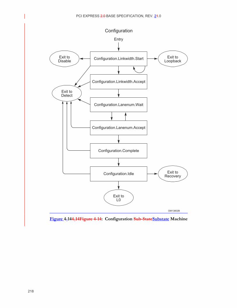
PCI EXPRESS 2.0 BASE SPECIFICATION, REV. 21.0
218
Exit toRecovery
OM13802B
Configuration.Linkwidth.Start
Configuration.Linkwidth.Accept
Configuration.Lanenum.Wait
Configuration.Lanenum.Accept
Configuration.Complete
Configuration.Idle
Entry
Configuration
Exit toL0
Exit toLoopback
Exit toDisable
Exit toDetect
Figure 4-144-14Figure 4-14: Configuration Sub-StateSubstate Machine
PCI EXPRESS 2.0 BASE SPECIFICATION, REV. 12.0
219
4.2.6.4. Recovery
The Recovery sub-statesubstate machine is shown in Figure 4-15Figure 4-15.
4.2.6.4.1. Recovery.RcvrLock
Transmitter sends TS1 ordered setOrdered Sets on all configured Lanes using the same Link and Lane numbers that were set after leaving Configuration. The speed_change bit (bit 7 of data rate identifier Symbol in TS1 Ordered Set) must be set to 1b if the directed_speed_change variable is set to 1b. The directed_speed_change variable is set to 1b if any configured Lane receives eight 5 consecutive TS1 Ordered Sets with the speed_change bit set to 1b. Only those data rates greater than 2.5 GT/s should be advertised that can be supported reliably. The N_FTS value in the TS1 Ordered Set transmitted reflects the number at the current speed of operation. A device is allowed to change the data rates it supports only during entry to this substate (from L0, L1, or Recovery.Speed) and must not change the values either in this substate or while in 10 Recovery.RcvrCfg substate. The successful_speed_negotiation variable is reset to 0b upon entry to this substate.
A Downstream component must set the Selectable De-emphasis bit (bit 6 of Symbol 4) of the TS1 Ordered Sets it transmits to match the desired de-emphasis level at 5 GT/s. The mechanism a Downstream component may adopt to request a de-emphasis level if it chooses to 15 do so is implementation specific. It must also be noted that since the Downstream component's request may not reach the Upstream component due to bit errors in the TS1 ordered sets, the Downstream component may attempt to re-request the desired de-emphasis level in subsequent entries to Recovery state when speed change is requested. An Upstream component must record the Selectable De-emphasis bit (Symbol 4 bit 6) in the Received TS1 Ordered Set in a 20 Downstream_de-emphasis_setting variable on exit from this state.
The Transmit Margin field of the Link Control 2 register is sampled on entry to this substate and becomes effective on the transmit package pins within 192 ns of entry to this substate and remains effective until a new value is sampled on a subsequent entry to this substate from L0, L0s, or L1. 25
• Note: After activating any inactive Lane, the Transmitter must wait for its TX common mode to settle before exiting Electrical Idle and transmitting the TS1 Ordered Sets.
• Note: Implementations must note that the voltage levels may change after an early bit/symbol lock since the new Transmit Margin field becomes effective within 192 ns after the other side enter Recovery.RcvrLock. The Receiver needs to reacquire bit/symbol lock 30 under those conditions.
a. Note: The directed_speed_change variable is set to 1b in L0 or L1 state for the side that is initiating a speed change. For the side that is not initiating a speed change, this bit is set to 1b in this substate if the received TS Ordered Sets have the speed change bit set to 1b. This bit is reset to 0b in the Recovery.Speed substate. 35
b. A device must accept all good TLPs and DLLPs it receives after entering this substate from L0 prior to receiving the first TS Ordered Set.
PCI EXPRESS 2.0 BASE SPECIFICATION, REV. 21.0
220
Next state is Recovery.RcvrCfg if eight consecutive TS1 or TS2 ordered setOrdered Sets are received on all configured Lanes with the same Link and Lane numbers that match what is being transmitted on those same Lanes and the speed_change bit is equal to the directed_speed_change variable.
• Note: If the Extended Synch bit is set, the Transmitter must send a minimum of 1024 5 consecutive TS1 ordered setOrdered Sets before transitioning to Recovery.RcvrCfg.
♦Note: Extended Synch allows external Link monitoring tools (e.g., logic analyzers) enough time to achieve bit and Symbol lock.
Otherwise, after a 24 ms timeout:
• Next state is Recovery.RcvrCfg if the following two conditions are true: 10
♦ Eight consecutive TS1 or TS2 Ordered Sets are received on any configured Lane with the same Link and Lane numbers that match what is being transmitted on the same Lane and the speed_change bit equal to 1b.
♦ Either the current data rate of operation is greater than 2.5 GT/s; or 5.0 GT/s or greater data rate identifiers are set in both the transmitted TS1 and the (eight consecutive) 15 received TS1 or TS2 Ordered Sets.
• Else the next state is Recovery.Speed if the speed of operation has not changed to a mutually negotiated data rate since entering Recovery from L0 (i.e., changed_speed_recovery = 0b) and the current speed of operation is greater than 2.5 GT/s. The new data rate to operate after leaving Recovery.Speed will be at 2.5 GT/s. 20 Note: This indicates that the Link was unable to operate at the current data rate (greater than 2.5 GT/s) and the Link will operate at the 2.5 GT/s data rate.
• Else the next state is Recovery.Speed if the operating speed has been changed to a mutually negotiated data rate since entering Recovery from L0 (changed_speed_recovery = 1b; i.e., the arc to this substate has been taken from Recovery.Speed). The new data rate to operate 25 after leaving Recovery.Speed is reverted back to the speed it was when Recovery was entered from L0.
Note: This indicates that the Link was unable to operate at the new negotiated data rate and will revert back to the old data rate with which it entered Recovery from L0.
• Else tThe next state is Configuration if any of the configured Lanes that are receiving a TS1 30 or TS2 ordered setOrdered Set have received at least one TS1 or TS2 with Link and Lane numbers that match what is being transmitted on those same Lanes and the operating speed has not changed to a mutually negotiated data rate (i.e., changed_speed_recovery = 0b) since entering Recovery and at least one of the following conditions is true:
♦ The directed_speed_change variable is equal to 0b and the speed_change bit on the 35 received TS1 or TS2 Ordered Set is equal to 0b.
♦ The current data rate of operation is 2.5 GT/s and 2.5 GT/s data rate is the highest commonly advertised data rate among the transmitted TS1 Ordered Sets and the received TS1 or TS2 Ordered Set(s).
2.• Otherwise, the next state is Detect. 40
PCI EXPRESS 2.0 BASE SPECIFICATION, REV. 12.0
221
IMPLEMENTATION NOTE
Example Showing Speed Change Algorithm Scaling Beyond 5.0 GT/s Suppose a Link connects two greater than 5.0 GT/s capable components, A and B. The Link comes up to L0 state in 2.5 GT/s speed. Component A decides to change the speed to greater than 5.0 GT/s, sets the directed_speed_change variable to 1b and enters Recovery.RcvrLock from L0. Component A sends TS1 Ordered Sets with speed_change bit set to 1b and advertises all three data rates. Component B sees the first TS1 in L0 state and enters Recovery.RcvrLock state. Initially, 5 component B sends TS1s with speed_change set to 0b. Component B will start sending the speed_change indication in its TS1 after it receives eight consecutive TS1 Ordered Sets from component A and advertises all three data rates it can support. Component B will enter Recovery.RcvrCfg from where it will enter Recovery.Speed. Component A will wait for eight consecutive TS1/TS2 with speed_change bit set from component B before moving to 10 Recovery.RcvrCfg and on to Recovery.Speed. Both component A and component B enter Recovery.Speed and record greater than 5.0 GT/s as the maximum speed they can operate with. The directed_speed_change variable will be reset to 0b when in Recovery.Speed. When they enter Recovery.RcvrLock from Recovery.Speed, they will operate in greater than 5.0 GT/s speed and send TS1s with speed_change set to 0b. If both sides work well at greater than 5.0 GT/s, they will 15 continue on to Recovery.RcvrCfg and enter L0 through Recovery.Idle at greater than 5.0 GT/s speed. However, if component B fails to achieve Symbol lock, it will timeout in Recovery.RcvrLock and enters Recovery.Speed. Component A would have moved on to Recovery.RcvrCfg but would see the Electrical Idle after receiving TS1s at greater than 5.0 GT/s after component B enters Recovery.Speed. This will cause component A to move to Recovery.Speed. After entering 20 Recovery.Speed for the second time, both sides will revert back to the speed they operated with prior to entering the Recovery state (2.5 GT/s). Both sides will enter L0 from Recovery in 2.5 GT/s. Component A may initiate the directed_speed_change variable for a second time, requesting greater than 5.0 GT/s speed in its data rate identifier, go through the same steps, fail to establish rates greater than 5.0 GT/s and go back to L0 in 2.5 GT/s speed. On the third attempt, 25 however, component A may decide to only advertise 2.5 GT/s and 5.0 GT/s rates and successfully establish the Link at 5.0 GT/s speed and enter L0 at that speed. However, if either side entered Detect, it should advertise 2.5 GT/s through greater than 5.0 GT/s capability since there may have been a hot plug event.
4.2.6.4.2. Recovery.Speed
The Transmitter enters Electrical Idle and stays there until the Receiver Lanes have entered 30 Electrical Idle, and then additionally remains there for at least 800 ns on a successful speed negotiation (i.e., successful_speed_negotiation = 1b) or at least 6 µs on an unsuccessful speed negotiation (i.e., successful_speed_negotiation = 0b), but stays there no longer than an additional 1 ms. The frequency of operation is changed to the new data rate only after the Receiver Lanes have entered Electrical Idle. If the new frequency of operation is the 5.0 GT/s 35 data rate, -6 dB de-emphasis level must be selected for operation if the select_deemphasis variable is 0b and -3.5 dB de-emphasis level must be selected for operation if the select_deemphasis variable is 1b.
PCI EXPRESS 2.0 BASE SPECIFICATION, REV. 21.0
222
An EIOS must be sent prior to entering Electrical Idle if the current Link speed is 2.5 GT/s. Two consecutive EIOSs must be sent prior to entering Electrical Idle if the current Link speed is greater than 2.5 GT/s.
The DC common mode voltage is not required to be within specification.
Note: An Electrical Idle condition may be inferred on the Lanes if an EIOS is received on any 5 of the configured Lanes or Electrical Idle is detected/inferred as described in Section 4.2.4.3.
• On entry to this substate following a successful speed negotiation (i.e., successful_speed_negotiation = 1b), an Electrical Idle condition may be inferred on the Receiver Lanes if a TS1 or TS2 Ordered Set has not been received in any configured Lane in a 1280 UI time interval. (This covers the case where the Link is operational and both sides 10 have successfully received TS Ordered Sets. Hence, a lack of a TS1 or TS2 Ordered Set in a 1280 UI interval can be interpreted as entry to Electrical Idle.)
• Else on entry to this substate following an unsuccessful speed negotiation (i.e., successful_speed_negotiation = 0b) if an exit from Electrical Idle has not been detected at least once in any configured Lane in a 16000 UI time interval in speeds other than 2.5 GT/s 15 and 2000 UI time interval in 2.5 GT/s speeds. (This covers the case where at least one side is having trouble receiving TS Ordered Sets that was transmitted by the other agent, and hence a lack of exit from Electrical Idle in a longer interval can be treated as equivalent to entry to Electrical Idle.)
Next state is Recovery.RcvrLock after the Transmitter Lanes are no longer required to be in 20 Electrical Idle as described in the condition above.
• If this substate has been entered from Recovery.RcvrCfg following a successful speed change negotiation (i.e., successful speed negotiation = 1b), the new data rate is changed on all the configured Lanes to the highest common data rate advertised by both sides of the Link. The changed_speed_recovery variable is set to 1b. 25
• Else if this substate is being entered for a second time since entering Recovery from L0 (i.e., changed_speed_recovery = 1b), the new data rate will be the data rate at which the LTSSM entered Recovery from L0 or L1. The changed_speed_recovery variable will be reset to 0b.
• Else the new data rate will be 2.5 GT/s. The changed_speed_recovery variable remains reset at 0b. 30
Note: This represents the case where the frequency of operation in L0 was greater than 2.5 GT/s and one side could not operate at that frequency and timed out in Recovery.RcvrLock the first time it entered that substate from L0 or L1.
Next state is Detect after a 48 ms timeout.
• Note: This transition is not possible under normal conditions. 35
The directed_speed_change variable will be reset to 0b. The new speed of operation must be reflected in the Current Link Speed field of the Link Status register.
• On a Link bandwidth change, if successful_speed_negotiation is set to 1b and the Autonomous Change bit ( bit 6 of Symbol 4) in the eight consecutive TS2 Ordered Sets in Recovery.RcvrCfg is set to 1b or the speed change was initiated by the Upstream component 40 for autonomous (non-reliability and not due to the setting of the Link Retrain bit), the Link
PCI EXPRESS 2.0 BASE SPECIFICATION, REV. 12.0
223
Autonomous Bandwidth Status bit of the Link Status register is set to 1b for an Upstream component.
• Else: on a Link bandwidth change, the Link Bandwidth Management Status bit of the Link Status register is set to 1b for an Upstream component.
4.2.6.4.2.4.2.6.4.3. Recovery.RcvrCfg
Transmitter sends TS2 ordered setOrdered Sets on all configured Lanes using the same Link and 5 Lane numbers that were set after leaving Configuration. The speed_change bit (bit 7 of data rate identifier Symbol in TS2 Ordered Set) must be set to 1b if the directed_speed_change variable is already set to 1b. The N_FTS value in the TS2 Ordered Set transmitted should reflect the number at the current speed of operation.
On entry to this substate, an Upstream component must set the select_deemphasis variable 10 equal to the Selectable De-emphasis bit in the Link Control 2 register or adopt some implementation specific mechanism to set the select_deemphasis variable, including using the value requested by the Downstream component in the eight consecutive TS1 Ordered Sets it received. An Upstream component advertising 5.0 GT/s data rates must set the Selectable De-emphasis bit (Symbol 4 bit 6) of the TS2 Ordered Sets it transmits identical to the 15 select_deemphasis variable. A Downstream component must set its Autonomous Change bit (Symbol 4 bit 6) to 1b in the TS2 Ordered Set if it intends to change the Link bandwidth for autonomous reasons.
• Note: For devices that support Link width upconfigure, it is recommended that the Electrical Idle detection circuitry should be activated in the set of currently inactive Lanes in 20 this substate, the Recovery.Idle substate, and Configuration.Linkwidth.Start substates, if directed_speed_change variable is reset to 0b. This is done so that during a Link upconfigure, the side that does not initiate the upconfiguration does not miss the first EIEOS sent by the initiator during the Configuration.Linkwidth.Start substate.
Next state is Recovery.Speed if all of the following conditions are true: 25
• Eight consecutive TS2 Ordered Sets are received on any configured Lane with identical data rate identifiers and the speed_change bit set to 1b
• Either the current data rate is greater than 2.5 GT/s or greater than 2.5 GT/s data rate identifiers are set both in the transmitted and the (eight consecutive) received TS2 Ordered Sets 30
• At least 32 TS2 Ordered Sets, without being interrupted by any intervening EIEOS, are transmitted with the speed_change bit set to 1b after receiving one TS2 Ordered Set with the speed_change bit set to 1b in the same configured Lane.
The data rate(s) advertised on the received eight consecutive TS2 Ordered Sets with the speed_change bit set is noted as the data rate(s) that can be supported by the other component. 35 The Autonomous Change bit (Symbol 4 bit 6) in these received eight consecutive TS2 Ordered Sets is noted by the Upstream component for possible logging in the Link Status register in Recovery.Speed substate. Downstream components must register the Selectable De-emphasis bit (bit 6 of Symbol 4) advertised in these eight consecutive TS2 Ordered Sets in the select_deemphasis variable. The new speed to change to in Recovery.Speed is the highest data 40
PCI EXPRESS 2.0 BASE SPECIFICATION, REV. 21.0
224
rate that can be supported by both components on the Link. The variable successful_speed_negotiation is set to 1b.
Next state is Recovery.Idle if the following two conditions are both true:
• Eight consecutive TS2 ordered setOrdered Sets are received on all configured Lanes with the same Link and Lane number that match what is being transmitted on those same Lanes 5 with identical data rate identifiers within each Lane and one of the following two sub-conditions are true:
♦ the speed_change bit is 0b in the received eight consecutive TS2 Ordered Sets
♦ current data rate is 2.5 GT/s and either no 5.0 GT/s, or higher, data rate identifiers are set in the received eight consecutive TS2 Ordered Sets, or no 5.0 GT/s, or higher, data 10 rate identifiers are being transmitted in the TS2 Ordered Sets
θ• 16 TS2 ordered setOrdered Sets are sent after receiving one TS2 ordered setOrdered Set without being interrupted by any intervening EIEOS. The changed_speed_recovery variable is reset to 0b on entry to Recovery.Idle.
• Note: If the N_FTS value was changed, the new value must be used for future L0s states. 15
• Note: Lane-to-Lane de-skew must be completed before leaving Recovery.RcvrCfg.
• The device must note the data rate identifier advertised on any configured Lane in the eight consecutive TS2 Ordered Sets described in this state transition. This will override any previously recorded value.
Next state is Configuration if eight consecutive TS1 ordered setOrdered Sets are received on any 20 configured Lanes with Link or Lane numbers that do not match what is being transmitted on those same Lanes and 16 TS2 ordered setOrdered Sets are sent after receiving one TS1 Ordered Set and one of the following two conditions apply:
• the speed_change bit is 0b on the received TS1 Ordered Sets
• no 5.0 GT/s, or higher, data rate identifiers are set, or no 5.0 GT/s, or higher, data rate 25 identifiers are being transmitted, and the current data rate is 2.5 GT/s
The changed_speed_recovery variable is reset to 0b if the LTSSM transitions to Configuration.
• Note: If the N_FTS value was changed, the new value must be used for future L0s states.
Next state is Recovery.Speed if the speed of operation has changed to a mutually negotiated data rate since entering Recovery from L0 or L1 (i.e., changed_speed_recovery = 1b) and an EIOS 30 has been detected or an Electrical Idle condition has been inferred/detected on any of the configured Lanes and no configured Lane received a TS2 Ordered Set since entering this substate (Recovery.RcvrCfg). The new data rate to operate after leaving Recovery.Speed will be reverted back to the speed of operation during entry to Recovery from L0.
Note: As described in Section 4.2.4.3, an Electrical Idle condition may be inferred if a TS1 or 35 TS2 Ordered Set has not been received in a 1280 UI time interval.
Next state is Recovery.Speed if the speed of operation has not changed to a mutually negotiated data rate since entering Recovery from L0 (i.e., changed_speed_recovery = 0b) and the current speed of operation is greater than 2.5 GT/s and an EIOS has been detected or an Electrical Idle
PCI EXPRESS 2.0 BASE SPECIFICATION, REV. 12.0
225
condition has been detected/inferred on any of the configured Lanes and no configured Lane received a TS2 Ordered Set since entering this substate (Recovery.RcvrCfg). The new data rate to operate after leaving Recovery.Speed will be 2.5 GT/s.
Note: As described in Section 4.2.4.3, an Electrical Idle condition may be inferred if a TS1 or TS2 Ordered Set has not been received in a 1280 UI time interval. 5
Note: This transition implies that the other side was unable to achieve Symbol lock at the speed with which it was operating. Hence both sides will go back to the 2.5 GT/s speed of operation and neither device will attempt to change the speed again without exiting Recovery state. It should also be noted that even though a speed change is involved here, the changed_speed_recovery will be 0b. 10
Otherwise, after a 48 ms timeout the next state is Detect.
4.2.6.4.3.4.2.6.4.4. Recovery.Idle
Next state is Disabled if directed.
• Note: “if directed” applies to a Downstream or optional crosslink Port that is instructed by a higher Layer to assert the Disable Link bit (TS1 and TS2) on the Link.
Next state is Hot Reset if directed. 15
• Note: “if directed” applies to a Downstream or optional crosslink Port that is instructed by a higher Layer to assert the Hot Reset bit (TS1 and TS2) on the Link.
Next state is Configuration if directed.
• Note: “if directed” applies to a Port that is instructed by a higher Layer to optionally re-configure the Link (i.e., different width Link). 20
Next state is Loopback if directed to this state, and the Transmitter is capable of being a Loopback loopback Mastermaster, which is determined by implementation specific means.
• Note: “if directed” applies to a Port that is instructed by a higher Layer to assert the Loopback bit (TS1 and TS2) on the Link.
Next state is Disabled immediately after any configured Lane has the Disable Link bit asserted in 25 two consecutively received TS1 ordered setOrdered Sets.
• Note: This is behavior only applicable to Upstream and optional crosslink Ports.
Next state is Hot Reset immediately after any configured Lane has the Hot Reset bit asserted in two consecutive TS1 ordered setOrdered Sets.
• Note: This is behavior only applicable to Upstream and optional crosslink Ports. 30
Next state is Configuration if two consecutive TS1 ordered setOrdered Sets are received on any configured Lane with a Lane number set to PAD.
• Note: A Port that optionally transitions to Configuration to change the Link configuration is guaranteed to send Lane numbers set to PAD on all Lanes.

PCI EXPRESS 2.0 BASE SPECIFICATION, REV. 21.0
226
• Note: It is recommended that the LTSSM initiate a Link width up/downsizing using this transition to reduce the time it takes to change the Link width.
Next state is Loopback if any configured Lane has the Loopback bit asserted in two consecutive TS1 ordered setOrdered Sets.
• Note: The device receiving the ordered setOrdered Set with the Loopback bit set becomes 5 the Loopback loopback Slaveslave.
Transmitter sends Idle data on all configured Lanes.
• Note: If directed to other states, Idle Characters Symbols do not have to be sent before transitioning to the other states (i.e., Disable, Hot Reset, Configuration, or Loopback)
Next state is L0 if eight consecutive Symbol Times of Idle data are received on all configured 10 Lanes and 16 Idle data Symbols are sent after receiving one Idle data Symbol.
• If software has written a 1b to the Retrain Link bit in the Link Control register since the last transition to L0 from Recovery or Configuration, the Upstream component must set the Link Bandwidth Management Status bit of the Link Status register to 1b.
Otherwise, after a 2 ms timeout the next state is Detect.: 15
• If the idle_to_rlock_transitioned variable is 0b, the next state is Recovery.RcvrLock.
♦ The idle_to_rlock_transitioned variable is set to 1b upon transitioning to Recovery.RcvrLock.
• Else the next state is Detect
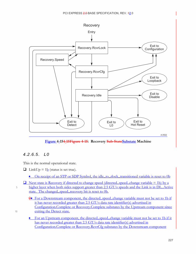
PCI EXPRESS 2.0 BASE SPECIFICATION, REV. 12.0
227
Exit toDisable
Exit toLoopback
A-0522
Entry
Recovery
Exit toDetect
Exit toL0
Exit toConfiguration
Exit toHot Reset
Recovery.RcvrLock
Recovery.RcvrCfg
Recovery.Speed
Recovery.Idle
Figure 4-154-15Figure 4-15: Recovery Sub-StateSubstate Machine
4.2.6.5. L0
This is the normal operational state.
LinkUp = 1b (status is set true).
• On receipt of an STP or SDP Symbol, the idle_to_rlock_transitioned variable is reset to 0b
Next state is Recovery if directed to change speed (directed_speed_change variable = 1b) by a higher layer when both sides support greater than 2.5 GT/s speeds and the Link is in DL_Active 5 state. The changed_speed_recovery bit is reset to 0b.
θ• For a Downstream component, the directed_speed_change variable must not be set to 1b if it has never recorded greater than 2.5 GT/s data rate identifier(s) advertised in Configuration.Complete or Recovery.Complete substates by the Upstream component since exiting the Detect state. 10
• For an Upstream component, the directed_speed_change variable must not be set to 1b if it has never recorded greater than 2.5 GT/s data rate identifier(s) advertised in Configuration.Complete or Recovery.RcvrCfg substates by the Downstream component
PCI EXPRESS 2.0 BASE SPECIFICATION, REV. 21.0
228
since exiting the Detect state. If greater than 2.5 GT/s data rate support has been noted, the Upstream component must set the directed_speed_change variable to 1b if the Retrain Link bit of the Link Control register is set to 1b and the Target Link Speed field in the Link Control 2 register is not equal to the current Link speed.
• A component supporting greater than 2.5 GT/s data rates must participate in the speed 5 change even if the Link is not in DL_Active state if it is requested by the other side through the TS Ordered Sets.
Next state is Recovery if directed to change Link width.
• The upper layer must not direct to increase the Link width if the other component did not advertise the capability to upconfigure the Link width during the Configuration state or if 10 the Link is currently operating at the maximum possible width it negotiated on initial entry to the L0 state.
• Normally, the upper layer will not reduce width if upconfigure_capable is reset to 0b other than reliability reasons, since the Link will not go back to the original width if upconfigure_capable is 0b. A component must not initiate reducing the Link width for 15 reasons other than reliability if the Hardware Autonomous Width Disable bit in the Link Control register is set to 1b.
• The decision to initiate an increase or decrease in the Link width, as allowed by the specification, is implementation specific.
Next state is Recovery if a TS1 or TS2 ordered setOrdered Set is received on any configured 20 Lane.
Next state is Recovery if directed to this state. If Electrical Idle is detected/inferred on all laneLanes without receiving an Electrical Idle ordered setEIOS on any laneLane, the port Port may transition to the Recovery state or may remain in L0. In the event that the port Port is in L0 and the Electrical Idle condition occurs without receiving an EIOSElectrical Idle Ordered 25 Set, errors may occur and the port Port may be directed to transition to Recovery.
• Note: As described in Section 4.2.4.3, an Electrical Idle condition may be inferred on all Lanes under any one of the following conditions: (i) absence of an Update_FC DLLP in any 128 μs window, (ii) absence of a SKP Ordered Set in any of the configured Lanes in any 128 μs window, or (iii) absence of either Update_FC DLLP or a SKP Ordered Set in any of 30 the configured Lanes in any 128 μs window.
• Note: “if directed” applies to a Port that is instructed by a higher Layer to transition to Recovery including the Retrain Link bit in the Link Control register being set.
• Note: The Transmitter may complete any TLP or DLLP in progress.
Next state is L0s for only the Transmitter if directed to this state. 35
• Note: “if directed” applies to a Port that is instructed by a higher Layer to initiate L0s (see Section 5.4.1.1.1).
• Note: This is a point where the TX and RX may diverge into different LTSSM states.
Next state is L0s for only the Receiver if an Electrical Idle ordered setEIOS is received on any Lanes and the Port is not directed to L1 or L2 states by any higher layers. 40

PCI EXPRESS 2.0 BASE SPECIFICATION, REV. 12.0
229
• Note: This is a point where the TX and RX may diverge into different LTSSM states.
Next state is L1:
i. If directed
and
ii. an Electrical Idle ordered setEIOS is received on any Lane 5
and
iii. an EIOSElectrical Idle ordered set is transmitted on all Lanes if the current Link speed is 2.5 GT/s or two consecutive EIOSs are transmitted on all Lanes if the current Link speed is greater than 2.5 GT/s.
• Note: “if directed” is defined as both ends of the Link having agreed to enter L1 10 immediately after the condition of both the receipt and transmission of an the EIOS(s)Electrical Idle ordered set is met (see Section 4.3.2.1).
• Note: When directed by a higher Layer one side of the Link always initiates and exits to L1 by transmitting an the EIOS(s)Electrical Idle ordered set on all Lanes, followed by a transition to Electrical Idle.38 The same Port then waits for the receipt of an EIOSElectrical 15 Idle ordered set on any Lane, and then immediately transitions to L1. Conversely, the side of the Link that first receives an the EIOS(s)Electrical Idle ordered set on any Lane must send an EIOSElectrical Idle ordered set on all Lanes and immediately transition to L1.
Next state is L2:
i. If directed 20
and
ii. an EIOSElectrical Idle ordered set is received on any Lane
and
iii. an EIOSElectrical Idle ordered set is transmitted on all Lanes if the current Link speed is 2.5 GT/s or two consecutive EIOSs are transmitted on all Lanes if the current Link speed is 25 greater than 2.5 GT/s.
• Note: “if directed” is defined as both ends of the Link having agreed to enter L2 immediately after the condition of both the receipt and transmission of an the EIOS(s)Electrical Idle ordered set is met (see Section 4.3.2.3 for more details).
• Note: When directed by a higher Layer, one side of the Link always initiates and exits to L2 30 by transmitting an EIOSElectrical Idle ordered set on all Lanes followed by a transition to Electrical Idle.39 The same Port then waits for the receipt of an EIOSElectrical Idle ordered set on any Lane, and then immediately transitions to L2. Conversely, the side of the Link
38 The common mode being driven must meet the Absolute Delta Between DC Common Mode During L0 and Electrical Idle (VTX-CM-DC-ACTIVE-IDLE-DELTA) specification (see Table 4-9). 39 The common mode being driven does not need to meet the Absolute Delta Between DC Common Mode During L0 and Electrical Idle (VTX-CM-DC-ACTIVE-IDLE-DELTA) specification (see Table 4-9).
PCI EXPRESS 2.0 BASE SPECIFICATION, REV. 21.0
230
that first receives an EIOSElectrical Idle ordered set on any Lane must send an EIOSElectrical Idle ordered set on all Lanes and immediately transition to L2.
4.2.6.6. L0s
The L0s sub-statesubstate machine is shown in Figure 4-16Figure 4-16.
4.2.6.6.1. Receiver L0s
4.2.6.6.1.1. Rx_L0s.Entry
Next state is Rx_L0s.Idle after a TTX-IDLE-MIN (Table 4-9Table 4-5) timeout
• Note: This is the minimum time the Transmitter must be in an Electrical Idle condition. 5
4.2.6.6.1.2. Rx_L0s.Idle
Next state is Rx_L0s.FTS if the Receiver detects an exit from Electrical Idle on any Lane of the configured Link.
4.2.6.6.1.3. Rx_L0s.FTS
The next state is L0 if a SKP ordered setOrdered Set is received on all configured Lanes of the Link.
• Note: The Receiver must be able to accept valid data immediately after the SKP ordered 10 setOrdered Set.
• Note: Lane-to-Lane de-skew must be completed before leaving Rx_L0s.FTS.
Otherwise, next state is Recovery after the N_FTS timeout.
• The N_FTS timeout shall be no shorter than 40*[N_FTS+3] * UI (The 3 * 40 UI is derived from six Symbols to cover a maximum SKP ordered setOrdered Set + four Symbols for a 15 possible extra FTS ordered set + 2 Symbols of design margin), and no longer than twice this amount. When the extended synch bit is set the Receiver N_FTS timeout must be adjusted to no shorter than 40* [2048] * UI (2048 FTS ordered sets) and no longer than 40* [4096] * UI (4096 FTS ordered sets). Implementations must take into account the worst case Lane to Lane skew, their design margins, as well as the four to eight consecutive EIE Symbols in 20 speeds other than 2.5 GT/s when choosing the appropriate timeout value within the specification’s defined range.
• Note: The Transmitter must also transition to Recovery, but may is permitted to complete any TLP or DLLP in progress.
• Note: It is recommended that the N_FTS field be increased when transitioning to Recovery 25 to prevent future transitions to Recovery from Rx_L0s.FTS.
PCI EXPRESS 2.0 BASE SPECIFICATION, REV. 12.0
231
4.2.6.6.2. Transmitter L0s
4.2.6.6.2.1. Tx_L0s.Entry
Transmitter sends one EIOS if the current Link speed is 2.5 GT/s or two consecutive EIOSs if the current Link speed is greater than 2.5 GT/sthe Electrical Idle ordered set and enters Electrical Idle.
• Note: The DC common mode voltage must be within specification by TTX-IDLE-SET-TO-IDLE.40 5
Next state is Tx_L0s.Idle after a TTX-IDLE-MIN (Table 4-9Table 4-5) timeout.
4.2.6.6.2.2. Tx_L0s.Idle
Next state is Tx_L0s.FTS if directed.
IMPLEMENTATION NOTE Increase of N_FTS Due to Timeout in Rx_L0s.FTS The Transmitter sends the N_FTS fast training sequences by going through Tx_L0s.FTS substates to enable the Receiver to reacquire its bit and Symbol lock. In the absence of the N_FTS fast training sequence, the Receiver will timeout in Rx_L0s.FTS substate and may increase the N_FTS 10 number it advertises in the Recovery state.
4.2.6.6.2.3. Tx_L0s.FTS
Transmitter sends N_FTS Fast Training Sequences on all configured Lanes.
• Note: Four to eight EIE Symbols must be sent prior to transmitting the N_FTS (or 4096 if Extended Sync = 1) number of FTS in speeds other than 2.5 GT/s. In 2.5 GT/s speed, Uup to one full FTS ordered set may be sent before the N_FTS (or 4096 if Extended Sync 15 = 1) number of FTS ordered sets are sent.
• Note: No SKP ordered setOrdered Sets can be inserted before all FTS ordered sets as defined by the agreed upon N_FTS parameter are transmitted.
• Note: If the Extended Synch bit is set, the Transmitter sends 4096 Fast Training Sequences.
Transmitter sends a single SKP ordered setOrdered Set on all configured Lanes. 20
Next state is L0. 40 The common mode being driven must meet the Absolute Delta Between DC Common Mode During L0 and Electrical Idle (VTX-CM-DC-ACTIVE-IDLE-DELTA) specification (see Table 4-9).
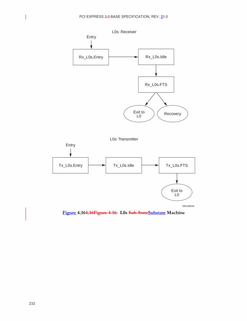
PCI EXPRESS 2.0 BASE SPECIFICATION, REV. 21.0
232
OM13804A
Tx_L0s.Entry Tx_L0s.Idle Tx_L0s.FTS
Entry
L0s: Transmitter
Rx_L0s.Entry
Rx_L0s.FTS
Rx_L0s.Idle
EntryL0s: Receiver
Exit toL0
Recovery
Exit toL0
Figure 4-164-16Figure 4-16: L0s Sub-StateSubstate Machine
PCI EXPRESS 2.0 BASE SPECIFICATION, REV. 12.0
233
4.2.6.7. L1
The L1 sub-statesubstate machine is shown in Figure 4-17Figure 4-17.
4.2.6.7.1. L1.Entry
All configured Transmitters are in Electrical Idle.
• Note: The DC common mode voltage must be within specification by TTX-IDLE-SET-TO-IDLE.
The next state is L1.Idle after a TTX-IDLE-MIN (Table 4-9Table 4-5) timeout. 5
• Note: This guarantees that the Transmitter has established the Electrical Idle condition.
4.2.6.7.2. L1.Idle
Transmitter remains in Electrical Idle.
• Note: The DC common mode voltage must be within specification.41
Next state is Recovery if any Receiver detects exit from Electrical Idle or directed after remaining in this substate for a minimum of 40 ns in speeds other than 2.5 GT/s. 10
• Note: A minimum stay of 40 ns is required in this substate in speeds other than 2.5 GT/s to account for the delay in the logic levels to arm the Electrical Idle detection circuitry in case the Link enters L1 and immediately exits the L1 state.
• Note: A component is allowed to set the directed_speed_change variable to 1b following identical rules described in L0 for setting this variable. When making such a transition, the 15 changed_speed_recovery variable must be reset to 0b. A component may also go through Recovery back to L0 and then set the directed_speed_change variable to 1b on the transition from L0 to Recovery.
θ• Note: A component is also allowed to enter Recovery from L1 if directed to change the Link width. The component must follow identical rules for changing the Link width as described 20 in the L0 state.
41 The common mode being driven must meet the Absolute Delta Between DC Common Mode During L0 and Electrical Idle (VTX-CM-DC-ACTIVE-IDLE-DELTA) specification (see Table 4-9).
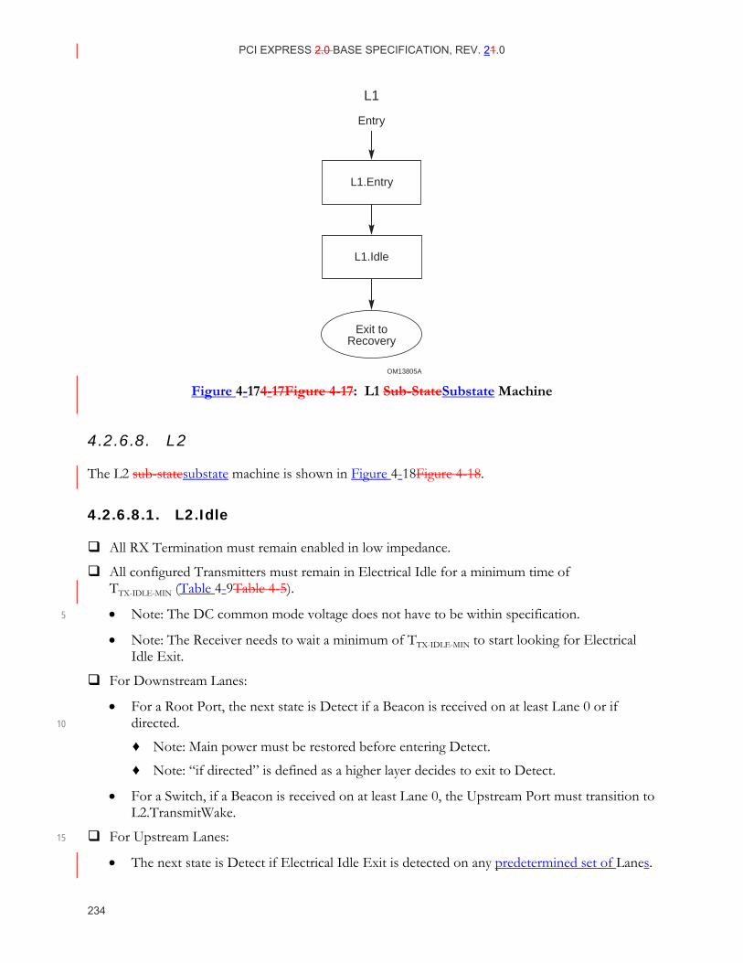
PCI EXPRESS 2.0 BASE SPECIFICATION, REV. 21.0
234
OM13805A
L1.Entry
L1.Idle
Entry
L1
Exit toRecovery
Figure 4-174-17Figure 4-17: L1 Sub-StateSubstate Machine
4.2.6.8. L2
The L2 sub-statesubstate machine is shown in Figure 4-18Figure 4-18.
4.2.6.8.1. L2.Idle
All RX Termination must remain enabled in low impedance.
All configured Transmitters must remain in Electrical Idle for a minimum time of TTX-IDLE-MIN (Table 4-9Table 4-5).
• Note: The DC common mode voltage does not have to be within specification. 5
• Note: The Receiver needs to wait a minimum of TTX-IDLE-MIN to start looking for Electrical Idle Exit.
For Downstream Lanes:
• For a Root Port, the next state is Detect if a Beacon is received on at least Lane 0 or if directed. 10
♦ Note: Main power must be restored before entering Detect.
♦ Note: “if directed” is defined as a higher layer decides to exit to Detect.
• For a Switch, if a Beacon is received on at least Lane 0, the Upstream Port must transition to L2.TransmitWake.
For Upstream Lanes: 15
• The next state is Detect if Electrical Idle Exit is detected on any predetermined set of Lanes.
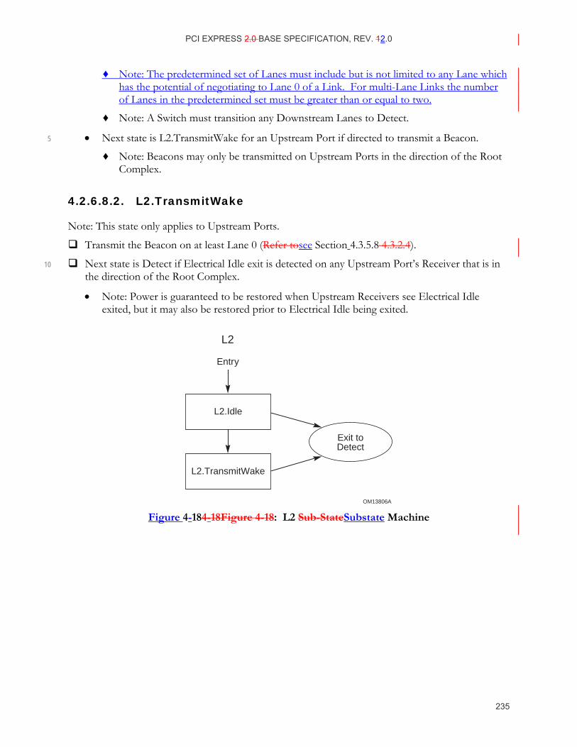
PCI EXPRESS 2.0 BASE SPECIFICATION, REV. 12.0
235
♦ Note: The predetermined set of Lanes must include but is not limited to any Lane which has the potential of negotiating to Lane 0 of a Link. For multi-Lane Links the number of Lanes in the predetermined set must be greater than or equal to two.
♦ Note: A Switch must transition any Downstream Lanes to Detect.
• Next state is L2.TransmitWake for an Upstream Port if directed to transmit a Beacon. 5
♦ Note: Beacons may only be transmitted on Upstream Ports in the direction of the Root Complex.
4.2.6.8.2. L2.TransmitWake
Note: This state only applies to Upstream Ports.
Transmit the Beacon on at least Lane 0 (Refer tosee Section 4.3.5.8 4.3.2.4).
Next state is Detect if Electrical Idle exit is detected on any Upstream Port’s Receiver that is in 10 the direction of the Root Complex.
• Note: Power is guaranteed to be restored when Upstream Receivers see Electrical Idle exited, but it may also be restored prior to Electrical Idle being exited.
OM13806A
L2.Idle
L2.TransmitWake
Entry
L2
Exit toDetect
Figure 4-184-18Figure 4-18: L2 Sub-StateSubstate Machine
PCI EXPRESS 2.0 BASE SPECIFICATION, REV. 21.0
236
4.2.6.9. Disabled
All Lanes transmit 16 to 32 TS1 ordered setOrdered Sets with the Disable Link bit (bit 1) asserted and then transition to Electrical Idle.
• Note: The Electrical Idle ordered setEIOS (one EIOS if the current Link speed is 2.5 GT/s and two consecutive EIOSs if the current Link speed is greater than 2.5 GT/s) must be sent prior to entering Electrical Idle. 5
• Note: The DC common mode voltage does not have to be within specification.42
If EIOS was transmitted (one if the current Link speed is 2.5 GT/s and two consecutive ones if the current Link speed is greater than 2.5 GT/s) and an EIOS was receivedan Electrical Idle ordered set was transmitted and received (even while transmitting TS1 with the Disable Link bit asserted), then: 10
• LinkUp = 0b (False)
♦ Note: At this point, the Lanes are considered Disabled.
• For Downstream components: The next state is Detect when Electrical Idle Exit is detected at the Receiver.
For Upstream components: The next state is Detect when directed (e.g., when the 15 Link Disable bit is reset to 0b by software).The next state is Detect when directed or if Electrical Idle is exited.
OtherwiseFor Downstream components, if no Electrical Idle ordered setEIOS is received after a 2 ms timeout, the next state is Detect.
4.2.6.10. Loopback
The Loopback sub-statesubstate machine is shown in Figure 4-19Figure 4-19. 20
4.2.6.10.1. Loopback.Entry
LinkUp = 0b (False)
If Loopback.Entry was entered from Configuration.LinkWidth.Start and the current data rate does not match the highest common transmitted and received data rate (Symbol 4 of the TS1 or TS2 Ordered Set) advertised on two consecutive TS1 or TS2 Ordered Sets on any Lane that detected a Receiver during Detect: 25
• Note: The loopback master controls the desired Loopback Link Speed and de-emphasis level by the loopback master sending a Link Speed that is common with the loopback slave.
42 The common mode being driven does need to meet the Absolute Delta Between DC Common Mode During L0 and Electrical Idle (VTX-CM-DC-ACTIVE-IDLE-DELTA) specification (see Table 4-9).
PCI EXPRESS 2.0 BASE SPECIFICATION, REV. 12.0
237
• Note: The operational speed, and de-emphasis level if the speed of operation is 5.0 GT/s, is evaluated just prior to entering this substate from Configuration.LinkWidth.Start. This clause will never be executed on entry to this substate from Recovery.Idle.
• The loopback master must transmit 16 consecutive TS1 Ordered Sets with the Data Rate field and the Selectable De-emphasis bit (Symbol 4 bit 6) identical to the TS1 Ordered Sets it 5 transmitted during the Configuration.LinkWidth.Start substate and with the Loopback bit (bit 2 of Symbol 5) asserted, followed by the EIOS (one EIOS if the current Link speed is 2.5 GT/s or two consecutive EIOSs if the current Link speed is greater than 2.5 GT/s), and then go to Electrical Idle. The loopback master must go to Electrical Idle, after sending the EIOS(s), for 1 ms. During this time the speed must be changed to the highest common 10 transmitted and received Link speed advertised on two consecutive TS1 Ordered Sets. The select_deemphasis variable must be set equal to the Selectable De-emphasis bit (Symbol 4 bit 6) in the two consecutive TS1 or TS2 Ordered Sets prior to entry to this substate. If speed is 5 GT/s, the de-emphasis level must be chosen to be -3.5 dB if select_demphasis is 1b else the de-emphasis level must be -6 dB. 15
• The loopback slave must send an EIOS and immediately go to Electrical Idle for 2 ms. During this time the speed must be changed to the highest common transmitted and received Link speed advertised on two consecutive TS1 Ordered Sets. The select_deemphasis variable must be set equal to the Selectable De-emphasis bit (bit 6) of Symbol 4 in the two consecutive TS1 or TS2 Ordered Sets prior to entry to this substate. If 20 the speed is 5 GT/s, the de-emphasis level must be chosen to be -3.5 dB if select_demphasis is 1b else the de-emphasis level must be -6 dB.
• Note: The loopback master should send adequate TS1 Ordered Sets if it wants the slave to reacquire bit and Symbol lock prior to sending the loopback test patterns.
• The loopback master must take into account the amount of time the slave can be in 25 Electrical Idle before starting to compare the data patterns it receives from the slave.
If the Compliance Receive bit (Symbol 5 bit 4) on the transmitted TS1 Ordered Sets is 0b, and the Compliance Receive bit was 0b on the two consecutive TS1 Ordered Sets that were received either in this substate or during the Configuration.Linkwidth.Start substate prior to transitioning to this substate : 30
θ• The Loopback loopback Master master device transmits TS1 ordered setOrdered Sets with the Loopback bit (bit 2) asserted until the Loopback loopback Master master receives identical TS1 ordered setOrdered Sets with the Loopback bit asserted on an implementation specific number of Lanes. The next state is Loopback.Active. However, if the loopback master does not receive identical TS1 Ordered Sets with Loopback bit asserted in the 35 implementation specific number of lanes, it must enter Loopback.Exit substate in an implementation specific timeout value less than 100 ms.
♦ Note: This indicates to the Loopback loopback Master master that the Loopback loopback Slave slave has successfully entered Loopback.
•Note: The Loopback Master timeout is implementation specific but must be less than 100 40 ms. The exit is to Loopback.Exit.
♦ Note: A boundary condition exists when the Loopback loopback Slave slave transitions to Loopback.Active that can cause the Loopback loopback Slave slave to discard a
PCI EXPRESS 2.0 BASE SPECIFICATION, REV. 21.0
238
scheduled SKP ordered setOrdered Set. If this occurs, the Loopback loopback Master master may not see a SKP ordered setOrdered Set for twice the normal SKP oOrdered -sSet scheduling interval.
θ• The next state for the Loopback loopback Slave slave is Loopback.Active.
♦ Note: The Loopback loopback Slave slave must transition on a Transmit Symbol 5 boundary and may truncated any ordered Ordered set Set in progress.
♦ Note: Until Symbol lock is achieved the Transmitter sends TS1 Ordered Sets with Lane and Link numbers set to PAD (K23.7) on all Lanes that detected a Receiver during Detect.
Else, the loopback master transmits TS1 Ordered Sets with the Loopback bit set for 2 ms prior 10 to transitioning to Loopback.Active.
• The next state for the loopback slave is Loopback.Active.
♦ Note: The Compliance Receive bit (bit 4 of Symbol 5) in the TS1 Ordered Set is set to help force a transition in to Loopback.Active for both the loopback master and the loopback slave in the case that successful Symbol lock cannot occur. Once the loopback 15 master asserts this bit in the TS1 Ordered Sets it transmits, it must not deassert that bit while in the Loopback state. This usage model is useful for test and validation purposes.
♦ Note: The loopback slave does not need to transition on a Transmit Symbol boundary and may truncate any Ordered Set in progress.
4.2.6.10.2. Loopback.Active
The Loopback loopback Master master must send valid 8b/10b data. The next state of the 20 Loopback Master is Loopback.Exit if directed.The loopback master should avoid sending EIOS as data until it wants to exit Loopback.
A Loopback loopback Slave slave is required to retransmit the received 10-bit information as received, with the polarity inversion determined in Polling applied, while continuing to perform clock tolerance compensation: 25
• SKPs must be added or deleted on a per Lane basis as outlined in Section 4.2.7 with the exception that SKPs do not have to be simultaneously added or removed across Lanes of a configured Link.
♦ If a SKP ordered setOrdered Set retransmission requires adding a SKP Symbol to accommodate timing tolerance correction, the SKP Symbol is inserted in the 30 retransmitted Symbol stream anywhere adjacent to a SKP Symbol in the SKP ordered setOrdered Set following the COM Symbol. The inserted SKP Symbol must be of the same disparity as the received SKPs Symbol(s) in the SKP ordered setOrdered Set.
♦ If a SKP ordered setOrdered Set retransmission requires dropping a SKP Symbol to accommodate timing tolerance correction, the SKP Symbol is simply not retransmitted. 35
• Note: No modifications of the received 10-bit data (except for polarity inversion determined in Polling) is are allowed by the Loopback loopback Slave slave even if it is determined to be an invalid 10-bit code (i.e., no legal translation to a control or data value possible).

PCI EXPRESS 2.0 BASE SPECIFICATION, REV. 12.0
239
Next state of the Loopback loopback Slave slave is Loopback.Exit if one of the following conditions apply:
• If directed or if four consecutive EIOSs are received on any Lane. It must be noted that the receiving four consecutive EIOS indicates that the Lane received four consecutive sets of COM, IDL, IDL, IDL or alternatively, two out of three K28.3 (IDL) Symbols in each of the 5 four consecutive sets of transmitted EIOS.
• Optionally, if current Link speed is 2.5 GT/s and an EIOS is received or Electrical Idle is detected/inferred on any Lane.
♦ Note: As described in Section 4.2.4.3, an Electrical Idle condition may be inferred if any of the configured Lanes remained electrically idle continuously for 128 μs by not 10 detecting an exit from Electrical Idle in the entire 128 μs window.
• Note: A loopback slave must be able to detect an Electrical Idle condition on any Lane within 1 ms of the EIOS being received by the loopback slave.
• Note: During the time after an EIOS is received and before Electrical Idle is actually detected by the Loopback Slave, the Loopback Slave may receive undefined 10-bit data, 15 which may be looped back by the transmitter.
• The TTX-IDLE-SET-TO-IDLE parameter does not apply in this case since the loopback slave may not even detect Electrical Idle until as much as 1 ms after the EIOS.
when an Electrical Idle ordered set is received or Electrical Idle is detected/inferred on any Lane. 20
Note: An electrical idle condition may be inferred if any of the configured lanes remained electrically idle continuously for 128μs by not detecting an exit from electrical idle in the entire 128μs window.
•Note: A Loopback Slave must be able to detect an Electrical Idle condition on any Lane within 1 ms of the Electrical Idle ordered set being received by the Loopback Slave. 25
•Note: During the time after an Electrical Idle ordered set is received and before Electrical Idle is actually detected by the Loopback Slave, the Loopback Slave may receive and transmit undefined 10-bit data.
•The TTX-IDLE-SET-TO-IDLE parameter does not apply in this case since the Loopback Slave may not even detect Electrical Idle until as much as 1 ms after the Electrical Idle ordered set. 30
The next state of the Loopback loopback Master master is Loopback.Exit if directed.
4.2.6.10.3. Loopback.Exit
The Loopback loopback Master master sends an EIOSElectrical Idle ordered set for components that support only the 2.5 GT/s data rate and eight consecutive sets of EIOSs for components that support greater than 2.5 GT/s data rates, and optionally for components that only support the 2.5 GT/s data rate, irrespective of the current Link speed, for Rev 2.0 and 35 beyond components and enters Electrical Idle on all Lanes for 2 ms.

PCI EXPRESS 2.0 BASE SPECIFICATION, REV. 21.0
240
• The Loopback loopback Master master must transition to a valid Electrical Idle condition43 on all Lanes within TTX-IDLE-SET-TO-IDLE after sending the last EIOSElectrical Idle ordered set.
• Note: The EIOSElectrical Idle ordered set can be useful in signifying the logical end of transmit and compare operations that occurred by the Loopback loopback Mastermaster. Any data received by the Loopback loopback Master master after the any EIOSElectrical 5 Idle ordered set is received should be ignored since it is undefined.
The Loopback loopback Slave slave must enter Electrical Idle on all Lanes for 2 ms.
• Note: Before entering Electrical Idle the Loopback loopback Slave slave must Loopback all Symbols that were received prior to detecting Electrical Idle. This ensures that the Loopback loopback Master master may see the EIOSElectrical Idle ordered set to signify the 10 logical end of any Loopback send and compare operations.
The next state of the Loopback loopback Master master and Loopback loopback Slave slave is Detect.
43 The common mode being driven does not need to meet the Absolute Delta Between DC Common Mode During L0 and Electrical Idle (VTX-CM-DC-ACTIVE-IDLE-DELTA) specification (see Table 4-9).
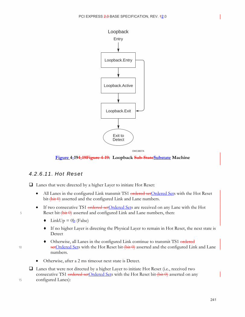
PCI EXPRESS 2.0 BASE SPECIFICATION, REV. 12.0
241
OM13807A
Loopback.Exit
Loopback.Entry
Loopback.Active
Entry
Loopback
Exit toDetect
Figure 4-194-19Figure 4-19: Loopback Sub-StateSubstate Machine
4.2.6.11. Hot Reset
Lanes that were directed by a higher Layer to initiate Hot Reset:
• All Lanes in the configured Link transmit TS1 ordered setOrdered Sets with the Hot Reset bit (bit 0) asserted and the configured Link and Lane numbers.
• If two consecutive TS1 ordered setOrdered Sets are received on any Lane with the Hot Reset bit (bit 0) asserted and configured Link and Lane numbers, then: 5
♦ LinkUp = 0b (False)
♦ If no higher Layer is directing the Physical Layer to remain in Hot Reset, the next state is Detect
♦ Otherwise, all Lanes in the configured Link continue to transmit TS1 ordered setOrdered Sets with the Hot Reset bit (bit 0) asserted and the configured Link and Lane 10 numbers.
• Otherwise, after a 2 ms timeout next state is Detect.
Lanes that were not directed by a higher Layer to initiate Hot Reset (i.e., received two consecutive TS1 ordered setOrdered Sets with the Hot Reset bit (bit 0) asserted on any configured Lanes): 15
PCI EXPRESS 2.0 BASE SPECIFICATION, REV. 21.0
242
• LinkUp = 0b (False)
• If any Lane of an Upstream Port of a Switch receives two consecutive TS1 Ordered Sets a training sequence with the Hot Reset bit asserted, all configured Downstream Ports must transition to Hot Reset as soon as possible.
♦ Note: Any optional crosslinks on the Switch are an exception to this rule and the 5 behavior is system specific.
• All Lanes in the configured Link transmit TS1 ordered setOrdered Sets with the Hot Reset bit (bit 0) asserted and the configured Link and Lane numbers.
• If two consecutive TS1 ordered setOrdered Sets were received with the Hot Reset bit (bit 0) asserted and the configured Link and Lane numbers, the next state is continues to be Hot 10 Reset and the 2 ms timer is reset.
• Otherwise, the next state is Detect after a 2 ms timeout.
Note: Generally, Lanes of a Downstream or optional crosslink Port will be directed to Hot Reset, and Lanes of an Upstream or optional crosslink Port will enter Hot Reset by receiving two consecutive TS1 Ordered Sets with the Hot Reset bit asserted on any configured Lanes, from 15 Recovery.Idle state.
4.2.7. Clock Tolerance Compensation
SKP ordered setOrdered Sets (defined below) are used to compensate for differences in frequencies between bit rates at two ends of a Link. The Receiver Physical Layer logical sub-block must include elastic buffering which performs this compensation. The interval between SKP ordered setOrdered Set transmissions is derived from the absolute value of the Transmit and Receive clock frequency 20 difference specified in Table 4-9Table 4-5. Having worse case clock frequencies at the limits of the tolerance specified will result in a 600 ppm difference between the Transmit and Receive clocks of a Link. As a result, the Transmit and Receive clocks can shift one clock every 1666 clocks.
4.2.7.1. Rules for Transmitters
All Lanes shall transmit Symbols at the same frequency (the difference between bit rates is 0 ppm within all multi-Lane Links). 25
When transmitted, the SKP ordered setOrdered Set shall be transmitted simultaneously on all Lanes of a multi-Lane Link (See see Section 4.2.4.8 and Table 4-9Table 4-5 for the definition of simultaneous in this context).
The transmitted SKP ordered setOrdered Set is: one COM Symbol followed by three consecutive SKP Symbols 30
The SKP ordered setOrdered Set shall be scheduled for insertion at an interval between 1180 and 1538 Symbol Times.
Scheduled SKP ordered setOrdered Sets shall be transmitted if a packet or Ordered Set is not already in progress, otherwise they are accumulated and then inserted consecutively at the next packet or Ordered Set boundary. 35
PCI EXPRESS 2.0 BASE SPECIFICATION, REV. 12.0
243
SKP ordered setOrdered Sets do not count as an interruption when monitoring for consecutive characters Symbols or ordered Ordered set Sets (i.e., eight consecutive TS1 ordered setOrdered Sets in Polling.Active).
SKP Ordered Sets must not be transmitted while the Compliance Pattern or the Modified Compliance Pattern (see Section 4.2.8) is in progress during Polling.Compliance if the 5 Compliance SOS bit of the Link Control 2 register is 0b. If the Compliance SOS bit of the Link Control 2 register is 1b, two consecutive SKP Ordered Sets must be sent (instead of one) for every scheduled SKP Ordered Set time interval.SKP ordered-sets must not be transmitted while the Compliance Pattern (see Section 4.2.8) is in progress during Polling.Compliance.
Any and all time spent in any lower power Link state (L0s, L1, L2) or in any other state when the 10 Transmitter is electrically idle (such as Detect and Recovery.Speed) does not count in (and may optionally reset) the 1180 to 1538 Symbol Time interval used to schedule the transmission of SKP Ordered Sets.Any and all time spent in any lower power Link state (L0s, L1, L2) does not count in the 1180 to 1538 Symbol interval used to schedule the transmission of SKP ordered sets. 15
During all lower power Link states any counter(s) or other mechanisms used to schedule SKP ordered setOrdered Sets must be reset.
4.2.7.2. Rules for Receivers
Receivers shall recognize received SKP ordered setOrdered Set consisting of one COM Symbol followed consecutively by one to five SKP Symbols.
• Note: The number of received SKP Symbols in an Ordered Set shall not vary from Lane-to-20 Lane in a multi-Lane Link.
Receivers shall be tolerant to receive and process SKP ordered setOrdered Sets at an average interval between 1180 to 1538 Symbol Times.
Receivers shall be tolerant to receive and process consecutive SKP ordered setOrdered Sets.
φ• Note: Receivers shall be tolerant to receive and process SKP ordered setOrdered Sets that 25 have a maximum separation dependent on the Max_Payload_Size a component supports. The formula for the maximum number of Symbols (N) between SKP oOrdered -sSets is: N = 1538 + (Max_payload_size_byte+2628). For example, if Max_Payload_Size is 4096 bytes, N = 1538 + 4096 + 26 28 = 56605662.
4.2.8. Compliance Pattern
During Polling, the Polling.Compliance sub-statesubstate must be entered from Polling.Active based 30 on the conditions described in Section 4.2.6.2.1.based on the presence of passive test equipment being attached to one Lane of a possible Link and being detected during the Detect State. The compliance pattern consists of the sequence of 8b/10b Symbols K28.5, D21.5, K28.5, and D10.2 repeating. The compliance sequence is as follows:
Symbol K28.5 D21.5 K28.5 D10.2
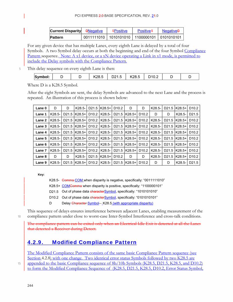
PCI EXPRESS 2.0 BASE SPECIFICATION, REV. 21.0
244
Current Disparity 0Negative 1Positive Positive1 Negative0
Pattern 0011111010 1010101010 1100000101 0101010101
For any given device that has multiple Lanes, every eighth Lane is delayed by a total of four Symbols. A two Symbol delay occurs at both the beginning and end of the four Symbol Compliance Pattern sequence. Note: A x1 device, or a xN device operating a Link in x1 mode, is permitted to include the Delay symbols with the Compliance Pattern.
This delay sequence on every eighth Lane is then: 5
Symbol: D D K28.5 D21.5 K28.5 D10.2 D D
Where D is a K28.5 Symbol.
After the eight Symbols are sent, the delay Symbols are advanced to the next Lane and the process is repeated. An illustration of this process is shown below:
Lane 0 D D K28.5- D21.5 K28.5+ D10.2 D D K28.5- D21.5 K28.5+ D10.2
Lane 1 K28.5- D21.5 K28.5+ D10.2 K28.5- D21.5 K28.5+ D10.2 D D K28.5- D21.5
Lane 2 K28.5- D21.5 K28.5+ D10.2 K28.5- D21.5 K28.5+ D10.2 K28.5- D21.5 K28.5+ D10.2
Lane 3 K28.5- D21.5 K28.5+ D10.2 K28.5- D21.5 K28.5+ D10.2 K28.5- D21.5 K28.5+ D10.2
Lane 4 K28.5- D21.5 K28.5+ D10.2 K28.5- D21.5 K28.5+ D10.2 K28.5- D21.5 K28.5+ D10.2
Lane 5 K28.5- D21.5 K28.5+ D10.2 K28.5- D21.5 K28.5+ D10.2 K28.5- D21.5 K28.5+ D10.2
Lane 6 K28.5- D21.5 K28.5+ D10.2 K28.5- D21.5 K28.5+ D10.2 K28.5- D21.5 K28.5+ D10.2
Lane 7 K28.5- D21.5 K28.5+ D10.2 K28.5- D21.5 K28.5+ D10.2 K28.5- D21.5 K28.5+ D10.2
Lane 8 D D K28.5- D21.5 K28.5+ D10.2 D D K28.5- D21.5 K28.5+ D10.2
Lane 9 K28.5- D21.5 K28.5+ D10.2 K28.5- D21.5 K28.5+ D10.2 D D K28.5- D21.5
Key:
K28.5- Comma COM when disparity is negative, specifically: “0011111010”
K28.5+
D21.5
COMComma when disparity is positive, specifically: “1100000101” Out of phase data characterSymbol, specifically: “1010101010”
D10.2 Out of phase data characterSymbol, specifically: “0101010101”
D Delay Character Symbol– K28.5 (with appropriate disparity)
This sequence of delays ensures interference between adjacent Lanes, enabling measurement of the compliance pattern under close to worst-case Inter-Symbol Interference and cross-talk conditions. 10
The compliance pattern can be exited only when an Electrical Idle Exit is detected at all the Lanes that detected a Receiver during Detect.
4.2.9. Modified Compliance Pattern
The Modified Compliance Pattern consists of the same basic Compliance Pattern sequence (see Section 4.2.8) with one change. Two identical error status Symbols followed by two K28.5 are appended to the basic Compliance sequence of 8b/10b Symbols (K28.5, D21.5, K28.5, and D10.2) 15 to form the Modified Compliance Sequence of (K28.5, D21.5, K28.5, D10.2, Error Status Symbol,
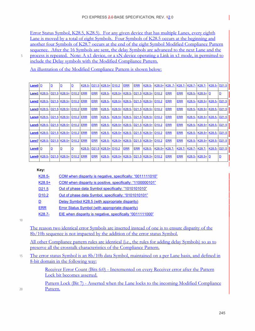
PCI EXPRESS 2.0 BASE SPECIFICATION, REV. 12.0
245
Error Status Symbol, K28.5, K28.5). For any given device that has multiple Lanes, every eighth Lane is moved by a total of eight Symbols. Four Symbols of K28.5 occurs at the beginning and another four Symbols of K28.7 occurs at the end of the eight Symbol Modified Compliance Pattern sequence. After the 16 Symbols are sent, the delay Symbols are advanced to the next Lane and the process is repeated. Note: A x1 device, or a xN device operating a Link in x1 mode, in permitted to 5 include the Delay symbols with the Modified Compliance Pattern.
An illustration of the Modified Compliance Pattern is shown below:
Lane0 D D D D K28.5- D21.5 K28.5+ D10.2 ERR ERR K28.5- K28.5+ K28..7- K28.7- K28.7- K28.7- K28.5- D21.5
Lane1 K28.5- D21.5 K28.5+ D10.2 ERR ERR K28.5- K28.5+ K28.5- D21.5 K28.5+ D10.2 ERR ERR K28.5- K28.5+ D D
Lane2 K28.5- D21.5 K28.5+ D10.2 ERR ERR K28.5- K28.5+ K28.5- D21.5 K28.5+ D10.2 ERR ERR K28.5- K28.5+ K28.5- D21.5
Lane3 K28.5- D21.5 K28.5+ D10.2 ERR ERR K28.5- K28.5+ K28.5- D21.5 K28.5+ D10.2 ERR ERR K28.5- K28.5+ K28.5- D21.5
Lane4 K28.5- D21.5 K28.5+ D10.2 ERR ERR K28.5- K28.5+ K28.5- D21.5 K28.5+ D10.2 ERR ERR K28.5- K28.5+ K28.5- D21.5
Lane5 K28.5- D21.5 K28.5+ D10.2 ERR ERR K28.5- K28.5+ K28.5- D21.5 K28.5+ D10.2 ERR ERR K28.5- K28.5+ K28.5- D21.5
Lane6 K28.5- D21.5 K28.5+ D10.2 ERR ERR K28.5- K28.5+ K28.5- D21.5 K28.5+ D10.2 ERR ERR K28.5- K28.5+ K28.5- D21.5
Lane7 K28.5- D21.5 K28.5+ D10.2 ERR ERR K28.5- K28.5+ K28.5- D21.5 K28.5+ D10.2 ERR ERR K28.5- K28.5+ K28.5- D21.5
Lane8 D D D D K28.5- D21.5 K28.5+ D10.2 ERR ERR K28.5- K28.5+ K28.7- K28.7- K28.7- K28.7- K28.5- D21.5
Lane9 K28.5- D21.5 K28.5+ D10.2 ERR ERR K28.5- K28.5+ K28.5- D21.5 K28.5+ D10.2 ERR ERR K28.5- K28.5+ D D
Key: K28.5- COM when disparity is negative, specifically: “0011111010”
K28.5+
D21.5
COM when disparity is positive, specifically: “1100000101” Out of phase data Symbol specifically: “1010101010”
D10.2 Out of phase data Symbol, specifically: “0101010101”
D Delay Symbol K28.5 (with appropriate disparity)
ERR Error Status Symbol (with appropriate disparity)
K28.7- EIE when disparity is negative, specifically “0011111000” 10
The reason two identical error Symbols are inserted instead of one is to ensure disparity of the 8b/10b sequence is not impacted by the addition of the error status Symbol.
All other Compliance pattern rules are identical (i.e., the rules for adding delay Symbols) so as to preserve all the crosstalk characteristics of the Compliance Pattern.
The error status Symbol is an 8b/10b data Symbol, maintained on a per Lane basis, and defined in 15 8-bit domain in the following way:
Receiver Error Count (Bits 6:0) - Incremented on every Receiver error after the Pattern Lock bit becomes asserted.
Pattern Lock (Bit 7) - Asserted when the Lane locks to the incoming Modified Compliance Pattern. 20
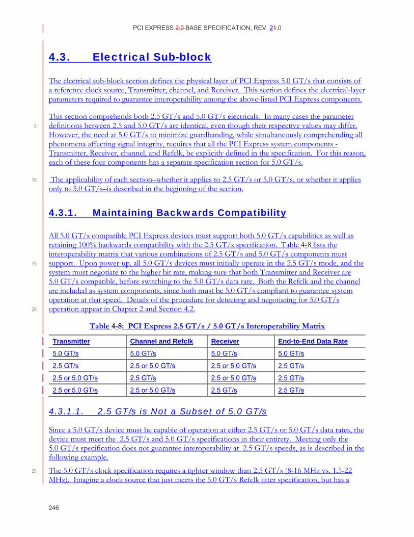
PCI EXPRESS 2.0 BASE SPECIFICATION, REV. 21.0
246
4.3. Electrical Sub-block
The electrical sub-block section defines the physical layer of PCI Express 5.0 GT/s that consists of a reference clock source, Transmitter, channel, and Receiver. This section defines the electrical-layer parameters required to guarantee interoperability among the above-listed PCI Express components.
This section comprehends both 2.5 GT/s and 5.0 GT/s electricals. In many cases the parameter definitions between 2.5 and 5.0 GT/s are identical, even though their respective values may differ. 5 However, the need at 5.0 GT/s to minimize guardbanding, while simultaneously comprehending all phenomena affecting signal integrity, requires that all the PCI Express system components - Transmitter, Receiver, channel, and Refclk, be explicitly defined in the specification. For this reason, each of these four components has a separate specification section for 5.0 GT/s.
The applicability of each section–whether it applies to 2.5 GT/s or 5.0 GT/s, or whether it applies 10 only to 5.0 GT/s–is described in the beginning of the section.
4.3.1. Maintaining Backwards Compatibility
All 5.0 GT/s compatible PCI Express devices must support both 5.0 GT/s capabilities as well as retaining 100% backwards compatibility with the 2.5 GT/s specification. Table 4-8 lists the interoperability matrix that various combinations of 2.5 GT/s and 5.0 GT/s components must support. Upon power-up, all 5.0 GT/s devices must initially operate in the 2.5 GT/s mode, and the 15 system must negotiate to the higher bit rate, making sure that both Transmitter and Receiver are 5.0 GT/s compatible, before switching to the 5.0 GT/s data rate. Both the Refclk and the channel are included as system components, since both must be 5.0 GT/s compliant to guarantee system operation at that speed. Details of the procedure for detecting and negotiating for 5.0 GT/s operation appear in Chapter 2 and Section 4.2. 20
Table 4-8: PCI Express 2.5 GT/s / 5.0 GT/s Interoperability Matrix
Transmitter Channel and Refclk Receiver End-to-End Data Rate
5.0 GT/s 5.0 GT/s 5.0 GT/s 5.0 GT/s
2.5 GT/s 2.5 or 5.0 GT/s 2.5 or 5.0 GT/s 2.5 GT/s
2.5 or 5.0 GT/s 2.5 GT/s 2.5 or 5.0 GT/s 2.5 GT/s
2.5 or 5.0 GT/s 2.5 or 5.0 GT/s 2.5 GT/s 2.5 GT/s
4.3.1.1. 2.5 GT/s is Not a Subset of 5.0 GT/s
Since a 5.0 GT/s device must be capable of operation at either 2.5 GT/s or 5.0 GT/s data rates, the device must meet the 2.5 GT/s and 5.0 GT/s specifications in their entirety. Meeting only the 5.0 GT/s specification does not guarantee interoperability at 2.5 GT/s speeds, as is described in the following example.
The 5.0 GT/s clock specification requires a tighter window than 2.5 GT/s (8-16 MHz vs. 1.5-22 25 MHz). Imagine a clock source that just meets the 5.0 GT/s Refclk jitter specification, but has a
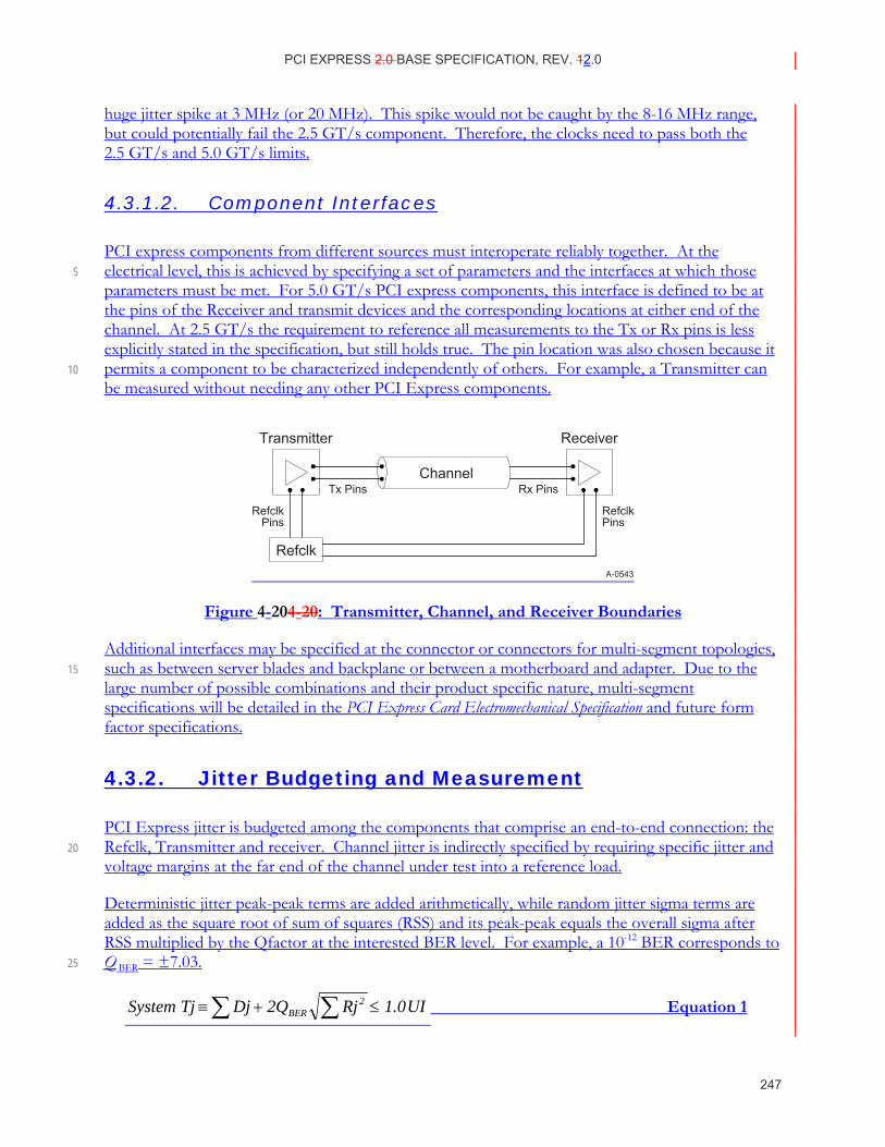
PCI EXPRESS 2.0 BASE SPECIFICATION, REV. 12.0
247
huge jitter spike at 3 MHz (or 20 MHz). This spike would not be caught by the 8-16 MHz range, but could potentially fail the 2.5 GT/s component. Therefore, the clocks need to pass both the 2.5 GT/s and 5.0 GT/s limits.
4.3.1.2. Component Interfaces
PCI express components from different sources must interoperate reliably together. At the electrical level, this is achieved by specifying a set of parameters and the interfaces at which those 5 parameters must be met. For 5.0 GT/s PCI express components, this interface is defined to be at the pins of the Receiver and transmit devices and the corresponding locations at either end of the channel. At 2.5 GT/s the requirement to reference all measurements to the Tx or Rx pins is less explicitly stated in the specification, but still holds true. The pin location was also chosen because it permits a component to be characterized independently of others. For example, a Transmitter can 10 be measured without needing any other PCI Express components.
A-0543
Transmitter Receiver
RefclkPins
Tx Pins
RefclkPins
Rx Pins
Refclk
Channel
Figure 4-204-20: Transmitter, Channel, and Receiver Boundaries
Additional interfaces may be specified at the connector or connectors for multi-segment topologies, such as between server blades and backplane or between a motherboard and adapter. Due to the 15 large number of possible combinations and their product specific nature, multi-segment specifications will be detailed in the PCI Express Card Electromechanical Specification and future form factor specifications.
4.3.2. Jitter Budgeting and Measurement
PCI Express jitter is budgeted among the components that comprise an end-to-end connection: the Refclk, Transmitter and receiver. Channel jitter is indirectly specified by requiring specific jitter and 20 voltage margins at the far end of the channel under test into a reference load.
Deterministic jitter peak-peak terms are added arithmetically, while random jitter sigma terms are added as the square root of sum of squares (RSS) and its peak-peak equals the overall sigma after RSS multiplied by the Qfactor at the interested BER level. For example, a 10-12 BER corresponds to Q BER = ±7.03. 25
UI1.0Rj2QDjTjSystem 2BER ≤+≡ ∑∑ Equation 1
PCI EXPRESS 2.0 BASE SPECIFICATION, REV. 21.0
248
A consequence of the RSS adding of Rj terms is that naively adding the Tj terms for Refclk, Transmitter, and Receiver will yield a sum greater than 1.0 UI. Details on how to derive meaningful jitter numbers from measurements appear in the respective sections for Transmitter, Receiver, and Refclk.
Jitter may be resolved into separate Dj and Rj components by application of the Dual Dirac 5 approximation method. The dual-Dirac model is a technique for quickly estimating total jitter defined at a low bit error ratio, Tj(BER), while not requiring a commensurately large number of samples. The deterministic and random components of the jitter signal are separated within the context of the model to yield two quantities, root-mean-square random jitter (Rj) and a model-dependent form of the peak-to-peak deterministic jitter, Dj(dd). The dual-Dirac model is 10 fundamentally a Gaussian approximation to the outer edges of the jitter distribution displaced by a fixed amount, Dj(dd). It rests on the assumption that the asymptotic tails of the distribution may be represented by the tails of the same Gaussian distribution that describes Rj; this is the key to how the dual-Dirac model is used to calculate Tj(BER): measurements of Rj and Dj(dd) may be performed on comparatively low statistics and Tj(BER) can be calculated using 15
Tj(BER) = 2QBER×σ + Dj(dd) Equation 2
It is important to realize that Tj(BER) calculated from Rj and Dj(dd) is not a model-dependent approximation. Its accuracy depends only on the accuracy with which Rj and Dj(dd) are measured – though, in practice Tj(BER) so calculated is almost always an extrapolation. While Dj(dd) is a model dependent quantity, it is also a well defined observable. On the other hand, Rj is not a 20 model-dependent quantity; it is the width of the Gaussian distribution that describes the random jitter PDF.
It is important to realize that Dj(dd) is not the same as the actual peak-to-peak spread of the Dj distribution, Dj(p-p). The two are related by Dj(dd) ≥ Dj(p-p). Dj(dd) has two distinct advantages over Dj(p-p): first, it is useful in estimating Tj(BER) – substitution of Dj(p-p) for Dj(dd) in Eq. (1) is 25 incorrect; and, second, Dj(dd) is much easier to measure.
4.3.3. Transmitter Specification
Transmitter AC performance is specified at pins of the DUT into a reference load, as illustrated in Figure 4-20Figure 4-23423. The data so obtained consists of a sequential set of voltage vs. time samples. Most Transmitter parameters may be obtained directly from the scope trace; however, some parameters must either be post processed or filtered directly to obtain meaningful eye margins. 30 Either approach is designed to remove jitter components that would be tracked by the Receiver and do not contribute meaningfully to the effective jitter seen at the Receiver's input latch.
Note that the Transmitter under test is driven by a low jitter “ideal” clock source. An ideal, rather than a nominal, oscillator is specified so that the measured jitter represents only those contributions from the Transmitter under test. The reference clock has a jitter budget that is specified separately. 35
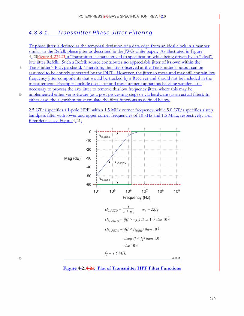
PCI EXPRESS 2.0 BASE SPECIFICATION, REV. 12.0
249
4.3.3.1. Transmitter Phase Jitter Filtering
Tx phase jitter is defined as the temporal deviation of a data edge from an ideal clock in a manner similar to the Refclk phase jitter as described in the JWG white paper. As illustrated in Figure 4-20Figure 4-23423, a Transmitter is characterized to specification while being driven by an “ideal”, low jitter Refclk. Such a Refclk source contributes no appreciable jitter of its own within the Transmitter’s PLL passband. Therefore, the jitter observed at the Transmitter's output can be 5 assumed to be entirely generated by the DUT. However, the jitter so measured may still contain low frequency jitter components that would be tracked by a Receiver and should not be included in the measurement. Examples include oscillator and measurement apparatus baseline wander. It is necessary to process the raw jitter to remove this low frequency jitter, where this may be implemented either via software (as a post processing step) or via hardware (as an actual filter). In 10 either case, the algorithm must emulate the filter functions as defined below.
2.5 GT/s specifies a 1-pole HPF with a 1.5 MHz corner frequency, while 5.0 GT/s specifies a step bandpass filter with lower and upper corner frequencies of 10 kHz and 1.5 MHz, respectively. For filter details, see Figure 4-21.
A-0544
0
-10
-20
-30
-40
-50
-60
104 105 106 107 108 109
Frequency (Hz)
Mag (dB)
Hlo-5GT/s
H2.5GT/s
Hhi-5GT/s
15
Figure 4-214-21: Plot of Transmitter HPF Filter Functions
PCI EXPRESS 2.0 BASE SPECIFICATION, REV. 21.0
250
4.3.3.2. Low and Full Swing Transmitter Output Levels
Both the 2.5 GT/s and 5.0 GT/s PCI Express specifications define two voltage swing levels: full swing and low swing. Full swing signaling implements de-emphasis, while low swing does not. Typically, low swing is specified for power sensitive applications where a shorter channel is acceptable. The requirement as to whether a Transmitter need support full swing, low swing, or both modes, is dependent on its usage model. The method by which the output mode is selected is 5 not explicitly defined in this specification, and may be implementation dependent. Note: All PCI Express device Transmitters must support full swing signaling, while support for half swing signaling is optional.
While two different Transmitter output signaling levels are defined, only a single Receiver specification is defined; this implies that margins (as specified at the Receiver) are identical regardless 10 of the Transmitter's output swing capabilities. It also implies that the channel’s characteristics need to be matched to the Transmitter output swing. Typically, low swing output is utilized for short channels, such as would occur in mobile platforms.
4.3.3.3. Transmitter Margining
5.0 GT/s Transmitters must implement voltage margining for both 5.0 GT/s and 2.5 GT/s operation, while 2.5 GT/s only Transmitters need not implement voltage margining. When 15 operating in the margining mode, a Transmitter outputs a signal at an amplitude whose value is determined by configuration register bits. The base specification only requires that a Tx be capable of margining voltage. However, other parameters, such as jitter and/or de-emphasis level may be optionally margined. Figure 4-22 illustrates the Tx margining voltages and corresponding margining configuration register codes. 20
The granularity for margining control is determined by the number of Lanes per Link such that margining must be controllable on at least a per Link basis and may be controllable on a per Lane basis.
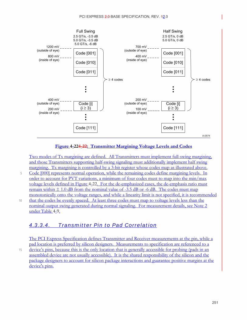
PCI EXPRESS 2.0 BASE SPECIFICATION, REV. 12.0
251
A-0574
Code [001]
Full Swing2.5 GT/s, -3.5 dB5.0 GT/s, -3.5 dB5.0 GT/s, -6 dB
Code [010]
Code [011]
Code [i](i 3)
Code [111]
4 codes
1200 mV(outside of eye)
800 mV(inside of eye)
400 mV(outside of eye)
200 mV(inside of eye)
Code [001]
Code [010]
Code [011]
Code [i](i 3)
Code [111]
4 codes
700 mV(outside of eye)
400 mV(inside of eye)
200 mV(outside of eye)
100 mV(inside of eye)
Half Swing2.5 GT/s, 0 dB5.0 GT/s, 0 dB
Figure 4-224-22: Transmitter Margining Voltage Levels and Codes
Two modes of Tx margining are defined. All Transmitters must implement full-swing margining, and those Transmitters supporting half-swing signaling must additionally implement half swing margining. Tx margining is controlled by a 3-bit register whose codes map as illustrated above. Code [000] represents normal operation, while the remaining codes define margining levels. In 5 order to account for PVT variations, a minimum of four codes must to map into the min/max voltage levels defined in Figure 4-22. For the de-emphasized cases, the de-emphasis ratio must remain within ± 1.0 dB from the nominal value of -3.5 dB or -6 dB. The codes must map monotonically onto the voltage ranges, and while a linearity limit is not specified, it is recommended that the codes be evenly spaced. At least three codes must map to voltage levels less than the 10 nominal output swing generated during normal signaling. For measurement details, see Note 2 under Table 4-9.
4.3.3.4. Transmitter Pin to Pad Correlation
The PCI Express Specification defines Transmitter and Receiver measurements at the pin, while a pad location is preferred by silicon designers. Measurements to specification are referenced to a device’s pins, because this is the only location that is generally accessible for probing (pads in an 15 assembled device are not usually accessible). It is the shared responsibility of the silicon and the package designers to account for silicon package interactions and guarantee positive margins at the device's pins.
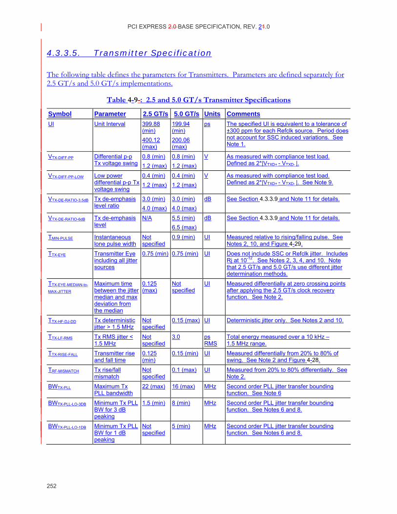
PCI EXPRESS 2.0 BASE SPECIFICATION, REV. 21.0
252
4.3.3.5. Transmitter Specification
The following table defines the parameters for Transmitters. Parameters are defined separately for 2.5 GT/s and 5.0 GT/s implementations.
Table 4-9-: 2.5 and 5.0 GT/s Transmitter Specifications
Symbol Parameter 2.5 GT/s 5.0 GT/s Units Comments UI Unit Interval 399.88
(min) 400.12 (max)
199.94 (min) 200.06 (max)
ps The specified UI is equivalent to a tolerance of ±300 ppm for each Refclk source. Period does not account for SSC induced variations. See Note 1.
VTX-DIFF-PP Differential p-p Tx voltage swing
0.8 (min) 1.2 (max)
0.8 (min) 1.2 (max)
V As measured with compliance test load. Defined as 2*|VTXD+ - VTXD- |.
VTX-DIFF-PP-LOW Low power differential p-p Tx voltage swing
0.4 (min) 1.2 (max)
0.4 (min) 1.2 (max)
V As measured with compliance test load. Defined as 2*|VTXD+ - VTXD- |. See Note 9.
VTX-DE-RATIO-3.5dB Tx de-emphasis level ratio
3.0 (min) 4.0 (max)
3.0 (min) 4.0 (max)
dB See Section 4.3.3.9 and Note 11 for details.
VTX-DE-RATIO-6dB Tx de-emphasis level
N/A 5.5 (min) 6.5 (max)
dB See Section 4.3.3.9 and Note 11 for details.
TMIN-PULSE Instantaneous lone pulse width
Not specified
0.9 (min) UI Measured relative to rising/falling pulse. See Notes 2, 10, and Figure 4-29.
TTX-EYE Transmitter Eye including all jitter sources
0.75 (min) 0.75 (min) UI Does not include SSC or Refclk jitter. Includes Rj at 10-12. See Notes 2, 3, 4, and 10. Note that 2.5 GT/s and 5.0 GT/s use different jitter determination methods.
TTX-EYE-MEDIAN-to-
MAX-JITTER Maximum time between the jitter median and max deviation from the median
0.125 (max)
Not specified
UI Measured differentially at zero crossing points after applying the 2.5 GT/s clock recovery function. See Note 2.
TTX-HF-DJ-DD Tx deterministic jitter > 1.5 MHz
Not specified
0.15 (max) UI Deterministic jitter only. See Notes 2 and 10.
TTX-LF-RMS Tx RMS jitter < 1.5 MHz
Not specified
3.0 ps RMS
Total energy measured over a 10 kHz – 1.5 MHz range.
TTX-RISE-FALL Transmitter rise and fall time
0.125 (min)
0.15 (min) UI Measured differentially from 20% to 80% of swing. See Note 2 and Figure 4-28.
TRF-MISMATCH Tx rise/fall mismatch
Not specified
0.1 (max) UI Measured from 20% to 80% differentially. See Note 2.
BWTX-PLL Maximum Tx PLL bandwidth
22 (max) 16 (max) MHz Second order PLL jitter transfer bounding function. See Note 6
BWTX-PLL-LO-3DB Minimum Tx PLL BW for 3 dB peaking
1.5 (min) 8 (min) MHz Second order PLL jitter transfer bounding function. See Notes 6 and 8.
BWTX-PLL-LO-1DB Minimum Tx PLL BW for 1 dB peaking
Not specified
5 (min) MHz Second order PLL jitter transfer bounding function. See Notes 6 and 8.
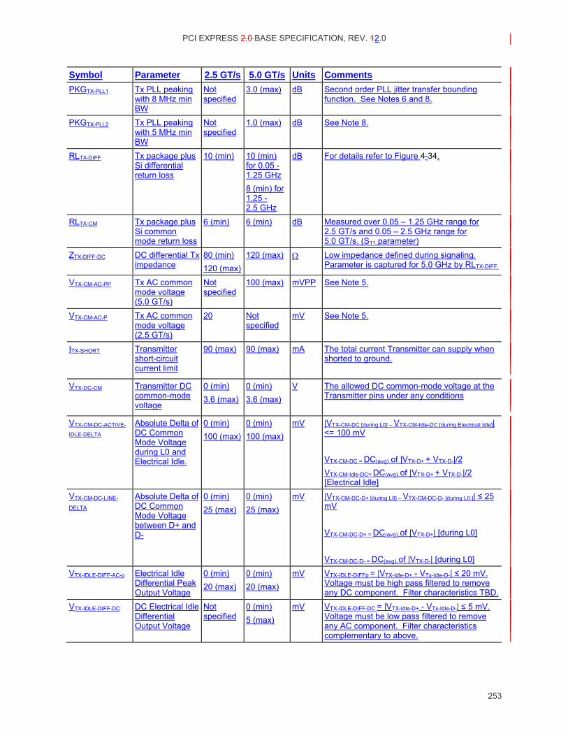
PCI EXPRESS 2.0 BASE SPECIFICATION, REV. 12.0
253
Symbol Parameter 2.5 GT/s 5.0 GT/s Units Comments PKGTX-PLL1 Tx PLL peaking
with 8 MHz min BW
Not specified
3.0 (max) dB Second order PLL jitter transfer bounding function. See Notes 6 and 8.
PKGTX-PLL2 Tx PLL peaking with 5 MHz min BW
Not specified
1.0 (max) dB See Note 8.
RLTX-DIFF Tx package plus Si differential return loss
10 (min) 10 (min) for 0.05 - 1.25 GHz 8 (min) for 1.25 - 2.5 GHz
dB For details refer to Figure 4-34.
RLTX-CM Tx package plus Si common mode return loss
6 (min) 6 (min) dB Measured over 0.05 – 1.25 GHz range for 2.5 GT/s and 0.05 – 2.5 GHz range for 5.0 GT/s. (S11 parameter)
ZTX-DIFF-DC DC differential Tx impedance
80 (min) 120 (max)
120 (max) Ω Low impedance defined during signaling. Parameter is captured for 5.0 GHz by RLTX-DIFF.
VTX-CM-AC-PP Tx AC common mode voltage (5.0 GT/s)
Not specified
100 (max) mVPP See Note 5.
VTX-CM-AC-P Tx AC common mode voltage (2.5 GT/s)
20 Not specified
mV See Note 5.
ITX-SHORT Transmitter short-circuit current limit
90 (max) 90 (max) mA The total current Transmitter can supply when shorted to ground.
VTX-DC-CM Transmitter DC common-mode voltage
0 (min) 3.6 (max)
0 (min) 3.6 (max)
V The allowed DC common-mode voltage at the Transmitter pins under any conditions
VTX-CM-DC-ACTIVE-
IDLE-DELTA
Absolute Delta of DC Common Mode Voltage during L0 and Electrical Idle.
0 (min) 100 (max)
0 (min) 100 (max)
mV |VTX-CM-DC [during L0] – VTX-CM-Idle-DC [during Electrical Idle]| <= 100 mV
VTX-CM-DC = DC(avg) of |VTX-D+ + VTX-D-|/2 VTX-CM-Idle-DC= DC(avg) of |VTX-D+ + VTX-D-|/2 [Electrical Idle]
VTX-CM-DC-LINE-
DELTA Absolute Delta of DC Common Mode Voltage between D+ and D-
0 (min) 25 (max)
0 (min) 25 (max)
mV |VTX-CM-DC-D+ [during L0] – VTX-CM-DC-D- [during L0.]| ≤ 25 mV
VTX-CM-DC-D+ = DC(avg) of |VTX-D+| [during L0] VTX-CM-DC-D- = DC(avg) of |VTX-D-| [during L0]
VTX-IDLE-DIFF-AC-p Electrical Idle Differential Peak Output Voltage
0 (min) 20 (max)
0 (min) 20 (max)
mV VTX-IDLE-DIFFp = |VTX-Idle-D+ - VTx-Idle-D-| ≤ 20 mV. Voltage must be high pass filtered to remove any DC component. Filter characteristics TBD.
VTX-IDLE-DIFF-DC DC Electrical Idle Differential Output Voltage
Not specified
0 (min) 5 (max)
mV VTX-IDLE-DIFF-DC = |VTX-Idle-D+ - VTx-Idle-D-| ≤ 5 mV. Voltage must be low pass filtered to remove any AC component. Filter characteristics complementary to above.
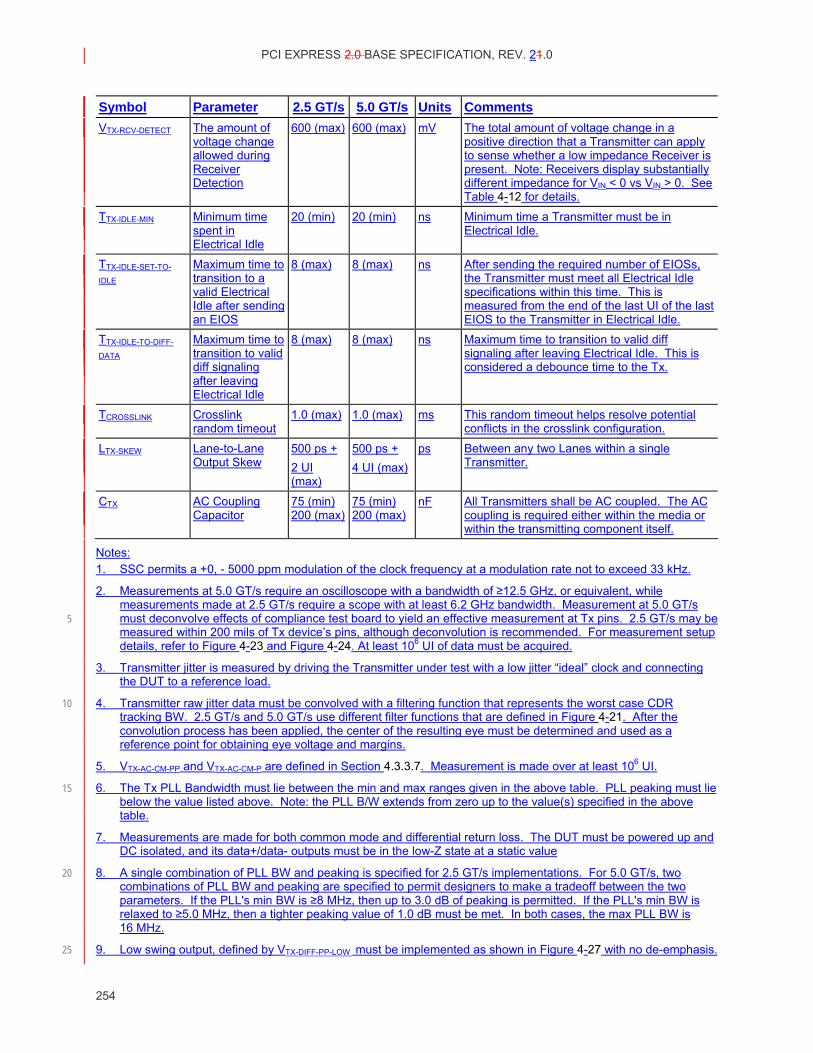
PCI EXPRESS 2.0 BASE SPECIFICATION, REV. 21.0
254
Symbol Parameter 2.5 GT/s 5.0 GT/s Units Comments VTX-RCV-DETECT The amount of
voltage change allowed during Receiver Detection
600 (max) 600 (max) mV The total amount of voltage change in a positive direction that a Transmitter can apply to sense whether a low impedance Receiver is present. Note: Receivers display substantially different impedance for VIN < 0 vs VIN > 0. See Table 4-12 for details.
TTX-IDLE-MIN Minimum time spent in Electrical Idle
20 (min) 20 (min) ns Minimum time a Transmitter must be in Electrical Idle.
TTX-IDLE-SET-TO-
IDLE Maximum time to transition to a valid Electrical Idle after sending an EIOS
8 (max) 8 (max) ns After sending the required number of EIOSs, the Transmitter must meet all Electrical Idle specifications within this time. This is measured from the end of the last UI of the last EIOS to the Transmitter in Electrical Idle.
TTX-IDLE-TO-DIFF-
DATA Maximum time to transition to valid diff signaling after leaving Electrical Idle
8 (max) 8 (max) ns Maximum time to transition to valid diff signaling after leaving Electrical Idle. This is considered a debounce time to the Tx.
TCROSSLINK Crosslink random timeout
1.0 (max) 1.0 (max) ms This random timeout helps resolve potential conflicts in the crosslink configuration.
LTX-SKEW Lane-to-Lane Output Skew
500 ps + 2 UI (max)
500 ps + 4 UI (max)
ps Between any two Lanes within a single Transmitter.
CTX AC Coupling Capacitor
75 (min) 200 (max)
75 (min) 200 (max)
nF All Transmitters shall be AC coupled. The AC coupling is required either within the media or within the transmitting component itself.
Notes: 1. SSC permits a +0, - 5000 ppm modulation of the clock frequency at a modulation rate not to exceed 33 kHz.
2. Measurements at 5.0 GT/s require an oscilloscope with a bandwidth of ≥12.5 GHz, or equivalent, while measurements made at 2.5 GT/s require a scope with at least 6.2 GHz bandwidth. Measurement at 5.0 GT/s must deconvolve effects of compliance test board to yield an effective measurement at Tx pins. 2.5 GT/s may be 5 measured within 200 mils of Tx device’s pins, although deconvolution is recommended. For measurement setup details, refer to Figure 4-23 and Figure 4-24. At least 106 UI of data must be acquired.
3. Transmitter jitter is measured by driving the Transmitter under test with a low jitter “ideal” clock and connecting the DUT to a reference load.
4. Transmitter raw jitter data must be convolved with a filtering function that represents the worst case CDR 10 tracking BW. 2.5 GT/s and 5.0 GT/s use different filter functions that are defined in Figure 4-21. After the convolution process has been applied, the center of the resulting eye must be determined and used as a reference point for obtaining eye voltage and margins.
5. VTX-AC-CM-PP and VTX-AC-CM-P are defined in Section 4.3.3.7. Measurement is made over at least 106 UI.
6. The Tx PLL Bandwidth must lie between the min and max ranges given in the above table. PLL peaking must lie 15 below the value listed above. Note: the PLL B/W extends from zero up to the value(s) specified in the above table.
7. Measurements are made for both common mode and differential return loss. The DUT must be powered up and DC isolated, and its data+/data- outputs must be in the low-Z state at a static value
8. A single combination of PLL BW and peaking is specified for 2.5 GT/s implementations. For 5.0 GT/s, two 20 combinations of PLL BW and peaking are specified to permit designers to make a tradeoff between the two parameters. If the PLL's min BW is ≥8 MHz, then up to 3.0 dB of peaking is permitted. If the PLL's min BW is relaxed to ≥5.0 MHz, then a tighter peaking value of 1.0 dB must be met. In both cases, the max PLL BW is 16 MHz.
9. Low swing output, defined by VTX-DIFF-PP-LOW must be implemented as shown in Figure 4-27 with no de-emphasis. 25
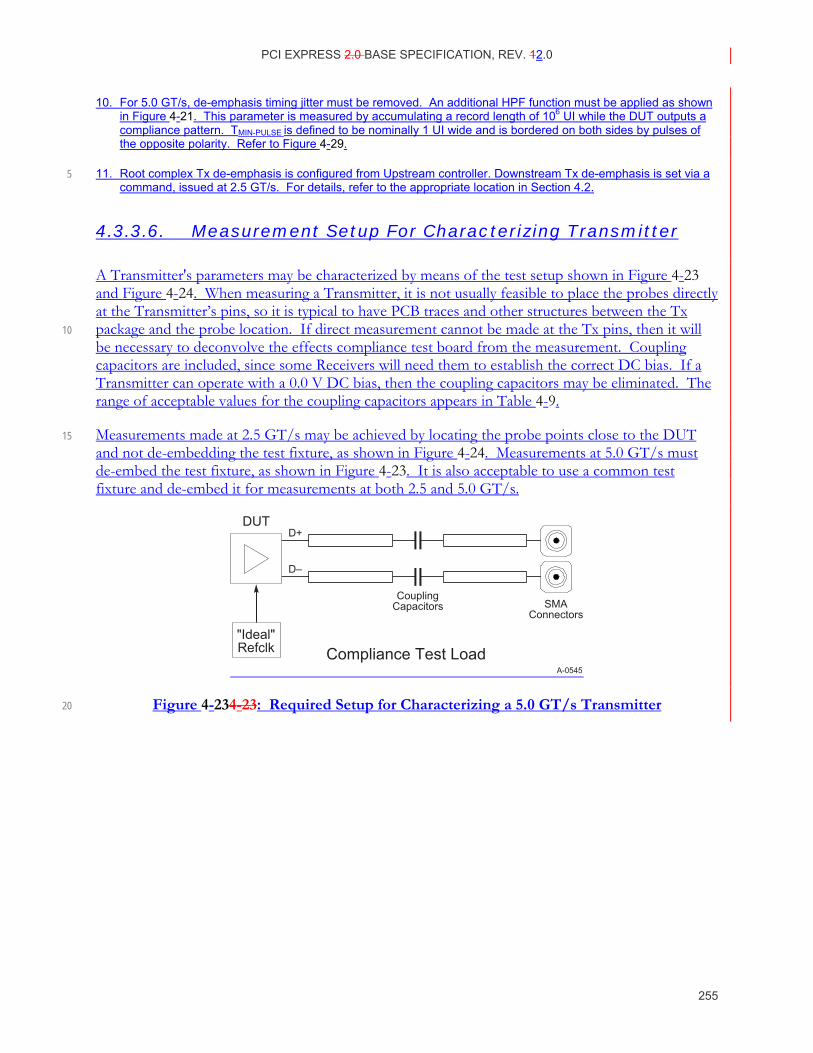
PCI EXPRESS 2.0 BASE SPECIFICATION, REV. 12.0
255
10. For 5.0 GT/s, de-emphasis timing jitter must be removed. An additional HPF function must be applied as shown in Figure 4-21. This parameter is measured by accumulating a record length of 106 UI while the DUT outputs a compliance pattern. TMIN-PULSE is defined to be nominally 1 UI wide and is bordered on both sides by pulses of the opposite polarity. Refer to Figure 4-29.
11. Root complex Tx de-emphasis is configured from Upstream controller. Downstream Tx de-emphasis is set via a 5 command, issued at 2.5 GT/s. For details, refer to the appropriate location in Section 4.2.
4.3.3.6. Measurement Setup For Characterizing Transmitter
A Transmitter's parameters may be characterized by means of the test setup shown in Figure 4-23 and Figure 4-24. When measuring a Transmitter, it is not usually feasible to place the probes directly at the Transmitter’s pins, so it is typical to have PCB traces and other structures between the Tx package and the probe location. If direct measurement cannot be made at the Tx pins, then it will 10 be necessary to deconvolve the effects compliance test board from the measurement. Coupling capacitors are included, since some Receivers will need them to establish the correct DC bias. If a Transmitter can operate with a 0.0 V DC bias, then the coupling capacitors may be eliminated. The range of acceptable values for the coupling capacitors appears in Table 4-9.
Measurements made at 2.5 GT/s may be achieved by locating the probe points close to the DUT 15 and not de-embedding the test fixture, as shown in Figure 4-24. Measurements at 5.0 GT/s must de-embed the test fixture, as shown in Figure 4-23. It is also acceptable to use a common test fixture and de-embed it for measurements at both 2.5 and 5.0 GT/s.
A-0545
DUTD+
D–
CouplingCapacitors SMA
Connectors
"Ideal"Refclk Compliance Test Load
Figure 4-234-23: Required Setup for Characterizing a 5.0 GT/s Transmitter 20
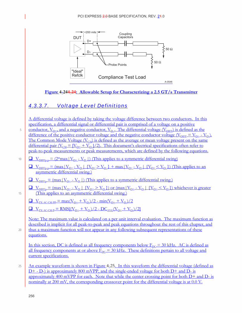
PCI EXPRESS 2.0 BASE SPECIFICATION, REV. 21.0
256
A-0546
DUTD+
D–
CouplingCapacitors
"Ideal"Refclk Compliance Test Load
50
50Probe Points
<200 mils
Figure 4-244-24: Allowable Setup for Characterizing a 2.5 GT/s Transmitter
4.3.3.7. Voltage Level Definitions
A differential voltage is defined by taking the voltage difference between two conductors. In this specification, a differential signal or differential pair is comprised of a voltage on a positive conductor, VD+, and a negative conductor, VD–. The differential voltage (VDIFF) is defined as the 5 difference of the positive conductor voltage and the negative conductor voltage (VDIFF = VD+ - VD-). The Common Mode Voltage (VCM) is defined as the average or mean voltage present on the same differential pair (VCM = [VD+ + VD–]/2). This document’s electrical specifications often refer to peak-to-peak measurements or peak measurements, which are defined by the following equations.
VDIFFp-p = (2*max|VD+ - VD-|) (This applies to a symmetric differential swing) 10
VDIFFp-p = (max|VD+ - VD-| VD+ > VD– + max|VD+ - VD-| VD+ < VD–) (This applies to an asymmetric differential swing.)
VDIFFp = (max|VD+ - VD-|) (This applies to a symmetric differential swing.)
VDIFFp = (max|VD+ - VD-| VD+ > VD-) or (max|VD+ - VD-| VD+ < VD-) whichever is greater (This applies to an asymmetric differential swing.) 15
VTX-AC-CM-PP = max(VD+ + VD-)/2 - min(VD+ + VD-)/2
VTX-AC-CM-P = RMS[(VD+ + VD-)/2 - DCAVG(VD+ + VD-)/2]
Note: The maximum value is calculated on a per unit interval evaluation. The maximum function as described is implicit for all peak-to-peak and peak equations throughout the rest of this chapter, and thus a maximum function will not appear in any following subsequent representations of these 20 equations.
In this section, DC is defined as all frequency components below FDC = 30 kHz. AC is defined as all frequency components at or above FDC = 30 kHz. These definitions pertain to all voltage and current specifications.
An example waveform is shown in Figure 4-25. In this waveform the differential voltage (defined as 25 D+ - D-) is approximately 800 mVPP, and the single-ended voltage for both D+ and D- is approximately 400 mVPP for each. Note that while the center crossing point for both D+ and D- is nominally at 200 mV, the corresponding crossover point for the differential voltage is at 0.0 V.
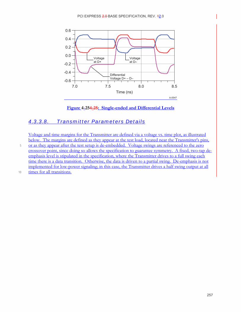
PCI EXPRESS 2.0 BASE SPECIFICATION, REV. 12.0
257
A-0547
0.6
0.4
0.2
0.0
-0.2
-0.4
-0.67.0 7.5
Time (ns)8.0 8.5
Voltageat D+
Voltageat D–
DifferentialVoltage D+ – D–
Figure 4-254-25: Single-ended and Differential Levels
4.3.3.8. Transmitter Parameters Details
Voltage and time margins for the Transmitter are defined via a voltage vs. time plot, as illustrated below. The margins are defined as they appear at the test load, located near the Transmitter's pins, or as they appear after the test setup is de-embedded. Voltage swings are referenced to the zero 5 crossover point, since doing so allows the specification to guarantee symmetry. A fixed, two-tap de-emphasis level is stipulated in the specification, where the Transmitter drives to a full swing each time there is a data transition. Otherwise, the data is driven to a partial swing. De-emphasis is not implemented for low-power signaling; in this case, the Transmitter drives a half swing output at all times for all transitions. 10
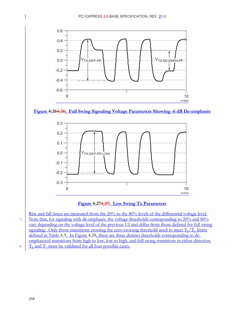
PCI EXPRESS 2.0 BASE SPECIFICATION, REV. 21.0
258
A-0548
0.6
0.4
0.2
0.0
-0.2
-0.4
-0.68 10
VTX-DE-EMPH-PPVTX-DIFF-PP
Figure 4-264-26: Full Swing Signaling Voltage Parameters Showing -6 dB De-emphasis
A-0549
0.3
0.2
0.1
0.0
-0.1
-0.2
-0.38 10
VTX-DIFF-PP-LOW
Figure 4-274-27: Low Swing Tx Parameters
Rise and fall times are measured from the 20% to the 80% levels of the differential voltage level. Note that, for signaling with de-emphasis, the voltage thresholds corresponding to 20% and 80% 5 vary depending on the voltage level of the previous UI and differ from those defined for full swing signaling. Only those transitions crossing the zero-crossing threshold need to meet TR/TF limits defined in Table 4-9. In Figure 4-28, there are three distinct thresholds corresponding to de-emphasized transitions from high to low, low to high, and full swing transitions in either direction. TR and TF must be validated for all four possible cases. 10
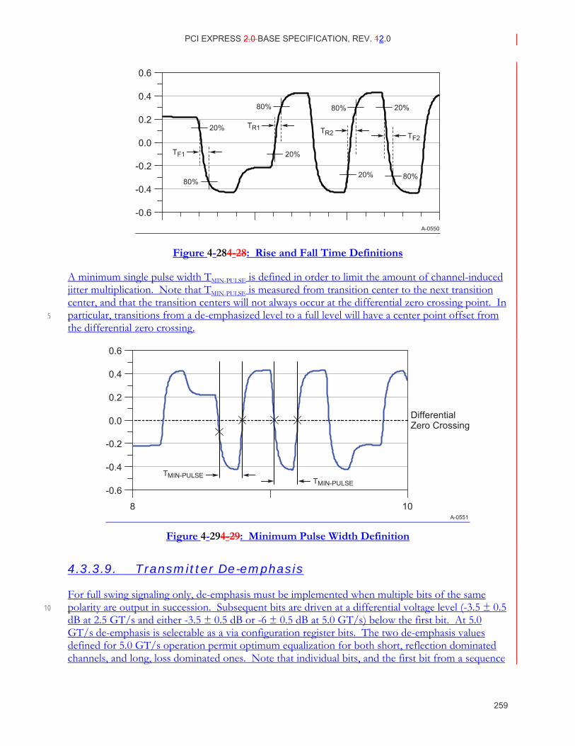
PCI EXPRESS 2.0 BASE SPECIFICATION, REV. 12.0
259
A-0550
0.6
0.4
0.2
0.0
-0.2
-0.4
-0.6
20%
TF1
80%
TR1
80%
20%
TR2
80%
20%
20%
TF2
80%
Figure 4-284-28: Rise and Fall Time Definitions
A minimum single pulse width TMIN-PULSE is defined in order to limit the amount of channel-induced jitter multiplication. Note that TMIN-PULSE is measured from transition center to the next transition center, and that the transition centers will not always occur at the differential zero crossing point. In particular, transitions from a de-emphasized level to a full level will have a center point offset from 5 the differential zero crossing.
0.6
0.4
0.2
0.0
-0.2
-0.4
-0.6
8 10A-0551
TMIN-PULSETMIN-PULSE
DifferentialZero Crossing
Figure 4-294-29: Minimum Pulse Width Definition
4.3.3.9. Transmitter De-emphasis
For full swing signaling only, de-emphasis must be implemented when multiple bits of the same polarity are output in succession. Subsequent bits are driven at a differential voltage level (-3.5 ± 0.5 10 dB at 2.5 GT/s and either -3.5 ± 0.5 dB or -6 ± 0.5 dB at 5.0 GT/s) below the first bit. At 5.0 GT/s de-emphasis is selectable as a via configuration register bits. The two de-emphasis values defined for 5.0 GT/s operation permit optimum equalization for both short, reflection dominated channels, and long, loss dominated ones. Note that individual bits, and the first bit from a sequence
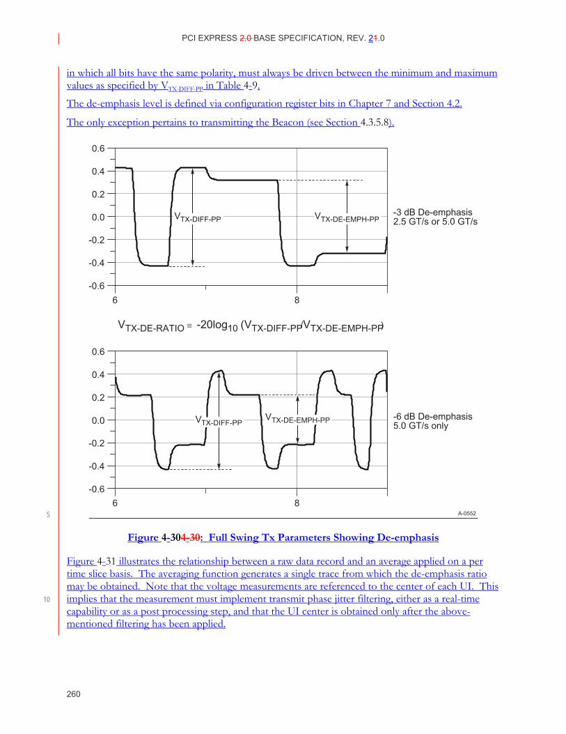
PCI EXPRESS 2.0 BASE SPECIFICATION, REV. 21.0
260
in which all bits have the same polarity, must always be driven between the minimum and maximum values as specified by VTX-DIFF-PP in Table 4-9.
The de-emphasis level is defined via configuration register bits in Chapter 7 and Section 4.2.
The only exception pertains to transmitting the Beacon (see Section 4.3.5.8 ).
0.6
0.4
0.2
0.0
-0.2
-0.4
-0.66 8
VTX-DIFF-PP VTX-DE-EMPH-PP-3 dB De-emphasis2.5 GT/s or 5.0 GT/s
-6 dB De-emphasis5.0 GT/s only
A-0552
0.6
0.4
0.2
0.0
-0.2
-0.4
-0.66 8
VTX-DE-RATIO -20log10 (VTX-DIFF-PP/VTX-DE-EMPH-PP)
VTX-DIFF-PPVTX-DE-EMPH-PP
5
Figure 4-304-30: Full Swing Tx Parameters Showing De-emphasis
Figure 4-31 illustrates the relationship between a raw data record and an average applied on a per time slice basis. The averaging function generates a single trace from which the de-emphasis ratio may be obtained. Note that the voltage measurements are referenced to the center of each UI. This implies that the measurement must implement transmit phase jitter filtering, either as a real-time 10 capability or as a post processing step, and that the UI center is obtained only after the above-mentioned filtering has been applied.
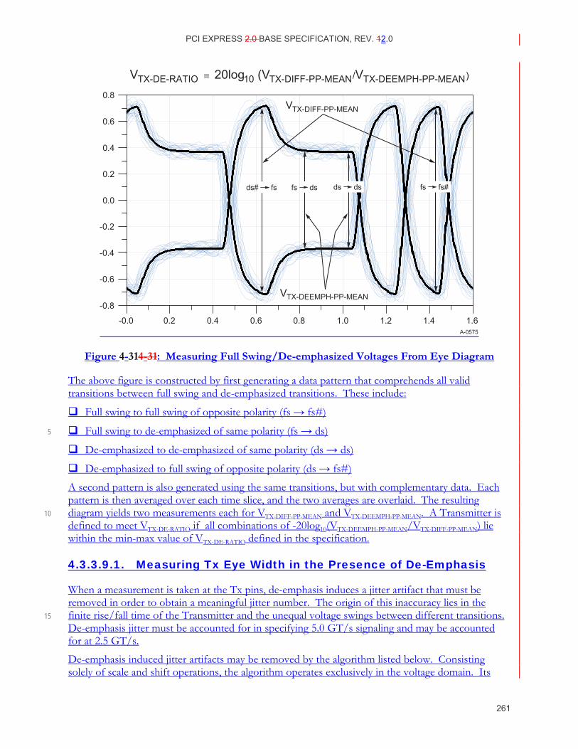
PCI EXPRESS 2.0 BASE SPECIFICATION, REV. 12.0
261
0.8
0.6
0.4
0.2
-0.4
-0.6
-0.8
-0.0 0.2 0.4 0.6 0.8 1.0 1.2 1.4 1.6
VTX-DE-RATIO 20log10 (VTX-DIFF-PP-MEAN/VTX-DEEMPH-PP-MEAN)
0.0
-0.2
A-0575
VTX-DIFF-PP-MEAN
ds# fs fs ds ds ds fs fs#
VTX-DEEMPH-PP-MEAN
Figure 4-314-31: Measuring Full Swing/De-emphasized Voltages From Eye Diagram
The above figure is constructed by first generating a data pattern that comprehends all valid transitions between full swing and de-emphasized transitions. These include:
Full swing to full swing of opposite polarity (fs → fs#)
Full swing to de-emphasized of same polarity (fs → ds) 5
De-emphasized to de-emphasized of same polarity (ds → ds)
De-emphasized to full swing of opposite polarity (ds → fs#)
A second pattern is also generated using the same transitions, but with complementary data. Each pattern is then averaged over each time slice, and the two averages are overlaid. The resulting diagram yields two measurements each for VTX-DIFF-PP-MEAN and VTX-DEEMPH-PP-MEAN. A Transmitter is 10 defined to meet VTX-DE-RATIO if all combinations of -20log10(VTX-DEEMPH-PP-MEAN/VTX-DIFF-PP-MEAN) lie within the min-max value of VTX-DE-RATIO defined in the specification.
4.3.3.9.1. Measuring Tx Eye Width in the Presence of De-Emphasis
When a measurement is taken at the Tx pins, de-emphasis induces a jitter artifact that must be removed in order to obtain a meaningful jitter number. The origin of this inaccuracy lies in the finite rise/fall time of the Transmitter and the unequal voltage swings between different transitions. 15 De-emphasis jitter must be accounted for in specifying 5.0 GT/s signaling and may be accounted for at 2.5 GT/s.
De-emphasis induced jitter artifacts may be removed by the algorithm listed below. Consisting solely of scale and shift operations, the algorithm operates exclusively in the voltage domain. Its
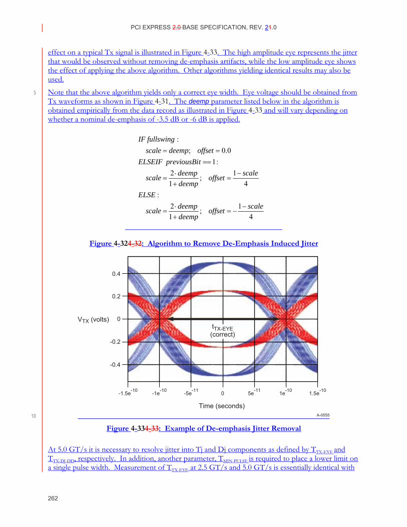
PCI EXPRESS 2.0 BASE SPECIFICATION, REV. 21.0
262
effect on a typical Tx signal is illustrated in Figure 4-33. The high amplitude eye represents the jitter that would be observed without removing de-emphasis artifacts, while the low amplitude eye shows the effect of applying the above algorithm. Other algorithms yielding identical results may also be used.
Note that the above algorithm yields only a correct eye width. Eye voltage should be obtained from 5 Tx waveforms as shown in Figure 4-31. The deemp parameter listed below in the algorithm is obtained empirically from the data record as illustrated in Figure 4-33 and will vary depending on whether a nominal de-emphasis of -3.5 dB or -6 dB is applied.
41;
12
:4
1;12
:10.0;
:
scaleoffsetdeempdeempscale
ELSE
scaleoffsetdeempdeempscale
tpreviousBiELSEIFoffsetdeempscale
fullswingIF
−−=
+⋅
=
−=
+⋅
=
====
Figure 4-324-32: Algorithm to Remove De-Emphasis Induced Jitter
A-0555
0.4
0.2
0
-0.2
-0.4
-1.5e-10 -1e-10 -5e-11 5e-11 1e-10 1.5e-100
tTX-EYE(correct)
VTX (volts)
Time (seconds) 10
Figure 4-334-33: Example of De-emphasis Jitter Removal
At 5.0 GT/s it is necessary to resolve jitter into Tj and Dj components as defined by TTX-EYE and TTX-DJ-DD, respectively. In addition, another parameter, TMIN-PULSE is required to place a lower limit on a single pulse width. Measurement of TTX-EYE at 2.5 GT/s and 5.0 GT/s is essentially identical with
PCI EXPRESS 2.0 BASE SPECIFICATION, REV. 12.0
263
the exception that a different filter function is applied at the two bit rates (see Figure 4-21). TTX-DJ-DD may be obtained by applying the Dual Dirac jitter estimation technique.
4.3.3.10. Transmitter PLL Bandwidth and Peaking
PLL bandwidth and peaking are defined for both the Transmitter and Receiver in order to place an upper limit on the amount of Refclk jitter that is propagated to the transmitted data and to the CDR. Defining PLL BW and peaking limits also guarantees a minimum degree of Tx/Rx jitter tracking in 5 those systems utilizing a common Refclk architecture.
Two sets of bandwidth and peaking are defined for 5.0 GT/s: 8-16 MHz with 3 dB of peaking and 5-16 MHz with 1 dB of peaking. This gives the designer the option of trading off between a low peaking PLL design vs. a low bandwidth design. For 2.5 GT/s, a single PLL bandwidth and peaking range is specified at 3-22 MHz with 3.0 dB of peaking. 10
4.3.3.11. Transmitter Return Loss
The PCI Express Specification defines both common mode and differential return loss for Transmitters.
Transmitter return loss measurements must be made with the device powered up and in a low impedance state. Both zero and one states should be tested. The Transmitter’s outputs must be held at a static value. No DC value is defined, since such measurements would preclude the use of 15 commonly used test equipment such as VNAs. Furthermore, the difference between Transmitter impedance measured at 50 MHz and at DC is negligible. Tx biasing must be maintained such that it establishes the same biasing conditions as would exist for a Tx operating under normal transmit conditions. Hot s-parameter measurements, taken when the outputs are switching, are also permissible. 20
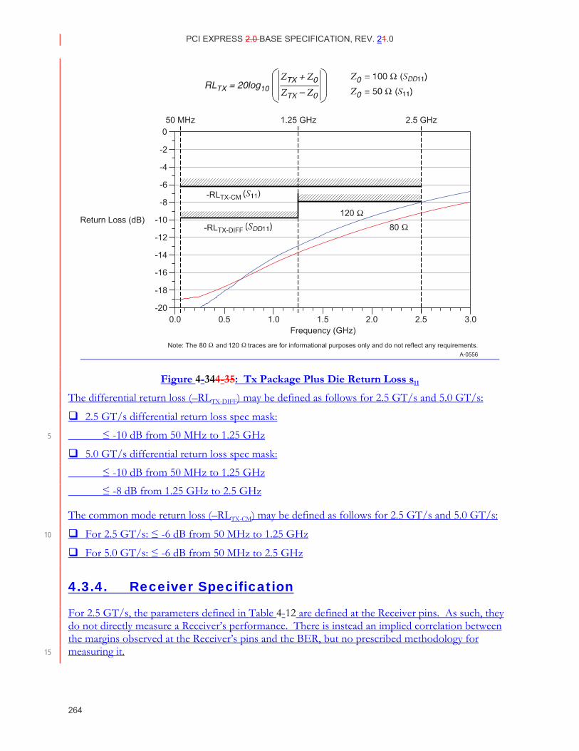
PCI EXPRESS 2.0 BASE SPECIFICATION, REV. 21.0
264
A-0556
Frequency (GHz)
50 MHz 1.25 GHz 2.5 GHz0
-2
-4
-6
-8
-10
-12
-14
-16
-18
-20
120
80
0.0 0.5 1.0 1.5 2.0 2.5 3.0
Return Loss (dB)
-RLTX-CM
-RLTX-DIFF
80 and traces are for informational purposes only and do not reflect any requirements.120Note: The
Figure 4-344-35: Tx Package Plus Die Return Loss s11
The differential return loss (–RLTX-DIFF) may be defined as follows for 2.5 GT/s and 5.0 GT/s:
2.5 GT/s differential return loss spec mask:
≤ -10 dB from 50 MHz to 1.25 GHz 5
5.0 GT/s differential return loss spec mask:
≤ -10 dB from 50 MHz to 1.25 GHz
≤ -8 dB from 1.25 GHz to 2.5 GHz
The common mode return loss (–RLTX-CM) may be defined as follows for 2.5 GT/s and 5.0 GT/s:
For 2.5 GT/s: ≤ -6 dB from 50 MHz to 1.25 GHz 10
For 5.0 GT/s: ≤ -6 dB from 50 MHz to 2.5 GHz
4.3.4. Receiver Specification
For 2.5 GT/s, the parameters defined in Table 4-12 are defined at the Receiver pins. As such, they do not directly measure a Receiver’s performance. There is instead an implied correlation between the margins observed at the Receiver’s pins and the BER, but no prescribed methodology for measuring it. 15
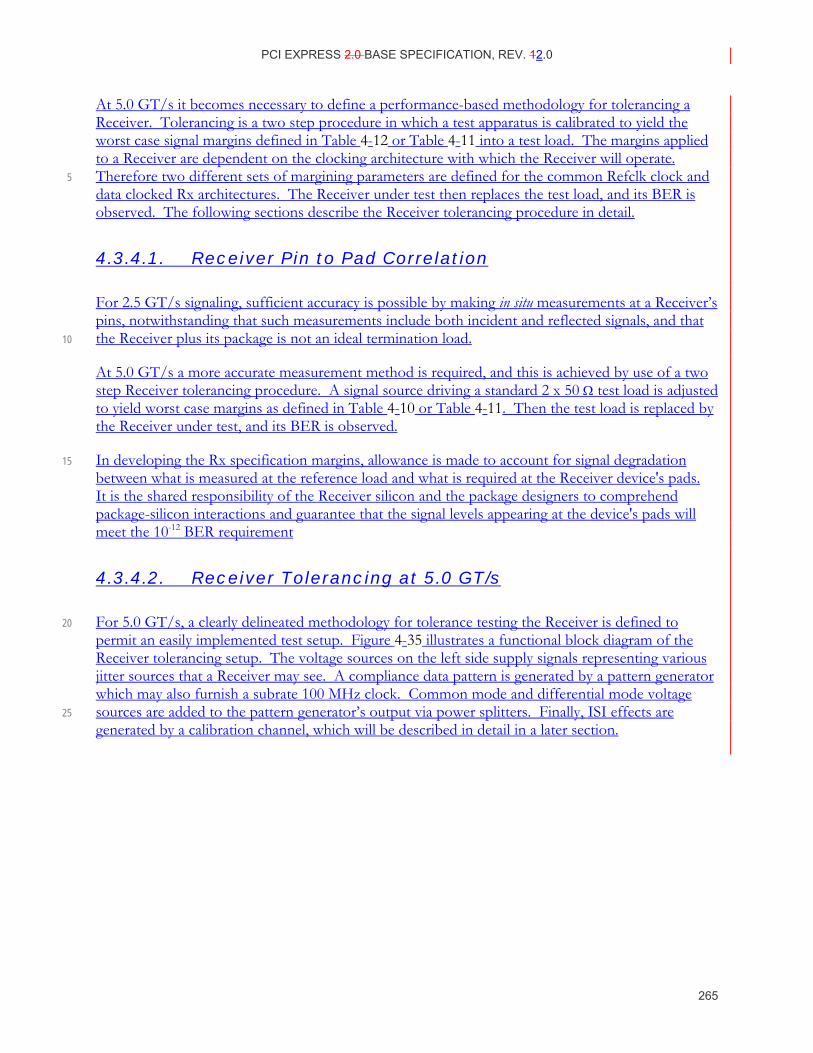
PCI EXPRESS 2.0 BASE SPECIFICATION, REV. 12.0
265
At 5.0 GT/s it becomes necessary to define a performance-based methodology for tolerancing a Receiver. Tolerancing is a two step procedure in which a test apparatus is calibrated to yield the worst case signal margins defined in Table 4-12 or Table 4-11 into a test load. The margins applied to a Receiver are dependent on the clocking architecture with which the Receiver will operate. Therefore two different sets of margining parameters are defined for the common Refclk clock and 5 data clocked Rx architectures. The Receiver under test then replaces the test load, and its BER is observed. The following sections describe the Receiver tolerancing procedure in detail.
4.3.4.1. Receiver Pin to Pad Correlation
For 2.5 GT/s signaling, sufficient accuracy is possible by making in situ measurements at a Receiver’s pins, notwithstanding that such measurements include both incident and reflected signals, and that the Receiver plus its package is not an ideal termination load. 10
At 5.0 GT/s a more accurate measurement method is required, and this is achieved by use of a two step Receiver tolerancing procedure. A signal source driving a standard 2 x 50 Ω test load is adjusted to yield worst case margins as defined in Table 4-10 or Table 4-11. Then the test load is replaced by the Receiver under test, and its BER is observed.
In developing the Rx specification margins, allowance is made to account for signal degradation 15 between what is measured at the reference load and what is required at the Receiver device's pads. It is the shared responsibility of the Receiver silicon and the package designers to comprehend package-silicon interactions and guarantee that the signal levels appearing at the device's pads will meet the 10-12 BER requirement
4.3.4.2. Receiver Tolerancing at 5.0 GT/s
For 5.0 GT/s, a clearly delineated methodology for tolerance testing the Receiver is defined to 20 permit an easily implemented test setup. Figure 4-35 illustrates a functional block diagram of the Receiver tolerancing setup. The voltage sources on the left side supply signals representing various jitter sources that a Receiver may see. A compliance data pattern is generated by a pattern generator which may also furnish a subrate 100 MHz clock. Common mode and differential mode voltage sources are added to the pattern generator’s output via power splitters. Finally, ISI effects are 25 generated by a calibration channel, which will be described in detail in a later section.
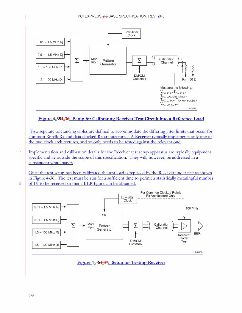
PCI EXPRESS 2.0 BASE SPECIFICATION, REV. 21.0
266
CalibrationChannel
A-0557
0.01 – 1.5 MHz Rj
1.5 – 100 MHz Dj
ModInput Pattern
Generator
RT = 50DM/CM
Crosstalk
0.01 – 1.5 MHz Dj
1.5 – 100 MHz Rj
Low JitterClock
Measure the following:VRX-EYE , TRX-EYE ,TRX-MAX-MIN-RATIO ,TRX-DJ-DD , TRX-MIN-PULSE ,VRX-CM-AC-PP
Figure 4-354-36: Setup for Calibrating Receiver Test Circuit into a Reference Load
Two separate tolerancing tables are defined to accommodate the differing jitter limits that occur for common Refclk Rx and data clocked Rx architectures. A Receiver typically implements only one of the two clock architectures, and so only needs to be tested against the relevant one.
Implementation and calibration details for the Receiver test setup apparatus are typically equipment 5 specific and lie outside the scope of this specification. They will, however, be addressed in a subsequent white paper.
Once the test setup has been calibrated the test load is replaced by the Receiver under test as shown in Figure 4-36. The test must be run for a sufficient time to permit a statistically meaningful number of UI to be received so that a BER figure can be obtained. 10
A-0558
CalibrationChannel
For Common Clocked RefclkRx Architecture Only
0.01 – 1.5 MHz Rj
1.5 – 100 MHz Dj
ModInput
Clk
PatternGenerator
DM/CMCrosstalk
0.01 – 1.5 MHz Dj
1.5 – 100 MHz Rj
Low JitterClock
ReceiverUnderTest
BER
100 MHz
Figure 4-364-37: Setup for Testing Receiver
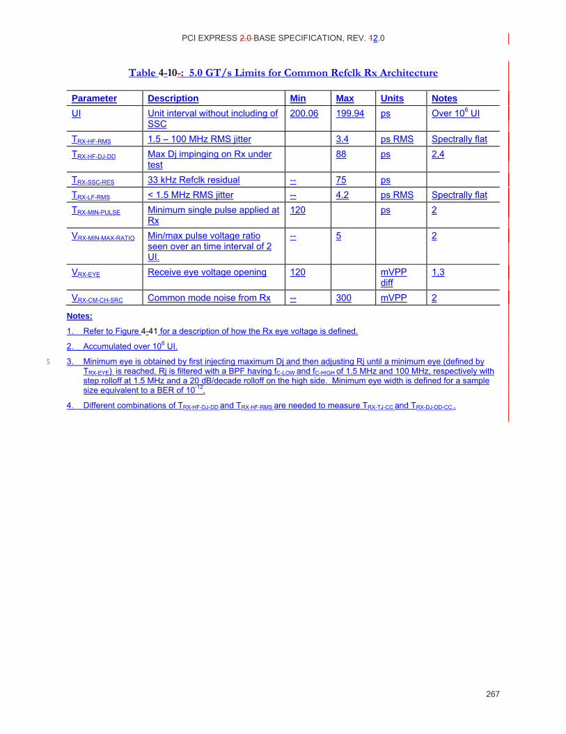
PCI EXPRESS 2.0 BASE SPECIFICATION, REV. 12.0
267
Table 4-10-: 5.0 GT/s Limits for Common Refclk Rx Architecture
Parameter Description Min Max Units Notes UI Unit interval without including of
SSC 200.06 199.94 ps Over 106 UI
TRX-HF-RMS 1.5 – 100 MHz RMS jitter 3.4 ps RMS Spectrally flat TRX-HF-DJ-DD Max Dj impinging on Rx under
test 88 ps 2,4
TRX-SSC-RES 33 kHz Refclk residual -- 75 ps TRX-LF-RMS < 1.5 MHz RMS jitter -- 4.2 ps RMS Spectrally flat TRX-MIN-PULSE Minimum single pulse applied at
Rx 120 ps 2
VRX-MIN-MAX-RATIO Min/max pulse voltage ratio seen over an time interval of 2 UI.
-- 5 2
VRX-EYE Receive eye voltage opening 120 mVPP diff
1,3
VRX-CM-CH-SRC Common mode noise from Rx -- 300 mVPP 2
Notes:
1. Refer to Figure 4-41 for a description of how the Rx eye voltage is defined.
2. Accumulated over 106 UI.
3. Minimum eye is obtained by first injecting maximum Dj and then adjusting Rj until a minimum eye (defined by 5 TRX-EYE) is reached. Rj is filtered with a BPF having fC-LOW and fC-HIGH of 1.5 MHz and 100 MHz, respectively with step rolloff at 1.5 MHz and a 20 dB/decade rolloff on the high side. Minimum eye width is defined for a sample size equivalent to a BER of 10-12.
4. Different combinations of TRX-HF-DJ-DD and TRX-HF-RMS are needed to measure TRX-TJ-CC and TRX-DJ-DD-CC..
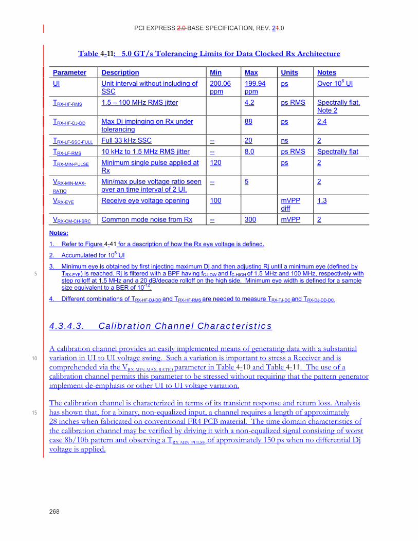
PCI EXPRESS 2.0 BASE SPECIFICATION, REV. 21.0
268
Table 4-11: 5.0 GT/s Tolerancing Limits for Data Clocked Rx Architecture
Parameter Description Min Max Units Notes UI Unit interval without including of
SSC 200.06 ppm
199.94 ppm
ps Over 106 UI
TRX-HF-RMS 1.5 – 100 MHz RMS jitter 4.2 ps RMS Spectrally flat, Note 2
TRX-HF-DJ-DD Max Dj impinging on Rx under tolerancing
88 ps 2,4
TRX-LF-SSC-FULL Full 33 kHz SSC -- 20 ns 2 TRX-LF-RMS 10 kHz to 1.5 MHz RMS jitter -- 8.0 ps RMS Spectrally flat TRX-MIN-PULSE Minimum single pulse applied at
Rx 120 ps 2
VRX-MIN-MAX-
RATIO Min/max pulse voltage ratio seen over an time interval of 2 UI.
-- 5 2
VRX-EYE Receive eye voltage opening 100 mVPP diff
1,3
VRX-CM-CH-SRC Common mode noise from Rx -- 300 mVPP 2
Notes:
1. Refer to Figure 4-41 for a description of how the Rx eye voltage is defined.
2. Accumulated for 106 UI
3. Minimum eye is obtained by first injecting maximum Dj and then adjusting Rj until a minimum eye (defined by TRX-EYE) is reached. Rj is filtered with a BPF having fC-LOW and fC-HIGH of 1.5 MHz and 100 MHz, respectively with 5 step rolloff at 1.5 MHz and a 20 dB/decade rolloff on the high side. Minimum eye width is defined for a sample size equivalent to a BER of 10-12.
4. Different combinations of TRX-HF-DJ-DD and TRX-HF-RMS are needed to measure TRX-TJ-DC and TRX-DJ-DD-DC.
4.3.4.3. Calibration Channel Characteristics
A calibration channel provides an easily implemented means of generating data with a substantial variation in UI to UI voltage swing. Such a variation is important to stress a Receiver and is 10 comprehended via the VRX-MIN-MAX-RATIO parameter in Table 4-10 and Table 4-11. The use of a calibration channel permits this parameter to be stressed without requiring that the pattern generator implement de-emphasis or other UI to UI voltage variation.
The calibration channel is characterized in terms of its transient response and return loss. Analysis has shown that, for a binary, non-equalized input, a channel requires a length of approximately 15 28 inches when fabricated on conventional FR4 PCB material. The time domain characteristics of the calibration channel may be verified by driving it with a non-equalized signal consisting of worst case 8b/10b pattern and observing a TRX-MIN-PULSE of approximately 150 ps when no differential Dj voltage is applied.
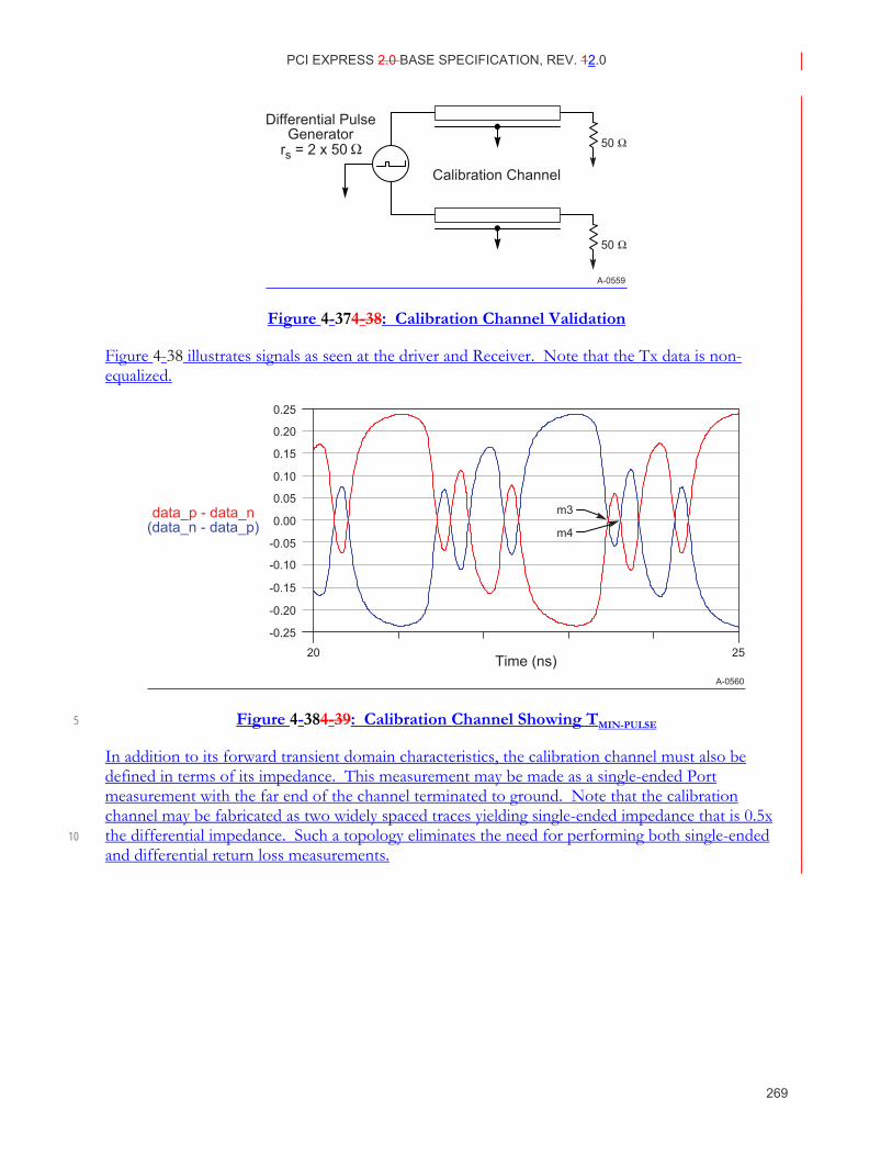
PCI EXPRESS 2.0 BASE SPECIFICATION, REV. 12.0
269
A-0559
50
50
Calibration Channel
rs = 2 x 50
Differential PulseGenerator
Figure 4-374-38: Calibration Channel Validation
Figure 4-38 illustrates signals as seen at the driver and Receiver. Note that the Tx data is non-equalized.
A-0560
0.25
-0.25
-0.20
-0.15
-0.10
-0.05
0.00
0.05
0.10
0.15
0.20
20 25Time (ns)
data_p - data_n(data_n - data_p)
m3
m4
Figure 4-384-39: Calibration Channel Showing TMIN-PULSE 5
In addition to its forward transient domain characteristics, the calibration channel must also be defined in terms of its impedance. This measurement may be made as a single-ended Port measurement with the far end of the channel terminated to ground. Note that the calibration channel may be fabricated as two widely spaced traces yielding single-ended impedance that is 0.5x the differential impedance. Such a topology eliminates the need for performing both single-ended 10 and differential return loss measurements.
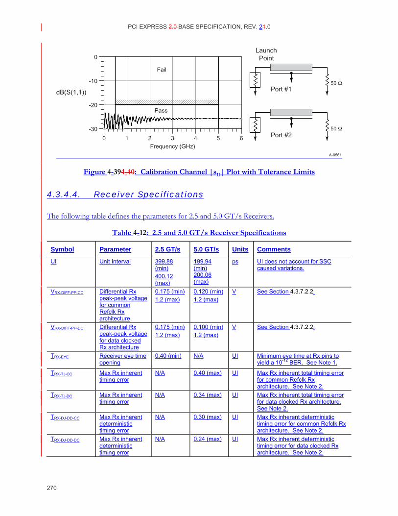
PCI EXPRESS 2.0 BASE SPECIFICATION, REV. 21.0
270
A-0561
50
50
Port #1
Port #2
LaunchPoint0
-10
-20
-300 1 2 3 4 5 6
Frequency (GHz)
dB(S(1,1))
Pass
Fail
Figure 4-394-40: Calibration Channel |s11| Plot with Tolerance Limits
4.3.4.4. Receiver Specifications
The following table defines the parameters for 2.5 and 5.0 GT/s Receivers.
Table 4-12: 2.5 and 5.0 GT/s Receiver Specifications
Symbol Parameter 2.5 GT/s 5.0 GT/s Units Comments
UI Unit Interval 399.88 (min) 400.12 (max)
199.94 (min) 200.06 (max)
ps UI does not account for SSC caused variations.
VRX-DIFF-PP-CC Differential Rx peak-peak voltage for common Refclk Rx architecture
0.175 (min) 1.2 (max)
0.120 (min) 1.2 (max)
V See Section 4.3.7.2.2.
VRX-DIFF-PP-DC Differential Rx peak-peak voltage for data clocked Rx architecture
0.175 (min) 1.2 (max)
0.100 (min) 1.2 (max)
V See Section 4.3.7.2.2.
TRX-EYE Receiver eye time opening
0.40 (min) N/A UI Minimum eye time at Rx pins to yield a 10-12 BER. See Note 1.
TRX-TJ-CC Max Rx inherent timing error
N/A 0.40 (max) UI Max Rx inherent total timing error for common Refclk Rx architecture. See Note 2.
TRX-TJ-DC Max Rx inherent timing error
N/A 0.34 (max) UI Max Rx inherent total timing error for data clocked Rx architecture. See Note 2.
TRX-DJ-DD-CC Max Rx inherent deterministic timing error
N/A 0.30 (max) UI Max Rx inherent deterministic timing error for common Refclk Rx architecture. See Note 2.
TRX-DJ-DD-DC Max Rx inherent deterministic timing error
N/A 0.24 (max) UI Max Rx inherent deterministic timing error for data clocked Rx architecture. See Note 2.
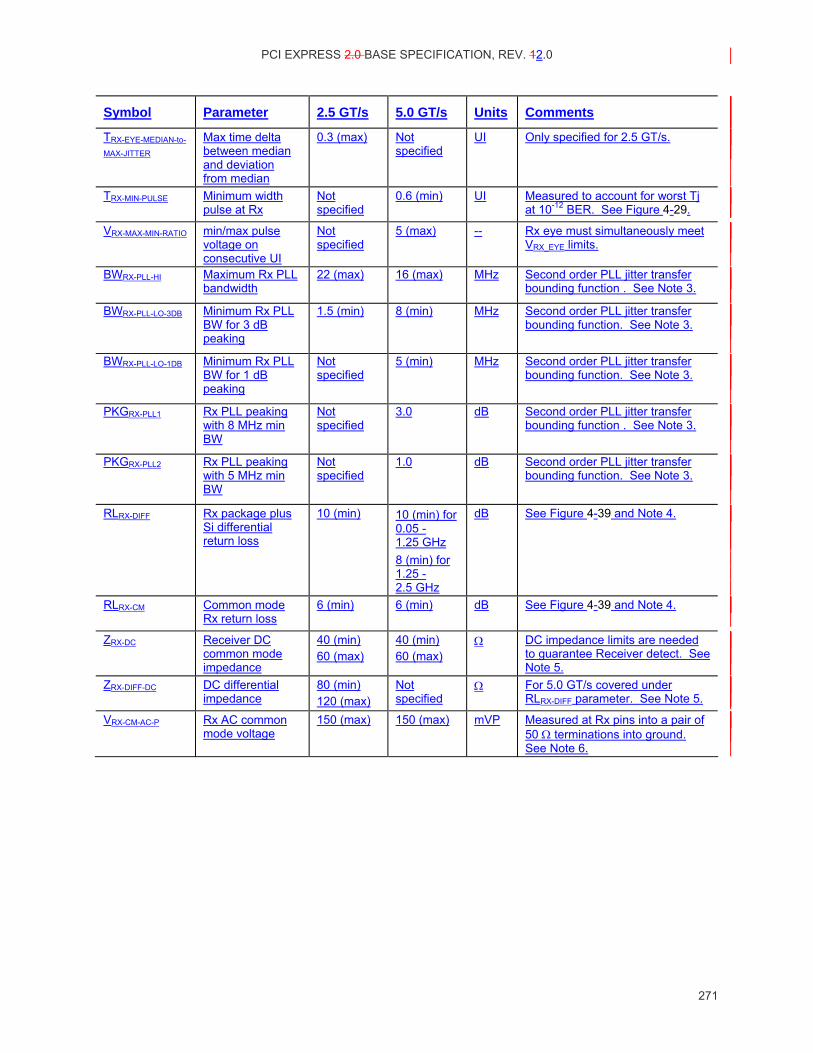
PCI EXPRESS 2.0 BASE SPECIFICATION, REV. 12.0
271
Symbol Parameter 2.5 GT/s 5.0 GT/s Units Comments
TRX-EYE-MEDIAN-to-
MAX-JITTER Max time delta between median and deviation from median
0.3 (max) Not specified
UI Only specified for 2.5 GT/s.
TRX-MIN-PULSE Minimum width pulse at Rx
Not specified
0.6 (min) UI Measured to account for worst Tj at 10-12 BER. See Figure 4-29.
VRX-MAX-MIN-RATIO min/max pulse voltage on consecutive UI
Not specified
5 (max) -- Rx eye must simultaneously meet VRX_EYE limits.
BWRX-PLL-HI Maximum Rx PLL bandwidth
22 (max) 16 (max) MHz Second order PLL jitter transfer bounding function . See Note 3.
BWRX-PLL-LO-3DB Minimum Rx PLL BW for 3 dB peaking
1.5 (min) 8 (min) MHz Second order PLL jitter transfer bounding function. See Note 3.
BWRX-PLL-LO-1DB Minimum Rx PLL BW for 1 dB peaking
Not specified
5 (min) MHz Second order PLL jitter transfer bounding function. See Note 3.
PKGRX-PLL1 Rx PLL peaking with 8 MHz min BW
Not specified
3.0 dB Second order PLL jitter transfer bounding function . See Note 3.
PKGRX-PLL2 Rx PLL peaking with 5 MHz min BW
Not specified
1.0 dB Second order PLL jitter transfer bounding function. See Note 3.
RLRX-DIFF Rx package plus Si differential return loss
10 (min) 10 (min) for 0.05 - 1.25 GHz 8 (min) for 1.25 - 2.5 GHz
dB See Figure 4-39 and Note 4.
RLRX-CM Common mode Rx return loss
6 (min) 6 (min) dB See Figure 4-39 and Note 4.
ZRX-DC Receiver DC common mode impedance
40 (min) 60 (max)
40 (min) 60 (max)
Ω DC impedance limits are needed to guarantee Receiver detect. See Note 5.
ZRX-DIFF-DC DC differential impedance
80 (min) 120 (max)
Not specified
Ω For 5.0 GT/s covered under RLRX-DIFF parameter. See Note 5.
VRX-CM-AC-P Rx AC common mode voltage
150 (max) 150 (max) mVP Measured at Rx pins into a pair of 50 Ω terminations into ground. See Note 6.
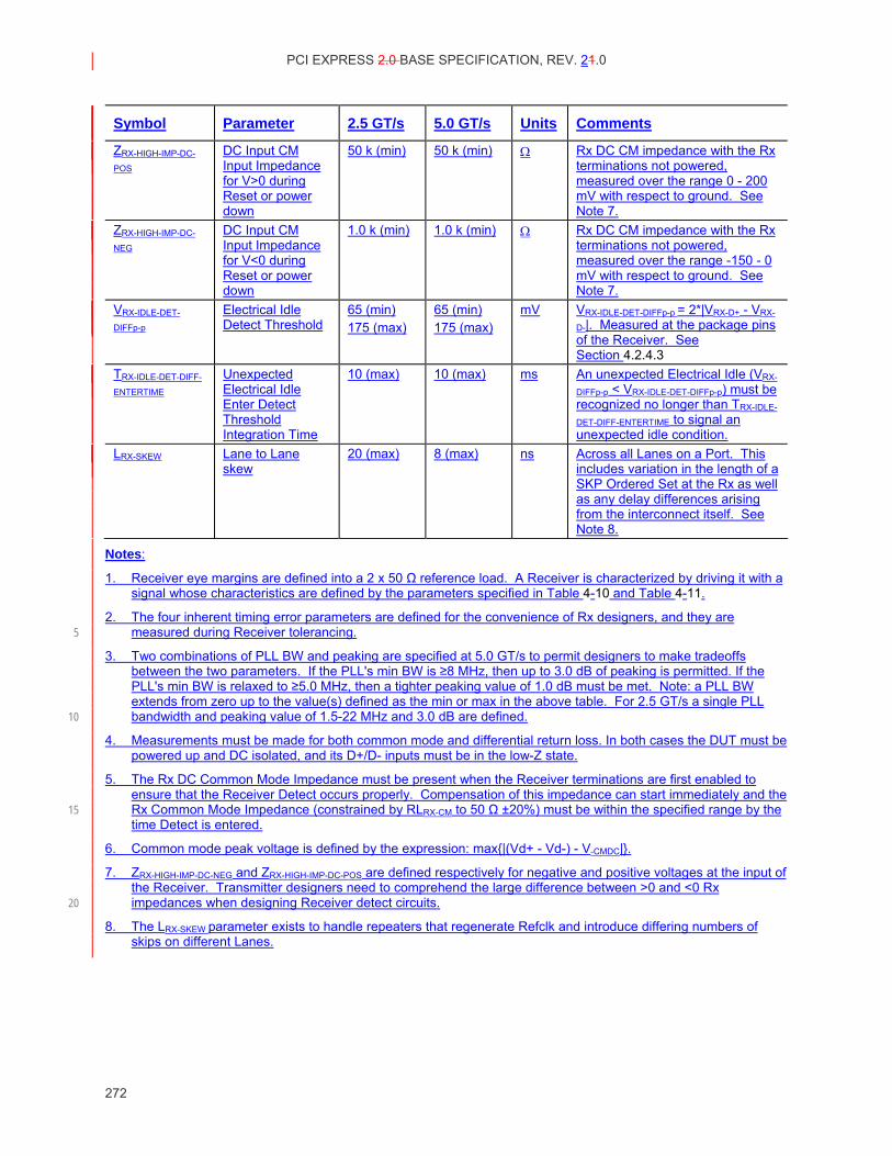
PCI EXPRESS 2.0 BASE SPECIFICATION, REV. 21.0
272
Symbol Parameter 2.5 GT/s 5.0 GT/s Units Comments
ZRX-HIGH-IMP-DC-
POS DC Input CM Input Impedance for V>0 during Reset or power down
50 k (min) 50 k (min) Ω Rx DC CM impedance with the Rx terminations not powered, measured over the range 0 - 200 mV with respect to ground. See Note 7.
ZRX-HIGH-IMP-DC-
NEG DC Input CM Input Impedance for V<0 during Reset or power down
1.0 k (min) 1.0 k (min) Ω Rx DC CM impedance with the Rx terminations not powered, measured over the range -150 - 0 mV with respect to ground. See Note 7.
VRX-IDLE-DET-
DIFFp-p Electrical Idle Detect Threshold
65 (min) 175 (max)
65 (min) 175 (max)
mV VRX-IDLE-DET-DIFFp-p = 2*|VRX-D+ - VRX-
D-|. Measured at the package pins of the Receiver. See Section 4.2.4.3
TRX-IDLE-DET-DIFF-
ENTERTIME Unexpected Electrical Idle Enter Detect Threshold Integration Time
10 (max) 10 (max) ms An unexpected Electrical Idle (VRX-
DIFFp-p < VRX-IDLE-DET-DIFFp-p) must be recognized no longer than TRX-IDLE-
DET-DIFF-ENTERTIME to signal an unexpected idle condition.
LRX-SKEW Lane to Lane skew
20 (max) 8 (max) ns Across all Lanes on a Port. This includes variation in the length of a SKP Ordered Set at the Rx as well as any delay differences arising from the interconnect itself. See Note 8.
Notes:
1. Receiver eye margins are defined into a 2 x 50 Ω reference load. A Receiver is characterized by driving it with a signal whose characteristics are defined by the parameters specified in Table 4-10 and Table 4-11.
2. The four inherent timing error parameters are defined for the convenience of Rx designers, and they are measured during Receiver tolerancing. 5
3. Two combinations of PLL BW and peaking are specified at 5.0 GT/s to permit designers to make tradeoffs between the two parameters. If the PLL's min BW is ≥8 MHz, then up to 3.0 dB of peaking is permitted. If the PLL's min BW is relaxed to ≥5.0 MHz, then a tighter peaking value of 1.0 dB must be met. Note: a PLL BW extends from zero up to the value(s) defined as the min or max in the above table. For 2.5 GT/s a single PLL bandwidth and peaking value of 1.5-22 MHz and 3.0 dB are defined. 10
4. Measurements must be made for both common mode and differential return loss. In both cases the DUT must be powered up and DC isolated, and its D+/D- inputs must be in the low-Z state.
5. The Rx DC Common Mode Impedance must be present when the Receiver terminations are first enabled to ensure that the Receiver Detect occurs properly. Compensation of this impedance can start immediately and the Rx Common Mode Impedance (constrained by RLRX-CM to 50 Ω ±20%) must be within the specified range by the 15 time Detect is entered.
6. Common mode peak voltage is defined by the expression: max|(Vd+ - Vd-) - V-CMDC|.
7. ZRX-HIGH-IMP-DC-NEG and ZRX-HIGH-IMP-DC-POS are defined respectively for negative and positive voltages at the input of the Receiver. Transmitter designers need to comprehend the large difference between >0 and <0 Rx impedances when designing Receiver detect circuits. 20
8. The LRX-SKEW parameter exists to handle repeaters that regenerate Refclk and introduce differing numbers of skips on different Lanes.
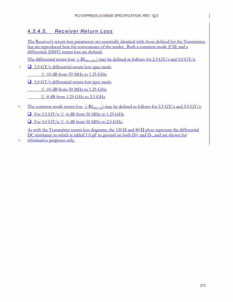
PCI EXPRESS 2.0 BASE SPECIFICATION, REV. 12.0
273
4.3.4.5. Receiver Return Loss
The Receiver’s return loss parameters are essentially identical with those defined for the Transmitter, but are reproduced here for convenience of the reader. Both a common mode (CM) and a differential (DIFF) return loss are defined.
The differential return loss (–RLRX-DIFF) may be defined as follows for 2.5 GT/s and 5.0 GT/s:
2.5 GT/s differential return loss spec mask: 5
≤ -10 dB from 50 MHz to 1.25 GHz
5.0 GT/s differential return loss spec mask:
≤ -10 dB from 50 MHz to 1.25 GHz
≤ -8 dB from 1.25 GHz to 2.5 GHz
The common mode return loss (–RLRX-CM) may be defined as follows for 2.5 GT/s and 5.0 GT/s: 10
For 2.5 GT/s: ≤ -6 dB from 50 MHz to 1.25 GHz
For 5.0 GT/s: ≤ -6 dB from 50 MHz to 2.5 GHz.
As with the Transmitter return loss diagrams, the 120 Ω and 80 Ω plots represent the differential DC resistance to which is added 1.0 pF to ground on both D+ and D-, and are shown for informative purposes only. 15
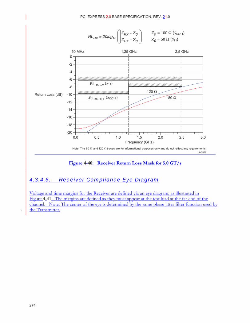
PCI EXPRESS 2.0 BASE SPECIFICATION, REV. 21.0
274
A-0576
Frequency (GHz)
50 MHz 1.25 GHz 2.5 GHz0
-2
-4
-6
-8
-10
-12
-14
-16
-18
-20
80
0.0 0.5 1.0 1.5 2.0 2.5 3.0
Return Loss (dB)
-RLRX-CM
-RLRX-DIFF
80 and traces are for informational purposes only and do not reflect any requirements.120Note: The
120
Figure 4-40: Receiver Return Loss Mask for 5.0 GT/s
4.3.4.6. Receiver Compliance Eye Diagram
Voltage and time margins for the Receiver are defined via an eye diagram, as illustrated in Figure 4-41. The margins are defined as they must appear at the test load at the far end of the channel. Note: The center of the eye is determined by the same phase jitter filter function used by the Transmitter. 5
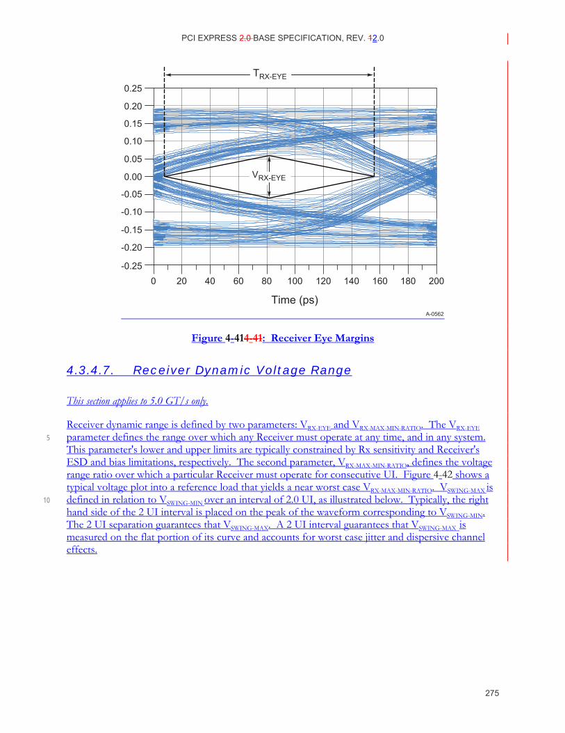
PCI EXPRESS 2.0 BASE SPECIFICATION, REV. 12.0
275
A-0562
0.25
0.20
0.15
0.10
0.05
0.00
-0.05
-0.10
-0.15
-0.20
-0.250 20 40 60 80 100 120 140 160 180 200
Time (ps)
TRX-EYE
VRX-EYE
Figure 4-414-41: Receiver Eye Margins
4.3.4.7. Receiver Dynamic Voltage Range
This section applies to 5.0 GT/s only.
Receiver dynamic range is defined by two parameters: VRX-EYE and VRX-MAX-MIN-RATIO. The VRX-EYE parameter defines the range over which any Receiver must operate at any time, and in any system. 5 This parameter's lower and upper limits are typically constrained by Rx sensitivity and Receiver's ESD and bias limitations, respectively. The second parameter, VRX-MAX-MIN-RATIO, defines the voltage range ratio over which a particular Receiver must operate for consecutive UI. Figure 4-42 shows a typical voltage plot into a reference load that yields a near worst case VRX-MAX-MIN-RATIO. VSWING-MAX is defined in relation to VSWING-MIN over an interval of 2.0 UI, as illustrated below. Typically, the right 10 hand side of the 2 UI interval is placed on the peak of the waveform corresponding to VSWING-MIN. The 2 UI separation guarantees that VSWING-MAX. A 2 UI interval guarantees that VSWING-MAX is measured on the flat portion of its curve and accounts for worst case jitter and dispersive channel effects.
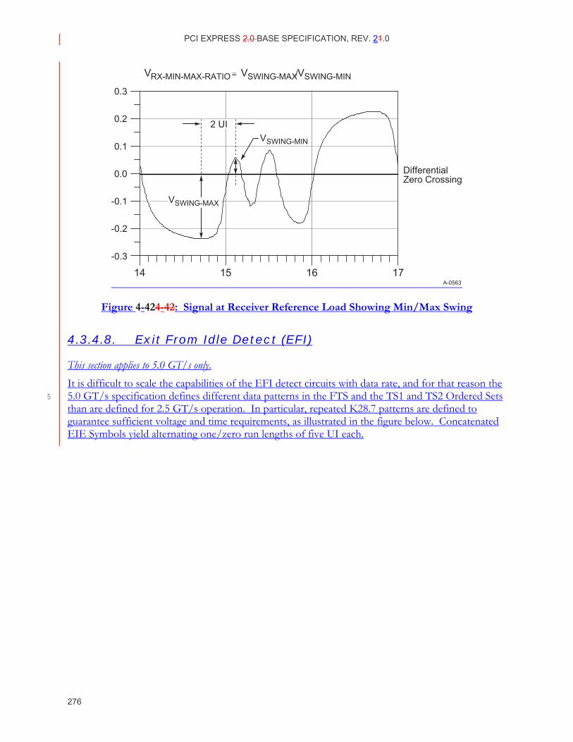
PCI EXPRESS 2.0 BASE SPECIFICATION, REV. 21.0
276
A-0563
0.3
0.2
0.1
0.0
-0.1
-0.2
-0.3
14 15 16 17
DifferentialZero Crossing
VSWING-MAX
2 UIVSWING-MIN
VRX-MIN-MAX-RATIO VSWING-MAX/VSWING-MIN
Figure 4-424-42: Signal at Receiver Reference Load Showing Min/Max Swing
4.3.4.8. Exit From Idle Detect (EFI)
This section applies to 5.0 GT/s only. It is difficult to scale the capabilities of the EFI detect circuits with data rate, and for that reason the 5.0 GT/s specification defines different data patterns in the FTS and the TS1 and TS2 Ordered Sets 5 than are defined for 2.5 GT/s operation. In particular, repeated K28.7 patterns are defined to guarantee sufficient voltage and time requirements, as illustrated in the figure below. Concatenated EIE Symbols yield alternating one/zero run lengths of five UI each.
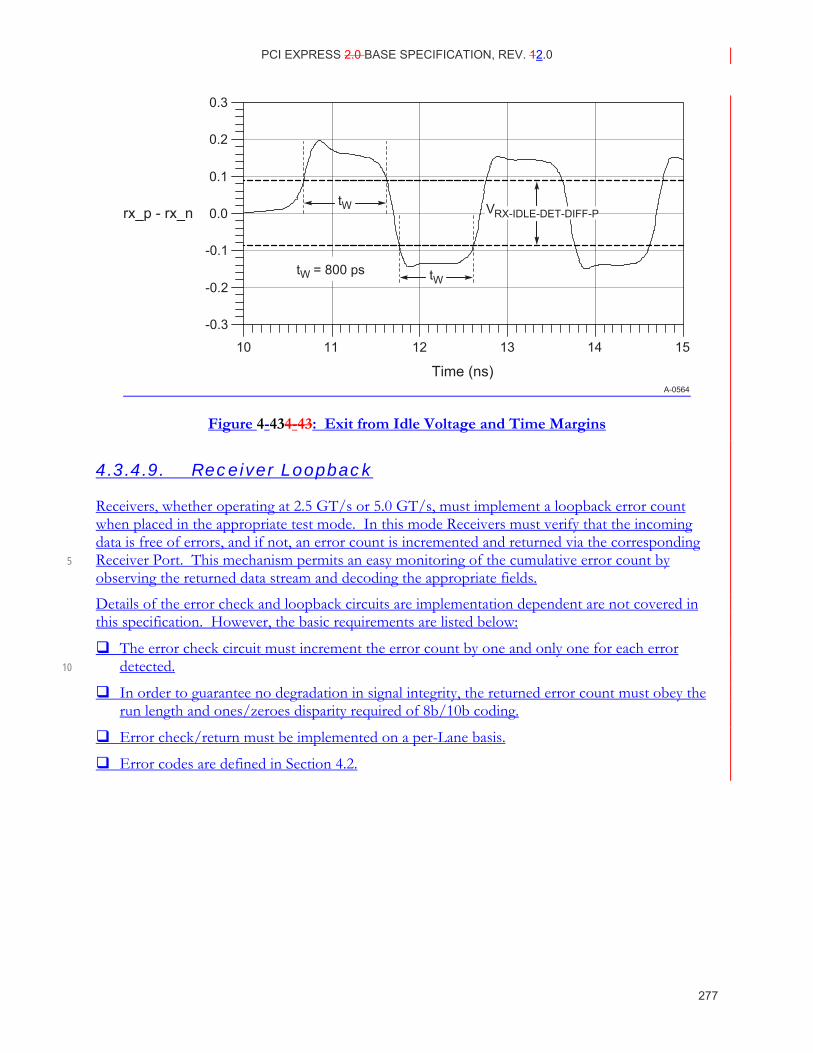
PCI EXPRESS 2.0 BASE SPECIFICATION, REV. 12.0
277
A-0564
0.3
0.2
0.1
0.0
-0.1
-0.2
-0.3
10 11 12 13 14 15
Time (ns)
rx_p - rx_ntW
tWtW = 800 ps
VRX-IDLE-DET-DIFF-P
Figure 4-434-43: Exit from Idle Voltage and Time Margins
4.3.4.9. Receiver Loopback
Receivers, whether operating at 2.5 GT/s or 5.0 GT/s, must implement a loopback error count when placed in the appropriate test mode. In this mode Receivers must verify that the incoming data is free of errors, and if not, an error count is incremented and returned via the corresponding Receiver Port. This mechanism permits an easy monitoring of the cumulative error count by 5 observing the returned data stream and decoding the appropriate fields.
Details of the error check and loopback circuits are implementation dependent are not covered in this specification. However, the basic requirements are listed below:
The error check circuit must increment the error count by one and only one for each error detected. 10
In order to guarantee no degradation in signal integrity, the returned error count must obey the run length and ones/zeroes disparity required of 8b/10b coding.
Error check/return must be implemented on a per-Lane basis.
Error codes are defined in Section 4.2.
PCI EXPRESS 2.0 BASE SPECIFICATION, REV. 21.0
278
4.3.5. Transmitter and Receiver DC Specifications
The parameters defined in this section are relevant to both 2.5 GT/s and 5.0 GT/s designs.
4.3.5.1. Channel AC Coupling Capacitors
Each Lane of a PCI Express Link must be AC coupled. The minimum and maximum values for the capacitance is given in Table 4-9. Capacitors must be placed on the Transmitter side of an interface that permits adapters to be plugged and unplugged. In a topology where everything is located on a single substrate, the capacitors may be located anywhere along the channel. External capacitors are 5 assumed because the values required are too large to feasibly construct on-chip.
4.3.5.2. ESD Protection
All signal and power pins must withstand 2000 V of ESD using the human body model and 500 V using the charged device model without damage. Class 2 per JEDEC JESE22-A114-A. This ESD protection mechanism also helps protect the powered down Receiver from potential common mode transients during certain possible reset or surprise insertion situations. 10
4.3.5.3. Short Circuit Requirements
All Transmitters and Receivers must support surprise hot insertion/removal without damage to the component. The Transmitter and Receiver must be capable of withstanding sustained short circuit to ground of D+ and D-.
4.3.5.4. Transmitter and Receiver Termination
The Transmitter is required to meet RLTX-DIFF and RLTX-CM (see Table 4-9 and Figure 4-23) any time functional differential signals are being transmitted. 15
The Transmitter is required only to meet ITX-SHORT (see Table 4-9) any time functional differential signals are not being transmitted.
Note: The differential impedance during this same time is not defined.
The Receiver is required to meet RLRX-DIFF and RLRX-CM (see Table 4-12Table 410) during all LTSSM states excluding only times during when the device is powered down, Fundamental 20 Reset is asserted, or when explicitly specified.
The Receiver is required to meet ZRX-HIGH-IMP-DC-NEG and ZRX-HIGH-IMP-DC-POS (see Table 4-12) any time adequate power is not provided to the Receiver, Fundamental Reset is asserted, or when explicitly specified.
PCI EXPRESS 2.0 BASE SPECIFICATION, REV. 12.0
279
4.3.5.5. Electrical Idle
Electrical Idle is a steady state condition where the Transmitter D+ and D- voltages are held constant at the same value. Electrical Idle is primarily used in power saving and inactive states (i.e., Disable).
Before a Transmitter enters Electrical Idle, is must always send the required number of EIOSs defined in Section 4.2.4.1 except for the LTSSM substates explicitly exempted from being a 5 requirement. After sending the last Symbol of the last of the required number of EIOSs, the Transmitter must be in a valid Electrical Idle state within the time as specified by TTX-IDLE-SET-TO-IDLE in Table 4-9.
The successful reception of an EIOS (see Section 4.2.4.1) occurs upon the receipt of two out of the three K28.3 (IDL) Symbols in the transmitted EIOS, irrespective of the current Link speed. It must 10 be noted that in substates (e.g., Loopback.Active for a loopback slave) where multiple consecutive EIOSs are expected, the Receiver must receive the appropriate number of EIOS sequences comprising of COM, IDL, IDL, IDL.
The low impedance common mode and differential Receiver terminations values (see Table 4-9 and Table 4-12) must be met in Electrical Idle. The Transmitter can be in either a low or high 15 impedance mode during Electrical Idle.
Any time a Transmitter enters Electrical Idle it must remain in Electrical Idle for a minimum of TTX-IDLE-MIN. The Receiver should expect the last EIOS followed by a minimum amount of time in Electrical Idle (TTX-IDLE-MIN) to arm its Electrical Idle Exit detector.
When the Transmitter transitions from Electrical Idle to a valid differential signal level it must meet 20 the output return loss specifications described in Figure 4-34 and transition from zero differential to full differential voltage consistent with the requirements of the Transmitter output characteristics shown in Figure 4-29 or Figure 4-27 after the allotted debounce time of TTX-IDLE-TO-DIFF-DATA (see Table 4-9).
Electrical Idle Exit shall not occur if a signal smaller than VRX-IDLE-DET-DIFFp-p minimum is detected at a 25 Receiver. Electrical Idle Exit shall occur if a signal larger than VRX-IDLE-DET-DIFFp-p maximum is detected at a Receiver. Electrical Idle may be detected on the received signal regardless of its frequency components, or it may be detected only when the received signal is switching at a frequency of 125 MHz or higher.
4.3.5.6. DC Common Mode Voltage
The Receiver DC common mode voltage is nominally 0 V during all states. 30
The Transmitter DC common mode voltage is held at the same value during all states unless otherwise specified. The range of allowed Transmitter DC common mode values is specified in Table 4-9 (VTX-DC-CM).
4.3.5.7. Receiver Detection
The Receiver Detection circuit is implemented as part of a Transmitter and must correctly detect whether a load impedance equivalent to a DC impedance implied by the ZRX-DC parameter (40 Ω-35
PCI EXPRESS 2.0 BASE SPECIFICATION, REV. 21.0
280
60 Ω) or lower is present. Note: Support for Rx detect is the reason why Receivers must spec their impedance at DC, while Transmitters need not.
The recommended behavior of the Receiver Detection sequence is described below:
Step 1. A Transmitter must start at a stable voltage prior to the detect common mode shift.
Step 2. A Transmitter changes the common mode voltage on D+ and D- consistent with meeting 5 the VTX-RCV-DETECT parameter and consistent with detection of Receiver high impedance which is bounded by parameters ZRX -HIGH-IMP-DC-POS, ZRX-HIGH-IMP-DC-NEG and Note 7 in Table 4-12.
Step 3. A Receiver is detected based on the rate that the lines change to the new voltage.
a. The Receiver is not present if the voltage at the Transmitter charges at a rate dictated 10 only by the Transmitter impedance and the capacitance of the interconnect and series capacitor.
b. The Receiver is present if the voltage at the Transmitter charges at a rate dictated by the Transmitter impedance, the series capacitor, the interconnect capacitance, and the Receiver termination. 15
Any time Electrical Idle is exited the detect sequence does not have to execute or may be aborted on that Lane.
4.3.5.7.1. Differential Receiver Detect
If an implementation chooses to transition from detect to polling based on Electrical Idle being broken prior to performing a Receiver detect sequence, an unreliable Link could be formed; due to the possibility that there may not be a low impedance termination resistor on both Rx differential 20 conductors, which make up the differential pair.
If the Receiver detection circuit performs the detect sequence on each conductor of the differential pair (both D+ and D-) and detects a load impedance greater than ZRX-DC on either conductor, the Receiver detection circuit shall interpret this as no termination load present and respond as if neither load were present. 25
In this revision of this specification, it is not required that the detect sequence be performed on both conductors of a differential pair. Future revisions of this specification may require the successful detection of a low impedance termination resistor on both differential pairs prior to transitioning to Polling.
4.3.5.8. Beacon
Support for Beacon is required for all PCI Express components that support a wakeup mechanism 30 in order to function in form factors that require the use of Beacon. However, not all systems and form factor specifications require the use of Beacon, and for components that are restricted to use in such environments it is not necessary to support Beacon.
Note: Devices operating at 5.0 GT/s speed do not need to support Beacon.
This section applies to all components that support Beacon. 35
PCI EXPRESS 2.0 BASE SPECIFICATION, REV. 12.0
281
The Beacon is a signal sent by a Downstream component to start the exit from an L2 state.
All Transmitter electrical specifications (Table 4-9) must be met while sending a Beacon with the following exceptions and clarifications.
The Beacon is a DC balanced signal of periodic arbitrary data, which is required to contain some pulse widths >= 2 ns but no larger than 16 μs. 5
The maximum time between qualifying pulses (2 ns <= x <= 16 μs) can be no longer than 16 μs.
DC balance must be always be restored within a maximum time of 32 μs.
Beacon is transmitted in a low impedance mode.
All Beacons must be transmitted and received on at least Lane 0 of multi-Lane Links.44 10
The output Beacon voltage level must be at a -6 dB de-emphasis level for Beacon pulses with a width greater than 500 ns.
The output Beacon voltage level can range between a specified voltage level (see VTX-DIFFp-p in Table 4-9) and a corresponding -3.5 dB de-emphasized voltage levels for Beacon pulses smaller than 500 ns. 15
The Lane-to-Lane Output Skew (see Table 4-9) and SKP Ordered Set output (see Section 4.2.7 ) specifications do not apply.
When any Bridge and/or Switch receives a Beacon at a Downstream Port, that component must propagate a Beacon wakeup indication Upstream. This wakeup indication must use the appropriate wakeup mechanism required by the system or form factor associated with the 20 Upstream Port of the Switch (see Section 5.3.3.2).
For the case described above of Beacon pulses with a width greater than 500 ns, the minimum Beacon amplitude is -6 dB down from the minimum differential peak to peak output voltage (VTX-DIFFp-p). The maximum Beacon amplitude for this case is -6 dB down from the maximum peak to peak output voltage (VTX-DIFFp-p). 25
44 Lane 0 as defined after Link width and Lane reversal negotiations are complete.
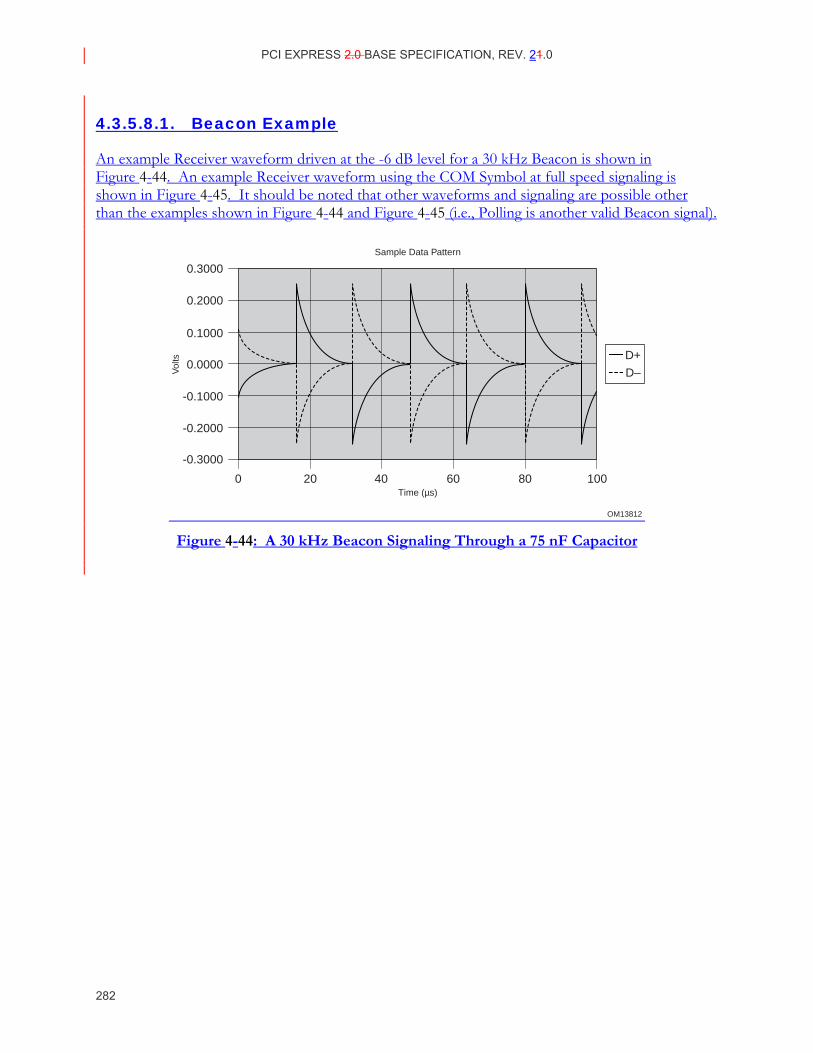
PCI EXPRESS 2.0 BASE SPECIFICATION, REV. 21.0
282
4.3.5.8.1. Beacon Example
An example Receiver waveform driven at the -6 dB level for a 30 kHz Beacon is shown in Figure 4-44. An example Receiver waveform using the COM Symbol at full speed signaling is shown in Figure 4-45. It should be noted that other waveforms and signaling are possible other than the examples shown in Figure 4-44 and Figure 4-45 (i.e., Polling is another valid Beacon signal).
OM13812
-0.3000
-0.2000
-0.1000
0.0000
0.1000
0.2000
0.3000
0 20 40 60 80 100
D+
D–
Time (µs)
Sample Data Pattern
Vol
ts
Figure 4-44: A 30 kHz Beacon Signaling Through a 75 nF Capacitor
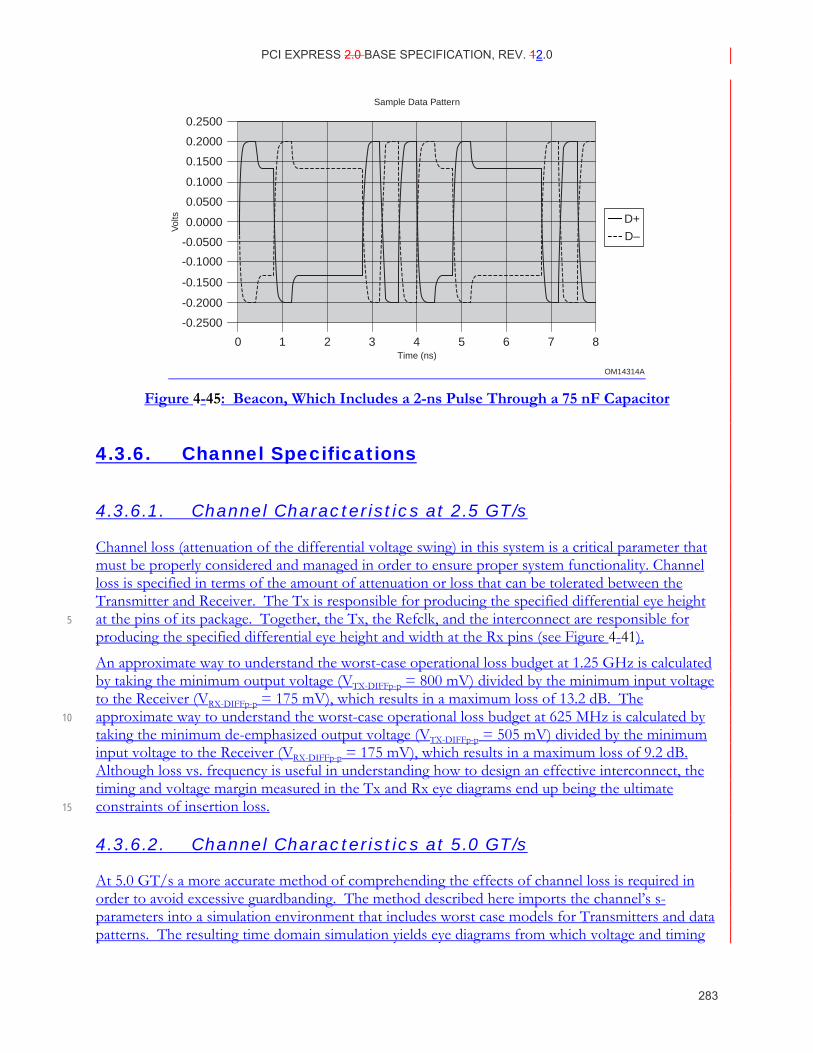
PCI EXPRESS 2.0 BASE SPECIFICATION, REV. 12.0
283
OM14314A
0.2500
-0.2500
-0.2000
-0.1500
-0.1000
-0.0500
0.0000
0.0500
0.1000
0.1500
0.2000
0 1 2 3 4 5 76 8
D+
D–
Time (ns)
Sample Data Pattern
Vol
ts
Figure 4-45: Beacon, Which Includes a 2-ns Pulse Through a 75 nF Capacitor
4.3.6. Channel Specifications
4.3.6.1. Channel Characteristics at 2.5 GT/s
Channel loss (attenuation of the differential voltage swing) in this system is a critical parameter that must be properly considered and managed in order to ensure proper system functionality. Channel loss is specified in terms of the amount of attenuation or loss that can be tolerated between the Transmitter and Receiver. The Tx is responsible for producing the specified differential eye height at the pins of its package. Together, the Tx, the Refclk, and the interconnect are responsible for 5 producing the specified differential eye height and width at the Rx pins (see Figure 4-41).
An approximate way to understand the worst-case operational loss budget at 1.25 GHz is calculated by taking the minimum output voltage (VTX-DIFFp-p = 800 mV) divided by the minimum input voltage to the Receiver (VRX-DIFFp-p = 175 mV), which results in a maximum loss of 13.2 dB. The approximate way to understand the worst-case operational loss budget at 625 MHz is calculated by 10 taking the minimum de-emphasized output voltage (VTX-DIFFp-p = 505 mV) divided by the minimum input voltage to the Receiver (VRX-DIFFp-p = 175 mV), which results in a maximum loss of 9.2 dB. Although loss vs. frequency is useful in understanding how to design an effective interconnect, the timing and voltage margin measured in the Tx and Rx eye diagrams end up being the ultimate constraints of insertion loss. 15
4.3.6.2. Channel Characteristics at 5.0 GT/s
At 5.0 GT/s a more accurate method of comprehending the effects of channel loss is required in order to avoid excessive guardbanding. The method described here imports the channel’s s-parameters into a simulation environment that includes worst case models for Transmitters and data patterns. The resulting time domain simulation yields eye diagrams from which voltage and timing
PCI EXPRESS 2.0 BASE SPECIFICATION, REV. 21.0
284
margins may be obtained and compared against those defined for the Receiver. Note: The methodology described in Sections 4.3.6.2 through 4.3.6.2.7 must be applied to 5.0 GT/s designs, and may be applied to 2.5 GT/s designs.
A channel's characteristics are completely defined by its s-parameters, in particular: insertion loss, return loss, and aggressor-victim coupling. It can been demonstrated that these parameters are 5 sufficient to completely quantize all channel-induced phenomena affecting eye margins including: I/O-channel impedance mismatch, insertion loss, jitter amplification, impedance discontinuities, and crosstalk. Long channels tend to be dominated by insertion loss and crosstalk, while short channels tend to dominated by impedance discontinuities. Since both types of channels are possible in PCI Express implementations, it is necessary provide a means of characterizing the channel that 10 comprehends all possible channel characteristics.
It is not, in general, possible to establish a straightforward correlation, easily expressed in graphical terms, between channel s-parameters and eye margins for all types of channels. For example plotting |s21| vs. frequency does not give useful correlations to eye margins for all possible channels. Instead it is necessary to convolve the channel's s-parameters with a worst case Transmitter 15 behavioral model and a worst case data pattern. The resulting time domain results, represented via an eye diagram, can then be compared against the VRX_EYE and TRX_EYE parameters defined in the Receiver specification. The following sections detail this procedure.
4.3.6.2.1. Procedure for Channel Measurement and Margin Extraction
A channel may be characterized to specification by means of the following procedure.
1. s-parameters for the channel under test are measured. These include insertion loss, return loss, 20 and (if applicable) crosstalk.
2. The s-parameters are imported into a simulation environment along with a reference load and a behavioral Transmitter model.
3. Worst case Transmitter corners and data patterns are driven through the channel model into a reference load. Then the resulting eye margins are post processed to account for Refclk and 25 Transmitter jitter effects that were not included in the simulation.
4. The resulting eye margins are compared to TRX_EYE and VRX_EYE in Table 4-12 to determine if the channel is within specification.
The following sections detail the four steps listed above.
4.3.6.2.2. Acquiring the Channel's s-parameters
Channel s-parameter data should be taken over the entirety of the 5.0 GT/s PCI Express signaling 30 spectral range which extends from approximately 250 MHz to 20 GHz or greater. Both near and far end return loss as well as forward and reverse insertion loss should be measured, since most simulation tools require a complete s-parameter representation.
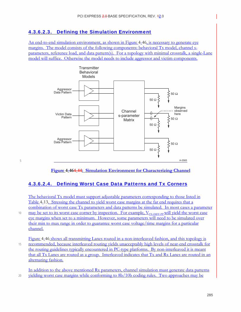
PCI EXPRESS 2.0 BASE SPECIFICATION, REV. 12.0
285
4.3.6.2.3. Defining the Simulation Environment
An end-to-end simulation environment, as shown in Figure 4-46, is necessary to generate eye margins. The model consists of the following components: behavioral Tx model, channel s-parameters, reference load, and data pattern(s). For a topology with minimal crosstalk, a single-Lane model will suffice. Otherwise the model needs to include aggressor and victim components.
A-0565
50
50
50
50
50
50
Channels-parameter
Matrix
AggressorData Pattern
Victim DataPattern
AggressorData Pattern
TransmitterBehavioral
Models
Marginsobservedhere
5
Figure 4-464-44: Simulation Environment for Characterizing Channel
4.3.6.2.4. Defining Worst Case Data Patterns and Tx Corners
The behavioral Tx model must support adjustable parameters corresponding to those listed in Table 4-13. Stressing the channel to yield worst case margins at the far end requires that a combination of worst case Tx parameters and data patterns be simulated. In most cases a parameter may be set to its worst case corner by inspection. For example, VTX-DIFF-PP will yield the worst case 10 eye margins when set to a minimum. However, some parameters will need to be simulated over their min to max range in order to guarantee worst case voltage/time margins for a particular channel.
Figure 4-46 shows all transmitting Lanes routed in a non-interleaved fashion, and this topology is recommended, because interleaved routing yields unacceptably high levels of near-end crosstalk for 15 the routing guidelines typically encountered in PC-type platforms. By non-interleaved it is meant that all Tx Lanes are routed as a group. Interleaved indicates that Tx and Rx Lanes are routed in an alternating fashion.
In addition to the above mentioned Rx parameters, channel simulation must generate data patterns yielding worst case margins while conforming to 8b/10b coding rules. Two approaches may be 20
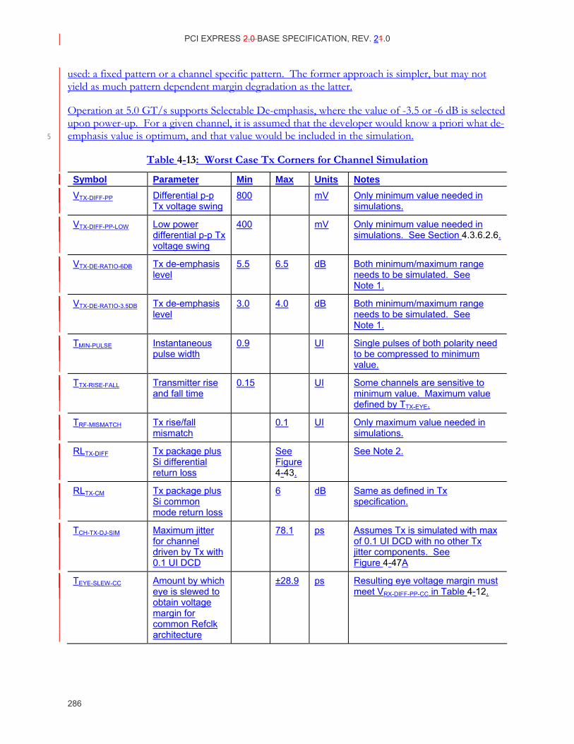
PCI EXPRESS 2.0 BASE SPECIFICATION, REV. 21.0
286
used: a fixed pattern or a channel specific pattern. The former approach is simpler, but may not yield as much pattern dependent margin degradation as the latter.
Operation at 5.0 GT/s supports Selectable De-emphasis, where the value of -3.5 or -6 dB is selected upon power-up. For a given channel, it is assumed that the developer would know a priori what de-emphasis value is optimum, and that value would be included in the simulation. 5
Table 4-13: Worst Case Tx Corners for Channel Simulation
Symbol Parameter Min Max Units Notes VTX-DIFF-PP Differential p-p
Tx voltage swing 800 mV Only minimum value needed in
simulations.
VTX-DIFF-PP-LOW Low power differential p-p Tx voltage swing
400 mV Only minimum value needed in simulations. See Section 4.3.6.2.6.
VTX-DE-RATIO-6DB Tx de-emphasis level
5.5 6.5 dB Both minimum/maximum range needs to be simulated. See Note 1.
VTX-DE-RATIO-3.5DB Tx de-emphasis level
3.0 4.0 dB Both minimum/maximum range needs to be simulated. See Note 1.
TMIN-PULSE Instantaneous pulse width
0.9 UI Single pulses of both polarity need to be compressed to minimum value.
TTX-RISE-FALL Transmitter rise and fall time
0.15 UI Some channels are sensitive to minimum value. Maximum value defined by TTX-EYE.
TRF-MISMATCH Tx rise/fall mismatch
0.1 UI Only maximum value needed in simulations.
RLTX-DIFF Tx package plus Si differential return loss
See Figure 4-43.
See Note 2.
RLTX-CM Tx package plus Si common mode return loss
6 dB Same as defined in Tx specification.
TCH-TX-DJ-SIM Maximum jitter for channel driven by Tx with 0.1 UI DCD
78.1 ps Assumes Tx is simulated with max of 0.1 UI DCD with no other Tx jitter components. See Figure 4-47A
TEYE-SLEW-CC Amount by which eye is slewed to obtain voltage margin for common Refclk architecture
±28.9 ps Resulting eye voltage margin must meet VRX-DIFF-PP-CC in Table 4-12.
PCI EXPRESS 2.0 BASE SPECIFICATION, REV. 12.0
287
Symbol Parameter Min Max Units Notes TEYE-SLEW-DC Amount by which
eye is slewed to obtain voltage margin for data clocked Rx architecture
±34.7 ps Resulting eye voltage margin must meet VRX-DIFF-PP-DC in Table 4-12.
Notes: 1. Two Tx de-emphasis ratios are defined to account for selectable Tx de-emphasis based on channel
characteristics. Usually the de-emphasis ratio is preset based on a priori knowledge of which value is optimum for the channel the Tx is driving, and that de-emphasis ratio is used to simulate the channel’s characteristics.
2. Typically a package is modeled as a combination of the Tx Si and the package interconnect, where the Si may be defined as a voltage or current source with a particular impedance driving a parasitic capacitance. The 5 package interconnect may be modeled as t-line elements. The combination of the above elements is then adjusted to yield one or more worst case impedance profiles that fit under the Tx return loss curves. Note that more than one package/Si model may be needed since it is not generally possible to synthesize a package/Si model that replicates the entire Tx return loss profile.
4.3.6.2.5. Accounting for Jitter When Characterizing the Channel
It is most convenient to simulate the channel without introducing low frequency jitter components 10 in either the Refclk or the Transmitter. These jitter components have been shown to propagate through the channel on a ps for ps basis. Pulse width compression, acting on single pulses sourced by the Transmitter, does need to be included in the simulation, since it interacts with the channel and produces so called jitter amplification. While they need not be included in the actual simulation, low frequency jitter components must be accounted for in the overall jitter budgeting process. This 15 will require that we deduct the worst case low frequency jitter components from the Refclk and the Transmitter from the simulated eye margins, before comparing against the Receiver eye parameters.
As mentioned above, the timing and voltage margins obtained when simulating the channel model need only include high frequency Tx jitter responsible for compressing a pulse to a minimum width. However, suitable post processing must be applied before we can compare the results against the Rx 20 jitter parameters:
1. Include the impact of non-simulated jitter > 1.5 MHz, but excluding DCD.
2. Determine the center of the eye in order to measure voltage and time margins.
Figure 4-47A illustrates the effect of simulating a channel with only DCD phase jitter included. The second step consists of replicating the effect that the non-simulated jitter components would have 25 on the eye, and this may be achieved by slewing the eye in the x-direction by an amount equal to ½ the Dj and Rj components that were not simulated. Note that since common Refclk Rx and data clocked Rx architectures specify different amounts of jitter, so the amount by which the simulated eye is slewed will differ. Once the composite eye has been generated the next step is to determine the eye center and obtain the eye voltage and time opening margins. Determining the eye center 30 may be achieved by using the filter function applied to the Receiver. Then the margins may be compared against the TRX-TJ-CC, TRX-TJ-DC and VRX-DIFF-PP-CC, VRX-DIFF-PP-DC, as appropriate for the common Refclk and the data clocked Rx architectures.
When simulating Tx jitter, we have assumed that the maximum amount of DCD (0.1 UI) is being applied. The difference between the maximum TTX-HF-DJ-DD (0.15 UI) and the above 0.1 UI 35
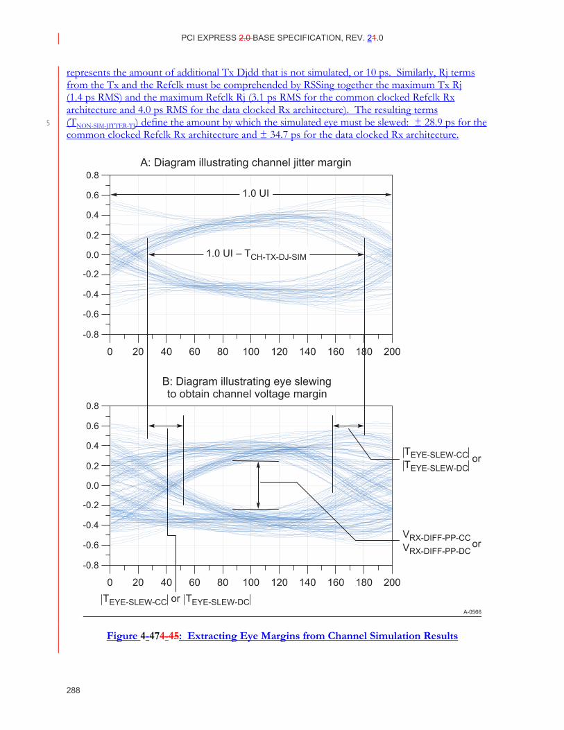
PCI EXPRESS 2.0 BASE SPECIFICATION, REV. 21.0
288
represents the amount of additional Tx Djdd that is not simulated, or 10 ps. Similarly, Rj terms from the Tx and the Refclk must be comprehended by RSSing together the maximum Tx Rj (1.4 ps RMS) and the maximum Refclk Rj (3.1 ps RMS for the common clocked Refclk Rx architecture and 4.0 ps RMS for the data clocked Rx architecture). The resulting terms (TNON-SIM-JITTER-TJ) define the amount by which the simulated eye must be slewed: ± 28.9 ps for the 5 common clocked Refclk Rx architecture and ± 34.7 ps for the data clocked Rx architecture.
0.8
0.6
0.4
0.2
0.0
-0.2
-0.4
-0.6
-0.8
0 20 40 60 80 100 120 140 160 180 200
A-0566
0.8
0.6
0.4
0.2
0.0
-0.2
-0.4
-0.6
-0.8
0 20 40 60 80 100
A: Diagram illustrating channel jitter margin
B: Diagram illustrating eye slewingto obtain channel voltage margin
120 140 160 180 200
VRX-DIFF-PP-CCVRX-DIFF-PP-DC
1.0 UI – TCH-TX-DJ-SIM
1.0 UI
TEYE-SLEW-CCTEYE-SLEW-DC
TEYE-SLEW-CC or TEYE-SLEW-DC
or
or
Figure 4-474-45: Extracting Eye Margins from Channel Simulation Results
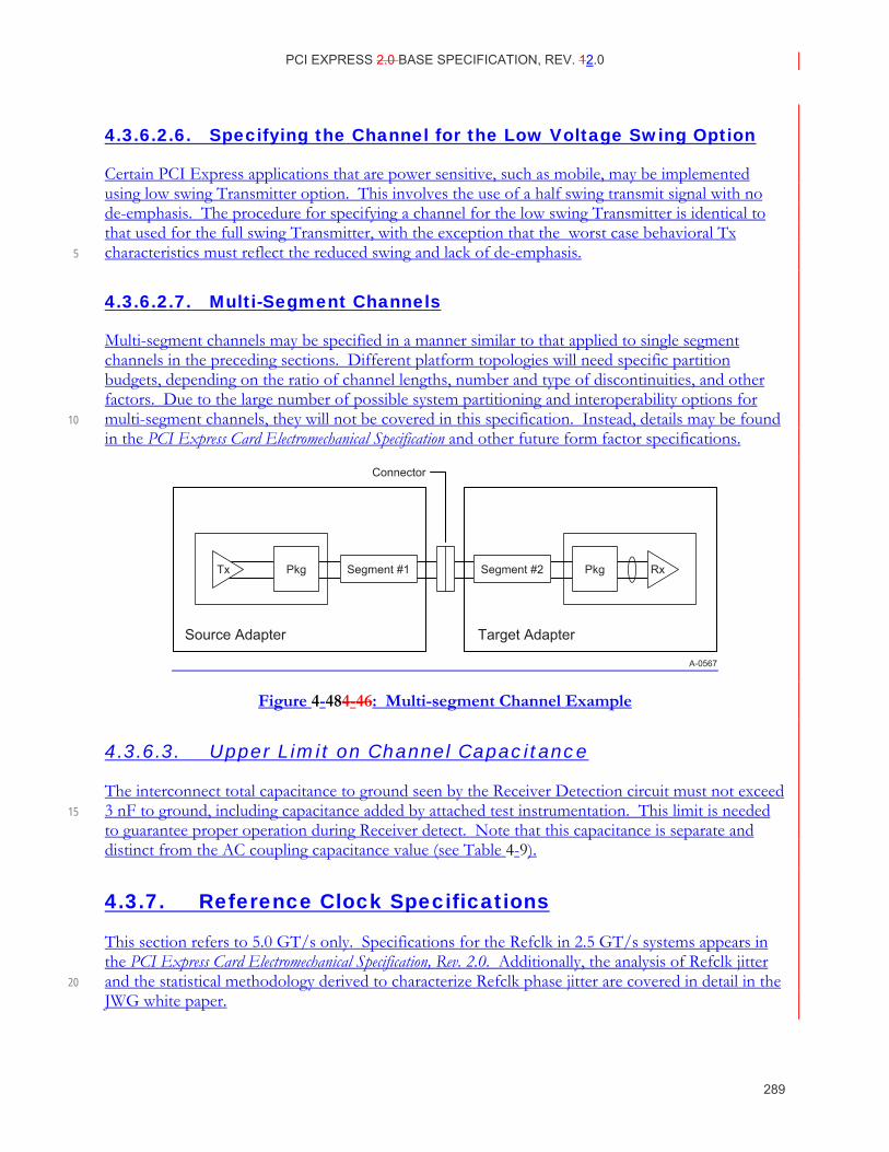
PCI EXPRESS 2.0 BASE SPECIFICATION, REV. 12.0
289
4.3.6.2.6. Specifying the Channel for the Low Voltage Swing Option
Certain PCI Express applications that are power sensitive, such as mobile, may be implemented using low swing Transmitter option. This involves the use of a half swing transmit signal with no de-emphasis. The procedure for specifying a channel for the low swing Transmitter is identical to that used for the full swing Transmitter, with the exception that the worst case behavioral Tx characteristics must reflect the reduced swing and lack of de-emphasis. 5
4.3.6.2.7. Multi-Segment Channels
Multi-segment channels may be specified in a manner similar to that applied to single segment channels in the preceding sections. Different platform topologies will need specific partition budgets, depending on the ratio of channel lengths, number and type of discontinuities, and other factors. Due to the large number of possible system partitioning and interoperability options for multi-segment channels, they will not be covered in this specification. Instead, details may be found 10 in the PCI Express Card Electromechanical Specification and other future form factor specifications.
A-0567
Pkg PkgSegment #1 Segment #2Tx Rx
Source Adapter Target Adapter
Connector
Figure 4-484-46: Multi-segment Channel Example
4.3.6.3. Upper Limit on Channel Capacitance
The interconnect total capacitance to ground seen by the Receiver Detection circuit must not exceed 3 nF to ground, including capacitance added by attached test instrumentation. This limit is needed 15 to guarantee proper operation during Receiver detect. Note that this capacitance is separate and distinct from the AC coupling capacitance value (see Table 4-9).
4.3.7. Reference Clock Specifications
This section refers to 5.0 GT/s only. Specifications for the Refclk in 2.5 GT/s systems appears in the PCI Express Card Electromechanical Specification, Rev. 2.0. Additionally, the analysis of Refclk jitter and the statistical methodology derived to characterize Refclk phase jitter are covered in detail in the 20 JWG white paper.
PCI EXPRESS 2.0 BASE SPECIFICATION, REV. 21.0
290
PCI Express Base Specification, Rev. 1.1 did not include Refclk parameters; instead, parameters for Refclk were defined in PCI Express Card Electromechanical Specification, Rev. 1.1. While developing the 5.0 GT/s specification, it became obvious that it made sense to include the Refclk as part of the electrical specification, and so it is included in this specification.
4.3.7.1. Spread Spectrum Clock (SSC) Sources
The data rate may be modulated from +0% to -0.5% of the nominal data rate frequency, at a 5 modulation rate in the range not exceeding 30 kHz – 33 kHz. The ±300 ppm requirement still holds, which requires the two communicating Ports be modulated such that they never exceed a total of 600 ppm difference. For most implementations this places the requirement that both Ports require the same bit rate clock source when the data is modulated with an SSC.
4.3.7.2. Refclk Architectures
Three distinct Refclk architectures are possible: common Refclk, separate Refclks, and data driving 10 PLL. Each has an associated filter function that comprehends the worst case combination of PLL bandwidth/peaking and equivalent jitter. The effective jitter seen at the Rx’s clock-data recovery inputs is a function of the difference in Rx and. Tx PLL bandwidth and peaking convolved with the jitter spectrum of the Refclk. It is also dependent on the Refclk architecture.
4.3.7.2.1. Filtering Functions Applied to Refclk Measurements
Raw Refclk data contains jitter over a wide range of frequencies, some of which will be tracked by 15 the Receiver or otherwise removed by the combination of the Tx and Rx PLLs. Consequently, it is necessary to apply a series of filter operations to raw Refclk data in order to obtain meaningful jitter measurements. The nature of the filter functions is in part dependent on the Refclk architecture. For example, the PLL functions for common Refclk Rx and data clocked Rx architectures are different and therefore yield differing amounts of HF Rj. Table 4-14 lists the filter functions for 20 common clocked and data clocked Rx architectures. In general, there are five different filter functions applied:
SSC separation: Used to remove SSC components from the low frequency range allowing one to define separate low frequency Rj and low frequency Dj components
0.01 – 1.5 MHz step BPF: Lower edge of filter removes 1/f jitter contributions that are 25 completely trackable by CDR. This function also removes high frequency jitter components.
1.5 MHz step HPF: Removes low frequency jitter components, allowing one to define those jitter components not trackable by CDR.
Edge filtering: Minimizes test equipment measurement artifacts caused by finite sampling/voltage resolution aperture. This is a voltage averaging process that is applied at a 30 frequency of 5 GHz.
PLL difference function or Max PLL BW function. The first is applied to the common clocked Refclk Rx architecture and comprehends worst case mismatch between Tx and Rx PLLs and

PCI EXPRESS 2.0 BASE SPECIFICATION, REV. 12.0
291
impact of transport delay. The second is applied to data clocked Rx architecture and comprehends maximum PLL BW and peaking.
Table 4-14: Filtering Functions Applied to Refclk Measurements
Refclk Architecture Common Refclk Rx Data Clocked Rx < 1.5 MHz jitter components SSC separation
PLL difference function - 1.5 MHZ step BPF
No SSC separation Max PLL BW fcn 0.01 - 1.5 MHz step BPF
> 1.5 MHz jitter components PLL difference function 1.5 MHz step HPF Edge filtering
Max PLL BW fcn 1.5 MHz step HPF Edge filtering
Implementation details for the PLL difference and maximum PLL functions are described in the sections relating to common Refclk Rx and data clocked Rx architectures that follow. The 1.5 MHz HPF and 0.01 – 1.5 MHz BPF characteristics are described in Figure 4-21. 5
4.3.7.2.2. Common Refclk Rx Architecture
This architecture implies that a single Refclk source is distributed to the Tx and Rx. As a consequence, much of the SSC jitter sourced by the Refclk is propagated equally through Tx and Rx PLLs, and so intrinsically tracks. Figure 4-49 illustrates the common Refclk Rx architecture, showing key noise, delay, and PLL transform sources. Since Refclk is common to both Tx and Rx, its noise characteristic, X1(s) is driven to both Tx and Rx PLLs. The amount of jitter appearing at 10 the CDR is then defined by the difference function between the Tx and Rx PLLs, HCC(s).
A-0568
Tx Latch Rx LatchChannel
Rx PLLTx PLLH1(s)X1(s) X1(s)
H2(s)
CDR
Refclk
T1 = Transport Delay Delta
Figure 4-494-47: Common Refclk Rx Architecture
Based on the above clock architecture, it is possible to define a difference function that corresponds to the worst case mismatch between Tx and Rx PLLs. Second order transfer functions are assumed, even though most PLL transfer functions are 3rd order or higher, since 2nd order functions tend to 15 yield a slightly conservative difference function vis-a-vis an actual PLL.
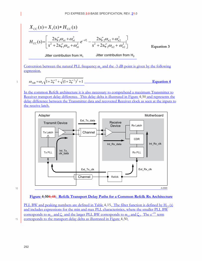
PCI EXPRESS 2.0 BASE SPECIFICATION, REV. 21.0
292
)()()( 1 sHsXsX CCCC ∗=
⎥⎦
⎤⎢⎣
⎡++
+−
+++
= −2222
2
2222
2111
2
2111
22
22)( 1
nn
nnsT
nn
nnCC ss
sess
ssHωωζ
ωωζωωζ
ωωζ
Jitter contribution from H1 Jitter contribution from H2
Conversion between the natural PLL frequency ωn and the -3 dB point is given by the following expression.
1)21(21 2223 ++++= ζζωω ndB Equation 4 5
In the common Refclk architecture it is also necessary to comprehend a maximum Transmitter to Receiver transport delay difference. This delay delta is illustrated in Figure 4-50 and represents the delay difference between the Transmitter data and recovered Receiver clock as seen at the inputs to the receive latch.
Motherboard
A-0569
Tx Latch Channel
Rx PLLTx PLL
Refclk
CDR
Rx Latch
Channel
Transmit Device ReceiveDevice
Adapter
Int_Tx_clk_data
Ext_Tx_clk Ext_Rx_clk
Ext_Tx_data
Int_Rx_data Int_Rx_clk
10
Figure 4-504-48: Refclk Transport Delay Paths for a Common Refclk Rx Architecture
PLL BW and peaking numbers are defined in Table 4-15. The filter function is defined by HCC(s) and includes expressions for the min and max PLL characteristics, where the smaller PLL BW corresponds to ωn1 and ζ1 and the larger PLL BW corresponds to ωn2 and ζ2. The e-sT1 term corresponds to the transport delay delta as illustrated in Figure 4-50. 15
Equation 3
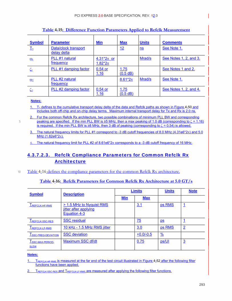
PCI EXPRESS 2.0 BASE SPECIFICATION, REV. 12.0
293
Table 4-15: Difference Function Parameters Applied to Refclk Measurement
Symbol Parameter Min Max Units Comments T1 Data/clock transport
delay delta 12 ns See Note 1.
ω1 PLL #1 natural frequency
4.31*2π or 1.82*2π
Mrad/s See Notes 1, 2, and 3.
ζ1 PLL #1 damping factor 0.54 or 1.16
1.75 (0.5 dB)
See Notes 1 and 2.
ω2 PLL #2 natural frequency
8.61*2π Mrad/s See Note 1.
ζ2 PLL #2 damping factor 0.54 or 1.16
1.75 (0.5 dB)
See Notes 1, 2, and 4.
Notes:
1. T1 defines to the cumulative transport delay delta of the data and Refclk paths as shown in Figure 4-50 and includes both off-chip and on-chip delay terms. Maximum internal transport delay for Tx and Rx is 2.0 ns.
2. For the common Refclk Rx architecture, two possible combinations of minimum PLL BW and corresponding peaking are specified. If the min PLL BW is ≥5 MHz, then a max peaking of 1.0 dB (corresponding to ζ = 1.16) 5 is required. If the min PLL BW is ≥8 MHz, then 3 dB of peaking (corresponding to ζ = 0.54) is allowed.
3. The natural frequency limits for PLL #1 correspond to -3 dB cutoff frequencies of 8.0 MHz (4.31e6*2π) and 5.0 MHz (1.82e6*2π).
4. The natural frequency limit for PLL #2 of 8.61e6*2π corresponds to a -3 dB cutoff frequency of 16 MHz.
4.3.7.2.3. Refclk Compliance Parameters for Common Refclk Rx Architecture
Table 4-16 defines the compliance parameters for the common Refclk Rx architecture. 10
Table 4-16: Refclk Parameters for Common Refclk Rx Architecture at 5.0 GT/s
Limits Units Note Symbol Description
Min Max
TREFCLK-HF-RMS > 1.5 MHz to Nyquist RMS jitter after applying Equation 4-3
3.1 ps RMS 1
TREFCLK-SSC-RES SSC residual 75 ps 1
TREFCLK-LF-RMS 10 kHz - 1.5 MHz RMS jitter 3.0 ps RMS 2
TSSC-FREQ-DEVIATION SSC deviation +0.0/-0.5 %
TSSC-MAX-PERIOD-
SLEW Maximum SSC df/dt 0.75 ps/UI 3
Notes:
1. TREFCLK-HF-RMS is measured at the far end of the test circuit illustrated in Figure 4-52 after the following filter functions have been applied.
2. TREFCLK-SSC-RES and TREFCLK-LF-RMS are measured after applying the following filter functions.
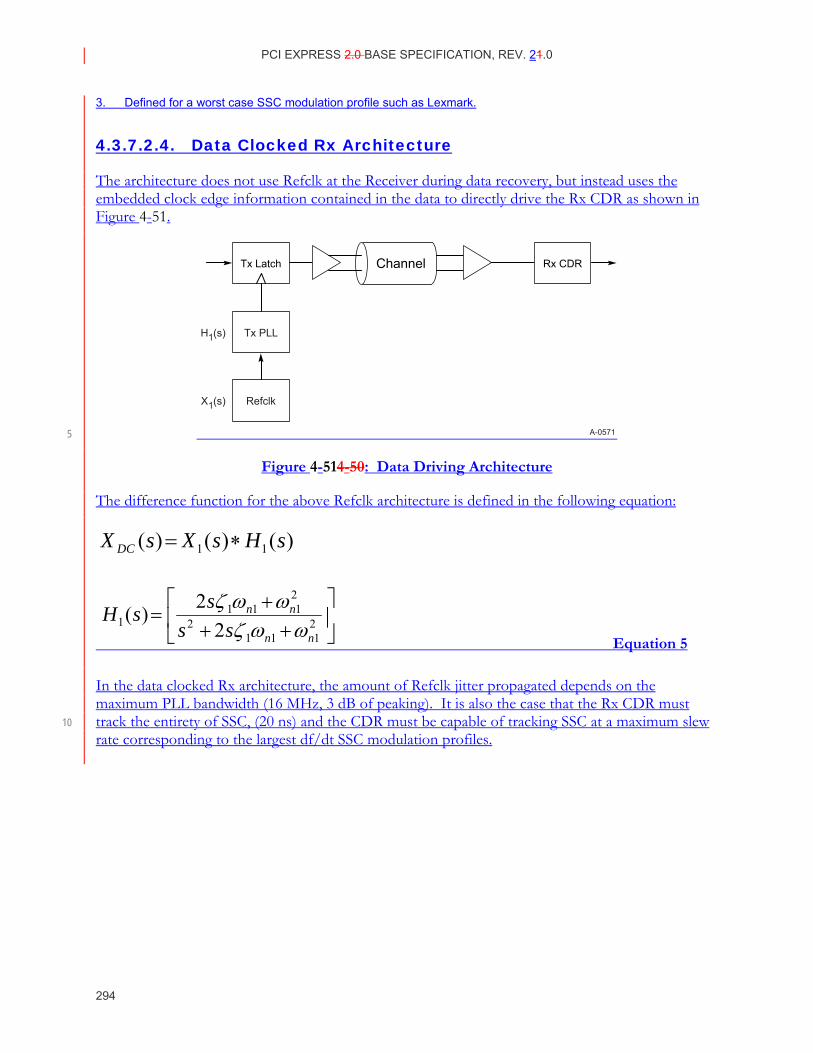
PCI EXPRESS 2.0 BASE SPECIFICATION, REV. 21.0
294
3. Defined for a worst case SSC modulation profile such as Lexmark.
4.3.7.2.4. Data Clocked Rx Architecture
The architecture does not use Refclk at the Receiver during data recovery, but instead uses the embedded clock edge information contained in the data to directly drive the Rx CDR as shown in Figure 4-51.
A-0571
Tx Latch Rx CDRChannel
RefclkX1(s)
Tx PLLH1(s)
5
Figure 4-514-50: Data Driving Architecture
The difference function for the above Refclk architecture is defined in the following equation:
)()()( 11 sHsXsX DC ∗=
⎥⎦
⎤⎢⎣
⎡++
+= 2
1112
2111
1 22)(
nn
nn
ssssH
ωωζωωζ
Equation 5
In the data clocked Rx architecture, the amount of Refclk jitter propagated depends on the maximum PLL bandwidth (16 MHz, 3 dB of peaking). It is also the case that the Rx CDR must track the entirety of SSC, (20 ns) and the CDR must be capable of tracking SSC at a maximum slew 10 rate corresponding to the largest df/dt SSC modulation profiles.
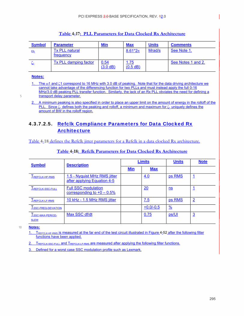
PCI EXPRESS 2.0 BASE SPECIFICATION, REV. 12.0
295
Table 4-17: PLL Parameters for Data Clocked Rx Architecture
Symbol Parameter Min Max Units Comments ω1 Tx PLL natural
frequency 8.61*2π Mrad/s See Note 1.
ζ1 Tx PLL damping factor 0.54 (3.0 dB)
1.75 (0.5 dB)
See Notes 1 and 2.
Notes: 1. The ω1 and ζ1 correspond to 16 MHz with 3.0 dB of peaking. Note that for the data driving architecture we
cannot take advantage of the differencing function for two PLLs and must instead apply the full 0-16 MHz/3.0 dB peaking PLL transfer function. Similarly, the lack of an Rx PLL obviates the need for defining a transport delay parameter. 5
2. A minimum peaking is also specified in order to place an upper limit on the amount of energy in the rolloff of the PLL. Since ζ1 defines both the peaking and rolloff, a minimum and maximum for ζ1 uniquely defines the amount of BW in the rolloff region.
4.3.7.2.5. Refclk Compliance Parameters for Data Clocked Rx Architecture
Table 4-18 defines the Refclk jitter parameters for a Refclk in a data clocked Rx architecture.
Table 4-18: Refclk Parameters for Data Clocked Rx Architecture
Limits Units Note Symbol Description
Min Max
TREFCLK-HF-RMS 1.5 - Nyquist MHz RMS jitter after applying Equation 4-5
4.0 ps RMS 1
TREFCLK-SSC-FULL Full SSC modulation corresponding to +0 – 0.5%
20 ns 1
TREFCLK-LF-RMS 10 kHz - 1.5 MHz RMS jitter 7.5 ps RMS 2
TSSC-FREQ-DEVIATION +0.0/-0.5 %
TSSC-MAX-PERIOD-
SLEW Max SSC df/dt 0.75 ps/UI 3
Notes: 10 1. TREFCLK-HF-RMS is measured at the far end of the test circuit illustrated in Figure 4-52 after the following filter
functions have been applied.
2. TREFCLK-SSC-FULL and TREFCLK-LF-RMS are measured after applying the following filter functions.
3. Defined for a worst case SSC modulation profile such as Lexmark.
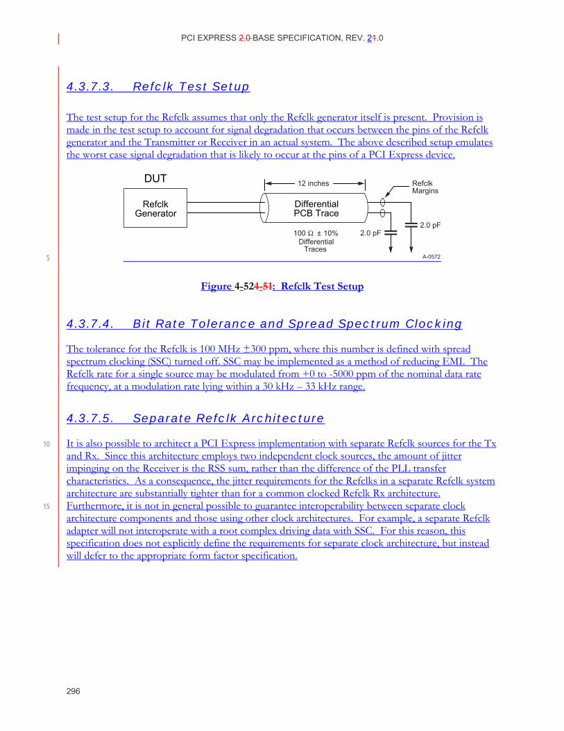
PCI EXPRESS 2.0 BASE SPECIFICATION, REV. 21.0
296
4.3.7.3. Refclk Test Setup
The test setup for the Refclk assumes that only the Refclk generator itself is present. Provision is made in the test setup to account for signal degradation that occurs between the pins of the Refclk generator and the Transmitter or Receiver in an actual system. The above described setup emulates the worst case signal degradation that is likely to occur at the pins of a PCI Express device.
A-0572
DifferentialPCB Trace
2.0 pF2.0 pF
RefclkGenerator
DUT 12 inches
100 ± 10% Differential
Traces
RefclkMargins
5
Figure 4-524-51: Refclk Test Setup
4.3.7.4. Bit Rate Tolerance and Spread Spectrum Clocking
The tolerance for the Refclk is 100 MHz ±300 ppm, where this number is defined with spread spectrum clocking (SSC) turned off. SSC may be implemented as a method of reducing EMI. The Refclk rate for a single source may be modulated from +0 to -5000 ppm of the nominal data rate frequency, at a modulation rate lying within a 30 kHz – 33 kHz range.
4.3.7.5. Separate Refclk Architecture
It is also possible to architect a PCI Express implementation with separate Refclk sources for the Tx 10 and Rx. Since this architecture employs two independent clock sources, the amount of jitter impinging on the Receiver is the RSS sum, rather than the difference of the PLL transfer characteristics. As a consequence, the jitter requirements for the Refclks in a separate Refclk system architecture are substantially tighter than for a common clocked Refclk Rx architecture. Furthermore, it is not in general possible to guarantee interoperability between separate clock 15 architecture components and those using other clock architectures. For example, a separate Refclk adapter will not interoperate with a root complex driving data with SSC. For this reason, this specification does not explicitly define the requirements for separate clock architecture, but instead will defer to the appropriate form factor specification.
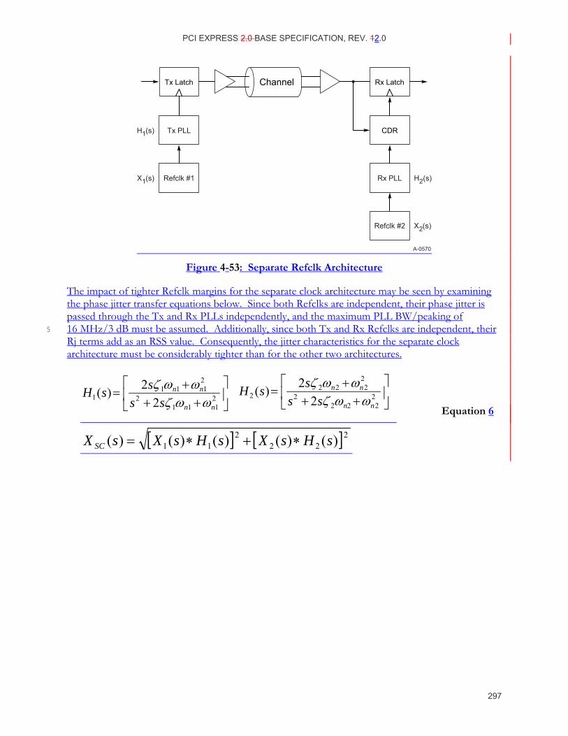
PCI EXPRESS 2.0 BASE SPECIFICATION, REV. 12.0
297
A-0570
Tx Latch Rx LatchChannel
Rx PLLRefclk #1X1(s) H2(s)
Refclk #2 X2(s)
CDRTx PLLH1(s)
Figure 4-53: Separate Refclk Architecture
The impact of tighter Refclk margins for the separate clock architecture may be seen by examining the phase jitter transfer equations below. Since both Refclks are independent, their phase jitter is passed through the Tx and Rx PLLs independently, and the maximum PLL BW/peaking of 16 MHz/3 dB must be assumed. Additionally, since both Tx and Rx Refclks are independent, their 5 Rj terms add as an RSS value. Consequently, the jitter characteristics for the separate clock architecture must be considerably tighter than for the other two architectures.
⎥ ⎦
⎤ ⎢ ⎣
⎡
+ + +
= 2 1 1 1
2 2 1 1 1
1 2 2 ) (
n n n n
s s s s H
ω ω ζω ω ζ
⎥⎦
⎤⎢⎣
⎡++
+= 2
2222
2222
2 22)(
nn
nn
ssssH
ωωζωωζ
[ ] [ ]2
222
11 )()()()()( sHsXsHsXsX SC ∗+∗=
Equation 6
PCI EXPRESS 2.0 BASE SPECIFICATION, REV. 21.0
298
4.2.Electrical Sub-block The electrical sub-block contains a Transmitter and a Receiver. The Transmitter is supplied by the logical sub-block with Symbols which it serializes and transmits onto a Lane. The Receiver is supplied with serialized Symbols from the Lane. It transforms the electrical signals into a bit stream which is de-serialized and supplied to the logical sub-block along with a Link clock recovered from the incoming serial stream. 5
4.2.8.Electrical Sub-Block Requirements
4.2.8.0.Clocking Dependencies
The Ports on the two ends of a Link must transmit data at a rate that is within 600 parts per million (ppm) of each other at all times. This is specified to allow bit rate clock sources with a +/- 300 ppm tolerance.
4.2.8.0.0.Spread Spectrum Clock (SSC) Sources
The data rate can be modulated from +0% to -0.5% of the nominal data rate frequency, at a modulation rate in the range not exceeding 30 kHz – 33 kHz. The +/- 300 ppm requirement still 10 holds, which requires the two communicating Ports be modulated such that they never exceed a total of 600 ppm difference. For most implementations this places the requirement that both Ports require the same bit rate clock source when the data is modulated with an SSC.
4.2.8.0.AC Coupling
Each Lane of a Link must be AC coupled. The minimum and maximum value for the capacitance is given in Table 4-5. The requirement for the inclusion of AC coupling capacitors on the 15 interconnect media is specified at the Transmitter.
4.2.8.0.Interconnect
In the context of this specification, the interconnect comprises everything between the pins at of a Transmitter package and the pins of a Receiver package. Often, this will consist of traces on a printed circuit board or other suitable medium, AC coupling capacitors and perhaps connectors. The interconnect total capacitance to ground seen by the Receiver Detection circuit (see 20 Section 4.3.1.8) must not exceed 3 nF, including capacitance added by attached test instrumentation. Note that this capacitance is separate and distinct from the AC Coupling capacitance value (see Section 4.3.1.2).
PCI EXPRESS 2.0 BASE SPECIFICATION, REV. 12.0
299
4.2.8.0.Termination
The Transmitter is required to meet RLTX-DIFF, RLTX-CM, and ZTX-DIFF-DC (see Table 4-5) any time functional differential signals are being transmitted.
The Transmitter is required only to meet ITX-SHORT (see Table 4-5) any time functional differential signals are not being transmitted.
•Note: The differential impedance during this same time is not defined. 5
The Receiver is required to meet RLRX-DIFF, RLRX-CM, ZRX-DIFF-DC, and ZRX-DC (see Table 4-6) during all LTSSM states excluding only times during when the device is powered down, Fundamental Reset is asserted, or when explicitly specified.
The Receiver is required to meet ZRX-HIGH-IMP-DC (see Table 4-6) any time adequate power is not provided to the Receiver, Fundamental Reset is asserted (see Section 4.2.4.5.1), or when 10 explicitly specified.
•Note: The Receiver differential impedance is not defined.
4.2.8.0.DC Common Mode Voltage
The Receiver DC common mode voltage is nominally 0 V during all states.
The Transmitter DC common mode voltage is held at the same value during all states unless otherwise specified. The range of allowed Transmitter DC common mode values is specified in 15 Table 4-5 (VTX-DC-CM).
4.2.8.0.ESD
All signal and power pins must withstand 2000 V of ESD using the human body model and 500 V using the charged device model without damage. Class 2 per JEDEC JESE22-A114-A.
This ESD protection mechanism also helps protect the powered down Receiver from potential common mode transients during certain possible reset or surprise insertion situations. 20
4.2.8.0.Short Circuit Requirements
All Transmitters and Receivers must support surprise hot insertion/removal without damage to the component. The Transmitter and Receiver must be capable of withstanding sustained short circuit to ground of D+ and D-. The Transmitter short circuit current limit ITX-SHORT is provided in Table 4-5.
PCI EXPRESS 2.0 BASE SPECIFICATION, REV. 21.0
300
4.2.8.0.Receiver Detection
The Receiver Detection circuit is performed by a Transmitter and must correctly detect whether a load impedance of ZRX-DC or lower is present.
The recommended behavior of the Receiver Detection sequence is described below.
Step 0.A Transmitter must start at a stable voltage prior to the detect common mode shift. This voltage can be VDD, GND, or some other stable common-mode voltage between VDD 5 and GND.
Step 0.A Transmitter changes the common mode voltage on D+ and D- to a different value.
.If the common-mode voltage is equal to VDD, the change must be towards GND.
.If the common-mode voltage is equal to GND, the change must be towards VDD.
.If the common-mode is set to a stable value between VDD and GND, the direction that 10 the voltage moved to get to this stable initial Electrical Idle voltage is important and the detect common mode shift must be in the opposite direction.
Step 0.A Receiver is detected based on the rate that the lines change to the new voltage.
.The Receiver is not present if the voltage at the Transmitter charges at a rate dictated only by the Transmitter impedance and the capacitance of the interconnect and series 15 capacitor.
.The Receiver is present if the voltage at the Transmitter charges at a rate dictated by the Transmitter impedance, the series capacitor, the interconnect capacitance, and the Receiver termination.
Any time Electrical Idle is exited the detect sequence does not have to execute or can be aborted on 20 that Lane.
PCI EXPRESS 2.0 BASE SPECIFICATION, REV. 12.0
301
IMPLEMENTATION NOTE
Differential Receiver Detect If an implementation chooses to transition from Detect to Polling based on electrical idle being broken prior to performing a receiver detect sequence, an unreliable link could be formed; due to the possibility that there may not be a low impedance termination resistor on both Rx differential conductors, which make up the differential pair.
If the Receiver Detection circuit performs the detect sequence on each conductor of the differential 5 pair (both D+ and D-) and detects a load impedance greater than ZRX-DC on either conductor, the Receiver Detection circuit shall interpret this as no termination load present and respond as if neither load was present.
In this revision of this specification, it is not required that the detect sequence be performed on both conductors of a differential pair. 10
Future revisions of this specification may require the successful detection of a low impedance termination resistor on both differential pairs prior to transitioning to Polling.
4.2.8.0.Electrical Idle
Electrical Idle is a steady state condition where the Transmitter D+ and D- voltages are held constant at the same value. Electrical Idle is primarily used in power saving and inactive states (i.e., Disable). 15
Before a Transmitter enters Electrical Idle, it must always send the Electrical Idle ordered set, a K28.5 (COM) followed by three K28.3 (IDL) (see Table 4-5), unless otherwise specified. After sending the last Symbol of the Electrical Idle ordered set, the Transmitter must be in a valid Electrical Idle state as specified by TTX-IDLE-SET-TO-IDLE (see Table 4-5).
The successful reception of an Electrical Idle ordered set occurs upon the receipt of two out of the 20 three K28.3 (IDL) characters in the transmitted Electrical Idle ordered set.
The low impedance common mode and differential Receiver terminations values (see Section 4.3.1.4) must be met in Electrical Idle. The Transmitter can be in either a low or high impedance mode during Electrical Idle.
Any time a Transmitter enters Electrical Idle it must remain in Electrical Idle for a minimum of 25 TTX-IDLE-MIN (see Table 4-5). The Receiver should expect the Electrical Idle ordered set followed by a minimum amount of time (TTX-IDLE-MIN) in Electrical Idle to enable its Electrical Idle Exit detector (see Table 4-5).
When the Transmitter transitions from Electrical Idle to a valid differential signal level it must meet the output return loss specifications in Table 4-5 and transition from zero differential to full 30 differential voltage consistent with the requirements of the Transmitter Compliance Eye Diagram of Figure 4-24 after the allotted debounce time of TTX-IDLE-TO-DIFF-DATA (see Table 4-5).
PCI EXPRESS 2.0 BASE SPECIFICATION, REV. 21.0
302
Electrical Idle Exit shall not occur if a signal smaller than VRX-IDLE-DET-DIFFp-p minimum is detected at a Receiver. Electrical Idle Exit shall occur if a signal larger than VRX-IDLE-DET-DIFFp-p maximum is detected at a Receiver.
4.2.8.Electrical Signal Specifications
A differential signal is defined by taking the voltage difference between two conductors. In this specification, a differential signal or differential pair is comprised of a voltage on a positive 5 conductor, VD+, and a negative conductor, VD-. The differential voltage (VDIFF) is defined as the difference of the positive conductor voltage and the negative conductor voltage (VDIFF = VD+ - VD-). The Common Mode Voltage (VCM) is defined as the average or mean voltage present on the same differential pair (VCM = [VD+ + VD-]/2). This document’s electrical specifications often refer to peak-to-peak measurements or peak measurements, which are defined by the following equations. 10
VDIFFp-p = (2*max|VD+ - VD-|) (This applies to a symmetric differential swing.)
VDIFFp-p = (max|VD+ - VD-| VD+ > VD- + max|VD+ - VD-| VD+ < VD-) (This applies to an asymmetric differential swing.)
VDIFFp = (max|VD+ - VD-|) (This applies to a symmetric differential swing.)
VDIFFp = (max|VD+ - VD-| VD+ > VD-) or (max|VD+ - VD-| VD+ < VD-) whichever is greater 15 (This applies to an asymmetric differential swing.)
VCMp = (max|VD+ + VD-|/2)
Note: The maximum value is calculated on a per unit interval evaluation. The maximum function as described is implicit for all peak-to-peak and peak equations throughout the rest of this chapter, and thus a maximum function will not appear in any following subsequent representations of these 20 equations.
In this section, DC is defined as all frequency components below Fdc = 30 kHz. AC is defined as all frequency components at or above Fdc = 30 kHz. These definitions pertain to all voltage and current specifications.
An example waveform is shown in Figure 4-20. In this waveform the differential peak-peak signal is 25 approximately 0.6 V, the differential peak signal is approximately 0.3 V and the common mode voltage is approximately 0.25 V.
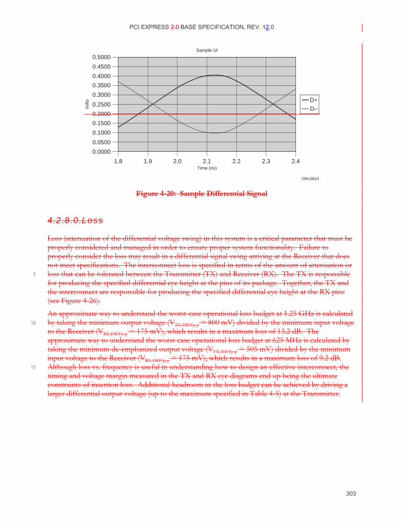
PCI EXPRESS 2.0 BASE SPECIFICATION, REV. 12.0
303
OM13810
0.5000
0.0000
0.0500
0.1000
0.1500
0.2000
0.2500
0.3000
0.3500
0.4000
0.4500
1.8 1.9 2.0 2.1 2.2 2.3 2.4
D+
D–
Time (ns)
Sample UI
Vol
ts
Figure 4-20: Sample Differential Signal
4.2.8.0.Loss
Loss (attenuation of the differential voltage swing) in this system is a critical parameter that must be properly considered and managed in order to ensure proper system functionality. Failure to properly consider the loss may result in a differential signal swing arriving at the Receiver that does not meet specifications. The interconnect loss is specified in terms of the amount of attenuation or loss that can be tolerated between the Transmitter (TX) and Receiver (RX). The TX is responsible 5 for producing the specified differential eye height at the pins of its package. Together, the TX and the interconnect are responsible for producing the specified differential eye height at the RX pins (see Figure 4-26).
An approximate way to understand the worst-case operational loss budget at 1.25 GHz is calculated by taking the minimum output voltage (VTX-DIFFp-p = 800 mV) divided by the minimum input voltage 10 to the Receiver (VRX-DIFFp-p = 175 mV), which results in a maximum loss of 13.2 dB. The approximate way to understand the worst-case operational loss budget at 625 MHz is calculated by taking the minimum de-emphasized output voltage (VTX-DIFFp-p = 505 mV) divided by the minimum input voltage to the Receiver (VRX-DIFFp-p = 175 mV), which results in a maximum loss of 9.2 dB. Although loss vs. frequency is useful in understanding how to design an effective interconnect, the 15 timing and voltage margin measured in the TX and RX eye diagrams end up being the ultimate constraints of insertion loss. Additional headroom in the loss budget can be achieved by driving a larger differential output voltage (up to the maximum specified in Table 4-5) at the Transmitter.
PCI EXPRESS 2.0 BASE SPECIFICATION, REV. 21.0
304
4.2.8.0.Jitter and BER
Jitter is categorized into random sources (Rj) and deterministic sources (Dj). The total jitter (Tj) is the convolution of the probability density functions for all the independent jitter sources, Rj and Dj. The nature of Rj can be approximated as Gaussian and is used to establish the bit error rate (BER) of the Link.
The UI allocation is given as the allowable Tj at the target BER. The UI allocation must meet a 5 maximum BER of 10-12 for the Tj. The allocation to Rj and Dj is not specified.
The methods for measuring the BER compliance are beyond the scope of this specification.
4.2.8.0.De-emphasis
De-emphasis is included (i.e., Generation 1 fundamental band = 250 MHz to 1.25 GHz).
De-emphasis must be implemented when multiple bits of the same polarity are output in succession. Subsequent bits are driven at a differential voltage level 3.5 dB (+/-.5 dB) below the first bit. Note 10 that individual bits, and the first bit from a sequence in which all bits have the same polarity, must always be driven between the Min and Max values as specified by VTX-DIFFp-p in Table 4-5.
The only exception pertains to transmitting the Beacon (see Section 4.3.2.4).
Note: The specified amount of de-emphasis allows for PCI Express designs to optimize maximum interoperability while minimizing complexity of managing configurable de-emphasis values. Thus, 15 the primary benefits of de-emphasis are targeted for worst-case loss budgets of 11-13.2 dB, while being slightly less optimal for lower loss systems. However, this tradeoff is more than offset by the fact that there is inherently more voltage margin in lower loss systems.
An example waveform illustrating de-emphasis and representing the bit sequence (from left to right) of 1001000011 is shown in Figure 4-21. 20
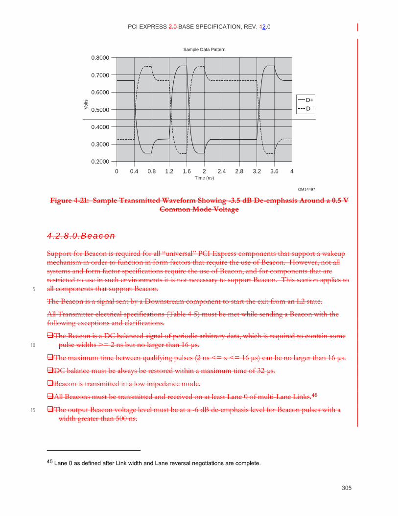
PCI EXPRESS 2.0 BASE SPECIFICATION, REV. 12.0
305
OM14497
0.2000
0.3000
0.4000
0.5000
0.6000
0.7000
0.8000
0 0.4 0.8 1.2 1.6 2 2.4 2.8 3.2 3.6 4
D+
D–
Time (ns)
Sample Data Pattern
Vol
ts
Figure 4-21: Sample Transmitted Waveform Showing -3.5 dB De-emphasis Around a 0.5 V
Common Mode Voltage
4.2.8.0.Beacon
Support for Beacon is required for all “universal” PCI Express components that support a wakeup mechanism in order to function in form factors that require the use of Beacon. However, not all systems and form factor specifications require the use of Beacon, and for components that are restricted to use in such environments it is not necessary to support Beacon. This section applies to all components that support Beacon. 5
The Beacon is a signal sent by a Downstream component to start the exit from an L2 state.
All Transmitter electrical specifications (Table 4-5) must be met while sending a Beacon with the following exceptions and clarifications.
The Beacon is a DC balanced signal of periodic arbitrary data, which is required to contain some pulse widths >= 2 ns but no larger than 16 μs. 10
The maximum time between qualifying pulses (2 ns <= x <= 16 μs) can be no larger than 16 μs.
DC balance must be always be restored within a maximum time of 32 μs.
Beacon is transmitted in a low impedance mode.
All Beacons must be transmitted and received on at least Lane 0 of multi-Lane Links.45
The output Beacon voltage level must be at a -6 dB de-emphasis level for Beacon pulses with a 15 width greater than 500 ns.
45 Lane 0 as defined after Link width and Lane reversal negotiations are complete.
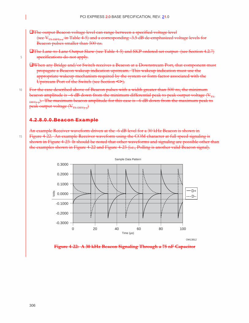
PCI EXPRESS 2.0 BASE SPECIFICATION, REV. 21.0
306
The output Beacon voltage level can range between a specified voltage level (see VTX-DIFFp-p in Table 4-5) and a corresponding -3.5 dB de-emphasized voltage levels for Beacon pulses smaller than 500 ns.
The Lane-to-Lane Output Skew (see Table 4-5) and SKP ordered set output (see Section 4.2.7) specifications do not apply. 5
When any Bridge and/or Switch receives a Beacon at a Downstream Port, that component must propagate a Beacon wakeup indication upstream. This wakeup indication must use the appropriate wakeup mechanism required by the system or form factor associated with the Upstream Port of the Switch (see Section <>).
For the case described above of Beacon pulses with a width greater than 500 ns, the minimum 10 beacon amplitude is –6 dB down from the minimum differential peak to peak output voltage (VTX-
DIFFp-p). The maximum beacon amplitude for this case is –6 dB down from the maximum peak to peak output voltage (VTX-DIFFp-p)
4.2.8.0.0.Beacon Example
An example Receiver waveform driven at the -6 dB level for a 30 kHz Beacon is shown in Figure 4-22. An example Receiver waveform using the COM character at full speed signaling is 15 shown in Figure 4-23 It should be noted that other waveforms and signaling are possible other than the examples shown in Figure 4-22 and Figure 4-23 (i.e., Polling is another valid Beacon signal).
OM13812
-0.3000
-0.2000
-0.1000
0.0000
0.1000
0.2000
0.3000
0 20 40 60 80 100
D+
D–
Time (µs)
Sample Data Pattern
Vol
ts
Figure 4-22: A 30 kHz Beacon Signaling Through a 75 nF Capacitor
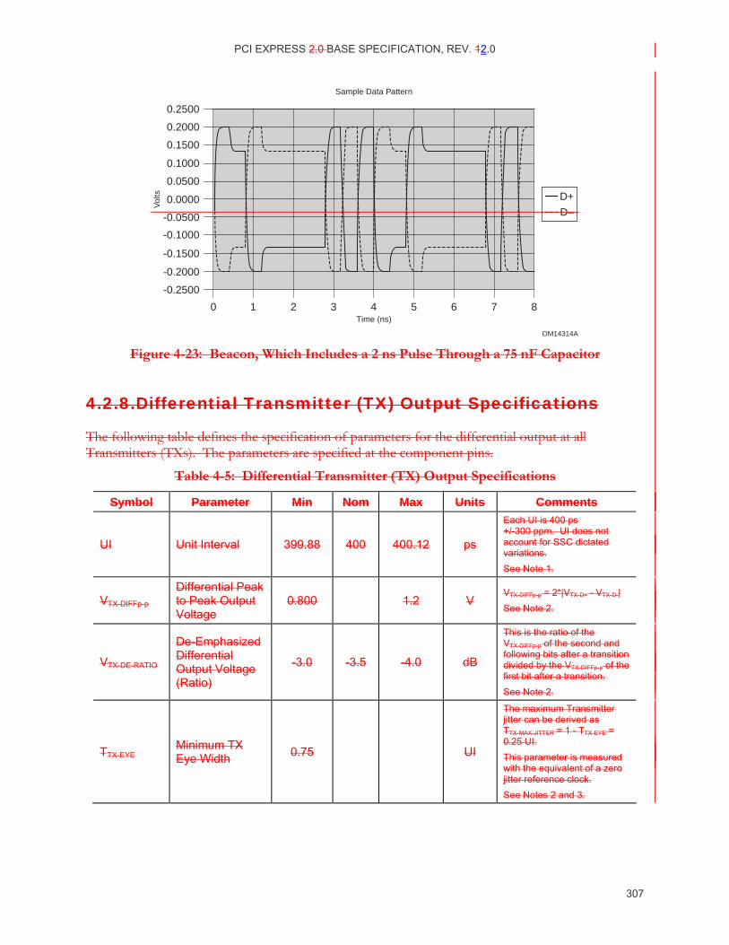
PCI EXPRESS 2.0 BASE SPECIFICATION, REV. 12.0
307
OM14314A
0.2500
-0.2500
-0.2000
-0.1500
-0.1000
-0.0500
0.0000
0.0500
0.1000
0.1500
0.2000
0 1 2 3 4 5 76 8
D+
D–
Time (ns)
Sample Data Pattern
Vol
ts
Figure 4-23: Beacon, Which Includes a 2 ns Pulse Through a 75 nF Capacitor
4.2.8.Differential Transmitter (TX) Output Specifications
The following table defines the specification of parameters for the differential output at all Transmitters (TXs). The parameters are specified at the component pins.
Table 4-5: Differential Transmitter (TX) Output Specifications
Symbol Parameter Min Nom Max Units Comments
UI Unit Interval 399.88 400 400.12 ps
Each UI is 400 ps +/-300 ppm. UI does not account for SSC dictated variations. See Note 1.
VTX-DIFFp-p Differential Peak to Peak Output Voltage
0.800 1.2 V VTX-DIFFp-p = 2*|VTX-D+ - VTX-D-| See Note 2.
VTX-DE-RATIO
De-Emphasized Differential Output Voltage (Ratio)
-3.0 -3.5 -4.0 dB
This is the ratio of the VTX-DIFFp-p of the second and following bits after a transition divided by the VTX-DIFFp-p of the first bit after a transition. See Note 2.
TTX-EYE Minimum TX Eye Width 0.75 UI
The maximum Transmitter jitter can be derived as TTX-MAX-JITTER = 1 - TTX-EYE = 0.25 UI. This parameter is measured with the equivalent of a zero jitter reference clock. See Notes 2 and 3.
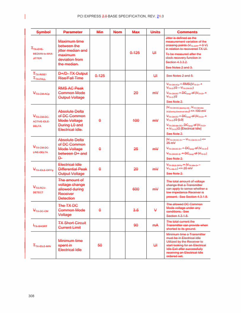
PCI EXPRESS 2.0 BASE SPECIFICATION, REV. 21.0
308
Symbol Parameter Min Nom Max Units Comments
TTX-EYE-
MEDIAN-to-MAX-
JITTER
Maximum time between the jitter median and maximum deviation from the median.
0.125 UI
Jitter is defined as the measurement variation of the crossing points (VTX-DIFF = 0 V) in relation to recovered TX UI. To be measured after the clock recovery function in Section 4.3.3.2.
See Notes 2 and 3.
TTX-RISE, TTX-FALL
D+/D- TX Output Rise/Fall Time 0.125 UI See Notes 2 and 5.
VTX-CM-ACp RMS AC Peak Common Mode Output Voltage
20 mV
VTX-CM-ACp = RMS(|VTX-D+ + VTX-D-|/2 – VTX-CM-DC) VTX-CM-DC = DC(avg) of |VTX-D+ + VTX-D-|/2 See Note 2.
VTX-CM-DC-
ACTIVE-IDLE-
DELTA
Absolute Delta of DC Common Mode Voltage During L0 and Electrical Idle.
0 100 mV
|VTX-CM-DC [during L0] – VTX-CM-Idle-
DC[During Electrical Idle.]| <= 100 mV
VTX-CM-DC = DC(avg) of |VTX-D+ + VTX-D-|/2 [L0] VTX-CM-Idle-DC= DC(avg) of |VTX-D+ + VTX-D-|/2 [Electrical Idle] See Note 2.
VTX-CM-DC-
LINE-DELTA
Absolute Delta of DC Common Mode Voltage between D+ and D-
0 25 mV
|VTX-CM-DC-D+ – VTX-CM-DC-D-| <= 25 mV
VTX-CM-DC-D+ = DC(avg) of |VTX-D+| VTX-CM-DC-D- = DC(avg) of |VTX-D-| See Note 2.
VTX-IDLE-DIFFp Electrical Idle Differential Peak Output Voltage
0 20 mV VTX-IDLE-DIFFp = |VTX-Idle-D+ - VTx-Idle-D-| <= 20 mV See Note 2.
VTX-RCV-
DETECT
The amount of voltage change allowed during Receiver Detection
600 mV
The total amount of voltage change that a Transmitter can apply to sense whether a low impedance Receiver is present. See Section 4.3.1.8.
VTX-DC-CM The TX DC Common Mode Voltage
0 3.6 V The allowed DC Common Mode voltage under any conditions. See Section 4.3.1.8.
ITX-SHORT TX Short Circuit Current Limit 90 mA
The total current the Transmitter can provide when shorted to its ground.
TTX-IDLE-MIN Minimum time spent in Electrical Idle
50 UI
Minimum time a Transmitter must be in Electrical Idle Utilized by the Receiver to start looking for an Electrical Idle Exit after successfully receiving an Electrical Idle ordered set.
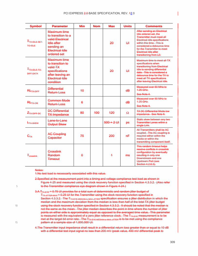
PCI EXPRESS 2.0 BASE SPECIFICATION, REV. 12.0
309
Symbol Parameter Min Nom Max Units Comments
TTX-IDLE-SET-
TO-IDLE
Maximum time to transition to a valid Electrical Idle after sending an Electrical Idle ordered set
20 UI
After sending an Electrical Idle ordered set, the Transmitter must meet all Electrical Idle specifications within this time. This is considered a debounce time for the Transmitter to meet Electrical Idle after transitioning from L0.
TTX-IDLE-TO-
DIFF-DATA
Maximum time to transition to valid TX specifications after leaving an Electrical Idle condition
20 UI
Maximum time to meet all TX specifications when transitioning from Electrical Idle to sending differential data. This is considered a debounce time for the TX to meet all TX specifications after leaving Electrical Idle.
RLTX-DIFF Differential Return Loss 10 dB
Measured over 50 MHz to 1.25 GHz. See Note 4.
RLTX-CM Common Mode Return Loss 6 dB
Measured over 50 MHz to 1.25 GHz. See Note 4.
ZTX-DIFF-DC DC Differential TX Impedance 80 100 120 Ω TX DC Differential Mode low
impedance. See Note 6.
LTX-SKEW Lane-to-Lane Output Skew 500 + 2 UI ps
Static skew between any two Transmitter Lanes within a single Link.
CTX AC Coupling Capacitor 75 200 nF
All Transmitters shall be AC coupled. The AC coupling is required either within the media or within the transmitting component itself.
Tcrosslink Crosslink Random Timeout
0 1 ms
This random timeout helps resolve conflicts in crosslink configuration by eventually resulting in only one Downstream and one Upstream Port (see Section 4.2.6.3).
Notes: 1.No test load is necessarily associated with this value.
2.Specified at the measurement point into a timing and voltage compliance test load as shown in Figure 4-25 and measured using the clock recovery function specified in Section 4.3.3.2. (Also refer to the Transmitter compliance eye diagram shown in Figure 4-24.) 5
3.A TTX-EYE = 0.75 UI provides for a total sum of deterministic and random jitter budget of TTX-JITTER-MAX = 0.25 UI for the Transmitter using the clock recovery function specified in Section 4.3.3.2. The TTX-EYE-MEDIAN-to-MAX-JITTER specification ensures a jitter distribution in which the median and the maximum deviation from the median is less than half of the total TX jitter budget using the clock recovery function specified in Section 4.3.3.2. It should be noted that the median is 10 not the same as the mean. The jitter median describes the point in time where the number of jitter points on either side is approximately equal as opposed to the averaged time value. This parameter is measured with the equivalent of a zero jitter reference clock. The TTX-EYE measurement is to be met at the target bit error rate. The TTX-EYE-MEDIAN-to-MAX-JITTER is to be met using the compliance pattern at a sample size of 1,000,000 UI. 15
4.The Transmitter input impedance shall result in a differential return loss greater than or equal to 10 dB with a differential test input signal no less than 200 mV (peak value, 400 mV differential peak to
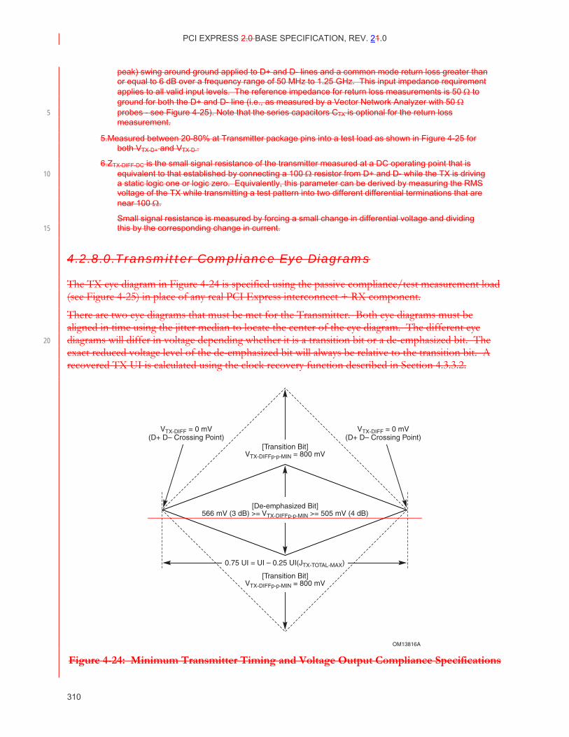
PCI EXPRESS 2.0 BASE SPECIFICATION, REV. 21.0
310
peak) swing around ground applied to D+ and D- lines and a common mode return loss greater than or equal to 6 dB over a frequency range of 50 MHz to 1.25 GHz. This input impedance requirement applies to all valid input levels. The reference impedance for return loss measurements is 50 Ω to ground for both the D+ and D- line (i.e., as measured by a Vector Network Analyzer with 50 Ω probes - see Figure 4-25). Note that the series capacitors CTX is optional for the return loss 5 measurement.
5.Measured between 20-80% at Transmitter package pins into a test load as shown in Figure 4-25 for both VTX-D+ and VTX-D-.
6.ZTX-DIFF-DC is the small signal resistance of the transmitter measured at a DC operating point that is equivalent to that established by connecting a 100 Ω resistor from D+ and D- while the TX is driving 10 a static logic one or logic zero. Equivalently, this parameter can be derived by measuring the RMS voltage of the TX while transmitting a test pattern into two different differential terminations that are near 100 Ω.
Small signal resistance is measured by forcing a small change in differential voltage and dividing this by the corresponding change in current. 15
4.2.8.0.Transmitter Compliance Eye Diagrams
The TX eye diagram in Figure 4-24 is specified using the passive compliance/test measurement load (see Figure 4-25) in place of any real PCI Express interconnect + RX component.
There are two eye diagrams that must be met for the Transmitter. Both eye diagrams must be aligned in time using the jitter median to locate the center of the eye diagram. The different eye diagrams will differ in voltage depending whether it is a transition bit or a de-emphasized bit. The 20 exact reduced voltage level of the de-emphasized bit will always be relative to the transition bit. A recovered TX UI is calculated using the clock recovery function described in Section 4.3.3.2.
OM13816A
[Transition Bit]VTX-DIFFp-p-MIN = 800 mV
[De-emphasized Bit]566 mV (3 dB) >= VTX-DIFFp-p-MIN >= 505 mV (4 dB)
[Transition Bit]VTX-DIFFp-p-MIN = 800 mV
VTX-DIFF = 0 mV(D+ D– Crossing Point)
VTX-DIFF = 0 mV(D+ D– Crossing Point)
0.75 UI = UI – 0.25 UI(JTX-TOTAL-MAX)
Figure 4-24: Minimum Transmitter Timing and Voltage Output Compliance Specifications

PCI EXPRESS 2.0 BASE SPECIFICATION, REV. 12.0
311
4.2.8.0.Eye Measurement Clock Recovery Function
The UI used to construct the compliance eye diagrams is to be recovered from the phase of the data transitions by applying the following filter function:
(4-1) 3
3 )(ω+
=s
ssH
where ω 3 is defined as:
(4-2) 63 105.1**2 xπω =
Equation (4-1) is a first order high pass filter with a rolloff of -20 dB/decade and a half power corner frequency at -3 dB of 1.5 MHz. This function is not meant as a requirement for a particular 5 measurement implementation. It is used as a bounding function for modeling purposes to establish the limits for the half power corner frequency for clock recovery function. Other implementations that can meet the frequency response given by this function are also acceptable.
When applying the clock recovery function to the 8b/10b encoded data, any missing transitions must be accounted for by a zero order hold of the phase. 10
IMPLEMENTATION NOTE
Clock Recovery Equation (4-2) is valid for measurements with a clean reference clock. Measurements that include SSC or clocks with significant jitter will not be meaningful with this recovery function. Measurements on clocks with SSC or jitter should use the clock recovery function given by Equation (4-3) in order to provide an approximation of the data eye when measured with the compliance method using a clean clock. 15
(4-3) |*2|)(3
3⎟⎟⎠
⎞⎜⎜⎝
⎛+
=ωsssH d
with ω 3 defined as before.
For those familiar with PCI Express Base Specification, Revision 1.0a, Equation 4-3 is the equivalent transfer function for that specification’s 250/3500 UI clock recovery algorithm.
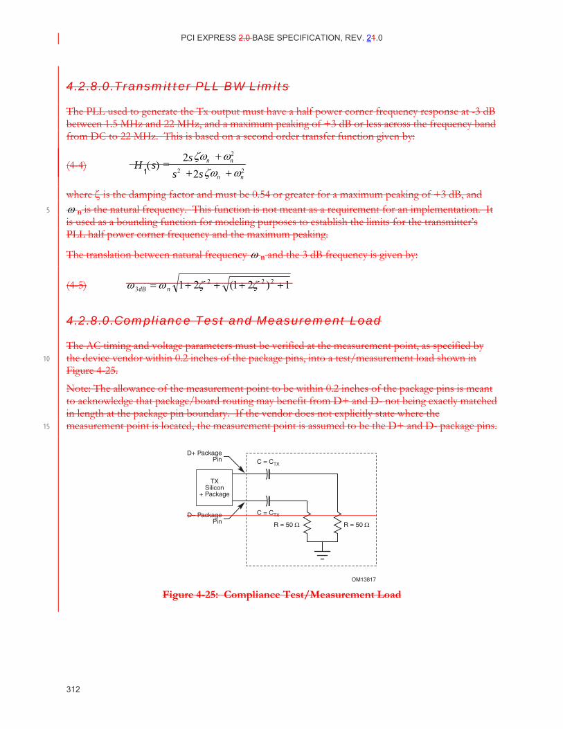
PCI EXPRESS 2.0 BASE SPECIFICATION, REV. 21.0
312
4.2.8.0.Transmitter PLL BW Limits
The PLL used to generate the Tx output must have a half power corner frequency response at -3 dB between 1.5 MHz and 22 MHz, and a maximum peaking of +3 dB or less across the frequency band from DC to 22 MHz. This is based on a second order transfer function given by:
(4-4) 22
2
2 2
) ( 1
nn n n
s s s
s H ωζω
ω ζω + +
+ =
where ζ is the damping factor and must be 0.54 or greater for a maximum peaking of +3 dB, and ω n is the natural frequency. This function is not meant as a requirement for an implementation. It 5 is used as a bounding function for modeling purposes to establish the limits for the transmitter’s PLL half power corner frequency and the maximum peaking.
The translation between natural frequency ω n and the 3 dB frequency is given by:
(4-5) 1)21(21 2223 ++++= ζζωω ndB
4.2.8.0.Compliance Test and Measurement Load
The AC timing and voltage parameters must be verified at the measurement point, as specified by the device vendor within 0.2 inches of the package pins, into a test/measurement load shown in 10 Figure 4-25.
Note: The allowance of the measurement point to be within 0.2 inches of the package pins is meant to acknowledge that package/board routing may benefit from D+ and D- not being exactly matched in length at the package pin boundary. If the vendor does not explicitly state where the measurement point is located, the measurement point is assumed to be the D+ and D- package pins. 15
OM13817
D+ PackagePin
D– PackagePin
C = CTX
C = CTX
R = 50 ΩR = 50 Ω
TXSilicon
+ Package
Figure 4-25: Compliance Test/Measurement Load
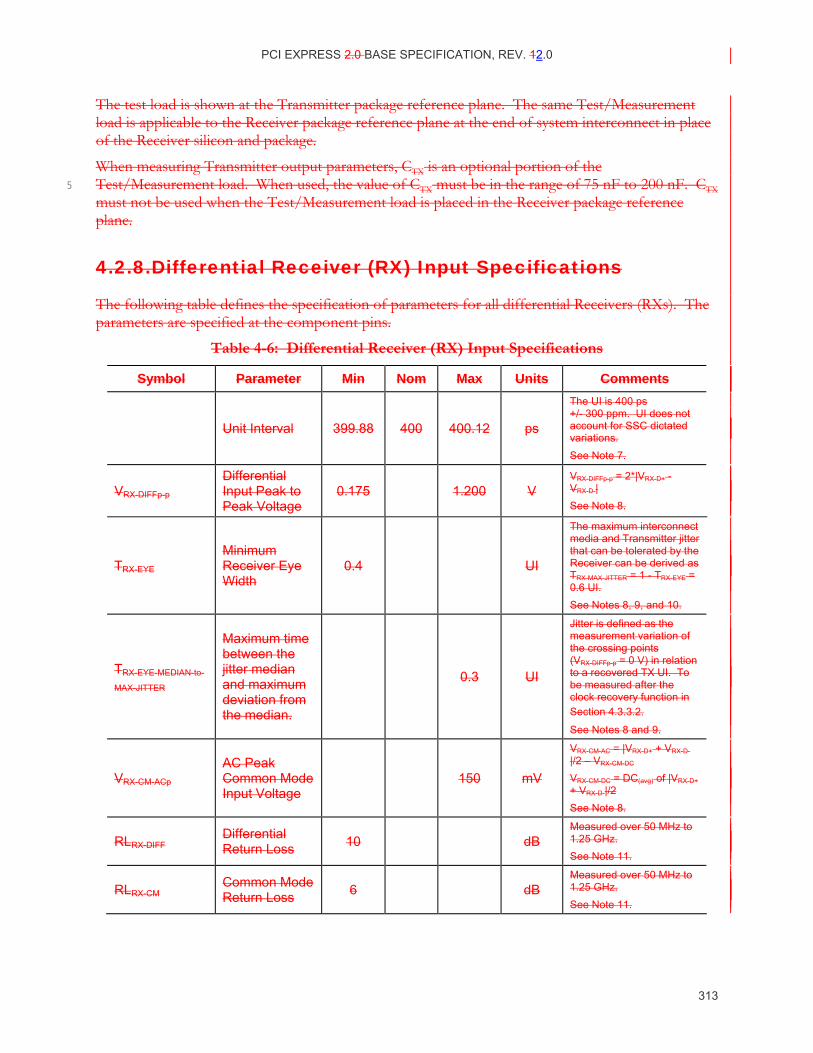
PCI EXPRESS 2.0 BASE SPECIFICATION, REV. 12.0
313
The test load is shown at the Transmitter package reference plane. The same Test/Measurement load is applicable to the Receiver package reference plane at the end of system interconnect in place of the Receiver silicon and package.
When measuring Transmitter output parameters, CTX is an optional portion of the Test/Measurement load. When used, the value of CTX must be in the range of 75 nF to 200 nF. CTX 5 must not be used when the Test/Measurement load is placed in the Receiver package reference plane.
4.2.8.Differential Receiver (RX) Input Specifications
The following table defines the specification of parameters for all differential Receivers (RXs). The parameters are specified at the component pins.
Table 4-6: Differential Receiver (RX) Input Specifications
Symbol Parameter Min Nom Max Units Comments
Unit Interval 399.88 400 400.12 ps
The UI is 400 ps +/- 300 ppm. UI does not account for SSC dictated variations. See Note 7.
VRX-DIFFp-p Differential Input Peak to Peak Voltage
0.175 1.200 V VRX-DIFFp-p = 2*|VRX-D+ - VRX-D-| See Note 8.
TRX-EYE Minimum Receiver Eye Width
0.4 UI
The maximum interconnect media and Transmitter jitter that can be tolerated by the Receiver can be derived as TRX-MAX-JITTER = 1 - TRX-EYE = 0.6 UI. See Notes 8, 9, and 10.
TRX-EYE-MEDIAN-to-
MAX-JITTER
Maximum time between the jitter median and maximum deviation from the median.
0.3 UI
Jitter is defined as the measurement variation of the crossing points (VRX-DIFFp-p = 0 V) in relation to a recovered TX UI. To be measured after the clock recovery function in Section 4.3.3.2.
See Notes 8 and 9.
VRX-CM-ACp AC Peak Common Mode Input Voltage
150 mV
VRX-CM-AC = |VRX-D+ + VRX-D-|/2 – VRX-CM-DC
VRX-CM-DC = DC(avg) of |VRX-D+ + VRX-D-|/2 See Note 8.
RLRX-DIFF Differential Return Loss 10 dB
Measured over 50 MHz to 1.25 GHz. See Note 11.
RLRX-CM Common Mode Return Loss 6 dB
Measured over 50 MHz to 1.25 GHz. See Note 11.
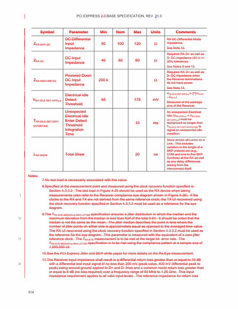
PCI EXPRESS 2.0 BASE SPECIFICATION, REV. 21.0
314
Symbol Parameter Min Nom Max Units Comments
ZRX-DIFF-DC DC Differential Input Impedance
80 100 120 Ω RX DC Differential Mode impedance. See Note 12.
ZRX-DC DC Input Impedance 40 50 60 Ω
Required RX D+ as well as D- DC impedance (50 Ω +/-20% tolerance). See Notes 8 and 12.
ZRX-HIGH-IMP-DC Powered Down DC Input Impedance
200 k Ω
Required RX D+ as well as D- DC impedance when the Receiver terminations do not have power. See Note 13.
VRX-IDLE-DET-DIFFp-p Electrical Idle Detect Threshold
65 175 mV VRX-IDLE-DET-DIFFp-p = 2*|VRX-D+ - VRX-D-| Measured at the package pins of the Receiver.
TRX-IDLE-DET-DIFF-
ENTERTIME
Unexpected Electrical Idle Enter Detect Threshold Integration Time
10 ms
An unexpected Electrical Idle (VRX-DIFFp-p < VRX-IDLE-
DET-DIFFp-p) must be recognized no longer than TRX-IDLE-DET-DIFF-ENTERTIME to signal an unexpected idle condition.
LRX-SKEW Total Skew 20 ns
Skew across all Lanes on a Link. This includes variation in the length of a SKP ordered set (e.g., COM and one to five SKP Symbols) at the RX as well as any delay differences arising from the interconnect itself.
Notes: 7.No test load is necessarily associated with this value.
8.Specified at the measurement point and measured using the clock recovery function specified in Section 4.3.3.2. The test load in Figure 4-25 should be used as the RX device when taking measurements (also refer to the Receiver compliance eye diagram shown in Figure 4-26). If the 5 clocks to the RX and TX are not derived from the same reference clock, the TX UI recovered using the clock recovery function specified in Section 4.3.3.2 must be used as a reference for the eye diagram.
9.The TRX-EYE-MEDIAN-to-MAX-JITTER specification ensures a jitter distribution in which the median and the maximum deviation from the median is less than half of the total 0.64. It should be noted that the 10 median is not the same as the mean. The jitter median describes the point in time where the number of jitter points on either side is approximately equal as opposed to the averaged time value. The RX UI recovered using the clock recovery function specified in Section 4.3.3.2 must be used as the reference for the eye diagram. This parameter is measured with the equivalent of a zero jitter reference clock. The TRX-EYE measurement is to be met at the target bit error rate. The 15 TRX-EYE-MEDIAN-to-MAX-JITTER specification is to be met using the compliance pattern at a sample size of 1,000,000 UI.
10.See the PCI Express Jitter and BER white paper for more details on the Rx-Eye measurement.
11.The Receiver input impedance shall result in a differential return loss greater than or equal to 10 dB with a differential test input signal of no less than 200 mV (peak value, 400 mV differential peak to 20 peak) swing around ground applied to D+ and D- lines and a common mode return loss greater than or equal to 6 dB (no bias required) over a frequency range of 50 MHz to 1.25 GHz. This input impedance requirement applies to all valid input levels. The reference impedance for return loss
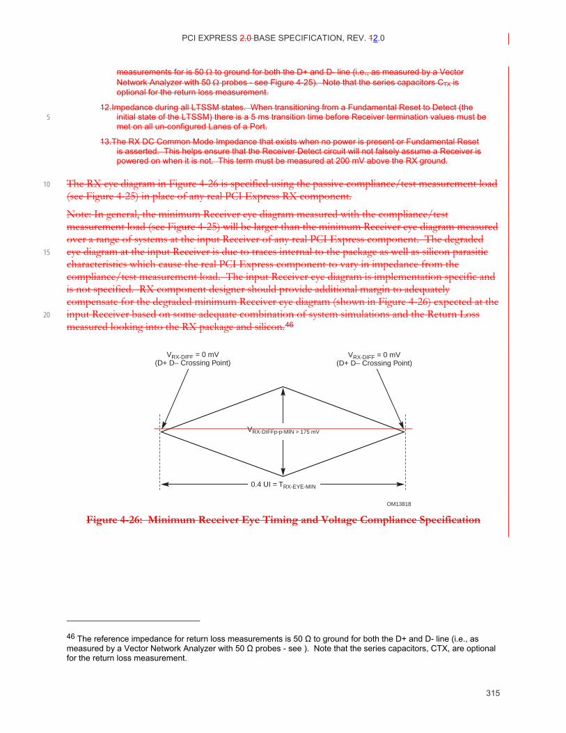
PCI EXPRESS 2.0 BASE SPECIFICATION, REV. 12.0
315
measurements for is 50 Ω to ground for both the D+ and D- line (i.e., as measured by a Vector Network Analyzer with 50 Ω probes - see Figure 4-25). Note that the series capacitors CTX is optional for the return loss measurement.
12.Impedance during all LTSSM states. When transitioning from a Fundamental Reset to Detect (the initial state of the LTSSM) there is a 5 ms transition time before Receiver termination values must be 5 met on all un-configured Lanes of a Port.
13.The RX DC Common Mode Impedance that exists when no power is present or Fundamental Reset is asserted. This helps ensure that the Receiver Detect circuit will not falsely assume a Receiver is powered on when it is not. This term must be measured at 200 mV above the RX ground.
The RX eye diagram in Figure 4-26 is specified using the passive compliance/test measurement load 10 (see Figure 4-25) in place of any real PCI Express RX component.
Note: In general, the minimum Receiver eye diagram measured with the compliance/test measurement load (see Figure 4-25) will be larger than the minimum Receiver eye diagram measured over a range of systems at the input Receiver of any real PCI Express component. The degraded eye diagram at the input Receiver is due to traces internal to the package as well as silicon parasitic 15 characteristics which cause the real PCI Express component to vary in impedance from the compliance/test measurement load. The input Receiver eye diagram is implementation specific and is not specified. RX component designer should provide additional margin to adequately compensate for the degraded minimum Receiver eye diagram (shown in Figure 4-26) expected at the input Receiver based on some adequate combination of system simulations and the Return Loss 20 measured looking into the RX package and silicon.46
OM13818
VRX-DIFF = 0 mV(D+ D– Crossing Point)
VRX-DIFF = 0 mV(D+ D– Crossing Point)
0.4 UI = TRX-EYE-MIN
VRX-DIFFp-p-MIN > 175 mV
Figure 4-26: Minimum Receiver Eye Timing and Voltage Compliance Specification
46 The reference impedance for return loss measurements is 50 Ω to ground for both the D+ and D- line (i.e., as measured by a Vector Network Analyzer with 50 Ω probes - see ). Note that the series capacitors, CTX, are optional for the return loss measurement.
PCI EXPRESS 2.0 BASE SPECIFICATION, REV. 21.0
316
5. Power Management This chapter describes PCI Express power management (PCI Express-PM) capabilities and protocols.
5.1. Overview PCI Express-PM provides the following services:
A mechanism to identify power management capabilities of a given functionFunction
The ability to transition a functionFunction into a certain power management state 5
Notification of the current power management state of a functionFunction
The option to wakeup the system on a specific event
PCI Express-PM is compatible with the PCI Bus Power Management Interface Specification, Revision 1.2, and the Advanced Configuration and Power Interface Specification, Revision 2.0. This chapter also defines PCI Express native power management extensions. These provide additional power management 10 capabilities beyond the scope of the PCI Bus Power Management Interface Specification.
PCI Express-PM defines Link power management states that a PCI Express physical Link is permitted to enter in response to either software driven D-state transitions or active state Link power management activities. PCI Express Link states are not visible directly to legacy bus driver software, but are derived from the power management state of the components residing on those 15 Links. Defined Link states are L0, L0s, L1, L2, and L3. The power savings increase as the Link state transitions from L0 through L3.
PCI Express cComponents are permitted tomay wakeup the system using a wakeup mechanism followed by a power management event (PME) Message. PCI Express systems may provide the optional auxiliary power supply (Vaux) needed for wakeup operation from states where the main 20 power supplies are off. PCI Express-PM extends beyond the PME mechanism defined in conventional PCI-PM as PCI Express PME Messages include the Requestor IDRequester ID of the requesting agent. These PME Messages are in-band TLPs routed from the requesting device Function towards the Root Complex.
5
PCI EXPRESS 2.0 BASE SPECIFICATION, REV. 12.0
317
Another distinction of the PCI Express-PM PME mechanism is in its separation of the following two PME tasks that are associated with PME:
Reactivation (wakeup) of the associated resources (i.e., re-establishing reference clocks and main power rails to the PCI Express components)
Sending a PME Message to the Root Complex 5
An autonomous hardware based active state mechanism, Active State Power Management, (ASPM) is an autonomous hardware-based, active state mechanism that enables power savings even when the connected components are in the D0 state. After a period of idle Link time, the ASPM mechanism engages in an ASPM Physical Physical-Layer protocol that places the idle Link into a lower power state. Once in the lower lower-power state, transitions to the fully operative L0 state 10 are triggered by traffic appearing on either side of the Link. ASPM may be disabled by software. Refer to Section 5.4.1 for more information on ASPM.
Throughout this document the term Upstream component, or Upstream device, is used to refer to the PCI Express component, Device, or Function that is on the end of the PCI Express Link that is hierarchically closer to the root of the PCI Express tree hierarchyRoot Complex. The term 15 Downstream component, or Downstream device, is used to refer to the PCI Express component, Device, or Function that is on the end of the Link that is hierarchically further from the root of the PCI Express tree hierarchyRoot Complex.
5.1.1. Statement of Requirements
All PCI Express componentsFunctions, with the exception of Functions in the a Root Complex, are required to meet or exceed the minimum requirements defined by the PCI-PM Software software 20 compatible PCI Express-PM features. Root Complexes are required to participate in Link power management DLLP protocols initiated by a Downstream device, when all functions Functions of a Downstream component enter a PCI-PM Software compatible low power state. For further details, refer to Section 5.3.2.
ASPM is a required feature (L0s entry at minimum) for Root Ports, Upstream Ports, and Switch 25 Downstream Ports. ASPM is a required feature (L0s entry at minimum) for all components including Root Complexes, and is configured separately via the native PCI Express configuration mechanisms. Refer to Section 5.4.1 for more information on ASPM.
5.2. Link State Power Management PCI Express defines Link power management states, replacing the bus power management states that were defined by the PCI Bus Power Management Interface Specification. Link states are not visible to 30 PCI-PM legacy compatible software, and are either derived from the power management D-states of the corresponding components connected to that Link or by ASPM protocols (refer tosee Section 5.4.1).
Note that the PCI Express Physical Layer may define additional intermediate states. See Refer to Chapter 4 for more detail on each state and how the Physical Layer handles transitions between 35 states.
PCI EXPRESS 2.0 BASE SPECIFICATION, REV. 21.0
318
PCI Express-PM defines the following Link power management states:
L0 – Active state.
L0 support is required for both ASPM and PCI-PM compatible power management
All PCI Express transactions and other operations are enabled.
L0 support is required for both ASPM and PCI-PM compatible power management 5
L0s – A low resume latency, energy saving “standby” state.
L0s support is required for ASPM. It is not applicable to PCI-PM compatible power management.
All main power supplies, component reference clocks, and components’ internal PLLs must be active at all times during L0s. TLP and DLLP transmission is disabled for a Link 10 communication through a Transmitter that is in L0s is prohibited. The L0s state is used exclusively for ASPM.
The PCI Express Physical Layer provides mechanisms for quick transitions from this state to the L0 state. When common (distributed) reference clocks are used on both sides of a given Link, the transition time from L0s to L0 is typically less than 100 Symbol Times. 15
It is possible for the Transmit side of one component on a Link to be in L0s while the Transmit side of the other component on the Link is in L0.
L1 – Higher latency, lower power “standby” state.
L1 support is required for PCI-PM compatible power management. L1 is optional for ASPM unless specifically required by a particular form factor. 20
All platform provided main power supplies and component reference clocks must remain active at all times during L1. All platform-provided component reference clocks must remain active during L1, except as permitted by Clock Power Management (using CLKREQ#) when enabled. The A component’s internal PLLs may be shut off during L1, enabling greater energy power savings at a cost of increased exit latency.47 25
The L1 state is entered whenever all functions Functions of a Downstream component on a given PCI Express Link are either programmed to a D-state other than D0., or The L1 state also is entered if the Downstream component requests L1 entry (ASPM) and receives positive acknowledgement for the request.
Exit from L1 is initiated by an upstream Upstream-initiated transaction targeting the a 30 Downstream component, or by the Downstream component’s desire to initiate initiation of a transaction heading upstreamUpstream. Transition from L1 to L0 is typically a few microseconds.
TLP and DLLP transmission is disabled for a Link in L1. TLP and DLLP communication over a Link that is in L1 is prohibited. 35
L2/L3 Ready – Staging point for L2 or L3.
47 For example, disabling the internal PLL may be something that is desirable when in D3hot, but not so when in D1 or D2.
PCI EXPRESS 2.0 BASE SPECIFICATION, REV. 12.0
319
L2/L3 Ready transition protocol support is required.
L2/L3 Ready is a pseudo-state (corresponding to the LTSSM L2 state) that a given Link enters into when preparing for the removal of power and clocks from the downstream Downstream component or from both attached components. This process is initiated after PM software transitions a device into a D3 state, and subsequently calls power management software to 5 initiate the removal of power and clocks. After the Link enters the L2/L3 Ready state the component(s) are ready for power removal. Depending upon the platform’s implementation choices with respect to providing a Vaux supply, aAfter main power has been removed, the Link will either settle intransition to L2 (i.e.,if Vaux is provided), or it will settle intransition to L3 if no Vaux is providedto a zero power “off” state (see L3). Note that these are PM pseudo-states 10 for the Link; under these conditions, the LTSSM will in, general, operate only on main power, and so will power off with main power removal.
The L2/L3 Ready state entry transition process must begin as soon as possible following the acknowledgment of a PME_Turn_Off Message, (i.e., the injection of a PME_TO_Ack TLP). The Downstream component initiates L2/L3 Ready entry by injecting sending a PM_Enter_L23 15 DLLP onto its Transmit Port. Refer to Section 5.6 for further detail on power management system Messages.
TLP and DLLP communicationtransmission over is disabled for a Link that is in L2/L3 Ready is not possible.
Note: Exit from L2/L3 ready Ready back to L0 will be through intermediate LTSSM states. 20 Refer to Chapter 4 for detailed information.
L2 – Auxiliary Auxiliary-powered Link, deep deep-energy energy-saving state.
L2 support is optional, and dependent upon platform supportthe presence of Vaux.
A component may only consume Vaux power if enabled to do so as described in Section 5.5.1.
In L2, – The the component’s main power supply inputs and reference clock inputs are shut 25 off.
When in L2 (with main power removed), any Link reactivation wakeup logic (Beacon or WAKE#), PME context, and any other “keep alive” logic is powered by Vaux.
TLP and DLLP communication overtransmission is disabled for a Link that is in L2 is not possible. 30
L3 – Link Off state.
Zero power stateWhen no power is present, the component is in the L3 state.
LDn – A transitional Link Down pseudo-state prior to L0.
This pseudo-state is associated with the LTSSM states Detect, Polling, and Configuration, and, when applicable, Disabled, Loopback, and Hot Reset. 35
Refer to Section 4.2 for further detail relating to entering and exiting each of the PCI Express L-states between L0 and L2/L3 Ready (L2.Idle from the Chapter 4 perspective). The L2 state is an abstraction for PM purposes distinguished by the presence of auxiliary power, and should not be construed to imply a requirement that the LTSSM remain active.
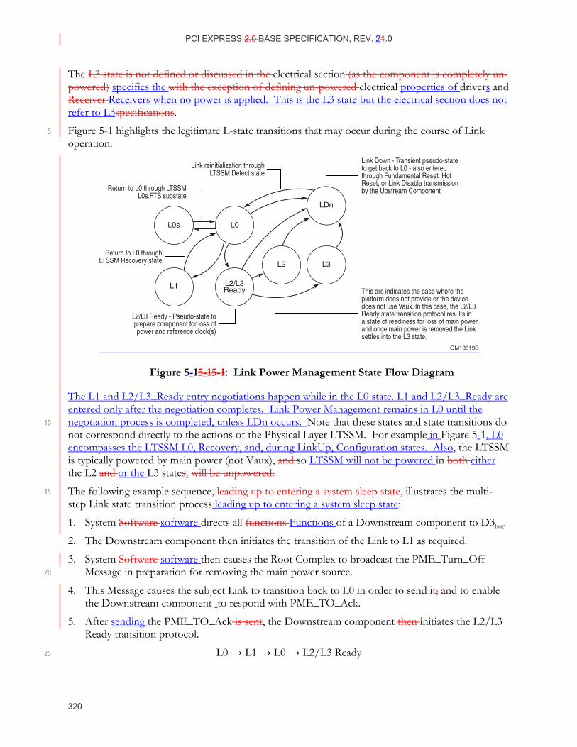
PCI EXPRESS 2.0 BASE SPECIFICATION, REV. 21.0
320
The L3 state is not defined or discussed in the electrical section (as the component is completely un-powered) specifies the with the exception of defining un-powered electrical properties of drivers and Receiver Receivers when no power is applied. This is the L3 state but the electrical section does not refer to L3specifications.
Figure 5-1 highlights the legitimate L-state transitions that may occur during the course of Link 5 operation.
OM13819B
L0L0s
L2 L3
LDn
L1 L2/L3Ready
Link Down - Transient pseudo-stateto get back to L0 - also enteredthrough Fundamental Reset, HotReset, or Link Disable transmissionby the Upstream ComponentReturn to L0 through LTSSM
L0s.FTS substate
L2/L3 Ready - Pseudo-state toprepare component for loss ofpower and reference clock(s)
Link reinitialization throughLTSSM Detect state
This arc indicates the case where theplatform does not provide or the devicedoes not use Vaux. In this case, the L2/L3Ready state transition protocol results ina state of readiness for loss of main power,and once main power is removed the Linksettles into the L3 state.
Return to L0 throughLTSSM Recovery state
Figure 5-15-1 5-1: Link Power Management State Flow Diagram
The L1 and L2/L3_Ready entry negotiations happen while in the L0 state. L1 and L2/L3_Ready are entered only after the negotiation completes. Link Power Management remains in L0 until the negotiation process is completed, unless LDn occurs. Note that these states and state transitions do 10 not correspond directly to the actions of the Physical Layer LTSSM. For example in Figure 5-1, L0 encompasses the LTSSM L0, Recovery, and, during LinkUp, Configuration states. Also, the LTSSM is typically powered by main power (not Vaux), and so LTSSM will not be powered in both either the L2 and or the L3 states. will be unpowered.
The following example sequence, leading up to entering a system sleep state, illustrates the multi-15 step Link state transition process leading up to entering a system sleep state:
1. System Software software directs all functions Functions of a Downstream component to D3hot.
2. The Downstream component then initiates the transition of the Link to L1 as required.
3. System Software software then causes the Root Complex to broadcast the PME_Turn_Off Message in preparation for removing the main power source. 20
4. This Message causes the subject Link to transition back to L0 in order to send it, and to enable the Downstream component to respond with PME_TO_Ack.
5. After sending the PME_TO_Ack is sent, the Downstream component then initiates the L2/L3 Ready transition protocol.
L0 → L1 → L0 → L2/L3 Ready 25
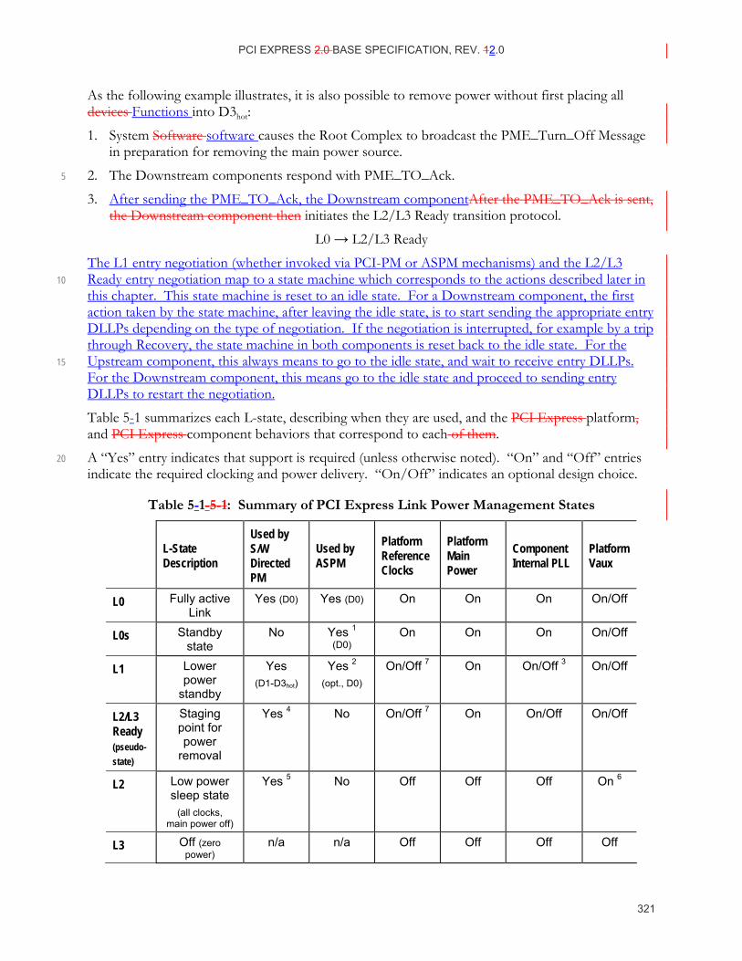
PCI EXPRESS 2.0 BASE SPECIFICATION, REV. 12.0
321
As the following example illustrates, it is also possible to remove power without first placing all devices Functions into D3hot:
1. System Software software causes the Root Complex to broadcast the PME_Turn_Off Message in preparation for removing the main power source.
2. The Downstream components respond with PME_TO_Ack. 5
3. After sending the PME_TO_Ack, the Downstream componentAfter the PME_TO_Ack is sent, the Downstream component then initiates the L2/L3 Ready transition protocol.
L0 → L2/L3 Ready
The L1 entry negotiation (whether invoked via PCI-PM or ASPM mechanisms) and the L2/L3 Ready entry negotiation map to a state machine which corresponds to the actions described later in 10 this chapter. This state machine is reset to an idle state. For a Downstream component, the first action taken by the state machine, after leaving the idle state, is to start sending the appropriate entry DLLPs depending on the type of negotiation. If the negotiation is interrupted, for example by a trip through Recovery, the state machine in both components is reset back to the idle state. For the Upstream component, this always means to go to the idle state, and wait to receive entry DLLPs. 15 For the Downstream component, this means go to the idle state and proceed to sending entry DLLPs to restart the negotiation.
Table 5-1 summarizes each L-state, describing when they are used, and the PCI Express platform, and PCI Express component behaviors that correspond to each of them.
A “Yes” entry indicates that support is required (unless otherwise noted). “On” and “Off” entries 20 indicate the required clocking and power delivery. “On/Off” indicates an optional design choice.
Table 5-1- 5-1: Summary of PCI Express Link Power Management States
L-State Description
Used by S/W Directed PM
Used by ASPM
Platform Reference Clocks
Platform Main Power
Component Internal PLL
Platform Vaux
L0 Fully active Link
Yes (D0) Yes (D0) On On On On/Off
L0s Standby state
No Yes 1
(D0) On On On On/Off
L1 Lower power
standby
Yes (D1-D3hot)
Yes 2 (opt., D0)
On/Off 7 On On/Off 3 On/Off
L2/L3 Ready (pseudo-state)
Staging point for power
removal
Yes 4 No On/Off 7 On On/Off On/Off
L2 Low power sleep state
(all clocks, main power off)
Yes 5
No Off Off Off On 6
L3 Off (zero power)
n/a n/a Off Off Off Off
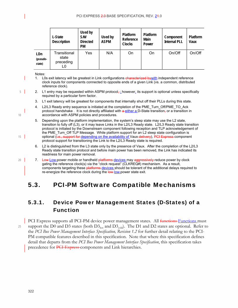
PCI EXPRESS 2.0 BASE SPECIFICATION, REV. 21.0
322
L-State Description
Used by S/W Directed PM
Used by ASPM
Platform Reference Clocks
Platform Main Power
Component Internal PLL
Platform Vaux
LDn (pseudo-state)
Transitional state
preceding L0
Yes N/A On On On/Off On/Off
Notes: 1. L0s exit latency will be greatest in Link configurations characterized bywith independent reference
clock inputs for components connected to opposite ends of a given Link (vs. a common, distributed reference clock).
2. L1 entry may be requested within ASPM protocol, ; however, its support is optional unless specifically 5 required by a particular form factor.
3. L1 exit latency will be greatest for components that internally shut off their PLLs during this state. 4. L2/L3 Ready entry sequence is initiated at the completion of the PME_Turn_Off/PME_TO_Ack
protocol handshake . It is not directly affiliated with a either a D-State transition, or a transition in accordance with ASPM policies and procedures. 10
5. Depending upon the platform implementation, the system’s sleep state may use the L2 state, transition to fully off (L3), or it may leave Links in the L2/L3 Ready state. L2/L3 Ready state transition protocol is initiated by the Downstream component following reception and TLP acknowledgement of the PME_Turn_Off TLP Message. While platform support for an L2 sleep state configuration is optional (i.e., support for depending on the availability of Vaux delivery), PCI Express component 15 protocol support for transitioning the Link to the L2/L3 Ready state is required.
6. L2 is distinguished from the L3 state only by the presence of Vaux. After the completion of the L2/L3 Ready state transition protocol and before main power has been removed, the Link has indicated its readiness for main power removal.
7. Low Low-power mobile or handheld platforms devices may aggressively reduce power by clock 20 gating the reference clock(s) via the “clock request” (CLKREQ#) mechanism. As a result, components targeting these platforms devices should be tolerant of the additional delays required to re-energize the reference clock during the low low-power state exit.
5.3. PCI-PM Software Compatible Mechanisms
5.3.1. Device Power Management States (D-States) of a Function
PCI Express supports all PCI-PM device power management states. All functions Functions must support the D0 and D3 states (both D3hot and D3cold). The D1 and D2 states are optional. Refer to 25 the PCI Bus Power Management Interface Specification, Revision 1.2 for further detail relating to the PCI-PM compatible features described in this specification. Note that where this specification defines detail that departs from the PCI Bus Power Management Interface Specification, this specification takes precedence for PCI Express components and Link hierarchies.
PCI EXPRESS 2.0 BASE SPECIFICATION, REV. 12.0
323
IMPLEMENTATION NOTE Switch and Root Port Virtual Bridge Behavior in Non-D0 States When a Type 1 Function associated with a Switch/Root Port, a “virtual bridge”, is in a non-D0 power state, it will emulate the behavior of a conventional PCI bridge in its handling of Memory, I/O, and Configuration Requests and Completions. All Memory and I/O requests flowing Downstream are terminated as Unsupported Requests. All Type 1 Configuration Requests are terminated as Unsupported Requests, however Type 0 Configuration Request handling is unaffected 5 by the virtual bridge D state. Completions flowing either direction across the virtual bridge are unaffected by the virtual bridge D state.
Note that the handling of Messages is not affected by the PM state of the virtual bridge.
5.3.1.1. D0 State
All PCI Express fFunctions must support the D0 state. D0 is divided into two distinct sub-statesubstates, the “un-initialized” sub-statesubstate and the “active” sub-statesubstate. When a PCI 10 Express component initially has its power appliedcomes out of Conventional Reset or FLR, it defaults to the D0uninitialized state. Components that are in this state will be enumerated and configured by the PCI Express Hierarchy enumeration process. Following the completion of the enumeration and configuration process the function Function enters the D0active state, the fully operational state for a PCI Express functionFunction. A function Function enters the D0active state 15 whenever any single or combination of the function’s Function’s Memory Space Enable, I/O Space Enable, or Bus Master Enable bits have been enabled by system software.
5.3.1.2. D1 State
D1 support is optional. While in the D1 state, a function Function must not initiate any Request TLPs on the Link with the exception of a PME Message as defined in Section 5.3.3. Configuration and Message requests Requests are the only TLPs accepted by a function Function in the D1 state. 20 All other received Requests must be handled as Unsupported Requests, and all received Completions may optionally be handled as Unexpected Completions. If an error caused by a received TLP (e.g., an Unsupported Request) is detected while in D1, and reporting is enabled, the linkLink must be returned to L0 if it is not already in L0 and an error message must be sent. If an error caused by an event other than a received TLP (e.g.,. a Completion Timeout) is detected while 25 in D1, an error message must be sent when the device Function is programmed back to the D0 state.
Note that a function’s Function’s software driver participates in the process of transitioning the function Function from D0 to D1. It contributes to the process by saving any functional state (if necessary), and otherwise preparing the function Function for the transition to D1. As part of this 30 quiescence process the function’s Function’s software driver must ensure that any mid-transaction TLPs (i.e., Requests with outstanding Completions), are terminated prior to handing control to the system configuration software that would then complete the transition to D1.
PCI EXPRESS 2.0 BASE SPECIFICATION, REV. 21.0
324
5.3.1.3. D2 State
D2 support is optional. While in the D2 state, a function Function must not initiate any Request TLPs on the Link with the exception of a PME Message as defined in Section 5.3.3. Configuration and Message requests are the only TLPs accepted by a function Function in the D2 state. All other received Requests must be handled as Unsupported Requests, and all received Completions may optionally be handled as Unexpected Completions. If an error caused by a received TLP (e.g., an 5 Unsupported Request) is detected while in D2, and reporting is enabled, the linkLink must be returned to L0 if it is not already in L0 and an error message must be sent. If an error caused by an event other than a received TLP (e.g., a Completion Timeout) is detected while in D2, an error message must be sent when the device Function is programmed back to the D0 state. Note that a function’s Function’s software driver participates in the process of transitioning the function 10 Function from D0 to D2. It contributes to the process by saving any functional state (if necessary), and otherwise preparing the function Function for the transition to D2. As part of this quiescence process the function’s Function’s software driver must ensure that any mid-transaction TLPs (i.e., Requests with outstanding Completions), are terminated prior to handing control to the system configuration software that would then complete the transition to D2. 15
5.3.1.4. D3 State
D3 support is required, (both the D3cold and the D3hot states). Functions supporting PME generation from D3 must support it for both D3cold and the D3hot states.
Functional context is required to be maintained by Ffunctions in the D3hot state if the No_Soft_Reset field in the PMCSRower Management Control/Status register is set to 1Set. In this case, software is not required to re-initialize the Ffunction after a transition from D3hot to D0 (the 20 device Function will be in the D0 initialized state). If the No_Soft_Reset bit is set to 0Clear, functional context is not required to be maintained by the Ffunction in the D3hot state. As a result, in this case software is required to fully re-initialize the Ffunction after a transition to D0 as the device Function will be in the D0uninitialized state.
The Functiondevice will be reset if the linkLink state has transitioned to the L2/L3 Ready state 25 regardless of the value of the No_Soft_Reset bit.
IMPLEMENTATION NOTE Transitioning to L2/L3 Ready As described in Section 5.2, transition to the L2/L3 Ready state is initiated by platform power management software in order to begin the process of removing main power and clocks from the device. As a result, it is expected that a device will transition to D3cold shortly after its linkLink transitions to L2/L3 Ready, making the No_Soft_Reset bit, which only applies to D3hot, irrelevant. 30 While there is no guarantee of this correlation between L2/L3 Ready and D3cold, system software should ensure that the L2/L3 Ready state is entered only when the intent is to remove device main power. Device Functions, including those that are otherwise capable of maintaining functional context while in D3hot (i.e., set the No_Soft_Reset bit), are required to re-initialize internal state as
PCI EXPRESS 2.0 BASE SPECIFICATION, REV. 12.0
325
described in Section 2.9.1 when exiting L2/L3 Ready due to the required DL_Down status indication.
System software must allow a minimum recovery time following a D3hot → D0 transition of at least 10 ms, prior to accessing the functionFunction. This recovery time may, for example, be used by the D3hot → D0 transitioning component to bootstrap any of its component interfaces (e.g., from 5 serial ROM) prior to being accessible. Attempts to target the function Function during the recovery time (including configuration request packets) will result in undefined behavior.
5.3.1.4.1. D3hot State
Configuration and Message requests are the only TLPs accepted by a function Function in the D3hot state. All other received Requests must be handled as Unsupported Requests, and all received Completions may optionally be handled as Unexpected Completions. If an error caused by a 10 received TLP (e.g., an Unsupported Request) is detected while in D3hot, and reporting is enabled, the linkLink must be returned to L0 if it is not already in L0 and an error message must be sent. If an error caused by an event other than a received TLP (e.g., a Completion Timeout) is detected while in D3hot, an error message may optionally be sent when the device Function is programmed back to the D0 state. Once in D3hot the function Function can later be transitioned into D3cold (by removing 15 power from its host component).
Note that a function’s Function’s software driver participates in the process of transitioning the function Function from D0 to D3hot. It contributes to the process by saving any functional state that would otherwise be lost with removal of main power, and otherwise preparing the function Function for the transition to D3hot. As part of this quiescence process the function’s Function’s 20 software driver must ensure that any outstanding transactions (i.e., Requests with outstanding Completions), are terminated prior to handing control to the system configuration software that would then complete the transition to D3hot.
Note that D3hot is also a useful state for reducing power consumption by idle components in an otherwise running system. 25
Functions that are in D3hot may be transitioned by software (writing to their PMCSR PowerState field) to the D0initialized D0active state or the D0uninitialized state. Note that the function Function is not required to generate an internal hardware reset during or immediately following its transition from D3hot to D0 (see usage of the No_Soft_Reset bit in the PMCSR).
5.3.1.4.2. D3cold State
A function Function transitions to the D3cold state when its main power is removed. A power-on 30 sequence with its associated cold reset transitions a function Function from the D3cold state to the D0uninititialized state. At this point, software must perform a full initialization of the function Function in order to re-establish all functional context, completing the restoration of the function Function to its D0active state.
Functions that support wakeup functionality from D3cold must maintain their PME context (in the 35 PMCSRPower Management Status/Control register) for inspection by PME service routine software during the course of the resume process.
PCI EXPRESS 2.0 BASE SPECIFICATION, REV. 21.0
326
IMPLEMENTATION NOTE
PME Context Examples of PME context include, but are not limited to, a function’s Function’s PME_Status bit, the requesting agent’s Requester ID, Caller ID if supported by a modem, IP information for IP directed network packets that trigger a resume event, etc.
A function’s Function’s PME assertion is acknowledged when system software performs a “write 1 to clear” configuration transaction to the asserting function’s Function’s PME_Status bit of its PCI-5 PM compatible PMCSR register.
An auxiliary power source must be used to support PME event detection within a deviceFunction, Link reactivation, and to preserve PME context from within D3cold. Note that once the I/O Hierarchy has been brought back to a fully communicating state, as a result of the Link reactivation, the waking agent then propagates a PME Message to the root of the Hierarchy indicating the source 10 of the PME event. Refer to Section 5.3.3 for further PME specific detail.
5.3.2. PM Software Control of the Link Power Management State
The power management state of a Link is determined by the D-state of its Downstream component.
Table 5-2 depicts the relationships between the power state of a component (Endpoint or Switchwith an Upstream Port) and its Upstream Link.
Table 5-2- 5-2: Relation Between Power Management States of Link and Components
Downstream Component D-State
Permissible Upstream Component D-State
Permissible Interconnect State
D0 D0 L0, L0s, L1(1), L2/L3 Ready
D1 D0-D1 L1, L2/L3 Ready
D2 D0-D2 L1, L2/L3 Ready
D3hot D0-D3hot L1, L2/L3 Ready
D3cold D0-D3cold L2(2), L3
Notes: 15 6.1. All PCI Express components are required to support ASPM with L0s entry during
idle at a minimum. The use of L1 within D0 is optional unless specifically required by a particular form factor.
7.2. If Vaux is provided by the platform, the Link sleeps in L2. In the absence of Vaux, the L-state is L3. 20
The following rules relate to PCI-PM compatible power management:
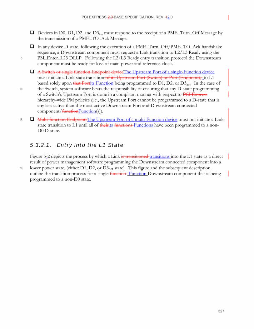
PCI EXPRESS 2.0 BASE SPECIFICATION, REV. 12.0
327
Devices in D0, D1, D2, and D3hot must respond to the receipt of a PME_Turn_Off Message by the transmission of a PME_TO_Ack Message.
In any device D state, following the execution of a PME_Turn_Off/PME_TO_Ack handshake sequence, a Downstream component must request a Link transition to L2/L3 Ready using the PM_Enter_L23 DLLP. Following the L2/L3 Ready entry transition protocol the Downstream 5 component must be ready for loss of main power and reference clock.
A Switch or single function Endpoint deviceThe Upstream Port of a single-Function device must initiate a Link state transition of its Upstream Port (Switch) or Port (Endpoint), to L1 based solely upon that Portits Function being programmed to D1, D2, or D3hot. In the case of the Switch, system software bears the responsibility of ensuring that any D-state programming 10 of a Switch’s Upstream Port is done in a compliant manner with respect to PCI Express hierarchy-wide PM policies (i.e., the Upstream Port cannot be programmed to a D-state that is any less active than the most active Downstream Port and Downstream connected component/functionFunction(s)).
Multi-function EndpointsThe Upstream Port of a multi-Function device must not initiate a Link 15 state transition to L1 until all of theirits functions Functions have been programmed to a non-D0 D-state.
5.3.2.1. Entry into the L1 State
Figure 5-2 depicts the process by which a Link is transitioned transitions into the L1 state as a direct result of power management software programming the Downstream connected component into a lower power state, (either D1, D2, or D3hot state). This figure and the subsequent description 20 outline the transition process for a single function -Function Downstream component that is being programmed to a non-D0 state.
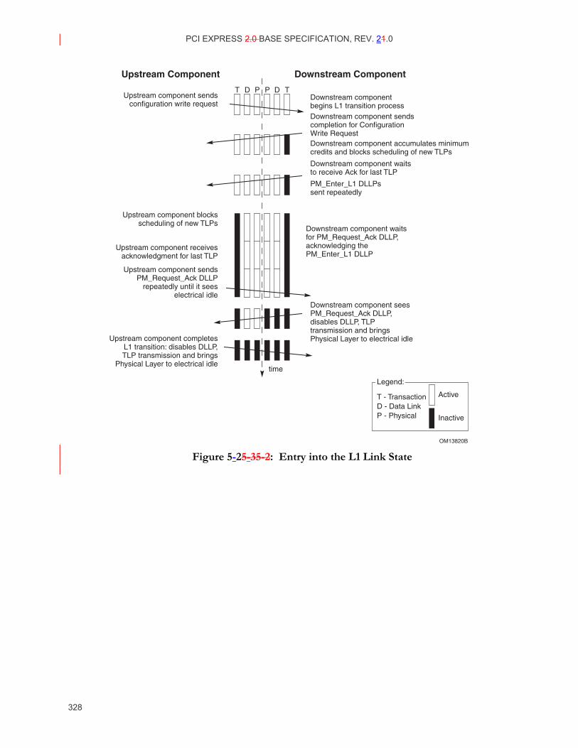
PCI EXPRESS 2.0 BASE SPECIFICATION, REV. 21.0
328
OM13820B
T D P P D TUpstream component sends
configuration write request
Upstream Component Downstream Component
Upstream component blocksscheduling of new TLPs
Upstream component receivesacknowledgment for last TLP
Upstream component sendsPM_Request_Ack DLLP
repeatedly until it seeselectrical idle
Upstream component completesL1 transition: disables DLLP,TLP transmission and brings
Physical Layer to electrical idle
Downstream component seesPM_Request_Ack DLLP,disables DLLP, TLPtransmission and bringsPhysical Layer to electrical idle
Downstream componentbegins L1 transition processDownstream component sendscompletion for ConfigurationWrite RequestDownstream component accumulates minimumcredits and blocks scheduling of new TLPs
Downstream component waitsto receive Ack for last TLP
PM_Enter_L1 DLLPssent repeatedly
time
Downstream component waitsfor PM_Request_Ack DLLP,acknowledging thePM_Enter_L1 DLLP
T - TransactionD - Data LinkP - Physical
Active
Inactive
Legend:
Figure 5-25-3 5-2: Entry into the L1 Link State
PCI EXPRESS 2.0 BASE SPECIFICATION, REV. 12.0
329
The following text provides additional detail for the Link state transition process shown in Figure 5-2.
PM Software Request:
1. PM Software software sends a Configuration Write Request TLP configuration write to the Downstream function’s Function’s PMCSR to change the Downstream function’s Function’s D-5 state (from D0 to D1 for example).
Downstream Component Link State Transition Initiation Process:
2. The Downstream component schedules the completion Completion response corresponding to the configuration Configuration write Write Request to its PMCSR PowerState field and accounts for the completion credits required. 10
3. The Downstream component must then wait until it accumulates at least the minimum number of credits required to send the largest possible packet for any FC type (if it does not already have such credits). All Transaction Layer TLP scheduling is then suspended.
4. The Downstream component then waits until it receives a Link Layer acknowledgement for the PMCSR write Write completionCompletion, and any other TLPs it had previously sent. The 15 component must retransmit a TLP out of its Data Link Layer Retry buffer if required to do so by Data Link Layer rules.
5. Once all of the Downstream component’s’ TLPs have been acknowledged, the Downstream component starts to transmit PM_Enter_L1 DLLPs. The Downstream component sends this DLLP repeatedly with no more than 4four symbol Symbol times of idle between subsequent 20 transmissions of the PM_Enter_L1 DLLP. The transmission of other DLLPs and SKP ordered setOrdered Sets is permitted at any time between PM_Enter_L1 transmissions, and do not contribute to the four symbol Symbol time idle limit.
The Downstream component continues to transmit the PM_Enter_L1 DLLP as described above until it receives a response from the Upstream component48 (PM_Request_Ack). 25
The Downstream component must continue to accept TLPs and DLLPs from the Upstream component, and it must also continue to respond with DLLPs, including FC update DLLPs and Ack/Nak DLLPs, as required. Any TLPs that are blocked from transmission (including responses to TLP(s) received) must be stored for later transmission, and must cause the Downstream component to initiate L1 exit as soon as possible following L1 entry. 30
Upstream Component Link State Transition Process:
6. Upon receiving the PM_Enter_L1 DLLP, the Upstream component blocks the scheduling of all TLP transmissions.
7. The Upstream component then must wait until it receives a Link Layer acknowledgement for the last TLP it had previously sent. The Upstream component must retransmit a TLP from its 35 Link Layer retry buffer if required to do so by the Link Layer rules.
8. Once all of the Upstream component’s TLPs have been acknowledged, the Upstream component must send PM_Request_Ack DLLPs downstreamDownstream, regardless of any
48 If at this point the Downstream component needs to initiate a transfer on the Link, it must first complete the transition to L1 regardless. Once in L1 it is then permitted to initiate an exit L1 to handle the transfer.
PCI EXPRESS 2.0 BASE SPECIFICATION, REV. 21.0
330
outstanding Requests. The Upstream component sends this DLLP repeatedly with no more than 4 four symbol Symbol times of idle between subsequent transmissions of the PM_Request_Ack DLLP. The transmission of SKP ordered setOrdered Sets is permitted at any time between PM_Request_Ack transmissions, and does not contribute to the 4 four symbol Symbol time idle limit. 5
The Upstream component continues to transmit the PM_Request_Ack DLLP as described above until it observes its receive Lanes enter into the Electrical Idle state. See Refer to Chapter 4 for more details on the Physical Layer behavior.
Completing the L1 Link State Transition:
9. Once the Downstream component has captured the PM_Request_Ack DLLP on its Receive 10 Lanes (signaling that the Upstream component acknowledged the transition to L1 request), it then disables DLLP transmission and brings the upstream Upstream directed physical Link into the Electrical Idle state.
10. When the Receive Lanes on the Upstream component observes its Receive Lanes enter the Electrical Idle state, it thenthe Upstream component stops sending PM_Request_Ack DLLPs, 15 disables DLLP transmission, and brings its Transmit Lanes to Electrical Idle completing the transition of the Link to L1.
When two components’ interconnecting Link is in L1 as a result of the Downstream component being programmed to a non-D0 state, both components suspend the operation of their Flow Control Update, TLP Completion Timeout, and, if implemented, Update FCP Timer (see 20 Section 2.6.1.2) counter mechanisms. Refer to Chapter 4 for more detail on the Physical Layer behavior.
Refer to Section 5.2 if the negotiation to L1 is interrupted.
Components on either end of a Link in L1 may optionally disable their internal PLLs in order to conserve more energy. Note, however, that platform supplied main power and reference clocks 25 must continue to be supplied to components on both ends of an L1 Link.
5.3.2.2. Exit from L1 State
L1 exit can be initiated by the component on either end of a PCI Express Link.
Upon exit from L1, it is recommended that the Downstream Component component send flow control update DLLPs for all enabled VCs and FC types starting within 1 μs of L1 exit.
The physical mechanism for transitioning a Link from L1 to L0 is described in detail in Chapter 4. 30
L1 exit must be initiated by a component if that component needs to transmit a TLP on the Link. An upstream Upstream component must initiate L1 exit on a downstream Downstream port Port even if it does not have the flow control credits needed to transmit the TLP that it needs to transmit. Following L1 exit, the upstream Upstream component must wait to receive the needed credit from the downstream Downstream component. Figure 5-3 outlines an example sequence that 35 would trigger an Upstream component to initiate transition of the Link to the L0 state.
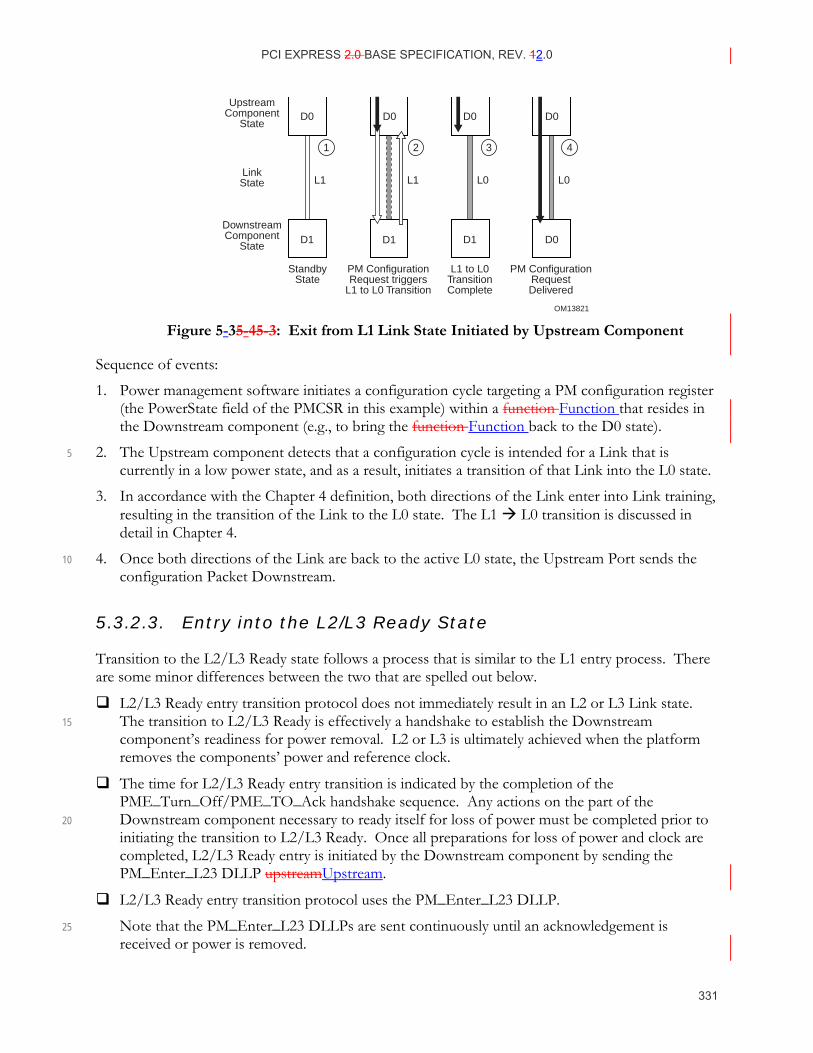
PCI EXPRESS 2.0 BASE SPECIFICATION, REV. 12.0
331
OM13821
UpstreamComponent
State
DownstreamComponent
State
StandbyState
PM ConfigurationRequest triggers
L1 to L0 Transition
L1 to L0TransitionComplete
PM ConfigurationRequestDelivered
LinkState
D0 D0 D0
D1 D1 D0
L1 L0 L0
D0
D1
L1
1 3 42
Figure 5-35-4 5-3: Exit from L1 Link State Initiated by Upstream Component
Sequence of events:
1. Power management software initiates a configuration cycle targeting a PM configuration register (the PowerState field of the PMCSR in this example) within a function Function that resides in the Downstream component (e.g., to bring the function Function back to the D0 state).
2. The Upstream component detects that a configuration cycle is intended for a Link that is 5 currently in a low power state, and as a result, initiates a transition of that Link into the L0 state.
3. In accordance with the Chapter 4 definition, both directions of the Link enter into Link training, resulting in the transition of the Link to the L0 state. The L1 L0 transition is discussed in detail in Chapter 4.
4. Once both directions of the Link are back to the active L0 state, the Upstream Port sends the 10 configuration Packet Downstream.
5.3.2.3. Entry into the L2/L3 Ready State
Transition to the L2/L3 Ready state follows a process that is similar to the L1 entry process. There are some minor differences between the two that are spelled out below.
L2/L3 Ready entry transition protocol does not immediately result in an L2 or L3 Link state. The transition to L2/L3 Ready is effectively a handshake to establish the Downstream 15 component’s readiness for power removal. L2 or L3 is ultimately achieved when the platform removes the components’ power and reference clock.
The time for L2/L3 Ready entry transition is indicated by the completion of the PME_Turn_Off/PME_TO_Ack handshake sequence. Any actions on the part of the Downstream component necessary to ready itself for loss of power must be completed prior to 20 initiating the transition to L2/L3 Ready. Once all preparations for loss of power and clock are completed, L2/L3 Ready entry is initiated by the Downstream component by sending the PM_Enter_L23 DLLP upstreamUpstream.
L2/L3 Ready entry transition protocol uses the PM_Enter_L23 DLLP.
Note that the PM_Enter_L23 DLLPs are sent continuously until an acknowledgement is 25 received or power is removed.

PCI EXPRESS 2.0 BASE SPECIFICATION, REV. 21.0
332
Refer to Section 5.2 if the negotiation to L2/L3 Ready is interrupted.
5.3.3. Power Management Event Mechanisms
5.3.3.1. Motivation
The PCI Express PME mechanism is software compatible with the PME mechanism defined by the PCI Bus Power Management Interface Specification. Power Management Events are generated by PCI Express fFunctions as a means of requesting a PM state change. Power Management Events are typically utilized to revive the system or an individual function Function from a low power state. 5
Power management software may transition a PCI Express Hierarchy into a low power state, and transition the Upstream Links of these devices into the non-communicating L2 state.49 The PCI Express PME generation mechanism is, therefore, broken into two components:
Waking a non-communicating Hierarchy (wakeup). This step is required only if the Upstream Link of the device originating the PME is in the non-communicating L2 state, since in that state 10 the device cannot send a PM_PME Message upstreamUpstream.
Sending a PM_PME Message to the root of the PCI Express Hierarchy
PME indications that originate from PCI Express Endpoints or PCI Express Legacy Endpoints are propagated to the Root Complex in the form of TLP messages. PM_PME messages Messages include the logical location ofidentify the requesting agent within the Hierarchy (in the form ofvia 15 the Requester ID of the PME message Message header). Explicit identification within the PM_PME message Message is intended to facilitate quicker PME service routine response, and hence shorter resume time.
If a Root Complex Event Collector is implemented, PME indications that originate from a Root Complex Integrated Endpoint may optionally be reported in a Root Complex Event Collector 20 residing on the same logical Logical bus Bus as the Root Complex Integrated Endpoint. The Root Complex Event Collector must explicitly declare supported Root Complex Integrated Endpoints as part of its capabilities; each Root Complex Integrated Endpoint must be associated with exactly one Root Complex Event Collector. Root Complex Event Collectors explicitly identify the logical location of the requesting agent to facilitate quicker PME service routine response. 25
PME indications that originate from a Root Port itself are reported through the same Root Port.
5.3.3.2. Link Wakeup
The Link wakeup mechanisms provide a means of signaling the platform to re-establish power and reference clocks to the components within its domain. There are two defined wakeup mechanisms: Beacon and WAKE#. The Beacon mechanism uses in-band signaling to implement wakeup functionality, and is described in Section 4.3.5.8. For components that support wakeup 30 functionality, Beacon is the required mechanism for all components, except for components 49 The L2 state is defined as “non-communicating” since component reference clock and main power supply are removed in that state.
PCI EXPRESS 2.0 BASE SPECIFICATION, REV. 12.0
333
designed exclusively for the followingthe form factor specification(s) targeted by the implementation determine the support requirements for the wakeup mechanism.: PCI Express Card Electromechanical Specification and PCI Express Mini Card Electromechanical Specification. Switch products components targeting applications where Beacon is used on some ports Ports of the Switch and WAKE# is used for other ports Ports must translate the wakeup mechanism appropriately (see the implementation 5 note entitled “Example of WAKE# to Beacon Translation” on page 334). In applications where WAKE# is the only wakeup mechanism used, the Root Complex is not required to support the receipt of Beacon. The WAKE# mechanism uses sideband signaling to implement wakeup functionality. WAKE# is an “open drain” signal asserted by components requesting wakeup and observed by the associated 10 power controller. WAKE# is only defined for certain form factors, and the detailed specifications for WAKE# are included in the relevant form factor specifications. Specific form factor specifications may require the use of either Beacon or WAKE# as the wakeup mechanism. All form factors that require WAKE# as the wakeup mechanism must permit components to also generate Beacon, although the Beacon may not be observed. 15
When WAKE# is used as a wakeup mechanism, once WAKE# has been asserted, the asserting PCI Express function Function must continue to drive the signal low until main power has been restored to the component as indicated by Fundamental Reset going inactive. WAKE# is not intended to be used as an input by any Endpoint, and the system is not required to route or buffer it in such a way that an Endpoint is guaranteed to be able to detect that the signal 20 has been asserted by another functionFunction. Before using any wakeup mechanism, functions a Function must be enabled by software to do so by setting the device’s Function’s PME_En bit in the Power Management Control/Status register (PMCSR). The PME_Status bit is sticky, and devices Functions must maintain the value of the PME_Status bit through reset if aux power is available and they are enabled for wakeup events (this 25 requirement also applies to the PME Enable bit in the PMCSR and the Aux Power PM Enable bit in the Device Control register). Systems that allow PME generation from D3cold state must provide auxiliary power to support Link wakeup when the main system power rails are off. A component may only consume auxiliary power if software has enabled it to do so as described in Section 5.5.1. Software is required to enable 30 auxiliary power consumption in all components that participate in Link wakeup, including all components that must propagate the Beacon signal. In the presence of legacy system software, this is the responsibility of system firmware. Regardless of the wakeup mechanism used, once the Link has been re-activated and trained, the requesting agent then propagates a PM_PME Message upstream Upstream to the Root Complex. 35 From a power management point of view, the two wakeup mechanisms provide the same functionality, and are not distinguished elsewhere in this chapter.
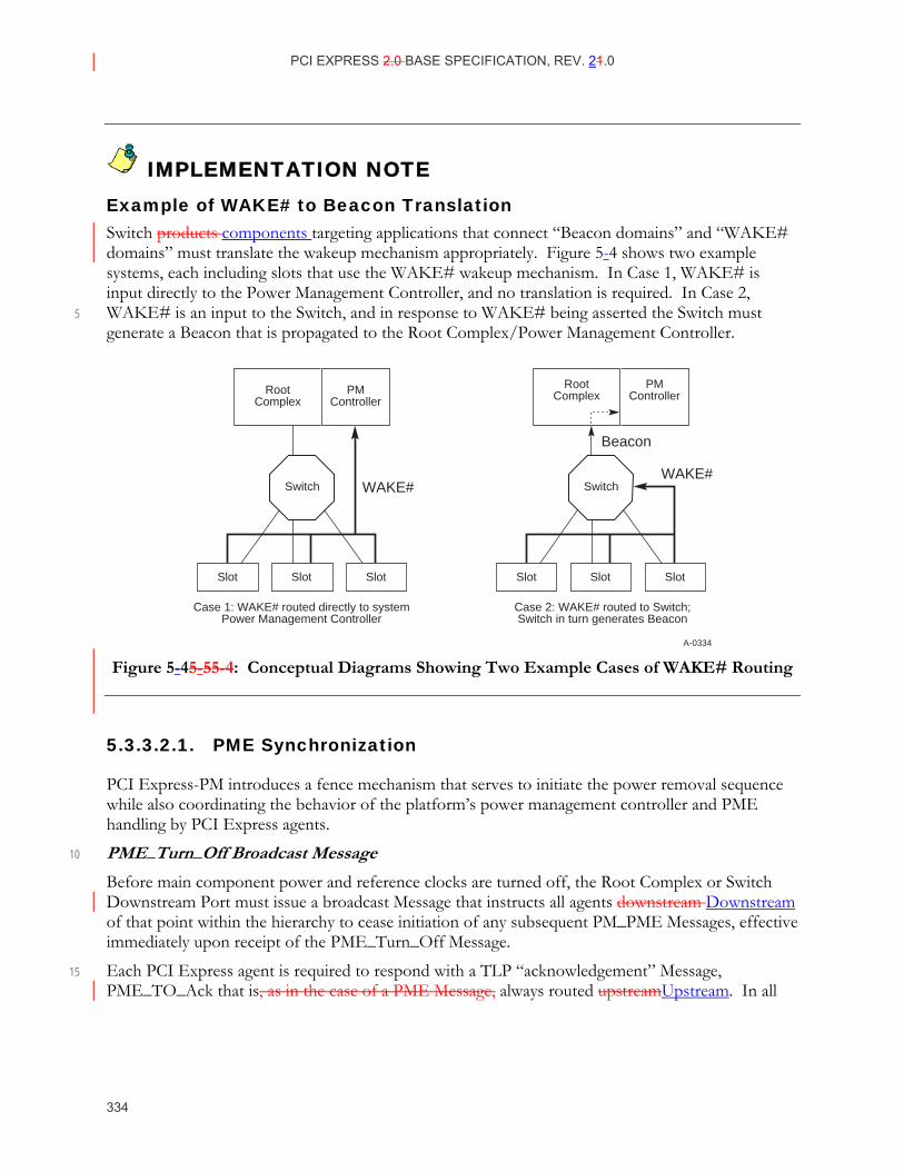
PCI EXPRESS 2.0 BASE SPECIFICATION, REV. 21.0
334
IMPLEMENTATION NOTE Example of WAKE# to Beacon Translation Switch products components targeting applications that connect “Beacon domains” and “WAKE# domains” must translate the wakeup mechanism appropriately. Figure 5-4 shows two example systems, each including slots that use the WAKE# wakeup mechanism. In Case 1, WAKE# is input directly to the Power Management Controller, and no translation is required. In Case 2, WAKE# is an input to the Switch, and in response to WAKE# being asserted the Switch must 5 generate a Beacon that is propagated to the Root Complex/Power Management Controller.
A-0334
Switch
RootComplex
PMController
SlotSlotSlot
WAKE#
Case 1: WAKE# routed directly to systemPower Management Controller
Switch
RootComplex
PMController
SlotSlotSlot
WAKE#
Beacon
Case 2: WAKE# routed to Switch;Switch in turn generates Beacon
Figure 5-45-5 5-4: Conceptual Diagrams Showing Two Example Cases of WAKE# Routing
5.3.3.2.1. PME Synchronization
PCI Express-PM introduces a fence mechanism that serves to initiate the power removal sequence while also coordinating the behavior of the platform’s power management controller and PME handling by PCI Express agents.
PME_Turn_Off Broadcast Message 10
Before main component power and reference clocks are turned off, the Root Complex or Switch Downstream Port must issue a broadcast Message that instructs all agents downstream Downstream of that point within the hierarchy to cease initiation of any subsequent PM_PME Messages, effective immediately upon receipt of the PME_Turn_Off Message.
Each PCI Express agent is required to respond with a TLP “acknowledgement” Message, 15 PME_TO_Ack that is, as in the case of a PME Message, always routed upstreamUpstream. In all
PCI EXPRESS 2.0 BASE SPECIFICATION, REV. 12.0
335
cases, the PME_TO_Ack Message must terminate at the PME_Turn_Off Message’s point of origin.50
A Switch must report an “aggregate” acknowledgement only after having received PME_TO_Ack Messages from each of its Downstream Ports. Once a PME_TO_Ack Message has arrived on each Downstream Port, the Switch must then send a PME_TO_Ack packet on its Upstream Port. The 5 occurrence of any one of the following must reset the aggregation mechanism: the transmission of the PME_TO_Ack message Message from the upstream Upstream portPort, the receipt of any TLP at the upstream Upstream portPort, the removal of main power to the Switch, or fundamental Fundamental resetReset.
All Endpoints components with an Upstream Port must accept and acknowledge the 10 PME_Turn_Off Message regardless of the D state of the associated device or any of its functions Functions for a multi-function Function device. Once an Endpoint component has sent a PME_TO_Ack Message, it must then prepare for removal of its power and reference clocks by initiating a transition to the L2/L3 Ready state.
A Switch must transition its Upstream Link to the L2/L3 Ready state after all of its Downstream 15 Ports have entered the L2/L3 Ready state.
The Links attached to the originator of the PME_Turn_Off Message are the last to assume the L2/L3 Ready state. This state transition serves as an indication to the power delivery manager51 that all Links within that portion of the PCI Express hierarchy Hierarchy have successfully retired all in flight PME Messages to the point of PME_Turn_Off Message origin and have performed any 20 necessary local conditioning in preparation for power removal.
In order to avoid deadlock in the case where one or more devices do not respond with a PME_TO_Ack Message and then put their linksLinks into the L2/L3 Ready state, the power manager must implement a timeout after waiting for a certain amount of time, after which it proceeds as if the Message had been received and all linksLinks put into the L2/L3 Ready state. The 25 recommended limit for this timer is in the range of 1 ms to 10 ms.
The power delivery manager must wait a minimum of 100 ns after observing all Links corresponding to the point of origin of the PME_Turn_Off Message enter L2/L3 Ready before removing the components’ reference clock and main power. This requirement does not apply in the case where the above mentioned timer triggers. 30
50 Point of origin for the PME_Turn_Off Message could be all of the Root Ports for a given Root Complex (full platform sleep state transition), an individual Root Port, or a Switch Downstream Port. 51 Power delivery control within this context relates to control over the entire PCI Express Link hierarchy, or over a subset of PCI Express Links ranging down to a single PCI Express Link and associated Endpoint for sub hierarchies supporting independently managed power and clock distribution.
PCI EXPRESS 2.0 BASE SPECIFICATION, REV. 21.0
336
IMPLEMENTATION NOTE
PME_TO_Ack Message Proxy by Switch Devices One of the PME_Turn_Off/PME_TO_Ack handshake's key roles is to ensure that all in flight PME Messages are flushed from the PCI Express fabric prior to sleep state power removal. This is guaranteed to occur because PME Messages and the PME_TO_Ack Messages both use the posted request queue within VC0 and so all previously injected PME Messages will be made visible to the system before the PME_TO_Ack is received at the Root Complex. Once all Downstream Ports of 5 the Root Complex receive a PME_TO_Ack Message the Root Complex can then signal the power manager that it is safe to remove power without loss of any PME Messages.
Switches create points of hierarchical expansion and, therefore, must wait for all of their connected Downstream Ports to receive a PME_TO_Ack Message before they can send a PME_TO_Ack Message upstream Upstream on behalf of the sub-hierarchy that it has created 10 downstreamDownstream. This can be accomplished very simply using common score boarding techniques. For example, once a PME_Turn_Off broadcast Message has been broadcast downstream Downstream of the Switch, the Switch simply checks off each Downstream Port having received a PME_TO_Ack. Once the last of its active Downstream Ports receives a PME_TO_Ack, the Switch will then send a single PME_TO_Ack Message upstream Upstream as a 15 proxy on behalf of the entire sub-hierarchy downstream Downstream of it. Note that once a Downstream Port receives a PME_TO_Ack Message and the Switch has scored its arrival, the Port is then free to drop the packet from its internal queues and free up the corresponding posted request queue FC credits.
5.3.3.3. PM_PME Messages
PM_PME Messages are posted Transaction Layer Packets (TLPs) that inform the power 20 management software which agent within the PCI Express Hierarchy requests a PM state change. PM_PME Messages, like all other Power Management system Messages, must use the general purpose Traffic Class, TC #0.
PM_PME Messages are always routed in the direction of the Root Complex. To send a PM_PME Message on its Upstream Link, a device must transition the Link to the L0 state (if the Link was not 25 in that state already). Unless otherwise noted, the device will keep the Link in the L0 state following the transmission of a PM_PME Message.
5.3.3.3.1. PM_PME “Backpressure” Deadlock Avoidance
A PCI Express Root Complex is typically implemented with local buffering to temporarily store temporarily a finite number of PM_PME Messages that could potentially be simultaneously propagating through the PCI Express Hierarchy at any given time. Given a limited number of 30 PM_PME Messages that can be stored within the Root Complex, there can be backpressure applied

PCI EXPRESS 2.0 BASE SPECIFICATION, REV. 12.0
337
to the upstream Upstream directed posted queue in the event that the capacity of this temporary PM_PME Message buffer is exceeded.
Deadlock can occur according to the following example scenario:
1. Incoming PM_PME Messages fill the Root Complex’s temporary storage to its capacity while there are additional PM_PME Messages still in the Hierarchy making their way 5 upstreamUpstream.
2. The Root Complex, on behalf of system software, issues a configuration Configuration read Read request Request targeting one of the PME requester’s PMCSR (e.g., reading its PME_Status bit).
3. The corresponding split completion Packet is required, as per producer/consumer ordering 10 rules, to push all previously posted PM_PME Messages out ahead of it, which in this case are PM_PME Messages that have no place to go.
4. The PME service routine cannot make progress; the PM_PME Message storage situation does not improve.
5. Deadlock occurs. 15
Precluding potential deadlocks requires the Root Complex to always enable forward progress under these circumstances. This must be done by accepting any PM_PME Messages that posted queue flow control credits allow for, and discarding any PM_PME Messages that create an overflow condition. This required behavior ensures that no deadlock will occur in these cases, ; however, PM_PME Messages will be discarded and hence lost in the process. 20
To ensure that no PM_PME Messages are lost permanently, all agents that are capable of generating PM_PME must implement a PME Service Timeout mechanism to ensure that their PME requests are serviced in a reasonable amount of time.
If after 100 ms (+ 50%/- 5%), the PME_Status bit of a requesting agent has not yet been cleared, the PME Service Timeout mechanism expires triggering the PME requesting agent to re-send the 25 temporarily lost PM_PME Message. If at this time the Link is in a non-communicating state, then, prior to re-sending the PM_PME Message, the agent must reactivate the Link as defined in Section 5.3.3.2.
5.3.3.4. PME Rules
All device Functions must implement the PCI-PM Power Management Capabilities (PMC) register and the PMCSR registers in accordance with the PCI-PM specification. These registers 30 reside in the PCI-PM compliant PCI Capability List format.
• PME capable functions Functions must implement the PME_Status bit, and underlying functional behavior, in their PMCSR configuration register.
• When a function Function initiates Link wakeup, or issues a PM_PME Message, it must set its PME_Status bit. 35
Switches must route a PM_PME received on any Downstream Port to their Upstream Port
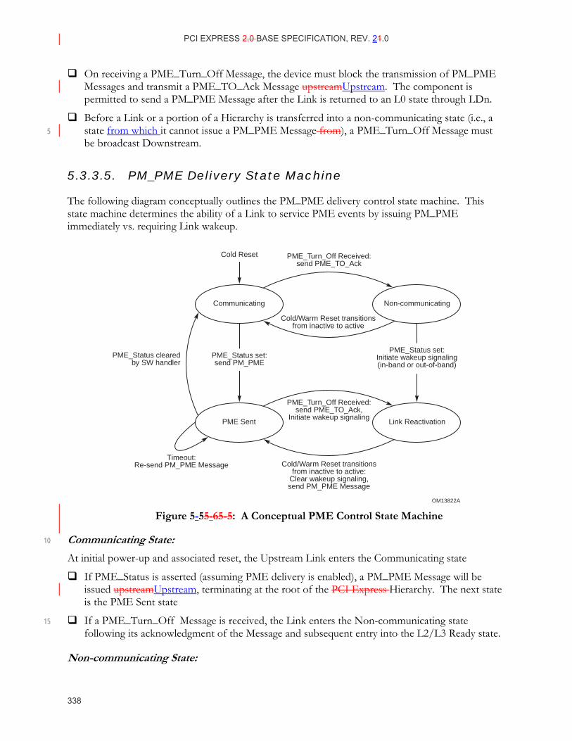
PCI EXPRESS 2.0 BASE SPECIFICATION, REV. 21.0
338
On receiving a PME_Turn_Off Message, the device must block the transmission of PM_PME Messages and transmit a PME_TO_Ack Message upstreamUpstream. The component is permitted to send a PM_PME Message after the Link is returned to an L0 state through LDn.
Before a Link or a portion of a Hierarchy is transferred into a non-communicating state (i.e., a state from which it cannot issue a PM_PME Message from), a PME_Turn_Off Message must 5 be broadcast Downstream.
5.3.3.5. PM_PME Delivery State Machine
The following diagram conceptually outlines the PM_PME delivery control state machine. This state machine determines the ability of a Link to service PME events by issuing PM_PME immediately vs. requiring Link wakeup.
OM13822A
Communicating Non-communicating
PME Sent Link Reactivation
PME_Status set:send PM_PME
PME_Status cleared by SW handler
Cold/Warm Reset transitionsfrom inactive to active:
Clear wakeup signaling,send PM_PME Message
Cold/Warm Reset transitionsfrom inactive to active
PME_Turn_Off Received:send PME_TO_Ack,
Initiate wakeup signaling
PME_Turn_Off Received:send PME_TO_Ack
PME_Status set:Initiate wakeup signaling(in-band or out-of-band)
Cold Reset
Timeout:Re-send PM_PME Message
Figure 5-55-6 5-5: A Conceptual PME Control State Machine
Communicating State: 10
At initial power-up and associated reset, the Upstream Link enters the Communicating state
If PME_Status is asserted (assuming PME delivery is enabled), a PM_PME Message will be issued upstreamUpstream, terminating at the root of the PCI Express Hierarchy. The next state is the PME Sent state
If a PME_Turn_Off Message is received, the Link enters the Non-communicating state 15 following its acknowledgment of the Message and subsequent entry into the L2/L3 Ready state.
Non-communicating State:
PCI EXPRESS 2.0 BASE SPECIFICATION, REV. 12.0
339
Following the restoration of power and clock, and the associated reset, the next state is the Communicating state.
If PME_Status is asserted, the Link will transition to the Link Reactivation state, and activate the wakeup mechanism.
PME Sent State 5
If PME_Status is cleared, the function Function becomes PME Capable again. Next state is the Communicating state.
If the PME_Status bit is not cleared Clear by the time the PME service timeout expires, a PM_PME Message is re-sent upstreamUpstream. See Refer to Section 5.3.3.3.1 for an explanation of the timeout mechanism. 10
If a PME Message has been issued but the PME_Status has not been cleared by software when the Link is about to be transitioned into a messaging incapable state (a PME_Turn_Off Message is received), the Link transitions into Link Reactivation state after sending a PME_TO_Ack Message. The device also activates the wakeup mechanism.
Link Reactivation State 15
Following the restoration of power and clock, and the associated reset, the Link resumes a transaction-capable state. The device clears the wakeup signaling, if necessary, and issues a PM_PME Upstream and transitions into the PME Sent state.
5.4. Native PCI Express Power Management Mechanisms
The following sections define power management features that require new software. While the presence of these features in new PCI Express designs will not break legacy software compatibility, 20 taking the full advantage of them requires new code to manage them.
These features are enumerated and configured using PCI Express native configuration mechanisms as described in Chapter 7 of this specification. Refer to Chapter 7 for specific register locations, bit assignments, and access mechanisms associated with these PCI Express-PM features.
5.4.1. Active State Power Management (ASPM)
All PCI Express components other than Root Complex Integrated Endpoints are required to 25 support the minimum requirements defined herein for Active State Link PM. Root Complex Integrated Endpoints do not have an associated link, and therefore do not support Active State Link PM. This feature must be treated as being orthogonal to the PCI-PM Software software compatible features from a minimum requirements perspective. For example, the Root Complex is exempt from the PCI-PM Software software compatible features requirements, ; however, it must 30 implement ASPM’s the minimum requirements of ASPM.
Components in the D0 state (i.e., fully active state) normally keep their Upstream Link in the active L0 state, as defined in Section 5.3.2. ASPM defines a protocol for components in the D0 state to
PCI EXPRESS 2.0 BASE SPECIFICATION, REV. 21.0
340
reduce Link power by placing their Links into a low power state and instructing the other end of the Link to do likewise. This capability allows hardware-autonomous, dynamic Link power reduction beyond what is achievable by software-only controlled (i.e., PCI-PM Software software driven) power management.
Two low power “standby” Link states are defined for ASPM. The L0s low power Link state is 5 optimized for short entry and exit latencies, while providing substantial power savings. If the L0s state is enabled in a device, it is required to bring any Transmit Link into L0s state whenever that Link is not in use (refer to Section 5.4.1.1.1 for details relating to the L0s invocation policy). All PCI Express components must support the L0s Link state from within the D0 device state.
The L1 Link state is optimized for maximum power savings at a cost of longer entry and exit 10 latencies. L1 reduces Link power beyond the L0s state for cases where very low power is required and longer transition times are acceptable. ASPM support for the L1 Link state is optional unless specifically required by a particular form factor.
Each PCI Express component must report its level of support for ASPM in the ASPM Support configuration field. 15
Each PCI Express component shall also report its L0s and L1 exit latency (the time that they require to transition from the L0s or L1 state to the L0 state). Endpoint Functions must also report the worst-case latency that they can withstand before risking, for example, internal fifo FIFO overruns due to the transition latency from L0s or L1 to the L0 state. Power management software can use the provided information to then enable the appropriate level of ASPM. 20
The L0s exit latency may differ significantly if the reference clock for opposing sides of a given Link is provided from the same source, or delivered to each component from a different source. PCI Express-PM software informs each PCI Express device of its clock configuration via the “common Common clock Clock configurationConfiguration” bit in their PCI Express Capability structure’s Link Control register. This bit serves as the determining factor in the L0s exit latency value reported 25 by the device. ASPM may be enabled or disabled by default depending on implementation specific criteria and/or the requirements of the associated form factor specification(s). Software can enable or disable ASPM using a process described in Section 5.4.1.3.1.
Power management software enables (or disables) ASPM in each Port of a component by programming the ASPM Control field. Note that new BIOS code can effectively enable or disable 30 ASPM functionality even when running with a legacy operating system.
IMPLEMENTATION NOTE
Isochronous Traffic and ASPM Isochronous traffic requires bounded service latency. ASPM may add latency to isochronous transactions beyond expected limits. A possible solution would be to disable ASPM for devices that are configured with an Isochronous Virtual Channel.
Multi-function EndpointsAn Upstream Port with a multi-Function device may be programmed with 35 different values in their respective Active_PM_En registers of each functionFunction. The policy
PCI EXPRESS 2.0 BASE SPECIFICATION, REV. 12.0
341
for such a component will be dictated by the most active common denominator among all D0 functions Functions according to the following rules:
Functions in a non-D0 state (D1 and deeper) are ignored in determining the ASPM policy
If any of the functionFunctions in the D0 state has its ASPM disabled (ASPM Control field = 00b) or if at least one of the functionFunctions in the D0 state is enabled for L0s only (ASPM 5 Control field = 01b) and at least one other functionFunction in the D0 state is enabled for L1 only (ASPM Control field = 10b), then ASPM is disabled for the entire component
Else, if at least one of the functionFunctions in the D0 state is enabled for L0s only (ASPM Control field = 01b), then ASPM is enabled for L0s only
Else, if at least one of the functionFunctions in the D0 state is enabled for L1 only (ASPM 10 Control field = 10b), then ASPM is enabled for L1 only
Else, ASPM is enabled for both L0s and L1 states
Note that the components must be capable of changing their behavior during runtime as device Functions enter and exit low power device states. For example, if one functionFunction within a multi-functionFunction component device is programmed to disable ASPM, then ASPM must be 15 disabled for that component device while that functionFunction is in the D0 state. Once the functionFunction transitions to a non-D0 state, ASPM can be enabled to at least the L0s state if all other functionFunctions are enabled for ASPM.
5.4.1.1. L0s ASPM State
All PCI Express devices must support the L0s low power Link state.
Transaction Layer and Link Layer timers are not affected by a transition to the L0s state (i.e., they 20 must follow the rules as defined in their respective chapters).
IMPLEMENTATION NOTE
Minimizing L0s Exit Latency L0s exit latency depends mainly on the ability of the Receiver to quickly acquire bit and Symbol synchronization. Different approaches exist for high-frequency clocking solutions which may differ significantly in their L0s exit latency, and therefore in the efficiency of ASPM. To achieve maximum power savings efficiency with ASPM, L0s exit latency should be kept low by proper selection of the 25 clocking solution.
5.4.1.1.1. Entry into the L0s State
Entry into the L0s state is managed separately for each direction of the Link. It is the responsibility of each device at either end of the Link to initiate an entry into the L0s state on its transmitting Lanes.
PCI EXPRESS 2.0 BASE SPECIFICATION, REV. 21.0
342
A Port that is disabled for the L0s state must not transition its transmitting Lanes to the L0s state. It must still however be able to tolerate having its Receiver Port Lanes entering L0s, (as a result of the device at the other end bringing its transmitting Lanes into L0s state), and then later returning to the L0 state.
L0s Invocation Policy 5
PCI Express Ports that are enabled for L0s entry must transition their Transmit Lanes to the L0s state if the defined idle conditions (below) are met for a period of time not to exceed 7 μs. Within this time period, the policy used by the Port to determine when to enter L0s is implementation specific.
Definition of Idle 10
The definition of an “idle” Upstream Port varies with device Function category. An Upstream Port with a multi-Function device is considered idle only when all of its Functions are idle.
An Endpoint Port, Function or a Root Port is determined to be idle if the following conditions are met:
No TLP is pending to transmit over the Link, or no FC credits are available to transmit any 15 TLPs
No DLLPs are pending for transmission
A Switch’s Upstream Port Function is determined to be idle if the following conditions are met:
All of the Switch’s Downstream Port Receive Lanes are in the L0s state
No pending TLPs to transmit, or no FC credits are available to transmit anything 20
No DLLPs are pending for transmission
A Switch’s Downstream Port is determined to be idle if the following conditions are met:
The Switch’s Upstream Port’s Receive Lanes are in the L0s state
No pending TLPs to transmit on this Link, or no FC credits are available
No DLLPs are pending for transmission 25
See Refer to Section 4.2 for details on L0s entry by the Physical Layer.
5.4.1.1.2. Exit from the L0s State
A component with its Transmitter in L0s must initiate L0s exit when it has a TLP or DLLP to transmit across the Link. Note that a transition from the L0s Link state does not depend on the status (or availability) of FC credits. The Link must be able to reach the L0 state, and to exchange FC credits across the Link. For example, if all credits of some type were consumed when the Link 30 entered L0s, then any component on either side of the Link must still be able to transition the Link to the L0 state when new credits need to be sent across the Link. Note that it may be appropriate for a component to anticipate the end of the idle condition and initiate L0s transmit exit; for example, when a NP request is received.

PCI EXPRESS 2.0 BASE SPECIFICATION, REV. 12.0
343
Downstream Initiated Exit
An Endpoint or SwitchThe Upstream Port of a component is permitted to initiate an exit from the L0s low low-power state on its Transmit Link, (Upstream Port Transmit Lanes in the case of a Downstream Switch), if it needs to communicate through the Link. The component initiates a transition to the L0 state on Lanes in the upstream Upstream direction as described in Section 4.2. 5
If the Upstream component is a Switch (i.e., it is not the Root Complex), then it must initiate a transition on its Upstream Port Transmit Lanes (if the Upstream Port’s Transmit Lanes are in a low low-power state) as soon as it detects an exit from L0s on any of its Downstream Ports.
Upstream Initiated Exit
The Root Complex or Switch (A Downstream Port) is permitted to initiate an exit from L0s low 10 power state on any of its Transmit Links if it needs to communicate through the Link. The component initiates a transition to the L0 state on Lanes in the downstream Downstream direction as described in Chapter 4.
If the Downstream component is contains a Switch (i.e., it is not an Endpoint), it must initiate a transition on all of its Downstream Port Transmit Lanes that are in L0s at that time as soon as it 15 detects an exit from L0s on its Upstream Port. Links that are already in the L0 state are not affected by this transition. Links whose Downstream component is in a low low-power state (i.e., D1-D3hot states) are also not affected by the exit transitions.
For example, consider a Switch with an Upstream Port in L0s and a Downstream device in a D1 state. A configuration request packet travels downstream Downstream to the Switch, intending 20 ultimately to ultimately reprogram the Downstream device from D1 to D0. The Switch’s Upstream Port Link must transition to the L0 state to allow the packet to reach the Switch. The Downstream Link connecting to the device in D1 state will not transition to the L0 state yet; it will remain in the L1 state. The captured packet is checked and routed to the Downstream Port that shares a Link with the Downstream device that is in D1. As described in Section 4.2, the Switch now transitions 25 the Downstream Link to the L0 state. Note that the transition to the L0 state was triggered by the packet being routed to that particular Downstream L1 Link, and not by the transition of the Upstream Port’s Link to the L0 state. If the packet’s destination was targeting a different Downstream Link, then that particular Downstream Link would have remained in the L1 state.
5.4.1.2. L1 ASPM State
A component may optionally support the ASPM L1 state; a state that provides greater power 30 savings at the expense of longer exit latency. L1 exit latency is visible to software, and reported via the Link Capabilities register defined in Section 7.8.6.
When supported, L1 entry is disabled by default in the ASPM Control configuration field. Software must enable ASPM L1 on the downstream Downstream component only if it is supported by both components on a Link. Software must sequence the enabling and disabling of ASPM L1 such that 35 the upstream Upstream component is enabled before the downstream Downstream component and disabled after the downstream Downstream component.
PCI EXPRESS 2.0 BASE SPECIFICATION, REV. 21.0
344
5.4.1.2.1. Entry into the L1 State
An Upstream Port on a Switch or Endpointcomponent enabled for L1 ASPM entry may initiate entry into the L1 Link state.
IMPLEMENTATION NOTE
Initiating L1 This specification does not dictate when an Endpointa component with an Upstream Port must initiate a transition to the L1 state. The interoperable mechanisms for transitioning into and out of L1 are defined within this specification, ; however, the specific ASPM policy governing when to 5 transition into L1 is left to the implementer.
One possible approach would be for the Downstream device to initiate a transition to the L1 state once the device has both its Receiver and Transmitter in the L0s state (RxL0s and TxL0s) for a set amount of time. Another approach would be for the Downstream device to initiate a transition to the L1 state once the Link has been idle in L0 for a set amount of time. This is particularly useful if 10 L0s entry is not enabled. Still another approach would be for the Downstream device to initiate a transition to the L1 state if it has completed its assigned tasks. Note that a component’s L1 invocation policy is in no way limited by these few examples.
Three power management Messages provide support for ASPM of the L1 state:
PM_ Active_State_Request_L1 (DLLP) 15
PM_ Request_Ack (DLLP)
PM_Active_State_Nak (TLP)
Downstream components enabled for ASPM L1 entry negotiate for L1 entry with the Upstream component on the Link.
A Downstream Port must accept a request to enter L1 if all of the following conditions are true: 20
The Port supports ASPM L1 entry, and ASPM L1 entry is enabled.52
No TLP is scheduled for transmission
No Ack or Nak DLLP is scheduled for transmission
A Switch Upstream Port may request L1 entry on its Link provided all of the following conditions are true: 25
The Upstream Port supports ASPM L1 entry and it is enabled
All of the Switch’s Downstream Port Links are in the L1 state (or deeper)
No pending TLPs to transmit 52 Software must enable ASPM L1 for the Downstream component only if it is also enabled for the Upstream component.
PCI EXPRESS 2.0 BASE SPECIFICATION, REV. 12.0
345
No pending DLLPs to transmit
The Upstream Port’s Receiver is idle for an implementation specific set amount of time
Note that it is legitimate for a Switch to be enabled for the ASPM L1 Link state on any of its Downstream Ports and to be disabled or not even supportive of ASPM L1 on its Upstream Port. In that case, Downstream Ports may enter the L1 Link state, but the Switch will never initiate an ASPM 5 L1 entry transition on its Upstream Port.
ASPM L1 Negotiation Rules (see Figure 5-6 and Figure 5-7)
The Downstream component must not initiate ASPM L1 entry until it accumulates at least the minimum number of credits required to send the largest possible packet for any FC type.
Upon deciding to enter a low low-power Link state, the Downstream component must block 10 movement of all TLPs from the Transaction Layer to the Data Link Layer for transmission (including completion packets).
• If any TLPs become available from the Transaction Layer for transmission during the L1 negotiation process, the transition to L1 must first be completed and then the Downstream component must initiate a return to L0. Refer to Section 5.2 if the negotiation to L1 is 15 interrupted.
The Downstream component must wait until it receives a Link Layer acknowledgement for the last TLP it had previously sent (i.e., the retry buffer is empty). The component must retransmit a TLP out of its Data Link Layer Retry buffer if required by the Data Link Layer rules.
The Downstream component then initiates ASPM negotiation by sending a 20 PM_Active_State_Request_L1 DLLP onto its Transmit Lanes. The Downstream component sends this DLLP repeatedly with no more than 4 four symbol Symbol times of idle between subsequent transmissions of the PM_Active_State_Request_L1 DLLP. The transmission of other DLLPs and SKP ordered setOrdered Sets is permittedmust occur as required at any time between PM_Active_State_Request_L1 transmissions, and do not contribute to the 4 four 25 symbol Symbol time idle limit. Transmission of SKP Ordered Sets during L1 entry follows the clock tolerance compensation rules in Section 4.2.7.
The Downstream component continues to transmit the PM_Active_State_Request_L1 DLLP as described above until it receives a response from the Upstream device (see below). The Downstream component remains in this loop waiting for a response from the Upstream 30 component.
• During this waiting period, the Downstream component must not initiate any Transaction Layer transfers. It must still accept TLPs and DLLPs from the Upstream component, storing for later transmission any TLP responses required. It continues to respond with DLLPs, including FC update DLLPs, as needed by the Link Layer protocol. 35
• If the Downstream component for any reason needs to transmit a TLP on the Link, it must first complete the transition to the low low-power Link state. Once in a lower power Link state, the Downstream component must then initiate exit of the low low-power Link state to handle the transfer. Refer to Section 5.2 if the negotiation to L1 is interrupted.
The Upstream component must immediately (while obeying all other rules in this specification) 40 respond to the request with either an acceptance or a rejection of the request.
PCI EXPRESS 2.0 BASE SPECIFICATION, REV. 21.0
346
• If the Upstream component is not able to accept the request, it must immediately (while obeying all other rules in this specification) reject the request.
Refer to Section 5.2 if the negotiation to L1 is interrupted.
Rules in case of rejection:
In the case of a rejection, the Upstream component must schedule, as soon as possible, a 5 rejection by sending the PM_Active_State_Nak Message to the Downstream component. Once the PM_Active_State_Nak Message is sent, the Upstream component is permitted to initiate any TLP or DLLP transfers.
If the request was rejected, the Downstream component must immediately transition its Transmit Lanes into the L0s state, provided L0s is enabled and that conditions for L0s entry are 10 met.
Prior to transmitting a PM_Active_State_Request_L1 DLLP associated with a subsequent ASPM L1 negotiation sequence, the Downstream component must either enter and exit L0s on its Transmitter, or it must wait at least 10 μs from the last transmission of the PM_Active_State_Request_L1 DLLP associated with the preceding ASPM L1 negotiation. This 15 10 μs timer must count only time spent in the LTSSM L0 and L0s states. The timer must hold in the LTSSM Recovery state. If the Link goes down and comes back up, the timer is ignored and the component is permitted to issue new ASPM L1 request after the linkLink has come back up.
IMPLEMENTATION NOTE
ASPM L1 Accept/Reject Considerations for the Upstream Component When the Upstream component has responded to the Downstream component’s ASPM L1 request 20 with a PM_Request_Ack DLLP to accept the L1 entry request, the ASPM L1 negotiation protocol clearly and unambiguously ends with the Link entering L1. However, if the Upstream component responds with a PM_Active_State_Nak Message to reject the L1 entry request, the termination of the ASPM L1 negotiation protocol is less clear. But, both components need to be designed to unambiguously terminate the protocol exchange. If this is not done, there is the risk that the two 25 components will get out of sync with each other, and the results may be undefined. For example, consider the following case:
The Downstream component requests ASPM L1 entry by transmitting a sequence of PM_Active_State_Request_L1 DLLPs.
Due to a temporary condition, the Upstream component responds with a 30 PM_Active_State_Nak Message to reject the L1 request.
The Downstream component continues to transmit the PM_Active_State_Request_L1 DLLPs for some time before it is able to respond to the PM_Active_State_Nak Message.
Meanwhile, the temporary condition that previously caused the Upstream component to reject the L1 request is resolved, and the Upstream component erroneously sees the continuing 35
PCI EXPRESS 2.0 BASE SPECIFICATION, REV. 12.0
347
PM_Active_State_Request_L1 DLLPs as a new request to enter L1, and responds by transmitting PM_Request_Ack DLLPs downstreamDownstream.
At this point, the result is undefined, because the Downstream component views the L1 request as rejected and finishing, but the Upstream component views the situation as a second L1 request being accepted. 5
To avoid this situation, the Downstream component needs to provide a mechanism to distinguish between one ASPM L1 request and another. The Downstream component does this by entering L0s or by waiting a minimum of 10 μs from the transmission of the last PM_Active_State_Request_L1 DLLP associated with the first ASPM L1 request before starting transmission of the PM_Active_State_Request_L1 DLLPs associated with the second request (as 10 described above).
If the Upstream component is capable of exhibiting the behavior described above, then it is necessary for the Upstream component to recognize the end of an L1 request sequence by detecting a transition to L0s on its Receiver or a break in the reception of PM_Active_State_Request_L1 DLLPs of 9.5 μs measured while in L0/L0s or more as a separation between ASPM L1 requests by 15 the Downstream component.
If there is a possibility of ambiguity, the Upstream component should reject the L1 request to avoid potentially creating the ambiguous situation outlined above.
Rules in case of acceptance:
If the Upstream component is ready to accept the request, it must block scheduling of any TLPs 20 from the Transaction Layer.
The Upstream component then must wait until it receives a Data Link Layer acknowledgement for the last TLP it had previously sent. The Upstream component must retransmit a TLP if required by the Data Link Layer rules.
Once all TLPs have been acknowledged, the Upstream component sends a PM_Request_Ack 25 DLLP downstreamDownstream. The Upstream component sends this DLLP repeatedly with no more than 4 four symbol Symbol times of idle between subsequent transmissions of the PM_Request_Ack DLLP. The transmission of SKP ordered setOrdered Sets is permittedmust occur as required at any time between PM_Request_Ack transmissions, and do not contribute to the 4 four symbol Symbol time idle limit. Transmission of SKP Ordered Sets during L1 entry 30 follows the clock tolerance compensation rules in Section 4.2.7.
The Upstream component continues to transmit the PM_Request_Ack DLLP as described above until it observes its Receive Lanes enter into the Electrical Idle state. See Refer to Chapter 4 for more details on the Physical Layer behavior.
If the Upstream component needs, for any reason, to transmit a TLP on the Link after it sends a 35 PM_Request_Ack DLLP, it must first complete the transition to the low low-power state, and then initiate an exit from the low low-power state to handle the transfer once the Link is back to L0. Refer to Section 5.2 if the negotiation to L1 is interrupted.
• The Upstream component must initiate an exit from L1 in this case even if it does not have the required flow control credit to transmit the TLP(s). 40
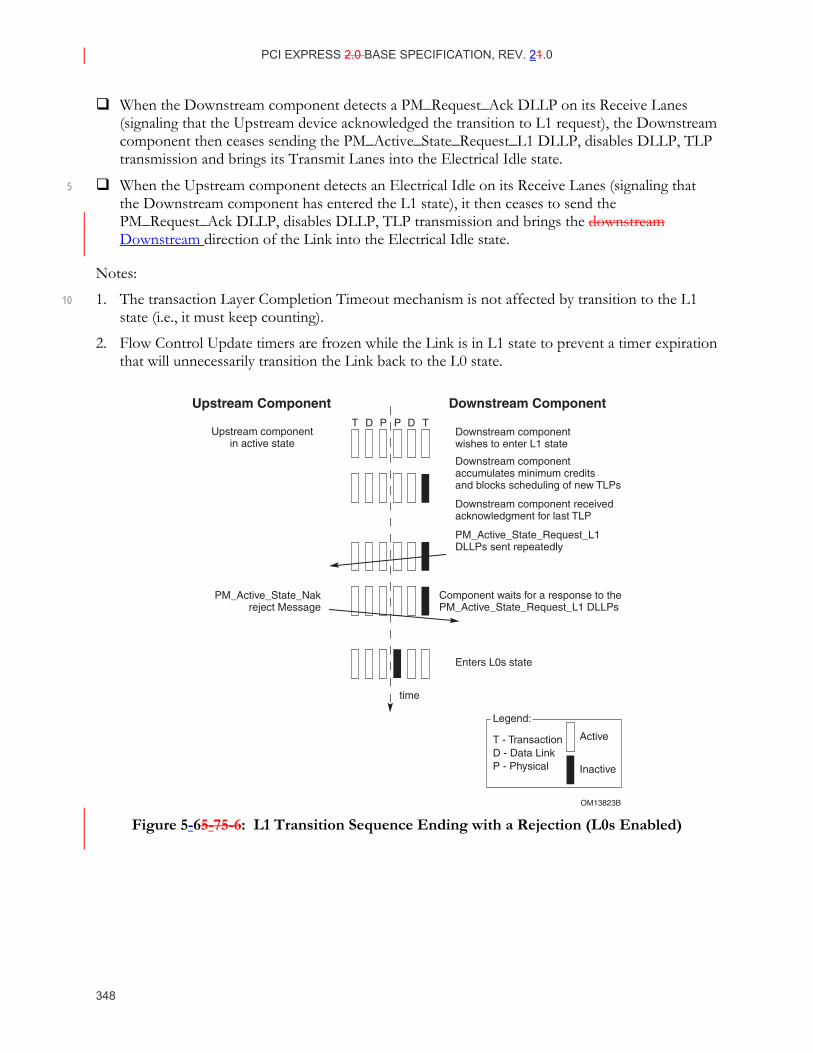
PCI EXPRESS 2.0 BASE SPECIFICATION, REV. 21.0
348
When the Downstream component detects a PM_Request_Ack DLLP on its Receive Lanes (signaling that the Upstream device acknowledged the transition to L1 request), the Downstream component then ceases sending the PM_Active_State_Request_L1 DLLP, disables DLLP, TLP transmission and brings its Transmit Lanes into the Electrical Idle state.
When the Upstream component detects an Electrical Idle on its Receive Lanes (signaling that 5 the Downstream component has entered the L1 state), it then ceases to send the PM_Request_Ack DLLP, disables DLLP, TLP transmission and brings the downstream Downstream direction of the Link into the Electrical Idle state.
Notes:
1. The transaction Layer Completion Timeout mechanism is not affected by transition to the L1 10 state (i.e., it must keep counting).
2. Flow Control Update timers are frozen while the Link is in L1 state to prevent a timer expiration that will unnecessarily transition the Link back to the L0 state.
OM13823B
T D P P D TUpstream component
in active state
PM_Active_State_Nakreject Message
Enters L0s state
Downstream componentwishes to enter L1 state
Downstream componentaccumulates minimum creditsand blocks scheduling of new TLPs
Downstream component receivedacknowledgment for last TLP
PM_Active_State_Request_L1DLLPs sent repeatedly
time
Component waits for a response to thePM_Active_State_Request_L1 DLLPs
T - TransactionD - Data LinkP - Physical
Active
Inactive
Legend:
Upstream Component Downstream Component
Figure 5-65-7 5-6: L1 Transition Sequence Ending with a Rejection (L0s Enabled)
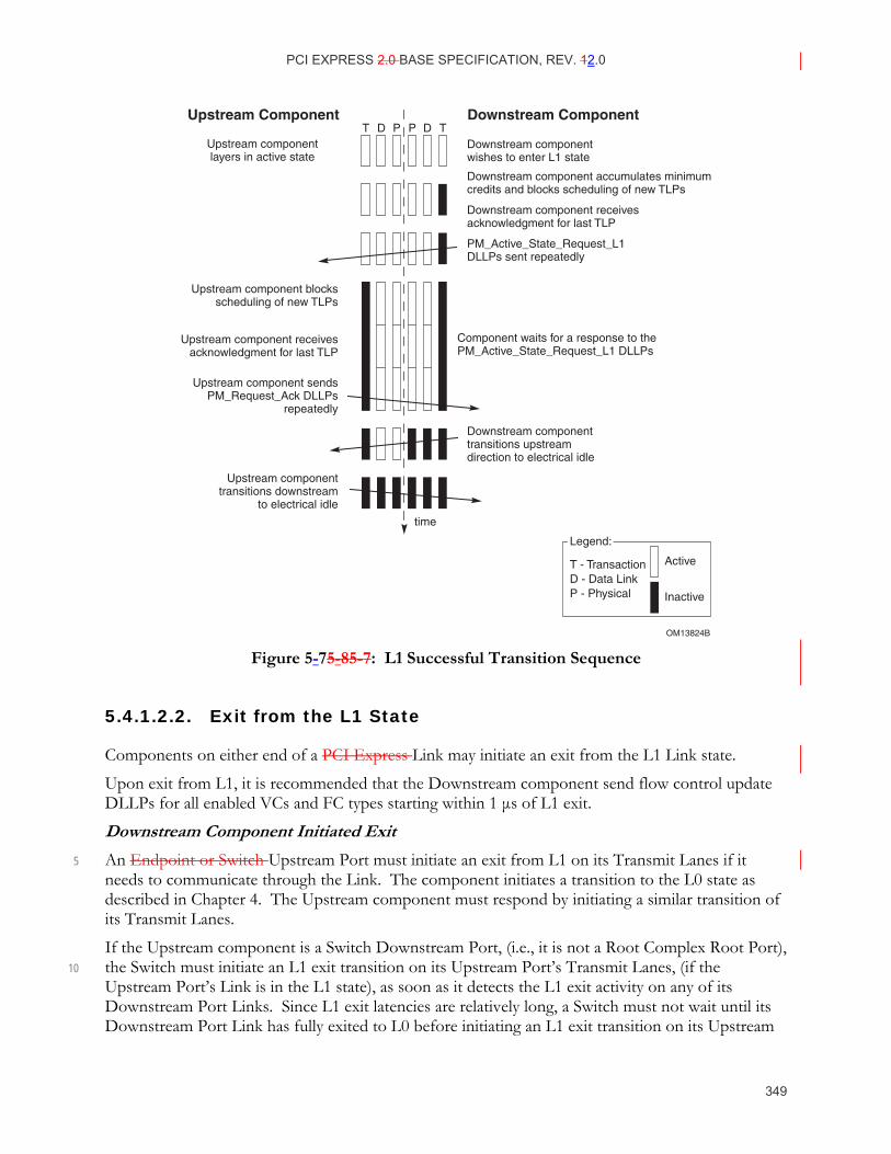
PCI EXPRESS 2.0 BASE SPECIFICATION, REV. 12.0
349
OM13824B
T D P P D TUpstream componentlayers in active state
Upstream component blocksscheduling of new TLPs
Upstream component receivesacknowledgment for last TLP
Upstream component sendsPM_Request_Ack DLLPs
repeatedly
Upstream componenttransitions downstream
to electrical idle
Downstream componenttransitions upstreamdirection to electrical idle
Downstream componentwishes to enter L1 state
Downstream component accumulates minimumcredits and blocks scheduling of new TLPs
Downstream component receivesacknowledgment for last TLP
PM_Active_State_Request_L1DLLPs sent repeatedly
time
T - TransactionD - Data LinkP - Physical
Active
Inactive
Legend:
Upstream Component Downstream Component
Component waits for a response to thePM_Active_State_Request_L1 DLLPs
Figure 5-75-8 5-7: L1 Successful Transition Sequence
5.4.1.2.2. Exit from the L1 State
Components on either end of a PCI Express Link may initiate an exit from the L1 Link state.
Upon exit from L1, it is recommended that the Downstream component send flow control update DLLPs for all enabled VCs and FC types starting within 1 μs of L1 exit.
Downstream Component Initiated Exit
An Endpoint or Switch Upstream Port must initiate an exit from L1 on its Transmit Lanes if it 5 needs to communicate through the Link. The component initiates a transition to the L0 state as described in Chapter 4. The Upstream component must respond by initiating a similar transition of its Transmit Lanes.
If the Upstream component is a Switch Downstream Port, (i.e., it is not a Root Complex Root Port), the Switch must initiate an L1 exit transition on its Upstream Port’s Transmit Lanes, (if the 10 Upstream Port’s Link is in the L1 state), as soon as it detects the L1 exit activity on any of its Downstream Port Links. Since L1 exit latencies are relatively long, a Switch must not wait until its Downstream Port Link has fully exited to L0 before initiating an L1 exit transition on its Upstream
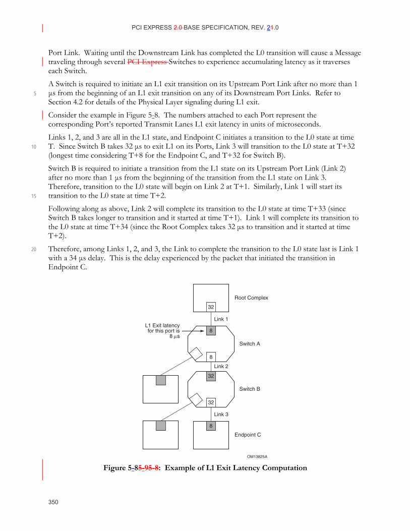
PCI EXPRESS 2.0 BASE SPECIFICATION, REV. 21.0
350
Port Link. Waiting until the Downstream Link has completed the L0 transition will cause a Message traveling through several PCI Express Switches to experience accumulating latency as it traverses each Switch.
A Switch is required to initiate an L1 exit transition on its Upstream Port Link after no more than 1 μs from the beginning of an L1 exit transition on any of its Downstream Port Links. Refer to 5 Section 4.2 for details of the Physical Layer signaling during L1 exit.
Consider the example in Figure 5-8. The numbers attached to each Port represent the corresponding Port’s reported Transmit Lanes L1 exit latency in units of microseconds.
Links 1, 2, and 3 are all in the L1 state, and Endpoint C initiates a transition to the L0 state at time T. Since Switch B takes 32 μs to exit L1 on its Ports, Link 3 will transition to the L0 state at T+32 10 (longest time considering T+8 for the Endpoint C, and T+32 for Switch B).
Switch B is required to initiate a transition from the L1 state on its Upstream Port Link (Link 2) after no more than 1 μs from the beginning of the transition from the L1 state on Link 3. Therefore, transition to the L0 state will begin on Link 2 at T+1. Similarly, Link 1 will start its transition to the L0 state at time T+2. 15
Following along as above, Link 2 will complete its transition to the L0 state at time T+33 (since Switch B takes longer to transition and it started at time T+1). Link 1 will complete its transition to the L0 state at time T+34 (since the Root Complex takes 32 μs to transition and it started at time T+2).
Therefore, among Links 1, 2, and 3, the Link to complete the transition to the L0 state last is Link 1 20 with a 34 μs delay. This is the delay experienced by the packet that initiated the transition in Endpoint C.
OM13825A
Root Complex
Switch A
Switch B
Endpoint C
Link 1
Link 2
Link 3
L1 Exit latencyfor this port is
8 μs
32
8
8
8
32
32
Figure 5-85-9 5-8: Example of L1 Exit Latency Computation
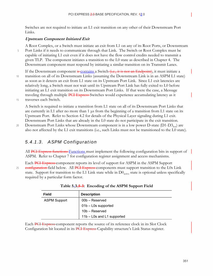
PCI EXPRESS 2.0 BASE SPECIFICATION, REV. 12.0
351
Switches are not required to initiate an L1 exit transition on any other of their Downstream Port Links.
Upstream Component Initiated Exit
A Root Complex, or a Switch must initiate an exit from L1 on any of its Root Ports, or Downstream Port Links if it needs to communicate through that Link. The Switch or Root Complex must be 5 capable of initiating L1 exit even if it does not have the flow control credits needed to transmit a given TLP. The component initiates a transition to the L0 state as described in Chapter 4. The Downstream component must respond by initiating a similar transition on its Transmit Lanes.
If the Downstream component is contains a Switch (i.e., it is not an Endpoint), it must initiate a transition on all of its Downstream Links (assuming the Downstream Link is in an ASPM L1 state) 10 as soon as it detects an exit from L1 state on its Upstream Port Link. Since L1 exit latencies are relatively long, a Switch must not wait until its Upstream Port Link has fully exited to L0 before initiating an L1 exit transition on its Downstream Port Links. If that were the case, a Message traveling through multiple PCI Express Switches would experience accumulating latency as it traverses each Switch. 15
A Switch is required to initiate a transition from L1 state on all of its Downstream Port Links that are currently in L1 after no more than 1 μs from the beginning of a transition from L1 state on its Upstream Port. Refer to Section 4.2 for details of the Physical Layer signaling during L1 exit. Downstream Port Links that are already in the L0 state do not participate in the exit transition. Downstream Port Links whose Downstream component is in a low power D-state (D1-D3hot) are 20 also not affected by the L1 exit transitions (i.e., such Links must not be transitioned to the L0 state).
5.4.1.3. ASPM Configuration
All PCI Express functions Functions must implement the following configuration bits in support of ASPM. Refer to Chapter 7 for configuration register assignment and access mechanisms.
Each PCI Express component reports its level of support for ASPM in the ASPM Support configuration field below. All PCI Express components must support transition to the L0s Link 25 state. Support for transition to the L1 Link state while in D0active state is optional unless specifically required by a particular form factor.
Table 5-3- 5-3: Encoding of the ASPM Support Field
Field Description ASPM Support 00b – Reserved
01b – L0s supported 10b – Reserved 11b – L0s and L1 supported
Each PCI Express component reports the source of its reference clock in its Slot Clock Configuration bit located in its PCI Express Capability structure’s Link Status register.
PCI EXPRESS 2.0 BASE SPECIFICATION, REV. 21.0
352
Table 5-4- 5-4: Description of the Slot Clock Configuration FieldBit
FieldBit Description Slot Clock Configuration
This bit indicates that the component uses the same physical reference clock that the platform provides on the connector. If the device component uses an independent clock irrespective of the presence of a reference on the connector, this bit must be clear. For Root and Switch Downstream Ports, this bit, when set, indicates that the Downstream Port is using the same reference clock as the Downstream device component or the slot. For Switch and Bridge Upstream Ports, this bit when set, indicates that the Upstream Port is using the same reference clock that the platform provides. Otherwise it is clear.
Each PCI Express component must support the Common Clock Configuration bit in their PCI Express Capability structure’s Link Status register. Software writes to this register bit to indicate to the device whether it is sharing the same clock source as the device on the other end of the Link.
Table 5-5- 5-5: Description of the Common Clock Configuration FieldBit
FieldBit Description Common Clock Configuration
This bit when set indicates that this component and the component at the opposite end of the Link are operating with a common clock source. A value of 0b indicates that this component and the component at the opposite end of the Link are operating with separate reference clock sources. Default value of this field bit is 0b. Components utilize this common clock configuration information to report the correct L0s and L1 Exit Latencies.
Each PCI Express Port reports the L0s and L1 exit latency (the time that they require to transition their Receive Lanes from the L0s or L1 state to the L0 state) in the L0s Exit Latency and the L1 Exit 5 Latency configuration fields, respectively.
If L1 state is not supported for ASPM (as reported in the ASPM Support field), the L1 Exit latency field is ignored.
Table 5-6- 5-6: Encoding of the L0s Exit Latency Field
Field Description
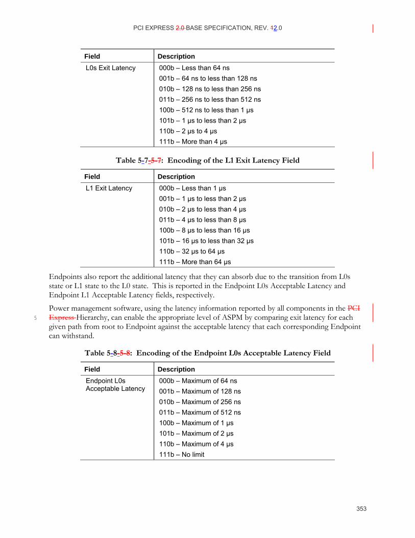
PCI EXPRESS 2.0 BASE SPECIFICATION, REV. 12.0
353
Field Description L0s Exit Latency 000b – Less than 64 ns
001b – 64 ns to less than 128 ns 010b – 128 ns to less than 256 ns 011b – 256 ns to less than 512 ns 100b – 512 ns to less than 1 μs 101b – 1 μs to less than 2 μs 110b – 2 μs to 4 μs 111b – More than 4 μs
Table 5-7- 5-7: Encoding of the L1 Exit Latency Field
Field Description L1 Exit Latency 000b – Less than 1 μs
001b – 1 μs to less than 2 μs 010b – 2 μs to less than 4 μs 011b – 4 μs to less than 8 μs 100b – 8 μs to less than 16 μs 101b – 16 μs to less than 32 μs 110b – 32 μs to 64 μs 111b – More than 64 μs
Endpoints also report the additional latency that they can absorb due to the transition from L0s state or L1 state to the L0 state. This is reported in the Endpoint L0s Acceptable Latency and Endpoint L1 Acceptable Latency fields, respectively.
Power management software, using the latency information reported by all components in the PCI Express Hierarchy, can enable the appropriate level of ASPM by comparing exit latency for each 5 given path from root to Endpoint against the acceptable latency that each corresponding Endpoint can withstand.
Table 5-8- 5-8: Encoding of the Endpoint L0s Acceptable Latency Field
Field Description Endpoint L0s Acceptable Latency
000b – Maximum of 64 ns 001b – Maximum of 128 ns 010b – Maximum of 256 ns 011b – Maximum of 512 ns 100b – Maximum of 1 μs 101b – Maximum of 2 μs 110b – Maximum of 4 μs 111b – No limit
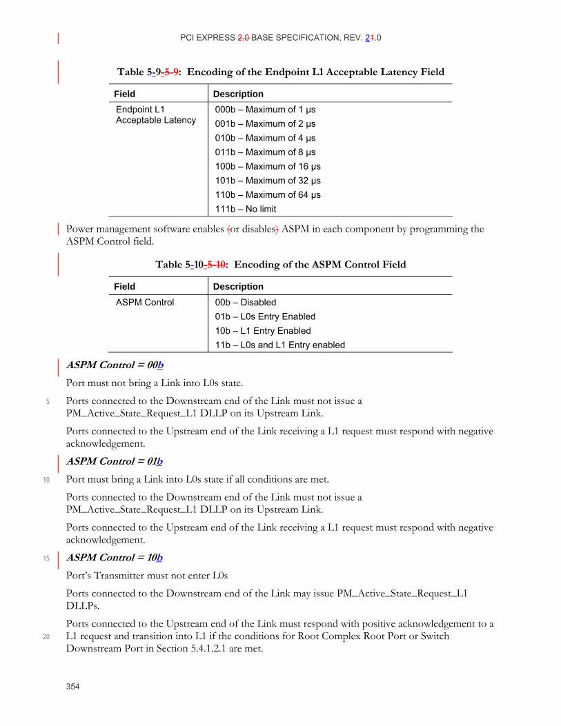
PCI EXPRESS 2.0 BASE SPECIFICATION, REV. 21.0
354
Table 5-9- 5-9: Encoding of the Endpoint L1 Acceptable Latency Field
Field Description Endpoint L1 Acceptable Latency
000b – Maximum of 1 μs 001b – Maximum of 2 μs 010b – Maximum of 4 μs 011b – Maximum of 8 μs 100b – Maximum of 16 μs 101b – Maximum of 32 μs 110b – Maximum of 64 μs 111b – No limit
Power management software enables (or disables) ASPM in each component by programming the ASPM Control field.
Table 5-10- 5-10: Encoding of the ASPM Control Field
Field Description ASPM Control 00b – Disabled
01b – L0s Entry Enabled 10b – L1 Entry Enabled 11b – L0s and L1 Entry enabled
ASPM Control = 00b
Port must not bring a Link into L0s state.
Ports connected to the Downstream end of the Link must not issue a 5 PM_Active_State_Request_L1 DLLP on its Upstream Link.
Ports connected to the Upstream end of the Link receiving a L1 request must respond with negative acknowledgement.
ASPM Control = 01b
Port must bring a Link into L0s state if all conditions are met. 10
Ports connected to the Downstream end of the Link must not issue a PM_Active_State_Request_L1 DLLP on its Upstream Link.
Ports connected to the Upstream end of the Link receiving a L1 request must respond with negative acknowledgement.
ASPM Control = 10b 15
Port’s Transmitter must not enter L0s
Ports connected to the Downstream end of the Link may issue PM_Active_State_Request_L1 DLLPs.
Ports connected to the Upstream end of the Link must respond with positive acknowledgement to a L1 request and transition into L1 if the conditions for Root Complex Root Port or Switch 20 Downstream Port in Section 5.4.1.2.1 are met.

PCI EXPRESS 2.0 BASE SPECIFICATION, REV. 12.0
355
ASPM Control = 11b
Port must bring a Link into the L0s state if all conditions are met.
Ports connected to the Downstream end of the Link may issue PM_Active_State_Request_L1 DLLPs.
Ports connected to the Upstream end of the Link must respond with positive acknowledgement to a 5 L1 request and transition into L1 if the conditions for Root Complex Root Port or Switch Downstream Port in Section 5.4.1.2.1 are met.
5.4.1.3.1. Software Flow for Enabling or Disabling ASPM
Following is an example software algorithm that highlights how to enable or disable ASPM in a PCI Express component.
PCI Express components power up with an appropriate value in their Slot Clock Configuration 10 bit. The method by which they initialize this bit is device-specific
PCI Express system software scans the Slot Clock Configuration bit in the components on both ends of each Link to determine if both are using the same reference clock source or reference clocks from separate sources. If the Slot Clock Configuration bits in both devices are setSet, they are both using the same reference clock source, otherwise they’re not. 15
PCI Express software updates the Common Clock Configuration bits in the components on both ends of each Link to indicate if those devices share the same reference clock and triggers Link retraining by writing 1b to the Retrain Link bit in the Link Control register of one of the Upstream components.
Devices must reflect the appropriate L0s/L1 exit latency in their L0s/L1 Exit Latency register 20 bits, per the setting of the Common Clock Configuration bit.
PCI Express system software then reads and calculates the L0s/L1 exit latency for each Endpoint based on the latencies reported by each Port. See Refer to Section 5.4.1.2.2 for an example.
For each Endpoint component with one or more Endpoint Functions, PCI Express system 25 software examines the Endpoint L0s/L1 Acceptable Latency, as reported by the each Endpoint component Function in their its Link Capabilities register, and enables or disables L0s/L1 entry (via the ASPM Control bits in the Link Control register) accordingly in some or all of the intervening device Ports on that hierarchy.
5.5. Auxiliary Power Support
5.5.1. Auxiliary Power Enabling
The PCI-PM specification requires that a function Function must support PME generation in order 30 to consume the maximum allowance of auxiliary current (375 mA vs. 20 mA). However, there are instances where functions Functions need to consume power even if they are “PME Disabled,” or

PCI EXPRESS 2.0 BASE SPECIFICATION, REV. 21.0
356
PME incapable by design. One example is a component with its system management mode active during a system low power state.
PCI Express PM provides a new Aux Power PM Enablecontrol bit in the Device Control register, Aux Power PM Enable, that provides the means for enabling a function Function to draw the maximum allowance of auxiliary current independent of its level of support for PME generation. 5
A PCI Express function Function requests aux power allocation by specifying a non-zero value in the Aux_Current field of the PMCower Management Capabilities register (PMC). Refer to Chapter 7 for the Aux Power PM Enable register bit assignment, and access mechanism.
Legacy PCI-PM software is unaware of this new bit and will only be able to enable aux current to a given function Function based on the function’s Function’s reported PME support, the 10 Aux_Current field value, and the function’s Function’s PME_Enable bit.
Allocation of aux power using Aux Power PM Enable is determined as follows:
Aux Power PM Enable = 1b:
Aux power is allocated as requested in the Aux_Current field of the PMCower Management Capabilities register (PMC), independent of the PME_En bit in the PMSCRower Management 15 Control/Status register (PMCSR). The PME_En bit still controls the ability to master PME.
Aux Power PM Enable = 0b:
Aux power allocation is controlled by the PME_En bit as defined in the PCI Bus Power Management Interface Specification.
The Aux Power PM Enable bit is sticky (see Section 7.4) so its state is preserved in the D3cold state, 20 and is not affected by the transitions from the D3cold state to the D0Uninitilaized state.
Typically, aux power is required to support the Beacon wakeup mechanism, and components supporting Beacon must not consume aux power unless enabled by software to do so. To enable finer granularity of power consumption, Root Ports and Switch Ports should support independent control of aux power consumption for each Port. However, it is permitted to logically OR the aux 25 power enables for multiple ports Ports and to combine the aux power control for those ports Ports so long as the combined aux power consumption does not exceed the sum of the amounts enabled by software.
5.6. Power Management System Messages and DLLPs
Table 5-11 defines the location of each PM packet in the PCI Express stack.
Table 5-11- 5-11: Power Management System Messages and DLLPs
Packet Type PM_Enter_L1 DLLP PM_Enter_L23 DLLP PM_Active_State_Request_L1 DLLP PM_Request_Ack DLLP
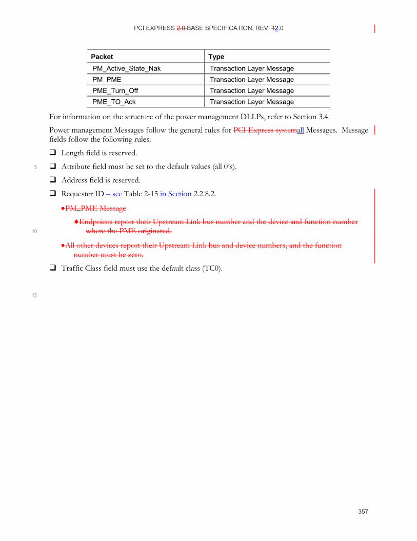
PCI EXPRESS 2.0 BASE SPECIFICATION, REV. 12.0
357
Packet Type PM_Active_State_Nak Transaction Layer Message PM_PME Transaction Layer Message PME_Turn_Off Transaction Layer Message PME_TO_Ack Transaction Layer Message
For information on the structure of the power management DLLPs, refer to Section 3.4.
Power management Messages follow the general rules for PCI Express systemall Messages. Message fields follow the following rules:
Length field is reserved.
Attribute field must be set to the default values (all 0’s). 5
Address field is reserved.
Requester ID – see Table 2-15 in Section 2.2.8.2.
•PM_PME Message
♦Endpoints report their Upstream Link bus number and the device and function number where the PME originated. 10
•All other devices report their Upstream Link bus and device numbers, and the function number must be zero.
Traffic Class field must use the default class (TC0).
15
PCI EXPRESS 2.0 BASE SPECIFICATION, REV. 21.0
358
6. System Architecture This chapter addresses various aspects of PCI Express interconnect architecture in a platform context. It covers the details of interrupt support, error signaling and logging, Virtual Channel and isochronous support, device synchronization, lock, reset and Hot-Plug.
6.1. Interrupt and PME Support The PCI Express interrupt model supports two mechanisms:
INTx emulation 5
Message Signaled Interrupt (MSI/MSI-X) Support.
For legacy compatibility, PCI Express provides a PCI INTx emulation mechanism to signal interrupts to the system interrupt controller (typically part of the Root Complex). This mechanism is compatible with existing PCI software, and provides the same level and type of service as the corresponding PCI interrupt signaling mechanism and is independent of system interrupt controller 10 specifics. This legacy compatibility mechanism allows boot device support without requiring complex BIOS-level interrupt configuration/control service stacks. It virtualizes PCI physical interrupt signals by using an in-band signaling mechanism.
In addition to PCI INTx compatible interrupt emulation, PCI Express requires support of MSI or MSI-X or both. The PCI Express MSI and MSI-X mechanisms are compatible with those defined 15 in the PCI Local Bus Specification, Revision 3.0.
6.1.1. Rationale for PCI Express Interrupt Model
PCI Express takes an evolutionary approach from PCI with respect to interrupt support.
As required for PCI/PCI-X interrupt mechanisms, each device Function is required to differentiate between INTx (legacy) and MSI (native) modes of operation. The PCI Express device complexity required to support both schemes is no different than that for PCI/PCI-X devices today. The 20 advantages of this approach include:
Compatibility with existing PCI Software Models
Direct support for boot devices
Easier End of Life (EOL) for INTx legacy mechanisms.
Existing software model is used to differentiate legacy (INTx) vs. MSI modes of operation; thus, no 25 special software support is required for PCI Express.
6
PCI EXPRESS 2.0 BASE SPECIFICATION, REV. 12.0
359
6.1.2. PCI Compatible INTx Emulation
PCI Express supports the PCI interrupts as defined in the PCI Local Bus Specification, Revision 3.0 including the Interrupt Pin and Interrupt Line registers of the PCI configuration spaceConfiguration Space for PCI device Functions. PCI Express devices support these registers for backwards compatibility; actual interrupt signaling uses in-band Messages rather than being signaled using physical pins. 5
Two types of Messages are defined, Assert_INTx and Deassert_INTx, for emulation of PCI INTx signaling, where x is A, B, C, and D for respective PCI interrupt signals. These Messages are used to provide “virtual wires” for signaling interrupts across a Link. Switches collect these virtual wires and present a combined set at the Switch’s Upstream Port. Ultimately, the virtual wires are routed to the Root Complex which maps the virtual wires to system interrupt resources. PCI Express dDevices 10 must use assert/de-assert Messages in pairs to emulate PCI interrupt level-triggered signaling. Actual mapping of PCI Express INTx emulation to system interrupts is implementation specific as is mapping of physical interrupt signals in conventional PCI today.
The legacy INTx emulation mechanism may be depreciated deprecated in a future version of this specification. 15
6.1.3. INTx Emulation Software Model
The software model for legacy INTx emulation matches that of PCI. The system BIOS reporting of chipset/platform interrupt mapping and the association of a each device Function’s interrupt with PCI interrupt lines is handled in exactly the same manner as with previous conventional PCI systems. Legacy software reads from the each device Function’s Interrupt Pin register to determine if the device Function is interrupt driven. A value between 01 and 04 indicates that the device 20 Function uses an emulated interrupt pin to generate an interrupt.
Note that similarly to physical interrupt signals, the INTx emulation mechanism may potentially cause spurious interrupts that must be handled by the system software.
6.1.4. Message Signaled Interrupt (MSI/MSI-X) Support
MSI/MSI-X interrupt support, which is optional for PCI 3.0 devices, is required for PCI Express devices. All PCI Express device Functions that are capable of generating interrupts must support 25 MSI or MSI-X or both. The MSI and MSI-X mechanisms deliver interrupts by performing memory write transactions. MSI and MSI-X are edge-triggered interrupt mechanisms; neither the PCI Local Bus Specification, Revision 3.0 nor this specification support level-triggered MSI/MSI-X interrupts. Certain PCI devices and their drivers rely on INTx-type level-triggered interrupt behavior (addressed by the PCI Express legacy INTx emulation mechanism). To take advantage of the MSI or MSI-X 30 capability and edge-triggered interrupt semantics, these devices and their drivers may have to be redesigned.
PCI EXPRESS 2.0 BASE SPECIFICATION, REV. 21.0
360
IMPLEMENTATION NOTE
Per Vector Masking with MSI/MSI-X Devices and drivers that use MSI or MSI-X have the challenge of coordinating exactly when new interrupt messages are generated. If hardware fails to send an interrupt message that software expects, an interrupt event might be “lost.” If hardware sends an interrupt message that software is not expecting, a “spurious” interrupt might result.
Per-Vector Masking (PVM) is an architected feature for MSI and MSI-X that can be used to assist in 5 this coordination. For example, when a software interrupt service routine begins, it can mask the vector to help avoid “spurious” interrupts. After the interrupt service routine services all the interrupt conditions that it is aware of, it can unmask the vector. If any interrupt conditions remain, hardware is required to generate a new interrupt message, guaranteeing that no interrupt events are lost. 10
PVM is a standard feature with MSI-X and an optional feature for MSI. For devices that implement MSI, implementing PVM as well is highly recommended.
A legacy Legacy Endpoint that implements MSI is required to support either the 32-bit or 64-bit Message Address version of the MSI capability Capability structure. A PCI Express Endpoint that implements MSI is required to support the 64-bit Message Address version of the MSI capability 15 Capability structure.
The requestor Requester of an MSI/MSI-X transaction must set the No Snoop and Relaxed Ordering attributes of the Transaction Descriptor to 0b.
Note that, unlike INTx emulation Messages, MSI/MSI-X transactions are not restricted to TC0 traffic class. 20
IMPLEMENTATION NOTE
Synchronization of Data Traffic and Message Signaled Interrupts MSI/MSI-X transactions are permitted to use the TC that is most appropriate for the device's programming model. This is generally the same TC as is used to transfer data; for legacy I/O, TC0 should be used.
If a device uses more than one TC, it must explicitly ensure that proper synchronization is maintained between data traffic and interrupt Message(s) not using the same TC. Methods for 25 ensuring this synchronization are implementation specific. One option is for a device to issue a zero-length Read (as described in Section 2.2.5) using each additional TC used for data traffic prior to issuing the MSI/MSI-X transaction. Other methods are also possible. Note, however, that platform software (e.g., a device driver) is generally only capable of issuing transactions using TC0.

PCI EXPRESS 2.0 BASE SPECIFICATION, REV. 12.0
361
6.1.5. PME Support
PCI Express supports power management events from native PCI Express devices as well as PME-capable PCI devices.
PME signaling is accomplished using an in-band Transaction Layer PME Message (PM_PME) as described in Chapter 5.
6.1.6. Native PME Software Model
PCI Express-aware software can enable a mode where the Root Complex signals PME via an 5 interrupt. When configured for native PME support, a Root Port receives the PME Message and sets the PME Status bit in its Root Status register. If software has set the PME Interrupt Enable bit in the Root Control register to 1b, the Root Port then generates an interrupt.
If the Root Port is enabled for level-triggered interrupt signaling using the INTx messages, the virtual INTx wire must be asserted whenever and as long as all of the following conditions are 10 satisfied:
The Interrupt Disable bit in the Command register is set to 0b.
The PME Interrupt Enable bit in the Root Control register is set to 1b.
The PME Status bit in the Root Status register is set.
Note that all other interrupt sources within the same Function will assert the same virtual INTx wire 15 when requesting service.
If the Root Port is enabled for edge-triggered interrupt signaling using MSI or MSI-X, an interrupt message must be sent every time the logical AND of the following conditions transitions from FALSE to TRUE:
The associated vector is unmasked (not applicable if MSI does not support PVM). 20
The PME Interrupt Enable bit in the Root Control register is set to 1b.
The PME Status bit in the Root Status register is set.
Note that PME and Hot-Plug Event interrupts (when both are implemented) always share the same MSI or MSI-X vector, as indicated by the Interrupt Message Number field in the PCI Express Capabilities register. 25
The software handler for this interrupt can determine which device sent the PME Message by reading the PME Requester ID field in the Root Status register in a Root Port. It dismisses the interrupt by writing a 1b to the PME Status bit in the Root Status register. See Refer to Section 7.8.13 for more details.
Root Complex Event Collectors provide support for the above described functionality for Root 30 Complex Integrated Endpoints.
PCI EXPRESS 2.0 BASE SPECIFICATION, REV. 21.0
362
6.1.7. Legacy PME Software Model
Legacy software, however, will not understand this mechanism for signaling PME. In the presence of legacy system software, the system power management logic in the Root Complex receives the PME Message and informs system software through an implementation specific mechanism. The Root Complex may utilize the PCI Express Requestor IDRequester ID in the PM_PME to inform system software which device caused the power management event. 5
Because it is delivered by a Message, PME has edge-triggered semantics in PCI Express, which differs from the level-triggered PME mechanism used for conventional PCI. It is the responsibility of the Root Complex to abstract this difference from system software to maintain compatibility with conventional PCI systems.
6.1.8. Operating System Power Management Notification
In order to maintain compatibility with non-PCI Express-aware system software, system power 10 management logic must be configured by firmware to use the legacy mechanism of signaling PME by default. PCI Express-aware system software must notify the firmware prior to enabling native, interrupt-based PME signaling. In response to this notification, system firmware must, if needed, reconfigure the Root Complex to disable legacy mechanisms of signaling PME. The details of this firmware notification are beyond the scope of this specification, but since it will be executed at 15 system run-time, the response to this notification must not interfere with system software. Therefore, following control handoff to the operating system, firmware must not write to available system memory or any PCI Express resources (e.g., Configuration Space structures) owned by the operating system.Therefore, the firmware must not write to system available memory or I/O, or the configuration space headers of any PCI device. 20
6.1.9. PME Routing Between PCI Express and PCI Hierarchies
PME-capable conventional PCI and PCI-X devices assert the PME# pin to signal a power management event. The PME# signal from PCI devices may either be converted to a PCI Express in-band PME Message by a PCI Express-PCI Bridge or routed directly to the Root Complex.
If the PME# signal from a PCI device is routed directly to the Root Complex, it signals system software using the same mechanism used in present PCI systems. A Root Complex may optionally 25 provide support for signaling PME from PCI devices to system software via an interrupt. In this scenario, it is recommended for the Root Complex to detect the busBus, device Device and function Function number Number of the PCI device that asserted PME#, and use this information to fill in the PME Requester ID field in the Root Port that originated the hierarchy containing the PCI device. If this is not possible, the Root Complex may optionally write the Requester ID of the Root 30 Port to this field.
Because Root Complex Integrated Endpoints are not contained in any of the hierarchy domains originated by Root Ports, these endpoints Endpoints signal system software of a PME using the same mechanism used in present PCI systems. A Root Complex Event Collector, if implemented, enables the PCI Express Native PME model for Root Complex Integrated Endpoints. 35
PCI EXPRESS 2.0 BASE SPECIFICATION, REV. 12.0
363
6.2. Error Signaling and Logging In this document, errors which must be checked and errors which may optionally be checked are identified. Each such error is associated either with the Port or with a specific device (or function Function in a multi-function Function device), and this association is given along with the description of the error. This section will discuss how errors are classified and reported.
6.2.1. Scope
This section explains the error signaling and logging requirements for PCI Express components. 5 This includes errors which occur on the PCI Express interface itself and those errors which occur on behalf of transactions initiated on PCI Express. This section does not focus on errors which occur within the component that are unrelated to a particular PCI Express transaction. This type of error signaling is better handled through proprietary methods employing device-specific interrupts.
PCI Express defines two error reporting paradigms: the baseline capability and the Advanced Error 10 Reporting capabilityCapability. The baseline error reporting capabilities are required of all PCI Express devices and define the minimum error reporting requirements. The Advanced Error Reporting capability Capability is defined for more robust error reporting and is implemented with a specific PCI Express capability Capability structure (refer to Chapter 7 for a definition of this optional capability). This section explicitly calls out all error handling differences between the 15 baseline and the Advanced Error Reporting capabilityCapability.
All PCI Express devices support existing, non-PCI Express-aware, software for error handling by mapping PCI Express errors to existing PCI reporting mechanisms, in addition to the PCI Express-specific mechanisms.
6.2.2. Error Classification
PCI Express errors can be classified as two types: Uncorrectable errors and Correctable errors. This 20 classification separates those errors resulting in functional failure from those errors resulting in degraded performance. Uncorrectable errors can further be classified as Fatal or Non-Fatal (see Figure 6-1).
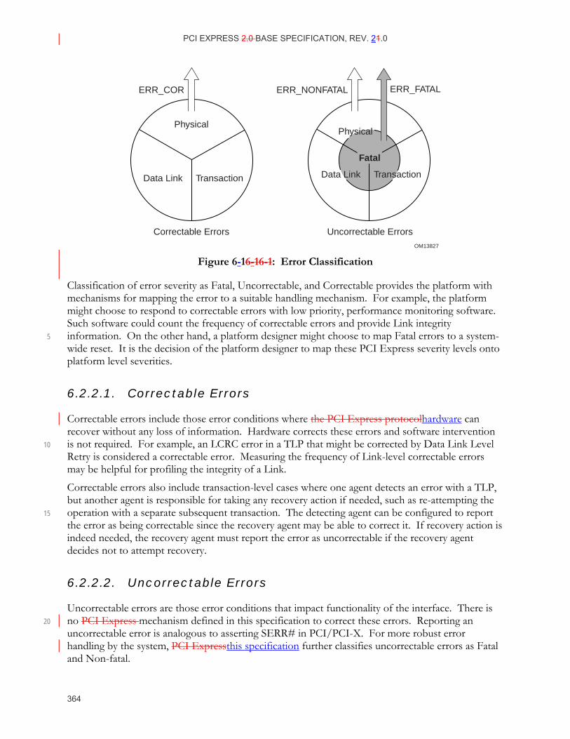
PCI EXPRESS 2.0 BASE SPECIFICATION, REV. 21.0
364
OM13827
Physical
Correctable Errors Uncorrectable Errors
ERR_COR ERR_FATAL
Data Link Transaction
ERR_NONFATAL
Fatal
Physical
Data Link Transaction
Figure 6-16-1 6-1: Error Classification
Classification of error severity as Fatal, Uncorrectable, and Correctable provides the platform with mechanisms for mapping the error to a suitable handling mechanism. For example, the platform might choose to respond to correctable errors with low priority, performance monitoring software. Such software could count the frequency of correctable errors and provide Link integrity information. On the other hand, a platform designer might choose to map Fatal errors to a system-5 wide reset. It is the decision of the platform designer to map these PCI Express severity levels onto platform level severities.
6.2.2.1. Correctable Errors
Correctable errors include those error conditions where the PCI Express protocolhardware can recover without any loss of information. Hardware corrects these errors and software intervention is not required. For example, an LCRC error in a TLP that might be corrected by Data Link Level 10 Retry is considered a correctable error. Measuring the frequency of Link-level correctable errors may be helpful for profiling the integrity of a Link.
Correctable errors also include transaction-level cases where one agent detects an error with a TLP, but another agent is responsible for taking any recovery action if needed, such as re-attempting the operation with a separate subsequent transaction. The detecting agent can be configured to report 15 the error as being correctable since the recovery agent may be able to correct it. If recovery action is indeed needed, the recovery agent must report the error as uncorrectable if the recovery agent decides not to attempt recovery.
6.2.2.2. Uncorrectable Errors
Uncorrectable errors are those error conditions that impact functionality of the interface. There is no PCI Express mechanism defined in this specification to correct these errors. Reporting an 20 uncorrectable error is analogous to asserting SERR# in PCI/PCI-X. For more robust error handling by the system, PCI Expressthis specification further classifies uncorrectable errors as Fatal and Non-fatal.
PCI EXPRESS 2.0 BASE SPECIFICATION, REV. 12.0
365
6.2.2.2.1. Fatal Errors
Fatal errors are uncorrectable error conditions which render the particular PCI Express Link and related hardware unreliable. For Fatal errors, a reset of the components on the Link may be required to return to reliable operation. Platform handling of Fatal errors, and any efforts to limit the effects of these errors, is platform implementation specific.
6.2.2.2.2. Non-Fatal Errors
Non-fatal errors are uncorrectable errors which cause a particular transaction to be unreliable but 5 the Link is otherwise fully functional. Isolating Non-fatal from Fatal errors provides Requester/Receiver logic in a device or system management software the opportunity to recover from the error without resetting the components on the Link and disturbing other transactions in progress. Devices not associated with the transaction in error are not impacted by the error.
6.2.3. Error Signaling
There are three complementary mechanisms in PCI Express which allow the agent detecting an 10 error to alert the system or another device that an error has occurred. The first mechanism is through a Completion Status, the second method is with in-band error Messages, and the third is with Error Forwarding (also known as data poisoning).
Note that it is the responsibility of the agent detecting the error to signal the error appropriately.
Section 6.2.6 describes all the errors and how the hardware is required to respond when the error is 15 detected.
6.2.3.1. Completion Status
The Completion Status field in the Completion header indicates when that the associated Request failed (refer tosee Section 2.2.9). This is one method of error reporting in PCI Express which enables the Requestor Requester to associate an error with a specific Request. In other words, since Non-Posted Requests are not considered complete until after the Completion returns, the 20 Completion Status field gives the Requester an opportunity to “fix” the problem at some higher level protocol (outside the scope of this specification). For example, if a Read is issued to prefetchable memory Memory space Space and the Completion returns with a Unsupported Request Completion Status, perhaps due to a temporary condition, the Requester may choose to reissue the Read Request without side effects. Note that from a PCI Express point of view, the reissued Read 25 Request is a distinct Request, and there is no relationship (on PCI Express) between the initial Request and the reissued Request.
PCI EXPRESS 2.0 BASE SPECIFICATION, REV. 21.0
366
6.2.3.2. Error Messages
Error Messages are sent to the Root Complex for reporting the detection of errors according to the severity of the error.
Error messages that originate from PCI Express or Legacy endpoints Endpoints are sent to corresponding Root Ports. Errors that originate from a Root Port itself are reported through the same Root Port. 5
If a Root Complex Event Collector is implemented, errors that originate from a Root Complex Integrated Endpoint may optionally be sent to the corresponding Root Complex Event Collector. Errors that originate from a Root Complex Integrated Endpoint are reported in a Root Complex Event Collector residing on the same logical Logical bus Bus as the Root Complex Integrated Endpoint. The Root Complex Event Collector must explicitly declare supported Root Complex 10 Integrated Endpoints as part of its capabilities; each Root Complex Integrated Endpoint must be associated with exactly one Root Complex Event Collector.
When multiple errors of the same severity are detected, the corresponding error Messages may be merged for different errors of the same severity. At least one error Message must be sent for detected errors of each severity level. Note, however, that the detection of a given error in some 15 cases will preclude the reporting of certain errors. See Refer to Section 6.2.3.2.3.
Table 6-1- 6-1: Error Messages
Error Message Description ERR_COR This Message is issued when the component Function or device
Device detects a correctable error on the PCI Express interface. Refer to Section 6.2.2.1 for the definition of a correctable error.
ERR_NONFATAL This Message is issued when the component Function or device Device detects a Non-fatal, uncorrectable error on the PCI Express interface. Refer to Section 6.2.2.2.2 for the definition of a Non-fatal, uncorrectable error.
ERR_FATAL This Message is issued when the component Function or device Device detects a Fatal, uncorrectable error on the PCI Express interface. Refer to Section 6.2.2.2.1 for the definition of a Fatal, uncorrectable error.
For these Messages, the Root Complex identifies the initiator of the Message by the Requester ID of the Message header. The Root Complex translates these error Messages into platform level events.
PCI EXPRESS 2.0 BASE SPECIFICATION, REV. 12.0
367
IMPLEMENTATION NOTE Use of ERR_COR, ERR_NONFATAL, and ERR_FATAL In the 1.0 and 1.0a specifications, a given error was either correctable, non-fatal, or fatal. Assuming signaling was enabled, correctable errors were always signaled with ERR_COR, non-fatal errors were always signaled with ERR_NONFATAL, and fatal errors were always signaled with ERR_FATAL.
In subsequent specifications that support Role-Based Error Reporting, non-fatal errors are 5 sometimes signaled with ERR_NONFATAL, sometimes signaled with ERR_COR, and sometimes not signaled at all, depending upon the role of the agent that detects the error and whether the agent implements AER (see Section 6.2.3.2.4). On some platforms, sending ERR_NONFATAL will preclude another agent from attempting recovery or determining the ultimate disposition of the error. For cases where the detecting agent is not the appropriate agent to determine the ultimate 10 disposition of the error, a detecting agent with AER can signal the non-fatal error with ERR_COR, which serves as an advisory notification to software. For cases where the detecting agent is the appropriate one, the agent signals the non-fatal error with ERR_NONFATAL.
For a given uncorrectable error that’s normally non-fatal, if software wishes to avoid continued hierarchy operation upon the detection of that error, software can configure detecting agents that 15 implement AER to escalate the severity of that error to fatal. A detecting agent (if enabled) will always signal a fatal error with ERR_FATAL, regardless of the agent’s role.
Software should recognize that a single transaction can be signaled by multiple agents using different types of error Messages. For example, a poisoned TLP might be signaled by intermediate Receivers with ERR_COR, while the ultimate destination Receiver might signal it with ERR_NONFATAL. 20
6.2.3.2.1. Uncorrectable Error Severity Programming (Advanced Error Reporting)
For device Functions implementing the Advanced Error Reporting capabilityCapability, the Uncorrectable Errors Severity register allows each uncorrectable error to be programmed to Fatal or Non-Fatal. Uncorrectable errors are not recoverable using defined PCI Express mechanisms. However, some platforms or devices might consider a particular error fatal to a Link or device while another platform considers that error non-fatal. The default value of the Uncorrectable Errors 25 Severity register serves as a starting point for this specification but the register can be reprogrammed if the device driver or platform software requires more robust error handling.
Baseline error handling does not support severity programming.
PCI EXPRESS 2.0 BASE SPECIFICATION, REV. 21.0
368
6.2.3.2.2. Masking Individual Errors
Section 6.2.6 lists all the errors governed by this specification and describes when each of the above error Messages are issued. The transmission of these error Messages by class (correctable, non-fatal, fatal) is enabled using the Reporting Enable fields of the Device Control register (see Section 7.8.4) or the SERR# Enable field bit in the PCI Command register (see Section 7.5.1.1).
For devices implementing the Advanced Error Reporting capability Capability the Uncorrectable 5 Error Mask register and Correctable Error Mask register allows each error condition to be masked independently. If Messages for a particular class of error are not enabled by the combined settings in the Device Control register and the PCI Command register, then no Messages of that class will be sent regardless of the values for the corresponding mask register.
If an individual error is masked when it is detected, its error status bit is still affected, but no error 10 reporting Message is sent to the Root Complex, and the Header Log and First Error Pointer registers are unmodified.
6.2.3.2.3. Error Pollution
Error pollution can occur if error conditions for a given transaction are not isolated to the most significant occurrence. For example, assume the Physical Layer detects a Receiver Error. This error is detected at the Physical Layer and an error is reported to the Root Complex. To avoid having this 15 error propagate and cause subsequent errors at upper layers (for example, a TLP error at the Data Link Layer), making it more difficult to determine the root cause of the error, subsequent errors which occur for the same packet will not be reported by the Data Link or Transaction layers. Similarly, when the Data Link Layer detects an error, subsequent errors which occur for the same packet will not be reported by the Transaction Layer. This behavior applies only to errors that are 20 associated with a particular packet – other errors are reported for each occurrence.
For errors detected in the Transaction layer, it is permitted and recommended that no more than one error be reported for a single received TLP, and that the following precedence (from highest to lowest) be used:
Receiver Overflow 25
Flow Control Protocol Error
ECRC Check Failed
Malformed TLP
Unsupported Request (UR), Completer Abort (CA), or Unexpected Completion53
Poisoned TLP Received 30
The Completion Timeout error is not in the above precedence list, since it is not detected by processing a received TLP.
53 These are mutually exclusive errors, so their relative order does not matter.
PCI EXPRESS 2.0 BASE SPECIFICATION, REV. 12.0
369
Here’s an example of the rationale behind the precedence list. If an ECRC Check fails for a given TLP, the entire contents of the TLP including its header is potentially corrupt, so it makes little sense to report errors like Malformed TLP or Unsupported Request detected with the TLP.
6.2.3.2.4. Advisory Non-Fatal Error Cases
In some cases the detector of a non-fatal error is not the most appropriate agent to determine whether the error is recoverable or not, or if it even needs any recovery action at all. For example, if 5 software attempts to perform a configuration read from a non-existent device or Function, the resulting UR Status in the Completion will signal the error to software, and software does not need for the Completer in addition to signal the error by sending an ERR_NONFATAL Message. In fact, on some platforms, signaling the error with ERR_NONFATAL results in a System Error, which breaks normal software probing. 10
“Advisory Non-Fatal Error” cases are predominantly determined by the role of the detecting agent (Requester, Completer, or Receiver) and the specific error. In such cases, an agent with AER signals the non-fatal error (if enabled) by sending an ERR_COR Message as an advisory to software, instead of sending ERR_NONFATAL. An agent without AER sends no Error Message for these cases, since software receiving ERR_COR would be unable to distinguish Advisory Non-Fatal Error 15 cases from the correctable error cases used to assess linkLink integrity.
Following are the specific cases of Advisory Non-Fatal Errors. Note that multiple errors from the same or different error classes (correctable, non-fatal, fatal) may be present with a single TLP. For example, an unexpected Completion might also be poisoned. See Refer to Section 6.2.3.2.3 for requirements and recommendations on reporting multiple errors. For the previous example, it is 20 recommended that “Unexpected Completion” be reported, and that “Poisoned TLP Received” not be reported.
If software wishes for an agent with AER to handle what would normally be an Advisory Non-Fatal Error case as being more serious, software can escalate the severity of the uncorrectable error to fatal, in which case the agent (if enabled) will signal the error with ERR_FATAL. 25
6.2.3.2.4.1. Completer Sending a Completion with UR/CA Status
A Completer generally sends a Completion with an Unsupported Request or Completer Abort (UR/CA) Status to signal a uncorrectable error for a Non-Posted Request.54 If the severity of the UR/CA error55 is non-fatal, the Completer must handle this case as an Advisory Non-Fatal Error.56 A Completer with AER signals the non-fatal error (if enabled) by sending an ERR_COR Message. A Completer without AER sends no Error Message for this case. 30
54 If the Completer is returning data in a Completion, and the data is bad or suspect, the Completer is permitted to signal the error using the Error Forwarding (Data Poisoning) mechanism instead of handling it as a UR or CA. 55 An ACS Violation error with a Non-Posted Request also results in the Completer sending a Completion with CA Status. If the severity of the ACS Violation error is non-fatal, the Completer must also handle this case as an Advisory Non-Fatal Error. 56 If the severity is fatal, the error is not an Advisory Non-Fatal Error, and must be signaled (if enabled) with ERR_FATAL.
PCI EXPRESS 2.0 BASE SPECIFICATION, REV. 21.0
370
Even though there was an uncorrectable error for this specific transaction, the Completer must handle this case as an Advisory Non-Fatal Error, since the Requester upon receiving the Completion with UR/CA Status is responsible for reporting the error (if necessary) using a Requester-specific mechanism (see Section 6.2.3.2.5).
6.2.3.2.4.2. Intermediate Receiver
When a Receiver that’s not serving as the ultimate PCI Express destination for a TLP detects57 a 5 non-fatal error with the TLP, this “intermediate” Receiver must handle this case as an Advisory Non-Fatal Error.58 A Receiver with AER signals the error (if enabled) by sending an ERR_COR Message. A Receiver without AER sends no Error Message for this case. An exception to the intermediate Receiver case for Root Complexes (RCs) and Bridges is noted below.
An example where the intermediate Receiver case occurs is a Switch that detects poison or bad 10 ECRC in a TLP that it is routing. Even though this was an uncorrectable (but non-fatal) error at this point in the TLP’s route, the intermediate Receiver handles it as an Advisory Non-Fatal Error, so that the ultimate Receiver of the TLP (i.e., the Completer for a Request TLP, or the Requester for a Completion TLP) is not precluded from handling the error more appropriately according to its error settings. For example, a given Completer that detects poison in a Memory Write Request59 15 might have the error masked (and thus go unsignaled), whereas a different Completer in the same hierarchy might signal that error with ERR_NONFATAL.
If an RC detects a non-fatal error with a TLP it normally would forward peer-to-peer between Root Ports, but the RC does not support propagating the error related information (e.g., a TLP Digest, EP bit, or equivalent) with the forwarded transaction, the RC must signal the error (if enabled) with 20 ERR_NONFATAL and also must not forward the transaction. An example is an RC needing to forward a poisoned TLP peer-to-peer between Root Ports, but the RC’s internal fabric does not support poison indication.
6.2.3.2.4.3. Ultimate PCI Express Receiver of a Poisoned TLP
When a poisoned TLP is received by its ultimate PCI Express destination, if the severity is non-fatal and the Receiver deals with the poisoned data in a manner that permits continued operation, the 25 Receiver must handle this case as an Advisory Non-Fatal Error.60 A Receiver with AER signals the error (if enabled) by sending an ERR_COR Message. A Receiver without AER sends no Error Message for this case. See Refer to Section 2.7.2.2 for special rules that apply for poisoned Memory Write Requests.
An example is a Root Complex that receives a poisoned Memory Write TLP that targets host 30 memory. If the Root Complex propagates the poisoned data along with its indication to host 57 If the Receiver does not implement ECRC Checking or ECRC Checking is not enabled, the Receiver will not detect an ECRC Check Failed error. 58 If the severity is fatal, the error is not an Advisory Non-Fatal Error, and must be signaled (if enabled) with ERR_FATAL. 59 See Section 2.7.2.2 for special rules that apply for poisoned Memory Write Requests. 60 If the severity is fatal, the error is not an Advisory Non-Fatal Error, and must be signaled (if enabled) with ERR_FATAL.
PCI EXPRESS 2.0 BASE SPECIFICATION, REV. 12.0
371
memory, it signals the error (if enabled) with an ERR_COR. If the Root Complex does not propagate the poison to host memory, it signals the error (if enabled) with ERR_NONFATAL.
Another example is a Requester that receives a poisoned Memory Read Completion TLP. If the Requester propagates the poisoned data internally or handles the error like it would for a Completion with UR/CA Status, it signals the error (if enabled) with an ERR_COR. If the 5 Requester does not handle the poison in a manner that permits continued operation, it signals the error (if enabled) with ERR_NONFATAL.
6.2.3.2.4.4. Requester with Completion Timeout
When the Requester of a Non-Posted Request times out while waiting for the associated Completion, the Requester is permitted to attempt to recover from the error by issuing a separate subsequent Request. The Requester is permitted to attempt recovery zero, one, or multiple (finite) 10 times, but must signal the error (if enabled) with an uncorrectable error Message if no further recovery attempt will be made.
If the severity of the Completion Timeout is non-fatal, and the Requester elects to attempt recovery by issuing a new request, the Requester must first handle the current error case as an Advisory Non-Fatal Error.61 A Requester with AER signals the error (if enabled) by sending an ERR_COR 15 Message. A Requester without AER sends no Error Message for this case.
Note that automatic recovery by the Requester from a Completion Timeout is generally possible only if the Non-Posted Request has no side-effects, but may also depend upon other considerations outside the scope of this specification.
6.2.3.2.4.5. Receiver of an Unexpected Completion
When a Receiver receives an unexpected Completion and the severity of the Unexpected 20 Completion error is non-fatal, the Receiver must handle this case as an Advisory Non-Fatal Error62. A Receiver with AER signals the error (if enabled) by sending an ERR_COR Message. A Receiver without AER sends no Error Message for this case.
If the unexpected Completion was a result of misrouting, the Completion Timeout mechanism at the associated Requester will trigger eventually, and the Requester may elect to attempt recovery. 25 Interference with Requester recovery can be avoided by having the Receiver of the unexpected Completion handle the error as an Advisory Non-Fatal Error.
6.2.3.2.5. Requester Receiving a Completion with UR/CA Status
When a Requester receives back a Completion with a UR/CA Status, generally the Completer has handled the error as an Advisory Non-Fatal Error, assuming the error severity was non-fatal at the
61 If the severity is fatal, the error is not an Advisory Non-Fatal Error, and must be signaled (if enabled) with ERR_FATAL. The Requester is strongly discouraged from attempting recovery since sending ERR_FATAL will often result in the entire hierarchy going down. 62 If the severity is fatal, the error is not an Advisory Non-Fatal Error, and must be signaled (if enabled) with ERR_FATAL.
PCI EXPRESS 2.0 BASE SPECIFICATION, REV. 21.0
372
Completer (see Section 6.2.3.2.4.1). The Requester must determine if any error recovery action is necessary, what type of recovery action to take, and whether or not to report the error.
If the Requester needs to report the error, the Requester must do so solely through a Requester-specific mechanism. For example, many devices have an associated device driver that can report errors to software. As another important example, the Root Complex on some platforms returns all 5 1’s to software if a Configuration Read Completion has a UR/CA Status.
The Requester is not permitted to report the error using PCI Express logging and error Message signaling.
6.2.3.3. Error Forwarding (Data Poisoning)
Error Forwarding, also known as data poisoning, is indicated by setting the EP field in a TLP. See Refer to Section 2.7.2. This is another method of error reporting in PCI Express that enables the 10 Receiver of a TLP to associate an error with a specific Request or Completion. In contrast toUnlike the Completion Status mechanism, however, Error Forwarding can be used with either Requests or Completions that contain data. In addition, “intermediate” Receivers along the TLP’s route, not just the Receiver at the ultimate destination, are required to detect and report (if enabled) receiving the poisoned TLP. This can help software determine if a particular Switch along the path poisoned the 15 TLP.
6.2.4. Error Logging
Section 6.2.6 lists all the errors governed by this specification and for each error, the logging requirements are specified. Device Functions that do not support the Advanced Error Reporting capability Capability log only the Device Status register bits indicating that an error has been detected. Note that some errors are also reported using the reporting mechanisms in the PCI 20 compatible (Type 00h and 01h) configuration registers. Section 7.5 describes how these register bits are affected by the different types of error conditions described in this section.
For device Functions supporting the Advanced Error Reporting capabilityCapability, each of the errors in Table 6-2, Table 6-3, and Table 6-4 corresponds to a particular bit in the Uncorrectable Error Status register or Correctable Error Status register. These registers are used by software to 25 determine more precisely which error and what severity occurred. For specific Transaction Layer errors the associated TLP header is recorded in the Header Log register if the error is the first uncorrectable error detected (corresponding to the setting of the First Error Pointer register).
In a multi-function Function device, PCI Express errors that are not related to any specific function Function within the device, are logged in the corresponding status and logging registers of all 30 functions Functions in that device.
The following PCI Express errors are not functionFunction-specific:
All Physical Layer errors
All Data Link Layer errors
PCI EXPRESS 2.0 BASE SPECIFICATION, REV. 12.0
373
These Transaction Layer errors:
• ECRC Fail
• UR, when caused by no function Function claiming a TLP
• Receiver Overflow
• Flow Control Protocol Error 5
• Malformed TLP
• Unexpected Completion, when caused by no Function claiming a Completion
On the detection of one of these errors, a multi-function Function device should generate at most one error reporting Message of a given severity, where the Message must report the Requestor IDRequester ID of a function Function of the device that is enabled to report that specific type of 10 error. If no function Function is enabled to send a reporting Message, the device does not send a reporting Message. If all reporting-enabled functions Functions have the same severity level set for the error, only one error Message is sent. If all reporting-enabled functions Functions do not have the same severity level set for the error, one error Message for each severity level is sent. Software is responsible for scanning all functions Functions in a multi-function Function device when it detects 15 one of those errors.
6.2.4.1. Root Complex Considerations (Advanced Error Reporting)
6.2.4.1.1. Error Source Identification
In addition to the above logging, a Root Port or Root Complex Event Collector that supports the Advanced Error Reporting capability Capability is required to implement the Error Source Identification register, which records the Requester ID of the first ERR_NONFATAL/ERR_FATAL (uncorrectable errors) and ERR_COR (correctable errors) 20 Messages received by the Root Port or Root Complex Event Collector. System software written to support Advanced Error Reporting can use the Root Error Status register to determine which fields hold valid information.
If a Root Complex Event Collector is implemented, errors from a Root Complex Integrated Endpoint may optionally be reported in a Root Complex Event Collector residing on the same 25 logical Logical bus Bus as the Root Complex Integrated Endpoint. The Root Complex Event Collector must explicitly declare supported Root Complex Integrated Endpoints as part of its capabilities. Each Root Complex Integrated Endpoint must be associated with exactly one Root Complex Event Collector.
For both Root Ports and Root Complex Event Collectors, in order for a received error Message or 30 an internally generated error Message to be recorded in the Root Error Status register and the Error Source Identification register, the error Message must be “transmitted.” See Refer to Section 6.2.8.1 for information on how received Messages are forwarded and transmitted. Internally generated error Messages are enabled for transmission with the SERR# Enable bit in the Command register
PCI EXPRESS 2.0 BASE SPECIFICATION, REV. 21.0
374
(ERR_NONFATAL and ERR_FATAL) or the Reporting Enable bits in the Device Control register (ERR_COR, ERR_NONFATAL, and ERR_FATAL).
6.2.4.1.2. Interrupt Generation
The Root Error Command register allows further control of Root Complex response to Correctable, Non-Fatal, and Fatal error Messages than the basic Root Complex capability to generate system errors in response to error Messages. Bit fields enable or disable generation of interrupts for the 5 three types of error Messages. System error generation in response to error Messages may be disabled via the PCI Express Capability structure.
If a Root Port or Root Complex Event Collector is enabled for level-triggered interrupt signaling using the INTx messages, the virtual INTx wire must be asserted whenever and as long as all of the following conditions are satisfied: 10
The Interrupt Disable bit in the Command register is set to 0b.
At least one error ErrorMessage Reporting Enable bit in the Root Error Command register and its associated error Messages Received bit in the Root Error Status register are both set to 1b.
Note that all other interrupt sources within the same Function will assert the same virtual INTx wire when requesting service. 15
If a Root Port or Root Complex Event Collector is enabled for edge-triggered interrupt signaling using MSI or MSI-X, an interrupt message must be sent every time the logical AND of the following conditions transitions from FALSE to TRUE:
The associated vector is unmasked (not applicable if MSI does not support PVM).
At least one error Error Message Reporting Enable bit in the Root Error Command register and 20 its associated error Messages Received bit in the Root Error Status register are both set to 1b.
Note that Advanced Error Reporting MSI/MSI-X interrupts always use the vector indicated by the Advanced Error Interrupt Message Number field in the Root Error Status register.
6.2.4.2. Multiple Error Handling (Advanced Error Reporting Capability)
For the Advanced Error Reporting capabilityCapability, the Uncorrectable Error Status register and Correctable Error Status register accumulate the collection of errors which occur on that particular 25 PCI Express interface. The bits remain set until explicitly cleared by software or reset. Since multiple bits might be set in the Uncorrectable Error Status register, the First Error Pointer register points to the unmasked uncorrectable error that occurred first. The First Error Pointer register is valid when the corresponding bit of the Uncorrectable Error Status register is set. The First Error Pointer value is not meaningful when the corresponding bit of the Uncorrectable Error Status 30 register is not set, or is an unimplemented or undefined bit. For errors which require header logging, the Header Log register loaded according to the same rules as the First Error Pointer register (such that the Header Log register will correspond to the error indicated in the First Error Pointer register, when the First Error Pointer register is valid).
PCI EXPRESS 2.0 BASE SPECIFICATION, REV. 12.0
375
Since the First Error Pointer and Header Log registers are only loaded for the first occurrence of an uncorrectable error, it is important that software services these registers in a timely manner, to limit the risk of missing this information for subsequent errors.
6.2.4.3. Advisory Non-Fatal Error Logging
Section 6.2.3.2.4 describes Advisory Non-Fatal Error cases, under which an agent with AER detecting an uncorrectable error of non-fatal severity signals the error (if enabled) using ERR_COR 5 instead of ERR_NONFATAL. For the same cases, an agent without AER sends no Error Message. The remaining discussion in this section is in the context of agents that do implement AER.
For Advisory Non-Fatal Error cases, since an uncorrectable error is signaled using the correctable Error Message, control/status/mask bits involving both uncorrectable and correctable errors apply. Figure 6-2 shows a flowchart of the sequence. Following are some of the unique aspects for logging 10 Advisory Non-Fatal Errors.
First, the uncorrectable error needs to be of severity non-fatal, as determined by the associated bit in the Uncorrectable Error Severity register. If the severity is fatal, the error does not qualify as an Advisory Non-Fatal Error, and will be signaled (if enabled) with ERR_FATAL.
Next, the specific error case needs to be one of the Advisory Non-Fatal Error cases documented in 15 Section 6.2.3.2.4. If not, the error does not qualify as an Advisory Non-Fatal Error, and will be signaled (if enabled) with an uncorrectable Error Message.
Next, the Advisory Non-Fatal Error Status bit is set in the Correctable Error Status register to indicate the occurrence of the advisory error, and the Advisory Non-Fatal Error Mask bit in the Correctable Error Mask register is checked to determine whether to proceed further with logging 20 and signaling.
If the Advisory Non-Fatal Error Mask bit is clear, logging proceeds by setting the “corresponding” bit in the Uncorrectable Error Status register, based upon the specific uncorrectable error that’s being reported as an advisory error. If the “corresponding” uncorrectable error bit in the Uncorrectable Error Mask register is clear, the First Error Pointer and Header Log registers are 25 updated to log the error, assuming they are not still “occupied” by a previous unserviced error.
Finally, an ERR_COR Message is sent if the Correctable Error Reporting Enable bit is set in the Device Control register.
6.2.5. Sequence of Device Error Signaling and Logging Operations
Figure 6-2 shows the sequence of operations related to signaling and logging of errors detected by a device. 30
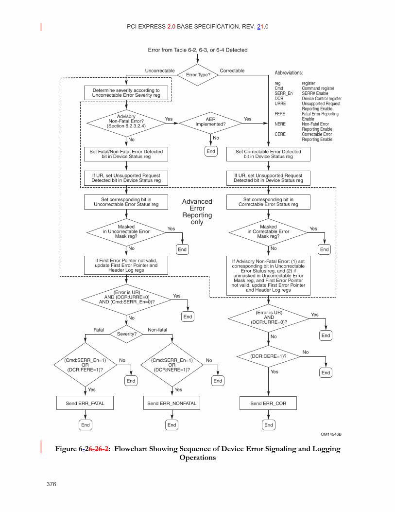
PCI EXPRESS 2.0 BASE SPECIFICATION, REV. 21.0
376
End
No
OM14546B
Error Type?
Error from Table 6-2, 6-3, or 6-4 Detected
CorrectableUncorrectable
Severity?Non-fatalFatal
Send ERR_FATAL Send ERR_NONFATAL
(Cmd:SERR_En=1)OR
(DCR:FERE=1)?
End
Yes
End
Yes
End
No (Cmd:SERR_En=1)OR
(DCR:NERE=1)?
End
No
End End
AdvancedError
Reportingonly
Determine severity according toUncorrectable Error Severity reg
Set Fatal/Non-Fatal Error Detectedbit in Device Status reg
If UR, set Unsupported RequestDetected bit in Device Status reg
Set corresponding bit inUncorrectable Error Status reg
No
If First Error Pointer not valid,update First Error Pointer and
Header Log regs
Maskedin Uncorrectable Error
Mask reg?
No
No
(Error is UR)AND (DCR:URRE=0)
AND (Cmd:SERR_En=0)?
Send ERR_COR
(DCR:CERE=1)?
End
Yes
End
Yes
End
No
End
Yes
Set Correctable Error Detectedbit in Device Status reg
If UR, set Unsupported RequestDetected bit in Device Status reg
Set corresponding bit inCorrectable Error Status reg
If Advisory Non-Fatal Error: (1) setcorresponding bit in Uncorrectable
Error Status reg, and (2) ifunmasked in Uncorrectable ErrorMask reg, and First Error Pointer
not valid, update First Error Pointerand Header Log regs
Maskedin Correctable Error
Mask reg?
No
No
(Error is UR)AND
(DCR:URRE=0)?
YesAdvisoryNon-Fatal Error?
(Section 6.2.3.2.4)AER
Implemented?Yes
Abbreviations:
regCmdSERR_EnDCRURRE
FERE
NERE
CERE
registerCommand registerSERR# EnableDevice Control registerUnsupported RequestReporting EnableFatal Error ReportingEnableNon-Fatal ErrorReporting EnableCorrectable ErrorReporting Enable
Yes Yes
Figure 6-26-2 6-2: Flowchart Showing Sequence of Device Error Signaling and Logging Operations
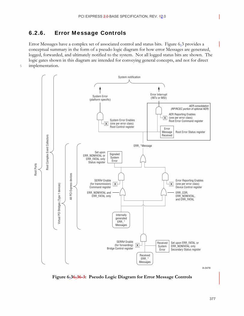
PCI EXPRESS 2.0 BASE SPECIFICATION, REV. 12.0
377
6.2.6. Error Message Controls
Error Messages have a complex set of associated control and status bits. Figure 6-3 provides a conceptual summary in the form of a pseudo logic diagram for how error Messages are generated, logged, forwarded, and ultimately notified to the system. Not all logged status bits are shown. The logic gates shown in this diagram are intended for conveying general concepts, and not for direct implementation. 5
A-0479
Root
Por
ts
Root
Com
plex
Eve
nt C
olle
ctor
s
All P
CI E
xpre
ss d
evic
es
Virtu
al P
CI B
ridge
s (T
ype
1 de
vice
s)
System notification
System Error(platform specific)
Error Interrupt(INTx or MSI)
System Error Enables(one per error class)Root Control register
ErrorMessageReceived
AER Reporting Enables(one per error class)Root Error Command register
AER consolidation(RP/RCEC portion of optional AER)
SignaledSystemError
ReceivedSystemError
Internallygenerated
ERR_*Messages
ReceivedERR_*
Messages
Root Error Status register
ERR_*Message
Set uponERR_NONFATAL or
ERR_FATAL onlyStatus register
SERR# Enable(for transmission)Command register
ERR_NONFATAL andERR_FATAL only
Error Reporting Enables(one per error class)Device Control register
ERR_COR,ERR_NONFATAL,and ERR_FATAL
Set upon ERR_FATAL orERR_NONFATAL onlySecondary Status register
SERR# Enable(for forwarding)
Bridge Control register
Figure 6-36-3 6-3: Pseudo Logic Diagram for Error Message Controls
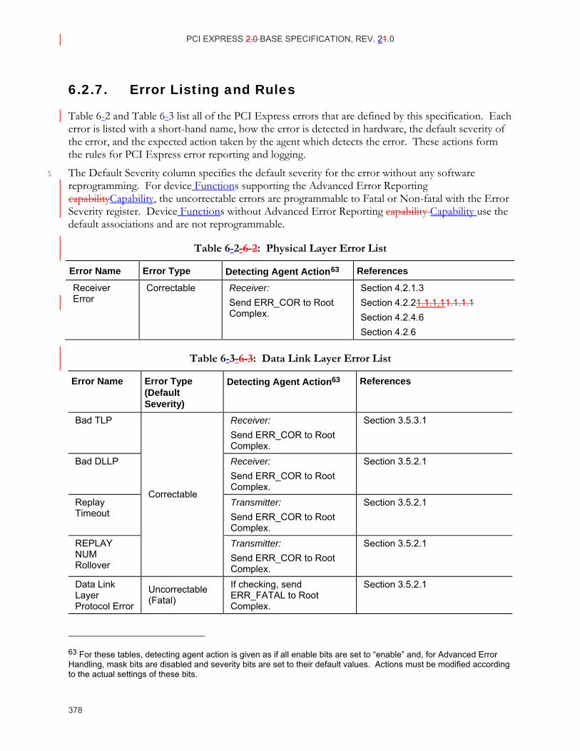
PCI EXPRESS 2.0 BASE SPECIFICATION, REV. 21.0
378
6.2.7. Error Listing and Rules
Table 6-2 and Table 6-3 list all of the PCI Express errors that are defined by this specification. Each error is listed with a short-hand name, how the error is detected in hardware, the default severity of the error, and the expected action taken by the agent which detects the error. These actions form the rules for PCI Express error reporting and logging.
The Default Severity column specifies the default severity for the error without any software 5 reprogramming. For device Functions supporting the Advanced Error Reporting capabilityCapability, the uncorrectable errors are programmable to Fatal or Non-fatal with the Error Severity register. Device Functions without Advanced Error Reporting capability Capability use the default associations and are not reprogrammable.
Table 6-2- 6-2: Physical Layer Error List
Error Name Error Type Detecting Agent Action63 References
Receiver Error
Correctable Receiver: Send ERR_COR to Root Complex.
Section 4.2.1.3 Section 4.2.21.1.1.1 1.1.1.1 Section 4.2.4.6 Section 4.2.6
Table 6-3- 6-3: Data Link Layer Error List
Error Name Error Type (Default Severity)
Detecting Agent Action63 References
Bad TLP Receiver: Send ERR_COR to Root Complex.
Section 3.5.3.1
Bad DLLP Receiver: Send ERR_COR to Root Complex.
Section 3.5.2.1
Replay Timeout
Transmitter: Send ERR_COR to Root Complex.
Section 3.5.2.1
REPLAY NUM Rollover
Correctable
Transmitter: Send ERR_COR to Root Complex.
Section 3.5.2.1
Data Link Layer Protocol Error
Uncorrectable (Fatal)
If checking, send ERR_FATAL to Root Complex.
Section 3.5.2.1
63 For these tables, detecting agent action is given as if all enable bits are set to “enable” and, for Advanced Error Handling, mask bits are disabled and severity bits are set to their default values. Actions must be modified according to the actual settings of these bits.
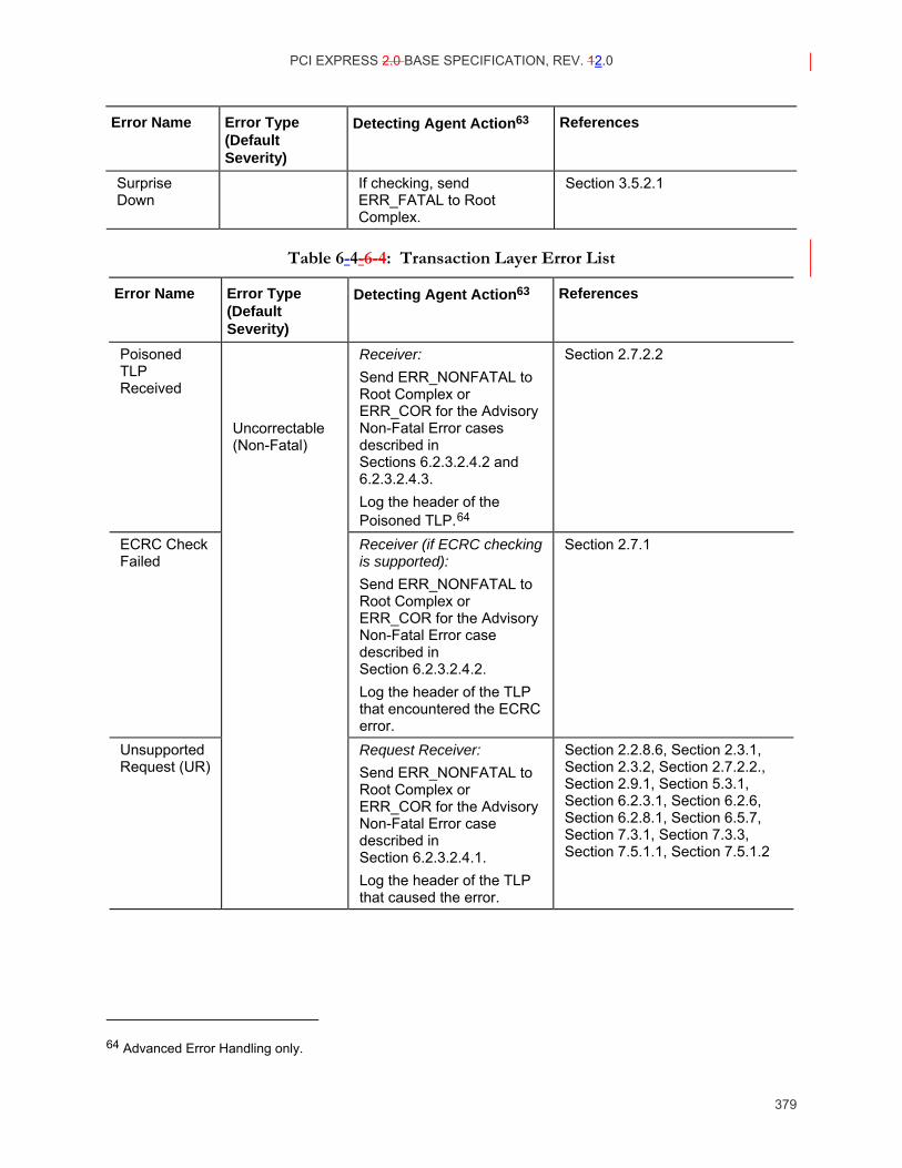
PCI EXPRESS 2.0 BASE SPECIFICATION, REV. 12.0
379
Error Name Error Type (Default Severity)
Detecting Agent Action63 References
Surprise Down
If checking, send ERR_FATAL to Root Complex.
Section 3.5.2.1
Table 6-4- 6-4: Transaction Layer Error List
Error Name Error Type (Default Severity)
Detecting Agent Action63 References
Poisoned TLP Received
Receiver: Send ERR_NONFATAL to Root Complex or ERR_COR for the Advisory Non-Fatal Error cases described in Sections 6.2.3.2.4.2 and 6.2.3.2.4.3. Log the header of the Poisoned TLP.64
Section 2.7.2.2
ECRC Check Failed
Receiver (if ECRC checking is supported): Send ERR_NONFATAL to Root Complex or ERR_COR for the Advisory Non-Fatal Error case described in Section 6.2.3.2.4.2. Log the header of the TLP that encountered the ECRC error.
Section 2.7.1
Unsupported Request (UR)
Uncorrectable (Non-Fatal)
Request Receiver: Send ERR_NONFATAL to Root Complex or ERR_COR for the Advisory Non-Fatal Error case described in Section 6.2.3.2.4.1. Log the header of the TLP that caused the error.
Section 2.2.8.6, Section 2.3.1, Section 2.3.2, Section 2.7.2.2., Section 2.9.1, Section 5.3.1, Section 6.2.3.1, Section 6.2.6, Section 6.2.8.1, Section 6.5.7, Section 7.3.1, Section 7.3.3, Section 7.5.1.1, Section 7.5.1.2
64 Advanced Error Handling only.
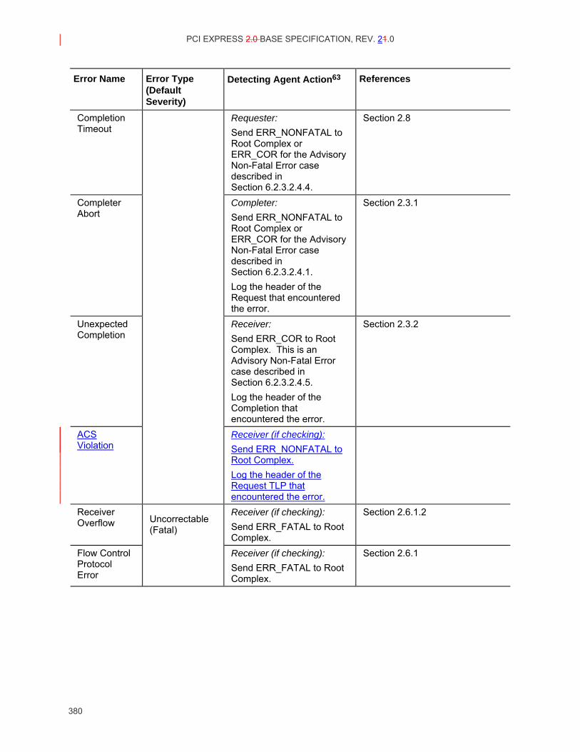
PCI EXPRESS 2.0 BASE SPECIFICATION, REV. 21.0
380
Error Name Error Type (Default Severity)
Detecting Agent Action63 References
Completion Timeout
Requester: Send ERR_NONFATAL to Root Complex or ERR_COR for the Advisory Non-Fatal Error case described in Section 6.2.3.2.4.4.
Section 2.8
Completer Abort
Completer: Send ERR_NONFATAL to Root Complex or ERR_COR for the Advisory Non-Fatal Error case described in Section 6.2.3.2.4.1. Log the header of the Request that encountered the error.
Section 2.3.1
Unexpected Completion
Receiver: Send ERR_COR to Root Complex. This is an Advisory Non-Fatal Error case described in Section 6.2.3.2.4.5. Log the header of the Completion that encountered the error.
Section 2.3.2
ACS Violation
Receiver (if checking): Send ERR_NONFATAL to Root Complex. Log the header of the Request TLP that encountered the error.
Receiver Overflow
Receiver (if checking): Send ERR_FATAL to Root Complex.
Section 2.6.1.2
Flow Control Protocol Error
Uncorrectable (Fatal)
Receiver (if checking): Send ERR_FATAL to Root Complex.
Section 2.6.1
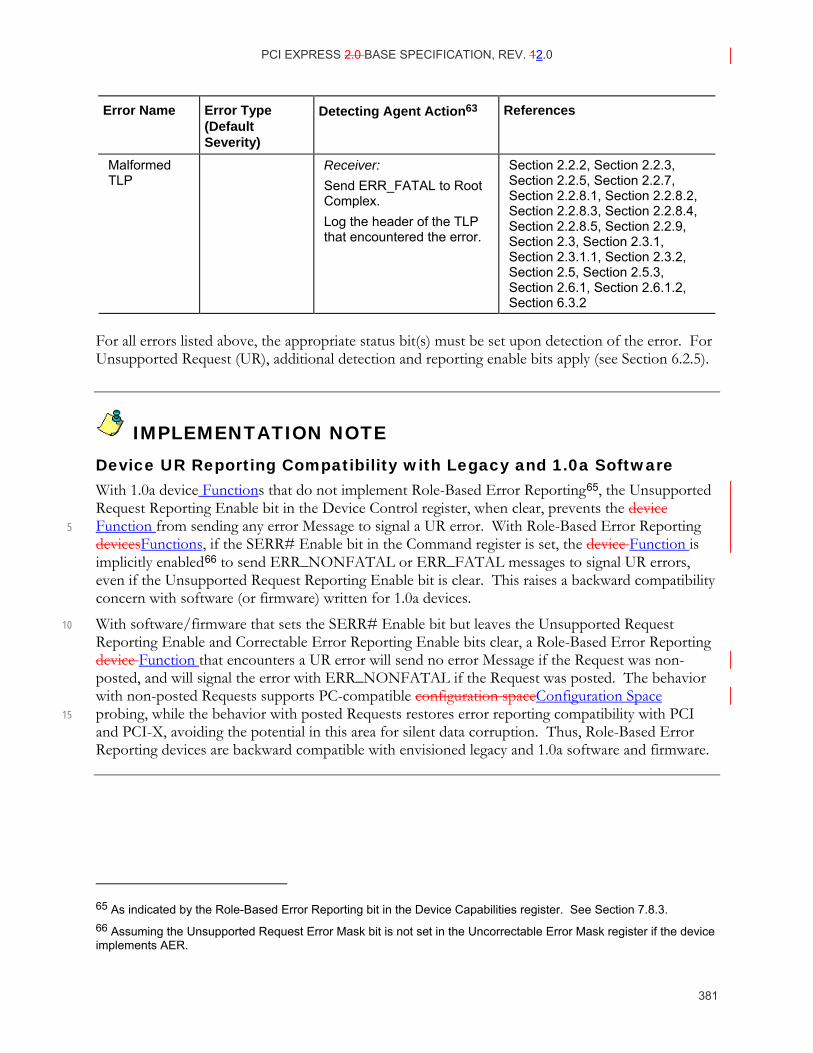
PCI EXPRESS 2.0 BASE SPECIFICATION, REV. 12.0
381
Error Name Error Type (Default Severity)
Detecting Agent Action63 References
Malformed TLP
Receiver: Send ERR_FATAL to Root Complex. Log the header of the TLP that encountered the error.
Section 2.2.2, Section 2.2.3, Section 2.2.5, Section 2.2.7, Section 2.2.8.1, Section 2.2.8.2, Section 2.2.8.3, Section 2.2.8.4, Section 2.2.8.5, Section 2.2.9, Section 2.3, Section 2.3.1, Section 2.3.1.1, Section 2.3.2, Section 2.5, Section 2.5.3, Section 2.6.1, Section 2.6.1.2, Section 6.3.2
For all errors listed above, the appropriate status bit(s) must be set upon detection of the error. For Unsupported Request (UR), additional detection and reporting enable bits apply (see Section 6.2.5).
IMPLEMENTATION NOTE Device UR Reporting Compatibility with Legacy and 1.0a Software With 1.0a device Functions that do not implement Role-Based Error Reporting65, the Unsupported Request Reporting Enable bit in the Device Control register, when clear, prevents the device Function from sending any error Message to signal a UR error. With Role-Based Error Reporting 5 devicesFunctions, if the SERR# Enable bit in the Command register is set, the device Function is implicitly enabled66 to send ERR_NONFATAL or ERR_FATAL messages to signal UR errors, even if the Unsupported Request Reporting Enable bit is clear. This raises a backward compatibility concern with software (or firmware) written for 1.0a devices.
With software/firmware that sets the SERR# Enable bit but leaves the Unsupported Request 10 Reporting Enable and Correctable Error Reporting Enable bits clear, a Role-Based Error Reporting device Function that encounters a UR error will send no error Message if the Request was non-posted, and will signal the error with ERR_NONFATAL if the Request was posted. The behavior with non-posted Requests supports PC-compatible configuration spaceConfiguration Space probing, while the behavior with posted Requests restores error reporting compatibility with PCI 15 and PCI-X, avoiding the potential in this area for silent data corruption. Thus, Role-Based Error Reporting devices are backward compatible with envisioned legacy and 1.0a software and firmware.
65 As indicated by the Role-Based Error Reporting bit in the Device Capabilities register. See Section 7.8.3. 66 Assuming the Unsupported Request Error Mask bit is not set in the Uncorrectable Error Mask register if the device implements AER.
PCI EXPRESS 2.0 BASE SPECIFICATION, REV. 21.0
382
6.2.7.1. Conventional PCI Mapping
In order to support conventional PCI driver and software compatibility, PCI Express error conditions, where appropriate, must be mapped onto the PCI Status register bits for error reporting.
In other words, when certain PCI Express errors are detected, the appropriate PCI Status register bit is set alerting the error to legacy PCI software. While the PCI Express error results in setting the PCI Status register, clearing the PCI Status register will not result in clearing bits in the 5 Uncorrectable Error Status register and Correctable Error Status register. Similarly, clearing bits in the Uncorrectable Error Status register and Correctable Error Status register will not result in clearing the PCI Status register.
The PCI command register has bits which control PCI error reporting. However, the PCI Command register does not affect the setting of the PCI Express error register bits. 10
PCI EXPRESS 2.0 BASE SPECIFICATION, REV. 12.0
383
6.2.8. Virtual PCI Bridge Error Handling
Virtual PCI Bridge configuration headers are associated with each PCI Express Port in a Root Complex or a Switch. For these cases, PCI Express error concepts require appropriate mapping to the PCI error reporting structures.
6.2.8.1. Error Message Forwarding and PCI Mapping for Bridge - Rules
In general, a TLP is either passed from one side of the Virtual PCI Bridge to the other, or is handled at the ingress side of the Bridge according to the same rules which apply to the ultimate recipient of 5 a TLP. The following rules cover PCI Express specific error related cases. See Refer to Section 6.2.6 for a conceptual summary on of Error Message Controls.
If a Request does not address a space mapped to either the Bridge’s internal space, or to the egress side of the BridgeIf a Request does not address a space mapped to the egress side of the Bridge, the Request is terminated at the ingress side as an Unsupported Request 10
Poisoned TLPs are forwarded according to the same rules as non-Poisoned TLPs
• When forwarding a Poisoned TLP from Primary to Secondary:
♦ the Receiving side must set the Detected Parity Error bit in the Status register
♦ the Transmitting side must set the Master Data Parity Error bit in the Secondary Status register if the Parity Error Response Enable bit in the Bridge Control register is set 15
• When forwarding a Poisoned TLP from Secondary to Primary:
♦ the Receiving side must set the Detected Parity Error bit in the Secondary Status register
♦ the Transmitting side must set the Master Data Parity Error bit in the Status register if the Parity Error Response bit in the Command register is set
ERR_COR, ERR_NONFATAL, and ERR_FATAL are forwarded from the secondary interface 20 to the primary interface, if the SERR# Enable bit in the Bridge Control register is set. A Bridge forwarding an error Message must not set the corresponding Error Detected bit in the Device Status register. Transmission of forwarded error Messages by the primary interface is controlled by multiple bits, as shown in Figure 6-3.
For a Root Port, error Messages forwarded from the secondary interface to the primary interface 25 must be enabled for “transmission” by the primary interface in order to cause a System Error via the Root Control register or (when the Advanced Error Reporting Capability is present) reporting via the Root Error Command register and logging in the Root Error Status register and Error Source Identification register.
PCI EXPRESS 2.0 BASE SPECIFICATION, REV. 21.0
384
For a Root Complex Event Collector (technically not a Bridge), error Messages “received” from associated Root Complex Integrated Endpoints must be enabled for “transmission” in order to cause a System Error via the Root Control register or (when the Advanced Error Reporting Capability is present) reporting via the Root Error Command register and logging in the Root Error Status register and Error Source Identification register. 5
6.3. Virtual Channel Support
6.3.1. Introduction and Scope
The Virtual Channel mechanism provides a foundation for supporting differentiated services within the PCI Express fabric. It enables deployment of independent physical resources that together with traffic labeling are required for optimized handling of differentiated traffic. Traffic labeling is supported using Transaction Class TLP-level labels. Exact The policy for traffic differentiation is determined by the TC/VC mapping and by the VC-based, Port-based, and functionFunction-based 10 arbitration mechanisms. The TC/VC mapping depends on the platform application requirements. These requirements drive the choice of the arbitration algorithms and configurability/programmability of arbiters allows detailed tuning of the traffic servicing policy.
Basic The definition of the Virtual Channel mechanism and associated Traffic Class labeling mechanisms is covered in Chapter 2. The VC configuration/programming model is defined in 15 Sections 7.11 and 7.18.
The remaining sections of this chapter This section covers VC mechanisms from the system perspective. They It addresses the next level of details on:
Supported TC/VC configurations
VC-based arbitration – algorithms and rules 20
Traffic ordering considerations
Isochronous support as a specific usage model
PCI EXPRESS 2.0 BASE SPECIFICATION, REV. 12.0
385
6.3.2. TC/VC Mapping and Example Usage
A Virtual Channel is established when one or more TC labels are associated with a physical resource designated by a VC ID. Every Traffic Class that is supported on a given path within the fabric must be mapped to one of the enabled Virtual Channels. Every Port must support the default TC0/VC0 pair – this is “hardwired.” Any additional TC label mapping or additional VC resource enablement is optional and is controlled by system software using the programming model described in 5 Sections 7.11 and 7.18.
The number of VC resources provisioned within a component or enabled within a given fabric may vary due to implementation and usage model requirements, due to Hot-Plug of disparate components with varying resource capabilities, or due to system software restricting what resources may be enabled on a given path within the fabric. 10
Some examples to illustrate:
A set of components (Root Complex, Endpoints, Switches) may only support the mandatory VC0 resource that must have TC0 mapped to VC0. System software may, based on application usage requirements, map one or all non-zero TC labels to VC0 as well on any or all paths within the fabric. 15
A set of components may support two VC resources, e.g., VC0 and VC1. System software must map TC0/VC0 and in addition, may map one or all non-zero TC labels to either VC0 or VC1. As above, these mappings may be enabled on any or all paths within the fabric. See Refer to the examples below for additional information.
A Switch may be implemented with eight Ports – seven x1 Links with two VC resources and one 20 x16 Link with one VC resource. System software may enable both VC resources on the x1 Links and assign one or more additional TC labels to either VC thus allowing the Switch to differentiate traffic flowing between any Ports. The x16 Link must also be also configured to map any non-TC0 traffic to VC0 if such traffic is to flow on this Link. Note: multi-Port components (Switches and Root Complex) are required to support independent TC/VC 25 mapping per PCI Express Port.
In any of the above examples, system software has the ability to map one, all, or a subset of the TC labels to a given VC. Should system software wish to restrict the number of traffic classes that may flow through a given Link, it may configure only a subset of the TC labels to the enabled VC resources. Any TLP that does not containindicating a TC label that has not been mapped to an 30 enabled VC resource shall must be treated as a malformed Malformed TLP and dropped by the receiving Port. This is referred to as TC Filtering; however,. Flow Control credits for this TLP will be lost, and an uncorrectable error will be generated, so software intervention will usually be required to restore proper operation after a TC Filtering event occurs.
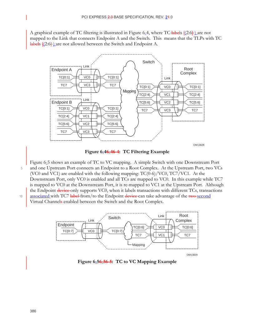
PCI EXPRESS 2.0 BASE SPECIFICATION, REV. 21.0
386
A graphical example of TC filtering is illustrated in Figure 6-4, where TC labels [(2:6] ) are not mapped to the Link that connects Endpoint A and the Switch. This means that the TLPs with TC labels [(2:6] ) are not allowed between the Switch and Endpoint A.
OM13828
Endpoint ALink
Switch
VC0
VC1
VC2
VC3
TC[0:1]
TC[2:4]
TC[5:6]
TC7
TC[0:1]
TC[2:4]
TC[5:6]
TC7
Endpoint BLink
VC0
VC1
VC2
VC3
TC[0:1]
TC[2:4]
TC[5:6]
TC7
TC[0:1]
TC[2:4]
TC[5:6]
TC7
Link
RootComplex
VC0
VC3
TC[0:1]
TC7
TC[0:1]
TC7
Mapping
Mapping
Figure 6-46-4 6-4: TC Filtering Example
Figure 6-5 shows an example of TC to VC mapping. A simple Switch with one Downstream Port and one Upstream Port connects an Endpoint to a Root Complex. At the Upstream Port, two VCs 5 (VC0 and VC1) are enabled with the following mapping: TC(0-6)/VC0, TC7/VC1. At the Downstream Port, only VC0 is enabled and all TCs are mapped to VC0. In this example while TC7 is mapped to VC0 at the Downstream Port, it is re-mapped to VC1 at the Upstream Port. Although the Endpoint device only supports VC0, when it labels transactions with different TCs, transactions associated with TC7 label from/to the Endpoint device can take advantage of the two second 10 Virtual Channels enabled between the Switch and the Root Complex.
OM13829
EndpointVC0TC[0:7] TC[0:7]
LinkSwitch
VC0
VC1
TC[0:6]
TC7
TC[0:6]
TC7
Link
Mapping
RootComplex
Figure 6-56-5 6-5: TC to VC Mapping Example
PCI EXPRESS 2.0 BASE SPECIFICATION, REV. 12.0
387
IMPLEMENTATION NOTE
Multiple TCs Over a Single VC A single VC implementation may benefit from using multiple TC labels. TC labels provide ordering domains that may be used to differentiate traffic within the Endpoint or the Root Complex independent of the number of VCs supported.
In a simple configuration, where only VC0 is supported, traffic differentiation may not be accomplished in an optimum manner since the different traffic classeTCs cannot be physically 5 segregated. However, the benefits of carrying multiple TC labels can still be exploited particularly in the small and “shallow” topologies where Endpoints are connected directly to Root Complex rather than through cascaded Switches. In these topologies traffic that is targeting Root Complex only needs to traverse a single Link, and an optimized scheduling of packets on both sides (Endpoint and Root Complex) based on TC labels may accomplish significant improvement over the case when a 10 single TC label is used. Still, the inability to route differentiated traffic through separate resources with fully independent flow-control and independent ordering exposes all of the traffic to the potential head-of-line blocking conditions. Optimizing Endpoint internal architecture to minimize the exposure to the blocking conditions can reduce those risks.
6.3.3. VC Arbitration
Arbitration is one of the key aspects of the Virtual Channel mechanism and is defined in a manner 15 that fully enables configurability to the specific application. In general, the definition of the PCI Express VC-based arbitration mechanism is driven by the following objectives:
To prevent false transaction timeouts and to guarantee data flow forward progress
To provide differentiated services between data flows within the fabric
To provide guaranteed bandwidth with deterministic (and reasonably small) end-to-end latency 20 between components
PCI Express Links are bidirectional, i.e., each PCI Express Port can be an Ingress or an Egress Port depending on the direction of traffic flow. This is illustrated by the example of a 3-Port Switch in Figure 6-6, where the paths for traffic flows flowing between Switch Ports are highlighted with different types of lines. In the following sections, PCI Express VC Arbitration is defined using a 25 Switch arbitration model since a the Switch is the PCI Express element that represents a functional superset from the arbitration perspective.
In addition, one-directional data flow is used in the description.
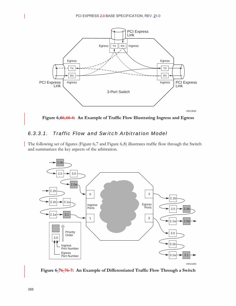
PCI EXPRESS 2.0 BASE SPECIFICATION, REV. 21.0
388
OM13830
3-Port Switch
PCI ExpressLink
PCI ExpressLink
Egress
Ingress
TX
RX
Egress
Ingress
TX
RX
Egress IngressTX
PCI ExpressLink
RX
Figure 6-66-6 6-6: An Example of Traffic Flow Illustrating Ingress and Egress
6.3.3.1. Traffic Flow and Switch Arbitration Model
The following set of figures (Figure 6-7 and Figure 6-8) illustrates traffic flow through the Switch and summarizes the key aspects of the arbitration.
22.1b
3
0
12.0a2.1a
2.0b2.0
2.0a
2.0
2.0b
2.1b
3.1b 3.1aIngressPorts
EgressPorts
3.0
PriorityOrder
EgressPort Number
IngressPort Number
3.0
2.1a 3.1
OM14284
3.0
3.1b
3.1a 3.1
Figure 6-76-7 6-7: An Example of Differentiated Traffic Flow Through a Switch
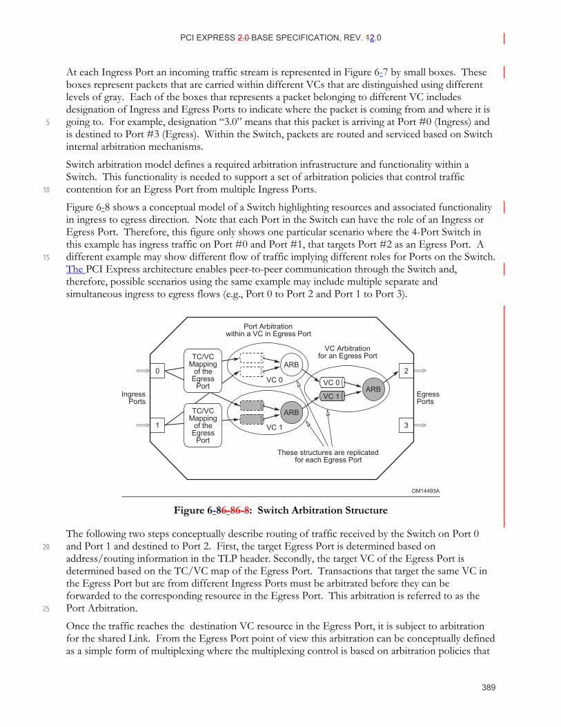
PCI EXPRESS 2.0 BASE SPECIFICATION, REV. 12.0
389
At each Ingress Port an incoming traffic stream is represented in Figure 6-7 by small boxes. These boxes represent packets that are carried within different VCs that are distinguished using different levels of gray. Each of the boxes that represents a packet belonging to different VC includes designation of Ingress and Egress Ports to indicate where the packet is coming from and where it is going to. For example, designation “3.0” means that this packet is arriving at Port #0 (Ingress) and 5 is destined to Port #3 (Egress). Within the Switch, packets are routed and serviced based on Switch internal arbitration mechanisms.
Switch arbitration model defines a required arbitration infrastructure and functionality within a Switch. This functionality is needed to support a set of arbitration policies that control traffic contention for an Egress Port from multiple Ingress Ports. 10
Figure 6-8 shows a conceptual model of a Switch highlighting resources and associated functionality in ingress to egress direction. Note that each Port in the Switch can have the role of an Ingress or Egress Port. Therefore, this figure only shows one particular scenario where the 4-Port Switch in this example has ingress traffic on Port #0 and Port #1, that targets Port #2 as an Egress Port. A different example may show different flow of traffic implying different roles for Ports on the Switch. 15 The PCI Express architecture enables peer-to-peer communication through the Switch and, therefore, possible scenarios using the same example may include multiple separate and simultaneous ingress to egress flows (e.g., Port 0 to Port 2 and Port 1 to Port 3).
OM14493A
Port Arbitrationwithin a VC in Egress Port
VC 0
VC 1
VC Arbitrationfor an Egress Port
These structures are replicatedfor each Egress Port
EgressPorts
IngressPorts
ARBVC 0
VC 1
0
1
2
3
TC/VCMapping
of theEgress
Port
TC/VCMapping
of theEgress
Port
ARB
ARB
Figure 6-86-8 6-8: Switch Arbitration Structure
The following two steps conceptually describe routing of traffic received by the Switch on Port 0 and Port 1 and destined to Port 2. First, the target Egress Port is determined based on 20 address/routing information in the TLP header. Secondly, the target VC of the Egress Port is determined based on the TC/VC map of the Egress Port. Transactions that target the same VC in the Egress Port but are from different Ingress Ports must be arbitrated before they can be forwarded to the corresponding resource in the Egress Port. This arbitration is referred to as the Port Arbitration. 25
Once the traffic reaches the destination VC resource in the Egress Port, it is subject to arbitration for the shared Link. From the Egress Port point of view this arbitration can be conceptually defined as a simple form of multiplexing where the multiplexing control is based on arbitration policies that
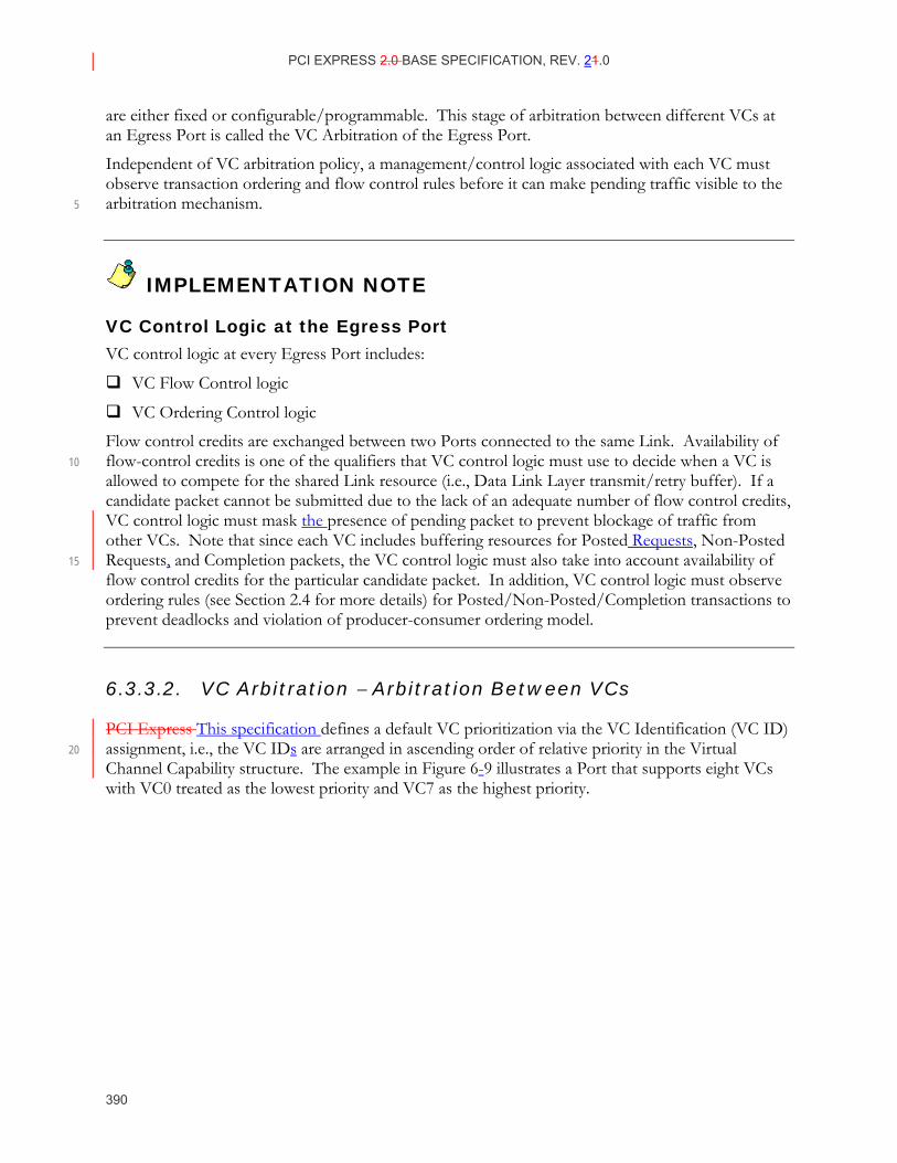
PCI EXPRESS 2.0 BASE SPECIFICATION, REV. 21.0
390
are either fixed or configurable/programmable. This stage of arbitration between different VCs at an Egress Port is called the VC Arbitration of the Egress Port.
Independent of VC arbitration policy, a management/control logic associated with each VC must observe transaction ordering and flow control rules before it can make pending traffic visible to the arbitration mechanism. 5
IMPLEMENTATION NOTE
VC Control Logic at the Egress Port VC control logic at every Egress Port includes:
VC Flow Control logic
VC Ordering Control logic
Flow control credits are exchanged between two Ports connected to the same Link. Availability of flow-control credits is one of the qualifiers that VC control logic must use to decide when a VC is 10 allowed to compete for the shared Link resource (i.e., Data Link Layer transmit/retry buffer). If a candidate packet cannot be submitted due to the lack of an adequate number of flow control credits, VC control logic must mask the presence of pending packet to prevent blockage of traffic from other VCs. Note that since each VC includes buffering resources for Posted Requests, Non-Posted Requests, and Completion packets, the VC control logic must also take into account availability of 15 flow control credits for the particular candidate packet. In addition, VC control logic must observe ordering rules (see Section 2.4 for more details) for Posted/Non-Posted/Completion transactions to prevent deadlocks and violation of producer-consumer ordering model.
6.3.3.2. VC Arbitration − Arbitration Between VCs
PCI Express This specification defines a default VC prioritization via the VC Identification (VC ID) assignment, i.e., the VC IDs are arranged in ascending order of relative priority in the Virtual 20 Channel Capability structure. The example in Figure 6-9 illustrates a Port that supports eight VCs with VC0 treated as the lowest priority and VC7 as the highest priority.
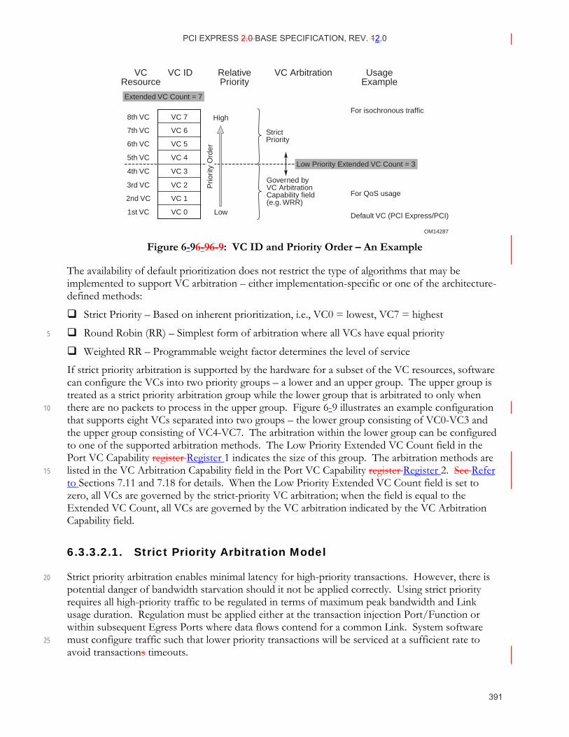
PCI EXPRESS 2.0 BASE SPECIFICATION, REV. 12.0
391
OM14287
VC 7
VC IDVCResource
RelativePriority
VC Arbitration UsageExample
High
StrictPriority
Governed byVC ArbitrationCapability field(e.g. WRR)
Low
VC 6
VC 5
VC 4
VC 3
VC 2
VC 1
VC 0
8th VC
7th VC
6th VC
5th VC
4th VC
3rd VC
2nd VC
1st VC
Low Priority Extended VC Count = 3
For isochronous traffic
For QoS usage
Default VC (PCI Express/PCI)
Extended VC Count = 7
Prio
rity
Ord
er
Figure 6-96-9 6-9: VC ID and Priority Order – An Example
The availability of default prioritization does not restrict the type of algorithms that may be implemented to support VC arbitration – either implementation-specific or one of the architecture-defined methods:
Strict Priority – Based on inherent prioritization, i.e., VC0 = lowest, VC7 = highest
Round Robin (RR) – Simplest form of arbitration where all VCs have equal priority 5
Weighted RR – Programmable weight factor determines the level of service
If strict priority arbitration is supported by the hardware for a subset of the VC resources, software can configure the VCs into two priority groups – a lower and an upper group. The upper group is treated as a strict priority arbitration group while the lower group that is arbitrated to only when there are no packets to process in the upper group. Figure 6-9 illustrates an example configuration 10 that supports eight VCs separated into two groups – the lower group consisting of VC0-VC3 and the upper group consisting of VC4-VC7. The arbitration within the lower group can be configured to one of the supported arbitration methods. The Low Priority Extended VC Count field in the Port VC Capability register Register 1 indicates the size of this group. The arbitration methods are listed in the VC Arbitration Capability field in the Port VC Capability register Register 2. See Refer 15 to Sections 7.11 and 7.18 for details. When the Low Priority Extended VC Count field is set to zero, all VCs are governed by the strict-priority VC arbitration; when the field is equal to the Extended VC Count, all VCs are governed by the VC arbitration indicated by the VC Arbitration Capability field.
6.3.3.2.1. Strict Priority Arbitration Model
Strict priority arbitration enables minimal latency for high-priority transactions. However, there is 20 potential danger of bandwidth starvation should it not be applied correctly. Using strict priority requires all high-priority traffic to be regulated in terms of maximum peak bandwidth and Link usage duration. Regulation must be applied either at the transaction injection Port/Function or within subsequent Egress Ports where data flows contend for a common Link. System software must configure traffic such that lower priority transactions will be serviced at a sufficient rate to 25 avoid transactions timeouts.
PCI EXPRESS 2.0 BASE SPECIFICATION, REV. 21.0
392
6.3.3.2.2. Round Robin Arbitration Model
Round Robin arbitration is used to provide, at the transaction level, equal67 opportunities to all traffic. Note that this scheme is used where different unordered streams need to be serviced with the same priority.
In the case where differentiation is required, a Weighted Round Robin scheme can be used. The WRR scheme is commonly used in the case where bandwidth regulation is not enforced by the 5 sources of traffic and therefore it is not possible to use the priority scheme without risking starvation of lower priority traffic. The key is that this scheme provides fairness during traffic contention by allowing at least one arbitration win per arbitration loop. Assigned weights regulate both minimum allowed bandwidth and maximum burstiness for each VC during the contention. This means that it bounds the arbitration latency for traffic from different VCs. Note that latencies 10 are also dependent on the maximum packet sizes allowed for traffic that is mapped onto those VCs.
One of the key usage models of the WRR scheme is support for QoS policy where different QoS levels can be provided using different weights.
Although weights can be fixed (by hardware implementation) for certain applications, to provide more generic support for different applications, PCI Express components that support the WRR 15 scheme are recommended to implement programmable WRR. Programming of WRR is controlled using the software interface defined in Sections 7.11 and 7.18.
6.3.3.3. Port Arbitration − Arbitration Within VC
For switchesSwitches, Port Arbitration refers to the arbitration at an Egress Port between traffic coming from other Ingress Ports that is mapped to the same VC. For Root Ports, Port Arbitration refers to the arbitration at a Root Egress Port between peer-to-peer traffic coming from other Root 20 Ingress Ports that is mapped to the same VC. For RCRBs, Port Arbitration refers to the arbitration at the RCRB (e.g., for host memory) between traffic coming from Root Ports that is mapped to the same VC. An inherent prioritization scheme for arbitration among VCs in this context is not applicable since it would imply strict arbitration priority for different Ports.Inherent prioritization scheme that makes sense when talking about arbitration among VCs in this context is not applicable 25 since it would imply strict arbitration priority for different Ports. Traffic from different Ports can be arbitrated using the following supported schemes:
Hardware-fixed arbitration scheme, e.g., Round Robin
Programmable WRR arbitration scheme
Programmable Time-based WRR arbitration scheme 30
Hardware-fixed RR or RR-like scheme is the simplest to implement since it does not require any programmability. It makes all Ports equal priority, which is acceptable for applications where no software-managed differentiation or per-Port-based bandwidth budgeting is required.
Programmable WRR allows flexibility since it can operate as flat RR or if differentiation is required, different weights can be applied to traffic coming from different Ports in the similar manner as 35
67 Note that this does not imply equivalence and fairness in the terms of bandwidth usage.
PCI EXPRESS 2.0 BASE SPECIFICATION, REV. 12.0
393
described in Section 6.3.3.2. This scheme is used where different allocation of bandwidth needs to be provided for different Ports.
A Time-based WRR is used for applications where not only different allocation of bandwidth is required but also a tight control of usage of that bandwidth. This scheme allows control of the amount of traffic that can be injected from different Ports within a certain fixed period of time. 5 This is required for certain applications such as isochronous services, where traffic needs to meet a strict deadline requirement. Section 6.3.3.4 provides basic rules to support isochronous applications. For more details on time-based arbitration and on the isochronous service as a usage model for this arbitration scheme refer to Appendix A.
6.3.3.4. Multi-function Function Devices and Function Arbitration
The multi-function Function arbitration model defines an optional arbitration infrastructure and 10 functionality within a multi-function Function device. This functionality is needed to support a set of arbitration policies that control traffic contention for the device’s Upstream Egress Port from its multiple functionsFunctions.
Figure 6-10 shows a conceptual model of a multi-function Function device highlighting resources and associated functionality. Note that each function Function optionally contains a VC Capability 15 structure, which if present manages TC/VC mapping, optional Port Arbitration, and optional VC arbitration, all within the functionFunction. The MFVC Capability structure manages TC/VC mapping, optional Function Arbitration, and optional VC Arbitration for the device’s Upstream Egress Port. Together these resources enable enhanced QoS management for upstream Upstream requests. However, in contrast to a complete switch Switch with devices on its downstream 20 Downstream Ports, the multi-function Function device model does not support full QoS management for peer-to-peer requests between functions Functions or for downstream Downstream requests.
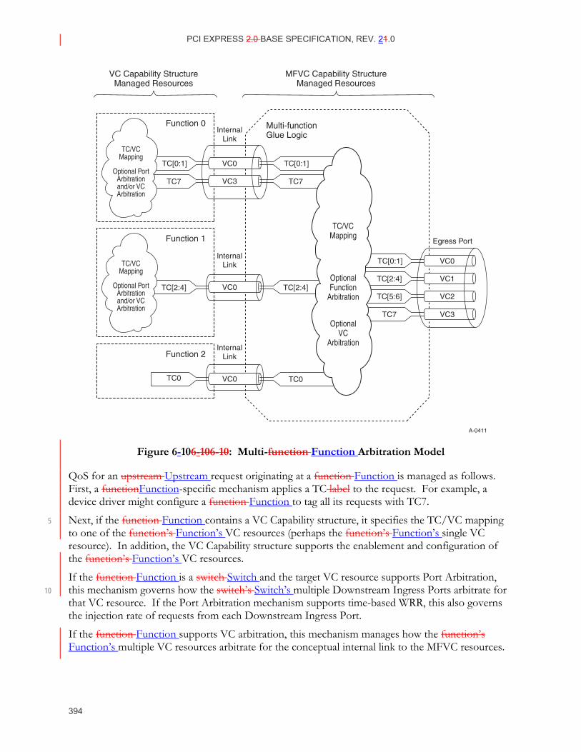
PCI EXPRESS 2.0 BASE SPECIFICATION, REV. 21.0
394
A-0411
Function 0 Multi-functionGlue Logic
VC0
VC1
VC2
VC3
TC[0:1]
TC[2:4]
TC[5:6]
TC7
Egress Port
VC0
InternalLink
VC3
TC[0:1]
TC7
TC[0:1]
TC7
TC/VCMapping
Optional PortArbitrationand/or VCArbitration
Function 1
InternalLink
VC0TC[2:4] TC[2:4]
Function 2Internal
Link
VC0TC0 TC0
Mapping
TC/VCMapping
OptionalFunction
Arbitration
OptionalVC
Arbitration
VC Capability StructureManaged Resources
MFVC Capability StructureManaged Resources
TC/VCMapping
Optional PortArbitrationand/or VCArbitration
Figure 6-106-10 6-10: Multi-function Function Arbitration Model
QoS for an upstream Upstream request originating at a function Function is managed as follows. First, a functionFunction-specific mechanism applies a TC label to the request. For example, a device driver might configure a function Function to tag all its requests with TC7.
Next, if the function Function contains a VC Capability structure, it specifies the TC/VC mapping 5 to one of the function’s Function’s VC resources (perhaps the function’s Function’s single VC resource). In addition, the VC Capability structure supports the enablement and configuration of the function’s Function’s VC resources.
If the function Function is a switch Switch and the target VC resource supports Port Arbitration, this mechanism governs how the switch’s Switch’s multiple Downstream Ingress Ports arbitrate for 10 that VC resource. If the Port Arbitration mechanism supports time-based WRR, this also governs the injection rate of requests from each Downstream Ingress Port.
If the function Function supports VC arbitration, this mechanism manages how the function’s Function’s multiple VC resources arbitrate for the conceptual internal link to the MFVC resources.
PCI EXPRESS 2.0 BASE SPECIFICATION, REV. 12.0
395
Once a request packet conceptually arrives at MFVC resources, address/routing information in the TLP header determines whether the request goes upstream Upstream or peer-to-peer to another functionFunction. For the case of peer-to-peer, QoS management is left to unarchitected device-specific mechanisms. For the case of upstreamUpstream, TC/VC mapping in the MFVC Capability structure determines which VC resource the request will target. The MFVC Capability structure also 5 supports enablement and configuration of the VC resources in the multi-function Function glue logic. If the target VC resource supports Function Arbitration, this mechanism governs how the multiple functions Functions arbitrate for this VC resource. If the Function Arbitration mechanism supports time-based WRR, this governs the injection rate of requests for each function Function into this VC resource. 10
Finally, if the MFVC Capability structure supports VC Arbitration, this mechanism governs how the MFVC’s multiple VCs compete for the device’s Upstream Egress Port. Independent of VC arbitration policy, management/control logic associated with each VC must observe transaction ordering and flow control rules before it can make pending traffic visible to the arbitration mechanism. 15
IMPLEMENTATION NOTE
Multi-Function Devices without the MFVC Capability Structure If a multi-function Function device lacks an MFVC Capability Structurestructure, the arbitration of data flows from different functions Functions of a multi-function Function device is beyond the scope of this specification However, if a multi-function Function device supports TCs other than TC0 and does not implement an MFVC Capability structure, it must implement a single VC Capability structure in Function 0 to provide architected TC/VC mappings for the Link. 20
6.3.4. Isochronous Support
Servicing isochronous data transfer requires a system to provide not only guaranteed data bandwidth but also deterministic service latency. The isochronous support mechanisms in PCI Express are defined to ensure that isochronous traffic receives its allocated bandwidth over a relevant period of time while also preventing starvation of the other traffic in the system. Isochronous support mechanisms apply to communication between Endpoint and Root Complex as well as to peer-to-25 peer communication.
Isochronous service is realized through proper use of PCI Express mechanisms such as TC transaction labeling, VC data-transfer protocol, and TC-to-VC mapping. End-to-end isochronous service requires software to set up proper configuration along the path between the Requester to and the Completer. This section describes the rules for software configuration and the rules 30 hardware components must follow to provide end-to-end isochronous services. More information and background material regarding isochronous applications and isochronous service design guidelines can be found in Appendix A.
PCI EXPRESS 2.0 BASE SPECIFICATION, REV. 21.0
396
6.3.4.1. Rules for Software Configuration
System software must obey the following rules to configure PCI Express fabric for isochronous traffic:
Software must designate one or more TC labels for isochronous transactions.
Software must ensure that the Attribute fields of all isochronous requests targeting the same Completer are fixed and identical. 5
Software must configure all VC resources used to support isochronous traffic to be serviced (arbitrated) at the requisite bandwidth and latency to meet the application objectives. This may be accomplished using strict priority, WRR, or hardware-fixed arbitration.
Software should not intermix isochronous traffic with non-isochronous traffic on a given VC.
Software must observe the Maximum Time Slots capability reported by the PCI Express Port or 10 RCRB.
Software must not assign all PCI Express Link capacity to isochronous traffic. This is required to ensure the requisite forward progress of other non-isochronous transactions to avoid false transaction timeouts.
Software must limit the Max_Payload_Size for each path that supports isochronous to meet the 15 isochronous latency. For example, all traffic flowing on a path from an isochronous capable device to the Root Complex should be limited to packets that do not exceed the Max_Payload_Size required to meet the isochronous latency requirements.
Software must set Max_Read_Request_Size of an isochronous-configured device with a value that does not exceed the Max_Payload_Size set for the device. 20
6.3.4.2. Rules for Requesters
A Requester requiring isochronous services must obey the following rules:
The value in the Length field of read requests must never exceed Max_Payload_Size.
If isochronous traffic targets the Root Complex and the RCRB indicates it cannot meet the isochronous bandwidth and latency requirements without requiring all transactions to set the No Snoop attribute bit, indicated by setting the Reject Snoop Transactions field, then this bit must 25 be set within the TLP header else the transaction will be rejected.
6.3.4.3. Rules for Completers
A Completer providing isochronous services must obey the following rules:
A Completer should not apply flow control induced backpressure to uniformly injected isochronous requests under normal operating conditions.
A Completer must report its isochronous bandwidth capability in the Maximum Time Slots field 30 in the VC Resource Capability register. Note that a Completer must account for partial writes.
PCI EXPRESS 2.0 BASE SPECIFICATION, REV. 12.0
397
A Completer must observe the maximum isochronous transaction latency.
A Root Complex as a Completer must implement at least one RCRB and support time-based Port Arbitration for the associated VCs. Note that time-based Port Arbitration only applies to request transactions.
6.3.4.4. Rules for Switches and Root Complexes Components
A Switch component providing isochronous services must obey the following rules. The same rules 5 apply to Root Complexes that support isochronous data flows peer-to-peer between Root Ports, abbreviated in this section as “P2P-RC.”.
An isochronous-configured Switch or P2P-RC Port should not apply flow control induced backpressure to uniformly injected isochronous requests under normal operating conditions.
An isochronous-configured Switch or P2P-RC Port must observe the maximum isochronous 10 transaction latency.
A Switch or P2P-RC component must support time-based Port Arbitration for each Port that supports one or more VCs capable of supporting isochronous traffic. Note that time-based Port Arbitration applies to request transactions but not to completion transactions.
6.3.4.5. Rules for Multi-function Function Devices
A multi-function Function device that includes an MFVC Capability structure providing 15 isochronous services must obey the following rules:
MFVC glue logic configured for isochronous operation should not apply backpressure to uniformly injected isochronous requests from its functions Functions under normal operating conditions.
The MFVC Capability structure must support time-based Function Arbitration for each VC 20 capable of supporting isochronous traffic. Note that time-based Function Arbitration applies only to upstream Upstream request transactions; it does not apply to any downstream Downstream or peer-to-peer request transactions, nor to any completion transactions.
A multi-function Function device that lacks an MFVC Capability structure has no architected mechanism to provide isochronous services for its multiple functions Functions concurrently. 25
PCI EXPRESS 2.0 BASE SPECIFICATION, REV. 21.0
398
6.4. Device Synchronization System software requires a “stop” mechanism for ensuring that there are no outstanding transactions for a particular device in a system. For example, without such a mechanism renumbering bus Bus numbers Numbers during system operation may cause the Requestor IDRequester ID (which includes the bus Bus numberNumber) for a given device to change while Requests or Completions for that device are still in flight, and may thus be rendered invalid due to 5 the change in the Requester ID. It is also desirable to be able to ensure that there are no outstanding transactions during a Hot-Plug orderly removal.
The details of stop mechanism implementation depend on the device hardware, device driver software, and system software. However, the fundamental requirements which must be supported to allow system software management of the PCI Express fabric include the abilities to: 10
Block the device from generating new Requests
Block the generation of Requests issued to the device
Determine that all Requests being serviced by the device have been completed
Determine that all non-posted Requests initiated by the device have completed
Determine that all posted Requests initiated by the device have reached their destination 15
The ability of the driver and/or system software to block new Requests from the device is supported by the Bus Master Enable, SERR# Enable, and Interrupt Disable bits in the Command register (Section 7.5.1.1) of each device Function, and other such control bits.
Requests issued to the device are generally under the direct control of the driver, so system software can block these Requests by directing the driver to stop generating them (the details of this 20 communication are system software specific). Similarly, Requests serviced by the device are normally under the device driver’s control, so determining the completion of such requests is usually trivial.
The Transaction Pending, or TP bit, provides a consistent way on a per-Function basis for software to determine that all non-posted Requests issued by the device have been completed (see Chapter 7). 25
Determining that posted Requests have reached their destination is handled by generating a transaction to “flush” any outstanding Requests. Writes to system memory using TC0 will be flushed by host reads of the device, and so require no explicit flush protocol. Writes using TCs other than TC0 require some type of flush synchronization mechanism. The mechanism itself is implementation specific to the device and its driver software. However, in all cases the device 30 hardware and software implementers should thoroughly understand the ordering rules described in Section 2.4. This is especially true if the Relaxed Ordering flag is set for any Requests initiated by the device.
PCI EXPRESS 2.0 BASE SPECIFICATION, REV. 12.0
399
IMPLEMENTATION NOTE
Flush Mechanisms In a simple case such as that of an Endpoint device communicating only with host memory through TC0, “flush” can be implemented simply by reading from the deviceEndpoint. If the device Endpoint issues writes to main memory using TCs other than TC0, “flush” can be implemented with a memory read on the corresponding TCs directed to main memory. The memory read needs to be performed on all TCs that the device Endpoint is using. 5
If a memory read is used to “flush” outstanding transactions, but no actual read is required, it may be desirable to use the zero-length read semantic described in Section 2.2.5.
Peer-to-peer interaction between devices requires an explicit synchronization protocol between the involved devices, even if all communication is through TC0. For a given system, the model for managing peer-to-peer interaction must be established. System software, and device hardware and 10 software must then conform to this model. The requirements for blocking Request generation and determining completion of Requests match the requirements for non-peer interaction, however the determination that Posted Requests have reached peer destination device(s) requires an explicit synchronization mechanism. The mechanism itself is implementation specific to the device, its driver software, and the model used for the establishment and disestablishment of peer 15 communications.
6.5. Locked Transactions
6.5.1. Introduction
Locked Transaction support is required to prevent deadlock in systems that use legacy software which causes the accesses to I/O devices. Note that some CPUs may generate locked accesses as a result of executing instructions that implicitly trigger lock. Some legacy software misuses these transactions and generates locked sequences even when exclusive access is not required. Because 20 locked accesses to I/O devices introduce potential deadlocks apart from those mentioned above, as well as serious performance degradation, PCI Express Endpoints are prohibited from supporting locked accesses, and new software must not use instructions which will cause locked accesses to I/O devices. Legacy Endpoints support locked accesses only for compatibility with existing software.
Only the Root Complex is allowed to initiate Locked Requests on PCI Express. Locked Requests 25 initiated by Endpoints and Bridges are not supported. This is consistent with limitations for locked transaction use outlined in the PCI Local Bus Specification, Revision 3.0 (Appendix F- Exclusive Accesses).
This section specifies the rules associated with supporting locked accesses from the Host CPU to legacy Legacy Endpoints, including the propagation of those transactions through Switches and PCI 30 Express/PCI Bridges.
PCI EXPRESS 2.0 BASE SPECIFICATION, REV. 21.0
400
6.5.2. Initiation and Propagation of Locked Transactions - Rules
Locked transaction sequences are generated by the Host CPU(s) as one or more reads followed by a number of writes to the same location(s). When a lock is established, all other traffic is blocked from using the path between the Root Complex and the locked legacy Legacy Endpoint or Bridge.
A locked transaction sequence or attempted locked transaction sequence is initiated on PCI Express using the “lock”–type Read Request/Completion (MRdLk/CplDLk) and terminated 5 with the Unlock Message
• Locked Requests which are completed with a status other than Successful Completion do not establish lock (explained in detail in the following sections)
• Regardless of the status of any of the Completions associated with a locked sequence, all locked sequences and attempted locked sequences must be terminated by the transmission 10 of an Unlock Message.
• MRdLk, CplDLk, and Unlock semantics are allowed only for the default Traffic Class (TC0)
• Only one locked transaction sequence attempt may be in progress at a given time within a single hierarchy domain
The Unlock Message is sent from the Root Complex down the locked transaction path to the 15 Completer, and may be broadcast from the Root Complex to all Endpoints and Bridges
• Any device which is not involved in the locked sequence must ignore this Message
Any violation of the rules for initiation and propagation of locked transactions can result in undefined device and/or system behavior
The initiation and propagation of a locked transaction sequence through PCI Express is performed 20 as follows:
A locked transaction sequence is started with a MRdLk Request
• Any successive reads for the locked transaction sequence must also use MRdLk Requests
• The Completions for any successful MRdLk Request use the CplDLk Completion type, or the CPlLk Completion type for unsuccessful Requests 25
If any read associated with a locked sequence is completed unsuccessfully, the Requester must assume that the atomicity of the lock is no longer assured, and that the path between the Requester and Completer is no longer locked
All writes for the locked sequence use MWr Requests
The Unlock Message is used to indicate the end of a locked sequence 30
• A Switch propagates Unlock Messages to the locked Egress Port
PCI EXPRESS 2.0 BASE SPECIFICATION, REV. 12.0
401
Upon receiving an Unlock Message, a legacy Legacy Endpoint or Bridge must unlock itself if it is in a locked state
• If not locked, or if the Receiver is a PCI Express Endpoint or Bridge which does not support lock, the Unlock Message is ignored and discarded
6.5.3. Switches and Lock - Rules
Switches must distinguish transactions associated with locked sequences from other transactions to 5 prevent other transactions from interfering with the lock and potentially causing deadlock. The following rules cover how this is done. Note that locked accesses are limited to TC0, which is always mapped to VC0.
When a Switch propagates a MRdLk Request from the Ingress Port (closest to the Root Complex) to the Egress Port, it must block all Requests which map to the default Virtual 10 Channel (VC0) from being propagated to the Egress Port
• If a subsequent MRdLk Request is Received at this Ingress Port addressing a different Egress Port, the behavior of the Switch is undefined
Note: This sort of split-lock access is not supported by PCI Express and software must not cause such a locked access. System deadlock may result from such accesses. 15
When the CplDLk for the first MRdLk Request is returned, if the Completion indicates a Successful Completion status, the Switch must block all Requests from all other Ports from being propagated to either of the Ports involved in the locked access, except for Requests which map to non-VC0 on the Egress Port
The two Ports involved in the locked sequence must remain blocked as described above until 20 the Switch receives the Unlock Message (at the Ingress Port for the initial MRdLk Request)
• The Unlock Message must be forwarded to the locked Egress Port
• The Unlock Message may be broadcast to all other Ports
• The Ingress Port is unblocked once the Unlock Message arrives, and the Egress Port(s) which were blocked are unblocked following the Transmission of the Unlock Message out 25 of the Egress Ports
♦ Ports which were not involved in the locked access are unaffected by the Unlock Message
6.5.4. PCI Express/PCI Bridges and Lock - Rules
The requirements for PCI Express/PCI Bridges are similar to those for Switches, except that, because PCI Express/PCI Bridges use only the default Virtual Channel and Traffic Class, all other 30 traffic is blocked during the locked access. The requirements on the PCI bus side of the PCI Express/PCI Bridge match the requirements for a PCI/PCI Bridge (see the PCI-to-PCI Bridge Architecture Specification, Revision 1.2 and the PCI Express to PCI/PCI-X Bridge Specification, Revision 1.0).
PCI EXPRESS 2.0 BASE SPECIFICATION, REV. 21.0
402
6.5.5. Root Complex and Lock - Rules
A Root Complex is permitted to support locked transactions as a Requestor. If locked transactions are supported, a Root Complex must follow the sequence described in Section 6.5.2 to perform a locked access. The mechanisms used by the Root Complex to interface PCI Express to the Host CPU(s) are outside the scope of this document.
6.5.6. Legacy Endpoints
Legacy Endpoints are permitted to support locked accesses, although their use is discouraged. If 5 locked accesses are supported, legacy Legacy Endpoints must handle them as follows:
The legacy Legacy Endpoint becomes locked when it Transmits the first Completion for the first Read Request of the locked access with a Successful Completion status
• If the completion status is not Successful Completion, the legacy Legacy Endpoint does not become locked 10
• Once locked, the legacy Legacy Endpoint must remain locked until it receives the Unlock Message
While locked, a legacy Legacy Endpoint must not issue any Requests using Traffic ClasseTCs which map to the default Virtual Channel (VC0)
Note that this requirement applies to all possible sources of Requests within the Endpoint, in 15 the case where there is more than one possible source of Requests.
• Requests may be issued using Traffic ClasseTCs which map to VCs other than the default Virtual Channel
6.5.7. PCI Express Endpoints
PCI Express Endpoints do not support lock. A PCI Express Endpoint must treat a MRdLk Request as an Unsupported Request (see Chapter 2). 20
6.6. PCI Express Reset - Rules This section specifies the behavior of PCI Express Reset mechanisms. This section covers the relationship between the architectural mechanisms defined in this document and the reset mechanisms defined in this document. Any relationship between the PCI Express Conventional reset Reset and component or platform reset is component or platform specific (respectively except as explicitly noted). 25
PCI EXPRESS 2.0 BASE SPECIFICATION, REV. 12.0
403
6.6.1. Conventional Reset
Conventional Reset includes all reset mechanisms other than Function Level Reset. There are two categories of Conventional Resets: Fundamental Reset and resets that are not Fundamental Reset. This section applies to all types of Conventional Reset.
In all form factors and system hardware configurations, there must, at some level, be a hardware mechanism for setting or returning all Port states to the initial conditions specified in this document 5 – this mechanism is called “Fundamental Reset.” This mechanism can take the form of an auxiliary signal provided by the system to a component or adapter card, in which case the signal must be called PERST#, and must conform to the rules specified in Section 4.2.4.7.1. When PERST# is provided to a component or adapter, this signal must be used by the component or adapter as Fundamental Reset. When PERST# is not provided to a component or adapter, Fundamental 10 Reset is generated autonomously by the component or adapter, and the details of how this is done are outside the scope of this document. If a Fundamental Reset is generated autonomously by the component or adapter, and if power is supplied by the platform to the component/adapter, the component/adapter must generate a Fundamental Reset to itself if the supplied power goes outside of the limits specified for the form factor or system. 15
There are three distinct types of Conventional Reset: cold, warm, and hot:
• A Fundamental Reset must occur following the application of power to the component. This is called a cold reset.
• In some cases, it may be possible for the Fundamental Reset mechanism to be triggered by hardware without the removal and re-application of power to the component. This is called 20 a warm reset. This document does not specify a means for generating a warm reset.
• There is an in-band mechanism for propagating Conventional Resetreset across a Link. This is called a hot reset and is described in Section 4.2.4.7.
Note also that the Data Link Layer reporting DL_Down status is in some ways identical to a hot reset – see Section 2.9. 25
On exit from any type of Conventional Resetreset (cold, warm, or hot), all Port registers and state machines must be set to their initialization values as specified in this document, except for sticky registers (see Section 7.4 and Section 7.6).
• Note that, from a device point of view, any type of Conventional Resetreset (cold, warm, hot, or DL_Down) has the same effect at the Transaction Layer and above as would RST# 30 assertion and de-assertion in conventional PCI.
On exit from a Fundamental Reset, the Physical Layer will attempt to bring up the Link (see Section 4.2.5). Once both components on a Link have entered the initial Link Training state, they will proceed through Link initialization for the Physical Layer and then through Flow Control initialization for VC0, making the Data Link and Transaction Layers ready to use the 35 Link
• Following Flow Control initialization for VC0, it is possible for TLPs and DLLPs to be transferred across the Link
PCI EXPRESS 2.0 BASE SPECIFICATION, REV. 21.0
404
Following a Conventional Resetreset, some devices may require additional time before they are able to respond to Requests they receive. Particularly for Configuration Requests it is necessary that components and devices behave in a deterministic way, which the following rules address.
The first set of rules addresses requirements for components and devices:
A component must enter the LTSSM Detect state within 20 ms of the end of Fundamental 5 Reset (Link Training is described in Section 4.2.4)
• Note: In some systems, it is possible that the two components on a Link may exit Fundamental Reset at different times. Each component must observe the requirement to enter the initial active Link Training state within 20 ms of the end of Fundamental Reset from its own point of view. 10
On the completion of Link Training (entering the DL_Active state, see Section 3.2), a component must be able to receive and process TLPs and DLLPs
The second set of rules addresses requirements placed on the system:
To allow components to perform internal initialization, system software must wait for at least 100 ms from the end of a Conventional Resetreset of one or more devices before it is permitted 15 to issue Configuration Requests to those devices
• A system must guarantee that all components intended to be software visible at boot time are ready to receive Configuration Requests within 100 ms of the end of Fundamental Conventional Reset at the Root Complex – how this is done is beyond the scope of this specification 20
The Root Complex and/or system software must allow at least 1.0 s (+50%/-0%) after a Conventional Resetreset of a device, before it may determine that a device which fails to return a Successful Completion status for a valid Configuration Request is a broken device
Note: This delay is analogous to the Trhfa parameter specified for PCI/PCI-X, and is intended to allow an adequate amount of time for devices which require self initialization. 25
When attempting a Configuration access to devices on a PCI or PCI-X bus segment behind a PCI Express/PCI(-X) Bridge, the timing parameter Trhfa must be respected
For this second set of rules, if system software does not have direct visibility into the state of Fundamental Reset (e.g., Hot-Plug; see Section 6.7), software must base these timing parameters on an event known to occur after the end of Fundamental Reset. 30
When a Link is in normal operation, the following rules apply:
If, for whatever reason, a normally operating Link goes down, the Transaction and Data Link Layers will enter the DL_Inactive state (see Sections 2.9 and 3.2.1)
For any Root or Switch Downstream Port, setting the Secondary Bus Reset bit of the Bridge Control register associated with the Port must cause a hot reset to be sent (see Section 4.2.4.7). 35
For a Switch, the following must cause a hot reset to be sent on all Downstream Ports:
• Setting the Secondary Bus Reset bit of the Bridge Control register associated with the Upstream Port
• The Data Link Layer of the Upstream Port reporting DL_Down status
PCI EXPRESS 2.0 BASE SPECIFICATION, REV. 12.0
405
• Receiving a hot reset on the Upstream Port
Certain aspects of Fundamental Reset are specified in this document and others are specific to a platform, form factor and/or implementation. Specific platforms, form factors or application spaces may require the additional specification of the timing and/or sequencing relationships between the components of the system for Fundamental Reset. For example, it might be required 5 that all PCI Express components within a chassis observe the assertion and deassertion of Fundamental Reset at the same time (to within some tolerance). In a multi-chassis environment, it might be necessary to specify that the chassis containing the Root Complex be the last to exit Fundamental Reset.
In all cases where power and PERST# are supplied, the following parameters must be defined: 10
Tpvperl – PERST# must remain active at least this long after power becomes valid
Tperst – When asserted, PERST# must remain asserted at least this long
Tfail – When power becomes invalid, PERST# must be asserted within this time
Additional parameters may be specified.
In all cases where a reference clock is supplied, the following parameter must be defined: 15
Tperst-clk – PERST# must remain active at least this long after any supplied reference clock is stable
Additional parameters may be specified.
6.6.2. Function-Level Reset (FLR)
The FLR mechanism enables software to quiesce and reset Endpoint hardware with Function-level granularity. Three example usage models illustrate the benefits of this feature: 20
In some systems, it is possible that the software entity that controls a Function will cease to operate normally. To prevent data corruption, it is necessary to stop all PCI Express and external I/O (not PCI Express) operations being performed by the Function. Other defined reset operations do not guarantee that external I/O operations will be stopped.
In a partitioned environment where hardware is migrated from one partition to another, it is 25 necessary to ensure that no residual “knowledge” of the prior partition be retained by hardware, for example, a user’s secret information entrusted to the first partition but not to the second. Further, due to the wide range of Functions, it is necessary that this be done in a Function-independent way.
When system software is taking down the software stack for a Function and then rebuilding that 30 stack, it is sometimes necessary to return the state to an uninitialized state before rebuilding the Function’s software stack.
Implementation of FLR is optional (not required), but is strongly recommended.
FLR applies on a per Function basis. Only the targeted Function is affected by the FLR operation. The Link state must not be affected by an FLR. 35
PCI EXPRESS 2.0 BASE SPECIFICATION, REV. 21.0
406
FLR modifies the Function state described by this specification as follows:
Function registers and Function-specific state machines must be set to their initialization values as specified in this document, except for the following:
• sticky-type registers (ROS, RWS, RW1CS)
• registers defined as type HwInit 5
• these other registers:
♦ Captured Slot Power Limit Value in the Device Capabilities register
♦ Captured Slot Power Limit Scale in the Device Capabilities register
♦ Max_Payload_Size in the Device Control register
♦ Active State Power Management (ASPM) Control in the Link Control register 10
♦ Read Completion Boundary (RCB) in the Link Control register
♦ Common Clock Configuration in the Link Control register
♦ Extended Synch in the Link Control register
♦ Enable Clock Power Management in the Link Control register
♦ Hardware Autonomous Width Disable bit in Link Control register 15
♦ Hardware Autonomous Speed Disable bit in the Link Control 2 register
♦ All registers in the Virtual Channel Capability structure
♦ All registers in the Multi-Function Virtual Channel Capability structure
Note that the controls that enable the Function to initiate requests on PCI Express are cleared, including Bus Master Enable, MSI Enable, and the like, effectively causing the Function to become 20 quiescent on the Link.
Note that Port state machines associated with Link functionality including those in the Physical and Data Link Layers are not reset by FLR, and VC0 remains initialized following an FLR.
Any outstanding INTx interrupt asserted by the Function must be de-asserted by sending the corresponding Deassert_INTx Message prior to starting the FLR. 25
Note that when the FLR is initiated to a Function of a multi-Function device, if another Function continues to assert a matching INTx, no Deassert_INTx Message will be transmitted.
After an FLR has been initiated by writing a 1b to the Initiate Function Level Reset bit, the Function must complete the FLR within 100 ms. If software initiates an FLR when the Transactions Pending bit is 1b, then software must not initialize the Function until allowing adequate time for any 30 associated Completions to arrive, or to achieve reasonable certainty that any remaining Completions will never arrive. For this purpose, it is recommended that software allow as much time as provided by the pre-FLR value for Completion Timeout on the device. If Completion Timeouts were disabled on the Function when FLR was issued, then the delay is system dependent but must be no less than 100 ms. 35
PCI EXPRESS 2.0 BASE SPECIFICATION, REV. 12.0
407
Note that upon receipt of an FLR, a device Function may either clear all transaction status including Transactions Pending or set the Completion Timeout to its default value so that all pending transactions will time out during FLR execution. Regardless, the Transactions Pending bit must be clear upon completion of the FLR.
Because FLR modifies Function state not described by this specification (in addition to state that is 5 described by this specification), it is necessary to specify the behavior of FLR using a set of criteria that, when applied to the Function, show that the Function has satisfied the requirements of FLR. The following criteria must be applied using Function-specific knowledge to evaluate the Function’s behavior in response to an FLR:
The Function must not give the appearance of an initialized adapter with an active host on any 10 external interfaces controlled by that Function. The steps needed to terminate activity on external interfaces are outside of the scope of this specification.
• For example, a network adapter must not respond to queries that would require adapter initialization by the host system or interaction with an active host system, but is permitted to perform actions that it is designed to perform without requiring host initialization or 15 interaction. If the network adapter includes multiple Functions that operate on the same external network interface, this rule affects only those aspects associated with the particular Function reset by FLR.
The Function must not retain within itself software readable state that potentially includes secret information associated with any preceding use of the Function. Main host memory assigned to 20 the Function must not be modified by the Function.
• For example, a Function with internal memory readable directly or indirectly by host software must clear or randomize that memory.
The Function must return to a state such that normal configuration of the Function’s PCI Express interface will cause it to be useable by drivers normally associated with the Function 25
When an FLR is initiated, the targeted Function must behave as follows:
The Function must return the Completion for the configuration write that initiated the FLR operation and then initiate the FLR.
While an FLR is in progress:
• If a Request arrives, the Request is permitted to be silently discarded (following update of 30 flow control credits) without logging or signaling it as an error.
• If a Completion arrives, the Completion is permitted to be handled as an Unexpected Completion or to be silently discarded (following update of flow control credits) without logging or signaling it as an error.
• While a Function is required to complete the FLR operation within the time limit described 35 above, the subsequent Function-specific initialization sequence may require additional time. If additional time is required, the Function must return a Configuration Request Retry Status (CRS) Completion Status when a Configuration Request is received after the time limit above. After the Function responds to a Configuration Request with a Completion status other than CRS, it is not permitted to return CRS until it is reset again. 40
PCI EXPRESS 2.0 BASE SPECIFICATION, REV. 21.0
408
IMPLEMENTATION NOTE
Avoiding Data Corruption From Stale Completions An FLR causes a Function to lose track of any outstanding nonposted Requests. Any corresponding Completions that later arrive are referred to as being "stale". If software issues an FLR while there are outstanding Requests, and then re-enables the Function for operation without waiting for potential stale Completions, any stale Completions that arrive afterwards may cause data corruption by being mistaken by the Function as belonging to Requests issued since the FLR. 5
Software can avoid data corruption from stale Completions in a variety of ways. Here's a possible algorithm:
1. Software that's performing the FLR synchronizes with other software that might potentially access the Function directly, and ensures such accesses do not occur during this algorithm.
2. Software clears the entire Command register, disabling the Function from issuing any new 10 Requests.
3. Software polls the Transactions Pending bit in the Device Status register either until it is clear or until it has been long enough that software is reasonably certain that Completions associated with any remaining outstanding Transactions will never arrive. On many platforms, the Transactions Pending bit will usually clear within a few milliseconds, so 15 software might choose to poll during this initial period using a tight software loop. On rare cases when the Transactions Pending bit does not clear by this time, software will need to poll for a much longer platform-specific period (potentially seconds), so software might choose to conduct this polling using a timer-based interrupt polling mechanism.
4. Software initiates the FLR. 20
5. Software waits 100 ms.
6. Software reconfigures the Function and enables it for normal operation.
6.7. PCI Express Hot-Plug Support The PCI Express architecture is designed to natively support both hot-add and hot-removal (“hot-plug”) of adapters and provides a “toolbox” of mechanisms that allow different user/operator models to be supported using a self-consistent infrastructure. This section defines the set of hot-25 plug mechanisms for PCI Express and specifies how the elements of hot-plug, such as indicators and push buttons, must behave if implemented in a system.
6.7.1. Elements of Hot-Plug
Table 6-5 lists the physical elements comprehended in PCI Expressthis specification for support of hot-plug models. A PCI Express form-factor specification must define how these elements are used in that form-factor. For a given form-factor specification, it is possible that only some of the 30
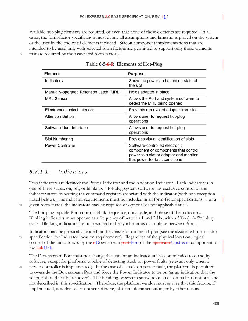
PCI EXPRESS 2.0 BASE SPECIFICATION, REV. 12.0
409
available hot-plug elements are required, or even that none of these elements are required. In all cases, the form-factor specification must define all assumptions and limitations placed on the system or the user by the choice of elements included. Silicon component implementations that are intended to be used only with selected form factors are permitted to support only those elements that are required by the associated form factor(s). 5
Table 6-5- 6-5: Elements of Hot-Plug
Element Purpose Indicators Show the power and attention state of
the slot Manually-operated Retention Latch (MRL) Holds adapter in place MRL Sensor Allows the Port and system software to
detect the MRL being opened Electromechanical Interlock Prevents removal of adapter from slot Attention Button Allows user to request hot-plug
operations Software User Interface Allows user to request hot-plug
operations Slot Numbering Provides visual identification of slots Power Controller Software-controlled electronic
component or components that control power to a slot or adapter and monitor that power for fault conditions
6.7.1.1. Indicators
Two indicators are defined: the Power Indicator and the Attention Indicator. Each indicator is in one of three states: on, off, or blinking. Hot-plug system software has exclusive control of the indicator states by writing the command registers associated with the indicator (with one exception noted below). The indicator requirements must be included in all form-factor specifications. For a given form factor, the indicators may be required or optional or not applicable at all. 10
The hot-plug capable Port controls blink frequency, duty cycle, and phase of the indicators. Blinking indicators must operate at a frequency of between 1 and 2 Hz, with a 50% (+/- 5%) duty cycle. Blinking indicators are not required to be synchronous or in-phase between Ports.
Indicators may be physically located on the chassis or on the adapter (see the associated form factor specification for Indicator location requirements). Regardless of the physical location, logical 15 control of the indicators is by the dDownstream port Port of the upstream Upstream component on the linkLink.
The Downstream Port must not change the state of an indicator unless commanded to do so by software, except for platforms capable of detecting stuck-on power faults (relevant only when a power controller is implemented). In the case of a stuck-on power fault, the platform is permitted 20 to override the Downstream Port and force the Power Indicator to be on (as an indication that the adapter should not be removed). The handling by system software of stuck-on faults is optional and not described in this specification. Therefore, the platform vendor must ensure that this feature, if implemented, is addressed via other software, platform documentation, or by other means.
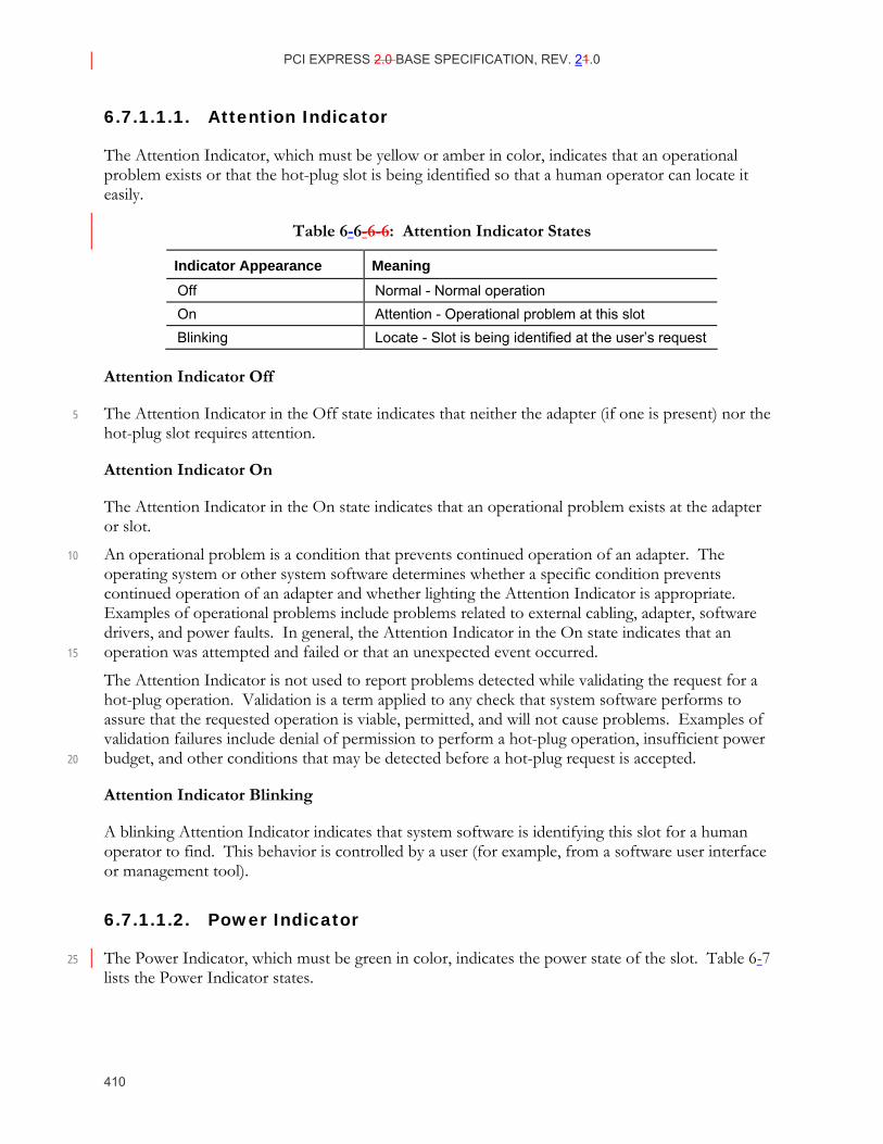
PCI EXPRESS 2.0 BASE SPECIFICATION, REV. 21.0
410
6.7.1.1.1. Attention Indicator
The Attention Indicator, which must be yellow or amber in color, indicates that an operational problem exists or that the hot-plug slot is being identified so that a human operator can locate it easily.
Table 6-6- 6-6: Attention Indicator States
Indicator Appearance Meaning Off Normal - Normal operation On Attention - Operational problem at this slot Blinking Locate - Slot is being identified at the user’s request
Attention Indicator Off
The Attention Indicator in the Off state indicates that neither the adapter (if one is present) nor the 5 hot-plug slot requires attention.
Attention Indicator On
The Attention Indicator in the On state indicates that an operational problem exists at the adapter or slot.
An operational problem is a condition that prevents continued operation of an adapter. The 10 operating system or other system software determines whether a specific condition prevents continued operation of an adapter and whether lighting the Attention Indicator is appropriate. Examples of operational problems include problems related to external cabling, adapter, software drivers, and power faults. In general, the Attention Indicator in the On state indicates that an operation was attempted and failed or that an unexpected event occurred. 15
The Attention Indicator is not used to report problems detected while validating the request for a hot-plug operation. Validation is a term applied to any check that system software performs to assure that the requested operation is viable, permitted, and will not cause problems. Examples of validation failures include denial of permission to perform a hot-plug operation, insufficient power budget, and other conditions that may be detected before a hot-plug request is accepted. 20
Attention Indicator Blinking
A blinking Attention Indicator indicates that system software is identifying this slot for a human operator to find. This behavior is controlled by a user (for example, from a software user interface or management tool).
6.7.1.1.2. Power Indicator
The Power Indicator, which must be green in color, indicates the power state of the slot. Table 6-7 25 lists the Power Indicator states.
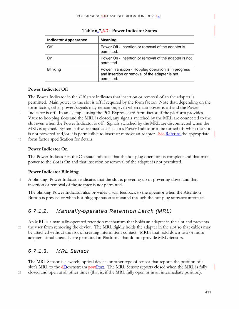
PCI EXPRESS 2.0 BASE SPECIFICATION, REV. 12.0
411
Table 6-7- 6-7: Power Indicator States
Indicator Appearance Meaning
Off Power Off - Insertion or removal of the adapter is permitted.
On Power On - Insertion or removal of the adapter is not permitted.
Blinking Power Transition - Hot-plug operation is in progress and insertion or removal of the adapter is not permitted.
Power Indicator Off
The Power Indicator in the Off state indicates that insertion or removal of an the adapter is permitted. Main power to the slot is off if required by the form factor. Note that, depending on the form factor, other power/signals may remain on, even when main power is off and the Power Indicator is off. In an example using the PCI Express card form factor, if the platform provides 5 Vaux to hot-plug slots and the MRL is closed, any signals switched by the MRL are connected to the slot even when the Power Indicator is off. Signals switched by the MRL are disconnected when the MRL is opened. System software must cause a slot’s Power Indicator to be turned off when the slot is not powered and/or it is permissible to insert or remove an adapter. See Refer to the appropriate form factor specification for details. 10
Power Indicator On
The Power Indicator in the On state indicates that the hot-plug operation is complete and that main power to the slot is On and that insertion or removal of the adapter is not permitted.
Power Indicator Blinking
A blinking Power Indicator indicates that the slot is powering up or powering down and that 15 insertion or removal of the adapter is not permitted.
The blinking Power Indicator also provides visual feedback to the operator when the Attention Button is pressed or when hot-plug operation is initiated through the hot-plug software interface.
6.7.1.2. Manually-operated Retention Latch (MRL)
An MRL is a manually-operated retention mechanism that holds an adapter in the slot and prevents the user from removing the device. The MRL rigidly holds the adapter in the slot so that cables may 20 be attached without the risk of creating intermittent contact. MRLs that hold down two or more adapters simultaneously are permitted in Platforms that do not provide MRL Sensors.
6.7.1.3. MRL Sensor
The MRL Sensor is a switch, optical device, or other type of sensor that reports the position of a slot’s MRL to the dDownstream portPort. The MRL Sensor reports closed when the MRL is fully closed and open at all other times (that is, if the MRL fully open or in an intermediate position). 25
PCI EXPRESS 2.0 BASE SPECIFICATION, REV. 21.0
412
If a power controller is implemented for the slot, the slot main power must be automatically removed from the slot when the MRL Sensor indicates that the MRL is open. If signals such as Vaux and SMBus are switched by the MRL, then these signals must be automatically removed from the slot when the MRL Sensor indicates that the MRL is open and must be restored to the slot when the MRL Sensor indicates that MRL has closed again. Refer to the appropriate form factor 5 specification to identify the signals, if any, switched by the MRL.
Note that the Hot-Plug Controller does not autonomously change the state of either the Power Indicator or the Attention Indicator based on MRL sensor changes.
IMPLEMENTATION NOTE
MRL Sensor Handling In the absence of an MRL sensor, for some form factors, staggered presence detect pins may be used to handle the switched signals. In this case, when the presence pins break contact, the switched 10 signals will be automatically removed from the slot.
If an MRL Sensor is implemented without a corresponding MRL Sensor input on the PCI Express Hot-Plug Controller, it is recommended that the MRL Sensor be routed to power fault input of the Hot-Plug Controller. This allows an active adapter to be powered off when the MRL is opened.
6.7.1.4. Electromechanical Interlock
An electromechanical interlock is a mechanism for physically locking the adapter or MRL in place 15 until system software releases it. The state of the electromechanical interlock is set by software and must not change except in response to a subsequent software command. In particular, the state of the electromechanical interlock must be maintained even when power to the hot-plug slot is removed.
The current state of the electromechanical interlock must be reflected at all times in the 20 Electromechanical Interlock Status field bit in the Slot Status register, which must be updated within 200 ms of any commanded change. Software must wait at least 1 second after issuing a command to toggle the state of the Electromechanical Interlock before another command to toggle the state can be issued. Systems may optionally expand control of interlocks to provide physical security of the adapter. 25
6.7.1.5. Attention Button
The Attention Button is a momentary-contact push button switch, located adjacent to each hot-plug slot or on the adapter that is pressed by the user to initiate a hot-plug operation at that slot. Regardless of the physical location of the button, the signal is processed and indicated to software by hot-plug hardware associated with the dDownstream port Port corresponding to the slot.
The Attention Button must allow the user to initiate both hot add and hot remove operations 30 regardless of the physical location of the button.

PCI EXPRESS 2.0 BASE SPECIFICATION, REV. 12.0
413
If present, the Power Indicator provides visual feedback to the human operator (if the system software accepts the request initiated by the Attention Button) by blinking. Once the Power Indicator begins blinking, a 5-second abort interval exists during which a second depression of the Attention Button cancels the operation.
If an operation initiated by an Attention Button fails for any reason, it is recommended that system 5 software present an error message explaining the failure via a software user interface or add the error message to a system log.
6.7.1.6. Software User Interface
System software provides a user interface that allows hot insertions and hot removals to be initiated and that allows occupied slots to be monitored. A detailed discussion of hot-plug user interfaces is operating system specific and is therefore beyond the scope of this document. 10
On systems with multiple hot-plug slots, the system software must allow the user to initiate operations at each slot independent of the states of all other slots. Therefore, the user is permitted to initiate a hot-plug operation on one slot using either the software user interface or the Attention Button while a hot-plug operation on another slot is in process, regardless of which interface was used to start the first operation. 15
6.7.1.7. Slot Numbering
A Physical Slot Identifier (as defined in PCI Hot-Plug Specification, Revision 1.1, Section 1.5) consists of an optional chassis number and the physical slot number of the slot. The physical slot number is a chassis unique identifier for a slot. System software determines the physical slot number from registers in the Port. Chassis number 0 is reserved for the main chassis. The chassis number for other chassis must be a non-zero value obtained from a PCI-to-PCI Bridge’s Chassis Number 20 register (see the PCI-to-PCI Bridge Architecture Specification, Revision 1.2, Section 13.4).
Regardless of the form factor associated with each slot, each physical slot number must be unique within a chassis.
6.7.1.8. Power Controller
The power controller is an element composed of one or more discrete components that acts under control of software to set the power state of either the hot-plug slot or the adapter as appropriate 25 for the specific form factor. The power controller must also monitor the slot/adapter for power fault conditions (as defined in the associated form factor specification) that occur on the slot/adapter’s main power rails and, if supported, auxiliary power rail.
If a power controller is not present, the power state of the hot-plug slot/adapter must be set automatically by the hot-plug controller in response to changes in the presence of an adapter in the 30 slot.
The power controller monitors main and auxiliary power faults independently. If a power controller detects a main power fault on the hot-plug slot/adapter, it must automatically set its internal main power fault latch and remove main power from the hot-plug slot/adapter (without affecting auxiliary power). Similarly, if a power controller detects an auxiliary power fault on the hot-plug 35

PCI EXPRESS 2.0 BASE SPECIFICATION, REV. 21.0
414
slot/adapter, it must automatically set its internal auxiliary power fault latch and remove auxiliary power from the hot-plug slot/adapter (without affecting main power). Power must remain off to the slot/adapter as long as the power fault condition remains latched, regardless of any writes by software to turn on power to the hot-plug slot/adapter. The main power fault latch is cleared when software turns off power to the hot-plug slot/adapter. The mechanism by which the auxiliary power 5 fault latch is cleared is form factor specific but generally requires auxiliary power to be removed from the hot-plug slot/adapter. For example, one form factor may remove auxiliary power when the MRL for the slot is opened while another may require the adapter to be physically removed from the slot. See Refer to the associated form factor specifications for specific requirements.
Since the Power Controller Control field bit in the Slot Control register reflects the last value written 10 and not the actual state of the power controller, this means there may be an inconsistency between the value of the Power Controller Control field bit and the state of the power to the slot/adapter in a power fault condition. To determine whether slot/adapter power is off due to a power fault, software must use the power fault software notification to detect power faults. To determine that a requested power-up operation has otherwise failed, software must use the hot-plug slot/adapter 15 power-up time out mechanism described in Section 6.7.3.3.
Software must not assume that writing to the Slot Control register to change the power state of a hot-plug slot/adapter causes an immediate power state transition. After turning power on, software must wait for a Data Link Layer State Changed event, as described in Section 6.7.3.3. After turning power off, software must wait for at least 1 second before taking any action that relies on power 20 having been removed from the hot-plug slot/adapter. For example, software is not permitted to turn off the power indicator (if present) or attempt to turn on the power controller before completing the 1 second wait period.
6.7.2. Registers Grouped by Hot-Plug Element Association
The registers described in this section are grouped by hot-plug element to convey all registers associated with implementing each element. Registers associated with each Downstream Port 25 implementing a hot-plug capable slot are located in the PCI Express Device Capabilities, Slot Capabilities, Slot Control, and Slot Status registers in the PCI Express Capability structure (see Section 7.8). Registers reporting the presence of hot-plug elements associated with the device Function on an adapter are located in the Device Capabilities register (also in the PCI Express Capability structure). 30
6.7.2.1. Attention Button Registers
Attention Button Present (Slot Capabilities and Device Capabilities) – This bit indicates if an Attention Button is electrically controlled by the chassis (Slot Capabilities) or by the adapter (Device Capabilities).
Attention Button Pressed (Slot Status) – This bit is set when an Attention Button electrically controlled by the chassis is pressed. 35
Attention Button Pressed Enable (Slot Control) – When setSet, this bit enables software notification on an Attention Button Pressed event (see Section 6.7.3.4).

PCI EXPRESS 2.0 BASE SPECIFICATION, REV. 12.0
415
6.7.2.2. Attention Indicator Registers
Attention Indicator Present (Slot Capabilities and Device Capabilities) – This bit indicates if an Attention Indicator is electrically controlled by the chassis (Slot Capabilities) or by the adapter (Device Capabilities).
Attention Indicator Control (Slot Control) – When written, sets an Attention Indicator electrically controlled by the chassis to the written state. 5
6.7.2.3. Power Indicator Registers
Power Indicator Present (Slot Capabilities and Device Capabilities) – This bit indicates if a Power Indicator is electrically controlled by the chassis (Slot Capabilities) or by the adapter (Device Capabilities).
Power Indicator Control (Slot Control) – When written, sets a Power Indicator electrically controlled by the chassis to the written state. 10
6.7.2.4. Power Controller Registers
Power Controller Present (Slot Capabilities) – This bit indicates if a Power Controller is implemented.
Power Controller Control (Slot Control) – Turns the Power Controller on or off according to the value written.
Power Fault Detected (Slot Status) – This bit is set when a power fault is detected at the slot or 15 the adapter.
Power Fault Detected Enable (Slot Control) – When setSet, this bit enables software notification on a power fault event (see Section 6.7.3.4).
6.7.2.5. Presence Detect Registers
Presence Detect State (Slot Status) – This bit indicates the presence of an adapter in the slot.
Presence Detect Changed (Slot Status) – This bit is set when a Presence presence Detect detect 20 state change is detected.
Presence Detect Changed Enable (Slot Control) – When setSet, this bit enables software notification on a presence detect changed event (see Section 6.7.3.4).
6.7.2.6. MRL Sensor Registers
MRL Sensor Present (Slot Capabilities) – This bit indicates if an MRL Sensor is implemented.
MRL Sensor Changed (Slot Status) – This bit is set when the value of the MRL Sensor state 25 changes.
PCI EXPRESS 2.0 BASE SPECIFICATION, REV. 21.0
416
MRL Sensor Changed Enable (Slot Control) – When setSet, this bit enables software notification on a MRL Sensor changed event (see Section 6.7.3.4).
MRL Sensor State (Slot Status) – This register reports the status of the MRL Sensor if one is implemented.
6.7.2.7. Electromechanical Interlock Registers
Electromechanical Interlock Present (Slot Capabilities) – This bit indicates if an 5 Electromechanical Interlock is implemented.
Electromechanical Interlock Status (Slot Status) – This bit reflects the current state of the Electromechanical Interlock.
Electromechanical Interlock Control (Slot Control) – This bit when set to 1b toggles the state of the Electromechanical Interlock. 10
6.7.2.8. Command Completed Registers
No Command Completed Support (Slot Capabilities) – This bit when set to 1b indicates that this slot does not generate software notification when an issued command is completed by the Hot-Plug Controller.
Command Completed (Slot Status) – This bit is set when the Hot-Plug Controller completes an issued command and is ready to accept the next command. 15
Command Completed Interrupt Enable (Slot Control) – When setSet, this bit enables software notification (see Section 6.7.3.4) when a command is completed by the hot-plug control logic.
6.7.2.9. Port Capabilities and Slot Information Registers
Slot Implemented (PCI Express Capabilities) – When setSet, this bit indicates that the Link associated with this Downstream Port is connected to a slot.
Physical Slot Number (Slot Capabilities) – This hardware initialized field indicates the physical 20 slot number attached to the Port.
Hot-Plug Capable (Slot Capabilities) – When setSet, this bit indicates this slot is capable of supporting hot-plug.
Hot-Plug Surprise (Slot Capabilities) – When setSet, this bit indicates that adapter removal from the system without any prior notification is permitted for the associated form factor. 25
6.7.2.10. Hot-Plug Interrupt Control Register
Hot-Plug Interrupt Enable (Slot Control) – When setSet, this bit enables generation of the hot-plug interrupt on enabled hot-plug events.
PCI EXPRESS 2.0 BASE SPECIFICATION, REV. 12.0
417
6.7.3. PCI Express Hot-Plug Events
A Downstream Port with hot-plug capabilities supports the following hot-plug events:
Slot Events:
• Attention Button Pressed
• Power Fault Detected
• MRL Sensor Changed 5
• Presence Detect Changed
Command Completed Events
Data Link Layer State Changed Events
Each of these events has a status field, which indicates that an event has occurred but has not yet been processed by software, and an enable field, which indicates whether the event is enabled for 10 software notification. Some events also have a capability field, which indicates whether the event type is supported on the portPort. The grouping of these fields by event type is listed in Section 6.7.2, and each individual field is described in Section 7.8.
6.7.3.1. Slot Events
A Downstream Port with hot-plug capabilities monitors the slot it controls for the slot events listed above. When one of these slot events is detected, the port Port indicates that the event has occurred 15 by setting the status field associated with the event. At that point, the event is pending until software clears the status field.
Once a slot event is pending on a particular slot, all subsequent events of that type are ignored on that slot until the event is cleared. The port Port must continue to monitor the slot for all other slot event types and report them as they occur. 20
If enabled through the associated enable field, slot events must generate a software notification. If the event is not supported on the port Port as indicated by the associated capability field, software must not enable software notification for the event. The mechanism by which this notification is reported to software is described in Section 6.7.3.4.
6.7.3.2. Command Completed Events
Since changing the state of some hot-plug elements may not happen instantaneously, PCI Express 25 supports hot-plug commands and command completed events. All hot-plug capable ports Ports are required to support hot-plug commands and, if the capability is reported, command completed events.
Software issues a command to a hot-plug capable Downstream Port by issuing a write transaction that targets any portion of the port’s Port’s Slot Control register. A single write to the Slot Control 30 register is considered to be a single command, even if the write affects more than one field in the Slot Control register. In response to this transaction, the port Port must carry out the requested

PCI EXPRESS 2.0 BASE SPECIFICATION, REV. 21.0
418
actions and then set the associated status field for the command completed event. The portPort must process the command normally even if the status field is already set when the command is issued. If a single command results in more than one action being initiated, the order in which the actions are executed is unspecified. All actions associated with a single command execution must not take longer than 1 second. 5
If command completed events are not supported as indicated by a value of 1b in the No Command Completed Support field of the Slot Capabilities register, a hot-plug capable portPort must process a write transaction that targets any portion of the portPort’s Slot Control register without any dependency on previous Slot Control writes. Software is permitted to issue multiple Slot Control writes in sequence without any delay between the writes. 10
If command completed events are supported, then Software software must wait for a command to complete before issuing the next command. However, if the status field is not set after the 1 second limit on command execution, software is permitted to repeat the command or to issue the next command. If software issues a write before the portPort has completed processing of the previous command and before the 1 second time limit has expired, the portPort is permitted to either accept 15 or discard the write. Such a write is considered a programming error, and could result in a discrepancy between the Slot Control register and the hot plug element state. To recover from such a programming error and return the controller to a consistent state, software must issue a write to the Slot Control register which conforms to the command completion rules.
If enabled through the associated enable field, the completion of a commands must generate a 20 software notification. The exception to this rule is a command that occurs as a result of a write to the Slot Control register that disables software notification of command completed events. Such a command must be processed as described above, but must not generate a software notification.
6.7.3.3. Data Link Layer State Changed Events
The Data Link Layer State Changed event provides an indication that the state of the Data Link Layer Link Active field bit in the Link Status register has changed. Support for Data Link Layer 25 State Changed events and software notification of these events are required for hot-plug capable dDownstream portsPorts. If this event is supported, the portPort sets the status field associated with the event when the value in the Data Link Layer Link Active field bit changes.
This event allows software to indirectly determine when power has been applied to a newly hot-plugged adapter. Software must wait for 100 ms after the Data Link Layer Link Active field bit 30 reads 1b before initiating a configuration access to the hot added device (see Section 6.6). Software must allow 1 second after the Data Link Layer Link Active field bit reads 1b before it is permitted to determine that a hot plugged device which fails to return a Successful Completion for a Valid Configuration Request is a broken device (see Section 6.6).
The Data Link Layer State Changed event must occur within 1 second of the event that initiates the 35 hot-insertion. If a power controller is supported, the time out interval is measured from when software initiated a write to the Slot Control register to turn on the power. If a power controller is not supported, the time out interval is measured from presence detect slot event. Software is allowed to time out on a hot add operation if the Data Link Layer State Changed event does not occur within 1 second. The action taken by software after such a timeout is implementation 40 specific.
PCI EXPRESS 2.0 BASE SPECIFICATION, REV. 12.0
419
6.7.3.4. Software Notification of Hot-Plug Events
A hot-plug capable Downstream Port must support generation of an interrupt on a hot-plug event. As described in Sections 6.7.3.1 and 6.7.3.2, each type of hot-plug event has both an enable field which enables software notification of that type of eventbit for interrupt generation and a status field bit that indicates that when an event has occurred but has not yet been processed by software. There is also a Hot-Plug Interrupt Enable bit in the Slot Control register that serves as a master 5 enable/disable bit for all hot-plug events.
If the Port is enabled for level-triggered interrupt signaling using the INTx messages, the virtual INTx wire must be asserted whenever and as long as the following conditions are satisfied:
The Interrupt Disable bit in the Command register is set to 0b.
The Hot Plug Interrupt Enable bit in the Slot Control register is set to 1b. 10
At least one hot-plug event status bit in the Slot Status register and its associated Enable bit in the Slot Control register are both set to 1b.
Note that all other interrupt sources within the same Function will assert the same virtual INTx wire when requesting service.
If the Port is enabled for edge-triggered interrupt signaling using MSI or MSI-X, an interrupt 15 message must be sent every time the logical AND of the following conditions transitions from FALSE to TRUE:
The associated vector is unmasked (not applicable if MSI does not support PVM).
The Hot Plug Interrupt Enable bit in the Slot Control register is set to 1b.
At least one hot-plug event status bit in the Slot Status register and its associated Enable bit in 20 the Slot Control register are both set to 1b.
Note that PME and Hot-Plug Event interrupts (when both are implemented) always share the same MSI or MSI-X vector, as indicated by the Interrupt Message Number field in the PCI Express Capabilities register.If the enable field for an event indicates that software notification of the event is disabled, the hot-plug capable Downstream Port must not generate an interrupt on that event. Hot-25 plug interrupt generation is also globally enabled through the Hot-Plug Interrupt Enable field in the Slot Control register. If this field indicates that hot-plug interrupts are disabled, the hot-plug capable Downstream Port must not generate an interrupt on any hot-plug event.
The Downstream Port must generate an interrupt on a hot-plug event following the rules for interrupt generation described in the rest of this document provided these disable conditions are not 30 present and the corresponding status field for the event is not set. If the status field is set, software has not yet handled a previous event; thus, a new interrupt must not be generated.
If the port is enabled for level-triggered interrupt generation using the INTx messages, the interrupt must remain asserted as long as global interrupt generation is enabled and at least one status field for an enabled hot-plug event remains set. If the port is enabled for edge-triggered interrupt generation 35 using MSI or MSI-X, an MSI must be sent whenever global interrupt generation is enabled and the status field for an enabled hot-plug event transitions from not set to set.
The portPort may optionally send an MSI when there are hot-plug events that occur while interrupt generation is disabled, and interrupt generation is subsequently enabled.
PCI EXPRESS 2.0 BASE SPECIFICATION, REV. 21.0
420
If wake generation is required by the associated form factor specification, a hot-plug capable Downstream Port must support generation of a wakeup event (using the PME mechanism) on hot-plug events that occur when the system is in a sleep state or the portPort is in device state D1, D2, or D3Hot.
Software enables a hot-plug event to generate a wakeup event by enabling software notification of 5 the event as described in Section 6.7.3.1. Note that in order for software to disable interrupt generation while keeping wakeup generation enabled, the Hot-Plug Interrupt Enable bit must be cleared. For form factors that support wake generation, a wakeup event must be generated if all three of the following conditions occur:
The status register for an enabled event transitions from not set to set 10
The portPort is in device state D1, D2, or D3Hot, and
The PME Enable bit in the portPort’s Power Management Control/Status register is set
Note that the Hot-Plug Controller generates the wakeup on behalf of the hot-plugged device, and it is not necessary for that device to have auxiliary (or main) power.
6.7.4. Firmware Support for Hot-Plug
Some systems that include hot-plug capable Root Ports and Switches that are released before ACPI-15 compliant operating systems with native hot-plug support are available, can use ACPI firmware for propagating hot-plug events. Firmware control of the hot-plug registers must be disabled if an operating system with native support is used. Platforms that provide ACPI firmware to propagate hot-plug events must also provide a mechanism to transfer control to the operating system. The details of this method are described in the PCI Firmware Specification. 20
6.8. Power Budgeting Capability With the addition of a hot-plug capability for adapters, the need arises for the system to be capable of properly allocating power to any new devices added to the system. This capability is a separate and distinct function from power management and a basic level of support is required to ensure proper operation of the system. The power budgeting concept puts in place the building blocks that allow devices to interact with systems to achieve these goals. There are many ways in which the 25 system can implement the actual power budgeting capabilities, and as such, they are beyond the scope of this specification.
Implementation of the power Power budgeting Budgeting capability Capability is optional for PCI Express devices that are implemented either in a form factor which does not require hot-plug support, or that are integrated on the system board. PCI Express fForm factor specifications may 30 require support for power budgeting. The devices and/or adapters are required by PCI Express to remain under the configuration power limit specified in the corresponding electromechanical specification until they have been configured and enabled by the system. The system should guarantee that power has been properly budgeted prior to enabling an adapter.
PCI EXPRESS 2.0 BASE SPECIFICATION, REV. 12.0
421
6.8.1. System Power Budgeting Process Recommendations
It is recommended that system firmware provide the power budget management agent the following information:
Total system power budget (power supply information).
Total power allocated by system firmware (system board devices).
Total number of slots and the types of slots. 5
System firmware is responsible for allocating power for all devices on the system board that do not have power budgeting capabilities. The firmware may or may not include standard PCI Express devices that are connected to the standard power rails. When the firmware allocates the power for a device then it must set the SYSTEM_ALLOC bit to 1b to indicate that it has been properly allocated. The power budget manager is responsible for allocating all PCI Express devices including 10 system board devices that have the power Power budgeting Budgeting capability Capability and have not been marked allocated. The power budget manager is responsible for determining if hot-plugged devices can be budgeted and enabled in the system.
There are alternate methods which may provide the same functionality, and it is not required that the power budgeting process be implemented in this manner. 15
6.9. Slot Power Limit Control PCI Express provides a mechanism for software controlled limiting of the maximum power per slot that PCI Express adapter (associated with that slot) can consume. The key elements of this mechanism are:
Slot Power Limit Value and Scale fields of the Slot Capability Capabilities register implemented in the Downstream Ports of a Root Complex and or a Switch 20
Captured Slot Power Limit Value and Scale fields of the Device Capability register implemented in the Upstream Ports of a Endpoint, Switch, and or PCI Express-PCI Bridge Functions present in an Upstream Port
Set_Slot_Power_Limit Message that conveys the content of the Slot Power Limit Value and Scale fields of the Slot Capability register of the Downstream Port (of a Root Complex or a 25 Switch) to the corresponding Captured Slot Power Limit Value and Scale fields of the Device Capability Capabilities register in the Upstream Port of the component connected to the same Link
Power limits on the platform are typically controlled by the software (for example, platform firmware) that comprehends the specifics of the platform such as: 30
Partitioning of the platform, including slots for I/O expansion using adapters
Power delivery capabilities
Thermal capabilities
PCI EXPRESS 2.0 BASE SPECIFICATION, REV. 21.0
422
This software is responsible for correctly programming the Slot Power Limit Value and Scale fields of the Slot Capability registers of the Downstream Ports connected to slots. After the value has been written into the register within the Downstream Port, it is conveyed to the adapter using the Set_Slot_Power_Limit Message (see Section 2.2.8.5). The recipient of the Message must use the value in the Message data payload to limit usage of the power for the entire adapter, unless the 5 adapter will never exceed the lowest value specified in the corresponding form factor specification. It is required that device driver software associated with the adapter be able (by reading the values of the Captured Slot Power Limit Value and Scale fields of the Device Capability Capabilities register) to configure hardware of the adapter to guarantee that the adapter will not exceed the imposed limit. In the case where the platform imposes a limit that is below the minimum needed for adequate 10 operation, the device driver will be able to communicate this discrepancy to higher level configuration software. Configuration software is required to set the Slot Power Limit to one of the maximum values specified for the corresponding form factor based on the capability of the platform.
The following rules cover the Slot Power Limit control mechanism: 15
For Adapters:
Until and unless a Set_Slot_Power_Limit Message is received indicating a Slot Power Limit value greater than the lowest value specified in the form factor specification for the adapter's form factor, the adapter must not consume more than the lowest value specified.
An adapter must never consume more power than what was specified in the most recently 20 received Set_Slot_Power_Limit Message or the minimum value specified in the corresponding form factor specification, whichever is higher.
Components with Endpoint, Switch, and or PCI Express-PCI Bridge components Functions that are targeted for integration on an adapter where total consumed power is below the lowest limit defined for the targeted form factor are permitted to ignore Set_Slot_Power_Limit 25 Messages, and to return a value of 0 in the Captured Slot Power Limit Value and Scale fields of the Device Capability Capabilities register
• Such components still must be able to receive the Set_Slot_Power_Limit Message without error but simply discard the Message value
For Root Complex and Switches which source slots: 30
Configuration software must not program a Set_Slot_Power_Limit value that indicates a limit that is lower than the lowest value specified in the form factor specification for the slot’s form factor.
PCI EXPRESS 2.0 BASE SPECIFICATION, REV. 12.0
423
IMPLEMENTATION NOTE
Example Adapter Behavior Based on the Slot Power Limit Control Capability The following power limit scenarios are examples of how an adapter must behave based on the Slot Power Limit control capability. The form factor limits are representations, and should not be taken as actual requirements.
Note: Form factor #1 has a maximum power requirement of 40 W and 25 W; form factor #2 has a maximum power requirement of 15 W. 5
Scenario 1: An Adapter Consuming 12 W
If the adapter is plugged into a form factor #1 40 W slot, the Slot Power Limit control mechanism is followed, and the adapter operates normally.
If the adapter is plugged into a form factor #1 25 W slot, the Slot Power Limit control mechanism is followed, and the adapter operates normally. 10
If the adapter is plugged into a form factor #2 15 W slot, the Slot Power Limit control mechanism is followed, and the adapter operates normally.
In all cases, since the adapter operates normally within all the form factors, it can ignore any of the slot power limit Messages.
Scenario 2: An Adapter Consuming 18 W 15
If the adapter is plugged into a form factor #1 40 W slot, the Slot Power Limit control mechanism is followed, and the adapter operates normally.
If the adapter is plugged into a form factor #1 25 W slot, the Slot Power Limit control mechanism is followed, and the adapter operates normally.
If the adapter is plugged into a form factor #2 15 W slot, the Slot Power Limit control 20 mechanism is followed, and the adapter must scale down to 15 W or disable operation. An adapter that does not scale within any of the power limits for a given form factor will always be disabled in that form factor and should not be used.
In this case, if the adapter is only to be used in form factor #1, it can ignore any of the slot power limit Messages. To be useful in form factor #2, the adapter should be capable of scaling to the 25 power limit of form factor #2.
Scenario 3: An Adapter Consuming 30 W
If the adapter is plugged into a form factor #1 40 W slot, the Slot Power Limit control mechanism is followed, and the device operates normally.
If the adapter is plugged into a form factor #1 25 W slot, the Slot Power Limit control 30 mechanism is followed, and the device must scale down to 25 W or disable operation.
PCI EXPRESS 2.0 BASE SPECIFICATION, REV. 21.0
424
If the adapter is plugged into a form factor #2 15 W slot, the Slot Power Limit control mechanism is followed, and the adapter must scale down to 15 W or disable operation. An adapter that does not scale within any of the power limits for a given form factor will always be disabled in that form factor and should not be used.
In this case, since the adapter consumes power above the lowest power limit for a slot, the adapter 5 must be capable of scaling or disabling to prevent system failures. Operation of adapters at power levels that exceed the capabilities of the slots in which they are plugged must be avoided.
IMPLEMENTATION NOTE
Slot Power Limit Control Registers Typically Slot Power Limit registers within Downstream Ports of Root Complex or a Switch Device will be programmed by platform-specific software. Some implementations may use a hardware method for initializing the values of these registers and, therefore, not require software support. 10
Components with Endpoint, Switch, and or PCI Express-PCI Bridge components Functions that are targeted for integration on the adapter where total consumed power is below the lowest limit defined for that form factor are allowed to ignore Set_Slot_Power_Limit Messages. Note that PCI Express components that take this implementation approach may not be compatible with potential future defined form factors. Such form factors may impose lower power limits that are below the 15 minimum required by a new adapter based on the existing component.
6.10. Root Complex Topology Discovery A PCI Express Root Complex may present one of the following topologies to configuration software:
A single opaque Root Complex such that software has no visibility with respect to internal operation of the Root Complex. All Root Ports are independent of each other from a software 20 perspective; no mechanism exists to manage any arbitration among the various Root Ports for any differentiated services.
A single Root Complex Component such that software has visibility and control with respect to internal operation of the Root Complex Component. As shown in Figure 6-11, software views the Root Ports as ingress Ingress ports Ports for the component. The Root Complex internal 25 portPort for traffic aggregation to a system eEgress portPort or an internal sink unit (such as memory) is represented by an RCRB structure. Controls for differentiated services are provided through a PCI Express Virtual Channel capability Capability structure located in the RCRB.
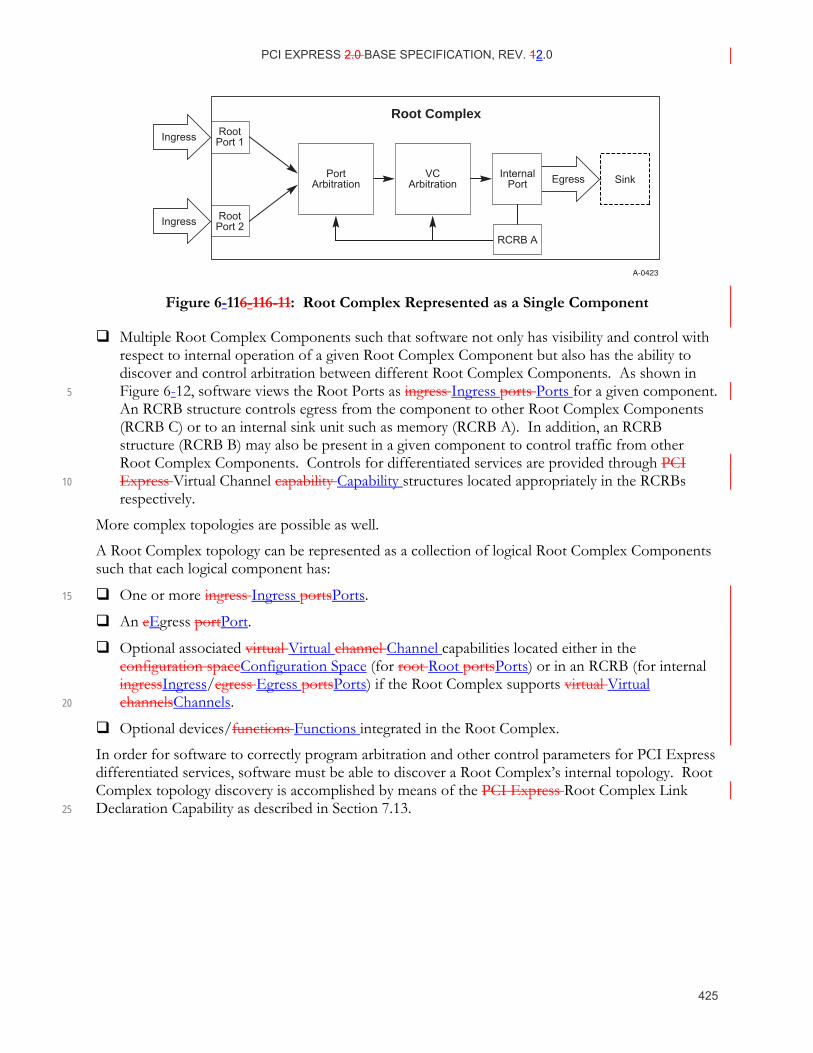
PCI EXPRESS 2.0 BASE SPECIFICATION, REV. 12.0
425
A-0423
Egress
Ingress RootPort 1
RootPort 2Ingress
PortArbitration
VCArbitration
InternalPort Sink
Root Complex
RCRB A
Figure 6-116-11 6-11: Root Complex Represented as a Single Component
Multiple Root Complex Components such that software not only has visibility and control with respect to internal operation of a given Root Complex Component but also has the ability to discover and control arbitration between different Root Complex Components. As shown in Figure 6-12, software views the Root Ports as ingress Ingress ports Ports for a given component. 5 An RCRB structure controls egress from the component to other Root Complex Components (RCRB C) or to an internal sink unit such as memory (RCRB A). In addition, an RCRB structure (RCRB B) may also be present in a given component to control traffic from other Root Complex Components. Controls for differentiated services are provided through PCI Express Virtual Channel capability Capability structures located appropriately in the RCRBs 10 respectively.
More complex topologies are possible as well.
A Root Complex topology can be represented as a collection of logical Root Complex Components such that each logical component has:
One or more ingress Ingress portsPorts. 15
An eEgress portPort.
Optional associated virtual Virtual channel Channel capabilities located either in the configuration spaceConfiguration Space (for root Root portsPorts) or in an RCRB (for internal ingressIngress/egress Egress portsPorts) if the Root Complex supports virtual Virtual channelsChannels. 20
Optional devices/functions Functions integrated in the Root Complex.
In order for software to correctly program arbitration and other control parameters for PCI Express differentiated services, software must be able to discover a Root Complex’s internal topology. Root Complex topology discovery is accomplished by means of the PCI Express Root Complex Link Declaration Capability as described in Section 7.13. 25
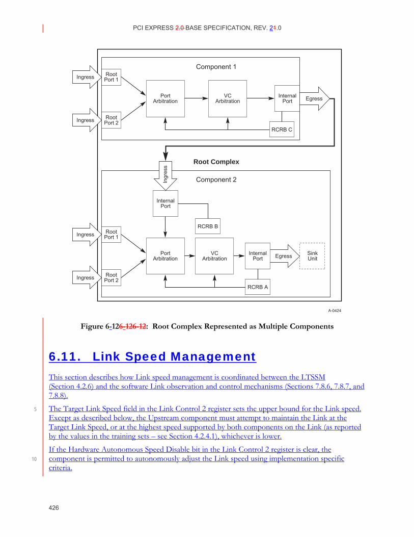
PCI EXPRESS 2.0 BASE SPECIFICATION, REV. 21.0
426
Egress
A-0424
Ingress RootPort 1
RootPort 2Ingress
PortArbitration
VCArbitration
InternalPort
Component 1
Egress
Ingress RootPort 1
RootPort 2Ingress
PortArbitration
VCArbitration
InternalPort
InternalPort
SinkUnit
Component 2
Root Complex
RCRB A
Ingr
ess
RCRB B
RCRB C
Figure 6-126-12 6-12: Root Complex Represented as Multiple Components
6.11. Link Speed Management This section describes how Link speed management is coordinated between the LTSSM (Section 4.2.6) and the software Link observation and control mechanisms (Sections 7.8.6, 7.8.7, and 7.8.8).
The Target Link Speed field in the Link Control 2 register sets the upper bound for the Link speed. 5 Except as described below, the Upstream component must attempt to maintain the Link at the Target Link Speed, or at the highest speed supported by both components on the Link (as reported by the values in the training sets – see Section 4.2.4.1), whichever is lower.
If the Hardware Autonomous Speed Disable bit in the Link Control 2 register is clear, the component is permitted to autonomously adjust the Link speed using implementation specific 10 criteria.
PCI EXPRESS 2.0 BASE SPECIFICATION, REV. 12.0
427
If the reliability of the Link is unacceptably low, then either component is permitted to lower the Link speed by removing the unreliable Link speed from the list of supported speeds advertised in the training sets the component transmits. The criteria for determination of acceptable Link reliability are implementation specific, and are not dependent on the setting of the Hardware Autonomous Speed Disable bit. 5
During any given speed negotiation it is possible that one or both components will advertise a subset of all speeds supported, as a means to cap the post-negotiation Link speed. It is permitted for a component to change its set of advertised supported speeds without requesting a Link speed change by driving the Link through Recovery without setting the speed change bit.
When a component’s attempt to negotiate to a particular Link speed fails, that component is not 10 permitted to attempt negotiation to that Link speed, or to any higher Link speed, until 200 ms has passed from the return to L0 following the failed attempt, or until the other component on the Link advertises support for the higher Link speed through its transmitted training sets (with or without a request to change the Link speed), whichever comes first.
Software is permitted to restrict the maximum speed of Link operation and set the preferred Link 15 speed by setting the value in the Target Link Speed field in the Upstream component. After modifying the value in the Target Link Speed field, software must trigger Link retraining by writing 1b to the Retrain Link bit. Software is notified of any Link speed changes (as well as any Link width changes) through the Link Bandwidth Notification Mechanism.
Software is permitted to cause a Link to transition to the Polling.Compliance LTSSM state by 20 writing to the Target Link Speed field and setting the Enter Compliance bit in the Link Control 2 register in both components, and then initiating a Hot Reset on the Link (through the Upstream component). Software is required to write the same value into the Target Link Speed field in both the Upstream and Downstream components. Note that this will take the Link to a DL_Down state and therefore cannot be done transparently to other software that is using the Link. The 25 Downstream Port will return to Polling.Active when the Enter Compliance bit is cleared.
6.12. Access Control Services (ACS) ACS defines a set of control points within a PCI Express topology to determine whether a TLP should be routed normally, blocked, or redirected. ACS is applicable to RCs, Switches, and multi-Function devices.68
ACS provides the following types of access control: 30
ACS Source Validation (V)
ACS Translation Blocking (B)
ACS P2P Request Redirect (R)
ACS P2P Completion Redirect (C)
ACS Upstream Forwarding (U) 35
68 Applicable Functions within multi-Function devices specifically include PCI Express Endpoints, Switch Upstream Ports, Legacy PCI Express Endpoints, and Root Complex Integrated Endpoints.
PCI EXPRESS 2.0 BASE SPECIFICATION, REV. 21.0
428
ACS P2P Egress Control (E)
ACS Direct Translated P2P (T)
The specific requirements for each of these are discussed in the following section. The letter in parenthesis following each type is the abbreviation for the associated capability and control bits defined in Section 7.16. 5
ACS hardware functionality is disabled by default, and is enabled only by ACS-aware software.
6.12.1. ACS Component Capability Requirements
ACS functionality is reported and managed via ACS Extended Capability structures. PCI Express components are permitted to implement ACS Extended Capability structures in some, none, or all of their applicable Functions. The extent of what is implemented is communicated through capability bits in each ACS Extended Capability structure. A given Function with an ACS Extended 10 Capability structure may be required or forbidden to implement certain capabilities, depending upon the specific type of the Function and whether it is part of a multi-Function device.
ACS is never applicable to a PCI Express to PCI Bridge Function or a Root Complex Event Collector Function, and such Functions must never implement an ACS Extended Capability structure. 15
6.12.1.1. ACS Downstream Ports
This section applies to Root Ports and Downstream Switch Ports that implement an ACS Extended Capability structure. This section applies to Downstream Port Functions both for single-Function devices and multi-Function devices.
ACS Source Validation: must be implemented.
When enabled, the Downstream Port tests the Bus Number from the Requester ID of each 20 Upstream Request received by the Port to determine if it is within the Bus Number “aperture” of the Port – the inclusive range specified by the Secondary Bus Number register and the Subordinate Bus Number register.
If the Bus Number from the Requester ID of the Request is not within this aperture, this is a reported error (ACS Violation) associated with the Receiving Port (see Section 6.12.4.) 25
Completions are never affected by ACS Source Validation.
ACS Translation Blocking: must be implemented.
When enabled, the Downstream Port checks the Address Translation (AT) field of each Upstream Memory Request received by the Port. If the AT field is not the default value, this is a reported error (ACS Violation) associated with the Receiving Port (see Section 6.12.4). 30
Completions are never affected by ACS Translation Blocking.
PCI EXPRESS 2.0 BASE SPECIFICATION, REV. 12.0
429
ACS P2P Request Redirect: must be implemented by Root Ports that support peer-to-peer traffic with other Root Ports69; must be implemented by Switch Downstream Ports.
ACS P2P Request Redirect is subject to interaction with the ACS P2P Egress Control and ACS Direct Translated P2P mechanisms (if implemented). Refer to Section 6.12.3 for more information. 5
When ACS P2P Request Redirect is enabled in a Switch Downstream Port, peer-to-peer Requests must be redirected Upstream towards the RC.
When ACS P2P Request Redirect is enabled in a Root Port, peer-to-peer Requests must be sent to Redirected Request Validation logic within the RC that determines whether the Request is “reflected” back Downstream towards its original target, or blocked as an ACS Violation error. 10 The algorithms and specific controls for making this determination are not architected by this specification.
Downstream Ports never redirect Requests that are traveling Downstream.
Completions are never affected by ACS P2P Request Redirect.
ACS P2P Completion Redirect: must be implemented by Root Ports that implement ACS P2P 15 Request Redirect; must be implemented by Switch Downstream Ports.
The intent of ACS P2P Completion Redirect is to avoid ordering rule violations between Completions and Requests when Requests are redirected. Refer to Section 6.12.5 for more information.
ACS P2P Completion Redirect does not interact with ACS controls that govern Requests. 20
When ACS P2P Completion Redirect is enabled in a Switch Downstream Port, peer-to-peer Read Completions that do not have the Relaxed Ordering Attribute bit set (1b) must be redirected Upstream towards the RC. Otherwise, peer-to-peer Completions must be routed normally.
When ACS P2P Completion Redirect is enabled in a Root Port, peer-to-peer Read Completions 25 that do not have the Relaxed Ordering bit set must be handled such that they do not pass Requests that are sent to Redirected Request Validation logic within the RC. Such Completions must eventually be sent Downstream towards their original peer-to-peer targets, without incurring additional ACS access control checks.
Downstream Ports never redirect Completions that are traveling Downstream. 30
Requests are never affected by ACS P2P Completion Redirect.
ACS Upstream Forwarding: must be implemented by Root Ports if the RC supports Redirected Request Validation; must be implemented by Switch Downstream Ports.
When ACS Upstream Forwarding is enabled in a Switch Downstream Port, and its Ingress Port receives an Upstream Request or Completion TLP targeting the Port’s own Egress Port, the 35 Port must instead forward the TLP Upstream towards the RC.
69 Root Port indication of ACS P2P Request Redirect or ACS P2P Completion Redirect support does not imply any particular level of peer-to-peer support by the Root Complex, or that peer-to-peer traffic is supported at all
PCI EXPRESS 2.0 BASE SPECIFICATION, REV. 21.0
430
When ACS Upstream Forwarding is enabled in a Root Port, and its Ingress Port receives an Upstream Request or Completion TLP that targets the Port’s own Egress Port, the Port must handle the TLP as follows. For a Request, the Root Port must handle it the same as a Request that the Port “redirects” with the ACS P2P Request Redirect mechanism. For a Completion, the Root Port must handle it the same as a Completion that the Port “redirects” with the ACS P2P 5 Completion Redirect mechanism.
When ACS Upstream Forwarding is not enabled on a Downstream Port, and its Ingress Port receives an Upstream Request or Completion TLP that targets the Port’s own Egress Port, the handling of the TLP is undefined.
ACS P2P Egress Control: implementation is optional. 10
ACS P2P Egress Control is subject to interaction with the ACS P2P Request Redirect and ACS Direct Translated P2P mechanisms (if implemented). Refer to Section 6.12.3 for more information.
A Switch that supports ACS P2P Egress Control can be selectively configured to block peer-to-peer Requests between its Downstream Ports. Software can configure the Switch to allow none 15 or only a subset of its Downstream Ports to send peer-to-peer Requests to other Downstream Ports. This is configured on a per Downstream Port basis.
An RC that supports ACS P2P Egress Control can be selectively configured to block peer-to-peer Requests between its Root Ports. Software can configure the RC to allow none or only a subset of the Root Port hierarchies to send peer-to-peer Requests to other Root Port 20 hierarchies. This is configured on a per Root Port basis.
With ACS P2P Egress Control in Downstream Ports, controls in the Ingress Port (“sending” Port) determine if the peer-to-peer Request is blocked, and if so, the Ingress Port handles the ACS Violation error per Section 6.12.4.
Completions are never affected by ACS P2P Egress Control. 25
ACS Direct Translated P2P: must be implemented by Root Ports that support Address Translation Services (ATS) and also support peer-to-peer traffic with other Root Ports;70 must be implemented by Switch Downstream Ports.
When ACS Direct Translated P2P is enabled in a Downstream Port, peer-to-peer Memory Requests whose Address Type (AT) field indicates a Translated address must be routed normally 30 (“directly”) to the peer Egress Port, regardless of ACS P2P Request Redirect and ACS P2P Egress Control settings. All other peer-to-peer Requests must still be subject to ACS P2P Request Redirect and ACS P2P Egress Control settings.
Completions are never affected by ACS Direct Translated P2P.
6.12.1.2. ACS Functions in Multi-Function Devices
This section applies to multi-Function device ACS Functions, with the exception of Downstream 35 Port Functions, which are covered in the preceding section.
70 Root Port indication of ACS Direct Translated P2P support does not imply any particular level of peer-to-peer support by the Root Complex, or that peer-to-peer traffic is supported at all.
PCI EXPRESS 2.0 BASE SPECIFICATION, REV. 12.0
431
ACS Source Validation: must not be implemented.
ACS Translation Blocking: must not be implemented.
ACS P2P Request Redirect: must be implemented by Functions that support peer-to-peer traffic with other Functions.
ACS P2P Request Redirect is subject to interaction with the ACS P2P Egress Control and ACS 5 Direct Translated P2P mechanisms (if implemented). Refer to Section 6.12.3 for more information.
When ACS P2P Request Redirect is enabled in a multi-Function device, peer-to-peer Requests (between Functions of the device) must be redirected Upstream towards the RC.
Completions are never affected by ACS P2P Request Redirect. 10
ACS P2P Completion Redirect: must be implemented by Functions that implement ACS P2P Request Redirect.
The intent of ACS P2P Completion Redirect is to avoid ordering rule violations between Completions and Requests when Requests are redirected. Refer to Section 6.12.5 for more information. 15
ACS P2P Completion Redirect does not interact with ACS controls that govern Requests.
When ACS P2P Completion Redirect is enabled in a multi-Function device, peer-to-peer Read Completions that do not have the Relaxed Ordering bit set must be redirected Upstream towards the RC. Otherwise, peer-to-peer Completions must be routed normally.
Requests are never affected by ACS P2P Completion Redirect. 20
ACS Upstream Forwarding: must not be implemented.
ACS P2P Egress Control: implementation is optional; is based on Function Numbers; controls peer-to-peer Requests between the different Functions within the multi-Function device.
ACS P2P Egress Control is subject to interaction with the ACS P2P Request Redirect and ACS Direct Translated P2P mechanisms (if implemented). Refer to Section 6.12.3 for more 25 information.
Each Function within a multi-Function device that supports ACS P2P Egress Control can be selectively enabled to block peer-to-peer communication with other Functions within the device. This is configured on a per Function basis. Conceptually, the Functions are interconnected through a transparent embedded Switch, and access control uses logic similar to that in a Switch 30 but validates whether the Function field within the Requester ID of a Request is allowed or not.
With ACS P2P Egress Control in multi-Function devices, controls in the "sending" Function determine if the Request is blocked, and if so, the "sending" Function handles the ACS Violation error per Section 6.12.4.
Completions are never affected by ACS P2P Egress Control. 35
ACS Direct Translated P2P: must be implemented if the multi-Function device Function supports Address Translation Services (ATS) and also peer-to-peer traffic with other Functions.
When ACS Direct Translated P2P is enabled in a multi-Function device Function, peer-to-peer Memory Requests whose Address Type (AT) field indicates a Translated address must be routed
PCI EXPRESS 2.0 BASE SPECIFICATION, REV. 21.0
432
normally (“directly”) to the peer Function, regardless of ACS P2P Request Redirect and ACS P2P Egress Control settings. All other peer-to-peer Requests must still be subject to ACS P2P Request Redirect and ACS P2P Egress Control settings.
Completions are never affected by ACS Direct Translated P2P.
6.12.1.3. Functions in Single-Function Devices
This section applies to single-Function device Functions, with the exception of Downstream Port 5 Functions, which are covered in a preceding section. No ACS capabilities are applicable, and the Function must not implement an ACS Extended Capability structure.
6.12.2. Interoperability
The following rules govern interoperability between ACS and non-ACS components:
When ACS P2P Request Redirect and ACS P2P Completion Redirect are not being used, ACS and non-ACS components may be intermixed within a topology and will interoperate fully. ACS 10 can be enabled in a subset of the ACS components without impacting interoperability.
When ACS P2P Request Redirect, ACS P2P Completion Redirect, or both are being used, certain components in the PCI Express hierarchy must support ACS Upstream Forwarding (of Upstream redirected Requests). Specifically:
• The associated Root Port71 must support ACS Upstream Forwarding. Otherwise, how the 15 Root Port handles Upstream redirected Request or Completion TLPs is undefined. The RC must also implement Redirected Request Validation.
• Between each ACS component where P2P TLP redirection is enabled and its associated Root Port, any intermediate Switches must support ACS Upstream Forwarding. Otherwise, how such Switches handle Upstream redirected TLPs is undefined. 20
6.12.3. ACS Peer-to-Peer Control Interactions
With each peer-to-peer Request, multiple ACS control mechanisms may interact to determine whether the Request is routed directly towards its peer-to-peer target, blocked immediately as an ACS Violation, or redirected Upstream towards the RC for access validation. Peer-to-peer Completion redirection is determined exclusively by the ACS P2P Completion Redirect mechanism.
If ACS Direct Translated P2P is enabled in a Port/Function, peer-to-peer Memory Requests whose 25 Address Translation (AT) field indicates a Translated address must be routed normally (“directly”) to the peer Port/Function, regardless of ACS P2P Request Redirect and ACS P2P Egress Control settings. Otherwise such Requests, and unconditionally all other peer-to-peer Requests, must be subject to ACS P2P Request Redirect and ACS P2P Egress Control settings. Specifically, the applicable Egress Control Vector bit, along with the ACS P2P Egress Control Enable bit (E) and 30
71 Not applicable for ACS Redirect between Functions of a multi-Function Root Complex Integrated Endpoint.
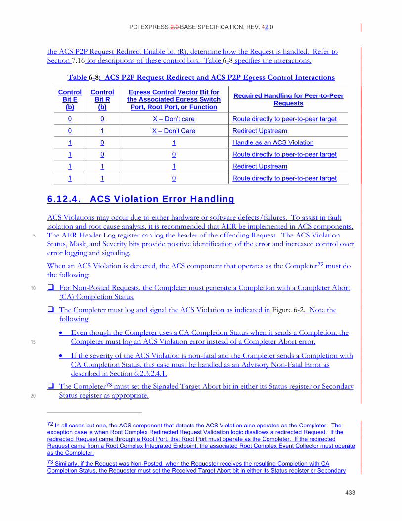
PCI EXPRESS 2.0 BASE SPECIFICATION, REV. 12.0
433
the ACS P2P Request Redirect Enable bit (R), determine how the Request is handled. Refer to Section 7.16 for descriptions of these control bits. Table 6-8 specifies the interactions.
Table 6-8: ACS P2P Request Redirect and ACS P2P Egress Control Interactions
Control Bit E (b)
Control Bit R (b)
Egress Control Vector Bit for the Associated Egress Switch Port, Root Port, or Function
Required Handling for Peer-to-Peer Requests
0 0 X – Don’t care Route directly to peer-to-peer target
0 1 X – Don’t Care Redirect Upstream
1 0 1 Handle as an ACS Violation
1 0 0 Route directly to peer-to-peer target
1 1 1 Redirect Upstream
1 1 0 Route directly to peer-to-peer target
6.12.4. ACS Violation Error Handling
ACS Violations may occur due to either hardware or software defects/failures. To assist in fault isolation and root cause analysis, it is recommended that AER be implemented in ACS components. The AER Header Log register can log the header of the offending Request. The ACS Violation 5 Status, Mask, and Severity bits provide positive identification of the error and increased control over error logging and signaling.
When an ACS Violation is detected, the ACS component that operates as the Completer72 must do the following:
For Non-Posted Requests, the Completer must generate a Completion with a Completer Abort 10 (CA) Completion Status.
The Completer must log and signal the ACS Violation as indicated in Figure 6-2. Note the following:
• Even though the Completer uses a CA Completion Status when it sends a Completion, the Completer must log an ACS Violation error instead of a Completer Abort error. 15
• If the severity of the ACS Violation is non-fatal and the Completer sends a Completion with CA Completion Status, this case must be handled as an Advisory Non-Fatal Error as described in Section 6.2.3.2.4.1.
The Completer73 must set the Signaled Target Abort bit in either its Status register or Secondary Status register as appropriate. 20
72 In all cases but one, the ACS component that detects the ACS Violation also operates as the Completer. The exception case is when Root Complex Redirected Request Validation logic disallows a redirected Request. If the redirected Request came through a Root Port, that Root Port must operate as the Completer. If the redirected Request came from a Root Complex Integrated Endpoint, the associated Root Complex Event Collector must operate as the Completer. 73 Similarly, if the Request was Non-Posted, when the Requester receives the resulting Completion with CA Completion Status, the Requester must set the Received Target Abort bit in either its Status register or Secondary
PCI EXPRESS 2.0 BASE SPECIFICATION, REV. 21.0
434
6.12.5. ACS Redirection Impacts on Ordering Rules
When ACS P2P Request Redirect is enabled, some or all peer-to-peer Requests are redirected, which can cause ordering rule violations in some cases. This section explores those cases, plus a similar case that occurs with RCs that implement “Request Retargeting” as an alternative mechanism for enforcing peer-to-peer access control.
6.12.5.1. Completions Passing Posted Requests
When a peer-to-peer Posted Request is redirected, a subsequent peer-to-peer non-RO74 Read 5 Completion that is routed directly can effectively pass the redirected Posted Request, violating the ordering rule that non-RO Read Completions must not pass Posted Requests. Refer to Section 2.4.1 for more information.
ACS P2P Completion Redirect can be used to avoid violating this ordering rule. When ACS P2P Completion Redirect is enabled, all peer-to-peer non-RO Read Completions will be redirected, thus 10 taking the same path as redirected peer-to-peer Posted Requests. Enabling ACS P2P Completion Redirect when some or all peer-to-peer Requests are routed directly will not cause any ordering rule violations, since it is permitted for a given Completion to be passed by any TLP other than another Completion with the same Transaction ID.
As an alternative mechanism to ACS P2P Request Redirect for enforcing peer-to-peer access 15 control, some RCs implement “Request Retargeting”, where the RC supports special address ranges for “peer-to-peer” traffic, and the RC will retarget validated Upstream Requests to peer devices. Upon receiving an Upstream Request targeting a special address range, the RC validates the Request, translates the address to target the appropriate peer device, and sends the Request back Downstream. With retargeted Requests that are Non-posted, if the RC does not modify the 20 Requester ID, the resulting Completions will travel “directly” peer-to-peer back to the original Requester, creating the possibility of non-RO Read Completions effectively passing retargeted Posted Requests, violating the same ordering rule as when ACS P2P Request Redirect is being used. ACS P2P Completion Redirect can be used to avoid violating this ordering rule here as well.
If ACS P2P Request Redirect and RC P2P Request Retargeting are not being used, there’s no 25 envisioned benefit to enabling ACS P2P Completion Redirect, and it is recommended not to do so because of potential performance impacts.
Status register as appropriate. Note that for the case of a multi-Function device incurring an ACS Violation error with a peer-to-peer Request between its Functions, the same Function might serve both as Requester and Completer. 74 In this section, “non-RO” is an abbreviation characterizing TLPs whose Relaxed Ordering Attribute field is not set.
PCI EXPRESS 2.0 BASE SPECIFICATION, REV. 12.0
435
IMPLEMENTATION NOTE Performance Impacts with ACS P2P Completion Redirect While the use of ACS P2P Completion Redirect can avoid ordering violations with Completions passing Posted Requests, it also may impact performance. Specifically, all redirected Completions will have to travel up to the RC from the point of redirection and back, introducing extra latency and possibly increasing Link and RC congestion.
Since peer-to-peer Read Completions with the Relaxed Ordering bit set are never redirected (thus 5 avoiding performance impacts), it is strongly recommended that Requesters be implemented to maximize the proper use of Relaxed Ordering, and that software enable Requesters to utilize Relaxed Ordering by setting the Enable Relaxed Ordering bit in the Device Control register.
If software enables ACS P2P Request Redirect, RC P2P Request Retargeting, or both, and software is certain that proper operation is not compromised by peer-to-peer non-RO Read Completions 10 passing peer-to-peer75 Posted Requests, it is recommended that software leave ACS P2P Completion Redirect disabled as a way to avoid its performance impacts.
6.12.5.2. Requests Passing Posted Requests
When some peer-to-peer Requests are redirected but other peer-to-peer Requests are routed directly, the possibility exists of violating the ordering rules where Non-posted Requests or non-RO Posted Requests must not pass Posted Requests. Refer to Section 2.4.1 for more information. 15
These ordering rule violation possibilities exist only when ACS P2P Request Redirect and ACS Direct Translated P2P are both enabled. Software should not enable both these mechanisms unless it is certain either that such ordering rule violations can’t occur, or that proper operation will not be compromised if such ordering rule violations do occur.
75 These include true peer-to-peer Requests that are redirected by the ACS P2P Request Redirect mechanism, as well as “logically peer-to-peer” Requests routed to the Root Complex that the Root Complex then retargets to the peer device.
PCI EXPRESS 2.0 BASE SPECIFICATION, REV. 21.0
436
IMPLEMENTATION NOTE Ensuring Proper Operation with ACS Direct Translated P2P The intent of ACS Direct Translated P2P is to optimize performance in environments where Address Translation Services (ATS) are being used with peer-to-peer communication whose access control is enforced by the RC. Permitting peer-to-peer Requests with Translated addresses to be routed directly avoids possible performance impacts associated with redirection, which introduces extra latency and may increase Link and RC congestion. 5
For the usage model where peer-to-peer Requests with Translated addresses are permitted, but those with Untranslated addresses are to be blocked as ACS Violations, it is recommended that software enable ACS Direct Translated P2P and ACS P2P Request Redirect, and configure the Redirected Request Validation logic in the RC to block the redirected Requests with Untranslated addresses. This configuration has no ordering rule violations associated with Requests passing Posted Requests. 10
For the usage model where some Requesters use Translated addresses exclusively with peer-to-peer Requests and some Requesters use Untranslated addresses exclusively with peer-to-peer Requests, and the two classes of Requesters do not communicate peer-to-peer with each other, proper operation is unlikely to be compromised by redirected peer-to-peer Requests (with Untranslated addresses) being passed by direct peer-to-peer Requests (with Translated addresses). It is 15 recommended that software not enable ACS Direct Translated P2P unless software is certain that proper operation is not compromised by the resulting ordering rule violations.
For the usage model where a single Requester uses both Translated and Untranslated addresses with peer-to-peer Requests, again it is recommended that software not enable ACS Direct Translated P2P unless software is certain that proper operation is not compromised by the resulting ordering rule 20 violations. This requires a detailed analysis of the peer-to-peer communications models being used, and is beyond the scope of this specification.
25
PCI EXPRESS 2.0 BASE SPECIFICATION, REV. 12.0
437
7. Software Initialization and Configuration The PCI Express Configuration model supports two configuration Configuration space Space access mechanisms:
PCI compatible configuration Configuration Access mechanism Mechanism (CAM)
PCI Express enhanced Enhanced configuration Configuration Access mechanismMechanism (ECAM) 5
The PCI compatible mechanism supports 100% binary compatibility with PCI 3.0 or later aware operating systems and their corresponding bus enumeration and configuration software.
The enhanced mechanism is provided to increase the size of available configuration Configuration space Space and to optimize access mechanisms.
7.1. Configuration Topology To maintain compatibility with PCI software configuration mechanisms, all PCI Express elements 10 have a PCI-compatible configuration Configuration space Space representation. Each PCI Express Link originates from a logical PCI-PCI Bridge and is mapped into configuration Configuration space Space as the secondary bus of this Bridge. The Root Port is a PCI-PCI Bridge structure that originates a PCI Express Link from a PCI Express Root Complex (see Figure 7-1).
A PCI Express Switch is represented by multiple PCI-PCI Bridge structures connecting PCI 15 Express Links to an internal logical PCI bus (see Figure 7-2). The Switch Upstream Port is a PCI-PCI Bridge; the secondary bus of this Bridge represents the Switch’s internal routing logic. Switch Downstream Ports are PCI-PCI Bridges bridging from the internal bus to buses representing the Downstream PCI Express Links from a PCI Express Switch. Only the PCI-PCI Bridges representing the Switch Downstream Ports may appear on the internal bus. Endpoints, represented 20 by Type 0 configuration Configuration space Space headers, may are not permitted to appear on the internal bus.
A PCI Express Endpoint is mapped into configuration Configuration space Space as a single Function in a Device, which might contain multiple Functions or just that Functionsingle logical device with one or more logical functionsFunctions. Both a PCI Express Endpoints and a Legacy 25 Endpoints are required to appear within one of the Hierarchy Domains originated by the Root Complex, meaning that they appear in configuration Configuration space Space in a tree that has a Root Port as its head. Root Complex Integrated Endpoints and Root Complex Event Collectors do not appear within one of the Hierarchy Domains originated by the Root Complex. These appear in configuration Configuration space Space as peers of the Root Ports. 30
7
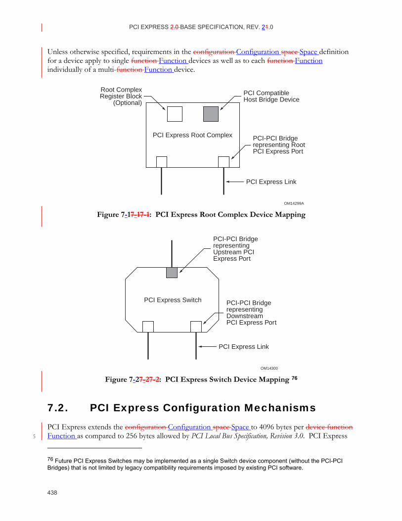
PCI EXPRESS 2.0 BASE SPECIFICATION, REV. 21.0
438
Unless otherwise specified, requirements in the configuration Configuration space Space definition for a device apply to single function Function devices as well as to each function Function individually of a multi-function Function device.
OM14299A
PCI Express Root Complex
Root ComplexRegister Block
(Optional)
PCI CompatibleHost Bridge Device
PCI-PCI Bridgerepresenting RootPCI Express Port
PCI Express Link
Figure 7-17-1 7-1: PCI Express Root Complex Device Mapping
OM14300
PCI Express Switch PCI-PCI BridgerepresentingDownstreamPCI Express Port
PCI-PCI BridgerepresentingUpstream PCIExpress Port
PCI Express Link
Figure 7-27-2 7-2: PCI Express Switch Device Mapping 76
7.2. PCI Express Configuration Mechanisms PCI Express extends the configuration Configuration space Space to 4096 bytes per device function Function as compared to 256 bytes allowed by PCI Local Bus Specification, Revision 3.0. PCI Express 5
76 Future PCI Express Switches may be implemented as a single Switch device component (without the PCI-PCI Bridges) that is not limited by legacy compatibility requirements imposed by existing PCI software.
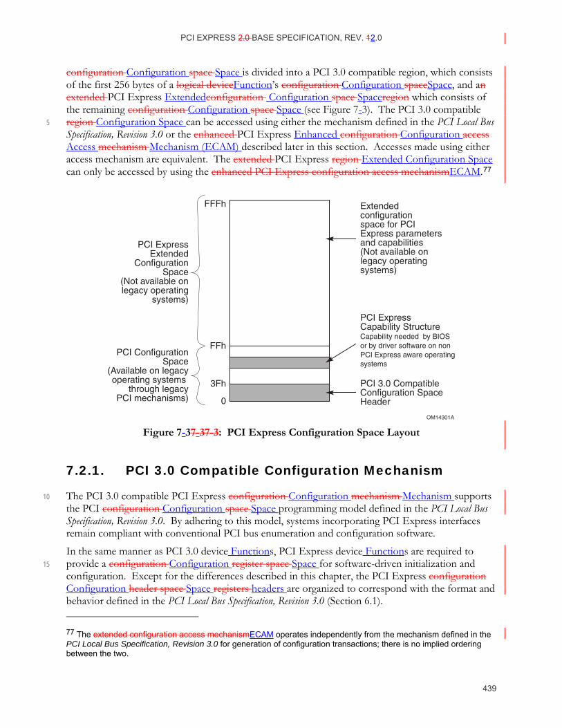
PCI EXPRESS 2.0 BASE SPECIFICATION, REV. 12.0
439
configuration Configuration space Space is divided into a PCI 3.0 compatible region, which consists of the first 256 bytes of a logical deviceFunction’s configuration Configuration spaceSpace, and an extended PCI Express Extendedconfiguration Configuration space Spaceregion which consists of the remaining configuration Configuration space Space (see Figure 7-3). The PCI 3.0 compatible region Configuration Space can be accessed using either the mechanism defined in the PCI Local Bus 5 Specification, Revision 3.0 or the enhanced PCI Express Enhanced configuration Configuration access Access mechanism Mechanism (ECAM) described later in this section. Accesses made using either access mechanism are equivalent. The extended PCI Express region Extended Configuration Space can only be accessed by using the enhanced PCI Express configuration access mechanismECAM.77
OM14301A
FFFh
FFh
3Fh
0
PCI ExpressExtended
ConfigurationSpace
(Not available onlegacy operating
systems)
PCI ConfigurationSpace
(Available on legacyoperating systems
through legacyPCI mechanisms)
Extendedconfigurationspace for PCIExpress parametersand capabilities(Not available onlegacy operatingsystems)
PCI 3.0 CompatibleConfiguration SpaceHeader
PCI ExpressCapability StructureCapability needed by BIOSor by driver software on nonPCI Express aware operatingsystems
Figure 7-37-3 7-3: PCI Express Configuration Space Layout
7.2.1. PCI 3.0 Compatible Configuration Mechanism
The PCI 3.0 compatible PCI Express configuration Configuration mechanism Mechanism supports 10 the PCI configuration Configuration space Space programming model defined in the PCI Local Bus Specification, Revision 3.0. By adhering to this model, systems incorporating PCI Express interfaces remain compliant with conventional PCI bus enumeration and configuration software.
In the same manner as PCI 3.0 device Functions, PCI Express device Functions are required to provide a configuration Configuration register space Space for software-driven initialization and 15 configuration. Except for the differences described in this chapter, the PCI Express configuration Configuration header space Space registers headers are organized to correspond with the format and behavior defined in the PCI Local Bus Specification, Revision 3.0 (Section 6.1). 77 The extended configuration access mechanismECAM operates independently from the mechanism defined in the PCI Local Bus Specification, Revision 3.0 for generation of configuration transactions; there is no implied ordering between the two.
PCI EXPRESS 2.0 BASE SPECIFICATION, REV. 21.0
440
The PCI 3.0 compatible configuration Configuration access Access mechanism Mechanism uses the same Request format as the enhanced PCI Express mechanismECAM. For PCI compatible Configuration Requests, the Extended Register Address field must be all zeros.
7.2.2. PCI Express Enhanced Configuration Access Mechanism (ECAM)
For systems that are PC-compatible, or that do not implement a processor-architecture-specific firmware interface standard that allows access to the Configuration Space, the enhanced 5 configuration access mechanismECAM is required as defined in this section.
For systems that implement a processor-architecture-specific firmware interface standard that allows access to the Configuration Space, the operating system uses the standard firmware interface, and the hardware access mechanism defined in this section is not required. For example, for systems that are compliant with Developer’s Interface Guide for 64-bit Intel Architecture-based Servers (DIG64), 10 Version 2.1,78 the operating system uses the SAL firmware service to access the Configuration Space.
In all systems, device drivers are encouraged to use the application programming interface (API) provided by the operating system to access the Configuration Space of its device and not directly use the hardware mechanism.
The ECAMenhanced PCI Express configuration access mechanism utilizes a flat memory-mapped 15 address space to access device configuration registers. In this case, the memory address determines the configuration register accessed and the memory data updates (for a write) or returns the contents of (for a read) the addressed register. The mapping from memory address space to PCI Express configuration Configuration space Space address is defined in Table 7-1.
The size and base address for the range of memory addresses mapped to the Configuration Space 20 are determined by the design of the host bridge and the firmware. They are reported by the firmware to the operating system in an implementation-specific manner. The size of the range is determined by the number of bits that the host bridge maps to the Bus Number field in the configuration address. In Table 7-1, this number of bits is represented as n, where 1 ≤ n ≤ 8. A host bridge that maps n memory address bits to the Bus Number field supports bus Bus numbers 25 Numbers from 0 to 2n – 1, inclusive, and the base address of the range is aligned to a 2(n+20) )-byte memory address boundary. Any bits in the Bus Number field that are not mapped from Memory memory Address address bits must be set to zeroClear.
For example, if a system maps three Memory memory Address address bits to the Bus Number field, the following are all true: 30
n = 3.
Address bits A[63:23] are used for the base address, which is aligned to a 223 223-byte (8 8-MB) boundary.
Address bits A[22:20] are mapped to bits [2:0] in the Bus Number field.
Bits [7:3] in the Bus Number field are set to Clearzero. 35
78 Developer’s Interface Guide for 64-bit Intel Architecture-based Servers (DIG64), Version 2.1, January 2002, www.dig64.org
PCI EXPRESS 2.0 BASE SPECIFICATION, REV. 12.0
441
The system is capable of addressing bus Bus numbers Numbers between 0 and 7, inclusive.
A minimum of one Memory memory Address address bit (n = 1) must be mapped to the Bus Number field. Systems are encouraged to map additional Memory memory Address address bits to the Bus Number field as needed to support a larger number of buses. Systems that support more than 4 GB of memory addresses are encouraged to map eight bits of Memory memory Address 5 address (n = 8) to the Bus Number field. Note that in systems that include multiple host bridges with different ranges of bus Bus numbers Numbers assigned to each host bridge, the highest bus Bus number Number for the system is limited by the number of bits mapped by the host bridge to which the highest bus number is assigned. In such a system, the highest bus Bus number Number assigned to a particular host bridge would be greater, in most cases, than the number of buses 10 assigned to that host bridge. In other words, for each host bridge, the number of bits mapped to the Bus Number field, n, must be large enough that the highest bus Bus number Number assigned to each particular bridge must be less than or equal to 2n – 1 for that bridge.
In some processor architectures, it is possible to generate memory space requestsaccesses that cannot be expressed in a single Configuration Request, for example due to crossing a DW aligned 15 boundary, or because a locked access is used. A Root Complex implementation is not required to support the translation to Configuration Requests of such memory space accessesrequests.
Table 7-1- 7-1: Enhanced Configuration Address Mapping
Memory Address79 PCI Express Configuration Space
A[(20 + n – 1):20] Bus Number 1 ≤ n ≤ 8
A[19:15] Device Number
A[14:12] Function Number
A[11:8] Extended Register Number
A[7:2] Register Number
A[1:0] Along with size of the access, used to generate Byte Enables
The system hardware must provide a method for the system software to guarantee that a write transaction using the enhanced configuration access mechanismECAM is completed by the completer before system software execution continues. 20
79 This address refers to the byte-level address from a software point of view.
PCI EXPRESS 2.0 BASE SPECIFICATION, REV. 21.0
442
IMPLEMENTATION NOTE Ordering Considerations for the Enhanced Configuration Access Mechanism The ECAMenhanced configuration accesses mechanism converts memory transactions from the host CPU into configuration Configuration transactions Requests on the PCI Express fabric. This conversion potentially creates ordering problems for the software, because writes to memory addresses are typically posted transactions but writes to Configuration Space are not posted on the PCI Express fabric. 5
Generally, software does not know when a posted transaction is completed by the completer. In those cases in which the software must know that a posted transaction is completed by the completer, one technique commonly used by the software is to read the location that was just written. For systems that follow the PCI ordering rules throughout, the read transaction will not complete until the posted write is complete. However, since the PCI ordering rules allow non-10 posted write and read transactions to be reordered with respect to each other, the CPU must wait for a non-posted write to complete on the PCI Express fabric to be guaranteed that the transaction is completed by the completer.
As an example, software may wish to configure a device Function’s Base Address register by writing to the device using the enhanced configuration access mechanismECAM, and then read a location in 15 the memory-mapped range described by this Base Address register. If the software were to issue the memory-mapped read before the ECAMenhanced-configuration-access-mechanism write was completed, it would be possible for the memory-mapped read to be re-ordered and arrive at the device before the configuration Configuration writeWrite Request, thus causing unpredictable results. 20
To avoid this problem, processor and host bridge implementations must ensure that a method exists for the software to determine when the write using the enhanced configuration access mechanismECAM is completed by the completer.
This method may simply be that the processor itself recognizes a memory range dedicated for mapping enhanced configurationECAM accesses as unique, and treats accesses to this range in the 25 same manner that it would treat other accesses that generate non-posted writes on the PCI Express fabric, i.e., that the transaction is not posted from the processor’s viewpoint. An alternative mechanism is for the host bridge (rather than the processor) to recognize the memory-mapped Configuration Space accesses and not to indicate to the processor that this write has been accepted until the non-posted configuration Configuration transaction Transaction has completed on the PCI 30 Express fabric. A third alternative would be for the processor and host bridge to post the memory-mapped write to the enhanced configuration access mechanismECAM and for the host bridge to provide a separate register that the software can read to determine when the configuration Configuration write Write Request has completed on the PCI Express fabric. Other alternatives are also possible. 35
PCI EXPRESS 2.0 BASE SPECIFICATION, REV. 12.0
443
IMPLEMENTATION NOTE Generating Configuration Requests Because Root Complex implementations are not required to support the generation of Configuration Requests from memory space accesses that cross DW boundaries, or that use locked semantics, software should take care not to cause the generation of such requests accesses when using the memory-mapped configuration access mechanismECAM unless it is known that the Root Complex implementation being used will support the translation. 5
7.2.2.1. Host Bridge Requirements
For those systems that implement the enhanced configuration access mechanismECAM, the PCI Express Host Bridge is required to translate the memory-mapped PCI Express configuration Configuration space Space accesses from the host processor to PCI Express configuration transactions. The use of Host Bridge PCI class code is reserved for backwards compatibility; host Bridge configuration Configuration space Space is opaque to standard PCI Express software and 10 may be implemented in an implementation specific manner that is compatible with PCI Host Bridge Type 0 configuration Configuration spaceSpace. A PCI Express Host Bridge is not required to signal errors through a Root Complex Event Collector. This support is optional for PCI Express Host Bridges.
7.2.2.2. PCI Express Device Requirements
Devices must support an additional 4 bits for decoding configuration register access, i.e., they must 15 decode the Extended Register Address[3:0] field of the Configuration Request header.
PCI EXPRESS 2.0 BASE SPECIFICATION, REV. 21.0
444
IMPLEMENTATION NOTE Device-Specific Registers in Configuration Space It is strongly recommended that PCI Express devices place no registers in Configuration Space other than those in Headers headers or Capability structures architected by applicable PCI specifications.
Device-specific registers that have legitimate reasons to be placed in Configuration Space (e.g., they need to be accessible before Memory Space is allocated) should be placed in a Vendor-Specific 5 Capability Structure structure (in PCI Compatible Configuration Space) or a Vendor-Specific Extended Capability Structure structure (in PCI Express Extended Configuration Space).
Device-specific registers accessed in the run-time environment by drivers should be placed in Memory Space that is allocated by one or more Base Address registers. Even though PCI Compatible or PCI Express Extended Configuration Space may have adequate room for run-time 10 device-specific registers, placing them there is highly discouraged for the following reasons:
Not all Operating Systems permit drivers to access Configuration Space directly.
Some platforms provide access to Configuration Space only via firmware calls, which typically have substantially lower performance compared to mechanisms for accessing Memory Space.
Even on platforms that provide direct accesss to a memory-mapped PCI Express Enhanced 15 Configuration Mechanism, performance for accessing Configuration Space will typically be significantly lower than for accessing Memory Space since:
• Configuration Reads and Writes must usually be DWORD or smaller in size,
• Configuration Writes are usually not posted by the platform, and
• Some platforms support only one outstanding Configuration Write at a time. 20
7.2.3. Root Complex Register Block
A Root Port or Root Complex Integrated Endpoint may be associated with an optional 4096 4096-byte block of memory mapped registers referred to as the Root Complex Register Block (RCRB). These registers are used in a manner similar to configuration Configuration space Space and can include PCI Express extended Extended capabilities Capabilities and other implementation specific registers that apply to the Root Complex. The structure of the RCRB is described in Section 7.9.2. 25
Multiple Root Ports or internal devices may are permitted to be associated with the same RCRB. The RCRB memory-mapped registers must not reside in the same address space as the memory-mapped configuration Configuration spaceSpace or Memory Space.
A Root Complex implementation is not required to support memory space requests accesses to an RCRB that cross DWORD aligned boundaries or accesses that use locked semantics. 30
PCI EXPRESS 2.0 BASE SPECIFICATION, REV. 12.0
445
IMPLEMENTATION NOTE Accessing Root Complex Register Block Because Root Complex implementations are not required to support memory space requests accesses to a RCRB that cross DW boundaries, or that use locked semantics, software should take care not to cause the generation of such accessesrequests when accessing a RCRB unless it is known that the Root Complex implementation being used will support the requestaccess.
7.3. Configuration Transaction Rules
7.3.1. Device Number
As in conventional PCI and PCI-X, all PCI Express components are restricted to implementing a 5 single device Device number Number on their primary interface (Upstream Port), but may are permitted to implement up to eight independent functions Functions within that device Device numberNumber. Each internal function Function is selected based on decoded address information that is provided as part of the address portion of Configuration Request packets.
Switches and Root Complexes must associate only Device 0 with the device attached to the logical 10 Logical bus Bus representing the Link from a Switch Downstream Port or a Root Port. Configuration Requests targeting the Bus Number associated with a Link specifying Device Number 0 are delivered to the device attached to the Link; Configuration Requests specifying all other Device Numbers (1-31) must be terminated by the Switch Downstream Port or the Root Port with an Unsupported Request Completion Status (equivalent to Master Abort in PCI). Devices must not 15 assume that Device Number 0 is associated with their Upstream Port, but must capture their assigned Device Number as discussed in Section 2.2.6.2. Devices must respond to all Type 0 Configuration Read Requests, regardless of the Device Number specified in the Request.
Switches, and components wishing to incorporate more than eight functions Functions at their upstream Upstream Port, may are permitted to implement one or more “virtual switches,” 20 represented by multiple Type 1 (PCI-PCI Bridge) configuration Configuration space Space headers as illustrated in Figure 7-2. These virtual switches serve to allow fan-out beyond eight functionsFunctions. Since Switch Downstream Ports may are permitted to appear on any Device Number, in this case all address information fields (Bus, Device, and Function Numbers) must be completely decoded to access the correct register. Any configuration Configuration access Request 25 targeting an unimplemented busBus, deviceDevice, or function Function must return a Completion with Unsupported Request Completion Status.
The following section provides details of the Configuration Space addressing mechanism.
7.3.2. Configuration Transaction Addressing
PCI Express Configuration Requests use the following addressing fields:
PCI EXPRESS 2.0 BASE SPECIFICATION, REV. 21.0
446
Bus Number – PCI Express maps logical PCI Bus Numbers onto PCI Express Links such that PCI 3.0 compatible configuration software views the configuration Configuration space Space of a PCI Express Hierarchy as a PCI hierarchy including multiple bus segments.
Device Number – Device Number association is discussed in Section 7.3.1.
Function Number – PCI Express also supports multi-function Function devices using the same 5 discovery mechanism as PCI 3.0.
Extended Register Number and Register Number – Specify the configuration Configuration space Space address of the register being accessed (concatenated such that the Extended Register Number forms the more significant bits).
7.3.3. Configuration Request Routing Rules
For PCI Express Endpoint devices, the following rules apply: 10
If Configuration Request Type is 1,
• Follow the rules for handling Unsupported Requests
If Configuration Request Type is 0,
• Determine if the Request addresses a valid local configuration Configuration spaceSpace
♦ If so, process the Request 15
♦ If not, follow rules for handling Unsupported Requests
For Root Ports, Switches, and PCI Express-PCI Bridges, the following rules apply:
Propagation of Configuration Requests from Downstream to Upstream as well as peer-to-peer are not supported
• Configuration Requests are initiated only by the Host Bridge 20
If Configuration Request Type is 0,
• Determine if the Request addresses a valid local configuration Configuration spaceSpace
♦ If so, process the Request
♦ If not, follow rules for handling Unsupported Requests
If Configuration Request Type is 1, apply the following tests, in sequence, to the Bus Number 25 field:
• If in the case of a PCI Express-PCI Bridge, equal to the bus Bus number Number assigned to secondary PCI bus or, in the case of a Switch or Root Complex, equal to the bus Bus number Number and decoded device Device numbers Numbers assigned to one of the Root (Root Complex) or Downstream Ports (Switch), 30
♦ Transform the Request to Type 0 by changing the value in the Type[4:0] field of the Request (see Table 2-3) – all other fields of the Request remain unchanged
♦ Forward the Request to that Downstream Port (or PCI bus, in the case of a PCI Express-PCI Bridge)
PCI EXPRESS 2.0 BASE SPECIFICATION, REV. 12.0
447
• If not equal to the bus Bus number Number of any of Downstream Ports or secondary PCI bus, but in the range of bus Bus numbers Numbers assigned to one ofeither a Downstream Port or a secondary PCI bus,
♦ Forward the Request to that Downstream Port interface without modification
• Else (none of the above) 5
♦ The Request is invalid – - follow the rules for handling Unsupported Requests
PCI Express-PCI Bridges must terminate as Unsupported Requests any Configuration Requests for which the Extended Register Address field is non-zero that are directed towards a PCI bus that does not support Extended Configuration Space.
Note: This type of access is a consequence of a programming error. 10
Additional rule specific to Root Complexes:
Configuration Requests addressing bus Bus numbers Numbers assigned to devices within the Root Complex are processed by the Root Complex
• The assignment of bus Bus numbers Numbers to the logical devices within a Root Complex may be done in an implementation specific way. 15
For all types of devices:
All other configuration Configuration space Space addressing fields are decoded according to the PCI Local Bus Specification, Revision 3.0.
7.3.4. PCI Special Cycles
PCI Special Cycles (see the PCI Local Bus Specification, Revision 3.0 for details) are not directly supported by PCI Express. PCI Special Cycles may be directed to PCI bus segments behind PCI 20 Express-PCI Bridges using Type 1 Configuration Cycles as described in PCI Local Bus Specification, Revision 3.0.
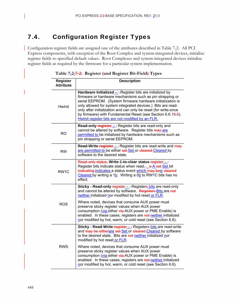
PCI EXPRESS 2.0 BASE SPECIFICATION, REV. 21.0
448
7.4. Configuration Register Types Configuration register fields are assigned one of the attributes described in Table 7-2. All PCI Express components, with exception of the Root Complex and system-integrated devices, initialize register fields to specified default values. Root Complexes and system-integrated devices initialize register fields as required by the firmware for a particular system implementation.
Table 7-2- 7-2: Register (and Register Bit-Field) Types
Register Attribute
Description
HwInit
Hardware Initialized – : Register bits are initialized by firmware or hardware mechanisms such as pin strapping or serial EEPROM. (System firmware hardware initialization is only allowed for system integrated devices.) Bits are read-only after initialization and can only be reset (for write-once by firmware) with Fundamental Reset (see Section 6.6.16.6). HwInit register bits are not modified by an FLR.
RO
Read-only register – : Register bits are read-only and cannot be altered by software. Register bits may are permitted to be initialized by hardware mechanisms such as pin strapping or serial EEPROM.
RW Read-Write register – : Register bits are read-write and may are permitted to be either set Set or cleared Cleared by software to the desired state.
RW1C
Read-only status, Write-1-to-clear status register – : Register bits indicate status when read, . a A set Set bit indicating indicates a status event which may beis cleared Cleared by writing a 1b. Writing a 0b to RW1C bits has no effect.
ROS
Sticky - Read-only register – : Registers bits are read-only and cannot be altered by software. Registers Bits are not neither initialized nor modified by hot reset or FLR.
Where noted, devices that consume AUX power must preserve sticky register values when AUX power consumption (via either via AUX power or PME Enable) is enabled. In these cases, registers are not neither initialized nor modified by hot, warm, or cold reset (see Section 6.6).
RWS
Sticky - Read-Write register – : Registers bits are read-write and may be eitherare set Set or cleared Cleared by software to the desired state. Bits are not neither initialized nor modified by hot reset or FLR.
Where noted, devices that consume AUX power must preserve sticky register values when AUX power consumption (via either via AUX power or PME Enable) is enabled. In these cases, registers are not neither initialized nor modified by hot, warm, or cold reset (see Section 6.6).
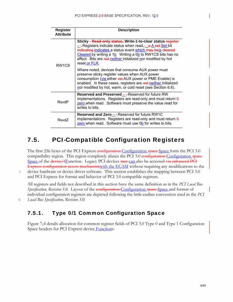
PCI EXPRESS 2.0 BASE SPECIFICATION, REV. 12.0
449
Register Attribute
Description
RW1CS
Sticky - Read-only status, Write-1-to-clear status register – : Registers indicate status when read, . a A set Set bit indicating indicates a status event which may beis cleared Cleared by writing a 1b. Writing a 0b to RW1CS bits has no effect. Bits are not neither initialized nor modified by hot reset or FLR.
Where noted, devices that consume AUX power must preserve sticky register values when AUX power consumption (via either via AUX power or PME Enable) is enabled. In these cases, registers are not neither initialized nor modified by hot, warm, or cold reset (see Section 6.6).
RsvdP
Reserved and Preserved – : Reserved for future RW implementations. Registers are read-only and must return 0 zero when read. Software must preserve the value read for writes to bits.
RsvdZ Reserved and Zero – : Reserved for future RW1C implementations. Registers are read-only and must return 0 zero when read. Software must use 0b for writes to bits.
7.5. PCI-Compatible Configuration Registers The first 256 bytes of the PCI Express configuration Configuration space Space form the PCI 3.0 compatibility region. This region completely aliases the PCI 3.0 configuration Configuration space Space of the device/fFunction. Legacy PCI devices may can also be accessed via enhanced PCI Express configuration access mechanismwith the ECAM without requiring any modifications to the device hardware or device driver software. This section establishes the mapping between PCI 3.0 5 and PCI Express for format and behavior of PCI 3.0 compatible registers.
All registers and fields not described in this section have the same definition as in the PCI Local Bus Specification, Revision 3.0. Layout of the configuration Configuration space Space and format of individual configuration registers are depicted following the little-endian convention used in the PCI Local Bus Specification, Revision 3.0. 10
7.5.1. Type 0/1 Common Configuration Space
Figure 7-4 details allocation for common register fields of PCI 3.0 Type 0 and Type 1 Configuration Space headers for PCI Express device Functions.
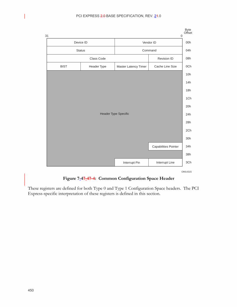
PCI EXPRESS 2.0 BASE SPECIFICATION, REV. 21.0
450
OM14315
Device ID Vendor ID
Status Command
Class Code Revision ID
Cache Line SizeMaster Latency TimerHeader TypeBIST
0
ByteOffset
31
04h
08h
00h
0Ch
10h
14h
18h
1Ch
20h
24h
28h
2Ch
30h
34h
38h
3Ch
Capabilities Pointer
Interrupt LineInterrupt Pin
Header Type Specific
Figure 7-47-4 7-4: Common Configuration Space Header
These registers are defined for both Type 0 and Type 1 Configuration Space headers. The PCI Express-specific interpretation of these registers is defined in this section.
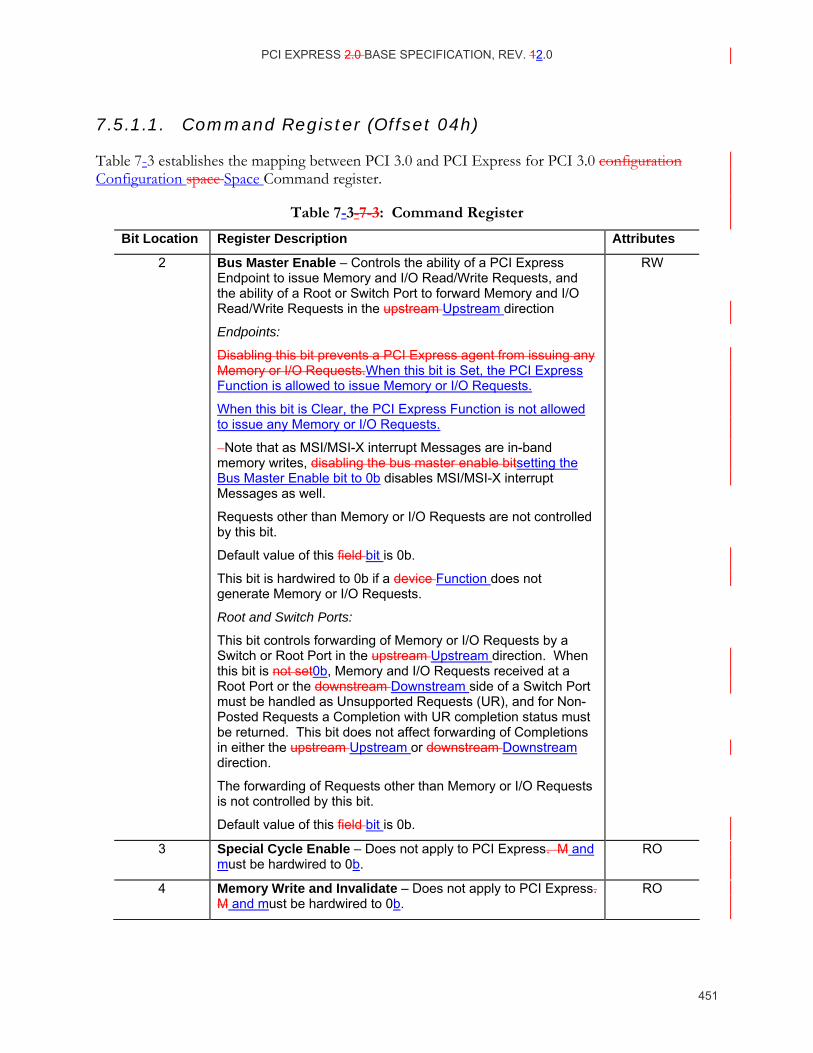
PCI EXPRESS 2.0 BASE SPECIFICATION, REV. 12.0
451
7.5.1.1. Command Register (Offset 04h)
Table 7-3 establishes the mapping between PCI 3.0 and PCI Express for PCI 3.0 configuration Configuration space Space Command register.
Table 7-3- 7-3: Command Register
Bit Location Register Description Attributes
2 Bus Master Enable – Controls the ability of a PCI Express Endpoint to issue Memory and I/O Read/Write Requests, and the ability of a Root or Switch Port to forward Memory and I/O Read/Write Requests in the upstream Upstream direction
Endpoints:
Disabling this bit prevents a PCI Express agent from issuing any Memory or I/O Requests.When this bit is Set, the PCI Express Function is allowed to issue Memory or I/O Requests.
When this bit is Clear, the PCI Express Function is not allowed to issue any Memory or I/O Requests.
Note that as MSI/MSI-X interrupt Messages are in-band memory writes, disabling the bus master enable bitsetting the Bus Master Enable bit to 0b disables MSI/MSI-X interrupt Messages as well.
Requests other than Memory or I/O Requests are not controlled by this bit.
Default value of this field bit is 0b.
This bit is hardwired to 0b if a device Function does not generate Memory or I/O Requests.
Root and Switch Ports:
This bit controls forwarding of Memory or I/O Requests by a Switch or Root Port in the upstream Upstream direction. When this bit is not set0b, Memory and I/O Requests received at a Root Port or the downstream Downstream side of a Switch Port must be handled as Unsupported Requests (UR), and for Non-Posted Requests a Completion with UR completion status must be returned. This bit does not affect forwarding of Completions in either the upstream Upstream or downstream Downstream direction.
The forwarding of Requests other than Memory or I/O Requests is not controlled by this bit.
Default value of this field bit is 0b.
RW
3 Special Cycle Enable – Does not apply to PCI Express. M and must be hardwired to 0b.
RO
4 Memory Write and Invalidate – Does not apply to PCI Express. M and must be hardwired to 0b.
RO
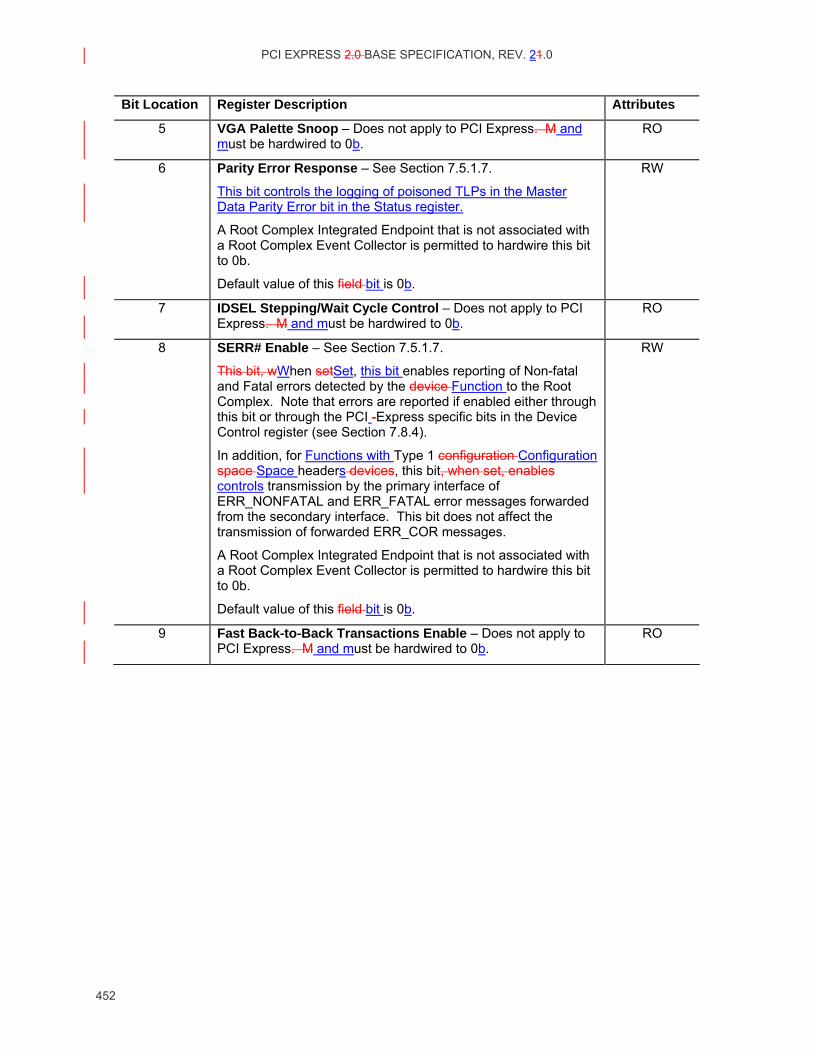
PCI EXPRESS 2.0 BASE SPECIFICATION, REV. 21.0
452
Bit Location Register Description Attributes
5 VGA Palette Snoop – Does not apply to PCI Express. M and must be hardwired to 0b.
RO
6 Parity Error Response – See Section 7.5.1.7.
This bit controls the logging of poisoned TLPs in the Master Data Parity Error bit in the Status register.
A Root Complex Integrated Endpoint that is not associated with a Root Complex Event Collector is permitted to hardwire this bit to 0b.
Default value of this field bit is 0b.
RW
7 IDSEL Stepping/Wait Cycle Control – Does not apply to PCI Express. M and must be hardwired to 0b.
RO
8 SERR# Enable – See Section 7.5.1.7.
This bit, wWhen setSet, this bit enables reporting of Non-fatal and Fatal errors detected by the device Function to the Root Complex. Note that errors are reported if enabled either through this bit or through the PCI -Express specific bits in the Device Control register (see Section 7.8.4).
In addition, for Functions with Type 1 configuration Configuration space Space headers devices, this bit, when set, enables controls transmission by the primary interface of ERR_NONFATAL and ERR_FATAL error messages forwarded from the secondary interface. This bit does not affect the transmission of forwarded ERR_COR messages.
A Root Complex Integrated Endpoint that is not associated with a Root Complex Event Collector is permitted to hardwire this bit to 0b.
Default value of this field bit is 0b.
RW
9 Fast Back-to-Back Transactions Enable – Does not apply to PCI Express. M and must be hardwired to 0b.
RO
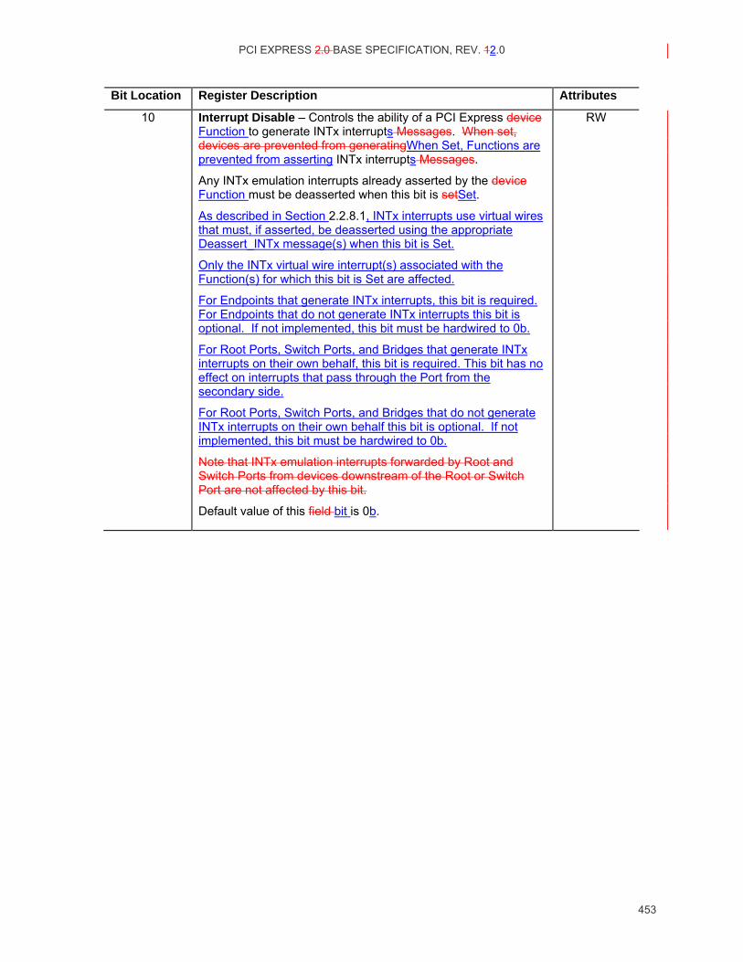
PCI EXPRESS 2.0 BASE SPECIFICATION, REV. 12.0
453
Bit Location Register Description Attributes
10 Interrupt Disable – Controls the ability of a PCI Express device Function to generate INTx interrupts Messages. When set, devices are prevented from generatingWhen Set, Functions are prevented from asserting INTx interrupts Messages.
Any INTx emulation interrupts already asserted by the device Function must be deasserted when this bit is setSet.
As described in Section 2.2.8.1, INTx interrupts use virtual wires that must, if asserted, be deasserted using the appropriate Deassert_INTx message(s) when this bit is Set.
Only the INTx virtual wire interrupt(s) associated with the Function(s) for which this bit is Set are affected.
For Endpoints that generate INTx interrupts, this bit is required. For Endpoints that do not generate INTx interrupts this bit is optional. If not implemented, this bit must be hardwired to 0b.
For Root Ports, Switch Ports, and Bridges that generate INTx interrupts on their own behalf, this bit is required. This bit has no effect on interrupts that pass through the Port from the secondary side.
For Root Ports, Switch Ports, and Bridges that do not generate INTx interrupts on their own behalf this bit is optional. If not implemented, this bit must be hardwired to 0b.
Note that INTx emulation interrupts forwarded by Root and Switch Ports from devices downstream of the Root or Switch Port are not affected by this bit.
Default value of this field bit is 0b.
RW
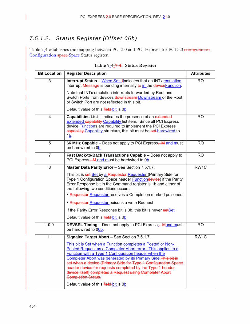
PCI EXPRESS 2.0 BASE SPECIFICATION, REV. 21.0
454
7.5.1.2. Status Register (Offset 06h)
Table 7-4 establishes the mapping between PCI 3.0 and PCI Express for PCI 3.0 configuration Configuration space Space Status register.
Table 7-4- 7-4: Status Register
Bit Location Register Description Attributes
3 Interrupt Status – When Set, Iindicates that an INTx emulation interrupt Message is pending internally to in the deviceFunction.
Note that INTx emulation interrupts forwarded by Root and Switch Ports from devices downstream Downstream of the Root or Switch Port are not reflected in this bit.
Default value of this field bit is 0b.
RO
4 Capabilities List – Indicates the presence of an extended Extended capability Capability list item. Since all PCI Express device Functions are required to implement the PCI Express capability Capability structure, this bit must be set hardwired to 1b.
RO
5 66 MHz Capable – Does not apply to PCI Express. M and must be hardwired to 0b.
RO
7 Fast Back-to-Back Transactions Capable – Does not apply to PCI Express. M and must be hardwired to 0b.
RO
8 Master Data Parity Error – See Section 7.5.1.7.
This bit is set Set by a Requestor Requester (Primary Side for Type 1 Configuration Space header Functiondevice) if the Parity Error Response bit in the Command register is 1b and either of the following two conditions occurs: • Requestor Requester receives a Completion marked poisoned
• Requestor Requester poisons a write Request
If the Parity Error Response bit is 0b, this bit is never setSet.
Default value of this field bit is 0b.
RW1C
10:9 DEVSEL Timing – Does not apply to PCI Express . Mand must be hardwired to 00b.
RO
11 Signaled Target Abort – See Section 7.5.1.7.
This bit is Set when a Function completes a Posted or Non-Posted Request as a Completer Abort error. This applies to a Function with a Type 1 Configuration header when the Completer Abort was generated by its Primary Side.This bit is set when a device (Primary Side for Type 1 Configuration Space header device for requests completed by the Type 1 header device itself) completes a Request using Completer Abort Completion Status.
Default value of this field bit is 0b.
RW1C
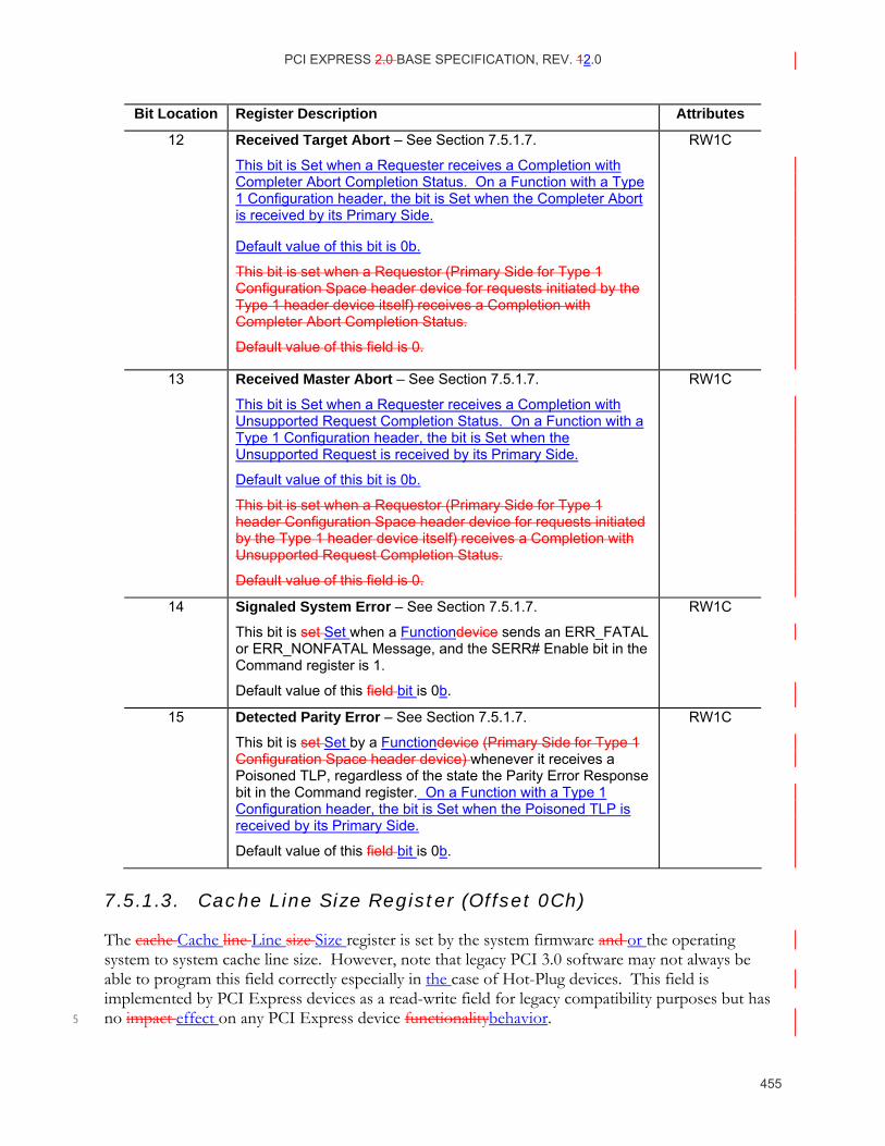
PCI EXPRESS 2.0 BASE SPECIFICATION, REV. 12.0
455
Bit Location Register Description Attributes
12 Received Target Abort – See Section 7.5.1.7.
This bit is Set when a Requester receives a Completion with Completer Abort Completion Status. On a Function with a Type 1 Configuration header, the bit is Set when the Completer Abort is received by its Primary Side.
Default value of this bit is 0b.
This bit is set when a Requestor (Primary Side for Type 1 Configuration Space header device for requests initiated by the Type 1 header device itself) receives a Completion with Completer Abort Completion Status.
Default value of this field is 0.
RW1C
13 Received Master Abort – See Section 7.5.1.7.
This bit is Set when a Requester receives a Completion with Unsupported Request Completion Status. On a Function with a Type 1 Configuration header, the bit is Set when the Unsupported Request is received by its Primary Side.
Default value of this bit is 0b.
This bit is set when a Requestor (Primary Side for Type 1 header Configuration Space header device for requests initiated by the Type 1 header device itself) receives a Completion with Unsupported Request Completion Status.
Default value of this field is 0.
RW1C
14 Signaled System Error – See Section 7.5.1.7.
This bit is set Set when a Functiondevice sends an ERR_FATAL or ERR_NONFATAL Message, and the SERR# Enable bit in the Command register is 1.
Default value of this field bit is 0b.
RW1C
15 Detected Parity Error – See Section 7.5.1.7.
This bit is set Set by a Functiondevice (Primary Side for Type 1 Configuration Space header device) whenever it receives a Poisoned TLP, regardless of the state the Parity Error Response bit in the Command register. On a Function with a Type 1 Configuration header, the bit is Set when the Poisoned TLP is received by its Primary Side.
Default value of this field bit is 0b.
RW1C
7.5.1.3. Cache Line Size Register (Offset 0Ch)
The cache Cache line Line size Size register is set by the system firmware and or the operating system to system cache line size. However, note that legacy PCI 3.0 software may not always be able to program this field correctly especially in the case of Hot-Plug devices. This field is implemented by PCI Express devices as a read-write field for legacy compatibility purposes but has no impact effect on any PCI Express device functionalitybehavior. 5
PCI EXPRESS 2.0 BASE SPECIFICATION, REV. 21.0
456
7.5.1.4. Master Latency Timer Register (Offset 0Dh)
This register is also referred to as pPrimary latency Latency timer Timer for Type 1 Configuration Space header devicesFunctions. The primary/master latency Latency timer Timer does not apply to PCI Express. This register must be hardwired to 00h.
7.5.1.5. Interrupt Line Register (Offset 3Ch)
As in PCI 3.0, the Interrupt Line register communicates interrupt line routing information. The register is read/write and must be implemented by any device (or device function)Function that uses 5 an interrupt pin (see following description). Values in this register are programmed by system software and are system architecture specific. The Functiondevice itself does not use this value; rather the value in this register is used by device drivers and operating systems.
7.5.1.6. Interrupt Pin Register (Offset 3Dh)
The Interrupt Pin register is a read-only register that identifies the legacy interrupt Message(s) the device (or device function)Function uses; (refer tosee Section 6.1 for further details). Valid values 10 are 1, 2, 3, and 4 that map to legacy interrupt Messages for INTA, INTB, INTC, and INTD respectively; a. A value of 00h indicates that the device Function uses no legacy interrupt Message(s).
7.5.1.7. Error Registers
The error Error controlControl/status Status register bits in the Command and Status registers (see Section 7.5.1.1 and Section 7.5.1.2 respectively) and the Bridge Control and Secondary Status 15 registers of Type 1 Configuration Space header Functiondevices (see Section 7.5.3.6 and Section 7.5.3.4 respectively) control PCI PCI-compatible error reporting for both PCI and PCI Express device Functions. Mapping of PCI Express errors onto PCI errors is also discussed in Section 6.2.7.1. In addition to the PCI PCI-compatible error control and status, PCI Express error reporting may be controlled separately from PCI device Functions through the PCI Express 20 Capability structure described in Section 7.8. The PCI PCI-compatible error Error control Control and status Status register fields do not have any effect on PCI Express error reporting enabled through the PCI Express Capability structure. PCI Express device Functions may also implement optional advanced error reporting as described in Section 7.10.
For PCI -Express Root Ports represented by a PCI 3.0 Type 1 Configuration Space header: 25
The primary side error Error Control/Status registers (control and status) apply to errors detected on the internal logic associated with the Root Complex.
The secondary side Error Control/Statuserror registers (control and status) apply to errors detected on the Link originating from the Root Port.
For PCI -Express Switch Upstream Ports represented by a PCI 3.0 Type 1 Configuration Space 30 header:
PCI EXPRESS 2.0 BASE SPECIFICATION, REV. 12.0
457
The primary side Error Control/Statuserror registers (control and status) apply to errors detected on the Upstream Link of the Switch.
The secondary side Error Control/Statuserror registers (control and status) apply to errors detected on the internal logic of the Switch.
For PCI -Express Switch Downstream Ports represented by a PCI 3.0 Type 1 Configuration Space 5 header:
The primary side Error Control/Statuserror registers (control and status) apply to errors detected on the internal logic of the Switch.
The secondary side Error Control/Statuserror registers (control and status) apply to errors detected on the Downstream Link originating from the Switch Port. 10
7.5.2. Type 0 Configuration Space Header
Figure 7-5 details allocation for register fields of PCI 3.0 Type 0 Configuration Space header for PCI Express device Functions.
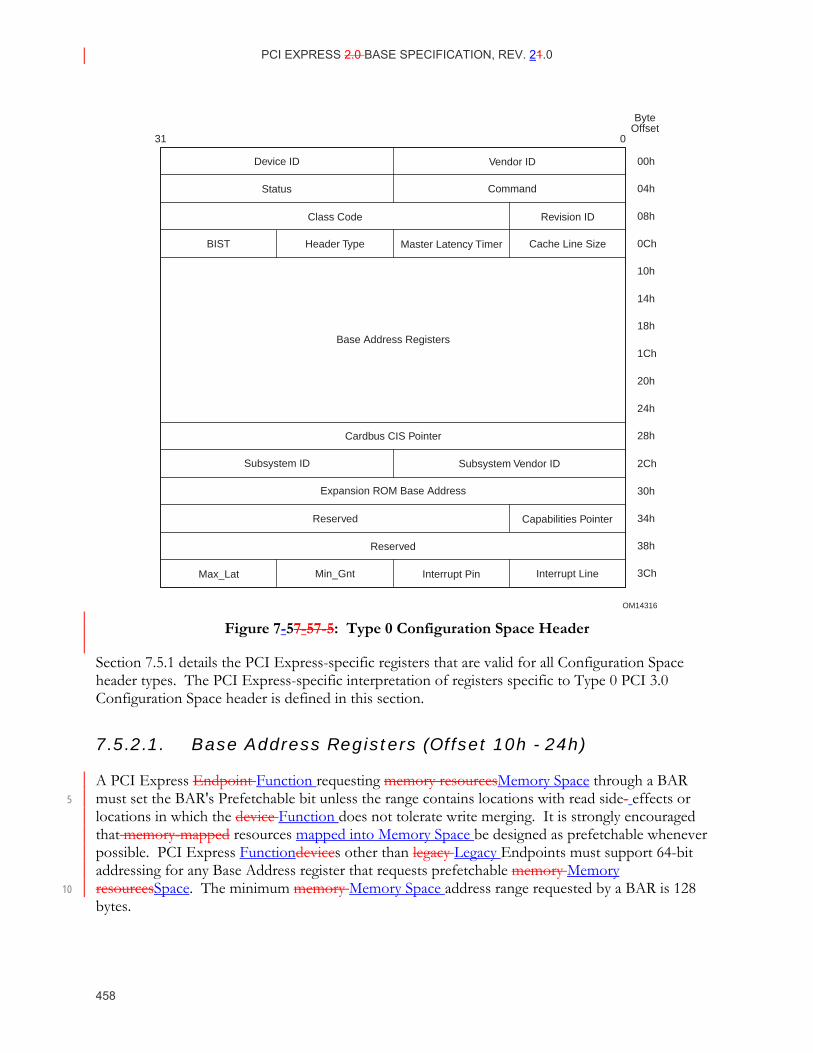
PCI EXPRESS 2.0 BASE SPECIFICATION, REV. 21.0
458
OM14316
Device ID Vendor ID
Status Command
Class Code Revision ID
Cache Line SizeMaster Latency TimerHeader TypeBIST
Reserved Capabilities Pointer
Interrupt LineInterrupt PinMin_GntMax_Lat
0
ByteOffset
31
04h
08h
00h
0Ch
10h
14h
18h
1Ch
20h
24h
28h
2Ch
30h
34h
38h
3Ch
Reserved
Subsystem ID Subsystem Vendor ID
Cardbus CIS Pointer
Base Address Registers
Expansion ROM Base Address
Figure 7-57-5 7-5: Type 0 Configuration Space Header
Section 7.5.1 details the PCI Express-specific registers that are valid for all Configuration Space header types. The PCI Express-specific interpretation of registers specific to Type 0 PCI 3.0 Configuration Space header is defined in this section.
7.5.2.1. Base Address Registers (Offset 10h - 24h)
A PCI Express Endpoint Function requesting memory resourcesMemory Space through a BAR must set the BAR's Prefetchable bit unless the range contains locations with read side- effects or 5 locations in which the device Function does not tolerate write merging. It is strongly encouraged that memory-mapped resources mapped into Memory Space be designed as prefetchable whenever possible. PCI Express Functiondevices other than legacy Legacy Endpoints must support 64-bit addressing for any Base Address register that requests prefetchable memory Memory resourcesSpace. The minimum memory Memory Space address range requested by a BAR is 128 10 bytes.
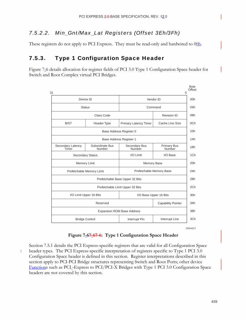
PCI EXPRESS 2.0 BASE SPECIFICATION, REV. 12.0
459
7.5.2.2. Min_Gnt/Max_Lat Registers (Offset 3Eh/3Fh)
These registers do not apply to PCI Express. They must be read-only and hardwired to 00h.
7.5.3. Type 1 Configuration Space Header
Figure 7-6 details allocation for register fields of PCI 3.0 Type 1 Configuration Space header for Switch and Root Complex virtual PCI Bridges.
OM14317
Device ID Vendor ID
Status Command
Class Code Revision ID
Cache Line SizePrimary Latency TimerHeader TypeBIST
Primary BusNumber
Secondary BusNumber
Subordinate BusNumber
Secondary LatencyTimer
Reserved Capability Pointer
Interrupt LineInterrupt PinBridge Control
0
ByteOffset
31
04h
08h
00h
0Ch
10h
14h
18h
1Ch
20h
24h
28h
2Ch
30h
34h
38h
3Ch
Expansion ROM Base Address
I/O Limit Upper 16 Bits I/O Base Upper 16 Bits
Memory Limit Memory Base
Prefetchable Memory Limit Prefetchable Memory Base
Prefetchable Base Upper 32 Bits
Prefetchable Limit Upper 32 Bits
I/O BaseI/O LimitSecondary Status
Base Address Register 0
Base Address Register 1
Figure 7-67-6 7-6: Type 1 Configuration Space Header
Section 7.5.1 details the PCI Express-specific registers that are valid for all Configuration Space header types. The PCI Express-specific interpretation of registers specific to Type 1 PCI 3.0 5 Configuration Space header is defined in this section. Register interpretations described in this section apply to PCI-PCI Bridge structures representing Switch and Root Ports; other device Functions such as PCI -Express to PCI/PCI-X Bridges with Type 1 PCI 3.0 Configuration Space headers are not covered by this section.
PCI EXPRESS 2.0 BASE SPECIFICATION, REV. 21.0
460
7.5.3.1. Base Address Registers (Offset 10h/14h)
A PCI Express Endpoint Function requesting memory resources through a BAR must set the BAR's Prefetchable bit unless the range contains locations with read side -effects or locations in which the Functiondevice does not tolerate write merging. It is strongly encouraged that memory-mapped resources be designed as prefetchable whenever possible. PCI Express device Functions other than legacy Legacy Endpoints must support 64-bit addressing for any Base Address register 5 that requests prefetchable memory resources. The minimum memory address range requested by a BAR is 128 bytes.
7.5.3.2. Primary Bus Number (Offset 18h)
Except as noted, this register is not used by PCI Express functions Functions but must be implemented as read-write for compatibility with legacy software. PCI Express functions Functions capture the Bus (and Device) Number as described in Section 2.2.6. See Refer to PCI Express to 10 PCI/PCI-X Bridge Specification, Revision 1.0 for exceptions to this requirement.
7.5.3.3. Secondary Latency Timer (Offset 1Bh)
This register does not apply to PCI Express. It must be read-only and hardwired to 00h.
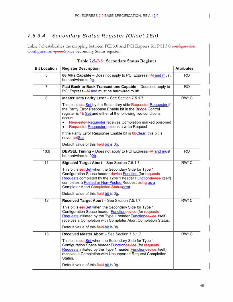
PCI EXPRESS 2.0 BASE SPECIFICATION, REV. 12.0
461
7.5.3.4. Secondary Status Register (Offset 1Eh)
Table 7-5 establishes the mapping between PCI 3.0 and PCI Express for PCI 3.0 configuration Configuration space Space Secondary Status register.
Table 7-5- 7-5: Secondary Status Register
Bit Location Register Description Attributes
5 66 MHz Capable – Does not apply to PCI Express. M and must be hardwired to 0b.
RO
7 Fast Back-to-Back Transactions Capable – Does not apply to PCI Express. M and must be hardwired to 0b.
RO
8 Master Data Parity Error – See Section 7.5.1.7.
This bit is set Set by the Secondary side Requestor Requester if the Parity Error Response Enable bit in the Bridge Control register is 1b Set and either of the following two conditions occurs: Requestor Requester receives Completion marked poisoned Requestor Requester poisons a write Request
If the Parity Error Response Enable bit is 0bClear, this bit is never setSet.
Default value of this field bit is 0b.
RW1C
10:9 DEVSEL Timing – Does not apply to PCI Express. M and must be hardwired to 00b.
RO
11 Signaled Target Abort – See Section 7.5.1.7.
This bit is set Set when the Secondary Side for Type 1 Configuration Space header device Function (for requests Requests completed by the Type 1 header Functiondevice itself) completes a Posted or Non-Posted Request using as a Completer Abort Completion Statuserror.
Default value of this field bit is 0b.
RW1C
12 Received Target Abort – See Section 7.5.1.7.
This bit is set Set when the Secondary Side for Type 1 Configuration Space header Functiondevice (for requests Requests initiated by the Type 1 header Functiondevice itself) receives a Completion with Completer Abort Completion Status.
Default value of this field bit is 0b.
RW1C
13 Received Master Abort – See Section 7.5.1.7.
This bit is set Set when the Secondary Side for Type 1 Configuration Space header Functiondevice (for requests Requests initiated by the Type 1 header Functiondevice itself) receives a Completion with Unsupported Request Completion Status.
Default value of this field bit is 0b.
RW1C

PCI EXPRESS 2.0 BASE SPECIFICATION, REV. 21.0
462
Bit Location Register Description Attributes
14 Received System Error – See Section 7.5.1.7.
This bit is set Set when the Secondary Side for a Type 1 configuration Configuration space Space header Functiondevice receives an ERR_FATAL or ERR_NONFATAL Message.
Default value of this field bit is 0b.
RW1C
15 Detected Parity Error – See Section 7.5.1.7.
This bit is set Set by the Secondary Side for a Type 1 Configuration Space header Functiondevice whenever it receives a Poisoned TLP, regardless of the state the Parity Error Response Enable bit in the Bridge Control register.
Default value of this field bit is 0b.
RW1C
7.5.3.5. Prefetchable Memory Base/Limit (Offset 24h)
The Prefetchable Memory Base and Prefetchable Memory Limit registers must indicate that 64-bit addresses are supported, as defined in PCI-to-PCI Bridge Architecture Specification, Revision 1.2.
7.5.3.6. Bridge Control Register (Offset 3Eh)
Table 7-6 establishes the mapping between PCI 3.0 and PCI Express for the PCI 3.0 configuration spaceConfiguration Space Bridge Control register.
Table 7-6- 7-6: Bridge Control Register
Bit Location Register Description Attributes
0 Parity Error Response Enable – See Section 7.5.1.7.
This bit controls the logging of poisoned TLPs in the Master Data Parity Error bit in the Secondary Status register.response to Poisoned TLPs.
Default value of this field bit is 0b.
RW
1 SERR# Enable – See Section 7.5.1.7.
This bit controls forwarding of ERR_COR, ERR_NONFATAL and ERR_FATAL from secondary to primary.
Default value of this field bit is 0b.
RW
5 Master Abort Mode – Does not apply to PCI Express. M and must be hardwired to 0b.
RO
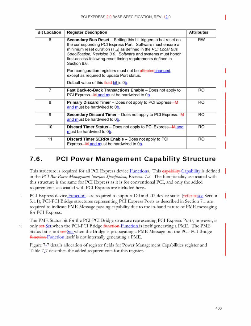
PCI EXPRESS 2.0 BASE SPECIFICATION, REV. 12.0
463
Bit Location Register Description Attributes
6 Secondary Bus Reset – Setting this bit triggers a hot reset on the corresponding PCI Express Port. Software must ensure a minimum reset duration (Trst) as defined in the PCI Local Bus Specification, Revision 3.0. Software and systems must honor first-access-following-reset timing requirements defined in Section 6.6.
Port configuration registers must not be affectedchanged, except as required to update Port status.
Default value of this field bit is 0b.
RW
7 Fast Back-to-Back Transactions Enable – Does not apply to PCI Express. M and must be hardwired to 0b.
RO
8 Primary Discard Timer – Does not apply to PCI Express. M and must be hardwired to 0b.
RO
9 Secondary Discard Timer – Does not apply to PCI Express. M and must be hardwired to 0b.
RO
10 Discard Timer Status – Does not apply to PCI Express. M and must be hardwired to 0b.
RO
11 Discard Timer SERR# Enable – Does not apply to PCI Express. M and must be hardwired to 0b.
RO
7.6. PCI Power Management Capability Structure This structure is required for all PCI Express device Functions. This capability Capability is defined in the PCI Bus Power Management Interface Specification, Revision. 1.2. The functionality associated with this structure is the same for PCI Express as it is for conventional PCI, and only the added requirements associated with PCI Express are included here..
PCI Express device Functions are required to support D0 and D3 device states (refer tosee Section 5 5.1.1); PCI-PCI Bridge structures representing PCI Express Ports as described in Section 7.1 are required to indicate PME Message passing capability due to the in-band nature of PME messaging for PCI Express.
The PME Status bit for the PCI-PCI Bridge structure representing PCI Express Ports, however, is only set Set when the PCI-PCI Bridge function Function is itself generating a PME. The PME 10 Status bit is not set Set when the Bridge is propagating a PME Message but the PCI-PCI Bridge function Function itself is not internally generating a PME.
Figure 7-7 details allocation of register fields for Power Management Capabilities register and Table 7-7 describes the added requirements for this register.
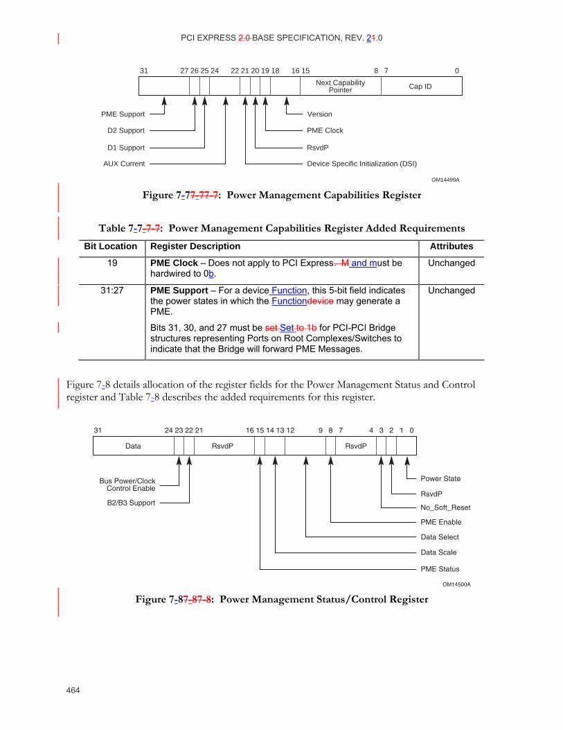
PCI EXPRESS 2.0 BASE SPECIFICATION, REV. 21.0
464
OM14499A
Cap IDNext CapabilityPointer
D1 Support
AUX Current
D2 Support
PME Support
RsvdP
Device Specific Initialization (DSI)
PME Clock
Version
31 27 26 25 24 22 21 20 19 18 16 15 8 7 0
Figure 7-77-7 7-7: Power Management Capabilities Register
Table 7-7- 7-7: Power Management Capabilities Register Added Requirements
Bit Location Register Description Attributes
19 PME Clock – Does not apply to PCI Express. M and must be hardwired to 0b.
Unchanged
31:27 PME Support – For a device Function, this 5-bit field indicates the power states in which the Functiondevice may generate a PME.
Bits 31, 30, and 27 must be set Set to 1b for PCI-PCI Bridge structures representing Ports on Root Complexes/Switches to indicate that the Bridge will forward PME Messages.
Unchanged
Figure 7-8 details allocation of the register fields for the Power Management Status and Control register and Table 7-8 describes the added requirements for this register.
OM14500A
RsvdP RsvdPData
B2/B3 Support
Bus Power/ClockControl Enable
Data Scale
PME Status
Data Select
RsvdP
No_Soft_Reset
PME Enable
Power State
31 24 23 22 21 16 15 14 13 12 9 8 7 2 1 034
Figure 7-87-8 7-8: Power Management Status/Control Register
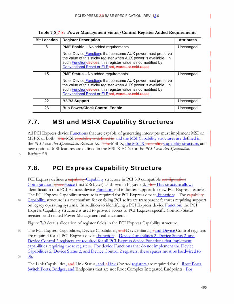
PCI EXPRESS 2.0 BASE SPECIFICATION, REV. 12.0
465
Table 7-8- 7-8: Power Management Status/Control Register Added Requirements
Bit Location Register Description Attributes
8 PME Enable – No added requirements
Note: Device Functions that consume AUX power must preserve the value of this sticky register when AUX power is available. In such Functiondevices, this register value is not modified by Conventional Reset or FLRhot, warm, or cold reset.
Unchanged
15 PME Status – No added requirements
Note: Device Functions that consume AUX power must preserve the value of this sticky register when AUX power is available. In such Functiondevices, this register value is not modified by Conventional Reset or FLRhot, warm, or cold reset.
Unchanged
22 B2/B3 Support Unchanged
23 Bus Power/Clock Control Enable Unchanged
7.7. MSI and MSI-X Capability Structures All PCI Express device Functions that are capable of generating interrupts must implement MSI or MSI-X or both. The MSI capability is defined in and the MSI Capability structures are defined in the PCI Local Bus Specification, Revision 3.0. The MSI-X, the MSI-X capability Capability structure, and new optional MSI features are defined in the MSI-X ECN for the PCI Local Bus Specification, Revision 3.0. 5
7.8. PCI Express Capability Structure PCI Express defines a capability Capability structure in PCI 3.0 compatible configuration Configuration space Space (first 256 bytes) as shown in Figure 7-3. for This structure allows identification of a PCI Express device Function and indicates support for new PCI Express features. The PCI Express Capability structure is required for PCI Express device Functions. The capability Capability structure is a mechanism for enabling PCI software transparent features requiring support 10 on legacy operating systems. In addition to identifying a PCI Express device Function, the PCI Express Capability structure is used to provide access to PCI Express specific Control/Status registers and related Power Management enhancements.
Figure 7-9 details allocation of register fields in the PCI Express Capability structure.
The PCI Express Capabilities, Device Capabilities, and Device Status, /and Device Control registers 15 are required for all PCI Express device Functions. Device Capabilities 2, Device Status 2, and Device Control 2 registers are required for all PCI Express device Functions that implement capabilities requiring those registers. For device Functions that do not implement the Device Capabilities 2, Device Status 2, and Device Control 2 registers, these spaces must be hardwired to 0b. 20
The Link Capabilities, and Link Status, and /Link Control registers are required for all Root Ports, Switch Ports, Bridges, and Endpoints that are not Root Complex Integrated Endpoints. For

PCI EXPRESS 2.0 BASE SPECIFICATION, REV. 21.0
466
Functions that do not implement the Link Capabilities, Link Status, and Link Control registers, these spaces must be hardwired to 0. Link Capabilities 2, Link Status 2, and Link Control 2 registers are required for all Root Ports, Switch Ports, Bridges, and Endpoints (except for Root Complex Integrated Endpoints) that implement capabilities requiring those registers. For Functions that do not implement the Link Capabilities 2, Link Status 2, and Link Control 2 registers, these spaces must 5 be hardwired to 0b.Endpoints are not required to implement registers other than those listed above and terminate the capability structure.
Slot Capabilities, Slot Status, and Slot Control registers are required for Switch Downstream and Root Ports if a slot is implemented on the Port (indicated by the Slot Implemented bit in the PCI Express Capabilities register). For Functions that do not implement the Slot Capabilities, Slot 10 Status, and Slot Control registers, these spaces must be hardwired to 0b. Slot Capabilities 2, Slot Status 2, and Slot Control 2 registers are required for Switch Downstream and Root Ports if a slot is implemented on the Port and the Function implements capabilities requiring those registers. For Functions that do not implement the Slot Capabilities 2, Slot Status 2, and Slot Control 2 registers, these spaces must be hardwired to 0b. 15
Root Ports and Root Complex Event Collectors must implement the Root Capabilities, Root Status, and Status/Root Control registers. in addition to PCI Express Capabilities, Device Capabilities, and Device Status/Control registers.For Functions that do not implement the Root Capabilities, Root Status, and Root Control registers, these spaces must be hardwired to 0b.
Slot Capabilities and Slot Status/Control registers are required for Switch Downstream and Root 20 Ports if a slot is implemented on the Port. Root Control/Status registers are required for Root Ports. Root Ports must implement the entire PCI Express Capability structure.
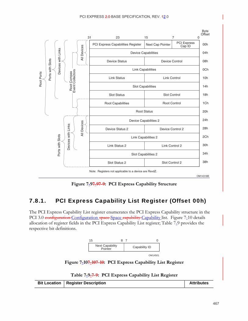
PCI EXPRESS 2.0 BASE SPECIFICATION, REV. 12.0
467
Dev
ices
with
Lin
ks
Por
ts w
ith S
lots
Roo
t Por
ts
OM14318B
PCI Express Capabilities Register
Device Capabilities
Link Capabilities
PCI ExpressCap IDNext Cap Pointer
071523
ByteOffset
31
04h
08h
00h
0Ch
10h
14h
18h
1Ch
20h
Root Control
Device Control
Root Capabilities
Slot ControlSlot Status
Device Status
Link ControlLink Status
Slot Capabilities
Root Status
All
Dev
ices
Dev
ices
with
Lin
ks
Por
ts w
ith S
lots A
ll D
evic
es
Roo
t Com
pex
Eve
nt C
olle
ctor
s
24h
28h
2Ch
30h
34h
38h
Device Capabilities 2
Link Capabilities 2
Device Control 2
Slot Control 2Slot Status 2
Device Status 2
Link Control 2Link Status 2
Slot Capabilities 2
Note: Registers not applicable to a device are RsvdZ.
Figure 7-97-9 7-9: PCI Express Capability Structure
7.8.1. PCI Express Capability List Register (Offset 00h)
The PCI Express Capability List register enumerates the PCI Express Capability structure in the PCI 3.0 configuration Configuration space Space capability Capability list. Figure 7-10 details allocation of register fields in the PCI Express Capability List register; Table 7-9 provides the respective bit definitions.
OM14501
Capability IDNext CapabilityPointer
15 8 7 0
Figure 7-107-10 7-10: PCI Express Capability List Register
Table 7-9- 7-9: PCI Express Capability List Register
Bit Location Register Description Attributes
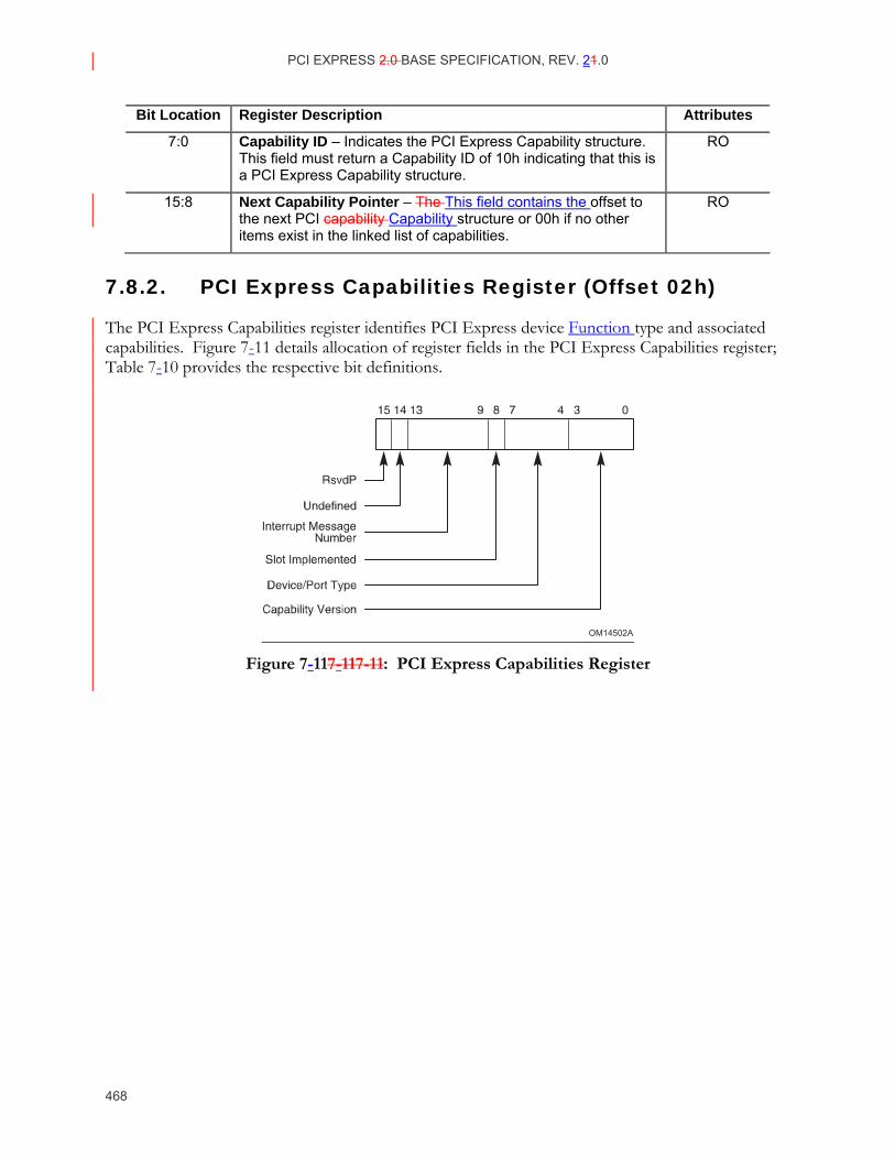
PCI EXPRESS 2.0 BASE SPECIFICATION, REV. 21.0
468
Bit Location Register Description Attributes
7:0 Capability ID – Indicates the PCI Express Capability structure. This field must return a Capability ID of 10h indicating that this is a PCI Express Capability structure.
RO
15:8 Next Capability Pointer – The This field contains the offset to the next PCI capability Capability structure or 00h if no other items exist in the linked list of capabilities.
RO
7.8.2. PCI Express Capabilities Register (Offset 02h)
The PCI Express Capabilities register identifies PCI Express device Function type and associated capabilities. Figure 7-11 details allocation of register fields in the PCI Express Capabilities register; Table 7-10 provides the respective bit definitions.
OM14502A
Figure 7-117-11 7-11: PCI Express Capabilities Register
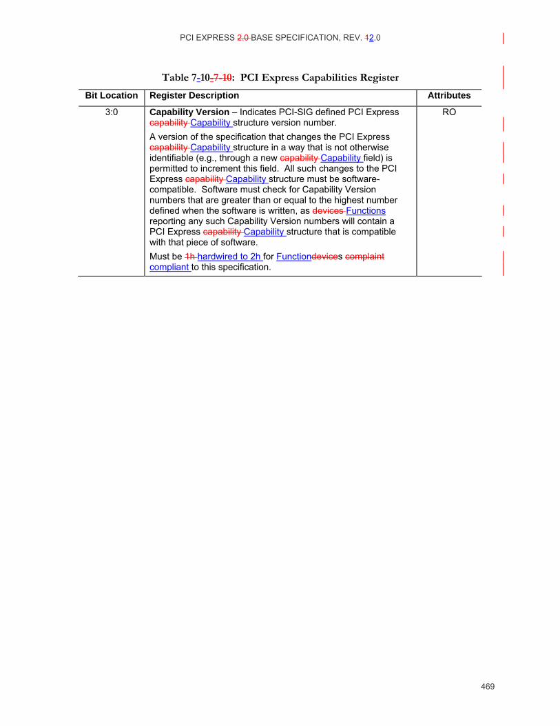
PCI EXPRESS 2.0 BASE SPECIFICATION, REV. 12.0
469
Table 7-10- 7-10: PCI Express Capabilities Register
Bit Location Register Description Attributes
3:0 Capability Version – Indicates PCI-SIG defined PCI Express capability Capability structure version number. A version of the specification that changes the PCI Express capability Capability structure in a way that is not otherwise identifiable (e.g., through a new capability Capability field) is permitted to increment this field. All such changes to the PCI Express capability Capability structure must be software-compatible. Software must check for Capability Version numbers that are greater than or equal to the highest number defined when the software is written, as devices Functions reporting any such Capability Version numbers will contain a PCI Express capability Capability structure that is compatible with that piece of software. Must be 1h hardwired to 2h for Functiondevices complaint compliant to this specification.
RO
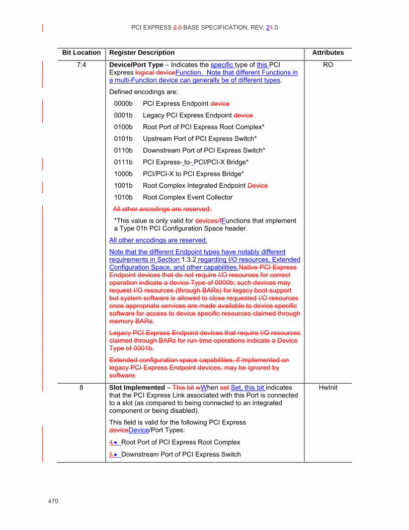
PCI EXPRESS 2.0 BASE SPECIFICATION, REV. 21.0
470
Bit Location Register Description Attributes
7:4 Device/Port Type – Indicates the specific type of this PCI Express logical deviceFunction. Note that different Functions in a multi-Function device can generally be of different types.
Defined encodings are:
0000b PCI Express Endpoint device
0001b Legacy PCI Express Endpoint device
0100b Root Port of PCI Express Root Complex*
0101b Upstream Port of PCI Express Switch*
0110b Downstream Port of PCI Express Switch*
0111b PCI Express- to- PCI/PCI-X Bridge*
1000b PCI/PCI-X to PCI Express Bridge*
1001b Root Complex Integrated Endpoint Device
1010b Root Complex Event Collector
All other encodings are reserved.
*This value is only valid for devices/fFunctions that implement a Type 01h PCI Configuration Space header.
All other encodings are reserved.
Note that the different Endpoint types have notably different requirements in Section 1.3.2 regarding I/O resources, Extended Configuration Space, and other capabilities.Native PCI Express Endpoint devices that do not require I/O resources for correct operation indicate a device Type of 0000b; such devices may request I/O resources (through BARs) for legacy boot support but system software is allowed to close requested I/O resources once appropriate services are made available to device specific software for access to device specific resources claimed through memory BARs.
Legacy PCI Express Endpoint devices that require I/O resources claimed through BARs for run-time operations indicate a Device Type of 0001b.
Extended configuration space capabilities, if implemented on legacy PCI Express Endpoint devices, may be ignored by software.
RO
8 Slot Implemented – This bit wWhen set Set, this bit indicates that the PCI Express Link associated with this Port is connected to a slot (as compared to being connected to an integrated component or being disabled).
This field is valid for the following PCI Express deviceDevice/Port Types:
4.• Root Port of PCI Express Root Complex
5.• Downstream Port of PCI Express Switch
HwInit
PCI EXPRESS 2.0 BASE SPECIFICATION, REV. 12.0
471
Bit Location Register Description Attributes
13:9 Interrupt Message Number – This registerfield must indicates which MSI/MSI-X vector is used for the interrupt message generated in association with any of the status bits in either the Slot Status register (see Section 6.7.3.4) or the Root Status register (see Section 6.1.6) of this capability Capability structure.
For MSI, the value in this register field indicates the offset between the base Message Data and the interrupt message that is generated. Hardware is required to update this field so that it is correct if the number of MSI Messages assigned to the Functiondevice changes when software writes to the Multiple Message Enable field in the MSI Message Control register.
For MSI-X, the value in this fieldregister indicates which MSI-X Table entry is used to generate the interrupt message. The entry must be one of the first 32 entries even if the function Function implements more than 32 entries. For a given MSI-X implementation, the entry must remain constant.
If both MSI and MSI-X are implemented, they are permitted to use different vectors, though software is permitted to enable only one mechanism at a time. If MSI-X is enabled, the value in this fieldregister must indicate the vector for MSI-X. If MSI is enabled or neither is enabled, the value in this fieldregister must indicate the vector for MSI. If software enables both MSI and MSI-X at the same time, the value in this fieldregister is undefined.
RO
14 The value read from this bit is undefined. In previous versions of this specification, this bit was used to indicate support for TCS Routing. System software should ignore the value read from this bit. System software is permitted to write any value to this bit.
RO
7.8.3. Device Capabilities Register (Offset 04h)
The Device Capabilities register identifies PCI Express device specific capabilities. Figure 7-12 details allocation of register fields in the Device Capabilities register; Table 7-11 provides the respective bit definitions.
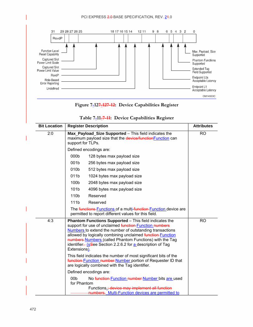
PCI EXPRESS 2.0 BASE SPECIFICATION, REV. 21.0
472
OM14503C
Figure 7-127-12 7-12: Device Capabilities Register
Table 7-11- 7-11: Device Capabilities Register
Bit Location Register Description Attributes
2:0 Max_Payload_Size Supported – This field indicates the maximum payload size that the device/functionFunction can support for TLPs. Defined encodings are:
000b 128 bytes max payload size 001b 256 bytes max payload size 010b 512 bytes max payload size 011b 1024 bytes max payload size 100b 2048 bytes max payload size 101b 4096 bytes max payload size 110b Reserved 111b Reserved The functions Functions of a multi-function Function device are permitted to report different values for this field.
RO
4:3 Phantom Functions Supported – This field indicates the support for use of unclaimed function Function numbers Numbers to extend the number of outstanding transactions allowed by logically combining unclaimed function Function numbers Numbers (called Phantom Functions) with the Tag identifier. (sSee Section 2.2.6.2 for a description of Tag Extensions). This field indicates the number of most significant bits of the function Function number Number portion of Requester ID that are logically combined with the Tag identifier. Defined encodings are:
00b No function Function number Number bits are used for Phantom Functions.; device may implement all function numbers. Multi-Function devices are permitted to
RO
PCI EXPRESS 2.0 BASE SPECIFICATION, REV. 12.0
473
Bit Location Register Description Attributes
implement up to 8 independent Functions. 01b First The most significant bit of the function Function number in Requestor IDRequester ID is used for Phantom Functions; ; device a multi-Function device is permitted to may implement functions Functions 0-3. Functions 0, 1, 2, and 3 may are permitted to claimuse functions Function Numbers 4, 5, 6, and 7 respectively as Phantom Functions respectively. 10b First The two most significant bits of function Function number Number in Requestor IDRequester ID are used for Phantom Functions; a multi-Function device may is permitted to implement functions Functions 0-1. Function 0 may claimis permitted to use functions Function Numbers 2, 4, and 6 for Phantom Functions. function Function 1 may claimis permitted to use functions Function Numbers 3, 5, and 7 as Phantom Functions. 11b All three 3 bits of function Function number Number in Requestor IDRequester ID used for Phantom Functions; . device The device must behave a single function Function 0 device that may claimis permitted to use all other functions Function Numbers as Phantom Functions.
Note that Phantom Function support for the Device Function must be enabled by the corresponding controlPhantom Functions Enable field in the Device Control register before the Function is permitted to use the Function Number field in the Requester ID for Phantom Functions.
5 Extended Tag Field Supported – This field bit indicates the maximum supported size of the Tag field as a Requester.
Defined encodings are:
0b 5-bit Tag field supported
1b 8-bit Tag field supported
Note that 8-bit Tag field support generation must be enabled by the corresponding control fieldExtended Tag Field Enable bit in the Device Control register before 8-bit Tags can be generated
RO
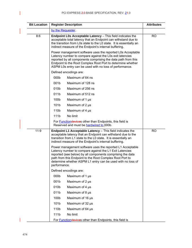
PCI EXPRESS 2.0 BASE SPECIFICATION, REV. 21.0
474
Bit Location Register Description Attributes
by the Requester.
8:6 Endpoint L0s Acceptable Latency – This field indicates the acceptable total latency that an Endpoint can withstand due to the transition from L0s state to the L0 state. It is essentially an indirect measure of the Endpoint’s internal buffering.
Power management software uses the reported L0s Acceptable Latency number to compare against the L0s exit latencies reported by all components comprising the data path from this Endpoint to the Root Complex Root Port to determine whether ASPM L0s entry can be used with no loss of performance.
Defined encodings are:
000b Maximum of 64 ns
001b Maximum of 128 ns
010b Maximum of 256 ns
011b Maximum of 512 ns
100b Maximum of 1 µs
101b Maximum of 2 µs
110b Maximum of 4 µs
111b No limit
For Functiondevices other than Endpoints, this field is Reserved and must be hardwired to 000b.
RO
11:9 Endpoint L1 Acceptable Latency – This field indicates the acceptable latency that an Endpoint can withstand due to the transition from L1 state to the L0 state. It is essentially an indirect measure of the Endpoint’s internal buffering.
Power management software uses the reported L1 Acceptable Latency number to compare against the L1 Exit Latencies reported (see below) by all components comprising the data path from this Endpoint to the Root Complex Root Port to determine whether ASPM L1 entry can be used with no loss of performance.
Defined encodings are:
000b Maximum of 1 µs
001b Maximum of 2 µs
010b Maximum of 4 µs
011b Maximum of 8 µs
100b Maximum of 16 µs
101b Maximum of 32 µs
110b Maximum of 64 µs
111b No limit
For Functiondevices other than Endpoints, this field is
RO
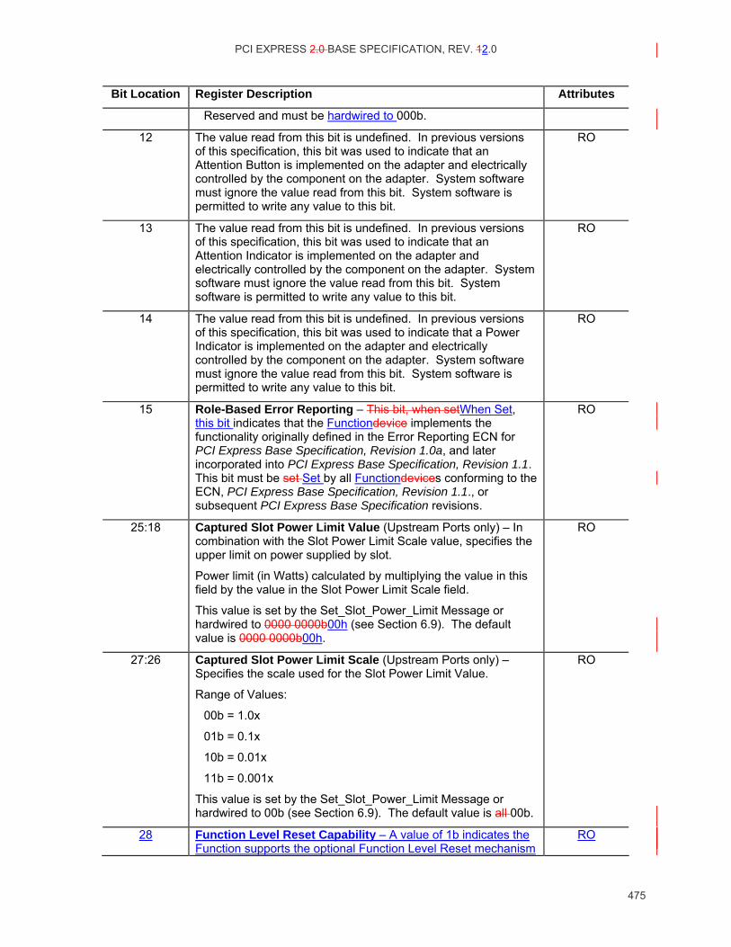
PCI EXPRESS 2.0 BASE SPECIFICATION, REV. 12.0
475
Bit Location Register Description Attributes
Reserved and must be hardwired to 000b.
12 The value read from this bit is undefined. In previous versions of this specification, this bit was used to indicate that an Attention Button is implemented on the adapter and electrically controlled by the component on the adapter. System software must ignore the value read from this bit. System software is permitted to write any value to this bit.
RO
13 The value read from this bit is undefined. In previous versions of this specification, this bit was used to indicate that an Attention Indicator is implemented on the adapter and electrically controlled by the component on the adapter. System software must ignore the value read from this bit. System software is permitted to write any value to this bit.
RO
14 The value read from this bit is undefined. In previous versions of this specification, this bit was used to indicate that a Power Indicator is implemented on the adapter and electrically controlled by the component on the adapter. System software must ignore the value read from this bit. System software is permitted to write any value to this bit.
RO
15 Role-Based Error Reporting – This bit, when setWhen Set, this bit indicates that the Functiondevice implements the functionality originally defined in the Error Reporting ECN for PCI Express Base Specification, Revision 1.0a, and later incorporated into PCI Express Base Specification, Revision 1.1. This bit must be set Set by all Functiondevices conforming to the ECN, PCI Express Base Specification, Revision 1.1., or subsequent PCI Express Base Specification revisions.
RO
25:18 Captured Slot Power Limit Value (Upstream Ports only) – In combination with the Slot Power Limit Scale value, specifies the upper limit on power supplied by slot.
Power limit (in Watts) calculated by multiplying the value in this field by the value in the Slot Power Limit Scale field.
This value is set by the Set_Slot_Power_Limit Message or hardwired to 0000 0000b00h (see Section 6.9). The default value is 0000 0000b00h.
RO
27:26 Captured Slot Power Limit Scale (Upstream Ports only) – Specifies the scale used for the Slot Power Limit Value.
Range of Values:
00b = 1.0x
01b = 0.1x
10b = 0.01x
11b = 0.001x
This value is set by the Set_Slot_Power_Limit Message or hardwired to 00b (see Section 6.9). The default value is all 00b.
RO
28 Function Level Reset Capability – A value of 1b indicates the Function supports the optional Function Level Reset mechanism
RO
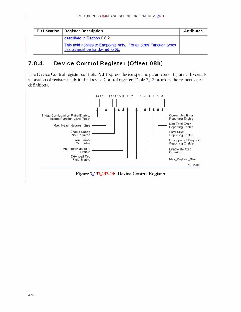
PCI EXPRESS 2.0 BASE SPECIFICATION, REV. 21.0
476
Bit Location Register Description Attributes
described in Section 6.6.2.
This field applies to Endpoints only. For all other Function types this bit must be hardwired to 0b.
7.8.4. Device Control Register (Offset 08h)
The Device Control register controls PCI Express device specific parameters. Figure 7-13 details allocation of register fields in the Device Control register; Table 7-12 provides the respective bit definitions.
OM14504C
Figure 7-137-13 7-13: Device Control Register
PCI EXPRESS 2.0 BASE SPECIFICATION, REV. 12.0
477
Table 7-12- 7-12: Device Control Register
Bit Location Register Description Attributes
0 Correctable Error Reporting Enable – This bit, in conjunction with other bits, controls sending ERR_COR Messages. Refer to(see Sections 6.2.5 and Section 6.2.6 for details). For a multi-function Function device, this bit controls error reporting for each function Function from point-of-view of the respective functionFunction.
For a Root Port, the reporting of correctable errors is internal to the root. No external ERR_COR Message is generated.
A Root Complex Integrated Endpoint that is not associated with a Root Complex Event Collector is permitted to hardwire this bit to 0b.
Default value of this field bit is 0b.
RW
1 Non-Fatal Error Reporting Enable – This bit, in conjunction with other bits, controls sending ERR_NONFATAL Messages. Refer to(see Sections 6.2.5 and Section 6.2.6 for details). For a multi-function Function device, this bit controls error reporting for each function Function from point-of-view of the respective functionFunction.
For a Root Port, the reporting of Non-fatal errors is internal to the root. No external ERR_NONFATAL Message is generated.
A Root Complex Integrated Endpoint that is not associated with a Root Complex Event Collector is permitted to hardwire this bit to 0b.
Default value of this field bit is 0b.
RW
2 Fatal Error Reporting Enable – This bit, in conjunction with other bits, controls sending ERR_FATAL Messages. Refer to (see Sections 6.2.5 and Section 6.2.6 for details). For a multi-function Function device, this bit controls error reporting for each function Function from point-of-view of the respective functionFunction.
For a Root Port, the reporting of Fatal errors is internal to the root. No external ERR_FATAL Message is generated.
A Root Complex Integrated Endpoint that is not associated with a Root Complex Event Collector is permitted to hardwire this bit to 0b.
Default value of this field bit is 0b.
RW
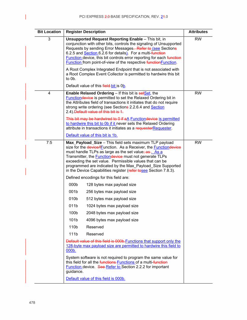
PCI EXPRESS 2.0 BASE SPECIFICATION, REV. 21.0
478
Bit Location Register Description Attributes
3 Unsupported Request Reporting Enable – This bit, in conjunction with other bits, controls the signaling of Unsupported Requests by sending Error Messages. Refer to (see Sections 6.2.5 and Section 6.2.6 for details). For a multi-function Function device, this bit controls error reporting for each function Function from point-of-view of the respective functionFunction.
A Root Complex Integrated Endpoint that is not associated with a Root Complex Event Collector is permitted to hardwire this bit to 0b.
Default value of this field bit is 0b.
RW
4 Enable Relaxed Ordering – If this bit is setSet, the Functiondevice is permitted to set the Relaxed Ordering bit in the Attributes field of transactions it initiates that do not require strong write ordering (see Sections 2.2.6.4 and Section 2.4).Default value of this bit is 1.
This bit may be hardwired to 0 if aA Functiondevice is permitted to hardwire this bit to 0b if it never sets the Relaxed Ordering attribute in transactions it initiates as a requesterRequester.
Default value of this bit is 1b.
RW
7:5 Max_Payload_Size – This field sets maximum TLP payload size for the device/fFunction. As a Receiver, the Functiondevice must handle TLPs as large as the set value; as . As a Transmitter, the Functiondevice must not generate TLPs exceeding the set value. Permissible values that can be programmed are indicated by the Max_Payload_Size Supported in the Device Capabilities register (refer tosee Section 7.8.3).
Defined encodings for this field are:
000b 128 bytes max payload size
001b 256 bytes max payload size
010b 512 bytes max payload size
011b 1024 bytes max payload size
100b 2048 bytes max payload size
101b 4096 bytes max payload size
110b Reserved
111b Reserved
Default value of this field is 000b.Functions that support only the 128-byte max payload size are permitted to hardwire this field to 000b.
System software is not required to program the same value for this field for all the functions Functions of a multi-function Function device. See Refer to Section 2.2.2 for important guidance.
Default value of this field is 000b.
RW
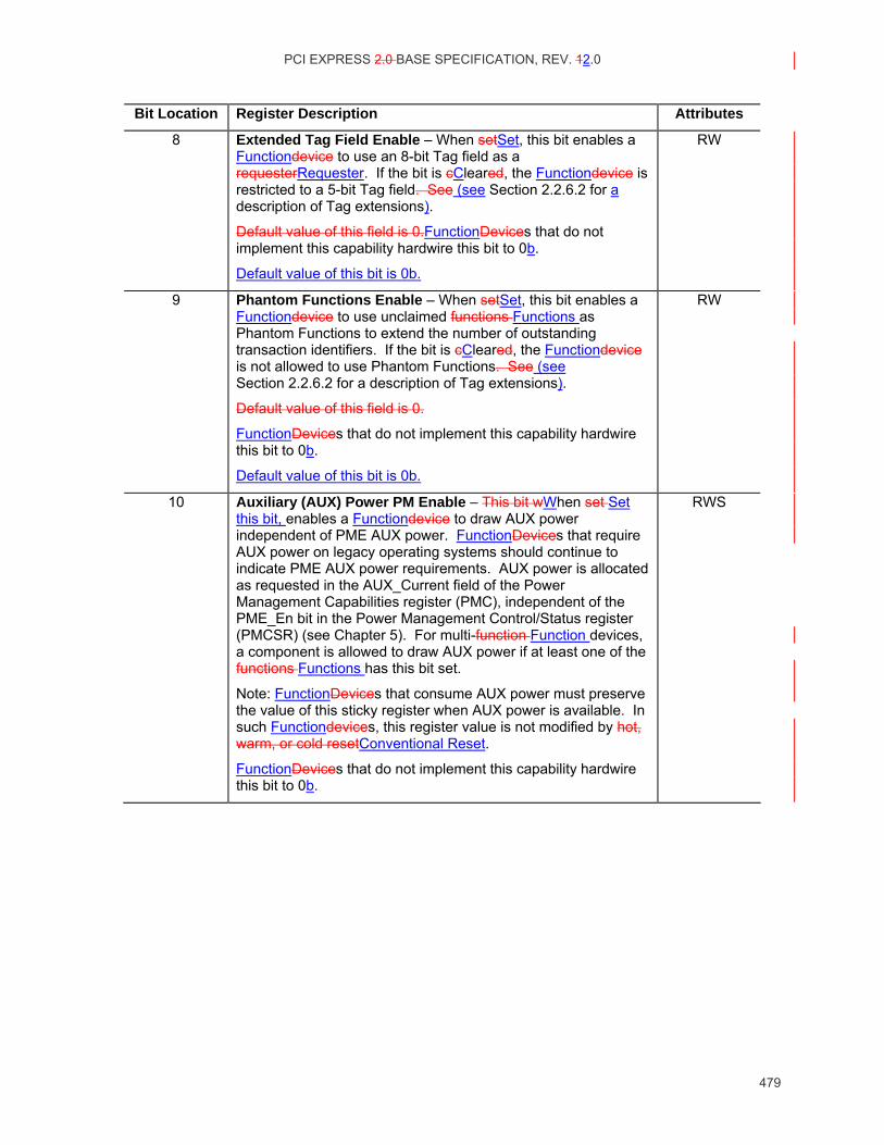
PCI EXPRESS 2.0 BASE SPECIFICATION, REV. 12.0
479
Bit Location Register Description Attributes
8 Extended Tag Field Enable – When setSet, this bit enables a Functiondevice to use an 8-bit Tag field as a requesterRequester. If the bit is cCleared, the Functiondevice is restricted to a 5-bit Tag field. See (see Section 2.2.6.2 for a description of Tag extensions).
Default value of this field is 0.FunctionDevices that do not implement this capability hardwire this bit to 0b.
Default value of this bit is 0b.
RW
9 Phantom Functions Enable – When setSet, this bit enables a Functiondevice to use unclaimed functions Functions as Phantom Functions to extend the number of outstanding transaction identifiers. If the bit is cCleared, the Functiondevice is not allowed to use Phantom Functions. See (see Section 2.2.6.2 for a description of Tag extensions).
Default value of this field is 0.
FunctionDevices that do not implement this capability hardwire this bit to 0b.
Default value of this bit is 0b.
RW
10 Auxiliary (AUX) Power PM Enable – This bit wWhen set Set this bit, enables a Functiondevice to draw AUX power independent of PME AUX power. FunctionDevices that require AUX power on legacy operating systems should continue to indicate PME AUX power requirements. AUX power is allocated as requested in the AUX_Current field of the Power Management Capabilities register (PMC), independent of the PME_En bit in the Power Management Control/Status register (PMCSR) (see Chapter 5). For multi-function Function devices, a component is allowed to draw AUX power if at least one of the functions Functions has this bit set.
Note: FunctionDevices that consume AUX power must preserve the value of this sticky register when AUX power is available. In such Functiondevices, this register value is not modified by hot, warm, or cold resetConventional Reset.
FunctionDevices that do not implement this capability hardwire this bit to 0b.
RWS
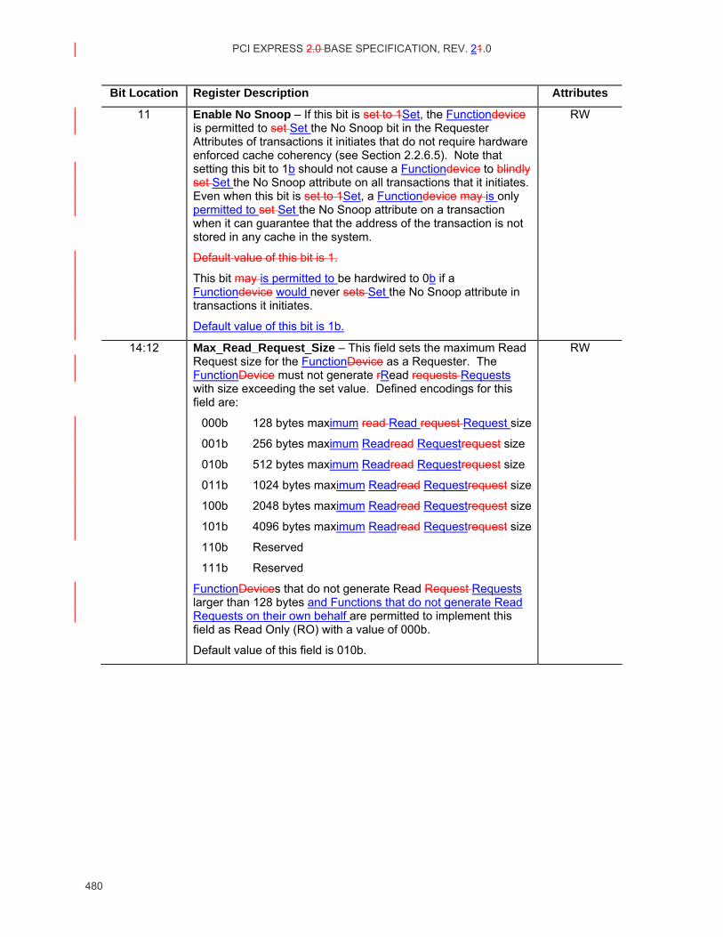
PCI EXPRESS 2.0 BASE SPECIFICATION, REV. 21.0
480
Bit Location Register Description Attributes
11 Enable No Snoop – If this bit is set to 1Set, the Functiondevice is permitted to set Set the No Snoop bit in the Requester Attributes of transactions it initiates that do not require hardware enforced cache coherency (see Section 2.2.6.5). Note that setting this bit to 1b should not cause a Functiondevice to blindly set Set the No Snoop attribute on all transactions that it initiates. Even when this bit is set to 1Set, a Functiondevice may is only permitted to set Set the No Snoop attribute on a transaction when it can guarantee that the address of the transaction is not stored in any cache in the system.
Default value of this bit is 1.
This bit may is permitted to be hardwired to 0b if a Functiondevice would never sets Set the No Snoop attribute in transactions it initiates.
Default value of this bit is 1b.
RW
14:12 Max_Read_Request_Size – This field sets the maximum Read Request size for the FunctionDevice as a Requester. The FunctionDevice must not generate rRead requests Requests with size exceeding the set value. Defined encodings for this field are:
000b 128 bytes maximum read Read request Request size
001b 256 bytes maximum Readread Requestrequest size
010b 512 bytes maximum Readread Requestrequest size
011b 1024 bytes maximum Readread Requestrequest size
100b 2048 bytes maximum Readread Requestrequest size
101b 4096 bytes maximum Readread Requestrequest size
110b Reserved
111b Reserved
FunctionDevices that do not generate Read Request Requests larger than 128 bytes and Functions that do not generate Read Requests on their own behalf are permitted to implement this field as Read Only (RO) with a value of 000b.
Default value of this field is 010b.
RW
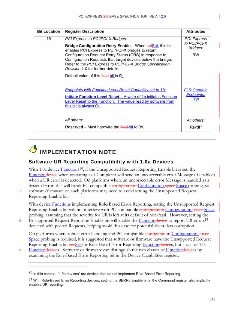
PCI EXPRESS 2.0 BASE SPECIFICATION, REV. 12.0
481
Bit Location Register Description Attributes
15 PCI Express to PCI/PCI-X Bridges:
Bridge Configuration Retry Enable – When setSet, this bit enables PCI Express to PCI/PCI-X bridges to return Configuration Request Retry Status (CRS) in response to Configuration Requests that target devices below the bridge. Refer to the PCI Express to PCI/PCI-X Bridge Specification, Revision 1.0 for further details.
Default value of this field bit is 0b.
Endpoints with Function Level Reset Capability set to 1b:
Initiate Function Level Reset – A write of 1b initiates Function Level Reset to the Function. The value read by software from this bit is always 0b.
All others:
Reserved – Must hardwire the field bit to 0b.
PCI Express to PCI/PCI-X
Bridges:
RW
FLR Capable Endpoints:
RW
All others:
RsvdP
IMPLEMENTATION NOTE Software UR Reporting Compatibility with 1.0a Devices With 1.0a device Functions80, if the Unsupported Request Reporting Enable bit is set, the Functiondevice when operating as a Completer will send an uncorrectable error Message (if enabled) when a UR error is detected. On platforms where an uncorrectable error Message is handled as a System Error, this will break PC-compatible configuration Configuration space Space probing, so software/firmware on such platforms may need to avoid setting the Unsupported Request 5 Reporting Enable bit.
With device Functions implementing Role-Based Error Reporting, setting the Unsupported Request Reporting Enable bit will not interfere with PC-compatible configuration Configuration space Space probing, assuming that the severity for UR is left at its default of non-fatal. However, setting the Unsupported Request Reporting Enable bit will enable the Functiondevice to report UR errors81 10 detected with posted Requests, helping avoid this case for potential silent data corruption.
On platforms where robust error handling and PC-compatible configuration Configuration space Space probing is required, it is suggested that software or firmware have the Unsupported Request Reporting Enable bit set Set for Role-Based Error Reporting Functiondevices, but clear for 1.0a Functiondevices. Software or firmware can distinguish the two classes of Functiondevices by 15 examining the Role-Based Error Reporting bit in the Device Capabilities register.
80 In this context, “1.0a devices” are devices that do not implement Role-Based Error Reporting. 81 With Role-Based Error Reporting devices, setting the SERR# Enable bit in the Command register also implicitly enables UR reporting.

PCI EXPRESS 2.0 BASE SPECIFICATION, REV. 21.0
482
IMPLEMENTATION NOTE Use of Max_Payload_Size The Max_Payload_Size mechanism allows software to control the maximum payload in packets sent by Endpoints to balance latency versus bandwidth trade-offs, particularly for isochronous traffic.
If software chooses to program the Max_Payload_Size of various system System elements Elements to non-default values, it must take care to ensure that each packet does not exceed the 5 Max_Payload_Size parameter of any system System element Element along the packet's path. Otherwise, the packet will be rejected by the system System element Element whose Max_Payload_Size parameter is too small.
Discussion of specific algorithms used to configure Max_Payload_Size so thatto meet this requirement is met is beyond the scope of this specification, but software should base its algorithm 10 upon factors such as the following:
the Max_Payload_Size capability of each system System element Element within a hierarchy
awareness of when system System elements Elements are added or removed through Hot-Plug operations
knowing which system System elements Elements send packets to each other, what type of 15 traffic is carried, what type of transactions are used, or if packet sizes are constrained by other mechanisms
For the case of firmware that configures system System elements Elements in preparation for running legacy operating system environments, the firmware may need to avoid programming a Max_Payload_Size above the default of 128 bytes, which is the minimum supported by Endpoints. 20
For example, if the operating system environment does not comprehend PCI Express, firmware probably should not program a non-default Max_Payload_Size for a hierarchy that supports Hot-Plug operations. Otherwise, if no software is present to manage Max_Payload_Size settings when a new element is added, improper operation may result. Note that a newly added element may not even support a Max_Payload_Size setting as large as the rest of the hierarchy, in which case software 25 may need to deny enabling the new element or reduce the Max_Payload_Size settings of other elements.
IMPLEMENTATION NOTE
Use of Max_Read_Request_Size The Max_Read_Request_Size mechanism allows improved control of bandwidth allocation in systems where quality of service (QoS) is important for the target applications. For example, an
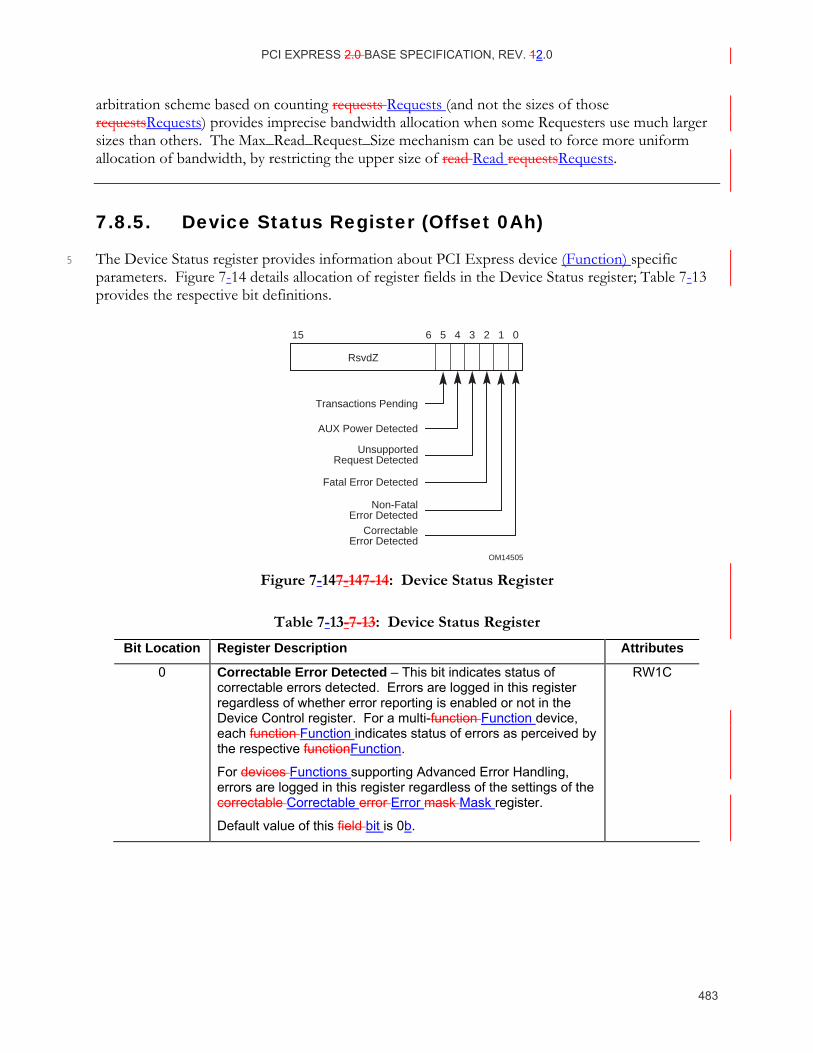
PCI EXPRESS 2.0 BASE SPECIFICATION, REV. 12.0
483
arbitration scheme based on counting requests Requests (and not the sizes of those requestsRequests) provides imprecise bandwidth allocation when some Requesters use much larger sizes than others. The Max_Read_Request_Size mechanism can be used to force more uniform allocation of bandwidth, by restricting the upper size of read Read requestsRequests.
7.8.5. Device Status Register (Offset 0Ah)
The Device Status register provides information about PCI Express device (Function) specific 5 parameters. Figure 7-14 details allocation of register fields in the Device Status register; Table 7-13 provides the respective bit definitions.
OM14505
Fatal Error Detected
CorrectableError Detected
UnsupportedRequest Detected
AUX Power Detected
Non-FatalError Detected
Transactions Pending
RsvdZ
15 6 5 4 3 2 1 0
Figure 7-147-14 7-14: Device Status Register
Table 7-13- 7-13: Device Status Register
Bit Location Register Description Attributes
0 Correctable Error Detected – This bit indicates status of correctable errors detected. Errors are logged in this register regardless of whether error reporting is enabled or not in the Device Control register. For a multi-function Function device, each function Function indicates status of errors as perceived by the respective functionFunction.
For devices Functions supporting Advanced Error Handling, errors are logged in this register regardless of the settings of the correctable Correctable error Error mask Mask register.
Default value of this field bit is 0b.
RW1C
PCI EXPRESS 2.0 BASE SPECIFICATION, REV. 21.0
484
Bit Location Register Description Attributes
1 Non-Fatal Error Detected – This bit indicates status of Non-fatal errors detected. Errors are logged in this register regardless of whether error reporting is enabled or not in the Device Control register. For a multi-Functionfunction device, each Functionfunction indicates status of errors as perceived by the respective Functionfunction.
For Functiondevices supporting Advanced Error Handling, errors are logged in this register regardless of the settings of the correctable Uncorrectable error Error mask Mask register.
Default value of this field bit is 0b.
RW1C
2 Fatal Error Detected – This bit indicates status of Fatal errors detected. Errors are logged in this register regardless of whether error reporting is enabled or not in the Device Control register. For a multi-Functionfunction device, each Functionfunction indicates status of errors as perceived by the respective Functionfunction.
For Functiondevices supporting Advanced Error Handling, errors are logged in this register regardless of the settings of the correctable Uncorrectable error Error mask Mask register.
Default value of this field bit is 0b.
RW1C
3 Unsupported Request Detected – This bit indicates that the Functiondevice received an Unsupported Request. Errors are logged in this register regardless of whether error reporting is enabled or not in the Device Control register. For a multi-Functionfunction device, each Functionfunction indicates status of errors as perceived by the respective Functionfunction.
Default value of this field bit is 0b.
RW1C
4 AUX Power Detected – FunctionDevices that require AUX power report this bit as set Set if AUX power is detected by the Functiondevice.
RO

PCI EXPRESS 2.0 BASE SPECIFICATION, REV. 12.0
485
Bit Location Register Description Attributes
5 Transactions Pending –
Endpoints:
This bit wWhen set Set, this bit indicates that the Functiondevice has issued Non-Posted Requests which that have not been completed. A Functiondevice reports this bit cleared only when all outstanding Non-Posted Requests have completed or have been terminated by the Completion Timeout mechanism. This bit must also be cleared upon the completion of an FLR.
Root and Switch Ports:
This bit wWhen set Set, this bit indicates that a Port has issued Non-Posted Requests on its own behalf (using the Port’s own Requester ID) which have not been completed. The Port reports this bit cleared only when all such outstanding Non-Posted Requests have completed or have been terminated by the Completion Timeout mechanism. Note that Root and Switch Ports implementing only the functionality required by this document do not issue Non-Posted Requests on their own behalf, and therefore are not subject to this case. Root and Switch Ports that do not issue Non-Posted Requests on their own behalf hardwire this bit to 0b.
RO
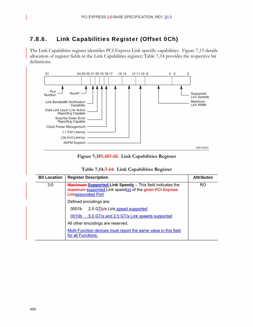
PCI EXPRESS 2.0 BASE SPECIFICATION, REV. 21.0
486
7.8.6. Link Capabilities Register (Offset 0Ch)
The Link Capabilities register identifies PCI Express Link specific capabilities. Figure 7-15 details allocation of register fields in the Link Capabilities register; Table 7-14 provides the respective bit definitions.
OM14506C
Figure 7-157-15 7-15: Link Capabilities Register
Table 7-14- 7-14: Link Capabilities Register
Bit Location Register Description Attributes
3:0 Maximum Supported Link Speeds – This field indicates the maximum supported Link speed(s) of the given PCI Express Linkassociated Port.
Defined encodings are:
0001b 2.5 GTb/s Link speed supported
0010b 5.0 GT/s and 2.5 GT/s Link speeds supported
All other encodings are reserved.
Multi-Function devices must report the same value in this field for all Functions.
RO
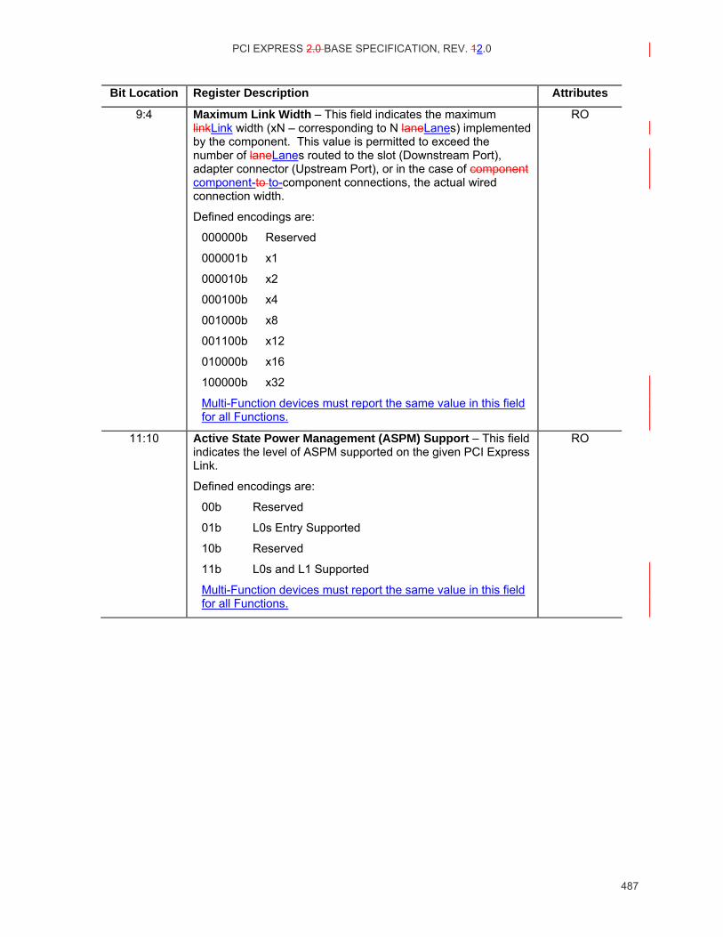
PCI EXPRESS 2.0 BASE SPECIFICATION, REV. 12.0
487
Bit Location Register Description Attributes
9:4 Maximum Link Width – This field indicates the maximum linkLink width (xN – corresponding to N laneLanes) implemented by the component. This value is permitted to exceed the number of laneLanes routed to the slot (Downstream Port), adapter connector (Upstream Port), or in the case of component component-to to-component connections, the actual wired connection width.
Defined encodings are:
000000b Reserved
000001b x1
000010b x2
000100b x4
001000b x8
001100b x12
010000b x16
100000b x32
Multi-Function devices must report the same value in this field for all Functions.
RO
11:10 Active State Power Management (ASPM) Support – This field indicates the level of ASPM supported on the given PCI Express Link.
Defined encodings are:
00b Reserved
01b L0s Entry Supported
10b Reserved
11b L0s and L1 Supported
Multi-Function devices must report the same value in this field for all Functions.
RO
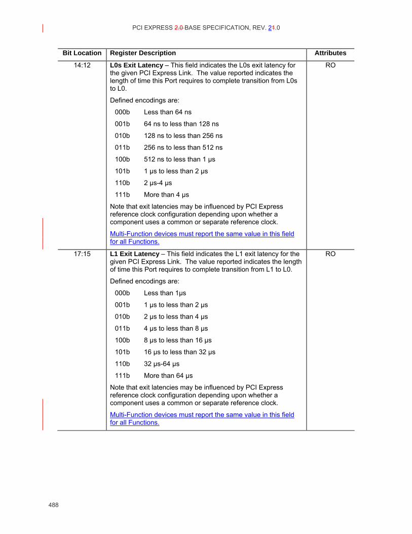
PCI EXPRESS 2.0 BASE SPECIFICATION, REV. 21.0
488
Bit Location Register Description Attributes
14:12 L0s Exit Latency – This field indicates the L0s exit latency for the given PCI Express Link. The value reported indicates the length of time this Port requires to complete transition from L0s to L0.
Defined encodings are:
000b Less than 64 ns
001b 64 ns to less than 128 ns
010b 128 ns to less than 256 ns
011b 256 ns to less than 512 ns
100b 512 ns to less than 1 µs
101b 1 µs to less than 2 µs
110b 2 µs-4 µs
111b More than 4 µs
Note that exit latencies may be influenced by PCI Express reference clock configuration depending upon whether a component uses a common or separate reference clock.
Multi-Function devices must report the same value in this field for all Functions.
RO
17:15 L1 Exit Latency – This field indicates the L1 exit latency for the given PCI Express Link. The value reported indicates the length of time this Port requires to complete transition from L1 to L0.
Defined encodings are:
000b Less than 1µs
001b 1 µs to less than 2 µs
010b 2 µs to less than 4 µs
011b 4 µs to less than 8 µs
100b 8 µs to less than 16 µs
101b 16 µs to less than 32 µs
110b 32 µs-64 µs
111b More than 64 µs
Note that exit latencies may be influenced by PCI Express reference clock configuration depending upon whether a component uses a common or separate reference clock.
Multi-Function devices must report the same value in this field for all Functions.
RO
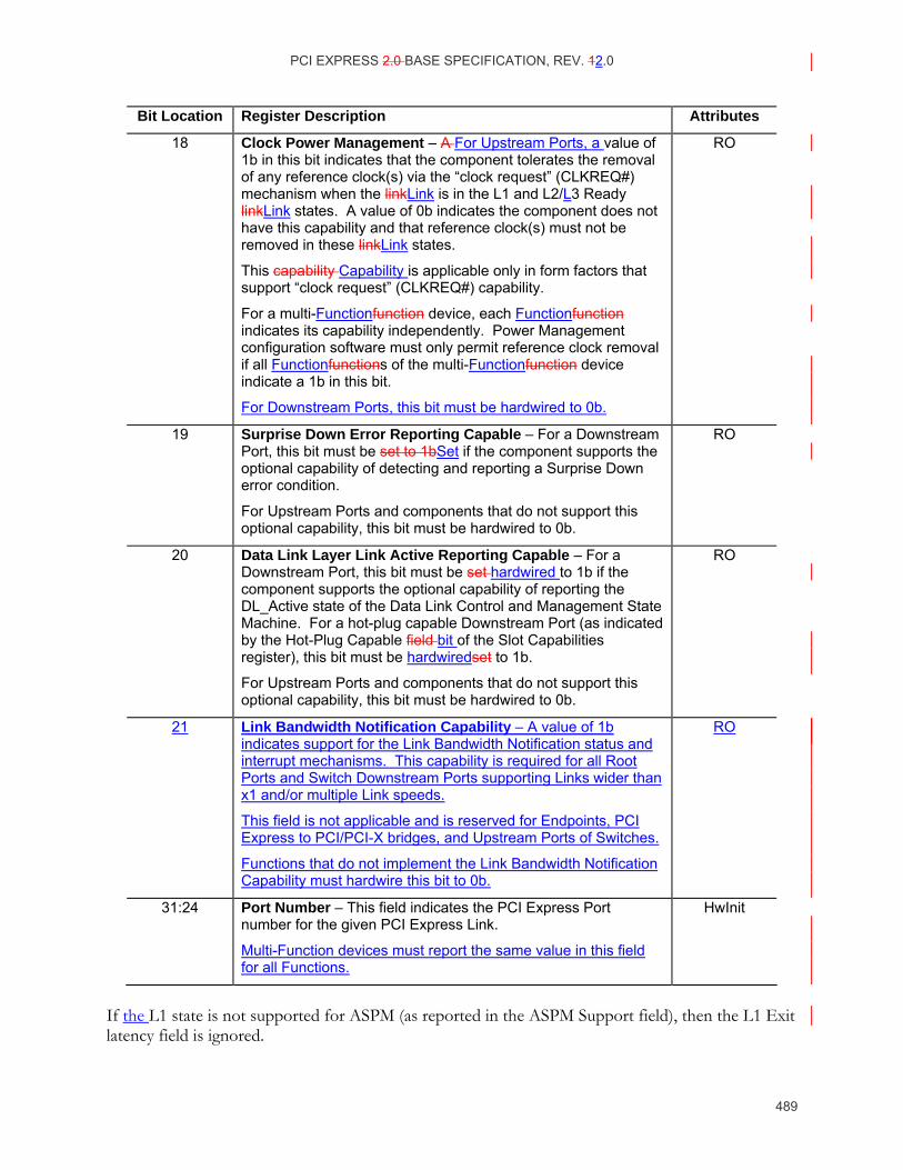
PCI EXPRESS 2.0 BASE SPECIFICATION, REV. 12.0
489
Bit Location Register Description Attributes
18 Clock Power Management – A For Upstream Ports, a value of 1b in this bit indicates that the component tolerates the removal of any reference clock(s) via the “clock request” (CLKREQ#) mechanism when the linkLink is in the L1 and L2/L3 Ready linkLink states. A value of 0b indicates the component does not have this capability and that reference clock(s) must not be removed in these linkLink states.
This capability Capability is applicable only in form factors that support “clock request” (CLKREQ#) capability.
For a multi-Functionfunction device, each Functionfunction indicates its capability independently. Power Management configuration software must only permit reference clock removal if all Functionfunctions of the multi-Functionfunction device indicate a 1b in this bit.
For Downstream Ports, this bit must be hardwired to 0b.
RO
19 Surprise Down Error Reporting Capable – For a Downstream Port, this bit must be set to 1bSet if the component supports the optional capability of detecting and reporting a Surprise Down error condition.
For Upstream Ports and components that do not support this optional capability, this bit must be hardwired to 0b.
RO
20 Data Link Layer Link Active Reporting Capable – For a Downstream Port, this bit must be set hardwired to 1b if the component supports the optional capability of reporting the DL_Active state of the Data Link Control and Management State Machine. For a hot-plug capable Downstream Port (as indicated by the Hot-Plug Capable field bit of the Slot Capabilities register), this bit must be hardwiredset to 1b.
For Upstream Ports and components that do not support this optional capability, this bit must be hardwired to 0b.
RO
21 Link Bandwidth Notification Capability – A value of 1b indicates support for the Link Bandwidth Notification status and interrupt mechanisms. This capability is required for all Root Ports and Switch Downstream Ports supporting Links wider than x1 and/or multiple Link speeds.
This field is not applicable and is reserved for Endpoints, PCI Express to PCI/PCI-X bridges, and Upstream Ports of Switches.
Functions that do not implement the Link Bandwidth Notification Capability must hardwire this bit to 0b.
RO
31:24 Port Number – This field indicates the PCI Express Port number for the given PCI Express Link.
Multi-Function devices must report the same value in this field for all Functions.
HwInit
If the L1 state is not supported for ASPM (as reported in the ASPM Support field), then the L1 Exit latency field is ignored.
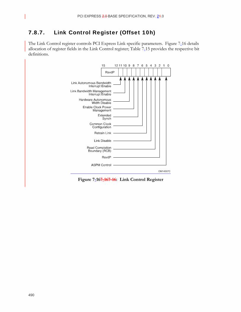
PCI EXPRESS 2.0 BASE SPECIFICATION, REV. 21.0
490
7.8.7. Link Control Register (Offset 10h)
The Link Control register controls PCI Express Link specific parameters. Figure 7-16 details allocation of register fields in the Link Control register; Table 7-15 provides the respective bit definitions.
OM14507C
RsvdP
Figure 7-167-16 7-16: Link Control Register
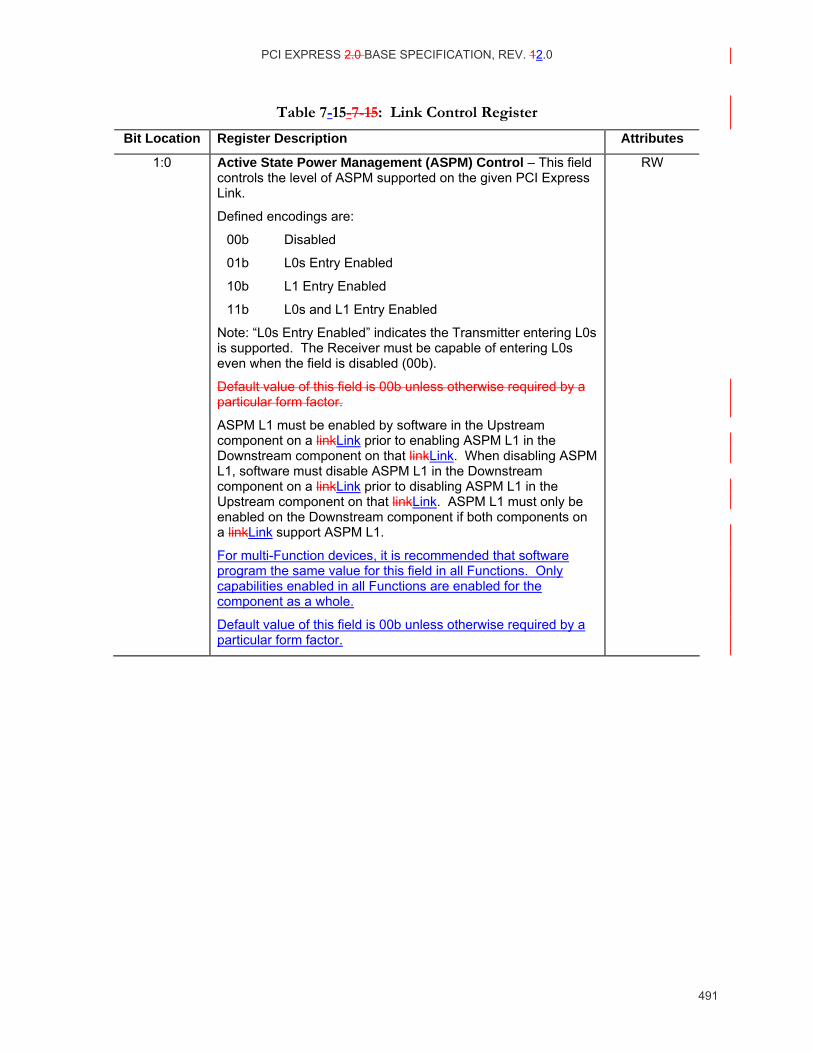
PCI EXPRESS 2.0 BASE SPECIFICATION, REV. 12.0
491
Table 7-15- 7-15: Link Control Register
Bit Location Register Description Attributes
1:0 Active State Power Management (ASPM) Control – This field controls the level of ASPM supported on the given PCI Express Link.
Defined encodings are:
00b Disabled
01b L0s Entry Enabled
10b L1 Entry Enabled
11b L0s and L1 Entry Enabled
Note: “L0s Entry Enabled” indicates the Transmitter entering L0s is supported. The Receiver must be capable of entering L0s even when the field is disabled (00b).
Default value of this field is 00b unless otherwise required by a particular form factor.
ASPM L1 must be enabled by software in the Upstream component on a linkLink prior to enabling ASPM L1 in the Downstream component on that linkLink. When disabling ASPM L1, software must disable ASPM L1 in the Downstream component on a linkLink prior to disabling ASPM L1 in the Upstream component on that linkLink. ASPM L1 must only be enabled on the Downstream component if both components on a linkLink support ASPM L1.
For multi-Function devices, it is recommended that software program the same value for this field in all Functions. Only capabilities enabled in all Functions are enabled for the component as a whole.
Default value of this field is 00b unless otherwise required by a particular form factor.
RW
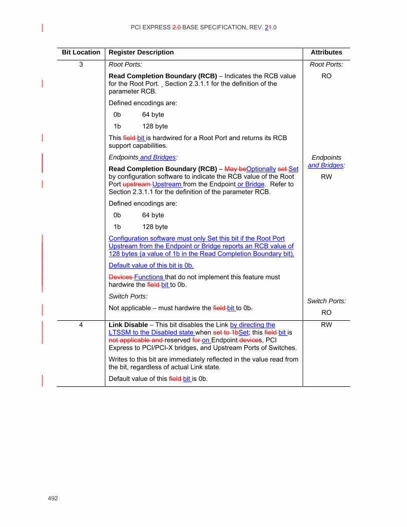
PCI EXPRESS 2.0 BASE SPECIFICATION, REV. 21.0
492
Bit Location Register Description Attributes
3 Root Ports:
Read Completion Boundary (RCB) – Indicates the RCB value for the Root Port. Section 2.3.1.1 for the definition of the parameter RCB.
Defined encodings are:
0b 64 byte
1b 128 byte
This field bit is hardwired for a Root Port and returns its RCB support capabilities.
Endpoints and Bridges:
Read Completion Boundary (RCB) – May beOptionally set Set by configuration software to indicate the RCB value of the Root Port upstream Upstream from the Endpoint or Bridge. Refer to Section 2.3.1.1 for the definition of the parameter RCB.
Defined encodings are:
0b 64 byte
1b 128 byte
Configuration software must only Set this bit if the Root Port Upstream from the Endpoint or Bridge reports an RCB value of 128 bytes (a value of 1b in the Read Completion Boundary bit).
Default value of this bit is 0b.
Devices Functions that do not implement this feature must hardwire the field bit to 0b.
Switch Ports:
Not applicable – must hardwire the field bit to 0b.
Root Ports:
RO
Endpoints and Bridges:
RW
Switch Ports:
RO
4 Link Disable – This bit disables the Link by directing the LTSSM to the Disabled state when set to 1bSet; this field bit is not applicable and reserved for on Endpoint devices, PCI Express to PCI/PCI-X bridges, and Upstream Ports of Switches.
Writes to this bit are immediately reflected in the value read from the bit, regardless of actual Link state.
Default value of this field bit is 0b.
RW
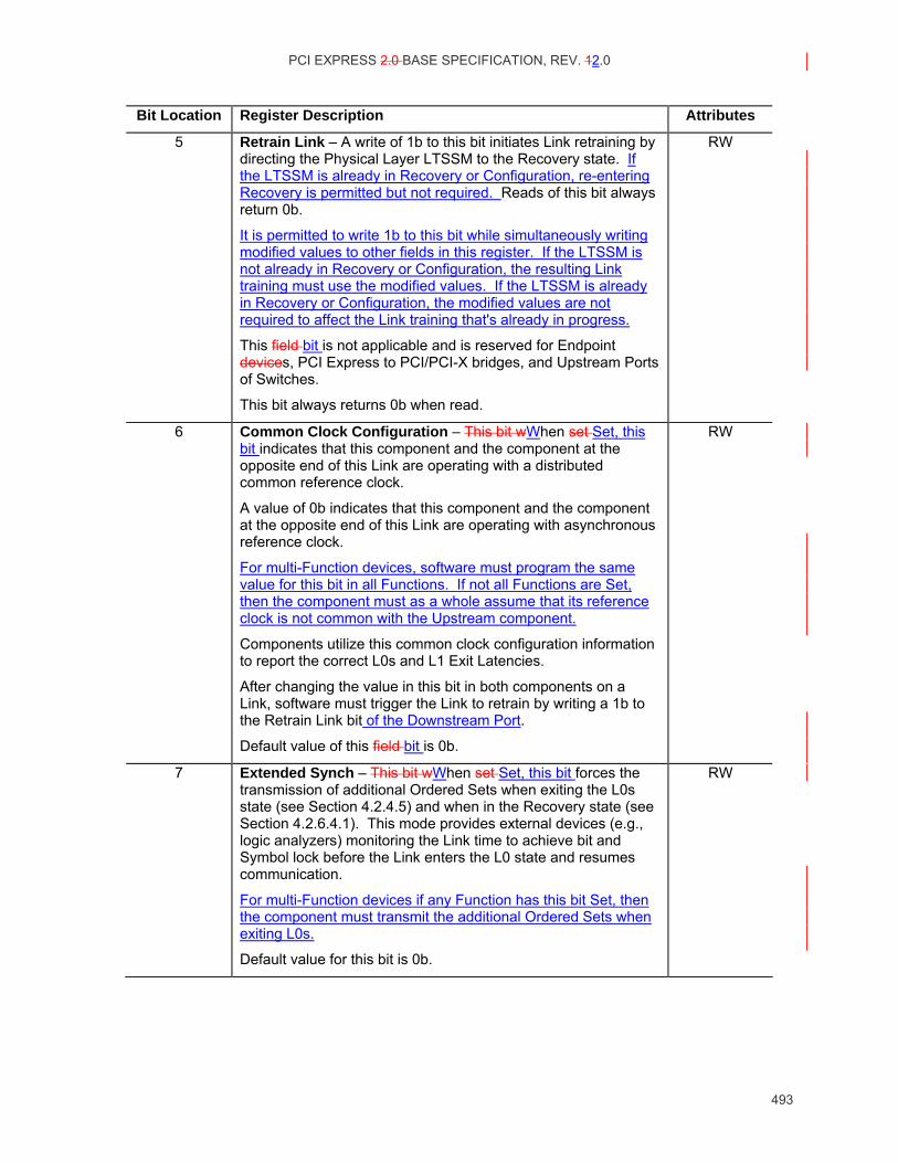
PCI EXPRESS 2.0 BASE SPECIFICATION, REV. 12.0
493
Bit Location Register Description Attributes
5 Retrain Link – A write of 1b to this bit initiates Link retraining by directing the Physical Layer LTSSM to the Recovery state. If the LTSSM is already in Recovery or Configuration, re-entering Recovery is permitted but not required. Reads of this bit always return 0b.
It is permitted to write 1b to this bit while simultaneously writing modified values to other fields in this register. If the LTSSM is not already in Recovery or Configuration, the resulting Link training must use the modified values. If the LTSSM is already in Recovery or Configuration, the modified values are not required to affect the Link training that's already in progress.
This field bit is not applicable and is reserved for Endpoint devices, PCI Express to PCI/PCI-X bridges, and Upstream Ports of Switches.
This bit always returns 0b when read.
RW
6 Common Clock Configuration – This bit wWhen set Set, this bit indicates that this component and the component at the opposite end of this Link are operating with a distributed common reference clock.
A value of 0b indicates that this component and the component at the opposite end of this Link are operating with asynchronous reference clock.
For multi-Function devices, software must program the same value for this bit in all Functions. If not all Functions are Set, then the component must as a whole assume that its reference clock is not common with the Upstream component.
Components utilize this common clock configuration information to report the correct L0s and L1 Exit Latencies.
After changing the value in this bit in both components on a Link, software must trigger the Link to retrain by writing a 1b to the Retrain Link bit of the Downstream Port. Default value of this field bit is 0b.
RW
7 Extended Synch – This bit wWhen set Set, this bit forces the transmission of additional Ordered Sets when exiting the L0s state (see Section 4.2.4.5) and when in the Recovery state (see Section 4.2.6.4.1). This mode provides external devices (e.g., logic analyzers) monitoring the Link time to achieve bit and Symbol lock before the Link enters the L0 state and resumes communication.
For multi-Function devices if any Function has this bit Set, then the component must transmit the additional Ordered Sets when exiting L0s.
Default value for this bit is 0b.
RW
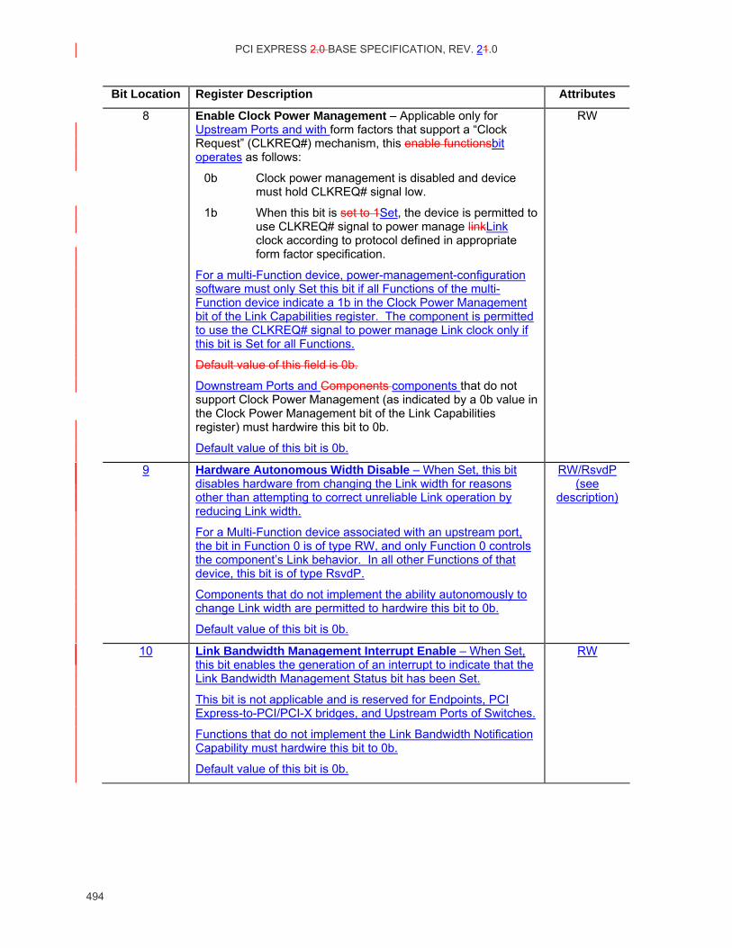
PCI EXPRESS 2.0 BASE SPECIFICATION, REV. 21.0
494
Bit Location Register Description Attributes
8 Enable Clock Power Management – Applicable only for Upstream Ports and with form factors that support a “Clock Request” (CLKREQ#) mechanism, this enable functionsbit operates as follows:
0b Clock power management is disabled and device must hold CLKREQ# signal low.
1b When this bit is set to 1Set, the device is permitted to use CLKREQ# signal to power manage linkLink clock according to protocol defined in appropriate form factor specification.
For a multi-Function device, power-management-configuration software must only Set this bit if all Functions of the multi-Function device indicate a 1b in the Clock Power Management bit of the Link Capabilities register. The component is permitted to use the CLKREQ# signal to power manage Link clock only if this bit is Set for all Functions.
Default value of this field is 0b.
Downstream Ports and Components components that do not support Clock Power Management (as indicated by a 0b value in the Clock Power Management bit of the Link Capabilities register) must hardwire this bit to 0b.
Default value of this bit is 0b.
RW
9 Hardware Autonomous Width Disable – When Set, this bit disables hardware from changing the Link width for reasons other than attempting to correct unreliable Link operation by reducing Link width.
For a Multi-Function device associated with an upstream port, the bit in Function 0 is of type RW, and only Function 0 controls the component’s Link behavior. In all other Functions of that device, this bit is of type RsvdP.
Components that do not implement the ability autonomously to change Link width are permitted to hardwire this bit to 0b.
Default value of this bit is 0b.
RW/RsvdP (see
description)
10 Link Bandwidth Management Interrupt Enable – When Set, this bit enables the generation of an interrupt to indicate that the Link Bandwidth Management Status bit has been Set.
This bit is not applicable and is reserved for Endpoints, PCI Express-to-PCI/PCI-X bridges, and Upstream Ports of Switches.
Functions that do not implement the Link Bandwidth Notification Capability must hardwire this bit to 0b.
Default value of this bit is 0b.
RW
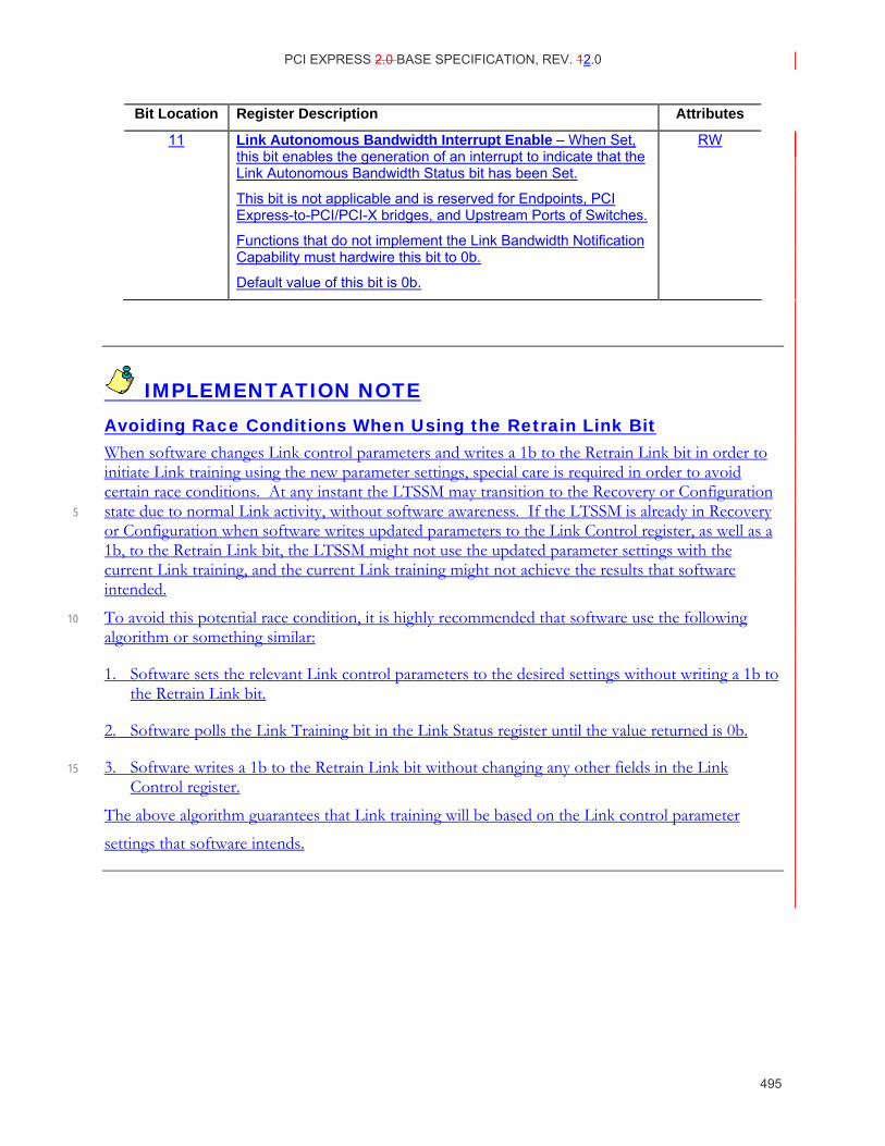
PCI EXPRESS 2.0 BASE SPECIFICATION, REV. 12.0
495
Bit Location Register Description Attributes
11 Link Autonomous Bandwidth Interrupt Enable – When Set, this bit enables the generation of an interrupt to indicate that the Link Autonomous Bandwidth Status bit has been Set.
This bit is not applicable and is reserved for Endpoints, PCI Express-to-PCI/PCI-X bridges, and Upstream Ports of Switches.
Functions that do not implement the Link Bandwidth Notification Capability must hardwire this bit to 0b.
Default value of this bit is 0b.
RW
IMPLEMENTATION NOTE Avoiding Race Conditions When Using the Retrain Link Bit When software changes Link control parameters and writes a 1b to the Retrain Link bit in order to initiate Link training using the new parameter settings, special care is required in order to avoid certain race conditions. At any instant the LTSSM may transition to the Recovery or Configuration state due to normal Link activity, without software awareness. If the LTSSM is already in Recovery 5 or Configuration when software writes updated parameters to the Link Control register, as well as a 1b, to the Retrain Link bit, the LTSSM might not use the updated parameter settings with the current Link training, and the current Link training might not achieve the results that software intended.
To avoid this potential race condition, it is highly recommended that software use the following 10 algorithm or something similar:
1. Software sets the relevant Link control parameters to the desired settings without writing a 1b to the Retrain Link bit.
2. Software polls the Link Training bit in the Link Status register until the value returned is 0b.
3. Software writes a 1b to the Retrain Link bit without changing any other fields in the Link 15 Control register.
The above algorithm guarantees that Link training will be based on the Link control parameter
settings that software intends.
PCI EXPRESS 2.0 BASE SPECIFICATION, REV. 21.0
496
IMPLEMENTATION NOTE Use of the Slot Clock Configuration and Common Clock Configuration Bits In order to accurately determine the common clocking configuration of components on opposite ends of a Link that crosses a connector, there are two pieces of information that are required. The following description defines these requirements.
The first necessary piece of information is whether the Port that connects to the slot uses a clock that has a common source and therefore constant phase relationship to the clock signal provided on 5 the slot. This information is provided by the system side component through a hardware initialized bit (Slot Clock Configuration) in its Link Status register. Note that some electromechanical form factor specifications may require the Port that connects to the slot use a clock that has a common source to the clock signal provided on the slot.
The second necessary piece of information is whether the device component on the adapter uses the 10 clock supplied on the slot or one generated locally on the adapter. It is tThe adapter design and layout that will determine whether or not the Endpoint component is connected to the clock source provided by the slot. An Endpoint component going onto this adapter should have some hardware initialized method for the adapter design/designer to indicate the configuration used for this particular adapter design. This information is reported by the Endpoint device in bit 12 (Slot Clock 15 Configuration) of itsin the Link Status register of each Function in the Upstream Port. Note that some electromechanical form factor specifications may require the Port on the adapter to use the clock signal provided on the connector.
System firmware or software will read this value from the components on both ends of a physical Link. If both devices components report the use of a common clock connection this 20 firmware/software will program bit 6 (Common Clock Configuration) of the Link Control register to a one on both components connected to the Link. Each component uses this bit to determine the length of time required to re-synch its Receiver to the opposing component's Transmitter when exiting L0s.
This value is reported as a time value in bits 12-14 of the Link Capabilities register (offset 0Ch) and 25 is sent to the opposing Transmitter as part if the initialization process as N_FTS. Components would be expected to require much longer synch times without common clocking and would therefore report a longer L0s exit latency in bits 12-14 of the Link Capabilities register and would send a larger number for N_FTS during training. This forces a requirement that whatever software changes this bit should force a Link retrain in order to get the correct N-FTS set for the Receivers at 30 both ends of the Link.
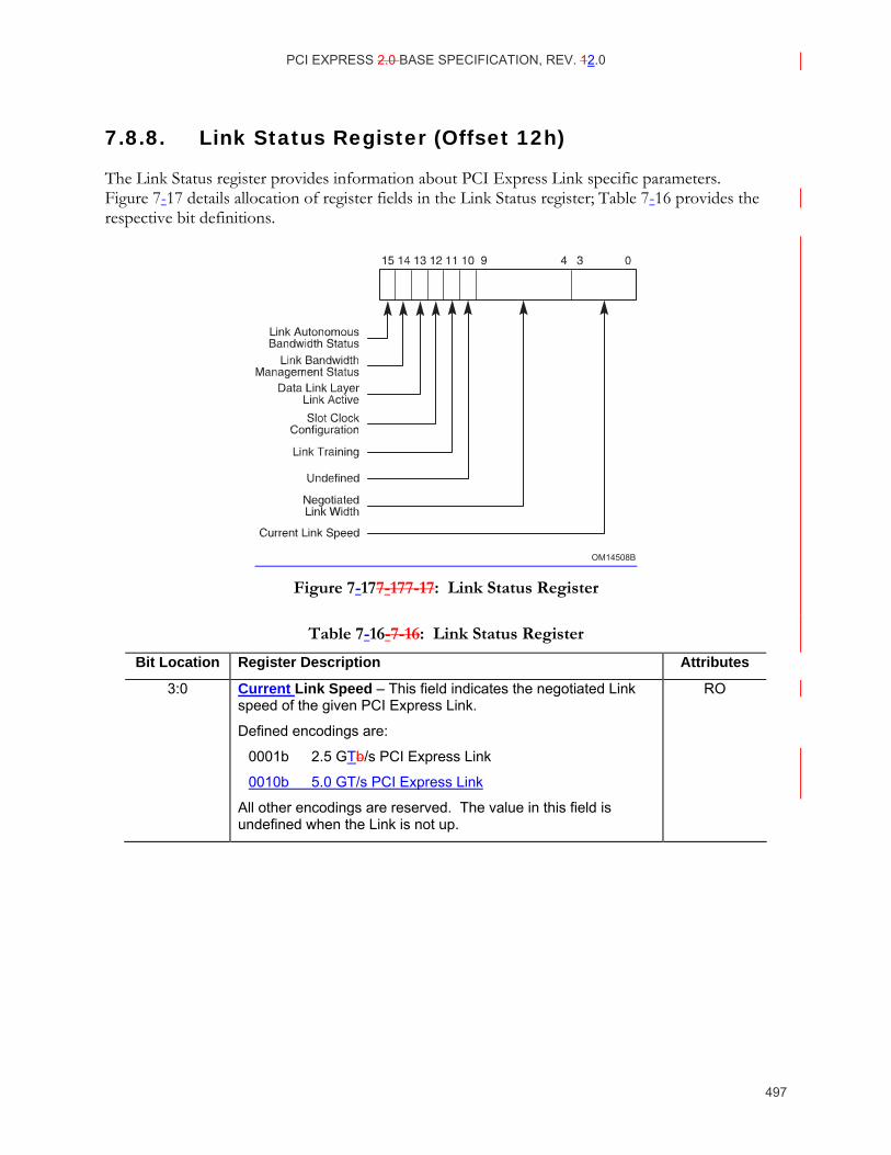
PCI EXPRESS 2.0 BASE SPECIFICATION, REV. 12.0
497
7.8.8. Link Status Register (Offset 12h)
The Link Status register provides information about PCI Express Link specific parameters. Figure 7-17 details allocation of register fields in the Link Status register; Table 7-16 provides the respective bit definitions.
OM14508B
Figure 7-177-17 7-17: Link Status Register
Table 7-16- 7-16: Link Status Register
Bit Location Register Description Attributes
3:0 Current Link Speed – This field indicates the negotiated Link speed of the given PCI Express Link.
Defined encodings are:
0001b 2.5 GTb/s PCI Express Link
0010b 5.0 GT/s PCI Express Link
All other encodings are reserved. The value in this field is undefined when the Link is not up.
RO
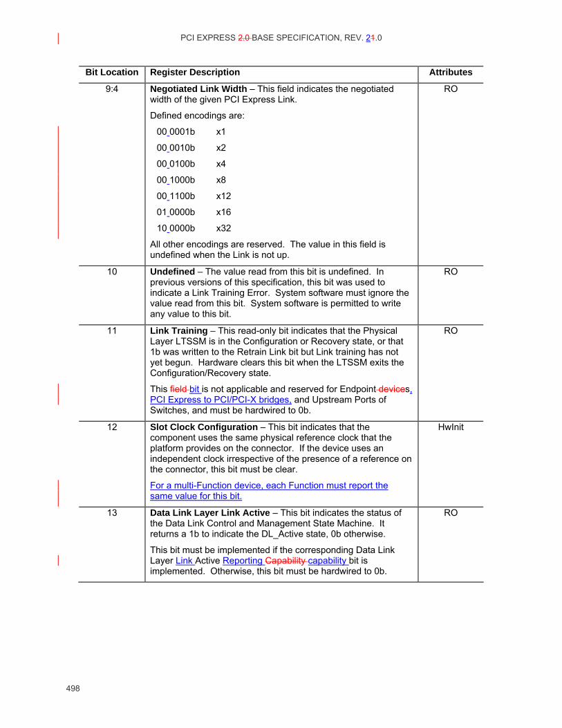
PCI EXPRESS 2.0 BASE SPECIFICATION, REV. 21.0
498
Bit Location Register Description Attributes
9:4 Negotiated Link Width – This field indicates the negotiated width of the given PCI Express Link.
Defined encodings are:
00 0001b x1
00 0010b x2
00 0100b x4
00 1000b x8
00 1100b x12
01 0000b x16
10 0000b x32
All other encodings are reserved. The value in this field is undefined when the Link is not up.
RO
10 Undefined – The value read from this bit is undefined. In previous versions of this specification, this bit was used to indicate a Link Training Error. System software must ignore the value read from this bit. System software is permitted to write any value to this bit.
RO
11 Link Training – This read-only bit indicates that the Physical Layer LTSSM is in the Configuration or Recovery state, or that 1b was written to the Retrain Link bit but Link training has not yet begun. Hardware clears this bit when the LTSSM exits the Configuration/Recovery state.
This field bit is not applicable and reserved for Endpoint devices, PCI Express to PCI/PCI-X bridges, and Upstream Ports of Switches, and must be hardwired to 0b.
RO
12 Slot Clock Configuration – This bit indicates that the component uses the same physical reference clock that the platform provides on the connector. If the device uses an independent clock irrespective of the presence of a reference on the connector, this bit must be clear.
For a multi-Function device, each Function must report the same value for this bit.
HwInit
13 Data Link Layer Link Active – This bit indicates the status of the Data Link Control and Management State Machine. It returns a 1b to indicate the DL_Active state, 0b otherwise.
This bit must be implemented if the corresponding Data Link Layer Link Active Reporting Capability capability bit is implemented. Otherwise, this bit must be hardwired to 0b.
RO
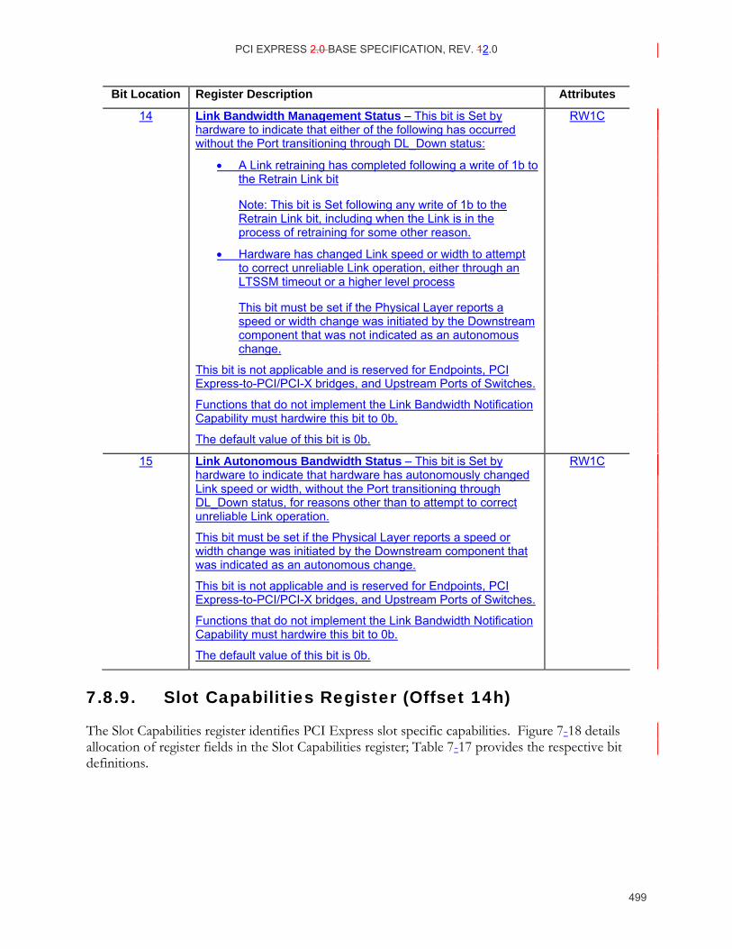
PCI EXPRESS 2.0 BASE SPECIFICATION, REV. 12.0
499
Bit Location Register Description Attributes
14 Link Bandwidth Management Status – This bit is Set by hardware to indicate that either of the following has occurred without the Port transitioning through DL_Down status:
• A Link retraining has completed following a write of 1b to the Retrain Link bit
Note: This bit is Set following any write of 1b to the Retrain Link bit, including when the Link is in the process of retraining for some other reason.
• Hardware has changed Link speed or width to attempt to correct unreliable Link operation, either through an LTSSM timeout or a higher level process
This bit must be set if the Physical Layer reports a speed or width change was initiated by the Downstream component that was not indicated as an autonomous change.
This bit is not applicable and is reserved for Endpoints, PCI Express-to-PCI/PCI-X bridges, and Upstream Ports of Switches.
Functions that do not implement the Link Bandwidth Notification Capability must hardwire this bit to 0b.
The default value of this bit is 0b.
RW1C
15 Link Autonomous Bandwidth Status – This bit is Set by hardware to indicate that hardware has autonomously changed Link speed or width, without the Port transitioning through DL_Down status, for reasons other than to attempt to correct unreliable Link operation.
This bit must be set if the Physical Layer reports a speed or width change was initiated by the Downstream component that was indicated as an autonomous change.
This bit is not applicable and is reserved for Endpoints, PCI Express-to-PCI/PCI-X bridges, and Upstream Ports of Switches.
Functions that do not implement the Link Bandwidth Notification Capability must hardwire this bit to 0b.
The default value of this bit is 0b.
RW1C
7.8.9. Slot Capabilities Register (Offset 14h)
The Slot Capabilities register identifies PCI Express slot specific capabilities. Figure 7-18 details allocation of register fields in the Slot Capabilities register; Table 7-17 provides the respective bit definitions.
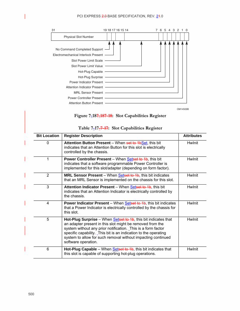
PCI EXPRESS 2.0 BASE SPECIFICATION, REV. 21.0
500
OM14509B
Attention Button Present
Attention Indicator Present
MRL Sensor Present
Hot-Plug Surprise
Power Controller Present
Hot-Plug Capable
Power Indicator Present
Slot Power Limit Value
No Command Completed Support
Electromechanical Interlock Present
Slot Power Limit Scale
Physical Slot Number
31 17 16 15 14 7 6 5 4 3 2 1 019 18
Figure 7-187-18 7-18: Slot Capabilities Register
Table 7-17- 7-17: Slot Capabilities Register
Bit Location Register Description Attributes
0 Attention Button Present – When set to 1bSet, this bit indicates that an Attention Button for this slot is electrically controlled by the chassis.
HwInit
1 Power Controller Present – When Setset to 1b, this bit indicates that a software programmable Power Controller is implemented for this slot/adapter (depending on form factor).
HwInit
2 MRL Sensor Present – When Setset to 1b, this bit indicates that an MRL Sensor is implemented on the chassis for this slot.
HwInit
3 Attention Indicator Present – When Setset to 1b, this bit indicates that an Attention Indicator is electrically controlled by the chassis.
HwInit
4 Power Indicator Present – When Setset to 1b, this bit indicates that a Power Indicator is electrically controlled by the chassis for this slot.
HwInit
5 Hot-Plug Surprise – When Setset to 1b, this bit indicates that an adapter present in this slot might be removed from the system without any prior notification. This is a form factor specific capability. This bit is an indication to the operating system to allow for such removal without impacting continued software operation.
HwInit
6 Hot-Plug Capable – When Setset to 1b, this bit indicates that this slot is capable of supporting hot-plug operations.
HwInit
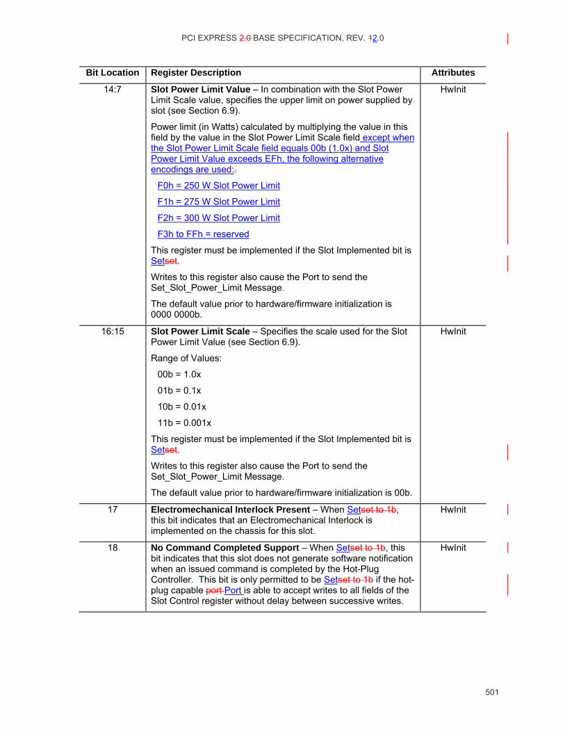
PCI EXPRESS 2.0 BASE SPECIFICATION, REV. 12.0
501
Bit Location Register Description Attributes
14:7 Slot Power Limit Value – In combination with the Slot Power Limit Scale value, specifies the upper limit on power supplied by slot (see Section 6.9).
Power limit (in Watts) calculated by multiplying the value in this field by the value in the Slot Power Limit Scale field except when the Slot Power Limit Scale field equals 00b (1.0x) and Slot Power Limit Value exceeds EFh, the following alternative encodings are used:.
F0h = 250 W Slot Power Limit
F1h = 275 W Slot Power Limit
F2h = 300 W Slot Power Limit
F3h to FFh = reserved
This register must be implemented if the Slot Implemented bit is Setset.
Writes to this register also cause the Port to send the Set_Slot_Power_Limit Message.
The default value prior to hardware/firmware initialization is 0000 0000b.
HwInit
16:15 Slot Power Limit Scale – Specifies the scale used for the Slot Power Limit Value (see Section 6.9).
Range of Values:
00b = 1.0x
01b = 0.1x
10b = 0.01x
11b = 0.001x
This register must be implemented if the Slot Implemented bit is Setset.
Writes to this register also cause the Port to send the Set_Slot_Power_Limit Message.
The default value prior to hardware/firmware initialization is 00b.
HwInit
17 Electromechanical Interlock Present – When Setset to 1b, this bit indicates that an Electromechanical Interlock is implemented on the chassis for this slot.
HwInit
18 No Command Completed Support – When Setset to 1b, this bit indicates that this slot does not generate software notification when an issued command is completed by the Hot-Plug Controller. This bit is only permitted to be Setset to 1b if the hot-plug capable port Port is able to accept writes to all fields of the Slot Control register without delay between successive writes.
HwInit
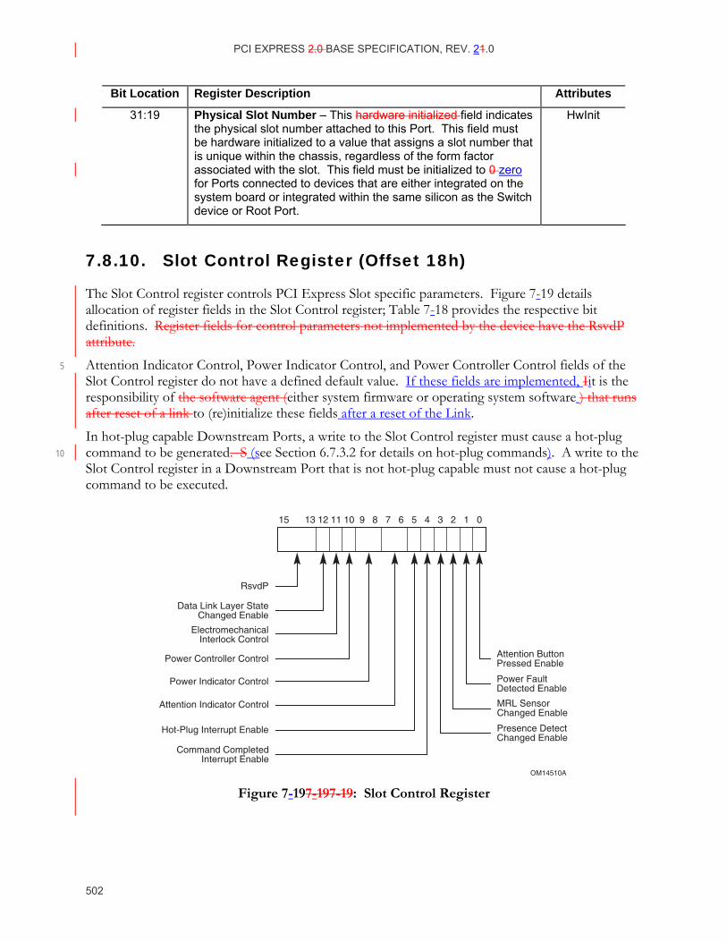
PCI EXPRESS 2.0 BASE SPECIFICATION, REV. 21.0
502
Bit Location Register Description Attributes
31:19 Physical Slot Number – This hardware initialized field indicates the physical slot number attached to this Port. This field must be hardware initialized to a value that assigns a slot number that is unique within the chassis, regardless of the form factor associated with the slot. This field must be initialized to 0 zero for Ports connected to devices that are either integrated on the system board or integrated within the same silicon as the Switch device or Root Port.
HwInit
7.8.10. Slot Control Register (Offset 18h)
The Slot Control register controls PCI Express Slot specific parameters. Figure 7-19 details allocation of register fields in the Slot Control register; Table 7-18 provides the respective bit definitions. Register fields for control parameters not implemented by the device have the RsvdP attribute.
Attention Indicator Control, Power Indicator Control, and Power Controller Control fields of the 5 Slot Control register do not have a defined default value. If these fields are implemented, Iit is the responsibility of the software agent (either system firmware or operating system software ) that runs after reset of a link to (re)initialize these fields after a reset of the Link.
In hot-plug capable Downstream Ports, a write to the Slot Control register must cause a hot-plug command to be generated. S (see Section 6.7.3.2 for details on hot-plug commands). A write to the 10 Slot Control register in a Downstream Port that is not hot-plug capable must not cause a hot-plug command to be executed.
OM14510A
Presence DetectChanged Enable
MRL SensorChanged Enable
Power FaultDetected Enable
Attention ButtonPressed Enable
Attention Indicator Control
Power Indicator Control
Command CompletedInterrupt Enable
Hot-Plug Interrupt Enable
RsvdP
Data Link Layer StateChanged Enable
ElectromechanicalInterlock Control
Power Controller Control
15 11 10 9 8 7 6 5 4 3 2 1 013 12
Figure 7-197-19 7-19: Slot Control Register
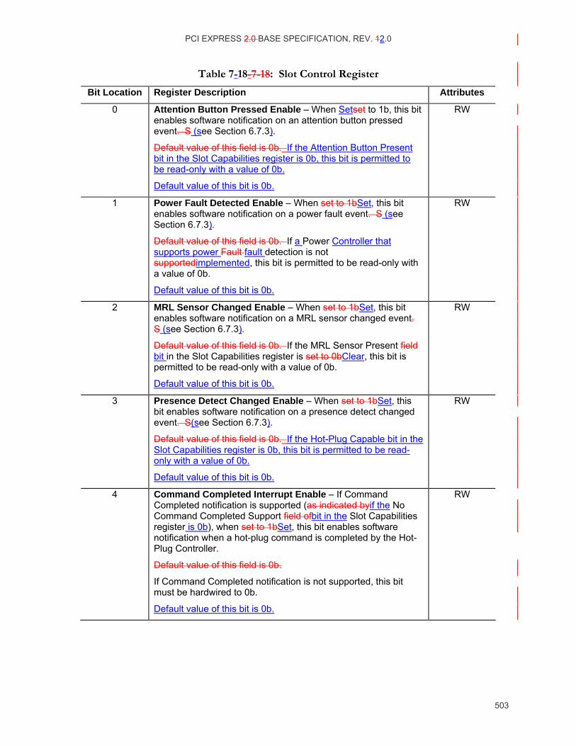
PCI EXPRESS 2.0 BASE SPECIFICATION, REV. 12.0
503
Table 7-18- 7-18: Slot Control Register
Bit Location Register Description Attributes
0 Attention Button Pressed Enable – When Setset to 1b, this bit enables software notification on an attention button pressed event. S (see Section 6.7.3).
Default value of this field is 0b. If the Attention Button Present bit in the Slot Capabilities register is 0b, this bit is permitted to be read-only with a value of 0b.
Default value of this bit is 0b.
RW
1 Power Fault Detected Enable – When set to 1bSet, this bit enables software notification on a power fault event. S (see Section 6.7.3).
Default value of this field is 0b. If a Power Controller that supports power Fault fault detection is not supportedimplemented, this bit is permitted to be read-only with a value of 0b.
Default value of this bit is 0b.
RW
2 MRL Sensor Changed Enable – When set to 1bSet, this bit enables software notification on a MRL sensor changed event. S (see Section 6.7.3).
Default value of this field is 0b. If the MRL Sensor Present field bit in the Slot Capabilities register is set to 0bClear, this bit is permitted to be read-only with a value of 0b.
Default value of this bit is 0b.
RW
3 Presence Detect Changed Enable – When set to 1bSet, this bit enables software notification on a presence detect changed event. S(see Section 6.7.3).
Default value of this field is 0b. If the Hot-Plug Capable bit in the Slot Capabilities register is 0b, this bit is permitted to be read-only with a value of 0b.
Default value of this bit is 0b.
RW
4 Command Completed Interrupt Enable – If Command Completed notification is supported (as indicated byif the No Command Completed Support field ofbit in the Slot Capabilities register is 0b), when set to 1bSet, this bit enables software notification when a hot-plug command is completed by the Hot-Plug Controller.
Default value of this field is 0b.
If Command Completed notification is not supported, this bit must be hardwired to 0b.
Default value of this bit is 0b.
RW

PCI EXPRESS 2.0 BASE SPECIFICATION, REV. 21.0
504
Bit Location Register Description Attributes
5 Hot-Plug Interrupt Enable – When set to 1bSet, this bit enables generation of an interrupt on enabled hot-plug events.
Default value of this field is 0b. If the Hot Plug Capable field bit in the Slot Capabilities register is set to 0bClear, this bit is permitted to be read-only with a value of 0b.
Default value of this bit is 0b.
RW
7:6 Attention Indicator Control – If an Attention Indicator is implemented, writes to this field set the Attention Indicator to the written Written state.
Reads of this field must reflect the value from the latest write, even if the corresponding hot-plug command is not complete, unless software issues a write without waiting for the previous command to complete in which case the read value is undefined.
Defined encodings are:
00b Reserved
01b On
10b Blink
11b Off
Note: The default value of this field must be one of the non-Reserved values. If the Attention Indicator Present bit in the Slot Capabilities register is 0b, this bit is permitted to be read-only with a value of 00b.
RW
9:8 Power Indicator Control – If a Power Indicator is implemented, writes to this field set the Power Indicator to the written Written state. Reads of this field must reflect the value from the latest write, even if the corresponding hot-plug command is not complete, unless software issues a write without waiting for the previous command to complete in which case the read value is undefined.
Defined encodings are:
00b Reserved
01b On
10b Blink
11b Off
Note: The default value of this field must be one of the non-Reserved values. If the Power Indicator Present bit in the Slot Capabilities register is 0b, this bit is permitted to be read-only with a value of 00b.
RW

PCI EXPRESS 2.0 BASE SPECIFICATION, REV. 12.0
505
Bit Location Register Description Attributes
10 Power Controller Control – If a Power Controller is implemented, this field bit when written sets the power state of the slot per the defined encodings. Reads of this field bit must reflect the value from the latest write, even if the corresponding hot-plug command is not complete, unless software issues a write without waiting for the previous command to complete in which case the read value is undefined.
Depending on the form factor, the power is turned on/off either to the slot or within the adapter. Note that in some cases the power controller may autonomously remove slot power or not respond to a power-up request based on a detected fault condition, independent of the Power Controller Control setting.
The defined encodings are:
0b Power On
1b Power Off
If the Power Controller Implemented bitfield in the Slot Capabilities register is set to 0bClear, then writes to this bitfield have no effect and the read value of this bitfield is undefined.
RW
11 Electromechanical Interlock Control – If an Electromechanical Interlock is implemented, a write of 1b to this bitfield causes the state of the interlock to toggle. A write of 0b to this bitfield has no effect. A read to of this register bit always returns a 0b.
RW
12 Data Link Layer State Changed Enable – If the Data Link Layer Link Active capability Capability is implemented, when set to 1bSet, this field bit enables software notification when Data Link Layer Link Active Reporting field bit is changed.
If the Data Link Layer Link Active Reporting Capability is not implemented, this bit is permitted to be read-only with a value of 0b.
Default value of this bit is 0b.
RW
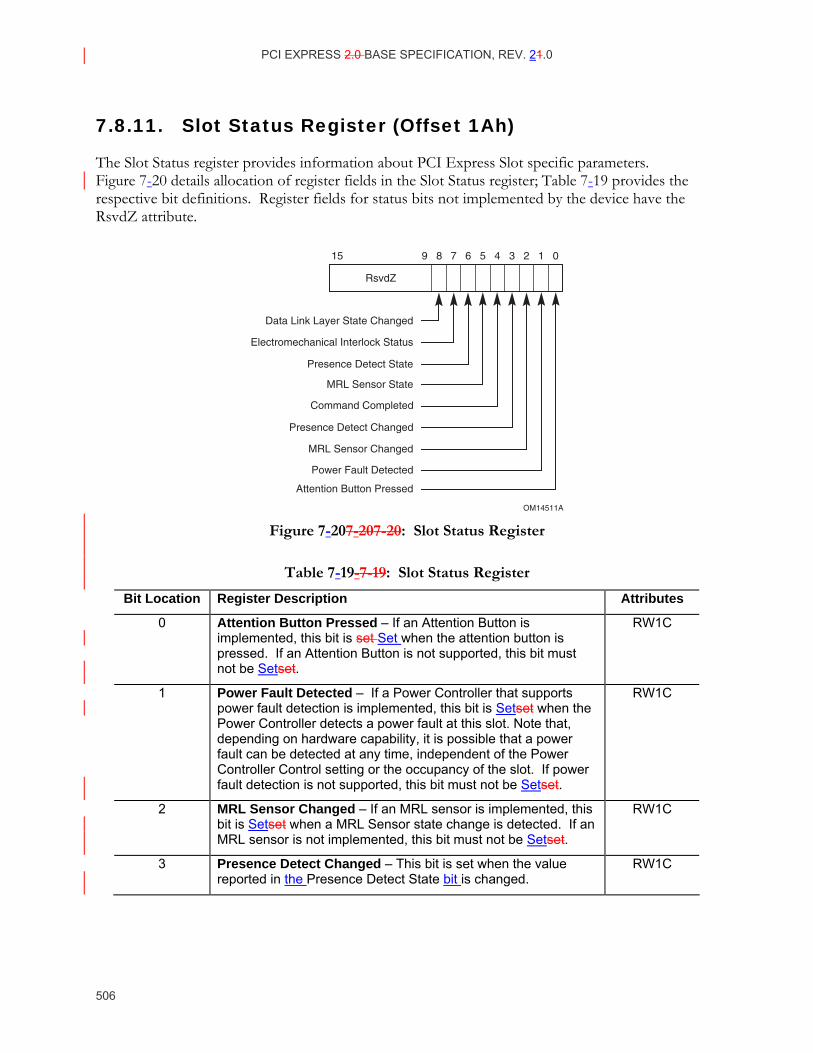
PCI EXPRESS 2.0 BASE SPECIFICATION, REV. 21.0
506
7.8.11. Slot Status Register (Offset 1Ah)
The Slot Status register provides information about PCI Express Slot specific parameters. Figure 7-20 details allocation of register fields in the Slot Status register; Table 7-19 provides the respective bit definitions. Register fields for status bits not implemented by the device have the RsvdZ attribute.
OM14511A
Presence Detect Changed
Power Fault Detected
Command Completed
MRL Sensor State
MRL Sensor Changed
Attention Button Pressed
Presence Detect State
Data Link Layer State Changed
RsvdZ
15 7 6 5 4 3 2 1 09 8
Electromechanical Interlock Status
Figure 7-207-20 7-20: Slot Status Register
Table 7-19- 7-19: Slot Status Register
Bit Location Register Description Attributes
0 Attention Button Pressed – If an Attention Button is implemented, this bit is set Set when the attention button is pressed. If an Attention Button is not supported, this bit must not be Setset.
RW1C
1 Power Fault Detected – If a Power Controller that supports power fault detection is implemented, this bit is Setset when the Power Controller detects a power fault at this slot. Note that, depending on hardware capability, it is possible that a power fault can be detected at any time, independent of the Power Controller Control setting or the occupancy of the slot. If power fault detection is not supported, this bit must not be Setset.
RW1C
2 MRL Sensor Changed – If an MRL sensor is implemented, this bit is Setset when a MRL Sensor state change is detected. If an MRL sensor is not implemented, this bit must not be Setset.
RW1C
3 Presence Detect Changed – This bit is set when the value reported in the Presence Detect State bit is changed.
RW1C

PCI EXPRESS 2.0 BASE SPECIFICATION, REV. 12.0
507
Bit Location Register Description Attributes
4 Command Completed – If Command Completed notification is supported (as indicated byif the No Command Completed Support field bit of in the Slot Capabilities register is 0b), this bit is Set set when a hot-plug command has completed and the Hot-Plug Controller is ready to accept a subsequent command. The Command Completed status bit is Setset as an indication to host software that the Hot-Plug Controller has processed the previous command and is ready to receive the next command; it provides no guarantee that the action corresponding to the command is complete.
If Command Completed notification is not supported, this bit must be hardwired to 0b.
RW1C
5 MRL Sensor State – This register bit reports the status of the MRL sensor if implemented.
Defined encodings are:
0b MRL Closed
1b MRL Open
RO
6 Presence Detect State – This bit indicates the presence of an adapter in the slot, reflected by the logical “OR” of the Physical Layer in-band presence detect mechanism and, if present, any out-of-band presence detect mechanism defined for the slot’s corresponding form factor. Note that the in-band presence detect mechanism requires that power be applied to an adapter for its presence to be detected. Consequently, form factors that require a power controller for hot-plug must implement a physical pin presence detect mechanism.
Defined encodings are:
0b Slot Empty
1b Card Present in slot
This register bit must be implemented on all Downstream Ports that implement slots. For Downstream Ports not connected to slots (where the Slot Implemented bit of the PCI Express Capabilities register is 0b), this bit must return be hardwired to 1b.
RO
7 Electromechanical Interlock Status – If an Electromechanical Interlock is implemented, this bit indicates the current status of the Electromechanical Interlock.
Defined encodings are:
0b Electromechanical Interlock Disengaged
1b Electromechanical Interlock Engaged
RO
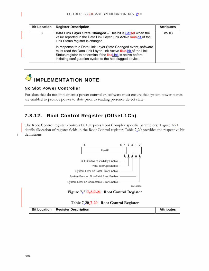
PCI EXPRESS 2.0 BASE SPECIFICATION, REV. 21.0
508
Bit Location Register Description Attributes
8 Data Link Layer State Changed – This bit is Setset when the value reported in the Data Link Layer Link Active field bit of the Link Status register is changed.
In response to a Data Link Layer State Changed event, software must read the Data Link Layer Link Active field bit of the Link Status register to determine if the linkLink is active before initiating configuration cycles to the hot plugged device.
RW1C
IMPLEMENTATION NOTE No Slot Power Controller For slots that do not implement a power controller, software must ensure that system power planes are enabled to provide power to slots prior to reading presence detect state.
7.8.12. Root Control Register (Offset 1Ch)
The Root Control register controls PCI Express Root Complex specific parameters. Figure 7-21 details allocation of register fields in the Root Control register; Table 7-20 provides the respective bit definitions. 5
OM14512A
System Error on Correctable Error Enable
System Error on Non-Fatal Error Enable
System Error on Fatal Error Enable
PME Interrupt Enable
CRS Software Visibility Enable
RsvdP
15 4 3 2 1 05
Figure 7-217-21 7-21: Root Control Register
Table 7-20- 7-20: Root Control Register
Bit Location Register Description Attributes
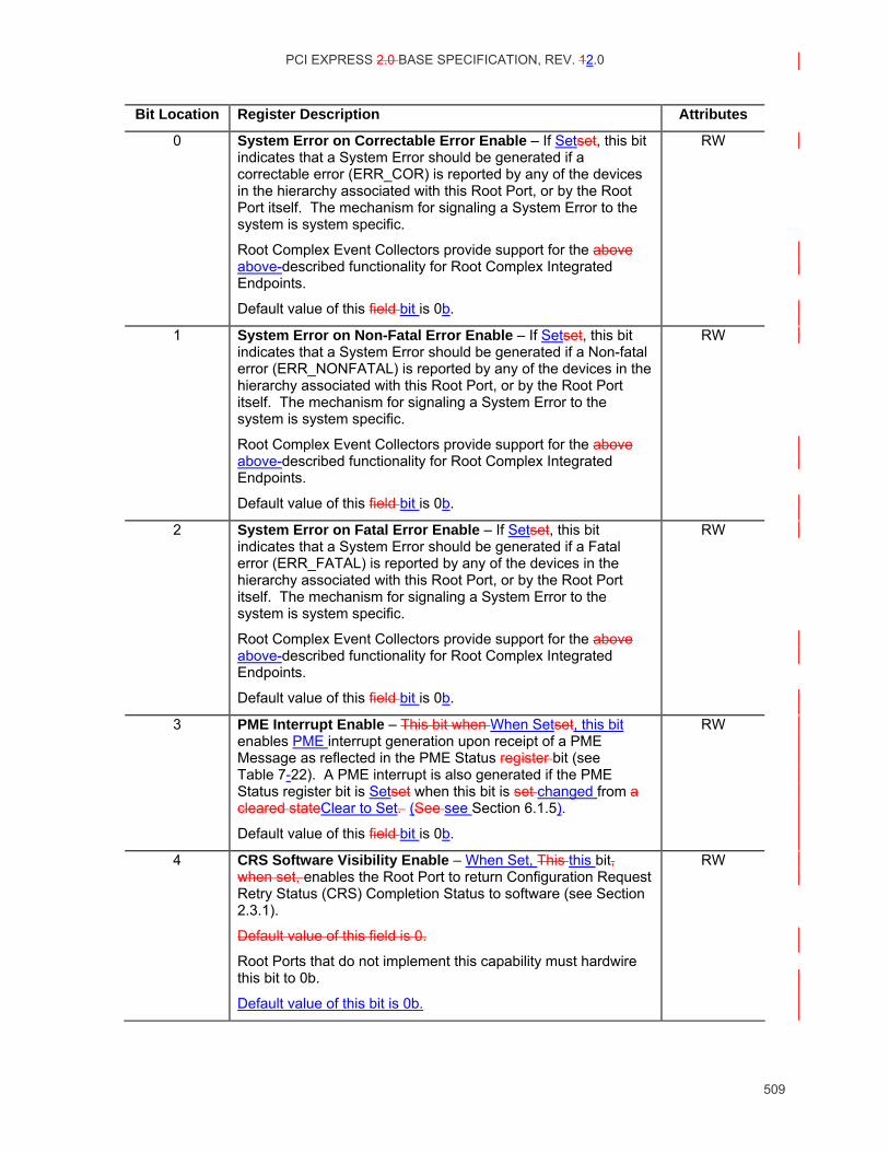
PCI EXPRESS 2.0 BASE SPECIFICATION, REV. 12.0
509
Bit Location Register Description Attributes
0 System Error on Correctable Error Enable – If Setset, this bit indicates that a System Error should be generated if a correctable error (ERR_COR) is reported by any of the devices in the hierarchy associated with this Root Port, or by the Root Port itself. The mechanism for signaling a System Error to the system is system specific.
Root Complex Event Collectors provide support for the above above-described functionality for Root Complex Integrated Endpoints.
Default value of this field bit is 0b.
RW
1 System Error on Non-Fatal Error Enable – If Setset, this bit indicates that a System Error should be generated if a Non-fatal error (ERR_NONFATAL) is reported by any of the devices in the hierarchy associated with this Root Port, or by the Root Port itself. The mechanism for signaling a System Error to the system is system specific.
Root Complex Event Collectors provide support for the above above-described functionality for Root Complex Integrated Endpoints.
Default value of this field bit is 0b.
RW
2 System Error on Fatal Error Enable – If Setset, this bit indicates that a System Error should be generated if a Fatal error (ERR_FATAL) is reported by any of the devices in the hierarchy associated with this Root Port, or by the Root Port itself. The mechanism for signaling a System Error to the system is system specific.
Root Complex Event Collectors provide support for the above above-described functionality for Root Complex Integrated Endpoints.
Default value of this field bit is 0b.
RW
3 PME Interrupt Enable – This bit when When Setset, this bit enables PME interrupt generation upon receipt of a PME Message as reflected in the PME Status register bit (see Table 7-22). A PME interrupt is also generated if the PME Status register bit is Setset when this bit is set changed from a cleared stateClear to Set. (See see Section 6.1.5).
Default value of this field bit is 0b.
RW
4 CRS Software Visibility Enable – When Set, This this bit, when set, enables the Root Port to return Configuration Request Retry Status (CRS) Completion Status to software (see Section 2.3.1).
Default value of this field is 0.
Root Ports that do not implement this capability must hardwire this bit to 0b.
Default value of this bit is 0b.
RW
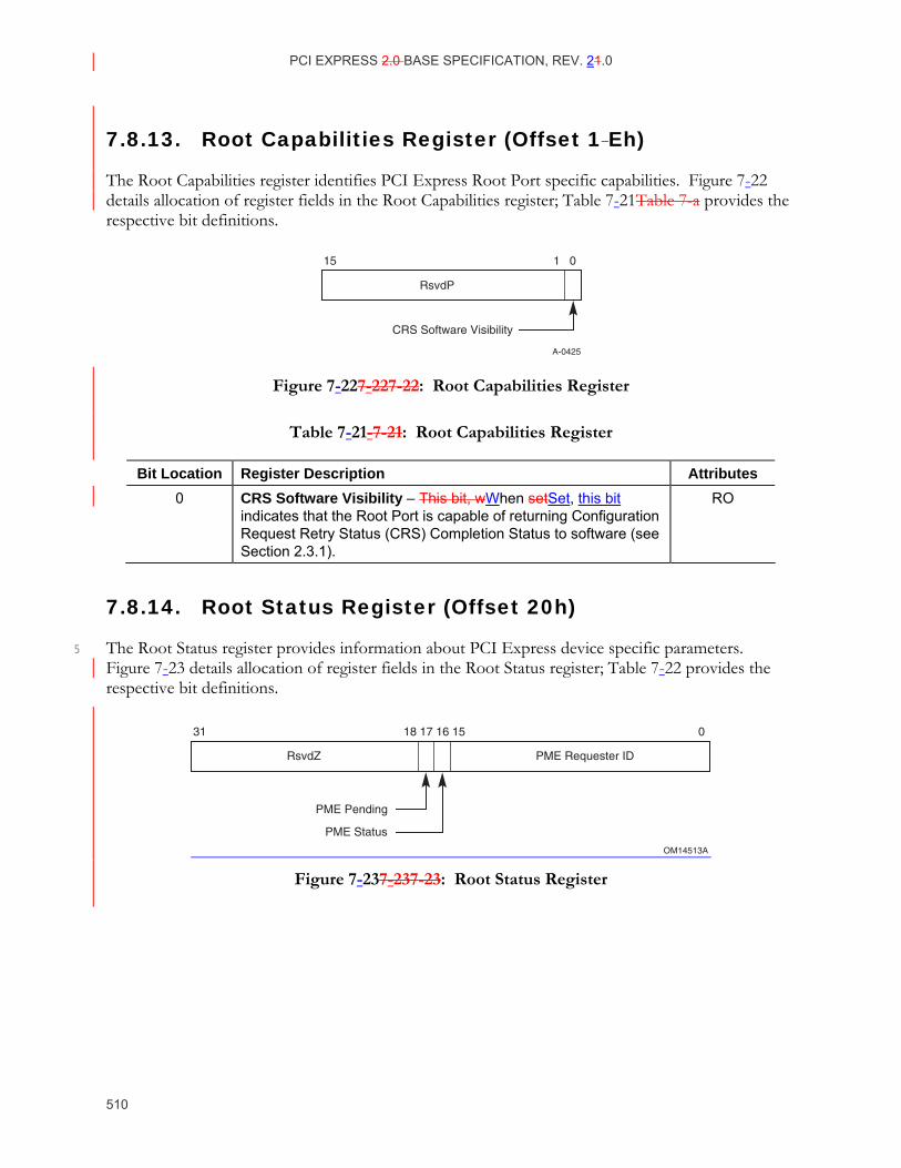
PCI EXPRESS 2.0 BASE SPECIFICATION, REV. 21.0
510
7.8.13. Root Capabilities Register (Offset 1 Eh)
The Root Capabilities register identifies PCI Express Root Port specific capabilities. Figure 7-22 details allocation of register fields in the Root Capabilities register; Table 7-21Table 7-a provides the respective bit definitions.
A-0425
RsvdP
CRS Software Visibility
15 1 0
Figure 7-227-22 7-22: Root Capabilities Register
Table 7-21- 7-21: Root Capabilities Register
Bit Location Register Description Attributes 0 CRS Software Visibility – This bit, wWhen setSet, this bit
indicates that the Root Port is capable of returning Configuration Request Retry Status (CRS) Completion Status to software (see Section 2.3.1).
RO
7.8.14. Root Status Register (Offset 20h)
The Root Status register provides information about PCI Express device specific parameters. 5 Figure 7-23 details allocation of register fields in the Root Status register; Table 7-22 provides the respective bit definitions.
OM14513A
PME Status
PME Pending
RsvdZ PME Requester ID
31 17 16 15 018
Figure 7-237-23 7-23: Root Status Register
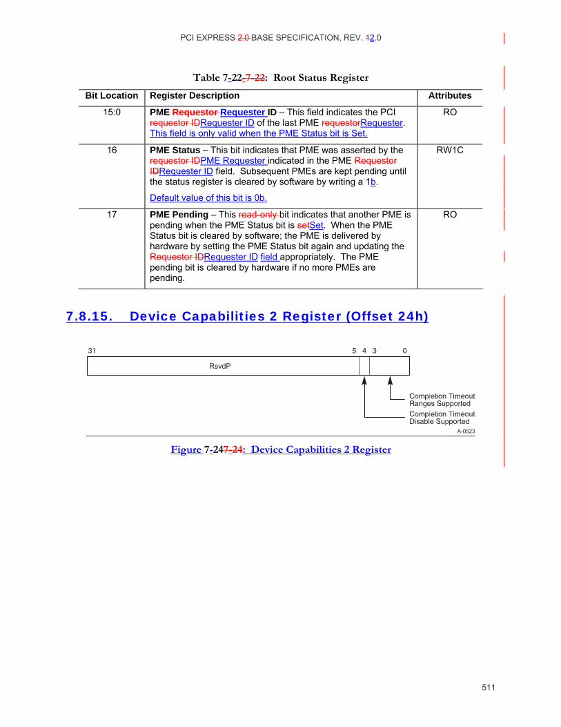
PCI EXPRESS 2.0 BASE SPECIFICATION, REV. 12.0
511
Table 7-22- 7-22: Root Status Register
Bit Location Register Description Attributes
15:0 PME Requestor Requester ID – This field indicates the PCI requestor IDRequester ID of the last PME requestorRequester. This field is only valid when the PME Status bit is Set.
RO
16 PME Status – This bit indicates that PME was asserted by the requestor IDPME Requester indicated in the PME Requestor IDRequester ID field. Subsequent PMEs are kept pending until the status register is cleared by software by writing a 1b.
Default value of this bit is 0b.
RW1C
17 PME Pending – This read-only bit indicates that another PME is pending when the PME Status bit is setSet. When the PME Status bit is cleared by software; the PME is delivered by hardware by setting the PME Status bit again and updating the Requestor IDRequester ID field appropriately. The PME pending bit is cleared by hardware if no more PMEs are pending.
RO
7.8.15. Device Capabilities 2 Register (Offset 24h)
A-0523
RsvdP
Figure 7-247-24: Device Capabilities 2 Register
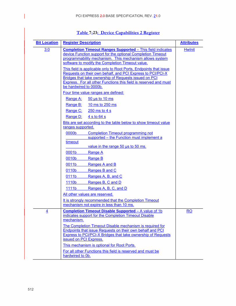
PCI EXPRESS 2.0 BASE SPECIFICATION, REV. 21.0
512
Table 7-23: Device Capabilities 2 Register
Bit Location Register Description Attributes
3:0 Completion Timeout Ranges Supported – This field indicates device Function support for the optional Completion Timeout programmability mechanism. This mechanism allows system software to modify the Completion Timeout value. This field is applicable only to Root Ports, Endpoints that issue Requests on their own behalf, and PCI Express to PCI/PCI-X Bridges that take ownership of Requests issued on PCI Express. For all other Functions this field is reserved and must be hardwired to 0000b. Four time value ranges are defined:
Range A: 50 µs to 10 ms Range B: 10 ms to 250 ms Range C: 250 ms to 4 s Range D: 4 s to 64 s
Bits are set according to the table below to show timeout value ranges supported.
0000b Completion Timeout programming not supported – the Function must implement a timeout value in the range 50 µs to 50 ms. 0001b Range A 0010b Range B 0011b Ranges A and B 0110b Ranges B and C 0111b Ranges A, B, and C 1110b Ranges B, C and D 1111b Ranges A, B, C, and D
All other values are reserved. It is strongly recommended that the Completion Timeout mechanism not expire in less than 10 ms.
HwInit
4 Completion Timeout Disable Supported – A value of 1b indicates support for the Completion Timeout Disable mechanism. The Completion Timeout Disable mechanism is required for Endpoints that issue Requests on their own behalf and PCI Express to PCI/PCI-X Bridges that take ownership of Requests issued on PCI Express. This mechanism is optional for Root Ports. For all other Functions this field is reserved and must be hardwired to 0b.
RO
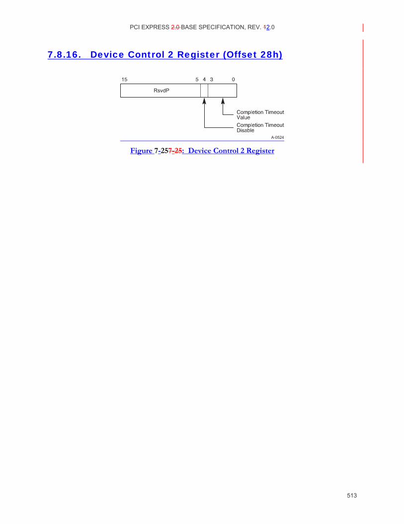
PCI EXPRESS 2.0 BASE SPECIFICATION, REV. 12.0
513
7.8.16. Device Control 2 Register (Offset 28h)
A-0524
RsvdP
Figure 7-257-25: Device Control 2 Register
PCI EXPRESS 2.0 BASE SPECIFICATION, REV. 21.0
514
Table 7-24: Device Control 2 Register
Bit Location Register Description Attributes
3:0 Completion Timeout Value – In device Functions that support Completion Timeout programmability, this field allows system software to modify the Completion Timeout value. This field is applicable to Root Ports, Endpoints that issue Requests on their own behalf, and PCI Express to PCI/PCI-X Bridges that take ownership of Requests issued on PCI Express. For all other Functions this field is reserved and must be hardwired to 0000b. A Function that does not support this optional capability must hardwire this field to 0000b and is required to implement a timeout value in the range 50 µs to 50 ms. Functions that support Completion Timeout programmability must support the values given below corresponding to the programmability ranges indicated in the Completion Timeout Ranges Supported field. Defined encodings:
0000b Default range: 50 µs to 50 ms It is strongly recommended that the Completion Timeout mechanism not expire in less than 10 ms. Values available if Range A (50 µs to 10 ms) programmability range is supported:
0001b 50 µs to 100 µs 0010b 1 ms to 10 ms
Values available if Range B (10 ms to 250 ms) programmability range is supported:
0101b 16 ms to 55 ms 0110b 65 ms to 210 ms
Values available if Range C (250 ms to 4 s) programmability range is supported:
1001b 260 ms to 900 ms 1010b 1 s to 3.5 s
Values available if the Range D (4 s to 64 s) programmability range is supported:
1101b 4 s to 13 s 1110b 17 s to 64 s
Values not defined above are reserved. Software is permitted to change the value in this field at any time. For Requests already pending when the Completion Timeout Value is changed, hardware is permitted to use either the new or the old value for the outstanding Requests, and is permitted to base the start time for each Request either on when this value was changed or on when each request was issued. The default value for this field is 0000b.
RW
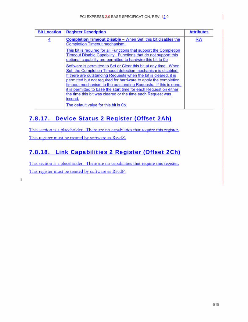
PCI EXPRESS 2.0 BASE SPECIFICATION, REV. 12.0
515
Bit Location Register Description Attributes
4 Completion Timeout Disable – When Set, this bit disables the Completion Timeout mechanism. This bit is required for all Functions that support the Completion Timeout Disable Capability. Functions that do not support this optional capability are permitted to hardwire this bit to 0b Software is permitted to Set or Clear this bit at any time. When Set, the Completion Timeout detection mechanism is disabled. If there are outstanding Requests when the bit is cleared, it is permitted but not required for hardware to apply the completion timeout mechanism to the outstanding Requests. If this is done, it is permitted to base the start time for each Request on either the time this bit was cleared or the time each Request was issued. The default value for this bit is 0b.
RW
7.8.17. Device Status 2 Register (Offset 2Ah)
This section is a placeholder. There are no capabilities that require this register.
This register must be treated by software as RsvdZ.
7.8.18. Link Capabilities 2 Register (Offset 2Ch)
This section is a placeholder. There are no capabilities that require this register.
This register must be treated by software as RsvdP.
5
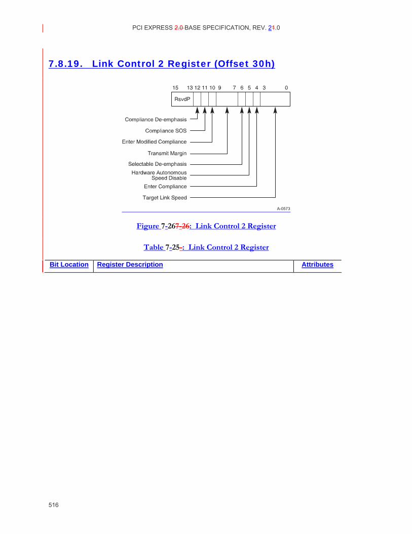
PCI EXPRESS 2.0 BASE SPECIFICATION, REV. 21.0
516
7.8.19. Link Control 2 Register (Offset 30h)
A-0573
Figure 7-267-26: Link Control 2 Register
Table 7-25-: Link Control 2 Register
Bit Location Register Description Attributes
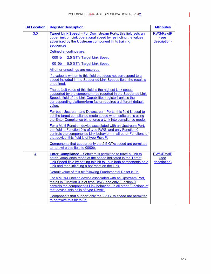
PCI EXPRESS 2.0 BASE SPECIFICATION, REV. 12.0
517
Bit Location Register Description Attributes
3:0 Target Link Speed – For Downstream Ports, this field sets an upper limit on Link operational speed by restricting the values advertised by the Upstream component in its training sequences.
Defined encodings are:
0001b 2.5 GT/s Target Link Speed
0010b 5.0 GT/s Target Link Speed
All other encodings are reserved.
If a value is written to this field that does not correspond to a speed included in the Supported Link Speeds field, the result is undefined.
The default value of this field is the highest Link speed supported by the component (as reported in the Supported Link Speeds field of the Link Capabilities register) unless the corresponding platform/form factor requires a different default value.
For both Upstream and Downstream Ports, this field is used to set the target compliance mode speed when software is using the Enter Compliance bit to force a Link into compliance mode.
For a Multi-Function device associated with an Upstream Port, the field in Function 0 is of type RWS, and only Function 0 controls the component’s Link behavior. In all other Functions of that device, this field is of type RsvdP.
Components that support only the 2.5 GT/s speed are permitted to hardwire this field to 0000b.
RWS/RsvdP(see
description)
4 Enter Compliance – Software is permitted to force a Link to enter Compliance mode at the speed indicated in the Target Link Speed field by setting this bit to 1b in both components on a Link and then initiating a hot reset on the Link.
Default value of this bit following Fundamental Reset is 0b.
For a Multi-Function device associated with an Upstream Port, the bit in Function 0 is of type RWS, and only Function 0 controls the component’s Link behavior. In all other Functions of that device, this bit is of type RsvdP.
Components that support only the 2.5 GT/s speed are permitted to hardwire this bit to 0b.
RWS/RsvdP(see
description)
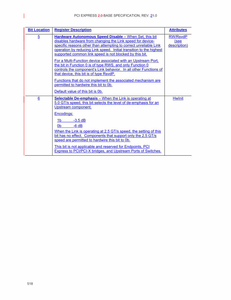
PCI EXPRESS 2.0 BASE SPECIFICATION, REV. 21.0
518
Bit Location Register Description Attributes
5 Hardware Autonomous Speed Disable – When Set, this bit disables hardware from changing the Link speed for device-specific reasons other than attempting to correct unreliable Link operation by reducing Link speed. Initial transition to the highest supported common link speed is not blocked by this bit.
For a Multi-Function device associated with an Upstream Port, the bit in Function 0 is of type RWS, and only Function 0 controls the component’s Link behavior. In all other Functions of that device, this bit is of type RsvdP.
Functions that do not implement the associated mechanism are permitted to hardwire this bit to 0b.
Default value of this bit is 0b.
RW/RsvdP (see
description)
6 Selectable De-emphasis – When the Link is operating at 5.0 GT/s speed, this bit selects the level of de-emphasis for an Upstream component.
Encodings:
1b -3.5 dB 0b -6 dB
When the Link is operating at 2.5 GT/s speed, the setting of this bit has no effect. Components that support only the 2.5 GT/s speed are permitted to hardwire this bit to 0b.
This bit is not applicable and reserved for Endpoints, PCI Express to PCI/PCI-X bridges, and Upstream Ports of Switches.
HwInit
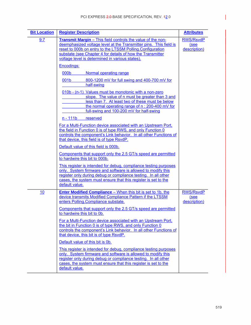
PCI EXPRESS 2.0 BASE SPECIFICATION, REV. 12.0
519
Bit Location Register Description Attributes
9:7 Transmit Margin – This field controls the value of the non-deemphasized voltage level at the Transmitter pins. This field is reset to 000b on entry to the LTSSM Polling.Configuration substate (see Chapter 4 for details of how the Transmitter voltage level is determined in various states).
Encodings:
000b Normal operating range
001b 800-1200 mV for full swing and 400-700 mV for half-swing
010b - (n-1) Values must be monotonic with a non-zero slope. The value of n must be greater than 3 and less than 7. At least two of these must be below the normal operating range of n : 200-400 mV for full-swing and 100-200 mV for half-swing
n - 111b reserved
For a Multi-Function device associated with an Upstream Port, the field in Function 0 is of type RWS, and only Function 0 controls the component’s Link behavior. In all other Functions of that device, this field is of type RsvdP.
Default value of this field is 000b.
Components that support only the 2.5 GT/s speed are permitted to hardwire this bit to 000b.
This register is intended for debug, compliance testing purposes only. System firmware and software is allowed to modify this register only during debug or compliance testing. In all other cases, the system must ensure that this register is set to the default value.
RWS/RsvdP(see
description)
10 Enter Modified Compliance – When this bit is set to 1b, the device transmits Modified Compliance Pattern if the LTSSM enters Polling.Compliance substate.
Components that support only the 2.5 GT/s speed are permitted to hardwire this bit to 0b.
For a Multi-Function device associated with an Upstream Port, the bit in Function 0 is of type RWS, and only Function 0 controls the component’s Link behavior. In all other Functions of that device, this bit is of type RsvdP.
Default value of this bit is 0b.
This register is intended for debug, compliance testing purposes only. System firmware and software is allowed to modify this register only during debug or compliance testing. In all other cases, the system must ensure that this register is set to the default value.
RWS/RsvdP(see
description)
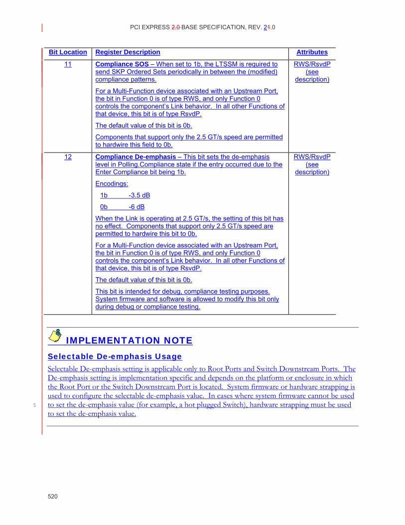
PCI EXPRESS 2.0 BASE SPECIFICATION, REV. 21.0
520
Bit Location Register Description Attributes
11 Compliance SOS – When set to 1b, the LTSSM is required to send SKP Ordered Sets periodically in between the (modified) compliance patterns.
For a Multi-Function device associated with an Upstream Port, the bit in Function 0 is of type RWS, and only Function 0 controls the component’s Link behavior. In all other Functions of that device, this bit is of type RsvdP.
The default value of this bit is 0b.
Components that support only the 2.5 GT/s speed are permitted to hardwire this field to 0b.
RWS/RsvdP(see
description)
12 Compliance De-emphasis – This bit sets the de-emphasis level in Polling.Compliance state if the entry occurred due to the Enter Compliance bit being 1b.
Encodings:
1b -3.5 dB
0b -6 dB
When the Link is operating at 2.5 GT/s, the setting of this bit has no effect. Components that support only 2.5 GT/s speed are permitted to hardwire this bit to 0b.
For a Multi-Function device associated with an Upstream Port, the bit in Function 0 is of type RWS, and only Function 0 controls the component’s Link behavior. In all other Functions of that device, this bit is of type RsvdP.
The default value of this bit is 0b.
This bit is intended for debug, compliance testing purposes. System firmware and software is allowed to modify this bit only during debug or compliance testing.
RWS/RsvdP(see
description)
IMPLEMENTATION NOTE Selectable De-emphasis Usage Selectable De-emphasis setting is applicable only to Root Ports and Switch Downstream Ports. The De-emphasis setting is implementation specific and depends on the platform or enclosure in which the Root Port or the Switch Downstream Port is located. System firmware or hardware strapping is used to configure the selectable de-emphasis value. In cases where system firmware cannot be used to set the de-emphasis value (for example, a hot plugged Switch), hardware strapping must be used 5 to set the de-emphasis value.
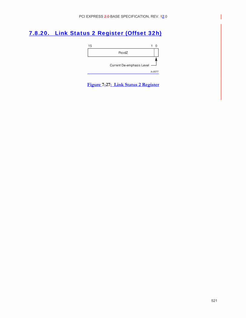
PCI EXPRESS 2.0 BASE SPECIFICATION, REV. 12.0
521
7.8.20. Link Status 2 Register (Offset 32h)
A-0577
Figure 7-27: Link Status 2 Register
PCI EXPRESS 2.0 BASE SPECIFICATION, REV. 21.0
522
Table 7-26: Link Status 2 Register
Bit Location Register Description Attributes
0 Current De-emphasis Level – When the Link is operating at 5 GT/s speed, this bit reflects the level of de-emphasis.
Encodings:
1b -3.5 dB
0b -6 dB
The value in this bit is undefined when the Link is operating at 2.5 GT/s speed.
Components that support only the 2.5 GT/s speed are permitted to hardwire this field to 0b.
RO
7.8.21. Slot Capabilities 2 Register (Offset 34h)
This section is a placeholder. There are no capabilities that require this register.
This register must be treated by software as RsvdP.
7.8.22. Slot Control 2 Register (Offset 38h)
This section is a placeholder. There are no capabilities that require this register.
This register must be treated by software as RsvdP.
7.8.23. Slot Status 2 Register (Offset 3Ah)
This section is a placeholder. There are no capabilities that require this register. 5
This register must be treated by software as RsvdZ.
7.9. PCI Express Extended Capabilities PCI Express Extended Capability registers are located in device configuration spaceConfiguration Space at offsets 256 or greater as shown in Figure 7-28 or in the Root Complex Register Block (RCRB). These registers when located in the device configuration spaceConfiguration Space are accessible using only the PCI Express extended Extended configuration spaceConfiguration Space 10 flat memory-mapped access mechanism.
PCI Express Extended Capability structures are allocated using a linked list of optional or required PCI Express Extended Capabilities following a format resembling PCI capability Capability structures. The first DWORD of the capability Capability structure identifies the capabilityCapability/ and version and points to the next capability Capability as shown in Figure 15 7-28.
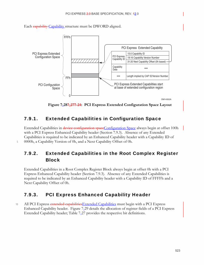
PCI EXPRESS 2.0 BASE SPECIFICATION, REV. 12.0
523
Each capability Capability structure must be DWORD aligned.
OM14302A
FFFh
FFh
0
PCI Express Extended Capabilities startat base of extended configuration region
PCI Express Extended Capability
PCI Express ExtendedConfiguration Space
PCI ConfigurationSpace
PCI ExpressCapability ID
CapabilityData
15:0 Capability ID
19:16 Capability Version Number
31:20 Next Capability Offset (0h based)
Length implied by CAP ID/Version Number
Figure 7-287-27 7-24: PCI Express Extended Configuration Space Layout
7.9.1. Extended Capabilities in Configuration Space
Extended Capabilities in device configuration spaceConfiguration Space always begin at offset 100h with a PCI Express Enhanced Capability header (Section 7.9.3). Absence of any Extended Capabilities is required to be indicated by an Enhanced Capability header with a Capability ID of 0000h, a Capability Version of 0h, and a Next Capability Offset of 0h. 5
7.9.2. Extended Capabilities in the Root Complex Register Block
Extended Capabilities in a Root Complex Register Block always begin at offset 0h with a PCI Express Enhanced Capability header (Section 7.9.3). Absence of any Extended Capabilities is required to be indicated by an Enhanced Capability header with a Capability ID of FFFFh and a Next Capability Offset of 0h.
7.9.3. PCI Express Enhanced Capability Header
All PCI Express extended capabilitiesExtended Capabilities must begin with a PCI Express 10 Enhanced Capability header. Figure 7-29 details the allocation of register fields of a PCI Express Extended Capability header; Table 7-27 provides the respective bit definitions.
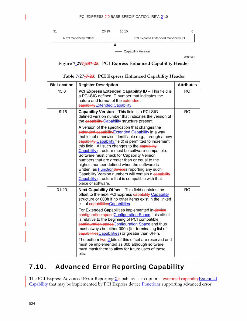
PCI EXPRESS 2.0 BASE SPECIFICATION, REV. 21.0
524
OM14514
Capability Version
Next Capability Offset PCI Express Extended Capability ID
31 20 16 1519 0
Figure 7-297-28 7-25: PCI Express Enhanced Capability Header
Table 7-27- 7-23: PCI Express Enhanced Capability Header
Bit Location Register Description Attributes 15:0 PCI Express Extended Capability ID – This field is
a PCI-SIG defined ID number that indicates the nature and format of the extended capabilityExtended Capability.
RO
19:16 Capability Version – This field is a PCI-SIG defined version number that indicates the version of the capability Capability structure present. A version of the specification that changes the extended capabilityExtended Capability in a way that is not otherwise identifiable (e.g., through a new capability Capability field) is permitted to increment this field. All such changes to the capability Capability structure must be software-compatible. Software must check for Capability Version numbers that are greater than or equal to the highest number defined when the software is written, as Functiondevices reporting any such Capability Version numbers will contain a capability Capability structure that is compatible with that piece of software.
RO
31:20 Next Capability Offset – This field contains the offset to the next PCI Express capability Capability structure or 000h if no other items exist in the linked list of capabilitiesCapabilities. For Extended Capabilities implemented in device configuration spaceConfiguration Space, this offset is relative to the beginning of PCI compatible configuration spaceConfiguration Space and thus must always be either 000h (for terminating list of capabilitiesCapabilities) or greater than 0FFh. The bottom two 2 bits of this offset are reserved and must be implemented as 00b although software must mask them to allow for future uses of these bits.
RO
7.10. Advanced Error Reporting Capability The PCI Express Advanced Error Reporting Ccapability is an optional extended capabilityExtended Capability that may be implemented by PCI Express device Functions supporting advanced error
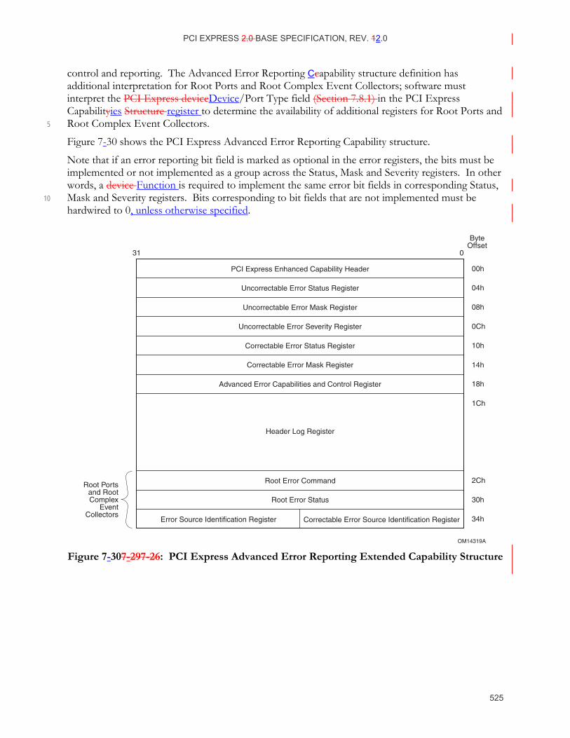
PCI EXPRESS 2.0 BASE SPECIFICATION, REV. 12.0
525
control and reporting. The Advanced Error Reporting Ccapability structure definition has additional interpretation for Root Ports and Root Complex Event Collectors; software must interpret the PCI Express deviceDevice/Port Type field (Section 7.8.1) in the PCI Express Capabilityies Structure register to determine the availability of additional registers for Root Ports and Root Complex Event Collectors. 5
Figure 7-30 shows the PCI Express Advanced Error Reporting Capability structure.
Note that if an error reporting bit field is marked as optional in the error registers, the bits must be implemented or not implemented as a group across the Status, Mask and Severity registers. In other words, a device Function is required to implement the same error bit fields in corresponding Status, Mask and Severity registers. Bits corresponding to bit fields that are not implemented must be 10 hardwired to 0, unless otherwise specified.
Root Portsand RootComplex
EventCollectors
OM14319A
0
ByteOffset
31
04h
08h
00h
0Ch
10h
14h
18h
1Ch
2Ch
30h
34hError Source Identification Register Correctable Error Source Identification Register
Root Error Command
Root Error Status
PCI Express Enhanced Capability Header
Uncorrectable Error Status Register
Uncorrectable Error Mask Register
Uncorrectable Error Severity Register
Correctable Error Status Register
Correctable Error Mask Register
Advanced Error Capabilities and Control Register
Header Log Register
Figure 7-307-29 7-26: PCI Express Advanced Error Reporting Extended Capability Structure
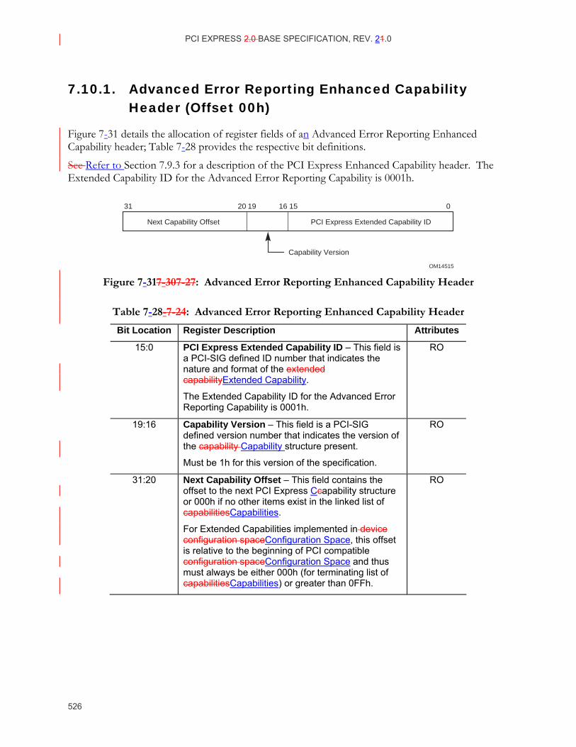
PCI EXPRESS 2.0 BASE SPECIFICATION, REV. 21.0
526
7.10.1. Advanced Error Reporting Enhanced Capability Header (Offset 00h)
Figure 7-31 details the allocation of register fields of an Advanced Error Reporting Enhanced Capability header; Table 7-28 provides the respective bit definitions.
See Refer to Section 7.9.3 for a description of the PCI Express Enhanced Capability header. The Extended Capability ID for the Advanced Error Reporting Capability is 0001h.
OM14515
Capability Version
Next Capability Offset PCI Express Extended Capability ID
31 20 16 1519 0
Figure 7-317-30 7-27: Advanced Error Reporting Enhanced Capability Header
Table 7-28- 7-24: Advanced Error Reporting Enhanced Capability Header
Bit Location Register Description Attributes
15:0 PCI Express Extended Capability ID – This field is a PCI-SIG defined ID number that indicates the nature and format of the extended capabilityExtended Capability.
The Extended Capability ID for the Advanced Error Reporting Capability is 0001h.
RO
19:16 Capability Version – This field is a PCI-SIG defined version number that indicates the version of the capability Capability structure present.
Must be 1h for this version of the specification.
RO
31:20 Next Capability Offset – This field contains the offset to the next PCI Express Ccapability structure or 000h if no other items exist in the linked list of capabilitiesCapabilities.
For Extended Capabilities implemented in device configuration spaceConfiguration Space, this offset is relative to the beginning of PCI compatible configuration spaceConfiguration Space and thus must always be either 000h (for terminating list of capabilitiesCapabilities) or greater than 0FFh.
RO
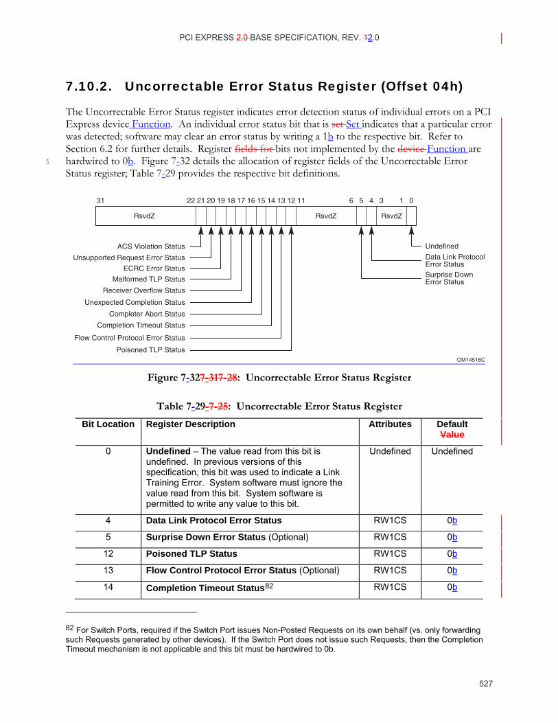
PCI EXPRESS 2.0 BASE SPECIFICATION, REV. 12.0
527
7.10.2. Uncorrectable Error Status Register (Offset 04h)
The Uncorrectable Error Status register indicates error detection status of individual errors on a PCI Express device Function. An individual error status bit that is set Set indicates that a particular error was detected; software may clear an error status by writing a 1b to the respective bit. Refer to Section 6.2 for further details. Register fields for bits not implemented by the device Function are hardwired to 0b. Figure 7-32 details the allocation of register fields of the Uncorrectable Error 5 Status register; Table 7-29 provides the respective bit definitions.
OM14516C
Data Link ProtocolError StatusSurprise DownError Status
Undefined
RsvdZ RsvdZRsvdZ
31 20 19 18 17 16 15 14 13 12 11 5 4 3 1 06
Unexpected Completion Status
Completion Timeout Status
Receiver Overflow Status
Malformed TLP Status
Completer Abort Status
Flow Control Protocol Error Status
Poisoned TLP Status
ACS Violation Status
ECRC Error Status
22 21
Unsupported Request Error Status
Figure 7-327-31 7-28: Uncorrectable Error Status Register
Table 7-29- 7-25: Uncorrectable Error Status Register
Bit Location Register Description Attributes Default Value
0 Undefined – The value read from this bit is undefined. In previous versions of this specification, this bit was used to indicate a Link Training Error. System software must ignore the value read from this bit. System software is permitted to write any value to this bit.
Undefined Undefined
4 Data Link Protocol Error Status RW1CS 0b
5 Surprise Down Error Status (Optional) RW1CS 0b
12 Poisoned TLP Status RW1CS 0b
13 Flow Control Protocol Error Status (Optional) RW1CS 0b
14 Completion Timeout Status82 RW1CS 0b
82 For Switch Ports, required if the Switch Port issues Non-Posted Requests on its own behalf (vs. only forwarding such Requests generated by other devices). If the Switch Port does not issue such Requests, then the Completion Timeout mechanism is not applicable and this bit must be hardwired to 0b.
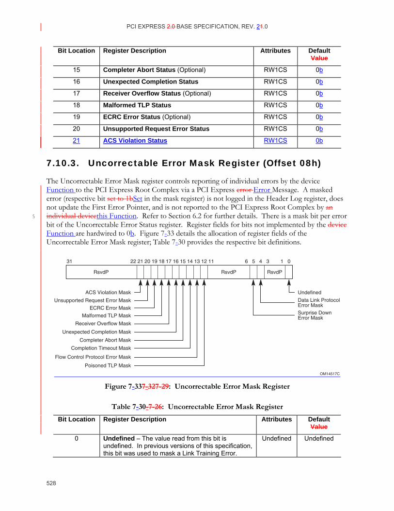
PCI EXPRESS 2.0 BASE SPECIFICATION, REV. 21.0
528
Bit Location Register Description Attributes Default Value
15 Completer Abort Status (Optional) RW1CS 0b
16 Unexpected Completion Status RW1CS 0b
17 Receiver Overflow Status (Optional) RW1CS 0b
18 Malformed TLP Status RW1CS 0b
19 ECRC Error Status (Optional) RW1CS 0b
20 Unsupported Request Error Status RW1CS 0b
21 ACS Violation Status RW1CS 0b
7.10.3. Uncorrectable Error Mask Register (Offset 08h)
The Uncorrectable Error Mask register controls reporting of individual errors by the device Function to the PCI Express Root Complex via a PCI Express error Error Message. A masked error (respective bit set to 1bSet in the mask register) is not logged in the Header Log register, does not update the First Error Pointer, and is not reported to the PCI Express Root Complex by an individual devicethis Function. Refer to Section 6.2 for further details. There is a mask bit per error 5 bit of the Uncorrectable Error Status register. Register fields for bits not implemented by the device Function are hardwired to 0b. Figure 7-33 details the allocation of register fields of the Uncorrectable Error Mask register; Table 7-30 provides the respective bit definitions.
OM14517C
Data Link ProtocolError MaskSurprise DownError Mask
Undefined
RsvdP RsvdPRsvdP
Unexpected Completion Mask
Completion Timeout Mask
Receiver Overflow Mask
Malformed TLP Mask
Completer Abort Mask
Flow Control Protocol Error Mask
Poisoned TLP Mask
ACS Violation Mask
ECRC Error Mask
31 20 19 18 17 16 15 14 13 12 11 5 4 3 1 0622 21
Unsupported Request Error Mask
Figure 7-337-32 7-29: Uncorrectable Error Mask Register
Table 7-30- 7-26: Uncorrectable Error Mask Register
Bit Location Register Description Attributes Default Value
0 Undefined – The value read from this bit is undefined. In previous versions of this specification, this bit was used to mask a Link Training Error.
Undefined Undefined
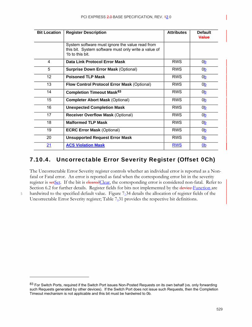
PCI EXPRESS 2.0 BASE SPECIFICATION, REV. 12.0
529
Bit Location Register Description Attributes Default Value
System software must ignore the value read from this bit. System software must only write a value of 1b to this bit.
4 Data Link Protocol Error Mask RWS 0b
5 Surprise Down Error Mask (Optional) RWS 0b
12 Poisoned TLP Mask RWS 0b
13 Flow Control Protocol Error Mask (Optional) RWS 0b
14 Completion Timeout Mask83 RWS 0b
15 Completer Abort Mask (Optional) RWS 0b
16 Unexpected Completion Mask RWS 0b
17 Receiver Overflow Mask (Optional) RWS 0b
18 Malformed TLP Mask RWS 0b
19 ECRC Error Mask (Optional) RWS 0b
20 Unsupported Request Error Mask RWS 0b
21 ACS Violation Mask RWS 0b
7.10.4. Uncorrectable Error Severity Register (Offset 0Ch)
The Uncorrectable Error Severity register controls whether an individual error is reported as a Non-fatal or Fatal error. An error is reported as fatal when the corresponding error bit in the severity register is setSet. If the bit is clearedClear, the corresponding error is considered non-fatal. Refer to Section 6.2 for further details. Register fields for bits not implemented by the device Function are hardwired to the specified default value. Figure 7-34 details the allocation of register fields of the 5 Uncorrectable Error Severity register; Table 7-31 provides the respective bit definitions.
83 For Switch Ports, required if the Switch Port issues Non-Posted Requests on its own behalf (vs. only forwarding such Requests generated by other devices). If the Switch Port does not issue such Requests, then the Completion Timeout mechanism is not applicable and this bit must be hardwired to 0b.
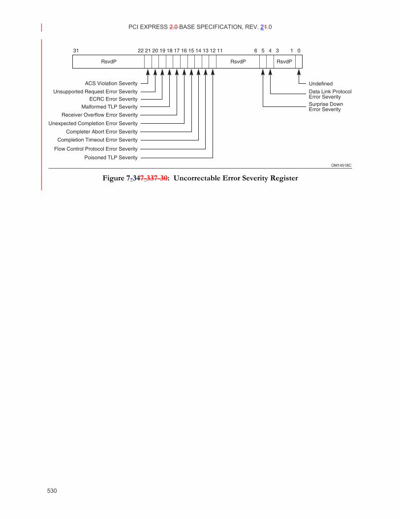
PCI EXPRESS 2.0 BASE SPECIFICATION, REV. 21.0
530
OM14518C
Data Link ProtocolError SeveritySurprise DownError Severity
Undefined
RsvdP RsvdPRsvdP
Unexpected Completion Error Severity
Completion Timeout Error Severity
Receiver Overflow Error Severity
Malformed TLP Severity
Completer Abort Error Severity
Flow Control Protocol Error Severity
Poisoned TLP Severity
ACS Violation Severity
ECRC Error Severity
31 20 19 18 17 16 15 14 13 12 11 5 4 3 1 0622 21
Unsupported Request Error Severity
Figure 7-347-33 7-30: Uncorrectable Error Severity Register
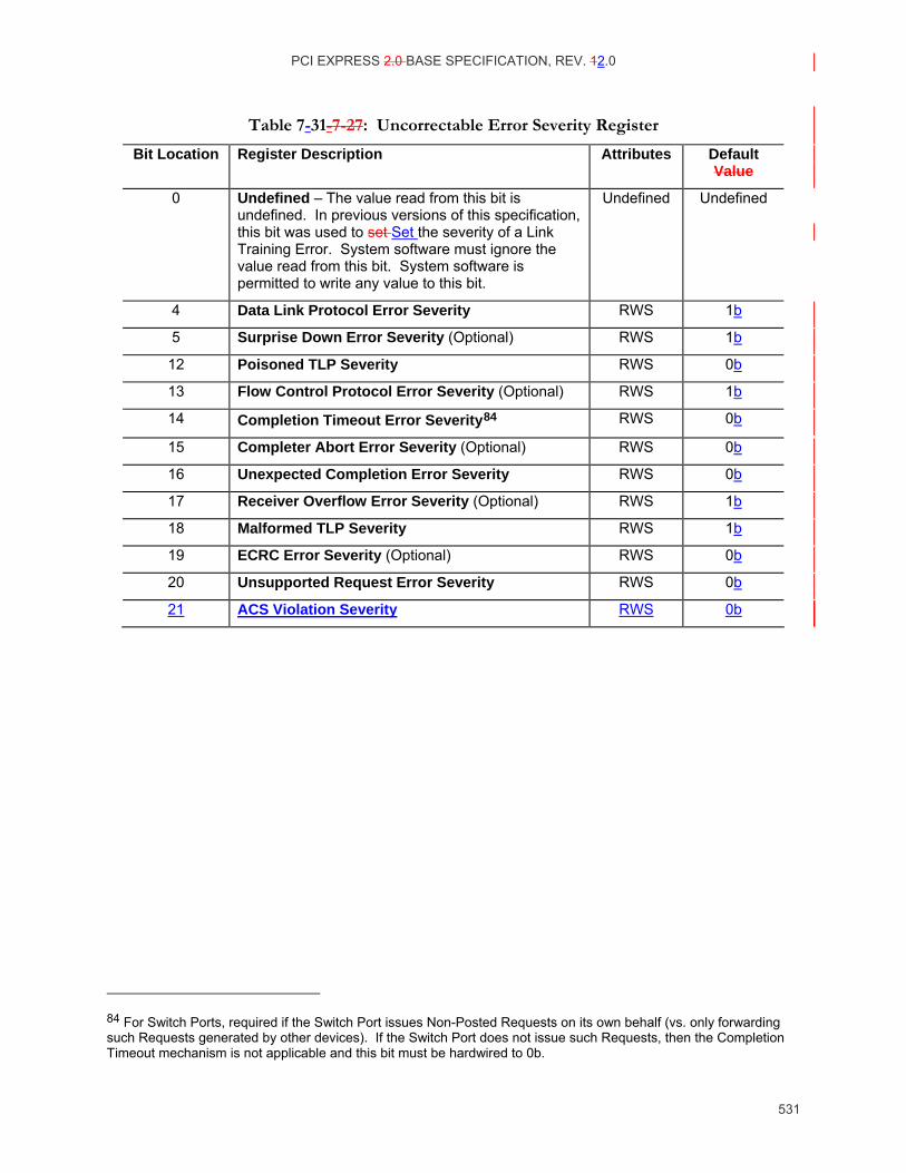
PCI EXPRESS 2.0 BASE SPECIFICATION, REV. 12.0
531
Table 7-31- 7-27: Uncorrectable Error Severity Register
Bit Location Register Description Attributes Default Value
0 Undefined – The value read from this bit is undefined. In previous versions of this specification, this bit was used to set Set the severity of a Link Training Error. System software must ignore the value read from this bit. System software is permitted to write any value to this bit.
Undefined Undefined
4 Data Link Protocol Error Severity RWS 1b
5 Surprise Down Error Severity (Optional) RWS 1b
12 Poisoned TLP Severity RWS 0b
13 Flow Control Protocol Error Severity (Optional) RWS 1b
14 Completion Timeout Error Severity84 RWS 0b
15 Completer Abort Error Severity (Optional) RWS 0b
16 Unexpected Completion Error Severity RWS 0b
17 Receiver Overflow Error Severity (Optional) RWS 1b
18 Malformed TLP Severity RWS 1b
19 ECRC Error Severity (Optional) RWS 0b
20 Unsupported Request Error Severity RWS 0b
21 ACS Violation Severity RWS 0b
84 For Switch Ports, required if the Switch Port issues Non-Posted Requests on its own behalf (vs. only forwarding such Requests generated by other devices). If the Switch Port does not issue such Requests, then the Completion Timeout mechanism is not applicable and this bit must be hardwired to 0b.
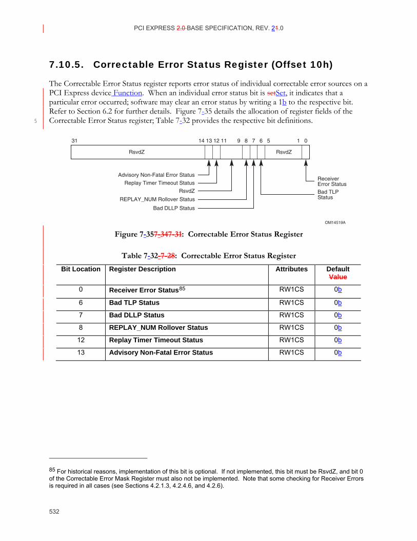
PCI EXPRESS 2.0 BASE SPECIFICATION, REV. 21.0
532
7.10.5. Correctable Error Status Register (Offset 10h)
The Correctable Error Status register reports error status of individual correctable error sources on a PCI Express device Function. When an individual error status bit is setSet, it indicates that a particular error occurred; software may clear an error status by writing a 1b to the respective bit. Refer to Section 6.2 for further details. Figure 7-35 details the allocation of register fields of the Correctable Error Status register; Table 7-32 provides the respective bit definitions. 5
OM14519A
Bad TLPStatus
ReceiverError Status
RsvdZ RsvdZ
Bad DLLP Status
REPLAY_NUM Rollover Status
RsvdZ
Replay Timer Timeout Status
Advisory Non-Fatal Error Status
31 12 11 9 8 7 6 5 1 01314
Figure 7-357-34 7-31: Correctable Error Status Register
Table 7-32- 7-28: Correctable Error Status Register
Bit Location Register Description Attributes Default Value
0 Receiver Error Status85 RW1CS 0b
6 Bad TLP Status RW1CS 0b
7 Bad DLLP Status RW1CS 0b
8 REPLAY_NUM Rollover Status RW1CS 0b
12 Replay Timer Timeout Status RW1CS 0b
13 Advisory Non-Fatal Error Status RW1CS 0b
85 For historical reasons, implementation of this bit is optional. If not implemented, this bit must be RsvdZ, and bit 0 of the Correctable Error Mask Register must also not be implemented. Note that some checking for Receiver Errors is required in all cases (see Sections 4.2.1.3, 4.2.4.6, and 4.2.6).
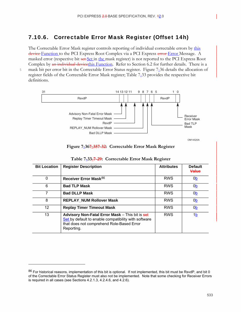
PCI EXPRESS 2.0 BASE SPECIFICATION, REV. 12.0
533
7.10.6. Correctable Error Mask Register (Offset 14h)
The Correctable Error Mask register controls reporting of individual correctable errors by this device Function to the PCI Express Root Complex via a PCI Express error Error Message. A masked error (respective bit set Set in the mask register) is not reported to the PCI Express Root Complex by an individual devicethis Function. Refer to Section 6.2 for further details. There is a mask bit per error bit in the Correctable Error Status register. Figure 7-36 details the allocation of 5 register fields of the Correctable Error Mask register; Table 7-33 provides the respective bit definitions.
OM14520A
Bad TLPMask
ReceiverError Mask
RsvdP RsvdP
Bad DLLP Mask
REPLAY_NUM Rollover Mask
RsvdP
Replay Timer Timeout Mask
Advisory Non-Fatal Error Mask
31 12 11 9 8 7 6 5 1 01314
Figure 7-367-35 7-32: Correctable Error Mask Register
Table 7-33- 7-29: Correctable Error Mask Register
Bit Location Register Description Attributes Default Value
0 Receiver Error Mask86 RWS 0b
6 Bad TLP Mask RWS 0b
7 Bad DLLP Mask RWS 0b
8 REPLAY_NUM Rollover Mask RWS 0b
12 Replay Timer Timeout Mask RWS 0b
13 Advisory Non-Fatal Error Mask – This bit is set Set by default to enable compatibility with software that does not comprehend Role-Based Error Reporting.
RWS 1b
86 For historical reasons, implementation of this bit is optional. If not implemented, this bit must be RsvdP, and bit 0 of the Correctable Error Status Register must also not be implemented. Note that some checking for Receiver Errors is required in all cases (see Sections 4.2.1.3, 4.2.4.6, and 4.2.6).
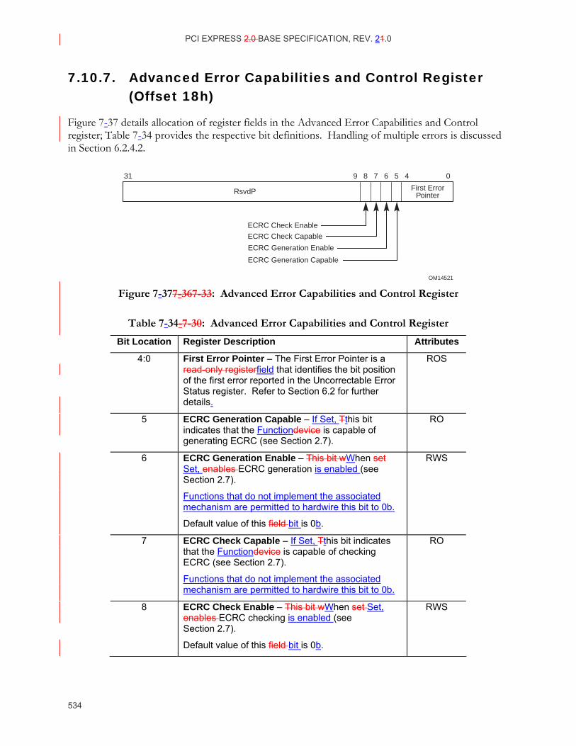
PCI EXPRESS 2.0 BASE SPECIFICATION, REV. 21.0
534
7.10.7. Advanced Error Capabilities and Control Register (Offset 18h)
Figure 7-37 details allocation of register fields in the Advanced Error Capabilities and Control register; Table 7-34 provides the respective bit definitions. Handling of multiple errors is discussed in Section 6.2.4.2.
OM14521
RsvdP First ErrorPointer
ECRC Generation Capable
ECRC Generation Enable
ECRC Check Capable
ECRC Check Enable
31 9 8 7 6 5 4 0
Figure 7-377-36 7-33: Advanced Error Capabilities and Control Register
Table 7-34- 7-30: Advanced Error Capabilities and Control Register
Bit Location Register Description Attributes
4:0 First Error Pointer – The First Error Pointer is a read-only registerfield that identifies the bit position of the first error reported in the Uncorrectable Error Status register. Refer to Section 6.2 for further details.
ROS
5 ECRC Generation Capable – If Set, Tthis bit indicates that the Functiondevice is capable of generating ECRC (see Section 2.7).
RO
6 ECRC Generation Enable – This bit wWhen set Set, enables ECRC generation is enabled (see Section 2.7).
Functions that do not implement the associated mechanism are permitted to hardwire this bit to 0b.
Default value of this field bit is 0b.
RWS
7 ECRC Check Capable – If Set, Tthis bit indicates that the Functiondevice is capable of checking ECRC (see Section 2.7).
Functions that do not implement the associated mechanism are permitted to hardwire this bit to 0b.
RO
8 ECRC Check Enable – This bit wWhen set Set, enables ECRC checking is enabled (see Section 2.7).
Default value of this field bit is 0b.
RWS
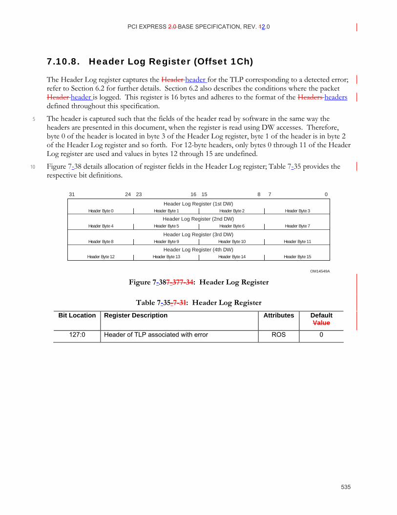
PCI EXPRESS 2.0 BASE SPECIFICATION, REV. 12.0
535
7.10.8. Header Log Register (Offset 1Ch)
The Header Log register captures the Header header for the TLP corresponding to a detected error; refer to Section 6.2 for further details. Section 6.2 also describes the conditions where the packet Header header is logged. This register is 16 bytes and adheres to the format of the Headers headers defined throughout this specification.
The header is captured such that the fields of the header read by software in the same way the 5 headers are presented in this document, when the register is read using DW accesses. Therefore, byte 0 of the header is located in byte 3 of the Header Log register, byte 1 of the header is in byte 2 of the Header Log register and so forth. For 12-byte headers, only bytes 0 through 11 of the Header Log register are used and values in bytes 12 through 15 are undefined.
Figure 7-38 details allocation of register fields in the Header Log register; Table 7-35 provides the 10 respective bit definitions.
OM14549A
Header Log Register (1st DW)
Header Log Register (2nd DW)
Header Log Register (3rd DW)
Header Log Register (4th DW)
Header Byte 0
Header Byte 4
Header Byte 8
Header Byte 12
Header Byte 1
Header Byte 5
Header Byte 9
Header Byte 13
Header Byte 2
Header Byte 6
Header Byte 10
Header Byte 14
Header Byte 3
Header Byte 7
Header Byte 11
Header Byte 15
31 24 23 16 15 8 7 0
Figure 7-387-37 7-34: Header Log Register
Table 7-35- 7-31: Header Log Register
Bit Location Register Description Attributes Default Value
127:0 Header of TLP associated with error ROS 0
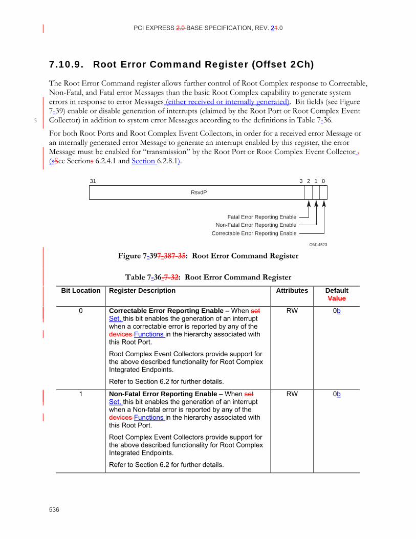
PCI EXPRESS 2.0 BASE SPECIFICATION, REV. 21.0
536
7.10.9. Root Error Command Register (Offset 2Ch)
The Root Error Command register allows further control of Root Complex response to Correctable, Non-Fatal, and Fatal error Messages than the basic Root Complex capability to generate system errors in response to error Messages (either received or internally generated). Bit fields (see Figure 7-39) enable or disable generation of interrupts (claimed by the Root Port or Root Complex Event Collector) in addition to system error Messages according to the definitions in Table 7-36. 5
For both Root Ports and Root Complex Event Collectors, in order for a received error Message or an internally generated error Message to generate an interrupt enabled by this register, the error Message must be enabled for “transmission” by the Root Port or Root Complex Event Collector . (sSee Sections 6.2.4.1 and Section 6.2.8.1).
OM14523
RsvdP
Correctable Error Reporting Enable
Non-Fatal Error Reporting Enable
Fatal Error Reporting Enable
31 3 2 1 0
Figure 7-397-38 7-35: Root Error Command Register
Table 7-36- 7-32: Root Error Command Register
Bit Location Register Description Attributes Default Value
0 Correctable Error Reporting Enable – When set Set, this bit enables the generation of an interrupt when a correctable error is reported by any of the devices Functions in the hierarchy associated with this Root Port.
Root Complex Event Collectors provide support for the above described functionality for Root Complex Integrated Endpoints.
Refer to Section 6.2 for further details.
RW 0b
1 Non-Fatal Error Reporting Enable – When set Set, this bit enables the generation of an interrupt when a Non-fatal error is reported by any of the devices Functions in the hierarchy associated with this Root Port.
Root Complex Event Collectors provide support for the above described functionality for Root Complex Integrated Endpoints.
Refer to Section 6.2 for further details.
RW 0b
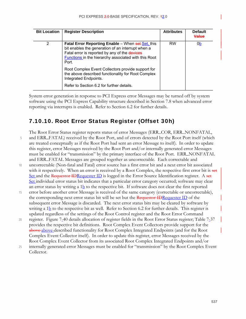
PCI EXPRESS 2.0 BASE SPECIFICATION, REV. 12.0
537
Bit Location Register Description Attributes Default Value
2 Fatal Error Reporting Enable – When set Set, this bit enables the generation of an interrupt when a Fatal error is reported by any of the devices Functions in the hierarchy associated with this Root Port.
Root Complex Event Collectors provide support for the above described functionality for Root Complex Integrated Endpoints.
Refer to Section 6.2 for further details.
RW 0b
System error generation in response to PCI Express error Messages may be turned off by system software using the PCI Express Capability structure described in Section 7.8 when advanced error reporting via interrupts is enabled. Refer to Section 6.2 for further details.
7.10.10. Root Error Status Register (Offset 30h)
The Root Error Status register reports status of error Messages (ERR_COR, ERR_NONFATAL, and ERR_FATAL) received by the Root Port, and of errors detected by the Root Port itself (which 5 are treated conceptually as if the Root Port had sent an error Message to itself). In order to update this register, error Messages received by the Root Port and/or internally generated error Messages must be enabled for “transmission” by the primary interface of the Root Port. ERR_NONFATAL and ERR_FATAL Messages are grouped together as uncorrectable. Each correctable and uncorrectable (Non-fatal and Fatal) error source has a first error bit and a next error bit associated 10 with it respectively. When an error is received by a Root Complex, the respective first error bit is set Set and the Requestor IDRequester ID is logged in the Error Source Identification register. A set Set individual error status bit indicates that a particular error category occurred; software may clear an error status by writing a 1b to the respective bit. If software does not clear the first reported error before another error Message is received of the same category (correctable or uncorrectable), 15 the corresponding next error status bit will be set but the Requestor IDRequester ID of the subsequent error Message is discarded. The next error status bits may be cleared by software by writing a 1b to the respective bit as well. Refer to Section 6.2 for further details. This register is updated regardless of the settings of the Root Control register and the Root Error Command register. Figure 7-40 details allocation of register fields in the Root Error Status register; Table 7-37 20 provides the respective bit definitions. Root Complex Event Collectors provide support for the above above-described functionality for Root Complex Integrated Endpoints (and for the Root Complex Event Collector itself). In order to update this register, error Messages received by the Root Complex Event Collector from its associated Root Complex Integrated Endpoints and/or internally generated error Messages must be enabled for “transmission” by the Root Complex Event 25 Collector.
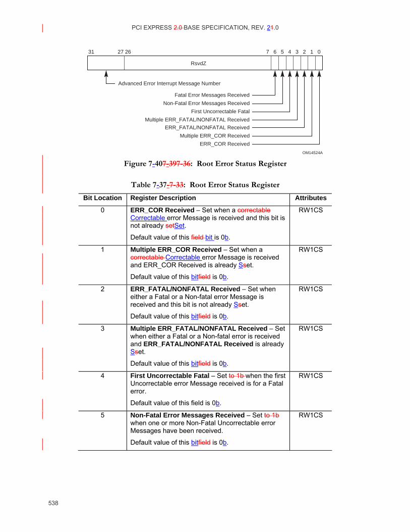
PCI EXPRESS 2.0 BASE SPECIFICATION, REV. 21.0
538
OM14524A
RsvdZ
Multiple ERR_COR Received
ERR_FATAL/NONFATAL Received
ERR_COR Received
Multiple ERR_FATAL/NONFATAL Received
Non-Fatal Error Messages Received
Fatal Error Messages Received
First Uncorrectable Fatal
Advanced Error Interrupt Message Number
31 27 26 4 3 2 1 07 6 5
Figure 7-407-39 7-36: Root Error Status Register
Table 7-37- 7-33: Root Error Status Register
Bit Location Register Description Attributes
0 ERR_COR Received – Set when a correctable Correctable error Message is received and this bit is not already setSet.
Default value of this field bit is 0b.
RW1CS
1 Multiple ERR_COR Received – Set when a correctable Correctable error Message is received and ERR_COR Received is already Sset.
Default value of this bitfield is 0b.
RW1CS
2 ERR_FATAL/NONFATAL Received – Set when either a Fatal or a Non-fatal error Message is received and this bit is not already Sset.
Default value of this bitfield is 0b.
RW1CS
3 Multiple ERR_FATAL/NONFATAL Received – Set when either a Fatal or a Non-fatal error is received and ERR_FATAL/NONFATAL Received is already Sset.
Default value of this bitfield is 0b.
RW1CS
4 First Uncorrectable Fatal – Set to 1b when the first Uncorrectable error Message received is for a Fatal error.
Default value of this field is 0b.
RW1CS
5 Non-Fatal Error Messages Received – Set to 1b when one or more Non-Fatal Uncorrectable error Messages have been received.
Default value of this bitfield is 0b.
RW1CS
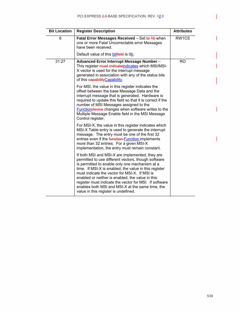
PCI EXPRESS 2.0 BASE SPECIFICATION, REV. 12.0
539
Bit Location Register Description Attributes
6 Fatal Error Messages Received – Set to 1b when one or more Fatal Uncorrectable error Messages have been received.
Default value of this bitfield is 0b.
RW1CS
31:27 Advanced Error Interrupt Message Number – This register must indicateindicates which MSI/MSI-X vector is used for the interrupt message generated in association with any of the status bits of this capabilityCapability.
For MSI, the value in this register indicates the offset between the base Message Data and the interrupt message that is generated. Hardware is required to update this field so that it is correct if the number of MSI Messages assigned to the Functiondevice changes when software writes to the Multiple Message Enable field in the MSI Message Control register.
For MSI-X, the value in this register indicates which MSI-X Table entry is used to generate the interrupt message. The entry must be one of the first 32 entries even if the function Function implements more than 32 entries. For a given MSI-X implementation, the entry must remain constant.
If both MSI and MSI-X are implemented, they are permitted to use different vectors, though software is permitted to enable only one mechanism at a time. If MSI-X is enabled, the value in this register must indicate the vector for MSI-X. If MSI is enabled or neither is enabled, the value in this register must indicate the vector for MSI. If software enables both MSI and MSI-X at the same time, the value in this register is undefined.
RO
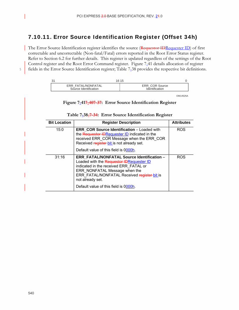
PCI EXPRESS 2.0 BASE SPECIFICATION, REV. 21.0
540
7.10.11. Error Source Identification Register (Offset 34h)
The Error Source Identification register identifies the source (Requestor IDRequester ID) of first correctable and uncorrectable (Non-fatal/Fatal) errors reported in the Root Error Status register. Refer to Section 6.2 for further details. This register is updated regardless of the settings of the Root Control register and the Root Error Command register. Figure 7-41 details allocation of register fields in the Error Source Identification register; Table 7-38 provides the respective bit definitions. 5
OM14525A
ERR_COR SourceIdentification
ERR_FATAL/NONFATALSource Identification
31 16 15 0
Figure 7-417-40 7-37: Error Source Identification Register
Table 7-38- 7-34: Error Source Identification Register
Bit Location Register Description Attributes
15:0 ERR_COR Source Identification – Loaded with the Requestor IDRequester ID indicated in the received ERR_COR Message when the ERR_COR Received register bit is not already set.
Default value of this field is 0000h.
ROS
31:16 ERR_FATAL/NONFATAL Source Identification – Loaded with the Requestor IDRequester ID indicated in the received ERR_FATAL or ERR_NONFATAL Message when the ERR_FATAL/NONFATAL Received register bit is not already set.
Default value of this field is 0000h.
ROS
PCI EXPRESS 2.0 BASE SPECIFICATION, REV. 12.0
541
7.11. Virtual Channel Capability The Virtual Channel (VC) Capability is an optional Extended Capability required for devices that have Ports (or for individual Functions) that support functionality beyond the default Traffic Class (TC0) over the default Virtual Channel (VC0).The PCI Express Virtual Channel (VC) capability is an optional extended capabilityExtended Capability that is required to be implemented by PCI Express Ports of devices that support PCI Express functionality beyond the general purpose I/O traffic, i.e., 5 the default Traffic Class 0 (TC0) over the default Virtual Channel 0 (VC0). This may apply to devices with only one VC that support TC filtering or to devices that support multiple VCs. Note that a PCI Express device that supports only TC0 over VC0 does not require VC extended capabilityExtended Capability and associated registers. Figure 7-42 provides a high level view of the PCI Express Virtual Channel Capability structure for all devices. This structure controls Virtual 10 Channel assignment for PCI Express Links and may be present in any device (or RCRB) that contains (controls) a port, or any device that has a Multi-Function Virtual Change (MFVC) Capability structure. Endpoint devices, Switch Ports (Upstream and Downstream), Root Ports and RCRB. Some registers/fields in the PCI Express Virtual Channel Capability structure may have different interpretation for Endpoint devices, Switch Ports, Root Ports and RCRB. Software must 15 interpret the PCI Express deviceDevice/Port Type field (Section 7.8.1) in the PCI Express Capability Capabilities structure register to determine the availability and meaning of these registers/fields.
The PCI Express VC Capability structure is permitted in the Extended Configuration Space of all single-function Function devices or in RCRBs. 20
A multi-functionFunction device at an Upstream Port may is permitted to optionally contain a Multi-Function Virtual Channel (MFVC) Capability structure (see Section 7.18). If a multi-functionFunction device contains an MFVC Capability structure, any or all of its functionFunctions are permitted to contain a VC Capability structure. Per-functionFunction VC Capability structures are also permitted for devices inside a Switch that contain only Switch Downstream Port 25 functionFunctions, or for Root Complex Integrated DevicesEndpoints. Otherwise, only functionFunction 0 is permitted to contain a VC Capability structure.
To preserve software backward compatibility, two Extended Capability IDs are permitted for VC Capability structures: 0002h and 0009h. Any VC Capability structure in a device that also contains an MFVC Capability structure must use the Extended Capability ID 0009h. A VC Capability 30 structure in a device that does not contain an MFVC Capability structure must use the Extended Capability ID 0002h.
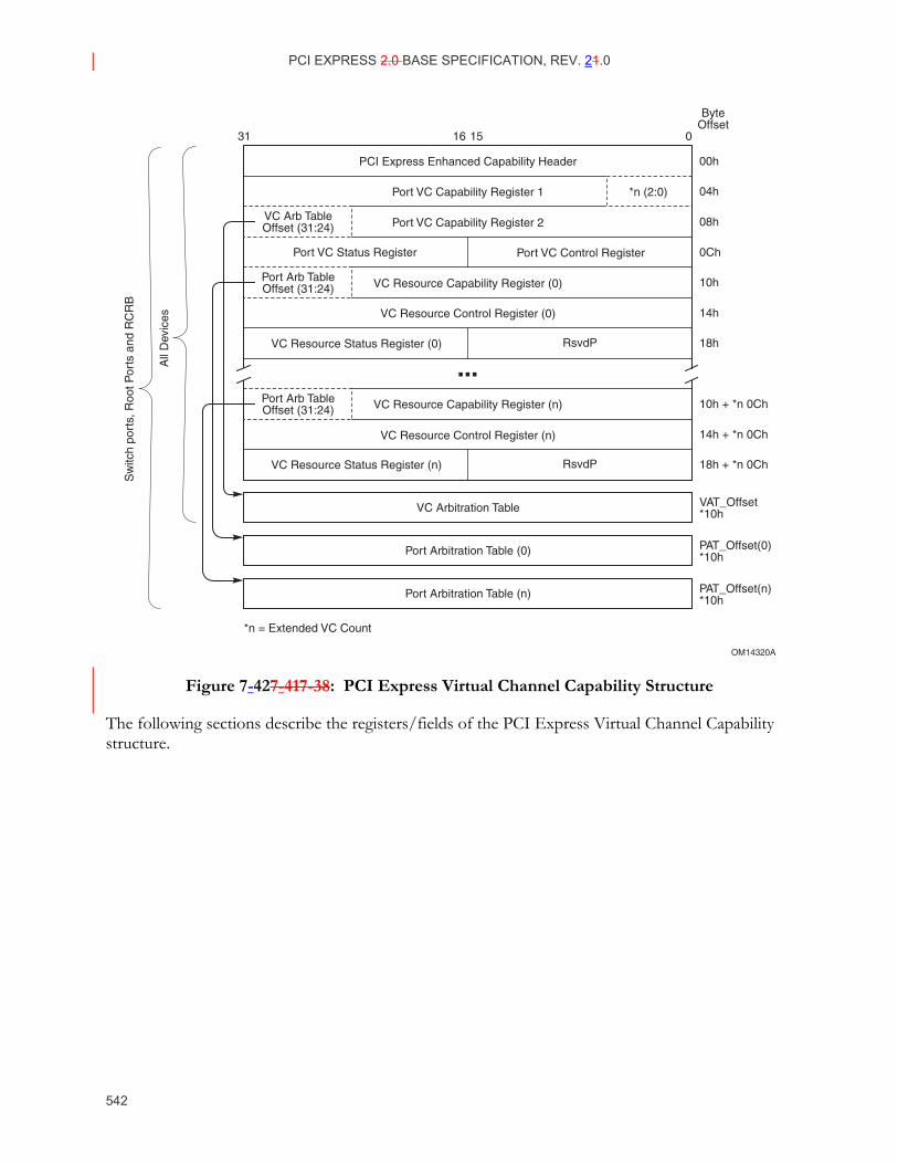
PCI EXPRESS 2.0 BASE SPECIFICATION, REV. 21.0
542
*n = Extended VC Count
OM14320A
Port VC Capability Register 2
Port VC Capability Register 1 *n (2:0)
PCI Express Enhanced Capability Header
Port VC Control RegisterPort VC Status Register
VC Arb TableOffset (31:24)
Port Arb TableOffset (31:24)
Port Arb TableOffset (31:24)
0
ByteOffset
31 16 15
04h
08h
00h
0Ch
10h
14h
18h
10h + *n 0Ch
14h + *n 0Ch
18h + *n 0Ch
VAT_Offset*10h
PAT_Offset(0)*10h
PAT_Offset(n)*10h
VC Resource Status Register (n) RsvdP
VC Resource Status Register (0) RsvdP
VC Arbitration Table
VC Resource Capability Register (0)
VC Resource Control Register (0)
VC Resource Control Register (n)
VC Resource Capability Register (n)
All
Dev
ices
Sw
itch
port
s, R
oot P
orts
and
RC
RB
Port Arbitration Table (0)
Port Arbitration Table (n)
Figure 7-427-41 7-38: PCI Express Virtual Channel Capability Structure
The following sections describe the registers/fields of the PCI Express Virtual Channel Capability structure.
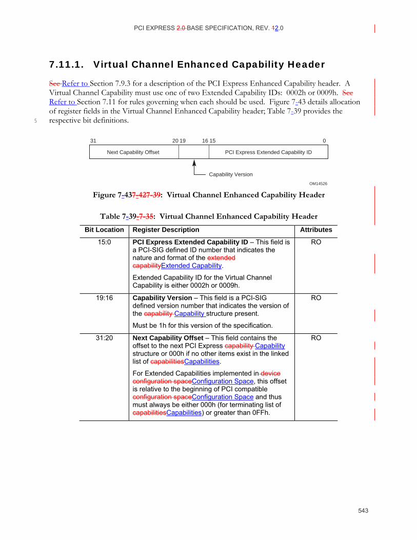
PCI EXPRESS 2.0 BASE SPECIFICATION, REV. 12.0
543
7.11.1. Virtual Channel Enhanced Capability Header
See Refer to Section 7.9.3 for a description of the PCI Express Enhanced Capability header. A Virtual Channel Capability must use one of two Extended Capability IDs: 0002h or 0009h. See Refer to Section 7.11 for rules governing when each should be used. Figure 7-43 details allocation of register fields in the Virtual Channel Enhanced Capability header; Table 7-39 provides the respective bit definitions. 5
OM14526
Capability Version
Next Capability Offset PCI Express Extended Capability ID
31 20 16 1519 0
Figure 7-437-42 7-39: Virtual Channel Enhanced Capability Header
Table 7-39- 7-35: Virtual Channel Enhanced Capability Header
Bit Location Register Description Attributes
15:0 PCI Express Extended Capability ID – This field is a PCI-SIG defined ID number that indicates the nature and format of the extended capabilityExtended Capability.
Extended Capability ID for the Virtual Channel Capability is either 0002h or 0009h.
RO
19:16 Capability Version – This field is a PCI-SIG defined version number that indicates the version of the capability Capability structure present.
Must be 1h for this version of the specification.
RO
31:20 Next Capability Offset – This field contains the offset to the next PCI Express capability Capability structure or 000h if no other items exist in the linked list of capabilitiesCapabilities.
For Extended Capabilities implemented in device configuration spaceConfiguration Space, this offset is relative to the beginning of PCI compatible configuration spaceConfiguration Space and thus must always be either 000h (for terminating list of capabilitiesCapabilities) or greater than 0FFh.
RO
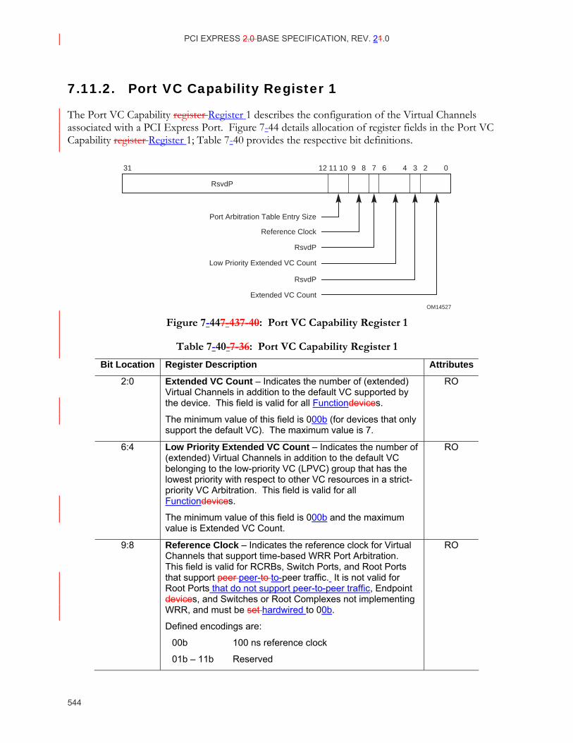
PCI EXPRESS 2.0 BASE SPECIFICATION, REV. 21.0
544
7.11.2. Port VC Capability Register 1
The Port VC Capability register Register 1 describes the configuration of the Virtual Channels associated with a PCI Express Port. Figure 7-44 details allocation of register fields in the Port VC Capability register Register 1; Table 7-40 provides the respective bit definitions.
OM14527
Low Priority Extended VC Count
RsvdP
Extended VC Count
RsvdP
Reference Clock
Port Arbitration Table Entry Size
RsvdP
31 12 11 10 9 8 7 6 4 3 2 0
Figure 7-447-43 7-40: Port VC Capability Register 1
Table 7-40- 7-36: Port VC Capability Register 1
Bit Location Register Description Attributes
2:0 Extended VC Count – Indicates the number of (extended) Virtual Channels in addition to the default VC supported by the device. This field is valid for all Functiondevices.
The minimum value of this field is 000b (for devices that only support the default VC). The maximum value is 7.
RO
6:4 Low Priority Extended VC Count – Indicates the number of (extended) Virtual Channels in addition to the default VC belonging to the low-priority VC (LPVC) group that has the lowest priority with respect to other VC resources in a strict-priority VC Arbitration. This field is valid for all Functiondevices.
The minimum value of this field is 000b and the maximum value is Extended VC Count.
RO
9:8 Reference Clock – Indicates the reference clock for Virtual Channels that support time-based WRR Port Arbitration. This field is valid for RCRBs, Switch Ports, and Root Ports that support peer peer-to to-peer traffic. It is not valid for Root Ports that do not support peer-to-peer traffic, Endpoint devices, and Switches or Root Complexes not implementing WRR, and must be set hardwired to 00b.
Defined encodings are:
00b 100 ns reference clock
01b – 11b Reserved
RO
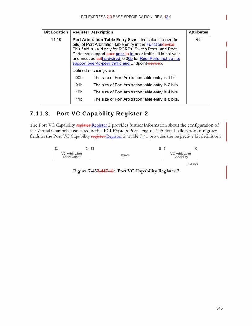
PCI EXPRESS 2.0 BASE SPECIFICATION, REV. 12.0
545
Bit Location Register Description Attributes
11:10 Port Arbitration Table Entry Size – Indicates the size (in bits) of Port Arbitration table entry in the Functiondevice. This field is valid only for RCRBs, Switch Ports, and Root Ports that support peer peer-to to-peer traffic. It is not valid and must be sethardwired to 00b for Root Ports that do not support peer-to-peer traffic and Endpoint devices.
Defined encodings are:
00b The size of Port Arbitration table entry is 1 bit.
01b The size of Port Arbitration table entry is 2 bits.
10b The size of Port Arbitration table entry is 4 bits.
11b The size of Port Arbitration table entry is 8 bits.
RO
7.11.3. Port VC Capability Register 2
The Port VC Capability register Register 2 provides further information about the configuration of the Virtual Channels associated with a PCI Express Port. Figure 7-45 details allocation of register fields in the Port VC Capability register Register 2; Table 7-41 provides the respective bit definitions.
OM14532
VC ArbitrationCapability
VC ArbitrationTable Offset RsvdP
31 24 23 8 7 0
Figure 7-457-44 7-41: Port VC Capability Register 2
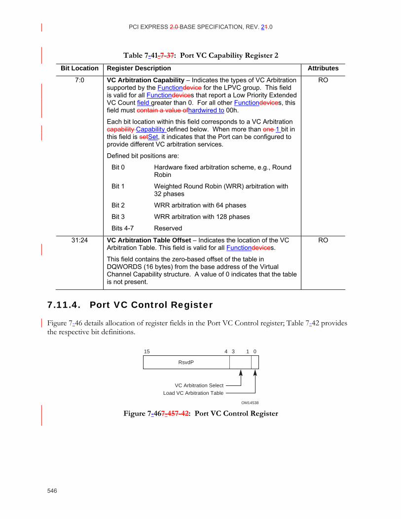
PCI EXPRESS 2.0 BASE SPECIFICATION, REV. 21.0
546
Table 7-41- 7-37: Port VC Capability Register 2
Bit Location Register Description Attributes
7:0 VC Arbitration Capability – Indicates the types of VC Arbitration supported by the Functiondevice for the LPVC group. This field is valid for all Functiondevices that report a Low Priority Extended VC Count field greater than 0. For all other Functiondevices, this field must contain a value ofhardwired to 00h.
Each bit location within this field corresponds to a VC Arbitration capability Capability defined below. When more than one 1 bit in this field is setSet, it indicates that the Port can be configured to provide different VC arbitration services.
Defined bit positions are:
Bit 0 Hardware fixed arbitration scheme, e.g., Round Robin
Bit 1 Weighted Round Robin (WRR) arbitration with 32 phases
Bit 2 WRR arbitration with 64 phases
Bit 3 WRR arbitration with 128 phases
Bits 4-7 Reserved
RO
31:24 VC Arbitration Table Offset – Indicates the location of the VC Arbitration Table. This field is valid for all Functiondevices.
This field contains the zero-based offset of the table in DQWORDS (16 bytes) from the base address of the Virtual Channel Capability structure. A value of 0 indicates that the table is not present.
RO
7.11.4. Port VC Control Register
Figure 7-46 details allocation of register fields in the Port VC Control register; Table 7-42 provides the respective bit definitions.
OM14538
RsvdP
Load VC Arbitration Table
VC Arbitration Select
15 1 04 3
Figure 7-467-45 7-42: Port VC Control Register
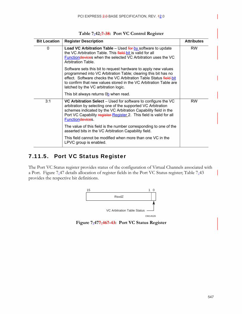
PCI EXPRESS 2.0 BASE SPECIFICATION, REV. 12.0
547
Table 7-42- 7-38: Port VC Control Register
Bit Location Register Description Attributes
0 Load VC Arbitration Table – Used for by software to update the VC Arbitration Table. This field bit is valid for all Functiondevices when the selected VC Arbitration uses the VC Arbitration Table.
Software sets this bit to request hardware to apply new values programmed into VC Arbitration Table; clearing this bit has no effect. Software checks the VC Arbitration Table Status field bit to confirm that new values stored in the VC Arbitration Table are latched by the VC arbitration logic.
This bit always returns 0b when read.
RW
3:1 VC Arbitration Select – Used for software to configure the VC arbitration by selecting one of the supported VC Arbitration schemes indicated by the VC Arbitration Capability field in the Port VC Capability register Register 2. This field is valid for all Functiondevices.
The value of this field is the number corresponding to one of the asserted bits in the VC Arbitration Capability field.
This field cannot be modified when more than one VC in the LPVC group is enabled.
RW
7.11.5. Port VC Status Register
The Port VC Status register provides status of the configuration of Virtual Channels associated with a Port. Figure 7-47 details allocation of register fields in the Port VC Status register; Table 7-43 provides the respective bit definitions.
OM14528
VC Arbitration Table Status
RsvdZ
15 1 0
Figure 7-477-46 7-43: Port VC Status Register
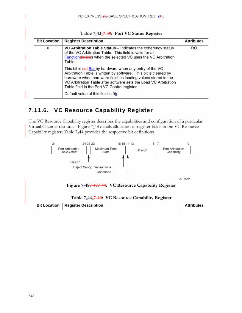
PCI EXPRESS 2.0 BASE SPECIFICATION, REV. 21.0
548
Table 7-43- 7-39: Port VC Status Register
Bit Location Register Description Attributes
0 VC Arbitration Table Status – Indicates the coherency status of the VC Arbitration Table. This field is valid for all Functiondevices when the selected VC uses the VC Arbitration Table.
This bit is set Set by hardware when any entry of the VC Arbitration Table is written by software. This bit is cleared by hardware when hardware finishes loading values stored in the VC Arbitration Table after software sets the Load VC Arbitration Table field in the Port VC Control register.
Default value of this field is 0b.
RO
7.11.6. VC Resource Capability Register
The VC Resource Capability register describes the capabilities and configuration of a particular Virtual Channel resource. Figure 7-48 details allocation of register fields in the VC Resource Capability register; Table 7-44 provides the respective bit definitions.
OM14529A
Port ArbitrationCapability
Maximum TimeSlots
Port ArbitrationTable Offset RsvdP
Reject Snoop Transactions
Undefined
RsvdP
31 24 23 22 16 15 14 8 7 013
Figure 7-487-47 7-44: VC Resource Capability Register
Table 7-44- 7-40: VC Resource Capability Register
Bit Location Register Description Attributes
PCI EXPRESS 2.0 BASE SPECIFICATION, REV. 12.0
549
Bit Location Register Description Attributes
7:0 Port Arbitration Capability – Indicates types of Port Arbitration supported by the VC resource. This field is valid for all Switch Ports, Root Ports that support peer peer-to to-peer traffic, and RCRBs, but not for PCI Express Endpoint devices or Root Ports that do not support peer peer-to to-peer traffic.
Each bit location within this field corresponds to a Port Arbitration capability Capability defined below. When more than one 1 bit in this field is setSet, it indicates that the VC resource can be configured to provide different arbitration services.
Software selects among these capabilities by writing to the Port Arbitration Select field (see below).
Defined bit positions are:
Bit 0 Non-configurable hardware-fixed arbitration scheme, e.g., Round Robin (RR)
Bit 1 Weighted Round Robin (WRR) arbitration with 32 phases
Bit 2 WRR arbitration with 64 phases
Bit 3 WRR arbitration with 128 phases
Bit 4 Time-based WRR with 128 phases
Bit 5 WRR arbitration with 256 phases
Bits 6-7 Reserved
RO
14 Undefined – The value read from this bit is undefined. In previous versions of this specification, this bit was used to indicate Advanced Packet Switching. System software must ignore the value read from this bit.
RO
15 Reject Snoop Transactions – When set to zero,Clear, transactions with or without the No Snoop bit set Set within the TLP Header header are allowed on this VC. When set to 1Set, any transaction for which the No Snoop attribute is applicable but is not Set without the No Snoop bit set within the TLP Header header will is permitted to be rejected as an Unsupported Request. Refer to Section 2.2.6.5 for information on where the No Snoop attribute is applicable. This field is valid for Root Ports and RCRB; it is not valid for PCI Express Endpoint devices or Switch Ports.
HwInit
22:16 Maximum Time Slots – Indicates the maximum number of time slots (minus one) that the VC resource is capable of supporting when it is configured for time-based WRR Port Arbitration. For example, a value 000 0000b in this field indicates the supported maximum number of time slots is 1 and a value of 127 111 1111b indicates the supported maximum number of time slot is 128. This field is valid for all Switch Ports, Root Ports that support peer peer-to to-peer traffic, and RCRBs, but is not valid for PCI Express Endpoint devices or Root Ports that do not support peer peer-to to-peer traffic. In addition, this field is valid only when the Port Arbitration Capability field indicates that the VC resource supports time-based WRR Port Arbitration.
HwInit
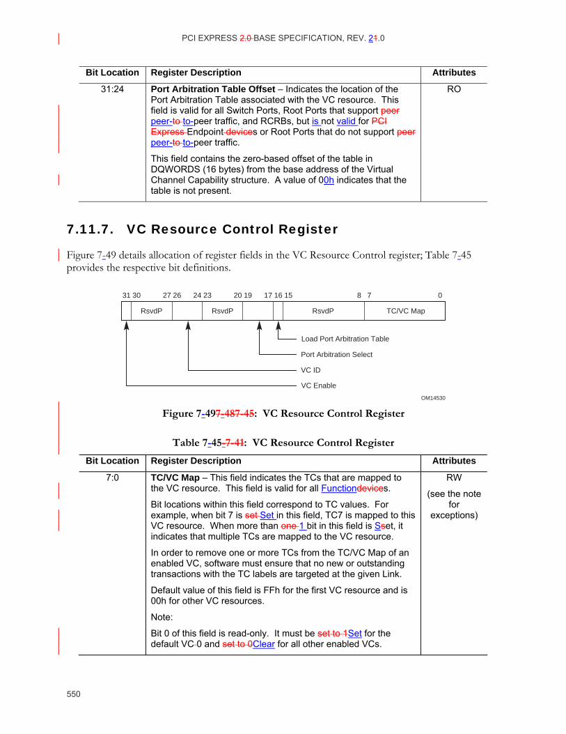
PCI EXPRESS 2.0 BASE SPECIFICATION, REV. 21.0
550
Bit Location Register Description Attributes
31:24 Port Arbitration Table Offset – Indicates the location of the Port Arbitration Table associated with the VC resource. This field is valid for all Switch Ports, Root Ports that support peer peer-to to-peer traffic, and RCRBs, but is not valid for PCI Express Endpoint devices or Root Ports that do not support peer peer-to to-peer traffic.
This field contains the zero-based offset of the table in DQWORDS (16 bytes) from the base address of the Virtual Channel Capability structure. A value of 00h indicates that the table is not present.
RO
7.11.7. VC Resource Control Register
Figure 7-49 details allocation of register fields in the VC Resource Control register; Table 7-45 provides the respective bit definitions.
OM14530
VC ID
VC Enable
Port Arbitration Select
Load Port Arbitration Table
RsvdP RsvdP RsvdP TC/VC Map
31 30 27 26 24 23 20 19 17 16 15 8 7 0
Figure 7-497-48 7-45: VC Resource Control Register
Table 7-45- 7-41: VC Resource Control Register
Bit Location Register Description Attributes
7:0 TC/VC Map – This field indicates the TCs that are mapped to the VC resource. This field is valid for all Functiondevices.
Bit locations within this field correspond to TC values. For example, when bit 7 is set Set in this field, TC7 is mapped to this VC resource. When more than one 1 bit in this field is Sset, it indicates that multiple TCs are mapped to the VC resource.
In order to remove one or more TCs from the TC/VC Map of an enabled VC, software must ensure that no new or outstanding transactions with the TC labels are targeted at the given Link.
Default value of this field is FFh for the first VC resource and is 00h for other VC resources.
Note:
Bit 0 of this field is read-only. It must be set to 1Set for the default VC 0 and set to 0Clear for all other enabled VCs.
RW
(see the note for
exceptions)
PCI EXPRESS 2.0 BASE SPECIFICATION, REV. 12.0
551
Bit Location Register Description Attributes
16 Load Port Arbitration Table – This bit, wWhen setSet, this bit updates the Port Arbitration logic from the Port Arbitration Table for the VC resource. This field bit is valid for all Switch Ports, Root Ports that support peer peer-to to-peer traffic, and RCRBs, but is not valid for PCI Express Endpoint devices or Root Ports that do not support peer peer-to to-peer traffic. In addition, this field bit is only valid when the Port Arbitration Table is used by the selected Port Arbitration scheme (that is indicated by a set Set bit in the Port Arbitration Capability field selected by Port Arbitration Select).
Software sets this bit to signal hardware to update Port Arbitration logic with new values stored in Port Arbitration Table; clearing this bit has no effect. Software uses the Port Arbitration Table Status bit to confirm whether the new values of Port Arbitration Table are completely latched by the arbitration logic.
This bit always returns 0b when read.
Default value of this field bit is 0b.
RW
19:17 Port Arbitration Select – This field configures the VC resource to provide a particular Port Arbitration service. This field is valid for RCRBs, Root Ports that support peer peer-to to-peer traffic, and Switch Ports, but is not valid for PCI Express Endpoint devices or Root Ports that do not support peer peer-to to-peer traffic.
The permissible value of this field is a number corresponding to one of the asserted bits in the Port Arbitration Capability field of the VC resource.
RW
26:24 VC ID – This field assigns a VC ID to the VC resource (see note for exceptions). This field is valid for all Functiondevices.
This field cannot be modified when the VC is already enabled.
Note:
For the first VC resource (default VC), this field is a read-only field thatand must be set hardwired to 000b (“hard-wired”).
RW
PCI EXPRESS 2.0 BASE SPECIFICATION, REV. 21.0
552
Bit Location Register Description Attributes
31 VC Enable – This fieldbit, when setSet, enables a Virtual Channel (see note 1 for exceptions). The Virtual Channel is disabled when this bitfield is cleared. This bitfield is valid for all Functiondevices.
Software must use the VC Negotiation Pending bit to check whether the VC negotiation is complete. When VC Negotiation Pending bit is cleared, a 1b read from this VC Enable bit indicates that the VC is enabled (Flow Control initialization is completed for the PCI Express Port); a 0b read from this bit indicates that the Virtual Channel is currently disabled.
Default value of this bitfield is 1b for the first VC resource and is 0b for other VC resource(s).
Notes:
1. This bit is hardwired to 1b for the default VC (VC0), i.e., writing to this bitfield has no effect for VC0.
2. To enable a Virtual Channel, the VC Enable bits for that Virtual Channel must be set Set in both components on a Link.
3. To disable a Virtual Channel, the VC Enable bits for that Virtual Channel must be cleared in both components on a Link.
4. Software must ensure that no traffic is using a Virtual Channel at the time it is disabled.
5. Software must fully disable a Virtual Channel in both components on a Link before re-enabling the Virtual Channel.
RW
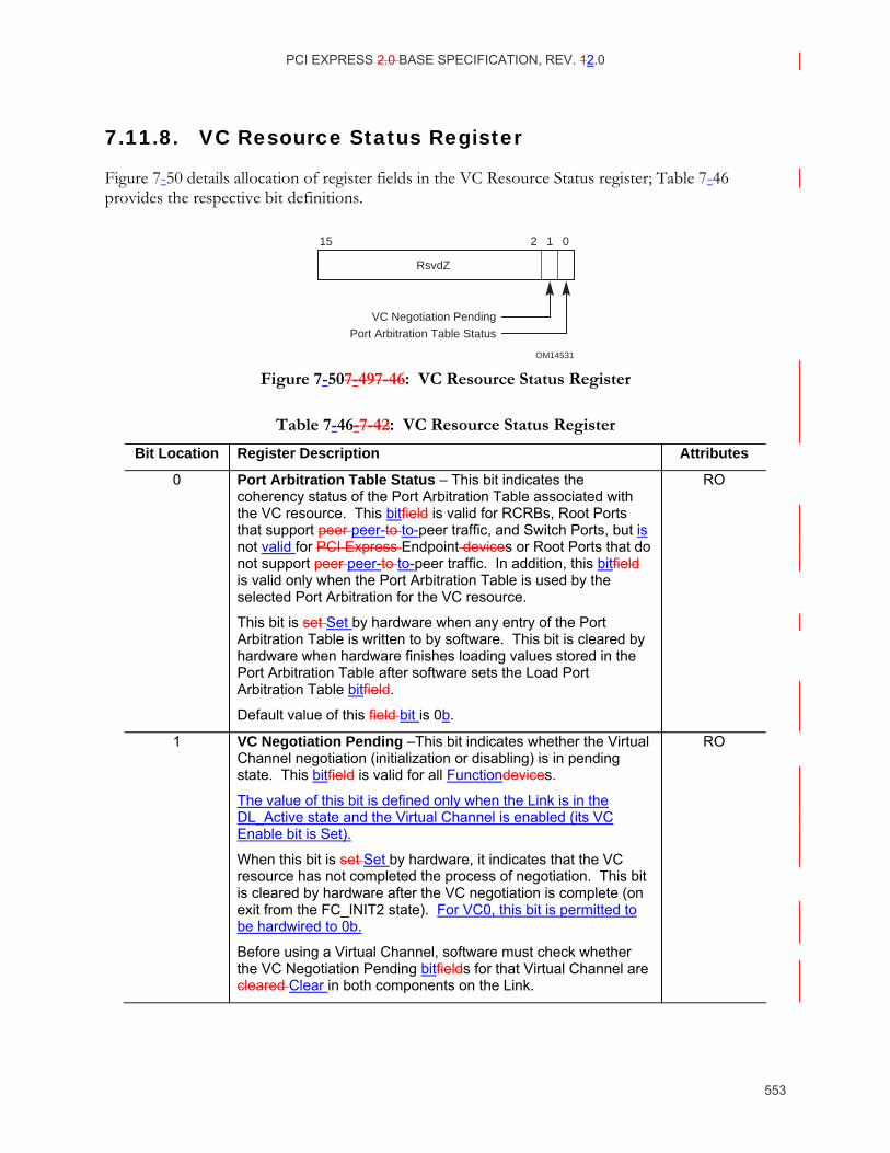
PCI EXPRESS 2.0 BASE SPECIFICATION, REV. 12.0
553
7.11.8. VC Resource Status Register
Figure 7-50 details allocation of register fields in the VC Resource Status register; Table 7-46 provides the respective bit definitions.
OM14531
RsvdZ
Port Arbitration Table Status
VC Negotiation Pending
15 2 1 0
Figure 7-507-49 7-46: VC Resource Status Register
Table 7-46- 7-42: VC Resource Status Register
Bit Location Register Description Attributes
0 Port Arbitration Table Status – This bit indicates the coherency status of the Port Arbitration Table associated with the VC resource. This bitfield is valid for RCRBs, Root Ports that support peer peer-to to-peer traffic, and Switch Ports, but is not valid for PCI Express Endpoint devices or Root Ports that do not support peer peer-to to-peer traffic. In addition, this bitfield is valid only when the Port Arbitration Table is used by the selected Port Arbitration for the VC resource.
This bit is set Set by hardware when any entry of the Port Arbitration Table is written to by software. This bit is cleared by hardware when hardware finishes loading values stored in the Port Arbitration Table after software sets the Load Port Arbitration Table bitfield.
Default value of this field bit is 0b.
RO
1 VC Negotiation Pending –This bit indicates whether the Virtual Channel negotiation (initialization or disabling) is in pending state. This bitfield is valid for all Functiondevices.
The value of this bit is defined only when the Link is in the DL_Active state and the Virtual Channel is enabled (its VC Enable bit is Set).
When this bit is set Set by hardware, it indicates that the VC resource has not completed the process of negotiation. This bit is cleared by hardware after the VC negotiation is complete (on exit from the FC_INIT2 state). For VC0, this bit is permitted to be hardwired to 0b.
Before using a Virtual Channel, software must check whether the VC Negotiation Pending bitfields for that Virtual Channel are cleared Clear in both components on the Link.
RO
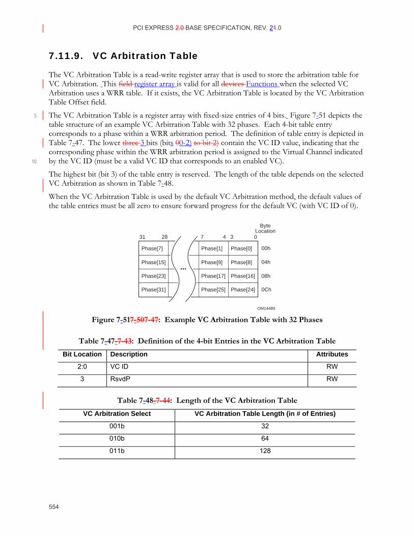
PCI EXPRESS 2.0 BASE SPECIFICATION, REV. 21.0
554
7.11.9. VC Arbitration Table
The VC Arbitration Table is a read-write register array that is used to store the arbitration table for VC Arbitration. This field register array is valid for all devices Functions when the selected VC Arbitration uses a WRR table. If it exists, the VC Arbitration Table is located by the VC Arbitration Table Offset field.
The VC Arbitration Table is a register array with fixed-size entries of 4 bits. Figure 7-51 depicts the 5 table structure of an example VC Arbitration Table with 32 phases. Each 4-bit table entry corresponds to a phase within a WRR arbitration period. The definition of table entry is depicted in Table 7-47. The lower three 3 bits (bits 00-2) to bit 2) contain the VC ID value, indicating that the corresponding phase within the WRR arbitration period is assigned to the Virtual Channel indicated by the VC ID (must be a valid VC ID that corresponds to an enabled VC). 10
The highest bit (bit 3) of the table entry is reserved. The length of the table depends on the selected VC Arbitration as shown in Table 7-48.
When the VC Arbitration Table is used by the default VC Arbitration method, the default values of the table entries must be all zero to ensure forward progress for the default VC (with VC ID of 0).
OM14489
Phase[0]
Phase[8]
Phase[16]
Phase[24]
Phase[1]
Phase[9]
Phase[17]
Phase[25]
Phase[7]
Phase[15]
Phase[23]
Phase[31]
31 7 4 328 0
ByteLocation
04h
08h
00h
0Ch
Figure 7-517-50 7-47: Example VC Arbitration Table with 32 Phases
Table 7-47- 7-43: Definition of the 4-bit Entries in the VC Arbitration Table
Bit Location Description Attributes
2:0 VC ID RW
3 RsvdP RW
Table 7-48- 7-44: Length of the VC Arbitration Table
VC Arbitration Select VC Arbitration Table Length (in # of Entries)
001b 32
010b 64
011b 128

PCI EXPRESS 2.0 BASE SPECIFICATION, REV. 12.0
555
7.11.10. Port Arbitration Table
The Port Arbitration Table register is a read-write register array that is used to store the WRR or time-based WRR arbitration table for Port Arbitration for the VC resource. This register array is valid for all Switch Ports, Root Ports that support peer peer-to to-peer traffic, and RCRBs, but is not valid for Endpoint devices or Root Ports that do not support peer-to-peer traffic. It is only present when one or more asserted bits in the Port Arbitration Capability field indicate that the device 5 component supports a Port Arbitration scheme that uses a programmable arbitration table. Furthermore, it is only valid when one of the above above-mentioned bits in the Port Arbitration Capability field is selected by the Port Arbitration Select field.
The Port Arbitration Table represents one Port arbitration period. Figure 7-52 shows the structure of an example Port Arbitration Table with 128 phases and 2-bit table entries. Each table entry 10 containing a Port Number corresponds to a phase within a Port arbitration period. For example, a table with 2-bit entries can be used by a Switch component with up to four Ports. A Port Number written to a table entry indicates that the phase within the Port Arbitration period is assigned to the selected PCI Express Port (the Port Number must be a valid one).
When the WRR Port Arbitration is used for a VC of any Egress Port, at each arbitration phase, 15 the Port Arbiter serves one transaction from the Ingress Port indicated by the Port Number of the current phase. When finished, it immediately advances to the next phase. A phase is skipped, i.e., the Port Arbiter simply moves to the next phase without delayimmediately, if the Ingress Port indicated by the phase does not contain any transaction for the VC (note that a phase cannot contain the Egress Port's Port Number). 20
When the Time-based WRR Port Arbitration is used for a VC of any given Port, at each arbitration phase aligning to a virtual timeslot, the Port Arbiter serves one transaction from the Ingress Port indicated by the Port Number of the current phase. It advances to the next phase at the next virtual timeslot. A phase indicates an “idle” timeslot, i.e., the Port Arbiter does not serve any transaction during the phase, if 25
• the phase contains the Egress Port's Port Number, or
• the Ingress Port indicated by the phase does not contain any transaction for the VC.
The Port Arbitration Table Entry Size field in the Port VC Capability register Register 1 determines the table entry size. The length of the table is determined by the Port Arbitration Select field as shown in Table 7-49. 30
When the Port Arbitration Table is used by the default Port Arbitration for the default VC, the default values for the table entries must contain at least one entry for each of the other PCI Express Ports of the device component to ensure forward progress for the default VC for each Port. The table may contain RR or RR-like fair Port Arbitration for the default VC.

PCI EXPRESS 2.0 BASE SPECIFICATION, REV. 21.0
556
OM14490
Phase[0]
Phase[16]
Phase[32]
Phase[48]
Phase[64]
Phase[80]
Phase[96]
Phase[112]
Phase[1]
Phase[17]
Phase[33]
Phase[49]
Phase[65]
Phase[81]
Phase[97]
Phase[113]
Phase[15]
Phase[31]
Phase[47]
Phase[63]
Phase[79]
Phase[95]
Phase[111]
Phase[127]
2 14 3 0
ByteLocation
31 30
04h
08h
00h
0Ch
10h
14h
18h
1Ch
Figure 7-527-51 7-48: Example Port Arbitration Table with 128 Phases and 2-bit Table
Entries
Table 7-49- 7-45: Length of Port Arbitration Table
Port Arbitration Select Port Arbitration Table Length (in number Number of Entries)
001b 32 010b 64 011b 128 100b 128 101b 256
7.12. Device Serial Number Capability The PCI Express Device Serial Number capability Capability is an optional extended capabilityExtended Capability that may be implemented by any PCI Express device Function. The Device Serial Number is a read-only 64-bit value that is unique for a given PCI Express device. Figure 7-53 details allocation of register fields in the PCI Express Capability structure.
All multi-function Function devices that implement this capability Capability must implement it for 5 Ffunction 0; other Ffunctions that implement this Ccapability must return the same Device Serial Number value as that reported by Ffunction 0.
A PCI Express multi-device component such as a PCI Express Switch that implements this Ccapability must return the same Device Serial Number for each device.
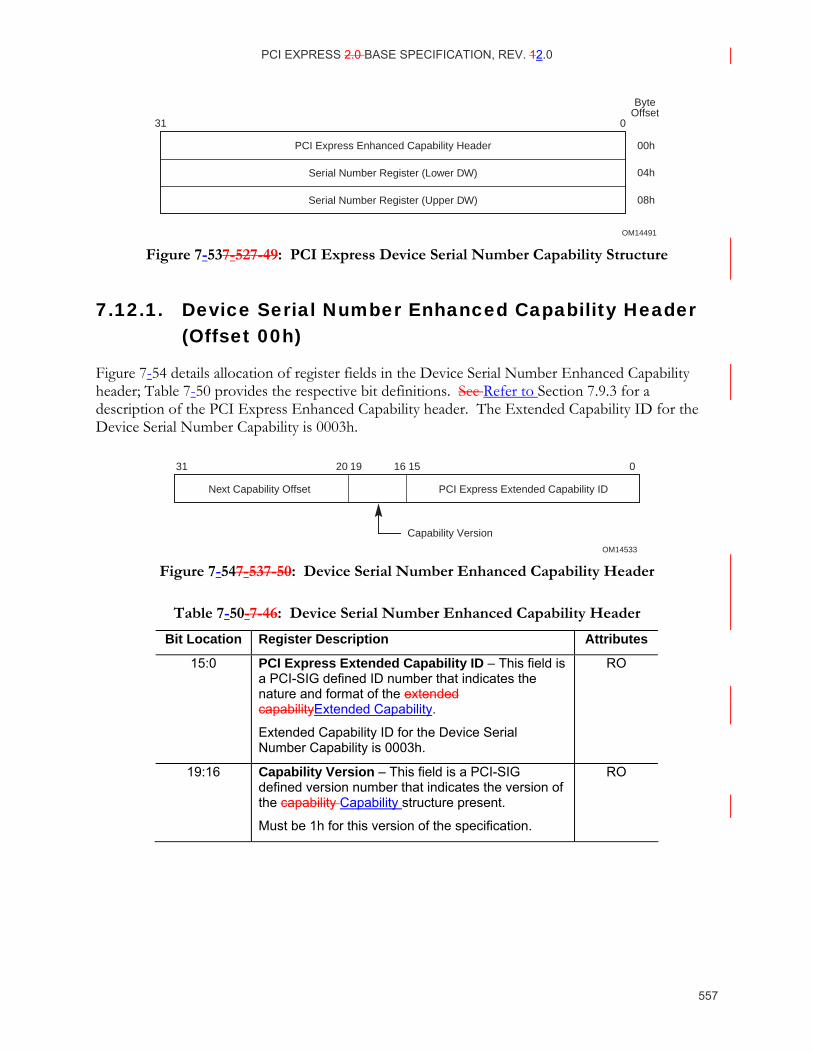
PCI EXPRESS 2.0 BASE SPECIFICATION, REV. 12.0
557
OM14491
0
ByteOffset
31
04h
08h
00hPCI Express Enhanced Capability Header
Serial Number Register (Lower DW)
Serial Number Register (Upper DW)
Figure 7-537-52 7-49: PCI Express Device Serial Number Capability Structure
7.12.1. Device Serial Number Enhanced Capability Header (Offset 00h)
Figure 7-54 details allocation of register fields in the Device Serial Number Enhanced Capability header; Table 7-50 provides the respective bit definitions. See Refer to Section 7.9.3 for a description of the PCI Express Enhanced Capability header. The Extended Capability ID for the Device Serial Number Capability is 0003h.
OM14533
Capability Version
Next Capability Offset PCI Express Extended Capability ID
31 20 16 1519 0
Figure 7-547-53 7-50: Device Serial Number Enhanced Capability Header
Table 7-50- 7-46: Device Serial Number Enhanced Capability Header
Bit Location Register Description Attributes
15:0 PCI Express Extended Capability ID – This field is a PCI-SIG defined ID number that indicates the nature and format of the extended capabilityExtended Capability.
Extended Capability ID for the Device Serial Number Capability is 0003h.
RO
19:16 Capability Version – This field is a PCI-SIG defined version number that indicates the version of the capability Capability structure present.
Must be 1h for this version of the specification.
RO
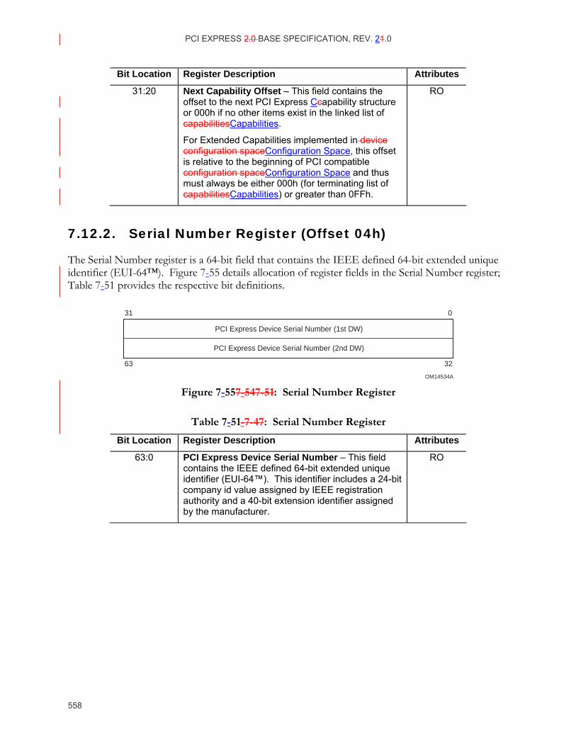
PCI EXPRESS 2.0 BASE SPECIFICATION, REV. 21.0
558
Bit Location Register Description Attributes
31:20 Next Capability Offset – This field contains the offset to the next PCI Express Ccapability structure or 000h if no other items exist in the linked list of capabilitiesCapabilities.
For Extended Capabilities implemented in device configuration spaceConfiguration Space, this offset is relative to the beginning of PCI compatible configuration spaceConfiguration Space and thus must always be either 000h (for terminating list of capabilitiesCapabilities) or greater than 0FFh.
RO
7.12.2. Serial Number Register (Offset 04h)
The Serial Number register is a 64-bit field that contains the IEEE defined 64-bit extended unique identifier (EUI-64™). Figure 7-55 details allocation of register fields in the Serial Number register; Table 7-51 provides the respective bit definitions.
OM14534A
PCI Express Device Serial Number (1st DW)
PCI Express Device Serial Number (2nd DW)
31 0
63 32
Figure 7-557-54 7-51: Serial Number Register
Table 7-51- 7-47: Serial Number Register
Bit Location Register Description Attributes
63:0 PCI Express Device Serial Number – This field contains the IEEE defined 64-bit extended unique identifier (EUI-64™). This identifier includes a 24-bit company id value assigned by IEEE registration authority and a 40-bit extension identifier assigned by the manufacturer.
RO
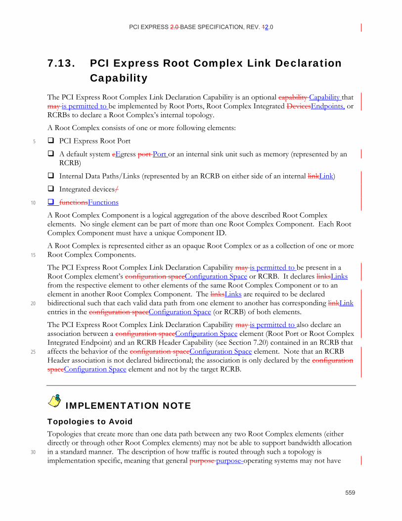
PCI EXPRESS 2.0 BASE SPECIFICATION, REV. 12.0
559
7.13. PCI Express Root Complex Link Declaration Capability
The PCI Express Root Complex Link Declaration Capability is an optional capability Capability that may is permitted to be implemented by Root Ports, Root Complex Integrated DevicesEndpoints, or RCRBs to declare a Root Complex’s internal topology.
A Root Complex consists of one or more following elements:
PCI Express Root Port 5
A default system eEgress port Port or an internal sink unit such as memory (represented by an RCRB)
Internal Data Paths/Links (represented by an RCRB on either side of an internal linkLink)
Integrated devices/
functionsFunctions 10
A Root Complex Component is a logical aggregation of the above described Root Complex elements. No single element can be part of more than one Root Complex Component. Each Root Complex Component must have a unique Component ID.
A Root Complex is represented either as an opaque Root Complex or as a collection of one or more Root Complex Components. 15
The PCI Express Root Complex Link Declaration Capability may is permitted to be present in a Root Complex element’s configuration spaceConfiguration Space or RCRB. It declares linksLinks from the respective element to other elements of the same Root Complex Component or to an element in another Root Complex Component. The linksLinks are required to be declared bidirectional such that each valid data path from one element to another has corresponding linkLink 20 entries in the configuration spaceConfiguration Space (or RCRB) of both elements.
The PCI Express Root Complex Link Declaration Capability may is permitted to also declare an association between a configuration spaceConfiguration Space element (Root Port or Root Complex Integrated Endpoint) and an RCRB Header Capability (see Section 7.20) contained in an RCRB that affects the behavior of the configuration spaceConfiguration Space element. Note that an RCRB 25 Header association is not declared bidirectional; the association is only declared by the configuration spaceConfiguration Space element and not by the target RCRB.
IMPLEMENTATION NOTE Topologies to Avoid Topologies that create more than one data path between any two Root Complex elements (either directly or through other Root Complex elements) may not be able to support bandwidth allocation in a standard manner. The description of how traffic is routed through such a topology is 30 implementation specific, meaning that general purpose purpose-operating systems may not have
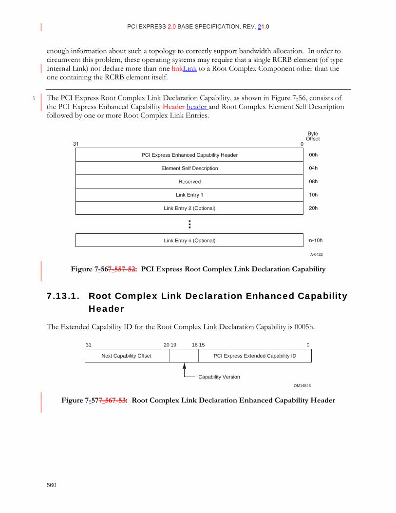
PCI EXPRESS 2.0 BASE SPECIFICATION, REV. 21.0
560
enough information about such a topology to correctly support bandwidth allocation. In order to circumvent this problem, these operating systems may require that a single RCRB element (of type Internal Link) not declare more than one linkLink to a Root Complex Component other than the one containing the RCRB element itself.
The PCI Express Root Complex Link Declaration Capability, as shown in Figure 7-56, consists of 5 the PCI Express Enhanced Capability Header header and Root Complex Element Self Description followed by one or more Root Complex Link Entries.
A-0422
0
ByteOffset
31
04h
08h
00h
10h
20h
n*10h
PCI Express Enhanced Capability Header
Element Self Description
Reserved
Link Entry 1
Link Entry 2 (Optional)
Link Entry n (Optional)
Figure 7-567-55 7-52: PCI Express Root Complex Link Declaration Capability
7.13.1. Root Complex Link Declaration Enhanced Capability Header
The Extended Capability ID for the Root Complex Link Declaration Capability is 0005h.
OM14526
Capability Version
Next Capability Offset PCI Express Extended Capability ID
31 20 16 1519 0
Figure 7-577-56 7-53: Root Complex Link Declaration Enhanced Capability Header
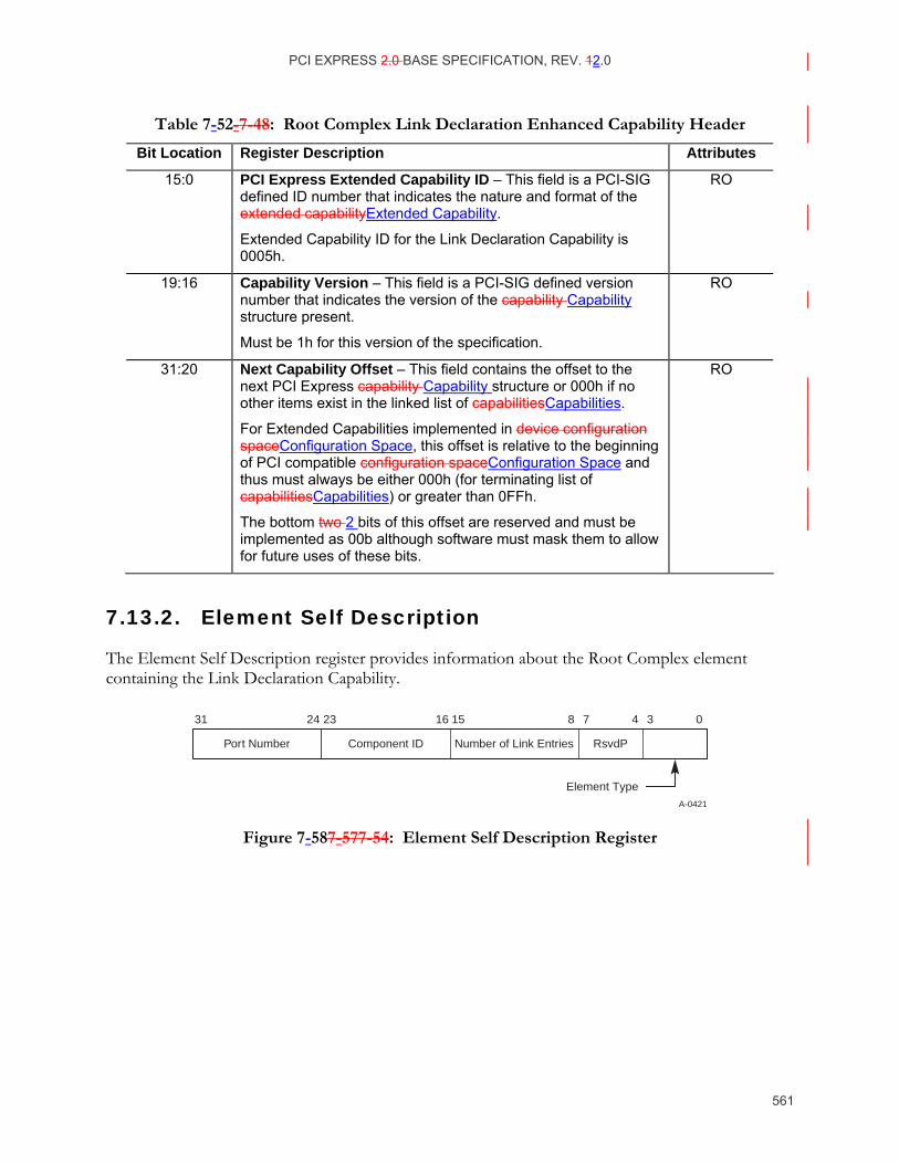
PCI EXPRESS 2.0 BASE SPECIFICATION, REV. 12.0
561
Table 7-52- 7-48: Root Complex Link Declaration Enhanced Capability Header
Bit Location Register Description Attributes
15:0 PCI Express Extended Capability ID – This field is a PCI-SIG defined ID number that indicates the nature and format of the extended capabilityExtended Capability.
Extended Capability ID for the Link Declaration Capability is 0005h.
RO
19:16 Capability Version – This field is a PCI-SIG defined version number that indicates the version of the capability Capability structure present.
Must be 1h for this version of the specification.
RO
31:20 Next Capability Offset – This field contains the offset to the next PCI Express capability Capability structure or 000h if no other items exist in the linked list of capabilitiesCapabilities.
For Extended Capabilities implemented in device configuration spaceConfiguration Space, this offset is relative to the beginning of PCI compatible configuration spaceConfiguration Space and thus must always be either 000h (for terminating list of capabilitiesCapabilities) or greater than 0FFh.
The bottom two 2 bits of this offset are reserved and must be implemented as 00b although software must mask them to allow for future uses of these bits.
RO
7.13.2. Element Self Description
The Element Self Description register provides information about the Root Complex element containing the Link Declaration Capability.
A-0421
Port Number RsvdPNumber of Link EntriesComponent ID
Element Type
31 24 23 16 15 08 7 4 3
Figure 7-587-57 7-54: Element Self Description Register
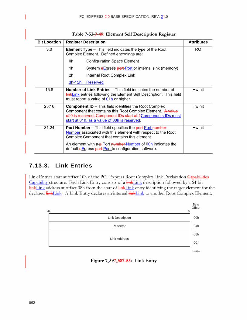
PCI EXPRESS 2.0 BASE SPECIFICATION, REV. 21.0
562
Table 7-53- 7-49: Element Self Description Register
Bit Location Register Description Attributes
3:0 Element Type – This field indicates the type of the Root Complex Element. Defined encodings are:
0h Configuration Space Element
1h System eEgress port Port or internal sink (memory)
2h Internal Root Complex Link
3h-15h Reserved
RO
15:8 Number of Link Entries – This field indicates the number of linkLink entries following the Element Self Description. This field must report a value of 01h or higher.
HwInit
23:16 Component ID – This field identifies the Root Complex Component that contains this Root Complex Element. A value of 0 is reserved; Component IDs start at 1Components IDs must start at 01h, as a value of 00h is reserved.
HwInit
31:24 Port Number – This field specifies the port Port number Number associated with this element with respect to the Root Complex Component that contains this element.
An element with a p Port number Number of 00h indicates the default eEgress port Port to configuration software.
HwInit
7.13.3. Link Entries
Link Entries start at offset 10h of the PCI Express Root Complex Link Declaration Capabilities Capability structure. Each Link Entry consists of a linkLink description followed by a 64-bit linkLink address at offset 08h from the start of linkLink entry identifying the target element for the declared linkLink. A Link Entry declares an internal linkLink to another Root Complex Element.
A-0420
0
ByteOffset
31
04h
08h
0Ch
00hLink Description
Reserved
Link Address
Figure 7-597-58 7-55: Link Entry
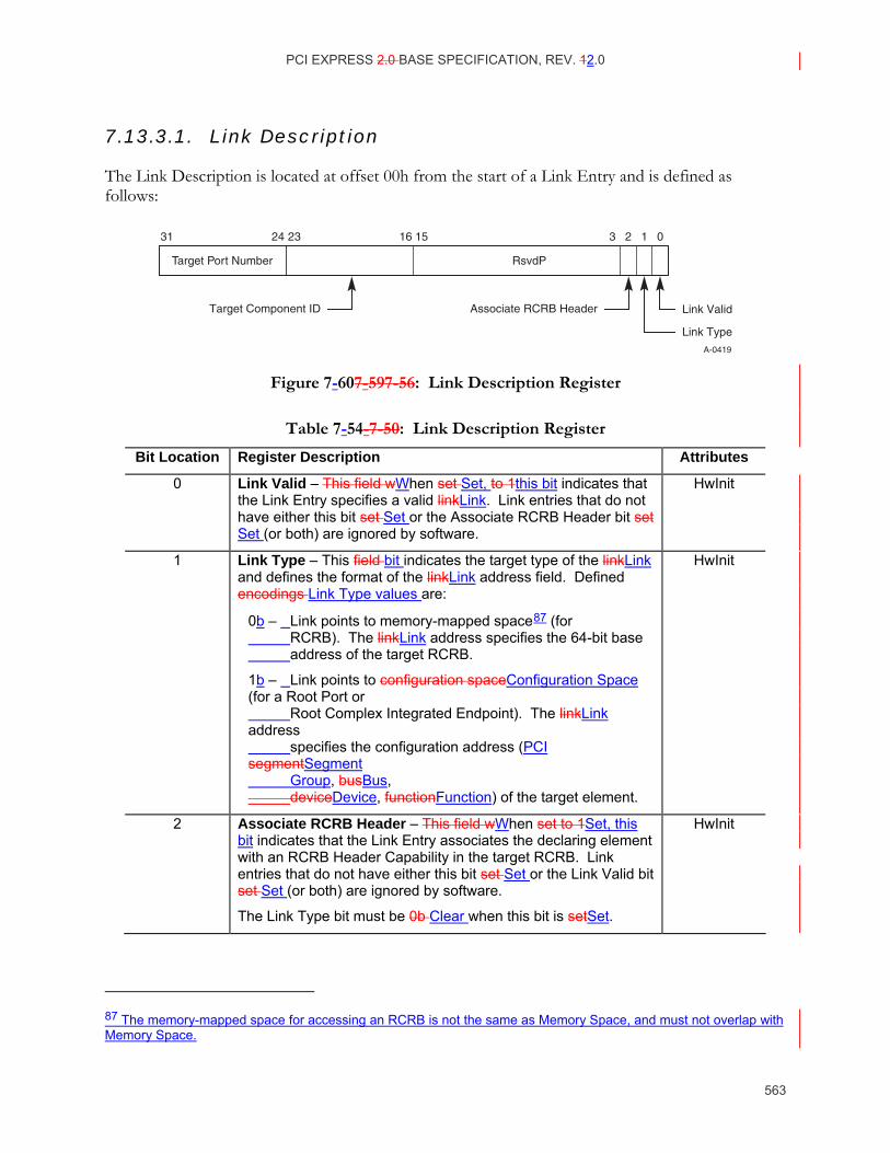
PCI EXPRESS 2.0 BASE SPECIFICATION, REV. 12.0
563
7.13.3.1. Link Description
The Link Description is located at offset 00h from the start of a Link Entry and is defined as follows:
A-0419
Link Type
Link Valid
Target Port Number RsvdP
Target Component ID Associate RCRB Header
31 24 23 16 15 2 1 03
Figure 7-607-59 7-56: Link Description Register
Table 7-54- 7-50: Link Description Register
Bit Location Register Description Attributes
0 Link Valid – This field wWhen set Set, to 1this bit indicates that the Link Entry specifies a valid linkLink. Link entries that do not have either this bit set Set or the Associate RCRB Header bit set Set (or both) are ignored by software.
HwInit
1 Link Type – This field bit indicates the target type of the linkLink and defines the format of the linkLink address field. Defined encodings Link Type values are:
0b – Link points to memory-mapped space87 (for RCRB). The linkLink address specifies the 64-bit base address of the target RCRB.
1b – Link points to configuration spaceConfiguration Space (for a Root Port or Root Complex Integrated Endpoint). The linkLink address specifies the configuration address (PCI segmentSegment Group, busBus, deviceDevice, functionFunction) of the target element.
HwInit
2 Associate RCRB Header – This field wWhen set to 1Set, this bit indicates that the Link Entry associates the declaring element with an RCRB Header Capability in the target RCRB. Link entries that do not have either this bit set Set or the Link Valid bit set Set (or both) are ignored by software.
The Link Type bit must be 0b Clear when this bit is setSet.
HwInit
87 The memory-mapped space for accessing an RCRB is not the same as Memory Space, and must not overlap with Memory Space.
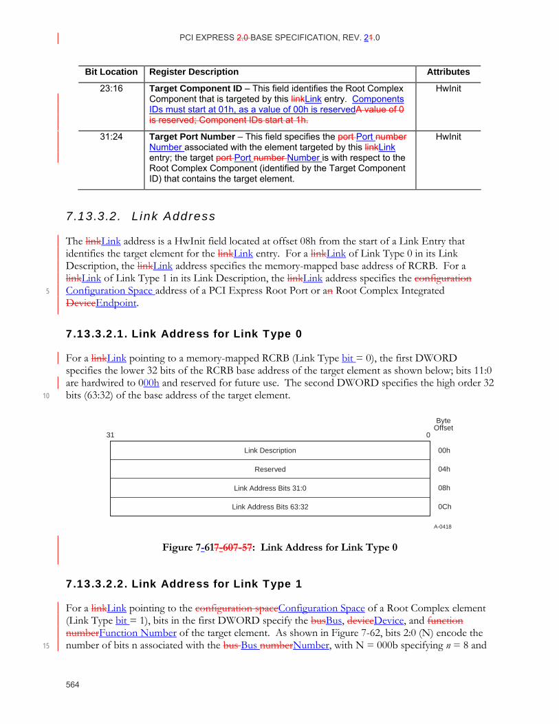
PCI EXPRESS 2.0 BASE SPECIFICATION, REV. 21.0
564
Bit Location Register Description Attributes
23:16 Target Component ID – This field identifies the Root Complex Component that is targeted by this linkLink entry. Components IDs must start at 01h, as a value of 00h is reservedA value of 0 is reserved; Component IDs start at 1h.
HwInit
31:24 Target Port Number – This field specifies the port Port number Number associated with the element targeted by this linkLink entry; the target port Port number Number is with respect to the Root Complex Component (identified by the Target Component ID) that contains the target element.
HwInit
7.13.3.2. Link Address
The linkLink address is a HwInit field located at offset 08h from the start of a Link Entry that identifies the target element for the linkLink entry. For a linkLink of Link Type 0 in its Link Description, the linkLink address specifies the memory-mapped base address of RCRB. For a linkLink of Link Type 1 in its Link Description, the linkLink address specifies the configuration Configuration Space address of a PCI Express Root Port or an Root Complex Integrated 5 DeviceEndpoint.
7.13.3.2.1. Link Address for Link Type 0
For a linkLink pointing to a memory-mapped RCRB (Link Type bit = 0), the first DWORD specifies the lower 32 bits of the RCRB base address of the target element as shown below; bits 11:0 are hardwired to 000h and reserved for future use. The second DWORD specifies the high order 32 bits (63:32) of the base address of the target element. 10
A-0418
0
ByteOffset
31
04h
08h
0Ch
00hLink Description
Reserved
Link Address Bits 63:32
Link Address Bits 31:0
Figure 7-617-60 7-57: Link Address for Link Type 0
7.13.3.2.2. Link Address for Link Type 1
For a linkLink pointing to the configuration spaceConfiguration Space of a Root Complex element (Link Type bit = 1), bits in the first DWORD specify the busBus, deviceDevice, and function numberFunction Number of the target element. As shown in Figure 7-62, bits 2:0 (N) encode the number of bits n associated with the bus Bus numberNumber, with N = 000b specifying n = 8 and 15
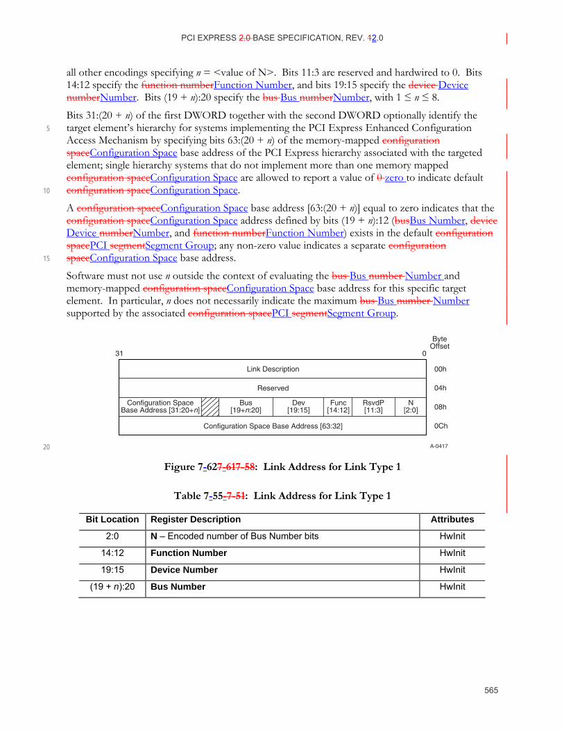
PCI EXPRESS 2.0 BASE SPECIFICATION, REV. 12.0
565
all other encodings specifying n = <value of N>. Bits 11:3 are reserved and hardwired to 0. Bits 14:12 specify the function numberFunction Number, and bits 19:15 specify the device Device numberNumber. Bits (19 + n):20 specify the bus Bus numberNumber, with 1 ≤ n ≤ 8.
Bits 31:(20 + n) of the first DWORD together with the second DWORD optionally identify the target element’s hierarchy for systems implementing the PCI Express Enhanced Configuration 5 Access Mechanism by specifying bits 63:(20 + n) of the memory-mapped configuration spaceConfiguration Space base address of the PCI Express hierarchy associated with the targeted element; single hierarchy systems that do not implement more than one memory mapped configuration spaceConfiguration Space are allowed to report a value of 0 zero to indicate default configuration spaceConfiguration Space. 10
A configuration spaceConfiguration Space base address [63:(20 + n)] equal to zero indicates that the configuration spaceConfiguration Space address defined by bits (19 + n):12 (busBus Number, device Device numberNumber, and function numberFunction Number) exists in the default configuration spacePCI segmentSegment Group; any non-zero value indicates a separate configuration spaceConfiguration Space base address. 15
Software must not use n outside the context of evaluating the bus Bus number Number and memory-mapped configuration spaceConfiguration Space base address for this specific target element. In particular, n does not necessarily indicate the maximum bus Bus number Number supported by the associated configuration spacePCI segmentSegment Group.
A-0417
0
ByteOffset
31
04h
08h
0Ch
00hLink Description
Reserved
Configuration SpaceBase Address [31:20+n]
Bus[19+n:20]
Dev[19:15]
Func[14:12]
RsvdP[11:3]
N[2:0]
Configuration Space Base Address [63:32]
20
Figure 7-627-61 7-58: Link Address for Link Type 1
Table 7-55- 7-51: Link Address for Link Type 1
Bit Location Register Description Attributes
2:0 N – Encoded number of Bus Number bits HwInit
14:12 Function Number HwInit
19:15 Device Number HwInit
(19 + n):20 Bus Number HwInit

PCI EXPRESS 2.0 BASE SPECIFICATION, REV. 21.0
566
Bit Location Register Description Attributes
63:(20 + n) PCI Express Configuration Space Base Address (1 ≤ n ≤ 8)
Note:
A Root Complex that does not implement multiple configuration spaceConfiguration Spaces is allowed to report this field as 0.
HwInit
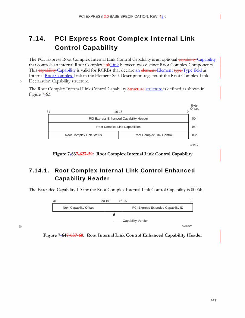
PCI EXPRESS 2.0 BASE SPECIFICATION, REV. 12.0
567
7.14. PCI Express Root Complex Internal Link Control Capability
The PCI Express Root Complex Internal Link Control Capability is an optional capability Capability that controls an internal Root Complex linkLink between two distinct Root Complex Components. This capability Capability is valid for RCRBs that declare an element Element type Type field as Internal Root Complex Link in the Element Self-Description register of the Root Complex Link Declaration Capability structure. 5
The Root Complex Internal Link Control Capability Structure structure is defined as shown in Figure 7-63.
A-0416
0
ByteOffset
31 16 15
04h
08h
00hPCI Express Enhanced Capability Header
Root Complex Link Capabilities
Root Complex Link Status Root Complex Link Control
Figure 7-637-62 7-59: Root Complex Internal Link Control Capability
7.14.1. Root Complex Internal Link Control Enhanced Capability Header
The Extended Capability ID for the Root Complex Internal Link Control Capability is 0006h.
OM14526
Capability Version
Next Capability Offset PCI Express Extended Capability ID
31 20 16 1519 0
10
Figure 7-647-63 7-60: Root Internal Link Control Enhanced Capability Header
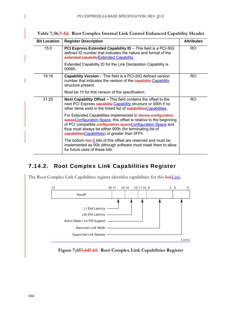
PCI EXPRESS 2.0 BASE SPECIFICATION, REV. 21.0
568
Table 7-56- 7-52: Root Complex Internal Link Control Enhanced Capability Header
Bit Location Register Description Attributes
15:0 PCI Express Extended Capability ID – This field is a PCI-SIG defined ID number that indicates the nature and format of the extended capabilityExtended Capability.
Extended Capability ID for the Link Declaration Capability is 0006h.
RO
19:16 Capability Version – This field is a PCI-SIG defined version number that indicates the version of the capability Capability structure present.
Must be 1h for this version of the specification.
RO
31:20 Next Capability Offset – This field contains the offset to the next PCI Express capability Capability structure or 000h if no other items exist in the linked list of capabilitiesCapabilities.
For Extended Capabilities implemented in device configuration spaceConfiguration Space, this offset is relative to the beginning of PCI compatible configuration spaceConfiguration Space and thus must always be either 000h (for terminating list of capabilitiesCapabilities) or greater than 0FFh.
The bottom two 2 bits of this offset are reserved and must be implemented as 00b although software must mask them to allow for future uses of these bits.
RO
7.14.2. Root Complex Link Capabilities Register
The Root Complex Link Capabilities register identifies capabilities for this linkLink.
A-0415A
RsvdP
Figure 7-657-64 7-61: Root Complex Link Capabilities Register
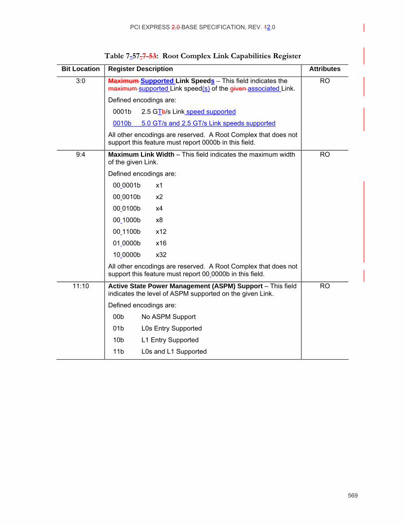
PCI EXPRESS 2.0 BASE SPECIFICATION, REV. 12.0
569
Table 7-57- 7-53: Root Complex Link Capabilities Register
Bit Location Register Description Attributes
3:0 Maximum Supported Link Speeds – This field indicates the maximum supported Link speed(s) of the given associated Link.
Defined encodings are:
0001b 2.5 GTb/s Link speed supported
0010b 5.0 GT/s and 2.5 GT/s Link speeds supported
All other encodings are reserved. A Root Complex that does not support this feature must report 0000b in this field.
RO
9:4 Maximum Link Width – This field indicates the maximum width of the given Link.
Defined encodings are:
00 0001b x1
00 0010b x2
00 0100b x4
00 1000b x8
00 1100b x12
01 0000b x16
10 0000b x32
All other encodings are reserved. A Root Complex that does not support this feature must report 00 0000b in this field.
RO
11:10 Active State Power Management (ASPM) Support – This field indicates the level of ASPM supported on the given Link.
Defined encodings are:
00b No ASPM Support
01b L0s Entry Supported
10b L1 Entry Supported
11b L0s and L1 Supported
RO
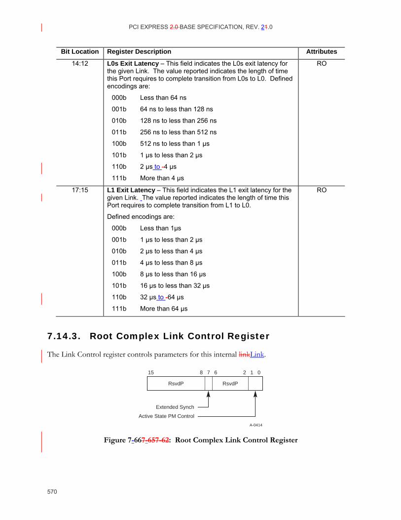
PCI EXPRESS 2.0 BASE SPECIFICATION, REV. 21.0
570
Bit Location Register Description Attributes
14:12 L0s Exit Latency – This field indicates the L0s exit latency for the given Link. The value reported indicates the length of time this Port requires to complete transition from L0s to L0. Defined encodings are:
000b Less than 64 ns
001b 64 ns to less than 128 ns
010b 128 ns to less than 256 ns
011b 256 ns to less than 512 ns
100b 512 ns to less than 1 µs
101b 1 µs to less than 2 µs
110b 2 µs to -4 µs
111b More than 4 µs
RO
17:15 L1 Exit Latency – This field indicates the L1 exit latency for the given Link. The value reported indicates the length of time this Port requires to complete transition from L1 to L0.
Defined encodings are:
000b Less than 1µs
001b 1 µs to less than 2 µs
010b 2 µs to less than 4 µs
011b 4 µs to less than 8 µs
100b 8 µs to less than 16 µs
101b 16 µs to less than 32 µs
110b 32 µs to -64 µs
111b More than 64 µs
RO
7.14.3. Root Complex Link Control Register
The Link Control register controls parameters for this internal linkLink.
A-0414
Active State PM Control
Extended Synch
RsvdP RsvdP
15 8 7 6 2 1 0
Figure 7-667-65 7-62: Root Complex Link Control Register
PCI EXPRESS 2.0 BASE SPECIFICATION, REV. 12.0
571
Table 7-58- 7-54: Root Complex Link Control Register
Bit Location Register Description Attributes
1:0 Active State Power Management (ASPM) Control – This field controls the level of ASPM supported on the given Link.
Defined encodings are:
00b Disabled
01b L0s Entry Enabled
10b L1 Entry Enabled
11b L0s and L1 Entry Enabled
Note: “L0s Entry Enabled” indicates the Transmitter entering L0s is supported. The Receiver must be capable of entering L0s even when the field is disabled (00b).
Default value of this field is implementation specific.
ASPM L1 must be enabled by software in the upstream Upstream component on a linkLink prior to enabling ASPM L1 in the downstream Downstream component on that linkLink. When disabling ASPM L1, software must disable ASPM L1 in the downstream Downstream component on a linkLink prior to disabling ASPM L1 in the upstream Upstream component on that linkLink. ASPM L1 must only be enabled on the downstream Downstream component if both components on a linkLink support ASPM L1.
A Root Complex that does not support this feature for the given internal linkLink must hardwire this field to 00b.
RW
7 Extended Synch – This bit when set Set forces the transmission of additional Ordered Sets when exiting the L0s state (see Section 4.2.4.5) and when in the Recovery state (see Section 4.2.6.4.1). This mode provides external devices (e.g., logic analyzers) monitoring the Link time to achieve bit and Symbol lock before the Link enters the L0 state and resumes communication.
Default value for this bit is 0b.
A Root Complex that does not support this feature for the given internal linkLink must hardwire this field bit to 0b.
Default value for this bit is 0b.
RW
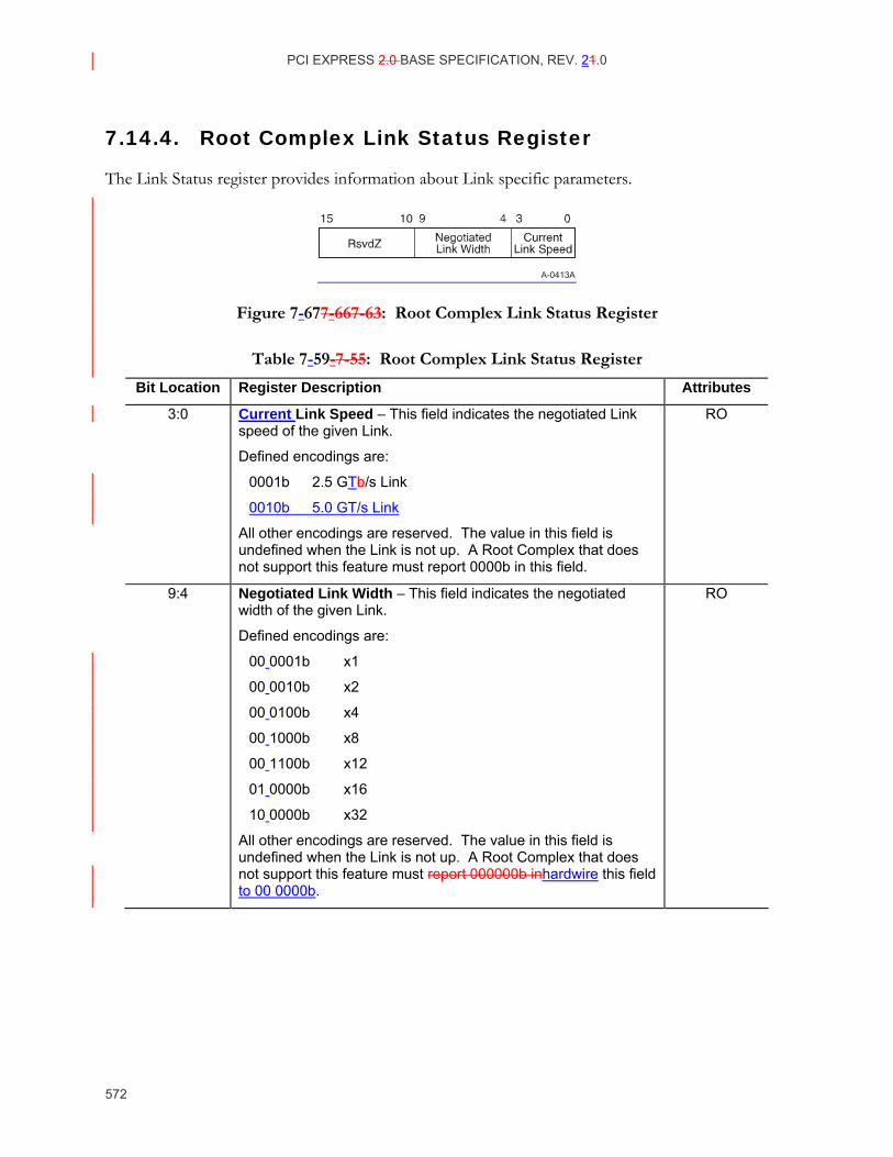
PCI EXPRESS 2.0 BASE SPECIFICATION, REV. 21.0
572
7.14.4. Root Complex Link Status Register
The Link Status register provides information about Link specific parameters.
A-0413A
Figure 7-677-66 7-63: Root Complex Link Status Register
Table 7-59- 7-55: Root Complex Link Status Register
Bit Location Register Description Attributes
3:0 Current Link Speed – This field indicates the negotiated Link speed of the given Link.
Defined encodings are:
0001b 2.5 GTb/s Link
0010b 5.0 GT/s Link
All other encodings are reserved. The value in this field is undefined when the Link is not up. A Root Complex that does not support this feature must report 0000b in this field.
RO
9:4 Negotiated Link Width – This field indicates the negotiated width of the given Link.
Defined encodings are:
00 0001b x1
00 0010b x2
00 0100b x4
00 1000b x8
00 1100b x12
01 0000b x16
10 0000b x32
All other encodings are reserved. The value in this field is undefined when the Link is not up. A Root Complex that does not support this feature must report 000000b inhardwire this field to 00 0000b.
RO
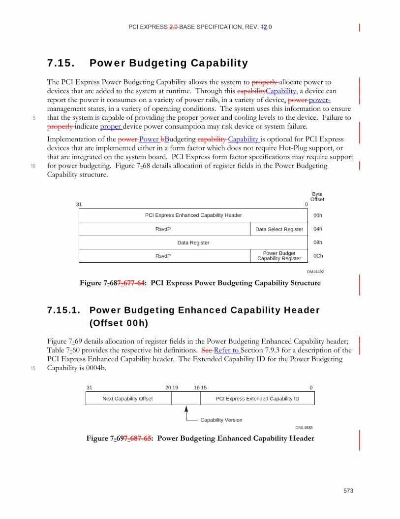
PCI EXPRESS 2.0 BASE SPECIFICATION, REV. 12.0
573
7.15. Power Budgeting Capability The PCI Express Power Budgeting Capability allows the system to properly allocate power to devices that are added to the system at runtime. Through this capabilityCapability, a device can report the power it consumes on a variety of power rails, in a variety of device, power power-management states, in a variety of operating conditions. The system uses this information to ensure that the system is capable of providing the proper power and cooling levels to the device. Failure to 5 properly indicate proper device power consumption may risk device or system failure.
Implementation of the power Power bBudgeting capability Capability is optional for PCI Express devices that are implemented either in a form factor which does not require Hot-Plug support, or that are integrated on the system board. PCI Express form factor specifications may require support for power budgeting. Figure 7-68 details allocation of register fields in the Power Budgeting 10 Capability structure.
RsvdP
RsvdP
Data Select Register
Power BudgetCapability Register
0
ByteOffset
31
04h
08h
00h
0Ch
PCI Express Enhanced Capability Header
Data Register
OM14492 Figure 7-687-67 7-64: PCI Express Power Budgeting Capability Structure
7.15.1. Power Budgeting Enhanced Capability Header (Offset 00h)
Figure 7-69 details allocation of register fields in the Power Budgeting Enhanced Capability header; Table 7-60 provides the respective bit definitions. See Refer to Section 7.9.3 for a description of the PCI Express Enhanced Capability header. The Extended Capability ID for the Power Budgeting Capability is 0004h. 15
OM14535
Capability Version
Next Capability Offset PCI Express Extended Capability ID
31 20 16 1519 0
Figure 7-697-68 7-65: Power Budgeting Enhanced Capability Header
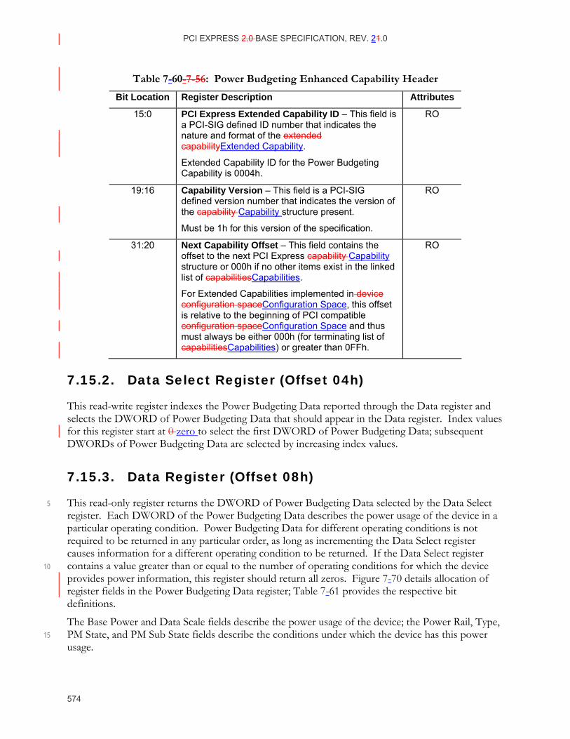
PCI EXPRESS 2.0 BASE SPECIFICATION, REV. 21.0
574
Table 7-60- 7-56: Power Budgeting Enhanced Capability Header
Bit Location Register Description Attributes
15:0 PCI Express Extended Capability ID – This field is a PCI-SIG defined ID number that indicates the nature and format of the extended capabilityExtended Capability.
Extended Capability ID for the Power Budgeting Capability is 0004h.
RO
19:16 Capability Version – This field is a PCI-SIG defined version number that indicates the version of the capability Capability structure present.
Must be 1h for this version of the specification.
RO
31:20 Next Capability Offset – This field contains the offset to the next PCI Express capability Capability structure or 000h if no other items exist in the linked list of capabilitiesCapabilities.
For Extended Capabilities implemented in device configuration spaceConfiguration Space, this offset is relative to the beginning of PCI compatible configuration spaceConfiguration Space and thus must always be either 000h (for terminating list of capabilitiesCapabilities) or greater than 0FFh.
RO
7.15.2. Data Select Register (Offset 04h)
This read-write register indexes the Power Budgeting Data reported through the Data register and selects the DWORD of Power Budgeting Data that should appear in the Data register. Index values for this register start at 0 zero to select the first DWORD of Power Budgeting Data; subsequent DWORDs of Power Budgeting Data are selected by increasing index values.
7.15.3. Data Register (Offset 08h)
This read-only register returns the DWORD of Power Budgeting Data selected by the Data Select 5 register. Each DWORD of the Power Budgeting Data describes the power usage of the device in a particular operating condition. Power Budgeting Data for different operating conditions is not required to be returned in any particular order, as long as incrementing the Data Select register causes information for a different operating condition to be returned. If the Data Select register contains a value greater than or equal to the number of operating conditions for which the device 10 provides power information, this register should return all zeros. Figure 7-70 details allocation of register fields in the Power Budgeting Data register; Table 7-61 provides the respective bit definitions.
The Base Power and Data Scale fields describe the power usage of the device; the Power Rail, Type, PM State, and PM Sub State fields describe the conditions under which the device has this power 15 usage.
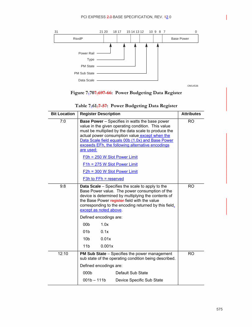
PCI EXPRESS 2.0 BASE SPECIFICATION, REV. 12.0
575
OM14536
PM Sub State
PM State
Type
Data Scale
Power Rail
RsvdP Base Power
31 21 20 18 17 15 14 13 12 10 9 8 7 0
Figure 7-707-69 7-66: Power Budgeting Data Register
Table 7-61- 7-57: Power Budgeting Data Register
Bit Location Register Description Attributes
7:0 Base Power – Specifies in watts the base power value in the given operating condition. This value must be multiplied by the data scale to produce the actual power consumption value except when the Data Scale field equals 00b (1.0x) and Base Power exceeds EFh, the following alternative encodings are used:
F0h = 250 W Slot Power Limit
F1h = 275 W Slot Power Limit
F2h = 300 W Slot Power Limit
F3h to FFh = reserved
RO
9:8 Data Scale – Specifies the scale to apply to the Base Power value. The power consumption of the device is determined by multiplying the contents of the Base Power register field with the value corresponding to the encoding returned by this field, except as noted above.
Defined encodings are:
00b 1.0x
01b 0.1x
10b 0.01x
11b 0.001x
RO
12:10 PM Sub State – Specifies the power management sub state of the operating condition being described.
Defined encodings are:
000b Default Sub State
001b – 111b Device Specific Sub State
RO
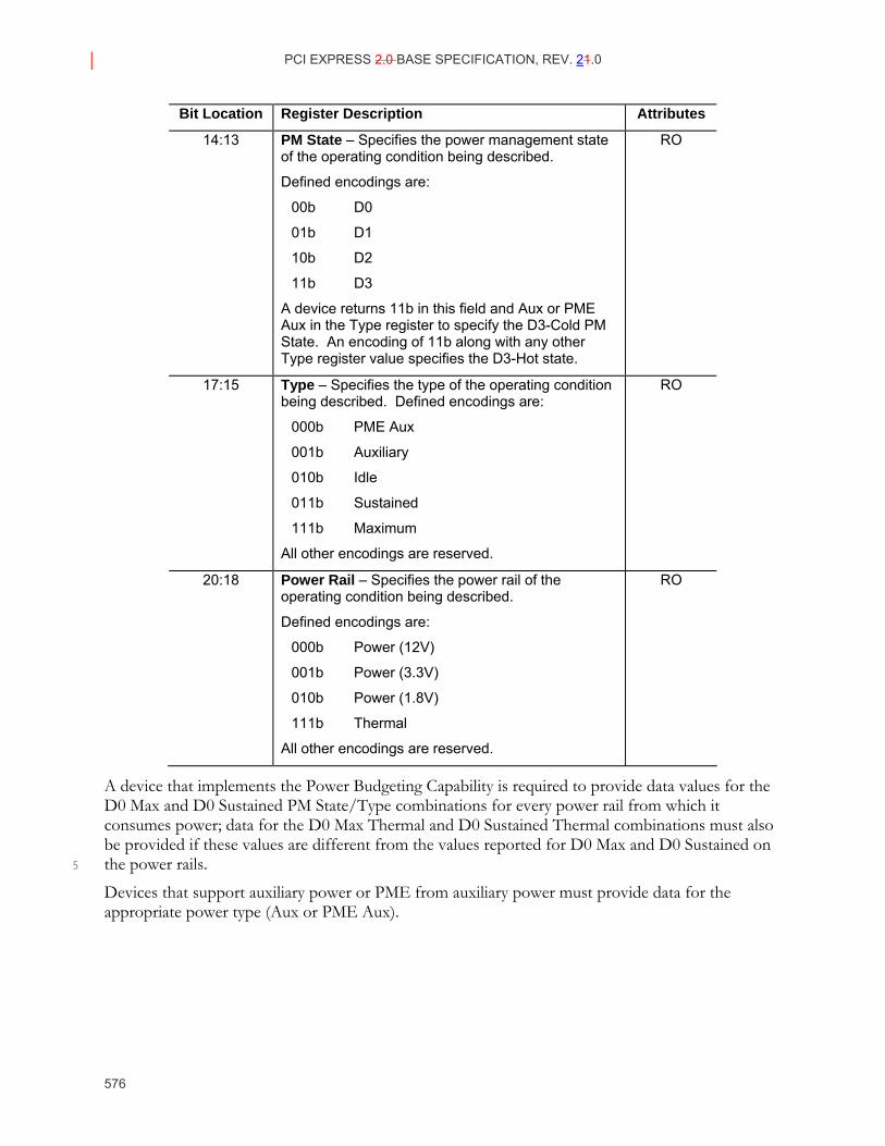
PCI EXPRESS 2.0 BASE SPECIFICATION, REV. 21.0
576
Bit Location Register Description Attributes
14:13 PM State – Specifies the power management state of the operating condition being described.
Defined encodings are:
00b D0
01b D1
10b D2
11b D3
A device returns 11b in this field and Aux or PME Aux in the Type register to specify the D3-Cold PM State. An encoding of 11b along with any other Type register value specifies the D3-Hot state.
RO
17:15 Type – Specifies the type of the operating condition being described. Defined encodings are:
000b PME Aux
001b Auxiliary
010b Idle
011b Sustained
111b Maximum
All other encodings are reserved.
RO
20:18 Power Rail – Specifies the power rail of the operating condition being described.
Defined encodings are:
000b Power (12V)
001b Power (3.3V)
010b Power (1.8V)
111b Thermal
All other encodings are reserved.
RO
A device that implements the Power Budgeting Capability is required to provide data values for the D0 Max and D0 Sustained PM State/Type combinations for every power rail from which it consumes power; data for the D0 Max Thermal and D0 Sustained Thermal combinations must also be provided if these values are different from the values reported for D0 Max and D0 Sustained on the power rails. 5
Devices that support auxiliary power or PME from auxiliary power must provide data for the appropriate power type (Aux or PME Aux).
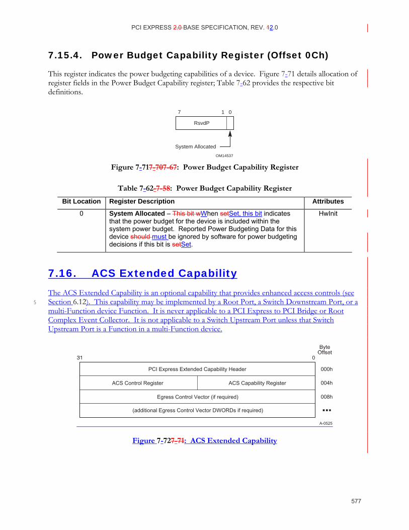
PCI EXPRESS 2.0 BASE SPECIFICATION, REV. 12.0
577
7.15.4. Power Budget Capability Register (Offset 0Ch)
This register indicates the power budgeting capabilities of a device. Figure 7-71 details allocation of register fields in the Power Budget Capability register; Table 7-62 provides the respective bit definitions.
OM14537
System Allocated
RsvdP
7 1 0
Figure 7-717-70 7-67: Power Budget Capability Register
Table 7-62- 7-58: Power Budget Capability Register
Bit Location Register Description Attributes
0 System Allocated – This bit wWhen setSet, this bit indicates that the power budget for the device is included within the system power budget. Reported Power Budgeting Data for this device should must be ignored by software for power budgeting decisions if this bit is setSet.
HwInit
7.16. ACS Extended Capability The ACS Extended Capability is an optional capability that provides enhanced access controls (see Section 6.12). This capability may be implemented by a Root Port, a Switch Downstream Port, or a 5 multi-Function device Function. It is never applicable to a PCI Express to PCI Bridge or Root Complex Event Collector. It is not applicable to a Switch Upstream Port unless that Switch Upstream Port is a Function in a multi-Function device.
A-0525
004h
008h
000hPCI Express Extended Capability Header
ACS Control Register ACS Capability Register
Egress Control Vector (if required)
(additional Egress Control Vector DWORDs if required)
Figure 7-727-71: ACS Extended Capability
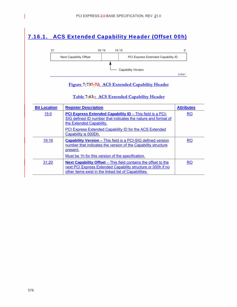
PCI EXPRESS 2.0 BASE SPECIFICATION, REV. 21.0
578
7.16.1. ACS Extended Capability Header (Offset 00h)
A-0541
Next Capability Offset PCI Express Extended Capability ID
Figure 7-737-72: ACS Extended Capability Header
Table 7-63-: ACS Extended Capability Header
Bit Location Register Description Attributes 15:0 PCI Express Extended Capability ID – This field is a PCI-
SIG defined ID number that indicates the nature and format of the Extended Capability. PCI Express Extended Capability ID for the ACS Extended Capability is 000Dh.
RO
19:16 Capability Version – This field is a PCI-SIG defined version number that indicates the version of the Capability structure present. Must be 1h for this version of the specification.
RO
31:20 Next Capability Offset – This field contains the offset to the next PCI Express Extended Capability structure or 000h if no other items exist in the linked list of Capabilities.
RO
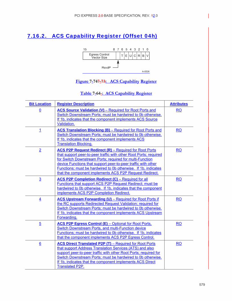
PCI EXPRESS 2.0 BASE SPECIFICATION, REV. 12.0
579
7.16.2. ACS Capability Register (Offset 04h)
A-0526
Egress ControlVector Size VBRCUET
Figure 7-747-73: ACS Capability Register
Table 7-64-: ACS Capability Register
Bit Location Register Description Attributes 0 ACS Source Validation (V) – Required for Root Ports and
Switch Downstream Ports; must be hardwired to 0b otherwise. If 1b, indicates that the component implements ACS Source Validation.
RO
1 ACS Translation Blocking (B) – Required for Root Ports and Switch Downstream Ports; must be hardwired to 0b otherwise. If 1b, indicates that the component implements ACS Translation Blocking.
RO
2 ACS P2P Request Redirect (R) – Required for Root Ports that support peer-to-peer traffic with other Root Ports; required for Switch Downstream Ports; required for multi-Function device Functions that support peer-to-peer traffic with other Functions; must be hardwired to 0b otherwise. If 1b, indicates that the component implements ACS P2P Request Redirect.
RO
3 ACS P2P Completion Redirect (C) – Required for all Functions that support ACS P2P Request Redirect; must be hardwired to 0b otherwise. If 1b, indicates that the component implements ACS P2P Completion Redirect.
RO
4 ACS Upstream Forwarding (U) – Required for Root Ports if the RC supports Redirected Request Validation; required for Switch Downstream Ports; must be hardwired to 0b otherwise. If 1b, indicates that the component implements ACS Upstream Forwarding.
RO
5 ACS P2P Egress Control (E) – Optional for Root Ports, Switch Downstream Ports, and multi-Function device Functions; must be hardwired to 0b otherwise. If 1b, indicates that the component implements ACS P2P Egress Control.
RO
6 ACS Direct Translated P2P (T) – Required for Root Ports that support Address Translation Services (ATS) and also support peer-to-peer traffic with other Root Ports; required for Switch Downstream Ports; must be hardwired to 0b otherwise. If 1b, indicates that the component implements ACS Direct Translated P2P.
RO
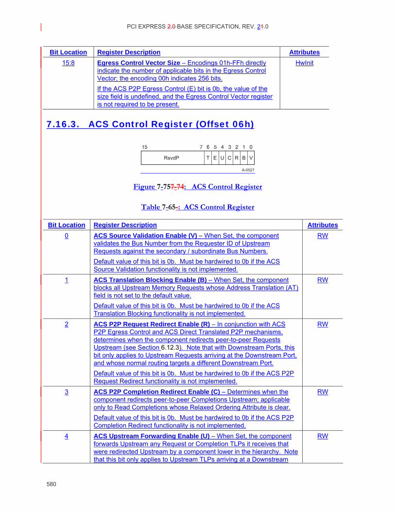
PCI EXPRESS 2.0 BASE SPECIFICATION, REV. 21.0
580
Bit Location Register Description Attributes 15:8 Egress Control Vector Size – Encodings 01h-FFh directly
indicate the number of applicable bits in the Egress Control Vector; the encoding 00h indicates 256 bits. If the ACS P2P Egress Control (E) bit is 0b, the value of the size field is undefined, and the Egress Control Vector register is not required to be present.
HwInit
7.16.3. ACS Control Register (Offset 06h)
A-0527
VBRCUETRsvdP
Figure 7-757-74: ACS Control Register
Table 7-65-: ACS Control Register
Bit Location Register Description Attributes 0 ACS Source Validation Enable (V) – When Set, the component
validates the Bus Number from the Requester ID of Upstream Requests against the secondary / subordinate Bus Numbers. Default value of this bit is 0b. Must be hardwired to 0b if the ACS Source Validation functionality is not implemented.
RW
1 ACS Translation Blocking Enable (B) – When Set, the component blocks all Upstream Memory Requests whose Address Translation (AT) field is not set to the default value. Default value of this bit is 0b. Must be hardwired to 0b if the ACS Translation Blocking functionality is not implemented.
RW
2 ACS P2P Request Redirect Enable (R) – In conjunction with ACS P2P Egress Control and ACS Direct Translated P2P mechanisms, determines when the component redirects peer-to-peer Requests Upstream (see Section 6.12.3). Note that with Downstream Ports, this bit only applies to Upstream Requests arriving at the Downstream Port, and whose normal routing targets a different Downstream Port. Default value of this bit is 0b. Must be hardwired to 0b if the ACS P2P Request Redirect functionality is not implemented.
RW
3 ACS P2P Completion Redirect Enable (C) – Determines when the component redirects peer-to-peer Completions Upstream; applicable only to Read Completions whose Relaxed Ordering Attribute is clear. Default value of this bit is 0b. Must be hardwired to 0b if the ACS P2P Completion Redirect functionality is not implemented.
RW
4 ACS Upstream Forwarding Enable (U) – When Set, the component forwards Upstream any Request or Completion TLPs it receives that were redirected Upstream by a component lower in the hierarchy. Note that this bit only applies to Upstream TLPs arriving at a Downstream
RW
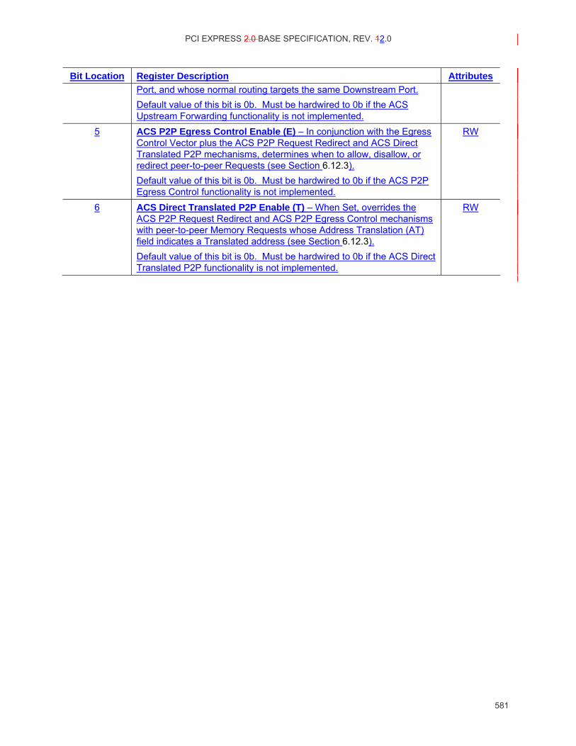
PCI EXPRESS 2.0 BASE SPECIFICATION, REV. 12.0
581
Bit Location Register Description Attributes Port, and whose normal routing targets the same Downstream Port. Default value of this bit is 0b. Must be hardwired to 0b if the ACS Upstream Forwarding functionality is not implemented.
5 ACS P2P Egress Control Enable (E) – In conjunction with the Egress Control Vector plus the ACS P2P Request Redirect and ACS Direct Translated P2P mechanisms, determines when to allow, disallow, or redirect peer-to-peer Requests (see Section 6.12.3). Default value of this bit is 0b. Must be hardwired to 0b if the ACS P2P Egress Control functionality is not implemented.
RW
6 ACS Direct Translated P2P Enable (T) – When Set, overrides the ACS P2P Request Redirect and ACS P2P Egress Control mechanisms with peer-to-peer Memory Requests whose Address Translation (AT) field indicates a Translated address (see Section 6.12.3). Default value of this bit is 0b. Must be hardwired to 0b if the ACS Direct Translated P2P functionality is not implemented.
RW
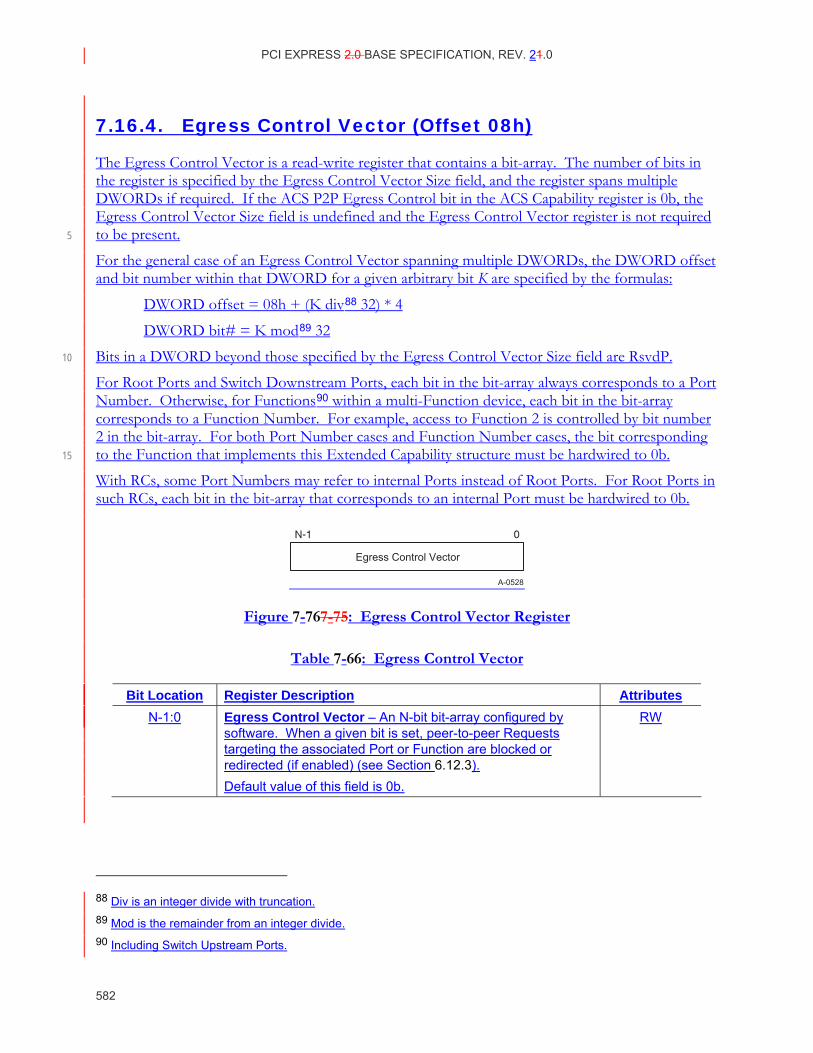
PCI EXPRESS 2.0 BASE SPECIFICATION, REV. 21.0
582
7.16.4. Egress Control Vector (Offset 08h)
The Egress Control Vector is a read-write register that contains a bit-array. The number of bits in the register is specified by the Egress Control Vector Size field, and the register spans multiple DWORDs if required. If the ACS P2P Egress Control bit in the ACS Capability register is 0b, the Egress Control Vector Size field is undefined and the Egress Control Vector register is not required to be present. 5
For the general case of an Egress Control Vector spanning multiple DWORDs, the DWORD offset and bit number within that DWORD for a given arbitrary bit K are specified by the formulas:
DWORD offset = 08h + (K div88 32) * 4
DWORD bit# = K mod89 32
Bits in a DWORD beyond those specified by the Egress Control Vector Size field are RsvdP. 10
For Root Ports and Switch Downstream Ports, each bit in the bit-array always corresponds to a Port Number. Otherwise, for Functions90 within a multi-Function device, each bit in the bit-array corresponds to a Function Number. For example, access to Function 2 is controlled by bit number 2 in the bit-array. For both Port Number cases and Function Number cases, the bit corresponding to the Function that implements this Extended Capability structure must be hardwired to 0b. 15
With RCs, some Port Numbers may refer to internal Ports instead of Root Ports. For Root Ports in such RCs, each bit in the bit-array that corresponds to an internal Port must be hardwired to 0b.
A-0528
Egress Control Vector
Figure 7-767-75: Egress Control Vector Register
Table 7-66: Egress Control Vector
Bit Location Register Description Attributes N-1:0 Egress Control Vector – An N-bit bit-array configured by
software. When a given bit is set, peer-to-peer Requests targeting the associated Port or Function are blocked or redirected (if enabled) (see Section 6.12.3). Default value of this field is 0b.
RW
88 Div is an integer divide with truncation. 89 Mod is the remainder from an integer divide. 90 Including Switch Upstream Ports.
PCI EXPRESS 2.0 BASE SPECIFICATION, REV. 12.0
583
The following examples illustrate how the vector might be configured:
For an 8-Port Switch, each Port will have a separate vector indicating which Downstream Egress Ports it may forward Requests to.
• Port 1 being not allowed to communicate with any other Downstream Ports would be configured as: 1111 1100b with 0b indicating in bit 0 corresponds to the Upstream Port and 5 a 0b in bit 1 represents the Ingress Port hardwired to 0b as well.
• Port 2 being allowed to communicate with Ports 3, 5, and 7 would be configured as: 0101 0010b.
For a 4-Function device, each Function will have a separate vector that indicates which Function it may forward Requests to. 10
• Function 0 being not allowed to communicate with any other Functions would be configured as: 1110b with 0b in bit 0 corresponding to Function 0.
• Function 1 being allowed to communicate with Functions 2 and 3 would be configured as: 0001b with a 0b in bit 1 corresponding to Function 1 hardwired to 0b as well.
7.16.7.17. PCI Express Root Complex Event Collector Endpoint Association Capability
The PCI Express Root Complex Event Collector Endpoint Association Capability is implemented 15 by Root Complex Event Collectors.
It declares the Root Complex Integrated Endpoints supported by the Root Complex Event Collector on the same logical Logical bus Bus on which the Root Complex Event Collector is located. A Root Complex Event Collector must implement the Root Complex Event Collector Endpoint Association Capability; no other PCI Express device Function may is permitted to 20 implement this capabilityCapability.
The PCI Express Root Complex Event Collector Endpoint Association Capability, as shown in Figure 7-77, consists of the PCI Express Enhanced Capability Header header followed by a DWORD bitmap enumerating Root Complex Integrated Endpoints associated with the Root Complex Event Collector. 25
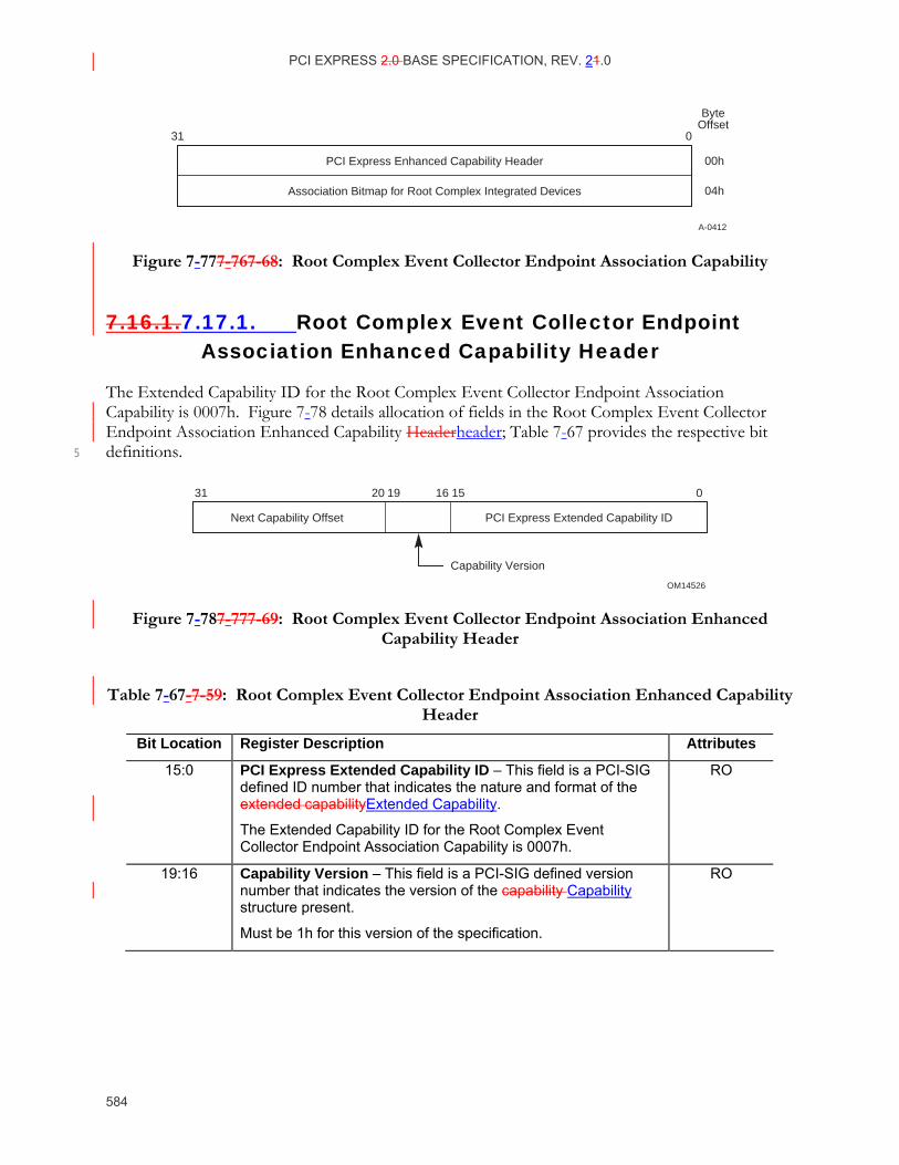
PCI EXPRESS 2.0 BASE SPECIFICATION, REV. 21.0
584
A-0412
0
ByteOffset
31
04h
00hPCI Express Enhanced Capability Header
Association Bitmap for Root Complex Integrated Devices
Figure 7-777-76 7-68: Root Complex Event Collector Endpoint Association Capability
7.16.1.7.17.1. Root Complex Event Collector Endpoint Association Enhanced Capability Header
The Extended Capability ID for the Root Complex Event Collector Endpoint Association Capability is 0007h. Figure 7-78 details allocation of fields in the Root Complex Event Collector Endpoint Association Enhanced Capability Headerheader; Table 7-67 provides the respective bit definitions. 5
OM14526
Capability Version
Next Capability Offset PCI Express Extended Capability ID
31 20 16 1519 0
Figure 7-787-77 7-69: Root Complex Event Collector Endpoint Association Enhanced Capability Header
Table 7-67- 7-59: Root Complex Event Collector Endpoint Association Enhanced Capability Header
Bit Location Register Description Attributes
15:0 PCI Express Extended Capability ID – This field is a PCI-SIG defined ID number that indicates the nature and format of the extended capabilityExtended Capability.
The Extended Capability ID for the Root Complex Event Collector Endpoint Association Capability is 0007h.
RO
19:16 Capability Version – This field is a PCI-SIG defined version number that indicates the version of the capability Capability structure present.
Must be 1h for this version of the specification.
RO
PCI EXPRESS 2.0 BASE SPECIFICATION, REV. 12.0
585
Bit Location Register Description Attributes
31:20 Next Capability Offset – This field contains the offset to the next PCI Express capability Capability structure or 000h if no other items exist in the linked list of capabilitiesCapabilities.
For Extended Capabilities implemented in device configuration spaceConfiguration Space, this offset is relative to the beginning of PCI compatible configuration spaceConfiguration Space and thus must always be either 000h (for terminating list of capabilitiesCapabilities) or greater than 0FFh.
The bottom two 2 bits of this offset are reserved and must be implemented as 00b although software must mask them to allow for future uses of these bits.
RO
7.16.2.7.17.2. Association Bitmap for Root Complex Integrated Endpoint Devices
The Association Bitmap for Root Complex Integrated Endpoint Devices is a read-only field register that sets the bits corresponding to the Device Numbers of Root Complex Integrated Endpoint Devices supported by the Root Complex Event Collector on the same logical Logical bus Bus as the Event Collector itself. The bit corresponding to the Device Number of the Root Complex Event Collector must always be setSet. 5
7.17.7.18. Multi-Function Virtual Channel Capability The Multi-Function Virtual Channel (MFVC) capability Capability is an extended capabilityExtended Capability required for PCI Express multi-function Function devices that have individual Functions that support functionality beyond the general-purpose IO traffic, i.e. the default Traffic Class (TC0) over the default Virtual Channel (VC0). When implemented, the MFVC capability Capability structure must be present in the Extended Configuration Space of Function 0 10 of the multi-function Function device’s Upstream Port. Figure 7-79 provides a high level view of the MFVC capability Capability structure. This MFVC capability Capability structure controls Virtual Channel assignment at the PCI Express Upstream Port of the multi-function Function device, while a VC capability Capability structure, if present in a function Function, controls the Virtual Channel assignment for that individual functionFunction. 15
A multi-function Function device is permitted to have an MFVC Capability structure even if none of its functions Functions have a VC Capability structure. However, an MFVC Capability structure is permitted only in Function 0 in the Upstream Port of a multi-function Function device.
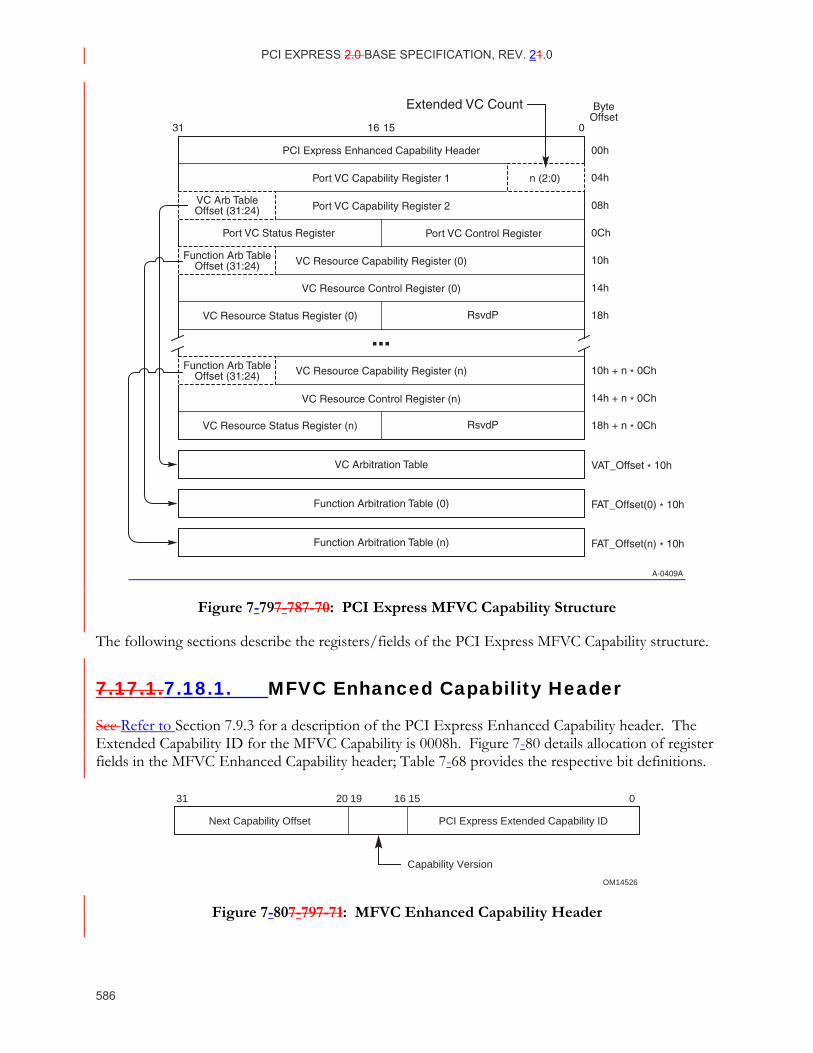
PCI EXPRESS 2.0 BASE SPECIFICATION, REV. 21.0
586
A-0409A
Port VC Capability Register 2
Port VC Capability Register 1 n (2:0)
PCI Express Enhanced Capability Header
Port VC Control RegisterPort VC Status Register
VC Arb TableOffset (31:24)
Function Arb TableOffset (31:24)
Function Arb TableOffset (31:24)
0
ByteOffset
31 16 15
04h
08h
00h
0Ch
10h
14h
18h
10h + n * 0Ch
14h + n * 0Ch
18h + n * 0Ch
VAT_Offset * 10h
FAT_Offset(0) * 10h
FAT_Offset(n) * 10h
VC Resource Status Register (n) RsvdP
VC Resource Status Register (0) RsvdP
VC Arbitration Table
VC Resource Capability Register (0)
VC Resource Control Register (0)
VC Resource Control Register (n)
VC Resource Capability Register (n)
Function Arbitration Table (0)
Function Arbitration Table (n)
Extended VC Count
Figure 7-797-78 7-70: PCI Express MFVC Capability Structure
The following sections describe the registers/fields of the PCI Express MFVC Capability structure.
7.17.1.7.18.1. MFVC Enhanced Capability Header
See Refer to Section 7.9.3 for a description of the PCI Express Enhanced Capability header. The Extended Capability ID for the MFVC Capability is 0008h. Figure 7-80 details allocation of register fields in the MFVC Enhanced Capability header; Table 7-68 provides the respective bit definitions.
OM14526
Capability Version
Next Capability Offset PCI Express Extended Capability ID
31 20 16 1519 0
Figure 7-807-79 7-71: MFVC Enhanced Capability Header
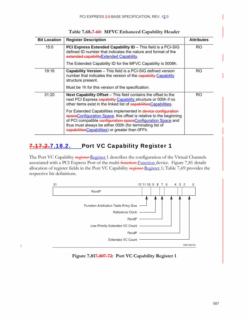
PCI EXPRESS 2.0 BASE SPECIFICATION, REV. 12.0
587
Table 7-68- 7-60: MFVC Enhanced Capability Header
Bit Location Register Description Attributes
15:0 PCI Express Extended Capability ID – This field is a PCI-SIG defined ID number that indicates the nature and format of the extended capabilityExtended Capability.
The Extended Capability ID for the MFVC Capability is 0008h.
RO
19:16 Capability Version – This field is a PCI-SIG defined version number that indicates the version of the capability Capability structure present.
Must be 1h for this version of the specification.
RO
31:20 Next Capability Offset – This field contains the offset to the next PCI Express capability Capability structure or 000h if no other items exist in the linked list of capabilitiesCapabilities.
For Extended Capabilities implemented in device configuration spaceConfiguration Space, this offset is relative to the beginning of PCI compatible configuration spaceConfiguration Space and thus must always be either 000h (for terminating list of capabilitiesCapabilities) or greater than 0FFh.
RO
7.17.2.7.18.2. Port VC Capability Register 1
The Port VC Capability register Register 1 describes the configuration of the Virtual Channels associated with a PCI Express Port of the multi-function Function device. Figure 7-81 details allocation of register fields in the Port VC Capability register Register 1; Table 7-69 provides the respective bit definitions.
OM14527A
RsvdP
5
Figure 7-817-80 7-72: Port VC Capability Register 1
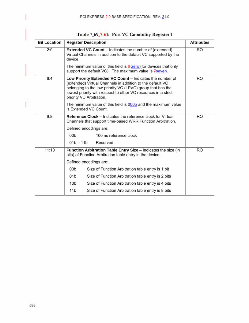
PCI EXPRESS 2.0 BASE SPECIFICATION, REV. 21.0
588
Table 7-69- 7-61: Port VC Capability Register 1
Bit Location Register Description Attributes
2:0 Extended VC Count – Indicates the number of (extended) Virtual Channels in addition to the default VC supported by the device.
The minimum value of this field is 0 zero (for devices that only support the default VC). The maximum value is 7seven.
RO
6:4 Low Priority Extended VC Count – Indicates the number of (extended) Virtual Channels in addition to the default VC belonging to the low-priority VC (LPVC) group that has the lowest priority with respect to other VC resources in a strict-priority VC Arbitration.
The minimum value of this field is 000b and the maximum value is Extended VC Count.
RO
9:8 Reference Clock – Indicates the reference clock for Virtual Channels that support time-based WRR Function Arbitration.
Defined encodings are:
00b 100 ns reference clock
01b – 11b Reserved
RO
11:10 Function Arbitration Table Entry Size – Indicates the size (in bits) of Function Arbitration table entry in the device.
Defined encodings are:
00b Size of Function Arbitration table entry is 1 bit
01b Size of Function Arbitration table entry is 2 bits
10b Size of Function Arbitration table entry is 4 bits
11b Size of Function Arbitration table entry is 8 bits
RO
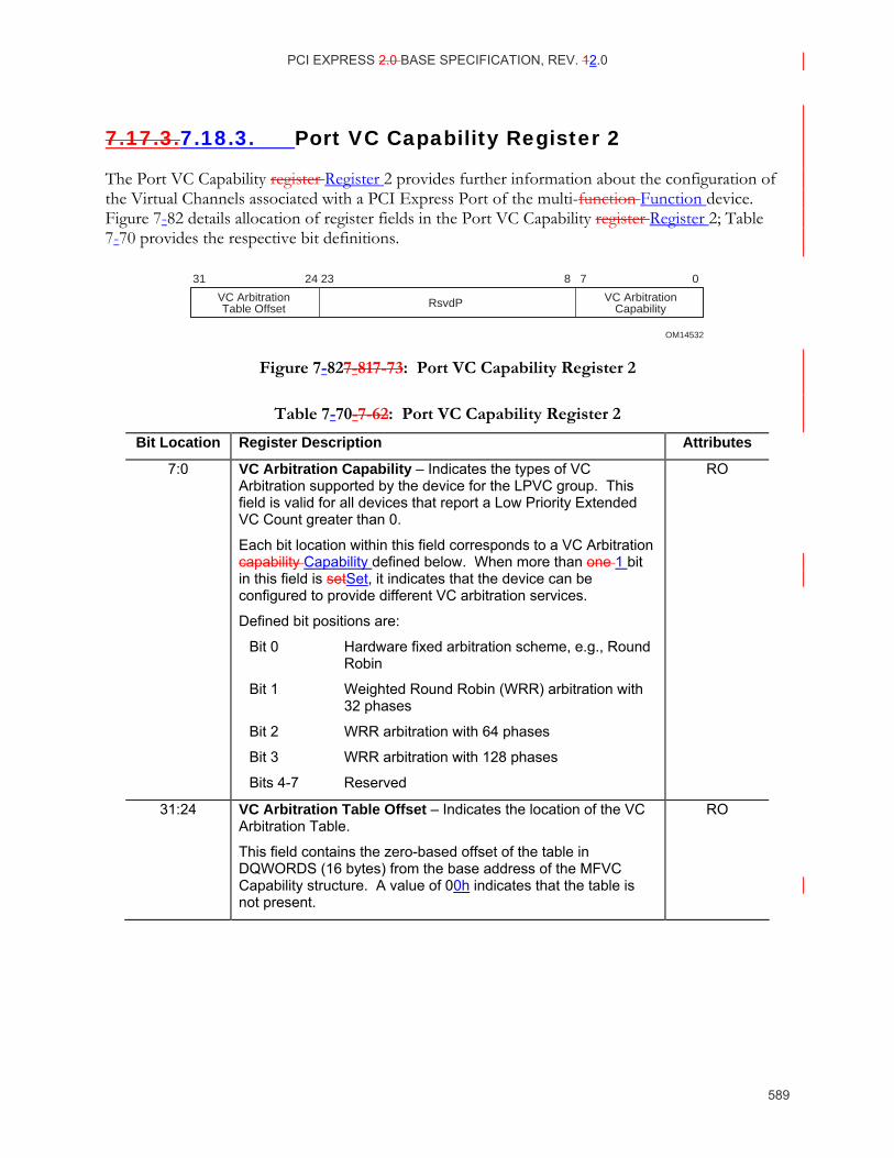
PCI EXPRESS 2.0 BASE SPECIFICATION, REV. 12.0
589
7.17.3.7.18.3. Port VC Capability Register 2
The Port VC Capability register Register 2 provides further information about the configuration of the Virtual Channels associated with a PCI Express Port of the multi-function Function device. Figure 7-82 details allocation of register fields in the Port VC Capability register Register 2; Table 7-70 provides the respective bit definitions.
OM14532
VC ArbitrationCapability
VC ArbitrationTable Offset RsvdP
31 24 23 8 7 0
Figure 7-827-81 7-73: Port VC Capability Register 2
Table 7-70- 7-62: Port VC Capability Register 2
Bit Location Register Description Attributes
7:0 VC Arbitration Capability – Indicates the types of VC Arbitration supported by the device for the LPVC group. This field is valid for all devices that report a Low Priority Extended VC Count greater than 0.
Each bit location within this field corresponds to a VC Arbitration capability Capability defined below. When more than one 1 bit in this field is setSet, it indicates that the device can be configured to provide different VC arbitration services.
Defined bit positions are:
Bit 0 Hardware fixed arbitration scheme, e.g., Round Robin
Bit 1 Weighted Round Robin (WRR) arbitration with 32 phases
Bit 2 WRR arbitration with 64 phases
Bit 3 WRR arbitration with 128 phases
Bits 4-7 Reserved
RO
31:24 VC Arbitration Table Offset – Indicates the location of the VC Arbitration Table.
This field contains the zero-based offset of the table in DQWORDS (16 bytes) from the base address of the MFVC Capability structure. A value of 00h indicates that the table is not present.
RO
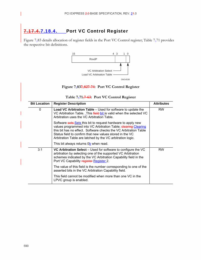
PCI EXPRESS 2.0 BASE SPECIFICATION, REV. 21.0
590
7.17.4.7.18.4. Port VC Control Register
Figure 7-83 details allocation of register fields in the Port VC Control register; Table 7-71 provides the respective bit definitions.
OM14538
RsvdP
Load VC Arbitration Table
VC Arbitration Select
15 1 04 3
Figure 7-837-82 7-74: Port VC Control Register
Table 7-71- 7-63: Port VC Control Register
Bit Location Register Description Attributes
0 Load VC Arbitration Table – Used for software to update the VC Arbitration Table. This field bit is valid when the selected VC Arbitration uses the VC Arbitration Table.
Software sets Sets this bit to request hardware to apply new values programmed into VC Arbitration Table; clearing Clearing this bit has no effect. Software checks the VC Arbitration Table Status field to confirm that new values stored in the VC Arbitration Table are latched by the VC arbitration logic.
This bit always returns 0b when read.
RW
3:1 VC Arbitration Select – Used for software to configure the VC arbitration by selecting one of the supported VC Arbitration schemes indicated by the VC Arbitration Capability field in the Port VC Capability register Register 2.
The value of this field is the number corresponding to one of the asserted bits in the VC Arbitration Capability field.
This field cannot be modified when more than one VC in the LPVC group is enabled.
RW
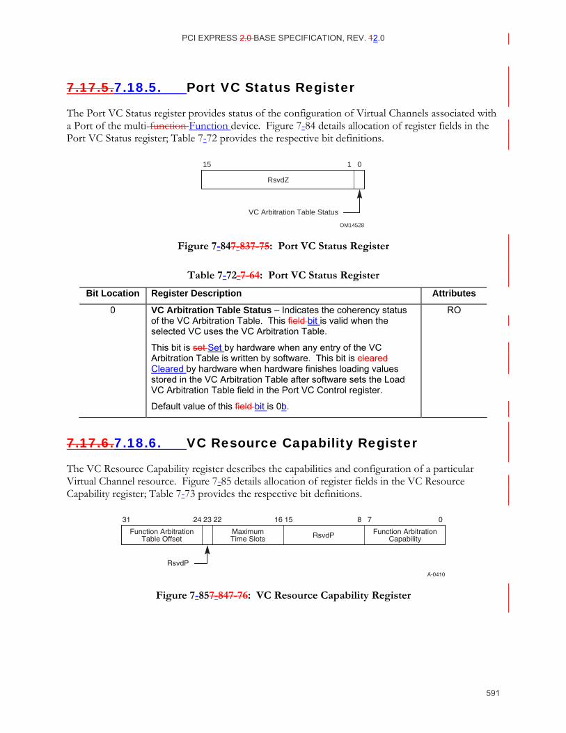
PCI EXPRESS 2.0 BASE SPECIFICATION, REV. 12.0
591
7.17.5.7.18.5. Port VC Status Register
The Port VC Status register provides status of the configuration of Virtual Channels associated with a Port of the multi-function Function device. Figure 7-84 details allocation of register fields in the Port VC Status register; Table 7-72 provides the respective bit definitions.
OM14528
VC Arbitration Table Status
RsvdZ
15 1 0
Figure 7-847-83 7-75: Port VC Status Register
Table 7-72- 7-64: Port VC Status Register
Bit Location Register Description Attributes
0 VC Arbitration Table Status – Indicates the coherency status of the VC Arbitration Table. This field bit is valid when the selected VC uses the VC Arbitration Table.
This bit is set Set by hardware when any entry of the VC Arbitration Table is written by software. This bit is cleared Cleared by hardware when hardware finishes loading values stored in the VC Arbitration Table after software sets the Load VC Arbitration Table field in the Port VC Control register.
Default value of this field bit is 0b.
RO
7.17.6.7.18.6. VC Resource Capability Register
The VC Resource Capability register describes the capabilities and configuration of a particular Virtual Channel resource. Figure 7-85 details allocation of register fields in the VC Resource Capability register; Table 7-73 provides the respective bit definitions.
A-0410
RsvdPFunction ArbitrationTable Offset
MaximumTime Slots
RsvdP
31 24 16 15 8 7 02223
Function ArbitrationCapability
Figure 7-857-84 7-76: VC Resource Capability Register
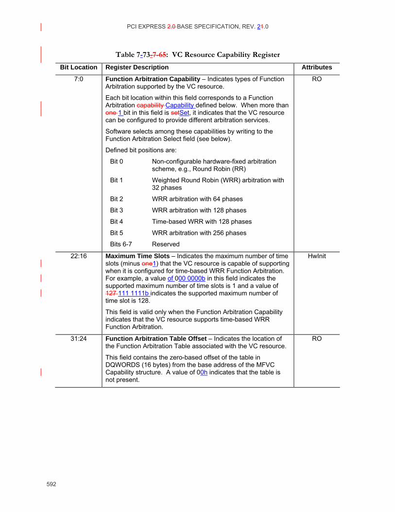
PCI EXPRESS 2.0 BASE SPECIFICATION, REV. 21.0
592
Table 7-73- 7-65: VC Resource Capability Register
Bit Location Register Description Attributes
7:0 Function Arbitration Capability – Indicates types of Function Arbitration supported by the VC resource.
Each bit location within this field corresponds to a Function Arbitration capability Capability defined below. When more than one 1 bit in this field is setSet, it indicates that the VC resource can be configured to provide different arbitration services.
Software selects among these capabilities by writing to the Function Arbitration Select field (see below).
Defined bit positions are:
Bit 0 Non-configurable hardware-fixed arbitration scheme, e.g., Round Robin (RR)
Bit 1 Weighted Round Robin (WRR) arbitration with 32 phases
Bit 2 WRR arbitration with 64 phases
Bit 3 WRR arbitration with 128 phases
Bit 4 Time-based WRR with 128 phases
Bit 5 WRR arbitration with 256 phases
Bits 6-7 Reserved
RO
22:16 Maximum Time Slots – Indicates the maximum number of time slots (minus one1) that the VC resource is capable of supporting when it is configured for time-based WRR Function Arbitration. For example, a value of 000 0000b in this field indicates the supported maximum number of time slots is 1 and a value of 127 111 1111b indicates the supported maximum number of time slot is 128.
This field is valid only when the Function Arbitration Capability indicates that the VC resource supports time-based WRR Function Arbitration.
HwInit
31:24 Function Arbitration Table Offset – Indicates the location of the Function Arbitration Table associated with the VC resource.
This field contains the zero-based offset of the table in DQWORDS (16 bytes) from the base address of the MFVC Capability structure. A value of 00h indicates that the table is not present.
RO
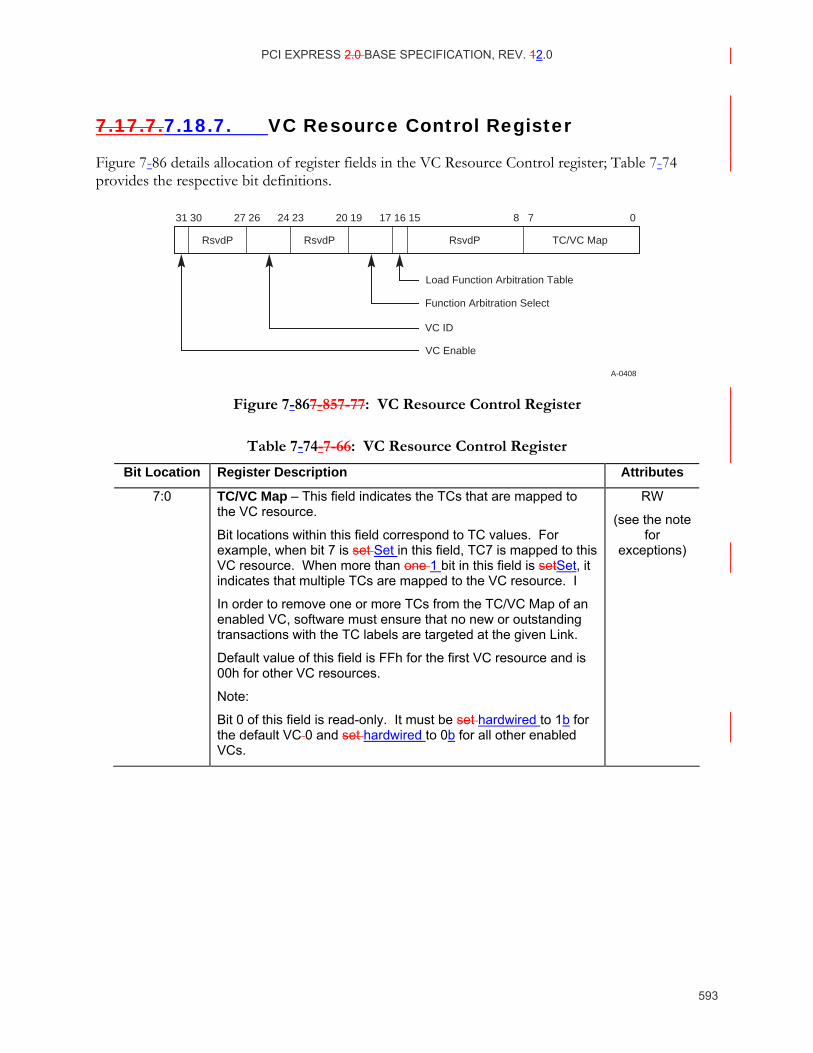
PCI EXPRESS 2.0 BASE SPECIFICATION, REV. 12.0
593
7.17.7.7.18.7. VC Resource Control Register
Figure 7-86 details allocation of register fields in the VC Resource Control register; Table 7-74 provides the respective bit definitions.
A-0408
TC/VC MapRsvdPRsvdP RsvdP
VC ID
VC Enable
Function Arbitration Select
Load Function Arbitration Table
31 27 26 24 20 19 16 15 8 7 0172330
Figure 7-867-85 7-77: VC Resource Control Register
Table 7-74- 7-66: VC Resource Control Register
Bit Location Register Description Attributes
7:0 TC/VC Map – This field indicates the TCs that are mapped to the VC resource.
Bit locations within this field correspond to TC values. For example, when bit 7 is set Set in this field, TC7 is mapped to this VC resource. When more than one 1 bit in this field is setSet, it indicates that multiple TCs are mapped to the VC resource. I
In order to remove one or more TCs from the TC/VC Map of an enabled VC, software must ensure that no new or outstanding transactions with the TC labels are targeted at the given Link.
Default value of this field is FFh for the first VC resource and is 00h for other VC resources.
Note:
Bit 0 of this field is read-only. It must be set hardwired to 1b for the default VC 0 and set hardwired to 0b for all other enabled VCs.
RW
(see the note for
exceptions)
PCI EXPRESS 2.0 BASE SPECIFICATION, REV. 21.0
594
Bit Location Register Description Attributes
16 Load Function Arbitration Table – This bit, wWhen setSet, this bit updates the Function Arbitration logic from the Function Arbitration Table for the VC resource. This field is only valid when the Function Arbitration Table is used by the selected Function Arbitration scheme (that is indicated by a set Set bit in the Function Arbitration Capability field selected by Function Arbitration Select).
Software sets this bit to signal hardware to update Function Arbitration logic with new values stored in the Function Arbitration Table; clearing this bit has no effect. Software uses the Function Arbitration Table Status bit to confirm whether the new values of Function Arbitration Table are completely latched by the arbitration logic.
This bit always returns 0b when read.
Default value of this field bit is 0b.
RW
19:17 Function Arbitration Select – This field configures the VC resource to provide a particular Function Arbitration service.
The permissible value of this field is a number corresponding to one of the asserted bits in the Function Arbitration Capability field of the VC resource.
RW
26:24 VC ID – This field assigns a VC ID to the VC resource (see note for exceptions).
This field cannot be modified when the VC is already enabled.
Note:
For the first VC resource (default VC), this field is a read-only field that must be set hardwired to 000 (“hard-wired”)b.
RW
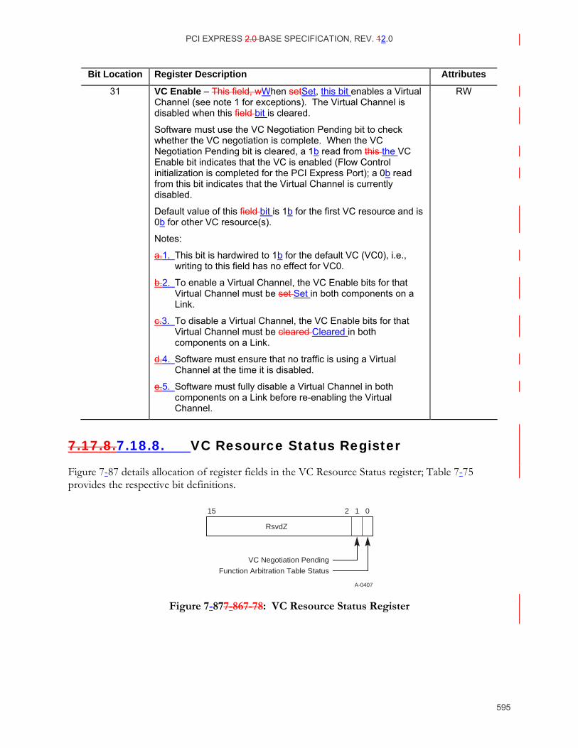
PCI EXPRESS 2.0 BASE SPECIFICATION, REV. 12.0
595
Bit Location Register Description Attributes
31 VC Enable – This field, wWhen setSet, this bit enables a Virtual Channel (see note 1 for exceptions). The Virtual Channel is disabled when this field bit is cleared.
Software must use the VC Negotiation Pending bit to check whether the VC negotiation is complete. When the VC Negotiation Pending bit is cleared, a 1b read from this the VC Enable bit indicates that the VC is enabled (Flow Control initialization is completed for the PCI Express Port); a 0b read from this bit indicates that the Virtual Channel is currently disabled.
Default value of this field bit is 1b for the first VC resource and is 0b for other VC resource(s).
Notes:
a.1. This bit is hardwired to 1b for the default VC (VC0), i.e., writing to this field has no effect for VC0.
b.2. To enable a Virtual Channel, the VC Enable bits for that Virtual Channel must be set Set in both components on a Link.
c.3. To disable a Virtual Channel, the VC Enable bits for that Virtual Channel must be cleared Cleared in both components on a Link.
d.4. Software must ensure that no traffic is using a Virtual Channel at the time it is disabled.
e.5. Software must fully disable a Virtual Channel in both components on a Link before re-enabling the Virtual Channel.
RW
7.17.8.7.18.8. VC Resource Status Register
Figure 7-87 details allocation of register fields in the VC Resource Status register; Table 7-75 provides the respective bit definitions.
A-0407
RsvdZ
Function Arbitration Table Status
VC Negotiation Pending
15 1 02
Figure 7-877-86 7-78: VC Resource Status Register
PCI EXPRESS 2.0 BASE SPECIFICATION, REV. 21.0
596
Table 7-75- 7-67: VC Resource Status Register
Bit Location Register Description Attributes
0 Function Arbitration Table Status – This bit indicates the coherency status of the Function Arbitration Table associated with the VC resource. This field bit is valid only when the Function Arbitration Table is used by the selected Function Arbitration for the VC resource.
This bit is set Set by hardware when any entry of the Function Arbitration Table is written to by software. This bit is cleared by hardware when hardware finishes loading values stored in the Function Arbitration Table after software sets the Load Function Arbitration Table fieldbit.
Default value of this field bit is 0b.
RO
1 VC Negotiation Pending – This bit indicates whether the Virtual Channel negotiation (initialization or disabling) is in pending state.
When this bit is set Set by hardware, it indicates that the VC resource is still in the process of negotiation. This bit is cleared by hardware after the VC negotiation is complete. For a non-default Virtual Channel, software may use this bit when enabling or disabling the VC. For the default VC, this bit indicates the status of the process of Flow Control initialization.
Before using a Virtual Channel, software must check whether the VC Negotiation Pending fields bits for that Virtual Channel are cleared Clear in both components on a Link.
RO
7.17.9.7.18.9. VC Arbitration Table
The definition of the VC Arbitration Table in the MFVC capability Capability structure is identical to that in the VC capability Capability structure (. Ssee Section 7.11.9 for details.)
7.17.10.7.18.10. Function Arbitration Table
The Function Arbitration Table register in the MFVC capability Capability structure takes the same form as the Port Arbitration Table register in the VC capability Capability structure (see Section 7.11.10). 5
The Function Arbitration Table register is a read-write register array that is used to store the WRR or time-based WRR arbitration table for Function Arbitration for the VC resource. It is only present when one or more asserted bits in the Function Arbitration Capability field indicate that the multi-function Function device supports a Function Arbitration scheme that uses a programmable arbitration table. Furthermore, it is only valid when one of the above above-mentioned bits in the 10 Function Arbitration Capability field is selected by the Function Arbitration Select field.
The Function Arbitration Table represents one function Function arbitration period. Each table entry containing a Function Number corresponds to a phase within a Function Arbitration period.

PCI EXPRESS 2.0 BASE SPECIFICATION, REV. 12.0
597
The table entry size must support enough values to specify all implemented functions Functions plus at least one value that does not correspond to an implemented functionFunction. For example, a table with 2-bit entries can be used by a multi-function Function device with up to three Functions.
A Function Number written to a table entry indicates that the phase within the Function Arbitration 5 period is assigned to the selected Function (the Function Number must be a valid one).
When the WRR Function Arbitration is used for a VC of the Egress Port of the multi-function Function device, at each arbitration phase the Function Arbiter serves one transaction from the Function indicated by the Function Number of the current phase. When finished, it immediately advances to the next phase. A phase is skipped, i.e., the Function Arbiter simply 10 moves to the next phase without delayimmediately if the Function indicated by the phase does not contain any transaction for the VC.
When the Time-based WRR Function Arbitration is used for a VC of the Egress Port of the multi-function Function device, at each arbitration phase aligning to a virtual timeslot, the Function Arbiter serves one transaction from the Function indicated by the Function Number 15 of the current phase. It advances to the next phase at the next virtual timeslot. A phase indicates an “idle” timeslot, i.e., the Function Arbiter does not serve any transaction during the phase, if
• the phase contains the Number of a Function that does not exist, or
• the Function indicated by the phase does not contain any transaction for the VC. 20
The Function Arbitration Table Entry Size field in the Port VC Capability register determines the table entry size. The length of the table is determined by the Function Arbitration Select field as shown in Table 7-76.
When the Function Arbitration Table is used by the default Function Arbitration for the default VC, the default values for the table entries must contain at least one entry for each of the active 25 Functions in the multi-function Function device to ensure forward progress for the default VC for the multi-function Function device’s Upstream Port. The table may contain RR or RR-like fair Function Arbitration for the default VC.
Table 7-76- 7-68: Length of Function Arbitration Table
Function Arbitration Select Function Arbitration Table Length (in Number of Entries)
001b 32
010b 64
011b 128
100b 128
101b 256
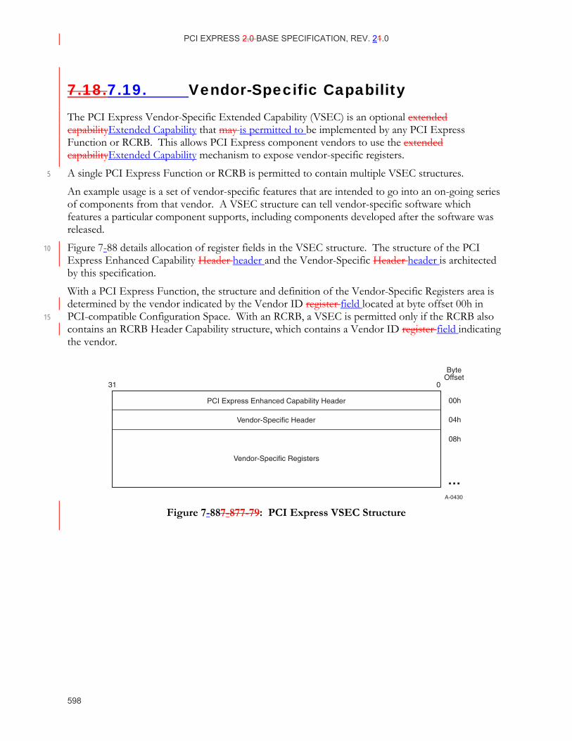
PCI EXPRESS 2.0 BASE SPECIFICATION, REV. 21.0
598
7.18.7.19. Vendor-Specific Capability The PCI Express Vendor-Specific Extended Capability (VSEC) is an optional extended capabilityExtended Capability that may is permitted to be implemented by any PCI Express Function or RCRB. This allows PCI Express component vendors to use the extended capabilityExtended Capability mechanism to expose vendor-specific registers.
A single PCI Express Function or RCRB is permitted to contain multiple VSEC structures. 5
An example usage is a set of vendor-specific features that are intended to go into an on-going series of components from that vendor. A VSEC structure can tell vendor-specific software which features a particular component supports, including components developed after the software was released.
Figure 7-88 details allocation of register fields in the VSEC structure. The structure of the PCI 10 Express Enhanced Capability Header header and the Vendor-Specific Header header is architected by this specification.
With a PCI Express Function, the structure and definition of the Vendor-Specific Registers area is determined by the vendor indicated by the Vendor ID register field located at byte offset 00h in PCI-compatible Configuration Space. With an RCRB, a VSEC is permitted only if the RCRB also 15 contains an RCRB Header Capability structure, which contains a Vendor ID register field indicating the vendor.
A-0430
0
ByteOffset
31
04h
08h
00hPCI Express Enhanced Capability Header
Vendor-Specific Header
Vendor-Specific Registers
Figure 7-887-87 7-79: PCI Express VSEC Structure
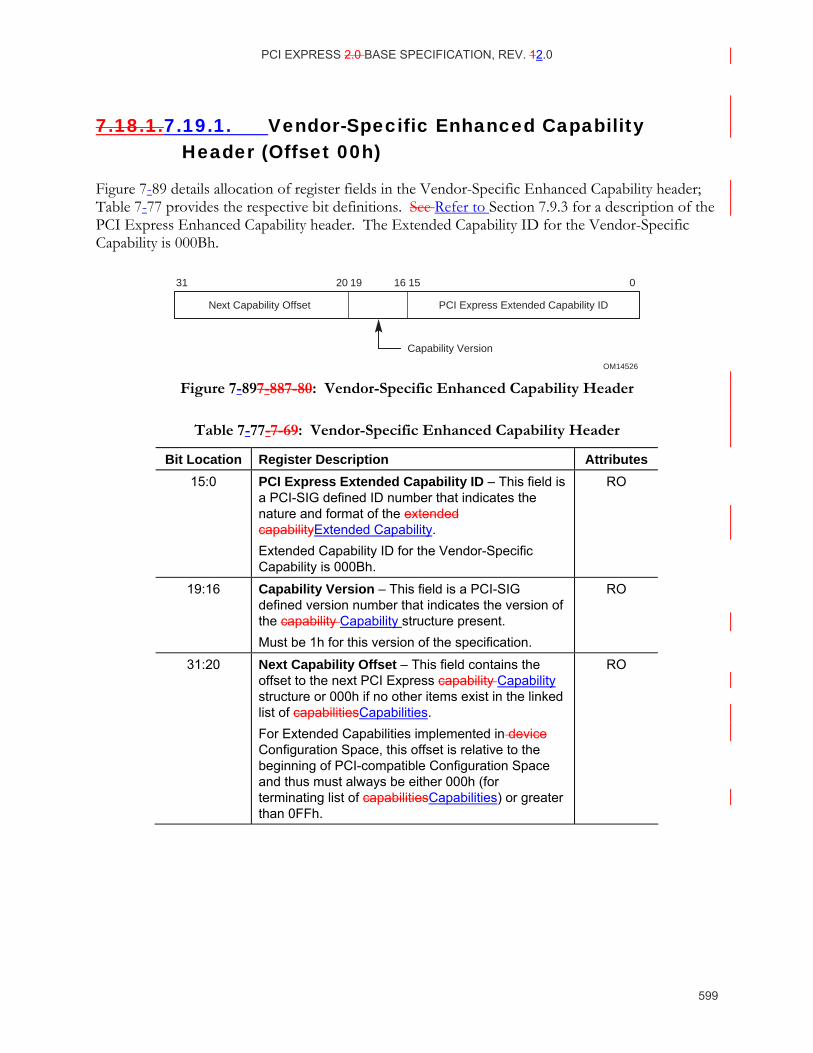
PCI EXPRESS 2.0 BASE SPECIFICATION, REV. 12.0
599
7.18.1.7.19.1. Vendor-Specific Enhanced Capability Header (Offset 00h)
Figure 7-89 details allocation of register fields in the Vendor-Specific Enhanced Capability header; Table 7-77 provides the respective bit definitions. See Refer to Section 7.9.3 for a description of the PCI Express Enhanced Capability header. The Extended Capability ID for the Vendor-Specific Capability is 000Bh.
OM14526
Capability Version
Next Capability Offset PCI Express Extended Capability ID
31 20 16 1519 0
Figure 7-897-88 7-80: Vendor-Specific Enhanced Capability Header
Table 7-77- 7-69: Vendor-Specific Enhanced Capability Header
Bit Location Register Description Attributes 15:0 PCI Express Extended Capability ID – This field is
a PCI-SIG defined ID number that indicates the nature and format of the extended capabilityExtended Capability. Extended Capability ID for the Vendor-Specific Capability is 000Bh.
RO
19:16 Capability Version – This field is a PCI-SIG defined version number that indicates the version of the capability Capability structure present. Must be 1h for this version of the specification.
RO
31:20 Next Capability Offset – This field contains the offset to the next PCI Express capability Capability structure or 000h if no other items exist in the linked list of capabilitiesCapabilities. For Extended Capabilities implemented in device Configuration Space, this offset is relative to the beginning of PCI-compatible Configuration Space and thus must always be either 000h (for terminating list of capabilitiesCapabilities) or greater than 0FFh.
RO
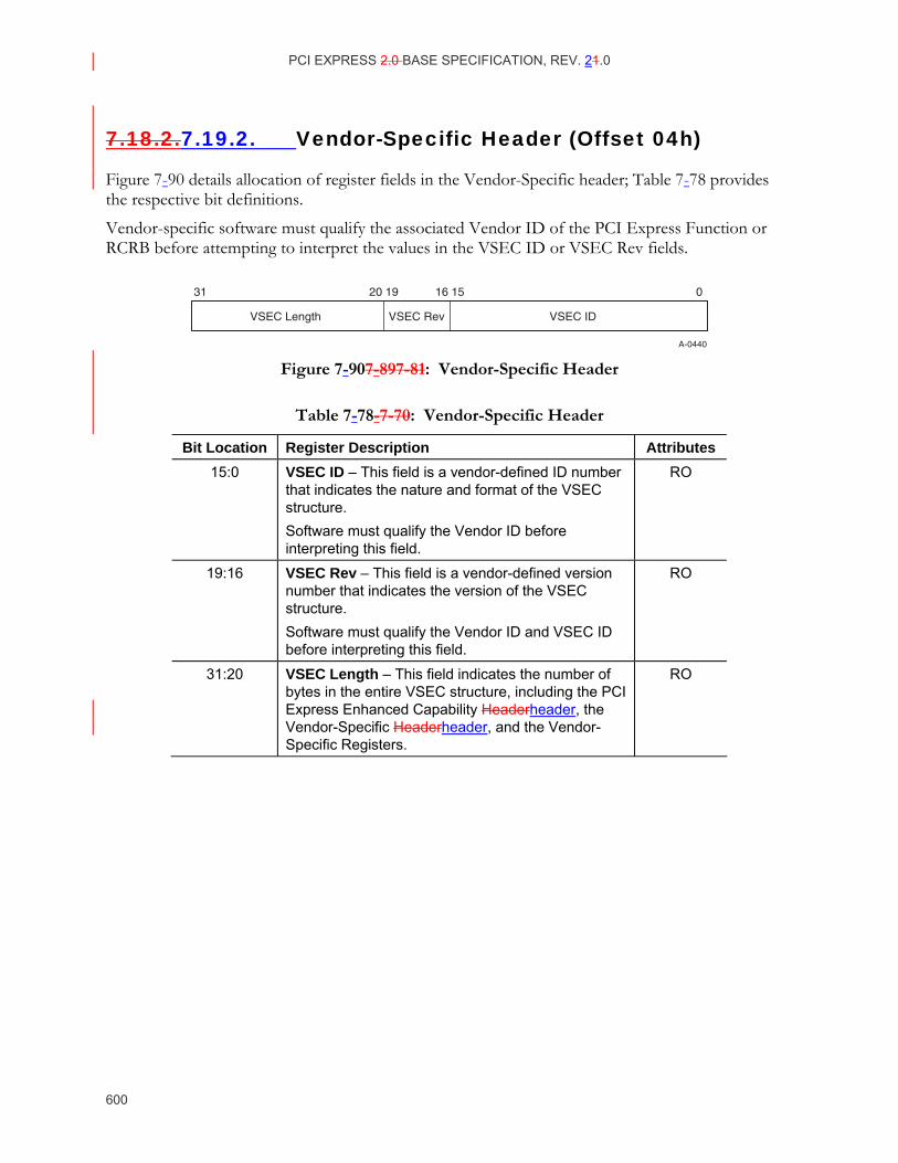
PCI EXPRESS 2.0 BASE SPECIFICATION, REV. 21.0
600
7.18.2.7.19.2. Vendor-Specific Header (Offset 04h)
Figure 7-90 details allocation of register fields in the Vendor-Specific header; Table 7-78 provides the respective bit definitions.
Vendor-specific software must qualify the associated Vendor ID of the PCI Express Function or RCRB before attempting to interpret the values in the VSEC ID or VSEC Rev fields.
A-0440
VSEC Rev VSEC IDVSEC Length
31 16 15 01920
Figure 7-907-89 7-81: Vendor-Specific Header
Table 7-78- 7-70: Vendor-Specific Header
Bit Location Register Description Attributes 15:0 VSEC ID – This field is a vendor-defined ID number
that indicates the nature and format of the VSEC structure. Software must qualify the Vendor ID before interpreting this field.
RO
19:16 VSEC Rev – This field is a vendor-defined version number that indicates the version of the VSEC structure. Software must qualify the Vendor ID and VSEC ID before interpreting this field.
RO
31:20 VSEC Length – This field indicates the number of bytes in the entire VSEC structure, including the PCI Express Enhanced Capability Headerheader, the Vendor-Specific Headerheader, and the Vendor-Specific Registers.
RO
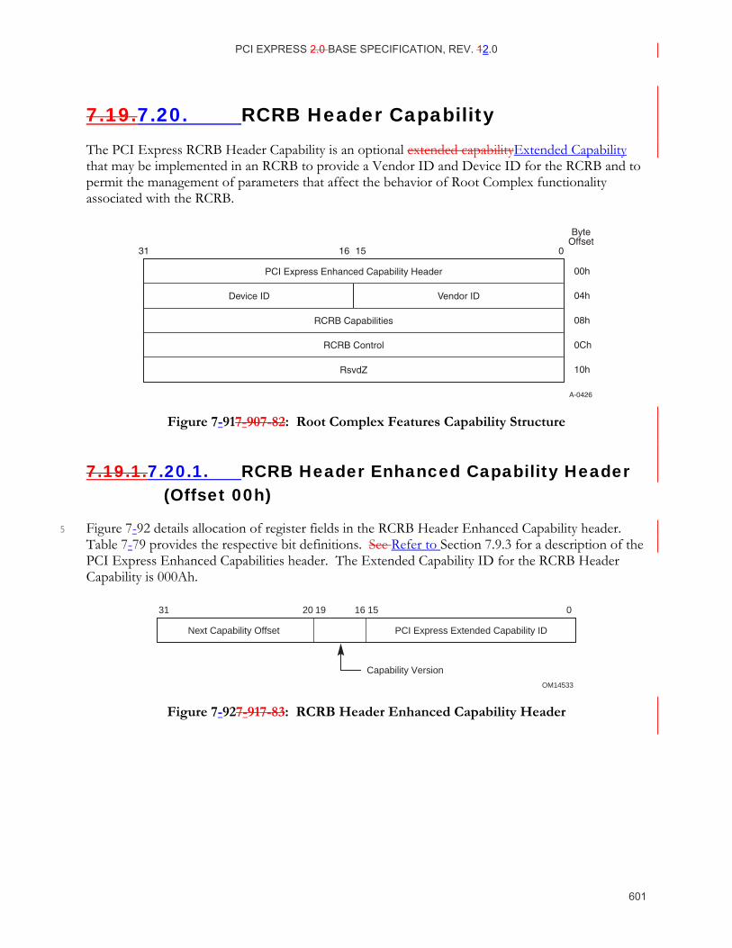
PCI EXPRESS 2.0 BASE SPECIFICATION, REV. 12.0
601
7.19.7.20. RCRB Header Capability The PCI Express RCRB Header Capability is an optional extended capabilityExtended Capability that may be implemented in an RCRB to provide a Vendor ID and Device ID for the RCRB and to permit the management of parameters that affect the behavior of Root Complex functionality associated with the RCRB.
A-0426
0
ByteOffset
31
04h
08h
00h
0Ch
10h
PCI Express Enhanced Capability Header
Vendor IDDevice ID
RCRB Capabilities
RCRB Control
RsvdZ
16 15
Figure 7-917-90 7-82: Root Complex Features Capability Structure
7.19.1.7.20.1. RCRB Header Enhanced Capability Header (Offset 00h)
Figure 7-92 details allocation of register fields in the RCRB Header Enhanced Capability header. 5 Table 7-79 provides the respective bit definitions. See Refer to Section 7.9.3 for a description of the PCI Express Enhanced Capabilities header. The Extended Capability ID for the RCRB Header Capability is 000Ah.
OM14533
Capability Version
Next Capability Offset PCI Express Extended Capability ID
31 20 16 1519 0
Figure 7-927-91 7-83: RCRB Header Enhanced Capability Header
PCI EXPRESS 2.0 BASE SPECIFICATION, REV. 21.0
602
Table 7-79- 7-71: RCRB Header Enhanced Capability Header
Bit Location Register Description Attributes 15:0 PCI Express Extended Capability ID – This field is
a PCI-SIG defined ID number that indicates the nature and format of the extended capabilityExtended Capability. Extended Capability ID for the RCRB Header Capability is 000Ah.
RO
19:16 Capability Version – This field is a PCI-SIG defined version number that indicates the version of the capability Capability structure present. Must be 1h for this version of the specification.
RO
31:20 Next Capability Offset – This field contains the offset to the next PCI Express capability Capability structure or 000h if no other items exist in the linked list of capabilitiesCapabilities. For Extended Capabilities implemented in device configuration spaceConfiguration Space, this offset is relative to the beginning of PCI compatible configuration spaceConfiguration Space and thus must always be either 000h (for terminating list of capabilitiesCapabilities) or greater than 0FFh.
RO
7.19.2.7.20.2. Vendor ID (Offset 04h) and Device ID (Offset 06h)
Figure 7-93 details allocation of register fields in the RCRB Capabilities register; Table 7-80 provides the respective bit definitions.
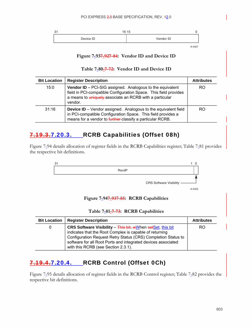
PCI EXPRESS 2.0 BASE SPECIFICATION, REV. 12.0
603
A-0427
Vendor IDDevice ID
31 16 15 0
Figure 7-937-92 7-84: Vendor ID and Device ID
Table 7-80- 7-72: Vendor ID and Device ID
Bit Location Register Description Attributes 15:0 Vendor ID – PCI-SIG assigned. Analogous to the equivalent
field in PCI-compatible Configuration Space. This field provides a means to uniquely associate an RCRB with a particular vendor.
RO
31:16 Device ID – Vendor assigned. Analogous to the equivalent field in PCI-compatible Configuration Space. This field provides a means for a vendor to further classify a particular RCRB.
RO
7.19.3.7.20.3. RCRB Capabilities (Offset 08h)
Figure 7-94 details allocation of register fields in the RCRB Capabilities register; Table 7-81 provides the respective bit definitions.
A-0425
RsvdP
CRS Software Visibility
31 1 0
Figure 7-947-93 7-85: RCRB Capabilities
Table 7-81- 7-73: RCRB Capabilities
Bit Location Register Description Attributes 0 CRS Software Visibility – This bit, wWhen setSet, this bit
indicates that the Root Complex is capable of returning Configuration Request Retry Status (CRS) Completion Status to software for all Root Ports and integrated devices associated with this RCRB (see Section 2.3.1).
RO
7.19.4.7.20.4. RCRB Control (Offset 0Ch)
Figure 7-95 details allocation of register fields in the RCRB Control register; Table 7-82 provides the respective bit definitions.
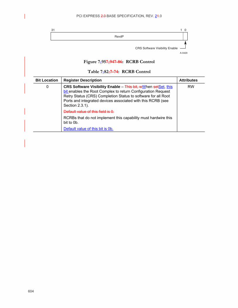
PCI EXPRESS 2.0 BASE SPECIFICATION, REV. 21.0
604
A-0429
RsvdP
CRS Software Visibility Enable
31 1 0
Figure 7-957-94 7-86: RCRB Control
Table 7-82- 7-74: RCRB Control
Bit Location Register Description Attributes 0 CRS Software Visibility Enable – This bit, wWhen setSet, this
bit enables the Root Complex to return Configuration Request Retry Status (CRS) Completion Status to software for all Root Ports and integrated devices associated with this RCRB (see Section 2.3.1). Default value of this field is 0. RCRBs that do not implement this capability must hardwire this bit to 0b. Default value of this bit is 0b.
RW
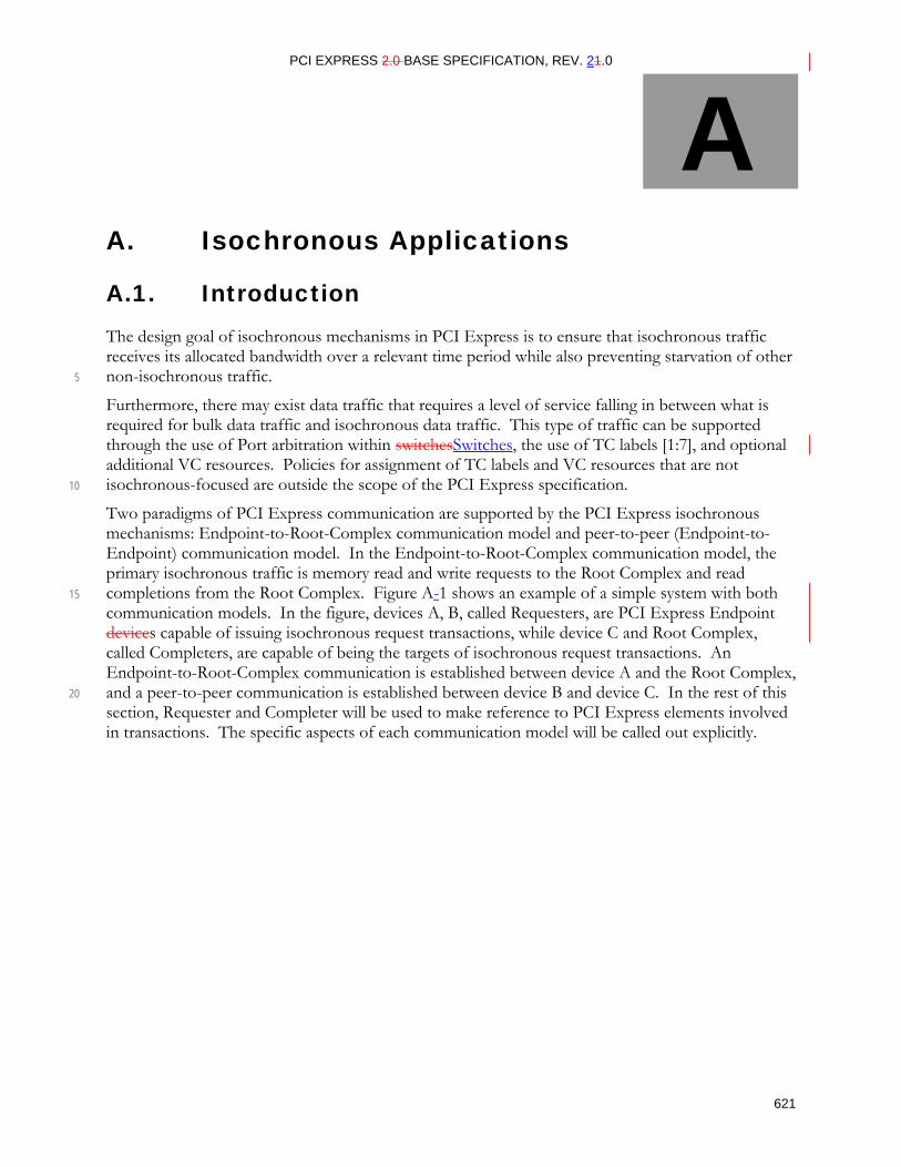
PCI EXPRESS 2.0 BASE SPECIFICATION, REV. 21.0
621
A. Isochronous Applications
A.1. Introduction The design goal of isochronous mechanisms in PCI Express is to ensure that isochronous traffic receives its allocated bandwidth over a relevant time period while also preventing starvation of other non-isochronous traffic. 5
Furthermore, there may exist data traffic that requires a level of service falling in between what is required for bulk data traffic and isochronous data traffic. This type of traffic can be supported through the use of Port arbitration within switchesSwitches, the use of TC labels [1:7], and optional additional VC resources. Policies for assignment of TC labels and VC resources that are not isochronous-focused are outside the scope of the PCI Express specification. 10
Two paradigms of PCI Express communication are supported by the PCI Express isochronous mechanisms: Endpoint-to-Root-Complex communication model and peer-to-peer (Endpoint-to-Endpoint) communication model. In the Endpoint-to-Root-Complex communication model, the primary isochronous traffic is memory read and write requests to the Root Complex and read completions from the Root Complex. Figure A-1 shows an example of a simple system with both 15 communication models. In the figure, devices A, B, called Requesters, are PCI Express Endpoint devices capable of issuing isochronous request transactions, while device C and Root Complex, called Completers, are capable of being the targets of isochronous request transactions. An Endpoint-to-Root-Complex communication is established between device A and the Root Complex, and a peer-to-peer communication is established between device B and device C. In the rest of this 20 section, Requester and Completer will be used to make reference to PCI Express elements involved in transactions. The specific aspects of each communication model will be called out explicitly.
A
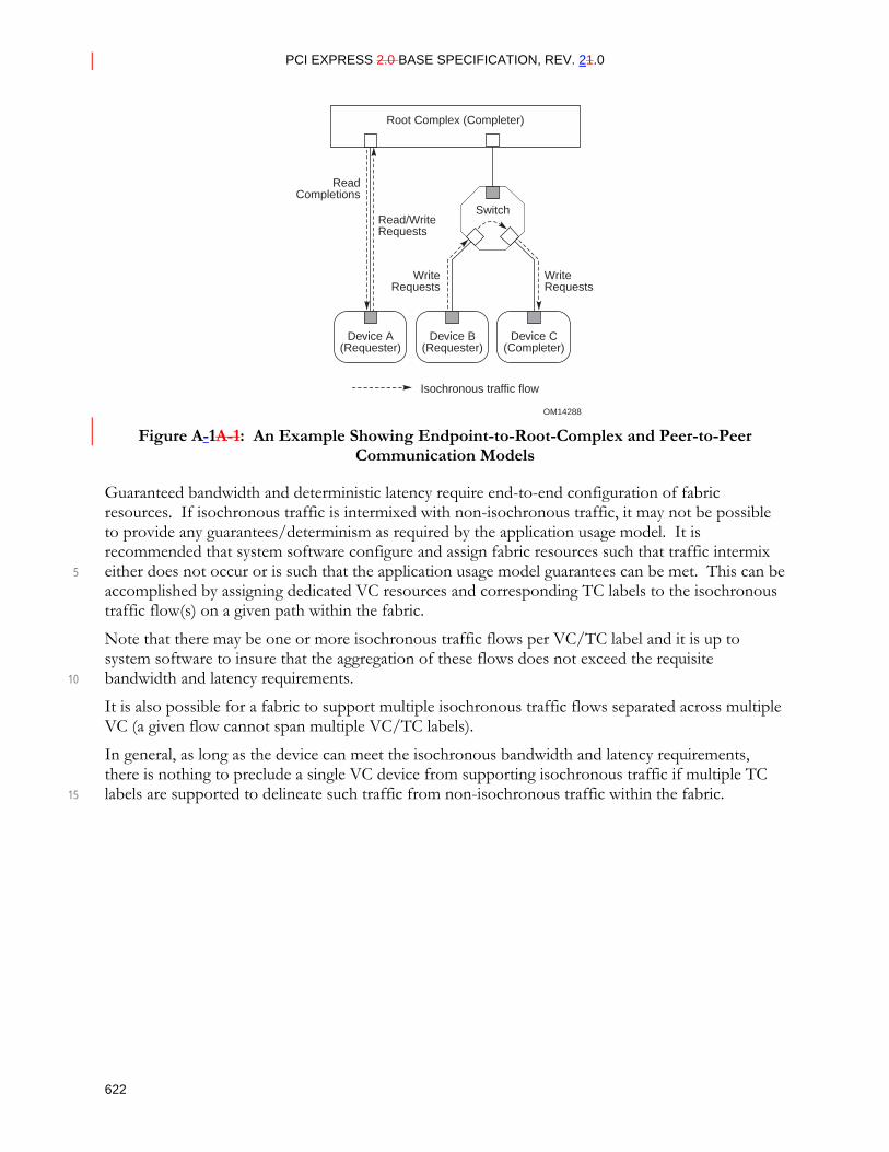
PCI EXPRESS 2.0 BASE SPECIFICATION, REV. 21.0
622
OM14288
Device A(Requester)
Switch
Isochronous traffic flow
Root Complex (Completer)
Device C(Completer)
Device B(Requester)
ReadCompletions
Read/WriteRequests
WriteRequests
WriteRequests
Figure A-1A-1: An Example Showing Endpoint-to-Root-Complex and Peer-to-Peer
Communication Models
Guaranteed bandwidth and deterministic latency require end-to-end configuration of fabric resources. If isochronous traffic is intermixed with non-isochronous traffic, it may not be possible to provide any guarantees/determinism as required by the application usage model. It is recommended that system software configure and assign fabric resources such that traffic intermix either does not occur or is such that the application usage model guarantees can be met. This can be 5 accomplished by assigning dedicated VC resources and corresponding TC labels to the isochronous traffic flow(s) on a given path within the fabric.
Note that there may be one or more isochronous traffic flows per VC/TC label and it is up to system software to insure that the aggregation of these flows does not exceed the requisite bandwidth and latency requirements. 10
It is also possible for a fabric to support multiple isochronous traffic flows separated across multiple VC (a given flow cannot span multiple VC/TC labels).
In general, as long as the device can meet the isochronous bandwidth and latency requirements, there is nothing to preclude a single VC device from supporting isochronous traffic if multiple TC labels are supported to delineate such traffic from non-isochronous traffic within the fabric. 15
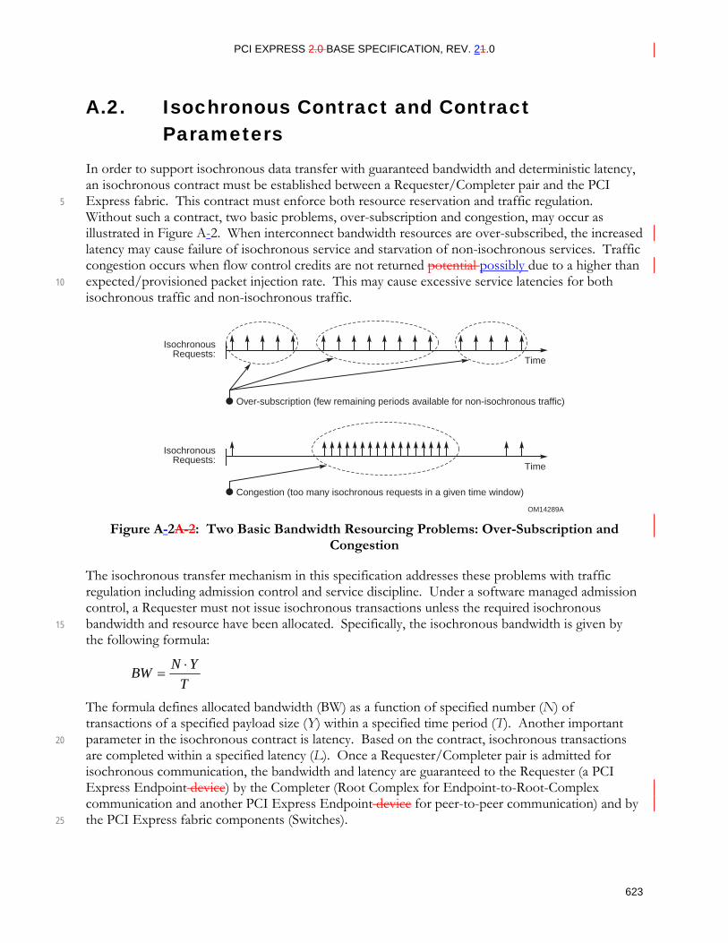
PCI EXPRESS 2.0 BASE SPECIFICATION, REV. 21.0
623
A.2. Isochronous Contract and Contract Parameters
In order to support isochronous data transfer with guaranteed bandwidth and deterministic latency, an isochronous contract must be established between a Requester/Completer pair and the PCI Express fabric. This contract must enforce both resource reservation and traffic regulation. 5 Without such a contract, two basic problems, over-subscription and congestion, may occur as illustrated in Figure A-2. When interconnect bandwidth resources are over-subscribed, the increased latency may cause failure of isochronous service and starvation of non-isochronous services. Traffic congestion occurs when flow control credits are not returned potential possibly due to a higher than expected/provisioned packet injection rate. This may cause excessive service latencies for both 10 isochronous traffic and non-isochronous traffic.
OM14289A
IsochronousRequests:
IsochronousRequests:
Time
Time
Over-subscription (few remaining periods available for non-isochronous traffic)
Congestion (too many isochronous requests in a given time window)
Figure A-2A-2: Two Basic Bandwidth Resourcing Problems: Over-Subscription and
Congestion
The isochronous transfer mechanism in this specification addresses these problems with traffic regulation including admission control and service discipline. Under a software managed admission control, a Requester must not issue isochronous transactions unless the required isochronous bandwidth and resource have been allocated. Specifically, the isochronous bandwidth is given by 15 the following formula:
TYNBW ⋅
=
The formula defines allocated bandwidth (BW) as a function of specified number (N) of transactions of a specified payload size (Y) within a specified time period (T). Another important parameter in the isochronous contract is latency. Based on the contract, isochronous transactions 20 are completed within a specified latency (L). Once a Requester/Completer pair is admitted for isochronous communication, the bandwidth and latency are guaranteed to the Requester (a PCI Express Endpoint device) by the Completer (Root Complex for Endpoint-to-Root-Complex communication and another PCI Express Endpoint device for peer-to-peer communication) and by the PCI Express fabric components (Switches). 25
PCI EXPRESS 2.0 BASE SPECIFICATION, REV. 21.0
624
Specific service disciplines must be implemented by isochronous-capable PCI Express components. The service disciplines are imposed to PCI Express Switches and Completers in such a manner that the service of isochronous requests is subject to a specific service interval (t). This mechanism is used to provide the method of controlling when an isochronous packet injected by a Requester is serviced. Consequently, isochronous traffic is policed in such manner that only packets that can be 5 injected into the fabric in compliance with the isochronous contract are allowed to make immediate progress and start being serviced by the PCI Express fabric. A non-compliant Requester that tries to inject more isochronous transactions than what was being allowed by the contract is prevented from doing so by the flow-control mechanism thereby allowing compliant Requesters to correctly operate independent of non-compliant Requesters. 10
In the Endpoint-to-Root-Complex model, since the aggregated isochronous traffic is eventually limited by the host memory subsystem's bandwidth capabilities, isochronous read requests, and write requests (and Messages) are budgeted together. A Requester may divide the isochronous bandwidth between read requests and write requests as appropriate.
A.2.1. Isochronous Time Period and Isochronous Virtual Timeslot
The PCI Express isochronous time period (T) is uniformly divided into units of virtual timeslots (t). 15 To provide precise isochronous bandwidth distribution only one isochronous request packet is allowed per virtual timeslot. The virtual timeslot supported by a PCI Express component is reported through the Reference Clock field in the PCI Express Virtual Channel Capability Structure structure or the Multi-Function Virtual Channel Capability structuredefined in Section 7.11. When Reference Clock = 00b, duration of a virtual timeslot t is 100 ns. Duration of isochronous time 20 period T depends on the number of phases of the supported time-based WRR Port arbitration table size. When the time-based WRR Port Arbitration Table size equals to 128, there are 128 virtual timeslots (t) in an isochronous time period, i.e. T = 12.8 µs.
Note that isochronous period T as well as virtual timeslots t do not need to be aligned and synchronized among different PCI Express isochronous devices, i.e., the notion of T, t is local to 25 each individual isochronous device.
PCI EXPRESS 2.0 BASE SPECIFICATION, REV. 21.0
625
A.2.2. Isochronous Payload Size
The payload size (Y) for isochronous transactions must not exceed Max_Payload_Size (see Section 7.8.4). After configuration, the Max_Payload_Size is set and fixed for each path that supports isochronous service with a value required to meet isochronous latency. The fixed Max_Payload_Size value is used for isochronous bandwidth budgeting regardless of the actual size of data payload associated with isochronous transactions. For isochronous bandwidth budgeting, 5 we have
d_SizeMax_Payloa=Y
A transaction with partial writes is treated as a normally accounted transaction. A Completer must account for partial writes as part of bandwidth assignment (for worst case servicing time).
A.2.3. Isochronous Bandwidth Allocation
Given T, t and Y, the maximum virtual timeslots within a time period is 10
tTN =max
and the maximum specifiable isochronous bandwidth is
tYBW =max
The granularity with which isochronous bandwidth can be allocated is defined as:
TYBW ygranularit = 15
Given T and t at 12.8 µs and 100 ns, respectively, Nmax is 128. As shown in Table A-1, BWmax and BWgranularity are functions of the isochronous payload size Y.
Table A-1: Isochronous Bandwidth Ranges and Granularities
Y (bytes) 128 256 512 1024BW max (MB/s) 1280 2560 5120 10240BW granularity (MB/s) 10 20 40 80
Similar to bandwidth budgeting, isochronous service disciplines including arbitration schemes are based on counting requests (not the sizes of those requests. Therefore, assigning isochronous bandwidth BWlink to a PCI Express Link is equivalent to assigning Nlink virtual timeslots per 20 isochronous period, where Nlink is given by
ygranularit
linklink BW
BWN =
A Switch Port serving as an Egress Port (or an RCRB serving as a “virtual” Egress Port) for an isochronous traffic, the Nmax virtual timeslots within T are represented by the time-based WRR Port Arbitration Table in the PCI Express Virtual Channel Capability Structure structure detailed in 25
PCI EXPRESS 2.0 BASE SPECIFICATION, REV. 21.0
626
Section 7.11. The table consists of Nmax entries. An entry in the table represents one virtual timeslot in the isochronous time period. When a table entry is given a value of PN, it means that the timeslot is assigned to an Ingress Port (in respect to the isochronous traffic targeting the Egress Port) designated by a Port Number of PN. Therefore, Nlink virtual timeslots are assigned to the Ingress Port when there are Nlink entries in the table with value of PN. The Egress Port may admit one 5 isochronous request transaction from the Ingress Port for further service only when the table entry reached by the Egress Port's isochronous time ticker (that increments by 1 every t time and wraps around when reaching T) is set to PN. Even if there are outstanding isochronous requests ready in the Ingress Port, they will not be served until next round of time-based WRR arbitration. In this manner, the time-based Port Arbitration Table serves for both isochronous bandwidth assignment 10 and isochronous traffic regulation.
For an PCI Express Endpoint device serving as a Requester or a Completer, isochronous bandwidth allocation is accomplished through negotiation between system software and device driver, which is outside of the scope of this specification.
A.2.4. Isochronous Transaction Latency
Transaction latency is composed of the latency through the PCI Express fabric and the latency 15 contributed by the Completer. Isochronous transaction latency is defined for each transaction and measured in units of virtual timeslot t.
• The read latency is defined as the round-trip latency. This is the delay from the time when the device submits a memory read request packet to its Transaction Layer (Transmit side) to the time when the corresponding read completion arrives at the device's Transaction Layer (Receive 20 side).
• The write latency is defined as the delay from the time when the Requester posts a memory write request to its PCI Express Transaction Layer (Transmit side) to the time when the data write becomes globally visible within the memory subsystem of the Completer. A write to memory reaches the point of global visibility when all agents accessing that memory address get the 25 updated data.
When the upper bound and the lower bound of isochronous transaction latency are provided, the size of isochronous data buffers in a Requester can be determined. For most of common platforms, the minimum isochronous transaction latency is much smaller than the maximum. As a conservative measure, the minimum isochronous transaction latency is assumed to be zero; only 30 guidelines on measuring the maximum isochronous transaction latency are provided here.
For a Requester, the maximum isochronous (read or write) transaction latency (L) can be accounted as the following:
CompleterFabric LLL += ,
where LFabric is the maximum latency of the PCI Express fabric and LCompleter is the maximum latency 35 of the Completer.
LFabric which applies to both read and write transactions, depends on the topology, latency across each PCI Express Link, and the arbitration point in the path between the Requester to the Completer. The latency on a PCI Express Link depends on pipeline delays, width and operational
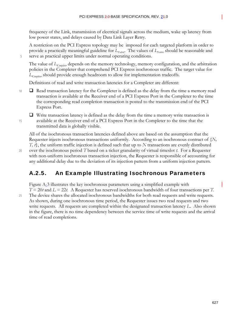
PCI EXPRESS 2.0 BASE SPECIFICATION, REV. 21.0
627
frequency of the Link, transmission of electrical signals across the medium, wake up latency from low power states, and delays caused by Data Link Layer Retry.
A restriction on the PCI Express topology may be imposed for each targeted platform in order to provide a practically meaningful guideline for LFabric. The values of LFabric should be reasonable and serve as practical upper limits under normal operating conditions. 5
The value of LCompleter depends on the memory technology, memory configuration, and the arbitration policies in the Completer that comprehend PCI Express isochronous traffic. The target value for LCompleter should provide enough headroom to allow for implementation tradeoffs.
Definitions of read and write transaction latencies for a Completer are different:
Read transaction latency for the Completer is defined as the delay from the time a memory read 10 transaction is available at the Receiver end of a PCI Express Port in the Completer to the time the corresponding read completion transaction is posted to the transmission end of the PCI Express Port.
Write transaction latency is defined as the delay from the time a memory write transaction is available at the Receiver end of a PCI Express Port in the Completer to the time that the 15 transmitted data is globally visible.
All of the isochronous transaction latencies defined above are based on the assumption that the Requester injects isochronous transactions uniformly. According to an isochronous contract of N, T, t, the uniform traffic injection is defined such that up to N transactions are evenly distributed over the isochronous period T based on a ticker granularity of virtual timeslot t. For a Requester 20 with non-uniform isochronous transaction injection, the Requester is responsible of accounting for any additional delay due to the deviation of its injection pattern from a uniform injection pattern.
A.2.5. An Example Illustrating Isochronous Parameters
Figure A-3 illustrates the key isochronous parameters using a simplified example with T = 20t and L = 22t. A Requester has reserved isochronous bandwidth of four transactions per T. The device shares the allocated isochronous bandwidths for both read requests and write requests. 25 As shown, during one isochronous time period, the Requester issues two read requests and two write requests. All requests are completed within the designated transaction latency L. Also shown in the figure, there is no time dependency between the service time of write requests and the arrival time of read completions.
PCI EXPRESS 2.0 BASE SPECIFICATION, REV. 21.0
628
OM14290
Completions
Requests
T
tR1 W1 W2R2
L W1 W2 R1 R2
Figure A-3A-3: A Simplified Example Illustrating PCI Express Isochronous Parameters
A.3. Isochronous Transaction Rules Isochronous transactions follow the same rules as described in Chapter 2. In order to assist the Completer to meet latency requirements, the following additional rules further illustrate and clarify the proper behavior of isochronous transactions:
The value in the Length field of requests must never exceed Max_Payload_Size. 5
A.4. Transaction Ordering In general, isochronous transactions follow the ordering rules described in Section 2.4. The following ordering rule further illustrates and clarifies the proper behavior of isochronous transactions:
There are no ordering guarantees between any isochronous and non-isochronous transactions 10 because the traffic has been segregated into distinct VC resources.
Isochronous write requests are serviced on any PCI Express Link in strictly the same order as isochronous write requests are posted.
Switches must allow isochronous posted requests to pass isochronous read completions.
A.5. Isochronous Data Coherency Cache coherency for isochronous transactions is an operating system software and Root Complex 15 hardware issue. PCI Express provides the necessary mechanism to control Root Complex behavior in terms of enforcing hardware cache coherency on a per transaction basis.
For platforms where snoop latency in a Root Complex is either unbounded or can be excessively large, in order to meet tight maximum isochronous transaction latency LCompleter, or more precisely LRoot_Complex, all isochronous transactions should have the No Snoop Attribute bit set. 20
A Root Complex must report the Root Complex's capability to the system software by setting the Reject Snoop Transactions field in the VC Resource Capability register (for any VC resource capable of supporting isochronous traffic) in its RCRB. Based on whether or not a Root Complex is capable of providing hardware enforced cache coherency for isochronous traffic while still meeting isochronous latency target, system software can then inform the device driver of Endpoint devices 25 to set or unset the No Snoop Attribute bit for isochronous transactions.
Note that cache coherency considerations for isochronous traffic do not apply to peer-to-peer communication.
PCI EXPRESS 2.0 BASE SPECIFICATION, REV. 21.0
629
A.6. Flow Control Completers and PCI Express fabric components should implement proper sizing of buffers such that under normal operating conditions, no backpressure due to flow control should be applied to isochronous traffic injected uniformly by a Requester. For Requesters that are compliant to the isochronous contract, but have bursty injection behavior, Switches and Completers may apply flow 5 control backpressure as long as the admitted isochronous traffic is uniform and compliant to the isochronous contract. Under abnormal conditions when isochronous traffic jitter becomes significant or when isochronous traffic is oversubscribed due to excessive Data Link Layer Retry, flow control provides a natural mechanism to ensure functional correctness.
A.7. Considerations for Bandwidth Allocation
A.7.1. Isochronous Bandwidth of PCI Express Links
Isochronous bandwidth budgeting for PCI Express Links can be derived based on Link parameters 10 such as isochronous payload size and the speed and width of the Link.
Isochronous bandwidth allocation for a PCI Express Link should be limited to certain percentage of the maximum effective Link bandwidth in order to leave sufficient bandwidth for non-isochronous traffic and to account for temporary Link bandwidth reduction due to retries. Link utilization is counted based on the actual cycles consumed on the physical PCI Express Link. The maximum 15 number of virtual slots allowed per Link (Nlink) depends on the isochronous packet payload size and the speed and width of the Link.
As isochronous bandwidth allocation on a PCI Express Link is based on number of requests Nlink per isochronous period. There is no distinction between read requests and write requests in budgeting isochronous bandwidth on a PCI Express Link. 20
A.7.2. Isochronous Bandwidth of Endpoint Devices
For peer-to-peer communication, the device driver is responsible for reporting to system software if the device is capable of being a Completer for isochronous transactions. In addition, the driver must report the device’s isochronous bandwidth capability. The specifics of the report mechanism are outside the scope of this specification.
A.7.3. Isochronous Bandwidth of Switches
Allocation of isochronous bandwidth for a Switch must consider the capacity and utilization of PCI 25 Express Links associated with the Ingress Port and the Egress Port of the Switch that connect the Requester and the Completer, respectively. The lowest common denominator of the two determines if a requested isochronous bandwidth can be supported.
PCI EXPRESS 2.0 BASE SPECIFICATION, REV. 21.0
630
A.7.4. Isochronous Bandwidth of Root Complex
Isochronous bandwidth of Root Complex is reported to the software through its RCRB Structurestructure. Specifically, the Maximum Time Slots field of the VC Resource Capability register in VC Capability Structure structure indicates the total isochronous bandwidth shared by the Root Ports associated with the RCRB. Details of the platform budgeting for available isochronous bandwidth within a Root Complex are outside of the scope of this specification. 5
A.8. Considerations for PCI Express Components
A.8.1. An PCI Express Endpoint Device as a Requester
Before an PCI Express Endpoint device as a Requester can start issuing isochronous request transactions, the following configuration steps must be performed by software:
Configuration of at least one VC resource capable of supporting isochronous communication and assignment of at least one TC label. 10
Enablement of this VC resource.
When the Requester uniformly injects isochronous requests, the Receive Port, either a Switch Port or a Root Port, should issue Flow Control credits back promptly such that no backpressure should be applied to the associated VC. This type of Requester may size its buffer based on the PCI Express fabric latency LFabric plus the Completer's latency LCompleter. 15
When isochronous transactions are injected non-uniformly, either some transactions experience longer PCI Express fabric delay or the Requester gets back-pressured on the associated VC. This type of Requester must size its buffer to account for the deviation of its injection pattern from uniformity.
A.8.2. An PCI Express Endpoint Device as a Completer
An PCI Express Endpoint device may serve as a Completer for isochronous peer-to-peer 20 communication. Before an PCI Express Endpoint device starts serving isochronous transactions, system software must identify/configure a VC resource capable of supporting isochronous traffic and assigned a corresponding TC label.
An Endpoint Completer must observe the maximum isochronous transaction latency (LCompleter). An Endpoint Completer does not have to regulate isochronous request traffic if attached to a switch 25 Switch since Switches implement traffic regulation. However, an Endpoint Completer must size its internal buffer such that no backpressure should be applied to the corresponding VC.
PCI EXPRESS 2.0 BASE SPECIFICATION, REV. 21.0
631
A.8.3. Switches
A Switch may have multiple ports capable of supporting isochronous transactions. Before a Switch starts serving isochronous transactions for a Port, the software must perform the following configuration steps:
Configuration/enablement of at least one VC resource capable of supporting isochronous communication. 5
Configuration of the Port as an Ingress Port:
• Configuration (or reconfiguration if the associated VC of the Egress Port is already enabled) of the time-based WRR Port Arbitration Table of the targeting Egress Port to include Nlink entries set to the Ingress Port's Port Number. Here Nlink is the isochronous allocation for the Ingress Port. 10
• Enabling the targeting Egress Port to load newly programmed Port Arbitration Table.
Configuration of the Port as an Egress Port:
• Configuration of each VC's Port Arbitration Table with number of entries set according to the assigned isochronous bandwidth for all Ingress Ports.
• Select proper VC Arbitration, e.g., as strict-priority based VC Arbitration. 15
• If required, configuration of the Port's VC Arbitration Table with large weights assigned accordingly to each associated VC.
Each VC associated with isochronous traffic may be served as the highest priority in arbitrating for the shared PCI Express Link resource at an Egress Port. This is comprehended by a Switch's internal arbitration scheme. 20
In addition, a Switch Port may use “just in time” scheduling mechanism to reduce VC arbitration latency. Instead of pipelining non-isochronous Transport Layer packets to the Data Link Layer of the Egress Port in a manner that Data Link Layer transmit buffer becomes saturated, the Switch Port may hold off scheduling of a new non-isochronous packet to the Data Link Layer as long as it is possible without incurring unnecessary Link idle time. 25
When a VC configured to support isochronous traffic is enabled for a Switch Port (ingress) that is connected to a Requester, the Switch must enforce proper traffic regulation to ensure that isochronous traffic from the Port conforms to this specification. With such enforcement, normal isochronous transactions from compliant Requesters will not be impacted by ill behavior of any incompliant non-compliant Requester. 30
The above isochronous traffic regulation mechanism only applies to request transactions but not to completion transactions. When Endpoint-to-Root-Complex and peer-to-peer communications co-exist in a Switch, an Egress Port may mix isochronous write requests and read completions in the same direction. In the case of contention, the Egress Port must allow write requests to pass read completions to ensure the Switch meets latency requirement for isochronous requests. 35
PCI EXPRESS 2.0 BASE SPECIFICATION, REV. 21.0
632
A.8.4. Root Complex
A Root Complex may have multiple Root Ports capable of supporting isochronous transactions. Before a Root Complex starts serving isochronous transactions for a Root Port, the Port must be configured by software to enable VC to support isochronous traffic using the following configuration steps:
Configuration of at least one VC resource capable of supporting isochronous communication 5 and assignment of at least one TC label.
Configuration of the Root Port as an Ingress Port:
• Configuration (or reconfiguration if the associated VC in RCRB is already enabled) of the time-based WRR Port Arbitration Table of the targeting RCRB to include Nlink entries set to the Ingress Port's Port Number. Here Nlink is the isochronous allocation for the Port. 10
• Enabling the targeting RCRB to load newly programmed Port Arbitration Table.
Configuration of the Root Port as an Egress Port:
• If supported, configuration of the Root Port's VC Arbitration Table with large weights assigned to the associated VC.
• If the Root Complex supports peer-to-peer traffic between Root Ports, configuration of the 15 Root Port's Port Arbitration Table number of entries is set according to the assigned isochronous bandwidth for all Ingress Ports.
A Root Complex must observe the maximum isochronous transaction latency (LCompleter or more precisely LRoot_Complex) that applies to all the Root Ports in the Root Complex. How a Root Complex schedules memory cycles for PCI Express isochronous transactions and other memory transactions 20 is outside of the scope of this specification as long as LRoot_Complex is met for PCI Express isochronous transactions.
When a VC is enabled to support isochronous traffic for a Root Port, the Root Complex must enforce proper traffic regulation to ensure that isochronous traffic from the Root Port confirms conforms to this specification. With such enforcement, normal isochronous transactions from 25 compliant Requesters will not be impacted by ill behavior of any incompliant non-compliant Requesters. Isochronous traffic regulation is implemented using the time-based Port Arbitration Table in RCRB.
Root Complex may perform the following operations for invalid isochronous transactions:
Return partial completions for read requests with the value in the Length field exceeding 30 Max_Payload_Size.
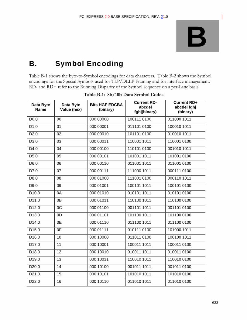
PCI EXPRESS 2.0 BASE SPECIFICATION, REV. 21.0
633
B. Symbol Encoding Table B-1 shows the byte-to-Symbol encodings for data characters. Table B-2 shows the Symbol encodings for the Special Symbols used for TLP/DLLP Framing and for interface management. RD- and RD+ refer to the Running Disparity of the Symbol sequence on a per-Lane basis.
Table B-1: 8b/10b Data Symbol Codes
Data Byte Name
Data Byte Value (hex)
Bits HGF EDCBA (binary)
Current RD- abcdei
fghj(binary)
Current RD+ abcdei fghj
(binary)
D0.0 00 000 00000 100111 0100 011000 1011
D1.0 01 000 00001 011101 0100 100010 1011
D2.0 02 000 00010 101101 0100 010010 1011
D3.0 03 000 00011 110001 1011 110001 0100
D4.0 04 000 00100 110101 0100 001010 1011
D5.0 05 000 00101 101001 1011 101001 0100
D6.0 06 000 00110 011001 1011 011001 0100
D7.0 07 000 00111 111000 1011 000111 0100
D8.0 08 000 01000 111001 0100 000110 1011
D9.0 09 000 01001 100101 1011 100101 0100
D10.0 0A 000 01010 010101 1011 010101 0100
D11.0 0B 000 01011 110100 1011 110100 0100
D12.0 0C 000 01100 001101 1011 001101 0100
D13.0 0D 000 01101 101100 1011 101100 0100
D14.0 0E 000 01110 011100 1011 011100 0100
D15.0 0F 000 01111 010111 0100 101000 1011
D16.0 10 000 10000 011011 0100 100100 1011
D17.0 11 000 10001 100011 1011 100011 0100
D18.0 12 000 10010 010011 1011 010011 0100
D19.0 13 000 10011 110010 1011 110010 0100
D20.0 14 000 10100 001011 1011 001011 0100
D21.0 15 000 10101 101010 1011 101010 0100
D22.0 16 000 10110 011010 1011 011010 0100
B
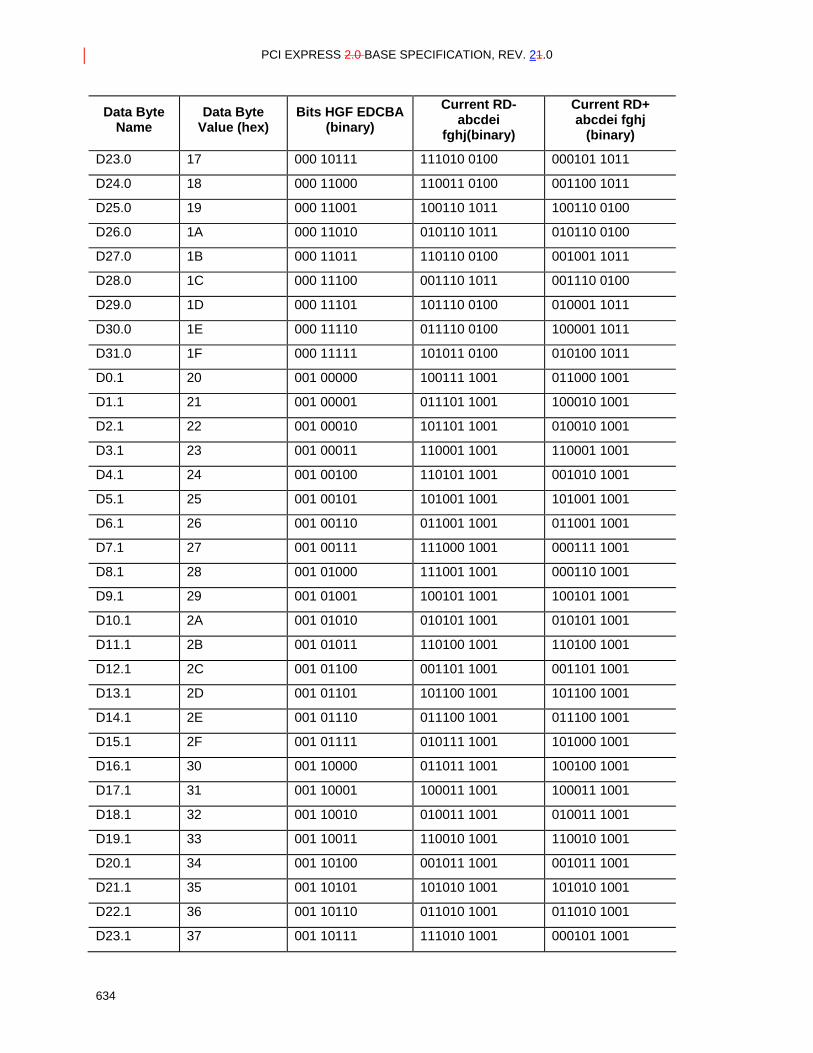
PCI EXPRESS 2.0 BASE SPECIFICATION, REV. 21.0
634
Data Byte Name
Data Byte Value (hex)
Bits HGF EDCBA (binary)
Current RD- abcdei
fghj(binary)
Current RD+ abcdei fghj
(binary)
D23.0 17 000 10111 111010 0100 000101 1011
D24.0 18 000 11000 110011 0100 001100 1011
D25.0 19 000 11001 100110 1011 100110 0100
D26.0 1A 000 11010 010110 1011 010110 0100
D27.0 1B 000 11011 110110 0100 001001 1011
D28.0 1C 000 11100 001110 1011 001110 0100
D29.0 1D 000 11101 101110 0100 010001 1011
D30.0 1E 000 11110 011110 0100 100001 1011
D31.0 1F 000 11111 101011 0100 010100 1011
D0.1 20 001 00000 100111 1001 011000 1001
D1.1 21 001 00001 011101 1001 100010 1001
D2.1 22 001 00010 101101 1001 010010 1001
D3.1 23 001 00011 110001 1001 110001 1001
D4.1 24 001 00100 110101 1001 001010 1001
D5.1 25 001 00101 101001 1001 101001 1001
D6.1 26 001 00110 011001 1001 011001 1001
D7.1 27 001 00111 111000 1001 000111 1001
D8.1 28 001 01000 111001 1001 000110 1001
D9.1 29 001 01001 100101 1001 100101 1001
D10.1 2A 001 01010 010101 1001 010101 1001
D11.1 2B 001 01011 110100 1001 110100 1001
D12.1 2C 001 01100 001101 1001 001101 1001
D13.1 2D 001 01101 101100 1001 101100 1001
D14.1 2E 001 01110 011100 1001 011100 1001
D15.1 2F 001 01111 010111 1001 101000 1001
D16.1 30 001 10000 011011 1001 100100 1001
D17.1 31 001 10001 100011 1001 100011 1001
D18.1 32 001 10010 010011 1001 010011 1001
D19.1 33 001 10011 110010 1001 110010 1001
D20.1 34 001 10100 001011 1001 001011 1001
D21.1 35 001 10101 101010 1001 101010 1001
D22.1 36 001 10110 011010 1001 011010 1001
D23.1 37 001 10111 111010 1001 000101 1001
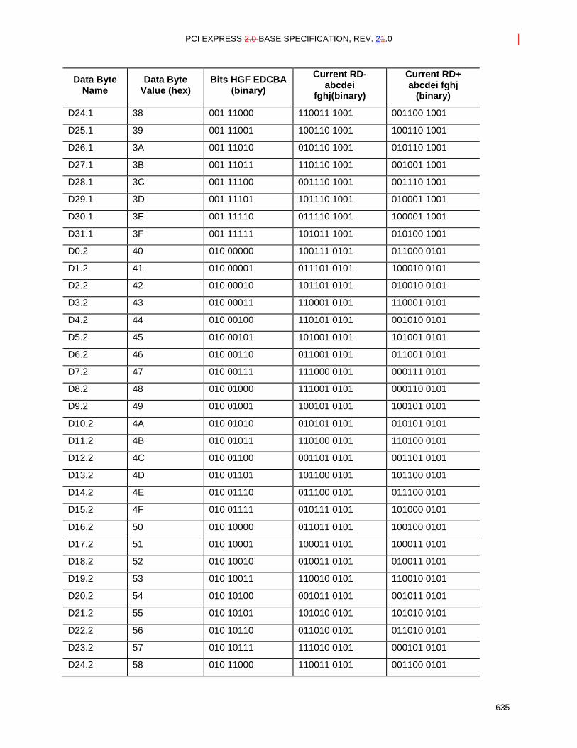
PCI EXPRESS 2.0 BASE SPECIFICATION, REV. 21.0
635
Data Byte Name
Data Byte Value (hex)
Bits HGF EDCBA (binary)
Current RD- abcdei
fghj(binary)
Current RD+ abcdei fghj
(binary)
D24.1 38 001 11000 110011 1001 001100 1001
D25.1 39 001 11001 100110 1001 100110 1001
D26.1 3A 001 11010 010110 1001 010110 1001
D27.1 3B 001 11011 110110 1001 001001 1001
D28.1 3C 001 11100 001110 1001 001110 1001
D29.1 3D 001 11101 101110 1001 010001 1001
D30.1 3E 001 11110 011110 1001 100001 1001
D31.1 3F 001 11111 101011 1001 010100 1001
D0.2 40 010 00000 100111 0101 011000 0101
D1.2 41 010 00001 011101 0101 100010 0101
D2.2 42 010 00010 101101 0101 010010 0101
D3.2 43 010 00011 110001 0101 110001 0101
D4.2 44 010 00100 110101 0101 001010 0101
D5.2 45 010 00101 101001 0101 101001 0101
D6.2 46 010 00110 011001 0101 011001 0101
D7.2 47 010 00111 111000 0101 000111 0101
D8.2 48 010 01000 111001 0101 000110 0101
D9.2 49 010 01001 100101 0101 100101 0101
D10.2 4A 010 01010 010101 0101 010101 0101
D11.2 4B 010 01011 110100 0101 110100 0101
D12.2 4C 010 01100 001101 0101 001101 0101
D13.2 4D 010 01101 101100 0101 101100 0101
D14.2 4E 010 01110 011100 0101 011100 0101
D15.2 4F 010 01111 010111 0101 101000 0101
D16.2 50 010 10000 011011 0101 100100 0101
D17.2 51 010 10001 100011 0101 100011 0101
D18.2 52 010 10010 010011 0101 010011 0101
D19.2 53 010 10011 110010 0101 110010 0101
D20.2 54 010 10100 001011 0101 001011 0101
D21.2 55 010 10101 101010 0101 101010 0101
D22.2 56 010 10110 011010 0101 011010 0101
D23.2 57 010 10111 111010 0101 000101 0101
D24.2 58 010 11000 110011 0101 001100 0101
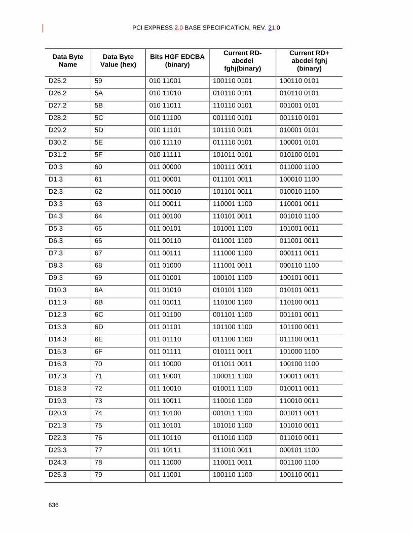
PCI EXPRESS 2.0 BASE SPECIFICATION, REV. 21.0
636
Data Byte Name
Data Byte Value (hex)
Bits HGF EDCBA (binary)
Current RD- abcdei
fghj(binary)
Current RD+ abcdei fghj
(binary)
D25.2 59 010 11001 100110 0101 100110 0101
D26.2 5A 010 11010 010110 0101 010110 0101
D27.2 5B 010 11011 110110 0101 001001 0101
D28.2 5C 010 11100 001110 0101 001110 0101
D29.2 5D 010 11101 101110 0101 010001 0101
D30.2 5E 010 11110 011110 0101 100001 0101
D31.2 5F 010 11111 101011 0101 010100 0101
D0.3 60 011 00000 100111 0011 011000 1100
D1.3 61 011 00001 011101 0011 100010 1100
D2.3 62 011 00010 101101 0011 010010 1100
D3.3 63 011 00011 110001 1100 110001 0011
D4.3 64 011 00100 110101 0011 001010 1100
D5.3 65 011 00101 101001 1100 101001 0011
D6.3 66 011 00110 011001 1100 011001 0011
D7.3 67 011 00111 111000 1100 000111 0011
D8.3 68 011 01000 111001 0011 000110 1100
D9.3 69 011 01001 100101 1100 100101 0011
D10.3 6A 011 01010 010101 1100 010101 0011
D11.3 6B 011 01011 110100 1100 110100 0011
D12.3 6C 011 01100 001101 1100 001101 0011
D13.3 6D 011 01101 101100 1100 101100 0011
D14.3 6E 011 01110 011100 1100 011100 0011
D15.3 6F 011 01111 010111 0011 101000 1100
D16.3 70 011 10000 011011 0011 100100 1100
D17.3 71 011 10001 100011 1100 100011 0011
D18.3 72 011 10010 010011 1100 010011 0011
D19.3 73 011 10011 110010 1100 110010 0011
D20.3 74 011 10100 001011 1100 001011 0011
D21.3 75 011 10101 101010 1100 101010 0011
D22.3 76 011 10110 011010 1100 011010 0011
D23.3 77 011 10111 111010 0011 000101 1100
D24.3 78 011 11000 110011 0011 001100 1100
D25.3 79 011 11001 100110 1100 100110 0011
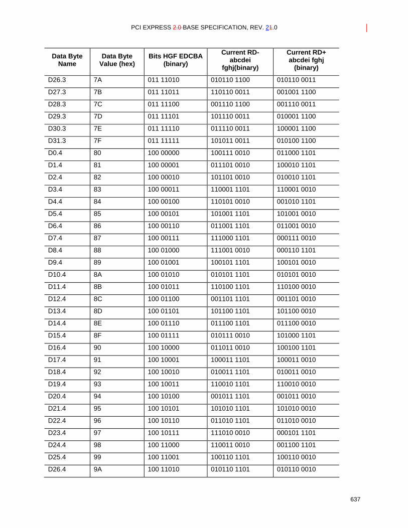
PCI EXPRESS 2.0 BASE SPECIFICATION, REV. 21.0
637
Data Byte Name
Data Byte Value (hex)
Bits HGF EDCBA (binary)
Current RD- abcdei
fghj(binary)
Current RD+ abcdei fghj
(binary)
D26.3 7A 011 11010 010110 1100 010110 0011
D27.3 7B 011 11011 110110 0011 001001 1100
D28.3 7C 011 11100 001110 1100 001110 0011
D29.3 7D 011 11101 101110 0011 010001 1100
D30.3 7E 011 11110 011110 0011 100001 1100
D31.3 7F 011 11111 101011 0011 010100 1100
D0.4 80 100 00000 100111 0010 011000 1101
D1.4 81 100 00001 011101 0010 100010 1101
D2.4 82 100 00010 101101 0010 010010 1101
D3.4 83 100 00011 110001 1101 110001 0010
D4.4 84 100 00100 110101 0010 001010 1101
D5.4 85 100 00101 101001 1101 101001 0010
D6.4 86 100 00110 011001 1101 011001 0010
D7.4 87 100 00111 111000 1101 000111 0010
D8.4 88 100 01000 111001 0010 000110 1101
D9.4 89 100 01001 100101 1101 100101 0010
D10.4 8A 100 01010 010101 1101 010101 0010
D11.4 8B 100 01011 110100 1101 110100 0010
D12.4 8C 100 01100 001101 1101 001101 0010
D13.4 8D 100 01101 101100 1101 101100 0010
D14.4 8E 100 01110 011100 1101 011100 0010
D15.4 8F 100 01111 010111 0010 101000 1101
D16.4 90 100 10000 011011 0010 100100 1101
D17.4 91 100 10001 100011 1101 100011 0010
D18.4 92 100 10010 010011 1101 010011 0010
D19.4 93 100 10011 110010 1101 110010 0010
D20.4 94 100 10100 001011 1101 001011 0010
D21.4 95 100 10101 101010 1101 101010 0010
D22.4 96 100 10110 011010 1101 011010 0010
D23.4 97 100 10111 111010 0010 000101 1101
D24.4 98 100 11000 110011 0010 001100 1101
D25.4 99 100 11001 100110 1101 100110 0010
D26.4 9A 100 11010 010110 1101 010110 0010
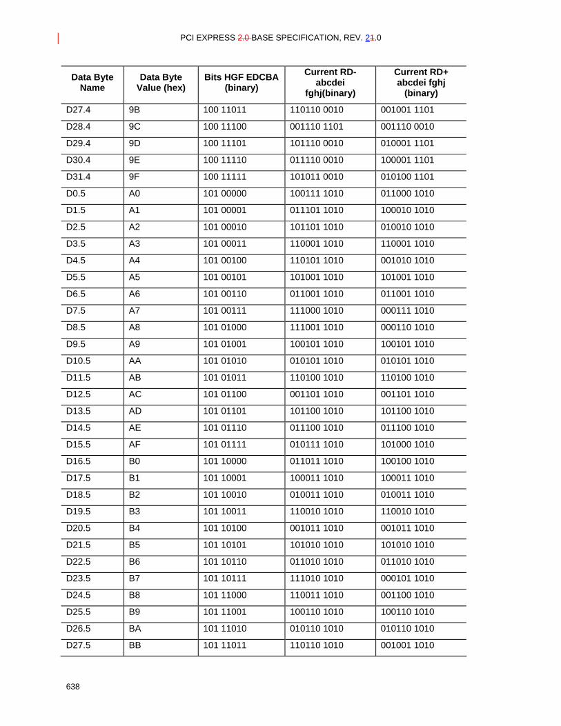
PCI EXPRESS 2.0 BASE SPECIFICATION, REV. 21.0
638
Data Byte Name
Data Byte Value (hex)
Bits HGF EDCBA (binary)
Current RD- abcdei
fghj(binary)
Current RD+ abcdei fghj
(binary)
D27.4 9B 100 11011 110110 0010 001001 1101
D28.4 9C 100 11100 001110 1101 001110 0010
D29.4 9D 100 11101 101110 0010 010001 1101
D30.4 9E 100 11110 011110 0010 100001 1101
D31.4 9F 100 11111 101011 0010 010100 1101
D0.5 A0 101 00000 100111 1010 011000 1010
D1.5 A1 101 00001 011101 1010 100010 1010
D2.5 A2 101 00010 101101 1010 010010 1010
D3.5 A3 101 00011 110001 1010 110001 1010
D4.5 A4 101 00100 110101 1010 001010 1010
D5.5 A5 101 00101 101001 1010 101001 1010
D6.5 A6 101 00110 011001 1010 011001 1010
D7.5 A7 101 00111 111000 1010 000111 1010
D8.5 A8 101 01000 111001 1010 000110 1010
D9.5 A9 101 01001 100101 1010 100101 1010
D10.5 AA 101 01010 010101 1010 010101 1010
D11.5 AB 101 01011 110100 1010 110100 1010
D12.5 AC 101 01100 001101 1010 001101 1010
D13.5 AD 101 01101 101100 1010 101100 1010
D14.5 AE 101 01110 011100 1010 011100 1010
D15.5 AF 101 01111 010111 1010 101000 1010
D16.5 B0 101 10000 011011 1010 100100 1010
D17.5 B1 101 10001 100011 1010 100011 1010
D18.5 B2 101 10010 010011 1010 010011 1010
D19.5 B3 101 10011 110010 1010 110010 1010
D20.5 B4 101 10100 001011 1010 001011 1010
D21.5 B5 101 10101 101010 1010 101010 1010
D22.5 B6 101 10110 011010 1010 011010 1010
D23.5 B7 101 10111 111010 1010 000101 1010
D24.5 B8 101 11000 110011 1010 001100 1010
D25.5 B9 101 11001 100110 1010 100110 1010
D26.5 BA 101 11010 010110 1010 010110 1010
D27.5 BB 101 11011 110110 1010 001001 1010
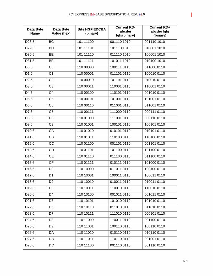
PCI EXPRESS 2.0 BASE SPECIFICATION, REV. 21.0
639
Data Byte Name
Data Byte Value (hex)
Bits HGF EDCBA (binary)
Current RD- abcdei
fghj(binary)
Current RD+ abcdei fghj
(binary)
D28.5 BC 101 11100 001110 1010 001110 1010
D29.5 BD 101 11101 101110 1010 010001 1010
D30.5 BE 101 11110 011110 1010 100001 1010
D31.5 BF 101 11111 101011 1010 010100 1010
D0.6 C0 110 00000 100111 0110 011000 0110
D1.6 C1 110 00001 011101 0110 100010 0110
D2.6 C2 110 00010 101101 0110 010010 0110
D3.6 C3 110 00011 110001 0110 110001 0110
D4.6 C4 110 00100 110101 0110 001010 0110
D5.6 C5 110 00101 101001 0110 101001 0110
D6.6 C6 110 00110 011001 0110 011001 0110
D7.6 C7 110 00111 111000 0110 000111 0110
D8.6 C8 110 01000 111001 0110 000110 0110
D9.6 C9 110 01001 100101 0110 100101 0110
D10.6 CA 110 01010 010101 0110 010101 0110
D11.6 CB 110 01011 110100 0110 110100 0110
D12.6 CC 110 01100 001101 0110 001101 0110
D13.6 CD 110 01101 101100 0110 101100 0110
D14.6 CE 110 01110 011100 0110 011100 0110
D15.6 CF 110 01111 010111 0110 101000 0110
D16.6 D0 110 10000 011011 0110 100100 0110
D17.6 D1 110 10001 100011 0110 100011 0110
D18.6 D2 110 10010 010011 0110 010011 0110
D19.6 D3 110 10011 110010 0110 110010 0110
D20.6 D4 110 10100 001011 0110 001011 0110
D21.6 D5 110 10101 101010 0110 101010 0110
D22.6 D6 110 10110 011010 0110 011010 0110
D23.6 D7 110 10111 111010 0110 000101 0110
D24.6 D8 110 11000 110011 0110 001100 0110
D25.6 D9 110 11001 100110 0110 100110 0110
D26.6 DA 110 11010 010110 0110 010110 0110
D27.6 DB 110 11011 110110 0110 001001 0110
D28.6 DC 110 11100 001110 0110 001110 0110
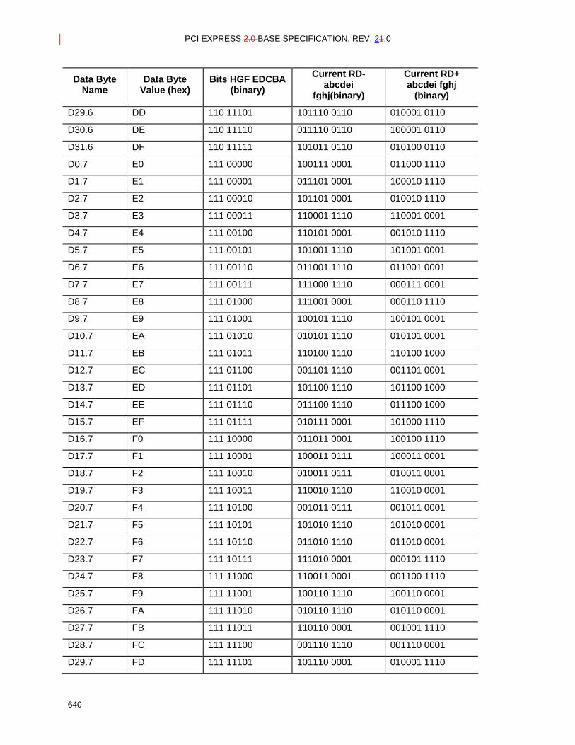
PCI EXPRESS 2.0 BASE SPECIFICATION, REV. 21.0
640
Data Byte Name
Data Byte Value (hex)
Bits HGF EDCBA (binary)
Current RD- abcdei
fghj(binary)
Current RD+ abcdei fghj
(binary)
D29.6 DD 110 11101 101110 0110 010001 0110
D30.6 DE 110 11110 011110 0110 100001 0110
D31.6 DF 110 11111 101011 0110 010100 0110
D0.7 E0 111 00000 100111 0001 011000 1110
D1.7 E1 111 00001 011101 0001 100010 1110
D2.7 E2 111 00010 101101 0001 010010 1110
D3.7 E3 111 00011 110001 1110 110001 0001
D4.7 E4 111 00100 110101 0001 001010 1110
D5.7 E5 111 00101 101001 1110 101001 0001
D6.7 E6 111 00110 011001 1110 011001 0001
D7.7 E7 111 00111 111000 1110 000111 0001
D8.7 E8 111 01000 111001 0001 000110 1110
D9.7 E9 111 01001 100101 1110 100101 0001
D10.7 EA 111 01010 010101 1110 010101 0001
D11.7 EB 111 01011 110100 1110 110100 1000
D12.7 EC 111 01100 001101 1110 001101 0001
D13.7 ED 111 01101 101100 1110 101100 1000
D14.7 EE 111 01110 011100 1110 011100 1000
D15.7 EF 111 01111 010111 0001 101000 1110
D16.7 F0 111 10000 011011 0001 100100 1110
D17.7 F1 111 10001 100011 0111 100011 0001
D18.7 F2 111 10010 010011 0111 010011 0001
D19.7 F3 111 10011 110010 1110 110010 0001
D20.7 F4 111 10100 001011 0111 001011 0001
D21.7 F5 111 10101 101010 1110 101010 0001
D22.7 F6 111 10110 011010 1110 011010 0001
D23.7 F7 111 10111 111010 0001 000101 1110
D24.7 F8 111 11000 110011 0001 001100 1110
D25.7 F9 111 11001 100110 1110 100110 0001
D26.7 FA 111 11010 010110 1110 010110 0001
D27.7 FB 111 11011 110110 0001 001001 1110
D28.7 FC 111 11100 001110 1110 001110 0001
D29.7 FD 111 11101 101110 0001 010001 1110
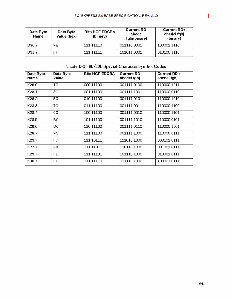
PCI EXPRESS 2.0 BASE SPECIFICATION, REV. 21.0
641
Data Byte Name
Data Byte Value (hex)
Bits HGF EDCBA (binary)
Current RD- abcdei
fghj(binary)
Current RD+ abcdei fghj
(binary)
D30.7 FE 111 11110 011110 0001 100001 1110
D31.7 FF 111 11111 101011 0001 010100 1110
Table B-2: 8b/10b Special Character Symbol Codes
Data Byte Name
Data Byte Value
Bits HGF EDCBA Current RD - abcdei fghj
Current RD + abcdei fghj
K28.0 1C 000 11100 001111 0100 110000 1011
K28.1 3C 001 11100 001111 1001 110000 0110
K28.2 5C 010 11100 001111 0101 110000 1010
K28.3 7C 011 11100 001111 0011 110000 1100
K28.4 9C 100 11100 001111 0010 110000 1101
K28.5 BC 101 11100 001111 1010 110000 0101
K28.6 DC 110 11100 001111 0110 110000 1001
K28.7 FC 111 11100 001111 1000 110000 0111
K23.7 F7 111 10111 111010 1000 000101 0111
K27.7 FB 111 11011 110110 1000 001001 0111
K29.7 FD 111 11101 101110 1000 010001 0111
K30.7 FE 111 11110 011110 1000 100001 0111

PCI EXPRESS 2.0 BASE SPECIFICATION, REV. 21.0
642
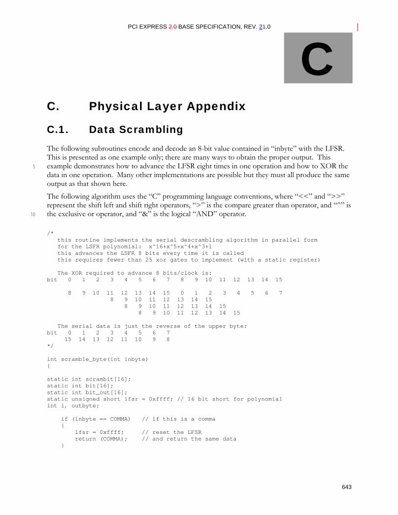
PCI EXPRESS 2.0 BASE SPECIFICATION, REV. 21.0
643
C. Physical Layer Appendix
C.1. Data Scrambling The following subroutines encode and decode an 8-bit value contained in “inbyte” with the LFSR. This is presented as one example only; there are many ways to obtain the proper output. This example demonstrates how to advance the LFSR eight times in one operation and how to XOR the 5 data in one operation. Many other implementations are possible but they must all produce the same output as that shown here.
The following algorithm uses the “C” programming language conventions, where “<<” and “>>” represent the shift left and shift right operators, “>” is the compare greater than operator, and “^” is the exclusive or operator, and “&” is the logical “AND” operator. 10
/* this routine implements the serial descrambling algorithm in parallel form for the LSFR polynomial: x^16+x^5+x^4+x^3+1 this advances the LSFR 8 bits every time it is called this requires fewer than 25 xor gates to implement (with a static register) The XOR required to advance 8 bits/clock is: bit 0 1 2 3 4 5 6 7 8 9 10 11 12 13 14 15 8 9 10 11 12 13 14 15 0 1 2 3 4 5 6 7 8 9 10 11 12 13 14 15 8 9 10 11 12 13 14 15 8 9 10 11 12 13 14 15 The serial data is just the reverse of the upper byte: bit 0 1 2 3 4 5 6 7 15 14 13 12 11 10 9 8 */ int scramble_byte(int inbyte) static int scrambit[16]; static int bit[16]; static int bit_out[16]; static unsigned short lfsr = 0xffff; // 16 bit short for polynomial int i, outbyte; if (inbyte == COMMA) // if this is a comma lfsr = 0xffff; // reset the LFSR return (COMMA); // and return the same data
C
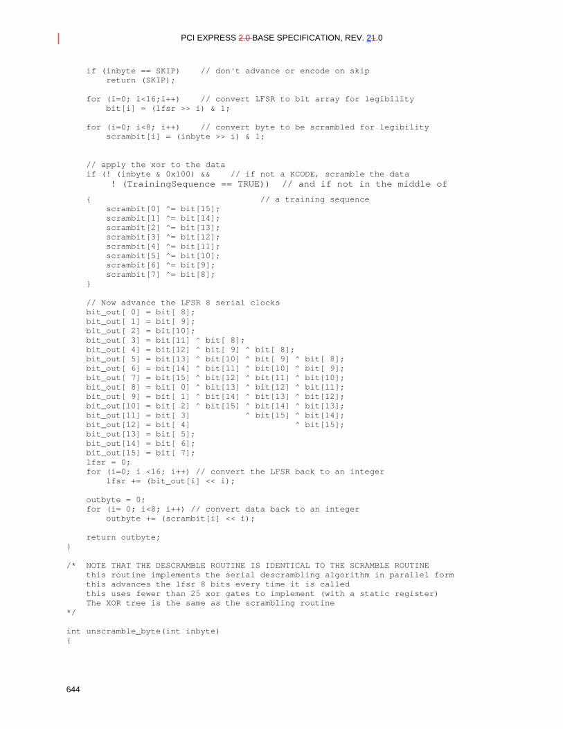
PCI EXPRESS 2.0 BASE SPECIFICATION, REV. 21.0
644
if (inbyte == SKIP) // don't advance or encode on skip return (SKIP); for (i=0; i<16;i++) // convert LFSR to bit array for legibility bit[i] = (lfsr >> i) & 1; for (i=0; i<8; i++) // convert byte to be scrambled for legibility scrambit[i] = (inbyte >> i) & 1; // apply the xor to the data if (! (inbyte & 0x100) && // if not a KCODE, scramble the data ! (TrainingSequence == TRUE)) // and if not in the middle of
// a training sequence scrambit[0] ^= bit[15]; scrambit[1] ^= bit[14]; scrambit[2] ^= bit[13]; scrambit[3] ^= bit[12]; scrambit[4] ^= bit[11]; scrambit[5] ^= bit[10]; scrambit[6] ^= bit[9]; scrambit[7] ^= bit[8]; // Now advance the LFSR 8 serial clocks bit_out[ 0] = bit[ 8]; bit_out[ 1] = bit[ 9]; bit_out[ 2] = bit[10]; bit_out[ 3] = bit[11] ^ bit[ 8]; bit_out[ 4] = bit[12] ^ bit[ 9] ^ bit[ 8]; bit_out[ 5] = bit[13] ^ bit[10] ^ bit[ 9] ^ bit[ 8]; bit_out[ 6] = bit[14] ^ bit[11] ^ bit[10] ^ bit[ 9]; bit_out[ 7] = bit[15] ^ bit[12] ^ bit[11] ^ bit[10]; bit_out[ 8] = bit[ 0] ^ bit[13] ^ bit[12] ^ bit[11]; bit_out[ 9] = bit[ 1] ^ bit[14] ^ bit[13] ^ bit[12]; bit_out[10] = bit[ 2] ^ bit[15] ^ bit[14] ^ bit[13]; bit_out[11] = bit[ 3] ^ bit[15] ^ bit[14]; bit_out[12] = bit[ 4] ^ bit[15]; bit_out[13] = bit[ 5]; bit_out[14] = bit[ 6]; bit_out[15] = bit[ 7]; lfsr = 0; for (i=0; i <16; i++) // convert the LFSR back to an integer lfsr += (bit_out[i] << i); outbyte = 0; for (i= 0; i<8; i++) // convert data back to an integer outbyte += (scrambit[i] << i); return outbyte; /* NOTE THAT THE DESCRAMBLE ROUTINE IS IDENTICAL TO THE SCRAMBLE ROUTINE this routine implements the serial descrambling algorithm in parallel form this advances the lfsr 8 bits every time it is called this uses fewer than 25 xor gates to implement (with a static register) The XOR tree is the same as the scrambling routine */ int unscramble_byte(int inbyte)
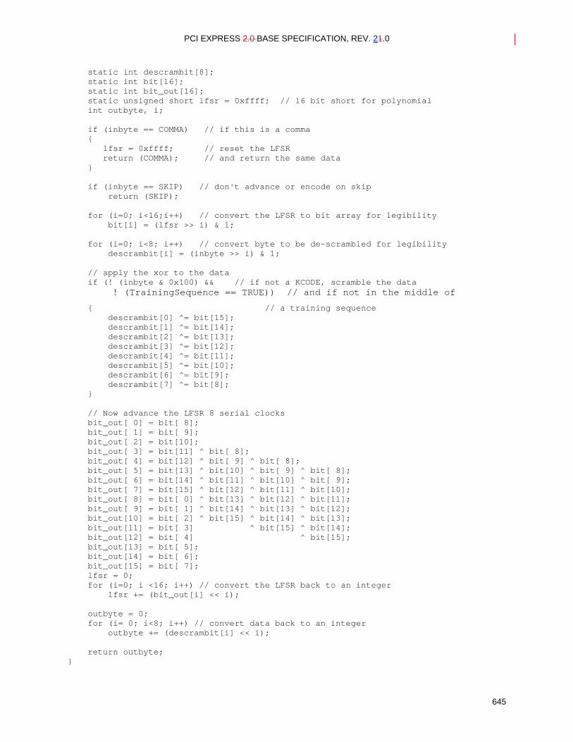
PCI EXPRESS 2.0 BASE SPECIFICATION, REV. 21.0
645
static int descrambit[8]; static int bit[16]; static int bit_out[16]; static unsigned short lfsr = 0xffff; // 16 bit short for polynomial int outbyte, i; if (inbyte == COMMA) // if this is a comma lfsr = 0xffff; // reset the LFSR return (COMMA); // and return the same data if (inbyte == SKIP) // don't advance or encode on skip return (SKIP); for (i=0; i<16;i++) // convert the LFSR to bit array for legibility bit[i] = (lfsr >> i) & 1; for (i=0; i<8; i++) // convert byte to be de-scrambled for legibility descrambit[i] = (inbyte >> i) & 1; // apply the xor to the data if (! (inbyte & 0x100) && // if not a KCODE, scramble the data ! (TrainingSequence == TRUE)) // and if not in the middle of
// a training sequence descrambit[0] ^= bit[15]; descrambit[1] ^= bit[14]; descrambit[2] ^= bit[13]; descrambit[3] ^= bit[12]; descrambit[4] ^= bit[11]; descrambit[5] ^= bit[10]; descrambit[6] ^= bit[9]; descrambit[7] ^= bit[8]; // Now advance the LFSR 8 serial clocks bit_out[ 0] = bit[ 8]; bit_out[ 1] = bit[ 9]; bit_out[ 2] = bit[10]; bit_out[ 3] = bit[11] ^ bit[ 8]; bit_out[ 4] = bit[12] ^ bit[ 9] ^ bit[ 8]; bit_out[ 5] = bit[13] ^ bit[10] ^ bit[ 9] ^ bit[ 8]; bit_out[ 6] = bit[14] ^ bit[11] ^ bit[10] ^ bit[ 9]; bit_out[ 7] = bit[15] ^ bit[12] ^ bit[11] ^ bit[10]; bit_out[ 8] = bit[ 0] ^ bit[13] ^ bit[12] ^ bit[11]; bit_out[ 9] = bit[ 1] ^ bit[14] ^ bit[13] ^ bit[12]; bit_out[10] = bit[ 2] ^ bit[15] ^ bit[14] ^ bit[13]; bit_out[11] = bit[ 3] ^ bit[15] ^ bit[14]; bit_out[12] = bit[ 4] ^ bit[15]; bit_out[13] = bit[ 5]; bit_out[14] = bit[ 6]; bit_out[15] = bit[ 7]; lfsr = 0; for (i=0; i <16; i++) // convert the LFSR back to an integer lfsr += (bit_out[i] << i); outbyte = 0; for (i= 0; i<8; i++) // convert data back to an integer outbyte += (descrambit[i] << i); return outbyte;
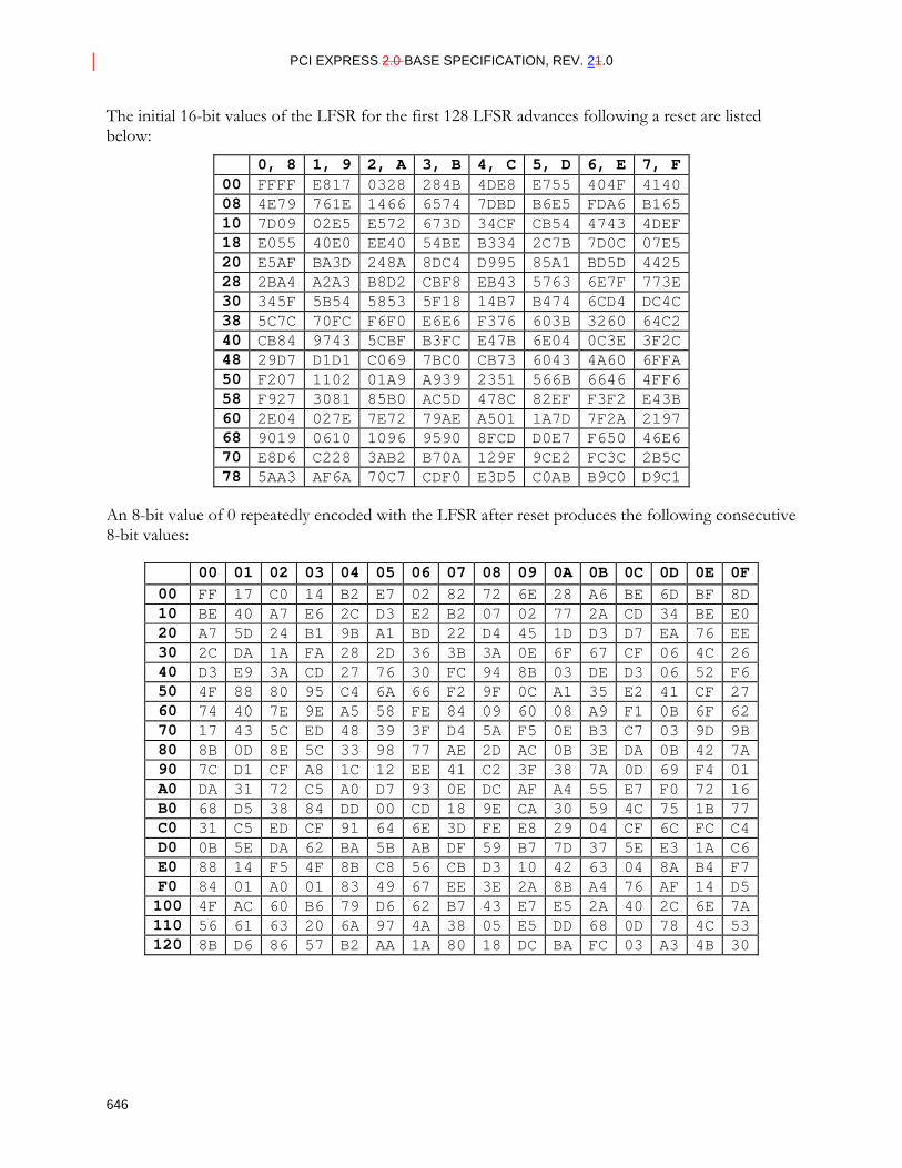
PCI EXPRESS 2.0 BASE SPECIFICATION, REV. 21.0
646
The initial 16-bit values of the LFSR for the first 128 LFSR advances following a reset are listed below:
0, 8 1, 9 2, A 3, B 4, C 5, D 6, E 7, F 00 FFFF E817 0328 284B 4DE8 E755 404F 4140 08 4E79 761E 1466 6574 7DBD B6E5 FDA6 B165 10 7D09 02E5 E572 673D 34CF CB54 4743 4DEF 18 E055 40E0 EE40 54BE B334 2C7B 7D0C 07E5 20 E5AF BA3D 248A 8DC4 D995 85A1 BD5D 4425 28 2BA4 A2A3 B8D2 CBF8 EB43 5763 6E7F 773E 30 345F 5B54 5853 5F18 14B7 B474 6CD4 DC4C 38 5C7C 70FC F6F0 E6E6 F376 603B 3260 64C2 40 CB84 9743 5CBF B3FC E47B 6E04 0C3E 3F2C 48 29D7 D1D1 C069 7BC0 CB73 6043 4A60 6FFA 50 F207 1102 01A9 A939 2351 566B 6646 4FF6 58 F927 3081 85B0 AC5D 478C 82EF F3F2 E43B 60 2E04 027E 7E72 79AE A501 1A7D 7F2A 2197 68 9019 0610 1096 9590 8FCD D0E7 F650 46E6 70 E8D6 C228 3AB2 B70A 129F 9CE2 FC3C 2B5C 78 5AA3 AF6A 70C7 CDF0 E3D5 C0AB B9C0 D9C1
An 8-bit value of 0 repeatedly encoded with the LFSR after reset produces the following consecutive 8-bit values:
00 01 02 03 04 05 06 07 08 09 0A 0B 0C 0D 0E 0F00 FF 17 C0 14 B2 E7 02 82 72 6E 28 A6 BE 6D BF 8D10 BE 40 A7 E6 2C D3 E2 B2 07 02 77 2A CD 34 BE E020 A7 5D 24 B1 9B A1 BD 22 D4 45 1D D3 D7 EA 76 EE30 2C DA 1A FA 28 2D 36 3B 3A 0E 6F 67 CF 06 4C 2640 D3 E9 3A CD 27 76 30 FC 94 8B 03 DE D3 06 52 F650 4F 88 80 95 C4 6A 66 F2 9F 0C A1 35 E2 41 CF 2760 74 40 7E 9E A5 58 FE 84 09 60 08 A9 F1 0B 6F 6270 17 43 5C ED 48 39 3F D4 5A F5 0E B3 C7 03 9D 9B80 8B 0D 8E 5C 33 98 77 AE 2D AC 0B 3E DA 0B 42 7A90 7C D1 CF A8 1C 12 EE 41 C2 3F 38 7A 0D 69 F4 01A0 DA 31 72 C5 A0 D7 93 0E DC AF A4 55 E7 F0 72 16B0 68 D5 38 84 DD 00 CD 18 9E CA 30 59 4C 75 1B 77C0 31 C5 ED CF 91 64 6E 3D FE E8 29 04 CF 6C FC C4D0 0B 5E DA 62 BA 5B AB DF 59 B7 7D 37 5E E3 1A C6E0 88 14 F5 4F 8B C8 56 CB D3 10 42 63 04 8A B4 F7F0 84 01 A0 01 83 49 67 EE 3E 2A 8B A4 76 AF 14 D5100 4F AC 60 B6 79 D6 62 B7 43 E7 E5 2A 40 2C 6E 7A110 56 61 63 20 6A 97 4A 38 05 E5 DD 68 0D 78 4C 53120 8B D6 86 57 B2 AA 1A 80 18 DC BA FC 03 A3 4B 30
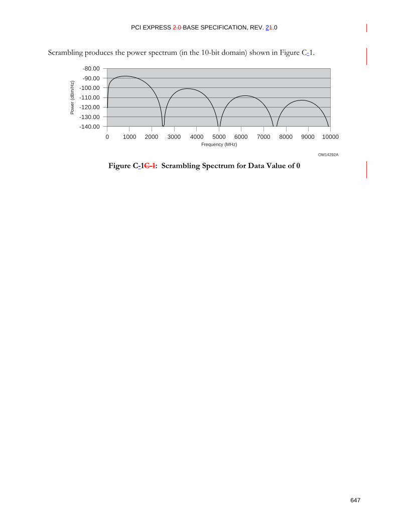
PCI EXPRESS 2.0 BASE SPECIFICATION, REV. 21.0
647
Scrambling produces the power spectrum (in the 10-bit domain) shown in Figure C-1.
OM14292A
-140.00
-130.00
-120.00
-110.00
-100.00
-90.00
-80.00
0 1000 2000 3000 4000 5000 6000 7000 8000 9000 10000Frequency (MHz)
Pow
er (
dBm
/Hz)
Figure C-1C-1: Scrambling Spectrum for Data Value of 0

PCI EXPRESS 2.0 BASE SPECIFICATION, REV. 21.0
648
PCI EXPRESS 2.0 BASE SPECIFICATION, REV. 21.0
649
D. Request Dependencies This appendix The PCI Express Base Specification does not specify the allowed rules governing the creation of resource dependencies between TLPs using different Traffic Classes. Such dDependencies between packets in different Traffic Classes can create potential deadlock if devices make different assumptions about what is allowed and what is not. Dependencies can be created 5 when a packet is forwarded (transmitted verbatim) or translated (transmitted with modification) from an input Port to an output Port.
Resource dependencies are created when received packets are either forwarded/translated and retransmitted on the same or a different linkLink. Due to the fact that the forwarding/translating device has finite buffer resources this behavior creates a dependency upon between the ability to 10 receive a packet on and the ability to transmit a packet (in potentially a different VC or sub-channel).
The following notation is used to create a framework to enumerate the possibilities:
X(m) -> Y(n)
This means:
a request in sub-channel X(TC=m) is translated/forwarded/translated in sub-channel Y(TC=n). 15
n and m are between 0-7.
X and Y are either P (Posted Request), N (Non-Posted Request), or C (Completion).
The list of possible dependencies is:
P(m) -> P(n)
P(m) -> N(n) 20
P(m) -> C(n)
N(m) -> P(n)
N(m) -> N(n)
N(m) -> C(n)
C(m) -> P(n) 25
C(m) -> N(n)
C(m) -> C(n)
D

PCI EXPRESS 2.0 BASE SPECIFICATION, REV. 21.0
650
For a given system, each of these dependencies needs to be classified as legal or illegal for each of the following cases:
Root port Port forwarding to own linkLink.
Root portPort forwarding to different Root Port’s linkLink.
Endpoint or Bridge forwarding to own linkLink. 5
A Switch will is not allowed to modify the TLPs that flow through it, but must ensure complete independence of resources assigned to separate VCs. System software must comprehend the system dependency rules when configuring TC/VC mapping throughout the system.
One possible legal mapping might beis:
RC (Same Port) RC (Different Port) Endpoint
P(m) -> P(n) m <= n m <= n m < n P(m) -> N(n) m < n m < n m < n P(m) -> C(n) illegal illegal illegal N(m) -> P(n) m < n m < n m < n N(m) -> N(n) m <= n m <= n m < n N(m) -> C(n) m = n m = n m = n C(m) -> P(n) illegal illegal illegal C(m) -> N(n) illegal illegal illegal C(m) -> C(n) m >= n m >= n m > n
Note that this discussion only deals with avoiding the deadlock caused by the creation of resource 10 dependencies. It does not deal with the additional livelock issues (or lack of forward progress) caused by the system’s virtual Virtual channel Channel arbitration policies.
Some of these potential dependencies are illegal or unreachable:
P(m) -> P(n), N(m) -> N(n)
• m = n – This case is illegal and will lead to deadlock, except when a Request is being 15 forwarded from one portPort to another of a Switch or Root Complex.
• m! = n – See discussion below.
P(m) -> N(n)
• m = n – This case is illegal and will lead to deadlock.
• m! = n – See discussion below. 20
N(m) -> P(n) – See discussion below.
P(m) -> C(n) – This case is illegal and will lead to deadlock.
PCI EXPRESS 2.0 BASE SPECIFICATION, REV. 21.0
651
N(m) -> C(n)
• m = n – This case occurs during the normal servicing of a non-posted request by either a root complex or an endpoint.
• m! = n – This case is unreachable and should never happen. Completions always use the same TC as the corresponding request. 5
C(m) -> P(n), C(m) -> N(n) – These cases are unreachable and should never happen due to the fact that completion buffers must be preallocated.
C(m) -> C(n)
• m = n – This case is illegal and will lead to deadlock, except when a Completion is being forwarded from one portPort to another of a Switch or Root Complex. 10
• m! = n – This case will occur if N(n)->N(m) dependencies are allowed.
Others of these potential dependencies may be legal when comprehended as part of a specific usage model. For example, these cases:
P(m) ->P(n), N(m) -> N(n), P(m) -> N(n), N(m) -> P(n) where m! = n
might exist where a device processes services incoming requests to complete those requests by 15 issuing modified versions of those requests using a different Traffic Class (for example, remapping the first requests address and generating the new request with the resulting address). In these cases, suitable rules must be applied to prevent circular dependencies that would lead to deadlock or livelock.
Examples of devices that may find the above mappings useful: 20
Bridges to complex protocols that require state to be save/restored to/from host memory, i.e., PCI Express to Infiniband bridges.
Messaging engines that must do address translation based upon page tables stored in host memory.
UMA graphics devices that store their frame buffer in host memory. 25

PCI EXPRESS 2.0 BASE SPECIFICATION, REV. 21.0
652
PCI EXPRESS 2.0 BASE SPECIFICATION, REV. 21.0
653
Acknowledgements The following persons were instrumental in the development of the PCI Express Base Specification:77
Chamath Abhayagunawardhana Intel Corporation Shiva Aditham Intel Corporation Jasmin Ajanovic Intel Corporation Katsutoshi Akagi NEC Corporation Sujith Arramreddy ServerWorks, Inc. Yuval Avnon Marvell Semiconductor, Inc. Jay Avula ServerWorks, Inc. Jasper Balraj Intel Corporation Nat Barbiero Advanced Micro Devices, Inc. Phillip Barnes Hewlett-Packard Company Suparna Behera LSI Logic Corporation Joseph A. Bennett Intel Corporation Richard Bell Advanced Micro Devices, Inc. Stuart Berke Hewlett-Packard Company Harish Bharadwaj LSI Logic Corporation Ajay V. Bhatt Intel Corporation Harmeet Bhugra IDT Corporation Cass Blodget Intel Corporation Jeffrey D. Bloom Intel Corporation Naveen Bohra Intel Corporation Jerry Bolen Intel Corporation Bala Cadambi Intel Corporation John Calvin Tektronix, Inc. Gord Caruk Advanced Micro Devices, Inc.ATI
Technologies Inc James Chapple Intel Corporation Santanu Chaudhuri Intel Corporation Rajinder Cheema LSI Logic Corporation Chih-Cheh Chen Intel Corporation Qunwei Chen Advanced Micro Devices, Inc. Gene Chui IDT Corporation Shawn Clayton Emulex Corporation Mark Clements IBM Corporation Debra Cohen Intel Corporation Brad Congdon Intel Corporation Mike Converse IDT Corporation Justin Coppin Hewlett-Packard Company Joe Cowan Hewlett-Packard Company
77 Company affiliation listed is at the time of specification contributions.
PCI EXPRESS 2.0 BASE SPECIFICATION, REV. 21.0
654
Carrie Cox IBM Corporation H. Clay Cranford IBM Corporation Kenneth C. Creta Intel Corporation Pamela Cristo Emulex Corporation Sanjay Dabral Intel Corporation Eric Dahlen Intel Corporation Tugrul Daim Intel Corporation Ron Dammann Intel Corporation Sumit Das Texas Instruments Incorporated Debendra Das Sharma Intel Corporation Nicole Daugherty Intel Corporation Karishma Dhruv LSI Logic Corporation Bob Divivier IDT Corporation Ken Drottar Intel Corporation Dave Dunning Intel Corporation Greg Ebert Intel Corporation Yaron Elboim Intel Corporation Bassam Elkhoury Intel Corporation Salem Emara Advanced Micro Devices, Inc. Mike Engbretson Tektronix, Inc. Blaise Fanning Intel Corporation Wes Ficken IBM Corporation Joshua Filliater LSI Logic Corporation Jim Foster IBM Corporation Mike Foxcroft Advanced Micro Devices, Inc.ATI
Technologies Inc Dan Froelich Intel Corporation Eric Geisler Intel Corporation Marc A. Goldschmidt Intel Corporation Alan Goodrum Hewlett-Packard Company Robert Gough Intel Corporation Brien Gray Intel Corporation Richard Greene Intel Corporation Stephen Greenwood ATI Technologies Inc. Buck Gremel Intel Corporation Ilya Granovsky IBM Corporation Vijay Gudur LSI Logic Corporation Dale Gulick Advanced Micro Devices, Inc. Mickey Gutman Intel Corporation Clifford D. Hall Intel Corporation Ken Haren Intel Corporation David Harriman Intel Corporation Hiromitsu Hashimoto NEC Corporation George R. Hayek Intel Corporation Wenmu He Texas Instruments Incorporated Bent Hessen-Schmidt SyntheSys Research

PCI EXPRESS 2.0 BASE SPECIFICATION, REV. 21.0
655
Hanh Hoang Intel Corporation Michael Hopgood nVidia Corporation Dorcas Hsia nVidia Corporation Mark Hummel Advanced Micro Devices, Inc. Mikal Hunsaker Intel Corporation Carl Jackson Hewlett-Packard Company David R. Jackson Intel Corporation Praveen Jain nVidia Corporation Duane January Intel Corporation Mike Jenkins LSI Logic Corporation Peter Jenkins IBM Corporation Hong Jiang Intel Corporation Viek Joshi Intel Corporation David Kahn Sun Microsystems, Inc. Girish Karanam LSI Logic Corporation Chad Kendall Broadcom Corporation David Kimble Texas Instruments Incorporated Mohammad Kolbehdari Intel Corporation Abhimanyu Kolla Intel Corporation Ganesh Kondapuram Intel Corporation Michael Krause Hewlett-Packard Company Akhilesh Kumar Intel Corporation Mohan J. Kumar Intel Corporation Richard Kunze Intel Corporation Hugh Kurth Sun Microsystems, Inc. Seh Kwa Intel Corporation Sunny Lam Intel Corporation Brian Langendorf Intel Corporation Brian L'Ecuyer Agilent Technologies, Inc. Beomtek Lee Intel Corporation Clifford D. Lee Intel Corporation David M. Lee Intel Corporation Edward Lee Advanced Micro Devices, Inc. Moshe Leibowitz IBM Corporation Mike Li Wavecrest Corporation Paul Li Pericom Semiconductor Corporation Stephen Li Texas Instruments Incorporated Jeff Lukanc IDT Corporation Jeffrey Lu IBM Corporation Ngoc Luu Advanced Micro Devices, Inc. Stephen Ma Advanced Micro Devices, Inc. Zorik Machulsky IBM Corporation Kevin Main Texas Instruments Incorporated Steve Manning Advanced Micro Devices, Inc. Jarek Marczewski Advanced Micro Devices, Inc. Mark Marlett LSI Logic Corporation

PCI EXPRESS 2.0 BASE SPECIFICATION, REV. 21.0
656
Alberto Martinez Intel Corporation Andrew Martwick Intel Corporation Paul Mattos IBM Corporation Robert A. Mayer Intel Corporation Pranav H. Mehta Intel Corporation Rich Mellitz Intel Corporation Cindy Merkin Dell Computer Corporation Dennis Miller Intel Corporation Jason Miller Sun Microsystems, Inc. Robert J. Miller Intel Corporation Suneel Mitbander Intel Corporation Daniel Moertl IBM Corporation Lee Mohrmann Dell Computer CorporationNational
Instruments Corporation Wayne Moore Intel Corporation Douglas R. Moran Intel Corporation Terry Morris Hewlett-Packard Company Jeff C. Morriss Intel Corporation Sridhar Muthrasanallur Intel Corporation Suresh Babu M. V. LSI Logic Corporation Gautam V. Naik LSI Logic Corporation Mohan K. Nair Intel Corporation Mukund Narasimhan Intel Corporation Alon Naveh Intel Corporation Surena Neshvad Intel Corporation Andy Ng IDT Corporation Manisha Nilange Intel Corporation Hajime Nozaki NEC Corporation Kugao Ohuchi NEC Corporation Olufemi Oluwafemi Intel Corporation Mike Osborn Advanced Micro Devices, Inc. Johathan Owen Advanced Micro Devices, Inc. Ali Oztaskin Intel Corporation Shreeram Palghat Intel Corporation Marc Pegolotti ServerWorks, Inc. Henry Peng Intel Corporation Tony Pierce Microsoft Corporation Harshit Poladi Intel Corporation Jim Prijic Intel Corporation Dave Puffer Intel Corporation Duane Quiet Intel Corporation Jeffrey D. Rabe Intel Corporation Kianoush Rahbar Intel Corporation Guru Rajamani Intel Corporation Ramesh Raman LSI Logic Corporation Todd Rasmus IBM Corporation

PCI EXPRESS 2.0 BASE SPECIFICATION, REV. 21.0
657
Ramakrishna Reddy LSI Logic Corporation Dick Reohr Intel Corporation Curtis Ridgeway LSI Logic Corporation Dwight Riley Hewlett-Packard Company Chris Runhaar nVidia Corporation Rajanataraj S. LSI Logic Corporation Devang Sachdev nVidia Corporation Bill Sauber Dell Computer Corporation Joe Schaefer Intel Corporation Daren Schmidt Intel Corporation Mark Schmisseur Intel Corporation Zale Schoenborn Intel Corporation Rick Schuckle Dell Computer Corporation Richard Schumacher Hewlett-Packard Company Tudor Secasiu Intel Corporation Kevin Senohrabek Advanced Micro Devices, Inc. Prashant Sethi Intel Corporation Ankur Shah Intel Corporation Vasudevan Shanmugasundaram Intel Corporation Wesley Shao Sun Microsystems, Inc. Charlie Shaver Hewlett-Packard Company John Sheplock IBM Corporation Mark Shillingburg Agilent Technologies Bill Sims nVidia Corporation Shamnad SN LSI Logic Corporation Gary Solomon Intel Corporation Gao Song IDT Corporation Stan Stanski IBM Corporation Ron Swartz Intel Corporation Miki Takahashi NEC Corporation Gerry Talbot Advanced Micro Devices, Inc. Anthony Tam Advanced Micro Devices, Inc. Matthew Tedone LSI Logic Corporation Grigori Temkine Advanced Micro Devices, Inc. Peter Teng NEC Corporation Bruce Tennant Intel Corporation Andrew Thornton Microsoft Corporation Alok Tripathi Intel Corporation William Tsu nVidia Corporation Arie van der Hoeven Microsoft Corporation Andrew Vargas Intel Corporation Robertson Velez ATI Technologies Inc Archana Vasudevan LSI Logic Corporation Kiran Velicheti Intel Corporation Balaji Vembu Intel Corporation Gary Verdun Dell Computer Corporation
PCI EXPRESS 2.0 BASE SPECIFICATION, REV. 21.0
658
Divya Vijayaraghavan LSI Logic CorporationAltera CorporationRavindra Viswanath LSI Logic Corporation Pete D. Vogt Intel Corporation Andrew Volk Intel Corporation Mahesh Wagh Intel Corporation Clint Walker Intel Corporation Davis Walker Microsoft Corporation Hui Wang IDT Corporation Dan Wartski Intel Corporation Eric Wehage Intel Corporation Dong Wei Hewlett-Packard Company Amir Wiener Intel Corporation Marc Wells Intel Corporation Bryan White Intel Corporation Paul Whittemore Sun Microsystems, Inc. Theodore L. Willke Intel Corporation Dawn Wood Intel Corporation David Wooten Microsoft Corporation Zhi Wong Altera Corporation William Wu Broadcom Corporation Liu Xin IDT Corporation Dan Yaklin Texas Instruments Incorporated Howard Yan Intel Corporation Al Yanes IBM Corporation Gin Yee Advanced Micro Devices, Inc. Ahmed Younis Xilinx, Inc. Dave Zenz Dell Computer Corporation Shubing Zhai IDT Corporation
Top Related