


Languages
Pages
Legal


Orbital-driven Mottness collapse in 1T-TaS2-xSex transition metal
dichalcogenide
Shuang Qiao1,2,*, Xintong Li1,*, Naizhou Wang3, Wei Ruan1, Cun Ye1, Peng Cai1, Zhenqi Hao1,
Hong Yao2,4, Xianhui Chen3,5, Jian Wu1,4,†, Yayu Wang1,4,†, Zheng Liu2,4,†
1State Key Laboratory of Low Dimensional Quantum Physics, Department of Physics, Tsinghua
University, Beijing 100084, P.R. China
2Institute for Advanced Study, Tsinghua University, Beijing 100084, P.R. China
3Hefei National Laboratory for Physical Science at Microscale and Department of Physics,
University of Science and Technology of China, Hefei, Anhui 230026, P.R. China
4Innovation Center of Quantum Matter, Beijing 100084, P.R. China
5Collaborative Innovation Center of Advanced Microstructures, Nanjing University, Nanjing
210093, China
*These authors contributed equally to this work.
†Email: [email protected];[email protected]; [email protected]

The vicinity of a Mott insulating phase has constantly been a fertile ground for finding
exotic quantum states, most notably the high Tc cuprates and colossal magnetoresistance
manganites. The layered transition metal dichalcogenide 1T-TaS2 represents another
intriguing example, in which the Mott insulator phase is intimately entangled with a series
of complex charge-density-wave (CDW) orders. More interestingly, it has been recently
found that 1T-TaS2 undergoes a Mott-insulator-to-superconductor transition induced by
high pressure, charge doping, or isovalent substitution. The nature of the Mott insulator
phase and transition mechanism to the conducting state is still under heated debate. Here,
by combining scanning tunneling microscopy (STM) measurements and first-principles
calculations, we investigate the atomic scale electronic structure of 1T-TaS2 Mott insulator
and its evolution to the metallic state upon isovalent substitution of S with Se. We identify
two distinct types of orbital textures - one localized and the other extended – and
demonstrates that the interplay between them is the key factor that determines the electronic
structure. Especially, we show that the continuous evolution of the charge gap visualized by
STM is due to the immersion of the localized-orbital-induced Hubbard bands into the
extended-orbital-spanned Fermi sea, featuring a unique evolution from a Mott gap to a
charge-transfer gap. This new mechanism of orbital-driven Mottness collapse revealed here
suggests an interesting route for creating novel electronic state and designing future
electronic devices.
1T-TaS2 has a trilayered (TL) structure as shown in Fig. 1a, in which the Ta atoms form a
planar triangular lattice sandwiched by two S-atom planes. It exhibits a series of complex CDW
orders at various temperature (T) ranges, including an incommensurate CDW at high T, a nearly
commensurate CDW (NCCDW) at intermediate T, and a commensurate CDW (CCDW) order in
the ground state1-3. The Mott insulator phase is believed to be a consequence of the CCDW order3-
7. Superconductivity emerges as the Mott insulator state is suppressed by pressure or doping8-15,
and the electronic phase diagram9,11,13,15 displays many similarities to that of the cuprates.
Currently there are many debates about the nature of the Mott insulator and how it evolves into
the metallic and eventually superconducting state9,10,12,14,16-22. Much of the challenge originates
from the observation that the electronic structure may be influenced by a number of factors,
including the CDW superstructure, phase separation and domain boundaries, strong disorders,
spin-orbit coupling and interlayer coupling.
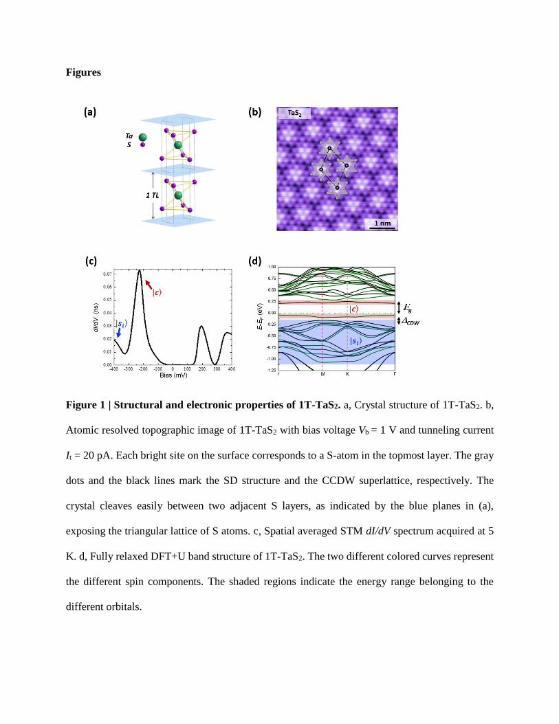
STM is an ideal experimental technique for probing the atomic scale electronic structure of
complex materials. Figure 1b displays the STM topographic image of pristine 1T-TaS2, which
clearly reveals the CCDW order with a √13 × √13 superlattice where 13 Ta atoms form a Star-
of-David (SD) structure. Note that the bright spots correspond to the S atoms lying in the
uppermost layer, and the position of the Ta atoms can be determined according to the octahedral
coordination. In Fig. 1c we show the spatially averaged differential conductance (dI/dV), which is
approximately proportional to the electron density of states (DOS), of pristine 1T-TaS2. An energy
gap around the Fermi level (EF) can be clearly observed, which is attributed to the Mott-Hubbard
gap of the insulating CCDW phase.
These spectroscopic features can be captured by density functional theory (DFT)
calculations including the onsite Hubbard U correction in a Hartree-Fock manner23. Figure 1d
shows the obtained band structure of a 1T-TaS2 TL with the CCDW superstructure. There is a full
charge gap around the EF, which is bounded by two narrow bands, corresponding to the upper and
lower Hubbard bands, respectively. The gap size is found to depend on the Hubbard repulsion U
and a choice of U = 2.27 eV as previously derived from the linear-response calculation is used to

reproduce the experimental value23. By turning off the +U correction and the spin degree of
freedom, in a plain DFT calculation the charge gap will collapse and the two narrow bands become
degenerate, giving a half-filled metallic state (Supplementary Fig. S4). These results corroborate
a Mott origin of the charge gap. There is another energy gap below the lower Hubbard band
isolating it from the underneath dispersive band continuum (shaded in blue in Fig. 1d), which is
commonly referred to as the CDW gap (𝛥CDW)24-26. This gap is manifested in the dI/dV spectrum
as a dip below the lower Hubbard peak (Fig. 1c).
Besides the CCDW superstructure and energy spectrum, equally important is the local DOS
(LDOS) mapping at selected energies, which contains the spatial characteristics of electronic
wavefunctions, i.e., the orbital texture. Figure 2a displays the dI/dV, or LDOS, mapping measured
at two representative energies. At Vb = 207 mV (upper panel), which corresponds to the lower
Hubbard band, the LDOS map shows a periodic pattern that is commensurate with the CCDW
superlattice. By comparing the LDOS map with the topographic image of the same area (Fig. 1b),
the bright spots are identified to be the center of SDs. Moving to lower energy with bias Vb = 422
mV (lower panel), a distinctly different orbital texture is revealed: the LDOS map exhibits a
kagome-like superstructure. Its bright/dark spots are inverse of the previous texture, indicating
contributions mainly from the surrounding Ta orbitals. LDOS maps at positive biases give a nearly
symmetric picture: the upper Hubbard band corresponds to an orbital texture concentrated on the
center of SDs, whereas at higher energy the bright spots shift to the surrounding Ta orbitals
(Supplementary Fig. S2).
To determine the nature of these two orbital textures discussed above, we proceed by
performing ab initio Wannier function analysis27-29. In the plain DFT band structure, the 6

dispersive bands below EF and the narrow bands near EF represent a seven-orbital subspace, which
will accommodate the thirteen unpaired d-electrons in a SD. Within this subspace, the spatial
distributions of the seven Wannier functions are plotted in Fig. 2b, which automatically separate
into two groups. The one denoted by |𝑐⟩ concentrates at the central Ta atom with a typical 𝑑𝑧2
geometry. The remaining six Wannier functions distribute dominantly along the edge of the SD
(|𝑠𝛼=1…6⟩), which can be viewed as the bonding orbitals of the surrounding Ta atoms. The
reconstructed band structure using |𝑐⟩ and |𝑠𝛼=1…6⟩ as basis well reproduces the DFT result
(Supplementary Fig. S4). This Wannier function analysis gives a natural explanation for the two
types of orbital textures observed by STM. In particular, it clarifies that the kagome-like texture
arises from a set of linear-shaped molecular orbitals.
At first glance, the orbital texture below 𝛥CDW, i.e. |𝑠𝛼=1…6⟩, appears to be irrelevant to the
low-energy physics. Indeed, in previous studies the electronic evolution is generally discussed
based on a one-band Hubbard model employing the |𝑐⟩ orbital alone20,30,31. Since this orbital is
largely localized, it is susceptible to a Mott transition, giving rise to the upper and lower Hubbard
bands. However, it is important to note that the validity of the one-band Hubbard model is
protected by a large 𝛥CDW . When the CCDW order is weakened, a one-band-to-multi-band
transition has to be considered, which in turn plays an important role in the collapse of the Mott
phase.
To test the validity of the two-orbital model, we further investigate the electronic structure
of 1T-TaS2 under external influence. A rather gentle perturbation to the 1T-TaS2 structure is to
modify the buckling of the S atoms around the central Ta, which is expected to affect the CCDW
order. Experimentally this can be effectively realized through isovalent substitution of S by Se12,13,

which has a larger ionic size and thus increases the buckling of the surrounding S atoms. We have
synthesized a series of Se-doped 1T-TaS2 single crystals, whose transport properties are shown in
Supplementary Fig. S1. Figure 3a displays a large area STM image on the surface of a sample with
Se content x = 0.5. Unlike the pristine sample (Fig. 1b), the surface structure now splits into
domains with varied domain size and sharp boundaries in between (Fig. 3a), which resembles the
so-called “mosaic” phase in 1T-TaS2 induced by voltage pulse in STM experiments32,33. A closer
examination around the domain walls reveals both translational and 30° degree rotational
mismatch between different domains (Supplementary Fig. S3). Increasing the Se concentration
from x = 0.5 to x = 1 creates more domain walls and defects, but the general topographic properties
remain the same. As shown in Fig. 3b, within a single domain the CCDW superlattice retains the
SD patterns as that in the undoped TaS2 sample. Atomic-precision topography shows intensity
modulation of the pristine lattice periodicity, suggesting spatial inhomogeneity of Se concentration.
Figure 3c shows the dI/dV spectra measured at various locations on the surface of the x = 1
sample, which exhibit a continuous evolution. There are still small areas showing a spectrum
similar to that in pristine 1T-TaS2 with a nearly unperturbed Mott gap (black curve), indicating
very low concentration of Se dopants locally. Moving upwards, the Mottness gap shrinks
continuously, presumably due to increasing Se doping (red and blue curves). With further
shrinking of the Mott gap, a broad V-shaped gap forms near EF, which looks reminiscent of the
pseudogap in underdoped cuprates. The V-shaped gap also shrinks gradually, and a finite DOS
appears at EF, indicating the transition into a metallic state. Eventually the gap vanishes completely
and a sharp peak emerges near EF, which looks similar to the Van Hove singularity (VHS) in
overdoped cuprates. There is a clear collapse of the Mottness gap induced by Se substitution of S,
which underlies the Mott insulator to metal phase transition.

To simulate the STM results on Se-doped 1T-TaS2, we performed DFT+U calculations on
supercells with different Se concentration. For a given Se concentration, the lowest-energy
substitution configuration is determined, and the DFT structural relaxation confirms that the main
effect of Se substitution is to increase the local buckling of the TL. The evolution of the band
structure is traced in Fig. 4, which reveals the complete Mott-insulator-to-metal transition process.
At low-doping concentration, despite a reduction of 𝛥CDW, Eg stays unchanged as it is dictated by
the effective Hubbard U of the |𝑐⟩-orbital alone. After the lower Hubbard band touches the |𝑠𝛼⟩-
orbital bands, the Mott gap transforms into the charge-transfer type gap because now the lowest
energy excitation is from the continuum band formed by the |𝑠𝛼⟩-orbitals to the upper Hubbard
band formed by the |𝑐⟩-orbital. The gap size shrinks continuously upon further doping. According
to the calculation, the critical point is reached at x ≈ 0.92, where the indirect charge-transfer gap
becomes zero. Beyond this critical doping concentration, the upper Hubbard band also sinks into
the |𝑠𝛼⟩-orbital bands, driving the system into the metallic regime. For the high-doping case, the
|𝑐⟩-orbital and |𝑠𝛼⟩-orbitals are strongly hybridized so that we can barely see the remnants of the
narrow upper Hubbard band around the Γ point at EF. We plot the DOS evolution as a function of
Se concentration in Fig. 3d, rendering a direct comparison with the STM dI/dV spectra of 1T-TaS2-
xSex samples. The U-shaped Mottness gap, the V-shaped pseudogap, and the sharp VHS-type peak
are all nicely reproduced in the theoretical simulation. The excellent agreement between theory
and experiment confirms the validity of the orbital-driven Mott insulator to metal transition.
We note that in the calculation no additional complexities, such as spin-orbit coupling, inter-
TL coupling and disorder, are introduced. We believe that the interplay between the |𝑐⟩-orbital
and |𝑠𝛼⟩-orbitals represents a universal origin of Mottness collapse in 1T-TaS2, no matter via

mechanical or chemical routes. To capture the essential physics of such novel Mottness collapse,
we propose a generalized effective multi-orbital Hubbard model as formulated below:
𝐻 = 𝛥𝑆𝐷 ∑ 𝑐𝐼†𝑐𝐼𝐼 + 𝑡𝑐𝑠 ∑ (𝑐𝐼
†𝑠𝐼𝛼𝐼𝛼 + 𝐻. 𝑐. ) + ∑ 𝑡𝑠𝑠𝐼𝛼,𝐽𝛽
𝑠𝐼𝛼† 𝑠𝐽𝛽𝐼𝛼,𝐽𝛽 + 𝑈 ∑ 𝑐𝐼↑
† 𝑐𝐼↓† 𝑐𝐼↓𝑐𝐼↑𝐼 , (1)
Where 𝛥SD is the onsite energy difference between |𝑐⟩ and |𝑠𝛼=1…6⟩ generated by the formation
of SD (Fig. 4b), and I,J indexes the SDs. The central orbital |𝑐⟩ experiences an onsite Coulomb
repulsion U, whereas the interaction terms of |𝑠𝛼=1…6⟩ are neglected considering they are less
localized. The values of 𝛥SD and the dominant hopping parameter (t) can be extracted by exploiting
the same Fourier transformation as used in the Wannier function analysis. We list the key
parameters for three typical 1T-TaS2 samples in the Supplementary Tab. SI.
According to this effective model, we schematically summarize the overall physics of the
orbital-driven electronic structure evolution in Se doped 1T-TaS2 (Fig. 4b). The key ingredient is
the organization of the two types of orbital textures |𝑐⟩ and |𝑠𝛼=1…6⟩ accompanied by the
formation of the SD structures (Fig. 2). The central orbital is isolated by the surrounding ones,
making inter-cluster hopping of central-orbital electrons possible only via high-order process. It is
thus susceptible to a Mott transition when |𝑐⟩ is separated from |𝑠𝛼⟩ in energy (left panel of Fig.
4). On the other hand, the |𝑠𝛼⟩ orbitals are extended with sizable hopping amplitude, naturally
giving rise to a metallic phase when |𝑐⟩ and |𝑠𝛼⟩ mix (right panel of Fig. 4). For the large 𝛥SD limit,
this model can be reduced to the one-band Hubbard model by integrating out the |𝑠𝛼⟩ orbitals.
However, the single-orbital half-filling condition no longer holds when 𝛥SD becomes small, which
can be achieved by either structural perturbation or chemical doping.

Our experimental observations and first-principle calculations in 1T-TaS2 reveal a new
mechanism of Mottness collapse, which is fundamentally different from previously known
examples such as charge-doping-induced collapse in cuprates and pressure-induced collapse in
weak Mott insulators. In the layered 1T-TaS2, the isovalent substitution of S with Se does not
induce additional charge carriers. Instead, it tunes the CDW order, and in turn drives the direct
Mott gap into an effective “charge-transfer” gap. To the best of our knowledge, it is the first time
that such a novel evolution between Mott gap and charge-transfer gap can be adiabatically accessed
in the same material. Upon further substitution, after the charge gap fully collapses, the low energy
degrees of freedom include the Fermi-surface-forming itinerant carriers and fluctuating local
magnetic moments, from which the superconductivity emerges, just like in heavy-fermion
superconductors and iron-based superconductors. It is thus interesting to as whether this parent
state for superconductivity is a heavy fermion liquid or a magnetic metal. We believe that the
richness of the orbital-tunable electronic structure in Se-doped TaS2 will shed important insights
into several important topics of modern condensed matter physics.
References
1 Wilson, J. A., Di Salvo, F. J. & Mahajan, S. Charge-density waves and superlattices in the
metallic layered transition metal dichalcogenides. Advances in Physics 24, 117-201 (1975).
2 Scruby, C. B., Williams, P. M. & Parry, G. S. The role of charge density waves in structural
transformations of 1T-TaS2. Philosophical Magazine 31, 255-274 (1975).
3 Fazekas, P. & Tosatti, E. Electrical, structural and magnetic properties of pure and doped
1T-TaS2. Philosophical Magazine Part B 39, 229-244 (1979).
4 Fazekas, P. & Tosatti, E. Charge carrier localization in pure and doped 1T-TaS2. Physica
B+C 99, 183 (1980).
5 Dardel, B. et al. Temperature-dependent pseudogap and electron localization in 1T-TaS2.
Physical Review B 45, 1462-1465 (1992).
6 Dardel, B. et al. Spectroscopic signatures of phase transitions in a charge-density-wave
system: 1T-TaS2. Physical Review B 46, 7407-7412 (1992).
7 Kim, J. J., Yamaguchi, W., Hasegawa, T. & Kitazawa, K. Observation of Mott localization
gap using low temperature scanning tunneling spectroscopy in commensurate 1T-TaS2.
Physical review letters 73, 2103-2106 (1994).
8 Morosan, E. et al. Superconductivity in CuxTiSe2. Nature Physics 2, 544-550 (2006).
9 Sipos, B. et al. From Mott state to superconductivity in 1T-TaS2. Nature Materials 7, 960-
965 (2008).
10 Ang, R. et al. Real-space coexistence of the melted Mott state and superconductivity in Fe-
substituted 1T-TaS2. Physical review letters 109, 176403 (2012).
11 Li, L. J. et al. Fe-doping-induced superconductivity in the charge-density-wave system 1T-
TaS2. EPL (Europhysics Letters) 97, 67005 (2012).
12 Ang, R. et al. Superconductivity and bandwidth-controlled Mott metal-insulator transition
in 1T-TaS2-xSex. Physical Review B 88, 115145 (2013).
13 Liu, Y. et al. Superconductivity induced by Se-doping in layered charge-density-wave
system 1T-TaS2-xSex. Applied Physics Letters 102, 192602 (2013).
14 Ang, R. et al. Atomistic origin of an ordered superstructure induced superconductivity in
layered chalcogenides. Nature Communications 6, 6091 (2015).
15 Yu, Y. et al. Gate-tunable phase transitions in thin flakes of 1T-TaS2. Nature
Nanotechnology 10, 270-276 (2015).
16 Mutka, H., Zuppiroli, L., Molinié, P. & Bourgoin, J. C. Charge-density waves and
localization in electron-irradiated 1T-TaS2. Physical Review B 23, 5030-5037 (1981).
17 Bovet, M. et al. Interplane coupling in the quasi-two-dimensional 1T-TaS2. Physical Review
B 67, 125105 (2003).
18 Rossnagel, K. & Smith, N. V. Spin-orbit coupling in the band structure of reconstructed 1T-
TaS2. Physical Review B 73, 0731066 (2006).
19 Xu, P. et al. Superconducting phase in the layered dichalcogenide 1T-TaS2 upon inhibition
of the metal-insulator transition. Physical Review B 81, 172503 (2010).
20 Lahoud, E., Meetei, O. N., Chaska, K. B., Kanigel, A. & Trivedi, N. Emergence of a Novel
Pseudogap Metallic State in a Disordered 2D Mott Insulator. Physical review letters 112,
206402 (2014).
21 Cho, D., Cho, Y.-H., Cheong, S.-W., Kim, K.-S. & Yeom, H. W. Interplay of electron-
electron and electron-phonon interactions in the low-temperature phase of 1T-TaS2. Physical
Review B 92, 085132 (2015).
22 Ritschel, T. et al. Orbital textures and charge density waves in transition metal
dichalcogenides. Nature Physics 11, 328-331 (2015).
23 Darancet, P., Millis, A. J. & Marianetti, C. A. Three-dimensional metallic and two-
dimensional insulating behavior in octahedral tantalum dichalcogenides. Physical Review B
90, 045134 (2014).

24 Smith, N. V., Kevan, S. D. & DiSalvo, F. J. Band structures of the layer compounds 1T-TaS2
and 2H-TaSe2 in the presence of commensurate charge-density waves. J. Phys. C: Solid State
Phys 18, 3175 (1985).
25 Zwick, F. et al. Spectral Consequences of Broken Phase Coherence in 1T-TaS2. Physical
review letters 81, 1058 (1998).
26 Clerc, F. et al. Lattice-distortion-enhanced electron-phonon coupling and Fermi surface
nesting in 1T-TaS2. Physical Review B 74, 155114 (2006).
27 Marzari, N. & Vanderbilt, D. Maximally localized generalized Wannier functions for
composite energy bands. Physical Review B 56, 12847 (1997).
28 Souza, I., Marzari, N. & Vanderbilt, D. Maximally localized Wannier functions for
entangled energy bands. Physical Review B 65, 035109 (2001).
29 Mostofi, A. A. et al. wannier90: A Tool for Obtaining Maximally-Localised Wannier
Functions. Comput. Phys. Commun 178, 685 (2008).
30 Aryanpour, K., Pickett, W. E. & Scalettar, R. T. Dynamical mean-field study of the Mott
transition in the half-filled Hubbard model on a triangular lattice. Physical Review B 74,
085117 (2006).
31 Perfetti, L. et al. Time evolution of the electronic structure of 1T-TaS2 through the insulator-
metal transition. Physical review letters 97, 067402 (2006).
32 Ma, L. et al. A metallic mosaic phase and the origin of Mott-insulating state in 1T-TaS2.
Nature communications 7, 10956 (2016).
33 Cho, D. et al. Nanoscale manipulation of the Mott insulating state coupled to charge order
in 1T-TaS2. Nature Communications 7, 10453 (2016).
34 Ye, C. et al. Visualizing the atomic-scale electronic structure of the Ca2CuO2Cl2 Mott
insulator. Nature Communications 4, 1365 (2013).
35 Kresse, G. & Hafner, J. Ab initio molecular dynamics for liquid metals. Phys. Rev. B 47,
558(R) (1993).
36 Kresse, G. & Hafner, J. Ab initio molecular-dynamics simulation of the liquid-metal-
amorphous-semiconductor transition in germanium. Phys. Rev. B 49, 14251 (1994).
37 Kresse, G. & Furthmüller, J. Efficiency of ab-initio total energy calculations for metals and
semiconductors using a plane-wave basis set. Comput. Mater. Sci 6, 15 (1996).
38 Kresse, G. & Furthmüller, J. Efficient iterative schemes for ab initio total-energy
calculations using a plane-wave basis set. Phys. Rev. B 54, 11169 (1996).
39 Kresse, G. & Joubert, D. From ultrasoft pseudopotentials to the projector augmented-wave
method. Phys. Rev. B 59, 1758 (1999).
40 Liechtenstein, A. I., Anisimov, V. I. & Zaanen, J. Density-functional theory and strong
interactions: Orbital ordering in Mott-Hubbard insulators. Physical Review B 52, R5467-
R5470 (1995).

41 Dudarev, S. L., Botton, G. A., Savrasov, S. Y., Humphreys, C. J. & Sutton, A. P. Electron-
energy-loss spectra and the structural stability of nickel oxide: An LSDA+U study. Physical
Review B 57, 1505 (1998).
42 Jellinek, F. The system tantalum-sulfur. Less-Common Met. 4, 9 (1962).
Acknowledgements This work is supported by NSFC under grant No 11534007 and MOST under
grant No 2015CB921000 of China. Z.L. is supported by Tsinghua University Initiative Scientific
Research Program. H.Y. is supported by NSFC under Grant No. 11474175. Z.L. and H.Y. also
acknowledge supports from the “Thousand Talents Plan of China” (for Young Professionals). N.W.
and X.C. acknowledge the “Strategic Priority Research Program (B)” of the Chinese Academy of
Sciences (Grant No. XDB04040100).
Author contributions Z.L., Y.W., J.W., and H.Y. conceived the project. N.W. and X.C. grew the
1T-TaS2-xSex single crystals and performed transport measurements. X.L., W.R., C.Y., P.C. and
Z.H carried out the STM measurements. S.Q., J.W., and Z.L. preformed the DFT calculations.
H.Y. and Z.L. contributed to the theoretical interpretations. S.Q., X.L., Y.W., and Z.L. prepared
the manuscript.
Additional information Correspondence and requests for materials should be addressed to J.W.,
Y.W., and Z.L.
Competing financial interests The authors declare no competing financial interests.
Figures
Figure 1 | Structural and electronic properties of 1T-TaS2. a, Crystal structure of 1T-TaS2. b,
Atomic resolved topographic image of 1T-TaS2 with bias voltage Vb = 1 V and tunneling current
It = 20 pA. Each bright site on the surface corresponds to a S-atom in the topmost layer. The gray
dots and the black lines mark the SD structure and the CCDW superlattice, respectively. The
crystal cleaves easily between two adjacent S layers, as indicated by the blue planes in (a),
exposing the triangular lattice of S atoms. c, Spatial averaged STM dI/dV spectrum acquired at 5
K. d, Fully relaxed DFT+U band structure of 1T-TaS2. The two different colored curves represent
the different spin components. The shaded regions indicate the energy range belonging to the
different orbitals.

Figure 2 | Two types of orbital texture in 1T-TaS2. a, Differential conductance (dI/dV) maps (42
× 42 Å2) measured at Vb = -0.2 V (up) and Vb = -0.4V (bottom) with tunneling current It = 20 pA.
The center of each CDW cluster is brighter at -0.2 V while the edges brighter at -0.4 V. b, Isovalue
surface of two types of ab initio Wannier function.
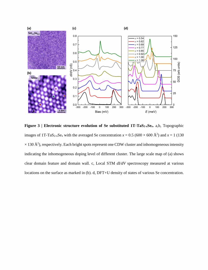
Figure 3 | Electronic structure evolution of Se substituted 1T-TaS2-xSex. a,b, Topographic
images of 1T-TaS2-xSex with the averaged Se concentration x = 0.5 (600 × 600 Å2) and x = 1 (130
× 130 Å2), respectively. Each bright spots represent one CDW cluster and inhomogeneous intensity
indicating the inhomogeneous doping level of different cluster. The large scale map of (a) shows
clear domain feature and domain wall. c, Local STM dI/dV spectroscopy measured at various
locations on the surface as marked in (b). d, DFT+U density of states of various Se concentration.
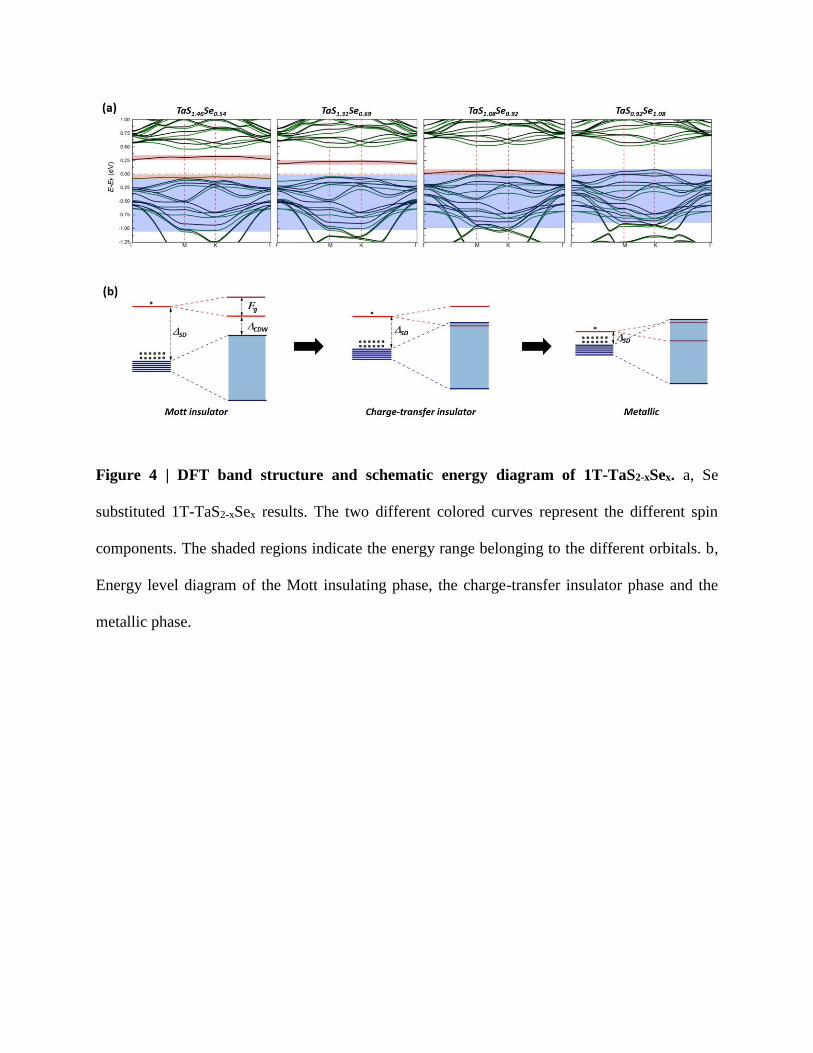
Figure 4 | DFT band structure and schematic energy diagram of 1T-TaS2-xSex. a, Se
substituted 1T-TaS2-xSex results. The two different colored curves represent the different spin
components. The shaded regions indicate the energy range belonging to the different orbitals. b,
Energy level diagram of the Mott insulating phase, the charge-transfer insulator phase and the
metallic phase.

Supplementary information for
Orbital-driven Mottness collapse in 1T-TaS2-xSex transition metal
dichalcogenide
Shuang Qiao1,2,*, Xintong Li1,*, Naizhou Wang3, Wei Ruan1, Cun Ye1, Peng Cai1, Zhenqi Hao1,
Hong Yao2,4, Xianhui Chen3,5, Jian Wu1,4,†, Yayu Wang1,4,†, Zheng Liu2,4,†
1State Key Laboratory of Low Dimensional Quantum Physics, Department of Physics, Tsinghua
University, Beijing 100084, P.R. China
2Institute for Advanced Studies, Tsinghua University, Beijing 100084, P.R. China
3Hefei National Laboratory for Physical Science at Microscale and Department of Physics,
University of Science and Technology of China, Hefei, Anhui 230026, P.R. China
4Innovation Center of Quantum Matter, Beijing 100084, P.R. China
5Collaborative Innovation Center of Advanced Microstructures, Nanjing University, Nanjing
210093, China
*These authors contributed equally to this work.
†Email: [email protected];[email protected]; [email protected]
Contents:
1. Methods
2. Supplementary experimental results
3. Theoretical Wannier function analysis

1. Methods
Crystal growth. The high-quality single crystals of 1T-TaS2-xSex (0 < x < 2) were synthesized by
chemical vapor transport method with iodine as transport agent. The powder of Ta, S, and Se is
weighted stoichiometrically and thoroughly grounded. Then the mixture together with 150 mg I2
is sealed into an evacuated quartz tube and then placed into a two-zone furnace with the
temperature gradient of 1253 K-1153 K for 1 week. The products were washed with ethanol to
remove the iodine at the surface.
STM and STS measurements. The STM experiments are performed with a cryogenic variable
temperature ultrahigh vacuum STM system. The 1T-TaS2-xSex crystal is cleaved in situ at T = 77
K and the measurement taken at 5 K with an electrochemically etched tungsten tip calibrated on a
clean Au (111) surface34. The STM topography is taken in the constant current mode, and the dI/dV
spectra are obtained with a standard lock-in technique with modulation frequency f = 423 Hz.
DFT calculations. The first-principles calculation based on the density functional theory is
performed using the Vienna Ab-initio Simulation Package35-388 with a 280 eV plane-wave basis
cutoff. The Perdew-Burke-Ernzerh generalized gradient approximation39 and the projector
augmented wave method39 are employed. The +U correction follows the simplified (rotational
invariant) approach introduced by Dudarev40,41. The integration over the Brillouin zone of the
√13 × √13 supercell including 15 Å vacuum space is obtained on a Gamma-centered 6 × 6 × 1
k mesh. The self-consistent iterations are converged to 10-5 eV precision of the total energy. We
use the lattice parameters determined by experiment42, and relax the atomic coordination self-
consistently until the forces are less than 0.002 eV/Å.
2. Supplementary experimental results

Figure S1a shows the in-plane resistivity data of three typical 1T-TaS2-xSex samples. For the
pristine 1T-TaS2, there is a well-defined phase transition around 180 K, known to be the NCCDW-
to-CCDW transition. Se substitution in the high-temperature NCCDW phase has little influence
on transport, indicating that Se atoms are weak scatterers. However, Se substitution strongly
suppresses the phase transition, and the discrepancy of the three samples in the low-temperature
region becomes significant. A clear insulating behavior, which is commonly attributed to Mott
localization, is found in the x = 0 sample below ~ 60 K. In contrast, the x = 1 sample keeps metallic
until a sudden drop of resistivity ~ 3 K, which has been confirmed to be a superconducting
transition. Figure S1b displays the location in the electronic phase diagram of these three 1T-TaS2-
xSex samples as derived from transport properties1.
Supplementary Figure S1 | a, Temperature dependence of the in-plane resistivity. b, Schematic
electronic phase diagram of 1T-TaS2-xSex derived from transport properties as a function of
temperature and x, the 3 points correspond to the same color line in (a).

Figure S2 shows LDOS maps of the two representative energies measured at positive biases,
exhibiting a periodic pattern commensurate with the SD superlattice. At the upper Hubbard band
energy Vb = 199 mV (left panel), the bright spots locate in the center of SDs. While moving to
higher energy with bias Vb = 484 mV (right panel), the bright regions shift to the surrounding Ta
orbitals. These results are nearly symmetric with the maps at negative biases, demonstrating two
types of orbital texture.
Supplementary Figure S2 | Differential conductance (dI/dV) maps (42 × 42 Å2) measured at Vb
= 199 mV (left) and Vb = 484 mV (right) with tunneling current It = 20 pA. The center of each
CDW cluster is brighter at 0.2 V while the edges brighter at 0.4 V.
Figure S3 displays a closer examination around the domain walls. Figure S3a,b are large
scaled topographic images of 1T-TaS2 and 1T-TaSSe samples, respectively, in which each bright
spot represent one CDW cluster. The uniform surface of parent compound is split into many
domains in doped sample by domain boundary (red square). There is rotation between different
domains as displayed by yellow arrows. Figure S3c,d are zoomed-in topographic images of Fig.
S3a,b with atomic resolution. Red dashed lines indicate the supper-lattice direction in both maps,

and half-cluster translation mismatch around domain boundaries is clearly demonstrated in Fig.
S3d.
Supplementary Figure S3 | a,b, Large scaled topographic images of 1T-TaS2 (225 × 225 Å2) and
1T-TaSSe (245 × 245 Å2) samples, each bright spot represent one CDW cluster. c,d, Zoom in
topographic images of (a) and (b) with atomic resolution.
3. Theoretical Wannier function analysis
Figure S4 shows the first-principles band structure of a 1T-TaS2 monolayer in the CCDW
structure obtained within the framework of the generalized gradient approximation (GGA)2
without spin degree of freedom. The most remarkable feature is a narrow band right at the Fermi

level. Besides, a set of 6 dispersive bands can be clearly differentiated below the Fermi level. These
6 bands along with the narrow band at the Fermi level consist of the downfolded seven-orbital
subspace as we proposed in main text. We then perform Fourier transformation from the Bloch
representation to the Wannier representation by using the WANNIER90 code3-5 within this
subspace. The onsite energy and hopping parameters between these Wannier functions can be
simultaneously calculated by performing the same Fourier transformation to the band eigenvalues.
As shown in main text Fig. 2(b), the seven Wannier functions automatically separate into two
groups, |𝑐⟩ and |𝑠𝛼=1…6⟩. With respect to the onsite energy, |𝑠𝛼=1…6⟩ are degenerate, as expected
from symmetry; |𝑐⟩ is 0.21 eV higher. The largest hopping amplitude is between |𝑐⟩ and |𝑠𝛼=1…6⟩,
followed by several hopping processes among |𝑠𝛼=1…6⟩. There is also considerable intercluster
hopping for |𝑠𝛼=1…6⟩ . We list the leading matrix elements in Tab. SI. The set of obtained
parameters for pristine 1T-TaS2 is susceptible to a Mott transition owing to a large positive 𝛥SD,
which on the one hand separates |𝑠𝛼=1…6⟩ far from the Fermi level, and on the other hand results
in a small effective hopping between |𝑐⟩ of the order O(tsc2tss/𝛥SD
2)<<U.
As the demonstration of the two-orbital-driven electronic transition, we manually increase
the buckling of the S atoms around the central Ta by 0.187 Å and perform the same calculation
and analysis. The results signal an insulator-to-metal transition tendency and a decrease of 𝛥SD,
rationalizing the concept of orbital-driven transition. Moreover, it is worth noting several points
that bridges the structural and chemical modification. Firstly, the DFT structural relaxation shows
that the substitutional Se atoms have nearly the same in-plane coordinates as S, but are about 0.187
Å above the S-plane. Meanwhile, the positions of Ta atoms hardly change. Therefore, Se
substitution plays the effective role of increasing the local buckling of the trilayer. Secondly, the
energy spectrum is found to be sensitive to the local buckling rather than the S/Se type. Using the

same buckled structure, very similar band structure can be obtained when replacing Se back to S.
Finally, the similarity between structural and chemical modification is also reflected by comparing
the extracted model parameters as shown in Tab. SI. In conclusion, structural modification and Se
doping can be viewed as alternative ways to modulate the interplay between orbital textures, also
manifesting the scenario of orbital-driven electronic transition.
Supplementary Figure 4 | DFT band structure of the 1T-TaS2 monolayer without spin degree of
freedom. The red dashed curves are the band structures by using the Wannier function basis.
Table SI: Single-electron parameters from Wannier function analysis as used in Eq. (1) in the
main context. The three columns correspond to the pristine 1T-TaS2, an arbitrarily deformed 1T-

TaS2 by manually increasing the out-of-plane distance between the central Ta and its nearest-
neighbor S-atoms by 0.187 Å, and a Se-doped 1T-TaS2-xSex with the Se concentration x = 0.92.
The right figure shows the meaning of the five dominant hopping processes between the |𝑠𝑖=1…6⟩-
orbitals.
Supplementary References:
1 Liu, Y. et al. Superconductivity induced by Se-doping in layered charge-density-wave
system 1T-TaS2−xSex. Appl. Phys. Lett. 102, 192602 (2013).
2 Perdew, J. P., Burke, K. & Ernzerhof, M. Generalized Gradient Approximation Made Simple.
Phys. Rev. Lett. 77, 3865 (1996).
3 Marzari, N. & Vanderbilt, D. Maximally localized generalized Wannier functions for
composite energy bands. Phys. Rev. B 56, 12847 (1997).
4 Souza, I., Marzari, N. & Vanderbilt, D. Maximally localized Wannier functions for
entangled energy bands. Phys. Rev. B 65, 035109 (2001).
5 Mostofi, A. A. et al. wannier90: A Tool for Obtaining Maximally-Localised Wannier
Functions. Comput. Phys. Commun 178, 685 (2008).
Top Related