


Languages
Pages
Legal


This is an Open Access document downloaded from ORCA, Cardiff University's institutional
repository: http://orca.cf.ac.uk/131349/
This is the author’s version of a work that was submitted to / accepted for publication.
Citation for final published version:
Lee, Hanleem, Harden-Chaters, William, Han, Soo Deok, Zhan, Shijie, Li, Benxuan, Bang, Sang
Yun, Choi, Hyung Woo, Lee, Sanghyo, Hou, Bo, Occhipinti, Luigi G. and Kim, Jong Min 2020.
Nano-to-microporous networks via inkjet printing of ZnO nanoparticles/graphene hybrid for
ultraviolet photodetectors. ACS Applied Nano Materials 3 (5) , pp. 4454-4464.
10.1021/acsanm.0c00558 file
Publishers page: http://dx.doi.org/10.1021/acsanm.0c00558
<http://dx.doi.org/10.1021/acsanm.0c00558>
Please note:
Changes made as a result of publishing processes such as copy-editing, formatting and page
numbers may not be reflected in this version. For the definitive version of this publication, please
refer to the published source. You are advised to consult the publisher’s version if you wish to cite
this paper.
This version is being made available in accordance with publisher policies. See
http://orca.cf.ac.uk/policies.html for usage policies. Copyright and moral rights for publications
made available in ORCA are retained by the copyright holders.

1
Nano-to-Micro porous Networks via Inkjet Printing
of ZnO Nanoparticles/Graphene hybrid for
Ultraviolet Photodetectors
Hanleem Leea, William Harden-Chatersa, Soo Deok Hana,*, Shijie Zhana, Benxuan Lia, Sang Yun
Banga, Hyung Woo Choia, Sanghyo Leea, Bo Houa,b*, Luigi G. Occhipintia, Jong Min Kima
a Department of Engineering, University of Cambridge, 9 JJ Thomson Avenue, Cambridge CB3
0FA, UK
b School of Physics and Astronomy, Cardiff University, The Parade, Cardiff, CF24 3AA, UK
KEYWORDS. Inkjet print, photodetector, microporous, ZnO nanoparticle (NP), flexible devices.
*Corresponding Authors: E-mail: [email protected] (S.D.H.), [email protected] (B.H.) Tel:
+44 (0)1223 748318.
ABSTRACT: Inkjet-printed photodetectors have gained enormous attention over the last decade.
However, device performance is limited without post-processing, such as annealing and UV
exposure. In addition, it is difficult to manipulate the surface morphology of the printed film using
an inkjet printer due to the limited options of low viscosity ink solutions. Here, we employ a
concept involving the control of the inkjet-printed film morphology via modulation of co-solvent

2
vapor pressure and surface tension for the creation of a high-performance ZnO-based
photodetector on a flexible substrate. The solvent boiling point across different co-solvent systems
is found to affect the film morphology, which results in not only distinct photo-response time but
also photo-detectivity. ZnO-based photodetectors were printed using different solvents which
display a fast photo-response in low-boiling point solvents due to the low carbon residue and larger
photo-detectivity in high-boiling point solvent systems due to the porous structure. The porous
structure is obtained using both gas-liquid surface tension differences and solid-liquid surface
differences, and the size of porosity is modulated from nano-size to micro-size depending on the
ratio between two solvents or two nanomaterials. Moreover, the conductive nature of graphene
enhances the transport behavior of the photocarrier, which enables a high-performance
photodetector with high photo-responsivity (7.5*102 AW-1) and fast photo-response (0.18 s) to be
achieved without the use of high-boiling point solvents.
INTRODUCTION
Recently, printed electronics have considerable interest as a possible candidate to develop large-
area electronic systems and flexible electronics at a low cost.1 Among many other printing
techniques, inkjet printing has been considered as a great candidate for the next generation printing
method due to several advantages such as its versatility on a wide range of possible substrates,
low-temperature processing (20 °C), high processing speeds, mask-less fabrication with a high
resolution (~50 μm), manufacturing scalability and low material losses (< 1 mL).2 Beyond the
resistor type film fabrication using conducting materials (e.g., Ag, graphene, and carbon
nanotube), technical improvement and in-depth study on this method over the last decade have
made it possible to deposit functional ink such as the organic semiconductor,3 light-emissive
polymers, 4 and metal oxide nanoparticles,5 which are necessary to realise fully printed electronics,

3
and a wide variety of electronics, such as: a solar cell,6 light-emitting diode,7 thin-film transistor,8
sensor,9 memory devices10, which have all been successfully presented up till now. Among them,
an inkjet-printed photodetector (PD) is expected to be an essential component for consumable IoTs
within optical communication for flexible devices, imaging, light sensing, and hazard detection in
the military and medical fields.11
The physical and electrical property of films produced by inkjet printing is strongly influenced by
the ink formula, including the rheological parameters. Improper ink formula can cause various
issues such as the coffee-ring effect, short term ink reliability, and improper drop pinning on the
substrate. Previous studies demonstrate the fascinating controllability of organic and polymer
functional ink.12 Several full inkjet printed organic PD have been described and have displayed a
similar level of device performance with the devices made using spin coating methods. For
example, a fully printed PD with Ag / P3HT: PC61BM/ PEDOT: PSS in a vertical configuration
showed good detectivity around 1.5 × 1012cm·Hz0.5·W−1 (at 0.9 V bias, 525 nm) with fall time
about 90 µs.13 Apart from a good jettability and morphology control of printed organic and
polymer PD, poor long-term stability, low intrinsic photoconductivity, limited device
configuration, and the dispersibility in biocompatible solvents are issues facing the development
of organic printed PD.
On the other hand, inorganic PD such as nanowire and nanoparticles demonstrate relatively high
photoconductivity (0.4 kHz bandwidth with high internal gain (G > 6.5 × 10³) than organic printed
PD through the controlled introduction of defects. Recently, some inorganic printed PD have been
demonstrated, but their performance is not comparable to that of inorganic PD made by other
solution coating method because of the low quality of the film.14 The poor controllability of

4
fabricating the desired network using inorganic ink via inkjet printing removes its outstanding
intrinsic optoelectrical property, and it results in poor device performance (i.e. short lifetime, low
response time, little gain), especially with low-temperature manufacturing processes (< 150 °C).
Thus, it is necessary to develop a new method to control the printability of inorganic ink for
realising a high-performance inorganic printed PD.
Previously, high boiling point solvents have been used for inorganic nanoparticle ink to enhance
ink stability and jettability. Despite this, the jettability of the nanoparticles is dependent on the
high boiling point solvent system, which is theoretically and experimentally well studied. The
practical property, such as the optoelectrical property of the film, is not thoroughly investigated.15
It is essential to consider the effect of the solvent on the device performance. High boiling solvent
residue can affect the physical properties of nano-dimensional inorganic materials. Most studies
with nanoparticles demonstrate proper functions following a high-temperature post-annealing
process (> 200 °C) or strong UV treatment. Yuhui Dong et al., demonstrated that the ZnO NP ink
in ethylene glycol/glycol mixture showed only photodetection behaviour after UV treatment.16
Photo-responsivity is relatively low over the device made by other solution-based coating
processes and required high external voltage (60 V) after UV treatment.
Moreover, in the field of flexible electronics and bio-electronics, low boiling point ink is highly
desired due to four main advantages.17 Firstly, fast evaporation of the solvent can reduce the
probability of re-dispersion between the layers of the heterostructure, making it possible to diverse
the device configuration. Secondly, low solvent residue decreases further damage to active
materials and increases operational stability. Thirdly, low boiling point inks have been shown to
minimise the ‘coffee ring’ effect which typically transports flakes to the edge of the deposited film
when dried; therefore the morphological uniformity and layered arrangement can be improved.18-

5
19 Finally, the lower boiling point solvents (<100 °C) tend to be biologically safer and more
economical than high boiling point organic solvent (>100 °C) such as ethylene glycol.20 However,
when a low boiling point inks are used in inkjet printing, they tend to dry around the inkjet nozzle
which can cause blockages when used over long periods (days) even when cleaning cycles are
applied.
In this study, we have designed a new strategy to create a highly desirable surface morphology
with inorganic NP ink using a low boiling point solvent. The NP ink in the co-solvent system with
1) high boiling solvent and low boiling solvent; and 2) two low boiling solvents; are investigated
in the aspects of surface morphology and optoelectrical property. Then, the effect of solvent
residue and contact junction status on printed electronics are researched. Finally, the microporous
structure is constructed to improve the responsivity of PD. This is achieved through maximising
the local surface tension differences during the printing, which shows high photoresponsivity
(R_Maximum: 7.5*102 AW-1) with the fast response time.
RESULTS AND DISCUSSION
Ink formulation Figure 1a shows the schematic illustration of the fabrication method for inkjet-
printed PD using inorganic ink. Among many other inorganic materials, we chose ZnO NP due to
its high quantum efficiency, low cost, stability, high-temperature operation capability, and
environmental compatibility.21 Typically, the high crystalline ZnO NPs were prepared according
to a previous report for our photodetector applications.22 As shown in Figure S1a, the X-ray
diffraction pattern for typical hexagonal crystal structures can be resolved. The characteristic peaks
of {100, 002, 101, 102, 110, 103} can be readily indexed according to the standard PDF: 80-0075.

6
The broad diffraction peaks indicate the small crystal domains which are consistent with the high-
resolution transmission electron microscopy (HRTEM) images (Figure S1b) and indexed selected-
area electron diffraction pattern (Figure S1c).
Figure 1. (a) Schematic illustration of the PD printing process using ZnO/Graphene: Inset is
interfacial tension of droplets with two cosolvent systems (EtOH/EG and EtOH/IPA) and their
corresponding Z values. (b) Transient photocurrent time plot as a function of inkjet drop spacing
in EtOH/EG co-solvent system with 18oC platen temperature. (c) On and off current distribution
depending on inkjet drop spacing (DS): 5 DS, denotes 5 drop spacing. (d) Transient photocurrent
time plot as a function of printing cycles for EtOH/EG ink with 40 oC platen temperature. (e)

7
Transient photocurrent time plot as a function of the printing cycle (ly) in EtOH/EG co-solvent
system with 40 oC platen temperature; 13DS-2ly, denotes 13 um drop spacing with 2 layers
printing. (f) On and off current distribution depending on the printing cycle. (g) Photoresponse
time for EtOH/EG and EtOH/IPA ink.
For a printed PD, Ag reactive ink is printed first, and photoactive material is printed on the top of
the electrode to build a planer architecture PD. To improve the detectivity of printed ZnO NP based
PD, the graphene flake and ZnO NP is deposited layer by layer. The ethanol, which is
biocompatible, is chosen as a primary low boiling solvent to estimate the jettability and
controllability of ZnO NP ink. Due to the low boiling point solvent rapidly drying around the
nozzle during the inkjet printing, we have designed co-solvent systems with ethanol for the low
boiling point ink for the inorganic ink. Either ethylene glycol (EG) or isopropanol (IPA) is used as
a minor solvent. We estimate the jettability of each ink and engineer them to be within the optimal
Z range (2< Z <24, Z=Oh -1 = (γρa)1/2/η ) before printing.23 The inverse Ohnesorge number (Oh)
is used as a figure of merit. Several important parameters including the ink viscosity η, surface
tension γ, density ρ, and the nozzle diameter, a (=21 μm) influence the jetting of individual drops
from a nozzle.24-25 In case of cosolvent ink, the degree of viscosity, surface tension, and vapor
pressure are the terms affected by mixing friction of two solvents, so it is possible to modulate the
Z value of our ink through changing the mixing ratio between them;
� �� = ∑ �, ��,� (xi,s is mole fraction, γi is the surface tension of each solvent) …. (1) � �� = exp exp ∑ ������ − .97�� . − 0.8, …. (2) �� � = a ∗ ln(ln �� + 0.8 ) + b …. (3)
8
(xi is mass friction, a, b is constant, ηi is the kinematic viscosity of each solvent)
�� = ∑ � �,� (xi is mole fraction, vpi is the vapor pressure of each solvent) .... (4)
These equations (1) – (4) are based on the ideal case, and it can be modified as a function of the
liquid system (thin film, droplet), but each component affected by the frictions will not be
changed.7, 26-27 Thus, we calculate a various ratio of EtOH/EG and EtOH/IPA cosolvent system
respectively to obtain the optimum Z value of our inks (Table S1). It appears that 10:1 vol % to
50:1 vol % EtOH/EG and below 5:1 vol % EtOH/IPA shows good jettability among other
compositions (Figure S2). The rheological parameters (,, and ) of ZnO NP ink is ZnO ~ 6 mPa
s, ZnO ~ 28.29 mN m-1, ZnO ~ 0.48 g cm-3, for 50:1 vol % EtOH/EG and ZnO ~ 1 mPa s, ZnO ~
27.97 mN m-1 for 5:1 vol % EtOH/IPA and its correlated Z value is 3.4 for 50:1 vol % EtOH/EG
and 16 for 5:1 vol % EtOH/IPA, which is in the optimum Z range (Figure 1a inset, Figure S2).
Owing to good jettability of inks, we can make a fine pattern using EtOH/EG and EtOH/IPA ink
while ZnO NP in EtOH shows poor line patterning due to satellite formation (Figure S3a, b)
ZnO NP printed PD. We fabricate a printed PD using ZnO NP in EtOH/EG and ZnO NP in
EtOH/IPA to investigate the solvent effect on the optoelectrical property of ZnO NP. EG is chosen
as a high boiling point solvent, and IPA is chosen as a low boiling point solvent. Before
investigating the solvent effect, photo-responsivity is tuned through the drop spacing and the
number of printing cycles using the EG/EtOH ink. Figure 1b shows the highest responsivity with
10 μm drop spacing under the same number of printing cycles. Despite the film with 5 μm drop
spacing containing twice the amount of ZnO NP than the 10 μm film, the 5 μm film shows lower
responsivity because a larger amount of high boiling point EG has remained during printing and
has increased the coffee ring effect (Figure S4a-c).
9
Moreover, performance repeatability is poor with narrow drop space printing. The film with 15
μm drop spacing has the smallest deviation of device performance among others (Figure 1c).
Therefore, a 13 μm drop spacing is adapted for both EtOH/EG and EtOH/IPA ink experiments.
Interestingly, all PD made by EtOH/EG ink demonstrate slow response time, large dark noise level,
and fast accumulation - recombination behaviour. Without any post-annealing process, the high
boiling point EG remains in the film, and it impedes the charge transport of photogenerated
carriers. Thus, photogenerated charge carriers are accumulated and spontaneously recombined at
the junction between the ZnO NPs film made by EtOH/EG ink. Therefore, the photocurrent
drastically decreases despite the continuous light exposure. FT-IR spectroscopy clearly indicates
a large amount of carbon residual with EtOH/EG ink, compared to EtOH/IPA ink without any
annealing process (Figure S4c). The C-C stretching, O-H stretching, C-O stretching are only
detected for EtOH/EG ink printed devices. After using a 40 °C platen temperature and 150 °C
post-annealing process for EtOH/EG ink, a large dark noise level, and fast accumulation -
recombination behaviour is reduced in Figure 1d and e, owing to the reduced solvent residue. Also,
photo-responsivity with different printing cycles are studied. The responsivity of the device is
proportionally increased with the increased number of printing cycles due to high absorption, but
the dark current, response time and the repeatability of the device somewhat decreases after 9
printing cycles due to the colloidal aggregation during printing (Figure1e, f). Finally, we fabricate
a device with a 13 μm drop spacing with 7 layers of printing for both ZnO NP in EtOH/EG and
ZnO NP in EtOH/IPA (Figure 1g). The EtOH/EG ink shows a higher Ilight/Idark ratio (11 at 405 nm
1mW) than EtOH/IPA ink (2 at 405 nm 1 mW), but the rising time and falling time of the
EtOH/IPA ink is 4 times higher than that of EtOH/EG ink (Figure 1e and 1g). Unlike the EtOH/IPA
ink, which has a similar surface tension between two solvents, EtOH/EG ink has a larger difference
10
in their surface tension so that the EtOH/EG ink formed a more porous and rougher surface than
EtOH/IPA ink. Atomic-force microscopy (AFM) analysis shows that many pores between 200 nm
to 1 μm exist in the film which is printed via EtOH/EG ink, in contrast to the smooth thin film
which is printed from EtOH/IPA ink (Figure S4d, e). The higher porosity of EtOH/EG ink
improved the PD performance due to the increased absorption of UV light within the porous
structure. The film printed from EtOH/EG ink showed twice the absorption at 360 nm - 400 nm
region than the film which was printed from the same amount of EtOH/IPA ink (Figure S4f). Due
to the different porosity between the two films, a more significant PD Ilight/Idark ratio is obtained
with EtOH/EG ink. Although the surface morphology of EtOH/EG ink printed films are optimised
through controlling the drop space, printing cycle, and annealing process, inferior device
performances remain (i.e. the response time, accumulation - recombination behaviour). We believe
that the high boiling point EG which remains after the annealing process (< 100 °C) is the origin
of the poor device's performance.
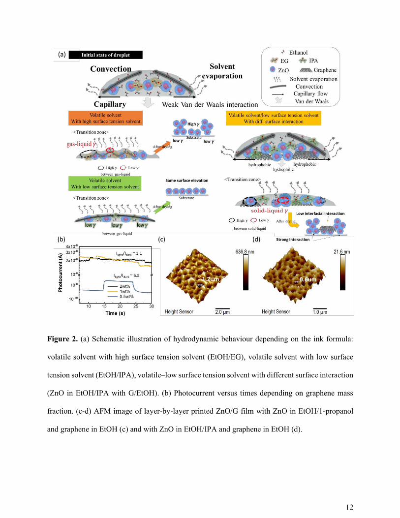
Microporous ZnO NP/Graphene via inkjet. To improve photo-detectivity from as-printed ZnO
films, we design a new approach to modulate the porosity of film using a mixing low-boiling point
cosolvent (EtOH/IPA) system as shown in Figure 2a. The microporous structure of EtOH/EG ink
is driven by ‘Bénard – Marangoni’ convection flow effect. Evaporation-driven surface tension
gradient in the liquid layer can cause the convective flow, and it generates a specific pattern on the
surface. Microporous structure formation by Bénard − Marangoni convection has been introduced
in spin coating28 and dip coating29 approaches. For instance, Hiroaki et al. demonstrated the
spontaneous porous pattern formation using cosolvents with high surface tension and low volatility
(e.g. 2-propanol with dipropylene glycol using the dip-coating method).29 Inkjet-printed films
have also been known to be affected by the Bénard − Marangoni convection.30 Improper Bénard

11
− Marangoni convection results in a coffee ring effect in the inkjet method. Thus, enhancing the
Bénard − Marangoni convection during inkjet printing can construct the microporous film
analogous to the dip-coating process, which shown by our EtOH/EG ink in this study. The initial
state of a droplet is similar between EtOH/EG (volatile solvent with high surface tension solvent)
and EtOH/IPA (volatile solvent with low surface tension solvent), while fluidic behaviour between
them have a huge difference. While the droplet reaches the transition zone, EtOH/EG undergoes
the Bénard − Marangoni convection due to different gas-liquid surface tension of EG, compared
to EtOH and IPA and it results in the porous structure. However, residual EG disrupts the photo-
response time so that another strategy to modulate the porosity is required.
12
Figure 2. (a) Schematic illustration of hydrodynamic behaviour depending on the ink formula:
volatile solvent with high surface tension solvent (EtOH/EG), volatile solvent with low surface
tension solvent (EtOH/IPA), volatile–low surface tension solvent with different surface interaction
(ZnO in EtOH/IPA with G/EtOH). (b) Photocurrent versus times depending on graphene mass
fraction. (c-d) AFM image of layer-by-layer printed ZnO/G film with ZnO in EtOH/1-propanol
and graphene in EtOH (c) and with ZnO in EtOH/IPA and graphene in EtOH (d).

13
In a low - low boiling point system, we facilitate the Bénard − Marangoni convection through
differentiating the surface tension using graphene flake. The Bénard − Marangoni convection can
be characterised by the Marangoni number, Ma:31
� = − ∂γ/∂T �2 ∇� �� = − ∂γ/∂C �2 ∇C �� ….… (4)
where ∂γ/ ∂T is the temperature derivative of the surface tension, ∂γ/ ∂C is the concentration
derivative of the surface tension, H is the thickness of the solution layer, μ is viscosity, α is thermal
diffusivity of the solution, D is the mass diffusivity of the component, and ∇T and ∇C are the
temperature and concentration gradient near the solution surface, respectively, because the Bénard
− Marangoni convection occurs when Ma is high. The Ma can be enlarged when increasing
temperature or increasing concentration gradients or increasing thicknesses. Lowering the
viscosity can also assist in creating a microporous pattern with low-low boiling point solvent. We
cannot manipulate the temperature factor within inkjet printing due to the use of a low-low boiling
solvent which would induce clogging issues, while concentration derivative and mass diffusivity
can be well controlled by differentiating the underlying materials.
Therefore, we have used graphene flakes to generate surface tension instead of using a high boiling
point solvent, which is EG for the co-solvent system, in a low boiling point co-solvent system. The
Graphene is synthesized via the solvent exfoliation method and re-dispersed in EtOH, followed by
our previous paper40 so that the physical property of graphene will be same. A solid-liquid surface
tension variation can be created between the hydrophobic graphene and hydrophilic ZnO NP which
can lead to ZnO/Graphene microporosity network via inkjet printing. The graphene flake and ZnO
NP are deposited layer by layer to enhance the Bénard – Marangoni effect. Firstly, we optimised
the mass friction between ZnO NP and Graphene for PD devices. Graphene is a highly electrically
14
conductive material. A small amount of graphene can improve PD performance by reducing
contact junction resistance between ZnO NPs. However, a large amount of graphene will induce a
fully conductive channel,32 which is not desirable for PDs. As shown in Figure 2b, a different mass
fraction between graphene and ZnO NP exhibit different photo-responsivity (Figure 2b). For
instance, the 2 wt% and 1 wt% graphene insertion on the ZnO film shows a higher dark current
and smaller Ilight/Idark ratio than the pure ZnO film. Based on photo-responsivity as a function of
graphene/ZnO ratio, we found 0.5 wt% graphene on ZnO film shows the best PD performance.
When the graphene concentration increases over 1 wt%, the dark current is increased due to the
conductive nature of graphene and the photoresponse is decreased due to intermolecular energy
transfer between graphene and ZnO NP. Therefore, it is an effective strategy that the porosity is
modulated by a solvent system with a fixed graphene concentration.
The surface morphology of ZnO NP/graphene is examined with various cosolvent systems. When
the low volatile cosolvent with lower surface tension is mixed (EtOH/1-Butanol), the low volatile
solvent evaporates together with the solutes during the EtOH evaporation.33 Therefore, the
generation of pinholes is successfully suppressed to 100 - 200 nm size regardless of surface tension
differences between ZnO and graphene (Figure S5). We believe butanol which has a longer alky
chain than ethanol can decrease surface tension difference between ZnO and graphene, which
results in the stronger interaction between residual butanol and graphene. On the other hand, ZnO
NPs in EtOH/1-propanol and EtOH/IPA demonstrate delicate microporous patterns via layer-by-
layer printing with graphene (Figure 2c, d). The AFM image of ZnO/graphene film using EtOH/1-
propanol (Figure 2c) indicates over 1 μm size holes were generated with 282 nm RMS in a 5 μm
x 5 μm area, while the ZnO/graphene film using EtOH/IPA (Figure 2d) shows approximately 600
nm size holes were generated with 13 nm RMS in a 5 μm x 5 μm area. The higher surface tension

15
from 1-propanol over IPA facilitates random fluctuations in local surface tension and causes lateral
fluid motion, resulting in the more significant regional surface tension differences.
As well as this, 1-propanol has higher vapor pressure and lower viscosity than1-Butanol, which
results in a microporous film structure during the fast evaporation. It should be noted that the
surface tension differences mainly induced by graphene flake, and the minor solvent should not
actively interact with the graphene flake. Fast evaporation cosolvent systems only affect the
microporous pattern formation induced by the Bénard−Marangoni convection with the
ZnO/graphene network.
A detailed investigation was conducted as a function of the co-solvent mixing ratio. The AFM
images indicate no porous structure with ZnO NP in EtOH (Figure 3a) and ZnO NP in IPA (Figure
3b). Regardless of the mixing ratio between EtOH and IPA, we found the ZnO NP ink shows a
small porosity, which gives a lower PD response because of small differences in the surface tension
(Figure 3a-c). Figure 3d-f shows the surface morphology of ZnO film on the top of graphene flake
film (2 cycles of ZnO printing on 1 cycle of graphene printed film). We found by just simply
coating ZnO on the graphene film can result in a porous structure. The film which was printed
using ZnO NP in 10:1 EtOH/IPA (Figure 3d) shows 30 – 80 nm pinholes with a large surface
roughness (RMS over 98 nm). The number of holes in this film dramatically increased compared
to that of ZnO only films, and we have found the number of the pores monoclinic increased as a
function of EtOH adding ratio. A monodispersed pinhole (approximately 100 nm) is obtained in
ZnO/graphene film which is printed through dispersing ZnO NP in 5:1 EtOH/IPA. This also
creates a fine surface morphology due to the rapid evaporation and low viscosity (Figure 3e).
However, the films printed from ZnO NP in 1:5 EtOH/IPA (Figure 3f) ink solution presents a large
difference in thickness (RMS over 114 nm) with inhomogeneous pinholes, unlike EtOH dominant
16
co-solvent system. The rapid solvent evaporation during the printing process is the key factor to
provide the concentration gradation of the solutes, which generates a local higher surface tension
as a result of different intermolecular interactions. Finally, we achieve the precise control of the
hole size from ZnO/graphene layer-by-layer printing, as shown in Figure 3g-i. We use a 5:1
EtOH/IPA solvent to ascend the number of holes in ZnO/graphene film, and the hole size is
controlled by using different concentration of graphene inks. For instance, the 0.1 mg/mL, 0.2
mg/mL, 0.4 mg/mL graphene solution create a well-packed printed film with below 100 nm hole
(Figure 3g), 200 – 500 nm hole (Figure 3h), 1 μm hole (Figure 3i), respectively. Furthermore, we
prepared cross-section specimens via FIB milling for direct analysis of the morphology of
ZnO/graphene film. As shown in Figure S6, graphene intercalated ZnO film can be readily
observed through the high-resolution TEM analysis, which matches with our understanding. The
layer-by-layer printed ZnO/Graphene using the high boiling point solvent show stacked film
configuration between ZnO and graphene while layer-by-layer printed ZnO/Graphene using low
boiling point solvents exhibit microporous structure.

17
Figure 3. (a-c) AFM image of ZnO film depending on different EtOH/IPA volume ratio: EtOH
(a), 5:1 EtOH/IPA (b), IPA(c). (d-f) AFM image of ZnO film on the top of printed graphene surface
depending on different EtOH/IPA volume ratio: 10:1 EtOH/IPA(d), 5:1 EtOH/IPA (e), 1:5
EtOH/IPA (f). (g-i) AFM image of layer by layer printed ZnO (in a 5:1 EtOH/IPA)/Graphene film
using depending on different graphene friction: 0.1 mg/mL (g), 0.2 mg/mL (h), 0.4 mg/mL (i).
ZnO/graphene printing sequence is same for (g)-(i); graphene (1 layer)/ZnO (2 layer)/ graphene (1
layer)/ZnO (2 layer)/ graphene (1 layer)/ZnO (3 layer)
Printed PD performance. The photodetectivity of as prepared layer-by-layer ZnO/graphene PD
are systematically studied to understand the correlation between surface morphology and the

18
optoelectrical property of ZnO NP. Due to the porous structure, the Ilight/Idark ratio of ZnO/graphene
PD drastically increased compared to Ilight/Idark ratio of ZnO film (Figure 4a-c). Interestingly, we
found the response time and Ilight/Idark ratio of PD is profoundly affected by the size of porosity and
surface roughness. Under 1mW 405 nm light irradiation, the layer-by-layer ZnO/graphene PD
printed from EtOH/1-propanol show an Ilight/Idark ratio of 16 with 10 s fallen time and ~10 s rise
time (Figure 4a). The Ilight/Idark ratio and response time decrease noticeably after the annealing
process, this may occur due to the large porosity (1 μm) and the high surface tension difference
between ZnO and graphene. A more significant porosity of the printed film indicates the formation
of a larger ZnO colloidal aggregation which indicates the poor response time has originated from
the inferior contact junction between each ZnO NPs due to the nanoscale graphene not sufficiently
bridging these voids (Figure 4d, Figure S7a).
On the other hand, the layer-by-layer printed ZnO/graphene PD using EtOH/IPA cosolvent system
shows an 8 Ilight/Idark ratio with 0.18 s rise time and 4 s fallen times (1mW 405 nm light exposure,
Figure 4b). After the annealing process, not only does the Ilight/Idark ratio enhances to 13.6 but also
maintains the rise time at 0.22 s. Based on height analysis, the microscopic surface roughness of
EtOH/IPA ink printed film is much smaller than EtOH/1-propanol (100 μm x 100 μm, Figure 4e,
Figure S7b), which suggest uniform graphene and ZnO deposition with porous structure can
significantly enhance photoresponsivity with fast photo-response time.

19
Figure 4. (a-c) Under 1 mW 405 nm irradiance, transient photocurrent plots of ZnO, layer-by-
layer printed ZnO/G and annealed ZnO/G film for ZnO in EtOH/1-propanol (5:1) with Graphene
in EtOH (a), ZnO in EtOH/IPA (5:1) with Graphene in EtOH (b), ZnO in EtOH/IPA (5:1) with
Graphene in DMF (c). (d-f) Height mapping for corresponding films: ZnO in EtOH/1-propanol
(5:1) with Graphene in EtOH (d), ZnO in EtOH/IPA (5:1) with Graphene in EtOH (e), ZnO in
EtOH/IPA (5:1) with Graphene in DMF (f).
To verify our hypothesis, we print a uniform graphene and ZnO film without a porous structure by
dispersing graphene in dimethylformamide (DMF). Generally, DMF is a high boiling solvent
which can hinder the evaporation during the printing process. Uniform and non-porous layer-by-
layer ZnO/graphene films are also obtained when we employ the ZnO NP in EtOH/IPA solution
(Figure 4f, Figure S7c). However, due to the large DMF residual, PD performance is inferior. Even
after the annealing process, Ilight/Idark ratio (around 7) of layer-by-layer printed ZnO/graphene PD
is still lower than the aforementioned porous structure (Figure 4c).

20
Table 1 demonstrated the PD performance depending on the solvent system with and without
graphene. When the co-solvent system is changed, the porosity of the film is changed, and when
the porosity is changed, Ilight/Idark ratio is changed. The high boiling point solvent which remains
even after the annealing process (< 100 °C) demonstrated inferior photoresponse time compared
to low boiling point co-solvent system since carbon residue hinders the transport of photocarrier
between ZnO NP. Porous structure also can be generated via graphene/ZnO NP. Even after one-
layer printing of ZnO on graphene, we can observe the porous structure. Fig. S8 is the one-layer
printing of ZnO for the same condition with Fig. 3e. When the number of printing is increased, the
porosity becomes discrete and uniform, which means there is a templating effect. However, the
size of the porosity is more or less the same. The pore size of the graphene/ZnO NP structure can
be tuned through graphene concentration and solvent type (~ 1 um to 100 nm). Even though the
micro-porous structure is obtained with high graphene concentration, the PD performance is poor
compared to similar microporous structure generated by EG/EtOH system due to the conductive
nature of graphene.
Table 1. Comparative table for photodetector performance in this work. The optimal parameters
result in the champion devices are also highlighted in the table. The red color is representative data
to show discrete PD performance changes depending on the solvent system and graphene insertion.
Material Solvent DS/layer I light/Idark
(405nm) t (fallen) Pore size
ZnO
EtOH 13/5 Not reproducible Cracked thin film
IPA 13/5 Not reproducible Thin film
EtOH/IPA 5:1 vol%
5/2 2.45 0.77 Thin-film with few pinholes
10/2 3.16 0.33 Thin-film with few pinholes
15/2 1.55 0.32 Thin film
20/2 1.18 0.49 Thin film

21
13/2 1.20 0.25 Thin film
13/5 1.39 0.56 Thin film
13/7 2.02 0.55 Thin film
13/9 1.22 0.39 Thin film
EtOH/EG 50:1 vol%
5/2 2.36 3.90 Microporous ~1um
10/2 3.10 1.25 Microporous ~1um
15/2 6.17 2.66 Nano-Microporous
20/2 3.82 3.01 Nano-Microporous
EtOH/EG 50:1 vol% (40 °C)
13/2 2.42 2.41 Nano-Microporous
13/5 3.00 2.21 Nano-Microporous
13/7 11.1 2.22 Nano-Microporous
13/9 4.21 2.25 Nano-Microporous
ZnO/G_2wt% EtOH/IPA 13/2 +1G 1.16 0.6 Microporous (1 um)
ZnO/G_1wt% EtOH/IPA 13/2+1G 1.15 0.4 200 – 500 nm
ZnO/G_0.5wt%
EtOH/IPA=10:1 13/2+1G - - 30 – 80 nm
EtOH/IPA =5:1 13/2+1G 6.50 1.03 Uniform 100 nm
EtOH/IPA=1:5 13/2+1G - - Thin film with few pinhole
EtOH/BuOH 13/2+1G - - Inhomogenous nanopore
ZnO/G Layer by layer
EtOH/PrOH 13/7+3G 16 10 Microporous (1.2 um), RMS↑
EtOH/IPA 13/7+3G 8 4 Nanoporous (600 nm) RMS↓
EtOH/IPA (annealed)
13/7+3G 13.6 9.82 Nanoporous (600 nm)
EtOH/IPA (7 fingers)
13/7+3G 14.4 6*104
(365nm)
9.22 2.4
Microporous
To improve and demonstrate the reliability of our printed UV PD, three parallel-connected seven
fingered channel is fabricated (optical microscopy image is shown as Figure S9). Due to the
inherent microstructures from as-prepared integrated electrodes (100 μm *800 μm / L*W), the

22
microporous size of layer-by-layer printed ZnO/graphene PD (EtOH/IPA ink) is changed from 500
nm to 1 μm (Figure 5a). Owing to the well-controlled porosity, as-prepared integrated UV PD
demonstrates remarkable performance. A 14.4 Ilight/Idark ratio can be achieved under 1mW 405nm
light irradiation, and a 6*104 Ilight/Idark ratio can be obtained under 0.5 mW 365nm light exposure.
Moreover, three parallel-connected seven fingered channel show an average 4*104 Ilight/Idark ratio
compared to 150 Ilight/Idark ratio from one-fingered channel among 20 devices (Figure 5b, c).
Figure 5. (a) Transient photocurrent plot for layer-by-layer printed ZnO/G on seven finger
channels under different irradiance wavelength. The background is the corresponding AFM image
of the film. (b-c) Ilight /Idark ratio distribution profile of PD devices with single-channel devices (b)
and multi-channel devices (c). (d) Voltage - current plot without light exposure depending on the
channel electrode: Al (Al), printed Ag (Ag), printed Ag with surface functionalization (AgSH),
and Au (Au) electrode. (e) Flexible durability test for printed ZnO PD and inkjet-printed flexible

23
integrated sensor networks (inset). (f) Ilight /Idark ratio and response time plot for previous studies
and our works.35-39
We use e-beam evaporation to deposit Al and Au electrode to understand the effect of work
function on devices since the Schottky contact with channel and electrode can induce a low dark
current. We found the Al -based electrode PD shows a higher dark current while the Au electrode
shows a lower dark current (Figure 5d). This means Al has Schottky contact with ZnO while Au
is ohmic contact. To modulate the work function of the printed Ag electrodes, we modify the Ag
electrodes surface with a thiol derivative.7 After thiol modification on the printed Ag electrode,
the dark current is mostly reduced. As a result, final PD demonstrates maximum responsivity
around 7.5*102 AW-1 and average 6.2*102 AW-1 for ten devices with average Ilight/Idark ratio around
4*104, which is an outstanding detectivity compared with other report printed ZnO PDs (Figure
5e).
Furthermore, the as-printed PDs also show excellent flexible durability. As shown in Figure 5f, an ε = 0.8 tensile strain is applied to the PD devices, and the photo-responsivity change is monitored
as a function of bending cycles. During the initial stage (up to 40 cycles of the flexible test),
Ilight/Idark ratio of device drastically decrease due to crack propagation which is well-known
phenomena for flexible devices. After 40 cycles, PD performance becomes stable, which is
consistent with the typical sliding behaviour of channel materials.34 Encouragingly, the as-printed
flexible PD shows robust performance even after 400 cycles of bending tests.
24
CONCLUSIONS
In summary, we propose a new approach to modulate the surface morphology of the inkjet-printed
nanoparticle film via using a low boiling point cosolvent ink solution. A volatile solvent is used as
the primary solvent to facilitate the evaporation of the solvent during the inkjet printing. To reduce
the clogging, the volatile solvent is mixed with a high boiling point solvent. The porous structure
is obtained using both gas-liquid surface tension differences and solid-liquid surface differences,
and the size of porosity is modulated from nano-size to micro-size depending on the ratio between
two solvents or two nanomaterials. The surface morphology and the PD performance are
summarized in Table 1. Depending on the surface tension of the minor solvent or minor material,
the surface morphology can be altered from a smooth thin film to nanoporous or micro-porous
film. The thin-film demonstrates low Ilight/Idark ratio, but fast photo-response time. When the
porosity increases, Ilight/Idark ratio increases because the absorption of UV light is increased within
the porous structure. Moreover, the small amount of graphene improves PD performance by
reducing contact junction resistance between ZnO NPs.
EXPERIMENTAL METHODS
Inkjet Printing. A drop-on-demand inkjet printer (Fujifilm Dimatix DMP-2800) equipped with a
21 µm diameter nozzle (Fujifilm DMC-11610) was used, and the volume of individual droplets
from the nozzle is controlled at ~10 pL during our printing process. The platen temperature was
kept at room temperature (<20 °C) throughout the printing of the heterostructures. Each ink was
printed at a maximum jetting frequency of 2 kHz. The polyethylene naphthalate (PEN) film
(Teonex®) is used for PD substrate due to good surface roughness. The patterned channel
electrodes are formed via printing Ag ink (jet-600C, supplied by Hisense Electronics, Kunshan,

25
China) on a PEN substrate at a drop spacing of 50 μm and then annealed at 130 °C for 30 min.
Then, the ZnO NP ink (25 mg/mL in specific solvent) is printed at a drop spacing of 13 μm with a
single nozzle jetting. Subsequently, the Graphene NP ink is printed at a drop spacing of 40 μm
with a single nozzle jetting. The Graphene printing is repeated every two printing cycles after each
ZnO ink printing cycle. The film is dried at room temperature in a vacuum desiccator. Followed
by the previous study.7 the work function modulation of Ag electrode is realised through applying
perfluorobenzenethiol (PFBT)-ethanol solution (PFBT : ethanol = 1:1000) on the Ag electrode for
3 min and then rinsed with ethanol.
Photodetectivity. Detectivity and photoresponsivity are calculated as a figure of merit for photo-
detection performance via the following equation.37
Photoresponsivity (�� = � ��ℎ − ��� �⁄
� = � � = � � �
ASSOCIATED CONTENT
Supporting Information.
The detail information about material characterization methods; XRD, TEM, SAED analysis
results of ZnO NPs (Figure S1); detail description about ink solution characterisation methods and
Z value for every ink formula (Table S1); the viscosity analysis of ink solutions (Figure S2); and
optical images (Figure S3), FTIR (Figure S4), AFM (Figure S3 and Figure S4), UV-VIS absorption
spectroscopy (Figure S5) of different types of ink solutions and printed line patterns; TEM cross-

26
section image of printed thin films (Figure S6); the detail information of device preparation and
characterisation methods; SEM (Figure S7) and AFM images (Figure S8) of as-printed thin films;
and optical microscopy images of the as-prepared photodetector and corresponding equivalent
circuit design (Figure S9).
AUTHOR INFORMATION
Corresponding Author
E-mail: [email protected] (S.D.H.).
E-mail: [email protected] (B.H.).
ORCID:
Hanleem Lee: https://orcid.org/0000-0003-0958-6514
Bo Hou: https://orcid.org/0000-0001-9918-8223
Author Contributions
H.L. and B.H. conceived the experiments and led the project. H.L. performed inkjet printing and
device fabrication. B.H. performed material synthesis and microscopy analysis. S.D.H., S.Y.B.,
S.L. conducted the e-beam deposition. W. H. C., B. L., S. Z., H.W.C assisted the device fabrication
and sample characterization. L.G.O and J.M.K. provided research infrastructure support. H.L. and
B.H. wrote the manuscript.
Notes
27
The authors declare no competing financial interest.
ACKNOWLEDGEMENT
The authors acknowledge the support from European Commission Horizon2020 under grant
agreement number (685758). The research leading to these results also received funding from
Engineering and Physical Sciences Research Council (EPSRC) under project reference of
EP/P027628/1.
ABBREVIATIONS
NP nanoparticle, PD photodetector, ZnO zinc oxide, EG ethylene glycol, IPA isopropanol, DMF
dimethylformamide, Au gold, Al aluminium, RMS root mean square, TEM transmission electron
microscopy, FIB Focused ion beam, AFM atomic force microscopy.
REFERENCES
1. Oliveira, J.; Brito-Pereira, R.; Gonçalves, B. F.; Etxebarria, I.; Lanceros-Mendez, S.
Recent developments on printed photodetectors for large area and flexible
applications. Org. Electron. 2019, 66, 216-226
2. Gao, M.; Li, L.; Song, Y., Inkjet printing wearable electronic devices. J. Mater.
Chem. C 2017, 5 (12), 2971-2993.
3. Kwon, J.; Takeda, Y.; Fukuda, K.; Cho, K.; Tokito, S.; Jung, S., Three-Dimensional,
Inkjet-Printed Organic Transistors and Integrated Circuits with 100% Yield, High
Uniformity, and Long-Term Stability. ACS Nano 2016, 10 (11), 10324-10330.

28
4. Kang, Y. J.; Bail, R.; Lee, C. W.; Chin, B. D., Inkjet Printing of Mixed-Host Emitting
Layer for Electrophosphorescent Organic Light-Emitting Diodes. ACS Appl. Mater.
Interfaces 2019, 11 (24), 21784-21794.
5. Huang, C.-C.; Kao, Z.-K.; Liao, Y.-C., Flexible Miniaturized Nickel Oxide
Thermistor Arrays via Inkjet Printing Technology. ACS Appl. Mater. Interfaces
2013, 5 (24), 12954-12959.
6. Jung, S.; Sou, A.; Banger, K.; Ko, D.-H.; Chow, P. C. Y.; McNeill, C. R.;
Sirringhaus, H., All-Inkjet-Printed, All-Air-Processed Solar Cells. Adv. Energy Mater
2014, 4 (14), 1400432.
7. Liu, Y.; Li, F.; Xu, Z.; Zheng, C.; Guo, T.; Xie, X.; Qian, L.; Fu, D.; Yan, X.,
Efficient All-Solution Processed Quantum Dot Light Emitting Diodes Based on Inkjet
Printing Technique. ACS Appl. Mater. Interfaces 2017, 9 (30), 25506-25512.
8. Jiang, C.; Choi, H. W.; Cheng, X.; Ma, H.; Hasko, D.; Nathan, A., Printed
subthreshold organic transistors operating at high gain and ultralow power. Science
2019, 363 (6428), 719-723.
9. Adly, N. Y.; Bachmann, B.; Krause, K. J.; Offenhäusser, A.; Wolfrum, B.;
Yakushenko, A., Three-dimensional inkjet-printed redox cycling sensor. RSC Adv.
2017, 7 (9), 5473-5479.
10. Huber, B.; Popp, P. B.; Kaiser, M.; Ruediger, A.; Schindler, C., Fully inkjet printed
flexible resistive memory. Appl. Phys. Lett 2017, 110 (14), 143503.
11. Jin, Y.; Wang, J.; Sun, B.; Blakesley, J. C.; Greenham, N. C., Solution-Processed
Ultraviolet Photodetectors Based on Colloidal ZnO Nanoparticles. Nano Lett. 2008, 8
(6), 1649-1653.
29
12. Singh, M.; Haverinen, H. M.; Dhagat, P.; Jabbour, G. E., Inkjet Printing—Process
and Its Applications. Adv. Mater 2010, 22 (6), 673-685.
13. Azzellino, G.; Grimoldi, A.; Binda, M.; Caironi, M.; Natali, D.; Sampietro, M., Fully
Inkjet-Printed Organic Photodetectors with High Quantum Yield. Adv. Mater 2013,
25 (47), 6829-6833
14. Deka Boruah, B., Zinc oxide ultraviolet photodetectors: rapid progress from
conventional to self-powered photodetectors. Nanoscale Adv. 2019, 1 (6), 2059-2085.
15. Nallan, H. C.; Sadie, J. A.; Kitsomboonloha, R.; Volkman, S. K.; Subramanian, V.,
Systematic Design of Jettable Nanoparticle-Based Inkjet Inks: Rheology, Acoustics,
and Jettability. Langmuir 2014, 30 (44), 13470-13477.
16. Dong, Y.; Zou, Y.; Song, J.; Li, J.; Han, B.; Shan, Q.; Xu, L.; Xue, J.; Zeng, H., An
all-inkjet-printed flexible UV photodetector. Nanoscale 2017, 9 (25), 8580-8585.
17. Withers, F.; Yang, H.; Britnell, L.; Rooney, A. P.; Lewis, E.; Felten, A.; Woods, C.
R.; Sanchez Romaguera, V.; Georgiou, T.; Eckmann, A.; Kim, Y. J.; Yeates, S. G.;
Haigh, S. J.; Geim, A. K.; Novoselov, K. S.; Casiraghi, C., Heterostructures Produced
from Nanosheet-Based Inks. Nano Lett. 2014, 14 (7), 3987-3992.
18. Sliz, R.; Lejay, M.; Fan, J. Z.; Choi, M.-J.; Kinge, S.; Hoogland, S.; Fabritius, T.;
García de Arquer, F. P.; Sargent, E. H., Stable Colloidal Quantum Dot Inks Enable
Inkjet-Printed High-Sensitivity Infrared Photodetectors. ACS Nano 2019, 13 (10),
11988-11995.
19. Carey, T.; Cacovich, S.; Divitini, G.; Ren, J.; Mansouri, A.; Kim, J. M.; Wang, C.;
Ducati, C.; Sordan, R.; Torrisi, F., Fully inkjet-printed two-dimensional material
30
field-effect heterojunctions for wearable and textile electronics. Nat. Commun 2017, 8
(1), 1202.
20. Fowles, J.; Banton, M.; Klapacz, J.; Shen, H., A toxicological review of the ethylene
glycol series: Commonalities and differences in toxicity and modes of action. Toxicol.
Lett. 2017, 278, 66-83.
21. Liu, K.; Sakurai, M.; Aono, M., ZnO-based ultraviolet photodetectors. Sensors
(Basel) 2010, 10 (9), 8604-8634.
22. Hou, B.; Cho, Y.; Kim, B. S.; Hong, J.; Park, J. B.; Ahn, S. J.; Sohn, J. I.; Cha, S.;
Kim, J. M. Highly Monodispersed PbS Quantum Dots for Outstanding Cascaded-
Junction Solar Cells. ACS Energy Lett. 2016, 1 (4), 834-839
23. Son, Y.; Kim, C.; Yang, D. H.; Ahn, D. J., Spreading of an Inkjet Droplet on a Solid
Surface with a Controlled Contact Angle at Low Weber and Reynolds Numbers.
Langmuir 2008, 24 (6), 2900-2907.
24. Fromm, J. E., Numerical Calculation of the Fluid Dynamics of Drop-on-Demand Jets.
IBM J. Res. Dev 1984, 28 (3), 322-333.
25. Deegan, R. D.; Bakajin, O.; Dupont, T. F.; Huber, G.; Nagel, S. R.; Witten, T. A.,
Capillary flow as the cause of ring stains from dried liquid drops. Nature 1997, 389
(6653), 827-829.
26. Centeno, G.; Sánchez-Reyna, G.; Ancheyta, J.; Muñoz, J. A. D.; Cardona, N., Testing
various mixing rules for calculation of viscosity of petroleum blends. Fuel 2011, 90
(12), 3561-3570.

31
27. Nemtsev, I. V.; Shabanova, O. V.; Shestakov, N. P.; Cherepakhin, A. V.; Zyryanov,
V. Y., Morphology stability of polymethylmethacrylate nanospheres formed in
water–acetone dispersion medium. Appl. Phys. A 2019, 125 (10), 738.
28. Birnie, D. P., A Model for Drying Control Cosolvent Selection for Spin-Coating
Uniformity: The Thin Film Limit. Langmuir 2013, 29 (29), 9072-9078.
29. Uchiyama, H.; Matsui, T.; Kozuka, H., Spontaneous Pattern Formation Induced by
Bénard–Marangoni Convection for Sol–Gel-Derived Titania Dip-Coating Films:
Effect of Co-solvents with a High Surface Tension and Low Volatility. Langmuir
2015, 31 (45), 12497-12504.
30. Majumder, M.; Rendall, C. S.; Eukel, J. A.; Wang, J. Y. L.; Behabtu, N.; Pint, C. L.;
Liu, T.-Y.; Orbaek, A. W.; Mirri, F.; Nam, J.; Barron, A. R.; Hauge, R. H.; Schmidt,
H. K.; Pasquali, M., Overcoming the “Coffee-Stain” Effect by Compositional
Marangoni-Flow-Assisted Drop-Drying. J. Phys. Chem. B 2012, 116 (22), 6536-
6542.
31. Zhang, N.; Chao, D. F., Mechanisms of convection instability in thin liquid layers
induced by evaporation. INT COMMUN HEAT MASS 1999, 26 (8), 1069-1080.
32. Hossain, R. F.; Deaguero, I. G.; Boland, T.; Kaul, A. B., Biocompatible, large-format,
inkjet printed heterostructure MoS2-graphene photodetectors on conformable
substrates. NPJ 2D Mater. Appl. 2017, 1 (1), 28.
33. Birnie, D. P., Rational solvent selection strategies to combat striation formation
during spin coating of thin films. J Mater. Res. 2011, 16 (4), 1145-1154.

32
34. Lee, H.; Lee, K.; Park, J. T.; Kim, W. C.; Lee, H., Well-Ordered and High Density
Coordination-Type Bonding to Strengthen Contact of Silver Nanowires on Highly
Stretchable Polydimethylsiloxane. Adv. Funct. Mater 2014, 24 (21), 3276-3283.
35. Tran, V.-T.; Wei, Y.; Yang, H.; Zhan, Z.; Du, H., All-inkjet-printed flexible ZnO
micro photodetector for a wearable UV monitoring device. Nanotechnology 2017, 28
(9), 095204.
36. Shao, D.; Yu, M.; Sun, H.; Hu, T.; lian, J.; Sawyer, S., High responsivity, fast
ultraviolet photodetector fabricated from ZnO nanoparticle–graphene core–shell
structures. Nanoscale 2013, 5 (9), 3664-3667.
37. Liu, B.; Wang, Z.; Dong, Y.; Zhu, Y.; Gong, Y.; Ran, S.; Liu, Z.; Xu, J.; Xie, Z.;
Chen, D.; Shen, G., ZnO-nanoparticle-assembled cloth for flexible photodetectors and
recyclable photocatalysts. J. Mater. Chem 2012, 22 (18), 9379-9384.
38. Gong, M.; Liu, Q.; Cook, B.; Kattel, B.; Wang, T.; Chan, W.-L.; Ewing, D.; Casper,
M.; Stramel, A.; Wu, J. Z., All-Printable ZnO Quantum Dots/Graphene van der
Waals Heterostructures for Ultrasensitive Detection of Ultraviolet Light. ACS Nano
2017, 11 (4), 4114-4123.
39. Pace, G.; Grimoldi, A.; Sampietro, M.; Natali, D.; Caironi, M., Printed
photodetectors. Semicond. Sci. Technol 2015, 30 (10), 104006.
40. Carey, T.; Cacovich, S.; Divitini, G.; Ren, J.; Mansouri, A.; Kim, J. M.; Wang, C.;
Ducati, C.; Sordan, R.; Torrisi, F. Fully inkjet-printed two-dimensional material field-
effect heterojunctions for wearable and textile electronics. Nat. Commun 2017, 8 (1),
1202.

33
Table of Contents (TOC)
Top Related