


Languages
Pages
Legal


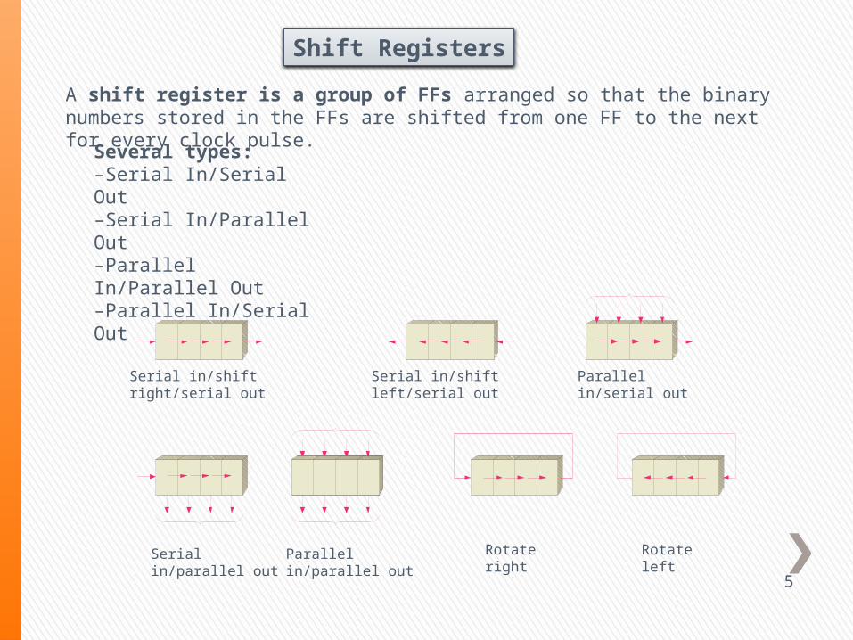
Shift Registers
1

video
2

Applications:
3
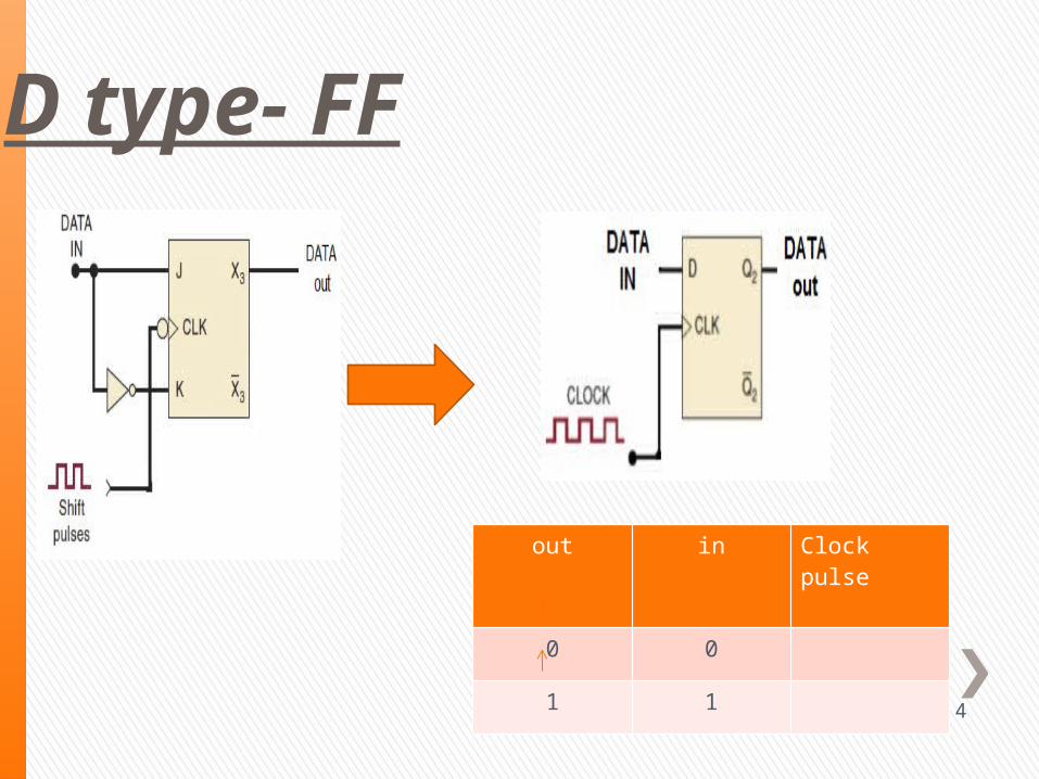
D type- FF
out in Clock pulse
0 0
1 1
4
Shift Registers
A shift register is a group of FFs arranged so that the binary numbers stored in the FFs are shifted from one FF to the next for every clock pulse.
Several types:–Serial In/Serial Out–Serial In/Parallel Out–Parallel In/Parallel Out–Parallel In/Serial Out
Serial in/shift right/serial out Serial in/shift left/serial out Parallel in/serial out
Parallel in/parallel outSerial in/parallel out Rotate right Rotate left
5
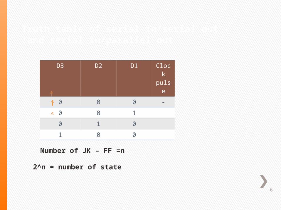
-Truth table of serial in/serial out and serial in/parallel out:
D3 D2 D1 Clock pulse
0 0 0 -
0 0 1
0 1 0
1 0 0
Number of JK – FF =n
2^n = number of state
6

7
Serial In/Serial Out Shift Registers
A serial in/serial out shift register will have data loaded into it one bit at aTime. Example, The 74HC166 (and also the 74ALS166) can be used as a serial-in/serial-out register. It is an eight-bit shift register.

8
Example: Draw the output of each stage.
9
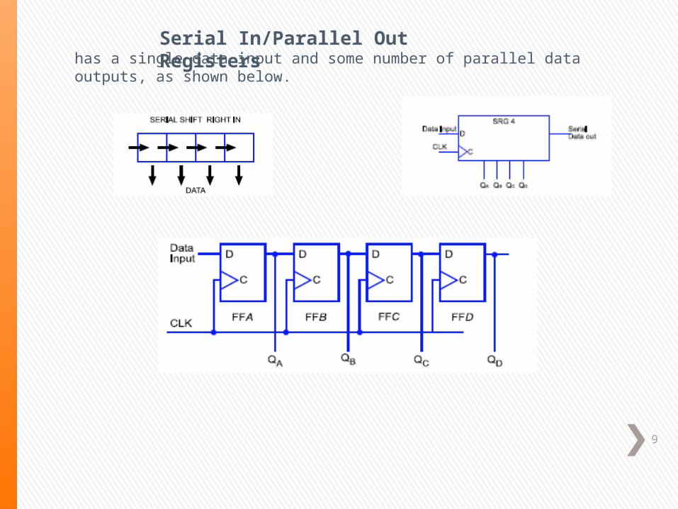
Serial In/Parallel Out Registershas a single data input and some number of parallel data outputs, as shown below.
10
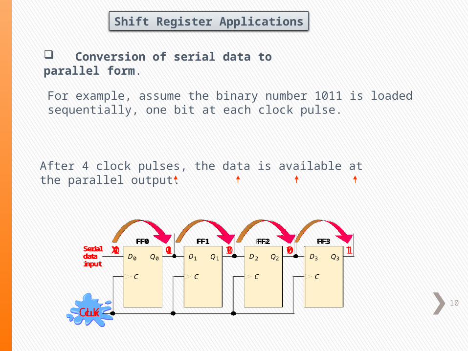
Conversion of serial data to parallel form.
For example, assume the binary number 1011 is loaded sequentially, one bit at each clock pulse.
C
FF0
CLK
C
FF1
C
FF2
D0 D1 D2
Serialdatainput
C
FF3
D3Q0 Q1 Q2 Q31
C
FF0
CLK
C
FF1
C
FF2
D0 D1 D2
Serialdatainput
C
FF3
D3Q0 Q1 Q2 Q3
0 1
C
FF0
CLK
C
FF1
C
FF2
D0 D1 D2
Serialdatainput
C
FF3
D3Q0 Q1 Q2 Q3
1 0 1
C
FF0
CLK
C
FF1
C
FF2
D0 D1 D2
Serialdatainput
C
FF3
D3Q0 Q1 Q2 Q3
1 1 0 1
C
FF0
CLK
C
FF1
C
FF2
D0 D1 D2
Serialdatainput
C
FF3
D3Q0 Q1 Q2 Q3
1X 1 0 1
C
FF0
CLK
C
FF1
C
FF2
D0 D1 D2
Serialdatainput
C
FF3
D3Q0 Q1 Q2 Q31X 1 0 1
CLKCLKCLKCLK
After 4 clock pulses, the data is available at the parallel output.
Shift Register Applications

Example: the 74ALS164 is an eight-bit serial in/parallel out shift register with each FF output externally accessible.
2^n = 8n = 3
11

Group work
12

-the 74ALS164 is an eight-bit serial in/parallel out shift register with each FF output externally accessible.
13

Shift Register Applications
Delay a digital signal
Shift registers can be used to delay a digital signal by a predetermined amount.
Q7
Q7
A
BData out
CLK40 MHz
Data in
CLK
Data in
Data outtd
C
SRG 8
EXAMPLE:
An 8-bit serial in/serial out shift register has a 40 MHz clock. What is the total delay through the register?
The delay for each clock is 1/40 MHz = 25 ns
The total delay is 8 x 25 ns = 200 ns
14

Individual work
15

- An 8-bit serial in/serial out shift register has a 60 MHz clock. What is the total delay through the register?
The delay for each clock is1/60 MHz = 10 ns.
The total delay is 8 x
10 ns = 80 ns
Solution:
16
Practical experiment
17

Quiz
18

Top Related