


Languages
Pages
Legal


September 2003 1
NanotechnologyResearch & Development
at the U.S. Department of Defense
Dr. Clifford LauODUSD(LABS)703-696-0371
26 September 2003
The presenter is solely responsible for the opinions expressed here.

September 2003 2
DoD’s Strategic Research Areas (SRA)
• Bioengineering Sciences
• Human Performance Sciences
• Information Dominance
• Multifunction Materials
• Nanoscience
• Propulsion and Energetic Sciences
Note: Nanoscience/nanotechnology impacts all six SRAs.

September 2003 3
The science and technology of controlling and manipulating things at the atomic layer and nanometer (10-9 m) scale.
•Fabrication, synthesis, and processing of materials with predetermined properties
•Characterization, novel phenomenon, and properties for structural, electronic, and biological materials
•Nanoscale concepts and devices
DoD Applications: Electronics, computers, Biochem sensors
Nanoscience/Nanotechnology
September 2003 4
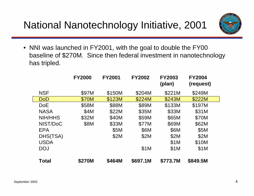
National Nanotechnology Initiative, 2001
FY2000 FY2001 FY2002 FY2003 FY2004(plan) (request)
• NNI was launched in FY2001, with the goal to double the FY00 baseline of $270M. Since then federal investment in nanotechnology has tripled.
NSF $97M $150M $204M $221M $249MDoD $70M $123M $224M $243M $222MDoE $58M $88M $89M $133M $197MNASA $4M $22M $35M $33M $31MNIH/HHS $32M $40M $59M $65M $70MNIST/DoC $8M $33M $77M $69M $62MEPA $5M $6M $6M $5MDHS(TSA) $2M $2M $2M $2MUSDA $1M $10MDOJ $1M $1M $1M
Total $270M $464M $697.1M $773.7M $849.5M
September 2003 5
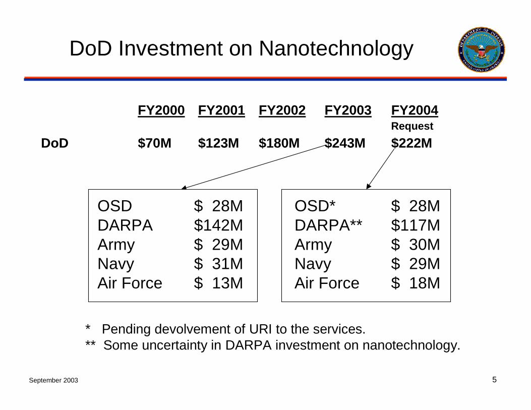
DoD Investment on Nanotechnology
FY2000 FY2001 FY2002 FY2003 FY2004
DoD $70M $123M $180M $243M $222M
OSD $ 28MDARPA $142MArmy $ 29MNavy $ 31MAir Force $ 13M
OSD* $ 28MDARPA** $117MArmy $ 30MNavy $ 29MAir Force $ 18M
Request
* Pending devolvement of URI to the services.** Some uncertainty in DARPA investment on nanotechnology.

September 2003 6
* NANOELECTRONICS/NANOPHOTONICS/NANOMAGNETICSNetwork Centric WarfareInformation DominanceUninhabited Combat VehiclesAutomation/Robotics for Reduced ManningEffective training through virtual realityDigital signal processing and communications
* NANOMATERIALS “BY DESIGN”Nano-energetic MaterialsHigh Performance, Affordable MaterialsMultifunction, Adaptive (Smart) MaterialsNanoengineered Functional MaterialsReduced Maintenance costs
* BIONANOTECHNOLOGY - WARFIGHTER PROTECTIONChemical/Biological Agent detection/destructionSoldier physical monitoring in the battlefield
DoD Focused Areas in NNI

September 2003 7
DoD Programs in Nanotechnology
• ArmyNanostructured polymers, quantum dots for IR sensing, nanoengineered clusters, nano-composites, Nanoenergetics, Institute for Soldier Nanotechnology (ISN)
• NavyNanoelectronics, nanowires and carbon nanotubes, nanostructured materials, ultrafine and thermal barrier nanocoatings, nanobio-materials and processes, nanomagnetics and non-volatile memories, IR transparent nanomaterials
• Air ForceNanostructure devices, nanomaterials by design, nano-bio interfaces, polymer nanocomposites,hybrid inorganic/organic nanomaterials, nanosensors for aerospace applications, nano-energeticparticles for propulsion
• DARPABio-molecular microsystems, metamaterials, molecular electronics, spin electronics, quantuminformation sciences, nanoscale mechanical arrays
• SBIRNanotechnologies, quantum devices, bio-chem decontaminations
• OSDMultidisciplinary University Research Initiative (MURI), DEPSCoR, NDSEG
September 2003 8
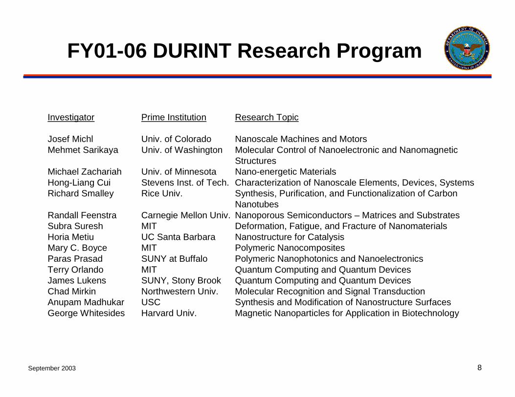
FY01-06 DURINT Research Program
Investigator Prime Institution Research Topic
Josef Michl Univ. of Colorado Nanoscale Machines and MotorsMehmet Sarikaya Univ. of Washington Molecular Control of Nanoelectronic and Nanomagnetic
StructuresMichael Zachariah Univ. of Minnesota Nano-energetic MaterialsHong-Liang Cui Stevens Inst. of Tech. Characterization of Nanoscale Elements, Devices, SystemsRichard Smalley Rice Univ. Synthesis, Purification, and Functionalization of Carbon
NanotubesRandall Feenstra Carnegie Mellon Univ. Nanoporous Semiconductors – Matrices and SubstratesSubra Suresh MIT Deformation, Fatigue, and Fracture of NanomaterialsHoria Metiu UC Santa Barbara Nanostructure for CatalysisMary C. Boyce MIT Polymeric NanocompositesParas Prasad SUNY at Buffalo Polymeric Nanophotonics and NanoelectronicsTerry Orlando MIT Quantum Computing and Quantum DevicesJames Lukens SUNY, Stony Brook Quantum Computing and Quantum DevicesChad Mirkin Northwestern Univ. Molecular Recognition and Signal TransductionAnupam Madhukar USC Synthesis and Modification of Nanostructure SurfacesGeorge Whitesides Harvard Univ. Magnetic Nanoparticles for Application in Biotechnology

September 2003 9
Multidisciplinary University Research Initiative (MURI)
FY Investigator Institution Research Topic
98-03 J. Sturm Princeton Univ. Engineering of Nanostructures and Devices98-03 A. Epstein MIT Microthermal Engines for Compact Powers98-03 B. Zinn Georgia Tech Microthermal Engines for Compact Powers98-03 S. Goodnick Arizona State U. Low-power, High Performance Nanoelectronic Circuits98-03 James Univ. Minnesota Computational Tools for Design of Nanodevices99-04 Brueck U. New Mexico Nanolithograph99-04 Datta Purdue Univ. Spin Semiconductors and Electronics00-05 Mabuchi Caltech Quantum Computing and Quantum Memory00-05 Shapiro MIT Quantum Computing and Quantum Memory01-06 Bruce Dunn UCLA 3-D Nanoarchitectures for Electrochemical Power Source01-06 Ken Poppelmeier Northwestern 3-D Nanoarchitectures for Electrochemical Power Source01-06 Shelton Taylor Univ Virginia Multifunctional Nano-engineered Coatings01-06 Ed Cussler Univ. Minnesota Multifunctional Nano-engineered Coatings02-07 I. Schuller UC San Diego Integrated Nanosensors02-07 D. Lambeth CMU Integrated Nanosensors03-08 Dan van der Weide Wisconsin Nanoprobes for Laboratory Design Instrum. Research03-08 Lukas Novotny U. Rochester Nanoprobes for Laboratory Design Instrum. Research03-08 William Doolittle Georgia Tech Next Generation Epitaxy for Laboratory Instru. Design03-08 Jimmy Xu Brown Univ. Direct Nanoscale Conversion of Biomolecular Signals
September 2003 10
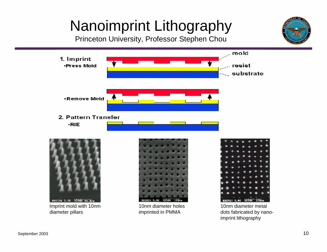
Nanoimprint LithographyPrinceton University, Professor Stephen Chou
Imprint mold with 10nmdiameter pillars
10nm diameter holesimprinted in PMMA
10nm diameter metaldots fabricated by nano-imprint lithography
September 2003 11
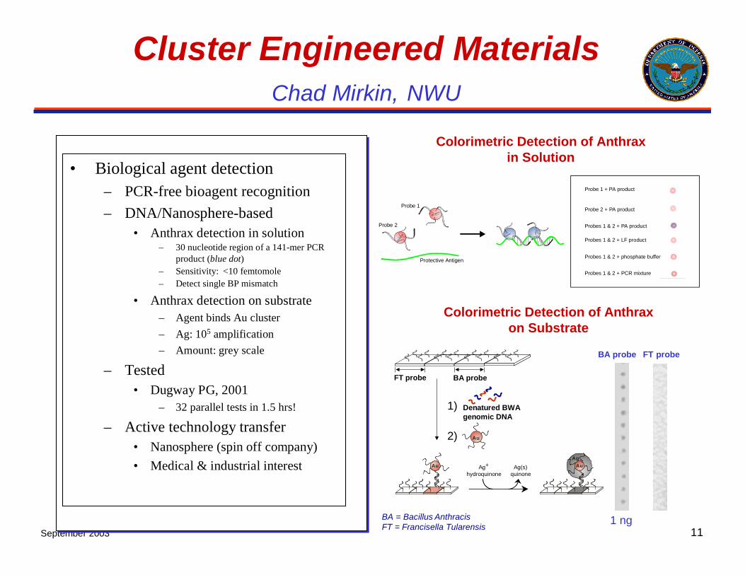
• Biological agent detection
– PCR-free bioagent recognition
– DNA/Nanosphere-based
• Anthrax detection in solution– 30 nucleotide region of a 141-mer PCR
product (blue dot)
– Sensitivity: <10 femtomole
– Detect single BP mismatch
• Anthrax detection on substrate
– Agent binds Au cluster
– Ag: 105 amplification
– Amount: grey scale
– Tested
• Dugway PG, 2001
– 32 parallel tests in 1.5 hrs!
– Active technology transfer
• Nanosphere (spin off company)
• Medical & industrial interest
Colorimetric Detection of Anthraxin Solution
Cluster Engineered MaterialsChad Mirkin, NWU
1)
2)
Denatured BWA genomic DNA
BA = Bacillus AnthracisFT = Francisella Tularensis
BA probe FT probe
FT probe BA probe
1 ng
Au AuAg
Ag+
hydroquinoneAg(s)
quinone
Au
Probe 1
Protective Antigen
Probe 2
Probe 1 + PA product
Probe 2 + PA product
Probes 1 & 2 + PA product
Probes 1 & 2 + LF product
Probes 1 & 2 + phosphate buffer
Probes 1 & 2 + PCR mixture
Colorimetric Detection of Anthraxon Substrate
September 2003 12
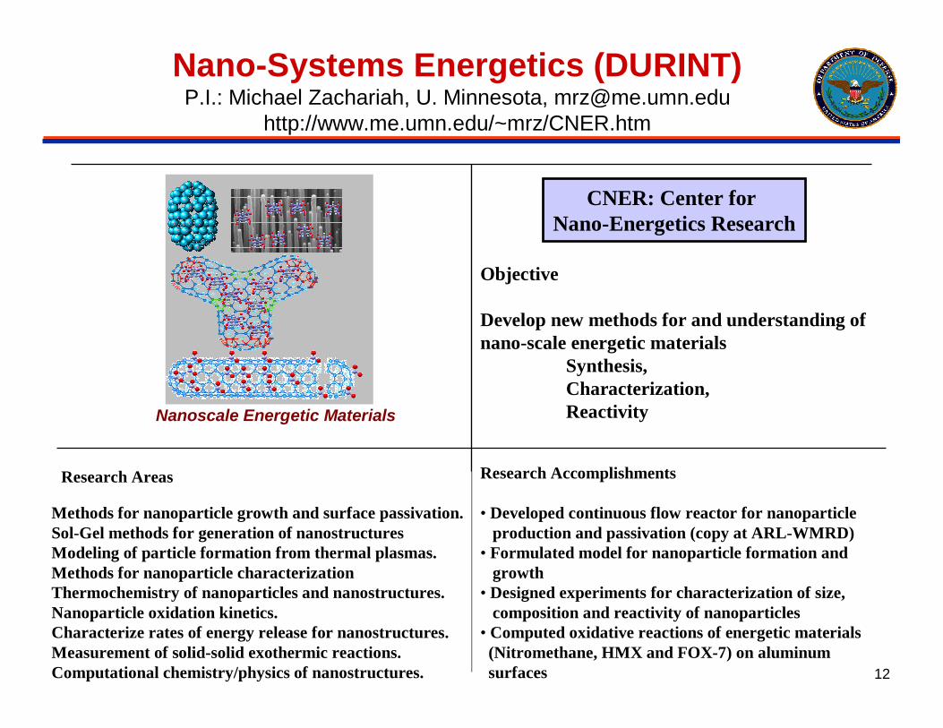
Nano-Systems Energetics (DURINT)P.I.: Michael Zachariah, U. Minnesota, [email protected]
http://www.me.umn.edu/~mrz/CNER.htm
Research Accomplishments
• Developed continuous flow reactor for nanoparticleproduction and passivation (copy at ARL-WMRD)
• Formulated model for nanoparticle formation andgrowth
• Designed experiments for characterization of size,composition and reactivity of nanoparticles
• Computed oxidative reactions of energetic materials(Nitromethane, HMX and FOX-7) on aluminumsurfaces
Objective
Develop new methods for and understanding of nano-scale energetic materials
Synthesis, Characterization, Reactivity
Methods for nanoparticle growth and surface passivation. Sol-Gel methods for generation of nanostructuresModeling of particle formation from thermal plasmas. Methods for nanoparticle characterization Thermochemistry of nanoparticles and nanostructures. Nanoparticle oxidation kinetics. Characterize rates of energy release for nanostructures. Measurement of solid-solid exothermic reactions. Computational chemistry/physics of nanostructures.
CNER: Center for Nano-Energetics Research
Research Areas
Nanoscale Energetic Materials
September 2003 13
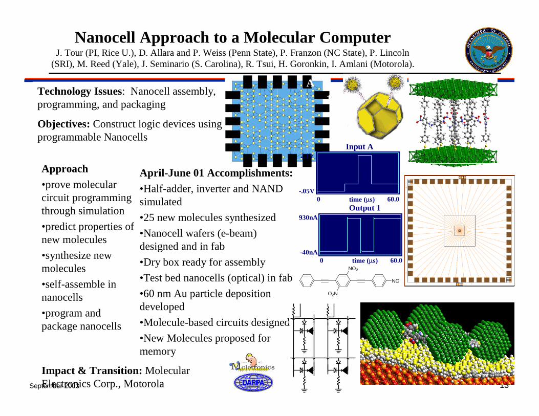
Approach
•prove molecular circuit programming through simulation
•predict properties of new molecules
•synthesize new molecules
•self-assemble in nanocells
•program and package nanocells
April-June 01 Accomplishments:
•Half-adder, inverter and NAND simulated
•25 new molecules synthesized
•Nanocell wafers (e-beam) designed and in fab
•Dry box ready for assembly
•Test bed nanocells (optical) in fab
•60 nm Au particle deposition developed
•Molecule-based circuits designed
•New Molecules proposed for memory
Impact & Transition: Molecular Electronics Corp., Motorola
Technology Issues: Nanocell assembly, programming, and packaging
Nanocell Approach to a Molecular ComputerJ. Tour (PI, Rice U.), D. Allara and P. Weiss (Penn State), P. Franzon (NC State), P. Lincoln
(SRI), M. Reed (Yale), J. Seminario (S. Carolina), R. Tsui, H. Goronkin, I. Amlani (Motorola).
Objectives: Construct logic devices using programmable Nanocells
A
1
2.1V
-.05V
Input A
time (µs)0 60.0
930nA
-40nA
Output 1
time (µs)0 60.0
W0
W1
R1
R0
RW0
RW1
RD0
RD1
NO2
O2N
NC
September 2003 14
Theoretical Analysis, Design, and Simulation of the Nanocell
• Calculated electrical characteristics for two new molecules proposed during the kick-off meeting: the dioxo with three rings (1), and the dinitro with four rings (2).
• First realistic molecular simulation of a fragment of the nanocell (below).
• New candidates for one-year room temperature memory proposed (lower right).
C
CN
N
O
N
O
N
C
NC
N
H
H
S-R
NO2
H2N
S-R
R1
R1
S-R
R = H, AcR1, R2 = H, NO2, NH2
September 2003 15
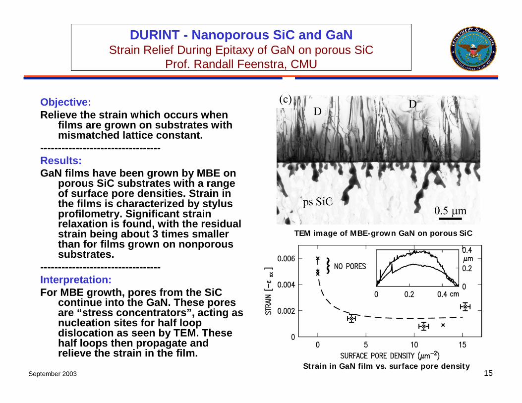
DURINT - Nanoporous SiC and GaNStrain Relief During Epitaxy of GaN on porous SiC
Prof. Randall Feenstra, CMU
Objective:Relieve the strain which occurs when
films are grown on substrates with mismatched lattice constant.
----------------------------------Results:GaN films have been grown by MBE on
porous SiC substrates with a range of surface pore densities. Strain in the films is characterized by stylus profilometry. Significant strain relaxation is found, with the residual strain being about 3 times smaller than for films grown on nonporous substrates.
----------------------------------Interpretation:For MBE growth, pores from the SiC
continue into the GaN. These pores are “stress concentrators”, acting as nucleation sites for half loop dislocation as seen by TEM. These half loops then propagate and relieve the strain in the film.
TEM image of MBE-grown GaN on porous SiC
Strain in GaN film vs. surface pore density

September 2003 16
Objectives• To understand and control the materials chemistry and physics
of nanotubes and nanotube-based materials;• To develop new nano-composites with enhanced mechanical,
thermal and electrical properties;• To fabricate nanotube-based electron field emission devices and
evaluate their properties for technological applications;• To investigate energy-storage capability of carbon nanotubes;• To fabricate nanotube NanoElectroMechanical Systems (NEMS).
Carbon Nanotube Based Materials and DevicesUniversity of North Carolina at Chapel Hill
URL: http://www.physics.unc.edu/~zhou/muri
Major Accomplishments
Multidisciplinary Approach
DOD RelevanceNew materials and technology for structural reinforcement, energy storage, electron emission, and nano-device applications.
•Established materials synthesis and processing capability•First observation of rolling at nanometer scale, including manipulation and simulation of NEMS friction•Measured and simulated the electro-mechanical properties of carbon nanotubes•Synthesized nanotube-based polymer composites•Fabricated nanotube field emission devices and demonstrated high current capability (4A/cm2)•Performed the first 13C NMR measurement of the electronic properties of the carbon nanotubes.
•Demonstrated high Li storage capacity in processed SWNTs.
Research Highlights
Anode-Cathode Distance (µm)
0 40 80 120 160
Vo
ltage
(V
)
0
400
800
1200
1600
2000
10 mA/cm2
J = 0.5 A/cm2
0.1 A/cm2
Carbon nanotube field emitters provide high current density and stability
Rolling and Friction at the atomic scale
•Materials synthesis, assembly, functionalization; •Nanometer-scale manipulation and measurements of transport, electronic and mechanical properties; •Spectroscopic characterization and studies; •Large-scale ab inito and empirical molecular dynamics simulation and theoretical calculations.
MURI TeamUNC: Physics, Chemistry, Materials Science and Computer ScienceNCSU: Physics and Materials ScienceDuke: Chemistry Industrial Partners: Lucent Technologies, Raychem Co. and Ise Electronics

September 2003 17
An Environmentally Compliant, Multi-Functional Coating for Aerospace Using Molecular and Nano-Engineering Methods
University of Virginia, Prof. Shelton Taylor
APPROACH• Multi-coat system built upon thermally
spayed amorphous Al-alloy cladding
• Combinatorial chemistry and nano-encapsulation to identify/deliver non-chromate inhibitors
• Colloidal crystalline arrays, and other molecular probes to provide sensing
DOD TECH PAYOFF• Will provide significant
advancement in corrosion protection, life cycle costs, and mission safety
GOALS/OBJECTIVES• To develop a new multi-functional
coating system for military aircraft• Coating will sense corrosion and
mechanical damage• Initiate mitigation response to
mechanical and chemical damage• Provide corrosion protection and
adhesion using environmentally compliant materials
Nano-crystalline cladding
Non-chromate inhibition
AA2024substrate
Sensing
September 2003 18
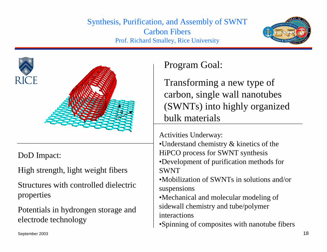
Program Goal:
Transforming a new type of carbon, single wall nanotubes(SWNTs) into highly organized bulk materials
DoD Impact:
High strength, light weight fibers
Structures with controlled dielectric properties
Potentials in hydrongen storage and electrode technology
Activities Underway:•Understand chemistry & kinetics of the HiPCO process for SWNT synthesis•Development of purification methods for SWNT•Mobilization of SWNTs in solutions and/or suspensions•Mechanical and molecular modeling of sidewall chemistry and tube/polymer interactions•Spinning of composites with nanotube fibers
Synthesis, Purification, and Assembly of SWNT Carbon Fibers
Prof. Richard Smalley, Rice University
September 2003 19
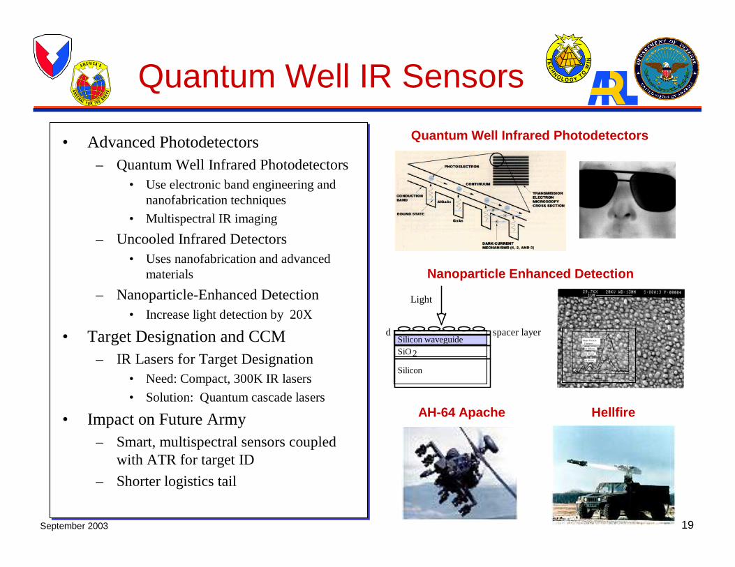
Quantum Well IR Sensors
• Advanced Photodetectors
– Quantum Well Infrared Photodetectors
• Use electronic band engineering and nanofabrication techniques
• Multispectral IR imaging
– Uncooled Infrared Detectors
• Uses nanofabrication and advanced materials
– Nanoparticle-Enhanced Detection
• Increase light detection by 20X
• Target Designation and CCM
– IR Lasers for Target Designation
• Need: Compact, 300K IR lasers
• Solution: Quantum cascade lasers
• Impact on Future Army
– Smart, multispectral sensors coupled with ATR for target ID
– Shorter logistics tail
spacer layerd
Light
Silicon waveguide
SiO2
Silicon
20
15
10
5
0
Enh
ance
men
t
1000900800700600500400
Wavelength (nm)
(c) 108 nm
(b) 66 nm
(a) 40 nm
Mean Particle
Diameter
Nanoparticle Enhanced Detection
Quantum Well Infrared Photodetectors
AH-64 Apache Hellfire
September 2003 20
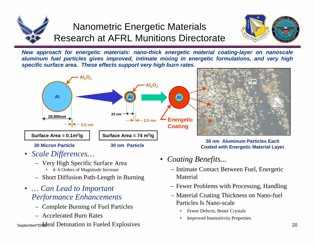
Nanometric Energetic MaterialsResearch at AFRL Munitions Directorate
• Scale Differences…– Very High Specific Surface Area
• 4- 6 Orders of Magnitude Increase
– Short Diffusion Path-Length in Burning
• … Can Lead to Important Performance Enhancements
– Complete Burning of Fuel Particles
– Accelerated Burn Rates
– Ideal Detonation in Fueled Explosives
AlAl
Al2O3
25 nm29,995nm
Surface Area = 0.1m2/g Surface Area = 74 m2/g
2.5 nm
Al2O3
2.5 nm
Al
EnergeticCoating
• Coating Benefits...– Intimate Contact Between Fuel, Energetic
Material
– Fewer Problems with Processing, Handling
– Material Coating Thickness on Nano-fuel Particles Is Nano-scale
• Fewer Defects, Better Crystals
• Improved Insensitivity Properties
New approach for energetic materials: nano-thick energetic material coating-layer on nanoscalealuminum fuel particles gives improved, intimate mixing in energetic formulations, and very high specific surface area. These effects support very high burn rates.
30 Micron Particle 30 nm Particle30 nm Aluminum Particles Each
Coated with Energetic Material Layer

September 2003 21
Institute for Soldier NanotechnologiesProf. Ed Thomas, MIT
Investment Areas• Nanofibres for Lighter Materials• Active/reactive Ballistic Protection (solve
energy dissipation problem)• Environmental Protection• Directed Energy Protection• Micro-Climate Conditioning• Signature Management• Chem/Bio Detection and Protection• Biomonitoring/Triage• Exoskeleton Components• Forward Counter Mine
University Affiliated Research Center• Investment in Soldier Protection• Industry partnership/participation• Accelerate transition of Research Products
Goals• Enhance Objective Force Warrior survivability• Leverage breakthroughs in nanoscience &
nanomanufacturing
Supramolecular Self-Assembly
MesoscopicIntegration
Molecular Scale Control
Nano-Scale Devices
Accomplishments
• Ribbons made of electroactive polymers• Artificial muscle and molecular muscle• Organic/inorganic multilayers for optical
Communications• Tunable optical fibers• Dendrimers for protective armors• Conducting polymer for bio-status monitors

September 2003 22
Enhanced National Security capabilities* Chem-bio warfare defense
Sensors with improved detection sensitivity and selectivity, decontamination
* Protective armors for the warriorStrong, light-weight bullet-stopping armors
* Reduction in weight of warfighting equipmentMiniaturization of sensors, computers, comm devices, and power supplies
* High performance platforms and weaponsGreater stealth, higher strength light-weight materials and structures
* High performance information technologyNanoelectronics for computers, memory, and information systems
* Energy and energetic materialsEnergetic nano-particles for fast release explosives and slow release propellants
* Uninhabited vehicles, miniature satellitesMiniaturization to reduce payload, increased endurance and range
Impact
Top Related