


Languages
Pages
Legal


MICROFABRICATED HIGH-PERFORMANCE LIQUID CHROMATOGRAPHY
(HPLC) SYSTEM WITH CLOSED-LOOP FLOW CONTROL
Thesis by
Jason Shih
In Partial Fulfillment of the Requirements
For the Degree of
Doctor of Philosophy
California Institute of Technology
Pasadena, CA
2008
(Defended 5/5/2008)

ii
© 2008
Jason Shih
All Rights Reserved

iii
Acknowledgements
I would first like to thank my graduate advisor, Dr. Yu-Chong Tai. From giving
me the opportunity to join his lab as a bored undergrad to mentoring me throughout my
graduate years, his guidance has been invaluable. I would also like to thank Dr. Terry
Lee from the City of Hope, who in many ways was a co-advisor throughout my graduate
studies. Without him, much of this work would have been impossible. Finally, I would
like to acknowledge Dr. Markus Kalkum, another PI at City of Hope, who I’ve been
lucky to work with in more recent years.
I have also had the opportunity to work with many talented students over the
years. In particular, I would like to acknowledge Jun Xie for mentoring me my first few
years in the Caltech Micromachining Lab and starting me down the microfluidics path. I
would also like to thank fellow Caltech Micromachining Lab members Trevor Roper,
Tanya Owen, Christine Garske, Agnes Tong, Ellis Meng, Justin Boland, Matthieu Liger,
Qing He, Victor Shih, Scott Miserendino, Angela Tooker, Damien Rodger, Changlin
Pang, PJ Chen, Quoc Quach, Wen Li, Nick Lo, Mike Liu, Luca Giacchino, Ray Huang,
Jefferey Lin, Monty Nandra, Justin Kim, Bo Lu, Yok Satsanarukkit, Wendian Shi, and
Ying-Ying Wang for their helpful suggestions and discussions during my time here.
My research has also taken me to City of Hope where I also got the chance to
work with many wonderful people. In particular, Yunan Miao, who taught me pretty
much everything I know about liquid chromatography and mass spectrometry, and spent
years helping me troubleshoot these devices. Also I would like to thank Roger Moore,
Karine Bagramyan, Diana Diaz-Arevalo, and Teresa Hong for help with my experiments.

iv
Finally, I would like to thank my family for their support over the years. Even
though I still don’t think they know exactly what I do as a graduate student (“I think he
makes small things”), their encouragement has kept me going over the years.

v
Abstract
This thesis presents the development of a microfabricated high-performance
liquid chromatography (HPLC) system. The design, fabrication, and characterization of
individual HPLC components such as high-pressure pumps, mixers, flow sensors,
composition sensors, separation columns, filters, and detectors is presented. These
individual components were then integrated to create robust, feedback-driven separation
systems capable of performing gradient, reverse-phase, nanoscale HPLC. Two separate
separation systems were created. The first integrated system was a microfluidic device
for HPLC tandem mass spectrometry (HPLC-MS/MS) designed for proteomic
applications. The second system was a portable HPLC conductivity detection (HPLC-
CD) system designed for point-of-care applications such as biodetection. Both systems
demonstrated good performance and repeatability. The performance of these systems is
largely attributable to the development of HPLC-compatible sensors that could provide
precise control over the elution profiles. These microfluidic closed-loop flow control
systems represent an important advancement in the microfluidics field, where open-loop
flow control is universally used, and risks becoming inadequate with the increasing
complexity of microfluidic systems.

vi
Table of Contents
Chapter 1: Introduction to Microfluidics ............................................................................ 1
1.1. Introduction.............................................................................................................. 1
1.2. Microfluidic Phenomena.......................................................................................... 2
1.2.1. Laminar Flow.................................................................................................... 2
1.2.2. Multiphase Interfaces........................................................................................ 4
1.2.3. Electrokinetics................................................................................................... 6
1.3. Fabrication Technologies......................................................................................... 8
1.3.1. Bulk Micromachining ....................................................................................... 9
1.3.2. Surface Micromachining................................................................................. 11
1.3.3. Soft Lithography ............................................................................................. 13
1.3.4. Other ............................................................................................................... 15
1.4. Microfluidic Components ...................................................................................... 15
1.4.1. Fluid Handling ................................................................................................ 16
1.4.2. Fluid Sensing .................................................................................................. 17
1.4.3. Fluid Interfacing.............................................................................................. 18
1.4.4. Fluid Processing.............................................................................................. 19
1.5. HPLC / Conclusion................................................................................................ 21
Chapter 2: Parylene Surface Micromachining Technology.............................................. 27
2.1. Introduction............................................................................................................ 27
2.1.1. Parylene Background ...................................................................................... 27
2.1.2. Parylene Surface Micromachining with Photoresist as a Sacrificial Material 29
2.2. Experimental .......................................................................................................... 31
vii
2.2.1. Materials ......................................................................................................... 31
2.2.2. Parylene Processing ........................................................................................ 33
2.2.2.1. Deposition................................................................................................ 33
2.2.2.2. Patterning ................................................................................................. 34
2.2.2.3. Surface Treatment and Adhesion............................................................. 35
2.2.3. Detailed Processing Examples........................................................................ 37
2.2.3.1. Example 1—Single Microchannel Fabrication........................................ 37
2.2.3.2. Example 2—Valve Fabrication................................................................ 39
2.2.3.3. Example 3—High-Pressure Microfluidics............................................... 45
2.2.3.4. Example 4—SU-8 Fluidic Ports .............................................................. 49
2.2.4. Common Problems.......................................................................................... 52
2.2.4.1. Adhesion Issues ....................................................................................... 52
2.2.4.2. Heating Issues .......................................................................................... 52
2.2.4.3. Photoresist Dissolution ............................................................................ 53
2.2.4.4. Conformality ............................................................................................ 54
2.3. Device Examples ................................................................................................... 54
2.3.1. Sensors ............................................................................................................ 54
2.3.2. Pumps.............................................................................................................. 56
2.3.3. Valves ............................................................................................................. 57
2.3.4. External Detector Interfacing.......................................................................... 57
2.3.5. Passive Fluidic Structures ............................................................................... 58
2.4. Conclusions............................................................................................................ 58
Chapter 3: Microfluidic Chip for Flow Control Applications .......................................... 60

viii
3.1. Introduction............................................................................................................ 60
3.2. Experimental .......................................................................................................... 62
3.2.1. Chip Design .................................................................................................... 62
3.2.2. Chip Fabrication.............................................................................................. 65
3.2.3. Composition Sensor ........................................................................................ 68
3.2.4. Flow Sensor .................................................................................................... 69
3.2.5. Sensor Calibration........................................................................................... 70
3.2.6. Chip Packaging ............................................................................................... 71
3.3. Results and Discussion .......................................................................................... 72
3.3.1. Mixer............................................................................................................... 72
3.3.2. Composition Sensor ........................................................................................ 72
3.3.3. Flow Sensor .................................................................................................... 76
3.4. Conclusion ............................................................................................................. 81
Chapter 4: High-Pressure Electrolysis Pumping............................................................... 82
4.1. Introduction............................................................................................................ 82
4.1.1. Electrolysis of Water....................................................................................... 84
4.2. Experimental .......................................................................................................... 85
4.2.1. Device Design................................................................................................. 85
4.2.2. Chip Fabrication.............................................................................................. 86
4.2.3. Pump Packaging.............................................................................................. 86
4.2.4. Pump Calibration ............................................................................................ 88
4.3. Results and Discussion .......................................................................................... 89
4.4. Conclusion ........................................................................................................... 100

ix
Chapter 5: Multi-Function Microfluidic Platform for Liquid Chromatography Tandem
Mass Spectrometry (LC-MS/MS)................................................................................... 102
5.1. Introduction.......................................................................................................... 102
5.2. Experimental ........................................................................................................ 104
5.2.1. Chip Design .................................................................................................. 104
5.2.2. Chip Fabrication............................................................................................ 108
5.2.3. Chip Packaging / Preparation........................................................................ 112
5.2.4. Sensor Operation........................................................................................... 112
5.2.5. Pneumatic Pump ........................................................................................... 112
5.2.6. Mass Spectrometry........................................................................................ 113
5.2.7. Data Acquisition ........................................................................................... 114
5.2.8. Chip Separation Configurations.................................................................... 115
5.2.8.1. Standard Column with Active Sensors .................................................. 115
5.2.8.2. Vented Column with Non-Active Sensors............................................. 116
5.2.8.3. Standard Column with On-Chip Feedback-Controlled Flow Control ... 118
5.3. Results and Discussion ........................................................................................ 119
5.3.1. Microfluidic Chip/Components .................................................................... 119
5.3.1.1. Analytical/Trap Column ........................................................................ 120
5.3.1.2. Bead Filter.............................................................................................. 120
5.3.1.3. Electrospray ........................................................................................... 121
5.3.2. Standard Column with Active Sensors ......................................................... 122
5.3.3. Vented Column with Non-Active Sensors.................................................... 124
5.3.4. Feedback-Controlled Operation.................................................................... 125

x
5.3.5. Standard Column with On-Chip Feedback-Controlled Flow Control .......... 128
5.4. Conclusion ........................................................................................................... 131
Chapter 6: Portable High-Performance Liquid Chromatography Conductivity Detection
(HPLC-CD) System........................................................................................................ 133
6.1. Introduction.......................................................................................................... 133
6.2. Experimental ........................................................................................................ 135
6.2.1. Modular System / Individual Chip Design ................................................... 135
6.2.2. Chip Fabrication............................................................................................ 137
6.2.3. Chip Packaging / Preparation........................................................................ 138
6.2.4. Electrolysis Pump Operation ........................................................................ 138
6.2.5. Flow Control Chip Operation ....................................................................... 138
6.2.6. Detector Operation........................................................................................ 139
6.2.7. Chip Separation Configurations.................................................................... 139
6.2.7.1. Separation with Conventional HPLC Pump .......................................... 140
6.2.7.2. Separation with Electrolysis Pumps....................................................... 141
6.2.8. Data Acquisition and Computer Control ...................................................... 143
6.3. Results and Discussion ........................................................................................ 144
6.3.1. Microfluidic Chips/Components................................................................... 144
6.3.1.1. Conductivity Detector............................................................................ 144
6.3.2. Separation with Agilent HPLC Pump........................................................... 146
6.3.3. Separation with Electrolysis Pumps.............................................................. 148
6.4. Conclusion ........................................................................................................... 154
Chapter 7: Conclusion..................................................................................................... 155

xi
Chapter 8: References ..................................................................................................... 156

xii
Figures / Tables
Figure 1-1: The different interfacial forces acting on a fluid in a microchannel................ 5
Figure 1-2: Diagram showing the principle of EOF .......................................................... 7
Figure 1-3: Fabrication of a microchannel using bulk micromachining and anodic
bonding ............................................................................................................................. 11
Figure 1-4: Fabrication of a microchannel using a surface micromachining process ..... 13
Figure 1-5: Fabrication of a microchannel using soft lithography .................................. 14
Table 1-1: Typical column sizes for HPLC ..................................................................... 23
Figure 1-6: Diagram of a basic binary HPLC system. Shown on the bottom is an actual
Eksigent NanoLC system with diagram of its internal components................................. 24
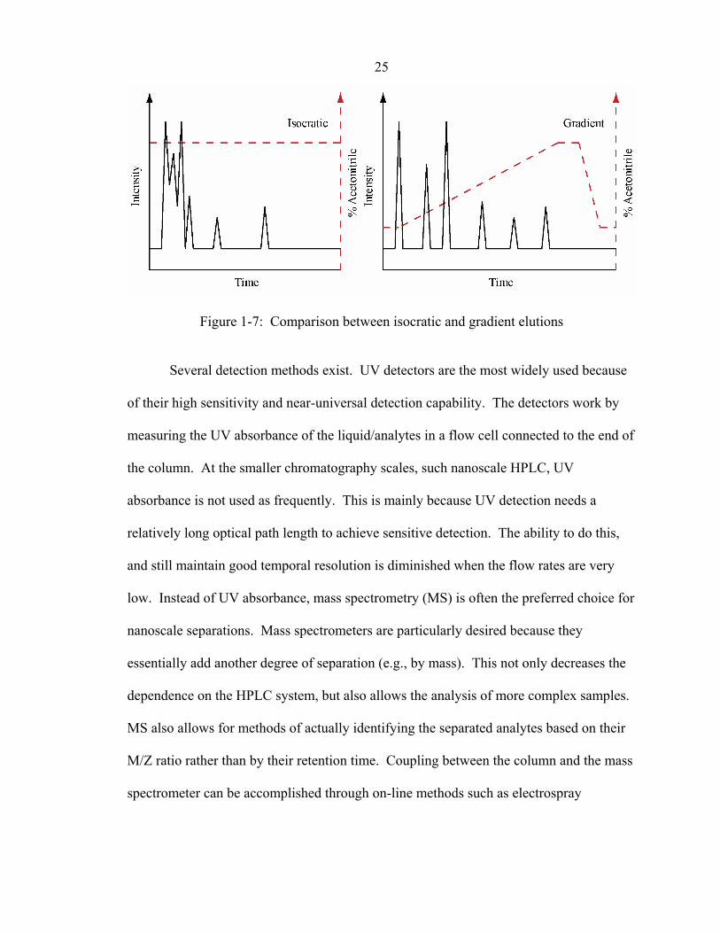
Figure 1-7: Comparison between isocratic and gradient elutions.................................... 25
Figure 2-1: Chemical structure of common Parylene monomers .................................... 28
Table 2-1: Key properties of Parylene C ......................................................................... 29
Figure 2-2: Diagram showing the Parylene deposition process....................................... 33
Figure 2-3: Process flow for single microchannel fabrication......................................... 37
Figure 2-4: Process flow for valve fabrication ................................................................ 40
Figure 2-5: Process flow for high-pressure-capable microchannel ................................. 46
Figure 2-6: Process flow showing the creating of SU-8-based ports at the inlet/outlet of a
microchannel..................................................................................................................... 49
Figure 2-7: A diagram showing the fluidic packaging concept....................................... 51
Figure 2-8: Picture and cross section of a flow control system consisting of an
electrostatic valve (left) and thermal flow sensor (right).................................................. 55

xiii
Figure 2-9: Picture and cross section of an electrostatically actuated peristaltic pump.
Individual chambers also can serve as pressure sensors................................................... 56
Figure 2-10: Picture and cross section of a normally closed passive check valve .......... 57
Figure 2-11: Picture and cross section of an electrospray nozzle.................................... 58
Figure 3-1: A picture and diagram of both the described chips. The various components
are highlighted blue (mixer), green (composition sensor), and red (flow sensor). Both
chips were 9.8 x 9.8 (L x W) mm2. A. Integrated chip. B. Standalone chip................. 63
Figure 3-2: A close-up picture of all the sensor designs presented in this chapter. All
devices are shown at the same scale. ................................................................................ 64
Figure 3-3: Process flow showing the fabrication of the standalone device. The left-hand
column shows a cross-sectional view where the liquid flow is from left to right. The
right-hand column shows a cross-sectional view where the flow is into the page. .......... 65
Figure 3-4: Packaged standalone device and close-up view of the electrode block........ 71
Figure 3-5: Equivalent circuits for the composition sensor. Cdl is the double layer
capacitance, Rl is the fluid resistance, Cp is the parasitic capacitance, and L is an external
inductor only used in the resonant-enhanced measurement circuit .................................. 73
Figure 3-6: Example calibration plots for the composition sensors on the integrated
device (500 kHz, 200 mV with resonant circuit) and standalone device (100 kHz, 200 mV
with non-resonant circuit). ................................................................................................ 74
Figure 3-7: Sample waveforms collected using the integrated device. The different
waveforms correspond to different fluid compositions ranging from 0–50% acetonitrile
(10% intervals). A flow rate of ~ 140 nL/min was used to generate all the waveforms.
The pulse was generated at t = 0 ms. ................................................................................ 76

xiv
Figure 3-8: Sample waveforms comparing the response of the integrated device and
standalone device. Both waveforms were collected at a flow rate of 140 nL/min and
using a 10% acetonitrile solution. The pulse was generated at t = 0 ms. ........................ 77
Figure 3-9: Flow sensor calibration plots for both the integrated and standalone devices.
The TOFs correspond to the peak position. The points are fitted (solid line) assuming an
ideal inverse relationship between TOF and flow rate. The dotted line represents the
expected TOFs based only on the physical sensor dimensions and flow rate. ................. 79
Figure 3-10: Sample waveforms collected using the flow sensor on the standalone device.
The flow rate was 140 nL/min for all waveforms and a 10% acetonitrile solution was
used. The pulse was generated at t = 0 ms....................................................................... 80
Figure 4-1: Different classes of microfluidic pumps and their corresponding maximum
backpressures and flow rates ............................................................................................ 82
Figure 4-2: A picture of the electrode array..................................................................... 86
Figure 4-3: A picture of the packaged electrolysis pump along with a cross-sectional
view. The electrolysis chamber is faintly visible in the center of the Ultem piece. ........ 87
Figure 4-4: A plot showing the increase in pressure inside the closed electrolysis system
at applied currents of 1, 2, and 3 mA. These three curves were collected using a 100%
water solution (0.1% formic acid). ................................................................................... 89
Figure 4-5: Comparison between mathematical model and actual data (Figure 4-4). The
model results are shown in the solid black lines............................................................... 93
Figure 4-6: A plot showing the flow rate, pressure, and current relationship for the
electrolysis pump. Also on the plot are single point calibrations to check the accuracy of

xv
the mathematical model. The discrete points are colored corresponding to the applied
current. .............................................................................................................................. 95
Figure 4-7: Plot of molecular efficiency as a function of pressure and current. Each of
the curves corresponds to a different applied electrolysis current. ................................... 97
Figure 4-8: I-V curve for the electrolysis device ............................................................. 98
Figure 4-9: Plot showing the power efficiency of the electrolysis pump at various
pressures and currents ....................................................................................................... 99
Figure 5-1: A picture and diagram of the presented chip. The various components are
highlighted in blue (mixer), green (composition sensor), red (flow sensor), orange (trap
column), purple (analytical column), brown (electrodes for applying electrospray
potential), yellow (electrospray nozzle), and gray (bead filters). The black dots represent
the location of fluidic ports. Overall chip size was 9.8 x 9.8 mm2. ............................... 105
Figure 5-2: Close-up pictures of all the individual components on the presented chip. All
devices are shown at the same scale. .............................................................................. 106
Figure 5-3: Process flow for the presented chip. The left-hand column shows a cross-
sectional view where the liquid flow is from left to right. The right-hand column shows a
cross-sectional view where the liquid flow is into the page. .......................................... 108
Figure 5-4: A picture of the custom-built two-channel pneumatic pump...................... 113
Figure 5-5: A picture of the chip/mass spectrometer interfacing .................................. 114
Figure 5-6: Fluidic configuration and separation method for the “Standard Column with
Active Sensors” configuration ........................................................................................ 115
xvi
Figure 5-7: Fluidic configuration and separation method for the “Vented Column with
Non-Active Sensors” configuration. V1 is internal to the autosampler but is shown
separately for clarity. ...................................................................................................... 117
Figure 5-8: Fluidic configuration and separation method for the “Standard Column with
On-Chip Feedback-Controlled Flow Control” configuration......................................... 118
Figure 5-9: Separation results using the “Standard Column with Active Sensors”
configuration. The MS data (top), flow sensor (bottom right), and composition sensor
(bottom left) data are plotted........................................................................................... 122
Figure 5-10: Separation results using the “Vented Column with Non-Active Sensors”
configuration. The MS data for three different sample concentrations are plotted. ...... 125
Figure 5-11: Equivalent electrical circuit for the fluidic system ................................... 126
Figure 5-12: Comparison between the pressures obtained during feedback drive
operation of a 0 to 30% acetonitrile gradient (solid lines) versus the pressure calculated
using a mathematical model (dotted lines). .................................................................... 127
Figure 5-13: Separation results using the “Standard Column with On-Chip Feedback-
Controlled Flow Control” configuration. The MS data (top), flow sensor (middle left),
composition sensor (middle right), and pump pressure (bottom) data are plotted. ........ 129
Figure 6-1: A picture and diagram of the presented separation/detection chip. The
various components are highlighted in purple (analytical column), gray (bead filter), and
red (conductivity detector). The black circles represent the location of the inlet and outlet
ports................................................................................................................................. 135

xvii
Figure 6-2: Close-up pictures of all the individual components on the column/detection
chip. The larger (70 x 1000 (W x L) µm2) detector is shown here. All devices are shown
at the same scale.............................................................................................................. 136
Figure 6-3: Process flow for the separation/detection chip. The left-hand column shows
a cross-sectional view where the liquid flow is from left to right. The right-hand column
shows a cross-sectional view where the liquid flow is into the page.............................. 137
Figure 6-4: Diagram of the commercial HPLC pump-driven setup along with the
separation method. An inset showing the operation principle of the injection valve is also
included........................................................................................................................... 140
Figure 6-5: Diagram of the electrolysis pump-driven setup along with the separation
method. An inset showing the operation principle of the injection valve is also included.
......................................................................................................................................... 142
Figure 6-6: A photograph of the entire separation system............................................. 143
Figure 6-7: Detector response at different aqueous concentrations of [H+]/[COOH-].
0.1% formic acid in water corresponds to 2.1 mM......................................................... 145
Figure 6-8: Separation of a five-peptide sample. The raw detector and baseline signals
(top left) are shown along with the compensated detector signal (top right). Also shown
are the composition (bottom left) and flow rate (bottom right) as indicated by the
integrated sensors............................................................................................................ 146
Table 6-1: Digital control algorithm for electrolysis pumps ......................................... 151
Figure 6-9: Separation of a five-peptide sample. The raw detector and baseline signals
(top left) are shown along with the compensated detector signal (top right). Also shown
are the composition (middle left), flow rate (middle right), pump-driving currents (bottom

xviii
left), and pump pressures (bottom right). To better show the trend, pump currents were
fitted with a 5 min moving average. ............................................................................... 152
Figure 6-10: Comparison between the actual electrolysis pump pressures and the
calculated ones ................................................................................................................ 153

1
Chapter 1: Introduction to Microfluidics
1.1. Introduction
Microfluidics is the study of fluid behavior/manipulation at sub-mm length scales.
Initially, the study of small-scale fluid transport was driven by the need to understand
natural phenomenon such as blood flow in human capillaries, water/mineral transport in
plants, and colloids. In the 1980s, the development of microfabrication technologies
allowed man-made microfluidic devices and systems to be created. These new
technologies enabled the further study of microfluidic phenomenon and also spurred the
development of miniature fluidic components such as pumps, valves, and mixers. More
recently, the focus has shifted to applying the numerous developed technologies and
devices towards biotechnology-related tasks. The development of microfluidic chips that
can replicate the analyses being done in a conventional laboratory, so-called lab-on-a-
chip devices or micro total analysis systems, is currently the driving force behind most
microfluidic research1.
The miniaturization of analytical systems has many potential advantages. Some
analytical tasks are theoretically expected to demonstrate improvements in performance
on smaller scales. Reducing the scale of the analysis also has the benefits of reduced
sample and reagent consumption. The small overall size also allows systems to be
portable, allowing on-the-spot analysis. Finally, the ability to integrate an entire
analytical procedure onto a single device has the potential to drastically reduce the
overall analysis cost.

2
This chapter will begin with a discussion of some key microfluidic principles.
Next, some of the most widely used fabrication technologies used to create microfluidic
devices and systems will be introduced. This will be followed by a discussion of
common microfluidic devices. Finally, special attention will be paid to high-performance
liquid chromatography (HPLC), which holds a central theme in this thesis, and its
relation to microfluidics.
1.2. Microfluidic Phenomena
Forces that are commonly seen in macroscale fluids can be inconsequential on the
microscale. For example, turbulence, which is commonly found in everyday life, rarely
exists in microfluidic systems. Likewise, the opposite can be true, and forces that usually
play a small role in macroscale fluids can become significant and in some cases dominate
in microfluidics. For example, surface tension and electrokinetic forces become more
apparent in the microscale and in many cases can be exploited.
1.2.1. Laminar Flow
Microfluidic devices by nature have a very low Reynolds number, the value of
which gives an indication of the flow regime (e.g., laminar, turbulent). The Reynolds
number is defined as
μρ hvD
=Re , (equation 1)
where Re is the Reynolds number, ρ is the fluid density, ν is the velocity of the fluid, Dh
is the hydraulic diameter, and µ is the fluid viscosity. Microfluidic flows generally have
a Reynolds number of < 1 and are almost always laminar. The biggest consequence of

3
laminar flow is that when two or more fluid streams combine, there is no turbulent
mixing. Mass transport between the two streams will be by diffusion alone.
Low-Reynolds-number, pressure-driven, incompressible flows can be described
by the Stokes equations,
0
2
=⋅∇+∇=∇
vfvp
v
vvμ , (equation 2)
where p is the fluid stress, µ is the fluid viscosity, v is the velocity, and f is the applied
body force. Analytical solutions of the Stokes equations, assuming no-slip boundary
conditions, have been obtained for channel geometries commonly encountered in
microfluidic devices. In all cases, the flow has a parabolic velocity profile. The bulk
flow through these channel geometries can be described using the concept of fluidic
resistance, where the flow through a given channel geometry is proportional to the
pressure drop over the channel and inversely proportional to the fluidic resistance, or
RPQ Δ
= , (equation 3)
where Q is the flow rate, ∆P is the pressure drop, and R is the fluidic resistance. For
circular channel geometries the fluidic resistance is found to be
4
8rLRcirc π
μ= , (equation 4)
where Rcirc is the fluidic resistance of a circular channel geometry, µ is the fluid viscosity,
L is the channel length, and r is the radius of the microchannel. The resistance of a low-
aspect-ratio rectangular microchannel (w>>h), another geometry often encountered in
microfluidic devices, is found to be
3
12wh
LRrecμ
= , (equation 5)

4
where Rrec is the fluidic resistance of a rectangular microchannel, µ is the fluid viscosity,
L is the channel length, w is the channel width, and h is the channel height2. With
channel dimensions on the µm scale, the fluidic resistance can be very significant. For
example, a 1-cm-long rectangular microchannel with a cross section of 100 x 5 (W x H)
µm2 would need a pressure of 167 kPa to produce a 1 µL/min flow of water.
The concept of fluidic resistance is useful for describing the splitting and
combining of flows in pressure-driven microfluidic systems. Networks of channels can
be analyzed using the same principles used to solve electrical circuits because of the
similarities between equation 3 and Ohm’s law. Basic rules used to solve electrical
circuits, such as Kirchhoff’s first and second rules can be applied to microfluidic
“circuits” as well. Kirchhoff’s first rule applied to microfluidics would simply demand
that the sum of flows going into any junction is equal the sum of flows going out, while
Kirchhoff’s second rule would imply that the sum of the pressure drops over any closed
microfluidic circuit must be zero. In some cases, electrical components such as
capacitors, inductors, and diodes can also be used to model microfluidic behavior.
1.2.2. Multiphase Interfaces
At a liquid/gas interface, the surface tension will give rise to a distortion of the
liquid/gas boundary. The relationship between the equilibrium pressure difference across
the interface and curvature is described by the Young-Laplace equation,
⎟⎟⎠
⎞⎜⎜⎝
⎛+=Δ
21
11rr
P γ , (equation 6)
where ∆P is the differential pressure, γ surface tension, and r1,2 are the principal radii of
curvature of the liquid/gas interface2.

5
In microfluidics, we often encounter liquid/solid/gas interfaces, such as a droplet
of water on a solid surface, or a column of liquid in a partially filled microchannel. The
balance of surface tension forces results in a characteristic contact angle at the
liquid/solid/gas interface. If the adhesive forces between the liquid and solid are greater
than that of the cohesive forces in the liquid, the contact angle will be < 90°. If the
opposite is true, the contact angle will be > 90°. For the specific case of water as the
working fluid, the solid is described a hydrophilic if the contact angle is < 90° and
hydrophobic if it is > 90°.
Figure 1-1: The different interfacial forces acting on a fluid in a microchannel
The balance of forces at the liquid/solid/gas interface can be described
mathematically. For the case of a liquid column in a partially filled microchannel as seen
in Figure 1-1, this balance of forces can be written as
θγγ coslg=ls , (equation 7)

6
where γls is the liquid/solid interface surface tension, γlg is the liquid/gas interface surface
tension, and θ is the contact angle. The exerted pressure can be calculated using equation
6. For a circular microchannel, the pressure can be expressed as
rP lsγ2=Δ , (equation 8)
where ∆P is the pressure, γls is the liquid/solid interface surface tension, and r is the
radius of the circular microchannel. One thing that becomes clear is that at smaller
channel dimensions, the pressure becomes larger and larger. For example, a 100 µm ID
glass capillary in contact with water will generate a pressure of nearly 3 kPa, which is
enough to support a column of water 30.6 cm in height.
1.2.3. Electrokinetics
Electrokinetics refers to the coupling between electric currents and fluid flows in
an electrolyte. The most common electrokinetic phenomenon is electro-osmosis, which
refers to the generation of fluid flow via the application of an electric field. Electro-
osmotic flow (EOF) is one of the primary methods of transporting fluids in
microchannels.
EOF is dependant on the formation of a double layer at the liquid/solid interface.
For example, glass in the presence of water at low pH will exhibit a negatively charged
surface consisting of SiO- groups. The free positive ions in the water are attracted to the
negatively charged surface and will form a layer of equal and opposite charge. These
layers of charge form what is called a double layer. The thickness of the double layer is
defined as the Debye length, which is inversely proportional to the square root of the ion
concentration and is generally < 100 nm for aqueous solutions. Applying an electric

7
field along the direction of the channel causes the positive ions in the double layer to
move towards the cathode. This movement of ions carries the bulk fluid along with it
generating net flow. This process is illustrated in Figure 1-2.
Figure 1-2: Diagram showing the principle of EOF
The fluid velocity is assumed to be zero at the liquid/solid surface. Towards the
edge of the double layer (e.g., one Debye length away from the liquid/solid interface), the
fluid velocity can be written as
Emvvv −= , (equation 9)
where v is the velocity, m is the mobility of the ions, and E is the electric field. This is
effectively the same velocity that the bulk fluid moves at as well, provided that the
dimensions of the channel are not too large. The ion mobility can be expressed as
μεζ
μλσ oDs k
m == , (equation 10)
where m the mobility of the ions, σs is the surface charge density, λD is the Debye length,
µ is the fluid viscosity, ζ is the zeta potential, k is the relative dielectric constant of the
liquid, and εo is the permittivity of free space. For most aqueous systems the zeta

8
potential is on the order of 10 mV, yielding a mobility on the order of 10-4 cm2/(s-V). A
1 kV/cm electric field would therefore yield a fluid velocity of 1 mm/s.
EOF is common in microfluidics because of its simplicity. Changes in flow are
made by simply changing the magnitude of the applied voltage. Another advantage of
EOFs is that the velocity profile is constant across the entire microchannel cross section.
This allows plugs of material to be transported from one place to another with minimal
distortion1.
1.3. Fabrication Technologies
Many different methods have been developed to fabricate microfluidic devices
and systems. The earliest attempts in the 1980s used microfabrication techniques
borrowed from the MEMS (MicroElectroMechanical Systems) field, which itself used
techniques borrowed heavily from the semiconductor industry3. Bulk micromachining4,
which usually involves the etching of silicon or glass and the subsequent bonding of two
or more different elements, was the method of choice for early microfluidic studies.
Surface micromachining techniques5 were also used for microfluidic applications. It
involves the repeated deposition and patterning of thin-film materials on a substrate to
build up 3-D structures. In the last several years, the micro-molding and bonding of
elastomers, dubbed soft lithography6, has also been studied and utilized heavily in the
creation of microfluidic devices. Finally, conventional polymer processing methods such
as hot embossing, injection molding, and casting have been applied to microfluidics as
well.

9
One common aspect of these different fabrication methods, with the exception of
the conventional polymer processing techniques, is that they all generally rely on
photolithography to produce the microscopic patterns required. Photolithography
involves the use of a photosensitive polymer called photoresist, which is spin-coated on a
substrate. Exposure of the polymer through a mask can make the corresponding exposed
regions soluble or insoluble in a developer solution. The patterned photoresist can be
used as a structural or sacrificial material itself, or used to pattern other materials through
various etch processes.
1.3.1. Bulk Micromachining
Bulk micromachining refers to the etching of a substrate to create a trench, hole,
or other structure. The most popular substrate is silicon because of the wide variety of
isotropic and anisotropic etches available. Wet and plasma etching methods are the most
common.
Wet etching of silicon can be done using many different solutions, the most
common include: HNA (HF, HNO3, and CH3COOH), KOH, EDP (Ethylene-diamine
pyrochatechol), and TMAH ((CH3)4NOH). HNA is isotropic, meaning that it etches all
crystal orientations of silicon equally. KOH, EDP, and TMAH are all anisotropic,
etching the 111 planes of silicon ~ 30–100x slower than the 100 planes. This
anisotropy can be exploited to create structures such as grooves with sidewalls
corresponding exactly to the 111 planes. Depending on the etchant, silicon oxide,
silicon nitride, photoresist, or a number of other materials may be used as a mask.

10
Plasma etching of silicon is also widely utilized. The main etch chemistry used is
based on SF6. In the highly energetic plasma state, SF6 reacts with silicon to form the
gaseous product SiF4. Different plasma configurations can allow for etches with varying
degrees of isotropy, ranging anywhere from isotropic to completely directional. This
anisotropy can be achieved, for example, by using reactive ion etching (RIE), which
involves the acceleration of the SF6 towards the substrate, leading to more vertical
sidewalls. Deep reactive ion etching (DRIE), a variation on RIE, alternates SF6 with
C4F8 plasmas. This switched plasma etching chemistry allows for almost perfectly
vertical trenches.
Bonding of multiple layers is usually required in bulk micromachined
microfluidic devices. Anodic bonding is the most popular bonding technique and is a
method for joining a silicon substrate with a Na+-based glass such as Pyrex. The bonding
process begins with the careful cleaning of both surfaces, with particular attention to
removing the native oxide from the silicon substrate. The glass and silicon are then
placed in contact with each other and heated to 200–500 ºC. A high potential, generally
between 500–1500 V, is then applied across the bonding interface, with the more positive
potential on the silicon. This causes the mobile Na+ ions in the glass to migrate towards
the cathode and away from the silicon/glass interface. This migration of ions leaves a
fixed negative charge in the glass at the bonding surface. The electrostatic attraction
between the negatively charged glass surface and the positively charged silicon keeps the
two substrates bonded. Some chemical bonding at the silicon/glass interface occurs due
to the close proximity of the two substrates.

11
The combination of bulk etching with wafer bonding can be used to produce
many basic microfluidic components. One of the earliest examples of a microfabricated
analytical system was a spiral column for use in gas chromatography7. HNA, with silicon
oxide as a mask, was used to etch trenches into a silicon substrate. A Pyrex substrate was
then used to cap off the channels using anodic bonding. This process is shown in Figure
1-3.
Figure 1-3: Fabrication of a microchannel using bulk micromachining and anodic
bonding
1.3.2. Surface Micromachining
Surface micromachining generally consists of the deposition and patterning of
alternating layers of a sacrificial and structural material. At the end of the process, the
sacrificial material is removed using a selective etch/dissolution process, leaving only the
structural material intact. Two main surface micromachining technologies have been
used for microfluidic applications. The first involves using polysilicon as the structural
material and silicon oxide as the sacrificial material. The second is completely polymer-
based and uses Parylene/photoresist as the structural/sacrificial materials.
Surface micromachining using polysilicon and silicon oxide has been one of the
most commercially successful methods of making MEMS devices. Both polysilicon and

12
silicon oxide can be deposited using chemical vapor deposition (CVD), which involves
the deposition of thin films on a substrate from the gaseous phase. CVD of polysilicon is
accomplished by using SiH4, which is pyrolized at 550–700 ºC to form polysilicon layers
up to several µm thick. The exact temperature determines the crystalline structure.
Patterning can be accomplished using SF6 plasma. Deposition of silicon oxide is
accomplished using a mixture of SiH4 and O2, generally at temperatures < 500 ºC.
Patterning is accomplished using HF. For both the CVD deposition of polysilicon and
silicon oxide, dopants can be added by introducing gases such as PH3 or B2H6 during the
deposition process. The resulting polysilicon will either be p-type or n-type, respectively.
When used during silicon oxide deposition, phosphosilicate glass (PSG) or boro-
phophososilicate glass (BPSG) can result8. These dopants can be used to change the
conductivity or etch characteristics of the material. Removal of the oxide sacrificial
layers at the end can be accomplished using HF.
Parylene/photoresist surface micromachining is a second method that has been
widely used to make microfluidic devices. Parylene is deposited using a room-
temperature CVD process. Gas-phase Parylene monomers are produced via the pyrolysis
of a stable Parylene dimer. The monomers then deposit as a polymer film on any
substrate. Thicknesses ranging from < 100 nm to > 100 µm can be deposited, with
patterning usually accomplished using O2 plasma. Photoresist, the sacrificial layer, is
spin coated and patterned using photolithography. Removal of the sacrificial photoresist
can be achieved using acetone or other solvent. This fabrication technology is used for
making all the devices in the subsequent chapters and will be discussed in great detail in
Chapter 2.

13
As an example, the fabrication of a microchannel using surface-micromachining
is depicted in Figure 1-4. Starting with a silicon substrate, a sacrificial material is
deposited and patterned. A layer of the structural material is then deposited, completely
encapsulating the sacrificial layer. After patterning the structural material to open the
ends of the channel, the sacrificial material can then be dissolved or etched away. This
simple process can be abstracted to include many more layers and used to make 3-D
microfluidic structures.
Figure 1-4: Fabrication of a microchannel using a surface micromachining process
1.3.3. Soft Lithography
The replica molding of Poly(dimethylsiloxane) (PDMS) has gained a lot of
attention in the last several years as a method to create microfluidic systems, mainly
because of its simplicity and fast production time. The process generally begins with the
creation of a master mold using standard photolithography-based processes. Molds can
range from patterned photoresist on a silicon substrate to bulk micromachined silicon.
This mold is then used to cast a PDMS piece. Common PDMS formulations such as
Sylgard 184 are generally cast using a two-part mixture consisting of a polymer base and
hardener mixed in a 10:1 ratio. Complete curing can be achieved in 1 hr at 100 ºC. After

14
removal from the mold, the PDMS piece can be bonded with other PDMS pieces or to a
solid substrate.
Glass is commonly used as the substrate to bond PDMS pieces to. Several
bonding methods exist. The most simple is simply wetting both the glass and PDMS and
joining the two pieces. As the liquid dries, the stiction forces will keep the two
components bonded together. If a more robust bond is needed, oxygen plasma or
chemical treatments can be used to make both the PDMS and glass pieces hydrophilic.
The two pieces are then placed in contact with each other and are held together through
hydrophilic interactions. For more complex devices, PDMS/PDMS bonding is
sometimes needed. One method of joining two PDMS pieces is by casting the two pieces
using a non-standard base:hardener ratio, one with a slightly higher than needed base
component and the other with a higher than normal hardener ratio. When these two
pieces are joined together and further cured, the residual PDMS components will cure at
the boundary creating a monolithic structure.
Figure 1-5: Fabrication of a microchannel using soft lithography
The process to create a network of microfluidic channels using soft lithography is
shown in Figure 1-5. After a mold has been made and a PDMS part has been cast, the
PDMS piece is bonded to a glass substrate. The resulting channels can be accessed by
punching holes through the entire PDMS piece. Components such as valves can be
15
realized by adding a second PDMS piece above the first one to create a top control
channel, which crosses perpendicular to the bottom fluid channel. Pneumatic actuation of
the top control channel can be used to collapse the bottom fluid channel, effectively
closing off the fluidic pathway6, 9.
1.3.4. Other
In addition to the previously discussed methods, numerous other technologies
have been used for microfluidic applications. Techniques such as hot embossing,
injection molding, and casting (soft lithography being an example) are often used. Also,
more direct micromachining methods such as laser ablation and micro-milling have also
found use. These techniques are mostly targeted towards polymer-based microfluidic
devices. Polymers that can be used include polyamide, polycarbonate, cycloolefin
copolymer, polymethylmethacrylate, and many others. Because many of these
technologies are based on well-developed conventional polymer-processing methods, this
has made them the choice for most commercially available microfluidic assays and micro
analytical systems on the market today10. One drawback of these methods is that they are
not able to achieve the same levels of complexity a photolithography-based technology is
capable of.
1.4. Microfluidic Components
Microfluidic devices can be broken down into four main categories: handling,
sensing, interfacing, and processing. The full extent of devices demonstrated to date is
too great to be covered here. Not only are there many approaches for each particular task,

16
but each approach can be realized using several different fabrication technologies as well.
An effort will be made here to briefly summarize some of the more common devices as
well as their operating principles.
1.4.1. Fluid Handling
Fluid handling refers to devices that are used to physically control the movement
of fluid. This includes components such as microchannels, valves, and pumps.
Microchannels are the most basic component of any microfluidic system and are
analogous to the pipes used in household plumbing systems. They are used to physically
transport fluid from one place to another in a microfluidic network.
Valves can be classified into one of two categories: active and passive. Active
valves are those which can be actuated, selectively closing off or opening the flow path.
The general design principle of microfluidic valves uses the action of a movable
mechanical structure that can be used to shut off flow. Usually this involves the creation
of structures such as flaps, membranes, and plugs that can be actuated to cover or open an
orifice. These structures can be actuated using many mechanisms, including magnetic,
electrostatic, pneumatic, piezoelectric, thermal, electrochemical, and phase change.
Passive valves on the other hand generally refer to check valves, which rectify the flow
without any outside actuation force. Like an active valve, check valves generally consist
of a moving flap, membrane, plug, or even ball that can move to cover or reveal an
opening. Instead of being actuated, passive valves open and close depending on the flow
direction, relying on hydrodynamic forces and built in stresses to change position11.

17
Microfluidic pumps can be broken down into two categories, mechanical and non-
mechanical. Most mechanical pumps are based on the same principles used in everyday
pumps. Check-valved pumps consist of an actuate-able fluid chamber with check valves
at the inlet and outlet. The check valves are oriented in the same direction so that flow is
rectified during the compression and expansion steps of the actuator. Peristaltic pumps
function through the wave-like actuation of a series of actuators. Rotary pumps use the
spinning action of a gear or impeller to move fluid. The actuation of mechanical pumps,
like active valves, can be implemented using a variety of different forces. On the non-
mechanical side, electro-osmotic pumping is the most common. It uses an electric field
to move surface charges on the channel sidewalls, which “carries” the surrounding fluid
with it via solvent drag. Electrohydrodynamic (EHD) pumps rely on the electrostatic
force exerted on a fluid when exposed to a changing electric field. Pumps based on the
creation of gas to displace fluid have also been demonstrated. Gas can be formed through
chemical, electrochemical, or thermal means12, 13.
1.4.2. Fluid Sensing
Sensors can be divided up into two different categories, ones that measure
physical properties of the fluid and others that measure chemical properties. Important
physical properties include pressure, flow rate, temperature, viscosity, and density.
Pressure sensors in microfluidics generally rely on measuring the deflection of a
membrane when subjected to a differential pressure. Common methods of measuring the
deflection include optical, piezoresistive, capacitive, and strain gauges. Flow sensors
based on many different operating principles have also been demonstrated. These

18
include ones that operate based on calorimetric principles, time-of-flight sensors which
measure the velocity of a tracer pulse, and sensors that measure the differential pressure
across a fixed fluidic resistance. Temperature measurements can be conducted using
miniaturized thermistors and thermocouples. Viscosity can be measured by using
oscillating structures to measure the damping forces. Density and/or mass can be
measured by using a hollow resonator structure that fluid passes through.
Chemical sensors are used to measure the contents of a particular fluid. This
includes universal detection and the specific detection of a particular molecule or class of
molecules. Electrochemical detectors are used to measure molecules that can be oxidized
or reduced. Conductivity sensors and sensors based on field effect transistors have been
used for measuring the ion content or pH of a fluid. Sensors with exposed electrodes are
often coated with a semi-permeable and/or functionalized membrane to increase
specificity. Acoustic wave sensors are also widely used and quantify the amount of
adsorbed molecules on a surface by measuring the propagation characteristics of an
acoustic wave. Optical detectors, which use light-sensitive elements, light sources, and
concentration/collection optics, have also been developed for common optical-based
measurements of fluids, such as absorbance, transmission, and fluorescence. Also,
cantilever-based sensors, which use the resonance characteristics of a functionalized
cantilever, have been used for the detection of specific molecules14.
1.4.3. Fluid Interfacing
Reliable interfacing between a microfluidic chip and the outside world is one of
the most critical aspects of developing microfluidic systems. Fluidic connections are

19
used to introduce liquid from outside sources onto the chip or send the processed fluid to
another instrument. The earliest methods used bulk micromachined ports in which tubes
could be inserted and bonded using adhesives. Microfabricated interlocking structures
were also developed and used instead of adhesives to keep the tubing in place.
Microfluidic manifolds, which can be clamped or glued to a microfluidic chip to access
the inlets/outlets, are also used.
It is also important to be able to interface microfluidic chips with specialized
detectors, particularly those which are difficult to integrate onto a chip. While many
external instruments can simply be connected to a microfluidic chip using a tube, some
instruments require unique interface devices. Electrospray emitters, which interface chip-
based analyses with a mass spectrometer, have been developed. Devices to analyze on-
chip fluid using a conventional NMR machine have also been demonstrated. Optical
detection methods such as UV absorbance and laser-induced fluorescence (LIF) have also
been successfully used to measure fluids through the use of chip-based optical flow
cells15.
1.4.4. Fluid Processing
Fluid processing is a very broad term and refers to the steps needed to process a
sample, often biological in origin. Some key steps include extraction, concentration,
mixing/reacting, and separation.
The need to concentrate and purify raw samples is a very important task in the life
sciences. Molecules of interest are often only present in very low abundance and can be
masked by the molecules of high abundance. One popular method is to use a

20
functionalized solid phase to capture molecules from the fluid. The solid phase can range
from the channel sidewalls themselves, to porous polymers that are polymerized on-chip,
to specially coated beads immobilized in a device. The capture of molecules from
solution can be based on any number of interactions including hydrophobic/hydrophilic
interaction or antibody/antigen binding. Miniaturized dialysis systems, which use a semi-
permeable membrane, have also been used to clean up raw samples. Electrically driven
concentration techniques have also been studied. For example, the use of nanochannels
with dimensions comparable to the Debye length have been used to concentrate
molecules based on electrokinetic principles16.
Mixers, like many of the other discussed components can be broken into passive
and active categories. Because microfluidic systems almost always function in the
laminar flow regime, passive mixers rely on diffusion. Designs are optimized to
maximize the contact area between the two incoming flows to increase diffusion and, as a
result, the mixing efficiency. Methods of doing this include laminating the flows and the
injection of one flow into the other using an array of nozzle-like structures. Active
mixers use external forces to disturb the flow to enhance the mixing speed. Pressure-
induced disturbances are often achieved by incorporating a mechanical actuator, much
like those found in active valves and mechanical pumps. Electric and/or magnetic fields
can also be used to improve mixing, and active mixers based on EHD, dielectrophoretic
(DEP), electrokinetic, and magneto hydrodynamic (MHD) forces have been
demonstrated. Finally, acoustic and thermal methods can be used to cause fluid
disturbances as well17. Many mixers also function as miniature reactors, speeding up on-

21
chip chemical reactions. These reactors often have integrated temperature sensing and
heaters to accurately control the reactor conditions18.
Many separation techniques are also available to process a sample prior to
detection. Separation is important in that it helps to reduce dependence on the sensor to
be able to distinguish between different analytes in the fluid. Many separation
technologies also have the net effect of concentration, as a particular molecule is more
highly concentrated in the separated band than it was in the original sample. Electrically
driven separations are extremely well studied. Electrophoretic separation devices are
based on the different migration speeds of charged molecules in a medium (such as a gel
or fluid) under the influence of an electric field. Specific techniques include capillary
electrophoresis (CE) and capillary zone electrophoresis (CZE). Liquid chromatography
(LC), which uses pressure driven flow, separates molecules based on their interaction
with a solid phase support and a liquid mobile phase. Hybrid devices, which combine LC
and electrophoresis, have also been demonstrated and include specific techniques such as
micellar electrokinetic chromatography (MEKC) and capillary electrochromatography
(CEC)16.
1.5. HPLC / Conclusion
All the devices previously mentioned can be integrated to form lab-on-a-chip
system for applications ranging from genomics and proteomics, to biodetection. This
thesis will focus on the development and integration of components for HPLC, which is
one of the most widely used and powerful separation techniques available to scientists
today. HPLC is based on the interaction between the analytes, a solid stationary phase,

22
and liquid mobile phase. By choosing the proper mobile phase and stationary phase
chemistries, analytes can be separated based on hydrophobicity, size, charge, and many
other properties.
A typical separation system includes three main components: 1) pumps to drive
the mobile phase, 2) a column, which contains the stationary phase (usually in the form
of beads with a specially treated surface), and 3) a detector. To begin a separation,
sample is first injected onto the column using an injection valve. After the sample has
been loaded, the pump is used to drive the mobile phase through the column. The various
molecules in the sample are then separated based on their varying retention properties.
As the components of the sample elute off the column, the detector measures their
concentration. A plot of the detector signal versus time is called a chromatogram. The
peak heights, widths, and retention times from the chromatogram can be used to quantify
and identify particular analytes in a complicated mixture.
The separation column itself can come in a variety of different diameters and
chemistries. Table 1-1 shows a few of the most common types of column sizes and the
flow rates that are used with them. Preparatory scale columns are the largest and are
usually only used for purification while the other columns are designed for quantitative
separations. The trend in HPLC has been towards smaller diameter columns, lower flow
rates, and smaller beads sizes. This decrease in scale has brought with it several
advantages, including an improvement in resolution and sensitivity. Higher resolution is
due the reduction in bead size. Higher sensitivity is attained because a particular analyte
is eluted in a smaller overall volume when smaller diameter columns/flow rates are used.
As most detectors are concentration sensitive, this improves the overall system sensitivity.

23
The choice of column chemistry depends mainly on the type of sample being separated.
Reverse-phase is the most common type of separation and uses a non-polar stationary
phase generally consisting of silica beads bound with hydrophobic alkyl chains (e.g., C4,
C8, or C18). These stationary phases are used with a moderately polar mobile phase (such
as water/acetonitrile mixtures) to separate molecules based on their hydrophobicity.
Column Type Diameter Flow Rate Preparatory > 5 mm > 5 mL/min Analytical 4–5 mm 1–10 mL/min
Narrowbore 2–4 mm 0.3–3 mL/min Microbore 1–2 mm 50–1000 µL/min Capillary 0.1–1 mm 0.4–200 µL/min Nanobore 25–100 µm 25–4000 nL/min
Table 1-1: Typical column sizes for HPLC
Because the column is packed with small diameter beads, the pressure needed to
drive the mobile phase is usually large, in most cases > 40 bar. While some HPLC
analyses only require the use of a single mobile phase (e.g., isocratic elution), more
advanced separation techniques require a mobile phase with a time-varying composition
(e.g., gradient elution). In these more advanced separations, the mobile phase is normally
composed of two different components, with the ratio of the two components varied over
time. In effect, this requires two pumps, one for each component of the binary solvent
system. As mentioned earlier, in the case of reverse-phase separations, a typical binary
solvent system might consist of water/acetonitrile. Figure 1-6 shows a diagram of a
typical binary HPLC system as well as a picture and diagram of an actual HPLC pump.
The advantage of a gradient elution becomes apparent when the sample contains
analytes with widely varying retention properties. For an isocratic elution, the eluent
composition must be chosen such that it is capable of eluting the most highly retained

24
analytes. Unfortunately, doing so can result in poor separation of the less strongly
retained analytes. A gradient elution solves this problem by slowly increasing the elution
strength of the mobile phase over time. One additional factor that must be taken into
account when working with gradient elutions is column equilibration. After the gradient
is complete, the column must be equilibrated with a low elution strength mobile phase
before starting the next separation. Figure 1-7 shows the effect of a gradient elution on a
separation.
Figure 1-6: Diagram of a basic binary HPLC system. Shown on the bottom is an actual
Eksigent NanoLC system with diagram of its internal components.
25
Figure 1-7: Comparison between isocratic and gradient elutions
Several detection methods exist. UV detectors are the most widely used because
of their high sensitivity and near-universal detection capability. The detectors work by
measuring the UV absorbance of the liquid/analytes in a flow cell connected to the end of
the column. At the smaller chromatography scales, such nanoscale HPLC, UV
absorbance is not used as frequently. This is mainly because UV detection needs a
relatively long optical path length to achieve sensitive detection. The ability to do this,
and still maintain good temporal resolution is diminished when the flow rates are very
low. Instead of UV absorbance, mass spectrometry (MS) is often the preferred choice for
nanoscale separations. Mass spectrometers are particularly desired because they
essentially add another degree of separation (e.g., by mass). This not only decreases the
dependence on the HPLC system, but also allows the analysis of more complex samples.
MS also allows for methods of actually identifying the separated analytes based on their
M/Z ratio rather than by their retention time. Coupling between the column and the mass
spectrometer can be accomplished through on-line methods such as electrospray

26
ionization (ESI) or through spotting on a plate for analysis later using matrix-assisted
laser desorption/ionization (MALDI).
As mentioned before, the progression of HPLC over the years has been towards
smaller diameter columns and flow rates. In fact, it is not uncommon to see columns
with an ID of < 50 µm and flow rates < 200 nL/min being used. These reductions in
scale have lead to higher-resolution and higher-sensitivity separations, which has helped
drive proteomics and other applications where complex mixtures of molecules need to be
analyzed. Nanoscale HPLC has decreased to the point where microfluidic technologies
can readily achieve the requisite dimensions and flow rates. There are several advantages
of using microfluidics to implement a miniature HPLC system. First of all, a
microfluidic system could provide a low-cost alternative to highly expensive
conventional HPLC systems. A highly integrated microfluidic system could also be
potentially easier to use, eliminating the need for highly trained personnel to conduct the
separations. Finally, the small physical size of microfluidic systems allows for the
creation of portable HPLC systems for point-of-care applications. The rest of this thesis
will describe in detail the development of HPLC-compatible components (e.g., pumps,
sensors, columns, filters), and the integration of these components to form a totally
miniaturized separation system.

27
Chapter 2: Parylene Surface Micromachining
Technology
2.1. Introduction
The fabrication technology used to create the microfluidic devices and systems in
the following chapters is based around Parylene, a thin-film, chemically inert, and
biocompatible polymer deposited using a room temperature chemical vapor deposition
(CVD) process. Surface micromachining, a common technique in microfabrication, is
used to build up the fluidic structures one Parylene layer at a time.
This chapter will begin by discussing Parylene, its material properties, and its
application to microfluidics. The processing methods are best explained through the use
of examples, and several illustrative processes will be described in detail. Common
problems and solutions will also be discussed. Finally, the advantages of this technology
will be examined. Overall, this chapter will give a detailed look at the Parylene surface
micromachining process. The subsequent chapters will only describe fabrication in brief
terms and this chapter should be referred to for detailed methodologies and underlying
fabrication principles.
2.1.1. Parylene Background
Parylene is a transparent, inert, biocompatible, low permeability, and high-
strength thin-film polymer that is conformally deposited using a room temperature CVD

28
process. The deposition thickness can range anywhere from < 0.1 µm to > 1000 µm.
Parylene’s unique room temperature conformal deposition process and material
properties have made it widely used as an protective coating for products ranging from
electronic components to medical devices such as catheters and pacemakers. Not
surprisingly, Parylene has found applications in microfluidics. The same properties that
make Parylene an ideal material for encapsulation make it promising for microfluidics
use.
Parylene was first produced in 1947 by Professor Michael Mojzesz Szwarc at the
University of Manchester in England. He discovered that the pyrolysis of para-xlene lead
to the deposition of a unique film downstream in cooler temperature zones. He noted the
unique chemical and mechanical properties of the film and named the material Szwarcite,
which we now know as poly-p-xylylene or Parylene N. His discovery prompted further
research at Union Carbide. It was here that William Franklin Gorham pioneered the
process of using a stable dimer, di-p-xylylene, to produce poly-p-xylylene. But it wasn’t
until Donald Cram developed a way to synthesize di-p-xylylene at UCLA in 1951 that
commercialization become possible. In all, Union Carbide developed over 20 types of
Parylene, though today only Parylene C, N, and D are commonly used. More recently
the commercialization of Parylene HT has added another dimer to that list.
Figure 2-1: Chemical structure of common Parylene monomers
29
The three commonly used Parylenes (C, D, and N) each have their own unique
properties. Their chemical structures are shown in Figure 2-1. Parylene C is generally
considered the best choice for microfluidic applications. It exhibits the lowest gas and
moisture permeability and also the highest mechanical strength of all the common
Parylenes. In addition it has the highest deposition rate, generally around 2–3 µm/hr.
Parylene C is also United States Pharmacopeia (USP) Class VI and ISO 10993 certified,
meeting the most stringent tests of biocompatibility. Optically, Parylene C is transparent
above 300 nm and throughout the visible range. Finally, Parylene C is also an excellent
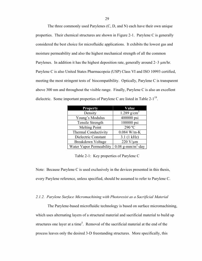
dielectric. Some important properties of Parylene C are listed in Table 2-119.
Property Value Density 1.289 g/cm3
Young’s Modulus 400000 psi Tensile Strength 100000 psi
Melting Point 290 ºC Thermal Conductivity 0.084 W/m-K
Dielectric Constant 3.1 (1 kHz) Breakdown Voltage 220 V/µm
Water Vapor Permeability 0.08 g-mm/m2-day
Table 2-1: Key properties of Parylene C
Note: Because Parylene C is used exclusively in the devices presented in this thesis,
every Parylene reference, unless specified, should be assumed to refer to Parylene C.
2.1.2. Parylene Surface Micromachining with Photoresist as a Sacrificial Material
The Parylene-based microfluidic technology is based on surface micromachining,
which uses alternating layers of a structural material and sacrificial material to build up
structures one layer at a time5. Removal of the sacrificial material at the end of the
process leaves only the desired 3-D freestanding structures. More specifically, this

30
technology is based around photoresist as the sacrificial material and Parylene as the
structural material.
One simple example that illustrates the basic fabrication principles is a
microchannel. The process begins with the deposition of a Parylene film on any substrate,
such as a silicon wafer. A sacrificial photoresist layer is then deposited using a spin-on
process, and patterned using photolithography. A second Parylene film is then coated to
encapsulate the sacrificial photoresist. The ends of the channels are then etched open
using an oxygen plasma with photoresist or metal as a mask. Finally the sacrificial
photoresist is removed using a suitable solvent such as acetone or methanol. This
example is described in more detail in example 1 of the experimental section and
diagrammed in Figure 2-3.
While a single microchannel only uses two Parylene layers and one sacrificial
photoresist layer, the basic concept can be generalized to use many more layers.
Selective patterning of these Parylene layers prior to additional sacrificial photoresist
layers can provide pathways for out-of-plane flow, opening the doors to devices such as
valves. The addition of new layers is not necessarily limited to Parylene and photoresist.
Polymers, such as epoxies and silicones, and metal layers can be used to add even more
functionality. In addition to the central surface micromachining technology, techniques
have also been developed to address the actual implementation and testing of the
Parylene microfluidics. This includes the development of fluidic input/output (I/O) ports,
which in combination with fluidic manifolds can be used to introduce and collect fluid
from our devices. Also, modifications to the core technology have been developed to
address special applications, such as high-performance liquid chromatography (HPLC).

31
These supporting technologies along with the core surface micromachining technology
are described in the experimental section.
2.2. Experimental
This section will begin by giving an introduction to basic Parylene processing
techniques such as deposition, patterning, and surface property control. Next, several
detailed protocols will be presented.
1. Example 1—Single Microchannel Fabrication: This will cover the
fabrication of the most basic structure in Parylene microfluidics.
2. Example 2—Valve Fabrication: This process details the fabrication of an
electrostatically actuated valve. This example highlights the importance of
proper surface treatments between different surfaces.
3. Example 3—High-Pressure Microfluidics: This example describes the
fabrication of a Parylene channel capable of sustaining much higher pressures
than the channel in Example 1.
4. Example 4—SU-8 Fluidic I/O Ports: The final section describes the making
of “fluidic ports” along with the fluidic manifold needed to input/collect liquid
to/from the microfluidic devices.
2.2.1. Materials
The list of materials is comprised of raw materials and equipment normally used
in the fabrication of Parylene surface micromachined devices at the Caltech

32
Micromachining Laboratory, where all the devices in this thesis were fabricated. Specific
model numbers are provided where applicable and available.
Processing Materials
• Silicon Wafers—Silicon Quest International
• Acetone, Isopropyl Alcohol, Concentrated H2O2, Concentrated H2SO4—VWR
Scientific
• Concentrated HF—Transene, Inc.
• Cr-7 Chrome Etchant, Au Etchant—Cyantek
• Cr, Au, Ti, Pt Pellets—Williams Advanced Materials
• A-174 Adhesion Promoter, Parylene C Dimer—Specialty Coating Systems
• AZ4620, AZ1518 Photoresists—AZ Electronic Materials
• SU-8, LOR3B Photoresists—Microchem
Processing Equipment
• Oxidation Furnace (Thermco)—Tetreon
• Plasma Chamber (PEII-A)—Technics Plasma
• DRIE (SLR Series)—Plasma-Therm
• Parylene Deposition Chamber (PDS 2010)—Specialty Coating Systems
• Spin Dryer (Model 914)—Applied Process Technology
• Photoresist Spinner (Model PWM32)—Headway Research, Inc.
• Photoresist Baking Oven (LAC Series)—Despatch
• Photoresist Baking Digital Hot Plate—Cole-Parmer

33
• Stepper (4800 DSW)—GCA Mann
• Contact Aligner—Kasper Instruments
• E-Beam Evaporator—CHA Industries
Fluidic Manifold Manufacturing
• Computer Numerical Controlled (CNC) Mill—Sherline Products, Inc.
• Plastics (PEEK, PEI, Teflon), Tooling (Machining Tools, Hardware)—McMaster
Carr
• O-Rings—Apple Rubber Products, Inc.
• Fittings/Tubing—Upchurch Scientific
Figure 2-2: Diagram showing the Parylene deposition process
2.2.2. Parylene Processing
2.2.2.1. Deposition
Parylene is deposited using a room temperature CVD process. The deposition
process begins with the vaporization of the Parylene dimer (~ 150 °C). Each individual
dimer is then pyrolized (~ 680 °C) and broken down into two individual monomers. The
gas-phase monomers then deposit as a polymer film downstream in a deposition chamber

34
at ambient temperature. The entire process is conducted in a medium vacuum (5–10
mTorr). The overall deposition process is illustrated in Figure 2-2. The deposition rate is
controlled by regulating the partial pressure of the Parylene monomer in the deposition
chamber. The reading from a pressure sensor in the deposition chamber is used as
feedback to control the vaporizer temperature in order to maintain a constant pressure. In
general, the partial pressure of the monomer is set to be approximately 15 mTorr, which
roughly translates to a deposition rate of 2–3 µm/hr. The total deposition thickness is
determined by the initial amount of Parylene dimer placed in the vaporizer. The exact
relationship between Parylene thickness and dimer amount will depend on the exact
machine and load19.
2.2.2.2. Patterning
Because Parylene is chemically inert to nearly all liquids, it cannot be effectively
etched using a wet process. Only a few solvents, such as chloro-napthalene are known to
dissolve Parylene, and this is only at a temperature of 175 °C. The preferred method of
Parylene patterning is oxygen plasma etching. The etching rate depends on many factors,
the most important being the type of plasma etcher, the power, and the oxygen pressure.
In general the etch rate will vary from 0–0.5 µm/min depending on the plasma conditions.
The most convenient material to use as a mask for Parylene etching is photoresist, as it
can be patterned to the correct thickness and has excellent adhesion to the Parylene.
Photoresist etches at nearly the same rate as Parylene in an oxygen plasma20. In general,
the photoresist mask needs to be at least twice the thickness of the Parylene to be etched.
For thick Parylene layers (> 10 µm), metal etch masks are normally used. Metals such as

35
Al and Au as thin as 2000 Å are sufficient to etch more than 30 µm of Parylene. These
metals, as long as they aren’t sputtered, have a nearly infinite etch ratio when compared
to Parylene. One advantage of using a metal etch mask is that it can be removed (via wet
etching) without disturbing any sacrificial photoresist that might have been revealed
during the Parylene etching. Stripping a photoresist etch mask, on the other hand, will
inevitably remove some of the exposed sacrificial photoresist as well.
All the Parylene etching processes described in the experimental section are based
on the use of a PEII-A parallel plate plasma etcher. Etch rates of ~ 0.15–0.2 µm/min are
generally observed. Etching is load dependant, which can cause some variation in the
etch rate.
2.2.2.3. Surface Treatment and Adhesion
As deposited, Parylene exhibits a water contact angle of approximately 75°. An
oxygen plasma treatment can make the surface extremely hydrophilic, reducing the water
contact angle to < 5°. An SF6 plasma treatment, on the other hand, can increase the
contact angle to > 105°. The Parylene surface can be partially restored to its natural, as-
deposited state by treating the surface with a dilute HF solution. These different surface
treatments play a large role in the adhesion between different layers.
Because Parylene is generally the first layer deposited on the substrate and needs
to withstand all subsequent processing steps, good adhesion between Parylene and the
substrate is critical. Parylene exhibits poor adhesion to a hydrophilic surface such as
silicon oxide. On the other hand, Parylene naturally adheres well to clean hydrophobic
surfaces. To attain good adhesion between Parylene and hydrophilic surfaces, an

36
adhesion promoter such as A-174 (gamma-methacryloxy propyltrimethoxysilane) is
generally used. In some cases, neglecting to use A-174 and directly depositing Parylene
on a hydrophilic surface will cause the Parylene layer to delaminate even in the presence
of a neutral solvent such as water. One limitation of the A-174 adhesion promoter is that
the organic solvent used to dissolve the A-174 will also dissolve any exposed photoresist
on the wafer. Because of this, it is often desirable to deposit a thin Parylene layer (after
application of A-174) prior to using any sacrificial photoresist layers. This eliminates the
need for adhesion promoter later in the process.
The most common interface encountered in device fabrication is that between
Parylene layers. The optimal surface treatment consists of an oxygen plasma
cleaning/roughening process followed by a rinse in a dilute HF solution. The plasma
roughening is believed to provide a pitted surface for the second Parylene layer to cling
onto and the dilute HF is thought to clean the Parylene surface and restore its natural
hydrophobicity.
Adhesion between photoresist and Parylene is generally good and no surface
treatment is necessary. The hydrophobic nature of both photoresist and Parylene
provides for naturally good adhesion. A short bake in the oven to remove any water on
the Parylene surface is usually performed.
Metal/Parylene interfaces are often encountered. The use of adhesion layers such
as Cr and Ti is often helpful to improve adhesion, particularly with Au, which
demonstrates very poor adhesion to Parylene. Other commonly used metals such as Al
and Pt do not need any adhesion layer. An oxygen plasma surface cleaning prior to metal
deposition can be performed to remove unwanted organic contaminants.

37
2.2.3. Detailed Processing Examples
2.2.3.1. Example 1—Single Microchannel Fabrication
For the purposes of this example, the fabrication of a single microchannel (1 cm x
100 µm x 10 µm—LxWxH) on a 500-µm-thick silicon wafer will be described. The
walls of the microchannel will be 5-µm-thick Parylene. A diagram of the process is
shown in Figure 2-3.
Figure 2-3: Process flow for single microchannel fabrication
A1. Grow 5000 Å silicon oxide on wafer using wet thermal oxidation. Example:
Temperature: 1050 °C, Duration: 1 hr
A2. Surface cleaning/treatment using oxygen plasma. Example: Power: 200 W,
Pressure: 200 mTorr O2, Duration: 2 min
A3. Apply A-174 adhesion promoter. Example: Prepare 100:100:1 (by volume)
solution of IPA:DI water:A-174. Stir and let stand for at least 2 hr. Submerge
wafer in A-174 solution for 15 min. Air dry for 15 min. Rinse with IPA for 15
s. Air dry for 30 s.
38
A4. Deposit 5 µm Parylene. Example: Parylene Dimer Amount: 7.5 g, Vaporizer
SP: 180 ºC, Pyrolysis SP: 690 ºC, Pressure SP: 23 mTorr
A5. Spin and pattern 10 µm photoresist layer. Example: Surface Dehydration: 15
min at 100 °C (oven), Photoresist: AZ4620, Spin Speed: 1400 RPM, Soft
Bake: 30 min at 100 °C (oven), Exposure: 700 mJ/cm2 g-Line, Development:
1.5 min in AZ351:DI Water (1:3), Post Bake: 2 hr at 120 °C (oven)
A6. Surface cleaning/roughening using oxygen plasma. Example: Power: 400 W,
Pressure: 200 mTorr O2, Duration: 1 min
A7. Surface cleaning/treatment using 5% HF dip followed by DI water rinse.
Example: HF Dip Duration: 5 sec
A8. Deposit 5 µm Parylene. Example: Parylene Dimer Amount: 7.5 g, Vaporizer
SP: 180 ºC, Pyrolysis SP: 690 ºC, Pressure SP: 23 mTorr
A9. Spin and pattern ~ 45–50 µm photoresist. Example: Surface Dehydration: 15
min at 100 °C (oven), Photoresist: AZ4620, Spin Speed: 500 RPM, Soft Bake:
5 min at 100 °C, cool to room temperature at 2 °C/min (hot plate), Exposure:
1500 mJ/cm2 g-Line, Development: 5 min in AZ351:DI Water (1:3), Post
Bake: 15 min at 100 °C (oven)
A10. Parylene etching using oxygen plasma. Example: Power: 400 W, Pressure:
200 mTorr O2, Duration: 80 min
A11. Strip photoresist etch mask using acetone/IPA followed by DI water rinse.
A12. Dissolve sacrificial photoresist in acetone. Example: Temperature: 25 ºC,
Duration: 2 days

39
A long post bake is necessary after patterning the sacrificial photoresist layer (step
A5). The reasoning behind this is that all liquids (e.g., solvent) need to be baked out of
the photoresist prior to encapsulation with Parylene. Not doing so can cause outgassing
during later high-temperature processes, such as during the Parylene plasma etch, and
cause the fully encapsulated channel to rupture.
Even though in this example only 20 µm of Parylene/photoresist needs to be
etched (e.g., 5 µm Parylene + 10 µm photoresist + 5 µm Parylene), a photoresist mask
greater than 40 µm is used (A9). This is to ensure there is enough photoresist to account
for non-uniformity in the photoresist mask thickness, particularly near the channel
structures where the photoresist is not conformally coated.
This example encounters Parylene/substrate and Parylene/Parylene interfaces. As
outlined earlier, Parylene/substrate adhesion, when the substrate is hydrophilic, is best
when using an adhesion promoter (A2–A3), and Parylene/Parylene adhesion is optimized
by using a combination of oxygen plasma cleaning/roughening and HF surface
cleaning/treatment (A6–A7). Also, the initial Parylene layer, while not necessary to
create the channel structure, is used to ensure that no more Parylene/substrate interfaces
are encountered later in the process. This is done to prevent the need to apply A-174
adhesion promoter mid-process, which would dissolve the sacrificial photoresist layer.
2.2.3.2. Example 2—Valve Fabrication
The method of making a microchannel can be expanded to create more
complicated microfluidic devices. For example, after step A11, instead of dissolving the
photoresist, another sacrificial photoresist layer can be added, followed by another

40
Parylene layer, and so on. To illustrate this, the fabrication of an in-channel electrostatic
valve21 will be described. The valve uses a circular composite (Parylene/metal/Parylene)
diaphragm with an etched hole in the center. Applying a high voltage to the diaphragm
electrode while grounding an electrode underneath the membrane will cause the
diaphragm to collapse, sealing the hole, and shutting off flow. In all, there are two metal
layers, two sacrificial photoresist layers, and four Parylene layers. The process is
diagramed in Figure 2-4.
Figure 2-4: Process flow for valve fabrication
B1. Grow 5000 Å silicon oxide on wafer using wet thermal oxidation. Example:
Temperature: 1050 °C, Duration: 1 hr

41
B2. Surface cleaning/treatment using oxygen plasma. Example: Power: 200 W,
Pressure: 200 mTorr O2, Duration: 2 min
B3. Deposit Cr/Au metal layer using evaporator. Example: Cr Thickness: 200 Å,
Au Thickness: 2000 Å
B4. Spin and pattern 10 µm photoresist layer. Example: Surface Dehydration: 15
min at 100 °C (oven), HMDS Vapor Prime: 2 min, Photoresist: AZ4620, Spin
Speed: 1400 RPM, Soft Bake: 30 min at 100 °C (oven), Exposure: 700 mJ/cm2
g-Line, Development: 1.5 min in AZ351:DI Water (1:3), Post Bake: 15 min at
100 °C (oven)
B5. Etch Cr/Au metal layer using Au (Type TFA) etchant and Cr (CR-7) etchant.
Example: Au Etching Duration: 50 sec, Cr Etching Duration: 10 sec
B6. Strip photoresist etch mask using acetone/IPA followed by DI water rinse.
B7. Surface cleaning/treatment using oxygen plasma. Example: Power: 200 W,
Pressure: 200 mTorr O2, Duration: 2 min
B8. Apply A-174 adhesion promoter. Example: Prepare 100:100:1 (by volume)
solution of IPA:DI water:A-174. Stir and let stand for at least 2 hr. Submerge
wafer in A-174 solution for 15 min. Air dry for 15 min. Rinse with IPA for 15
s. Air dry for 30 s.
B9. Deposit 1 µm Parylene. Example: Parylene Dimer Amount: 1.5 g, Vaporizer
SP: 180 ºC, Pyrolysis SP: 690 ºC, Pressure SP: 23 mTorr
B10. Spin and pattern 5 µm photoresist layer. Example: Surface Dehydration: 15
min at 100 °C (oven), Photoresist: AZ4620, Spin Speed: 2500 RPM, Soft

42
Bake: 30 min at 100 °C (oven), Exposure: 250 mJ/cm2 g-Line, Development:
1.5 min in AZ351:DI Water (1:3), Post Bake: 2 hr at 120 °C (oven)
B11. Surface cleaning/roughening using oxygen plasma. Example: Power: 400 W,
Pressure: 200 mTorr O2, Duration: 1 min
B12. Surface cleaning/treatment using 5% HF dip followed by DI water rinse.
Example: HF Dip Duration: 5 sec
B13. Deposit 1 µm Parylene. Example: Parylene Dimer Amount: 1.5 g, Vaporizer
SP: 180 ºC, Pyrolysis SP: 690 ºC, Pressure SP: 23 mTorr
B14. Surface cleaning/treatment using oxygen plasma. Example: Power: 200 W,
Pressure: 200 mTorr O2, Duration: 2 min
B15. Deposit Cr/Au metal layer using evaporator. Example: Cr Thickness: 200 Å,
Au Thickness: 2000 Å
B16. Spin and pattern 10 µm photoresist layer. Example: Surface Dehydration: 15
min at 100 °C (oven), HMDS Vapor Prime: 1 min, Photoresist: AZ4620, Spin
Speed: 1400 RPM, Soft Bake: 30 min at 100 °C (oven), Exposure: 700 mJ/cm2
g-Line, Development: 1.5 min in AZ351:DI Water (1:3), Post Bake: 15 min at
100 °C (oven)
B17. Etch Cr/Au metal layer using Au (Type TFA) etchant and Cr (CR-7) etchant.
Example: Au Etching Duration: 50 sec, Cr Etching Duration: 10 sec
B18. Strip photoresist etch mask using acetone/IPA followed by DI water rinse.
B19. Surface cleaning/roughening using oxygen plasma. Example: Power: 400 W,
Pressure: 200 mTorr O2, Duration: 1 min

43
B20. Surface cleaning/treatment using 5% HF dip followed by DI water rinse.
Example: HF Dip Duration: 5 sec
B21. Deposit 1 µm Parylene. Example: Parylene Dimer Amount: 1.5 g, Vaporizer
SP: 180 ºC, Pyrolysis SP: 690 ºC, Pressure SP: 23 mTorr
B22. Surface cleaning/treatment using oxygen plasma. Example: Power: 200 W,
Pressure: 200 mTorr O2, Duration: 2 min
B23. Deposit Cr/Au metal layer using evaporator. Example: Cr Thickness: 200 Å,
Au Thickness: 2000 Å
B24. Spin and pattern 10 µm photoresist layer. Example: Surface Dehydration: 15
min at 100 °C (oven), HMDS Vapor Prime: 1 min, Photoresist: AZ4620, Spin
Speed: 1400 RPM, Soft Bake: 30 min at 100 °C (oven), Exposure: 700 mJ/cm2
g-Line, Development: 1.5 min in AZ351:DI Water (1:3), Post Bake: 15 min at
100 °C (oven)
B25. Etch Cr/Au metal layer using Au (Type TFA) etchant and Cr (CR-7) etchant.
Example: Au Etching Duration: 50 sec, Cr Etching Duration: 10 sec
B26. Strip photoresist etch mask using acetone/IPA followed by DI water rinse.
B27. Parylene etching using oxygen plasma. Example: Power: 400 W, Pressure:
200 mTorr O2, Duration: 8 min
B28. Strip Cr/Au etch mask using Au (Type TFA) etchant and Cr (CR-7) etchant
followed by DI water rinse.
B29. Spin and pattern 5 µm photoresist layer. Example: Photoresist: Surface
Dehydration: 15 min at 100 °C (oven), AZ4620, Spin Speed: 1400 RPM, Soft

44
Bake: 30 min at 100 °C (oven), Exposure: 700 mJ/cm2 g-Line, Development:
1.5 min in AZ351:DI Water (1:3), Post Bake: 2 hr at 120 °C (oven)
B30. Surface cleaning/roughening using oxygen plasma. Example: Power: 400 W,
Pressure: 200 mTorr O2, Duration: 1 min
B31. Surface cleaning/treatment using 5% HF dip followed by DI water rinse.
Example: HF Dip Duration: 5 sec
B32. Deposit 5 µm Parylene. Example: Parylene Dimer Amount: 7.5 g, Vaporizer
SP: 180 ºC, Pyrolysis SP: 690 ºC, Pressure SP: 23 mTorr
B33. Spin and pattern ~ 45–50 µm photoresist. Example: Surface Dehydration: 15
min at 100 °C (oven), Photoresist: AZ4620, Spin Speed: 500 RPM, Soft Bake:
5 min at 100 °C, cool to room temperature at 2 °C/min (hot plate), Exposure:
1500 mJ/cm2 g-Line, Development: 5 min in AZ351:DI Water (1:3), Post
Bake: 15 min at 100 °C (oven)
B34. Parylene etching using oxygen plasma. Example: Power: 400 W, Pressure:
200 mTorr O2, Duration: 75 min
B35. Strip photoresist etch mask using acetone/IPA followed by DI water rinse.
B36. Dissolve sacrificial photoresist in acetone. Example: Temperature: 25 ºC,
Duration: 2 days
As for the microchannel process (example 1), a long post bake is used for any
photoresist layer that will be encapsulated by Parylene (B10, B29). Also, a very thick
photoresist etch mask (B33) is used to make sure there is sufficient photoresist coverage
over the entire topology of the device.

45
A Cr/Au metal layer instead of photoresist is used as an etch mask for the
patterning of the central hole in the valve membrane (B22–B28). This is because the first
sacrificial photoresist layer is revealed during the Parylene etching. If a photoresist etch
mask had been used, the removal of the etch mask with acetone/IPA would have removed
some of the revealed sacrificial photoresist layer. Using Cr/Au as an etch mask solves
this problem because the etchants used to remove the metals do not have any effect on the
revealed photoresist.
There is a clear repetition of steps as each surface is treated before adding a new
layer. Once again, an adhesion promoter (B7–B8) is applied before depositing the first
Parylene layer on the substrate. Also, the combination of oxygen plasma and HF
treatment (B11–B12, B19–B20, B30–B31) is used on every Parylene/Parylene interface.
This structure also has metal/Parylene interfaces, which were not present in the
microchannel example. To ensure there is good adhesion, a combination of oxygen
plasma treatment and Cr adhesion layer is used (B14–B15, B22–B23).
2.2.3.3. Example 3—High-Pressure Microfluidics
One of the limitations of the surface micromachined channels described to this
point is the complete reliance on Parylene to Parylene adhesion. While suitable for low
pressure applications (< 2 bar) the channels will rupture at higher pressures. To address
this, an anchoring technology, which allows the fabrication of fluidic structures capable
of withstanding > 100 bar, has been developed. This technology utilizes mushroom-
shaped trenches etched into the wafer surface along the sides of the microchannel
pathway. The trenches are etched using a two-step deep reactive ion etching (DRIE)

46
process. The first step consists of a standard Bosch process and produces vertical
trenches. The second step is an isotropic SF6 etch to produce a mushroom shaped bulb at
the bottom of the trench. Because of the highly conformal nature of Parylene deposition,
this trench will be completely filled with Parylene providing a mechanical mechanism for
securing the Parylene layer to the substrate22.
The processing steps for the fabrication of a single microchannel (1 cm x 100 µm
x 10 µm—LxWxH) on a 500-µm-thick silicon wafer are listed below. The top and side
walls of the channel will be 10 µm Parylene while the bottom of the channel will be a
silicon oxide surface. The process is diagrammed in Figure 2-5.
Figure 2-5: Process flow for high-pressure-capable microchannel
C1. Grow 5000 Å silicon oxide on wafer using wet thermal oxidation. Example:
Temperature: 1050 °C, Duration: 1 hr
C2. Spin and pattern 2 µm photoresist layer. Example: Surface Dehydration: 15
min at 100 °C (oven), HMDS Vapor Prime: 2 min, Photoresist: AZ1518, Spin
Speed: 4000 RPM, Soft Bake: 30 min at 100 °C (oven), Exposure: 200 mJ/cm2
g-Line, Development: 1.5 min in AZ351:DI Water (1:4), Post Bake: 15 min at
100 °C (oven)

47
C3. Etch silicon oxide using buffered HF. Example: Duration: 6 min
C4. Strip photoresist etch mask using acetone/IPA followed by DI water rinse.
C5. Surface cleaning/treatment using oxygen plasma. Example: Power: 200 W,
Pressure: 200 mTorr O2, Duration: 2 min
C6. Spin and pattern 10 µm photoresist layer. Example: Surface Dehydration: 15
min at 100 °C (oven), HMDS Vapor Prime: 2 min, Photoresist: AZ4620, Spin
Speed: 1400 RPM, Soft Bake: 30 min at 100 °C (oven), Exposure: 700 mJ/cm2
g-Line, Development: 1.5 min in AZ351:DI Water (1:3), Post Bake: 2 hr at
120 °C (oven)
C7. Surface cleaning using oxygen plasma. Example: Power: 200 W, Pressure:
200 mTorr O2, Duration: 2 min
C8. Surface cleaning using 5% HF dip followed by DI water rinse. Example: HF
Dip Duration: 5 sec
C9. Etch anchors using DRIE. Example: Etch 1 Recipe: Bosch process, Etch 1
Depth: 50 µm, Etch 2 Recipe: SF6, Etch 2 Depth: 10 µm
C10. Deposit 10 µm Parylene. Example: Parylene Dimer Amount: 15 g, Vaporizer
SP: 180 ºC, Pyrolysis SP: 690 ºC, Pressure SP: 23 mTorr
C11. Spin and pattern ~ 45–50 µm photoresist. Example: Surface Dehydration: 15
min at 100 °C (oven), Photoresist: AZ4620, Spin Speed: 500 RPM, Soft Bake:
5 min at 100 °C, cool to room temperature at 2 °C/min (hot plate), Exposure:
1500 mJ/cm2 g-Line, Development: 5 min in AZ351:DI Water (1:3), Post
Bake: 15 min at 100 °C (oven)

48
C12. Parylene etching using oxygen plasma. Example: Power: 400 W, Pressure:
200 mTorr O2, Duration: 80 min
C13. Strip photoresist etch mask using acetone/IPA followed by DI water rinse.
C14. Dissolve sacrificial photoresist in acetone. Example: Temperature: 25 ºC,
Duration: 2 days
The overall process is very similar to that of making a non-anchored
microchannel (example 1). The long post bake of the sacrificial photoresist (C6) and a
thick photoresist etch mask (C11) still apply.
Several design rules need to be considered when making the anchors. The width
of the anchors needs to be less than twice the thickness of the Parylene layer it is
anchoring. For example, to anchor a 10 µm Parylene layer to the substrate an anchor
width of 10–15 µm is typical. In this process, the mask for etching the anchors is defined
using oxide on one edge and the sacrificial photoresist on the other edge. The DRIE
process will etch the sacrificial photoresist slightly (e.g., ~ 1:100 to 1:50
photoresist:silicon). This needs to be taken into account if accurate channel heights are
desired.
No surface treatments are necessary prior to the Parylene deposition because the
reliance is on mechanical anchoring of the Parylene to the substrate instead of chemical
adhesion.

49
2.2.3.4. Example 4—SU-8 Fluidic Ports
The purely surface micromachined fluidic structures described so far provide no
easy way to connect the channel to external pumps or sensors. One way to overcome this
is to use SU-8, a photopatternable epoxy, to completely encapsulate the fluidic structures
and create ports at the inlets and outlets. This is done by adding a single SU-8 layer just
prior to photoresist dissolution. The SU-8 has the added advantage of strengthening the
channels, allowing them to withstand higher pressures. The processing steps for adding
SU-8-based ports to the microchannel described in example 1 are described below and
diagrammed in Figure 2-6.
Figure 2-6: Process flow showing the creating of SU-8-based ports at the inlet/outlet of a
microchannel
Start by performing steps A1–A11, then continuing as follows:
D1. Surface cleaning/treatment using oxygen plasma. Example: Power: 200 W,
Pressure: 200 mTorr O2, Duration: 2 min
D2. Surface cleaning using 5% HF dip followed by DI water rinse. Example: HF
Dip Duration: 5 sec

50
D3. Spin and pattern 50 µm SU-8 layer. Example: Surface Dehydration: 15 min at
100 °C (oven), Photoresist: SU-8 50, Spin Speed: 2400 RPM, Soft Bake: 30
min at 80 °C, heat/cool from/to room temperature at 2 °C/min (hot plate),
Exposure: 2000 mJ/cm2 g-line, Post Exposure Bake: 10 min at 80 °C, heat/cool
from/to room temperature at 2 °C/min (hot plate), Development: 4 min in SU-8
developer (PGMEA), Post Bake: 1 hr at 100 °C, heat/cool from/to room
temperature at 2 °C/min (hot plate)
The process is finished by performing step A12.
Steps D1–D2 are cleaning steps to prepare the wafer surface for the SU-8 layer.
Not cleaning the wafer surface will likely lead to delamination of the SU-8 from the
wafer during photoresist dissolution. Delamination is caused by swelling of the SU-8
after long soaks in organic solvents such as acetone or IPA. To reduce swelling it is
recommended to use higher exposure dosages and longer post bakes of the SU-8 layer
than recommended in the manufacturer data sheets to ensure full cross linking and best
possible chemical inertness. For example, the recipe above has an exposure dose 4x that
of the one recommended by the manufacturer. With full cross linking, SU-8 can
withstand even heated acetone solutions (40 ºC) for weeks without any cracking or
delamination from the wafer surface. In some cases, using a DRIE process to etch
anchors in the substrate prior to SU-8 coating can help improve the adhesion. In much
the same way the anchors improved Parylene adhesion in example 3, they can also help
prevent SU-8 delamination.

51
Instead of using photoresist as an etch mask (A9–A10), a metal mask can also be
used. The advantage of using a metal etch mask is that it can be removed without
dissolving any of the sacrificial photoresist in the channel that was revealed during the
Parylene etch. If too much sacrificial photoresist is removed, the SU-8 can seep into the
channels and potentially lead to blockages.
Once the fluidic ports are created on the chips, fluid connections can be made
using a fluidic manifold. The manifold will have ports, which on one end will seal
against the port on the chip and on the other end connects to the desired tubing. These
manifolds are generally made out of high-performance, chemically inert plastics such as
PEEK, PEI, and Teflon, using conventional machining methods.
The sealing between the manifold and the chip can be done using either gaskets or
o-rings. With the proper high-pressure fitting and commercially available o-rings, the
packaging scheme can withstand pressures > 100 bar. O-rings 0.5 x 0.5 mm (ID x cross-
section diameter) or smaller are typically used.
Figure 2-7: A diagram showing the fluidic packaging concept
Tubing to manifold connections can be made using a variety of different fittings.
The most useful ones tend to be those designed for HPLC, which are made to a tight-

52
tolerance and with low volume and high pressure in mind. One example of a fluidic
manifold can be seen in Figure 2-7. The diagrammed packaging scheme also has
alignment grooves to hold the chip and o-rings. These grooves facilitate alignment of the
manifold, o-rings, and chip.
2.2.4. Common Problems
2.2.4.1. Adhesion Issues
In nearly all cases, unsuccessful fabrication of Parylene-based microfluidic
devices is caused by failure in adhesion between layers. Good adhesion can be
consistently achieved with the use of proper surface treatment before the addition of each
layer, whether it be metal, photoresist, or Parylene.
2.2.4.2. Heating Issues
Another common problem is the formation of bubbles in Parylene-encapsulated
sacrificial photoresist. The formation of these bubbles will cause the channel to expand,
eventually rupturing. This is most often seen during plasma etching steps where the
substrate temperature is not completely regulated.
This problem can be avoided in two ways. First, do a lengthy post bake of any
sacrificial photoresist layer after development to remove any residual solvents in the
photoresist. And second, use low power plasma settings and/or divide the entire etch into
shorter, and therefore cooler, etching cycles. As a general rule, any process done on the
device should not exceed the photoresist baking temperatures.

53
2.2.4.3. Photoresist Dissolution
Another problematic step is the dissolution of the photoresist sacrificial layer.
The photoresist dissolution process is limited by not only the solubility of the photoresist
in the organic solvent used, but also how fast photoresist can diffuse out of the channels23.
For devices where there is a very long channel length, photoresist dissolution can take a
significant amount of time. It is important to wait until all the photoresist has dissolved
and diffused out of the channel before drying the devices, otherwise the residual
photoresist will remain in the channels and need to be dissolved again. Solvents such as
IPA or methanol dissolve the photoresist at a similar rate, and for a 1-cm-long channel,
require approximately one week until the photoresist is completely removed. Stronger
solvents such as acetone are much faster, needing only a few days for the same-sized
channels. Heating the solvent can also greatly increase the dissolution rate. While
acetone is much faster, there can be a tendency for the acetone to attack interfaces,
causing delamination. Acetone also has the tendency to swell some photoresist, such as
SU-8. This swelling can cause cracks to form in the SU-8 and underlying Parylene.
Because of this, the SU-8 processing parameters must be highly controlled. An
optimized SU-8 process like the one described in example 4 is able to withstand Acetone
for months without any noticeable effect.
One method that has been particularly effective in speeding up the photoresist
dissolution process is to flush the channel with Acetone as soon as the photoresist has
been dissolved all the way through. This eliminates the need to wait for the photoresist to
diffuse out. Using this technique, microchannels as long as 5 cm have been fully released
in less than 1 week.

54
2.2.4.4. Conformality
As with any surface-micromachining process, the conformality of the different
layers plays a key role in attaining the desired device. Parylene naturally produces a
conformal coating, but spun-on photoresist does not. This is particularly evident when
the photoresist layer that is being added is thinner than the structures already on the wafer.
It is important to check each photoresist layer after lithography to make sure it achieves
the desired height.
2.3. Device Examples
Numerous devices have been demonstrated with this technology. A brief
summary of them will be given here.
2.3.1. Sensors
A thermal flow sensor21 was demonstrated and operated using a calorimetric
principle. The temperature of a heater integrated into the channel was dependent on the
channel flow rate, the higher the flow rate, the lower the temperature of the heater. With
water, the flow sensor demonstrated good performance between 0–100 nL/min with a
sensitivity of 0.8 nL/min. For air, the range was from 0–10 µL/min with a sensitivity of
0.2 µL/min. A picture and diagram of this device can be found in Figure 2-8.
A time-of-flight (TOF) flow sensor24 (also see Chapter 3) was also fabricated and
characterized. Flow rate measurements were based on detecting the traveling time of an
electrochemically generated ion pulse over a fixed distance, giving a measure of the

55
linear flow velocity. The flow sensor was optimized for flow rates < 200 nL/min and
demonstrated a sensitivity of 1.6 nL/min.
Figure 2-8: Picture and cross section of a flow control system consisting of an
electrostatic valve (left) and thermal flow sensor (right)
In-channel pressure sensors, as seen in Figure 2-9, have also been reported25.
This sensor used the deflection of a circular membrane integrated into the bottom of the
channel to determine the relative pressure inside. The deflection of the membrane was
measured using capacitive techniques. The sensor was characterized from 0–35 kPa and
demonstrated a resolution of 0.03 kPa.
Sensors have also been developed to measure the electrical properties of the fluid
inside Parylene channels. By measuring the electrical properties of the liquid, the
composition of miscible organic/aqueous solutions were determined24, 25 (also see
Chapter 3). Also, integrated electrochemical/coductivity detectors were used for analyte
detection in miniaturized separation systems26, 27 (also see Chapter 6).
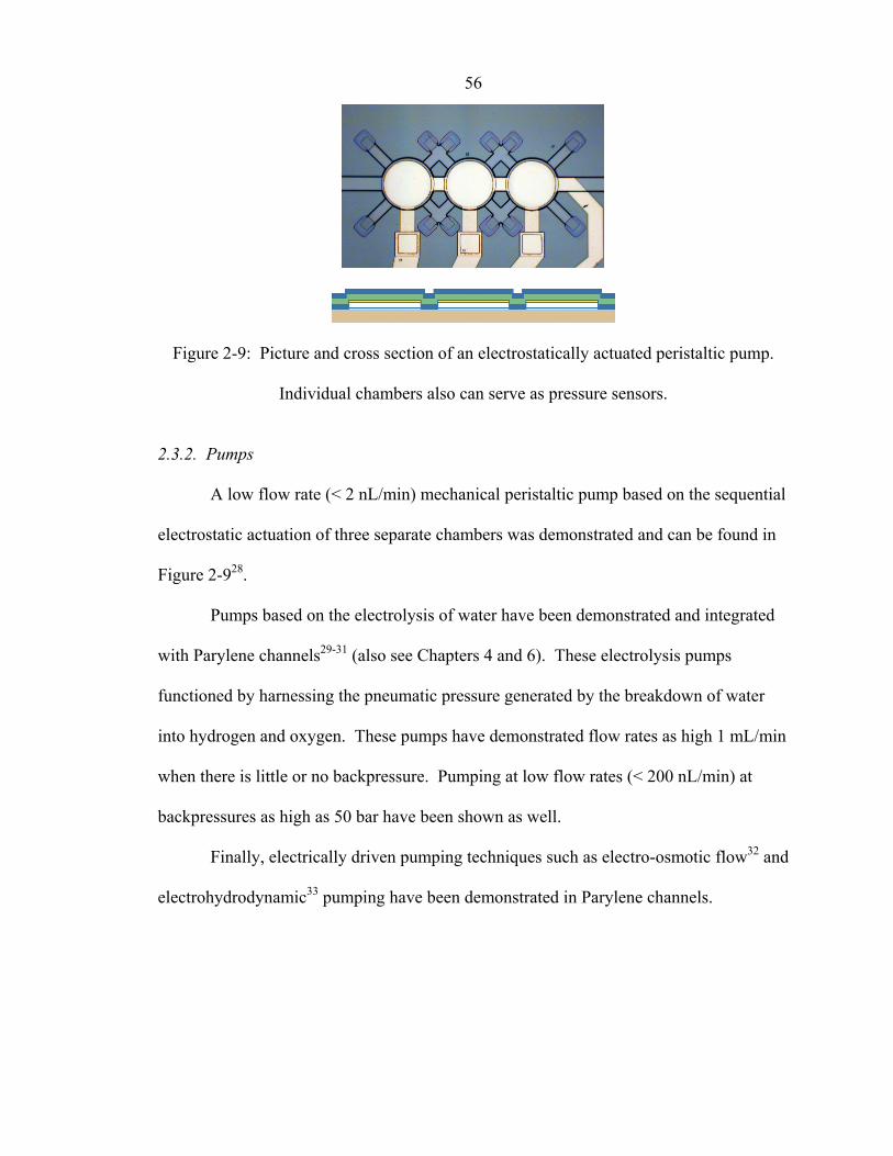
56
Figure 2-9: Picture and cross section of an electrostatically actuated peristaltic pump.
Individual chambers also can serve as pressure sensors.
2.3.2. Pumps
A low flow rate (< 2 nL/min) mechanical peristaltic pump based on the sequential
electrostatic actuation of three separate chambers was demonstrated and can be found in
Figure 2-928.
Pumps based on the electrolysis of water have been demonstrated and integrated
with Parylene channels29-31 (also see Chapters 4 and 6). These electrolysis pumps
functioned by harnessing the pneumatic pressure generated by the breakdown of water
into hydrogen and oxygen. These pumps have demonstrated flow rates as high 1 mL/min
when there is little or no backpressure. Pumping at low flow rates (< 200 nL/min) at
backpressures as high as 50 bar have been shown as well.
Finally, electrically driven pumping techniques such as electro-osmotic flow32 and
electrohydrodynamic33 pumping have been demonstrated in Parylene channels.

57
2.3.3. Valves
Several designs of check valves have been demonstrated34-38. These check valves
operate by utilizing the vertical motion of a Parylene flap or diaphragm to alternately seal
or reveal an opening depending on the flow direction. An example can be found in
Figure 2-10.
Figure 2-10: Picture and cross section of a normally closed passive check valve
Active valves have also been demonstrated. Like the check valves, these valves
operated based on the vertical movement of a flap or diaphragm to open or close an
opening. Actuation methods include electrostatic21, thermal39, and hybrid techniques40.
An example of an electrostatically actuated valve is shown in Figure 2-8.
2.3.4. External Detector Interfacing
An electrospray nozzle, which could be interfaced to a mass spectrometer41, was
demonstrated. An example is shown in Figure 2-11. These nozzles have been used to
couple the output of chip-based analyses to a mass spectrometer30, 31, 42 (also see Chapter
5) with performance comparable to pulled fused silica nozzles.

58
Figure 2-11: Picture and cross section of an electrospray nozzle
2.3.5. Passive Fluidic Structures
Common passive fluidic structures have also been demonstrated. Passive,
diffusion-based mixers24, 31, 43 (also see Chapters 3, 5, and 6), which rely on reducing the
diffusion lengths, have been used for a variety of liquids and flow rates.
Filters for the collection of particles have been demonstrated. These include in-
channel weir-type filters, which rely on a decrease in channel height to filter particles31
(also see Chapters 5 and 6), as well as filters that utilize many small holes etched in a
Parylene membrane.
2.4. Conclusions
The presented Parylene-based surface micromachining technology has several
advantages that stem from its reliance on widely used and developed microelectronics
manufacturing techniques. Because the process is lithography-based, it is easy to
fabricate devices on a large scale. Lithographic techniques also enable the processes to
utilize a large number of layers without having to worry about layer-to-layer alignment.
It is this ability to use many different layers that allows us to make a large variety of
devices of varying complexity. Another advantage of using the same techniques from the

59
microelectronics industry is that we could potentially create microfluidic devices on top
of pre-fabricated integrated circuits. The integration of electronics with fluidics could
lead to highly miniaturized microfluidic systems.
A second advantage of the technology is that it can be used to create a large
number of demonstrated devices. Also, because these devices share a common
technology, the ability to integrate different components is made much easier. In general,
fabricating a system with many different components is no more difficult than fabricating
the single most complicated component in the system. The ability to integrate many
components together will be demonstrated in the following chapters.
A final but important advantage comes from the unique properties of Parylene.
Its low permeability, optical transparency, high mechanical strength, excellent dielectric
properties, and biocompatibility all make it an ideal material from both a mechanical and
chemical standpoint.
Probably the most serious disadvantage of this technology is that it is more
complicated than some of the other available microfluidic technologies both in terms of
the number of processing steps and specialized fabrication equipment it requires. Some
alternative approaches are designed to go from conception to fabrication in just a few
hours. However, this comes at the cost of limited capacity for mass production and
limited functionality, reducing the scope of possible applications.

60
Chapter 3: Microfluidic Chip for Flow Control
Applications
3.1. Introduction
Flow control is a very fundamental and challenging problem in the microfluidics
field. It is especially critical with regards to the development of lab-on-a-chip systems.
Currently, most demonstrated lab-on-a-chip devices have no closed-loop flow control and
rely exclusively on open-loop control. This open-loop control often takes the form of
physically defined fluid reservoirs or pre-calibrated pumping mechanisms. As the tasks
that need to be accomplished on chip become more complicated, these simple methods
become inadequate. For example, a pump that is part of a lab-on-a-chip device might be
affected by changes in the working fluid’s properties. Small changes in these properties
could prevent the pump from delivering the desired flow rate and cause inaccuracies in
the final analysis. For example, in a previously demonstrated fully-integrated high-
performance liquid chromatography (HPLC) system on a chip31, the lack of any closed-
loop flow control led to non-reproducible separations. By integrating sensing systems
into this and other microfluidic systems, these inaccuracies can be eliminated.
One of the most demanding flow control applications is nanoscale HPLC. HPLC
is a powerful liquid phase separation technique, which separates a mixture of analytes
based on their interaction with a solid stationary phase and a liquid mobile phase. HPLC
is largely a fluid control problem where accurate and repeatable fluid flow is needed in

61
order to produce repeatable separations. There are a large variety of stationary phases
and mobile phase chemistries, which can be used to separate analytes based on size,
charge, hydrophobicity, and many other properties. One of the most widely used
techniques is reverse-phase HPLC. Reverse-phase separations use a hydrophobic
stationary phase in conjunction with a mobile phase generally consisting of
water/acetonitrile. Some separations require only the use of an isocratic elution, where
the water/acetonitrile ratio is constant throughout the separation. For more complicated
samples, gradient elutions, where the water/acetonitrile ratio is varied during the
separation, are needed. As a result, any flow control system designed for HPLC must
have accurate control over both the fluid composition and flow rate. This is complicated
by the fact that nanoscale HPLC occurs at flow rates < 200 nL/min and can require
water/acetonitrile compositions ranging from 0–50%. HPLC is also performed at high
pressures, putting further strain on the flow control system.
Sensors form the core of any flow control system. Because flow rate is one of the
most important physical parameters, several types of flow sensors have been
demonstrated, the most common being thermal44, 45, electrochemical46, 47, and those based
on hydrodynamics48, 49. However, these sensor types share one drawback; their response
is dependent on the properties of the fluid. This is not ideal in situations where the fluid
composition is constantly changing. In order to obtain a more reliable measurement of
flow rate, a time-of-flight (TOF) approach is used here, where the flow sensor measures
the time it takes a tracer pulse to travel a certain distance. This gives a direct
measurement of linear flow velocity, which is directly related to the volumetric flow rate.
The main advantage of a TOF flow sensor is that its response should be independent of

62
the working fluid. Different types of TOF flow sensors have been researched in the past,
with thermal pulse50, 51 and electrochemical pulse52, 53 sensors being the most common.
An electrochemical pulse was used in this work. The advantage of an electrochemical
pulse over a thermal pulse is that the pulse is isolated inside the microchannel, resulting
in less pulse broadening. A thermal pulse, on the other hand, would broaden as it loses
heat to the microchannel walls. Another important class of microfluidic sensors is those
used to sense changes in the fluid composition. In this work, to measure the
water/acetonitrile ratio, a measurement of the electrical properties of the fluid was
conducted. This is a proven concept which has been used to measure the composition of
all different states of matter.
This chapter will cover the development of flow and composition sensors that are
compatible with nanoscale reverse-phase HPLC. Because these sensors were designed
with specifically reverse-phase separations in mind, water/acetonitrile (0.1% formic acid)
solutions ranging from 0 to 50% acetonitrile were used in all experiments. The sensors
were also designed for flow rates < 200 nL/min and pressures > 40 bar.
3.2. Experimental
3.2.1. Chip Design
Two different chip designs will be discussed in this chapter. Both chips were
designed to be interfaced with a two-channel pumping system (e.g., one channel being
water and the other being acetonitrile). Both devices accepted the two input fluids, mixed
them, and measured the total flow rate and composition, where composition was based on

63
volume and described as a percentage (Vcomponent/Vtotal%). The implementation of these
chips into closed-loop flow control systems is discussed in Chapters 5 and 6.
A.
B.
Figure 3-1: A picture and diagram of both the described chips. The various components
are highlighted blue (mixer), green (composition sensor), and red (flow sensor). Both
chips were 9.8 x 9.8 (L x W) mm2. A. Integrated chip. B. Standalone chip
The two designs differed in their fluidic configuration and also sensor dimensions.
In one approach, referred to as the integrated design and shown in Figure 3-1A, the
output of the mixer was directed through the sensors and into a serpentine on-chip
separation column. The second design, shown in Figure 3-1B and designated the
standalone design, directed the flow out through a third fluidic port. Besides having a

64
different fluidic configuration, the standalone version also implemented changes in
sensor design that improved sensitivity and accuracy.
Figure 3-2: A close-up picture of all the sensor designs presented in this chapter. All
devices are shown at the same scale.
Pictures of the sensors on integrated devices can be found in Figure 3-2. The
composition sensor consisted of an interdigitated set of electrodes with an electrode
width/spacing of 7.5/7.5 µm. The total area of the sensor was 70 x 300 (W x L) µm2 and
the microchannel dimensions were 80 x 25 (W x H) µm2. For the flow sensor, the
spacing between the pulse-generating electrodes (1 and 2) was 100 µm and the distance
between the pulse electrodes’ midpoint and detector electrodes (3 and 4) was 450 µm.
The channel dimensions were 80 x 3.5 (W x H) µm2. The integrated mixer (not shown in
Figure 3-2) was 30 x 25 (WxH) µm2 in cross section and 8.8 mm long.
Close ups of the sensors on the standalone device can be found in Figure 3-2 also.
The composition sensor also consisted of a set of interdigitated electrodes with a
width/spacing of 7.5/7.5 µm. The total area of this sensor was increased to 70 x 2000 (W
x L) µm2 and the microchannel dimensions were 80 x 20 (W x H) µm2. For the flow
sensor, the spacing between the pulse electrodes (1 and 2) was increased to 150 µm and

65
the spacing between the pulsing electrodes and the detector electrodes (3 and 4) was also
increased to 675 µm. The channel dimension remained unchanged at 80 x 3.5 (W x H)
µm2. A second pair of detection electrodes was also fabricated and located only 475 µm
from pulsing electrodes’ midpoint. These detector electrodes were designed for lower
flow rates but were not used in any experiments. The integrated mixer (not shown in
Figure 3-2) was 30 x 20 (WxH) µm2 in cross section and 15.7 mm long.
Figure 3-3: Process flow showing the fabrication of the standalone device. The left-hand
column shows a cross-sectional view where the liquid flow is from left to right. The
right-hand column shows a cross-sectional view where the flow is into the page.
3.2.2. Chip Fabrication
The technology used to fabricate these devices was described in detail in Chapter
2. These chips utilized the high-pressure anchoring technology and SU-8-based fluidic

66
ports outlined there. The process to make both these chips was identical and is
diagrammed in Figure 3-3. The process could be broken down into nine basic steps as
follows:
1. Silicon Oxide Deposition and Patterning: A 4000 Å silicon oxide (SiOx) layer was
grown on a silicon wafer. Next, a 5 µm AZ1518 photoresist layer was spun on the wafer
and patterned using photolithography. The exposed silicon oxide was then etched using a
buffered HF solution. Afterwards, the photoresist was stripped using acetone and
isopropyl alcohol. The oxide layer served two functions. First, as an insulation layer
between the electrodes and the silicon wafer, and second, as a mask for DRIE etching
(see step 4).
2. Metal Deposition and Patterning: A 3 µm composite lift-off photoresist layer made up
of LOR3B and AZ1518 was deposited and photo-patterned. The use of LOR3B as the
base layer created a re-entrant profile ideal for lift-off. Then a 200/2000 Å Ti/Pt layer
was deposited via e-beam deposition. The Ti was used to improve adhesion between the
Pt and the oxide surface. After metal deposition, liftoff was accomplished by dissolving
the photoresists using ST-22 photoresist stripper. The resulting metal layer was used to
define all the active electrodes, as well as the metal lines and pads needed for electrical
connections.
3. Sacrificial Photoresist: A 25 µm AZ4620 photoresist layer was spun on the wafer. By
using two exposures, one full, and one partial, a bi-level (25 µm/3.5 µm), monolithic
photoresist structure was produced. A bi-level sacrificial layer was necessary to reduce
the channel height where the flow sensor was located. This sacrificial photoresist layer

67
was temporarily used to define the channel and would eventually be dissolved away (step
9).
4. Parylene Anchors and Deposition: Using a deep reactive ion etching (DRIE)
instrument, 40-µm-deep trenches were created on the sides of the channels. The oxide,
patterned in step 1, was used as a mask for DRIE etching. Afterwards, a 10 µm Parylene
layer was deposited. The DRIE trenches took advantage of the conformal nature of the
Parylene deposition and served to anchor the Parylene layer to the substrate. By
mechanically anchoring the encapsulating layer, much higher pressures could be
sustained by the channels.
5. First Parylene Patterning: A 200/2000-Å-thick Cr/Au layer was e-beam deposited and
patterned by using a 40 µm AZ4620 photoresist mask. The metal was etched using Au
etchant type TFA (KI) and CR-7 Cr etchant (perchloric acid). After metal etching, the
photoresist was stripped using acetone and isopropyl alcohol. The Cr/Au metal layer was
then used as an etch mask for Parylene patterning, which was accomplished using an
oxygen plasma. This patterning was used to remove Parylene over the areas where the
SU-8 anchors would be etched (step 6).
6. SU-8 Anchors: Before the formation of the SU-8 anchors, the Cr/Au layer was
patterned again using the same process outlined in step 5. Then, a thick 40 µm AZ4620
photoresist layer was spun and patterned. This formed a mask to DRIE etch shallow 30
µm trenches near the SU-8 edges. The photoresist was stripped using acetone and
isopropyl alcohol.

68
7. Second Parylene Patterning: The Parylene was etched in oxygen plasma using the
Cr/Au mask patterned in step 6. After Parylene etching, the metal mask was stripped
using Au etchant and Cr etchant.
8. SU-8 Encapsulation: A 50-µm-thick SU-8 layer was spun on the wafer and patterned.
This SU-8 layer filled the trenches (step 6), which helped improve SU-8 adhesion to the
substrate. This was especially critical, as the entire chip would be soaked in harsh
organic solvents later in the process (step 9). The SU-8 also helped to strengthen the
channels further so they could withstand the high operating pressures. Finally, the SU-8
sealed the regions where the electrodes crossed into the channel, preventing these areas
from leaking during high-pressure operation.
9. Photoresist Dissolution: To finish the chip, the sacrificial photoresist was dissolved
away using acetone and the wafer was diced to yield the individual devices
3.2.3. Composition Sensor
The composition sensor relied on a measurement of the fluid electrical admittance
to deduce the water/acetonitrile percentage. The sensor on the integrated device was
operated by applying a 500 kHz, 200 mV AC (HP8111A, Agilent Technologies) signal
across electrodes the two electrodes (1 and 2, see Figure 3-2 for electrode numbering).
The resulting current was measured using an I V converter with a gain (Vpp/Ipp) of
3.18x10⁴ Ω (OP37, Analog Devices). The AC voltage output was converted to a DC
signal using an AC RMS converter (AD636, Analog Devices). The total gain (Vout/Ipp)
was 1.12x10⁵ Ω. The operation of the sensor on the standalone device was identical

69
except for the use of a 100 kHz, 200 mV excitation signal and a reduced total gain
(Vout/Ipp) of 1.07x10⁵ Ω.
Prior to sensor use, the electrodes were electrochemically cleaned by cycling the
electrode voltage between -2.0 and +2.0 V repeatedly until consistent current profiles
were achieved (e.g., cyclic voltamograms). This conditioning of the electrodes improved
the stability and repeatability of the sensor measurements.
3.2.4. Flow Sensor
The flow sensor was a TOF sensor that measured the velocity of an
electrochemically generated ion pulse. On the integrated device the electrochemical
pulse was generated by applying a +25 V, 7 ms square pulse to upstream pulse electrode
(1) while the downstream pulse electrode (2) was grounded (see Figure 3-2 for electrode
numbering). This electrical pulse was created by using a HP33120A arbitrary function
generator (Agilent Technologies) that switched a high-voltage LCC110 solid-state relay
(Clare, Inc.). The voltage was supplied using an HP6209B variable DC voltage supply
(Agilent Technologies). Downstream ion pulse detection was achieved by measuring the
fluid admittance. This was accomplished by applying a 20 kHz, 100 mV AC signal
(HP8904A, Agilent Technologies) across the detector electrodes (3 and 4). The resulting
current was measured using an I V converter with a gain (Vpp/Ipp) of 5x10⁵ (OP27,
Analog Devices). The amplitude of signal was measured using an EG&G 5206 2-phase
lock-in amplifier (Princeton Applied Research) using an integration time of 3 ms and a
gain of 200. Overall gain (Vout/Ipp) was 1x10⁸ Ω. The operation of the sensor on the

70
standalone device was identical except for the use of a 30 kHz, 200 mV AC excitation
signal and a reduced overall gain (Vout/Ipp) of 1.67x10⁷ Ω.
As with the composition sensor, cyclic voltamograms were repeatedly conducted
on the detector electrodes (3 and 4) until stable results were given. This improved the
sensitivity of the electrodes to the passing ion pulses.
3.2.5. Sensor Calibration
To calibrate the sensors, the chips were connected to a commercial HPLC pump
(Agilent 1100 Series Nano Pump or Agilent 1100 Series Quaternary Pump) equipped
with a water/acetonitrile (0.1% formic acid) solvent system. All sensors were controlled
and monitored using a DAQPad-6020E data acquisition unit (National Instruments) in
conjunction with LabVIEW (National Instruments). Flow rate measurements were
conducted at a frequency of 0.1 Hz and composition measurements at 1 Hz.
To provide a realistic environment for calibration, the sensors were operated at
pressures consistent with nanoscale HPLC. For the case of the integrated chip, this was
done by directing the output flow from the sensors into the on-chip serpentine channel.
The channel was packed with 5 µm C18 beads (Grace Vydac) to produce a high
backpressure. For the standalone chip, an appropriate length of 15 µm ID fused silica
tubing (Polymicro Technologies) connected to the chip outlet was used to provide the
backpressure. Calibration backpressures ranged from 10 to 50 bar.

71
3.2.6. Chip Packaging
Fluidic connections to the chips were made using a CNC-machined Ultem
(polyetherimide) fluidic manifold. The manifold was clamped onto the top chip surface
and micro o-rings (Apple Rubber) were used to create a seal between the chip and
manifold. Grooves were used to hold the o-rings and chip in place to facilitate alignment.
Ports were machined into the manifold and used with commercially available fittings
(Upchurch Scientific). The fittings allowed direct connection of standard 360 µm OD
fused silica tubing (Polymicro Technologies) to the chip. The ports were machined as
specified by Upchurch and provided a minimal dead volume and high-pressure-capable
connection. Total connector volume was estimated to be < 8 nL. Electrical connections
between the external circuitry and the chip were accomplished by using spring-loaded
electrical probes (Everett Charles Technologies). An electrode block that housed up to
20 of these probes was made. The electrode block was positioned and then clamped
down on the electrical pads to make contact with the chip. The other end of the electrical
probes was clamped against a printed circuit board (PCB) that was connected to the
measurement circuit. One example of a packaged device is shown in Figure 3-4.
Figure 3-4: Packaged standalone device and close-up view of the electrode block

72
3.3. Results and Discussion
3.3.1. Mixer
The mixer relied completely on passive diffusion. The small cross section of the
mixer brought the two incoming flows in close contact, reducing the distance the two
liquids had to diffuse for complete mixing. The mixer dwell time (about 4 seconds for
the integrated chip and 6 seconds for the standalone chip at 100 nL/min) was more than
adequate to achieve complete mixing. In fact, total mixing was likely achieved after only
1 second based on the known diffusion constants of acetonitrile and water. Similar
designs had been used to great effectiveness in the past31, 54.
The mixer played no functional role in any of the experiments described in this
chapter. Its role was more prominent when these devices were interfaced with pumps for
feedback-controlled experiments. This is described in Chapters 5 and 6.
3.3.2. Composition Sensor
Binary mixtures of liquids were expected to have different electrical properties at
varying compositions. This was especially the case in water/acetonitrile mixtures where
one component is conductive (water), while the other is an excellent insulator
(acetonitrile).
One important consideration that had to be taken into account was possible
changes in the electrode surface, whether by metal degradation or absorbed molecules.
These changes to the electrode surface caused a shift in the double layer capacitance and
could produce changes in the sensor readings over time. This was particularly the case

73
for our microelectrodes, where the double layer capacitances and fluid impedance were
both low. An equivalent circuit can be found in Figure 3-5. To negate these electrode
surface effects, the measurement frequency had to be high enough to make the AC
impedance of the double layer capacitances much smaller than the bulk fluid impedance.
In the case of the sensor on the integrated device, a frequency of 500 kHz was needed to
provide good stability. The downside of increasing the measurement frequency was that
the large parasitic capacitances would dominate the overall sensor response. This was
especially the case for the composition sensor on the integrated device, where the
combined AC impedance of the double layer and bulk fluid was large compared to the
AC impedance of the parasitic capacitance. To overcome this problem, a 10 mH inductor
was placed in parallel with the sensor, which when combined with the parasitic
capacitance, produced an LC circuit that resonated near the 500 kHz measurement
frequency. The equivalent circuit is also shown in Figure 3-5.
Figure 3-5: Equivalent circuits for the composition sensor. Cdl is the double layer
capacitance, Rl is the fluid resistance, Cp is the parasitic capacitance, and L is an external
inductor only used in the resonant-enhanced measurement circuit

74
This technique55 resulted in a measurement largely dominated by the fluid
conductivity. The overall impedance of the non-resonant circuit is given by:
))R1(44(R4
22l
2222
22l
2
ωωω
sdlssdl
dl
CCCCCCZ
++++
= . (equation 1)
When an inductor that satisfies the resonant condition,
po LC
1=ω , (equation 2)
is added in parallel to the sensor, the overall impedance becomes
222 4
dlol C
RZω
+= , (equation 3)
where as long as the resonant/measurement frequency is high, should be approximately
equal to the fluid impedance.
0
1
2
3
4
5
6
7
0 10 20 30 40
% Acetonitrile
Vol
tage
(V)
integrated device
standalone device
50
Figure 3-6: Example calibration plots for the composition sensors on the integrated
device (500 kHz, 200 mV with resonant circuit) and standalone device (100 kHz, 200 mV
with non-resonant circuit).

75
A calibration curve for the composition sensor on the integrated device is shown
in Figure 3-6. The sensor precision was 0.3% acetonitrile and accuracy was estimated to
be better than 1%. One drawback with this sensor was that there was a decrease in
sensitivity at the higher organic compositions. This was likely due to changes in the
circuit response as the resonant frequency shifted away from the measurement frequency
(e.g., 500 kHz). This is possible because changes in fluid composition are accompanied
by changes in fluid dielectric constant, which has a direct affect on the parasitic
capacitance. A second cause is a natural saturation in the fluid impedance at higher
organic ratios.
The composition sensor on the standalone device was designed to address the
deficiencies in the first design. By greatly increasing the electrode area, the double layer
capacitance was increased and the fluid impedance was decreased. This allowed the
measurement frequency to be increased without using a resonant circuit to compensate
for the parasitic capacitance. Not only did this simplify the measurement circuit, the
measurements were no longer affected by non-ideal effects that occurred when the
resonant frequency of the circuit shifted. Calibration data for the standalone device
sensor is shown in Figure 3-6 and confirmed the expected improvement. The sensitivity
was improved by roughly a factor of two and the sensor response at the higher
acetonitrile percentages was also improved without sacrificing long-term stability.
It should be noted that this type of sensor was sensitive to many factors, including
the amount of dissolved gas in the fluids, the exact formic acid percentage, as well as the
temperature of the chip. To get accurate absolute measurements of the fluid composition,
our solvents had to be carefully prepared. Our solvent preparation was based on standard

76
LC protocols and included the use of high-purity solvents and degassed liquids. While
this gave us very repeatable results using a single chip with a single batch of solvents,
solvent batch-to-batch as well as chip-to-chip variations eventually need to be accounted
for. One potential way to account for possible variations is to have separate sensors to
measure the bulk electrical properties of the two individual fluid components prior to
mixing. This would provide a baseline upon which to base our composition
measurements.
-0.10
-0.05
0.00
0.05
0.10
0.15
0.20
-50 0 50 100 150 200
Time (ms)
Vol
tage
(V)
0% acetonitrile 10% acetonitrile 20% acetonitrile 30% acetonitrile 40% acetonitrile 50% acetonitrile
pulse 2
pulse 1
Figure 3-7: Sample waveforms collected using the integrated device. The different
waveforms correspond to different fluid compositions ranging from 0–50% acetonitrile
(10% intervals). A flow rate of ~ 140 nL/min was used to generate all the waveforms.
The pulse was generated at t = 0 ms.
3.3.3. Flow Sensor
In aqueous solutions, the main electrochemical reaction at the pulse electrodes (1
and 2, see Figure 3-2 for electrode numbering) was the electrolysis of water:
Anode (Electrode 1): 2H2O O2 + 4H+ + 4e-

77
Cathode (Electrode 2): 2H2O + 2e- H2 + 2OH-
Overall: 2H2O 2H2 + O2
This effectively produced two ion pulses. First, a pulse with an excess of ions (formed at
electrode 1) resulting from the production of H+. And second, a depletion of ions
(formed at electrode 2) resulting from the neutralization of the H+ ions naturally present
in the solution (0.1% formic acid).
-0.15
-0.10
-0.05
0.00
0.05
0.10
0.15
-50 0 50 100 150 200
Time (ms)
Vol
tage
(V)
integrated device
standalone device
Figure 3-8: Sample waveforms comparing the response of the integrated device and
standalone device. Both waveforms were collected at a flow rate of 140 nL/min and
using a 10% acetonitrile solution. The pulse was generated at t = 0 ms.
Waveforms collected using the integrated device can be found in Figure 3-7.
They showed the expected response and registered two separate ion pulses corresponding
to the ion depletion and ion excess. There was a baseline shift in the waveforms at
different compositions. This was expected and was caused by the same principles
governing the composition sensor. This baseline shift is not seen in Figure 3-7 as the
baseline level of the waveforms have all been zeroed for clarity. A comparison between

78
the waveforms seen in the integrated device versus the standalone device can be seen in
Figure 3-8. As expected, both the peak and valley were shifted to a later time in the
standalone device (e.g., peak position: 62.7 versus 98.8 ms, valley position: 46.7 versus
73.6 ms). Also, the time between the valley and peak (e.g., 16.0 versus 25.2 ms)
increased, as was expected given the larger pulsing electrode spacing. These increases in
TOF and valley/peak spacing matched up well with the corresponding 50% increase in
the electrode spacing in the standalone design.
A calibration plot for the flow sensor on the integrated device is shown in Figure
3-9. Sensor precision was 0.9 nL/min and accuracy was estimated to be better than 3
nL/min. The calibration data for the flow sensor on the standalone device is also shown
in Figure 3-9. For both designs, the sensor response closely followed the expected
inverse relationship between TOF and flow rate as shown by fitted curves. This indicated
relatively ideal behavior of the ion pulses. An increase in sensor precision was not seen
with the standalone design. This was an indication that the main factor likely limiting the
precision of the sensor was the width of the detector area. A smaller detector would have
likely improved the time resolution. The measured TOFs were in close agreement with
the expected TOFs, which are also plotted in Figure 3-9. The expected TOFs were
calculated solely based on the physical dimensions of the channel and the volumetric
flow rate. The discrepancy was well within the margin of error when taking into account
uncertainty in the channel dimensions. When comparing sensors on different chips, the
variation was low (< 5%). Chip to chip variation was limited only by how accurately we
could control the sensor dimensions.

79
50
70
90
110
130
150
80 100 120 140 160
Flow Rate (nL/min)
TOF
(ms)
standalone device
integrated device
Figure 3-9: Flow sensor calibration plots for both the integrated and standalone devices.
The TOFs correspond to the peak position. The points are fitted (solid line) assuming an
ideal inverse relationship between TOF and flow rate. The dotted line represents the
expected TOFs based only on the physical sensor dimensions and flow rate.
One problem with this type of sensor was that it ceased to function at higher
acetonitrile percentages. This is evident in Figure 3-7, where decreased sensitivity to the
ion pulses was observed at the higher organic compositions. This was most likely
because the bulk fluid impedance began to saturate at the higher organic compositions,
reducing the effect additional ions in the solution had on the fluid admittance. The
increase in fluid impedance also would have caused fewer ions to be generated via
electrolysis. One possible solution that was investigated was to try and improve detection
by looking at the phase dependence of the pulse detection system. During normal sensor
use, only the amplitude of the current was measured with no regard to phase. The use of
a lock-in amplifier allowed for the phase dependence of the detector electrodes to be
studied. Figure 3-10 shows waveforms collected using different phase offsets. The

80
detector waveforms exhibited a marked difference. For example, as the phase setting was
increased from 0 to 90º, there was increased sensitivity to the peak and reduced
sensitivity to the valley. Here, a phase setting of 0° corresponded to looking at the
waveform component in-phase with the excitation signal, after accounting for the
inverting I V converter. It is likely that the phase could be tuned for optimum
sensitivity to either the peak or valley, potentially allowing flow measurements over a
larger composition range.
-0.15
-0.10
-0.05
0.00
0.05
0.10
0.15
-50 0 50 100 150 200
Time (ms)
Vol
tage
(V)
90 º 75 º 60 º 45 º 30 º 15 º 0 º
Figure 3-10: Sample waveforms collected using the flow sensor on the standalone device.
The flow rate was 140 nL/min for all waveforms and a 10% acetonitrile solution was
used. The pulse was generated at t = 0 ms.
Changes in the sensor design could also be implemented to extend the
compositional range of the flow sensor. For example, it would be possible to add a tracer
molecule in the liquid that is electrochemically active. This would generate a strong
electrochemical pulse that would be detected regardless of the fluid composition. A
second possibility is to use a thermal pulse instead of an electrochemical pulse.

81
Unfortunately, a thermal pulse, while likely to work for any fluid, is more susceptible to
broadening. A final possibility is to place the flow sensor at the head of the mixer, prior
to any significant mixing of the two flows. The sensor response would likely be
dominated by the aqueous “section” of the flow, allowing flow measurements even when
a majority of the flow was organic.
3.4. Conclusion
Sensors that meet the requirements of nanoscale HPLC have been developed and
characterized. Both sensors were designed to work for flow rates < 200 nL/min,
pressures > 40 bar, and fluid compositions ranging from 0–50% acetonitrile. While the
sensors both demonstrated reduced sensitivity at higher acetonitrile percentages, this
should not affect their application in HPLC as the majority of separations do not require
acetonitrile percentages much higher than 50–60%.

82
Chapter 4: High-Pressure Electrolysis Pumping
4.1. Introduction
The ability to move fluids is one of the most basic tasks in microfluidics. As
described in Chapter 1, pumping is generally achieved using non-mechanical methods,
such as electro-osmotic flow, or mechanical methods, such as miniature diaphragm or
peristaltic pumps. A summary of the major classes of pumps was discussed in Chapter 1.
Because of their simplicity, electrically driven flows are generally used in microfluidic
systems. Mechanical pumps are usually avoided when it comes to lab-on-a-chip systems
as they are seen to be too complex and unreliable.
Figure 4-1: Different classes of microfluidic pumps and their corresponding maximum
backpressures and flow rates

83
The biggest challenge in creating a microfluidic high-performance liquid
chromatography (HPLC) system is the development of a miniature high-pressure
pumping system. To illustrate, Figure 4-112 contains a plot showing the maximum
backpressure and flow rates of several demonstrated microfluidic pumps. None of the
surveyed pumps are capable of use in nanoscale HPLC where pressures are > 40 bar
(4x10⁶ Pa) and flow rates are < 0.2 µL/min. Also, many of the pumps surveyed would
not even work with the acetonitrile/water solutions used in reverse-phase HPLC. There
has been some effort to build microfluidic high-pressure pumps, largely with HPLC in
mind. The majority of these efforts have been based on electrokinetic forces. The most
promising examples are those which use a packed capillary56-58 or micromachined
channels to increase the liquid/solid contact area and at the same time prevent pressure-
driven backflow. These pumps, while demonstrated to pressures as high as 500 bar,
require voltages ranging anywhere from 1000–7000 V. These pumps also generally
require the use of specially designed solvents for optimal performance. Another potential
problem is related to the use of extremely high voltages. The high voltages involved can
have electrophoretic effects on the separation. While in some hybrid separation
techniques this is actually desired, HPLC systems require a pressure-driven pumping
system.
One alternative to high-pressure pumping, which has not been as well researched,
are pumps based on the electrochemical generation of gas. In one form, these pumps
operate by generating gas via electrolysis. The produced gas displaces the fluid out of the
electrolysis chamber and into the desired target. This mechanism may not be considered
“pumping” in the classical sense in that there is only a pump outlet while traditional

84
pumps have both an inlet where they draw liquid and an outlet where they expel it. The
electrolysis pump is analogous to a syringe, where only a fixed amount of fluid can be
delivered before a refill is needed. One advantage of these pumps is their ability to
generate very high pressures. For example, the electrolysis of water is theoretically
capable of pressures up to nearly 2000 bar59. While electrolysis of water as a pumping
mechanism has been studied in the past30, 60-63, it is still poorly understood and has only
been characterized at pressures < 10 bar, which is not suitable for most HPLC separations.
This chapter will discuss the fabrication and characterization of a high-pressure
pump based on the electrolysis of water. Because nanoscale reverse-phase HPLC is the
targeted application, direct electrolysis of mobile phases (e.g., acetonitrile/water (0.1%
formic acid) solutions) will be performed. The pumps are designed to operate in the
nanoscale HPLC flow regime with flow rates < 200 nL/min and backpressures > 40 bar.
4.1.1. Electrolysis of Water
The electrolysis of water generates H2 and O2 via the following half reactions:
Anode: 2H2O O2 + 4H+ + 4e-
Cathode: 2H2O + 2e- H2 + 2OH-
Overall: 2H2O 2H2 + O2
In the ideal situation, two H2 molecules and one O2 molecule are generated for every four
electrons. In reality, there are possible side reactions, which can reduce the conversion
efficiency. The minimum theoretical voltage for electrolysis is 1.23 V based on the
Gibbs free energy of formation. In the case of Pt electrodes, an over-potential of at least
0.5 V is generally needed, bringing the minimum actual voltage to approximately 1.7 V.

85
The over-potential required is a function of the electrode material, electrode configuration,
and ionic strength of the electrolyte. In general, the over-potential also gives a measure
of how much of the total power input is dissipated as heat at the electrode/electrolyte
interface.
4.2. Experimental
4.2.1. Device Design
The device consisted of a set of microfabricated planar electrodes on a soda-lime
glass substrate. A picture and diagram of the electrode array can be seen in Figure 4-2.
The central, circular electrode array had a diameter of 8.5 mm and the total chip
dimensions were 17.5 x 15 (W x H) mm2. The interdigitated electrodes had a
width/spacing of 250 µm. A CNC-machined electrolysis chamber was constructed and
placed over the electrodes. While a microfabricated electrolysis chamber could have
been used, any micromachined chamber would have had a greatly reduced volume, likely
on the order of a few µL. While this volume may have been suitable for a single
separation, multiple separations would have been impossible without refilling. For
example, a typical separation might last 1–2 hours at a flow rate of 150 nL/min, or a total
volume of 0.9–1.8 µL. The CNC-machined electrolysis chamber had a volume of 300
µL, allowing for more than 30 hours of continuous operation. The larger electrolysis
chamber also allowed for the integration of fluidic ports, which could be used for filling
the pump and connecting the pump to other devices (e.g., the devices presented in
Chapter 3). Finally, the CNC-machined chamber allowed for the integration of a
commercial pressure sensor to better monitor the electrolysis process.
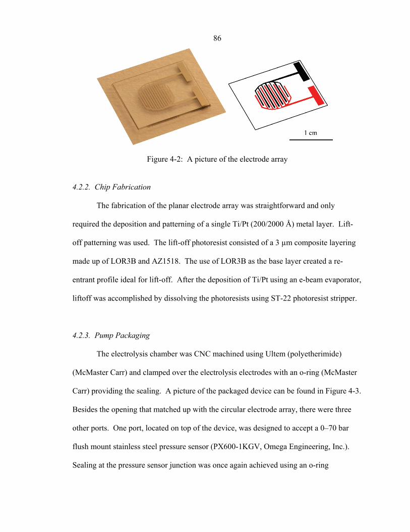
86
Figure 4-2: A picture of the electrode array
4.2.2. Chip Fabrication
The fabrication of the planar electrode array was straightforward and only
required the deposition and patterning of a single Ti/Pt (200/2000 Å) metal layer. Lift-
off patterning was used. The lift-off photoresist consisted of a 3 µm composite layering
made up of LOR3B and AZ1518. The use of LOR3B as the base layer created a re-
entrant profile ideal for lift-off. After the deposition of Ti/Pt using an e-beam evaporator,
liftoff was accomplished by dissolving the photoresists using ST-22 photoresist stripper.
4.2.3. Pump Packaging
The electrolysis chamber was CNC machined using Ultem (polyetherimide)
(McMaster Carr) and clamped over the electrolysis electrodes with an o-ring (McMaster
Carr) providing the sealing. A picture of the packaged device can be found in Figure 4-3.
Besides the opening that matched up with the circular electrode array, there were three
other ports. One port, located on top of the device, was designed to accept a 0–70 bar
flush mount stainless steel pressure sensor (PX600-1KGV, Omega Engineering, Inc.).
Sealing at the pressure sensor junction was once again achieved using an o-ring

87
(McMaster Carr). A second port was used for pump filling purposes. During filling, this
port was left open as a vent, and after filling, the port was plugged using a commercially
available HPLC column plug (Upchurch Scientific). The final port was connected to a
coil of Teflon FEP or stainless steel tubing (Upchurch Scientific) that served as the
solvent reservoir. This connection was made using a commercial high-pressure fitting
(Upchurch Scientific).
Figure 4-3: A picture of the packaged electrolysis pump along with a cross-sectional
view. The electrolysis chamber is faintly visible in the center of the Ultem piece.
While the electrolysis chamber could have been simultaneously used as the
solvent reservoir, we chose to use an external reservoir to prevent gas from contaminating
the liquid. This is important for applications that are sensitive to dissolved gas, such as
HPLC. The other end of the coiled tubing served as the pump outlet. For electrical
connections, miniature screw terminals were positioned next to the on-chip electrical
pads and used to clamp bare wires down onto the pads. The entire setup was capable of
sustaining pressures > 70 bar.

88
4.2.4. Pump Calibration
The pump was filled by pumping degassed acetonitrile/water (0.1% formic acid)
solutions into the pump outlet, through the coiled solvent reservoir, and into the
electrolysis chamber. In this way, both the solvent reservoir and electrolysis chambers
were filled simultaneously. The fill port was left unplugged during filling and closed
again after the system had been completely filled. The pump was operated by passing a
constant current through the electrolysis electrodes. The current was either supplied
using a custom-built V I converter (OP741, National Semiconductor) or a HP6186C
DC current source (Agilent Technologies). The applied current, required voltage, and
chamber pressure were recorded using a DAQPad-6020E data acquisition unit (National
Instruments) in conjunction with LabVIEW (National Instruments). Data acquisition and
electrolysis current control were both at 1 Hz.
Two different calibration methods were used to characterize the pump. In the first
method, a valve was positioned at the end of the coiled solvent reservoir and placed in the
closed position. A constant current was applied to the electrolysis electrodes and the rise
in pressure inside the closed system was monitored. In the second setup, the outlet of the
pump was connected to a 0–140 bar pressurized nitrogen gas cylinder. A constant
backpressure was applied and a constant current fed through the electrolysis electrodes.
The resulting flow rate was determined by measuring the linear velocity of the liquid/gas
interface in a tube with known ID. In this setup, clear Teflon FEP rather than stainless
steel tubing was used to observe the interface movement.

89
4.3. Results and Discussion
A majority of the experiments were conducted using the closed system setup.
With the pump outlet closed off, currents ranging from 1–3 mA were applied to the
electrolysis electrodes and the increase in internal pressure was monitored over time.
Figure 4-4 shows the collected data when using a 100% water solution (0.1% formic
acid). The maximum pressure generated during these experiments was approximately
50–60 bar, though higher currents readily resulted in faster pressure increases and higher
maximum pressures.
0
10
20
30
40
50
60
0 50 100 150 200
Time (min)
Pres
sure
(bar
)
3 mA
2 mA
1 mA
Figure 4-4: A plot showing the increase in pressure inside the closed electrolysis system
at applied currents of 1, 2, and 3 mA. These three curves were collected using a 100%
water solution (0.1% formic acid).
Developing a mathematical model to explain the pressure evolution in Figure 4-4
was important in understanding the underlying principles. The fundamental basis for our
calculation was simply the ideal gas law:
RTtntVtP )()()( = , (equation 1)

90
where P(t) is the pressure, V(t) is the volume, n(t) is the total number of moles of gas, R
is the universal gas constant, and T is the temperature. Given the volume and total molar
amount of gas inside the chamber, the expected pressure could be readily calculated.
First, the evolution of the gas volume was characterized. If the electrolysis
chamber was completely rigid and did not exhibit any pressure-related expansion, the gas
volume would have remained constant and have been equal to the initial volume of gas
inside the system (introduced during initial filling). This was not the case though, as the
o-rings as well as the tubing exhibited pressure-related expansion. This was easily
measured and was explained by the following equation:
))(()( oeo PtPkVtV −+= , (equation 2)
where V(t) is the volume, Vo is the initial gas volume, ke is the volume expansion
coefficient, P(t) is the internal pump pressure, and Po is the initial/ambient pressure. ke
was experimentally determined to be 0.50 µL/bar. This value was attained by applying a
pressure to the pump chamber via the pump outlet. The displacement of the air-water
interface in the solvent reservoir gave a measurement of the volume expansion. The
linear response of the volume expansion was confirmed to be accurate to > 70 bar. Vo
varied from one filling to another and needed to be experimentally determined.
Next, the sources of gas generation and gas loss were examined. The only source
of gas generation was electrolysis and, due to basic electrochemical principles, the gas
generation rate was known to be directly proportional to the applied electrolysis current.
Ideally, for every four electrons passing through the electrodes, three gas molecules were
generated (two H2 and one O2), but in reality not all the current was converted to gas.
This was due to molecules in the solution that oxidized or reduced more readily than

91
water. The efficiency that electrons are converted into the desired byproducts (in this
case H2 and O2) is known as the faradaic efficiency. In our situation, there were several
reactions that could reduce the efficiency. For example, the formate ion is known to be
oxidized, particularly in the presence of a catalytic electrode like Pt. Also, with Pt
electrodes, it is known that H2 can be oxidized and O2 be reduced64, 65 via the following
half reactions:
Anode: H2 2H+ + 2e-
Cathode: O2 + 2H2O + 4e- 4 OH-.
The oxidation of H2 and reduction of O2 are known to significantly decrease the faradaic
efficiency, especially when the anode and cathode are in close proximity to each other64,
as was the case here. While technically not recombination, the replacement of either of
the standard water electrolysis half reactions with the corresponding half reaction above
has the same net effect as recombination (e.g., 2H2 + O2 2H2O). Overall, the gas
generation rate could be expressed as follows:
ae NqI
dttdn
43)( ε
=+
, (equation 3)
where dn(t)+/dt is the molar gas generation rate, ε is the faradaic efficiency, I is the
current, qe is the charge of an electron and Na is Avogadro’s number. Gas loss on the
other hand was possible via permeation of gas out of the electrolysis chamber and also
through the recombination of H2 and O2 at the catalytic Pt electrode surface. Gas loss
through permeation is well known to be directly proportional to the differential pressure.
Likewise, the recombination of dissolved H2 and O2 was also expected to be proportional
to pressure, as the higher the pressure, the higher the concentration of dissolved gas in the
liquid. These two factors could be lumped together and be expressed as follows:
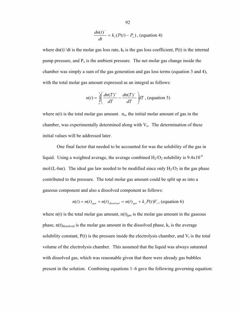
92
))(()(ol PtPk
dttdn
−=−
, (equation 4)
where dn(t)-/dt is the molar gas loss rate, kl is the gas loss coefficient, P(t) is the internal
pump pressure, and Po is the ambient pressure. The net molar gas change inside the
chamber was simply a sum of the gas generation and gas loss terms (equation 3 and 4),
with the total molar gas amount expressed as an integral as follows:
dTdTTdn
dTTdntn
t
o∫ ⎟⎟
⎠
⎞⎜⎜⎝
⎛−=
−+ )()()( , (equation 5)
where n(t) is the total molar gas amount. no, the initial molar amount of gas in the
chamber, was experimentally determined along with Vo. The determination of these
initial values will be addressed later.
One final factor that needed to be accounted for was the solubility of the gas in
liquid. Using a weighted average, the average combined H2/O2 solubility is 9.4x10⁻⁴
mol/(L-bar). The ideal gas law needed to be modified since only H2/O2 in the gas phase
contributed to the pressure. The total molar gas amount could be split up as into a
gaseous component and also a dissolved component as follows:
tsgasdissolvedgas VtPktntntntn )()()()()( +=+= , (equation 6)
where n(t) is the total molar gas amount, n(t)gas is the molar gas amount in the gaseous
phase, n(t)dissolved is the molar gas amount in the dissolved phase, ks is the average
solubility constant, P(t) is the pressure inside the electrolysis chamber, and Vt is the total
volume of the electrolysis chamber. This assumed that the liquid was always saturated
with dissolved gas, which was reasonable given that there were already gas bubbles
present in the solution. Combining equations 1–6 gave the following governing equation:
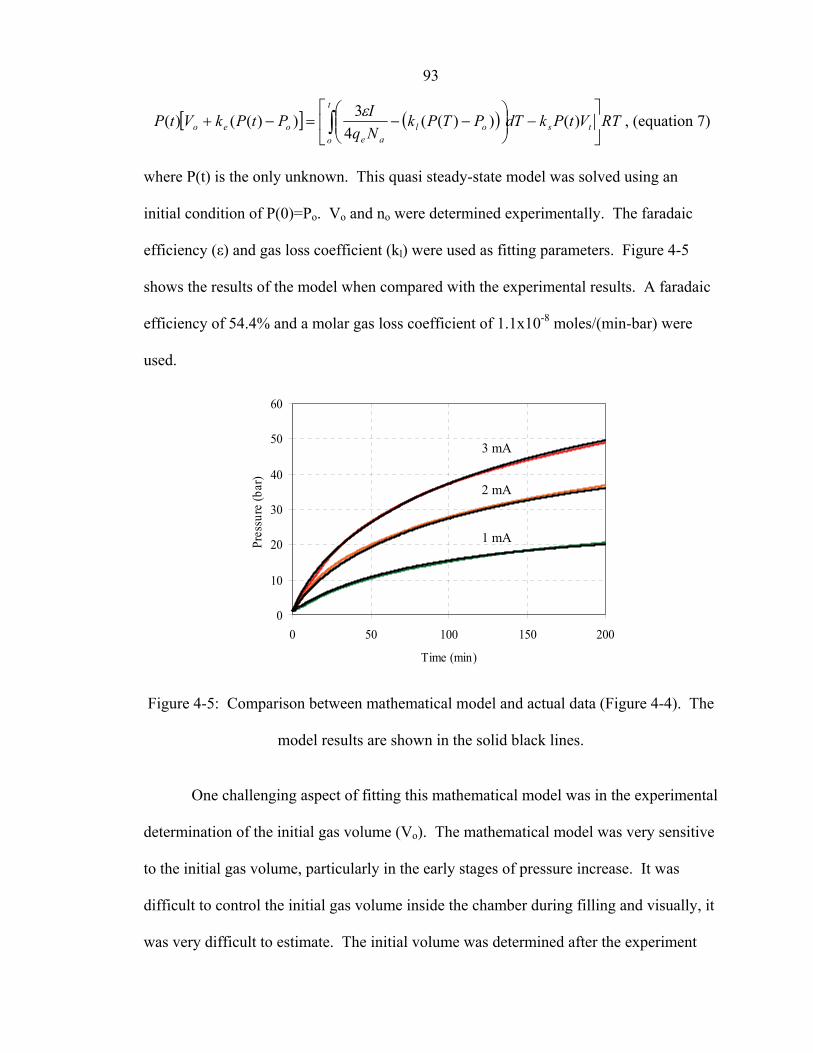
93
[ ] ( ) RTVtPkdTPTPkNqIPtPkVtP ts
t
ool
aeoeo ⎥
⎦
⎤⎢⎣
⎡−⎟⎟
⎠
⎞⎜⎜⎝
⎛−−=−+ ∫ )())((
43))(()( ε , (equation 7)
where P(t) is the only unknown. This quasi steady-state model was solved using an
initial condition of P(0)=Po. Vo and no were determined experimentally. The faradaic
efficiency (ε) and gas loss coefficient (kl) were used as fitting parameters. Figure 4-5
shows the results of the model when compared with the experimental results. A faradaic
efficiency of 54.4% and a molar gas loss coefficient of 1.1x10⁻⁸ moles/(min-bar) were
used.
0
10
20
30
40
50
60
0 50 100 150 200
Time (min)
Pres
sure
(bar
)
3 mA
2 mA
1 mA
Figure 4-5: Comparison between mathematical model and actual data (Figure 4-4). The
model results are shown in the solid black lines.
One challenging aspect of fitting this mathematical model was in the experimental
determination of the initial gas volume (Vo). The mathematical model was very sensitive
to the initial gas volume, particularly in the early stages of pressure increase. It was
difficult to control the initial gas volume inside the chamber during filling and visually, it
was very difficult to estimate. The initial volume was determined after the experiment

94
was completed. Post-experiment, the outlet valve was opened and the pressure released
for a short period of time. The liquid that came out was collected and the volume
measured. The amount of ejected liquid along with the associated pressure loss could be
used to back calculate the initial gas volume as follows:
)( fioefi
fo PPPk
PPVP
V −−+−
Δ= , (equation 8)
where Vo is the initial gas volume, Pi is the pressure prior to pressure release, Pf is the
pressure after pressure release, ∆V is the ejected fluid volume, ke is the chamber volume
expansion coefficient, and Po is the initial/ambient gas pressure. In general, our filling
method resulted in an initial gas volume of around 5–20 µL. Vo was also used to
calculate no, the initial molar gas volume inside the chamber, using the ideal gas law.
The greatest advantage of devising this mathematical model was that it could be
used to calculate the pressure versus flow versus current relationship of the pump when
operated as a non-closed system. The complete knowledge of this three-way relationship
was directly applicable to real pumping situations. Because we only wanted to know the
steady-state, constant pressure flow rate, factors such as dissolved gas and volume
expansion of the electrolysis chamber were not needed. In the steady-state, only the gas
generation and gas loss needed to be considered. The flow rate achieved at a given
pressure and current could be calculated as follows:
PRT
dttdn
dttdnF ⎟⎟
⎠
⎞⎜⎜⎝
⎛−=
−+ )()( , (equation 9)
where F is the steady-state flow rate, R is the universal gas constant, T is the temperature,
and P is the steady-state internal pump pressure. The expressions for dn(t)+/dt and dn(t)-
/dt were previously described in equations 3 and 4. The fitting parameters found before
95
(ε = 54.4% and kl =1.1x10⁻⁸ moles/(min-bar)) were used to calculate the
flow/pressure/current relationship. The results can be found in Figure 4-6. This data
could be used to estimate what currents were needed to drive the pump. For example, for
a given fluidic load and desired flow rate, the corresponding backpressure could be
calculated. The current corresponding to the desired flow rate and backpressure could
then be read directly from Figure 4-6.
0
50
100
150
200
250
300
0 10 20 30 40 50 6
Pressure (bar)
Flow
Rat
e (n
L/m
in)
0.5 1.0 1.5 2.0 2.5 3.0 3.5 4.0 mA
0
Figure 4-6: A plot showing the flow rate, pressure, and current relationship for the
electrolysis pump. Also on the plot are single point calibrations to check the accuracy of
the mathematical model. The discrete points are colored corresponding to the applied
current.
To check the accuracy of the model, several discrete data points were collected.
This was accomplished using the non-closed setup described in the experimental section.
A backpressure was applied to the pump using a nitrogen gas cylinder and a constant
current applied through the electrodes. The linear velocity of the water/air interface in
the solvent reservoir was measured to determine the resulting flow rate. Four discrete

96
points were collected and are also plotted in Figure 4-6. Agreement with the
mathematical model was good. Any discrepancy was likely caused by the system not
being in equilibrium, as it was difficult to judge when the pump had finally stabilized.
This was likely the reason why all the discrete points demonstrated a flow rate slightly
below the one calculated using the mathematical model. This was also the reason why a
non-closed system was not chosen for pump calibration. The need to test a large number
of points and the long period of time needed to wait for the pump to stabilize would have
made calibration inaccurate and time consuming. Testing the electrolysis in a closed
system effectively allowed the calibration of the pump across a variety of flow rates,
pressures, and currents with a few simple experiments.
Another key point that could be taken away from Figure 4-6 was the x-intercept
of the various curves. These intercepts represented the point where the pressure was high
enough that the gas generation rate was equal to gas loss rate. Therefore, they
represented the maximum pressure that could be achieved with this pump at a given
current. This is important because for most pumping applications there is not only a need
to increase, but also to decrease the pressure as necessary (e.g., if you want to lower the
flow rate). The intercepts could be used to determine how far the current needed to be
lowered to induce a pressure loss.
One important figure of merit for these pumps was the efficiency. Efficiency
could be defined in multiple ways. One way to define efficiency was to compare the
actual flow rate with the expected flow rate for a particular current assuming 100%
faradaic efficiency. This was termed the molecular efficiency and was calculated as
follows:

97
⎟⎟⎠
⎞⎜⎜⎝
⎛==
PNqIRTF
FF
ae
idealmolecular
43
ε , (equation 10)
where F is the steady-state flow rate, I is the current, R is the ideal gas constant, T is the
temperature, qe is the charge of en electron, Na is Avogadro’s number, and P is the
steady-state internal pump pressure. Figure 4-7 shows a plot of the molecular efficiency
as a function of pressure and current. As expected, at a pressure of 1 bar, the molecular
efficiency was a maximum and had a value equal to the actual faradaic efficiency (ε =
54.4%). As the pressure increased, the efficiency dropped as the gas loss rate increased.
0
10
20
30
40
50
60
0 10 20 30 40 50 6
Pressure (bar)
Effic
ienc
y (%
)
0.5 1.0 1.5 2.0 2.5 3.0 3.5 4.0 mA
0
Figure 4-7: Plot of molecular efficiency as a function of pressure and current. Each of
the curves corresponds to a different applied electrolysis current.
Another measure of efficiency that was worth examining was the power
efficiency. This compared the amount of power dissipated by the pump versus the total
work done by the gas in the electrolysis chamber. To determine this, first the I-V
relationship for our electrochemical cell had to be measured. This is shown in Figure 4-8.
At low currents, the voltage was near 1.7 V, the expected minimum voltage.

98
1
2
3
4
5
0 1 2 3
Current (mA)
Vol
tage
(V)
4
Figure 4-8: I-V curve for the electrolysis device
The power efficiency of the pump could then be calculated using the following
equation:
IVPF
power =ε , (equation 11)
where P is the steady-state pressure in the pump, F is the steady-state flow rate, I is the
applied current, and V is the voltage drop across the electrochemical cell. Combining the
data in Figure 4-6 and Figure 4-8 , this power efficiency could be calculated. The results
are shown in Figure 4-9. At low pressures, low currents had the best efficiency, reaching
nearly 0.4%. As the pressure increased, the higher currents eventually become the most
power efficient. This was expected since at high pressures the gas loss rate became
higher and higher, reducing a greater portion of the flow rate at low currents. In HPLC,
where the pressure is nearly always > 40 bar, higher currents were the most efficient.
The theoretical maximum power efficiency could be calculated by assuming a
100% faradaic efficiency and lowest possible driving voltage (e.g., 1.7 V for Pt
electrodes). This calculation yielded a maximum power efficiency of 1.1%. Low power

99
efficiency was expected since a vast majority of the power went into the stored energy
potential in H2 and O2.
0
0.1
0.2
0.3
0.4
0.5
0 10 20 30 40 50 6
Pressure (bar)
Pow
er E
ffici
ency
(%)
0.5 1.0 1.5 2.0 2.5 3.0 3.5 4.0 mA
0
Figure 4-9: Plot showing the power efficiency of the electrolysis pump at various
pressures and currents
One final important issue concerning the pump was the time response. Because
this pump relied on the build up and release of pressure to deliver varying flow rates, the
response time was slow, particularly at high operating pressures. This was evident from
Figure 4-4. In fact, the data in Figure 4-4 represented the maximum pressure ramp rates
because there was no pressure loss due to any liquid flow from the pump. Pressure
release was also slow as no method to actively vent the gas was implemented. The
response time of the pump had a strong dependence on the gas volume inside the
electrolysis chamber. Changing the pump pressure when there was a large evolved gas
volume in the electrolysis chamber took much longer than when the gas volume was
small. These difficulties in controlling the pump necessitated the use of sensors for
feedback-based control. This was especially the case when the transient performance of
100
the pump needed to be carefully regulated, as it does in HPLC. The integration of these
high-pressure pumps into a closed-loop feedback control system is discussed in Chapter 6.
4.4. Conclusion
A high-pressure electrolysis-based pump was designed and characterized. Even
at flow rates consistent with nanoscale HPLC (e.g., 150 nL/min at a pressure of 40 bar)
power consumption was still < 15 mW. While all the data presented was for 100% water
(0.1% formic acid) solutions, reverse-phase HPLC also requires the pump to deliver
fluids with higher organic compositions, up to a maximum of roughly 50%.
Characterization of the pump was also conducted at these higher organic compositions.
There was not a significant difference in the pump performance other than the need for a
higher driving voltage. This was expected because neither the faradaic efficiency nor the
gas loss coefficient were expected to change significantly with the change in electrolyte.
In general, for identical electrolysis currents, a 60% acetonitrile electrolyte needed twice
the voltage of a 100% water electrolyte. This equated to a doubling in the power
consumption.
There are still several possible improvements that can be made to the pump. For
example, the use of HPLC mobile phases for the electrolyte is non-ideal. A specialized,
strong electrolyte consisting of H2SO4 or Na2SO4 would be able to reduce the power
consumption drastically, perhaps by as much as a factor of two. The use of a special
electrolyte would require the implementation of a flexible barrier to separate the
electrolyte and the mobile phase though. Another possible improvement is in developing
methods to separate the produced O2 and H2. This would most likely enable faradaic

101
efficiencies of close to 100%, a 2x improvement over what it is now. This would once
again reduce the overall power consumption.
There are several possible ways of improving the pump time response. A
mechanism that allows the pump to selectively recombine O2 and H2 would probably
allow better control of the pump. An improvement in the transient response of the pump
can also be made by using a smaller and/or less flexible electrolysis chamber. Both these
changes would mean that less gas would need to be generated to increase the pressure,
with the opposite being true for decreasing the pressure. This comes at the cost of
pressure stability, though. Smaller chambers are much more prone to pressure
fluctuations than larger ones. In an application such as HPLC, where stability is
important and fast transient response is rarely needed, a large electrolysis chamber is
probably preferred.

102
Chapter 5: Multi-Function Microfluidic Platform
for Liquid Chromatography Tandem Mass
Spectrometry (LC-MS/MS)
5.1. Introduction
High-performance liquid chromatography tandem mass spectrometry (HPLC/MS-
MS) is recognized as one of the most powerful analytical techniques available and is
widely used in the biological sciences. One of the most important applications of HPLC-
MS/MS is in the field of proteomics. The ability to separate and identify the components
in a highly complicated mixture makes HPLC-MS/MS the preferred tool for a large
number of proteomic studies66. Instead of analyzing the proteins directly, it is common to
homogenize the mixture by performing an enzymatic digestion of the protein mixture.
Trypsin, which cleaves peptides at the carboxyl side of the amino acids Lys and Arg, is
often used as the digestion enzyme. The protein mixture is thus converted into a peptide
mixture, which is more suitable for HPLC/MS-MS analysis.
The coupling of HPLC and MS can be accomplished in one of two ways:
electrospray ionization (ESI) and matrix-assisted laser desorption/ionization (MALDI)66.
In this work ESI is used. It is an on-line approach meaning that the detection is done
concurrently with the separation. In ESI, a microscopic nozzle is used to create a fine
spray. The formation of this spray is in part facilitated by the establishment of a high
potential difference between the nozzle and the mass spectrometer opening. As the

103
droplets travel towards the mass spectrometer inlet, via coloumbic attraction, the solvent
evaporates, creating smaller and smaller drops. This forces the analyte ions closer and
closer together until the electrostatic repulsion of the ions overcomes the surface tension
of the liquid drop and causes the drop to break down into even finer ones. This process
of coloumbic fission continues until there are only lone analyte ions entering the mass
spectrometer, where their m/z ratio is measured. Tandem MS, where selected ions are
collected and further disassociated inside the mass spectrometer, is often used. The
information gathered about the primary and secondary (fragment) ions can be used to
determine the original peptide sequences. The peptide sequences detected in the mixture
can then be compared to databases to see which proteins originally were in the sample67,
68.
The high-resolution and high-sensitivity separation of peptides is generally done
through nanoscale reverse-phase HPLC, where a hydrophobic stationary phase, such as
C8 or C18, is used. Peptides exhibit a wide range of hydrophobicities, making isocratic
elutions unsuitable. An isocratic separation conducted at an acetonitrile percentage high
enough to elute the most hydrophobic peptide would result in extremely poor separation
of the less hydrophobic ones. Gradient elutions, where the eluent composition is varied
throughout the separation, are typically used instead. For example, a typical gradient
might ramp linearly from 0 to 50% acetonitrile at a rate of 1%/min while maintaining a
constant flow rate of 150 nL/min. This gradient causes the peptides to elute off the
column in order of increasing hydrophobicity. The flow control systems used to generate
gradient elutions are inherently more complicated than those for isocratic elutions. This
is further complicated by the low flow rates and high pressure requirements. As a result,

104
HPLC systems are generally extremely expensive and complicated to operate. The work
presented in this chapter aims to simplify the overall separation system by integrating the
majority of HPLC components on a single microfluidic chip. This not only could lead to
lower cost analyses, but also a miniaturized separation platform.
To date, most of the work done on miniaturized separation devices has been
focused on electrically driven separations69-71. The development of miniaturized HPLC
systems began with the development of on-chip columns interfaced with conventional
HPLC hardware72. It is only relatively recently that more advanced microfluidic HPLC
systems have been developed31, 72-76, with the trend being towards more highly integrated
devices. One important distinction of the chip presented in this chapter is the integration
of sensors. These sensors were used to not only passively monitor the fluid flow, but also
used as feedback for controlling the pumping.
5.2. Experimental
5.2.1. Chip Design
The presented chip included the following components: a passive mixer for
producing the binary solvent mixtures; an electrochemical time-of-flight (TOF) flow
sensor for flow rate measurements; an impedance-based composition sensor to measure
the organic solvent percentage in the eluent; analytical and trap columns for separation
and enrichment; weir-type filters for retaining the beads in the columns; and a polymer
electrospray nozzle for MS detection. The mixer and sensors were previously discussed
in detail in Chapter 3. A picture of the device can be found in Figure 5-1.

105
Figure 5-1: A picture and diagram of the presented chip. The various components are
highlighted in blue (mixer), green (composition sensor), red (flow sensor), orange (trap
column), purple (analytical column), brown (electrodes for applying electrospray
potential), yellow (electrospray nozzle), and gray (bead filters). The black dots represent
the location of fluidic ports. Overall chip size was 9.8 x 9.8 mm2.
Images of all the individual devices on the chip can be found in Figure 5-2. The
passive mixer consisted of a 30 x 25 (W x H) µm2 in cross section and 8.8-mm-long
channel. The small cross section was designed to bring the two incoming flows in close
contact and reduce the distance molecules had to diffuse for complete mixing. The
composition sensor consisted of a set of interdigitated electrodes with a width/spacing of
7.5 µm. The electrodes covered a total area of 70 x 300 (W x L) µm2 and were located in
a channel with a cross section of 80 x 25 (W x H) µm2. A measurement of the impedance
of the fluid was used to deduce the water/acetonitrile ratio. For the flow sensor, the
electrodes used to generate the electrochemical pulse had a spacing of 100 µm and the
detector electrodes were located 450 µm downstream. The flow sensor channel
dimensions were 80 x 3.5 (W x H) µm2. The time it took for the electrochemical pulse to
travel from the pulsing electrodes to the detector electrodes was used to measure the

106
linear fluid velocity, which could then be converted to a volumetric flow rate. The
analytical column had a cross section of 80 x 25 (W x H) µm2 with a total length of 4.2
cm. The trap column on the other hand had a slightly larger cross section of 120 x 25 (W
x H) µm2, but was much shorter, with a total length of only 0.9 cm. The bead filters were
constructed by using a step in the channel height. The filter height was around 3.5 µm,
which prevented any particles larger than that from passing through. The electrodes used
to establish the electrospray potential were identical in design to those used to measure
the fluid composition. The electrospray nozzle consisted of a freestanding Parylene
channel, which extended 0.9 cm past the edge of the chip. The end of the nozzle
terminated in a triangular nib with a terminal radius of roughly 1–2 µm. Finally, the
fluidic inlet/outlet ports were defined in SU-8 and were 200 x 200 (W x L) µm2.
Figure 5-2: Close-up pictures of all the individual components on the presented chip. All
devices are shown at the same scale.

107
The chip was designed such that the different components could be bypassed
and/or turned off as needed. This, combined with the ability to selectively access and
close off the many different fluidic ports on the chip, allowed this single chip to be
operated in many different separation configurations. A summary of the configurations
and the components they used is as follows:
1. Standard Column with Active Sensors: The chip was used as a nanobore
format column with the benefit of integrated sensors for eluent monitoring. In
this setup, the sensors, analytical column, and electrospray nozzle were used with
conventional HPLC hardware to perform separations.
2. Vented Column with Non-Active Sensors: The chip was used as a nanobore
format column with an integrated vented trap column for sample loading and
enrichment. In this setup, the trap column, analytical column, and electrospray
nozzle were once again used with conventional HPLC hardware to perform
separations.
3. Standard Column with On-Chip Feedback Flow Control: The chip was used
as a nanobore format column with the addition of an on-chip mixer and sensors
for feedback-controlled on-chip gradient generation. In this setup, the mixer,
sensors, analytical column, and electrospray nozzle were all used. Instead of
using a conventional HPLC pump, a custom-built two-channel pneumatic pump
was used to drive the flow.
The setups and experimental procedures for each of these configurations will be
described in detail later in the chapter.

108
5.2.2. Chip Fabrication
The technology used to fabricate this chip was described in detail in Chapter 2.
These chips utilized the high-pressure anchoring technology and SU-8-based fluidic ports
outlined in Chapter 2. The process is diagrammed in Figure 5-3 and can be broken down
into eleven steps.
Figure 5-3: Process flow for the presented chip. The left-hand column shows a cross-
sectional view where the liquid flow is from left to right. The right-hand column shows a
cross-sectional view where the liquid flow is into the page.

109
1. Silicon Oxide Deposition and Patterning: A 4000 Å silicon oxide (SiOx) layer was
grown on a silicon wafer. Next, a 5 µm AZ1518 photoresist layer was spun on the wafer
and patterned using photolithography. The exposed silicon oxide was then etched using a
buffered HF solution. Afterwards, the photoresist was stripped using acetone and
isopropyl alcohol. The oxide layer served three functions: first, as an insulation layer
between the electrodes and the silicon wafer; second, as a mask for DRIE etching (see
step 5); and third, as a mask for XeF2 silicon during the undercutting of the electrospray
nozzle (step 11).
2. Parylene Deposition and Patterning: After treating the wafer surface with A-174
adhesion promoter, a 5 µm Parylene layer was deposited. Patterning of this layer was
accomplished using oxygen plasma with a photo-patterned 10 µm AZ 4620 photoresist
layer as a mask. This layer would eventually form the base of the electrospray nozzle.
After etching, the remaining photoresist was stripped using acetone and isopropyl alcohol.
3. Metal Deposition and Patterning: A 3 µm composite lift-off photoresist layer made up
of LOR3B and AZ1518 was deposited and photo-patterned. The use of LOR3B as the
base layer created a re-entrant profile ideal for lift-off. A 200/2000 Å Ti/Pt layer was
then deposited via e-beam deposition. The Ti was used to improve adhesion between the
Pt and the oxide surface. After metal deposition, liftoff was accomplished by dissolving
the photoresists using ST-22 photoresist stripper. The resulting metal layer was used to
define all the electrodes, as well as the metal lines and pads needed for electrical
connections.
4. Sacrificial Photoresist: A 25 µm AZ4620 photoresist layer was spun on the wafer. By
using two exposures, one full, and one partial, a bi-level (25 µm/3.5 µm), monolithic

110
photoresist structure was produced. A bi-level sacrificial layer was necessary to reduce
the channel height where the flow sensor and filters were located. This sacrificial
photoresist layer was temporarily used to define the channel and would eventually be
dissolved away (step 10).
5. Parylene Anchors and Deposition: A deep reactive ion etcher (DRIE) was used to
etch 40-µm-deep trenches on the sides of the channels. The oxide, patterned in step 1,
was used as a mask for DRIE etching. Afterwards, a 10 µm Parylene-C layer was
deposited. The DRIE trenches took advantage of the conformal nature of the Parylene
deposition and served to anchor the Parylene layer to the substrate. By mechanically
anchoring the encapsulating layer, much higher pressures could be sustained by the
channels.
6. Parylene Patterning: A 200/2000-Å-thick Cr/Au layer was e-beam deposited and
patterned by using a 40 µm AZ4620 photoresist mask. The metal was etched using Au
etchant type TFA (KI-based) and CR-7 Cr etchant (perchloric-acid-based). After metal
etching, the photoresist was stripped using acetone and isopropyl alcohol. The Cr/Au
metal layer was then used as an etch mask for Parylene patterning, which was
accomplished using an oxygen plasma. This patterning was used to remove Parylene
over the areas where the SU-8 anchors would be etched (step 7).
7. SU-8 Anchors: Before the formation of the SU-8 anchors, the Cr/Au layer was
patterned again using the same process outlined in step 6. Then, a 40-µm-thick AZ4620
photoresist layer was spun and patterned. This formed a mask to DRIE etch shallow 30
µm trenches near the SU-8 edges. The photoresist was stripped using acetone and
isopropyl alcohol.

111
8. Parylene Patterning: The Parylene was etched in oxygen plasma using the Cr/Au
mask patterned in step 7. This etch step opened all the ends of the microchannels and the
electrospray nozzle opening. After Parylene etching, the metal mask was stripped using
Au etchant and Cr-7 Cr etchant.
9. SU-8 Encapsulation: A 50-µm-thick SU-8 layer was spun on the wafer and patterned.
This SU-8 layer filled the trenches (step 7), which helped improve SU-8 adhesion to the
substrate. This was especially critical, as the entire chip would be soaked in harsh
organic solvents later in the process (step 10). The SU-8 also helped to strengthen the
channels further so they could withstand the high operating pressures. Finally, the SU-8
also sealed the regions where the electrodes crossed into the channel, preventing these
areas from leaking during high-pressure operation.
10. Photoresist Dissolution: The sacrificial photoresist was dissolved using acetone over
a period of 1 week, after which the channels were individually flushed with fresh acetone.
The wafer was then rinsed in isopropyl alcohol and water before drying.
11. XeF2 Etching: To make the electrospray nozzle freestanding, XeF2, a gas-phase
isotropic silicon etchant was used to remove the silicon underneath the nozzle.
Simultaneously, this etch step was used to etch trenches along all the lines where the
individual chips were to be separated. XeF2 has nearly an infinite etch ratio between
SiOx and Si, and the oxide patterned in step 1 was used to constrain the silicon etching to
underneath the nozzle and along chip edges. Using the trenches as a guide, the wafer was
manually scribed and separated into individual dies.

112
5.2.3. Chip Packaging / Preparation
The packaging of this chip was identical to the chips described in Chapter 3.
Multiple manifolds with various numbers of openings were used in the testing of this
device. Single, dual, and triple inlet manifolds were used in our separation experiments
depending on the particular configuration. When the chip was fitted with these manifolds,
any of the on-chip fluidic ports that did not match up with a corresponding port in the
manifold was effectively sealed off.
Before the chip could be tested, the analytical column, and in some cases the trap
column, were packed with beads. This was accomplished by using a single inlet
manifold. By positioning the manifold over the correct port while simultaneously
blocking all other ports (except for the column outlet) the columns could be individually
packed with the desired support, generally 3 or 5 µm C18 support (Varian, Inc. or Grace
Vydac). Columns were packed by forcing a bead/isopropyl alcohol slurry mixture into
the column at pressures up to 100 bar. A pressure bomb with magnetic stirrer was used
to hold the slurry and keep the beads in suspension during packing.
5.2.4. Sensor Operation
The operation of the sensors was previously described in Chapter 3. The sensors
on this device were identical to the sensors on the integrated device discussed there.
5.2.5. Pneumatic Pump
For feedback-controlled separations a custom-built two-channel pump was used.
A conventional HPLC pump could not be used because they do not allow for the control

113
of the individual pump channels. The pump was a pressure-driven setup with two
separate, but identically built channels, both powered by a common 45 bar nitrogen gas
cylinder. Each channel consisted of a Model 3110, 0–40 bar electrically controlled
pressure regulator (March-Bellofram) that directly controlled the pressure inside of a 1
mL solvent loop. Solvent loops were constructed using Teflon FEP tubing (Upchurch
Scientific). A 40 mL gas sample chamber (Swagelok) was placed in between the
regulator and liquid reservoir to reduce pressure fluctuations. The solvent loops were
connected to 360 µm OD fused silica tubing (10–15 µm ID) (Polymicro Technologies)
that could then be connected to the actual chip. For all our experiments, the pumps were
loaded with degassed 100/0/0.1 and 40/60/0.1 (water/acetonitrile/formic acid) solutions.
A photograph of the pump can be found in Figure 5-4.
Figure 5-4: A picture of the custom-built two-channel pneumatic pump
5.2.6. Mass Spectrometry
All MS analyses were performed using an Agilent 1100 series LC-MSD SL ion
trap mass spectrometer. The packaged chip was positioned in front of the mass

114
spectrometer on an axis orthogonal to the mass spectrometer inlet. The chip was attached
to a 3-axis stage and the chip was manually positioned for optimal electrospray.
Electrodes on the chip located between the end of the analytical column and the
electrospray nozzle were grounded. The voltage setting was -1900 V for the mass
spectrometer inlet and -1400 V for the counter electrode. Both full range mass spectra
and MS/MS spectra were collected. A picture of the chip interfaced to the mass
spectrometer can be found in Figure 5-5 .
Figure 5-5: A picture of the chip/mass spectrometer interfacing
5.2.7. Data Acquisition
In the configurations where the sensors were active, the sensors were controlled
and monitored using a DAQPad-6020E data acquisition unit (National Instruments) in
conjunction with LabVIEW (National Instruments). Flow rate measurements were
conducted at a frequency of 0.1 Hz and composition measurements at 1 Hz. Control of
the custom-built pneumatic pump and the feedback algorithms used to control it were
also implemented in LabVIEW. Feedback was implemented by using a proportional
feedback algorithm. The pump control voltages were updated at 1 Hz. The conventional
HPLC hardware, which included the Agilent 1100 series nanoflow pump, isocratic pump,

115
micro well-plate autosampler, and mass spectrometer, was controlled using the
manufacturer’s software.
5.2.8. Chip Separation Configurations
5.2.8.1. Standard Column with Active Sensors
The first separation configuration used the single inlet manifold. An Agilent 1100
series nanoflow pump was connected to our chip via a single open port. An Agilent 1100
series micro-well-plate autosampler was placed in-line between the pump and chip for
automated sample metering. A diagram of the setup can be found in Figure 5-6.
Figure 5-6: Fluidic configuration and separation method for the “Standard Column with
Active Sensors” configuration
The analytical column was packed with 5 µm C18 support (Grace Vydac) to a
length of approximately 3 cm. To begin, a sample was injected directly onto the
analytical column using a 100/0/0.1 (water/acetonitrile/formic acid) solution at setpoint

116
flow rate of 150 nL/min. After the sample was loaded, the autosampler’s internal sample
loop was bypassed and a pre-programmed gradient elution was delivered by the nanoflow
LC pump. The autosampler’s sample loop was bypassed during the delivery of the
gradient to reduce delay. The gradient ramped linearly from 0 to 30% acetonitrile at a
rate of 1%/min and at a constant setpoint flow rate of 150 nL/min. The sensors
monitored the flow rate and fluid composition flowing into the column in real time. Only
a single flow path existed throughout the separation. The liquid entered the chip at port 1,
and was directed through the mixer, sensors, trap column, analytical column, and
electrospray nozzle, in that order. The mixer and trap column served no purpose except
to direct the flow. This setup was designed to mimic the application of a nanobore
format column with the added benefit of having sensors to monitor the eluent.
5.2.8.2. Vented Column with Non-Active Sensors
In the second configuration, both the chip’s trap column and analytical column
were packed using 3 µm C18 support (Varian, Inc.). The trap column had a total length of
0.8 cm and the analytical column was 3 cm long. The trap column was interfaced to an
Agilent 1100 series micro-well-plate autosampler/isocratic pump combination for sample
loading. The chip was also interfaced to an Agilent 1100 series nanoflow pump for
gradient delivery. A diagram of the setup can be found in Figure 5-7.
To begin, the autosampler /isocratic pump was used to pump the sample through
the trap column at a flow rate of 1 µL/min using a 100/0/0.1 (water/acetonitrile/formic
acid) solution. During this stage of the separation, flow from the autosampler entered
through port 3, was directed through the trap column, and out through port 2.
Simultaneously, the flow entering the chip at port 1 also exited out through port 2. After

117
sample loading and desalting was complete, the internal autosampler valve was switched,
automatically blocking off both the trap column inlet and outlet ports (ports 2 and 3).
The Agilent 1100 series nanoflow pump was then used to deliver a linear 0 to 50%
acetonitrile gradient at a ramp rate of 1%/min and a constant setpoint flow rate of 150
nL/min. The gradient entered through port 1 and traversed the mixer, sensors, trap
column, analytical column, and electrospray nozzle, in that order. The mixer and sensors
served no purpose other than providing a flow path. During this step, the sample was
eluted off the trap column and onto the analytical column and separated. Sensors were
not active in this configuration, though they could have been used to monitor the eluent
flow in much the same way they were used in the “Standard Column with Active
Sensors” configuration. The overall separation setup is similar to the vented column
approach described in literature77.
Figure 5-7: Fluidic configuration and separation method for the “Vented Column with
Non-Active Sensors” configuration. V1 is internal to the autosampler but is shown
separately for clarity.

118
5.2.8.3. Standard Column with On-Chip Feedback-Controlled Flow Control
The third configuration utilized the integrated sensors for feedback-controlled
operation. The custom-built two-channel pneumatically driven pump was used along
with our dual-input fluidic manifold. The two solvent loops were loaded with 100/0/0.1
(water/acetonitrile/formic acid), designated channel A, and 40/60/0.1, designated channel
B. In this configuration, an Agilent 1100 series micro-well-plate autosampler was placed
in line between pump channel A and the chip. Valves (Upchurch Scientific) were also
positioned on each of the pump channels for situations where we wanted only channel A
or channel B to be active. The analytical column was packed with 5 µm C18 support
(Grace Vydac) to a length of 3 cm. A diagram can be found in Figure 5-8.
Figure 5-8: Fluidic configuration and separation method for the “Standard Column with
On-Chip Feedback-Controlled Flow Control” configuration
To begin, pump channel A was used to pump the sample directly onto the
analytical column at a flow rate of 136 nL/min. During sample loading, valve 2 was

119
closed and flow entering through port 1 was directed through the mixer, sensors, trap
column, analytical column, and electrospray nozzle, in that order. Once sample loading
was complete, valve 2 was opened and pump channel B activated to produce a linear
gradient from 0 to 30% acetonitrile at a rate of 1%/min and at a constant flow rate of 136
nL/min. During the gradient elution, liquids entered through ports 1 and 2
simultaneously and were directed through the mixer, sensors, trap column, analytical
column, and electrospray nozzle, in that order. A flow rate of 136 nL/min was chosen to
match the flow rates measured using the on-chip sensors in “Standard Column with
Active Sensors” configuration in order to enable a better comparison.
5.3. Results and Discussion
5.3.1. Microfluidic Chip/Components
The microfluidic chip was designed to be compatible with HPLC analyses.
Important properties include high-pressure operation, solvent resistance, biocompatibility,
and durability. These goals were largely achieved. During column packing the chip
experienced pressures as high as 100 bar with no noticeable effects. Also, an analysis of
the MS data while flowing a high percentage of acetonitrile through the chip did not
indicate any significant source of background noise, confirming the solvent resistance of
our chip. The use of known biocompatible, low-retention materials such as Parylene also
assured compatibility with biological molecules. To demonstrate durability, individual
chips were operated for more than 72 hours with only slight degradation to the
electrospray nozzle.

120
The design and performance of the mixer, composition sensor, and flow sensor
were all previously discussed in detail in Chapter 3. The characterization and
performance of the rest of the individual components will be briefly described here.
5.3.1.1. Analytical/Trap Column
The dimensions of the analytical column were chosen to be comparable to a 50
µm ID column. One important characterization of the column that had to be performed
was the determination of the flow resistance of the packed column. This was
accomplished by pumping fluid through the column at a fixed pressure and measuring the
resulting flow. For a column packed with 5 µm support, a flow resistance of 0.029
bar/(nL/min)/cP/cm was determined. This implies that the pressure needed to drive 100
nL/min of water (e.g., 1 cP viscosity) through a 3 cm column would be 8.7 bar. The
same measurement was conducted with columns packed with 3 µm support and a flow
resistance of 0.077 bar/(nL/min)/cP/cm was determined. The flow resistance ratio
between the 3 and 5 µm bead-packed columns should be proportional to the square of the
bead diameter, or 2.78. The measured ratio of 2.67 was a close match and the
discrepancy could have easily been caused by irregularities in the support size and shape.
The trap column, with a cross-sectional area 150% greater than the analytical column,
showed a corresponding reduction in the flow resistance.
5.3.1.2. Bead Filter
The weir-type filters used in this device all had a height of approximately 3.5 µm.
They effectively stopped 3 and 5 µm beads in the columns. The ability to retain 3 µm

121
beads was largely due to the fact that the beads were not perfectly spherical or uniform in
size. The presence of just a few irregularly large beads was enough to prevent any
further beads from passing through. The thickness variation of the filters across each
wafer was estimated to be < 1 µm. Unfortunately this still meant that some devices were
more effective in holding the beads than others, particularly when attempting to use 3 µm
beads. This was remedied in some cases by using a small number (10–50) of 5 µm beads
to plug the filter prior to actually packing the column with 3 µm support.
5.3.1.3. Electrospray
The electrospray nozzle was thoroughly tested before any separations were
conducted. The nozzle was tested over a wide range of solvent compositions and flow
rates. Stable electrospray was even obtained at flow rates < 50 nL/min, which is usually
a good indication of a well-designed nozzle. The nozzle was tested in both orthogonal
and head-on configurations and worked similarly in both cases. While the Agilent 1100
series LC-MSD SL ion trap mass spectrometer used in our separation experiments
required the nozzle potential to be held at ground, many other mass spectrometers require
the nozzle voltage to be floated at high voltage (~ 1–3 kV). The nozzle was tested under
these conditions as well. The durability of the nozzle proved to be the one weak spot on
the chip and it was generally the first component to wear out. The electrospray process
appeared to slowly wear away the Parylene, causing a blunting of the nozzle tip and
degrading performance over time. A metal-coated electrospray tip could potentially be
used to improve durability.

122
-50
-25
0
25
50
75
0 20 40 60 80 100
Time (min)
% A
ceto
nitri
le
0
50
100
150
200
0 20 40 60 80 100
Time (min)Fl
ow R
ate
(nL/
min
)
programmed programmed
actual actual
Figure 5-9: Separation results using the “Standard Column with Active Sensors”
configuration. The MS data (top), flow sensor (bottom right), and composition sensor
(bottom left) data are plotted.
5.3.2. Standard Column with Active Sensors
Separations of 250 fmol Bovine Serum Albumin (BSA) digest were conducted
and yielded results that were reasonable given the column dimensions and separation
method. An example can be found in Figure 5-9 along with the recorded sensor data. A
subsequent analysis of the MS data yielded protein coverage of about 50%, similar to
what is normally achieved using a commercially available nanobore column. This meant
that 50% of the amino acids in the BSA protein were identified during the analysis. The
sensor data provided interesting insight into the actual separation itself. Based on the
programmed composition profile and the composition detector data, there was an 11 min
delay for compositional changes to propagate from the pump to the on-chip sensors. The

123
negative acetonitrile percentage registered at ~ 15–25 min indicated the sample plug
being loaded onto the column. The sensors also clearly registered the passing of the
gradient through the column from 65–95 min. This corresponded very well with the
actual elution of the peptides from the column. Some delay was expected between the
gradient reaching the sensors and the peaks eluting because the sensors were located at
the head of the column. Breakthrough time for our column and flow rate was
approximately 1 min.
Another interesting consequence of having the sensors was that we were able to
detect flow rate inconsistencies. For example, from 0–50 min, when the autosampler
valve was in mainpass mode, the flow rate was much lower than when the autosampler
valve was in bypass mode (> 50 min). This was most likely due to the large internal
autosampler volume when in mainpass mode. Our sensor data also indicated that there
were fluctuations in flow rate during the actual gradient and particularly when there were
sudden changes in the fluid composition (e.g., at the 90 min mark). These flow errors
were confirmed by measuring accumulation of liquid in a clear capillary to determine the
actual flow rate. We believe that these fluctuations had minimal effect on the actual
separation itself. In fact, when performing the same experiment many times, the results
were nearly identical, indicating excellent repeatability for our HPLC pump and on-chip
column.
The integration of sensors into the column has many possible uses. By
monitoring the flow in the column and comparing it to the flow that the pump is
indicating, it can be very easy to troubleshoot leaks or blockages in the fluid lines. These
problems could be nearly impossible to find otherwise, given the low working flow rates.

124
The sensors could also possibly improve the efficiency of HPLC systems. Since the
column conditions are always known, the guesswork can be taken out of the steps such as
column equilibration. Finally the addition of sensors could also potentially open the door
for comparing separations done on the different HPLC systems. HPLC systems naturally
tend to behave slightly differently from one another, particularly when gradient elutions
are used. This is caused by different systems having different delay volumes. This
variation in delay essentially causes different degrees of gradient “blurring”. By
monitoring the flow at the column and correlating that with the separation, comparisons
could be made based on the measured column conditions rather than the programmed
elution profile. This ability would enable better cross-laboratory comparisons of
gradient-based separations.
5.3.3. Vented Column with Non-Active Sensors
One drawback of directly injecting the sample onto the analytical column was that
it could only be done at a relatively low flow rate because of pressure considerations. If
the sample volume was high, the sample loading process took a long time. This
configuration, with the addition of a shorter trap column, was designed to address these
problems. The shorter and wider trap column could be used to load the sample at high
flow rates while still maintaining a reasonable backpressure. Separations of different
amounts of a BSA digest are shown in Figure 5-10. The intensity of the peaks scaled
nearly directly with the amount of sample, indicating ideal and repeatable capture/elution
of the sample by/from the trap column. Coverage of the BSA protein was similar to the
previous setup.

125
Figure 5-10: Separation results using the “Vented Column with Non-Active Sensors”
configuration. The MS data for three different sample concentrations are plotted.
The sensors, while not activated in these separation experiments, could have been
used to monitor the sample loading and gradient elution in much the same way done in
the “Standard Column with Active Sensors” configuration. Another advantage of a trap
column, besides improved sample loading times, is that it can be used to enrich “dirty”
samples without exposing the mass spectrometer to unwanted contaminants.
5.3.4. Feedback-Controlled Operation
Before using the sensors for feedback-controlled separations, the feedback system
was characterized. When using the on-chip sensors with our two-channel pump, the
standard deviation from the set points flow rates and compositions was very low,
approximately 0.3% acetonitrile and 1.2 nL/min. These deviations were either the same

126
or slightly higher than the sensor precision values determined in our calibrations in
Chapter 3, indicating that control was largely limited by the characteristics of the sensors.
When running programmed linear gradients like those seen in nanoscale HPLC, run-to-
run repeatability was excellent. Standard deviations from the mean gradient were only
0.3% acetonitrile and 1.6 nL/min
One way to check whether the flow control system was working properly was by
comparing the pressures inside the two pump channels during feedback-controlled
gradient generation with the pressures expected based on theoretical calculations. In our
fluidic system there are three important fluidic resistances: the resistance of the tubing
connecting channel A of the pump to the chip, the resistance of the tubing connecting
channel B of the pump to the chip, and finally the column resistance. The relevant
resistances, pressures, and flow rates are all shown in Figure 5-11 using an electrical
circuit analogy.
Figure 5-11: Equivalent electrical circuit for the fluidic system
While the viscosity of the liquid flowing through Ra and Rb is constant, the
viscosity of the fluid flowing through the column is actually dependant on the ratio
between Fa and Fb, since the viscosity of acetonitrile/water mixtures is dependant on the

127
acetonitrile/water ratio. Taking this into account, the governing series of equations
comes directly from the application of the fluidic equivalents of Kirchoff’s loop rules:
)()()(
0)()(
)(6.0)()6.0()()(
0)()(
)(6.0)()0()()(
tFtFtFtFtF
tFtFRtFRtP
tFtFtFtFRtFRtP
bac
ba
bccbbb
ba
bccaaa
+=
=⎟⎟⎠
⎞⎜⎜⎝
⎛+
−−
=⎟⎟⎠
⎞⎜⎜⎝
⎛+
−−
ηη
ηη
, (equation 1)
where η(x) is a known function representing the absolute viscosity of the liquid as a
function of the acetonitrile amount (e.g., η(0) being the absolute viscosity of a 100%
water solution and η(1) being the absolute viscosity of a 100% acetonitrile solution), and
channels A/B contain a 100/0/0.1 and 40/60/0.1 (water/acetonitrile/formic acid) solutions,
respectively. Ra, Rb, and Rc can all be independently measured, meaning that Pa and Pb
can be readily calculated for any given desired flow profile (Fa(t), Fb(t)).
0
10
20
30
40
0 10 20 30 4
Time (min)
Pres
sure
(bar
)
0
Pump A
Pump B
Figure 5-12: Comparison between the pressures obtained during feedback drive
operation of a 0 to 30% acetonitrile gradient (solid lines) versus the pressure calculated
using a mathematical model (dotted lines).

128
Figure 5-12 shows a comparison between the calculated pressure curves and the
ones obtained during feedback-driven operation for a 0 to 30% acetonitrile gradient
(1%/min) at a flow rate of 150 nL/min. For this simulation, the following resistance
values were measured and used: Raη(0) = 0.148 bar/(nL/min), Rbη(0.60) = 0.206
bar/(nL/min), and Rc = 0.110 bar/(nL/min)/cP. The good correlation was confirmation
that the closed-loop flow control system was working properly.
5.3.5. Standard Column with On-Chip Feedback-Controlled Flow Control
This last separation configuration was designed to show the advantages of using
the integrated sensors for feedback-driven gradient generation. Consecutive separations
of 250 fmol BSA digest are shown in Figure 5-13.

129
110
120
130
140
150
160
35 45 55 65 75
Time (min)
Flow
Rat
e (n
L/m
in)
-5
5
15
25
35
35 45 55 65 75
Time (min)
% A
ceto
nitri
le
0
10
20
30
40
50
35 45 55 65 75
Time (min)
A P
ress
ure
(bar
)
0
10
20
30
40
50
35 45 55 65 75
Time (min)B
Pre
ssur
e (b
ar)
Figure 5-13: Separation results using the “Standard Column with On-Chip Feedback-
Controlled Flow Control” configuration. The MS data (top), flow sensor (middle left),
composition sensor (middle right), and pump pressure (bottom) data are plotted.
Protein coverage was generally around 50–60%, again in line with our previous
experiments. The separations, while very similar to separations conducted using the
commercial HPLC pump, in terms of peak resolution and protein coverage, did not
exhibit the same kind of repeatability. Relative standard deviation (RSD) of the elution
times for the mid-eluting peaks was 3.3%. This is slightly higher than the values
generally specified for commercial nanoflow HPLC systems. One factor that might have
contributed to this higher RSD value is that the gradient was generated so close to the
column. Any minor fluctuations in the composition or flow rate will be seen by the
column almost immediately, having an adverse effect on the separation. On the other
hand, in a commercial HPLC system the swept volume between the pump and the actual
130
column is often times many orders of magnitude larger than in our chip. This is evident
by the long gradient delay observed in the “Standard Column with Active Sensors”
configuration. This long dwell time actually had the advantages of smoothing out any
fluctuations in the flow. Possible corrections to this are more sensitive and accurate
sensors or the inclusion of a larger volume buffer zone between the sensor and column.
On the other hand, having the gradient generated on chip does have many
advantages. For example, complex gradient shapes can be generated with little distortion.
Our system is well suited for this task because any gradient that is generated will
maintain the desired flow profile with minimum “blurring”. On the other hand, a
conventional system would most likely produce distortions to complex flow profiles due
to diffusion and non-perfect fluidic connections.
Another advantage of having the gradient generated so closely to the column is
that rapid and accurate changes in the fluid composition can be made. This could allow
for faster overall analysis times since time is not wasted waiting for changes in fluid
compositions to reach the column. Another interesting possibility that this configuration
opens up is the ability to do rapid analysis of unknown samples. Unknown samples are
generally run using a long, shallow gradient over a wide organic range. With this chip,
the gradient formation could conceivably be altered based on the mass spectrometer
response allowing the gradient to be steeper when the peak density is low, and shallower
when the peak density is high. The results of this initial separation could be used directly
in generating a general method for that sample and ones of similar origin.

131
5.4. Conclusion
The fabricated chip proved to be very capable in conducting reverse-phase
separations of peptide mixtures. This single chip had the ability to interface with
commercial HPLC hardware, offering a plug-in solution for HPLC-MS/MS. Also, by
connecting the chip to a custom-built two-channel pumping system, on-chip feedback-
controlled gradient generation could be accomplished, producing a HPLC system that is
unmatched when it comes to rapid and accurate changes in column flow.
There was some concern that the electrochemical TOF flow sensor might cause
problems with the separation. For example, the high-voltage pulses will most likely
oxidize/reduce the analytes. Fortunately, the duty cycle of the pulse generation is only
0.07% so only a tiny fraction of the analyte would have been affected. A second concern
was directed at the gas generated during the high-voltage pulses. Because of the high
pressure, the gas would have dissolved into the fluid immediately, but would have
eventually resurfaced at the low-pressure end of the system (e.g., after the column).
These gas bubbles could destabilize the electrospray process. Fortunately, no gas was
observed post column and separations conducted with the flow sensor active were
identical to ones conducted with the sensor disabled.
One element that was not used in this chapter was the high-pressure electrolysis
pumps. Electrolysis electrodes were actually integrated on the chip, as seen in Figure 5-1,
and consisted of an oval chamber defined in SU-8 with a set of interdigitated electrodes
inside. These integrated pumps were ultimately not used because of the low volume.
Even when using a CNC-machined reservoir, the overall volume of the liquid reservoir
would have only been 2–3 µL, which is barely enough for a single separation. This

132
meant that the reservoirs would have had to be refilled after each separation, most likely
using an automated refill system. The added complexity of this would have exceeded the
pneumatic pump setup and was therefore not pursued.

133
Chapter 6: Portable High-Performance Liquid
Chromatography Conductivity Detection (HPLC-
CD) System
6.1. Introduction
High-performance liquid chromatography (HPLC), as discussed in Chapter 5, is a
powerful separation technique which can be used to analyze complex mixtures of
biological molecules. In the last chapter we demonstrated a miniature microfluidic
platform for proteomic applications. While proteomic analyses are generally conducted
in a laboratory, there are several potential applications of HPLC that would require a
miniature separation platform for field use. One example is a miniature biodetection
system that could be part of an early warning system. Similarly, a hand-held system can
be used by first responders to quickly assess the extent of a biological disaster. While the
HPLC-tandem mass spectrometry (MS/MS) chip described in Chapter 5 could be used
for biodetection, there were several factors that limited its portability. Mass
spectrometers are expensive, bulky, and consume significant power, making them
unsuitable for a hand-held tool. While there are efforts to create miniature mass
spectrometers78, the inability to generate high vacuums has hindered performance.
Another factor that limited the portability of our HPLC-MS/MS chip was the large size
and high power consumption of the pumps. In the case of the pneumatic pumping system,
a high-pressure gas source was also required.
134
The HPLC/MS-MS chip had most of the components integrated onto a single chip.
Another possibility is to make several microfluidic devices and connect them together.
This modular approach has many advantages. One obvious advantage is the ability to
replace components if one were to break or wear out. The ability to switch out
components can also be useful for other reasons. For example, the column chemistry can
be changed by simply swapping out one column for another. The biggest disadvantage of
using a modular system is that it adds volume between the different components in the
fluidic system. If these volumes are not carefully controlled, the overall separation
performance of the system can be affected. Another disadvantage is that a modular
system places an added burden on the packaging because chip-to-chip connections
become necessary.
This chapter will describe the design and fabrication of a completely portable
separation platform. Many of the devices described in the earlier chapters, as well as
newly presented devices, were connected together using a modular concept to create a
fully functioning gradient-capable reverse-phase nanoscale HPLC system. To date, only
one fully portable HPLC system has been demonstrated, by Sandia National
Laboratories73, 74. Their portable system integrates an electrokinetic pump, valves,
column, and an optical detector into a handheld device. The integration of sensors and
use of closed-loop control is one big distinction of the presented portable system. These
added features enable the use of more advanced separation techniques and improve
reliability.
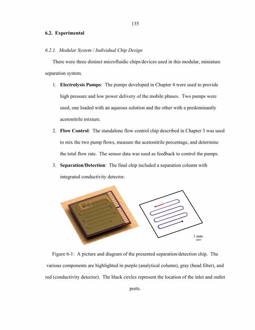
135
6.2. Experimental
6.2.1. Modular System / Individual Chip Design
There were three distinct microfluidic chips/devices used in this modular, miniature
separation system.
1. Electrolysis Pumps: The pumps developed in Chapter 4 were used to provide
high pressure and low power delivery of the mobile phases. Two pumps were
used, one loaded with an aqueous solution and the other with a predominantly
acetonitrile mixture.
2. Flow Control: The standalone flow control chip described in Chapter 3 was used
to mix the two pump flows, measure the acetonitrile percentage, and determine
the total flow rate. The sensor data was used as feedback to control the pumps.
3. Separation/Detection: The final chip included a separation column with
integrated conductivity detector.
Figure 6-1: A picture and diagram of the presented separation/detection chip. The
various components are highlighted in purple (analytical column), gray (bead filter), and
red (conductivity detector). The black circles represent the location of the inlet and outlet
ports.
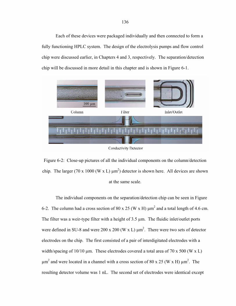
136
Each of these devices were packaged individually and then connected to form a
fully functioning HPLC system. The design of the electrolysis pumps and flow control
chip were discussed earlier, in Chapters 4 and 3, respectively. The separation/detection
chip will be discussed in more detail in this chapter and is shown in Figure 6-1.
Figure 6-2: Close-up pictures of all the individual components on the column/detection
chip. The larger (70 x 1000 (W x L) µm2) detector is shown here. All devices are shown
at the same scale.
The individual components on the separation/detection chip can be seen in Figure
6-2. The column had a cross section of 80 x 25 (W x H) µm2 and a total length of 4.6 cm.
The filter was a weir-type filter with a height of 3.5 µm. The fluidic inlet/outlet ports
were defined in SU-8 and were 200 x 200 (W x L) µm2. There were two sets of detector
electrodes on the chip. The first consisted of a pair of interdigitated electrodes with a
width/spacing of 10/10 µm. These electrodes covered a total area of 70 x 500 (W x L)
µm2 and were located in a channel with a cross section of 80 x 25 (W x H) µm2. The
resulting detector volume was 1 nL. The second set of electrodes were identical except

137
they covered a larger area of 70 x 1000 (W x L) µm2. The detector volume was also
larger as a result (e.g., 2 nL). The two detectors could also be connected in parallel to
form a single 70 x 1500 (W x L) µm2 sensor.
6.2.2. Chip Fabrication
The processes used to make the electrolysis pump and flow control chip were
already discussed in Chapters 4 and 3, respectively. The process to make the
separation/detection chip was identical to the one used to make the flow control chip. A
diagram of the separation/detection chip at various points in the process is shown in
Figure 6-3. A description of the individual steps can be found in Chapter 3.
Figure 6-3: Process flow for the separation/detection chip. The left-hand column shows
a cross-sectional view where the liquid flow is from left to right. The right-hand column
shows a cross-sectional view where the liquid flow is into the page.

138
6.2.3. Chip Packaging / Preparation
The packaging of the electrolysis pumps and flow control chip were described
previously in Chapters 4 and 3. The packaging of the separation/detection chip was
identical to that of the flow control chip, except for the number of fluidic ports. The
separation/detection chip used a manifold with only two fluidic ports, one as an inlet
feeding into the column, and the other as an outlet at the other end.
The column on the separation/detection chip, like the column on the HPLC-
MS/MS chip in Chapter 5, had to be packed with beads prior to testing. This was
accomplished by using the same two-port manifold equipped during normal operation of
the chip. The column was slurry packed using 3 µm C18 support (Varian, Inc.) at a
pressure of 100 bar using the same setup described in Chapter 5.
6.2.4. Electrolysis Pump Operation
The electrolysis pumps were controlled by applying a current through the
electrodes. The magnitude of the current was varied based on the sensor data and
programmed flow profile. Current was delivered using a voltage-controlled current
source (OP741, National Semiconductor) with a maximum output voltage of +/-12 V.
Detailed information about the pump operation can be found in Chapter 4.
6.2.5. Flow Control Chip Operation
The flow control chip had a passive mixer along with two sensors. The first
sensor was an impedance-based composition sensor, which determined the
water/acetonitrile percentage based on electrical measurements. The second sensor was a

139
time-of-flight (TOF) flow sensor, which measured the velocity of an electrochemically
generated ion pulse to deduce the flow rate. The flow control chip used here is identical
to the standalone device discussed in Chapter 3, which should be referred to for more
detail.
6.2.6. Detector Operation
The detector on the separation/detection chip was based on measuring the
conductivity of the solution. Conductivity detection was achieved by applying a 100 kHz,
200 mV AC (HP8111A, Agilent Technologies) signal across the detector electrodes. The
resulting current was measured using an I V converter (OP37, Analog Devices). The
AC voltage output was converted to a DC signal using an AC RMS converter (AD636,
Analog Devices). The total gain (Vout/Ipp) was 1.07x10⁵ Ω. For all experiments in this
chapter, both sets of detector electrodes were connected in parallel to form a single 70 x
1500 (W x L) µm2 sensor.
6.2.7. Chip Separation Configurations
Two different separation configurations were used. In the first setup, the
electrolysis pumps were not used and the flow control and separation/detection chips
were interfaced with a commercial Agilent HPLC pump to conduct separations. This was
done to provide a baseline separation for the purpose of comparison. In the second
separation configuration, the high-pressure electrolysis pumps were used to drive the
fluid flow.

140
Figure 6-4: Diagram of the commercial HPLC pump-driven setup along with the
separation method. An inset showing the operation principle of the injection valve is also
included.
6.2.7.1. Separation with Conventional HPLC Pump
In this separation configuration, an Agilent 1100 Series Quaternary Pump
equipped with a homemade 2080:1 capillary flow splitter was used to run the separation.
The pump was equipped with a water/acetonitrile (0.1% formic acid) solvent system and
connected to one of the mixer inputs on the flow control chip, with the other mixer input
blocked off and unused. The flow was directed through the mixer and sensors, out of the
flow control chip, and into a manually actuated Nanovolume® two-position, six-port
sample injection valve (Vici Valco Instruments). This two-position valve allowed a
sample loop (100 nL) to be filled via a syringe and then switched online. The output of
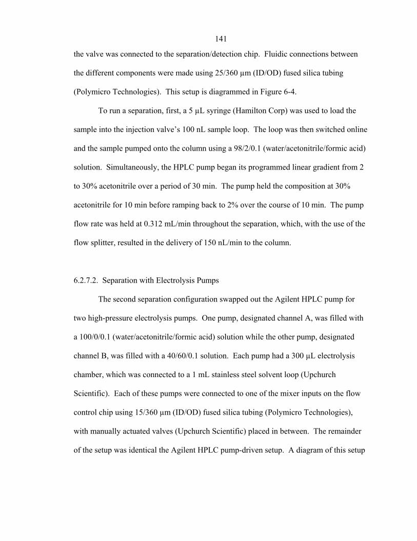
141
the valve was connected to the separation/detection chip. Fluidic connections between
the different components were made using 25/360 µm (ID/OD) fused silica tubing
(Polymicro Technologies). This setup is diagrammed in Figure 6-4.
To run a separation, first, a 5 µL syringe (Hamilton Corp) was used to load the
sample into the injection valve’s 100 nL sample loop. The loop was then switched online
and the sample pumped onto the column using a 98/2/0.1 (water/acetonitrile/formic acid)
solution. Simultaneously, the HPLC pump began its programmed linear gradient from 2
to 30% acetonitrile over a period of 30 min. The pump held the composition at 30%
acetonitrile for 10 min before ramping back to 2% over the course of 10 min. The pump
flow rate was held at 0.312 mL/min throughout the separation, which, with the use of the
flow splitter, resulted in the delivery of 150 nL/min to the column.
6.2.7.2. Separation with Electrolysis Pumps
The second separation configuration swapped out the Agilent HPLC pump for
two high-pressure electrolysis pumps. One pump, designated channel A, was filled with
a 100/0/0.1 (water/acetonitrile/formic acid) solution while the other pump, designated
channel B, was filled with a 40/60/0.1 solution. Each pump had a 300 µL electrolysis
chamber, which was connected to a 1 mL stainless steel solvent loop (Upchurch
Scientific). Each of these pumps were connected to one of the mixer inputs on the flow
control chip using 15/360 µm (ID/OD) fused silica tubing (Polymicro Technologies),
with manually actuated valves (Upchurch Scientific) placed in between. The remainder
of the setup was identical the Agilent HPLC pump-driven setup. A diagram of this setup

142
can be found in Figure 6-5. A photograph of the actual experiment can also be found in
Figure 6-6.
Figure 6-5: Diagram of the electrolysis pump-driven setup along with the separation
method. An inset showing the operation principle of the injection valve is also included.
The separation method was slightly different from the Agilent HPLC pump-
driven separation. After filling the sample loop and switching the loop online as done
before, the gradient was started after a 5 min delay instead of immediately after the valve
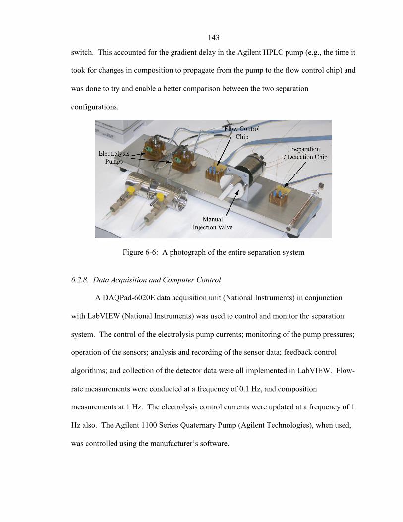
143
switch. This accounted for the gradient delay in the Agilent HPLC pump (e.g., the time it
took for changes in composition to propagate from the pump to the flow control chip) and
was done to try and enable a better comparison between the two separation
configurations.
Figure 6-6: A photograph of the entire separation system
6.2.8. Data Acquisition and Computer Control
A DAQPad-6020E data acquisition unit (National Instruments) in conjunction
with LabVIEW (National Instruments) was used to control and monitor the separation
system. The control of the electrolysis pump currents; monitoring of the pump pressures;
operation of the sensors; analysis and recording of the sensor data; feedback control
algorithms; and collection of the detector data were all implemented in LabVIEW. Flow-
rate measurements were conducted at a frequency of 0.1 Hz, and composition
measurements at 1 Hz. The electrolysis control currents were updated at a frequency of 1
Hz also. The Agilent 1100 Series Quaternary Pump (Agilent Technologies), when used,
was controlled using the manufacturer’s software.

144
6.3. Results and Discussion
6.3.1. Microfluidic Chips/Components
The electrolysis pump and flow control chip were studied and presented in detail
in Chapters 3 and 4. Two of the three components on the separation/detection chip (e.g.,
analytical column and filter) were identical to components already on the HPLC-MS/MS
chip and were described in Chapter 5. Only the conductivity detector will require further
discussion in this chapter.
6.3.1.1. Conductivity Detector
Originally, the detection electrodes were designed to be used for both
electrochemical and conductivity detection. However, initial tries to implement
electrochemical detection using DC amperometry were met with little success. It was
believed that this was mainly caused by contamination of the electrode surface. Many of
our electrode-based sensors, such as the composition sensor in Chapter 3, were also very
easily contaminated. This problem was compounded by the fact that there was no direct
access to the electrodes and the usual mechanical methods of cleaning the working
electrodes were not possible. Pulsed amperometric techniques, which electrochemically
clean the electrode surface periodically, would have been more effective, but were not
pursued.
Electrochemical detection was abandoned in favor of conductivity-based
detection. AC conductivity measurements using our microfabricated electrodes proved to
be much less problematic. This was most likely because the use of an AC excitation
signal with sufficient frequency eliminated the sensor’s dependence on a clean electrode

145
surface. Figure 6-7 contains a plot showing the response of the conductivity sensors to
varying concentrations of formic acid, which is the main electrolyte in the mobile phases.
The sensitivity was estimated be better than 1 µM. One limitation of conductivity
detection is that only ions can be detected, limiting what analytes can be analyzed. Post-
column reactions/derivatizations could be potentially used and would enable the detection
of normally neutral molecules, providing more general detection capability.
During the passing of a solvent gradient, this detector demonstrated significant
drift. This was expected, due to changes in the bulk fluid conductivity at various
water/acetonitrile ratios. This was the same principle that was used for composition
measurements. This drift was accounted for by comparing actual separations with blank
runs. Direct subtraction of the two signals gave a well-compensated detector signal with
minimal drift.
1.4
1.6
1.8
2.0
2.2
2.4
2.6
2.8
1.0 1.5 2.0 2.5 3.0
[H+]/[COOH-] mM
Det
ecto
r (V
)
Figure 6-7: Detector response at different aqueous concentrations of [H+]/[COOH-].
0.1% formic acid in water corresponds to 2.1 mM.

146
1.4
1.6
1.8
2.0
2.2
2.4
0 10 20 30 40
Time (min)
Det
ecto
r (V
)
-0.1
0.0
0.1
0.2
0.3
0.4
0 10 20 30 4
Time (min)
Det
ecto
r (V
)
0
blank compensated detector signal
separation
0
10
20
30
40
0 10 20 30 40
Time (min)
% A
ceto
nitri
le
120
130
140
150
160
170
0 10 20 30 4
Time (min)
Flow
Rat
e (n
L/m
in)
0
programmed programmed
actual actual
Figure 6-8: Separation of a five-peptide sample. The raw detector and baseline signals
(top left) are shown along with the compensated detector signal (top right). Also shown
are the composition (bottom left) and flow rate (bottom right) as indicated by the
integrated sensors.
6.3.2. Separation with Agilent HPLC Pump
A peptide mixture was used to assess the separation performance. The mixture
contained five peptides: Gly-Tyr (MW 238.2), Val-Tyr-Val (MW 379.5), Methionine
Enkephalin Acetate (Tyr-Gly-Gly-Phe-Met) (MW 573.7), Leucine Enkephalin (Tyr-Gly-
Gly-Phe-Leu) (MW 555.6), and Angiotensin II (Asp-Arg-Val-Tyr-Ile-His-Pro-Phe) (MW
1046.2). Separations of 100 nL of a 1 mg/mL (each component) stock sample solution
were conducted and an example can be found in Figure 6-8. The separations showed the

147
expected five peaks. The di- and tri-peptides both eluted out before the start of the
gradient. This was expected because of their small size.
Based on the composition sensor data, there was a delay of approximately 6 min
for compositional changes to reach the flow control chip after being generated in the
HPLC pump. After reaching the composition sensor, it took another 3 min for the liquid
to reach the end of the column. The 3 min delay time included the sample loop volume
because it was left online during the entire separation. The composition sensor indicated
a highly linear gradient delivered by the HPLC pump. The flow sensor also indicated
good flow stability. Some flow fluctuations were observed, particularly during the
gradient. This is highly characteristic of split-flow nanoflow systems where
compositional changes propagate at varying speeds along the two flow paths, slightly
changing the desired 2080:1 split flow ratio.
One of the problems with this separation was that a very large quantity of sample
had to be used. This was mainly due to a relatively low detector sensitivity, at least when
compared to MS. Overall, 0.1 µg of each peptide (e.g., 0.5 µg total amount) had to be
injected to get good peak detection. Unfortunately, this was near or exceeding the
amount of sample that would normally be appropriate for a column of these dimensions.
As a result, overloading effects were seen. Characteristic behavior that indicates sample
overloading are peaks that show a steep rise, but slow falloff rather than the desired
symmetrical peak shape. The last three peaks in our separation were classic examples of
this. Besides poor peak shapes, sample overloading can also reduce the peak retention
times. This is because of competition of analytes on the column, where more
hydrophobic peptides displace the less hydrophobic ones. It is expected that with an

148
improvement in detector sensitivity, the amount of sample could be reduced, allowing a
better overall separation.
One interesting point that should be noted was that the analyte peaks were
detected as a decrease in conductivity. This was caused by the proton transfer between
the solution and the peptides. H+ was the main ion in the mobile phases (from the formic
acid). It also had the highest contribution to the overall liquid conductivity because of its
high mobility. At low pH, the amine group on the amino acids accepted an H+. This
essentially removed H+ ions from solution and put a net positive charge on the peptide.
While the total charge in the solution remained the same, the overall mobility of the
charged peptide was significantly lower than the free H+ ions, resulting in a lower overall
conductivity. Originally, separations were conducted using 0.1% trifluoroacetic acid
(TFA) rather than formic acid. TFA is usually used by default for most peptide/protein
separations. When TFA was used in our separation experiments, the sensitivity of the
conductivity detection dropped to a point where the peaks were only barely discernable.
This was believed to be due to the ion-suppression properties of TFA. A similar problem
is believed to happen when TFA is used with MS detection79, which is why formic acid is
preferred in HPLC-MS/MS.
6.3.3. Separation with Electrolysis Pumps
Because the electrolysis pumps were filled at atmospheric pressure, the pumps
first had to be pressurized. This was most efficiently done by closing the valves
separating the electrolysis pumps from the flow control chip. With a closed electrolysis
system, similar to the one used for calibration in Chapter 4, a high current was applied

149
until the pressures reached the desired starting point, generally around 40–55 bar. The
valves were then opened to push the fluids into the rest of the fluidic system and the
closed-loop flow control system activated.
Because nearly all aspects of this separation system were susceptible to gas (e.g.
composition sensor, flow sensor, column, and detector), the flow was allowed to flush the
gas out of the fluidic system for 20–30 min before any separations were attempted. The
existence of gas in the fluidic system was easily monitored by looking at the low pressure
end of the separation system, or the detector. Any bubbles trapped in the fluidic system
would become most prominent at the low-pressure end since the dissolved gas would
“undissolve” there. The column detector was used to observe any passing bubbles, which
expressed themselves as sharp valleys in the conductivity measurements. Flow
equilibration was continued until the detector indicated a bubble-free flow. Another
source of gas is from the electrolysis chamber itself. The use of a large buffer volume (>
1 mL) between the electrolysis chamber and the chip ensured that this would not cause
any problems.
The overall design of the fluidic system had to take into account the capabilities
of the electrolysis pumps. As was mentioned in Chapter 4, the electrolysis pumps were
relatively slow to react, with a maximum ramp rate on the order of 0.1–0.2 bar/min. The
fluidic system had to be designed to make sure that ramp rates beyond this were not
needed for the programmed flow profiles. This was controlled by changing the diameter
and length of the fused silica tubing connecting the pumps to the flow control chip.
Large diameter and short lengths (e.g., low fluidic resistances) meant that only small
changes in pressure were needed to achieve changes in composition. The opposite was

150
true of small diameter and longer tubing lengths. One drawback of making the fluidic
resistance small was that it could cause instability in the system. Small pressure
fluctuations in any of the pumps would have a large effect on the composition, potentially
ruining the separation. In the end, these factors were balanced to achieve good pump
stability while still maintaining the ability to change the composition at the requisite rate.
The mathematical model developed in Chapter 4 to simulate the pneumatic pump-driven
flow control system was also applied here to determine the optimal tubing lengths. In the
end, 0.35 m long and 15 µm ID lengths of tubing were chosen for both pumps.
Another consequence of the slow response of the pump was that it complicated
the design of the feedback algorithms. Ideally, with the slow response of these pumps,
the control algorithms needed to not only consider the error history, but also look at the
future desired flow profile. This, however, would have complicated the control
algorithms. Another complication was that knowledge of the pump state was critical to
pump control. The frequency response of the electrolysis pumps had a strong
dependence on the volume of gas in the electrolysis chamber. Unfortunately, state
estimation can be difficult, with errors likely building up over long periods of time. In
the end, a digital control algorithm with three different current states was used for
pumping. The pumps were run using only 0, 2, and 4 mA driving current. The values of
these three levels were based on the pump calibration curves in Chapter 4. With an
expected operating pressure of around 40 bar and a total flow rate of 150 nL/min, an
average current in the vicinity of 2 mA was expected and was therefore chosen as the
middle level. 4 mA, on the other hand, was capable of pressures and flow rates
significantly higher than necessary and was chosen for the high-state level. The high

151
state was generally reserved for situations where the pump pressure needed to be
increased. Finally 0 mA was used when there was a desire to decrease the pump pressure.
The lookup table in Table 6-1 was used to control the pumps. This simple control
algorithm proved to be very reliable and actually resulted in better performance than
attempts to implement a PID control algorithm. During a typical gradient, compositional
set point errors were < 0.1 % acetonitrile and flow rate errors were < 3 nL/min.
Flow Error (+) = too high (-) = too low
Composition Error(+) %ACN too low(-) %ACN too high
Pump A Current (mA)
Pump B Current (mA)
+ + 0.0 4.0 + - 4.0 0.0 - + 2.0 4 .0 - - 4.0 2.0
Table 6-1: Digital control algorithm for electrolysis pumps
1.4
1.6
1.8
2.0
2.2
2.4
0 10 20 30 40
Time (min)
Det
ecto
r (V
)
-0.1
0.0
0.1
0.2
0.3
0.4
0 10 20 30 4
Time (min)
Det
ecto
r (V
)
0
compensated detector signal blank
separation
0
10
20
30
40
0 10 20 30 40
Time (min)
% A
ceto
nitri
le
120
130
140
150
160
170
0 10 20 30 4
Time (min)
Flow
Rat
e (n
L/m
in)
0
programmed programmed
actual actual

152
0
1
2
3
4
5
0 10 20 30 40
Time (min)
Cur
rent
(mA
)
35
40
45
50
0 10 20 30 4
Time (min)
Pres
sure
(bar
)
0
Pump A Pump A
Pump B Pump B
Figure 6-9: Separation of a five-peptide sample. The raw detector and baseline signals
(top left) are shown along with the compensated detector signal (top right). Also shown
are the composition (middle left), flow rate (middle right), pump-driving currents (bottom
left), and pump pressures (bottom right). To better show the trend, pump currents were
fitted with a 5 min moving average.
Figure 6-9 shows a separation of the same five peptide mixture used earlier. The
sample amount was once again 100 nL of a 1 mg/mL stock solution. No real difference
could be found between the separations conducted using this setup and the setup using
the commercial HPLC pump. Small shifts in the peak positions could have been easily
caused by differences in the flow rate.
Looking at the currents used to drive the electrolysis pumps revealed some
interesting points. First of all, the average current was generally around 2–3 mA, which
was completely expected based on our calibration of the electrolysis pump in Chapter 4.
Also, the basic trend for the channel A current was downwards while the channel B
current was upwards. This was expected, given the slope of the desired gradient. The
pressure inside the electrolysis pumps also demonstrated upward and downward slopes as
expected. The same mathematical model used in Chapter 5 to compare the actual

153
pneumatic pump pressures versus the expected ones could be applied to this system as
well. The results of this calculation can be found in Figure 6-10. For this simulation, the
following resistance values were measured and used: Raη(0) = 0.043 bar/(nL/min),
Rbη(0.60) = 0.034 bar/(nL/min), and Rc = 0.281 bar/(nL/min)/cP.
35
40
45
50
0 10 20 30
Time (min)
Pres
sure
(bar
)
40
Pump A (Theory) Pump A
(Actual)
Pump B (Theory)
Pump B (Actual)
Figure 6-10: Comparison between the actual electrolysis pump pressures and the
calculated ones
Interestingly enough, the ratio of the actual pump pressures matched up with the
ratio of the calculated pressures very well. This was a good indication that the
compositional changes were well controlled by the feedback system. This was backed up
by the composition sensor data. The actual pump pressures differed slightly from those
predicted by the model. The effect of this discrepancy was evident by looking at the flow
rate data in Figure 6-9. From 0–10 and 30–40 min, the flow rate was higher than the 150
nL/min set point. Expectedly, the actual pump pressures were also higher than the
theoretical pump pressures during those same intervals. The opposite was true of the 10–
30 min interval where the flow rate was less than the 150 nL/min set point. Therefore,

154
even though the calculated and actual pressures look significantly different, the only
consequence was a deviation of ±3 nL/min from the set point flow rate.
6.4. Conclusion
A portable HPLC separation platform was demonstrated and characterized. The
platform used a modular approach where several different chip/devices were connected to
form a working system. The overall size of the system (excluding electronics) was small
enough to be handheld and had a total power consumption of only 30 mW. The
separation performance was adequate but suffered due to column overloading, a result of
a detector’s less than ideal sensitivity. Improvements to the detector would likely have
resulted in much higher-resolution separations.

155
Chapter 7: Conclusion
In the past few chapters, numerous individual microfluidic devices have been
demonstrated. This includes: high-pressure electrolysis pumps, mixers, composition
sensors, flow sensors, columns, frits, electrospray nozzles, and conductivity detectors.
All the developed components were designed to withstand the rigorous high pressure,
low flow rate, and solvent compatibility requirements of nanoscale HPLC. These
individual components were then integrated together to form gradient-capable, reverse-
phase, nanoscale HPLC systems.
Over the past few decades, almost every imaginable microfluidic component has
been demonstrated, and each component has been realized using several microfabrication
technologies. While standalone microfluidic components are sometimes useful,
ultimately, integration of various microfluidic components is absolutely necessary to
create more powerful microfluidic systems. The advancement of the microfluidics field
hinges on this. Despite this fact, many microfluidic efforts are still aimed at producing
individual components. It is hoped that the work presented in this thesis will encourage
others to push for the high-level integration of microfluidic components as well.

156
Chapter 8: References
(1) Stone, H. A.; Stroock, A. D.; Ajdari, A. Annual Review of Fluid Mechanics 2004, 36, 381-411.
(2) Beebe, D. J.; Mensing, G. A.; Walker, G. M. Annual Review of Biomedical Engineering 2002, 4, 261-286.
(3) Ho, C. M.; Tai, Y. C. Annual Review of Fluid Mechanics 1998, 30, 579-612.
(4) Kovacs, G. T. A.; Maluf, N. I.; Petersen, K. E. Proceedings of the IEEE 1998, 86, 1536-1551.
(5) Bustillo, J. M.; Howe, R. T.; Muller, R. S. Proceedings of the IEEE 1998, 86, 1552-1574.
(6) Whitesides, G. M.; Ostuni, E.; Takayama, S.; Jiang, X. Y.; Ingber, D. E. Annual Review of Biomedical Engineering 2001, 3, 335-373.
(7) Terry, S. C.; Jerman, J. H.; Angell, J. B. IEEE Transactions on Electron Devices 1979, 26, 1880-1886.
(8) Maluf, N. An introduction to Microelectromechanical Systems Engineering; Artech House, Inc.: Norwood, MA, 2000.
(9) Unger, M. A.; Chou, H. P.; Thorsen, T.; Scherer, A.; Quake, S. R. Science 2000, 288, 113-116.
(10) Becker, H.; Gartner, C. Electrophoresis 2000, 21, 12-26.
(11) Oh, K. W.; Ahn, C. H. Journal of Micromechanics and Microengineering 2006, 16, R13-R39.
(12) Nguyen, N. T.; Huang, X. Y.; Chuan, T. K. Journal of Fluids Engineering-Transactions of the ASME 2002, 124, 384-392.
(13) Woias, P. Sensors and Actuators B—Chemical 2005, 105, 28-38.
(14) Kovacs, G. T. A. Micromachined Transducers Sourcebook McGraw-Hill Science/Engineering/Math, 1998.
(15) Reyes, D. R.; Iossifidis, D.; Auroux, P. A.; Manz, A. Analytical Chemistry 2002, 74, 2623-2636.

157
(16) Lion, N.; Rohner, T. C.; Dayon, L.; Arnaud, I. L.; Damoc, E.; Youhnovski, N.; Wu, Z. Y.; Roussel, C.; Josserand, J.; Jensen, H.; Rossier, J. S.; Przybylski, M.; Girault, H. H. Electrophoresis 2003, 24, 3533-3562.
(17) Nguyen, N. T.; Wu, Z. G. Journal of Micromechanics and Microengineering 2005, 15, R1-R16.
(18) Auroux, P. A.; Iossifidis, D.; Reyes, D. R.; Manz, A. Analytical Chemistry 2002, 74, 2637-2652.
(19) SCS In SCS Technical Document, 2007, pp 1-12.
(20) Meng, E.; Tai, Y. C. 18th IEEE International Conference on Micro Electro Mechanical Systems (MEMS 2005) 2005, 568-571.
(21) Xie, J.; Shih, J.; Tai, Y. C. 16th IEEE International Conference on Micro Electro Mechanical Systems (MEMS 2003) 2003, 20-23.
(22) Liger, M.; Rodger, D. C.; Tai, Y. C. 16th IEEE International Conference on Micro Electro Mechanical Systems (MEMS 2003) 2003, 602-605.
(23) Walsh, K.; Norville, J.; Tai, Y. C. 14th IEEE International Conference on Micro Electro Mechanical Systems (MEMS 2001) 2001, 114-117.
(24) Shih, J.; Tai, Y.-C.; Miao, Y.; Lee, T. D. 5th IEEE Conference on Sensors (SENSORS 2006) 2006, 1432-1435.
(25) Shih, J.; Xie, J.; Tai, Y. C. 12th International Conference On Solid-State Sensors, Actuators And Microsystems (Transducers 2003) 2003, 388-391.
(26) He, Q.; Pang, C.; Tai, Y. C.; Lee, T. D. 17th IEEE International Conference on Micro Electro Mechanical Systems (MEMS 2004) 2004, 212-215.
(27) Miserendino, S., California Institute of Technology, Pasadena, 2007.
(28) Xie, J.; Shih, J.; Lin, Q. A.; Yang, B. Z.; Tai, Y. C. Lab on a Chip 2004, 4, 495-501.
(29) Li, P.-Y.; Shih, J.; Lo, R.; Adams, B.; Agrawal, R.; Saati, S.; Humayun, M. S.; Tai, Y.-C.; Meng, E. 20th IEEE International Conference on Micro Electro Mechanical Systems (MEMS 2007) 2007, 15-18.
(30) Xie, J.; Miao, Y. N.; Shih, J.; He, Q.; Liu, J.; Tai, Y. C.; Lee, T. D. Analytical Chemistry 2004, 76, 3756-3763.
(31) Xie, J.; Miao, Y. N.; Shih, J.; Tai, Y. C.; Lee, T. D. Analytical Chemistry 2005, 77, 6947-6953.

158
(32) Selvaganapathy, P.; Yit-shun Leung, K.; Renaud, P.; Mastrangelo, C. H. Microelectromechanical Systems, Journal of 2002, 11, 448-453.
(33) Chen, C.-L.; Selvarasah, S.; Chao, S.-H.; Khanicheh, A.; Mavroidis, C.; Dokmeci, M. R. 2nd IEEE International Conference on Nano/Micro Engineered and Molecular Systems (NEMS 2007) 2007, 826-829.
(34) Chen, P. J.; Rodger, D. C.; Meng, E. M.; Humayun, M. S.; Tai, Y. C. Journal of Microelectromechanical Systems 2007, 16, 223-231.
(35) Chen, P.-J.; Tai, Y.-C. 20th IEEE International Conference on Micro Electro Mechanical Systems (MEMS 2007) 2007, 453-456.
(36) Wang, X. Q.; Lin, Q.; Tai, Y. C. 12th IEEE International Conference on Micro Electro Mechanical Systems (MEMS 1999) 1999, 177-182.
(37) Wang, X. Q.; Tai, Y. C. 13th IEEE International Conference on Micro Electro Mechanical Systems (MEMS 2000) 2000, 68-73.
(38) Xie, J.; Yang, X.; Wang, X. Q.; Tai, Y. C. 14th IEEE International Conference on Micro Electro Mechanical Systems (MEMS 2001) 2001, 539-542.
(39) Selvaganapathy, P.; Carlen, E. T.; Mastrangelo, C. H. Sensors and Actuators A—Physical 2003, 104, 275-282.
(40) Ryu, K. S.; Wang, X.; Shaikh, K.; Goluch, E.; Mathias, P.; Liu, C. 9th International Conference on Miniaturized Systems for Chemistry and Life Sciences (µTAS 2005) 2005, 1192-1194.
(41) Licklider, L.; Wang, X. Q.; Desai, A.; Tai, Y. C.; Lee, T. D. Analytical Chemistry 2000, 72, 367-375.
(42) Shih, J.; Miao, Y. N.; Lee, T. D.; Tai, Y. C. 10th International Conference on Miniaturized Systems for Chemistry and Life Sciences (μTAS2006) 2006, 1573-1575.
(43) Liu, M. C.; Ho, D.; Tai, Y.-C. 2nd IEEE International Conference on Nano/Micro Engineered and Molecular Systems (NEMS 2007) 2007, 993-996.
(44) Lammerink, T. S. J.; Tas, N. R.; Elwenspoek, M.; Fluitman, J. H. J. Sensors and Actuators A—Physical 1993, 37-8, 45-50.
(45) Wu, S. Y.; Lin, Q.; Yuen, Y.; Tai, Y. C. Sensors and Actuators A—Physical 2001, 89, 152-158.
(46) Collins, J.; Lee, A. P. Lab on a Chip 2004, 4, 7-10.
(47) Wu, J.; Ye, J. Lab on a Chip 2005, 5, 1344-1347.

159
(48) Czaplewski, D. A.; Ilic, B. R.; Zalalutdinov, M.; Olbricht, W. L.; Zehnder, A. T.; Craighead, H. G.; Michalske, T. A. Journal of Microelectromechanical Systems 2004, 13, 576-585.
(49) Oosterbroek, R. E.; Lammerink, T. S. J.; Berenschot, J. W.; Krijnen, G. J. M.; Elwenspoek, M. C.; van den Berg, A. Sensors and Actuators A—Physical 1999, 77, 167-177.
(50) Ashauer, M.; Glosch, H.; Hedrich, F.; Hey, N.; Sandmaier, H.; Lang, W. Sensors and Actuators A—Physical 1999, 73, 7-13.
(51) Meng, E.; Tai, Y. C. 12th International Conference on Solid-State Sensors, Actuators and Microsystems (Transducers 2003) 2003, 686-689.
(52) Harnett, C. K.; Mosier, B. P.; Caton, P. F.; Wiedenman, B.; Crocker, R. W. 7th International Conference on Micro Total Analysis Systems (μTAS 2003) 2003, 139-142.
(53) Wu, J. A.; Sansen, W. Sensors and Actuators A—Physical 2002, 97-8, 68-74.
(54) Veenstra, T. T.; Lammerink, T. S. J.; Elwenspoek, M. C.; van den Berg, A. Journal of Micromechanics and Microengineering 1999, 9, 199-202.
(55) Shih, C. Y.; Li, W.; Zheng, S.; Tai, Y. C. 5th IEEE Conference on Sensors (SENSORS 2006) 2006, 271-274.
(56) Shulin, Z.; Chuan-Hua, C.; Mikkelsen, J. C., Jr.; Santiago, J. G. Sensors and Actuators B—Chemical 2001, B79, 107-114.
(57) Reichmuth, D. S.; Chirica, G. S.; Kirby, B. J. Sensors and Actuators B—Chemical 2003, 92, 37-43.
(58) Paul, P. H.; Arnold, D. W.; Rakestraw, D. J. 3rd International Conference on Miniaturized Systems for Chemistry and Life Sciences (uTAS 1998) 1998, 49-52.
(59) Cameron, C. G.; Freund, M. S. Proceedings of the National Academy of Sciences of the United States of America 2002, 99, 7827-7831.
(60) Suzuki, H.; Yoneyama, R. Sensors and Actuators B—Chemical 2003, 96, 38-45.
(61) Suzuki, H.; Yoneyama, R. Sensors and Actuators B—Chemical 2002, 86, 242-250.
(62) Bohm, S.; Timmer, B.; Olthuis, W.; Bergveld, P. Journal of Micromechanics and Microengineering 2000, 10, 498-504.
(63) Munyan, J. W.; Fuentes, H. V.; Draper, M.; Kelly, R. T.; Woolley, A. T. Lab on a Chip 2003, 3, 217-220.

160
(64) Jones, J. E.; Hansen, L. D.; Jones, S. E.; Shelton, D. S.; Thorne, J. M. Journal of Physical Chemistry 1995, 99, 6973-6979.
(65) Will, F. G. Journal of Electroanalytical Chemistry 1997, 426, 177-184.
(66) Aebersold, R.; Mann, M. Nature 2003, 422, 198-207.
(67) Hunt, D. F.; Yates, J. R.; Shabanowitz, J.; Winston, S.; Hauer, C. R. Proceedings of the National Academy of Sciences of the United States of America 1986, 83, 6233-6237.
(68) Eng, J. K.; McCormack, A. L.; Yates, J. R. Journal of the American Society for Mass Spectrometry 1994, 5, 976-989.
(69) Bruin, G. J. M. Electrophoresis 2000, 21, 3931-3951.
(70) Harrison, D. J.; Fluri, K.; Seiler, K.; Fan, Z. H.; Effenhauser, C. S.; Manz, A. Science 1993, 261, 895-897.
(71) Jacobson, S. C.; Hergenroder, R.; Koutny, L. B.; Ramsey, J. M. Analytical Chemistry 1994, 66, 1114-1118.
(72) Ocvirk, G.; Verpoorte, E.; Manz, A.; Grasserbauer, M.; Widmer, H. M. Analytical Methods and Instrumentation 1995, 2, 74-82.
(73) Lindner, D. Lab on a Chip 2001, 1, 15N-19N.
(74) de Mello, A. Lab on a Chip 2002, 2, 48N-54N.
(75) Reichmuth, D. S.; Shepodd, T. J.; Kirby, B. J. Analytical Chemistry 2005, 77, 2997-3000.
(76) Yin, N. F.; Killeen, K.; Brennen, R.; Sobek, D.; Werlich, M.; van de Goor, T. V. Analytical Chemistry 2005, 77, 527-533.
(77) Licklider, L. J.; Thoreen, C. C.; Peng, J. M.; Gygi, S. P. Analytical Chemistry 2002, 74, 3076-3083.
(78) Badman, E. R.; Cooks, R. G. Journal of Mass Spectrometry 2000, 35, 659-671.
(79) Annesley, T. M. Clinical Chemistry 2003, 49, 1041-1044.
Top Related