


Languages
Pages
Legal

MGM13P Mighty Gecko Module Data Sheet
The MGM13P Mighty Gecko Module (MGM13P) is a small form factor, certified module,enabling rapid development of wireless mesh networking solutions.
Based on the Silicon Labs EFR32MG13 Mighty Gecko SoC, the MGM13P combines anenergy- efficient, multi-protocol wireless SoC with a proven RF/antenna design and in-dustry leading wireless software stacks. This integration accelerates time-to-market andsaves months of engineering effort and development costs. In addition, common soft-ware and development tools enable seamless migration between modules and discreteSoC-based designs.
MGM13P modules can be used in a wide variety of applications:
KEY FEATURES
• 32-bit ARM® Cortex®-M4 core at 38.4MHz
• 512 kB of flash memory and 64 kB of RAM• Zigbee, Thread, BLE, and multi-protocol
support• Pin compatible with MGM12P module• 12-channel Peripheral Reflex System,
Low-Energy Sensor Interface &Multichannel Capacitive Sense Interface
• Integrated PA with up to 10 dBm transmitpower
• Robust peripheral set and up to 25 GPIO
• IoT Multi-Protocol Devices• Connected Home• Lighting• Health and Wellness• Metering• Building Automation and Security
Antenna Timers and Triggers
32-bit bus
Peripheral Reflex System
Serial Interfaces
I/O Ports Analog I/F
Lowest power mode with peripheral operational:
USART
Low Energy UARTTM
I2C
External Interrupts
General Purpose I/O
Pin Reset
Pin Wakeup
ADC
VDAC
Analog Comparator
EM3—StopEM2—Deep SleepEM1—Sleep EM4—Hibernate EM4—ShutoffEM0—Active
Energy Management
Brown-Out Detector
DC-DC Converter
Voltage Regulator Voltage Monitor
Power-On Reset
Other
Capacitive Touch
Op-Amp
IDAC
CRYPTO
CRC
True Random Number Generator
SMU
Core / Memory
ARM CortexTM M4 processorwith DSP extensions, FPU and MPU
ETM Debug Interface RAM Memory LDMA Controller
Flash Program Memory
Real Time Counter and
CalendarCryotimer
Timer/Counter
Low Energy Timer
Pulse Counter Watchdog Timer
Protocol Timer
Low Energy Sensor Interface
Radio Transceiver
DEMOD
AGC
IFADC
CR
C
BU
FC
MOD
FRC
RA
C
I
Q
RF FrontendLNA
PAFrequency Synthesizer
PGA
BA
LUN
Chip Antennaor
U.FL Connector
Matching
Crystals
38.4 MHz
32.768 kHz
Clock Management
L-FRC Oscillator
H-FRC Oscillator
Auxiliary H-F RC Oscillator
Ultra L-F RC Oscillator
L-F Crystal Oscillator
H-F Crystal Oscillator
silabs.com | Building a more connected world. Rev. 1.0
1. Feature List
The MGM13P highlighted features are listed below.• Low Power Wireless System-on-Chip.
• High Performance 32-bit 38.4 MHz ARM Cortex®-M4 withDSP instruction and floating-point unit for efficient signalprocessing
• Embedded Trace Macrocell (ETM) for advanced debugging• 512 kB flash program memory• 64 kB RAM data memory• 2.4 GHz radio operation• TX power up to 10 dBm
• Low Energy Consumption• 11 mA RX current at 250 kbps, O-QPSK DSSS• 9.9 mA RX current at 1 Mbps, GFSK• 8.5 mA TX current at 0 dBm output power• 87 μA/MHz in Active Mode (EM0)• 1.4 μA EM2 DeepSleep current (64 kB RAM retention and
RTCC running from LFXO)• 1.3 μA EM2 DeepSleep current (16 kB RAM retention and
RTCC running from LFRCO)• Wake on Radio with signal strength detection, preamble
pattern detection, frame detection and timeout• High Receiver Performance
• -102.8 dBm sensitivity at 125 kbit/s GFSK• -94.6 dBm sensitivity at 1 Mbit/s GFSK• -91 dBm sensitivity at 2 Mbit/s GFSK• -102.1 dBm sensitivity at 250 kbps DSSS-OQPSK, 2.4 GHz
• Supported Protocols• Zigbee• Thread• Bluetooth Low Energy (Bluetooth 5)
• Support for Internet Security• General Purpose CRC• True Random Number Generator (TRNG)• 2 × Hardware Cryptographic Acceleration for AES 128/256,
SHA-1, SHA-2 (SHA-224 and SHA-256) and ECC• Regulatory Certifications
• FCC• CE• IC / ISEDC• MIC / Telec
• Wide selection of MCU peripherals• 12-bit 1 Msps SAR Analog to Digital Converter (ADC)• 2 × Analog Comparator (ACMP)• 2 × Digital to Analog Converter (VDAC)• 3 × Operational Amplifier (Opamp)• Digital to Analog Current Converter (IDAC)• Low-Energy Sensor Interface (LESENSE)• Multi-channel Capacitive Sense Interface (CSEN)• 25 pins connected to analog channels (APORT) shared be-
tween analog peripherals• 25 General Purpose I/O pins with output state retention and
asynchronous interrupts• 8 Channel DMA Controller• 12 Channel Peripheral Reflex System (PRS)• 2 × 16-bit Timer/Counter
• 3 or 4 Compare/Capture/PWM channels• 1 × 32-bit Timer/Counter
• 3 Compare/Capture/PWM channels• 32-bit Real Time Counter and Calendar• 16-bit Low Energy Timer for waveform generation• 32-bit Ultra Low Energy Timer/Counter for periodic wake-up
from any Energy Mode• 16-bit Pulse Counter with asynchronous operation• 2 × Watchdog Timer• 3 × Universal Synchronous/Asynchronous Receiver/Trans-
mitter (UART/SPI/SmartCard (ISO 7816)/IrDA/I2S)• Low Energy UART (LEUART™)• 2 × I2C interface with SMBus support and address recogni-
tion in EM3 Stop• Wide Operating Range
• 1.8 V to 3.8 V single power supply• Integrated DC-DC• -40 °C to +85 °C
• Dimensions• 12.9 × 17.8 × 2.3 mm (W × L × H)
MGM13P Mighty Gecko Module Data SheetFeature List
silabs.com | Building a more connected world. Rev. 1.0 | 2

2. Ordering Information
Table 2.1. Ordering Information
Ordering Code Protocol Stack
Frequency Band
@ Max TX Power AntennaFlash(kB)
RAM(kB) GPIO Packaging
MGM13P02F512GA-V2R • BluetoothLow Energy
• Zigbee• Thread• Multiprotocol
2.4 GHz @ 10 dBm Built-in 512 64 25 Reel
MGM13P02F512GA-V2 • BluetoothLow Energy
• Zigbee• Thread• Multiprotocol
2.4 GHz @ 10 dBm Built-in 512 64 25 Tray
MGM13P02F512GE-V2R • BluetoothLow Energy
• Zigbee• Thread• Multiprotocol
2.4 GHz @ 10 dBm U.FL 512 64 25 Reel
MGM13P02F512GE-V2 • BluetoothLow Energy
• Zigbee• Thread• Multiprotocol
2.4 GHz @ 10 dBm U.FL 512 64 25 Tray
Devices are not pre-programmed with a firmware image.
MGM13P Mighty Gecko Module Data SheetOrdering Information
silabs.com | Building a more connected world. Rev. 1.0 | 3

Table of Contents1. Feature List . . . . . . . . . . . . . . . . . . . . . . . . . . . . . . . . 2
2. Ordering Information . . . . . . . . . . . . . . . . . . . . . . . . . . . . 3
3. System Overview . . . . . . . . . . . . . . . . . . . . . . . . . . . . . . 73.1 Introduction. . . . . . . . . . . . . . . . . . . . . . . . . . . . . . . 7
3.2 Radio. . . . . . . . . . . . . . . . . . . . . . . . . . . . . . . . . 73.2.1 Antenna Interface . . . . . . . . . . . . . . . . . . . . . . . . . . 73.2.2 RFSENSE . . . . . . . . . . . . . . . . . . . . . . . . . . . . . 83.2.3 Packet and State Trace . . . . . . . . . . . . . . . . . . . . . . . . 83.2.4 Random Number Generator . . . . . . . . . . . . . . . . . . . . . . . 8
3.3 Power . . . . . . . . . . . . . . . . . . . . . . . . . . . . . . . . 93.3.1 Energy Management Unit (EMU) . . . . . . . . . . . . . . . . . . . . . 93.3.2 DC-DC Converter . . . . . . . . . . . . . . . . . . . . . . . . . . 93.3.3 Power Domains . . . . . . . . . . . . . . . . . . . . . . . . . . .10
3.4 General Purpose Input/Output (GPIO). . . . . . . . . . . . . . . . . . . . . .10
3.5 Clocking . . . . . . . . . . . . . . . . . . . . . . . . . . . . . . . .103.5.1 Clock Management Unit (CMU) . . . . . . . . . . . . . . . . . . . . . .103.5.2 Internal Oscillators and Crystals . . . . . . . . . . . . . . . . . . . . . .10
3.6 Counters/Timers and PWM . . . . . . . . . . . . . . . . . . . . . . . . .113.6.1 Timer/Counter (TIMER) . . . . . . . . . . . . . . . . . . . . . . . .113.6.2 Wide Timer/Counter (WTIMER) . . . . . . . . . . . . . . . . . . . . . .113.6.3 Real Time Counter and Calendar (RTCC) . . . . . . . . . . . . . . . . . .113.6.4 Low Energy Timer (LETIMER) . . . . . . . . . . . . . . . . . . . . . .113.6.5 Ultra Low Power Wake-up Timer (CRYOTIMER) . . . . . . . . . . . . . . . .113.6.6 Pulse Counter (PCNT) . . . . . . . . . . . . . . . . . . . . . . . . .113.6.7 Watchdog Timer (WDOG) . . . . . . . . . . . . . . . . . . . . . . . .11
3.7 Communications and Other Digital Peripherals . . . . . . . . . . . . . . . . . . .123.7.1 Universal Synchronous/Asynchronous Receiver/Transmitter (USART) . . . . . . . . .123.7.2 Low Energy Universal Asynchronous Receiver/Transmitter (LEUART) . . . . . . . . .123.7.3 Inter-Integrated Circuit Interface (I2C) . . . . . . . . . . . . . . . . . . . .123.7.4 Peripheral Reflex System (PRS) . . . . . . . . . . . . . . . . . . . . .123.7.5 Low Energy Sensor Interface (LESENSE) . . . . . . . . . . . . . . . . . .12
3.8 Security Features. . . . . . . . . . . . . . . . . . . . . . . . . . . . .123.8.1 GPCRC (General Purpose Cyclic Redundancy Check) . . . . . . . . . . . . . .123.8.2 Crypto Accelerator (CRYPTO) . . . . . . . . . . . . . . . . . . . . . .133.8.3 True Random Number Generator (TRNG) . . . . . . . . . . . . . . . . . .133.8.4 Security Management Unit (SMU) . . . . . . . . . . . . . . . . . . . . .13
3.9 Analog . . . . . . . . . . . . . . . . . . . . . . . . . . . . . . . .133.9.1 Analog Port (APORT) . . . . . . . . . . . . . . . . . . . . . . . . .133.9.2 Analog Comparator (ACMP) . . . . . . . . . . . . . . . . . . . . . . .133.9.3 Analog to Digital Converter (ADC) . . . . . . . . . . . . . . . . . . . . .133.9.4 Capacitive Sense (CSEN) . . . . . . . . . . . . . . . . . . . . . . . .133.9.5 Digital to Analog Current Converter (IDAC) . . . . . . . . . . . . . . . . . .14
silabs.com | Building a more connected world. Rev. 1.0 | 4

3.9.6 Digital to Analog Converter (VDAC) . . . . . . . . . . . . . . . . . . . .143.9.7 Operational Amplifiers . . . . . . . . . . . . . . . . . . . . . . . . .14
3.10 Reset Management Unit (RMU) . . . . . . . . . . . . . . . . . . . . . . .14
3.11 Core and Memory . . . . . . . . . . . . . . . . . . . . . . . . . . . .143.11.1 Processor Core . . . . . . . . . . . . . . . . . . . . . . . . . . .143.11.2 Memory System Controller (MSC) . . . . . . . . . . . . . . . . . . . .143.11.3 Linked Direct Memory Access Controller (LDMA) . . . . . . . . . . . . . . .14
3.12 Memory Map . . . . . . . . . . . . . . . . . . . . . . . . . . . . . .15
3.13 Configuration Summary . . . . . . . . . . . . . . . . . . . . . . . . . .16
4. Electrical Specifications . . . . . . . . . . . . . . . . . . . . . . . . . . 174.1 Electrical Characteristics . . . . . . . . . . . . . . . . . . . . . . . . . .17
4.1.1 Absolute Maximum Ratings . . . . . . . . . . . . . . . . . . . . . . .184.1.2 Operating Conditions . . . . . . . . . . . . . . . . . . . . . . . . .194.1.3 DC-DC Converter . . . . . . . . . . . . . . . . . . . . . . . . . .204.1.4 Current Consumption . . . . . . . . . . . . . . . . . . . . . . . . .214.1.5 Wake Up Times . . . . . . . . . . . . . . . . . . . . . . . . . . .244.1.6 Brown Out Detector (BOD) . . . . . . . . . . . . . . . . . . . . . . .244.1.7 Frequency Synthesizer . . . . . . . . . . . . . . . . . . . . . . . . .254.1.8 2.4 GHz RF Transceiver Characteristics . . . . . . . . . . . . . . . . . . .264.1.9 Oscillators . . . . . . . . . . . . . . . . . . . . . . . . . . . . .294.1.10 Flash Memory Characteristics . . . . . . . . . . . . . . . . . . . . . .314.1.11 General-Purpose I/O (GPIO) . . . . . . . . . . . . . . . . . . . . . .324.1.12 Voltage Monitor (VMON) . . . . . . . . . . . . . . . . . . . . . . . .344.1.13 Analog to Digital Converter (ADC) . . . . . . . . . . . . . . . . . . . .354.1.14 Current Digital to Analog Converter (IDAC) . . . . . . . . . . . . . . . . .374.1.15 Analog Comparator (ACMP) . . . . . . . . . . . . . . . . . . . . . .394.1.16 I2C . . . . . . . . . . . . . . . . . . . . . . . . . . . . . . .414.1.17 USART SPI . . . . . . . . . . . . . . . . . . . . . . . . . . . .44
5. Typical Connection Diagrams . . . . . . . . . . . . . . . . . . . . . . . . 465.1 Network Co-Processor (NCP) Application with UART Host . . . . . . . . . . . . . . .46
5.2 Network Co-Processor (NCP) Application with SPI Host. . . . . . . . . . . . . . . .46
5.3 SoC Application . . . . . . . . . . . . . . . . . . . . . . . . . . . . .47
6. Layout Guidelines . . . . . . . . . . . . . . . . . . . . . . . . . . . . 486.1 Module Placement and Application PCB Layout Guidelines . . . . . . . . . . . . . .48
6.2 Effect of Plastic and Metal Materials . . . . . . . . . . . . . . . . . . . . . .49
6.3 Locating the Module Close to Human Body . . . . . . . . . . . . . . . . . . . .49
6.4 2D Radiation Pattern Plots . . . . . . . . . . . . . . . . . . . . . . . . .50
7. Hardware Design Guidelines . . . . . . . . . . . . . . . . . . . . . . . .527.1 Power Supply Requirements . . . . . . . . . . . . . . . . . . . . . . . . .52
7.2 Reset Functions . . . . . . . . . . . . . . . . . . . . . . . . . . . . .52
7.3 Debug and Firmware Updates . . . . . . . . . . . . . . . . . . . . . . . .527.3.1 Programming and Debug Connections . . . . . . . . . . . . . . . . . . .52
silabs.com | Building a more connected world. Rev. 1.0 | 5

7.3.2 Packet Trace Interface (PTI) . . . . . . . . . . . . . . . . . . . . . . .52
8. Pin Definitions . . . . . . . . . . . . . . . . . . . . . . . . . . . . . . 538.1 MGM13P Device Pinout . . . . . . . . . . . . . . . . . . . . . . . . . .53
8.2 GPIO Functionality Table . . . . . . . . . . . . . . . . . . . . . . . . . .55
8.3 Alternate Functionality Overview . . . . . . . . . . . . . . . . . . . . . . .65
8.4 Analog Port (APORT) Client Maps . . . . . . . . . . . . . . . . . . . . . . .75
9. Package Specifications . . . . . . . . . . . . . . . . . . . . . . . . . . 849.1 MGM13P Dimensions . . . . . . . . . . . . . . . . . . . . . . . . . . .84
9.2 MGM13P Module Footprint . . . . . . . . . . . . . . . . . . . . . . . . .85
9.3 MGM13P Recommended PCB Land Pattern . . . . . . . . . . . . . . . . . . .86
9.4 MGM13P Package Marking . . . . . . . . . . . . . . . . . . . . . . . . .87
10. Tape and Reel Specifications . . . . . . . . . . . . . . . . . . . . . . . . 8810.1 Tape and Reel Specification . . . . . . . . . . . . . . . . . . . . . . . .88
10.2 Reel Material and Dimensions . . . . . . . . . . . . . . . . . . . . . . . .88
10.3 Module Orientation and Tape Feed . . . . . . . . . . . . . . . . . . . . . .89
10.4 Cover Tape Information . . . . . . . . . . . . . . . . . . . . . . . . . .89
11. Soldering Recommendations . . . . . . . . . . . . . . . . . . . . . . . . 9011.1 Soldering Recommendations . . . . . . . . . . . . . . . . . . . . . . . .90
12. Certifications . . . . . . . . . . . . . . . . . . . . . . . . . . . . . . 9112.1 Qualified Antenna Types . . . . . . . . . . . . . . . . . . . . . . . . . .91
12.2 Bluetooth . . . . . . . . . . . . . . . . . . . . . . . . . . . . . . .91
12.3 CE . . . . . . . . . . . . . . . . . . . . . . . . . . . . . . . . .91
12.4 FCC. . . . . . . . . . . . . . . . . . . . . . . . . . . . . . . . .92
12.5 ISED Canada . . . . . . . . . . . . . . . . . . . . . . . . . . . . .93
12.6 Japan . . . . . . . . . . . . . . . . . . . . . . . . . . . . . . . .95
13. Revision History. . . . . . . . . . . . . . . . . . . . . . . . . . . . . 96
silabs.com | Building a more connected world. Rev. 1.0 | 6

3. System Overview
3.1 Introduction
The MGM13P product family combines an energy-friendly MCU with a highly integrated radio transceiver and a high performance, ultrarobust antenna. The devices are well suited for any battery operated application, as well as other system where ultra-small size, reliablehigh performance RF, low-power consumption and easy application development are key requirements. This section gives a short intro-duction to the full radio and MCU system.
A detailed block diagram of the MGM13P Bluetooth Smart module is shown in the figure below.
Analog Peripherals
Clock Management
HFRCO
IDAC
ARM Cortex-M4 Core
512 KB ISP FlashProgram Memory
64 KB RAM
AHB
Watchdog Timer
RESETn
Digital Peripherals
Inpu
t Mux
Port Mapper
Port I/O Configuration
Analog Comparator
12-bit ADCTemp Sense
VDD
Internal Reference
IOVDD
ULFRCO
LFXO
HFXO
Memory Protection Unit
LFRCO
APB
DMA Controller
+-
APO
RT
Floating Point UnitEnergy Management
PAVDD / RFVDD / DVDD
VBAT
bypass
VREGVDD / AVDD
IOVDD
VDAC +-
Op-Amp
Capacitive Touch
LESENSE
CRC
CRYPTO
I2C
LEUART
USART
RTC / RTCC
PCNT
CRYOTIMER
TIMER
LETIMER
Port F Drivers PFn
Port D Drivers PDn
Port C Drivers PCn
Port B Drivers PBn
Port ADrivers PAn
Mux
& F
B
DC-DC Converter
Debug Signals(shared w/GPIO)
Brown Out / Power-On
Reset
Reset Management
UnitSerial Wire and ETM Debug /
Programming
AUXHFRCO
Radio Transciever
RF Frontend
PA
I
Q
LNA
BA
LUN
Frequency Synthesizer
DEMOD
AGC
IFADC
CR
C
BU
FC
MOD
FRC
RA
C
PGA
Antenna
Chip Antenna
orU.FL
Connector
Matching
1V8
Voltage Regulator
Voltage Monitor
Internal Crystals
38.4 MHz Crystal
32.768 kHz Crystal
Figure 3.1. MGM13P Block Diagram
3.2 Radio
The Mighty Gecko modules feature a highly configurable radio transceiver that supports a wide range of wireless protocols includingZigbee, Thread, and Bluetooth Low Energy.
3.2.1 Antenna Interface
MGM13P module family includes options for either a high-performance, integrated chip antenna (MGM13PxxFxxxGA), or external an-tenna via a U.FL connector (MGM13PxxFxxxGE). The table below includes performance specifications for the integrated chip antenna.
MGM13P Mighty Gecko Module Data SheetSystem Overview
silabs.com | Building a more connected world. Rev. 1.0 | 7

Table 3.1. Antenna Efficiency and Peak Gain
Parameter With optimal layout Note
Efficiency -1.5 to -3 dB Antenna efficiency, gain and radiation pattern are highly depend-ent on the application PCB layout and mechanical design. Referto 6. Layout Guidelines for PCB layout and antenna integrationguidelines for optimal performance. Typical efficiency gain is ex-pected to be from -3.5 to -5 dB.
Peak gain 1 dBi
3.2.2 RFSENSE
The RFSENSE module generates a system wakeup interrupt upon detection of wideband RF energy at the antenna interface, providingtrue RF wakeup capabilities from low energy modes including EM2, EM3 and EM4.
RFSENSE triggers on a relatively strong RF signal and is available in the lowest energy modes, allowing exceptionally low energy con-sumption. RFSENSE does not demodulate or otherwise qualify the received signal, but software may respond to the wakeup event byenabling normal RF reception.
Various strategies for optimizing power consumption and system response time in presence of false alarms may be employed usingavailable timer peripherals.
3.2.3 Packet and State Trace
The MGM13P Frame Controller has a packet and state trace unit that provides valuable information during the development phase. Itfeatures:• Non-intrusive trace of transmit data, receive data and state information• Data observability on a single-pin UART data output, or on a two-pin SPI data output• Configurable data output bitrate / baudrate• Multiplexed transmitted data, received data and state / meta information in a single serial data stream
3.2.4 Random Number Generator
The Frame Controller (FRC) implements a random number generator that uses entropy gathered from noise in the RF receive chain.The data is suitable for use in cryptographic applications.
Output from the random number generator can be used either directly or as a seed or entropy source for software-based random num-ber generator algorithms such as Fortuna.
MGM13P Mighty Gecko Module Data SheetSystem Overview
silabs.com | Building a more connected world. Rev. 1.0 | 8

3.3 Power
The MGM13P has an Energy Management Unit (EMU) and efficient integrated regulators to generate internal supply voltages. Only asingle external supply voltage is required, from which all internal voltages are created. An integrated DC-DC buck regulator is utilized tofurther reduce the current consumption. Figure 3.2 Power Supply Configuration for +10 dBm Devices on page 9 shows how the ex-ternal and internal supplies of the module are connected.
DC-DC
Analog
DVDD
PAVDD
RFVDD
VDD
Digital
RF PA
RF
VREGVDD
AVDD
I/O InterfacesIOVDD
Figure 3.2. Power Supply Configuration for +10 dBm Devices
3.3.1 Energy Management Unit (EMU)
The Energy Management Unit manages transitions of energy modes in the device. Each energy mode defines which peripherals andfeatures are available and the amount of current the device consumes. The EMU can also be used to turn off the power to unused RAMblocks, and it contains control registers for the dc-dc regulator and the Voltage Monitor (VMON). The VMON is used to monitor multiplesupply voltages. It has multiple channels which can be programmed individually by the user to determine if a sensed supply has fallenbelow a chosen threshold.
3.3.2 DC-DC Converter
The DC-DC buck converter covers a wide range of load currents and provides up to 90% efficiency in energy modes EM0, EM1, EM2and EM3. Patented RF noise mitigation allows operation of the DC-DC converter without degrading sensitivity of radio components.Protection features include programmable current limiting, short-circuit protection, and dead-time protection. The DC-DC converter mayalso enter bypass mode when the input voltage is too low for efficient operation. In bypass mode, the DC-DC input supply is internallyconnected directly to its output through a low resistance switch. Bypass mode also supports in-rush current limiting to prevent inputsupply voltage droops due to excessive output current transients.
MGM13P Mighty Gecko Module Data SheetSystem Overview
silabs.com | Building a more connected world. Rev. 1.0 | 9
3.3.3 Power Domains
The MGM13P has two peripheral power domains for operation in EM2 and lower. If all of the peripherals in a peripheral power domainare configured as unused, the power domain for that group will be powered off in the low-power mode, reducing the overall currentconsumption of the device.
Table 3.2. Peripheral Power Subdomains
Peripheral Power Domain 1 Peripheral Power Domain 2
ACMP0 ACMP1
PCNT0 CSEN
ADC0 VDAC0
LETIMER0 LEUART0
LESENSE I2C0
APORT I2C1
- IDAC
3.4 General Purpose Input/Output (GPIO)
MGM13P has up to 25 General Purpose Input/Output pins. Each GPIO pin can be individually configured as either an output or input.More advanced configurations including open-drain, open-source, and glitch-filtering can be configured for each individual GPIO pin.The GPIO pins can be overridden by peripheral connections, like SPI communication. Each peripheral connection can be routed to sev-eral GPIO pins on the device. The input value of a GPIO pin can be routed through the Peripheral Reflex System to other peripherals.The GPIO subsystem supports asynchronous external pin interrupts.
3.5 Clocking
3.5.1 Clock Management Unit (CMU)
The Clock Management Unit controls oscillators and clocks in the MGM13P. Individual enabling and disabling of clocks to all peripheralmodules is performed by the CMU. The CMU also controls enabling and configuration of the oscillators. A high degree of flexibility al-lows software to optimize energy consumption in any specific application by minimizing power dissipation in unused peripherals andoscillators.
3.5.2 Internal Oscillators and Crystals
The MGM13P fully integrates several oscillator sources and two crystals.• The high-frequency crystal oscillator (HFXO) and integrated 38.4 MHz crystal provide a precise timing reference for the MCU and
radio.• The low-frequency crystal oscillator (LFXO) and integrated 32.768 kHz crystal provide an accurate timing reference for low energy
modes and the real-time-clock circuits.• An integrated high frequency RC oscillator (HFRCO) is available for the MCU system, when crystal accuracy is not required. The
HFRCO employs fast startup at minimal energy consumption combined with a wide frequency range.• An integrated auxilliary high frequency RC oscillator (AUXHFRCO) is available for timing the general-purpose ADC and the Serial
Wire Viewer port with a wide frequency range.• An integrated low frequency 32.768 kHz RC oscillator (LFRCO) for low power operation where high accuracy is not required.• An integrated ultra-low frequency 1 kHz RC oscillator (ULFRCO) is available to provide a timing reference at the lowest energy con-
sumption in low energy modes.
MGM13P Mighty Gecko Module Data SheetSystem Overview
silabs.com | Building a more connected world. Rev. 1.0 | 10

3.6 Counters/Timers and PWM
3.6.1 Timer/Counter (TIMER)
TIMER peripherals keep track of timing, count events, generate PWM outputs and trigger timed actions in other peripherals through thePRS system. The core of each TIMER is a 16-bit counter with up to 4 compare/capture channels. Each channel is configurable in oneof three modes. In capture mode, the counter state is stored in a buffer at a selected input event. In compare mode, the channel outputreflects the comparison of the counter to a programmed threshold value. In PWM mode, the TIMER supports generation of pulse-widthmodulation (PWM) outputs of arbitrary waveforms defined by the sequence of values written to the compare registers, with optionaldead-time insertion available in timer unit TIMER_0 only.
3.6.2 Wide Timer/Counter (WTIMER)
WTIMER peripherals function just as TIMER peripherals, but are 32 bits wide. They keep track of timing, count events, generate PWMoutputs and trigger timed actions in other peripherals through the PRS system. The core of each WTIMER is a 32-bit counter with up to4 compare/capture channels. Each channel is configurable in one of three modes. In capture mode, the counter state is stored in abuffer at a selected input event. In compare mode, the channel output reflects the comparison of the counter to a programmed thresh-old value. In PWM mode, the WTIMER supports generation of pulse-width modulation (PWM) outputs of arbitrary waveforms defined bythe sequence of values written to the compare registers, with optional dead-time insertion available in timer unit WTIMER_0 only.
3.6.3 Real Time Counter and Calendar (RTCC)
The Real Time Counter and Calendar (RTCC) is a 32-bit counter providing timekeeping in all energy modes. The RTCC includes aBinary Coded Decimal (BCD) calendar mode for easy time and date keeping. The RTCC can be clocked by any of the on-board oscilla-tors with the exception of the AUXHFRCO, and it is capable of providing system wake-up at user defined instances. When receivingframes, the RTCC value can be used for timestamping. The RTCC includes 128 bytes of general purpose data retention, allowing easyand convenient data storage in all energy modes down to EM4H.
A secondary RTC is used by the RF protocol stack for event scheduling, leaving the primary RTCC block available exclusively for appli-cation software.
3.6.4 Low Energy Timer (LETIMER)
The unique LETIMER is a 16-bit timer that is available in energy mode EM2 Deep Sleep in addition to EM1 Sleep and EM0 Active. Thisallows it to be used for timing and output generation when most of the device is powered down, allowing simple tasks to be performedwhile the power consumption of the system is kept at an absolute minimum. The LETIMER can be used to output a variety of wave-forms with minimal software intervention. The LETIMER is connected to the Real Time Counter and Calendar (RTCC), and can be con-figured to start counting on compare matches from the RTCC.
3.6.5 Ultra Low Power Wake-up Timer (CRYOTIMER)
The CRYOTIMER is a 32-bit counter that is capable of running in all energy modes. It can be clocked by either the 32.768 kHz crystaloscillator (LFXO), the 32.768 kHz RC oscillator (LFRCO), or the 1 kHz RC oscillator (ULFRCO). It can provide periodic Wakeup eventsand PRS signals which can be used to wake up peripherals from any energy mode. The CRYOTIMER provides a wide range of inter-rupt periods, facilitating flexible ultra-low energy operation.
3.6.6 Pulse Counter (PCNT)
The Pulse Counter (PCNT) peripheral can be used for counting pulses on a single input or to decode quadrature encoded inputs. Theclock for PCNT is selectable from either an external source on pin PCTNn_S0IN or from an internal timing reference, selectable fromamong any of the internal oscillators, except the AUXHFRCO. The module may operate in energy mode EM0 Active, EM1 Sleep, EM2Deep Sleep, and EM3 Stop.
3.6.7 Watchdog Timer (WDOG)
The watchdog timer can act both as an independent watchdog or as a watchdog synchronous with the CPU clock. It has windowedmonitoring capabilities, and can generate a reset or different interrupts depending on the failure mode of the system. The watchdog canalso monitor autonomous systems driven by PRS.
MGM13P Mighty Gecko Module Data SheetSystem Overview
silabs.com | Building a more connected world. Rev. 1.0 | 11

3.7 Communications and Other Digital Peripherals
3.7.1 Universal Synchronous/Asynchronous Receiver/Transmitter (USART)
The Universal Synchronous/Asynchronous Receiver/Transmitter is a flexible serial I/O module. It supports full duplex asynchronousUART communication with hardware flow control as well as RS-485, SPI, MicroWire and 3-wire. It can also interface with devices sup-porting:• ISO7816 SmartCards• IrDA• I2S
3.7.2 Low Energy Universal Asynchronous Receiver/Transmitter (LEUART)
The unique LEUARTTM provides two-way UART communication on a strict power budget. Only a 32.768 kHz clock is needed to allowUART communication up to 9600 baud. The LEUART includes all necessary hardware to make asynchronous serial communicationpossible with a minimum of software intervention and energy consumption.
3.7.3 Inter-Integrated Circuit Interface (I2C)
The I2C module provides an interface between the MCU and a serial I2C bus. It is capable of acting as both a master and a slave andsupports multi-master buses. Standard-mode, fast-mode and fast-mode plus speeds are supported, allowing transmission rates from 10kbit/s up to 1 Mbit/s. Slave arbitration and timeouts are also available, allowing implementation of an SMBus-compliant system. Theinterface provided to software by the I2C module allows precise timing control of the transmission process and highly automated trans-fers. Automatic recognition of slave addresses is provided in active and low energy modes.
3.7.4 Peripheral Reflex System (PRS)
The Peripheral Reflex System provides a communication network between different peripheral modules without software involvement.Peripheral modules producing Reflex signals are called producers. The PRS routes Reflex signals from producers to consumer periph-erals which in turn perform actions in response. Edge triggers and other functionality such as simple logic operations (AND, OR, NOT)can be applied by the PRS to the signals. The PRS allows peripheral to act autonomously without waking the MCU core, saving power.
3.7.5 Low Energy Sensor Interface (LESENSE)
The Low Energy Sensor Interface LESENSETM is a highly configurable sensor interface with support for up to 16 individually configura-ble sensors. By controlling the analog comparators, ADC, and DAC, LESENSE is capable of supporting a wide range of sensors andmeasurement schemes, and can for instance measure LC sensors, resistive sensors and capacitive sensors. LESENSE also includes aprogrammable finite state machine which enables simple processing of measurement results without CPU intervention. LESENSE isavailable in energy mode EM2, in addition to EM0 and EM1, making it ideal for sensor monitoring in applications with a strict energybudget.
3.8 Security Features
3.8.1 GPCRC (General Purpose Cyclic Redundancy Check)
The GPCRC module implements a Cyclic Redundancy Check (CRC) function. It supports both 32-bit and 16-bit polynomials. The sup-ported 32-bit polynomial is 0x04C11DB7 (IEEE 802.3), while the 16-bit polynomial can be programmed to any value, depending on theneeds of the application.
MGM13P Mighty Gecko Module Data SheetSystem Overview
silabs.com | Building a more connected world. Rev. 1.0 | 12

3.8.2 Crypto Accelerator (CRYPTO)
The Crypto Accelerator is a fast and energy-efficient autonomous hardware encryption and decryption accelerator. EFR32 devices sup-port AES encryption and decryption with 128- or 256-bit keys, ECC over both GF(P) and GF(2m), SHA-1 and SHA-2 (SHA-224 andSHA-256).
Supported block cipher modes of operation for AES include: ECB, CTR, CBC, PCBC, CFB, OFB, GCM, CBC-MAC, GMAC and CCM.
Supported ECC NIST recommended curves include P-192, P-224, P-256, K-163, K-233, B-163 and B-233.
The CRYPTO1 block is tightly linked to the Radio Buffer Controller (BUFC) enabling fast and efficient autonomous cipher operations ondata buffer content. It allows fast processing of GCM (AES), ECC and SHA with little CPU intervention.
CRYPTO also provides trigger signals for DMA read and write operations.
3.8.3 True Random Number Generator (TRNG)
The TRNG module is a non-deterministic random number generator based on a full hardware solution. The TRNG is validated withNIST800-22 and AIS-31 test suites as well as being suitable for FIPS 140-2 certification (for the purposes of cryptographic key genera-tion).
3.8.4 Security Management Unit (SMU)
The Security Management Unit (SMU) allows software to set up fine-grained security for peripheral access, which is not possible in theMemory Protection Unit (MPU). Peripherals may be secured by hardware on an individual basis, such that only priveleged accesses tothe peripheral's register interface will be allowed. When an access fault occurs, the SMU reports the specific peripheral involved andcan optionally generate an interrupt.
3.9 Analog
3.9.1 Analog Port (APORT)
The Analog Port (APORT) is an analog interconnect matrix allowing access to many analog modules on a flexible selection of pins.Each APORT bus consists of analog switches connected to a common wire. Since many clients can operate differentially, buses aregrouped by X/Y pairs.
3.9.2 Analog Comparator (ACMP)
The Analog Comparator is used to compare the voltage of two analog inputs, with a digital output indicating which input voltage is high-er. Inputs are selected from among internal references and external pins. The tradeoff between response time and current consumptionis configurable by software. Two 6-bit reference dividers allow for a wide range of internally-programmable reference sources. TheACMP can also be used to monitor the supply voltage. An interrupt can be generated when the supply falls below or rises above theprogrammable threshold.
3.9.3 Analog to Digital Converter (ADC)
The ADC is a Successive Approximation Register (SAR) architecture, with a resolution of up to 12 bits at up to 1 Msps. The outputsample resolution is configurable and additional resolution is possible using integrated hardware for averaging over multiple samples.The ADC includes integrated voltage references and an integrated temperature sensor. Inputs are selectable from a wide range ofsources, including pins configurable as either single-ended or differential.
3.9.4 Capacitive Sense (CSEN)
The CSEN module is a dedicated Capacitive Sensing block for implementing touch-sensitive user interface elements such a switchesand sliders. The CSEN module uses a charge ramping measurement technique, which provides robust sensing even in adverse condi-tions including radiated noise and moisture. The module can be configured to take measurements on a single port pin or scan throughmultiple pins and store results to memory through DMA. Several channels can also be shorted together to measure the combined ca-pacitance or implement wake-on-touch from very low energy modes. Hardware includes a digital accumulator and an averaging filter,as well as digital threshold comparators to reduce software overhead.
MGM13P Mighty Gecko Module Data SheetSystem Overview
silabs.com | Building a more connected world. Rev. 1.0 | 13

3.9.5 Digital to Analog Current Converter (IDAC)
The Digital to Analog Current Converter can source or sink a configurable constant current. This current can be driven on an output pinor routed to the selected ADC input pin for capacitive sensing. The full-scale current is programmable between 0.05 µA and 64 µA withseveral ranges consisting of various step sizes.
3.9.6 Digital to Analog Converter (VDAC)
The Digital to Analog Converter (VDAC) can convert a digital value to an analog output voltage. The VDAC is a fully differential, 500ksps, 12-bit converter. The opamps are used in conjunction with the VDAC, to provide output buffering. One opamp is used per single-ended channel, or two opamps are used to provide differential outputs. The VDAC may be used for a number of different applicationssuch as sensor interfaces or sound output. The VDAC can generate high-resolution analog signals while the MCU is operating at lowfrequencies and with low total power consumption. Using DMA and a timer, the VDAC can be used to generate waveforms without anyCPU intervention. The VDAC is available in all energy modes down to and including EM3.
3.9.7 Operational Amplifiers
The opamps are low power amplifiers with a high degree of flexibility targeting a wide variety of standard opamp application areas, andare available down to EM3. With flexible built-in programming for gain and interconnection they can be configured to support multiplecommon opamp functions. All pins are also available externally for filter configurations. Each opamp has a rail to rail input and a rail torail output. They can be used in conjunction with the VDAC module or in stand-alone configurations. The opamps save energy, PCBspace, and cost as compared with standalone opamps because they are integrated on-chip.
3.10 Reset Management Unit (RMU)
The RMU is responsible for handling reset of the MGM13P. A wide range of reset sources are available, including several power supplymonitors, pin reset, software controlled reset, core lockup reset, and watchdog reset.
3.11 Core and Memory
3.11.1 Processor Core
The ARM Cortex-M processor includes a 32-bit RISC processor integrating the following features and tasks in the system:• ARM Cortex-M4 RISC processor achieving 1.25 Dhrystone MIPS/MHz• Memory Protection Unit (MPU) supporting up to 8 memory segments• Up to 512 kB flash program memory• Up to 64 kB RAM data memory• Configuration and event handling of all modules• 2-pin Serial-Wire debug interface
3.11.2 Memory System Controller (MSC)
The Memory System Controller (MSC) is the program memory unit of the microcontroller. The flash memory is readable and writablefrom both the Cortex-M and DMA. The flash memory is divided into two blocks; the main block and the information block. Program codeis normally written to the main block, whereas the information block is available for special user data and flash lock bits. There is also aread-only page in the information block containing system and device calibration data. Read and write operations are supported in en-ergy modes EM0 Active and EM1 Sleep.
3.11.3 Linked Direct Memory Access Controller (LDMA)
The Linked Direct Memory Access (LDMA) controller allows the system to perform memory operations independently of software. Thisreduces both energy consumption and software workload. The LDMA allows operations to be linked together and staged, enabling so-phisticated operations to be implemented.
MGM13P Mighty Gecko Module Data SheetSystem Overview
silabs.com | Building a more connected world. Rev. 1.0 | 14
3.12 Memory Map
The MGM13P memory map is shown in the figures below. RAM and flash sizes are for the largest memory configuration.
Figure 3.3. MGM13P Memory Map — Core Peripherals and Code Space
MGM13P Mighty Gecko Module Data SheetSystem Overview
silabs.com | Building a more connected world. Rev. 1.0 | 15

Figure 3.4. MGM13P Memory Map — Peripherals
3.13 Configuration Summary
The features of the MGM13P are a subset of the feature set described in the device reference manual. The table below describes de-vice specific implementation of the features. Remaining modules support full configuration.
Table 3.3. Configuration Summary
Module Configuration Pin Connections
USART0 IrDA SmartCard US0_TX, US0_RX, US0_CLK, US0_CS
USART1 IrDA I2S SmartCard US1_TX, US1_RX, US1_CLK, US1_CS
USART2 IrDA SmartCard US2_TX, US2_RX, US2_CLK, US2_CS
TIMER0 with DTI TIM0_CC[2:0], TIM0_CDTI[2:0]
TIMER1 - TIM1_CC[3:0]
WTIMER0 with DTI WTIM0_CC[2:0], WTIM0_CDTI[2:0]
MGM13P Mighty Gecko Module Data SheetSystem Overview
silabs.com | Building a more connected world. Rev. 1.0 | 16

4. Electrical Specifications
4.1 Electrical Characteristics
All electrical parameters in all tables are specified under the following conditions, unless stated otherwise:• Typical values are based on TAMB=25 °C and VDD= 3.3 V, by production test and/or technology characterization.• Radio performance numbers are measured in conducted mode, based on Silicon Laboratories reference designs using output pow-
er-specific external RF impedance-matching networks for interfacing to a 50 Ω antenna.• Minimum and maximum values represent the worst conditions across supply voltage, process variation, and operating temperature,
unless stated otherwise.
The MGM13P module has only one external supply pin (VDD). There are several internal supply rails mentioned in the electrical specifi-cations, whose connections vary based on transmit power configuration. Refer to for the relationship between the module's externalVDD pin and internal voltage supply rails.
Refer to for more details about operational supply and temperature limits.
MGM13P Mighty Gecko Module Data SheetElectrical Specifications
silabs.com | Building a more connected world. Rev. 1.0 | 17

4.1.1 Absolute Maximum Ratings
Stresses above those listed below may cause permanent damage to the device. This is a stress rating only and functional operation ofthe devices at those or any other conditions above those indicated in the operation listings of this specification is not implied. Exposureto maximum rating conditions for extended periods may affect device reliability. For more information on the available quality and relia-bility data, see the Quality and Reliability Monitor Report at http://www.silabs.com/support/quality/pages/default.aspx.
Table 4.1. Absolute Maximum Ratings
Parameter Symbol Test Condition Min Typ Max Unit
Storage temperature range TSTG -40 — 85 °C
Voltage on any supply pin VDDMAX -0.3 — 3.8 V
Voltage ramp rate on anysupply pin
VDDRAMPMAX — — 1 V / µs
DC voltage on any GPIO pin VDIGPIN 5V tolerant GPIO pins1 2 3 -0.3 — Min of 5.25and IOVDD
+2
V
Standard GPIO pins -0.3 — IOVDD+0.3 V
Maximum RF level at input PRFMAX2G4 — — 10 dBm
Total current into supply pins IVDDMAX Source — — 200 mA
Total current into VSSground lines
IVSSMAX Sink — — 200 mA
Current per I/O pin IIOMAX Sink — — 50 mA
Source — — 50 mA
Current for all I/O pins IIOALLMAX Sink — — 200 mA
Source — — 200 mA
Junction temperature TJ -40 — 105 °C
Note:1. When a GPIO pin is routed to the analog module through the APORT, the maximum voltage = IOVDD.2. Valid for IOVDD in valid operating range or when IOVDD is undriven (high-Z). If IOVDD is connected to a low-impedance source
below the valid operating range (e.g. IOVDD shorted to VSS), the pin voltage maximum is IOVDD + 0.3 V, to avoid exceeding themaximum IO current specifications.
3. To operate above the IOVDD supply rail, over-voltage tolerance must be enabled according to the GPIO_Px_OVTDIS register.Pins with over-voltage tolerance disabled have the same limits as Standard GPIO.
MGM13P Mighty Gecko Module Data SheetElectrical Specifications
silabs.com | Building a more connected world. Rev. 1.0 | 18
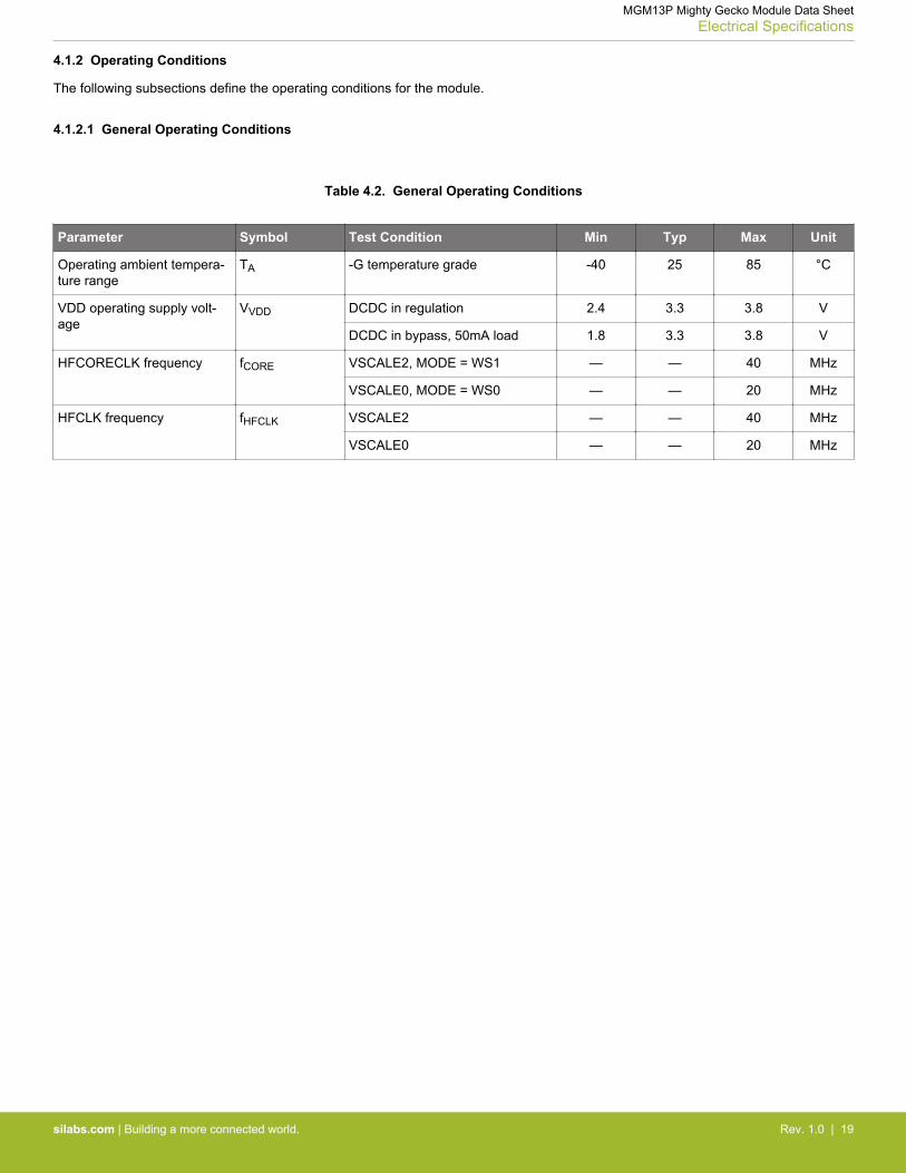
4.1.2 Operating Conditions
The following subsections define the operating conditions for the module.
4.1.2.1 General Operating Conditions
Table 4.2. General Operating Conditions
Parameter Symbol Test Condition Min Typ Max Unit
Operating ambient tempera-ture range
TA -G temperature grade -40 25 85 °C
VDD operating supply volt-age
VVDD DCDC in regulation 2.4 3.3 3.8 V
DCDC in bypass, 50mA load 1.8 3.3 3.8 V
HFCORECLK frequency fCORE VSCALE2, MODE = WS1 — — 40 MHz
VSCALE0, MODE = WS0 — — 20 MHz
HFCLK frequency fHFCLK VSCALE2 — — 40 MHz
VSCALE0 — — 20 MHz
MGM13P Mighty Gecko Module Data SheetElectrical Specifications
silabs.com | Building a more connected world. Rev. 1.0 | 19

4.1.3 DC-DC Converter
Test conditions: V_DCDC_I=3.3 V, V_DCDC_O=1.8 V, I_DCDC_LOAD=50 mA, Heavy Drive configuration, F_DCDC_LN=7 MHz, un-less otherwise indicated.
Table 4.3. DC-DC Converter
Parameter Symbol Test Condition Min Typ Max Unit
Input voltage range VDCDC_I Bypass mode, IDCDC_LOAD = 50mA
1.8 — VVREGVDD_
MAX
V
Low noise (LN) mode, 1.8 V out-put, IDCDC_LOAD = 100 mA, orLow power (LP) mode, 1.8 V out-put, IDCDC_LOAD = 10 mA
2.4 — VVREGVDD_
MAX
V
Output voltage programma-ble range1
VDCDC_O 1.8 — VVREGVDD V
Max load current ILOAD_MAX Low noise (LN) mode, Medium orHeavy Drive2
— — 70 mA
Low noise (LN) mode, LightDrive2
— — 50 mA
Low power (LP) mode,LPCMPBIASEMxx3 = 0
— — 75 µA
Low power (LP) mode,LPCMPBIASEMxx3 = 3
— — 10 mA
Note:1. Due to internal dropout, the DC-DC output will never be able to reach its input voltage, VVREGVDD.2. Drive levels are defined by configuration of the PFETCNT and NFETCNT registers. Light Drive: PFETCNT=NFETCNT=3; Medi-
um Drive: PFETCNT=NFETCNT=7; Heavy Drive: PFETCNT=NFETCNT=15.3. LPCMPBIASEMxx refers to either LPCMPBIASEM234H in the EMU_DCDCMISCCTRL register or LPCMPBIASEM01 in the
EMU_DCDCLOEM01CFG register, depending on the energy mode.
MGM13P Mighty Gecko Module Data SheetElectrical Specifications
silabs.com | Building a more connected world. Rev. 1.0 | 20

4.1.4 Current Consumption
4.1.4.1 Current Consumption 3.3 V using DC-DC Converter
Unless otherwise indicated, typical conditions are: VDD = 3.3 V. T = 25 °C. Minimum and maximum values in this table represent theworst conditions across supply voltage and process variation at T = 25 °C.
Table 4.4. Current Consumption 3.3 V using DC-DC Converter
Parameter Symbol Test Condition Min Typ Max Unit
Current consumption in EM0mode with all peripherals dis-abled, DCDC in Low NoiseDCM mode2
IACTIVE_DCM 38.4 MHz crystal, CPU runningwhile loop from flash4
— 87 — µA/MHz
38 MHz HFRCO, CPU runningPrime from flash
— 69 — µA/MHz
38 MHz HFRCO, CPU runningwhile loop from flash
— 70 — µA/MHz
38 MHz HFRCO, CPU runningCoreMark from flash
— 82 — µA/MHz
26 MHz HFRCO, CPU runningwhile loop from flash
— 76 — µA/MHz
1 MHz HFRCO, CPU runningwhile loop from flash
— 615 — µA/MHz
Current consumption in EM0mode with all peripherals dis-abled, DCDC in Low NoiseCCM mode1
IACTIVE_CCM 38.4 MHz crystal, CPU runningwhile loop from flash4
— 97 — µA/MHz
38 MHz HFRCO, CPU runningPrime from flash
— 80 — µA/MHz
38 MHz HFRCO, CPU runningwhile loop from flash
— 81 — µA/MHz
38 MHz HFRCO, CPU runningCoreMark from flash
— 92 — µA/MHz
26 MHz HFRCO, CPU runningwhile loop from flash
— 94 — µA/MHz
1 MHz HFRCO, CPU runningwhile loop from flash
— 1145 — µA/MHz
Current consumption in EM0mode with all peripherals dis-abled and voltage scalingenabled, DCDC in LowNoise CCM mode1
IACTIVE_CCM_VS 19 MHz HFRCO, CPU runningwhile loop from flash
— 101 — µA/MHz
1 MHz HFRCO, CPU runningwhile loop from flash
— 1124 — µA/MHz
Current consumption in EM1mode with all peripherals dis-abled, DCDC in Low NoiseDCM mode2
IEM1_DCM 38.4 MHz crystal4 — 56 — µA/MHz
38 MHz HFRCO — 39 — µA/MHz
26 MHz HFRCO — 46 — µA/MHz
1 MHz HFRCO — 588 — µA/MHz
Current consumption in EM1mode with all peripherals dis-abled and voltage scalingenabled, DCDC in LowNoise DCM mode2
IEM1_DCM_VS 19 MHz HFRCO — 50 — µA/MHz
1 MHz HFRCO — 572 — µA/MHz
MGM13P Mighty Gecko Module Data SheetElectrical Specifications
silabs.com | Building a more connected world. Rev. 1.0 | 21

Parameter Symbol Test Condition Min Typ Max Unit
Current consumption in EM2mode, with voltage scalingenabled, DCDC in LP mode3
IEM2_VS Full 64 kB RAM retention andRTCC running from LFXO
— 1.4 — µA
Full 64 kB RAM retention andRTCC running from LFRCO
— 1.5 — µA
1 bank RAM retention and RTCCrunning from LFRCO5
— 1.3 — µA
Current consumption in EM3mode, with voltage scalingenabled
IEM3_VS Full 64 kB RAM retention andCRYOTIMER running from ULFR-CO
— 1.14 — µA
Current consumption inEM4H mode, with voltagescaling enabled
IEM4H_VS 128 byte RAM retention, RTCCrunning from LFXO
— 0.75 — µA
128 byte RAM retention, CRYO-TIMER running from ULFRCO
— 0.44 — µA
128 byte RAM retention, no RTCC — 0.42 — µA
Current consumption inEM4S mode
IEM4S No RAM retention, no RTCC — 0.07 — µA
Note:1. DCDC Low Noise CCM Mode = Light Drive (PFETCNT=NFETCNT=3), F=6.4 MHz (RCOBAND=4), ANASW=DVDD.2. DCDC Low Noise DCM Mode = Light Drive (PFETCNT=NFETCNT=3), F=3.0 MHz (RCOBAND=0), ANASW=DVDD.3. DCDC Low Power Mode = Medium Drive (PFETCNT=NFETCNT=7), LPOSCDIV=1, LPCMPBIASEM234H=0, LPCLIMILIM-
SEL=1, ANASW=DVDD.4. CMU_HFXOCTRL_LOWPOWER=0.5. CMU_LFRCOCTRL_ENVREF = 1, CMU_LFRCOCTRL_VREFUPDATE = 1
MGM13P Mighty Gecko Module Data SheetElectrical Specifications
silabs.com | Building a more connected world. Rev. 1.0 | 22

4.1.4.2 Current Consumption Using Radio
Unless otherwise indicated, typical conditions are: VBATT = 3.3 V. T = 25 °C. DC-DC on. Minimum and maximum values in this tablerepresent the worst conditions across supply voltage and process variation at T = 25 °C.
Table 4.5. Current Consumption Using Radio
Parameter Symbol Test Condition Min Typ Max Unit
Current consumption in re-ceive mode, active packetreception (MCU in EM1 @38.4 MHz, peripheral clocksdisabled), T ≤ 85 °C
IRX_ACTIVE 125 kbit/s, 2GFSK, F = 2.4 GHz,Radio clock prescaled by 4
— 10.5 — mA
500 kbit/s, 2GFSK, F = 2.4 GHz,Radio clock prescaled by 4
— 10.4 — mA
1 Mbit/s, 2GFSK, F = 2.4 GHz,Radio clock prescaled by 4
— 9.9 — mA
2 Mbit/s, 2GFSK, F = 2.4 GHz,Radio clock prescaled by 4
— 10.6 — mA
802.15.4 receiving frame, F = 2.4GHz, Radio clock prescaled by 3
— 11 — mA
Current consumption in re-ceive mode, listening forpacket (MCU in EM1 @ 38.4MHz, peripheral clocks disa-bled), T ≤ 85 °C
IRX_LISTEN 125 kbit/s, 2GFSK, F = 2.4 GHz,No radio clock prescaling
— 10.5 — mA
500 kbit/s, 2GFSK, F = 2.4 GHz,No radio clock prescaling
— 10.5 — mA
1 Mbit/s, 2GFSK, F = 2.4 GHz, Noradio clock prescaling
— 10.9 — mA
2 Mbit/s, 2GFSK, F = 2.4 GHz, Noradio clock prescaling
— 11.6 — mA
802.15.4, F = 2.4 GHz, No radioclock prescaling
— 11.9 — mA
Current consumption intransmit mode (MCU in EM1@ 38.4 MHz, peripheralclocks disabled), T ≤ 85 °C
ITX F = 2.4 GHz, CW, 0 dBm outputpower, Radio clock prescaled by 3
— 8.5 — mA
F = 2.4 GHz, CW, 0 dBm outputpower, Radio clock prescaled by 1
— 9.6 — mA
F = 2.4 GHz, CW, 10 dBm outputpower
— 38.2 — mA
MGM13P Mighty Gecko Module Data SheetElectrical Specifications
silabs.com | Building a more connected world. Rev. 1.0 | 23

4.1.5 Wake Up Times
Table 4.6. Wake Up Times
Parameter Symbol Test Condition Min Typ Max Unit
Wake up time from EM1 tEM1_WU — 3 — AHBClocks
Wake up from EM2 tEM2_WU Code execution from flash — 10.9 — µs
Code execution from RAM — 3.8 — µs
Wake up from EM3 tEM3_WU Code execution from flash — 10.9 — µs
Code execution from RAM — 3.8 — µs
Wake up from EM4H1 tEM4H_WU Executing from flash — 90 — µs
Wake up from EM4S1 tEM4S_WU Executing from flash — 300 — µs
Time from release of resetsource to first instruction ex-ecution
tRESET Soft Pin Reset released — 51 — µs
Any other reset released — 358 — µs
Power mode scaling time tSCALE VSCALE0 to VSCALE2, HFCLK =19 MHz4 2
— 31.8 — µs
VSCALE2 to VSCALE0, HFCLK =19 MHz3
— 4.3 — µs
Note:1. Time from wake up request until first instruction is executed. Wakeup results in device reset.2. VSCALE0 to VSCALE2 voltage change transitions occur at a rate of 10 mV/µs for approximately 20 µs. During this transition,
peak currents will be dependent on the value of the DECOUPLE output capacitor, from 35 mA (with a 1 µF capacitor) to 70 mA(with a 2.7 µF capacitor).
3. Scaling down from VSCALE2 to VSCALE0 requires approximately 2.8 µs + 29 HFCLKs.4. Scaling up from VSCALE0 to VSCALE2 requires approximately 30.3 µs + 28 HFCLKs.
4.1.6 Brown Out Detector (BOD)
Table 4.7. Brown Out Detector (BOD)
Parameter Symbol Test Condition Min Typ Max Unit
AVDD BOD threshold VAVDDBOD AVDD rising — — 1.8 V
AVDD falling (EM0/EM1) 1.62 — — V
AVDD falling (EM2/EM3) 1.53 — — V
AVDD BOD hysteresis VAVDDBOD_HYST — 20 — mV
AVDD BOD response time tAVDDBOD_DELAY Supply drops at 0.1V/µs rate — 2.4 — µs
EM4 BOD threshold VEM4DBOD AVDD rising — — 1.7 V
AVDD falling 1.45 — — V
EM4 BOD hysteresis VEM4BOD_HYST — 25 — mV
EM4 BOD response time tEM4BOD_DELAY Supply drops at 0.1V/µs rate — 300 — µs
MGM13P Mighty Gecko Module Data SheetElectrical Specifications
silabs.com | Building a more connected world. Rev. 1.0 | 24

4.1.7 Frequency Synthesizer
Table 4.8. Frequency Synthesizer
Parameter Symbol Test Condition Min Typ Max Unit
RF synthesizer frequencyrange
fRANGE 2400 - 2483.5 MHz 2400 — 2483.5 MHz
LO tuning frequency resolu-tion with 38.4 MHz crystal
fRES 2400 - 2483.5 MHz — — 73 Hz
Frequency deviation resolu-tion with 38.4 MHz crystal
dfRES 2400 - 2483.5 MHz — — 73 Hz
Maximum frequency devia-tion with 38.4 MHz crystal
dfMAX 2400 - 2483.5 MHz — — 1677 kHz
MGM13P Mighty Gecko Module Data SheetElectrical Specifications
silabs.com | Building a more connected world. Rev. 1.0 | 25
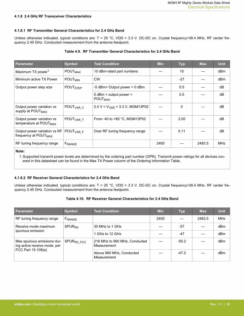
4.1.8 2.4 GHz RF Transceiver Characteristics
4.1.8.1 RF Transmitter General Characteristics for 2.4 GHz Band
Unless otherwise indicated, typical conditions are: T = 25 °C, VDD = 3.3 V. DC-DC on. Crystal frequency=38.4 MHz. RF center fre-quency 2.45 GHz. Conducted measurement from the antenna feedpoint.
Table 4.9. RF Transmitter General Characteristics for 2.4 GHz Band
Parameter Symbol Test Condition Min Typ Max Unit
Maximum TX power1 POUTMAX 10 dBm-rated part numbers — 10 — dBm
Minimum active TX Power POUTMIN CW -27 — dBm
Output power step size POUTSTEP -5 dBm< Output power < 0 dBm — 0.5 — dB
0 dBm < output power <POUTMAX
— 0.5 — dB
Output power variation vssupply at POUTMAX
POUTVAR_V 2.4 V < VVDD < 3.3 V, MGM13P02 — 0 — dB
Output power variation vstemperature at POUTMAX
POUTVAR_T From -40 to +85 °C, MGM13P02 — 2.05 — dB
Output power variation vs RFfrequency at POUTMAX
POUTVAR_F Over RF tuning frequency range — 0.11 — dB
RF tuning frequency range FRANGE 2400 — 2483.5 MHz
Note:1. Supported transmit power levels are determined by the ordering part number (OPN). Transmit power ratings for all devices cov-
ered in this datasheet can be found in the Max TX Power column of the Ordering Information Table.
4.1.8.2 RF Receiver General Characteristics for 2.4 GHz Band
Unless otherwise indicated, typical conditions are: T = 25 °C, VDD = 3.3 V. DC-DC on. Crystal frequency=38.4 MHz. RF center fre-quency 2.45 GHz. Conducted measurement from the antenna feedpoint.
Table 4.10. RF Receiver General Characteristics for 2.4 GHz Band
Parameter Symbol Test Condition Min Typ Max Unit
RF tuning frequency range FRANGE 2400 — 2483.5 MHz
Receive mode maximumspurious emission
SPURRX 30 MHz to 1 GHz — -57 — dBm
1 GHz to 12 GHz — -47 — dBm
Max spurious emissions dur-ing active receive mode, perFCC Part 15.109(a)
SPURRX_FCC 216 MHz to 960 MHz, ConductedMeasurement
— -55.2 — dBm
Above 960 MHz, ConductedMeasurement
— -47.2 — dBm
MGM13P Mighty Gecko Module Data SheetElectrical Specifications
silabs.com | Building a more connected world. Rev. 1.0 | 26

4.1.8.3 RF Receiver Characteristics for 802.15.4 DSSS-OQPSK in the 2.4 GHz Band
Unless otherwise indicated, typical conditions are: T = 25 °C, VDD = 3.3 V. DC-DC on. Crystal frequency=38.4 MHz. RF center fre-quency 2.45 GHz. Conducted measurement from the antenna feedpoint.
Table 4.11. RF Receiver Characteristics for 802.15.4 DSSS-OQPSK in the 2.4 GHz Band
Parameter Symbol Test Condition Min Typ Max Unit
Sensitivity, 1% PER SENS Signal is reference signal. Packetlength is 20 octets. Using DC-DCconverter.
— -102.1 — dBm
Signal is reference signal. Packetlength is 20 octets. Without DC-DC converter.
— -102.1 — dBm
4.1.8.4 RF Receiver Characteristics for Bluetooth Low Energy in the 2.4GHz Band, 125 kbps Data Rate
Unless otherwise indicated, typical conditions are: T = 25 °C, VDD = 3.3 V. DC-DC on. Crystal frequency=38.4 MHz. RF center fre-quency 2.45 GHz. Conducted measurement from the antenna feedpoint.
Table 4.12. RF Receiver Characteristics for Bluetooth Low Energy in the 2.4GHz Band, 125 kbps Data Rate
Parameter Symbol Test Condition Min Typ Max Unit
Sensitivity, 0.1% BER SENS Signal is reference signal1. UsingDC-DC converter.
— -102.8 — dBm
With non-ideal signals as speci-fied in RF-PHY.TS.4.2.2, section4.6.1.
— -102.4 — dBm
Note:1. Reference signal is defined 2GFSK at -67 dBm, Modulation index = 0.5, BT = 0.5, Bit rate = 125 kbps, desired data = PRBS9;
interferer data = PRBS15; frequency accuracy better than 1 ppm.
4.1.8.5 RF Receiver Characteristics for Bluetooth Low Energy in the 2.4GHz Band, 500 kbps Data Rate
Unless otherwise indicated, typical conditions are: T = 25 °C, VDD = 3.3 V. DC-DC on. Crystal frequency=38.4 MHz. RF center fre-quency 2.45 GHz. Conducted measurement from the antenna feedpoint.
Table 4.13. RF Receiver Characteristics for Bluetooth Low Energy in the 2.4GHz Band, 500 kbps Data Rate
Parameter Symbol Test Condition Min Typ Max Unit
Sensitivity, 0.1% BER SENS Signal is reference signal1. UsingDC-DC converter.
— -98.4 — dBm
With non-ideal signals as speci-fied in RF-PHY.TS.4.2.2, section4.6.1.
— -97.4 — dBm
Note:1. Reference signal is defined 2GFSK at -67 dBm, Modulation index = 0.5, BT = 0.5, Bit rate = 500 kbps, desired data = PRBS9;
interferer data = PRBS15; frequency accuracy better than 1 ppm.
MGM13P Mighty Gecko Module Data SheetElectrical Specifications
silabs.com | Building a more connected world. Rev. 1.0 | 27
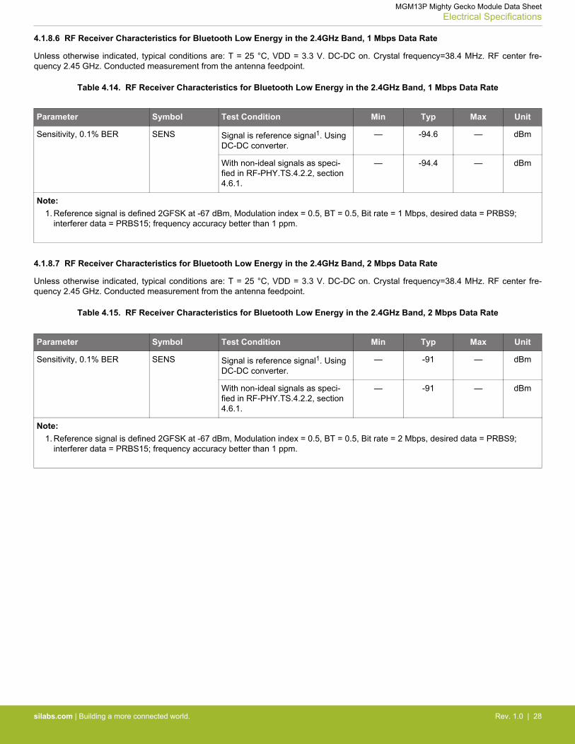
4.1.8.6 RF Receiver Characteristics for Bluetooth Low Energy in the 2.4GHz Band, 1 Mbps Data Rate
Unless otherwise indicated, typical conditions are: T = 25 °C, VDD = 3.3 V. DC-DC on. Crystal frequency=38.4 MHz. RF center fre-quency 2.45 GHz. Conducted measurement from the antenna feedpoint.
Table 4.14. RF Receiver Characteristics for Bluetooth Low Energy in the 2.4GHz Band, 1 Mbps Data Rate
Parameter Symbol Test Condition Min Typ Max Unit
Sensitivity, 0.1% BER SENS Signal is reference signal1. UsingDC-DC converter.
— -94.6 — dBm
With non-ideal signals as speci-fied in RF-PHY.TS.4.2.2, section4.6.1.
— -94.4 — dBm
Note:1. Reference signal is defined 2GFSK at -67 dBm, Modulation index = 0.5, BT = 0.5, Bit rate = 1 Mbps, desired data = PRBS9;
interferer data = PRBS15; frequency accuracy better than 1 ppm.
4.1.8.7 RF Receiver Characteristics for Bluetooth Low Energy in the 2.4GHz Band, 2 Mbps Data Rate
Unless otherwise indicated, typical conditions are: T = 25 °C, VDD = 3.3 V. DC-DC on. Crystal frequency=38.4 MHz. RF center fre-quency 2.45 GHz. Conducted measurement from the antenna feedpoint.
Table 4.15. RF Receiver Characteristics for Bluetooth Low Energy in the 2.4GHz Band, 2 Mbps Data Rate
Parameter Symbol Test Condition Min Typ Max Unit
Sensitivity, 0.1% BER SENS Signal is reference signal1. UsingDC-DC converter.
— -91 — dBm
With non-ideal signals as speci-fied in RF-PHY.TS.4.2.2, section4.6.1.
— -91 — dBm
Note:1. Reference signal is defined 2GFSK at -67 dBm, Modulation index = 0.5, BT = 0.5, Bit rate = 2 Mbps, desired data = PRBS9;
interferer data = PRBS15; frequency accuracy better than 1 ppm.
MGM13P Mighty Gecko Module Data SheetElectrical Specifications
silabs.com | Building a more connected world. Rev. 1.0 | 28
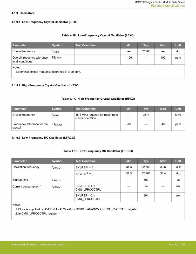
4.1.9 Oscillators
4.1.9.1 Low-Frequency Crystal Oscillator (LFXO)
Table 4.16. Low-Frequency Crystal Oscillator (LFXO)
Parameter Symbol Test Condition Min Typ Max Unit
Crystal frequency fLFXO — 32.768 — kHz
Overall frequency tolerancein all conditions1
FTLFXO -100 — 100 ppm
Note:1. Nominal crystal frequency tolerance of ± 20 ppm.
4.1.9.2 High-Frequency Crystal Oscillator (HFXO)
Table 4.17. High-Frequency Crystal Oscillator (HFXO)
Parameter Symbol Test Condition Min Typ Max Unit
Crystal frequency fHFXO 38.4 MHz required for radio trans-ciever operation
— 38.4 — MHz
Frequency tolerance for thecrystal
FTHFXO -40 — 40 ppm
4.1.9.3 Low-Frequency RC Oscillator (LFRCO)
Table 4.18. Low-Frequency RC Oscillator (LFRCO)
Parameter Symbol Test Condition Min Typ Max Unit
Oscillation frequency fLFRCO ENVREF2 = 1 31.3 32.768 33.6 kHz
ENVREF2 = 0 31.3 32.768 33.4 kHz
Startup time tLFRCO — 500 — µs
Current consumption 1 ILFRCO ENVREF = 1 inCMU_LFRCOCTRL
— 342 — nA
ENVREF = 0 inCMU_LFRCOCTRL
— 494 — nA
Note:1. Block is supplied by AVDD if ANASW = 0, or DVDD if ANASW=1 in EMU_PWRCTRL register.2. In CMU_LFRCOCTRL register.
MGM13P Mighty Gecko Module Data SheetElectrical Specifications
silabs.com | Building a more connected world. Rev. 1.0 | 29

4.1.9.4 High-Frequency RC Oscillator (HFRCO)
Table 4.19. High-Frequency RC Oscillator (HFRCO)
Parameter Symbol Test Condition Min Typ Max Unit
Frequency accuracy fHFRCO_ACC At production calibrated frequen-cies, across supply voltage andtemperature
-2.5 — 2.5 %
Start-up time tHFRCO fHFRCO ≥ 19 MHz — 300 — ns
4 < fHFRCO < 19 MHz — 1 — µs
fHFRCO ≤ 4 MHz — 2.5 — µs
Current consumption on allsupplies
IHFRCO fHFRCO = 38 MHz — 267 299 µA
fHFRCO = 32 MHz — 224 248 µA
fHFRCO = 26 MHz — 189 211 µA
fHFRCO = 19 MHz — 154 172 µA
fHFRCO = 16 MHz — 133 148 µA
fHFRCO = 13 MHz — 118 135 µA
fHFRCO = 7 MHz — 89 100 µA
fHFRCO = 4 MHz — 34 44 µA
fHFRCO = 2 MHz — 29 40 µA
fHFRCO = 1 MHz — 26 36 µA
Coarse trim step size (% ofperiod)
SSHFRCO_COARS
E
— 0.8 — %
Fine trim step size (% of pe-riod)
SSHFRCO_FINE — 0.1 — %
Period jitter PJHFRCO — 0.2 — % RMS
Frequency limits fHFRCO_BAND FREQRANGE = 0, FINETUNIN-GEN = 0
3.47 — 6.15 MHz
FREQRANGE = 3, FINETUNIN-GEN = 0
6.24 — 11.45 MHz
FREQRANGE = 6, FINETUNIN-GEN = 0
11.3 — 19.8 MHz
FREQRANGE = 7, FINETUNIN-GEN = 0
13.45 — 22.8 MHz
FREQRANGE = 8, FINETUNIN-GEN = 0
16.5 — 29.0 MHz
FREQRANGE = 10, FINETUNIN-GEN = 0
23.11 — 40.63 MHz
FREQRANGE = 11, FINETUNIN-GEN = 0
27.27 — 48 MHz
FREQRANGE = 12, FINETUNIN-GEN = 0
33.33 — 54 MHz
MGM13P Mighty Gecko Module Data SheetElectrical Specifications
silabs.com | Building a more connected world. Rev. 1.0 | 30
4.1.9.5 Ultra-low Frequency RC Oscillator (ULFRCO)
Table 4.20. Ultra-low Frequency RC Oscillator (ULFRCO)
Parameter Symbol Test Condition Min Typ Max Unit
Oscillation frequency fULFRCO 0.95 1 1.07 kHz
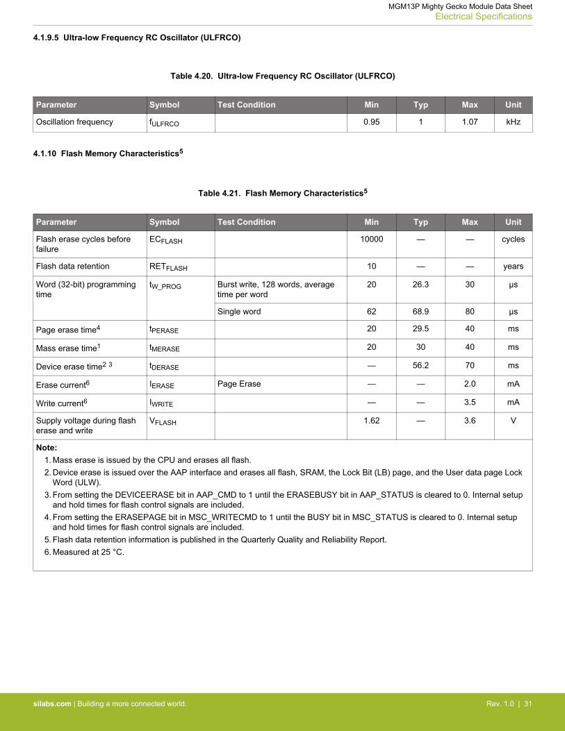
4.1.10 Flash Memory Characteristics5
Table 4.21. Flash Memory Characteristics5
Parameter Symbol Test Condition Min Typ Max Unit
Flash erase cycles beforefailure
ECFLASH 10000 — — cycles
Flash data retention RETFLASH 10 — — years
Word (32-bit) programmingtime
tW_PROG Burst write, 128 words, averagetime per word
20 26.3 30 µs
Single word 62 68.9 80 µs
Page erase time4 tPERASE 20 29.5 40 ms
Mass erase time1 tMERASE 20 30 40 ms
Device erase time2 3 tDERASE — 56.2 70 ms
Erase current6 IERASE Page Erase — — 2.0 mA
Write current6 IWRITE — — 3.5 mA
Supply voltage during flasherase and write
VFLASH 1.62 — 3.6 V
Note:1. Mass erase is issued by the CPU and erases all flash.2. Device erase is issued over the AAP interface and erases all flash, SRAM, the Lock Bit (LB) page, and the User data page Lock
Word (ULW).3. From setting the DEVICEERASE bit in AAP_CMD to 1 until the ERASEBUSY bit in AAP_STATUS is cleared to 0. Internal setup
and hold times for flash control signals are included.4. From setting the ERASEPAGE bit in MSC_WRITECMD to 1 until the BUSY bit in MSC_STATUS is cleared to 0. Internal setup
and hold times for flash control signals are included.5. Flash data retention information is published in the Quarterly Quality and Reliability Report.6. Measured at 25 °C.
MGM13P Mighty Gecko Module Data SheetElectrical Specifications
silabs.com | Building a more connected world. Rev. 1.0 | 31
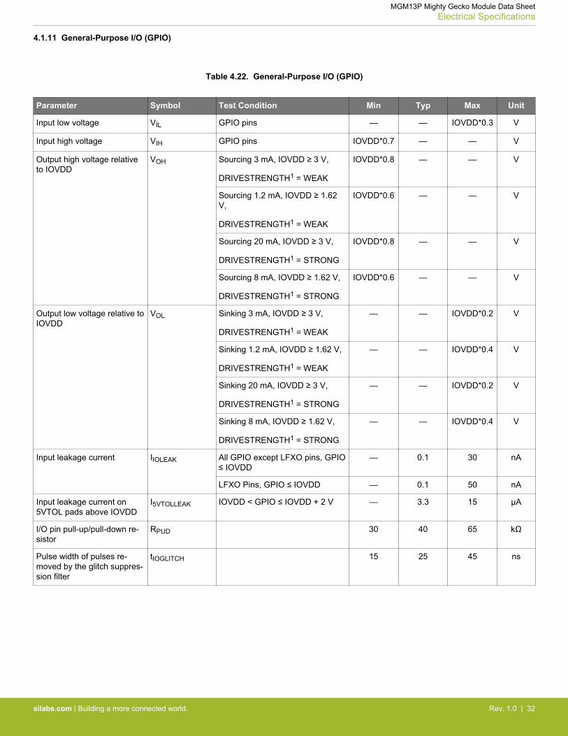
4.1.11 General-Purpose I/O (GPIO)
Table 4.22. General-Purpose I/O (GPIO)
Parameter Symbol Test Condition Min Typ Max Unit
Input low voltage VIL GPIO pins — — IOVDD*0.3 V
Input high voltage VIH GPIO pins IOVDD*0.7 — — V
Output high voltage relativeto IOVDD
VOH Sourcing 3 mA, IOVDD ≥ 3 V,
DRIVESTRENGTH1 = WEAK
IOVDD*0.8 — — V
Sourcing 1.2 mA, IOVDD ≥ 1.62V,
DRIVESTRENGTH1 = WEAK
IOVDD*0.6 — — V
Sourcing 20 mA, IOVDD ≥ 3 V,
DRIVESTRENGTH1 = STRONG
IOVDD*0.8 — — V
Sourcing 8 mA, IOVDD ≥ 1.62 V,
DRIVESTRENGTH1 = STRONG
IOVDD*0.6 — — V
Output low voltage relative toIOVDD
VOL Sinking 3 mA, IOVDD ≥ 3 V,
DRIVESTRENGTH1 = WEAK
— — IOVDD*0.2 V
Sinking 1.2 mA, IOVDD ≥ 1.62 V,
DRIVESTRENGTH1 = WEAK
— — IOVDD*0.4 V
Sinking 20 mA, IOVDD ≥ 3 V,
DRIVESTRENGTH1 = STRONG
— — IOVDD*0.2 V
Sinking 8 mA, IOVDD ≥ 1.62 V,
DRIVESTRENGTH1 = STRONG
— — IOVDD*0.4 V
Input leakage current IIOLEAK All GPIO except LFXO pins, GPIO≤ IOVDD
— 0.1 30 nA
LFXO Pins, GPIO ≤ IOVDD — 0.1 50 nA
Input leakage current on5VTOL pads above IOVDD
I5VTOLLEAK IOVDD < GPIO ≤ IOVDD + 2 V — 3.3 15 µA
I/O pin pull-up/pull-down re-sistor
RPUD 30 40 65 kΩ
Pulse width of pulses re-moved by the glitch suppres-sion filter
tIOGLITCH 15 25 45 ns
MGM13P Mighty Gecko Module Data SheetElectrical Specifications
silabs.com | Building a more connected world. Rev. 1.0 | 32
Parameter Symbol Test Condition Min Typ Max Unit
Output fall time, From 70%to 30% of VIO
tIOOF CL = 50 pF,
DRIVESTRENGTH1 = STRONG,
SLEWRATE1 = 0x6
— 1.8 — ns
CL = 50 pF,
DRIVESTRENGTH1 = WEAK,
SLEWRATE1 = 0x6
— 4.5 — ns
Output rise time, From 30%to 70% of VIO
tIOOR CL = 50 pF,
DRIVESTRENGTH1 = STRONG,
SLEWRATE = 0x61
— 2.2 — ns
CL = 50 pF,
DRIVESTRENGTH1 = WEAK,
SLEWRATE1 = 0x6
— 7.4 — ns
Note:1. In GPIO_Pn_CTRL register.
MGM13P Mighty Gecko Module Data SheetElectrical Specifications
silabs.com | Building a more connected world. Rev. 1.0 | 33

4.1.12 Voltage Monitor (VMON)
Table 4.23. Voltage Monitor (VMON)
Parameter Symbol Test Condition Min Typ Max Unit
Supply current (includingI_SENSE)
IVMON In EM0 or EM1, 1 supply moni-tored
— 6.3 8 µA
In EM0 or EM1, 4 supplies moni-tored
— 12.5 15 µA
In EM2, EM3 or EM4, 1 supplymonitored and above threshold
— 62 — nA
In EM2, EM3 or EM4, 1 supplymonitored and below threshold
— 62 — nA
In EM2, EM3 or EM4, 4 suppliesmonitored and all above threshold
— 99 — nA
In EM2, EM3 or EM4, 4 suppliesmonitored and all below threshold
— 99 — nA
Loading of monitored supply ISENSE In EM0 or EM1 — 2 — µA
In EM2, EM3 or EM4 — 2 — nA
Threshold range VVMON_RANGE 1.62 — 3.4 V
Threshold step size NVMON_STESP Coarse — 200 — mV
Fine — 20 — mV
Response time tVMON_RES Supply drops at 1V/µs rate — 460 — ns
Hysteresis VVMON_HYST — 26 — mV
MGM13P Mighty Gecko Module Data SheetElectrical Specifications
silabs.com | Building a more connected world. Rev. 1.0 | 34
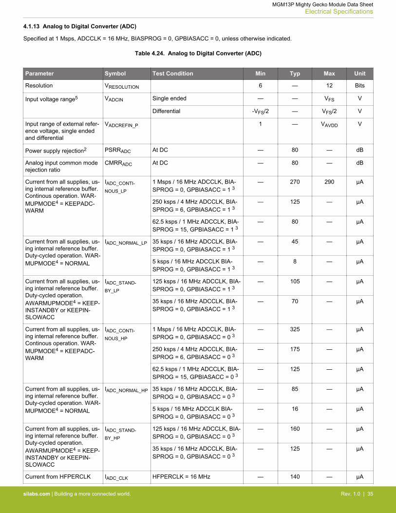
4.1.13 Analog to Digital Converter (ADC)
Specified at 1 Msps, ADCCLK = 16 MHz, BIASPROG = 0, GPBIASACC = 0, unless otherwise indicated.
Table 4.24. Analog to Digital Converter (ADC)
Parameter Symbol Test Condition Min Typ Max Unit
Resolution VRESOLUTION 6 — 12 Bits
Input voltage range5 VADCIN Single ended — — VFS V
Differential -VFS/2 — VFS/2 V
Input range of external refer-ence voltage, single endedand differential
VADCREFIN_P 1 — VAVDD V
Power supply rejection2 PSRRADC At DC — 80 — dB
Analog input common moderejection ratio
CMRRADC At DC — 80 — dB
Current from all supplies, us-ing internal reference buffer.Continous operation. WAR-MUPMODE4 = KEEPADC-WARM
IADC_CONTI-
NOUS_LP
1 Msps / 16 MHz ADCCLK, BIA-SPROG = 0, GPBIASACC = 1 3
— 270 290 µA
250 ksps / 4 MHz ADCCLK, BIA-SPROG = 6, GPBIASACC = 1 3
— 125 — µA
62.5 ksps / 1 MHz ADCCLK, BIA-SPROG = 15, GPBIASACC = 1 3
— 80 — µA
Current from all supplies, us-ing internal reference buffer.Duty-cycled operation. WAR-MUPMODE4 = NORMAL
IADC_NORMAL_LP 35 ksps / 16 MHz ADCCLK, BIA-SPROG = 0, GPBIASACC = 1 3
— 45 — µA
5 ksps / 16 MHz ADCCLK BIA-SPROG = 0, GPBIASACC = 1 3
— 8 — µA
Current from all supplies, us-ing internal reference buffer.Duty-cycled operation.AWARMUPMODE4 = KEEP-INSTANDBY or KEEPIN-SLOWACC
IADC_STAND-
BY_LP
125 ksps / 16 MHz ADCCLK, BIA-SPROG = 0, GPBIASACC = 1 3
— 105 — µA
35 ksps / 16 MHz ADCCLK, BIA-SPROG = 0, GPBIASACC = 1 3
— 70 — µA
Current from all supplies, us-ing internal reference buffer.Continous operation. WAR-MUPMODE4 = KEEPADC-WARM
IADC_CONTI-
NOUS_HP
1 Msps / 16 MHz ADCCLK, BIA-SPROG = 0, GPBIASACC = 0 3
— 325 — µA
250 ksps / 4 MHz ADCCLK, BIA-SPROG = 6, GPBIASACC = 0 3
— 175 — µA
62.5 ksps / 1 MHz ADCCLK, BIA-SPROG = 15, GPBIASACC = 0 3
— 125 — µA
Current from all supplies, us-ing internal reference buffer.Duty-cycled operation. WAR-MUPMODE4 = NORMAL
IADC_NORMAL_HP 35 ksps / 16 MHz ADCCLK, BIA-SPROG = 0, GPBIASACC = 0 3
— 85 — µA
5 ksps / 16 MHz ADCCLK BIA-SPROG = 0, GPBIASACC = 0 3
— 16 — µA
Current from all supplies, us-ing internal reference buffer.Duty-cycled operation.AWARMUPMODE4 = KEEP-INSTANDBY or KEEPIN-SLOWACC
IADC_STAND-
BY_HP
125 ksps / 16 MHz ADCCLK, BIA-SPROG = 0, GPBIASACC = 0 3
— 160 — µA
35 ksps / 16 MHz ADCCLK, BIA-SPROG = 0, GPBIASACC = 0 3
— 125 — µA
Current from HFPERCLK IADC_CLK HFPERCLK = 16 MHz — 140 — µA
MGM13P Mighty Gecko Module Data SheetElectrical Specifications
silabs.com | Building a more connected world. Rev. 1.0 | 35
Parameter Symbol Test Condition Min Typ Max Unit
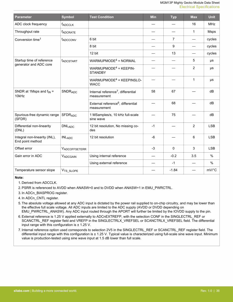
ADC clock frequency fADCCLK — — 16 MHz
Throughput rate fADCRATE — — 1 Msps
Conversion time1 tADCCONV 6 bit — 7 — cycles
8 bit — 9 — cycles
12 bit — 13 — cycles
Startup time of referencegenerator and ADC core
tADCSTART WARMUPMODE4 = NORMAL — — 5 µs
WARMUPMODE4 = KEEPIN-STANDBY
— — 2 µs
WARMUPMODE4 = KEEPINSLO-WACC
— — 1 µs
SNDR at 1Msps and fIN =10kHz
SNDRADC Internal reference7, differentialmeasurement
58 67 — dB
External reference6, differentialmeasurement
— 68 — dB
Spurious-free dynamic range(SFDR)
SFDRADC 1 MSamples/s, 10 kHz full-scalesine wave
— 75 — dB
Differential non-linearity(DNL)
DNLADC 12 bit resolution, No missing co-des
-1 — 2 LSB
Integral non-linearity (INL),End point method
INLADC 12 bit resolution -6 — 6 LSB
Offset error VADCOFFSETERR -3 0 3 LSB
Gain error in ADC VADCGAIN Using internal reference — -0.2 3.5 %
Using external reference — -1 — %
Temperature sensor slope VTS_SLOPE — -1.84 — mV/°C
Note:1. Derived from ADCCLK.2. PSRR is referenced to AVDD when ANASW=0 and to DVDD when ANASW=1 in EMU_PWRCTRL.3. In ADCn_BIASPROG register.4. In ADCn_CNTL register.5. The absolute voltage allowed at any ADC input is dictated by the power rail supplied to on-chip circuitry, and may be lower than
the effective full scale voltage. All ADC inputs are limited to the ADC supply (AVDD or DVDD depending onEMU_PWRCTRL_ANASW). Any ADC input routed through the APORT will further be limited by the IOVDD supply to the pin.
6. External reference is 1.25 V applied externally to ADCnEXTREFP, with the selection CONF in the SINGLECTRL_REF orSCANCTRL_REF register field and VREFP in the SINGLECTRLX_VREFSEL or SCANCTRLX_VREFSEL field. The differentialinput range with this configuration is ± 1.25 V.
7. Internal reference option used corresponds to selection 2V5 in the SINGLECTRL_REF or SCANCTRL_REF register field. Thedifferential input range with this configuration is ± 1.25 V. Typical value is characterized using full-scale sine wave input. Minimumvalue is production-tested using sine wave input at 1.5 dB lower than full scale.
MGM13P Mighty Gecko Module Data SheetElectrical Specifications
silabs.com | Building a more connected world. Rev. 1.0 | 36

4.1.14 Current Digital to Analog Converter (IDAC)
Table 4.25. Current Digital to Analog Converter (IDAC)
Parameter Symbol Test Condition Min Typ Max Unit
Number of ranges NIDAC_RANGES — 4 — ranges
Output current IIDAC_OUT RANGSEL1 = RANGE0 0.05 — 1.6 µA
RANGSEL1 = RANGE1 1.6 — 4.7 µA
RANGSEL1 = RANGE2 0.5 — 16 µA
RANGSEL1 = RANGE3 2 — 64 µA
Linear steps within eachrange
NIDAC_STEPS — 32 — steps
Step size SSIDAC RANGSEL1 = RANGE0 — 50 — nA
RANGSEL1 = RANGE1 — 100 — nA
RANGSEL1 = RANGE2 — 500 — nA
RANGSEL1 = RANGE3 — 2 — µA
Total accuracy, STEPSEL1 =0x10
ACCIDAC EM0 or EM1, AVDD=3.3 V, T = 25°C
-3 — 3 %
EM0 or EM1, Across operatingtemperature range
-18 — 22 %
EM2 or EM3, Source mode,RANGSEL1 = RANGE0,AVDD=3.3 V, T = 25 °C
— -2 — %
EM2 or EM3, Source mode,RANGSEL1 = RANGE1,AVDD=3.3 V, T = 25 °C
— -1.7 — %
EM2 or EM3, Source mode,RANGSEL1 = RANGE2,AVDD=3.3 V, T = 25 °C
— -0.8 — %
EM2 or EM3, Source mode,RANGSEL1 = RANGE3,AVDD=3.3 V, T = 25 °C
— -0.5 — %
EM2 or EM3, Sink mode, RANG-SEL1 = RANGE0, AVDD=3.3 V, T= 25 °C
— -0.7 — %
EM2 or EM3, Sink mode, RANG-SEL1 = RANGE1, AVDD=3.3 V, T= 25 °C
— -0.6 — %
EM2 or EM3, Sink mode, RANG-SEL1 = RANGE2, AVDD=3.3 V, T= 25 °C
— -0.5 — %
EM2 or EM3, Sink mode, RANG-SEL1 = RANGE3, AVDD=3.3 V, T= 25 °C
— -0.5 — %
Start up time tIDAC_SU Output within 1% of steady statevalue
— 5 — µs
MGM13P Mighty Gecko Module Data SheetElectrical Specifications
silabs.com | Building a more connected world. Rev. 1.0 | 37

Parameter Symbol Test Condition Min Typ Max Unit
Settling time, (output settledwithin 1% of steady state val-ue),
tIDAC_SETTLE Range setting is changed — 5 — µs
Step value is changed — 1 — µs
Current consumption2 IIDAC EM0 or EM1 Source mode, ex-cluding output current, Across op-erating temperature range
— 11 15 µA
EM0 or EM1 Sink mode, exclud-ing output current, Across operat-ing temperature range
— 13 18 µA
EM2 or EM3 Source mode, ex-cluding output current, T = 25 °C
— 0.023 — µA
EM2 or EM3 Sink mode, exclud-ing output current, T = 25 °C
— 0.041 — µA
EM2 or EM3 Source mode, ex-cluding output current, T ≥ 85 °C
— 11 — µA
EM2 or EM3 Sink mode, exclud-ing output current, T ≥ 85 °C
— 13 — µA
Output voltage compliance insource mode, source currentchange relative to currentsourced at 0 V
ICOMP_SRC RANGESEL1=0, output voltage =min(VIOVDD, VAVDD
2-100 mv)— 0.11 — %
RANGESEL1=1, output voltage =min(VIOVDD, VAVDD
2-100 mV)— 0.06 — %
RANGESEL1=2, output voltage =min(VIOVDD, VAVDD
2-150 mV)— 0.04 — %
RANGESEL1=3, output voltage =min(VIOVDD, VAVDD
2-250 mV)— 0.03 — %
Output voltage compliance insink mode, sink currentchange relative to currentsunk at IOVDD
ICOMP_SINK RANGESEL1=0, output voltage =100 mV
— 0.12 — %
RANGESEL1=1, output voltage =100 mV
— 0.05 — %
RANGESEL1=2, output voltage =150 mV
— 0.04 — %
RANGESEL1=3, output voltage =250 mV
— 0.03 — %
Note:1. In IDAC_CURPROG register.2. The IDAC is supplied by either AVDD, DVDD, or IOVDD based on the setting of ANASW in the EMU_PWRCTRL register and
PWRSEL in the IDAC_CTRL register. Setting PWRSEL to 1 selects IOVDD. With PWRSEL cleared to 0, ANASW selects be-tween AVDD (0) and DVDD (1).
MGM13P Mighty Gecko Module Data SheetElectrical Specifications
silabs.com | Building a more connected world. Rev. 1.0 | 38
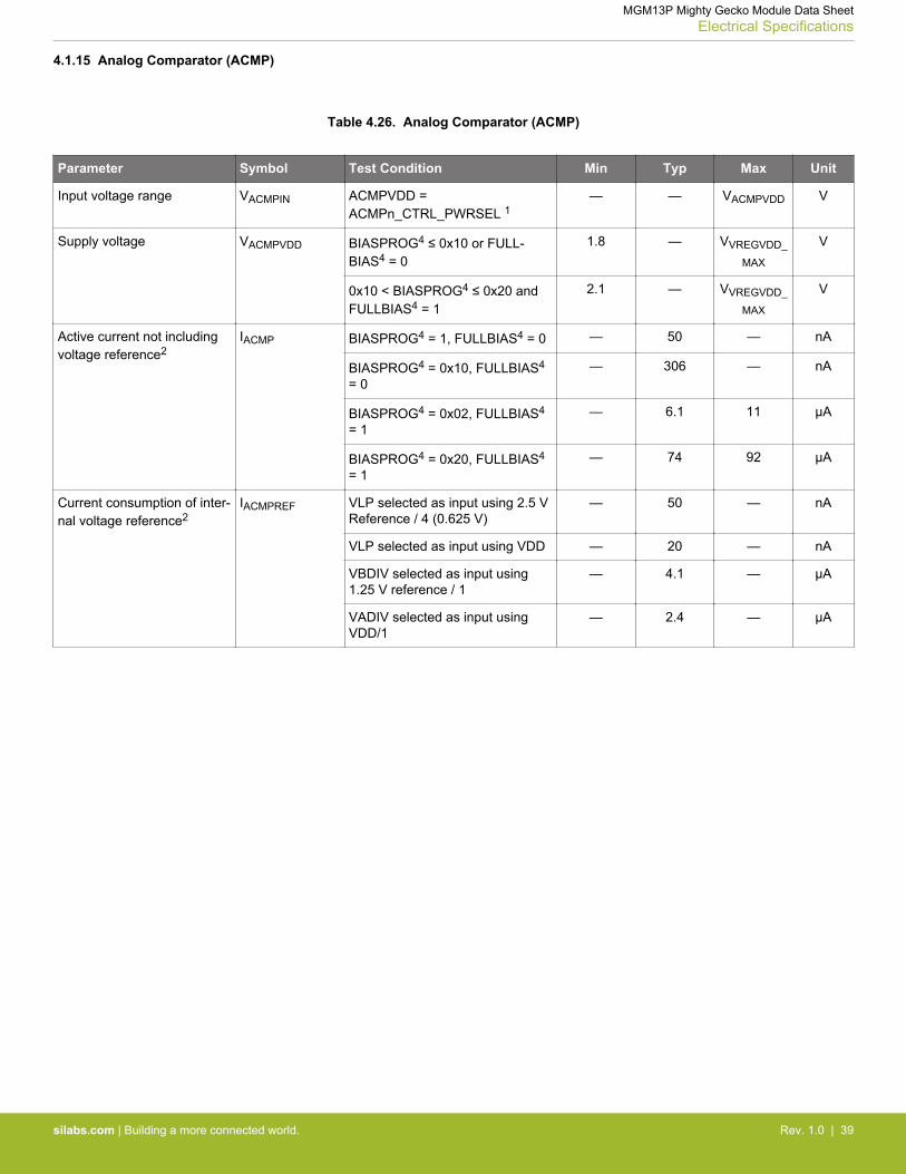
4.1.15 Analog Comparator (ACMP)
Table 4.26. Analog Comparator (ACMP)
Parameter Symbol Test Condition Min Typ Max Unit
Input voltage range VACMPIN ACMPVDD =ACMPn_CTRL_PWRSEL 1
— — VACMPVDD V
Supply voltage VACMPVDD BIASPROG4 ≤ 0x10 or FULL-BIAS4 = 0
1.8 — VVREGVDD_
MAX
V
0x10 < BIASPROG4 ≤ 0x20 andFULLBIAS4 = 1
2.1 — VVREGVDD_
MAX
V
Active current not includingvoltage reference2
IACMP BIASPROG4 = 1, FULLBIAS4 = 0 — 50 — nA
BIASPROG4 = 0x10, FULLBIAS4
= 0— 306 — nA
BIASPROG4 = 0x02, FULLBIAS4
= 1— 6.1 11 µA
BIASPROG4 = 0x20, FULLBIAS4
= 1— 74 92 µA
Current consumption of inter-nal voltage reference2
IACMPREF VLP selected as input using 2.5 VReference / 4 (0.625 V)
— 50 — nA
VLP selected as input using VDD — 20 — nA
VBDIV selected as input using1.25 V reference / 1
— 4.1 — µA
VADIV selected as input usingVDD/1
— 2.4 — µA
MGM13P Mighty Gecko Module Data SheetElectrical Specifications
silabs.com | Building a more connected world. Rev. 1.0 | 39
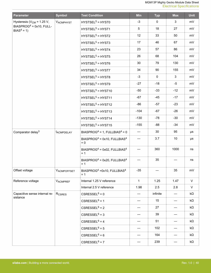
Parameter Symbol Test Condition Min Typ Max Unit
Hysteresis (VCM = 1.25 V,BIASPROG4 = 0x10, FULL-BIAS4 = 1)
VACMPHYST HYSTSEL5 = HYST0 -3 0 3 mV
HYSTSEL5 = HYST1 5 18 27 mV
HYSTSEL5 = HYST2 12 33 50 mV
HYSTSEL5 = HYST3 17 46 67 mV
HYSTSEL5 = HYST4 23 57 86 mV
HYSTSEL5 = HYST5 26 68 104 mV
HYSTSEL5 = HYST6 30 79 130 mV
HYSTSEL5 = HYST7 34 90 155 mV
HYSTSEL5 = HYST8 -3 0 3 mV
HYSTSEL5 = HYST9 -27 -18 -5 mV
HYSTSEL5 = HYST10 -50 -33 -12 mV
HYSTSEL5 = HYST11 -67 -45 -17 mV
HYSTSEL5 = HYST12 -86 -57 -23 mV
HYSTSEL5 = HYST13 -104 -67 -26 mV
HYSTSEL5 = HYST14 -130 -78 -30 mV
HYSTSEL5 = HYST15 -155 -88 -34 mV
Comparator delay3 tACMPDELAY BIASPROG4 = 1, FULLBIAS4 = 0 — 30 95 µs
BIASPROG4 = 0x10, FULLBIAS4
= 0— 3.7 10 µs
BIASPROG4 = 0x02, FULLBIAS4
= 1— 360 1000 ns
BIASPROG4 = 0x20, FULLBIAS4
= 1— 35 — ns
Offset voltage VACMPOFFSET BIASPROG4 =0x10, FULLBIAS4
= 1-35 — 35 mV
Reference voltage VACMPREF Internal 1.25 V reference 1 1.25 1.47 V
Internal 2.5 V reference 1.98 2.5 2.8 V
Capacitive sense internal re-sistance
RCSRES CSRESSEL6 = 0 — infinite — kΩ
CSRESSEL6 = 1 — 15 — kΩ
CSRESSEL6 = 2 — 27 — kΩ
CSRESSEL6 = 3 — 39 — kΩ
CSRESSEL6 = 4 — 51 — kΩ
CSRESSEL6 = 5 — 102 — kΩ
CSRESSEL6 = 6 — 164 — kΩ
CSRESSEL6 = 7 — 239 — kΩ
MGM13P Mighty Gecko Module Data SheetElectrical Specifications
silabs.com | Building a more connected world. Rev. 1.0 | 40

Parameter Symbol Test Condition Min Typ Max Unit
Note:1. ACMPVDD is a supply chosen by the setting in ACMPn_CTRL_PWRSEL and may be IOVDD, AVDD or DVDD.2. The total ACMP current is the sum of the contributions from the ACMP and its internal voltage reference. IACMPTOTAL = IACMP +
IACMPREF.3. ± 100 mV differential drive.4. In ACMPn_CTRL register.5. In ACMPn_HYSTERESIS registers.6. In ACMPn_INPUTSEL register.
4.1.16 I2C
4.1.16.1 I2C Standard-mode (Sm)1
Table 4.27. I2C Standard-mode (Sm)1
Parameter Symbol Test Condition Min Typ Max Unit
SCL clock frequency2 fSCL 0 — 100 kHz
SCL clock low time tLOW 4.7 — — µs
SCL clock high time tHIGH 4 — — µs
SDA set-up time tSU_DAT 250 — — ns
SDA hold time3 tHD_DAT 100 — 3450 ns
Repeated START conditionset-up time
tSU_STA 4.7 — — µs
(Repeated) START conditionhold time
tHD_STA 4 — — µs
STOP condition set-up time tSU_STO 4 — — µs
Bus free time between aSTOP and START condition
tBUF 4.7 — — µs
Note:1. For CLHR set to 0 in the I2Cn_CTRL register.2. For the minimum HFPERCLK frequency required in Standard-mode, refer to the I2C chapter in the reference manual.3. The maximum SDA hold time (tHD_DAT) needs to be met only when the device does not stretch the low time of SCL (tLOW).
MGM13P Mighty Gecko Module Data SheetElectrical Specifications
silabs.com | Building a more connected world. Rev. 1.0 | 41

4.1.16.2 I2C Fast-mode (Fm)1
Table 4.28. I2C Fast-mode (Fm)1
Parameter Symbol Test Condition Min Typ Max Unit
SCL clock frequency2 fSCL 0 — 400 kHz
SCL clock low time tLOW 1.3 — — µs
SCL clock high time tHIGH 0.6 — — µs
SDA set-up time tSU_DAT 100 — — ns
SDA hold time3 tHD_DAT 100 — 900 ns
Repeated START conditionset-up time
tSU_STA 0.6 — — µs
(Repeated) START conditionhold time
tHD_STA 0.6 — — µs
STOP condition set-up time tSU_STO 0.6 — — µs
Bus free time between aSTOP and START condition
tBUF 1.3 — — µs
Note:1. For CLHR set to 1 in the I2Cn_CTRL register.2. For the minimum HFPERCLK frequency required in Fast-mode, refer to the I2C chapter in the reference manual.3. The maximum SDA hold time (tHD,DAT) needs to be met only when the device does not stretch the low time of SCL (tLOW).
MGM13P Mighty Gecko Module Data SheetElectrical Specifications
silabs.com | Building a more connected world. Rev. 1.0 | 42
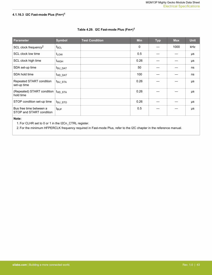
4.1.16.3 I2C Fast-mode Plus (Fm+)1
Table 4.29. I2C Fast-mode Plus (Fm+)1
Parameter Symbol Test Condition Min Typ Max Unit
SCL clock frequency2 fSCL 0 — 1000 kHz
SCL clock low time tLOW 0.5 — — µs
SCL clock high time tHIGH 0.26 — — µs
SDA set-up time tSU_DAT 50 — — ns
SDA hold time tHD_DAT 100 — — ns
Repeated START conditionset-up time
tSU_STA 0.26 — — µs
(Repeated) START conditionhold time
tHD_STA 0.26 — — µs
STOP condition set-up time tSU_STO 0.26 — — µs
Bus free time between aSTOP and START condition
tBUF 0.5 — — µs
Note:1. For CLHR set to 0 or 1 in the I2Cn_CTRL register.2. For the minimum HFPERCLK frequency required in Fast-mode Plus, refer to the I2C chapter in the reference manual.
MGM13P Mighty Gecko Module Data SheetElectrical Specifications
silabs.com | Building a more connected world. Rev. 1.0 | 43
4.1.17 USART SPI
SPI Master Timing
Table 4.30. SPI Master Timing
Parameter Symbol Test Condition Min Typ Max Unit
SCLK period 1 3 2 tSCLK 2 *tHFPERCLK
— — ns
CS to MOSI 1 3 tCS_MO -12.5 — 14 ns
SCLK to MOSI 1 3 tSCLK_MO -8.5 — 10.5 ns
MISO setup time 1 3 tSU_MI IOVDD = 1.62 V 90 — — ns
IOVDD = 3.0 V 42 — — ns
MISO hold time 1 3 tH_MI -9 — — ns
Note:1. Applies for both CLKPHA = 0 and CLKPHA = 1 (figure only shows CLKPHA = 0).2. tHFPERCLK is one period of the selected HFPERCLK.3. Measurement done with 8 pF output loading at 10% and 90% of VDD (figure shows 50% of VDD).
CS
SCLKCLKPOL = 0
MOSI
MISO
tCS_MO
tH_MItSU_MI
tSCKL_MO
tSCLK
SCLKCLKPOL = 1
Figure 4.1. SPI Master Timing Diagram
MGM13P Mighty Gecko Module Data SheetElectrical Specifications
silabs.com | Building a more connected world. Rev. 1.0 | 44
SPI Slave Timing
Table 4.31. SPI Slave Timing
Parameter Symbol Test Condition Min Typ Max Unit
SCLK period 1 3 2 tSCLK 6 *tHFPERCLK
— — ns
SCLK high time1 3 2 tSCLK_HI 2.5 *tHFPERCLK
— — ns
SCLK low time1 3 2 tSCLK_LO 2.5 *tHFPERCLK
— — ns
CS active to MISO 1 3 tCS_ACT_MI 4 — 70 ns
CS disable to MISO 1 3 tCS_DIS_MI 4 — 50 ns
MOSI setup time 1 3 tSU_MO 12.5 — — ns
MOSI hold time 1 3 2 tH_MO 13 — — ns
SCLK to MISO 1 3 2 tSCLK_MI 6 + 1.5 *tHFPERCLK
— 45 + 2.5 *tHFPERCLK
ns
Note:1. Applies for both CLKPHA = 0 and CLKPHA = 1 (figure only shows CLKPHA = 0).2. tHFPERCLK is one period of the selected HFPERCLK.3. Measurement done with 8 pF output loading at 10% and 90% of VDD (figure shows 50% of VDD).
CS
SCLKCLKPOL = 0
MOSI
MISO
tCS_ACT_MI
tSCLK_HI
tSCLKtSU_MO
tH_MO
tSCLK_MI
tCS_DIS_MI
tSCLK_LO
SCLKCLKPOL = 1
Figure 4.2. SPI Slave Timing Diagram
MGM13P Mighty Gecko Module Data SheetElectrical Specifications
silabs.com | Building a more connected world. Rev. 1.0 | 45

5. Typical Connection Diagrams
5.1 Network Co-Processor (NCP) Application with UART Host
The MGM13P can be controlled over the UART interface as a peripheral to an external host processor. Typical power supply, program-ming/debug, and host interface connections are shown in the figure below. Refer to AN958: Debugging and Programming Interfaces forCustom Designs for more details.
Host CPU
VDD
PTI_FRAME
TCK / SWCLK
TMS / SWDIO
TDO / SWO
TDI
+3.3 V
WirelessModule
GND
PD13
PD14
PD15
PA0
PA1
PA2
PA3
PA4
PA5
PB11
GND
GND
RESETn
VDD
PF7
PF6
PF5
PF4
PF3
PF2
PF1
PF0
GNDPB13
PC6
PC7
PC8
PC9
PC10
PC11
RX
TX
RTS
CTS
GPIO
RESETn
VSS
+3.3 V
RESETn
PTI_DATA
PTI_FRAME (PB13)
13579
246810
+3.3 V
TDO / SWO (PF2)TCK / SWCLK (PF0)TMS / SWDIO (PF1)
RESETn
Mini Simplicity Debug Connector
PTI_DATA (PB11)
Figure 5.1. Connection Diagram: UART NCP Configuration
5.2 Network Co-Processor (NCP) Application with SPI Host
The MGM13P can be controlled over the SPI interface as a peripheral to an external host processor. Typical power supply, program-ming/debug and host interface connections are shown in the figure below. Refer to AN958: Debugging and Programming Interfaces forCustom Designs for more details.
Host CPU
VDD
PTI_FRAME
TCK / SWCLK
TMS / SWDIO
TDO / SWO
TDI
+3.3 V
WirelessModule
GND
PD13
PD14
PD15
PA0
PA1
PA2
PA3
PA4
PA5
PB11
GND
GND
RESETn
VDD
PF7
PF6
PF5
PF4
PF3
PF2
PF1
PF0
GNDPB13
PC6
PC7
PC8
PC9
PC10
PC11
MOSI
MISO
SCLK
nCS
GPIO
VSS
+3.3 V
RESETn
PTI_DATA
PTI_FRAME (PB13)
13579
246810
+3.3 V
TDO / SWO (PF2)TCK / SWCLK (PF0)TMS / SWDIO (PF1)
RESETn
Mini Simplicity Debug Connector
PTI_DATA (PB11)
nWAKE
nHOST_INT
RESETn
Figure 5.2. Connection Diagram: SPI NCP Configuration
MGM13P Mighty Gecko Module Data SheetTypical Connection Diagrams
silabs.com | Building a more connected world. Rev. 1.0 | 46

5.3 SoC Application
The MGM13P can be used in a standalone SoC configuration with no external host processor. Typical power supply and programming/debug connections are shown in the figure below. Refer to AN958: Debugging and Programming Interfaces for Custom Designs formore details.
Serial Flash(optional)
VDD
TCK / SWCLK
TMS / SWDIO
TDO / SWO
TDI
+3.3 V
WirelessModule
GND
PD13
PD14
PD15
PA0
PA1
PA2
PA3
PA4
PA5
PB11
GND
GND
RESETn
VDD
PF7
PF6
PF5
PF4
PF3
PF2
PF1
PF0
GNDPB13
PC6
PC7
PC8
PC9
PC10
PC11
MOSI
MISO
SCLK
nCS
VSS
+3.3 V
RESETn
PTI_FRAME (PB13)
13579
246810
+3.3 V
TDO / SWO (PF2)TCK / SWCLK (PF0)TMS / SWDIO (PF1)
RESETn
Mini Simplicity Debug Connector
PTI_DATA (PB11)
PTI_FRAME
PTI_DATA
Figure 5.3. Connection Diagram: SoC Configuration
MGM13P Mighty Gecko Module Data SheetTypical Connection Diagrams
silabs.com | Building a more connected world. Rev. 1.0 | 47
6. Layout Guidelines
For optimal performance of the MGM13P (with integrated antenna), please follow the PCB layout guidelines and ground plane recom-mendations indicated in this section.
6.1 Module Placement and Application PCB Layout Guidelines
• Place the module at the edge of the PCB, as shown in Figure 6.1 Recommended Application PCB Layout for MGM13P with Integra-ted Antenna on page 48.
• Do not place any metal (traces, components, battery, etc.) within the clearance area of the antenna.• Connect all ground pads directly to a solid ground plane.• Place the ground vias as close to the ground pads as possible.• Do not place plastic or any other dielectric material in contact with the antenna.
Place vias close to each of the module’s GND pads
Place vias along all PCB edges
Wireless Module(Top View)
GND
GND
GND
GND
Antenna ClearanceNo metal in this area
Align module edge with PCB edge
Figure 6.1. Recommended Application PCB Layout for MGM13P with Integrated Antenna
MGM13P Mighty Gecko Module Data SheetLayout Guidelines
silabs.com | Building a more connected world. Rev. 1.0 | 48
Figure 6.2 Non-optimal Module Placements for MGM13P with Integrated Antenna on page 49 shows examples of layouts that willresult in severely degraded RF performance.
Figure 6.2. Non-optimal Module Placements for MGM13P with Integrated Antenna
The amount of ground plane surrounding the sides of the module will also impact the maximum RF range, as shown in Figure6.3 Impact of GND Plane Size vs. Range for MGM13P on page 49.
Figure 6.3. Impact of GND Plane Size vs. Range for MGM13P
6.2 Effect of Plastic and Metal Materials
Do not place plastic or any other dielectric material in close proximity to the antenna.
Any metallic objects in close proximity to the antenna will prevent the antenna from radiating freely. The minimum recommended dis-tance of metallic and/or conductive objects is 10 mm in any direction from the antenna except in the directions of the application PCBground planes.
6.3 Locating the Module Close to Human Body
Placing the module in contact with or very close to the human body will negatively impact antenna efficiency and reduce range.
MGM13P Mighty Gecko Module Data SheetLayout Guidelines
silabs.com | Building a more connected world. Rev. 1.0 | 49
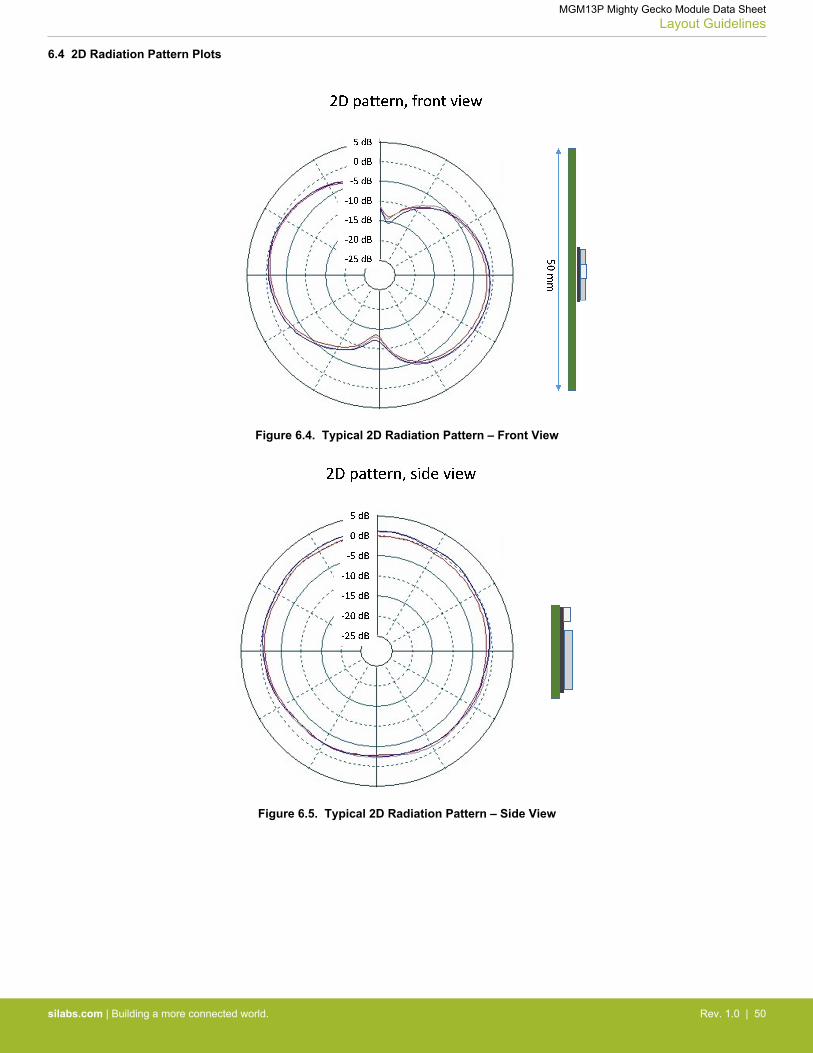
6.4 2D Radiation Pattern Plots
Figure 6.4. Typical 2D Radiation Pattern – Front View
Figure 6.5. Typical 2D Radiation Pattern – Side View
MGM13P Mighty Gecko Module Data SheetLayout Guidelines
silabs.com | Building a more connected world. Rev. 1.0 | 50
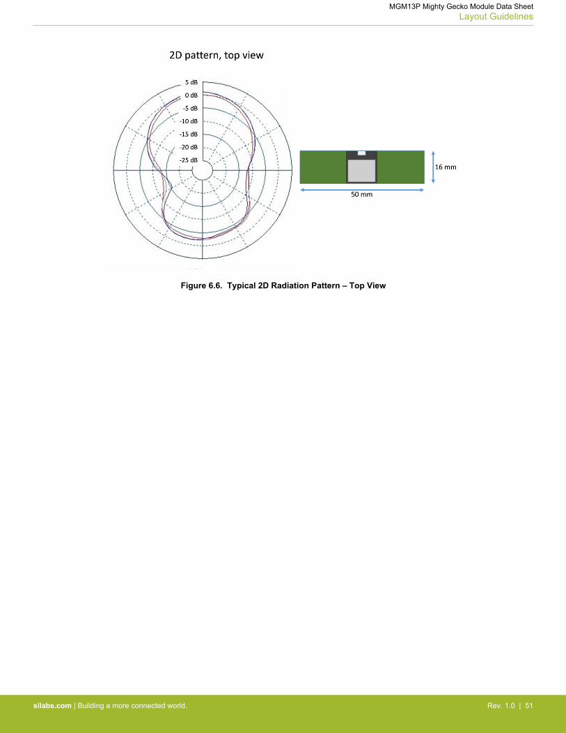
Figure 6.6. Typical 2D Radiation Pattern – Top View
MGM13P Mighty Gecko Module Data SheetLayout Guidelines
silabs.com | Building a more connected world. Rev. 1.0 | 51

7. Hardware Design Guidelines
The MGM13P is an easy-to-use module with regard to hardware application design. The additional guidelines in this section should befollowed to guarantee optimal performance.
7.1 Power Supply Requirements
Coin cell batteries cannot withstand high peak currents (e.g. higher than 15 mA). If the peak current exceeds 15 mA it is recommendedto place a 47 - 100 µF capacitor in parallel with the coin cell battery to improve battery life time. Note that the total current consumptionof the application is a combination of the radio, peripherals and MCU current consumption, and all power consumers must be taken intoaccount. MGM13P should be powered by a unipolar supply voltage with nominal value of 3.3 V.
7.2 Reset Functions
The MGM13P can be reset by three different methods: by pulling the RESET line low, by the internal watchdog timer or by softwarecommand. The reset state in MGM13P does not provide any power saving functionality and is not recommended as a means to con-serve power. MGM13P has an internal system power-up reset function. The RESET pin includes an on-chip pull-up resistor and can beleft unconnected if no external reset switch or source is used.
7.3 Debug and Firmware Updates
This section contains information on debugging and firmware update methods. For additional information, refer to the following applica-tion note: AN958: Debugging and Programming Interfaces for Custom Designs.
7.3.1 Programming and Debug Connections
It is recommended to expose the debug pins in your own hardware design for firmware update and debug purposes. The following tablelists the required pins for JTAG connection and SWD connections.
Certain debug pins have internal pull-down or pull-ups enabled by default, and leaving them enabled may increase current consumptionif left connected to supply or ground. If the JTAG pins are enabled, the module must be power cycled to return to a SWD debug config-uration.
Table 7.1. Debug Pins
Pin Name Pin Number JTAG Signal SWD Signal Comments
PF3 24 TDI N/A This pin is disabled after reset. Once enabled the pinhas a built-in pull-up.
PF2 23 TDO N/A This pin is disabled after reset.
PF1 22 TMS SWDIO Pin is enabled after reset and has a built-in pull-up.
PF0 21 TCK SWCLK Pin is enabled after reset and has a built-in pull-down.
7.3.2 Packet Trace Interface (PTI)
The MGM13P integrates a true PHY-level packet trace interface (PTI) with the MAC, allowing complete, non-intrusive capture of allpackets to and from the EFR32 Wireless STK development tools. The PTI_DATA and PTI_FRAME signals are accessed via the PB11and PB12 pins, respectively.
MGM13P Mighty Gecko Module Data SheetHardware Design Guidelines
silabs.com | Building a more connected world. Rev. 1.0 | 52
8. Pin Definitions
8.1 MGM13P Device Pinout
Figure 8.1. MGM13P Device Pinout
The following table provides package pin connections and general descriptions of pin functionality. For detailed information on the sup-ported features for each GPIO pin, see 8.2 GPIO Functionality Table or 8.3 Alternate Functionality Overview.
Table 8.1. MGM13P Device Pinout
Pin Name Pin(s) Description Pin Name Pin(s) Description
GND
1122031
Ground PD13 2 GPIO
PD14 3 GPIO PD15 4 GPIO
PA0 5 GPIO PA1 6 GPIO
PA2 7 GPIO PA3 8 GPIO
MGM13P Mighty Gecko Module Data SheetPin Definitions
silabs.com | Building a more connected world. Rev. 1.0 | 53
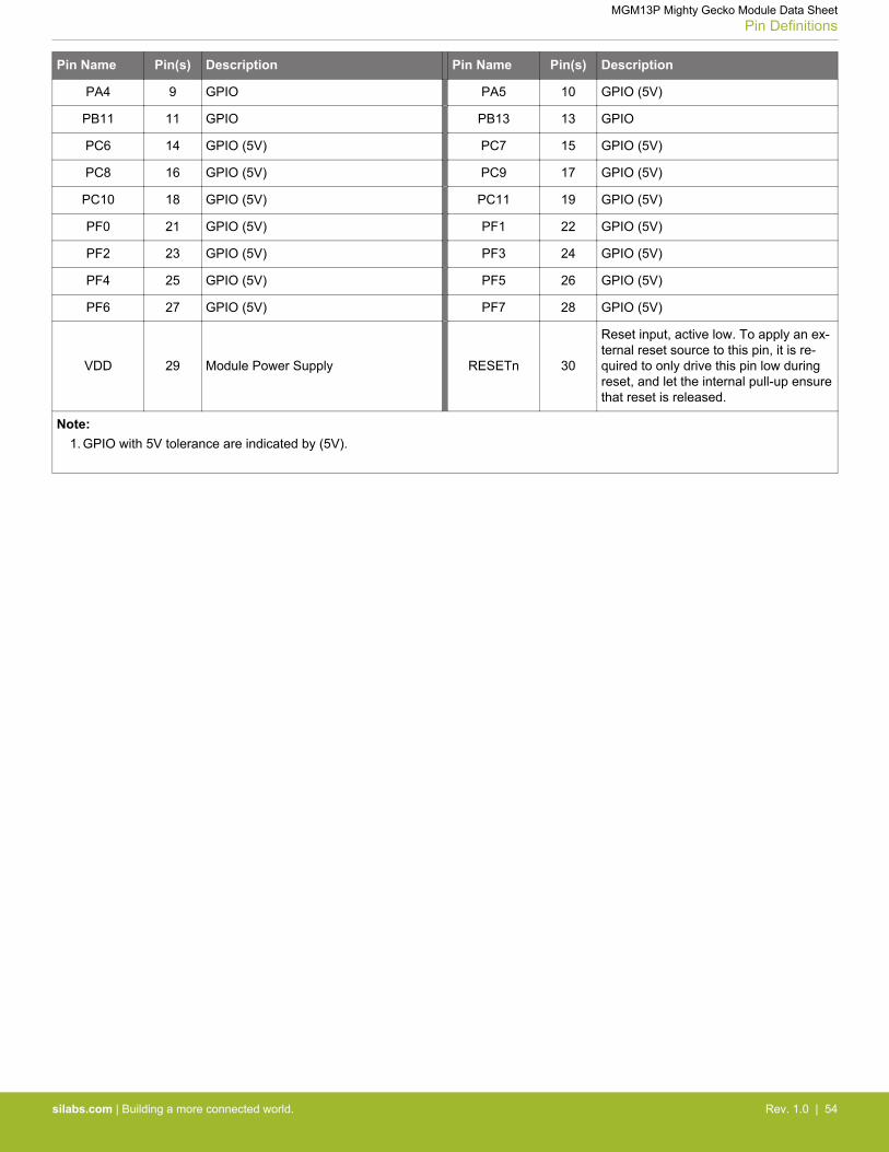
Pin Name Pin(s) Description Pin Name Pin(s) Description
PA4 9 GPIO PA5 10 GPIO (5V)
PB11 11 GPIO PB13 13 GPIO
PC6 14 GPIO (5V) PC7 15 GPIO (5V)
PC8 16 GPIO (5V) PC9 17 GPIO (5V)
PC10 18 GPIO (5V) PC11 19 GPIO (5V)
PF0 21 GPIO (5V) PF1 22 GPIO (5V)
PF2 23 GPIO (5V) PF3 24 GPIO (5V)
PF4 25 GPIO (5V) PF5 26 GPIO (5V)
PF6 27 GPIO (5V) PF7 28 GPIO (5V)
VDD 29 Module Power Supply RESETn 30
Reset input, active low. To apply an ex-ternal reset source to this pin, it is re-quired to only drive this pin low duringreset, and let the internal pull-up ensurethat reset is released.
Note:1. GPIO with 5V tolerance are indicated by (5V).
MGM13P Mighty Gecko Module Data SheetPin Definitions
silabs.com | Building a more connected world. Rev. 1.0 | 54

8.2 GPIO Functionality Table
A wide selection of alternate functionality is available for multiplexing to various pins. The following table shows the name of each GPIOpin, followed by the functionality available on that pin. Refer to 8.3 Alternate Functionality Overview for a list of GPIO locations availablefor each function.
Table 8.2. GPIO Functionality Table
GPIO Name Pin Alternate Functionality / Description
Analog Timers Communication Radio Other
PD13
VDAC0_OUT0ALT /OPA0_OUTALT #1
BUSCY BUSDXOPA1_P
TIM0_CC0 #21TIM0_CC1 #20TIM0_CC2 #19
TIM0_CDTI0 #18TIM0_CDTI1 #17TIM0_CDTI2 #16TIM1_CC0 #21TIM1_CC1 #20TIM1_CC2 #19TIM1_CC3 #18
WTIM0_CDTI0 #29WTIM0_CDTI1 #27WTIM0_CDTI2 #25LETIM0_OUT0 #21LETIM0_OUT1 #20PCNT0_S0IN #21PCNT0_S1IN #20
US0_TX #21US0_RX #20
US0_CLK #19US0_CS #18
US0_CTS #17US0_RTS #16US1_TX #21US1_RX #20
US1_CLK #19US1_CS #18
US1_CTS #17US1_RTS #16LEU0_TX #21LEU0_RX #20I2C0_SDA #21I2C0_SCL #20
FRC_DCLK #21FRC_DOUT #20
FRC_DFRAME #19MODEM_DCLK #21MODEM_DIN #20
MODEM_DOUT #19MODEM_ANT0 #18MODEM_ANT1 #17
PRS_CH3 #12PRS_CH4 #4PRS_CH5 #3
PRS_CH6 #15ACMP0_O #21ACMP1_O #21
LES_CH5
PD14BUSDY BUSCXVDAC0_OUT1 /
OPA1_OUT
TIM0_CC0 #22TIM0_CC1 #21TIM0_CC2 #20
TIM0_CDTI0 #19TIM0_CDTI1 #18TIM0_CDTI2 #17TIM1_CC0 #22TIM1_CC1 #21TIM1_CC2 #20TIM1_CC3 #19
WTIM0_CDTI0 #30WTIM0_CDTI1 #28WTIM0_CDTI2 #26LETIM0_OUT0 #22LETIM0_OUT1 #21PCNT0_S0IN #22PCNT0_S1IN #21
US0_TX #22US0_RX #21
US0_CLK #20US0_CS #19
US0_CTS #18US0_RTS #17US1_TX #22US1_RX #21
US1_CLK #20US1_CS #19
US1_CTS #18US1_RTS #17LEU0_TX #22LEU0_RX #21I2C0_SDA #22I2C0_SCL #21
FRC_DCLK #22FRC_DOUT #21
FRC_DFRAME #20MODEM_DCLK #22MODEM_DIN #21
MODEM_DOUT #20MODEM_ANT0 #19MODEM_ANT1 #18
CMU_CLK0 #5PRS_CH3 #13PRS_CH4 #5PRS_CH5 #4
PRS_CH6 #16ACMP0_O #22ACMP1_O #22
LES_CH6GPIO_EM4WU4
PD15
VDAC0_OUT0ALT /OPA0_OUTALT #2
BUSCY BUSDXOPA1_N
TIM0_CC0 #23TIM0_CC1 #22TIM0_CC2 #21
TIM0_CDTI0 #20TIM0_CDTI1 #19TIM0_CDTI2 #18TIM1_CC0 #23TIM1_CC1 #22TIM1_CC2 #21TIM1_CC3 #20
WTIM0_CDTI0 #31WTIM0_CDTI1 #29WTIM0_CDTI2 #27LETIM0_OUT0 #23LETIM0_OUT1 #22PCNT0_S0IN #23PCNT0_S1IN #22
US0_TX #23US0_RX #22
US0_CLK #21US0_CS #20
US0_CTS #19US0_RTS #18US1_TX #23US1_RX #22
US1_CLK #21US1_CS #20
US1_CTS #19US1_RTS #18LEU0_TX #23LEU0_RX #22I2C0_SDA #23I2C0_SCL #22
FRC_DCLK #23FRC_DOUT #22
FRC_DFRAME #21MODEM_DCLK #23MODEM_DIN #22
MODEM_DOUT #21MODEM_ANT0 #20MODEM_ANT1 #19
CMU_CLK1 #5PRS_CH3 #14PRS_CH4 #6PRS_CH5 #5
PRS_CH6 #17ACMP0_O #23ACMP1_O #23
LES_CH7DBG_SWO #2
MGM13P Mighty Gecko Module Data SheetPin Definitions
silabs.com | Building a more connected world. Rev. 1.0 | 55

GPIO Name Pin Alternate Functionality / Description
Analog Timers Communication Radio Other
PA0 BUSDY BUSCXADC0_EXTN
TIM0_CC0 #0TIM0_CC1 #31TIM0_CC2 #30
TIM0_CDTI0 #29TIM0_CDTI1 #28TIM0_CDTI2 #27
TIM1_CC0 #0TIM1_CC1 #31TIM1_CC2 #30TIM1_CC3 #29
WTIM0_CC0 #0 LE-TIM0_OUT0 #0 LE-
TIM0_OUT1 #31PCNT0_S0IN #0PCNT0_S1IN #31
US0_TX #0 US0_RX#31 US0_CLK #30
US0_CS #29US0_CTS #28US0_RTS #27
US1_TX #0 US1_RX#31 US1_CLK #30
US1_CS #29US1_CTS #28US1_RTS #27LEU0_TX #0
LEU0_RX #31I2C0_SDA #0I2C0_SCL #31
FRC_DCLK #0FRC_DOUT #31
FRC_DFRAME #30MODEM_DCLK #0MODEM_DIN #31
MODEM_DOUT #30MODEM_ANT0 #29MODEM_ANT1 #28
CMU_CLK1 #0PRS_CH6 #0
PRS_CH7 #10PRS_CH8 #9PRS_CH9 #8ACMP0_O #0ACMP1_O #0
LES_CH8
PA1BUSCY BUSDX
ADC0_EXTPVDAC0_EXT
TIM0_CC0 #1TIM0_CC1 #0TIM0_CC2 #31
TIM0_CDTI0 #30TIM0_CDTI1 #29TIM0_CDTI2 #28
TIM1_CC0 #1TIM1_CC1 #0TIM1_CC2 #31TIM1_CC3 #30
WTIM0_CC0 #1 LE-TIM0_OUT0 #1 LE-
TIM0_OUT1 #0PCNT0_S0IN #1PCNT0_S1IN #0
US0_TX #1 US0_RX#0 US0_CLK #31
US0_CS #30US0_CTS #29US0_RTS #28
US1_TX #1 US1_RX#0 US1_CLK #31
US1_CS #30US1_CTS #29US1_RTS #28LEU0_TX #1LEU0_RX #0I2C0_SDA #1I2C0_SCL #0
FRC_DCLK #1FRC_DOUT #0
FRC_DFRAME #31MODEM_DCLK #1MODEM_DIN #0
MODEM_DOUT #31MODEM_ANT0 #30MODEM_ANT1 #29
CMU_CLK0 #0PRS_CH6 #1PRS_CH7 #0
PRS_CH8 #10PRS_CH9 #9ACMP0_O #1ACMP1_O #1
LES_CH9
PA2
VDAC0_OUT1ALT /OPA1_OUTALT #1
BUSDY BUSCXOPA0_P
TIM0_CC0 #2TIM0_CC1 #1TIM0_CC2 #0
TIM0_CDTI0 #31TIM0_CDTI1 #30TIM0_CDTI2 #29
TIM1_CC0 #2TIM1_CC1 #1TIM1_CC2 #0TIM1_CC3 #31WTIM0_CC0 #2
WTIM0_CC1 #0 LE-TIM0_OUT0 #2 LE-
TIM0_OUT1 #1PCNT0_S0IN #2PCNT0_S1IN #1
US0_TX #2 US0_RX#1 US0_CLK #0
US0_CS #31US0_CTS #30US0_RTS #29
US1_TX #2 US1_RX#1 US1_CLK #0
US1_CS #31US1_CTS #30US1_RTS #29LEU0_TX #2LEU0_RX #1I2C0_SDA #2I2C0_SCL #1
FRC_DCLK #2FRC_DOUT #1
FRC_DFRAME #0MODEM_DCLK #2MODEM_DIN #1
MODEM_DOUT #0MODEM_ANT0 #31MODEM_ANT1 #30
PRS_CH6 #2PRS_CH7 #1PRS_CH8 #0
PRS_CH9 #10ACMP0_O #2ACMP1_O #2
LES_CH10
MGM13P Mighty Gecko Module Data SheetPin Definitions
silabs.com | Building a more connected world. Rev. 1.0 | 56
GPIO Name Pin Alternate Functionality / Description
Analog Timers Communication Radio Other
PA3BUSCY BUSDXVDAC0_OUT0 /
OPA0_OUT
TIM0_CC0 #3TIM0_CC1 #2TIM0_CC2 #1
TIM0_CDTI0 #0TIM0_CDTI1 #31TIM0_CDTI2 #30
TIM1_CC0 #3TIM1_CC1 #2TIM1_CC2 #1TIM1_CC3 #0
WTIM0_CC0 #3WTIM0_CC1 #1 LE-TIM0_OUT0 #3 LE-
TIM0_OUT1 #2PCNT0_S0IN #3PCNT0_S1IN #2
US0_TX #3 US0_RX#2 US0_CLK #1
US0_CS #0US0_CTS #31US0_RTS #30
US1_TX #3 US1_RX#2 US1_CLK #1
US1_CS #0US1_CTS #31US1_RTS #30LEU0_TX #3LEU0_RX #2I2C0_SDA #3I2C0_SCL #2
FRC_DCLK #3FRC_DOUT #2
FRC_DFRAME #1MODEM_DCLK #3MODEM_DIN #2
MODEM_DOUT #1MODEM_ANT0 #0
MODEM_ANT1 #31
PRS_CH6 #3PRS_CH7 #2PRS_CH8 #1PRS_CH9 #0ACMP0_O #3ACMP1_O #3
LES_CH11GPIO_EM4WU8
PA4
VDAC0_OUT1ALT /OPA1_OUTALT #2
BUSDY BUSCXOPA0_N
TIM0_CC0 #4TIM0_CC1 #3TIM0_CC2 #2
TIM0_CDTI0 #1TIM0_CDTI1 #0
TIM0_CDTI2 #31TIM1_CC0 #4TIM1_CC1 #3TIM1_CC2 #2TIM1_CC3 #1
WTIM0_CC0 #4WTIM0_CC1 #2
WTIM0_CC2 #0 LE-TIM0_OUT0 #4 LE-
TIM0_OUT1 #3PCNT0_S0IN #4PCNT0_S1IN #3
US0_TX #4 US0_RX#3 US0_CLK #2
US0_CS #1US0_CTS #0
US0_RTS #31US1_TX #4 US1_RX
#3 US1_CLK #2US1_CS #1
US1_CTS #0US1_RTS #31LEU0_TX #4LEU0_RX #3I2C0_SDA #4I2C0_SCL #3
FRC_DCLK #4FRC_DOUT #3
FRC_DFRAME #2MODEM_DCLK #4MODEM_DIN #3
MODEM_DOUT #2MODEM_ANT0 #1MODEM_ANT1 #0
PRS_CH6 #4PRS_CH7 #3PRS_CH8 #2PRS_CH9 #1ACMP0_O #4ACMP1_O #4
LES_CH12
PA5VDAC0_OUT0ALT /OPA0_OUTALT #0
BUSCY BUSDX
TIM0_CC0 #5TIM0_CC1 #4TIM0_CC2 #3
TIM0_CDTI0 #2TIM0_CDTI1 #1TIM0_CDTI2 #0TIM1_CC0 #5TIM1_CC1 #4TIM1_CC2 #3TIM1_CC3 #2
WTIM0_CC0 #5WTIM0_CC1 #3
WTIM0_CC2 #1 LE-TIM0_OUT0 #5 LE-
TIM0_OUT1 #4PCNT0_S0IN #5PCNT0_S1IN #4
US0_TX #5 US0_RX#4 US0_CLK #3
US0_CS #2US0_CTS #1US0_RTS #0
US1_TX #5 US1_RX#4 US1_CLK #3
US1_CS #2US1_CTS #1US1_RTS #0
US2_TX #0 US2_RX#31 US2_CLK #30
US2_CS #29US2_CTS #28US2_RTS #27LEU0_TX #5LEU0_RX #4I2C0_SDA #5I2C0_SCL #4
FRC_DCLK #5FRC_DOUT #4
FRC_DFRAME #3MODEM_DCLK #5MODEM_DIN #4
MODEM_DOUT #3MODEM_ANT0 #2MODEM_ANT1 #1
CMU_CLKI0 #4PRS_CH6 #5PRS_CH7 #4PRS_CH8 #3PRS_CH9 #2ACMP0_O #5ACMP1_O #5
LES_CH13ETM_TCLK #1
MGM13P Mighty Gecko Module Data SheetPin Definitions
silabs.com | Building a more connected world. Rev. 1.0 | 57
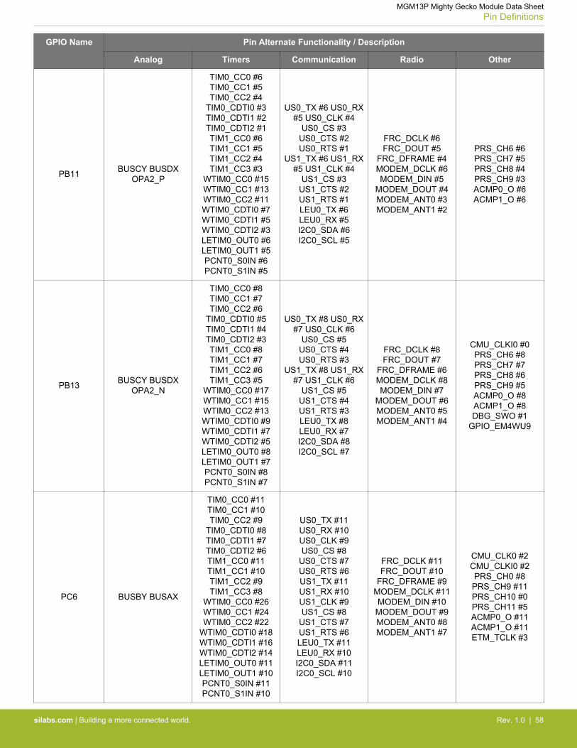
GPIO Name Pin Alternate Functionality / Description
Analog Timers Communication Radio Other
PB11 BUSCY BUSDXOPA2_P
TIM0_CC0 #6TIM0_CC1 #5TIM0_CC2 #4
TIM0_CDTI0 #3TIM0_CDTI1 #2TIM0_CDTI2 #1TIM1_CC0 #6TIM1_CC1 #5TIM1_CC2 #4TIM1_CC3 #3
WTIM0_CC0 #15WTIM0_CC1 #13WTIM0_CC2 #11WTIM0_CDTI0 #7WTIM0_CDTI1 #5WTIM0_CDTI2 #3LETIM0_OUT0 #6LETIM0_OUT1 #5PCNT0_S0IN #6PCNT0_S1IN #5
US0_TX #6 US0_RX#5 US0_CLK #4
US0_CS #3US0_CTS #2US0_RTS #1
US1_TX #6 US1_RX#5 US1_CLK #4
US1_CS #3US1_CTS #2US1_RTS #1LEU0_TX #6LEU0_RX #5I2C0_SDA #6I2C0_SCL #5
FRC_DCLK #6FRC_DOUT #5
FRC_DFRAME #4MODEM_DCLK #6MODEM_DIN #5
MODEM_DOUT #4MODEM_ANT0 #3MODEM_ANT1 #2
PRS_CH6 #6PRS_CH7 #5PRS_CH8 #4PRS_CH9 #3ACMP0_O #6ACMP1_O #6
PB13 BUSCY BUSDXOPA2_N
TIM0_CC0 #8TIM0_CC1 #7TIM0_CC2 #6
TIM0_CDTI0 #5TIM0_CDTI1 #4TIM0_CDTI2 #3TIM1_CC0 #8TIM1_CC1 #7TIM1_CC2 #6TIM1_CC3 #5
WTIM0_CC0 #17WTIM0_CC1 #15WTIM0_CC2 #13WTIM0_CDTI0 #9WTIM0_CDTI1 #7WTIM0_CDTI2 #5LETIM0_OUT0 #8LETIM0_OUT1 #7PCNT0_S0IN #8PCNT0_S1IN #7
US0_TX #8 US0_RX#7 US0_CLK #6
US0_CS #5US0_CTS #4US0_RTS #3
US1_TX #8 US1_RX#7 US1_CLK #6
US1_CS #5US1_CTS #4US1_RTS #3LEU0_TX #8LEU0_RX #7I2C0_SDA #8I2C0_SCL #7
FRC_DCLK #8FRC_DOUT #7
FRC_DFRAME #6MODEM_DCLK #8MODEM_DIN #7
MODEM_DOUT #6MODEM_ANT0 #5MODEM_ANT1 #4
CMU_CLKI0 #0PRS_CH6 #8PRS_CH7 #7PRS_CH8 #6PRS_CH9 #5ACMP0_O #8ACMP1_O #8DBG_SWO #1
GPIO_EM4WU9
PC6 BUSBY BUSAX
TIM0_CC0 #11TIM0_CC1 #10TIM0_CC2 #9
TIM0_CDTI0 #8TIM0_CDTI1 #7TIM0_CDTI2 #6TIM1_CC0 #11TIM1_CC1 #10TIM1_CC2 #9TIM1_CC3 #8
WTIM0_CC0 #26WTIM0_CC1 #24WTIM0_CC2 #22
WTIM0_CDTI0 #18WTIM0_CDTI1 #16WTIM0_CDTI2 #14LETIM0_OUT0 #11LETIM0_OUT1 #10PCNT0_S0IN #11PCNT0_S1IN #10
US0_TX #11US0_RX #10US0_CLK #9US0_CS #8
US0_CTS #7US0_RTS #6US1_TX #11US1_RX #10US1_CLK #9US1_CS #8
US1_CTS #7US1_RTS #6LEU0_TX #11LEU0_RX #10I2C0_SDA #11I2C0_SCL #10
FRC_DCLK #11FRC_DOUT #10
FRC_DFRAME #9MODEM_DCLK #11MODEM_DIN #10
MODEM_DOUT #9MODEM_ANT0 #8MODEM_ANT1 #7
CMU_CLK0 #2CMU_CLKI0 #2PRS_CH0 #8
PRS_CH9 #11PRS_CH10 #0PRS_CH11 #5ACMP0_O #11ACMP1_O #11ETM_TCLK #3
MGM13P Mighty Gecko Module Data SheetPin Definitions
silabs.com | Building a more connected world. Rev. 1.0 | 58

GPIO Name Pin Alternate Functionality / Description
Analog Timers Communication Radio Other
PC7 BUSAY BUSBX
TIM0_CC0 #12TIM0_CC1 #11TIM0_CC2 #10TIM0_CDTI0 #9TIM0_CDTI1 #8TIM0_CDTI2 #7TIM1_CC0 #12TIM1_CC1 #11TIM1_CC2 #10TIM1_CC3 #9
WTIM0_CC0 #27WTIM0_CC1 #25WTIM0_CC2 #23
WTIM0_CDTI0 #19WTIM0_CDTI1 #17WTIM0_CDTI2 #15LETIM0_OUT0 #12LETIM0_OUT1 #11PCNT0_S0IN #12PCNT0_S1IN #11
US0_TX #12US0_RX #11
US0_CLK #10US0_CS #9
US0_CTS #8US0_RTS #7US1_TX #12US1_RX #11
US1_CLK #10US1_CS #9
US1_CTS #8US1_RTS #7LEU0_TX #12LEU0_RX #11I2C0_SDA #12I2C0_SCL #11
FRC_DCLK #12FRC_DOUT #11
FRC_DFRAME #10MODEM_DCLK #12MODEM_DIN #11
MODEM_DOUT #10MODEM_ANT0 #9MODEM_ANT1 #8
CMU_CLK1 #2PRS_CH0 #9
PRS_CH9 #12PRS_CH10 #1PRS_CH11 #0ACMP0_O #12ACMP1_O #12
ETM_TD0
PC8 BUSBY BUSAX
TIM0_CC0 #13TIM0_CC1 #12TIM0_CC2 #11
TIM0_CDTI0 #10TIM0_CDTI1 #9TIM0_CDTI2 #8TIM1_CC0 #13TIM1_CC1 #12TIM1_CC2 #11TIM1_CC3 #10
WTIM0_CC0 #28WTIM0_CC1 #26WTIM0_CC2 #24
WTIM0_CDTI0 #20WTIM0_CDTI1 #18WTIM0_CDTI2 #16LETIM0_OUT0 #13LETIM0_OUT1 #12PCNT0_S0IN #13PCNT0_S1IN #12
US0_TX #13US0_RX #12
US0_CLK #11US0_CS #10US0_CTS #9US0_RTS #8US1_TX #13US1_RX #12
US1_CLK #11US1_CS #10US1_CTS #9US1_RTS #8LEU0_TX #13LEU0_RX #12I2C0_SDA #13I2C0_SCL #12
FRC_DCLK #13FRC_DOUT #12
FRC_DFRAME #11MODEM_DCLK #13MODEM_DIN #12
MODEM_DOUT #11MODEM_ANT0 #10MODEM_ANT1 #9
PRS_CH0 #10PRS_CH9 #13PRS_CH10 #2PRS_CH11 #1ACMP0_O #13ACMP1_O #13
ETM_TD1
PC9 BUSAY BUSBX
TIM0_CC0 #14TIM0_CC1 #13TIM0_CC2 #12
TIM0_CDTI0 #11TIM0_CDTI1 #10TIM0_CDTI2 #9TIM1_CC0 #14TIM1_CC1 #13TIM1_CC2 #12TIM1_CC3 #11
WTIM0_CC0 #29WTIM0_CC1 #27WTIM0_CC2 #25
WTIM0_CDTI0 #21WTIM0_CDTI1 #19WTIM0_CDTI2 #17LETIM0_OUT0 #14LETIM0_OUT1 #13PCNT0_S0IN #14PCNT0_S1IN #13
US0_TX #14US0_RX #13
US0_CLK #12US0_CS #11
US0_CTS #10US0_RTS #9US1_TX #14US1_RX #13
US1_CLK #12US1_CS #11
US1_CTS #10US1_RTS #9LEU0_TX #14LEU0_RX #13I2C0_SDA #14I2C0_SCL #13
FRC_DCLK #14FRC_DOUT #13
FRC_DFRAME #12MODEM_DCLK #14MODEM_DIN #13
MODEM_DOUT #12MODEM_ANT0 #11MODEM_ANT1 #10
PRS_CH0 #11PRS_CH9 #14PRS_CH10 #3PRS_CH11 #2ACMP0_O #14ACMP1_O #14
ETM_TD2
MGM13P Mighty Gecko Module Data SheetPin Definitions
silabs.com | Building a more connected world. Rev. 1.0 | 59
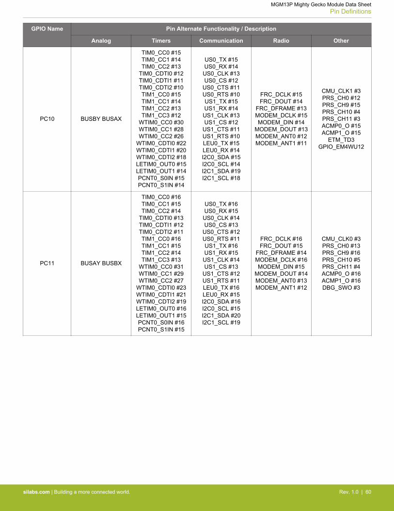
GPIO Name Pin Alternate Functionality / Description
Analog Timers Communication Radio Other
PC10 BUSBY BUSAX
TIM0_CC0 #15TIM0_CC1 #14TIM0_CC2 #13
TIM0_CDTI0 #12TIM0_CDTI1 #11TIM0_CDTI2 #10TIM1_CC0 #15TIM1_CC1 #14TIM1_CC2 #13TIM1_CC3 #12
WTIM0_CC0 #30WTIM0_CC1 #28WTIM0_CC2 #26
WTIM0_CDTI0 #22WTIM0_CDTI1 #20WTIM0_CDTI2 #18LETIM0_OUT0 #15LETIM0_OUT1 #14PCNT0_S0IN #15PCNT0_S1IN #14
US0_TX #15US0_RX #14
US0_CLK #13US0_CS #12
US0_CTS #11US0_RTS #10US1_TX #15US1_RX #14
US1_CLK #13US1_CS #12
US1_CTS #11US1_RTS #10LEU0_TX #15LEU0_RX #14I2C0_SDA #15I2C0_SCL #14I2C1_SDA #19I2C1_SCL #18
FRC_DCLK #15FRC_DOUT #14
FRC_DFRAME #13MODEM_DCLK #15MODEM_DIN #14
MODEM_DOUT #13MODEM_ANT0 #12MODEM_ANT1 #11
CMU_CLK1 #3PRS_CH0 #12PRS_CH9 #15PRS_CH10 #4PRS_CH11 #3ACMP0_O #15ACMP1_O #15
ETM_TD3GPIO_EM4WU12
PC11 BUSAY BUSBX
TIM0_CC0 #16TIM0_CC1 #15TIM0_CC2 #14
TIM0_CDTI0 #13TIM0_CDTI1 #12TIM0_CDTI2 #11TIM1_CC0 #16TIM1_CC1 #15TIM1_CC2 #14TIM1_CC3 #13
WTIM0_CC0 #31WTIM0_CC1 #29WTIM0_CC2 #27
WTIM0_CDTI0 #23WTIM0_CDTI1 #21WTIM0_CDTI2 #19LETIM0_OUT0 #16LETIM0_OUT1 #15PCNT0_S0IN #16PCNT0_S1IN #15
US0_TX #16US0_RX #15
US0_CLK #14US0_CS #13
US0_CTS #12US0_RTS #11US1_TX #16US1_RX #15
US1_CLK #14US1_CS #13
US1_CTS #12US1_RTS #11LEU0_TX #16LEU0_RX #15I2C0_SDA #16I2C0_SCL #15I2C1_SDA #20I2C1_SCL #19
FRC_DCLK #16FRC_DOUT #15
FRC_DFRAME #14MODEM_DCLK #16MODEM_DIN #15
MODEM_DOUT #14MODEM_ANT0 #13MODEM_ANT1 #12
CMU_CLK0 #3PRS_CH0 #13PRS_CH9 #16PRS_CH10 #5PRS_CH11 #4ACMP0_O #16ACMP1_O #16DBG_SWO #3
MGM13P Mighty Gecko Module Data SheetPin Definitions
silabs.com | Building a more connected world. Rev. 1.0 | 60
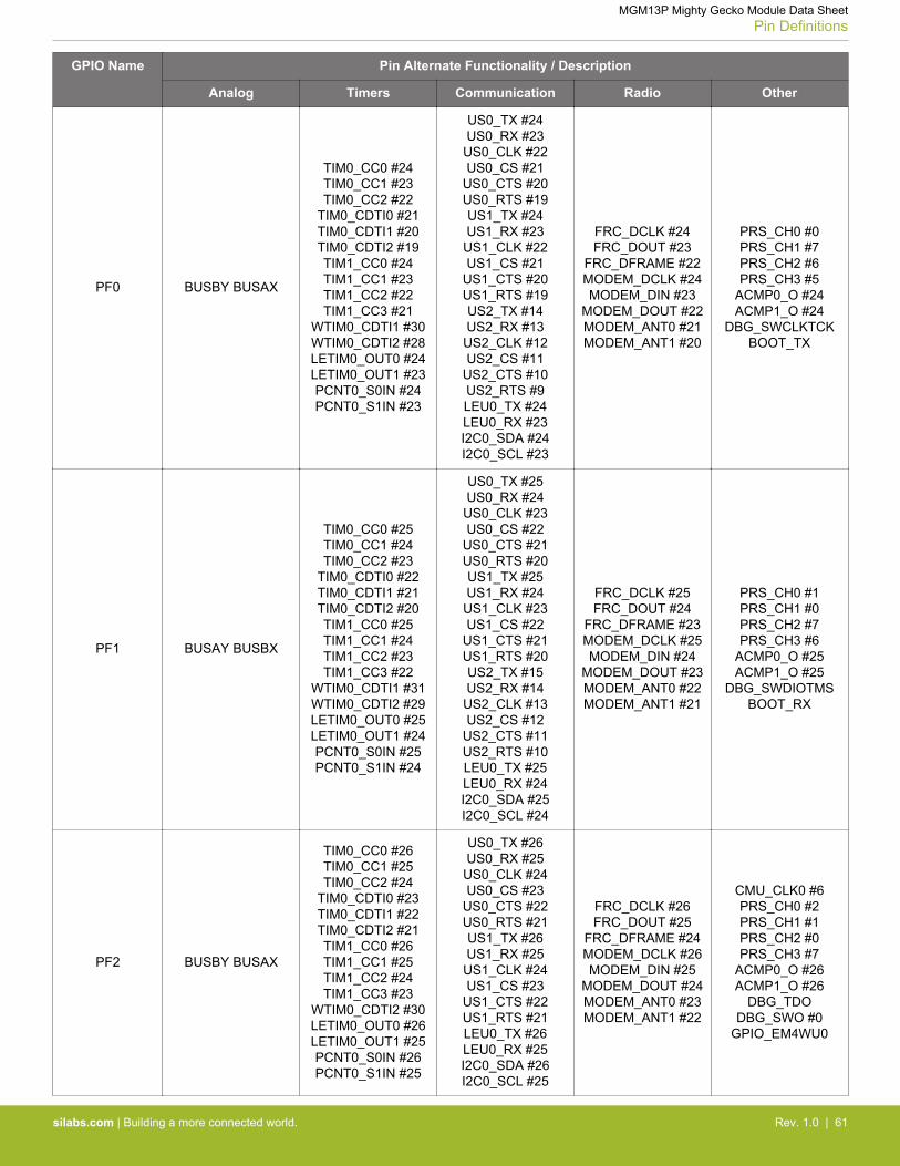
GPIO Name Pin Alternate Functionality / Description
Analog Timers Communication Radio Other
PF0 BUSBY BUSAX
TIM0_CC0 #24TIM0_CC1 #23TIM0_CC2 #22
TIM0_CDTI0 #21TIM0_CDTI1 #20TIM0_CDTI2 #19TIM1_CC0 #24TIM1_CC1 #23TIM1_CC2 #22TIM1_CC3 #21
WTIM0_CDTI1 #30WTIM0_CDTI2 #28LETIM0_OUT0 #24LETIM0_OUT1 #23PCNT0_S0IN #24PCNT0_S1IN #23
US0_TX #24US0_RX #23
US0_CLK #22US0_CS #21
US0_CTS #20US0_RTS #19US1_TX #24US1_RX #23
US1_CLK #22US1_CS #21
US1_CTS #20US1_RTS #19US2_TX #14US2_RX #13
US2_CLK #12US2_CS #11
US2_CTS #10US2_RTS #9LEU0_TX #24LEU0_RX #23I2C0_SDA #24I2C0_SCL #23
FRC_DCLK #24FRC_DOUT #23
FRC_DFRAME #22MODEM_DCLK #24MODEM_DIN #23
MODEM_DOUT #22MODEM_ANT0 #21MODEM_ANT1 #20
PRS_CH0 #0PRS_CH1 #7PRS_CH2 #6PRS_CH3 #5
ACMP0_O #24ACMP1_O #24
DBG_SWCLKTCKBOOT_TX
PF1 BUSAY BUSBX
TIM0_CC0 #25TIM0_CC1 #24TIM0_CC2 #23
TIM0_CDTI0 #22TIM0_CDTI1 #21TIM0_CDTI2 #20TIM1_CC0 #25TIM1_CC1 #24TIM1_CC2 #23TIM1_CC3 #22
WTIM0_CDTI1 #31WTIM0_CDTI2 #29LETIM0_OUT0 #25LETIM0_OUT1 #24PCNT0_S0IN #25PCNT0_S1IN #24
US0_TX #25US0_RX #24
US0_CLK #23US0_CS #22
US0_CTS #21US0_RTS #20US1_TX #25US1_RX #24
US1_CLK #23US1_CS #22
US1_CTS #21US1_RTS #20US2_TX #15US2_RX #14
US2_CLK #13US2_CS #12
US2_CTS #11US2_RTS #10LEU0_TX #25LEU0_RX #24I2C0_SDA #25I2C0_SCL #24
FRC_DCLK #25FRC_DOUT #24
FRC_DFRAME #23MODEM_DCLK #25MODEM_DIN #24
MODEM_DOUT #23MODEM_ANT0 #22MODEM_ANT1 #21
PRS_CH0 #1PRS_CH1 #0PRS_CH2 #7PRS_CH3 #6
ACMP0_O #25ACMP1_O #25
DBG_SWDIOTMSBOOT_RX
PF2 BUSBY BUSAX
TIM0_CC0 #26TIM0_CC1 #25TIM0_CC2 #24
TIM0_CDTI0 #23TIM0_CDTI1 #22TIM0_CDTI2 #21TIM1_CC0 #26TIM1_CC1 #25TIM1_CC2 #24TIM1_CC3 #23
WTIM0_CDTI2 #30LETIM0_OUT0 #26LETIM0_OUT1 #25PCNT0_S0IN #26PCNT0_S1IN #25
US0_TX #26US0_RX #25
US0_CLK #24US0_CS #23
US0_CTS #22US0_RTS #21US1_TX #26US1_RX #25
US1_CLK #24US1_CS #23
US1_CTS #22US1_RTS #21LEU0_TX #26LEU0_RX #25I2C0_SDA #26I2C0_SCL #25
FRC_DCLK #26FRC_DOUT #25
FRC_DFRAME #24MODEM_DCLK #26MODEM_DIN #25
MODEM_DOUT #24MODEM_ANT0 #23MODEM_ANT1 #22
CMU_CLK0 #6PRS_CH0 #2PRS_CH1 #1PRS_CH2 #0PRS_CH3 #7
ACMP0_O #26ACMP1_O #26
DBG_TDODBG_SWO #0
GPIO_EM4WU0
MGM13P Mighty Gecko Module Data SheetPin Definitions
silabs.com | Building a more connected world. Rev. 1.0 | 61
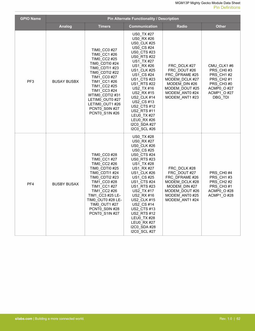
GPIO Name Pin Alternate Functionality / Description
Analog Timers Communication Radio Other
PF3 BUSAY BUSBX
TIM0_CC0 #27TIM0_CC1 #26TIM0_CC2 #25
TIM0_CDTI0 #24TIM0_CDTI1 #23TIM0_CDTI2 #22TIM1_CC0 #27TIM1_CC1 #26TIM1_CC2 #25TIM1_CC3 #24
WTIM0_CDTI2 #31LETIM0_OUT0 #27LETIM0_OUT1 #26PCNT0_S0IN #27PCNT0_S1IN #26
US0_TX #27US0_RX #26
US0_CLK #25US0_CS #24
US0_CTS #23US0_RTS #22US1_TX #27US1_RX #26
US1_CLK #25US1_CS #24
US1_CTS #23US1_RTS #22US2_TX #16US2_RX #15
US2_CLK #14US2_CS #13
US2_CTS #12US2_RTS #11LEU0_TX #27LEU0_RX #26I2C0_SDA #27I2C0_SCL #26
FRC_DCLK #27FRC_DOUT #26
FRC_DFRAME #25MODEM_DCLK #27MODEM_DIN #26
MODEM_DOUT #25MODEM_ANT0 #24MODEM_ANT1 #23
CMU_CLK1 #6PRS_CH0 #3PRS_CH1 #2PRS_CH2 #1PRS_CH3 #0
ACMP0_O #27ACMP1_O #27
DBG_TDI
PF4 BUSBY BUSAX
TIM0_CC0 #28TIM0_CC1 #27TIM0_CC2 #26
TIM0_CDTI0 #25TIM0_CDTI1 #24TIM0_CDTI2 #23TIM1_CC0 #28TIM1_CC1 #27TIM1_CC2 #26
TIM1_CC3 #25 LE-TIM0_OUT0 #28 LE-
TIM0_OUT1 #27PCNT0_S0IN #28PCNT0_S1IN #27
US0_TX #28US0_RX #27
US0_CLK #26US0_CS #25
US0_CTS #24US0_RTS #23US1_TX #28US1_RX #27
US1_CLK #26US1_CS #25
US1_CTS #24US1_RTS #23US2_TX #17US2_RX #16
US2_CLK #15US2_CS #14
US2_CTS #13US2_RTS #12LEU0_TX #28LEU0_RX #27I2C0_SDA #28I2C0_SCL #27
FRC_DCLK #28FRC_DOUT #27
FRC_DFRAME #26MODEM_DCLK #28MODEM_DIN #27
MODEM_DOUT #26MODEM_ANT0 #25MODEM_ANT1 #24
PRS_CH0 #4PRS_CH1 #3PRS_CH2 #2PRS_CH3 #1
ACMP0_O #28ACMP1_O #28
MGM13P Mighty Gecko Module Data SheetPin Definitions
silabs.com | Building a more connected world. Rev. 1.0 | 62
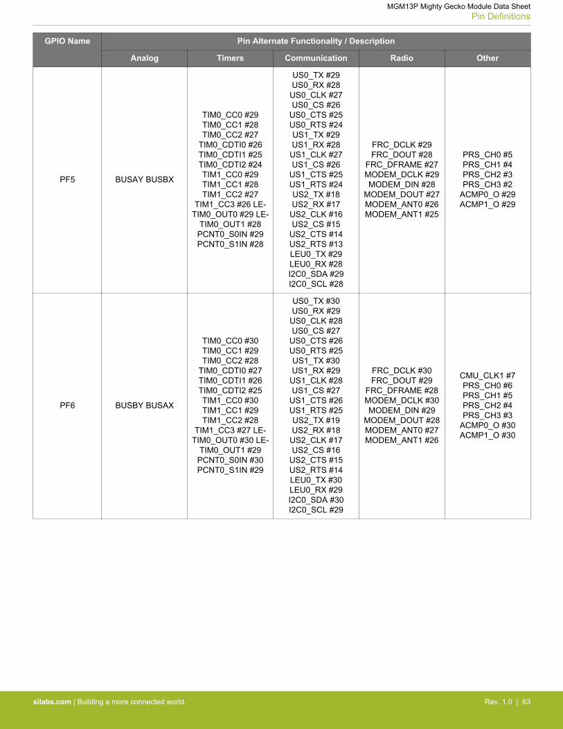
GPIO Name Pin Alternate Functionality / Description
Analog Timers Communication Radio Other
PF5 BUSAY BUSBX
TIM0_CC0 #29TIM0_CC1 #28TIM0_CC2 #27
TIM0_CDTI0 #26TIM0_CDTI1 #25TIM0_CDTI2 #24TIM1_CC0 #29TIM1_CC1 #28TIM1_CC2 #27
TIM1_CC3 #26 LE-TIM0_OUT0 #29 LE-
TIM0_OUT1 #28PCNT0_S0IN #29PCNT0_S1IN #28
US0_TX #29US0_RX #28
US0_CLK #27US0_CS #26
US0_CTS #25US0_RTS #24US1_TX #29US1_RX #28
US1_CLK #27US1_CS #26
US1_CTS #25US1_RTS #24US2_TX #18US2_RX #17
US2_CLK #16US2_CS #15
US2_CTS #14US2_RTS #13LEU0_TX #29LEU0_RX #28I2C0_SDA #29I2C0_SCL #28
FRC_DCLK #29FRC_DOUT #28
FRC_DFRAME #27MODEM_DCLK #29MODEM_DIN #28
MODEM_DOUT #27MODEM_ANT0 #26MODEM_ANT1 #25
PRS_CH0 #5PRS_CH1 #4PRS_CH2 #3PRS_CH3 #2
ACMP0_O #29ACMP1_O #29
PF6 BUSBY BUSAX
TIM0_CC0 #30TIM0_CC1 #29TIM0_CC2 #28
TIM0_CDTI0 #27TIM0_CDTI1 #26TIM0_CDTI2 #25TIM1_CC0 #30TIM1_CC1 #29TIM1_CC2 #28
TIM1_CC3 #27 LE-TIM0_OUT0 #30 LE-
TIM0_OUT1 #29PCNT0_S0IN #30PCNT0_S1IN #29
US0_TX #30US0_RX #29
US0_CLK #28US0_CS #27
US0_CTS #26US0_RTS #25US1_TX #30US1_RX #29
US1_CLK #28US1_CS #27
US1_CTS #26US1_RTS #25US2_TX #19US2_RX #18
US2_CLK #17US2_CS #16
US2_CTS #15US2_RTS #14LEU0_TX #30LEU0_RX #29I2C0_SDA #30I2C0_SCL #29
FRC_DCLK #30FRC_DOUT #29
FRC_DFRAME #28MODEM_DCLK #30MODEM_DIN #29
MODEM_DOUT #28MODEM_ANT0 #27MODEM_ANT1 #26
CMU_CLK1 #7PRS_CH0 #6PRS_CH1 #5PRS_CH2 #4PRS_CH3 #3
ACMP0_O #30ACMP1_O #30
MGM13P Mighty Gecko Module Data SheetPin Definitions
silabs.com | Building a more connected world. Rev. 1.0 | 63

GPIO Name Pin Alternate Functionality / Description
Analog Timers Communication Radio Other
PF7 BUSAY BUSBX
TIM0_CC0 #31TIM0_CC1 #30TIM0_CC2 #29
TIM0_CDTI0 #28TIM0_CDTI1 #27TIM0_CDTI2 #26TIM1_CC0 #31TIM1_CC1 #30TIM1_CC2 #29
TIM1_CC3 #28 LE-TIM0_OUT0 #31 LE-
TIM0_OUT1 #30PCNT0_S0IN #31PCNT0_S1IN #30
US0_TX #31US0_RX #30
US0_CLK #29US0_CS #28
US0_CTS #27US0_RTS #26US1_TX #31US1_RX #30
US1_CLK #29US1_CS #28
US1_CTS #27US1_RTS #26US2_TX #20US2_RX #19
US2_CLK #18US2_CS #17
US2_CTS #16US2_RTS #15LEU0_TX #31LEU0_RX #30I2C0_SDA #31I2C0_SCL #30
FRC_DCLK #31FRC_DOUT #30
FRC_DFRAME #29MODEM_DCLK #31MODEM_DIN #30
MODEM_DOUT #29MODEM_ANT0 #28MODEM_ANT1 #27
CMU_CLKI0 #1CMU_CLK0 #7PRS_CH0 #7PRS_CH1 #6PRS_CH2 #5PRS_CH3 #4
ACMP0_O #31ACMP1_O #31
GPIO_EM4WU1
MGM13P Mighty Gecko Module Data SheetPin Definitions
silabs.com | Building a more connected world. Rev. 1.0 | 64
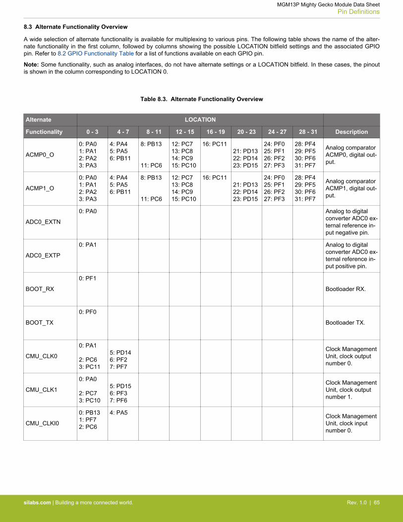
8.3 Alternate Functionality Overview
A wide selection of alternate functionality is available for multiplexing to various pins. The following table shows the name of the alter-nate functionality in the first column, followed by columns showing the possible LOCATION bitfield settings and the associated GPIOpin. Refer to 8.2 GPIO Functionality Table for a list of functions available on each GPIO pin.
Note: Some functionality, such as analog interfaces, do not have alternate settings or a LOCATION bitfield. In these cases, the pinoutis shown in the column corresponding to LOCATION 0.
Table 8.3. Alternate Functionality Overview
Alternate LOCATION
Functionality 0 - 3 4 - 7 8 - 11 12 - 15 16 - 19 20 - 23 24 - 27 28 - 31 Description
ACMP0_O
0: PA01: PA12: PA23: PA3
4: PA45: PA56: PB11
8: PB13
11: PC6
12: PC713: PC814: PC915: PC10
16: PC1121: PD1322: PD1423: PD15
24: PF025: PF126: PF227: PF3
28: PF429: PF530: PF631: PF7
Analog comparatorACMP0, digital out-put.
ACMP1_O
0: PA01: PA12: PA23: PA3
4: PA45: PA56: PB11
8: PB13
11: PC6
12: PC713: PC814: PC915: PC10
16: PC1121: PD1322: PD1423: PD15
24: PF025: PF126: PF227: PF3
28: PF429: PF530: PF631: PF7
Analog comparatorACMP1, digital out-put.
ADC0_EXTN
0: PA0 Analog to digitalconverter ADC0 ex-ternal reference in-put negative pin.
ADC0_EXTP
0: PA1 Analog to digitalconverter ADC0 ex-ternal reference in-put positive pin.
BOOT_RX
0: PF1
Bootloader RX.
BOOT_TX
0: PF0
Bootloader TX.
CMU_CLK0
0: PA1
2: PC63: PC11
5: PD146: PF27: PF7
Clock ManagementUnit, clock outputnumber 0.
CMU_CLK1
0: PA0
2: PC73: PC10
5: PD156: PF37: PF6
Clock ManagementUnit, clock outputnumber 1.
CMU_CLKI0
0: PB131: PF72: PC6
4: PA5 Clock ManagementUnit, clock inputnumber 0.
MGM13P Mighty Gecko Module Data SheetPin Definitions
silabs.com | Building a more connected world. Rev. 1.0 | 65
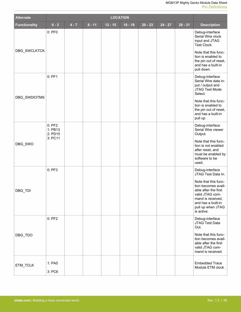
Alternate LOCATION
Functionality 0 - 3 4 - 7 8 - 11 12 - 15 16 - 19 20 - 23 24 - 27 28 - 31 Description
DBG_SWCLKTCK
0: PF0 Debug-interfaceSerial Wire clockinput and JTAGTest Clock.
Note that this func-tion is enabled tothe pin out of reset,and has a built-inpull down.
DBG_SWDIOTMS
0: PF1 Debug-interfaceSerial Wire data in-put / output andJTAG Test ModeSelect.
Note that this func-tion is enabled tothe pin out of reset,and has a built-inpull up.
DBG_SWO
0: PF21: PB132: PD153: PC11
Debug-interfaceSerial Wire viewerOutput.
Note that this func-tion is not enabledafter reset, andmust be enabled bysoftware to beused.
DBG_TDI
0: PF3 Debug-interfaceJTAG Test Data In.
Note that this func-tion becomes avail-able after the firstvalid JTAG com-mand is received,and has a built-inpull up when JTAGis active.
DBG_TDO
0: PF2 Debug-interfaceJTAG Test DataOut.
Note that this func-tion becomes avail-able after the firstvalid JTAG com-mand is received.
ETM_TCLK 1: PA5
3: PC6
Embedded TraceModule ETM clock .
MGM13P Mighty Gecko Module Data SheetPin Definitions
silabs.com | Building a more connected world. Rev. 1.0 | 66
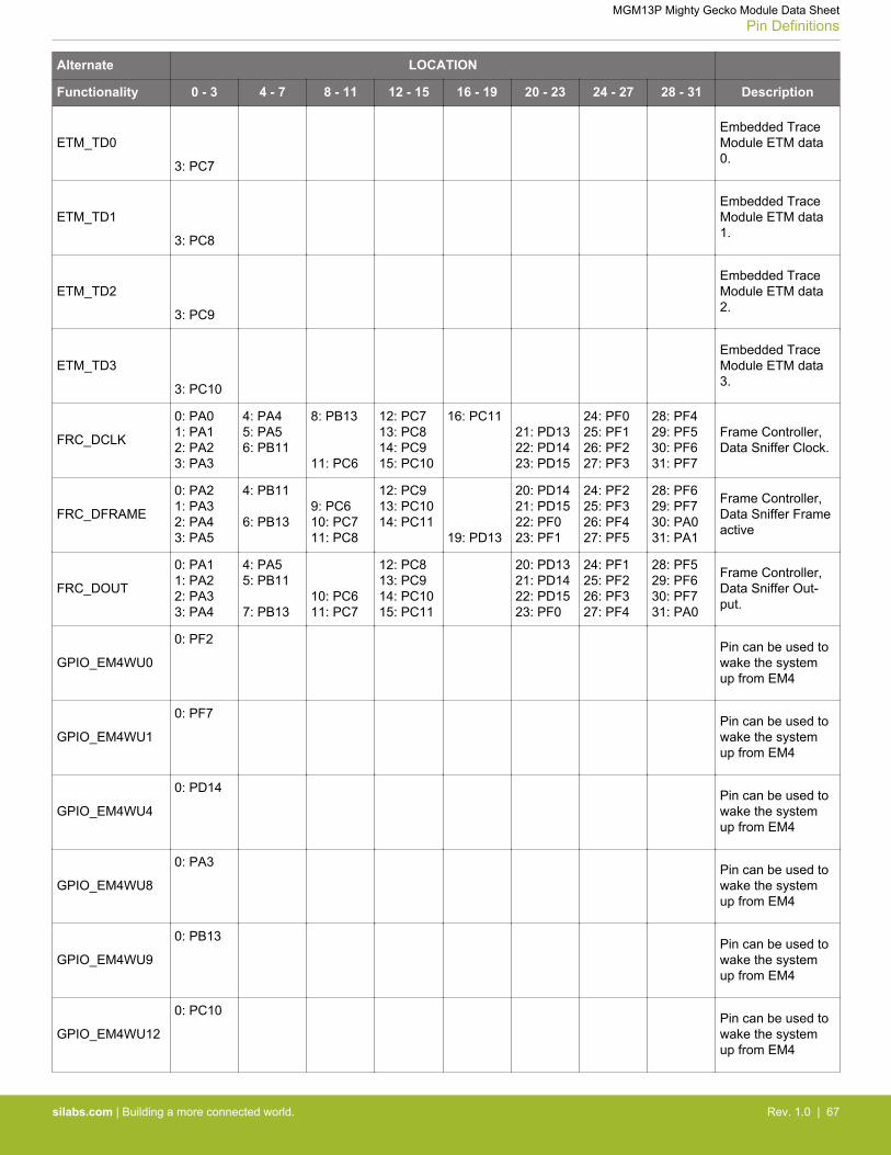
Alternate LOCATION
Functionality 0 - 3 4 - 7 8 - 11 12 - 15 16 - 19 20 - 23 24 - 27 28 - 31 Description
ETM_TD0
3: PC7
Embedded TraceModule ETM data0.
ETM_TD1
3: PC8
Embedded TraceModule ETM data1.
ETM_TD2
3: PC9
Embedded TraceModule ETM data2.
ETM_TD3
3: PC10
Embedded TraceModule ETM data3.
FRC_DCLK
0: PA01: PA12: PA23: PA3
4: PA45: PA56: PB11
8: PB13
11: PC6
12: PC713: PC814: PC915: PC10
16: PC1121: PD1322: PD1423: PD15
24: PF025: PF126: PF227: PF3
28: PF429: PF530: PF631: PF7
Frame Controller,Data Sniffer Clock.
FRC_DFRAME
0: PA21: PA32: PA43: PA5
4: PB11
6: PB139: PC610: PC711: PC8
12: PC913: PC1014: PC11
19: PD13
20: PD1421: PD1522: PF023: PF1
24: PF225: PF326: PF427: PF5
28: PF629: PF730: PA031: PA1
Frame Controller,Data Sniffer Frameactive
FRC_DOUT
0: PA11: PA22: PA33: PA4
4: PA55: PB11
7: PB1310: PC611: PC7
12: PC813: PC914: PC1015: PC11
20: PD1321: PD1422: PD1523: PF0
24: PF125: PF226: PF327: PF4
28: PF529: PF630: PF731: PA0
Frame Controller,Data Sniffer Out-put.
GPIO_EM4WU0
0: PF2 Pin can be used towake the systemup from EM4
GPIO_EM4WU1
0: PF7 Pin can be used towake the systemup from EM4
GPIO_EM4WU4
0: PD14 Pin can be used towake the systemup from EM4
GPIO_EM4WU8
0: PA3 Pin can be used towake the systemup from EM4
GPIO_EM4WU9
0: PB13 Pin can be used towake the systemup from EM4
GPIO_EM4WU12
0: PC10 Pin can be used towake the systemup from EM4
MGM13P Mighty Gecko Module Data SheetPin Definitions
silabs.com | Building a more connected world. Rev. 1.0 | 67
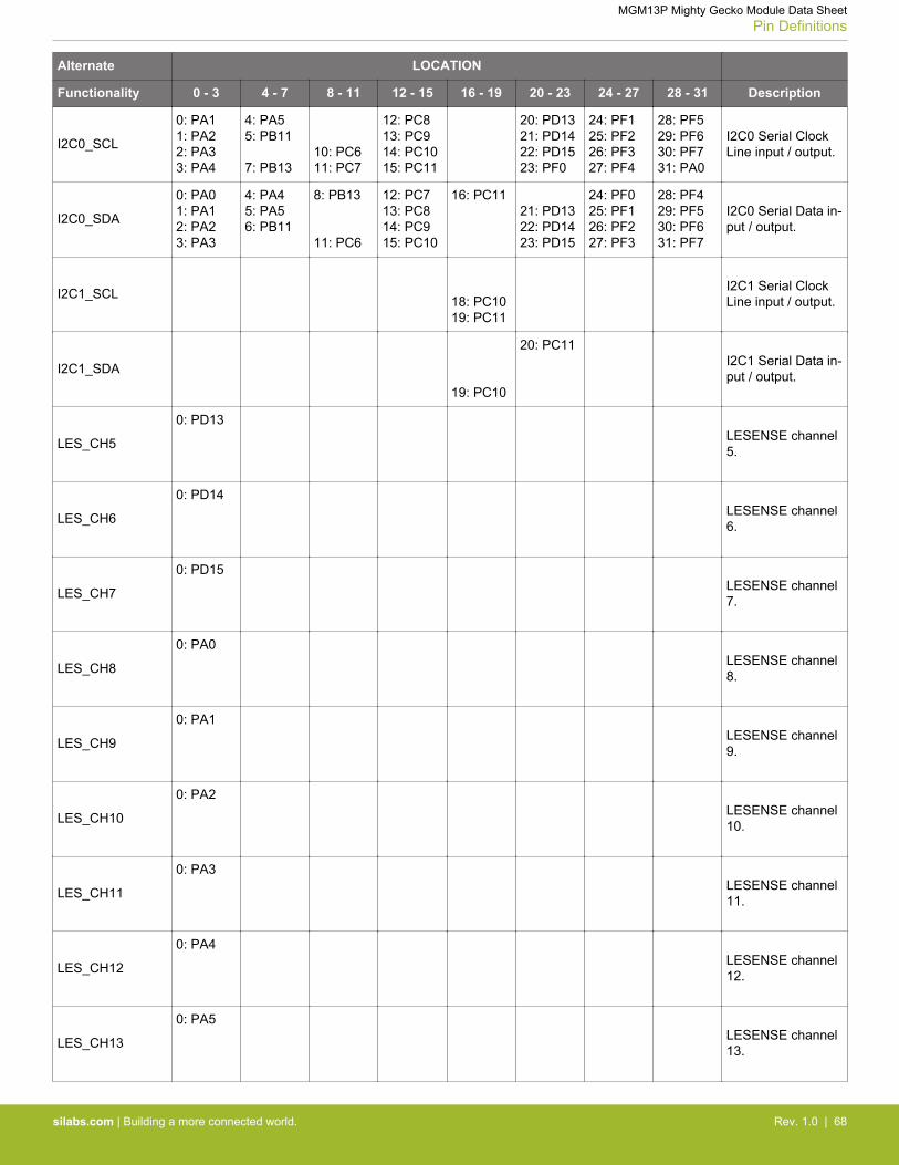
Alternate LOCATION
Functionality 0 - 3 4 - 7 8 - 11 12 - 15 16 - 19 20 - 23 24 - 27 28 - 31 Description
I2C0_SCL
0: PA11: PA22: PA33: PA4
4: PA55: PB11
7: PB1310: PC611: PC7
12: PC813: PC914: PC1015: PC11
20: PD1321: PD1422: PD1523: PF0
24: PF125: PF226: PF327: PF4
28: PF529: PF630: PF731: PA0
I2C0 Serial ClockLine input / output.
I2C0_SDA
0: PA01: PA12: PA23: PA3
4: PA45: PA56: PB11
8: PB13
11: PC6
12: PC713: PC814: PC915: PC10
16: PC1121: PD1322: PD1423: PD15
24: PF025: PF126: PF227: PF3
28: PF429: PF530: PF631: PF7
I2C0 Serial Data in-put / output.
I2C1_SCL 18: PC1019: PC11
I2C1 Serial ClockLine input / output.
I2C1_SDA
19: PC10
20: PC11I2C1 Serial Data in-put / output.
LES_CH5
0: PD13LESENSE channel5.
LES_CH6
0: PD14LESENSE channel6.
LES_CH7
0: PD15LESENSE channel7.
LES_CH8
0: PA0LESENSE channel8.
LES_CH9
0: PA1LESENSE channel9.
LES_CH10
0: PA2LESENSE channel10.
LES_CH11
0: PA3LESENSE channel11.
LES_CH12
0: PA4LESENSE channel12.
LES_CH13
0: PA5LESENSE channel13.
MGM13P Mighty Gecko Module Data SheetPin Definitions
silabs.com | Building a more connected world. Rev. 1.0 | 68
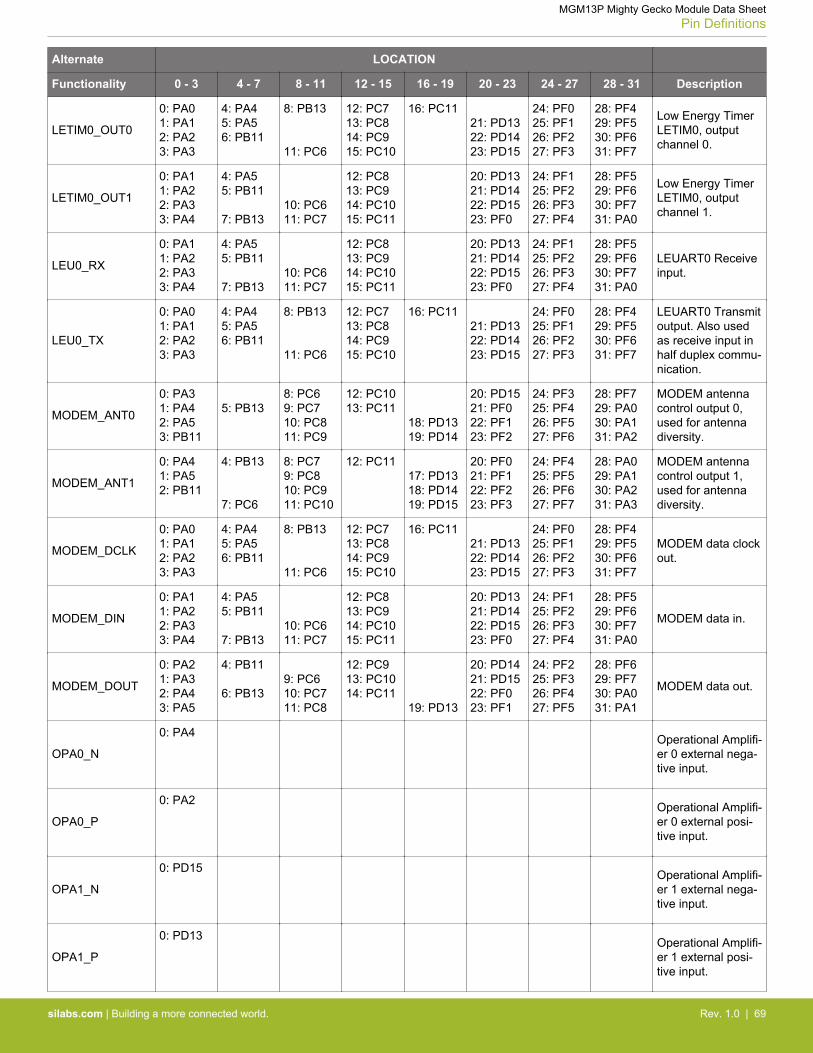
Alternate LOCATION
Functionality 0 - 3 4 - 7 8 - 11 12 - 15 16 - 19 20 - 23 24 - 27 28 - 31 Description
LETIM0_OUT0
0: PA01: PA12: PA23: PA3
4: PA45: PA56: PB11
8: PB13
11: PC6
12: PC713: PC814: PC915: PC10
16: PC1121: PD1322: PD1423: PD15
24: PF025: PF126: PF227: PF3
28: PF429: PF530: PF631: PF7
Low Energy TimerLETIM0, outputchannel 0.
LETIM0_OUT1
0: PA11: PA22: PA33: PA4
4: PA55: PB11
7: PB1310: PC611: PC7
12: PC813: PC914: PC1015: PC11
20: PD1321: PD1422: PD1523: PF0
24: PF125: PF226: PF327: PF4
28: PF529: PF630: PF731: PA0
Low Energy TimerLETIM0, outputchannel 1.
LEU0_RX
0: PA11: PA22: PA33: PA4
4: PA55: PB11
7: PB1310: PC611: PC7
12: PC813: PC914: PC1015: PC11
20: PD1321: PD1422: PD1523: PF0
24: PF125: PF226: PF327: PF4
28: PF529: PF630: PF731: PA0
LEUART0 Receiveinput.
LEU0_TX
0: PA01: PA12: PA23: PA3
4: PA45: PA56: PB11
8: PB13
11: PC6
12: PC713: PC814: PC915: PC10
16: PC1121: PD1322: PD1423: PD15
24: PF025: PF126: PF227: PF3
28: PF429: PF530: PF631: PF7
LEUART0 Transmitoutput. Also usedas receive input inhalf duplex commu-nication.
MODEM_ANT0
0: PA31: PA42: PA53: PB11
5: PB138: PC69: PC710: PC811: PC9
12: PC1013: PC11
18: PD1319: PD14
20: PD1521: PF022: PF123: PF2
24: PF325: PF426: PF527: PF6
28: PF729: PA030: PA131: PA2
MODEM antennacontrol output 0,used for antennadiversity.
MODEM_ANT1
0: PA41: PA52: PB11
4: PB13
7: PC6
8: PC79: PC810: PC911: PC10
12: PC1117: PD1318: PD1419: PD15
20: PF021: PF122: PF223: PF3
24: PF425: PF526: PF627: PF7
28: PA029: PA130: PA231: PA3
MODEM antennacontrol output 1,used for antennadiversity.
MODEM_DCLK
0: PA01: PA12: PA23: PA3
4: PA45: PA56: PB11
8: PB13
11: PC6
12: PC713: PC814: PC915: PC10
16: PC1121: PD1322: PD1423: PD15
24: PF025: PF126: PF227: PF3
28: PF429: PF530: PF631: PF7
MODEM data clockout.
MODEM_DIN
0: PA11: PA22: PA33: PA4
4: PA55: PB11
7: PB1310: PC611: PC7
12: PC813: PC914: PC1015: PC11
20: PD1321: PD1422: PD1523: PF0
24: PF125: PF226: PF327: PF4
28: PF529: PF630: PF731: PA0
MODEM data in.
MODEM_DOUT
0: PA21: PA32: PA43: PA5
4: PB11
6: PB139: PC610: PC711: PC8
12: PC913: PC1014: PC11
19: PD13
20: PD1421: PD1522: PF023: PF1
24: PF225: PF326: PF427: PF5
28: PF629: PF730: PA031: PA1
MODEM data out.
OPA0_N
0: PA4 Operational Amplifi-er 0 external nega-tive input.
OPA0_P
0: PA2 Operational Amplifi-er 0 external posi-tive input.
OPA1_N
0: PD15 Operational Amplifi-er 1 external nega-tive input.
OPA1_P
0: PD13 Operational Amplifi-er 1 external posi-tive input.
MGM13P Mighty Gecko Module Data SheetPin Definitions
silabs.com | Building a more connected world. Rev. 1.0 | 69
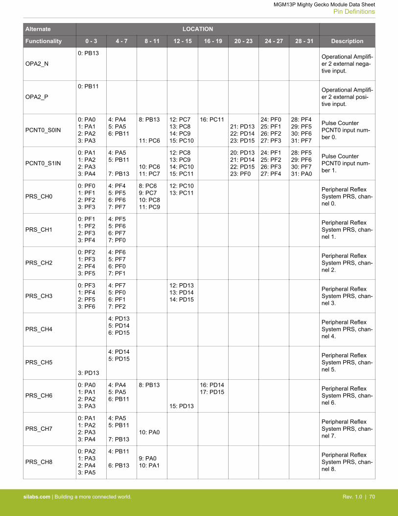
Alternate LOCATION
Functionality 0 - 3 4 - 7 8 - 11 12 - 15 16 - 19 20 - 23 24 - 27 28 - 31 Description
OPA2_N
0: PB13 Operational Amplifi-er 2 external nega-tive input.
OPA2_P
0: PB11 Operational Amplifi-er 2 external posi-tive input.
PCNT0_S0IN
0: PA01: PA12: PA23: PA3
4: PA45: PA56: PB11
8: PB13
11: PC6
12: PC713: PC814: PC915: PC10
16: PC1121: PD1322: PD1423: PD15
24: PF025: PF126: PF227: PF3
28: PF429: PF530: PF631: PF7
Pulse CounterPCNT0 input num-ber 0.
PCNT0_S1IN
0: PA11: PA22: PA33: PA4
4: PA55: PB11
7: PB1310: PC611: PC7
12: PC813: PC914: PC1015: PC11
20: PD1321: PD1422: PD1523: PF0
24: PF125: PF226: PF327: PF4
28: PF529: PF630: PF731: PA0
Pulse CounterPCNT0 input num-ber 1.
PRS_CH0
0: PF01: PF12: PF23: PF3
4: PF45: PF56: PF67: PF7
8: PC69: PC710: PC811: PC9
12: PC1013: PC11 Peripheral Reflex
System PRS, chan-nel 0.
PRS_CH1
0: PF11: PF22: PF33: PF4
4: PF55: PF66: PF77: PF0
Peripheral ReflexSystem PRS, chan-nel 1.
PRS_CH2
0: PF21: PF32: PF43: PF5
4: PF65: PF76: PF07: PF1
Peripheral ReflexSystem PRS, chan-nel 2.
PRS_CH3
0: PF31: PF42: PF53: PF6
4: PF75: PF06: PF17: PF2
12: PD1313: PD1414: PD15
Peripheral ReflexSystem PRS, chan-nel 3.
PRS_CH4
4: PD135: PD146: PD15
Peripheral ReflexSystem PRS, chan-nel 4.
PRS_CH5
3: PD13
4: PD145: PD15 Peripheral Reflex
System PRS, chan-nel 5.
PRS_CH6
0: PA01: PA12: PA23: PA3
4: PA45: PA56: PB11
8: PB13
15: PD13
16: PD1417: PD15 Peripheral Reflex
System PRS, chan-nel 6.
PRS_CH7
0: PA11: PA22: PA33: PA4
4: PA55: PB11
7: PB1310: PA0
Peripheral ReflexSystem PRS, chan-nel 7.
PRS_CH8
0: PA21: PA32: PA43: PA5
4: PB11
6: PB139: PA010: PA1
Peripheral ReflexSystem PRS, chan-nel 8.
MGM13P Mighty Gecko Module Data SheetPin Definitions
silabs.com | Building a more connected world. Rev. 1.0 | 70

Alternate LOCATION
Functionality 0 - 3 4 - 7 8 - 11 12 - 15 16 - 19 20 - 23 24 - 27 28 - 31 Description
PRS_CH9
0: PA31: PA42: PA53: PB11
5: PB138: PA09: PA110: PA211: PC6
12: PC713: PC814: PC915: PC10
16: PC11 Peripheral ReflexSystem PRS, chan-nel 9.
PRS_CH10
0: PC61: PC72: PC83: PC9
4: PC105: PC11 Peripheral Reflex
System PRS, chan-nel 10.
PRS_CH11
0: PC71: PC82: PC93: PC10
4: PC115: PC6 Peripheral Reflex
System PRS, chan-nel 11.
TIM0_CC0
0: PA01: PA12: PA23: PA3
4: PA45: PA56: PB11
8: PB13
11: PC6
12: PC713: PC814: PC915: PC10
16: PC1121: PD1322: PD1423: PD15
24: PF025: PF126: PF227: PF3
28: PF429: PF530: PF631: PF7
Timer 0 CaptureCompare input /output channel 0.
TIM0_CC1
0: PA11: PA22: PA33: PA4
4: PA55: PB11
7: PB1310: PC611: PC7
12: PC813: PC914: PC1015: PC11
20: PD1321: PD1422: PD1523: PF0
24: PF125: PF226: PF327: PF4
28: PF529: PF630: PF731: PA0
Timer 0 CaptureCompare input /output channel 1.
TIM0_CC2
0: PA21: PA32: PA43: PA5
4: PB11
6: PB139: PC610: PC711: PC8
12: PC913: PC1014: PC11
19: PD13
20: PD1421: PD1522: PF023: PF1
24: PF225: PF326: PF427: PF5
28: PF629: PF730: PA031: PA1
Timer 0 CaptureCompare input /output channel 2.
TIM0_CDTI0
0: PA31: PA42: PA53: PB11
5: PB138: PC69: PC710: PC811: PC9
12: PC1013: PC11
18: PD1319: PD14
20: PD1521: PF022: PF123: PF2
24: PF325: PF426: PF527: PF6
28: PF729: PA030: PA131: PA2
Timer 0 Compli-mentary Dead TimeInsertion channel 0.
TIM0_CDTI1
0: PA41: PA52: PB11
4: PB13
7: PC6
8: PC79: PC810: PC911: PC10
12: PC1117: PD1318: PD1419: PD15
20: PF021: PF122: PF223: PF3
24: PF425: PF526: PF627: PF7
28: PA029: PA130: PA231: PA3
Timer 0 Compli-mentary Dead TimeInsertion channel 1.
TIM0_CDTI2
0: PA51: PB11
3: PB136: PC67: PC7
8: PC89: PC910: PC1011: PC11
16: PD1317: PD1418: PD1519: PF0
20: PF121: PF222: PF323: PF4
24: PF525: PF626: PF727: PA0
28: PA129: PA230: PA331: PA4
Timer 0 Compli-mentary Dead TimeInsertion channel 2.
TIM1_CC0
0: PA01: PA12: PA23: PA3
4: PA45: PA56: PB11
8: PB13
11: PC6
12: PC713: PC814: PC915: PC10
16: PC1121: PD1322: PD1423: PD15
24: PF025: PF126: PF227: PF3
28: PF429: PF530: PF631: PF7
Timer 1 CaptureCompare input /output channel 0.
TIM1_CC1
0: PA11: PA22: PA33: PA4
4: PA55: PB11
7: PB1310: PC611: PC7
12: PC813: PC914: PC1015: PC11
20: PD1321: PD1422: PD1523: PF0
24: PF125: PF226: PF327: PF4
28: PF529: PF630: PF731: PA0
Timer 1 CaptureCompare input /output channel 1.
TIM1_CC2
0: PA21: PA32: PA43: PA5
4: PB11
6: PB139: PC610: PC711: PC8
12: PC913: PC1014: PC11
19: PD13
20: PD1421: PD1522: PF023: PF1
24: PF225: PF326: PF427: PF5
28: PF629: PF730: PA031: PA1
Timer 1 CaptureCompare input /output channel 2.
TIM1_CC3
0: PA31: PA42: PA53: PB11
5: PB138: PC69: PC710: PC811: PC9
12: PC1013: PC11
18: PD1319: PD14
20: PD1521: PF022: PF123: PF2
24: PF325: PF426: PF527: PF6
28: PF729: PA030: PA131: PA2
Timer 1 CaptureCompare input /output channel 3.
MGM13P Mighty Gecko Module Data SheetPin Definitions
silabs.com | Building a more connected world. Rev. 1.0 | 71

Alternate LOCATION
Functionality 0 - 3 4 - 7 8 - 11 12 - 15 16 - 19 20 - 23 24 - 27 28 - 31 Description
US0_CLK
0: PA21: PA32: PA43: PA5
4: PB11
6: PB139: PC610: PC711: PC8
12: PC913: PC1014: PC11
19: PD13
20: PD1421: PD1522: PF023: PF1
24: PF225: PF326: PF427: PF5
28: PF629: PF730: PA031: PA1
USART0 clock in-put / output.
US0_CS
0: PA31: PA42: PA53: PB11
5: PB138: PC69: PC710: PC811: PC9
12: PC1013: PC11
18: PD1319: PD14
20: PD1521: PF022: PF123: PF2
24: PF325: PF426: PF527: PF6
28: PF729: PA030: PA131: PA2
USART0 chip se-lect input / output.
US0_CTS
0: PA41: PA52: PB11
4: PB13
7: PC6
8: PC79: PC810: PC911: PC10
12: PC1117: PD1318: PD1419: PD15
20: PF021: PF122: PF223: PF3
24: PF425: PF526: PF627: PF7
28: PA029: PA130: PA231: PA3
USART0 Clear ToSend hardwareflow control input.
US0_RTS
0: PA51: PB11
3: PB136: PC67: PC7
8: PC89: PC910: PC1011: PC11
16: PD1317: PD1418: PD1519: PF0
20: PF121: PF222: PF323: PF4
24: PF525: PF626: PF727: PA0
28: PA129: PA230: PA331: PA4
USART0 RequestTo Send hardwareflow control output.
US0_RX
0: PA11: PA22: PA33: PA4
4: PA55: PB11
7: PB1310: PC611: PC7
12: PC813: PC914: PC1015: PC11
20: PD1321: PD1422: PD1523: PF0
24: PF125: PF226: PF327: PF4
28: PF529: PF630: PF731: PA0
USART0 Asynchro-nous Receive.
USART0 Synchro-nous mode MasterInput / Slave Out-put (MISO).
US0_TX
0: PA01: PA12: PA23: PA3
4: PA45: PA56: PB11
8: PB13
11: PC6
12: PC713: PC814: PC915: PC10
16: PC1121: PD1322: PD1423: PD15
24: PF025: PF126: PF227: PF3
28: PF429: PF530: PF631: PF7
USART0 Asynchro-nous Transmit. Al-so used as receiveinput in half duplexcommunication.
USART0 Synchro-nous mode MasterOutput / Slave In-put (MOSI).
US1_CLK
0: PA21: PA32: PA43: PA5
4: PB11
6: PB139: PC610: PC711: PC8
12: PC913: PC1014: PC11
19: PD13
20: PD1421: PD1522: PF023: PF1
24: PF225: PF326: PF427: PF5
28: PF629: PF730: PA031: PA1
USART1 clock in-put / output.
US1_CS
0: PA31: PA42: PA53: PB11
5: PB138: PC69: PC710: PC811: PC9
12: PC1013: PC11
18: PD1319: PD14
20: PD1521: PF022: PF123: PF2
24: PF325: PF426: PF527: PF6
28: PF729: PA030: PA131: PA2
USART1 chip se-lect input / output.
US1_CTS
0: PA41: PA52: PB11
4: PB13
7: PC6
8: PC79: PC810: PC911: PC10
12: PC1117: PD1318: PD1419: PD15
20: PF021: PF122: PF223: PF3
24: PF425: PF526: PF627: PF7
28: PA029: PA130: PA231: PA3
USART1 Clear ToSend hardwareflow control input.
US1_RTS
0: PA51: PB11
3: PB136: PC67: PC7
8: PC89: PC910: PC1011: PC11
16: PD1317: PD1418: PD1519: PF0
20: PF121: PF222: PF323: PF4
24: PF525: PF626: PF727: PA0
28: PA129: PA230: PA331: PA4
USART1 RequestTo Send hardwareflow control output.
MGM13P Mighty Gecko Module Data SheetPin Definitions
silabs.com | Building a more connected world. Rev. 1.0 | 72

Alternate LOCATION
Functionality 0 - 3 4 - 7 8 - 11 12 - 15 16 - 19 20 - 23 24 - 27 28 - 31 Description
US1_RX
0: PA11: PA22: PA33: PA4
4: PA55: PB11
7: PB1310: PC611: PC7
12: PC813: PC914: PC1015: PC11
20: PD1321: PD1422: PD1523: PF0
24: PF125: PF226: PF327: PF4
28: PF529: PF630: PF731: PA0
USART1 Asynchro-nous Receive.
USART1 Synchro-nous mode MasterInput / Slave Out-put (MISO).
US1_TX
0: PA01: PA12: PA23: PA3
4: PA45: PA56: PB11
8: PB13
11: PC6
12: PC713: PC814: PC915: PC10
16: PC1121: PD1322: PD1423: PD15
24: PF025: PF126: PF227: PF3
28: PF429: PF530: PF631: PF7
USART1 Asynchro-nous Transmit. Al-so used as receiveinput in half duplexcommunication.
USART1 Synchro-nous mode MasterOutput / Slave In-put (MOSI).
US2_CLK
12: PF013: PF114: PF315: PF4
16: PF517: PF618: PF7 30: PA5
USART2 clock in-put / output.
US2_CS
11: PF0
12: PF113: PF314: PF415: PF5
16: PF617: PF7 29: PA5 USART2 chip se-
lect input / output.
US2_CTS 10: PF011: PF1
12: PF313: PF414: PF515: PF6
16: PF7 28: PA5 USART2 Clear ToSend hardwareflow control input.
US2_RTS 9: PF010: PF111: PF3
12: PF413: PF514: PF615: PF7 27: PA5
USART2 RequestTo Send hardwareflow control output.
US2_RX
13: PF014: PF115: PF3
16: PF417: PF518: PF619: PF7 31: PA5
USART2 Asynchro-nous Receive.
USART2 Synchro-nous mode MasterInput / Slave Out-put (MISO).
US2_TX
0: PA5
14: PF015: PF1
16: PF317: PF418: PF519: PF6
20: PF7 USART2 Asynchro-nous Transmit. Al-so used as receiveinput in half duplexcommunication.
USART2 Synchro-nous mode MasterOutput / Slave In-put (MOSI).
VDAC0_EXT
0: PA1 Digital to analogconverter VDAC0external referenceinput pin.
MGM13P Mighty Gecko Module Data SheetPin Definitions
silabs.com | Building a more connected world. Rev. 1.0 | 73

Alternate LOCATION
Functionality 0 - 3 4 - 7 8 - 11 12 - 15 16 - 19 20 - 23 24 - 27 28 - 31 Description
VDAC0_OUT0 /OPA0_OUT
0: PA3 Digital to AnalogConverter DAC0output channelnumber 0.
VDAC0_OUT0ALT / OPA0_OUT-ALT
0: PA51: PD132: PD15
Digital to AnalogConverter DAC0 al-ternative output forchannel 0.
VDAC0_OUT1 /OPA1_OUT
0: PD14 Digital to AnalogConverter DAC0output channelnumber 1.
VDAC0_OUT1ALT / OPA1_OUT-ALT
1: PA22: PA4
Digital to AnalogConverter DAC0 al-ternative output forchannel 1.
WTIM0_CC0
0: PA01: PA12: PA23: PA3
4: PA45: PA5
15: PB11
17: PB1326: PC627: PC7
28: PC829: PC930: PC1031: PC11
Wide timer 0 Cap-ture Compare in-put / output channel0.
WTIM0_CC1
0: PA21: PA32: PA43: PA5
13: PB11
15: PB13
24: PC625: PC726: PC827: PC9
28: PC1029: PC11
Wide timer 0 Cap-ture Compare in-put / output channel1.
WTIM0_CC2
0: PA41: PA5
11: PB11
13: PB1322: PC623: PC7
24: PC825: PC926: PC1027: PC11
Wide timer 0 Cap-ture Compare in-put / output channel2.
WTIM0_CDTI0
7: PB11
9: PB1318: PC619: PC7
20: PC821: PC922: PC1023: PC11
29: PD1330: PD1431: PD15
Wide timer 0 Com-plimentary DeadTime Insertionchannel 0.
WTIM0_CDTI1 5: PB11
7: PB13
16: PC617: PC718: PC819: PC9
20: PC1021: PC11
27: PD13
28: PD1429: PD1530: PF031: PF1
Wide timer 0 Com-plimentary DeadTime Insertionchannel 1.
WTIM0_CDTI2
3: PB11
5: PB1314: PC615: PC7
16: PC817: PC918: PC1019: PC11
25: PD1326: PD1427: PD15
28: PF029: PF130: PF231: PF3
Wide timer 0 Com-plimentary DeadTime Insertionchannel 2.
MGM13P Mighty Gecko Module Data SheetPin Definitions
silabs.com | Building a more connected world. Rev. 1.0 | 74

8.4 Analog Port (APORT) Client Maps
The Analog Port (APORT) is an infrastructure used to connect chip pins with on-chip analog clients such as analog comparators, ADCs,DACs, etc. The APORT consists of a set of shared buses, switches, and control logic needed to configurably implement the signal rout-ing. Figure 8.2 APORT Connection Diagram on page 75 shows the APORT routing for this device family (note that available featuresmay vary by part number). A complete description of APORT functionality can be found in the Reference Manual.
PF0
PF1
PF2
PF3
PF4
PF5
PF6
PF7
PC
6
PC
7
PC
8
PC
9
PC
10
PC
11
PD
9
PD
10
PD
14
PD
13
PD
12
PD
11
PD15
PA0
PA4
PA3
PA2
PA1
PA5
PB14
PB13
PB12
PB11
PB15
AX
AY BX
BY
CX
CY
DX
DY
IDAC01X1Y
POS
NEG
ACMP01Y2Y3Y4Y
POS
NEG
ACMP1
ADC0
EXTPEXTN
POS
NEGOPA0
1X2X3X4X
1Y2Y3Y4Y
1XOPA0_P
OPA0_N
OUT0OUT0ALTOUT1OUT2OUT3OUT4
OUT
POS
NEGOPA1
OUT
1X2X3X4X
1Y2Y3Y4Y
1XOPA1_P
OPA1_N
OUT1OUT1ALT
OUT1OUT2OUT3OUT4
ADC_EXTP
ADC_EXTN
OUT0
OU
T1
OPA0_N
OPA0_P
OPA1_N
OPA
1_P
VD
AC
0_OU
T0ALT
OU
T0ALT
VDAC0_OUT0ALTOUT0ALT
VDAC0_OUT0ALTOUT0ALT
VDAC0_OUT1ALTOUT1ALT
VDAC0_OUT1ALTOUT1ALT
VD
AC
0_OU
T0ALT
OU
T1ALT
nX, nY APORTnX, APORTnY
AX, BY, … BUSAX, BUSBY, ...
POS
NEGOPA2
1X2X3X4X
1Y2Y3Y4Y
1XOPA2_P
OPA2_N
OUT2OUT2ALTOUT1OUT2OUT3OUT4
OUT
CEXT1X1Y3X3Y
CSEN
CEXT_SENSE
2X2Y4X4Y
OUT2
OPA2_P
OPA2_N
1X2X3X4X
2X3X4X
1Y2Y3Y4Y
1X
NEXT1NEXT0
NEXT1NEXT0
NEXT1NEXT0
NEXT1NEXT0
POS
NEG
1X2X3X4X
1Y2Y3Y4Y
NEXT0
NEXT1
NEXT2
NEXT2
NEXT0
NEXT1
Figure 8.2. APORT Connection Diagram
Client maps for each analog circuit using the APORT are shown in the following tables. The maps are organized by bus, and show theperipheral's port connection, the shared bus, and the connection from specific bus channel numbers to GPIO pins.
MGM13P Mighty Gecko Module Data SheetPin Definitions
silabs.com | Building a more connected world. Rev. 1.0 | 75

In general, enumerations for the pin selection field in an analog peripheral's register can be determined by finding the desired pin con-nection in the table and then combining the value in the Port column (APORT__), and the channel identifier (CH__). For example, if pinPF7 is available on port APORT2X as CH23, the register field enumeration to connect to PF7 would be APORT2XCH23. The sharedbus used by this connection is indicated in the Bus column.
Table 8.4. ACMP0 Bus and Pin Mapping
Port
Bus
CH
31
CH
30
CH
29
CH
28
CH
27
CH
26
CH
25
CH
24
CH
23
CH
22
CH
21
CH
20
CH
19
CH
18
CH
17
CH
16
CH
15
CH
14
CH
13
CH
12
CH
11
CH
10
CH
9
CH
8
CH
7
CH
6
CH
5
CH
4
CH
3
CH
2
CH
1
CH
0
AP
OR
T1X
BU
SA
X
PF6
PF4
PF2
PF0
PC
10
PC
8
PC
6
AP
OR
T1Y
BU
SA
Y
PF7
PF5
PF3
PF1
PC
11
PC
9
PC
7
AP
OR
T2X
BU
SB
X
PF7
PF5
PF3
PF1
PC
11
PC
9
PC
7
AP
OR
T2Y
BU
SB
Y
PF6
PF4
PF2
PF0
PC
10
PC
8
PC
6
AP
OR
T3X
BU
SC
X
PB
14
PB
12
PA
4
PA
2
PA
0
PD
14
PD
12
PD
10
AP
OR
T3Y
BU
SC
Y
PB
15
PB
13
PB
11
PA
5
PA
3
PA
1
PD
15
PD
13
PD
11
PD
9
AP
OR
T4X
BU
SD
X
PB
15
PB
13
PB
11
PA
5
PA
3
PA
1
PD
15
PD
13
PD
11
PD
9
AP
OR
T4Y
BU
SD
Y
PB
14
PB
12
PA
4
PA
2
PA
0
PD
14
PD
12
PD
10
MGM13P Mighty Gecko Module Data SheetPin Definitions
silabs.com | Building a more connected world. Rev. 1.0 | 76

Table 8.5. ACMP1 Bus and Pin MappingPo
rt
Bus
CH
31
CH
30
CH
29
CH
28
CH
27
CH
26
CH
25
CH
24
CH
23
CH
22
CH
21
CH
20
CH
19
CH
18
CH
17
CH
16
CH
15
CH
14
CH
13
CH
12
CH
11
CH
10
CH
9
CH
8
CH
7
CH
6
CH
5
CH
4
CH
3
CH
2
CH
1
CH
0
AP
OR
T1X
BU
SA
X
PF6
PF4
PF2
PF0
PC
10
PC
8
PC
6
AP
OR
T1Y
BU
SA
Y
PF7
PF5
PF3
PF1
PC
11
PC
9
PC
7
AP
OR
T2X
BU
SB
X
PF7
PF5
PF3
PF1
PC
11
PC
9
PC
7
AP
OR
T2Y
BU
SB
Y
PF6
PF4
PF2
PF0
PC
10
PC
8
PC
6
AP
OR
T3X
BU
SC
X
PB
14
PB
12
PA
4
PA
2
PA
0
PD
14
PD
12
PD
10
AP
OR
T3Y
BU
SC
Y
PB
15
PB
13
PB
11
PA
5
PA
3
PA
1
PD
15
PD
13
PD
11
PD
9
AP
OR
T4X
BU
SD
X
PB
15
PB
13
PB
11
PA
5
PA
3
PA
1
PD
15
PD
13
PD
11
PD
9
AP
OR
T4Y
BU
SD
Y
PB
14
PB
12
PA
4
PA
2
PA
0
PD
14
PD
12
PD
10
MGM13P Mighty Gecko Module Data SheetPin Definitions
silabs.com | Building a more connected world. Rev. 1.0 | 77
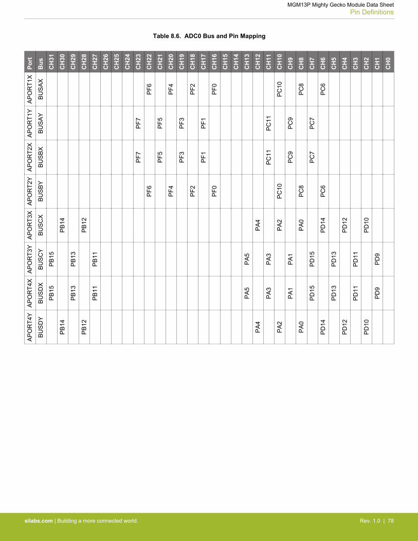
Table 8.6. ADC0 Bus and Pin MappingPo
rt
Bus
CH
31
CH
30
CH
29
CH
28
CH
27
CH
26
CH
25
CH
24
CH
23
CH
22
CH
21
CH
20
CH
19
CH
18
CH
17
CH
16
CH
15
CH
14
CH
13
CH
12
CH
11
CH
10
CH
9
CH
8
CH
7
CH
6
CH
5
CH
4
CH
3
CH
2
CH
1
CH
0
AP
OR
T1X
BU
SA
X
PF6
PF4
PF2
PF0
PC
10
PC
8
PC
6
AP
OR
T1Y
BU
SA
Y
PF7
PF5
PF3
PF1
PC
11
PC
9
PC
7
AP
OR
T2X
BU
SB
X
PF7
PF5
PF3
PF1
PC
11
PC
9
PC
7
AP
OR
T2Y
BU
SB
Y
PF6
PF4
PF2
PF0
PC
10
PC
8
PC
6
AP
OR
T3X
BU
SC
X
PB
14
PB
12
PA
4
PA
2
PA
0
PD
14
PD
12
PD
10
AP
OR
T3Y
BU
SC
Y
PB
15
PB
13
PB
11
PA
5
PA
3
PA
1
PD
15
PD
13
PD
11
PD
9
AP
OR
T4X
BU
SD
X
PB
15
PB
13
PB
11
PA
5
PA
3
PA
1
PD
15
PD
13
PD
11
PD
9
AP
OR
T4Y
BU
SD
Y
PB
14
PB
12
PA
4
PA
2
PA
0
PD
14
PD
12
PD
10
MGM13P Mighty Gecko Module Data SheetPin Definitions
silabs.com | Building a more connected world. Rev. 1.0 | 78
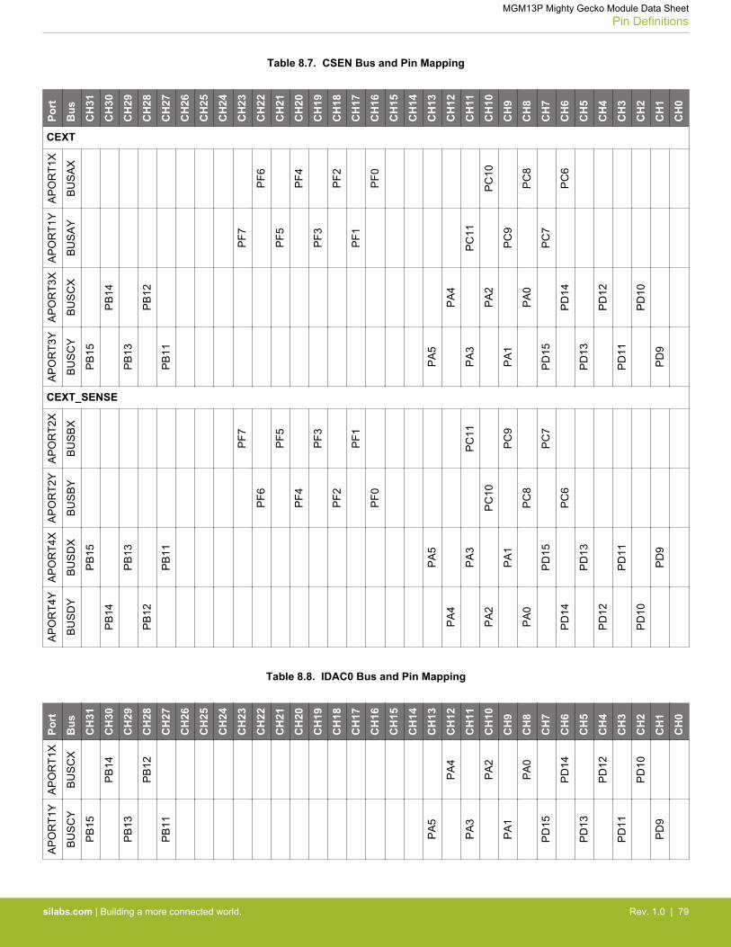
Table 8.7. CSEN Bus and Pin MappingPo
rt
Bus
CH
31
CH
30
CH
29
CH
28
CH
27
CH
26
CH
25
CH
24
CH
23
CH
22
CH
21
CH
20
CH
19
CH
18
CH
17
CH
16
CH
15
CH
14
CH
13
CH
12
CH
11
CH
10
CH
9
CH
8
CH
7
CH
6
CH
5
CH
4
CH
3
CH
2
CH
1
CH
0
CEXT
AP
OR
T1X
BU
SA
X
PF6
PF4
PF2
PF0
PC
10
PC
8
PC
6
AP
OR
T1Y
BU
SA
Y
PF7
PF5
PF3
PF1
PC
11
PC
9
PC
7
AP
OR
T3X
BU
SC
X
PB
14
PB
12
PA
4
PA
2
PA
0
PD
14
PD
12
PD
10
AP
OR
T3Y
BU
SC
Y
PB
15
PB
13
PB
11
PA
5
PA
3
PA
1
PD
15
PD
13
PD
11
PD
9
CEXT_SENSE
AP
OR
T2X
BU
SB
X
PF7
PF5
PF3
PF1
PC
11
PC
9
PC
7
AP
OR
T2Y
BU
SB
Y
PF6
PF4
PF2
PF0
PC
10
PC
8
PC
6
AP
OR
T4X
BU
SD
X
PB
15
PB
13
PB
11
PA
5
PA
3
PA
1
PD
15
PD
13
PD
11
PD
9
AP
OR
T4Y
BU
SD
Y
PB
14
PB
12
PA
4
PA
2
PA
0
PD
14
PD
12
PD
10
Table 8.8. IDAC0 Bus and Pin Mapping
Port
Bus
CH
31
CH
30
CH
29
CH
28
CH
27
CH
26
CH
25
CH
24
CH
23
CH
22
CH
21
CH
20
CH
19
CH
18
CH
17
CH
16
CH
15
CH
14
CH
13
CH
12
CH
11
CH
10
CH
9
CH
8
CH
7
CH
6
CH
5
CH
4
CH
3
CH
2
CH
1
CH
0
AP
OR
T1X
BU
SC
X
PB
14
PB
12
PA
4
PA
2
PA
0
PD
14
PD
12
PD
10
AP
OR
T1Y
BU
SC
Y
PB
15
PB
13
PB
11
PA
5
PA
3
PA
1
PD
15
PD
13
PD
11
PD
9
MGM13P Mighty Gecko Module Data SheetPin Definitions
silabs.com | Building a more connected world. Rev. 1.0 | 79
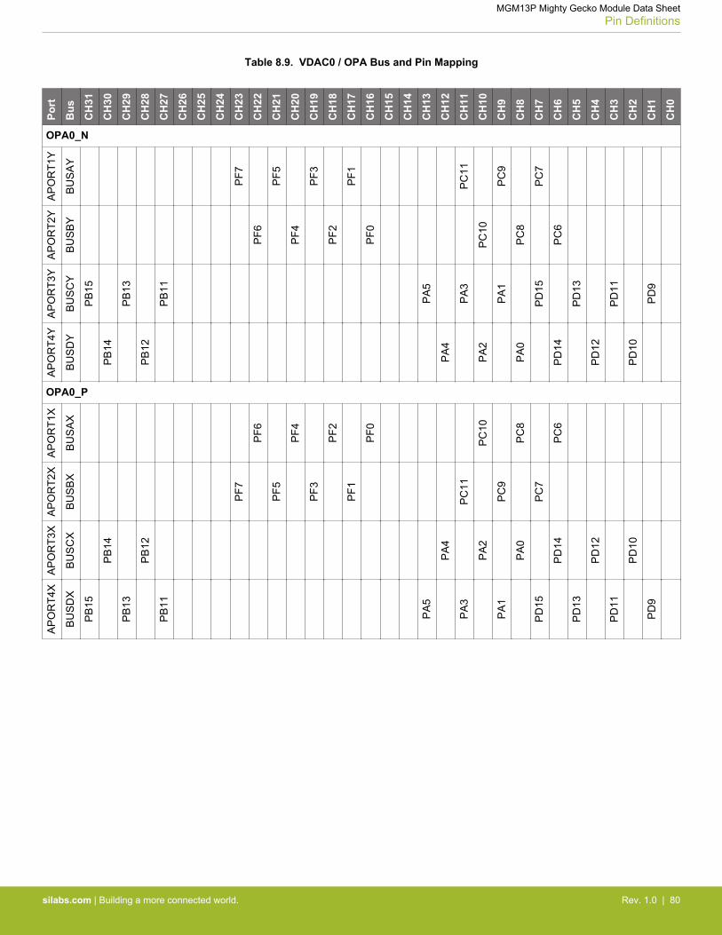
Table 8.9. VDAC0 / OPA Bus and Pin MappingPo
rt
Bus
CH
31
CH
30
CH
29
CH
28
CH
27
CH
26
CH
25
CH
24
CH
23
CH
22
CH
21
CH
20
CH
19
CH
18
CH
17
CH
16
CH
15
CH
14
CH
13
CH
12
CH
11
CH
10
CH
9
CH
8
CH
7
CH
6
CH
5
CH
4
CH
3
CH
2
CH
1
CH
0
OPA0_N
AP
OR
T1Y
BU
SA
Y
PF7
PF5
PF3
PF1
PC
11
PC
9
PC
7
AP
OR
T2Y
BU
SB
Y
PF6
PF4
PF2
PF0
PC
10
PC
8
PC
6
AP
OR
T3Y
BU
SC
Y
PB
15
PB
13
PB
11
PA
5
PA
3
PA
1
PD
15
PD
13
PD
11
PD
9
AP
OR
T4Y
BU
SD
Y
PB
14
PB
12
PA
4
PA
2
PA
0
PD
14
PD
12
PD
10
OPA0_P
AP
OR
T1X
BU
SA
X
PF6
PF4
PF2
PF0
PC
10
PC
8
PC
6
AP
OR
T2X
BU
SB
X
PF7
PF5
PF3
PF1
PC
11
PC
9
PC
7
AP
OR
T3X
BU
SC
X
PB
14
PB
12
PA
4
PA
2
PA
0
PD
14
PD
12
PD
10
AP
OR
T4X
BU
SD
X
PB
15
PB
13
PB
11
PA
5
PA
3
PA
1
PD
15
PD
13
PD
11
PD
9
MGM13P Mighty Gecko Module Data SheetPin Definitions
silabs.com | Building a more connected world. Rev. 1.0 | 80
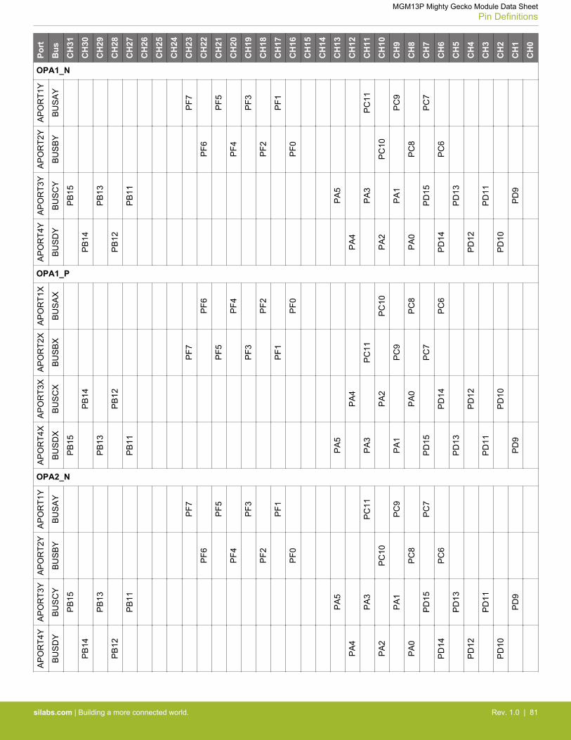
Port
Bus
CH
31
CH
30
CH
29
CH
28
CH
27
CH
26
CH
25
CH
24
CH
23
CH
22
CH
21
CH
20
CH
19
CH
18
CH
17
CH
16
CH
15
CH
14
CH
13
CH
12
CH
11
CH
10
CH
9
CH
8
CH
7
CH
6
CH
5
CH
4
CH
3
CH
2
CH
1
CH
0
OPA1_N
AP
OR
T1Y
BU
SA
Y
PF7
PF5
PF3
PF1
PC
11
PC
9
PC
7
AP
OR
T2Y
BU
SB
Y
PF6
PF4
PF2
PF0
PC
10
PC
8
PC
6
AP
OR
T3Y
BU
SC
Y
PB
15
PB
13
PB
11
PA
5
PA
3
PA
1
PD
15
PD
13
PD
11
PD
9
AP
OR
T4Y
BU
SD
Y
PB
14
PB
12
PA
4
PA
2
PA
0
PD
14
PD
12
PD
10
OPA1_P
AP
OR
T1X
BU
SA
X
PF6
PF4
PF2
PF0
PC
10
PC
8
PC
6
AP
OR
T2X
BU
SB
X
PF7
PF5
PF3
PF1
PC
11
PC
9
PC
7
AP
OR
T3X
BU
SC
X
PB
14
PB
12
PA
4
PA
2
PA
0
PD
14
PD
12
PD
10
AP
OR
T4X
BU
SD
X
PB
15
PB
13
PB
11
PA
5
PA
3
PA
1
PD
15
PD
13
PD
11
PD
9
OPA2_N
AP
OR
T1Y
BU
SA
Y
PF7
PF5
PF3
PF1
PC
11
PC
9
PC
7
AP
OR
T2Y
BU
SB
Y
PF6
PF4
PF2
PF0
PC
10
PC
8
PC
6
AP
OR
T3Y
BU
SC
Y
PB
15
PB
13
PB
11
PA
5
PA
3
PA
1
PD
15
PD
13
PD
11
PD
9
AP
OR
T4Y
BU
SD
Y
PB
14
PB
12
PA
4
PA
2
PA
0
PD
14
PD
12
PD
10
MGM13P Mighty Gecko Module Data SheetPin Definitions
silabs.com | Building a more connected world. Rev. 1.0 | 81
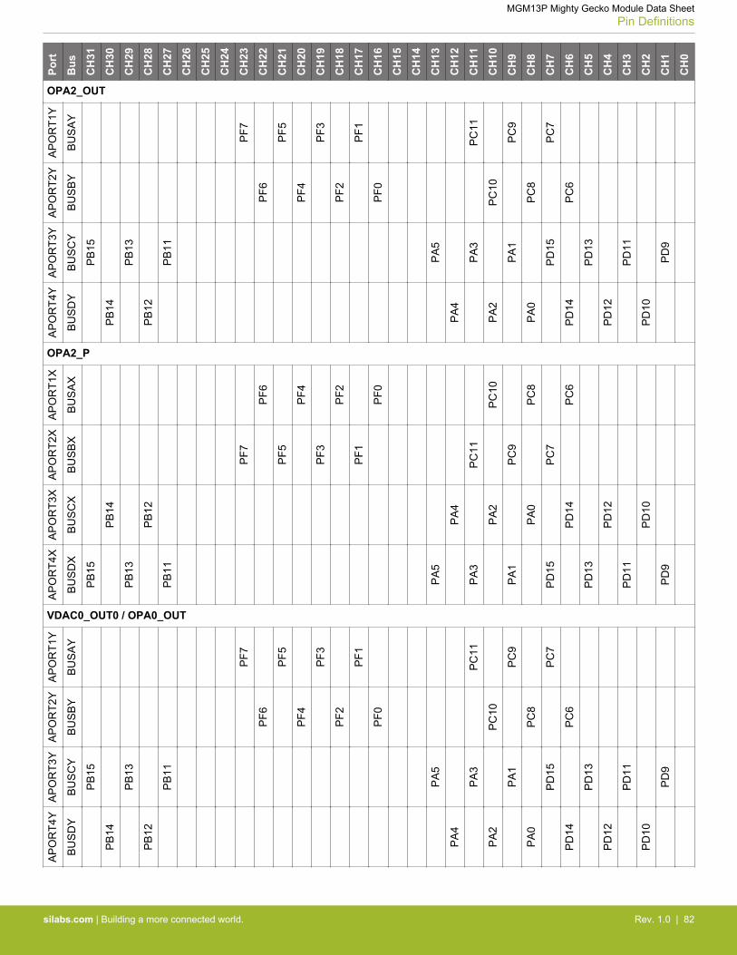
Port
Bus
CH
31
CH
30
CH
29
CH
28
CH
27
CH
26
CH
25
CH
24
CH
23
CH
22
CH
21
CH
20
CH
19
CH
18
CH
17
CH
16
CH
15
CH
14
CH
13
CH
12
CH
11
CH
10
CH
9
CH
8
CH
7
CH
6
CH
5
CH
4
CH
3
CH
2
CH
1
CH
0
OPA2_OUT
AP
OR
T1Y
BU
SA
Y
PF7
PF5
PF3
PF1
PC
11
PC
9
PC
7
AP
OR
T2Y
BU
SB
Y
PF6
PF4
PF2
PF0
PC
10
PC
8
PC
6
AP
OR
T3Y
BU
SC
Y
PB
15
PB
13
PB
11
PA
5
PA
3
PA
1
PD
15
PD
13
PD
11
PD
9
AP
OR
T4Y
BU
SD
Y
PB
14
PB
12
PA
4
PA
2
PA
0
PD
14
PD
12
PD
10
OPA2_P
AP
OR
T1X
BU
SA
X
PF6
PF4
PF2
PF0
PC
10
PC
8
PC
6
AP
OR
T2X
BU
SB
X
PF7
PF5
PF3
PF1
PC
11
PC
9
PC
7
AP
OR
T3X
BU
SC
X
PB
14
PB
12
PA
4
PA
2
PA
0
PD
14
PD
12
PD
10
AP
OR
T4X
BU
SD
X
PB
15
PB
13
PB
11
PA
5
PA
3
PA
1
PD
15
PD
13
PD
11
PD
9
VDAC0_OUT0 / OPA0_OUT
AP
OR
T1Y
BU
SA
Y
PF7
PF5
PF3
PF1
PC
11
PC
9
PC
7
AP
OR
T2Y
BU
SB
Y
PF6
PF4
PF2
PF0
PC
10
PC
8
PC
6
AP
OR
T3Y
BU
SC
Y
PB
15
PB
13
PB
11
PA
5
PA
3
PA
1
PD
15
PD
13
PD
11
PD
9
AP
OR
T4Y
BU
SD
Y
PB
14
PB
12
PA
4
PA
2
PA
0
PD
14
PD
12
PD
10
MGM13P Mighty Gecko Module Data SheetPin Definitions
silabs.com | Building a more connected world. Rev. 1.0 | 82
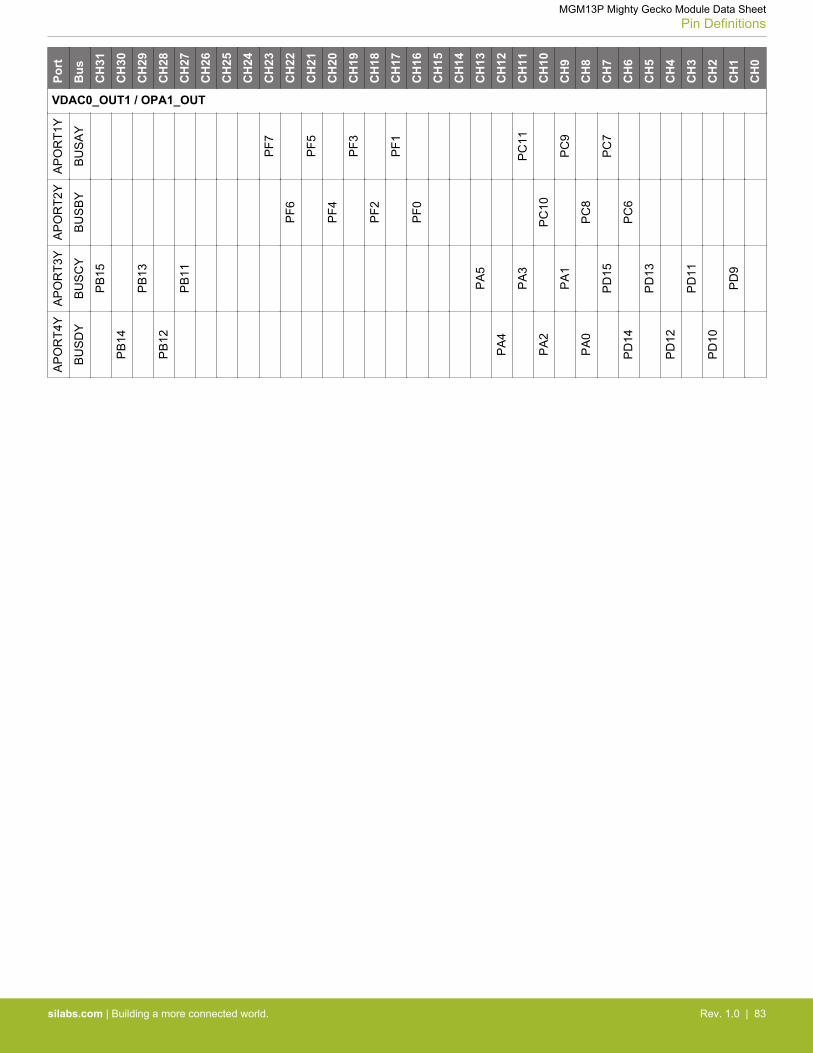
Port
Bus
CH
31
CH
30
CH
29
CH
28
CH
27
CH
26
CH
25
CH
24
CH
23
CH
22
CH
21
CH
20
CH
19
CH
18
CH
17
CH
16
CH
15
CH
14
CH
13
CH
12
CH
11
CH
10
CH
9
CH
8
CH
7
CH
6
CH
5
CH
4
CH
3
CH
2
CH
1
CH
0
VDAC0_OUT1 / OPA1_OUT
AP
OR
T1Y
BU
SA
Y
PF7
PF5
PF3
PF1
PC
11
PC
9
PC
7
AP
OR
T2Y
BU
SB
Y
PF6
PF4
PF2
PF0
PC
10
PC
8
PC
6
AP
OR
T3Y
BU
SC
Y
PB
15
PB
13
PB
11
PA
5
PA
3
PA
1
PD
15
PD
13
PD
11
PD
9
AP
OR
T4Y
BU
SD
Y
PB
14
PB
12
PA
4
PA
2
PA
0
PD
14
PD
12
PD
10
MGM13P Mighty Gecko Module Data SheetPin Definitions
silabs.com | Building a more connected world. Rev. 1.0 | 83
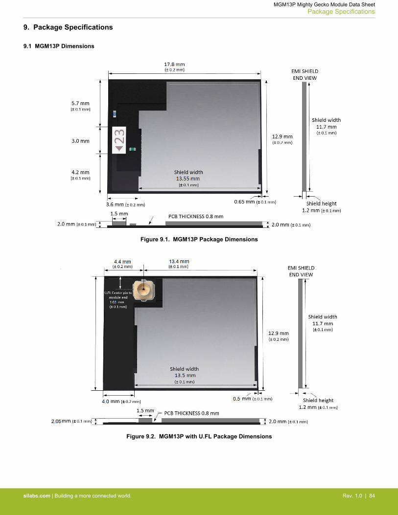
9. Package Specifications
9.1 MGM13P Dimensions
Figure 9.1. MGM13P Package Dimensions
Figure 9.2. MGM13P with U.FL Package Dimensions
MGM13P Mighty Gecko Module Data SheetPackage Specifications
silabs.com | Building a more connected world. Rev. 1.0 | 84

9.2 MGM13P Module Footprint
The figure below shows the Module footprint and PCB dimensions.
Figure 9.3. MGM13P Footprint
MGM13P Mighty Gecko Module Data SheetPackage Specifications
silabs.com | Building a more connected world. Rev. 1.0 | 85

9.3 MGM13P Recommended PCB Land Pattern
The figure below shows the recommended land pattern. The antenna clearance section is not required for MGM13P module versionswith a U.FL connector.
Figure 9.4. MGM13P Recommended PCB Land Pattern
MGM13P Mighty Gecko Module Data SheetPackage Specifications
silabs.com | Building a more connected world. Rev. 1.0 | 86

9.4 MGM13P Package Marking
The figure below shows the module markings printed on the RF-shield.
Figure 9.5. MGM13P Package Marking
The module marking consists of:
MGM13Pxxxxxxx - Part number designation
Model: MGM13Pxxx – Model number designation
FCC ID: QOQMGM13P
IC: 5123A-MGM13P
MSIP-CRM-BGT-MGM13Pxxx
CE Logo
Japan Logo and ID: 209-J00283
YYWWTTTT• YY – The last 2 digits of the assembly year• WW – The 2 digit work week when the device was assembled• TTTT – A trace or manufacturing code. The first letter is the device revision.
MGM13P Mighty Gecko Module Data SheetPackage Specifications
silabs.com | Building a more connected world. Rev. 1.0 | 87

10. Tape and Reel Specifications
10.1 Tape and Reel Specification
This section contains information regarding the tape and reel packaging for the MGM13P Mighty Gecko Module.
10.2 Reel Material and Dimensions
• Reel material: Polystyrene (PS)• Reel diameter: 13 inches (330 mm)• Number of modules per reel: 1000 pcs• Disk deformation, folding whitening and mold imperfections: Not allowed• Disk set: consists of two 13 inch (330 mm) rotary round disks and one central axis (100 mm)• Antistatic treatment: Required• Surface resistivity: 104 - 109 Ω/sq.
Figure 10.1. Reel Dimension — Side View
Symbol Dimensions [mm]
W0 44.0 +0.5/-.0.0
W1 48.0
MGM13P Mighty Gecko Module Data SheetTape and Reel Specifications
silabs.com | Building a more connected world. Rev. 1.0 | 88

10.3 Module Orientation and Tape Feed
The user direction of feed, start and end of tape on reel and orientation of the modules on the tape are shown in the figure below.
Figure 10.2. Module Orientation and Feed Direction
10.4 Cover Tape Information
Figure 10.3. Cover Tape Information
Symbol Dimensions [mm]
Thickness (T) 0.055 +0.005/-0.003
Width (W) 37.50 +0.30/-0.10
MGM13P Mighty Gecko Module Data SheetTape and Reel Specifications
silabs.com | Building a more connected world. Rev. 1.0 | 89

11. Soldering Recommendations
11.1 Soldering Recommendations
This section describes the soldering recommendations for the MGM13P module.
MGM13P is compatible with industrial standard reflow profile for Pb-free solders. The reflow profile used is dependent on the thermalmass of the entire populated PCB, heat transfer efficiency of the oven, and particular type of solder paste used.
• Refer to technical documentations of particular solder paste for profile configurations.• Avoid usining more than two reflow cycles.• A no-clean, type-3 solder paste is recommended.• A stainless steel, laser-cut and electro-polished stencil with trapezoidal walls should be used to assure good solder paste release.• Recommended stencil thickness is 0.100mm (4 mils).• Refer to the recommended PCB land pattern for an example stencil aperture size.• For further recommendation, please refer to the JEDEC/IPC J-STD-020, IPC-SM-782 and IPC 7351 guidelines.
MGM13P Mighty Gecko Module Data SheetSoldering Recommendations
silabs.com | Building a more connected world. Rev. 1.0 | 90

12. Certifications
12.1 Qualified Antenna Types
The MGM13P has been designed to operate with a standard 2.14 dBi dipole antenna. Any antenna of a different type or with a gainhigher than 2.14 dBi is strictly prohibited for use with this device. Using an antenna of a different type or gain more than 2.14 dBi willrequire additional testing for FCC, CE and IC. The required antenna impedance is 50 Ω.
Table 12.1. Qualified Antennas for MGM13P
Antenna Type Maximum Gain
Dipole 2.14 dBi
12.2 Bluetooth
MGM13P is based on prequalified RF-PHY component QDID 101562. To make a Bluetooth end product listing the module integratorshould combine this QDID with the prequalified Wireless Gecko Link Layer and Wireless Gecko Host components.
12.3 CE
The MGM13P02 module is in conformity with the essential requirements and other relevant requirements of the Radio Equipment Di-rective (RED) (2014/53/EU). Please note that every application using the MGM13P02 will need to perform the radio EMC tests on theend product, according to EN 301 489-17. Separate RF testing is not required provided that the customer follows the module manufac-turer's recommendations and instructions and does not make modifications (e.g. to the provided antenna solutions or requirements). Aformal DoC is available via www.silabs.com
MGM13P Mighty Gecko Module Data SheetCertifications
silabs.com | Building a more connected world. Rev. 1.0 | 91
12.4 FCC
This device complies with Part 15 of the FCC Rules. Operation is subject to the following two conditions:1. This device may not cause harmful interference, and2. This device must accept any interference received, including interference that may cause undesirable operation.
Any changes or modifications not expressly approved by Silicon Labs could void the user’s authority to operate the equipment.
FCC RF Radiation Exposure Statement:
This equipment complies with FCC radiation exposure limits set forth for an uncontrolled environment. End users must follow the specif-ic operating instructions for satisfying RF exposure compliance. This transmitter meets both portable and mobile limits as demonstratedin the RF Exposure Analysis and SAR test report. This transmitter must not be co-located or operating in conjunction with any otherantenna or transmitter except in accordance with FCC multi-transmitter product procedures.
OEM Responsibilities to comply with FCC Regulations:
OEM integrator is responsible for testing their end-product for any additional compliance requirements required with this module instal-led (for example, digital device emissions, PC peripheral requirements, etc.).• With MGM13P02 the antenna(s) must be installed such that a minimum separation distance of 7.7 mm is maintained between the
radiator (antenna) and all persons at all times.• The transmitter module must not be co-located or operating in conjunction with any other antenna or transmitter except in accord-
ance with FCC multi-transmitter product procedures.
Important Note:
In the event that the above conditions cannot be met (for certain configurations or co-location with another transmitter), then the FCCauthorization is no longer considered valid and the FCC ID cannot be used on the final product. In these circumstances, the OEM inte-grator will be responsible for re-evaluating the end product (including the transmitter) and obtaining a separate FCC authorization.
End Product Labeling
The variants of MGM13P Modules are labeled with their own FCC ID. If the FCC ID is not visible when the module is installed insideanother device, then the outside of the device into which the module is installed must also display a label referring to the enclosedmodule. In that case, the final end product must be labeled in a visible area with the following:
"Contains Transmitter Module FCC ID: QOQMGM13P"
Or
"Contains FCC ID: QOQMGM13P"
The OEM integrator has to be aware not to provide information to the end user regarding how to install or remove this RF module orchange RF related parameters in the user manual of the end product.
MGM13P Mighty Gecko Module Data SheetCertifications
silabs.com | Building a more connected world. Rev. 1.0 | 92

12.5 ISED Canada
ISEDC
This radio transmitter (IC: 5123A-MGM13P) has been approved by Industry Canada to operate with the antenna types listed above,with the maximum permissible gain indicared. Antenna types not included in this list, having a gain greater than the maximum gainindicated for that type, are strictly prohibited for use with this device.
This device complies with Industry Canada’s license-exempt RSS standards. Operation is subject to the following two conditions:1. This device may not cause interference; and2. This device must accept any interference, including interference that may cause undesired operation of the device
RF Exposure Statement
Exception from routine SAR evaluation limits are given in RSS-102 Issue 5.
The models MGM13P02A and MGM13P02E meet the given requirements when the minimum separation distance to human body is 20mm.
RF exposure or SAR evaluation is not required when the separation distance is same or more than stated above. If the separation dis-tance is less than stated above the OEM integrator is responsible for evaluating the SAR.
OEM Responsibilities to comply with IC Regulations
The MGM13P modules have been certified for integration into products only by OEM integrators under the following conditions:• The antenna(s) must be installed such that a minimum separation distance as stated above is maintained between the radiator (an-
tenna) and all persons at all times.• The transmitter module must not be co-located or operating in conjunction with any other antenna or transmitter.
As long as the two conditions above are met, further transmitter testing will not be required. However, the OEM integrator is still respon-sible for testing their end-product for any additional compliance requirements required with this module installed (for example, digitaldevice emissions, PC peripheral requirements, etc.).
IMPORTANT NOTE
In the event that these conditions cannot be met (for certain configurations or co-location with another transmitter), then the ISEDCauthorization is no longer considered valid and the IC ID cannot be used on the final product. In these circumstances, the OEM integra-tor will be responsible for re-evaluating the end product (including the transmitter) and obtaining a separate ISEDC authorization.End Product Labeling
The MGM13P module is labeled with its own IC ID. If the IC ID is not visible when the module is installed inside another device, thenthe outside of the device into which the module is installed must also display a label referring to the enclosed module. In that case, thefinal end product must be labeled in a visible area with the following:
“Contains Transmitter Module IC: 5123A-MGM13P ”
or
“Contains IC: 5123A-MGM13P”
The OEM integrator has to be aware not to provide information to the end user regarding how to install or remove this RF module orchange RF related parameters in the user manual of the end product.
MGM13P Mighty Gecko Module Data SheetCertifications
silabs.com | Building a more connected world. Rev. 1.0 | 93

ISEDC (Français)
Industrie Canada a approuvé l’utilisation de cet émetteur radio (IC: 5123A-MGM13P) en conjonction avec des antennes de type dipo-laire à 2.14dBi ou des antennes embarquées, intégrée au produit. L’utilisation de tout autre type d’antenne avec ce composant est pro-scrite.
Ce composant est conforme aux normes RSS, exonérées de licence d'Industrie Canada. Son mode de fonctionnement est soumis auxdeux conditions suivantes:
1. Ce composant ne doit pas générer d’interférences.2. Ce composant doit pouvoir est soumis à tout type de perturbation y compris celle pouvant nuire à son bon fonctionnement.
Déclaration d'exposition RF
L'exception tirée des limites courantes d'évaluation SAR est donnée dans le document RSS-102 Issue 5.
Les modules MGM13P02A and MGM13P02E répondent aux exigences requises lorsque la distance minimale de séparation avec lecorps humain est de 20 mm.
La déclaration d’exposition RF ou l'évaluation SAR n'est pas nécessaire lorsque la distance de séparation est identique ou supérieure àcelle indiquée ci-dessus. Si la distance de séparation est inférieure à celle mentionnées plus haut, il incombe à l'intégrateur OEM deprocédé à une évaluation SAR.
Responsabilités des OEM pour une mise en conformité avec le Règlement du Circuit Intégré
Le module MGM13P a été approuvé pour l'intégration dans des produits finaux exclusivement réalisés par des OEM sous les condi-tions suivantes:• L'antenne (s) doit être installée de sorte qu'une distance de séparation minimale indiquée ci-dessus soit maintenue entre le radiateur
(antenne) et toutes les personnes avoisinante, ce à tout moment.• Le module émetteur ne doit pas être localisé ou fonctionner avec une autre antenne ou un autre transmetteur que celle indiquée
plus haut.
Tant que les deux conditions ci-dessus sont respectées, il n’est pas nécessaire de tester ce transmetteur de façon plus poussée. Ce-pendant, il incombe à l’intégrateur OEM de s’assurer de la bonne conformité du produit fini avec les autres normes auxquelles il pour-rait être soumis de fait de l’utilisation de ce module (par exemple, les émissions des périphériques numériques, les exigences de pé-riphériques PC, etc.).
REMARQUE IMPORTANTE
ans le cas où ces conditions ne peuvent être satisfaites (pour certaines configurations ou co-implantation avec un autre émetteur), l'au-torisation ISEDC n'est plus considérée comme valide et le numéro d’identification ID IC ne peut pas être apposé sur le produit final.Dans ces circonstances, l'intégrateur OEM sera responsable de la réévaluation du produit final (y compris le transmetteur) et de l'ob-tention d'une autorisation ISEDC distincte.Étiquetage des produits finis
Les modules MGM13P sont étiquetés avec leur propre ID IC. Si l'ID IC n'est pas visible lorsque le module est intégré au sein d'un autreproduit, cet autre produit dans lequel le module est installé devra porter une étiquette faisant apparaitre les référence du module inté-gré. Dans un tel cas, sur le produit final doit se trouver une étiquette aisément lisible sur laquelle figurent les informations suivantes:
“Contient le module transmetteur: 5123A-MGM13P ”
or
“Contient le circuit: 5123A-MGM13P”
L'intégrateur OEM doit être conscient qu’il ne doit pas fournir, dans le manuel d’utilisation, d'informations relatives à la façon d'installerou de d’enlever ce module RF ainsi que sur la procédure à suivre pour modifier les paramètres liés à la radio.
MGM13P Mighty Gecko Module Data SheetCertifications
silabs.com | Building a more connected world. Rev. 1.0 | 94
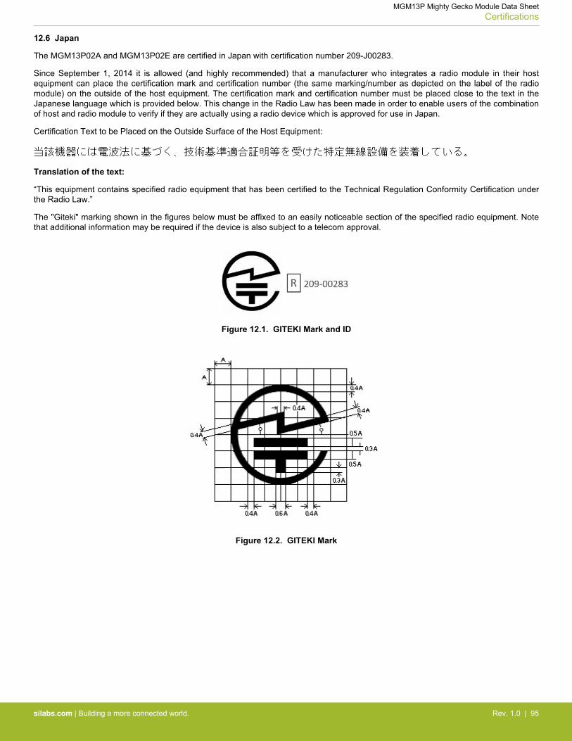
12.6 Japan
The MGM13P02A and MGM13P02E are certified in Japan with certification number 209-J00283.
Since September 1, 2014 it is allowed (and highly recommended) that a manufacturer who integrates a radio module in their hostequipment can place the certification mark and certification number (the same marking/number as depicted on the label of the radiomodule) on the outside of the host equipment. The certification mark and certification number must be placed close to the text in theJapanese language which is provided below. This change in the Radio Law has been made in order to enable users of the combinationof host and radio module to verify if they are actually using a radio device which is approved for use in Japan.
Certification Text to be Placed on the Outside Surface of the Host Equipment:
Translation of the text:
“This equipment contains specified radio equipment that has been certified to the Technical Regulation Conformity Certification underthe Radio Law.”
The "Giteki" marking shown in the figures below must be affixed to an easily noticeable section of the specified radio equipment. Notethat additional information may be required if the device is also subject to a telecom approval.
Figure 12.1. GITEKI Mark and ID
Figure 12.2. GITEKI Mark
MGM13P Mighty Gecko Module Data SheetCertifications
silabs.com | Building a more connected world. Rev. 1.0 | 95

13. Revision History
Revision 1.0
February 2018• Added V2 part numbers to Table 2.1 Ordering Information on page 3.• Updated 4.1 Electrical Characteristics with latest characterization data and test limits.• Added certification details.
Revision 0.1
September 15, 2017• Initial Release.
MGM13P Mighty Gecko Module Data SheetRevision History
silabs.com | Building a more connected world. Rev. 1.0 | 96

http://www.silabs.com
Silicon Laboratories Inc.400 West Cesar ChavezAustin, TX 78701USA
Simplicity StudioOne-click access to MCU and wireless tools, documentation, software, source code libraries & more. Available for Windows, Mac and Linux!
IoT Portfoliowww.silabs.com/IoT
SW/HWwww.silabs.com/simplicity
Qualitywww.silabs.com/quality
Support and Communitycommunity.silabs.com
DisclaimerSilicon Labs intends to provide customers with the latest, accurate, and in-depth documentation of all peripherals and modules available for system and software implementers using or intending to use the Silicon Labs products. Characterization data, available modules and peripherals, memory sizes and memory addresses refer to each specific device, and "Typical" parameters provided can and do vary in different applications. Application examples described herein are for illustrative purposes only. Silicon Labs reserves the right to make changes without further notice and limitation to product information, specifications, and descriptions herein, and does not give warranties as to the accuracy or completeness of the included information. Silicon Labs shall have no liability for the consequences of use of the information supplied herein. This document does not imply or express copyright licenses granted hereunder to design or fabricate any integrated circuits. The products are not designed or authorized to be used within any Life Support System without the specific written consent of Silicon Labs. A "Life Support System" is any product or system intended to support or sustain life and/or health, which, if it fails, can be reasonably expected to result in significant personal injury or death. Silicon Labs products are not designed or authorized for military applications. Silicon Labs products shall under no circumstances be used in weapons of mass destruction including (but not limited to) nuclear, biological or chemical weapons, or missiles capable of delivering such weapons.
Trademark InformationSilicon Laboratories Inc.® , Silicon Laboratories®, Silicon Labs®, SiLabs® and the Silicon Labs logo®, Bluegiga®, Bluegiga Logo®, Clockbuilder®, CMEMS®, DSPLL®, EFM®, EFM32®, EFR, Ember®, Energy Micro, Energy Micro logo and combinations thereof, "the world’s most energy friendly microcontrollers", Ember®, EZLink®, EZRadio®, EZRadioPRO®, Gecko®, ISOmodem®, Micrium, Precision32®, ProSLIC®, Simplicity Studio®, SiPHY®, Telegesis, the Telegesis Logo®, USBXpress®, Zentri and others are trademarks or registered trademarks of Silicon Labs. ARM, CORTEX, Cortex-M3 and THUMB are trademarks or registered trademarks of ARM Holdings. Keil is a registered trademark of ARM Limited. All other products or brand names mentioned herein are trademarks of their respective holders.
Top Related