


Languages
Pages
Legal


Metal Oxide Based Perovskite Solar Cells and High Efficiency Development
*T. Miyasaka
Toin University of Yokohama, Graduate School of engineering, Aoba, Yokohama, Kanagawa 225-8503 *[email protected]
Keywords: perovskite, solar cell, metal oxide, semiconductor, efficiency
With certified highest efficiency of 22.1%, research of perovskite solar cell is being directed to ensure
compatibility of stable efficiency and high stability (durability) for practical applications. Creation of low cost and
large area manufacture process for industrialization is also desired in R&Ds of perovskite solar cells, in which
vacuum-free and sinter-less high-speed coating technology enables considerable reduction of process cost. Our
study has been focused on development of low temperature cell fabrication process and material engineering for
high quality hetero-junction interfaces of perovskite crystals which leads to suppression of recombination and
enhancement of voltage and efficiency. High open-circuit voltage (Voc) of perovskite cells (1.1-1.2V vs band gap
energy of 1.55-1.6 eV) is the advantage superior to existing solar cells (Fig. 1). Using TiO2 as electron transporter
and preparing defect-less interfacial structures, our triple-cation based large grain perovskite cells (Fig. 2) give
hysteresis-free high performance with efficiency close to 20% (Fig. 3). Good proportionality of photocurrent and
light intensity relationship is confirmed. The intensity dependence of Voc demonstrated a good characteristic with
high ideality factor (n>1.7) that leads to high Voc value with small recombination loss of the cell working under 1
sun intensity. We could achieve stable efficiency up to 21.6% with high Voc of 1.18V by improving the continuous
interfacial structure between TiO2 and perovskite, which was all based on low temperature solution processes
(<150oC) of compact and mesoporous TiO2 layers. Stability of I-V characteristics (hysteresis suppression) and
durability of the high performance device can also be improved by interface structure engineering in material and
film preparation.
Fig. 2 A layered device structure with large perovskite grains
Fig. 3 Photovoltaic characteristics of triple-cation perovskite solar cell capable of 20% efficiency
References:
1) T. Miyasaka, Chem. Lett. 2015, 44, 720-729.
2) N.-G. Park, M. Gratzel, T. Miyasaka, K. Zhu, K. Emery, Nature Energy, 2016, 16152.
Fig. 1 Energy diagram for carrier transfers

(a) (b) (c)
Abstract Guideline (Leave two lines for presentation number)
Effects of Doped Electron Transport Layers on the Performance of Large
Active Area Perovskite Cell with High Efficiency
* Trilok Singh* and Tsutomu Miyasaka
Graduate School of Engineering, Toin University of Yokohama, 1614 Kuroganecho, Aoba, Yokohama 225-8503,
Japan
Keywords (Perovskite, large active area, doping, stability
The hybrid Organic-inorganic perovskite materials have gained a huge attention as an excellent light absorber in
thin film photovoltaic cells (PVCs) due to their great promising optoelectronic properties and its facile fabrication
process. In last seven years the power conversion efficiency has exceeds 22%, however there is still a huge
possibility of improvement to improve further (31%). However, various layers in the hetero-structure perovskite
device plays an equally important role to optimize device performance and long term stability. The other challenge
is to grow uniform perovskite films on large area substrates of different compact layer to fabricate large area (10x10
mm2) perovskite cells. The crucial point to access the rapidly growing perovskite technology for commercialization
is large area cell fabrication at relatively low temperature under controlled humidity (~ 30% RH) and understanding
its optoelectronic properties.
This presentation will focus on the fabrication of large active area (5x5 mm2) perovskite solar cells with modified
fabrication process on various metal doped electron transport layers and their photovoltaic characteristics. Our
recent finding showed that films fabrication parameters (temperature, humidity, dripping, substrates
preconditioning), uniformity, grain growth, post annealing and host substrate surface states vastly influenced the
final device performance. Our best device showed steady state power conversion efficiency beyond 20.6% cell
active area 5x5 mm2. The doping of substrate showed very low interface resistance between perovskite and metal
oxide compact layer which promotes fast injection and extraction of charge carriers at the interface. Moreover, this
talk will also highlight large area cell (active area 10x10 mm2) fabrication and optimization.
Fig 1. SEM top view images of perovskite films grown on (a) Undoped (b) doped TiO2 compact layer and (c) Steady
state power conversion efficiency of champion cell.
Purified Materials for Fabrication of Efficient Perovskite Solar Cells with
High Reproducibility
*A. Wakamiya
1), M. Ozaki
1), A. Shimazaki
1), M. Jung
1), Y. Murata
1), I. Okada
2), and T. Tanabe
2)
1)Institute for Chemical Research, Kyoto University, Uji, Kyoto, Japan,
2)Tokyo Chemical Industry CO. LTD, 12-8
Kitachou, Sasame, Toda, Saitama, Japan *[email protected]
Keywords: Perovskite Solar Cells, Purified Materials, Semi-conductors, Lead Halide
Perovskite solar cells (PSCs) have attracted much attention as
cost-effective next generation printable photovoltaics. Power
conversion efficiencies (PCEs) in such cells have been
substantially increased in a relatively short period, mainly on
account of improvements of the fabrication protocols for the
perovskite layer as well as the development of new materials for
buffer layers. We have devoted our efforts to this field from the
viewpoints of development of purified materials. In this
presentation, our approaches toward development of high PCE
cells in terms of materials science are introduced.
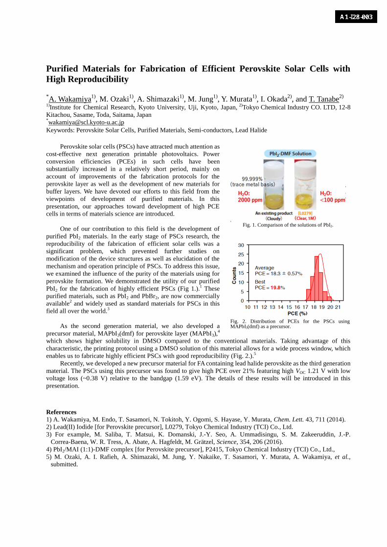
One of our contribution to this field is the development of
purified PbI2 materials. In the early stage of PSCs research, the
reproducibility of the fabrication of efficient solar cells was a
significant problem, which prevented further studies on
modification of the device structures as well as elucidation of the
mechanism and operation principle of PSCs. To address this issue,
we examined the influence of the purity of the materials using for
perovskite formation. We demonstrated the utility of our purified
PbI2 for the fabrication of highly efficient PSCs (Fig 1.).1 These
purified materials, such as PbI2 and PbBr2, are now commercially
available2 and widely used as standard materials for PSCs in this
field all over the world.3
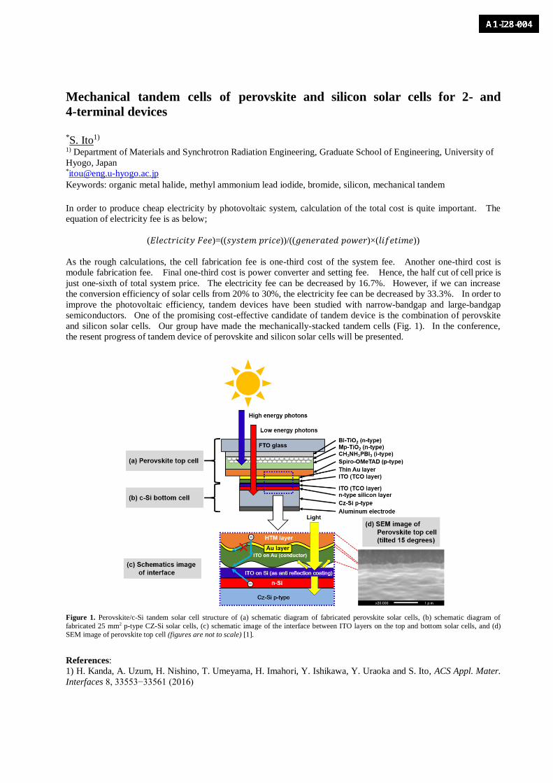
As the second generation material, we also developed a
precursor material, MAPbI3(dmf) for perovskite layer (MAPbI3),4
which shows higher solubility in DMSO compared to the conventional materials. Taking advantage of this
characteristic, the printing protocol using a DMSO solution of this material allows for a wide process window, which
enables us to fabricate highly efficient PSCs with good reproducibility (Fig. 2.).5
Recently, we developed a new precursor material for FA containing lead halide perovskite as the third generation
material. The PSCs using this precursor was found to give high PCE over 21% featuring high VOC 1.21 V with low
voltage loss (~0.38 V) relative to the bandgap (1.59 eV). The details of these results will be introduced in this
presentation.
References 1) A. Wakamiya, M. Endo, T. Sasamori, N. Tokitoh, Y. Ogomi, S. Hayase, Y. Murata, Chem. Lett. 43, 711 (2014).
2) Lead(II) Iodide [for Perovskite precursor], L0279, Tokyo Chemical Industry (TCI) Co., Ltd.
3) For example, M. Saliba, T. Matsui, K. Domanski, J.-Y. Seo, A. Ummadisingu, S. M. Zakeeruddin, J.-P.
Correa-Baena, W. R. Tress, A. Abate, A. Hagfeldt, M. Grätzel, Science, 354, 206 (2016).
4) PbI2/MAI (1:1)-DMF complex [for Perovskite precursor], P2415, Tokyo Chemical Industry (TCI) Co., Ltd.,
5) M. Ozaki, A. I. Rafieh, A. Shimazaki, M. Jung, Y. Nakaike, T. Sasamori, Y. Murata, A. Wakamiya, et al.,
submitted.
Fig. 1. Comparison of the solutions of PbI2.
Fig. 2. Distribution of PCEs for the PSCs using MAPbI3(dmf) as a precursor.
Mechanical tandem cells of perovskite and silicon solar cells for 2- and
4-terminal devices
*S. Ito1) 1) Department of Materials and Synchrotron Radiation Engineering, Graduate School of Engineering, University of
Hyogo, Japan *[email protected]
Keywords: organic metal halide, methyl ammonium lead iodide, bromide, silicon, mechanical tandem
In order to produce cheap electricity by photovoltaic system, calculation of the total cost is quite important. The
equation of electricity fee is as below;
(𝐸𝑙𝑒𝑐𝑡𝑟𝑖𝑐𝑖𝑡𝑦 𝐹𝑒𝑒)=((𝑠𝑦𝑠𝑡𝑒𝑚 𝑝𝑟𝑖𝑐𝑒))/((𝑔𝑒𝑛𝑒𝑟𝑎𝑡𝑒𝑑 𝑝𝑜𝑤𝑒𝑟)×(𝑙𝑖𝑓𝑒𝑡𝑖𝑚𝑒))
As the rough calculations, the cell fabrication fee is one-third cost of the system fee. Another one-third cost is
module fabrication fee. Final one-third cost is power converter and setting fee. Hence, the half cut of cell price is
just one-sixth of total system price. The electricity fee can be decreased by 16.7%. However, if we can increase
the conversion efficiency of solar cells from 20% to 30%, the electricity fee can be decreased by 33.3%. In order to
improve the photovoltaic efficiency, tandem devices have been studied with narrow-bandgap and large-bandgap
semiconductors. One of the promising cost-effective candidate of tandem device is the combination of perovskite
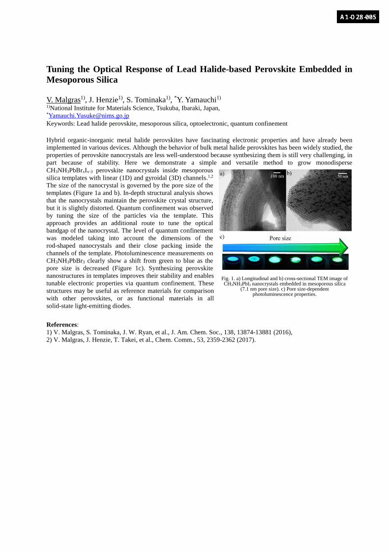
and silicon solar cells. Our group have made the mechanically-stacked tandem cells (Fig. 1). In the conference,
the resent progress of tandem device of perovskite and silicon solar cells will be presented.
Figure 1. Perovskite/c-Si tandem solar cell structure of (a) schematic diagram of fabricated perovskite solar cells, (b) schematic diagram of
fabricated 25 mm2 p-type CZ-Si solar cells, (c) schematic image of the interface between ITO layers on the top and bottom solar cells, and (d)
SEM image of perovskite top cell (figures are not to scale) [1].
References:
1) H. Kanda, A. Uzum, H. Nishino, T. Umeyama, H. Imahori, Y. Ishikawa, Y. Uraoka and S. Ito, ACS Appl. Mater.
Interfaces 8, 33553−33561 (2016)
Tuning the Optical Response of Lead Halide-based Perovskite Embedded in
Mesoporous Silica
V. Malgras1), J. Henzie1), S. Tominaka1), *Y. Yamauchi1) 1)National Institute for Materials Science, Tsukuba, Ibaraki, Japan,
Keywords: Lead halide perovskite, mesoporous silica, optoelectronic, quantum confinement
Hybrid organic-inorganic metal halide perovskites have fascinating electronic properties and have already been
implemented in various devices. Although the behavior of bulk metal halide perovskites has been widely studied, the
properties of perovskite nanocrystals are less well-understood because synthesizing them is still very challenging, in
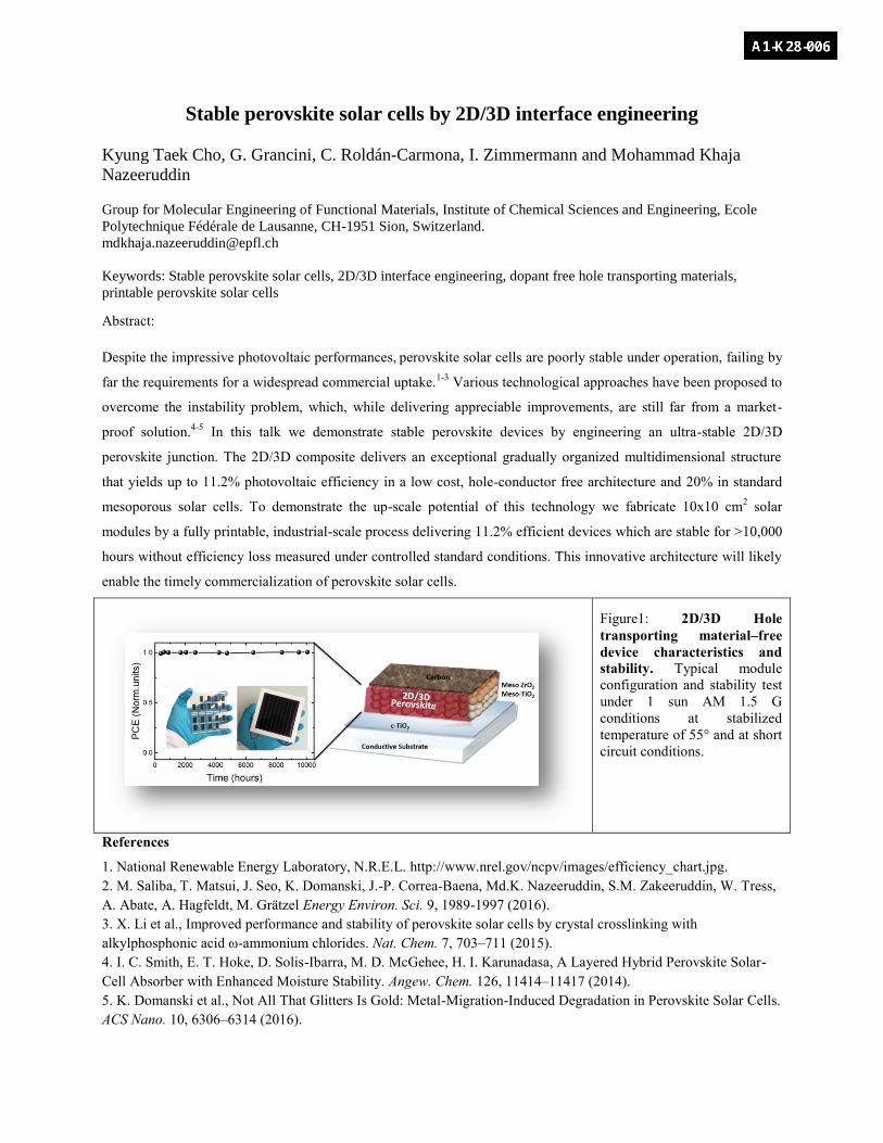
part because of stability. Here we demonstrate a simple and versatile method to grow monodisperse
CH3NH3PbBrxIx‑3 perovskite nanocrystals inside mesoporous
silica templates with linear (1D) and gyroidal (3D) channels.1,2
The size of the nanocrystal is governed by the pore size of the
templates (Figure 1a and b). In-depth structural analysis shows
that the nanocrystals maintain the perovskite crystal structure,
but it is slightly distorted. Quantum confinement was observed
by tuning the size of the particles via the template. This
approach provides an additional route to tune the optical
bandgap of the nanocrystal. The level of quantum confinement
was modeled taking into account the dimensions of the
rod-shaped nanocrystals and their close packing inside the
channels of the template. Photoluminescence measurements on
CH3NH3PbBr3 clearly show a shift from green to blue as the
pore size is decreased (Figure 1c). Synthesizing perovskite
nanostructures in templates improves their stability and enables
tunable electronic properties via quantum confinement. These
structures may be useful as reference materials for comparison
with other perovskites, or as functional materials in all
solid-state light-emitting diodes.
References:
1) V. Malgras, S. Tominaka, J. W. Ryan, et al., J. Am. Chem. Soc., 138, 13874-13881 (2016),
2) V. Malgras, J. Henzie, T. Takei, et al., Chem. Comm., 53, 2359-2362 (2017).
Fig. 1. a) Longitudinal and b) cross-sectional TEM image of CH3NH3PbI3 nanocrystals embedded in mesoporous silica
(7.1 nm pore size). c) Pore size-dependent photoluminescence properties.
Stable perovskite solar cells by 2D/3D interface engineering
Kyung Taek Cho, G. Grancini, C. Roldán-Carmona, I. Zimmermann and Mohammad Khaja
Nazeeruddin
Group for Molecular Engineering of Functional Materials, Institute of Chemical Sciences and Engineering, Ecole
Polytechnique Fédérale de Lausanne, CH-1951 Sion, Switzerland.
Keywords: Stable perovskite solar cells, 2D/3D interface engineering, dopant free hole transporting materials,
printable perovskite solar cells
Abstract:
Despite the impressive photovoltaic performances, perovskite solar cells are poorly stable under operation, failing by
far the requirements for a widespread commercial uptake.1-3
Various technological approaches have been proposed to
overcome the instability problem, which, while delivering appreciable improvements, are still far from a market-
proof solution.4-5
In this talk we demonstrate stable perovskite devices by engineering an ultra-stable 2D/3D
perovskite junction. The 2D/3D composite delivers an exceptional gradually organized multidimensional structure
that yields up to 11.2% photovoltaic efficiency in a low cost, hole-conductor free architecture and 20% in standard
mesoporous solar cells. To demonstrate the up-scale potential of this technology we fabricate 10x10 cm2 solar
modules by a fully printable, industrial-scale process delivering 11.2% efficient devices which are stable for >10,000
hours without efficiency loss measured under controlled standard conditions. This innovative architecture will likely
enable the timely commercialization of perovskite solar cells.
Figure1: 2D/3D Hole
transporting material–free
device characteristics and
stability. Typical module
configuration and stability test
under 1 sun AM 1.5 G
conditions at stabilized
temperature of 55° and at short
circuit conditions.
References
1. National Renewable Energy Laboratory, N.R.E.L. http://www.nrel.gov/ncpv/images/efficiency_chart.jpg.
2. M. Saliba, T. Matsui, J. Seo, K. Domanski, J.-P. Correa-Baena, Md.K. Nazeeruddin, S.M. Zakeeruddin, W. Tress,
A. Abate, A. Hagfeldt, M. Grätzel Energy Environ. Sci. 9, 1989-1997 (2016).
3. X. Li et al., Improved performance and stability of perovskite solar cells by crystal crosslinking with
alkylphosphonic acid ω-ammonium chlorides. Nat. Chem. 7, 703–711 (2015).
4. I. C. Smith, E. T. Hoke, D. Solis-Ibarra, M. D. McGehee, H. I. Karunadasa, A Layered Hybrid Perovskite Solar-
Cell Absorber with Enhanced Moisture Stability. Angew. Chem. 126, 11414–11417 (2014).
5. K. Domanski et al., Not All That Glitters Is Gold: Metal-Migration-Induced Degradation in Perovskite Solar Cells.
ACS Nano. 10, 6306–6314 (2016).
A universal concept to design customized heterojunction Interfaces for
perovskite solar cells with enhanced efficiency and longevity
*Y. Hou1) and C. J. Brabec1)2) 1) Institute of Materials for Electronics and Energy Technology (i-MEET), Department of Materials Science and
Engineering, Friedrich-Alexander University Erlangen-Nuremberg, Martensstrasse 7, 91058 Erlangen, Germany, 2)
Bavarian Center for Applied Energy Research (ZAE Bayern), Haberstr. 2a, 91058 Erlangen, Germany *[email protected]
Keywords: Perovskite solar cells, Hole-transporting layer, dopants-free, Low temperature solution-processing,
Stability.
Thin-film solar cells based on hybrid organo-halide lead perovskites achieved power conversion efficiency
exceeding 22% and are already on par with the well-established thin film photovoltaic technologies. One major
bottleneck allowing to drive this technology further towards commercialization are the interfacial losses at the hole
materials, leaving few material choices and inevitably compromise device efficiency or stability. Developing a novel
concept for solution processed, reliable, cost efficient and improved hole transporting materials which do not
compromise efficiency, stability and scalability,2) becoming of
paramount importance and still challenging the perovskite
community.
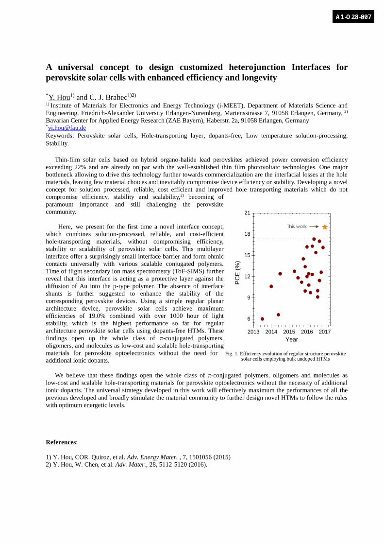
Here, we present for the first time a novel interface concept,
which combines solution-processed, reliable, and cost-efficient
hole-transporting materials, without compromising efficiency,
stability or scalability of perovskite solar cells. This multilayer
interface offer a surprisingly small interface barrier and form ohmic
contacts universally with various scalable conjugated polymers.
Time of flight secondary ion mass spectrometry (ToF-SIMS) further
reveal that this interface is acting as a protective layer against the
diffusion of Au into the p-type polymer. The absence of interface
shunts is further suggested to enhance the stability of the
corresponding perovskite devices. Using a simple regular planar
architecture device, perovskite solar cells achieve maximum
efficiencies of 19.0% combined with over 1000 hour of light
stability, which is the highest performance so far for regular
architecture perovskite solar cells using dopants-free HTMs. These
findings open up the whole class of π-conjugated polymers,
oligomers, and molecules as low-cost and scalable hole-transporting
materials for perovskite optoelectronics without the need for
additional ionic dopants.
We believe that these findings open the whole class of π-conjugated polymers, oligomers and molecules as
low-cost and scalable hole-transporting materials for perovskite optoelectronics without the necessity of additional
ionic dopants. The universal strategy developed in this work will effectively maximum the performances of all the
previous developed and broadly stimulate the material community to further design novel HTMs to follow the rules
with optimum energetic levels.
References:
1) Y. Hou, COR. Quiroz, et al. Adv. Energy Mater. , 7, 1501056 (2015)
2) Y. Hou, W. Chen, et al. Adv. Mater., 28, 5112-5120 (2016).
Fig. 1. Efficiency evolution of regular structure perovskite solar cells employing bulk undoped HTMs
2013 2014 2015 2016 2017
6
9
12
15
18
21
Year
PC
E (
%)
This work

Interfacial engineering for efficient and stable inverted perovskite solar cells W. Chen 1) 2), *A. B. Djurišić 1), F. Z. Liu1), H. W. Tom1), and Z. B. He2) 1) Department of Physics, The University of Hong Kong, Pokfulam, Hong Kong SAR, 2) Department of Materials Science and Engineering, South University of Science and Technology, Shenzhen, China. *[email protected] Keywords: Interfacial engineering, perovskite solar cell, hole transport layer, stability; Organometallic halide perovskite solar cells have been attracting increasing attention in recent years due to their rapidly increasing efficiency. Among different device structures for perovskite solar cells (PSCs), inverted planar structure is attracting increasing attention due to its simplicity, possibility of low temperature processing, and low hysteresis. Efficiency over 20% has been achieved with this structure. For the “inverted” structure, however, the barrier at the contact interface between a Fermi level of various electrode metals (e.g., Ag, Au) and the lowest unoccupied molecular orbital (LUMO) of the electron transport material (for example, PCBM) influences directly the charge transportation at the metal organic semiconductor interface, and leads to poor performance of the PSCs. To obtain a quai-ohmic contact at the interface between the metal electrode and the electron-transporting materials (ETM), the interface engineering on PSCs is indispensable. Another key issue for achieving high performance and stable inverted planar PSCs is the hole-transporting layer, for which better energy level arrangement with perovskite, high chemical stability, easily solution process are required. Here, we present series of research works about the cathode interfacial engineering and hole-transporting materials (HTM) for inverted planar PSCs in our lab. Chemical stable and simple solution processed organic polymer PEOz and metal acetylacetonates were employed as cathode interfacial layers (CILs) to modify the PCBM/Ag interface in the inverted planar PSCs (Fig. 1). High performance and stable perovskite solar cells have been achieved with different hole transporting layer (PEDOT:PSS and NiOx or Cs doped NiOx) and different CILs. We have investigated in details the impacts of different CILs and HTMs on the perovskite morphologies, interfacial properties, charge carrier transfer behaviors, band energy arrangement, device performance and stabilities of the inverted planar PSCs via various characteristic techniques such as SEM, AFM, TR-PL, SKPM, UPS, XPS et. al. The best-performed device has been achieved to over 19 % efficiency through HTM and CIL engineering, as presented at Fig. 2.
Moreover, the stability test results showed that our NiOx HTM and metal acetylacetonates CILs based PSCs are highly stable at inert or ambient environments, which are extremely promising for the future development in the market of the perovskite solar cells. References: [1] Y. Hou, W. Chen, D. Baran, T. Stubhan, N. A. Luechinger, B. Hartmeier, M. Richter, J. Min, S. Chen, C. O. Quiroz, N. Li, H. Zhang, T. Heumueller, G. J. Matt, A. Osvet, K. Forberich, Z. G. Zhang, Y. Li, B. Winter,
P. Schweizer, E. Spiecker, C. J. Brabec, Adv. Mater. 2016, 28, 5112. [2] W. Chen, Y. D. Zhu, Y. Z. Yu, L. M. Xu, G. N. Zhang, Z. B. He, Chem. Mater. 2016, 28, 4879. [3] W. Chen, G.-n. Zhang, L.-m. Xu, R. Gu, Z.-h. Xu, H.-j. Wang, Z.-b. He, Materials Today Energy 2016, 1-2, 1. [4] W. Chen, K. Li, Y. Wang, X. Feng, Z. Liao, Q. Su, X. Lin, Z. He, J. Phys. Chem. Lett. 2017, 8, 591. [5] W. Chen, L. Xu, X. Feng, J. Jie, Z. He, Adv. Mater. 2017, 10.1002/adma.201603923. [6] W. Chen, F. Liu, X. Feng, A. B. Djurišić, Z. He, W.K. Chan, Adv. Energy Mater. 2017, submitted.
FTO Glass
Hole transport layers
PCBM
MAPbI3
Ag
Interfacial layers Poly(2-ethyl-2-oxazoline) (PEOz)
PEDOT:PSS;
NiOx
Cs:NiOx
Fig. 1. The inverted planar PSCs architectures and the corresponding chemical structures of thematerials used at our devices.
Fig. 2. Selected J-V curves of our optimal inverted planar PSCs with Cs:NiOx as HTM and ZrAcac as CIL.
0.0 0.2 0.4 0.6 0.8 1.0 1.20
5
10
15
20
Backward:Jsc: 21.95Voc: 1.081FF: 78.3PCE: 18.58
Forward:Jsc: 21.88Voc: 1.078FF: 77.6PCE: 18.32
Cur
rent
Den
sity
(mA/
cm2 )
Voltage (V)
ZrAcac/Ag Forward scan ZrAcac/Ag backward scan
Backward: Jsc: 22.10 mA/cm2
Voc: 1.078V FF: 77.6 % PCE: 18.50 %
Backward: Jsc: 22.17 mA/cm2
Voc: 1.079V FF: 7�.1 % PCE: 18.�9 %
0.0 0.2 0.4 0.6 0.8 1.0 1.20
5
10
15
20
Cur
rent
Den
sity
(mA
/cm2 )
Voltage (V)
Cs:NiOx Forward Cs:NiOx Backward
Backward: Jsc: 21.77 mA/cm2
Voc: 1.121V FF: 79.3 % PCE: 19.35 %
Backward: Jsc: 21.72 mA/cm2
Voc: 1.100V FF: 79.5 % PCE: 18.99 %
a) b)
NiOx/MAPbI3/PCBM/ZrAcac/Ag Cs:NiOx/MAPbI3/PCBM/ZrAcac/Ag

Spiro-MeOTAD Hole Transport Layer in Perovskite Solar Cells L.K. Ono1), Z. Hawash1), S.R. Raga1), E.J. Juarez-Perez1), M.R. Leyden1), Y. Kato1), M.-C. Jung1), M. Remeika1), S. Wang1), M.V. Lee1), A.J. Winchester1), A. Gabe1), Y. Jiang1), and *Y.B. Qi1) 1) Energy Materials and Surface Sciences Unit (EMSS), Okinawa Institute of Science and Technology Graduate University (OIST), 1919-1 Tancha, Onna-son, Kunigami-gun, Okinawa 904-0495, Japan *[email protected] Keywords: photoemission spectroscopy, scanning probe microscopy, conductivity, solar cell, stability.
In organic-inorganic hybrid perovskite solar cells, optimization of hole transport materials (HTMs) is important for enhancing solar power conversion efficiency and improving stability. At OIST, a team of researchers in the Energy Materials and Surface Sciences Unit has been making concerted efforts to study 2,2’,7,7’-tetrakis[N,N-di-(4-methoxyphenyl)amino]-9,9’-spirobifluorene (spiro-MeOTAD), which is the most widely used HTM in perovskite solar cells.1-8 In this talk, we will present our latest understanding of fundamental interactions between Li-bis(trifluoromethanesulfonyl)-imide (LiTFSI), 4-tert-butylpyridine (t-BP) and spiro-MeOTAD. We will also show how gas exposure (e.g., exposure to O2, H2O, N2) influences electronic structures and conductivity of such HTM films. In addition, we will propose further strategies to improve perovskite solar cell performance and stability.5-7
References 1) L.K. Ono and Y.B. Qi*, J. Phys. Chem. Lett. 7, 4764-4794 (2016). 2) E.J. Juarez-Perez, M.R. Leyden, S. Wang, L.K. Ono, Z. Hawash, Y.B. Qi*, Chem. Mater. 28, 5702-5709 (2016). 3) Z. Hawash, L.K. Ono, Y.B. Qi*, Adv. Mater. Interfaces 3, 1600117 (2016). 4) Z. Hawash, L.K. Ono, S.R. Raga, M.V. Lee, Y.B. Qi*, Chem. Mater. 27, (2015) 562-569. 5) L.K. Ono+, S.R. Raga+, M. Remeika, A.J. Winchester, A. Gabe, Y.B. Qi*, J. Mater. Chem. A 3, 15451-15456 (2015) (+These authors contributed equally). 6) Y. Kato, L.K. Ono, M.V. Lee, S. Wang, S.R. Raga, Y.B. Qi*, Adv. Mater. Interfaces 2, 1500195 (2015). 7) M.C. Jung, S.R. Raga, L.K. Ono, Y.B. Qi*, Sci. Rep. 5, 9863 (2015). 8) L.K. Ono, P. Schulz, J.J. Endres, G.O. Nikiforov, Y. Kato, A. Kahn, Y.B. Qi*, J. Phys. Chem. Lett. 5, 1374-1379 (2014).
Ruddlesden–Popper Perovskite sulfides A3B2S7: A new family of ferroelectric
photovoltaic materials for the visible spectrum
*Gaoyang Gou
1) and
*Ju Li
2)
1) Frontier Institute of Science and Technology, Xi'an Jiaotong University, Xi'an 710049, People's Republic of China
2) Department of Nuclear Science and Engineering, Massachusetts Institute of Technology, Cambridge, MA 02139,
United States *[email protected], [email protected] (Corresponding authors)
Keywords: Perovskite solar cell, Ferroelectric photonvoltaics, First-principles calculations, Hybrid improper
ferroelectrics,
Perovskite ferroelectric materials exhibit the novel ferroelectric photovoltaic effect, where photon-excited
electron–hole pairs can be separated by ferroelectric polarization. Especially, semiconducting ferroelectric materials
with small band gaps (Eg) have been extensively studied for applications in solar energy conversion. Traditional
route for creating semiconducting ferroelectrics requires cation doping, where Eg of the insulating perovskite
ferroelectric oxides are reduced via substitution of certain cations.(1,2)
But cation doping tends to reduce the carrier
mobility due to the scattering, and usually lead to poor photovoltaic efficiency. In the present work, based on
first-principles calculations, we propose and demonstrate a new strategy for designing stoichiometric
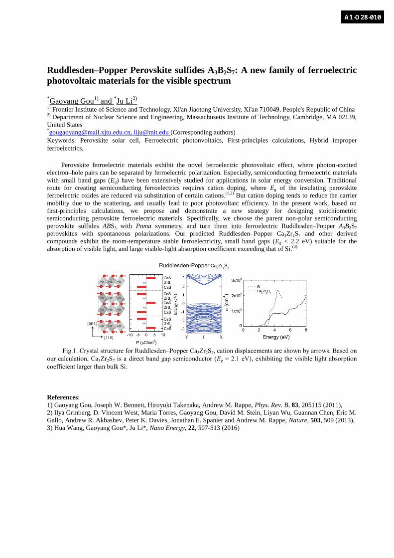
semiconducting perovskite ferroelectric materials. Specifically, we choose the parent non-polar semiconducting
perovskite sulfides ABS3 with Pnma symmetry, and turn them into ferroelectric Ruddlesden–Popper A3B2S7
perovskites with spontaneous polarizations. Our predicted Ruddlesden–Popper Ca3Zr2S7 and other derived
compounds exhibit the room-temperature stable ferroelectricity, small band gaps (Eg < 2.2 eV) suitable for the
absorption of visible light, and large visible-light absorption coefficient exceeding that of Si.(3)
Fig.1. Crystal structure for Ruddlesden–Popper Ca3Zr2S7, cation displacements are shown by arrows. Based on
our calculation, Ca3Zr2S7 is a direct band gap semiconductor (Eg = 2.1 eV), exhibiting the visible light absorption
coefficient larger than bulk Si.
References:
1) Gaoyang Gou, Joseph W. Bennett, Hiroyuki Takenaka, Andrew M. Rappe, Phys. Rev. B, 83, 205115 (2011),
2) Ilya Grinberg, D. Vincent West, Maria Torres, Gaoyang Gou, David M. Stein, Liyan Wu, Guannan Chen, Eric M.
Gallo, Andrew R. Akbashev, Peter K. Davies, Jonathan E. Spanier and Andrew M. Rappe, Nature, 503, 509 (2013),
3) Hua Wang, Gaoyang Gou*, Ju Li*, Nano Energy, 22, 507-513 (2016)

Bandgap Tuning of Lead free Bismuth Halide Perovskite Solar Cells
J. Shin
1), and
*M. Song
1)
1) Advanced Functional Thin Films Department, Korea Institute of Materials Science (KIMS)
Keywords: perovskite, photovoltaics, lead free solar cell, bismuth based perovskite
Solution-processable organic-inorganic halide perovskite solar cells have attracted much attention as a light
absorber because of a high absorption coefficient, high crystallinity at low temperature, and long range of balanced
electron-hole transport length. The performance of lead based perovskite materials have already surpassed over 22%.
That is similar efficiency with silicon thin film solar cells. Despite the excellent high photovoltaic and photo
efficiency that these materials have demonstrated, many researchers are attempting to replace lead with other
materials because the lead based perovskites have drawbacks such as the toxicity and the instability of the material
to atmospheric moisture. To address the toxicity issue, tin-based halide perovskites have been reported recently.
Although over 6% efficiencies have been achieved, these materials are not stable in air because of oxidation of Sn2+
to Sn4+. Therefore all manufacturing process has to be carried out in the nitrogen gas atmosphere because this
oxidation process occurs so rapidly that all the processes.
Bismuth based perovskite has an electron configuration like that of a Bi3+
(6s26p
0) which contribute to the
material’s shallow defect states, long carrier lifetimes and strong absorption. And being adjacent cations in the
periodic table, the Bi3+
and Pb2+
have very similar ionic radii, which may lead to easy incorporation into the
perovskite lattice. Moreover, Bi3+
is also a promising stable metal ion compared to Sn2+
. However, the best power
conversion efficiency of the bismuth perovskite (Cs3Bi2I9) solar cell was reported 1.09% with around 2.2eV band
gap. Therefore, band gap tuning is needed to enhance performance. Recently, Johansson et al. reported CsBi3I10
material, its band gap was 1.77eV, which gives a considerably red-shifted absorption spectrum compared to
Cs3Bi2I9.
Here I will present on the synthesis, optical properties and solar cell performance with the ABi3I10 (A= Cs,
methylammonium(MA), formamidinium (FA)) materials for photovoltaic applications.
Fig. 1. (a) Before and (b) after heat treatment normalized absorption spectra of ABi3I10 thin films.

Abstract Guideline (Leave two lines for presentation number)
Bismuth Based Light Absorbers for Lead-Free Perovskite Solar Cells.
Ashish Kulkarni and Tsutomu Miyasaka* Graduate school of Engineering, Toin University of Yokohama, 1614 Kurogane-cho, Aoba, Kanagawa, Yokohama,
Japan.
Corresponding author: *[email protected]
Keywords: Perovskite solar cell, Photovoltaics, Lead-free, Bismuth iodide, N-methyl-2-pyrrolidone (NMP)
In just 8 years lead based perovskite have experienced unprecedented rise in power conversion efficiency
(PCE) from 3.8% to certified 22.1% owing to their exceptional optoelectronic properties, suitable band gap and
processibility with simple solution process. In a way to commercialization, long term stability (to several tens of
years) and lead toxicity are standing as a major obstacle. Although several reports have shown promising stability of
lead perovskite, replacing toxic lead with eco-friendly metal with similar optoelectronic properties and device
performance with that of lead still remains a big challenge. Tin (Sn) based perovskite was the first step to address
the toxicity issue and thereafter many efforts have been made to improve the efficiency of Sn-perovskite.
Unfortunately, Sn-based perovskites are not stable in open-air atmosphere as it gets oxidize from +2 to +4 oxidation
state. Additionally, oxidized tin (Sn4+
) acts as a p-type dopant within the perovskite material and this effect is named
as “self-doping effect” which limits the efficiency. Additionally, recent reports have suggested that Sn-perovskite
can even be more toxic when exposed to air due to release of hydroiodic acid (HI) into the environment. Along with
Sn-perovskite, germanium (Ge) and copper (Cu) based perovskite were explored but the efficiency is far much
behind due to instability in air and heavy mass of holes respectively.
Bismuth being an eco-friendly material, recently found its place in perovskite family. Bismuth iodide (BiI3)
when reacted with methylammonium iodide (MAI) forms methylammonium iodobismuthates (MIB) which is a zero
dimensional material. This present talk will cover the effect of various under layer electron transporting later (ETL)
(Anatase, Brookite mesoporous TiO2 and planar structured) on the morphology of MIB, their optoelectronic
properties, device performance. Champion short-circuit current density-voltage (J-V) curve is shown in Fig. 1(a)
with high performance with anatase mesoporous under layer compared to brookite and planar structured cell.
Further, we present the morphological evolution of MIB by bringing in N-methyl-2-pyrrolidone (NMP) as a
morphology controller. The morphology of MIB changes drastically with change in the concentration of NMP.
Short-circuit current (Jsc) enhances at particular concentration of 2.5% of NMP in MIB-DMF solution leading to
enhancement in device performance up to 0.31% from 0.17% (without NMP) as shown in Fig. 1(b). This talk will
also focus on the photovoltaic performance of other new bismuth based light absorbing materials for photovoltaic
cell. Moreover, we present further research direction towards high efficiency for lead-free bismuth perovskite solar
cells.
Fig. 1: J-V curves of best performing devices with (a) different TiO2 scaffold layers and (b) with different
concentrations of NMP additive.
References:
1. T. Singh, A. Kulkarni, M. Ikegami, T. Miyasaka, ACS Appl. Mater. Interfaces, 8 (23), 14542–14547 (2016).
2. A. Kulkarni, T. Singh, M. Ikegami, T. Miyasaka, RSC Adv., 7, 9456-9460 (2017).
Enhancement of efficiency for perovskite solar cells consisting of Sn from view
point of interfacial and crystal architecture -Approach to high efficiency-
Shuzi Hayase Kyushu Institute of Technology [email protected] Keywords: Sn, Perovskite, Interface, Traps, crystal, high efficiency The efficiency of perovskite solar cells consisting of Pb has been reported to be over 20%. Absorption edge of perovskite (PVK) solar cells consisting of MAPbI3 is 800nm (Band gap: 1.55eV) which is limiting the enhancement of the efficiency from the view point of Jsc. According to our simulation, light harvesting in the area of near IR up to 900nm (band gap:1.38eV) is necessary for enhancing the efficiency. This prompted us to develop new solar cells having photoconversion properties in longer wavelength region. The other motivation of perovskite solar cells consisting of Sn is that this is one of approaches for Pb free perovskite solar cells and one of the candidates for bottom layer of all perovskite tandem solar cells.
Fig. 1. Expected efficiency with various Voc loss (Efficiency vs. Band gap :Absorption spectrum edge)
10.7 12.2 13.9
15.7 17.8 20.0 22.3
24.6 27.3 30.2 33.1
0
5
10
15
20
25
30
35
300 400 500 600 700 800 900 100011001200
Sola
r cel
l effi
cien
cy /
%
Wavelength / nm
0.0 (Voc loss)
0.1 (Voc loss)
0.2 (Voc loss)
0.3 (Voc loss)
0.4 (Voc loss)
0.5 (Voc loss)
0.6 (Voc loss)
0.7 (Voc loss)
0.8 (Voc loss)
0.9 (Voc loss)2.48eV
Absorption spectrum edge/nm
①30.4mA/cm2 x 0.98V x 0.75 = 22.3%
②24.3 mA/cm2 x 1.15V x 0.75 = 21%
Calculated condition: FF:0.75, IPCE:90%
(Corresponding to Band gap)
1.38eV1.77eV
1.55eV
We have already reported that mixed metal perovskite (MAPbxSnyI3) showed photoconversion properties in IR
region (up to 1000 nm) (1-2). The short circuit current (Jsc) was high, reaching to 30 mA/cm2 (for comparison, 24mA/cm2 for MAPbI3) because of light harvesting properties from visible to IR region. However, the open-circuit voltage (Voc) was lower than 0.3 V and the voltage loss expected from the band gap was 0.6-0.7 V, which was much larger than that of MAPbI3 (0.4 V), suggesting the presence of high density charge recombination centers. We discuss why the perovskite solar cells consisting of Sn has low efficiency, compared to MAPbI3 from the view point of hetero-interface architecture. Finally, 16% efficiency of mixed metal SnPb perovskite solar cell is reported.
References: 1) S. Nakabayashi, et al., J. Photonics for Energy; 2015, 5, 057410. 2) Y. Ogomi, et al., J. Phys. Chem. Lett. 2014, 5, 1004-1011
Charge distribution in perovskite solar cell
under irradiation at VOC determined from
transient optoelectronic measurements.
Wheeler et al., in revision
Optical assay of perovskite film stability
under light / oxygen stress as a function of
iodide / bromine ratio
Pont et al., J. Mat. Chem A in revision
Charge carrier kinetics and stability challenges in perovskite solar cells
James R Durrant Department of Chemistry, Centre for Plastic Electronics, Imperial College London, London SW7 2AZ, U.K.
and SPECIFIC IKC, College of Engineering, University of Swansea, Swansea, U.K, [email protected]
Keywords: perovskite solar cells, charge separation and recombination, stability
In my talk, I will focus primarily on the charge transfer and
recombination processes which are key determinants of the
efficiency of methylammonium lead halide perovskite solar cells.
Experimentally our studies of charge transfer are based on transient
absorption and photoluminescence measurements on timescales
from femtoseconds to steady state. I will focus in particular upon
the kinetics and efficiency of charge transfer from the photoactive
perovskite layer to organic electron and hole collection layers in
planar structure films and devices. Topics to be addressed will
include the competition between charge transfer and charge
trapping / recombination as a function of charge carrier density,
material selection and processing and film aging, and the
correlations between these processes and device photocurrent
generation. The optical studies will be complimented by transient
photocurrent and photovoltage studies of charge recombination as a
function of photoactive layer and charge collection layer
composition, and correlated with measurements of device voltage.
The second part of my talk will address the stability of the same devices, addressing in particular the photoinduced
degradation of perovskite devices under oxygen exposure, and how the selection appropriate material choice and
film processing can enhance performance.
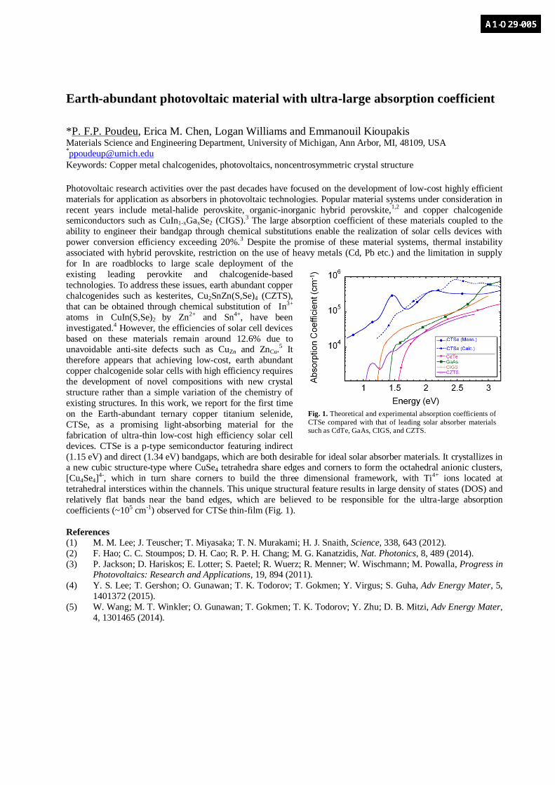
Earth-abundant photovoltaic material with ultra-large absorption coefficient
*P. F.P. Poudeu, Erica M. Chen, Logan Williams and Emmanouil Kioupakis
Materials Science and Engineering Department, University of Michigan, Ann Arbor, MI, 48109, USA
Keywords: Copper metal chalcogenides, photovoltaics, noncentrosymmetric crystal structure
Photovoltaic research activities over the past decades have focused on the development of low-cost highly efficient
materials for application as absorbers in photovoltaic technologies. Popular material systems under consideration in
recent years include metal-halide perovskite, organic-inorganic hybrid perovskite,1,2 and copper chalcogenide semiconductors such as CuIn1-xGaxSe2 (CIGS).3 The large absorption coefficient of these materials coupled to the
ability to engineer their bandgap through chemical substitutions enable the realization of solar cells devices with
power conversion efficiency exceeding 20%.3 Despite the promise of these material systems, thermal instability
associated with hybrid perovskite, restriction on the use of heavy metals (Cd, Pb etc.) and the limitation in supply
for In are roadblocks to large scale deployment of the
existing leading perovkite and chalcogenide-based
technologies. To address these issues, earth abundant copper
chalcogenides such as kesterites, Cu2SnZn(S,Se)4 (CZTS),
that can be obtained through chemical substitution of In3+
atoms in CuIn(S,Se)2 by Zn2+ and Sn4+, have been
investigated.4 However, the efficiencies of solar cell devices
based on these materials remain around 12.6% due to unavoidable anti-site defects such as CuZn and ZnCu.
5 It
therefore appears that achieving low-cost, earth abundant
copper chalcogenide solar cells with high efficiency requires
the development of novel compositions with new crystal
structure rather than a simple variation of the chemistry of
existing structures. In this work, we report for the first time
on the Earth-abundant ternary copper titanium selenide,
CTSe, as a promising light-absorbing material for the
fabrication of ultra-thin low-cost high efficiency solar cell
devices. CTSe is a p-type semiconductor featuring indirect
(1.15 eV) and direct (1.34 eV) bandgaps, which are both desirable for ideal solar absorber materials. It crystallizes in a new cubic structure-type where CuSe4 tetrahedra share edges and corners to form the octahedral anionic clusters,
[Cu4Se4]4-, which in turn share corners to build the three dimensional framework, with Ti4+ ions located at
tetrahedral interstices within the channels. This unique structural feature results in large density of states (DOS) and
relatively flat bands near the band edges, which are believed to be responsible for the ultra-large absorption
coefficients (~105 cm-1) observed for CTSe thin-film (Fig. 1).
References (1) M. M. Lee; J. Teuscher; T. Miyasaka; T. N. Murakami; H. J. Snaith, Science, 338, 643 (2012).
(2) F. Hao; C. C. Stoumpos; D. H. Cao; R. P. H. Chang; M. G. Kanatzidis, Nat. Photonics, 8, 489 (2014).
(3) P. Jackson; D. Hariskos; E. Lotter; S. Paetel; R. Wuerz; R. Menner; W. Wischmann; M. Powalla, Progress in Photovoltaics: Research and Applications, 19, 894 (2011).
(4) Y. S. Lee; T. Gershon; O. Gunawan; T. K. Todorov; T. Gokmen; Y. Virgus; S. Guha, Adv Energy Mater, 5,
1401372 (2015).
(5) W. Wang; M. T. Winkler; O. Gunawan; T. Gokmen; T. K. Todorov; Y. Zhu; D. B. Mitzi, Adv Energy Mater,
4, 1301465 (2014).
Fig. 1. Theoretical and experimental absorption coefficients of
CTSe compared with that of leading solar absorber materials such as CdTe, GaAs, CIGS, and CZTS.
Organic-Inorganic Halide Perovskite Covering from PV to Memrister
*Nam-Gyu Park
School of Chemical Enginerring, Sungkyunkwan University, Suwon 440-746, Korea *[email protected] (Corresponding author)
Keywords: Perovskite, Solar Cell, Adduct, Grain Boundary Healing, LED, X-ray Imaging, Memrister
Since the first report on the solid-state perovskite solar cell with power conversion efficiency (PCE) of 9.7% in 2012
by our group, its certified PCE now reaches 22%. It is believed that perovskite solar cell is promising
next-generation photovoltaics (PVs) due to superb performance and very low cost. In this talk, the history of
perovskite photovoltaics will be briefly presented along with scientific progress of perovskite solar cells.
Methodologies to achieve hysteresis-free, stable and high PCE perovskite solar cells will be introduced. Lewis
acid-base adduct approach has been found to be very reliable and reproducible method to get high quality perovskite
layer minimizing non-radiative recombination. Non-stoichiometric precursor in adduct process demonstrated grain
boundary healing effect, which further improved voltage and fill factor due to long carrier life time of perovskite
and improved charge transporting at grain boundary as well. Grain boundary healing process yields PCE as high as
20.4%. Moisture was effectively protected and hysteresis was significantly reduced by introducing 2-dimensioanl
perovskite at grain boundary of 3-dimensional perovskite grains. Ion migration is one of factors affecting stability
and hysteresis, which can be deactivated by 2-dimensional perovskite with higher barrier energy for ion migration.
Thermal stability of perovskite material was found to be stable up to 120 oC in the absence of moisture, but that of
full device was sensitive to selective contacts, indicating that thermally stable selective contacts are equally
important. Universal method to remove hysteresis will be also given in this talk. Beyond PV, recent progress in
resistive memory and X-ray imaging applications will be also covered in this talk.
References 1) N.-G. Park et al. Towards stable and commercially available perovskite solar cells, Nature Energy,
doi:10.1038/nenergy.2016.152 (2016)
2) D.-Y. Son et al. Self-formed grain boundary healing layer for highly efficient CH3NH3PbI3 perovskite solar cells,
Nature Energy, 1, 16081, (2016)
3) N.Y. Ahn et al. Highly Reproducible Perovskite Solar Cells with Average Efficiency of 18.3% and Best
Efficiency of 19.7% Fabricated via Lewis Base Adduct of Lead(II) Iodide, J. Am. Chem. Soc., 137, 8696 (2015)
4) N,-G. Park, Perovskite solar cells : Switchable photovoltaics, Nature Materials, 14, 140 (2015)
5) J.-H. Im, Growth of CH3NH3PbI3 cuboids with controlled size for high-efficiency perovskite solar cells, Nature
Nanotechnology, 9, 927 (2014)
6) J.-W. Lee, High-efficiency perovskite solar cells based on the black polymorph of HC(NH2)2PbI3, Advanced
Materials, 26, 4991 (2014)
7) H.-S. Kim et al. Mechanism of carrier accumulation in perovskite thin-absorber solar cells, Nature
Communications, 4, 2242 (2013)
8) H.-S. Kim et al. Lead iodide perovskite sensitized all-solid-state submicron thin film mesoscopic solar
cell with efficiency exceeding 9%, Scientific Reports, 2, 591 (2012)

Two-Dimensional Perovskites Prepared using Various Components
*Y. Takeoka
1), R. Arai
1), R. Hamaguchi
1), M. Yoshizawa-Fujita
1), and M. Rikukawa
1)
1) Department of Materials and Life Sciences, Sophia University
Keywords: Two-dimensional perovskites, Perovskite solar cells, Control of orientation
Organic-inorganic perovskites containing organic amines and metal halides have recently attracted much attention
due to their unique electrical and optical properties, along with the high conversion efficiency of the perovskite solar
cells (PSCs). The organic-inorganic perovskites are a relatively large family, thanks to various combinations of
organic and inorganic components. Our group has fabricated wide range of organic-inorganic perovkites having
three-dimensional (3D), two-dimensional (2-D), one-dimensional (1-D), and zero-dimensional (0-D) network of
lead halide octahedra [PbX6]4-
using various kinds of organic amines as shown in Figure 1.1,2
While 3D perovskites,
APbI3 (A = Cs+, CH3NH3
+, CH(NH2)2
+), have been studied as light harvesters in PSCs, their long-term robustness,
especially in the presence of moisture, due to the inherent instability of 3D perovskite compounds are should be the
subject to be improved. To improve the stability of PSCs, some groups have recently reported the application of 2D
perovskite compounds that have improved resistance to moisture. These 2D compounds tend to orient parallel to
their substrates, which is not favorable for applications in PSC light harvesters.
Our group have recently reported the orientation control of 2D perovskites by using various components.3), 4)
Here, we report the orientation control of 2D perovskites using organic amines having carboxy groups, and other
cations. Perovskite solutions were prepared by reacting stoichiometric amounts of HOOC(CH2)n-1NH3I with PbI2
in N,N-dimethylformamide. The structure of perovskite compounds was investigated by the out-of-plane X-ray
diffraction (XRD) measurements. Formation of layered perovskite structure was confirmed for
[HOOC(CH2)n-1NH3]2PbI4 (n = 4, 7). The orientations of the 2D structures were investigated by two-dimensional
X-ray images. As shown in Figure 2, it was suggested that the crystalline growth of [HOOC(CH2)n-1NH3]2PbI4 was
random compared with highly oriented [CH3(CH2)n-1NH3]2PbI4. From the differential scanning calorimetry studies,
[CH3(CH2)6NH3]2PbI4 crystals showed phase transition peaks at -1.6, 12.3, and 35.9 ºC, whereas no transition peak
was observed for [HOOC(CH2)6NH3]2PbI4. Thermal stabilities increased due to control of phase transitions of
organic layers by introducing carboxy group. The [HOOC(CH2)n-1NH3]2PbI4 (n = 4 or 7) films showed exciton
absorption peaks around 500 nm. These results showed that the quantum confinement effects were maintained
despite the introduction of the carboxy groups.
References 1) Y. Takeoka, K. Asai, M. Rikukawa, and K. Sanui, Chem. Lett., 34 (4), 602-603 (2005).
2) Y. Takeoka, K. Asai, M. Rikukawa, and K. Sanui, Bull. Chem., 24, 1607-1613 (2006).
3) R. Arai, M. Yoshizawa-Fujita, Y. Takeoka, M. Rikukawa, ACS Omega, 2 (5), 2333-2336 (2017).
4) R. Hamaguchi, M. Yoshizawa-Fujita, T. Miyasaka, H. Kunugita, K. Ema, Y. Takeoka, M. Rikukawa, Chem.
Comm, 53, 4366-4369 (2017).
Figure 1 2D WAXS images of (a)
[HOOC(CH2)6NH3]2PbI4 and (b)
[CH3(CH2)6NH3]2PbI4 (n = 7) films.
(a)
(b)
One dimensional chain of
[Pb3I10]4- unit
2D
Two dimensional sheet
One dimensional chain of
[Pb2I9]5- unit
One dimensional
chain
3D
0D
1D
1-2D
1-3D
Figure 2 Organic-inorganic perovskites having zero to three dimensionality.
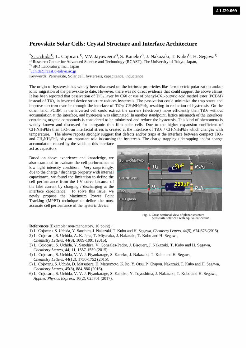
Perovskite Solar Cells: Crystal Structure and Interface Architecture *S. Uchida1), L. Cojocaru1), V.V. Jayaweera2), S. Kaneko2), J. Nakazaki, T. Kubo1), H. Segawa1) 1) Research Center for Advanced Science and Technology (RCAST), The University of Tokyo, Japan, 2) SPD Laboratory, Inc., Japan *[email protected]
Keywords: Perovskite, Solar cell, hysteresis, capacitance, inductance
The origin of hysteresis has widely been discussed on the intrinsic proprieties like ferroelectric polarization and/or
ionic migration of the perovskite to date. However, there was no direct evidence that could support the above claims.
It has been reported that passivation of TiO2 layer by C60 or use of phenyl-C61-butyric acid methyl ester (PCBM)
instead of TiO2 in inverted device structure reduces hysteresis. The passivation could minimize the trap states and
improve electron transfer through the interface of TiO2/ CH3NH3PbI3, resulting in reduction of hysteresis. On the
other hand, PCBM in the inverted cell could extract the carriers (electrons) more efficiently than TiO2 without
accumulation at the interface, and hysteresis was eliminated. In another standpoint, lattice mismatch of the interfaces
containing organic compounds is considered to be minimized and reduce the hysteresis. This kind of phenomena is
widely known and discussed for inorganic thin film solar cells. Due to the higher expansion coefficient of
CH3NH3PbI3 than TiO2, an interfacial stress is created at the interface of TiO2 / CH3NH3PbI3 which changes with
temperature. The above reports strongly suggest that defects and/or traps at the interface between compact TiO2
and CH3NH3PbI3 play an important role in causing the hysteresis. The charge trapping / detrapping and/or charge
accumulation caused by the voids at this interface
act as capacitors.
Based on above experience and knowledge, we
also examined to evaluate the cell performance at
low light intensity condition. Very surprisingly,
due to the charge / discharge property with internal
capacitance, we found the limitation to define the
cell performance from the I-V curve because of
the fake current by charging / discharging at the
interface capacitance. To solve this issue, we
newly propose the Maximum Power Point
Tracking (MPPT) technique to define the most
accurate cell performance of the hysteric device.
References (Example: non-mandatory, 10 point) :
1) L. Cojocaru, S. Uchida, Y. Sanehira, J. Nakazaki, T. Kubo and H. Segawa, Chemistry Letters, 44(5), 674-676 (2015).
2) L. Cojocaru, S. Uchida, A. K. Jena, T. Miyasaka, J. Nakazaki, T. Kubo and H. Segawa,
Chemistry Letters, 44(8), 1089-1091 (2015).
3) L. Cojocaru, S. Uchida, Y. Sanehira, V. Gonzales-Pedro, J. Bisquert, J. Nakazaki, T. Kubo and H. Segawa,
Chemistry Letters, 44, 11, 1557-1559 (2015).
4) L. Cojocaru, S. Uchida, V. V. J. Piyankarage, S. Kaneko, J. Nakazaki, T. Kubo and H. Segawa,
Chemistry Letters, 44(12), 1750-1752 (2015).
5) L. Cojocaru, S. Uchida, D. Matsubara, H. Matsumoto, K. Ito, Y. Otsu, P. Chapon. Nakazaki, T. Kubo and H. Segawa,
Chemistry Letters, 45(8), 884-886 (2016).
6) L. Cojocaru, S. Uchida, V. V. J. Piyankarage, S. Kaneko, Y. Toyoshima, J. Nakazaki, T. Kubo and H. Segawa,
Applied Physics Express, 10(2), 025701 (2017).
Fig. 1. Cross sectional view of planar structure perovskite solar cell with equivalent circuit.

Dynamic electrical model describing hysteresis effects in perovskite solar cells
*G .A. Nemnes1,2), C. Besleaga3), A.G. Tomulescu3), V. Stancu3), L. Pintilie3), I. Pintilie3), K.Torfason4), A. Manolescu4) 1)Horia Hulubei National Institute for Physics and Nuclear Engineering, P.O. Box MG-6, 077126 Magurele-Ilfov,Romania 2)University of Bucharest, Faculty of Physics, “Materials and Devices for Electronics and Optoelectronics” ResearchCenter, 077125 Magurele-Ilfov, Romania 3)National Institute of Materials Physics, Magurele 077125, Ilfov, Romania4)School of Science and Engineering, Reykjavik University, Menntavegur 1, IS-101 Reykjavik, Iceland *alexandru.nemnes @ nipne.ro Keywords : dynamic electrical model, hysteresis
The dynamic hysteresis typically observed in the J-V characteristics of perovskite solar cells (PSCs) fuelsan ongoing debate about its origins, accuratedetermination of the photoconversion efficiency (PCE),while also being associated with long-term stabilityissues [1,2]. Several mechanisms have been proposed toaccount for the observed hysteretic behavior: ionmigration, capacitive effects, charge trapping and de-trapping, ferroelectric polarization, charge accumulationat the interfaces or a combination of these. It is alreadyestablished that the hysteretic behavior is influenced byseveral measurement settings such as the bias scan rateand range, but also by the solar cell pre-conditioning byvoltage poling and light soaking.
In Ref. [3] we introduced a dynamic electricalmodel (DEM) in terms of an equivalent circuit, where thehysteretic effects are reproduced qualitatively andquantitatively. DEM explains the dependence of thehysteresis amplitude and short circuit current on the biasscan rate. It also reproduces the current overshoot in thereverse characteristics experimentally observed and itsdependence on bias pre-poling. The basic assumption is thatthe slow process (typically in the order of seconds) governing the evolution of the time-dependent polarization isdescribed in the single relaxation time approximation, however the steady state polarization value being a biasdependent quantity. Our model is compatible with several slow relaxation mechanisms such as: ion migration,Maxwell-Wagner-Sillars polarization at the interfaces or slow alignment of ferroelectric domains in the perovskite.Recently, a drift-diffusion based model [4] was developed employing a kinetic relaxation constant of similar type.Both models [3,4] reproduce the peculiar features of dynamic hysteresis, in particular bias pre-poled samples, asindicated in Fig. 1. We discuss here DEM extensions and other hysteretic effects measured in J-V characteristics,consistently reproduced by simulations.
References : 1) H. J. Snaith, A. Abate, J. M. Ball et. al., J. Phys. Chem. Lett. 5, 1511-1515 (2014),2) N. K. Elumalai, A. Uddin, Sol. Energy Mater. Sol. Cells, 157, 476-509 (2016),3) G. A. Nemnes, C. Besleaga, A. G. Tomulescu et al., Sol. Energy Mater. Sol Cells, 159, 197-203 (2017),4) S. Ravishankar, O. Almora, C. Echeverría-Arrondo et al., J. Phys. Chem. Lett. 8, 915-921 (2017).
Fig. 1 Dynamic hysteresis in perovskite solar cells.Theory (DEM) and Experiment.
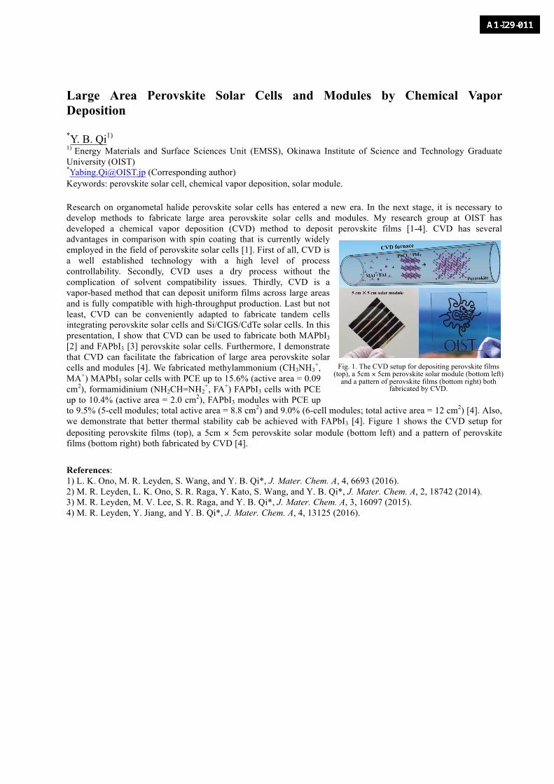
Large Area Perovskite Solar Cells and Modules by Chemical Vapor Deposition *Y. B. Qi1) 1) Energy Materials and Surface Sciences Unit (EMSS), Okinawa Institute of Science and Technology Graduate University (OIST) *[email protected] (Corresponding author) Keywords: perovskite solar cell, chemical vapor deposition, solar module. Research on organometal halide perovskite solar cells has entered a new era. In the next stage, it is necessary to develop methods to fabricate large area perovskite solar cells and modules. My research group at OIST has developed a chemical vapor deposition (CVD) method to deposit perovskite films [1-4]. CVD has several advantages in comparison with spin coating that is currently widely employed in the field of perovskite solar cells [1]. First of all, CVD is a well established technology with a high level of process controllability. Secondly, CVD uses a dry process without the complication of solvent compatibility issues. Thirdly, CVD is a vapor-based method that can deposit uniform films across large areas and is fully compatible with high-throughput production. Last but not least, CVD can be conveniently adapted to fabricate tandem cells integrating perovskite solar cells and Si/CIGS/CdTe solar cells. In this presentation, I show that CVD can be used to fabricate both MAPbI3 [2] and FAPbI3 [3] perovskite solar cells. Furthermore, I demonstrate that CVD can facilitate the fabrication of large area perovskite solar cells and modules [4]. We fabricated methylammonium (CH3NH3
+, MA+) MAPbI3 solar cells with PCE up to 15.6% (active area = 0.09 cm2), formamidinium (NH2CH=NH2
+, FA+) FAPbI3 cells with PCE up to 10.4% (active area = 2.0 cm2), FAPbI3 modules with PCE up to 9.5% (5-cell modules; total active area = 8.8 cm2) and 9.0% (6-cell modules; total active area = 12 cm2) [4]. Also, we demonstrate that better thermal stability cab be achieved with FAPbI3 [4]. Figure 1 shows the CVD setup for depositing perovskite films (top), a 5cm × 5cm perovskite solar module (bottom left) and a pattern of perovskite films (bottom right) both fabricated by CVD [4].
References: 1) L. K. Ono, M. R. Leyden, S. Wang, and Y. B. Qi*, J. Mater. Chem. A, 4, 6693 (2016). 2) M. R. Leyden, L. K. Ono, S. R. Raga, Y. Kato, S. Wang, and Y. B. Qi*, J. Mater. Chem. A, 2, 18742 (2014). 3) M. R. Leyden, M. V. Lee, S. R. Raga, and Y. B. Qi*, J. Mater. Chem. A, 3, 16097 (2015). 4) M. R. Leyden, Y. Jiang, and Y. B. Qi*, J. Mater. Chem. A, 4, 13125 (2016).
Fig. 1. The CVD setup for depositing perovskite films (top), a 5cm × 5cm perovskite solar module (bottom left)
and a pattern of perovskite films (bottom right) both fabricated by CVD.
Photoexcited Carrier Dynamics, Interface Passivation and Mechanism for Improving
Photovoltaic Performance of Perovskite Solar Cells
Qing Shen1,5, Yuhei Ogomi2,5, Taro Toyoda1,5, Kenji Yoshino3,5, Takashi Minemoto4,5 and Shuzi Hayase2,5
1Faculty of Informatics and Engineering, The University of Electro-Communications, Japan 2Graduate School of Life Science and Systems Engineering, Kyushu Institute of Technology, Japan 3Department of Electrical and Electronic Engineering, Miyazaki University, Japan 4Faculty of Science and Engineering, Ritsumeikan University, Japan 5CREST, Japan Science and Technology Agency (JST), Japan
*Corresponding Authors: [email protected] ; [email protected]
The interest in organometal trihalide Pb perovskite (CH3NH3PbI3)-based solar cells has increased
more and more in recent years because of the high efficiencies achieved, with a record of over 22%
[1], and the simple low temperature preparation method. The high efficiency was thought to mainly
originate from the strong optical absorption over a broader range (up to 800 nm for Pb ), low Urbach
energy due to low defect states, and longer lifetimes of photoexcited charge carriers of the
organometal trihalide Pb perovskite absorbers. Further improvements in the photovoltaic
performance can be obtained by increasing the light harvesting in the NIR region up to 1000 nm by
using Sn/Pb cocktail halide based perovskite materials [2]. On the other hand, a good understanding
of the key factors governing the photovoltaic performance of the Pb and Sn/Pb perovskite solar cells,
especially photoexcited carrier dynamics, is very vital for uncovering the mechanism of achieving
high efficiency. In this presentation, we would like to focus on the photoexcited carrier dynamics of
Pb and Sn/Pb perovskite solar cells, including photoexcited carrier lifetime, charge separation and
recombination dynamics at the interfaces of electron transport material/perovskite and hole transport
material/perovskite, and the relationships between these dynamics and the photovoltaic properties.
The mechanism for improving the energy conversion efficiency of the perovskite solar cells by means
of interface engineering will be discussed [3-6].
References:
[1] http://www.nrel.gov/ncpv/.
[2] Y. Ogomi,* A. Morita, S. Tsukamoto, T. Saitho, N. Fujikawa, Q. Shen, T. Toyoda,
K.Yoshino, S. Pandey, T. Ma, and S. Hayase, J. Phys. Chem. Lett. (2014), Vol. 5, 1004.
[3] Q. Shen, Y. Ogomi, J. Chang, S. Tsukamoto, K. Kukihara, T. Oshima, N. Osada,
K. Yoshino, K. Katayama, T. Toyoda and S. Hayase, Phys. Chem. Chem. Phys.(2014), Vol. 16, 19984.
[4] Q. Shen, Y. Ogomi, J. Chang, T. Toyoda, K. Fujiwara, K. Yoshino, K. Sato,
K. Yamazaki, M. Akimoto, Y. Kuga, K. Katayama, and S. Hayase, J. Mater. Chem. A (2015), Vol. 3,
9308.
[5] Q. Shen, Y. Ogomi, T. Toyoda, K. Yoshino, S. Hayase, Perovskite Materials - Synthesis,
Characterisation, Properties, and Applications, Chapter 13, Likun Pan (Ed.), (INTECH, Feb. 2016).
[6] M. Moriya, D. Hirotani, T. Ohta, Y. Ogomi, Q. Shen, T. S. Ripolles, K. Yoshino, T. Toyoda, T. Minemoto,
and S. Hayase: Architecture of the Interface between the Perovskite and Hole-Transport Layers in
Perovskite Solar Cells, ChemSusChem 2016, 9, 2634.
Novel Multi-Functional π-Conjugated Polymers for Efficient Dopant-Free
Ambient Stable Perovskite Solar Cells and Organic Solar Cells Application
*M. Song
Advanced Functional Thin Films Department, Korea Institute of Materials Science (KIMS) *[email protected]
Keywords: stable, perovskite solar cells, organic solar cells, time-resolved microwave conductivity, dopant-free
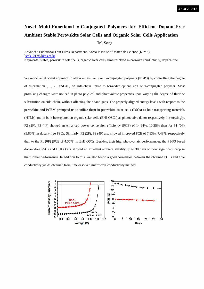
We report an efficient approach to attain multi-functional π-conjugated polymers (P1-P3) by controlling the degree
of fluorination (0F, 2F and 4F) on side-chain linked to benzodithiophene unit of π-conjugated polymer. Most
promising changes were noticed in photo physical and photovoltaic properties upon varying the degree of fluorine
substitution on side-chain, without affecting their band gaps. The properly aligned energy levels with respect to the
perovskite and PCBM prompted us to utilize them in perovskite solar cells (PSCs) as hole transporting materials
(HTMs) and in bulk heterojunction organic solar cells (BHJ OSCs) as photoactive donor respectively. Interestingly,
P2 (2F), P3 (4F) showed an enhanced power conversion efficiency (PCE) of 14.94%, 10.35% than for P1 (0F)
(9.80%) in dopant-free PSCs. Similarly, P2 (2F), P3 (4F) also showed improved PCE of 7.93%, 7.43%, respectively
than to the P1 (0F) (PCE of 4.35%) in BHJ OSCs. Besides, their high photovoltaic performances, the P1-P3 based
dopant-free PSCs and BHJ OSCs showed an excellent ambient stability up to 30 days without significant drop in
their initial performance. In addition to this, we also found a good correlation between the obtained PCEs and hole
conductivity yields obtained from time-resolved microwave conductivity method.
Enhancing the Efficiency of Silicon based Solar Cells by Forming CsPbBr3
Perovskite-Multicrystalline Silicon Hybrid Structure *Y. Q. Cao1)2), B. Xi1), X. H. Zeng1) and J. Xu2) 1) College of Physics Science and Technology, Yangzhou University, Yangzhou, China, 2) National Laboratory of
Solid State Microstructures and School of Electronic Science and Engineering and Collaborative Innovation Center
of Advanced Microstructures, Nanjing University, Nanjing, China *[email protected]
Keywords: Caesium lead halide perovskite quantum dots (CsPbBr3 QDs), multicrystalline silicon solar cells,
down-shifting effect
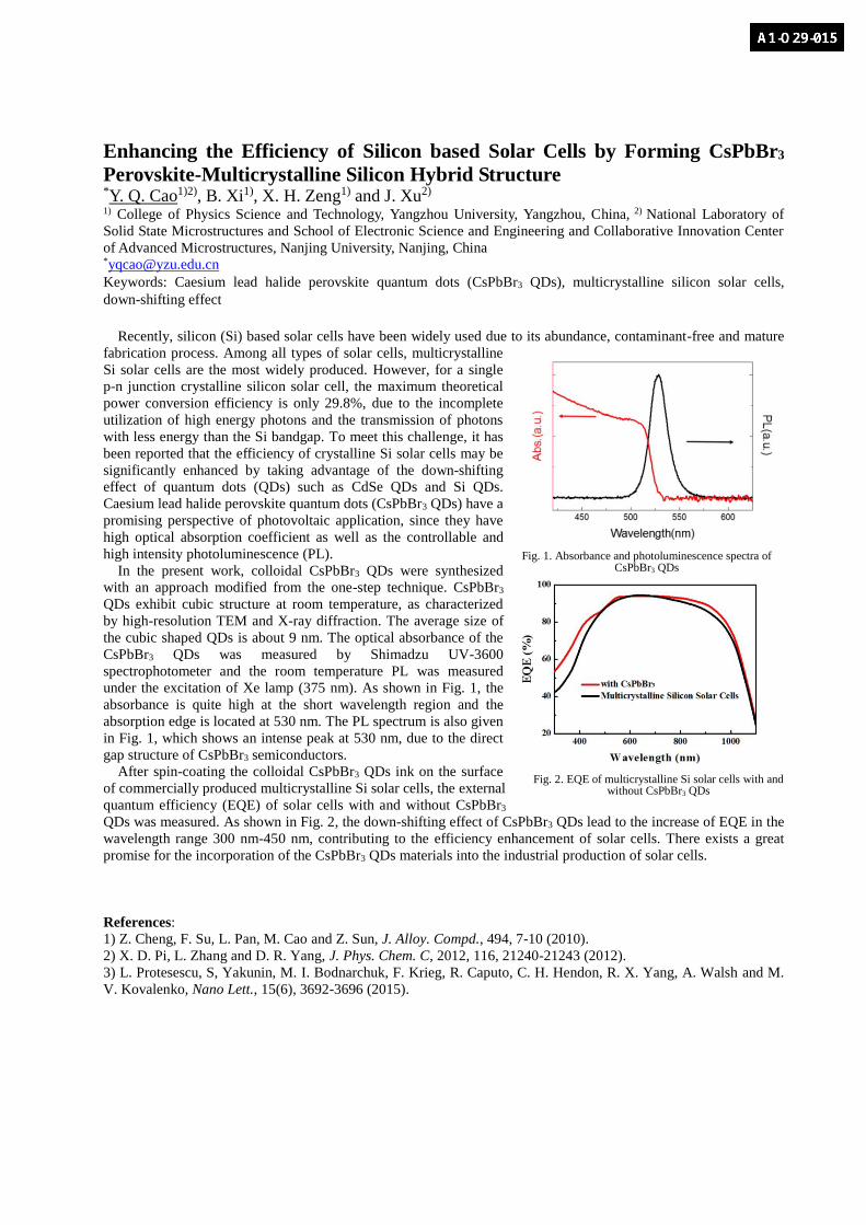
Recently, silicon (Si) based solar cells have been widely used due to its abundance, contaminant-free and mature
fabrication process. Among all types of solar cells, multicrystalline
Si solar cells are the most widely produced. However, for a single
p-n junction crystalline silicon solar cell, the maximum theoretical
power conversion efficiency is only 29.8%, due to the incomplete
utilization of high energy photons and the transmission of photons
with less energy than the Si bandgap. To meet this challenge, it has
been reported that the efficiency of crystalline Si solar cells may be
significantly enhanced by taking advantage of the down-shifting
effect of quantum dots (QDs) such as CdSe QDs and Si QDs.
Caesium lead halide perovskite quantum dots (CsPbBr3 QDs) have a
promising perspective of photovoltaic application, since they have
high optical absorption coefficient as well as the controllable and
high intensity photoluminescence (PL).
In the present work, colloidal CsPbBr3 QDs were synthesized
with an approach modified from the one-step technique. CsPbBr3
QDs exhibit cubic structure at room temperature, as characterized
by high-resolution TEM and X-ray diffraction. The average size of
the cubic shaped QDs is about 9 nm. The optical absorbance of the
CsPbBr3 QDs was measured by Shimadzu UV-3600
spectrophotometer and the room temperature PL was measured
under the excitation of Xe lamp (375 nm). As shown in Fig. 1, the
absorbance is quite high at the short wavelength region and the
absorption edge is located at 530 nm. The PL spectrum is also given
in Fig. 1, which shows an intense peak at 530 nm, due to the direct
gap structure of CsPbBr3 semiconductors.
After spin-coating the colloidal CsPbBr3 QDs ink on the surface
of commercially produced multicrystalline Si solar cells, the external
quantum efficiency (EQE) of solar cells with and without CsPbBr3
QDs was measured. As shown in Fig. 2, the down-shifting effect of CsPbBr3 QDs lead to the increase of EQE in the
wavelength range 300 nm-450 nm, contributing to the efficiency enhancement of solar cells. There exists a great
promise for the incorporation of the CsPbBr3 QDs materials into the industrial production of solar cells.
References:
1) Z. Cheng, F. Su, L. Pan, M. Cao and Z. Sun, J. Alloy. Compd., 494, 7-10 (2010).
2) X. D. Pi, L. Zhang and D. R. Yang, J. Phys. Chem. C, 2012, 116, 21240-21243 (2012).
3) L. Protesescu, S, Yakunin, M. I. Bodnarchuk, F. Krieg, R. Caputo, C. H. Hendon, R. X. Yang, A. Walsh and M.
V. Kovalenko, Nano Lett., 15(6), 3692-3696 (2015).
Fig. 2. EQE of multicrystalline Si solar cells with and without CsPbBr3 QDs
Fig. 1. Absorbance and photoluminescence spectra of CsPbBr3 QDs
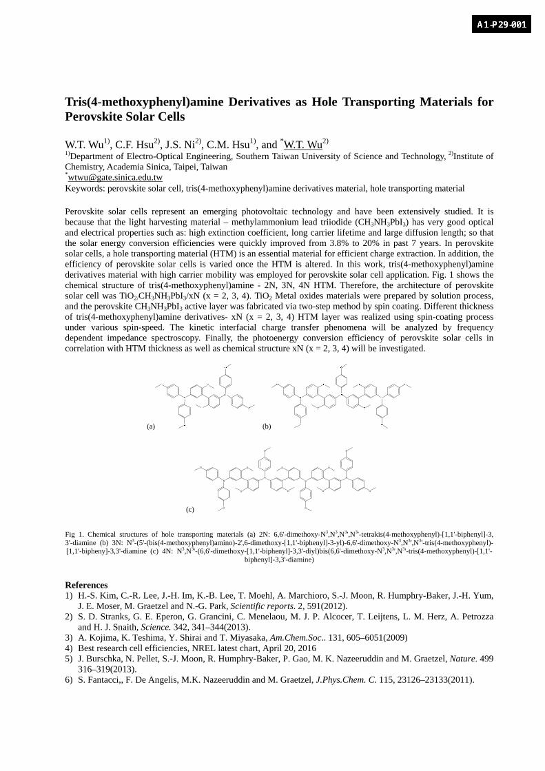
Tris(4-methoxyphenyl)amine Derivatives as Hole Transporting Materials for Perovskite Solar Cells W.T. Wu1), C.F. Hsu2), J.S. Ni2), C.M. Hsu1), and *W.T. Wu2) 1)Department of Electro-Optical Engineering, Southern Taiwan University of Science and Technology, 2)Institute of Chemistry, Academia Sinica, Taipei, Taiwan *[email protected] Keywords: perovskite solar cell, tris(4-methoxyphenyl)amine derivatives material, hole transporting material Perovskite solar cells represent an emerging photovoltaic technology and have been extensively studied. It is because that the light harvesting material – methylammonium lead triiodide (CH3NH3PbI3) has very good optical and electrical properties such as: high extinction coefficient, long carrier lifetime and large diffusion length; so that the solar energy conversion efficiencies were quickly improved from 3.8% to 20% in past 7 years. In perovskite solar cells, a hole transporting material (HTM) is an essential material for efficient charge extraction. In addition, the efficiency of perovskite solar cells is varied once the HTM is altered. In this work, tris(4-methoxyphenyl)amine derivatives material with high carrier mobility was employed for perovskite solar cell application. Fig. 1 shows the chemical structure of tris(4-methoxyphenyl)amine - 2N, 3N, 4N HTM. Therefore, the architecture of perovskite solar cell was TiO2/CH3NH3PbI3/xN (x = 2, 3, 4). TiO2 Metal oxides materials were prepared by solution process, and the perovskite CH3NH3PbI3 active layer was fabricated via two-step method by spin coating. Different thickness of tris(4-methoxyphenyl)amine derivatives- xN (x = 2, 3, 4) HTM layer was realized using spin-coating process under various spin-speed. The kinetic interfacial charge transfer phenomena will be analyzed by frequency dependent impedance spectroscopy. Finally, the photoenergy conversion efficiency of perovskite solar cells in correlation with HTM thickness as well as chemical structure xN (x = 2, 3, 4) will be investigated.
(a) (b)
(c)
O
O
O
O
NN
O
O
O
N
O
O
O
N
O
O
Fig 1. Chemical structures of hole transporting materials (a) 2N: 6,6'-dimethoxy-N3,N3,N3',N3'-tetrakis(4-methoxyphenyl)-[1,1'-biphenyl]-3,3'-diamine (b) 3N: N3-(5'-(bis(4-methoxyphenyl)amino)-2',6-dimethoxy-[1,1'-biphenyl]-3-yl)-6,6'-dimethoxy-N3,N3',N3'-tris(4-methoxyphenyl)-[1,1'-bipheny]-3,3'-diamine (c) 4N: N3,N3'-(6,6'-dimethoxy-[1,1'-biphenyl]-3,3'-diyl)bis(6,6'-dimethoxy-N3,N3',N3'-tris(4-methoxyphenyl)-[1,1'-
biphenyl]-3,3'-diamine)
References 1) H.-S. Kim, C.-R. Lee, J.-H. Im, K.-B. Lee, T. Moehl, A. Marchioro, S.-J. Moon, R. Humphry-Baker, J.-H. Yum,
J. E. Moser, M. Graetzel and N.-G. Park, Scientific reports. 2, 591(2012). 2) S. D. Stranks, G. E. Eperon, G. Grancini, C. Menelaou, M. J. P. Alcocer, T. Leijtens, L. M. Herz, A. Petrozza
and H. J. Snaith, Science. 342, 341–344(2013). 3) A. Kojima, K. Teshima, Y. Shirai and T. Miyasaka, Am.Chem.Soc.. 131, 605–6051(2009) 4) Best research cell efficiencies, NREL latest chart, April 20, 2016 5) J. Burschka, N. Pellet, S.-J. Moon, R. Humphry-Baker, P. Gao, M. K. Nazeeruddin and M. Graetzel, Nature. 499
316–319(2013). 6) S. Fantacci,, F. De Angelis, M.K. Nazeeruddin and M. Graetzel, J.Phys.Chem. C. 115, 23126–23133(2011).

Achievement of least reflectance on Silicon substrate using controlled surface texturing by anisotropic etching B.S. Akila, T. Balaganapathi, B. KaniAmuthan, S. Vinoth, and *P. Thilakan Photon Energy Technology Laboratory, Centre for Green Energy Technology, Madanjeet School of Green Energy Technologies, Pondicherry University, Puducherry – 605014, India *[email protected] Keywords: Anisotropic etching, random pyramids, aspect ratio, reflectance, histogram
Worldwide establishment of solar photovoltaic power plants unanimously utilizes Silicon based solar cells due to its relatively simple and cost effective industrial fabrication processes, which includes the surface texturing by anisotropic etching [1]. Anisotropic etching reduces the surface reflectance and improves the internal quantum efficiency. Substantial amount of research has been carried out to bring down the spectral reflection losses to less than one percentage (R<1%) and inverted pyramid structures with buried contact resulted in the least reflectance between 20-10% in the UV region [2,3]. Still, there is a room to bring down the reflection losses to still lowest possible level using conventional etching process than the reported values that will in turn ease the technology and improve the efficiency of silicon solar cell.
In this regard, efforts are made to optimize the industrially compatible anisotropic etching process to tune the spectral reflectance towards minimum level in the overall spectral range of the absorption of Silicon. Anisotropic etching process was optimized by varying the etching parameters such the temperature, concentration ratio between the etchants and time. Results were analyzed using FE-SEM, Zeta analysis and UV-Visible spectral measurements. A lowest weighted spectral reflectance of 10.76% for the spectral region between 300 nm to 1100 nm was achieved against the reported 11.2% so far. The details about the correlation between the processes conditions, pyramidal morphology and the spectral reflectance will be reported in the
presentation. References 1) A. Ingenito, O. Isabella and M. Zeman, Prog. Photovol. Res. Appl., 23, 1649-1659 (2015), 2) C.H. Sun, W.L. Min, N.C. Linn and P. Jiang, J. Vac. Sci. Technol. B., 27, 3 (2009), 3) J. Zhao, A. Wang, M.A. Green and F. Ferrazza, Appl. Phys. Lett., 73, 1991 (1998).
Fig. 1. Plot of etchant ratio versus aspect ratio with corresponding SEM images

Analysis of Electronic Structure According to Depth in Two Types of Perovskite Solar Cell Structure K. Eom1), J. Hwang1), U. Kwon1), S. Kalanur1), *H. Park1)2) and *H. Seo1)3) 1)Department of Energy Systems Research, Ajou University, Suwon 16499, Republic of Korea 2)Department of Electrical and Computer Engineering, Ajou University, Suwon 16499, Republic of Korea 3)Department of Materials Science and Engineering, Ajou University, Suwon 16499, Republic of Korea *[email protected]; *[email protected] Keywords : Perovskite, Solar cells, XPS, Band alignments, meso-TiO2
In recent years, a solar cell technology utilizing organometal trihalide perovskite materials, ABX3, as light absorber has attracted great attention due to properties such as broadband light absorption, long carrier diffusion length. Perovskite solar cells (PSC) has achieved a power conversion efficiency (PCE) of about 20% up to now. In general, p-i-n type devices have simple planar structure, which can be prepared by low-temperature solution process. Also, the short hole diffusion length can be compensated to improve the charge balance. However, since the hysteresis occurs, it is difficult to obtain the accurate PCE. In the case of n-i-p structure, meso-TiO2 is inserted between compact TiO2 and absorber layer to increase their interfacial area by forming nanostructure. Thus this structure is advantageous for adjusting the flux of the electrons towards the Transparent conducting oxide (TCO) electrode to attain a better charge balance. In various types of solar cells, interfacial states such as the chemical and electronic structures between the individual layers have been widely investigated with the aim of improving performance. Especially, the electronic structure at the heterojunction interface, such as the conduction band offset (CBO) and valence band offset (VBO), was shown to be crucial to determine the output voltage and photocurrent of most solar cell devices. However, another studies, the bandgap of each layer was roughly estimated by individually analyzing its potential by cyclic voltammetry.
In this study, in an attempt to determine the correlation between the energy-band structure of PSCs and their PCEs at the stacked cell level, we analyzed the energy-band structures of the overall device structures of both p-i-n-type and n-i-p-type PSC devices by using depth profile X-ray photoelectron spectroscopy (XPS), with which we can directly access the interface of each layer. As a result, we identify the electron transport mechanism and its relevance to the band alignment and its effect on PCE by comparing two different PSCs structures.
Fig. 1. Two types of PSC structure and band alignment diagrams: (a) planar structure and (b) mesoporous (mp) structure
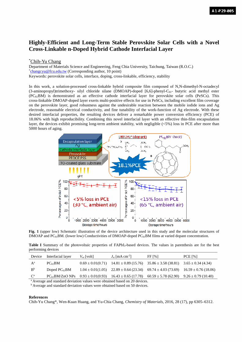
Highly-Efficient and Long-Term Stable Perovskite Solar Cells with a Novel Cross-Linkable n-Doped Hybrid Cathode Interfacial Layer *Chih-Yu Chang Department of Materials Science and Engineering, Feng Chia University, Taichung, Taiwan (R.O.C.) *[email protected] (Corresponding author, 10 point) Keywords: perovskite solar cells, interface, doping, cross-linkable, efficiency, stability In this work, a solution-processed cross-linkable hybrid composite film composed of N,N-dimethyl-N-octadecyl (3-aminopropyl)trimethoxy- silyl chloride silane (DMOAP)-doped [6,6]-phenyl-C61- butyric acid methyl ester (PC61BM) is demonstrated as an effective cathode interfacial layer for perovskite solar cells (PeSCs). This cross-linkable DMOAP-doped layer exerts multi-positive effects for use in PeSCs, including excellent film coverage on the perovskite layer, good robustness against the undesirable reaction between the mobile iodide ions and Ag electrode, reasonable electrical conductivity, and fine tunability of the work-function of Ag electrode. With these desired interfacial properties, the resulting devices deliver a remarkable power conversion efficiency (PCE) of 18.06% with high reproducibility. Combining this novel interfacial layer with an effective thin-film encapsulation layer, the devices exhibit promising long-term ambient stability, with negligible (<5%) loss in PCE after more than 5000 hours of aging.
Fig. 1 (upper low) Schematic illustration of the device architecture used in this study and the molecular structures of DMOAP and PC61BM. (lower low) Conductivities of DMOAP-doped PC61BM films at varied dopant concentration. Table I Summary of the photovoltaic properties of FAPbI3-based devices. The values in parenthesis are for the best performing devices
a Average and standard deviation values were obtained based on 20 devices. b Average and standard deviation values were obtained based on 50 devices.
References Chih-Yu Chang*, Wen-Kuan Huang, and Yu-Chia Chang, Chemistry of Materials, 2016, 28 (17), pp 6305–6312.
Device Interfacial layer Voc [volt] Jsc [mA cm-2] FF [%] PCE [%]
Aa PC61BM 0.69 ± 0.01(0.71) 14.81 ± 0.89 (15.76) 35.86 ± 3.58 (38.81) 3.65 ± 0.34 (4.34)
Bb Doped PC61BM 1.04 ± 0.01(1.05) 22.89 ± 0.64 (23.34) 69.74 ± 4.03 (73.69) 16.59 ± 0.76 (18.06)
Ca PC61BM/ZnO NPs 0.93 ± 0.01(0.93) 16.43 ± 0.65 (17.78) 60.59 ± 5.78 (62.90) 9.26 ± 0.79 (10.40)
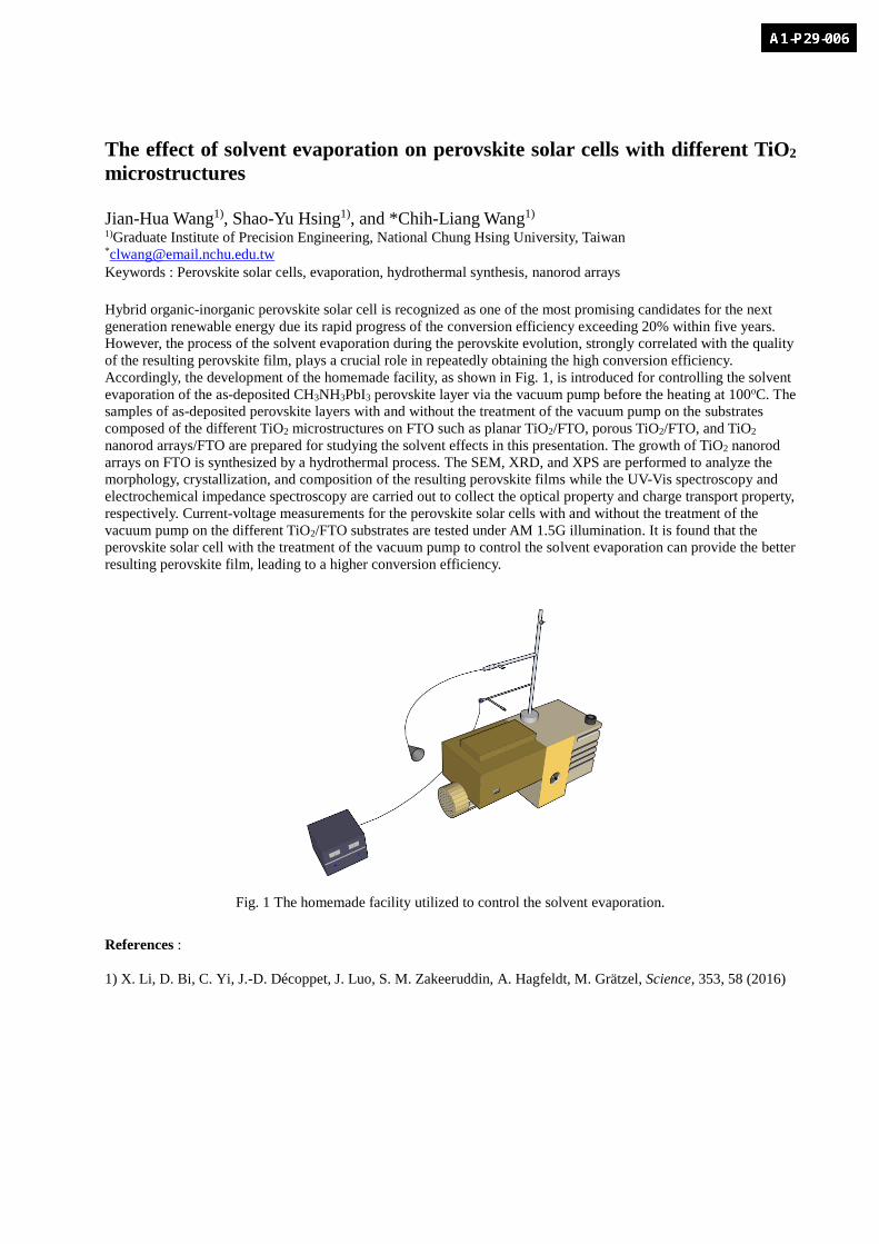
The effect of solvent evaporation on perovskite solar cells with different TiO2
microstructures
Jian-Hua Wang1), Shao-Yu Hsing1), and *Chih-Liang Wang1) 1)Graduate Institute of Precision Engineering, National Chung Hsing University, Taiwan *[email protected]
Keywords : Perovskite solar cells, evaporation, hydrothermal synthesis, nanorod arrays
Hybrid organic-inorganic perovskite solar cell is recognized as one of the most promising candidates for the next
generation renewable energy due its rapid progress of the conversion efficiency exceeding 20% within five years.
However, the process of the solvent evaporation during the perovskite evolution, strongly correlated with the quality
of the resulting perovskite film, plays a crucial role in repeatedly obtaining the high conversion efficiency.
Accordingly, the development of the homemade facility, as shown in Fig. 1, is introduced for controlling the solvent
evaporation of the as-deposited CH3NH3PbI3 perovskite layer via the vacuum pump before the heating at 100oC. The
samples of as-deposited perovskite layers with and without the treatment of the vacuum pump on the substrates
composed of the different TiO2 microstructures on FTO such as planar TiO2/FTO, porous TiO2/FTO, and TiO2
nanorod arrays/FTO are prepared for studying the solvent effects in this presentation. The growth of TiO2 nanorod
arrays on FTO is synthesized by a hydrothermal process. The SEM, XRD, and XPS are performed to analyze the
morphology, crystallization, and composition of the resulting perovskite films while the UV-Vis spectroscopy and
electrochemical impedance spectroscopy are carried out to collect the optical property and charge transport property,
respectively. Current-voltage measurements for the perovskite solar cells with and without the treatment of the
vacuum pump on the different TiO2/FTO substrates are tested under AM 1.5G illumination. It is found that the
perovskite solar cell with the treatment of the vacuum pump to control the solvent evaporation can provide the better
resulting perovskite film, leading to a higher conversion efficiency.
Fig. 1 The homemade facility utilized to control the solvent evaporation.
References :
1) X. Li, D. Bi, C. Yi, J.-D. Décoppet, J. Luo, S. M. Zakeeruddin, A. Hagfeldt, M. Grätzel, Science, 353, 58 (2016)
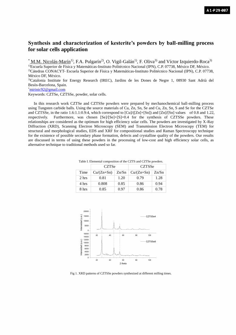
Synthesis and characterization of kesterite’s powders by ball-milling process
for solar cells application
* M.M. Nicolás-Marín1), F.A. Pulgarín2), O. Vigil-Galán1), F. Oliva3) and Víctor Izquierdo-Roca3) 1)Escuela Superior de Física y Matemáticas-Instituto Politécnico Nacional (IPN), C.P. 07738, México DF, México. 2)Cátedras CONACYT- Escuela Superior de Física y Matemáticas-Instituto Politécnico Nacional (IPN), C.P. 07738,
México DF, México. 3)Catalonia Institute for Energy Research (IREC), Jardins de les Dones de Negre 1, 08930 Sant Adrià del
Besòs-Barcelona, Spain. *[email protected]
Keywords: CZTSe, CZTSSe, powder, solar cells.
In this research work CZTSe and CZTSSe powders were prepared by mechanochemical ball-milling process
using Tungsten carbide balls. Using the source materials of Cu, Zn, Sn, Se and Cu, Zn, Sn, S and Se for the CZTSe
and CZTSSe, in the ratio 1.6:1.1:0.9:4, which correspond to [Cu]/([Zn]+[Sn]) and [Zn]/[Sn] values of 0.8 and 1.22,
respectively. Furthermore, was chosen [Se]/[Se]+[S]=0.4 for the synthesis of CZTSSe powders. These
relationships are considered as the optimum for high efficiency solar cells. The powders are investigated by X-Ray
Diffraction (XRD), Scanning Electron Microscopy (SEM) and Transmission Electron Microscopy (TEM) for
structural and morphological studies, EDS and XRF for compositional studies and Raman Spectroscopy technique
for the existence of possible secondary phase formation, defects and crystalline quality of the powders. Our results
are discussed in terms of using these powders in the processing of low-cost and high efficiency solar cells, as
alternative technique to traditional methods used so far.
Table I. Elemental composition of the CZTS and CZTSe powders.
20 40 60 80 100
0
2000
4000
6000
8000
10000
12000
14000
16000
CZTSSe8
Inte
nsid
ad
(u
.a.)
2 theta
20 40 60 80 100
0
5000
10000
15000
20000
CZTSSe4
Inte
nsid
ad
(u
.a.)
Fig 1. XRD patterns of CZTSSe powders synthesized at different milling times.
CZTSe CZTSSe
Time Cu/(Zn+Sn) Zn/Sn Cu/(Zn+Sn) Zn/Sn
2 hrs 0.81 1.20 0.79 1.28
4 hrs 0.808 0.85 0.86 0.94
8 hrs 0.85 0.97 0.86 0.78
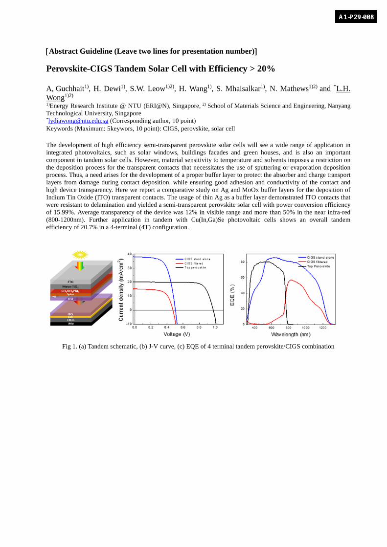
[Abstract Guideline (Leave two lines for presentation number)] Perovskite-CIGS Tandem Solar Cell with Efficiency > 20% A, Guchhait1), H. Dewi1), S.W. Leow1)2), H. Wang1), S. Mhaisalkar1), N. Mathews1)2) and *L.H. Wong1)2) 1)Energy Research Institute @ NTU (ERI@N), Singapore, 2) School of Materials Science and Engineering, Nanyang Technological University, Singapore
*[email protected] (Corresponding author, 10 point) Keywords (Maximum: 5keywors, 10 point): CIGS, perovskite, solar cell The development of high efficiency semi-transparent perovskite solar cells will see a wide range of application in integrated photovoltaics, such as solar windows, buildings facades and green houses, and is also an important component in tandem solar cells. However, material sensitivity to temperature and solvents imposes a restriction on the deposition process for the transparent contacts that necessitates the use of sputtering or evaporation deposition process. Thus, a need arises for the development of a proper buffer layer to protect the absorber and charge transport layers from damage during contact deposition, while ensuring good adhesion and conductivity of the contact and high device transparency. Here we report a comparative study on Ag and MoOx buffer layers for the deposition of Indium Tin Oxide (ITO) transparent contacts. The usage of thin Ag as a buffer layer demonstrated ITO contacts that were resistant to delamination and yielded a semi-transparent perovskite solar cell with power conversion efficiency of 15.99%. Average transparency of the device was 12% in visible range and more than 50% in the near infra-red (800-1200nm). Further application in tandem with Cu(In,Ga)Se photovoltaic cells shows an overall tandem efficiency of 20.7% in a 4-terminal (4T) configuration.
Fig 1. (a) Tandem schematic, (b) J-V curve, (c) EQE of 4 terminal tandem perovskite/CIGS combination
Top Related