


Languages
Pages
Legal

© Fraunhofer IFAM Dresden
Seite 1
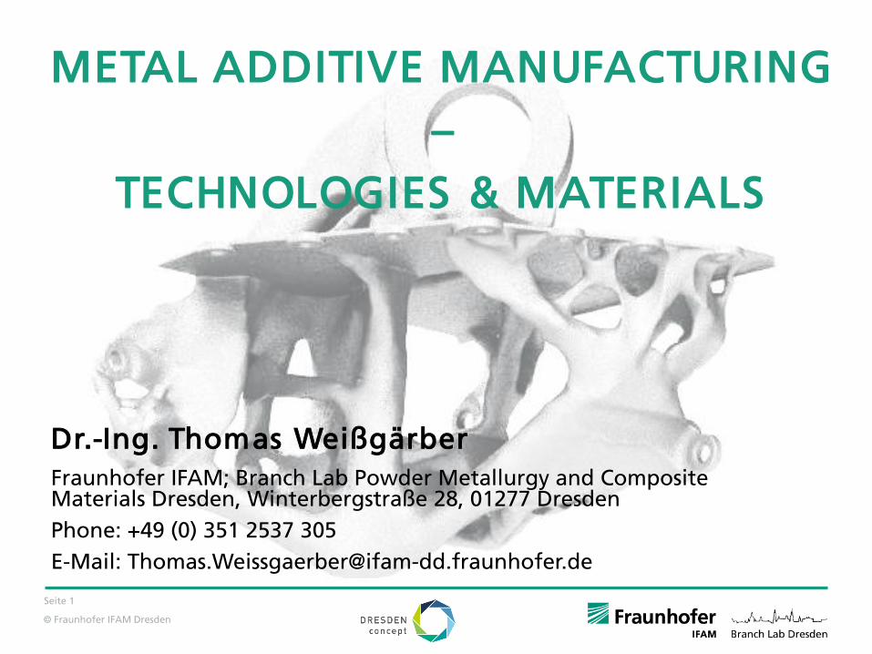
METAL ADDITIVE MANUFACTURING
–
TECHNOLOGIES & MATERIALS
Dr.-Ing. Thomas Weißgärber
Fraunhofer IFAM; Branch Lab Powder Metallurgy and Composite Materials Dresden, Winterbergstraße 28, 01277 Dresden
Phone: +49 (0) 351 2537 305
E-Mail: [email protected]

© Fraunhofer IFAM Dresden
Seite 2
Outline
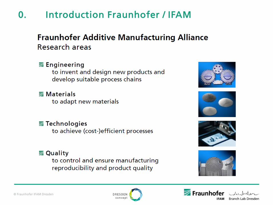
0. Introduction Fraunhofer / IFAM
1. Introduction AM Technologies
2. Metal AM – Technologies
2.1 Overview
2.2 Melting Technologies
2.2.1 Electron Beam Free Form Fabrication (EBFF)
2.2.2 Direct Metal Deposition (Laser)
2.2.3 Laser Beam Melting (LBM)
2.2.4 Electron Beam Melting (EBM)
© Fraunhofer IFAM Dresden
Seite 3
Outline
2. Metal AM – Technologies
2.3 Solid State Technologies
2.3.1 Introduction
2.3.2 Material Jetting
2.3.3 Binder Jetting
2.3.4 Fused Filament Fabrication (FFF)
2.3.5 3d Screen Printing
2.3.6 Sheet Lamination
© Fraunhofer IFAM Dresden
Fraunhofer-Gesellschaft
München
Holzkirchen
Freiburg
Efringen-Kirchen
FreisingStuttgart
PfinztalKarlsruheSaarbrücken
St. IngbertKaiserslautern
DarmstadtWürzburg
Erlangen
Nürnberg
Ilmenau
Schkopau
Teltow
Oberhausen
Duisburg
EuskirchenAachen
St. Augustin
Schmallenberg
Dortmund
PotsdamBerlin
Rostock
LübeckItzehoe
Braunschweig
Hannover
Bremen
Bremerhaven
Jena
Leipzig
Chemnitz
Dresden
CottbusMagdeburg
Halle
Fürth
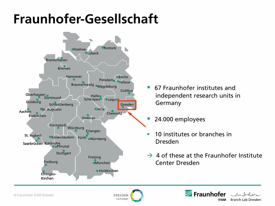
67 Fraunhofer institutes and
independent research units in
Germany
24.000 employees
10 institutes or branches in
Dresden
4 of these at the Fraunhofer Institute
Center Dresden

© Fraunhofer IFAM Dresden
Fraunhofer IFAM: Branch Lab Dresden
Head of IFAM Dresden (prov. from 01/04/19): Dr.-Ing. Thomas Weißgärber
Permanent staff
Student employees
Budget
Industry
Projects
Public funding
Investments
Area
(Budget 2017)
74
35
7,8 Mio. €
32 %
60 %
8 %
0,7 Mio. €
2850 m2

© Fraunhofer IFAM Dresden
Profile of Fraunhofer IFAM Dresden
Cellular Metallic Materials Sintered and Composite Materials
Fields of competence
Energy und Thermal ManagementHydrogen Technology
Elektrolysis Storage Hydrolysis Simulation Analysis
Fiber Structures
HollowSpheres
MetalFoams
3D MetalPrinting
3D WireStructures
Lightweight Materials
Tribology
Thermal Management
High-temperature
and corrosion-resistantMaterials
Thermo-electrics
PorousMetalPaper
Thermal Storage Devices
Additive Manufacturing

© Fraunhofer IFAM Dresden
SEBM competence @ IFAM Dresden
Powder Design Process
Accredited lab for characterization
Assessment of new powder analytics
Design rules „Design for AM“, e.g.
topology optimization
Process development
New materials Prototypes and
Components
© Fraunhofer IFAM Dresden
0. Introduction Fraunhofer / IFAM

© Fraunhofer IFAM Dresden
Seite 9
1. Introduction AM Technologies
It is defined as the process of joining materials to make objects from 3D model data, usually layer upon layer, as opposed to subtractive manufacturing methodologies. Synonyms are additive fabrication, additive processes, additive techniques, additive layer manufacturing, layer manufacturing, and freeform fabrication.
Additive Manufacturing: Definition

© Fraunhofer IFAM Dresden
Seite 10
1. Introduction AM Technologies

© Fraunhofer IFAM Dresden
Seite 11
Metal Additive Manufacturing at Fraunhofer IFAM
Electron Beam Melting (EBM) [DD]
3D Metal Printing -Screen Printing approach(3DMP) [DD]
Laser Beam Melting (LBM) [HB]
3D Metal Printing -Binder Jetting approach(3DP) [HB]
3D Metal Printing -Binder Jetting approach(3DP) [HB]
Introduction
© Fraunhofer IFAM Dresden
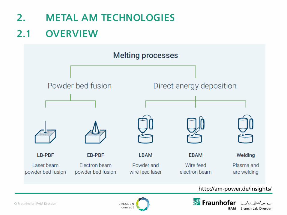
2. METAL AM TECHNOLOGIES
2.1 OVERVIEW
http://am-power.de/insights/

© Fraunhofer IFAM Dresden
2. METAL AM TECHNOLOGIES
2.1 OVERVIEW
http://am-power.de/insights/

© Fraunhofer IFAM Dresden
Seite 14
Comparison between different AM Technologies Wire FeedPowder FeedPowder Bed
laser beame- beam
laser beam laser beame- beamplasma
laser e- beam e- beamlaser laser
Part complexity
Accuracy
Part size
Build rate
Material variety
Material quality
2. METAL AM TECHNOLOGIES
2.2 MELTING TECHNOLOGIES

© Fraunhofer IFAM Dresden
Part Dimensions:
Diameter up to 40cm
Length / Width app.. 60cm
Built Rate: 2,3kg/h
50% Material Savingcompared with machining
Sciaky, Inc.
Selected Parameters:
Wire diameter: 2,36mm (TiAl6V4)
Wire feeding: 1780mm/min
Wall Thicknesses: bis zu 0,76mm möglich
METAL AM TECHNOLOGIES
2.2.1 Electron Beam Free Form Fabrication (EBFF)
© Fraunhofer IFAM Dresden
METAL AM TECHNOLOGIES
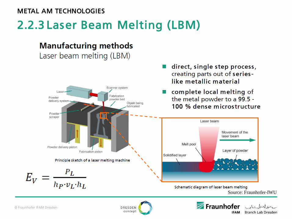
2.2.3 Laser Beam Melting (LBM)
Source: Fraunhofer-IWU
© Fraunhofer IFAM Dresden
Seite 17
EBM is a hot process
each layer of powder is pre-heated, temperature is material-dependent (e.g. Ti-6Al-4V: ca. 700°C, TiAl: > 1000°C)
powder “smoke” due to local buildup of charge is prevented by slight sintering of powder particles
thermal stresses can be minimized
EBM uses high vacuum as process atmosphere
this is required in order for the electron beam to work
highly reactive materials can be processed
outgassing of impurities
thermal insulation
METAL AM TECHNOLOGIES
2.2.4 Electron Beam Melting (EBM)

© Fraunhofer IFAM Dresden
Seite 18
Construction of an EBM-machine
1
2
3
http://www.arcam.com/technology/electron-beam-melting/hardware/
METAL AM TECHNOLOGIES (Electron Beam Melting (EBM))

© Fraunhofer IFAM Dresden
Methods of the powder evaluation
Seite 19
property norm relevance
Particle size distributionDIN 13320
Flowability (powder feed and raking)
Hall Flow/Gustavsson (time) DIN ISO 4490/DIN EN ISO
13517Flowability
Layer homogeneity
Morphology (SEM) Flowability (powder feed and raking)
Apparent densityDIN ISO 3923/DIN ISO
3953Layer homogeneity
ImpuritiesDIN EN ISO 9556 (C, S)
DIN ISO 4491 (O, N)Contamination before & after process,
Component quality and properties
Moisture measurement(TGA)
Flowability (powder feed and raking)Component quality (internal faults)
Composition (ICP-OES, carrier gas hot extraction)
Component quality and properties
Powder density DIN 51 913 Component quality (internal faults)
METAL AM TECHNOLOGIES (Electron Beam Melting (EBM))

© Fraunhofer IFAM Dresden
Seite 20
Powder properties: comparison LBM - EBM
LBM:
differences in particle size
(~8 µm)
differences in flowability
(32 – 53s)
EBM:
low Al content (at lowerlimit but withinspecifiaction)
low Oxygen content
Powder EOSConcept
Laser
SLM
SolutionsArcam
D10 µm 21.9 20.2 28.2 51.4
D50 µm 31.9 29.8 36.6 73.2
D90 µm 46.3 43.7 49.2 107.8
Flowability s 39.3 53.2 31.7 21.8
Bulk density g/cm³ 2.46 2.54 2.45 2.59
Apparent
density
g/cm³2.83 2.83
2.73 2.81
Al- proportion % 6.49 6.38 6.37 5.75
V- proportion % 4.09 3.91 3.90 3.97
Fe- proportion % 0.24 0.22 0.22 0.21
O- proportion % 0.188 0.147 0.143 0.116
N- proportion % 0.010 0.009 0.016 0.017
METAL AM TECHNOLOGIES (Electron Beam Melting (EBM))

© Fraunhofer IFAM Dresden
Seite 21
slight increase of oxygen content
better flowability
all other properties remain constant
new 13 build jobs
d10 µm 51,4 53,7d50 µm 73,2 75,7d90 µm 107,8 110,2
Hall-Flow (2.5 mm) s 21,8 20,8
Rohdichte g/cm³ 2,59 2,56
O m% 0,12 0,14
N m% 0,017 0,018
Powder properties, surplus powder EBM
METAL AM TECHNOLOGIES (Electron Beam Melting (EBM))
© Fraunhofer IFAM Dresden
Seite 22
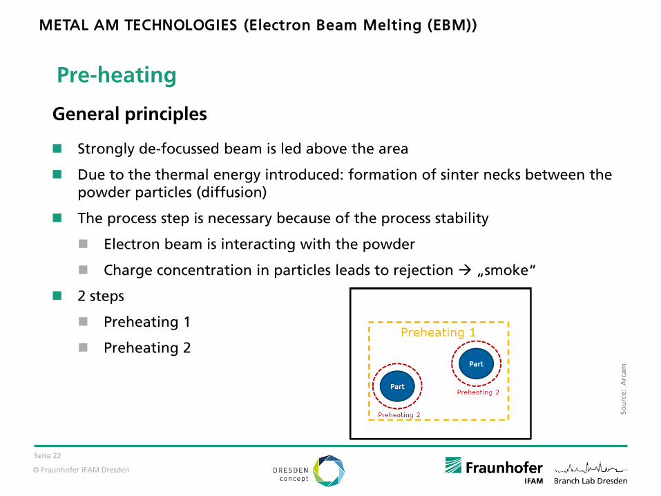
Strongly de-focussed beam is led above the area
Due to the thermal energy introduced: formation of sinter necks between thepowder particles (diffusion)
The process step is necessary because of the process stability
Electron beam is interacting with the powder
Charge concentration in particles leads to rejection „smoke“
2 steps
Preheating 1
Preheating 2
General principles
Pre-heating
So
urc
e: A
rca
m
METAL AM TECHNOLOGIES (Electron Beam Melting (EBM))

© Fraunhofer IFAM Dresden
Seite 23
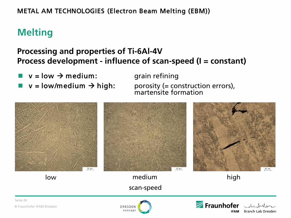
Processing and properties of Ti-6Al-4VProcess development - influence of scan-speed (I = constant)
v = low
Very uneven surface, dents
too much powder hasmolten
Density > 100%
possible evaporating of Al
v = high
Uneven surface
Density < 100%
inner Porosity
low highv
Melting
METAL AM TECHNOLOGIES (Electron Beam Melting (EBM))
© Fraunhofer IFAM Dresden
Seite 24
v = low medium: grain refining
v = low/medium high: porosity (= construction errors), martensite formation
scan-speed
low medium high
Processing and properties of Ti-6Al-4VProcess development - influence of scan-speed (I = constant)
Melting
METAL AM TECHNOLOGIES (Electron Beam Melting (EBM))
© Fraunhofer IFAM Dresden
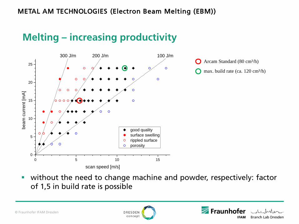
without the need to change machine and powder, respectively: factorof 1,5 in build rate is possible
0 5 10 15
0
5
10
15
20
25
300 J/m 100 J/m
good quality
surface swelling
rippled surface
porosity
beam
curr
ent [m
A]
scan speed [m/s]
200 J/m
Arcam Standard (80 cm³/h)
max. build rate (ca. 120 cm³/h)
Melting – increasing productivity
METAL AM TECHNOLOGIES (Electron Beam Melting (EBM))

© Fraunhofer IFAM Dresden
Design limits for small structures
geometry demonstrator (available from RTC Duisburg)
METAL AM TECHNOLOGIES (Electron Beam Melting (EBM))
Design rules for EBM
© Fraunhofer IFAM Dresden
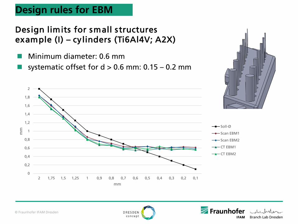
Design limits for small s tructuresexample (I) – cylinders (Ti6Al4V; A2X)
Minimum diameter: 0.6 mm
systematic offset for d > 0.6 mm: 0.15 – 0.2 mm
0
0,2
0,4
0,6
0,8
1
1,2
1,4
1,6
1,8
2
2 1,75 1,5 1,25 1 0,9 0,8 0,7 0,6 0,5 0,4 0,3 0,2 0,1
mm
mm
Soll-Ø
Scan EBM1
Scan EBM2
CT EBM1
CT EBM2
Design rules for EBM

© Fraunhofer IFAM Dresden
minimum wall thickness ≥ 0.6 mm
systematic offset for d > 0.6 mm: up to 0.2 mm
0
0,2
0,4
0,6
0,8
1
1,2
1,4
1,6
1,8
2
2 1,75 1,5 1,25 1 0,9 0,8 0,7 0,6 0,5 0,4 0,3 0,2 0,1
mm
mm
Soll-Dicke
x-Richtung EBM1
y-Richtung EBM1
x-Richtung EBM2
y-Richtung EBM2
Design rules for EBM
Design limits for small s tructuresexample (I) – walls (s traight) (Ti6Al4V; A2X)

© Fraunhofer IFAM Dresden
„comparison“ LBM – EBM
material LBM EBM
Ti-6Al-4V
Ni-Basis (e.g. IN 718, IN 625)
TiAl (RNT650, TNM)
Al-bases (e.g. AlSi-X, AlMgSc)
CoCr
Stainless steel (e.g. 1.4404, 17-4PH)
tool steel (e.g. 1.2709) ---
Copper alloys (e.g. CuNi2SiCr) ---
pure copper
Materials
METAL AM TECHNOLOGIES (Electron Beam Melting (EBM))
© Fraunhofer IFAM Dresden
Seite 30
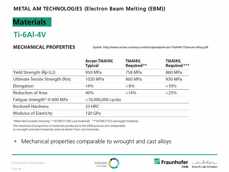
Ti-6Al-4V
Mechanical properties comparable to wrought and cast alloys
Quelle: http://www.arcam.com/wp-content/uploads/Arcam-Ti6Al4V-Titanium-Alloy.pdf
Materials
METAL AM TECHNOLOGIES (Electron Beam Melting (EBM))

© Fraunhofer IFAM Dresden
EBM (Arcam A2X, 3 kW)
Ti6Al4V Powder45-105 µm, 1200-1400 ppm O
Beam current: 15mA
700 °C (for Ti-6Al-4V)
fully lamellar (basket weave) at low scan speeds (α-lamellae thickness app. ca. 20 µm)
Refining up to 2…3 µm at higher scan speeds
Formation of needle like α‘-martensite at very high scan speeds
Kirchner et al., Process window for electron beam melting of Ti-6Al-4V, Powder Metallurgy 58 (2015), 246-249
Ti-6Al-4V
Materials
METAL AM TECHNOLOGIES (Electron Beam Melting (EBM))

© Fraunhofer IFAM Dresden
EBM (Arcam A2X, 3 kW)
Ti6Al4V Powder45-105 µm, 1200-1400 ppm O
Heat Treatment of „as-built“ parts
Low temperature: no significant microstructural changes compared to “as-built”, α-lamellas up to3µm thcik
With increasing temperature coarsening of the α-Phase, in particular along former β-grain boundaries
above β-Transus temperature coarsening of the α-phase
HT 1 HT 3 HT 6
Kirchner et al., Mechanical Properties of Ti-6Al-4V fabricated by Electron Beam Melting, Key. Eng. Mat. 704 (2016), 235-240
Ti-6Al-4V
Materials
METAL AM TECHNOLOGIES (Electron Beam Melting (EBM))

© Fraunhofer IFAM Dresden
Youngs Modulus 114…123GPa, comparable with dense material without texture
HT1 tensile strength of1023MPa nearly identical with “as-built”, elongation 15%
Higher heat treatment temperature leads to small reduction of strength
AMS 4928 Specification is fullfilled
BM (Arcam A2X, 3 kW)
Ti6Al4V Powder45-105 µm, 1200-1400 ppm O
Heat Treatment of „as-built“ Bauteile
Kirchner et al., Mechanical Properties of Ti-6Al-4V fabricated by Electron Beam Melting, Key. Eng. Mat. 704 (2016), 235-240
Ti-6Al-4V
Materials
METAL AM TECHNOLOGIES (Electron Beam Melting (EBM))

© Fraunhofer IFAM Dresden
TiAl
EBM (Arcam A2X, 3 kW)
Bau
rich
tun
gH. Clemens:, Montanuniversität Leoben
IFAM Dresden
Baudana et al
METAL AM TECHNOLOGIES (Electron Beam Melting (EBM))
Materials

© Fraunhofer IFAM Dresden
EBM (Arcam A2X, 3 kW)
Heat Treatment of TiAl EBM-Parts
Material: RNT650 (Ti48Al2Nb0.7Cr0.3Si)
A: “as-built” - “fine-grained, equiaxed” (Porosität<1%)
B: 1300 °C / 2h - “fine-grained equiaxed” with small amount of lamella grains
C: 1350 °C / 2h - “duplex”
D: 1360 °C / 2h - “near lamellar”
E: 1365 °C / 2h - “fully lamellar” with small amount of globular grains
F: 1370 °C / 2h - “fully lamellar”
Microstructure can be tailored but “temperature window” is relatively small
G. Baudana, et al.Electron Beam Melting of Ti-48Al-2Nb-0.7Cr-0.3Si: Feasibility investigation, Intermetallics, Volume 73, 2016, 43-49
TiAl
METAL AM TECHNOLOGIES (Electron Beam Melting (EBM))
Materials

© Fraunhofer IFAM Dresden
EBM (Arcam A2X, 3 kW)
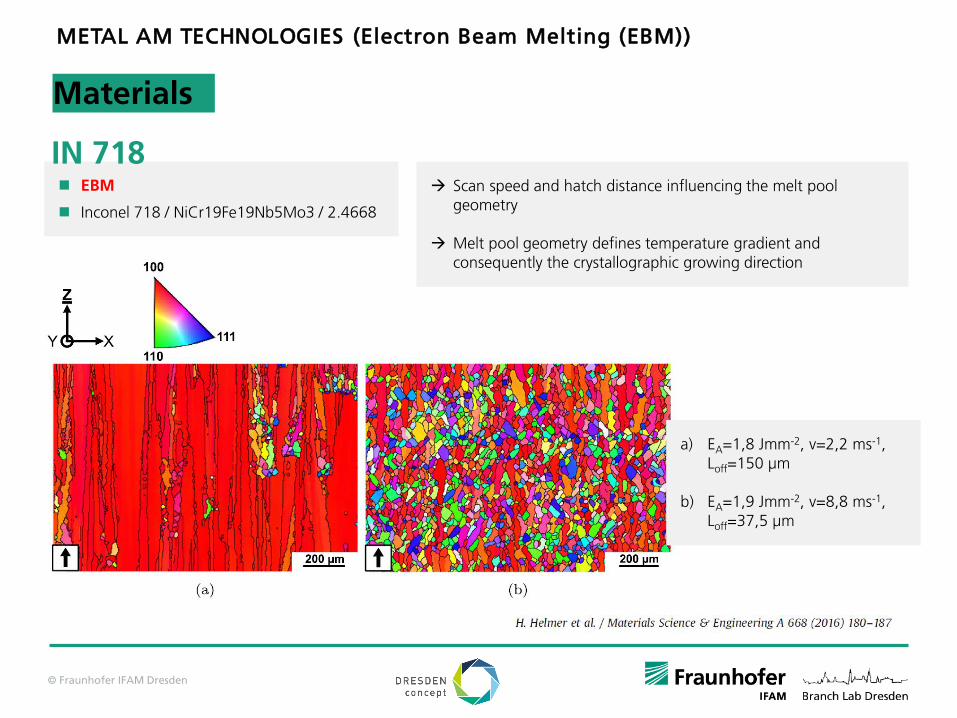
Inconel 718 / NiCr19Fe19Nb5Mo3 / 2.4668
Strong (100)-Texture parrallel to buildingdirection
Microstructure design possible by choosingproper scan parameters
Kirchner et al, Electron Beam Melting of Inconel 718, Proceedings DDMC 2018, Berlin, March 14 – 15 2018, 154, ISBN 978-3-8396-1320-7
𝐸L =𝑈𝐵 × 𝐼𝑏𝑒𝑎𝑚
𝑣𝑠𝑐𝑎𝑛
IN 718
METAL AM TECHNOLOGIES (Electron Beam Melting (EBM))
Materials
© Fraunhofer IFAM Dresden
EBM
Inconel 718 / NiCr19Fe19Nb5Mo3 / 2.4668
a) EA=1,8 Jmm-2, v=2,2 ms-1, Loff=150 µm
b) EA=1,9 Jmm-2, v=8,8 ms-1, Loff=37,5 µm
Scan speed and hatch distance influencing the melt poolgeometry
Melt pool geometry defines temperature gradient andconsequently the crystallographic growing direction
IN 718
METAL AM TECHNOLOGIES (Electron Beam Melting (EBM))
Materials

© Fraunhofer IFAM Dresden
EBM
304L / X2CrNi19-11 / 1.4306
Pre-Heating: 880 °C, layer thickness: 70 µm, hatch distance: 100 µm
200 J/m line energy for complete densification necessary
Kirchner et al., Selective Electron Beam Melting Of Austenitic Stainless Steel, EBAM
2018
304L
METAL AM TECHNOLOGIES (Electron Beam Melting (EBM))
Materials

© Fraunhofer IFAM Dresden
Topology optimization of aerospace partoptimization result (II)
step 1: scale 1:2, material: Ti-6Al-4V (1st design)
step 2: full scale part (recalculated design after changes in loads, rivet holes, …)
dimensions in build chamber (x/y/z): 171 / 179 / 158 mm
build time: 29h
for testing, part has been completely surface-treated (CNC + electro-polish)
1st design 2nd design, as-built 2nd design, finished
Applications
METAL AM TECHNOLOGIES (Electron Beam Melting (EBM))

© Fraunhofer IFAM Dresden
Source: http://www.gereports.com/post/94658699280/this-electron-gun-builds-jet-engines/ (last access: 02 Dec 2016)
EBM-manufactured turbine blades for different aero engines (from left to right): LEAP, GEnx, GE90, GE9X
serial and prototype parts – Avio GETiAl
Applications
METAL AM TECHNOLOGIES (Electron Beam Melting (EBM))
© Fraunhofer IFAM Dresden
Examples from aerospace
Seite 41
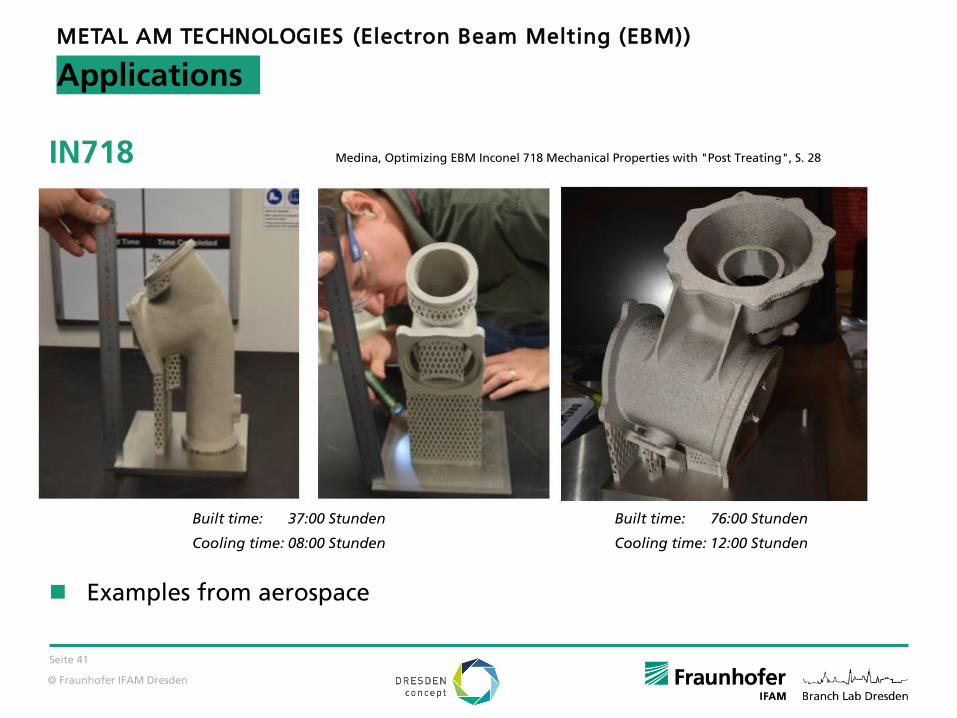
IN718 Medina, Optimizing EBM Inconel 718 Mechanical Properties with "Post Treating", S. 28
Built time: 37:00 Stunden
Cooling time: 08:00 Stunden
Built time: 76:00 Stunden
Cooling time: 12:00 Stunden
Applications
METAL AM TECHNOLOGIES (Electron Beam Melting (EBM))

© Fraunhofer IFAM Dresden
application:
Medicine (Knee, tooth)
Turbines (nozzles and blades)
Seite 42
CoCrArcam AB, Arcam ASTM F75 CoCr, p. 2
Applications
METAL AM TECHNOLOGIES (Electron Beam Melting (EBM))
© Fraunhofer IFAM Dresden
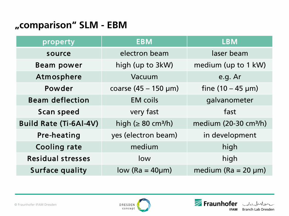
„comparison“ SLM - EBM
property EBM LBM
source electron beam laser beam
Beam power high (up to 3kW) medium (up to 1 kW)
Atmosphere Vacuum e.g. Ar
Powder coarse (45 – 150 µm) fine (10 – 45 µm)
Beam deflection EM coils galvanometer
Scan speed very fast fast
Build Rate (Ti-6Al-4V) high (≥ 80 cm³/h) medium (20-30 cm³/h)
Pre-heating yes (electron beam) in development
Cooling rate medium high
Residual stresses low high
Surface quality low (Ra = 40µm) medium (Ra = 20 µm)

© Fraunhofer IFAM Dresden
sintering
printing material
(e.g suspension,
filament)
process technologies
„green part“
CAD design
(format e.g. .stl)
Solid state processes :
• No melting of particles
• Multi step production process
• 1. Preparation of green parts
• 2. Sintering process
• 3. Post Processing (optional)
Exception: LOM/UAM
2. METAL AM TECHNOLOGIES
2.3 Solid State TECHNOLOGIES
2.3.1 Introduction

© Fraunhofer IFAM Dresden
Fundamentals of sinteringsintering
Green
part
Sintered
part
First step: Debindering
Removal of binders by
Heat
Solvent
2. METAL AM TECHNOLOGIES
2.3 Solid State TECHNOLOGIES
2.3.1 Introduction
© Fraunhofer IFAM Dresden
Fundamentals of sinteringsintering
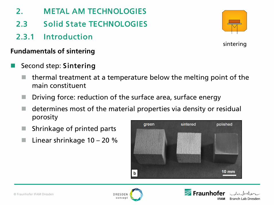
Second step: S intering
thermal treatment at a temperature below the melting point of the main constituent
Driving force: reduction of the surface area, surface energy
determines most of the material properties via density or residual porosity
Shrinkage of printed parts
Linear shrinkage 10 – 20 %
2. METAL AM TECHNOLOGIES
2.3 Solid State TECHNOLOGIES
2.3.1 Introduction
© Fraunhofer IFAM Dresden
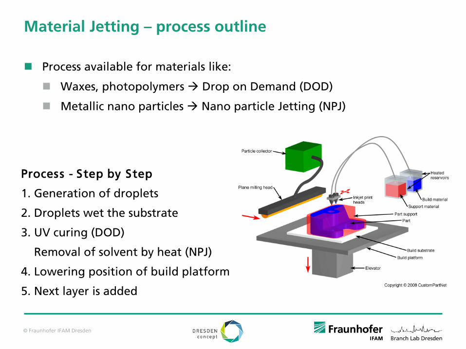
Material Jetting – process outline
Process - Step by Step
1. Generation of droplets
2. Droplets wet the substrate
3. UV curing (DOD)
Removal of solvent by heat (NPJ)
4. Lowering position of build platform
5. Next layer is added
Process available for materials like:
Waxes, photopolymers Drop on Demand (DOD)
Metallic nano particles Nano particle Jetting (NPJ)

© Fraunhofer IFAM Dresden
Material Jetting – process characteristics
Process properties:
Resolution: 30 – 100 µm
Build rate: 6 – 24 cm3/h
Layer thickness: up to 2 µm
Support structures: yes, printed parallel
Materials: metals, ceramics
Powder requirements: < 2 µm
Source: XJET
Droplets created by Inkjet Printing
© Fraunhofer IFAM Dresden
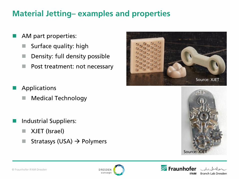
Material Jetting– examples and properties
AM part properties:
Surface quality: high
Density: full density possible
Post treatment: not necessary
Applications
Medical Technology
Industrial Suppliers:
XJET (Israel)
Stratasys (USA) Polymers
Source: XJET
Source: XJET

© Fraunhofer IFAM Dresden
Material Jetting– examples and properties
Advantages
High accuracy
Smooth surfaces
Low sintering temperatures
Disadvantages
Expensive powders
Slow process
Source: XJET
Source: XJET
© Fraunhofer IFAM Dresden
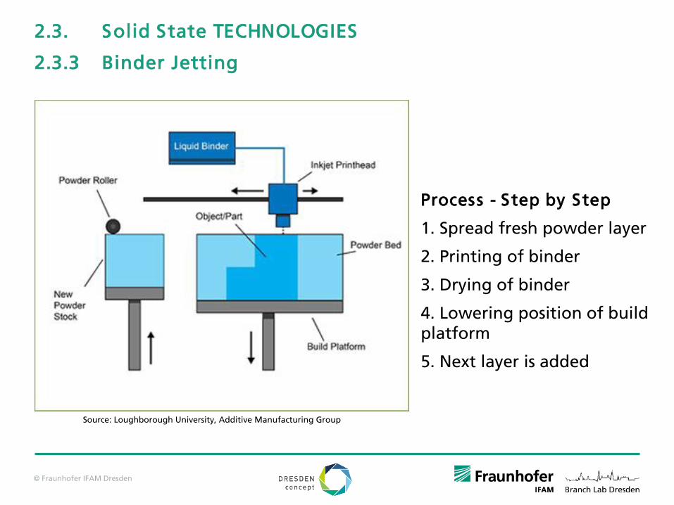
Process - Step by Step
1. Spread fresh powder layer
2. Printing of binder
3. Drying of binder
4. Lowering position of build platform
5. Next layer is added
Source: Loughborough University, Additive Manufacturing Group
2.3. Solid State TECHNOLOGIES
2.3.3 Binder Jetting

© Fraunhofer IFAM Dresden
Binder Jetting – process characteristics
Process properties:
Resolution: > 125 µm
Large parts possible
Build rate: up to 1000 cm3/h
Layer thickness: > 90 µm
Support structures: not needed
Materials:
Full range of MIM materials
Ceramics, Steels
Powder requirements: > 20 µm
Source: Ex One
© Fraunhofer IFAM Dresden
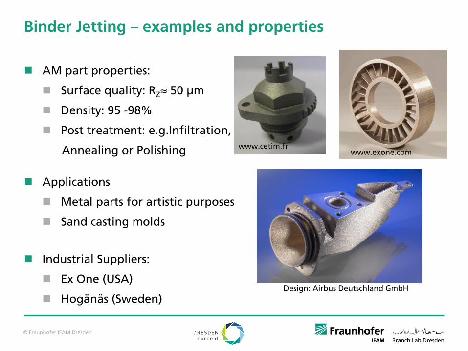
Binder Jetting – examples and properties
AM part properties:
Surface quality: RZ≈ 50 µm
Density: 95 -98%
Post treatment: e.g.Infiltration,
Annealing or Polishing www.exone.comwww.cetim.fr
Applications
Metal parts for artistic purposes
Sand casting molds
Design: Airbus Deutschland GmbH
Industrial Suppliers:
Ex One (USA)
Hogänäs (Sweden)

© Fraunhofer IFAM Dresden
Advantages
High resolution
Material variety
No supports structures
Fast process
Disadvantages
Post-processing steps necessary
Shrinkage during sintering
Binder Jetting – examples and properties
www.exone.comwww.cetim.fr
Design: Airbus Deutschland GmbH
© Fraunhofer IFAM Dresden
Process - Step by Step
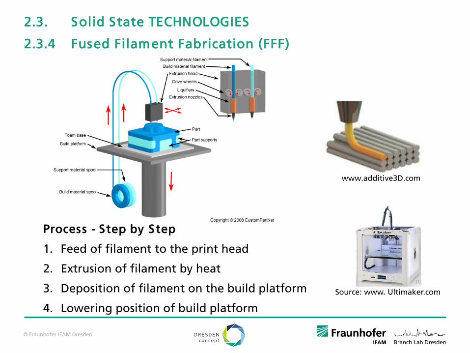
1. Feed of filament to the print head
2. Extrusion of filament by heat
3. Deposition of filament on the build platform
4. Lowering position of build platform
www.additive3D.com
[1]
Source: www. Ultimaker.com
2.3. Solid State TECHNOLOGIES
2.3.4 Fused Filament Fabrication (FFF)
© Fraunhofer IFAM Dresden
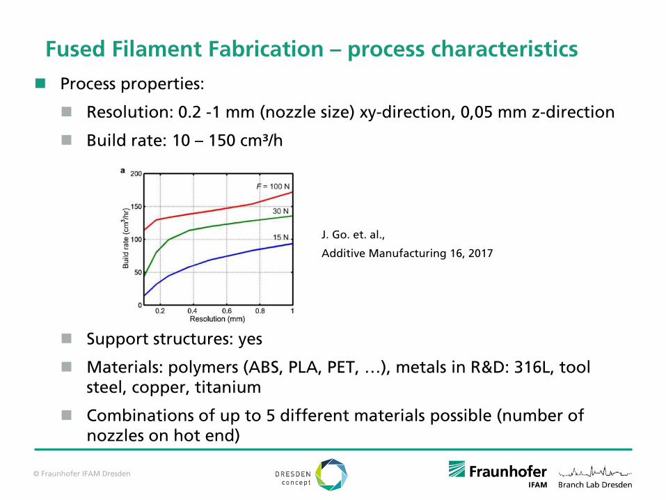
Process properties:
Resolution: 0.2 -1 mm (nozzle size) xy-direction, 0,05 mm z-direction
Build rate: 10 – 150 cm³/h
Support structures: yes
Materials: polymers (ABS, PLA, PET, …), metals in R&D: 316L, tool steel, copper, titanium
Combinations of up to 5 different materials possible (number of nozzles on hot end)
Fused Filament Fabrication – process characteristics
J. Go. et. al.,
Additive Manufacturing 16, 2017
© Fraunhofer IFAM Dresden
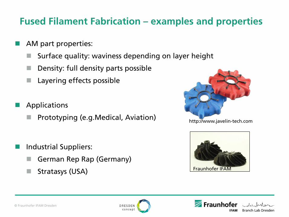
AM part properties:
Surface quality: waviness depending on layer height
Density: full density parts possible
Layering effects possible
Fused Filament Fabrication – examples and properties
Applications
Prototyping (e.g.Medical, Aviation)
Industrial Suppliers:
German Rep Rap (Germany)
Stratasys (USA)
http://www.javelin-tech.com
Fraunhofer IFAM

© Fraunhofer IFAM Dresden
Advantages
Low machinery invest
Low machinery complexity
Multimaterial systems possible
Disadvantages
Poor surface quality
Post processing necessary
Metallic systems not commerciallyavailable
Fused Filament Fabrication – examples and properties
http://www.javelin-tech.com
Fraunhofer IFAM

© Fraunhofer IFAM Dresden
#-planes -> #-screens
Small #-planes preferred
Screen can be seen as tool
heat exchanger
11
design screen/stencil „green part“ sinteringprinting
suspension
2.3. Solid State TECHNOLOGIES
2.3.5 3d Screen Printing

© Fraunhofer IFAM Dresden
Screen printing:Polymer coating defines layout
Stencil printing:Cut openings define layout
Fineline-printing: ~80 µm
std. screen ~70 µm mesh opening
Sample screen (left) and close-up showing coating (right)
12
design screen/stencil „green part“ sinteringprinting
suspension
3D screen printing – process outline

© Fraunhofer IFAM Dresden
Paste: powder, additives, binder, carrier
Solid loading 20-45 vol%
Adjusting viscosity right is crucial
Layer height 5-50 µm (screen)
Layer height 300 µm (stencil)
13
design screen/stencil „green part“ sinteringprinting
suspension
3D screen printing – process outline

© Fraunhofer IFAM Dresden
Repeated printing and curing
Layer thickness 10-300 µm
Printing time per layer ~3 s
Drying time per layer 15-30 s
Print-sealing of cavities possible
14
design screen/stencil „green part“ sinteringprinting
suspension
3D screen printing – process outline
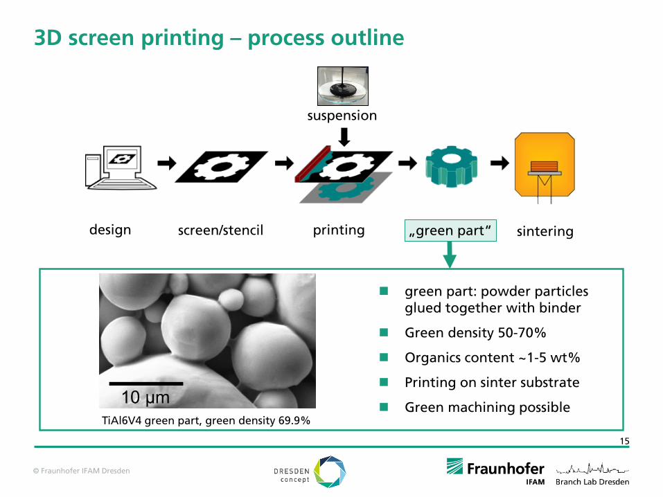
© Fraunhofer IFAM Dresden
green part: powder particlesglued together with binder
Green density 50-70%
Organics content ~1-5 wt%
Printing on sinter substrate
Green machining possible
15
design screen/stencil „green part“ sinteringprinting
suspension
binder
particle
TiAl6V4 green part, green density 69.9%
3D screen printing – process outline

© Fraunhofer IFAM Dresden
Removal of binder/additives
Select atmospheres/pressures
FTIR assisted optimization
Sintering to nearly full density
Shrinkage ~15-20 % (lin.)heat treatment at Fraunhofer IFAM, branch lab Dresden
16
design screen/stencil „green part“ sinteringprinting
suspension
3D screen printing – process outline

© Fraunhofer IFAM Dresden
3D screen printing– process characteristics
Process properties:
Resolution: 60 - 80 µm
Typical dimensions / highest height: small parts preferred
Build rate: 60 – 120 cm3/h
Support structures: not necessary
Materials: Metals + Ceramics with d90< 1/3 of mesh opening
3D Screen Printing Unit at Fraunhofer IFAM
© Fraunhofer IFAM Dresden
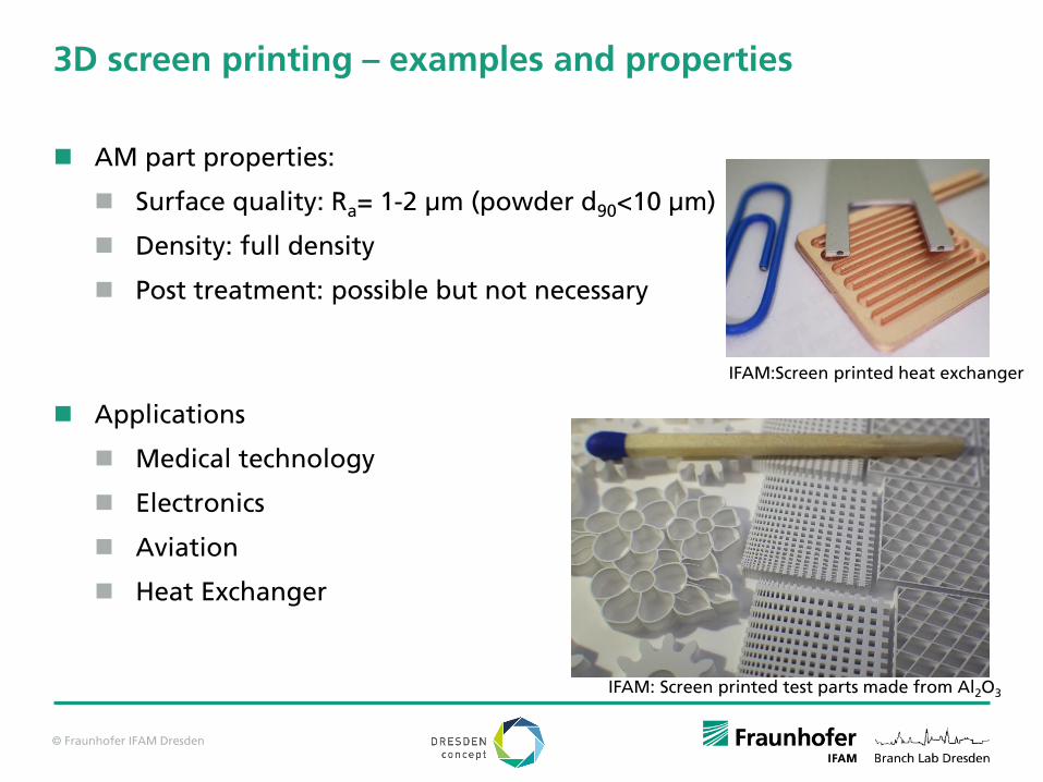
3D screen printing – examples and properties
AM part properties:
Surface quality: Ra= 1-2 µm (powder d90<10 µm)
Density: full density
Post treatment: possible but not necessary
IFAM:Screen printed heat exchanger
Applications
Medical technology
Electronics
Aviation
Heat Exchanger
IFAM: Screen printed test parts made from Al2O3
© Fraunhofer IFAM Dresden
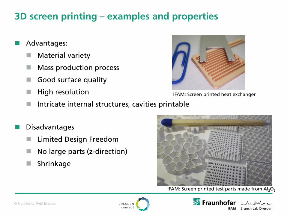
3D screen printing – examples and properties
Advantages:
Material variety
Mass production process
Good surface quality
High resolution
Intricate internal structures, cavities printable
IFAM: Screen printed heat exchanger
Disadvantages
Limited Design Freedom
No large parts (z-direction)
Shrinkage
IFAM: Screen printed test parts made from Al2O3

© Fraunhofer IFAM Dresden
Source: Loughborough University, Additive Manufacturing Group
Process - Step by Step
1. A sheet of material is placed on a cutting bed
2. The sheet is cutted / milled in the desired shape (laser / milling cutter)
3. Sheets are bonded to the previous layers using an adhesive (LOM) or welding (UAM)
4. The next layer is added.
(Steps two and three can be reversed and alternatively, the material can be cut before being positioned and bonded)
Process available for materials like:
Paper, plastic sheets Layer objective Modelling (LOM)
Metallic sheets Ultrasonic additive manufacturing (UAM)
2.3. Solid State TECHNOLOGIES
2.3.6 Sheet Lamination
© Fraunhofer IFAM Dresden
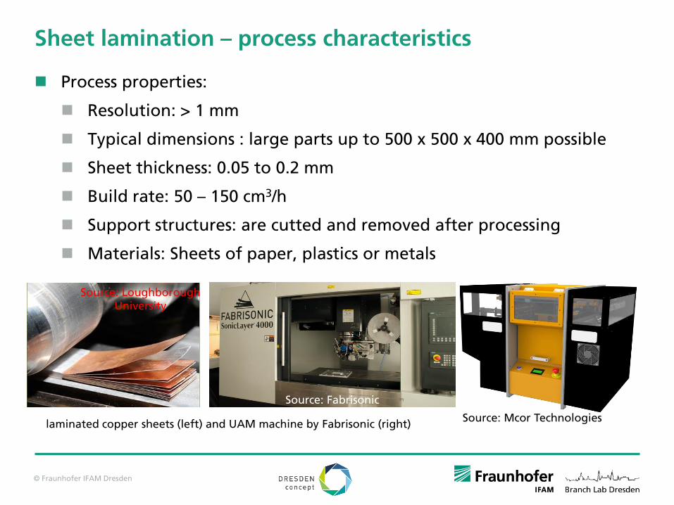
Sheet lamination – process characteristics
Process properties:
Resolution: > 1 mm
Typical dimensions : large parts up to 500 x 500 x 400 mm possible
Sheet thickness: 0.05 to 0.2 mm
Build rate: 50 – 150 cm3/h
Support structures: are cutted and removed after processing
Materials: Sheets of paper, plastics or metals
Source: Mcor Technologies
Source: Fabrisonic
laminated copper sheets (left) and UAM machine by Fabrisonic (right)
Source: Loughborough University

© Fraunhofer IFAM Dresden
Sheet Lamination– examples and properties
AM part properties:
Surface quality: good
Density: full density
Post treatment: not necessary
Applications
Decorative Objects (LOM)
Models for Casting Molds (LOM)
Injection molding dies (UAM)
Parts with internal channels
Source:Tedata.com
Source: Raprotec GmbH
Source: Fabrisonic
Industrial Suppliers:
Fabrisonic (USA)
Mcor (Ireland)
© Fraunhofer IFAM Dresden
Sheet Lamination
Advantages
Low cost
Parts can be used immediately after the process (no need for post curing)
High build rate 250 – 350 cm3/h
Multimaterial systems possible
Disadvantages
Material waste
Limited resolution (especially in z-direction)
No structural parts (low mechanical strength)
© Fraunhofer IFAM Dresden
http://am-power.de/insights/
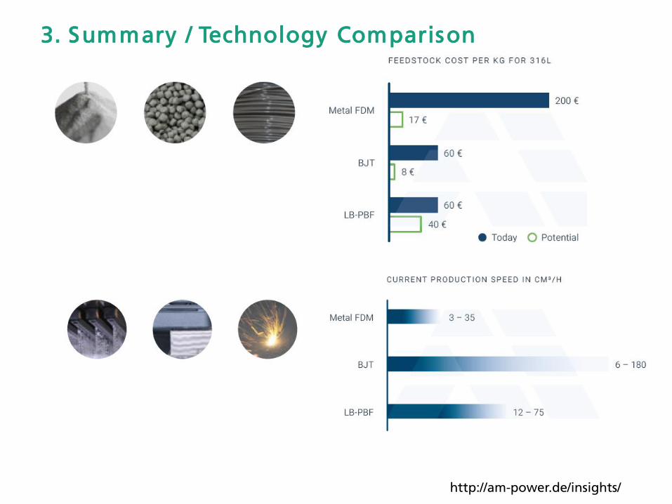
3. Summary / Technology Comparison

© Fraunhofer IFAM Dresden
3. Summary / Technology Comparison
http://am-power.de/insights/
© Fraunhofer IFAM Dresden
http://am-power.de/insights/
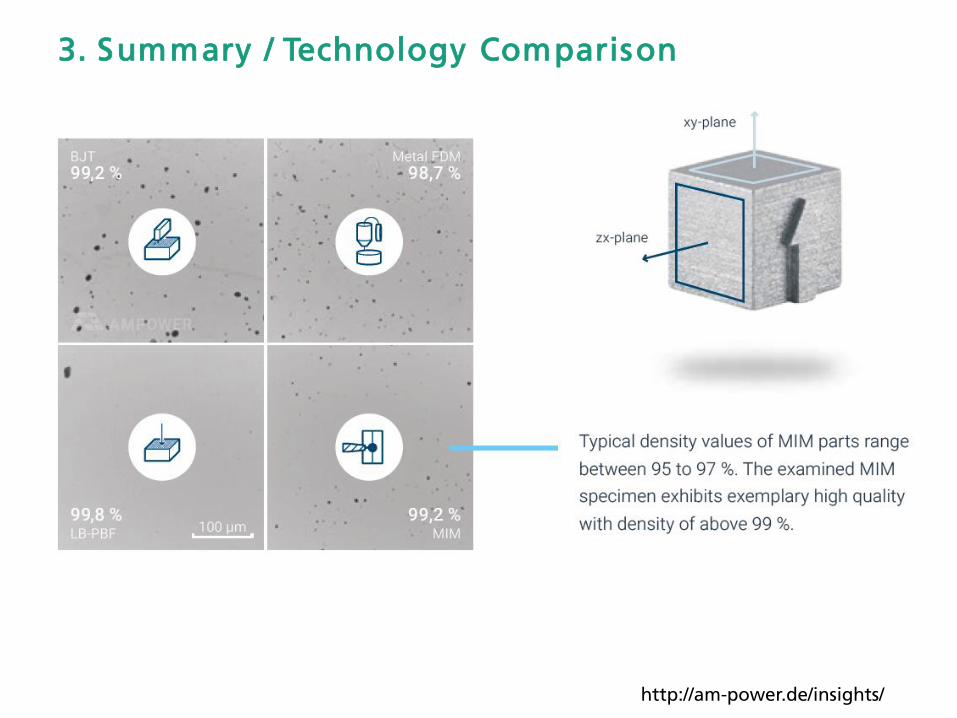
3. Summary / Technology Comparison

© Fraunhofer IFAM Dresden
http://am-power.de/insights/
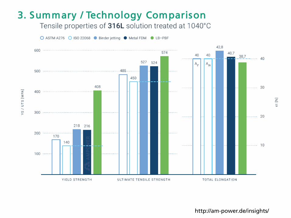
3. Summary / Technology Comparison

© Fraunhofer IFAM Dresden
http://am-power.de/insights/
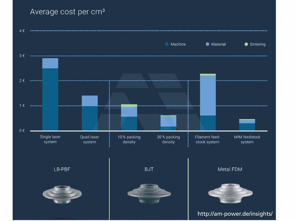
3. Summary / Technology Comparison
© Fraunhofer IFAM Dresden
http://am-power.de/insights/
3. Summary / Technology Comparison

© Fraunhofer IFAM Dresden http://am-power.de/insights/
© Fraunhofer IFAM Dresden
http://am-power.de/insights/
Top Related