


Languages
Pages
Legal

LT3581
13581fb
For more information www.linear.com/LT3581
TYPICAL APPLICATION
DESCRIPTION
3.3A Boost/Inverting DC/DC Converter with Fault Protection
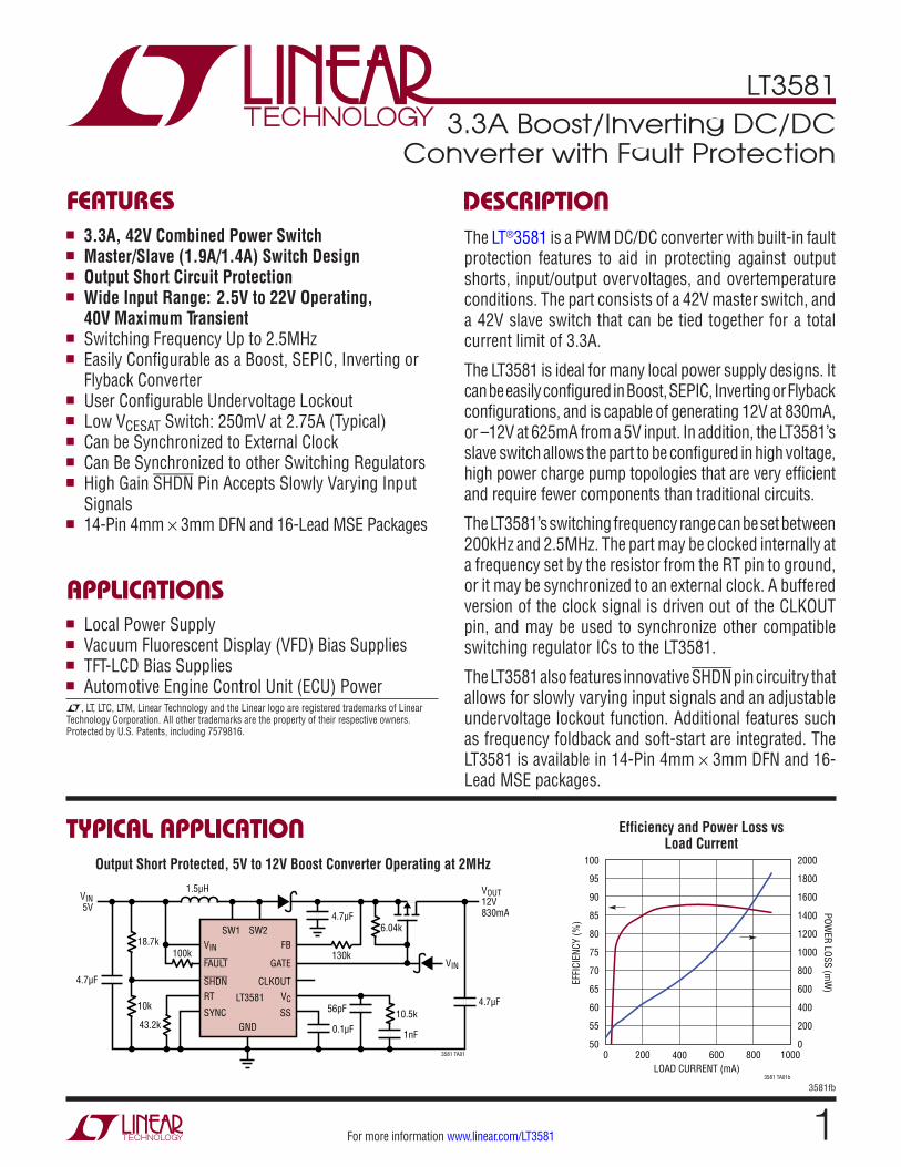
The LT®3581 is a PWM DC/DC converter with built-in fault protection features to aid in protecting against output shorts, input/output overvoltages, and overtemperature conditions. The part consists of a 42V master switch, and a 42V slave switch that can be tied together for a total current limit of 3.3A.
The LT3581 is ideal for many local power supply designs. It can be easily configured in Boost, SEPIC, Inverting or Flyback configurations, and is capable of generating 12V at 830mA, or –12V at 625mA from a 5V input. In addition, the LT3581’s slave switch allows the part to be configured in high voltage, high power charge pump topologies that are very efficient and require fewer components than traditional circuits.
The LT3581’s switching frequency range can be set bet ween 200kHz and 2.5MHz. The part may be clocked internally at a frequency set by the resistor from the RT pin to ground, or it may be synchronized to an external clock. A buffered version of the clock signal is driven out of the CLKOUT pin, and may be used to synchronize other compatible switching regulator ICs to the LT3581.
The LT3581 also features innovative SHDN pin circuitry that allows for slowly varying input signals and an adjustable undervoltage lockout function. Additional features such as frequency foldback and soft-start are integrated. The LT3581 is available in 14-Pin 4mm × 3mm DFN and 16-Lead MSE packages.
Output Short Protected, 5V to 12V Boost Converter Operating at 2MHz
FEATURES
APPLICATIONS
n 3.3A, 42V Combined Power Switchn Master/Slave (1.9A/1.4A) Switch Designn Output Short Circuit Protection n Wide Input Range: 2.5V to 22V Operating,
40V Maximum Transientn Switching Frequency Up to 2.5MHzn Easily Configurable as a Boost, SEPIC, Inverting or
Flyback Convertern User Configurable Undervoltage Lockout n Low VCESAT Switch: 250mV at 2.75A (Typical)n Can be Synchronized to External Clockn Can Be Synchronized to other Switching Regulatorsn High Gain SHDN Pin Accepts Slowly Varying Input
Signalsn 14-Pin 4mm × 3mm DFN and 16-Lead MSE Packages
n Local Power Supplyn Vacuum Fluorescent Display (VFD) Bias Suppliesn TFT-LCD Bias Suppliesn Automotive Engine Control Unit (ECU) PowerL, LT, LTC, LTM, Linear Technology and the Linear logo are registered trademarks of Linear Technology Corporation. All other trademarks are the property of their respective owners. Protected by U.S. Patents, including 7579816.
VIN5V
VIN
6.04k
100k 130k
43.2k
4.7µF
1.5µH
1nF
3581 TA01
0.1µF
4.7µF10.5k
4.7µF
VOUT12V830mA
SW1 SW2FB
CLKOUT
GATE
VC
SS
VIN
RT
GNDSYNC
FAULT
SHDN
LT358156pF
18.7k
10k
LOAD CURRENT (mA)0
50
EFFI
CIEN
CY (%
)
POWER LOSS (m
W)
55
65
70
75
400
100
95
3581 TA01b
60
200 1000800600
80
85
90
0
200
600
2000
1200
1400
1600
1800
400
800
1000
Efficiency and Power Loss vs Load Current
LT3581
23581fb
For more information www.linear.com/LT3581
PIN CONFIGURATION
ABSOLUTE MAXIMUM RATINGS
VIN Voltage ................................................. –0.3V to 40VSW1/SW2 Voltage ..................................... –0.4V to 42VRT Voltage ................................................... –0.3V to 5VSS, FB Voltage .......................................... –0.3V to 2.5VVC Voltage .................................................... –0.3V to 2VSHDN Voltage ............................................ –0.3V to 40VSYNC Voltage ............................................ –0.3V to 5.5VGATE Voltage ............................................. –0.3V to 80VFAULT Voltage ............................................ –0.3V to 40V
(Note 1)
1
2
3
4
5
6
7
14
13
12
11
10
9
8
SYNC
SS
RT
SHDN
CLKOUT
SW2
SW2
FB
VC
GATE
FAULT
VIN
SW1
SW1
TOP VIEW
DE14 PACKAGE14-PIN (4mm × 3mm) PLASTIC DFN
15GND
TJMAX = 125°C, θJA = 43°C/W, θJC = 4.3°C/W
EXPOSED PAD (PIN 15) IS GND, MUST BE SOLDERED TO PCB
12345678
FBVC
GATEFAULT
VINSW1SW1SW1
161514131211109
SYNCSSRTSHDNCLKOUTSW2SW2SW2
TOP VIEW
MSE PACKAGE16-LEAD PLASTIC MSOP
17GND
TJMAX = 125°C, θJA = 45°C/W, θJC = 10°C/W EXPOSED PAD (PIN 17) IS GND, MUST BE SOLDERED TO PCB
ORDER INFORMATIONLEAD FREE FINISH TAPE AND REEL PART MARKING* PACKAGE DESCRIPTION TEMPERATURE RANGE
LT3581EDE#PBF LT3581EDE#TRPBF 3581 14-Lead (4mm × 3mm) Plastic DFN –40°C to 125°C
LT3581IDE#PBF LT3581IDE#TRPBF 3581 14-Lead (4mm × 3mm) Plastic DFN –40°C to 125°C
LT3581HDE#PBF LT3581HDE#TRPBF 3581 14-Lead (4mm × 3mm) Plastic DFN –40°C to 150°C
LT3581EMSE#PBF LT3581EMSE#TRPBF 3581 16-Lead Plastic MSOP –40°C to 125°C
LT3581IMSE#PBF LT3581IMSE#TRPBF 3581 16-Lead Plastic MSOP –40°C to 125°C
Consult LTC Marketing for parts specified with wider operating temperature ranges. *The temperature grade is identified by a label on the shipping container. Consult LTC Marketing for information on non-standard lead based finish parts.For more information on lead free part marking, go to: http://www.linear.com/leadfree/ For more information on tape and reel specifications, go to: http://www.linear.com/tapeandreel/
FAULT Current .....................................................±500µACLKOUT Voltage .......................................... –0.3V to 3VCLKOUT Current.......................................................1mAOperating Junction Temperature Range
LT3581E (Notes 2, 4) ......................... –40°C to 125°C LT3581I (Notes 2, 4) .......................... –40°C to 125°C
LT3581H (Notes 2, 4) .........................–40°C to 150°CStorage Temperature Range .................. –65°C to 150°C
LT3581
33581fb
For more information www.linear.com/LT3581
ELECTRICAL CHARACTERISTICS
PARAMETER CONDITIONS MIN TYP MAX UNITS
Minimum Input Voltage l 2.3 2.5 V
VIN Overvoltage Lockout 22.1 23.5 25 V
Positive Feedback Voltage l 1.195 1.215 1.230 V
Negative Feedback Voltage l 3 9 16 mV
Positive FB Pin Bias Current VFB = Positive Feedback Voltage, Current into Pin l 81 83.3 85 µA
Negative FB Pin Bias Current VFB = Negative Feedback Voltage, Current out of Pin l 81 83.3 85.5 µA
Error Amp Transconductance ΔI = 10μA 270 µmhos
Error Amp Voltage Gain 70 V/V
Quiescent Current Not Switching 1.9 2.3 mA
Quiescent Current in Shutdown VSHDN = 0V 0 1 µA
Reference Line Regulation 2.5V ≤ VIN ≤ 20V 0.01 0.05 %/V
Switching Frequency, fOSC RT = 34k l 2.25 2.5 2.75 MHz
RT = 432k l 180 200 220 kHz
Switching Frequency in Foldback Compared to Normal fOSC 1/6 ratio
Switching Frequency Range Free-Running or Synchronizing l 200 2500 kHz
SYNC High Level for Synchronization l 1.3 V
SYNC Low Level for Synchronization l 0.4 V
SYNC Clock Pulse Duty Cycle VSYNC = 0V to 2V 20 80 %
Recommended Minimum SYNC Ratio fSYNC/fOSC
3/4
Minimum Off-Time 45 ns
Minimum On-Time 55 ns
SW1 Current Limit At All Duty Cycles l 1.9 2.4 3 A
Current Sharing (SW2/SW1) 78 %
SW1 + SW2 Current Limit At All Duty Cycles, SW2/SW1 = 78% (Note 3) l 3.3 4.3 5.4 A
Switch VCESAT SW1 & SW2 Tied Together, ISW1 + ISW2 = 2.75A 250 mV
SW1 Leakage Current VSW1 = 5V 0.01 1 µA
SW2 Leakage Current VSW2 = 5V 0.01 1 µA
The l denotes the specifications which apply over the full operating temperature range, otherwise specifications are at TA = 25°C. VIN = 5V, VSHDN = VIN, VFAULT = VIN, unless otherwise noted. (Note 2).
LT3581
43581fb
For more information www.linear.com/LT3581
Note 1: Stresses beyond those listed under Absolute Maximum Ratings may cause permanent damage to the device. Exposure to any Absolute Maximum Rating condition for extended periods may affect device reliability and lifetime.Note 2: The LT3581E is guaranteed to meet performance specifications from 0°C to 125°C. Specifications over the –40°C to 125°C junction temperature range are assured by design, characterization and correlation with statistical process controls. The LT3581I is guaranteed over the full –40°C to 125°C operating junction temperature range. The LT3581H is
ELECTRICAL CHARACTERISTICS The l denotes the specifications which apply over the full operating temperature range, otherwise specifications are at TA = 25°C. VIN = 5V, VSHDN = VIN, VFAULT = VIN, unless otherwise noted. (Note 2).
PARAMETER CONDITIONS MIN TYP MAX UNITS
Soft-Start Charge Current VSS = 30mV, Current Flows Out of SS pin l 5.7 8.7 11.3 µA
Soft-Start Discharge Current Part in FAULT, VSS = 2.1V, Current Flows into SS Pin l 5.7 8.7 11.3 µA
Soft-Start High Detection Voltage Part in FAULT l 1.65 1.8 1.95 V
Soft-Start Low Detection Voltage Part Exiting FAULT l 30 50 85 mV
SHDN Minimum Input Voltage High Active Mode, SHDN Rising (LT3581E, LT3581I) Active Mode, SHDN Rising (LT3581H) Active Mode, SHDN Falling (LT3581E, LT3581I, LT3581H)
l
l
l
1.27 1.27 1.24
1.33 1.33 1.3
1.41 1.44 1.38
V V V
SHDN Input Voltage Low Shutdown Mode l 0.3 V
SHDN Pin Bias Current VSHDN = 3V VSHDN = 1.3V VSHDN = 0V
9.7
40 11.4
0
60 13.4 0.1
µA µA µA
CLKOUT Output Voltage High CCLKOUT = 50pF 1.9 2.1 2.3 V
CLKOUT Output Voltage Low CCLKOUT = 50pF 5 200 mV
CLKOUT Duty Cycle TJ = 25°C 42 %
CLKOUT Rise Time CCLKOUT = 50pF 12 ns
CLKOUT Fall Time CCLKOUT = 50pF 8 ns
GATE Pull Down Current VGATE = 3V (LT3581E, LT3581I) VGATE = 3V (LT3581H) VGATE = 80V (LT3581E, LT3581I, LT3581H)
l
l
l
800 700 800
933 900 933
1100 1100 1100
µA µA µA
GATE Leakage Current VGATE = 50V, GATE Off 0.01 1 µA
FAULT Output Voltage Low 50μA into FAULT Pin (LT3581E, LT3581I) 50μA into FAULT Pin (LT3581H)
l
l
100 100
300 400
mV mV
FAULT Leakage Current VFAULT = 40V, FAULT Off 0.01 1 µA
FAULT Input Voltage Low l 700 750 800 mV
FAULT Input Voltage High l 950 1000 1050 mV
guaranteed over the full –40°C to 150°C operating junction temperature range. Operating lifetime is derated at junction temperatures greater than 125°C.Note 3: Current limit guaranteed by design and/or correlation to static test.Note 4: This IC includes overtemperature protection that is intended to protect the device during momentary overload conditions. Junction temperature will exceed 150°C when overtemperature protection is active. Continuous operation over the specified maximum operating junction temperature may impair device reliability.

LT3581
53581fb
For more information www.linear.com/LT3581
TYPICAL PERFORMANCE CHARACTERISTICS
Switch Fault Current Limit vs Temperature
Positive Feedback Voltage vs Temperature
CLKOUT Duty Cycle vs Temperature
Oscillator Frequency Frequency Foldback Gate Current vs Gate Voltage
Switch Fault Current Limit vs Duty Cycle
Switch Saturation Voltage with SW1 and SW2 Tied Together
Current Sharing Between SW1 and SW2 When Tied Together
TA = 25°C, unless otherwise noted.
DUTY CYCLE (%)20
0
SW1
+ SW
2 FA
ULT
CURR
ENT
LIM
IT (A
)
1
2
3
4
30 50 70 80
3581 G01
5
6
40 60
SW1 + SW2 CURRENT (A)0
SATU
RATI
ON V
OLTA
GE (m
V)200
250
300
54
3581 G02
150
100
0321
50
450
400
350
SW1 + SW2 CURRENT (A)0
CURR
ENT
SHAR
ING
= SW
2/SW
1 (%
)
50
60
70
54
3581 G03
40
30
0321
10
20
100
90
80
TEMPERATURE (°C)–50 –250
SW1
+ SW
2 FA
ULT
CURR
ENT
LIM
IT (A
)
1
2
3
4
0 50 125 150
3581 G04
5
6
25 75 100 –50 –25 0 50 125 15025 75 100TEMPERATURE (°C)
1.2100
POSI
TIVE
FB
VOLT
AGE
(V)
1.2125
1.2200
3581 G05
1.2175
1.2150
TEMPERATURE (°C)–75 –50 –25
10
CLKO
UT D
C (%
)
20
30
40
50
0 50 125 150
3581 G06
60
80
70
25 75 100
–50 –25 0 50 125 15025 75 100TEMPERATURE (°C)
0
FREQ
UENC
Y (k
Hz)
3200
3581 G07
2800
2400
2000
1600
1200
800
400
RT = 34k
RT = 432k
FB VOLTAGE (V)0
0
SWIT
CHIN
G FR
EQUE
NCY
RATI
O (f S
W/f O
SC)
1/41/51/6
1/2
1/3
1
0.2 0.4 0.6 0.8
3581 G08
1.0 1.2
BOOSTINGCONFIGURATIONS
INVERTINGCONFIGURATIONS
0 60 8020 40GATE VOLTAGE (V)
0
GATE
CUR
RENT
(µA)
1000
3581 G09
900
800
700
600
500
400
200
100
300
125°C
–40°C
25°C

LT3581
63581fb
For more information www.linear.com/LT3581
TYPICAL PERFORMANCE CHARACTERISTICS
SHDN Pin Current SHDN Pin Current Internal UVLO
CLKOUT Rise Time at 1MHz VIN OVLOFAULT Input Voltage Threshold with Hysteresis
Gate Current vs SS VoltageCommanded Current Limit vs SS Voltage
SHDN Voltage Threshold with Hysteresis
SS VOLTAGE (V)0
0
GATE
CUR
RENT
(µA)
100
300
500
700
200
400
600
800
0.25 0.50 0.75 1.00
3581 G10
1.25 1.50
900
1000
SS VOLTAGE (V)0
0
SW1
+ SW
2 CU
RREN
T (A
)
1
2
3
0.2 0.4 0.6 0.8
3580 G11
1.0 1.2
4
5
–50 –25 0 50 125 15025 75 100TEMPERATURE (°C)
1.20
SHDN
VOL
TAGE
(V)
1.22
1.26
1.28
1.30
1.40
1.34
3581 G12
1.24
1.36
1.38
1.32
SHDN RISING
SHDN FALLING
SHDN VOLTAGE (V)0
0
SHDN
PIN
CUR
RENT
(µA)
4
8
12
16
20
24
28
32
0.4 1.0 1.40.2 1.20.6 1.60.8 1.8 2.0
3581 G13
125°C
–40°C
25°C
SHDN VOLTAGE (V)0
SHDN
PIN
CUR
RENT
(µA)
200
250
15 25
3581 G14
150
100
5 10 20 403530
50
0
125°C
–40°C
25°C
–50 –25 0 50 125 15025 75 100TEMPERATURE (°C)
2.20
V IN
VOLT
AGE
(V)
2.22
2.26
2.28
2.30
2.40
2.34
3581 G15
2.24
2.36
2.38
2.32
–50 –25 0 50 125 15025 75 100TEMPERATURE (°C)
16
V IN
VOLT
AGE
(V)
18
20
30
24
3581 G17
26
28
22
–50 –25 0 50 125 15025 75 100TEMPERATURE (°C)
0
FAUL
T VO
LTAG
E (V
)
1.25
0.50
3581 G18
0.75
1.00
0.25
FAULT RISING
FAULT FALLING
0 50 250200150100CLKOUT CAPACITIVE LOAD (pF)
0
CLKO
UT R
ISE
OR F
ALL
TIM
E (n
s)
5
15
20
25
50
35
3581 G16
10
40
45
30
CLKOUT FALL TIME
CLKOUT RISE TIME
TA = 25°C, unless otherwise noted.

LT3581
73581fb
For more information www.linear.com/LT3581
PIN FUNCTIONSFB (Pin 1/Pin 1): Positive and Negative Feedback Pin. For a Boost or Inverting Converter, tie a resistor from the FB pin to VOUT according to the following equations:
RFB = VOUT –1.215V83.3•10–6
;Boost or SEPIC Converter
RFB = | VOUT | + 9mV83.3•10–6
; Inverting Converter
VC (Pin 2/Pin 2): Error Amplifier Output Pin. Tie external com pensation network to this pin.
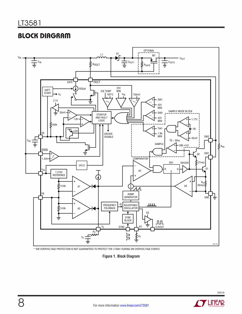
GATE (Pin 3/Pin 3): PMOS Gate Drive Pin. The GATE pin is a pull-down current source, used to drive the gate of an external PMOS for output short circuit protection or output disconnect. The GATE pin current increases linearly with the SS pin’s voltage, with a maximum pull-down current of 933µA at SS voltages exceeding 500mV. Note that if the SS voltage is greater than 500mV and the GATE pin voltage is less than 2V, then the GATE pin looks like a 2kΩ impedance to ground. See the Appendix for more information.
FAULT (Pin 4/Pin 4): Fault Indication Pin. This active low, bidirectional pin can either be pulled low (below 750mV) by an external source, or internally by the chip to indicate a fault. When pulled low, this pin causes the power switches to turn off, the GATE pin to become high impedance, the CLKOUT pin to become disabled, and the SS pin to go through a charge/discharge sequence. The end/absence of a fault is indicated when the voltage on this pin exceeds 1V. A pull-up resistor or current source is needed on this pin to pull it above 1V in the absence of a fault.
VIN (Pin 5/Pin 5): Input Supply Pin. Must be locally by-passed.
SW1 (Pins 6, 7/Pins 6,7, 8): Master Switch Pin. This is the collector of the internal master NPN power switch. Minimize the metal trace area connected to this pin to minimize EMI.
SW2 (Pins 8, 9/Pins 9, 10, 11): Slave Switch Pin. This is the collector of the internal slave NPN power switch. Minimize the metal trace area connected to this pin to minimize EMI.
CLKOUT (Pin 10/Pin 12): Clock Output Pin. Use this pin to synchronize one or more other compatible switching regulator ICs to the LT3581. The clock that this pin outputs runs at the same frequency as the internal oscillator of the part or as the SYNC pin. CLKOUT may also be used as a temperature monitor since the CLKOUT pin’s duty cycle varies linearly with the part’s junction temperature. Note that the CLKOUT pin is only meant to drive capacitive loads up to 50pF.
SHDN (Pin 11/Pin 13): Shutdown Pin. In conjunction with the UVLO (undervoltage lockout) circuit, this pin is used to enable/disable the chip and restart the soft-start sequence. Drive below 300mV to disable the chip. Drive above 1.33V (typical) to activate the chip and restart the soft-start sequence. Do not float this pin.
RT (Pin 12/Pin 14): Timing Resistor Pin. Adjusts the LT3581’s switching frequency. Place a resistor from this pin to ground to set the frequency to a fixed free running level. Do not float this pin.
SS (Pin 13/Pin 15): Soft-Start Pin. Place a soft-start capacitor here. Upon start-up, the SS pin will be charged by a (nominally) 250k resistor to about 2.1V. During a fault, the SS pin will be slowly charged up and eventually discharged as part of a timeout sequence (see the State Diagram for more information on the SS pin’s role during a fault event).
SYNC (Pin 14/Pin 16): To synchronize the switching frequency to an outside clock, simply drive this pin with a clock. The high voltage level of the clock must exceed 1.3V, and the low level must be less than 0.4V. Drive this pin to less than 0.4V to revert to the internal free running clock. See the Applications Information section for more information.
GND (Exposed Pad Pin 15/Exposed Pad Pin 17): Ground. Exposed pad must be soldered directly to local ground plane.
(DFN/MSOP)
LT3581
83581fb
For more information www.linear.com/LT3581
BLOCK DIAGRAM
FREQUENCYFOLDBACK
RAMPGENERATOR
COMPARATOR
DRIVERDISABLE
SSLDO
VC
RGATE
14.6k
14.6k
SR1
A3
SYNC CLKOUT
÷N
SS
SHDN
COUT1
SW1
SW2
FB
27mΩ
RS20mΩ
GND
RT
RT
RC
CC
VC
RFB
DRIVER
D1
VIN
SYNCBLOCK
UVLOR
SQ
3581 BD
–
+A4
Q2
+–
TD ~ 30ns
VBE • 0.9
1.17V
45mV
L1
FB
∑
ADJUSTABLEOSCILLATOR
–
+
–
+A1
A3
CSS
CIN
1.33V
+–
–+
+–
250k
2.1V
1.8V
50mV
SOFT-START
STARTUPAND FAULT
LOGIC
COUT2
VOUTVIN
M1
GATE
OPTIONAL
SAMPLE MODE BLOCK
RFAULT
FAULT
933µA
– + +–+ – +–
+– +
–
+–
+–
DIE TEMP22VMIN
165°C VIN 750mV
SW1**
**SW OVERVOLTAGE PROTECTION IS NOT GUARANTEED TO PROTECT THE LT3581 DURING SW OVERVOLTAGE EVENTS
**
ISW1
42VMIN
42VMIN
1.9AMIN
SW2
SAMPLE
–
+A2
1.215VREFERENCE
Q1
Figure 1. Block Diagram

LT3581
93581fb
For more information www.linear.com/LT3581
SHDN < 1.33V (TYPICAL)or
VIN < 2.3V (TYPICAL)
SHDN > 1.33V (TYPICAL)AND
VIN > 2.3V (TYPICAL)
FAULT DETECTED
• SS CHARGES UP• IGATE OFF• FAULT PIN PULLED LOW INTERNALLY BY LT3581• SWITCHER DISABLED• CLKOUT DISABLED
SS < 50mV
IF |VOUT| DROPS CAUSING:FB < 1.17V (BOOST)
ORFB > 45mV (INVERTING)
FAULT1
FAULT1
SS > 1.8V ANDNO FAULT1 CONDITIONS STILL DETECTED
SS < 50mVFAULT1
FAULT1
FAULT1
FAULT1
FAULT2
FAULT PIN > 1.0V
FAULT1 = OVER VOLTAGE PROTECTION ON VIN (VIN > 22V MIN) OVER TEMPERATURE (TJUNCTION > 165°C) OVER CURRENT ON SW1 (ISW1 > 1.9A MIN) OVER VOLTAGE PROTECTION ON SW1 (VSW1 > 42V MIN) OVER VOLTAGE PROTECTION ON SW2 (VSW2 > 42V MIN) FAULT2 = FAULT PULLED LOW EXTERNALLY (FAULT < 0.75V)
CHIP OFF
• ALL SWITCHES DISABLED• IGATE OFF• FAULTS CLEARED
INITIALIZE
• SS PULLED LOW
NORMAL MODE
• NORMAL OPERATION• CLKOUT ENABLED WHEN SS > 1.8V
SAMPLE MODE
• Q1 & Q2 SWITCHES FORCED ON EVERY CYCLE FOR AT LEAST MINIMUM ON TIME• IGATE FULLY ACTIVATED WHEN SS > 500mV
SOFT START
• IGATE ENABLED • SS CHARGES UP• SWITCHER ENABLED
POST FAULT DELAY
• SS SLOWLY DISCHARGES
LOCAL FAULT OVER
• INTERNAL FAULT PIN PULLDOWN RELEASED BY LT3581• SS CONTINUES DISCHARGING TO GND
3581 SD
STATE DIAGRAM
Figure 2. State Diagram

LT3581
103581fb
For more information www.linear.com/LT3581
OPERATIONOPERATION – OVERVIEW
The LT3581 uses a constant-frequency, current mode con-trol scheme to provide excellent line and load regulation. The part’s undervoltage lockout (UVLO) function, together with soft-start and frequency foldback, offers a controlled means of starting up. Fault features are incorporated in the LT3581 to aid in the detection of output shorts, over-volt-age, and overtemperature conditions. Refer to the Block Diagram (Figure 1) and the State Diagram (Figure 2) for the following description of the part’s operation.
OPERATION – START-UP
Several functions are provided to enable a very clean start-up for the LT3581:
Precise Turn-On Voltage
The SHDN pin is compared to an internal voltage reference to give a precise turn on voltage level. Taking the SHDN pin above 1.33V (typical) enables the part. Taking the SHDN pin below 300mV shuts down the chip, resulting in extremely low quiescent current. The SHDN pin has 30mV of hysteresis to protect against glitches and slow ramping.
Undervoltage Lockout (UVLO)
The SHDN pin can also be used to create a configurable UVLO. The UVLO function sets the turn on/off of the LT3581 at a desired input voltage (VINUVLO). Figure 3 shows how a resistor divider (or single resistor) from VIN to the SHDN pin can be used to set VINUVLO. RUVLO2 is optional. It may be left out, in which case set it to infinite in the equation below. For increased accuracy, set RUVLO2 ≤ 10k. Pick RUVLO1 as follows:
RUVLO1 = VINUVLO –1.33V1.33V
RUVLO2
+ 11.6µA
RUVLO2(OPTIONAL)
1.33VRUVLO1
3581 F03
VINVIN
ACTIVE/LOCKOUT
GND
11.6µAAT 1.33V
–
+
SHDN
Figure 3. Configurable UVLO
The LT3581 also has internal UVLO circuitry that disables the chip when VIN < 2.3V (typical).
Soft-Start of Switch Current
The soft-start circuitry provides for a gradual ramp-up of the switch current (refer to Commanded Current Limit vs SS Voltage in Typical Performance Characteristics). When the part is brought out of shutdown, the external SS capacitor is first discharged which resets the states of the logic circuits in the chip. Then an integrated 250k resistor pulls the SS pin to ~1.8V. The ramp rate of the SS pin voltage is set by this 250k resistor and the external capacitor connected to this pin. Once SS gets to 1.8V, the CLKOUT pin is enabled, and an internal regulator pulls the pin up quickly to ~2.1V. Typical values for the external soft-start capacitor range from 100nF to 1μF.
Soft-Start of External PMOS (if used)
The soft-start circuitry also gradually ramps up the GATE pin pull-down current which allows an external PMOS to slowly turn on (M1 in Block Diagram). The GATE pin current increases linearly with the SS voltage, with a maximum current of 933µA when the SS voltage gets above 500mV. Note that if the GATE pin voltage is less than 2V for SS voltages exceeding 500mV, then the GATE pin impedance to ground is 2kΩ. The soft turn on of the external PMOS helps limit inrush current at start-up, making hot-plugs of LT3581s feasible and safe.
LT3581
113581fb
For more information www.linear.com/LT3581
Sample Mode
Sample Mode is the mechanism used by the LT3581 to aid in the detection of output shorts. It refers to a state of the LT3581 where the master and slave power switches (Q1 and Q2) are turned on for a minimum period of time every clock cycle (or every few clock cycles in frequency foldback) in order to “sample” the inductor current. If the sampled current through Q1 exceeds the master switch cur-rent limit of 1.9A (min), the LT3581 triggers an overcurrent fault internally (see Operation-Fault section for details). Sample Mode is active when FB is out of regulation by more than approximately 3.7% (45mV < FB < 1.17V).
Frequency Foldback
The frequency foldback circuit reduces the switching fre-quency when 350mV < FB < 900mV (typical). This feature lowers the minimum duty cycle that the part can achieve, thus allowing better control of the inductor current dur-ing start-up. When the FB voltage is pulled outside of this range, the switching frequency returns to normal.
Note that the peak inductor current at start-up is a function of many variables including load profile, output capacitance, target VOUT, VIN, switching frequency, etc. Test each and every application’s performance at start-up to ensure that the peak inductor current does not exceed the minimum fault current limit.
OPERATION – REGULATION
The following description of the LT3581’s operation as-sumes that the FB voltage is close enough to its regulation target so that the part is not in sample mode. Use the Block Diagram as a reference when stepping through the following description of the LT3581 operating in regulation. At the start of each oscillator cycle, the SR latch (SR1) is set, which turns on the power switches Q1 and Q2. The collector current through the master switch, Q1, is ~1.3 times the collector current through the slave switch, Q2, when the collectors of the two switches are tied together.
OPERATIONQ1’s emitter current flows through a current sense resistor (RS) generating a voltage proportional to the total switch current. This voltage (amplified by A4) is added to a sta-bilizing ramp and the resulting sum is fed into the positive terminal of the PWM comparator A3. When the voltage on the positive input of A3 exceeds the voltage on the negative input, the SR latch is reset, turning off the master and slave power switches. The voltage on the negative input of A3 (VC pin) is set by A1 (or A2), which is simply an amplified difference between the FB pin voltage and the reference voltage (1.215V if the LT3581 is configured as a boost converter, or 9mV if configured as an inverting converter). In this manner, the error amplifier sets the correct peak current level to maintain output regulation.
As long as the part is not in fault (see Operation – Fault section) and the SS pin exceeds 1.8V, the LT3581 drives its CLKOUT pin at the frequency set by the RT pin or the SYNC pin. The CLKOUT pin can be used to synchronize other compatible switching regulator ICs (including additional LT3581s) with the LT3581. Additionally, CLKOUT’s duty cycle varies linearly with the part’s junction temperature, and may be used as a temperature monitor.
OPERATION – FAULT
The LT3581’s FAULT pin is an active low, bidirectional pin that is pulled low to indicate a fault. Each of the following events can trigger a fault in the LT3581:
A. FAULT1 events: 1. SW Overcurrent: a. ISW1 > 1.9A (minimum) b. (ISW1 + ISW2) > 3.3A (minimum) 2. VIN Voltage > 22V (minimum) 3. SW1 Voltage and/or SW2 Voltage > 42V (minimum) 4. Die Temperature > 165°C
B. FAULT2 events: 1. Pulling the FAULT pin low externally
LT3581
123581fb
For more information www.linear.com/LT3581
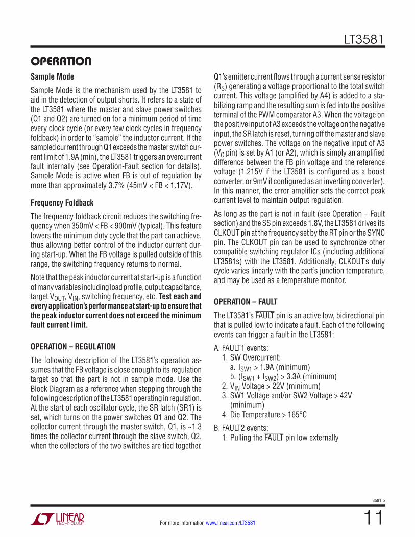
OPERATIONRefer to the State Diagram (Figure 2) for the following description of the LT3581’s operation during a fault event. When a fault is detected, in addition to the FAULT pin being pulled low internally, the LT3581 also disables its CLKOUT pin, turns off its power switches, and the GATE pin becomes high impedance. The external PMOS, M1, turns off when the gate of M1 is pulled up to its source by the external RGATE resistor (see Block Diagram). With the external PMOS turned off, the power path from VIN to VOUT is cut off, protecting power components downstream.
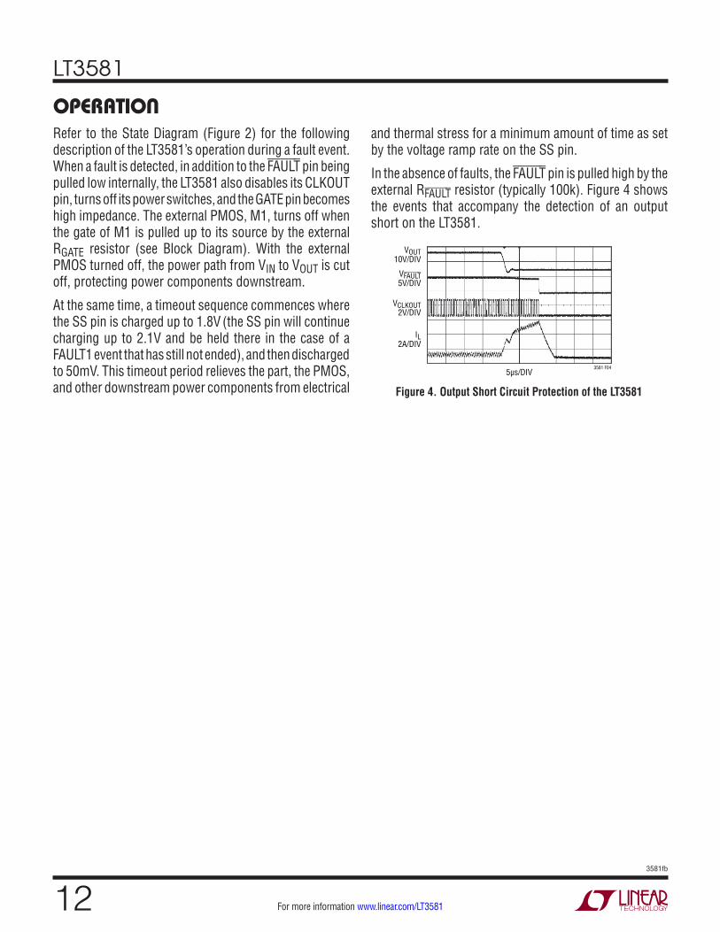
At the same time, a timeout sequence commences where the SS pin is charged up to 1.8V (the SS pin will continue charging up to 2.1V and be held there in the case of a FAULT1 event that has still not ended), and then discharged to 50mV. This timeout period relieves the part, the PMOS, and other downstream power components from electrical Figure 4. Output Short Circuit Protection of the LT3581
VOUT10V/DIV
VCLKOUT2V/DIV
IL2A/DIV
VFAULT5V/DIV
3581 F045µs/DIV
and thermal stress for a minimum amount of time as set by the voltage ramp rate on the SS pin.
In the absence of faults, the FAULT pin is pulled high by the external RFAULT resistor (typically 100k). Figure 4 shows the events that accompany the detection of an output short on the LT3581.
LT3581
133581fb
For more information www.linear.com/LT3581
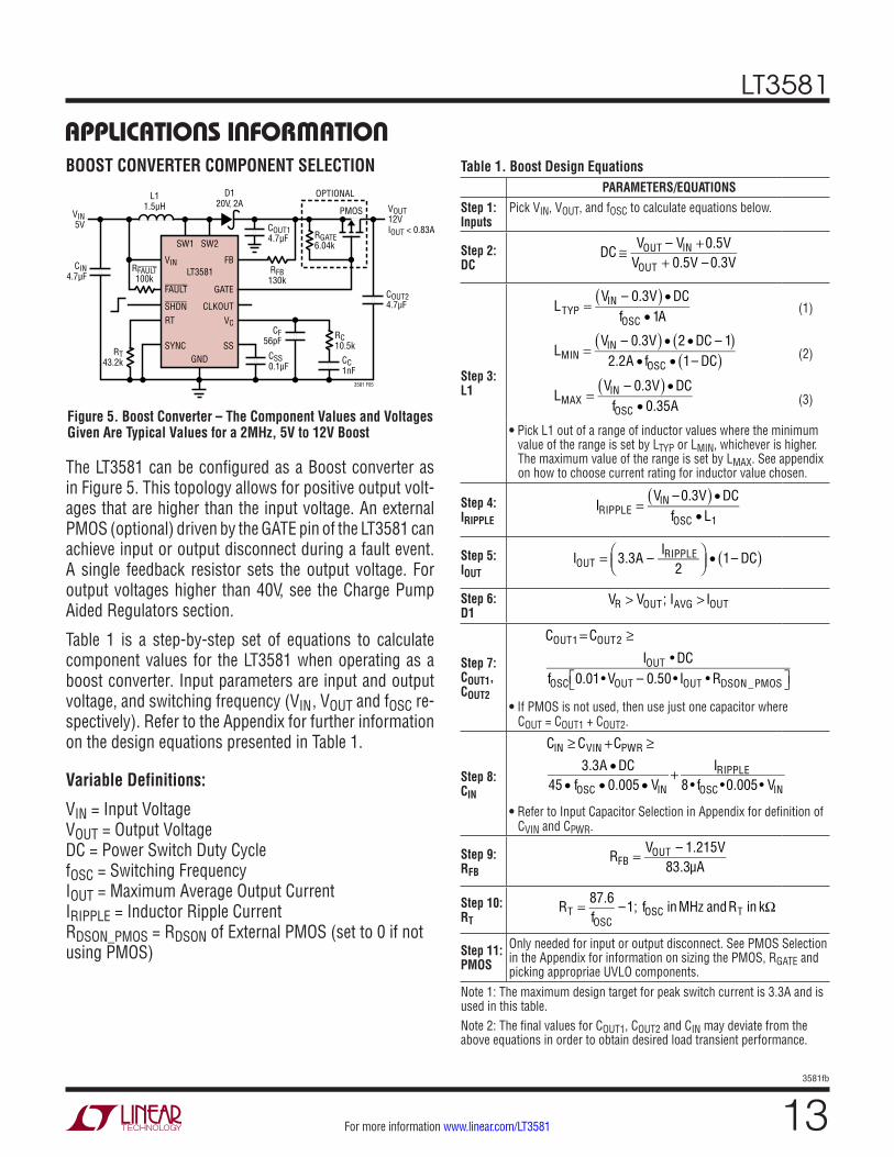
APPLICATIONS INFORMATION
Figure 5. Boost Converter – The Component Values and Voltages Given Are Typical Values for a 2MHz, 5V to 12V Boost
BOOST CONVERTER COMPONENT SELECTIOND1
20V, 2AVIN5V
RGATE6.04k
RFAULT100k
RFB130k
RT43.2k
CIN4.7µF
L11.5µH
CC1nF
COUT24.7µF
3581 F05
CSS0.1µF
RC10.5k
COUT14.7µF
VOUT12VIOUT < 0.83A
SW1 SW2
FB
CLKOUT
GATE
VC
SS
VIN
RT
GNDSYNC
FAULT
SHDN
LT3581
CF56pF
OPTIONAL
PMOS
The LT3581 can be configured as a Boost converter as in Figure 5. This topology allows for positive output volt-ages that are higher than the input voltage. An external PMOS (optional) driven by the GATE pin of the LT3581 can achieve input or output disconnect during a fault event. A single feedback resistor sets the output voltage. For output voltages higher than 40V, see the Charge Pump Aided Regulators section.
Table 1 is a step-by-step set of equations to calculate component values for the LT3581 when operating as a boost converter. Input parameters are input and output voltage, and switching frequency (VIN, VOUT and fOSC re-spectively). Refer to the Appendix for further information on the design equations presented in Table 1.
Variable Definitions:
VIN = Input Voltage VOUT = Output Voltage DC = Power Switch Duty Cycle fOSC = Switching Frequency IOUT = Maximum Average Output Current IRIPPLE = Inductor Ripple Current RDSON_PMOS = RDSON of External PMOS (set to 0 if not using PMOS)
Table 1. Boost Design EquationsPARAMETERS/EQUATIONS
Step 1: Inputs
Pick VIN, VOUT, and fOSC to calculate equations below.
Step 2: DC
DC ≅ VOUT – VIN + 0.5VVOUT + 0.5V – 0.3V
Step 3: L1
LTYP =VIN – 0.3V( ) • DC
fOSC • 1A
LMIN =VIN – 0.3V( ) • 2 • DC – 1( )
2.2A • fOSC • 1– DC( )
LMAX =VIN – 0.3V( ) • DC
fOSC • 0.35A
(1)
(2)
(3)
• Pick L1 out of a range of inductor values where the minimum value of the range is set by LTYP or LMIN, whichever is higher. The maximum value of the range is set by LMAX. See appendix on how to choose current rating for inductor value chosen.
Step 4: IRIPPLE
IRIPPLE =VIN – 0.3V( ) • DC
fOSC • L1
Step 5: IOUT
IOUT = 3.3A –IRIPPLE
2
• 1– DC( )
Step 6: D1 VR > VOUT; IAVG > IOUT
Step 7: COUT1, COUT2
COUT1 = COUT2 ≥IOUT • DC
fOSC 0.01• VOUT – 0.50 • IOUT • RDSON _PMOS • If PMOS is not used, then use just one capacitor where COUT = COUT1 + COUT2.
Step 8: CIN
CIN ≥ CVIN + CPWR ≥3.3A • DC
45 • fOSC • 0.005 • VIN+ IRIPPLE
8 • fOSC •0.005• VIN
• Refer to Input Capacitor Selection in Appendix for definition of CVIN and CPWR.
Step 9: RFB
RFB = VOUT – 1.215V83.3µA
Step 10: RT
RT = 87.6fOSC
–1; fOSC inMHz andRT in kΩ
Step 11: PMOS
Only needed for input or output disconnect. See PMOS Selection in the Appendix for information on sizing the PMOS, RGATE and picking appropriae UVLO components.
Note 1: The maximum design target for peak switch current is 3.3A and is used in this table.Note 2: The final values for COUT1, COUT2 and CIN may deviate from the above equations in order to obtain desired load transient performance.

LT3581
143581fb
For more information www.linear.com/LT3581
APPLICATIONS INFORMATION
Figure 6. SEPIC Converter – The Component Values and Voltages Given Are Typical Values for a 700kHz, Wide Input Range (3V to 16V) SEPIC Converter with 5V Out
SEPIC CONVERTER COMPONENT SELECTION (COUPLED OR UN-COUPLED INDUCTORS)
The LT3581 can also be configured as a SEPIC as shown in Figure 6. This topology allows for positive output voltages that are lower, equal, or higher than the input voltage. Out-put disconnect is inherently built into the SEPIC topology, meaning no DC path exists between the input and output due to capacitor C1. This implies that a PMOS controlled by the GATE pin is not required in the power path.
Table 2 is a step-by-step set of equations to calculate component values for the LT3581 when operating as a SEPIC converter. Input parameters are input and output voltage, and switching frequency (VIN, VOUT and fOSC re-spectively). Refer to the Appendix for further information on the design equations presented in Table 2.
Variable Definitions:
VIN = Input Voltage VOUT = Output Voltage DC = Power Switch Duty Cycle fOSC = Switching Frequency IOUT = Maximum Average Output Current IRIPPLE = Inductor Ripple Current
Table 2. SEPIC Design EquationsPARAMETERS/EQUATIONS
Step 1: Inputs
Pick VIN, VOUT, and fOSC to calculate equations below.
Step 2: DC
DC ≅ VOUT + 0.5VVIN + VOUT + 0.5V – 0.3V
Step 3: L
LTYP =VIN – 0.3V( ) • DC
fOSC • 1A
LMIN =VIN – 0.3V( ) • 2 • DC – 1( )
2.2A • fOSC • 1– DC( )
LMAX =VIN – 0.3V( ) • DC
fOSC • 0.35A
(1)
(2)
(3)
• Pick L out of a range of inductor values where the minimum value of the range is set by LTYP or LMIN, whichever is higher. The maximum value of the range is set by LMAX. See Appendix on how to choose current rating for inductor value chosen. • Pick L1 = L2 = L for coupled inductors. • Pick L1L2 = L for un-coupled inductors.
Step 4: IRIPPLE
IRIPPLE =
VIN – 0.3V( ) • DCfOSC • L
• L = L1 = L2 for coupled inductors. • L = L1L2 for un-coupled inductors.
Step 5: IOUT
IOUT = 3.3A –IRIPPLE
2
• 1– DC( )
Step 6: D1 VR > VIN + VOUT; IAVG > IOUT
Step 7: C1 C1 ≥ 1µF; VRATING ≥ VIN
Step 8: COUT
COUT ≥ IOUT • DCfOSC •0.005• VOUT
Step 9: CIN
CIN ≥ CVIN + CPWR ≥3.3A • DC
45 • fOSC • 0.005 • VIN+ IRIPPLE
8 • fOSC •0.005• VIN
• Refer to Input Capacitor Selection in Appendix for definition of CVIN and CPWR.
Step 10: RFB
RFB = VOUT – 1.215V83.3µA
Step 11: RT
RT = 87.6fOSC
–1; fOSC inMHz andRT in kΩ
Note 1: The maximum design target for peak switch current is 3.3A and is used in this table.Note 2: The final values for COUT, CIN and C1 may deviate from the above equations in order to obtain desired load transient performance.
D130V, 2A
VIN3V TO 16V
RFAULT100k
RT124k
L13.3µH
3581 F06
CSS1µF
COUT22µF×2
L23.3µH
CIN22µF
VOUT5VIOUT < 0.9A (VIN = 3V)IOUT < 1.5A (VIN = 12V)
SW1 SW2
FB
CLKOUT
GATE
VC
SS
VIN
RT
GNDSYNC
FAULT
SHDNENABLE
LT3581
CF100pF
C11µF
RFB45.3k
•
•
CC2.2nF
RC7.87k
LT3581
153581fb
For more information www.linear.com/LT3581
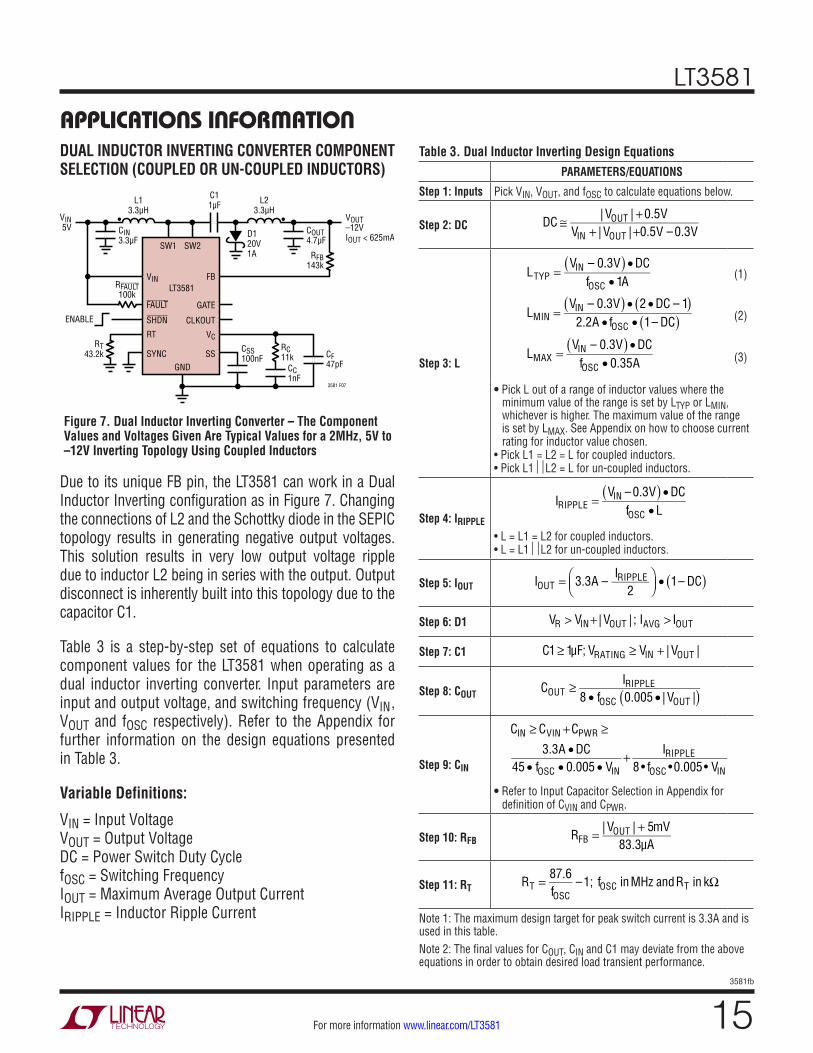
Due to its unique FB pin, the LT3581 can work in a Dual Inductor Inverting configuration as in Figure 7. Changing the connections of L2 and the Schottky diode in the SEPIC topology results in generating negative output voltages. This solution results in very low output voltage ripple due to inductor L2 being in series with the output. Output disconnect is inherently built into this topology due to the capacitor C1.
Table 3 is a step-by-step set of equations to calculate component values for the LT3581 when operating as a dual inductor inverting converter. Input parameters are input and output voltage, and switching frequency (VIN, VOUT and fOSC respectively). Refer to the Appendix for further information on the design equations presented in Table 3.
Variable Definitions:
VIN = Input Voltage VOUT = Output Voltage DC = Power Switch Duty Cycle fOSC = Switching Frequency IOUT = Maximum Average Output Current IRIPPLE = Inductor Ripple Current
APPLICATIONS INFORMATION
Figure 7. Dual Inductor Inverting Converter – The Component Values and Voltages Given Are Typical Values for a 2MHz, 5V to –12V Inverting Topology Using Coupled Inductors
DUAL INDUCTOR INVERTING CONVERTER COMPONENT SELECTION (COUPLED OR UN-COUPLED INDUCTORS)
Table 3. Dual Inductor Inverting Design EquationsPARAMETERS/EQUATIONS
Step 1: Inputs Pick VIN, VOUT, and fOSC to calculate equations below.
Step 2: DC DC ≅ | VOUT | + 0.5V
VIN + | VOUT | +0.5V – 0.3V
Step 3: L
LTYP =VIN – 0.3V( ) • DC
fOSC • 1A
LMIN =VIN – 0.3V( ) • 2 • DC – 1( )
2.2A • fOSC • 1– DC( )
LMAX =VIN – 0.3V( ) • DC
fOSC • 0.35A
(1)
(2)
(3)
• Pick L out of a range of inductor values where the minimum value of the range is set by LTYP or LMIN, whichever is higher. The maximum value of the range is set by LMAX. See Appendix on how to choose current rating for inductor value chosen. • Pick L1 = L2 = L for coupled inductors. • Pick L1L2 = L for un-coupled inductors.
Step 4: IRIPPLE IRIPPLE =
VIN – 0.3V( ) • DCfOSC • L
• L = L1 = L2 for coupled inductors. • L = L1L2 for un-coupled inductors.
Step 5: IOUT IOUT = 3.3A –
IRIPPLE2
• 1– DC( )
Step 6: D1 VR > VIN + | VOUT | ; IAVG > IOUT
Step 7: C1 C1 ≥ 1µF; VRATING ≥ VIN + | VOUT |
Step 8: COUT COUT ≥ IRIPPLE
8 • fOSC 0.005 • | VOUT |( )
Step 9: CIN
CIN ≥ CVIN + CPWR ≥3.3A • DC
45 • fOSC • 0.005 • VIN+ IRIPPLE
8 • fOSC •0.005• VIN
• Refer to Input Capacitor Selection in Appendix for definition of CVIN and CPWR.
Step 10: RFB RFB = | VOUT | + 5mV
83.3µA
Step 11: RT RT = 87.6
fOSC–1; fOSC inMHz andRT in kΩ
Note 1: The maximum design target for peak switch current is 3.3A and is used in this table.Note 2: The final values for COUT, CIN and C1 may deviate from the above equations in order to obtain desired load transient performance.
L23.3µH
D120V1A
VIN5V
RFAULT100k
RT43.2k
L13.3µH
3581 F07
CSS100nF
COUT4.7µF
CIN3.3µF
VOUT–12VIOUT < 625mA
SW1 SW2
FB
CLKOUT
GATE
VC
SS
VIN
RT
GNDSYNC
FAULT
SHDNENABLE
LT3581
CF47pF
RFB143k
• •
CC1nF
RC11k
C11µF
LT3581
163581fb
For more information www.linear.com/LT3581
3581 F08
VOUT
CINB
A
SYNC
GND
A: RETURN CIN GROUND DIRECTLY TO LT3581 EXPOSED PAD PIN 17. IT IS ADVISED TO NOT COMBINE CIN GROUND WITH GND EXCEPT AT THE EXPOSED PAD.B: RETURN COUT AND COUT1 GROUND DIRECTLY TO LT3581 EXPOSED PAD PIN 17. IT IS ADVISED TO NOT COMBINE COUT AND COUT1 GROUND WITH GND EXCEPT AT THE EXPOSED PAD.
SHDN
CLKOUT
+
–
VIN+
–
L1
17
1
2
3
4
5
6
7
8
16
15
14
13
12
11
10
9 COUT1
RGATE
COUT
D1 M1
D2
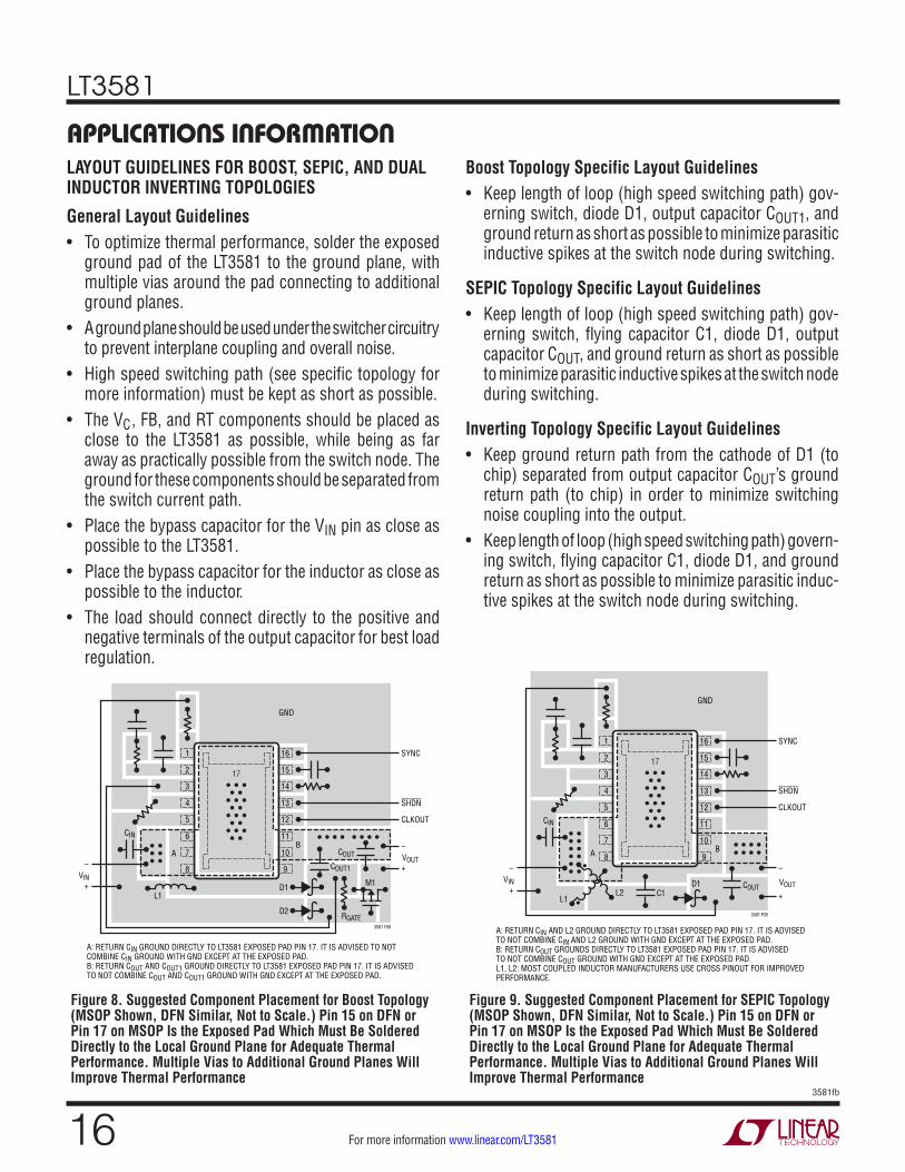
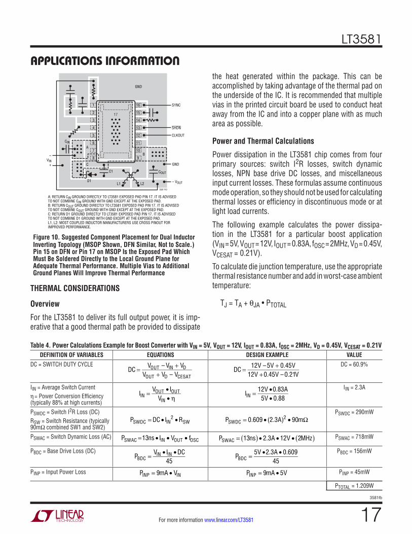
APPLICATIONS INFORMATIONLAYOUT GUIDELINES FOR BOOST, SEPIC, AND DUAL INDUCTOR INVERTING TOPOLOGIES
General Layout Guidelines• To optimize thermal performance, solder the exposed
ground pad of the LT3581 to the ground plane, with multiple vias around the pad connecting to additional ground planes.
• A ground plane should be used under the switcher circuitry to prevent interplane coupling and overall noise.
• High speed switching path (see specific topology for more information) must be kept as short as possible.
• The VC, FB, and RT components should be placed as close to the LT3581 as possible, while being as far away as practically possible from the switch node. The ground for these components should be separated from the switch current path.
• Place the bypass capacitor for the VIN pin as close as possible to the LT3581.
• Place the bypass capacitor for the inductor as close as possible to the inductor.
• The load should connect directly to the positive and negative terminals of the output capacitor for best load regulation.
Boost Topology Specific Layout Guidelines• Keep length of loop (high speed switching path) gov-
erning switch, diode D1, output capacitor COUT1, and ground return as short as possible to minimize parasitic inductive spikes at the switch node during switching.
SEPIC Topology Specific Layout Guidelines• Keep length of loop (high speed switching path) gov-
erning switch, flying capacitor C1, diode D1, output capacitor COUT, and ground return as short as possible to minimize parasitic inductive spikes at the switch node during switching.
Inverting Topology Specific Layout Guidelines• Keep ground return path from the cathode of D1 (to
chip) separated from output capacitor COUT’s ground return path (to chip) in order to minimize switching noise coupling into the output.
• Keep length of loop (high speed switching path) govern-ing switch, flying capacitor C1, diode D1, and ground return as short as possible to minimize parasitic induc-tive spikes at the switch node during switching.
Figure 8. Suggested Component Placement for Boost Topology (MSOP Shown, DFN Similar, Not to Scale.) Pin 15 on DFN or Pin 17 on MSOP Is the Exposed Pad Which Must Be Soldered Directly to the Local Ground Plane for Adequate Thermal Performance. Multiple Vias to Additional Ground Planes Will Improve Thermal Performance
Figure 9. Suggested Component Placement for SEPIC Topology (MSOP Shown, DFN Similar, Not to Scale.) Pin 15 on DFN or Pin 17 on MSOP Is the Exposed Pad Which Must Be Soldered Directly to the Local Ground Plane for Adequate Thermal Performance. Multiple Vias to Additional Ground Planes Will Improve Thermal Performance
3581 F09
VOUT
CIN
C1D1
BA
SYNC
GND
A: RETURN CIN AND L2 GROUND DIRECTLY TO LT3581 EXPOSED PAD PIN 17. IT IS ADVISED TO NOT COMBINE CIN AND L2 GROUND WITH GND EXCEPT AT THE EXPOSED PAD.B: RETURN COUT GROUNDS DIRECTLY TO LT3581 EXPOSED PAD PIN 17. IT IS ADVISED TO NOT COMBINE COUT GROUND WITH GND EXCEPT AT THE EXPOSED PAD.L1, L2: MOST COUPLED INDUCTOR MANUFACTURERS USE CROSS PINOUT FOR IMPROVED PERFORMANCE.
COUT
SHDN
CLKOUT
+
–VIN
+
– •
•L2
L1
17
1
2
3
4
5
6
7
8
16
15
14
13
12
11
10
9
LT3581
173581fb
For more information www.linear.com/LT3581
APPLICATIONS INFORMATION
THERMAL CONSIDERATIONS
Overview
For the LT3581 to deliver its full output power, it is imp-erative that a good thermal path be provided to dissipate
the heat generated within the package. This can be accomplished by taking advantage of the thermal pad on the underside of the IC. It is recommended that multiple vias in the printed circuit board be used to conduct heat away from the IC and into a copper plane with as much area as possible.
Power and Thermal Calculations
Power dissipation in the LT3581 chip comes from four primary sources: switch I2R losses, switch dynamic losses, NPN base drive DC losses, and miscellaneous input current losses. These formulas assume continuous mode operation, so they should not be used for calculating thermal losses or efficiency in discontinuous mode or at light load currents.
The following example calculates the power dissipa-tion in the LT3581 for a particular boost application (VIN = 5V, VOUT = 12V, IOUT = 0.83A, fOSC = 2MHz, VD = 0.45V, VCESAT = 0.21V).
To calculate die junction temperature, use the appropriate thermal resistance number and add in worst-case ambient temperature:
TJ = TA + θJA • PTOTAL
Table 4. Power Calculations Example for Boost Converter with VIN = 5V, VOUT = 12V, IOUT = 0.83A, fOSC = 2MHz, VD = 0.45V, VCESAT = 0.21VDEFINITION OF VARIABLES EQUATIONS DESIGN EXAMPLE VALUE
DC = SWITCH DUTY CYCLE
DC = VOUT – VIN + VD
VOUT + VD – VCESAT DC = 12V – 5V + 0.45V
12V + 0.45V – 0.21V
DC = 60.9%
IIN = Average Switch Currentη = Power Conversion Efficiency (typically 88% at high currents)
IIN = VOUT • IOUTVIN • η
IIN = 12V •0.83A5V • 0.88
IIN = 2.3A
PSWDC = Switch I2R Loss (DC)RSW = Switch Resistance (typically 90mΩ combined SW1 and SW2)
PSWDC = DC • IIN2 • RSW PSWDC = 0.609 • (2.3A)2 • 90mΩ
PSWDC = 290mW
PSWAC = Switch Dynamic Loss (AC) PSWAC =13ns • IIN • VOUT • fOSC PSWAC = 13ns( ) • 2.3A • 12V • 2MHz( ) PSWAC = 718mW
PBDC = Base Drive Loss (DC)
PBDC = VIN • IIN • DC
45 PBDC = 5V •2.3A • 0.609
45
PBDC = 156mW
PINP = Input Power Loss PINP = 9mA • VIN PINP = 9mA • 5V PINP = 45mW
PTOTAL = 1.209W
Figure 10. Suggested Component Placement for Dual Inductor Inverting Topology (MSOP Shown, DFN Similar, Not to Scale.) Pin 15 on DFN or Pin 17 on MSOP Is the Exposed Pad Which Must Be Soldered Directly to the Local Ground Plane for Adequate Thermal Performance. Multiple Vias to Additional Ground Planes Will Improve Thermal Performance
3581 F10
CIN
B
A
C
SYNC
GND
A: RETURN CIN GROUND DIRECTLY TO LT3581 EXPOSED PAD PIN 17. IT IS ADVISED TO NOT COMBINE CIN GROUND WITH GND EXCEPT AT THE EXPOSED PAD.B: RETURN COUT GROUND DIRECTLY TO LT3581 EXPOSED PAD PIN 17. IT IS ADVISED TO NOT COMBINE COUT GROUND WITH GND EXCEPT AT THE EXPOSED PAD.C: RETURN D1 GROUND DIRECTLY TO LT3581 EXPOSED PAD PIN 17. IT IS ADVISED TO NOT COMBINE D1 GROUND WITH GND EXCEPT AT THE EXPOSED PAD.L1, L2: MOST COUPLED INDUCTOR MANUFACTURERS USE CROSS PINOUT FOR IMPROVED PERFORMANCE.
COUT
SHDN
CLKOUT
– VOUT
GNDVIN
+
–
••L2L1
17
1
2
3
4
5
6
7
8
16
15
14
13
12
11
10
9
C1
D1

LT3581
183581fb
For more information www.linear.com/LT3581
APPLICATIONS INFORMATIONwhere TJ = Die Junction Temperature, TA = Ambient Tem-perature, PTOTAL is the final result from the calculations shown in Table 4, and θJA is the thermal resistance from the silicon junction to the ambient air.
The published (http://www.linear.com/designtools/pack-aging/Linear_Technology_Thermal_Resistance_Table.pdf) θJA value is 43°C/W for the 4mm × 3mm 14-pin DFN package and 45°C/W for the 16-lead MSOP package. In practice, lower θJA values are realizable if board layout is performed with appropriate grounding (accounting for heat sinking properties of the board) and other considerations listed in the Layout Guidelines section. For instance, a θJA value of ~24°C/W was consistently achieved for both MSE and DFN packages of the LT3581 (at VIN = 5V, VOUT = 12V, IOUT = 0.83A, fOSC = 2MHz) when board layout was optimized as per the suggestions in the Board Layout Guidelines section.
Junction Temperature Measurement
The duty cycle of the CLKOUT signal is linearly propor-tional to die junction temperature, TJ. To get a temperature reading, measure the duty cycle of the CLKOUT signal and use the following equation to approximate the junction temperature:
TJ = DCCLKOUT – 35%
0.3%
where DCCLKOUT is the CLKOUT duty cycle in % and TJ is the die junction temperature in °C. Although the actual die temperature can deviate from the above equation by ±15°C, the relationship between change in CLKOUT duty cycle and change in die temperature is well defined. Basi-cally a 1% change in CLKOUT duty cycle corresponds to a 3.33°C change in die temperature. Note that the CLKOUT pin is only meant to drive capacitive loads up to 50pF.
Thermal Lockout
A fault condition occurs when the die temperature exceeds 165°C (see Operation Section), and the part goes into thermal lockout. The fault condition ceases when the die temperature drops by ~5°C (nominal).
SWITCHING FREQUENCY
There are several considerations in selecting the operat-ing frequency of the converter. The first is staying clear of sensitive frequency bands, which cannot tolerate any spectral noise. For example, in products incorporating RF communications, the 455kHz IF frequency is sensitive to any noise, therefore switching above 600kHz is desired. Some communications have sensitivity to 1.1MHz and in that case a 1.5MHz switching converter frequency may be employed. The second consideration is the physical size of the converter. As the operating frequency goes up, the inductor and filter capacitors go down in value and size. The tradeoff is efficiency, since the losses due to switch-ing dynamics (see Thermal Considerations), Schottky diode charge, and other capacitive loss terms increase proportionally with frequency.
Oscillator Timing Resistor (RT)
The operating frequency of the LT3581 can be set by the internal free-running oscillator. When the SYNC pin is driven low (< 0.4V), the frequency of operation is set by a resistor from the RT pin to ground. An internally trimmed timing capacitor resides inside the IC. The oscillator frequency is calculated using the following formula:
fOSC = 87.6
RT + 1
where fOSC is in MHz and RT is in k. Conversely, RT (in k) can be calculated from the desired frequency (in MHz) using:
RT = 87.6
fOSC–1
LT3581
193581fb
For more information www.linear.com/LT3581
ENABLE
1.5µH
1.5µH
6.8µF 4.7µF
4.7µF
2.2µF
100pF
SW1 SW2GATE FB
VC
SS
GNDSYNC
CLKOUTVIN
RT
SHDN
FAULT
LT3581SLAVE
SW1 SW2GATE CLKOUT
VC
SS
GNDSYNC
FBVIN
RT
FAULT
SHDN
LT3581MASTER
143k
VOUT–12V450mA
VIN5V
VOUT12V830mA
10k
10.5k
2.2nF0.1µF
0.1µF
130k
43.2k
56pF1nF
43.2k
100k
10k
3581 F11
6.8µF
Figure 11. A Single Inductor Inverting Topology Is Synchronized with a Boost Regulator to Generate –12V and 12V Outputs. The External PMOS Helps Disconnect the Input from the Power Paths During Fault Events
Also, the FAULT pins can be tied together so that a fault condition from one LT3581 causes all of the LT3581s to enter fault, until the fault condition disappears.
CHARGE PUMP AIDED REGULATORS
Designing charge pumps with the LT3581 can offer ef-ficient solutions with fewer components than traditional circuits because of the master/slave switch configuration on the IC. Although the slave switch, SW2, operates in phase with the master switch, SW1, it is only the current through the master switch (SW1) that is sensed by the current comparator (A4 in Block Diagram) as part of the current feedback loop. This method of operation by the master/slave switches can offer the following benefits to charge pump designs:
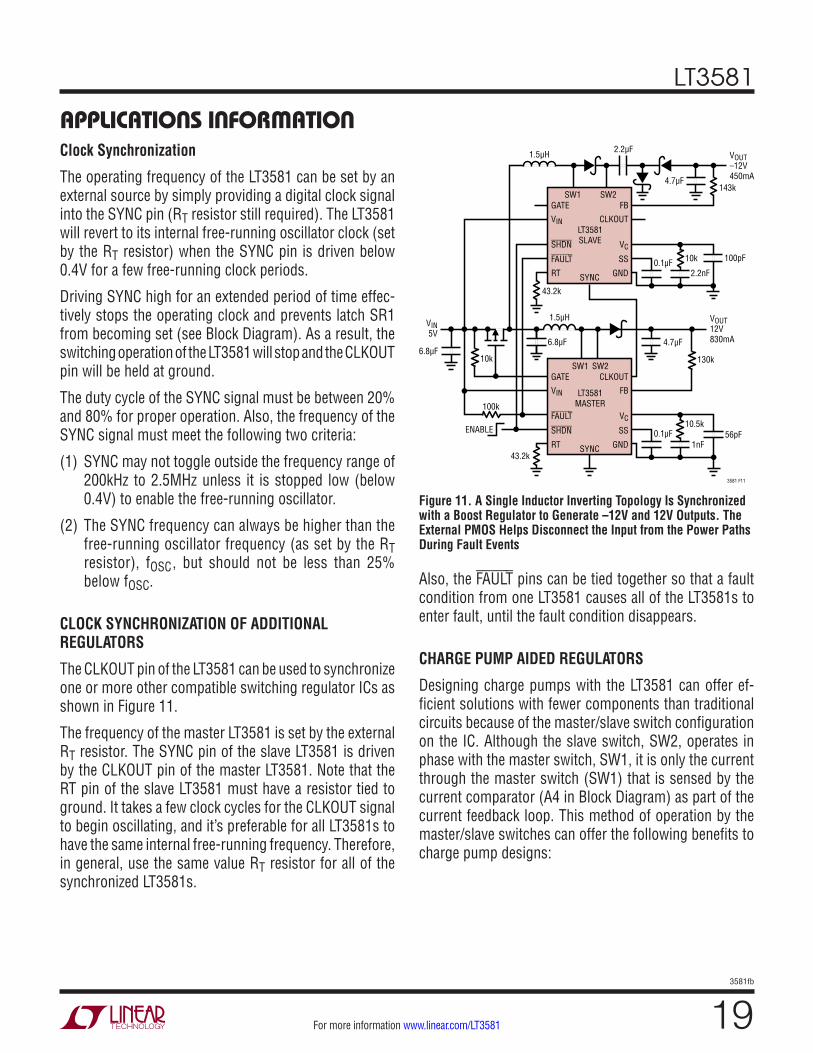
APPLICATIONS INFORMATIONClock Synchronization
The operating frequency of the LT3581 can be set by an external source by simply providing a digital clock signal into the SYNC pin (RT resistor still required). The LT3581 will revert to its internal free-running oscillator clock (set by the RT resistor) when the SYNC pin is driven below 0.4V for a few free-running clock periods.
Driving SYNC high for an extended period of time effec-tively stops the operating clock and prevents latch SR1 from becoming set (see Block Diagram). As a result, the switching operation of the LT3581 will stop and the CLKOUT pin will be held at ground.
The duty cycle of the SYNC signal must be between 20% and 80% for proper operation. Also, the frequency of the SYNC signal must meet the following two criteria:
(1) SYNC may not toggle outside the frequency range of 200kHz to 2.5MHz unless it is stopped low (below 0.4V) to enable the free-running oscillator.
(2) The SYNC frequency can always be higher than the free-running oscillator frequency (as set by the RT resistor), fOSC, but should not be less than 25% below fOSC.
CLOCK SYNCHRONIZATION OF ADDITIONAL REGULATORS
The CLKOUT pin of the LT3581 can be used to synchronize one or more other compatible switching regulator ICs as shown in Figure 11.
The frequency of the master LT3581 is set by the external RT resistor. The SYNC pin of the slave LT3581 is driven by the CLKOUT pin of the master LT3581. Note that the RT pin of the slave LT3581 must have a resistor tied to ground. It takes a few clock cycles for the CLKOUT signal to begin oscillating, and it’s preferable for all LT3581s to have the same internal free-running frequency. Therefore, in general, use the same value RT resistor for all of the synchronized LT3581s.
LT3581
203581fb
For more information www.linear.com/LT3581
APPLICATIONS INFORMATION• The slave switch, by not performing a current sense
operation like the master switch, can sustain fairly large current spikes when the flying capacitors charge up. Since this current spike flows through SW2, it does not affect the operation of the current comparator (A4 in Block Diagram).
• The master switch, immune from the capacitor current spike (seen only by the slave switch) can sense the inductor current more accurately.
• Since the slave switch can sustain large current spikes, the diodes that feed current into the flying capacitors do not need current limiting resistors, leading to efficiency and thermal improvements.
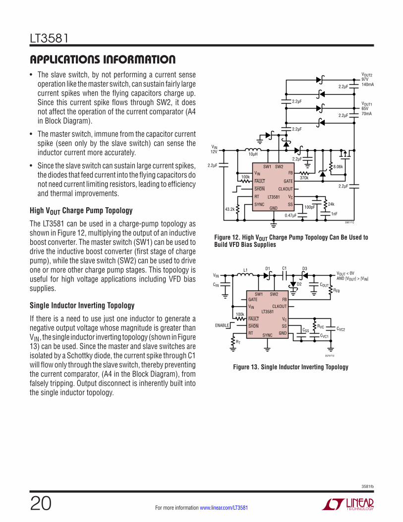
High VOUT Charge Pump Topology
The LT3581 can be used in a charge-pump topology as shown in Figure 12, multiplying the output of an inductive boost converter. The master switch (SW1) can be used to drive the inductive boost converter (first stage of charge pump), while the slave switch (SW2) can be used to drive one or more other charge pump stages. This topology is useful for high voltage applications including VFD bias supplies.
Single Inductor Inverting Topology
If there is a need to use just one inductor to generate a negative output voltage whose magnitude is greater than VIN, the single inductor inverting topology (shown in Figure 13) can be used. Since the master and slave switches are isolated by a Schottky diode, the current spike through C1 will flow only through the slave switch, thereby preventing the current comparator, (A4 in the Block Diagram), from falsely tripping. Output disconnect is inherently built into the single inductor topology.
VIN12V
VOUT297V140mA
VOUT165V70mA
24k
2.2µF10µH
2.2µF
2.2µF
0.47µF43.2k 100pF
1nF
100k
2.2µF
370k
SW1 SW2FB
VC
SSGND
SYNC
GATE
CLKOUT
VIN
RT
FAULT
SHDN
LT3581
3581 F12
8.06k
2.2µF
2.2µF
2.2µF
Figure 12. High VOUT Charge Pump Topology Can Be Used to Build VFD Bias Supplies
ENABLECVC2
VIN
COUT
VOUT < 0VAND |VOUT| > |VIN|
SW1 SW2GATE FB
VC
SS
GNDSYNC
CLKOUTVIN
RT
FAULT
SHDN
LT3581100k
L1 D1
D2
D3C1
RFB
CVC1
CSS
CIN
RVC
RT
3579 F13
Figure 13. Single Inductor Inverting Topology
LT3581
213581fb
For more information www.linear.com/LT3581
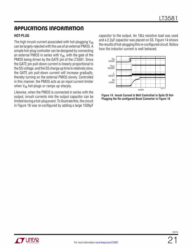
VOUT10V/DIV
SS1V/DIV
IL5A/DIV
VIN5V/DIV
3581 F141s/DIV
APPLICATIONS INFORMATION
Figure 14. Inrush Current Is Well Controlled in Spite Of Hot-Plugging the Re-configured Boost Converter in Figure 18
HOT-PLUG
The high inrush current associated with hot-plugging VIN can be largely rejected with the use of an external PMOS. A simple hot-plug controller can be designed by connecting an external PMOS in series with VIN, with the gate of the PMOS being driven by the GATE pin of the LT3581. Since the GATE pin pull-down current is linearly proportional to the SS voltage, and the SS charge up time is relatively slow, the GATE pin pull-down current will increase gradually, thereby turning on the external PMOS slowly. Controlled in this manner, the PMOS acts as an input current limiter when VIN hot-plugs or ramps up sharply.
Likewise, when the PMOS is connected in series with the output, inrush currents into the output capacitor can be limited during a hot-plug event. To illustrate this, the circuit in Figure 18 was re-configured by adding a large 1500µF
capacitor to the output. An 18Ω resistive load was used and a 2.2µF capacitor was placed on SS. Figure 14 shows the results of hot-plugging this re-configured circuit. Notice how the inductor current is well behaved.
LT3581
223581fb
For more information www.linear.com/LT3581
APPENDIXSETTING THE OUTPUT VOLTAGE
The output voltage is set by connecting a resistor (RFB) from VOUT to the FB pin. RFB is determined by using the following equation:
RFB = | VOUT – VFB |
83.3µA
where VFB is 1.215V (typical) for non-inverting topologies (i.e. boost and SEPIC regulators) and 5mV (typical) for inverting topologies.
POWER SWITCH DUTY CYCLE
In order to maintain loop stability and deliver adequate current to the load, the power NPNs (Q1 and Q2 in the Block Diagram) cannot remain “on” for 100% of each clock cycle. The maximum allowable duty cycle is given by:
DCMAX =
TP –MinOffTime( )TP
•100%
where TP is the clock period and MinOffTime (found in the Electrical Characteristics) is typically 60ns.
Conversely, the power NPNs (Q1 and Q2 in the Block Dia-gram) cannot remain “off” for 100% of each clock cycle, and will turn on for a minimum on time (MinOnTime) when in regulation. This MinOnTime governs the minimum al-lowable duty cycle given by:
DCMIN =
MinOnTime( )TP
•100%
Where TP is the clock period and MinOnTime (found in the Electrical Characteristics) is typically 100ns.
The application should be designed such that the operating duty cycle is between DCMIN and DCMAX.
Duty cycle equations for several common topologies are given below where VD is the diode forward voltage drop and VCESAT is the collector to emitter saturation voltage of the switch. VCESAT, with SW1 and SW2 tied together, is typically 250mV when the combined switch current (ISW1 + ISW2) is 2.75A.
For the boost topology (see Figure 5):
DCBOOST ≅ VOUT – VIN + VD
VOUT + VD – VCESAT
For the SEPIC or Dual Inductor Inverting topology (see Figures 6 and 7):
DCSEPIC _&_INVERT ≅ VD + | VOUT |
VIN + | VOUT | + VD − VCESAT
For the Single Inductor Inverting topology (see Figure 13):
DCSI_INVERT = | VOUT | −VIN + VCESAT + 3• VD
|VOUT | + 3• VD
The LT3581 can be used in configurations where the duty cycle is higher than DCMAX, but it must be operated in the discontinuous conduction mode so that the effective duty cycle is reduced.
INDUCTOR SELECTION
General Guidelines: The high frequency operation of the LT3581 allows for the use of small surface mount inductors. For high efficiency, choose inductors with high frequency core material, such as ferrite, to reduce core losses. Also to improve efficiency, choose inductors with more volume for a given inductance. The inductor should have low DCR (copper-wire resistance) to reduce I2R losses, and must be able to handle the peak inductor current without saturating. Note that in some applications, the current handling requirements of the inductor can be lower, such as in the SEPIC topology where each inductor only carries one half of the total switch current. Molded chokes or chip inductors usually do not have enough core area to support peak inductor currents in the 2A to 6A range. To minimize radiated noise, use a toroidal or shielded inductor. See Table 5 for a list of inductor manufacturers.
Table 5. Inductor ManufacturersSumida CDR6D28MN and CDR7D28MN
Serieswww.sumida.com
Coilcraft MSD7342 Series www.coilcraft.com
Vishay IHLP-1616BZ-01, IHLP-2020BZ-01 and IHLP-2525CZ-01 Series
www.vishay.com
Taiyo Yuden NR Series www.t-yuden.com
Wurth WE-PD Series www.we-online.com
TDK VLF, SLF and RLF Series www.tdk.com
LT3581
233581fb
For more information www.linear.com/LT3581
Minimum Inductance
Although there can be a tradeoff with efficiency, it is often desirable to minimize board space by choosing smaller inductors. When choosing an inductor, there are three conditions that limit the minimum inductance: (1) provid-ing adequate load current, (2) avoidance of subharmonic oscillations and (3) supplying a minimum ripple current to avoid false tripping of the current comparator.
Adequate Load Current
Small value inductors result in increased ripple currents and thus, due to the limited peak switch current, decrease the average current that can be provided to the load. In order to provide adequate load current, L should be at least:
LBOOST >DC • VIN − VCESAT( )
2• fOSC • IPK − | VOUT |• IOUTVIN • η
or
LDUAL>DC • VIN − VCESAT( )
2•fOSC• IPK− | VOUT|• IOUTVIN • η
−IOUT
BoostTopology
SEPICorInvertingTopologies
where:
LBOOST = L1 for Boost Topologies (see Figure 5) LDUAL = L1 = L2 for Coupled Dual Inductor Topologies (see Figures 6 and 7) LDUAL = L1 || L2 for Uncoupled Dual Inductor Topologies (see Figures 6 and 7) DC = Switch Duty Cycle (see Power Switch Duty Cycle section in Appendix) IPK = Maximum Peak Switch Current; should not exceed 3.3A for a combined SW1 + SW2 current, or 1.9A of SW1 current if SW1 is being used by itself. η = Power Conversion Efficiency (typically 88% for Boost and 75% for Dual Inductor Topologies at High Currents) fOSC = Switching Frequency IOUT = Maximum Output Current
APPENDIXNegative values of LBOOST or LDUAL indicate that the out-put load current, IOUT, exceeds the switch current limit capability of the LT3581.
Avoiding Sub-Harmonic Oscillations
The LT3581’s internal slope compensation circuit will prevent sub-harmonic oscillations that can occur when the duty cycle is greater than 50%, provided that the inductance exceeds a certain minimum value. In applica-tions that operate with duty cycles greater than 50%, the inductance must be at least:
LMIN =
VIN − VCESAT( ) • 2 • DC− 1( )2.2A• fOSC • 1−DC( )
where:
LMIN = L1 for Boost Topologies (see Figure 5) LMIN = L1 = L2 for Coupled Dual Inductor Topologies (see Figures 6 and 7) LMIN = L1 || L2 for Uncoupled Dual Inductor Topologies (see Figures 6 and 7)
Maximum Inductance
Excessive inductance can reduce ripple current to levels that are difficult for the current comparator (A4 in the Block Diagram) to cleanly discriminate, causing duty cycle jitter and/or poor regulation. The maximum inductance can be calculated by:
LMAX = VIN − VCESAT
350mA• DC
fOSC
where:
LMAX = L1 for Boost Topologies (see Figure 5) LMAX = L1 = L2 for Coupled Dual Inductor Topologies (see Figures 6 and 7) LMAX = L1 || L2 for Uncoupled Dual Inductor Topologies (see Figures 6 and 7)
LT3581
243581fb
For more information www.linear.com/LT3581
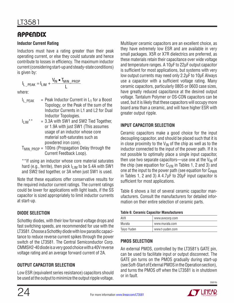
APPENDIXInductor Current Rating
Inductors must have a rating greater than their peak operating current, or else they could saturate and hence contribute to losses in efficiency. The maximum inductor current (considering start-up and steady-state conditions) is given by:
IL _PEAK = ILIM +
VIN • TMIN _PROP
L where:
IL_PEAK = Peak Inductor Current in L1 for a Boost Topology, or the Peak of the sum of the Inductor Currents in L1 and L2 for Dual Inductor Topologies. ILIM** = 3.3A with SW1 and SW2 Tied Together, or 1.9A with just SW1 (This assumes usage of an inductor whose core material soft-saturates such as powdered iron core). TMIN_PROP = 100ns (Propagation Delay through the Current Feedback Loop).
**If using an inductor whose core material saturates hard (e.g., ferrite), then pick ILIM to be 5.4A with SW1 and SW2 tied together, or 3A when just SW1 is used.
Note that these equations offer conservative results for the required inductor current ratings. The current ratings could be lower for applications with light loads, if the SS capacitor is sized appropriately to limit inductor currents at start-up.
DIODE SELECTION
Schottky diodes, with their low forward voltage drops and fast switching speeds, are recommended for use with the LT3581. Choose a Schottky diode with low parasitic capaci-tance to reduce reverse current spikes through the power switch of the LT3581. The Central Semiconductor Corp. CMMSH2-40 diode is a very good choice with a 40V reverse voltage rating and an average forward current of 2A.
OUTPUT CAPACITOR SELECTION
Low ESR (equivalent series resistance) capacitors should be used at the output to minimize the output ripple voltage.
Multilayer ceramic capacitors are an excellent choice, as they have extremely low ESR and are available in very small packages. X5R or X7R dielectrics are preferred, as these materials retain their capacitance over wide voltage and temperature ranges. A 10μF to 22μF output capacitor is sufficient for most applications, but systems with very low output currents may need only 2.2μF to 10μF. Always use a capacitor with a sufficient voltage rating. Many ceramic capacitors, particularly 0805 or 0603 case sizes, have greatly reduced capacitance at the desired output voltage. Tantalum Polymer or OS-CON capacitors can be used, but it is likely that these capacitors will occupy more board area than a ceramic, and will have higher ESR with greater output ripple.
INPUT CAPACITOR SELECTION
Ceramic capacitors make a good choice for the input decoupling capacitor, and should be placed such that it is in close proximity to the VIN of the chip as well as to the inductor connected to the input of the power path. If it is not possible to optimally place a single input capacitor, then use two separate capacitors—use one at the VIN of the chip (see equation for CVIN in Tables 1, 2 and 3) and one at the input to the power path (see equation for CPWR in Tables 1, 2 and 3) A 4.7μF to 20μF input capacitor is sufficient for most applications.
Table 6 shows a list of several ceramic capacitor man-ufacturers. Consult the manufacturers for detailed infor-mation on their entire selection of ceramic parts.
Table 6: Ceramic Capacitor ManufacturersAVX www.avxcorp.com
Murata www.murata.com
Taiyo Yuden www.t-yuden.com
PMOS SELECTION
An external PMOS, controlled by the LT3581’s GATE pin, can be used to facilitate input or output disconnect. The GATE pin turns on the PMOS gradually during start-up (see Soft-Start of External PMOS in the Operation section), and turns the PMOS off when the LT3581 is in shutdown or in fault.
LT3581
253581fb
For more information www.linear.com/LT3581
APPENDIXThe use of the external PMOS, controlled by the GATE pin, is particularly beneficial when dealing with unintended output shorts in a boost regulator. In a conventional boost regulator, the inductor, Schottky diode, and power switches are susceptible to damage in the event of an output short to ground. Using an external PMOS in the boost regulator’s power path (path from VIN to VOUT) controlled by the GATE pin, will serve to disconnect the input from the output when the output has a short to ground, thereby helping save the IC, and the other components in the power path from damage. Ensure that both, the diode and the inductor can survive low duty cycle current pulses of 3 to 4 times their steady state levels.
The PMOS chosen must be capable of handling the maxi-mum input or output current depending on whether the PMOS is used at the input (see Figure 11) or the output (see Figure 18).
Ensure that the PMOS is biased with enough source to gate voltage (VSG) to enhance the device into the triode mode of operation. The higher the VSG voltage that biases the PMOS into triode, the lower the RDSON of the PMOS, thereby lowering power dissipation in the device during normal operation, as well as improving the efficiency of the application in which the PMOS is used. The follow-ing equations show the relationship between RGATE (see Block Diagram) and the desired VSG that the PMOS is biased with:
VSG =VIN
RGATERGATE + 2kΩ
if VGATE < 2V
933µA•RGATE if VGATE ≥ 2V
When using a PMOS, it is advisable to configure the specific application for undervoltage lockout (see the Operations section). The goal is to have VIN get to a certain minimum voltage where the PMOS has sufficient headroom to attain a high enough VSG, which prevents it from entering the saturation mode of operation during start-up.
Figure 18 shows the PMOS connected in series with the output to act as an output disconnect during a fault con-dition. The Schottky diode from the VIN pin to the GATE pin is optional and helps turn off the PMOS quicker in the
event of hard shorts. The resistor divider from VIN to the SHDN pin sets a UVLO of 4V for this application.
Connecting the PMOS in series with the output offers certain advantages over connecting it in series with the input:
• Since the load current is always less than the input current for a boost converter, the current rating of the PMOS goes down.
• A PMOS in series with the output can be biased with a higher overdrive voltage than a PMOS used in series with the input, since VOUT > VIN. This higher overdrive results in a lower RDSON rating for the PMOS, thereby improving the efficiency of the regulator.
In contrast, an input connected PMOS works as a simple hot-plug controller (covered in more detail in the Hot-Plug section). The input connected PMOS also functions as an inexpensive means of protecting against multiple output shorts in boost applications that synchronize the LT3581 with other compatible ICs (see Figure 11).
Table 7 shows a list of several discrete PMOS manufa-cturers. Consult the manufacturers for detailed information on their entire selection of PMOS devices.
Table 7. Discrete PMOS ManufacturersVishay www.vishay.com
Fairchild Semiconductor www.fairchildsemi.com
COMPENSATION – ADJUSTMENT
To compensate the feedback loop of the LT3581, a series resistor-capacitor network in parallel with an optional single capacitor should be connected from the VC pin to GND. For most applications, choose a series capacitor in the range of 1nF to 10nF with 2.2nF being a good starting value. The optional parallel capacitor should range in value from 47pF to 160pF with 100pF being a good starting value. The compensation resistor, RC, is usually in the range of 5k to 50k with 10k being a good starting value. A good technique to compensate a new application is to use a 100k potentiometer in place of the series resistor RC. With the series and parallel capacitors at 2.2nF and 100pF respectively, adjust the potentiometer while observing the transient response and the optimum value for RC can be
LT3581
263581fb
For more information www.linear.com/LT3581
VOUTAC-COUPLED
500mV/DIV
IL1A/DIV
3581 F15a50µs/DIV
VOUTAC-COUPLED
500mV/DIV
IL1A/DIV
3581 F15b50µs/DIV
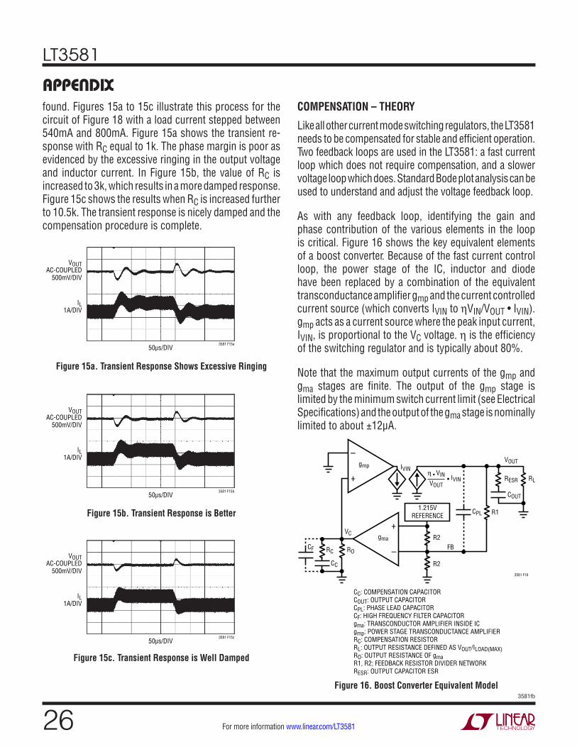
APPENDIXfound. Figures 15a to 15c illustrate this process for the circuit of Figure 18 with a load current stepped between 540mA and 800mA. Figure 15a shows the transient re-sponse with RC equal to 1k. The phase margin is poor as evidenced by the excessive ringing in the output voltage and inductor current. In Figure 15b, the value of RC is increased to 3k, which results in a more damped response. Figure 15c shows the results when RC is increased further to 10.5k. The transient response is nicely damped and the compensation procedure is complete.
Figure 15a. Transient Response Shows Excessive Ringing
Figure 15b. Transient Response is Better
Figure 15c. Transient Response is Well Damped
VOUTAC-COUPLED
500mV/DIV
IL1A/DIV
3581 F15c50µs/DIV
COMPENSATION – THEORY
Like all other current mode switching regulators, the LT3581 needs to be compensated for stable and efficient operation. Two feedback loops are used in the LT3581: a fast current loop which does not require compensation, and a slower voltage loop which does. Standard Bode plot analysis can be used to understand and adjust the voltage feedback loop.
As with any feedback loop, identifying the gain and phase contribution of the various elements in the loop is critical. Figure 16 shows the key equivalent elements of a boost converter. Because of the fast current control loop, the power stage of the IC, inductor and diode have been replaced by a combination of the equivalent transconductance amplifier gmp and the current controlled current source (which converts IVIN to ηVIN/VOUT • IVIN). gmp acts as a current source where the peak input current, IVIN, is proportional to the VC voltage. η is the efficiency of the switching regulator and is typically about 80%.
Note that the maximum output currents of the gmp and gma stages are finite. The output of the gmp stage is limited by the minimum switch current limit (see Electrical Specifications) and the output of the gma stage is nominally limited to about ±12μA.
1.215VREFERENCE
IVINη • VIN
VOUT• IVIN
VOUT
COUT
CPL
RESR RL
RO
VC
RC
CC
CF
R1
FBR2
R2
–
+
–
+
3581 F16
gmp
gma
CC: COMPENSATION CAPACITORCOUT: OUTPUT CAPACITORCPL: PHASE LEAD CAPACITORCF: HIGH FREQUENCY FILTER CAPACITORgma: TRANSCONDUCTOR AMPLIFIER INSIDE ICgmp: POWER STAGE TRANSCONDUCTANCE AMPLIFIERRC: COMPENSATION RESISTORRL: OUTPUT RESISTANCE DEFINED AS VOUT/ILOAD(MAX)RO: OUTPUT RESISTANCE OF gmaR1, R2; FEEDBACK RESISTOR DIVIDER NETWORKRESR: OUTPUT CAPACITOR ESR
Figure 16. Boost Converter Equivalent Model
LT3581
273581fb
For more information www.linear.com/LT3581
From Figure 16, the DC gain, poles and zeros can be calculated as follows:
DC Gain:(Breaking loop at FB pin)
ADC = AOL(0) = ∂VC∂VFB
• ∂IVIN∂VC
• ∂VOUT∂IVIN
• ∂VFB∂VOUT
=
gma •RO( )•gmp • η• VINVOUT
• RL2
• 0.5R2R1 + 0.5R2
Output Pole:P1= 22• π •RL •COUT
Error AmpPole:P2 = 12• π • RO +RC •CC
Error Amp Zero: Z1= 12• π •RC •CC
ESR Zero: Z2 = 12• π •RESR •COUT
RHP Zero: Z3 = VIN2 •RL
2• π • VOUT2 •L
HighFrequency Pole:P3 > fS3
Phase Lead Zero: Z4 = 12• π •R1•CPL
Phase LeadPole:P4 = 1
2• π •R1• R2
2
R1+ R22
•CPL
Error AmpFilter Pole:
P5 = 1
2• π • RC •RORC +RO
•CF
,CF < CC10
The current mode zero (Z3) is a right half plane zero which can be an issue in feedback control design, but is manage-able with proper external component selection.
APPENDIXUsing the circuit in Figure 18 as an example, Table 8 shows the parameters used to generate the Bode plot shown in Figure 17.
Table 8. Bode Plot ParametersPARAMETER VALUE UNITS COMMENT
RL 14.5 Ω Application Specific
COUT 9.4 µF Application Specific
RESR 1 mΩ Application Specific
RO 305 kΩ Not Adjustable
CC 1000 pF Adjustable
CF 56 pF Optional/Adjustable
CPL 0 pF Optional/Adjustable
RC 10.5 kΩ Adjustable
R1 130 kΩ Adjustable
R2 14.6 kΩ Not Adjustable
VREF 1.215 V Not Adjustable
VOUT 12 V Application Specific
VIN 5 V Application Specific
gma 270 µmho Not Adjustable
gmp 15.1 mho Not Adjustable
L 1.5 µH Application Specific
fOSC 2 MHz Adjustable
From Figure 17, the phase is –130° when the gain reaches 0dB giving a phase margin of 50°. The crossover frequency is 17kHz, which is more than three times lower than the frequency of the RHP zero Z3 to achieve adequate phase margin.
Figure 17. Bode Plot for Example Boost Converter
FREQUENCY (Hz)10
50GAIN
(dB)
PHASE (DEG)
70
90
110
130
100 1k 10k 100k 1M
3851 F17
30
10
–10
–30
150
170
–120
–80
–40
–240
–280
–160
–180
–360
–320
–200
0
PHASE
GAIN

LT3581
283581fb
For more information www.linear.com/LT3581
TYPICAL APPLICATIONS
Figure 18. 2MHz, 5V to 12V, 830mA Boost Converter with Output Short Circuit Protection
VIN5V
VIN
6.04k
100k 130k D2
D1M1
43.2k
C14.7µF
L11.5µH
1nF
3581 F18
0.1µF10.5k
C24.7µF
VOUT12V830mA
C34.7µF
SW1 SW2
FB
CLKOUT
GATE
VC
SS
VIN
RT
GNDSYNC
C1: 4.7µF, 16V, X7R, 1206C2, C3: 4.7µF, 25V, X7R, 1206D1: DIODES INC. PD3S230H-7
D2: VISHAY MSS2P3L1: SUMIDA CDR6D28MN-IR5M1: VISHAY SILICONIX SI7123DN
FAULT
SHDN
LT358156pF
18.7k
10k
Transient Response with 430mA to 830mA to 430mA Load Step
VOUTAC-COUPLED
1V/DIV
LOAD0.5A/DIV
IL1A/DIV
3581 TA02a50µs/DIV
Switching Waveforms with 830mA LoadVOUT
AC-COUPLED200mV/DIV
VCLKOUT(BW LIMIT)
2V/DIV
VSW0.5A/DIV
IL1A/DIV
3581 TA02b500ns/DIV
2MHz, 5V, 1.1A Boost Converter Operates from an Input Range of 2.8V to 4.2V
D1VIN
2.8V TO 4.2V
100k45.3k
43.2k
C13.3µF
L10.68µH
1.5nF
3581 TA03a
0.1µF
6.98k
VOUT5V1.1A
C222µF
SW1 SW2
FB
CLKOUT
GATE
VC
SS
VIN
RT
GNDSYNC
FAULT
SHDN
LT3581
68pF
C1: 3.3µF, 16V, X7R, 1206C2: 22µF, 16V, X7R, 1210D1: DIODES INC. PD3S230H-7L1: VISHAY IHLP1616 BZ-01-OR68 (ONLY 4.1mm × 4.5mm × 2mm)
Efficiency and Power Loss at VIN = 3.3V
LOAD CURRENT (mA)0
50
EFFI
CIEN
CY (%
)
POWER LOSS (m
W)
55
65
70
75
400
90
3581 TA03b
60
200 12001000800600
80
85
0
200
600
2000
1200
1400
1600
1800
400
800
1000

LT3581
293581fb
For more information www.linear.com/LT3581
High Efficiency, VFD (Vacuum Fluorescent Display) Power Supply Switches at 2MHz to Avoid AM Band
TYPICAL APPLICATIONS
VIN9V TO 16V
VIN
VOUT297V90mA (VIN = 9V)140mA (VIN = 12V)180mA (VIN = 16V)
VOUT165V60mA (VIN = 9V)70mA (VIN = 12V)90mA (VIN = 16V)
24k
C22.2µF
L110µH
C52.2µF
C42.2µF
0.47µF43.2k
100pF
1nF
100k
C12.2µF
365k
D3
D2D1
D7
D9*10V
D4
D5
D6
10k
32.6k SW1 SW2FB
VC
SSGND
SYNC
GATE
CLKOUT
VIN
RT
FAULT
SHDN
LT3581
3581 TA04a
8.06k
C62.2µF
C72.2µF
C32.2µF
D8*
M1*
C1: 2.2µF, 25V, X7R, 1206C2 TO C7: 2.2µF, 50V, X7R, 1206D1 TO D7: CENTRAL SEMI SOD123F
D8: CENTRAL SEMI CMDSH-3TRD9: CENTRAL SEMI CMHZ5240B-LTZL1: TAIYO YUDEN NR6045T100MM1: VISHAY SILICONIX SI7611DN
*OPTIONAL,FOR OUTPUT SHORT-CIRCUIT PROTECTION
DANGER HIGH VOLTAGE! OPERATION BY HIGH VOLTAGE TRAINED PERSONNEL ONLY
Transient Response with 60mA to 140mA to 60mA Load Step on VOUT2 (VIN = 12V)
VOUTAC-COUPLED
2V/DIV
ILOAD0.1A/DIV
IL0.5A/DIV
3581 TA04b100µs/DIV
Start-Up Waveforms
VOUT250V/DIV
VOUT150V/DIV
VSS1V/DIV
IL0.5A/DIV
3581 TA04c100ms/DIV
Efficiency and Power Loss at VIN = 12V
TOTAL OUTPUT POWER (W)0
70
EFFI
CIEN
CY (%
)POW
ER LOSS (mW
)
75
8
90
3581 TA04d
4 201612
80
85
1.0
3.0
1.5
2.0
2.5

LT3581
303581fb
For more information www.linear.com/LT3581
TYPICAL APPLICATIONS2MHz, 12V SEPIC Converter Can Accept Input Voltages from 9V to 16V
VIN9V TO 16V
100k
130k
43.2k
C13.3µF
2.2nF
3581 TA06a
0.1µF
C310µF
10k
VOUT12V1A (VIN = 9V)1.1A (VIN = 12V)1.3A (VIN = 16V)
C22.2µF
SW1 SW2
FB
CLKOUT
GATE
VC
SS
VIN
RT
GNDSYNC
FAULT
SHDN
LT3581
100pF
C1: 3.3µF, 25V, X7R, 1206C2: 2.2µF, 50V, X7R, 1206C3: 10µF, 25V, X7R, 1210D1: CENTRAL SEMI CTLSH2-40M832L1, L2: COILCRAFT MSD7342-332MLB
L23.3µH
L13.3µH
•
•
D1
Efficiency Line Regulation with No Load
Load Regulation at VIN = 12
LOAD CURRENT (mA)0
50
EFFI
CIEN
CY (%
)
55
65
70
75
1200
100
95
3581 TA06b
60
300 1500900600
80
85
90
VIN = 16V
VIN = 9V
VIN = 12V
VIN (V)8
11.990
V OUT
(V)
11.998
11.996
11.994
11.992
12.000
9 12 141310 1511 16 17
3581 TA06c
LINE REGULATION ~0.0044%/V
ILOAD (mA)0
11.96
V OUT
(V)
12.00
11.99
11.98
11.97
12.01
400 800600 1000200 1200 1400
3581 TA06d
LOAD REGULATION ~0.25%/A

LT3581
313581fb
For more information www.linear.com/LT3581
TYPICAL APPLICATIONS
Efficiency
VBAT3V TO 36V
(VBAT AT START-UP = 6V TO 16V)
100k
10k
24.9k
174k
C110µF
2.2nF
3581 TA07a
1µF
C547µF×2
10k
VOUT3.3V0.9A (3V < VBAT < 9V)1.5A (VBAT = 9V)
C210nF
Q1
C34.7µF
C42.2µF
SW1 SW2
FB
CLKOUT
GATE
VC
SS
VIN
RT
GNDSYNC
FAULT
SHDN
LT3581
47pF
C1: 10µF, 50V, X7R, 1210C2: 10nF, 25V, X7R, 0603C3: 4.7µF, 25V, X7R, 1206C4: 2.2µF, 50V, X7R, 1206C5: 47µF, 10V, X7R, 1210D1: CENTRAL SEMI CMHZ5248B-LTZ
D2: CENTRAL SEMI CMMSH2-40D3: DIODES INC. PD3S230H-7L1, L2: COILCRAFT MSD7342-332MLBM1: 2N7002Q1: MMBT3904
L23.3µH
L13.3µH
•
•
D2
M1
D3
D118V
470pF
10k200k
Wide Input Range, 3.3V SEPIC Converter Can Operate from 3V to 36V
Wide Input Range SEPIC Can Ride Through VBAT Voltages that Are Higher than VIN_OVP
VBAT10V/DIV
VOUT2V/DIV
IL2A/DIV
3581 TA07c1s/DIV
VBAT = 17V VBAT = 31V
VOUT = 3.3V
LOAD CURRENT (mA)0
50
EFFI
CIEN
CY (%
)
55
65
70
75
400
80
3581 TA07b
60
1600800 1200
VBAT = 3V
VBAT = 9V
VBAT = 12V
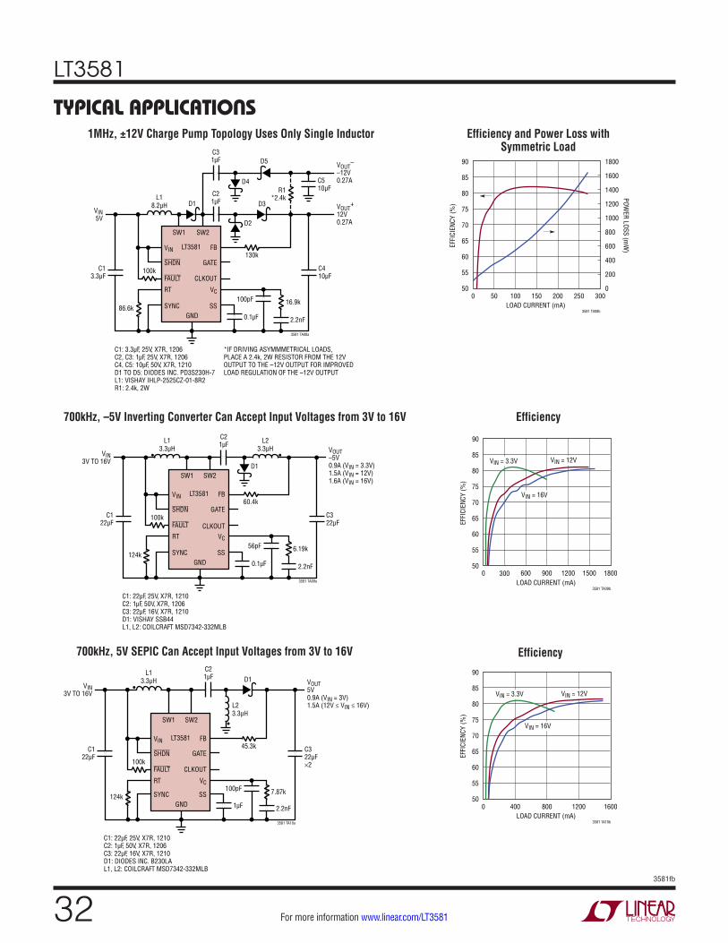
LT3581
323581fb
For more information www.linear.com/LT3581
TYPICAL APPLICATIONS1MHz, ±12V Charge Pump Topology Uses Only Single Inductor
VIN5V
100k
130k
86.6k
C13.3µF
2.2nF
3581 TA08a
0.1µF
C410µF
C510µF
16.9k
VOUT+
12V0.27A
VOUT–
–12V0.27A
C21µF
SW1 SW2
FB
CLKOUT
GATE
VC
SS
VIN
RT
GNDSYNC
FAULT
SHDN
LT3581
100pF
C1: 3.3µF, 25V, X7R, 1206C2, C3: 1µF, 25V, X7R, 1206C4, C5: 10µF, 50V, X7R, 1210D1 TO D5: DIODES INC. PD3S230H-7L1: VISHAY IHLP-2525CZ-01-8R2R1: 2.4k, 2W
*IF DRIVING ASYMMMETRICAL LOADS,PLACE A 2.4k, 2W RESISTOR FROM THE 12VOUTPUT TO THE –12V OUTPUT FOR IMPROVED LOAD REGULATION OF THE –12V OUTPUT
D2
D1L1
8.2µH D3
C31µF
D4
D5
R1*2.4k
Efficiency and Power Loss with Symmetric Load
700kHz, –5V Inverting Converter Can Accept Input Voltages from 3V to 16V
VIN3V TO 16V
100k
60.4k
124k
C122µF
2.2nF
3581 TA09a
0.1µF
C322µF
6.19k
VOUT–5V0.9A (VIN = 3.3V)1.5A (VIN = 12V)1.6A (VIN = 16V)
C21µF
SW1 SW2
FB
CLKOUT
GATE
VC
SS
VIN
RT
GNDSYNC
FAULT
SHDN
LT3581
56pF
C1: 22µF, 25V, X7R, 1210C2: 1µF, 50V, X7R, 1206C3: 22µF, 16V, X7R, 1210D1: VISHAY SSB44L1, L2: COILCRAFT MSD7342-332MLB
L23.3µH
D1
L13.3µH
• •
Efficiency
LOAD CURRENT (mA)0
50
EFFI
CIEN
CY (%
)
POWER LOSS (m
W)
55
65
70
75
15050
90
3581 TA08b
60
100 300250200
80
85
0
200
600
1800
1200
1400
1600
400
800
1000
LOAD CURRENT (mA)0
50
EFFI
CIEN
CY (%
)
55
65
70
75
300
90
3581 TA09b
60
1800900 1500600 1200
80
85VIN = 3.3V VIN = 12V
VIN = 16V
Efficiency700kHz, 5V SEPIC Can Accept Input Voltages from 3V to 16V
VIN3V TO 16V
100k
45.3k
124k
C122µF
2.2nF
3581 TA10a
1µF
C322µF×2
7.87k
VOUT5V0.9A (VIN = 3V)1.5A (12V ≤ VIN ≤ 16V)
C21µF
SW1 SW2
FB
CLKOUT
GATE
VC
SS
VIN
RT
GNDSYNC
FAULT
SHDN
LT3581
100pF
C1: 22µF, 25V, X7R, 1210C2: 1µF, 50V, X7R, 1206C3: 22µF, 16V, X7R, 1210D1: DIODES INC. B230LAL1, L2: COILCRAFT MSD7342-332MLB
L23.3µH
L13.3µH
•
•
D1
LOAD CURRENT (mA)0
50
EFFI
CIEN
CY (%
)
55
65
70
75
400
90
3581 TA10b
60
1600800 1200
80
85VIN = 3.3V VIN = 12V
VIN = 16V

LT3581
333581fb
For more information www.linear.com/LT3581
PACKAGE DESCRIPTIONPlease refer to http://www.linear.com/designtools/packaging/ for the most recent package drawings.
MSOP (MSE16) 0213 REV F
0.53 ±0.152(.021 ±.006)
SEATINGPLANE
0.18(.007)
1.10(.043)MAX
0.17 – 0.27(.007 – .011)
TYP
0.86(.034)REF
0.50(.0197)
BSC
16
16151413121110
1 2 3 4 5 6 7 8
9
9
1 8
NOTE:1. DIMENSIONS IN MILLIMETER/(INCH)2. DRAWING NOT TO SCALE3. DIMENSION DOES NOT INCLUDE MOLD FLASH, PROTRUSIONS OR GATE BURRS. MOLD FLASH, PROTRUSIONS OR GATE BURRS SHALL NOT EXCEED 0.152mm (.006") PER SIDE4. DIMENSION DOES NOT INCLUDE INTERLEAD FLASH OR PROTRUSIONS. INTERLEAD FLASH OR PROTRUSIONS SHALL NOT EXCEED 0.152mm (.006") PER SIDE5. LEAD COPLANARITY (BOTTOM OF LEADS AFTER FORMING) SHALL BE 0.102mm (.004") MAX6. EXPOSED PAD DIMENSION DOES INCLUDE MOLD FLASH. MOLD FLASH ON E-PAD SHALL NOT EXCEED 0.254mm (.010") PER SIDE.
0.254(.010) 0° – 6° TYP
DETAIL “A”
DETAIL “A”
GAUGE PLANE
5.10(.201)MIN
3.20 – 3.45(.126 – .136)
0.889 ±0.127(.035 ±.005)
RECOMMENDED SOLDER PAD LAYOUT
0.305 ±0.038(.0120 ±.0015)
TYP
0.50(.0197)
BSC
BOTTOM VIEW OFEXPOSED PAD OPTION
2.845 ±0.102(.112 ±.004)
2.845 ±0.102(.112 ±.004)
4.039 ±0.102(.159 ±.004)
(NOTE 3)
1.651 ±0.102(.065 ±.004)
1.651 ±0.102(.065 ±.004)
0.1016 ±0.0508(.004 ±.002)
3.00 ±0.102(.118 ±.004)
(NOTE 4)
0.280 ±0.076(.011 ±.003)
REF
4.90 ±0.152(.193 ±.006)
DETAIL “B”
DETAIL “B”CORNER TAIL IS PART OF
THE LEADFRAME FEATURE.FOR REFERENCE ONLY
NO MEASUREMENT PURPOSE
0.12 REF
0.35REF
MSE Package16-Lead Plastic MSOP, Exposed Die Pad
(Reference LTC DWG # 05-08-1667 Rev F)
LT3581
343581fb
For more information www.linear.com/LT3581
DE Package14-Lead Plastic DFN (4mm × 3mm)
(Reference LTC DWG # 05-08-1708 Rev B)
3.00 ±0.10(2 SIDES)
4.00 ±0.10(2 SIDES)
NOTE:1. DRAWING PROPOSED TO BE MADE VARIATION OF VERSION (WGED-3) IN JEDEC PACKAGE OUTLINE MO-2292. DRAWING NOT TO SCALE 3. ALL DIMENSIONS ARE IN MILLIMETERS4. DIMENSIONS OF EXPOSED PAD ON BOTTOM OF PACKAGE DO NOT INCLUDE MOLD FLASH. MOLD FLASH, IF PRESENT, SHALL NOT EXCEED 0.15mm ON ANY SIDE5. EXPOSED PAD SHALL BE SOLDER PLATED6. SHADED AREA IS ONLY A REFERENCE FOR PIN 1 LOCATION ON THE TOP AND BOTTOM OF PACKAGE
0.40 ± 0.10
BOTTOM VIEW—EXPOSED PAD
1.70 ± 0.10
0.75 ±0.05
R = 0.115TYP
R = 0.05TYP
3.00 REF
1.70 ± 0.05
17
148
PIN 1TOP MARK
(SEE NOTE 6)
0.200 REF
0.00 – 0.05
(DE14) DFN 0806 REV B
PIN 1 NOTCHR = 0.20 OR0.35 × 45°CHAMFER
3.00 REF
RECOMMENDED SOLDER PAD PITCH AND DIMENSIONSAPPLY SOLDER MASK TO AREAS THAT ARE NOT SOLDERED
2.20 ±0.05
0.70 ±0.05
3.60 ±0.05
PACKAGEOUTLINE
0.25 ± 0.05 0.25 ± 0.050.50 BSC
3.30 ±0.05 3.30 ±0.10
0.50 BSC
PACKAGE DESCRIPTIONPlease refer to http://www.linear.com/designtools/packaging/ for the most recent package drawings.
LT3581
353581fb
For more information www.linear.com/LT3581
Information furnished by Linear Technology Corporation is believed to be accurate and reliable. However, no responsibility is assumed for its use. Linear Technology Corporation makes no representa-tion that the interconnection of its circuits as described herein will not infringe on existing patent rights.
REVISION HISTORYREV DATE DESCRIPTION PAGE NUMBER
A 11/13 Added H-grade to Absolute Maximum Ratings table and Order Information tableClarified Electrical Characteristics
24
B 07/14 Clarified FAULT Output Voltage Low on Electrical Characteristics table, Typ was 150, changed to 100 4
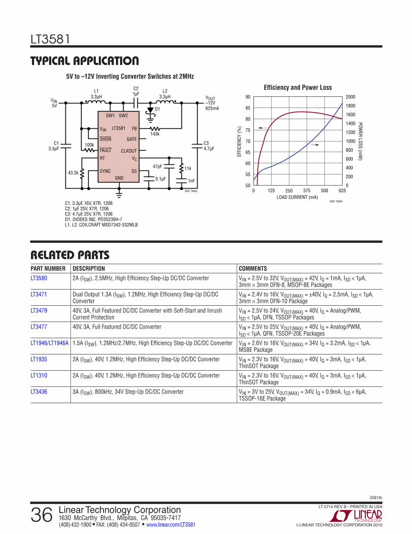
LT3581
363581fb
For more information www.linear.com/LT3581Linear Technology Corporation1630 McCarthy Blvd., Milpitas, CA 95035-7417
LINEAR TECHNOLOGY CORPORATION 2010
LT 0714 REV B • PRINTED IN USA
(408) 432-1900 FAX: (408) 434-0507 www.linear.com/LT3581
RELATED PARTSPART NUMBER DESCRIPTION COMMENTS
LT3580 2A (ISW), 2.5MHz, High Efficiency Step-Up DC/DC Converter VIN = 2.5V to 32V, VOUT(MAX) = 42V, IQ = 1mA, ISD < 1µA, 3mm × 3mm DFN-8, MSOP-8E Packages
LT3471 Dual Output 1.3A (ISW), 1.2MHz, High Efficiency Step-Up DC/DC Converter
VIN = 2.4V to 16V, VOUT(MAX) = ±40V, IQ = 2.5mA, ISD < 1µA, 3mm × 3mm DFN-10 Package
LT3479 40V, 3A, Full Featured DC/DC Converter with Soft-Start and Inrush Current Protection
VIN = 2.5V to 24V, VOUT(MAX) = 40V, IQ = Analog/PWM, ISD < 1µA, DFN, TSSOP Packages
LT3477 40V, 3A, Full Featured DC/DC Converter VIN = 2.5V to 25V, VOUT(MAX) = 40V, IQ = Analog/PWM, ISD < 1µA, QFN, TSSOP-20E Packages
LT1946/LT1946A 1.5A (ISW), 1.2MHz/2.7MHz, High Efficiency Step-Up DC/DC Converter VIN = 2.6V to 16V, VOUT(MAX) = 34V, IQ = 3.2mA, ISD < 1µA, MS8E Package
LT1935 2A (ISW), 40V, 1.2MHz, High Efficiency Step-Up DC/DC Converter VIN = 2.3V to 16V, VOUT(MAX) = 40V, IQ = 3mA, ISD < 1µA, ThinSOT Package
LT1310 2A (ISW), 40V, 1.2MHz, High Efficiency Step-Up DC/DC Converter VIN = 2.3V to 16V, VOUT(MAX) = 40V, IQ = 3mA, ISD < 1µA, ThinSOT Package
LT3436 3A (ISW), 800kHz, 34V Step-Up DC/DC Converter VIN = 3V to 25V, VOUT(MAX) = 34V, IQ = 0.9mA, ISD < 6µA, TSSOP-16E Package
TYPICAL APPLICATION5V to –12V Inverting Converter Switches at 2MHz
VIN5V
100k
143k
43.2k
C13.3µF
1nF
3581 TA05a
0.1µF
C34.7µF
11k
VOUT–12V625mA
C21µF
SW1 SW2
FB
CLKOUT
GATE
VC
SS
VIN
RT
GNDSYNC
FAULT
SHDN
LT3581
47pF
C1: 3.3µF, 16V, X7R, 1206C2: 1µF, 25V, X7R, 1206C3: 4.7µF, 25V, X7R, 1206D1: DIODES INC. PD3S230H-7L1, L2: COILCRAFT MSD7342-332MLB
L23.3µH
D1
L13.3µH
• •
Efficiency and Power Loss
50
55
65
70
75
90
60
80
85
LOAD CURRENT (mA)0
EFFI
CIEN
CY (%
)
POWER LOSS (m
W)
250
3581 TA05b
125 6255003750
200
600
2000
1200
1400
1600
1800
400
800
1000
Top Related