


Languages
Pages
Legal


Low Energy Design Techniques for Data
Converters
Harijot Singh Bindra
Researcher, Integrated Circuit Design
University of Twente, Enschede, The Netherlands
1email : [email protected]

Overview
Motivation
– Input Buffer Requirement
Reducing Input Drive Current
Low power single supply buffered SAR ADC
– Proposed Solution
– Integration of Buffer with SAR ADC
– Offset Correction
Measurement Results
Conclusion
2

EIN
• Overall low energy (EIN+ EADC) consumption
SENSOR
3
Digital
O/P
EADC
ADC
CS
VADC
Motivation

Motivation
– Input Buffer Requirement
Reducing Input Drive Current
Low power single supply buffered SAR ADC
– Proposed Solution
– Integration of Buffer with SAR ADC
– Offset Correction
Measurement Results
Conclusion
4
Overview

vDD
Low Power (V2/ZOUT)
ZOUT ZIN
Δ𝐕𝐂𝐒
0
VPK
time
VIN
Low Noise (kT/CS)
(Large CS)
ZOUT > ZIN
SENSOR
5
Digital
O/P
EADC
ADC
CS
VADC
Motivation – Input Buffer

VIN,ADC ≈ 0
ZIN
VSENSOR
VIN,ADCZOUT
VIN,ADC =
ZIN
ZIN + ZOUTVSENSOR
ZOUT >> ZIN
Low power sensor cannot drive ADC input
6
Motivation – Input Buffer

SENSOR
BUFFER
Δ𝐕𝐂𝐒
0
VPK
time
VIN,BUFF
vDD
Buffer the input signal !!
vDD
vDD
7
Digital
O/P
EADC
ADC
CS
Motivation – Input Buffer
SENSOR
Class-A
BUFFER
IADC
IIN
IBIAS
ADCVIN,min = VGS
vDDvDD
0
VPK
time
vDD
VIN,BUFF
8
Digital
O/PADC
CS
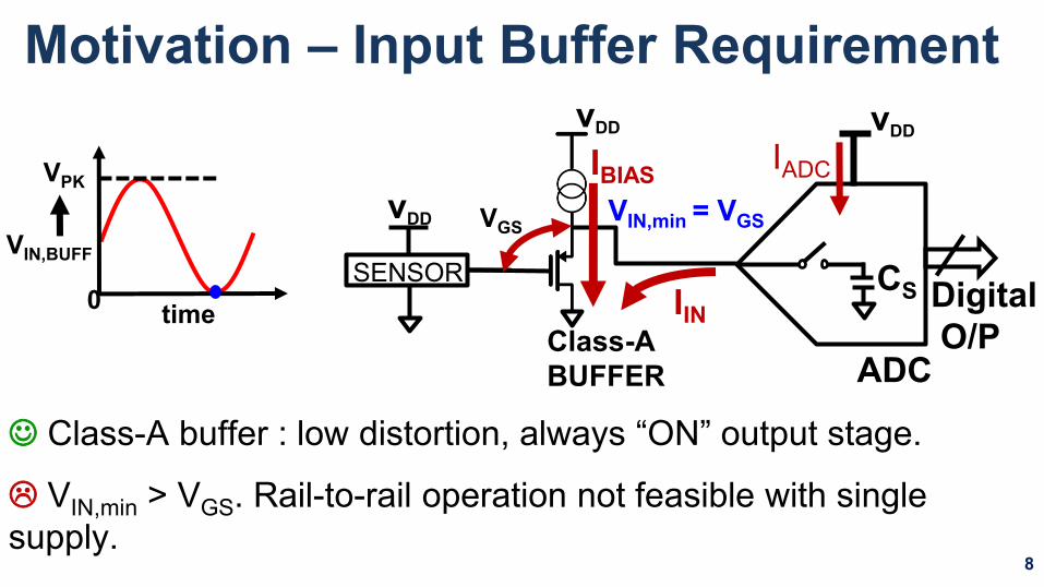
Motivation – Input Buffer Requirement
Class-A buffer : low distortion, always “ON” output stage.
VIN,min > VGS. Rail-to-rail operation not feasible with single
supply.
VGS

SENSOR
Class-A
BUFFER
IADC
IIN
IBIAS
ADC
vDDvDD
0
VPK
time
vDD
VIN,BUFF
9
Digital
O/PADC
CS
Motivation – Input Buffer Requirement
VIN,max < VDD
IBIAS ≥ IIN,MAX and VIN,max < VDD - VDS
Power hungry and poor efficiency. PBUFF ≥ VPKIBIAS
VDS

Input capacitance (CIN) is 0.2pF (18x lower than CS)
Additional high supply voltages (≈ 3xVPK) required
VIN,pk = 0.9V
2.5V
VBIAS
To T/H
Krämer, JSSC 2015
CS
CIN
VIN
1.2V2.5V
10
Prior Art - Source Follower embedded in SAR

SENSOR
Class-A
BUFFER
IADC
ADC
vDD
0
VPK
time
VIN,BUFF
11
Digital
O/PADC
CS
Motivation – Input Buffer Requirement
IIN
VIN
vDD
IBIAS ≥ IIN,MAXvDD
• Walden FoM (incl. buffer), FoMW,buff = (PADC+PBUFF)/(fS·2ENOB)
• PBUFF FoMW,buff

SENSOR
Class-A
BUFFER
IADC
ADC
vDD
0
VPK
time
VIN,BUFF
12
Digital
O/PADC
CS
Motivation – Input Buffer Requirement
IIN
VIN
vDD
IBIAS ≥ IIN,MAXvDD
• Single VDD with near rail-to-rail signal swing.
• Minimize IBIAS (or IIN,MAX) low FoMW,buff.
• Minimize EIN.
EIN

Motivation
– Input Buffer Requirement
Reducing Input Drive Current (A-SSCC 2017)
Low power single supply buffered SAR ADC
– Proposed Solution
– Integration of Buffer with SAR ADC
– Offset Correction
Measurement Results
Conclusion
13
Overview
14
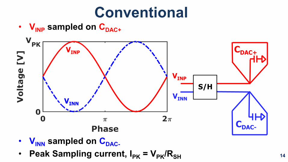
Conventional• VINP sampled on CDAC+
• VINN sampled on CDAC-
• Peak Sampling current, IPK = VPK/RSH
CDAC+
CDAC-
VINP
VINN
S/H
VINN
VINP

DAC Voltages
VINN
VINP
VPK
VPK
0
0
Δ𝐕𝐂𝐃𝐀𝐂+
CDAC+
time
ConversionReset
Δ𝐕𝐂𝐃𝐀𝐂+
CDAC-
DAC Voltages
15
Track
Conventional

DAC Voltages
VINN
VINP
VPK
VPK
0
0
Track
Δ𝐕𝐂𝐃𝐀𝐂+
CDAC+
time
ConversionReset
Δ𝐕𝐂𝐃𝐀𝐂+
CDAC-
DAC Voltages
16
Conventional

DAC Voltages
VINN
VINP
VPK
VPK
0
0
Δ𝐕𝐂𝐃𝐀𝐂+
CDAC+
time
ConversionReset
Δ𝐕𝐂𝐃𝐀𝐂+
CDAC-
DAC Voltages
17
Track
Track
Conventional

SENSOR
Class-A
BUFFER
IADC
ADC
vDD
18
Digital
O/PADC
CS
Reducing Δ𝐕𝐂𝐬 and Input Current
IIN
VIN
vDD
IBIAS ≥ IIN,MAXvDDΔ𝐕𝐂𝐒
0
VPK
time
VIN,BUFF
For Nyquist rate ADCs, Δ𝐕𝐂𝐬 ⩽ VPK
IIN,MAX = (N·CS·VPK/TTRACK) [N = 0.69(#Bits)]

SENSOR
Class-A
BUFFER
IADC
ADC
vDD
19
Digital
O/PADC
CS
Reducing Δ𝐕𝐂𝐬 and Input Current
IIN
VIN
vDD
IBIAS ≥ IIN,MAXvDD
• Linear Settling
• IIN,MAX = (N·CS·ΔVCs/TTRACK)
• IIN,MAX ΔVCS
Δ𝐕𝐂𝐒
0
VPK
time
VIN,BUFF

CLK
VINP
VINP
• Full-scale range of VINP divided in 3-parts
– Each sub-range of VINP sampled onto the respective CDAC
– Limits the ΔVCsto VPK/3 [ Bindra, ASSCC 2017 ]
20
Reducing Δ𝐕𝐂𝐬 and Input Current

21
Reducing Δ𝐕𝐂𝐬 and Input Current
CLK
VINP

22
Reducing Δ𝐕𝐂𝐬 and Input Current
CLK
VINP

23
Reducing Δ𝐕𝐂𝐬 and Input Current
CLK
VINP

VHALF
VDAC
VREF1
VREF2
CLK
CompCLK
CONTROL
LOGIC
S1 S1b
REGISTER
3:1 MUX
EN(Φ1)
B1<9:0>,
READY1
B<9:0>,READY
EN(Φ1)
EN(Φ2)EN(Φ3)
RPS_EN, SEL1,SEL2
DATA
EN_LATCH
CDAC1
CDAC2
CDAC3
RANGE PRE-SELECTION
(RPS) LOGIC BLOCK
SL1
SL2
DECODER
Φ1Φ2Φ3
VINPRMEAS
INPUT CURRENT
MEASUREMENT
AMPLIFIER
RPS_EN, SEL1,SEL2
Measurement - Input Sampling CurrentRPS_EN, SEL1,SEL2
On-chip Input Current
Measurement amplifier
RMEAS
CLK
VINP
B<9:0>, RDY 24
Single
Comparator

Die micrograph (65nm CMOS)
CDAC1 CDAC2 CDAC3
S/H1
Measurement
Amplifier
S/H2 S/H3
480µm
15
0µ
m
ADC
130µm
26
0µ
m
Ref. Voltage
Generation
Caps
Range Pre-
SelectComparator
• Area – 0.08 mm2
(including decaps)
• Measurement amplifier to
compare input sampling
current
• CDACs not selected act
as decap (connected to
single reference voltage)
25

fS = 2MS/s and fIN = 999.9375kHz
Beat frequency = fS/2 – fIN = 62.5 Hz
IIN = 𝚫𝐕𝐂𝐬/ (RMEAS + RSH)
RMEAS + RSH ≤ 1/[(N+1) ·C · 10· fS]
Time (ms)
Conventional
IIN(µA)
0
1023
0 87654321
120
-120
0
0 87654321
OUTPUT
CODE
Measurements- Input Sampling Current
26

Time (ms)
Conventional
IIN
(µA)
0
1023
0 87654321
120
-120
Proposed
IIN
(µA)0
120
-120
0
0 87654321
0 87654321
Range 2
Alternating between Range 1 and 3
OUTPUTCODE
Measurements- Input Sampling Current
27

Reduced ΔVCs reduces peak input sampling current.
IIN,PEAK
(µA)
Proposed
Conventional ÷2.4
28
Reducing Δ𝐕𝐂𝐬 and Input Current
fIN / fS

Motivation
– Input Buffer Requirement
Reducing Input Drive Current
Low power single supply buffered SAR ADC (CICC 2019)
– Proposed Solution
– Integration of Buffer with SAR ADC
– Offset Correction
Measurement Results
Conclusion
29
Overview
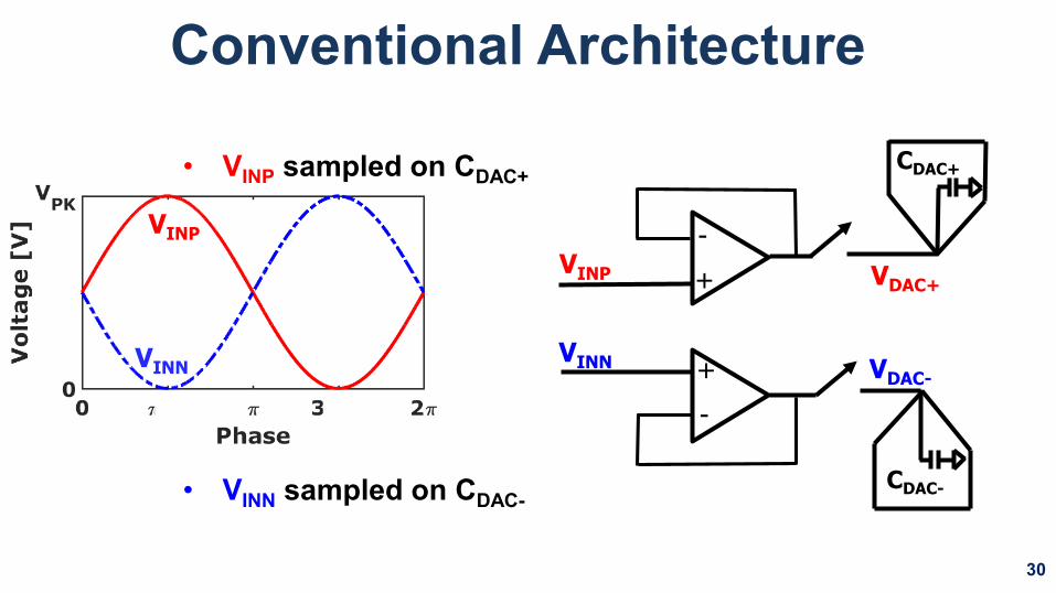
• VINP sampled on CDAC+
• VINN sampled on CDAC-
CDAC+
CDAC-
VINP
VINN
+
+
-
-
VINP
VINN
VDAC+
VDAC-
30
Conventional Architecture

Complimentary input pair can handle rail-to-rail input.
Distortion due to signal dependent gm variation and offset
modulation.[ Huijsing, JSSC 1980 ]
Current
SummationVINP VINN
VINP
VINN
31
Conventional Architecture

Motivation
– Input Buffer Requirement
Reducing Input Drive Current
Low power single supply buffered SAR ADC (CICC 2019)
– Proposed Solution
– Integration of Buffer with SAR ADC
– Offset Correction
Measurement Results
Conclusion
32
Overview

SWAP
SWAP LOGIC
CLK
Input CLK first turns ON the Front end comparator
SWAP
33
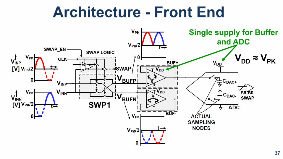
Architecture - Front End
[ Bindra, CICC 2019 ]
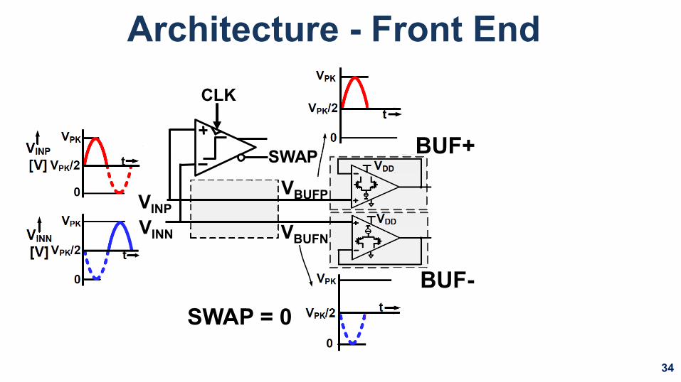
VBUFP
VBUFN
SWAP = 0
VBUFP
VBUFN
SWAP
CLK
VDD ≈ VPK
BUF+
BUF-
34
Architecture - Front End
VINP
VINN
BUF+
BUF-

VBUFP
VBUFN
SWAP = 0
VBUFP
VBUFN
SWAP
CLK
VDD ≈ VPK
BUF+
BUF-
35
Architecture - Front End
VINP
VINN

VBUFP
VBUFN
SWAP = 1
VBUFP
VBUFN
SWAP
CLK
VDD ≈ VPK
BUF+
BUF-
36
Architecture - Front End
VINP
VINN
VBUFP
VBUFN
VBUFP
VBUFN
VBUFP
VBUFN
SWP1
Single supply for Buffer
and ADC
VDD ≈ VPK
37
Architecture - Front End

Motivation
– Input Buffer Requirement
Reducing Input Drive Current
Low power single supply buffered SAR ADC (CICC 2019)
– Proposed Solution
– Integration of Buffer with SAR ADC
– Offset Correction
Measurement Results
Conclusion
38
Overview

S1
S2SWP1
cv
VBUFN
VBUFP
39
B9 B8 B1
B9 B8 B1
Architecture - Buffers integrated with ADC
cv
• SWP1 turn “OFF” delayed
wrt S1 and S2 at the end of
tracking
• Prevents sampling of kT/C
noise at the buffer’s input

cv
cv
cv
SWAP = 0
cv
VBUFN
VBUFP
B9….B0
B9….B0
B9 B8 B1
B9 B8 B1
40
Architecture - Buffers integrated with ADC

cv
cv
cv
SWAP = 0
cv
Main comparator does full 10b SAR conversion
VBUFN
VBUFP
B9 B8 B1
B9 B8 B1
B9….B0
B9….B0
41
Architecture - Buffers integrated with ADC

cv
cv
cv
SWP2 ensures that comparator offset is
same for SWAP =0 and SWAP =1
SWAP = 1
VBUFN
VBUFP
B9 B8 B1
B9 B8 B1
B9….B0
B9….B0
42
Architecture - Buffers integrated with ADC

cv
cv
cv
SWAP = 1
SWP3 keeps SAR loop convergent
VBUFN
VBUFP
B9 B8 B1
B9 B8 B1
B9….B0
B9….B0
43
Architecture - Buffers integrated with ADC

cv
cv
c
vc
vB9-B0 SWAP
VBUFN
VBUFP
ФSWPФNOSWP
cv
B9 B8 B1
B9 B8 B1
cvB9….B0
cvB9….B0
44
Architecture - Buffers integrated with ADC

• MATLAB simulated RMS and maximum change in voltage at the buffer input
• Reduced by 2x compared to conventional sampling
• EIN = CIN ·Δ𝐕𝐁𝐔𝐅𝐏·VDD is also reduced by 2x
45
Change in voltage (VBUF and VCDAC)

Motivation
– Input Buffer Requirement
Reducing Input Drive Current
Low power single supply buffered SAR ADC (CICC 2019)
– Proposed Solution
– Integration of Buffer with SAR ADC
– Offset Correction
Measurement Results
Conclusion
46
Overview
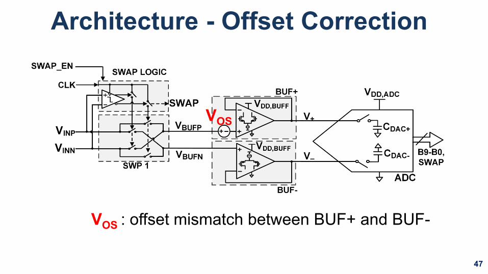
VOS : offset mismatch between BUF+ and BUF-
VOS
47
Architecture - Offset Correction
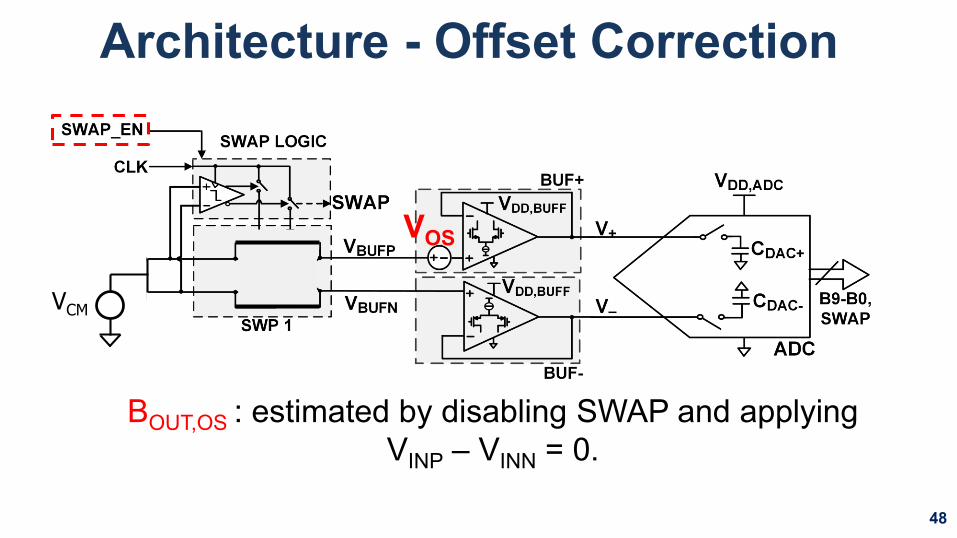
BOUT,OS : estimated by disabling SWAP and applying
VINP – VINN = 0.
VCM
VOS
48
Architecture - Offset Correction
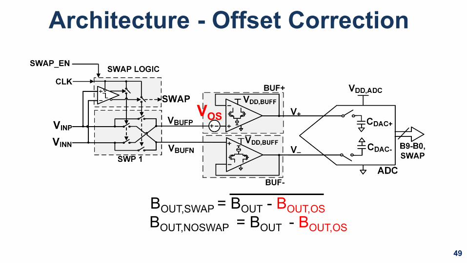
BOUT,SWAP = BOUT - BOUT,OS
BOUT,NOSWAP = BOUT - BOUT,OS
VOS
49
Architecture - Offset Correction

Motivation
– Input Buffer Requirement
Reducing Input Drive Current
Low power single supply buffered SAR ADC
– Proposed Solution
– Integration of Buffer with SAR ADC
– Offset Correction
Measurement Results
Conclusion
50
Overview

Area : 0.075mm2
(incl. decaps)
Power Consumption
ADC : 9µW
Buffers : 70µW each
51
Die micrograph (65nm CMOS)

SWAP_EN = ‘OFF’ VIN,diff = 2VP-P
52
Measurement Results - FFT

SWAP_EN = ‘ON’ VIN,diff = 2VP-P
53
Measurement Results - FFT

• fS = 4MS/s
• INL = 1.2LSB
• DNL = 0.5LSB
54
Measurement Results - INL/DNL

• Maximum jump is at mid-code due to non-segmented
DAC array
-0.4
-0.2
0
0.2
Y : -0.49
X : 511
460 500 540 580
55
Measurement Results - INL/DNL

• fS = 4MS/s
• SFDR > 64dB over Nyquist
range
• SNDR > 54dB over Nyquist
range
56
Measurement Results – SFDR/SNDR

Architecture This Work
Krämer
ISSCC
2015
Tseng
JSSC
2016Technology (nm) 65 40 28
Supply [V]ADC
1.21.2 1.1
Buffer 2.5 1.2
Diff. Input Signal (VPK-PK) 2 1.8 1.2
Maximum Sampling Rate (MS/s) 4 35 100
Power Consumption
(ADC+Buffer) in mW0.149 54.5 3.1
ENOB [bits] 8.7 12.1 7.2
FoMw (fJ/conversion) = (PADC+PBuffer)/2ENOB·fS 87 355 200
Area (in mm2)0.075
(incl. decap)
0.24
(incl. decap)
0.024
(Core only)
57
Table of Comparison

Motivation
– Input Buffer Requirement
– Prior Art
Architecture
– Proposed Solution
– Integration of Buffer with SAR ADC
– Offset Correction
Measurement Results
Conclusion
58
Overview

• Buffers and ADC operate at single supply voltage
(1.2V) while processing near rail-to-rail inputs.
• Swapping the inputs allow each of the input
buffer to handle one-half the full-scale range.
• State-of-the-art Walden FoM (ADC+Buffer) of
87fJ/conv-step.
59
Conclusion
Top Related