


Languages
Pages
Legal

LOGIC CIRCUITS
Ho Kyung Kim, Ph.D.
School of Mechanical Engineering
Pusan National University
Basic Experiment and Design of Electronics
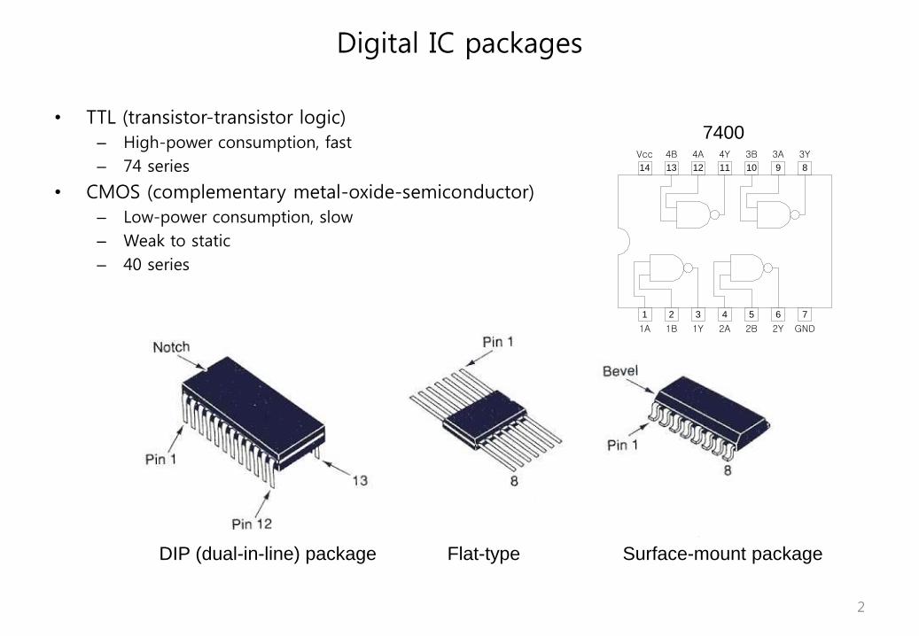
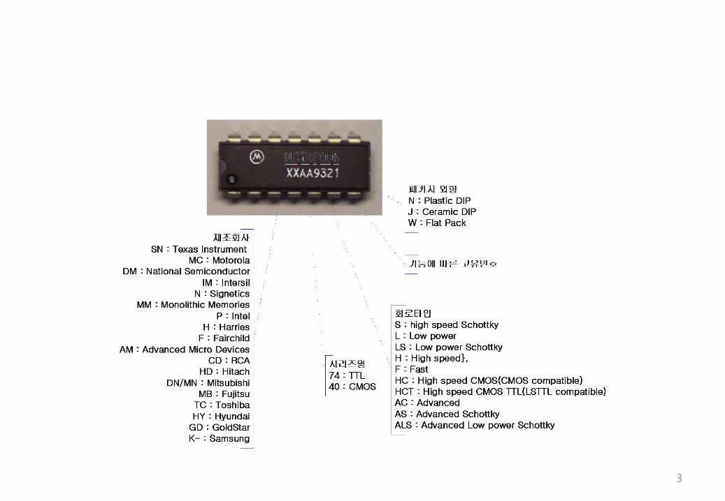
Digital IC packages
• TTL (transistor-transistor logic)
– High-power consumption, fast
– 74 series
• CMOS (complementary metal-oxide-semiconductor)
– Low-power consumption, slow
– Weak to static
– 40 series
2
1 2 3 4 5 6 7
814 13 12 11 10 9
1Y 2A1A 1B
Vcc 4Y 3B4B
2B GND
3A4A
2Y
3Y
DIP (dual-in-line) package Flat-type Surface-mount package
7400
3

Outline
• Combinational logic circuits
– Output depends on only the present inputs; not on the past inputs
– Multiplex
– ROM
– Decoder
– RAM
– PLD
• Sequential logic circuits
– Output depends on both the present and past inputs; hence having “memory” function
– Flip-flops
– Counters
4

• Multiplex
• ROM
• Decoder
• RAM
• PLD
Combinational logic circuits (modules)
5

Calculator
Encoder CPU Decoder
Input
Key pad
Decimal 4 bits
BCD
4 bits
BCD
7 bits
Output
7-sement
display
6

• Half adder (HA)
– 2 inputs: 𝑋 and 𝑌
– 3 outputs: 𝑆 (sum, LSB) and 𝐶𝑂𝑈𝑇 (carry, MSB)
X Y COUT S
0
0
1
1
0
1
0
1
0
0
0
1
0
1
1
0
HA
X
Y
S
COUT
X
YS
COUT
XYCOUT
YXYXYXS
7

• Full adder (FA)
– 3 inputs: 𝑋, 𝑌, and 𝐶𝐼𝑁
– 2 outputs: 𝑆 and 𝐶𝑂𝑈𝑇
X Y CIN COUT S
0
0
0
0
1
1
1
1
0
0
1
1
0
0
1
1
0
1
0
1
0
1
0
1
0
0
0
1
0
1
1
1
0
1
1
0
1
0
0
1
IN
ININ
ININININ
ININININ
CYX
ZXZXZX
CYXCYX
YCCYXCYCYX
XYCCYXCYXCYXS
)()(
)()(
)(
)()1(
)]()([
)(
)()()(
YXCXY
YXYXCCXY
XXYYYXCXY
YXCXY
YCXCXY
CCXYYYXCXXYC
XYCCXYXYCCYXXYCYCX
XYCCXYCYXYCXC
IN
ININ
IN
IN
ININ
ININININ
ININININININ
ININININOUT
FAX
Y
S
COUT
CIN
X
Y
COUT
S
CINXY
XY
HA HA
8

• For the output 𝑆:
• For the output 𝐶𝑂𝑈𝑇 :
00 01 11 10
0 0 1 0 1
1 1 0 1 0
YCINX
IN
ININININ
CYX
XYCCYXCYXCYXS
00 01 11 10
0 0 0 1 0
1 0 1 1 1
YCINX
)(
)()1(
)]()([
)(
YXCXY
YXYXCCXY
XXYYYXCXY
YXCXY
YCXCXYC
IN
ININ
IN
IN
ININOUT
Y S
COUT
X
CIN
9

• Selecting one of many inputs (also called data selectors)
• Consisting of 2𝑛 data lines, 𝑛 address lines, 1 output, 1 enable control input
• Ex) 4-to-1 MUX
Multiplexers
10

• Read-only memory
• Holding information in storage (“memory”) that cannot be altered but can be “read” by a logic circuit
• Consisting 2𝑚 × 𝑛 cells
– 𝑚 = # of address lines
– 𝑛 = # of bits in each word stored in ROM
• When an address line is selected, the binary word corresponding to the address selected appears at the output
• c.f., EPROM (erasable programmable ROM)
• Ex) 22 × 4 ROM
ROM
11

• Ex) 8-word × 4-bit (or 22 × 4) ROM
A B C F0 F1 F2 F3
0
0
0
0
1
1
1
1
0
0
1
1
0
0
1
1
0
1
0
1
0
1
0
1
1
1
0
0
1
0
1
0
0
0
1
1
1
0
1
1
1
1
1
0
0
0
1
0
0
0
1
1
0
1
1
1
typical data
stored in ROM
(23 words of
4bits each)
12
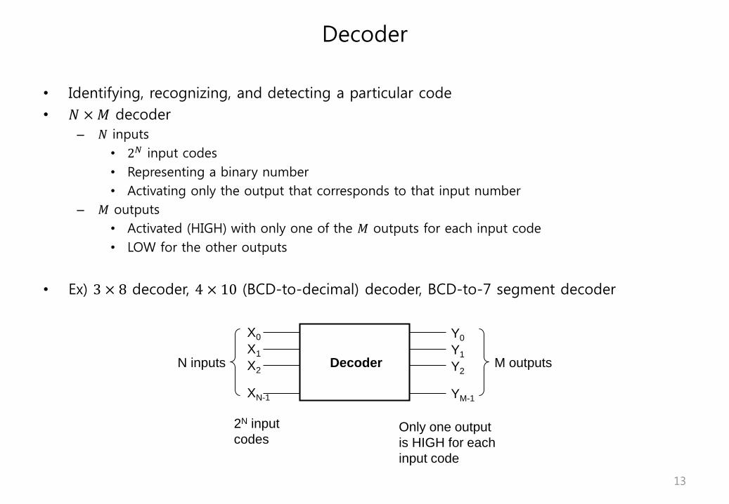
• Identifying, recognizing, and detecting a particular code
• 𝑁 × 𝑀 decoder
– 𝑁 inputs
• 2𝑁 input codes
• Representing a binary number
• Activating only the output that corresponds to that input number
– 𝑀 outputs
• Activated (HIGH) with only one of the 𝑀 outputs for each input code
• LOW for the other outputs
• Ex) 3 × 8 decoder, 4 × 10 (BCD-to-decimal) decoder, BCD-to-7 segment decoder
Decoder
Decoder
X0
X1
X2
XN-1
Y0
Y1
Y2
YM-1
2N input
codesOnly one output
is HIGH for each
input code
N inputs M outputs
13
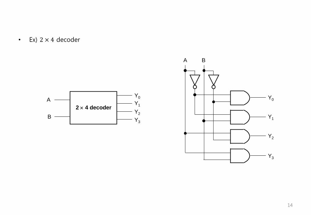
• Ex) 2 × 4 decoder
2 4 decoder
A
B
Y0
Y1
Y2
Y3
Y0
Y1
Y2
Y3
A B
14

• Ex) 3 × 8 decoder
a b c y0 y1 y2 y3 y4 y5 y6 y7
0 0 0
0 0 1
0 1 0
0 1 1
1 0 0
1 0 1
1 1 0
1 1 1
1
0
0
0
0
0
0
0
0
1
0
0
0
0
0
0
0
0
1
0
0
0
0
0
0
0
0
1
0
0
0
0
0
0
0
0
1
0
0
0
0
0
0
0
0
1
0
0
0
0
0
0
0
0
1
0
0
0
0
0
0
0
0
1
15
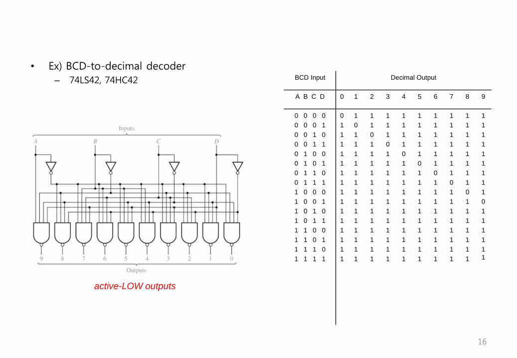
• Ex) BCD-to-decimal decoder
– 74LS42, 74HC42 BCD Input Decimal Output
A B C D 0 1 2 3 4 5 6 7 8 9
0 0 0 0
0 0 0 1
0 0 1 0
0 0 1 1
0 1 0 0
0 1 0 1
0 1 1 0
0 1 1 1
1 0 0 0
1 0 0 1
1 0 1 0
1 0 1 1
1 1 0 0
1 1 0 1
1 1 1 0
1 1 1 1
0
1
1
1
1
1
1
1
1
1
1
1
1
1
1
1
1
0
1
1
1
1
1
1
1
1
1
1
1
1
1
1
1
1
0
1
1
1
1
1
1
1
1
1
1
1
1
1
1
1
1
0
1
1
1
1
1
1
1
1
1
1
1
1
1
1
1
1
0
1
1
1
1
1
1
1
1
1
1
1
1
1
1
1
1
0
1
1
1
1
1
1
1
1
1
1
1
1
1
1
1
1
0
1
1
1
1
1
1
1
1
1
1
1
1
1
1
1
1
0
1
1
1
1
1
1
1
1
1
1
1
1
1
1
1
1
0
1
1
1
1
1
1
1
1
1
1
1
1
1
1
1
1
0
1
1
1
1
1
1
active-LOW outputs
16

• Commonly used for address decoding or memory expansion
• Ex) 2-to-4 decoder
Decoder and RAM
• SRAM (static random access, or read and write, memory)
17
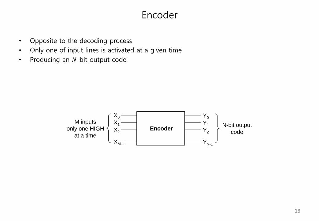
• Opposite to the decoding process
• Only one of input lines is activated at a given time
• Producing an 𝑁-bit output code
Encoder
Encoder
X0
X1
X2
XM-1
Y0
Y1
Y2
YN-1
M inputs
only one HIGH
at a time
N-bit output
code
18

• Ex) 8 × 3 decoder
y0 y1 y2 y3 y4 y5 y6 y7 a b c d
0
1
X
X
X
X
X
X
X
0
0
1
X
X
X
X
X
X
0
0
0
1
X
X
X
X
X
0
0
0
0
1
X
X
X
X
0
0
0
0
0
1
X
X
X
0
0
0
0
0
0
1
X
X
0
0
0
0
0
0
0
1
X
0
0
0
0
0
0
0
0
1
0
0
0
0
0
1
1
1
1
0
0
0
1
1
0
0
1
1
0
0
1
0
1
0
1
0
1
0
1
1
1
1
1
1
1
1
19
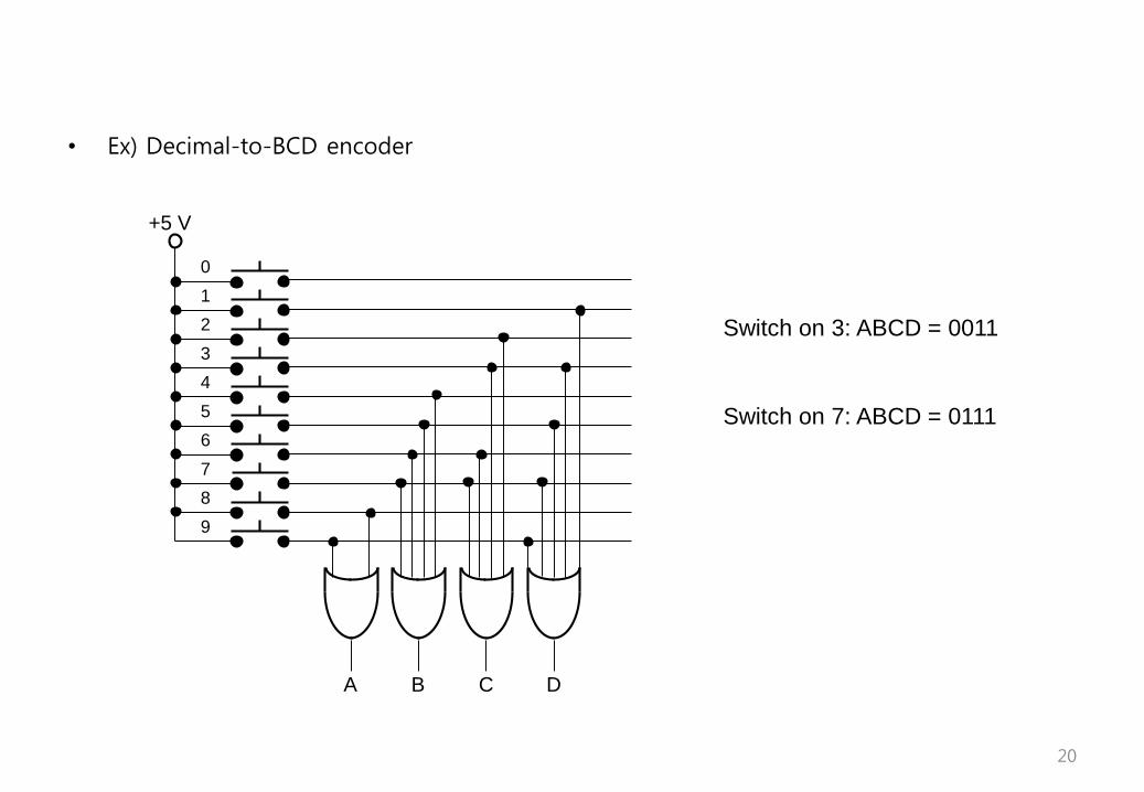
• Ex) Decimal-to-BCD encoder
A B C D
+5 V
0
1
2
3
4
5
6
7
8
9
Switch on 3: ABCD = 0011
Switch on 7: ABCD = 0111
20

• Programmable logic device
– PROM (programmable read-only memory)
– PLA (programmable logic array)
– PAL/GAL (programmable array logic/generic array logic)
• Arrays of gates (e.g., AND and OR gates) having interconnections that can be programmed to perform a specific logical function
– Programming language: hardware description languages (HDLs)
• Used for various digital logic designs
PLD
21
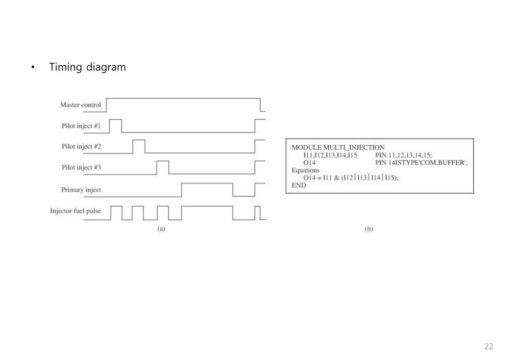
• Timing diagram
22

• Combinational logic circuits provide outputs that are based on a combination of present inputs only
• Sequential logic circuits depend on present and past input values (it memorizes!)
– Being able to store information
Sequential logic circuits
23

• Basic information storage device in a digital circuit
• Many different varieties of flip-flops
– RS FF
– D FF
– JK FF
– T FF
• Common characteristics
– Bistable device
• Remaining in one of two stable states (0 and 1) until appropriate conditions cause FF to change state
• Memory element
– Two outputs; complement ( 𝑄) and uncomplement (𝑄) outputs
• Synchronous operation by a “clock” signal
• Asynchronous operation
– Independent of the clock
– Level sensitive ( “Latch”)
Flip-flops
24

• Two inputs (𝑆 set and 𝑅 reset), two outputs (𝑄 and 𝑄, called the state of FF)
RS filp-flop
Requiring the FF to set and reset at the same time! Time delays!
25
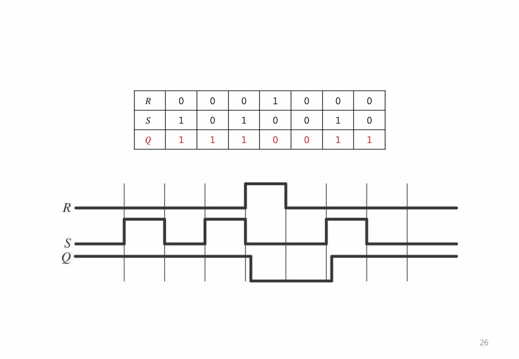
𝑅 0 0 0 1 0 0 0
𝑆 1 0 1 0 0 1 0
𝑄 1 1 1 0 0 1 1
26

• Ex) Initial state 𝑄 = 0 (then, 𝑄 = 1); apply 𝑆 = 1
– 𝑄 = 𝑆 ∙ 𝑄 = 0 ∙ 1 = 1 SET
• 𝑄 becomes 0; 𝑄 = 0 ∙ 0 = 1 still SET
• Cross-coupled feedback from outputs 𝑄 and 𝑄to the input of the NAND gates is such that the set condition sustains itself
27

• RS FF with enable (𝐸), preset (𝑃), and clear (𝐶) inputs
– 𝑅 or 𝑆 is effective only when 𝐸 = 1
• Synchronizing signal
– Direct inputs 𝑃 and 𝐶 allow the user to preset or clear the FF at any time (asynchronous operation)
• 𝑆 = 1 (preset) when 𝑃 = 1
• 𝑄 = 0 (cleared) when 𝐶 = 1
28
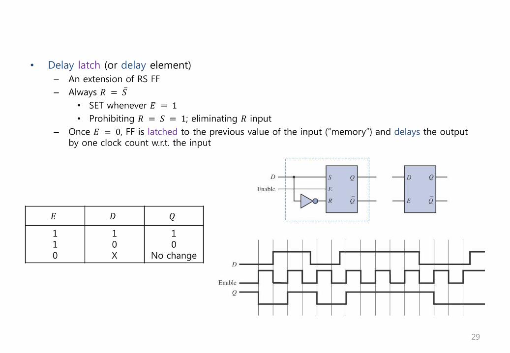
• Delay latch (or delay element)
– An extension of RS FF
– Always 𝑅 = 𝑆
• SET whenever 𝐸 = 1
• Prohibiting 𝑅 = 𝑆 = 1; eliminating 𝑅 input
– Once 𝐸 = 0, FF is latched to the previous value of the input (“memory”) and delays the output by one clock count w.r.t. the input
𝐸 𝐷 𝑄
110
10X
10
No change
29

• An extension of data latch with two RS FFs
• Changing state only on the positive edge of the clock (leading or positive edge-triggered)
• Similarly, trailing or negative edge-triggered D FF
D flip-flop
𝐷 𝐶𝐿𝐾 𝑄
01
01
indicating “leading edge-trigger
𝐷 𝐶𝐿𝐾 𝑄
01
01
30

• Note that “C” implies the “control” signal
31
Q
Q
Q
CLK
DD
C
Q
Q
D Q
QCLK
D Q
QCLK

• Same as RS FF except that J = K = 1 states
JK flip-flop
32
J K Q
0
0
1
1
0
1
0
1
No change
Reset
Set
Toggle
J
K
Q
Q
CLK
J
K
Q
Q
CLK
K
CLK
Q
J

indicating “trailing edge-triggerC
(no change)
33

𝐽 0 1 0 1 0 0 1
𝐾 0 1 1 0 0 1 1
𝑄 1 0 0 1 1 0 1
34

• Master/slave FF
– Delayed output by the width of clock pulse
35
J
K
Q
Q
CLK
J
K
Q
Q
CLK
Master Slave
J
K
Q
CLK
tnmaster
tn+1
slave
J K Qn+1
0
0
1
1
0
1
0
1
Qn (no change)
Reset
Set
Qn (toggle)
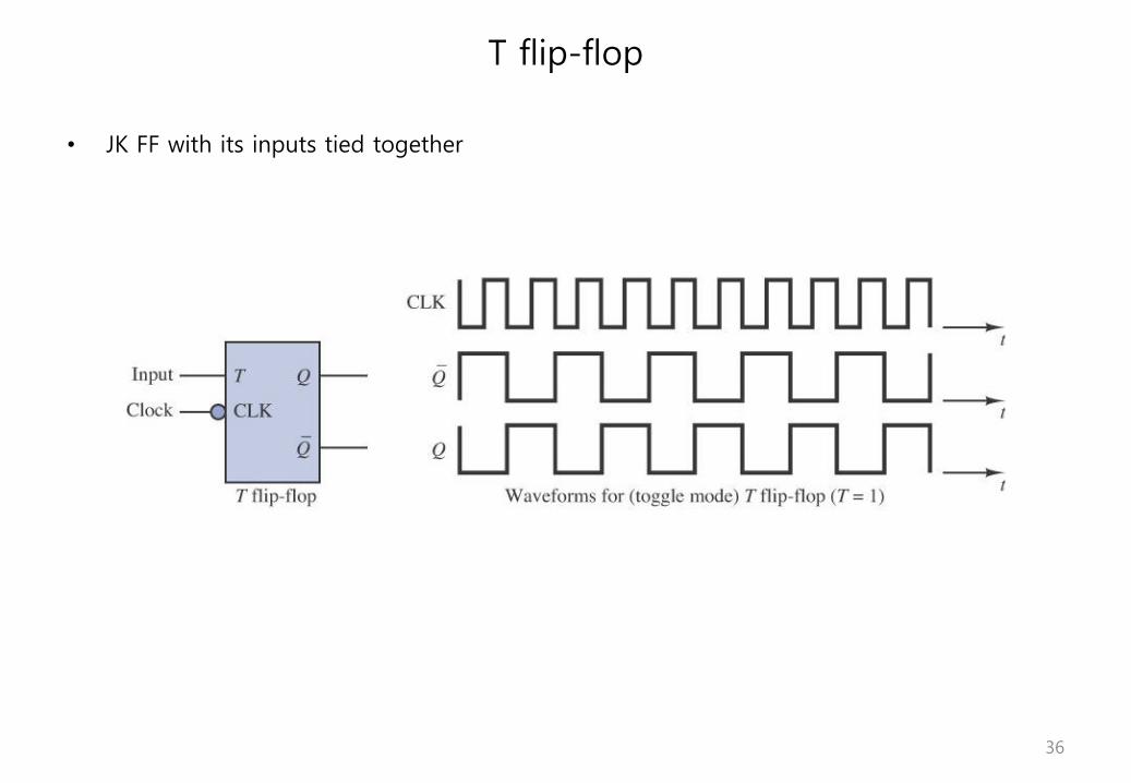
• JK FF with its inputs tied together
T flip-flop
36
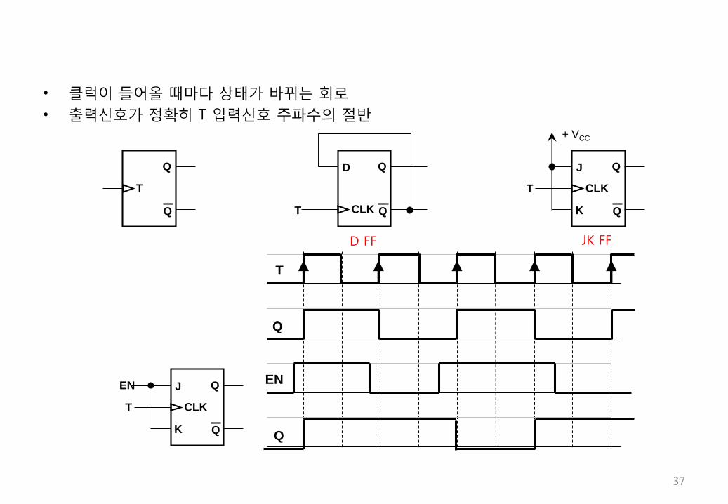
• 클럭이 들어올 때마다 상태가 바뀌는 회로
• 출력신호가 정확히 T 입력신호 주파수의 절반
37
Q
Q
T
D Q
QCLKT
J
K
Q
Q
CLKT
+ VCC
J
K
Q
Q
CLKT
EN
Q
EN
Q
T
D FF JK FF
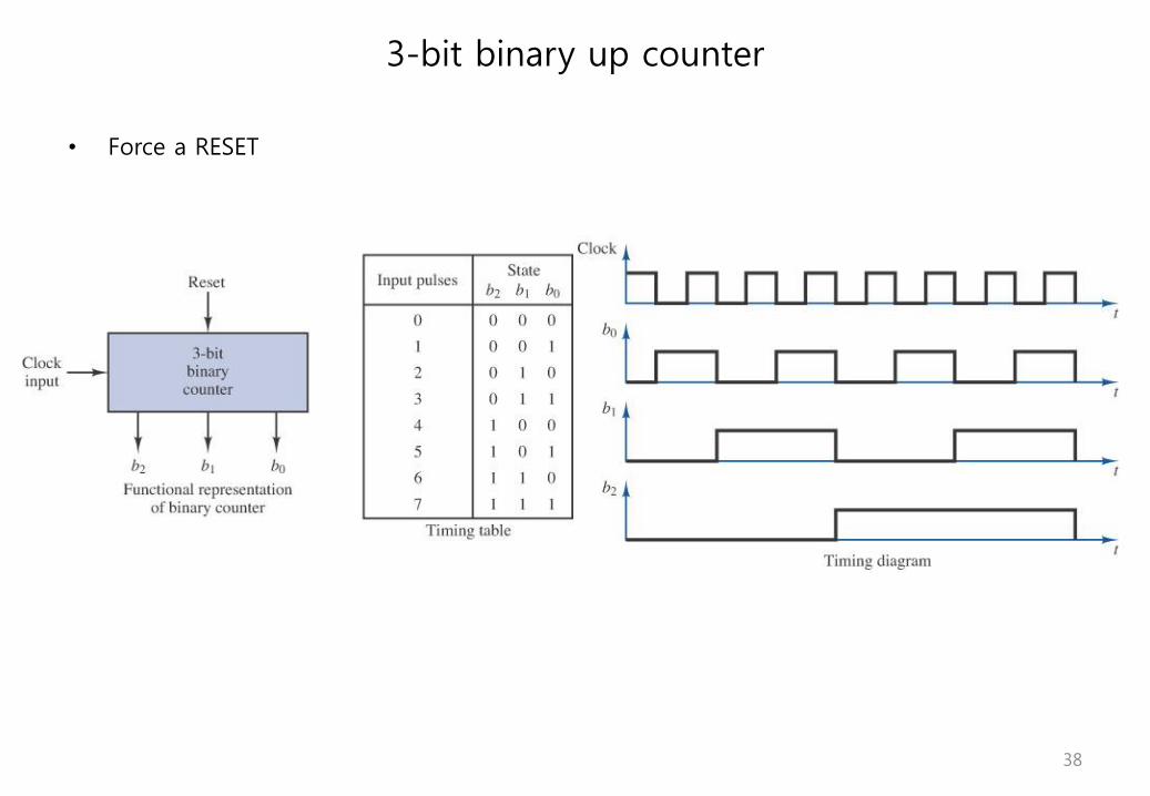
• Force a RESET
3-bit binary up counter
38

• Count from 0 to 9 and then RESET
• Impractical due to propagation delays
Decade counter
39

• Consists of a cascade of 3 JK FFs
Ripple counter
40

• Asynchronous counter
– T FF
– 𝑛 serial cascades = (2𝑛 − 1) counter
– Slow
Ripple-up counter
41
Q0
T0
Q1
T1
Q2
T2
Q0 (LSB) Q1 Q2
Q0
Q1
Q2
CLK
0
0
0
0
1
0
0
1
0
1
0
2
1
1
0
3
0
0
1
4
1
0
1
5
0
1
1
6
1
1
1
7
Q0
T0
Q1
T1
Q2
T2
Q0 Q1 Q2
Q0 Q1

• Asynchronous counter
Ripple-down counter
42
Q0
T0
Q1
T1
Q2
T2
Q0 (LSB) Q1 Q2 Q0
Q1
Q2
CLK
1
1
1
7
0
1
1
6
1
0
1
5
0
0
1
4
1
1
0
3
0
1
0
2
1
0
0
1
0
0
0
0

• Parallel counter
• Fast
• Complex
Synchronous counter
43
J0
K0
Q0
CLK
+ VCC
J1
K1
Q1
CLK
J2
K2
Q2
CLK
J3
K3
Q3
CLK
Q0 Q1 Q2 Q3
F0 F1 F2 F3

44
1 2 3 4 5 6 7 8 9 10 11 12 13 14 15

Divider circuit
45

Synchronous counter
46

Ring counter
47
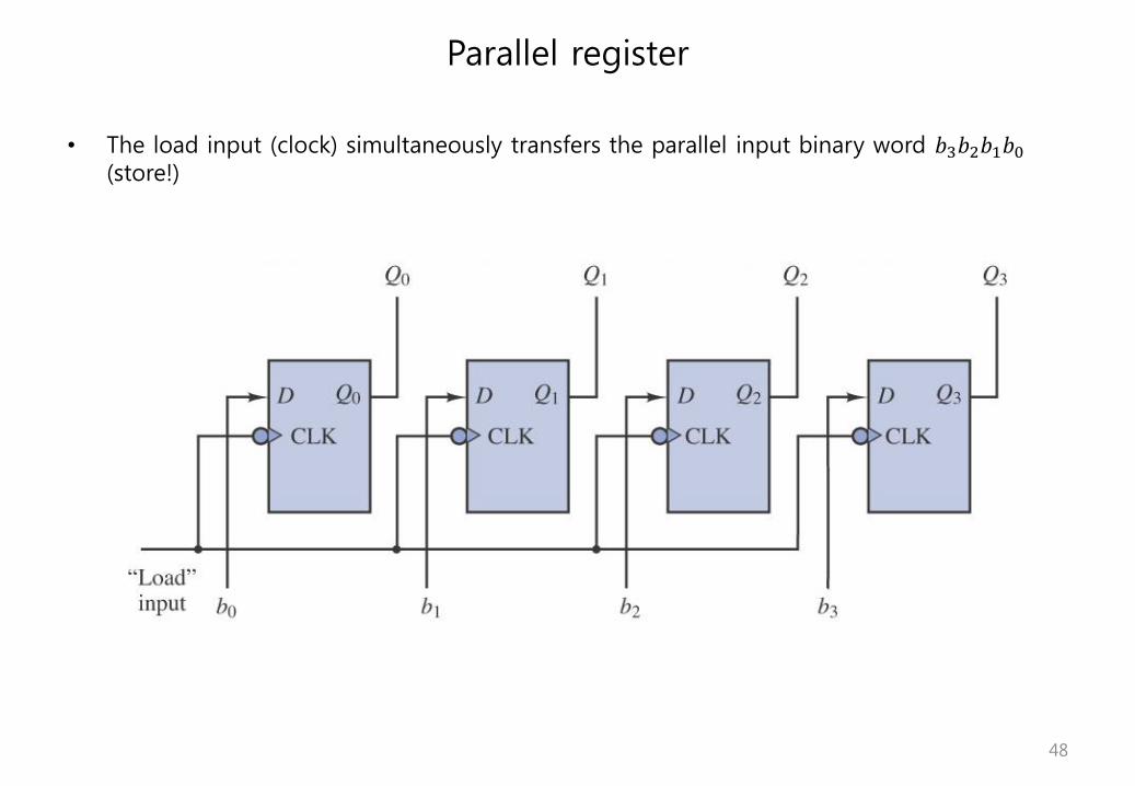
• The load input (clock) simultaneously transfers the parallel input binary word 𝑏3𝑏2𝑏1𝑏0
(store!)
Parallel register
48

Shift register
49
Top Related