


Languages
Pages
Legal


Library Expert Surface Mount Families
PCB Libraries, Inc. Get updates at www.PCBLibraries.com/downloads
Stay connected ‐ follow us! updated 1‐8‐15
Non‐polarized Rectangular Chip Components
Chip Capacitor
Chip Resistor
Chip Inductor
Chip Fuse
Chip Thermistor
Chip Varistor
Chip Non‐polarized Diode
Land Pattern Zero Rotation
Library Expert Surface Mount Families
PCB Libraries, Inc. Get updates at www.PCBLibraries.com/downloads
Stay connected ‐ follow us! updated 1‐8‐15
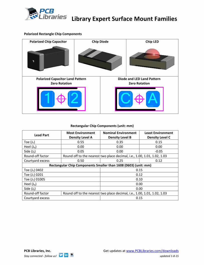
Polarized Rectangle Chip Components
Polarized Chip Capacitor
Chip Diode
Chip LED
Polarized Capacitor Land Pattern Zero Rotation
Diode and LED Land Pattern Zero Rotation
Rectangular Chip Components (unit: mm)
Lead Part Most Environment Density Level A
Nominal Environment Density Level B
Least Environment Density Level C
Toe (JT) 0.55 0.35 0.15
Heel (JH) 0.00 0.00 0.00
Side (JS) 0.05 0.00 ‐0.05
Round‐off factor Round off to the nearest two place decimal, i.e., 1.00, 1.01, 1.02, 1.03
Courtyard excess 0.50 0.25 0.12
Rectangular Chip Components Smaller than 1608 (0603) (unit: mm)
Toe (JT) 0402 0.15
Toe (JT) 0201 0.12
Toe (JT) 01005 0.10
Heel (JH) 0.00
Side (JS) 0.00
Round‐off factor Round off to the nearest two place decimal, i.e., 1.00, 1.01, 1.02, 1.03
Courtyard excess 0.15

Library Expert Surface Mount Families
PCB Libraries, Inc. Get updates at www.PCBLibraries.com/downloads
Stay connected ‐ follow us! updated 1‐8‐15
Rectangular Chip Component Package Sizes
Table of Chip Package Size Codes and Dimensions
EIA (inch) Name Inch Dimensions IEC (metric) Name Metric Dimensions
01005 0.0157 in × 0.0079 in 0402 0.4 mm × 0.2 mm
0201 0.024 in × 0.012 in 0603 0.6 mm × 0.3 mm
0402 0.039 in × 0.020 in 1005 1.0 mm × 0.5 mm
0603 0.063 in × 0.031 in 1608 1.6 mm × 0.8 mm
0805 0.079 in × 0.049 in 2012 2.0 mm × 1.25 mm
1008 0.098 in × 0.079 in 2520 2.5 mm × 2.0 mm
1206 0.126 in × 0.063 in 3216 3.2 mm × 1.6 mm
1210 0.126 in × 0.098 in 3225 3.2 mm × 2.5 mm
1806 0.177 in × 0.063 in 4516 4.5 mm × 1.6 mm
1812 0.18 in × 0.13 in 4532 4.5 mm × 3.2 mm
2010 0.197 in × 0.098 in 5025 5.0 mm × 2.5 mm
2512 0.25 in × 0.13 in 6332 6.4 mm × 3.2 mm
2920 (0.29 in × 0.20 in 7451 7.4 mm × 5.1 mm
Non‐polarized Molded Body Inward Flat Ribbon Components
Capacitors (CAPM)
Molded Non‐polarized Diode (DIOMN)
Fuses (FUSM)
Molded Body Inductor (INDM)
Molded Precision Inductor (INDPM)
Molded Resistors (RESM)
Land Pattern Zero Rotation

Library Expert Surface Mount Families
PCB Libraries, Inc. Get updates at www.PCBLibraries.com/downloads
Stay connected ‐ follow us! updated 1‐8‐15
Polarized Molded Body Inward Flat Ribbon Components
Molded Body Polarized
Capacitor (CAPMP)
Molded Body Diode (DIOM)
Molded Body LED (LEDM)
Polarized Capacitor Land Pattern Zero Rotation
Diode and LED Land Pattern Zero Rotation
Inward Flat Ribbon L‐Leads (unit: mm)
Lead Part Most Environment Density Level A
Nominal Environment Density Level B
Least Environment Density Level C
Toe (JT) (to find G dim) 0.25 0.15 0.07
Heel (JH) (to find Z dim) 0.80 0.50 0.20
Side (JS) 0.01 ‐0.05 ‐0.10
Round‐off factor Round off to the nearest two place decimal, i.e., 1.00, 1.01, 1.02, 1.03
Courtyard excess 0.50 0.25 0.12
Common Molded Body Tantalum Capacitors
EIA Size Code Package Dimensions KEMET Case Code AVX Case Code
2012‐12 2.0 mm × 1.3 mm × 1.2 mm R R
3216‐10 3.2 mm × 1.6 mm × 1.0 mm I K
3216‐12 3.2 mm × 1.6 mm × 1.2 mm S S
3216‐18 3.2 mm × 1.6 mm × 1.8 mm A A
3528‐12 3.5 mm × 2.8 mm × 1.2 mm T T
3528‐21 3.5 mm × 2.8 mm × 2.1 mm B B
6032‐15 6.0 mm × 3.2 mm × 1.5 mm U W
6032‐28 6.0 mm × 3.2 mm × 2.8 mm C C
7260‐38 7.3 mm × 6.0 mm × 3.8 mm E V
7343‐20 7.3 mm × 4.3 mm × 2.0 mm V Y
7343‐31 7.3 mm × 4.3 mm × 3.1 mm D D
7343‐43 7.3 mm × 4.3 mm × 4.3 mm X E

Library Expert Surface Mount Families
PCB Libraries, Inc. Get updates at www.PCBLibraries.com/downloads
Stay connected ‐ follow us! updated 1‐8‐15
Common Molded Body Diodes
JEDEC Standard Case Code Package Dimensions
DO‐214AA SMB 5.30 mm × 3.60 mm × 2.25 mm
DO‐214AB SMC 7.95 mm × 5.90 mm × 2.25 mm
DO‐214AC SMA 5.20 mm × 2.60 mm × 2.15 mm
Metal Electrode Leadless Face (MELF)
MELF Resistor (RESMELF)
MELF Fuse (FUSEMELF)
MELF Diode (DIOMELF)
Resistor and Fuse Land Pattern Zero Rotation A
Diode Land Pattern Zero Rotation
Metal Electrode Leadless Face (MELF) (unit: mm)
Lead Part Most Environment Density Level A
Nominal Environment Density Level B
Least Environment Density Level C
Toe (JT) 0.60 0.40 0.20
Heel (JH) 0.20 0.10 0.02
Side (JS) 0.10 0.05 0.01
Round‐off factor Round off to the nearest two place decimal, i.e., 1.00, 1.01, 1.02, 1.03
Courtyard excess 0.50 0.25 0.12
Common MELF Package Sizes
Common Case Names Size Code Package Dimensions
MicroMelf (MMU) 0102 2.20 mm L X 1.10 mm Dia.
MiniMelf (MMA) 0204 3.60 mm L X 1.40 mm Dia.
Melf (MMB) 0207 5.80 mm L X 2.20 mm Dia.

Library Expert Surface Mount Families
PCB Libraries, Inc. Get updates at www.PCBLibraries.com/downloads
Stay connected ‐ follow us! updated 1‐8‐15
Small Outline Diode (SOD) with Gull‐Wing Leads
Small Outline Diode (SOD)
SOD Land Pattern
Zero Rotation A
Flat Ribbon L and Gull‐Wing Leads (unit: mm)
Lead Part Most Environment Density Level A
Nominal Environment Density Level B
Least Environment Density Level C
Toe (JT) 0.55 0.35 0.15
Heel (JH)1 0.45 0.35 0.25
Side (JS) 0.05 0.03 0.01
Round‐off factor Round off to the nearest two place decimal, i.e., 1.00, 1.01, 1.02, 1.03
Courtyard excess 0.50 0.25 0.12
Common Small Outline Diode (SOD) Sizes
Case Code Package Dimensions
SOD‐123 3.68 mm × 1.17 mm × 1.60 mm
SOD‐128 5.00 mm × 2.70 mm × 1.10 mm
SOD‐323 1.70 mm × 1.25 mm × 0.95 mm
SOD‐523 1.25 mm × 0.85 mm × 0.65 mm
SOD‐723 1.40 mm × 0.60 mm × 0.59 mm
Small Outline Diode Flat Lead (SODFL)
Small Outline Diode Flat Lead
SODFL Land Pattern
Zero Rotation
Small Outline Diodes, Flat Lead (unit: mm)
Lead Part Most Environment Density Level A
Nominal Environment Density Level B
Least Environment Density Level C
Toe (JT) 0.30 0.20 0.10
Heel (JH) 0.00 0.00 0.00
Side (JS) 0.05 0.00 ‐0.05
Round‐off factor Round off to the nearest two place decimal, i.e., 1.00, 1.01, 1.02, 1.03
Courtyard excess 0.20 0.15 0.12
Library Expert Surface Mount Families
PCB Libraries, Inc. Get updates at www.PCBLibraries.com/downloads
Stay connected ‐ follow us! updated 1‐8‐15
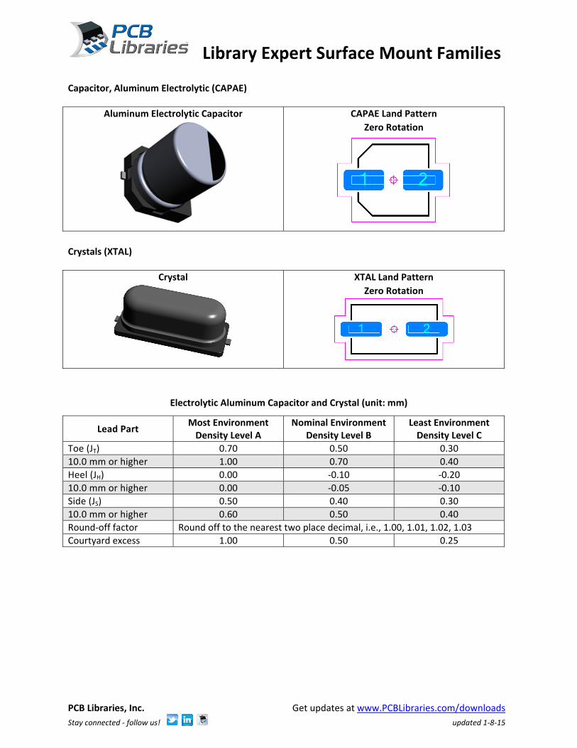
Capacitor, Aluminum Electrolytic (CAPAE)
Aluminum Electrolytic Capacitor
CAPAE Land Pattern
Zero Rotation
Crystals (XTAL)
Crystal
XTAL Land Pattern
Zero Rotation
Electrolytic Aluminum Capacitor and Crystal (unit: mm)
Lead Part Most Environment Density Level A
Nominal Environment Density Level B
Least Environment Density Level C
Toe (JT) 0.70 0.50 0.30
10.0 mm or higher 1.00 0.70 0.40
Heel (JH) 0.00 ‐0.10 ‐0.20
10.0 mm or higher 0.00 ‐0.05 ‐0.10
Side (JS) 0.50 0.40 0.30
10.0 mm or higher 0.60 0.50 0.40
Round‐off factor Round off to the nearest two place decimal, i.e., 1.00, 1.01, 1.02, 1.03
Courtyard excess 1.00 0.50 0.25
Library Expert Surface Mount Families
PCB Libraries, Inc. Get updates at www.PCBLibraries.com/downloads
Stay connected ‐ follow us! updated 1‐8‐15
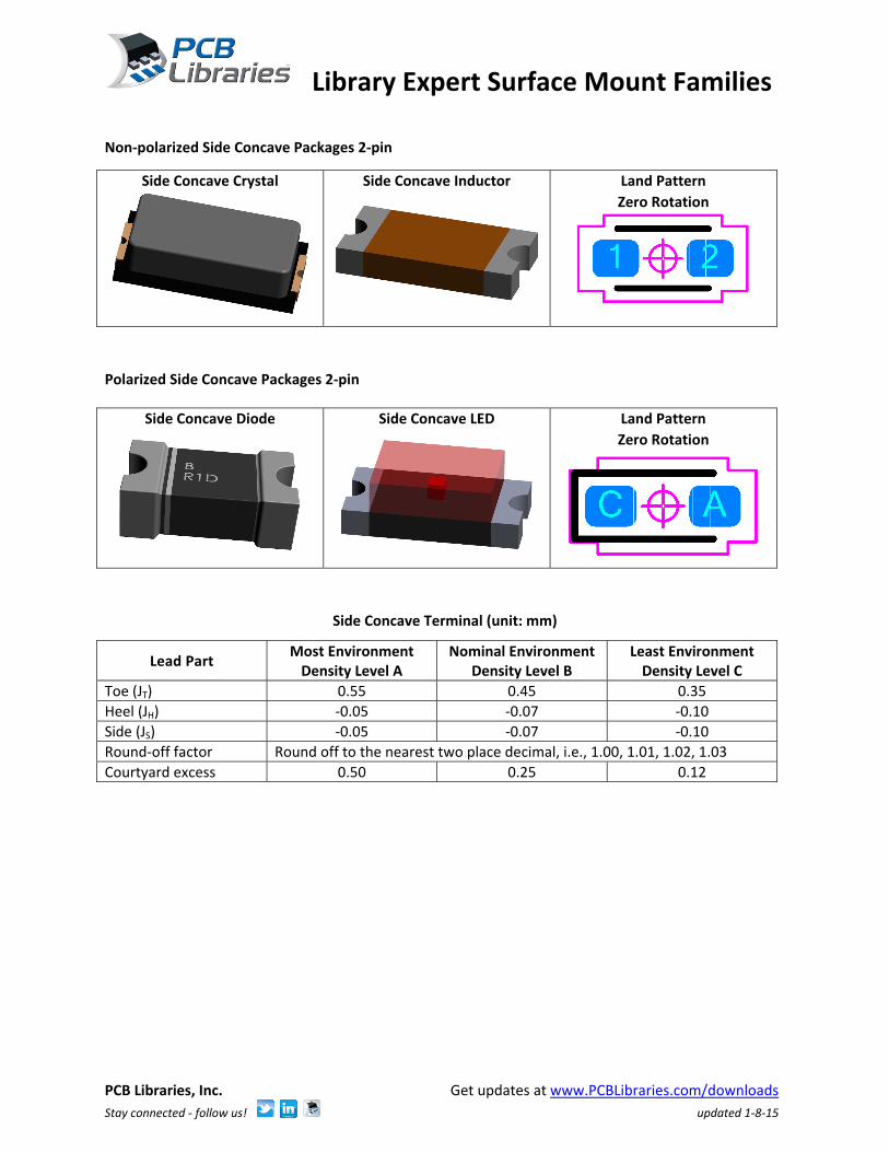
Non‐polarized Side Concave Packages 2‐pin
Side Concave Crystal
Side Concave Inductor
Land Pattern
Zero Rotation
Polarized Side Concave Packages 2‐pin
Side Concave Diode
Side Concave LED
Land Pattern
Zero Rotation
Side Concave Terminal (unit: mm)
Lead Part Most Environment Density Level A
Nominal Environment Density Level B
Least Environment Density Level C
Toe (JT) 0.55 0.45 0.35
Heel (JH) ‐0.05 ‐0.07 ‐0.10
Side (JS) ‐0.05 ‐0.07 ‐0.10
Round‐off factor Round off to the nearest two place decimal, i.e., 1.00, 1.01, 1.02, 1.03
Courtyard excess 0.50 0.25 0.12

Library Expert Surface Mount Families
PCB Libraries, Inc. Get updates at www.PCBLibraries.com/downloads
Stay connected ‐ follow us! updated 1‐8‐15
Non‐polarized Dual Flat No‐Lead (DFN) 2‐pin
DFN Resistor, Inductor, Capacitor, Crystal, Fuse
Non‐polarized DFN Land Pattern
Zero Rotation
Polarized Dual Flat No‐Lead (DFN) 2‐pin
DFN Diode and LED
DFN Diode and LED Land Pattern
Zero Rotation
2‐pin Dual Flat No‐Lead (DFN) (unit: mm)
Lead Part Most Environment Density Level A
Nominal Environment Density Level B
Least Environment Density Level C
Periphery 0.05 0.00 ‐0.05
Round‐off factor Round off to the nearest two place decimal, i.e., 1.00, 1.01, 1.02, 1.03
Courtyard excess 0.50 0.25 0.12
Dual Flat No‐Lead (DFN) Less than 1608 (0603)
Periphery ‐0.04
Round‐off factor Round off to the nearest two place decimal, i.e., 1.00, 1.01, 1.02, 1.03
Courtyard excess 0.15
Library Expert Surface Mount Families
PCB Libraries, Inc. Get updates at www.PCBLibraries.com/downloads
Stay connected ‐ follow us! updated 1‐8‐15
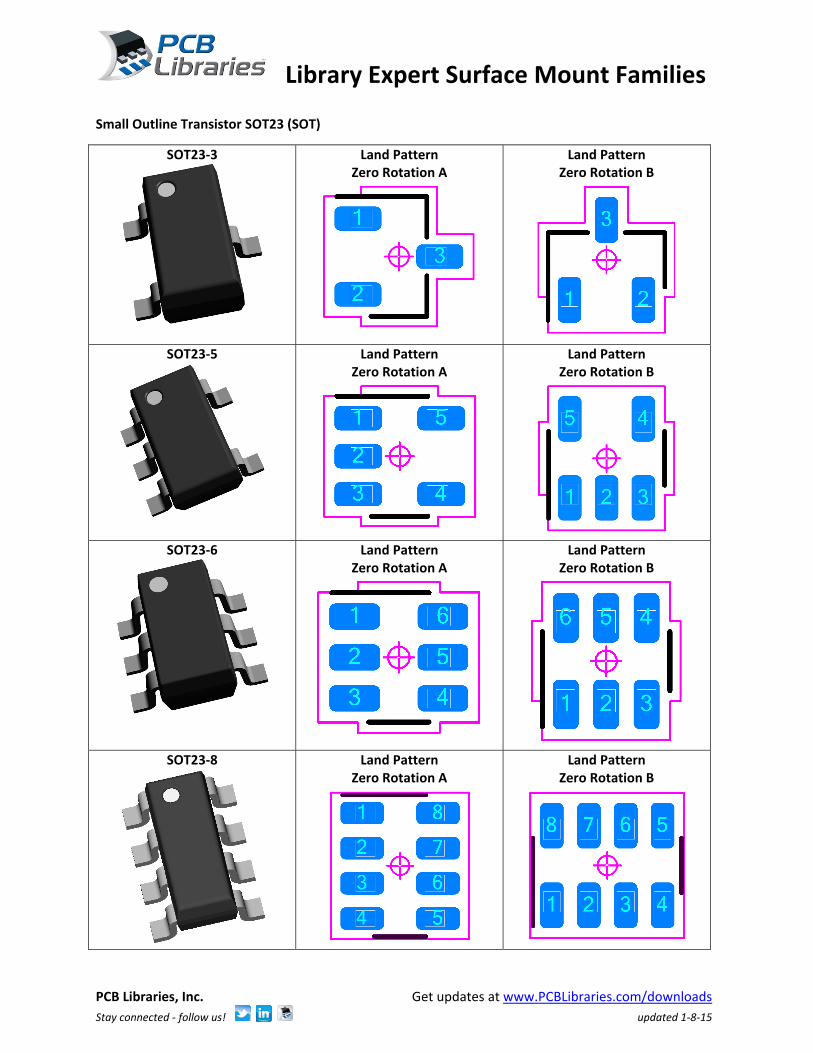
Small Outline Transistor SOT23 (SOT)
SOT23‐3
Land Pattern Zero Rotation A
Land Pattern Zero Rotation B
SOT23‐5
Land Pattern Zero Rotation A
Land Pattern Zero Rotation B
SOT23‐6
Land Pattern Zero Rotation A
Land Pattern Zero Rotation B
SOT23‐8
Land Pattern Zero Rotation A
Land Pattern Zero Rotation B

Library Expert Surface Mount Families
PCB Libraries, Inc. Get updates at www.PCBLibraries.com/downloads
Stay connected ‐ follow us! updated 1‐8‐15
Small Outline Transistor SOT143 (SOT)
SOT143
Land Pattern Zero Rotation A
Land Pattern Zero Rotation B
SOT143 Reverse
Land Pattern Zero Rotation A
Land Pattern Zero Rotation B
Small Outline Transistor SOT223 (SOT)
SOT223‐4
Land Pattern Zero Rotation A
Land Pattern Zero Rotation B
SOT223‐5
Land Pattern Zero Rotation A
Land Pattern Zero Rotation B
Library Expert Surface Mount Families
PCB Libraries, Inc. Get updates at www.PCBLibraries.com/downloads
Stay connected ‐ follow us! updated 1‐8‐15
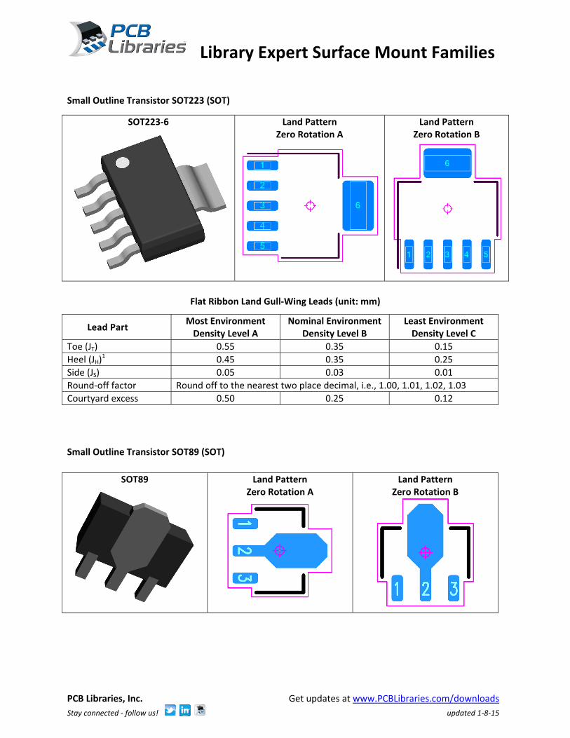
Small Outline Transistor SOT223 (SOT)
SOT223‐6 Land Pattern Zero Rotation A
Land Pattern Zero Rotation B
Flat Ribbon Land Gull‐Wing Leads (unit: mm)
Lead Part Most Environment Density Level A
Nominal Environment Density Level B
Least Environment Density Level C
Toe (JT) 0.55 0.35 0.15
Heel (JH)1 0.45 0.35 0.25
Side (JS) 0.05 0.03 0.01
Round‐off factor Round off to the nearest two place decimal, i.e., 1.00, 1.01, 1.02, 1.03
Courtyard excess 0.50 0.25 0.12
Small Outline Transistor SOT89 (SOT)
SOT89
Land Pattern Zero Rotation A
Land Pattern Zero Rotation B

Library Expert Surface Mount Families
PCB Libraries, Inc. Get updates at www.PCBLibraries.com/downloads
Stay connected ‐ follow us! updated 1‐8‐15
Small Outline Transistor, Flat Lead (SOTFL)
SOTFL 3‐Pin
Land Pattern Zero Rotation A
Land Pattern Zero Rotation B
SOTFL 5‐Pin
Land Pattern Zero Rotation A
Land Pattern Zero Rotation B
SOTFL 6‐Pin
Land Pattern Zero Rotation A
Land Pattern Zero Rotation B
SOTFL 8‐Pin
Land Pattern Zero Rotation A
Land Pattern Zero Rotation B
Small Outline Components, Flat Lead (unit: mm)
Lead Part Most Environment Density Level A
Nominal Environment Density Level B
Least Environment Density Level C
Toe (JT) 0.30 0.20 0.10
Heel (JH) 0.00 0.00 0.00
Side (JS) 0.05 0.00 ‐0.05
Round‐off factor Round off to the nearest two place decimal, i.e., 1.00, 1.01, 1.02, 1.03
Courtyard excess1 0.20 0.15 0.12

Library Expert Surface Mount Families
PCB Libraries, Inc. Get updates at www.PCBLibraries.com/downloads
Stay connected ‐ follow us! updated 1‐8‐15
Transistor Outline (DPAK)
TO DPAK Extended Thermal Tab
Land Pattern Zero Rotation A
Land Pattern Zero Rotation B
TO DPAK Under Body Thermal Tab
Land Pattern Zero Rotation A
Land Pattern Zero Rotation B
Gull‐Wing and Flat Lug Leads (unit: mm)
Lead Part Most Environment Density Level A
Nominal Environment Density Level B
Least Environment Density Level C
Toe (JT) 0.55 0.35 0.15
Heel (JH) 0.45 0.35 0.25
Side (JS) 0.05 0.03 0.01
Round‐off factor Round off to the nearest two place decimal, i.e., 1.00, 1.01, 1.02, 1.03
Courtyard excess 0.50 0.25 0.12
Transistor, Dual Flat No‐lead (TRXDFN)
Transistor DFN 3‐Pin
Land Pattern Zero Rotation A
Land Pattern Zero Rotation B
Library Expert Surface Mount Families
PCB Libraries, Inc. Get updates at www.PCBLibraries.com/downloads
Stay connected ‐ follow us! updated 1‐8‐15
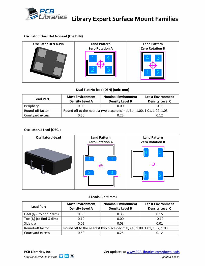
Oscillator, Dual Flat No‐lead (OSCDFN)
Oscillator DFN 4‐Pin
Land Pattern Zero Rotation A
Land Pattern Zero Rotation B
Dual Flat No‐lead (DFN) (unit: mm)
Lead Part Most Environment Density Level A
Nominal Environment Density Level B
Least Environment Density Level C
Periphery 0.05 0.00 ‐0.05
Round‐off factor Round off to the nearest two place decimal, i.e., 1.00, 1.01, 1.02, 1.03
Courtyard excess 0.50 0.25 0.12
Oscillator, J‐Lead (OSCJ)
Oscillator J‐Lead
Land Pattern Zero Rotation A
Land Pattern Zero Rotation B
J‐Leads (unit: mm)
Lead Part Most Environment Density Level A
Nominal Environment Density Level B
Least Environment Density Level C
Heel (JH) (to find Z dim) 0.55 0.35 0.15
Toe (JT) (to find G dim) 0.10 0.00 ‐0.10
Side (JS) 0.05 0.03 0.01
Round‐off factor Round off to the nearest two place decimal, i.e., 1.00, 1.01, 1.02, 1.03
Courtyard excess 0.50 0.25 0.12
Library Expert Surface Mount Families
PCB Libraries, Inc. Get updates at www.PCBLibraries.com/downloads
Stay connected ‐ follow us! updated 1‐8‐15
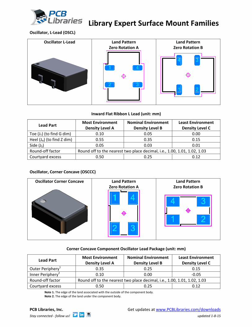
Oscillator, L‐Lead (OSCL)
Oscillator L‐Lead
Land Pattern Zero Rotation A
Land Pattern Zero Rotation B
Inward Flat Ribbon L Lead (unit: mm)
Lead Part Most Environment Density Level A
Nominal Environment Density Level B
Least Environment Density Level C
Toe (JT) (to find G dim) 0.10 0.05 0.00
Heel (JH) (to find Z dim) 0.55 0.35 0.15
Side (JS) 0.05 0.03 0.01
Round‐off factor Round off to the nearest two place decimal, i.e., 1.00, 1.01, 1.02, 1.03
Courtyard excess 0.50 0.25 0.12
Oscillator, Corner Concave (OSCCC)
Oscillator Corner Concave
Land Pattern Zero Rotation A
Land Pattern Zero Rotation B
Corner Concave Component Oscillator Lead Package (unit: mm)
Lead Part Most Environment Density Level A
Nominal Environment Density Level B
Least Environment Density Level C
Outer Periphery1 0.35 0.25 0.15
Inner Periphery2 0.10 0.00 ‐0.05
Round‐off factor Round off to the nearest two place decimal, i.e., 1.00, 1.01, 1.02, 1.03
Courtyard excess 0.50 0.25 0.12
Note 1. The edge of the land associated with the outside of the component body. Note 2. The edge of the land under the component body.

Library Expert Surface Mount Families
PCB Libraries, Inc. Get updates at www.PCBLibraries.com/downloads
Stay connected ‐ follow us! updated 1‐8‐15
Oscillator, Side Concave (OSCSC)
Oscillator Side Concave 4‐Pin
Land Pattern Zero Rotation A
Land Pattern Zero Rotation B
Oscillator Side Concave 6‐Pin
Land Pattern Zero Rotation A
Land Pattern Zero Rotation B
Side Concave (4‐pin) Diode and LED
Diode Side Concave 4‐Pin
LED Side Concave 4‐Pin
Land Pattern Zero Rotation A
Land Pattern Zero Rotation B

Library Expert Surface Mount Families
PCB Libraries, Inc. Get updates at www.PCBLibraries.com/downloads
Stay connected ‐ follow us! updated 1‐8‐15
Side Lead Flat, Concave and Convex Terminal (unit: mm)
Lead Part Most Environment Density Level A
Nominal Environment Density Level B
Least Environment Density Level C
Toe (JT) 0.55 0.45 0.35
Heel (JH) ‐0.05 ‐0.07 ‐0.10
Side (JS) ‐0.05 ‐0.07 ‐0.10
Round‐off factor Round off to the nearest two place decimal, i.e., 1.00, 1.01, 1.02, 1.03
Courtyard excess 0.50 0.25 0.12
Small Outline IC (SOIC)
Small Outline IC
Land Pattern Zero Rotation A
Land Pattern Zero Rotation B
Small Outline IC (SOIC) with Thermal Tab
SOIC with Thermal Tab
Land Pattern Zero Rotation A
Land Pattern Zero Rotation B

Library Expert Surface Mount Families
PCB Libraries, Inc. Get updates at www.PCBLibraries.com/downloads
Stay connected ‐ follow us! updated 1‐8‐15
Small Outline Package (SOP)
Small Outline Package
Land Pattern Zero Rotation A
Land Pattern Zero Rotation B
Small Outline Package (SOP) with Thermal Tab
SOP with Thermal Tab
Land Pattern Zero Rotation A
Land Pattern Zero Rotation B
Ceramic Flat Package (CFP)
Ceramic Flat Pack
Land Pattern Zero Rotation A
Land Pattern Zero Rotation B

Library Expert Surface Mount Families
PCB Libraries, Inc. Get updates at www.PCBLibraries.com/downloads
Stay connected ‐ follow us! updated 1‐8‐15
Quad Flat Package (QFP)
Quad Flat Package
Land Pattern Zero Rotation A
Land Pattern Zero Rotation B
Quad Flat Package (QFP) with Thermal Tab
Quad Flat Package with Thermal Tab
Land Pattern Zero Rotation A
Land Pattern Zero Rotation B
Ceramic Quad Flat Package (CQFP)
Ceramic Quad Flat Pack
Land Pattern Zero Rotation A
Land Pattern Zero Rotation B

Library Expert Surface Mount Families
PCB Libraries, Inc. Get updates at www.PCBLibraries.com/downloads
Stay connected ‐ follow us! updated 1‐8‐15
Flat Ribbon L and Gull‐Wing Leads (greater than 0.625 mm pitch) (unit: mm)
Lead Part Most Environment Density Level A
Nominal Environment Density Level B
Least Environment Density Level C
Toe (JT) 0.55 0.35 0.15
Heel (JH)1 0.45 0.35 0.25
Side (JS) 0.05 0.03 0.01
Round‐off factor Round off to the nearest two place decimal, i.e., 1.00, 1.01, 1.02, 1.03
Courtyard excess 0.50 0.25 0.12
Note 1. For gull wing components where dimension Smin is less than or equal to dimension Emax, use the following heel fillet goals:
Density Level A ‐ 0.25 mm Density Level B ‐ 0.15 mm Density Level C ‐ 0.05 mm Note 2. This does not apply to gull wing components where the lead terminals have a tolerance L that is greater than 0.5 mm.
Flat Ribbon L and Gull‐Wing Leads (less than or equal to 0.625 mm pitch) (unit: mm)
Lead Part Most Environment Density Level A
Nominal Environment Density Level B
Least Environment Density Level C
Toe (JT) 0.55 0.35 0.15
Heel (JH)1 0.45 0.35 0.25
Side (JS) 0.01 ‐0.02 ‐0.04
Round‐off factor Round off to the nearest two place decimal, i.e., 1.00, 1.01, 1.02, 1.03
Courtyard excess 0.50 0.25 0.12
Note 1. For gull wing components where dimension Smin is less than or equal to dimension Emax, use the following heel fillet goals: Density Level A ‐ 0.25 mm
Small Outline J‐Lead (SOJ)
Small Outline J‐Lead
Land Pattern Zero Rotation A
Land Pattern Zero Rotation B
Plastic Leaded Chip Carrier (PLCC)
Plastic Leaded Chip Carrier
Land Pattern Zero Rotation A
Land Pattern Zero Rotation B

Library Expert Surface Mount Families
PCB Libraries, Inc. Get updates at www.PCBLibraries.com/downloads
Stay connected ‐ follow us! updated 1‐8‐15
Small Outline J‐Lead (unit: mm)
Lead Part Most Environment Density Level A
Nominal Environment Density Level B
Least Environment Density Level C
Heel (JH) (to find Z dim) 0.55 0.35 0.15
Toe (JT) (to find G dim) 0.10 0.00 ‐0.10
Side (JS) 0.05 0.03 0.01
Round‐off factor Round off to the nearest two place decimal, i.e., 1.00, 1.01, 1.02, 1.03
Courtyard excess 0.50 0.25 0.12
Small Outline L‐Lead (SOL)
Small Outline L‐Lead
Land Pattern Zero Rotation A
Land Pattern Zero Rotation B
Small Outline L‐Lead (SOL) (unit: mm)
Lead Part Most Environment Density Level A
Nominal Environment Density Level B
Least Environment Density Level C
Toe (JT) (to find G dim) 0.10 0.00 ‐0.10
Heel (JH) (to find Z dim) 0.55 0.35 0.15
Side (JS) 0.01 ‐0.02 ‐0.04
Round‐off factor Round off to the nearest two place decimal, i.e., 1.00, 1.01, 1.02, 1.03
Courtyard excess 0.50 0.25 0.12

Library Expert Surface Mount Families
PCB Libraries, Inc. Get updates at www.PCBLibraries.com/downloads
Stay connected ‐ follow us! updated 1‐8‐15
Ball Grid Array, Collapsing Ball (BGA)
Collapsing Ball Grid Array
Land Pattern Zero Rotation A
Land Pattern Zero Rotation B
Collapsing Ball Grid Array (BGA) (unit: mm)
Lead Part Most Environment Density Level A
Nominal Environment Density Level B
Least Environment Density Level C
Periphery 25% reduction below nominal ball diameter
20% reduction below nominal ball diameter
15% reduction below nominal ball diameter
Round‐off factor Round off to the nearest two place decimal, i.e., 1.00, 1.01, 1.02, 1.03
Courtyard excess 1.00 0.50 0.25
Ball Grid Array, Non‐collapsing Ball (BGAN)
Non‐collapsing Ball Grid Array
Land Pattern Zero Rotation A
Land Pattern Zero Rotation B
Non‐collapsing Ball Grid Array (BGA) (unit: mm)
Lead Part Most Environment Density Level A
Nominal Environment Density Level B
Least Environment Density Level C
Periphery
15% increase above the nominal ball or column
diameter
10% increase above the nominal ball or column
diameter
5% increase above the nominal ball or column
diameter
Round‐off factor Round off to the nearest two place decimal, i.e., 1.00, 1.01, 1.02, 1.03
Courtyard excess 1.00 0.50 0.25

Library Expert Surface Mount Families
PCB Libraries, Inc. Get updates at www.PCBLibraries.com/downloads
Stay connected ‐ follow us! updated 1‐8‐15
Column Grid Array (CGA)
Column Grid Array
Land Pattern Zero Rotation A
Land Pattern Zero Rotation B
Column Grid Array (CGA)
Lead Part Nominal Environment
Density Level B
Periphery 0.10
Round‐off factor Round off to the nearest two place decimal, i.e., 1.00, 1.01, 1.02, 1.03
Courtyard excess 1.00

Library Expert Surface Mount Families
PCB Libraries, Inc. Get updates at www.PCBLibraries.com/downloads
Stay connected ‐ follow us! updated 1‐8‐15
Small Outline No‐lead (SON)
Small Outline No‐lead
Land Pattern Zero Rotation A
Land Pattern Zero Rotation B
Small Outline No‐lead (SON) with Thermal Tab
SON with Thermal Tab
Land Pattern Zero Rotation A
Land Pattern Zero Rotation B
Quad Flat No‐lead (QFN)
Quad Flat No‐lead
Land Pattern Zero Rotation A
Land Pattern Zero Rotation B

Library Expert Surface Mount Families
PCB Libraries, Inc. Get updates at www.PCBLibraries.com/downloads
Stay connected ‐ follow us! updated 1‐8‐15
Quad Flat No‐lead (QFN) with Thermal Tab
QFN with Thermal Tab
Land Pattern Zero Rotation A
Land Pattern Zero Rotation B
Small Outline No‐Lead and Quad Flat No‐Lead (unit: mm)
Lead Part Most Environment Density Level A
Nominal Environment Density Level B
Least Environment Density Level C
Toe (JT) 0.40 0.30 0.20
Heel (JH) 0.00 0.00 0.00
Side (JS) ‐0.04 ‐0.04 ‐0.04
Round‐off factor Round off to the nearest two place decimal, i.e., 1.00, 1.01, 1.02, 1.03
Courtyard excess 0.50 0.25 0.12

Library Expert Surface Mount Families
PCB Libraries, Inc. Get updates at www.PCBLibraries.com/downloads
Stay connected ‐ follow us! updated 1‐8‐15
Pull‐back Small Outline No‐lead (PSON)
Pull‐back Small Outline No‐lead
Land Pattern Zero Rotation A
Land Pattern Zero Rotation B
Pull‐back Small Outline No‐lead (PSON) with Thermal Tab
PQFN with Thermal Tab
Land Pattern Zero Rotation A
Land Pattern Zero Rotation B
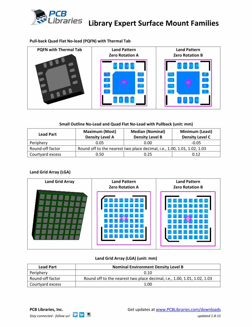
Pull‐back Quad Flat No‐lead (PQFN)
Pull‐back Quad Flat No‐Lead
Land Pattern Zero Rotation A
Land Pattern Zero Rotation B
Library Expert Surface Mount Families
PCB Libraries, Inc. Get updates at www.PCBLibraries.com/downloads
Stay connected ‐ follow us! updated 1‐8‐15
Pull‐back Quad Flat No‐lead (PQFN) with Thermal Tab
PQFN with Thermal Tab
Land Pattern Zero Rotation A
Land Pattern Zero Rotation B
Small Outline No‐Lead and Quad Flat No‐Lead with Pullback (unit: mm)
Lead Part Maximum (Most) Density Level A
Median (Nominal) Density Level B
Minimum (Least) Density Level C
Periphery 0.05 0.00 ‐0.05
Round‐off factor Round off to the nearest two place decimal, i.e., 1.00, 1.01, 1.02, 1.03
Courtyard excess 0.50 0.25 0.12
Land Grid Array (LGA)
Land Grid Array
Land Pattern Zero Rotation A
Land Pattern Zero Rotation B
Land Grid Array (LGA) (unit: mm)
Lead Part Nominal Environment Density Level B
Periphery 0.10
Round‐off factor Round off to the nearest two place decimal, i.e., 1.00, 1.01, 1.02, 1.03
Courtyard excess 1.00

Library Expert Surface Mount Families
PCB Libraries, Inc. Get updates at www.PCBLibraries.com/downloads
Stay connected ‐ follow us! updated 1‐8‐15
Leadless Chip Carrier (LCC)
Leadless Chip Carrier
Land Pattern Zero Rotation A
Land Pattern Zero Rotation B
Leadless Chip Carrier (LCC) (unit: mm)
Lead Part Most Environment Density Level A
Nominal Environment Density Level B
Least Environment Density Level C
Heel (JH) (to find Z dim) 0.65 0.55 0.45
Toe (JT) (to find G dim) 0.25 0.15 0.05
Side (JS) 0.05 ‐0.05 ‐0.15
Round‐off factor Round off to the nearest two place decimal, i.e., 1.00, 1.05, 1.10, 1.15
Courtyard excess 0.50 0.25 0.12

Library Expert Surface Mount Families
PCB Libraries, Inc. Get updates at www.PCBLibraries.com/downloads
Stay connected ‐ follow us! updated 1‐8‐15
Resistor, Side Concave Chip Array (RESCAV)
Concave Chip Array Resistor
Land Pattern Zero Rotation A
Land Pattern Zero Rotation B
Inductor, Side Flat Chip Array (INDCAV)
Concave Chip Array Inductor
Land Pattern Zero Rotation A
Land Pattern Zero Rotation B
Resistor, Side Concave Chip Array 4‐Sided (RESCAV)
Example of 3D STEP model
Land Pattern Zero Rotation A
Land Pattern Zero Rotation B

Library Expert Surface Mount Families
PCB Libraries, Inc. Get updates at www.PCBLibraries.com/downloads
Stay connected ‐ follow us! updated 1‐8‐15
Resistor, Convex Chip Array Type E (RESCAXE)
Convex Chip Array Type E
Land Pattern Zero Rotation A
Land Pattern Zero Rotation B
Resistor, Convex Chip Array Type S (RESCAXS)
Convex Chip Array Type S
Land Pattern Zero Rotation A
Land Pattern Zero Rotation B
Side Flat/Concave/Convex Terminals (unit: mm)
Lead Part Most Environment Density Level A
Nominal Environment Density Level B
Least Environment Density Level C
Toe (JT) 0.55 0.45 0.35
Heel (JH) ‐0.05 ‐0.07 ‐0.10
Side (JS) ‐0.05 ‐0.07 ‐0.10
Round‐off factor Round off to the nearest two place decimal, i.e., 1.00, 1.01, 1.02, 1.03
Courtyard excess 0.50 0.25 0.12
Top Related