


Languages
Pages
Legal

Lecture 6 - 1Introduction to Digital Integrated Circuit DesignData Path Circuits
Lecture 6
Data Path Circuits
Konstantinos MasselosDepartment of Electrical & Electronic Engineering
Imperial College London
URL: http://cas.ee.ic.ac.uk/~kostasE-mail: [email protected]
Lecture 6 - 2Introduction to Digital Integrated Circuit DesignData Path Circuits
Based on slides/material by…
J. Rabaey http://bwrc.eecs.berkeley.edu/Classes/IcBook/instructors.html“Digital Integrated Circuits: A Design Perspective”, Prentice Hall
D. Harris http://www.cmosvlsi.com/coursematerials.htmlWeste and Harris, “CMOS VLSI Design: A Circuits and Systems Perspective”, Addison Wesley
Lecture 6 - 3Introduction to Digital Integrated Circuit DesignData Path Circuits
Recommended Reading
J. Rabaey et. al. “Digital Integrated Circuits: A Design Perspective”: Chapter 11
Weste and Harris, “CMOS VLSI Design: A Circuits and Systems Perspective”: Chapter 10
Lecture 6 - 4Introduction to Digital Integrated Circuit DesignData Path Circuits
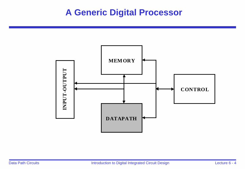
A Generic Digital Processor
MEMORY
DATAPATH
CONTROL
INPU
T-O
UT
PUT
Lecture 6 - 5Introduction to Digital Integrated Circuit DesignData Path Circuits
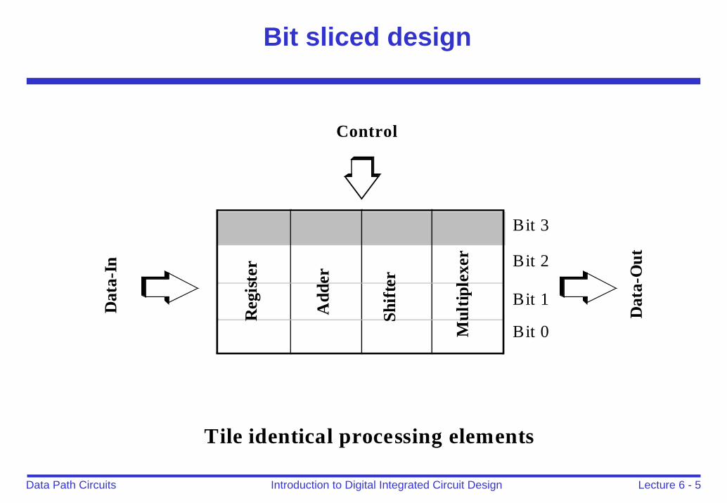
Bit sliced design
Bit 3
Bit 2
Bit 1
Bit 0
Reg
ister
Add
er
Shift
er
Mul
tiple
xer
ControlD
ata-
In
Dat
a-O
ut
Tile identical processing elements
Lecture 6 - 6Introduction to Digital Integrated Circuit DesignData Path Circuits
Outline
Adders
Multipliers
Shifters
Comparators
Layout issues
Lecture 6 - 7Introduction to Digital Integrated Circuit DesignData Path Circuits
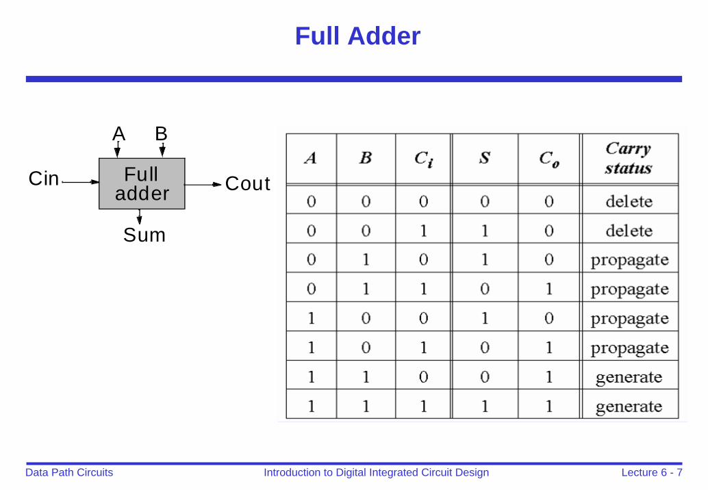
Full Adder
A B
Cout
Sum
Cin Fulladder
Lecture 6 - 8Introduction to Digital Integrated Circuit DesignData Path Circuits
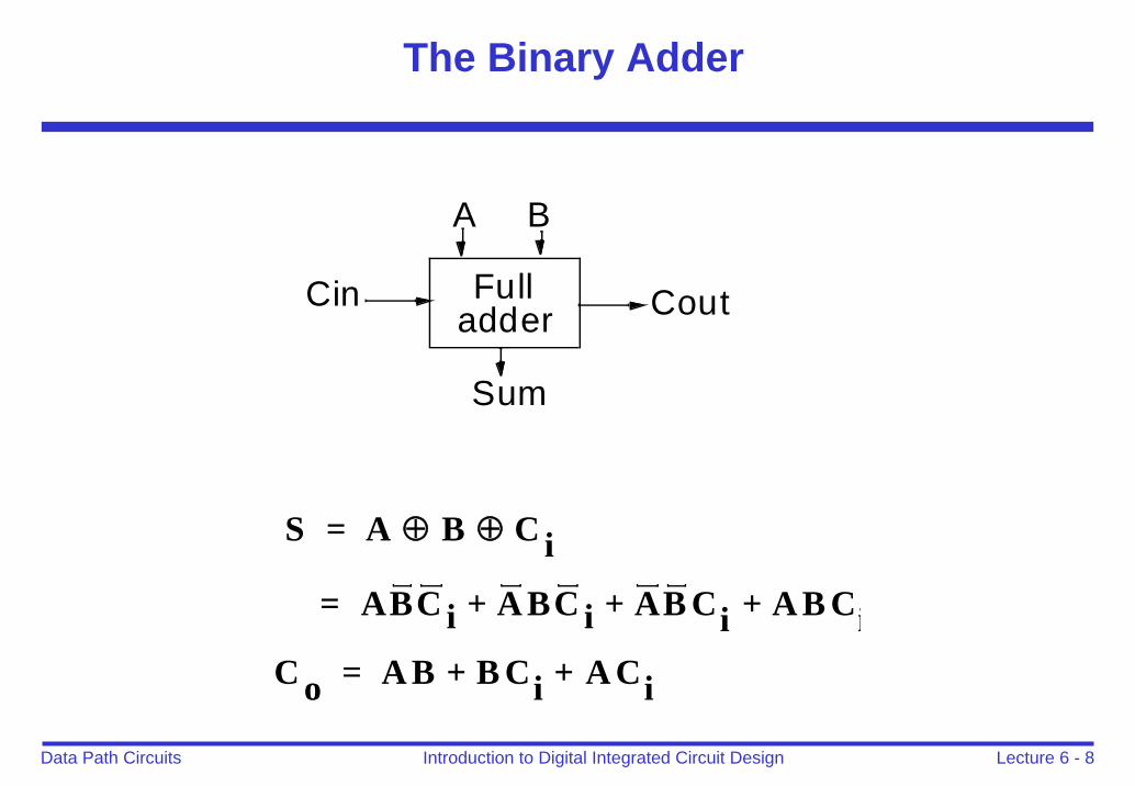
The Binary Adder
S A B C i⊕ ⊕=
A= BC i A BC i AB Ci A B Ci+ + +
C o A B B Ci A Ci+ +=
A B
Cout
Sum
Cin Fulladder
Lecture 6 - 9Introduction to Digital Integrated Circuit DesignData Path Circuits
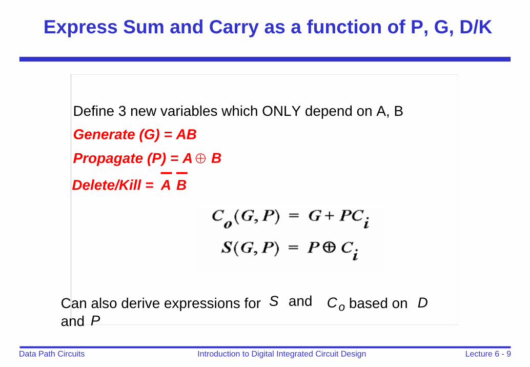
Express Sum and Carry as a function of P, G, D/K
Define 3 new variables which ONLY depend on A, BGenerate (G) = ABPropagate (P) = A ⊕ B
Delete/Kill = A B
Can also derive expressions for S and Co based on Dand P
Lecture 6 - 10Introduction to Digital Integrated Circuit DesignData Path Circuits
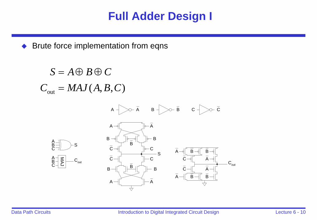
Full Adder Design I
Brute force implementation from eqns
out ( , , )S A B C
C MAJ A B C= ⊕ ⊕=
ABC
S
Cout
MA
J
ABC
A
B BB
A
CS
C
CC
B BB
A A
A B
C
B
A
CBA A B C
Cout
C
A
A
BB
Lecture 6 - 11Introduction to Digital Integrated Circuit DesignData Path Circuits
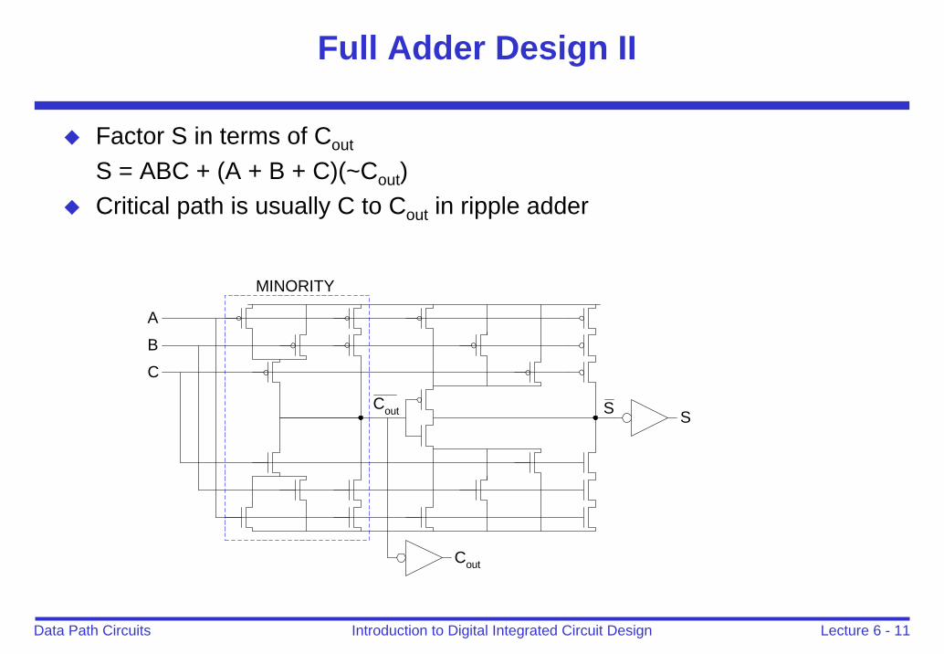
Full Adder Design II
Factor S in terms of Cout
S = ABC + (A + B + C)(~Cout)Critical path is usually C to Cout in ripple adder
SS
Cout
A
B
C
Cout
MINORITY
Lecture 6 - 12Introduction to Digital Integrated Circuit DesignData Path Circuits
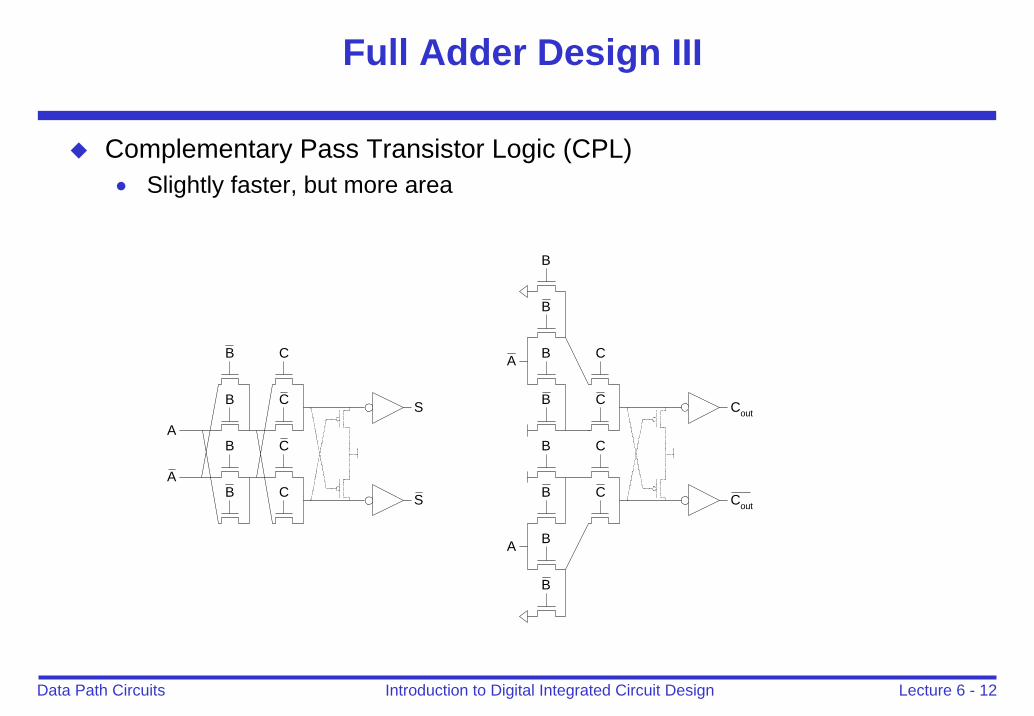
Full Adder Design III
Complementary Pass Transistor Logic (CPL)• Slightly faster, but more area
A
C
S
S
B
B
C
C
C
B
B Cout
Cout
C
C
C
C
B
B
B
B
B
B
B
B
A
A
A
Lecture 6 - 13Introduction to Digital Integrated Circuit DesignData Path Circuits
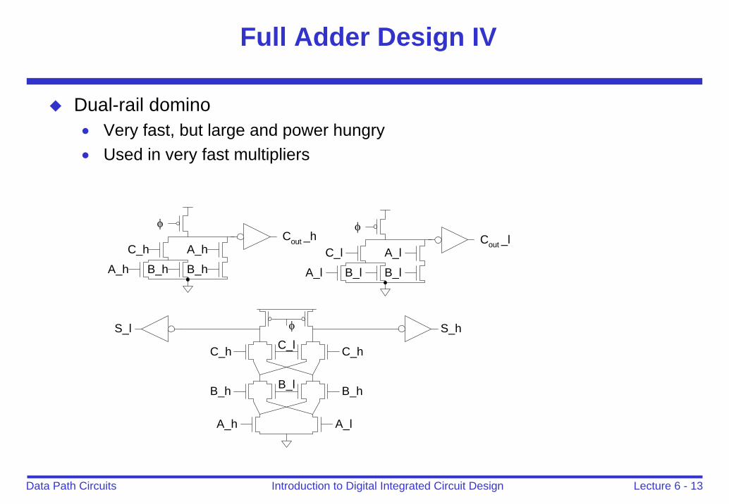
Full Adder Design IV
Dual-rail domino• Very fast, but large and power hungry• Used in very fast multipliers
Cout _h
A_h B_h
C_h
B_h
A_h
φCout _l
A_l B_l
C_l
B_l
A_l
φ
S_hS_l
A_h
B_h B_hB_l
A_l
C_lC_h C_h
φ
Lecture 6 - 14Introduction to Digital Integrated Circuit DesignData Path Circuits
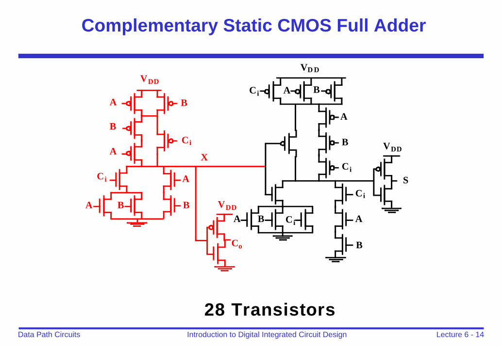
Complementary Static CMOS Full Adder
VDD
VD D
VDD
VDD
A B
Ci
S
Co
X
B
A
Ci A
BBA
Ci
A B Ci
Ci
B
A
Ci
A
B
BA
28 Transistors
Lecture 6 - 15Introduction to Digital Integrated Circuit DesignData Path Circuits
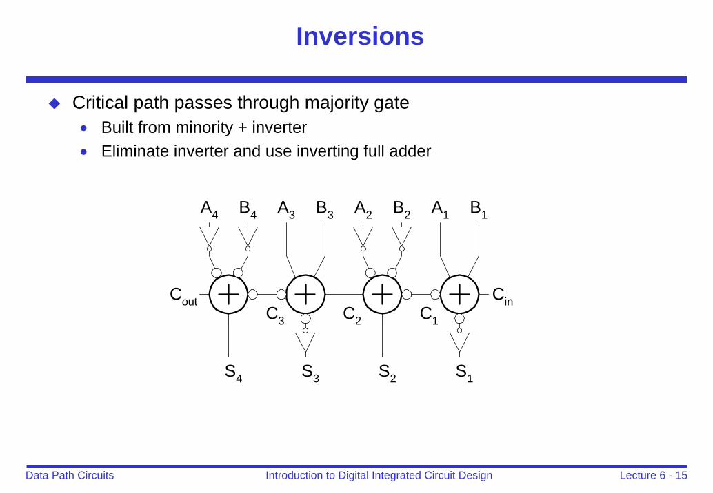
Inversions
Critical path passes through majority gate• Built from minority + inverter• Eliminate inverter and use inverting full adder
Cout Cin
B1A1B2A2B3A3B4A4
S1S2S3S4
C1C2C3
Lecture 6 - 16Introduction to Digital Integrated Circuit DesignData Path Circuits
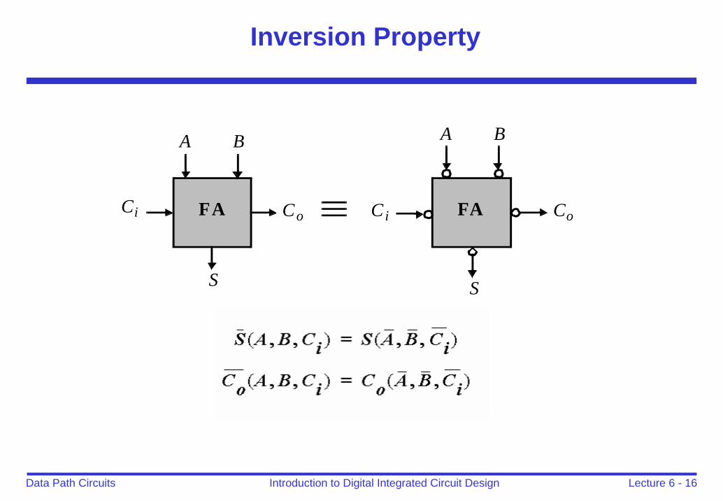
Inversion Property
A B
S
CoCi FA
A B
S
CoCi FA
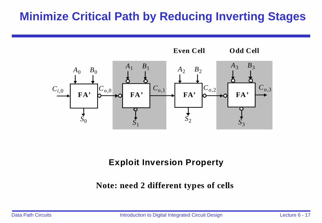
Lecture 6 - 17Introduction to Digital Integrated Circuit DesignData Path Circuits
Minimize Critical Path by Reducing Inverting Stages
A0 B0
S0
Co ,0Ci ,0
A1 B1
S1
Co ,1
A2 B2
S2
Co,2 Co,3FA’ FA’ FA’ FA’
A3 B3
S3
Odd CellEven Cell
Exploit Inversion Property
Note: need 2 different types of cells
Lecture 6 - 18Introduction to Digital Integrated Circuit DesignData Path Circuits
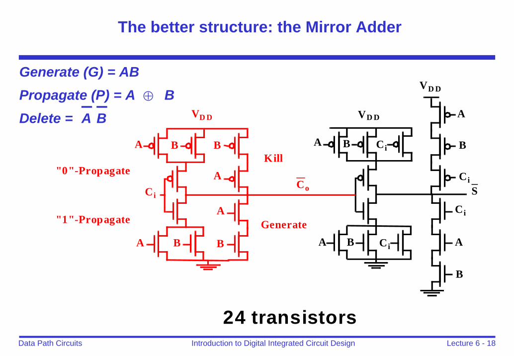
The better structure: the Mirror Adder
VD D
Ci
A
BBA
B
A
A BKill
Generate"1"-Propagate
"0"-Propagate
VD D
Ci
A B Ci
Ci
B
A
Ci
A
BBA
VD D
SCo
24 transistors
Generate (G) = ABPropagate (P) = A ⊕ BDelete = A B
Lecture 6 - 19Introduction to Digital Integrated Circuit DesignData Path Circuits
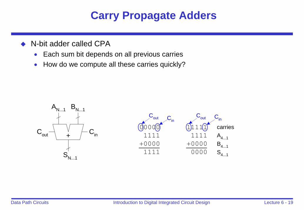
Carry Propagate Adders
N-bit adder called CPA• Each sum bit depends on all previous carries• How do we compute all these carries quickly?
+
BN...1AN...1
SN...1
CinCout 11111 1111 +0000 0000
A4...1
carries
B4...1
S4...1
CinCout
00000 1111 +0000 1111
CinCout
Lecture 6 - 20Introduction to Digital Integrated Circuit DesignData Path Circuits
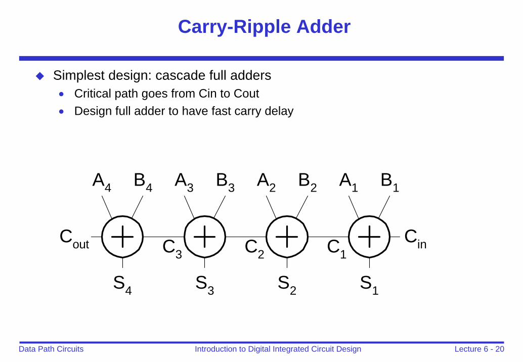
Carry-Ripple Adder
Simplest design: cascade full adders• Critical path goes from Cin to Cout• Design full adder to have fast carry delay
CinCout
B1A1B2A2B3A3B4A4
S1S2S3S4
C1C2C3
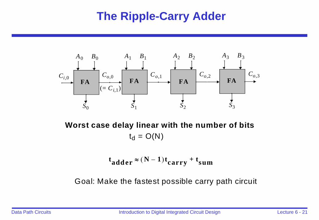
Lecture 6 - 21Introduction to Digital Integrated Circuit DesignData Path Circuits
The Ripple-Carry Adder
A0 B0
S0
Co,0Ci,0
A1 B1
S1
Co ,1
A2 B2
S2
Co ,2
A3 B3
S3
Co ,3
(= Ci,1)FA FA FA FA
Worst case delay linear with the number of bits
tadd er N 1–( ) tcarry tsum+≈
td = O(N)
Goal: Make the fastest possible carry path circuit
Lecture 6 - 22Introduction to Digital Integrated Circuit DesignData Path Circuits
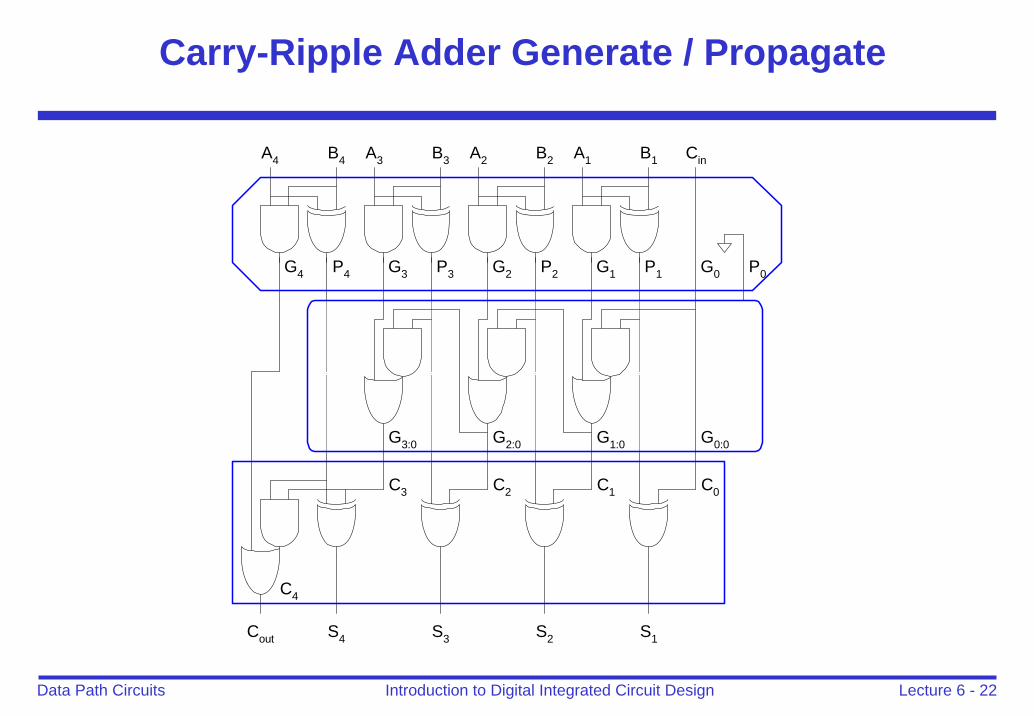
Carry-Ripple Adder Generate / Propagate
S1
B1A1
P1G1
G0:0
S2
B2
P2G2
G1:0
A2
S3
B3A3
P3G3
G2:0
S4
B4
P4G4
G3:0
A4 Cin
G0 P0
C0C1C2C3
Cout
C4
Lecture 6 - 23Introduction to Digital Integrated Circuit DesignData Path Circuits
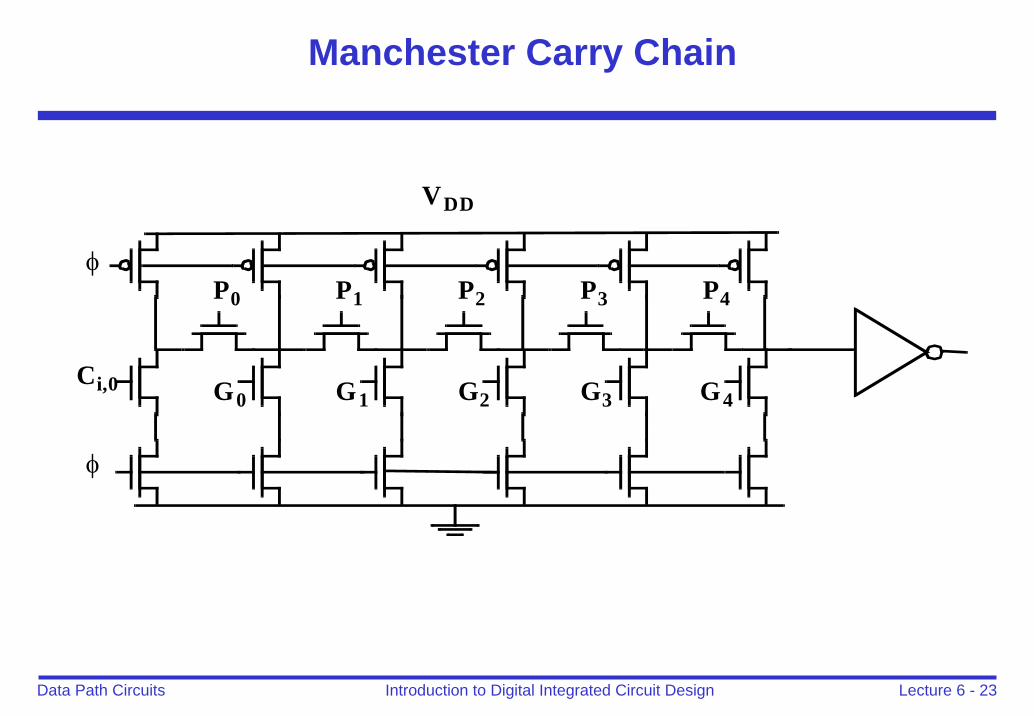
Manchester Carry Chain
P0
Ci,0
P1
G0
P2
G1
P3
G2
P4
G3 G4
φ
φ
VDD
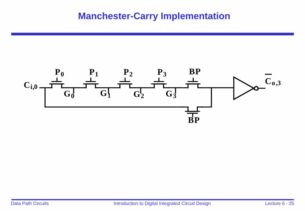
Lecture 6 - 24Introduction to Digital Integrated Circuit DesignData Path Circuits
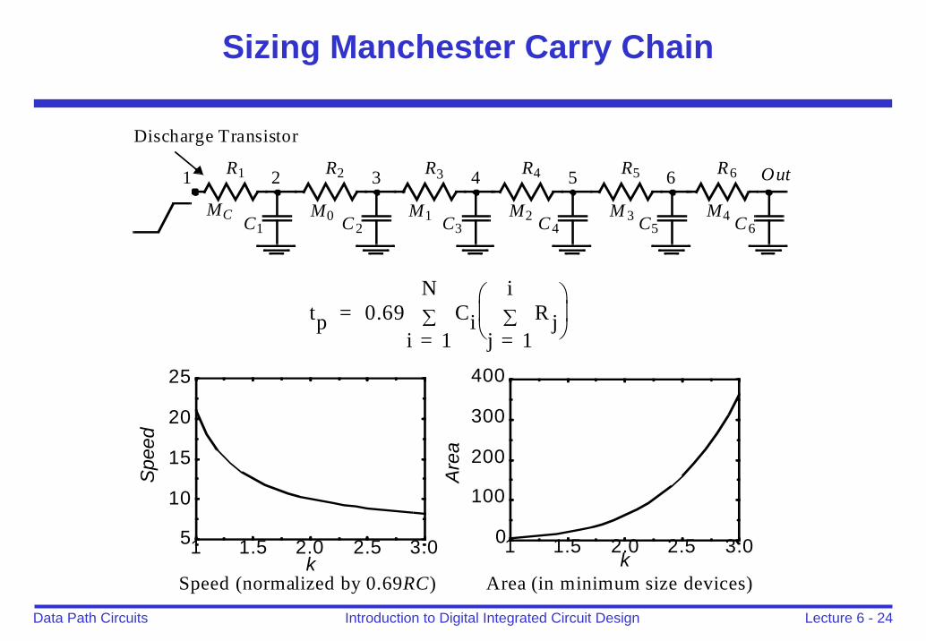
Sizing Manchester Carry Chain
R1
C1
R2
C2
R3
C3
R4
C4
R5
C5
R6
C6
Out
M0 M1 M2 M 3 M4MC
Discharge Transistor
1 2 3 4 5 6
tp 0.69 Ci R jj 1=
i∑
⎝ ⎠⎜ ⎟⎛ ⎞
i 1=
N∑=
1 1.5 2.0 2.5 3.0k
5
10
15
20
25
Spe
ed
1 1.5 2.0 2.5 3.0k
0
100
200
300
400
Are
a
Speed (normalized by 0.69RC) Area (in minimum size devices)
Lecture 6 - 25Introduction to Digital Integrated Circuit DesignData Path Circuits
Manchester-Carry Implementation
P0
Ci,0
P1
G0
P2
G1
P3
G2
BP
G3
BP
Co,3
Lecture 6 - 26Introduction to Digital Integrated Circuit DesignData Path Circuits
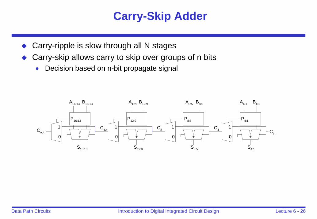
Carry-Skip Adder
Carry-ripple is slow through all N stagesCarry-skip allows carry to skip over groups of n bits• Decision based on n-bit propagate signal
Cin+
S4:1
P4:1
A4:1 B4:1
+
S8:5
P8:5
A8:5 B8:5
+
S12:9
P12:9
A12:9 B12:9
+
S16:13
P16:13
A16:13 B16:13
CoutC4
1
0
C81
0
C121
0
1
0
Lecture 6 - 27Introduction to Digital Integrated Circuit DesignData Path Circuits
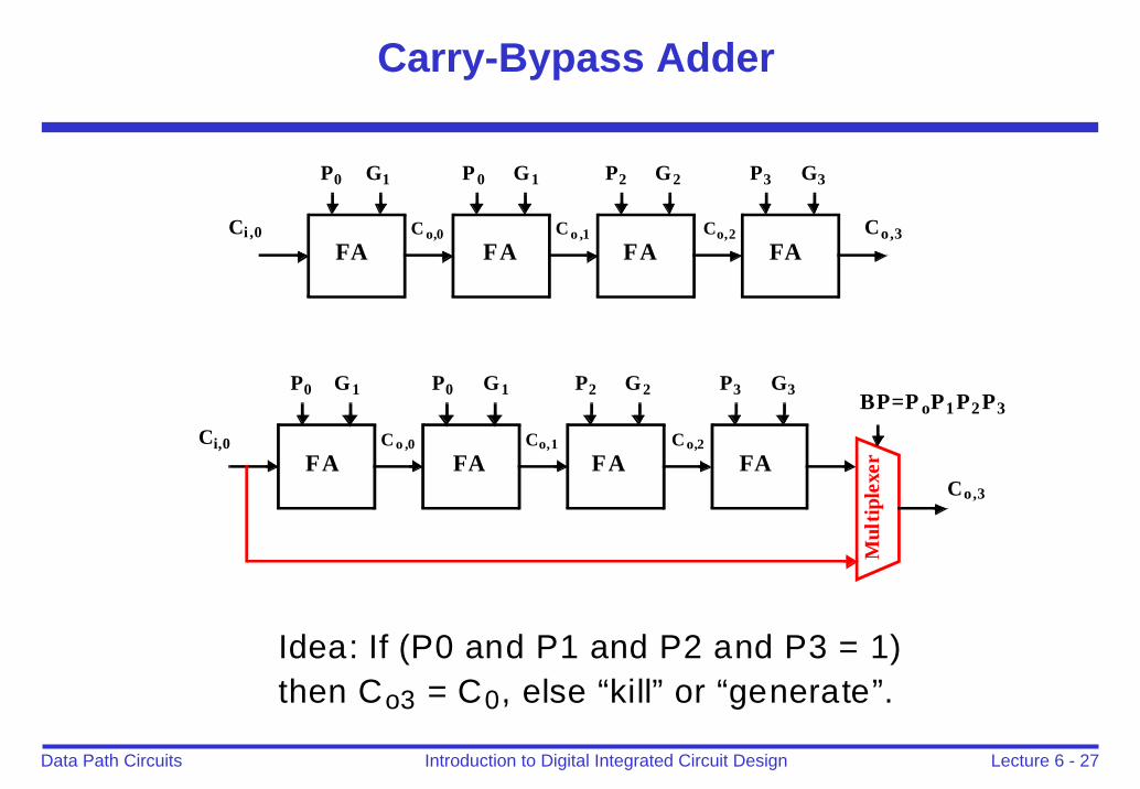
Carry-Bypass Adder
FA FA FA FA
P0 G1 P 0 G1 P2 G2 P3 G3
Co,3Co,2C o ,1C o,0Ci ,0
FA FA FA FA
P0 G1 P0 G1 P2 G2 P3 G3
Co,2Co,1Co ,0Ci,0
Co,3
Mul
tiple
xer
BP=P oP1P2P3
Idea: If (P0 and P1 and P2 and P3 = 1)then Co3 = C0, else “kill” or “generate”.
Lecture 6 - 28Introduction to Digital Integrated Circuit DesignData Path Circuits
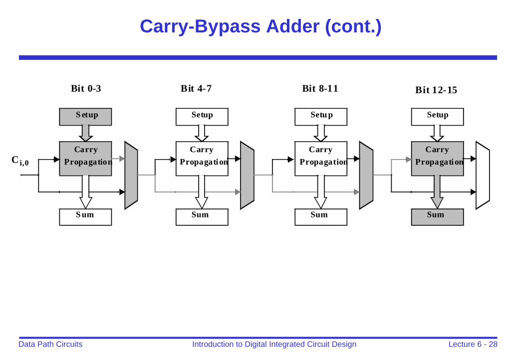
Carry-Bypass Adder (cont.)
S etup
CarryPropagation
S um
Setup
CarryPropagation
Sum
Setu p
CarryPropagation
Sum
Setup
CarryPropagation
Sum
Bit 0-3 Bit 4-7 Bit 8-11 Bit 12-15
Ci,0
Lecture 6 - 29Introduction to Digital Integrated Circuit DesignData Path Circuits
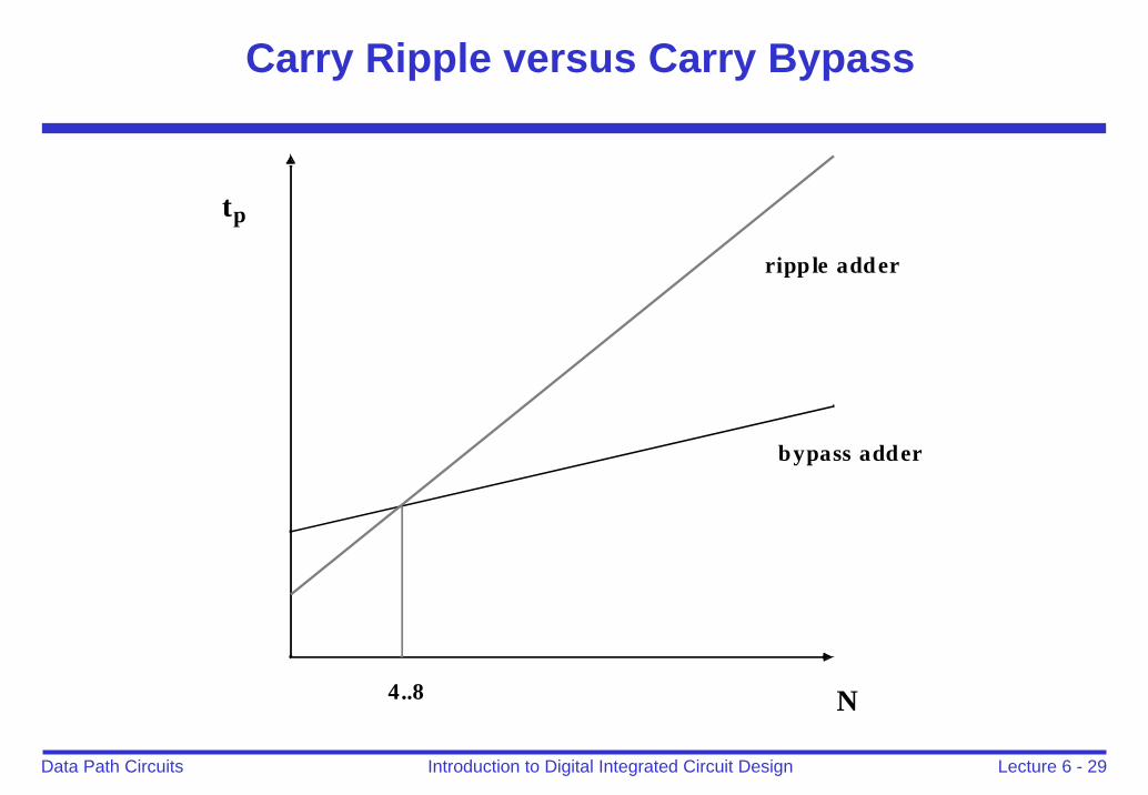
Carry Ripple versus Carry Bypass
N
tp
ripple adder
bypass adder
4..8
Lecture 6 - 30Introduction to Digital Integrated Circuit DesignData Path Circuits
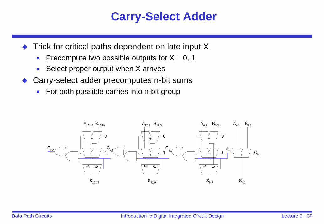
Carry-Select Adder
Trick for critical paths dependent on late input X• Precompute two possible outputs for X = 0, 1• Select proper output when X arrives
Carry-select adder precomputes n-bit sums• For both possible carries into n-bit group
Cin+
A4:1 B4:1
S4:1
C4
+
+
01A8:5 B8:5
S8:5
C8
+
+
01
A12:9 B12:9
S12:9
C12
+
+
01
A16:13 B16:13
S16:13
Cout
0
1
0
1
0
1
Lecture 6 - 31Introduction to Digital Integrated Circuit DesignData Path Circuits
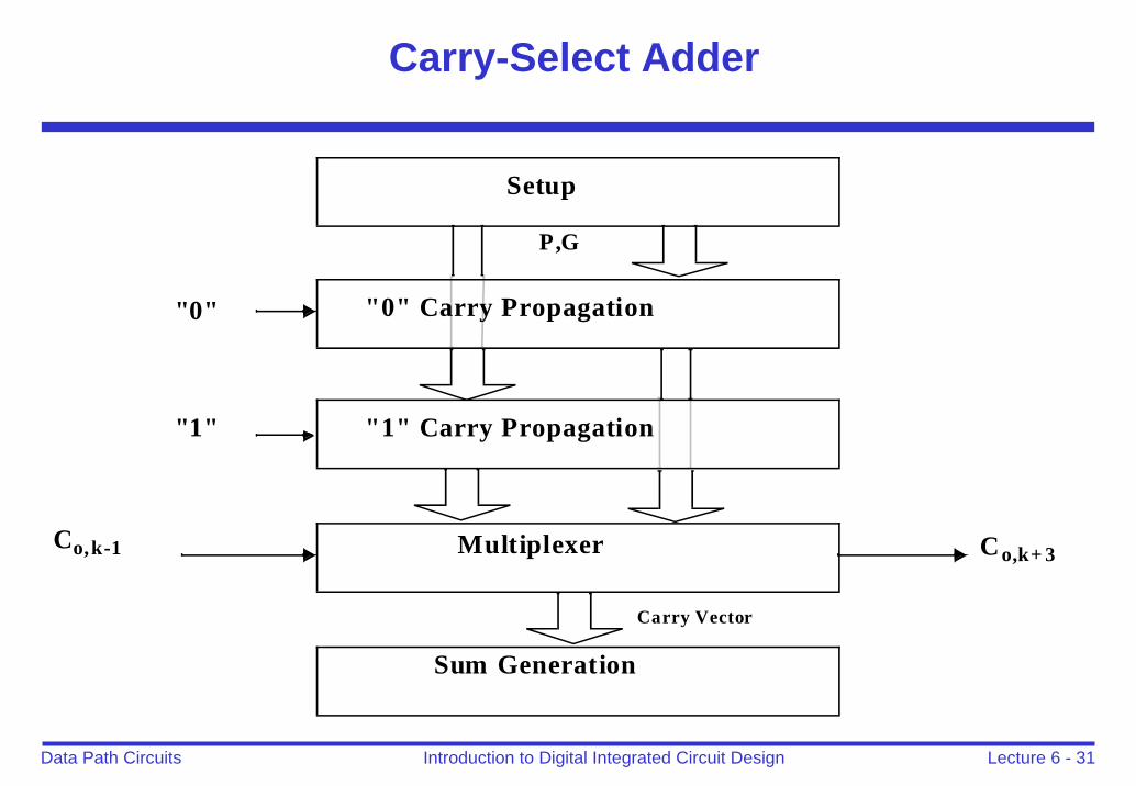
Carry-Select Adder
Setup
"0" Carry Propagation
"1" Carry Propagation
Multiplexer
Sum Generation
Co,k-1 Co,k+ 3
"0"
"1"
P,G
Carry Vector
Lecture 6 - 32Introduction to Digital Integrated Circuit DesignData Path Circuits
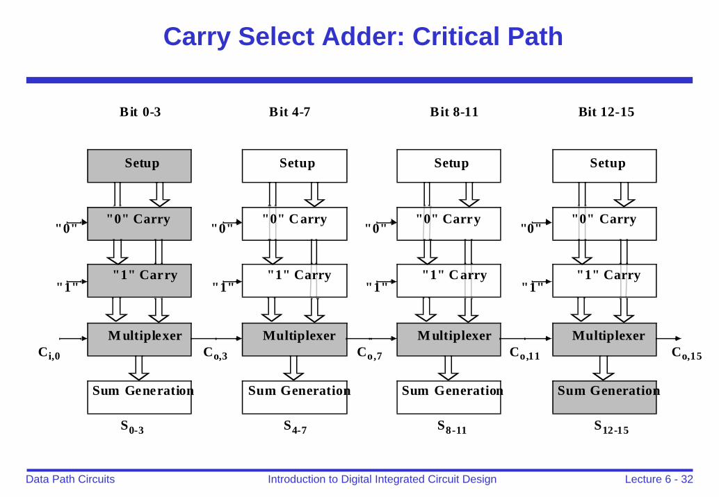
Carry Select Adder: Critical Path
Setup
"0" Carry
"1" Carry
M ultiplexer
Sum Generation
"0"
"1"
Setup
"0" C arry
"1" Carry
Multiplexer
Sum Generation
"0"
"1"
Setup
"0" Carry
"1" C arry
M ultiplexer
Sum Generation
"0"
"1"
Setup
"0" Carry
"1" Carry
Multiplexer
Sum Generation
"0"
"1"
Bit 0-3 Bit 4-7 Bit 8-11 Bit 12-15
S0-3 S4-7 S8-11 S12-15
Co,15Co,11Co,7Co,3Ci,0
Lecture 6 - 33Introduction to Digital Integrated Circuit DesignData Path Circuits
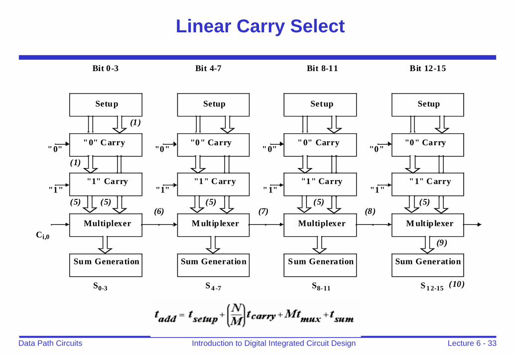
Linear Carry Select
Setup
"0" Carry
"1" Carry
Multiplexer
Sum Generation
"0"
"1"
Setup
"0" Carry
"1" Carry
M ultip lexer
Sum Generation
"0"
"1"
Setup
"0" Carry
"1" Carry
Multiplexer
Sum Generation
"0"
"1"
Setup
"0" Carry
"1" Carry
M ultiplexer
Sum Generation
"0"
"1"
Bit 0-3 Bit 4-7 Bit 8-11 Bit 12-15
S0-3 S 4 -7 S8-11 S 1 2-15
Ci,0
(1)
(1)
(5)(6) (7) (8)
(9)
(10)
(5) (5) (5)(5)
Lecture 6 - 34Introduction to Digital Integrated Circuit DesignData Path Circuits
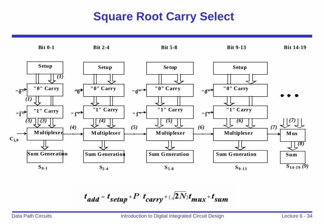
Square Root Carry Select
Setup
"0" Carry
"1" Carry
M ultiplexer
Sum Generation
"0"
"1"
Setup
"0" Carry
"1" Carry
M ultiplexer
Sum Generation
"0"
"1"
Setup
"0" Carry
"1" Carry
M ultiplexer
Sum Generation
"0"
"1"
Setup
"0" Carry
"1" Carry
Multiplexer
Sum Generation
"0"
"1"
Bit 0-1 Bit 2-4 Bit 5-8 Bit 9-13
S0-1 S2-4 S5-8 S9-13
Ci,0
(4) (5) (6) (7)
(1)
(1)
(3) (4) (5) (6)
M ux
Sum
S14-19
(7)
(8)
Bit 14-19
(9)
(3)
Lecture 6 - 35Introduction to Digital Integrated Circuit DesignData Path Circuits
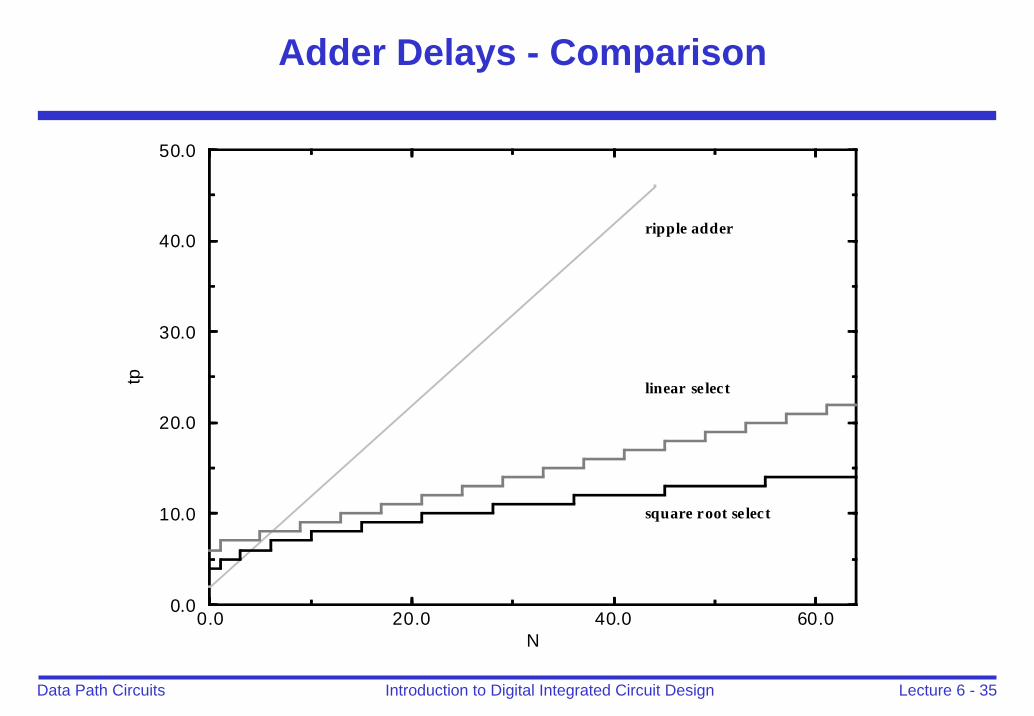
Adder Delays - Comparison
0.0 20.0 40.0 60.0N
0.0
10.0
20.0
30.0
40.0
50.0tp
ripple adder
linear select
square root select
Lecture 6 - 36Introduction to Digital Integrated Circuit DesignData Path Circuits
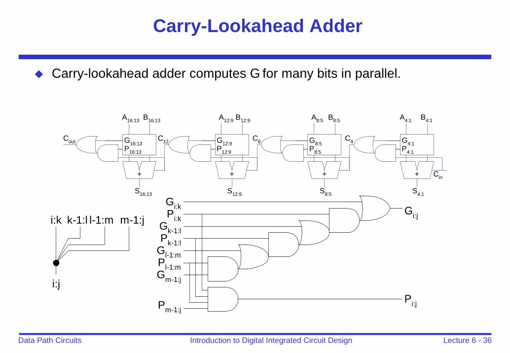
Carry-Lookahead Adder
Cin+
S4:1
G4:1P4:1
A4:1 B4:1
+
S8:5
G8:5P8:5
A8:5 B8:5
+
S12:9
G12:9P12:9
A12:9 B12:9
+
S16:13
G16:13P16:13
A16:13 B16:13
C4C8C12Cout
Carry-lookahead adder computes G for many bits in parallel.
i:j
i:k k-1:l l-1:m m-1:j
Gi:k
Gk-1:l
Gl-1:m
Gm-1:j
Gi:j
Pi:j
Pi:k
Pk-1:l
Pl-1:m
Pm-1:j
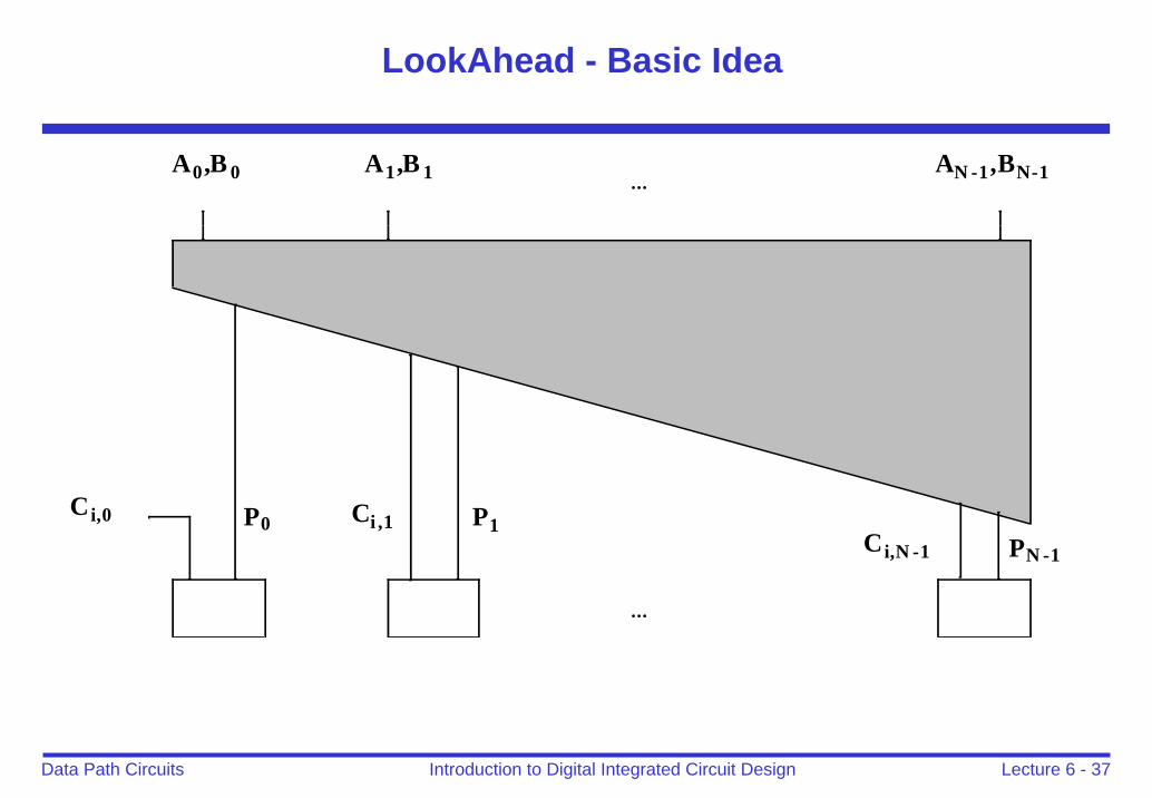
Lecture 6 - 37Introduction to Digital Integrated Circuit DesignData Path Circuits
LookAhead - Basic Idea
A0,B 0 A1,B 1 AN -1,BN-1...
Ci,0 P0 Ci,1 P1Ci,N -1 PN -1
...
Lecture 6 - 38Introduction to Digital Integrated Circuit DesignData Path Circuits
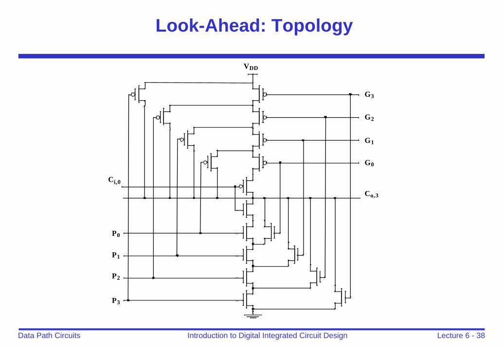
Look-Ahead: Topology
VDD
P3
P2
P1
P0
G3
G2
G1
G0
Ci,0
Co,3
Lecture 6 - 39Introduction to Digital Integrated Circuit DesignData Path Circuits
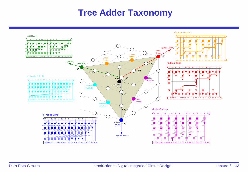
Tree Adder
If lookahead is good, lookahead across lookahead!• Recursive lookahead gives O(log N) delay
Many variations on tree addersIdeal N-bit tree adder would have• L = log N logic levels• Fanout never exceeding 2• No more than one wiring track between levels
Describe adder with 3-D taxonomy (l, f, t)• Logic levels: L + l• Fanout: 2f + 1• Wiring tracks: 2t
Known tree adders sit on plane defined byl + f + t = L-1
Lecture 6 - 40Introduction to Digital Integrated Circuit DesignData Path Circuits
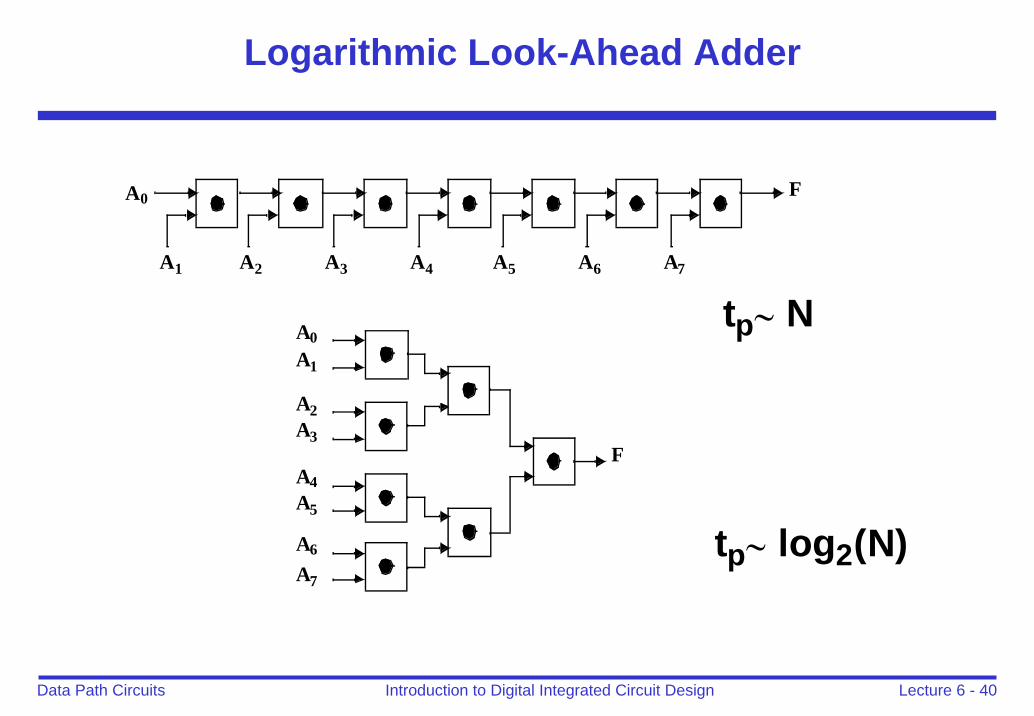
Logarithmic Look-Ahead Adder
A7
F
A6A5A4A3A2A1
A0
A0A1
A2A3
A4A5
A6
A7
F
tp∼ log2(N)
tp∼ N
Lecture 6 - 41Introduction to Digital Integrated Circuit DesignData Path Circuits
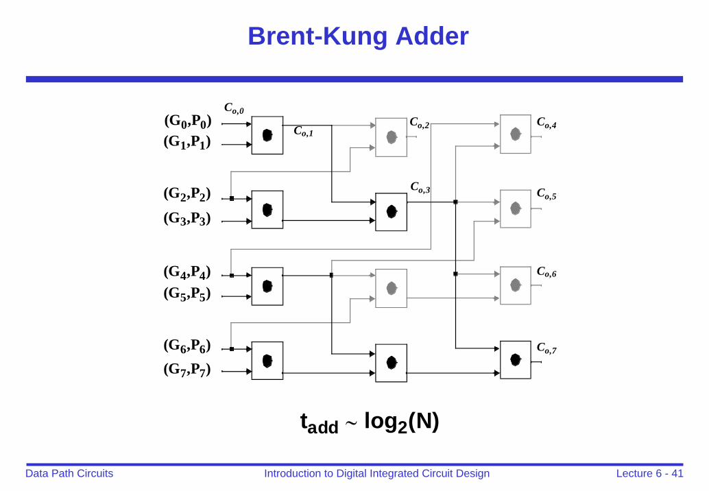
Brent-Kung Adder
(G0,P0)(G1,P1)
(G2,P2)(G3,P3)
(G4,P4)(G5,P5)
(G6,P6)(G7,P7)
Co,0
Co,1Co,2
Co,3
Co,4
Co,5
Co,6
Co,7
tadd ∼ log2(N)
Lecture 6 - 42Introduction to Digital Integrated Circuit DesignData Path Circuits
Tree Adder Taxonomy
f (Fanout)
t (Wire Tracks)
l (Logic Levels)
0 (2)1 (3)
2 (5)
3 (9)
0 (4)
1 (5)
2 (6)
3 (8)
2 (4)
1 (2)
0 (1)
3 (7)
Kogge-Stone
Sklansky
Brent-Kung
Han-Carlson
Knowles[2,1,1,1]
Knowles[4,2,1,1]
Ladner-Fischer
Han-Carlson
Ladner-Fischer
New(1,1,1)
(c) Kogge-Stone
1:02:13:24:35:46:57:68:79:810:911:1012:1113:1214:1315:14
3:04:15:26:37:48:59:610:711:812:913:1014:1115:12
4:05:06:07:08:19:210:311:412:513:614:715:8
2:0
0123456789101112131415
15:014:013:012:011:010:0 9:0 8:0 7:0 6:0 5:0 4:0 3:0 2:0 1:0 0:0
(e) Knowles [2,1,1,1]
1:02:13:24:35:46:57:68:79:810:911:1012:1113:1214:1315:14
3:04:15:26:37:48:59:610:711:812:913:1014:1115:12
4:05:06:07:08:19:210:311:412:513:614:715:8
2:0
0123456789101112131415
15:014:013:012:011:010:0 9:0 8:0 7:0 6:0 5:0 4:0 3:0 2:0 1:0 0:0
(b) Sklansky
1:0
2:03:0
3:25:47:69:811:1013:1215:14
6:47:410:811:814:1215:12
12:813:814:815:8
0123456789101112131415
15:014:013:012:011:010:0 9:0 8:0 7:0 6:0 5:0 4:0 3:0 2:0 1:0 0:0
1:03:25:47:69:811:1013:12
3:07:411:815:12
5:07:013:815:8
15:14
15:8 13:0 11:0 9:0
0123456789101112131415
15:0 14:0 13:0 12:0 11:0 10:0 9:0 8:0 7:0 6:0 5:0 4:0 3:0 2:0 1:0 0:0
(f) Ladner-Fischer
(a) Brent-Kung
1:03:25:47:69:811:1013:1215:14
3:07:411:815:12
7:015:8
11:0
5:09:013:0
0123456789101112131415
15:014:013:0 12:011:010:0 9:0 8:0 7:0 6:0 5:0 4:0 3:0 2:0 1:0 0:0
1:03:25:47:69:811:1013:1215:14
3:05:27:49:611:813:1015:12
5:07:09:211:413:615:8
0123456789101112131415
15:014:013:012:011:010:0 9:0 8:0 7:0 6:0 5:0 4:0 3:0 2:0 1:0 0:0
(d) Han-Carlson
Lecture 6 - 43Introduction to Digital Integrated Circuit DesignData Path Circuits
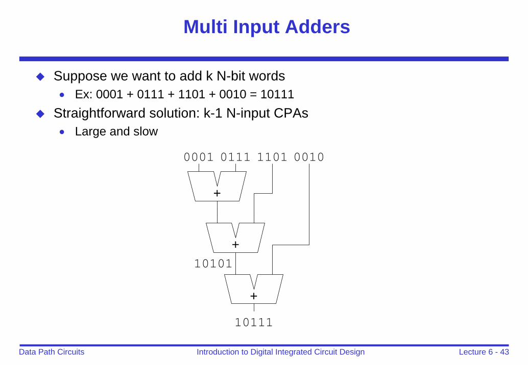
Multi Input Adders
Suppose we want to add k N-bit words• Ex: 0001 + 0111 + 1101 + 0010 = 10111
Straightforward solution: k-1 N-input CPAs• Large and slow
+
+
0001 0111
+
1101 0010
10101
10111
Lecture 6 - 44Introduction to Digital Integrated Circuit DesignData Path Circuits
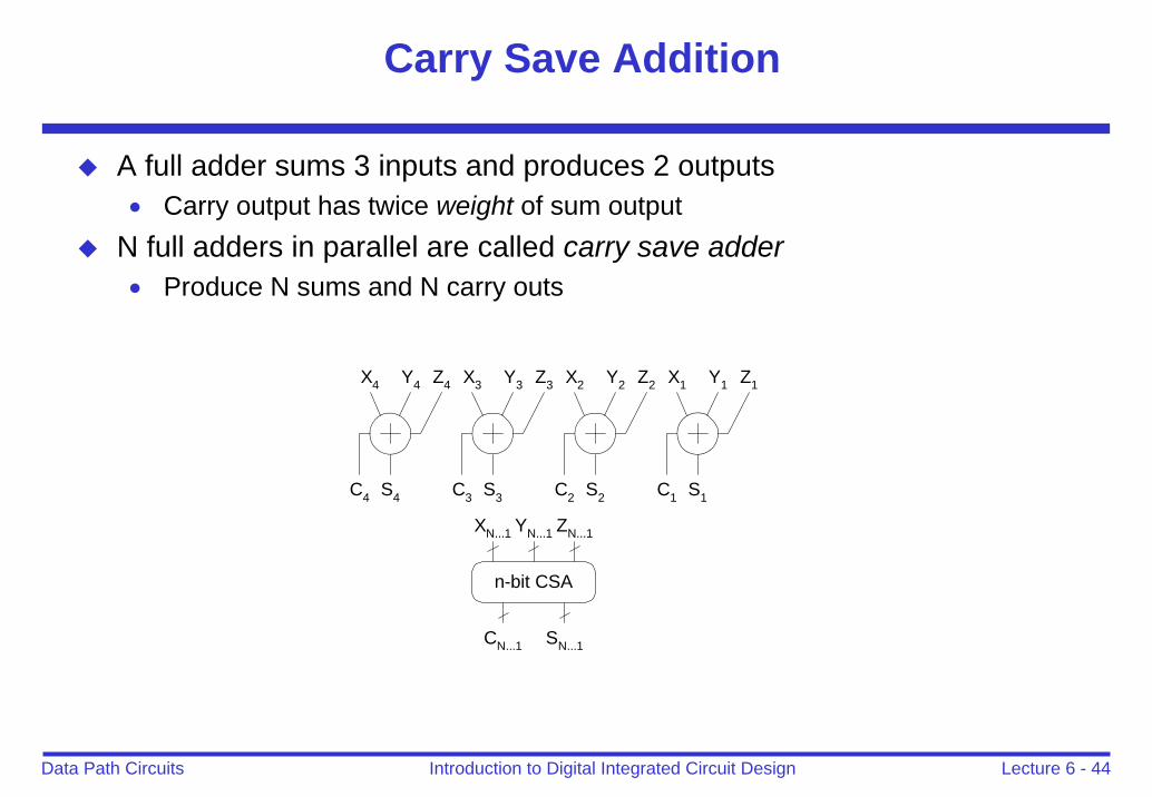
Carry Save Addition
A full adder sums 3 inputs and produces 2 outputs• Carry output has twice weight of sum output
N full adders in parallel are called carry save adder• Produce N sums and N carry outs
Z4Y4X4
S4C4
Z3Y3X3
S3C3
Z2Y2X2
S2C2
Z1Y1X1
S1C1
XN...1 YN...1 ZN...1
SN...1CN...1
n-bit CSA
Lecture 6 - 45Introduction to Digital Integrated Circuit DesignData Path Circuits
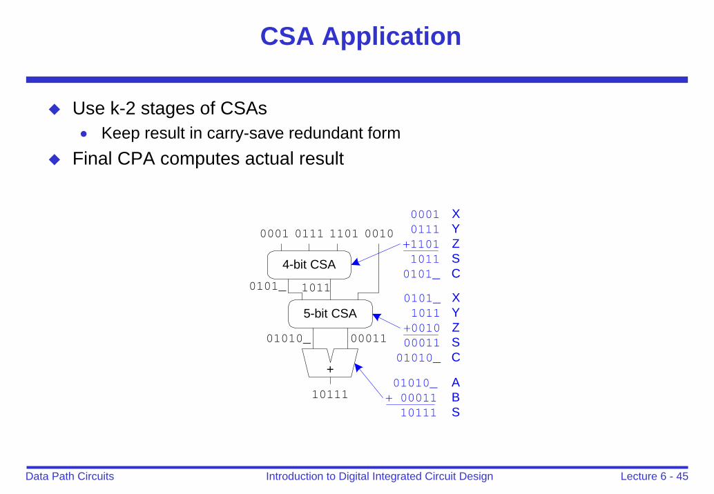
CSA Application
Use k-2 stages of CSAs• Keep result in carry-save redundant form
Final CPA computes actual result
4-bit CSA
5-bit CSA
0001 0111 1101 0010
+
10110101_
01010_ 00011
0001 0111+1101 10110101_
XYZSC
0101_ 1011 +0010 0001101010_
XYZSC
01010_+ 00011 10111
ABS
10111
Lecture 6 - 46Introduction to Digital Integrated Circuit DesignData Path Circuits
Outline
Adders
Multipliers
Shifters
Comparators
Layout issues
Lecture 6 - 47Introduction to Digital Integrated Circuit DesignData Path Circuits
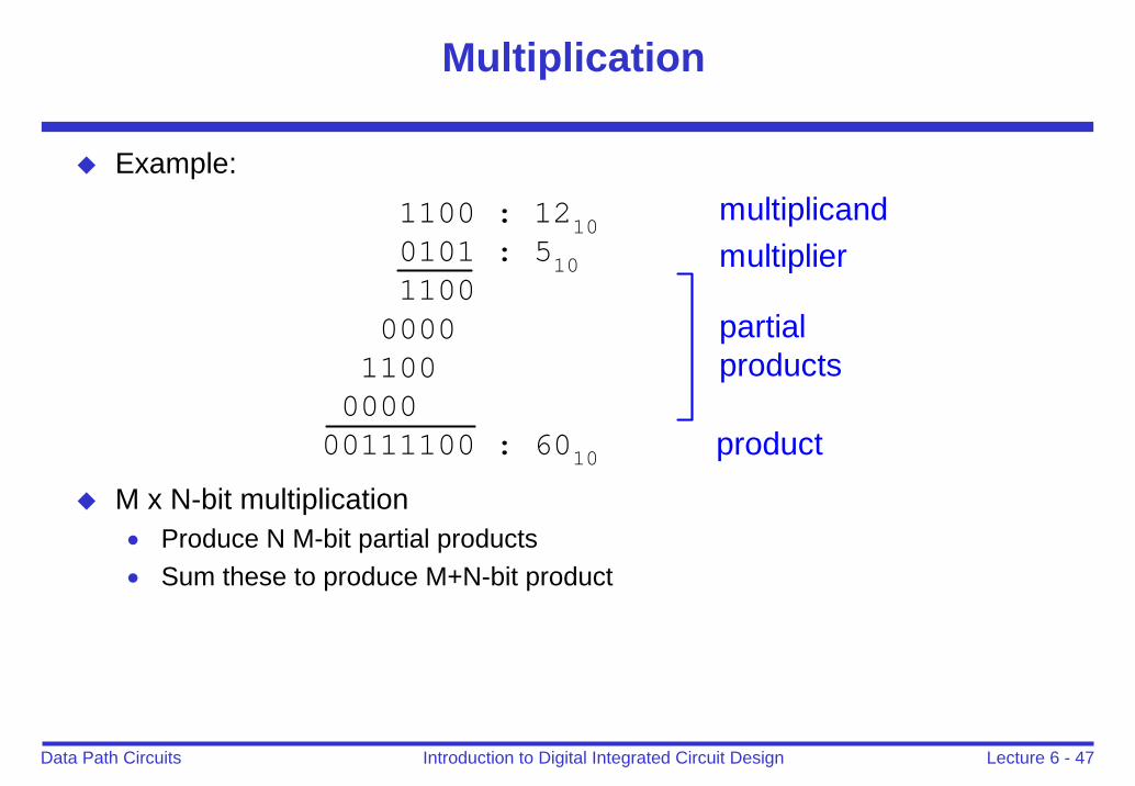
Multiplication
Example:
M x N-bit multiplication• Produce N M-bit partial products• Sum these to produce M+N-bit product
1100 : 1210 0101 : 510 1100 0000 1100 000000111100 : 6010
multipliermultiplicand
partialproducts
product
Lecture 6 - 48Introduction to Digital Integrated Circuit DesignData Path Circuits
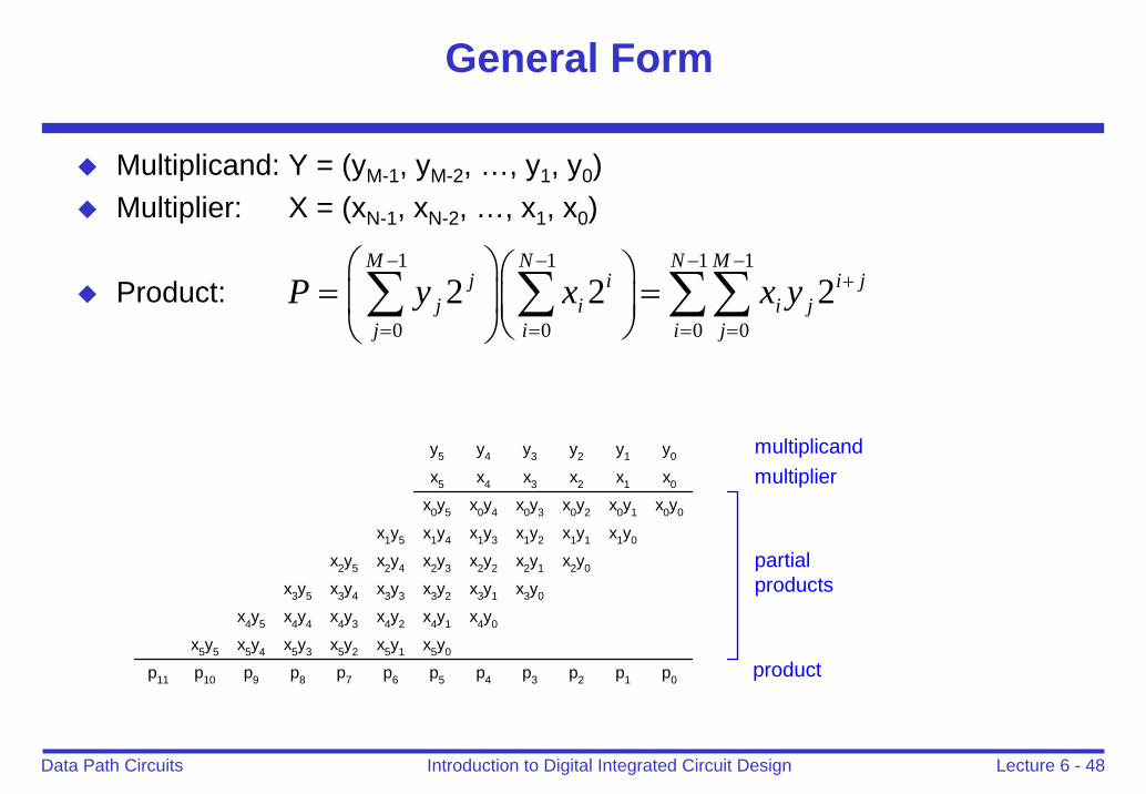
General Form
Multiplicand: Y = (yM-1, yM-2, …, y1, y0)Multiplier: X = (xN-1, xN-2, …, x1, x0)
Product:1 1 1 1
0 0 0 0
2 2 2M N N M
j i i jj i i j
j i i j
P y x x y− − − −
+
= = = =
⎛ ⎞ ⎛ ⎞= =⎜ ⎟⎜ ⎟⎝ ⎠⎝ ⎠
∑ ∑ ∑∑
x0y5 x0y4 x0y3 x0y2 x0y1 x0y0
y5 y4 y3 y2 y1 y0
x5 x4 x3 x2 x1 x0
x1y5 x1y4 x1y3 x1y2 x1y1 x1y0
x2y5 x2y4 x2y3 x2y2 x2y1 x2y0
x3y5 x3y4 x3y3 x3y2 x3y1 x3y0
x4y5 x4y4 x4y3 x4y2 x4y1 x4y0
x5y5 x5y4 x5y3 x5y2 x5y1 x5y0
p0p1p2p3p4p5p6p7p8p9p10p11
multipliermultiplicand
partialproducts
product
Lecture 6 - 49Introduction to Digital Integrated Circuit DesignData Path Circuits
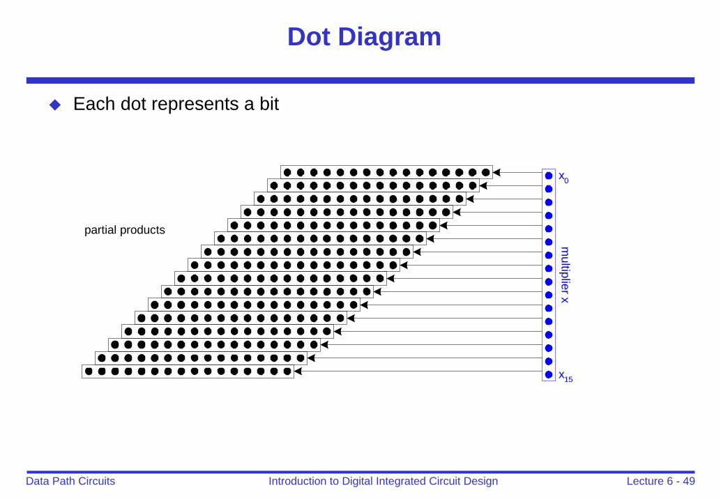
Dot Diagram
Each dot represents a bit
partial products
multiplier x
x0
x15
Lecture 6 - 50Introduction to Digital Integrated Circuit DesignData Path Circuits
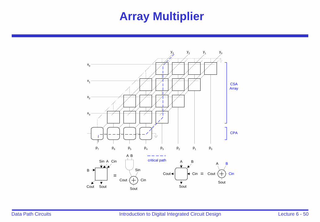
Array Multiplier
y0y1y2y3
x0
x1
x2
x3
p0p1p2p3p4p5p6p7
B
ASin Cin
SoutCout
BA
CinCout
Sout
Sin
=
CSAArray
CPA
critical path BA
Sout
Cout CinCout
Sout
=Cin
BA
Lecture 6 - 51Introduction to Digital Integrated Circuit DesignData Path Circuits
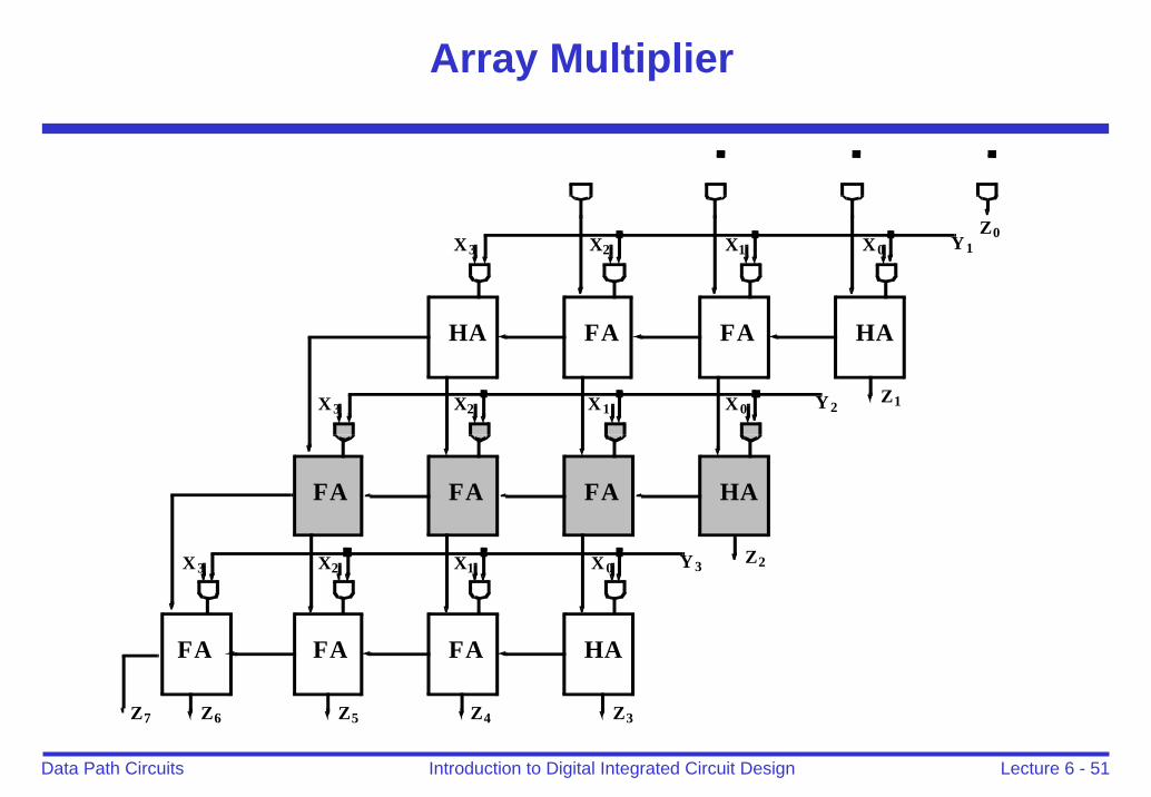
Array Multiplier
HA FA FA HA
FA FA FA HA
FA FA FA HA
X0X1X2X3 Y1
X0X1X2X3 Y2
X0X1X2X3 Y3
Z1
Z2
Z3Z4Z5Z6
Z0
Z7
Lecture 6 - 52Introduction to Digital Integrated Circuit DesignData Path Circuits
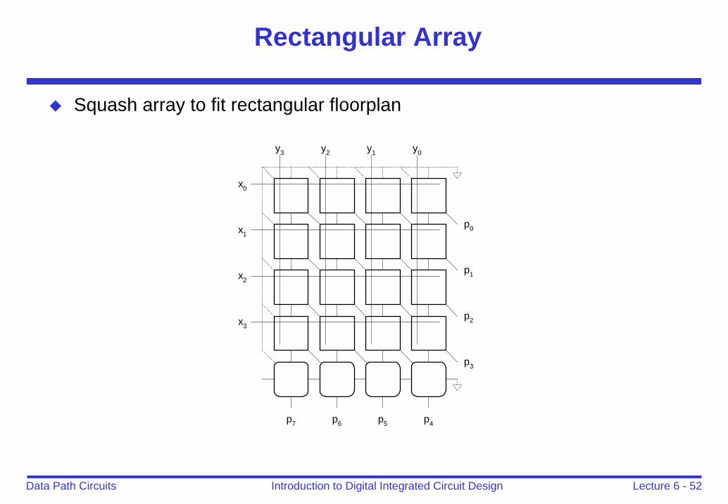
Rectangular Array
Squash array to fit rectangular floorplan
y0y1y2y3
x0
x1
x2
x3
p0
p1
p2
p3
p4p5p6p7
Lecture 6 - 53Introduction to Digital Integrated Circuit DesignData Path Circuits
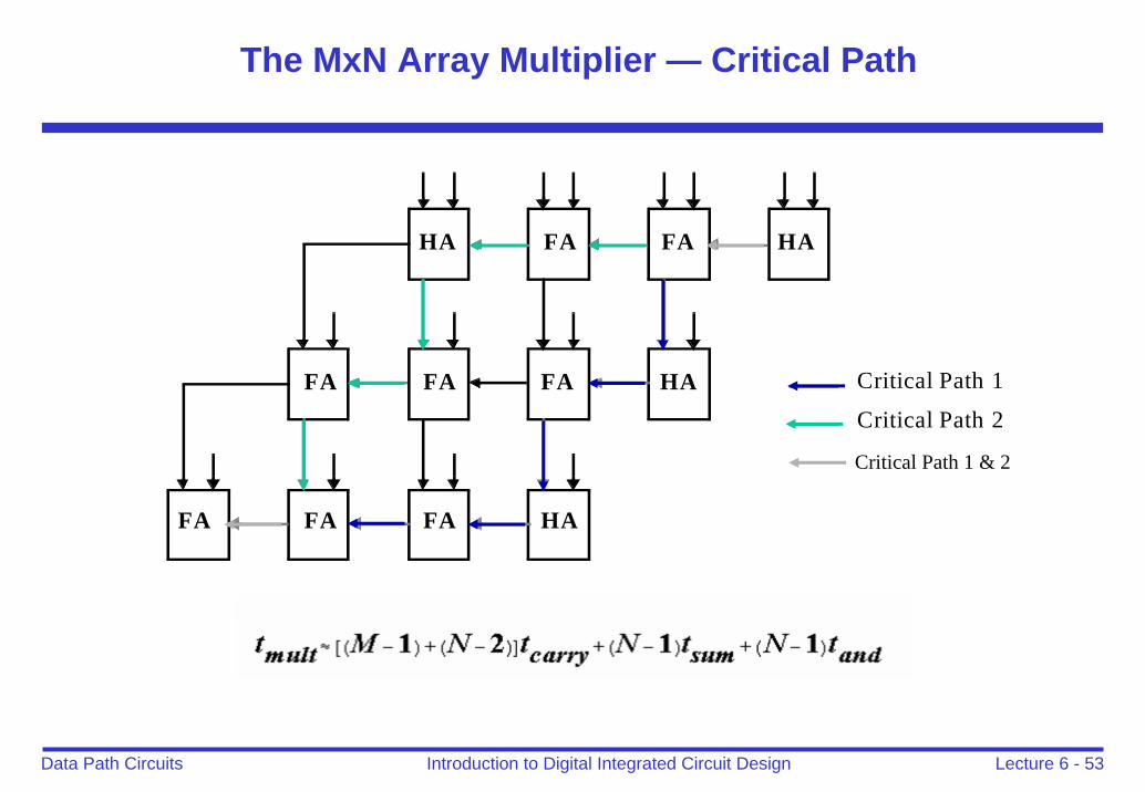
The MxN Array Multiplier — Critical Path
HA FA FA HA
HAFAFAFA
FAFA FA HA
Critical Path 1
Critical Path 2
Critical Path 1 & 2
Lecture 6 - 54Introduction to Digital Integrated Circuit DesignData Path Circuits
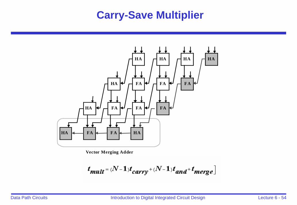
Carry-Save Multiplier
HA HA HA HA
FAFAFAHA
FAHA FA FA
FAHA FA HA
Vector Merging Adder
Lecture 6 - 55Introduction to Digital Integrated Circuit DesignData Path Circuits
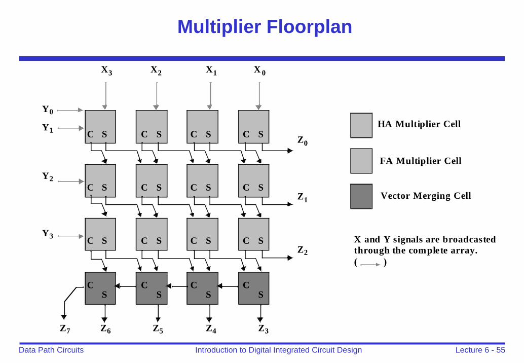
Multiplier Floorplan
SCSCSCSC
SCSCSCSC
SCSCSCSC
SC
SC
SC
SC
Z0
Z1
Z2
Z3Z4Z5Z6Z7
X 0X1X2X3
Y1
Y2
Y3
Y0
Vector Merging Cell
HA Multiplier Cell
FA Multiplier Cell
X and Y signals are broadcastedthrough the complete array.( )
Lecture 6 - 56Introduction to Digital Integrated Circuit DesignData Path Circuits
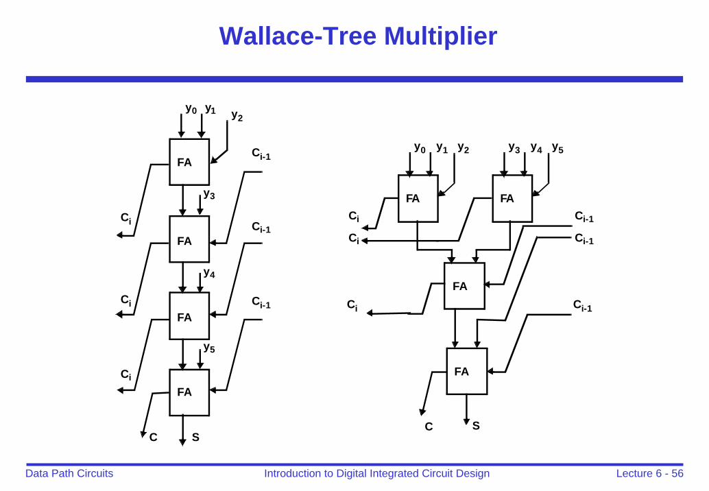
Wallace-Tree Multiplier
FA
FA
FA
FA
y0 y1 y2
y3
y4
y5
S
Ci-1
Ci-1
Ci-1
Ci
Ci
Ci
FA
y0 y1 y2
FA
y3 y4 y5
FA
FA
CC S
Ci-1
Ci-1
Ci-1
Ci
Ci
Ci
Lecture 6 - 57Introduction to Digital Integrated Circuit DesignData Path Circuits
Fewer Partial Products
Partial products result from the logical AND of multiplicand Y with a multiplier bit Xi. • Each row in the partial product array is either a copy of the multiplicand or a
row of zeros (depending on the multiplier bit)In most cases the partial product array has many zero rows that have no impact on the result and thus represent a waste of effort when addedCareful optimization of the partial product generation can lead to some substantial delay and area reductionsIn the case of a multiplier consisting of all 1’s all the partial products exist, while in the case of all 0’s there is none• This allows us to reduce the number of generated partial products by half
01111110 as multiplier produces 6 non-zero partial product rowsThe number of non zero rows can be reduced by recoding the multiplier in the form 100000(-1)0 – Booth recoding• Only two partial products need to be added but the final adder has to perform
subtraction as wellReduced number of partial products: speedup + area reduction
Lecture 6 - 58Introduction to Digital Integrated Circuit DesignData Path Circuits
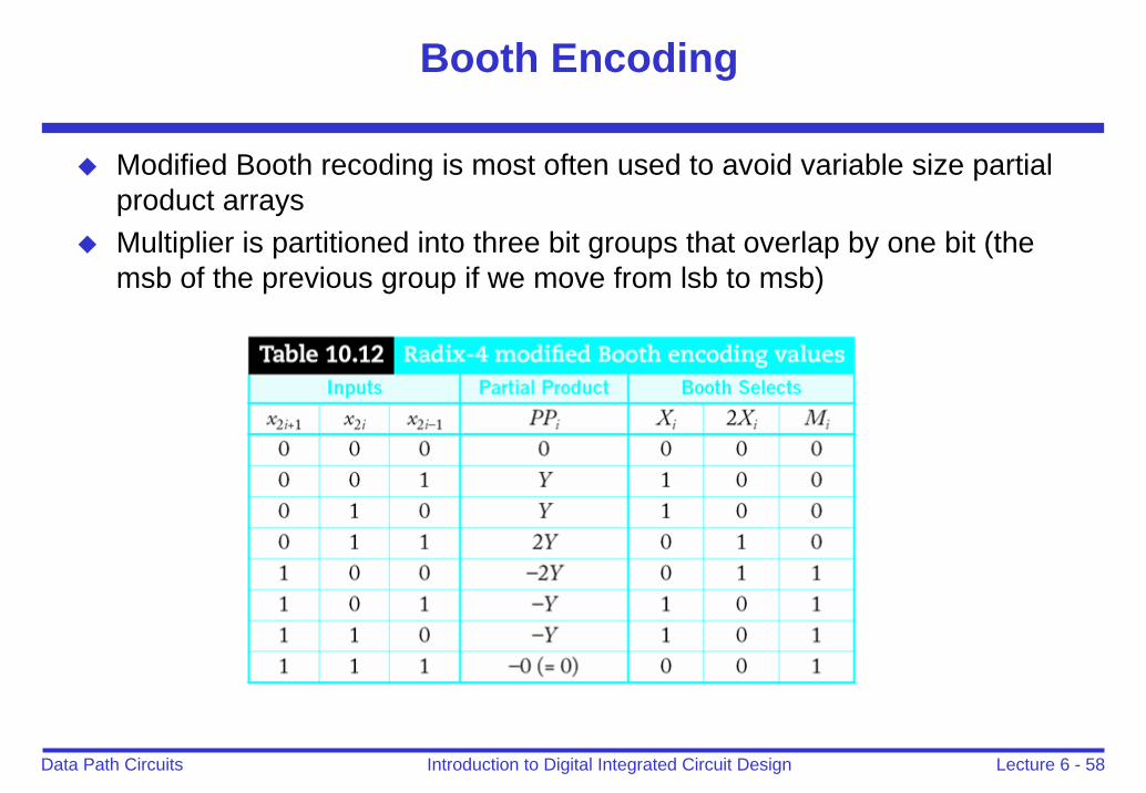
Booth Encoding
Modified Booth recoding is most often used to avoid variable size partial product arraysMultiplier is partitioned into three bit groups that overlap by one bit (the msb of the previous group if we move from lsb to msb)
Lecture 6 - 59Introduction to Digital Integrated Circuit DesignData Path Circuits
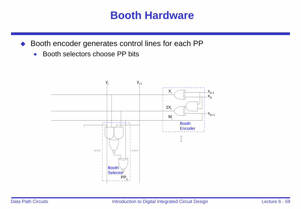
Booth Hardware
Booth encoder generates control lines for each PP• Booth selectors choose PP bits
Mi
yj
Xi
yj-1
2Xi
PPij
BoothSelector
BoothEncoder
x2i+1
x2i
x2i-1
Lecture 6 - 60Introduction to Digital Integrated Circuit DesignData Path Circuits
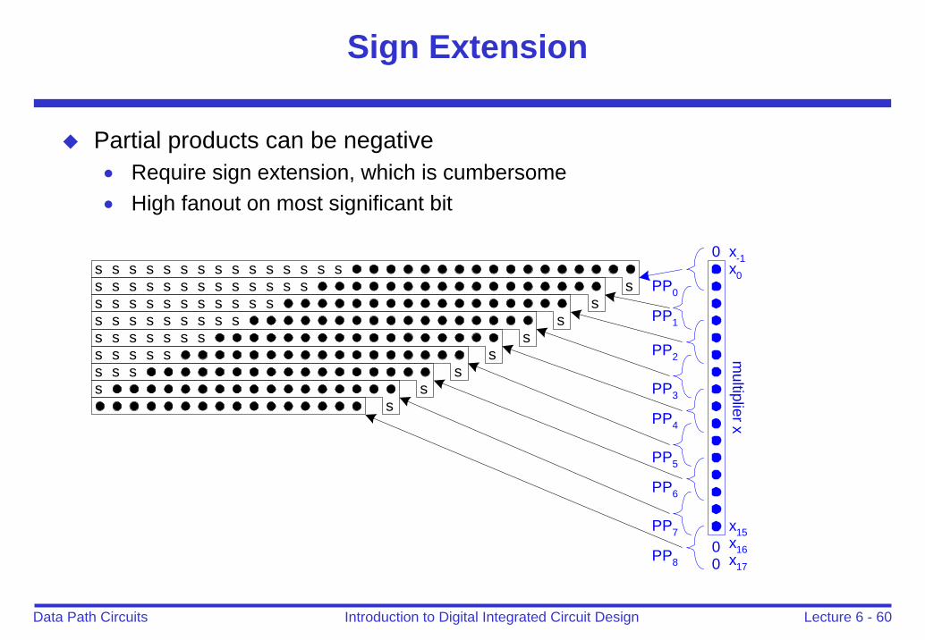
Sign Extension
Partial products can be negative• Require sign extension, which is cumbersome• High fanout on most significant bit
multiplier x
x0
x15
0
00
x-1
x16x17
ssssssssssssssss
ssssssssssssss
ssssssssssss
ssssssssss
ssssssss
ssssss
ssss
ss
PP0
PP1
PP2
PP3
PP4
PP5
PP6
PP7
PP8
Lecture 6 - 61Introduction to Digital Integrated Circuit DesignData Path Circuits
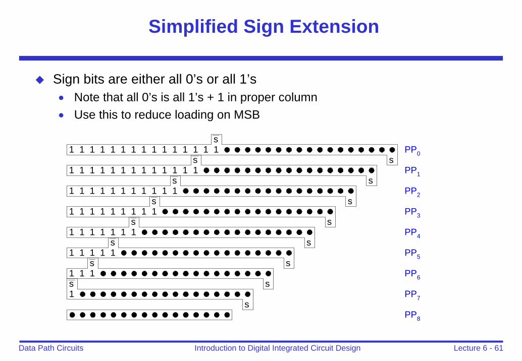
Simplified Sign Extension
Sign bits are either all 0’s or all 1’s• Note that all 0’s is all 1’s + 1 in proper column• Use this to reduce loading on MSB
s111111111111111s
s1111111111111s
s11111111111s
s111111111s
s1111111s
s11111s
s111s
s1s
PP0
PP1
PP2
PP3
PP4
PP5
PP6
PP7
PP8
Lecture 6 - 62Introduction to Digital Integrated Circuit DesignData Path Circuits
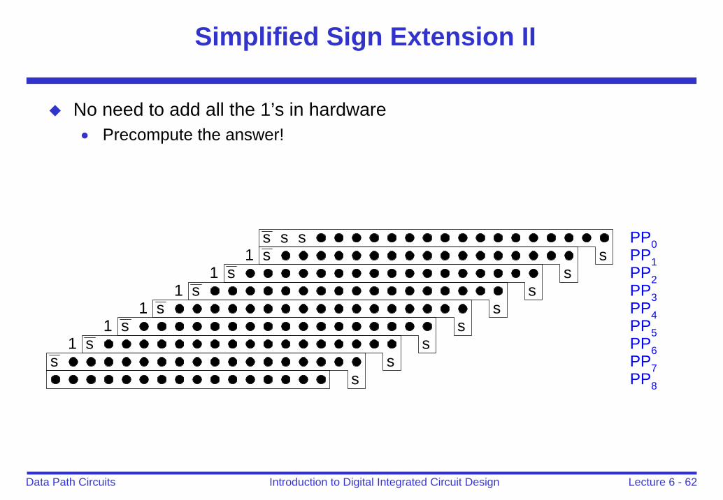
Simplified Sign Extension II
No need to add all the 1’s in hardware• Precompute the answer!
ssss
ss1
ss1
ss1
ss1
ss1
ss1
ss
PP0PP1PP2PP3PP4PP5PP6PP7PP8
Lecture 6 - 63Introduction to Digital Integrated Circuit DesignData Path Circuits
Advanced Multiplication
Signed vs. unsigned inputsHigher radix Booth encodingArray vs. tree CSA networks
Lecture 6 - 64Introduction to Digital Integrated Circuit DesignData Path Circuits
Multipliers —Summary
• Optimization Goals Different Vs Binary Adder
• Once Again: Identify Critical Path
• Other possible techniques
- Data encoding (Booth)- Pipelining
FIRST GLIMPSE AT SYSTEM LEVEL OPTIMIZATION
- Logarithmic versus Linear (Wallace Tree Mult)
Lecture 6 - 65Introduction to Digital Integrated Circuit DesignData Path Circuits
Outline
Adders
Multipliers
Shifters
Comparators
Layout issues
Lecture 6 - 66Introduction to Digital Integrated Circuit DesignData Path Circuits
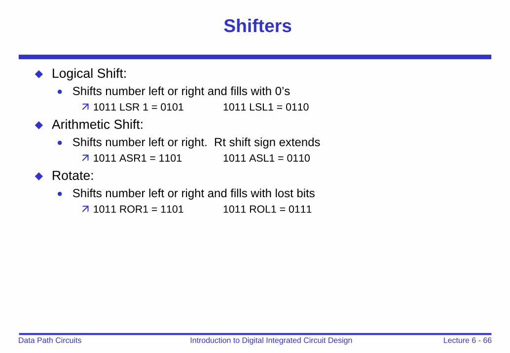
Shifters
Logical Shift:• Shifts number left or right and fills with 0’s
1011 LSR 1 = 0101 1011 LSL1 = 0110
Arithmetic Shift:• Shifts number left or right. Rt shift sign extends
1011 ASR1 = 1101 1011 ASL1 = 0110
Rotate:• Shifts number left or right and fills with lost bits
1011 ROR1 = 1101 1011 ROL1 = 0111
Lecture 6 - 67Introduction to Digital Integrated Circuit DesignData Path Circuits
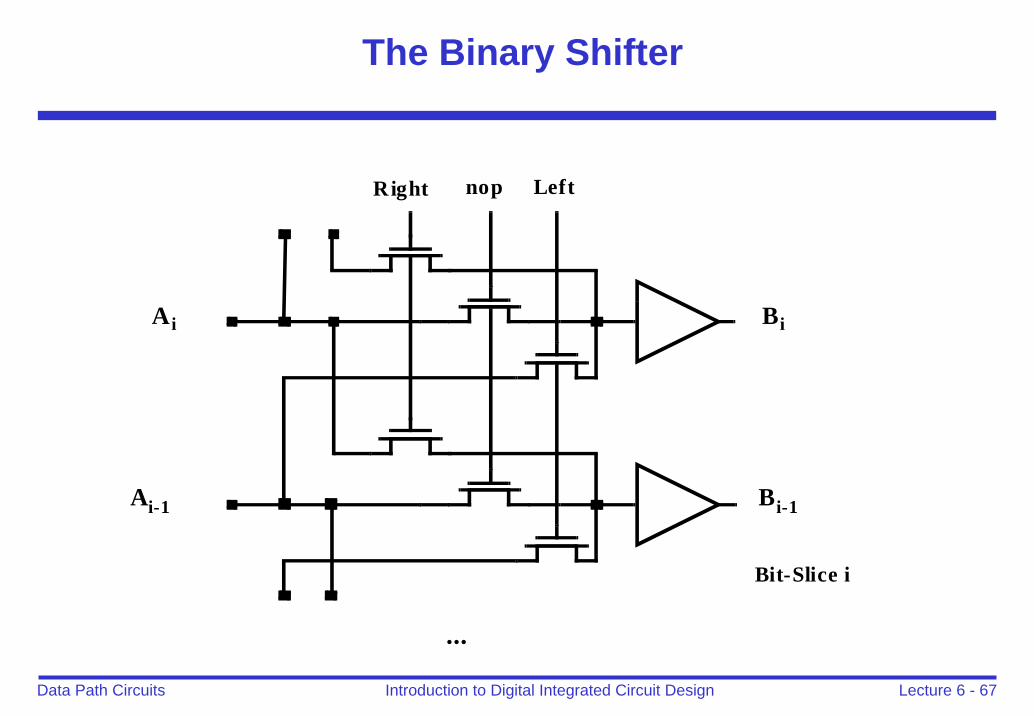
The Binary Shifter
Ai
Ai-1
Bi
Bi-1
Right Leftnop
Bit-Slice i
...
Lecture 6 - 68Introduction to Digital Integrated Circuit DesignData Path Circuits
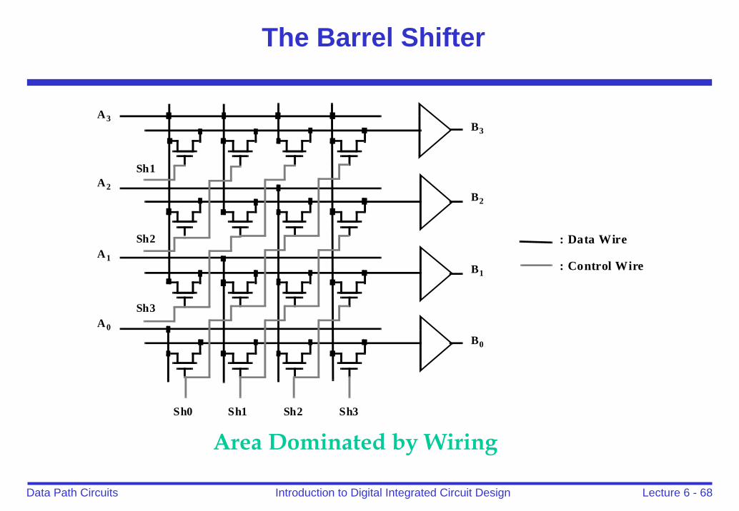
The Barrel Shifter
Sh3Sh2Sh1Sh0
Sh3
Sh2
Sh1
A3
A2
A1
A0
B3
B2
B1
B0
: Control Wire
: Data Wire
Area Dominated by Wiring
Lecture 6 - 69Introduction to Digital Integrated Circuit DesignData Path Circuits
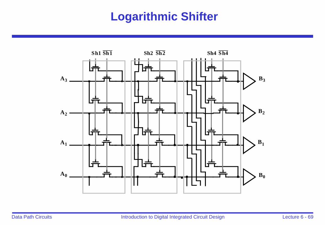
Logarithmic Shifter
Sh1 Sh1 Sh2 Sh2 Sh4 Sh4
A3
A2
A1
A0
B1
B0
B2
B3
Lecture 6 - 70Introduction to Digital Integrated Circuit DesignData Path Circuits
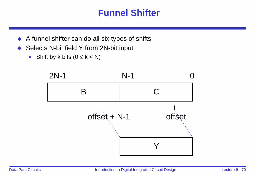
Funnel Shifter
A funnel shifter can do all six types of shiftsSelects N-bit field Y from 2N-bit input• Shift by k bits (0 ≤ k < N)
B C
offsetoffset + N-1
0N-12N-1
Y
Lecture 6 - 71Introduction to Digital Integrated Circuit DesignData Path Circuits
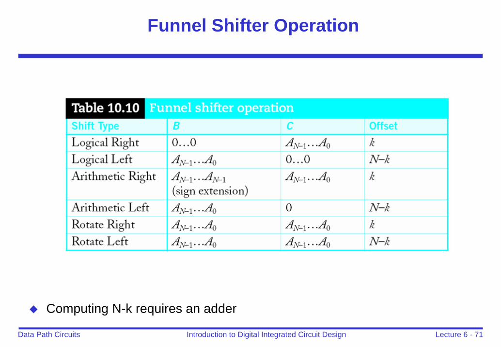
Funnel Shifter Operation
Computing N-k requires an adder
Lecture 6 - 72Introduction to Digital Integrated Circuit DesignData Path Circuits
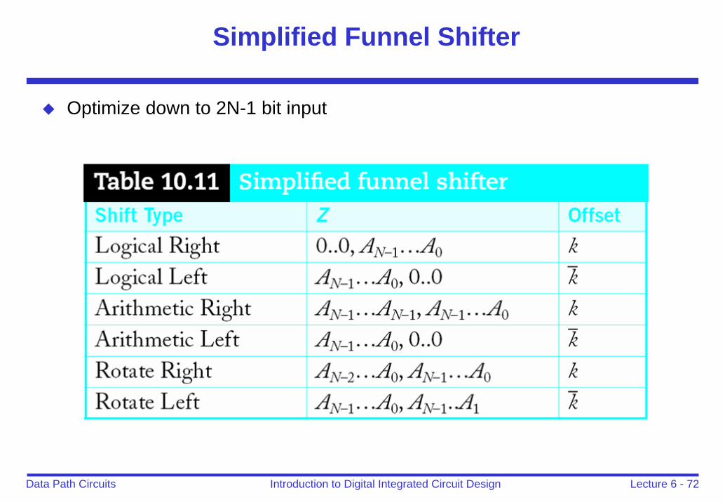
Simplified Funnel Shifter
Optimize down to 2N-1 bit input
Lecture 6 - 73Introduction to Digital Integrated Circuit DesignData Path Circuits
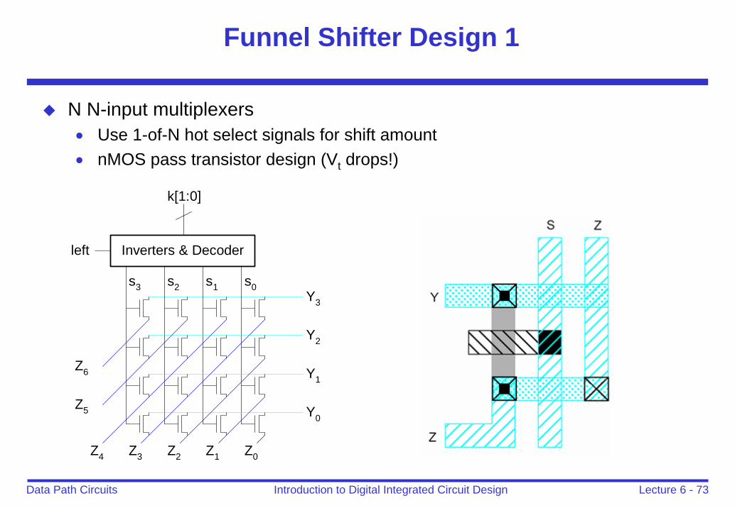
Funnel Shifter Design 1
N N-input multiplexers• Use 1-of-N hot select signals for shift amount• nMOS pass transistor design (Vt drops!)
k[1:0]
s0s1s2s3Y3
Y2
Y1
Y0
Z0Z1Z2Z3Z4
Z5
Z6
left Inverters & Decoder
Lecture 6 - 74Introduction to Digital Integrated Circuit DesignData Path Circuits
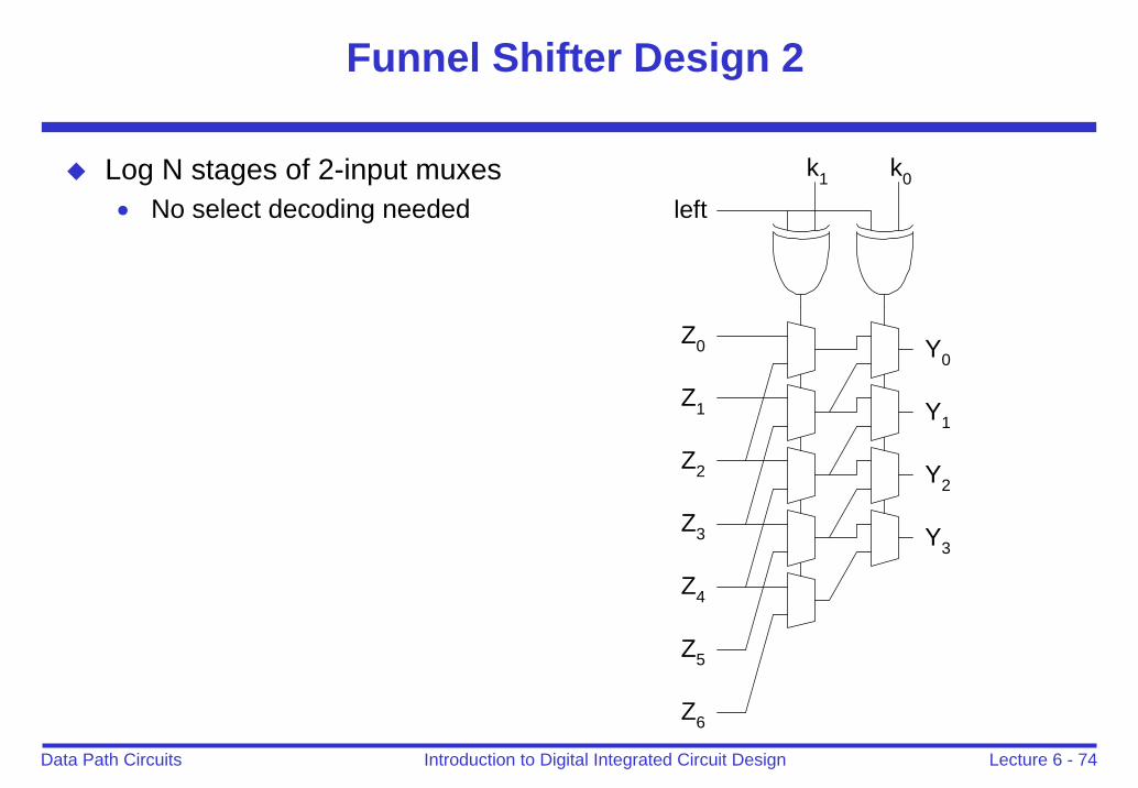
Funnel Shifter Design 2
Log N stages of 2-input muxes• No select decoding needed
Y3
Y2
Y1
Y0Z0
Z1
Z2
Z3
Z4
Z5
Z6
k0k1
left
Lecture 6 - 75Introduction to Digital Integrated Circuit DesignData Path Circuits
Outline
Adders
Multipliers
Shifters
Comparators
Layout issues
Lecture 6 - 76Introduction to Digital Integrated Circuit DesignData Path Circuits
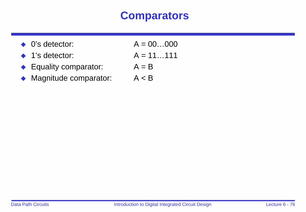
Comparators
0’s detector: A = 00…0001’s detector: A = 11…111Equality comparator: A = BMagnitude comparator: A < B
Lecture 6 - 77Introduction to Digital Integrated Circuit DesignData Path Circuits
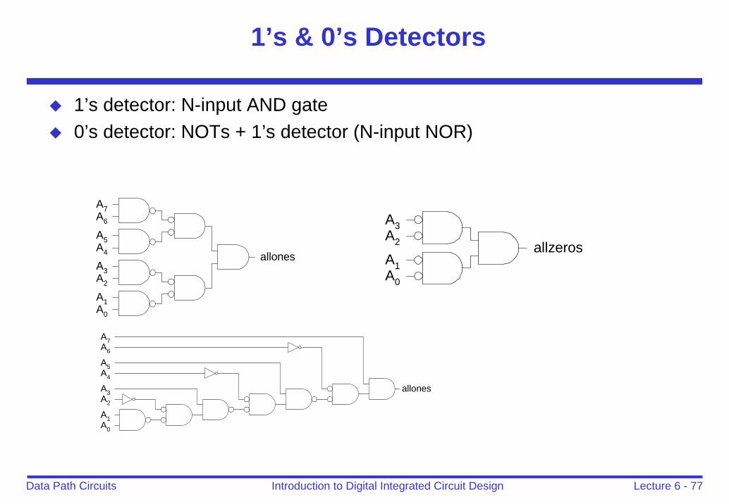
1’s & 0’s Detectors
1’s detector: N-input AND gate0’s detector: NOTs + 1’s detector (N-input NOR)
A0
A1
A2
A3
A4
A5
A6
A7
allones
A0
A1
A2
A3
allzeros
allones
A1
A2
A3
A4
A5
A6
A7
A0
Lecture 6 - 78Introduction to Digital Integrated Circuit DesignData Path Circuits
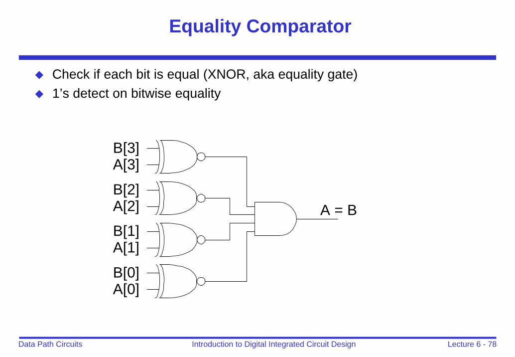
Equality Comparator
Check if each bit is equal (XNOR, aka equality gate)1’s detect on bitwise equality
A[0]B[0]
A = B
A[1]B[1]
A[2]B[2]
A[3]B[3]
Lecture 6 - 79Introduction to Digital Integrated Circuit DesignData Path Circuits
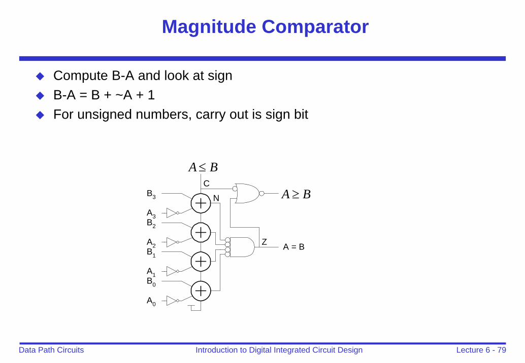
Magnitude Comparator
Compute B-A and look at signB-A = B + ~A + 1For unsigned numbers, carry out is sign bit
A0
B0
A1
B1
A2
B2
A3
B3
A = BZ
C
A B≤
N A B≥
Lecture 6 - 80Introduction to Digital Integrated Circuit DesignData Path Circuits
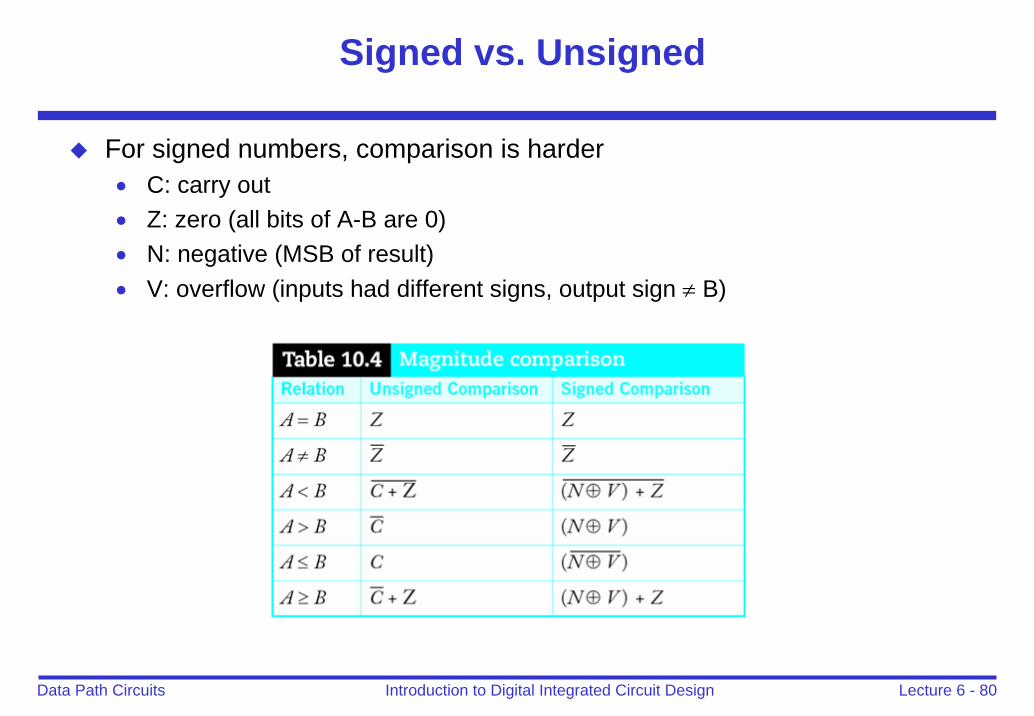
Signed vs. Unsigned
For signed numbers, comparison is harder• C: carry out• Z: zero (all bits of A-B are 0)• N: negative (MSB of result)• V: overflow (inputs had different signs, output sign ≠ B)
Lecture 6 - 81Introduction to Digital Integrated Circuit DesignData Path Circuits
Outline
Adders
Multipliers
Shifters
Comparators
Layout issues
Lecture 6 - 82Introduction to Digital Integrated Circuit DesignData Path Circuits
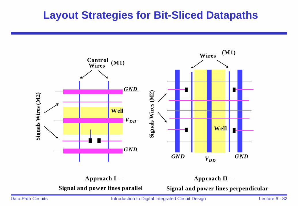
Layout Strategies for Bit-Sliced Datapaths
Well
ControlWires (M1)
Well
Wires (M1)
GND VDDGND
GND
VDD
GND
Approach I —Signal and power lines parallel
Approach II —
Signal and power lines perpendicular
Sign
als W
ires
(M2)
Sign
als W
ires
(M2)
Lecture 6 - 83Introduction to Digital Integrated Circuit DesignData Path Circuits
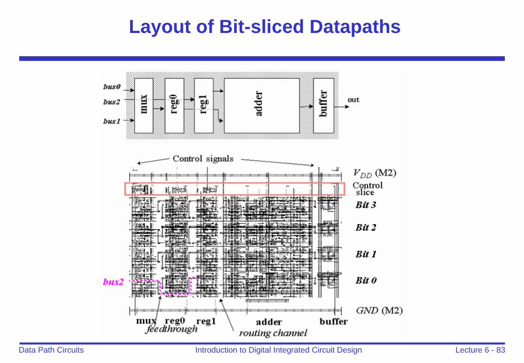
Layout of Bit-sliced Datapaths
Lecture 6 - 84Introduction to Digital Integrated Circuit DesignData Path Circuits
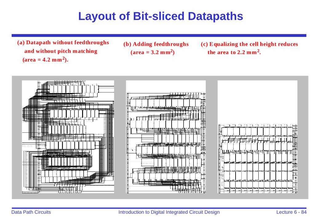
Layout of Bit-sliced Datapaths
(a) Datapath without feedthroughsand without pitch matching
(area = 4.2 mm2).
(b) Adding feedthroughs(area = 3.2 mm2)
(c) Equalizing the cell height reducesthe area to 2.2 mm2.
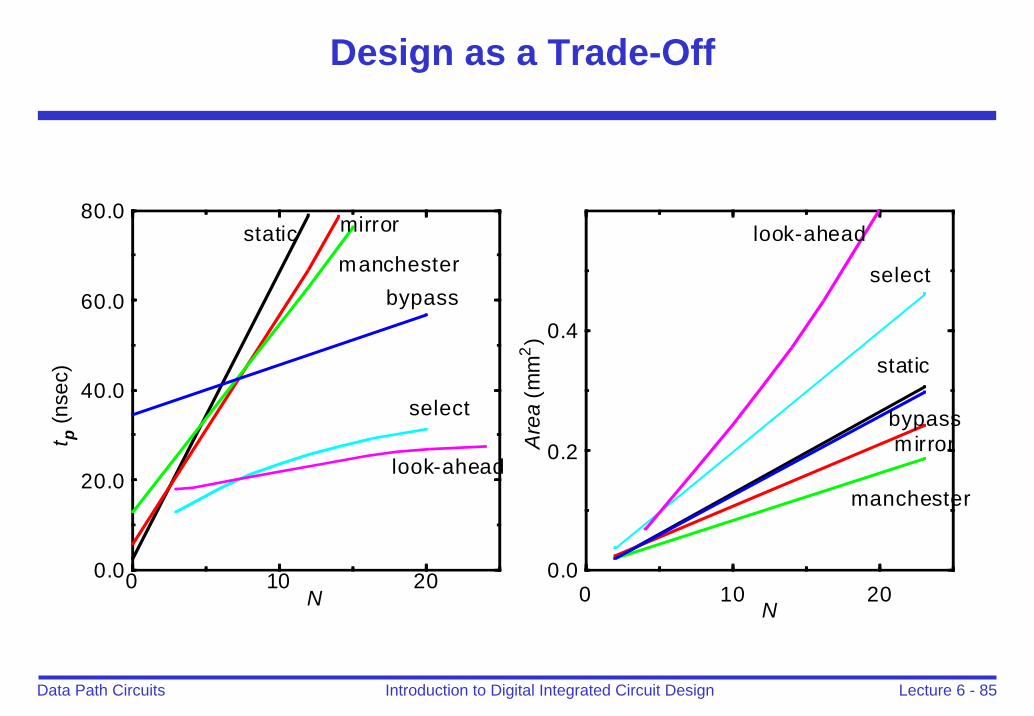
Lecture 6 - 85Introduction to Digital Integrated Circuit DesignData Path Circuits
Design as a Trade-Off
0 10 20N
0.0
20.0
40.0
60.0
80.0
t p (n
sec)
0 10 20N
0.0
0.2
0.4
Are
a (m
m2)
look-ahead
select
bypassmanchester
mirrorstatic
manchester
look-ahead
select
static
mirrorbypass
Lecture 6 - 86Introduction to Digital Integrated Circuit DesignData Path Circuits
Important Design Concepts
The most important rule is to select the right structure before starting an elaborate circuit optimization.• Going for the optimal performance of a complex structure by rigorously optimizing
transistor sizes and topologies probably will not give the best result. • Optimizations at the higher levels of abstraction (logic or architectural level) can often
generate more dramatic results. Simple first order calculations can help give a global picture of the pros and cons of a proposed structure
Determine the critical timing path through the circuit and focus most of your optimization efforts on that part of the circuit. • Hand analysis + CAD tools for critical path analysis and transistor sizing• Non critical parts can be downsized to reduce power
Circuit size is not only determined by the number and size of transistors but also by other factors such as wiring and number of vias and contacts. An obscure optimization can sometimes help to get a better result however it may also lead to irregular and convoluted topology. • Regularity and modularity are very important properties
Power and speed can be traded off through a choice of circuit sizing, supply voltages and transistor thresholds.
Lecture 6 - 87Introduction to Digital Integrated Circuit DesignData Path Circuits
Summary
A data path is best implemented in a bit-sliced fashion. A single layout is used repetitively for every bit in the data word. This regular approach eases the design effort and results in fast and dense layouts.A ripple carry adder has a performance that is linearly proportional to the number of bits. Circuit optimizations concentrate on reducing the delay of the carry path. • A number of circuit topologies exist proving that careful optimization of the circuit
topology and the transistor sizes helps to reduce the capacitance on the carry bitOther adder structures use logic optimizations to increase the performance (carry-bypass, carry select, carry lookahead) • Performance increase comes at the cost of area
A multiplier is nothing more than a collection of cascaded adders. Critical path is far more complex and optimizations are different compared to adders. • Carry save technique: logic manipulation to turn the adder array into a regular structure
with well defined critical timing path – easy to optimize• Booth recoding and partial product accumulation in a tree reduces the complexity and
delay of large multipliers The performance and the area of a programmable shifter are dominated by the wiring.• The exploitation of regularity can help to minimize the impact of the interconnect wires.
Top Related