


Languages
Pages
Legal

NPN-‐transistor to J-‐FET to MOS-‐FET revolu7on
Lecture 15

Evolu7on and Revolu7on in Electronics
The structures of gate and oxide are shrunk over 7me to achieve faster opera7on and higher packing density. This is evolu&on Inherent problems tend to become limi7ng factors. Different concepts are invented to overcome these problems and lead to leaps in performance improvements. This is revolu&onary progress.

npn transistor (or pnp) N-‐type and p-‐type materials are joint (or prepared on a single piece). The middle base piece is controlled to transmit or inhibit carrier conduc7on.

Junc7on Field Effect Transistor (J-‐FET) n+-‐type material from source to drain (formerly emiOer to collector) sandwiched between two p+-‐type gates (superscripts stand for high doping). The p-‐type gates are biased in reverse (nega7ve), i.e. a deple7on zone builds up. The source is nega7ve and the drain posi7ve (also in reverse). The deple7on zone increases towards the drain.

Junc7on Field Effect Transistor (J-‐FET) n+-‐type material from source to drain (formerly emiOer to collector) sandwiched between two p+-‐type gates (superscripts stand for high doping). The p-‐type gates are biased in reverse (nega7ve), i.e. a deple7on zone builds up. The source is nega7ve and the drain posi7ve (also in reverse). The deple7on zone increases towards the drain. Increasing the bias nega7vely on the drain increases the deple7on zone and pinches off the current from source to drain.

Junc7on Field Effect Transistor (J-‐FET) n+-‐type material from source to drain (formerly emiOer to collector) sandwiched between two p+-‐type gates (superscripts stand for high doping). The p-‐type gates are biased in reverse (nega7ve), i.e. a deple7on zone builds up. The source is nega7ve and the drain posi7ve (also in reverse). The deple7on zone increases towards the drain. Increasing the bias nega7vely on the drain increases the deple7on zone and pinches off the current from source to drain.

Junc7on Field Effect Transistor (J-‐FET) n+-‐type material from source to drain (formerly emiOer to collector) sandwiched between two p+-‐type gates (superscripts stand for high doping). The p-‐type gates are biased in reverse (nega7ve), i.e. a deple7on zone builds up. The source is nega7ve and the drain posi7ve (also in reverse). The deple7on zone increases towards the drain. Increasing the source drain bias (more posi7ve at the drain) increases the current. At the same 7me it increases the deple7on region near the drain. Eventually these two cancel each other.


Connec7ng a metal with a semiconductor via an insulator: like an air gap The vacuum level and Fermi levels do not move. Here FM and FS happen to match in the unbiased system. When applying a posi7ve bias to the metal electrons are pulled towards the oxide interface. In equilibrium the diffusion current and the driY current match. With a nega7ve bias to the metal electrons are pushed away from the oxide. The deple7on layer is increased. No free carriers exist.
Metal Oxide Semiconductor junc7on
2/3
2
*22exp ⎟⎟⎠
⎞⎜⎜⎝
⎛ ⋅=⎟⎟⎠
⎞⎜⎜⎝
⎛ −−⋅=
hTkmN
TkEE
NN Bec
B
Fgce
π

Metal Oxide Semiconductor junc7on
With a much larger nega7ve bias to the metal electrons are pushed farther away from the oxide. The deple7on layer con7nues to increase. Not so fast. The Fermi level dips down towards the valence band. Hole carriers can exist. They could be thermally created elsewhere. Electrons are pushed away and holes are aOracted towards the insulator. Basically, a p-‐type semiconductor condi7on is generated near the oxide (insulator). This is a inversion layer.
At t=0 apply the bias: At tdrain the electrons are pushed out of a 1 m layer: At tequilibrum equilibrium is aOained due to driY and diffusion currents. thermal genera7on of carriers in sufficiently pure materials may take seconds. Inversion can exist for quite some 7me. The surface layer currents (or their inhibi7on) are the founda7on of capacitors, MOS-‐FETs and CCDs The basic structure can be used as a variable (voltage controlled) resistor, as a capacitor, or as a transistor
msmhrm 3/1/1 µ⇒µ fast
slow
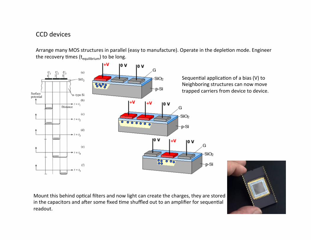
CCD devices Arrange many MOS structures in parallel (easy to manufacture). Operate in the deple7on mode. Engineer the recovery 7mes (tequilibrium) to be long.
Sequen7al applica7on of a bias (V) to Neighboring structures can now move trapped carriers from device to device.
Mount this behind op7cal filters and now light can create the charges, they are stored in the capacitors and aYer some fixed 7me shuffled out to an amplifier for sequen7al readout.
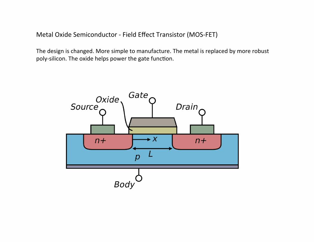
Metal Oxide Semiconductor -‐ Field Effect Transistor (MOS-‐FET) The design is changed. More simple to manufacture. The metal is replaced by more robust poly-‐silicon. The oxide helps power the gate func7on.
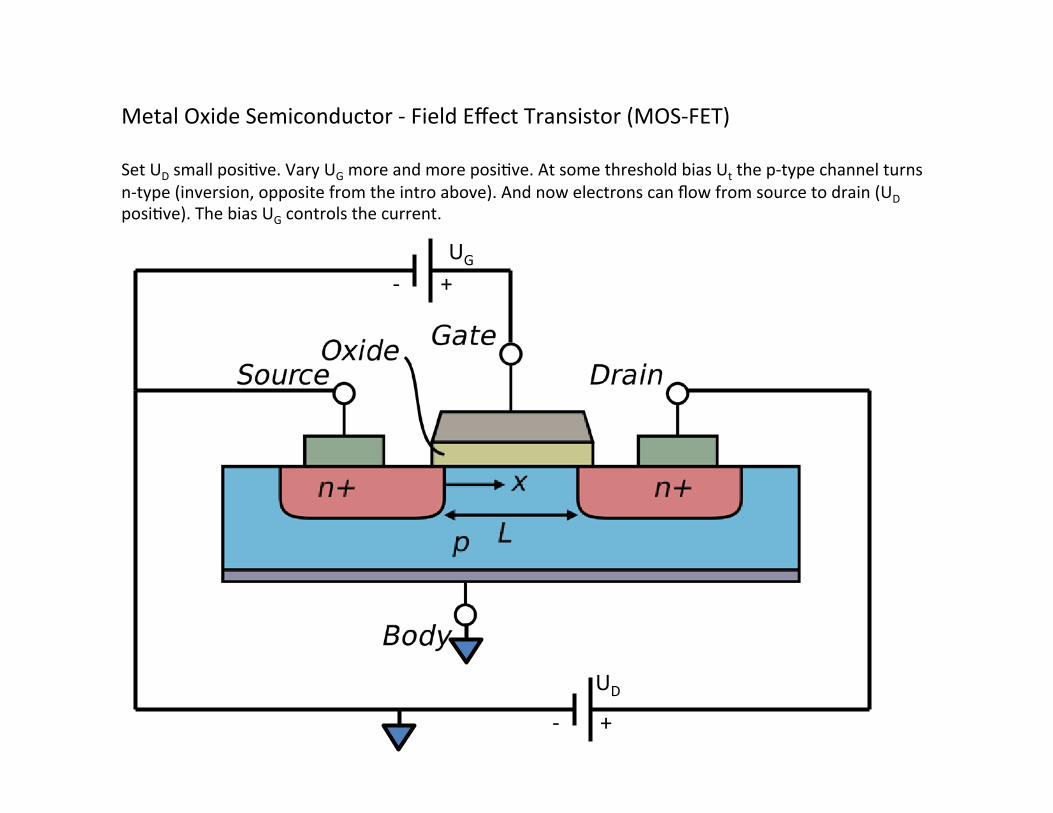
Metal Oxide Semiconductor -‐ Field Effect Transistor (MOS-‐FET) Set UD small posi7ve. Vary UG more and more posi7ve. At some threshold bias Ut the p-‐type channel turns n-‐type (inversion, opposite from the intro above). And now electrons can flow from source to drain (UD posi7ve). The bias UG controls the current.
+ -‐
UD
UG + -‐

Metal Oxide Semiconductor -‐ Field Effect Transistor (MOS-‐FET) Set UD small posi7ve. Vary UG more and more posi7ve. At some threshold bias Ut the p-‐type channel turns n-‐type (inversion, opposite from the intro above). And now electrons can flow from source to drain (UD posi7ve). The bias UG controls the current. ID changes as a func7on of a “variable resistor” controlled by UG.
+ -‐
UD
UG + -‐
UD
UG ID
Ut

Metal Oxide Semiconductor -‐ Field Effect Transistor (MOS-‐FET) Vary UD to larger and larger values. The bias from UG to the channel edges drops on the drain side. The inversion layer is pinched. At sufficient UD the drain current ID saturates.
+ -‐
UD
UG + -‐
Bias differen7al drops source to drain


+ -‐
UD
UG + -‐
Metal Oxide Semiconductor -‐ Field Effect Transistor (MOS-‐FET) The drain current is controlled by several factors ( ) ⎥⎦
⎤⎢⎣⎡ −−⋅= 2
21
DSDStGSoxD VVVVLWCI µ
W is the width of the channel into the page

Small bias changes between gate and source Ugs effect large changes in the current from source to drain Isd. The ra7o the two is the transconductance gm of the MOS-‐FET gm is similar to the inverse of a resistance.
GS
SDm U
Ig =

Silicon fin – transistor (fin-‐FET) The design is changed again into 3D. Grown in top of SoI material (Silicon on insulator). No more than 5% increase in cost. 37% faster and 90% less sta7c leakage current.
hOps://www.youtube.com/watch?v=Jctk0DI7YP8 video on fin-‐FETs

Basic MOS device physics Lecture 15
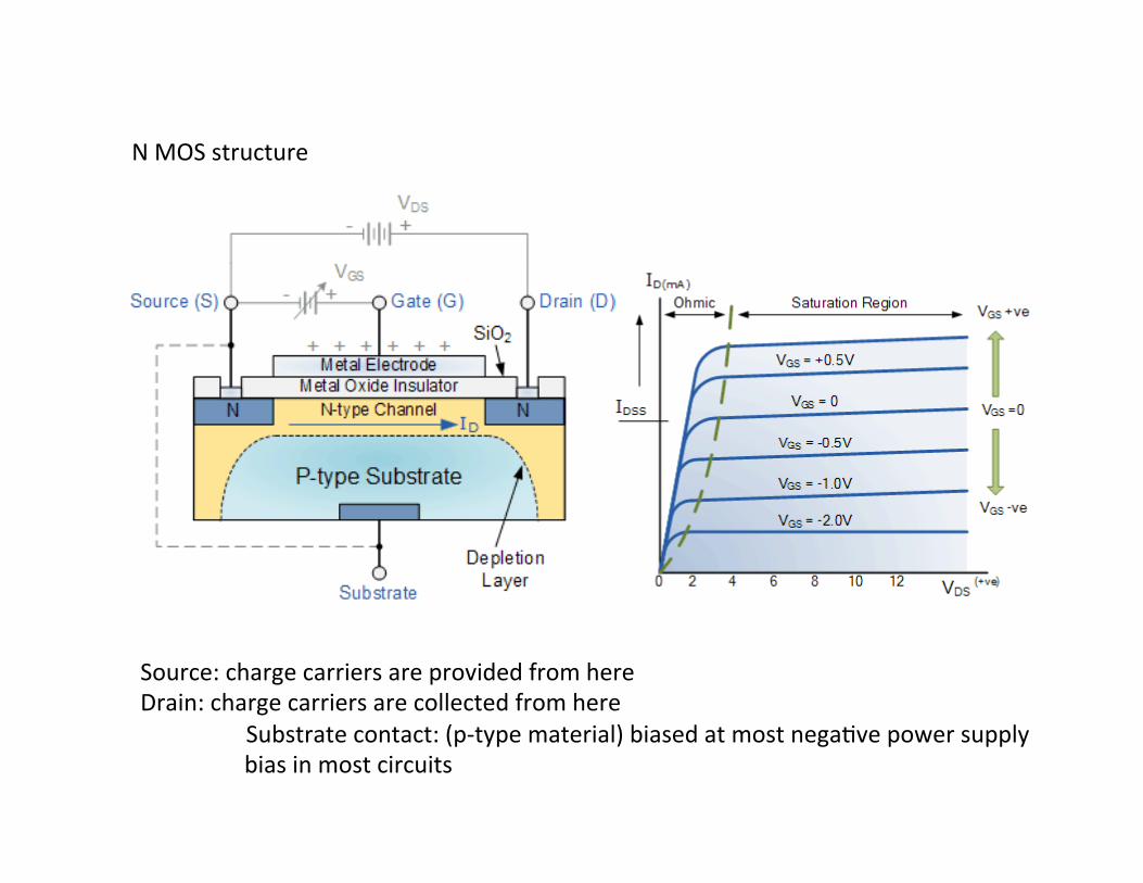
N MOS structure
Source: charge carriers are provided from here Drain: charge carriers are collected from here Substrate contact: (p-‐type material) biased at most nega7ve power supply
bias in most circuits

Short channel MOS-‐FET Sub threshold characteris7cs A small percentage of electrons have sufficient thermal energy (several kBT) to overcome the poten7al barrier A small current is the result

Short channel MOS-‐FET Poten7al contours (solid) in a long channel MOS-‐FET along with electron densi7es (dashed)
Top Related