


Languages
Pages
Legal

Laquestiondeladurabilitédestechnologiesdecalculetde
télécommunication
José HalloyProf. of Physics, Université Paris Diderot

Sustainability: long durationEnergy and resources transition
Climate change

It’snotclimatechange–it’severythingchange
MargaretAtwood

AlphaGo defeated Lee Sedol
4 8 4 | N A T U R E | V O L 5 2 9 | 2 8 J A N U A R Y 2 0 1 6
ARTICLEdoi:10.1038/nature16961
Mastering the game of Go with deep neural networks and tree searchDavid Silver1*, Aja Huang1*, Chris J. Maddison1, Arthur Guez1, Laurent Sifre1, George van den Driessche1, Julian Schrittwieser1, Ioannis Antonoglou1, Veda Panneershelvam1, Marc Lanctot1, Sander Dieleman1, Dominik Grewe1, John Nham2, Nal Kalchbrenner1, Ilya Sutskever2, Timothy Lillicrap1, Madeleine Leach1, Koray Kavukcuoglu1, Thore Graepel1 & Demis Hassabis1
All games of perfect information have an optimal value function, v*(s), which determines the outcome of the game, from every board position or state s, under perfect play by all players. These games may be solved by recursively computing the optimal value function in a search tree containing approximately bd possible sequences of moves, where b is the game’s breadth (number of legal moves per position) and d is its depth (game length). In large games, such as chess (b ≈ 35, d ≈ 80)1 and especially Go (b ≈ 250, d ≈ 150)1, exhaustive search is infeasible2,3, but the effective search space can be reduced by two general principles. First, the depth of the search may be reduced by position evaluation: truncating the search tree at state s and replacing the subtree below s by an approximate value function v(s) ≈ v*(s) that predicts the outcome from state s. This approach has led to superhuman performance in chess4, checkers5 and othello6, but it was believed to be intractable in Go due to the complexity of the game7. Second, the breadth of the search may be reduced by sampling actions from a policy p(a|s) that is a prob-ability distribution over possible moves a in position s. For example, Monte Carlo rollouts8 search to maximum depth without branching at all, by sampling long sequences of actions for both players from a policy p. Averaging over such rollouts can provide an effective position evaluation, achieving superhuman performance in backgammon8 and Scrabble9, and weak amateur level play in Go10.
Monte Carlo tree search (MCTS)11,12 uses Monte Carlo rollouts to estimate the value of each state in a search tree. As more simu-lations are executed, the search tree grows larger and the relevant values become more accurate. The policy used to select actions during search is also improved over time, by selecting children with higher values. Asymptotically, this policy converges to optimal play, and the evaluations converge to the optimal value function12. The strongest current Go programs are based on MCTS, enhanced by policies that are trained to predict human expert moves13. These policies are used to narrow the search to a beam of high-probability actions, and to sample actions during rollouts. This approach has achieved strong amateur play13–15. However, prior work has been limited to shallow
policies13–15 or value functions16 based on a linear combination of input features.
Recently, deep convolutional neural networks have achieved unprec-edented performance in visual domains: for example, image classifica-tion17, face recognition18, and playing Atari games19. They use many layers of neurons, each arranged in overlapping tiles, to construct increasingly abstract, localized representations of an image20. We employ a similar architecture for the game of Go. We pass in the board position as a 19 × 19 image and use convolutional layers to construct a representation of the position. We use these neural networks to reduce the effective depth and breadth of the search tree: evaluating positions using a value network, and sampling actions using a policy network.
We train the neural networks using a pipeline consisting of several stages of machine learning (Fig. 1). We begin by training a supervised learning (SL) policy network pσ directly from expert human moves. This provides fast, efficient learning updates with immediate feedback and high-quality gradients. Similar to prior work13,15, we also train a fast policy pπ that can rapidly sample actions during rollouts. Next, we train a reinforcement learning (RL) policy network pρ that improves the SL policy network by optimizing the final outcome of games of self-play. This adjusts the policy towards the correct goal of winning games, rather than maximizing predictive accuracy. Finally, we train a value network vθ that predicts the winner of games played by the RL policy network against itself. Our program AlphaGo efficiently combines the policy and value networks with MCTS.
Supervised learning of policy networksFor the first stage of the training pipeline, we build on prior work on predicting expert moves in the game of Go using supervised learning13,21–24. The SL policy network pσ(a | s) alternates between con-volutional layers with weights σ, and rectifier nonlinearities. A final soft-max layer outputs a probability distribution over all legal moves a. The input s to the policy network is a simple representation of the board state (see Extended Data Table 2). The policy network is trained on randomly
The game of Go has long been viewed as the most challenging of classic games for artificial intelligence owing to its enormous search space and the difficulty of evaluating board positions and moves. Here we introduce a new approach to computer Go that uses ‘value networks’ to evaluate board positions and ‘policy networks’ to select moves. These deep neural networks are trained by a novel combination of supervised learning from human expert games, and reinforcement learning from games of self-play. Without any lookahead search, the neural networks play Go at the level of state- of-the-art Monte Carlo tree search programs that simulate thousands of random games of self-play. We also introduce a new search algorithm that combines Monte Carlo simulation with value and policy networks. Using this search algorithm, our program AlphaGo achieved a 99.8% winning rate against other Go programs, and defeated the human European Go champion by 5 games to 0. This is the first time that a computer program has defeated a human professional player in the full-sized game of Go, a feat previously thought to be at least a decade away.
1Google DeepMind, 5 New Street Square, London EC4A 3TW, UK. 2Google, 1600 Amphitheatre Parkway, Mountain View, California 94043, USA.*These authors contributed equally to this work.
© 2016 Macmillan Publishers Limited. All rights reserved
4 8 6 | N A T U R E | V O L 5 2 9 | 2 8 J A N U A R Y 2 0 1 6
ARTICLERESEARCH
learning of convolutional networks, won 11% of games against Pachi23 and 12% against a slightly weaker program, Fuego24.
Reinforcement learning of value networksThe final stage of the training pipeline focuses on position evaluation, estimating a value function vp(s) that predicts the outcome from posi-tion s of games played by using policy p for both players28–30
E( )= | = ∼…v s z s s a p[ , ]pt t t T
Ideally, we would like to know the optimal value function under perfect play v*(s); in practice, we instead estimate the value function
ρv p for our strongest policy, using the RL policy network pρ. We approx-imate the value function using a value network vθ(s) with weights θ,
⁎( )≈ ( )≈ ( )θ ρv s v s v sp . This neural network has a similar architecture to the policy network, but outputs a single prediction instead of a prob-ability distribution. We train the weights of the value network by regres-sion on state-outcome pairs (s, z), using stochastic gradient descent to minimize the mean squared error (MSE) between the predicted value vθ(s), and the corresponding outcome z
∆θθ
∝∂ ( )∂( − ( ))θ
θv s z v s
The naive approach of predicting game outcomes from data con-sisting of complete games leads to overfitting. The problem is that successive positions are strongly correlated, differing by just one stone, but the regression target is shared for the entire game. When trained on the KGS data set in this way, the value network memorized the game outcomes rather than generalizing to new positions, achieving a minimum MSE of 0.37 on the test set, compared to 0.19 on the training set. To mitigate this problem, we generated a new self-play data set consisting of 30 million distinct positions, each sampled from a sepa-rate game. Each game was played between the RL policy network and itself until the game terminated. Training on this data set led to MSEs of 0.226 and 0.234 on the training and test set respectively, indicating minimal overfitting. Figure 2b shows the position evaluation accuracy of the value network, compared to Monte Carlo rollouts using the fast rollout policy pπ; the value function was consistently more accurate. A single evaluation of vθ(s) also approached the accuracy of Monte Carlo rollouts using the RL policy network pρ, but using 15,000 times less computation.
Searching with policy and value networksAlphaGo combines the policy and value networks in an MCTS algo-rithm (Fig. 3) that selects actions by lookahead search. Each edge
(s, a) of the search tree stores an action value Q(s, a), visit count N(s, a), and prior probability P(s, a). The tree is traversed by simulation (that is, descending the tree in complete games without backup), starting from the root state. At each time step t of each simulation, an action at is selected from state st
= ( ( )+ ( ))a Q s a u s aargmax , ,ta
t t
so as to maximize action value plus a bonus
( )∝( )+ ( )
u s a P s aN s a
, ,1 ,
that is proportional to the prior probability but decays with repeated visits to encourage exploration. When the traversal reaches a leaf node sL at step L, the leaf node may be expanded. The leaf position sL is processed just once by the SL policy network pσ. The output prob-abilities are stored as prior probabilities P for each legal action a, ( )= ( | )σP s a p a s, . The leaf node is evaluated in two very different ways:
first, by the value network vθ(sL); and second, by the outcome zL of a random rollout played out until terminal step T using the fast rollout policy pπ; these evaluations are combined, using a mixing parameter λ, into a leaf evaluation V(sL)
λ λ( )= ( − ) ( )+θV s v s z1L L L
At the end of simulation, the action values and visit counts of all traversed edges are updated. Each edge accumulates the visit count and mean evaluation of all simulations passing through that edge
∑
∑
( )= ( )
( )=( )
( ) ( )
=
=
N s a s a i
Q s aN s a
s a i V s
, 1 , ,
, 1,
1 , ,
i
n
i
n
Li
1
1
where sLi is the leaf node from the ith simulation, and 1(s, a, i) indicates
whether an edge (s, a) was traversed during the ith simulation. Once the search is complete, the algorithm chooses the most visited move from the root position.
It is worth noting that the SL policy network pσ performed better in AlphaGo than the stronger RL policy network pρ, presumably because humans select a diverse beam of promising moves, whereas RL opti-mizes for the single best move. However, the value function ( )≈ ( )θ ρv s v sp derived from the stronger RL policy network performed
Figure 3 | Monte Carlo tree search in AlphaGo. a, Each simulation traverses the tree by selecting the edge with maximum action value Q, plus a bonus u(P) that depends on a stored prior probability P for that edge. b, The leaf node may be expanded; the new node is processed once by the policy network pσ and the output probabilities are stored as prior probabilities P for each action. c, At the end of a simulation, the leaf node
is evaluated in two ways: using the value network vθ; and by running a rollout to the end of the game with the fast rollout policy pπ, then computing the winner with function r. d, Action values Q are updated to track the mean value of all evaluations r(·) and vθ(·) in the subtree below that action.
Selectiona b c dExpansion Evaluation Backup
pS
pV
Q + u(P)
Q + u(P)Q + u(P)
Q + u(P)
P P
P P
Q
Q
Q
rr r r
P
max
max
P
QT
QT
QT
QT
QT QT
© 2016 Macmillan Publishers Limited. All rights reserved
2 8 J A N U A R Y 2 0 1 6 | V O L 5 2 9 | N A T U R E | 4 8 5
ARTICLE RESEARCH
sampled state-action pairs (s, a), using stochastic gradient ascent to maximize the likelihood of the human move a selected in state s
∆σσ
∝∂ ( | )∂
σp a slog
We trained a 13-layer policy network, which we call the SL policy network, from 30 million positions from the KGS Go Server. The net-work predicted expert moves on a held out test set with an accuracy of 57.0% using all input features, and 55.7% using only raw board posi-tion and move history as inputs, compared to the state-of-the-art from other research groups of 44.4% at date of submission24 (full results in Extended Data Table 3). Small improvements in accuracy led to large improvements in playing strength (Fig. 2a); larger networks achieve better accuracy but are slower to evaluate during search. We also trained a faster but less accurate rollout policy pπ(a|s), using a linear softmax of small pattern features (see Extended Data Table 4) with weights π; this achieved an accuracy of 24.2%, using just 2 µs to select an action, rather than 3 ms for the policy network.
Reinforcement learning of policy networksThe second stage of the training pipeline aims at improving the policy network by policy gradient reinforcement learning (RL)25,26. The RL policy network pρ is identical in structure to the SL policy network,
and its weights ρ are initialized to the same values, ρ = σ. We play games between the current policy network pρ and a randomly selected previous iteration of the policy network. Randomizing from a pool of opponents in this way stabilizes training by preventing overfitting to the current policy. We use a reward function r(s) that is zero for all non-terminal time steps t < T. The outcome zt = ± r(sT) is the termi-nal reward at the end of the game from the perspective of the current player at time step t: +1 for winning and −1 for losing. Weights are then updated at each time step t by stochastic gradient ascent in the direction that maximizes expected outcome25
∆ρρ
∝∂ ( | )
∂ρp a s
zlog t t
t
We evaluated the performance of the RL policy network in game play, sampling each move ∼ (⋅| )ρa p st t from its output probability distribution over actions. When played head-to-head, the RL policy network won more than 80% of games against the SL policy network. We also tested against the strongest open-source Go program, Pachi14, a sophisticated Monte Carlo search program, ranked at 2 amateur dan on KGS, that executes 100,000 simulations per move. Using no search at all, the RL policy network won 85% of games against Pachi. In com-parison, the previous state-of-the-art, based only on supervised
Figure 1 | Neural network training pipeline and architecture. a, A fast rollout policy pπ and supervised learning (SL) policy network pσ are trained to predict human expert moves in a data set of positions. A reinforcement learning (RL) policy network pρ is initialized to the SL policy network, and is then improved by policy gradient learning to maximize the outcome (that is, winning more games) against previous versions of the policy network. A new data set is generated by playing games of self-play with the RL policy network. Finally, a value network vθ is trained by regression to predict the expected outcome (that is, whether
the current player wins) in positions from the self-play data set. b, Schematic representation of the neural network architecture used in AlphaGo. The policy network takes a representation of the board position s as its input, passes it through many convolutional layers with parameters σ (SL policy network) or ρ (RL policy network), and outputs a probability distribution ( | )σp a s or ( | )ρp a s over legal moves a, represented by a probability map over the board. The value network similarly uses many convolutional layers with parameters θ, but outputs a scalar value vθ(s′) that predicts the expected outcome in position s′.
Regr
essi
on
Cla
ssifi
catio
nClassification
Self Play
Policy gradient
a b
Human expert positions Self-play positions
Neural netw
orkD
ata
Rollout policy
pS pV pV�U (a⎪s) QT (s′)pU QT
SL policy network RL policy network Value network Policy network Value network
s s′
Figure 2 | Strength and accuracy of policy and value networks. a, Plot showing the playing strength of policy networks as a function of their training accuracy. Policy networks with 128, 192, 256 and 384 convolutional filters per layer were evaluated periodically during training; the plot shows the winning rate of AlphaGo using that policy network against the match version of AlphaGo. b, Comparison of evaluation accuracy between the value network and rollouts with different policies.
Positions and outcomes were sampled from human expert games. Each position was evaluated by a single forward pass of the value network vθ, or by the mean outcome of 100 rollouts, played out using either uniform random rollouts, the fast rollout policy pπ, the SL policy network pσ or the RL policy network pρ. The mean squared error between the predicted value and the actual game outcome is plotted against the stage of the game (how many moves had been played in the given position).
15 45 75 105 135 165 195 225 255 >285Move number
0.10
0.15
0.20
0.25
0.30
0.35
0.40
0.45
0.50
Mea
n sq
uare
d er
ror
on e
xper
t gam
es
Uniform random rollout policyFast rollout policyValue networkSL policy networkRL policy network
50 51 52 53 54 55 56 57 58 59Training accuracy on KGS dataset (%)
0
10
20
30
40
50
60
70128 filters192 filters256 filters384 filters
Alp
haG
o w
in ra
te (%
)
a b
© 2016 Macmillan Publishers Limited. All rights reserved
2 8 J A N U A R Y 2 0 1 6 | V O L 5 2 9 | N A T U R E | 4 8 5
ARTICLE RESEARCH
sampled state-action pairs (s, a), using stochastic gradient ascent to maximize the likelihood of the human move a selected in state s
∆σσ
∝∂ ( | )∂
σp a slog
We trained a 13-layer policy network, which we call the SL policy network, from 30 million positions from the KGS Go Server. The net-work predicted expert moves on a held out test set with an accuracy of 57.0% using all input features, and 55.7% using only raw board posi-tion and move history as inputs, compared to the state-of-the-art from other research groups of 44.4% at date of submission24 (full results in Extended Data Table 3). Small improvements in accuracy led to large improvements in playing strength (Fig. 2a); larger networks achieve better accuracy but are slower to evaluate during search. We also trained a faster but less accurate rollout policy pπ(a|s), using a linear softmax of small pattern features (see Extended Data Table 4) with weights π; this achieved an accuracy of 24.2%, using just 2 µs to select an action, rather than 3 ms for the policy network.
Reinforcement learning of policy networksThe second stage of the training pipeline aims at improving the policy network by policy gradient reinforcement learning (RL)25,26. The RL policy network pρ is identical in structure to the SL policy network,
and its weights ρ are initialized to the same values, ρ = σ. We play games between the current policy network pρ and a randomly selected previous iteration of the policy network. Randomizing from a pool of opponents in this way stabilizes training by preventing overfitting to the current policy. We use a reward function r(s) that is zero for all non-terminal time steps t < T. The outcome zt = ± r(sT) is the termi-nal reward at the end of the game from the perspective of the current player at time step t: +1 for winning and −1 for losing. Weights are then updated at each time step t by stochastic gradient ascent in the direction that maximizes expected outcome25
∆ρρ
∝∂ ( | )
∂ρp a s
zlog t t
t
We evaluated the performance of the RL policy network in game play, sampling each move ∼ (⋅| )ρa p st t from its output probability distribution over actions. When played head-to-head, the RL policy network won more than 80% of games against the SL policy network. We also tested against the strongest open-source Go program, Pachi14, a sophisticated Monte Carlo search program, ranked at 2 amateur dan on KGS, that executes 100,000 simulations per move. Using no search at all, the RL policy network won 85% of games against Pachi. In com-parison, the previous state-of-the-art, based only on supervised
Figure 1 | Neural network training pipeline and architecture. a, A fast rollout policy pπ and supervised learning (SL) policy network pσ are trained to predict human expert moves in a data set of positions. A reinforcement learning (RL) policy network pρ is initialized to the SL policy network, and is then improved by policy gradient learning to maximize the outcome (that is, winning more games) against previous versions of the policy network. A new data set is generated by playing games of self-play with the RL policy network. Finally, a value network vθ is trained by regression to predict the expected outcome (that is, whether
the current player wins) in positions from the self-play data set. b, Schematic representation of the neural network architecture used in AlphaGo. The policy network takes a representation of the board position s as its input, passes it through many convolutional layers with parameters σ (SL policy network) or ρ (RL policy network), and outputs a probability distribution ( | )σp a s or ( | )ρp a s over legal moves a, represented by a probability map over the board. The value network similarly uses many convolutional layers with parameters θ, but outputs a scalar value vθ(s′) that predicts the expected outcome in position s′.
Regr
essi
on
Cla
ssifi
catio
nClassification
Self Play
Policy gradient
a b
Human expert positions Self-play positions
Neural netw
orkD
ata
Rollout policy
pS pV pV�U (a⎪s) QT (s′)pU QT
SL policy network RL policy network Value network Policy network Value network
s s′
Figure 2 | Strength and accuracy of policy and value networks. a, Plot showing the playing strength of policy networks as a function of their training accuracy. Policy networks with 128, 192, 256 and 384 convolutional filters per layer were evaluated periodically during training; the plot shows the winning rate of AlphaGo using that policy network against the match version of AlphaGo. b, Comparison of evaluation accuracy between the value network and rollouts with different policies.
Positions and outcomes were sampled from human expert games. Each position was evaluated by a single forward pass of the value network vθ, or by the mean outcome of 100 rollouts, played out using either uniform random rollouts, the fast rollout policy pπ, the SL policy network pσ or the RL policy network pρ. The mean squared error between the predicted value and the actual game outcome is plotted against the stage of the game (how many moves had been played in the given position).
15 45 75 105 135 165 195 225 255 >285Move number
0.10
0.15
0.20
0.25
0.30
0.35
0.40
0.45
0.50M
ean
squa
red
err
oron
exp
ert
gam
es
Uniform random rollout policyFast rollout policyValue networkSL policy networkRL policy network
50 51 52 53 54 55 56 57 58 59Training accuracy on KGS dataset (%)
0
10
20
30
40
50
60
70128 filters192 filters256 filters384 filters
Alp
haG
o w
in r
ate
(%)
a b
© 2016 Macmillan Publishers Limited. All rights reserved
4 8 6 | N A T U R E | V O L 5 2 9 | 2 8 J A N U A R Y 2 0 1 6
ARTICLERESEARCH
learning of convolutional networks, won 11% of games against Pachi23 and 12% against a slightly weaker program, Fuego24.
Reinforcement learning of value networksThe final stage of the training pipeline focuses on position evaluation, estimating a value function vp(s) that predicts the outcome from posi-tion s of games played by using policy p for both players28–30
E( )= | = ∼…v s z s s a p[ , ]pt t t T
Ideally, we would like to know the optimal value function under perfect play v*(s); in practice, we instead estimate the value function
ρv p for our strongest policy, using the RL policy network pρ. We approx-imate the value function using a value network vθ(s) with weights θ,
⁎( )≈ ( )≈ ( )θ ρv s v s v sp . This neural network has a similar architecture to the policy network, but outputs a single prediction instead of a prob-ability distribution. We train the weights of the value network by regres-sion on state-outcome pairs (s, z), using stochastic gradient descent to minimize the mean squared error (MSE) between the predicted value vθ(s), and the corresponding outcome z
∆θθ
∝∂ ( )∂( − ( ))θ
θv s z v s
The naive approach of predicting game outcomes from data con-sisting of complete games leads to overfitting. The problem is that successive positions are strongly correlated, differing by just one stone, but the regression target is shared for the entire game. When trained on the KGS data set in this way, the value network memorized the game outcomes rather than generalizing to new positions, achieving a minimum MSE of 0.37 on the test set, compared to 0.19 on the training set. To mitigate this problem, we generated a new self-play data set consisting of 30 million distinct positions, each sampled from a sepa-rate game. Each game was played between the RL policy network and itself until the game terminated. Training on this data set led to MSEs of 0.226 and 0.234 on the training and test set respectively, indicating minimal overfitting. Figure 2b shows the position evaluation accuracy of the value network, compared to Monte Carlo rollouts using the fast rollout policy pπ; the value function was consistently more accurate. A single evaluation of vθ(s) also approached the accuracy of Monte Carlo rollouts using the RL policy network pρ, but using 15,000 times less computation.
Searching with policy and value networksAlphaGo combines the policy and value networks in an MCTS algo-rithm (Fig. 3) that selects actions by lookahead search. Each edge
(s, a) of the search tree stores an action value Q(s, a), visit count N(s, a), and prior probability P(s, a). The tree is traversed by simulation (that is, descending the tree in complete games without backup), starting from the root state. At each time step t of each simulation, an action at is selected from state st
= ( ( )+ ( ))a Q s a u s aargmax , ,ta
t t
so as to maximize action value plus a bonus
( )∝( )+ ( )
u s a P s aN s a
, ,1 ,
that is proportional to the prior probability but decays with repeated visits to encourage exploration. When the traversal reaches a leaf node sL at step L, the leaf node may be expanded. The leaf position sL is processed just once by the SL policy network pσ. The output prob-abilities are stored as prior probabilities P for each legal action a, ( )= ( | )σP s a p a s, . The leaf node is evaluated in two very different ways:
first, by the value network vθ(sL); and second, by the outcome zL of a random rollout played out until terminal step T using the fast rollout policy pπ; these evaluations are combined, using a mixing parameter λ, into a leaf evaluation V(sL)
λ λ( )= ( − ) ( )+θV s v s z1L L L
At the end of simulation, the action values and visit counts of all traversed edges are updated. Each edge accumulates the visit count and mean evaluation of all simulations passing through that edge
∑
∑
( )= ( )
( )=( )
( ) ( )
=
=
N s a s a i
Q s aN s a
s a i V s
, 1 , ,
, 1,
1 , ,
i
n
i
n
Li
1
1
where sLi is the leaf node from the ith simulation, and 1(s, a, i) indicates
whether an edge (s, a) was traversed during the ith simulation. Once the search is complete, the algorithm chooses the most visited move from the root position.
It is worth noting that the SL policy network pσ performed better in AlphaGo than the stronger RL policy network pρ, presumably because humans select a diverse beam of promising moves, whereas RL opti-mizes for the single best move. However, the value function ( )≈ ( )θ ρv s v sp derived from the stronger RL policy network performed
Figure 3 | Monte Carlo tree search in AlphaGo. a, Each simulation traverses the tree by selecting the edge with maximum action value Q, plus a bonus u(P) that depends on a stored prior probability P for that edge. b, The leaf node may be expanded; the new node is processed once by the policy network pσ and the output probabilities are stored as prior probabilities P for each action. c, At the end of a simulation, the leaf node
is evaluated in two ways: using the value network vθ; and by running a rollout to the end of the game with the fast rollout policy pπ, then computing the winner with function r. d, Action values Q are updated to track the mean value of all evaluations r(·) and vθ(·) in the subtree below that action.
Selectiona b c dExpansion Evaluation Backup
pS
pV
Q + u(P)
Q + u(P)Q + u(P)
Q + u(P)
P P
P P
Q
Q
Q
rr r r
P
max
max
P
QT
QT
QT
QT
QT QT
© 2016 Macmillan Publishers Limited. All rights reserved

AlphaGo defeated Lee Sedol
~100 W per CPU~200 W per GPU

AlphaGo defeated Lee Sedol: energy cost
Brain ~ 20 W2500 kCal/day~ 120 W
130 GJ = 9.7 days 34 years = 130 GJ
~ 155 kW

Current computing industry is based on crystalline semiconductors

are often used as computing nodes forthose machines.
The trends for microprocessor-based com-puters are clear. The performance per unit forPCs, regressed over time, shows a doublingtime of 1.50 years from 1975 (the introduc-tion date of the Altair 8800 kit PC) to2009.10 This rate corresponds to the popularinterpretation of Moore’s law, but not itsexact 1975 formulation.
Figure 3 shows the results in terms of thenumber of calculations per kilowatt-hour ofelectricity consumed for the computers forwhich both performance and measuredpower data are available. These data includea range of computers, from PCs to mainframecomputers.11
The transition from vacuum tube to tran-sistorized computing is clearly evident inthe data. During 1959, 1960, and 1961, astransistorized computers came to market inlarge numbers, there is a difference of abouttwo orders of magnitude between the mostand least electricity-intensive computers.Logical gates constructed with discrete tran-sistors circa 1960 used significantly less
power than those made with vacuum tubesand diodes, and the transition to transistorsalso led to a period of great technologicalinnovation as engineers experimented withdifferent ways to build these machinesto maximize performance and improvereliability.
Computations per kilowatt-hour doubledevery 1.57 years over the entire analysis pe-riod, a rate of improvement only slightlyslower than that for PCs, which saw effi-ciency double every 1.52 years from 1975to 2009 (see Figure 4). The data show signif-icant increases in computational efficiencyeven during the vacuum tube and discrete-transistor eras. From 1946 (ENIAC) to 1958(when the last of the primarily tube-basedcomputers in our sample came on line),computations per kilowatt-hour doubledevery 1.35 years. Computations per kilowatt-hour increased even more rapidly during theshift from tubes to transistors, but the paceof change slowed during the era of discretetransistors.
In the recent years for which we havemore than a few data points (2001, 2004,2008, and 2009), there is a factor of two orthree separating the lowest and highest esti-mates of computations per kilowatt-hour,which indicates substantial variation in thedata in any given year. This variation is partlythe result of including different types ofcomputers in the sample (desktops, servers,laptops, and supercomputers), but the differ-ences tend to be swamped by the rapid in-crease in performance per computer overtime, which drives the results.
Explaining These TrendsEven current computing technology is farfrom the minimum theoretically possible en-ergy used per computation.12 In 1985, thephysicist Richard Feynman analyzed the elec-tricity needed for computers that use elec-trons for switching and estimated that therewas a factor of 1011 improvement that wastheoretically possible compared to computertechnology at that time.13 Since then, perfor-mance per kilowatt-hour for computer sys-tems has improved by a factor of 4 ! 104
based on our regressions, but there is still along way to go with current technology be-fore reaching the theoretical limits—andthat doesn’t even consider the possibility ofnew methods of computation such as opticalor quantum computing.
For vacuum-tube computers, both compu-tational speed and reliability issues encouraged
[3B2-9] man2011030046.3d 29/7/011 10:35 Page 48
Implications of Historical Trends in the Electrical Efficiency of Computing
Figure 2. Computational capacity over time (computations/second per
computer). These data are based on William D. Nordhaus’ 2007 work,9
with additional data added post-1985 for computers not considered
in his study. Doubling time for personal computers only (1975 to 2009)
is 1.5 years.
48 IEEE Annals of the History of Computing
Koomey, Jonathan, et al. "Implications of historicaltrends in the electricalefficiency of computing." IEEE Annalsof the History of Computing 33.3 (2011): 46-54.

Koomey, JonathanG.,H.ScottMatthews,andEricWilliams. "Smarteverything:Willintelligentsystems reduce resourceuse?." Annual ReviewofEnvironment andResources 38(2013):311-343.
EG38CH12-Koomey ARI 16 September 2013 12:59
1E+00
1E+01
1E+02
1E+03
1E+04
1E+05
1E+06
1E+07
1E+08
1E+09
1E+10
1E+11
1E+12
1E+13
1E+14
1E+15
1E+16
1940 1950 1960 1970 1980 1990 2000 2010
Com
puta
tions
per
kW
h
2008+2009 laptops
Cray 1 supercomputer
Univac III (transistors)
Eniac
IBM PC-XT
Univac II
Univac I
EDVAC
IBM PC-AT
486/25 and 486/33Desktops
SiCortex SC5832
SDS 920
DEC PDP-11/20
IBM PC
Gateway P3, 733 MHz
IBM PS/2 E + Sun SS1000
Altair 8800
Apple IIe
Macintosh 128k Compaq Deskpro 386/20e
Figure 2Energy efficiency of general-purpose computers over time (1946–2009). Adapted from Reference 7.
316 Koomey · Matthews ·Williams
Ann
u. R
ev. E
nviro
n. R
esou
r. 20
13.3
8:31
1-34
3. D
ownl
oade
d fr
om w
ww
.ann
ualre
view
s.org
Acc
ess p
rovi
ded
by 8
1.19
4.30
.216
on
12/1
4/16
. For
per
sona
l use
onl
y.

Fig. 1 Schematic flow diagram of integrated-circuit fabrication.
Fig. 2 Size comparison of a wafer to individual components. (a) Semiconductor wafer. (b) Chip. (c) MOSFET and bipolar transistor.
After processing, each wafer contains hundreds or thousands of identical rectangular chips (or dice), typically between 1 and 20 mm on each side, as shown in Fig. 2a. The chips are separated by sawing or laser cutting; Figure 2b shows a separated chip. Schematic top views of a single MOSFET and a single bipolar transistor are shown in Fig. 2c to give some perspective on the relative size of a component in an IC chip. Prior to chip separation, each chip is electrically tested. Defective chips are usually marked with an inkless map file. Good chips are selected and packaged to provide an appropriate thermal, electrical, and interconnection environment for electronic applications.2
506 Semiconductors

30 2. Material Science
Table 2.6. Part of the Periodic Table of elements showing a selection of dopantand alloy elements for silicon. Lower indices show the atomic mass number andupper indices the atomic number of each element
Main Group
III IV V
B510.8 C6
12.0 N714.0
Al1327.0 Si1428.1 P 1531.0
Ga3169.7 Ge32
72.6 As3374.9
In49114.8 Sn50
118.7 Sb51121.7
shell electrons), the chemical behaviour, the solid solubility and the diffusionconstant. The atomic radius of nitrogen is too small for a substitutionalposition in Si, it therefore fails as a donor in Si. Boron and phosphorus aresmaller than Si (covalent radius of Si: 0.117 nm), therefore thick and heavilydoped layers are under tensile strain. Arsenic has a near identical covalentradius to Si, therefore heavily n-doped layers (e.g. buried layers for collectorcontacts) are preferably As doped. Antimony (as Ga, In) is larger than Si,which results in compressively strained layers. The maximum solid solubilityis obtained 100 ◦C to 150 ◦C below the melting point. It ranges from about1021 cm−3 for B and As to several 1018 cm−3 for Ga. At the low temperaturesused for the fabrication of many quantum effect devices the solid solubilitiesare considerably lower, but metastable high solubilities can be obtained easily.From the four main dopants B, P, As, Sb the former two (B, P) diffusefaster than the later ones (As, Sb). At lower process temperatures (< 850 ◦C)transient enhanced diffusion (TED) created by nonequilibrium point defectconcentrations has to be considered.
During growth at lower temperatures the phenomenon of surface segrega-tion turned out to be the most important transport mechanism of dopants.To explain this phenomenon, consider a two atom system with matrix atoms(e.g. Si) and dopant atoms (e.g. Sb). The impinging matrix atoms are in-corporated at steps (either from misorientation or from nucleation) and thesteps move forward due to this mechanism. Surface segregation occurs whenthe second atom (dopant) is not incorporated into the first but manages tocontinue to reside on the growing surface. This can happen by either climb-ing across the steps or by an atomic exchange (Fig. 2.16) from a subsurfaceposition to a surface (adatom) position. The driving force for this exchangestems from an energy gain when comparing the pair dopant atom/matrixadatom (initial state) with matrix atom/dopant adatom (final state).
It is immediately clear, that a BCF-type of diffusion theory with itsadatom capture at steps cannot describe a segregating dopant. In the case ofa strongly segregating species we can completely neglect the matrix steps andassume a locally homogeneous adatom density of dopants, nS (note: in BCF
60 3. Resume of Semiconductor Physics
Ge
Sia a
Diamond Zinc Blend
Fig. 3.4. (a) The diamond crystal structure of elemental Si and Ge. The zinc blendstructure is that found for compound semiconductors such as GaAs and orderedSi0.5Ge0.5
Γ
L
XK WΣ
∆Λ U
Fig. 3.5. The body centred cubic reciprocal lattice along with the Brillouin zoneboundaries and the major symmetry points marked on the using the standard grouptheory symbols
The unit cell of the reciprocal lattice can be formed by constructing theWigner-Seitz cell. The Wigner-Seitz cell is primitive and displays the sym-metry of the crystal system. To obtain this cell one must start at any of thelattice points and the origin and draw vectors to all the neighbouring latticepoints. Planes perpendicular to and passing through the midpoints of thesevectors are constructed. The Wigner-Seitz cell is then the smallest volumeabout the origin bounded by these planes.
For a face centred cubic lattice, the reciprocal lattice which forms theWigner-Seitz cell is a body centred cubic lattice. Figure 3.5 shows the bodycentred cubic reciprocal lattice along with the corresponding Brillouin zoneboundaries with the major symmetry points marked by the standard grouptheory symbols. Once the crystal structure of a material is known, this fre-quently allows the calculation of the energy band structure from Schrodinger’sequation to be simplified when the symmetry of the system is taken into ac-count.
3.3 The Concentration of Carriers in a Semiconductor 75
104
103
102
101
100
10-1
10-2
10-3
10-4
1012 1013 1014 1015 1016 1017 1018 1019 1020 1021
Impurity concentration (cm-3)
p-type (B)
n-type (P)
Silicon300 K
Res
istiv
ity
(W-c
m)
Fig. 3.18. The resistivity of n and p-doped Si as a function of doping density (afterSze)
Si Si Si
Si
SiSiSi
SiSi
Si Si Si
Si
SiSiSi
P+Si
Si Si Si
Si
SiSiSi
B-Siq+
q-
Fig. 3.19. Electrical conduction in semiconductors using the s−p3 bonding picture.(a) Intrinsic silicon has no free electrons and is an insulator. (b) P doped materialhas a free electron for each P atom and hence is n-type. (c) B doped material hasan electron missing from a bond and hence is p-type
where kB is the Boltzmann constant, T is the absolute temperature and EF
is the Fermi energy. The Fermi energy, EF is defined as the energy which sep-arates the filled from the unfilled states and is strictly speaking only definedat T =0K. At T=0K, the chemical potential = EF but at finite tempera-tures the two values may differ substantially depending on the system andany applied voltages. Here we will ignore the differences and call both theFermi energy although one should remember that at finite temperatures youare really dealing with the chemical potential. Away from equilibrium, suchas when a bias is applied across a sample, the system has no common Fermienergy but a local Fermi level is defined which can vary spacially in the sys-tem. The Fermi energy is the energy at which the probability of occupation
"Silicon Quantum Integrated Circuits. Silicon-Germanium Heterostructure Devices: Basics and Realisations” E. Kasper and D. J. Paul Springer, Berlin, 2005

342 10. Integration
10.7 Strained-Si CMOS
p-Si substrate
p-Si1-yGey graded buffer
p-Si1-yGey buffer
p-Si1-yGey well n-Si1-yGey well
STI STI STI
n+ poly p+ poly
silicide silicide
silicide silicidesilicidesilicide pstrained-Si
nstrained-Si
oxide
n+ n+ p+ p+
oxide
p-Si1-yGey punch stop n-Si1-yGey punch stop
n-MOS p-MOS
Fig. 10.23. A schematic diagram of strained-Si n- and p-MOS transistors. The Gecontent in the substrate (y) can be chosen to optimise the performance of eitherthe n- or p-MOS transistor or both
Strained-Si transistors where discussed in detail in Sect. 7.2. The majoradvantage of such a technique is that MOSFETs with the same design asthat which has been discussed above in Sect. 10.3 may be fabricated usingthe same CMOS processing tools on fabrication plants which already exist.Slight modifications must be made to the fabrication process as implantationinto a strained layer will result in an amorphous layer which when annealledmay not return to its originally grown level of strain. In addition the problemsof Ge diffusion discussed in Sect. 10.4 must also be addressed as no strained-Si layer will remain if too high a thermal budget is used. Therefore cleverdesigns must be implemented to circumvent such problems.
Figure 10.24 shows one possible way of circumventing many of the fabri-cation issues of strained-Si CMOS. First the virtual substrate is grown (Fig.10.24(a)) and the n- and p-wells for the CMOS are implanted (Fig. 10.24(b)).Shallow trench isolation (STI) can also be implemented before the well im-plants are implanted. The wafer can now be annealled at high temperatureto active the well implants. The wafer is cleaned, placed in a CVD systemand the strained-Si layer is grown on top of the wafer (Fig. 10.24(c)). Thiscan now be processed almost as a normal CMOS process (Sect. 10.3).

Fig. 19 Monolithic tandem solar cell.1
It has a higher built-in voltage and hence a higher open-circuit voltage, and a higher cell efficiency. High doping also reduces the parasitic series resistance. Similar InGaP/GaAs/InGaAs 3-junction cells grown on a Ge substrate show a higher efficiency. Tandem solar cells with efficiency as high as 40% have been obtained.10
10.3.2 Thin-Film Solar Cells
The biggest problem with the conventional Si solar cell is cost. It requires a relatively thick layer of single crystalline silicon in order to have reasonable photon capture rates, and such silicon is an expensive commodity. The thin-film solar cell can provide a lower-cost alternate approach.
Amorphous Si Solar CellAmorphous silicon (a-Si) thin films can be deposited directly on low-cost large-area substrates. In amorphous silicon, the distribution of bond lengths and bond angles disturb the long-range order of the crystalline silicon lattice and change the optical and electronic properties. The optical energy gap increases from 1.12 eV of single crystalline silicon to about 1.7 eV. Due to internal scattering, the apparent optical absorption is nearly an order of magnitude higher than the crystalline material.
The basic cell structure for a series interconnected a-Si solar cells is shown11 in Fig. 20. A layer of SiO2 followed by a transparent conducting layer of a large bandgap, degenerately doped semiconductor such as SnO2 is deposited onto a glass substrate and patterned using a laser. The substrate is then coated by a p-i-n junction stack of amorphous silicon by the decomposition of silane in a radio-frequency plasma-discharge system. After deposition, the a-Si layers are patterned by a laser system. A layer of aluminum is sputtered onto the rest of the silicon and this layer is also patterned by laser. This technique forms a series of interconnected cells, as shown in Fig. 20. The cell has the lowest manufacturing cost but a modest efficiency of 6%.
Photodetectors and Solar Cells 345
Same issues for photovoltaicscrystalline semiconductors

EG38CH12-Koomey ARI 16 September 2013 12:59
1E+00
1E+01
1E+02
1E+03
1E+04
1E+05
1E+06
1E+07
1E+08
1E+09
1E+10
1E+11
1E+12
1E+13
1E+14
1E+15
1E+16
1E+17
1E+18
1E+19
1E+20
1E+21
1E+22
1940 1950 1960 1970 1980 1990 2000 2010 2020 2030 2040 2050
Com
puta
tions
per
kW
h
2008+2009 laptops
Univac III (transistors)
Eniac
IBM PC
Apple IIe
Feynman's limit(3 atom transistor)
Figure 3When will the energy efficiency of general-purpose computers hit Feynman’s limit (11) if historical trends continue? Historical datataken from Figure 2.
Reductions in standby power are limited byleakage current and thus are related to semi-conductor architecture, voltage (26), and tran-sistor size. Since the end of Dennard scalingin the early 2000s, various methods have been
used to reduce leakage current for the fastestmicroprocessors (19), but the engineering tech-niques used for those devices are not necessarilythe same as the techniques that would be suc-cessful for ultralow-power chips running at less
318 Koomey · Matthews ·Williams
Ann
u. R
ev. E
nviro
n. R
esou
r. 20
13.3
8:31
1-34
3. D
ownl
oade
d fr
om w
ww
.ann
ualre
view
s.org
Acc
ess p
rovi
ded
by 8
1.19
4.30
.216
on
12/1
4/16
. For
per
sona
l use
onl
y.
Reaching the physical limits

Page 12
lengths the devices show tunnelling effects at 5 K [Kawaura 1998].The eventual limitations for conventional single gate MOSFETs are expected to be for mini-
mum feature sizes of about 30 nm on SOI substrates [Taur 1997], before degradation in deviceperformance can no longer be compensated. The limit is dictated simultaneously by Zener break-down of source / substrate junctions as well as by leakage across the gate oxide, due to the need tocompress vertical dimensions in order to maintain good electrostatic control of the channel current.For MOSFETs below 30 nm, one must change the basic design of the MOSFET, either by using aback-gate (the dual gate MOSFET [Taur 1997]) or by using a second gate to create shallow (2DEG)ohmic contacts to reduce short channel effects [Kawaura 1998]. The dual gate may be scaled downto about 5 or 6 nm, while the gated-contact MOSFETs are predicted to achieve approximately 15nm [Iwai 1998].
2.1.3 Economical Limits
CPU and ASIC manufacturers already state that CMOS production continuing on down Moore’slaw past 100 nm groundrules will be inevitable [Siemens, IBM, Lucent] but DRAM producers aremore concerned that economics may limit future DRAM generations even before 100 nm is reached[Toshiba, Samsung]. The major companies are predicting that Moore’s law will slow towards2010, but the reduction in cost per function on the chip will continue at the same rate due to changesin systems design including self-test and error tolerant architectures along with increased integra-tion levels leading to the system-on-a-chip. While cross-talk and the lack of a Si light emitter arepresent limitations to increased functionality and reduced cost per function on chips, eventually,radio frequency and optical functions (optical inter-chip / inter-system and on-chip interconnects)will all be integrated onto CMOS chips to reduce systems costs (Figure 1.3).
Figure 2.1:- An energy - delay diagram for single electronics. Room temperature operation canonly be achieved to the right of the line labelled room temperature. The lower left-handcorner of the diagram is inaccessible due to quantum fluctuations and the lower right-handcorner of the diagram is inaccessible due to dissipation. The dissipation limit is representedby three lines, each corresponding to a different device density, n. The current trends inCMOS and single electronics are indicated in the diagram [Hadley 1996].
Energy dissipation as heat is an important issue

Energy dissipation as heat is an important issue


Criticality of metals and metalloidsT. E. Graedela,b,1, E. M. Harpera, N. T. Nassara, Philip Nussa, and Barbara K. Recka
aCenter for Industrial Ecology, Yale University, New Haven, CT 06511; and bStellenbosch Institute for Advanced Study, Stellenbosch 7602, South Africa
Edited by B. L. Turner, Arizona State University, Tempe, AZ, and approved February 27, 2015 (received for review January 8, 2015)
Imbalances between metal supply and demand, real or antici-pated, have inspired the concept of metal criticality. We herecharacterize the criticality of 62 metals and metalloids in a 3D“criticality space” consisting of supply risk, environmental implica-tions, and vulnerability to supply restriction. Contributing factorsthat lead to extreme values include high geopolitical concentra-tion of primary production, lack of available suitable substitutes,and political instability. The results show that the limitations formany metals important in emerging electronics (e.g., gallium andselenium) are largely those related to supply risk; those of plati-num group metals, gold, and mercury, to environmental implica-tions; and steel alloying elements (e.g., chromium and niobium) aswell as elements used in high-temperature alloys (e.g., tungstenand molybdenum), to vulnerability to supply restriction. The met-als of most concern tend to be those available largely or entirely asbyproducts, used in small quantities for highly specialized applica-tions, and possessing no effective substitutes.
economic geology | materials science | substitution | supply risk |sustainability
Modern technology relies on virtually all of the stable ele-ments of the periodic table. Fig. 1, which pictures the
concentrations of elements on a printed circuit board, providesan illustration of that fact. The concentrations of copper and ironare obviously the highest, and others such as cesium are muchlower, but concentration clearly does not reflect elemental im-portance: all of the elements are required to maintain the func-tions for which the board was designed. However, some elementsmay not be routinely available well into the future. How is this riskof availability, or “elemental criticality,” to be determined?Some perspective on elemental origins and availability is
useful in discussing criticality. As is now well established, theelements of the periodic table, which together create and definethe composition of our planet, were created over the eons in thecenters of exploding stars (1, 2). Their relative abundances in theuniverse are not duplicated in Earth’s crust, however, because ofthe differentiating processes of material accretion, geologicalsegregation, and tectonic evolution (3). A feature of Earth’s ore-forming processes is their creation of large spatial disparities inelemental abundance, with some locales hosting rich stores ofmineable resources, others almost none. It is these resources,rich or not, dispersed or not, that enable modern technology andhence modern society.Until the second half of the 20th century, only a modest
fraction of the elements was used in technology to any significantdegree, and limits to those resources were not thought to bematters for useful discussion. The situation began to change withthe publication of the “Paley Report” in 1952 (4), which sug-gested that resource limitations were, in fact, possible. A decadelater, a civil war in the Democratic Republic of the Congo causeda significant, if temporary, decrease in the supply of cobalt (5),indicating that the Paley Report’s concerns might indeed havemerit. More recently, a decrease in exports of rare earth ele-ments by China resulted in a variety of technological disruptions(5, 6). The result has been numerous calls in recent years (e.g.,refs. 7–9) to better assess elemental resources and to determinewhich of them are “critical,” the aim being to minimize furtherdisruptions to global and national technologies and economies.
Despite one’s intuition that it should be straightforward todesignate one element as critical and another as not, determiningcriticality turns out to be very challenging indeed. This is becausecriticality depends not only on geological abundance, but ona host of other factors such as the potential for substitution, thedegree to which ore deposits are geopolitically concentrated, thestate of mining technology, the amount of regulatory oversight,geopolitical initiatives, governmental instability, and economicpolicy (10). As various organizations (e.g., refs. 11–13) haveattempted to determine resource criticality in recent years, a va-riety of metrics and methodological approaches have been cho-sen. The predictable result has been that criticality designationshave differed widely (14), thus offering relatively little guidanceto industrial users of the resources or to governments concernedabout the resilience of their supplies.In an effort to bring enhanced rigor and transparency to the
evaluation of resource criticality, we have developed a quitecomprehensive methodology. It is applicable to users of differentorganizational types (e.g., corporations, national governments,global-level analysts) and is purposely flexible so as to allow usercontrol over aspects of the methodology such as the relativeweighting of variables. As with any evaluation using an aggre-gation of indicators, the choice of those indicators is, in part, anexercise in judgment (15), but alternative choices have beenevaluated over several years and we believe all of our finalchoices to be defendable in detail.We have applied the methodology to 62 metals and metal-
loids (hereafter termed “metals” for simplicity of exposition)—essentially all elements except highly soluble alkalis and halo-gens, the noble gases, nature’s “grand nutrients” (carbon, nitrogen,oxygen, phosphorus, sulfur), and radioactive elements such as ra-dium and francium that are of little technological use. Detailedresults for individual groups of elements have been published sep-arately (16–21). Here we report on the patterns and dependencies
Significance
In the past decade, sporadic shortages of metals and metalloidscrucial to modern technology have inspired attempts to de-termine the relative “criticality” of various materials as a guideto materials scientists and product designers. The variety ofmethodologies that have been used for this purpose have(predictably) resulted in widely varying results, which are there-fore of little use. In the present study, we develop a comprehen-sive, flexible, and transparent approach that we apply to 62metals and metalloids. We find that the metals of most con-cern tend to be those with three characteristics: they areavailable largely or entirely as byproducts, they are used insmall quantities for highly specialized applications, and theypossess no effective substitutes.
Author contributions: T.E.G. and B.K.R. designed research; T.E.G., E.M.H., N.T.N., P.N., andB.K.R. performed research; E.M.H., N.T.N., and P.N. analyzed data; and T.E.G., E.M.H., N.T.N.,and B.K.R. wrote the paper.
The authors declare no conflict of interest.
This article is a PNAS Direct Submission.1To whom correspondence should be addressed. Email: [email protected].
This article contains supporting information online at www.pnas.org/lookup/suppl/doi:10.1073/pnas.1500415112/-/DCSupplemental.
www.pnas.org/cgi/doi/10.1073/pnas.1500415112 PNAS | April 7, 2015 | vol. 112 | no. 14 | 4257–4262
SUST
AINABILITY
SCIENCE
There are only a few metals that have an overall high scorealong the supply risk dimension (i.e., the metals that have smallgeological resources relative to their current demands and thatare mainly recovered as byproducts of other metals, with byproductscalled companions in our analysis). These include indium, arsenic,thallium, antimony, silver, and selenium, metals important inmodern electronics and thin-film solar cell technology.From an environmental implications perspective, the most
concern rests with precious metals (gold and the platinum groupmetals, in particular), because of environmental impacts relatedto extraction and processing. On the vulnerability to supply re-striction dimension, the degree to which suitable substitutes areunavailable is a signal of concern. That parameter singles outmagnesium, chromium, manganese, rhodium, yttrium, and sev-eral rare earths for attention. All of the elements mentionedabove should thus be targeted for special consideration in anygeneral effort to minimize the use of metals that are the moreproblematic from various criticality perspectives.In stating these results, we recognize that a significant degree
of uncertainty exists in this analysis. For a variety of reasonsrelated to data limitations and data consistency, this uncertainty
cannot be rigorously determined. However, our Monte Carloapproach to quantifying uncertainty, and the generation and dis-play of uncertainty clouds for the results (SI Appendix, section 5) isa significant step in that direction.Reductions in uncertainty will likely occur over time as a result
of improved information on geological resources estimates, moreaccurate production figures for companion metals, updated lifecycle assessment information related to mining and processing,and improved characterization of the identification and perfor-mance of substitutes.A seemingly obvious thing to do is to compare the results of
this exercise with those from other criticality determinations, butdoing so turns out to be quite difficult. The results from the USNational Research Council (11) were described in that reportas preliminary and treated a very limited number of elements.Determinations from the British Geological Survey (12) coveronly supply risk, not vulnerability. The EU report (13) was de-veloped specifically for European economic vulnerability. Fur-ther, the methodologies are all rather different, often not welldescribed, and only the present study treated all of the rare earthelements and platinum group metals on an individual basis.About all that can be said in a comparative sense is that the morerecent studies appear to agree in finding that elements that areless widely used are generally more critical.Unlike many research results in the physical sciences, a criti-
cality of metals assessment should not be regarded as static, but asa result that will evolve over time as new ore deposits are located,political circumstances change, and technologies undergo trans-formation. This dynamic characteristic of metal criticality requiresthat evaluations such as that done in the present work be period-ically updated. However, data revisions are not frequent, and majortransformations in technology and society often occur slowly (27).We thus regard criticality reassessments on perhaps 5-y intervals asboth practical and perfectly adequate for most uses.We view the results of this work as not purely of academic
interest, but also of significant value to industrial productdesigners and to national policy makers. Designers are alreadyadvised to choose materials so as to minimize embodied energyand energy consumption during use (28). The present study addsan additional dimension to materials choice: that of minimizingcriticality in material choices. For designers, the criticality des-ignations are surely relevant to efforts that seek to minimizecorporate exposure to problematic metals in product design,especially for products expected to have long service lives. Per-haps more important to designers than the aggregate assess-ments, however, are those for individual indicators, becausemanufacturers may be able to minimize or avoid some risks ifthose risks are recognized (29), especially if current designs in-volve metals in or near problematic regions of criticality space.For example, efforts can be made to find secure sources of supply,to increase material utilization in manufacturing, to reduce the useof critical metals, or to increase critical metal recycling (30). Cross-metal analyses of specific criticality indicators can also revealproperties of individual metals or metal groups, as we have shownin the cases of potential substitutability (23) and environmentalimplications (25). Considerations such as these extend the productdesigner’s remit from a sole focus on materials science to con-sideration of corporate metal management as well. In the case ofsupplier nations or user nations, recognizing the regions ofopportunity and of danger in connection with their own resourcesand industries can minimize risk going forward.A final point of discussion relates to the relevance of the
present work to national and global resources policy. Whether ornot individual products or corporate product portfolios are designedwith metal criticality in mind, it is indisputable that the world’smodern technology is completely dependent on the routineavailability of the full spectrum of metals, now and in the fu-ture. Tomorrow’s technology cannot be predicted with much
Fig. 6. Periodic tables of criticality for 62 metals, 2008 epoch, global levelfor (A) supply risk, (B) environmental implications, and (C) vulnerability tosupply restriction.
Graedel et al. PNAS | April 7, 2015 | vol. 112 | no. 14 | 4261
SUST
AINABILITY
SCIENCE

22. X. Zhang, S. Cheng, X. Huang, B. E. Logan, EnergyEnviron. Sci. 3, 659 (2010).
23. R. A. Rozendal, H. V. V. Hamelers, C. J. N. Buisman,Environ. Sci. Technol. 40, 5206 (2006).
24. J. R. Kim, S. Cheng, S.-E. Oh, B. E. Logan, Environ. Sci.Technol. 41, 1004 (2007).
25. Y. Fan, E. Sharbrough, H. Liu, Environ. Sci. Technol. 42,8101 (2008).
26. Y. Fan, H. Hu, H. Liu, Environ. Sci. Technol. 41, 8154 (2007).27. S. Hays, F. Zhang, B. E. Logan, J. Power Sources 196,
8293 (2011).28. Y. Ahn, B. E. Logan, Bioresour. Technol. 101, 469 (2010).29. P. D. Kiely, J. M. Regan, B. E. Logan, Curr. Opin. Biotechnol.
22, 378 (2011).30. D. F. Call, B. E. Logan, Appl. Environ. Microbiol. 77,
8791 (2011).31. A. M. Speers, G. Reguera, Appl. Environ. Microbiol. 78,
437 (2012).32. G. Lettinga, Antonie van Leeuwenhoek 67, 3 (1995).33. K. Rabaey, N. Boon, S. D. Siciliano, M. Verhaege,
W. Verstraete, Appl. Environ. Microbiol. 70, 5373 (2004).34. S. T. Read, P. Dutta, P. L. Bond, J. Keller, K. Rabaey, BMC
Microbiol. 10, 98 (2010).35. A. Venkataraman, M. A. Rosenbaum, S. D. Perkins, J. J. Werner,
L. T. Angenent, Energy Environ. Sci. 4, 4550 (2011).36. B. E. Logan et al., Environ. Sci. Technol. 42, 8630 (2008).37. D. H. Park, M. Laivenieks, M. V. Guettler, M. K. Jain,
J. G. Zeikus, Appl. Environ. Microbiol. 65, 2912 (1999).
38. P. Clauwaert et al., Water Sci. Technol. 57, 575 (2008).39. S. Cheng, D. Xing, D. F. Call, B. E. Logan, Environ. Sci.
Technol. 43, 3953 (2009).40. P. Parameswaran, H. Zhang, C. I. Torres, B. E. Rittmann,
R. Krajmalnik-Brown, Biotechnol. Bioeng. 105, 69 (2010).41. J. R. Ambler, B. E. Logan, Int. J. Hydrogen Energy 36,
160 (2011).42. G. K. Rader, B. E. Logan, Int. J. Hydrogen Energy 35,
8848 (2010).43. R. D. Cusick et al., Appl. Microbiol. Biotechnol. 89, 2053 (2011).44. J.-Y. Nam, B. E. Logan, Int. J. Hydrogen Energy 36,
15105 (2011).45. R. A. Rozendal, A. W. Jeremiasse, H. V. M. Hamelers,
C. J. N. Buisman, Environ. Sci. Technol. 42, 629 (2008).46. K. Rabaey, S. Bützer, S. Brown, J. Keller, R. A. Rozendal,
Environ. Sci. Technol. 44, 4315 (2010).47. R. A. Rozendal, E. Leone, J. Keller, K. Rabaey, Electrochem.
Commun. 11, 1752 (2009).48. J. M. Foley, R. A. Rozendal, C. K. Hertle, P. A. Lant,
K. Rabaey, Environ. Sci. Technol. 44, 3629 (2010).49. K. Rabaey, R. A. Rozendal,Nat. Rev. Microbiol. 8, 706 (2010).50. K. P. Nevin, T. L. Woodard, A. E. Franks, A. M. Summers,
D. R. Lovley, mBiol. 1, 1 (2010).51. K. P. Nevin et al., Appl. Environ. Microbiol. 77, 2882 (2011).52. R. Emde, B. Schink, Appl. Environ. Microbiol. 56, 2771
(1990).53. M. Hongo, M. Iwahara, Agric. Biol. Chem. 43, 2075 (1979).54. T. S. Kim, B. H. Kim, Biotechnol. Lett. 10, 123 (1988).
55. J. M. Flynn, D. E. Ross, K. A. Hunt, D. R. Bond, J. A. Gralnick.mBiol. 1, e00190 (2010).
56. K. J. J. Steinbusch, H. V. M. Hamelers, J. D. Schaap,C. Kampman, C. J. N. Buisman, Environ. Sci. Technol. 44,513 (2010).
57. O. Nowak, S. Keil, C. Fimml, Water Sci. Technol. 64,1 (2011).
58. E. S. Heidrich, T. P. Curtis, J. Dolfing, Environ. Sci.Technol. 45, 827 (2011).
59. G. Z. Ramon, B. J. Feinberg, E. M. V. Hoek, EnergyEnviron. Sci. 4, 4423 (2011).
60. J. Kuleszo, C. Kroeze, J. Post, B. M. Fekete, J. Integr.Environ. Sci. 7 (suppl. 1), 89 (2010).
61. Y. Kim, B. E. Logan, Environ. Sci. Technol. 45, 5834(2011).
62. Y. Kim, B. E. Logan, Proc. Natl. Acad. Sci. U.S.A. 108,16176 (2011).
63. T.-W. Kim et al., Desalination 284, 253 (2012).64. R. D. Cusick, Y. Kim, B. E. Logan, Science 335, 1474
(2012); 10.1126/science.1219330.
Acknowledgments: This research was supported by awardKUS-I1-003-13 from the King Abdullah University of Scienceand Technology (B.E.L.) and the Multidisciplinary ResearchPartnership Ghent Bio-Economy and the European UnionFramework Programme 7 project “ProEthanol” (K.R.).
10.1126/science.1217412
REVIEW
Challenges in Metal RecyclingBarbara K. Reck* and T. E. Graedel
Metals are infinitely recyclable in principle, but in practice, recycling is often inefficient oressentially nonexistent because of limits imposed by social behavior, product design, recyclingtechnologies, and the thermodynamics of separation. We review these topics, distinguishing amongcommon, specialty, and precious metals. The most beneficial actions that could improve recyclingrates are increased collection rates of discarded products, improved design for recycling, and theenhanced deployment of modern recycling methodology. As a global society, we are currentlyfar away from a closed-loop material system. Much improvement is possible, but limitations of manykinds—not all of them technological—will preclude complete closure of the materials cycle.
The generation now between the ages of20 and 30 is, in many parts of the world,the first to have grown up with the re-
cycling bin as a normal part of life. Discardedpaper, cans, and bottles have designated placesto go, and often go there. The situation is less cer-tain for products used for a number of years be-fore being discarded—computers, refrigerators,automobiles—for which recycling procedureshave been diverse and sporadic. And few knowwhat happens to obsolete equipment used onbehalf of individuals but owned by corporationsor organizations—medical imaging machines, air-craft engines, and the like.
The recycling of products in the “occasional-ly discarded” or “owned by somebody else” cat-egories is complicated by the rapid expansion of
the designer’s materials palette that has takenplace in the past several decades (1, 2). Today,virtually every stable element in the periodic ta-ble is used so as to take advantage of its uniquephysical and chemical properties. The result isthat many products are more functional and reli-able than before. An unintended consequence isthat recycling has become much more compli-cated and challenging.
Several reviews of metal recycling have ap-peared in recent years (3–5). They discuss centralissues such as recycling technologies, economiclimitations, and methods of enhancement. Someopen questions still remain: How much is goingon, and what are the trends? What are its limits?Is a closed-loop materials economy possible? Itis these systems-level topics that are the focusof the present work.
The Current Status of Metal RecyclingHow well is the world doing at recycling the di-verse mix of elements in modern products? Two
metrics answer this question best: recycled con-tent and end-of-life recycling rate (EOL-RR). Re-cycled content describes the share of scrap inmetal production, which is important to get asense of the magnitude of secondary supply. Thisindicator, however, has two limitations. First, life-times of metal-containing products often spanseveral decades, which, in combination with rapidgrowth in metal use, means that recycled metalflows will meet only a modest portion of demandfor many years to come. Second, it does not dis-tinguish between new (yield loss from fabricationand manufacturing) and old (postconsumer) scrapas input material, making it vulnerable to artifi-cially increased rates based solely on preconsum-er sources (fabricators may be given incentives toincrease their scrap output to meet secondary de-mand, making recycled content an incentive forinefficiencies in fabrication and manufacturing).What recycled content means to encourage, in-stead, is the amount of old scrap that is collectedand processed for recycling [also expressed asold scrap ratio (6)]. The indicator that measuresthis more directly is the EOL-RR, defined as thefraction of metal in discarded products that is reusedin such a way as to retain its functional properties.
The EOL-RR depends on the collection rateof end-of-life products and the efficiency of thesubsequent separation and pre-processing steps,all involving complex interactions of a wide va-riety of players (7). A United Nations panel re-cently defined and quantified recycling rates for60 elements (Fig. 1) (8). Two messages jump outat once from the figure. The first is that EOL-RRsfor the commonly used “base metals” (iron, cop-per, zinc, etc.) are above 50% (although, as thereport is careful to point out, usually not very farabove 50%). The second, and striking, impression
Center for Industrial Ecology, School of Forestry and Environ-mental Studies, Yale University, New Haven, CT 06511, USA.
*To whom correspondence should be addressed. E-mail:[email protected]
10 AUGUST 2012 VOL 337 SCIENCE www.sciencemag.org690
on
Augu
st 1
3, 2
012
ww
w.s
cien
cem
ag.o
rgD
ownl
oade
d fro
m
22. X. Zhang, S. Cheng, X. Huang, B. E. Logan, EnergyEnviron. Sci. 3, 659 (2010).
23. R. A. Rozendal, H. V. V. Hamelers, C. J. N. Buisman,Environ. Sci. Technol. 40, 5206 (2006).
24. J. R. Kim, S. Cheng, S.-E. Oh, B. E. Logan, Environ. Sci.Technol. 41, 1004 (2007).
25. Y. Fan, E. Sharbrough, H. Liu, Environ. Sci. Technol. 42,8101 (2008).
26. Y. Fan, H. Hu, H. Liu, Environ. Sci. Technol. 41, 8154 (2007).27. S. Hays, F. Zhang, B. E. Logan, J. Power Sources 196,
8293 (2011).28. Y. Ahn, B. E. Logan, Bioresour. Technol. 101, 469 (2010).29. P. D. Kiely, J. M. Regan, B. E. Logan, Curr. Opin. Biotechnol.
22, 378 (2011).30. D. F. Call, B. E. Logan, Appl. Environ. Microbiol. 77,
8791 (2011).31. A. M. Speers, G. Reguera, Appl. Environ. Microbiol. 78,
437 (2012).32. G. Lettinga, Antonie van Leeuwenhoek 67, 3 (1995).33. K. Rabaey, N. Boon, S. D. Siciliano, M. Verhaege,
W. Verstraete, Appl. Environ. Microbiol. 70, 5373 (2004).34. S. T. Read, P. Dutta, P. L. Bond, J. Keller, K. Rabaey, BMC
Microbiol. 10, 98 (2010).35. A. Venkataraman, M. A. Rosenbaum, S. D. Perkins, J. J. Werner,
L. T. Angenent, Energy Environ. Sci. 4, 4550 (2011).36. B. E. Logan et al., Environ. Sci. Technol. 42, 8630 (2008).37. D. H. Park, M. Laivenieks, M. V. Guettler, M. K. Jain,
J. G. Zeikus, Appl. Environ. Microbiol. 65, 2912 (1999).
38. P. Clauwaert et al., Water Sci. Technol. 57, 575 (2008).39. S. Cheng, D. Xing, D. F. Call, B. E. Logan, Environ. Sci.
Technol. 43, 3953 (2009).40. P. Parameswaran, H. Zhang, C. I. Torres, B. E. Rittmann,
R. Krajmalnik-Brown, Biotechnol. Bioeng. 105, 69 (2010).41. J. R. Ambler, B. E. Logan, Int. J. Hydrogen Energy 36,
160 (2011).42. G. K. Rader, B. E. Logan, Int. J. Hydrogen Energy 35,
8848 (2010).43. R. D. Cusick et al., Appl. Microbiol. Biotechnol. 89, 2053 (2011).44. J.-Y. Nam, B. E. Logan, Int. J. Hydrogen Energy 36,
15105 (2011).45. R. A. Rozendal, A. W. Jeremiasse, H. V. M. Hamelers,
C. J. N. Buisman, Environ. Sci. Technol. 42, 629 (2008).46. K. Rabaey, S. Bützer, S. Brown, J. Keller, R. A. Rozendal,
Environ. Sci. Technol. 44, 4315 (2010).47. R. A. Rozendal, E. Leone, J. Keller, K. Rabaey, Electrochem.
Commun. 11, 1752 (2009).48. J. M. Foley, R. A. Rozendal, C. K. Hertle, P. A. Lant,
K. Rabaey, Environ. Sci. Technol. 44, 3629 (2010).49. K. Rabaey, R. A. Rozendal,Nat. Rev. Microbiol. 8, 706 (2010).50. K. P. Nevin, T. L. Woodard, A. E. Franks, A. M. Summers,
D. R. Lovley, mBiol. 1, 1 (2010).51. K. P. Nevin et al., Appl. Environ. Microbiol. 77, 2882 (2011).52. R. Emde, B. Schink, Appl. Environ. Microbiol. 56, 2771
(1990).53. M. Hongo, M. Iwahara, Agric. Biol. Chem. 43, 2075 (1979).54. T. S. Kim, B. H. Kim, Biotechnol. Lett. 10, 123 (1988).
55. J. M. Flynn, D. E. Ross, K. A. Hunt, D. R. Bond, J. A. Gralnick.mBiol. 1, e00190 (2010).
56. K. J. J. Steinbusch, H. V. M. Hamelers, J. D. Schaap,C. Kampman, C. J. N. Buisman, Environ. Sci. Technol. 44,513 (2010).
57. O. Nowak, S. Keil, C. Fimml, Water Sci. Technol. 64,1 (2011).
58. E. S. Heidrich, T. P. Curtis, J. Dolfing, Environ. Sci.Technol. 45, 827 (2011).
59. G. Z. Ramon, B. J. Feinberg, E. M. V. Hoek, EnergyEnviron. Sci. 4, 4423 (2011).
60. J. Kuleszo, C. Kroeze, J. Post, B. M. Fekete, J. Integr.Environ. Sci. 7 (suppl. 1), 89 (2010).
61. Y. Kim, B. E. Logan, Environ. Sci. Technol. 45, 5834(2011).
62. Y. Kim, B. E. Logan, Proc. Natl. Acad. Sci. U.S.A. 108,16176 (2011).
63. T.-W. Kim et al., Desalination 284, 253 (2012).64. R. D. Cusick, Y. Kim, B. E. Logan, Science 335, 1474
(2012); 10.1126/science.1219330.
Acknowledgments: This research was supported by awardKUS-I1-003-13 from the King Abdullah University of Scienceand Technology (B.E.L.) and the Multidisciplinary ResearchPartnership Ghent Bio-Economy and the European UnionFramework Programme 7 project “ProEthanol” (K.R.).
10.1126/science.1217412
REVIEW
Challenges in Metal RecyclingBarbara K. Reck* and T. E. Graedel
Metals are infinitely recyclable in principle, but in practice, recycling is often inefficient oressentially nonexistent because of limits imposed by social behavior, product design, recyclingtechnologies, and the thermodynamics of separation. We review these topics, distinguishing amongcommon, specialty, and precious metals. The most beneficial actions that could improve recyclingrates are increased collection rates of discarded products, improved design for recycling, and theenhanced deployment of modern recycling methodology. As a global society, we are currentlyfar away from a closed-loop material system. Much improvement is possible, but limitations of manykinds—not all of them technological—will preclude complete closure of the materials cycle.
The generation now between the ages of20 and 30 is, in many parts of the world,the first to have grown up with the re-
cycling bin as a normal part of life. Discardedpaper, cans, and bottles have designated placesto go, and often go there. The situation is less cer-tain for products used for a number of years be-fore being discarded—computers, refrigerators,automobiles—for which recycling procedureshave been diverse and sporadic. And few knowwhat happens to obsolete equipment used onbehalf of individuals but owned by corporationsor organizations—medical imaging machines, air-craft engines, and the like.
The recycling of products in the “occasional-ly discarded” or “owned by somebody else” cat-egories is complicated by the rapid expansion of
the designer’s materials palette that has takenplace in the past several decades (1, 2). Today,virtually every stable element in the periodic ta-ble is used so as to take advantage of its uniquephysical and chemical properties. The result isthat many products are more functional and reli-able than before. An unintended consequence isthat recycling has become much more compli-cated and challenging.
Several reviews of metal recycling have ap-peared in recent years (3–5). They discuss centralissues such as recycling technologies, economiclimitations, and methods of enhancement. Someopen questions still remain: How much is goingon, and what are the trends? What are its limits?Is a closed-loop materials economy possible? Itis these systems-level topics that are the focusof the present work.
The Current Status of Metal RecyclingHow well is the world doing at recycling the di-verse mix of elements in modern products? Two
metrics answer this question best: recycled con-tent and end-of-life recycling rate (EOL-RR). Re-cycled content describes the share of scrap inmetal production, which is important to get asense of the magnitude of secondary supply. Thisindicator, however, has two limitations. First, life-times of metal-containing products often spanseveral decades, which, in combination with rapidgrowth in metal use, means that recycled metalflows will meet only a modest portion of demandfor many years to come. Second, it does not dis-tinguish between new (yield loss from fabricationand manufacturing) and old (postconsumer) scrapas input material, making it vulnerable to artifi-cially increased rates based solely on preconsum-er sources (fabricators may be given incentives toincrease their scrap output to meet secondary de-mand, making recycled content an incentive forinefficiencies in fabrication and manufacturing).What recycled content means to encourage, in-stead, is the amount of old scrap that is collectedand processed for recycling [also expressed asold scrap ratio (6)]. The indicator that measuresthis more directly is the EOL-RR, defined as thefraction of metal in discarded products that is reusedin such a way as to retain its functional properties.
The EOL-RR depends on the collection rateof end-of-life products and the efficiency of thesubsequent separation and pre-processing steps,all involving complex interactions of a wide va-riety of players (7). A United Nations panel re-cently defined and quantified recycling rates for60 elements (Fig. 1) (8). Two messages jump outat once from the figure. The first is that EOL-RRsfor the commonly used “base metals” (iron, cop-per, zinc, etc.) are above 50% (although, as thereport is careful to point out, usually not very farabove 50%). The second, and striking, impression
Center for Industrial Ecology, School of Forestry and Environ-mental Studies, Yale University, New Haven, CT 06511, USA.
*To whom correspondence should be addressed. E-mail:[email protected]
10 AUGUST 2012 VOL 337 SCIENCE www.sciencemag.org690
on
Augu
st 1
3, 2
012
www.
scie
ncem
ag.o
rgDo
wnlo
aded
from
is the number of elements that are seldom if everrecycled. It turns out that most of these are in-creasingly used in small amounts for very precisetechnological purposes, such as red phosphors,high-strength magnets, thin-film solar cells, andcomputer chips. In those applications, often in-volving highly comingled “specialty metals,” re-covery can be so technologically and economicallychallenging that the attempt is seldom made.Overall, modern technology has produced a co-nundrum: The more intricate the product andthe more diverse the materials set it uses, the bet-ter it is likely to perform, but the more difficult itis to recycle so as to preserve the resources thatwere essential to making it work in the first place.
The benefits of recycling are many, the mostobvious being the potential to reduce the extrac-tion of virgin ores, thus extendingthe life of those resources. The envi-ronmental impacts of metal produc-tion are reduced substantially whenrecycled materials rather than pri-mary materials are used (9), and re-cycling a metal is generally muchmore energy-efficient than acquiringit from a mine (10–13). Depending onthe metal and the form of scrap, re-cycling can save as much as a factor of10 or 20 in energy consumption (14).
Factors influencing the recyclingefficiency are the volumes involvedand the economic value of the me-tal. Metals that are typically used inlarge quantities (enabling economiesof scale) represent the largest fractionof currently recycled metals. Thesemetals, which occur in relatively pureform and are straightforward to re-melt, include steel, aluminum, copper,zinc, lead, and nickel. Their EOL-RRs are above 50%, and the life-times of the products in which theyare used often span several decades.Recycling infrastructures are wellestablished.
At the other end of the spectrum are metalsused in only small amounts. “Specialty”metals areused to enable enhanced performance in modernhigh-technology products such as jet engines, solarcells, and consumer electronics. In such applica-tions, mixing of materials is extensive, separationtechnology is challenging, and the economics areoften unfavorable because of the small amountsinvolved. The trend to use specialty metals is in-creasing, and given the short lifetimes of manyelectronic devices, end-of-life losses will also in-crease sharply soon unless better recycling man-agement options are found. Most of the materialsshown in red in Fig. 1 fall into the specialtymetalsgroup [e.g., indium (15), rare earth elements (16)].
A special case of metals used in small amountsare those with high economic value, such as pre-cious metals. Their value is a key incentive for
recycling (17), yet their end-of-life recycling rateis at best on the order of 60% (6). The reason isthat despite high recycling rates for traditionaluses in jewelry or industrial catalysts, the collec-tion and recycling of platinum, palladium, andrhodium from automotive catalysts is more chal-lenging. Here, collection rates fluctuate aroundjust 50% in developed countries, largely as theresult of exports of used vehicles to developingcountries with minimal recycling technology(18). The same factors are also involved in themeager 5 to 10% recycling of platinum groupmetals in electronics (19). Within developingcountries, informal recycling and low-technologyprocessing combine to sharply limit the recoveryof precious metals from consumer products (20).
Hazardous metals recycling takes place only
occasionally and at low rates. Cadmium is most-ly recycled in the form of nickel-cadmium bat-teries, where low collection rates limit the recyclingefficiency (21, 22), and global recycling ratesof mercury-containing fluorescent light bulbsare found to range at best from 10 to 20% (23).Lead is an exception. Eighty percent of today’slead use is for batteries (24, 25) in gasoline- anddiesel-driven automobiles and for backup powersupplies, and collection and pre-processing ratesfrom these uses are estimated to be within 90to 95% as a result of stringent regulation world-wide (25). The result is a nearly closed-loop sys-tem for lead use in batteries.
Ecotoxicity challenges can also arise from thedisposal ofmetal-containingnanomaterials.Althoughmodern solid-waste incinerators are found toefficiently remove engineered nanomaterials from
flue gas, the disposal problem is only shifted tosubsequent processing steps such as landfills, asthe incineration process does not change the stablestructure and properties of these materials (26),which is likely also the case in recycling processes.
Metal life cycles from cradle to grave. The po-tential for recycling depends on approaches andactions taken at each stage of the life cycle. Thiscan be illustrated by example (Fig. 2A). Theleft panel shows the 2005 global life cycle fornickel (27). Of the 650 Gg (thousands of metrictons) of nickel that were discarded from use, abouttwo-thirds was returned. Together with manufac-turing scrap (165 Gg of Ni), recycled nickel pro-vides about one-third of the nickel required forfabrication and manufacturing—obviously wellworth doing, but with the potential for further im-
provement. By contrast, the right panel shows the2007 global life cycle for neodymium (16). Inthis cycle, 15.6 Gg of Nd was used in fabricationand manufacturing, but only 1.2 Gg of Nd wasdiscarded from use (mostly because products con-taining neodymium are rather recent arrivals onthe market and have not yet become obsolete).Little to none of that material is currently beingrecycled, and if it were, it would not play a ma-jor supply role. In years to come and as discardsmount, however, neodymium recycling has thepotential to be of benefit. Although the two ele-ments represent the two extremes in end-of-liferecycling, it is sobering to note that even theoverall life cycle efficiency of the more efficientone, nickel, is only 52%—that is, almost half ofthe extracted nickel is only used once before beinglost as production waste, waste in landfills, or for
21 21
1817161514131211
10Ne
9F
8O
7N
6C
5B
4Be
3Li
HeH
1817161514131211
10Ne
9F
8O
7N
6C
5B
4Be
3Li
HeH
36Kr
35Br
34Se
33As
32Ge
31Ga
30Zn
29Cu
28Ni
27Co
26Fe
25Mn
24Cr
23V
22Ti
21Sc
20Ca
19K
18Ar
17Cl
16S
15P
14Si
13Al
12Mg
11Na
36Kr
35Br
34Se
33As
32Ge
31Ga
30Zn
29Cu
28Ni
27Co
26Fe
25Mn
24Cr
23V
22Ti
21Sc
20Ca
19K
18Ar
17Cl
16S
15P
14Si
13Al
12Mg
11Na
86Rn
85At
84Po
83Bi
82Pb
81Tl
80Hg
79Au
78Pt
77Ir
76Os
75Re
74W
73Ta
72Hf
*56Ba
55Cs
54Xe
53I
52Te
51Sb
50Sn
49In
48Cd
47Ag
46Pd
45Rh
44Ru
43Tc
42Mo
41Nb
40Zr
39Y
38Sr
37Rb
86Rn
85At
84Po
83Bi
82Pb
81Tl
80Hg
79Au
78Pt
77Ir
76Os
75Re
74W
73Ta
72Hf
*56Ba
55Cs
54Xe
53I
52Te
51Sb
50Sn
49In
48Cd
47Ag
46Pd
45Rh
44Ru
43Tc
42Mo
41Nb
40Zr
39Y
38Sr
37Rb
717069686766656463626160595857* L th id 717069686766656463626160595857* L th id
118Uuo
(117)(Uus)
116Uuh
115Uup
114Uuq
113Uut
112Uub
111Rg
110Ds
109Mt
108Hs
107Bh
106Sg
105Db
104Rf
**88Ra
87Fr
RnAtPoBiPbTlHgAuPtIrOsReWTaHfBaCs
118Uuo
(117)(Uus)
116Uuh
115Uup
114Uuq
113Uut
112Uub
111Rg
110Ds
109Mt
108Hs
107Bh
106Sg
105Db
104Rf
**88Ra
87Fr
RnAtPoBiPbTlHgAuPtIrOsReWTaHfBaCs
103Lr
102No
101Md
100Fm
99Es
98Cf
97Bk
96Cm
95Am
94Pu
93Np
92U
91Pa
90Th
89Ac
** Actinides
71Lu
70Yb
69Tm
68Er
67Ho
66Dy
65Tb
64Gd
63Eu
62Sm
61Pm
60Nd
59Pr
58Ce
57La
* Lanthanides
103Lr
102No
101Md
100Fm
99Es
98Cf
97Bk
96Cm
95Am
94Pu
93Np
92U
91Pa
90Th
89Ac
** Actinides
71Lu
70Yb
69Tm
68Er
67Ho
66Dy
65Tb
64Gd
63Eu
62Sm
61Pm
60Nd
59Pr
58Ce
57La
* Lanthanides
<1% 1-10% >10-25% >25-50% >50%
Fig. 1. Global estimates of end-of-life recycling rates for 60 metals and metalloids, circa 2008 [adapted from (6)].
www.sciencemag.org SCIENCE VOL 337 10 AUGUST 2012 691
SPECIALSECTION
on
Augu
st 1
3, 2
012
ww
w.s
cien
cem
ag.o
rgD
ownl
oade
d fro
m
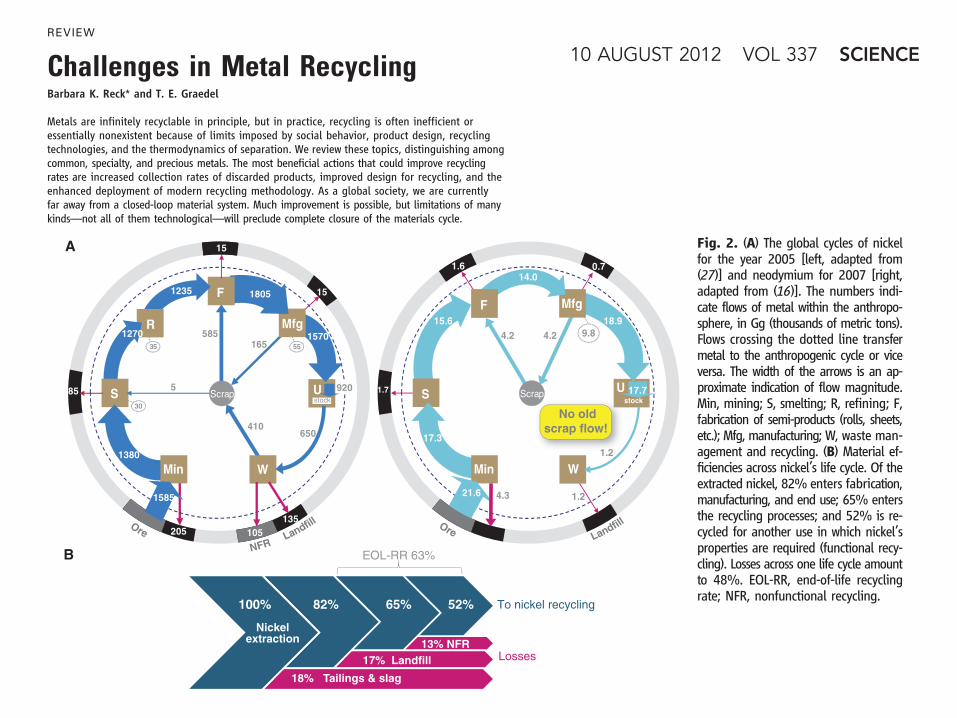
22. X. Zhang, S. Cheng, X. Huang, B. E. Logan, EnergyEnviron. Sci. 3, 659 (2010).
23. R. A. Rozendal, H. V. V. Hamelers, C. J. N. Buisman,Environ. Sci. Technol. 40, 5206 (2006).
24. J. R. Kim, S. Cheng, S.-E. Oh, B. E. Logan, Environ. Sci.Technol. 41, 1004 (2007).
25. Y. Fan, E. Sharbrough, H. Liu, Environ. Sci. Technol. 42,8101 (2008).
26. Y. Fan, H. Hu, H. Liu, Environ. Sci. Technol. 41, 8154 (2007).27. S. Hays, F. Zhang, B. E. Logan, J. Power Sources 196,
8293 (2011).28. Y. Ahn, B. E. Logan, Bioresour. Technol. 101, 469 (2010).29. P. D. Kiely, J. M. Regan, B. E. Logan, Curr. Opin. Biotechnol.
22, 378 (2011).30. D. F. Call, B. E. Logan, Appl. Environ. Microbiol. 77,
8791 (2011).31. A. M. Speers, G. Reguera, Appl. Environ. Microbiol. 78,
437 (2012).32. G. Lettinga, Antonie van Leeuwenhoek 67, 3 (1995).33. K. Rabaey, N. Boon, S. D. Siciliano, M. Verhaege,
W. Verstraete, Appl. Environ. Microbiol. 70, 5373 (2004).34. S. T. Read, P. Dutta, P. L. Bond, J. Keller, K. Rabaey, BMC
Microbiol. 10, 98 (2010).35. A. Venkataraman, M. A. Rosenbaum, S. D. Perkins, J. J. Werner,
L. T. Angenent, Energy Environ. Sci. 4, 4550 (2011).36. B. E. Logan et al., Environ. Sci. Technol. 42, 8630 (2008).37. D. H. Park, M. Laivenieks, M. V. Guettler, M. K. Jain,
J. G. Zeikus, Appl. Environ. Microbiol. 65, 2912 (1999).
38. P. Clauwaert et al., Water Sci. Technol. 57, 575 (2008).39. S. Cheng, D. Xing, D. F. Call, B. E. Logan, Environ. Sci.
Technol. 43, 3953 (2009).40. P. Parameswaran, H. Zhang, C. I. Torres, B. E. Rittmann,
R. Krajmalnik-Brown, Biotechnol. Bioeng. 105, 69 (2010).41. J. R. Ambler, B. E. Logan, Int. J. Hydrogen Energy 36,
160 (2011).42. G. K. Rader, B. E. Logan, Int. J. Hydrogen Energy 35,
8848 (2010).43. R. D. Cusick et al., Appl. Microbiol. Biotechnol. 89, 2053 (2011).44. J.-Y. Nam, B. E. Logan, Int. J. Hydrogen Energy 36,
15105 (2011).45. R. A. Rozendal, A. W. Jeremiasse, H. V. M. Hamelers,
C. J. N. Buisman, Environ. Sci. Technol. 42, 629 (2008).46. K. Rabaey, S. Bützer, S. Brown, J. Keller, R. A. Rozendal,
Environ. Sci. Technol. 44, 4315 (2010).47. R. A. Rozendal, E. Leone, J. Keller, K. Rabaey, Electrochem.
Commun. 11, 1752 (2009).48. J. M. Foley, R. A. Rozendal, C. K. Hertle, P. A. Lant,
K. Rabaey, Environ. Sci. Technol. 44, 3629 (2010).49. K. Rabaey, R. A. Rozendal,Nat. Rev. Microbiol. 8, 706 (2010).50. K. P. Nevin, T. L. Woodard, A. E. Franks, A. M. Summers,
D. R. Lovley, mBiol. 1, 1 (2010).51. K. P. Nevin et al., Appl. Environ. Microbiol. 77, 2882 (2011).52. R. Emde, B. Schink, Appl. Environ. Microbiol. 56, 2771
(1990).53. M. Hongo, M. Iwahara, Agric. Biol. Chem. 43, 2075 (1979).54. T. S. Kim, B. H. Kim, Biotechnol. Lett. 10, 123 (1988).
55. J. M. Flynn, D. E. Ross, K. A. Hunt, D. R. Bond, J. A. Gralnick.mBiol. 1, e00190 (2010).
56. K. J. J. Steinbusch, H. V. M. Hamelers, J. D. Schaap,C. Kampman, C. J. N. Buisman, Environ. Sci. Technol. 44,513 (2010).
57. O. Nowak, S. Keil, C. Fimml, Water Sci. Technol. 64,1 (2011).
58. E. S. Heidrich, T. P. Curtis, J. Dolfing, Environ. Sci.Technol. 45, 827 (2011).
59. G. Z. Ramon, B. J. Feinberg, E. M. V. Hoek, EnergyEnviron. Sci. 4, 4423 (2011).
60. J. Kuleszo, C. Kroeze, J. Post, B. M. Fekete, J. Integr.Environ. Sci. 7 (suppl. 1), 89 (2010).
61. Y. Kim, B. E. Logan, Environ. Sci. Technol. 45, 5834(2011).
62. Y. Kim, B. E. Logan, Proc. Natl. Acad. Sci. U.S.A. 108,16176 (2011).
63. T.-W. Kim et al., Desalination 284, 253 (2012).64. R. D. Cusick, Y. Kim, B. E. Logan, Science 335, 1474
(2012); 10.1126/science.1219330.
Acknowledgments: This research was supported by awardKUS-I1-003-13 from the King Abdullah University of Scienceand Technology (B.E.L.) and the Multidisciplinary ResearchPartnership Ghent Bio-Economy and the European UnionFramework Programme 7 project “ProEthanol” (K.R.).
10.1126/science.1217412
REVIEW
Challenges in Metal RecyclingBarbara K. Reck* and T. E. Graedel
Metals are infinitely recyclable in principle, but in practice, recycling is often inefficient oressentially nonexistent because of limits imposed by social behavior, product design, recyclingtechnologies, and the thermodynamics of separation. We review these topics, distinguishing amongcommon, specialty, and precious metals. The most beneficial actions that could improve recyclingrates are increased collection rates of discarded products, improved design for recycling, and theenhanced deployment of modern recycling methodology. As a global society, we are currentlyfar away from a closed-loop material system. Much improvement is possible, but limitations of manykinds—not all of them technological—will preclude complete closure of the materials cycle.
The generation now between the ages of20 and 30 is, in many parts of the world,the first to have grown up with the re-
cycling bin as a normal part of life. Discardedpaper, cans, and bottles have designated placesto go, and often go there. The situation is less cer-tain for products used for a number of years be-fore being discarded—computers, refrigerators,automobiles—for which recycling procedureshave been diverse and sporadic. And few knowwhat happens to obsolete equipment used onbehalf of individuals but owned by corporationsor organizations—medical imaging machines, air-craft engines, and the like.
The recycling of products in the “occasional-ly discarded” or “owned by somebody else” cat-egories is complicated by the rapid expansion of
the designer’s materials palette that has takenplace in the past several decades (1, 2). Today,virtually every stable element in the periodic ta-ble is used so as to take advantage of its uniquephysical and chemical properties. The result isthat many products are more functional and reli-able than before. An unintended consequence isthat recycling has become much more compli-cated and challenging.
Several reviews of metal recycling have ap-peared in recent years (3–5). They discuss centralissues such as recycling technologies, economiclimitations, and methods of enhancement. Someopen questions still remain: How much is goingon, and what are the trends? What are its limits?Is a closed-loop materials economy possible? Itis these systems-level topics that are the focusof the present work.
The Current Status of Metal RecyclingHow well is the world doing at recycling the di-verse mix of elements in modern products? Two
metrics answer this question best: recycled con-tent and end-of-life recycling rate (EOL-RR). Re-cycled content describes the share of scrap inmetal production, which is important to get asense of the magnitude of secondary supply. Thisindicator, however, has two limitations. First, life-times of metal-containing products often spanseveral decades, which, in combination with rapidgrowth in metal use, means that recycled metalflows will meet only a modest portion of demandfor many years to come. Second, it does not dis-tinguish between new (yield loss from fabricationand manufacturing) and old (postconsumer) scrapas input material, making it vulnerable to artifi-cially increased rates based solely on preconsum-er sources (fabricators may be given incentives toincrease their scrap output to meet secondary de-mand, making recycled content an incentive forinefficiencies in fabrication and manufacturing).What recycled content means to encourage, in-stead, is the amount of old scrap that is collectedand processed for recycling [also expressed asold scrap ratio (6)]. The indicator that measuresthis more directly is the EOL-RR, defined as thefraction of metal in discarded products that is reusedin such a way as to retain its functional properties.
The EOL-RR depends on the collection rateof end-of-life products and the efficiency of thesubsequent separation and pre-processing steps,all involving complex interactions of a wide va-riety of players (7). A United Nations panel re-cently defined and quantified recycling rates for60 elements (Fig. 1) (8). Two messages jump outat once from the figure. The first is that EOL-RRsfor the commonly used “base metals” (iron, cop-per, zinc, etc.) are above 50% (although, as thereport is careful to point out, usually not very farabove 50%). The second, and striking, impression
Center for Industrial Ecology, School of Forestry and Environ-mental Studies, Yale University, New Haven, CT 06511, USA.
*To whom correspondence should be addressed. E-mail:[email protected]
10 AUGUST 2012 VOL 337 SCIENCE www.sciencemag.org690
on
Augu
st 1
3, 2
012
ww
w.s
cien
cem
ag.o
rgD
ownl
oade
d fro
m
incorporation as a trace constituent into a recy-cled stream of iron or copper alloys (Fig. 2B). Thisconfirms the results of Markov chain modeling,which shows that a unit of the common metalsiron, copper, or nickel is only reused two or threetimes before being lost (28–30), gainsaying thenotion of metals being repeatedly recyclable.
Product Recovery and Recycling TechnologyAn engineer or scientist instinctively thinks oftechnology when the topic of recycling is raised,but it turns out that social and cultural aspectsare at least as important, perhaps more so (31, 32).Metal price is a key driver directly affecting col-lection and processing efficiencies (1, 5). Exten-sive manual disassembly of discarded electronicsis typically not economically feasible in indus-trialized countries but may be advantageous inemerging economies such as India and China(17, 33). Figure 3 shows the main steps involvedin recycling, the key perspective being that theoverall efficiency is the product of the efficienciesat each stage. As with a chain, the weakest linkcontrols the performance of the system. The figurealso shows the associated recovery and recyclingefficiencies for nickel and neodymium across allend-of-life products, as well as the specific casesof nickel and rhenium from end-of-life aerospacesuperalloys. The first stage is collection, which re-fers to the transfer of an unwanted product fromthe owner to a suitable recycling facility.
Collection, pre-processing, and end processing.Collection rates vary greatly among differentwaste streams, depending on price, logistics,
and other factors. Waste of electrical and elec-tronic equipment (WEEE), in contrast, often hasrelatively low collection rates despite legisla-tive efforts. In the European Union, 25 to 40%of WEEE is collected and treated in the officialsystem (34), the rest being discarded into munic-ipal waste, exported as used products or scrap, orotherwise lost. Current WEEE legislation in theEuropean Union and Japan focuses on massrecovery, which favors steel and base metals usedin large quantities, whereas precious and special-ty metals, found in small electrical and electronicequipment, are often not recovered (35, 36). Con-sidering this situation, as well as the recent de-bate on critical metals [e.g., (37)], a revision ofthese priorities seems likely (34).
After collection, the postconsumer metal en-ters a series of pre-processing steps, including re-peated sorting (e.g., manual, magnetic, optical),dismantling, and physical and chemical separa-tion (38, 39). Issues of scale are important here.Virgin materials processing is generally large inscale, using processes underwritten by historical-ly low energy prices. In contrast, recycling is oftenlocal, more labor-intensive, and smaller in scale.In such a situation, the monetary returns are oftennot sufficient to justify the purchase of modern“sense and sort” technologies, and much other-wise recoverable material is lost.
The example of a nickel- and rhenium-containing aerospace superalloy shows how price,material combinations, size, and shape can drivethe efficiency (Fig. 3). One company estimatesthat collection rates of these superalloys are around
90% because of their high value and the fa-vorable logistics of a relatively small industry(40). Around 80% of the scrap is in solid piecesthat can easily undergo grade-specific identifi-cation and recycling. The other 20% is in theform of turnings and other small fractions andcan be sent to a stainless steel smelter. This trans-lates into an 81% efficiency for nickel, which isrequired in both the superalloy and stainless steel,but only a 68% efficiency for rhenium (Fig. 3).Similarly, neodymium may be collected at a rateof 30% from electronics or magnets, but with noelement-specific recycling technology existing atpresent, its overall recycling efficiency is nearzero and it will either be discarded or become atrace element in recycled metal.
After pre-processing, the material will be sentto a smelter or other thermochemical facility whereprocessing has been optimized (end-processing).In most cases, these are primary smelters, althoughsome facilities—including electric arc furnacesin steel production as well as smelters processingelectronic wastes for the recovery of precious metals,copper, and some specialty metals—specializein processing secondary metals. As Fig. 1 shows,some metals have fairly high overall recyclingrates, generally because they are used in large,easy-to-identify applications such as steel beamsor lead batteries, but half or more of the metalsface the larger challenge of the recycling se-quence and its typical efficiencies.
Recycling technology. Collection efficienciesare related to social and governmental factors,but separation and sorting efficiencies relate to
Fig. 2. (A) The global cycles of nickelfor the year 2005 [left, adapted from(27)] and neodymium for 2007 [right,adapted from (16)]. The numbers indi-cate flows of metal within the anthropo-sphere, in Gg (thousands of metric tons).Flows crossing the dotted line transfermetal to the anthropogenic cycle or viceversa. The width of the arrows is an ap-proximate indication of flow magnitude.Min, mining; S, smelting; R, refining; F,fabrication of semi-products (rolls, sheets,etc.); Mfg, manufacturing; W, waste man-agement and recycling. (B) Material ef-ficiencies across nickel’s life cycle. Of theextracted nickel, 82% enters fabrication,manufacturing, and end use; 65% entersthe recycling processes; and 52% is re-cycled for another use in which nickel’sproperties are required (functional recy-cling). Losses across one life cycle amountto 48%. EOL-RR, end-of-life recyclingrate; NFR, nonfunctional recycling.
EOL-RR 63%
To nickel recycling 100% 82% 65% 52%
Nickel
17% Landfill13% NFR
Nickelextraction
Losses
18% Tailings & slag
100% 82% 65% 52%
Nickelextraction
B
Scrap
in W
S U
Min
MfgF
14.0
17.3
15.6
21.6
18.9
4.3
1.7
1.6 0.7
1.2
1.2
4.2 4.2 9.8
17.7stock
Scrap
in W
S U
Mfg
F
R
Min
1235
1380
1270
1585
1570
205
85
15
15
650
585165 55
135
35
105
1805
5
410
stock30
No oldscrap flow!
A
Ore NFR Landfill Ore
Landfill
920
10 AUGUST 2012 VOL 337 SCIENCE www.sciencemag.org692
on
Augu
st 1
3, 2
012
ww
w.s
cien
cem
ag.o
rgD
ownl
oade
d fro
m


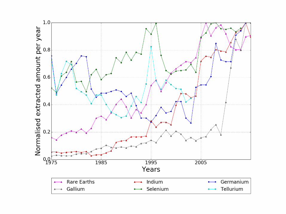

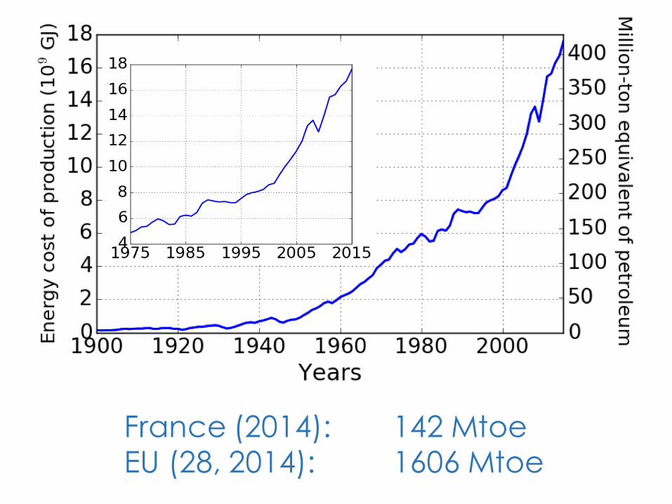
France (2014): 142 MtoeEU (28, 2014): 1606 Mtoe
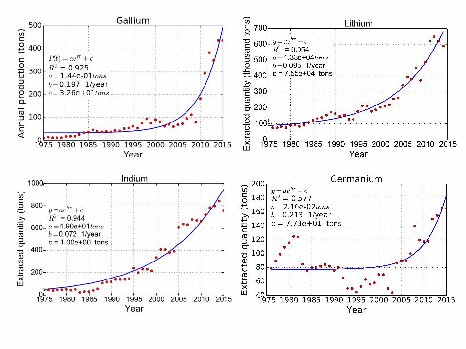

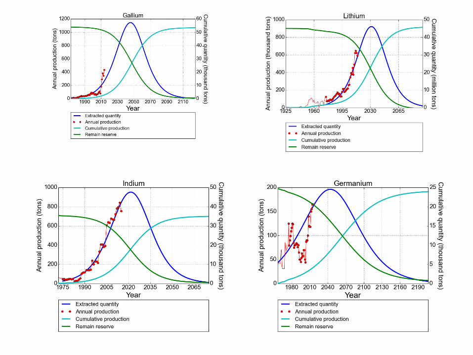


Non-renewables & energy conundrumLess concentrated minerals
Extraction of raw materials requires more energy
Energy is less accessible
More raw materials are necessary to produce energy

C H N O P S
Living systems share the same chemistry


284 IEEE JOURNAL OF SOLID-STATE CIRCUITS, VOL. 47, NO. 1, JANUARY 2012
An 8-Bit, 40-Instructions-Per-Second OrganicMicroprocessor on Plastic Foil
Kris Myny, Student Member, IEEE, Erik van Veenendaal, Gerwin H. Gelinck, Jan Genoe, Member, IEEE,Wim Dehaene, Senior Member, IEEE, and Paul Heremans
Abstract—Forty years after the first silicon microprocessors, wedemonstrate an 8-bit microprocessor made from plastic electronictechnology directly on flexible plastic foil. The operation speed istoday limited to 40 instructions per second. The power consump-tion is as low as 100 W. The ALU-foil operates at a supply voltageof 10 V and back-gate voltage of 50 V. The microprocessor canexecute user-defined programs: we demonstrate the execution ofthe multiplication of two 4-bit numbers and the calculation of themoving average of a string of incoming 6-bit numbers. To executesuch dedicated tasks on the microprocessor, we create small plasticcircuits that generate the sequences of appropriate instructions.The near transparency, mechanical flexibility, and low power con-sumption of the processor are attractive features for integration oneveryday objects, where it could be programmed as, amongst otheritems, a calculator, timer, or game controller.
Index Terms—Dual-gate, flexible circuits, flexible micropro-cessor, flexible processor, organic circuits, organic microprocessor,organic processor, organic transistor, plastic circuits, plasticmicroprocessor, plastic processor.
I. INTRODUCTION
E LECTRONICS pervades everyday life and is undeniablymaking its way from computing to telephony and to as-
sisting us in everyday tasks through products such as electronicpaper to read and write, electronic noses to sense gases, smartlighting with electronics to save energy, and so on. The key en-abler of these pervasive electronics applications is the fact thatintegration of ever more transistors with ever smaller dimen-sions has resulted in the cost of a single semiconductor tran-sistor, or switch, to dwindle to the level of ten nano-dollars pertransistor. Nevertheless, if the cost of a transistor in a chip isnegligible and decreasing, the cost of placing and routing elec-tronics on daily objects is not necessarily proportionally low.
Manuscript received May 07, 2011; revised July 17, 2011; acceptedSeptember 05, 2011. Date of publication November 04, 2011; date of currentversion December 23, 2011. This paper was approved by Guest Editor SatoshiShigematsu. This work was supported in part by the EU-Projects COSMIC(ISTIP-247681) and ORICLA (FP7-ICT-2009-4 247798).K. Myny is with imec, 3001 Leuven, Belgium, the Katholieke Universiteit
Leuven, 3001 Leuven, Belgium, and also with the Katholieke Hogeschool Lim-burg, 3590 Diepenbeek, Belgium (e-mail: [email protected]).E. van Veenendaal is with Polymer Vision, 5656 AE Eindhoven, The Nether-
lands.J. Genoe is with imec, 3001 Leuven, Belgium, and also with the Katholieke
Hogeschool Limburg, 3590 Diepenbeek, Belgium.G. H. Gelinck is with the Holst Centre/TNO, 5605 KN Eindhoven, The
Netherlands.W. Dehaene, and P. Heremans are with imec, 3001 Leuven, Belgium, and
also with the Katholieke Universiteit Leuven, 3001 Leuven, Belgium.Color versions of one or more of the figures in this paper are available online
at http://ieeexplore.ieee.org.Digital Object Identifier 10.1109/JSSC.2011.2170635
Plastic electronics refers to the technology to make transistorsand circuits with thin-film organic or plastic semiconductorson arbitrary substrates, including not only rigid substrates suchas glass, but also flexible plastic foils. A variety of organicmolecules and polymers have been developed as semiconduc-tors, and the best ones [1]–[4] today feature a charge carriermobility on the order of 1–10 cm /Vs, some 100 to 1000 timeslower than that of silicon. When integrated into circuits, therealistic mobility values are somewhat lower but neverthelesssufficient for applications such as backplanes for flexibleactive-matrix displays, in particular for flexible electronicpapers [5]. The first dedicated circuit applications of organicthin-film transistors have also appeared in recent years, suchas recently demonstrated by the integration of an organic linedriver for an organic active matrix OLED display [6]. Such cir-cuits can be made directly on thin and ultra-flexible plastic foils,which allows them to be very simply laminated on everydayobjects, and furthermore provides appealing characteristics interms of bending radius and robustness: we no longer talk offlexible electronics but of truly crinkable electronics [7].Here, we investigate the possibility to use this technology to
realize microprocessors on plastic foil. As the cost of an elec-tronic chip decreases with production volume, ultralow-cost mi-croprocessors on easy-to-integrate flexible foils will be an en-abler for ambient intelligence: one and the same type of chipcan be integrated on vastly different types of objects to performcustomized functions, such as identification, simple computing,and controlling.The organic microprocessor has been implemented as two
different foils: an arithmetic and logic unit (ALU) foil and aninstruction foil. The ALU-foil is a general-purpose foil whichcan execute a multitude of functions. On the other hand, the in-struction foil is a dedicated chip that generates the sequence ofinstructions to obtain a specific function. It sends this sequenceof instructions to the ALU-foil such that the combination of bothfoils results in the execution of a specific algorithm. The firstprototype of the organic microprocessor [8] had only one in-struction foil available and could operate up to six operationsper second (OPS). In this paper, we report an improved organicmicroprocessor that can run 40 OPS and can operate with twodifferent instruction foils. We first discuss the technology andchoice of logic family used for the microprocessor foil. Sub-sequently, we report on the design and measurement data ofthe ALU-foil. Next, a complete integrated microprocessor isdemonstrated by combining the ALU-foil with the instructionfoil. Finally, we conclude by comparing the organic micropro-cessor to the silicon Intel 4004 early-days processor.
0018-9200/$26.00 © 2011 IEEE
Mostly organic materials (carbon based)Au for gates

284 IEEE JOURNAL OF SOLID-STATE CIRCUITS, VOL. 47, NO. 1, JANUARY 2012
An 8-Bit, 40-Instructions-Per-Second OrganicMicroprocessor on Plastic Foil
Kris Myny, Student Member, IEEE, Erik van Veenendaal, Gerwin H. Gelinck, Jan Genoe, Member, IEEE,Wim Dehaene, Senior Member, IEEE, and Paul Heremans
Abstract—Forty years after the first silicon microprocessors, wedemonstrate an 8-bit microprocessor made from plastic electronictechnology directly on flexible plastic foil. The operation speed istoday limited to 40 instructions per second. The power consump-tion is as low as 100 W. The ALU-foil operates at a supply voltageof 10 V and back-gate voltage of 50 V. The microprocessor canexecute user-defined programs: we demonstrate the execution ofthe multiplication of two 4-bit numbers and the calculation of themoving average of a string of incoming 6-bit numbers. To executesuch dedicated tasks on the microprocessor, we create small plasticcircuits that generate the sequences of appropriate instructions.The near transparency, mechanical flexibility, and low power con-sumption of the processor are attractive features for integration oneveryday objects, where it could be programmed as, amongst otheritems, a calculator, timer, or game controller.
Index Terms—Dual-gate, flexible circuits, flexible micropro-cessor, flexible processor, organic circuits, organic microprocessor,organic processor, organic transistor, plastic circuits, plasticmicroprocessor, plastic processor.
I. INTRODUCTION
E LECTRONICS pervades everyday life and is undeniablymaking its way from computing to telephony and to as-
sisting us in everyday tasks through products such as electronicpaper to read and write, electronic noses to sense gases, smartlighting with electronics to save energy, and so on. The key en-abler of these pervasive electronics applications is the fact thatintegration of ever more transistors with ever smaller dimen-sions has resulted in the cost of a single semiconductor tran-sistor, or switch, to dwindle to the level of ten nano-dollars pertransistor. Nevertheless, if the cost of a transistor in a chip isnegligible and decreasing, the cost of placing and routing elec-tronics on daily objects is not necessarily proportionally low.
Manuscript received May 07, 2011; revised July 17, 2011; acceptedSeptember 05, 2011. Date of publication November 04, 2011; date of currentversion December 23, 2011. This paper was approved by Guest Editor SatoshiShigematsu. This work was supported in part by the EU-Projects COSMIC(ISTIP-247681) and ORICLA (FP7-ICT-2009-4 247798).K. Myny is with imec, 3001 Leuven, Belgium, the Katholieke Universiteit
Leuven, 3001 Leuven, Belgium, and also with the Katholieke Hogeschool Lim-burg, 3590 Diepenbeek, Belgium (e-mail: [email protected]).E. van Veenendaal is with Polymer Vision, 5656 AE Eindhoven, The Nether-
lands.J. Genoe is with imec, 3001 Leuven, Belgium, and also with the Katholieke
Hogeschool Limburg, 3590 Diepenbeek, Belgium.G. H. Gelinck is with the Holst Centre/TNO, 5605 KN Eindhoven, The
Netherlands.W. Dehaene, and P. Heremans are with imec, 3001 Leuven, Belgium, and
also with the Katholieke Universiteit Leuven, 3001 Leuven, Belgium.Color versions of one or more of the figures in this paper are available online
at http://ieeexplore.ieee.org.Digital Object Identifier 10.1109/JSSC.2011.2170635
Plastic electronics refers to the technology to make transistorsand circuits with thin-film organic or plastic semiconductorson arbitrary substrates, including not only rigid substrates suchas glass, but also flexible plastic foils. A variety of organicmolecules and polymers have been developed as semiconduc-tors, and the best ones [1]–[4] today feature a charge carriermobility on the order of 1–10 cm /Vs, some 100 to 1000 timeslower than that of silicon. When integrated into circuits, therealistic mobility values are somewhat lower but neverthelesssufficient for applications such as backplanes for flexibleactive-matrix displays, in particular for flexible electronicpapers [5]. The first dedicated circuit applications of organicthin-film transistors have also appeared in recent years, suchas recently demonstrated by the integration of an organic linedriver for an organic active matrix OLED display [6]. Such cir-cuits can be made directly on thin and ultra-flexible plastic foils,which allows them to be very simply laminated on everydayobjects, and furthermore provides appealing characteristics interms of bending radius and robustness: we no longer talk offlexible electronics but of truly crinkable electronics [7].Here, we investigate the possibility to use this technology to
realize microprocessors on plastic foil. As the cost of an elec-tronic chip decreases with production volume, ultralow-cost mi-croprocessors on easy-to-integrate flexible foils will be an en-abler for ambient intelligence: one and the same type of chipcan be integrated on vastly different types of objects to performcustomized functions, such as identification, simple computing,and controlling.The organic microprocessor has been implemented as two
different foils: an arithmetic and logic unit (ALU) foil and aninstruction foil. The ALU-foil is a general-purpose foil whichcan execute a multitude of functions. On the other hand, the in-struction foil is a dedicated chip that generates the sequence ofinstructions to obtain a specific function. It sends this sequenceof instructions to the ALU-foil such that the combination of bothfoils results in the execution of a specific algorithm. The firstprototype of the organic microprocessor [8] had only one in-struction foil available and could operate up to six operationsper second (OPS). In this paper, we report an improved organicmicroprocessor that can run 40 OPS and can operate with twodifferent instruction foils. We first discuss the technology andchoice of logic family used for the microprocessor foil. Sub-sequently, we report on the design and measurement data ofthe ALU-foil. Next, a complete integrated microprocessor isdemonstrated by combining the ALU-foil with the instructionfoil. Finally, we conclude by comparing the organic micropro-cessor to the silicon Intel 4004 early-days processor.
0018-9200/$26.00 © 2011 IEEE
MYNY et al.: ORGANIC MICROPROCESSOR ON PLASTIC FOIL 285
(a) (b)
Fig. 1. (a) Cross section of the dual-gate OTFT technology. (b) Typical measured transfer characteristic of this OTFT ( m/ m) when using theback-gate as -control gate (right). (Figures from [11].)
II. TECHNOLOGY AND LOGIC FAMILY
In our organic thin-film transistor (OTFT) technology,
all layers to make the circuits are processed directly on a
25- m-thick PEN (polyethylene naphthalate) foil and consist
of polymers or organic molecules, with the exception of metals
(Au) for gates, sources, drains, and interconnect lines between
the transistors [9]. The OTFT technology is a unipolar p-type,
single- technology, using pentacene as semiconductor. The
basic transistor has a channel length of 5 m.
The yield of larger integrated circuits in such a single- ,
p-type-only technology is intrinsically limited, as a result of the
parameter variability [10]. Myny et al. have demonstrated an in-creased circuit robustness by the addition of an extra gate to each
OTFT, leading to the availability of multiple ’s in a unipolar
p-type technology [11]. The organic microprocessor has been
designed in this technology. A cross section is shown in Fig. 1.
As depicted, each TFT comprises two gates, a front gate and
a back gate. The front gate controls the channel current while
the back gate, which is weakly coupled to the semiconductor
channel, is used to shift the transistor’s threshold voltage. This
is depicted in Fig. 1. As a consequence, the of each single
transistor can be independently tuned.
The key factor when determining the choice of logic family
for the basic circuit gates is the circuit robustness parameterized
by the noise margin. Fig. 2 shows the noise margin (at
20 V) of typical zero- inverters when no back-gate is used,
compared with the noise margin achievable with an optimized
dual-gate zero- topology. In this optimized topology, the
back gates of the load transistors are connected to the front gates,
while all back gates of the drive transistors are connected to
a common rail, to which a back-gate voltage is applied exter-
nally [11].
The typical spread on threshold voltage in organic TFT tech-
nology is 0.2 to 0.5 V, which is large compared with the noise
margin achievable with single-gate technology. As a result, it
is common practice in the field of organic electronics to usea transistor-level approach to design (simple) circuits. Indeed,
it is usually necessary to simulate the schematic entry with an
analog circuit-level simulator (such as Spectre or Spice) and use
Fig. 2. Noise margin of single- zero- inverter with single-gate pen-tacene TFT technology (top) and of optimized dual- inverter using dual-gatepentacene TFT technology (bottom).
Monte Carlo simulations to predict yield. However, such analog
circuit-level simulators are not adapted to deal with the needed
level of complexity to design and simulate an organic micro-
processor due to the large number of (parallel) switching gates,
large amount of input, control, and output signals. In contrast,
in our optimized dual-gate, the much improved noise margin al-
lows to make use of common digital design practices. Starting
from the basic characteristics of inverters and other logic gates,
we designed a robust library of basic digital logic gates (in-
verters, NANDs, buffers). This standard cell library was used to
290 IEEE JOURNAL OF SOLID-STATE CIRCUITS, VOL. 47, NO. 1, JANUARY 2012
TABLE ISPECIFICATIONS OF THE CIRCUIT FOILS
TABLE IICOMPARISON WITH THE EARLY SILICON PROCESSOR
instructions are hardcoded on the foil. A different foil is de-signed for every program. For the low-cost, low-complexitybut high-volume applications that are envisaged here, this pro-cedure could even be a realistic commercial scenario. The in-struction sets generated by the multiplier instruction foil andthe moving averager foil are shown in Fig. 9(B) and (D), re-spectively.The operation of the running averager instruction foil by itself
is shown in Fig. 10(A). This circuit does not contain a ripplecarry adder, and therefore it has a shorter critical path comparedwith the microprocessor. Stand-alone, the instruction circuit canrun at a clock speed of 70 Hz.Finally, we demonstrate the combined operation of an instruc-
tion foil with the microprocessor.We conducted this experimentwith the running averager. The correct operation of this combi-nation is shown in Fig. 10(B). This demonstration shows that the
microprocessor can indeed accept its instruction set from a ded-icated plastic circuit and is not limited to instruction sets froma test board.
V. CONCLUSION
In Table I, we summarize the circuits fabricated and demon-strated in plastic technology. With less than 100 W, the powerconsumption of the flexible chips is already quite low and couldfurther be reduced by voltage scaling in the future [15], [16].Such very low power consumption is very important for wide-spread mobile applications on everyday objects.To conclude, we compare in Table II the characteristics of
the first plastic microprocessor with the early silicon proces-sors made in p-type-only silicon technology some four decadesago.1 Significant correspondence can be seen regarding param-eters such as gate length, supply voltage and transistor count,but some marked differences are also clear. The instruction rateof the plastic technology is about three orders of magnitudeslower than the early silicon processor, as a direct consequenceof the three-orders-of-magnitude lower carrier mobility in or-ganic semiconductors. However, on the positive side, the powerconsumption is also four orders of magnitude smaller. In fu-ture implementations, semiconductors such as amorphous ox-ides [17] could boost the performance to an intermediate speed,with still very attractive power consumption for low-cost, low-performance, and mobile applications.
ACKNOWLEDGMENT
This work was performed in a collaboration between imecand TNO in the frame of the HOLST Centre.
REFERENCES
[1] P. T. Herwig and K. Müllen, “A soluble pentacene precursor: Syn-thesis, solid-state conversion into pentacene and application in a field-effect transistor,” Adv. Mater., vol. 11, pp. 480–483, 1999.
[2] J. H. Chen, S. Subramaniam, S. R. Parkin, M. Siegler, K. Gallup,C. Haughn, D. C. Martin, and J. E. Anthony, “The influence of sidechains on the structures and properties of functionalized pentacenes,”J. Mater. Chemistry, vol. 18, no. 17, p. 1961, 2008.
[3] N. Kobayashi, M. Sasaki, and K. Nomoto, “Stable peri-Xanthenoxan-thene thin-film transistors with efficient carrier injection,” ChemistryMater., vol. 21, no. 3, p. 552, 2009.
[4] B. Yoo, B. A. Jones, D. Basu, D. Fine, T. Jung, S. Mohapatra, A. Fac-chetti, K. Dimmler, M. R. Wasielewski, T. J. Marks, and A. Dodabal-apur, “High-performance solution-deposited n-channel organic transis-tors and their complementary circuits,” Adv. Mater., vol. 19, no. 22, p.4028, 2007.
[5] G. H. Gelinck, H. E. A. Huitema, E. van Veenendaal, E. Cantatore, L.Schrijnemakers, J. B. P. H. van der Putten, T. C. T. Geuns, M. Been-hakkers, B. Giesbers, B.-H. Huisman, E. M. Benito, F. J. Touwslager,A.Marsman, B. van Rens, and D.M. de Leeuw, “Flexible active matrixdisplays and shift registers based on solution-processed organic tran-sistors,” Nature Mater., vol. 3, p. 106, 2004.
[6] M. Noda, N. Kobayashi, M. Katsuhara, A. Yumoto, S. Ushikura, R.Yasuda, N. Hirai, G. Yukawa, I. Yagi, and K. Nomoto, “A rollableAM-OLED display driven by OTFTs,” in Proc. SID, 2010, vol. 41,no. 1, pp. 710–713.
1Historic data are collected on the Intel Museum. [Online]. Available:http://www.intel.com/about/companyinfo/museum/exhibits/4004/index.htm.The specifications can be found at http://datasheets.chipdb.org/Intel/MCS-4/datashts/intel-4004.pdf

“From the point of view of the mathematician the property of being digital should be of greater interest than that of being electronic.”
Alan TuringLecture to the London Mathematical Society on 20 February 1947
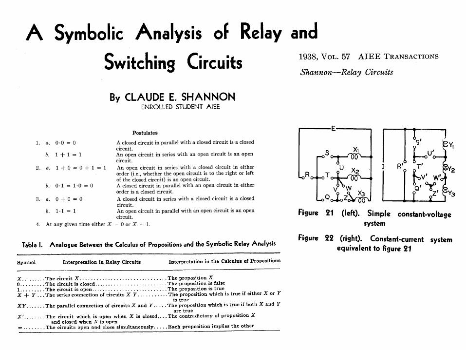
A r I 1A lIl* f n | | closed circuit, and the symbol 1 (unity) toA Symbolic t6tnaiysis or ue ay and represent the hindrance of an open cir-cuit. Thus when the circuit a-b is openXab and when closed Xab = 0.Swi chi, Circuits Two hindrances Xab and Xc will besaid to be equal if whenever the circuita-b is open, the circuit c-d is open, and
By CLAUDE E. SHANNON whenever a-b is closed, c-d is closed.ENROLLED STUDENT AIEE Now let the symbol + (plus) be defined
to mean the series connection of the two-I. Introduction bolic study of logic. For the synthesis terminal circuits whose hindrances are
problem the desired characteristics are added together. Thus Xab + Xd is the
N THE CONTROL and protective first written as a system of equations, and hindrance of the circuit a-d when b and c* circuits of complex electrical systems the equations are then manipulated into are connected together. Similarly theit is frequently necessary to make in- the form representing the simplest cir- product of two hindrances X,,b'X,4 ortricate interconnections of relay contacts cuit. The circuit may then be immedi- more briefly XabXc, will be defined toand switches. Examples of these cir- ately drawn from the equations. By mean the hindrance of the circuit formedcuits occur in automatic telephone ex- this method it is always possible to find by connecting the circuits a-b and c-d inchanges, industrial motor-control equip- the simplest circuit containing only parallel. A relay contact or switch willment, and in almost any circuits designed series and parallel connections, and in be represented in a circuit by the symbolto perform complex operations auto- some cases the simplest circuit containing in figure 1, the letter being the cor-matically. In this paper a mathematical any type of connection. responding hindrance function. Figureanalysis of certain of the properties of Our notation is taken chiefly from 2 shows the interpretation of the plussuch networks will be made. Particular symbolic logic. Of the many systems in sign and figure 3 the multiplication sign.attention will be given to the problem of common use we have chosen the one This choice of symbols makes the ma-network synthesis. Given certain char- which seems simplest and most suggestive nipulation of hindrances very similar toacteristics, it is required to find a circuit for our interpretation. Some of our ordinary numerical algebra.incorporating these characteristics. The phraseology, as node, mesh, delta, wye, It is evident that with the above defi-solution of this type of problem is not etc., is borrowed from ordinary network nitions the following postulates will hold:unique and methods of finding those par-ticular circuits requiring the least num- Postulatesber of relay contacts and switch blades 1. a. 0 * 0 = 0 A closed circuit in parallel with a closed circuit is a closedwill be studied. Methods will also be circuit.described for finding any number of cir- b. 1 + 1 = I An open circuit in series with an open circuit is an opencuits equivalent to a given circuit in all circuit.operating characteristics. It will be 2. a. 1 + 0 = 0 + 1 = 1 An open circuit in series with a closed circuit in eithershown that several of the well-known order (i.e., whether the open circuit is to the right or leftth*eorems on impedance networks have of the closed circuit) is an open circuit.
b. O * 1 = 1 0 = O A closed circuit in parallel with an open circuit in eitherroughly analogous theorems in relay order is a closed circuit.circuits. Notable among these are the 3. a. 0 + 0 = 0 A closed circuit in series with a closed circuit is a closeddelta-wye and star-mesh transformations, circuit.and the duality theorem. b. 1 1 = 1 An open circuit in parallel with an open circuit is an openThe method of attack on these prob- circuit.
lems may be described briefly as follows: 4 At any given time either X c 0 or X = 1.any circuit is represented by a set ofequations, the terms of the equations..correspondingtohe variou rel atn theory for similar concepts in switching These are sufficient to develop all the
circuits. theorems which will be used in connectionswitches in the circuit. A calculus is with circuits containing only series anddeveloped for manipulating these equa- II Series-Parallel parallel connections. The postulates aretions by simple mathematical processes, Two-Terminal Circuits arranged in pairs to emphasize a dualitymost of which are similar to ordinary relationship between the operations ofalgebraic algorisms. This calculus is FUNDAMENTAL DEFINITIONS addition and multiplication and theshown to be exactly analogous to the AND POSTULATES quantities zero and one. Thus, if incalculus of -propositions used in the sym- We shall limit our treatment to cir- any of the a postulates the zero's are re-
cuits containing only relay contacts and placed by one's and the multiplicationsPaper number 38-80, recommended by the AIEE switches, and therefore at any given time by additions and vice versa, the cor-committees on communication and basic sciences the circuit between any two terminals responding b postulate will result. Thisand presented at the AIEE summer convention,Washington, D. C., June 20-24, 1938. Manuscript must be either open (infinite impedance) fact is of great importance. It givessubmitted March 1. 1938; made available for or closed (zero impedance). Let us as- each theorem a dual theorem, it being
preprintingMay27, 1938. ~~sociate a symbol Xai or more simply X, necessary to prove only one to establish
department of electrical engineering at MaWssachu- wtthtemnlaadb.Tivn- both. The only one of these postulatessetts Institute of Technology, Cambridge. This able, a function of time, will be called which differs from ordinary algebra is lb.paper is an abstract of a thesis presented at MITfor the degree of master of science. The author is the hindrance of the two-terminal cir- However, this enables great simplifica-indebted to Doctor F. L. Hitchcock, Doctor cuit a-b. The symbol 0 (zero) will he tions in the manipulation of theseVannevar Bush, and Doctor 5. H. Caldwell, all ofMIT, for helpful encouragement and criticism, used to represent the hindrance of a symbols.
1938, VOL. 57 Shannon-Relay Circuits 713
THEOREMS (3b), however, is not true inr numerical hindrance functions above. Usually thealgebra. two subjects are developed simultane-
In this section a number of theorems We shall now define a new operation to ously from the same set of postulates,governing the combination of hindrances be called negation. The negative of a except for the addition in the case of thewill be given. Inasmuch as any of the hindrance X will be written X' and is calculus of propositions of a postulatetheorems may be proved by a very defined as a variable which is equal to 1 equivalent to postulate 4 above. E. V.
Huntington4 gives the following set ofx postulates for symbolic logic:
Xab x Y X+Y [ X.Ya o- b -__0 o-Qo o0- = -0 °" * -_-' 0' 1. The class K contains at least two dis-
y o Ftinct elements.
simple process, the proofs will not be Figure 1 (left). Symbol for hindrance 2. If a and b are in the class K then
given except for an illustrative example. function a + b is in the class K.
The method of proof is that of "perfect Figure 2 (middle). Interpretation of addition 3. a + b = b + ainduction," i.e., the verification of thetheorem for all possible cases. Since by Figure 3 (right). Interpretation of multipli- 4. (a + b) + c = a ± (b + c)postulate 4 each variable is limited to cation 5. a + a = athe values 0 and 1, this is a simple matter. 6. ab + ab' = a where ab IS defined asSome of the theorems may be provedmore elegantly by recourse to previous when X equals 0 and equal to 0 when X (a'
fb')'
theorems, but the method of perfect in- equals 1. If X is the dr o If we let the class K be the class consist-duction is so universal that it is probably the make ontats of aring of the two elements and 1 then these
hindrance of the break contacts of theto be preferred. same relay. The definition of the nega- postulates follow from those given in the
samerely.Te dfiniionof te nga- first section. Also postulates 1, 2, and 3X + Y = Y + X (la) tive of a hindrance gives the following givnt can be deducedfo Hunting-
given there can be deduced from Hunting-XY = YX (lb) theorems: ton's postulates. Adding 4 and restrict-
X + (Y + Z) = (X + Y) + Z (2a) x + X' = 1 (6a) ing our discussion to the calculus of propo-sitions, it is evident that a perfect
X(YZ) = (X Y)Z (2b) XX' = 0 (6b) analogy exists between the calculus for
X(Y + Z) = XY + XZ (3a) °' = 1 (7a) switching circuits and this branch ofX(Y +7b)Z)=XY+ xz(3asymbolic logic.** The two interpreta-
X + YZ = (X + Y)(X + Z) (3b) 1' = 0 (7b) tions of the symbols are shown in table I.
1-X = X (4a) (X')Y = X (8) Due to this analogy any theorem of thecalculus of propositions is also a true
o + X-X (4b) ANALOGUE WITH THE theorem if interpreted in terms of relay
1 + X = 1 (5a) CALCULUS OF PROPOSITIONS circuits. The remaining theorems in
O-X = O (5b) We are now in a position to demon- this section are taken directly from thisstrate the equivalence of this calculus with field.
For example, to prove theorem 4a, certain elementary parts of the calculus De Morgan's theorem:
note that X is either 0 or 1. If it is 0, of propositions. The algebra of logie1-3 (X + Y + Z . .) = X'. Y'.Z' (9a)the theorem follows from postulate 2b; originated by George Boole, is a sym-if 1, it follows from postulate 3b. Theo- bolic method of investigating logical (X-Y-Z Y)' = X' + Y'+ Z'+
rem 4b now follows by the duality princi- relationships. The symbols of Boolean (9b)
ple, replacing the 1 by 0 and the - by +. algebra admit of two logical interpreta- This theorem gives the negative of a sumDue to the associative laws (2a and 2b) tions. If interpreted in terms of classes, or product in terms of the negatives of
parentheses may be omitted in a sum or the variables are not limited to the two the summands or factors. It may beproduct of several terms without am- possible values 0 and 1. This interpre- easily verified for two terms by substitut-biguity. The z and H symbols will be tation is known as the algebra of classes- ing all possible values and then extendedused as in ordinary algebra. If, however, the terms are taken to rep- to any number n of variables by mathe-The distributive law (3a) makes it resent propositions, we have the calculus matical induction.
possible to "multiply out" products and of propositions in which variables are A function of certain variables X1,to factor sums. The dual of this theorem limited to the values 0 and 1,* as are the X2 .X is any expression formed
from the variables with the operationsof addition, multiplication, and negation.
Table 1. Analogue Between the Calculus of Propositions and the Symbolic Relay Analysis1. For all numbered references, see list at end of
Symbol Interpretation in Relay Circuits Interpretation in the Calculus of Propositions paper.* This refers only to the classical theory of thecalculus of propositions. Recently some work has
X....The circuit X ....................Theproposition X been done with logical systems in which proposi-
0....The circuit is closed .................... The proposition is false tions may have more than two "truth values."1....The circuit is open .................... The proposition is true ** This analogy may also be seen from a slightlyX + Y .. ..The series connection of circuits X Y ....................The proposition which is true if either X or Y different viewpoint. Instead of associating Xab
XY....The parallel connection of circuiits X and Y .................... The proposition which is true if both X and Y prpoiretiowthathe circuita-tab is open. Then allare true the symbols are directly interpreted as propositions
.Tlhe circuit which is open when X is closed, .....................Thecontradictory of proposition X and the operations of addition and multiplicationand closed when X is open will be seen to represent series and parallel connec-
. The circuits open and close simultaneously....................Each proposition implies the other tions.
714 Shannon-Relay Circuits AIFE TRANSACTIONS
tion of n variables may be expanded requiring the most elements using any Eabout the nth variable as follows: type of circuit has not as yet been deter- ||,
mined. S XI utf(Xi, X2. .. Xn) =f=Xnf(Xi.. Xn_-1, 1) + ined. 1S
Xn'f(XI. . . Xn-1, 0) (19) DUAL NETWORKS R T 2 IR' , YtNow the terms f(Xi . . . X_1, 1) and The negative of any network may be | w Q,O'f(Xi . . . X,,- 1, 0) are functions of n-I found by De Morgan's theorem, but the L,Q<0- Z J ZI zY3variables and if they individually require network must first be transformed into an Figure 21 (left). Simple constant-voltagethe most elements for n -1 variables, then equivalent series-parallel circuit (unless Simf will require the most elements for n it is already of this type). A theorem will systemvariables, providing there is no other be developed with which the negative of Figure 22 (right). Constant-current systemmethod of writingf so that less elements any planar two-terminal circuit may be equivalent to figure 21are required. We have assumed that found directly. As a corollary a methodthe most elements for n - 1 variables are of finding a constant-current circuit path represents a path across M dividingrequired by vXn and its negative. If we, the circuit from c to d along which every1 element of M is one. Hence XCd = 1.therefore, substitute forf(Xi ... Xn- 1, l) SE | Similarly, ifXC = 0, then X0b = 1,the function 02 Xk and for f(X ... | y2 and it follows that Xab = Xcd.
1 n It is evident from this theorem that a
Xn-1, 0) the function we find: egative for any planar network may bek /we find: Xn=realized with the same number of elements
n-1 n-1 1 as the given network. t=Xn X + Xn,' Xk ) = ( X,k Figure 19 (left). General constant-voltage In a constant-voltage relay system all
1 \1 1 \ I relay circuit the relays are in parallel across the line.From the symmetry of this function there Figure 20 (right). General constant-current To open a relay a series connection isis no other way of expanding which will relay circuit opened. The general constant-voltage
system is shown in figure 19. In a con-stant-current system the relays are all inT
R )7 equivalent to a given constant-voltage series in the line. To de-operate a relaya U >6 ~S.-.-.--b circuit and vice versa will be given. it is short-circuited. The general con-
v \bz Let N represent a planar network of stant-current circuit corresponding to° z hindrances, with the function Xab figure 19 is shown in figure 20. If the
Figure 18. Nonplanar network between the terminals a and b which are relay Ye of figure 20 is to be operatedon the outer edge of the network. For whenever the relay Xk of figure 19 isdefiniteness consider the network of operated and not otherwise, then evi-
reduce the number of elements. If the figure 15 (here the hindrances are shown dently the hindrance in parallel with Ykffunctions are substituted in the other merely as lines). which short-circuits it must be theorder we get: Now let M represent the dual of N negative of the hindrance in series with
n-1 n-1 n as found by the following process; for Xk which connects it across the voltagef I X n-(¢ Xt%'+X,,' v Xt =Xk each contour or mesh of N assign a node source. If this is true for all the relays,\1 J 1 1 or junction point of M. For each ele- we shall say that the constant-current
This completes the proof that these func- ment of N, say Xk, separating the con- and constant-voltage systems are equiva-tions require the most elements. tours r and s there corresponds an ele- lent. The above theorem may beToshowthateach-requires (3.2n12) ment Xk' connecting the nodes r and s used to find equivalent circuits of this
elements, let the number of elements re- of M. The area exterior to N is to be sort, for if we make the networks N andquired be denoted by s(n). Then from considered as two meshes, c and d, cor- M of figures 19 and 20 duals in the sense(19) we get the difference equation: responding to nodes c and d of M. Thus described, with Xk and Yk as correspond-the dual of figure 15 is the network of ing elements, then the condition will bes(n) = 2s(n - 1) + 2 figure 16. satisfied. A simple example of this is
Theorem: If M and N bear this du- shown in figures 21 and 22.with s(2) = 4. This iS linear, with con- ality relationship, then Xab = XCd'. Tosualcoefficients, and may be solved by prove this, let the network M be super-
the usual methods. The solution is: imposed upon N, the nodes of M within GENERAL SYMMETRIC FUNCTIONi(n) = 3 2 -2 2 the corresponding meshes of N and cor- It has been shown that any function
responding elements crossing. For the represents explicitly a series-parallel cir-as may easily be verified by substituting network of figure 15, this is shown in cuit. The series-parallel realization mayin the difference equation and boundary figure 17 with N solid and M dotted. require more elements, however, thancondition. Incidentally, the easiest method of find- some other network representing the sameNote that the above only applies to a ing the dual of a network (whether of this function. In this section a method will
series-parallel realization. In a later type or an impedance network) is to draw he given for finding a circuit representingsection it will be shown that the function the required network superimposed on a certain type of function which in generalZ AT and its negative may be realized the given network. Now, if Xab = 0, is muchmore economical of elements than1 ~~~~~~~~~~~thenthere must be some path from a to b t This is not in general true if the word "planar"with 4(n-1) elements using a more along the lines of N such that every ele- is omitted. The nonplanar network XabJ ofgeneral tyeof circuit. The function ment on this path equals zero. But this figure 18, for example, has no negative containing
1938, VOL. 57 Shannon-Relay Circuits 719

Obsolete architecture ?
Binary numbers
Boolean logic
Arithmetic computation
Data processing
Information processing

Obsolete architecture ?Higher frequencies means more instructions per second.
More instructions per seconds means more energy dissipation.
Higher densities of transistors means more instructions per second.
Higher densities of transistors means reaching the physical limits of semiconductors


7.2 Grand challenges
7.2.1 Computational state variable(s) other than solely electron charge
7.2.2 Non-thermal equilibrium systems
7.2.3 Novel Energy Transfer Interactions
7.2.4 Nanoscale Thermal Management
7.2.5 Sub-lithographic Manufacturing Process
7.2.6 Alternative Architectures

Towards a radical biomimetic approach ?
Materials do matter: they are crucial, embodiment.
Living systems are sustainable because they are connected to biogeochemical cycle.
We must invent technologies that are connected to the biogeochemical cycle.
This implies that everything must be re-invented from materials to architectures and processes
We may only have about a century, maybe even less, to do so…
Top Related