


Languages
Pages
Legal


L 19: Low Power Circuit Optimization
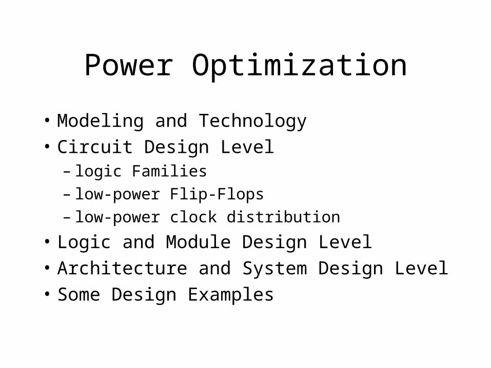
Power Optimization
• Modeling and Technology• Circuit Design Level
– logic Families– low-power Flip-Flops– low-power clock distribution
• Logic and Module Design Level• Architecture and System Design Level• Some Design Examples
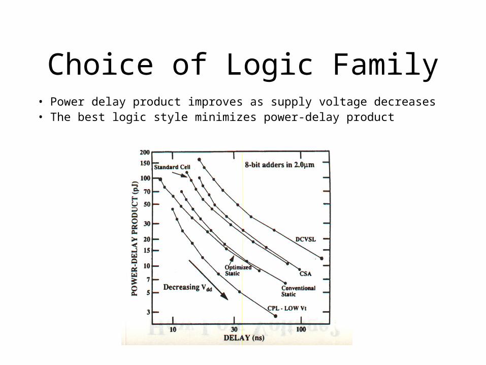
Choice of Logic Family• Power delay product improves as supply voltage decreases• The best logic style minimizes power-delay product
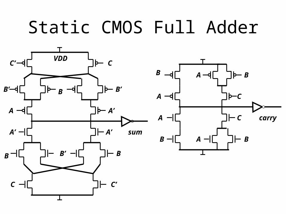
Static CMOS Full Adder
B
A
VDDC’ C
B’B’
A A’
A’ A’
BB
C C’
B
B’
A
B
A B
C
C
A Bsum
carry

NO Race dynamic CMOS logic(NORA)
• Full Adder
A
B
C
A B
phi
phi
phi carry
Phi’phi’
A B C
phi’
A
B
C
sum
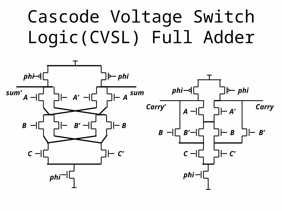
Cascode Voltage Switch Logic(CVSL) Full Adder
phi phi
A
B
C’
A
B
C
A’
B’
sumsum’
A’
B
C’
phi
A
B’
C
B B’
Carry’ Carry
phi
phi phi

Differential Cascode Voltage Switch Logic
• (DCVSL)
A
B
C’
A
B
C
A’
B’
sumsum’
A’
B
C’
A
B’
C
B B’
Carry’ Carry

CMOS NonThreshold Logic(CNTL) Full Adder
A
B
C’
A
B
C
A’
B’
sumsum’
A’
B
C’
A
B’
C
B B’
Carry’ Carry
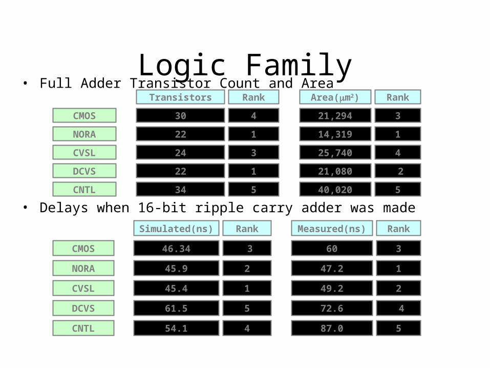
Logic Family• Full Adder Transistor Count and Area
Transistors Rank Area(m2) Rank
CMOS
NORA
CVSL
DCVS
CNTL
30
22
24
22
34
4
1
3
1
5
21,294
14,319
25,740
21,080
40,020
3
1
4
2
5
Simulated(ns) Rank Measured(ns) Rank
CMOS
NORA
CVSL
DCVS
CNTL
46.34
45.9
45.4
61.5
54.1
3
2
1
5
4
60
47.2
49.2
72.6
87.0
3
1
2
4
5
• Delays when 16-bit ripple carry adder was made
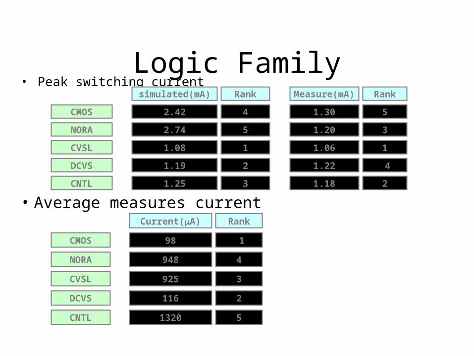
Logic Family• Peak switching current
simulated(mA) Rank Measure(mA) Rank
CMOS
NORA
CVSL
DCVS
CNTL
2.42
2.74
1.08
1.19
1.25
4
5
1
2
3
1.30
1.20
1.06
1.22
1.18
5
3
1
4
2
Current(A) Rank
CMOS
NORA
CVSL
DCVS
CNTL
98
948
925
116
1320
1
4
3
2
5
• Average measures current

A A’ Z Z’
A
A’
Z
Z’
Q’ Q
A B
B
B’
B’ A’
(AB)’ AB
Complementary Pass Transistor Logic(CPL)

A
B
B’
B’ A’
AB(AB)’
VDDVDD
VDD
VDD-VTN
High Level Degradation

B
A
B’
A’
AB
B’B
A
(AB)’
A’
Dual Path Transistor Logic(DPL)

A B
B
B’
B’ A’
(AB)’ AB
NMOS CPLNetwork
O’ O
Swing Restored Pass Transistor
• Logic(SRPL)

• Power consumption of Flip-Flop
– power consumed for the internal state change
– power consumed for the clocking
• Because the stage change is infrequent, the clocking capacitance must be reduced.
• Conventional C2MOS Flip-Flop
At each clock, the switched capacitance is 10MOS gates
Low-Power Flip-Flops
clk clkb
D
clk
clkb clkb
clk
clkb
clk clk
clkb
Q

Low-Power Flip-Flops• Gated D Flip-Flop
• SSTC(Static Single-Transistor Clocked Flip-Flop
D Q
Clk
D
CK
At each clock, the switchedcapacitance 2 MOS gates, but Slow and about 40 transistors
Db
clk
QQb
D x xbx xb
The switched capacitance is 2 MOS gates and
16 transistors

Power Optimization
• Modeling and Technology
• Circuit Design Level
• Logic and Module Design Level– logic synthesis– module design optimization
• Architecture and System Design Level
• Some Design Examples

Module Design Optimization
• Power dissipation
– layout
• 2um CMOS MOSIS
– condition
• 1,000 pseudo-random input
• averaging the result
• Result– CSA has lowest power
dissipation• power supply current
falls to zero faster
• Arithmetic component : Adder
Adder Type
Ripple CarryCarry Skip-ICarry Skip-II
Carry LookaheadCarry Select
Conditional Sum
Delay(nsec)
54.2728.3821.8417.1319.5620.05
Area(mm2)
0.25270.44920.51490.74541.05321.4784
Current(mW)
0.1170.1090.1260.1710.2160.304
•Carry Skip-I : constant block size•Carry Skip-II : variable block size

Module Design Optimization
• Power estimation– conditions
• 50,000 random distribution input • Result
– wallace multiplier• more attractive when operand size is large• irregular layout and large layout area
• array multiplier– becomes unattractive as operand size
increase– has higher average number of logic
transitions– has much higher delay
• Arithmetic component : Multiplier
8b16b32b8b16b32b
Wallace
ModifiedArray
Multiplier Type
50 98
198 35 51 63
Delay(in gate) Size(gates)
567 2,405 9,918
613 2,569
10,413
Transition
583 7,348
99,102 573
3,874 19,548
Top Related