


Languages
Pages
Legal


ISSCC 2003 / SESSION 10 / HIGH SPEED BUILDING BLOCKS / PAPER 10.5
10.5 Broadband ESD Protection Circuits in CMOS Technology
Sherif Galal, Behzad Razavi
Electrical Engineering Department, University of California, Los Angeles, CA
As device dimensions scale down and the operating speed of inte-grated circuits scales up, electrostatic discharge (ESD) proves anincreasingly more critical issue. With hundreds of gigahertz I/Opads in typical data communication circuits, microprocessors,and memories, both the voltage tolerance and the area of ESDprotection devices become important design parameters. It ispossible to use inductive peaking to improve the bandwidth, but,with an ESD capacitance of 1.2pF, the impedance mismatch atthe input or output results in S11 or S22 of only -4dB at 5GHz, cor-rupting broadband data considerably. Also, distributed ESDstructures [1] suffer from the loss-capacitance trade-off of on-chip transmission lines and require a large area. For example, ametal6-metal1 microstrip designed to absorb an ESD capaci-tance of 1.2pF must be 8mm long and 14µm wide while intro-ducing 1.5dB of midband loss. The distribution of the ESD capac-itance over a resistive line may also compromise the voltage tol-erance because an ESD event injects a large current into theline, creating a potential gradient from one end to the other.
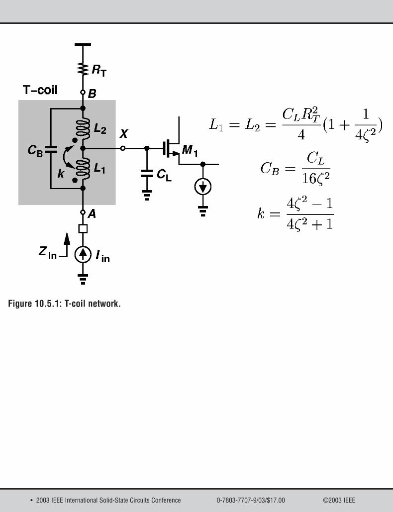
The use of T-coil networks in ESD circuits can overcome theabove difficulties. Shown in Fig. 10.5.1, such a network consistsof inductors L1 and L2 with a coupling factor of k [2] and a bridgecapacitor CB. An important attribute of this network that has notbeen exploited is that proper choice of the T-coil parameters canyield Zin = RT independent of CL and the frequency. At low fre-quencies, L1 and L2 short RT to the input, and at high frequencies,L1 and L2 are open and the bridge capacitor CB plays the samerole. For Zin to remain constant and equal to RT with frequency,the equations in Fig. 10.5.1 must hold. Moreover, for a well-behaved transfer function (uniform group delay), ζ = √3/2, reduc-ing these expressions to: L1 = L2 = CLR2
T/3, CB = CL/12, k = 1/2.
In addition to a constant input resistance, T-coils also increasethe transfer bandwidth to a much greater extent than inductivepeaking does [2]. In the ideal case, the bandwidth improvementfactor reaches 2.72 for T-coils with k = 1/2 and only 1.6 for induc-tive peaking having the same type of response. These observa-tions suggest that capacitor CL in Fig. 10.5.1 can be replaced bya standard ESD structure. The principal challenge therefore liesin the design of the T-coil itself for low loss and proper mutualcoupling.
The fortunate coincidence L1 = L2 points to the use of a symmet-ric spiral realization of the T-coil, Fig. 10.5.2a, with the centertap representing the output terminal. The total inductancebetween nodes A and B is equal to 2L(k+1) = 3L = CLR2
T. ASITICsimulations indicate that the coupling coefficient between thetwo halves in Fig. 10.5.2a is a strong function of the line spacing.Thus, with an initial guess for the number of turns and the outerdimension, the line width is chosen to minimize the loss, and theline spacing to obtain k=1/2. Next, the outer dimension is adjust-ed to achieve LAB=CLR2
T.
If used in broadband circuits, T-coils must be modeled such thattheir response remains accurate for approximately the lastdecade of the band of interest. Figure 10.5.2b shows the distrib-uted model used here. The spiral is decomposed into eight sec-tions, and each section is represented by an inductance, seriesand parallel resistances, and parasitic capacitance to the sub-
strate. The fringe capacitance between adjacent turns is alsoincluded. Since this capacitance appears between nodes A and Bin a distributed form, the bridge capacitance, CB, is chosen equalto the required value minus the total interwinding capacitance.
Another attribute of T-coils proves particularly important ininput ESD design. To the first order, the series resistance of L1
and L2 does not affect the midband gain. It is readily seen in Fig.10.5.1 that equal resistors placed in series with L1 and L2 leaveVX unchanged if the circuit is driven by a source impedance equalto RT. This is in sharp contrast to the behavior of ESD structuresdistributed over transmission lines, where the low-frequencymetal resistance forms a voltage divider with the terminationresistor.
The utility of T-coils is limited to low-impedance interfaces. SinceL1 and L2 are proportional to RT
2, large inductance values may benecessary if RT reaches several hundred ohms. For I/O interfaces,on the other hand, LAB falls in the range of a few nanohenries,lending itself to a compact symmetric implementation.
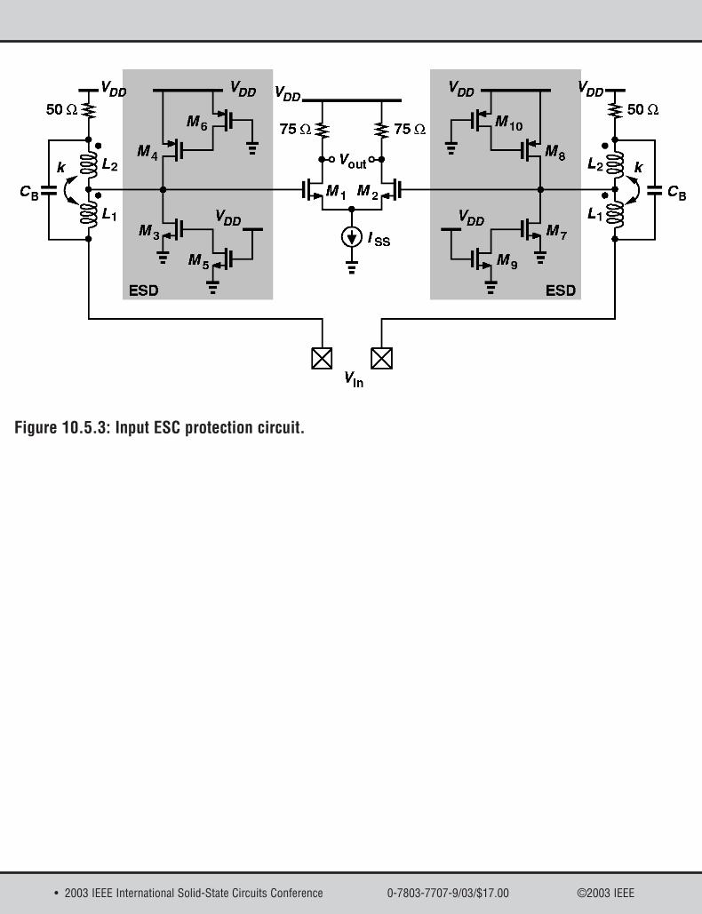
Figure 10.5.3 illustrates the overall input protection circuit.Devices M3-M6 and M7-M10 are standard ESD structures providedby the foundry. Driving 75Ω on-chip and 50Ω off-chip loads, dif-ferential pair M1-M2 represents a typical input stage and allowsmeasurement of the broadband performance. Each T-coil occu-pies an area of 85µmx85µm, a factor of 15 lower than that in thedistributed ESD example.
For output protection, the two ports of the T-coil are swapped,with the output current injected into the center tap. Figure10.5.4 shows the resulting circuit. The dynamics are identical tothose of the input structure. This topology, too, is free from mid-band loss.
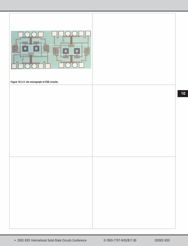
The input and output protection circuits shown in Figs. 10.5.3and 10.5.4 are fabricated in 0.18µm CMOS technology. The diephotograph of both circuits is shown in Fig. 10.5.5. The ESD tol-erance is tested according to the JEDEC standards, JESD22-A114-B for the human body model (HBM) [3] and JESD22-A115A for the machine model (MM) [4]. The zapping voltage isvaried from 200V to 2000V in steps of 200V for HBM and from50V to 200V in steps of 50V for MM. The measured HBM toler-ance is 1000V for the input structure and 800V for the outputstructure. For MM, both circuits exhibit a tolerance of 100V.
The ESD circuits have also been tested for high-frequency char-acteristics. Figure 10.5.6 plots S11 and S22 for the input and out-put topologies, respectively, as a function of frequency. The mea-sured S11 remains below -24dB and S22 below -20dB for frequen-cies as high as 10GHz. These quantities fall below -30dB at a fewgigahertz, suggesting that the low-frequency resistance of thesymmetric inductor does not degrade the matching significantly.Figure 10.5.7 shows the measured eye diagrams for both struc-tures with an input pattern of 223-1 at 10Gb/s.
References[1] B. Kleveland, et al., ‘‘Distributed ESD Protection for High-SpeedIntegrated Circuits,’’ IEEE Electron Device Letters, vol. 21, pp. 390-392,Aug. 2000.[2] Dennis L. Feucht, Handbook of Analog Circuit Design, San Diego:Academic Press, 1990.[3] JEDEC Standard JESD22-A114-B, ‘‘Electrostatic Discharge (ESD)Sensitivity Testing Human Body Model,’’ JEDEC, 2000.[4] EIA/JEDEC Standard Test Method A115-A, ‘‘Electrostatic Discharge(ESD) Sensitivity Testing Machine Model (MM),’’ EIA/JEDEC, 1997.
• 2003 IEEE International Solid-State Circuits Conference 0-7803-7707-9/03/$17.00 ©2003 IEEE

ISSCC 2003 / February 11, 2003 / Salon 9 / 10:15 AM
10
Figure 10.5.1: T-coil network. Figure 10.5.2: T-coil network (a) implementation, (b) distributed model.
Figure 10.5.3: Input ESC protection circuit.
Figure 10.5.6: Measured return loss: (a) input ESD, (b) output ESD(Horizontal scale: -2GHz/div., vertical scale: 10dB/div.).
Figure 10.5.4: Output ESD protection circuit.
Input Structure
Output Structure
Figure 10.5.7: 10Gb/s eye diagrams for input and output ESD struc-tures (Horizontal scale: 20ps/div., vertical scale: 50 mV/div.).
• 2003 IEEE International Solid-State Circuits Conference 0-7803-7707-9/03/$17.00 ©2003 IEEE
10
• 2003 IEEE International Solid-State Circuits Conference 0-7803-7707-9/03/$17.00 ©2003 IEEE
Figure 10.5.5: die micrograph of ESD circuits.
• 2003 IEEE International Solid-State Circuits Conference 0-7803-7707-9/03/$17.00 ©2003 IEEE
Figure 10.5.1: T-coil network.

• 2003 IEEE International Solid-State Circuits Conference 0-7803-7707-9/03/$17.00 ©2003 IEEE
Figure 10.5.2: T-coil network (a) implementation, (b) distributed model.
• 2003 IEEE International Solid-State Circuits Conference 0-7803-7707-9/03/$17.00 ©2003 IEEE
Figure 10.5.3: Input ESC protection circuit.

• 2003 IEEE International Solid-State Circuits Conference 0-7803-7707-9/03/$17.00 ©2003 IEEE
Figure 10.5.4: Output ESD protection circuit.

• 2003 IEEE International Solid-State Circuits Conference 0-7803-7707-9/03/$17.00 ©2003 IEEE
Figure 10.5.5: die micrograph of ESD circuits.

• 2003 IEEE International Solid-State Circuits Conference 0-7803-7707-9/03/$17.00 ©2003 IEEE
Figure 10.5.6: Measured return loss: (a) input ESD, (b) output ESD (Horizontal scale: -2GHz/div.,vertical scale: 10dB/div.).

• 2003 IEEE International Solid-State Circuits Conference 0-7803-7707-9/03/$17.00 ©2003 IEEE
Input Structure
Output Structure
Figure 10.5.7: 10Gb/s eye diagrams for input and output ESD structures (Horizontal scale:20ps/div., vertical scale: 50 mV/div.).
Top Related