


![summary SA3 JPTM1 fnl kaku.ppt [ ݊ [ h]) · (1)NARL: Dr.Franz M.C.Cheng introduced NARL organization for disaster mitigation. NARL explained satellite program and related technologies](https://static.fdocuments.in/doc/165x107/5f0df28e7e708231d43cde2a/summary-sa3-jptm1-fnl-kakuppt-h-1narl-drfranz-mccheng-introduced.jpg)
Languages
Pages
Legal


[email protected]://csce.uark.edu +1 (479) 575-6043
Introduction to Design CompilerCourtesy of Dr. An-Yeu Wu @NTU, CIC/NARL@Taiwan

Synthesis = translation + optimization
We will get a gate level circuit with timing information after Synthesis
What is Synthesis
11/2/2017 CSCE/ELEG 4914: Advnaced Digital Design 2

Design Compiler
Initialize the environment:
● initrc dc-m
Start Design Compiler:
●dc_shell: command line tool
●design_vision: GUIor by start_gui in dc_shell
11/2/2017 CSCE/ELEG 4914: Advnaced Digital Design 3

Design Compiler maps Synopsys design block to gate level design with a user specified library
Design Compiler
Technology
Library
timing info
RTL Design
11/2/2017 CSCE/ELEG 4914: Advnaced Digital Design 4

Synthesis Design Flow
Specification
RTL Coding Prepare
Setting Design Environment
Setting Design Constraint
Compile Design
Analysis
Cell
Library
Gate-level Netlist
11/2/2017 CSCE/ELEG 4914: Advnaced Digital Design 5

Develop the HDL design description and simulate the design description to verify that it is correct.
Set up the environment
●Set the appropriate technology, synthetic, and symbol libraries, target libraries, and link libraries.
●Set the necessary compilation options, including options to read in the input files and specify the output formats.
Read the HDL design description
Define the design.
●Set design attributes
●Set design rules
●Set realistic constraints (timing and area goals)
●Determine a compile methodology
Synthesis Design Flow
11/2/2017 CSCE/ELEG 4914: Advnaced Digital Design 6

Timing library”
●higher level abstract view of the timing and power of this circuit suitable for use by the ASIC tools.
●Essentially, these tools run many, many circuit-level simulations to create characterization data stored in a .lib (Liberty) file. This file is a text file
●Synopsys tool reads a binary format (.db) which is compiled from .lib file to accelerate the process
Timing Library
11/2/2017 CSCE/ELEG 4914: Advnaced Digital Design 7

What’s inside (thousands of lines)
Timing Library
cell (NAND3X0) {cell_footprint : "nand3x0 ";area : 7.3728 ;cell_leakage_power : 9.151417e+04;...pin (IN1) {
fanout_load : 0.059000;direction : "input";fall_capacitance : 2.212771;capacitance : 2.190745;rise_capacitance : 2.168719;...internal_power () {
when : "!IN2&!IN3";rise_power ("power_inputs_1") {
/* index_1 = input transition time */index_1(" 0.0160000, 0.0320000, 0.0640000, 0.1280000, 0.2560000, 0.5120000, 1.0240000");values ("-1.2575404, -1.2594251, -1.2887053, -1.2413107, -1.2083520, -1.2261536, -1.1689351");
}fall_power ("power_inputs_1") {
/* index_1 = input transition time */index_1(" 0.0160000, 0.0320000, 0.0640000, 0.1280000, 0.2560000, 0.5120000, 1.0240000");values (" 1.9840914, 1.9791286, 2.0696119, 2.0561270, 2.0655292, 2.0637255, 2.0668630");
}….
Std. cell general information
Pin information
Power information
11/2/2017 CSCE/ELEG 4914: Advnaced Digital Design 8
Continue
Timing Library
…pin (QN) {
direction : "output";power_down_function : "!VDD + VSS";function : "(IN3*IN2*IN1)'";...timing () {
related_pin : "IN1";timing_sense : "negative_unate";cell_rise ("del_1_7_7") {
/* index_1 = input net transition time */index_1("0.016, 0.032, 0.064, 0.128, 0.256, 0.512, 1.024");/* index_2 = total output net capacitance */index_2("0.1, 3.75, 7.5, 13, 26, 52, 104");values(
"0.0178632, 0.0275957, 0.0374970, 0.0517788, 0.0856314, 0.1538226, 0.2886417", \"0.0215562, 0.0316225, 0.0414275, 0.0556431, 0.0895029, 0.1573472, 0.2917113", \"0.0261721, 0.0387623, 0.0496870, 0.0639978, 0.0973798, 0.1643430, 0.3008298", \"0.0323952, 0.0479363, 0.0614787, 0.0790854, 0.1144558, 0.1806003, 0.3153037", \"0.0413278, 0.0605217, 0.0771532, 0.0986336, 0.1423713, 0.2144832, 0.3477775", \"0.0540991, 0.0787062, 0.0997246, 0.1260550, 0.1797894, 0.2692040, 0.4165220", \"0.0712053, 0.1041857, 0.1296371, 0.1645895, 0.2318538, 0.3420702, 0.5237414");
}
Timing information
11/2/2017 CSCE/ELEG 4914: Advnaced Digital Design 9

File->Setup [Using FreePDK45 Example]
●You will need initrc FreePDK45 before starting design compiler
● If DesignWare Lib is used, add dw_foundation.sldb into link_library
11/2/2017 10CSCE/ELEG 4914: Advnaced Digital Design
Initial Setup
set_app_var search_path ". $::env(PDK_DIR)/osu_soc/lib/files $synopsys_root/libraries/syn/"
set_app_var link_library "* gscl45nm.db"
set_app_var target_library "gscl45nm.db"
set_app_var symbol_library "generic.sdb"
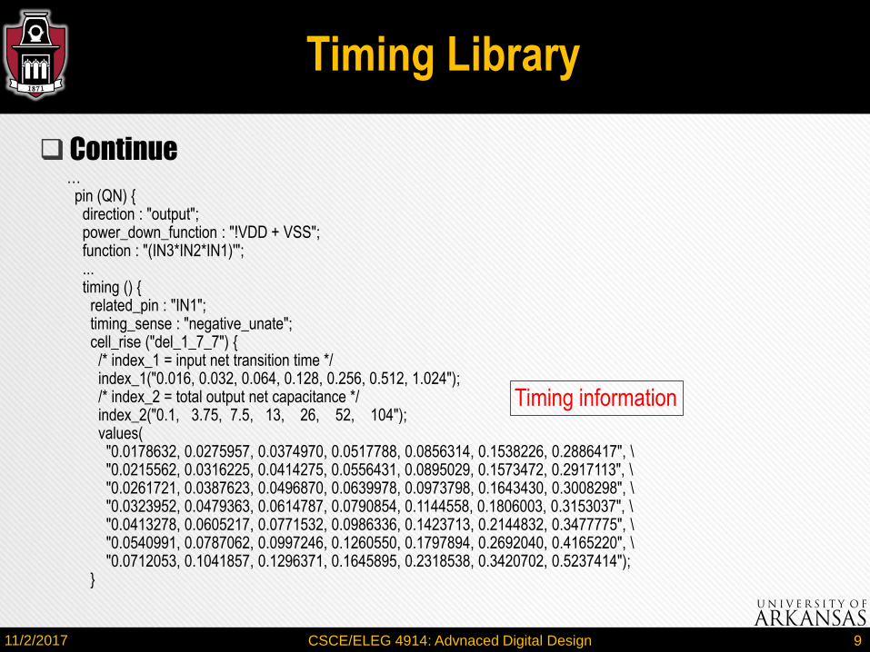
Read netlists or other design descriptions into Design Compiler
●File/Read
Support many different formats:
●DDC (binary): .ddc
●Verilog: .v
●VHDL: .vhd
●EDIF
Read File
11/2/2017 CSCE/ELEG 4914: Advnaced Digital Design 11

File/Analyze
●The analyze command reads the Verilog RTL into an intermediate internal representation.
File/Elaborate
●The elaborate command recursively resolves all of the module references starting from the top-level module
●also infers various registers and/or advanced data-path components.
File/Link Design
●Link all parts together
Analyze & Elaborate & Link
11/2/2017 CSCE/ELEG 4914: Advnaced Digital Design 12

Setting Design Environemnt:
●Operating Environment (a)
● Input Driving Strength (b)
●Output Loading (c)
● Input/Output Delay (d)
●Wire Load Model (e)
Setting Design Environment
U1
U2M1
(a) Set_operating_conditions
(d) set_input_delay
(b) set_driving_cell
(d) set_output_delay
(c) set_load
(e) set_wire_load_model
11/2/2017 CSCE/ELEG 4914: Advnaced Digital Design 13

Attributes/Operating Environment/Operating Condition (GUI)
Setting Operating Condition
Maximum => slow ( setup time )
Minimum => fast (hold time)
11/2/2017 CSCE/ELEG 4914: Advnaced Digital Design 14

Set input
●Attribute/Operating Environment/Drive Strength
Setting Input Drive
11/2/2017 CSCE/ELEG 4914: Advnaced Digital Design 15

Attribute/Operating Environment/Load
Setting Output Loading(GUI)
11/2/2017 CSCE/ELEG 4914: Advnaced Digital Design 16
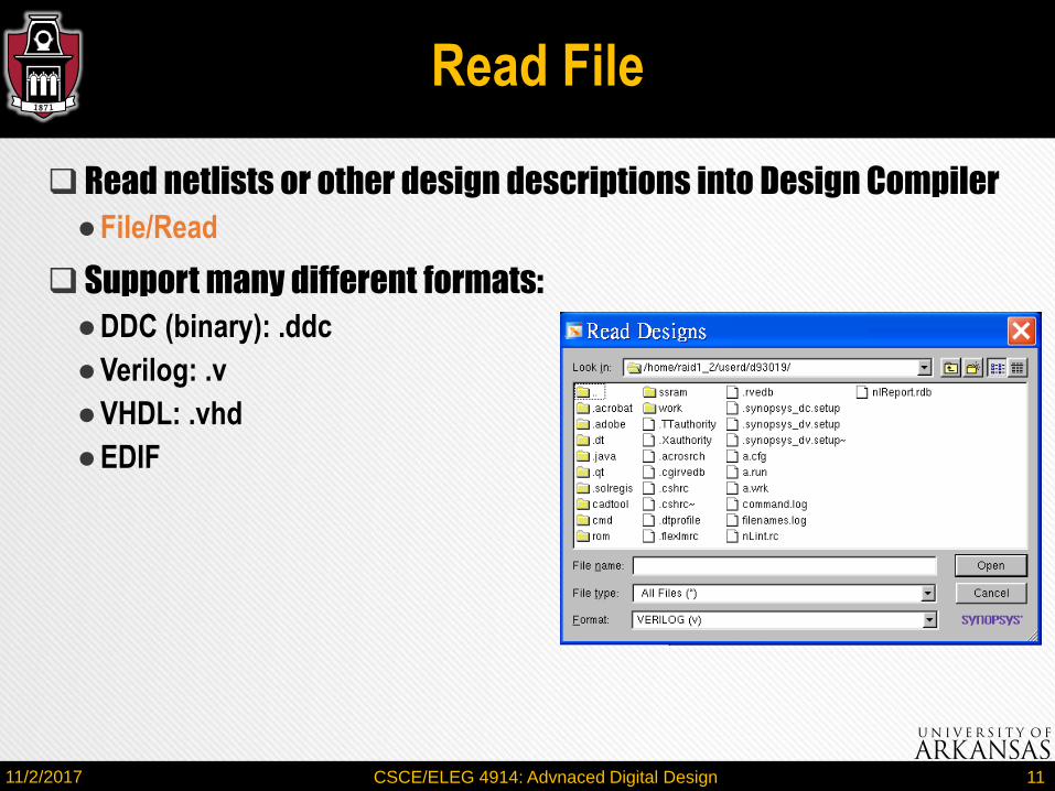
Delay Calculation:
●clock cycle >= DFF clk-Q delay + c + DFF setup
● Input delay = DFF clk-Q delay + a
●Output delay = e + DFF setup
Input/Output Delay
11/2/2017 CSCE/ELEG 4914: Advnaced Digital Design 17
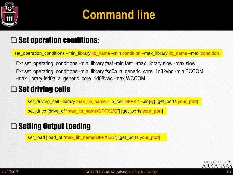
Set operation conditions:
Set driving cells
Setting Output Loading
Command line
set_driving_cell –library max_lib_name –lib_cell DFFX2 –pin{Q} [get_ports your_port]
set_drive [drive_of “max_lib_name/DFFX2/Q”] [get_ports your_port]
Ex: set_operating_conditions -min_library fsd0a_a_generic_core_1d32vbc -min BCCOM
-max_library fsd0a_a_generic_core_1d08vwc -max WCCOM
set_operation_conditions –min_library lib_name –min condition –max_library lib_name –max condition
Ex: set_operating_conditions -min_library fast -min fast -max_library slow -max slow
set_load [load_of “max_lib_name/DFFX1/D”] [get_ports your_port]
11/2/2017 CSCE/ELEG 4914: Advnaced Digital Design 18

Select input ports
●Attributes/Operating Environment/Input Delay
Setting Input Delay
Specify
maximum
input delay
Specify
minimum
input delay
11/2/2017 CSCE/ELEG 4914: Advnaced Digital Design 19

Select output ports
●Attributes/Operating Environment/Output Delay
Setting Output Delay
Specify
maximum
output delay
Specify
minimum
output delay
11/2/2017 CSCE/ELEG 4914: Advnaced Digital Design 20

Wire load model estimates wire capacitance based on chip area & cell fanout
●Setting this information during compile in order to model the design more accurately
●Attributes/Operating Environment/Wire Load
Setting Wire Load Model
11/2/2017 CSCE/ELEG 4914: Advnaced Digital Design 21

Constraints are goals that the Design Compiler uses for optimizing a design into target technology library.
Design Rule Constraints : technology-specific restriction
●Ex: maximum transition, maximum fanout, maximum capacitance.
Optimization Constraints : design goals and requirements
●Ex: maximum delay, minimum delay, maximum area, maximum power.
During compile, Design Compiler attempts to meet all constraints.
● If constraints too tight, it may not meet those
Design Constraints
11/2/2017 CSCE/ELEG 4914: Advnaced Digital Design 22

Optimization Constraints
● Basic clock constraints concept
● Constraint for Special Circuit
● Constraints for Power & Area
Design Rule Constraints
Final check constraints before compile
Setting Design Constraints
11/2/2017 CSCE/ELEG 4914: Advnaced Digital Design 23

What should be defined?
●Period
●Waveform
●Uncertainty▪ Skew
●Latency▪ Source latency (option)
▪ Network latency
●Transition▪ Input transition
▪ Clock transition
All register-to-register path are constrained now
Define Clock Specification
11/2/2017 CSCE/ELEG 4914: Advnaced Digital Design 24

Select clock port
●Attributes/Clocks/Specify
Combinational delay is constraint by:
●Or create virtual clock
Specify Clock Constrains
set_max_delay 10 -from all_input -to all_output
create_clock -period 10 -name clk
11/2/2017 CSCE/ELEG 4914: Advnaced Digital Design 25

creat_clock :
●define your clock’s waveform & respect the set-up time requirements of all clocked flip-flops
set_fix_hold :
● respect the hold time requirement of all clocked flip-flops
set_dont_touch_network :
●do not re-buffer the clock network
Command Line
create_clock -name "CLK" -period 10 -waveform {0 5} [get_ports CLK ]
set_fix_hold [get_clocks CLK]
set_dont_touch_network [get_clocks CLK]
11/2/2017 CSCE/ELEG 4914: Advnaced Digital Design 26

Attributes/OptimizationConstraints/Design Constraints
Area Unit :
●Equivalent gate count
●um x um
●Transistors
Setting Area&Power Constraint
set_max_total_power 0.0uw
set_max_dynamic_power 0.0uw
set_max_leakage_power 0.0uw
set_max_area 0
11/2/2017 CSCE/ELEG 4914: Advnaced Digital Design 27

Vendors impose design rules that restrict how many cells are connected to one another based on capacitance, transition ,and fanout
You may apply more conservative design rules to:
●Anticipate the interface environment your block will see
●Prevent the design from operating cells close to their limits, where performance degrades rapidly
DC respects design rules as highest priority of all in the following order:
●set_max_transition
●set_max_fanout
●set_max_capacitance
Design Rule Constraints
11/2/2017 CSCE/ELEG 4914: Advnaced Digital Design 28

Check Design
●Execute check_design command before you optimize your design
Some possible issues
●Error (bus width mismatch)▪ Error: In design ‘bcd7segs’, cell ‘decoder’ has more pins than it’s reference
‘d1’ has ports
●Warnings (dangling ports)▪ Warning: In design ‘converter’, port ‘A’ is not connected to any nets
Check Timing
●After setting constraints, verify that there are no remaining unconstrained paths: check_timing
Check Design
11/2/2017 CSCE/ELEG 4914: Advnaced Digital Design 29

The compile command optimizes and maps the current_design
Design/Compile design
Compile the Design
compile -map_effort medium
compile_ultra
11/2/2017 CSCE/ELEG 4914: Advnaced Digital Design 30

Generating Reports
●Design / Report
●Timing / Report
Report Design & Timing
11/2/2017 CSCE/ELEG 4914: Advnaced Digital Design 31

Write out the design netlist after synthesis
Save the Design
11/2/2017 CSCE/ELEG 4914: Advnaced Digital Design 32

Use the following reports to check constraints before compiling
Design/Report XXXX
●Report Design▪ In this report you can check the operating condition and wire load model
●Report Clocks
Notice that all the information about timing is at Timing/Report XXX
Check Constraints
11/2/2017 CSCE/ELEG 4914: Advnaced Digital Design 33

Report Design Hierarchy
●Hierarchy report shows the component used in your block & hierarchy
Report Reference
●Reference report shows statistical result about reference in the design
Report Net
●Net report shows the statistical results of each net
Report Area
●Area report shows the um2 of the design
Report Power
●Power report shows the estimated power consumption
Report Constraints
●Constraints report shows if compiled design meets your constraints
Report Design
11/2/2017 CSCE/ELEG 4914: Advnaced Digital Design 34

Extract report data with command line
Generate Text Report
redirect xxx_area.rpt { report_area }
redirect xxx_power.rpt { report_power }
redirect xxx_hierarchy.rpt { report_hierarchy }
redirect xxx_nets.rpt { report_nets }
redirect xxx_constraints.rpt { report_constraints }
redirect xxx_reference.rpt { report_reference }
11/2/2017 CSCE/ELEG 4914: Advnaced Digital Design 35

Timing / Report Timing Path
Report Timing
Fractional part length
11/2/2017 CSCE/ELEG 4914: Advnaced Digital Design 36
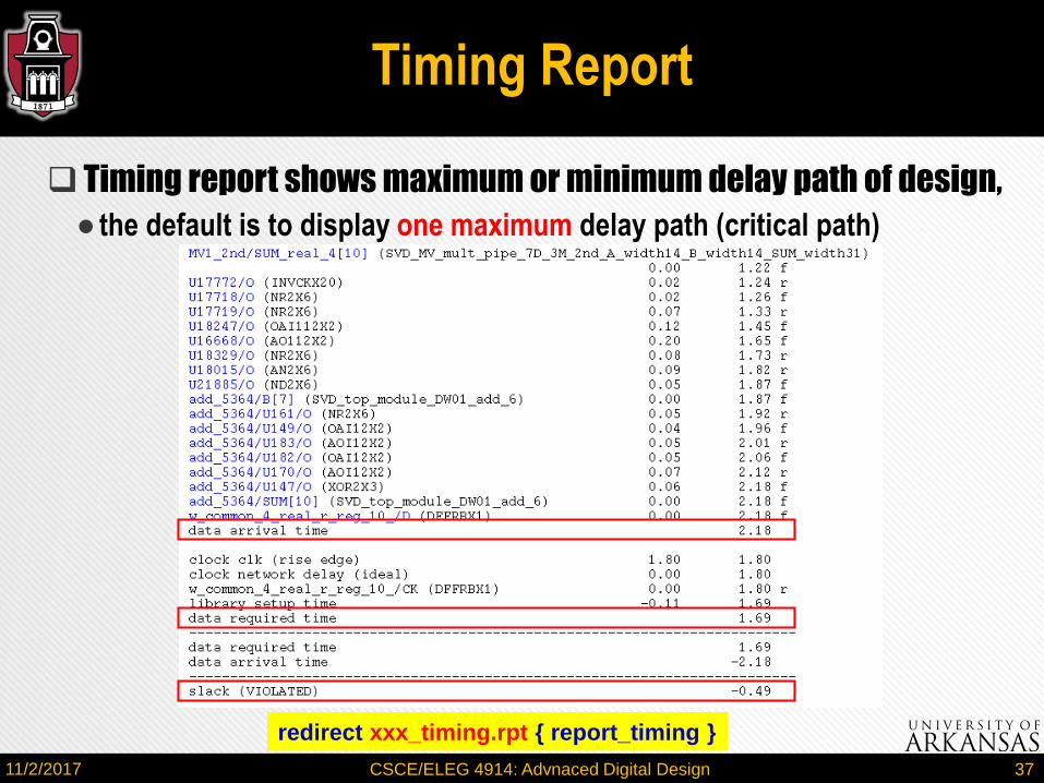
Timing report shows maximum or minimum delay path of design,
● the default is to display one maximum delay path (critical path)
Timing Report
redirect xxx_timing.rpt { report_timing }
11/2/2017 CSCE/ELEG 4914: Advnaced Digital Design 37

Slack is the resulting margin between required & actual arrival time
Positive slack or zero means meet constraints
Negative slack means violate constraints
Setup Time Check (max delay check)
Hold Time Check (min delay check)
What is Slack
Slack_setup = Data Required Time – Data Arrival Time
Slack_hold = Data Arrival Time - Data Required Time
11/2/2017 CSCE/ELEG 4914: Advnaced Digital Design 38

Save your design to file before you quit Design Compiler
File/Save saves your design in the ddc format
File/Save As can save your design in other Write formats
●Verilog: .v
●VHDL: .vhd
●EDIF
●Synopsys DDC formats
●Timing Constraints: .sdc
Save Design
write -hierarchy -format ddc -output xxx.ddc
write -hierarchy -format verilog -output xxx.v
write_sdc xxx.sdc
11/2/2017 CSCE/ELEG 4914: Advnaced Digital Design 39

Save gate-level netlist.
●“File”->”Save As”
Save your design.
●“File”-“Save”
Save the timing information.
●“File”-“Save Info”-”Design Timing”, choose sdf format.
Save script file with the constraints you have made.
●“File”- “Save Info”- “Design Setup”
Re-run all steps automatically.
●“File”-“Execute Script”
Save Files
write -format verilog -hierarchy -output "ALU_s.v" find (design, ALU)
write -format db -hierarchy -output "ALU_s.db" find (design, ALU)
write_sdf ALU_s.sdf
11/2/2017 CSCE/ELEG 4914: Advnaced Digital Design 40

Write out gate-level netlist
● File/Save As Verilog (for File format)
● dc_shell> write -format verilog –hierarchy -output chip.vg
Get SDF
● File/Save Info Design timing Select chip.sdf
● dc_shell> write_sdf –version 2.1 -context verilog chip.sdf
Modify your testbench file
$sdf_annotate (“the_SDF_file_name”, top_module_instance_name);
Simulation with timing information back-annotated
Gate-Level Simulation (Verilog)
11/2/2017 CSCE/ELEG 4914: Advnaced Digital Design 41

Design Example:
●Adder64 (combinational)▪ Script provided: dc_shell -f dc.tcl
Lab4:
●Adder128 (combinational)▪ Modify Adder64.v file to create 128 bit adder
▪ Compare synthesized results against 64bit adder
●FPGen (sequential with clock pin name ‘clk’, system verilog format)▪ add dw_foundation.sldb into link_library
▪ analyze -format sverilog $systemVerilogs
▪ current_design FPGen
▪ create_clock -period $myPeriod_ns clk
Example
11/2/2017 CSCE/ELEG 4914: Advnaced Digital Design 42
Top Related