


Languages
Pages
Legal

8/4/2019 Interfacing the Keyboard to 8051 Micro Controller 11
http://slidepdf.com/reader/full/interfacing-the-keyboard-to-8051-micro-controller-11 1/10
Interfacing the Keyboard to 8051 microcontroller
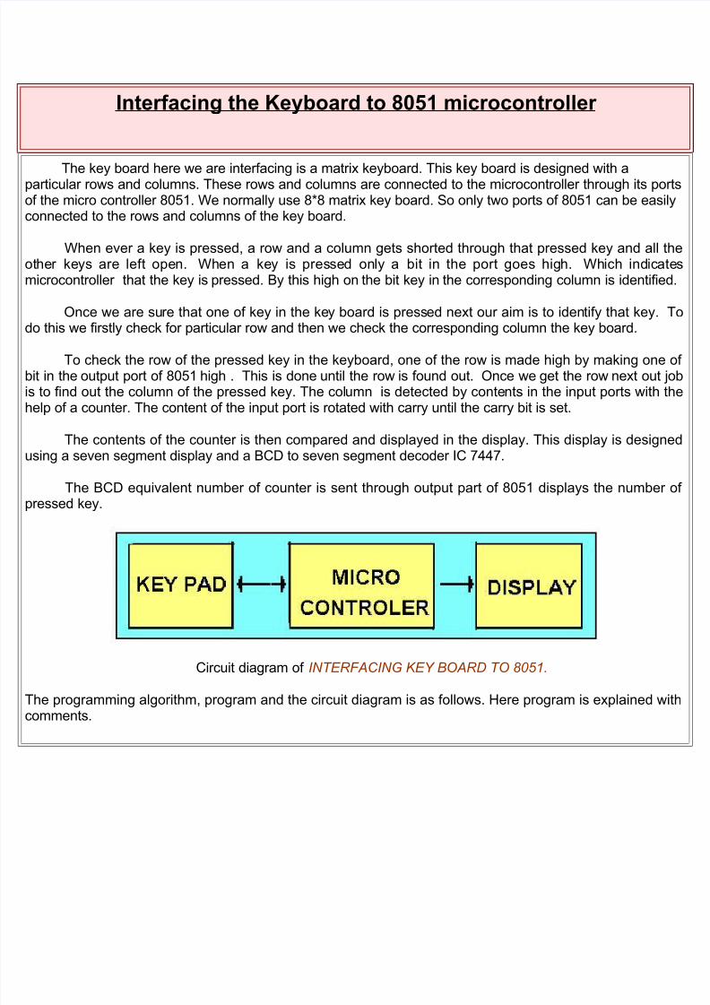
The key board here we are interfacing is a matrix keyboard. This key board is designed with aparticular rows and columns. These rows and columns are connected to the microcontroller through its poof the micro controller 8051. We normally use 8*8 matrix key board. So only two ports of 8051 can be easconnected to the rows and columns of the key board.
When ever a key is pressed, a row and a column gets shorted through that pressed key and all other keys are left open. When a key is pressed only a bit in the port goes high. Which indicamicrocontroller that the key is pressed. By this high on the bit key in the corresponding column is identifie
Once we are sure that one of key in the key board is pressed next our aim is to identify that key. do this we firstly check for particular row and then we check the corresponding column the key board.
To check the row of the pressed key in the keyboard, one of the row is made high by making onebit in the output port of 8051 high . This is done until the row is found out. Once we get the row next outs to find out the column of the pressed key. The column is detected by contents in the input ports withhelp of a counter. The content of the input port is rotated with carry until the carry bit is set.
The contents of the counter is then compared and displayed in the display. This display is desigusing a seven segment display and a BCD to seven segment decoder IC 7447.
The BCD equivalent number of counter is sent through output part of 8051 displays the numbepressed key.
Circuit diagram of INTERFACING KEY BOARD TO 8051.
The programming algorithm, program and the circuit diagram is as follows. Here program is explained wcomments.
8/4/2019 Interfacing the Keyboard to 8051 Micro Controller 11
http://slidepdf.com/reader/full/interfacing-the-keyboard-to-8051-micro-controller-11 2/10
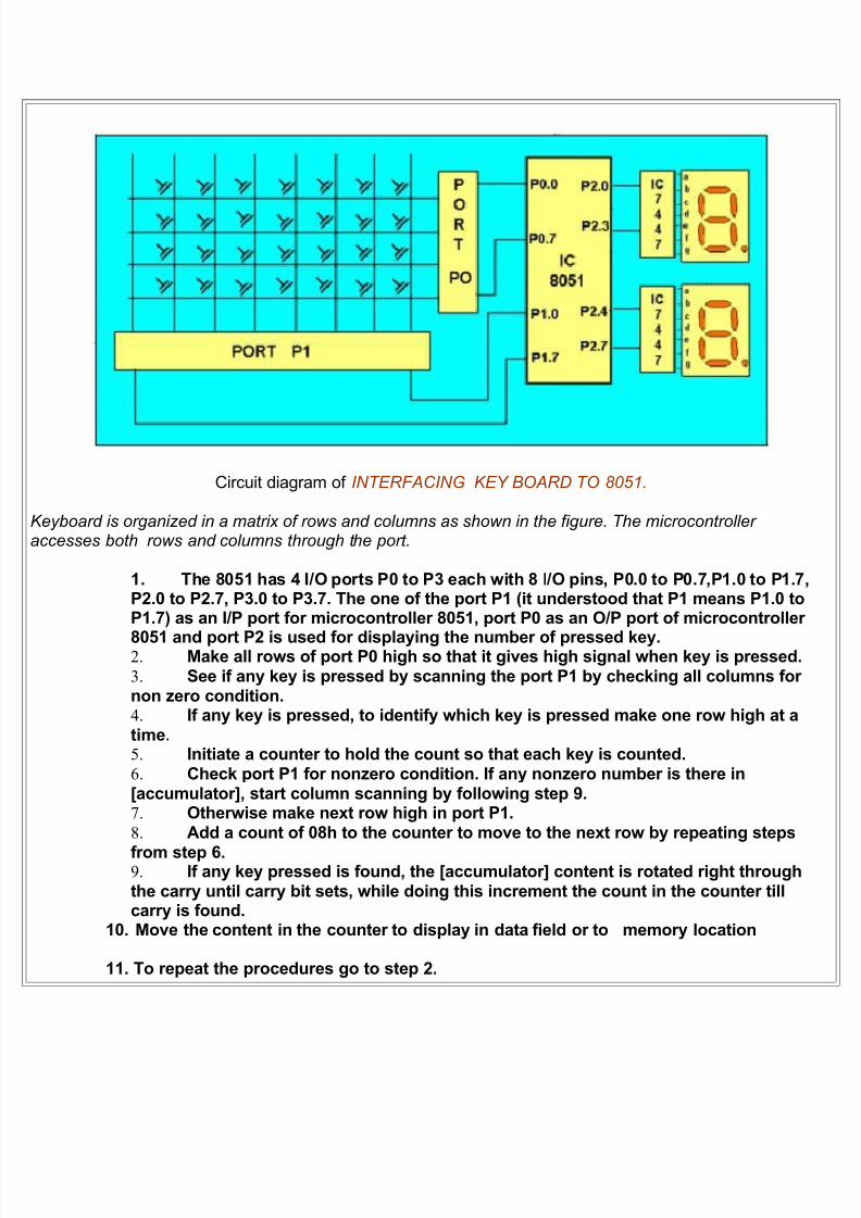
Circuit diagram of INTERFACING KEY BOARD TO 8051.
Keyboard is organized in a matrix of rows and columns as shown in the figure. The microcontroller accesses both rows and columns through the port.
1. The 8051 has 4 I/O ports P0 to P3 each with 8 I/O pins, P0.0 to P0.7,P1.0 to P1.7P2.0 to P2.7, P3.0 to P3.7. The one of the port P1 (it understood that P1 means P1.0 toP1.7) as an I/P port for microcontroller 8051, port P0 as an O/P port of microcontroller
8051 and port P2 is used for displaying the number of pressed key.2. Make all rows of port P0 high so that it gives high signal when key is pressed.3. See if any key is pressed by scanning the port P1 by checking all columns fornon zero condition.4. If any key is pressed, to identify which key is pressed make one row high at atime.5. Initiate a counter to hold the count so that each key is counted.6. Check port P1 for nonzero condition. If any nonzero number is there in[accumulator], start column scanning by following step 9.7. Otherwise make next row high in port P1.8. Add a count of 08h to the counter to move to the next row by repeating steps
from step 6.9. If any key pressed is found, the [accumulator] content is rotated right throughthe carry until carry bit sets, while doing this increment the count in the counter tillcarry is found.
10. Move the content in the counter to display in data field or to memory location
11. To repeat the procedures go to step 2.
8/4/2019 Interfacing the Keyboard to 8051 Micro Controller 11
http://slidepdf.com/reader/full/interfacing-the-keyboard-to-8051-micro-controller-11 3/10
BASICS OF STEPPER MOTOR
Of all motors, step motor is the easiest to control. It's handling simplicity is really hard to deny
- all there is to do is to bring the sequence of rectangle impulses to one input of step controller
and direction information to another input. Direction information is very simple and comes
down to "left" for logical one on that pin and "right" for logical zero. Motor control is also very
simple - every impulse makes the motor operating for one step and if there is no impulse the
motor won't start. Pause between impulses can be shorter or longer and it defines revolution
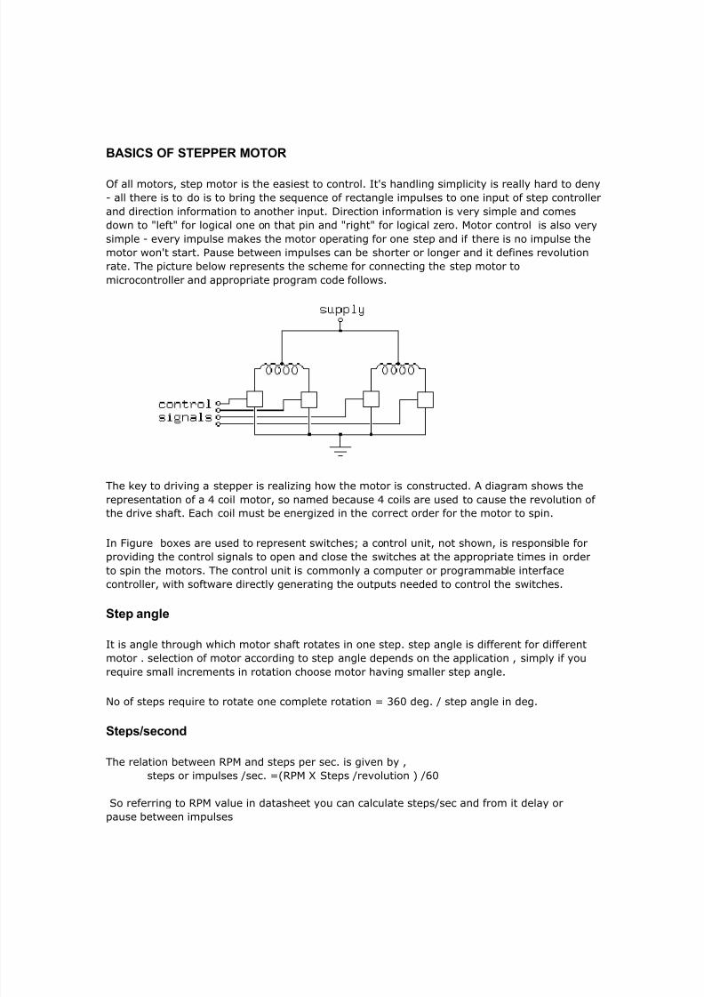
rate. The picture below represents the scheme for connecting the step motor to
microcontroller and appropriate program code follows.
The key to driving a stepper is realizing how the motor is constructed. A diagram shows the
representation of a 4 coil motor, so named because 4 coils are used to cause the revolution of
the drive shaft. Each coil must be energized in the correct order for the motor to spin.
In Figure boxes are used to represent switches; a control unit, not shown, is responsible for
providing the control signals to open and close the switches at the appropriate times in order
to spin the motors. The control unit is commonly a computer or programmable interface
controller, with software directly generating the outputs needed to control the switches.
Step angle
It is angle through which motor shaft rotates in one step. step angle is different for different
motor . selection of motor according to step angle depends on the application , simply if you
require small increments in rotation choose motor having smaller step angle.
No of steps require to rotate one complete rotation = 360 deg. / step angle in deg.
Steps/second
The relation between RPM and steps per sec. is given by ,
steps or impulses /sec. =(RPM X Steps /revolution ) /60
So referring to RPM value in datasheet you can calculate steps/sec and from it delay or
pause between impulses
8/4/2019 Interfacing the Keyboard to 8051 Micro Controller 11
http://slidepdf.com/reader/full/interfacing-the-keyboard-to-8051-micro-controller-11 4/10
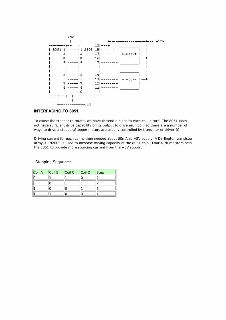
INTERFACING TO 8051.
To cause the stepper to rotate, we have to send a pulse to each coil in turn. The 8051 does
not have sufficient drive capability on its output to drive each coil, so there are a number of
ways to drive a stepper,Stepper motors are usually controlled by transistor or driver IC .
Driving current for each coil is then needed about 60mA at +5V supply. A Darlington transistor
array, ULN2003 is used to increase driving capacity of the 8051 chip. Four 4.7k resistors help
the 8051 to provide more sourcing current from the +5V supply.
Stepping Sequence
Coil A Coil B Coil C Coil D Step
0 1 1 0 1
0 0 1 1 2
1 0 0 1 3
1 1 0 0 4
8/4/2019 Interfacing the Keyboard to 8051 Micro Controller 11
http://slidepdf.com/reader/full/interfacing-the-keyboard-to-8051-micro-controller-11 5/10
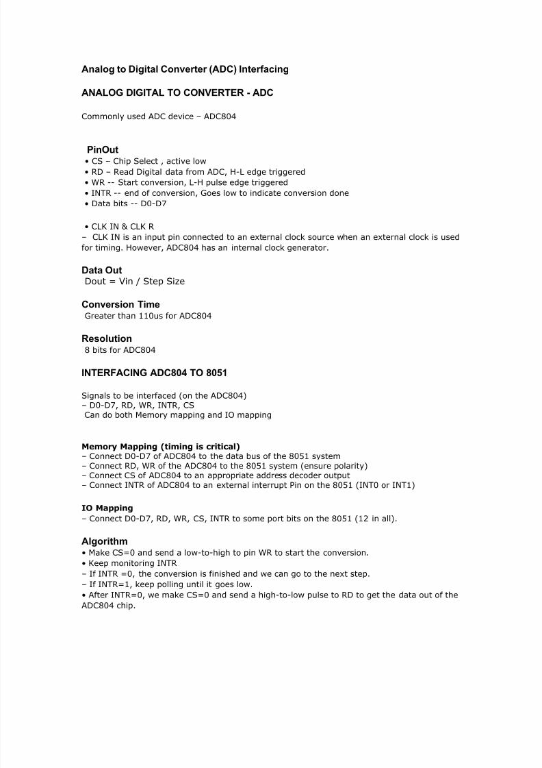
Analog to Digital Converter (ADC) Interfacing
ANALOG DIGITAL TO CONVERTER - ADC
Commonly used ADC device – ADC804
PinOut • CS – Chip Select , active low
• RD – Read Digital data from ADC, H-L edge triggered
• WR -- Start conversion, L-H pulse edge triggered
• INTR -- end of conversion, Goes low to indicate conversion done
• Data bits -- D0-D7
• CLK IN & CLK R
– CLK IN is an input pin connected to an external clock source when an external clock is used
for timing. However, ADC804 has an internal clock generator.
Data OutDout = Vin / Step Size
Conversion Time Greater than 110us for ADC804
Resolution 8 bits for ADC804
INTERFACING ADC804 TO 8051
Signals to be interfaced (on the ADC804)
– D0-D7, RD, WR, INTR, CSCan do both Memory mapping and IO mapping
Memory Mapping (timing is critical)– Connect D0-D7 of ADC804 to the data bus of the 8051 system– Connect RD, WR of the ADC804 to the 8051 system (ensure polarity)– Connect CS of ADC804 to an appropriate address decoder output– Connect INTR of ADC804 to an external interrupt Pin on the 8051 (INT0 or INT1)
IO Mapping
– Connect D0-D7, RD, WR, CS, INTR to some port bits on the 8051 (12 in all).
Algorithm• Make CS=0 and send a low-to-high to pin WR to start the conversion.
• Keep monitoring INTR
– If INTR =0, the conversion is finished and we can go to the next step.
– If INTR=1, keep polling until it goes low.
• After INTR=0, we make CS=0 and send a high-to-low pulse to RD to get the data out of the
ADC804 chip.
8/4/2019 Interfacing the Keyboard to 8051 Micro Controller 11
http://slidepdf.com/reader/full/interfacing-the-keyboard-to-8051-micro-controller-11 6/10
8/4/2019 Interfacing the Keyboard to 8051 Micro Controller 11
http://slidepdf.com/reader/full/interfacing-the-keyboard-to-8051-micro-controller-11 7/10
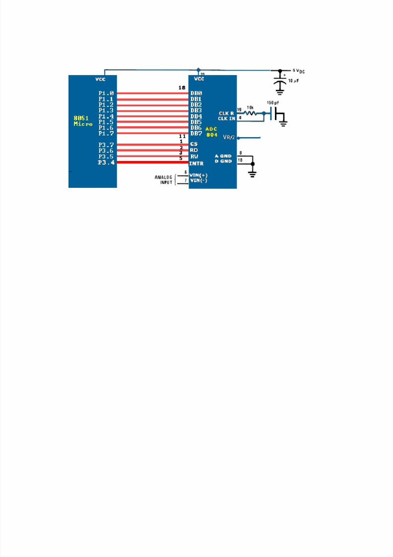
LCD interfacing
UNDERSTANDING LCD
Pinout
• 8 data pins D7:D0Bi-directional data/command pins.
Alphanumeric characters are sent in ASCII format.
• RS: Register Select
RS = 0 -> Command Register is selected
RS = 1 -> Data Register is selected
• R/W: Read or Write
0 -> Write, 1 -> Read
• E: Enable (Latch data)
Used to latch the data present on the data pins.
A high-to-low edge is needed to latch the data.
• VEE : contrast control
NOTE: When writing to the display, data is transferred only on the high to low transition of this
signal. However, when reading from the display, data will become available shortly after the
low to high transition and remain available until the signal falls low again.
Display Data RAM (DDRAM)
Display data RAM (DDRAM) is where you send the characters (ASCII code) you want to see on
the LCD screen. It stores display data represented in 8-bit character codes. Its capacity is 80
characters (bytes). Below you see DD RAM address layout of a 2*16 LCD.
Character Generator RAM (CGRAM)-User defined character RAM
8/4/2019 Interfacing the Keyboard to 8051 Micro Controller 11
http://slidepdf.com/reader/full/interfacing-the-keyboard-to-8051-micro-controller-11 8/10
In the character generator RAM, we can define our own character patterns by program. CG
RAM is 64 bytes ,allowing for eight 5*8 pixel, character patterns to be defined. However how
to define this and use it is out of scope of this tutorial. So I will not talk any more about
CGRAM
Registers
The LCD HD44780 has two 8-bit registers, an instruction register (IR) and a data register
(DR). The IR stores instruction codes. The DR temporarily stores data to be written into
DDRAM or CGRAM and temporarily stores data to be read from DDRAM or CGRAM. Data
written into the DR is automatically written into DDRAM or CGRAM by an internal operation. .
These two registers can be selected by the register selector (RS) signal. See the table below:
Register Selection
RS R/W Operation
0 0 IR write as an internal operation (display clear, etc.)
0 1 Read busy flag (DB7) and address counter (DB0 to DB6)
1 0 DR write as an internal operation (DR to DDRAM or CGRAM)
1 1 DR read as an internal operation (DDRAM or CGRAM to DR)
Busy Flag (BF)
When the busy flag is 1, the LCD is in the internal operation mode, and the next instructionwill not be accepted. When RS = 0 and R/W = 1 (see the table above), the busy flag is outputto DB7 (MSB of LCD data bus). The next instruction must be written after ensuring that thebusy flag is 0.
LCD Commands
The LCD’s internal controller accepts several commands and modifies the display accordingly.
These commands would be things like:
– Clear screen
– Return home
– Shift display right/left
Entry mode set
This command sets cursor move direction and display shift ON/OFF. There are 4 possible
function set commands;04, 05, 06, and 07. This command changes the direction the cursor
moves by setting the address counter to increment or decrement.
INTERFACING LCD TO 8051
8/4/2019 Interfacing the Keyboard to 8051 Micro Controller 11
http://slidepdf.com/reader/full/interfacing-the-keyboard-to-8051-micro-controller-11 9/10
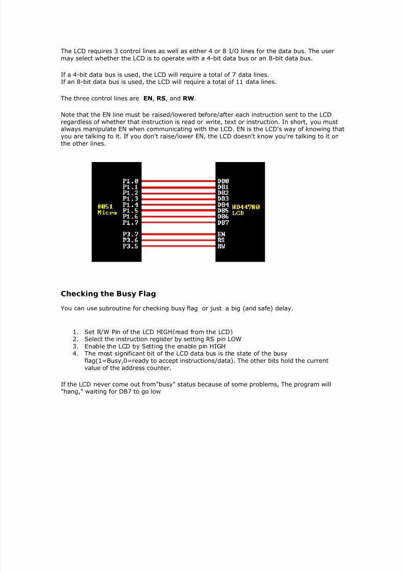
The LCD requires 3 control lines as well as either 4 or 8 I/O lines for the data bus. The usermay select whether the LCD is to operate with a 4-bit data bus or an 8-bit data bus.
If a 4-bit data bus is used, the LCD will require a total of 7 data lines.If an 8-bit data bus is used, the LCD will require a total of 11 data lines.
The three control lines are EN, RS, and RW.
Note that the EN line must be raised/lowered before/after each instruction sent to the LCDregardless of whether that instruction is read or write, text or instruction. In short, you mustalways manipulate EN when communicating with the LCD. EN is the LCD's way of knowing thatyou are talking to it. If you don't raise/lower EN, the LCD doesn't know you're talking to it onthe other lines.
Checking the Busy Flag
You can use subroutine for checking busy flag or just a big (and safe) delay.
1. Set R/W Pin of the LCD HIGH(read from the LCD)2. Select the instruction register by setting RS pin LOW3. Enable the LCD by Setting the enable pin HIGH4. The most significant bit of the LCD data bus is the state of the busy
flag(1=Busy,0=ready to accept instructions/data). The other bits hold the currentvalue of the address counter.
If the LCD never come out from”busy" status because of some problems, The program will"hang," waiting for DB7 to go low
8/4/2019 Interfacing the Keyboard to 8051 Micro Controller 11
http://slidepdf.com/reader/full/interfacing-the-keyboard-to-8051-micro-controller-11 10/10
DAC INTERFACING
This section will show how to interface a DAC (digital-to-analog converter) to the 8051.
Digital-to-analog (DAC) converter
The digital-to-analog converter (DAC) is a device widely used to convert digital pulses to
analog signals. In this section we discuss the basics of interfacing a DAC to the 8051.Recall from your digital electronics book the two methods of creating a DAC: binary
weighted and R/2R ladder. The vast majority of integrated circuit DACs, including the
MC1408 (DAC0808) used in this section, use the R/2R method since it can achieve a
much higher degree of precision.. The number of data bit inputs decides the resolution of
the DAC since the number of analog output levels is equal to 2″, where n is the number of
data bit inputs. Therefore, an 8-input DAC such as the DAC0808 provides 256 discrete
voltage (or current) levels of output.
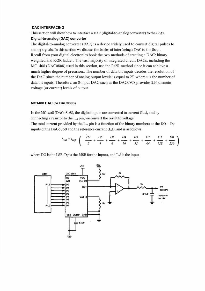
MC1408 DAC (or DAC0808)
In the MC1408 (DAC0808), the digital inputs are converted to current (Iout), and by
connecting a resistor to the Iout pin, we convert the result to voltage.
The total current provided by the Iout pin is a function of the binary numbers at the DO – D7
inputs of the DAC0808 and the reference current (Iref), and is as follows:
where DO is the LSB, D7 is the MSB for the inputs, and Iref is the input