


Languages
Pages
Legal

Interconnection and Packaging in IBM Blue Gene/L
Yi ZhuFeb 12, 2007
Outline
Design goals Architecture Design philosophy
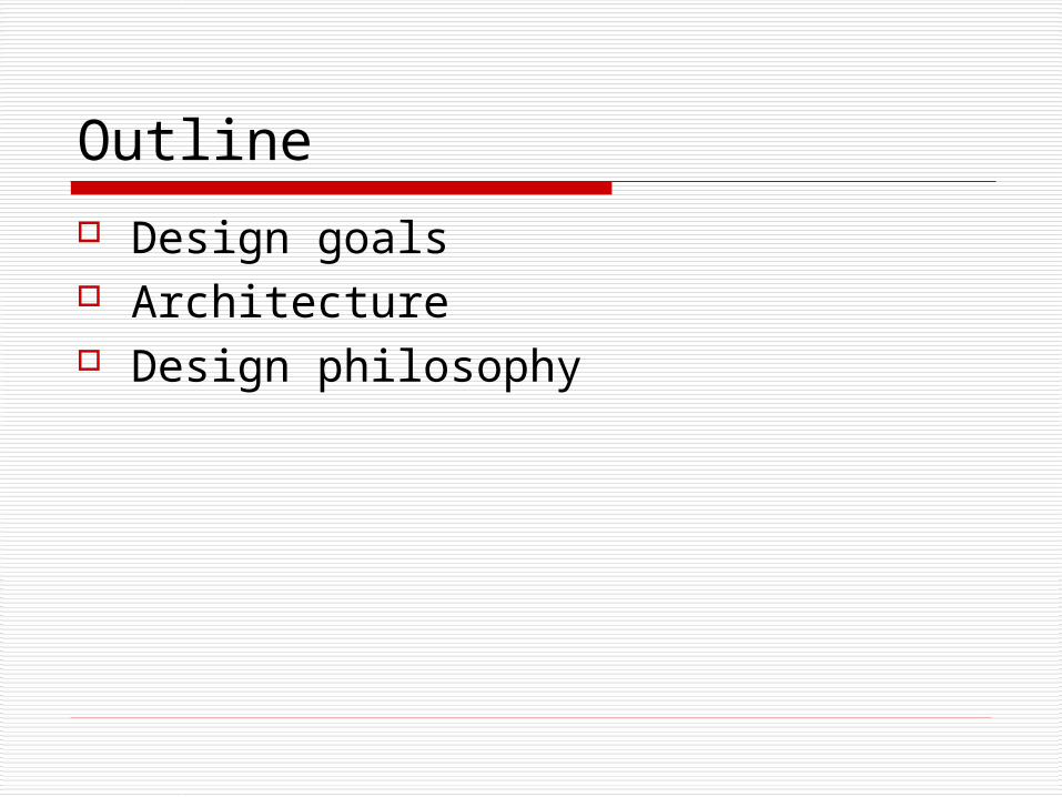
Main Design Goals for Blue Gene/L Improve computing capability, holding total
system cost. Reduce cost/FLOP. Reduce complexity and size.
~25KW/rack is max for air-cooling in standard room.
700MHz PowerPC440 for ASIC has excellent FLOP/Watt.
Maximize Integration: On chip: ASIC with everything except main
memory. Off chip: Maximize number of nodes in a rack..

Blue Gene/L Packaging 2 nodes per compute card. 16 compute cards per node board. 16 node boards per 512-node
midplane. Two midplanes in a 1024-node rack. 64 racks

Introduction
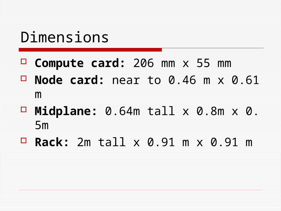
Dimensions
Compute card: 206 mm x 55 mm Node card: near to 0.46 m x 0.61 m Midplane: 0.64m tall x 0.8m x 0.5m Rack: 2m tall x 0.91 m x 0.91 m
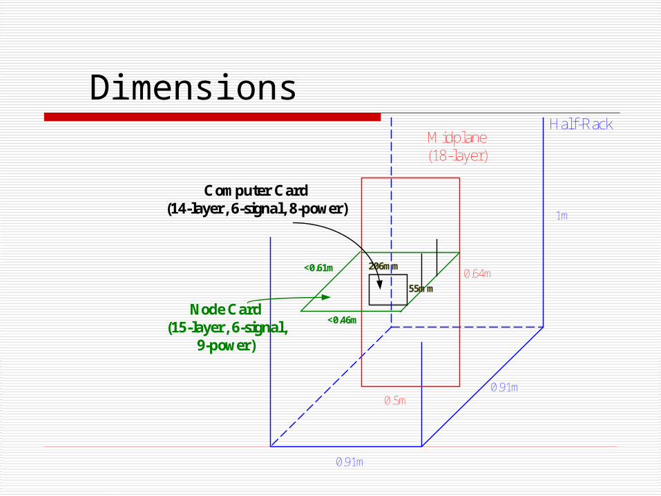
DimensionsHalf-Rack
0.91m
0.91m
1m
Midplane(18-layer)
0.5m
0.64m<0.61m
<0.46mNode Card
(15-layer, 6-signal,9-power)
55mm
206mm
Computer Card(14-layer, 6-signal, 8-power)

Topology
On one midplane: 16 node cards x 16 computer cards x 2 chips – 8x8x8 torus
Among midplanes: three network switches, one per dimension – 8x4x4 torus
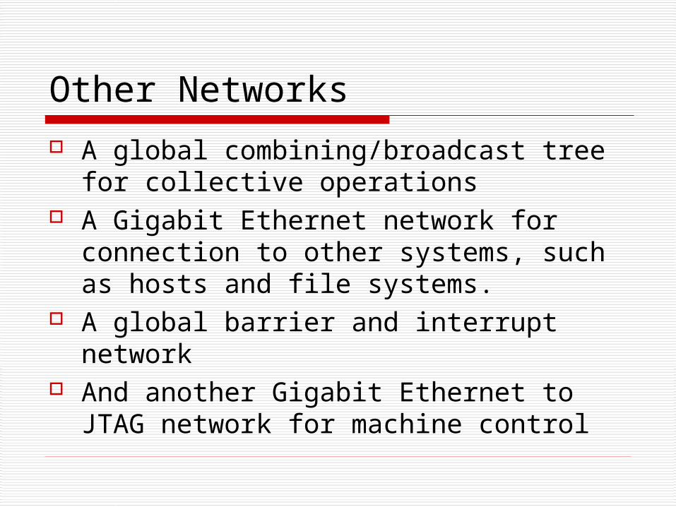
Other Networks
A global combining/broadcast tree for collective operations
A Gigabit Ethernet network for connection to other systems, such as hosts and file systems.
A global barrier and interrupt network And another Gigabit Ethernet to JTAG
network for machine control
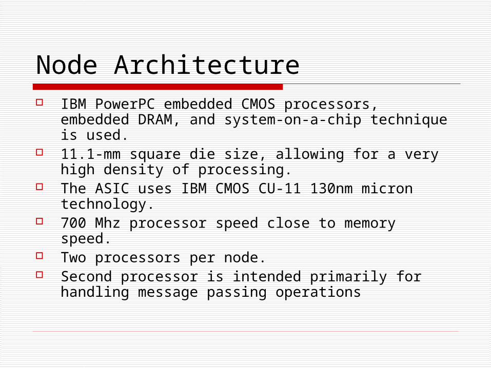
Node Architecture IBM PowerPC embedded CMOS processors, embedded
DRAM, and system-on-a-chip technique is used. 11.1-mm square die size, allowing for a very high
density of processing. The ASIC uses IBM CMOS CU-11 130nm micron
technology. 700 Mhz processor speed close to memory speed. Two processors per node. Second processor is intended primarily for handling
message passing operations

First Level Packaging
Dimension: 32mm x 25mm 474 pins
328 signals for the memory interface A bit-serial torus bus A 3-port double-bit-wide bus 4 global OR signals for fast asynchronous
barriers
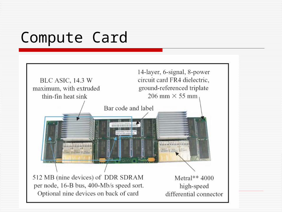
Compute Card

Node Card
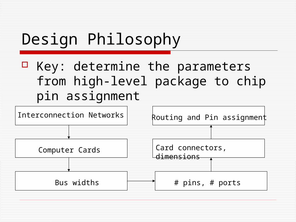
Design Philosophy
Key: determine the parameters from high-level package to chip pin assignment
Interconnection Networks
Computer Cards
Bus widths # pins, # ports
Card connectors, dimensions
Routing and Pin assignment
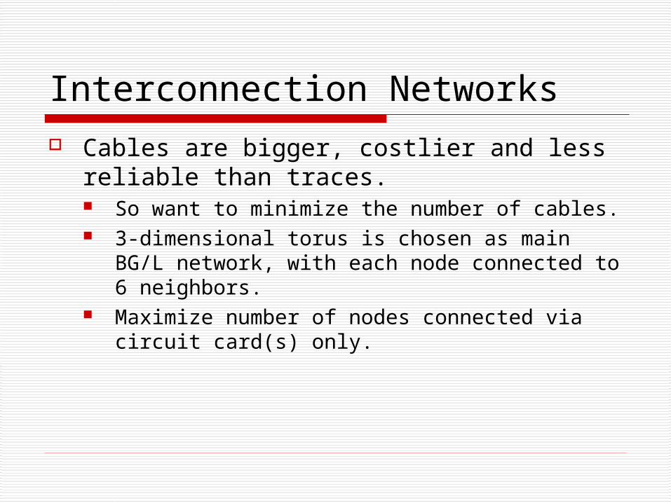
Interconnection Networks Cables are bigger, costlier and less reliable
than traces. So want to minimize the number of cables. 3-dimensional torus is chosen as main BG/L
network, with each node connected to 6 neighbors.
Maximize number of nodes connected via circuit card(s) only.
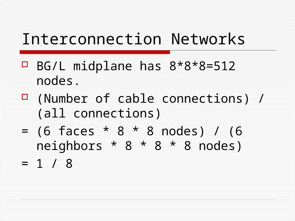
Interconnection Networks
BG/L midplane has 8*8*8=512 nodes. (Number of cable connections) / (all
connections) = (6 faces * 8 * 8 nodes) / (6 neighbors *
8 * 8 * 8 nodes)= 1 / 8

Compute Card
Determined by the trade off space, function and cost
Fewest possible computer ASICs per card has lowest cost for test, rework and replacement
Two ASICs per card are more space-efficient due to the share SDRAM
Bus Widths
Bus width of the torus network was decided primarily by # cables that could be physically connected to a midplane
Collective network and interrupt bus widths and topology were determined by computer card form

# Pins and # Ports
# Pins per ASIC is determined by the choice of collective network and interrupt bus widths + # ports escaping each ASIC
# collective ports per ASIC & between card connectors was a tradeoff between collective network latency and system form factor
Final Choices 3 collective ports per ASIC 2 bidirectional bits per collective port 4 bidirectional global interrupt bit per int
errupt bus 32mmx25mm package Other factors (computer card form, width
s of various buses…) are determined to yield the maximal density of ASICs per rack

Design Philosophy
Next to determine: Circuit card connectors Card cross section Card wiring
Objectives Compactness Low cost Electrical signaling quality
Card-to-Card Connectors Differential: because all high-speed buses are di
fferential Two differential signal pairs per column of pins
Signal buses to spread out horizontally across nearly the entire width of each connection
Fewer layers to escape, fewer crosses Final choice: Metral 4000 connector

Circuit Card Cross Sections
Fundamental requirement: high electrical signaling quality
Alternating signal and ground layers 14 total layers except the midplane (18 la
yers) Node card requires additional power laye
rs to distribute 1.5V core voltage to computer cards
Circuit Card Cross Sections
In some layers with long distance nets, need low resistive loss Wide (190 um to 215 um) 1.0-ounce copper tr
aces Other layers, minimize card thickness
Narrow (100 um) 0.5-ounce nets Card dielectrics: low-cost FR4
Sufficient for signaling speed 1.4 Gb/s

Card Sizes Determined by a combination of manufacturab
ility and system form factor consideration Node cards are near to the maximum card size
obtainable from the industry-standard low cost 0.46m x 0.61m
Midplane is confined to the largest panel size that could still be manufactured by multiple card vendors

Card Wiring
Goal: minimize card layers (minimize card cost)
Routing order 3d torus network (most regular and
numerous) on cards Pin assignment for torus network to
minimize net signal crossing
Card Wiring Routing order (cont’d)
Global collective network & interrupt bus Exact logical structures determined to
minimize # layers Layout of 16-byte-wide SDRAM
Optimize package escape and # routing layers
ASIC pin assignment High-speed clocks Low-speed nets

References “Overview of the Blue Gene/L system architectur
e”, IBM J Res. & Dev., Vol. 49, No. 2/3, March/May 2005
“Packaging the Blue Gene/L supercomputer”, IBM J Res. & Dev., Vol. 49, No. 2/3, March/May 2005
“Blue Gene/L torus interconnection network”, IBM J Res. & Dev., Vol. 49, No. 2/3, March/May 2005
Top Related