


Languages
Pages
Legal

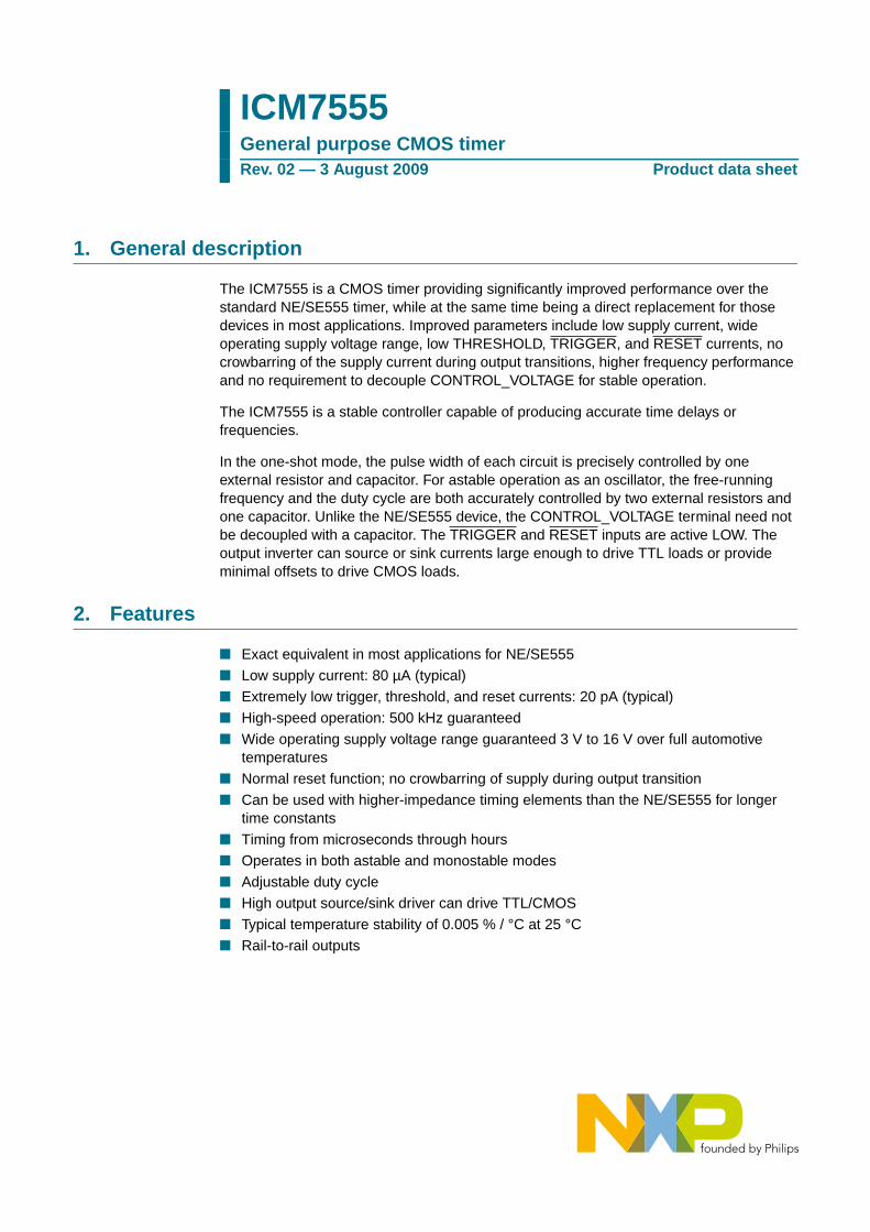
1. General description
The ICM7555 is a CMOS timer providing significantly improved performance over thestandard NE/SE555 timer, while at the same time being a direct replacement for thosedevices in most applications. Improved parameters include low supply current, wideoperating supply voltage range, low THRESHOLD, TRIGGER, and RESET currents, nocrowbarring of the supply current during output transitions, higher frequency performanceand no requirement to decouple CONTROL_VOLTAGE for stable operation.
The ICM7555 is a stable controller capable of producing accurate time delays orfrequencies.
In the one-shot mode, the pulse width of each circuit is precisely controlled by oneexternal resistor and capacitor. For astable operation as an oscillator, the free-runningfrequency and the duty cycle are both accurately controlled by two external resistors andone capacitor. Unlike the NE/SE555 device, the CONTROL_VOLTAGE terminal need notbe decoupled with a capacitor. The TRIGGER and RESET inputs are active LOW. Theoutput inverter can source or sink currents large enough to drive TTL loads or provideminimal offsets to drive CMOS loads.
2. Features
n Exact equivalent in most applications for NE/SE555
n Low supply current: 80 µA (typical)
n Extremely low trigger, threshold, and reset currents: 20 pA (typical)
n High-speed operation: 500 kHz guaranteed
n Wide operating supply voltage range guaranteed 3 V to 16 V over full automotivetemperatures
n Normal reset function; no crowbarring of supply during output transition
n Can be used with higher-impedance timing elements than the NE/SE555 for longertime constants
n Timing from microseconds through hours
n Operates in both astable and monostable modes
n Adjustable duty cycle
n High output source/sink driver can drive TTL/CMOS
n Typical temperature stability of 0.005 % / °C at 25 °Cn Rail-to-rail outputs
ICM7555General purpose CMOS timerRev. 02 — 3 August 2009 Product data sheet

NXP Semiconductors ICM7555General purpose CMOS timer
3. Applications
n Precision timing
n Pulse generation
n Sequential timing
n Time delay generation
n Pulse width modulation
n Pulse position modulation
n Missing pulse detector
4. Ordering information
5. Functional diagram
Table 1. Ordering information
Type number Temperature range Package
Name Description Version
ICM7555CD Tamb = 0 °C to +70 °C SO8 plastic small outline package; 8 leads; body width 3.9 mm SOT96-1
ICM7555ID Tamb = −40 °C to +85 °C
ICM7555CN Tamb = 0 °C to +70 °C DIP8 plastic dual in-line package; 8 leads (300 mil) SOT97-1
ICM7555IN Tamb = −40 °C to +85 °C
Remark: Unused inputs should be connected to appropriate voltage from Table 3.
Fig 1. Functional diagram
002aae403
flip-flop
RESET4
comparator Aoutputdrivers
OUTPUT3
N
DISCHARGE
GND
7
1
comparator BR
R
R
GND1
2TRIGGER
CONTROL_VOLTAGE5THRESHOLD6
VDD8
ICM7555_2 © NXP B.V. 2009. All rights reserved.
Product data sheet Rev. 02 — 3 August 2009 2 of 22

NXP Semiconductors ICM7555General purpose CMOS timer
6. Pinning information
6.1 Pinning
6.2 Pin description
7. Functional description
Refer to Figure 1 “Functional diagram”.
7.1 Function selection
[1] RESET will dominate all other inputs; TRIGGER will dominate over THRESHOLD.
Fig 2. Pin configuration for SO8 Fig 3. Pin configuration for DIP8
VDD
DISCHARGE
THRESHOLD
CONTROL_VOLTAGE
GND
TRIGGER
OUTPUT
RESET
ICM7555CDICM7555ID
002aae400
1
2
3
4
6
5
8
7 ICM7555CNICM7555IN
GND VDD
TRIGGER DISCHARGE
OUTPUT THRESHOLD
RESET CONTROL_VOLTAGE
002aae401
1
2
3
4
6
5
8
7
Table 2. Pin description
Symbol Pin Description
GND 1 supply ground
TRIGGER 2 start timer input; (active LOW)
OUTPUT 3 timer logic level output
RESET 4 timer inhibit input; (active LOW)
CONTROL_VOLTAGE 5 timing capacitor upper voltage sense input
THRESHOLD 6 timing capacitor lower voltage sense input
DISCHARGE 7 timing capacitor discharge output
VDD 8 supply voltage
Table 3. Function selection
THRESHOLD voltage TRIGGER voltage RESET[1] OUTPUT Discharge switch
don’t care don’t care L L on
> 2⁄3 V+ > 1⁄3 V+ H L on
Vth < 2⁄3 V+ Vtrig > 1⁄3 V+ H stable stable
don’t care < 1⁄3 V+ H H off
ICM7555_2 © NXP B.V. 2009. All rights reserved.
Product data sheet Rev. 02 — 3 August 2009 3 of 22
NXP Semiconductors ICM7555General purpose CMOS timer
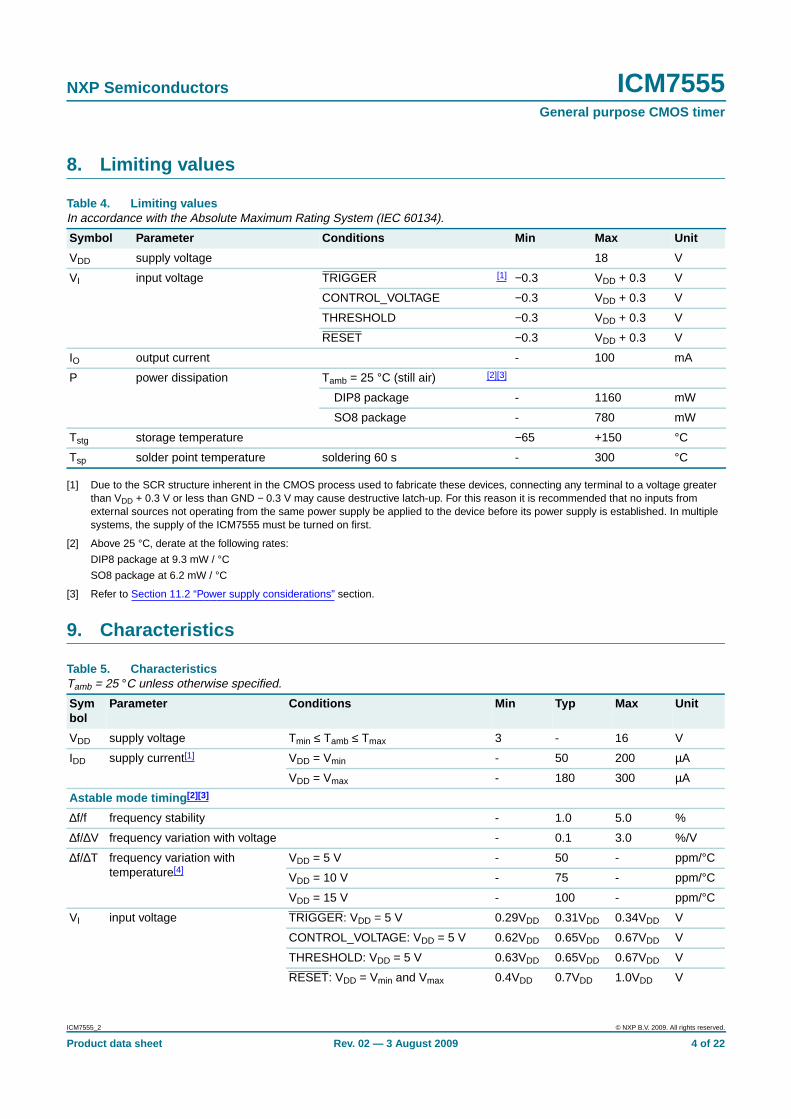
8. Limiting values
[1] Due to the SCR structure inherent in the CMOS process used to fabricate these devices, connecting any terminal to a voltage greaterthan VDD + 0.3 V or less than GND − 0.3 V may cause destructive latch-up. For this reason it is recommended that no inputs fromexternal sources not operating from the same power supply be applied to the device before its power supply is established. In multiplesystems, the supply of the ICM7555 must be turned on first.
[2] Above 25 °C, derate at the following rates:
DIP8 package at 9.3 mW / °CSO8 package at 6.2 mW / °C
[3] Refer to Section 11.2 “Power supply considerations” section.
9. Characteristics
Table 4. Limiting valuesIn accordance with the Absolute Maximum Rating System (IEC 60134).
Symbol Parameter Conditions Min Max Unit
VDD supply voltage 18 V
VI input voltage TRIGGER [1] −0.3 VDD + 0.3 V
CONTROL_VOLTAGE −0.3 VDD + 0.3 V
THRESHOLD −0.3 VDD + 0.3 V
RESET −0.3 VDD + 0.3 V
IO output current - 100 mA
P power dissipation Tamb = 25 °C (still air) [2][3]
DIP8 package - 1160 mW
SO8 package - 780 mW
Tstg storage temperature −65 +150 °C
Tsp solder point temperature soldering 60 s - 300 °C
Table 5. CharacteristicsTamb = 25 °C unless otherwise specified.
Symbol
Parameter Conditions Min Typ Max Unit
VDD supply voltage Tmin ≤ Tamb ≤ Tmax 3 - 16 V
IDD supply current[1] VDD = Vmin - 50 200 µA
VDD = Vmax - 180 300 µA
Astable mode timing [2] [3]
∆f/f frequency stability - 1.0 5.0 %
∆f/∆V frequency variation with voltage - 0.1 3.0 %/V
∆f/∆T frequency variation withtemperature[4]
VDD = 5 V - 50 - ppm/°C
VDD = 10 V - 75 - ppm/°C
VDD = 15 V - 100 - ppm/°C
VI input voltage TRIGGER: VDD = 5 V 0.29VDD 0.31VDD 0.34VDD V
CONTROL_VOLTAGE: VDD = 5 V 0.62VDD 0.65VDD 0.67VDD V
THRESHOLD: VDD = 5 V 0.63VDD 0.65VDD 0.67VDD V
RESET: VDD = Vmin and Vmax 0.4VDD 0.7VDD 1.0VDD V
ICM7555_2 © NXP B.V. 2009. All rights reserved.
Product data sheet Rev. 02 — 3 August 2009 4 of 22

NXP Semiconductors ICM7555General purpose CMOS timer
[1] The supply current value is essentially independent of the TRIGGER, THRESHOLD and RESET voltages.
[2] Astable timing is calculated using the following equation:
The components are defined in Figure 15.
[3] RA, RB = 1 kΩ to 100 kΩ; C = 0.1 µF; 5 V < VDD < 15 V
[4] Parameter is not 100 % tested.
II input current TRIGGER
VDD = Vtrig = Vmax - 50 - pA
VDD = Vtrig = 5 V - 10 - pA
VDD = Vtrig = Vmin - 1 - pA
THRESHOLD
VDD = Vth = Vmax - 50 - pA
VDD = Vth = 5 V - 10 - pA
VDD = Vth = Vmin - 1 - pA
RESET
VDD = Vrst = Vmax - 100 - pA
VDD = Vrst = 5 V - 20 - pA
VDD = Vrst = Vmin - 2 - pA
VOL LOW-level output voltage VDD = Vmax; Isink = 3.2 mA - 0.1 0.4 V
VDD = 5 V; Isink = 3.2 mA - 0.2 0.4 V
VOH HIGH-level output voltage Isource = −1.0 mA
VDD = Vmax 15.25 15.7 - V
VDD = 5 Vmax 4.0 4.5 - V
Vo output voltage DISCHARGE:VDD = 5 V; IDIS = 10 mA
- 0.2 0.4 V
tr(o) output rise time[4] RL = 10 MΩ; CL = 10 pF;VDD = 5 V
- 45 75 ns
tf(o) output fall time[4] - 20 75 ns
fosc oscillator frequency astable mode - - 500 kHz
Table 5. Characteristics …continuedTamb = 25 °C unless otherwise specified.
Symbol
Parameter Conditions Min Typ Max Unit
f1.38
RA 2RB+( )C---------------------------------=
ICM7555_2 © NXP B.V. 2009. All rights reserved.
Product data sheet Rev. 02 — 3 August 2009 5 of 22

NXP Semiconductors ICM7555General purpose CMOS timer
10. Typical performance curves
Fig 4. Supply current versus supply voltage
Tamb = +25 °C.
Fig 5. High output voltage drop versus output source current
Tamb = +25 °C.
Fig 6. Discharge low output voltage versus discharge sink current
VDD (V)0 2015105
002aae404
100
150
50
200
250IDD(µA)
0
Tamb = −55 °C+25 °C
+125 °C
002aae405
VDD − VO (V)10−1 102101
10
1
102
Io(source)(mA)
10−1
VDD = 18 V5 V2 V
002aae406
VDIS (V)10−1 101
10
1
102
IDIS(mA)
10−1
VDD = 18 V5 V2 V
ICM7555_2 © NXP B.V. 2009. All rights reserved.
Product data sheet Rev. 02 — 3 August 2009 6 of 22

NXP Semiconductors ICM7555General purpose CMOS timer
a. Tamb = +125 °C.
b. Tamb = +25 °C.
c. Tamb = −55 °C.
Fig 7. Low output voltage versus output sink current
002aae407
VOL (V)10−1 101
10
1
102
Io(sink)(mA)
10−1
VDD = 18 V5 V2 V
002aae408
VOL (V)10−1 101
10
1
102
Io(sink)(mA)
10−1
VDD = 18 V5 V2 V
002aae409
VOL (V)10−1 101
10
1
102
Io(sink)(mA)
10−1
VDD = 18 V5 V2 V
ICM7555_2 © NXP B.V. 2009. All rights reserved.
Product data sheet Rev. 02 — 3 August 2009 7 of 22

NXP Semiconductors ICM7555General purpose CMOS timer
Fig 8. Minimum pulse width for triggering
Fig 9. Propagation delay versus voltage level of TRIGGER pulse (V DD = 5 V)
lowest voltage level of TRIGGER pulse (% VDD)0 40302010
002aae410
200
300
100
400
500
0
TRIGGER pulse width (ns) VDD = 18 V5 V2 V
lowest voltage level of TRIGGER pulse (% VDD)0 40302010
002aae411
0
750
500
250
1000
tPD(ns) Tamb = −55 °C
+25 °C+125 °C
ICM7555_2 © NXP B.V. 2009. All rights reserved.
Product data sheet Rev. 02 — 3 August 2009 8 of 22

NXP Semiconductors ICM7555General purpose CMOS timer
Tamb = +25 °CRA = RB = 10 kΩC = 0.1 µF
Fig 10. Normalized frequency stability as a function of supply voltage (astable mode)
RA = RB = 1 kΩC = 0.1 µF
Fig 11. Normalized frequency stability as a function of temperature (astable mode)
VDD (V)0 2015105
002aae413
0
2
−2
4
6
−4
normalized frequency(%)
Tamb (°C)−75 1257525−25
002aae414
−4
2
0
−2
4
normalized frequency(%)
VDD = 18 V5 V2 V
ICM7555_2 © NXP B.V. 2009. All rights reserved.
Product data sheet Rev. 02 — 3 August 2009 9 of 22

NXP Semiconductors ICM7555General purpose CMOS timer
VDD = 5 V; Tamb = +25 °C
Fig 12. Free-running frequency as a function of R A, RB resistance and externalcapacitance
VDD = 5 V; Tamb = +25 °C
Fig 13. Monostable time delay versus R A resistance and external capacitance
002aae415102
C (µF)
10−5
f (Hz)10−1 107
10−4
106105104103102101
10−3
10−2
10−1
1
10
1 kΩ10 kΩ
100 kΩ1 MΩ
10 MΩ
002aae416102
C (µF)
10−5
td (s)10−7 10
10−4
110−110−210−310−410−510−6
10−3
10−2
10−1
1
10 1 kΩ10 kΩ
100 kΩ1 MΩ
10 MΩ
ICM7555_2 © NXP B.V. 2009. All rights reserved.
Product data sheet Rev. 02 — 3 August 2009 10 of 22

NXP Semiconductors ICM7555General purpose CMOS timer
11. Application information
11.1 GeneralThe ICM7555 device is, in most instances, a direct replacement for the NE/SE555 device.However, it is possible to effect economies in the external component count using theICM7555. Because the NE/SE555 device produces large crowbar currents in the outputdriver, it is necessary to decouple the power supply lines with a good capacitor close tothe device. The ICM7555 device produces no such transients. See Figure 14.
The ICM7555 produces supply current spikes of only 2 mA to 3 mA instead of300 mA to 400 mA and supply decoupling is normally not necessary. Secondly, in mostinstances, the CONTROL_VOLTAGE decoupling capacitors are not required since theinput impedance of the CMOS comparators on chip are very high. Thus, for manyapplications, 2 capacitors can be saved using an ICM7555.
11.2 Power supply considerationsAlthough the supply current consumed by the ICM7555 device is very low, the totalsystem supply can be high unless the timing components are high-impedance. Therefore,high values for R and low values for C in Figure 15 and Figure 16 are recommended.
11.3 Output drive capabilityThe output driver consists of a CMOS inverter capable of driving most logic familiesincluding CMOS and TTL. As such, if driving CMOS, the output swing at all supplyvoltages will equal the supply voltage. At a supply voltage of 4.5 V or more, the ICM7555will drive at least 2 standard TTL loads.
Tamb = +25 °C(1) NE/SE555
(2) ICM7555
Fig 14. Supply current transient compared with a standard NE/SE555 device during anoutput transition
100
300
500
IDD(mA)
−100
time (ns)0 800600200 400
002aae417
(1)
(2)
ICM7555_2 © NXP B.V. 2009. All rights reserved.
Product data sheet Rev. 02 — 3 August 2009 11 of 22

NXP Semiconductors ICM7555General purpose CMOS timer
11.4 Astable operationIf the circuit is connected as shown in Figure 15, it will trigger itself and free run as amultivibrator. The external capacitor charges through RA and RB and discharges throughRB only. Thus, the duty cycle (δ) may be precisely set by the ratio of these two resistors. Inthis mode of operation, the capacitor charges and discharges between 1⁄3 VDD and2⁄3 VDD. Since the charge rate and the threshold levels are directly proportional to thesupply voltage, the frequency of oscillation is independent of the supply voltage.
(1)
(2)
11.5 Monostable operationIn this mode of operation, the timer functions as a one-shot. Initially, the externalcapacitor (C) is held discharged by a transistor inside the timer. Upon application of anegative pulse to pin 2, TRIGGER, the internal flip-flop is set, which releases thelow-impedance on DISCHARGE; the external capacitor charges and drives the OUTPUTHIGH. The voltage across the capacitor increases exponentially with a time constantt = RAC. When the voltage across the capacitor equals 2⁄3 V+, the comparator resets theflip-flop, which in turn discharges the capacitor rapidly and also drives the OUTPUT to itsLOW state. TRIGGER must return to a HIGH state before the OUTPUT can return to aLOW state.
Fig 15. Astable operation
f1.38
RA 2RB+( ) C×--------------------------------------=
δRA RB+
RA 2RB+-----------------------=
GND
TRIGGER
OUTPUT
RESET
1
2
3
4VDD
C
RB
RA
VDD
OUTPUT
DISCHARGE
THRESHOLD
CONTROL_VOLTAGE
VDD8
7
6
5
VDD
002aae418
ICM7555_2 © NXP B.V. 2009. All rights reserved.
Product data sheet Rev. 02 — 3 August 2009 12 of 22

NXP Semiconductors ICM7555General purpose CMOS timer
11.6 Control voltageThe CONTROL_VOLTAGE terminal permits the two trip voltages for the THRESHOLDand TRIGGER internal comparators to be controlled. This provides the possibility ofoscillation frequency modulation in the astable mode, or even inhibition of oscillation,depending on the applied voltage. In the monostable mode, delay times can be changedby varying the applied voltage to the CONTROL_VOLTAGE pin.
11.7 RESETThe RESET terminal is designed to have essentially the same trip voltage as the standardNE/SE555 device, i.e., 0.6 V to 0.7 V. At all supply voltages it represents an extremelyhigh input impedance. The mode of operation of the RESET function is, however, muchimproved over the standard NE/SE555 device in that it controls only the internal flip-flop,which in turn controls simultaneously the state of the OUTPUT and DISCHARGE pins.This avoids the multiple threshold problems sometimes encountered with slow fallingedges in the NE/SE555 devices.
VDD ≤ 18 V; t = 1.05 RAC
Fig 16. Monostable operation
GND
TRIGGER
OUTPUT
RESET
1
2
3
4
DISCHARGE
THRESHOLD
CONTROL_VOLTAGE
VDD8
7
6
5
VDD
002aae419
RA
optionalcapacitor C
ICM7555_2 © NXP B.V. 2009. All rights reserved.
Product data sheet Rev. 02 — 3 August 2009 13 of 22

NXP Semiconductors ICM7555General purpose CMOS timer
12. Package outline
Fig 17. Package outline SOT96-1 (SO8)
UNITA
max. A1 A2 A3 bp c D(1) E(2) (1)e HE L L p Q Zywv θ
REFERENCESOUTLINEVERSION
EUROPEANPROJECTION ISSUE DATE
IEC JEDEC JEITA
mm
inches
1.750.250.10
1.451.25
0.250.490.36
0.250.19
5.04.8
4.03.8
1.276.25.8
1.050.70.6
0.70.3 8
0
o
o
0.25 0.10.25
DIMENSIONS (inch dimensions are derived from the original mm dimensions)
Notes
1. Plastic or metal protrusions of 0.15 mm (0.006 inch) maximum per side are not included.
2. Plastic or metal protrusions of 0.25 mm (0.01 inch) maximum per side are not included.
1.00.4
SOT96-1
X
w M
θ
AA1
A2
bp
D
HE
Lp
Q
detail X
E
Z
e
c
L
v M A
(A )3
A
4
5
pin 1 index
1
8
y
076E03 MS-012
0.0690.0100.004
0.0570.049
0.010.0190.014
0.01000.0075
0.200.19
0.160.15
0.050.2440.228
0.0280.024
0.0280.012
0.010.010.041 0.0040.0390.016
0 2.5 5 mm
scale
SO8: plastic small outline package; 8 leads; body width 3.9 mm SOT96-1
99-12-2703-02-18
ICM7555_2 © NXP B.V. 2009. All rights reserved.
Product data sheet Rev. 02 — 3 August 2009 14 of 22

NXP Semiconductors ICM7555General purpose CMOS timer
Fig 18. Package outline SOT97-1 (DIP8)
REFERENCESOUTLINEVERSION
EUROPEANPROJECTION ISSUE DATE
IEC JEDEC JEITA
SOT97-199-12-2703-02-13
UNIT Amax.
1 2 b1(1) (1) (1)
b2 c D E e M ZHL
mm
DIMENSIONS (inch dimensions are derived from the original mm dimensions)
A min.
A max. b
max.wMEe1
1.731.14
0.530.38
0.360.23
9.89.2
6.486.20
3.603.05
0.2542.54 7.628.257.80
10.08.3
1.154.2 0.51 3.2
inches 0.0680.045
0.0210.015
0.0140.009
1.070.89
0.0420.035
0.390.36
0.260.24
0.140.12
0.010.1 0.30.320.31
0.390.33
0.0450.17 0.02 0.13
b2
050G01 MO-001 SC-504-8
MH
c
(e )1
ME
A
L
seat
ing
plan
e
A1
w Mb1
e
D
A2
Z
8
1
5
4
b
E
0 5 10 mm
scale
Note
1. Plastic or metal protrusions of 0.25 mm (0.01 inch) maximum per side are not included.
pin 1 index
DIP8: plastic dual in-line package; 8 leads (300 mil) SOT97-1
ICM7555_2 © NXP B.V. 2009. All rights reserved.
Product data sheet Rev. 02 — 3 August 2009 15 of 22

NXP Semiconductors ICM7555General purpose CMOS timer
13. Soldering of SMD packages
This text provides a very brief insight into a complex technology. A more in-depth accountof soldering ICs can be found in Application Note AN10365 “Surface mount reflowsoldering description”.
13.1 Introduction to solderingSoldering is one of the most common methods through which packages are attached toPrinted Circuit Boards (PCBs), to form electrical circuits. The soldered joint provides boththe mechanical and the electrical connection. There is no single soldering method that isideal for all IC packages. Wave soldering is often preferred when through-hole andSurface Mount Devices (SMDs) are mixed on one printed wiring board; however, it is notsuitable for fine pitch SMDs. Reflow soldering is ideal for the small pitches and highdensities that come with increased miniaturization.
13.2 Wave and reflow solderingWave soldering is a joining technology in which the joints are made by solder coming froma standing wave of liquid solder. The wave soldering process is suitable for the following:
• Through-hole components
• Leaded or leadless SMDs, which are glued to the surface of the printed circuit board
Not all SMDs can be wave soldered. Packages with solder balls, and some leadlesspackages which have solder lands underneath the body, cannot be wave soldered. Also,leaded SMDs with leads having a pitch smaller than ~0.6 mm cannot be wave soldered,due to an increased probability of bridging.
The reflow soldering process involves applying solder paste to a board, followed bycomponent placement and exposure to a temperature profile. Leaded packages,packages with solder balls, and leadless packages are all reflow solderable.
Key characteristics in both wave and reflow soldering are:
• Board specifications, including the board finish, solder masks and vias
• Package footprints, including solder thieves and orientation
• The moisture sensitivity level of the packages
• Package placement
• Inspection and repair
• Lead-free soldering versus SnPb soldering
13.3 Wave solderingKey characteristics in wave soldering are:
• Process issues, such as application of adhesive and flux, clinching of leads, boardtransport, the solder wave parameters, and the time during which components areexposed to the wave
• Solder bath specifications, including temperature and impurities
ICM7555_2 © NXP B.V. 2009. All rights reserved.
Product data sheet Rev. 02 — 3 August 2009 16 of 22

NXP Semiconductors ICM7555General purpose CMOS timer
13.4 Reflow solderingKey characteristics in reflow soldering are:
• Lead-free versus SnPb soldering; note that a lead-free reflow process usually leads tohigher minimum peak temperatures (see Figure 19) than a SnPb process, thusreducing the process window
• Solder paste printing issues including smearing, release, and adjusting the processwindow for a mix of large and small components on one board
• Reflow temperature profile; this profile includes preheat, reflow (in which the board isheated to the peak temperature) and cooling down. It is imperative that the peaktemperature is high enough for the solder to make reliable solder joints (a solder pastecharacteristic). In addition, the peak temperature must be low enough that thepackages and/or boards are not damaged. The peak temperature of the packagedepends on package thickness and volume and is classified in accordance withTable 6 and 7
Moisture sensitivity precautions, as indicated on the packing, must be respected at alltimes.
Studies have shown that small packages reach higher temperatures during reflowsoldering, see Figure 19.
Table 6. SnPb eutectic process (from J-STD-020C)
Package thickness (mm) Package reflow temperature ( °C)
Volume (mm 3)
< 350 ≥ 350
< 2.5 235 220
≥ 2.5 220 220
Table 7. Lead-free process (from J-STD-020C)
Package thickness (mm) Package reflow temperature ( °C)
Volume (mm 3)
< 350 350 to 2000 > 2000
< 1.6 260 260 260
1.6 to 2.5 260 250 245
> 2.5 250 245 245
ICM7555_2 © NXP B.V. 2009. All rights reserved.
Product data sheet Rev. 02 — 3 August 2009 17 of 22

NXP Semiconductors ICM7555General purpose CMOS timer
For further information on temperature profiles, refer to Application Note AN10365“Surface mount reflow soldering description”.
14. Soldering of through-hole mount packages
14.1 Introduction to soldering through-hole mount packagesThis text gives a very brief insight into wave, dip and manual soldering.
Wave soldering is the preferred method for mounting of through-hole mount IC packageson a printed-circuit board.
14.2 Soldering by dipping or by solder waveDriven by legislation and environmental forces the worldwide use of lead-free solderpastes is increasing. Typical dwell time of the leads in the wave ranges from3 seconds to 4 seconds at 250 °C or 265 °C, depending on solder material applied, SnPbor Pb-free respectively.
The total contact time of successive solder waves must not exceed 5 seconds.
The device may be mounted up to the seating plane, but the temperature of the plasticbody must not exceed the specified maximum storage temperature (Tstg(max)). If theprinted-circuit board has been pre-heated, forced cooling may be necessary immediatelyafter soldering to keep the temperature within the permissible limit.
14.3 Manual solderingApply the soldering iron (24 V or less) to the lead(s) of the package, either below theseating plane or not more than 2 mm above it. If the temperature of the soldering iron bit isless than 300 °C it may remain in contact for up to 10 seconds. If the bit temperature isbetween 300 °C and 400 °C, contact may be up to 5 seconds.
MSL: Moisture Sensitivity Level
Fig 19. Temperature profiles for large and small components
001aac844
temperature
time
minimum peak temperature= minimum soldering temperature
maximum peak temperature= MSL limit, damage level
peak temperature
ICM7555_2 © NXP B.V. 2009. All rights reserved.
Product data sheet Rev. 02 — 3 August 2009 18 of 22

NXP Semiconductors ICM7555General purpose CMOS timer
14.4 Package related soldering information
[1] For SDIP packages, the longitudinal axis must be parallel to the transport direction of the printed-circuitboard.
[2] For PMFP packages hot bar soldering or manual soldering is suitable.
15. Abbreviations
Table 8. Suitability of through-hole mount IC packages for dipping and wave soldering
Package Soldering method
Dipping Wave
CPGA, HCPGA - suitable
DBS, DIP, HDIP, RDBS, SDIP, SIL suitable suitable[1]
PMFP[2] - not suitable
Table 9. Abbreviations
Acronym Description
CMOS Complementary Metal-Oxide Semiconductors
TTL Transistor-Transistor Logic
SCR Silicon-Controlled Rectifier
ICM7555_2 © NXP B.V. 2009. All rights reserved.
Product data sheet Rev. 02 — 3 August 2009 19 of 22

NXP Semiconductors ICM7555General purpose CMOS timer
16. Revision history
Table 10. Revision history
Document ID Release date Data sheet status Change notice Supersedes
ICM7555_2 20090803 Product data sheet - ICM7555_1
Modifications: • The format of this data sheet has been redesigned to comply with the new identity guidelines of NXPSemiconductors.
• Legal texts have been adapted to the new company name where appropriate.
• Provided separate pinning diagrams for SO8 and DIP8 packages (Figure 2 and Figure 3,respectively).
• Added Table 2 “Pin description”.
• Table 4 “Limiting values”:
– Symbols VTRIG, VCV, VTH, VRST are replaced with VI (specific pin names are now noted underConditions column).
– Symbol/parameter “PDMAX, maximum power dissipation” replaced with “P, power dissipation” (onlymaximum values given).
– Symbol/parameter “TSTG, storage temperature range” replaced with “Tstg, storage temperature”.
– Symbol changed from “TSOLD” to “Tsp, solder point temperature”
• Table 5 “Characteristics”:
– Symbols ∆f/f, ∆f/∆V, ∆f/∆T, have been added for Astable mode timing.
– Symbols VTRIG, VCV, VTH, VRST are replaced with VI (specific pin names are now noted underConditions column).
– Symbols ITRIG, ITH, IRST are replaced with II (specific pin names are now noted under Conditionscolumn).
– Symbol/parameter “VDIS, discharge output voltage” changed to “Vo, output voltage” (specific pinname is now noted under Conditions column).
– Symbol/parameter “tR, rise time of output” changed to “tr(o), output rise time”.
– Symbol/parameter “tF, fall time of output” changed to “tf(o), output fall time”.
– Symbol “FMAX” changed to “fosc, oscillator frequency”.
• Section 11.4 “Astable operation”: changed symbol for duty cycle from “D” to “δ”.
• Added Section 12 “Package outline”.
• Added soldering information.
• Added Section 15 “Abbreviations”.
ICM7555_1 19940831 Product specification ECN 853-1192 13721dated 1994 Aug 31
-
ICM7555_2 © NXP B.V. 2009. All rights reserved.
Product data sheet Rev. 02 — 3 August 2009 20 of 22

NXP Semiconductors ICM7555General purpose CMOS timer
17. Legal information
17.1 Data sheet status
[1] Please consult the most recently issued document before initiating or completing a design.
[2] The term ‘short data sheet’ is explained in section “Definitions”.
[3] The product status of device(s) described in this document may have changed since this document was published and may differ in case of multiple devices. The latest product statusinformation is available on the Internet at URL http://www.nxp.com.
17.2 Definitions
Draft — The document is a draft version only. The content is still underinternal review and subject to formal approval, which may result inmodifications or additions. NXP Semiconductors does not give anyrepresentations or warranties as to the accuracy or completeness ofinformation included herein and shall have no liability for the consequences ofuse of such information.
Short data sheet — A short data sheet is an extract from a full data sheetwith the same product type number(s) and title. A short data sheet is intendedfor quick reference only and should not be relied upon to contain detailed andfull information. For detailed and full information see the relevant full datasheet, which is available on request via the local NXP Semiconductors salesoffice. In case of any inconsistency or conflict with the short data sheet, thefull data sheet shall prevail.
17.3 Disclaimers
General — Information in this document is believed to be accurate andreliable. However, NXP Semiconductors does not give any representations orwarranties, expressed or implied, as to the accuracy or completeness of suchinformation and shall have no liability for the consequences of use of suchinformation.
Right to make changes — NXP Semiconductors reserves the right to makechanges to information published in this document, including withoutlimitation specifications and product descriptions, at any time and withoutnotice. This document supersedes and replaces all information supplied priorto the publication hereof.
Suitability for use — NXP Semiconductors products are not designed,authorized or warranted to be suitable for use in medical, military, aircraft,space or life support equipment, nor in applications where failure ormalfunction of an NXP Semiconductors product can reasonably be expectedto result in personal injury, death or severe property or environmental
damage. NXP Semiconductors accepts no liability for inclusion and/or use ofNXP Semiconductors products in such equipment or applications andtherefore such inclusion and/or use is at the customer’s own risk.
Applications — Applications that are described herein for any of theseproducts are for illustrative purposes only. NXP Semiconductors makes norepresentation or warranty that such applications will be suitable for thespecified use without further testing or modification.
Limiting values — Stress above one or more limiting values (as defined inthe Absolute Maximum Ratings System of IEC 60134) may cause permanentdamage to the device. Limiting values are stress ratings only and operation ofthe device at these or any other conditions above those given in theCharacteristics sections of this document is not implied. Exposure to limitingvalues for extended periods may affect device reliability.
Terms and conditions of sale — NXP Semiconductors products are soldsubject to the general terms and conditions of commercial sale, as publishedat http://www.nxp.com/profile/terms, including those pertaining to warranty,intellectual property rights infringement and limitation of liability, unlessexplicitly otherwise agreed to in writing by NXP Semiconductors. In case ofany inconsistency or conflict between information in this document and suchterms and conditions, the latter will prevail.
No offer to sell or license — Nothing in this document may be interpretedor construed as an offer to sell products that is open for acceptance or thegrant, conveyance or implication of any license under any copyrights, patentsor other industrial or intellectual property rights.
Export control — This document as well as the item(s) described hereinmay be subject to export control regulations. Export might require a priorauthorization from national authorities.
17.4 TrademarksNotice: All referenced brands, product names, service names and trademarksare the property of their respective owners.
18. Contact information
For more information, please visit: http://www .nxp.com
For sales office addresses, please send an email to: salesad [email protected]
Document status [1] [2] Product status [3] Definition
Objective [short] data sheet Development This document contains data from the objective specification for product development.
Preliminary [short] data sheet Qualification This document contains data from the preliminary specification.
Product [short] data sheet Production This document contains the product specification.
ICM7555_2 © NXP B.V. 2009. All rights reserved.
Product data sheet Rev. 02 — 3 August 2009 21 of 22

NXP Semiconductors ICM7555General purpose CMOS timer
19. Contents
1 General description . . . . . . . . . . . . . . . . . . . . . . 12 Features . . . . . . . . . . . . . . . . . . . . . . . . . . . . . . . 13 Applications . . . . . . . . . . . . . . . . . . . . . . . . . . . . 24 Ordering information . . . . . . . . . . . . . . . . . . . . . 25 Functional diagram . . . . . . . . . . . . . . . . . . . . . . 26 Pinning information . . . . . . . . . . . . . . . . . . . . . . 36.1 Pinning . . . . . . . . . . . . . . . . . . . . . . . . . . . . . . . 36.2 Pin description . . . . . . . . . . . . . . . . . . . . . . . . . 37 Functional description . . . . . . . . . . . . . . . . . . . 37.1 Function selection. . . . . . . . . . . . . . . . . . . . . . . 38 Limiting values. . . . . . . . . . . . . . . . . . . . . . . . . . 49 Characteristics . . . . . . . . . . . . . . . . . . . . . . . . . . 410 Typical performance curves . . . . . . . . . . . . . . . 611 Application information. . . . . . . . . . . . . . . . . . 1111.1 General . . . . . . . . . . . . . . . . . . . . . . . . . . . . . . 1111.2 Power supply considerations . . . . . . . . . . . . . 1111.3 Output drive capability . . . . . . . . . . . . . . . . . . 1111.4 Astable operation . . . . . . . . . . . . . . . . . . . . . . 1211.5 Monostable operation . . . . . . . . . . . . . . . . . . . 1211.6 Control voltage . . . . . . . . . . . . . . . . . . . . . . . . 1311.7 RESET . . . . . . . . . . . . . . . . . . . . . . . . . . . . . . 1312 Package outline . . . . . . . . . . . . . . . . . . . . . . . . 1413 Soldering of SMD packages . . . . . . . . . . . . . . 1613.1 Introduction to soldering . . . . . . . . . . . . . . . . . 1613.2 Wave and reflow soldering . . . . . . . . . . . . . . . 1613.3 Wave soldering . . . . . . . . . . . . . . . . . . . . . . . . 1613.4 Reflow soldering . . . . . . . . . . . . . . . . . . . . . . . 1714 Soldering of through-hole mount packages . 1814.1 Introduction to soldering through-hole mount
packages . . . . . . . . . . . . . . . . . . . . . . . . . . . . 1814.2 Soldering by dipping or by solder wave . . . . . 1814.3 Manual soldering . . . . . . . . . . . . . . . . . . . . . . 1814.4 Package related soldering information . . . . . . 1915 Abbreviations . . . . . . . . . . . . . . . . . . . . . . . . . . 1916 Revision history . . . . . . . . . . . . . . . . . . . . . . . . 2017 Legal information. . . . . . . . . . . . . . . . . . . . . . . 2117.1 Data sheet status . . . . . . . . . . . . . . . . . . . . . . 2117.2 Definitions . . . . . . . . . . . . . . . . . . . . . . . . . . . . 2117.3 Disclaimers . . . . . . . . . . . . . . . . . . . . . . . . . . . 2117.4 Trademarks . . . . . . . . . . . . . . . . . . . . . . . . . . . 2118 Contact information. . . . . . . . . . . . . . . . . . . . . 2119 Contents . . . . . . . . . . . . . . . . . . . . . . . . . . . . . . 22
© NXP B.V. 2009. All rights reserved.For more information, please visit: http://www.nxp.comFor sales office addresses, please send an email to: [email protected]
Date of release: 3 August 2009
Document identifier: ICM7555_2
Please be aware that important notices concerning this document and the product(s)described herein, have been included in section ‘Legal information’.
Top Related