


Languages
Pages
Legal


HSPICE Device ModelsQuick Reference Guide
®
Version W-2005.03, March 2005

Copyright Notice and Proprietary InformationCopyright © 2005 Synopsys, Inc. All rights reserved. This software and documentation contain confidential and proprietary information that is the property of Synopsys, Inc. The software and documentation are furnished under a license agreement and may be used or copied only in accordance with the terms of the license agreement. No part of the software and documentation may be reproduced, transmitted, or translated, in any form or by any means, electronic, mechanical, manual, optical, or otherwise, without prior written permission of Synopsys, Inc., or as expressly provided by the license agreement.
Right to Copy DocumentationThe license agreement with Synopsys permits licensee to make copies of the documentation for its internal use only. Each copy shall include all copyrights, trademarks, service marks, and proprietary rights notices, if any. Licensee must assign sequential numbers to all copies. These copies shall contain the following legend on the cover page:
“This document is duplicated with the permission of Synopsys, Inc., for the exclusive use of __________________________________________ and its employees. This is copy number __________.”
Destination Control StatementAll technical data contained in this publication is subject to the export control laws of the United States of America. Disclosure to nationals of other countries contrary to United States law is prohibited. It is the reader’s responsibility to determine the applicable regulations and to comply with them.
DisclaimerSYNOPSYS, INC., AND ITS LICENSORS MAKE NO WARRANTY OF ANY KIND, EXPRESS OR IMPLIED, WITH REGARD TO THIS MATERIAL, INCLUDING, BUT NOT LIMITED TO, THE IMPLIED WARRANTIES OF MERCHANTABILITY AND FITNESS FOR A PARTICULAR PURPOSE.
Registered Trademarks (®)Synopsys, AMPS, Arcadia, C Level Design, C2HDL, C2V, C2VHDL, Cadabra, Calaveras Algorithm, CATS, CSim, Design Compiler, DesignPower, DesignWare, EPIC, Formality, HSPICE, Hypermodel, iN-Phase, in-Sync, Leda, MAST, Meta, Meta-Software, ModelAccess, ModelTools, NanoSim, OpenVera, PathMill, Photolynx, Physical Compiler, PowerMill, PrimeTime, RailMill, Raphael, RapidScript, Saber, SiVL, SNUG, SolvNet, Stream Driven Simulator, Superlog, System Compiler, Testify, TetraMAX, TimeMill, TMA, VCS, Vera, and Virtual Stepper are registered trademarks of Synopsys, Inc.
Trademarks (™)abraCAD, abraMAP, Active Parasitics, AFGen, Apollo, Apollo II, Apollo-DPII, Apollo-GA, ApolloGAII, Astro, Astro-Rail, Astro-Xtalk, Aurora, AvanTestchip, AvanWaves, BCView, Behavioral Compiler, BOA, BRT, Cedar, ChipPlanner, Circuit Analysis, Columbia, Columbia-CE, Comet 3D, Cosmos, CosmosEnterprise, CosmosLE, CosmosScope, CosmosSE, Cyclelink, Davinci, DC Expert, DC Expert Plus, DC Professional, DC Ultra, DC Ultra Plus, Design Advisor, Design Analyzer, Design Vision, DesignerHDL, DesignTime, DFM-Workbench, DFT Compiler, Direct RTL, Direct Silicon Access, Discovery, DW8051, DWPCI, Dynamic-Macromodeling, Dynamic Model Switcher, ECL Compiler, ECO Compiler, EDAnavigator, Encore, Encore PQ, Evaccess, ExpressModel, Floorplan Manager, Formal Model Checker, FoundryModel, FPGA Compiler II, FPGA Express, Frame Compiler, Galaxy, Gatran, HDL Advisor, HDL Compiler, Hercules, Hercules-Explorer, Hercules-II, Hierarchical Optimization Technology, High Performance Option, HotPlace, HSPICE-Link, iN-Tandem, Integrator, Interactive Waveform Viewer, i-Virtual Stepper, Jupiter, Jupiter-DP, JupiterXT, JupiterXT-ASIC, JVXtreme, Liberty, Libra-Passport, Library Compiler, Libra-Visa, Magellan, Mars, Mars-Rail, Mars-Xtalk, Medici, Metacapture, Metacircuit, Metamanager, Metamixsim, Milkyway, ModelSource, Module Compiler, MS-3200, MS-3400, Nova Product Family, Nova-ExploreRTL, Nova-Trans, Nova-VeriLint, Nova-VHDLlint, Optimum Silicon, Orion_ec, Parasitic View, Passport, Planet, Planet-PL, Planet-RTL, Polaris, Polaris-CBS, Polaris-MT, Power Compiler, PowerCODE, PowerGate, ProFPGA, ProGen, Prospector, Protocol Compiler, PSMGen, Raphael-NES, RoadRunner, RTL Analyzer, Saturn, ScanBand, Schematic Compiler, Scirocco, Scirocco-i, Shadow Debugger, Silicon Blueprint, Silicon Early Access, SinglePass-SoC, Smart Extraction, SmartLicense, SmartModel Library, Softwire, Source-Level Design, Star, Star-DC, Star-MS, Star-MTB, Star-Power, Star-Rail, Star-RC, Star-RCXT, Star-Sim, Star-SimXT, Star-Time, Star-XP, SWIFT, Taurus, Taurus-Device, Taurus-Layout, Taurus-Lithography, Taurus-Process, Taurus-Topography, Taurus-Visual, Taurus-Workbench, TimeSlice, TimeTracker, Timing Annotator, TopoPlace, TopoRoute, Trace-On-Demand, True-Hspice, TSUPREM-4, TymeWare, VCS Express, VCSi, Venus, Verification Portal, VFormal, VHDL Compiler, VHDL System Simulator, VirSim, and VMC are trademarks of Synopsys, Inc.
Service Marks (sm)MAP-in, SVP Café, and TAP-in are service marks of Synopsys, Inc.
SystemC is a trademark of the Open SystemC Initiative and is used under license.ARM and AMBA are registered trademarks of ARM Limited.All other product or company names may be trademarks of their respective owners.
Document Order Number: 37822-000-XAHSPICE Device Models Quick Reference, Version W-2005.03

Table of Contents
Discrete Device Library (DDL) 1
Passive Devices and Independent Sources 2
Diodes 11
BJT Element 19
Level 9 VBIC99 Model 38
JFET and MESFET Elements 41
MOSFET Elements 48
MOSFET Models 54


Discrete Device Library (DDL)The Synopsys Discrete Device Library is a set of models of discrete components for use with HSPICE and Star-SimXT circuit simulators. It includes Diodes, FETs, MACROs (op-amps and comparators), Burr Brown, PMI, Signetics, and TI.
• For descriptions of Transmission Line and IBIS models, see the HSPICE Signal Integrity Guide. These are not HSPICE device models, so this manual does not describe them.
• For detailed descriptions of MOSFET models summarized in this manual, see the HSPICE MOSFET Models Manual.
• For detailed descriptions of all other types of models summarized in this manual, see the HSPICE Elements and Device Models Manual.
DDL Use
DDL AccessHSPICE circuit simulation automatically looks for a file in the local directory named hspice.ini. To override this name, enter default_include=<file name> in a meta.cfg file. For example:
* hspice.ini* sample Automatic Include File Option.OPTION+ search=/usr/meta/h92/lib/pmi+ search=/usr/meta/h92/lib/burr_brn+ search=/usr/meta/h92/lib/linear+ search=/usr/meta/h92/lib/signet+ search=/usr/meta/h92/lib/ti+ search=/usr/meta/h92/lib/bjt+ search=/usr/meta/h92/lib/dio+ search=/usr/meta/h92/lib/fet+ search=/usr/meta/h92/lib/macro****add user options, parameters, model *** includes, subcircuit includes or*** libraries here
General Form X1 n1 n2 ... subcircuitname PAR1=val ...
n1, n2 Node names.
PAR1 Parameter defined at top of each macro.
subcircuit name Model name from DDL list.
X1 Subcircuit call.
Discrete Device Library (DDL) 1
2
Passive Devices and Independent Sources
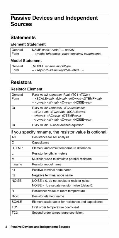
StatementsElement Statement
Model Statement
ResistorsResistor Element
If you specify mname, the resistor value is optional.
General Form
NAME node1,node2 … nodeN+ <model reference> value <optional parameters>
General Form
.MODEL mname modeltype+ <keyword=value keyword=value...>
General Form
Rxxx n1 n2 <mname> Rval <TC1 <TC2>> + <SCALE=val> <M=val> <AC=val><DTEMP=val> + <L=val> <W=val> <C=val> <NOISE=val>
Or Rxxx n1 n2 <mname> <R=>resistance +<TC1=val> <TC2=val> <SCALE=val> +<M=val> <AC=val> <DTEMP=val> +< L=val> <W=val> <C=val> <NOISE=val>
Or Rxxx n1 n2 R=‘user-defined equation’
AC Resistance for AC analysis
C Capacitance
DTEMP Element and circuit temperature difference
L Resistor length, in meters
M Multiplier used to simulate parallel resistors
mname Resistor model name
n1 Positive terminal node name
n2 Negative terminal node name
NOISE NOISE = 0, do not evaluate resistor noise.
NOISE = 1, evaluate resistor noise (default).
R Resistance value at room temperature
Rxxx Resistor element name
SCALE Element scale factor for resistance and capacitance
TC1 First order temperature coefficient
TC2 Second-order temperature coefficient
Passive Devices and Independent Sources

Wire RC Model
Noise Parameter for ResistorsResistor models generate electrical thermal noise. However, some tasks, such as macro modeling, require noiseless resistor models.
• If you set noise=1 (default), or if you do not specify the noise parameter, HSPICE models a resistor that generates noise.
• If you do not want the resistor model to generate thermal noise, set noise=0 in the instance statement (noiseless resistor model).
Resistor Model SelectorFor multiple resistor models, you can use the automatic model selector in HSPICE to find the proper model for each resistor.
The model selector syntax is based on a common model root name, with a unique extension for each model.
The resistor model selector uses the following criteria:
LMIN <= L < LMAXWMIN <= W < WMAX
user-defined equation
Function of any node voltages, element currents, temperature, frequency, or time
W Resistor width
General Form .MODEL mname R keyword=value <CRATIO=val>
keyword Any model parameter name.
mname Model name.
R Specifies a wire model.
CRATIO Ratio for total wire element parasitic capacitance. Assign a value between 0 and 1 to CRATIO.
Passive Devices and Independent Sources 3

4
CapacitorsCapacitor Element
If you choose a model for the capacitor, capval specifications are optional.
If a capacitor model uses the same name as a parameter for capval, the model name is taken to avoid syntactic conflicts.
General Form
Cxxx n1 n2 <mname> capval <TC1> <TC2> + <SCALE=val> <IC=val> <M=val> <W=val> <L=val>+ <DTEMP=val>
Or Cxxx n1 n2 <mname> C=capacitance <TC1=val> + <TC2=val> <IC=val><M=val> <W=val>+ <L=val> <DTEMP=val>
Or Cxxx n1 n2 C=‘equation’ <CTYPE=0|1>+ <above_options...>
Cxxx Capacitor element name. Must begin with C, followed by up to 1023 alphanumeric characters.
n1 Positive terminal node name.
n2 Negative terminal node name.
mname Capacitance model name.
C=capacitance
Capacitance at room temperature, as a numeric value or a parameter, in farads.
TC1 First-order temperature coefficient.
TC2 Second-order temperature coefficient.
SCALE Element scale parameter.
IC Initial voltage across the capacitor, in volts.
M Multiplier to simulate multiple parallel capacitors. Default=1.0
W Capacitor width, in meters.
L Capacitor length, in meters.
DTEMP Element temperature difference from the circuit temperature, in degrees Celsius.
C=‘equation’
Capacitance at room temperature, as a function of a node voltage, branch current, or independent variable such as time, frequency (HERTZ), or temperature.
CTYPE Determines capacitance charge calculation, for elements with capacitance equations.
Passive Devices and Independent Sources
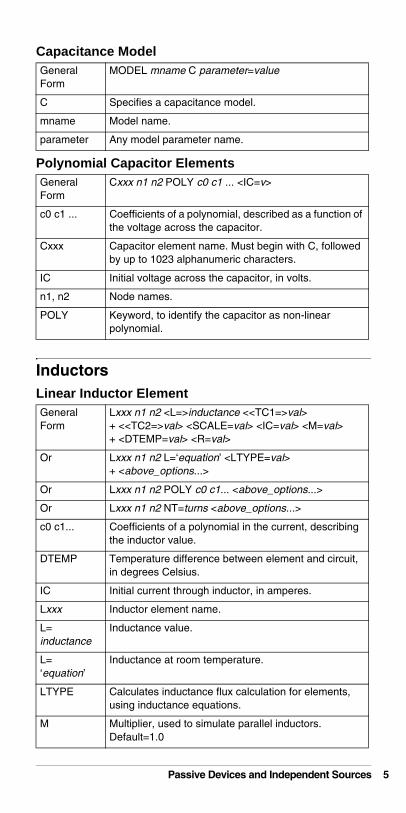
Capacitance Model
Polynomial Capacitor Elements
InductorsLinear Inductor Element
General Form
MODEL mname C parameter=value
C Specifies a capacitance model.
mname Model name.
parameter Any model parameter name.
General Form
Cxxx n1 n2 POLY c0 c1 ... <IC=v>
c0 c1 ... Coefficients of a polynomial, described as a function of the voltage across the capacitor.
Cxxx Capacitor element name. Must begin with C, followed by up to 1023 alphanumeric characters.
IC Initial voltage across the capacitor, in volts.
n1, n2 Node names.
POLY Keyword, to identify the capacitor as non-linear polynomial.
General Form
Lxxx n1 n2 <L=>inductance <<TC1=>val> + <<TC2=>val> <SCALE=val> <IC=val> <M=val>+ <DTEMP=val> <R=val>
Or Lxxx n1 n2 L=‘equation’ <LTYPE=val>+ <above_options...>
Or Lxxx n1 n2 POLY c0 c1... <above_options...>
Or Lxxx n1 n2 NT=turns <above_options...>
c0 c1... Coefficients of a polynomial in the current, describing the inductor value.
DTEMP Temperature difference between element and circuit, in degrees Celsius.
IC Initial current through inductor, in amperes.
Lxxx Inductor element name.
L=inductance
Inductance value.
L=‘equation’
Inductance at room temperature.
LTYPE Calculates inductance flux calculation for elements, using inductance equations.
M Multiplier, used to simulate parallel inductors. Default=1.0
Passive Devices and Independent Sources 5

6
Mutual Inductor Element
Polynomial Inductor Element
MagneticsMagnetic Winding Element
Mutual Core Statement
n1, n2 Positive and negative terminal node names.
NT=turns Number of inductive magnetic winding turns.
POLY Keyword that specifies the inductance, calculated by a polynomial.
R Inductor resistance, in ohms. Default=0.0
SCALE Element scale parameter; scales inductance by its value. Default=1.0
TC1 First-order temperature coefficient.
TC2 Second-order temperature coefficient.
General Form Kxxx Lyyy Lzzz <K=>coupling
Mutual Core Form
Kaaa Lbbb <Lccc ... <Lddd>> mname <MAG = magnetization>
K=coupling Coefficient of mutual coupling.
Kxxx Mutual inductor element name.
Lyyy Name of the first of two coupled inductors.
Lzzz Name of the second of two coupled inductors.
Kaaa Saturable core element name. Must begin with K, followed by up to 1023 alphanumeric characters.
Lbbb, Lccc, Lddd
Names of the windings about the Kaaa core. Must use the magnetic winding syntax.
mname Saturable core model name.
MAG =magnetization
Initial magnetization of the saturable core. You can set this to +1, 0, or -1.
General Form
Lxxx n1 n2 POLYc0 c1 <L=>inductance + <<TC1=>val> <<TC2=>val> <SCALE=val> + <IC=val> <M=val> <DTEMP=val> <R=val>
General Form
Lxxx n1 n2 NT=turns <L=>inductance <<TC1=>val> + <<TC2=>val> <SCALE=val> <IC=val> <M=val>+ <DTEMP=val> <R=val>
General Form Kaaa Lbbb <Lccc ... <Lddd>> mname+ <MAG=magnetization>
K=coupling Coefficient of mutual coupling.
Kaaa Saturable core element name.
Passive Devices and Independent Sources

Magnetic Core Model
Independent Source Element
Kxxx Mutual inductor element name.
Lbbb, Lccc, Lddd
Names of the windings about the Kaaa core.
Lyyy Name of the first of two coupled inductors.
Lzzz Name of the second of two coupled inductors.
MAG=magnetization
Initial magnetization of the saturable core.
mname Saturable core model name.
General Form .MODEL mname L (<pname1=val1>…)
CORE Identifies a Jiles-Atherton Ferromagnetic Core model.
L Identifies a saturable core model
LEVEL=x Equation selection for Jiles-Atherton model.
mname Model name.
pname1=val1 Value of the model parameter.
General Form Vxxx n+ n- <<DC=> dcval> <tranfun> <AC=acmag, + <acphase>>
Or Iyyy n+ n- <<DC=> dcval> <tranfun> <AC=acmag, + <acphase>> + <M=val>
AC AC source keyword, for use in AC small-signal analysis.
acmag Magnitude (RMS) of AC source in volts.
acphase Phase of the AC source, in degrees.
DC=dcval DC source keyword, and value in volts.
Iyyy Independent current source element name.
M Multiplier to simulate multiple parallel current sources.
n+ Positive node.
n- Negative node.
tranfun Transient source function (one or more of: AM, DC, EXP, PE, PL, PU, PULSE, PWL, SFFM, SIN).
Vxxx Independent voltage source element name.
Passive Devices and Independent Sources 7

8
Port Element
Independent SourcesPulse Source Function
Sinusoidal Source Function
Exponential Source Function
General Form Pxxx p n port=number+ $ **** Voltage or Power Information ********+ <dc mag> <ac <mag <phase>>> + <one tran waveform>+ $ **** Power Switch ********+ <zo=val> <rdc=val> <rac=val> + <rtran=val>
<dc mag> DC voltage or power source value. Unlike the V/I source, you must explicitly specify the DC voltage.
<ac <mag <phase>>> AC voltage or power source value.
<one tran waveforms> TRAN voltage or power source waveform.
<zo=val> System impedance, used in .LIN analysis. Currently supports only real impedance. You can also enter zo=val. zo defaults to 50 ohms.
<rdc=val> Series resistance for DC analysis. Overrides zo for DC analysis.
General Form Vxxx n+ n- PU<LSE> <(>v1 v2 <td <tr <tf <pw + <per>>>>> <)>
Or Ixxx n+ n- PU<LSE> <(>v1 v2 + <td <tr <tf <pw <per>>>>> <)>
General Form Vxxx n+ n- SIN <(> vo va <freq <td <q <j>>>> <)>
Or Ixxx n+ n- SIN <(> vo va <freq <td <q <j>>>> <)>
General Form Vxxx n+ n- EXP <(> v1 v2 <td1 <t1 <td2 <t2>>>> <)>
Or Ixxx n+ n- EXP <(> v1 v2 <td1 <t1 <td2 <t2>>>> <)>
Passive Devices and Independent Sources

Piecewise Linear Source Function
MSINC and ASPEC
Data Driven Piecewise Linear Source Function
Single-Frequency FM Source Function
Amplitude Modulation Source Function
General Form Vxxx n+ n- PWL <(> t1 v1 <t2 v2 t3 v3…> <R + <=repeat>> <TD=delay> <)>
Or Ixxx n+ n- PWL <(> t1 v1 <t2 v2 t3 v3…> + <R <=repeat>> <TD=delay> <)>
General Form Ixxx n+ n- PL <(> v1 t1 <v2 t2 v3 t3…> <R + <=repeat>> <TD=delay> <)>
General Form Vxxx n+ n- PWL (TIME, PV)
along with: .DATA datanameTIME PVt1 v1t2 v2t3 v3t4 v4. . ..ENDDATA.TRAN DATA=datanam
Or Ixxx n+ n- PWL (TIME, PV)
General Form Vxxx n+ n- SFFM <(> vo va <fc <mdi <fs>>> <)>
Or Ixxx n+ n- SFFM <(> vo va <fc <mdi <fs>>> <)>
General Form Vxxx n+ n- AM <(> so sa fm fc <td> <)>
Or Ixxx n+ n- AM <(> so sa fm fc <td> <)>
AM Keyword for an amplitude-modulated, time-varying source.
EXP Keyword for a exponential time-varying source.
fc Carrier frequency, in Hz.
fm Modulation frequency in hertz. Default=1/TSTOP.
freq Source frequency in Hz. Default=1/TSTOP.
fs Signal frequency in Hz.
j Phase delay in units of degrees.
mdi Modulation index that determines the magnitude of deviation from the carrier frequency.
oc Offset constant, a unitless constant that determines the absolute magnitude of the modulation. Default=0.0.
per Pulse repetition period, in seconds.
PULSE Keyword for a pulsed time-varying source.
Passive Devices and Independent Sources 9

10
Pattern Source Function
PV Parameter name for amplitude value provided in a .DATA statement.
pw Pulse width (the width of the plateau portion of the pulse), in seconds.
PWL Keyword for a piecewise linear time-varying source.
q Damping factor in units of 1/seconds.
sa Signal amplitude, in volts or amps. Default=0.0
SFFM Keyword for a single-frequency, frequency-modulated time-varying source.
SIN Keyword for a sinusoidal time-varying source.
t1 Rise time constant, in seconds.
t1 t2 … tn Timepoint values, where the corresponding current or voltage value is valid.
t2 Fall time constant, in seconds.
td Delay time before the start of the signal, in seconds. Default=0.0
tf Duration of the recovery ramp, in seconds, from the pulse plateau, back to the initial value (forward transit time).
TIME Parameter name for time value, provided in a .DATA statement.
tr Duration of the onset ramp, in seconds, from the initial value, to the pulse plateau value (reverse transit time).
v1 v2 … vn Current or voltage values, at the corresponding timepoint.
va Voltage or current RMS amplitude, in volts or amps.
vo Voltage or current offset, in volts or amps.
Vxxx, Ixxx Independent voltage source.
General Form Vxxx n+ n- PAT <(> vhi vlo td tr tf tsample data+ <RB=val> <R=repeat> <)>Vxxx n+ n- PAT <(> vhi vlo td tr tf tsample+ [component 1 ... componentn] <RB=val>+ <R=repeat> <)>
Or Ixxx n+ n- PAT <(> vhi vlo td tr tf tsample data+ <RB=val> <R=repeat> <)>Ixxx n+ n- PAT <(> vhi vlo td tr tf tsample+ [component 1 ... componentn] <RB=val>+ <R=repeat> <)>
Passive Devices and Independent Sources

Pattern Command-Driven Pattern Source
See the HSPICE Command Reference for the syntax and description of the pattern command (.PAT).Pseudo Random-Bit Generator Source (PRBS Function)
Diodes
General Form Vxxx n+ n- PAT <(> vhi vlo td tr tf tsample PatName+ <RB=val> <R=repeat> <)>
Ixxx n+ n- PAT <(> vhi vlo td tr tf tsample Patname+ <RB=val> <R=repeat> <)>
General Form vxxx n+ n- LFSR <(> vlow vhigh tdelay trise tfall rate+ seed <[> taps <]> <rout=val> <)>
Or Ixxx n+ n- LFSR <(> vlow vhigh tdelay trise tfall rate+ seed <[> taps <]> <rout=val> <)>
LFSR Specifies the voltage/current source as PRBS.
vlow The minimum voltage/current level.
vhigh The maximum voltage/current level.
tdelay Specifies the initial time delay to the first transition.
trise Specifies the duration of the onset ramp (in seconds), from the initial value to the pulse plateau value (reverse transit time).
tfall Specifies the duration of the recovery ramp (in seconds), from the pulse plateau, back to the initial value (forward transit time).
rate The bit rate. seed The initial value loaded into the shift register.
taps The bits used to generate feedback.
rout The output resistance.
Diodes 11

12
Diode Element
Junction Model Statement
General Form Dxxx nplus nminus mname <<AREA = >area> + <<PJ = >val> <WP = val> <LP = val> + <WM = val> <LM = val> <OFF> <IC = vd> <M = val> + <DTEMP = val>
Or Dxxx nplus nminus mname <W = width> <L = length> + <WP = val> <LP = val> <WM = val> <LM = val> + <OFF> <IC = vd> <M = val> <DTEMP = val>
AREA Area of the diode.
DTEMP Difference between the element temperature and the circuit temperature, in Celsius.
Dxxx Diode element name.
IC = vd Initial voltage across the diode element.
L Diode length, in meters (LEVEL = 3 diode model only).
LM Length of metal capacitor, in meters (for LEVEL = 3 diode model only).
LP Length of polysilicon capacitor in meters (for LEVEL = 3 diode model only).
M Multiplier, to simulate multiple diodes in parallel.
mname Diode model name reference.
nminus Negative terminal (cathode) node name.
nplus Positive terminal (anode) node name.
OFF Initial element condition is OFF in DC analysis.
PJ Periphery of junction.
W Diode width, in meters (LEVEL = 3 diode only).
WM Width of metal capacitor, in meters (for LEVEL = 3 diode model only).
WP Width of polysilicon capacitor, in meters (for LEVEL = 3 diode model only).
General Form .MODEL mname D <LEVEL=val><keyword=val>
mname Model name
D Identifies a diode model
LEVEL LEVEL=1: Junction diodeLEVEL=2: Fowler-Nordheim diodeLEVEL=3: Geometric junction diode processingLEVEL=4: Philips JUNCAP model
keyword Model parameter keyword, such as CJO or IS
Diodes

Junction Model ParametersJunction .DC Parameters LEVEL 1 and 3Name (Alias) Unit Default Description
AREA - 1.0 Junction area. For LEVEL=1, AREA is unitless, for LEVEL=3,
unit is meter2.
EXPLI amp/AREAeff
0.0 Current-explosion model parameter.
EXPLIR amp/AREAeff
EXPLI Reverse mode current explosion model parameter.
IB amp/AREAeff
1.0e-3 Current at breakdown voltage.
IBV amp/AREAeff
1.0e-3 Current at breakdown voltage.
IK (IKF, JBF)
amp/AREAeff
0.0 Forward knee current.
IKR (JBR) amp/AREAeff
0.0 Reverse knee current.
IS (JS) amp/AREAeff
1.0e-140.0
Saturation current per unit area.Level 1 default=1.0e-14.Level 3 default=0.0.
JSW (ISP) amp/PJeff
0.0 Sidewall saturation current per unit junction periphery.
L - - Default diode length.
LEVEL - 1 Diode model selector.
N - 1.0 Emission coefficient
PJ - 0.0 Junction periphery
RS ohms or
ohms/m20.0 Ohmic series resistance.
SHRINK - 1.0 Shrink factor.
VB (BV, VAR, VRB)
V 0.0 Reverse breakdown voltage.
W - - Default width of diode
XW - - Accounts for masking and etching effects.
NBV N Breakdown emission coefficient.
JTUN amp/AREAeff
0.0 Tunneling saturation current per unit area.
Diodes 13

14
Junction Capacitance Parameters
Metal and Poly Parameters Level 3
JTUNSW amp/PJeff
0.0 Sidewall tunneling saturation current per unit junction periphery.
NTUN 30 Tunneling emission coefficient.
Name (Alias) Unit Default Description
CJ (CJA, CJO)
F/AREAeff
0.0 Zero-bias bottomwall capacitance
CJP (CJSW)
F/PJeff 0.0 Zero-bias periphery capacitance
FC - 0.5 Coefficient for forward-bias depletion area capacitance
FCS - 0.5 Coefficient for forward-bias depletion periphery capacitance
M (EXA, MJ)
- 0.5 Area junction grading coefficient
MJSW (EXP)
- 0.33 Periphery junction grading coefficient
PB (PHI, VJ, PHA)
V 0.8 Area junction contact potential
PHP V PB Periphery junction contact potential
TT s 0.0 Transit time
Name (Alias) Unit Default Description
LM m 0.0 Default length of metal
LP m 0.0 Default length of polysilicon.
WM m 0.0 Default width of metal.
WP m 0.0 Default width of polysilicon.
XM m 0.0 Accounts for masking and etching effects in metal layer.
XOI Å 7000 Thickness of poly, to bulk oxide.
XOM Å 10k Thickness of metal, to bulk oxide.
XP m 0.0 Accounts for masking and etching effects in poly layer.
Name (Alias) Unit Default Description
Diodes

Noise Parameters LEVEL 1 and 3
Temperature EffectsTemperature Effect Parameters LEVEL 1 and 3
Name (Alias) Unit Default Description
AF - 1.0 Flicker noise exponent
KF - 0.0 Flicker noise coefficient
Name (Alias) Unit Default Description
CTA (CTC)
1/° 0.0 Temperature coefficient for area junction capacitance (CJ).
CTP 1/° 0.0 Temperature coefficient for periphery junction capacitance (CJP).
EG eV - Energy gap for pn junction diode.
GAP1 eV/° 7.02e-4 First bandgap correction factor. From Sze, alpha term.
GAP2 ° 1108 Second bandgap correction factor. From Sze, beta term.
TCV 1/° 0.0 Breakdown voltage temperature coefficient.
TLEV - 0.0 Temperature equation LEVEL selector for diode; interacts with TLEVC.
TLEVC - 0.0 LEVEL selector for diode temperature, junction capacitances, and contact potentials; use with TLEV.
TM1 1/° 0.0 First-order temperature coefficient for MJ.
TM2 1/°2 0.0 Second-order MU temperature coefficient.
TPB (TVJ)
V/° 0.0 Temperature coefficient for PB.
TPHP V/° 0.0 Temperature coefficient for PHP.
TREF °c 25.0 Model reference temperature (LEVEL 1 or 3 only).
TRS 1/° 0.0 Resistance temperature coefficient.
TTT1 1/° 0.0 First-order temperature coefficient for TT.
Diodes 15

16
Fowler-Nordheim Diode
Fowler-Nordheim Tunnel Diode Element
Diode Model Parameters LEVEL=2
TTT2 1/°2 0.0 Second-order TT temperature coefficient.
XTI - 3.0 Saturation current temperature exponent.
XTITUN 3.0 Exponent for the tunneling current temperature.
LEVEL 2 Form
Dxxx nplus nminus mname <W=val<L=val>> + <WP=val><OFF> <IC=vd> <M=val>
Dxxx Diode element name.
nplus Positive terminal (anode) node name.
nminus Negative terminal (cathode) node name.
mname Model name.
AREA Diode area (unitless for LEVEL = 1 diode; square meters for LEVEL = 3 diode; not used in Level=2).
OFF Sets initial condition to OFF in DC analysis. Default=ON.
IC=vd Initial voltage across this element.
M Multiplier, to simulate multiple diodes.
W Width of diode, in meters. Overrides W in the LEVEL 2 model. Default=0.0
L Length of diode, in meters. Overrides L in the LEVEL 2 model. Default=0.0
PJ Periphery of junction (unitless for LEVEL = 1; meters for LEVEL = 3 diode; not used in Level=2).
WP Width of polysilicon capacitor, in meters.
WM Width of metal capacitor, in meters; not in Level=2.
LM Length of metal capacitor, in meters; not in Level=2.
Name (Alias) Unit Default Description
EF V/cm 1.0e8 Forward critical electric field
ER V/cm EF Reverse critical electric field
JF amp/V2 1.0e-10
Forward Fowler-Nordheim current coefficient
Name (Alias) Unit Default Description
Diodes

Level 4 JUNCAP Diode Model
General Syntax
JR amp/V2 JF Reverse Fowler-Nordheim current coefficient
L m 0.0 Length of diode for calculation of Fowler-Nordheim current
TOX Å 100.0 Thickness of oxide layer
W m 0.0 Width of diode for calculation of Fowler-Nordheim current
XW m 0.0 Account for masking and etching effects
General Form Dxxx nodeplus nodeminus modelname <<area=>val> + <<peri=>val><<pgate>=val> <<dtemp>=val>+ <<off>=val> <<IC=>val> <<m=>val>
Dxxx Diode element name. Must begin with D.
nodeplus Positive terminal (anode) node name. Series resistor of the equivalent circuit is attached to this terminal
nminus Negative terminal (cathode) node name
mname Diode model name reference
area Diode area. In the model card, AB can use this value.
peri Side-wall length in the AB diffusion area, which is not under the gate. In the model card, LS uses this value.
pgate Side-wall length in the AB diffusion area, which is under the gate. In the model card, LG uses this value.
off Sets initial condition for this element to OFF, in DC analysis. The default is ON
M Multiplier, to simulate multiple diodes in parallel. The M setting affects all currents, capacitances and resistances. Default=1
ic Initial voltage across a diode element. Use this value when you specify the UIC option in the .tran statement. The .IC statement overrides this value.
Dtemp Difference between element temperature and circuit temperature, in degrees celsius. Default=0.0
.option list Prints the updated temperature parameters for the juncap diode model
Name (Alias) Unit Default Description
Diodes 17

18
Juncap Model Statement
Juncap Model Parameters
General Form .MODEL modelname D level=4 <keyword=val>
modelname Model name
D Identifies a diode model
LEVEL Identifies a diode modelLEVEL = 4: JUNCAP Diode Model
keyword Model parameter keyword (JSGBR, JSDBR)
Name (Alias) Unit Default Description
AB M2 1e-12 Diffusion area
LS M 0.0 Length of side-wall for AB diffusion area, not under gate. (Default deviates from Philips JUNCAP = 1.0e-6)
LG M 0.0 Length of side-wall for AB diffusion area, under gate. (Default deviates from Philips JUNCAP = 1.0e-6)
DTA C 0.0 Juncap temperature offset
TR C 25 Pre-set temp parameters
VR V 0.0 Pre-set voltage parameters
JSGBR Am-2 1.0E-3 Bottom saturation-current density, due to electron hole generation at V=VR
JSDBR Am-2 1.0E-3 Bottom saturation-current density, due to back contact
JSGSR Am-2 1.0E-3 Sidewall saturation-current, due to electron hole generation at V=VR
JSDSR Am-2 1.0E-3 Sidewall saturation-current, due to back contact
JSGGR Am-2 1.0E-3 Gate edge saturation current, due to electron hole generation at V=VR
JSDGR Am-2 1.0E-3 Gate edge saturation current, due to back contact
NB 1.0 Emission coefficient of bottom forward current
NS 1.0 Emission coefficient of sidewall forward current
NG 1.0 Emission coefficient of gate edge forward current
VB V 0.9 Reverse breakdown voltage
CJBR Fm-2 1.0E-12 Bottom junction capacitance
Diodes

BJT Element
CJSR Fm-2 1.0E-12 Sidewall junction capacitance
CJGR Fm-2 1.0E-12 Gate edge junction capacitance
VDBR V 1.00 Diffusion voltage, bottom junction
VDSR V 1.00 Diffusion voltage of sidewall junction
VDGR V 1.00 Diffusion voltage of gate edge junction
PB 0.40 Bottom junction grading coefficient
PS 0.40 Sidewall junction grading coefficient
PG 0.40 Gate edge junction grading coefficient
General Form Qxxx nc nb ne <ns> mname <AREA=area> <OFF> + <IC=vbeval, vceval> <M=val> <DTEMP=val>
Or Qxxx nc nb ne <ns> mname <AREA=area>+ <AREAB=val> <AREAC=val> <OFF> + <VBE=vbeval> <VCE=vceval> <M=val>+ <DTEMP=val>
AREA=area Emitter area multiplying factor, which affects currents, resistances, and capacitances. Default = 1.0.
AREAB Base AREA multiplying factor. Default = AREA
AREAC Collector AREA multiplying factor. Default = AREA
DTEMP The difference between the element and circuit temperatures, in degrees Celsius.
IC=vbeval,VBE, vceval, VCE
Initial internal base-emitter voltage (vbeval) and collector-emitter voltage (vceval).
M Multiplier, to simulate multiple BJTs in parallel.
mname BJT model name reference.
nb Base terminal node name.
nc Collector terminal node name.
ne Emitter terminal node name.
ns Substrate terminal node name, optional.
OFF Sets initial condition to OFF in DC analysis.
Qxxx BJT element name. Must begin with Q, followed by up to 1023 alphanumeric characters.
Name (Alias) Unit Default Description
BJT Element 19

20
BJT Model Statement
BJT Model ParametersBasic DC Model Parameters
General Form .MODEL mname NPN <(> <pname1=val1> ... <)>
Or .MODEL mname PNP <pname1=val1> ...
mname Model name.
NPN Identifies an NPN transistor model.
pname1 Several model parameters are possible.
PNP Identifies a PNP transistor model.
Name (Alias) Unit Default Definition
BF (BFM) - 100.0 Ideal maximum forward BETA
BR (BRM) - 1.0 Ideal maximum reverse BETA
BULK(NSUB)
- 0.0 Sets the bulk node to a global node name
IBC amp 0.0 Reverse saturation current between base and collector
EXPLI amp 1.e15 Current explosion model parameter
IBE amp 0.0 Reverse saturation current between base and emitter
IS amp 1.0e-16 Transport saturation current
ISS amp 0.0 Reverse saturation current bulk-to-collector or bulk-to-base
LEVEL - 1.0 Model selector
NF - 1.0 Forward current emission coefficient
NR - 1.0 Reverse current emission coefficient
NS - 1.0 Substrate current emission coefficient
SUBS - - Substrate connection selector
UPDATE - 0 Selects alternate base charge equation
BJT Element

Low-Current Beta Degradation Effect Parameters
Base Width Modulation Parameters
High-Current Beta Degradation Effect Parameters
Parasitic Resistance Parameters
Name (Alias) Unit Default Definition
ISC (C4, JLC)
amp 0.0 Base-collector leakage saturation current
ISE (C2, JLE)
amp 0.0 Base-emitter leakage saturation current
NC (NLC) - 2.0 Base-collector leakage emission coefficient
NE (NLE) - 1.5 Base-emitter leakage emission coefficient
Name (Alias) Unit Default Definition
VAF (VA, VBF) V 0.0 Forward early voltage
VAR (VB, VRB, BV) V 0.0 Reverse early voltage
Name (Alias) Unit Default Definition
IKF (IK, JBF) amp 0.0 Corner for forward Beta high-current roll-off
IKR (JBR) amp 0.0 Corner for reverse Beta high-current roll-off
NKF - 0.5 Exponent for high-current Beta roll-off
IKF (IK, JBF) amp 0.0 Corner for forward Beta high-current roll-off
Name (Alias) Unit Default Definition
IRB (IRB, IOB)
amp 0.0 Base current, where base resistance falls half-way to RBM
RB ohm 0.0 Base resistance
RBM ohm RB Minimum high-current base resistance
RC ohm 0.0 Collector resistance
RE ohm 0.0 Emitter resistance
BJT Element 21

22
Junction Capacitor Parameters
Parasitic Capacitances Parameters
Transit Time Parameters
Name (Alias) Unit Default Definition
CJC F 0.0 Base-collector zero-bias depletion capacitance
CJE F 0.0 Base-emitter zero-bias depletion capacitance
CJS (CCS, CSUB)
F 0.0 Zero-bias collector substrate capacitance
FC - 0.5 Coefficient for forward bias depletion capacitance
MJC (MC) - 0.33 Base-collector junction exponent (grading factor)
MJE (ME) - 0.33 Base-emitter junction exponent (grading)
MJS (ESUB)
- 0.5 Substrate junction exponent (grading factor)
VJC (PC) V 0.75 Base-collector built-in potential
VJE (PE) V 0.75 Base-emitter built-in potential
VJS (PSUB)
V 0.75 Substrate junction built-in potential
XCJC (CDIS)
- 1.0 Internal base fraction of base-collector depletion capacitance
Name (Alias) Unit Default Definition
CBCP F 0.0 External base-collector constant capacitance
CBEP F 0.0 External base-emitter constant capacitance
CCSP F 0.0 External collector substrate constant capacitance (vertical) or base substrate (lateral)
Name (Alias) Unit Default Definition
ITF (JTF) amp 0.0 TF high-current parameter
PTF × 0.0 Frequency multiplier to determine excess phase
TF s 0.0 Base forward transit time
TR s 0.0 Base reverse transit time
BJT Element

Noise Parameters
LEVEL 6 Philips Bipolar Model
VTF V 0.0 TF base-collector voltage dependence on coefficient
XTF - 0.0 TF bias dependence coefficient
Name (Alias) Unit Default Definition
AF - 1.0 Flicker-noise exponent
KF - 0.0 Flicker-noise coefficient
General Form
Qxxx nc nb ne <ns> nt mname <AREA=val> <OFF> + <VBE=val> <VCE=val> <M=val> <DTEMP=val> + <tnodeout>
Qxxx nc nb ne nt mname <AREA=val> <OFF>+ <VBE=val> <VCE=val> <M=val> <DTEMP=val> + <tnodeout>
This second form uses nt as a self-heating node but does not use a substrate node.
AREA Normalized emitter area.
DTEMP Difference between element and circuit temperature.
M Multiplier for multiple BJTs in parallel.
mname BJT model name reference.
nb Base node name or number.
nc Collector terminal node name or number.
ne Emitter terminal node name or number.
ns Substrate node name or number.
nt Self-heating node name or number.
OFF Sets initial condition=OFF for the element in DC analysis.
Qxxx BJT element name. Must begin with Q, then up to 1023 alphanumeric characters.
tnodeout Identify self heating node from substrate node.
VBE Initial internal base to emitter voltage.
VCE Initial internal collector to emitter voltage.
Name (Alias) Unit Default Definition
BJT Element 23

24
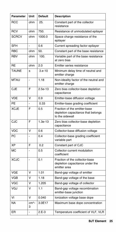
Philips MEXTRAM 503 ParametersThe following tables describe MEXTRAM Levels 503 as Level 6 model parameters, including parameter names, descriptions, units, default values, notes.Flags - Level 503
Basic Parameters - Level 503
Parameter Unit Default Description
EXAVL - 0 Flag for extended modeling avalanche currents
EXMOD - 0 Flag for extended modeling of the reverse current gain
EXPHI - 1 Flag, distributed high frequency effects
OUTFLAG - 0 Flag, displays more output data.
Parameter Unit Default Description
TREF oC 0.0 Model nominal temperature
IS A 5.E-17 Collector-emitter saturation current
BF A 140.0 Ideal forward current gain
XIBI - 0.0 Fraction of ideal base current belonging to sidewall
IBF A 2.0E-14 Saturation current of the non-ideal forward base current
VLF V 0.5 Cross-over voltage of the non-ideal forward base current
IK A 15.E-3 High-injection knee current
BRI - 16.0 Ideal reverse current gain
IBR A 8.0e-15 Saturation current of the non-ideal reverse base current
VLR V 0.5 Cross-over voltage of the non-ideal reverse base current
XEXT - 0.5 Part of I EX,Q EX, Q TEX and I SUB that depends on VBC1 base-collector voltage
QBO C 1.2e-12 Base charge at zero bias
ETA - 4.0 Factor of built-in field of the base
AVL - 50. Weak avalanche parameter
EFI - 0.7 Electric field intercept (with EXAVL=1)
IHC A 3.e-3 Critical hot-carrier current
BJT Element
RCC ohm 25. Constant part of the collector resistance
RCV ohm 750. Resistance of unmodulated epilayer
SCRCV ohm 1000.0 Space charge resistance of the epilayer
SFH - 0.6 Current spreading factor epilayer
RBC ohm 50. Constant part of the base resistance
RBV ohm 100. Variable part of the base resistance at zero bias
RE ohm 2.0 Emitter series resistance
TAUNE s 3.e-10 Minimum delay time of neutral and emitter charge
MTAU - 1.18 Non-ideality factor of the neutral and emitter charge
CJE F 2.5e-13 Zero bias collector-base depletion capacitance
VDE V 0.9 Emitter-base diffusion voltage
PE - 0.33 Emitter-base grading coefficient
XCJE F 0.5 Fraction of the emitter-base depletion capacitance that belongs to the sidewall
CJC F 1.3e-13 Zero bias collector-base depletion capacitance
VDC V 0.6 Collector-base diffusion voltage
PC - 0.4 Collector-base grading coefficient variable part
XP F 0.2 Constant part of CJC
MC - 0.5 Collector current modulation coefficient
XCJC - 0.1 Fraction of the collector-base depletion capacitance under the emitter area
VGE V 1.01 Band-gap voltage of emitter
VGB V 1.18 Band-gap voltage of the base
VGC V 1.205 Band-gap voltage of collector
VGJ V 1.1 Band-gap voltage recombination emitter-base junction
VI V 0.040 Ionization voltage base dope
NA cm^-3
3.0E17 Maximum base dope concentration
ER - 2.E-3 Temperature coefficient of VLF, VLR
Parameter Unit Default Description
BJT Element 25
26
You can use either of two parameters to specify the difference between the circuit temperature and the ambient temperature in the MEXTRAM model:
• dtemp instance parameter, as set in the element statement.
• DTA global model parameter.
• DTA and dtemp both default to zero. dtemp overrides DTA locally, if you specify both. The dtemp value derates the temperature in model equations and parameters.
• If you do not specify either the dtemp or the DTA parameter, then dtemp=0.0.
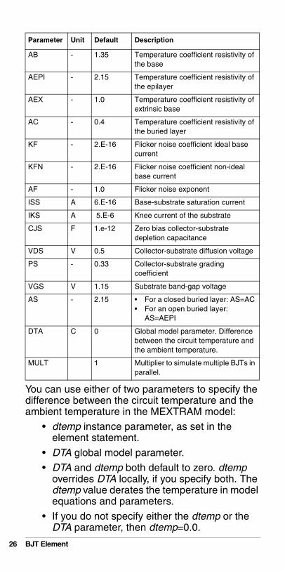
AB - 1.35 Temperature coefficient resistivity of the base
AEPI - 2.15 Temperature coefficient resistivity of the epilayer
AEX - 1.0 Temperature coefficient resistivity of extrinsic base
AC - 0.4 Temperature coefficient resistivity of the buried layer
KF - 2.E-16 Flicker noise coefficient ideal base current
KFN - 2.E-16 Flicker noise coefficient non-ideal base current
AF - 1.0 Flicker noise exponent
ISS A 6.E-16 Base-substrate saturation current
IKS A 5.E-6 Knee current of the substrate
CJS F 1.e-12 Zero bias collector-substrate depletion capacitance
VDS V 0.5 Collector-substrate diffusion voltage
PS - 0.33 Collector-substrate grading coefficient
VGS V 1.15 Substrate band-gap voltage
AS - 2.15 • For a closed buried layer: AS=AC • For an open buried layer:
AS=AEPI
DTA C 0 Global model parameter. Difference between the circuit temperature and the ambient temperature.
MULT 1 Multiplier to simulate multiple BJTs in parallel.
Parameter Unit Default Description
BJT Element

• If you specify DTA but not dtemp, dtemp uses the DTA value.
• If you specify dtemp, then simulation uses the dtemp value, and ignores the DTA value.
Philips MEXTRAM 504 ParametersThe following tables describe MEXTRAM Level 504 (Level 6) model parameters, including parameter names, units, default values, descriptions, and notes. Parameters with * are not in the DC model.
Flags - Level 504
Parameter Unit Default Description
LEVEL - 6 Model level
VERS - 504 Flag for choosing MEXTRAM model (level 503 or 504)
EXMOD - 1 Flag for extended modeling of the reverse current gain
EXPHI - 1 *Flag for distributed high frequency effects in transient
EXAVL - 0 Flag for extended modeling of avalanche currents
TREF ^C 25.0 Reference temperature
SUBS - 1 Flag for substrate effect.
• subs=1 applies substrate effect.• subs=0 does not apply substrate
effect.
OUTFLAG - 0 Flag, displays more output data.
Basic Parameters - Level 504
Parameter Unit Default Description
IS A 2.2e-17 Collector-emitter saturation current
VER 2.5 Reverse early voltage
VEF 44.0 Forward early voltage
BF - 215.0 Ideal forward current gain
XIBI - 0.0 Fraction of ideal base current that belongs to the sidewall
IBF A 2.7e-15 Saturation current of non-ideal forward base current
MLF V 2.0 Non-ideality factor of non-ideal forward base current
BJT Element 27
28
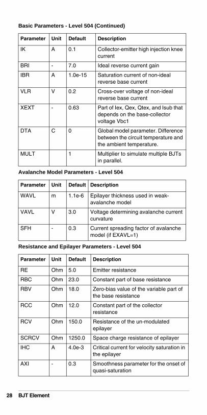
IK A 0.1 Collector-emitter high injection knee current
BRI - 7.0 Ideal reverse current gain
IBR A 1.0e-15 Saturation current of non-ideal reverse base current
VLR V 0.2 Cross-over voltage of non-ideal reverse base current
XEXT - 0.63 Part of Iex, Qex, Qtex, and Isub that depends on the base-collector voltage Vbc1
DTA C 0 Global model parameter. Difference between the circuit temperature and the ambient temperature.
MULT 1 Multiplier to simulate multiple BJTs in parallel.
Avalanche Model Parameters - Level 504
Parameter Unit Default Description
WAVL m 1.1e-6 Epilayer thickness used in weak-avalanche model
VAVL V 3.0 Voltage determining avalanche current curvature
SFH - 0.3 Current spreading factor of avalanche model (if EXAVL=1)
Resistance and Epilayer Parameters - Level 504
Parameter Unit Default Description
RE Ohm 5.0 Emitter resistance
RBC Ohm 23.0 Constant part of base resistance
RBV Ohm 18.0 Zero-bias value of the variable part of the base resistance
RCC Ohm 12.0 Constant part of the collector resistance
RCV Ohm 150.0 Resistance of the un-modulated epilayer
SCRCV Ohm 1250.0 Space charge resistance of epilayer
IHC A 4.0e-3 Critical current for velocity saturation in the epilayer
AXI - 0.3 Smoothness parameter for the onset of quasi-saturation
Basic Parameters - Level 504 (Continued)
Parameter Unit Default Description
BJT Element

Base-Emitter Capacitances - Level 504
Parameter Unit Default Description
CJE F 7.3e-14 *Zero bias emitter-base depletion capacitance
VDE V 0.95 Emitter-base diffusion voltage
PE - 0.4 Emitter-base grading coefficient
XCJE - 0.4 *Fraction of the emitter-base depletion capacitance that belongs to the sidewall
CBEO F 0.0 Base-emitter extrinsic capacitance
Base-Collector Capacitances - Level 504
Parameter Unit Default Description
CJC F 7.8e-14 *Zero bias collector-base depletion capacitance
VDC V 0.68 Collector-base diffusion voltage
PC - 0.5 Collector-base grading coefficient
XP - 0.35 Constant part of CJC
MC - 0.5 Coefficient for the current modulation of the collector-base depletion capacitance
XCJC - 3.2e-2 *Fraction of the collector-base depletion capacitance under the emitter
CBCO F 0.0 Base-collector extrinsic capacitance
Transit Time Parameters - Level 504
Parameter Unit Default Description
MTAU - 1.0 *Non-ideality, emitter stored charge
TAUB S 4.2e-12 *Transit time of stored base charge
TAUE S 2.0e-12 *Minimum transit time of stored emitter charge
TEPI S 4.1e-11 *Transit time, stored epilayer charge
TAUR S 5.2e-10 *Transit time of reverse extrinsic stored base charge
DEG EV 0.0 Bandgap difference over base
XREC - 0.0 Pre-factor of recombination Ib1 part
Temperature Parameters - Level 504
AQBO - 0.3 Temperature coefficient of the zero-bias base charge
BJT Element 29

30
AE - 0.0 Temperature coefficient of the resistivity of the emitter
AB - 1.0 Temperature coefficient of the resistivity of the base
AEPI - 2.5 Temperature coefficient of the resistivity of the epilayer
AEX - 0.62 Temperature coefficient of resistivity of extrinsic base
AC - 2.0 Temperature coefficient of resistivity of the buried layer
DVGBF V 5.0e-2 Bandgap voltage difference of forward current gain
CVGBR V 4.5e-2 Bandgap voltage difference of reverse current gain
VGB V 1.17 Bandgap voltage of the base
VGC V 1.18 Bandgap voltage of collector
VGJ V 1.15 Bandgap voltage recombination emitter-base junction
DVGTE V 0.05 *Bandgap voltage difference of emitter stored charge
Noise Parameters - Level 504
Parameter Unit Default Description
AF - 2.0 Exponent of the flicker-noise
KF - 2.0e-11 Flicker-noise coefficient of the ideal base current
KFN - 2.0e-11 Flicker-noise coefficient of the non-ideal base current
Substrate Parameters - Level 504
Parameter Unit Default Description
ISS A 4.8e-17 Base-substrate saturation current
IKS A 2.5e-4 Base-substrate high injection knee current
CJS F 3.15e-13 *Zero bias collector-substrate depletion capacitance
VDS V 0.62 *Collector-substrate diffusion voltage
PS - 0.34 *Collector-substrate grading coefficient
VGS V 1.2 Bandgap voltage of substrate
AS - 1.58 • For a closed buried layer: AS=AC• For open buried layer: AS=AEPI
Temperature Parameters - Level 504 (Continued)
BJT Element

LEVEL 8 HiCUM ModelThe general form is the same as in LEVEL 6 Philips Bipolar Model on page 23.Model Parameters
Internal TransistorsTransfer Current Parameters
BE Depletion Capacitance Parameters
Self-Heating Parameters - Level 504
Parameter Unit Default Description
RTH oC/W 0 Thermal resistance
CTH J/oC 0 Thermal capacitance
Parameter Unit Default Description
LEVEL - 8 HiCUM BJT level
TREF C 26.85 Temperature in simulation
VERS - 2.0 Version (use 2.1.for self-heating)
Parameter Unit Default Description
C10 A^2s 3.76e-32 Constant (if IS>0, C10=IS*QP0; otherwise C10=C10)
Qp0 As 2.78e-14 Zero-bias hole charge
ICH A 2.09e-0z High-current correction for 2D/3D
HFC - 1.0 Weighting factor for Qfc (in HBTs)
HFE - 1.0 Weighting factor for Qef in HBTs
HJCI - 1.0 Weighting factor for Qjci in HBTs
HJEI - 0.0 Weighting factor for Qjei in HBTs
ALIT - 0.45 Factor for additional iT delay time
Parameter Unit Default Description
VDEI V 0.95 Built-in voltage
CJEI0 F 8.11e-15 Zero-bias value
ZEI - 0.5 Exponent coefficient
ALJEI - 1.8 Ratio of max. to zero-bias value
BJT Element 31
32
BC Depletion Capacitance Parameters
Forward Transit Time Parameters
Critical Current Parameters
Inverse Transit Time
Base Current Components
Parameter Unit Default Description
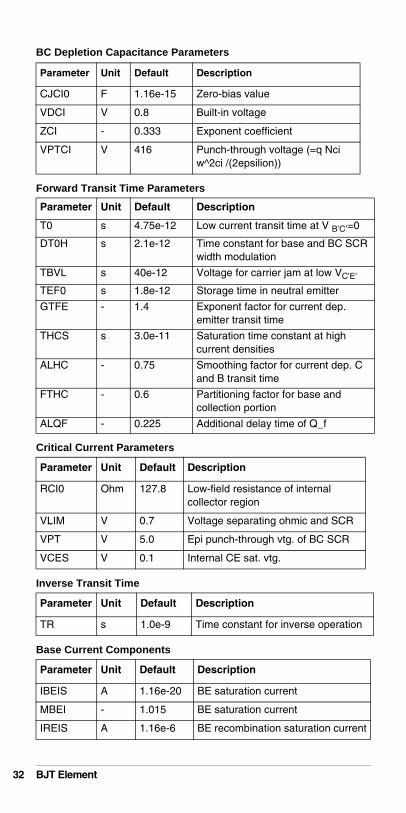
CJCI0 F 1.16e-15 Zero-bias value
VDCI V 0.8 Built-in voltage
ZCI - 0.333 Exponent coefficient
VPTCI V 416 Punch-through voltage (=q Nci w^2ci /(2epsilion))
Parameter Unit Default Description
T0 s 4.75e-12 Low current transit time at V B’C’=0
DT0H s 2.1e-12 Time constant for base and BC SCR width modulation
TBVL s 40e-12 Voltage for carrier jam at low VC'E'
TEF0 s 1.8e-12 Storage time in neutral emitter
GTFE - 1.4 Exponent factor for current dep. emitter transit time
THCS s 3.0e-11 Saturation time constant at high current densities
ALHC - 0.75 Smoothing factor for current dep. C and B transit time
FTHC - 0.6 Partitioning factor for base and collection portion
ALQF - 0.225 Additional delay time of Q_f
Parameter Unit Default Description
RCI0 Ohm 127.8 Low-field resistance of internal collector region
VLIM V 0.7 Voltage separating ohmic and SCR
VPT V 5.0 Epi punch-through vtg. of BC SCR
VCES V 0.1 Internal CE sat. vtg.
Parameter Unit Default Description
TR s 1.0e-9 Time constant for inverse operation
Parameter Unit Default Description
IBEIS A 1.16e-20 BE saturation current
MBEI - 1.015 BE saturation current
IREIS A 1.16e-6 BE recombination saturation current
BJT Element
Weak BC Avalanche Breakdown
Internal Base Resistance
Lateral Scaling
Peripheral ElementsBE Depletion Capacitance
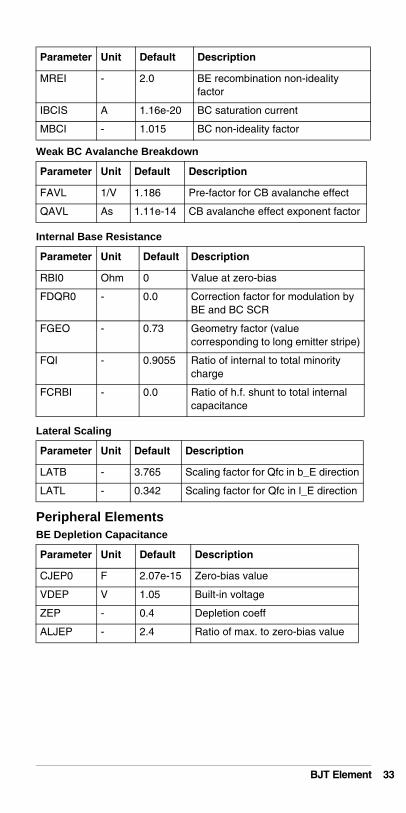
MREI - 2.0 BE recombination non-ideality factor
IBCIS A 1.16e-20 BC saturation current
MBCI - 1.015 BC non-ideality factor
Parameter Unit Default Description
FAVL 1/V 1.186 Pre-factor for CB avalanche effect
QAVL As 1.11e-14 CB avalanche effect exponent factor
Parameter Unit Default Description
RBI0 Ohm 0 Value at zero-bias
FDQR0 - 0.0 Correction factor for modulation by BE and BC SCR
FGEO - 0.73 Geometry factor (value corresponding to long emitter stripe)
FQI - 0.9055 Ratio of internal to total minority charge
FCRBI - 0.0 Ratio of h.f. shunt to total internal capacitance
Parameter Unit Default Description
LATB - 3.765 Scaling factor for Qfc in b_E direction
LATL - 0.342 Scaling factor for Qfc in l_E direction
Parameter Unit Default Description
CJEP0 F 2.07e-15 Zero-bias value
VDEP V 1.05 Built-in voltage
ZEP - 0.4 Depletion coeff
ALJEP - 2.4 Ratio of max. to zero-bias value
Parameter Unit Default Description
BJT Element 33

34
Base Current
BE Tunneling
External ElementsBC Capacitance
BC Base Current Component
Other External Elements
Substrate Transistor
Parameter Unit Default Description
IBEPS A 3.72e-21 Saturation current
MBEP - 1.015 Non-ideality factor
IREPS A 1e-30 Recombination saturation factor
MREP - 2.0 Recombination non-ideality factor
Parameter Unit Default Description
IBETS A 0 Saturation current
ABET - 0.0 Exponent coefficient
Parameter Unit Default Description
CJCX0 F 5.393e-15 Zero-bias depletion value
VDCX V 0.7 Built-in voltage
ZCX - 0.333 Exponent coefficient
VPTCX V 100 Punch-through voltage
CCOX F 2.97e-15 Collector oxide capacitance
FBC - 0.1526 Partitioning factor for C_BCX=C'_BCx+C"_BCx
Parameter Unit Default Description
IBCXS A 4.39e-20 Saturation current
MBCX - 1.03 Non-ideality factor
Parameter Unit Default Description
CEOX F 1.13e-15 Emitter-base isolation overlap cap
RBX Ohm 0 External base series resistance
RE Ohm 0 Emitter series resistance
RCX Ohm 0 External collector series resistance
Parameter Unit Default Description
ITSS A 0.0 Transfer saturation current
MSF - 0.0 Non-ideality (forward transfer current)
TSF - 0.0 Minority charge storage transit time
BJT Element

Collector-Substrate Depletion Capacitance
Substrate Coupling Network
Noise Parameters
Temperature Dependence
ISCS A 0.0 Saturation current of CS diode
MSC - 0.0 Non-ideality factor of CS diode
Parameter Unit Default Description
CJS0 F 3.64e-14 Zero-bias value of CS depletion cap
VDS V 0.6 Built-in voltage
ZS - 0.447 Exponent coefficient
VPTS V 1000 Punch-through voltage
Parameter Unit Default Description
RSU Ohm 0 Substrate series resistance
CSU F 0 Substrate capacitance from bulk material permittivity
Parameter Unit Default Description
KF - 1.43e-8 Flicker noise factor (no unit for AF=2!)
AF - 2.0 Flicker noise exponent factor
KRBI - 1.17 Factor for internal base resistance
Parameter Unit Default Description
ALB 1/K 6.3e-3 Temperature coefficient of forward current gain
ALT0 1/K 0 First-order temperature coefficient of TEF0
KT0 1/K 0 Second-order temperature coefficient of TEF0
ZETACI - 1.6 Temperature exponent factor RCI0
ALVS 1/K 1e-3 Temperature coefficient of saturation drift velocity
ALCES 1/K 0.4e-3 Relative temperature coefficient of VCES
VGB V 1.17 Bandgap-voltage
ZETARBI - .588 Temperature exponent factor of RBi0
ZETARBX - 0.2060 Temperature exponent factor of RBX
ZETARCX - 0.2230 Temperature exponent factor of RCX
ZETARE - 0 Temperature exponent factor of RE
Parameter Unit Default Description
BJT Element 35

36
Self-Heating
To use the self-heating HiCUM feature (in BJT Level 8), set vers=2.1 and set an RTH parameter value other than 0. If you use vers=2.0 or RTH=0, then self-heating is OFF.
The self-heating effect also applies to the circuit temperature, as an increased self-heating temperature. T = Tckt(circuit temp.) + Tsh(self heating temp.) + dtemp (the difference between the circuit temperature and the ambient temperature).
Other Parameters
ALFAV 1/K 8.25e-5 Temperature coefficient for avalanche breakdown
ALQAV 1/K 1.96e-4 Temperature coefficient for avalanche breakdown
Parameter Unit Default Description
RTH K/W 0 Thermal resistance (not supported in v2000.4)
CTH Ws/K 0 Thermal resistance (not supported in v2000.4)
Parameter Unit Default Description
FBCS - 1.0 Determine external BC capacitance partitioning.
IS A -1.0 Ideal saturation current:
if IS>0, C10=IS*QP0
KRBI - 1.0 Noise analysis of internal resistance.
MCF - 1.0 Non-ideality factor of reverse current between base and collector. VT=VT*MCF
ZETACX - 1.0 Temperature exponent factor (epi-layer)
MSR - 1.0 Non-ideality factor of reverse current in substrate transistor. VT=VT*MSR
Parameter Unit Default Description
BJT Element

Default Parameter set for HiCum v2.1LEVEL = 8 TREF = 300.15 K (uses TNOM value if you do not specify TREF)VERS = 2.1 C10 = 2e-30 A^2s QP0 = 2e-14 As ICH = 1e+20 A HFC = 1 HFE = 1 HJCI = 1 HJEI = 1 ALIT = 0 CJEI0 = 0 F VDEI = 0.9 V ZEI = 0.5 ALJEI = 2.5 CJCI0 = 0 F VDCI = 0.7 V ZCI = 0.4 VPTCI = 1e+20 V T0 = 0 s DT0H = 0 s TBVL = 0 s TEF0 = 0 s GTFE = 1 THCS = 0 s ALHC = 0.1 FTHC = 0 ALQF = 0 RCI0 = 150 ohm VLIM = 0.4 V VPT = 3 V VCES = 0.1 V TR = 0 s IBEIS = 1e-18 A MBEI = 1 IREIS = 1e-30 A MREI = 2 IBCIS = 1e-16 A MBCI = 1 FAVL = 0 1/V QAVL = 0 As RBI0 = 0 ohm FDQR0 = 0 FGEO = 0.6557 FQI = 1 FCRBI = 0 LATB = 0 LATL = 0 CJEP0 = 0 F VDEP = 0.9 V ZEP = 0.5
ALJEP = 2.5 IBEPS = 1e-30 A MBEP = 1 IREPS = 1e-30 A MREP = 2 IBETS = 0 A ABET = 40 CJCX0 = 0 F VDCX = 0.7 V ZCX = 0.4 VPTCX = 1e+20 V CCOX = 0 F FBC = 0 IBCXS = 1e-30 A MBCX = 1 CEOX = 0 F RBX = 0 ohm RE = 0 ohm RCX = 0 ohm ITSS = 1e-30 A MSF = 1 TSF = 0 ISCS = 1e-30 A MSC = 1 CJS0 = 0 F VDS = 0.6 V ZS = 0.5 VPTS = 1e+20 V RSU = 0 ohm CSU = 0 F KF = 0 AF = 2 VGB = 1.17 V ALB = 0.005 1/K ALT0 = 0 1/K KT0 = 0 1/K ZETACI = 0 ALVS = 0 1/K ALCES = 0 1/K ZETARBI = 0 ZETARBX = 0 ZETARCX = 0 ZETARE = 0 ALFAV = 0.00083 1/K ALQAV = 0.002 1/K RTH = 0 K/W CTH = 0 K/W KRBI = 1 ZETACX = 0 IS = 1e-16 MCF = 1 MSR = 1 FBCS = -1
BJT Element 37

38
Level 9 VBIC99 ModelThe VBIC 95 (Vertical Bipolar Inter-Company Model) for Motorola bipolar transistor device is BJT level 4. VBIC99 (the new version of the VBIC model) is BJT level 9. To use the VBIC99 model, specify the Level 9 parameter for the bipolar transistor model.
VBIC99 covers several improved effects, compared to the VBIC95 model. In VBIC99, temperature coefficients of base and collector resistances are separate. The temperature dependence of the built-in potential is also improved.Element SyntaxThe element syntax of BJT Level 9 is:
VBIC99 ModelThe VBIC99 model includes several effects that are improved compared to the VBIC95 model:
• Temperature dependency for parameters.
• Base-emitter breakdown model.
General Form
Qxxx nc nb ne <ns> mname <AREA=val><OFF>+ <VBE=val> <VCE=val> <M=val><DTEMP=val>
<angle brackets> indicate optional parameters.
Qxxx BJT element name. Must begin with “Q”, which can be followed by up to 1023 alphanumeric characters.
nc Collector terminal node name or number.
nb Base terminal node name and number.
ne Emitter terminal node name or number.
ns Substrate node name or number.
nt Self-heating node name or number.
mname BJT model name reference.
AREA The normalized emitter area. VBIC99 level 9 model has no area effect. Default value=1. Area is used only as an alias of the multiplication factor (M).
OFF Sets initial condition to OFF, for this element in DC analysis. You cannot use OFF with VBE or VCE.
VBE Initial internal base-emitter voltage.
VCE Initial internal collector-emitter voltage.
M Multiplier to simulate multiple BJTs in parallel.
DTEMP Temperature difference of element and circuit.
Level 9 VBIC99 Model
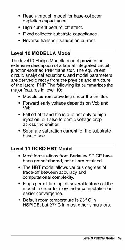
• Reach-through model for base-collector depletion capacitance
• High current beta rolloff effect.
• Fixed collector-substrate capacitance
• Reverse transport saturation current.
Level 10 MODELLA ModelThe level10 Philips Modella model provides an extensive description of a lateral integrated circuit junction-isolated PNP transistor. The equivalent circuit, analytical equations, and model parameters are derived directly from the physics and structure of the lateral PNP. The following list summarizes the major features in level 10:
• Models current crowding under the emitter.
• Forward early voltage depends on Vcb and Veb.
• Fall off of ft and hfe is due not only to high injection, but also to ohmic voltage drop across the emitter.
• Separate saturation current for the substrate-base diode.
Level 11 UCSD HBT Model• Most formulations from Berkeley SPICE have
been grandfathered, not all are retained.
• The HBT model allows various degrees of trade-off between accuracy and computational complexity.
• Flags permit turning off several features of the model in order to allow faster computation or easier convergence.
• Default room temperature is 25o C in HSPICE, but 27o C in most other simulators.
Level 9 VBIC99 Model 39

40
• The model parameter set should always include the TREF model reference temperature. The default TREF value is 27.
• You can use DTEMP with this model.Element SyntaxThe element syntax of BJT Level 11 is:
For more information, see
http://hbt.ucsd.edu
Also, see “BJT Level 11 UCSD HBT Model” in the HSPICE Elements and Device Models Manual.
General Form
Qxxx nc nb ne <ns> mname <AREA=val><OFF><+ VBE=val> <VCE=val> <M=val><DTEMP=val>
<angle brackets> indicate optional parameters.
Qxxx BJT element name. Must begin with Q, followed by up to 1023 alphanumeric characters.
nc Collector terminal node name or number.
nb Base terminal node name and number.
ne Emitter terminal node name or number.
ns Substrate node name or number.
t Self-heating node name or number.
mname BJT model name reference.
AREA Normalized emitter area.
OFF Sets initial condition to OFF for this element in DC analysis. Do not use OFF with VBE or VCE.
VBE Initial internal base-emitter voltage.
VCE Initial internal collector-emitter voltage.
M Multiplier to simulate multiple BJTs in parallel.
DTEMP Difference between the temperature of the element and the circuit.
Level 9 VBIC99 Model

JFET and MESFET Elements
General Form for Elements
JFET and MESFET Model Statements
General Form Jxxx nd ng ns <nb> mname <<<AREA> = area | + <W = val> <L = val>> <OFF> <IC = vdsval,vgsval> + <M = val> <DTEMP = val>
Or Jxxx nd ng ns <nb> mname <<<AREA> = area> | + <W = val> <L = val>> <OFF> <VDS = vdsval>+ <VGS = vgsval> <M = val> <DTEMP = val>
AREA = area Area multiplying factor that affects the BETA, RD, RS, IS, CGS and CGD model parameters. Default=1.0 (square meters).
DTEMP Difference between element temperature and circuit temperature, degrees Celsius.
IC = vdsval, vgsval, VDS, VGS
Initial internal drain-source voltage (vdsval) and gate-source voltage (vgsval).
Jxxx JFET or MESFET element name.
L FET gate length in meters.
M Multiplier to simulate multiple JFETs or MESFETs in parallel. Default=1.
mname JFET or MESFET model name reference.
nb Bulk terminal node name (optional).
nd Drain terminal node name.
ng Gate terminal node name.
ns Source terminal node name.
OFF Sets initial condition to OFF for this element in DC analysis.
W FET gate width in meters.
General Form .MODEL mname NJF <LEVEL=val>+ <pname1=val1> ...
Or .MODEL mname PJF <LEVEL=val>+ <pname1=val1> ...
LEVEL Selects different DC model equations
mname Model name
NJF Identifies an n-channel JFET or MESFET model
PJF Identifies a p-channel JFET or MESFET model
pname1=val1 Can include several model parameters
JFET and MESFET Elements 41

42
JFET Model ParametersGate Diode DC Parameters
Gate Capacitance LEVEL 1, 2, and 3 Parameters
Name (Alias) Unit Default Description
ACM - - Area calculation method
ALIGN m 0 Misalignment of gate
AREA - - The default area multiplier
HDIF m 0 Distance of the heavily diffused or low resistance region from source or drain contact edge to lightly-doped region
IS amp 1.0e-14 Gate junction saturation current
L m 0.0 Default length of FET
LDEL m 0.0 Difference between drawn and actual or optical device length
LDIF m 0 Width of the lightly doped region from heavily doped region to transistor edge
N - 1.0 Emission coefficient for gate-drain and gate-source diodes
RD ohm 0.0 Drain ohmic resistance
RG ohm 0.0 Gate resistance
RS ohm 0.0 Source ohmic resistance
RSH ohm/sq 0 Heavily doped region, sheet resistance
RSHG ohm/sq 0 Gate sheet resistance
RSHL ohm/sq 0 Lightly doped region, sheet resistance
W m 0.0 Default width of FET
WDEL m 0.0 The difference between drawn & actual or optical device width
Name (Alias) Unit Default Description
CAPOP - 0.0 Capacitor model selector
CALPHA ALPHA - Saturation factor for capacitance model (CAPOP=2 only)
CAPDS F 0 Drain to source capacitance for TriQuint model
JFET and MESFET Elements

DC Model LEVEL 1 Parameters
DC Model LEVEL 2 Parameters
CGAMDS GAMDS - Threshold lowering factor for capacitance (CAPOP=2 only)
CGD F 0.0 Zero-bias gate-drain junction capacitance
CGS F 0.0 Zero-bias gate-source junction capacitance
CRAT 0.666 Source fraction of gate capacitance (use with GCAP)
GCAP F - Zero-bias gate capacitance
Name (Alias) Unit Default Description
LEVEL - 1.0 LEVEL=1 invokes SPICE JFET model.
BETA amp/V2 1.0e-4 Transconductance parameter, gain.
LAMBDA 1/V 0.0 Channel length modulation parameter.
ND 1/V 0.0 Drain subthreshold factor.
NG - 0.0 Gate subthreshold factor.
VTO V -2.0 Threshold voltage.
Name (Alias) Unit Default Description
LEVEL - 1.0 LEVEL of FET DC model.
BETA amp/V2 1.0e-4 Transconductance parameter, gain.
LAMBDA 1/V 0.0 Channel length modulation parameter.
LAM1 1/V 0.0 Channel length modulation gate voltage parameter.
ND 1/V 0.0 Drain subthreshold factor.
NG - 0.0 Gate subthreshold factor.
VTO V -2.0 Threshold voltage.
Name (Alias) Unit Default Description
JFET and MESFET Elements 43

44
DC Model LEVEL 3 Parameters
TOM Model Parameters
Name (Alias) Unit Default Description
LEVEL - 1.0 FET DC model level; LEVEL=3 is Curtice MESFET model
A m 0.5m Active layer thickness
ALPHA 1/V 2.0 Saturation factor
BETA amp /V 2 1.0e-4 Transconductance parameter, gain
D - 11.7 Semiconductor dielectric constant: Si=11.7, GaAs=10.9
DELTA - 0 Ids feedback parameter of TriQuint model
GAMDS (GAMMA)
- 0 Drain voltage, induced threshold voltage lowering coefficient
LAMBDA 1/V 0.0 Channel length modulation parameter
K1 V1/2 0.0 Threshold voltage sensitivity to bulk node
NCHAN atom/
cm31.552e16
Effective dopant concentration in the channel
ND 1/V 0.0 Drain subthreshold factor
NG - 0.0 Gate subthreshold factor
SAT - 0.0 Saturation factor
SATEXP - 3 Drain voltage exponent
UCRIT V/cm 0 Critical field for mobility degradation
VBI - 1.0 Gate diode built-in voltage
VGEXP (Q) - 2.0 Gate voltage exponent
VP - - Pinch-off voltage (default is calculated)
Name (Alias) Unit Default Description
BETATCE - - Temperature coefficient for BETA
DELTA - - IDS feedback parameter
CAPDS - - Drain-to-source capacitance
BETAeff BETA Weff M⋅Leff
-----------------------⋅=
JFET and MESFET Elements
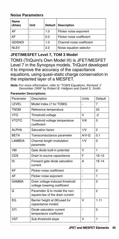
Noise Parameters
JFET/MESFET Level 7, TOM 3 ModelTOM3 (TriQuint’s Own Model III) is JFET/MESFET Level 7 in the Synopsys models. TriQuint developed it to improve the accuracy of the capacitance equations, using quasi-static charge conservation in the implanted layer of a MESFET.Note: For more information, refer to “TOM3 Equations, Revised: 2
December 1999” by Robert B. Hallgren and David S. Smith.Parameter Descriptions
Name (Alias) Unit Default Description
AF - 1.0 Flicker noise exponent
KF - 0.0 Flicker noise coefficient
GDSNOI - 1.0 Channel noise coefficient
NLEV - 2.0 Noise equation selector
Parameter Description Units Default
LEVEL Model Index (7 for TOM3) - 7
TNOM Reference temperature 25
VTO Threshold voltage V -2
VTOTC Threshold voltage temperature coefficient
V/K 0
ALPHA Saturation factor 1/V 2
BETA Transconductance parameter A/V-Q 0.1
LAMBDA Channel length modulation parameter
1/V 0
VBI Gate diode built-in potential V 1
CDS Drain to source capacitance F 1E-12
IS Forward gate diode saturation current
A 1E-14
KF Flicker noise coefficient - 0
AF Flicker noise exponent - 1
GAMMA Drain voltage-induced threshold voltage lowering coefficient
- 0
Q Parameter Q to model the non-square-law of the drain current
- 2
EG Barrier height at 0K(used for capacitance model)
V 1.11
XTI Diode saturation current temperature coefficient
- 0
VST Sub-threshold slope V 1
JFET and MESFET Elements 45

46
JFET Level 8 Materka ModelThis section summarizes the Synopsys JFET & MESFET model Level=8. For more information about this model, see Compact dc Model of GaAs FETs for Large-Signal Computer Calculation, IEEE Journal of Solid-State Circuits, Volume SC-18, No.2, April 1983, Computer Calculation of Large-Signal
ALPHATCE ALPHA temperature coefficient (exponential)
K-1 0
ILK Leakage diode current parameter A 0
PLK Leakage diode potential parameter V 1
K Knee-function parameter - 2
VSTTC Linear temperature coefficient of VST
VK-1 0
QGQL Charge parameter FV 5E-16
QGQH Charge parameter FV -2E-16
QGI0 Charge parameter A 1E-6
QGAG Charge parameter V-1 1
QGAD Charge parameter V-1 1
QGGB Charge parameter A-1V-1 100
QGCL Charge parameter F 2E-16
QGSH Sidewall capacitance F 1E-16
QGDH Sidewall capacitance F 0
QGG0 Charge parameter F 0
MST Sub-threshold slope – drain parameter
V-1 0
N Forward gate diode ideality factor - 1
GAMMATC Linear temperature coefficient for GAMMA
K-1 0
VBITC Linear temperature coefficient for VBI
VK-1 0
CGSTCE Linear temperature coefficient for CGS
K-1 0
CGDTCE Linear temperature coefficient for CGD
K-1 0
MSTTC Linear temperature coefficient for MST
V-1K-1 0
BETATCE Linear temperature coefficient for BETA
K-1 0
Parameter Description Units Default
JFET and MESFET Elements
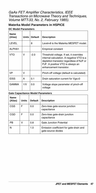
GaAs FET Amplifier Characteristics, IEEE Transactions on Microwave Theory and Techniques, Volume MTT-33, No. 2, February 1985).Materka Model Parameters in HSPICEDC Model Parameters
Gate Capacitance Model Parameters
Name (Alias) Units Default Description
LEVEL 8 Level=8 is the Materka MESFET model.
ALPHA1 Empirical constant
VTO V -2.0 Threshold voltage. If set, it overrides internal calculation. A negative VTO is a depletion transistor regardless of NJF or PJF. A positive VTO is always an enhancement transistor.
VP V Pinch-off voltage (default is calculated)
IDSS A 0.1 Drain saturation current for Vgs=0
GAMMA 1/V 0.0 Voltage slope parameter of pinch-off voltage
Name (Alias) Units Default Description
CGS F 0.0 Zero-bias gate-source junction capacitance
CGD F 0.0 Zero-bias gate-drain junction capacitance
PB V 0.8 Gate Junction Potential
N 1.0 Emission coefficient for gate-drain and gate-source diodes
JFET and MESFET Elements 47

48
MOSFET Elements
MOSFET Element StatementGeneral Form
Mxxx nd ng ns <nb> mname <<L = > length> + <<W = >width> <AD = val> <AS = val> <PD = val> + <PS = val> <NRD = val> <NRS = val> <RDC = val> +<RSC = val> <OFF> <IC = vds,vgs,vbs> <M = val> + <DTEMP = val> <GEO = val> <DELVTO = val>
Or .OPTION WL Mxxx nd ng ns <nb> mname <width>+ <length> <other options...>
AD Drain diffusion area.
AS Source diffusion area.
DELVTO Zero-bias threshold voltage shift.
DTEMP Difference between element temperature and circuit temperature in degrees Celsius.
GEO Source/drain sharing selector for MOSFET model parameter value ACM = 3.
IC = vds, vgs, vbs
Initial voltage across external drain/source (vds), gate/source (vgs), and bulk/source terminals (vbs)
L MOSFET channel length in meters.
M Multiplier, simulate multiple parallel MOSFETs
mname MOSFET model name reference.
Mxxx MOSFET element name.
nb Bulk terminal node name, which is optional.
nd Drain terminal node name.
ng Gate terminal node name.
NRD Number of squares of drain diffusion for resistance calculations.
NRS Number of squares of source diffusion for resistance calculations.
ns Source terminal node name.
OFF Sets initial condition for this element to OFF in DC analysis.
PD Perimeter of the drain junction.
PS Perimeter of the source junction.
RDC Additional drain resistance due to contact resistance, in units of ohms.
RSC Additional source resistance, due to contact resistance, in units of ohms.
W MOSFET channel width, in meters.
MOSFET Elements
MOSFET Model Statement
Diode Model ParametersDC Model Parameters
Capacitance Model Parameters
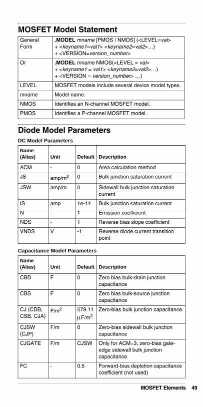
General Form
.MODEL mname [PMOS | NMOS] (<LEVEL=val> + <keyname1=val1> <keyname2=val2>…)+ <VERSION=version_number>
Or .MODEL mname NMOS(<LEVEL = val>+ <keyname1 = val1> <keyname2=val2>…)+ <VERSION = version_number> …)
LEVEL MOSFET models include several device model types.
mname Model name.
NMOS Identifies an N-channel MOSFET model.
PMOS Identifies a P-channel MOSFET model.
Name (Alias) Unit Default Description
ACM - 0 Area calculation method
JS amp/m2 0 Bulk junction saturation current
JSW amp/m 0 Sidewall bulk junction saturation current
IS amp 1e-14 Bulk junction saturation current
N - 1 Emission coefficient
NDS - 1 Reverse bias slope coefficient
VNDS V -1 Reverse diode current transition point
Name (Alias) Unit Default Description
CBD F 0 Zero bias bulk-drain junction capacitance
CBS F 0 Zero bias bulk-source junction capacitance
CJ (CDB, CSB, CJA)
F/m2 579.11
µF/m2Zero-bias bulk junction capacitance
CJSW (CJP)
F/m 0 Zero-bias sidewall bulk junction capacitance
CJGATE F/m CJSW Only for ACM=3, zero-bias gate-edge sidewall bulk junction capacitance
FC - 0.5 Forward-bias depletion capacitance coefficient (not used)
MOSFET Elements 49

50
Drain and Source Resistance Model Parameters
MOS Common Geometry Model Parameters
MJ (EXA, EXJ, EXS, EXD)
- 0.5 Bulk junction grading coefficient
MJSW (EXP)
- 0.33 Bulk sidewall junction grading coefficient
NSUB (DNB, NB)
1/cm3 1e15 Substrate doping
PB (PHA, PHS, PHD)
V 0.8 Bulk junction contact potential
PHP V PB Bulk sidewall junction contact potential
TT s 0 Transit time
Name (Alias) Unit Default Description
RD ohm/sq 0.0 Drain ohmic resistance
RDC ohm 0.0 Additional drain resistance due to contact resistance
LRD ohm/m 0 Drain resistance length sensitivity
WRD ohm/m 0 Drain resistance width sensitivity
PRD ohm/m2 0 Drain resistance product (area) sensitivity
RS ohm/sq 0.0 Source ohmic resistance
LRS ohm/m 0 Source resistance length sensitivity
WRS ohm/m 0 Source resistance width sensitivity
PRS ohm/m2 0 Source resistance product (area) sensitivity
RSC ohm 0.0 Additional source resistance due to contact resistance
RSH (RL) ohm/sq 0.0 Drain and source diffusion sheet resistance
Name (Alias) Unit Default Description
HDIF m 0 Length of heavily doped diffusion
LD (DLAT,LATD)
m - Lateral diffusion into channel from source and drain diffusion
LDIF m 0 Length of lightly doped diffusion adjacent to gate
Name (Alias) Unit Default Description
MOSFET Elements
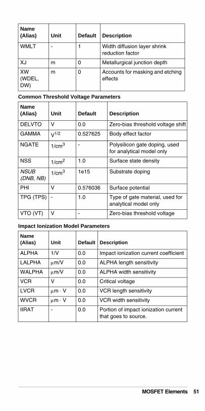
Common Threshold Voltage Parameters
Impact Ionization Model Parameters
WMLT - 1 Width diffusion layer shrink reduction factor
XJ m 0 Metallurgical junction depth
XW (WDEL, DW)
m 0 Accounts for masking and etching effects
Name (Alias) Unit Default Description
DELVTO V 0.0 Zero-bias threshold voltage shift
GAMMA V1/2 0.527625 Body effect factor
NGATE 1/cm3 - Polysilicon gate doping, used for analytical model only
NSS 1/cm2 1.0 Surface state density
NSUB (DNB, NB)
1/cm3 1e15 Substrate doping
PHI V 0.576036 Surface potential
TPG (TPS) - 1.0 Type of gate material, used for analytical model only
VTO (VT) V - Zero-bias threshold voltage
Name (Alias) Unit Default Description
ALPHA 1/V 0.0 Impact ionization current coefficient
LALPHA µm/V 0.0 ALPHA length sensitivity
WALPHA µm/V 0.0 ALPHA width sensitivity
VCR V 0.0 Critical voltage
LVCR µm ⋅ V 0.0 VCR length sensitivity
WVCR µm ⋅ V 0.0 VCR width sensitivity
IIRAT - 0.0 Portion of impact ionization current that goes to source.
Name (Alias) Unit Default Description
MOSFET Elements 51

52
Gate Capacitance Model ParametersBasic Gate Capacitance Parameters
Gate Overlap Capacitance Model Parameters
Meyer Capacitance Parameters CAPOP=0, 1, 2
Name (Alias) Unit Default Description
CAPOP - 2.0 Capacitance model selector
COX (CO) F/m2 3.453e-4 Oxide capacitance
TOX m 1e-7 Oxide thickness, calculated from COX, when COX is input
Name (Alias) Unit Default Description
CGBO (CGB)
F/m 0.0 Gate-bulk overlap capacitance per meter channel length
CGDO (CGD, C2)
F/m 0.0 Gate-drain overlap capacitance per meter channel width
CGSO (CGS, C1)
F/m 0.0 Gate-source overlap capacitance per meter channel width
LD (LATD, DLAT)
m - Lateral diffusion into channel from source and drain diffusion
METO m 0.0 Fringing field factor for gate-to-source and gate-to-drain overlap capacitance calculation
WD m 0.0 Lateral diffusion into channel from bulk along width
Name (Alias) Unit Default Description
CF1 V 0.0 Transition of cgs from depletion to weak inversion for CGSO
CF2 V 0.1 Transition of cgs from weak to strong inversion region
CF3 - 1.0 Transition of cgs and cgd from saturation to linear region as a function of vds
CF4 - 50.0 Contour of cgb and cgs smoothing factors
CF5 - 0.667 Capacitance multiplier for cgs in saturation region
CF6 - 500.0 Contour of cgd smoothing factor
CGBEX - 0.5 Cgb exponent
MOSFET Elements

Gate Capacitances (Simpson Integration) CAPOP=3
CAPOP=3 uses the same set of equations and parameters as the CAPOP=2 model. Charges are obtained by Simpson numeric integration instead of the box integration in CAPOP models 1, 2, and 6.Charge Conservation Parameters (CAPOP=4)
Gate Capacitance CAPOP=5
Use CAPOP=5 for no capacitors and simulation does not calculate the gate capacitance.
Noise Parameters
Temperature Effects Parameters
Name (Alias) Unit Default Description
XQC - 0.5 Coefficient of channel charge share attributed to drain
Name (Alias) Unit Default Description
AF - 1.0 Flicker noise exponent
KF - 0.0 Flicker noise coefficient
GDSNOI - 1.0 Channel thermal noise coefficient
NLEV - 2.0 Noise equation selector
Name (Alias) Unit Default Description
BEX - -1.5 Low field mobility, UO, temperature exponent
CTA 1/°K 0.0 Junction capacitance CJ temperature coefficient
CTP 1/°K 0.0 Junction sidewall capacitance CJSW temperature coefficient
EG eV - Energy gap for pn junction diode
F1EX - 0 Bulk junction bottom grading coefficient
GAP1 eV/°K 7.02e-4 First bandgap correction factor
GAP2 °K 1108 Second bandgap correction factor
LAMEX 1/°K 0 LAMBDA temperature coefficient
N - 1.0 Emission coefficient
MOSFET Elements 53

54
MOSFET Models
MOSFET Model Table
MJ - 0.5 Bulk junction bottom grading coefficient
MJSW - 0.33 Bulk junction sidewall grading coefficient
PTA V/°K 0.0 Junction potential PB temperature coefficient
PTC V/°K 0.0 Fermi potential PHI temperature coefficient
PTP V/°K 0.0 Junction potential PHP temperature coefficient
TCV V/°K 0.0 Threshold voltage temperature coefficient
TLEV - 0.0 Temperature equation LEVEL selector
TLEVC - 0.0 Temperature equation LEVEL selector for junction capacitances/potentials
TRD 1/°K 0.0 Temperature coefficient for drain resistor
TRS 1/°K 0.0 Temperature coefficient for source resistor
XTI - 0.0 Saturation current temperature exponent
LEVEL MOSFET Model Description All Platforms including PC
All Platforms except PC
1 Schichman-Hodges X
2 MOS2 Grove-Frohman (SPICE 2G)
X
3 MOS3 empirical (SPICE 2G) X
4 Grove-Frohman: LEVEL 2 model based on SPICE 2E.3
X
5 AMI-ASPEC depletion and enhancement (Taylor-Huang)
X
6 Lattin-Jenkins-Grove (ASPEC style parasitics)
X
7 Lattin-Jenkins-Grove (SPICE style parasitics)
X
8 Advanced LEVEL 2 X
9 ** AMD X
Name (Alias) Unit Default Description
MOSFET Models
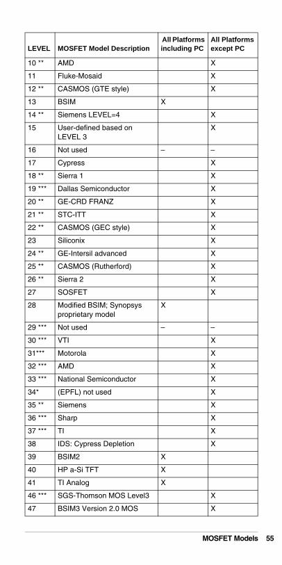
10 ** AMD X
11 Fluke-Mosaid X
12 ** CASMOS (GTE style) X
13 BSIM X
14 ** Siemens LEVEL=4 X
15 User-defined based on LEVEL 3
X
16 Not used – –
17 Cypress X
18 ** Sierra 1 X
19 *** Dallas Semiconductor X
20 ** GE-CRD FRANZ X
21 ** STC-ITT X
22 ** CASMOS (GEC style) X
23 Siliconix X
24 ** GE-Intersil advanced X
25 ** CASMOS (Rutherford) X
26 ** Sierra 2 X
27 SOSFET X
28 Modified BSIM; Synopsys proprietary model
X
29 *** Not used – –
30 *** VTI X
31*** Motorola X
32 *** AMD X
33 *** National Semiconductor X
34* (EPFL) not used X
35 ** Siemens X
36 *** Sharp X
37 *** TI X
38 IDS: Cypress Depletion X
39 BSIM2 X
40 HP a-Si TFT X
41 TI Analog X
46 *** SGS-Thomson MOS Level3 X
47 BSIM3 Version 2.0 MOS X
LEVEL MOSFET Model Description All Platforms including PC
All Platforms except PC
MOSFET Models 55

56
Parameters in MOSFET Output Templates
49 BSIM3 Version 3 (Enhanced) MOS
X
50 Philips MOS9 X
53 BSIM3 Version 3 (Berkeley) MOS
X
54 BSIM4 (Berkeley) X
55 EPFL-EKV Version 2.6, R 11 X
57 UC Berkeley BSIM3-SOI MOSFET Version 2.0.1
X
58 University of Florida SOI Version 4.5
X
59 UC Berkeley BSIM3-SOI-FD X
61 RPT Amorphous Silicon TFT X
62 RPT PolySilicon TFT X
63 Philips MOS11 X
64 STARC HiSIM model X
* not officially released** equations are proprietary – documentation not provided*** requires a license; equations are proprietary – no documentation
Name Alias Description MOSFET Levels
L LV1 Channel Length (L) All
W LV2 Channel Width (W) All
AD LV3 Area of the drain diode (AD) All
AS LV4 Area of the source diode (AS) All
ICVDS LV5 Initial condition for the drain-source voltage (VDS)
All
ICVGS LV6 Initial condition for the gate-source voltage (VGS)
All
ICVBS LV7 Initial condition for the bulk-source voltage (VBS)
All except 57, 58, 59
ICVES LV7 Initial condition for the substrate-source voltage (VES)
57, 58, 59
VTH LV9 Threshold voltage (bias dependent)
All
LEVEL MOSFET Model Description All Platforms including PC
All Platforms except PC
MOSFET Models
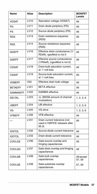
VDSAT LV10 Saturation voltage (VDSAT) All
PD LV11 Drain diode periphery (PD) All
PS LV12 Source diode periphery (PS) All
RDS LV13 Drain resistance (squares) (RDS)
All
RSS LV14 Source resistance (squares) (RSS)
All
GDEFF LV16 Effective drain conductance (1/RDeff), rgeoMod is not 0
All
GSEFF LV17 Effective source conductance (1/RSeff), (rgeoMod is not 0)
All
CDSAT LV18 Drain-bulk saturation current, at -1 volt bias
All
CSSAT LV19 Source-bulk saturation current, at -1 volt bias.
All
VDBEFF V20 Effective drain bulk voltage All
BETAEFF LV21 BETA effective All
GAMMAEFF LV22 GAMMA effective All
DELTAL LV23 ∆L (MOS6 amount of channel modulation)
1, 2, 3, 6
UBEFF LV24 UB effective 1, 2, 3, 6
VG LV25 VG drive 1, 2, 3, 6
VFBEFF LV26 VFB effective All
— LV31 Drain current tolerance (not used in HSPICE releases after 95.3)
All
IDSTOL LV32 Source-diode current tolerance All
IDDTOL LV33 Drain-diode current tolerance All
COVLGS LV36 Gate-source overlap and fringing capacitances
All
COVLGD LV37 Gate-drain overlap and fringing capacitances
All
COVLGB LV38 Gate-bulk overlap capacitances
All except 57, 59
COVLGE LV38 Gate-substrate overlap capacitances
57, 59
Name Alias Description MOSFET Levels
MOSFET Models 57

58
VBS LX1 Bulk-source voltage (VBS) All except 57, 59
VES LX1 Substrate-source voltage (VES)
57, 59
VGS LX2 Gate-source voltage (VGS) All
VDS LX3 Drain-source voltage (VDS) All
CDO LX4 DC drain current (CDO) All
CBSO LX5 DC source-bulk diode current (CBSO)
All
CBDO LX6 DC drain-bulk diode current (CBDO)
All
GMO LX7 DC gate transconductance (GMO)
All
GDSO LX8 DC drain-source conductance (GDSO)
All
GMBSO LX9 DC substrate transconductance (GMBSO)
All except 57, 58, 59
GMESO LX9 DC substrate transconductance (GMBSO)
57, 58, 59
GBDO LX10 Conductance of the drain diode (GBDO)
All
GBSO LX11 Conductance of the source diode (GBSO)
All
QB LX12 Total bulk (body) charge (QB)—Meyer and Charge Conservation
All
CQB LX13 Bulk (body) charge current (CQB)—Meyer and Charge Conservation
All
QG LX14 Total Gate charge (QG)—Meyer and Charge Conservation
All
CQG LX15 Gate charge current (CQG)—Meyer & Charge Conservation
All
QD LX16 Total Drain charge (QD) 49, 53
Name Alias Description MOSFET Levels
MOSFET Models

QD LX16 Channel charge (QD)—Meyer and Charge Conservation
All except 49, 53
CQD LX17 Drain charge current (CQD) 49, 53
CQD LX17 Channel charge current (CQD)—Meyer and Charge Conservation
All except 49, 53
CGGBO LX18 CGGBO = dQg/dVg = CGS + CGD + CGB - Meyer and Charge Conservation
All except 54, 57, 59, 60
CGGBO LX18 Intrinsic gate capacitance 54, 57, 59, 60
CGDBO LX19 CGDBO = -dQg/dVd - Meyer and Charge Conservation
All except 54, 57, 59, 60
CGDBO LX19 Intrinsic gate-to-drain capacitance
54, 57, 59, 60
CGSBO LX20 CGSBO = -dQg/dVd - Meyer and Charge Conservation
All except 54, 57, 59, 60
CGSBO LX20 Intrinsic gate-to-source capacitance
54, 57, 59, 60
CBGBO LX21 CBGBO = -dQb/dVg - Meyer and Charge Conservation
All except 54, 57, 59, 60
CBGBO LX21 Intrinsic bulk-to-gate capacitance
54
CBGBO LX21 Intrinsic floating body-to-gate capacitance
57, 59, 60
CBDBO LX22 CBDBO = -dQb/dVd - Meyer and Charge Conservation
All except 54, 57, 59, 60
CBDBO LX22 Intrinsic bulk-to-drain capacitance
54
CBDBO LX22 Intrinsic floating body-to-drain capacitance
57, 59, 60
CBSBO LX23 CBSBO = -dQb/dVs - Meyer and Charge Conservation
All except 54, 57, 59, 60
CBSBO LX23 Intrinsic bulk-to-source capacitance
54
CBSBO LX23 Intrinsic floating body-to-source capacitance
57, 59, 60
Name Alias Description MOSFET Levels
MOSFET Models 59

60
QBD LX24 Drain-bulk charge (QBD) 49, 53, 54
— LX25 Drain-bulk charge current (CQBD), (not used in HSPICE releases after 95.3)
All
QBS LX26 Source-bulk charge (QBS) All
— LX27 Source-bulk charge current (CQBS), (not used after HSPICE release 95.3)
All
CAP_BS LX28 Bias dependent bulk-source capacitance
All except 57, 58
CAP_BS LX28 Extrinsic drain to substrate Capacitances—Meyer and Charge Conservation.
CAP_BS=csbox+csesw
csbox is the substrate-to-source bottom capacitance
csesw is the substrate-to-source sidewall capacitance
57, 58
CAP_BD LX29 Bias dependent bulk-drain capacitance
All except 57, 58
CAP_BD LX29 Extrinsic source to substrate Capacitances—Meyer and Charge Conservation.
CAP_BD=cdbox+cdesw
cdbox is the substrate-to-drain bottom capacitance
cdesw is the substrate-to-drain sidewall capacitance
57, 58
CQS LX31 Channel-charge current (CQS) All
CDGBO LX32 CDGBO = -dQd/dVg intrinsic drain-to-gate capacitance—Meyer & Charge Conservation
All
CDDBO LX33 CDDBO = dQd/dVd intrinsic drain capacitance—Meyer and Charge Conservation
All
CDSBO LX34 CDSBO = -dQd/dVs intrinsic drain-to-source capacitance—Meyer & Charge Conservation
All
QE LX35 Substrate charge (QE)—Meyer and Charge Conservation
57, 58, 59
Name Alias Description MOSFET Levels
MOSFET Models

CQE LX36 Substrate charge current (CQE)—Meyer and Charge Conservation
57, 58, 59
CDEBO LX37 CDEBO = -dQd/dVe intrinsic drain-to-substrate capacitance
57, 59
igso LX38 Gate-to-Source Current 54
CBEBO LX38 CBEBO = -dQb/dVe intrinsic floating body-to-substrate capacitance
57, 59
igdo LX39 Gate-to-Drain Current 54
CEEBO LX39 CEEBO = dQe/dVe intrinsic substrate capacitance
57, 59
CEGBO LX40 CEGBO = -dQe/dVg intrinsic substrate-to-gate capacitance
57, 59
CEDBO LX41 CEDBO = -dQe/dVd intrinsic substrate-to-drain capacitance
57, 59
CESBO LX42 CESBO = -dQe/dVs intrinsic substrate-to-source capacitance
57, 59
VBSI LX43 Body-source voltage (VBS)—Meyer & Charge Conservation
57, 58, 59
ICH LX44 Channel current—Meyer and Charge Conservation
57, 58, 59
IBJT LX45 Parasitic BJT collector current—Meyer and Charge Conservation
57, 58, 59
III LX46 Impact ionization current—Meyer & Charge Conservation
57, 58, 59
IGIDL LX47 GIDL current—Meyer and Charge Conservation
57, 58, 59
ITUN LX48 Tunneling current—Meyer and Charge Conservation
57, 58, 59
Qbacko LX49 Internal body charge 57, 59
Ibp LX50 Body contact current 57, 59
Sft LX51 Value of the temperature node with shmod=1
57, 59
VBFLOAT LX52 Internal body node voltage, if you do not specify the terminal
57, 59
Rbp LX53 Combination of rbody and rhalo 57, 59
IGB LX54 Gate tunneling current 57, 59
Name Alias Description MOSFET Levels
MOSFET Models 61
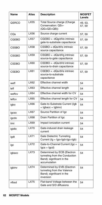
62
QSRCO LX55 Total Source charge (Charge Conservation: QS=-(QG+QD+QB))
49, 53, 57, 59
CQs LX56 Source charge current 57, 59
CGEBO LX57 CGEBO = -dQg/dVe intrinsic gate-to-substrate capacitance
57, 59
CSSBO LX58 CSSBO = dQs/dVs intrinsic source capacitance
57, 59
CSGBO LX59 CSGBO = -dQs/dVg intrinsic source-to-gate capacitance
57, 59
CSDBO LX60 CSDBO = -dQs/dVd intrinsic source-to-drain capacitance
57, 59
CSEBO LX61 CSEBO = -dQs/dVe intrinsic source-to-substrate capacitance
57, 59
weff LX62 Effective channel width 54
leff LX63 Effective channel length 54
weffcv LX64 Effective channel width for CV 54
leffcv LX65 Effective channel length for CV 54
igbo LX66 Gate-to-Substrate Current (Igb = Igbacc + Igbinv)
54
igcso LX67 Source Partition of Igc 54
igcdo LX68 Drain Partition of Igc 54
iimi LX69 Impact ionization current 54
igidlo LX70 Gate-induced drain leakage current
54
igdt LX71 Gate Dielectric Tunneling Current (Ig = Igs+Igd+Igc+Igb)
54
igc LX72 Gate-to-Channel Current (Igc = Igcs + Igcd)
54
igbacc LX73 Determined by ECB (Electron tunneling from the Conduction Band); significant in the accumulation
54
igbinv LX74 Determined by EVB (Electron tunneling from the Valence Band); significant in the inversion
54
vfbsd LX75 Flat-band Voltage between the Gate and S/D diffusions
54
Name Alias Description MOSFET Levels
MOSFET Models

vgse LX76 Effective Gate-to-Source Voltage
54
vox LX77 Voltage Across Oxide 54
rdv LX78 Asymmetric and Bias-Dependent Source Resistance, (rdsMod = 1)
54
rsv LX79 Asymmetric and Bias-Dependent Drain Resistance, (rdsMod = 1)
54
cap_bsz LX80 Zero voltage bias bulk-source capacitance
54
cap_bdz LX81 Zero voltage bias bulk-drain capacitance
54
CGGBM LX82 Total gate capacitance (including intrinsic), and all overlap and fringing components
54, 57, 59, 60
CGDBM LX83 Total gate-to-drain capacitance (including intrinsic), and overlap and fringing components
54, 57, 59, 60
CGSBM LX84 Total gate-to-source capacitance (including intrinsic), and overlap and fringing components
54, 57, 59, 60
CDDBM LX85 Total drain capacitance (including intrinsic), overlap and fringing components, and junction capacitance
54, 57, 59, 60
CDSBM LX86 Total drain-to-source capacitance
54, 57, 60
CDGBM LX87 Total drain-to-gate capacitance (including intrinsic), and overlap and fringing components
54, 57, 59, 60
CBGBM LX88 Total bulk-to-gate (floating body-to-gate) capacitance, including intrinsic and overlap components
54, 57, 59, 60
CBDBM LX89 Total bulk-to-drain capacitance (including intrinsic), and junction capacitance
54
Name Alias Description MOSFET Levels
MOSFET Models 63
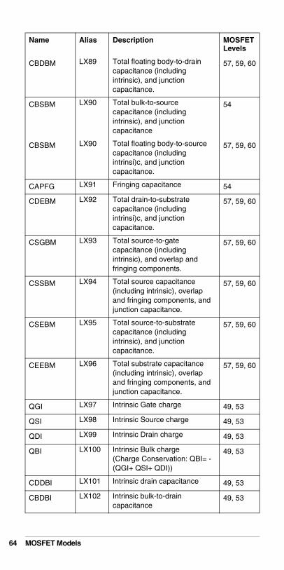
64
CBDBM LX89 Total floating body-to-drain capacitance (including intrinsic), and junction capacitance.
57, 59, 60
CBSBM LX90 Total bulk-to-source capacitance (including intrinsic), and junction capacitance
54
CBSBM LX90 Total floating body-to-source capacitance (including intrinsi)c, and junction capacitance.
57, 59, 60
CAPFG LX91 Fringing capacitance 54
CDEBM LX92 Total drain-to-substrate capacitance (including intrinsi)c, and junction capacitance.
57, 59, 60
CSGBM LX93 Total source-to-gate capacitance (including intrinsic), and overlap and fringing components.
57, 59, 60
CSSBM LX94 Total source capacitance (including intrinsic), overlap and fringing components, and junction capacitance.
57, 59, 60
CSEBM LX95 Total source-to-substrate capacitance (including intrinsic), and junction capacitance.
57, 59, 60
CEEBM LX96 Total substrate capacitance (including intrinsic), overlap and fringing components, and junction capacitance.
57, 59, 60
QGI LX97 Intrinsic Gate charge 49, 53
QSI LX98 Intrinsic Source charge 49, 53
QDI LX99 Intrinsic Drain charge 49, 53
QBI LX100 Intrinsic Bulk charge (Charge Conservation: QBI= -(QGI+ QSI+ QDI))
49, 53
CDDBI LX101 Intrinsic drain capacitance 49, 53
CBDBI LX102 Intrinsic bulk-to-drain capacitance
49, 53
Name Alias Description MOSFET Levels
MOSFET Models
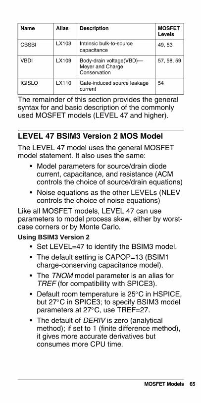
The remainder of this section provides the general syntax for and basic description of the commonly used MOSFET models (LEVEL 47 and higher).
LEVEL 47 BSIM3 Version 2 MOS ModelThe LEVEL 47 model uses the general MOSFET model statement. It also uses the same:
• Model parameters for source/drain diode current, capacitance, and resistance (ACM controls the choice of source/drain equations)
• Noise equations as the other LEVELs (NLEV controls the choice of noise equations)
Like all MOSFET models, LEVEL 47 can use parameters to model process skew, either by worst-case corners or by Monte Carlo.Using BSIM3 Version 2
• Set LEVEL=47 to identify the BSIM3 model.
• The default setting is CAPOP=13 (BSIM1 charge-conserving capacitance model).
• The TNOM model parameter is an alias for TREF (for compatibility with SPICE3).
• Default room temperature is 25°C in HSPICE, but 27°C in SPICE3; to specify BSIM3 model parameters at 27°C, use TREF=27.
• The default of DERIV is zero (analytical method); if set to 1 (finite difference method), it gives more accurate derivatives but consumes more CPU time.
CBSBI LX103 Intrinsic bulk-to-source capacitance
49, 53
VBDI LX109 Body-drain voltage(VBD)—Meyer and Charge Conservation
57, 58, 59
IGISLO LX110 Gate-induced source leakage current
54
Name Alias Description MOSFET Levels
MOSFET Models 65

66
• Three ways that BSIM3 can calculate Vth:
- User-specified K1 and K2 values.
- GAMMA1, GAMMA2, VBM, and VBX values entered in the .MODEL statement.
- User-specified NPEAK, NSUB, XT, and VBM values.
• NPEAK and U0 can be in meters or centimeters. You must enter the parameter NSUB in cm-3 units.
• VTH0 for P-channel in the .MODEL statement is negative.
• Default value of KT1 is -0.11.
• Minimum LITL value is 1.0e-9 m.
• VSAT, after temperature adjustment, is not allowed to go below a minimum value of 1.0e4 m/sec, to assure that it is positive after temperature compensation.
• The model parameters that accommodate temperature dependencies are KT1 and KT2 for VTH, UTE for U0, AT for VSAT, UA1 for UA, UB1 for UB, and UC1 for UC.
• Set up the conversion of temperature between HSPICE and SPICE3 as follows:SPICE3:.OPTION TEMP=125.MODEL NCH NMOS LEVEL=8 +TNOM =27 ...HSPICE:.TEMP 125.MODEL NCH NMOS LEVEL=47 +TREF =27 ...
• SCALM affects the common MOS parameters, such as XL, LD, XW, WD, CJ, CJSW, JS, and JSW.
• LEVEL 47 uses MOS parasitic models, specified by ACM.
• LEVEL 47 uses MOS noise models, specified by NLEV.
• DELVTO and DTEMP on the element line can be used with LEVEL 47.
MOSFET Models
• The impact ionization current set by PSCBE1 and PSCBE2 contributes to the drain-source current; not bulk current.
LEVEL 49 and 53 BSIM3v3 MOS ModelsLEVELs 49 and 53 use the general model statement described in MOSFET Model Statement on page 49. They also maintain compliance with the UC Berkeley release of BSIM3v3. Differences between LEVEL 49 and 53 are:
• LEVEL 49 complies with Berkeley BSIM3v3, but enhanced for higher speed. To achieve this, ACM defaults to 0 in LEVEL 49; Berkeley BSIM3v3 compliance requires ACM=10.
• LEVEL 53, is completely compliant with Berkeley BSIM3v3; all HSPICE-specific parameters default to OFF.
• Level 53 maintains full compliance with the Berkeley release, including numerically-identical model equations, identical parameter default values, and identical parameter range limits.
• Level 49 and 53 both support the following instance parameters, along with the DELVTO instance parameter, for local mismatch and NBTI (negative bias temperature instability) modeling:
- MULU0, low-field mobility (U0) multiplier. Default=1.0.
- MULUA, first-order mobility degradation coefficient (UA) multiplier.
- MULUB, second-order mobility degradation coefficient (UB) multiplier.
When HSPICE prints back a MOSFET element summary (.option list), it identifies the BSIM3V3 MOSFET, and prints back these three additional instance parameters.
For more information about this model, see “LEVELs 49 and 53 BSIM3v3 MOS Models” in the HSPICE MOSFET Models Manual.
MOSFET Models 67

68
Selecting Model VersionsThe recommended BSIM3v3 model specification is LEVEL=49, VERSION=3.22.
LEVEL 50 Philips MOS9 ModelThe Philips MOS9 model, available in HSPICE as LEVEL 50, uses the general model statement described in MOSFET Model Statement on page 49. Specific changes include:
• The ACM Parasitic Diode Model, using parameters JS, JSW, N, CJ, CJSW, CJGATE, MJ, MJSW, PB, PHP, ACM, and HDIF was added.
• The Philips JUNCAP Parasitic Diode Model were added.
• The JUNCAP=1 model parameter selects the JUNCAP Model, JUNCAP=0 (default) selects the ACM Model.
• Gate noise current is not available.
For more information, see
http://www.us.semiconductors.com/Philips_Models.
LEVEL 54 BSIM 4.0 ModelGeneral Form
Mxxx nd ng ns <nb> mname <L=val> + <W=val> <M=val> <AD=val> <AS=val> + <PD=val> <PS=val> <RGATEMOD=val> + <RBODYMOD=val> <TRNQSMOD=val> + <ACNQSMOD=val> <GEOMOD=val> + <RGEOMOD=val> <NRS=val> <NRD=val> + <RBPB=val> <RBPD=val> <RBPS=val> + <RBDB=val> <RBSB=val> <NF=val> + <MIN=val> <RDC=val> <RSC=val> + <DELVTO=val> <MULU0=val>+ <DELK1=val> <DELNFCT=val> <DELTOX=val>+ <RGATEMOD=val> <OFF> <IC=Vds, Vgs, Vbs>
nd Drain terminal node name ng Gate terminal node name ns Source terminal node name nb Bulk terminal node name mname MOSFET model name reference
MOSFET Models

L BSIM4 MOSFET channel length in meters W BSIM4 MOSFET channel width in meters AD Drain diffusion area AS Source diffusion area PD Perimeter of the drain junction:
if PERMOD=0, excludes the gate edge;otherwise, includes the gate edge
PS Perimeter of the source junction: if PERMOD=0, excludes the gate edge;otherwise, includes the gate edge
RGATEMOD Gate resistance model selector RBODYMOD Substrate resistance network model
selector TRNQSMOD Transient NQS model selector ACNQSMOD AC small-signal NQS model selector GEOMOD Geometry-dependent parasitics model
selector—specifies how the end S/Ddiffusions are connected
RGEOMOD Source/drain diffusion resistance and contact model selector—specifies the end S/D contact type: point, wide or merged, and how S/D parasitics resistance is computed
NRS Number of source diffusion squares NRD Number of drain diffusion squares RBPB Resistance connected between
bNodePrime and bNode RBPD Resistance connected between
bNodePrime and dbNode RBPS Resistance connected between
bNodePrime and sbNode RBDB Resistance connected between dbNode
and bNode RBSB Resistance connected between sbNode
and bNode NF Number of device fingers MIN Whether to minimize the number of drain
or source diffusions for even-number fingered device
RDC Drain contact resistance for per-finger device
RSC Source contact resistance for per-finger device
DELVTO Shift in zero-bias threshold voltage VTH0(DELVT0) MULU0 Low-field mobility (U0) multiplier
MOSFET Models 69

70
DELK1 Shift in body bias coefficient K1 DELNFCT Shift in subthreshold swing (NFACTOR) DELTOX Shift in gate electrical/physical equivalent
oxide thickness (TOXE and TOXP)RGATEMOD Gate resistance model selectorOFF Sets initial condition=OFF in DC analysis IC Initial guess in the order LMLT Channel length shrink factor, specified in
the model card. Default=1.0.WMLT Channel width shrink factor, specified in
the model card. Default=1.0.
Level 54, the UC Berkeley BSIM 4.0.0 MOS model, can model sub-0.13 micron CMOS technology and RF high-speed CMOS circuit simulation.
BSIM4.0.0 has major improvements and additions over BSIM3v3, including:
• Model of intrinsic input resistance (Rii) for both RF, high-frequency analog, and high-speed digital applications
• Flexible substrate resistance network for RF modeling
• A channel thermal noise model and a noise partition model for the induced gate noise
• A non-quasi-static (NQS) model consistent with the Rii-based RF model and an AC model that accounts for the NQS effect in both transconductances and capacitances
• A gate-direct tunneling model• A geometry-dependent parasitics model for
various source/drain connections and multi-finger devices
• A model for steep vertical retrograde doping profiles
• A model for pocket-implanted devices in Vth, bulk charge effect model, and Rout
• Asymmetrical and bias-dependent source/drain resistance. Select either internal or external to the intrinsic MOSFET.
• Accepts either electrical or physical gate oxide thickness as the model input.
MOSFET Models

• Quantum mechanical charge-layer-thickness model for both IV and CV
• A mobility model for predictive modeling• A gate-induced drain leakage (GIDL) current
model• A unified flicker (1/f) noise model, which is
smooth over all bias regions and considers the bulk charge effect
• Different diode IV and CV characteristics for source and drain junctions
• Junction diode breakdown with or without current limiting
• Dielectric constant of a gate dielectric as a model parameter
BSIM4.2.1 has the following major improvements and additions over BSIM4.2.0:
• GISL (Gate Induced Source Leakage) current component corresponds to the same current at the drain side (GIDL).
• The warning limits for effective channel length, channel width, and gate oxide thickness have been reduced, to avoid unnecessary warnings if you use BSIM4 aggressively, beyond the desired model card application ranges.
• The DELTOX parameter in the MOS active element (M) models the relative variation on the transconductance (oxide thickness) of the MOS in Monte Carlo analysis.
HSPICE also supports BSIM4.2.3 and BSIM4.3.0
LEVEL 55 EPFL-EKV MOSFET ModelThe EPFL-EKV MOSFET model is scalable, compact, and built on fundamental physical properties of the MOS structure. LEVEL 55 uses the general model statement (see MOSFET Model Statement on page 49). Use this model to design and simulate low-voltage, low-current analog, and mixed analog-digital circuits with submicron CMOS.
MOSFET Models 71
72
Single Equation ModelThe EPFL-EKV MOSFET model is a “single expression” which preserves continuity of first- and higher-order derivatives with respect to any terminal voltage, in the entire range of validity of the model.
Use analytical expressions of first-order derivatives as transconductances or transcapacitances.
LEVEL 55 models these physical effects:
• Basic geometrical and process-related aspects as oxide thickness, junction depth, effective channel length, and width
• Effects of doping profile, substrate effect
• Modeling of weak, moderate, and strong inversion behavior
• Modeling of mobility effects due to vertical and lateral fields, velocity saturation
• Short-channel effects as channel-length modulation (CLM), source and drain charge-sharing, reverse short channel effect (RSCE)
• Substrate current due to impact ionization• Quasi-static charge-based dynamic model• Thermal and flicker noise modeling• First-order NQS model for transadmittances• Short-distance geometry- and bias-
dependent device matching.Coherence of Static and Dynamic Models
Simulation derives all aspects of the static, the quasi-static, and the non-quasi-static (NQS) dynamic and noise models, from the normalized transconductance-to-current ratio. These expressions use symmetric normalized forward and reverse currents. • For quasi-static dynamic operations, you can
use either a charge-based model for the node charges and trans-capacitances, or a simpler capacitances model.
• The dynamic model, including the time constant for the NQS model, is described in symmetrical terms of the forward and reverse normalized currents.
MOSFET Models

The charge formulation also expresses effective mobility dependence of a local field.
LEVEL 57 UC Berkeley BSIM3-SOI ModelGeneral Form
Mxxx nd ng ns ne <np> <nb> <nT> mname+ <L=val> <W=val> <M=val> <AD=val> <AS=val> + <PD=val> <PS=val> <NRD=val> <NRS=val> + <NRB=val> <RTH0=val> <CTH0=val> <NBC=val>+ <NSEG=val> <PDBCP=val> <PSBCP=val> + <AGBCP=val> <AEBCP=val> <VBSUSR=val> + <DELTOX=val> <TNODEOUT> <off> <BJToff=val>+ <IC=Vds, Vgs, Vbs, Ves, Vps>
AD Drain diffusion area
AEBCP Parasitic body-to-substrate overlap area for body contact
AGBCP Parasitic gate-to-body overlap area for body contact
AS Source diffusion area
BJTOFF Turning off BJT if equal to 1
CTH0 Thermal capacitance per unit width
DELTOX Shift in gate electrical/physical equivalent oxide thickness (TOXE and TOXP)
FRBODY Coefficient of distributed body resistance effects. Default is 1.0.
IC Initial guess in the order
L SOI MOSFET channel length in meters
M Multiplier to simulate multiple SOI MOSFETs in parallel
mname MOSFET model name reference
Mxxx SOI MOSFET element name
nb Internal body node name or number
NBC Number of body contact isolation edge
nd Drain terminal node name or number
ne Back gate (or substrate) node name or number
ng Front gate node name or number
np External body contact node name or number
NRB Number of squares for body series resistance
NRD Number of squares of drain diffusion for drain series resistance
NRS Number of squares of source diffusion for source series resistance
ns Source terminal node name or number
NSEG Number of segments for channel width partitioning
nT Temperature node name or number
MOSFET Models 73
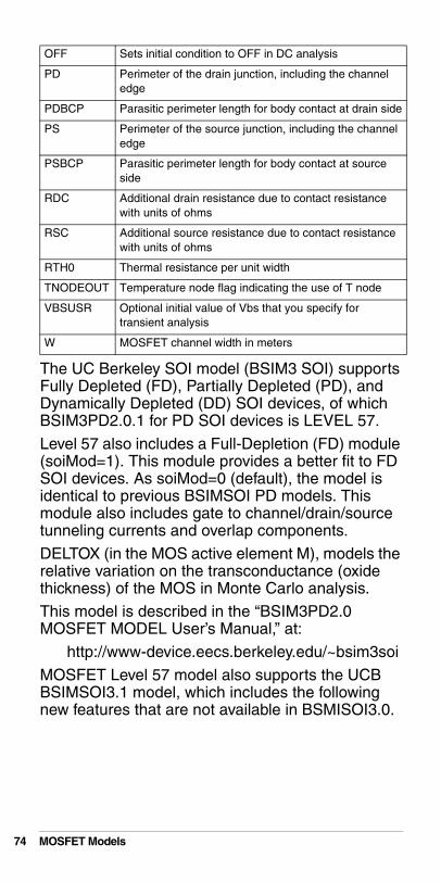
74
The UC Berkeley SOI model (BSIM3 SOI) supports Fully Depleted (FD), Partially Depleted (PD), and Dynamically Depleted (DD) SOI devices, of which BSIM3PD2.0.1 for PD SOI devices is LEVEL 57.
Level 57 also includes a Full-Depletion (FD) module (soiMod=1). This module provides a better fit to FD SOI devices. As soiMod=0 (default), the model is identical to previous BSIMSOI PD models. This module also includes gate to channel/drain/source tunneling currents and overlap components.
DELTOX (in the MOS active element M), models the relative variation on the transconductance (oxide thickness) of the MOS in Monte Carlo analysis.
This model is described in the “BSIM3PD2.0 MOSFET MODEL User’s Manual,” at:
http://www-device.eecs.berkeley.edu/~bsim3soi
MOSFET Level 57 model also supports the UCB BSIMSOI3.1 model, which includes the following new features that are not available in BSMISOI3.0.
OFF Sets initial condition to OFF in DC analysis
PD Perimeter of the drain junction, including the channel edge
PDBCP Parasitic perimeter length for body contact at drain side
PS Perimeter of the source junction, including the channel edge
PSBCP Parasitic perimeter length for body contact at source side
RDC Additional drain resistance due to contact resistance with units of ohms
RSC Additional source resistance due to contact resistance with units of ohms
RTH0 Thermal resistance per unit width
TNODEOUT Temperature node flag indicating the use of T node
VBSUSR Optional initial value of Vbs that you specify for transient analysis
W MOSFET channel width in meters
MOSFET Models

Ideal Full-Depletion (FD) ModelingBSIMSOI3.0 supports the modeling of these two families of SOI MOSFETs, with a SOIMOD switching model flag.
• SOIMO =0 for partially depleted devices (PD).• SOIMOD=1 for devices that tend to operate in
a mixed mode of PD and FD.
V3.1 also provides an ideal full-depletion (FD) module (SOIMOD=2), not available in V3.0, to model FD SOI devices that literally exhibit no floating-body behavior. As in BSIMSOI3.0, the default SOIMOD value is 0 for BSIMSOI3.1.
The following physical modeling components, related to the internal SOI body node, are critical for accurately modeling PD SOI devices, but are not needed for the ideal FD module.
• Source/Drain to body diode currents• Source-Body-Drain parasitic BJT currents• Impact ionization currents• Gate-body direct currents• Body-related capacitances.
Gate Resistance Modeling
BSIMSOI3.1 uses the same gate resistance models as in the BSIM4 model, with four options for various gate-resistance modeling topologies.
• RGATEMOD, gate-resistance model selector
- RGATEMOD = 0: No gate resistance (default)
- RGATEMOD = 1: Constant gate resistance
- RGATEMOD = 2: Rii model with variable resistance
- RGATEMOD = 3: Rii model with two nodes
• XRCRG1, parameter for distributed channel-resistance effect for intrinsic input resistance
• XRCRG2, parameter to account for the excess channel diffusion resistance for intrinsic input resistance
MOSFET Models 75

76
• NGCON, number of gate contacts
• XGW, distance from the gate contact to the channel edge in the W direction
• XGL, offset of the gate length due to variations in patterning
• RSHG, gate electrode sheet resistanceGate Resistance Equivalent Circuit
• RGATEMOD = 0: No gate resistance (default)
• RGATEMOD = 1: Constant gate resistance
• RGATEMOD = 2: Variable resistance with Rii model
• RGATEMOD = 3: Rii model with two nodes
• Rgeltd: (Poly) gate electrode resistance, bias independent
• Rii: Intrinsic input gate resistance, reflected to the gate from the intrinsic channel region. It is bias dependent and a first-order non-quasi static model, for RF and rapid transient MOSFET operations
Enhanced Binning Capability
Model parameters for the following components are now binnable, for better accuracy and scalability:
• Junction depth
• Gate-tunneling current
• Temperature dependence of threshold voltage, mobility, saturation velocity, parasitic resistance, and diode currents.
LEVEL 58 University of Florida SOI Model
UFSOI has non-fully depleted (NFD) and fully depleted (FD) SOI models (no dynamic mode operating between NFD and FD allowed) that separately describe two main types of SOI devices.
General Form
Mxxx nd ngf ns <ngb> mname <L=val> <W=val> + <M=val> <AD=val> <AS=val> <PD=val> <PS=val> + <NRD=val> <NRS=val> <NRB=val> <RTH=val>+ <CTH=val> <off> <IC=Vds,Vgfs,VGbs>
MOSFET Models
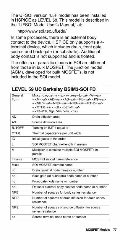
The UFSOI version 4.5F model has been installed in HSPICE as LEVEL 58. This model is described in the “UFSOI Model User’s Manual,” at:
http://www.soi.tec.ufl.edu/
In some processes, there is an external body contact to the device. HSPICE only supports a 4-terminal device, which includes drain, front gate, source and back gate (or substrate). Additional body contact is not supported and is floated.
The effects of parasitic diodes in SOI are different from those in bulk MOSFET. The junction model (ACM), developed for bulk MOSFETs, is not included in the SOI model.
LEVEL 59 UC Berkeley BSIM3-SOI FDGeneral Form
Mxxx nd ng ns ne <np> mname <L=val><W=val> + <M=val> <AD=val> <AS=val> <PD=val> <PS=val> + <NRD=val><NRS=val> <NRB=val> <RTH0=val>+ <CTH0=val> <off> <BJToff=val>+ <IC=Vds, Vgs, Vbs, Ves, Vps>
AD Drain diffusion area
AS Source diffusion area
BJTOFF Turning off BJT if equal to 1
CTH0 Thermal capacitance per unit width
IC Initial guess in the order
L SOI MOSFET channel length in meters
M Multiplier to simulate multiple SOI MOSFETs in parallel
mname MOSFET model name reference
Mxxx SOI MOSFET element name
nd Drain terminal node name or number
ne Back gate (or substrate) node name or number
ng Front gate node name or number
np Optional external body contact node name or number
NRB Number of squares for body series resistance
NRD Number of squares of drain diffusion for drain series resistance
NRS Number of squares of source diffusion for source series resistance
ns Source terminal node name or number
MOSFET Models 77

78
The UC Berkeley SOI (BSIM3 SOI) Fully Depleted (FD) model is MOSFET LEVEL 59.
This model is described in the “BSIM3SOI FD2.1 MOSFET MODEL User Manual,” at:
http://www-device.eecs.berkeley.edu/~bsim3soi
LEVEL 60 UC Berkeley BSIM3-SOI DD Model
OFF Sets initial condition to OFF in DC analysis
PD Perimeter of drain junction, including the channel edge
PS Perimeter of source junction, including the channel edge
RTH0 Thermal resistance per unit width
W MOSFET channel width in meters
General Form
Mxxx nd ng ns ne <np> mname <L=val> <W=val> + <M=val> <AD=val> <AS=val><PD=val> <PS=val> + <NRD=val> <NRS=val> <NRB=val> <RHT0=val> + <CTH0=val> <off> <BJToff=val>+ <IC=Vds, Vgs, Vbs, Ves, Vps>
Mxxx SOI MOSFET element name
nd Drain terminal node name or number
ng Front gate node name or number
ns Source terminal node name or number
ne Back gate or substrate node name or number
np External body contact node name or number
mname MOSFET model name reference
L SOI MOSFET channel length in meters
W SOI MOSFET channel width in meters
M Multiplier to simulate multiple SOI MOSFETs
AD Drain diffusion area
AS Source diffusion area
PD Drain junction perimeter, including channel edge
PS Source junction perimeter, including channel edge
NRD Number of squares of drain diffusion for drain series resistance
NRS Number of squares of source diffusion for source series diffusion
NRB Number of squares in body series resistance
RDC Additional drain resistance due to contact resistance, in units of ohms
MOSFET Models
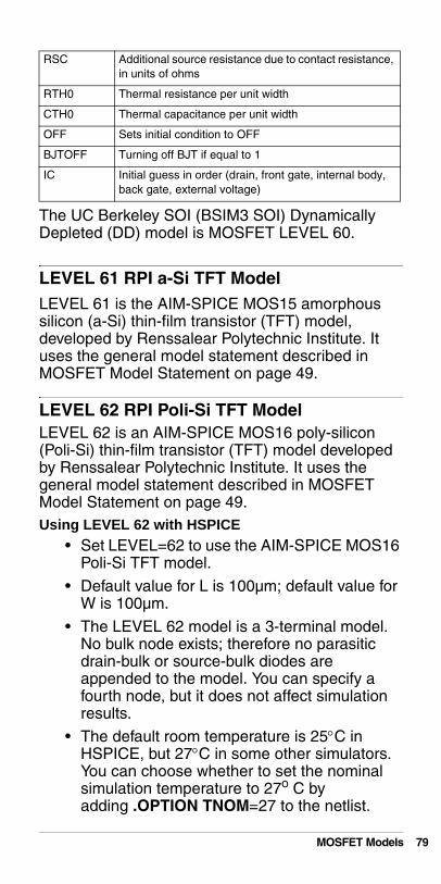
The UC Berkeley SOI (BSIM3 SOI) Dynamically Depleted (DD) model is MOSFET LEVEL 60.
LEVEL 61 RPI a-Si TFT ModelLEVEL 61 is the AIM-SPICE MOS15 amorphous silicon (a-Si) thin-film transistor (TFT) model, developed by Renssalear Polytechnic Institute. It uses the general model statement described in MOSFET Model Statement on page 49.
LEVEL 62 RPI Poli-Si TFT ModelLEVEL 62 is an AIM-SPICE MOS16 poly-silicon (Poli-Si) thin-film transistor (TFT) model developed by Renssalear Polytechnic Institute. It uses the general model statement described in MOSFET Model Statement on page 49. Using LEVEL 62 with HSPICE
• Set LEVEL=62 to use the AIM-SPICE MOS16 Poli-Si TFT model.
• Default value for L is 100µm; default value for W is 100µm.
• The LEVEL 62 model is a 3-terminal model. No bulk node exists; therefore no parasitic drain-bulk or source-bulk diodes are appended to the model. You can specify a fourth node, but it does not affect simulation results.
• The default room temperature is 25°C in HSPICE, but 27°C in some other simulators. You can choose whether to set the nominal simulation temperature to 27o C by adding .OPTION TNOM=27 to the netlist.
RSC Additional source resistance due to contact resistance, in units of ohms
RTH0 Thermal resistance per unit width
CTH0 Thermal capacitance per unit width
OFF Sets initial condition to OFF
BJTOFF Turning off BJT if equal to 1
IC Initial guess in order (drain, front gate, internal body, back gate, external voltage)
MOSFET Models 79

80
LEVEL 63, Philips MOS11 ModelThe Philips MOS Model 11, Level 1100 and 1101, are available as Level 63 in the Synopsys HSPICE device models (based on the “Unclassified Report NL-UR 2001/813” by R. Langevelde).
Philips MOS Model 11, Level 1101, is an updated version of Level 1100. It uses the same basic equations as Level 1100, but uses different geometry scaling rules.
It includes two types of geometrical scaling rules: physical rules and binning rules. To select these scaling rules, use the Version parameter (1100, 11010, or 11011).
Also, for the parasitic diode model, the Philips JUNCAP Parasitic Diode Model was added.
For more information about the MOS Model 11 and the Philips JUNCAP Parasitic Diode Model, see:
http://www.semiconductors.philips.com/Philips_Models
Using the Philips MOS11 Model in HSPICE• Set Level=63 to select Philips MOS Model 11.
• Set the MOS11 version:
- Set Version=1100 to identify Philips MOS Model 11, Level 1100.
- Set Version=11010 to identify Philips MOS Model 11, Level 1101 (physical geometry scaling rules).
- Set Version=11011 to identify Philips MOS Model 11, Level 1101 (binning geometry scaling rules).
• The default room temperature is 25oC in HSPICE, but is 27oC in most other simulators. When comparing to other simulators, set the simulation temperature to 27, using .TEMP 27 or .OPTION TNOM=27.
• The set of model parameters should always include the model reference temperature, TR, which corresponds to TREF in other levels in HSPICE. The default for TR is 21.0, to match the Philips simulator.
MOSFET Models
• The model has its own charge-based capacitance model. The CAPOP parameter, which selects different capacitance models, is ignored in this model.
• The model uses analytical derivatives for the conductances, and ignores the DERIV parameter for the finite difference method.
• DTEMP can be used with this model. It is set on the element line and increases the temperature of individual elements relative to the circuit temperature.
• Since defaults are nonzero, it is strongly recommended that every model parameter listed in Level 63 Model Parameters table be set in the .MODEL statement.
• The general syntax for MOSFET element is the same as the other standard MOSFET models other than PS and PD. In Level=63, PS and PD are defined as the length of the sidewall of the source/drain which is not under the gate.
• MOS11 has LMIN as its own parameter, which has the difference definition from that of HSPICE. To avoid the conflict with LMIN in HSPICE, LMIN parameter in HSPICE level=63 was changed to LLMIN.
LEVEL 64 HiSIM1.0 ModelHiSIM (Hiroshima-university STARC IGFET Model) is a publicly-available MOSFET model for circuit simulation. It uses drift-diffusion approximation, and a channel-surface-potential description. Level 64 Model Selectors
Parameter Default Description
LEVEL 64 Model selector
VERSION 100 Model version number
MOSFET Models 81
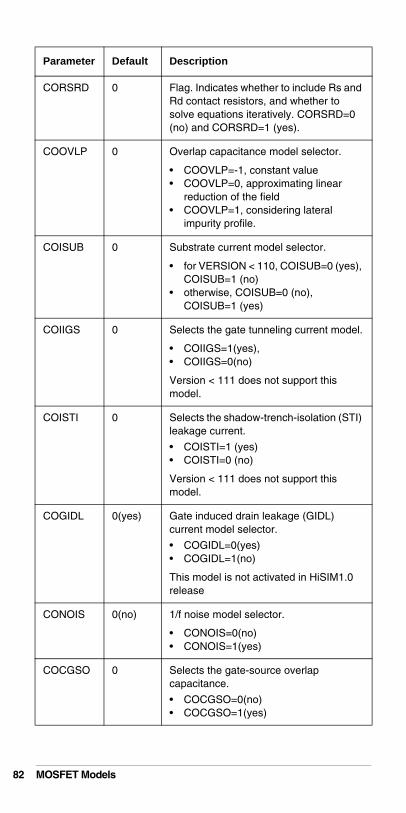
82
CORSRD 0 Flag. Indicates whether to include Rs and Rd contact resistors, and whether to solve equations iteratively. CORSRD=0 (no) and CORSRD=1 (yes).
COOVLP 0 Overlap capacitance model selector.
• COOVLP=-1, constant value• COOVLP=0, approximating linear
reduction of the field• COOVLP=1, considering lateral
impurity profile.
COISUB 0 Substrate current model selector.
• for VERSION < 110, COISUB=0 (yes), COISUB=1 (no)
• otherwise, COISUB=0 (no), COISUB=1 (yes)
COIIGS 0 Selects the gate tunneling current model.
• COIIGS=1(yes),• COIIGS=0(no)
Version < 111 does not support this model.
COISTI 0 Selects the shadow-trench-isolation (STI) leakage current.
• COISTI=1 (yes) • COISTI=0 (no)
Version < 111 does not support this model.
COGIDL 0(yes) Gate induced drain leakage (GIDL) current model selector.
• COGIDL=0(yes)• COGIDL=1(no)
This model is not activated in HiSIM1.0 release
CONOIS 0(no) 1/f noise model selector.
• CONOIS=0(no)• CONOIS=1(yes)
COCGSO 0 Selects the gate-source overlap capacitance.
• COCGSO=0(no)• COCGSO=1(yes)
Parameter Default Description
MOSFET Models
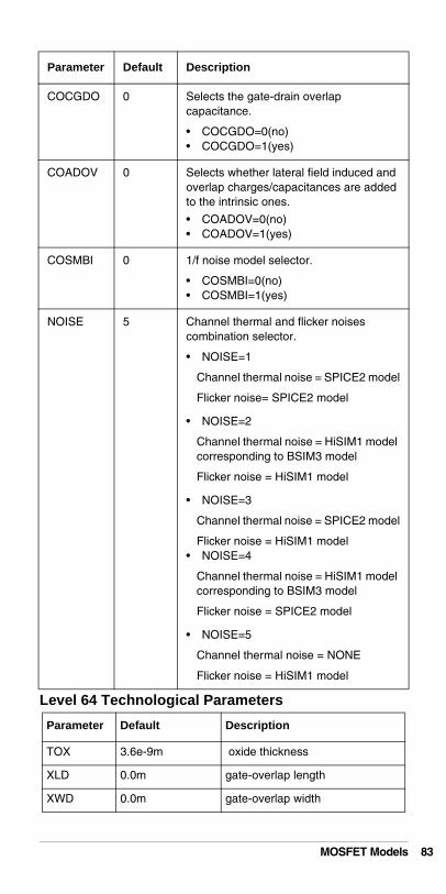
Level 64 Technological Parameters
COCGDO 0 Selects the gate-drain overlap capacitance.
• COCGDO=0(no)• COCGDO=1(yes)
COADOV 0 Selects whether lateral field induced and overlap charges/capacitances are added to the intrinsic ones.
• COADOV=0(no)• COADOV=1(yes)
COSMBI 0 1/f noise model selector.
• COSMBI=0(no)• COSMBI=1(yes)
NOISE 5 Channel thermal and flicker noises combination selector.
• NOISE=1
Channel thermal noise = SPICE2 model
Flicker noise= SPICE2 model
• NOISE=2
Channel thermal noise = HiSIM1 model corresponding to BSIM3 model
Flicker noise = HiSIM1 model
• NOISE=3
Channel thermal noise = SPICE2 model
Flicker noise = HiSIM1 model• NOISE=4
Channel thermal noise = HiSIM1 model corresponding to BSIM3 model
Flicker noise = SPICE2 model
• NOISE=5
Channel thermal noise = NONE
Flicker noise = HiSIM1 model
Parameter Default Description
TOX 3.6e-9m oxide thickness
XLD 0.0m gate-overlap length
XWD 0.0m gate-overlap width
Parameter Default Description
MOSFET Models 83
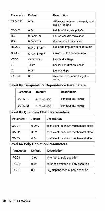
84
Level 64 Temperature Dependence Parameters
Level 64 Quantum Effect Parameters
Level 64 Poly Depletion Parameters
XPOLYD 0.0m difference between gate-poly and design lengths
TPOLY 0.0m height of the gate poly-Si
RS 0.0ohm*m source-contact resistance
RD 0.0ohm*m drain-contact resistance
NSUBC 5.94e+17cm-3 substrate-impurity concentration
NSUBP 5.94e+17cm-3 maxim pocket concentration
VFBC -0.722729 V flat-band voltage
LP 0.0m pocket penetration length
XJ 0.0m junction depth
KAPPA 3.9 dielectric constance for gate-oxide
Parameter Default Description
BGTMP1 9.03e-5eVK-1 bandgap narrowing
BGTMP2 3.05e-7eVK-2 bandgap narrowing
Parameter Default Description
QME1 0.0mV coefficient, quantum mechanical effect
QME2 0.0V coefficient, quantum mechanical effect
QME3 0.0m coefficient, quantum mechanical effect
Parameter Default Description
PGD1 0.0V strength of poly depletion
PGD2 0.0V threshold voltage of poly depletion
PGD3 0.0 Vds dependence of poly depletion
Parameter Default Description
MOSFET Models

Level 64 Short Channel Parameters
Level 64 Narrow Channel Parameters
Level 64 Mobility Parameters
Parameter Default Description
PARL1 1.0 strength of lateral-electric-field gradient
PARL2 2.2e-8m depletion width of channel/contact junction
SC1 13.5V-1 short-channel coefficient 1
SC2 1.8V-2 short-channel coefficient 2
SC3 0.0V-2m short-channel coefficient 3
SCP1 0.0V-1 short-channel coefficient 1 for pocket
SCP2 0.0V-2 short-channel coefficient 2 for pocket
SCP3 0.0V-2m short-channel coefficient 3 for pocket
Parameter Default Description
WFC 0.0m*F/cm2 voltage reduction
MUEPH2 0.0 mobility reduction
W0 0.0log(cm) minimum gate width
Parameter Default Description
VDS0 0.05V drain voltage for extracting low-field mobility
MUECB0 300.0cm2/Vs Coulomb scattering
MUECB1 30.0cm2/Vs Coulomb scattering
MUEPH0 0.295 phonon scattering
MUEPH1 1.0e7 phonon scattering
MUETMP 0.0 temperature dependence of phonon scattering
MUESR0 1.0 surface-roughness scattering
MUESR1 7.0e8 surface-roughness scattering
NDEP 1.0 coefficient of effective-electric field
NINV 0.5 coefficient of effective-electric field
NINVD 0.0V-1 modification of NINV
MOSFET Models 85

86
Level 64 Channel Length Modulation Parameters
Level 64 Substrate Current Parameters
Level 64 Gate Current Parameters
BB 2.0(NMOS)1.0(PMOS)
high-field-mobility degradation
VMAX 1.0e7cm/s maximum saturation velocity
VOVER 0.0 velocity overshoot effect
VOVERP 0.0 Lgate dependence of velocity overshoot
RPOCK1 0.0V2*m1/2/A resistance coefficient caused by the potential barrier
RPOCK2 0.0V resistance coefficient caused by the potential barrier
Parameter Default Description
CLM1 0.3 hardness coefficient of channel/contact junction
CLM2 0.0 coefficient for QB contribution
CLM3 0.0 coefficient for QI contribution
Parameter Default Description
SUB1 0.0V-1 substrate current coefficient 1
SUB2 -70.0 substrate current coefficient 2
SUB3 1.0 substrate current coefficient 3
Parameter Default Description
GLEAK1 0.0A*V-3/2/C gate current coefficient 1
GLEAK2 0.0 gate current coefficient 2
GLEAK3 0.0 gate current coefficient 3
GLPART1 0 partitioning ratio of gate leakage current
GLPART2 0 partitioning ratio of gate leakage current
Parameter Default Description
MOSFET Models
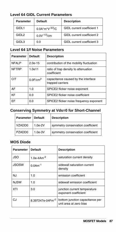
Level 64 GIDL Current Parameters
Level 64 1/f Noise Parameters
Conserving Symmetry at Vds=0 for Short-Channel
MOS Diode
Parameter Default Description
GIDL1 0.0A*m*V-3/2/C GIDL current coefficient 1
GIDL2 0.0V-1/2/cm GIDL current coefficient 2
GIDL3 0.0 GIDL current coefficient 3
Parameter Default Description
NFALP 2.0e-15 contribution of the mobility fluctuation
NFTRP 1.0e11 ratio of trap density to attenuation coefficient
CIT 0.0F/cm2 capacitance caused by the interface trapped carriers
AF 1.0 SPICE2 flicker noise exponent
KF 0.0 SPICE2 flicker noise coefficient
EF 0.0 SPICE2 flicker noise frequency exponent
Parameter Default Description
VZADD0 1.0e-2V symmetry conservation coefficient
PZADD0 1.0e-3V symmetry conservation coefficient
Parameter Default Description
JSO 1.0e-4Am-2 saturation current density
JSOSW 0.0Am-1 sidewall saturation current density
NJ 1.0 emission coefficient
NJSW 1.0 sidewall emission coefficient
XTI 3.0 junction current temperature exponent coefficient
CJ 8.397247e-04Fm-2 bottom junction capacitance per unit area at zero bias
MOSFET Models 87

88
Subthreshold Swing
Model parameter defaults in the above tables are valid only for versions 100 and 110. For other versions, please refer to the following table:
CJSW 5.0e-10Fm-1 source/drain sidewall junction capacitance per unit area at zero bias
CJSWG 5.0e-10Fm-1 source/drain gate sidewall junction capacitance per unit area at zero bias
MJ 0.5 bottom junction capacitance grading coefficient
MJSW 0.33 source/drain sidewall junction capacitance grading coefficient
MJSWG 0.33 source/drain gate sidewall junction capacitance grading coefficient
PB 1.0V bottom junction build-in potential
PBSW 1.0V source/drain sidewall junction build-in potential
PBSWG 1.0V source/drain gate sidewall junction build-in potential
VDIFFJ 0.5V diode threshold voltage between source/drain and substrate
PTHROU 0.0 correction for steep subthreshold swing
Parameter Default Description
PTHROU 0.0 correction for steep subthreshold swing
Parameter Version=100, 110 Others
VMAX 1.00e+7 7.00e+6
BGTMP1 9.03e-5 90.25e-6
BGTMP2 3.05e-7 100.0e-9
Parameter Default Description
MOSFET Models

TOX 3.60e-9 5.0e-9
RS 0.0 80.0e-6
RD 0.0 80.0e-6
VFBC -0.722729 -1.0
NSUBC 5.94e+17 1.0e+17
PARL2 2.20e-8 1.0e+17
LP 0.0 15.0e-9
NSUBP 5.94e+17 1.0e+17
SC1 13.5 0.0
SC2 1.8 0.0
PGD1 0.0 0.01
PGD2 0.0 1.0
PGD3 0.0 0.8
NINVD 0.0 1.0e-9
MUEPH1 1.00e+7 25.0e+3
MUEPH0 0.295 0.300
MUESR1 7.00e+8 2.0e+15
MUESR0 1.0 2.0
MUETMP 0.0 1.5
SUB1 0.0 10.0
SUB2 -70.0 20.0
SUB3 1.0 0.8
CJ 8.397247e-04 5.0e-04
CLM1 0.3 0.7
CLM2 0.0 2.0
CLM3 0.0 1.0
RPOCK1 0.0 0.01
Parameter Version=100, 110 Others
MOSFET Models 89

90
MOSFETSTo turn off model effects, use the following settings:
• Short-Channel Effect SC1 = SC2 = SC3 = 0• Reverse-Short-Channel Effect LP = 0• Quantum-Mechanical Effect QME1=QME2=QME3=0• Poly-Depletion Effect PGD1=PGD2=PGD3=0• Channel-Length Modulation CLM1=CLM2=CLM3=0• Narrow-Channel Effect WFC = MUEPH2 = 0
RPOCK2 0.0 0.1
RPOCP1 0.0 1.0
VOVER 0.0 0.01
VOVERP 0.0 0.1
QME1 0.0 40.0e-12
QME2 0.0 300.0e-12
GIDL1 0.0 5.0e-3 for HiSIM101, 5.0e-6 for others
GIDL2 0.0 1.0e+6
GIDL3 0.0 0.3
GLEAK1 0.0 0.01e+6 for HiSIM101, 10.0e+3 for others
GLEAK2 0.0 20.0e+6
GLEAK3 0.0 0.3
PZADD0 1.0e-3 5.0e-3
NFTRP 100.0e+9 10.0e+9
NFALP 2.00e-15 1.0e-16
Parameter Version=100, 110 Others
MOSFET Models
Top Related