


Languages
Pages
Legal

This is information on a product in full production.
March 2014 DocID026040 Rev 1 1/18
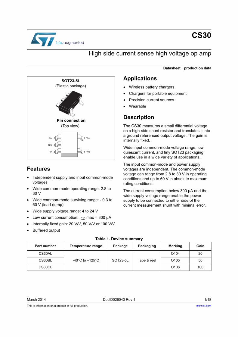
CS30
High side current sense high voltage op amp
Datasheet - production data
Features
• Independent supply and input common-mode voltages
• Wide common-mode operating range: 2.8 to 30 V
• Wide common-mode surviving range: - 0.3 to 60 V (load-dump)
• Wide supply voltage range: 4 to 24 V
• Low current consumption: ICC max = 300 µA
• Internally fixed gain: 20 V/V, 50 V/V or 100 V/V
• Buffered output
Applications
• Wireless battery chargers
• Chargers for portable equipment
• Precision current sources
• Wearable
Description
The CS30 measures a small differential voltage on a high-side shunt resistor and translates it into a ground referenced output voltage. The gain is internally fixed.
Wide input common-mode voltage range, low quiescent current, and tiny SOT23 packaging enable use in a wide variety of applications.
The input common-mode and power supply voltages are independent. The common-mode voltage can range from 2.8 to 30 V in operating conditions and up to 60 V in absolute maximum rating conditions.
The current consumption below 300 µA and the wide supply voltage range enable the power supply to be connected to either side of the current measurement shunt with minimal error.
2
1
3Vp
Out
Gnd
4
5
Vm
Vcc
SOT23-5L(Plastic package)
Pin connection(Top view)
Table 1. Device summary
Part number Temperature range Package Packaging Marking Gain
CS30AL
-40°C to +125°C SOT23-5L Tape & reel
O104 20
CS30BL O105 50
CS30CL O106 100
www.st.com
Contents CS30
2/18 DocID026040 Rev 1
Contents
1 Application schematic and pin description . . . . . . . . . . . . . . . . . . . . . . 3
2 Absolute maximum ratings and operating conditions . . . . . . . . . . . . . 4
3 Electrical characteristics . . . . . . . . . . . . . . . . . . . . . . . . . . . . . . . . . . . . . 5
3.1 Electrical characteristics curves . . . . . . . . . . . . . . . . . . . . . . . . . . . . . . . . . 8
4 Parameter definitions . . . . . . . . . . . . . . . . . . . . . . . . . . . . . . . . . . . . . . . 12
4.1 Common mode rejection ratio (CMR) . . . . . . . . . . . . . . . . . . . . . . . . . . . . 12
4.2 Supply voltage rejection ratio (SVR) . . . . . . . . . . . . . . . . . . . . . . . . . . . . 12
4.3 Gain (Av) and input offset voltage (Vos) . . . . . . . . . . . . . . . . . . . . . . . . . . 12
4.4 Output voltage drift versus temperature . . . . . . . . . . . . . . . . . . . . . . . . . . 13
4.5 Output voltage accuracy . . . . . . . . . . . . . . . . . . . . . . . . . . . . . . . . . . . . . . 14
5 Application information . . . . . . . . . . . . . . . . . . . . . . . . . . . . . . . . . . . . . 15
6 Package information . . . . . . . . . . . . . . . . . . . . . . . . . . . . . . . . . . . . . . . . 16
7 Revision history . . . . . . . . . . . . . . . . . . . . . . . . . . . . . . . . . . . . . . . . . . . 17

DocID026040 Rev 1 3/18
CS30 Application schematic and pin description
18
1 Application schematic and pin description
The CS30 high-side current sense amplifier features a 2.8 to 30 V input common-mode range that is independent of the supply voltage. The main advantage of this feature is that it allows high-side current sensing at voltages much greater than the supply voltage (VCC).
Figure 1. Application schematic
Table 2 describes the function of each pin. The pin positions are shown in the illustration on the cover page and in Figure 1 above.
Table 2. Pin description
Symbol Type Function
Out Analog outputOutput voltage, proportional to the magnitude of the sense voltage Vp-Vm.
Gnd Power supply Ground line
VCC Power supply Positive power supply line
Vp Analog inputConnection for the external sense resistor. The measured current enters the shunt on the Vp side.
Vm Analog inputConnection for the external sense resistor. The measured current exits the shunt on the Vm side.
Absolute maximum ratings and operating conditions CS30
4/18 DocID026040 Rev 1
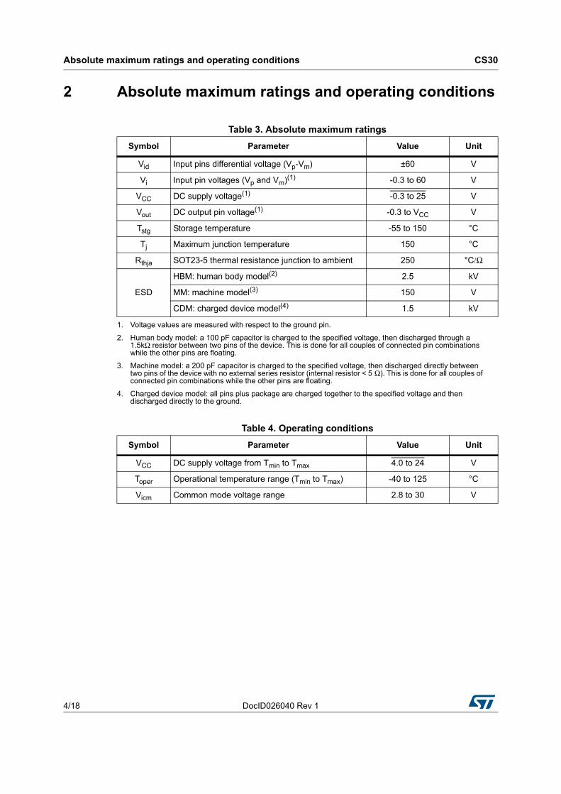
2 Absolute maximum ratings and operating conditions
Table 3. Absolute maximum ratings
Symbol Parameter Value Unit
Vid Input pins differential voltage (Vp-Vm) ±60 V
Vi Input pin voltages (Vp and Vm)(1)
1. Voltage values are measured with respect to the ground pin.
-0.3 to 60 V
VCC DC supply voltage(1) -0.3 to 25 V
Vout DC output pin voltage(1) -0.3 to VCC V
Tstg Storage temperature -55 to 150 °C
Tj Maximum junction temperature 150 °C
Rthja SOT23-5 thermal resistance junction to ambient 250 °C/Ω
ESD
HBM: human body model(2)
2. Human body model: a 100 pF capacitor is charged to the specified voltage, then discharged through a 1.5kΩ resistor between two pins of the device. This is done for all couples of connected pin combinations while the other pins are floating.
2.5 kV
MM: machine model(3)
3. Machine model: a 200 pF capacitor is charged to the specified voltage, then discharged directly between two pins of the device with no external series resistor (internal resistor < 5 Ω). This is done for all couples of connected pin combinations while the other pins are floating.
150 V
CDM: charged device model(4)
4. Charged device model: all pins plus package are charged together to the specified voltage and then discharged directly to the ground.
1.5 kV
Table 4. Operating conditions
Symbol Parameter Value Unit
VCC DC supply voltage from Tmin to Tmax 4.0 to 24 V
Toper Operational temperature range (Tmin to Tmax) -40 to 125 °C
Vicm Common mode voltage range 2.8 to 30 V

DocID026040 Rev 1 5/18
CS30 Electrical characteristics
18
3 Electrical characteristics
Table 5. Supply(1)
Symbol Parameter Test conditions Min. Typ. Max. Unit
ICC Total supply currentVsense = 0 V
Tmin < Tamb < Tmax165 300 µA
1. Unless otherwise specified, the test conditions are Tamb = 25°C, VCC = 12 V, Vsense = Vp-Vm = 50 mV, Vm = 12 V, no load on Out.
Table 6. Input(1)
Symbol Parameter Test conditions Min. Typ. Max. Unit
CMRCommon mode rejection
Variation of Vout versus Vicm referred to input(2)
2.8 V < Vicm < 30 V
Tmin < Tamb < Tmax90 105 dB
SVRSupply voltage rejection
Variation of Vout versus VCC(3)
4.0 V < VCC < 24 V
Vsense = 30 mV
Tmin < Tamb < Tmax
90 105 dB
Vos Input offset voltage(4) Tamb = 25°CTmin < Tamb < Tmax
±0.2
±0.9
±1.5
±2.3mV
dVos/dT Input offset drift vs. T Tmin < Tamb < Tmax -3 µV/°C
Ilk Input leakage currentVCC = 0 V
Tmin < Tamb < Tmax1 µA
Iib Input bias currentVsense = 0 V
Tmin < Tamb < Tmax5.5 8 µA
1. Unless otherwise specified, the test conditions are Tamb = 25°C, VCC = 12 V, Vsense = Vp-Vm = 50 mV, Vm = 12 V, no load on Out.
2. See Section 4.1: Common mode rejection ratio (CMR) on page 12 for the definition of CMR.
3. See Section 4.2: Supply voltage rejection ratio (SVR) on page 12 for the definition of SVR.
4. See Section 4.3: Gain (Av) and input offset voltage (Vos) on page 12 for the definition of Vos.

Electrical characteristics CS30
6/18 DocID026040 Rev 1
Table 7. Output(1)
Symbol Parameter Test conditions Min. Typ. Max. Unit
Av Gain
CS30A
CS30B
CS30C
20
50
100
V/V
ΔAv Gain accuracyTamb = 25°C
Tmin < Tamb < Tmax
±2.5
±4.5%
ΔVout/ΔT Output voltage drift vs. T(2) Tmin < Tamb < Tmax 0.4 mV/°C
ΔVout/ΔIout Output stage load regulation-10 mA < Iout <10 mA
Iout sink or source current3 4 mV/mA
ΔVout Total output voltage accuracy(3) Vsense = 50 mV Tamb = 25°C Tmin < Tamb < Tmax
±2.5
±4.5%
ΔVout Total output voltage accuracyVsense = 100 mV Tamb = 25°C Tmin < Tamb < Tmax
±3.5
±5%
ΔVout Total output voltage accuracyVsense = 20 mV Tamb = 25°C Tmin < Tamb < Tmax
±8
±11%
ΔVout Total output voltage accuracyVsense = 10 mV Tamb = 25°C Tmin < Tamb < Tmax
±15
±20%
Isc-sink Short-circuit sink currentOut connected to VCC, Vsense = -1 V
30 60 mA
Isc-source Short-circuit source currentOut connected to Gnd
Vsense = 1 V15 26 mA
Voh
Output stage high-state saturation voltage
Voh=VCC-Vout
Vsense = 1 V
Iout = 1 mA0.8 1 V
VolOutput stage low-state saturation voltage
Vsense = -1 V
Iout = 1 mA50 100 mV
1. Unless otherwise specified, the test conditions are Tamb = 25°C, VCC = 12 V, Vsense = Vp-Vm = 50 mV, Vm = 12 V, no load on Out.
2. See Output voltage drift versus temperature on page 13 for the definition.
3. Output voltage accuracy is the difference with the expected theoretical output voltage Vout-th = Av*Vsense. See Output voltage accuracy on page 14 for a more detailed definition.
DocID026040 Rev 1 7/18
CS30 Electrical characteristics
18
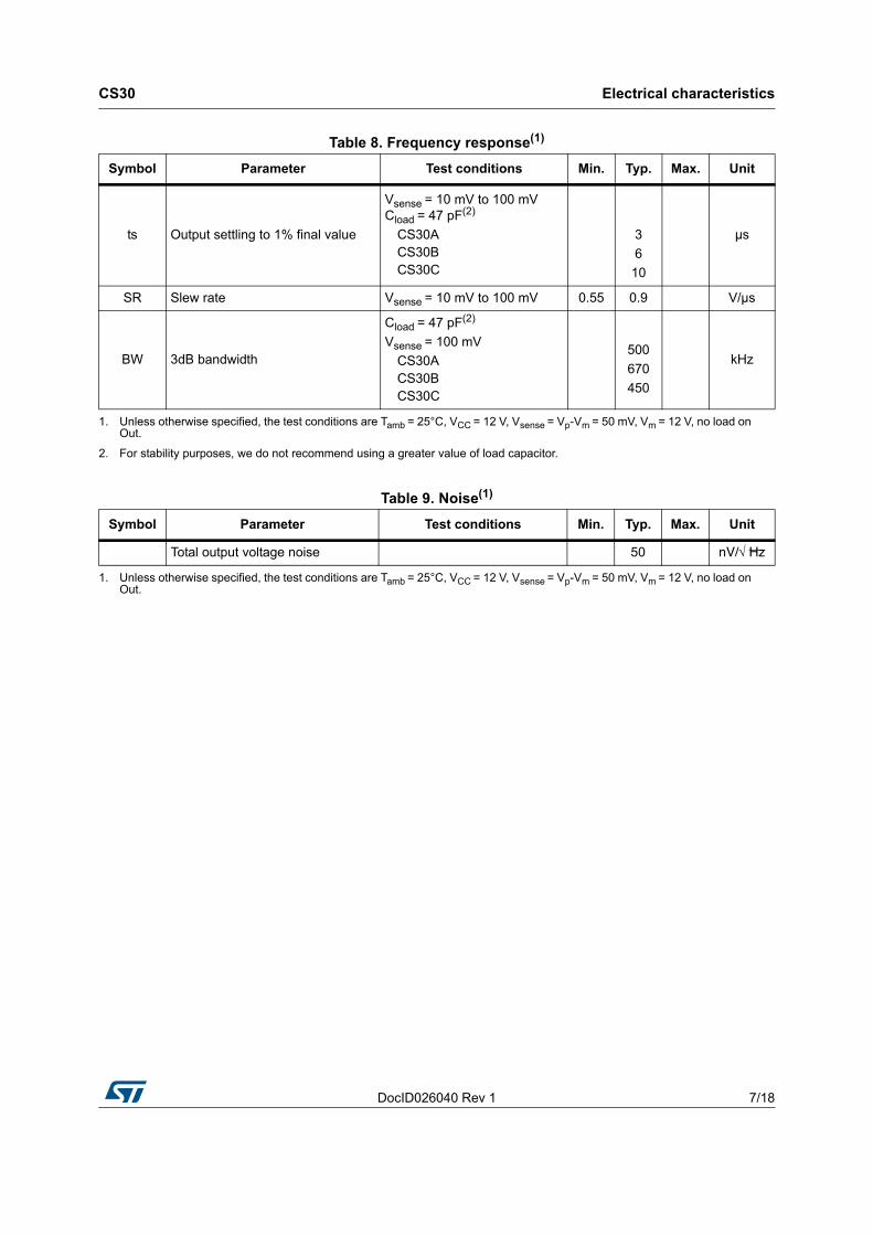
Table 8. Frequency response(1)
Symbol Parameter Test conditions Min. Typ. Max. Unit
ts Output settling to 1% final value
Vsense = 10 mV to 100 mV Cload = 47 pF(2)
CS30ACS30BCS30C
3
6
10
µs
SR Slew rate Vsense = 10 mV to 100 mV 0.55 0.9 V/µs
BW 3dB bandwidth
Cload = 47 pF(2)
Vsense = 100 mV
CS30ACS30BCS30C
500
670
450
kHz
1. Unless otherwise specified, the test conditions are Tamb = 25°C, VCC = 12 V, Vsense = Vp-Vm = 50 mV, Vm = 12 V, no load on Out.
2. For stability purposes, we do not recommend using a greater value of load capacitor.
Table 9. Noise(1)
Symbol Parameter Test conditions Min. Typ. Max. Unit
Total output voltage noise 50 nV/√ Hz
1. Unless otherwise specified, the test conditions are Tamb = 25°C, VCC = 12 V, Vsense = Vp-Vm = 50 mV, Vm = 12 V, no load on Out.
Electrical characteristics CS30
8/18 DocID026040 Rev 1
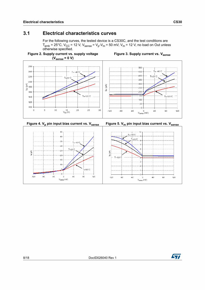
3.1 Electrical characteristics curves
For the following curves, the tested device is a CS30C, and the test conditions are Tamb = 25°C, VCC = 12 V, Vsense = Vp-Vm = 50 mV, Vm = 12 V, no load on Out unless otherwise specified.
Figure 2. Supply current vs. supply voltage (Vsense = 0 V)
Figure 3. Supply current vs. Vsense
Figure 4. Vp pin input bias current vs. Vsense Figure 5. Vm pin input bias current vs. Vsense

DocID026040 Rev 1 9/18
CS30 Electrical characteristics
18
Figure 6. Minimum common mode operating voltage vs. temperature
Figure 7. Output stage low-state saturation voltage versus output current (Vsense = -1 V)
Figure 8. Output stage high-state saturation voltage versus output current
(Vsense = +1 V)
Figure 9. Output short-circuit source current versus temperature (Out pin connected to
ground)
Figure 10. Output short-circuit sink current versus temperature (Out pin connected to VCC)
Figure 11. Output stage load regulation
Electrical characteristics CS30
10/18 DocID026040 Rev 1
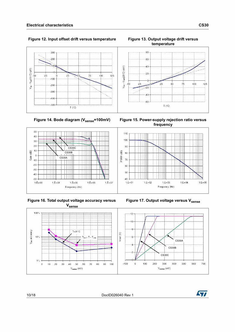
Figure 12. Input offset drift versus temperature Figure 13. Output voltage drift versus temperature
Figure 14. Bode diagram (Vsense=100mV) Figure 15. Power-supply rejection ratio versus frequency
CS30C
CS30B
CS30A
Figure 16. Total output voltage accuracy versus Vsense
Figure 17. Output voltage versus Vsense
CS30A
CS30B
CS30C

DocID026040 Rev 1 11/18
CS30 Electrical characteristics
18
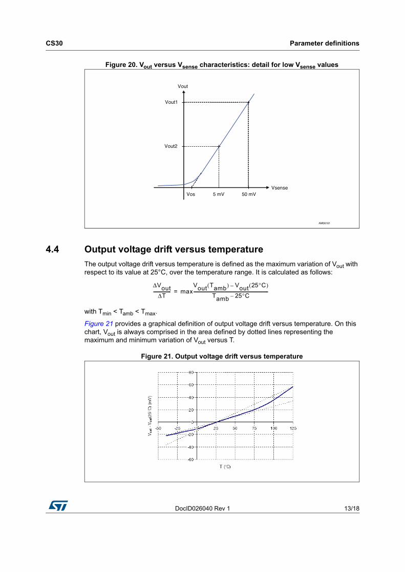
Figure 18. Output voltage versus Vsense (detail for low Vsense values)
Figure 19. Step response
CS30A
CS30B
CS30C
CS30A
CS30B
CS30C

Parameter definitions CS30
12/18 DocID026040 Rev 1
4 Parameter definitions
4.1 Common mode rejection ratio (CMR)
The common-mode rejection ratio (CMR) measures the ability of the current-sensing amplifier to reject any DC voltage applied on both inputs Vp and Vm. The CMR is referred back to the input so that its effect can be compared with the applied differential signal. The CMR is defined by the formula:
4.2 Supply voltage rejection ratio (SVR)
The supply-voltage rejection ratio (SVR) measures the ability of the current-sensing amplifier to reject any variation of the supply voltage VCC. The SVR is referred back to the input so that its effect can be compared with the applied differential signal. The SVR is defined by the formula:
4.3 Gain (Av) and input offset voltage (Vos)
The input offset voltage is defined as the intersection between the linear regression of the Vout versus Vsense curve with the X-axis (see Figure 20). If Vout1 is the output voltage with Vsense=Vsense1=50mV and Vout2 is the output voltage with Vsense=Vsense2=5mV, then Vos can be calculated with the following formula:
The amplification gain Av is defined as the ratio between output voltage and input differential voltage:
CMR 20–ΔVout
ΔVicm Av⋅----------------------------log⋅=
SVR 20–ΔVout
ΔVCC Av⋅---------------------------log⋅=
Vos Vsense1
Vsense1 Vsense2–
Vout1 Vout2–------------------------------------------------ Vout1⋅ –=
AvVout
Vsense------------------=
DocID026040 Rev 1 13/18
CS30 Parameter definitions
18
Figure 20. Vout versus Vsense characteristics: detail for low Vsense values
4.4 Output voltage drift versus temperature
The output voltage drift versus temperature is defined as the maximum variation of Vout with respect to its value at 25°C, over the temperature range. It is calculated as follows:
with Tmin < Tamb < Tmax.
Figure 21 provides a graphical definition of output voltage drift versus temperature. On this chart, Vout is always comprised in the area defined by dotted lines representing the maximum and minimum variation of Vout versus T.
Figure 21. Output voltage drift versus temperature
ΔVoutΔT
----------------- maxVout Tamb( ) Vout 25°C( )–
Tamb 25°C–-------------------------------------------------------------------------=

Parameter definitions CS30
14/18 DocID026040 Rev 1
4.5 Output voltage accuracy
The output voltage accuracy is the difference between the actual output voltage and the theoretical output voltage. Ideally, the current sensing output voltage should be equal to the input differential voltage multiplied by the theoretical gain, as in the following formula:
Vout-th=Av Vsense
The actual value is very slightly different, mainly due to the effects of:
• the input offset voltage Vos,
• non-linearity
Figure 22. Vout vs. Vsense theoretical and actual characteristics
The output voltage accuracy, expressed in percentage, can be calculated with the following formula:
with Av = 20 V/V for CS30A, Av = 50 V/V for CS30B and Av = 100 V/V for CS30C.
ΔVout
abs Vout Av Vsense⋅( )–( )
Av Vsense⋅-----------------------------------------------------------------------=
DocID026040 Rev 1 15/18
CS30 Application information
18
5 Application information
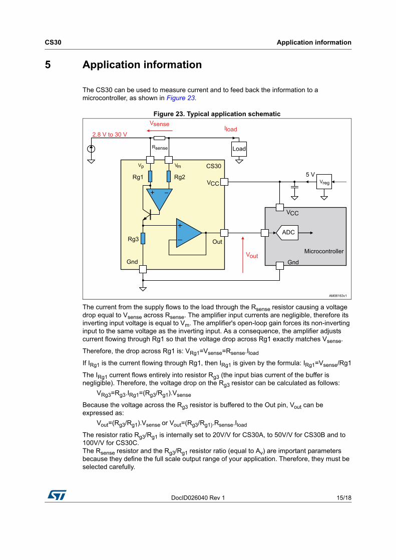
The CS30 can be used to measure current and to feed back the information to a microcontroller, as shown in Figure 23.
Figure 23. Typical application schematic
The current from the supply flows to the load through the Rsense resistor causing a voltage drop equal to Vsense across Rsense. The amplifier input currents are negligible, therefore its inverting input voltage is equal to Vm. The amplifier's open-loop gain forces its non-inverting input to the same voltage as the inverting input. As a consequence, the amplifier adjusts current flowing through Rg1 so that the voltage drop across Rg1 exactly matches Vsense.
Therefore, the drop across Rg1 is: VRg1=Vsense=Rsense.Iload
If IRg1 is the current flowing through Rg1, then IRg1 is given by the formula: IRg1=Vsense/Rg1
The IRg1 current flows entirely into resistor Rg3 (the input bias current of the buffer is negligible). Therefore, the voltage drop on the Rg3 resistor can be calculated as follows:
VRg3=Rg3.IRg1=(Rg3/Rg1).Vsense
Because the voltage across the Rg3 resistor is buffered to the Out pin, Vout can be expressed as:
Vout=(Rg3/Rg1).Vsense or Vout=(Rg3/Rg1).Rsense.Iload
The resistor ratio Rg3/Rg1 is internally set to 20V/V for CS30A, to 50V/V for CS30B and to 100V/V for CS30C.The Rsense resistor and the Rg3/Rg1 resistor ratio (equal to Av) are important parameters because they define the full scale output range of your application. Therefore, they must be selected carefully.
5 V
Vsense
Vout
Load
Iload2.8 V to 30 V
Rsense
Vreg
Vp Vm
Out
Gnd
VCCRg1 Rg2
Rg3
CS30
Microcontroller
ADC
Gnd
VCC
AM06163v1
Package information CS30
16/18 DocID026040 Rev 1
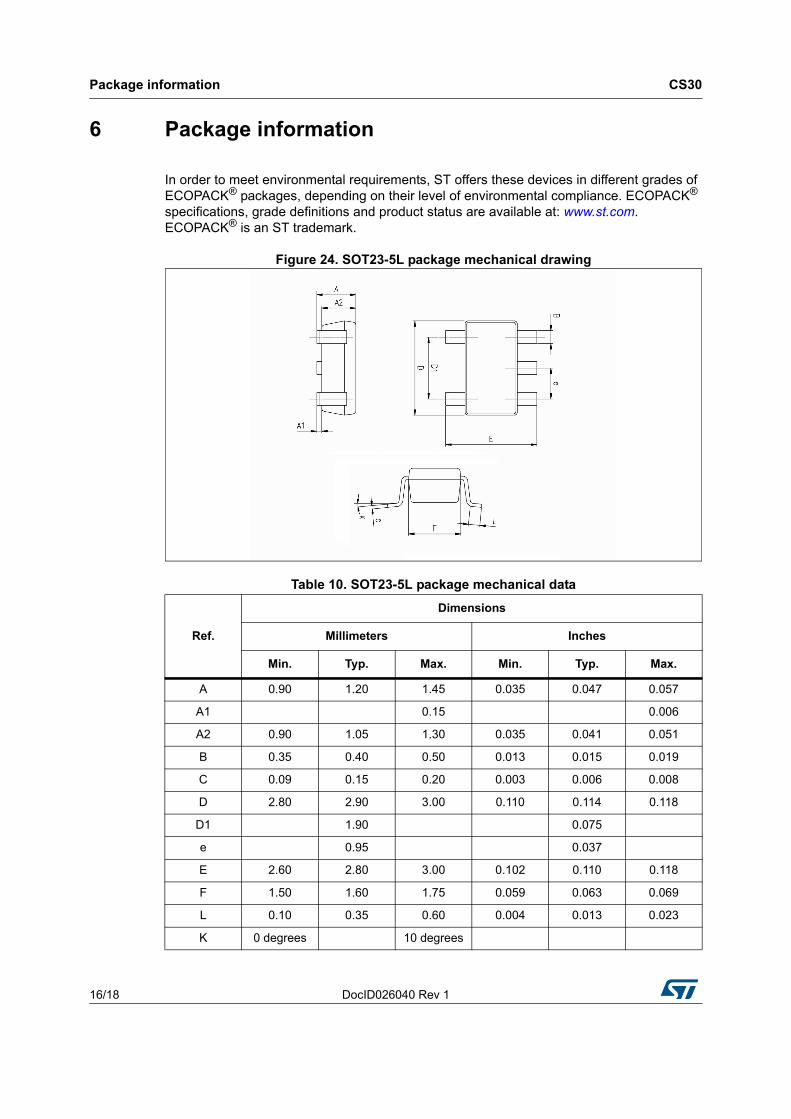
6 Package information
In order to meet environmental requirements, ST offers these devices in different grades of ECOPACK® packages, depending on their level of environmental compliance. ECOPACK® specifications, grade definitions and product status are available at: www.st.com. ECOPACK® is an ST trademark.
Figure 24. SOT23-5L package mechanical drawing
Table 10. SOT23-5L package mechanical data
Ref.
Dimensions
Millimeters Inches
Min. Typ. Max. Min. Typ. Max.
A 0.90 1.20 1.45 0.035 0.047 0.057
A1 0.15 0.006
A2 0.90 1.05 1.30 0.035 0.041 0.051
B 0.35 0.40 0.50 0.013 0.015 0.019
C 0.09 0.15 0.20 0.003 0.006 0.008
D 2.80 2.90 3.00 0.110 0.114 0.118
D1 1.90 0.075
e 0.95 0.037
E 2.60 2.80 3.00 0.102 0.110 0.118
F 1.50 1.60 1.75 0.059 0.063 0.069
L 0.10 0.35 0.60 0.004 0.013 0.023
K 0 degrees 10 degrees

DocID026040 Rev 1 17/18
CS30 Revision history
18
7 Revision history
Table 11. Document revision history
Date Revision Changes
06-Mar-2014 1 Initial release
CS30
18/18 DocID026040 Rev 1
Please Read Carefully:
Information in this document is provided solely in connection with ST products. STMicroelectronics NV and its subsidiaries (“ST”) reserve theright to make changes, corrections, modifications or improvements, to this document, and the products and services described herein at anytime, without notice.
All ST products are sold pursuant to ST’s terms and conditions of sale.
Purchasers are solely responsible for the choice, selection and use of the ST products and services described herein, and ST assumes noliability whatsoever relating to the choice, selection or use of the ST products and services described herein.
No license, express or implied, by estoppel or otherwise, to any intellectual property rights is granted under this document. If any part of thisdocument refers to any third party products or services it shall not be deemed a license grant by ST for the use of such third party productsor services, or any intellectual property contained therein or considered as a warranty covering the use in any manner whatsoever of suchthird party products or services or any intellectual property contained therein.
UNLESS OTHERWISE SET FORTH IN ST’S TERMS AND CONDITIONS OF SALE ST DISCLAIMS ANY EXPRESS OR IMPLIEDWARRANTY WITH RESPECT TO THE USE AND/OR SALE OF ST PRODUCTS INCLUDING WITHOUT LIMITATION IMPLIEDWARRANTIES OF MERCHANTABILITY, FITNESS FOR A PARTICULAR PURPOSE (AND THEIR EQUIVALENTS UNDER THE LAWSOF ANY JURISDICTION), OR INFRINGEMENT OF ANY PATENT, COPYRIGHT OR OTHER INTELLECTUAL PROPERTY RIGHT.
ST PRODUCTS ARE NOT DESIGNED OR AUTHORIZED FOR USE IN: (A) SAFETY CRITICAL APPLICATIONS SUCH AS LIFESUPPORTING, ACTIVE IMPLANTED DEVICES OR SYSTEMS WITH PRODUCT FUNCTIONAL SAFETY REQUIREMENTS; (B)AERONAUTIC APPLICATIONS; (C) AUTOMOTIVE APPLICATIONS OR ENVIRONMENTS, AND/OR (D) AEROSPACE APPLICATIONSOR ENVIRONMENTS. WHERE ST PRODUCTS ARE NOT DESIGNED FOR SUCH USE, THE PURCHASER SHALL USE PRODUCTS ATPURCHASER’S SOLE RISK, EVEN IF ST HAS BEEN INFORMED IN WRITING OF SUCH USAGE, UNLESS A PRODUCT ISEXPRESSLY DESIGNATED BY ST AS BEING INTENDED FOR “AUTOMOTIVE, AUTOMOTIVE SAFETY OR MEDICAL” INDUSTRYDOMAINS ACCORDING TO ST PRODUCT DESIGN SPECIFICATIONS. PRODUCTS FORMALLY ESCC, QML OR JAN QUALIFIED AREDEEMED SUITABLE FOR USE IN AEROSPACE BY THE CORRESPONDING GOVERNMENTAL AGENCY.
Resale of ST products with provisions different from the statements and/or technical features set forth in this document shall immediately voidany warranty granted by ST for the ST product or service described herein and shall not create or extend in any manner whatsoever, anyliability of ST.
ST and the ST logo are trademarks or registered trademarks of ST in various countries.Information in this document supersedes and replaces all information previously supplied.
The ST logo is a registered trademark of STMicroelectronics. All other names are the property of their respective owners.
© 2014 STMicroelectronics - All rights reserved
STMicroelectronics group of companies
Australia - Belgium - Brazil - Canada - China - Czech Republic - Finland - France - Germany - Hong Kong - India - Israel - Italy - Japan - Malaysia - Malta - Morocco - Philippines - Singapore - Spain - Sweden - Switzerland - United Kingdom - United States of America
www.st.com
Top Related