


Languages
Pages
Legal


High Powered Microwave Wideband Interference on Electronics
MERIT 2006
Konstantin Khrustov Saket Vora University of Illinois at Chicago North Carolina State University
Dr. John Rodgers Faculty Advisor
Institute for Research in Electronics & Applied Physics
Department of Electrical & Computer Engineering
University of Maryland-College Park
Abstract
With rapid advances in the physical downscaling of integrated circuits, the effects of electromagnetic
interference have become too important to ignore. This project explores the effects of high-power
wideband microwave interference on feedback circuits in switching power supplies. Spurious fluctuations
in these feedback signals may cause electronic systems to reset, shut down, or even sustain physical
damage. Identifying the characteristics of disruptive signals is critical to developing countermeasures to
them. A traveling-wave tube (TWT) was configured as an oscillator which generated wideband microwave
signals with variable amplitude, frequency and pulse width. The power supply functions were measured
as its control circuitry was excited by microwave pulses from the TWT. By varying the drive parameters,
the regimes where the system is susceptible to microwaves were experimentally determined. The results
show that nonlinearity and parasitic resonances in electronic circuits renders them vulnerable to
microwave sources even though, by design, these circuits should not respond to such high frequency
excitation.

2
Table of Contents
Table of Contents 2
Introduction 3
Circuitry Analysis 4
A. Power Supply Circuit 4
B. Downconverted DC Voltages in Integrated Circuits 6
C. Determining Injection Sites 8
D. Comparison with Digital Inverter 8
Traveling Wave Tube Oscillator 8
A. Overview 8
B. TWT Characteristics 9
C. Oscillator Setup 10
Experiment Setup 12
A. Chaotic RF Injection 12
B. Coherent RF Injection 13
C. ‘Power Supply-On’ Injection 13
Results 13
A. Output Voltage Disturbances 13
B. Power Supply Shutdowns 16
Conclusions 17
Acknowledgements 18
References 18

3
Introduction
Engineers have sought to protect electronics from harmful electromagnetic interference (EMI) for years,
whether it originated from components internal to their systems or from effects external to their systems.
Common sources of interference such as the 60 Hz power line noise or local oscillators have been
extensively studied and defensive practices now exist for them. There are three critical factors that
together serve as motivation for this research project.
First, the physical size of integrated circuits continues to shrink. The thickness of dielectric material
separating a MOSFET’s gate from its channel is becoming smaller at the expense of greater susceptibility
to shot-noise, the possibility of permanent damage from over-voltage conditions, and increased leakage
currents. To offset the higher power consumptions due to such leakage currents, designers continue to
lower the operating voltages of integrated circuits. This reduces the noise immunity of circuits and
requires even finer control and regulation of bias voltages. While mixed-mode design and system-on-a-
chip approaches to communication systems aid in reducing costs and miniaturization, they reduce the
isolation between components and thus increase the chances for crosstalk and coupling effects.
The second factor is the proliferation of electronic devices that operate in the microwave band.
Microwaves describe the part of the electromagnetic spectrum between 300 MHz and 30 GHz, which
corresponds to wavelengths of between 1 cm and 1 mm. Cell phones, wireless networks, processors, and
data buses all operate now in this frequency range. In addition to the widespread use of the microwave
spectrum, the technical barrier of entry to designing and building high powered sources of microwaves is
lowering.
Finally, it is suspected that chaotic and wideband signals can be particularly harmful if manifested as
electromagnetic interference [2]. Narrowband or coherent signals exist over a very small bandwidth of
frequencies, from a few Hz to a few kHz. While they exhibit good signal power retention over great
distances, their narrow bandwidth makes them easier to block with defensive countermeasures.
Wideband signals exist over such a large bandwidth that it is difficult to fully protect against them [1].
Chaotic signals are of interest because they have wideband signal characteristics and yet are
deterministic, not stochastic. Chaotic systems feature extreme sensitivity to initial conditions, making them
practically impossible to accurately predict without detailed knowledge of the source generating such a
signal. Different integrated circuits are resonant at different frequencies. Electromagnetic interference with
a bandwidth wide enough to encompass many of these resonant frequencies could simultaneously excite
and disrupt multiple aspects of an electronic system.
We sought to investigate whether there was a difference between using chaotic signals or coherent
signals to disrupt electronics through electromagnetic interference. We injected high powered microwave

4
pulses into a computer power supply and a high speed digital inverter, which represent two very different
types of electronic components commonly found.
Circuitry Analysis
A. Power Supply Circuit
A standard computer power supply was chosen as the primary device of interest for this
investigation for several reasons. Earlier research observed that a LAN switch would sometimes
experience power interruptions, system restarts, or even complete shutdowns when exposed to radiated
microwave interference. Although the power supply circuitry of the device was not the component being
studied, it was suspected that RF coupling into feedback circuits between the main board and the power
supply was causing instabilities that led to the erratic behavior [2]. Previous research [10-11] in
researching instabilities in power supplies focused on internally generated EMI at lower frequencies than
our experiment setup. A system restart or shutdown is a catastrophic failure for time or mission-critical
systems. Furthermore, the design of switching power supplies found in the vast majority of computers
adhere to the ATX standard, a form factor developed by Intel over a decade ago. A vulnerability found in
one ATX power supply is likely to affect a large number of computers. An ATX switching power supply
outputs ±5V, ±12V, and +3.3V DC voltages. Two wires are used for communication between the supply
and the motherboard.
ATX DC Output Voltage Regulation
Output Minimum Nominal Maximum
+3.3V +3.14 +3.30 +3.47
+5V +4.75 +5.00 +5.25
-5V -4.50 -5.00 -5.50
+12V +11.40 +12.00 +12.60
-12V -10.80 -12.00 -13.20
Table 1 – ATX specifications for minimum, nominal, and maximum DC output voltages. [4]
When a user presses the soft power button on their computer, the motherboard sends and holds a TTL
low signal to the power supply via the ‘power supply on’ (PS-ON) wire. Once the output voltages of the
power supply are stabilized above the ATX undervoltage limits, the power supply sends and holds an
active high signal to the motherboard via the ‘PowerGood’ wire. If this high signal drops low even
momentarily, the motherboard will interpret that the power it is receiving is no longer good and will shut
down as a protective measure against over or under voltage damage.
A 200W ATX power supply was examined in order to determine locations of high susceptibility to HPM
interference. A circuit schematic could not be located for the particular model under test, but other
resources such as [5] and physically re-drawing parts of the schematic through observation gave us an

5
understanding of the power supply’s functionality. Two key integrated circuits were of interest – a LM339
quad comparator and a DBL494 Pulse Width Modulation (PWM) chip.
The LM339 and DBL494 Chips on the Power Supply Board
Figure 1 – A close-up of the power supply board. The LM339 and DBL494 chips can be seen, as well as the PowerGood wire (gray) and the PS-ON wire (green).
Figure 2 – Partial schematic of the power supply featuring the LM339 and DBL494 chips. The feedback line is highlighted in green, the PowerGood line is in red, and the PS-ON line is in orange.
6
The four differential comparators inside the LM339 handles the PowerGood and PS-ON signals, while the
PWM chip directs the switching of two key power transistors and controls the DC output voltage by
adjusting the duty cycle of a square pulse train. A feedback line from the outputs is monitored through an
error amplifier, which compares it to an internally generated sawtooth waveform. For the time that the
sawtooth waveform is above the feedback voltage, the square pulse is high. If the feedback voltage
decreases, the sawtooth wave is greater than the feedback voltage for a longer period of time, resulting in
a wider pulse width, greater duty cycle, and increased DC output voltage.
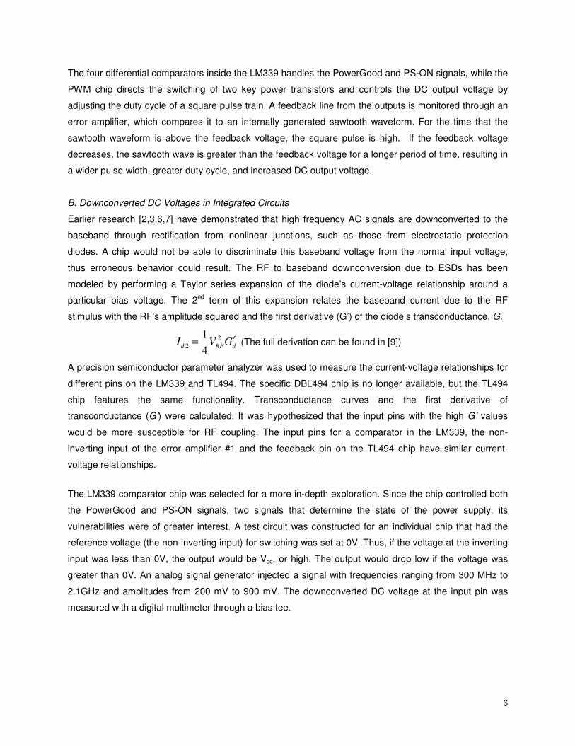
B. Downconverted DC Voltages in Integrated Circuits
Earlier research [2,3,6,7] have demonstrated that high frequency AC signals are downconverted to the
baseband through rectification from nonlinear junctions, such as those from electrostatic protection
diodes. A chip would not be able to discriminate this baseband voltage from the normal input voltage,
thus erroneous behavior could result. The RF to baseband downconversion due to ESDs has been
modeled by performing a Taylor series expansion of the diode’s current-voltage relationship around a
particular bias voltage. The 2nd
term of this expansion relates the baseband current due to the RF
stimulus with the RF’s amplitude squared and the first derivative (G’) of the diode’s transconductance, G.
2
2
1
4d RF d
I V G′= (The full derivation can be found in [9])
A precision semiconductor parameter analyzer was used to measure the current-voltage relationships for
different pins on the LM339 and TL494. The specific DBL494 chip is no longer available, but the TL494
chip features the same functionality. Transconductance curves and the first derivative of
transconductance (G’) were calculated. It was hypothesized that the input pins with the high G’ values
would be more susceptible for RF coupling. The input pins for a comparator in the LM339, the non-
inverting input of the error amplifier #1 and the feedback pin on the TL494 chip have similar current-
voltage relationships.
The LM339 comparator chip was selected for a more in-depth exploration. Since the chip controlled both
the PowerGood and PS-ON signals, two signals that determine the state of the power supply, its
vulnerabilities were of greater interest. A test circuit was constructed for an individual chip that had the
reference voltage (the non-inverting input) for switching was set at 0V. Thus, if the voltage at the inverting
input was less than 0V, the output would be Vcc, or high. The output would drop low if the voltage was
greater than 0V. An analog signal generator injected a signal with frequencies ranging from 300 MHz to
2.1GHz and amplitudes from 200 mV to 900 mV. The downconverted DC voltage at the input pin was
measured with a digital multimeter through a bias tee.
7
Downconverted DC vs. RF Input Amplitude
RF Frequencies 300 MHz to 1.1 GHz
LM339 - Inverting Input
-300
-250
-200
-150
-100
-50
0
200 300 400 500 600 700 800 900
RF Input Amplitude (mV)
Do
wn
co
nvert
ed
DC
(m
V)
300 MHz
500 MHz
700 MHz
900 MHz
1.1 GHz
Figure 3 – The downconverted DC vs. RF input amplitude for frequencies ranging from 300 MHz to 1.1 GHz.
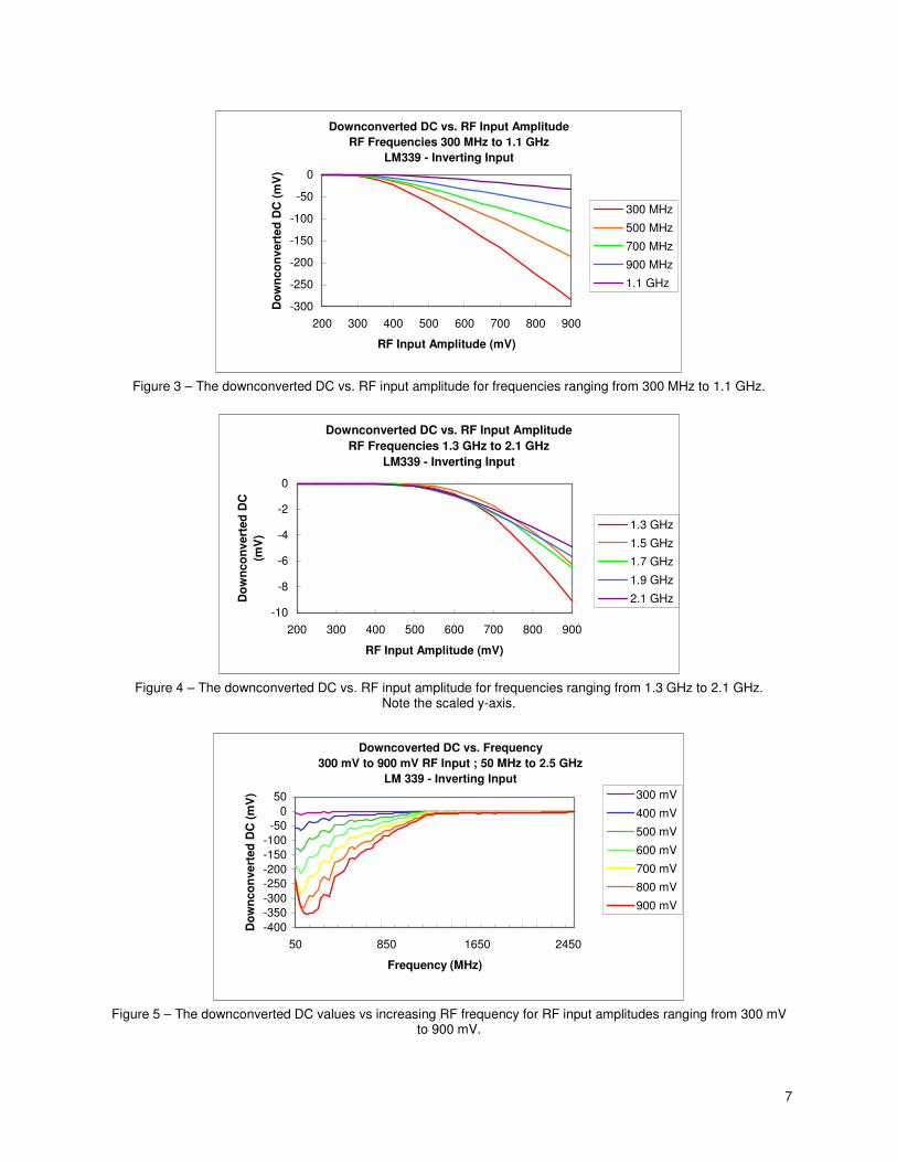
Downconverted DC vs. RF Input Amplitude
RF Frequencies 1.3 GHz to 2.1 GHz
LM339 - Inverting Input
-10
-8
-6
-4
-2
0
200 300 400 500 600 700 800 900
RF Input Amplitude (mV)
Do
wn
co
nvert
ed
DC
(mV
)
1.3 GHz
1.5 GHz
1.7 GHz
1.9 GHz
2.1 GHz
Figure 4 – The downconverted DC vs. RF input amplitude for frequencies ranging from 1.3 GHz to 2.1 GHz.
Note the scaled y-axis.
Downcoverted DC vs. Frequency
300 mV to 900 mV RF Input ; 50 MHz to 2.5 GHz
LM 339 - Inverting Input
-400
-350
-300
-250
-200
-150
-100
-50
0
50
50 850 1650 2450
Frequency (MHz)
Do
wn
co
nvert
ed
DC
(m
V) 300 mV
400 mV
500 mV
600 mV
700 mV
800 mV
900 mV
Figure 5 – The downconverted DC values vs increasing RF frequency for RF input amplitudes ranging from 300 mV
to 900 mV.

8
As predicted above, the downconverted DC to RF amplitude curves feature a square-law relationship. A
frequency dependence was observed, for as the frequency of the exciting RF signal increased, the
magnitude of downconverted DC voltage decreased. Since our high powered wideband microwave
source operates in the 1 GHz to 2 GHz range, a greater signal power would be needed for
downconverting large DC voltages.
C. Determining Injection Sites
While radiating high powered microwave interference into the power supply enclosure would be more
realistic, it presents considerable difficulties in determining precisely which aspect of the power supply
circuitry is causing any observable problems in the state of the power supply or in the output voltages. It
is not practical to monitor dozens of different sites on the circuit board. Instead, seven sites were
identified that could potentially cause disruptions in power supply operation.
Injection Site Reason
Inverting & Non-inverting input into comparator #4 Determines the state of the PowerGood signal
Inverting input into comparator #1 Receives PS-ON signal
Inverting & Non-inverting inputs into error amplifier #1 in PWM chip
Receives the DC output feedback line and determines pulse width.
Feedback input into PWM chip This is an additional feedback line that can be used with the PWM chip.
PS-ON wire A disruption in the active low signal could cause shutdown. The long wire is a natural antenna for EMI.
Table 2- Injection sites and reason for susceptibility
D. Comparison with Digital Inverter
A digital inverter chip 74VHC was chosen for a comparison with the power supply circuitry. In-depth
investigation of RF effects on high speed digital electronics can be explored further in [3], and its non-
linear responses to chaotic modulation is known.
Traveling Wave Tube Oscillator
A. TWT Overview
A traveling wave tube (TWT) is a device that is used to create high power radio frequency (RF)
signals. It is a high gain and low-noise amplifier that can be used as an oscillator. The injected RF signal
into a TWT travels along a helical transmission line inside a vacuum tube waveguide which allows the
signal’s electromagnetic fields to interact with an electron beam that passes through the center of the coil.
This interaction amplifies the input signal. TWTs have been designed to operate for frequencies as low as
500MHz and as high as 300 GHz. They are used extensively in satellite communication and airborne
radar systems.

9
Figure 6 – Functional diagram of a traveling wave tube. [13]
We used a Hughes INMARSAT 8537H model which operates in the L-band (1-2 GHz) and has an
approximate gain of 50 dB with an output power of 80W.
B. TWT Characteristics
First, the intrinsic characteristics of this particular TWT model were tested in its normal amplifier
configuration. Using a vector network analyzer (VNA), we performed a S21 (forward transmission) S-
parameter measurement to measure the gain of the TWT versus both frequency and input powers.
Gain vs. Frequency
for Varying Drive Powers
26
31
36
41
46
51
1.0 1.3 1.5 1.8 2.0
Frequency (GHz)
Ad
juste
d G
ain
(d
B)
.
+4.89dBm
-0.11dBm
-5dBm
-15dBm
Figure 7 – Gain vs Frequency for varying drive powers.
Though the TWT specifications stated a center frequency of 1.5 GHz, we measured a frequency of 1.65
GHz as where the highest gain took place for the power levels of interest. In Figure 7, it can be seen that
for high input RF powers, the gain around 1.85 GHz dips low. This information is important because
wideband signals will be used with this TWT.

10
Normalized Gain vs Input Power
-5
-4
-3
-2
-1
0
1
-60 -50 -40 -30 -20 -10 0 10
Input Power (dBm)
No
rmalized
Gain
(d
B)
-60 to -45 dBm
-45 to -30 dBm
-30 to -15 dBm
-15 to -5 dBm
-5.12dBm to 4.89dBm
Figure 8 – Normalized Gain vs. Input Power Sweep.
As the input RF signal increases in amplitude, the output also increases linearly. However, at high input
signal powers, the interaction inside the TWT that amplifies the signal reaches a saturation point and
cannot continue to linearly amplify the signal. An increase in the input signal thus no longer results in a
corresponding increase in the output signal. Figure 8 shows the gain compression that occurs between -
15 dBm and 0 dBm of input signal power. Operating the TWT in this region results in non-linear
amplification, which generates subharmonics and eigenfrequencies in the RF signal. This is a critical pre-
requisite for creating wideband and chaotic signals.
C. Oscillator Setup
The TWT amplifier was then configured as a feedback pulsed oscillator. The output of the TWT
was passed through variable attenuators that controlled the loop gain as well as 15m of coaxial cable,
which added a time delay of approximately 54 ns. A PIN diode triggered by a pulse generator was
connected in series before the signal was fed back into the input. The period of the pulse was set to over
200 ms, and the pulse width could be varied from 5 µs to 50 ms. Upon startup, the TWT amplifies the
inherent noise into the system. The time delay causes the signal to continually switch between generative
and degenerative feedback, and adjusting the loop gain changes the resulting chaotic dynamics of the
signal.[12]
Figure 9 – TWT Oscillator block diagram.
11
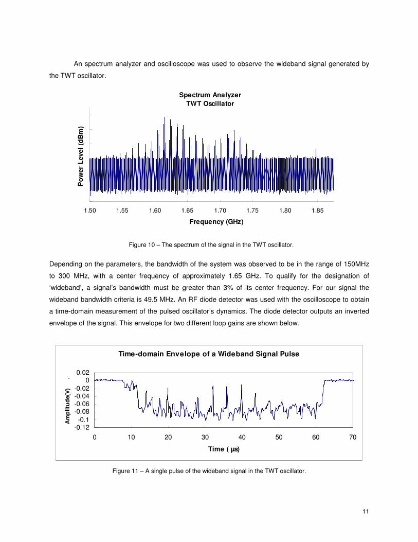
An spectrum analyzer and oscilloscope was used to observe the wideband signal generated by
the TWT oscillator.
Spectrum Analyzer
TWT Oscillator
1.50 1.55 1.60 1.65 1.70 1.75 1.80 1.85
Frequency (GHz)
Po
wer
Level
(dB
m)
Figure 10 – The spectrum of the signal in the TWT oscillator.
Depending on the parameters, the bandwidth of the system was observed to be in the range of 150MHz
to 300 MHz, with a center frequency of approximately 1.65 GHz. To qualify for the designation of
‘wideband’, a signal’s bandwidth must be greater than 3% of its center frequency. For our signal the
wideband bandwidth criteria is 49.5 MHz. An RF diode detector was used with the oscilloscope to obtain
a time-domain measurement of the pulsed oscillator’s dynamics. The diode detector outputs an inverted
envelope of the signal. This envelope for two different loop gains are shown below.
Time-domain Envelope of a Wideband Signal Pulse
-0.12-0.1
-0.08-0.06-0.04-0.02
00.02
0 10 20 30 40 50 60 70
Time ( µs)
Am
plitu
de(V
) .
Figure 11 – A single pulse of the wideband signal in the TWT oscillator.

12
Time-domain Envelope of a Wideband Signal Pulse
-0.2
-0.15
-0.1
-0.05
0
0.05
0 10 20 30 40 50 60 70 80
Time (µs)
Am
plitu
de(V
) .
Figure 12 – Oscilloscope graph of the Envelope Function for a different attenuation level.
Because chaotic systems exhibit extreme sensitivity to initial conditions and system parameters, even
miniscule changes in the loop gain such as putting force on the dial of a variable attenuator but not visibly
adjusting it, can dramatically change the signal’s dynamics.
Experiment Setup
Figure 13 – Experimental Setup for RF injection into DuT.
A. Chaotic RF Injection
The power supply was readied for RF injection by installing a RF coaxial jack and connector into
the supply’s enclosure. The end of the coaxial wire was soldered to the different injection sites as the
experiment progressed. Additional ports were created with feed-through capacitors which allowed
monitoring of DC voltages at various locations inside the power supply during injection. An oscilloscope
was used to monitor the oscillator’s wideband signal to make sure there was sufficient chaotic
modulation. A variable step attenuator with an attenuation range of 0 to 69 dB was placed before the
Device under Test, which provided a controlled way of adjusting the RF input power from effectively no
power to 39 dBm into the DUT. Another oscilloscope monitored DC output voltages and the PowerGood

13
signal from the power supply’s wire connector. For each of the injection points identified above and the
digital inverter chip, the RF input signal power and the width of the chaotically modulated pulse was
varied.
B. Coherent RF Injection
Since the TWT oscillator has a wideband signal, an alternative microwave source was needed to
generate single frequency (coherent) signals. An analog signal generator outputted a 1.65 GHz sinusoidal
wave and was set to pulse its output to the same settings as the TWT oscillator’s pulse generator. A
solid-state amplifier with a 31 dB gain was used to boost the signal power for proper comparison with the
high powered TWT. Coherently modulated pulses were injected into the same points as well as the digital
inverter chip while the outputs of the power supply and inverter were monitored.
C. Power Supply-On Wire Injection
The experiment setup was modified slightly during RF injection into the PS-ON wire. The power
supply began shutting down after receiving the high powered microwave pulses, and in order to
accurately measure the time-to-shutdown after the excitation pulse, the +5V DC output was used as a
trigger instead of the pulse generator. The oscilloscope triggered when the line’s voltage dropped below
4.6V. It was then possible to measure the time between the trigger point and the excitation pulse.
Results
RF Injection into the comparator that controls the PowerGood signal, the feedback pin of the PWM chip,
the inverting input of the PWM chip’s error amplifier, and the inverting input into the comparator that
receives the ‘power supply on’ command all did not result in any output voltage deviations, restart, or
shutdown events. Injection into two sites did cause adverse effects, which fall into two categories – output
voltage disturbances & shutdown.
A. Output Voltage Disturbances
As mentioned above, a feedback line from the DC outputs to the non-inverting input of the PWM
chip’s error amplifier. When high powered microwave pulses were injected into this pin, a disturbance in
the +5V output was observed. The graphs below depict the emergence of the disturbance as the RF input
power increases.

14
+5V Output Disturbances to Chaotically Modulated Pulses
for Increasing RF Input Power
4.5
4.75
5
5.25
0 1 2 3 4 5
Time (ms)
+5
V O
utp
ut Excitation Pulse
No RF input
29 dBm RF Pow er
32 dBm RF Pow er
37 dBm RF Pow er
Figure 14 – The output disturbance due to a chaotic pulse (whose magnitude is not related to the y-axis)
for varying RF input signal powers.
The last figure in the series above is of interest, for it shows that the output voltage of the +5V output
increased more than 250 mV above its nominal voltage - above the maximum that the ATX specification
specifies for that output voltage.
In order to determine the degree to which this disturbance was a result of the chaotic modulation, an
analog signal generator combined with a solid state amplifier was used to inject coherent signals with a
frequency of 1.65 GHz into the same input pin. The figures below depict the disturbance that was
observed at increasing input power levels.
+5V Output Disturbances to Coherently Modulated Pulses
for Increasing RF Input Power
4.5
4.75
5
5.25
5.5
0 1 2 3 4 5
Time (ms)
+5V
Ou
tpu
t Excitation Pulse
No RF input
21 dBm RF Power
24 dBm RF Power
29 dBm RF Power
Figure 15 – The output disturbance due to a coherent pulse (whose magnitude is not related to the y-axis)
for varying RF input signal powers.

15
The output disturbances due to high powered pulsed coherent microwaves were essentially the same as
those due to high powered pulsed wideband microwaves. The chaotic modulation is having no significant
effect on the circuitry’s response. A comparison between a response to a chaotic pulse and a coherent
pulse is shown below.
Output Deviation due to Chaotic and Coherent Pulses
-150
-50
50
150
250
0 1 2 3 4 5 6 7
Time (ms)
Ou
tpu
t D
evia
tio
n (
mV
)
Chaotic Response
Coherent Response
Excitation Pulse
Figure 16 – A comparison of the voltage disturbance on the +5V output due to a chaotic and coherent pulse. A pulse
waveform is shown to provide reference to the pulse event and width.
For each of the figures above the injection powers are only approximate values. The shape of the output
disturbance can be explained by what is occurring at the input pin junction. Measurements with the
semiconductor parameter analyzer shows that the non-inverting error amplifier input has a similar I-V
characteristic as that of the comparator inputs. RF amplitude to downconverted DC voltage
measurements for the comparator inputs showed that the downconverted voltage is negative. This
negative voltage decreases the feedback signal, causing the pulse width to increase and thus increasing
the DC output voltage.
The shape of the curve is due to the parasitic RC time constants present in the input junction. As
investigated in [R3] in relation to high speed digital circuits, the voltage at the input pin takes time to bleed
off. As the negative downconverted DC voltage diminishes, the feedback voltage returns to its nominal
voltage and after a small overshoot by the PWM, the +5V output voltage returns to normal. The long RC
time constant that the response exhibits prevents it from reacting to the chaotic modulation in the high
powered microwave pulses from the TWT oscillator. Though the excitation amplitude might drop low
momentarily due to the modulation, the junction cannot dissipate the charge it has accumulated before
the amplitude rises again.
16
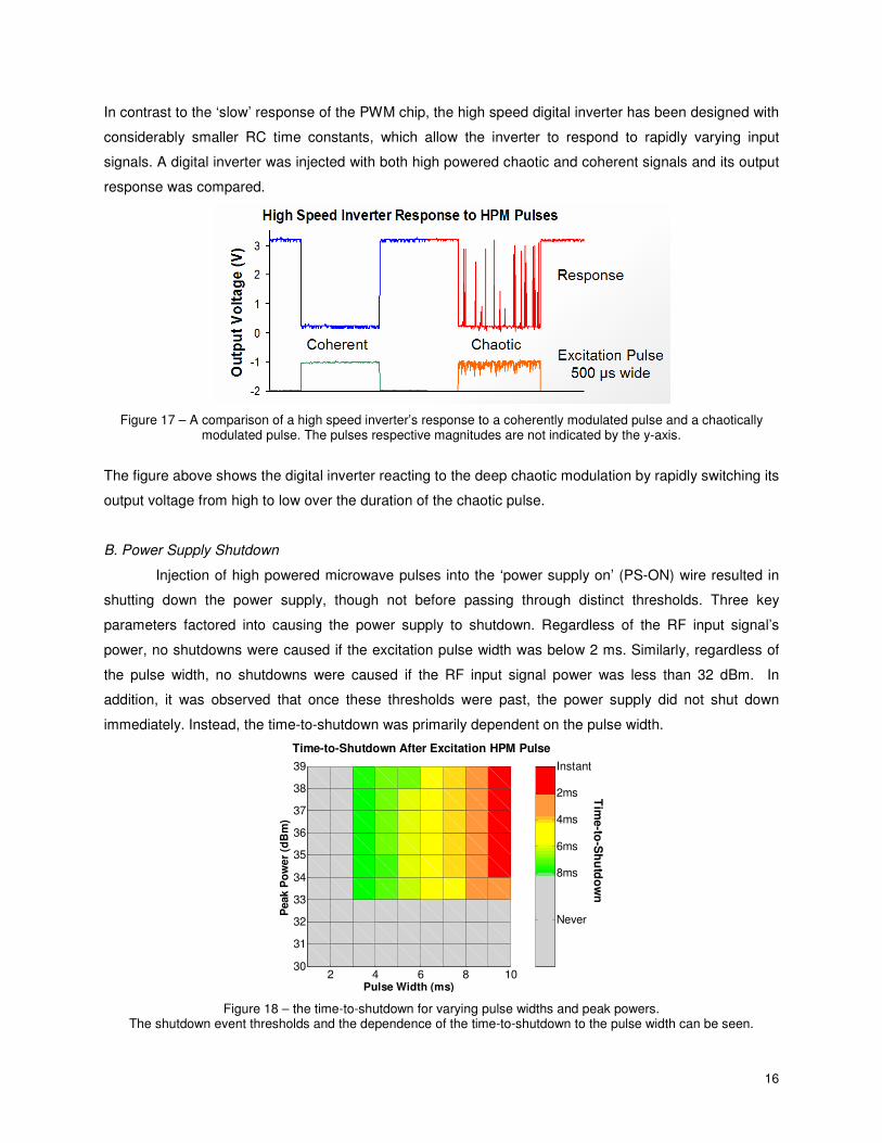
In contrast to the ‘slow’ response of the PWM chip, the high speed digital inverter has been designed with
considerably smaller RC time constants, which allow the inverter to respond to rapidly varying input
signals. A digital inverter was injected with both high powered chaotic and coherent signals and its output
response was compared.
Figure 17 – A comparison of a high speed inverter’s response to a coherently modulated pulse and a chaotically modulated pulse. The pulses respective magnitudes are not indicated by the y-axis.
The figure above shows the digital inverter reacting to the deep chaotic modulation by rapidly switching its
output voltage from high to low over the duration of the chaotic pulse.
B. Power Supply Shutdown
Injection of high powered microwave pulses into the ‘power supply on’ (PS-ON) wire resulted in
shutting down the power supply, though not before passing through distinct thresholds. Three key
parameters factored into causing the power supply to shutdown. Regardless of the RF input signal’s
power, no shutdowns were caused if the excitation pulse width was below 2 ms. Similarly, regardless of
the pulse width, no shutdowns were caused if the RF input signal power was less than 32 dBm. In
addition, it was observed that once these thresholds were past, the power supply did not shut down
immediately. Instead, the time-to-shutdown was primarily dependent on the pulse width.
30
31
32
33
34
35
36
37
38
39
2 4 6 8 10Pulse Width (ms)
Peak P
ow
er
(dB
m)
Instant
2ms
4ms
6ms
8ms
Never
Time-to-Shutdown After Excitation HPM Pulse
Tim
e-to
-Sh
utd
ow
n
Figure 18 – the time-to-shutdown for varying pulse widths and peak powers. The shutdown event thresholds and the dependence of the time-to-shutdown to the pulse width can be seen.

17
For pulse widths of 9 ms or more, the power supply immediately shutdown after the excitation pulse. The
time-to-shutdown increased to 8ms as the pulse width was reduced to 3ms, where it met the threshold for
pulse width. It is critical to remember that the power referred to in the figure above is not the average
power delivered to the power supply. It is instead the peak power, or the power contained in the pulse.
We hypothesize that the high powered microwave pulse from the TWT temporarily increases the voltage
on the comparator inputs which monitors the PS-ON signal from the motherboard, causing the
comparator to no longer recognize the signal as active low (in our case, the PS-ON wire was tied to
ground). According to ATX specifications, the PS-ON signal can be just momentarily open circuited and it
will be interpreted by the power supply as a ‘power supply off’ command.
Conclusions
The high powered microwave pulses used to simulate electromagnetic interference caused
disruptions in the normal operation of the power supply and digital inverter. These disruptions ranged
from causing overvoltage and undervoltage conditions in the DC output voltage to completely shutting
down the power supply – a serious failure for electronic systems. While chaotically modulated pulses did
not affect the power supply any more than coherent pulses, the chaotic modulation caused massive
disruptions in the operation of the high speed digital inverter. Each of the erroneous switches that were
due to the inverter responding to the chaotic modulation is a bit error and aggregated data corruption or
even system lockups can occur in finely synchronized digital circuits. This investigation shows that circuit
designers must be mindful of the parasitic RC time constants seen by system-critical components. The
power supply’s ‘slow’ time constants prevent the rapid shifts in the EMI’s amplitude from causing switch
operations. In contrast, the same traits of the digital inverter that give it a ‘high speed’ designation leave it
vulnerable to erratic switching due to chaotic or wideband electromagnetic interference. The difference in
response between the power supply circuitry and the digital inverter provide validation to the idea that
chaotic and wideband signals are ideal candidates for disrupting electronics, because the wideband
nature of the interference ensures that some part of the system will be affected.
The high powered microwave interference was also able to cause the power supply to shutdown when
injected into the PS-ON wire. This is an especially vulnerable part of the power supply because the long
wire that extends from the power supply to the motherboard make it a natural antenna for coupling
electromagnetic interference. It was discovered that the characteristics of fatal pulses were not linearly
dependent on pulse width or peak power. Instead, sharp thresholds must be passed before shutdowns
occur. The existence of these thresholds, and the fact that for short pulse widths it takes 8ms after the
excitation pulse for shutdown to occur, can give system designers a starting point for developing new and
more effective EMI protection for power supplies.

18
Further investigation into this topic must include studying the penetration of radiated high power
microwaves into computer enclosures, testing the power supply’s response to EMI when loaded with an
operational motherboard, and exploring deeper the sequence of events that occur inside the power
supply that result in shutdown when RF is coupled into the PS-ON wire.
Acknowledgements We would like to thank our primary faculty advisor Dr. John Rodgers, who devoted an immeasurable
amount of time in the laboratory teaching us the underlying theory behind our research project and
advising us on experimental procedures. Todd Firestone provided valuable insight and experience in
troubleshooting our experiments and helping explain the effects being observed. The interactions with
Kristy Gaff and Michelle Adan, two TREND students also under Dr. Rodgers, created a lighthearted
atmosphere in the lab and we all collectively helped one another in our projects. Finally, we thank the
entire team at IREAP and the ECE Department at the University of Maryland, for making us feel truly
welcomed.
References [1] Abrams, Michael. “The Dawn of the E-Bomb”. IEEE Spectrum. Nov. 2003. [2] Rodgers, John. Direct discussions. June – August, 2006. [3] Firestone, Todd M. “RF Induced Nonlinear Effects in High Speed Electronics”. Master’s Thesis, University of Maryland-College Park, © 2004. [4] ATX/ATX12V Power Supply Design Guide, Version 1.1. Intel Corporation, © 2000. [5] Ruzicka, Pavel. “Wiring Diagram of 200W ATX PC Power Supply. URL < http://pavouk.comp.cz/hw/en_atxps.html > © 2003. [6] Richardson, Robert E. “Quiescent Operating Point Shift in Bipolar Transistors with AC Excitation.” IEEE Journal of Solid-State Circuits, Vol. SC-14, No.6, Dec 1979. [7] Forcier, Marie L. and Richardson, Robert E. “Microwave Rectification RFI Response in Field Effect Transistors.” IEEE Transactions on Electromagnetic Compatibility, Vol. EMC-21, No. 4, Nov 1979. [8] ENEE 482 Seminar: Nonlinearity in Microwave Circuits and Systems. Rodgers, John. PowerPoint; Apr. 2006.
[9] ENEE 482 Seminar: Nonlinearity in Microwave Circuits and Systems. Dr. John Rodgers. PowerPoint; Slides 11-14. Apr. 2006.
[10] C.K. Tse, Yufei Zhou, F.C.M. Lau, and S.S. Qiu. “Intermittent Chaos in Switching Power Supplies Due to Unintended Coupling of Spurious Signals.” Pgs 642-645. , © 2003. [11] J.A. Ferreira, P.R. Willcock, S.R. Holm. “Sources, Paths and Traps of Conducted EMI in Switch Mode Circuits.” IEEE Industry Application Society Annual Meeting. 5-9 Oct. 1997. [12] S. Bhattacharjee, C. Marchewka, J.H. Booske, and J.E. Scharer. “Experimental Observation and Characterization of Chaos in a Driven TWT Oscillator with Delayed Feedback” University of Wisconsin-Modbon, Electrical and Computer Engineering Dept., 141.5 Engineering Drive, Madkon, WI 53706 [13] Traveling Wave Tube graphic. URL < http://www2.jpl.nasa.gov/basics/bsfii8.gif >
Top Related