


Languages
Pages
Legal


Getting All the Light Out, or No Photon Left Behind
Steve Forrest
Departments of Electrical Engineering and
Computer Science, and Physics
University of Michigan
Ann Arbor, MI 48109
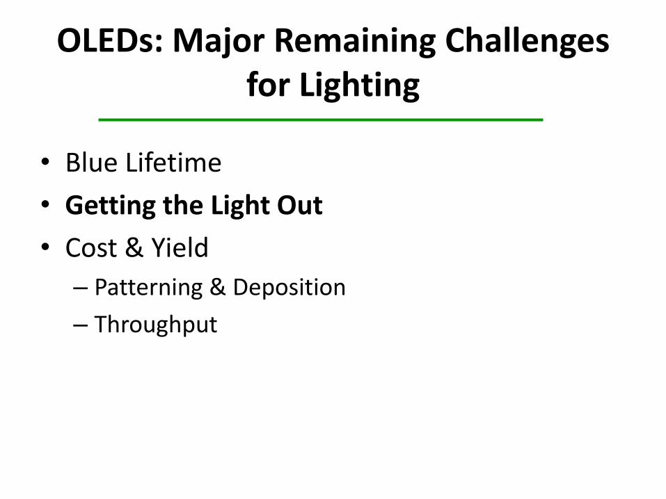
OLEDs: Major Remaining Challenges for Lighting
• Blue Lifetime
• Getting the Light Out
• Cost & Yield
– Patterning & Deposition
– Throughput
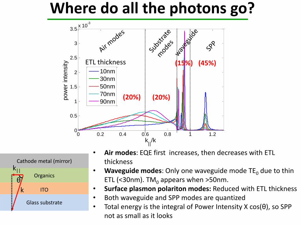
Cathode metal (mirror)
Organics
ITO
Glass substrate
k||
k
θ
• Air modes: EQE first increases, then decreases with ETL thickness
• Waveguide modes: Only one waveguide mode TE0 due to thin ETL (<30nm). TM0 appears when >50nm.
• Surface plasmon polariton modes: Reduced with ETL thickness • Both waveguide and SPP modes are quantized • Total energy is the integral of Power Intensity X cos(θ), so SPP
not as small as it looks
Where do all the photons go?
0 0.2 0.4 0.6 0.8 1 1.20
0.5
1
1.5
2
2.5
3
3.5x 10
-3
k||/k
pow
er
inte
nsity
10nm
30nm
50nm
70nm
90nm
ETL thickness
(20%) (20%)
(15%) (45%)
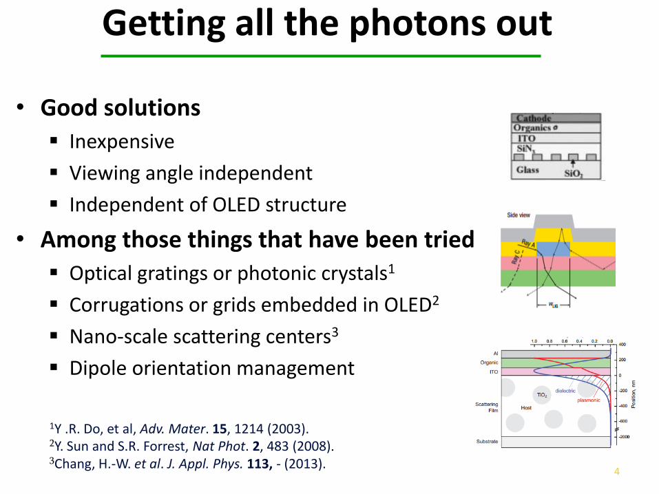
• Good solutions
Inexpensive
Viewing angle independent
Independent of OLED structure
• Among those things that have been tried
Optical gratings or photonic crystals1
Corrugations or grids embedded in OLED2
Nano-scale scattering centers3
Dipole orientation management
4
1Y .R. Do, et al, Adv. Mater. 15, 1214 (2003). 2Y. Sun and S.R. Forrest, Nat Phot. 2, 483 (2008). 3Chang, H.-W. et al. J. Appl. Phys. 113, - (2013).
Getting all the photons out
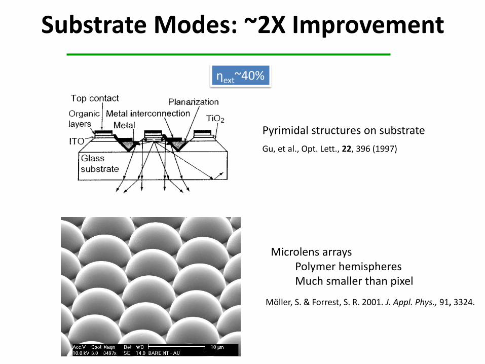
Substrate Modes: ~2X Improvement
Gu, et al., Opt. Lett., 22, 396 (1997)
ηext~40%
Pyrimidal structures on substrate
Microlens arrays Polymer hemispheres Much smaller than pixel
Möller, S. & Forrest, S. R. 2001. J. Appl. Phys., 91, 3324.

6
Metal electrode pixel
Organics
Low-index grid
ITO
Glass substrate
Side view
wLIG
worg
Waveguide Modes Embedded Low Index Grid
ηext~60% (incl. substrate modes)
Sun, Y. & Forrest, S. R. 2008. Nature Photon., 2, 483.

7
2mm
The Real Things
• OLED >> Grid size >> Wavelength • Embedded into OLED structure • May partially decouple waveguide mode from SPPs

8
400 600 800
0.0
0.5
1.0
No
rm.
EL
(a
.u.)
Wavelength (nm)
Dev. 1
Dev. 4
10-6
1x10⁻⁵
1x10⁻⁴
10-3
10-2
10-1
0
10
20
30
Po
we
r E
ffic
ien
cy (
lm/W
)
Exte
rna
l Q
ua
ntu
m E
ffic
ien
cy (
%)
Current Density (mA/cm2)
Dev. 4
Dev. 3
Dev. 2
Dev. 1
0
10
20
30
40
50
60
70
80
Dev. 1 x 1.32
Dev.1x1.68
Dev. 1 x 2.3
10-3 10-2 10-1 100 101 102 10-3 10-2 10-1 100 101 102
Device Performance Using Embedded Grids + Microlens
Device 1: Conventional Device 2: LIG only Device 3: Microlenses only Device 4: LIG + Microlenses
Method is Wavelength Independent
Sun, Y. & Forrest, S. R. 2008. Nature Photon., 2, 483.

A better approach: Sub-Anode Grid
A multi-wavelength scale dielectric grid between glass and transparent anode (sub-anode grid)
The grid is out of the OLED active region
Waveguided light is scattered into substrate and air modes
9
Cathode
nglass=1.5
nhost
norg=1.7, nITO=1.8
ngrid ngrid waveguided power + dissipation
Collect substrate mode power
Qu,Slootsky, Forrest, Nature Photonics (2015)

Emission fields
10
WITH GRID
WITHOUT GRID
VERTICAL DIPOLE
HORIZONTAL DIPOLE
Mostly in-plane (Waveguided)
Mostly out-of-plane (Glass + air)
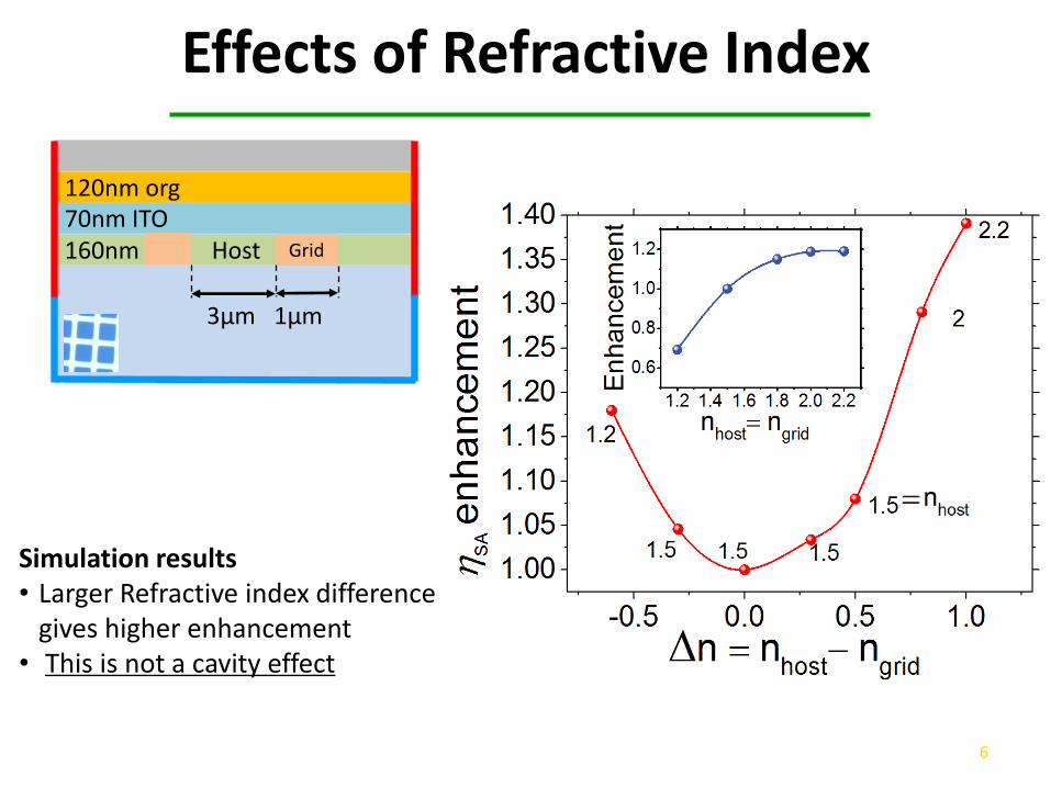
Effects of Refractive Index
6
160nm Host
120nm org 70nm ITO
Grid
3µm 1µm
Simulation results • Larger Refractive index difference
gives higher enhancement • This is not a cavity effect

450 500 550 600 650 700 750 8000.0
0.5
1.0
Inte
nsity (
No
rm.)
Wavelength (nm)
Optical Characteristics
13
Little or no impact on emission characteristics of the OLED
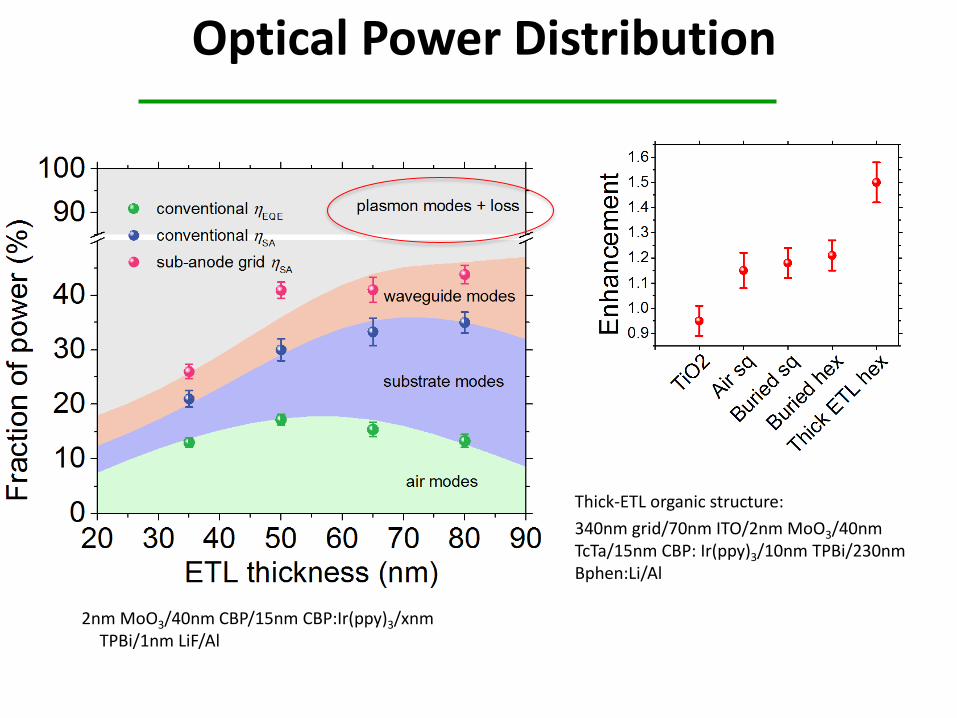
Optical Power Distribution
Thick-ETL organic structure:
340nm grid/70nm ITO/2nm MoO3/40nm TcTa/15nm CBP: Ir(ppy)3/10nm TPBi/230nm Bphen:Li/Al
2nm MoO3/40nm CBP/15nm CBP:Ir(ppy)3/xnm TPBi/1nm LiF/Al

Pt(dbq)(acac)
Isotropic Orientation
Horizontal Orientation
Manipulating Molecular Orientation
Ir(ppy)3

Example results
0 10 20 30 40 50 60 70 80 900.0
0.5
1.0
1.5
2.0
2.5
Detector Angle [Degree]N
orm
alize
d I
nte
nsit
y
Isotropic (hor
= 66.7%)
Horizontal (hor
= 100%)
Fit (hor
= 45.9%)
CBP:Pt(dbq)(dpm) 8wt%
Pt(dbq)(dpm)
0 10 20 30 40 50 60 70 80 900.0
0.5
1.0
1.5
2.0
Detector Angle [Degree]
No
rmalized
In
ten
sit
y
Isotropic (hor
= 66.7%)
Horizontal (hor
= 100%)
Fit (hor
= 65.9%)
CBP:Irppy3 8wt%
Ir(ppy)3
Approach largely impractical • Added constraints on molecular design • Added constraints on process (growth) conditions: may not align as expected • Added constraints on device architecture • Alignment is never “perfect”: only modest improvements
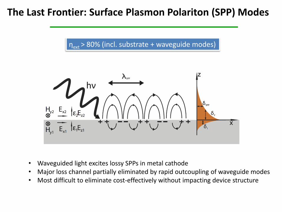
The Last Frontier: Surface Plasmon Polariton (SPP) Modes
ηext > 80% (incl. substrate + waveguide modes)
• Waveguided light excites lossy SPPs in metal cathode • Major loss channel partially eliminated by rapid outcoupling of waveguide modes • Most difficult to eliminate cost-effectively without impacting device structure
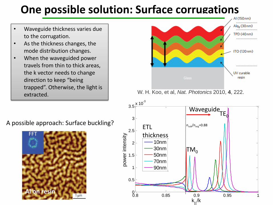
One possible solution: Surface corrugations
• Waveguide thickness varies dueto the corrugation.
• As the thickness changes, themode distribution changes.
• When the waveguided powertravels from thin to thick areas,the k vector needs to changedirection to keep “beingtrapped”. Otherwise, the light isextracted.
0.8 0.85 0.9 0.95 10
0.5
1
1.5
2
2.5
3
3.5x 10
-3
k||/k
pow
er
inte
nsity
10nm
30nm
50nm
70nm
90nm
TM0
TE0
ETL thickness
Waveguide
nsub/norg=0.88
W. H. Koo, et al, Nat. Photonics 2010, 4, 222.
A possible approach: Surface buckling?
FFT
Al on resin
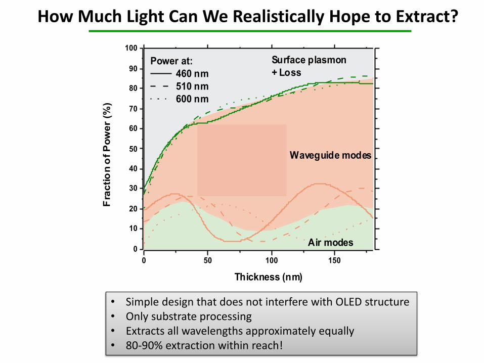
• Simple design that does not interfere with OLED structure • Only substrate processing • Extracts all wavelengths approximately equally • 80-90% extraction within reach!
0 50 100 150
0
10
20
30
40
50
60
70
80
90
100
Power at:
460 nm
510 nm
600 nm
Air modes
Waveguide modes
Fra
cti
on
of
Po
we
r (%
)
ETL Thickness (nm)
Surface plasmon
+ Loss
SubstrateMetalmirror
ITO70nmOrganic120nm
ITO50nm
SiO2xnm
SiO2
How Much Light Can We Realistically Hope to Extract?
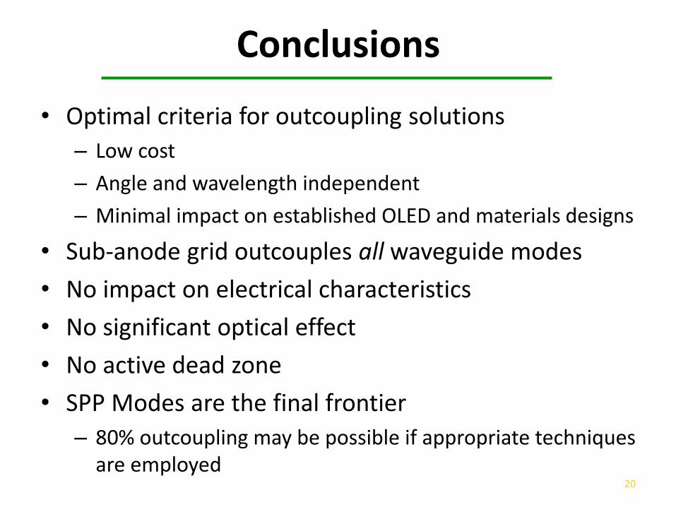
Conclusions
• Optimal criteria for outcoupling solutions
– Low cost
– Angle and wavelength independent
– Minimal impact on established OLED and materials designs
• Sub-anode grid outcouples all waveguide modes
• No impact on electrical characteristics
• No significant optical effect
• No active dead zone
• SPP Modes are the final frontier
– 80% outcoupling may be possible if appropriate techniques are employed
20