


Languages
Pages
Legal

i
FULLY INTEGRATED DC-DC BUCK CONVERTER
Carlos Eldio Soria Azevedo
Thesis to obtain the Master of Science Degree in
Electrical and Computer Engineering
Supervisors: Prof. João Manuel Torres Caldinhas Simões Vaz
Prof. Pedro Nuno Mendonça dos Santos
Examination Committee
Chairperson: Prof. Gonçalo Nuno Gomes Tavares
Supervisor: Prof. João Manuel Torres Caldinhas Simões Vaz
Members of the Committee: Prof. Marcelino Bicho dos Santos
May 2015

ii

iii
Abstract
In the last few years, we have witnessed an increasingly power demand from the consumer applications,
especially from the portable battery powered devices. From this perspective a trade-off between efficiency,
performance and flexibility has gained special attention in recent technologies. Simultaneously, because passive
components dictate the size of the power converter, higher integration and miniaturization to achieve compact
and low-cost solutions is mandatory. Those constrains brings new challenges and new opportunities to the power
electronics field.
This dissertation presents the design and implementation of a fully integrated inductor-based dc-dc converter
operating at very high frequency. The system is implemented with a synchronous buck converter topology, using
standard CMOS 0.13µm technology from UMC, without resorting to any extra processing steps or expensive
post-fabrication process such as thick film inductors, stacked chips and bond-wires inductors.
The converter is operated in voltage-mode control employing the pulse width modulation technique to down
convert the battery voltage to the nominal output voltage. First, a basic introduction to dc-dc converters, with
emphasis on the buck converter and control scheme is given, along with the used governing steady-state model
equations. Then the open loop transfer function of the power converter is explored with help of computer
assisted design tools and a type II compensation network is designed to compensate the double pole introduced
by the output LC filter network. At the same time, a comprehensive explanation of each building block that
incorporates the converter and its operation is included.
The implemented system is capable of converting an input voltage from 2.8V to 3.6V into an output voltage of
1.2V at 518MHz. The buck converter can supply an output power of 90mW up to 150mW with an efficiency
around 30%. An output ripple of 85mV was achieved
The development of this work includes the schematic and layout design, being the schematic validated by means
of simulations and layout validated by post-layout simulations, based on design rules check, layout versus
schematic and process, temperature and voltage variations.

iv

v
Resumo
Nos últimos anos temos vindo a assistir a um aumento da potência consumida pelos equipamentos de electrónica
de consumo, especialmente nos equipamentos portáteis que operam a bateria. Deste ponto de vista, nas mais
recentes tecnologias tem-se vindo a dar um maior enfâse ao compromisso entre a eficiência e a performance.
Simultaneamente, dado que os componentes passivos ditam a dimensão do conversor de potência, tornou-se
imperativo estudar novas soluções que permitam uma maior integração e miniaturização do conversor para
alcançar soluções mais compactas a preços acessíveis. Estas restrições trazem novos desafios e oportunidades no
campo da electrónica de potência.
Esta dissertação consiste no projecto e na implementação de um conversor dc-dc a operar a muito alta
frequência. O sistema é implementado através de um conversor redutor síncrono na tecnologia CMOS 0.13µm
da UMC sem recorrer a quaisquer passos de fabrico extras, tais como bobines de wire-bonding, circuitos
integrados empilhados ou outros.
O conversor é operado no modo de controlo em tensão com a técnica de modulação por largura de impulso para
reduzir a tensão de alimentação da bateria para o valor nominal de saída. Numa primeira fase será dado uma
breve introdução sobre os conversores dc-dc com especial enfâse no conversor redutor bem como as técnicas de
controlo e as equações em regime estático que governam o circuito.
Depois é feita uma análise ao conversor sobre o ponto de vista de sinais fracos para a obtenção da função de
transferência em malha aberta com ajuda de ferramentas computacionais e com estes resultados projectar o
controlador de modo a compensar o pólo duplo introduzido pelo filtro LC na saída. Ao mesmo tempo é dada
uma breve explicação sobre o funcionamento de cada bloco que constitui o conversor.
O sistema implementado é capaz de converter uma tensão de entrada entre 2.8V e 3.6V numa tensão de saída de
1.2V a operar a uma frequência de comutação de 518MHz. O conversor redutor implementado pode fornecer
uma potência de saída de 90mW até 150mW com um rendimento na casa dos 30%. O valor do tremor da tensão
de saída do conversor foi de 86mV.
O projecto deste trabalho inclui o projecto do circuito em esquemático e layout, sendo que o esquemático é
validado através de simulações e o layout validado através de simulações pós-layout, baseadas nas regras de
projecto, layout versus esquemático e variações de processo, temperatura e tensão.

vi

vii
Acknowledgments
The last years that I spent in Instituto Superior Técnico will be the most memorable ones, not only because I
made good friends, met incredible colleagues but also because I had to conciliate my job with the course.
Sometimes I catch myself thinking how this accomplishment was possible. Only with God’s help.
In first place I want to thank my parents and wife for their faith, support and motivation. I want to apologize for
my absence in some important dates and special occasions. To my wife, I apologize by the time we were not
together.
I would like to express my sincerest gratitude to my advisors, Professors João Vaz and Pedro Santos for their
unconditional support, guidance and encouragement during the research of this dissertation.
I want to thank you to Instituto de Telecomunicações at Instituto Superior Técnico for receiving me on their
facilities where I spent much of the time doing my research.
Furthermore, I would like to extend my gratitude to all professors that have influenced me to earn interest for
microelectronics and power electronics field and for sharing their knowledge through the classes and private
conversations.
Carlos Eldio Soria Azevedo
2015-04-15

viii

ix
Table of Contents
Abstract................................................................................................................................................................. iii
Resumo................................................................................................................................................................... v
Acknowledgments ............................................................................................................................................... vii
Table of Contents.................................................................................................................................................. ix
List of figures........................................................................................................................................................ xi
List of Tables........................................................................................................................................................ xv
List of Acronyms ............................................................................................................................................... xvii
1. Introduction .................................................................................................................................................. 1
1.1. State-of-the-Art ................................................................................................................................... 2
1.2. Objectives............................................................................................................................................ 4
1.3. Specifications ...................................................................................................................................... 4
1.4. Thesis Organization............................................................................................................................. 5
2. DC-DC Converter Fundamentals................................................................................................................ 7
2.1. Overview of the Buck Converter Operation........................................................................................ 8
2.2. Steady-State Analysis ........................................................................................................................ 13
2.2.1. Inductor Sizing .................................................................................................................... 17
2.2.2. Capacitor Sizing .................................................................................................................. 18
2.2.3. Effects of Non-Idealities ..................................................................................................... 19
2.2.4. Efficiency and Power Loss Analysis ................................................................................... 21
2.3. Buck Converter Feedback Control .................................................................................................... 23
2.3.1. Voltage-Mode Control of Buck Converter.......................................................................... 25
2.3.2. Compensator Design Overview........................................................................................... 28
3. DC-DC Converter Systemic Design .......................................................................................................... 33
3.1. Power-stage Design........................................................................................................................... 33
3.2. Small-signal Analysis ........................................................................................................................ 39
3.2.1. Open-loop Frequency Response.......................................................................................... 40
3.2.2. Compensator Design ........................................................................................................... 43
4. System Design and Simulations................................................................................................................. 49
4.1. Operation Transconductance Amplifier............................................................................................. 49
4.2. Fast Comparator ................................................................................................................................ 54
4.3. Sawtooth Generator........................................................................................................................... 60

x
4.4. Bandgap Voltage Reference............................................................................................................... 63
4.5. Current Reference Generator............................................................................................................. 67
4.6. DC-DC Buck converter simulation ................................................................................................... 70
5. Layout Implementation and Post-Layout Simulations ........................................................................... 75
5.1. Substrate Noise Effects ..................................................................................................................... 76
5.2. Power Supply and Ground Planning ................................................................................................. 76
5.3. Power Transistors and Drivers Considerations.................................................................................. 76
5.4. Layout Implementation of Each Block.............................................................................................. 79
5.5. Custom-Made Metal-Track Inductor................................................................................................. 83
5.6. Post-Layout Simulations ................................................................................................................... 84
5.6.1. Nominal Conditions of Operation ....................................................................................... 86
5.6.2. Post-layout Transient Response for Load Step.................................................................... 87
5.6.3. Post-layout Corners Transient Response for a Load Step ................................................... 88
5.7. Final Results...................................................................................................................................... 89
6. Conclusion ................................................................................................................................................... 91
7. Future Work................................................................................................................................................ 93
8. References ................................................................................................................................................... 95

xi
List of figures
Figure 1: State-of-the-art literature results for inductor-based dc-dc converter ...................................................... 3
Figure 2: System block diagram of battery-operated device, exhibiting the dc-dc converters. [National
Semiconductors] ..................................................................................................................................................... 7
Figure 3: The (a) Asynchronous buck converter. (b) Synchronous buck converter representation......................... 9
Figure 4: Buck converter waveforms for the (a) control, (b) inductor current, (c) inductor voltage and (d)
switching node, operating in the continuous conduction mode............................................................................. 10
Figure 5: Buck converter waveforms for the (a) control, (b) inductor current, (c) inductor voltage and (d)
switching node, operating at the discontinuous conduction mode .........................................................................11
Figure 6: Buck converter waveforms for the (a) control, (b) inductor current, (c) inductor voltage and (d)
switching node for the critical mode of operation................................................................................................. 12
Figure 7: (a) On-state of the synchronous buck converter. (b) Off-state of the synchronous buck converter. ...... 13
Figure 8: Detailed CCM operation of the synchronous buck converter. ............................................................... 14
Figure 9: Detailed DCM operation of the synchronous buck converter. ............................................................... 16
Figure 10: Equivalent circuit for the dead-time sub-interval conduction.............................................................. 16
Figure 11: A representative view of the buck converter output voltage ripple and inductor current ripple, for the
calculation of the output capacitor. ....................................................................................................................... 19
Figure 12: The equivalent buck converter circuit contemplating the conduction losses. ...................................... 20
Figure 13: Mosfet hard-switching representation ................................................................................................. 21
Figure 14: Buck converter closed loop representation. ......................................................................................... 24
Figure 15: Buck converter current-mode control representation........................................................................... 25
Figure 16: Detailed view of the buck converter employing all the system blocks................................................ 26
Figure 17: PWM waveform .................................................................................................................................. 27
Figure 18: Detail of the PWM generator configuration. ....................................................................................... 27
Figure 19: Non-overlapping clocks....................................................................................................................... 28
Figure 20: Body-diode conduction detail.............................................................................................................. 28
Figure 21: Type II compensation circuit ............................................................................................................... 29
Figure 22: Type II asymptotic Bode plot............................................................................................................... 30
Figure 23: Type III compensation circuit. ............................................................................................................. 30
Figure 24: Type III asymptotic Bode plot ............................................................................................................. 31
Figure 25: Representation of the overall power stage block. ................................................................................ 33

xii
Figure 26: Determined values for the output filter used in the buck converter. .................................................... 34
Figure 27: Power switches showing the obtained channel width. ......................................................................... 35
Figure 28: Simulation showing the power switches on-resistance function of their width. .................................. 35
Figure 29: Power drivers consisting on a chain of inverters. ................................................................................ 37
Figure 30: The non-overlapping block consisting in a two NOR gates and two NOT gates. ................................ 38
Figure 31: The two non-overlapped signals to be applied at the input of the drivers............................................ 39
Figure 32: Test bench used to perform the PSS and PAC analysis in the buck converter. .................................... 41
Figure 33: Signals involved in the PWM wave generation. .................................................................................. 41
Figure 34: Open loop frequency response of the implemented buck converter. ................................................... 42
Figure 35: Open loop frequency response with no series resistance in the output inductor. ................................. 42
Figure 36: Compensated error amplifier with its respective compensation network. ........................................... 44
Figure 37: Frequency response of the designed compensator. .............................................................................. 45
Figure 38: Complete test bench used to perform the closed-loop feedback frequency response. ......................... 45
Figure 39: Closed Loop frequency response of the buck converter. ..................................................................... 46
Figure 40: Transient response comparison of the output voltage between the two crossover frequencies for a load
step of 50mA......................................................................................................................................................... 46
Figure 41: Comparison between the two closed loop frequency responses. ......................................................... 47
Figure 42: A 50mA step load response with extremes and nominal battery voltage. ............................................ 48
Figure 43: Schematic used to perform the efficiency simulation. ......................................................................... 48
Figure 44: Symmetrical operational transconductance amplifier topology........................................................... 49
Figure 45: Symmetrical operational transconductance amplifier test bench for the open loop frequency response,
input impedance and PSRR+ and PSSR-. ............................................................................................................. 50
Figure 46: Symmetrical operational transconductance amplifier test bench for the output impedance
measurement. ........................................................................................................................................................ 51
Figure 47: Operational transconductance open-loop frequency response. ............................................................ 52
Figure 48: Operational transconductance open loop PSRR. ................................................................................. 52
Figure 49: Operational transconductance amplifier input impedance................................................................... 53
Figure 50: Operational transconductance amplifier output impedance................................................................. 53
Figure 51: Fast comparator used for the PWM operation. .................................................................................... 55
Figure 52: Transfer curve of a comparator (a) without offset and (b) with offset. ................................................ 56
Figure 53: Test bench used to simulate the dc characteristic of the comparator.................................................... 57

xiii
Figure 54: Comparator’s dc characteristic and offset representation. ................................................................... 57
Figure 55: Propagation delay representation......................................................................................................... 58
Figure 56: Fast comparator test bench to determine propagation delay. ............................................................... 59
Figure 57: Simulation results for a switching frequency of 500MHz. .................................................................. 59
Figure 58: Simplified view of the implemented sawtooth generator..................................................................... 60
Figure 59: Schematic of the implemented sawtooth generator. ............................................................................ 61
Figure 60: Test bench implemented to perform the sawtooth generator simulations. ........................................... 61
Figure 61: Sawtooth waveform with the fast comparator output voltage and the upper limit threshold............... 62
Figure 62: Schematic of the implemented bandgap voltage reference generator. ................................................. 63
Figure 63: Bandgap voltage reference generator test bench for the simulated results. ......................................... 64
Figure 64: Temperature dependence of the bandgap output reference voltage. .................................................... 64
Figure 65: Bandgap start-up time.......................................................................................................................... 65
Figure 66: Bandgap output voltage reference as a function of supply voltage...................................................... 65
Figure 67: Bandgap power-supply rejection ratio. ................................................................................................ 66
Figure 68: Schematic of the implemented current reference generator. ................................................................ 67
Figure 69: Simplified view of the implemented current reference generator. ....................................................... 67
Figure 70: Test bench used in the simulations of the implemented current reference generator. .......................... 68
Figure 71: Output current reference simulation taking into account the BGVR as the voltage reference. ........... 69
Figure 72:Test bench for the nominal operation and for step load and line transient response............................. 70
Figure 73: Buck converter operating at 75mA nominal output current................................................................. 70
Figure 74: Transient response of the buck converter for a load step of 50mA...................................................... 71
Figure 75: Transient response of the buck converter for line variations. .............................................................. 72
Figure 76: Transient response of the buck converter and BGVR for line variations............................................. 73
Figure 77: Transient response of the buck converter and BGVR without considering the line variation for the
bandgap voltage reference..................................................................................................................................... 73
Figure 78: Detailed view of the worst case transient response of the buck converter and BGVR without
considering the line variation for the bandgap voltage reference.......................................................................... 74
Figure 79: Detailed View of the floorplan of the die............................................................................................. 75
Figure 80: Detail of the single transistor that constitutes the power transistor ..................................................... 77
Figure 81: Overall view of the PMOS high-side power switch. On the left are the source and gate connections
whereas at the right is the drain connection (dimensions: W=123µm, H=101µm)............................................... 77

xiv
Figure 82: Overall view of the PMOS high-side power switch driver. On the left is the input terminal of the
driver, on the right the output terminal (dimensions: W=79µm, H=54µm). ......................................................... 78
Figure 83: Detail of the single transistor that constitutes the NMOS low-side power switch (dimensions:
W=9.3µm, H=8.7µm). .......................................................................................................................................... 78
Figure 84: Overall view of the NMOS low-side power switch. On the left are the source and gate connections
whereas at the right is the drain connection (dimensions: W=72µm, H=60µm)................................................... 78
Figure 85: Overall view of the NMOS low-side power switch driver. On the left is the input terminal of the
driver and at the right is the output terminal (dimensions: W=58µm, H=36µm).................................................. 79
Figure 86: Overall view of the power switches and their respective drivers......................................................... 80
Figure 87: Overall view of the bandgap voltage reference (dimensions: W=180µm, H=236µm). ....................... 80
Figure 88: Overall view of the current reference (dimensions: W=61µm, H=45µm)........................................... 81
Figure 89: Overall view of the fast comparator (dimensions: W=58µm, H=38µm). ............................................ 81
Figure 90: Overall view of the MOSCAP (dimensions: W=755µm, H=781µm).................................................. 82
Figure 91: Overall view of the sawtooth generator (dimensions: W=40µm, H=35µm). ...................................... 82
Figure 92: Overall view of symmetrical operational transconductance amplifier................................................. 83
Figure 93: Overall view of the custom made metal track inductor (dimensions: W=335µm, H=335µm)............ 84
Figure 94: Overall view of the full chip (dimensions: W=1575µm, H=1575µm)................................................. 84
Figure 95: Post-layout test bench used to perform the post-layout simulation, including the pad connection as
well as the bonding wires...................................................................................................................................... 85
Figure 96: Post-layout buck converter operating at 75mA nominal output current with. ..................................... 86
Figure 97: Post-layout transient response of the buck converter for a load step of 50mA, from 75mA to 125mA.
.............................................................................................................................................................................. 87
Figure 98: Post-layout transient response of the buck converter for a load step of 50mA, from 125mA to 75mA.
.............................................................................................................................................................................. 87
Figure 99: Post-layout corners transient response of the buck converter for a load step of 50mA, from 75mA to
125mA. ................................................................................................................................................................. 88
Figure 100: Post-layout corners transient response of the buck converter for a load step of 50mA, from 125mA to
50mA. ................................................................................................................................................................... 88

xv
List of Tables
Table 1: List of recent publications on inductor-based dc-dc converters. ............................................................... 2
Table 2: Main dc-dc converter specification ........................................................................................................... 5
Table 3: Main specifications for the implemented dc-dc buck converter. ............................................................. 34
Table 4: Summary of the main specifications of the buck converter power-stage. ............................................... 36
Table 5: Components values for the compensation network as shown in figure 36.............................................. 44
Table 6: New components values for the compensation network. ........................................................................ 47
Table 7: Operational transconductance amplifier characteristics. ......................................................................... 54
Table 8: Fast comparator characteristics ............................................................................................................... 60
Table 9: Sawtooth generator main characteristics. ................................................................................................ 62
Table 10: Bandgap voltage reference main characteristics. .................................................................................. 66
Table 11: Main characteristics of the current reference......................................................................................... 69
Table 12: Final characteristics Summary of the designed dc-dc buck converter................................................... 89

xvi

xvii
List of Acronyms
AC Alternating Current
CMOS Complementary Metal-Oxide-Semiconductor
CCM Continuous Conduction Mode
DC Direct Current
DCR Direct Current Resistance
DCM Discontinuous Conduction Mode
DRC Design Rule Check
ESR Equivalent Series Resistance
ESD Electrostatic Discharge
FSW Switching Frequency
FC Crossover Frequency
GBW Gain-Bandwidth Product
IC Integrated Circuit
LDO Low-Dropout
MOSFET Metal-Oxide Semiconductor Field Effect Transistor
MOSCAP Metal-Oxide Semiconductor Capacitor
MIMCAP Metal-Insulator-Metal Capacitor
MOS Metal-Oxide Semiconductor
MM Mix-Mode
NMOS N-Type Metal-Oxide Semiconductor
OTA Operation Transconductance Amplifier
PFM Pulse Frequency Modulation
PMOS P-Type Metal-Oxide Semiconductor
PSRR Power Supply Rejection Ratio
PWM Pulse-Width Modulation
PVT Process-Voltage-Temperature
RF Radio-Frequency

xviii
RON Power-MOS channel conduction resistance
SC Switched-Capacitor
SiGe Silicon-Germanium
TSW Switching Period
TON PMOS Conduction Time
TOFF NMOS Conduction Time
UMC United Microelectronics Corporation
µn/p MOS Transistor Majority Carriers Effective

1
1.Introduction
Power electronics is the key technology to improve the performance and efficiency on a variety of electronics
systems. To the electronic industry, power consumption started to get a special attention due to an increase of
portable battery powered devices, especially to those devices that have grown in different functionalities which
is translated into a larger number of circuits and hardware. In this way, power consumption became one of the
design constrain and behind this constrain there is another fact which is related to the CMOS technology that
keeps scaling down and at same time the supply voltages, while the demand for the power consumption remains
the same. Consequently the voltage headroom for the analog circuits design also decreases, becoming more
difficult for engineers to design electronic circuits.
Meanwhile, we have been witnessing a demand for integrated switching power conversion, driven by the
consumer electronics gadgets needs and the advances in several technological fields. Thus, the full integration of
the switching power converter is mandatory. As the technologies have evolved, the methods to supply power to
these electronic systems have evolved as well. Different analog and digital circuit blocks, due to their
characteristics, need to operate at different voltage levels, distributed throughout the integrated circuit. For
example, analog circuits usually need higher voltage supply than digital circuits in order to feed power amplifiers
that need to provide acceptable power to antenna. This increases the number of external dc-dc converters along
with the total number of off-chip components, printed circuit board area, bond-wire connections to the chip die
and consequently the total system cost [1]. In order to overcome these issues and achieve a significant gain in
efficiency of the overall converter while at same time maximizing power density and minimizing chip area, one
needs to fully integrate the switching power converter block into the chip [2] accomplishing simultaneously, a
more complete customization and flexible realization for power management systems in a single chip. One
solution is to have an on-chip inductor-based DC-DC switching convertor. Although these are most used in off-
chip implementations, there have been some efforts to fully integrate this type of switching converters, reducing
the inductor size by means of higher switching frequencies (since the required values of inductors and capacitors
vary inversely with the operating switching frequency) [2] [4].
The challenge in raising the frequency is the capability to maintain the efficiency of the switching converter as
the frequency rises. However, the design in the high frequency domain requires further attention to parasitic
impedances (which can became a dominant factor), skin effect, switching spikes and electromagnetic
compatibility, like crosstalk and switching noise, which may result on chip malfunction or failure.
The resulting decrease in required reactive components size offers a design leap that allows the inductor to be
fully integrated into the power-supply block, achieving a considerably smaller size switching converter. Despite
that, the quality of the reactive components depends on the technology being used. Yet, this type of switching
power conversion block is giving its first steps to become fully integrated, when compared to other mature
technologies like low drop-out voltage regulators (LDO) and switched capacitor (SC) converters [3] [4].
Recent works have shown the potential of full-integrated DC-DC converters operating at high frequency, around
200MHz at hundreds of mW/mm2 regarding power densities [4 - 10]. However, achieving higher frequencies so
that miniaturization and full integration can be accomplished remains a great challenge.

2
1.1. State-of-the-Art
The inductive dc-dc power conversion has been the reference design for most switched voltage regulators,
existing different types of topologies well studied, documented and disseminated. Currently the established state-
of-the-art for dc-dc power converters requires a limited number of external components. The next natural step is
to integrate the external components by means of the most widely used technology, the standard CMOS. Most of
the current published work presented here goes towards the full integration of inductive dc-dc converters. There
are other publications requiring extra processing steps, like thick film inductors, stacked chips and bond-wires
inductors [3] [4] [7]. The most used one is the step-down power converter, since modern applications are
normally lithium-ion battery-operated, requiring multiple lower than battery supply voltages. An overview of
full-integrated dc-dc converters recent results is presented in table 1, which was adapted from [6].
Table 1: List of recent publications on inductor-based dc-dc converters.
In table 1 it is possible to compare the most important specification parameters such as the maximum efficiency
achieved by the overall converter, the maximum switching frequency, the maximum output power, the area
occupied by the integrated dc-dc converter as well as the obtained power density.
All the compared converters use CMOS processes, except Abedinpour [10] work, that uses a SiGe 0.18 µm
process with the inductor consisting in optional patterned electroplated copper layer. Apart from Abedinpour [10]
and Wens [6] all the other converters presented have similar power densities, however they are bounded bellow
220 mW/mm2 while efficiencies do not exceed 70%. On wibben’s work [5] the use of stacked converters with
interleaved on-chip coupled inductor is exploited, reducing the current ripple and enabling the use of a small
inductor. This way, having a smaller inductance the series resistance is reduced, making possible a higher
efficiency. Comparing Wibben’s [5] work with Hazucha’s work [11] it’s possible to find that [11] has higher
Tech.
(µm)
Ui
(V)
Uo
(V)
Io, max
(mA)
Po, max
(mW)
Max η
(%)
Max Freq.
(MHz)
L
(nH)
C
(nF)
Pw. Dens.
(mW/mm2)
Area
(mm2)
[5, Wibben 2008] 0.13CMOS 1.2 0.9 350 315 77.9 170 2 x 2 5.2 210 1.5
[6, Wens 2008] 0.13CMOS 2.6 1.2 150 180 52 300 9.8 15.07 53 3.375
[7, Wens 2009] 0.13CMOS 2.6 1.2 667 800 58 225 4 x 3.9 12.17 213 3.76
[8, Kudva 2011] 0.13CMOS 1.2 0.88 332.5 266 74.5 300 2 5 167 1.59
[9, Jinhua 2009] 0.13CMOS 3.3 1.8 400 720 70.4 250 10.5 3.6 180 4
[10, Abedinp. 2007] 0.18BiCMOS 2.8 1.8 200 360 64 45 2 x 11 6 53 6.75
[11, Hazucha 2005] 0.09CMOS 1.2 0.9 300 270 83 233 4 x 6.8 off-chip 2.5 213 1.267

3
efficiency. However the difference can by neglected if one consider that [11] uses more inductance off-chip,
which allows a better quality factor and, at the same time, a smaller chip area.
In Jinhua’s [9] work, they were only focused on power efficiency regardless of occupied area, which is the
highest one when compared to the other works. When comparing [9] and [5], the author states that for the same
voltage conversion ratio he can achieve a peak efficiency of 80.5%, almost the same as in [11], considering that
[11] used on-package air-core. However the chip area occupied by [9], due to the size of the inductor, is not
feasible.
Moving away from traditionally inductor-based converters, in Wens work [7], one can observe a multilevel buck
converter. The four-phase converter presents the highest output power and the same power density as in
Hazucha’s work [11], although in [11] off-chip air core inductors is used, which are not taken into account for
the occupied chip area. The drawback of Wens [7] work has to do with the chip area occupied, which becomes
impracticable like Jinhua’s [9] work, because of the four inductors, reflecting itself in the efficiency achieved.
Looking to Kudva’s [8] work, it is possible to verify that these results are in the middle ground. Comparing to
other works, [8] does not use any special process option, neither interleaved of multiphase techniques. The fact
that the converter can reach such efficiency is because the control can change adaptively between different
modes of operation by detecting the output current. The author claims that a peak efficiency of 77% can be
reached under reduced temperature operation.
In figure 1, it is possible to compare the same results presented on table 1, plotting merely the “peak efficiency”
versus “power density” in order to give an overview in terms of performance metrics and possible application-
driven design guidelines, adapted from [4].
Figure 1: State-of-the-art literature results for inductor-based dc-dc converter
0102030405060708090
0 50 100 150 200 250
Max
Eff.
(%)
Power Density (mW/mm2)
MAX EFFICIENCY VERSUS POWER DENSITY
[5]
[6]
[7]
[8]
[9]
[10]
[11]
4
1.2. Objectives
The integration of a dc-dc converter operating at very high frequency brings several challenges to power
management integrated circuits. The main goal of this dissertation is to explore, design and implement a fully
integrated inductor-based buck converter using standard CMOS 0.13µm technology from UMC, operating at
very high frequency, without resorting to extra processing steps or expensive post-fabrication process like thick
film inductors, stacked chips and bond-wires inductors.
The development of this work includes the schematic and layout design, with schematic validated by means of
simulations and layout validated by post-layout simulations based on design rules check, layout versus schematic
verification and process, temperature and voltage corners functionality.
As stability analysis is important for switching converters and any system with negative feedback, a careful
investigation in the converter loop gain and compensator will be done using Spectre Periodic Steady State
Analysis to design the controller. This type of analysis is suitable for switching converters because of their time-
varying nature and because it is possible to enter into account with all parasitic effects on the circuit (parasitic
capacitance, bonding-wires, track and interconnections resistances), unlike the traditional average models, like
state-space-modelling that ignores some of them.
A special attention will be given also to the power stage, including the driver section, power devices and
inductor, because they are a key section, which determines the efficiency, ripple and noise of the converter.
1.3. Specifications
In this section the main specifications for the proposed dc-dc buck converter are given. The central objective of
this work is to implement a fully integrated buck converter therefore the integration of the inductor and the
capacitor is the main concern taking into account the minimal parasitic resistance of such components. For the
target nominal output power around 90mW at 1.2V feeding a fixed 15Ω load it is desired that the converter
delivers this amount of power at the maximum efficiency as possible. Other target specifications includes low
output voltage ripple, fast transient response for the load step, wide input voltage operation within a considerable
operating junction temperature range. The main specifications to be achieved are presented below.
5
Technology UMC 130nm MM/RF
Analog Core Area 2.46mm2
Topology Fully Integrated Buck Converter
Parameter Symbol Min Typ Max Units Comments
Operating Junction Temperature Tj -40 25 125 ºC
Supply Voltage Vin 2.6 3.3 3.6 V
Output Voltage Vout 1.2 V
Output Voltage Ripple ∆Vo 85 mV
Output Current Io 75 mA
Switching Frequency Fsw 500 MHz
Inductor Fully Integrated
Table 2: Main dc-dc converter specification
1.4. Thesis Organization
This thesis is organized into six chapters. Chapter 1 gives a brief overview about the topic of high frequency
buck converter and the review of the art-of-the-art.
In chapter 2 an introduction to the dc-dc converter operation is given, including the mathematical concepts that
govern the dc-dc converter. It discusses the different types of techniques used to control the dc-dc converter as
well the compensator design. A particular emphasis is given on how the dc-dc converter operates in PWM mode.
Chapter 3 addresses the system implementation and the stability analysis. This will be done in a systemic
approach through simulations and not as conventionally is done using MATLAB of Mathcad tools. A stability
analysis will be carried out by Spectre periodic steady state analysis and periodic AC analysis, so that the
feedback controller design can be designed. Afterwards a stability test will be performed to assess the overall
system stability of the implemented compensator. Additionally, it will be given a brief explanation of each
building blocks used in the system on how they work.
After a more theoretical insight gained in last chapters, chapter 4 brings the system implementation. It is
presented each building block structure used in the system design as well as their simulation results.
Finally, in chapter 5 the layout design and post-layout simulation are presented.
Chapter 6 and chapter 7 contain the conclusions and discussions of the obtained results, and some future work to
be done.

6

7
2. DC-DC Converter FundamentalsIn order to get an understanding on how a dc-dc converter operates, this chapter will introduce some of the
fundamental theory used to describe the basic principles of operation.
Over the years, dc-dc converter increased in popularity due to several advantages that they present [15],
especially their efficient performance over a large range of input voltage. The proper operation of electronics
equipment depends on the reliability and performance of the power supply.
As known, many electronic equipment, especially those that are portable and battery operated, requires a reliable
power supply with a good performance: Efficient energy conversion, to prolong the battery life and good
dynamic response concerning line and load variations. However, batteries have the problem of varying its output
voltage over time and, without a bridge structure that links the battery to each circuit block, the performance of
the device might be compromised.
As for an example, a smartphone needs a stable and regulated voltage supply to power up all the building blocks
in the device. Since this is a battery-operated device, usually with a lithium battery that provides a higher voltage
level than what is required, ranging from 2.7V-4.2V [13], a dc-dc converter is needed to down convert the
battery voltage. Here, the dc-dc converter is the bridge referred above. The most popular topology used to
perform this operation is the buck converter, in which the output voltage is always lower than the input voltage.
This way, one can say that a dc-dc converter can be described as a circuit that converters a regulated or
unregulated DC input voltage to a regulated DC output voltage. Normally the output voltage is at different
voltage level than the input, in which it can be higher or lower.
Figure 2: System block diagram of battery-operated device, exhibiting the dc-dc converters. [National
Semiconductors]
The dc-dc converter can be implemented based one of the two major types of switched-mode dc-dc converter:
inductive or capacitive. The widely used is the inductor based dc-dc converter, due to the simplicity of his

8
topology and control approach. This type of converter dominates the design of applications where high
conversion ratio, high efficiency, tight output voltage regulation and high output power are needed. The
conversion ratio is set by the duty-cycle. On the other side, switched-capacitor dc-dc converter has been used in
low power and low conversion ratio applications, where efficiency and regulation is not of great concern. In
several publications it is possible to understand that there are some issues related with the regulation of these
converters, which are the focus of several research attentions [3-4, 15]. Here the conversion ratio is set by the
topology architecture through the charge and discharge of several capacitors. Switched capacitor dc-dc converter
is out of the scope of this work.
In recent years, there have been some efforts to fully integrate the inductive-type dc-dc converter [5 -9]. Because
devices are decreasing in size and increasing in functionality, there is a need to reduce or eliminate the passive
off-chip components. To achieve full integration, the switching frequency must rise to several hundreds of
MHz’s. This brings some benefits, starting with the reduction in the number of external components, because the
passive components values drop to a few nH and nF, decreasing this way the power management printed circuit
board footprint and consequently the cost. Another benefit is an improvement in the transient response due to the
higher bandwidth. At same time, increasing the switching frequency brings some challenges. The converter
efficiency tends to drop, because the switching losses are proportional do the switching frequency and the
converter will be more susceptible to high-frequency noise.
On the other hand, the quality factor of this integrated inductor is low, due to the higher ESR resistance, which
translates into another source of power loss with consequence in the overall converter efficiency. So, to design a
highly efficient and fully integrated inductor-based dc-dc converter, the understanding of the converter power
loss mechanism is important. From now on the inductor-based dc-dc converter, which is the converter used in
this thesis, will be referred as buck converter.
2.1. Overview of the Buck Converter Operation
As mentioned before, the dc-dc buck converter changes the power supply voltage to a lower output voltage. In
literature it is possible to notice that there are two main types of buck converters: synchronous and
asynchronous. Essentially, both converters have the same basic principle of operation. The traditional buck
converter is known as the asynchronous buck converter. This type of buck converter uses a schottky diode as the
low-side switch, known as freewheeling diode. This diode has the responsibility to keep the current flow in the
inductor, as shown in figure 3 (a).
9
LO
CO
IL
Vlx
Con
trol
Q1
Q2
LO
CO RO
IL
VlxVout
Con
trol
Q1
D1
Vin Vin
RO
Vout
Figure 3: The (a) Asynchronous buck converter. (b) Synchronous buck converter representation.
However, due to the recent developments in the electronic field, especially in the telecommunications and
computing industry, the operating voltages of such systems have dropped below 1V. At those low voltages, the
voltage drop across the freewheeling diode is inadmissibly high resulting in poor converter efficiency [16]. The
solution found for this problem was to use, as a low-side switch, another MOSFET, which can be fabricated with
a low RDS(on) providing a small voltage drop at its terminals. The MOSFET Q1 is referred to as the control switch
or high-side switch and Q2 as the synchronous switch or low-side switch. This is why the synchronous buck is
called this way and is depicted in figure 3 (b).

10
vL(t)
Vin - Vout
t
iL(t)
- Vout
t
IL=Io Δ IL
On State Off State
δTsw Tsw
δ(t)
t
Vin
t
vlx(t)
(a)
(b)
(c)
(d)
Figure 4: Buck converter waveforms for the (a) control, (b) inductor current, (c) inductor voltage and (d)
switching node, operating in the continuous conduction mode.
The buck converter can operate in two modes, those are, the continuous conduction mode (CCM) and the
discontinuous conduction mode (DCM), depending on the shape of the inductor current. In the CCM the inductor
current never goes to zero during the entire switching cycle as exemplified in figure 4, while the DCM is
characterized by the inductor current being zero during one portion of the switching cycle as depicted in figure 5.
It remains at zero for some time interval and starting from zero, increases until he reaches the peak value and
then returns to zero again, repeating each switching cycle.

11
vL(t)
Vin - Vout
t
iL(t)
- Vout
t
Δ IL
On State Off State
δTsw Tsw
δ(t)
t
vlx(t)
Vin
t
Vout
(a)
(b)
(c)
(d)
Figure 5: Buck converter waveforms for the (a) control, (b) inductor current, (c) inductor voltage and (d)switching node, operating at the discontinuous conduction mode
When the buck converter is operating at the boundary of the CCM and the DCM, it is called as the critical mode
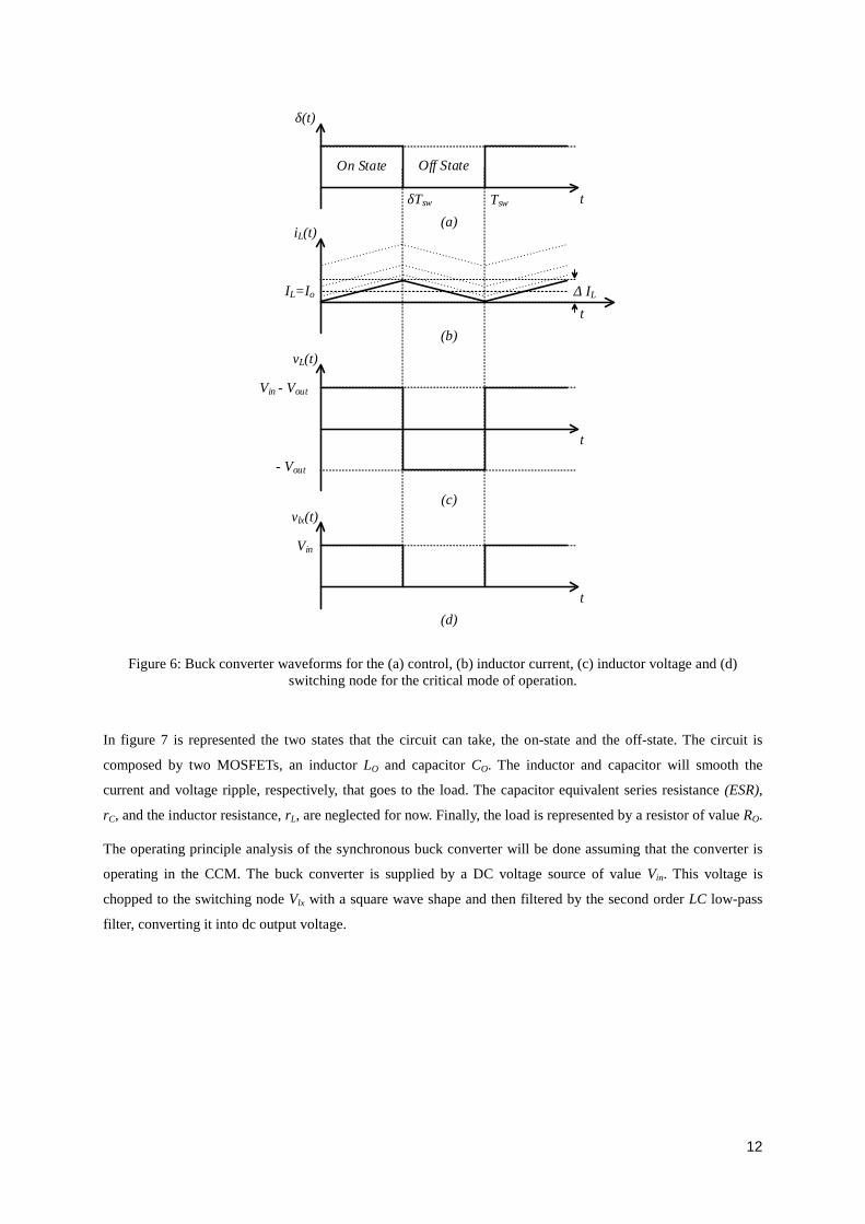
(CM). Figure 6 shows this mode of operation.
Usually the buck converter is operated in the CCM because the performance and the output power rating are
higher when compared to the other modes. However, in some applications where the output power is low, it can
be advantageous to operate the buck converter in the DCM, resulting generally in a smaller converter size.
Nowadays there are dc-dc converter called dual mode dc-dc converter that works in both modes of operation,
employing for the DCM the pulse frequency modulation (PFM) control technique.
12
vL(t)
Vin - Vout
t
iL(t)
- Vout
t
IL=Io Δ IL
On State Off State
δTsw Tsw
δ(t)
t
Vin
t
vlx(t)
(a)
(b)
(c)
(d)
Figure 6: Buck converter waveforms for the (a) control, (b) inductor current, (c) inductor voltage and (d)switching node for the critical mode of operation.
In figure 7 is represented the two states that the circuit can take, the on-state and the off-state. The circuit is
composed by two MOSFETs, an inductor LO and capacitor CO. The inductor and capacitor will smooth the
current and voltage ripple, respectively, that goes to the load. The capacitor equivalent series resistance (ESR),
rC, and the inductor resistance, rL, are neglected for now. Finally, the load is represented by a resistor of value RO.
The operating principle analysis of the synchronous buck converter will be done assuming that the converter is
operating in the CCM. The buck converter is supplied by a DC voltage source of value Vin. This voltage is
chopped to the switching node Vlx with a square wave shape and then filtered by the second order LC low-pass
filter, converting it into dc output voltage.

13
SW1
LO
COSW2
IL
Vlx
Isw2
SW1
LO
COSW2
IL
Vlx
Isw1
Vin Vin
RO
Vout
RO
Vout
Figure 7: (a) On-state of the synchronous buck converter. (b) Off-state of the synchronous buck converter.
The SW1 and SW2 are turned on and off alternatively, complementarily to each other, with a certain switching
frequency fsw and duty cycle δ=ton/Tsw, where ton is the time interval when the switch SW1 is closed and Tsw is a
complete switching cycle. During the on-state, 0 < t < ton, as illustrated in figure 7 (a), the high-side switch SW1
is closed and the low-side switch SW2 is open. The power supply voltage is applied to the inductor and a voltage
is developed across it with a value of VL = Vin – Vout (assuming that there is no voltage drop across the high-side
switch). This potential difference, if positive, gives rise to a current in the inductor. The circuit waveforms are
shown in figure 7. As long as there will be a current flowing from the power supply to the load, the inductor will
store energy in its magnetic field, the capacitor will store energy in the electric field between its plates, and the
load will be fed.
Regarding the off-state, denoted as toff = (1- δ) Tsw, or ton < t < Tsw, the high-side switch SW1 will be open and
the low-side switch SW2 closed. The inductor will try to maintain his current flowing. During this period of time
the current decreases, because the voltage at his terminals is negative, of value VL = 0 – Vo < 0, (neglecting the
voltage drop across the low-side switch) since Vo > 0. The output voltage at the load terminals is always positive.
Please referrer to figure 8. The presence of the low-side switch allows an alternative path for the load current and
so for the inductor current, which cannot vary on a discontinuous way, flowing in the same direction. Without the
low-side switch SW2, the high-side switch SW1 could be destructed at the time of its cut-off.
2.2. Steady-State Analysis
The steady-state analysis is done for the operation in the CCM. A small reference to the DCM is made at the end
of this sub-chapter. For the steady-state analysis the principles of inductor volt-second balance and capacitor
charge balance are assumed. These are used so that the solution for the inductor currents and capacitor voltages
of the converter can be derived. Another useful approximation is the linear ripple approximation that facilitates
the steady state analysis. Steady-state means that the input voltage, output voltage and duty-cycle are not varying
with time. From this point onwards it will be possible to derive the filter elements of the converter.
As mentioned before, the buck converter changes the power supply voltage to a lower output voltage. This is
done by varying the duty-cycle of the converter. The derivation of the steady-state condition is made thanks to
14
the principle of the inductor volt-second balance [15]. The principle basically states that the net change in an
inductor current over a switching period is zero. This is an important result because it allows obtaining the duty-
cycle ratio and shows how the output voltage depends on it. For the time being it is assumed that the power
switches are ideal and there are no losses in the converter as well any parasitic effects. Therefore, the duty-cycle
and consequently the output voltage, is given by [15]:
= ( 1 )
Clearly one can see that the output voltage varies linearly with the duty-cycle of the power devices.
On State Off State
δTsw (1-δ)Tsw
vL(t)
Vin - Vout
t
δTsw (1-δ)Tsw
iL(t)
- Vout
t
ILmax
ILmin IL=Io
Vin - Vout
L- Vout
L
Δ IL
Tsw
(a)
(b)
Figure 8: Detailed CCM operation of the synchronous buck converter.
Analyzing the buck converter, we can get the differential equation that describes the current in the inductor for
the on-state 0 < t < ton:
( ) = ( 2 )
At same time if we examine the waveforms in figure 8, assuming steady state, we can realize that the current at
iL(δTsw) = iLmax, meaning that it suffers an increment of ΔiL, relatively to the current at iL (0) = ILmin with ΔiL =
ILmax – ILmin. Nevertheless, integrating both sides of equation (2), in that time interval, the solution can be given
as:
( ) = + ( ) ( 3 )
Where iL(0) is the initial current at the start of the interval. The inductor current will be maximum as t = ton. At
that time, ILmax is: = + ( 4 )

15
Now, considering the off-state, where ton < t < toff, when the high-side switch is off, the current in the inductor
completes its path through the low-side switch. Therefore, the equation that describes the current in the inductor
is: ( ) = − ( 5 )
Integrating both sides of equation (5), in that time interval, the solution is given as:
( ) = − + ( ) ( 6 )
Where iL(0) is the initial current at the start of the interval. The inductor current will be minimum at t = toff. At
that time, iLmin is:
= − ( − ) + ( 7 )
From (3) and (8) the incremental current ripple expression can be found to be:
= − = = ( − ) ( 8 )
Because the average current that flows into the inductor is the same as the one that goes to the load, we can
calculate the average current inductor as:
= = ( 9 )
The expression for the maximum and minimum currents that flows in the inductor can be now established. The
minimum current at the inductor, ILmin=iL (0), can be found by subtracting half of the total variation of the current
ΔIL to the average current of the inductor, which leads to:
= − = − ( − ) ( 10 )
And in the analogous way, ILmax=iL(δTsw), can be found by summing half of the total variation of the current ΔIL
to the average current of the inductor:
= + = + ( − ) ( 11 )
For an additional understanding refer again to figure 8. As mentioned before, the buck converter can operate in
the DCM under certain conditions. A brief description of the origins of this conduction mode is explained and
the duty-cycle conversion ratio is derived.
16
vL(t)
Vin - Vout
t
iL(t)
- Vout
t
Δ IL
(b)
(a)
δSW1Tsw
δSW2Tsw
δdtTsw
Vin - Vout
L
- Vout
L
ILmax
Figure 9: Detailed DCM operation of the synchronous buck converter.
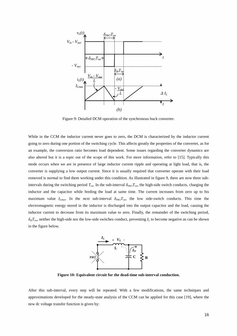
While in the CCM the inductor current never goes to zero, the DCM is characterized by the inductor current
going to zero during one portion of the switching cycle. This affects greatly the properties of the converter, as for
an example, the conversion ratio becomes load dependent. Some issues regarding the converter dynamics are
also altered but it is a topic out of the scope of this work. For more information, refer to [15]. Typically this
mode occurs when we are in presence of large inductor current ripple and operating at light load, that is, the
converter is supplying a low output current. Since it is usually required that converter operate with their load
removed is normal to find them working under this condition. As illustrated in figure 9, there are now three sub-
intervals during the switching period Tsw. In the sub-interval δSW1Tsw, the high-side switch conducts, charging the
inductor and the capacitor while feeding the load at same time. The current increases from zero up to his
maximum value ILmax. In the next sub-interval δSW2Tsw, the low side-switch conducts. This time the
electromagnetic energy stored in the inductor is discharged into the output capacitor and the load, causing the
inductor current to decrease from its maximum value to zero. Finally, the remainder of the switching period,
δdtTsw, neither the high-side nor the low-side switches conduct, preventing IL to become negative as can be shown
in the figure below.
L
C R
VLIL
SW2
IO
Figure 10: Equivalent circuit for the dead-time sub-interval conduction.
After this sub-interval, every step will be repeated. With a few modifications, the same techniques and
approximations developed for the steady-state analysis of the CCM can be applied for this case [19], where the
new dc voltage transfer function is given by:

17
= = = ( 12 )
This introduces a new degree of freedom, yet with high inductor current ripple. In this relation it is possible to
verify that Vo/Vin<1.
2.2.1. Inductor Sizing
From (5) we can find the inductor value that guarantees a certain inductor current variation equals to ΔIL:
= = ( − ) ( 13 )
It can be proven that for a maximum ΔIL, the inductor has its maximum value for δ=1/2. From (13), the inductor
value is:
= = ( 14 )
This relation allows us to find the necessary inductor value to keep the maximum output current ripple bellow
the allowed maximum value for ΔiLmax.
However, if one needs to determine the minimum value of the inductor to ensure that the converter does not goes
to the DCM but stays in the limit of the CCM (critical mode), the ILmin ≥ 0, which means that:− ≥ ( 15 )
Therefore: − ( − ) ≥ ( 16 )
Leading to: ≥ ( − ) ( 17 )
This way one can ensure that the converter will work in the CCM if:≥ ( − ) ( 18 )
And in DCM if: ≤ ( − ) ( 19 )

18
2.2.2. Capacitor Sizing
As one can realize from figure 11, when the high-side switch is closed, that is, from 0 < t < ton, the charge
variation ΔQ supplied to the capacitor corresponds to the area of the triangle with base Tsw and height ΔiL/2:
∆ = = ( 20 )
Supposing that the output capacitor is assumed to be large enough and constant, ΔVo << Vo, as well as all the
ripple component in the inductor current flows through the capacitor, we get:
= → ∆ = ∆ ( 21 )
This means that the minimum filter capacitance required to reduce the ripple voltage bellow the specified value
is:
= ∆ ( ) = ∆ ( )( 22 )
This equation shows that the value of Co that guarantees a certain Vo /ΔVo is inversely proportional to the
switching frequency squared. Attending to [19]:
∆ = ( ) = ( − ) ( 23 )
Where,
= √ ( 24 )
It is another interesting way to explain how the voltage ripple can be minimized by selecting a corner frequency
of the low pass filter at the output of the buck converter such that fc << fsw. However one must be careful to
decide how big the output capacitor can be. Not only because it occupies a large area but, as it will be shown
ahead, because if the capacitor has a large ESR under some circumstances it can truly increase the output ripple
as it is represented in the figure below. The output voltage ripple here is represented as a slow moving sinusoidal
waveform, magnified for a better comprehension.

19
On State Off State
δTsw (1-δ)Tsw
vL(t)
Vin - Vout
t
δTsw (1-δ)Tsw
iL(t)
- Vout
t
ILmax
ILmin
IL=Io
ΔIL/2
Tsw
(a)
(b)
ΔQ
Tsw/2
δTsw (1-δ)Tsw
vC(t)
t
ΔVo
(c)
Vo
Figure 11: A representative view of the buck converter output voltage ripple and inductor current ripple, for thecalculation of the output capacitor.
2.2.3. Effects of Non-Idealities
Up until now we assumed that the buck converter was ideal and without losses. In fact, this is not true because
all these non-idealities influence the circuit behavior as well as all quantities that are processed in the converter,
namely the output voltage. The losses in the circuit are associated with the conduction losses and switching
losses as it will be seen more ahead. The conduction losses are related to the passive components, namely the
series resistance of the inductor, and with the on resistance of the high-side and low-side switches. Another
conduction loss, although not the most important, is associated with the ESR of the output capacitor. In figure 9
are presented the parasitic contribution for the considered conduction losses.

20
CR
rC
VC
Vrc
LrL
VL
VO
Q1
Q2
VDD
Con
trol
&D
rive
rs r on
,pr o
n,n
VrL
Figure 12: The equivalent buck converter circuit contemplating the conduction losses.
If we take into account the voltage drop of each component, the conversion ratio of the buck converter is no
longer the same as presented at the beginning of this chapter. To obtain the new duty-cycle ratio, one must take
into account the voltage drop of the high-side switch, given by:
= , ( 25 )
As well for the low side-switch:
= , ( − ) ( 26 )
And finally for the inductor, due to the parasitic resistance:
= ( 27 )
Following the same approach as before (principle of the inductor volt-second balance) the derivation of the new
conversion ratio is given by [19]:
= ( 28 )
This result shows that the converter is no longer dependent only on the duty-cycle but also on the load meaning
that the duty-cycle increases when the output load current increases. This is justified by the fact that in the
numerator of (28) the losses are summing and in the denominator the losses are subtracting. Notice that if VrL,
VSW2 and VSW1 were zero, we would get the same conversion ratio as before.
Regarding the capacitor ESR there is one reminder that must be done. If the output capacitor presents an
equivalent series resistance (ESR), as shown in figure 12, the additional output voltage ripple caused by this
parasitic resistance might not be neglected when compared to ΔVo. This additional ESR voltage ripple can be
calculated as [29]:

21
∆ = = ( − ) ( 29 )
The power dissipated on the ESR of the capacitor is proportional to the capacitor RMS current square. This
current shape is approximately equal to a triangular waveform of amplitude ΔiL/2, given by:
= √ ( 30 )
In order to minimize the power loss from the capacitor ESR, one must design a capacitor with the lowest ESR
value, capable of supporting ICRMS current, at the switching frequency. Another non-ideality related to the
capacitor is its equivalent series inductance (ESL), not represented in figure 12. The undesired effects caused by
the ESL are related to discontinuities in the output voltage at high frequency.
2.2.4. Efficiency and Power Loss Analysis
The efficiency and the power losses in a dc-dc converter are of great importance when designing a converter,
which means that a poor efficiency will be translated into excessive power dissipation and consequently a
considerable power waste. As mentioned before, the dc-dc converter losses are related to the static losses that are
related to the inductor, power switches, bonding-wire stray resistance and dynamic losses which basically
comprise the switching losses because of the charge and discharge of parasitic capacitances in the power devices.
This phenomenon occurs due to the hard switching event, where the current flows into the device, in its turn on
event, before the voltage across him collapses, as is roughly illustrated in the figure below. This type of losses is
proportional to the switching frequency.
VDSIDS
t
Figure 13: Mosfet hard-switching representation
The first source of losses to be analyzed is the conduction loss. The conduction losses basically occur when the
high-side or the low-side switches are conducting. They are calculated as the product between the square of the
transistor RMS current value that flows through him and its equivalent on-resistance. The expression that models
this resistance is obtained by the quadratic-model of the mosfet transistor considering that it is operating in the
triode region with a low VDS voltage [14]:
, = , ( 31 )
And

22
, = | | , ( 32 )
With βn=knW/L and βp=kpW/L respectably and kn,p=µn,pCox. However, it is important to tell that these equations
are more suitable to describe long channel MOSFETs. For short channel transistors, the models are far more
complex to make hand calculations and find only application in computational simulations. When the high-side
switch is conducting the associated conduction loss is given by [19]:
= , , ( 33 )
Where,
, = + ∆( 34 )
Or
, = ( 35 )
assuming the duty-cycle of the lossless converter and that the inductor current ripple is much smaller when
compared to the average inductor current, being this one equal to the output current in the steady-state operation.
Analogously, for the low-side switch, the conduction loss is:
= , , ( 36)
With
, = ( − ) + ∆( 37 )
Or
, = ( − ) ( 38 )
The other source of losses is the parasitic resistance of the inductor, ESR. This loss can be calculated as:
= ( 39 )
Where

23
= + ∆( 40 )
Finally, the last source of conduction loss is related to the body diodes of the switches. As it will be explained in
the next chapter, the high-side and low-side switches have an associated mechanism that prevents shoot-through
currents between the power supply and ground. This mechanism is known as dead-time generator which consists
of a non-overlap circuit that prevents both high-side and low-side switch from conducting simultaneously.
During this dead-time, both switches are supposed to be off, while the continuous inductor current flows through
the body diode of the low-side switch. When the body diode is conducting, its conduction loss can be calculated
as:
= ( 41 )
Where tdt is the total dead-time in one switching cycle. Please, do not confuse this dead-time with the dead-time
in DCM synchronous buck converters. If the dead-time generator is designed properly, the conduction loss from
the body-diode can be very small.
Now regarding the switching losses, these comprise the I-V overlap losses in the switch and the fCV2 losses,
which is directly proportional to the switching frequency. These losses are dominant at low load conditions and
at high frequencies. Moreover, these losses accounts with the turn-on and turn-off process. For sake of simplicity
the detailed mathematical treatment will not be presented. For more information refer to [21]. Assuming that the
turn-on and turn-off times are the same, the switching losses can be represented as:
= ( 42 )
Finally another switching loss is related to the gate drive. Essentially, the power dissipation in the gate drivers is
mostly due to the dynamic power used to charge and discharge the parasitic capacitor from the power devices.
This topic will not be discussed here. The global efficiency of the converter is found to be:
= = ∑ = ∑ ( 43 )
2.3. Buck Converter Feedback Control
A dc-dc converter must provide a regulated output voltage under several conditions such as load and input
voltage variations. Furthermore, the converter must ensure that the regulation is always achieved under process
variations, wide input voltage variations and different temperature range (PVT). However these are not the only
requisites when it comes to voltage regulation. There are some additional performance parameters that are
desired, such as, fast settling time, low overshoot and small ringing in the transient response.
24
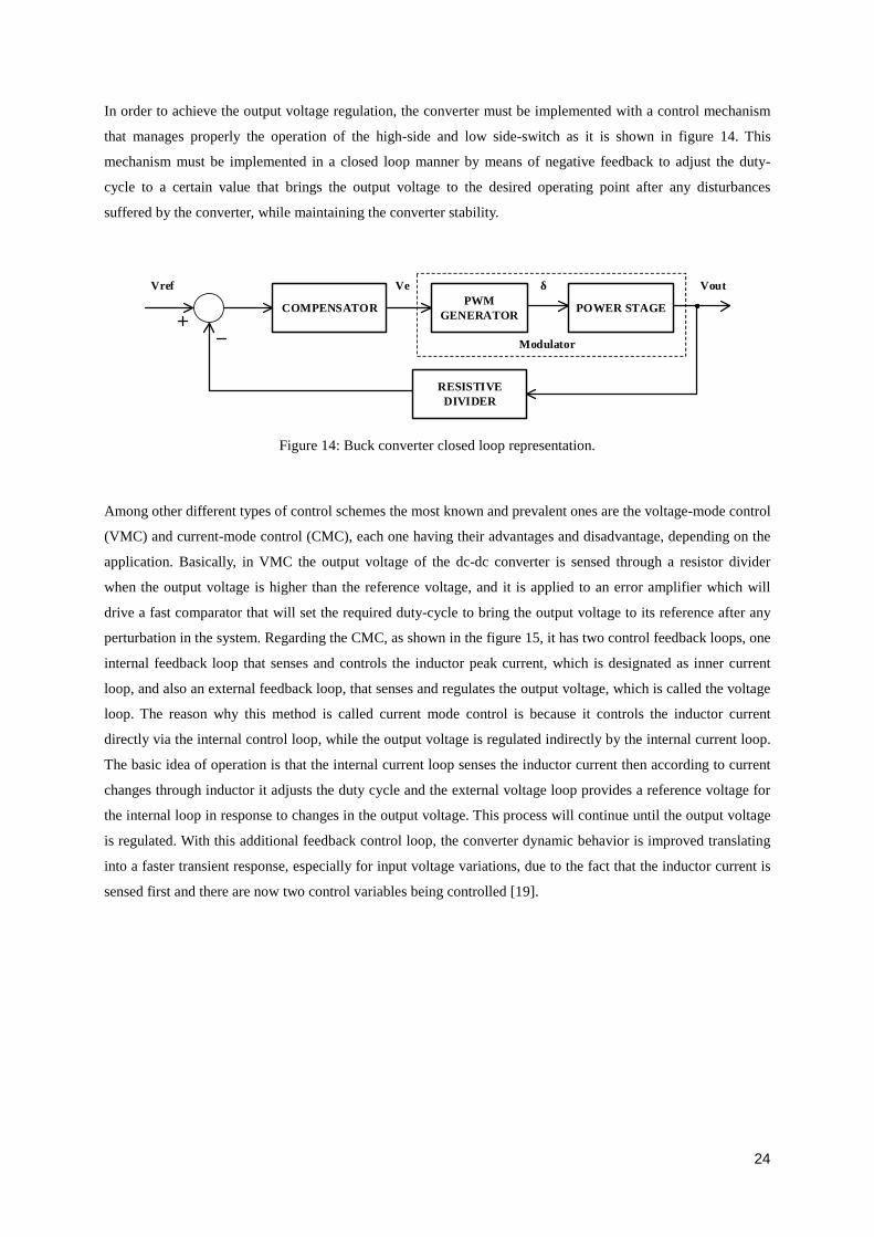
In order to achieve the output voltage regulation, the converter must be implemented with a control mechanism
that manages properly the operation of the high-side and low side-switch as it is shown in figure 14. This
mechanism must be implemented in a closed loop manner by means of negative feedback to adjust the duty-
cycle to a certain value that brings the output voltage to the desired operating point after any disturbances
suffered by the converter, while maintaining the converter stability.
PWMGENERATOR
POWER STAGE
RESISTIVEDIVIDER
Vout
COMPENSATOR
δVeVref
Modulator
Figure 14: Buck converter closed loop representation.
Among other different types of control schemes the most known and prevalent ones are the voltage-mode control
(VMC) and current-mode control (CMC), each one having their advantages and disadvantage, depending on the
application. Basically, in VMC the output voltage of the dc-dc converter is sensed through a resistor divider
when the output voltage is higher than the reference voltage, and it is applied to an error amplifier which will
drive a fast comparator that will set the required duty-cycle to bring the output voltage to its reference after any
perturbation in the system. Regarding the CMC, as shown in the figure 15, it has two control feedback loops, one
internal feedback loop that senses and controls the inductor peak current, which is designated as inner current
loop, and also an external feedback loop, that senses and regulates the output voltage, which is called the voltage
loop. The reason why this method is called current mode control is because it controls the inductor current
directly via the internal control loop, while the output voltage is regulated indirectly by the internal current loop.
The basic idea of operation is that the internal current loop senses the inductor current then according to current
changes through inductor it adjusts the duty cycle and the external voltage loop provides a reference voltage for
the internal loop in response to changes in the output voltage. This process will continue until the output voltage
is regulated. With this additional feedback control loop, the converter dynamic behavior is improved translating
into a faster transient response, especially for input voltage variations, due to the fact that the inductor current is
sensed first and there are now two control variables being controlled [19].

25
Figure 15: Buck converter current-mode control representation.
The main disadvantages of VMC relates to the fact that any change in the load or in the input voltage must first
be sensed as an output change so that the control loop can take any action. This is turned into a slow response.
Moreover the loop gain is proportional to Vin, as it will be seen ahead, complicating further the compensation.
However, the main advantage of this control technique is related to the fact that there is only a single feedback
path which turns out to have a simple implementation.
Because in CMC there are two feedback loops the circuit analysis and control implementation are more difficult
and complex control. Nevertheless, since the inductor current rises with a slope determined by Vin-Vo, this
waveform will react immediately to the line voltage changes eliminating the delay responses with the input
voltage changes. However the control loop can become unstable at duty-cycles above 50% unless slope
compensation is added. It worth say that since the output filter of the buck converter adds two poles to the
control loop, with CMC the effect of the output inductor is minimized and the filter starts to offer only a single
pole to the feedback loop. Since CMC is out of the scope of this work, this will not be addressed hereinafter. For
more information about this control method, refer to [15, 20]. For this design the VMC is implemented.
2.3.1. Voltage-Mode Control of Buck Converter
A complete VMC synchronous buck converter scheme is illustrated in the figure bellow. It is formed by two
main blocks: the power block and the feedback control block. The power block consists on the driver section,
power switches and the output filter, whereas the feedback control comprises the sampling network, the
compensator, sawtooth generator, fast comparator and the non-overlap circuit.

26
Figure 16: Detailed view of the buck converter employing all the system blocks
As shown in the figure 16, the output voltage of the converter is used in the feedback (sometimes a resistor
divider network can be used to down convert the output voltage to the same level as the reference voltage in the
error amplifier) loop and it is applied directly to the error amplifier. The error amplifier then compares the
sampled voltage to the reference voltage and the resultant voltage error is amplified and applied to the fast
comparator. Additionally, the error amplifier is responsible to compensate the feedback loop from the LC filter
double pole and ensure a stable feedback loop (i.e. increase the phase margin (PM) and gain margin (GM)). After
this, the voltage error is compared with a sawtooth signal, responsible to set the switching frequency with
amplitude Vp, in order to produce the pulse width modulation (PWM) signal.
CR
rC
LrL
VOUT
Q1
Q2
VDD
r on
,pr o
n,n
Non-Overlap
Driver Section
FastComparator
Sawtooth Error-Amplifier
Vref
Z1
Filter Section
Power Switches
PWM SignalVe EA
Z2
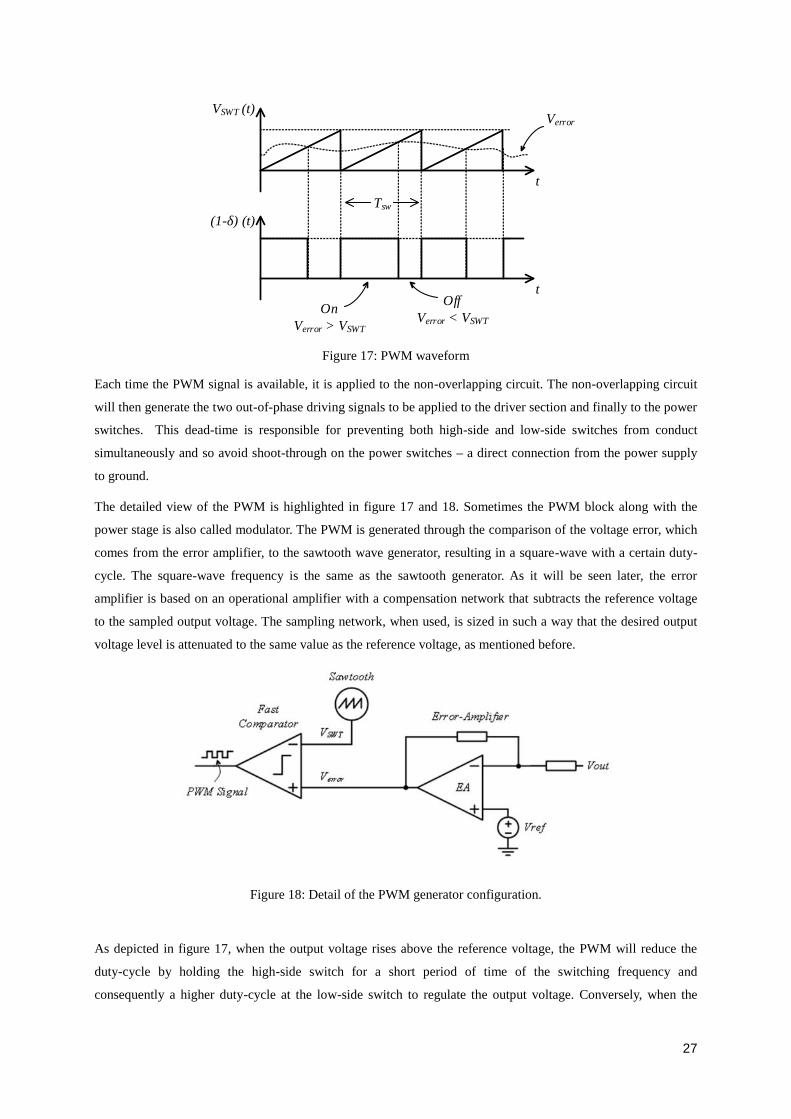
27
t
VSWT (t)
t
(1-δ) (t)
OnVerror > VSWT
Tsw
Verror
OffVerror < VSWT
Figure 17: PWM waveform
Each time the PWM signal is available, it is applied to the non-overlapping circuit. The non-overlapping circuit
will then generate the two out-of-phase driving signals to be applied to the driver section and finally to the power
switches. This dead-time is responsible for preventing both high-side and low-side switches from conduct
simultaneously and so avoid shoot-through on the power switches – a direct connection from the power supply
to ground.
The detailed view of the PWM is highlighted in figure 17 and 18. Sometimes the PWM block along with the
power stage is also called modulator. The PWM is generated through the comparison of the voltage error, which
comes from the error amplifier, to the sawtooth wave generator, resulting in a square-wave with a certain duty-
cycle. The square-wave frequency is the same as the sawtooth generator. As it will be seen later, the error
amplifier is based on an operational amplifier with a compensation network that subtracts the reference voltage
to the sampled output voltage. The sampling network, when used, is sized in such a way that the desired output
voltage level is attenuated to the same value as the reference voltage, as mentioned before.
Figure 18: Detail of the PWM generator configuration.
As depicted in figure 17, when the output voltage rises above the reference voltage, the PWM will reduce the
duty-cycle by holding the high-side switch for a short period of time of the switching frequency and
consequently a higher duty-cycle at the low-side switch to regulate the output voltage. Conversely, when the

28
output voltage goes below the reference voltage, the PWM will increase the duty-cycle from the high-side switch
by holding him for a longer period of time of the switching frequency and consequently lowering the duty-cycle
from the low-side switch. Here, the PWM determines the required duty-cycle to maintain the output voltage at
the desired level.
The non-overlapping waveforms are presented in figure 19. The two signals must be precisely generated in a
complementary way so that they can be as much as possible accurately lined up so that a fixed dead-time can be
obtained.
t
δ (t)
t
PMOSON
(1-δ) (t)
NMOSON
Non-overlapping interval
Figure 19: Non-overlapping clocks.
During this dead-time, both switches are supposed to be off, and because the inductor must maintain his current
flowing, the body diode of the low-side switch turns on. As the body diode conducts, there will be also some
power loss. This dead-time interval is equally important to help improve one part of the converter efficiency (as
mentioned in section 2.2.4) through the PWM operation.
t
PMOSOFF
Non-overlapping interval
Body-diode conduction
Figure 20: Body-diode conduction detail
2.3.2. Compensator Design Overview
As said before, the buck converter has an LC filter that introduces a pair of poles in the closed loop of the overall
converter. For system stability, the closed loop system should have some compensation to boost the phase
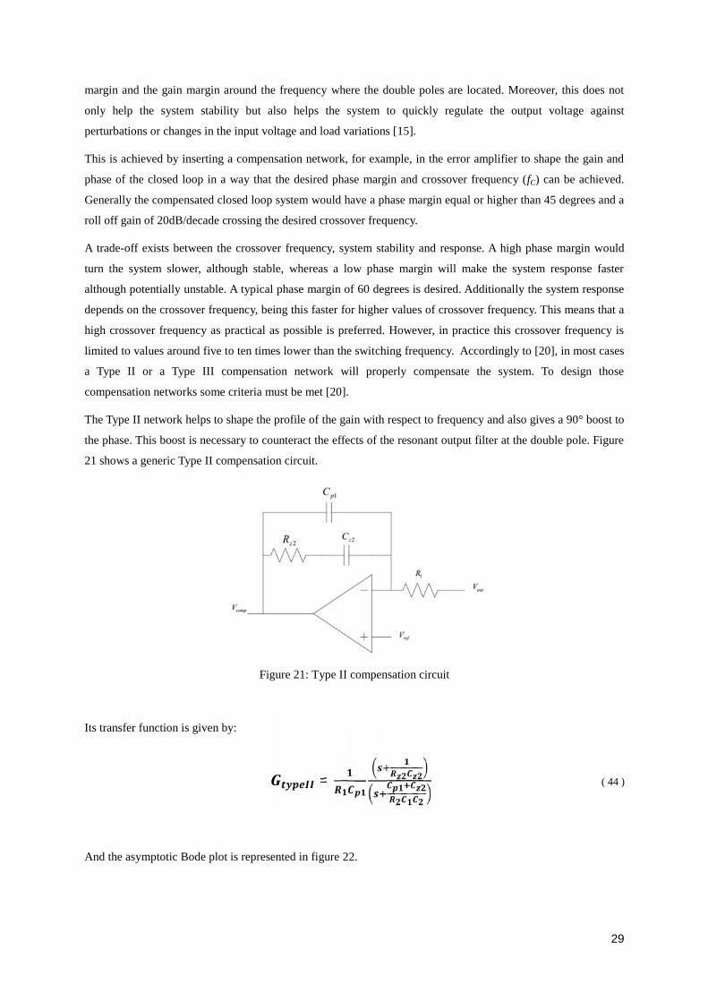
29
margin and the gain margin around the frequency where the double poles are located. Moreover, this does not
only help the system stability but also helps the system to quickly regulate the output voltage against
perturbations or changes in the input voltage and load variations [15].
This is achieved by inserting a compensation network, for example, in the error amplifier to shape the gain and
phase of the closed loop in a way that the desired phase margin and crossover frequency (fC) can be achieved.
Generally the compensated closed loop system would have a phase margin equal or higher than 45 degrees and a
roll off gain of 20dB/decade crossing the desired crossover frequency.
A trade-off exists between the crossover frequency, system stability and response. A high phase margin would
turn the system slower, although stable, whereas a low phase margin will make the system response faster
although potentially unstable. A typical phase margin of 60 degrees is desired. Additionally the system response
depends on the crossover frequency, being this faster for higher values of crossover frequency. This means that a
high crossover frequency as practical as possible is preferred. However, in practice this crossover frequency is
limited to values around five to ten times lower than the switching frequency. Accordingly to [20], in most cases
a Type II or a Type III compensation network will properly compensate the system. To design those
compensation networks some criteria must be met [20].
The Type II network helps to shape the profile of the gain with respect to frequency and also gives a 90° boost to
the phase. This boost is necessary to counteract the effects of the resonant output filter at the double pole. Figure
21 shows a generic Type II compensation circuit.
Figure 21: Type II compensation circuit
Its transfer function is given by:
= ( 44 )
And the asymptotic Bode plot is represented in figure 22.
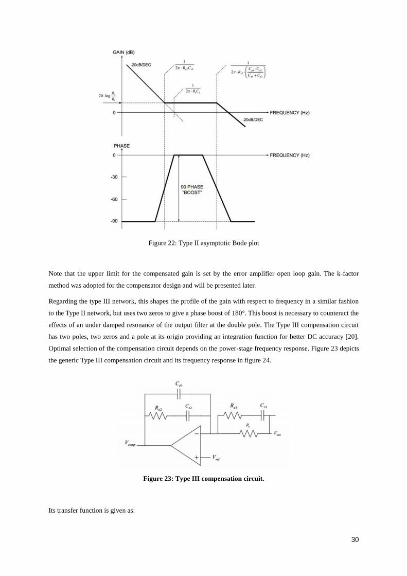
30
Figure 22: Type II asymptotic Bode plot
Note that the upper limit for the compensated gain is set by the error amplifier open loop gain. The k-factor
method was adopted for the compensator design and will be presented later.
Regarding the type III network, this shapes the profile of the gain with respect to frequency in a similar fashion
to the Type II network, but uses two zeros to give a phase boost of 180°. This boost is necessary to counteract the
effects of an under damped resonance of the output filter at the double pole. The Type III compensation circuit
has two poles, two zeros and a pole at its origin providing an integration function for better DC accuracy [20].
Optimal selection of the compensation circuit depends on the power-stage frequency response. Figure 23 depicts
the generic Type III compensation circuit and its frequency response in figure 24.
Figure 23: Type III compensation circuit.
Its transfer function is given as:
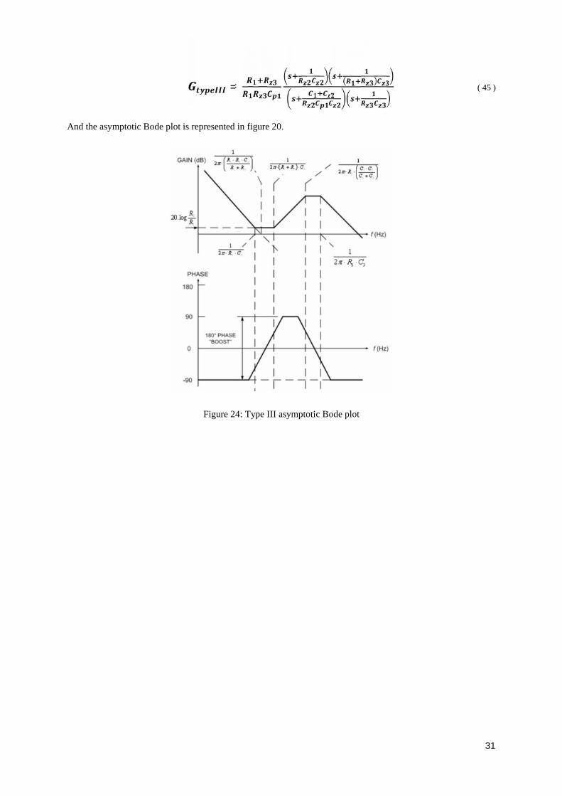
31
= ( 45 )
And the asymptotic Bode plot is represented in figure 20.
Figure 24: Type III asymptotic Bode plot

32

33
3. DC-DC Converter Systemic DesignIn this chapter it will be given a description on the system implementation in a systemic approach and analyze
the system stability so that the compensator can be designed. The stability test will be performed through a load
step simulation for different input voltages. The primary specifications, given in chapter 1 and repeated here for
convenience, are presented in table 3 and they constitute the basis for the design of the power-stage and feedback
control loop. The switching frequency is the key parameter to design either the power-stage block or the
feedback control loop. For the power-stage block, the switching frequency determines the size of the output filter
together with the specified ripple, and for the control loop it sets the transient responses for the perturbations
caused in the system.
3.1. Power-stage DesignThe implemented synchronous buck converter consists on the voltage-mode control using the pulse-width
technique since the load current will be high enough to make the inductor current operate in the CCM.
Figure 25: Representation of the overall power stage block.
In figure 25 it is presented the power stage of the buck converter implemented in this work. Based on the system
specification given bellow, a first approach for its design in made.

34
Parameter Symbol Min Typ Max Units Comments
Operating Junction Temperature Tj -40 25 125 ºC
Supply Voltage Vin 2.6 3.3 3.6 V
Output Voltage Vout 1.195 1.2 1.205 V
Output Voltage Ripple ∆Vo 85 mV
Output Current Io 75 mA
Inductor Current Ripple ∆IL
Switching Frequency Fsw 500 MHz
Table 3: Main specifications for the implemented dc-dc buck converter.
Regarding the output filter of the buck converter, using the steady-state equations in (13) and (22) the inductor
and capacitor values were determined. As shown by those equations, generally the capacitor and inductor
depends on the voltage ripple, current ripple and switching frequency respectively. It is important to take care
when it comes to choose the proper inductor value, since the inductor value controls the amount of current ripple
that the output capacitor will get. Moreover, because the inductor parasitic resistance, known as dc-resistance
(DCR) impacts the overall performance of the converter, minimizing its value is essential. When dealing with
high output current, it is important to design an inductor with minimum DCR value. However, there is a trade-off
between this DCR value and the inductance value. Smaller DCR means lower inductor values but lower inductor
values translates into large current ripple through the inductor. So basically, the minimum inductance value is
mostly dependent on the current ripple for the specific application.
Figure 26: Determined values for the output filter used in the buck converter.
At same time it worth say that the ESR of the capacitor plays an important role here, since the output voltage
ripple is dependent on that value too (that is ΔVout=ΔVc+ΔVrc). The implementation of the inductor will be
constrained by the inductor current ripple, its series resistance and the available die area. For the capacitor, it will
be more about the type of output capacitor that will be used, based on the die area available for its
implementation which indirectly will affect its parasitic ESR. Figure 26 shows the obtained values for both
components and are summarized in table 4.

35
Figure 27: Power switches showing the obtained channel width.
Concerning the power switches, those can be designed for an optimal power loss making the conduction losses
and switching losses approximately the same [22]. The on-resistance of the power switches constitutes the major
portion of the conduction losses along with the inductor series resistance due to the fact that the load current
passes in both resistance each switching cycle. For this reason it is important to minimize the on-resistance of the
power switches. However this implies large areas for both high-side and low-side switches and, at same time,
larger gate driver power consumption. Due to this constrain, the decision fall upon the lowest on-resistance that
one could get taking into account the minimum area as possible The on-resistance was determined through
simulations and the result is depicted in figure 28, where it is shown the on-resistance of both switches versus its
width.
Figure 28: Simulation showing the power switches on-resistance function of their width.
0
1
2
3
4
5
0 0,0002 0,0004 0,0006 0,0008
Res
ista
nce
[Ω]
Width [m]
Power Switches On-resistance
RON PMOS RON NMOS

36
The criteria to select the appropriate power switches widths were based on simulation and trading off its size
with the best achievable on-resistance. The widths for the high-side and low-side switches were chosen to be
6000µm and 2000µm, respectively, as shown in figure 27. This way we have the same on-resistance for both
switches with the NMOS switch being 3 times smaller than the PMOS due to the higher electron mobility. The
length used for both power switches was the minimum accepted by the technology. Table 4 summarizes the main
specifications for the power stage of the buck converter.
Parameter Symbol Min Typ Max Units Comments
Ouput Capacitor COUT 5.1 nF
Output Inductor LOUT 13 nH
NMOS power switch width WNMOS 2000 µm
PMOS power switch width WPMOS 6000 µm
On-resistance of PMOS power device Rdson,p 0.63 Ω
On-resistance of NMOS power device Rdson,n 0.62 Ω
Switching Frequency Fsw 450 500 550 MHz
Table 4: Summary of the main specifications of the buck converter power-stage.
Due to the large sizes of the power switches, their gate capacitances are very large and therefore a buffer stage
made of inverters is necessary to charge the parasitic capacitances of the power devices. Thus, a chain of N
inverters is used and can be scaled with a constant tapering factor u, such that the ratio of the average dynamic
current to load capacitance is equal for each inverter in the chain. This result in an equal delay and the same
rise/fall time at each inverter node are equal. Under some assumptions [22, 23] the suitable tapering factor that
produces this effect is the Euler’s number e ≈ 2,7. Taking into account an estimate for the power switches and the
minimal sized inverter gate capacitances, a chain of 9 inverters were used with a tapering factor of 3 to save area.
This is illustrated in figure 29.
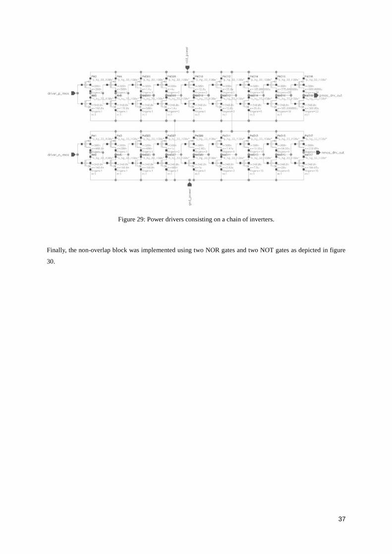
37
Figure 29: Power drivers consisting on a chain of inverters.
Finally, the non-overlap block was implemented using two NOR gates and two NOT gates as depicted in figure
30.

38
Figure 30: The non-overlapping block consisting in a two NOR gates and two NOT gates.
This block is necessary to split the PWM signal into two non-overlapping signals that drive the buffers of each
power switches. At same time it generates a fixed delay ensuring that there is some dead-time period between
each power switches turn-on and turn-off period. This dead-time is crucial from the power consumption point of
view, as if both the PMOS and NMOS switches are turned on together for some period, very high shoot-through
currents would pass from the supply to the ground through each of them. This means if a short dead-time is used
it can cause shoot-through but a long dead-time would mean a higher conduction losses because the parasitic
diode in the low-side switch would be conducting for a longer period of time. In the figure bellow it is possible
to visualize the simulated results of the designed non-overlapping circuit. It depicts a fast transient behavior with
the pull-up edge slope around 11,7V/ns and the pull-down edge slop around 20V/ns.

39
Figure 31: The two non-overlapped signals to be applied at the input of the drivers
It worth say that during this non-overlapping period, with both switches off, the inductor will pull some current
through the low-side switch parasitic body diode to force the continuous current in the inductor as it will be seen
ahead. This effect will provoke a negative voltage spike at the low-side power switch terminals which
corresponds to the reverse conduction of the parasitic body diode [15].
3.2. Small-signal Analysis
Modeling correctly the buck converter dynamic behavior is an important step to analyze and design properly the
closed-loop control especially to know how the output voltage of the converter will respond to perturbations in
the input voltage and load current. A well-compensated buck converter is crucial to meet the performance
specification. However this is a difficult task due to the non-linear time-varying nature of the PWM which is
working in a large signal mode. Nevertheless, by using some modeling techniques [24] it is possible to derive a
continuous time-invariant linear model to represent the switching converter and with this overcame the problem.
Being the system now a linear network, it is possible to apply all the control theory to design the feedback
control loop. Basically this modeling is an extension of the steady-state models presented in chapter 2 [15] with
the difference that now the dynamics introduced by the inductor and capacitor are taken into account. The
resulting model offers an insight into the system behavior under some assumption and approximations to neglect
some complicated phenomena’s.
In the several past years, there have been many efforts to create appropriate models to describe converters
behavior. Nowadays there are a few models and analysis methods that have been adopted. As for an example we
can consider the state-space averaging technique, which approximates the switching converter as a continuous
linear system [24].
Yet, the modeling mentioned above is done under some assumptions. For example it requires that the effective
output filter corner frequency to be much smaller than the switching frequency [24]. Moreover, those models do
-0,15
0,45
1,05
1,65
2,25
2,85
3,45
0,0E+00 5,0E-10 1,0E-09 1,5E-09 2,0E-09 2,5E-09 3,0E-09 3,5E-09 4,0E-09
Vol
tage
[V
]
Time [ns]
Non-overlapping Signals

40
not enter into account with the delay and parasitic capacitances in the several blocks of the converter, especially
in the power switches, comparator and driver section. The delay of the comparator and driver section, when
operating at high switching frequency, cannot be ignored since they can be very high and comparable to the
switching cycle period. Although the averaging technique is a good tool and very well accepted around the world
it is not accurate enough to analyze dc-dc converters operating at high switching frequency range.
Due to this issue, a different method to analyze the buck converter with a good degree of accuracy may be
through simulation. But due to the fact that dc-dc converters are non-linear switched systems working in large-
signal mode the traditional spice simulator cannot perform loop gain simulation of this kind of system.
For this work Spectre simulator was used to access the open loop frequency response of the converter and the
loop stability analysis. This is possible due to to the Periodic Steady-State (PSS) analysis, in combination with
the Periodic Small-Signal AC analysis (PAC) or the Periodic Stability Analysis (PSTB). This general method is
suitable for any dc-dc switching converter and the results are accurate comparing with the average modeling
techniques, even at high frequency [26].
The PSS analysis is a large-signal analysis, which directly computes the periodic steady-state response of the
circuit in the time domain using the iterative Shooting Newton method [25]. This kind of analysis is frequently
used in RF simulations, where the carrier is a periodic signal. For the case of the dc-dc converter, we have a
similar situation. Thinking on the PWM block with a fixed duty-cycle, the switching frequency is constant, so
the steady state is periodic as well.
After the PSS analysis, the small-signal perturbations are applied using PAC or PSTB analysis to perform the
frequency response of the converter and then determine open-loop gain, closed loop gain, gain margin, phase
margin and crossover frequency, also known as the closed loop system bandwidth. The input perturbation is
applied to the PWM duty-cycle and the output is the output voltage perturbation.
This type of analysis belongs to the large-signal / small-signal methods and is very efficient for non-linear or
switched circuits excited by a large-signal plus a small-signal. A particular case of this analysis is, for example,
the incremental study of an amplifier circuit around a DC bias point. In this case the large signal is the constant
bias signal.
With this kind of analysis all the relevant physical effects in the power stage, like nonlinearities and reactive
effects, are taken into account allowing a full assessment of the loop stability.
3.2.1. Open-loop Frequency Response
In this section the PSS and PAC analysis are applied to the synchronous buck converter to determine the open-
loop frequency response of the buck converter. In order to design the feedback control loop, one must know the
control-to-output transfer function of the power stage, that is, the open loop gain of the buck converter. An ideal
sawtooth generator was implemented using an ideal pulse generator. The pulse width modulator was
implemented using an ideal comparator done with a voltage-controller voltage source. The two inputs of this
comparator are the sawtooth generator output and an ideal voltage source that simulates the error voltage that
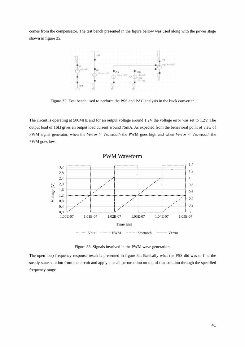
41
comes from the compensator. The test bench presented in the figure bellow was used along with the power stage
shown in figure 25.
Figure 32: Test bench used to perform the PSS and PAC analysis in the buck converter.
The circuit is operating at 500MHz and for an output voltage around 1.2V the voltage error was set to 1.2V. The
output load of 16Ω gives an output load current around 75mA. As expected from the behavioral point of view of
PWM signal generator, when the Verror > Vsawtooth the PWM goes high and when Verror < Vsawtooth the
PWM goes low.
Figure 33: Signals involved in the PWM wave generation.
The open loop frequency response result is presented in figure 34. Basically what the PSS did was to find the
steady-state solution from the circuit and apply a small perturbation on top of that solution through the specified
frequency range.
0
0,2
0,4
0,6
0,8
1
1,2
1,4
0,0
0,4
0,8
1,2
1,6
2,0
2,4
2,8
3,2
1,00E-07 1,01E-07 1,02E-07 1,03E-07 1,04E-07 1,05E-07
Vol
tage
[V
]
Time [ns]
PWM Waveform
Vout PWM Sawtooth Verror

42
Figure 34: Open loop frequency response of the implemented buck converter.
In fact it may seem awkward this kind of result because we are not seeing any effect of the typical two resonant
poles from the output resonant tank filter, composed by the inductor and output capacitor. This can be explained
making reference to the inductor series resistance and the on-resistance from the power devices. This problem
lowers down the Q value of the resonant tank. However, and just as an example, if the series resistance of the
inductor was removed, the result would be more similar to the traditional frequency response of a resonant tank
filter, as depicted in the figure below.
Figure 35: Open loop frequency response with no series resistance in the output inductor.
-360
-300
-240
-180
-120
-60
0
-35
-30
-25
-20
-15
-10
-5
01E+0 1E+1 1E+2 1E+3 1E+4 1E+5 1E+6 1E+7 1E+8 1E+9
PH
ASE
[D
EG
RE
E]
GA
IN [
DB
]
FREQUENCY [HZ]
Open-loop Frequency Response
PAC Freq. Resp. PAC Phase Resp.
1E+0 1E+1 1E+2 1E+3 1E+4 1E+5 1E+6 1E+7 1E+8 1E+9-360
-300
-240
-180
-120
-60
0
-60
-50
-40
-30
-20
-10
0
10
PH
ASE
[D
egre
e]
GA
IN[d
B]
FREQUENCY [Hz]
Open-loop Freq. Resp. w/o Inductor DCR
PAC Freq. Resp. PAC Phase Resp.

43
It is possible to see that the resonance frequency from the LC tank is around 20MHz whereas for the frequency
response of figure 34 is not visible. However one can notice that the gain roll-off in figure 34 is -40dB/dec.
showing the effect of the complex conjugate poles, in the same location, of the second order filter.
3.2.2. Compensator Design
After the power-stage design and the open-loop frequency response evaluated, the compensator can now be
designed. The objective of the design of the compensation network is to shape the compensator frequency
response so that in the closed-loop operation the frequency response of the converter can be correct so that when
the loop gain cross the 0dB axis there is sufficient phase difference between the error and the output signal [20].
At same time the compensator must provide high gain value in the dc frequency to reduce the static error. This
frequency difference referred above is normally called phase margin and it is usually chosen between 45º and 60º
as it was mentioned in chapter 2, allowing good stability and fast transient response. Another equivalent
parameter is the gain margin in which a value between 10 to 15dB is a good target.
To design the compensator a stabilization tool called k-factor was used. This approach consists in deriving a
number k based on the observation of the open-loop Bode plot of the switching converter to be stabilized. This k
number will indicate the necessary distance between the frequency position of the poles and zeros implemented
by the compensation network. Through selecting the desired crossover frequency and the amount of necessary
phase margin at that crossover frequency, the k factor will place the poles and zeros to make the crossover
frequency the geometric mean between their respective locations. There will be a place where the highest phase
boost will occur [20]. Normally the crossover frequency is selected to be somewhat around 1/10 to 1/5 of the
switching frequency. It worth say that, although this is a simple technique, there are some issues associated to it
described in [20]. However, as a starting point, it is a good option. Moreover fine tuning is always needed, not
only due to multiple parasitic effects, but also to achieve the best possible performance. Having determined the
k factor, the derivation of all the components in the compensation network is easily obtained.
As presented in chapter 2, there are two common compensation network that can be used in the buck converter,
those are the type II and type III compensator. For this work, type II compensator will be used due to the lower
number of components when compared to the type III. This type of compensator has one pole at the origin, one
zero and a high-frequency pole. Normally the zero is placed between the poles, and is between the zero and the
second pole where the maximum phase boost is achieved up to 90º.
Using the k factor tool the first thing to do is to select the crossover frequency. As we operate at 500MHz the rule
of thumb shows that one should select a crossover frequency of, for example, 50MHz which corresponds to
1/10th of the switching frequency. However, as for a first step, a crossover frequency of 10MHz is chosen and the
desired phase margin is 60º. The obtained components values are resumed in table 5.
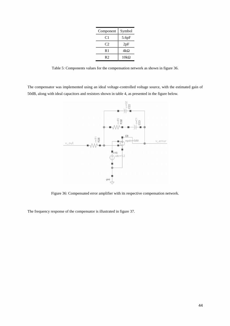
44
Component Symbol
C1 5.6pF
C2 2pF
R1 4kΩ
R2 10kΩ
Table 5: Components values for the compensation network as shown in figure 36.
The compensator was implemented using an ideal voltage-controlled voltage source, with the estimated gain of
50dB, along with ideal capacitors and resistors shown in table 4, as presented in the figure below.
Figure 36: Compensated error amplifier with its respective compensation network.
The frequency response of the compensator is illustrated in figure 37.

45
Figure 37: Frequency response of the designed compensator.
The test bench used to simulate the closed feedback is depicted in figure 38. This includes the power-stage, the
sawtooth and the compensator. A probe at the output of the converter was used to break the loop so that the PSS
and PSTB analysis can perform the loop gain analysis.
Figure 38: Complete test bench used to perform the closed-loop feedback frequency response.
-40
-20
0
20
40
60
0
40
80
120
160
200
1E+0 1E+2 1E+4 1E+6 1E+8
GA
IN[d
B]
PH
AS
E [
DE
GR
EE
]
FREQUENCY [HZ]
Compensator Frequency Response
PHASE GAIN

46
The loop gain response of the converter in illustrated in the figure bellow.
Figure 39: Closed Loop frequency response of the buck converter.
The results from the loop gain analysis shows that the closed loop system has a 72.6º of phase margin but with a
unity gain bandwidth of 6.4MHz. The high phase margin results in a very stable system, however the low
bandwidth compared to the one chosen will result in a more slow transient response, as it is possible to check in
the next figure.
Figure 40: Transient response comparison of the output voltage between the two crossover frequencies for a loadstep of 50mA.
The output voltage of the closed loop gain with 62º has a transient response around 100ns whereas the other has
a transient response higher than 200ns.
-200
-150
-100
-50
0
50
100
-180
-120
-60
0
60
120
180
1E+0 1E+1 1E+2 1E+3 1E+4 1E+5 1E+6 1E+7 1E+8 1E+9
GA
IN [
dB
]
PH
ASE
[D
egre
e]
FREQUENCY [Hz]
Closed Loop Frequency Response
CL. LOOP PHASE (73°) CL. LOOP GAIN (73°)
1,15
1,20
1,25
1,30
1,35
3,0E-07 3,5E-07 4,0E-07 4,5E-07 5,0E-07 5,5E-07
Out
put V
olta
ge [
V]
Time [ns]
Transient Response Comparison
Vout (62º) Vout (73º)
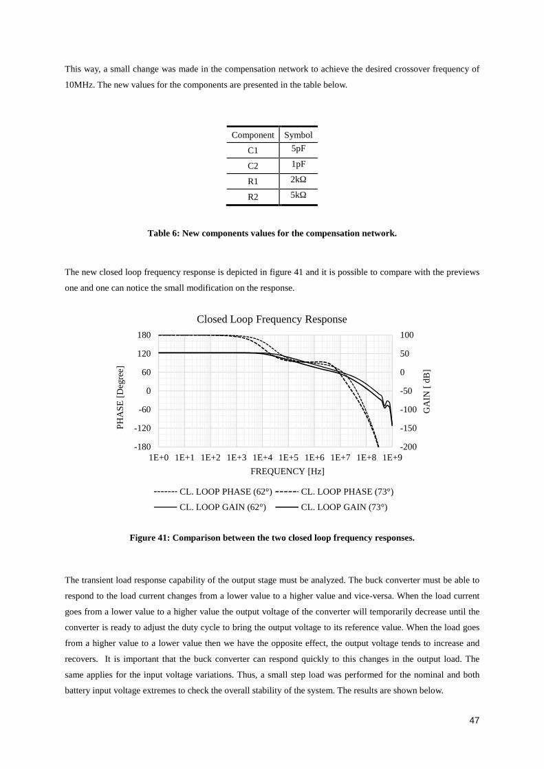
47
This way, a small change was made in the compensation network to achieve the desired crossover frequency of
10MHz. The new values for the components are presented in the table below.
Component Symbol
C1 5pF
C2 1pF
R1 2kΩ
R2 5kΩ
Table 6: New components values for the compensation network.
The new closed loop frequency response is depicted in figure 41 and it is possible to compare with the previews
one and one can notice the small modification on the response.
Figure 41: Comparison between the two closed loop frequency responses.
The transient load response capability of the output stage must be analyzed. The buck converter must be able to
respond to the load current changes from a lower value to a higher value and vice-versa. When the load current
goes from a lower value to a higher value the output voltage of the converter will temporarily decrease until the
converter is ready to adjust the duty cycle to bring the output voltage to its reference value. When the load goes
from a higher value to a lower value then we have the opposite effect, the output voltage tends to increase and
recovers. It is important that the buck converter can respond quickly to this changes in the output load. The
same applies for the input voltage variations. Thus, a small step load was performed for the nominal and both
battery input voltage extremes to check the overall stability of the system. The results are shown below.
-200
-150
-100
-50
0
50
100
-180
-120
-60
0
60
120
180
1E+0 1E+1 1E+2 1E+3 1E+4 1E+5 1E+6 1E+7 1E+8 1E+9
GA
IN [
dB
]
PH
ASE
[D
egre
e]
FREQUENCY [Hz]
Closed Loop Frequency Response
CL. LOOP PHASE (62°) CL. LOOP PHASE (73°)
CL. LOOP GAIN (62°) CL. LOOP GAIN (73°)
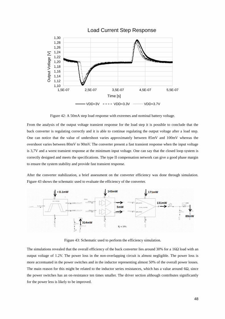
48
Figure 42: A 50mA step load response with extremes and nominal battery voltage.
From the analysis of the output voltage transient response for the load step it is possible to conclude that the
buck converter is regulating correctly and it is able to continue regulating the output voltage after a load step.
One can notice that the value of undershoot varies approximately between 85mV and 100mV whereas the
overshoot varies between 80mV to 90mV. The converter present a fast transient response when the input voltage
is 3,7V and a worst transient response at the minimum input voltage. One can say that the closed loop system is
correctly designed and meets the specifications. The type II compensation network can give a good phase margin
to ensure the system stability and provide fast transient response.
After the converter stabilization, a brief assessment on the converter efficiency was done through simulation.
Figure 43 shows the schematic used to evaluate the efficiency of the converter.
Figure 43: Schematic used to perform the efficiency simulation.
The simulations revealed that the overall efficiency of the buck converter lies around 30% for a 16Ω load with an
output voltage of 1.2V. The power loss in the non-overlapping circuit is almost negligible. The power loss is
more accentuated in the power switches and in the inductor representing almost 50% of the overall power losses.
The main reason for this might be related to the inductor series resistances, which has a value around 6Ω, since
the power switches has an on-resistance ten times smaller. The driver section although contributes significantly
for the power less is likely to be improved.
1,101,121,141,161,181,201,221,241,261,281,30
1,5E-07 2,5E-07 3,5E-07 4,5E-07 5,5E-07
Out
put V
otla
ge [V
]
Time [s]
Load Current Step Response
VDD=3V VDD=3.3V VDD=3.7V
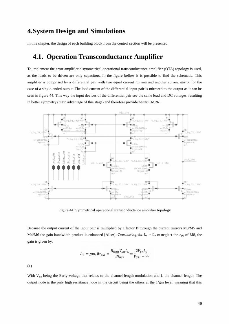
49
4.System Design and SimulationsIn this chapter, the design of each building block from the control section will be presented.
4.1. Operation Transconductance AmplifierTo implement the error amplifier a symmetrical operational transconductance amplifier (OTA) topology is used,
as the loads to be driven are only capacitors. In the figure bellow it is possible to find the schematic. This
amplifier is comprised by a differential pair with two equal current mirrors and another current mirror for the
case of a single-ended output. The load current of the differential input pair is mirrored to the output as it can be
seen in figure 44. This way the input devices of the differential pair see the same load and DC voltages, resulting
in better symmetry (main advantage of this stage) and therefore provide better CMRR.
Figure 44: Symmetrical operational transconductance amplifier topology
Because the output current of the input pair is multiplied by a factor B through the current mirrors M3/M5 and
M4/M6 the gain bandwidth product is enhanced [Allen]. Considering the L8 > L6 to neglect the rDS of M8, the
gain is given by:
= = = 2 −(1)
With VEn being the Early voltage that relates to the channel length modulation and L the channel length. The
output node is the only high resistance node in the circuit being the others at the 1/gm level, meaning that this

50
circuit is a single-stage amplifier with its gain matching almost the gain of the single stage differential amplifier.
The enhanced gain-bandwidth product:
= 2(2)
From (2) it is possible to verify that increasing B increases the GBW. Examining the current mirror node
composed by M4 and M6 and the output node, which is a high impedance node the non-dominant pole is given
by [27]:
= 2 ( + 3)(3)
Here, B sets a boundary to the maximum GBW reachable through the increase of B. As mentioned in chapter 2,
the error amplifier should have a high DC-gain, to decrease the static error and a high gain bandwidth product
(GBW product), which raise some power consumption tradeoffs in the amplifier. For this design it was tried to
get the best trade-off between those parameters, gain and GBW product, especially power consumption and gain-
bandwidth product. The bias current was made with a cascode current mirror to improve PSRR of the amplifier.
The minimum ICMR is set by M1 and M2 while the maximum is set by M10 since M9 has its VDS voltage fixed.
To improve the ICMR that transistor should have low overdrive voltage. The test benches used in the simulations
are presented in the following figures.
Figure 45: Symmetrical operational transconductance amplifier test bench for the open loop frequency response,input impedance and PSRR+ and PSSR-.
51
Figure 46: Symmetrical operational transconductance amplifier test bench for the output impedancemeasurement.
The next figures show the open loop PSRR+, PSRR- and the open loop frequency response along with the phase
response of the designed amplifier for a 1pF load. The gain-bandwidth product is around 195MHz and the DC
gain is about 50dB while the phase margin reaches 56º, which is an acceptable value.
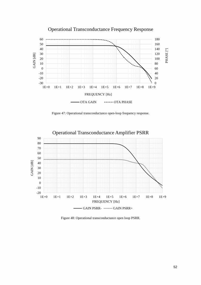
52
Figure 47: Operational transconductance open-loop frequency response.
Figure 48: Operational transconductance open loop PSRR.
1E+0 1E+1 1E+2 1E+3 1E+4 1E+5 1E+6 1E+7 1E+8 1E+90
20
40
60
80
100
120
140
160
180
-30
-20
-10
0
10
20
30
40
50
60
PH
ASE
[º]
GA
IN [
dB]
FREQUENCY [Hz]
Operational Transconductance Frequency Response
OTA GAIN OTA PHASE
-20
-10
0
10
20
30
40
50
60
70
80
90
1E+0 1E+1 1E+2 1E+3 1E+4 1E+5 1E+6 1E+7 1E+8 1E+9
GA
IN [
dB]
FREQUENCY [Hz]
Operational Transconductance Amplifier PSRR
GAIN PSRR- GAIN PSRR+
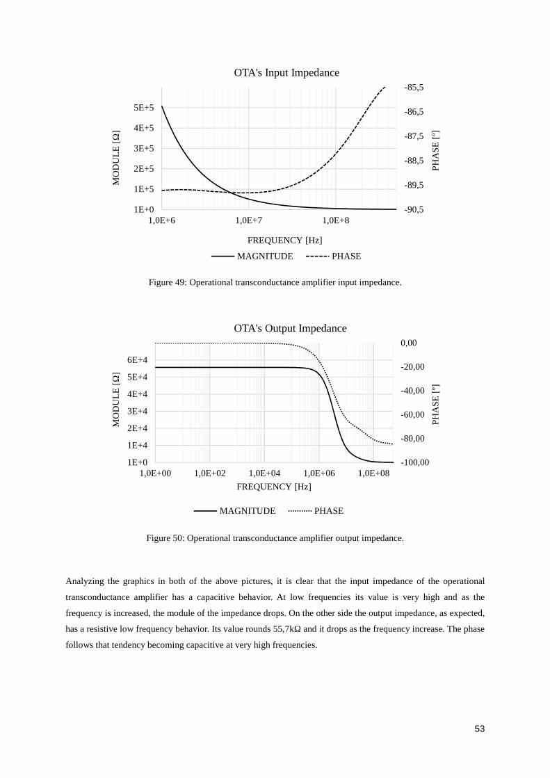
53
Figure 49: Operational transconductance amplifier input impedance.
Figure 50: Operational transconductance amplifier output impedance.
Analyzing the graphics in both of the above pictures, it is clear that the input impedance of the operational
transconductance amplifier has a capacitive behavior. At low frequencies its value is very high and as the
frequency is increased, the module of the impedance drops. On the other side the output impedance, as expected,
has a resistive low frequency behavior. Its value rounds 55,7kΩ and it drops as the frequency increase. The phase
follows that tendency becoming capacitive at very high frequencies.
-90,5
-89,5
-88,5
-87,5
-86,5
-85,5
1E+0
1E+5
2E+5
3E+5
4E+5
5E+5
1,0E+6 1,0E+7 1,0E+8
PH
ASE
[º]
MO
DU
LE
[Ω
]
FREQUENCY [Hz]
OTA's Input Impedance
MAGNITUDE PHASE
-100,00
-80,00
-60,00
-40,00
-20,00
0,00
1E+0
1E+4
2E+4
3E+4
4E+4
5E+4
6E+4
1,0E+00 1,0E+02 1,0E+04 1,0E+06 1,0E+08
PH
ASE
[º]
MO
DU
LE
[Ω
]
FREQUENCY [Hz]
OTA's Output Impedance
MAGNITUDE PHASE

54
Table 7 resumes the mains characteristics of the symmetrical OTA amplifier.
Symbol Parameter Typical Units
Vin Input Voltage 3.3 V
T Temperature 27 ºC
IQon Current Consumption 744.9 uA
A0 Open Loop Gain 47.1 dB
BW Bandwidth 1.58 MHz
GBW @ 1pF load Gain-BW product 193.3 MHz
PM Phase Margin 57.3 º
OL PSRR+ @ 1MHz Open Loop PSRR+ 1 dB
OL PSRR- @ 1MHz Open Loop PSRR- 29 dB
Table 7: Operational transconductance amplifier characteristics.
4.2. Fast Comparator
For the implementation of the fast comparator, dynamic comparators are not used since those topologies call for
a precise clock that is out of the scope this work. This means that only non-clocked comparator will be analyzed.
Non-clocked comparators are known as open-loop comparators. There are four comparators types that could be
implemented for this block. Those are the two-stage comparator, the folded cascode comparator, the clamped
push-pull comparator and the cross-coupled load comparator, being the last one a regenerative comparator
because of its internal positive feedback.
The two-stage comparator is like the miller two-stage amplifier being the mainly difference related to the fact
that this two-stage comparator is not compensated, which translates into a larger bandwidth. The only concern
here is the location of the poles that should have a large magnitude to reduce the propagation delay time [27].
Since the poles are related to the intrinsic capacitances and resistances of the mosfets to ground at the output
node of each stage, it is important to keep those as small as possible. This is valid in general to all comparators.
Concerning the clamped push-pull comparator, it has a small difference to the previous one. The current-mirror
load is replaced by a diode-connected mosfet which reduces the gain. Though, one can increase the gain using a
cascode structure at the output but that would lead to a small response due to its low frequency pole [27].
Nevertheless, its advantage is the ability to drive large currents into the output capacitor without needing any
output buffers. The ability to sink and source current to the output depends on the tail current (bias current) times
the current ratio from the input differential pair load to the output. The folded-cascode performance is similar to
the clamped push-pull with its output cascoded. The main difference is a better common-mode input voltage
range [27]. Generally speaking, comparators employing cascode structures should not be used if a linear
response is desired and because they are slow. Finally the cross-coupled load comparator, looks like the clamped
comparator but it has an internal positive feedback. The advantage of this comparator to the others is that the
internal positive feedback improves greatly the gain, minimizes the propagation delay and provides a fast
clipping [30]. Output buffers can be used to improve the driving capability for capacitive loads. The selected

55
structure to implement the pulse width modulation function was the cross-coupled load comparator whose
schematic is presented below.
Figure 51: Fast comparator used for the PWM operation.
As it was said, this topology uses positive feedback in the differential input stage to increase the gain and it’s
followed by a differential to single-ended conversion by means of three current mirrors and two inverters to
improve the comparator driving capability and get a rail-to-rail output voltage. The core of the comparator is
composed by the transistors PM1, 2, 12 and NM3-6, which consists on a differential input stage. The transistor
PM12 sets the tail current, PM1, 2 are the source coupled differential input pair plus NM3, 5 along with NM4,6
are the cross-coupled bi-stable current source as the load for the differential input stage. Transistor MN7-MN8
and PM9-PM10 converts the differential voltages in NM5, 6 into a current difference at the input node of the
buffers. This difference is applied into the rds of NM8 and PM10 generating a voltage at that node, in the end it
converts a differential output to a single-ended output, followed by two buffers to improve the output driving
capability. This way, the current mirrors that transform the differential output to single-ended can be made small
to reduce the parasitic capacitances at their gates for a faster response. The gain of the first stage is given by
[31]:
= ( ⁄ )( ⁄ ) 11 −(4)
With,
= ( ⁄ )( ⁄ )(5)
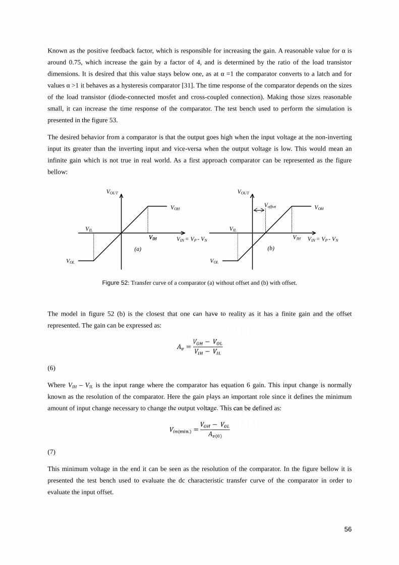
56
Known as the positive feedback factor, which is responsible for increasing the gain. A reasonable value for α is
around 0.75, which increase the gain by a factor of 4, and is determined by the ratio of the load transistor
dimensions. It is desired that this value stays below one, as at α =1 the comparator converts to a latch and for
values α >1 it behaves as a hysteresis comparator [31]. The time response of the comparator depends on the sizes
of the load transistor (diode-connected mosfet and cross-coupled connection). Making those sizes reasonable
small, it can increase the time response of the comparator. The test bench used to perform the simulation is
presented in the figure 53.
The desired behavior from a comparator is that the output goes high when the input voltage at the non-inverting
input its greater than the inverting input and vice-versa when the output voltage is low. This would mean an
infinite gain which is not true in real world. As a first approach comparator can be represented as the figure
bellow:
VIH
VIL
Voffset
VIN = VP - VN
VOUT
VIH
VIL
VIN = VP - VN
VOUT
VIH
VOH
VOL
VOH
VOL
(a) (b)
Figure 52: Transfer curve of a comparator (a) without offset and (b) with offset.
The model in figure 52 (b) is the closest that one can have to reality as it has a finite gain and the offset
represented. The gain can be expressed as:
= −−(6)
Where VIH – VIL is the input range where the comparator has equation 6 gain. This input change is normally
known as the resolution of the comparator. Here the gain plays an important role since it defines the minimum
amount of input change necessary to change the output voltage. This can be defined as:
( .) = −( )(7)
This minimum voltage in the end it can be seen as the resolution of the comparator. In the figure bellow it is
presented the test bench used to evaluate the dc characteristic transfer curve of the comparator in order to
evaluate the input offset.

57
Figure 53: Test bench used to simulate the dc characteristic of the comparator.
The results from the simulation are depicted in figure 54. The chosen input voltage sweep VDD/2 was done for
those values because the power supply voltage is 3.3V. As it can be seen from the simulation result, the input
systematic offset is around 850µV.
Figure 54: Comparator’s dc characteristic and offset representation.
Another important parameter that characterizes the comparator it’s the propagation delay which is related to the
speed limitation of comparators. Basically it sets the time response of comparators. The propagation delay can be
Offset Voltage
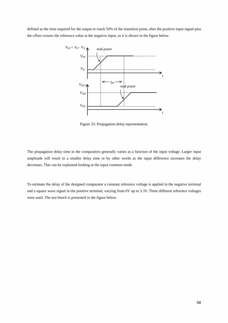
58
defined as the time required for the output to reach 50% of the transition point, after the positive input signal plus
the offset crosses the reference value at the negative input, as it is shown in the figure below.
t
VIN = VP - VN mid-point
t
VOUT
VIH
VIL
tpd
VOH
VOL
mid-point
Figure 55: Propagation delay representation.
The propagation delay time in the comparators generally varies as a function of the input voltage. Larger input
amplitude will result in a smaller delay time or by other words as the input difference increases the delay
decreases. This can be explained looking at the input common mode
To estimate the delay of the designed comparator a constant reference voltage is applied in the negative terminal
and a square wave signal in the positive terminal, varying from 0V up to 3.3V. Three different reference voltages
were used. The test bench is presented in the figure below.
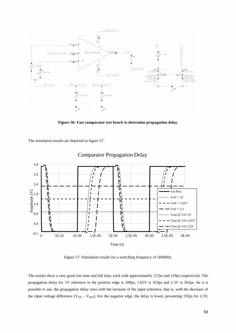
59
Figure 56: Fast comparator test bench to determine propagation delay.
The simulation results are depicted in figure 57.
Figure 57: Simulation results for a switching frequency of 500MHz.
The results show a very good rise time and fall time, each with approximately 157ps and 119ps respectively. The
propagation delay for 1V reference in the positive edge is 289ps, 1.65V is 353ps and 2.3V is 565ps. As it is
possible to see, the propagation delay rises with the increase of the input reference, that is, with the decrease of
the input voltage difference (VDD – VREF). For the negative edge, the delay is lower, presenting 192ps for 2.3V,
-0,1
0,4
0,9
1,4
1,9
2,4
2,9
3,4
0 5E-10 1E-09 1,5E-09 2E-09 2,5E-09 3E-09 3,5E-09 4E-09
Am
plitu
de [
V]
Time [s]
Comparator Propagation Delay
Vin Plus
Vref = 1V
Vref = 1,65V
Vref = 2,3
Vout @ Vrf=1V
Vout @ Vrf=1,65V
Vout @ Vrf=2,3V

60
216ps for 1.65V and 224ps for 1V. Table 7 resumes the mains characteristics of the fast comparator. That said the
total delay for each reference voltage is given by the average of the rising and falling edge delays, which is, for
1V reference the total delay is 256.5ps, for 1.65V is 284.5ps and for 2.3V is 378.5ps.
Symbol Parameter Typical Units
Vin Input Voltage 3.3 V
T Temperature 25 ºC
IQon Current Consumption 541 uA
Vos Offset Voltage 850 µV
GBW Gain-BW product 830 MHz
BW Bandwidth 251 MHz
Table 8: Fast comparator characteristics
4.3. Sawtooth Generator
The sawtooth generator block is an important structure in the generation of the PWM signal to control the power
switches of the dc-dc converter. This block is normally implemented with a timed charging current source into a
capacitor and a controlled switch to reset or discharge the capacitor. Typically the switch control circuit is
implemented with two comparators whose reference signal sets the lower and upper limits of the sawtooth
signal. Those comparators must be fast enough to ensure the reset operation through the controlled switch in a
short time period so that their non-idealities can be diminished. One of the most important issues regards to the
delay introduced by the comparator causing some problems in achieving the desired requirements.
A simplified view is presented in figure 58. This circuit is composed by the fast comparator implemented in
section 4.2 plus a switch and a capacitor.
C
VH
SW
VSW
Fast Comparator
IREF
Figure 58: Simplified view of the implemented sawtooth generator.
The implemented sawtooth generator is presented in the figure 59 and it consists basically of a simple capacitor
charge-discharge circuit. A current source is connected to the capacitor and this current is used to control the
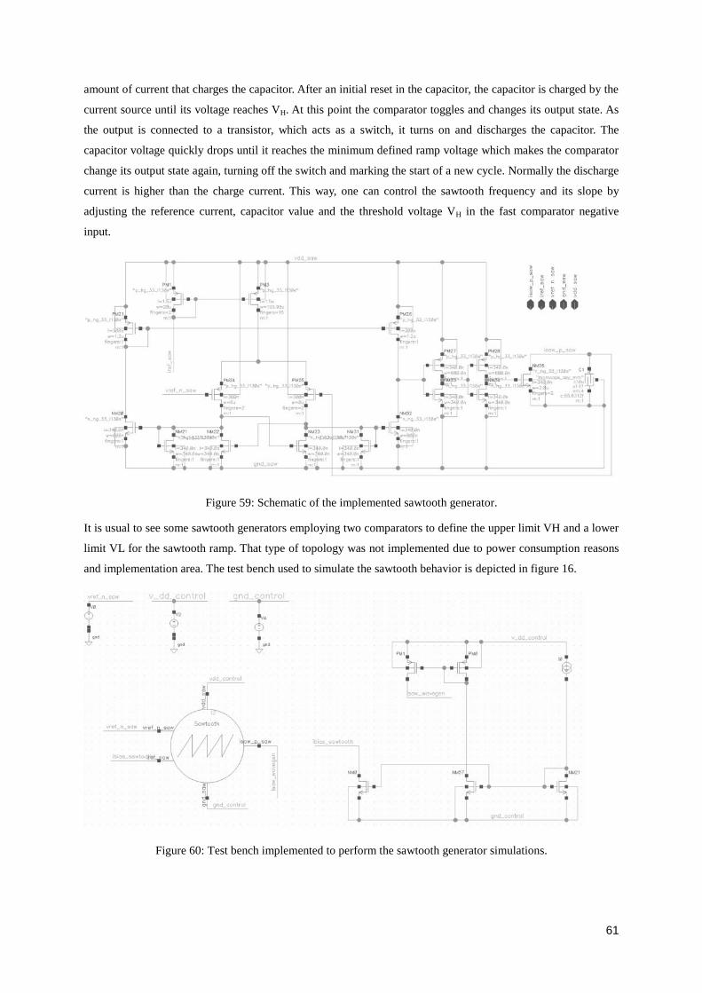
61
amount of current that charges the capacitor. After an initial reset in the capacitor, the capacitor is charged by the
current source until its voltage reaches VH. At this point the comparator toggles and changes its output state. As
the output is connected to a transistor, which acts as a switch, it turns on and discharges the capacitor. The
capacitor voltage quickly drops until it reaches the minimum defined ramp voltage which makes the comparator
change its output state again, turning off the switch and marking the start of a new cycle. Normally the discharge
current is higher than the charge current. This way, one can control the sawtooth frequency and its slope by
adjusting the reference current, capacitor value and the threshold voltage VH in the fast comparator negative
input.
Figure 59: Schematic of the implemented sawtooth generator.
It is usual to see some sawtooth generators employing two comparators to define the upper limit VH and a lower
limit VL for the sawtooth ramp. That type of topology was not implemented due to power consumption reasons
and implementation area. The test bench used to simulate the sawtooth behavior is depicted in figure 16.
Figure 60: Test bench implemented to perform the sawtooth generator simulations.

62
Figure 61: Sawtooth waveform with the fast comparator output voltage and the upper limit threshold.
From the result obtained through simulation, it is possible to verify that the achieved sawtooth frequency is
around 503MHz. In figure 61 the simulation results are shown. Here we can see the effect of the delay caused by
the comparator, which translates into an error in the upper limit threshold voltage of the sawtooth waveform.
This error can be calculated as:
=Even for a small delay, the error voltage is large due to the high change rate in the rising edge. The table below
summarizes the main characteristics of the sawtooth waveform generator.
Symbol Parameter Typical Units
Vin Input Voltage 3.3 V
T Temperature 25 ºC
IQon Current Consumption 520 uA
Fsawt Sawtooth Frequency 503 MHz
Asawt Sawtooth Amplitude 1.6 V
Table 9: Sawtooth generator main characteristics.
-0,1
0,4
0,9
1,4
1,9
2,4
2,9
3,4
4,96E-07 4,97E-07 4,97E-07 4,98E-07 4,98E-07 4,99E-07 4,99E-07 5,00E-07 5,00E-07
AM
PL
ITU
DE
[V
]
TIME [s]
Sawtooth Waveform
SAWTOOTH WAVEFORM VREF FAST COMPARATOR OUTPUT
Verror

63
4.4. Bandgap Voltage ReferenceThe voltage reference adopted for this work is the well-known and well-documented bandgap voltage reference
(BGVR) [12]. The implemented circuit is illustrated in the figure bellow.
Figure 62: Schematic of the implemented bandgap voltage reference generator.
The bandgap core is represented at the right in figure 62. It consists of nine BJT grouped in a 1:8 ratio. The
amplifier senses the voltages generated by the BJTs, driving the top resistors such that those nodes settles to
approximately equal voltages, being the bandgap output voltage reference obtained at the output of the amplifier.
The amplifier is comprised by a two-stage topology, being the first stage a folded-cascode amplifier and the
second stage a common source that provides the necessary current to the bandgap core. The folded cascode
amplifier, with cascode current mirrors, was adopted due to its high gain capability, low power consumption and
high PSRR performance [28]. As this is a self-biased circuit, it requires a start-up circuit to make sure that the
circuit does not get stuck at the zero operating point [28] and it is represented bellow the folded-cascode
amplifier in figure 62. Typically it consists in a small circuit that injects some current in the bandgap core to
achieve the desired operating point. The test bench used for the simulation results is shown below.
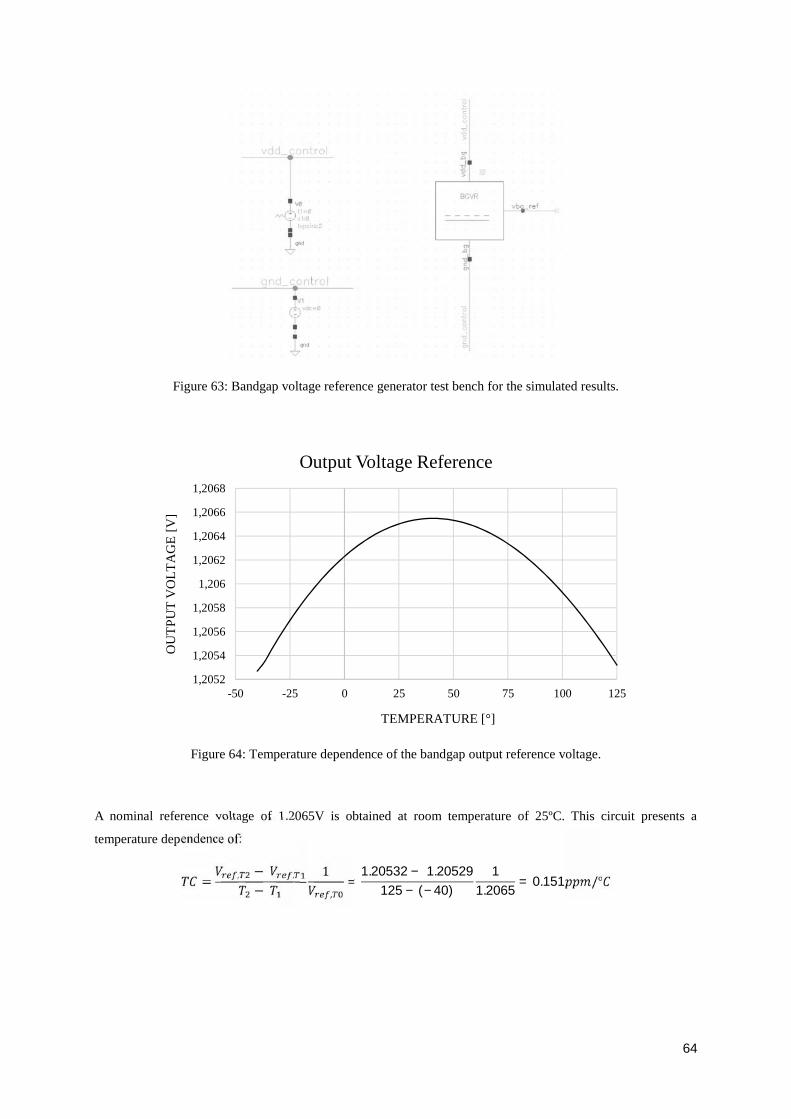
64
Figure 63: Bandgap voltage reference generator test bench for the simulated results.
Figure 64: Temperature dependence of the bandgap output reference voltage.
A nominal reference voltage of 1.2065V is obtained at room temperature of 25ºC. This circuit presents a
temperature dependence of:
= , − ,− 1 , = 1.20532 − 1.20529125 − (−40) 11.2065 = 0.151 /°
1,2052
1,2054
1,2056
1,2058
1,206
1,2062
1,2064
1,2066
1,2068
-50 -25 0 25 50 75 100 125
OU
TP
UT
VO
LT
AG
E [
V]
TEMPERATURE [°]
Output Voltage Reference

65
Figure 65: Bandgap start-up time.
In figure 65 it is represented the start-up response of the bandgap. Right after the bandgap voltage reference is
fed by the power supply, it takes around 3µs to achieve its nominal stable voltage reference, which is 1.2065V at
room temperature.
Figure 66: Bandgap output voltage reference as a function of supply voltage.
As for the output voltage regulation, it is possible to see in figure 66 that the bandgap voltage stabilizes as soon
as the power supply reaches 1.4V.
-0,2
0
0,2
0,4
0,6
0,8
1
1,2
1,4
0
0,5
1
1,5
2
2,5
3
3,5
0,0E+00 1,0E-06 2,0E-06 3,0E-06 4,0E-06 5,0E-06
OU
TP
UT
VO
LT
AG
E [
V]
PO
WE
R S
UP
PL
Y V
OL
TA
GE
[V
]
TIME [s]
Start-up Time
VDD VOUT
0
0,2
0,4
0,6
0,8
1
1,2
1,4
0 0,5 1 1,5 2 2,5 3 3,5 4
BG
VR
OU
TP
UT
VO
LT
AG
E [
V]
POWER SUPPLY VOLTAGE [V]
Output Voltage Regulation
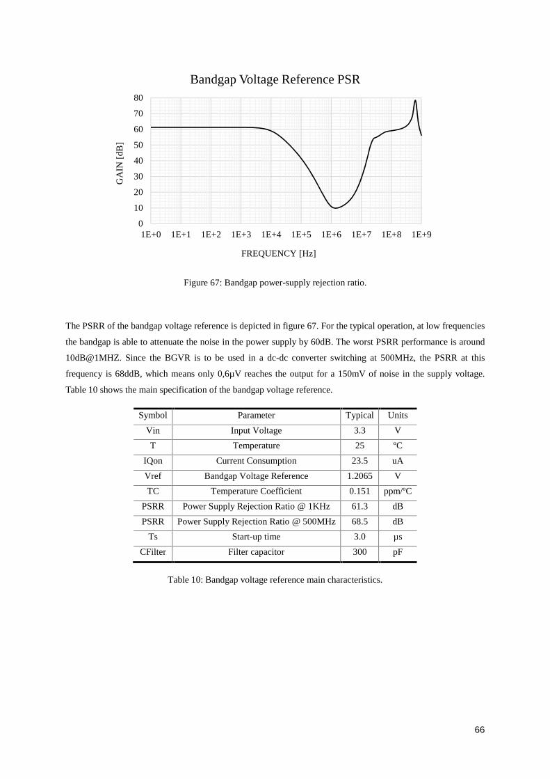
66
Figure 67: Bandgap power-supply rejection ratio.
The PSRR of the bandgap voltage reference is depicted in figure 67. For the typical operation, at low frequencies
the bandgap is able to attenuate the noise in the power supply by 60dB. The worst PSRR performance is around
10dB@1MHZ. Since the BGVR is to be used in a dc-dc converter switching at 500MHz, the PSRR at this
frequency is 68ddB, which means only 0,6µV reaches the output for a 150mV of noise in the supply voltage.
Table 10 shows the main specification of the bandgap voltage reference.
Symbol Parameter Typical Units
Vin Input Voltage 3.3 V
T Temperature 25 ºC
IQon Current Consumption 23.5 uA
Vref Bandgap Voltage Reference 1.2065 V
TC Temperature Coefficient 0.151 ppm/ºC
PSRR Power Supply Rejection Ratio @ 1KHz 61.3 dB
PSRR Power Supply Rejection Ratio @ 500MHz 68.5 dB
Ts Start-up time 3.0 µs
CFilter Filter capacitor 300 pF
Table 10: Bandgap voltage reference main characteristics.
0
10
20
30
40
50
60
70
80
1E+0 1E+1 1E+2 1E+3 1E+4 1E+5 1E+6 1E+7 1E+8 1E+9
GA
IN [
dB]
FREQUENCY [Hz]
Bandgap Voltage Reference PSR

67
4.5. Current Reference GeneratorA current reference itself doesn’t exist. They are derived from the bandgap voltage reference block and one or
two resistors. The structure implemented for the current reference generator is illustrated in the schematic of
figure 68 and in the simplified view of figure 69.
Figure 68: Schematic of the implemented current reference generator.
The circuit consists on a self-biased differential amplifier which converters the reference voltage into a current.
R
OTA AMPLIFIER IREF
VREF
Figure 69: Simplified view of the implemented current reference generator.
This reference voltage is imposed across the resistor which by Ohm’s law will generate the output current
reference. This current will be exactly the same as the one flowing in the resistance. Being the reference voltage
provided by the bandgap voltage reference, the temperature coefficient of the current reference is determined by
the TC of the resistor and the BGVR, inheriting this way the ability to outperform over a very large temperature
ranges. The main source of error is caused by the offset of the amplifier and the accuracy of the resistors, being
the last one the worst. Because of this, an external resistor is used to reduce not only the influence of the resistor

68
accuracy in the current reference but to adjust that value. The drawback of this option is the need of an extra
PAD to connect the external resistor. The generated current reference is then mirrored by a current mirror and
from there it is again mirrored through a structure of current mirrors so that it can be distributed to the several
blocks in the chip. The test bench used to obtain the simulations is presented below.
Figure 70: Test bench used in the simulations of the implemented current reference generator.
The selected output resistance was made based on the maximum allowed current consumption of the current
reference generator with the commercially available resistance values. The selected resistor value was 120kΩ
with an accuracy of 0.1% and a TC of ±25ppm/ºC.
Figure 70.1: Output current reference simulation.
1,0002E-05
1,0003E-05
1,0004E-05
1,0005E-05
1,0006E-05
1,0007E-05
1,0008E-05
1,0009E-05
1,0010E-05
-50 -30 -10 10 30 50 70 90 110 130
Out
put C
urre
nt [A
]
Temperature [˚C]
IREF @ Output resistor
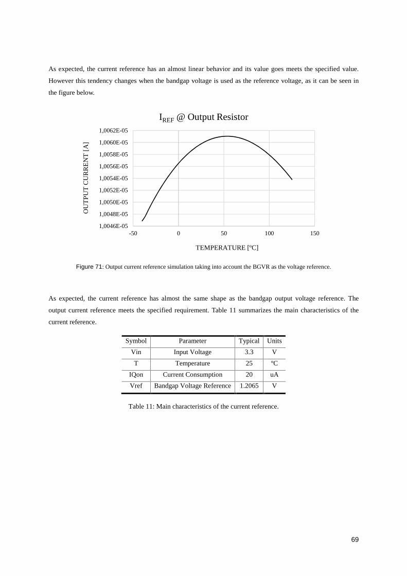
69
As expected, the current reference has an almost linear behavior and its value goes meets the specified value.
However this tendency changes when the bandgap voltage is used as the reference voltage, as it can be seen in
the figure below.
Figure 71: Output current reference simulation taking into account the BGVR as the voltage reference.
As expected, the current reference has almost the same shape as the bandgap output voltage reference. The
output current reference meets the specified requirement. Table 11 summarizes the main characteristics of the
current reference.
Symbol Parameter Typical Units
Vin Input Voltage 3.3 V
T Temperature 25 ºC
IQon Current Consumption 20 uA
Vref Bandgap Voltage Reference 1.2065 V
Table 11: Main characteristics of the current reference.
1,0046E-05
1,0048E-05
1,0050E-05
1,0052E-05
1,0054E-05
1,0056E-05
1,0058E-05
1,0060E-05
1,0062E-05
-50 0 50 100 150
OU
TP
UT
CU
RR
EN
T [
A]
TEMPERATURE [ºC]
IREF @ Output Resistor
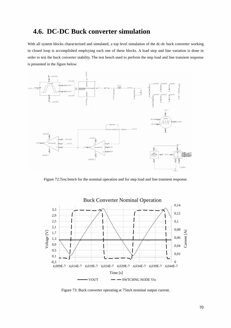
70
4.6. DC-DC Buck converter simulationWith all system blocks characterized and simulated, a top level simulation of the dc-dc buck converter working
in closed loop is accomplished employing each one of these blocks. A load step and line variation is done in
order to test the buck converter stability. The test bench used to perform the step load and line transient response
is presented in the figure below.
Figure 72:Test bench for the nominal operation and for step load and line transient response.
Figure 73: Buck converter operating at 75mA nominal output current.
0
0,02
0,04
0,06
0,08
0,1
0,12
0,14
-0,3
0,1
0,5
0,9
1,3
1,7
2,1
2,5
2,9
3,3
4,009E-7 4,014E-7 4,019E-7 4,024E-7 4,029E-7 4,034E-7 4,039E-7 4,044E-7
Cur
rent
[A
]
Vol
tage
[V
]
Time [s]
Buck Converter Nominal Operation
VOUT SWTCHNG NODE Vlx
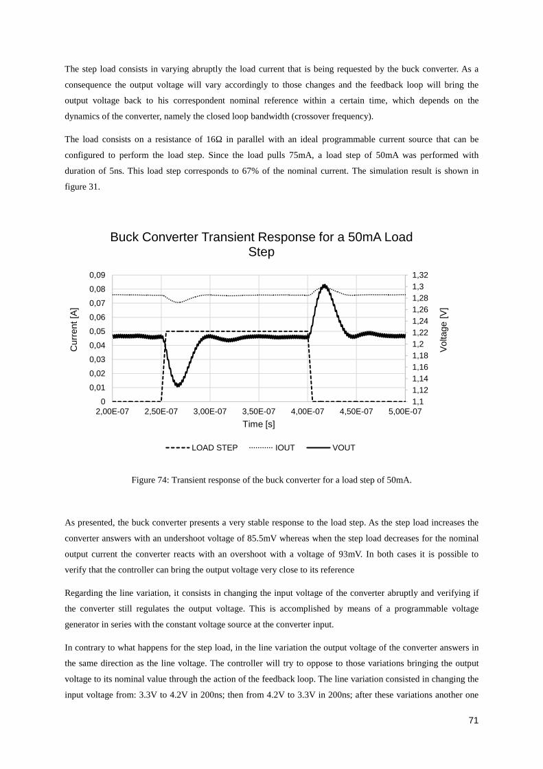
71
The step load consists in varying abruptly the load current that is being requested by the buck converter. As a
consequence the output voltage will vary accordingly to those changes and the feedback loop will bring the
output voltage back to his correspondent nominal reference within a certain time, which depends on the
dynamics of the converter, namely the closed loop bandwidth (crossover frequency).
The load consists on a resistance of 16Ω in parallel with an ideal programmable current source that can be
configured to perform the load step. Since the load pulls 75mA, a load step of 50mA was performed with
duration of 5ns. This load step corresponds to 67% of the nominal current. The simulation result is shown in
figure 31.
Figure 74: Transient response of the buck converter for a load step of 50mA.
As presented, the buck converter presents a very stable response to the load step. As the step load increases the
converter answers with an undershoot voltage of 85.5mV whereas when the step load decreases for the nominal
output current the converter reacts with an overshoot with a voltage of 93mV. In both cases it is possible to
verify that the controller can bring the output voltage very close to its reference
Regarding the line variation, it consists in changing the input voltage of the converter abruptly and verifying if
the converter still regulates the output voltage. This is accomplished by means of a programmable voltage
generator in series with the constant voltage source at the converter input.
In contrary to what happens for the step load, in the line variation the output voltage of the converter answers in
the same direction as the line voltage. The controller will try to oppose to those variations bringing the output
voltage to its nominal value through the action of the feedback loop. The line variation consisted in changing the
input voltage from: 3.3V to 4.2V in 200ns; then from 4.2V to 3.3V in 200ns; after these variations another one
1,11,121,141,161,181,21,221,241,261,281,31,32
0
0,01
0,02
0,03
0,04
0,05
0,06
0,07
0,08
0,09
2,00E-07 2,50E-07 3,00E-07 3,50E-07 4,00E-07 4,50E-07 5,00E-07
Volta
ge [V
]
Cur
rent
[A]
Time [s]
Buck Converter Transient Response for a 50mA LoadStep
LOAD STEP IOUT VOUT
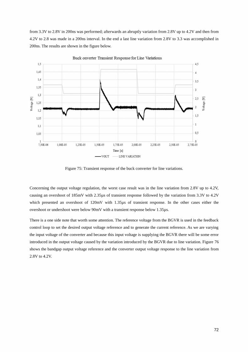
72
from 3.3V to 2.8V in 200ns was performed; afterwards an abruptly variation from 2.8V up to 4.2V and then from
4.2V to 2.8 was made in a 200ns interval. In the end a last line variation from 2.8V to 3.3 was accomplished in
200ns. The results are shown in the figure below.
Figure 75: Transient response of the buck converter for line variations.
Concerning the output voltage regulation, the worst case result was in the line variation from 2.8V up to 4.2V,
causing an overshoot of 185mV with 2.35µs of transient response followed by the variation from 3.3V to 4.2V
which presented an overshoot of 120mV with 1.35µs of transient response. In the other cases either the
overshoot or undershoot were below 90mV with a transient response below 1.35µs.
There is a one side note that worth some attention. The reference voltage from the BGVR is used in the feedback
control loop to set the desired output voltage reference and to generate the current reference. As we are varying
the input voltage of the converter and because this input voltage is supplying the BGVR there will be some error
introduced in the output voltage caused by the variation introduced by the BGVR due to line variation. Figure 76
shows the bandgap output voltage reference and the converter output voltage response to the line variation from
2.8V to 4.2V.

73
Figure 76: Transient response of the buck converter and BGVR for line variations.
This way, in order to evaluate the response of the system without the influence of the bandgap voltage reference
another line variation was performed for the worst case shown in figure 76, but now using a separately power
supply for the bandgap voltage reference. The results are shown below.
Figure 77: Transient response of the buck converter and BGVR without considering the line variation for thebandgap voltage reference.

74
In figure 78 it is possible to have a better look at the transient response.
Figure 78: Detailed view of the worst case transient response of the buck converter and BGVR withoutconsidering the line variation for the bandgap voltage reference.
As it is possible to realize, the system had a considerable improvement over the line transient response. The
controller is able to recover the output voltage in a very short time with a minimum overshoot and undershoot
effect. In worst case line variations, that was from 2.8V up to 4.2V the overshoot was below 50mV and the
converter was able to recover the output voltage within 450ns although with an output voltage error of 1.2%
when compared to its nominal operating output voltage.

75
5. Layout Implementation and Post-Layout Simulations
After the implementation of each block in the schematic view, this chapter will give emphasis to the layout
implementation and the top-level post-layout simulations. The layout of this system was implemented using the
standard CMOS UMC 130nm MM/RF technology. In first place, a careful planning of the floorplan was done, as
presented below, showing the location of the bond-pads and each functional cell. This floorplan serves as a guide
during the layout although it can be changed and revised accordingly whenever necessary.
VDD CONTROLEXT. R.VDDPOWER
VD
D P
OW
ER
GN
D P
OW
ER
GND POWER
GND CONTROL
GN
D C
AP
AC
ITO
RO
UT
PU
T
OUTPUTCAPACITOR
OUTPUTINDUCTOR
POWER STAGECONTROL
1570
µm
1570µm
Figure 79: Detailed View of the floorplan of the die.
In a dc-dc converter, the layout is of highest importance, especially when operating at very-high frequency
where the performance of the system can become degraded if a careless layout is done. Thus, some relevant
implementation details that can affect the functioning and performance of the converter must be taken into

76
account. Therefore some of the relevant layout practices used in this work are described, such as substrate noise
effects, power transistors layout, number of metal layers and their routing as well as the importance of keeping
the size of each cell as small as possible.
5.1. Substrate Noise Effects
One of the most important issues in the layout of this work is related to substrate noise since the dc-dc converter
has different blocks that generates electrical disturbing signals, like power switches operating at very high
frequency and their respective drivers. Hence the substrate is prone to noise injected by the switching behavior
of the power stage that can influence the performance of other analog blocks, as they share the same substrate.
These disturbances should be minimized as much as possible as it will be explained below. This source of noise
is the capacitive coupling between the interconnections and the substrate and junction capacitances between the
n-wells and the substrate.
5.2. Power Supply and Ground Planning
Because there are no perfect ground and power nodes inside the chip, the bonding wires inductance creates
crosstalk between different parts of the circuit and system. To minimize this effect the power supply was
separated into two rails, one for the power block and another for the control block. For the same reason different
ground rails were also used. Therefore each section sees its own noise, being the control noise very small when
compared to the one generated by the power stage. This solution implied the use of several pads, which leads to
an increase in the occupied area.
5.3. Power Transistors and Drivers Considerations
A special attention was given to the power transistor and their respective drivers from the perspective of isolating
each one with a guard-ring (depicted in the figure 73) as they are the major source of noise and susceptible to
inject majorities carrier’s (electrons and holes) into the substrate due to the switching activity.
As for an example, during the converter operation, the switching node Vlx, and therefore the VDS of the low-side
switch, can go below the substrate potential leading to some charge injection in the substrate. The same thing can
happen if that same switching node (or any other) voltage goes above the VDD voltage. Those voltage spikes can
be sufficient to directly bias the parasitic junctions between the drain/source and substrate/n-well.
The reason could be exactly because of the above mentioned switching behavior of the power transistors but also
because resistive power and ground path from the power PADs to the substrate and N-WELL. So additional
routing of the power and ground paths must be designed carefully.
Another issue created by the bonding wires is the generation of large di/dt values which gives rise to power
supply bouncing when large currents flows through, which can be dangerous if the voltages limits are exceeded.

77
Figure 80: Detail of the single transistor that constitutes the power transistor
Each power transistor is composed by the connection of several small transistors, as shown in figure 73 and
figure 74, connected in parallel, laid out in a way to simplify its connection to the next one. Each of these small
transistors was designed with several fingers so that the parasitic capacitances and parasitic resistances are
minimized and to make the layout more compact. Each small transistor has its own guard-ring by the reasons
mentioned before and to prevent the latch-up phenomenon.
A trade-off was made between the width of the transistor and the number of fingers to be used. The main
objective was to find the best relation between those two parameters so that the final result could outcome in the
lowest influence from the parasitic resistance for the on-resistance for the power transistor as well as it gate
parasitic capacitance. The next figures shows the detailed view of each section in the power stage.
Figure 81: Overall view of the PMOS high-side power switch. On the left are the source and gate connectionswhereas at the right is the drain connection (dimensions: W=123µm, H=101µm).

78
Figure 82: Overall view of the PMOS high-side power switch driver. On the left is the input terminal of thedriver, on the right the output terminal (dimensions: W=79µm, H=54µm).
Figure 83: Detail of the single transistor that constitutes the NMOS low-side power switch (dimensions:W=9.3µm, H=8.7µm).
Figure 84: Overall view of the NMOS low-side power switch. On the left are the source and gate connectionswhereas at the right is the drain connection (dimensions: W=72µm, H=60µm).

79
Figure 85: Overall view of the NMOS low-side power switch driver. On the left is the input terminal of thedriver and at the right is the output terminal (dimensions: W=58µm, H=36µm).
In the design of the power drivers, the gate of each transistor was designed with poly and metal 1 to reduce as
much as possible the high gate resistance to avoid large distributed RC delay effect.
5.4. Layout Implementation of Each BlockSome of the most known layout techniques [18] were taken into account. Generally, it was given attention to
symmetry for better matching, multi-finger transistors to reduce parasitic capacitances; current mirrors were
interdigitized as well as differential pairs instead of using common centroid technique, to avoid additional
parasitic capacitances. Whenever possible the source terminals of a multi-finger transistor were realized by the
outer fingers and the drain terminals by the inner fingers since those are critical nodes especially for the
differential pairs as they influence the speed of the amplifier. Overlapping between signals lines was avoided
unless impossible, and interconnections were kept as short as possible. In the next figures each block that
composes the dc-dc buck converter is shown. Interconnections with poly were avoided because of their parasitic
resistance and high parasitic capacitance to substrate. Routing over the gates of critical transistor and their
respective active areas is avoided. It was always given preference to short metal connection between each block
and prevent very long metal lines to keep the voltage drop very low. When that was not possible, the ones that
were longer were made wide enough and stacked with one or more metals through vias to at least neglect their
resistive effect.

80
Figure 86: Overall view of the power switches and their respective drivers
The overall layout of the power block is depicted in the figure 8. Metals were connected by as many vias as
possible to reduce the resistance and avoid current crowding in vias. For the power supply path, metal 1 up to
metal 5 were used to minimize the parasitic resistance and allow high current densities. The maximum width
used was 10µm to avoid slotting. The 90º corners are avoided in the drain output node since it is a critical node
where will be processed high current densities. Here it was used 8 metal layers, starting in metal 2 and gradually
increasing those metals up to metal 8. Several vias was used to interconnect the metal layers between them and
therefore reduce the parasitic resistance. Narrower paths were avoided in the path of high currents to avoid high
current densities or current crowding so as to avoid electromigration. The power transistors were arranged in a
way to get an array not too different from a square-like shape.
Figure 87: Overall view of the bandgap voltage reference (dimensions: W=180µm, H=236µm).

81
The overall layout of the bandgap voltage reference is depicted in the figure 9. The BJT transistors were
organized as an array of 3x3. Here and in general the differential pair was interdigitized for the reasons
mentioned above. The decoupling capacitor at the bandgap output was arranged in a matrix of 6x6. Between the
interconnections was used at least 2 vias to guarantee that at least one of them ensures the connection in case of
any manufacturing defects or faulty contact.
Figure 88: Overall view of the current reference (dimensions: W=61µm, H=45µm).
In overall, the connections between each transistors and components were maintained as simple as possible with
minimum 90º turns.
Figure 89: Overall view of the fast comparator (dimensions: W=58µm, H=38µm).
The comparator was carefully designed taking into account the minimization of the parasitic capacitances to
avoid an increase in the propagation delay for the rise and fall times. Interconnection were kept simple and short
as possible.
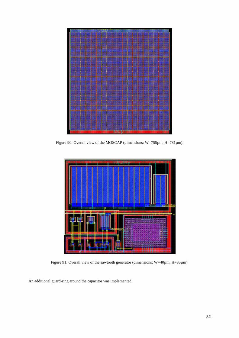
82
Figure 90: Overall view of the MOSCAP (dimensions: W=755µm, H=781µm).
Figure 91: Overall view of the sawtooth generator (dimensions: W=40µm, H=35µm).
An additional guard-ring around the capacitor was implemented.

83
Figure 92: Overall view of symmetrical operational transconductance amplifier
Symmetry was always taken into account. It worth say that the design rule checks (DRC) was a constant concern
through the layout design as well as the layout-versus-schematic (LVS). Calibre was used to perform the DRC
rules check and Assura to extract the parasitic capacitance and resistances.
5.5. Custom-Made Metal-Track InductorFor this work a metal track inductor designed in the research team was used. In figure 15 is shown the layout
view of the custom-made hexagonal metal track inductor. This inductor was designed in Cadence Virtuoso
Layout Suite L tool and then exported to ADS Momentum for electromagnetic simulation (EM) and
optimization. The windings made with staked metal 8 and Aluminum layers to reduce the spiral resistance. Metal
width is 10um and spirals spacing is 1.6um. This was an iterative process until the optimum value of the required
inductance was obtained with the minimum DCR resistance. This inductor offers an inductance of 13nH with 9Ω
@ 1GHz and 13nH with 6Ω @ DC.
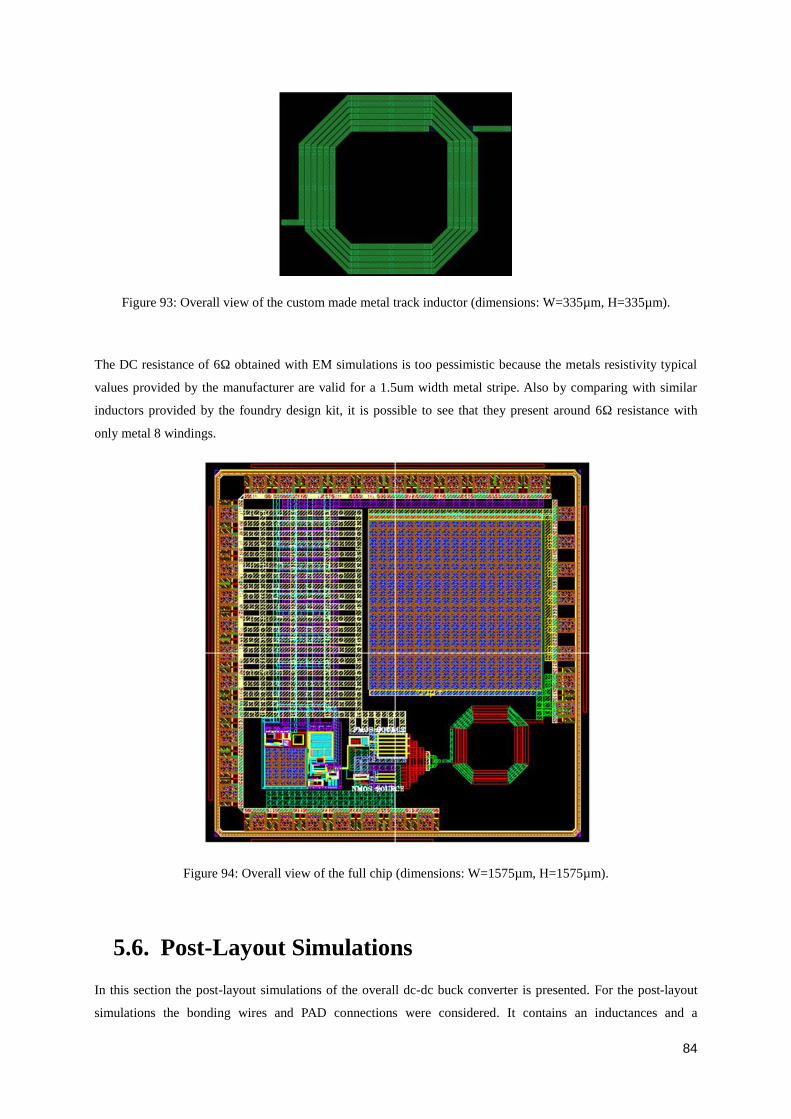
84
Figure 93: Overall view of the custom made metal track inductor (dimensions: W=335µm, H=335µm).
The DC resistance of 6Ω obtained with EM simulations is too pessimistic because the metals resistivity typical
values provided by the manufacturer are valid for a 1.5um width metal stripe. Also by comparing with similar
inductors provided by the foundry design kit, it is possible to see that they present around 6Ω resistance with
only metal 8 windings.
Figure 94: Overall view of the full chip (dimensions: W=1575µm, H=1575µm).
5.6. Post-Layout SimulationsIn this section the post-layout simulations of the overall dc-dc buck converter is presented. For the post-layout
simulations the bonding wires and PAD connections were considered. It contains an inductances and a
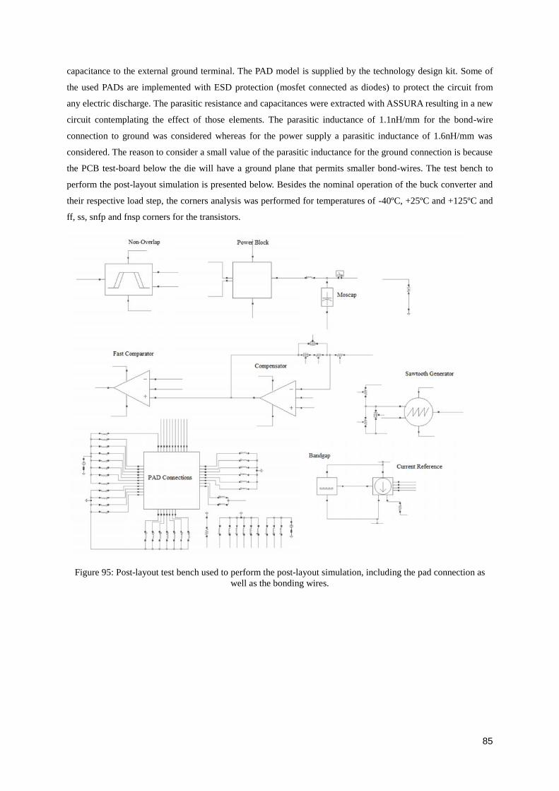
85
capacitance to the external ground terminal. The PAD model is supplied by the technology design kit. Some of
the used PADs are implemented with ESD protection (mosfet connected as diodes) to protect the circuit from
any electric discharge. The parasitic resistance and capacitances were extracted with ASSURA resulting in a new
circuit contemplating the effect of those elements. The parasitic inductance of 1.1nH/mm for the bond-wire
connection to ground was considered whereas for the power supply a parasitic inductance of 1.6nH/mm was
considered. The reason to consider a small value of the parasitic inductance for the ground connection is because
the PCB test-board below the die will have a ground plane that permits smaller bond-wires. The test bench to
perform the post-layout simulation is presented below. Besides the nominal operation of the buck converter and
their respective load step, the corners analysis was performed for temperatures of -40ºC, +25ºC and +125ºC and
ff, ss, snfp and fnsp corners for the transistors.
Figure 95: Post-layout test bench used to perform the post-layout simulation, including the pad connection aswell as the bonding wires.
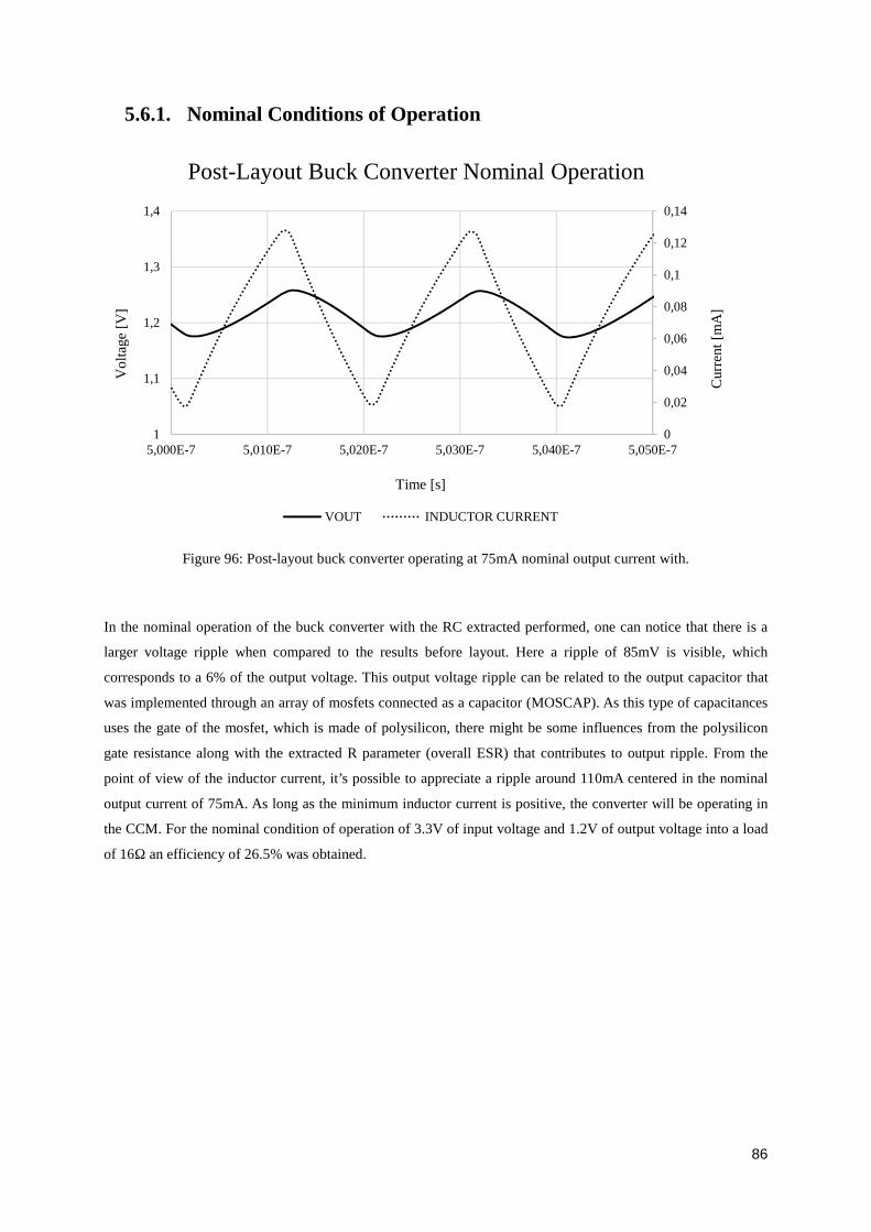
86
5.6.1. Nominal Conditions of Operation
Figure 96: Post-layout buck converter operating at 75mA nominal output current with.
In the nominal operation of the buck converter with the RC extracted performed, one can notice that there is a
larger voltage ripple when compared to the results before layout. Here a ripple of 85mV is visible, which
corresponds to a 6% of the output voltage. This output voltage ripple can be related to the output capacitor that
was implemented through an array of mosfets connected as a capacitor (MOSCAP). As this type of capacitances
uses the gate of the mosfet, which is made of polysilicon, there might be some influences from the polysilicon
gate resistance along with the extracted R parameter (overall ESR) that contributes to output ripple. From the
point of view of the inductor current, it’s possible to appreciate a ripple around 110mA centered in the nominal
output current of 75mA. As long as the minimum inductor current is positive, the converter will be operating in
the CCM. For the nominal condition of operation of 3.3V of input voltage and 1.2V of output voltage into a load
of 16Ω an efficiency of 26.5% was obtained.
0
0,02
0,04
0,06
0,08
0,1
0,12
0,14
1
1,1
1,2
1,3
1,4
5,000E-7 5,010E-7 5,020E-7 5,030E-7 5,040E-7 5,050E-7
Cur
rent
[m
A]
Vol
tage
[V
]
Time [s]
Post-Layout Buck Converter Nominal Operation
VOUT INDUCTOR CURRENT
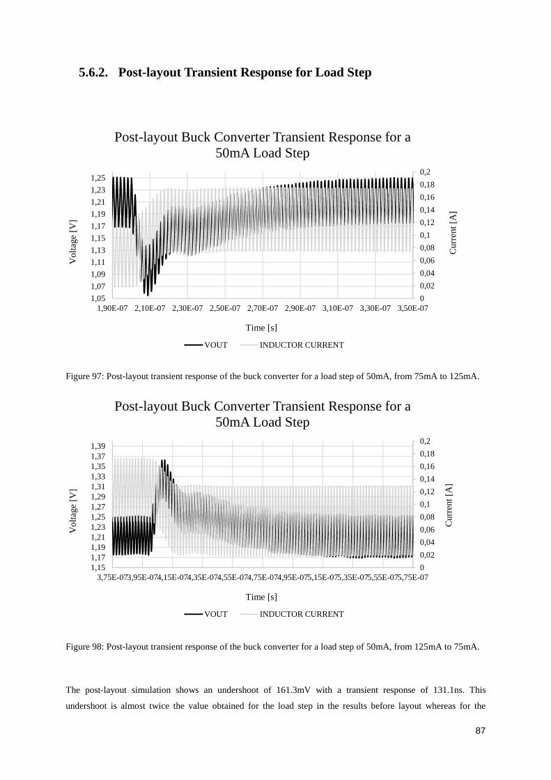
87
5.6.2. Post-layout Transient Response for Load Step
Figure 97: Post-layout transient response of the buck converter for a load step of 50mA, from 75mA to 125mA.
Figure 98: Post-layout transient response of the buck converter for a load step of 50mA, from 125mA to 75mA.
The post-layout simulation shows an undershoot of 161.3mV with a transient response of 131.1ns. This
undershoot is almost twice the value obtained for the load step in the results before layout whereas for the
0
0,02
0,04
0,06
0,08
0,1
0,12
0,14
0,16
0,18
0,2
1,05
1,07
1,09
1,11
1,13
1,15
1,17
1,19
1,21
1,23
1,25
1,90E-07 2,10E-07 2,30E-07 2,50E-07 2,70E-07 2,90E-07 3,10E-07 3,30E-07 3,50E-07
Cur
rent
[A
]
Vol
tage
[V
]
Time [s]
Post-layout Buck Converter Transient Response for a50mA Load Step
VOUT INDUCTOR CURRENT
0
0,02
0,04
0,06
0,08
0,1
0,12
0,14
0,16
0,18
0,2
1,151,171,191,211,231,251,271,291,311,331,351,371,39
3,75E-073,95E-074,15E-074,35E-074,55E-074,75E-074,95E-075,15E-075,35E-075,55E-075,75E-07
Cur
rent
[A
]
Vol
tage
[V
]
Time [s]
Post-layout Buck Converter Transient Response for a50mA Load Step
VOUT INDUCTOR CURRENT
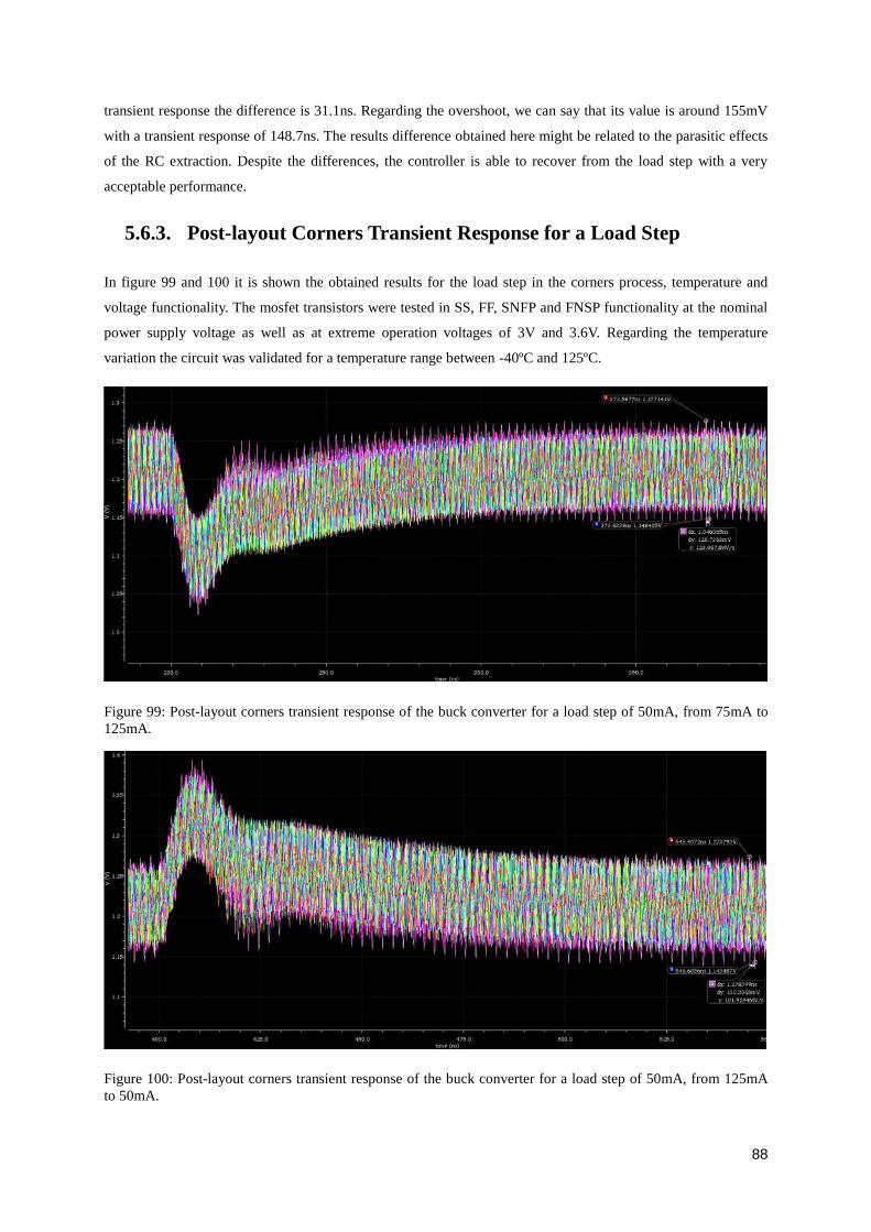
88
transient response the difference is 31.1ns. Regarding the overshoot, we can say that its value is around 155mV
with a transient response of 148.7ns. The results difference obtained here might be related to the parasitic effects
of the RC extraction. Despite the differences, the controller is able to recover from the load step with a very
acceptable performance.
5.6.3. Post-layout Corners Transient Response for a Load Step
In figure 99 and 100 it is shown the obtained results for the load step in the corners process, temperature and
voltage functionality. The mosfet transistors were tested in SS, FF, SNFP and FNSP functionality at the nominal
power supply voltage as well as at extreme operation voltages of 3V and 3.6V. Regarding the temperature
variation the circuit was validated for a temperature range between -40ºC and 125ºC.
Figure 99: Post-layout corners transient response of the buck converter for a load step of 50mA, from 75mA to125mA.
Figure 100: Post-layout corners transient response of the buck converter for a load step of 50mA, from 125mAto 50mA.

89
The results shows a voltage ripple of 130mV for the worst case corner, mosfets process corner at SS for an
operating voltage of 3.6V and 125ºC). The worst case transient response lies between 160ns to 170ns.
5.7. Final Results
The obtained final results are given in the table below.
Technology UMC 130nm MM/RF
Analog Core Area 2.46mm2
Parameter Symbol Min Typ Max Units Comments
Operating JunctionTemperature
Tj -40 25 125 ºC
Supply Voltage Vin 2.6 3.3 3.6 V
Output Voltage Vout 1.213 V
Output VoltageRipple
∆Vo 85 mV
Output Current Io 75 mA
Maximum OutputCurrent
Iomax 125 mA
Load TransientResponse
Trlo < 150 ns For a load step of 50mA.
Line TransientResponse
Trli < 5 µs For a line step from 2.8V up to 4.2V.
Switching Frequency Fsw 380 518 580 MHz
Integrated InductorL 13 nH
DCR 6 Ω
Integrated CapacitorCout 5 nF
ESR 0.7 Ω
Nominal Efficiency ηnom 26.5 %Efficiency at the nominal output
voltage 1.21V and current 75mA.
Table 12: Final characteristics Summary of the designed dc-dc buck converter.

90

91
6. Conclusion
To the knowledge of the author, this is the first fully integrated dc-dc buck converter operating at 500MHz
employing voltage-mode pwm control.
A fully integrated dc-dc buck converter operating at very-high frequency in a voltage mode control, to regulate
the output voltage, was presented and investigated for a CMOS 130nm technology. The control system has
proven to operate and regulate the output voltage of the converter with load variation from 90mW up to 150mW
over a power supply voltage from 2.8V to 3.6. The full integration of the inductor was accomplished and it was
demonstrated that it is possible to fully integrate such converter. An efficiency of 28.6% was achieved at nominal
operating condition for a conversion ratio from 3.3V to 1.2V taking into account the non-idealities of the
switches on-resistance and the parasitic resistance of the inductor. A considerable share of the converter power
losses occur mostly in the driver section of the power train and in the series resistance of the output inductor
filter.
The bond-wire played an important role in the circuit performance since they influence the switching behavior of
the converter in a way that the switching nodes present a superimposed resonance.
A more accurate value for the metals resistivity could certainly lead to better simulated results for the efficiency,
due to a lower value that would be obtained for the inductor DC resistance.
A different approach to the study of the stability has been presented, using periodic steady state simulations from
Cadence Spectre simulator. The obtained results with PSS plus PSTB analysis has proven to be accurate by
successfully modeling the frequency response of the converter and compensating the closed-loop feedback,
instead of constructing it equivalent linear circuit. This method has the advantage to assess all the control loop
parameters that sometimes are difficult to model, and because of that neglected, like for example the on-
resistance of the power switches, the parasitic capacitances from each block, the total delay of the system, etc.
Some problems have arisen during the progress of this work. Let’s consider the sawtooth generator example.
After the extraction of its layout parasitic elements, the switching frequency has seen its value decreased by
30%. This was due to the parasitic capacitances and resistance in the transistors and interconnections. After
identifying this problem, several iterations were performed, based on the estimation of the parasitic capacitances,
until the desired switching frequency was achieved. This value was slightly above from what it has been
projected although without affecting the system performance (3.6%). Also a minor problem was found during the
compensator implementation. The bandwidth of the operational transconductance amplifier influences the
overall frequency response of the compensator when high control crossover frequencies are desired. It was
identified in this work that the selected topology for the amplifier was almost at its limits to provide a good
performance in closed loop crossover frequency. What this means is that the frequency response of the
compensation circuit goes beyond the limit of the error amplifier gain-bandwidth product implying that its
internal GBW product sets the maximum closed-loop crossover frequency of the system. The only way to avoid
this problem are to stay below the GBW of the error amplifier or to re-design the amplifier that constitutes the
compensator in order to achieve a higher GBW product. This comes with an expense of more power
consumption, which means that with a carefully trade-off between the closed loop crossover frequency and the

92
amplifier power consumption, the necessary amplifier performance can be achieved, taking full advantage of the
best determined closed-loop crossover frequency with any of the two presented compensators.
The fully integration and high frequency operation of dc-dc converter will become a trend in the following years
for modern power electronics. The research has proven that this is an endless topic in power electronics.

93
7. Future Work
As a future work some improvements can be made. First, the efficiency of the converter should be improved
starting with an optimization of the driver section in the power train, since this was the major source of power
losses in this work.
The proposed inductor should be measured to obtain the DC resistance. For that an individual inductor with
PADs should be designed. Because the resistance value is low, an accurate measure is difficult to obtain due the
test setup parasitic resistance. Calibration techniques must be employed.
If the operation of the converter at light load is desired for future applications, the PFM operation should be
implemented, since it presents better efficiency results when compared to the PWM mode of operation.
A different approach in the implementation of the sawtooth generator should be explored, since the actual
implementation performance depends on the power supply voltage.
Another problem that was identified regarding the high frequency operation was the delay, as the switching
period is so small the control loop is sensitive to the delay of the circuit. This way it is necessary to explore some
high-speed circuit design techniques to overcome this problem.
The layout of the output capacitor should be improved so that the output voltage ripple can be lowered and the
study of the inclusion of other types of capacitors in parallel with the MOSCAP, especially MIM and MOM
capacitors. The advantage of MIM capacitor is that they can be implemented at the top of the chip and therefore
above any kind of capacitor that implements the output capacitor filter

94

95
8. References
[1] S. Musunuri, P. L. Chapman, J. Zou, and C. Liu, “Design issues for monolithic dc–dc converters,” IEEE
Trans. Power Electron., vol. 20, no. 3, pp. 639–649, May 2005.
[2] Steyaert M., Van Breussegem T., Meyvaert H., Callemeyn P., Wens M., “DC-DC converters: From discrete
towards fully integrated CMOS”, in Proceedings of the European Solid-State Circuits Conference, pp. 42-49,
Sept. 2011.
[3] S.R. Sanders, E. Alon, Hanh-Phuc Le, M.D. Seeman, M. John, V.W. Ng, “The Road to Fully Integrated DC–
DC Conversion via the Switched-Capacitor Approach”, IEEE Trans. Power Electron., vol. 28, no. 9, pp. 4146–
4155, Sept. 2013.
[4] Gerard Villar-Piqué, Henk Jan Bergveld, and Eduard Alarcón, “Survey and Benchmark of Fully Integrated
Switching Power Converters: Switched-Capacitor Versus Inductive Approach”, IEEE Trans. Power Electron.,
vol. 28, no. 9, pp. 4156–4167, Sept. 2013.
[5] J. Wibben and R. Harjani, “A high-efficiency DC-DC converter using 2nH integrated inductors”, IEEE J.
Solid-State Circuits, vol. 43, no. 4, pp. 844–854, Apr. 2008.
[6] Wens M., Cornelissens K., Steyaert M., "A Fully-Integrated 130nm CMOS DC-DC Step-Down Converter,
Regulated by a Constant On/Off-Time Control System", in Proceedings of European Solid-State Circuits
Conference, 34, pp. 62-65, Sep 2008.
[7] M. Wens and M. Steyaert, “An 800mW fully-integrated 130nm CMOS DC-DC step-down multi-phase
converter, with on-chip spiral inductors and capacitors”, in Proc. IEEE Energy Convers. Congr. Expo., pp. 3706–
3709, Sep. 2009.
[8] S. S. Kudva and R. Harjani, “Fully-integrated on-chip DC-DC converter with a 450X output range”, IEEE J.
Solid-State Circuits, vol. 46, no. 8, pp. 1940–1951, Aug. 2011.
[9] N. Jinhua, Z. Hong, and B. Y. Liu, “Improved on-chip components for integrated DC-DC converters in
0.13μm CMOS”, in Proc. IEEE Eur. Solid-State Circuits Conf., pp. 448–451, Sept. 2009.

96
[10] S. Abedinpour, B. Bakkaloglu, and S. Kiaei, “A multistage interleaved synchronous buck converter with
integrated output filter in 0.18μm SiGe process”, IEEE Trans. Power Electron., vol. 22, no. 6, pp. 2164–2175,
Nov. 2007.
[11] P. Hazucha, G. Schrom, J. Hahn, B. A. Bloechel, P. Hack, G. E. Dermer, S. Narendra, D. Gardner, T. Karnik,
V. De, and S. Borkar, “A 233-MHz 80%-87% efficient four-phase dc–dc converter utilizing air-core inductors on
package”, IEEE J. Solid-State Circuits, vol. 40, no. 4, pp. 838–845, Apr. 2005.
[12] B. Razavi, Design of Analog CMOS Integrated Circuits. McGraw Hill Higher Education, first edition ed.,
10 2003.
[13] M. Wens and M. Steyaert, Design and Implementation of Fully-Integrated Inductive DC-DC Converters in
Standard CMOS (Analog Circuits and Signal Processing). Springer, 1st edition. ed., 5 2011.
[14] A. S. Sedra and K. C. Smith, Microelectronic Circuits. Revised Edition (Oxford Series in Electrical and
Computer Engineering). Oxford University Press, USA, 5 har/cdr ed., 8 2007.
[15] Robert W. Erickson and Dragan Maksimovic, Fundamentals of Power Electronics. Kluwer Academic
Publishers, Second edition ed., 2004.
[16] Ned Mohan, Power Electronics: A first Course. Wiley, First edition ed., 2011.
[17] Willy M. C. Sansen, Analog Design Essentials. Springer, First edition ed., 2006.
[18] A. Hastings, The Art of Analog Layout. Pearson Education, First edition ed., 2005.
[19] Marian K. Kazimierczuk, “Pulse-width Modulated DC-DC Power Converters”, Wiley, First edition ed.,
2008.
[20] Christophe Basso, “Switch-Mode Power Supplies Spice Simulations and Practical Designs”, McGraw Hill,
First edition ed., 2008.

97
[21] Shen, Z. J., Yali Xiong, Xu Cheng, Yue Fu, Kumar P., “Power MOSFET Switching Loss Analysis: A New
Insight”, IEEE Industry Applications Conference Record, vol. 3, Apr. 2006.
[22] A. J. Strakakos, S. R. Sanders, R. W. Brodersen, “A low-voltage CMOS DC-DC converter for a portable
battery-operated system”, IEEE Power Electronics Specialists Conference, PESC ’94 Record, 20-25 June 1994,
Volume 1, pp. 619 – 626.
[23] N. C. Li, G. L. Haviland, and A. A. Tuszynski, “CMOS tapered buffer”, IEEE J. Solid-State Circuits, Vol.
25, no. 4, pp. 1005, Aug. 1990.
[24] R. D. Middlebrook and S. Cuk, “A general unified approach to modeling switching-converter power
stages”, Int. J. Electronics, vol. 42, no. 6, pp. 521-550, June 1977.
[25] Cadence, “Virtuoso Spectre circuit simulator rf analysis theory”.
[26] Lei Liao et al. “An integrated voltage-mode pwm controlled buck converter with active compensation”,
IEEE Electronics, Circuits, and Systems (ICECS), 7th IEEE International conference, 2010.
[27] Philip E. Allen, Douglas R. Holberg, “CMOS Analog Circuit Design”. Oxford University Press, Second
edition ed., 2002.
[28] R. Jacob Baker, “CMOS: Circuit Design, Layout, and Simulation”, 3rd Edition. Pearson Education, Third
ed., 2011.
[29] Ned Mohan, Tore M. Undeland, William P. Robbins, “Power Electronics: Converters, Applications”, Wiley,
Third ed., 2003.
[30] Mike Wens, Michiel Steyaert, “Design and Implementation of Fully-Integrated Inductive DC-DC
Converters in Standard CMOS”, Springer, First ed., 2011.
[31] Roubik Gregorian, “Introduction to CMOS op-amps and comparators”, Wiley, First ed., 1999.

98
[32] Rashid, Muhammad H., “Power Electronics Handbook”, Academic Press, First ed., 2001.
Top Related